

Clifton LAboratories Z10042AV Assembly And Operation Manual
Z10042AV
Broadband Norton Amplifier
Ass embly and Op eratio n Manual
Revised 23 October 2010
Clifton Laboratories
7236 Clifton Road
Clifton, VA 20124
(703) 830 0368
www.cliftonlaboratories.com

Table of Contents
Model Z10042AV Broadband Norton Amplifier ......................................................................................................... 3
Trademarks and Copyright ......................................................................................................................................... 3
Warranty ............................................................................................................................................................................ 3
Safety Information .............................................................................................................................................................. 4
General Information and Specifications .................................................................................................................... 4
Description ........................................................................................................................................................................ 5
Specifications .................................................................................................................................................................... 7
Assembly ................................................................................................................................................................................ 8
Parts Provided .................................................................................................................................................................. 8
Errata: ............................................................................................................................................................................... 11
Overview of Installing Surface Mount Parts ..................................................................................................... 11
Component Location .................................................................................................................................................. 14
Assembly Order ............................................................................................................................................................ 15
Post Construction Adjustment and Checkout .................................................................................................. 23
Input and Output Connections ............................................................................................................................... 26
Schematic and Theory of Operation and Troubleshooting .................................................................................. 30
Theory of Operation ................................................................................................................................................... 30
Schematic ........................................................................................................................................................................ 34
Voltage and Resistance Troubleshooting Data ................................................................................................ 35
Appendix A Typical Performance Data ......................................................................................................................... 36
Bandwidth ........................................................................................................................................................................... 36
Appendix B – PCB Mounting Hole Dimensions ......................................................................................................... 38
Appendix C – Norton Amplifier Patent, US Patent No. 3,891,934 ..................................................................... 39
Appendix D Manual Backdating ...................................................................................................................................... 45
Z10042AV Construction and Operations Manual Page 1
Applicability of Manual
This manual applies to the Z10042AV printed circuit board revision 1.0 and later. The circuit
board revision is silk screened on the PCB, just below the model number.
Z10042AV Construction and Operations Manual Page 2

Model Z10042AV Broadband Norton Amplifier
Revised 23 Octo ber 20 10
(c) 2010 Ja ck R. Smith d/b/a/ Clift on Laboratories.
Trademarks and Copyright
Material in this document copyrighted © 2010 Clifton Laboratories. All rights reserved. It is
provided to allow the Z10042AV purchasers to maintain their equipment and such other purposes
as may not be prohibited by law.
Warranty
This warranty is effective as of the date of first consumer purchase.
What is covered: During the ninety (90) days after date of purchase, Clifton Laboratories will
correct any defects in the Z10042AV due to defective parts or workmanship (if purchased as an
assembled unit) free of charge (post-paid). You must send the unit at your expense to Clifton
Laboratories, but we will pay return shipping. Clifton Laboratories’ warranty does not extend to
defects caused by your incorrect assembly or use of unauthorized parts or materials or
construction practices.
What is not covered: If the Z10042AV is purchased as a kit, this warranty does not cover
correction of assembly errors or misalignment; repair of damage caused by misuse, negligence, or
builder modifications; or any performance malfunctions involving non-Clifton Laboratories
accessory equipment. The use of acid-core solder, water-soluble flux solder, or any corrosive or
conductive flux or solvent will void this warranty in its entirety. Damage to the Z10042AV or
equipment connected to it caused by lightning strikes is not covered under the warranty. Whether
purchased as an assembled unit or as a kit, also not covered is reimbursement for loss of use,
inconvenience, customer assembly or alignment time, or cost of unauthorized service.
Limitation of incidental or consequential damages: This warranty does not extend to nonClifton Laboratories equipment or components used in conjunction with our products. Any such
repair or replacement is the responsibility of the customer. Clifton Laboratories will not be liable for
any special, indirect, incidental or consequential damages, including but not limited to any loss of
business or profits.
Under no circumstances is Clifton Laboratories liable for damage to your equipment
connected to the Z10042AV resulting from use of the Z10042AV, whether in accordance with
the instructions in this Manual or otherwise.
Z10042AV Construction and Operations Manual Page 3

Safety Information
The Z10042AV operates with a user-supplied DC power supply of 13 to 15 Volts at 100 to 120 mA.
The Z10042AV, although designed as a low signal level preamplifier, is capable of RF output power
approaching the 1 watt level. This output power is capable of damaging receivers or the receiver
section of a transceiver or test equipment. It is the user’s responsibility to ensure that the
Z10042AV is properly connected to whatever devices it will be used with.
The Z10042AV has no replaceable fuses; rather a self-resetting polyfuse limits short circuit current
to approximately 200 mA.
The Z10042AV is designed to be used only with receive-type power levels. It should not be used
with transmitting equipment. The Z10042AV’s maximum permitted input RF power is 100 mW
(+20 dBm). Power in excess of this level may damage the Z10042AV or equipment connected to it, or
both. In addition, since the Z10042AV has appreciable gain, output power levels sufficient to damage
connected equipment may occur with input signal levels well below +20 dBm.
Although the Z10042AV contains protective measures, all of these protection measures assume that
the Z10042AV is properly grounded and that good engineering practices have been used in its
installation and construction of the ground system. The Z10042AV is not intended to survive a
direct lightning strike to an antenna connected to its input, whether powered up or not. However,
the protective measures incorporated into the Z10042AV’s design should aid in reducing damage.
Z10042AV Construction and Operations Manual Page 4

General Information and Specifications
Description
The term “Norton Amplifiers” refers to a class of transformer feedback amplifiers developed by Dr.
David Norton and described in his US Patent No. 3,891,934, granted June 24, 1975 and now in the
public domain. (A copy of Dr. Norton’s patent is Appendix C to this Manual.) A Norton amplifier
permits the distortion reducing benefits of negative feedback to be applied without impairing the
amplifier’s noise figure. Hence, Norton amplifiers are also known as “noiseless feedback” amplifiers.
The Z10042AV is a broadband (25 KHz to 20 MHz) Norton-style amplifier providing 11 dB gain
(other gain values are possible) with very high 3rd order and 2nd order intermodulation intercepts,
IP3 and IP2, respectively, with a noise figure of approximately 2 dB. The Z10042AV is designed for
either indoor or outdoor use, with DC power supplied through either separate connections or
duplexed over the output coaxial cable. Optional indoor and outdoor die cast enclosures are
available for the Z10042AV.
The Z10042AV is derived from the Norton Amplifier developed by Dr. Dallas Lankford and
described in his publication Common Base Transformer Feedback Norton Amplifiers, dated 8 June
1994, revised 21 May 2007, available at
http://www.kongsfjord.no/dl/Amplifiers/Common%20Base%20Transformer%20Feedback%20N
orton%20Amplifiers.pdf.
The Z10042AV modifies Dr. Lankford’s design in several respects:
Automatic input disconnect upon DC power removal along with over-voltage gas trap
protection
Over voltage and reverse voltage protection on the DC Power.
DC power either separately or duplex power.
Optional balanced or unbalanced input.
Shunt fed to reduce effect of DC saturation of T2 and T4
Component values selected to extend lower -3 dB point to approximately 30 KHz.
Clifton Laboratories also offers the Z1203A DC power injector usable with the Z10042AV to provide
DC power over the output coaxial cable. This is useful for remote mounted amplifiers.
The Z10042AV is available as a kit, including a double sided, silk screened solder masked printed
circuit boards and all electronic parts or as an assembled and tested printed circuit board. Options
include an indoor enclosure with BNC connectors or an outdoor weatherproof die cast enclosure
with a choice of BNC, UHF or Type N connectors.
Typical kit construction time is three to five hours depending on your work practices. The kit is
suitable for relatively inexperienced builders, although Clifton Laboratories does not recommend it
to purchasers who have never built an electronic kit before. Also, if you have never wound a toroid
inductor or transformer, you might wish to ask an experienced builder to show you how it’s done.
Z10042AV Construction and Operations Manual Page 5

The Z10042AV is generally electrically similar to the Z10042A, but has a revised printed circuit
board layout to accommodate components required for low frequency extension. In addition, a few
of the Z10042A’s through-hole components are replaced with surface mount equivalents in the
Z10042AV layout.
Other than frequency response, the Z10042AV’s performance matches the Z10042A. The
differences in performance, design and construction are:
Feedback transformers T2 and T4 wound with 2:22:8 turns instead of 1:11:4. This change is
required to increase magnetizing inductance to support operation below 100 KHz.
Upper -3 dB point reduced to 20 MHz, mostly a consequence of increased capacitance in T2
and T4 from doubling the number of turns.
RF chokes L1-L4 increased in value to improve low frequency response. L2 and L4 relocated
to bottom board surface for improved clearance.
Reverse polarity protection diode D1 replaced with surface mount diode.
Overload protection resettable fuse F1 replaced with surface mount version
Spark gaps SA1 and SA2 replaced with surface mount version
DC power feed and duplex power jumper consolidated into single connector and circuit
revised so that DC power is always fed through L5, to reduce possible noise riding on power
feed.
DC power/power mode J3 now male connector for improved safety. (DC power supplied
with matching female connector which avoids inadvertent short circuits.)
RF choke L5 replaced with surface mount version.
General PCB cleanup, with added jumper and connector information appearing on silk
screen.
Z10042AV Construction and Operations Manual Page 6

Specifications
Parameter
Value
PCB Dimensions
3.50” x 2.50” x 0.75” vertical clearance required. (88.9mm x 63.5mm x 19mm).
Four mounting holes for 4-40 screws provided, template in Appendix B.
DC Power Required
Maximum: 15V
Minimum: 13.8V [may not meet specifications below this voltage. See Appendix
D for performance versus supply voltage considerations.]
Negative to ground, typical DC current 60-100 mA depending on bias
adjustment.
As an option, a reduced power version of the Z10042AV is available, with
approximately 25 mA, usable down to 12V input. 2nd and 3rd order
intermodulation performance is degraded with this option; noise figure is
improved over normal idle current.
Maximum RF Power
Input
Do not exceed 100 milliwatts (+20 dBm). IP3 performance specifications are
based upon -10 dBm signal input; performance not warranted at greater input
levels.
Test Conditions
Performance data is for a 2:22:8 turns ratio design, 13.8 VDC after adjusting
balance trimpots for minimum 2nd harmonic distortion. Unless otherwise
indicated, performance measurements are made with direct DC power, not
duplexed. Figures stated as “typical” are not warranted.
3 dB Bandwidth
30 KHz – 20 MHz.
2nd and 3rd Order
Intermodulation
Intercept
Measured with 3 and 4 MHz input tones, adjusted for 0 dBm output from the
Z10042AV. Protocol as discussed later in this manual. Intercepts are output
referenced.
OIP2: +80 dBm (typically > +90 dBm)
OIP3: +45 dBm (typically +46 to +48 dBm)
Gain
11 dB nominal at 1 MHz.
1 dB Gain
Compression
+19 dBm input.
Noise Figure
2.5 dB maximum 10-30 MHz. Typically 2 dB or less at 10 MHz.
Input VSWR
When terminated with 50 ohm load, input VSWR is less than 2:1 over the range
300 KHz – 30 MHz, and is typically below 1.5:1 over this range.
Common Mode
Rejection in
Balanced Input
Mode
Typically 50 dB at 1 MHz, decreases with increasing frequency.
Z10042AV Construction and Operations Manual Page 7
Assembly
Photograph
Qty
ID
Description and
Comments
Component
Marking
5
C2, C4, C7,C10, C18,
1u0 X7R 25V, 1206 size
surface mount ceramic
capacitors.
None
Same as above
7
C3, C6, C11, C14,
C15, C16, C17
2u2 X7R 25V, 1206 size
surface mount ceramic
capacitors.
None
Same as above
4
C20,C21,C22, C23
10pF, C0G 50V, 1206
size surface mount
ceramic capacitors
None
Same as above
2
C5, C8
1000pF, C0G 50V, 1206
size surface mount
ceramic capacitors
None
1
C19
10uF/25V 105°C
aluminum electrolytic
capacitor.
10 EHA
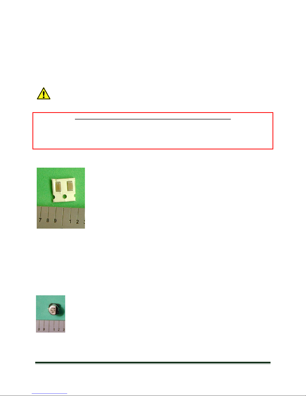
Parts Provided
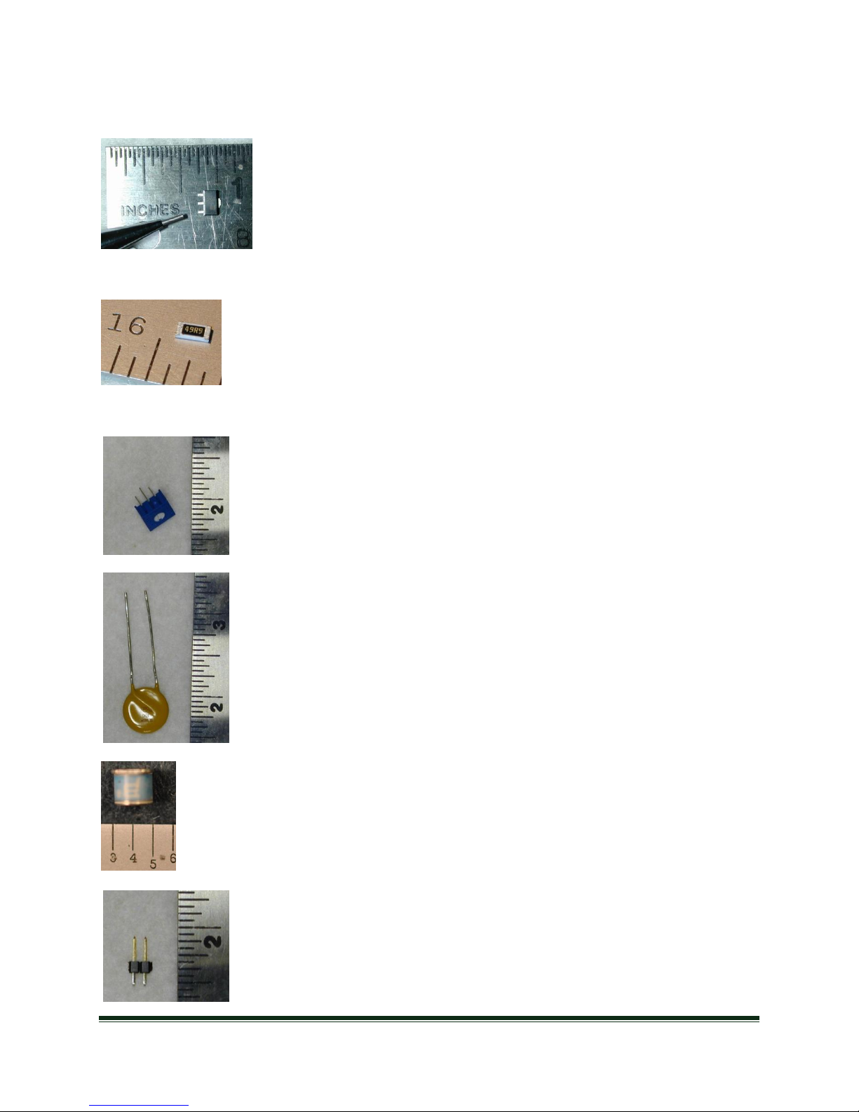
Before starting your build, please take a moment and inventory the parts provided against the list
below. The ruler is marked in decimal (tenths) inches. One inch is 25.4mm and 0.1 inch is 2.54mm.
(Some older photos use a ruler marked in fractions of an inch, such as 1/16th.)
Many parts in this kit are not marked and can easily be confused. Parts are provided in
individually labeled paper envelopes. Please keep parts in the associated envelope when not
being installed.
A note on how component values are identified in this manual
This document follows the international practice of using the value multiplier to indicate the
decimal point. Thus, a 1.0µF capacitor is identified as 1µ0 and a 10,000 ohm resistor is identified as
10K0.
Z10042AV Construction and Operations Manual Page 8
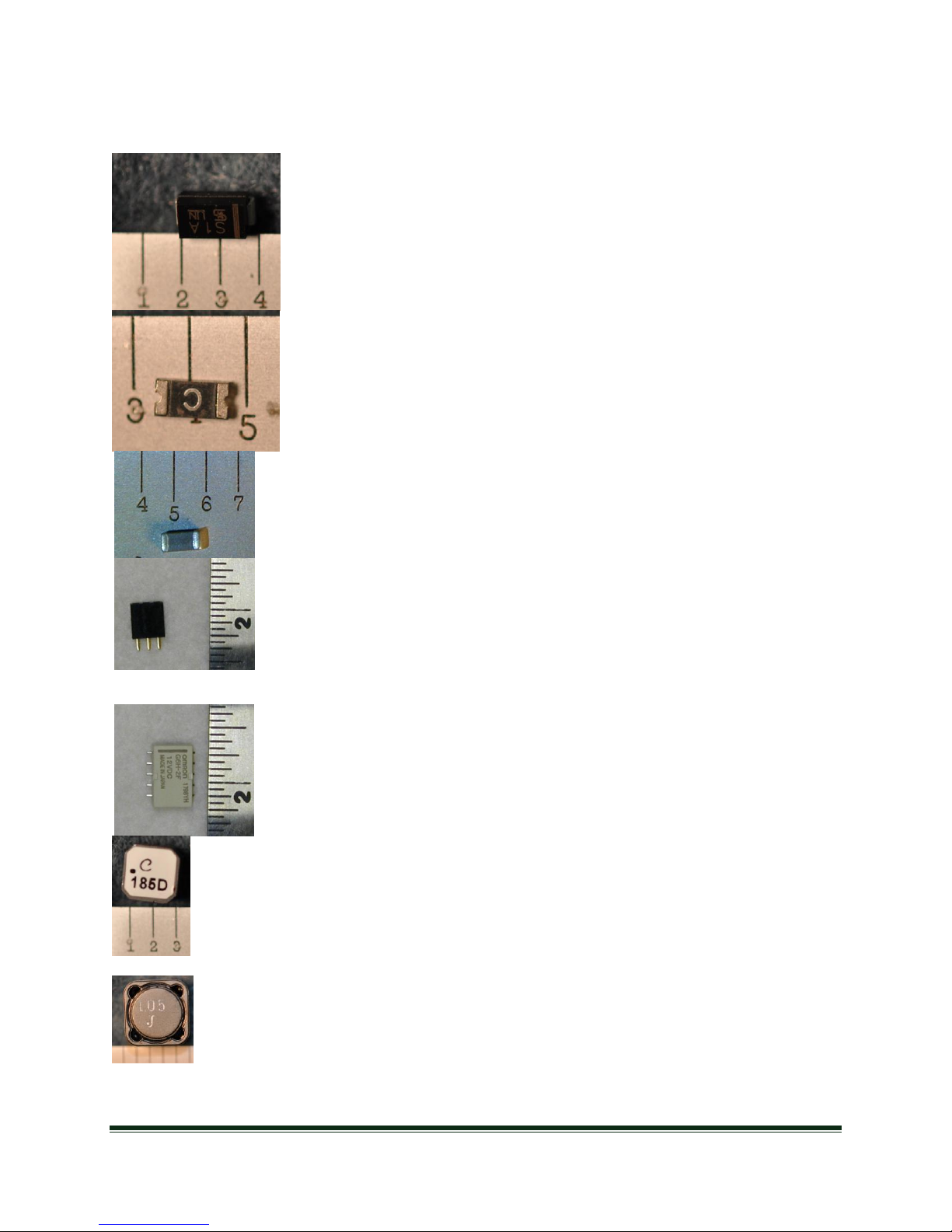
Photograph
Qty
ID
Description and
Comments
Component
Marking
1
D1
Silicon diode, 1A or
greater, 50V or greater.
Typically a S1A part
S1A
1
F1
200 mA Raychem
“polyfuse” PTC varistor,
surface mount 1206
size.
C
2
FB1,FB3
Surface mount ferrite
bead
None
2 [3place]
1 [4place]
J1, J2 and input for
J3.
J1: 4-place
J2: 3-place
0.1-inch header
sockets
J3: 4 place 0.1-inch
header pins
None
1
K1
G6H-2F-DC12 double
pole, double throw 12V
surface mount relay
G6H-2F12VDC
2
L1 & L3
2m2 RF choke
(shielded)
225D
2
L2 & L4
3m3 RF choke (shielded)
335D
1
L5
1m0 RF choke (shielded)
105J
Z10042AV Construction and Operations Manual Page 9
Photograph
Qty
ID
Description and
Comments
Component
Marking
2
Q1, Q2
NPN transistor, UHF,
type NE85634, SOT-89
package
RE
¼ watt, 1% 1206 Surface Mount Resistors
2
R1,R6
560R
5600
2
R4,R12
49R9
49R9
2
R10, R5
1K50
1501
4
R2, R7,
R9,R11
10R0
10R0
2
R3, R8
100R Trim-pot
101
1
RV1
14mm dia. 18V overvoltage MOV
180M
2
SA1, SA2
Spark gap
90V
11
J4
Total of 11 pins
supplied. Pins are 0.1
inch spaced, 0.025 inch
square gold flashed. 4
pins to mate with J1; 3
pins to mate with J2 and
None
Z10042AV Construction and Operations Manual Page 10

Photograph
Qty
ID
Description and
Comments
Component
Marking
4 pins for J3.
4
T1,T2,T3, T4
0.5 inch diameter ferrite
cores; relative
permeability 5K, builder
to wind.
None
1
PCB
Printed circuit board.
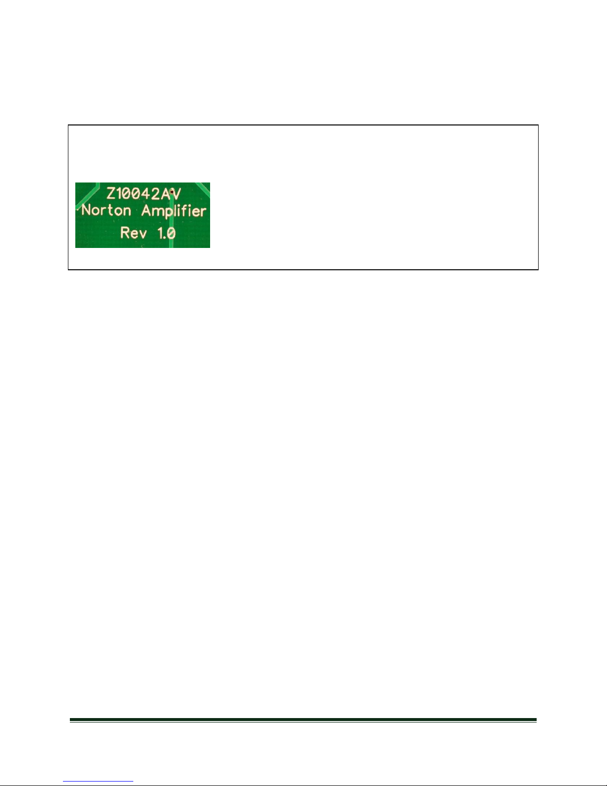
Identified as Z10042AV
Z10042AV
and revision
number
None
1 length #24
wire (64
inches/1.625m)
red; 1 length
#24 wire (12
inches/480mm)
green.
None
No. 24 AWG magnet
wire, use for T2 and T4.
(The two lengths will be
different color; usually
the long wire will be red
and the short green, but
this may be reversed
depending upon wire
stocks.)
None
None
2 lengths #26
wire
None
No. 26 AWG magnet
wire, use for T1 and T3.
One length red, one
length green.
None
None
2 inches
(50mm) foam
tape
None
Length of ¼ inch (6mm)
wide, double sided
foam tape
None
Errata:
None known for revision 1.0
Overview of Installing Surface Mount Parts
1. You may wish to apply a sparing amount of liquid flux to pads before
soldering. Clifton Laboratories uses MG Chemical flux, part number 835100ML (also available as a flux pen, part number 835-P.) Both products are
available from Mouser and other suppliers. To apply liquid flux, a wooden
toothpick may be used or the flux can be dispensed from a needle oiler. (If
using the flux pen, wipe it across pads before soldering.) MG Chemicals 835
flux leaves a distinct residue. The residue
Z10042AV Construction and Operations Manual Page 11
will not damage the board but if desired, it
may be removed with flux remover or 91%
isopropyl alcohol available locally.

2. If the component has one pad that is a ground, lightly tin the non-ground pad. If neither pad
is a ground connection, tin either one of the pads.
3. Using forceps or a very light touch with long nose pliers, slide the component into place
while heating the tinned pad. Check that the component is more or less centered on the
pads and remove the soldering iron when centered. Too much pressure will crack these
parts so use a light touch.
4. Solder the other pad. Touch up the first pad if necessary.
5. Although the Z10042AV’s ground pads use “thermal relief” it may still be difficult to make
with a small soldering pencil, as the large foil area requires more heat capacity than a
normal floating pad.
Z10042AV Construction and Operations Manual Page 12
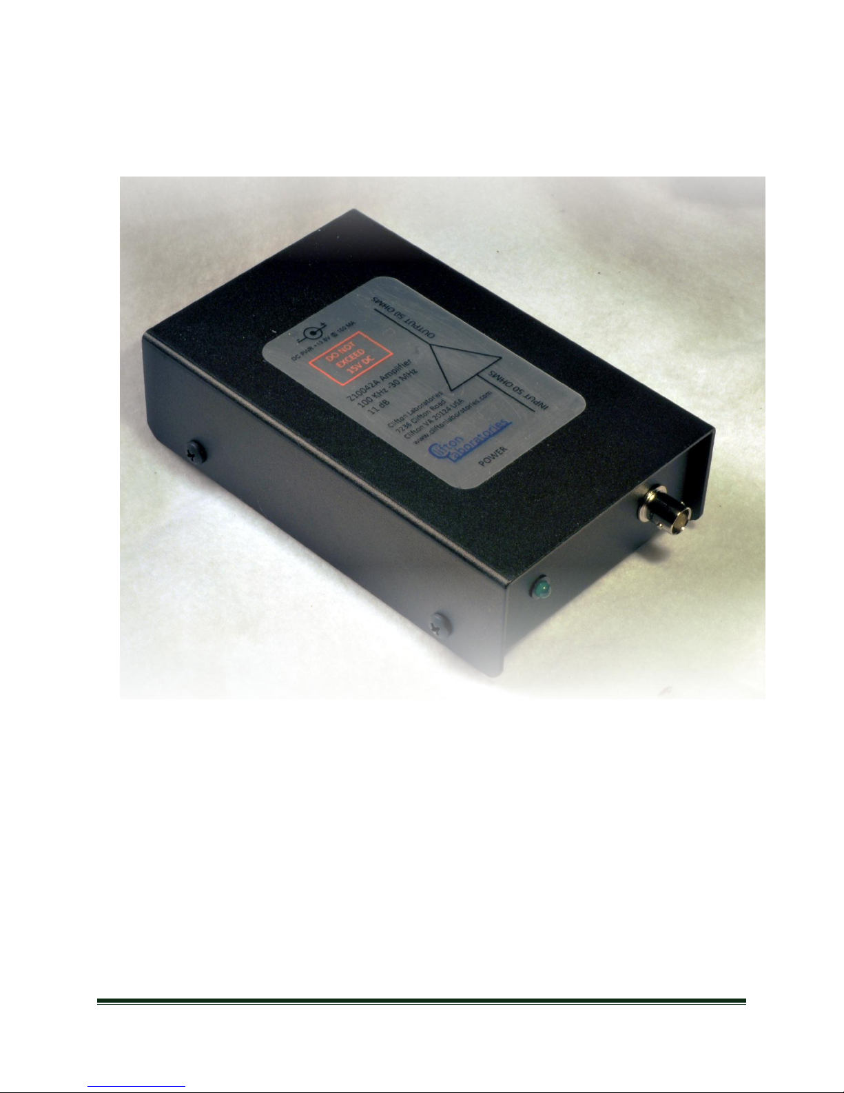
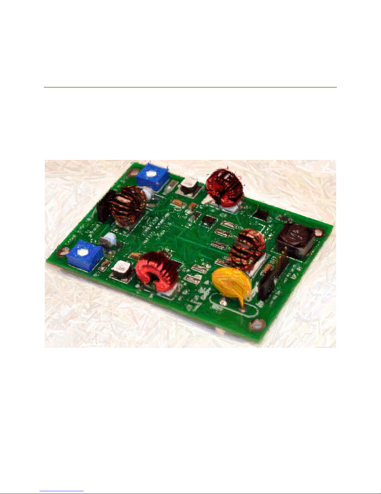
The image below shows a Z10042AV installed in the optional enclosure. (The label is for a
Z1002A amplifier.)
Z10042AV Construction and Operations Manual Page 13
 Loading...