

Page 1

Page 2

Page 3

Notebook Computer
X7200
Service Manual
Preface
Preface
I
Page 4

Preface
Preface
Notice
The company reserves the right to revise this publication or to change its contents without notice. Information contained
herein is for reference only and does not constitute a commitment on the part of the manufacturer or any subsequent vendor. They assume no responsibility or liability for any errors or inaccuracies that may appear in this publication nor are
they in anyway responsible for any loss or damage resulting from the use (or misuse) of this publication.
This publication and any accompanying software may not, in whole or in part, be reproduced, translated, transmitted or
reduced to any machine readable form without prior consent from the vendor, manufacturer or creators of this publication, except for copies kept by the user for backup purposes.
Brand and product names mentioned in this publication may or may not be copyrights and/or registered trademarks of
their respective companies. They are mentioned for identification purposes only and are not intended as an endorsement
of that product or its manufacturer.
Version 1.0
September 2010
Trademarks
Intel and Intel Core are trademarks of Intel Corporation.
Windows® is a registered trademark of Microsoft Corporation.
Other brand and product names are trademarks and /or registered trademarks of their respective companies.
II
Page 5

About this Manual
This manual is intended for service personnel who have completed sufficient training to undertake the maintenance and
inspection of personal computers.
It is organized to allow you to look up basic information for servicing and/or upgrading components of the X7200 series
notebook PC.
The following information is included:
Chapter 1, Introduction, provides general information about the location of system elements and their specifications.
Chapter 2, Disassembly, provides step-by-step instructions for disassembling parts and subsystems and how to upgrade
elements of the system.
Preface
Appendix A, Part Lists
Appendix B, Schematic Diagrams
Appendix C, Updating the FLASH ROM BIOS
Preface
III
Page 6

Preface
Preface
IMPORTANT SAFETY INSTRUCTIONS
Follow basic safety precautions, including those listed below, to reduce the risk of fire, electric shock and injury to persons when using any electrical equipment:
1. Do not use this product near water, for example near a bath tub, wash bowl, kitchen sink or laundry tub, in a wet
basement or near a swimming pool.
2. Avoid using a telephone (other than a cordless type) during an electrical storm. There may be a remote risk of electrical shock from lightning.
3. Do not use the telephone to report a gas leak in the vicinity of the leak.
4. Use only the power cord and batteries indicated in this manual. Do not dispose of batteries in a fire. They may
explode. Check with local codes for possible special disposal instructions.
5. This product is intended to be supplied by a Listed Power Unit with an AC Input of 100 - 240V, 50 - 60Hz, DC Output
of 20V, 15A (300W) minimum AC/DC Adapter.
This Computer’s Optical Device is a Laser Class 1 Product
IV
FCC Statement
This device complies with Part 15 of the FCC Rules. Operation is subject to the following two conditions:
This device may not cause harmful interference.
This device must accept any interference received, including interference that may cause undesired operation.
Page 7
Instructions for Care and Operation
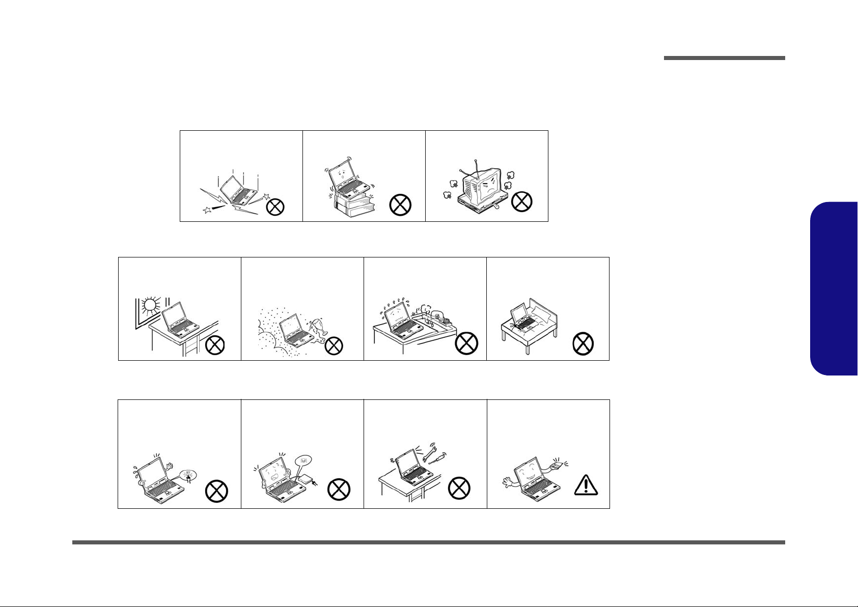
The notebook computer is quite rugged, but it can be damaged. To prevent this, follow these suggestions:
1. Don’t drop it, or expose it to shock. If the computer falls, the case and the components could be damaged.
Preface
Do not expose the computer
to any shock or vibration.
Do not place it on an unstable
surface.
Do not place anything heavy
on the computer.
2. Keep it dry, and don’t overheat it. Keep the computer and power supply away from any kind of heating element. This
is an electrical appliance. If water or any other liquid gets into it, the co mputer could be badly damaged.
Do not expose it to excessive
heat or direct sunlight.
Do not leave it in a place
where foreign matter or moisture may affect the system.
Don’t use or store the computer in a humid environment.
Do not place the computer on
any surface which will block
the vents.
3. Follow the proper working procedures for the computer. Shut the computer down properly and don’t forget to save
your work. Remember to periodically save your data as data may be lost if the battery is depleted.
Do not turn off the power
until you properly shut down
all programs.
Do not turn off any peripheral
devices when the computer is
on.
Do not disassemble the computer by yourself.
Perform routine maintenance
on your computer.
Preface
V
Page 8
Preface
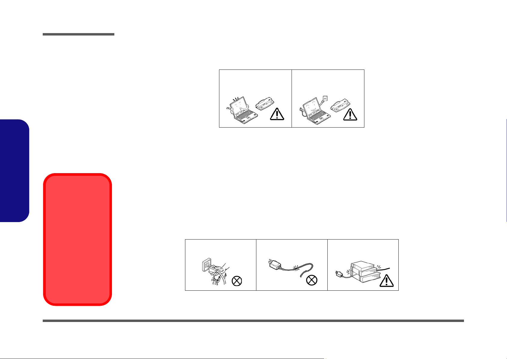
Power Safety
Warning
Before you undertake
any upgrade procedures, make sure that
you have turned off the
power, and disconnected all peripherals
and cables (including
telephone lines). It is
advisable to also remove your battery in
order to prevent accidentally turning the
machine on.
4. Avoid interference. Keep the computer away from high capacity transformers, electric motors, and oth er strong mag-
netic fields. These can hinder proper performance and damage your data.
5. Take care when using peripheral devices.
Preface
VI
Use only approved brands of
peripherals.
Unplug the power cord befor e
attaching peripheral devices.
Power Safety
The computer has specific power requirements:
• Only use a power adapter approved for use with this computer.
• Your AC adapter may be designed for international travel but it still requires a stea dy, uninterrupted po wer supply. If you ar e
unsure of your local power specifications, consult your service representative or local power company.
• The power adapter may have either a 2-prong or a 3-prong grounded plug. The third prong is an important safety feature; do
not defeat its purpose. If you do not have access to a compatible outlet, have a qualified electrician install one.
• When you want to unplug the power cord, be sure to disconnect it by the plug head, not by its wire.
• Make sure the socket and any extension cord(s) you use can support the total current load of all the connected devices.
• Before cleaning the computer, make sure it is disconnected from any external power supplies.
Do not plug in the power
cord if you are wet.
Do not use the power cord if
it is broken.
Do not place heavy objects
on the power cord.
Page 9

Battery Precautions
Battery Disposal
The product that you have purchased contains a rechargeable battery. The battery is recyclable. At the end of its useful life, under various state and local laws, it may be illegal to dispose of this battery into the municipal waste stream. Check with your local solid waste
officials for details in your area for recycling options or proper disposal.
Caution
Danger of explosion if battery is incorrectly replaced. Replace only with the same or equivalent type recommended by the manufacturer.
Discard used battery according to the manufacturer’s instructions.
Battery Level
Click the battery icon in the taskbar to see the current battery level and charge status. A battery that drops below a level of 10%
will not allow the computer to boot up. Make sure that any battery that drops below 10% is recharged within one week.
• Only use batteries designed for this computer. The wrong battery type may explode, leak or damage the computer.
• Do not continue to use a battery that has been dropped, or that appears damaged (e.g. bent or twisted) in any way. Even if the
computer continues to work with a damaged battery in place, it may cause circuit damage, which may possibly result in fire.
• Recharge the batteries using the notebook’s system. Incorrect recharging may make the battery explode.
• Do not try to repair a battery pack. Refer any battery pack repair or replacement to your service representative or qualified service
personnel.
• Keep children away from, and promptly dispose of a damaged battery. Always dispose of batteries carefully. Batteries may explode
or leak if exposed to fire, or improperly handled or discarded.
• Keep the battery away from metal appliances.
• Affix tape to the battery contacts before disposing of the battery.
• Do not touch the battery contacts with your hands or metal objects.
Battery Guidelines
The following can also apply to any backup batteries you may have.
• If you do not use the battery for an extended period, then remove the battery from the computer for storage.
• Before removing the battery for storage charge it to 60% - 70%.
• Check stored batteries at least every 3 months and charge them to 60% - 70%.
Preface
Preface
VII
Page 10
Preface
Shut Down
Note that you should always shut your computer down by
choosing Shut Down from the Start Menu. This will help
prevent hard disk or system problems.
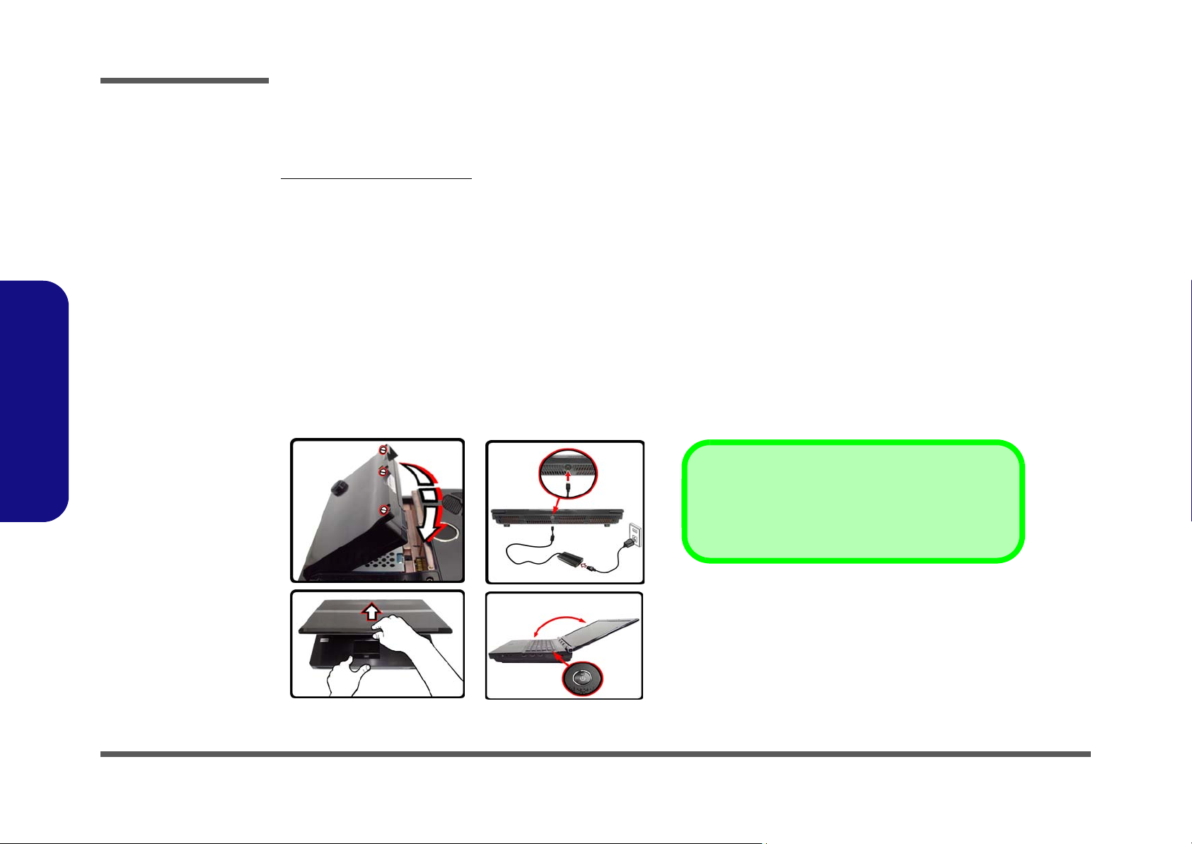
Figure 1 - Opening the Lid/LCD/Computer with AC/DC Adapter
Plugged-In
Preface
Related Documents
You may also need to consult the following manual for additional information:
User’s Manual on CD/DVD
This describes the notebook PC’s features and the procedures for operating the computer and its ROM-based setup program. It also describes the installation and operation of the utility programs provided with the notebook PC.
System Startup
1. Remove all packing materials.
2. Place the computer on a stable surface.
3. Insert the battery and tighten the screws.
4. Securely attach any peripherals you want to use with the computer (e.g. keyboard and mouse) to their ports.
5. Attach the AC/DC adapter to the DC-In jack at the rear of the computer, then plug the AC power cord into an outlet, and connect the AC power cord
to the AC/DC adapter.
6. Use one hand to raise the lid/LCD to a comfortable viewing angle (do not to exceed 135 degrees);
support the base of the computer (Note: Never lift the computer by the lid/LCD).
7. Press the power button to turn the computer “on”.
use the other hand (as illustrated in Figure 1) to
VIII
Page 11

Contents
Preface
Introduction ..............................................1-1
Overview .........................................................................................1-1
Specifications ..................................................................................1-2
External Locator - Top View with LCD Panel Open ......................1-4
External Locator - Front & Right Side Views .................................1-5
External Locator - Left Side & Rear View .....................................1-6
External Locator - Bottom View .....................................................1-7
Mainboard Overview - Top (Key Parts) .........................................1-8
Mainboard Overview - Bottom (Key Parts) ....................................1-9
Mainboard Overview - Top (Connectors) .....................................1-10
Mainboard Overview - Bottom (Connectors) ...............................1-11
Disassembly ...............................................2-1
Overview .........................................................................................2-1
Maintenance Tools ..........................................................................2-2
Connections .....................................................................................2-2
Maintenance Precautions .................................................................2-3
Disassembly Steps ...........................................................................2-4
Removing the Battery ......................................................................2-5
Removing the Optical (CD/DVD) Device ......................................2-6
Removing the Processor ..................................................................2-7
Removing and Installing the Video Card ........................................2-9
Removing the Keyboard ................................................................2-12
Removing the Wireless LAN Module ...........................................2-16
Removing the Bluetooth Module ..................................................2-17
Removing the System Memory (RAM) ........................................2-18
Removing the Hard Disk(s) from the Primary HDD Bay .............2-20
Removing the Hard Disk from the Secondary HDD Bay .............2-23
Removing the Hinges ....................................................................2-25
Part Lists ..................................................A-1
Part List Illustration Location ........................................................ A-2
Top ................................................................................................. A-3
Bottom ........................................................................................... A-4
LCD ............................................................................................... A-5
SATA DVD Super-Multi ............................................................... A-6
SATA Blu-Ray Combo .................................................................. A-7
VGA-GTX1 ................................................................................... A-8
Schematic Diagrams.................................B-1
System Block Diagram ...................................................................B-2
LGA1366 Part A DDR3 1/2 ...........................................................B-3
LGA1366 Part B DDR3 2/2 ...........................................................B-4
LGA1366 Part C QPI ......................................................................B-5
LGA1366 Part D Power ..................................................................B-6
LGA1366 Part E GND, Thermal ....................................................B-7
DDR3 Channel A SO-DIMM_0 .....................................................B-8
DDR3 Channel B SO-DIMM_1 .....................................................B-9
DDR3 Channel C SO-DIMM_2 ...................................................B-10
X58 QPI Interface .........................................................................B-11
X58 PCIEX16, PCIEX4, DMI ......................................................B-12
X58 MISC .....................................................................................B-13
X58 PWR ......................................................................................B-14
X58 GND ......................................................................................B-15
ICH10 DMI/PCIE/USB/SATA ....................................................B-16
ICH10 PCI/SPI/Other ...................................................................B-17
ICH10 Power/GND ......................................................................B-18
Fan CTRL .....................................................................................B-19
Clock Generator CV193 ...............................................................B-20
Preface
IX
Page 12

Preface
Clock Buffer ICS9DB403GLFT .................................................. B-21
MXM 3.0 PCI-E Master ...............................................................B-22
MXM 3.0 PCI-E SLAVER .......................................................... B-23
HDMI-In Buffer/SATA HDD CON ............................................B-24
HDMI Port ....................................................................................B-25
LCD, INT .....................................................................................B-26
DVI-I ............................................................................................ B-27
DP Switch SN75DP128 ...............................................................B-28
KBC-ITE IT8512E ....................................................................... B-29
USB 3.0 ........................................................................................ B-30
PCIE Card Reader/LAN JMC251 ................................................B-31
1394B (TI-XIO2221BZAY) ........................................................B-32
Codec888, Subwoofer, DMIC ...................................................... B-33
Audio AMP TPA6047A4/TPA6211 ............................................ B-34
WLAN/HDMI-In/TV/ROBSON ..................................................B-35
CCD/BT/SATA ............................................................................B-36
Preface
Daughter Connector ..................................................................... B-37
Power CPU_VTT ......................................................................... B-38
Power VCORE ............................................................................. B-39
Power 1.5V/0.75VS ......................................................................B-40
Power 1.8VS, 1.1VS ....................................................................B-41
12V/Power Switch ........................................................................B-42
Power VDD3, VDD5, ICH_1.1VS .............................................. B-43
Power AC_In, Charge ..................................................................B-44
Audio Board ................................................................................. B-45
Card Reader Board .......................................................................B-46
Click Board ..................................................................................B-47
Consumer IR Board ...................................................................... B-48
Switch Board ................................................................................B-49
USB Board ................................................................................... B-50
Finger Sensor Board .....................................................................B-51
Touch Sensor Board .....................................................................B-52
Power LED Board .........................................................................B-53
Updating the FLASH ROM BIOS......... C-1
To update the FLASH ROM BIOS you must: C-1
Download the BIOS ........................................................................C-1
Unzip the downloaded files to a bootable CD/DVD/ or USB Flash
drive ................................................................................................C-1
Set the computer to boot from the external drive ...........................C-1
Use the flash tools to update the BIOS ...........................................C-2
Restart the computer (booting from the HDD) ...............................C-2
X
Page 13

Chapter 1: Introduction
Overview
This manual covers the information you need to service or upgrade the X7200 series notebook computer. Information
about operating the computer (e.g. getting started, and the Setup utility) is in the User’s Manual. Information about drivers (e.g. VGA & audio) is also found in the User’s Manual. The manual is shipped with the computer.
Operating systems (e.g. Windows Vista/ Window 7, etc.) have their own manuals as do application softwares (e.g. word
processing and database programs). If you have questions about those programs, you should consult those manuals.
Introduction
The X7200 series notebook is designed to be upgradeable. See Disassembly on page 2 - 1 for a detailed description of
the upgrade procedures for each specific component. Please take note of the warning and safety information indicated
by the “” symbol.
The balance of this chapter reviews the computer’s technical specifications and features.
1.Introduction
Overview 1 - 1
Page 14
Introduction
CPU
The CPU is not a user serviceable part. Accessing the CPU in any way may violate your
warranty.
Latest Specification Information
The specifications listed in this section are correct at the time of going to press. Certain items
(particularly processor types/speeds) may be
changed, delayed or updated due to the manufacturer's release schedule. Check with your
service center for details.
RAM Module Speeds
Use either 1066MHz OR 1333MHz DDRIII
(DDR3) modules of the same brand. Do not mix
DRAM speeds/brands in order to prevent unexpected system behavior.
RAID Hard Disks
All hard disks in a RAID should be identical
(the same size and brand) in order to prevent
unexpected system behavior.
Specifications
1.Introduction
Processor Options
Intel® Core™ i7 Processor
i7-975 (3.33 GHz, 6.4 GT/s, 8M L3 Cache, 45nm, LGA1366
Package)
i7-950 (3.06 GHz, 4.8 GT/s, 8M L3 Cache, 45nm, LGA1366
Package)
i7-930 (2.8 GHz, 4.8 GT/s, 8M L3 Cache, 45nm, LGA1366
Package)
i7-920 (2.66 GHz, 4.8 GT/s, 8M L3 Cache, 45nm, LGA1366
Package)
LCD
17.3" FHD TFT LCD
Memory
Three 204 Pin SO-DIMM Sockets Supporting DDR3 1066/
1333MHz Memory
Memory Expandable up to 12GB
(Factory Option) Intel Turbo Memory (Robson) Module
(4GB)
Core Logic
Intel® X58 + ICH10R
BIOS
Phoenix BIOS (16Mb SPI Flash-ROM)
Storage
Three Changeable 2.5" (6cm) 9.5 mm (h) SATA (Serial) Hard
Disk Drives supporting RAID level 0/1/5/Recovery
(Factory Option) One Changeable 12.7mm(h) Optical
Device Type Drive (Super Multi Drive Module or
Blu-Ray Combo Drive Module)
Video Adapter
nVIDIA® GeForce GTX 480M / GTX 485M / GTX 470M /
GTX 460M / N10E-GLM3 PCIe Video Card (SLI)
2GB GDDR5 Video RAM on board
Microsoft DirectX® 11 Compatible
Security
Security (Kensington® Type) Lock Slot
BIOS Password
Fingerprint Reader Module
Keyboard
Full-size “WinKey” keyboard (with numeric keypad)
Pointing Device
Built-in TouchPad (scrolling key functionality integrated)
Communication
Built-In Giga Base-TX Ethernet LAN
3.0M Pixel USB PC Camera Module
(Factory Option) TV Tuner Module
(Factory Option) HDMI-In Module
(Factory Option) Bluetooth 2.1 + EDR (Enhanced Data
Rate) Module
Wireless LAN Module Options:
(Factory Option) Intel® WiFi Link 6200 (802.11a/g/n)
less LAN Half Mini-Card Module
(Factory Option) Intel® WiFi Link 6300 (802.11a/g/n) Wire-
less LAN Half Mini-Card Module
(Factory Option) Third-Party 802.1 1b/g/n Wireless LAN Half
Mini-Card Module
Wire-
1 - 2 Specifications
Page 15

Introduction
Card Reader
Embedded 9-in-1 Card Reader
MMC (MultiMedia Card) / RS MMC
SD (Secure Digital) / Mini SD / SDHC/ SDXC Compatible
MS (Memory Stick) / MS Pro / MS Duo
Mini Card Slots
Slot 1 for WLAN Module
(Factory Option) Slot 2 for TV Tuner Module or Turbo Mem-
ory Module
(Factory Option) Slot 3 for HDMI-In Mo
dule
Interface
Three USB 2.0 Ports
Two USB 3.0 Ports
One eSATA Port
One HDMI-Out Port
(Factory Option) One HDMI-In Port
One DVI-Out Port
One S/PDIF Out Jack & Rear Speaker Out
One Headphone/Speaker-Out Jack
One Microphone-In Jack/Center Speaker Out
One Line-In Jack/Side Speaker Out
One Mini-IEEE1394b Port
One RJ-45 LAN Jack
One DC-In Jack
One Infrared Receiver for Optional TV Tuner Remote Control
One CATV Antenna Jack (for Optional TV Tuner)
High Definition Audio Compliant Interface
S/PDIF Digital Output
Five Speakers
One Sub Woofer
Built-In Microphone
Dolby Home Theater (5.1 Channel) Certified
External 7.1 Chanel for Power DVD and Gaming
Environmental Spec
Temperature
Operating: 5°C - 35°C
Non-Operating: -20°C - 60°C
Relative Humidity
Operating: 20% - 80%
Non-Operating: 10% - 90%
Power
Full Range AC/DC Adapter
AC Input: 100 - 240V, 50 - 60Hz
DC Output: 20V, 15A (300W)
Removable Polymer Smart Lithium-Ion Battery Pack,
78.44WH
Dimensions & Weight
419mm (w) * 286mm (d) * 60.7mm (h)
Around 5.5 kg with 1 Video Card, Battery and ODD
1.Introduction
Audio
Specifications 1 - 3
Page 16
Introduction
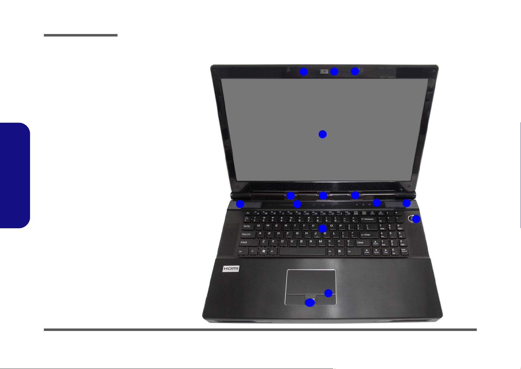
Figure 1
Top View
1. PC Camera
2. Built-In Digital
Microphone
3. LCD
4. LED Status
Indicators
5. Touch Sensor
Instant Keys
6. Speakers
7. Power Button
8. Keyboard
9. TouchPad and
Buttons
10.Fingerprint Reader
Module
2
5
1
7
9
4
6
3
8
10
6
6
6
6
2
1.Introduction
External Locator - Top View with LCD Panel Open
1 - 4 External Locator - Top View with LCD Panel Open
Page 17
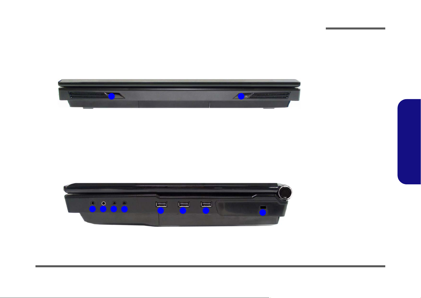
External Locator - Front & Right Side Views
Figure 2
Front View
1. Infrared Receiver
2. LED Power
Indicators
Figure 3
Right Side View
1. Line-In Jack
2. S/PDIF-Out Jack
3. Microphone-In
Jack
4. Headphone-In
Jack
5. USB 2.0 Port
6. Security Lock
Slot
1
FRONT VIEW
2
15243
5 5
RIGHT SIDE VIEW
6
Introduction
1.Introduction
External Locator - Front & Right Side Views 1 - 5
Page 18
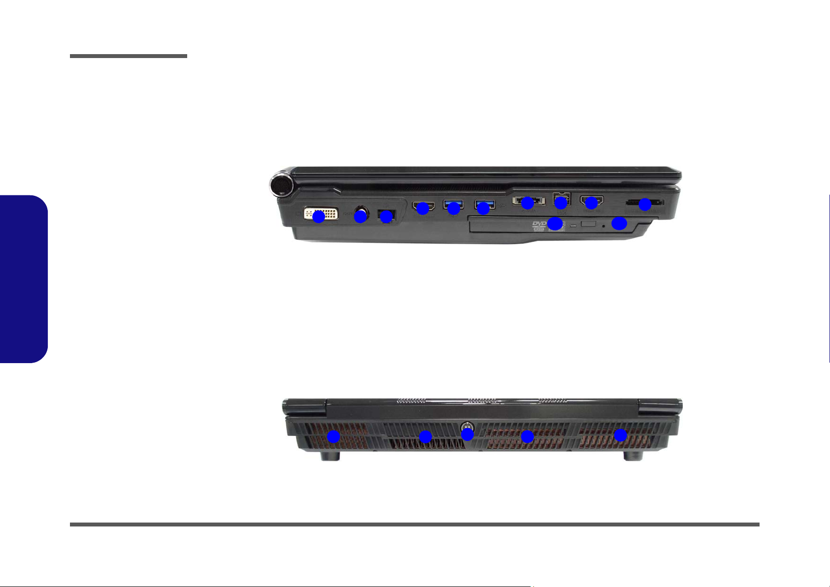
Introduction
Figure 4
Left Side View
1. DVI-Out Port
2. Cable (CATV)
Antenna Jack
3. RJ-45 LAN Jack
4. HDMI-Out Port
5. USB 3.0 Ports
6. eSATA Port
7. Mini-IEEE 1394b
Port
8. HDMI-In Port
(Factory Option)
9. 9-in-1 Card
Reader
10.Optical Device
Drive Bay
11. Emergency Eject
Hole
1 32
4 5
876
5
9
LEFT SIDE VIEW
10
11
Figure 5
Rear View
1. Vent
2. DC-In Jack
1
REAR VIEW
2
1
1
1
1.Introduction
1 - 6 External Locator - Left Side & Rear View
External Locator - Left Side & Rear View
/
Page 19
External Locator - Bottom View
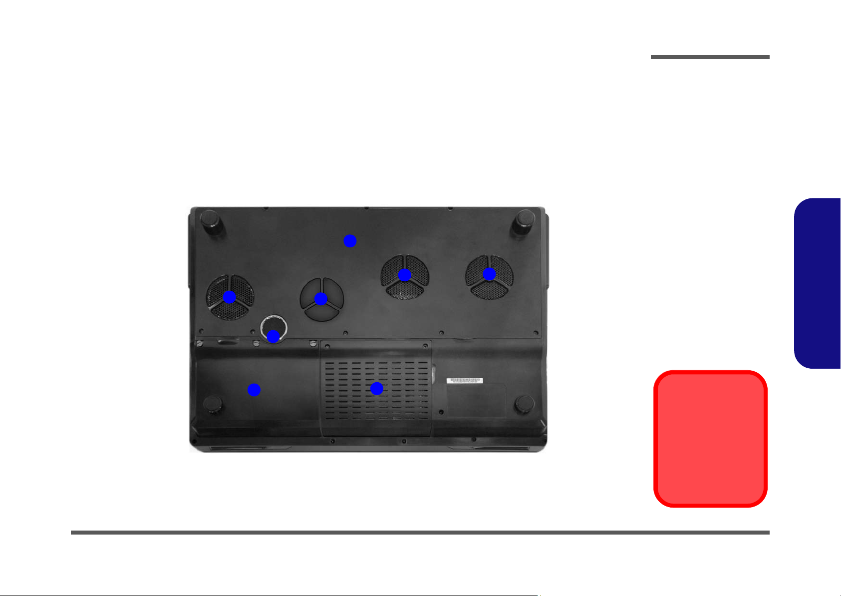
Figure 6
Bottom View
1. Component Bay
Cover
2. Vent
3. Sub Woofer
4. Primary HDD Bay
(HDD1 & 2)
5. Battery
(Secondary HDD
Bay - HDD3)
Overheating
To prevent your computer from overheating, make sure nothing blocks any vent
while the computer is
in use.
2
2
3
2
1
5
2
4
Introduction
1.Introduction
External Locator - Bottom View 1 - 7
Page 20
Introduction
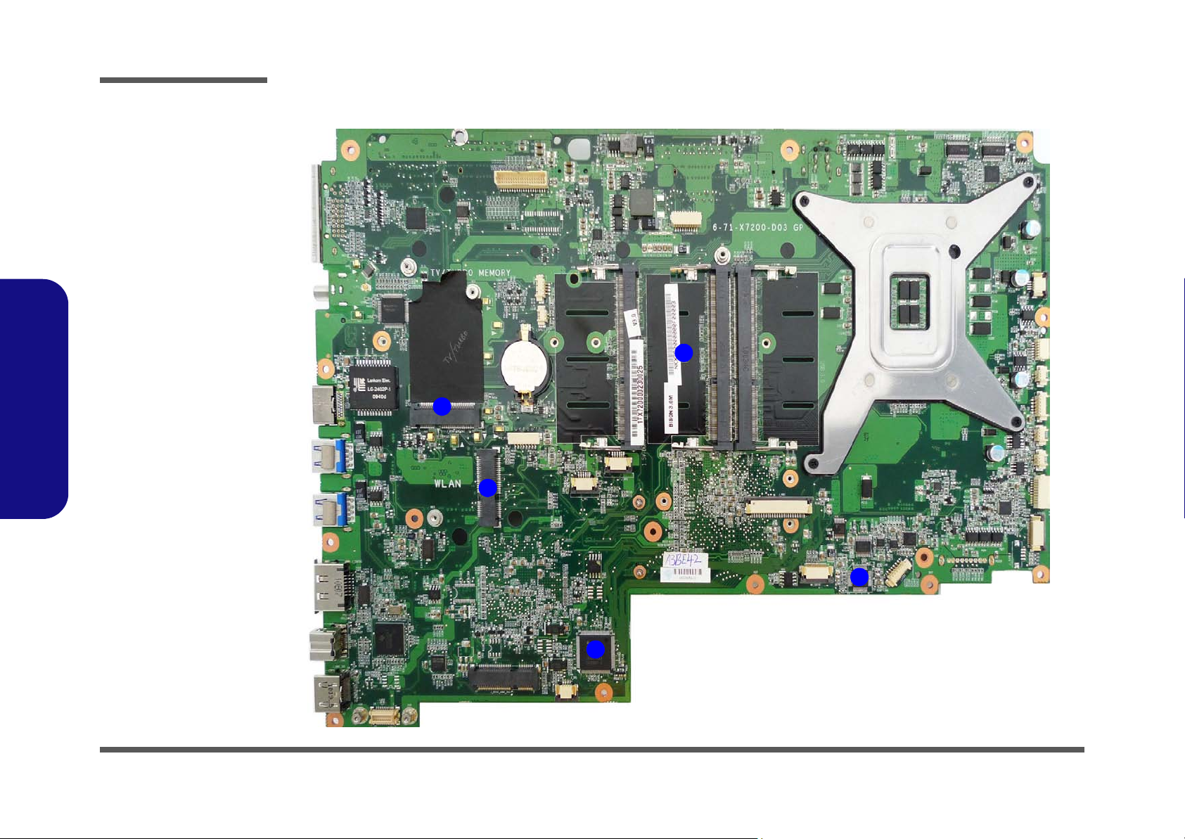
Figure 7
Mainboard Top
Key Parts
1. TV Turbo Memory Connector
2. Mini-Card Connector (WLAN
Module)
3. KBC-ITE
IT8502E
4. Memory Slots
DDR3 SO-DIMM
5. Azalia Codec
1
4
3
2
5
1.Introduction
Mainboard Overview - Top (Key Parts)
1 - 8 Mainboard Overview - Top (Key Parts)
Page 21
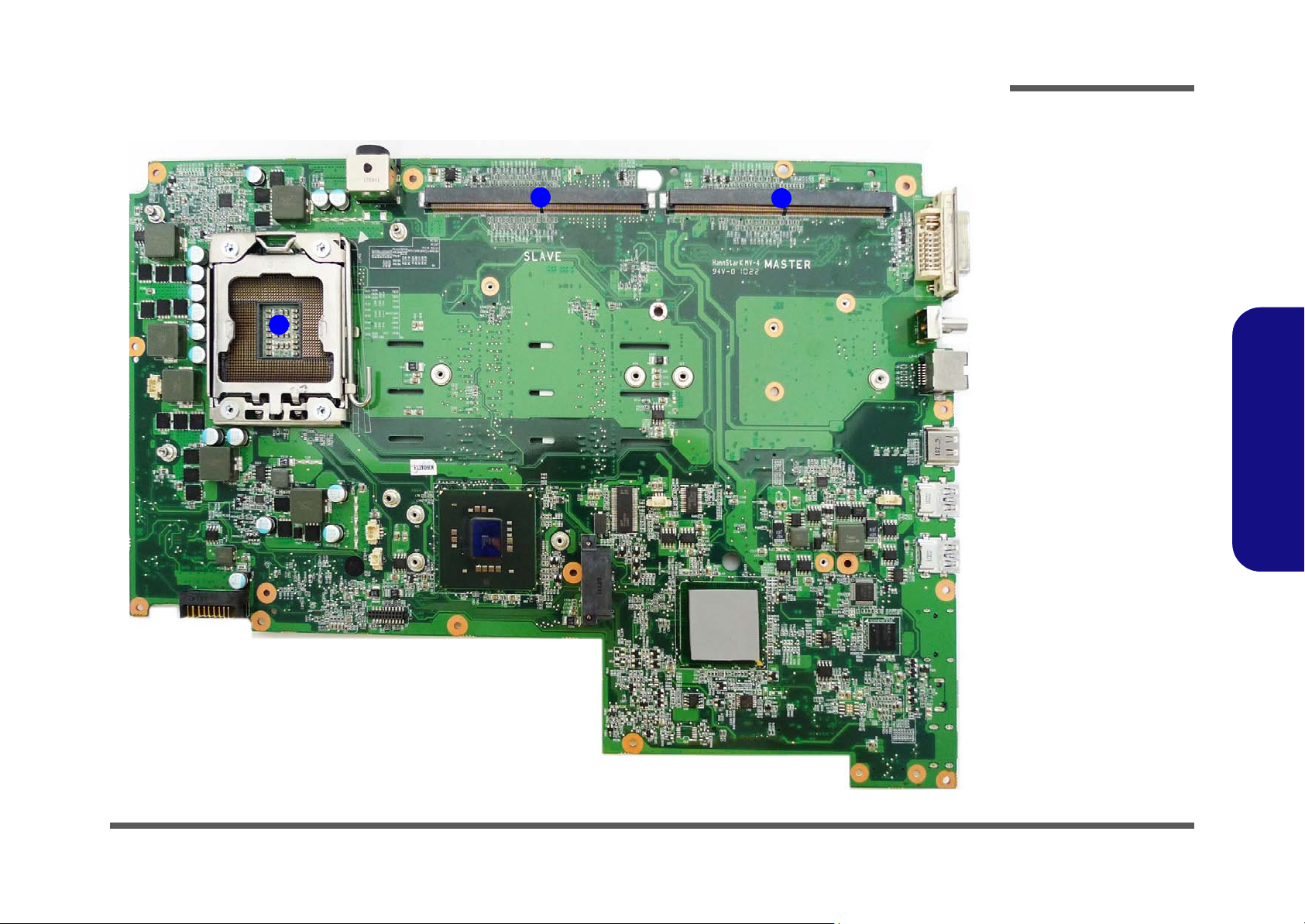
Mainboard Overview - Bottom (Key Parts)
1
2
2
Figure 8
Mainboard Bottom
Key Parts
1. CPU Socket (no
CPU installed)
2. VGA-Card
Connectors
3. Clock Generator
Introduction
1.Introduction
Mainboard Overview - Bottom (Key Parts) 1 - 9
Page 22
Introduction
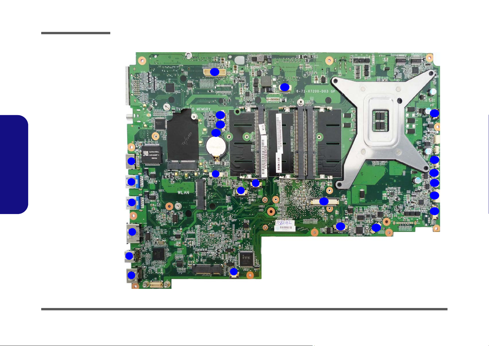
Figure 9
Mainboard Top
Connectors
1. HDMI-Out Port
2. USB 3.0 Ports
3. eSATA Port
4. Mini-IEEE 1394b Port
5. HDMI-In Port
6. Consumer Infrared
Connector
7. Bluetooth Cable
Connector 1
8. TouchPad Cable
Connector
9. Fingerprint Cable
Connector
10. Keyboard Cable
Connector
11. SATA HDD 1
Connector
12. LED Connector
13. Audio Board
Connector
14. USB Connector
15. Sub Woofer
Connector
16. Speaker Connector
17. CCD Connector
18. Switch Board Cable
Connector
19. Sensor Connector
20. LCD Cable
Connector
21. Microphone Cable
Connector
22. Speaker Connector
23. CMOS Battery
Connector
6
4
8
1
2
2
3
9
10
11
5
12
13
14
15
16
17
18
19
20
7
21
22
23
1.Introduction
1 - 10 Mainboard Overview - Top (Connectors)
Mainboard Overview - Top (Connectors)
Page 23
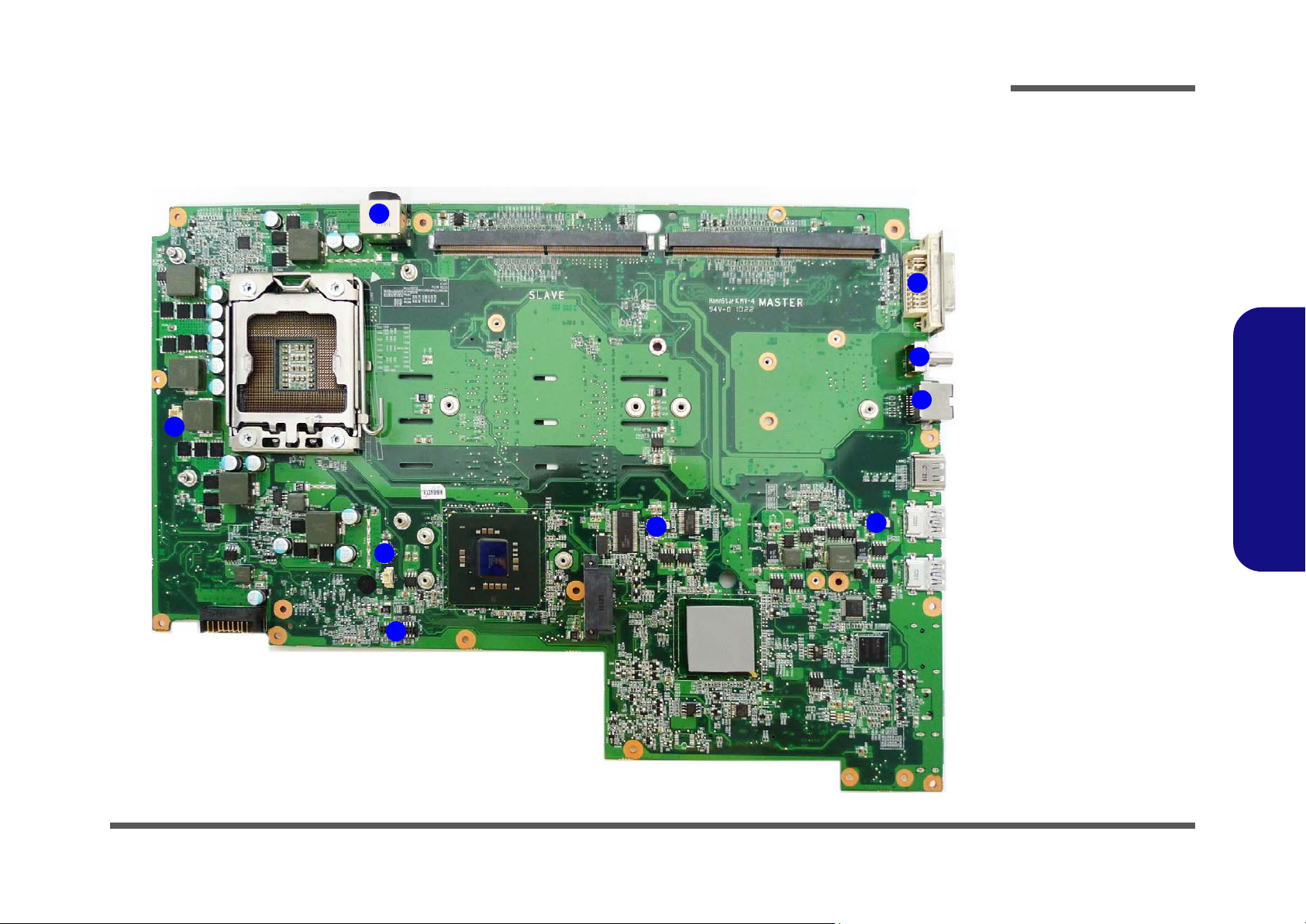
Mainboard Overview - Bottom (Connectors)
Figure 10
Mainboard Bottom
Connectors
1. CPU Fan Cable
Connector 1
2. CPU Fan Cable
Connector 2
3. SATA HDD 2
Connector
4. VGA Fan 2 Cable
Connector
5. VGA Fan 1 Cable
Connector
6. RJ-45 LAN Jack
7. Cable (CATV)
Antenna Jack
8. DVI-Out Port
9. DC-In Jack
1
2
3
4
5
6
7
8
9
Introduction
1.Introduction
Mainboard Overview - Bottom (Connectors) 1 - 11
Page 24

Introduction
1.Introduction
1-12
Page 25
Chapter 2: Disassembly
Information
Warning
Overview
This chapter provides step-by-step instructions for disassembling the X7200 series notebook’s parts and subsystems.
When it comes to reassembly, reverse the procedures (unless otherwise indicated).
We suggest you completely review any procedure before you take the computer apart.
Disassembly
Procedures such as upgrading/replacing the RAM, optical device and hard disk are included in the User’s Manual but are
repeated here for your convenience.
To make the disassembly process easier each section may have a box in the page margin. Information contained under
the figure # will give a synopsis of the sequence of procedures involved in the disassembly procedure. A box with a
lists the relevant parts you will have after the disassembly process is complete. Note: The parts listed will be for the disassembly procedure listed ONLY, and not any previous disassembly step(s) required. Refer to the part list for the previous disassembly procedure. The amount of screws you should be left with will be listed here also.
A box with a will also provide any possible helpful information. A box with a contains warnings.
An example of these types of boxes are shown in the sidebar.
2.Disassembly
Overview 2 - 1
Page 26

Disassembly
2.Disassembly
NOTE: All disassembly procedures assume that the system is turned OFF, and disconnected from any power supply (the
battery is removed too).
Maintenance Tools
The following tools are recommended when working on the notebook PC:
• M3 Philips-head screwdriver
• M2.5 Philips-head screwdriver (magnetized)
• M2 Philips-head screwdriver
• Small flat-head screwdriver
• Pair of need le-nose pliers
• Anti-static wrist-strap
Connections
Connections within the computer are one of four types:
Locking collar sockets for ribbon connectors To release these connectors, use a small flat-head screwdriver to
gently pry the locking collar away from its base. When replacing the connection, make sure the connector is oriented in the
same way. The pin1 side is usually not indicated.
2 - 2 Overview
Pressure sockets for multi-wire connectors To release this connector type, grasp it at its head and gently
rock it from side to side as you pull it out. Do not pull on the
wires themselves. When replacing the connection, do not try to
force it. The socket only fits one way.
Pressure sockets for ribbon connectors To release these connectors, use a small pair of needle-nose pli-
ers to gently lift the connector away from its socket. When replacing the connection, make sure the connector is oriented in
the same way. The pin1 side is usually not indicated.
Board-to-board or multi-pin sockets To separate the boards, gently rock them from side to side as
you pull them apart. If the connection is very tight, use a small
flat-head screwdriver - use just enough force to start.
Page 27

Maintenance Precautions
Power Safety
Warning
Before you undertake
any upgrade procedures, make sure that
you have turned off the
power, and disconnected all peripherals
and cables (including
telephone lines). It is
advisable to also remove your battery in
order to prevent accidentally turning the
machine on.
The following precautions are a reminder. To avoid personal injury or damage to the computer while performing a removal and/or replacement job, take the following precautions:
1. Don't drop it. Perform your repairs and/or upgrades on a stable surface. If the computer falls, the case and other
components could be damaged.
2. Don't overheat it. Note the proximity of any heating elements. Keep the computer out of direct sunlight.
3. Avoid interference. Note the proximity of any high capacity transformers, electric motors, and other strong mag-
netic fields. These can hinder proper performance and damage component s and/or data. You should also monitor
the position of magnetized tools (i.e. screwdrivers).
4. Keep it dry. This is an electrical appliance. If water or any other liquid gets into it, the computer could be badly
damaged.
5. Be careful with power. Avoid accidental shocks, discharges or explosions.
•Before removing or servicing any part from the computer, turn the computer off and detach any power supplies.
•When you want to unplug the power cord or any cable/wire, be sure to disconnect it by the plug head. Do not pull on the wire.
6. Peripherals – Turn off and detach any peripherals.
7. Beware of static discharge. ICs, such as the CPU and main support chips, are vulnerable to static electricity.
Before handling any part in the computer, discharge any static electricity inside the computer. When handling a
printed circuit board, do not use gloves or other materials which allow static electricity buildup. We suggest that
you use an anti-static wrist strap instead.
8. Beware of corrosion. As you perform your job, avoid touching any connector leads. Even the cleanest hands produce oils which can attract corrosive elements.
9. Keep your work environment clean. Tobacco smoke, dust or other air-born particulate matter is often attracted
to charged surfaces, reducing performance.
10. Keep track of the components. When removing or replacing any part, be careful not to leave small part s, such as
screws, loose inside the computer.
Cleaning
Do not apply cleaner directly to the computer, use a soft clean cloth.
Do not use volatile (petroleum distillates) or abrasive cleaners on any part of the computer.
Disassembly
2.Disassembly
Overview 2 - 3
Page 28

Disassembly
Disassembly Steps
The following table lists the disassembly steps, and on which page to find the related information. PLEASE PERFORM
THE DISASSEMBLY STEPS IN THE ORDER INDICATED.
2.Disassembly
To remove the Battery:
1. Remove the battery page 2 - 5
To remove the Optical Device:
1. Remove the battery page 2 - 5
2. Remove the Optical device page 2 - 6
To remove a Processor:
1. Remove the battery page 2 - 5
2. Remove the processor page 2 - 7
To remove and install a Video Card:
1. Remove the battery page 2 - 5
2. Remove the video card page 2 - 9
3. Install the video card page 2 - 11
To remove the Keyboard:
1. Remove the battery page 2 - 5
2. Remove the keyboard page 2 - 12
To remove the Bluetooth Module:
1. Remove the battery page 2 - 5
2. Remove the Bluetooth page 2 - 17
To remove the System Memory:
1. Remove the battery page 2 - 5
2. Remove the system memory page 2 - 18
To remove the HDD:
1. Remove the battery page 2 - 5
2. Remove the HDD from the Primary HDD Bay page 2 - 20
3. Remove the HDD from the Primary HDD Bay page 2 - 24
To remove the Hinges:
1. Remove the battery page 2 - 5
2. Remove the LCD back cover page 2 - 26
To remove the Wireless LAN Module:
1. Remove the battery page 2 - 5
2. Remove the wireless LAN page 2 - 16
2 - 4 Disassembly Steps
Page 29
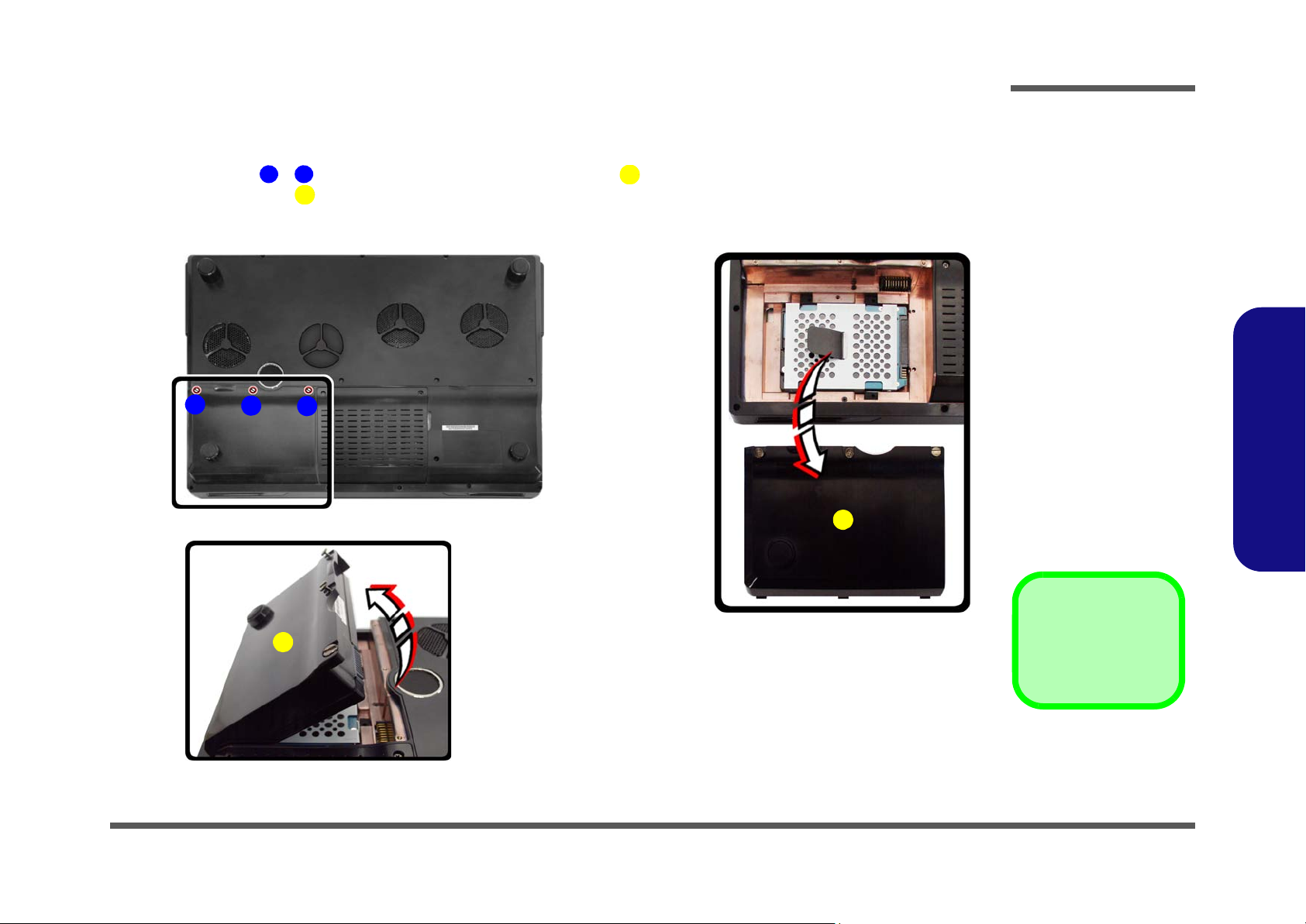
Removing the Battery
4. Battery
•3 Screws
13646
4
a.
4
b.
2
3
1
c.
4
Figure 1
Battery Removal
a. Loosen screws.
b. Carefully lift the battery
up.
c. Remove the battery from
the battery bay.
1. Turn the computer off, and turn it over.
2. Loosen screws - (Figure 1a
3. Remove the battery from the battery bay (Figure 1c
) and carefully lift the battery up (Figure 1b).
Disassembly
).
2.Disassembly
Removing the Battery 2 - 5
Page 30
Disassembly
Figure 2
Optical Device
Removal
a. Remove the screws from
the hard disk bay cover.
b. Remove the hard disk
bay cover.
c Remove the screw
d. Use a screwdriver to
carefully push out the
optical device at point
.
51234
6
5
6. Optical Device
•3 Screws
1
4
a.
c.
b. d.
2
5
3
6
Removing the Optical (CD/DVD) Device
1. Turn off the computer, remove the battery (page 2 - 5).
2. Remove screws
3. Remove the hard disk bay cover (Figure 2b
4. Remove the screw at point (Figure 2c
point (Figure 2d
5. Reverse the process to install any new optical device.
& from the hard disk bay cover (Figure 2a).
).
), and use a screwdriver to carefully push out the optical device at
).
2.Disassembly
2 - 6 Removing the Optical (CD/DVD) Device
Page 31

Removing the Processor
1
5
689
10
11
17
18
Figure 3
Processor Removal
a. Remove the screws from
the component bay cover.
b. Remove the screws from
the CPU fan.
c. Disconnect the fan cable
and remove the CPU
fan.
d. Remove the screws from
the CPU heatsink.
Heat Sink Screw
Removal and Insertion
Remove the screws from the
heat sink in the order indicated here:
7-6-5-4-3-2-1
.
When tightening the screws,
make sure that they are tightened in the order:
1-2-3-4-5-
6-7
.
10.CPU Fan
18.CPU Heatsink
•15 Screws
a.
1
2
3
b.
c.
5
4
6
7
8
9
10
d.
13
12
11
14
15
16
17
Screw 1
Screw 6
Screw 2
Screw 7
Screw 3
Screw 4
Screw 5
18
Heat Sink Screw Removal and Insertion
Remove the screws from the heat sink in the order indicated here:
7-6-5-4-3-2-1
. When
tightening the screws, make sure that they are tightened in the order:
1-2-3-4-5-6-7
.
1. Turn off the computer, remove the battery (page 2 - 5).
2. Remove the screws - from the component bay cover (Figure 3a).
3. Remove the screws - from the CPU fan (Figure 3b).
4. Disconnect the fan cable
5. Remove the screws - from the CPU heatsink (Figure 3d).
and remove the CPU fan (Figure 3c).
Disassembly
2.Disassembly
Removing the Processor 2 - 7
Page 32

Disassembly
18
192021
22
23
23
Figure 4
Processor Removal
(cont’d)
e. Carefully lift up the heat
sink off the computer by
pulling the plastic strip up.
f. Press down and hold the
latch (with the latch held
down you will be able to release it)
g. Turn the release latch to
unlock the CPU.
h. Lift the CPU out of the
socket.
e.
18
f.
g.
h.
19
23
23
20
21
22
18.CPU Heatsink
23.CPU
6. Carefully lift up the heat sink off the computer by pulling the plastic strip up (Figure 4e).
7. Press down and hold the latch (with the latch held down you will be able to release it) (Figure 4f).
8. Move the latch upward and bracket downward fully in the direction indicated to unlock the CPU
(Fig-
ure 4g).
9. Carefully (it may be hot) lift the CPU up out of the socket (Figure 4h).
10. Reverse the process to install a new CPU.
1 1. When re-inserting the CPU, pay careful attention to the pin alignment, it will fit only one way (DO NOT FORCE IT!).
2.Disassembly
The heat sink, and CPU
area in general, contains
parts which are subjected
to high temperatures. Allow
the area time to cool before
removing these parts.
2 - 8 Removing the Processor
Caution
Page 33

Removing and Installing the Video Card
11 & 12.Fan Units
21 & 22.Heat Sink Units
29 & 30.Video Cards
•20 Screws
Caution
The heat sink, and video
card area in general,
contains parts which are
subject to high temperatures. Allow the area
time to cool before removing these parts.
Figure 5
Video Card
Removal Procedure
a. Remove the fan
screws.
b. Disconnect the fan ca-
bles & remove the fan
units.
c. Remove the screws in
the correct order.
d. Carefully remove the
heat sink units by pulling the plastic strips
up. Remove the video
189
10
11
12
13
20
21
22
232425
28
29
30
3
a.
2
1
4
6
7
8
5
12
c.
b.
d.
Screw 3
13
14
Heat Sink Screw Removal and
Insertion
Remove the screws from the heat sink in
the order indicated here:
4-3-2-1
.
When tightening the screws, make sure
that they are tightened in the order:
1-2-3-
4
.
15
12
16
14
13
15
20
18
1719
21
22
Screw 1
Screw 3
Screw 1
Screw 2
Screw 4 Screw 2
Screw 4
10
23
24
25 26 27 28
11
9
29 30
Video Card Removal Procedure
1. Turn off the computer, turn it over and remove the battery (page 2 - 5) and component cover (page 2 - 7).
Remove screws - (Figure 5a).
2.
3. Disconnect the fan cables & and remove the fan units & (Figure 5b).
4. Remove screws - from the heat sink unit in the order indicated on the label (i.e screw 4 first through to
screw 1 last)
Carefully (it may be hot) remove the heat sink units & by pulling the plastic strips & up (Figure
5.
d).
5
Remove screws - from the video cards & (Figure 5d).
6.
(Figure 5c).
Disassembly
2.Disassembly
Removing and Installing the Video Card 2 - 9
Page 34

Disassembly
Figure 6
Video Card
Removal (cont’d)
e. The video cards will
pop up.
f. Disconnect the video
card cables and remove the video cards.
29
30
31
32
29
30
29 & 30.Video Cards
Caution
The heat sink, and video
card area in general,
contains parts which are
subject to high temperatures. Allow the area
time to cool before removing these parts.
e.
f.
29 30
31
32
7. The video cards & will pop up.
8. Disconnect the video card cables & and remove the video cards & (Figure 6f).
2.Disassembly
2 - 10 Removing and Installing the Video Card
Page 35

Installing a New Video Card
Figure 7
Installing a New
Video Card
g. Insert the video cards
at a 30 degree angle.
h. Fit the connectors
straight and even.
29
30
g. h.
25
28
Caution
The heat sink, and video
card area in general,
contains parts which are
subject to high temperatures. Allow the area
time to cool before removing these parts.
1. Prepare to fit the video cards & into the slot by holding it at about a 30° angle (page 2 - 10).
2. The card needs to be fully into the slot, and the video card and socket have a guide-key and pin which align to
allow the card to fit securely (
Fit the connectors firmly into the socket, straight and evenly (Figure 7h).
3.
Figure 7h).
Disassembly
2.Disassembly
4. DO NOT attempt to push one end of the card in ahead of the other.
5. The card’s pin alignment will allow it to only fit one way. Make sure the module is seated as far into the socket
as it will go (none of the gold colored contact should be showing). DO NOT FORCE the card; it should fit without
much pressure.
6. Secure the card with screws - (Figure 5 on page 2 - 9).
Place the heat sink back on the card, and secure the screws in the order indicated in Figure 5 on page 2 - 9.
7.
Attach the video card fan and secure with the screws as indicated in Figure 5 on page 2 - 9.
8.
Reinsert the component bay cover, and secure with the screws as indicated in Figure 14 on page 2 - 18.
9.
Removing and Installing the Video Card 2 - 11
Page 36

Disassembly
134
6. LED Cover Module
•3 Screws
5
6
Figure 8
Keyboard Removal
a. Remove screws from the
bottom of the computer.
b. Turn the computer over,
open the Lid/LCD, and
carefully (a cable is connected to the underside of
the LED cover module) unsnap up the LED cover
module from point on
the right .
c. Disconnect cable and re-
move the LED cover module .
4
a.
b.
2
3
4
1
c.
5
5
6
6
Removing the Keyboard
1. Turn off the computer and remove the battery (page 2 - 5).
2. Remove screws
3. Turn the computer over, open the Lid/LCD, and carefully (a cable is connected to the underside of the LED cover
module) unsnap up the LED cover module from point on the right (Figure 8b).
4. Disconnect cable and remove the LED cover module (Figure 8c).
- from the bottom of the computer (Figure 8a).
2.Disassembly
2 - 12 Removing the Keyboard
Page 37

5. Remove screws - from the keyboard (Figure 9d).
7
11
12
12
13
14
14. Keyboard
•5 Screws
d. f.
e.
7 8 9
13
12
1110
14
Keyboard Tabs
Re-Inserting the Keyboard
When re-inserting the keyboard,
align first the four keyboard tabs
(Figure 9f) that are located at
the bottom, to the slots in the
case.
Figure 9
Keyboard Removal
(cont’d.)
d. Remove screws from
the keyboard.
e. Carefully lift the key-
board up, being careful
not to bend the keyboard
ribbon cable . Disconnect the keyboard ribbon
cable from the locking
collar socket .
f. Remove the keyboard.
6. Carefully lift the keyboard up, being careful not to bend the keyboard ribbon cable . Disconnect the keyboard
ribbon cable from the locking collar socket (Figure 9e).
7. Remove the keyboard (Figure 9f).
Disassembly
2.Disassembly
Removing the Keyboard 2 - 13
Page 38

Disassembly
15
17 1819
18
g.
h.
2
1
15
17
i.
16
18
19
18
Figure 10
Keyboard
Removal (cont’d.)
g. Remove screws
from the keyboard
shielding plate.
h. Lift the keyboard
shielding plate up in
the direction of the arrow.
i. Remove the key-
board shielding plate.
18. Keyboard Shielding
Plate
•3 Screws
2.Disassembly
8. Remove screws - from the keyboard shielding plate (Figure 10g).
9. Lift the keyboard shielding plate up in the direction of the arrow (Figure 10h).
10. Remove the keyboard shielding plate (Figure 10i).
2 - 14 Removing the Keyboard
Page 39

Keyboard Shielding Plate Insertion
Figure 11
Keyboard
Shielding Plate
Insertion
a. When re-inserting the
keyboard shielding
plate make sure you
insert it by sliding it
into position at an angle as illustrated by
arrow below, and
press it down into position.
b. Secure the plate with
screws.
•3 Screws
123
5
1
4
2
3
5
a.
b.
1. When re-inserting the keyboard shielding plate make sure you insert it by sliding it into position at an angle as
illustrated by arrow below, and press it down into position (Figure 11a).
2. Secure the plate with screws - (Figure 11b).
Disassembly
2.Disassembly
Removing the Keyboard 2 - 15
Page 40

Disassembly
Figure 12
Wireless LAN
Module Removal
a. The Wireless LAN mod-
ule will be visible at point
on the mainboard.
b. Disconnect the cables
and remove the screw.
c. The WLAN module will
pop up.
d. Lift the WLAN module
out.
Note: Make sure you
reconnect the antenna
cable to ‘’1’’ +
‘’2’’socket (Figure
b).
112
3
4
5
5
5
4
b.
c.
a. d.
2
3
5
1
5. WLAN Module.
•1 Screw
Removing the Wireless LAN Module
1. Turn off the computer, remove the battery (page 2 - 5) and the keyboard (page 2 - 9).
2. The Wireless LAN module will be visible at point (Figure 12a) on the mainboard.
3. Carefully disconnect cables - , then remove screw from the module socket (Figure 12b
4. The Wireless LAN module (Figure 12c) will pop-up.
5. Lift the Wireless LAN module (Figure 12d) up and off the computer.
2.Disassembly
).
2 - 16 Removing the Wireless LAN Module
Page 41

Figure 13
Bluetooth Module
Removal
a. The Bluetooth module
will be visible at point
.
b. Remove the screw, discon-
nect the cable and the
connector.
c. Lift the Bluetooth module
up off the socket.
1
1
234
5
a.
b.
1
5
c.
3
4
2
5. Bluetooth Module
•1 Screw
Removing the Bluetooth Module
1. Turn off the computer, remove the battery (page 2 - 5) and the keyboard (page 2 - 9).
2. The Bluetooth module will be visible at point
3. Remove screw
(Figure 13b).
4. Carefully separate the Bluetooth module from the connector and disconnect the cable (Figure 13b).
5. Lift the Bluetooth module
(Figure 13c) up and off the computer..
(Figure 13a).
Disassembly
2.Disassembly
Removing the Bluetooth Module 2 - 17
Page 42

Disassembly
Figure 14
RAM Module
Removal
a. The RAM modules
will be visible at
points - .
b. Gently pull the two
release latches on
the sides of the
memory socket in
the direction indicated by the arrows.
c.The RAM module will
pop-up, and you can
then remove it.
Contact Warning
Be careful not to touch
the metal pins on the
module’s connecting
edge. Even the cleanest hands have oils
which can attract particles, and degrade the
module’s performance.
13134
9
10
10.RAM Module
a.
2
4
1
b.
3
5
6
7
8
9
c.
10
2.Disassembly
Removing the System Memory (RAM)
The computer has three memory sockets for 204 pin Small Outline Dual In-line Memory Modules (SO-DIMM) supporting DDR3 1066/1333MHz. The main memory can be expanded up to 12GB. The SO-DIMM modules supported are
1024MB, and 2048MB and DDRIII Modules. The total memory size is automatically detected by the POST routine once
you turn on your computer.
Memory Upgrade Process
1. Turn off the computer, remove the battery (page 2 - 5) and the keyboard (page 2 - 9).
2. The RAM modules will be visible at points
3. Gently pull the two release latches ( - ) on the sides of the memory socket in the direction indicated by the
arrows (Figure 14b
).
4. The RAM module will pop-up (Figure 14c), and you can then remove it.
.
- (Figure 14a).
2 - 18 Removing the System Memory (RAM)
Page 43

5. Pull the latches to release the second and third modules if necessary.
6. Insert a new module holding it at about a 30° angle and fit the connectors firmly into the memory slot.
7. The module’s pin alignment will allow it to only fit one way. Make sure the module is seated as far into the slot as it
will go. DO NOT FORCE the module; it should fit without much pressure.
8. Press the module in and down towards the mainboard until the slot levers click into place to secure the module.
9. Replace the bay cover and screws (make sure you reconnect the fan cable before screwing down the bay
cover).
10. Restart the computer to allow the BIOS to register the new memory configuration as it starts up.
Disassembly
2.Disassembly
Removing the System Memory (RAM) 2 - 19
Page 44

Disassembly
Figure 15
Removing the
Hard Disk(s) from
the Primary HDD
Bay
a. Remove screws and
disconnect cable from
the hard disk assembly.
b. Remove the hard disk
assembly.
c. Grip the tab to re-
move the HDD cable.
6. Hard Disk Assembly
•4 Screws
145
6
1
2
5
3
4
a.
b.
7
c.
6
7
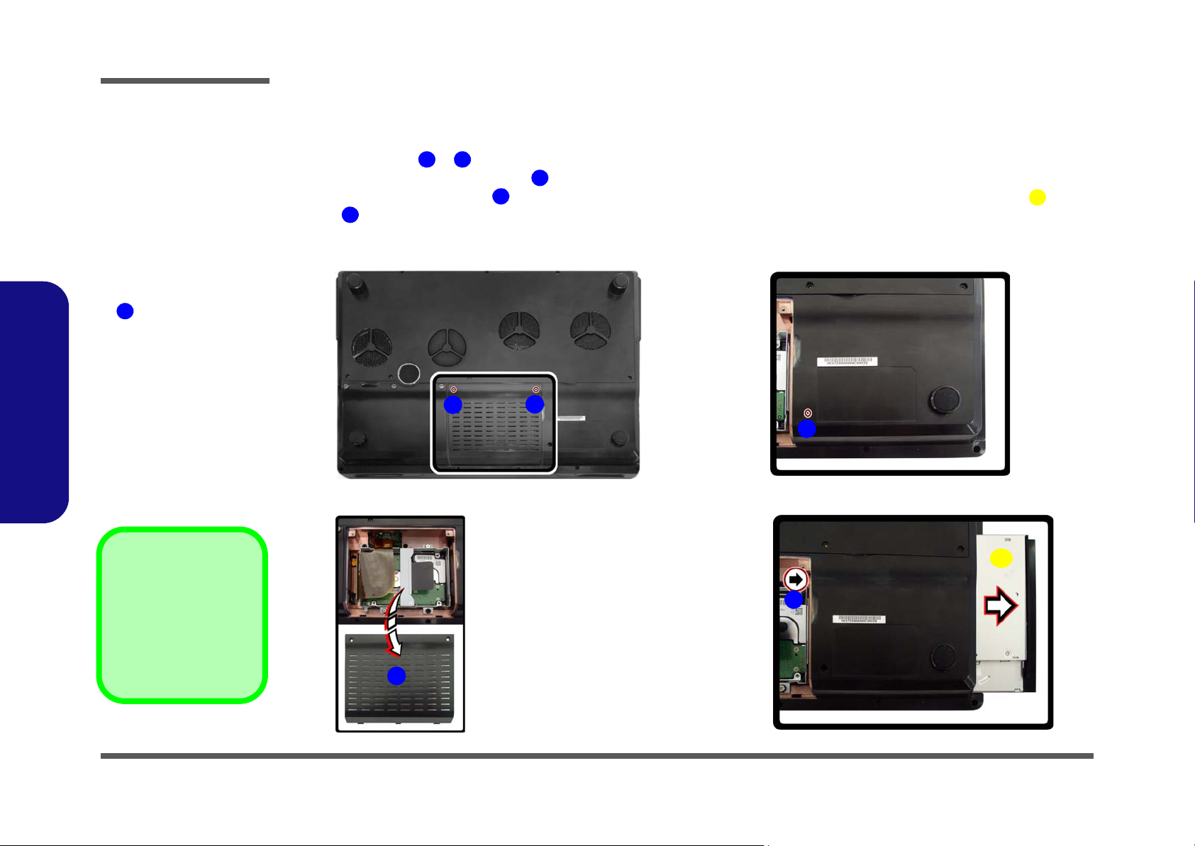
Removing the Hard Disk(s) from the Primary HDD Bay
The hard disk drive can be taken out to accommodate other 2.5" serial (SATA) hard disk drives with a height of 9.5mm
(h). Follow your operating system’s installation instructions, and install all necessary drivers and utilities (as outlined in
Chapter 4 of the User’s Manual) when setting up a new hard disk.
2.Disassembly
1. Turn off the computer ,remove the battery (page 2 - 5) and hard disk bay cover (page 2 - 6).
2. Remove screws - from the hard disk assembly (Figure 15a).
3. Disconnect cable from the hard disk assembly (Figure 15a).
4. Remove the hard disk assembly (Figure 15b).
5. Grip the tab to remove the HDD cable
(Figure 15c).
2 - 20 Removing the Hard Disk(s) from the Primary HDD Bay
Page 45

6. Remove screws - (Figure 16d). *The number and sequence of screws to be removed will depend on
8
11
9
8
11
10
9
8
11
10
d.
Figure 16
Removing the
Hard Disk(s) from
the Primary HDD
Bay (cont’d.)
d. Remove the screws.
•4 Screws
whether or not you have one or two hard disks installed in the case.
Disassembly
2.Disassembly
Removing the Hard Disk(s) from the Primary HDD Bay 2 - 21
Page 46

Disassembly
1
2
3
6
2
3
3
4
5
6
3
4
5
6
a.
b.
2
1
1
2
Figure 17
Inserting the
Primary Hard
Disk(s)
a. Insert the HDD into
the case.
b. Insert screws to se-
cure the hard disk(s)
in the case.
1. Hard Disk
2. Hard Disk Case
•4 Screws
Inserting the Primary Hard Disk(s)
1. Insert the HDD(s) into the HDD case as illustrated (Figure 17a). *Make sure the cable connectors are
facing towards the gap at the rear of the case.
2. Insert screws - to secure the hard disk(s) in the case (Figure 17b).
2.Disassembly
2 - 22 Removing the Hard Disk(s) from the Primary HDD Bay
Page 47

3. Firmly insert the HDD cable into the hard disk assembly in the direction of the arrow as indicated
7
8
9
7
10
13
9
11
10
12
c.
d.
7
8
7
7
13
Figure 18
Inserting the
Primary Hard
Disk(s) (cont’d.)
c. Firmly insert the HDD
cable into the hard
disk assembly.
d. Insert the HDD as-
sembly into the bay
by pushing it straight
down. Firmly connect
the cable and then secure the assembly
with screws.
8. Hard Disk Assembly
9. Hard Disk Cable
•4 Screws
below (Figure 18c).
4. Insert the HDD assembly into the bay by pushing it straight down (Figure 18d). *Do not insert the assembly at
an angle.
5. Firmly connect cable to the mainboard and then secure the assembly with screws - (Figure 18d).
Disassembly
Removing the Hard Disk from the Secondary HDD Bay
2.Disassembly
Removing the Hard Disk from the Secondary HDD Bay 2 - 23
Page 48

Disassembly
145
1 2
5
3 4
6
7
8
9
a.
b.
c.
d.
11
10
Figure 19
Removing the
Hard Disk from the
Secondary HDD
Bay
a. Remove screws from
the hard disk assembly.
b. Grip the tab and slide
the hard disk assembly in the direction of
the arrow . Lift the
hard disk assembly
out of the compartment.
c. Remove screws from
the hard disk assembly.
d. Separate the HDD
from the HDD case.
5
10. Hard Disk
11. Hard Disk Case
•8 Screws
6
9
10
11
1. Remove screws - from the hard disk assembly (Figure 19a).
2. Grip the tab and slide the hard disk assembly in the direction of the arrow (Figure 19b).
3. Lift the hard disk assembly out of the compartment (Figure 19b).
4. Remove screws - from the hard disk assembly (Figure 19c).
5. Separate the hard disk from the HDD case (Figure 19d).
6. Insert the replacement HDD into the case *Make sure the cable connector is facing towards the rear of the
case as illustrated below.
2.Disassembly
2 - 24 Removing the Hard Disk from the Secondary HDD Bay
Page 49

7. Replace screws - (page 2 - 23).
6912
12
e.
Figure 20
Removing the
Hard Disk(s) from
the Secondary
HDD Bay (cont’d.)
e. Insert the HDD as-
sembly into the bay
by pushing it straight
down and then slide it
in the direction of the
arrow to lock in place.
8. Insert the HDD assembly into the bay by pushing it straight down (do not insert the assembly at an angle) and then
slide it in the direction of the arrow to lock in place (Figure 20e).
Disassembly
2.Disassembly
Removing the Hard Disk from the Secondary HDD Bay 2 - 25
Page 50

Disassembly
Figure 21
Hinge Removal
a. Re-insert the hinges into
the top case.
b. Raise the LCD to a 90°
angle.
c. Remove the whole LCD
assembly again from the
base of the computer.
Remove the screws at
the base of the LCD assembly.
1. LCD Assembly
•4 Screws
1
2
3
4
7
a.
2
3
4
5
6
b.
1
c.
Note:
This is the position of the hinges prior to
re-inserting them into the top case of the
computer.
Note:
This will be the new position of the hinges
after re-inserting them into the top case of
the computer.
7
2.Disassembly
Removing the Hinges
1. The whole LCD assembly is detached from the base of the computer.
2. Re-insert hinges & (Figure 21a) into the top case and raise the LCD to a 90° angle (Figure 21b) to adjust
the positioning of the hinges for removal.
3. Remove the whole LCD assembly again from the base of the computer (Figure 21c).
4. Remove screws - at the base of the LCD assembly (Figure 21c).
2 - 26 Removing the Hinges
Page 51

5. Remove hinges & (Figure 22d).
8
9
Figure 22
Hinge Removal
d. Remove the hinges.
8 & 9.Hinges
d.
8
9
Disassembly
2.Disassembly
Removing the Hinges 2 - 27
Page 52

Disassembly
2.Disassembly
2-28
Page 53

Appendix A:Part Lists
This appendix breaks down the X7200 series notebook’s construction into a series of illustrations. The component part
numbers are indicated in the tables opposite the drawings.
Note: This section indicates the manufacturer’s part numbers. Your organization may use a different system, so be sure
to cross-check any relevant documentation.
Note: Some assemblies may have parts in common (especially screws). However, the part lists DO NOT indicate the
total number of duplicated parts used.
Part Lists
Note: Be sure to check any update notices. The parts shown in these illustrations are appropriate for the system at the
time of publication. Over the product life, some parts may be improved or re-configured, resulting in new part numbers.
A.Part Lists
A-1
Page 54

Part Lists
Table A - 1
Part List Illustration
Location
Part List Illustration Location
The following table indicates where to find the appropriate part list illustration.
Part X7200
Top
page A - 3
A.Part Lists
Bottom
LCD
SATA DVD Super-Multi
SATA Blu-Ray Combo
VGA-GTX1
page A - 4
page A - 5
page A - 6
page A - 7
page A - 8
A - 2 Part List Illustration Location
Page 55

Top
Figure A - 1
Top
黑色
凱碩
藍天 互億
非耐落
非耐落
Part Lists
A.Part Lists
Top A - 3
Page 56

Part Lists
Figure A - 2
Bottom
非耐落
A.Part Lists
Bottom
A - 4 Bottom
Page 57

LCD
Figure A - 3
LCD
Part Lists
A.Part Lists
LCD A - 5
Page 58

Part Lists
Figure A - 4
SATA DVD Super-
Multi
非耐落
A.Part Lists
SATA DVD Super-Multi
A - 6 SATA DVD Super-Multi
Page 59

SATA Blu-Ray Combo
Figure A - 5
SATA Blu-Ray
Combo
非耐落
Part Lists
A.Part Lists
SATA Blu-Ray Combo A - 7
Page 60

Part Lists
Figure A - 6
VGA-GTX1
增加
(半卡)
(半卡)
非耐落
A.Part Lists
VGA-GTX1
A - 8 VGA-GTX1
Page 61

Appendix B: Schematic Diagrams
Table B - 1
SCHEMATIC
DIAGRAMS
Version Note
The schematic diagrams in this chapter
are based upon version 6-7P-X720A003A. If your mainboard
(or other boards) are a
later version, please
check with the Service
Center for updated diagrams (if required).
This appendix has circuit diagrams of the X7200 notebook’s PCB’s. The following table indicates where to find the appropriate schematic diagram.
Diagram - Page Diagram - Page Diagram - Page
Schematic Diagrams
System Block Diagram - Page B - 2 Clock Generator CV193 - Page B - 20 Power CPU_VTT - Page B - 38
LGA1366 Part A DDR3 1/2 - Page B - 3 - Page B - 20 Power VCORE - Page B - 39
LGA1366 Part B DDR3 2/2 - Page B - 4 MXM 3.0 PCI-E Master - Page B - 22 Power 1.5V/0.75VS - Page B - 40
LGA1366 Part C QPI - Page B - 5 - Page B - 22 Power 1.8VS, 1.1VS - Page B - 41
LGA1366 Part D Power - Page B - 6 HDMI-In Buffer/SATA HDD CON - Page B - 24 12V/Power Switch - Page B - 42
LGA1366 Part E GND, Thermal - Page B - 7 HDMI Port - Page B - 25
DDR3 Channel A SO-DIMM_0 - Page B - 8 LCD, INT - Page B - 26 Power AC_In, Charge - Page B - 44
DDR3 Channel B SO-DIMM_1 - Page B - 9 DVI-I - Page B - 27 Audio Board - Page B - 45
DDR3 Channel C SO-DIMM_2 - Page B - 10 DP Switch SN75DP128 - Page B - 28 Card Reader Board - Page B - 46
X58 QPI Interface - Page B - 11 KBC-ITE IT8512E - Page B - 29 Click Board - Page B - 47
X58 PCIEX16, PCIEX4, DMI - Page B - 12 USB 3.0 - Page B - 30 Consumer IR Board - Page B - 48
X58 MISC - Page B - 13 PCIE Card Reader/LAN JMC251 - Page B - 31 Switch Board - Page B - 49
X58 PWR - Page B - 14 1394B (TI-XIO2221BZAY) - Page B - 32 USB Board - Page B - 50
X58 GND - Page B - 15 Codec888, Subwoofer, DMIC - Page B - 33 Finger Sensor Board - Page B - 51
ICH10 DMI/PCIE/USB/SATA - Page B - 16 Audio AMP TPA6047A4/TPA6211 - Page B - 34 Touch Sensor Board - Page B - 52
ICH10 PCI/SPI/Other - Page B - 17 WLAN/HDMI-In/TV/ROBSON - Page B - 35 Power LED Board - Page B - 53
ICH10 Power/GND - Page B - 18 CCD/BT/SATA - Page B - 36
Fan CTRL - Page B - 19 Daughter Connector - Page B - 37
B.Schematic Diagrams
Power VDD3, VDD5, ICH_1.1VS - Page B 43
B-1
Page 62
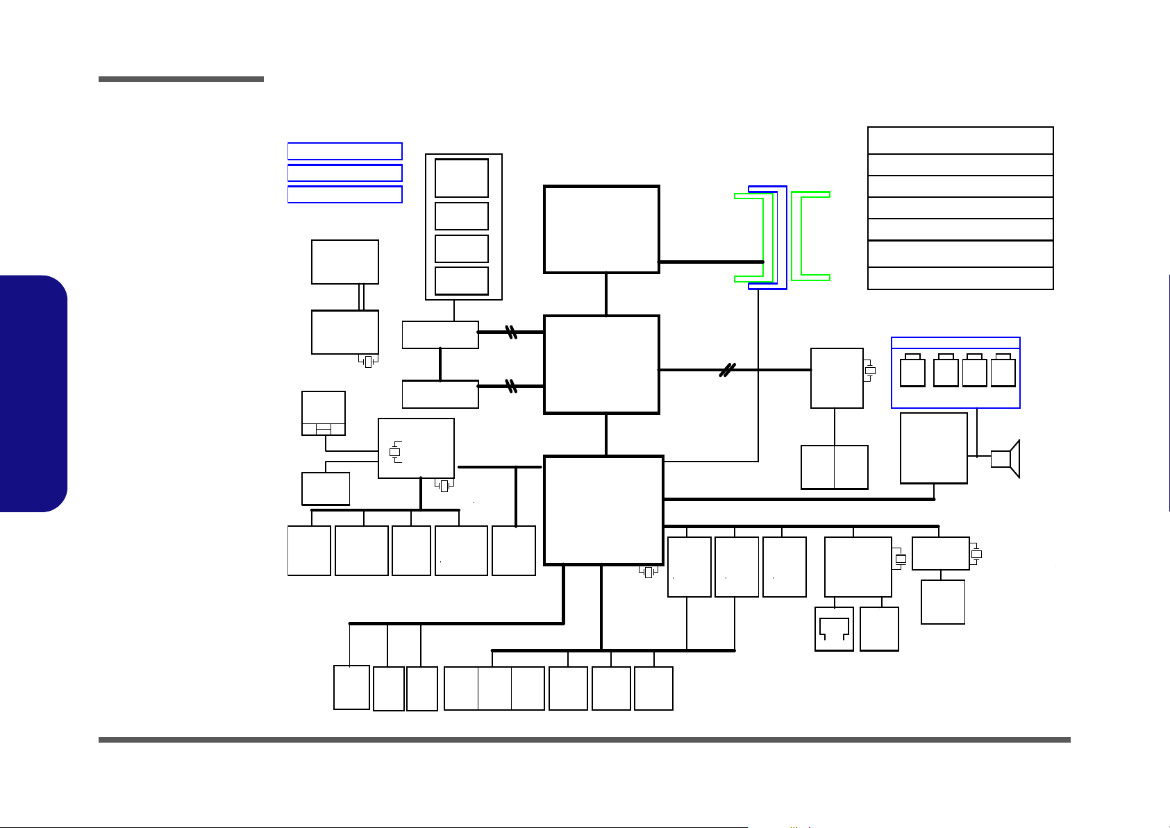
Schematic Diagrams
Sheet 1 of 52
System Block
Diagram
PORT1
3.0USB
USB1
PORT2
uPD720200
USB 3.0
Host
USB2
24 MHz
PCI-E x2
GLAN
&
CARD READER
JMC251
(OPTION)
ICH_1.1VS
12V,12 VS
Touch Sensor Board
IR
CONSUMER
CPU_VTT
98.304
MHz
CLEVO X 7200 S yst e m Block Diagram
XIO2221ZAY
SMART
BATTERY
(OPTION)
LGA1366
SATA
HDD
HDMI
300MB/s
BUFFER
TOUCH
PAD
SLI
LVDS
7.1 CHANNEL OUT
AUDIO BOARD
SOCKET
CV193
PCI-E x16
33 MHz
6.4 GT/s
IEEE
1394b
5VS,3VS,1.5VS,5V,3V,VCCA_1.1VS
Click Board
HP
OUT
BT
EMC1402
EC
Bloomfield
USB4
THERMAL
SENSOR
Switch Board
PCIE CLOCK
P.8
PORT3
IOH
SYS5V,SYS10V,SYS15V,VDD3,VDD5
INT.
SPK
1295 ball
DMI
Finger
Printer
SO-DIMM1
676 mBGA
ICS9DB403
MXM 3.0
VGA Card
Master
CLOCK GEN.
TPM
DDRIII
Mini CARD
USB2
SATA
1066/1333 MHz
AZALIA LINK
USB9
USB
QPI
4.8 GT/s
14.318 MHz
LPC
EC SMBUS
32.768 KHz
WLAN
32.768 KHz
Default
PROCESSOR
Mini CARD
MXM 3.0
VGA Card
Slave
1.5V,0.75VS
SOCKET
ICH10
RJ-45
100 MHz
LINE
IN
ROBSON/TV
25 MHz
SATA
ODD
2.0
SMART
FAN
MIC
IN
USB1
SPDIF
OUT
eSATA
3D PANEL
e DP
MMC/SD/MS/ MS Pr o
CARD
READER
7 in 1
Intel
Tylersburg
SYSTEM SMBUS
24 MHz
PCIE
IT8512E
USB0
DDR3 SDRAM SOCKET
PORT2
USB8
USB3
South Bridge
VIN,VA
SO-DIMM0
HDMI-in
USB11
SO-DIMM2
10 MHz
PORT1
PCIE CLOCK
Mini CARD
P.7
Socket-B
AZALIA
CODEC+
AMPLIFIER
ALC888-VC2
TPA6047A4
TPA6211A1
X4
1.8VS,1.1VS
INT. K/B
CCD
SOCKET
VCORE
P.9
PCI-E x16
DVI/RGB
System Block Diagram
B.Schematic Diagrams
B - 2 System Block Diagram
Page 63

LGA1366 Part A DDR3 1/2
M_DATA_B23
M_DQS_C_DN1
M_DATA_C38
M_DATA_B24
M_D A TA _A50
M_D A TA _A49
M_D A TA _A53
M_DATA_B26
M_DATA_C39
M_D A TA _A52
M_DATA_B25
M_D A TA _A51
M_DATA_B28
M_DATA_C40
M_D A TA _A55
M_DATA_B27
M_D A TA _A54
M_DATA_C41
M_D A TA _A57
M_DATA_B29
M_D A TA _A56 M_DQS_C_DN2
M_DATA_C42
M_DATA_B31
M_D A TA _A59
M_DQS_C_DN3
M_DATA_B30
M_D A TA _A58
M_DATA_C43
M_D A TA _A61
M_DQS_C_DN4
M_DATA_B32
M_D A TA _A60
M_DQS_C_DN5
M_DATA_B34
M_D A TA _A63
M_DATA_B33
M_D A TA _A62
M_DATA_B35
M_DATA_C44
M_DQS_A_DP[7:0]
ChannelC
ChannelB
ChannelA
M_DQS_A_DN[7:0]
M_DATA_B[63:0]
M_DQS_B_DN[7:0]
M_DQS_B_DP[7:0]
M_DQS_C_DP[7:0]
M_DATA_A[63:0]
M_DATA_C[63:0]
M_DQS_C_DN[7:0]
M_CB_ECC_A[7:0]
M_CB_ECC_C[7:0]
M_CB_ECC_B[7:0]
2 OF 12
J_CPU1B
Molex SD-475 94-00 1
DDR1_DQ_0
AA37
DDR1_DQ_1
AA36
DDR1_DQ_2
Y35
DDR1_DQ_3
Y34
DDR1_DQ_4
AA35
DDR1_DQ_5
AB36
DDR1_DQ_6
Y40
DDR1_DQ_7
Y39
DDR1_DQ_8
P34
DDR1_DQ_9
P35
DDR1_DQ_10
P39
DDR1_DQ_11
N39
DDR1_DQ_12
R34
DDR1_DQ_13
R35
DDR1_DQ_14
N37
DDR1_DQ_15
N38
DDR1_DQ_16
M35
DDR1_DQ_17
M34
DDR1_DQ_18
K35
DDR1_DQ_19
J35
DDR1_DQ_20
N34
DDR1_DQ_21
M36
DDR1_DQ_22
J36
DDR1_DQ_23
H36
DDR1_DQ_24
H33
DDR1_DQ_25
L33
DDR1_DQ_26
K32
DDR1_DQ_27
J32
DDR1_DQ_28
J34
DDR1_DQ_29
H34
DDR1_DQ_30
L32
DDR1_DQ_31
K30
DDR1_DQ_32
E9
DDR1_DQ_33
E8
DDR1_DQ_34
E5
DDR1_DQ_35
F5
DDR1_DQ_36
F10
DDR1_DQ_37
G8
DDR1_DQ_38
D6
DDR1_DQ_39
F6
DDR1_DQ_40
H8
DDR1_DQ_41
J6
DDR1_DQ_42
G4
DDR1_DQ_43
H4
DDR1_DQ_44
G9
DDR1_DQ_45
H9
DDR1_DQ_46
G5
DDR1_DQ_47
J5
DDR1_DQ_48
K4
DDR1_DQ_49
K5
DDR1_DQ_50
R5
DDR1_DQ_51
T5
DDR1_DQ_52
J4
DDR1_DQ_53
M6
DDR1_DQ_54
R8
DDR1_DQ_55
R7
DDR1_DQ_56
W6
DDR1_DQ_57
W7
DDR1_DQ_58
Y10
DDR1_DQ_59
W10
DDR1_DQ_60
V9
DDR1_DQ_61
W5
DDR1_DQ_62
AA7
DDR1_DQ_63
W9
DDR1_ECC_0
D36
DDR1_ECC_1
F36
DDR1_ECC_2
E33
DDR1_ECC_3
G36
DDR1_ECC_4
E37
DDR1_ECC_5
F37
DDR1_ECC_6
E34
DDR1_ECC_7
G35
DDR1_DQS_P0
Y38
DDR1_DQS_P1
R38
DDR1_DQS_P2
L35
DDR1_DQS_P3
L30
DDR1_DQS_P4
E7
DDR1_DQS_P5
H6
DDR1_DQS_P6
L6
DDR1_DQS_P7
Y8
DDR1_DQS_P8
G33
DDR1_DQS_P9
AA40
DDR1_DQS_P10
P36
DDR1_DQS_P11
L37
DDR1_DQS_P12
K34
DDR1_DQS_P13
F8
DDR1_DQS_P14
H7
DDR1_DQS_P15
M5
DDR1_DQS_P16
Y4
DDR1_DQS_P17
F35
DDR1_DQS_N0
Y37
DDR1_DQS_N1
R37
DDR1_DQS_N2
L36
DDR1_DQS_N3
L31
DDR1_DQS_N4
D7
DDR1_DQS_N5
G6
DDR1_DQS_N6
L5
DDR1_DQS_N7
Y9
DDR1_DQS_N8
G34
DDR1_DQS_N9
AA41
DDR1_DQS_N10
P37
DDR1_DQS_N11
K37
DDR1_DQS_N12
K33
DDR1_DQS_N13
F7
DDR1_DQS_N14
J7
DDR1_DQS_N15
M4
DDR1_DQS_N16
Y5
DDR1_DQS_N17
E35
1 OF 12
J_CPU1A
Molex SD-47594-001
DDR0_DQ_0
W41
DDR0_DQ_1
V41
DDR0_DQ_2
R43
DDR0_DQ_3
R42
DDR0_DQ_4
W40
DDR0_DQ_5
W42
DDR0_DQ_6
U41
DDR0_DQ_7
T42
DDR0_DQ_8
N41
DDR0_DQ_9
N43
DDR0_DQ_10
K42
DDR0_DQ_11
K43
DDR0_DQ_12
P42
DDR0_DQ_13
P41
DDR0_DQ_14
L43
DDR0_DQ_15
L42
DDR0_DQ_16
H41
DDR0_DQ_17
H43
DDR0_DQ_18
E42
DDR0_DQ_19
E43
DDR0_DQ_20
J42
DDR0_DQ_21
J41
DDR0_DQ_22
F43
DDR0_DQ_23
F42
DDR0_DQ_24
D40
DDR0_DQ_25
C41
DDR0_DQ_26
A38
DDR0_DQ_27
D37
DDR0_DQ_28
D41
DDR0_DQ_29
D42
DDR0_DQ_30
C38
DDR0_DQ_31
B38
DDR0_DQ_32
B5
DDR0_DQ_33
C4
DDR0_DQ_34
F1
DDR0_DQ_35
G3
DDR0_DQ_36
B6
DDR0_DQ_37
C6
DDR0_DQ_38
F3
DDR0_DQ_39
F2
DDR0_DQ_40
H2
DDR0_DQ_41
H1
DDR0_DQ_42
L1
DDR0_DQ_43
M1
DDR0_DQ_44
G1
DDR0_DQ_45
H3
DDR0_DQ_46
L3
DDR0_DQ_47
L2
DDR0_DQ_48
N1
DDR0_DQ_49
N2
DDR0_DQ_50
T1
DDR0_DQ_51
T2
DDR0_DQ_52
M3
DDR0_DQ_53
N3
DDR0_DQ_54
R4
DDR0_DQ_55
T3
DDR0_DQ_56
U4
DDR0_DQ_57
V1
DDR0_DQ_58
Y2
DDR0_DQ_59
Y3
DDR0_DQ_60
U1
DDR0_DQ_61
U3
DDR0_DQ_62
V4
DDR0_DQ_63
W4
DDR0_ECC_0
C36
DDR0_ECC_1
A36
DDR0_ECC_2
F32
DDR0_ECC_3
C33
DDR0_ECC_4
C37
DDR0_ECC_5
A37
DDR0_ECC_6
B34
DDR0_ECC_7
C34
DDR0_DQS_P0
T43
DDR0_DQS_P1
L41
DDR0_DQS_P2
F41
DDR0_DQS_P3
B39
DDR0_DQS_P4
E3
DDR0_DQS_P5
K2
DDR0_DQS_P6
R2
DDR0_DQS_P7
W2
DDR0_DQS_P8
D34
DDR0_DQS_P9
V43
DDR0_DQS_P10
N42
DDR0_DQS_P11
H42
DDR0_DQS_P12
D39
DDR0_DQS_P13
D5
DDR0_DQS_P14
J2
DDR0_DQS_P15
P2
DDR0_DQS_P16
V2
DDR0_DQS_P17
B36
DDR0_DQS_N0
U43
DDR0_DQS_N1
M41
DDR0_DQS_N2
G41
DDR0_DQS_N3
B40
DDR0_DQS_N4
E4
DDR0_DQS_N5
K3
DDR0_DQS_N6
R3
DDR0_DQS_N7
W1
DDR0_DQS_N8
D35
DDR0_DQS_N9
V42
DDR0_DQS_N10
M43
DDR0_DQS_N11
G43
DDR0_DQS_N12
C39
DDR0_DQS_N13
D4
DDR0_DQS_N14
J1
DDR0_DQS_N15
P1
DDR0_DQS_N16
V3
DDR0_DQS_N17
B35
3 OF 12
J_CPU1C
Molex SD-47594-001
DDR2_DQ_0
W34
DDR2_DQ_1
W35
DDR2_DQ_2
V36
DDR2_DQ_3
U36
DDR2_DQ_4
U34
DDR2_DQ_5
V34
DDR2_DQ_6
V37
DDR2_DQ_7
V38
DDR2_DQ_8
U38
DDR2_DQ_9
U39
DDR2_DQ_10
R39
DDR2_DQ_11
T36
DDR2_DQ_12
W39
DDR2_DQ_13
V39
DDR2_DQ_14
T41
DDR2_DQ_15
R40
DDR2_DQ_16
M39
DDR2_DQ_17
M40
DDR2_DQ_18
J40
DDR2_DQ_19
J39
DDR2_DQ_20
P40
DDR2_DQ_21
N36
DDR2_DQ_22
L40
DDR2_DQ_23
K38
DDR2_DQ_24
G40
DDR2_DQ_25
F40
DDR2_DQ_26
J37
DDR2_DQ_27
H37
DDR2_DQ_28
H39
DDR2_DQ_29
G39
DDR2_DQ_30
F38
DDR2_DQ_31
E38
DDR2_DQ_32
K12
DDR2_DQ_33
J12
DDR2_DQ_34
H13
DDR2_DQ_35
L13
DDR2_DQ_36
G11
DDR2_DQ_37
G10
DDR2_DQ_38
H12
DDR2_DQ_39
L12
DDR2_DQ_40
L10
DDR2_DQ_41
K10
DDR2_DQ_42
M9
DDR2_DQ_43
N9
DDR2_DQ_44
L11
DDR2_DQ_45
M10
DDR2_DQ_46
L8
DDR2_DQ_47
M8
DDR2_DQ_48
P7
DDR2_DQ_49
N6
DDR2_DQ_50
P9
DDR2_DQ_51
P10
DDR2_DQ_52
N8
DDR2_DQ_53
N7
DDR2_DQ_54
R10
DDR2_DQ_55
R9
DDR2_DQ_56
U5
DDR2_DQ_57
U6
DDR2_DQ_58
T10
DDR2_DQ_59
U10
DDR2_DQ_60
T6
DDR2_DQ_61
T7
DDR2_DQ_62
V8
DDR2_DQ_63
U9
DDR2_ECC_0
H32
DDR2_ECC_1
F33
DDR2_ECC_2
E29
DDR2_ECC_3
E30
DDR2_ECC_4
J31
DDR2_ECC_5
J30
DDR2_ECC_6
F31
DDR2_ECC_7
F30
DDR2_DQS_P0
W37
DDR2_DQS_P1
T37
DDR2_DQS_P2
K40
DDR2_DQS_P3
E39
DDR2_DQS_P4
J10
DDR2_DQS_P5
L7
DDR2_DQS_P6
P6
DDR2_DQS_P7
U8
DDR2_DQS_P8
G29
DDR2_DQS_P9
U35
DDR2_DQS_P10
U40
DDR2_DQS_P11
M38
DDR2_DQS_P12
H38
DDR2_DQS_P13
H11
DDR2_DQS_P14
K9
DDR2_DQS_P15
N4
DDR2_DQS_P16
V6
DDR2_DQS_P17
H31
DDR2_DQS_N0
W36
DDR2_DQS_N1
T38
DDR2_DQS_N2
K39
DDR2_DQS_N3
E40
DDR2_DQS_N4
J9
DDR2_DQS_N5
K7
DDR2_DQS_N6
P5
DDR2_DQS_N7
T8
DDR2_DQS_N8
G30
DDR2_DQS_N9
T35
DDR 2_DQS_N10
T40
DDR 2_DQS_N11
L38
DDR 2_DQS_N12
G38
DDR 2_DQS_N13
J11
DDR 2_DQS_N14
K8
DDR 2_DQS_N15
P4
DDR 2_DQS_N16
V7
DDR 2_DQS_N17
G31
M_DQS_A_DN[7:0]7
M_DQS_A_DP[7:0]7
M_DATA_A[63:0]7
M_DQS_B_DN[7:0]8
M_DQS_B_DP[7:0]8
M_DATA_B[63:0]8
M_DQS_C_DN[7:0]9
M_DQS_C_DP[7:0]9
M_DATA_C[63:0]9
M_DATA_C45
M_CB_ECC_C0
M_DQS_C_DN6
M_DATA_B36
M_DATA_B39
M_DATA_C46
M_DQS_C_DN7
M_DATA_B38
M_DATA_B37
M_DATA_B41
M_DATA_B40
M_DQS_A_DP0
M_DATA_C47
M_DATA_C49
M_DATA_B43
M_DQS_A_DP1
M_DATA_B42
M_DATA_C48
M_CB_ECC_C1
M_DQS_A_DP4
M_DATA_B44
M_CB_ECC_C2
M_DQS_A_DP3
M_DQS_A_DP2
M_CB_ECC_C3
M_DQS_A_DP6 M_DATA_B45
M_DATA_C50
M_DQS_A_DP5
M_DATA_B47
M_DATA_C51
M_CB_ECC_C4
M_DQS_A_DN0
M_DATA_B46
M_DQS_A_DP7
M_DATA_B49
M_CB_ECC_C6
M_DATA_C52
M_DATA_B48
M_CB_ECC_C5
M_DATA_B51
M_CB_ECC_C7
M_DATA_B50
M_DQS_A_DN1
M_DATA_C53
M_DQS_A_DN5
M_DQS_A_DN4
M_DATA_B52
M_DQS_A_DN3
M_DATA_C54
M_DQS_A_DN2
M_DQS_A_DN7
M_DQS_A_DN6
M_DATA_B53
M_DATA_C55
M_DATA_C 0
M_DATA_B56
M_DATA_C57
M_DATA_B55
M_DATA_C56
M_DATA_B54
M_DATA_C59M_DATA_B59
M_DATA_B58 M_DATA_C58
M_DATA_C 1
M_DATA_B57
M_DATA_B61
M_DATA_C 3
M_DATA_C60M_DATA_B60
M_DATA_C 2
M_DATA_C 5
M_DATA_B63
M_DATA_C 4
M_DATA_C61
M_DATA_B62
M_DQS_B_DP0
M_DATA_C 7
M_DATA_C63
M_DATA_C 6
M_DATA_C62
M_DQS_C_DP0
M_DATA_C 9
M_DQS_B_DN 0
M_DATA_C 8
M_C B _EC C _ A1
M_DATA_C12
M_DATA_C11
M_C B _EC C _ A0
M_DATA_C10
M_DQS_C_DP1
M_DATA_C14
M_C B _EC C _ A4
M_C B _EC C _ A3
M_DATA_C13
M_C B _EC C _ A2
M_C B _EC C _ A7
M_DATA_C15
M_C B _EC C _ A6
M_DQS_B_DP1
M_C B _EC C _ A5
M_DQS_B_DP3
M_CB_ECC_B0
M_DQS_C_DP2M_DQS_B_DP2
M_DATA_C16
M_DQS_B_DP5
M_CB_ECC_B1
M_DATA_C18
M_DQS_B_DP4
M_DQS_C_DP3
M_DATA_C17
M_CB_ECC_B2
M_DQS_B_DP6
M_D A TA _A0
M_DATA_C19
M_DQS_C_DP4
M_CB_ECC_B4
M_DQS_B_DP7
M_DQS_C_DP5
M_DATA_C20
M_CB_ECC_B3
M_DQS_C_DP6
M_CB_ECC_B6
M_DATA_C21
M_CB_ECC_B5
M_D A TA _A1
M_DQS_B_DN 1
M_DQS_C_DP7
M_DATA_C22
M_CB_ECC_B7
M_D A TA _A5
M_DATA_B0
M_D A TA _A4
M_D A TA _A3
M_D A TA _A2
M_DATA_C23
M_DQS_B_DN 2
M_D A TA _A7
M_D A TA _A6
M_DATA_C24
M_DQS_B_DN 3
M_DATA_C25
M_D A TA _A10
M_D A TA _A9
M_D A TA _A8
M_D A TA _A14
M_DQS_B_DN 4
M_D A TA _A13
M_DATA_B1
M_D A TA _A12
M_D A TA _A11
M_D A TA _A17
M_DATA_B2
M_D A TA _A16
M_D A TA _A15
M_DATA_C26
M_D A TA _A19
M_DATA_B3
M_D A TA _A18
M_DATA_C27
M_DQS_B_DN 5
M_DATA_C28
M_DATA_B5
M_D A TA _A21
M_DQS_B_DN 6
M_D A TA _A20
M_DATA_B4
M_DQS_C_DN0
M_DQS_B_DN 7
M_DATA_B6
M_D A TA _A23
M_D A TA _A22
M_D A TA _A25
M_DATA_C29
M_DATA_B7
M_D A TA _A24
M_D A TA _A28
M_DATA_C30
M_DATA_B9
M_D A TA _A27
M_DATA_B8
M_D A TA _A26
M_D A TA _A31 M_DATA_C31
M_D A TA _A30
M_DATA_B10
M_D A TA _A29
M_DATA_C32
M_D A TA _A33
M_DATA_B12
M_D A TA _A32
M_DATA_B11
M_DATA_C33
M_D A TA _A36
M_DATA_B14
M_D A TA _A35
M_DATA_B13
M_D A TA _A34
M_D A TA _A39
M_DATA_B16
M_D A TA _A38
M_DATA_B15
M_D A TA _A37
M_DATA_B18
M_D A TA _A41
M_DATA_B17
M_D A TA _A40
M_DATA_C34
M_D A TA _A43
M_DATA_B19
M_DATA_C35
M_D A TA _A42
M_D A TA _A44
M_D A TA _A46
M_DATA_B21
M_DATA_C36
M_D A TA _A45
M_DATA_B20
M_D A TA _A48
M_DATA_C37
M_DATA_B22
M_D A TA _A47
Sheet 2 of 52
LGA1366 Part A
DDR3 1/2
Schematic Diagrams
B.Schematic Diagrams
LGA1366 Part A DDR3 1/2 B - 3
Page 64

Schematic Diagrams
Sheet 3 of 52
LGA1366 Part B
DDR3 2/2
M_SBS_C1M_SBS_A1
M_SBS_A2
M_SCKE_A1
M_WE_A_N
M_SBS_C2
5 mils Trace widt h
1500mi ls m ax trac e length
DIMM1 no using
DIMM1 no using
M_RA S_A_N
CK_M_CH0_3_DN
M_R AS_C_ N
M_WE_C_N
M_C AS_C_ N
M_CA S_A_N
ChannelA
M_SCS_C_N1
M_SCS_C_N0
M_SCKE_A0
ChannelB
Z0320
M_MAA_A[15:0]
Z0321
M_SCKE_C1
CK_M_ CH1_2_DP
Z0322
Z0323
Z0324
ChannelC
Z0325
M_SCS_A_N0
M_SCS_A_N4
Z0329
Z0326
Z0331
Z0327
Z0328
Z0330
M_SCS_A_N1
Z0336
Z0332
Z0338
Z0337
Z0334
Z0335
CK_M_CH2_3_DN
CK_M_CH2_2_DP
CK_M_CH2_0_DP
CK_M_CH2_1_DP
CK_M_CH2_0_DN
CK_M_CH2_3_DP
CK_M_CH2_2_DN
CK_M_CH2_1_DN
Z0355
Z0353
Z0357
Z0333 Z0354
Z0356
Z0352
Z0350
Z0348
M_SCS_A_N5
Z0351
Z0347
Z0349
Z0340
Z0345
Z0342
Z0341
Z0339
DDR0_DRAMRST
M_OD T_A 0
Z0346
Z0344
Z0343
Z0301
Z0303
Z0305
Z0302
Z0306
Z0304
M_SBS_A[2:0]
Z0313
Z0309
Z0312
Z0311
Z0310
Z0314
Z0316
Z0318
Z0315
Z0319
Z0317
Z0308
M_OD T_A 1
Z0307
M_SCKE_C0
DDR_COMP0
CK_M_ CH0_3_DN
CK_M_ CH0_3_DP
CK_M_ CH0_2_DN
CK_M_ CH0_2_DP
M_SCKE_A[1:0]
DDR0_DRAMRST
M_CAS_A_N
M_RAS_A_N
M_W E_A_N
M_SCS_A_N1
M_SCS_A_N0
M_OD T_A[1 :0 ]
CK_M_CH0_0_DP
DDR1_DRAMRST
M_MAA_B1 3
M_MAA_B1 4
M_OD T_B 1
M_MAA_B1 2
M_OD T_B 0
M_OD T_C 1
M_OD T_C 0
M_RAS_B_N
M_MAA_B1 1
M_MAA_B9
M_MAA_B1 0
M_MAA_B7
M_MAA_B8
M_CAS_B_N
M_MAA_B5
M_MAA_B6
M_WE_B_N
M_MAA_B4
M_MAA_B1
M_MAA_B2
M_MAA_B3
M_SBS_B2
M_MAA_B0
CK_M_CH1_0_D P
M_SBS_B1
M_SBS_B0
CK_M_CH1_0_D N
M_SCKE_B0
DDR_COMP0
M_SCS_B_N0
CK_M_CH1_1_D P
M_MAA_A0
CK_M_CH1_1_D N
M_SCS_B_N1
CK_M_CH1_2_D N
CK_M_CH1_2_D P
CK_M_CH1_3_D N
CK_M_CH1_3_D P
M_MAA _C0
M_MAA_B1 5
DDR_COMP1
M_SCKE_B1
DDR_COMP1
R413 24.9_1%_04
4 OF 12
J_CPU1D
Molex SD-475 94-001
DDR1_MA_0
J14
DDR1_MA_1
J16
DDR1_MA_2
J17
DDR1_MA_3
L28
DDR1_MA_4
K28
DDR1_MA_5
F22
DDR1_MA_6
J27
DDR1_MA_7
D22
DDR1_MA_8
E22
DDR1_MA_9
G24
DDR1_MA_10
H14
DDR1_MA_11
E23
DDR1_MA_12
E24
DDR1_MA_13
B14
DDR1_MA_14
H26
DDR1_MA_15
F26
DDR1_BA_0
C18
DDR1_BA_1
K13
DDR1_BA_2
H27
DDR1_RAS*
G14
DDR1_CAS*
E14
DDR1_WE*
G13
DDR1_CS_0*
D12
DDR1_CS_1*
A8
DDR1_CS_2*
E15
DDR1_CS_3*
E13
DDR1_CS_4*
C17
DDR1_CS_5*
E10
DDR1_CS_6/ODT_4*
C14
DDR1_CS_7/ODT_5*
E12
DDR1_CLK_P0
C21
DDR1_CLK_P1
G19
DDR1_CLK_P2
K18
DDR1_CLK_P3
H18
DDR1_CLK_N0
D21
DDR1_CLK_N1
G20
DDR1_CLK_N2
L18
DDR1_CLK_N3
H19
DDR1_CKE_0
H28
DDR1_CKE_1
E27
DDR1_CKE_2
D27
DDR1_CKE_3
C27
RSVD_G28
G28
RSVD_H29
H29
RSVD_E28
E28
RSVD_F28
F28
DDR1_ODT_0
D11
DDR1_ODT_1
C8
DDR1_ODT_2
D14
DDR1_ODT_3
F11
DDR1_MA_PAR
D20
DDR1_PAR_ERR_0*
C22
DDR1_PAR_ERR_1*
E25
DDR1_PAR_ERR_2*
F25
DDR_COMP_1
Y7
DDR1_RESET*
D29
RSVD_F27
F27
DDR0_MA_0
A20
DDR0_MA_1
B21
DDR0_MA_2
C23
DDR0_MA_3
D24
DDR0_MA_4
B23
DDR0_MA_5
B24
DDR0_MA_6
C24
DDR0_MA_7
A25
DDR0_MA_8
B25
DDR0_MA_9
C26
DDR0_MA_10
B19
DDR0_MA_11
A26
DDR0_MA_12
B26
DDR0_MA_13
A10
DDR0_MA_14
A28
DDR0_MA_15
B29
DDR0_BA_0
B16
DDR0_BA_1
A16
DDR0_BA_2
C28
DDR0_RAS*
A15
DDR0_CAS*
C12
DDR0_WE*
B13
DDR0_CS_0*
G15
DDR0_CS_1*
B10
DDR0_CS_2*
C13
DDR0_CS_3*
B9
DDR0_CS_4*
B15
DDR0_CS_5*
A7
DDR0_CS_6/ODT_4*
C11
DDR0_CS_7/ODT_5*
B8
DDR0_CLK_P0
J19
DDR0_CLK_P1
D19
DDR0_CLK_P2
F18
DDR0_CLK_P3
E20
DDR0_C LK_N0
K19
DDR0_C LK_N1
C19
DDR0_C LK_N2
E18
DDR0_C LK_N3
E19
DDR0_CKE_0
C29
DDR0_CKE_1
A30
DDR0_CKE_2
B30
DDR0_CKE_3
B31
RSVD_A31
A31
RSVD_C32
C32
RSVD_C31
C31
RSVD_D31
D31
DDR0_ODT_0
F12
DDR0_ODT_1
C9
DDR0_ODT_2
B11
DDR0_ODT_3
C7
DDR0_MA_PAR
B20
DDR0_PAR_ERR _0*
D25
DDR0_PAR_ERR _1*
B28
DDR0_PAR_ERR _2*
A27
RSVD_B33*
B33
DDR_COMP_0
AA8
DDR0_RESET*
D32
DDR_COMP2
CK_M_CH0_2_DP
M_MAA _C1
DDR_COMP2
5 OF 12
J_CPU1E
Molex SD -47594-001
DDR2_MA_15
G25
DDR2_MA_14
H24
DDR2_MA_13
F15
DDR2_MA_12
G23
DDR2_MA_11
H23
DDR2_MA_10
H17
DDR2_MA_9
H22
DDR2_MA_8
L25
DDR2_MA_7
J24
DDR2_MA_6
K22
DDR2_MA_5
K23
DDR2_MA_4
F20
DDR2_MA_3
J20
DDR2_MA_2
G18
DDR2_MA_1
K17
DDR2_MA_0
A18
DDR2_BA_2
L26
DDR2_BA_1
F17
DDR2_BA_0
A17
DDR2_RAS*
D17
DDR2_CAS*
F16
DDR2_WE*
C16
DDR2_C S_0*
G16
DDR2_C S_1*
K14
DDR2_C S_2*
D16
DDR2_C S_3*
H16
DDR2_C S_4*
E17
DDR2_C S_5*
D9
DDR2_CS_6/ODT_4*
L17
DDR2_CS_7/ODT_5*
J15
DDR2_CLK_P0
J22
DDR2_CLK_N0
J21
DDR2_CLK_P1
L20
DDR2_CLK_N1
K20
DDR2_CLK_P2
H21
DDR2_CLK_N2
G21
DDR2_CLK_P3
L22
DDR2_CLK_N3
L21
DDR2_CKE_0
J26
DDR2_CKE_1
G26
DDR2_CKE_2
D26
DDR2_CKE_3
L27
RSVD_K27
K27
RSVD_D30
D30
RSVD_K29
K29
RSVD_J29
J29
DDR2_ODT_3
D10
DDR2_ODT_2
D15
DDR2_ODT_1
F13
DDR2_ODT_0
L16
DDR2_MA_PAR
B18
DDR2_PAR_ERR_0*
F21
DDR2_PAR_ERR_1*
J25
DDR2_PAR_ERR_2*
F23
RSVD_K25*
K25
DDR_COMP_2
AC1
DDR2_RESET*
E32
DIMM1 no using
CK_M_ CH2_2_DP
R411 130_1%_04
CK_M_ CH2_2_DN
CK_M_ CH2_3_DP
CK_M_ CH2_3_DN
CK_M_CH0_3_DP
R412 100_1%_04
M_SCKE_A[1:0]7
M_SBS_A[2:0]7
M_MAA_A[15:0]7
CK_M_CH0_0_DN7
CK_M_CH0_0_DP7
M_OD T_A[1 :0 ]7
M_MAA _C2
M_RAS_A_N7
CK_M_CH0_1_DN7
CK_M_CH0_1_DP7
M_SCS_A_N17
M_WE_A_N7
M_CAS_A_N7
M_SCKE_B[1:0]8
DDR0_DRAMRST7
M_SCS_A_N07
M_MAA_B[15:0]8
CK_M_CH1_0_DN8
CK_M_CH1_0_DP8
M_OD T_B[1 :0 ]8
M_SBS_B[2:0]8
CK_M_CH1_1_DN8
CK_M_CH1_1_DP8
CK_M_ CH1_3_DP
CK_M_ CH1_3_DN
DIMM1 no using
M_WE_B_N8
M_CAS_B_N8
M_RAS_B_N8
M_MAA _C3
CK_M_ CH1_2_DN
M_SCS_B_N18
M_SCS_B_N08
DDR1_DRAMRST8
CK_M_CH2_0_DP9
M_OD T_C [1: 0]9
M_SCKE_C[1:0]9
M_SBS_C[2:0]9
CK_M_CH2_1_DP9
CK_M_CH2_0_DN9
M_MAA _C[1 5: 0]9
DDR2_DRAMRST9
M_RAS_C_N9
CK_M_CH2_1_DN9
M_SCS_C_N09
M_WE_C_N9
M_CAS_C_N9
M_SCS_C_N19
M_MAA _C4
M_MAA _C5
M_MAA_A1
M_MAA _C6
M_MAA_A2
DDR2_DRAMRST
M_MAA _C7
M_MAA_B[15:0]
M_MAA_A3
DDR1_DRAMRST
M_MAA_A4
M_SBS_B[2:0]
M_SCKE_B[1:0]
M_MAA _C8
M_RAS_B_N
M_W E_B_N
M_MAA_A5
M_SCS_B_N1
M_SCS_B_N0
M_CAS_B_N
M_OD T_B[1 :0 ]
CK_M_CH1_0_DP
M_MAA_A6
CK_M_CH1_0_DN
M_MAA _C9
CK_M_CH0_0_DN
CK_M_CH1_1_DN
CK_M_CH1_1_DP
M_MAA_A7
M_MAA_A8
M_MAA _C10M_MAA_A9
M_MAA _C11M_MAA_A1 0
M_MAA_A1 1 M_MAA _C12
M_MAA_A1 2
M_MAA_A1 3
M_MAA _C13
M_MAA_A1 4
M_MAA _C14
M_MAA_A1 5
M_MAA _C15
M_SCS_C_N6 DIMM1 no using
M_SCS_C_N5
M_SBS_A0
DIMM1 no usingM_SCS_B_N5
M_SCS_B_N4
M_MAA _C[1 5: 0]
M_SBS_C[2:0]
DDR2_DRAMRST
CK_M_CH0_1_DP
CK_M_CH0_1_DN
M_SCKE_C[1:0]
M_W E_C _N
M_SCS_C_N0
M_CAS_C_N
M_RAS_C_N
M_SCS_C_N1
M_OD T_C [1: 0]
CK_M_CH2_0_DP
CK_M_CH2_1_DP
CK_M_CH2_0_DN
CK_M_CH2_1_DN
M_SBS_C0
CK_M_CH0_0_DP
CK_M_CH0_0_DN
CK_M_CH0_1_DN
CK_M_CH0_1_DP
CK_M_CH0_2_DN
LGA1366 Part B DDR3 2/2
B.Schematic Diagrams
B - 4 LGA1366 Part B DDR3 2/2
Page 65

LGA1366 Part C QPI
CSI0_CLKRX_DP
CSI0_CLKTX_DN
CSI0_CLKTX_DP
CSI0_CLKRX_DN
CSI0_DRX_DN2
VTT_PW RGD
TO POWER
CSI0_DRX_DN3
CSI0_DRX_DP[19:0]
CSI0_DRX_DN4
CSI0_DRX_DN5
CSI0_DRX_DN6
CSI0_DRX_DN7
Z04133
Z04003
CSI0_DRX_DN8
THERMTRIP#
CSI0_DTX_DP1
CSI0_DRX_DN9
H_MBP_N1
H_PSI#
CSI0_DRX_DN10
CSI0_DTX_DP2
PECI
H_CPURST#
CPU_TAPGOOD
CSI0_DRX_DN11
CSI0_DTX_DP3
H_PRDY_N
HWRST#
H_TCK
H_TDI
H_TDO
H_TRST_N
H_TMS
CRB_C PU_GTLREF
VTT_PW RGD
CSI0_DRX_DN12
CSI0_DTX_DP4
VCC_SEN SE
VSS_SENSE
CSI0_DRX_DN13
H_MBP_N2
CSI0_DTX_DP5
Z04135
CSI0_DRX_DN14
CK_133M_CPU_DP
CK_133M_CPU_DN
CPUVTT_VID2
CPUVTT_VID3
CPUVTT_VID4
CSI0_DTX_DP6
H_MBP_N3
CSI0_DRX_DN15
CK_H_BCLK_ITP_DN
CK_H_BCLK_ITP_DP
CSI0_DTX_DP7
PLT_MNR_EXTTS_N1
CSI0_DRX_DN16
PLT_MNR_EXTTS_N0
IMON
CPU_VTT_FB-
CPU_VTT_FB
VCC_SEN SE
VSS_SENSE
CPUVTT_VID4
CPUVTT_VID3
VDDPWRGOOD
CPUVTT_VID2
VTT_PWRGD
H_PWRGD
H_PSI#
CSI0_DTX_DP8
H_MBP_N4
CSI0_DRX_DN17
CSI0_DTX_DP9
CSI0_DRX_DN18
CSI0_DTX_DP10
H_MBP_N5
CSI0_DRX_DN19
CSI0_DTX_DP11
H_MBP_N6
CSI0_DTX_DP12
CSI0_DTX_DP13
CPU_D DR_VREF
H_MBP_N7
CSI0_DTX_DP14
CSI0_DTX_DP15
THER MTRI P#
CSI0_DTX_DP16
CSI0_DTX_DP17
VDDPW RGOOD
CSI0_DRX_DP1
H_VID1
COMP0
CSI0_DTX_DP18
H_VID2 CSI0_DRX_DP2
H_VID3
H_PRDY_N
H_VID4
CSI0_DRX_DP3
H_PWRGD
H_VID5
CSI0_DRX_DP4
CSI0_DTX_DN1
H_VID6
SKTOCC#
CSI0_DTX_DP[19:0]
CSI0_DRX_DN[19:0]
CSI0_DTX_DN[19:0]
H_VID7
CSI0_DRX_DP5
H_MBP_N0
H_TDO
COMP0
CPU_TAPGOOD
CSI0_DTX_DN2
CSI0_DTX_DP19
CSI0_DRX_DP6
H_TDI
H_TRST_N
H_TCK
H_TMS
H_VID0
H_PROCHOT#
H_CATERR_N
CSI0_DTX_DN3
CSI0_DRX_DP7
CSI0_DTX_DN4
CSI0_DRX_DP8
H_VID[7:0]
CSI0_DTX_DN5
CSI0_DRX_DP9
H_PREQ _N
CSI0_DTX_DN6
CSI0_DRX_DP10
CSI0_DTX_DN7
HWRST#
CPU _VTT_F B-
CPU _VTT_F B
Z04136
CSI0_DRX_DP11
SKTOCC#
CSI0_DTX_DN8
CSI0_DRX_DP19
IMON
CSI0_DRX_DP12
CSI0_DTX_DN9
CSI0_DRX_DP0
CSI0_CLKRX_DN
CSI0_CLKRX_DP
CSI0_DRX_DN0
CSI0_CLKTX_DN
CSI0_CLKTX_DP
CSI0_DRX_DP13
CSI0_DTX_DN10
QPI BUS External Connection
CSI0_DRX_DP14
CSI0_DTX_DN11
R75 49. 9_1%_04
R77
*1K_1%_04
C137
*0.1u_10V_X5R_04
R407 51_1%_04
C642
0.1u_10V_X5R_04
C138
0.01u_50V_X7R_06
R73 49. 9_1%_04
R431
1K_1%_04
C602
0.1u_10V_X7R_04
Q3
2N3904
B
E C
R404 51_1%_04
R1 10K_04
Backup,Bloomf iel d proces sor is
designed with an internal VREF
CSI0_DRX_DP15
C112
0.1u_10V_X5R_04
CSI0_DTX_DN12
R405 51_1%_04
7 OF 12
J_CPU1G
Molex SD-47594-001
QPI_DRX_DN19
AR38
QPI_DRX_DN18
AP39
QPI_DRX_DN17
AP40
QPI_DRX_DN16
AM41
QPI_DRX_DN15
AM40
QPI_DRX_DN14
AM43
QPI_DRX_DN13
AN42
QPI_DRX_DN12
AR40
QPI_DRX_DN11
AR43
QPI_DRX_DN10
AT42
QPI_DRX_DN9
AU41
QPI_DRX_DN8
AV40
QPI_DRX_DN7
AT39
QPI_DRX_DN6
AY38
QPI_DRX_DN5
AW38
QPI_DRX_DN4
BA37
QPI_DRX_DN3
AY36
QPI_DRX_DN2
AV37
QPI_DRX_DN1
AV38
QPI_DRX_DN0
AU37
QPI_DRX_DP19
AP38
QPI_DRX_DP18
AN39
QPI_DRX_DP17
AP41
QPI_DRX_DP16
AM42
QPI_DRX_DP15
AN40
QPI_DRX_DP14
AN43
QPI_DRX_DP13
AP42
QPI_DRX_DP12
AT40
QPI_DRX_DP11
AT43
QPI_DRX_DP10
AU42
QPI_DRX_DP9
AU40
QPI_DRX_DP8
AW40
QPI_DRX_DP7
AU39
QPI_DRX_DP6
BA38
QPI_DRX_DP5
AW37
QPI_DRX_DP4
BA36
QPI_DRX_DP3
AW36
QPI_DRX_DP2
AV36
QPI_DRX_DP1
AU38
QPI_DRX_DP0
AT37
QPI_C LKRX_DP
AR41
QPI_C LKRX_DN
AR42
QPI_C LKTX_DP
AG42
QPI_C LKTX_DN
AF42
QPI_DTX_DN19
AF40
QPI_DTX_DN18
AE38
QPI_DTX_DN17
AB38
QPI_DTX_DN16
AC38
QPI_DTX_DN15
AC40
QPI_DTX_DN14
AD39
QPI_DTX_DN13
AB43
QPI_DTX_DN12
AC42
QPI_DTX_DN11
AE41
QPI_DTX_DN10
AE43
QPI_DTX_DN9
AG41
QPI_DTX_DN8
AH43
QPI_DTX_DN7
AJ42
QPI_DTX_DN6
AH42
QPI_DTX_DN5
AK41
QPI_DTX_DN4
AJ40
QPI_DTX_DN3
AJ39
QPI_DTX_DN2
AK38
QPI_DTX_DN1
AG39
QPI_DTX_DN0
AH38
QPI_DTX_DP19
AE40
QPI_DTX_DP18
AD38
QPI_DTX_DP17
AB39
QPI_DTX_DP16
AC39
QPI_DTX_DP15
AC41
QPI_DTX_DP14
AD40
QPI_DTX_DP13
AC43
QPI_DTX_DP12
AD42
QPI_DTX_DP11
AE42
QPI_DTX_DP10
AF43
QPI_DTX_DP9
AG40
QPI_DTX_DP8
AJ43
QPI_DTX_DP7
AK42
QPI_DTX_DP6
AH41
QPI_DTX_DP5
AK40
QPI_DTX_DP4
AH40
QPI_DTX_DP3
AJ38
QPI_DTX_DP2
AK37
QPI_DTX_DP1
AF39
QPI_DTX_DP0
AG38
QPI_CMP0
AL43
H_PROCHOT#
H_CATERR_N
H_CPURST#
Bloomfi eld now requires board level t er mi nat i on
f or J TAG signals.
THERMTRIP#
PECI
8 OF 12
J_CPU1H
Molex SD-47594-001
RSVD
AM8
RSVD
AL8
RSVD
AM6
RSVD
AM7
RSVD
AN5
RSVD
AN6
RSVD
AM4
RSVD
AN4
RSVD
AP3
RSVD
AP4
RSVD
AM2
RSVD
AM3
RSVD
AN1
RSVD
AM1
RSVD
AP2
RSVD
AN2
RSVD
AR4
RSVD
AR5
RSVD
AT1
RSVD
AR1
RSVD
AT3
RSVD
AT2
RSVD
AU4
RSVD
AU3
RSVD
AW4
RSVD
AW3
RSVD
AU7
RSVD
AU6
RSVD
AY6
RSVD
AY5
RSVD
AW5
RSVD
AY8
RSVD
BA8
RSVD
AV7
RSVD
AW7
RSVD
AU8
RSVD
AV8
RSVD
AT6
RSVD
AR6
RSVD
AF6
RSVD
AC8
RSVD
AD8
RSVD
AD5
RSVD
AE5
RSVD
AD6
RSVD
AD7
RSVD
AB6
RSVD
AC6
RSVD
AC4
RSVD
AD4
RSVD
AE3
RSVD
AE4
RSVD
AC3
RSVD
AB3
RSVD
AD2
RSVD
AD3
RSVD
AE1
RSVD
AD1
RSVD
AF2
RSVD
AF3
RSVD
AH2
RSVD
AG2
RSVD
AH3
RSVD
AH4
RSVD
AK1
RSVD
AJ1
RSVD
AJ3
RSVD
AJ2
RSVD
AG7
RSVD
AG6
RSVD
AJ4
RSVD
AK4
RSVD
AK6
RSVD
AK5
RSVD
AH6
RSVD
AJ6
RSVD
AJ8
RSVD
AJ7
RSVD
AG8
RSVD
AH8
RSVD
AE6
RSVD
AL6
RSVD
BA7
RSVD
BA6
RSVD
AV5
R379
10K_04
R410 806_1%_04
CSI0_DTX_DN13
CSI0_DRX_DP16
R408 51_1%_04
R79 51_1%_04
CK_133M_CPU_DN
CK_133M_CPU_DP
6 OF 12
J_CPU1F
Molex SD-47594-001
RSVD
AF1
RSVD
AG1
BCLK_DN
AH35
BCLK_DP
AJ35
BCLK_ITP_DN
AA4
BCLK_ITP_DP
AA5
COMP0
AB41
CAT_ERR*
AC37
PROCH OT*
AG35
SKTOCC*
AG36
RESET*
AL39
THER MTRI P*
AG37
PECI
AH36
RSVD
AK35
DBR*
AF10
BPM_0*
B3
BPM_1*
A5
BPM_2*
C2
BPM_3*
B4
BPM_4*
D1
BPM_5*
C3
BPM_6*
D2
BPM_7*
E2
PRDY *
B41
PREQ*
C42
TCK
AH10
TDI
AJ9
TDO
AJ10
TMS
AG10
TRST*
AH9
RSVD
AH5
RSVD
BA4
RSVD
AY4
RSVD
AW41
RSVD
AY40
RSVD
BA40
RSVD
AV2
RSVD
AW2
RSVD
AY3
RSVD
AV1
RSVD
AV42
RSVD
AV43
RSVD
AW42
RSVD
AY41
RSVD
AU2
RVSD
A40
RVSD
AL5
RVSD
AL4
RVSD
AL40
RVSD
AL41
RVSD
K24
RVSD
AK36
RVSD
L15
RVSD
K15
DDR_VREF
L23
RVSD
AJ37
RVSD
AT5
RVSD
AT4
RSVD_AK7
AK7
ISENSE
AK8
VTTD_SENSE
AE36
VSS_SENSE_VTTD
AE37
VCC_SEN SE
AR9
RSVD
V11
VSS_SENSE
AR8
RSVD
U11
VCCTT_VID_4
AV6
VCCTT_VID_3
AF7
VCCTT_VID_2
AV3
VTTPWRGOOD
AB35
VDDPWR GOOD
AA6
VCCPWR GOOD
AR7
RSVD
AF4
DDR_THERM*
AB5
PSI*
AP7
VID_0/MSID_0
AL10
VID_1/MSID_1
AL9
VID_2/MSID_2
AN9
VID_3/CSC_0
AM10
VID_4/CSC_1
AN10
VID_5/CSC_2
AP9
VID6
AP8
VID7
AN8
RSVD
AG4
RSVD
AG5
RSVD
AK2
RSVD
AL3
RSVD
AL38
RSVD
AM36
RSVD
AM38
RSVD
AN36
RSVD
AN38
RSVD
AR36
RSVD
AR37
RSVD
AT36
RSVD
AY39
RSVD
AY35
RSVD
AW39
RSVD
AV35
R409
2K_04
C601
10u_6.3V_08_H125
Q32
2N3904
B
E C
R403 1K_04
R450
21_1%_04
R449 49.9_1%_04
R76 *1K_1%_04
CRB_CPU_GTLREF
CSI0_DTX_DN14
R65 1K_1%_04
R66 * 1K_04
CSI0_DRX_DP17
C136
*0.1u_10V_X5R_04
R406 51_1%_04
R78 49. 9_1%_04
R74 * 10K_04
VDDPW RGOOD
R72 49. 9_1%_04
1.5V
1.5V
CPU_VTT
CPU_VTT
CSI0_DTX_DP[19:0]10
CPU_VTT
5V
CSI0_DRX_DN[19:0]10
CSI0_DRX_DP[19:0]10
CSI0_D TX_DN[19:0]10
CSI0_C LKTX_DN10
CSI0_C LKTX_DP10
CSI0_CLKRX_DN10
CSI0_CLKRX_DP10
IMON38
CK_133M_CPU_DP19
CK_133M_CPU_DN19
CPU_VTT_FB-37
CPU_VTT_FB37
H_PSI#38
CPUVTT_VID237
CPUVTT_VID337
CPUVTT_VID437
CSI0_DTX_DN15
VCC_SEN SE38
H_PROCHOT#15,38
H_VID[7:0]38
HWRST#16
H_CPURST#12
H_PWRGD12,16
VSS_SENSE38
THERMTRIP#15
PECI15,28
CSI0_DRX_DP18
H_CPURST#
PWRGD_PS12,15,16,28,38
CPU_VTT5,15,37,38
1.5V5,7.. 9,29,39,41,42
5V17,22,25,29,35..42
CSI0_DTX_DN16
CSI0_DTX_DN17
CSI0_DTX_DN0
CSI0_DTX_DP0
CPU_DDR_VREF
CSI0_DTX_DN18
H_PROCHOT#
CSI0_DRX_DN1
CSI0_DTX_DN19
Sheet 4 of 52
LGA1366 Part C
QPI
Schematic Diagrams
LGA1366 Part C QPI B - 5
B.Schematic Diagrams
Page 66

Schematic Diagrams
C620
0.1u_10V_X7R_04
C88
0.1u_10V_X7R_04
C100
0.1u_10V_X7R_04
C659
10u_10V_Y5V_08
C655
10u_10V_Y5V_08
C630
10u_10V_Y5V_08
C635
10u_10V_Y5V_08
C649
10u_10V_Y5V_08
C105
0.1u_10V_X7R_04
C660
0.1u_10V_X7R_04
C628
10u_10V_Y5V_08
C106
0.1u_10V_X7R_04
10 OF 12
J_CPU1J
Molex SD-47594-001
VDDQ
A24
VDDQ
A29
VDDQ
B7
VDDQ
B12
VDDQ
B17
VDDQ
B22
VDDQ
B27
VDDQ
B32
VDDQ
C10
VDDQ
C15
VDDQ
C20
VDDQ
C25
VDDQ
C30
VDDQ
D13
VDDQ
D18
VDDQ
D23
VDDQ
D28
VDDQ
E11
VDDQ
E16
VDDQ
E21
VDDQ
E26
VDDQ
E31
VDDQ
F14
VDDQ
F19
VDDQ
F24
VDDQ
G17
VDDQ
G22
VDDQ
G27
VDDQ
H15
VDDQ
H20
VDDQ
H25
VDDQ
J18
VDDQ
J23
VDDQ
J28
VDDQ
K16
VDDQ
K21
VDDQ
K26
VDDQ
L14
VDDQ
L19
VDDQ
L24
VDDQ
M17
VDDQ
M27
VDDQ
A19
VDDQ
A14
VDDQ
A9
VCCP
R33
VCCP
R11
VCCP
M13
VCCP
M15
VCCP
M19
VCCP
M21
VCCP
M23
VCCP
M25
VCCP
M29
VCCP
M31
VCCP
M33
VCCP
N11
VCCP
N33
VCCP
T11
VCCP
T33
VCCP
W11
VCCP
AH11
VCCP
AH33
VCCP
AK11
VCCP
AK12
VCCP
AK13
VCCP
AK15
VCCP
AK16
VCCP
AK18
VCCP
AK19
VCCP
AK21
VCCP
AK24
VCCP
AK25
VCCP
AK27
VCCP
AK28
VCCP
AK30
VCCP
AK31
VCCP
AK33
VCCP
AL12
VCCP
AL13
VCCP
AL15
VCCP
AL16
VCCP
AL18
VCCP
AL19
VCCP
AL21
VCCP
AL24
VCCP
AL25
VCCP
AL27
VCCP
AL28
VCCP
AL30
VCCP
AL31
VCCP
AL33
VCCP
AL34
VCCP
AM12
VCCP
AM13
VCCP
AM15
VCCP
AM16
VCCP
AM18
VCCP
AM19
VCCP
AM21
VCCP
AM24
VCCP
AM25
VCCP
AM27
VCCP
AM28
VCCP
AM30
VCCP
AM31
VCCP
AM33
VCCP
AM34
VCCP
AN12
VCCP
AN13
VCCP
AN15
VCCP
AN16
VCCP
AN18
VCCP
AN19
VCCP
AN21
VCCP
AN24
VCCP
AN25
VCCP
AN27
VCCP
AN28
VCCP
AN30
VCCP
AN31
VCCP
AN33
VCCP
AN34
VCCP
AP12
VCCP
AP13
VCCP
AP15
VCCP
AP16
VCCP
AP18
VCCP
AP19
VCCP
AP21
VCCP
AP24
VCCP
AP25
VCCP
AP27
VCCP
AP28
VCCP
AP30
VCCP
AP31
VCCP
AP33
VCCP
AP34
VCCP
AR10
VCCP
AR12
VCCP
AR13
VCCP
AR15
VCCP
AR16
VCCP
AR18
VCCP
AR19
VCCP
AJ11
VCCP
AJ33
C101
0.1u_10V_X7R_04
9 OF 12
J_CPU1I
Molex SD-47594-001
VCCP
AR21
VCCP
AR24
VCCP
AR25
VCCP
AR27
VCCP
AR28
VCCP
AR30
VCCP
AR31
VCCP
AR33
VCCP
AR34
VCCP
AT9
VCCP
AT10
VCCP
AT12
VCCP
AT13
VCCP
AT15
VCCP
AT16
VCCP
AT18
VCCP
AT19
VCCP
AT21
VCCP
AT24
VCCP
AT25
VCCP
AT27
VCCP
AT28
VCCP
AT30
VCCP
AT33
VCCP
AT34
VCCP
AU9
VCCP
AU10
VCCP
AU12
VCCP
AU13
VCCP
AU15
VCCP
AU16
VCCP
AU18
VCCP
AU19
VCCP
AU21
VCCP
AU24
VCCP
AU25
VCCP
AU27
VCCP
AU28
VCCP
AU30
VCCP
AU31
VCCP
AU33
VCCP
AU34
VCCP
AV9
VCCP
AV10
VCCP
AV12
VCCP
AV13
VCCP
AV15
VCCP
AV16
VCCP
AV18
VCCP
AV19
VCCP
AV21
VCCP
AV24
VCCP
AV25
VCCP
AV27
VCCP
AV28
VCCP
AV30
VCCP
AV31
VCCP
AV33
VCCP
AV34
VCCP
AW9
VCCP
AW10
VCCP
AW12
VCCP
AW13
VCCP
AW15
VCCP
AW16
VCCP
AW19
VCCP
AW21
VCCP
AW24
VCCP
AW25
VCCP
AW27
VCCP
AW28
VCCP
AW30
VCCP
AW31
VCCP
AW33
VCCP
AW34
VCCP
AY9
VCCP
AY10
VCCP
AY12
VCCPLL
V33
VCCPLL
U33
VCCPLL
W33
VCCP
AY13
VCCP
AY15
VCCP
AY16
VCCP
AY18
VCCP
AY19
VCCP
AY21
VCCP
AY24
VCCP
AY25
VCCP
AY27
VCCP
AY28
VCCP
AY30
VCCP
AY31
VCCP
AY33
VCCP
AY34
VCCP
BA9
VCCP
BA10
VCCP
BA12
VCCP
BA13
VCCP
BA15
VCCP
BA16
VCCP
BA18
VCCP
BA19
VCCP
BA24
VCCP
BA25
VCCP
BA27
VCCP
BA28
VCCP
BA30
VCCP
M11
VTTA
AG34
VTTA
AF34
VTTA
AF33
VTTA
AF11
VTTA
AE33
VTTA
AE11
VTTA
AE10
VTTA
AD10
VTTD
AF37
VTTD
AF36
VTTD
AF9
VTTD
AE35
VTTD
AA10
VTTD
AA11
VTTD
AA33
VTTD
AB8
VTTD
AB9
VTTD
AB10
VTTD
AB11
VTTD
AB33
VTTD
AB34
VTTD
AC10
VTTD
AC11
VTTD
AC33
VTTD
AC34
VTTD
AC35
VTTD
AD9
VTTD
AD34
VTTD
AE9
VTTD
AE34
VTTD
AF8
VCCP
AW18
VTTD
AD35
VTTD
AD36
VTTD
AE8
VCCP
AT31
C634
10u_10V_Y5V_08
C633
10u_10V_Y5V_08
C90
0.1u_10V_X7R_04
+
C118
330u_2V_V_B
12
C622
10u_10V_Y5V_08
C639
10u_10V_Y5V_08
C126
0.1u_10V_X7R_04
C658
10u_10V_Y5V_08
C656
0.1u_10V_X7R_04
C654
10u_10V_Y5V_08
+
C104
330u_2V_V_B
12
C623
10u_10V_Y5V_08
C121
0.1u_10V_X7R_04
+
C119
330u_2V_V_B
12
C110
0.1u_10V_X7R_04
+
C103
330u_2V_V_B
12
C117
0.1u_10V_X7R_04
+
C102
330u_2V_V_B
12
C123
0.1u_10V_X7R_04
C645
10u_10V_Y5V_08
C111
10u_10V_Y5V_08
C89
10u_10V_Y5V_08
C116
0.1u_10V_X7R_04
C636
10u_10V_Y5V_08
+
C129
330u_2V_V_B
12
C128
0.1u_10V_X7R_04
C124
0.1u_10V_X7R_04
C107
0.1u_10V_X7R_04
C109
0.1u_10V_X7R_04
C114
0.1u_10V_X7R_04
C631
10u_10V_Y5V_08
C646
10u_10V_Y5V_08
C122
0.1u_10V_X7R_04
C657
0.1u_10V_X7R_04
C647
10u_10V_Y5V_08
C643
10u_10V_Y5V_08
C652
10u_10V_Y5V_08
C127
10u_10V_Y5V_08
C115
0.1u_10V_X7R_04
C640
10u_10V_Y5V_08
C650
10u_10V_Y5V_08
C648
10u_10V_Y5V_08
C627
10u_10V_Y5V_08
C99
0.1u_10V_X7R_04
C130
0.1u_10V_X7R_04
C626
0.1u_10V_X7R_04
C632
10u_10V_Y5V_08
C644
10u_10V_Y5V_08
C629
0.1u_10V_X7R_04
C661
0.1u_10V_X7R_04
C651
10u_10V_Y5V_08
+
C120
330u_2V_V_B
12
C125
0.1u_10V_X7R_04
VCORE
VCOREVCORE
1.8VS
VCORE 1.5V
VCORE
CPU_VTT
CPU_VTT
CPU_VTT
CPU_VTT
1.8VS
1.5V
VCORE
CPU_VTT4,15,37, 38
VCORE38
1.8VS13,40
1.5V4,7..9,29,39, 41,42
CAD NOTE:
PLACE ALL 0805 CAPS INSIDE
CPU SOCKET CAVITY
Sheet 5 of 52
LGA1366 Part D
Power
B.Schematic Diagrams
B - 6 LGA1366 Part D Power
LGA1366 Part D Power
Page 67

LGA1366 Part E GND, Thermal
C695
*0.1u_10V_X7R_04
11 OF 12
J_CPU1K
Molex SD-47594-001
VSS
B42
VSS
B37
VSS
B2
VSS
A41
VSS
A39
VSS
A35
VSS
A6
VSS
A4
VSS
C5
VSS
E6
VSS
E1
VSS
D43
VSS
D38
VSS
D33
VSS
D8
VSS
D3
VSS
C43
VSS
C40
VSS
C35
VSS
E36
VSS
E41
VSS
F4
VSS
F9
VSS
F29
VSS
F34
VSS
F39
VSS
G2
VSS
G7
VSS
G12
VSS
G32
VSS
G37
VSS
G42
VSS
H5
VSS
H10
VSS
H30
VSS
H35
VSS
BA39
VSS
BA35
VSS
BA29
VSS
BA26
VSS
BA20
VSS
BA17
VSS
BA14
VSS
BA11
VSS
BA5
VSS
BA3
VSS
AY42
VSS
AY37
VSS
AY32
VSS
AY29
VSS
AY26
VSS
AY23
VSS
AY22
VSS
AY20
VSS
AY17
VSS
AY14
VSS
AY11
VSS
AY7
VSS
AY2
VSS
AW35
VSS
AW32
VSS
AW29
VSS
AW26
VSS
AW23
VSS
AW22
VSS
AW20
VSS
AW17
VSS
AW14
VSS
AW11
VSS
AW8
VSS
AW6
VSS
AW1
VSS
AV41
VSS
AV39
VSS
AV32
VSS
AV29
VSS
AV26
VSS
AV23
VSS
AV22
VSS
AV20
VSS
AV17
VSS
AV14
VSS
AV11
VSS
AV4
VSS
AU43
VSS
AU36
VSS
AU35
VSS
AU32
VSS
AU29
VSS
AU26
VSS
AU23
VSS
AU22
VSS
AU20
VSS
AU17
VSS
AU14
VSS
AU11
VSS
AU5
VSS
AU1
VSS
AT41
VSS
AT38
VSS
AT35
VSS
AT32
VSS
AT29
VSS
AT26
VSS
AT23
VSS
AT22
VSS
AT20
VSS
AT17
VSS
AT14
VSS
AT11
VSS
AT8
VSS
AT7
VSS
AR39
VSS
AR35
VSS
AR32
VSS
AR29
VSS
AR26
VSS
AR23
VSS
AR22
VSS
AR20
VSS
AR17
VSS
AR14
VSS
AR11
VSS
AR3
VSS
AR2
VSS
AP43
VSS
AP37
VSS
AP36
VSS
AP35
VSS
AP32
VSS
AP29
VSS
AP26
VSS
AP23
VSS
AP22
VSS
AP20
VSS
AP17
VSS
AP14
VSS
AP11
VSS
AP10
VSS
AP6
VSS
AP5
VSS
AP1
VSS
AN41
VSS
AN37
VSS
AN35
VSS
AN32
VSS
AN29
VSS
AN26
VSS
AN22
VSS
AN20
VSS
AN17
VSS
AN14
VSS
AN11
VSS
AN23
C693
*1000p_50V_X7R_04
R451 10K_04
12 OF 12
J_CPU1L
Molex SD-47594-001
VSS
AN7
VSS
AN3
VSS
AM39
VSS
AM37
VSS
AM35
VSS
AM32
VSS
AM29
VSS
AM26
VSS
AM23
VSS
AM22
VSS
AM20
VSS
AM17
VSS
AM14
VSS
AM11
VSS
AM9
VSS
AM5
VSS
AL42
VSS
AL37
VSS
AL36
VSS
AL35
VSS
AL32
VSS
AL29
VSS
AL26
VSS
AL23
VSS
AL22
VSS
AL17
VSS
AL14
VSS
AL11
VSS
AL7
VSS
AL2
VSS
AL1
VSS
AK43
VSS
AK39
VSS
AK34
VSS
AK32
VSS
AK29
VSS
AK26
VSS
AK23
VSS
AK22
VSS
AK20
VSS
AK17
VSS
AK14
VSS
AK10
VSS
AK9
VSS
AK3
VSS
AJ41
VSS
AJ36
VSS
AJ34
VSS
AJ5
VSS
AH39
VSS
AH37
VSS
AH34
VSS
AH7
VSS
AH1
VSS
AG43
VSS
AG33
VSS
AG11
VSS
AG9
VSS
AG3
VSS
AF41
VSS
AF38
VSS
AF35
VSS
AF5
VSS
AE39
VSS
AE7
VSS
AE2
VSS
AD43
VSS
AD11
VSS
AD37
VSS
AC36
VSS
AC9
VSS
AC5
VSS
AC2
VSS
AB42
VSS
AC7
VSS
AL20
VSS
AB40
VSS
AB37
VSS
AB7
VSS
AB4
VSS
AA39
VSS
AA38
VSS
AA34
VSS
AA9
VSS
AA3
VSS
Y41
VSS
Y36
VSS
Y33
VSS
Y11
VSS
Y6
VSS
Y1
VSS
W43
VSS
W38
VSS
W8
VSS
W3
VSS
V40
VSS
V35
VSS
V10
VSS
V5
VSS
U42
VSS
U37
VSS
U7
VSS
U2
VSS
T39
VSS
T34
VSS
T9
VSS
T4
VSS
R41
VSS
R36
VSS
R6
VSS
R1
VSS
P43
VSS
P38
VSS
P33
VSS
P11
VSS
P8
VSS
P3
VSS
N40
VSS
N35
VSS
N10
VSS
N5
VSS
M42
VSS
M37
VSS
M32
VSS
M30
VSS
M28
VSS
M26
VSS
M24
VSS
M22
VSS
M20
VSS
M18
VSS
M16
VSS
M14
VSS
M12
VSS
M7
VSS
M2
VSS
L39
VSS
L34
VSS
L29
VSS
L9
VSS
L4
VSS
K41
VSS
K36
VSS
K31
VSS
K11
VSS
K6
VSS
K1
VSS
J43
VSS
J38
VSS
J33
VSS
J13
VSS
J8
VSS
AD33
VSS
AD41
VSS
J3
VSS
H40
R448 *0_04
R453
*100K_04
U34
*EMC1402
VDD
1
D+
2
D-
3
THERM
4
GND
5
ALERT
6
SDATA
7
SCLK
8
3V
SMD_VGA_THERM 21,28
3V
H_THERMDC12
H_THERMDA12
3V12,13,15..17,20,21,25,28..30,34,35,37..41
SMC_VGA_THERM 21,28
Place near to the CPU
Layout Note:
Close to Thermal IC
Route H_THERMDA and
H_THERMDC on same layer.
10 mil trace on 10 mil spacing.
Layout Note:
ADM1032 1000p
F75383M 2200p
Z0601
SMD_V GA_ THER M
SMC_V GA_ THER M
Thermal IC
20MIL
H_THERMDC
H_THERMDA
SYSTHER M_ALERT# 25
C921
0.1u_10V_X7R_04
C922
0.1u_10V_X7R_04
U62
G711ST9U
OUT1VCC
2
GND
3
3V
THERM_VOLT 28
H_THERMDC
H_THERMDA
1
3
2
Analog Thermal Sensor For
Auburndale/Arrundale/Clarksfield
Analog Th er mal Sensor
1:2 (4mils:8mils)
D03
Place near to X58(U3 9)
Sheet 6 of 52
LGA1366 Part E
GND, Thermal
Schematic Diagrams
B.Schematic Diagrams
LGA1366 Part E GND, Thermal B - 7
Page 68

Schematic Diagrams
M_DATA_A[ 63: 0]
M_MAA_A7
M_DATA_A60
M_DATA_A40
CK_M_CH0_0_DP
DIMM_CA_VREF_A
M_CAS_A_N
M_DA TA_A 7
M_SCS_A_N0
M_DATA_A30
M_DATA_A52
M_DATA_A18
ChannelA
M_DQS_A_DP1
M_MAA_A8
M_DATA_A61
M_DATA_A41
PM_EXTTS_DDR#
M_DA TA_A 8
M_DATA_A31
M_DATA_A53
M_DATA_A19
PM_EXTTS_DDR#
DDR0_DRAMRST
M_DQS_A_DP2
M_DATA_A42
MS:8.5 / 5 / 8.5
SL: 4 / 4 / 4
M_DATA_A62
M_MAA_A9
M_DQS_A_DP8
CK_M_CH0_0_DN
M_DA TA_A 9
15mils trace
34mils spacing
M_DATA_A20
M_DATA_A54
M_RAS_A_N
Layout Note:
M_DQS_A_DP[ 7:0]
M_DQS_A_DP3
M_DATA_A43
M_SBS_A1
M_DATA_A63
M_DATA_A10M_MAA_A10
M_DQS_A_DN8
M_DATA_A21
M_DATA_A55
CLK0/space/CLK_1
C85
4.7u_6.3V_X5R_06
J_D IMM1 B
DDR3_SODIMM0_204P
VDD1
75
VDD2
76
VDD3
81
VDD4
82
VDD5
87
VDD6
88
VDD7
93
VDD8
94
VDD9
99
VDD10
100
VDD11
105
VDD12
106
VDDSPD
199
NC1
77
NC2
122
NCTEST
125
VREF_DQ
1
VSS1
2
VSS2
3
VSS3
8
VSS4
9
VSS5
13
VSS6
14
VSS7
19
VSS8
20
VSS9
25
VSS10
26
VSS11
31
VSS12
32
VSS13
37
VSS14
38
VSS15
43
VSS16
44
VSS17
48
VSS18
49
VSS19
54
VSS20
55
VSS21
60
VSS22
61
VSS23
65
VSS24
66
VSS25
71
VSS26
72
VSS27
127
VSS28
128
VSS29
133
VSS30
134
VSS31
138
VSS32
139
VSS33
144
VSS34
145
VSS35
150
VSS36
151
VSS37
155
VSS38
156
VSS39
161
VSS40
162
VSS41
167
VSS42
168
VSS43
172
VSS44
173
VSS45
178
VSS46
179
VSS47
184
VSS48
185
VSS49
189
VSS50
190
VSS51
195
VSS52
196
G2
GND2
G1
GND1
VTT2
204
VTT1
203
VREF_CA
126
RESET#
30
EVENT#
198
VDD13
111
VDD14
112
VDD16
118
VDD15
117
VDD17
123
VDD18
124
M_CB_ECC_A[7:0]
C691
10u_10V_Y5V_08
C637
10u_10V_Y5V_08
C665
0.1u_10V_X7R_04
C618
0.1u_10V_X7R_04
C670
1u_6.3V_Y5V_04
R440
1K_1%_04
C87
2.2u_16V_X5R_06
R420
10K_0 4
C625
0.1u_10V_X7R_04
C671
0.1u_10V_X7R_04
C692
10u_10V_Y5V_08
C677
10u_10V_Y5V_08
R438
1K_1%_04
SO-DIMM0
C684
0.1u_10V_X7R_04
+
C664
100u_6.3V_B_A
C680
0.01u_16V_X7R_04
C674
10u_10V_Y5V_08
C690
0.1u_10V_X7R_04
NC4
NC_04
M_DQS_A_DN1
M_DATA_A32
M_MAA_A15
J_D I MM1A
DDR3_SODIMM0_204P
A0
98
A1
97
A2
96
A3
95
A4
92
A5
91
A6
90
A7
86
A8
89
A9
85
A10/AP
107
A11
84
A12/BC#
83
A13
119
A14
80
A15
78
DQ0
5
DQ1
7
DQ2
15
DQ3
17
DQ4
4
DQ5
6
DQ6
16
DQ7
18
DQ8
21
DQ9
23
DQ10
33
DQ11
35
DQ12
22
DQ13
24
DQ14
34
DQ15
36
DQ16
39
DQ17
41
DQ18
51
DQ19
53
DQ20
40
DQ21
42
DQ22
50
DQ23
52
DQ24
57
DQ25
59
DQ26
67
DQ27
69
DQ28
56
DQ29
58
DQ30
68
DQ31
70
DQ32
129
DQ33
131
DQ34
141
DQ35
143
DQ36
130
DQ37
132
DQ38
140
DQ39
142
DQ40
147
DQ41
149
DQ42
157
DQ43
159
DQ44
146
DQ45
148
DQ46
158
DQ47
160
DQ48
163
DQ49
165
DQ50
175
DQ51
177
DQ52
164
DQ53
166
DQ54
174
DQ55
176
DQ56
181
DQ57
183
DQ58
191
DQ59
193
DQ60
180
DQ61
182
DQ62
192
DQ63
194
BA0
109
BA1
108
RAS#
110
WE#
113
CAS#
115
S0#
114
S1#
121
CKE0
73
CKE1
74
CK0
101
CK0#
103
CK1
102
CK1#
104
SDA
200
SCL
202
SA1
201
SA0
197
DM0
11
DM1
28
DM2
46
DM3
63
DM4
136
DM5
153
DM6
170
DM7
187
DQS0
12
DQS1
29
DQS2
47
DQS3
64
DQS4
137
DQS5
154
DQS6
171
DQS7
188
DQS0#
10
DQS1#
27
DQS2#
45
DQS3#
62
DQS4#
135
DQS5#
152
DQS6#
169
DQS7#
186
ODT0
116
ODT1
120
BA2
79
C638
*10u_ 10V_Y 5V_08
C86
4.7u_6.3V_X5R_06
R424
10K_04
C612
0.1u_10V_X7R_04
C686
0.1u_10V_X7R_04
VDDSPDA
1.5V
1.5V
VDDSPDA
0.75V
3VS
1.5V4,5,8,9,29,39, 41,42
1.5V
0.75V
M_MAA_ A[1 5: 0] 3
M_DATA_A[63:0] 2
3VS8,9,12,13,15. .28,30.. 34,36,37,40,41
M_OD T_A[ 1: 0] 3
M_DQS_A_DN[7:0] 2
M_DQS_A_DP[7:0] 2
CK_M_CH0_0_DP 3
M_SCKE_A[1:0] 3
M_SBS_A[2:0] 3
CK_M_CH0_1_DP 3
CK_M_CH0_1_DN 3
CK_M_CH0_0_DN 3
M_DATA_A44
M_SCS_A_N0 3
M_WE _A_N 3
M_CAS_A_N 3
M_RAS_A_N 3
SCLK 8,9, 12,16,19,20, 34,37,38
DDR0_DRAMRST 3
M_SCS_A_N1 3
SCLK
0.75V8, 9,39
PM_EXTTS_DDR# 8,9
SDATA 8,9, 12, 16, 19,20, 34, 37,38
M_DQS_A_DP4
M_DATA_A11
M_SBS_A2
M_WE _A_N
M_SCS_A_N1
M_MAA_A11
M_DATA_A22
M_DATA_A56
Low
Low
High
High Low
Low
SA1
SA0
CHCCHB
CHADIM0
M_DATA_A33
M_DQS_A_DN2
M_MAA_A1
M_DATA_A45
M_DATA_A12
M_DQS_A_DP5
M_DATA_A23
M_MAA_A12
20mils trace
M_MAA _A[ 15: 0]
M_DATA_A34
M_SBS_A0
M_DQS_A_DN3
ChannelA
M_DATA_A46
M_MAA_A2
M_SCKE_A[1:0]
M_DATA_A24
M_SCS_A_N0
M_DQS_A_DP6
M_SCS_A_N1
M_DA TA_A 1
M_MAA_A13
M_DATA_A35
M_SCKE_A0
M_DATA_A47
Z0702
M_DATA_A57
M_SCKE_A1
M_DQS_A_DN4
CK_M_CH0_1_DP
CK_M_CH0_1_DN
M_MAA_A3
M_DATA_A25 Z0701
M_CAS_A_N
M_RAS_A_N
M_DQS_A_DP7
M_DA TA_A 2
M_WE_A_N
SA0_DIM0
M_MAA_A14
SA1_DIM0
M_SBS_A[2:0]
M_DATA_A36
SCLK
M_DATA_A13
SDATA
M_DATA_A48
M_ODT_A0
M_DATA_A26
M_ODT_A1
M_MAA_A4
M_DQS_A_DN5
M_DA TA_A 3
M_DATA_A14
M_DA TA_A 0
SDATA
M_DATA_A37
From power 0.75V
M_DATA_A49
M_DATA_A27
DDR0_DRAMRST
M_DA TA_A 4
M_DQS_A_DP0
M_DATA_A15
M_MAA_A5
M_DQS_A_DN6
M_DQS_A_DN[7:0]
CK_M_CH0_0_DP
M_DATA_A58
CK_M_CH0_0_DN
M_DATA_A38
CK_M_CH0_1_DP
CK_M_CH0_1_DN
M_DATA_A50
M_DATA_A28
M_DA TA_A 5
M_DQS_A_DN0
M_DATA_A16
M_MAA_A0
M_MAA_A6
M_DQS_A_DN7
M_OD T_A[ 1: 0]
M_DATA_A59
CLOSE TO SO-DIMM_0
M_DATA_A39
DIMM_CA_VREF_A
M_DATA_A51
M_DATA_A29
M_DA TA_A 6
M_DATA_A17
Sheet 7 of 52
DDR3 Channel A
SO-DIMM_0
DDR3 Channel A SO-DIMM_0
B.Schematic Diagrams
B - 8 DDR3 Channel A SO-DIMM_0
Page 69

DDR3 Channel B SO-DIMM_1
M_DATA_B[63:0]
M_DATA_B57
M_MAA_ B12
M_MAA_ B3
CK_M_CH1_0_DP
M_DATA_B25
M_CAS_B_N
M_SCS_B_N0
ChannelB
PM_EXTTS_DDR#
PM_EXTTS_DDR #
M_DATA_B36
M_DATA_B1 5
DDR1_DRAMRST
MS:8.5 / 5 / 8.5
SL: 4 / 4 / 4
CK_M_CH1_0_DN
15mils trace
34mils spacing
M_DATA_B47
M_DQS_B_DN1
M_MAA_ B4
M_MAA_ B13
M_RAS_B_N
Layout Note:
M_DQS_B_D P[7:0 ]
CLK0/space/CLK_1
SO-DIMM1
SCLK
M_SCS_B_N1
M_WE _B_N
M_DATA_B58
M_MAA_B[15:0]
ChannelB
20mils trace
M_SBS_B0
M_SCS_B_ N0
M_SCKE_B[1:0]
M_DATA_B26
M_SCS_B_ N1
M_DATA_B37
Z0803
M_SCKE_B 0
M_DATA_B1 6
CK_M_CH1_1_DN
CK_M_CH1_1_DP
Z0802
M_SCKE_B 1
M_CAS_B_ N
Z0801
SA0_DIM1
M_WE_B_N
M_RAS_B_ N
M_SBS_B[2:0]
SA1_DIM1
SCLK
M_OD T_B0
SDATA
M_OD T_B1
SDATA
M_DATA_B0
DDR1_DRAMRST
M_DATA_B48M_DQS_B_DP0
M_DQS_B_DN[7:0]
CK_M_CH1_0_DN
CK_M_CH1_0_DP
CK_M_CH1_1_DN
CK_M_CH1_1_DP
M_MAA_ B0
M_DQS_B_DN0
M_ODT_B[1: 0]
M_DQS_B_DN2
M_MAA_ B5
CLOSE TO SO-DIMM_1
DIMM_CA_VREF_B
M_DATA_B1 7
M_DQS_B_DP1
M_DATA_B27
M_DATA_B59
M_MAA_ B14
M_MAA_ B6
M_DQS_B_DN3
M_DATA_B49
M_DATA_B7
M_DATA_B38
M_DQS_B_DP2
M_DATA_B1 8
M_DATA_B28
M_DATA_B29
M_MAA_ B7
M_DQS_B_DN4
M_DATA_B50
M_DATA_B8
M_DATA_B39
M_DATA_B9
M_DATA_B40
M_DQS_B_DP3
M_DATA_B1 9
M_DATA_B2 0
M_DATA_B1
M_MAA_ B8
M_DQS_B_DN5
M_DATA_B51
M_DATA_B41
M_DATA_B1 0
M_DQS_B_DP4
M_DATA_B60
M_DATA_B30
M_DATA_B2 1
M_DATA_B2
M_MAA_ B9
M_DQS_B_DN6
M_DATA_B52
High
High Low
Low
Low
Low
M_DATA_B42
M_DATA_B61
M_DATA_B1 1
M_DATA_B31
M_DATA_B32
M_DATA_B22
M_DATA_B3
M_DQS_B_DN7
M_DATA_B53M_DQS_B_DP5
M_DQS_B_DP6
M_DATA_B43
M_DATA_B62
M_DATA_B1 2
M_DATA_B44
M_DATA_B33
M_DATA_B4
M_DATA_B54
M_SBS_B1
M_SBS_B2
M_MAA_ B10
M_MAA_ B1
M_DQS_B_DP7
M_DATA_B63
M_DATA_B1 3
M_DATA_B34
M_DATA_B23
M_DATA_B5
M_DATA_B55
M_DATA_B6
M_DATA_B56
M_MAA_ B11
M_MAA_ B2
M_DATA_B45
M_DATA_B46
M_DATA_B1 4
M_DATA_B35
M_DATA_B24
SA1
SA0
M_DQS_A_DN8
M_DQS_A_DP8
M_MAA_ B15
C78
10u_10V_Y5V_08
NC3
NC_04
C617
0.1u_10V_X7R_04
C84
4.7u _6.3V _X5R_06
R441
1K_1%_04
C82
10u_10V_Y5V_08
R426
10K_04
C676
0.1u_10V_X7R_04
+
C81
100u_6.3V_B_A
C689
0.1u_10V_X7R_04
C667
0.1u_10V_X7R_04
C80
10u_10V _Y5 V_08
C624
0.1u_10V_X7R_04
C76
*10u_10V_Y5V_08
J_DIMM2B
DDR3_SODIMM1_204P
VDD1
75
VDD2
76
VDD3
81
VDD4
82
VDD5
87
VDD6
88
VDD7
93
VDD8
94
VDD9
99
VDD10
100
VDD11
105
VDD12
106
VDDSPD
199
NC1
77
NC2
122
NCTEST
125
VREF_DQ
1
VSS1
2
VSS2
3
VSS3
8
VSS4
9
VSS5
13
VSS6
14
VSS7
19
VSS8
20
VSS9
25
VSS10
26
VSS11
31
VSS12
32
VSS13
37
VSS14
38
VSS15
43
VSS16
44
VSS17
48
VSS18
49
VSS19
54
VSS20
55
VSS21
60
VSS22
61
VSS23
65
VSS24
66
VSS25
71
VSS26
72
VSS27
127
VSS28
128
VSS29
133
VSS30
134
VSS31
138
VSS32
139
VSS33
144
VSS34
145
VSS35
150
VSS36
151
VSS37
155
VSS38
156
VSS39
161
VSS40
162
VSS41
167
VSS42
168
VSS43
172
VSS44
173
VSS45
178
VSS46
179
VSS47
184
VSS48
185
VSS49
189
VSS50
190
VSS51
195
VSS52
196
G2
GND2
G1
GND1
VTT2
204
VTT1
203
VREF_CA
126
RESET#
30
EVENT#
198
VDD13
111
VDD14
112
VDD16
118
VDD15
117
VDD17
123
VDD18
124
C616
2.2u_6.3V_X5R_04
C77
10u_10V_Y5V_08
C682
0.1u _10V_X7R _04
C79
10u_10V_Y5V_08
J_D IMM2A
DDR3 _SODIMM1_204P
A0
98
A1
97
A2
96
A3
95
A4
92
A5
91
A6
90
A7
86
A8
89
A9
85
A10/AP
107
A11
84
A12/BC#
83
A13
119
A14
80
A15
78
DQ0
5
DQ1
7
DQ2
15
DQ3
17
DQ4
4
DQ5
6
DQ6
16
DQ7
18
DQ8
21
DQ9
23
DQ10
33
DQ11
35
DQ12
22
DQ13
24
DQ14
34
DQ15
36
DQ16
39
DQ17
41
DQ18
51
DQ19
53
DQ20
40
DQ21
42
DQ22
50
DQ23
52
DQ24
57
DQ25
59
DQ26
67
DQ27
69
DQ28
56
DQ29
58
DQ30
68
DQ31
70
DQ32
129
DQ33
131
DQ34
141
DQ35
143
DQ36
130
DQ37
132
DQ38
140
DQ39
142
DQ40
147
DQ41
149
DQ42
157
DQ43
159
DQ44
146
DQ45
148
DQ46
158
DQ47
160
DQ48
163
DQ49
165
DQ50
175
DQ51
177
DQ52
164
DQ53
166
DQ54
174
DQ55
176
DQ56
181
DQ57
183
DQ58
191
DQ59
193
DQ60
180
DQ61
182
DQ62
192
DQ63
194
BA0
109
BA1
108
RAS#
110
WE#
113
CAS#
115
S0#
114
S1#
121
CKE0
73
CKE1
74
CK0
101
CK0#
103
CK1
102
CK1#
104
SDA
200
SCL
202
SA1
201
SA0
197
DM0
11
DM1
28
DM2
46
DM3
63
DM4
136
DM5
153
DM6
170
DM7
187
DQS0
12
DQS1
29
DQS2
47
DQS3
64
DQS4
137
DQS5
154
DQS6
171
DQS7
188
DQS0#
10
DQS1#
27
DQS2#
45
DQS3#
62
DQS4#
135
DQS5#
152
DQS6#
169
DQS7#
186
ODT0
116
ODT1
120
BA2
79
DIMM_CA_VREF_B
R423
10K_04
C687
0.01u_16V_X7R _04
C681
0.1u_10V_X7R_04
C613
0.1u_10V_X7R_04
C621
4.7u_6.3 V_X5R_04
C672
1u_6.3V_Y5V_04
R439
1K_1%_04
1.5V
VDD SPDB
0.75V
1.5V
0.75V
3VS
1.5V
M_CAS_B_N 3
M_DATA_B[63:0] 2
3VS VDDSPDB
M_RAS_B_N 3
CK_M_C H1_0 _DN 3
M_SCS_B_N0 3
SCLK 7,9,12,16,19,20,34,37,38
M_MAA_B[15:0] 3
M_DQS_B_DP[7:0] 2
CK_M_C H1_0 _DP 3
M_SCS_B_N1 3
M_WE _B_N 3
CK_M_C H1_1 _DN 3
SDATA 7,9,12,16,19,20,34,37,38
M_SCKE_B[1:0] 3
DDR1_DRAMRST 3
M_SBS_B[2:0] 3
PM_EXTTS_DDR# 7,9
CK_M_C H1_1 _DP 3
M_OD T_B[1:0 ] 3
M_DQS_B_DN[7 : 0] 2
SO- D IMM_1 is p laced farther fr om
the CPU than SO-DIMM_0
From power 0.75V
DIM0
Layout note:
CHCCHB
CHA
M_CB_ECC_B[7:0]
Sheet 8 of 52
DDR3 Channel B
SO-DIMM_1
Schematic Diagrams
B.Schematic Diagrams
DDR3 Channel B SO-DIMM_1 B - 9
Page 70

Schematic Diagrams
M_MAA_ C1 4
M_DA TA_C 48
M_DA TA_C 5
M_MAA_ C3
M_DATA_C[63:0]
CK_M_CH2_0_DP
M_DA TA_C 59
M_CAS_C_N
M_DA TA_C 17
M_SCS_C_N0
ChannelC
PM_EXTTS_D DR#
DDR2_DRAMRST
PM_EXTTS_DDR#
MS:8.5 / 5 / 8.5
SL: 4 / 4 / 4
M_DQS_A_DP8
M_DQS_A_DN8
CK_M_CH2_0_DN
M_DA TA_C 27
M_DA TA_C 38
15mils trace
34mils spacing
M_DA TA_C 6
M_MAA_ C4
M_RAS_C_N
Layout Note:
M_DA TA_C 49
M_DQS_C_DP[7:0]
CLK0/space/CLK_1
SO-DIMM2
SCLK
M_SCS_C_N1
M_WE_C _N
20mils trace
M_SBS_C0
M_MAA_C[ 15:0]
ChannelC
M_SCKE_C [1: 0]
M_SCS_C_N1
M_SCS_C_N0
M_DA TA_C 60
M_SC KE_ C0
High
High Low
Low
Low
Low
Z0903
DIM0
SA1
SA0
CHCCHB
CHA
Z0902
M_SC KE_ C1
Z0901
CK_M_CH2_1_DN
CK_M_CH2_1_DP
M_WE_C _N
M_RAS_C_N
M_CAS_C_N
SA0_DIM2
SCLK
M_SBS_C[2:0]
SA1_DIM2
M_OD T_C 0
SDATA
M_DA TA_C 28
M_OD T_C 1
M_DA TA_C 0
M_DA TA_C 7
SDATA
M_DA TA_C 39
From power 0.75V
M_DQS_C_DN1
DDR2_DRAMRST
M_DQS_C_DP0
M_DQS_C_DN[7:0]
M_MAA_ C5
CK_M_CH2_0_DN
CK_M_CH2_0_DP
CK_M_CH2_1_DN
CK_M_CH2_1_DP
M_MAA_ C0
M_DQS_C_DN0
M_ODT_C[1:0]
CLOSE TO SO-DIMM_2
DIMM_CA_VREF _C
M_DA TA_C 19
M_DA TA_C 50
M_MAA_ C6
M_DQS_C_DN2
M_DA TA_C 40
M_DA TA_C 29
M_DA TA_C 8
M_DA TA_C 61
M_DA TA_C 62
M_SBS_C1
M_DQS_C_DP1
M_DA TA_C 20
M_DA TA_C 51
M_DA TA_C 30
M_DA TA_C 9
M_DA TA_C 21
M_DA TA_C 52
M_MAA_ C7
M_DQS_C_DN3
M_DA TA_C 41
M_DA TA_C 42
M_DA TA_C 31
M_DA TA_C 10
M_DA TA_C 63
M_SBS_C2
M_DQS_C_DP2
M_DA TA_C 22
M_DA TA_C 53
M_MAA_ C8
M_DQS_C_DN4
M_DQS_C_DN5
M_DA TA_C 43
M_DA TA_C 32
M_DA TA_C 11
M_DQS_C_DP3
M_DA TA_C 12
M_DQS_C_DP4
M_DA TA_C 23
M_DA TA_C 54
M_MAA_ C9
M_MAA_ C1 0
M_DQS_C_DN6
M_DA TA_C 1
M_DA TA_C 44
M_DA TA_C 33
Layout note:
SO-DIMM_2 is placed farther from
the CPU than SO-DIMM_1
M_DA TA_C 55
M_DA TA_C 45
M_DA TA_C 34
M_MAA_ C1
M_DQS_C_DP5
M_DA TA_C 13
M_DA TA_C 24
M_DA TA_C 56
M_MAA_ C1 1
M_DQS_C_DN7
M_DA TA_C 2
M_DA TA_C 18
M_MAA_ C2
M_DA TA_C 35
M_DQS_C_DP6
M_DA TA_C 14
M_DA TA_C 15
M_DA TA_C 57
M_MAA_ C1 2
M_DA TA_C 3
M_DA TA_C 46
M_DA TA_C 47
M_DA TA_C 4
M_DA TA_C 25
M_DA TA_C 36
M_DQS_C_DP7
M_DA TA_C 26
M_DA TA_C 16
M_DA TA_C 58
M_MAA_ C1 3
M_DA TA_C 37
M_MAA_ C1 5
DIMM_CA_VREF _C
C615
0.1u_10V_X7R_04
C610
4.7u_6.3V_X5R_04
C619
0.1u_10V_X7R_04
C688
0.1u_10V_X7R_04
R443
1K_1%_04
C611
4.7u_6.3V_X5R_06
C668
0.1u_10V_X7R_04
C683
0.01u_16V_X7R_04
C685
0.1u_10V_X7R_04
C669
0.1 u_10V _X7R_0 4
J_D IMM3 B
DDR3_SODIMM2_204P
VDD 1
75
VDD 2
76
VDD 3
81
VDD 4
82
VDD 5
87
VDD 6
88
VDD 7
93
VDD 8
94
VDD 9
99
VDD 10
100
VDD 11
105
VDD 12
106
VDD SPD
199
NC1
77
NC2
122
NCTEST
125
VREF _DQ
1
VSS1
2
VSS2
3
VSS3
8
VSS4
9
VSS5
13
VSS6
14
VSS7
19
VSS8
20
VSS9
25
VSS10
26
VSS11
31
VSS12
32
VSS13
37
VSS14
38
VSS15
43
VSS16
44
VSS17
48
VSS18
49
VSS19
54
VSS20
55
VSS21
60
VSS22
61
VSS23
65
VSS24
66
VSS25
71
VSS26
72
VSS27
127
VSS28
128
VSS29
133
VSS30
134
VSS31
138
VSS32
139
VSS33
144
VSS34
145
VSS35
150
VSS36
151
VSS37
155
VSS38
156
VSS39
161
VSS40
162
VSS41
167
VSS42
168
VSS43
172
VSS44
173
VSS45
178
VSS46
179
VSS47
184
VSS48
185
VSS49
189
VSS50
190
VSS51
195
VSS52
196
G2
GND2
G1
GND1
VTT2
204
VTT1
203
VREF _CA
126
RESET#
30
EVEN T#
198
VDD 13
111
VDD 14
112
VDD 16
118
VDD 15
117
VDD 17
123
VDD 18
124
R425
10K_04
R422
10K_04
+
C662
100u_6.3V_B_A
R427
*10K_04
C679
1u_6.3V_Y5V_04
C673
0.1u_10V_X7R_04
R421
*10K_04
C678
10u_10V_Y5V_08
C675
10u_10V_Y5V_08
C666
10u_10V_Y5V_08
C609
2.2u_6.3V_X5R_04
R442
1K_1%_04
J_DIMM3A
DDR3_SODIMM2_204P
A0
98
A1
97
A2
96
A3
95
A4
92
A5
91
A6
90
A7
86
A8
89
A9
85
A10/AP
107
A11
84
A12/BC#
83
A13
119
A14
80
A15
78
DQ0
5
DQ1
7
DQ2
15
DQ3
17
DQ4
4
DQ5
6
DQ6
16
DQ7
18
DQ8
21
DQ9
23
DQ10
33
DQ11
35
DQ12
22
DQ13
24
DQ14
34
DQ15
36
DQ16
39
DQ17
41
DQ18
51
DQ19
53
DQ20
40
DQ21
42
DQ22
50
DQ23
52
DQ24
57
DQ25
59
DQ26
67
DQ27
69
DQ28
56
DQ29
58
DQ30
68
DQ31
70
DQ32
129
DQ33
131
DQ34
141
DQ35
143
DQ36
130
DQ37
132
DQ38
140
DQ39
142
DQ40
147
DQ41
149
DQ42
157
DQ43
159
DQ44
146
DQ45
148
DQ46
158
DQ47
160
DQ48
163
DQ49
165
DQ50
175
DQ51
177
DQ52
164
DQ53
166
DQ54
174
DQ55
176
DQ56
181
DQ57
183
DQ58
191
DQ59
193
DQ60
180
DQ61
182
DQ62
192
DQ63
194
BA0
109
BA1
108
RAS#
110
WE#
113
CAS#
115
S0#
114
S1#
121
CKE0
73
CKE1
74
CK0
101
CK0#
103
CK1
102
CK1#
104
SDA
200
SCL
202
SA1
201
SA0
197
DM0
11
DM1
28
DM2
46
DM3
63
DM4
136
DM5
153
DM6
170
DM7
187
DQS0
12
DQS1
29
DQS2
47
DQS3
64
DQS4
137
DQS5
154
DQS6
171
DQS7
188
DQS0#
10
DQS1#
27
DQS2#
45
DQS3#
62
DQS4#
135
DQS5#
152
DQS6#
169
DQS7#
186
ODT0
116
ODT1
120
BA2
79
C614
0.1u_10V_X7R_04
NC5
NC_04
1.5V
1.5V
1.5V
0.75V
0.75V
VDDSPDC
3VS
M_CAS_C_N 3
M_DATA_C[63:0] 2
3VS VDDSPDC
M_RAS_C_N 3
CK_M_CH2_0_DN 3
M_SC S_C _N 0 3
SCLK 7, 8,12,16,19,20, 34,37,38
M_MAA_ C[ 15: 0] 3
M_DQS_C_DP[7:0] 2
CK_M_CH2_0_DP 3
M_SC S_C _N 1 3
M_WE_C_N 3
CK_M_CH2_1_DP 3
CK_M_CH2_1_DN 3
SDATA 7,8,1 2,16,19,20,34, 37,38
M_SC KE_ C[ 1: 0] 3
DDR2_DRAMRST 3
M_SBS_C[2: 0] 3
PM_EXTTS_DD R# 7,8
1.5V4,5,7, 8,29,39,41,42
M_OD T_C [1: 0] 3
M_DQS_C_DN[7:0] 2
0.75V7,8,39
3VS7,8,12,13,15. .28,30.. 34,36,37,40,41
M_CB_ECC_C[7:0]
Sheet 9 of 52
DDR3 Channel C
SO-DIMM_2
DDR3 Channel C SO-DIMM_2
B.Schematic Diagrams
B - 10 DDR3 Channel C SO-DIMM_2
Page 71

X58 QPI Interface
Z1002
Z1003
Z1004
ICH_GP8
ICH_GP12
Default
SUSB#
0 1 5.90 GT/s
Note:Checklist CSISBLC_SEL :
100 Ohm res t o GND
CSISBLC_SEL
SUSB#
0727 D03 BCN upated
CSI0_DTX_DN 16
CSI0_DTX_DN 15
CSI0_DTX_DN 14
CSI_FREQ_0
CSI0_DRX_DN3
CSI0_DTX_DN 18
CSI0_DTX_DN 17
CSI0_DTX_DP4
CSI0_DTX_DN 19
VRM_EN _TBG
CSI0_CLKRX_DN
CSI0_DRX_DN[19:0]
CSI 0_C LKTX_DN
CSI 0_C LKTX_DP
CSI0_DR X_DP[19:0]
Z1001
CSI0_DTX_DP6
CSI0_DTX_DP5
CSI0_DTX_DP7
CSI0_DTX_DP9
CSI0_DTX_DP8
CSI0_DTX_DP10
CSI0_DRX_DN2
CSI0_CLKRX_DP
CSI0_DRX_DN0
CSI0_DRX_DN1
CSI0_DRX_DN7
CSI0_DRX_DN5
CSI0_DRX_DN6
CSI0_DRX_DN4
CSI0_DRX_DN10
CSI0_DRX_DN9
CSI0_DRX_DN8
CSI0_DRX_DN14
CSI0_DRX_DN13
CSI0_DTX_DP11
CSI0_DRX_DN12
CSI0_DRX_DN11
CSI0_DRX_DN17
CSI0_DRX_DN16
CSI0_DRX_DN15
CSI0_DTX_DP12
CSI0_DRX_DN18
CSI0_DRX_DP0
CSI0_DRX_DN19
CSI0_DRX_DP4
CSI0_DRX_DP3
CSI0_DRX_DP2
CSI0_DTX_DP13
CSI0_DRX_DP1
CSI0_DRX_DP6
CSI0_DTX_DP14
CSI0_DRX_DP5
CSI0_DRX_DP9
CSI0_DTX_DP15
CSI0_DRX_DP8
CSI0_DRX_DP7
CSI0_DRX_DP13
CSI0_DTX_DP16
CSI0_DRX_DP12
CSI0_DRX_DP11
CSI0_DRX_DP10
CSI0_DTX_DP18
CSI0_DRX_DP17
CSI0_DRX_DP16
CSI0_DTX_DP17
CSI0_DRX_DP15
CSI0_DRX_DP14
CK_133M_IOH_DN
CSI0_DTX_DP19CSI0_DRX_DP19
CSI0_DRX_DP18
CK_133M_IOH_DP
CSI_FREQ_0
CSI0_DTX_DP0
CSI_FREQ_1
CSI0_DTX_DN[19:0]
QPI BUS External Connection
CSI0_RCOMP
CSI 0_C LKRX_DN
CSI0_DTX_DP1
CK_133M_IOH_DN
CSI 0_C LKRX_DP
CSI0_DTX_DP2
CSI0_CLKTX_DN
CSI0_DTX_DP[ 19: 0]
CSI0_DTX_DP3
CSI0_DTX_DN 2
CSI0_DTX_DN 1
CSI0_DTX_DN 0
CSI0_DTX_DN 7
CSI0_DTX_DN 6
CSI0_DTX_DN 5
CSI0_DTX_DN 4
CSI0_DTX_DN 3
CSI0_DTX_DN 9
CSI0_CLKTX_DP
CSI0_DTX_DN 8
CSISBLC_SEL
CSI0_DTX_DN 11
CSI0_DTX_DN 10
CSI0_DTX_DN 13
CSI0_DTX_DN 12
CK_133M_IOH_DP
VRM_EN _TBG
CSI_FREQ_1
1
0
0
0
GP8
6.40 GT/s
4.80 GT/s
GP12
QPI Frequency Mod e
ICH_GP12
R530
1K_04
C166
10u_6.3V_08_H12
R510
1.2K _1%_04
C714
1u_6.3V_ Y5V_04
R509
1K_04
C181
*0.1u_10V_X7R _04
R531
1.2K_1%_04
R184
100_04
C744
10u_6. 3V_08_ H125
1:CSI PLL USES ON DIE VR
0:internal
L78
HCB1 005KF -121T20_ 04
C711
1u_6.3V_Y5V_04
R529
1K_04
L84 HC B1005 KF-12 1T20_04
R183
*1K_04
1 OF 13
REV=1.6
U39-1
TYLERSBURG
QPI0TNCLK_0
AC1
QPI0TPCLK_0
AB1
QPI0TNDAT_0
AG6
QPI0TNDAT_1
AG5
QPI0TNDAT_2
AJ4
QPI0TNDAT_3
AG3
QPI0TNDAT_4
AJ1
QPI0TNDAT_5
AH2
QPI0TNDAT_6
AF4
QPI0TNDAT_7
AF1
QPI0TNDAT_8
AE2
QPI0TNDAT_9
AD3
QPI0TNDAT_10
AA2
QPI0TNDAT_11
Y1
QPI0TNDAT_12
W2
QPI0TNDAT_13
Y3
QPI0TNDAT_14
W4
QPI0TNDAT_15
W5
QPI0TNDAT_16
W8
QPI0TNDAT_17
W7
QPI0TNDAT_18
Y6
QPI0TNDAT_19
AA5
QPI0TPDAT_0
AF6
QPI0TPDAT_1
AH5
QPI0TPDAT_2
AH4
QPI0TPDAT_3
AF3
QPI0TPDAT_4
AH1
QPI0TPDAT_5
AG2
QPI0TPDAT_6
AE4
QPI0TPDAT_7
AE1
QPI0TPDAT_8
AD2
QPI0TPDAT_9
AC3
QPI0TPDAT_10
AB2
QPI0TPDAT_11
W1
QPI0TPDAT_12
V2
QPI0TPDAT_13
AA3
QPI0TPDAT_14
Y4
QPI0TPDAT_15
V6
QPI0TPDAT_16
V8
QPI0TPDAT_17
Y7
QPI0TPDAT_18
AA6
QPI0TPDAT_19
AB5
QPI0REFCLKN
AC7
QPI0REFCLKP
AB7
VCCAQPI0PLL_1
AD5
QPIFREQSEL0
AG35
QPIFREQSEL1
AA30
VRMEN
Y29
QPISBLCSEL
AJ35
QPI0ICOMP
Y9
QPI0RCOMP
AA9
TESTLO14
AA29
RSVD
AF7
RSVD
AD8
RSVD
AC9
RSVD
AE7
RSVD
AE8
RSVD
AD9
QPI0RNCLK_0
L5
QPI0RPCLK_0
K5
QPI0RNDAT_0
K8
QPI0RNDAT_1
J7
QPI0RNDAT_2
H6
QPI0RNDAT_3
G5
QPI0RNDAT_4
J4
QPI0RNDAT_5
G4
QPI0RNDAT_6
G1
QPI0RNDAT_7
H2
QPI0RNDAT_8
J3
QPI0RNDAT_9
K1
QPI0RNDAT_10
N1
QPI0RNDAT_11
L3
QPI0RNDAT_12
N2
QPI0RNDAT_13
T1
QPI0RNDAT_14
P3
QPI0RNDAT_15
R4
QPI0RNDAT_16
T5
QPI0RNDAT_17
P5
QPI0RNDAT_18
R7
QPI0RNDAT_19
P6
QPI0RPDAT_0
L8
QPI0RPDAT_1
K7
QPI0RPDAT_2
J6
QPI0RPDAT_3
H5
QPI0RPDAT_4
K4
QPI0RPDAT_5
F4
QPI0RPDAT_6
F1
QPI0RPDAT_7
G2
QPI0RPDAT_8
H3
QPI0RPDAT_9
J1
QPI0RPDAT_10
M1
QPI0RPDAT_11
M3
QPI0RPDAT_12
P2
QPI0RPDAT_13
R1
QPI0RPDAT_14
R3
QPI0RPDAT_15
T4
QPI0RPDAT_16
U5
QPI0RPDAT_17
N5
QPI0RPDAT_18
T7
QPI0RPDAT_19
R6
VCCAQPI0RXBG_1
D1
VCCAQPI0TXBG_2
U2
QPI0VRMVREF0_1
L10
QPI0VRMVREF1_1
M11
QPI0VRMVREF2_1
T2
QPI0VRMVREF3_1
U3
QPI0VRMVREF4_1
AB10
RSVD
L2
RSVD
K2
RSVD
AC4
RSVD
AB4
RSVD
AA8
RSVD
AB8
RSVD
N7
RSVD
M7
RSVD
M9
RSVD
L9
R513 10K_04
Q41
2N3904
B
E C
L79
HCB1 005KF -121T20_ 04
C167
0.1u_10V_X7R_04
C155
*0.1u_10V _X7R_04
R185
100_04
R508 10K_04
REV=1.6
2 OF 13
U39-2
TYLER SBURG
RSVD
A11
RSVD
A12
RSVD
D11
RSVD
D12
RSVD
F7
RSVD
E7
RSVD
D5
RSVD
C7
RSVD
A5
RSVD
B6
RSVD
D8
RSVD
A8
RSVD
B9
RSVD
C10
RSVD
B13
RSVD
A14
RSVD
B15
RSVD
C14
RSVD
D15
RSVD
E15
RSVD
H15
RSVD
G15
RSVD
F14
RSVD
E13
RSVD
F8
RSVD
E6
RSVD
D6
RSVD
C8
RSVD
A6
RSVD
B7
RSVD
D9
RSVD
A9
RSVD
B10
RSVD
C11
RSVD
B12
RSVD
A15
RSVD
B16
RSVD
C13
RSVD
D14
RSVD
F16
RSVD
H16
RSVD
G14
RSVD
F13
RSVD
E12
RSVD
G11
RSVD
G12
RSVD
J14
RSVD
J13
VCCAQPI0PLL_2
E10
RSVD
G9
RSVD
H10
RSVD
J11
RSVD
G8
RSVD
H9
RSVD
J10
VSS
E23
VCCAQPI0_2
E24
RSVD
B23
RSVD
B24
VSS
H24
VSS
G25
VSS
F26
VSS
E27
VSS
D25
VSS
D27
VSS
A27
VSS
B26
VSS
C25
VSS
A24
VSS
A21
VSS
C23
VSS
B21
VSS
A18
VSS
C20
VSS
D19
VSS
E18
VSS
E20
VSS
G19
VSS
F20
VCCAQPI0_2
H23
VCCAQPI0_2
G24
VCCAQPI0_2
F25
VCCAQPI0_2
E26
VCCAQPI0_2
D24
VCCAQPI0_2
D28
VCCAQPI0_2
A28
VCCAQPI0_2
B27
VCCAQPI0_2
C26
VCCAQPI0_2
A25
VCCAQPI0_2
A22
VCCAQPI0_2
C22
VCCAQPI0_2
B20
VCCAQPI0_2
A19
VCCAQPI0_2
C19
VCCAQPI0_2
D18
VCCAQPI0_2
E17
VCCAQPI0_2
E21
VCCAQPI0_2
G18
VCCAQPI0_2
F19
VCCAQPI0RXBG_2
A30
VCCAQPI0RXBG_2
B17
QPI0VRMVREF0_2
J23
QPI0VRMVREF1_2
H26
QPI0VRMVREF2_2
B18
QPI0VRMVREF3_2
C17
QPI0VRMVREF4_2
K11
RSVD
H13
RSVD
H12
RSVD
G21
RSVD
G22
RSVD
H21
RSVD
J21
R528
*100_04
R92
*100K_04
R167
21_1%_04
L44 *HCB1 005KF-121T20
C743
1u_6.3V_ Y5V_04
L52 HCB1 608 KF-121T25_06
Q44
2N3904
B
E C
V_1P1_CSIBG_RX
V_1P1_C SIBG_PN1
V_1P1_CSIBG_TX
V_1P1_CSIPLL
V_1P1_CSIBG_TX
1.1VS
1.1VS
VCCA_1. 1VSV_1P1_CSIBG_RX
Form ICH10
VCCA_1.1VS
V_1P1_C SIPLL
V_1P1_CSIBG_PN1
1.1VS V_1P1_CSI
V_1P1_C SIBG_PN 1
CSI0_DRX_DN[19:0]4
V_1P1_CSI
V_1P1_C SI
VCCA _1.1VS
CSI0_DTX_DP[19:0]4
CSI0_DTX_DN[19:0]4
CSI0_DRX_DP[19:0]4
CSI0_CLKTX_DN4
CSI0_CLKRX_DP4
CSI0_CLKRX_DN4
CK_133M_IOH_DP19
CK_133M_IOH_DN19
CSI0_CLKTX_DP4
1.1VS11..13,17,19,40,41
SUSB#16,28 , 29,41
ICH_GP816
ICH_GP1216
ICH_GP8 16
ICH_GP12 16
SUSB#6, 28,29,41
VCCA_1.1VS11,13, 41
Z1005
10mA
10mA
Two GPIO of IC H10 C ontorl The QPI FR EQ
ICH_GP8
Sheet 10 of 52
X58 QPI Interface
Schematic Diagrams
B.Schematic Diagrams
X58 QPI Interface B - 11
Page 72

Schematic Diagrams
P
N
N
N
P
N N
P
P
PEG_RXP3
N
P
P
P
N
P
N
PEG_TXN3
PEG_TXN14
PEG_TXN10
DMI_RXP1
PEG_RXP15
PEG_RXN15
PEG_TXN6
PEG_TXN13
PEG_RXP4
PEG_TXN9
DMI_RXN1
DMI_RXP0
EXP_C_RX_DN[3:0]
PEG_TXN5
EXP_C_RX_DP[3:0]
PEG_RXP14
PEG_TXN12
DMI_RXP2
EXP_C_RX_DP0
PEG_TXN8
EXP_C_TX _DP1
EXP_C_TX _DN0
EXP_C_TX _DN1
EXP_C_TX _DP3
EXP_C_TX _DP0
PEG_RXN14
EXP_C_TX_DN3PEG_RX_USB3#
EXP_C_RX_DP2
PEG_RX_USB3
EXP_C_RX_DP1
EXP_C_RX_DN0
PCIEX4 D900F none using now
DMI
CK_PE_100M_IOH0_DN
PEG_TXN[15: 0]
PEG_RXN[15:0]
PEG_TXP[15:0]
CK_PE_100M_IOH0_DP
PCIEX16_1
PEG_RXP[15:0]
DMI_RXN0
PEG_TXN4
11/4
DMI_RXN2
CK_PE_100M_IOH1_DP
CK_PE_100M_IOH1_DN
DMI_RXP3
PEG_RXN11
PEG_RXP13
DMITXP1
DMITXN2
DMITXP3
DMITXP2
DMITXP0
DMITXN0
DMITXN3
DMITXN1
PEG_RXN13
PEG_TXN2
PCIEX16_2
DMI_RXN3
PEG_RXN10
PEG_RXP2
PEG_RXP12
PEG_RXN12
PEG_TXN1
DMI_TXN1
PEG_RXP1
PEG_RXN9
P
C912 0.1u_10V_X7R_04
C913 0.1u_10V_X7R_04
Z1116
Z1111
Z1117
Z1113
PEG_TXN0
Z1101
75mA
75mA
Z1108
Z1102
Z1106
Z1105
Z1103
Z1109
PEG_TX_USB3 29
PEG_TX_USB3# 29
Z1104
PEG_RX_USB329
PEG_RX_USB3#29
PEG_RXN8
PEG_RXP0
PEG_TXP15
RX
DMI_TXN2
N
TX
DMI_TXN0
DMI_TXP[3:0]
DMI_RXN[3:0]
DMI_RXP[3:0]
DMI_TXN[3:0]
PEG_TXP11
DMI_TXN3
PEG_TXP7
N
P
PEG_TXP14
PEG_RXN7
PEG_TXP3
N
P
PEG_TXP10
PEG_TXP6
DMI_TXP1
P
N
PEG_TXP13
PEG1_TXP[15..0]
PEG1_TXN[ 15..0]
PEG1_TXN[15..0]22
PEG_RXN6
PE0_COMP
PEG1_TXP[15..0]22
PEG_TXP2
CK_PE_100M_IOH0_DP
CK_PE_100M_IOH0_DN
PE0_RBIAS
PEG1_TXP2
PEG1_TXP3
PEG1_TXP0
PEG1_TXP1
PE1_COMP
PEG1_RXN14
PEG1_RXN15
PEG1_RXN13
PEG1_RXN12
PE1_RBIAS
PEG1_RXP14
PEG1_RXP15
PEG1_RXP12
PEG1_RXP13
PEG1_RXN10
PEG1_RXN11
PEG1_TXN15
PEG1_RXP11
PEG1_RXP10
PEG1_RXN8
PEG1_RXN9
PEG1_RXP9
PEG1_RXP8
PEG1_RXN5
PEG1_RXN6
PEG1_RXN7
PEG1_RXN4
PEG1_RXP7
PEG1_RXP6
PEG1_RXP5
PEG1_RXP4
PEG1_RXN2
PEG1_RXN1
PEG1_RXN0
PEG1_RXP3
PEG1_RXN3
PEG1_RXP1
PEG1_RXP0
PEG1_RXP2
PEG_TXP9
CK_PE_100M_IOH1_DP
CK_PE_100M_IOH1_DN
PEG1_TXP15
PEG1_TXN13
PEG1_TXN14
PEG1_TXN12
PEG1_TXP14
PEG1_TXP12
PEG1_TXN11
PEG1_TXN10
PEG1_TXN8
PEG1_TXP9
PEG1_TXP8
PEG1_TXP10
PEG1_TXP11
PEG1_TXN9
PEG1_TXN4
PEG1_TXN6
PEG1_TXN7
PEG1_TXP7
PEG1_TXN5
PEG1_TXP5
PEG1_TXP6
PEG1_TXP4
PEG1_TXN2
PEG1_TXN3
PEG_TXP5
PEG1_TXN0
PEG1_TXN1
PEG_RXP11
PEG_TXP12
PEG_RXN5
N
P
N
N
P
N
P
P
PEG1_RXP[15..0]
PEG1_RXN[15..0]
PEG1_RXN[15..0]22
PEG1_RXP[15..0]22
PEG_TXP1
DMI_TXP2
2mA
2mA
PEG_TXP8
PEG_TXP4
PEG_RXP10
EXP_C_TX_DN[3:0]
PEG_RXN4
DMI_TXP3
PEG_TXP0
PEG_RXN3
PEG_RXP7
PEG_RXP9
PEG_RXN2
EXP_C_TX_DP[3:0]
PEG_RXP8
PEG_RXP6
C311 0.1u_10V_X7R_04
C308 0.1u_10V_X7R_04
C758
10u_6.3V_08_H125
C312 0.1u_10V_X7R_04
L64
HCB1005KF-121T20_04
C747
10u_6.3V_08_H125
R548
750_1%_04
C746
1u_6.3V_Y5V_04
L88
HCB1005KF-121T20_04
C310 0.1u_10V_X7R_04
C314 0.1u_10V_X7R_04
PEG_RXN1
R545
100_1%_04
C315 0.1u_10V_X7R_04
C756
10u_6.3V_08_H125
C313 0.1u_10V_X7R_04
C294
10u_6.3V_08_H125
L89
*HCB1005KF-121T20_04
C291
1u_6.3V_Y5V_04
R541 *1K_04
C755
1u_6.3V_Y5V_04
5 OF 13
REV=1.6
U39-5
TYLERSBURG
PE1RN_0
AJ16
PE1RN_1
AJ18
PE1RP_0
AK16
PE1RP_1
AJ17
PE2RN_0
AL17
PE2RN_1
AM17
PE2RP_0
AK17
PE2RP_1
AM18
PE1TN_0
AP16
PE1TN_1
AR16
PE1TP_0
AN16
PE1TP_1
AR15
PE2TN_0
AP18
PE2TN_1
AR17
PE2TP_0
AP17
PE2TP_1
AT17
DMIRN_0
AL18
DMIRN_1
AL20
DMIRN_2
AK21
DMIRN_3
AJ19
DMIRP_0
AL19
DMIRP_1
AK20
DMIRP_2
AJ21
DMIRP_3
AK19
DMITN_0
AR19
DMITN_1
AN20
DMITN_2
AR20
DMITN_3
AN21
DMITP_0
AP19
DMITP_1
AN19
DMITP_2
AR21
DMITP_3
AM21
PESBLCSEL
AK35
RSVD
AG8
RSVD
AG9
RSVD
AT12
RSVD
AT13
RSVD
AF10
RSVD
AE10
RSVD
AF9
RSVD
AD10
RSVD
AH31
RSVD
AG30
RSVD
AM30
RSVD
AM29
RSVD
AH26
RSVD
AG27
RSVD
AG26
RSVD
AH28
R540 100_04
C757
1u_6.3V_Y5V_04
R551
100_1%_04
PEG1_TXP13
3 OF 13
REV=1.6
U39-3
TYLERSBURG
PE7RN_0
AH24
PE7RN_1
AJ23
PE7RN_2
AL23
PE7RN_3
AK24
PE7RP_0
AH23
PE7RP_1
AK23
PE7RP_2
AL24
PE7RP_3
AK25
PE8RN_0
AM26
PE8RN_1
AJ26
PE8RN_2
AL27
PE8RN_3
AH25
PE8RP_0
AL26
PE8RP_1
AJ27
PE8RP_2
AL28
PE8RP_3
AJ25
PE9RN_0
AL29
PE9RN_1
AK30
PE9RN_2
AL31
PE9RN_3
AK28
PE9RP_0
AK29
PE9RP_1
AK31
PE9RP_2
AL32
PE9RP_3
AJ28
PE10RN_0
AK33
PE10RN_1
AL34
PE10RN_2
AK32
PE10RN_3
AH30
PE10RP_0
AL33
PE10RP_1
AM34
PE10RP_2
AJ32
PE10RP_3
AJ30
PE1CLKN
AG29
PE1CLKP
AF29
PE1RCOMPO
AP35
PE1ICOMPI
AN35
PE1ICOMPO
AN36
PE1RBIAS
AN34
PE7TN_0
AR28
PE7TN_1
AN27
PE7TN_2
AP25
PE7TN_3
AP23
PE7TP_0
AP28
PE7TP_1
AP27
PE7TP_2
AN25
PE7TP_3
AR23
PE8TN_0
AN23
PE8TN_1
AR25
PE8TN_2
AR26
PE8TN_3
AT27
PE8TP_0
AN24
PE8TP_1
AR24
PE8TP_2
AP26
PE8TP_3
AT26
PE9TN_0
AN29
PE9TN_1
AT29
PE9TN_2
AR30
PE9TN_3
AN30
PE9TP_0
AN28
PE9TP_1
AT28
PE9TP_2
AR29
PE9TP_3
AP30
PE10TN_0
AT32
PE10TN_1
AR31
PE10TN_2
AP33
PE10TN_3
AN32
PE10TP_0
AT31
PE10TP_1
AP31
PE10TP_2
AR33
PE10TP_3
AP32
VCCDPE1PLL
AT22
VCCAPE1PLL
AT20
VCCAPE1BG
AT19
PEG_RXP5
REV=1.6
4 OF 13
U39-4
TYLERSBU RG
PE3RN_0
AJ6
PE3RN_1
AL4
PE3RN_2
AL5
PE3RN_3
AK7
PE3RP_0
AK6
PE3RP_1
AL3
PE3RP_2
AK5
PE3RP_3
AL7
PE4RN_0
AJ7
PE4RN_1
AM7
PE4RN_2
AL8
PE4RN_3
AJ9
PE4RP_0
AJ8
PE4RP_1
AM8
PE4RP_2
AL9
PE4RP_3
AK9
PE5RN_0
AK10
PE5RN_1
AK11
PE5RN_2
AM13
PE5RN_3
AL13
PE5RP_0
AL10
PE5RP_1
AJ11
PE5RP_2
AM12
PE5RP_3
AL14
PE6RN_0
AK12
PE6RN_1
AL15
PE6RN_2
AJ14
PE6RN_3
AJ12
PE6RP_0
AL12
PE6RP_1
AK15
PE6RP_2
AK14
PE6RP_3
AJ13
PE0CLKN
AN10
PE0CLKP
AN11
PE0RCOMPO
AM1
PE0ICOMP1
AP3
PE0ICOMPO
AL1
PE0RBIAS
AN13
PE3TN_0
AN4
PE3TN_1
AR4
PE3TN_2
AP6
PE3TN_3
AT5
PE3TP_0
AN5
PE3TP_1
AP4
PE3TP_2
AN6
PE3TP_3
AT4
PE4TN_0
AR5
PE4TN_1
AR7
PE4TN_2
AP7
PE4TN_3
AT9
PE4TP_0
AR6
PE4TP_1
AT7
PE4TP_2
AP8
PE4TP_3
AT8
PE5TN_0
AR9
PE5TN_1
AT10
PE5TN_2
AP11
PE5TN_3
AP13
PE5TP_0
AP9
PE5TP_1
AR10
PE5TP_2
AR11
PE5TP_3
AP12
PE6TN_0
AN15
PE6TN_1
AT15
PE6TN_2
AR14
PE6TN_3
AM16
PE6TP_0
AN14
PE6TP_1
AT14
PE6TP_2
AP14
PE6TP_3
AM15
VCCDPEPLL
AP2
VCCAPEPLL
AN1
VCCAPEBG
AN2
L86
*HCB1005KF-121T20_04
C307 0.1u_10V_X7R_04
R245
750_1%_04
V_1P5_PEBG0
V_1P1_PEPLLA
V_1P5_PEBG1
V_1P1_PEPLLA
V_1P1_PEPLLD
V_1P1_PEPLLD
V_1P5_PEBG0
V_1P1_PEPLLA
V_1P1_PEPLLD
V_1P5_PEBG1
1.1VS
1.1VS1.1VS
1.5VS
PEG_TXP[15:0]21
PEG_TXN[15: 0]21
VCCA_1.1VS
PEG_RXP[15:0]21
PEG_RXN[15:0]21
CK_PE_100M_IOH0_DP19
CK_PE_100M_IOH0_DN19
DMI_TXP[3:0]15
DMI_TXN[3: 0]15
DMI_RXN[3:0]15
1.5VS13,15,17,31,34,40,41
1.1VS10,12,13,17,19,40,41
DMI_RXP[3:0]15
CK_PE_100M_IOH1_DN19
CK_PE_100M_IOH1_DP19
VCCA_1.1VS10,13,41
PEG_RXN0
DMI_TXP0
PEG_TXN15
PEG_TXN11
PEG_TXN7
Sheet 11 of 52
X58 PCIEX16,
PCIEX4, DMI
X58 PCIEX16, PCIEX4, DMI
B.Schematic Diagrams
B - 12 X58 PCIEX16, PCIEX4, DMI
Page 73

X58 MISC
Sheet 12 of 52
X58 MISC
R580 10K_04 Q52
2N3904
B
E C
RN1
10K_8P4R_04
1
2
3
4 5
6
7
8
R467 *10mil_NP_04
R127 1K_04
R222 10K_04
R482 1K_04
R246 1K_04
R128 *1K_04
R615 *10K_04
R526 10 0_04
R136 *1K_04
R88 10K_1%_04
R558 1K_04
R248 1K_04
R472 * 0_04
R155 51_1%_04
R160 *0_04
R476 10K_1%_04
R150 1K_04
R210 *1K_04
R610
*1K_04
R229 1K_04
REV=1.6
6 OF 13
U39-6
TYLERSBURG
RSVD_D
F36
RSVD_D
G36
RSVD_D
J30
RSVD_D
F35
RSVD_D
H32
RSVD_D
H31
RSVD_D
E35
RSVD_D
J29
RSVD_D
G31
RSVD_D
F33
RSVD_D
G30
RSVD_D
H29
RSVD_D
J35
RSVD_D
J32
RSVD_D
J36
RSVD_D
M32
RSVD_D
P35
RSVD_D
N34
RSVD_D
P34
RSVD_D
M36
RSVD_D
N33
RSVD_D
M30
RSVD_D
P32
DDRPLLREFCLKN
G34
DDRPLLREFCLKP
G33
RSVD_D
L29
RSVD_D
M29
RSVD_D
L28
RSVD_D
K28
VCCADDRPLL
N36
RSVD_D
K34
RSVD_D
K33
RSVD_D
F32
RSVD_D
F29
RSVD_D
H28
RSVD_D
M27
RSVD_D
K30
RSVD_D
J33
RSVD_D
K36
RSVD_D
K31
RSVD_D
F30
RSVD_D
M35
RSVD_D
M33
RSVD_D
N31
RSVD_D
N30
RSVD_D
E32
RSVD_D
E34
RSVD
L34
RSVD
L31
RSVD
L35
RSVD
L32
RSVD
H34
RSVD
H35
RN3
1K_8P4R_04
1
2
3
4 5
6
7
8
H_PWRGD_IOH
H_THERMDA
H_THERMDC
7 OF 13
REV=1.6
U39-7
TYLERSBURG
A20M*
AC31
FERR*
AL36
INIT*
AE30
INTR
AB31
NMI
AD32
SMI*
AG32
LTRESET*
AE27
CL_CLK
U34
CL_DATA
T34
CLRST*
U32
VREF CL
T36
PLLPW RD ET
C35
AUXPWRGOOD
C32
COREPLLPWRDET
AC28
COREPWRGOOD
D34
CORERST*
D33
RESETO*
AL2
TESTLO9
AF34
TESTLO5
AJ34
TESTHI3
R29
VSS
B34
TESTLO16
W27
TESTLO11
AE34
TESTLO17
V32
TESTLO10
AF32
TESTLO15
Y28
TESTLO12
AC32
TESTLO8
AF35
TESTLO13
AB30
TESTHI2
U28
TESTLO18
T27
RSVD_D
U29
RSVD_D
T31
ERR_N_0
AD27
ERR_N_1
AF28
ERR_N_2
AE28
TESTLO6
AH34
RSVD
AG33
TESTLO7
AH33
PEHPSCL
AB28
PEHPSDA
AD30
SMBSCL
AB27
SMBSDA
AD29
SMBUSI D
AE31
TSI R EF
AJ3
TESTLO1
AR12
TESTLO2
AN9
TESTLO3
AN8
TESTLO4
AM6
RSVD
AM3
RSVD
AM5
TSD A
AM2
TSD C
AK3
THE RM AL ER T*
AD26
THE RM TR IP *
AC26
TEST_0
A2
TEST_1
A36
TEST_2
B1
TEST_3
AT1
TEST_4
AT36
XDP CL K1 XP
AH36
XDPCLK1XN
AG36
XDP DQ _0
W33
XDP DQ _1
W36
XDP DQ _2
V33
XDP DQ _3
V36
XDP DQ _4
Y34
XDP DQ _5
V35
XDP DQ _6
W34
XDP DQ _7
U35
XDP DQ _8
AD36
XDP DQ _9
AB33
XDP DQ_ 10
AA36
XDP DQ_ 11
AA33
XDP DQ_ 12
AE36
XDP DQ_ 13
AC34
XDP DQ_ 14
AB36
XDP DQ_ 15
AB34
XDP DQ SN _ 0
Y35
XDPDQSP_0
AA35
XDP DQ SN _ 1
AC35
XDPDQSP_1
AD35
XDPRDY ACK*
Y31
XDP RD Y R EQ *
W31
EXTSYSTRIG
AK36
TCK
T33
TDI
V26
TDO
V30
TMS
U31
TRST*
R30
PEWIDTH_0
R33
PEWIDTH_1
T30
PEWIDTH_2
R36
PEWIDTH_3
N28
PEWIDTH_4
T28
PEWIDTH_5
P28
TESTHI1
P29
LEGACYIOH
R32
TESTLO19
R35
TESTLO23
AC29
TESTLO24
AA26
TESTLO21
AD33
TESTLO25
AE33
SINGLE_IOH
P31
CL_CLK_SRC
N27
TESTLO22
C33
TESTLO26
D36
RSVD
W28
RSVD
AF31
RMIICLK
G28
RMIICLKREFOUT
J26
RMIICRSDV
A31
RMIIMDC
D30
RMIIMDIO
D31
RMIIRXD[0]
B32
RMIIRXD[1]
E29
RMIITXD[0]
E31
RMIITXD[1]
J27
RMIITXEN
G27
R212 10 0_04
R217 10 0_04
R490
475_1%_04
R108 1K_04
R137 1K_04
R174 100_04
C703
*0.1u_10V_X7R_04
R189 10K_1%_04
R176 51_1%_04
Q51
*2N3904
B
E C
R532 2.49K_1%_04
C796
1u_10V_X5R_06
R199 1K_04
R152 30.1K_04
RN2
1K_8P4R_04
1
2
3
4 5
6
7
8
Q49
2N3904
B
E C
R198 *1K_04
R95
100K_04
R484 1K_04
5VS
3VS
1.1VS
1.1VS
3VS
1.1VS
3VS
1.1VS
3VS
3V
1.1VS
3VS
H_A20M#15
3VS
H_INTR15
H_INIT#15
H_FERR#15
ICH_SYNC#16
H_SMI#15
H_NMI15
3VS7..9,13,15..28,30..34,36,37,40,41
H_CPURST#4
IOH_CLPWROK15
H_THERMDC6
H_THERMDA6
5VS17,18,21.. 24,26,27, 31..34,36, 41
1.1VS10,11,13,17, 19,40,41
SDATA7..9,16,19,20,34,37,38
SCLK7..9,16,19,20,34,37,38
ICH_VRM_PWRGD16
GP5616
PLTRST#15,16,20,21,28
PWRGD_PS4,15,16,28, 38
H_PWRGD4,16
PLTRST#15,16,20, 21,28
IOH_CLPWRDET
CL_N_CLK15,34
CL_N_DATA15,34
3V6,13,15..17,20,21, 25,28..30, 34,35,37. .41
PWROKICH15,16,24..26
CL_RST15,34
0727 D03 BCN upated
PWRGD_PS
6-01-74117-QF0
PLTRST_DLY#
Z1218
Z1205
Z1220
Z1221
Z1222
SPARE2_TBG
SPARE0_TBG
SPARE1_TBG
SPARE4_TBG
SPARE6_TBG
NODEID_2_TBG
NODEID_3_TBG
NODEID_4_TBG
SPARE7_TBG
SPARE5_TBG
SPARE3_TBG
CL_CLK
CL_DATA
SCLK
SDATA
Z1219
CL_VREF_IOH
TP_E DM_ TBG
TP_HVM_MODE_TBG
TP_ IS H IF T_ TBG
TP_BICLK_TBG
TP_PLLBYP_TBG
IOH_CLPWROK
PLTRST_DLY#
CL_RST_N
Z1229
Z1227
Z1223
TBG_TESTPO INT_8
Z1209
TBG_RS VD_B32
IOH_CLPWRDET
EXT_T BG _AK36
PLLDET_3V
PLTRST_DLY#
TBG_RS VD_E29
H_PWRGD_IOH
TBG_RSVD_A31
TBG_ITEST
TBG_ I SAF E
Z1211
ICH_VRM_PWRGD
IOH_ITPMEN
TP_I SH I FT _TB G
NODEID_2_TBG
ISCAN_MODE_TBG
TP_E DM_ TBG
NODEID_3_TBG
DISPULTSO_TBG
Z1217
TP_BICLK_TBG
TP_HVM_MODE_TBG
TP_PLL BY P_TBG
EXT_T B G_AK36
IOH_XDP_PRESENT_GTL
IOH_DFX_2
IOH_DFX_1
TBG_RSVD_G28
TBG_RSVD_E29
IOH_JTAG_TCK
IOH_DFX_3
IOH_JTAG_TDI
IOH_JTAG_TDO
IOH_JTAG_TMS
TPEV_ERR_2_TBG
IOH_JTAG_TRST_N
TBG_TESTPOI NT_0
NODEID_4_TBG
TBG_TESTPOI NT_1
TBG_TESTPOI NT_2
TBG_TESTPOI NT_3
Z1218
IOH_JTAG_TDO
IOH_JTAG_TMS
IOH_JTAG_TCK
IOH_XDP_PRESENT_GTL
IOH_JTAG_TDI
IOH_JTAG_TRST_N
TBG_TESTPOI NT_4
TBG_RSVD_B32
TBG_TESTPOI NT_5
TBG_TESTPOI NT_6
TBG_TESTPOI NT_7
TBG_TESTPOI NT_8
Z1203
SPARE0_TBG
IOH_CLPWRDET
TP_TBG_THERMALERT_N
SPARE1_TBG
TP_TBG_THERMTRIP_N
GP56
SPARE2_TBG
0727 D03 BCN upated
SPARE3_TBG
SPARE4_TBG
TBG_B MCIN IT
SPARE5_TBG
SPARE6_TBG
SPARE7_TBG
CK_133M_CL_DN
CK_133M_CL_DP
Z1213
Z1214
TBG_ITEST
Z1216
Z1215
Z1206
TP_TBG_THERMTRIP_N
TBG_BMCINIT
TBG_RS VD_G28
TP_TBG_T HERMALERT_N
CL_CLK
TBG_RS VD_A31
CL_DATA
CL_RST_N
CL_VREF_IOH
TP_ IS H IF T_ TBG
TP_BICLK_TBG
TP_HVM_MODE_TBG
TBG_TESTPOI NT_3
TBG_TESTPOI NT_0
DESIGN NOTE: 2 X 16/1 X 4 (PCI-E):111011
TBG_TESTPOI NT_7
TBG_TESTPOI NT_1
Z1231
TBG_TESTPOI NT_6
TBG_TESTPOI NT_4
TBG_TESTPO INT_2
TBG_TESTPO INT_5
Z1232
TPM
Low enable
High
disab le
TBG_ I SAF E
IOH_ITPMEN
IOH_DFX_2
IOH_DFX_3
IOH_DFX_1
PLLDET_3V
DESIGN NOTE:
DDR frequency selection : IOH_DFX[3:2]
"00" = 133MHz input, 200M Hzcore
"01" = 100 MHz input
Z1230
Z1225
PLLDET_3V
0727 D03 BCN upated
TP_TRNGTEST
R709 *0_04
D03
Z1224
PWROKICH PLLDET_3V
Change to 0.35V
Vref Voltage:0.33V
SPARE4_TBG
C725
0.1u_10V_X7R_04
R179 51_1%_04
R591
*10K_04
R177 *0_04
R164 100_04
R161 15K_04
Q48
*2N3904
B
E C
U36
74LVC1G17GW
2
1
4
3
5
R608
8.2K_04
R175 2.7K_04
R163 *0_04
R225 10K_1%_04
R98 *10mil_short
R178 1K_04
R520 *1K_04
R240 *0_04
R94 2.2K_04
R207 0_04
R180 51_1%_04
R208 1K_04
R182 2.7K_04
R247 1K_04
Q50
2N3904
B
E C
R188 1K_04
R149 *0_04
R465 *2.2K_04
R168 51_1%_04
C713
1u_10V_X5R_06
R156 51_1%_04
H_PWRGD_IOH
Z1226
R230 1K_ 04
R611 10 K_04
C154
1u_10V_X5R_06
R216 1K_04
R491
1K_1%_04
R144 1K_04
R143 *0_04
R99 *10mil_short
R103 *1K_04
R614
10K_04
R223 *1K_04
R606
1K_04
R107 *1K_04
R233 100_04
R165 1K_ 04
R469 4.99K_04
R239 *0_04
R170 10K_1%_04
Q53
2N3904
B
E C
Z1204
Z1228
R607
100K_04
R542 1K_04
R157 1K_ 04
R238 * 10K_04
R462 *10m il_NP_04
R169 1K_04
C795
*1u_10V_06
R228 *0_04
R104 1K_04
R612 *0_04
R173 *0_04
R519 1K_04
R483 *1K_04
R237 * 10K_04
Schematic Diagrams
B.Schematic Diagrams
X58 MISC B - 13
Page 74

Schematic Diagrams
Sheet 13 of 52
X58 PWR
Z1310
C914
0.1u_10V_X7R_04
C915
0.1u_10V_X7R_04
11/3
V_1P8_PLL
200mA
C187
0.1u_10V_X7R_04
60mA
480mA
8 OF 13
REV=1.6
U39-8
TYLERSBU RG
VCC
AA16
VCC
AA18
VCC
AA24
VCC
AB15
VCC
AB17
VCC
AB19
VCC
P15
VCC
P17
VCC
P19
VCC
R16
VCC
R18
VCC
R20
VCC
T17
VCC
T19
VCC
U16
VCC
U18
VCC
U20
VCC
U22
VCC
V17
VCC
V19
VCC
V21
VCC
V23
VCC
V24
VCC
W16
VCC
W18
VCC
W20
VCC
W22
VCC
W24
VCC
Y17
VCC
Y19
VCC
Y21
VCC
Y23
VCC
Y25
VCC
Y26
VCC
AA20
VCC
AA22
VCC
AB21
VCC
AB23
VCC
AC20
VCC
AC22
VCCAPE
AC12
VCCAPE
AC13
VCCAPE
AC15
VCCAPE
AC17
VCCAPE
AC19
VCCAPE
AD12
VCCAPE
AD13
VCCAPE
AD14
VCCAPE
AD15
VCCAPE
AD16
VCCAPE
AD17
VCCAPE
AD18
VCCAPE
AD19
VCCAPE
AE12
VCCAPE
AE13
VCCAPE
AE14
VCCAPE
AE15
VCCAPE
AE16
VCCAPE
AE17
VCCAPE
AE18
VCCAPE
AE19
VCCAPE
AF12
VCCAPE
AF13
VCCAPE
AF15
VCCAPE
AF17
VCCAPE
AF19
VCCAPE1
AD20
VCCAPE1
AD21
VCCAPE1
AD22
VCCAQPI 0
AA12
VCCAQPI 0
AA13
VCCAQPI 0
AA14
VCCAQPI 0
AA15
VCCAQPI 0
N12
VCCAQPI 0
P12
VCCAQPI 0
P13
VCCAQPI 0
R12
VCCAQPI 0
R13
VCCAQPI 0
R14
VCCAQPI 0
T14
VCCAQPI 0
T15
VCCAQPI 0
U11
VCCAQPI 0
U12
VCCAQPI 0
U13
VCCAQPI 0
U14
VCCAQPI 0
U15
VCCAQPI 0
V14
VCCAQPI 0
V15
VCCAQPI 0
W11
VCCAQPI 0
W12
VCCAQPI 0
W13
VCCAQPI 0
W14
VCCAQPI 0
W15
VCCAQPI 0
Y14
VCCAQPI 0
Y15
VCCAQPI 0
K15
VCCAQPI 0
K17
VCCAQPI 0
K19
VCCAQPI 0
L13
VCCAQPI 0
L15
VCCAQPI 0
L17
VCCAQPI 0
L19
VCCAQPI 0
L20
VCCAQPI 0
M12
VCCAQPI 0
M13
VCCAQPI 0
M14
VCCAQPI 0
M15
VCCAQPI 0
M16
VCCAQPI 0
M17
VCCAQPI 0
M18
VCCAQPI 0
M19
VCCAQPI 0
M20
VCCAQPI 0
N13
VCCAQPI 0
N14
VCCAQPI 0
N15
VCCAQPI 0
N16
VCCAQPI 0
N17
VCCAQPI 0
N18
VCCAQPI 0
N19
VCCAPE1
AD23
VCCAPE1
AD24
VCCAPE1
AD25
VCCAPE1
AE20
VCCAPE1
AE21
VCCAPE1
AE22
VCCAPE1
AE23
VCCAPE1
AE24
VCCAPE1
AE25
VCCAPE1
AF20
VCCAPE1
AF21
VCCAPE1
AF22
VCCAPE1
AF23
C252
*10u_6.3V_08_H125
C203
1u_6.3V_X5R_04
C168
1u_6.3V_X5R_04
C230
*1u_6.3V_X5R_04
R158
*1K_04
C720
10u_6.3V_08_H125
C270
10u_6.3V_08_H125
C236
1u_6.3V_X5R_04
C218
*1u_6.3V_X5R_04
C227
0.1u_10V_X7R_04
C302
1u_6.3V_X5R_04
C219
1u_6.3V_X5R_04
L55 HCB1608KF-121T25_06
C301
10u_6.3V_08_H125
C204
10u_6.3V_08_H125
R151
*20mil_P_04
C247
0.1u_10V_X7R_04
L45
*HCB1608KF-121T25_06
REV=1.6
9 OF 13
U39-9
TYLERSBU RG
VCCMISC 33
AB24
VCCMISC 33
AB25
VCCMISC33_CL
K20
VCCMISC33_CL
K21
VCCMISC33_CL
M21
VCCDDR_C L_18
L25
VCCDDR_C L_18
M23
VCCDDR_C L_18
M24
VCCDDR_C L_18
M26
VCCDDR_C L_18
N24
VCCDDR_C L_18
N25
VCCDDR_C L_18
P23
VCCDDR_C L_18
P25
VCCDDR_C L_18
P26
VTTDDR
R24
VCCXDP18
T25
VCCXDP18
U26
VTTXDP
U25
VCC_CL
K22
VCC_CL
K23
VCC_CL
L22
VCC_CL
N22
VCC_CL
P21
VCC_CL
R22
VCC_CL
R26
VCC_CL
T21
VCC_CL
T23
VCC_CL
T24
VCCFHVCORE
V29
VCC_CL
R27
VCCTS
AK2
VCCQPI0VRMRXOP0_1
N4
VCCQPI0VRMRXOP1_1
M6
VCCQPI0VRMRXOP2_1
AD6
VCCQPI0VRMRXOP3_1
V3
VCCQPI0VRMTXOP0_1
AC10
VCCQPI0VRMRXOP0_2
D21
VCCQPI0VRMRXOP1_2
F22
VCCQPI0VRMRXOP2_2
F10
VCCQPI0VRMRXOP3_2
C16
VCCQPI0VRMTXOP0_2
K10
VCCQPI0VRMRX0_1
D2
VCCQPI0VRMRX1_1
E3
VCCQPI0VRMRX2_1
F3
VCCQPI0VRMRX3_1
E2
VCCQPI 0VRMTX_1
AE5
VCCQPI0VRMRX0_2
B30
VCCQPI0VRMRX1_2
C29
VCCQPI0VRMRX2_2
C28
VCCQPI0VRMRX3_2
B29
VCCQPI 0VRMTX_2
E9
VCCPE1VRM
AR34
VCCPEVRM
AT18
C210
10u_6.3V_08_H125
L58
*HCB1005KF-121T20_04
C161
10u_6.3V_08_H125
C223
0.1u_10V_X7R_04
C244
*1u_6.3V_X5R_04
L46
HCB1608KF-121T25_06
C214
0.1u_10V_X7R_04
C220
10u_6.3V_08_H125
C184
1u_6.3V_X5R_04
L66
HCB1005KF-121T20_04
C175
*1u_6.3V_X5R_04
C190
1u_6.3V_X5R_04
C224
*10u_6.3V_08_H125
R138
*20mil_P_04
C237
*1u_6.3V_X5R_04
C242
*0.1u_10V_X7R_04
C226
0.1u_10V_X7R_04
C235
10u_6.3V_08_H125
L54 *HCB1608KF-121T25_06
C732
*10u_6.3V_08_H125
C185
10u_6.3V_08_H125
C225
1u_6.3V_X5R_04
C213
0.1u_10V_X7R_04
R97
*0_04
C275
0.1u_10V_X7R_04
12
C178
10u_6.3V_08_H125
C705
10u_6.3V_08_H125
C163
*10u_6.3V_08_H125
C211
10u_6.3V_08_H125
C164
10u_6.3V_08_H125
C731
10u_6.3V_08_H125
L60
HCB1005KF-121T20_04
L48
HCB1005KF-121T20_04
C202
10u_6.3V_08_H125
L50
*HCB1005KF-121T20_04
L47 HCB1608KF-121T25_06
C271
1u_6.3V_X5R_04
C212
10u_6.3V_08_H125
C182
0.1u_10V_X7R_04
C228
10u_6.3V_08_H125
L51
*HCB1005KF-121T20
C229
*0.1u_10V_X7R_04
C183
10u_6.3V_08_H125
C170
1u_6.3V_X5R_04
1.1VS
1.1VS
1.1VS1.1VS
V_1P1_CSI VRMBYP_TX
V_1P1_CSI VRMBYP_R X
3VS
V_1P8_PLL
V_1P5_PEVRM
V_1P1_CL
V_0P9_CL
V_1P8_PLL
V_0P9_CL
V_1P8_CSIVRM_RX
V_1P5_PEVRM
V_1P1_CL
V_1P1_CL
V_1P8_CL
V_1P8_CSIVRM_TX
V_1P1_CSIVRMBYP_RX
V_1P1_CSIVRMBYP_TX
V_1P1_CL
1.1VS
1.5VS
1.8VS
1.1VS
1.1VS
1.1VS
1.1VS
1.5VS
V_1P1_CL
V_1P8_CL
1.1VS
V_0P9_CL
V_1P8_PLL
1.8VS
V_1P8_CSIVRM_TX
V_1P8_CSIV RM_RX
1.8VS
1.1VS
3V
3VS
1.5VS11,15,17,31,34,40,41
3VS7..9,12,15.. 28,30..34, 36,37,40,41
VCCA_1. 1VS
VCCA_1. 1VS10,11,41
3V6,12,15..17, 20,21,25,28.. 30,34,35,37..41
1.8VS5, 40
1.1VS10..12,17,19,40,41
480mA
60mA
Z1301
Z1309
Z1308
Z1307
Z1306
Z1305
Z1304
Z1303
Z1302
X58 PWR
B.Schematic Diagrams
B - 14 X58 PWR
Page 75

X58 GND
12 OF 13
REV=1.6
U39-12
TYLERSBUR G
VSS
A3
VSS
A33
VSS
A35
VSS
A4
VSS
AA1
VSS
AA11
VSS
AA19
VSS
AA23
VSS
AA28
VSS
AA34
VSS
AA7
VSS
AB12
VSS
AB14
VSS
AB18
VSS
AB22
VSS
AB29
VSS
AB32
VSS
AB6
VSS
AC11
VSS
AC16
VSS
AC2
VSS
AC23
VSS
AC27
VSS
AC33
VSS
AC5
VSS
AD1
VSS
AD28
VSS
AD34
VSS
AD7
VSS
AE26
VSS
AE3
VSS
AE35
VSS
AE9
VSS
AF14
VSS
AF18
VSS
AF24
VSS
AF27
VSS
AF33
VSS
AF5
VSS
AG1
VSS
AG11
VSS
AG13
VSS
AG15
VSS
AG17
VSS
AG19
VSS
AG21
VSS
AG23
VSS
AG25
VSS
AG31
VSS
AG4
VSS
AH12
VSS
AH22
VSS
AH3
VSS
AH35
VSS
AH7
VSS
AJ15
VSS
AJ20
VSS
AJ24
VSS
AJ31
VSS
AJ36
VSS
AK1
VSS
AK18
VSS
AK26
VSS
AK34
VSS
AK8
VSS
AL16
VSS
AL22
VSS
AL30
VSS
AL6
VSS
AM19
VSS
AM28
VSS
AM33
VSS
AM4
VSS
AN12
VSS
AN22
VSS
AN3
VSS
AN7
VSS
AP10
VSS
AP20
VSS
AP24
VSS
AP34
VSS
AP5
VSS
AR13
VSS
AR2
VSS
AR27
VSS
AR32
VSS
AR36
VSS
AT16
VSS
AT21
VSS
AT3
VSS
AT33
VSS
AT35
VSS
AT6
VSS
B11
VSS
B19
VSS
B22
VSS
B28
VSS
B31
VSS
B35
VSS
B5
VSS
C1
VSS
C2
VSS
C24
VSS
C3
VSS
C31
VSS
C36
VSS
C9
VSS
D23
VSS
D29
VSS
D32
VSS
D4
VSS
E1
VSS
E22
VSS
E28
VSS
E33
VSS
E4
VSS
E8
VSS
F2
VSS
F24
VSS
F28
VSS
F34
VSS
F6
VSS
G10
VSS
G20
VSS
G26
VSS
G3
VSS
G35
VSS
G7
VSS
H11
VSS
H19
VSS
H25
VSS
H30
VSS
H36
VSS
H7
VSS
Y8
VSS
A26
REV=1.6
13 OF 13
U39-13
TYLER SBUR G
RSVD
AA27
RSVD
AA32
RSVD
AC25
RSVD
AC6
RSVD
AF26
RSVD
AH10
RSVD
AH11
RSVD
AH13
RSVD
AH14
RSVD
AH15
RSVD
AH16
RSVD
AH19
RSVD
AH20
RSVD
AH21
RSVD
AH29
RSVD
AH8
RSVD
AH9
RSVD
AM10
RSVD
AM11
RSVD
AM20
RSVD
AM22
RSVD
AM24
RSVD
AM25
RSVD
AM27
RSVD
AM31
RSVD
AM35
RSVD
AN18
RSVD
AN33
RSVD
AP21
RSVD
AT23
RSVD
AT24
RSVD
B4
RSVD
C4
RSVD
C5
RSVD
D22
RSVD
E16
RSVD
F11
RSVD_SP
A13
RSVD_SP
A17
RSVD_SP
A20
RSVD_SP
C15
RSVD_SP
D13
RSVD_SP
D17
RSVD_SP
E14
RSVD_SP
F15
RSVD_SP
G16
RSVD_SP
J12
RSVD_SP
J17
RSVD
F17
RSVD
F23
RSVD
H17
RSVD
H18
RSVD
H20
RSVD
J16
RSVD
J24
RSVD
K12
RSVD
K13
RSVD
K24
RSVD
K25
RSVD
K27
RSVD
L26
RSVD
L6
RSVD
M4
RSVD
N11
RSVD
N8
RSVD
P10
RSVD
P8
RSVD
P9
RSVD
R9
RSVD
T10
RSVD
T8
RSVD
U10
RSVD
U6
RSVD
U8
RSVD
U9
RSVD
V27
RSVD
V5
RSVD
W10
RSVD
W30
RSVD
Y10
RSVD
Y32
RSVD
J19
RSVD
V9
RSVD
AH18
RSVD_SP
A16
RSVD_SP
A23
RSVD_SP
B14
RSVD_SP
C12
RSVD_SP
C18
RSVD_SP
D16
RSVD_SP
F12
RSVD_SP
G13
RSVD_SP
G17
RSVD_SP
H14
RSVD_SP
J15
RSVD_SP
J18
REV=1.6
11 OF 13
U39-11
TY LER SB U R G
VSS
J25
VSS
J28
VSS
J31
VSS
J22
VSS
J20
VSS
J2
VSS
J9
VSS
J5
VSS
J8
VSS
J34
VSS
K14
VSS
K16
VSS
K18
VSS
K26
VSS
K29
VSS
K3
VSS
K32
VSS
K35
VSS
K6
VSS
K9
VSS
L1
VSS
L11
VSS
L12
VSS
L14
VSS
L16
VSS
L18
VSS
L21
VSS
L23
VSS
L24
VSS
L27
VSS
L30
VSS
L33
VSS
L36
VSS
L4
VSS
L7
VSS
M10
VSS
M2
VSS
M22
VSS
M25
VSS
M28
VSS
M31
VSS
M34
VSS
M5
VSS
M8
VSS
N10
VSS
N20
VSS
N21
VSS
N23
VSS
N26
VSS
N29
VSS
N3
VSS
N32
VSS
N35
VSS
N6
VSS
N9
VSS
P1
VSS
P11
VSS
P14
VSS
P16
VSS
P18
VSS
P20
VSS
P22
VSS
P24
VSS
P27
VSS
P30
VSS
P33
VSS
P36
VSS
P4
VSS
P7
VSS
R10
VSS
R11
VSS
R15
VSS
R17
VSS
R19
VSS
R2
VSS
R21
VSS
R23
VSS
R25
VSS
R28
VSS
R31
VSS
R34
VSS
R5
VSS
R8
VSS
T11
VSS
T12
VSS
T13
VSS
T16
VSS
T18
VSS
T20
VSS
T22
VSS
T26
VSS
T29
VSS
T3
VSS
T32
VSS
T35
VSS
T6
VSS
T9
VSS
U1
VSS
U17
VSS
U19
VSS
U21
VSS
U23
VSS
U24
VSS
U27
VSS
U30
VSS
U33
VSS
U36
VSS
U4
VSS
U7
VSS
V1
VSS
V10
VSS
V11
VSS
V12
VSS
V13
VSS
V16
VSS
V18
VSS
V20
VSS
V22
VSS
V25
VSS
V28
VSS
V31
VSS
V34
VSS
V4
VSS
V7
VSS
W17
VSS
W19
VSS
W21
VSS
W23
VSS
W25
VSS
W26
VSS
W29
VSS
W3
VSS
W32
VSS
W35
VSS
W6
VSS
W9
VSS
Y11
VSS
Y12
VSS
Y13
VSS
Y16
VSS
Y18
VSS
Y2
VSS
Y20
VSS
Y22
VSS
Y24
VSS
Y27
VSS
Y30
VSS
Y33
VSS
Y36
VSS
Y5
10 OF 13
REV=1.6
U39-10
TY LER S B UR G
VSS
A10
VSS
A29
VSS
A32
VSS
A34
VSS
A7
VSS
AA10
VSS
AA17
VSS
AA21
VSS
AA25
VSS
AA31
VSS
AA4
VSS
AB11
VSS
AB13
VSS
AB16
VSS
AB20
VSS
AB26
VSS
AB3
VSS
AB35
VSS
AB9
VSS
AC14
VSS
AC18
VSS
AC21
VSS
AC24
VSS
AC30
VSS
AC36
VSS
AC8
VSS
AD11
VSS
AD31
VSS
AD4
VSS
AE11
VSS
AE29
VSS
AE32
VSS
AE6
VSS
AF11
VSS
AF16
VSS
AF2
VSS
AF25
VSS
AF30
VSS
AF36
VSS
AF8
VSS
AG10
VSS
AG12
VSS
AG14
VSS
AG16
VSS
AG18
VSS
AG20
VSS
AG22
VSS
AG24
VSS
AG28
VSS
AG34
VSS
AG7
VSS
AH17
VSS
AH27
VSS
AH32
VSS
AH6
VSS
AJ10
VSS
AJ2
VSS
AJ22
VSS
AJ29
VSS
AJ33
VSS
AJ5
VSS
AK13
VSS
AK22
VSS
AK27
VSS
AK4
VSS
AL11
VSS
AL21
VSS
AL25
VSS
AL35
VSS
AM14
VSS
AM23
VSS
AM32
VSS
AM36
VSS
AM9
VSS
AN17
VSS
AN26
VSS
AN31
VSS
AP1
VSS
AP15
VSS
AP22
VSS
AP29
VSS
AP36
VSS
AR1
VSS
AR18
VSS
AR22
VSS
AR3
VSS
AR35
VSS
AR8
VSS
AT11
VSS
AT2
VSS
AT25
VSS
AT30
VSS
AT34
VSS
B2
VSS
B25
VSS
B3
VSS
B33
VSS
B36
VSS
B8
VSS
C21
VSS
C27
VSS
C30
VSS
C34
VSS
C6
VSS
D10
VSS
D20
VSS
D26
VSS
D3
VSS
D35
VSS
D7
VSS
E11
VSS
E19
VSS
E25
VSS
E30
VSS
E36
VSS
E5
VSS
F18
VSS
F21
VSS
F27
VSS
F31
VSS
F5
VSS
F9
VSS
G23
VSS
G29
VSS
G32
VSS
G6
VSS
H1
VSS
H22
VSS
H27
VSS
H33
VSS
H4
VSS
H8
Z1417
Z1414
Z1415
Z1401
Z1406
Z1405
Z1413
Z1410
Z1407
Z1409
Z1411
Z1408
Z1403
Z1402
Z1412
Z1404
Z1416
Z1419
Z1429
Z1418
Z1421
Z1423
Z1420
Z1425
Z1427
Z1424
Z1422
Z1426
Z1428
Z1431
Z1432
Z1436
Z1435
Z1433
Z1434
Z1430
Z1447
Z1444
Z1446
Z1441
Z1438
Z1443
Z1437
Z1445
Z1442
Z1439
Z1440
Z1448
Z1454
Z1451
Z1458
Z1449
Z1450
Z1455
Z1457
Z1453
Z1452
Z1456
Z1459
Z1468
Z1462
Z1463
Z1464
Z1460
Z1469
Z1461
Z1467
Z1466
Z1465
Z1479
Z1476
Z1470
Z1474
Z1475
Z1478
Z1472
Z1480
Z1482
Z1477
Z1483
Z1473
Z1481
Z1471
Z1488
Z1484
Z1494
Z1490
Z1486
Z1489
Z1485
Z1487
Z1493
Z1492
Z1491
Z1495
Sheet 14 of 52
X58 GND
Schematic Diagrams
X58 GND B - 15
B.Schematic Diagrams
Page 76

Schematic Diagrams
Sheet 15 of 52
ICH10 DMI/PCIE/
USB/SATA
PM_PWROK
PWROKICH
(IMP809)
POWER OK
THER M#
Z1518
Z1519
PWRGD_PS
CK_USB_48M_ICH
C350 0. 1u_1 0V_X7R _04
Z1528
C345 0. 1u_1 0V_X7R _04
CL_N_VREF_ICH
VREF=0. 33V
Z1532
Z1527
THERMTRI P#
H_NMI
H_SMI#
PECI
H_INIT#
H_INTR
H_A20M#
GA20#
CK_100M_SATA_L
USB_P8- 3 4
CK_100M_SATA_H
PE1_RX_HDMI-IN#34
PE1_RX_HDMI-IN34
USB_P8+ 34
CL_N_DATA
USBRBIAS_L
PE1_TX_HDMI-IN#34
PE1_TX_HD MI-IN34
TV/ROBSON
DMI_RXP0
CL_N_CLK
IOH_CLPWROK
CL_N_VREF_ICH
DMI_TXP[3:0]
USB_ P10+
USB_ P10-
DMI_TXN1
SB_KBCRST#
H_FERR#
Z1526
LPC_SI RQ
SB_KBCRST#
PCH_BT_EN#
ICH_GP17
SATALED
THE RM#
DMI_TXP1
PWRGD_PS
Z1508
DMI_RXN1
USB
DMI_TXP0
DMIRXP1
DMIRXP3
DMIRXP2
DMIRXP0
DMIRXN2
DMIRXN0
DMIRXN3
DMIRXN1
DMI_TXN0
HDD2
CL_N_DATA
CL_N_CLK
CL_RST
PECI
ODD
Z1515
Z1516
HDD1
SATALED
USB_P0+
Z1514
Z1517
USB_ P9+USB_ P9+
USB_ P11+U SB_P1 1+
USB_P0-
USB_ P11-USB_P1 1-
USB_ P9-
DMI_RXP1
HDD0
USB_ P8+
USB_ P8-
SATA
CK_PE_100M_ICH_L
CK_PE_100M_ICH_H
Z1502
DMI_RXN0
SATA_R X#4
SATA_R X4
SATA_TX#4
SATA_TX4
BUF _PLT_RS T#
FINGERPRINT
CK_100M_SATA_H
CK_100M_SATA_L
SATA2GP
SATA3GP
SPI_C LK
ICH_GP21
ICH_GP19
PCH_BT_EN#34
D03
DMI_RXP[3:0]
DMI_RXN[3:0]
Z1504
DMI_TXN[3:0]
PE2_TX_1394B31
PE2_TX_1394B#31
CK_USB_48M_ICH
IOH_CLPWROK
DMI_TXN2
GA20#
DMI
R205 *10K_04
R249 *0_04
R235 100_04
C379 0. 1u_1 0V_X7R _04
R602 33_04
R309 *0_04
R276 10K_04
U26
*G690L293T73
GND
1
RST#
2
VCC
3
R329
*100K_04
USB_P3- 3 5
USB_P3+ 35
R518
10K_04
C754 0.1u_10V_X7R_04
R339
8.2K_04
R522 *62_04
DMI_TXP2
ICH10
SATA
HOST
REV = 0.72
IC
3OF6
U1LBU42C
ICH10R
SDATAOUT0/GP39
AH23
SDATAOUT1/GP48
AD20
SATA_C LKP
AF19
SATA1GP/GP19
AE20
SATA0GP/GP21
AK25
SATARBIAS
AJ6
SATARBIASB
AK6
SATALEDB
AE7
TP7
B16
A20GATE
P8
A20MB
AJ28
INTR
AH27
NMI
AF24
PECI
AC23
PWM0
AJ21
PWM1
AJ22
PWM2
AK22
INITB
AE23
SLOAD/GP38
AK24
SCLOCK/GP22
AJ24
GP49
AJ25
SERI RQ
N6
TACH 0/G P17
AH21
CL_RST0B
G20
TP5
C18
CL_DATA0
H21
TP4
E19
CL_VREF0
C27
TP6
A16
CLPWROK
T6
SST
C19
TACH 1/G P1
AK21
TACH 2/G P6
AH22
TACH 3/G P7
AK23
SATA0RXN
AK17
SATA0RXP
AJ17
SATA0TXN
AK19
SATA0TXP
AJ19
SATA1RXN
AJ15
SATA1RXP
AK15
SATA1TXN
AH16
SATA1TXP
AF16
SATA2RXN
AJ13
SATA2RXP
AK13
SATA2TXN
AH14
SATA2TXP
AF14
SATA3RXN
AJ11
SATA3RXP
AK11
SATA3TXN
AF12
SATA3TXP
AH12
SATA4RXN
AJ9
SATA4RXP
AK9
SATA4TXN
AF10
SATA4TXP
AH9
SATA5RXN
AJ7
SATA5RXP
AK7
SATA5TXN
AF8
SATA5TXP
AH7
SATA_C LKN
AF18
SATA2GP/GP36
AE21
SATA3GP/GP37
AE22
SATA4GP
AF22
SATA5GP
AD21
IGNNEB
AC22
INIT3_3VB
M3
FERRB
AJ27
RCINB
L3
SMIB
AH26
STPCLKB
AJ29
THR MTR IP B
AD24
GLAN_COMPO
A29
GLAN_COMPI
B29
CL_CLK0
G22
Q29
2N3904
B
E C
C357 0. 1u_1 0V_X7R _04
C400 *0.1u_10 V_X7R_04
C383 0. 1u_1 0V_X7R _04
R594 33_04
C751 0.1u_10V_X7R_04
U24
74AHC 1G08G W
2
1
4
3
5
C788 *33p_50V_NP O_04
BID1
ICH10
PCI-E
USB
DMI
REV = 0.72
2OF6
IC
U1LBU42B
ICH10R
USBP2N
AD1
USBP2P
AD2
USBP1N
AE3
USBP0P
AD5
DMI0RXN
W28
DMI3TXN
AD29
USBP11N
V1
USBP11P
V2
DMI_ZCOMP
AF30
PERN4
H30
PERP4
H29
PETN4
J26
PETN5
G26
PETP5
G28
DMI_IRCOMP
AF28
DMI3TXP
AD30
DMI2TXP
AB29
PERP5
F29
PERN5
F30
PETP4
J28
PETP3
L28
PETN3
L26
PERP3
K29
PERN3
K30
PETP2
N28
PETN2
N26
PERN2
M30
DMI3RXP
AE26
DMI2RXN
AC26
DMI1TXP
Y29
DMI1TXN
Y30
DMI3RXN
AF26
DMI2TXN
AB30
DMI_CLKN
U26
DMI_CLKP
U25
USBP10P
W3
USBP10N
W2
USBP3N
AB6
USBP3P
AB5
USBP4N
AC3
USBP4P
AC2
USBP5N
AB1
USBP5P
AB2
USBP6N
Y6
USBP6P
Y5
USBP7N
AA3
USBP7P
AA2
USBP8N
Y1
USBP8P
Y2
USBP9N
V6
USBP9P
V5
OC0B/GP59
P5
OC1B/GP40
N3
DMI2RXP
AC28
USBP1P
AE2
USBP0N
AD6
DMI0RXP
W26
DMI0TXN
V30
DMI0TXP
V29
DMI1RXN
AA26
DMI1RXP
AA28
OC2B/GP41
P7
OC3B/GP42
R7
OC4B/GP43
N2
OC5B/GP29
N1
OC6B/GP30
N5
OC7B/GP31
M1
OC8B/GP44
P3
OC9B/GP45
R6
OC10B/GP46
T7
OC11B/GP47
P1
USBR BIAS B
AG1
USBRBIAS
AG2
CLK48
AG3
PERP2
M29
PETP1
R28
PETN1
R26
PERP1
P29
PERN1
P30
PETP6/GLAN_TXP
E28
PETN6/ GLAN _TXN
E26
PERP6/ GLAN _RXP
D30
PERN6/GLAN_RXN
D29
BID0
R515
2.2K_04
C363 0. 1u_1 0V_X7R _04
C402 *0.1u_10 V_X7R_04
C387 0. 1u_1 0V_X7R _04
RN8
10K_8P4R_04
1
2
3
4 5
6
7
8
R578 33_04
C370 0. 1u_1 0V_X7R _04
MXM_PRESNT#
R511
*10K_04
R295
1K_04
C434
*0.1u_ 10V_X5R_ 04
R521 10K_04
R296
*3.24K_1%_04
R527 24.9_1%_04
R512
*10K_04
R593 1K_04
R575 10K_04
C762 0.1u_10V_X7R_04
C771 0.1u_10V_X7R_04
C789 *33p_50V_NP O_04
R601 *20mil_N P_04
R585 33_04
R259 *10K_04
RN7
10K_8P4R_04
1
2
3
4 5
6
7
8
RN4
10K_8P4R_04
1
2
3
4 5
6
7
8
Q30
2N3904
B
E C
C403
*0.1u_ 10V_X5R_ 04
R516 10K_04
RN13
10K_8P4R_04
1
2
3
4 5
6
7
8
Z1513
R327 8.2K_04
C775 0.1u_10V_X7R_04
Z1511
Z1512
R524 10K_04
C772 0.1u_10V_X7R_04
Z1510
R242 24.9_1%_04
R333
*0_04
C764 0.1u_10V_X7R_04
Z1531
U45
25VF016B
CE#
1
SO
2
WP#
3
VSS
4
SI
5
SCK
6
HOLD#
7
VDD
8
R330
*10K_04
RN14
10K_8P4R_04
1
2
3
4 5
6
7
8
D15
*RB751V
A C
R279 *0_04
R613 24.9_1%_04
Z1534
R552 21_1%_04
J_ICH_SPI1
SPNZ -08S3- B-C-0-P
12
34
56
78
R204 10K_04
C430
0.1u _16V_ Y5 V_04
R517 *10K_04
HOST
C786 *33p_50V_NP O_04
C759 0.1u_10V_X7R_04
C792 *33p_50V_NP O_04
C395 0. 1u_1 0V_X7R _04
R525
10K_04
C791 0.1u _16V_Y 5V_04
Z1535
SATA_R X5
R278 *0_04
SATA_R X#5
SATA_TX#5
e-STAT
R332
*0_04
R570 10K_04
SATA_TX5
R592 1K_04
C398 0. 1u_1 0V_X7R _04
1.5VS
3VS
3VS
3VS
3VS
Z1536
3VS
3VS
3VS
3V
1.5VS
3VS
3V
CPU_VTT
DMI_TXN[3:0]11
DMI_TXP[3: 0]11
DMI_RXN[3:0]11
DMI_RXP[3:0]11
CK_PE_100M_ICH_L19
CK_PE_100M_ICH_H19
SATALED
CK_100M_SATA_L19
CK_100M_SATA_H19
SATALED36
SATABI AS
DMI_RXN2
Z1537
CL_N_CLK12 ,34
CL_N_DATA12 ,34
CL_RST12,34
CK_USB_48M_ICH19
H_SMI#12
IOH_CLPWROK12
THER MTRIP#4
SB_KBCRST#28
GA20#28
LPC_SIRQ20,28
H_FERR#12
H_A20M#12
H_INIT#12
H_INTR12
H_NMI12
PECI4,28
Z1538
3VS7..9, 12,13,16.. 28,3 0..34,36,37 ,40, 41
CPU_VTT4,5,37,38
CK_PE_100M_ICH_H
CK_PE_100M_ICH_L
PE2_RX_1394B#31
SPI_C S
PE2_RX_1394B31
PE3_TX_WAN34
PE3_TX_WAN #34
PE3_RX_WAN#34
PE3_RX_WAN34
PE4_TX_JMB30
PE4_TX_JMB#30
PE4_RX_JMB#30
PE4_RX_JMB30
PE5_TX_ROBSON34
Z1533
PE5_TX_ROBSON#34
PE5_RX_ROBSON#34
PE5_RX_ROBSON34
Z1509
Z1521
Z1520
H_PROCHOT#4,38
THERM# 16
PM_PW ROK 16
PW ROKIC H 12,16,24..26
BUF_PLT_RST# 29..31,34
PLTRST#12,16, 20,21, 28
Z1524
Z1525
Z1522
MXM_PRESN T#21
SATA_RX#1 23
SATA_RX1 23
Z1523
SATA_TX 0 23
SATA_TX#1 23
SATA_TX#4 23
Z1530
SATA_RX#0 23
SATA_TX 1 23
SATA_RX4 23
Z1529
SATA_TX 2 23
SATA_RX#2 23
SATA_RX#4 23
SATA_TX#0 23
SATA_TX 4 23
SATA_TX#2 23
SATA_RX2 23
SATA_RX0 23
1.5VS11,13,17 ,31, 34,40, 41
3V6 ,12,13 ,16, 17,20, 21,25, 28.. 30,3 4,35,37.. 41
PWRGD_P S4,12,16,28, 38
SPI_MOSI 16
SPI_MISO 16
SPI_CS 16
SPI_CLK 16
SATA_RX#5 35
SATA_TX 5 35
SATA_TX#5 35
SATA_RX5 35
USB_P4- 3 5
USB_P11+ 34
USB_P1+ 36
USB_P0- 3 6
USB_P2+ 36
USB_P2- 3 6
USB_P1- 3 6
USB_P0+ 36
USB_P4+ 35
USB_P11- 34
MXM_PRESN T#
CL To IOH
THERMTRIP#
SB_KBCRST#
H_NMI
LPC_SIRQ
ICH_PECI
H_FERR#
ICH_INIT_33V
DMI_RXP2
SATA_R X1
SATA_TX1
SATA_R X#1
SATA_TX#1
Z1539
H_INIT#
H_INTR
SATA_TX2
SATA_R X2
GA20#
H_A20M#
PE6_RX_USB3#
PE6_RX_USB3
SATA_R X#2
SATA_TX#2
SATA_TX0
SATA_R X0
SATA_R X#0
SATA_TX#0
Z1507 H_SMI#
Z1540
OC#0
Z1501
CL_DATA0
CL_RST_0B
CL_CLK0
DMI_TXN3
Z1541
Z1542
Z1546
Z1544
Z1543
Z1545
SPI_VCC SPI_MOS I
SPI_MI SO
Z1506
OC#0
OC#136
OC#036
D03
Z1503
Z1505
IC H_GPIO29 39
IC H_GPIO30 39
IC H_GPIO31 40
ICH_GPIO30
OC#4
OC#8
OC#1
OC#9
ICH_GPIO31
OC#11
ICH_GPIO29
OC#3
OC#2
DMI_TXP3
BID1
BID0
PCH_BT_EN#
ICH_GP17
LPC_SIRQ
ICH_GPIO29
OC#10
OC#9
OC#1
OC#11
OC#8
ICH_GPIO31
ICH_GPIO30
OC#4
OC#2
R268 10K_04
OC#10
PORT0
PORT1
PORT2
PORT3
BT
CCD
WLAN
DMI_RXN3
ICH_GP21
SATA3GP
ICH_GP19
SATA5GP
SATA4GP
SATA2GP
USB_P5-
USB_P4-
OC#3
USB_P5+
USB_P4+
USB_P3+
USB_P2USB_P3-
USB_P2+
USB_P1USB_P1+
SPI_CLK
SPI_VCC
SPI_MOSI SPI_MISO
SPI_CS
DMI_RXP3
SATA5GP
SATA4GP
USB_P9- 36
USB_P9+ 36
ICH_GPIO49
CL_RST
ICH10 DMI/PCIE/USB/SATA
B.Schematic Diagrams
B - 16 ICH10 DMI/PCIE/USB/SATA
Page 77
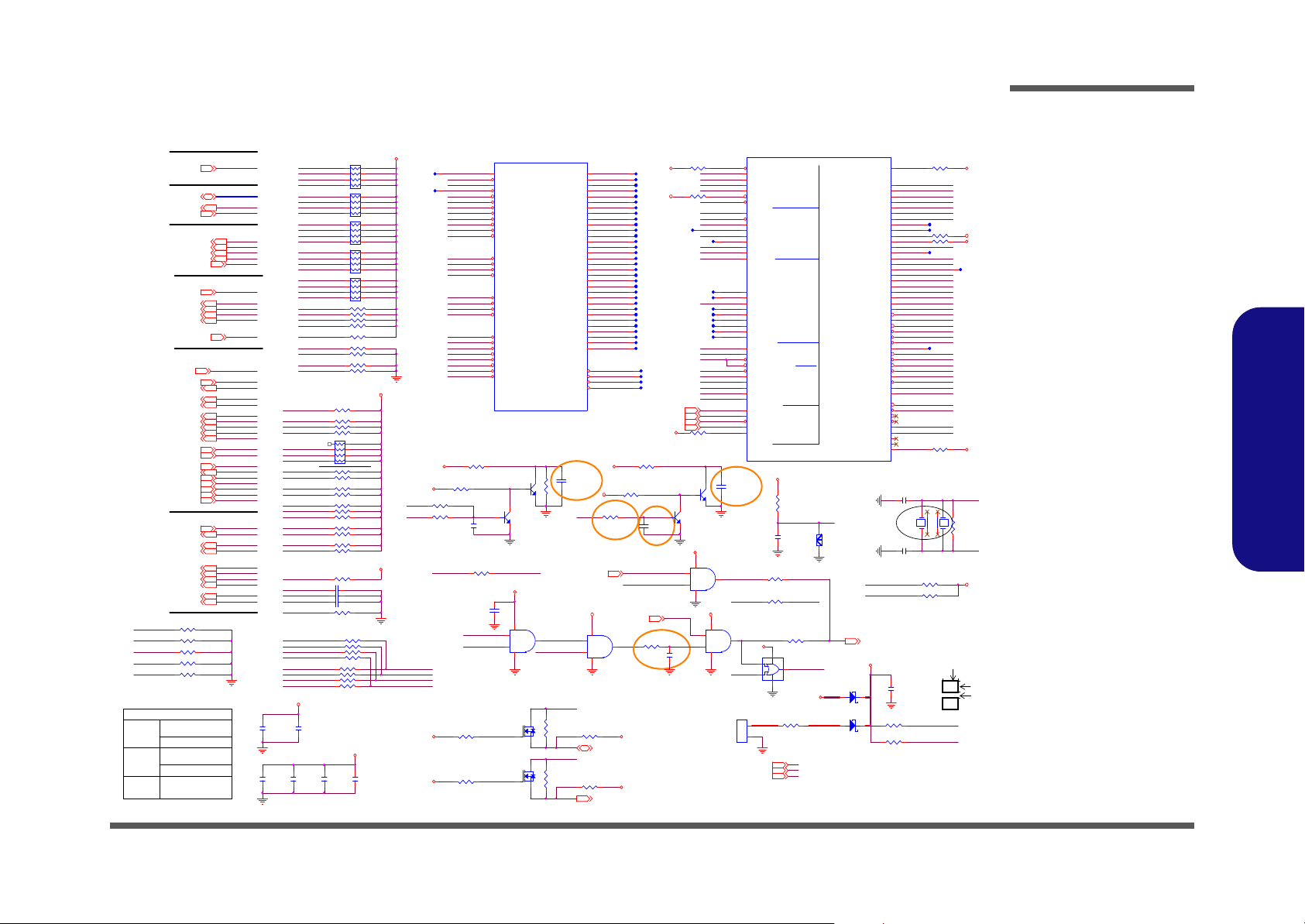
ICH10 PCI/SPI/Other
Z1618
SYNC
HWRST#
PCI_AD 5
BIT_CLK
SDATO
Z1617
Z1615
RSTB
SMBCLK
SMBDATA
PCI_C/ B E#2
PCI_AD 30
PCI_GNT#1
Z1631
PCI_AD 18
PCI_REQ#3
PWROKICH
VRM_PWRGD
Z1633
H_PWRGD
PCI_AD 6
5mil
Z1624
Z1622
Z1623
Z1626
Z1627
Z1625
PCI_C/ B E#3
SUSB#
25mil
20mils
35mil
PCI_GNT#2
PCI_AD 31
PCI_AD 19
Clear CMOS
X8
*32.76 8KHz
14
3 2
PWRGD_3V
Co-layout
HDA_SDOU T
PCI_AD 7
Z1611
SUSB#
Z1612
PCI_DEVSEL#
PCI_IRDY#
VRM_PWRGD? VR_Ready (VRM_PWRGD)?
PCI_SERR#
PCI_STOP#
CHANGE TO 10K FOR QUALIFIED CHIPSETS
PCI_PLOCK#
VRM_PW RGD
PCI_TRDY#
ICH_VRM_PWRGD
PCI_PERR#
PCI_FRAME#
ICH_GP35
PCI_REQ#0
PCI_PME#
PCI_REQ#2
PCI_REQ#1
PCI_INT#D
PCI_INT#B
PCI_INT#A
PCI_GNT#1
PCI_INT#H
PCI_INT#C
PCI_INT#F
PCI_INT#E
PCI_INT#G
ICH_SYNC#
ICHSPK
PCI_GNT#3
ICH_GP9
PCI_AD 20
SB_BLON
PWRGD_PS_BUF
PWRGD_PS
PCI_GNT#0
PCI_AD 8
R550 0_04
PCI_GNT#0
R547 0_04
R544 0_04
R539 0_04
PCI_REQ#0
PCI_INT#C
PCI_INT#B
PCI_INT#A
PCI_INT#H
PCI_INT#F
PCI_INT#D
PCI_INT#E
PCI_INT#G
SUS_ST#
PCI_AD 0
PCI_TRDY#
PCI_FRAME#
PCIRST#
PCI_C/ B E#0
PCI_DEVSEL#
PCI_PLOCK#
PCI_PAR
PCI_IRDY#
PCI_STOP#
CK_P_33M_ICH
PCI_SERR#
PCI_PME#
PCI_PERR#
PCI_AD 21
PWR_BTN#
LPCPME#
PCI_AD 9
Z1610
SWI#
SMI#
SCI#
PM_PWROK
ICH_GP35
ALERT#
Z1607
HDA_BIT_CLK32
PCI_AD 22
SUS_ST#
HDA_SDIN1
ICH_GP8
HDA_SDOUT32
ICH_GP12
HDA_SYNC32
HDA_BIT_C LK
MXM_SD IN 2
Z1630
PWRGD_PS
PWRGD_PS_BUF
Z1629
PCI_AD 10
PWRGD _PS_BU F
SMBCLK
ICH_GP11
SMLINK0
SMLINK1
ICH_GP72
PCI_GNT#2
PCI_GNT#3
MXM_SDATO
MXM_SY NC
MXM_BIT_CL K
SUS_ST#
MXM_AC_RESET#
PCI_AD 23
PE_WAKE#
ICH_WAKE#
PCI_AD 11
TPM_PP need pull down,d is ab le TPM
MXM_AC_RESET#
MXM_BI T_C LK
MXM_SD ATO
MXM_SY NC
LPC_AD[3:0]
GPIO
HDA_SD OUT
CK_PWRGD
CK_14M_IC H
HDA_SY NC
SCI#
LPCPME#
SMI#
ICHSPK
SUSB#
H_PWRGD
HDA_SD IN0
ICH_GP12
RSMRST#
PWROKICH
ODD_DETECT#
HWRST#
PE_WAKE#
PLTRST#
LPC_FRAME#
HDA_RSTB
HDA_BIT_CLK
ICH_GP8
SWI#
HD Audio
LPC
SUSC#
THER M#
PWR_BTN#
ICH_SYNC#
VRM_PWRGD
ICH _VRM_PW RG D
Z1632
SUS_ST#
PE_WAKE# ICH_WAKE#
PCI_AD 24
SBTPM_PP
PCI_AD 12
RTCX1
RTCX2
Zo= 55O? 5%
CK_P_33M_ICH
PCI_REQ#3
LPCPME#
RTCRST#
INTRUDER#Z1614Z1613
R549 0_ 04
INTVRMEN
R546 0_ 04
R543 0_ 04
R538 0_ 04
PCI_AD 25
PCI_AD 13
PCI Interface
LAN_RST#
J_RTC1
BH800.9G
1
2
Z1606
R619 8.2K_04
X5
32.768KHz
14
3 2
MXM_SD IN 2
Q57
2N3904
B
E C
R314 10K_04
R639 390K_06
PCI_AD 1
C316
*0.1u _10V_X7R_04
R315 10K_04
R277 10K_ 04
R675 0_04
R624 8. 2K_04
R642 1K _04
R340 150 K_04
R308 8.2K_04
SMBDATA
C424
1u_10V_X5R_06
R306 10K_04
R286 1K_04
R267 2. 2K_04
R231 10K _04
Z1619
R660 *0_04
R643 10K_ 04
R600 10K_ 04
R287 10K_04
U49D
74LVC08P W
12
13
11
147
C802 *1U_6.3V_04
PCI_AD 26
R661 100 K_04
R623 4.7K_04
U49B
74LVC08PW
4
5
6
147
R275 10K_04
R581 10 K_04
RN10
8P4RX8.2K_04
1
2
3
4 5
6
7
8
C415 20p _50V_NPO_ 04
Q26
MTN7002ZH S3
G
DS
Q27
MTN7002ZHS3
G
DS
R672 *0_04
C858
*1u_10V_X5R_06
R307 4.7K_04
R625 *1K_04
RN12
8P4RX8.2K_04
1
2
3
4 5
6
7
8
Q28
2N3904
B
E C
R290 1K_04
HDA_SDIN032
C849
0.1u_10V_X7R_04
C860
*1u_6.3 V_X5R_04
C385
0.1u_10V_X7R_0 4
Z1620
R667 0_04
R310
10M_04
PCI_AD 14
R294 * 1K_04
D11
ASD751V
A C
C411
0.1u_10V_X7R_04
R316 10K_04
C413 *1U_6.3V_04
R291 *1K_04
C286
*0.1u_1 0V_X7R_04
R587 * 10K_04
Z1621
RN15
8P4RX8.2K_04
1
2
3
4 5
6
7
8
R288 1M_04
U51
74AHC1G32GW
4
53
1
2
RN9
8P4RX8.2K_04
1
2
3
4 5
6
7
8
C337
0.1u_10V _X7R_04
R281 2.2K_04
R649 10K_04
JOPEN1
*OPEN_35mil
R631 8.2K_04
R83 3 90K_1%_06
R224 4. 7K_04
R566 * 8.2K_04
SB_MUTE#
R630 1K_04
ICH10
LPC AUDIO
RTC
LAN
MISC
SPISM B
REV = 0.72
4OF6
IC
U1LBU42D
ICH10R
FWH 4/LF RAMEB
L5
HDA_RSTB
AJ1
HDA_SDI N1
AH4
HDA_SDI N2
AH1
SLP_S4B
B13
SLP_S5B/GPIO63
G17
SLP_S3B
A13
SPKR
N8
HDA_SDI N3
AJ3
HDA_SDO UT
AJ2
HDA_SY NC
AK1
CLK14
M5
HDA_SDI N0
AK3
RSMRSTB
F22
INTVRMEN
E23
HDA_BI T_C LK
AH3
FWH0/LAD0
K3
FWH1/LAD1
H1
FWH2/LAD2
M7
GP20
AF5
GP57/TPM_PP/ JTAGTCK
C12
LAN100_SLP
E21
SUSCL K/GP62
R5
PWROK
C25
CK_PWRGD
T8
FWH3/LAD3
J1
RTCX1
A21
RTCX2
B21
SMBCLK
H16
SMBDATA
E16
SMLINK 0
A15
SMLINK 1
B15
CPUPWRGD
AD23
LINKALERTB/GP60/JTAGRST
F18
SPI_C S0B
E25
SPI_C LK
G23
SPI_C S1B
F23
SRTCR STB
H20
GP28
G18
GP27
A11
S4_STATEB/GP26
C11
GP18
K1
GP0/BMBUSYB
N7
LDRQ 0B
L6
LAN_R STSYN C
E14
GLAN_CLK
F25
LAN_R STB
C21
LAN_R XD0
G15
LAN_R XD2
E13
LAN_TXD0
F15
LAN_TXD1
F14
LAN_TXD2
G14
RTCRSTB
A25
SMBALER TB/GP11/ JTAGTDO
C16
SPI_MOSI
C26
SPI_MI SO
B26
GP14/JTAGTDI/QST_BMBUS YB
A9
STP_PCIB/GP 15
C15
DPRSLPVR/GP16
M2
GP24/MEM_LED
A14
STP_CPUB/GP25
B18
GP32
K2
GP56
F16
GP33
AF6
GP34
AH5
THR MB
AK26
VRMPWRGD
C22
MCH _SYN C B
AH25
PWRBTNB
T3
RIB
G19
SUS_STATB/LPCPD/GP61
R1
SYS_R ESETB
F19
PLTRSTB
C14
WAKEB
E20
INTRUDERB
G21
SLP_MB
F17
GP72
C13
DPRSTPB
AK28
DPSLPB
AE24
TP3
F20
SATACLKREQB/GP 35
L1
LAN_R XD1
H14
LDRQ 1B/GP23
J3
DRAMPWROK/GP8
A20
GP9/WOL_EN
A18
GP10/CPU_MISSI NG/JTAGTMS
C17
GP12
A8
GP13
A19
R82 1K_04
R568 8. 2K_04
C835
*0.1u_1 0V_X7R_04
R650 *10K_04
GP56
D12
ASD751V
A C
R328 *0_04
R618 8.2K_04
R270
*0_04
R282 4. 7K_04
C303 *1U_6.3V_04
R219 1K_ 04
R274
*0_04
R280 2.2K_04
U49A
74LVC08PW
1
2
3
147
R620 1. 1K_04
R616 10K _04
R318
100K_0 4
R269 8.2K_04
R273 10K _04
PCI_AD 2
ICH10
PCI
REV = 0.72
U1LB
1OF6
IC
U42A
ICH 10R
PIRQEB/GP2
K6
PIRQFB/GP3
L7
C/BE3B
E8
AD27
D1
REQ3B/GP54
G8
REQ2B/GP52
F13
REQ1B/GP50
G13
PIRQBB
E1
PIRQCB
F1
PIRQAB
J5
GNT0B
H5
SERRB
K5
DEVSELB
C6
PAR
E3
PERRB
F5
FRAMEB
G12
PLOCKB
H8
TRDY B
E6
PMEB
R3
IRDYB
J8
C/BE2B
C4
C/BE1B
G9
C/BE0B
F11
PIRQHB/GP5
G2
PIRQGB/GP4
F2
PIRQDB
A3
REQ0B
K7
STOPB
F10
PCIRSTB
R2
PCICLK
B3
AD30
G1
AD31
H3
AD19
G10
AD29
F3
AD28
J7
AD23
G5
AD15
D2
AD14
C5
AD13
F8
AD11
A4
AD10
E7
AD9
B4
AD8
B6
AD7
B7
AD6
E10
AD5
E12
AD4
A5
AD3
C9
AD2
E9
AD22
H6
AD21
D3
AD20
G6
AD24
C1
AD25
C2
AD26
C3
AD17
G7
AD18
E11
AD16
E5
AD0
C10
GNT1B/GP51
A7
GNT2B/GP53
C7
GNT3B/GP55
F7
AD12
H12
AD1
C8
C433
4.7u_6.3V_X5R_06
R622 1. 1K_04
C318
0.1u_10V_X7R_0 4
R663 10K_04
C419 20p _50V_NPO_ 04
U49C
74LVC08P W
9
10
8
147
R266 * 8.2K_04
ODD_DETECT#
Q56
2N3904
B
E C
R285
47K_1%_04
R523 1K _04
C145
1u_6.3V_Y 5V_04
R674 1K_04
R317 10K _04
Q31
2N3904
B
E C
RN11
8P4RX8.2K_04
1
2
3
4 5
6
7
8
R632 10K_04
RN16
8P4RX10K_04
1
2
3
4 5
6
7
8
0727 D03 BCN upated
C382
1u_6.3V_Y 5V_04
R271 4. 7K_04
RTCVCC
3V
3VS
PCI_AD 27
3VS
3VS
3VS
3VS
3V
3V
3V
3V
3VS
VDD3
3V
RTCVCC
RTCVCC
3VS
3V
3VS
3V
3V
3VS
3VS
3V
3VS
3VS
SCLK 7..9,12,19,20,34,37,38
3V
3V
3V
LPC_FRAME#20,28
SDATA 7 ..9,1 2,19,20, 34,37,38
MISC
ICH_GP810
ICH_GP1210
LPCPME#28
HDA_RSTB32,33
CK_14M_ICH19
RSMRST#
Z1605
SWI#28
SMI#28
SCI#28
LPC_AD[3:0]20, 28
PLTRST#12, 15,20, 21,28
ICHSPK32
CK_P_33M_I CH19
HWRST#4
SUS_ST#20
H_PWRGD4, 12
PCI_AD 15
HW S trap
SUSC#28
THERM#15
CK_PWRGD19,20
ICH_VRM_PWRGD12
VRM_PWRGD38
RSMRST#28
PWR_BTN#28
ICH_SYNC#12
PE_WAKE#29,30, 34
SUSB#10,28, 29,41
SB_BLON25
ODD_DETECT#23
PWROKICH12, 15,24. .26
MXM_AC_RESET#21
MXM_SDATO21
MXM_SYN C21
ICH_SUSB#
3VS7..9,12,13,15,17..28,30..34,36,37,40,41
3V6,12,13,15,17, 20,21 ,25,28. .30,34 ,35,37. .41
MXM_BIT_CL K21
VDD328,34..36,39,41..43
LAN100_SL P
PWRGD_3V19
PWR OKICH 12,15,2 4..26
PM_PWROK15
1.5V_PW RGD39
SPI_MISO15
PWRGD_PS4,12,15, 28,38
GP5612
SPI_MOSI15
SPI_CLK15
SPI_CS15
PWRGD_PS_BUF19
ICH_CPU_STP19
ICH_PCI_STP19
ODD_DETECT#
SB_BLON
SPKR
H
L
SB_BLON
HDA_RSTB
HD Audio
For M X M
MXM_SDIN 221
NO Reboo t
NOT NO rebo ot
PCI_AD 3
0727 D03 BCN upated
ICH_VRM_PWRGD
PCIE_ RST#
Z1628
PCI_AD 28
PCI_GNT#0
SB_MUTE#
LPC ROM
SPI ROML
H
if not use PULL LOWLAN_R ST#
PCI_AD 16
Z1616
D03
PCI_REQ#1
PLTRST#
ICH_PCI_STP
ICH_CPU_STP
SPI_MISO
SPI_MOSI
SPI_CL K
SPI_CS
LPC_AD 0
Z1601
LPC_AD 2
LPC_AD 3
LPC_F RAME#
LPC_AD 1
PWRO KIC H
INTVRMEN
RSMRST#
ICHSPK
INTRUDER#
Z1602
HWRST#
ICH_WAKE#
PLTRST#
GP56
ICH_GP9
HDA_SDIN0
RSTB
BIT_CL K
ICH_PCI_STP
SMI#
ICH_GP12
SCI#
ICH_GP8
SWI#PCI_AD 4
ICH_GP72
CK_PWRGD
ICH_SUSB#
SUSC#
LAN_R ST#
Z1603
CK_14M_IC H
SYN C
SDATO
SMLINK 1
RTCRST#
RTCX1
RTCX2
ALERT#
SMBDATA
SMBCLK
ICH_GP11
SMLINK 0
GP56
HDA_SYN C
THE RM#
SBTPM_PP
LAN100_SLP
ICH_GP35
Z1608
PCI_C/ B E#1
ICH_CPU_STP
ICH_VRM_PWRGD
ICH_SYNC#
PWR_ BTN#
RI#
H_PWRGD
PCI_AD 29
PCI_AD 17
ICH_VRM_PWRGD
PCI_REQ#2
PWRGD_3V
PE_WAKE#
RI#
Sheet 16 of 52
ICH10 PCI/SPI/
Other
Schematic Diagrams
B.Schematic Diagrams
ICH10 PCI/SPI/Other B - 17
Page 78

Schematic Diagrams
VSS_100
ICH10
VSS_099
REV = 0.72
6OF6
U1LB
IC
U42F
ICH 10R
VSS_003
AA1
VSS_004
AA29
VSS_144
R13
VSS_145
R14
VSS_142
P28
VSS_141
P26
VSS_139
P19
VSS_138
P18
VSS_137
P17
VSS_136
P16
VSS_135
P15
VSS_134
P14
VSS_133
P13
VSS_132
P12
VSS_131
N30
VSS_100
H13
VSS_001
A1
VSS_002
A30
VSS_005
AA30
VSS_006
AA5
VSS_007
AA6
VSS_008
AB26
VSS_009
AB28
VSS_010
AB3
VSS_011
AC1
VSS_012
AC12
VSS_013
AC24
VSS_014
AC29
VSS_015
AC30
VSS_016
AC5
VSS_017
AC6
VSS_018
AC8
VSS_019
AD14
VSS_020
AD15
VSS_021
AD16
VSS_022
AD18
VSS_023
AD19
VSS_024
AD22
VSS_025
AD3
VSS_026
AD7
VSS_027
AD9
VSS_028
AE1
VSS_029
AE10
VSS_030
AE12
VSS_031
AE13
VSS_032
AE14
VSS_033
AE15
VSS_034
AE16
VSS_035
AE18
VSS_036
AE19
VSS_037
AE25
VSS_038
AE5
VSS_039
AE6
VSS_040
AE8
VSS_041
AE9
VSS_042
AF13
VSS_043
AF15
VSS_044
AF20
VSS_045
AF23
VSS_046
AF25
VSS_047
AF29
VSS_049
AF9
VSS_050
AG28
VSS_051
AH13
VSS_052
AH15
VSS_053
AH19
VSS_054
AH2
VSS_055
AH20
VSS_056
AH6
VSS_057
AH8
VSS_058
AJ12
VSS_059
AJ14
VSS_060
AJ16
VSS_061
AJ20
VSS_062
AJ23
VSS_063
AJ26
VSS_064
AJ5
VSS_065
AJ8
VSS_066
AK12
VSS_067
AK14
VSS_068
AK16
VSS_069
AK2
VSS_070
AK29
VSS_071
AK30
VSS_072
AK8
VSS_073
B11
VSS_074
B14
VSS_075
B17
VSS_076
B19
VSS_077
B2
VSS_078
B22
VSS_079
B25
VSS_080
B28
VSS_081
B5
VSS_082
B8
VSS_083
D28
VSS_084
E15
VSS_085
E18
VSS_086
E2
VSS_087
E22
VSS_088
E29
VSS_089
E30
VSS_090
F12
VSS_091
F21
VSS_092
F26
VSS_093
F28
VSS_094
F6
VSS_095
F9
VSS_096
G16
VSS_097
G25
VSS_098
G29
VSS_099
G30
VSS_198
B27
VSS_197
AF3
VSS_194
AK27
VSS_196
AJ4
VSS_195
AH29
VSS_102
H2
VSS_103
H22
VSS_104
H25
VSS_106
H28
VSS_185
W23
VSS_182
W1
VSS_167
U15
VSS_186
W29
VSS_183
W14
VSS_181
V7
VSS_180
V3
VSS_179
V28
VSS_178
V26
VSS_177
V18
VSS_176
V17
VSS_175
V16
VSS_174
V15
VSS_172
V13
VSS_166
U14
VSS_165
U13
VSS_164
T5
VSS_163
T29
VSS_162
T2
VSS_161
T19
VSS_160
T18
VSS_159
T17
VSS_158
T16
VSS_157
T15
VSS_156
T14
VSS_155
T13
VSS_154
T12
VSS_153
R8
VSS_152
R30
VSS_151
R29
VSS_150
R23
VSS_149
R18
VSS_148
R17
VSS_147
R16
VSS_143
P6
VSS_140
P2
VSS_107
H9
VSS_146
R15
VSS_184
W16
VSS_192
Y3
VSS_191
Y28
VSS_110
J6
VSS_108
J29
VSS_173
V14
VSS_171
U23
VSS_170
U18
VSS_169
U17
VSS_168
U16
VSS_190
Y26
VSS_193
Y7
VSS_189
W6
VSS_188
W5
VSS_187
W30
VSS_105
H26
VSS_101
H19
VSS_048
AF7
VSS_109
J30
VSS_111
K26
VSS_112
K28
VSS_113
L2
VSS_114
L23
VSS_115
L29
VSS_116
L30
VSS_117
M14
VSS_118
M16
VSS_119
M26
VSS_120
M28
VSS_121
M6
VSS_122
M8
VSS_123
N13
VSS_130
N29
VSS_129
N23
VSS_128
N18
VSS_127
N17
VSS_126
N16
VSS_125
N15
VSS_124
N14
C800
0.1u_1 0V_X7R_04
V_1P5_ICH
5V
RTCVCC
3V
RTCVCC
3VS
3VS
3VS
1.5VS
3V
3VS
3V
5VS
1.5VS
1.5VS
3V
1.5VS
1.5VS
ICH_1. 1VS
1.5VS
1.5VS
ICH_1.1VS
3V
1.5VS
1.5VS
1.5VS
3VS
1.5VS
3V6,12,13,15,16,20,21,25,28..30,34,35,37..41
1.1VS
3VS
CPU_VTT4, 5,15,37, 38 5VS12,18,21..24,26,27,31..34,36,41
3VS7..9,12,1 3,15,16, 18..28, 30..34, 36,37, 40,41
1.1VS10..13, 19,40, 41
5V4,22,25,29, 35..42
1.5VS11, 13,15, 31,34,40, 41
ICH _1.1VS42
GLCI_PLL
VCCD MI_PLL_ICH
VCCHDA
V_1P5_ICH
Z1702
V_1P1EP_IN T
Z1701
VCCSATA_PLL_ICH
VCCDMI_PLL_ICH
GLCI_PLL
V_1P1_STBY _I NT
V_1P5_CL_IN T
V_3P3_CL_R
NC f or IC H1 0 power pin/ N o LAN
V_1P05_VCCA UX
V_REF 5V_SU S
V_1P5_CL_IN T
V_REF5V
VCCSATA_PLL_ICH
V_REF5V_SUS
V_REF 5V
Z1703
L106
*HCB100 5KF-121T20_04
C329
*1U_6.3V _X5R_04
C405
0.1u_10V_X7R_04
3V
L90
HCB1608KF -121T25_06
C738
10u_6.3V_08_H125
C282
0.1u_1 0V_X7R_04
L71
HCB1005KF -121T20_04
Q55
2N3904
B
E C
C276
1u_6.3V_X5R_04
C388 *0.1u_10V_X7R_04
C406
1u_6.3V_X5R_04
VCCC L_3V_I CH
C399
10u_6.3V_08_H125
C338
10u_6.3V_08_H125
C367
0.1u_10V_X7R_04
C745
0.1u_10V_X7R_04
C296
0.1u_10V_X7R_04
C384
*0. 1u_10V_X7R _04
C378
0.1u_10V_X7R_04
C750
1u_6.3V_X5R_04
C375
10u_6.3V_08_H125
C810
1u_6.3V_Y5V_04
C781
4.7u_6.3V _X5R_06
C290
1u_6.3V_X5R_04
C366
0.1u_10V_X7R_04
C381
0.1u_10V_X7R_04
C797
10u_6.3V_08_H125
C380
1u_6.3V_X5R_04
ICH10
REV = 0.72
MATERI AL = I C
U1LB
5OF6
U42E
ICH10R
VCC3_3_04
AC19
VCC3_3_06
AF21
VCC1_ 1_26
W15
VCC1_ 1_27
W17
VCC1_ 1_24
W12
VCC1_ 1_25
W13
VCC1_ 1_28
W18
VCC1_ 1_29
W19
V_CPU_IO_1
AH28
V_CPU_IO_2
AJ30
VCC3_ 3_01
AH30
VCC3_ 3_02
AK4
VCC3_3_07
AH24
VCCSATAPLL
AK20
VCCDMIPLL
T30
VCCUSBPLL
AK5
VCC3_ 3_11
G11
VCC3_ 3_12
G3
VCC3_ 3_13
H7
VCC3_ 3_14
J2
VCC1_5_B_12
AE30
VCC1_5_B_20
M23
VCC1_5_B_13
J24
VCC1_5_B_16
K24
VCC3_ 3_09
B1
VCC3_ 3_08
A2
VCC1_5_B_10
AE28
VCC1_5_B_14
J25
VCC1_5_B_17
K25
VCC1_5_B_19
L25
VCC1_5_B_21
M24
VCC1_5_B_22
M25
VCC3_ 3_16
L8
VCC1_5_A_26
AC15
VCC1_5_A_27
AC16
VCC1_5_A_08
AK18
VCC1_5_A_07
AJ18
VCC1_5_A_06
AH18
VCC1_5_A_05
AH17
VCC1_5_A_04
AF17
VCC1_5_A_03
AE17
VCC1_5_A_02
AD17
VCC1_5_A_01
AC17
VCC1_5_A_18
AK10
VCC1_5_A_17
AJ10
VCC1_5_A_16
AH11
VCC1_5_A_15
AH10
VCC1_5_A_14
AF11
VCC1_5_A_13
AE11
VCC1_5_A_12
AD13
VCC1_5_A_11
AD12
VCC1_5_A_10
AD11
VCC1_5_A_09
AC13
VCC1_5_B_46
Y25
VCC1_5_B_45
Y24
VCC1_5_B_44
Y23
VCC1_5_B_43
W25
VCC1_5_B_42
W24
VCC1_5_B_41
V25
VCC1_5_B_37
U29
VCC1_5_B_36
U28
VCC1_5_B_35
U24
VCC1_5_B_34
T28
VCC1_5_B_33
T26
VCC1_5_B_32
T25
VCC1_5_B_31
T24
VCC1_5_B_30
T23
VCC1_5_B_29
R25
VCC1_5_B_28
R24
VCC1_5_B_27
P25
VCC1_5_B_26
P24
VCC1_5_B_25
P23
VCC1_5_B_24
N25
VCC1_5_B_23
N24
VCC1_5_B_18
L24
VCC1_5_B_15
K23
VCC1_5_B_11
AE29
VCCSUS1_5_1
H18
VCCC L1_1
A23
VCCSUS1_1_1
AC7
VCCRTC
A22
VCCSUS 3_3_06
H15
VCCSUS 3_3_05
E17
VCCSUS 3_3_04
C20
VCCSUS 3_3_03
B20
VCCSUS 3_3_02
A17
VCCSUS 3_3_17
Y8
VCCSUS 3_3_16
W8
VCCSUS 3_3_15
W7
VCCSUS 3_3_14
V8
VCCSUS 3_3_13
U8
VCCSUS 3_3_12
U7
VCCSUS 3_3_11
U6
VCCSUS 3_3_10
U5
VCCSUS 3_3_09
U3
VCCSUS 3_3_08
U2
VCCSUS 3_3_07
U1
VCCLAN3_3_2
B12
VCCLAN3_3_1
A12
VCC1_ 1_23
V19
VCC1_ 1_22
V12
VCC1_ 1_21
U19
VCC1_ 1_20
U12
VCC1_ 1_19
R19
VCC1_ 1_16
N12
VCC1_ 1_15
M19
VCC1_ 1_12
M15
VCC1_ 1_08
H24
VCC1_ 1_06
G24
VCC1_ 1_05
F24
VCC1_ 1_04
E24
VCC1_ 1_03
C24
VCC1_ 1_02
B24
VCC1_ 1_01
A24
VCC1_5_A_32
T1
VCC1_5_A_31
AB8
VCC1_5_A_30
AB7
VCC1_5_A_29
AA8
VCC1_5_A_28
AA7
VCCLAN1_1_2
B10
VCCLAN1_1_1
A10
VCC1_ 1_07
H23
VCC3_ 3_15
K8
VCC3_ 3_10
B9
VCC1_5_A_25
AC14
V5REF
A6
VCCHDA
AC10
VCC1_5_A_20
AC18
VCCG LANPLL
A28
VCC1_5_B_03
AA25
VCC1_5_B_04
AB24
VCC1_5_B_05
AB25
VCC1_5_B_06
AC25
VCC1_5_B_07
AD25
VCC1_5_B_08
AD26
VCC1_5_B_09
AD28
VCC1_5_B_38
U30
VCC1_5_B_39
V23
VCC1_5_B_40
V24
VCCSUS1_5_2
AD8
VCCSUS1_1_2
H17
VCCGLAN3_3
A27
VCC1_5_B_02
AA24
VCCGLAN1 _5_3
C29
VCCCL3_ 3_2
C23
VCCSUS 3_3_01
AF2
VCCGLAN1 _5_4
C30
VCCCL3_ 3_1
B23
VCCDMI_2
AG30
VCCDMI_1
AG29
VCC1_5_A_19
AC11
VCC1_5_A_24
H11
VCC1_5_A_23
H10
V5REF _SUS
AF1
VCCGLAN1 _5_2
C28
VCCGLAN1 _5_1
B30
VCC1_5_B_01
AA23
VCC3_3_05
AC21
VCC3_3_03
AD10
VCCSUSHDA
AC9
VCCCL1_5
A26
VCC1_5_A_21
AC20
VCC1_5_A_22
AB23
VCC1_ 1_18
R12
VCC1_ 1_17
N19
VCC1_ 1_14
M18
VCC1_ 1_13
M17
VCC1_ 1_11
M13
VCC1_ 1_10
M12
VCC1_ 1_09
J23
C804
0.1u_10V_X7R_04
C324
10u_6.3V_08_H 125
C322 *0.1u_10V_X7R_04
L87
HCB1005KF -121T20_04
C343
10u_6.3V_08_H125
C386
0.1u_10V_X7R_04
L91
HCB1608KF -121T25_06
C325
10u_6.3V_08_H 125
L85
HCB1005KF -121T20_04
C811
0.1u_10V_X7R_04
C803 *0.1u_1 0V_X7R_04
C330
0.1u_10V_X7R_04
C780
0.1u_10V_X7R_04
C342
1u_6.3V_X5R_04
C323
*1U_6.3V_X5R_04
C358
1u_6.3V_X5R_04
C344
1u_6.3V_X5R_04
Q45
2N3904
B
E C
C377
10u_6.3V_08_H 125
C273
0.1u_10V_X7R_04
C326
10u_6.3V_08_H 125
C410
0.1u_10V_X7R_04
C376
0.1u_10V_X7R_04
R556
100_06
R617 * 10mil_NP_0 4
C799
0.1u_10V_X7R_04
L83
HCB1608KF -121T25_06
C404
0.1u_10V_X7R_04
C749
0.1u_10V_X7R_04
C748
4.7u_6.3V_ X5R_06
C327
1u_6.3V_X5R_04
R629
10_06
Sheet 17 of 52
ICH10 Power/GND
B.Schematic Diagrams
B - 18 ICH10 Power/GND
ICH10 Power/GND
Page 79

Fan CTRL
Sheet 18 of 52
Fan CTRL
3VS
VGA_FAN128
3VS
R686
*100K_04
3VS
U53
*74AHC1G32GW
4
53
1
2
Q60
*MTN7002ZHS3
G
DS
R684
*100K_04
U21
G990P11U
VOUT
3
GND
5
VIN
2
FON
1
VSET
4
GND
6
GND
7
GND
8
D8 *SCS355V
AC
U10
G990P11U
VOUT
3
GND
5
VIN
2
FON
1
VSET
4
GND
6
GND
7
GND
8
R559
*0_04
C774
0.1u_16V _Y5V_04
C200
0.1u_16V_Y5V_04
R67 4.7K_04
C207
10u_10V_Y5V_08
U38
G990P11U
VOUT
3
GND
5
VIN
2
FON
1
VSET
4
GND
6
GND
7
GND
8
J_CPUFAN1
85205-03001
1
2
3
C143
0.1u_16 V_Y 5V_04
R166 4.7K_04
C142
10u_10V _Y5V _08
R478 4.7K_04
C724
10u_10V_Y5V_08
3VS
J_SYSFAN1
85205-03001
1
2
3
R80
*0_04
Z1802
D13 *SCS355V
AC
Z1804
J_VGAFAN2
85205-03001
1
2
3
D25 *SCS355V
AC
R145
*0_04
5VS
3VS
5VS
5VS5VS_CFAN
3VS
5VS
5VS
3VS
5VS_CFAN
5VS_SFAN
5VS_VFAN2
5VS_VFAN2
5VS_SFAN
5VS
5VS12 ,17,21..24,26,27,31..34,36,41
CPU_FAN28
VGASEN_SEL28
CPU_VTT4,5,15,37,38
SYS _FAN28
3VS7..9,12,13,15..17,19..28,30..34,36,37,40,41
VGA_FANSEN1
CPU_FANSEN 28
VGA_FANSEN2
VGA_FON2#VGA_F ON2#
VGA_F ANS EN2
U31
PI5A3158
0B0
2
1B0
11
S0
10
0B1
5
1B1
8
S1
7
VCC
12
A0
1
GND
3
VCC
9
GND
6
A1
4
3
VGA_FANSEN 28
1
J_VGAFAN1
SYS _FON # SYS_FON #
3
R100
*10K_04
J_SYSFAN1
5VS
VGA_FON1#
1
SYS FAN CONTROL
Z1807
R366 0_04
VGASEN _SEL
VGA_FAN228
C458 0.1u_16V_Y5V_04
SYSFAN_SEN
3VS
Z1808
Z1809
R377 0_04
R368 0_04
CPU_FANSEN
VGA_FANSEN
VGASEN_SEL28
Q59
*MTN7002ZHS3
G
DS
U52
*74AHC1G32GW
4
53
1
2
3VS
R683
*100K_04
Z1803
R685
*100K_04
Z1805
CPUFAN_SEN
Z1806
SYS FAN _SEN
Z1810
Z1811
Z1812
Z1813
Z1801
R376 0_04
R365 0_04
R375 0_04
R367 0_04
SYS FAN _SEN
VGA_F ANSE N2
CPUFAN_SEN
VGA_F ANSE N1
3VS
3VS
1
J_CPUFAN1
CPU FAN CONTROL
J_VGAFAN1
3
R101
*0_04
VGA_F ON1#
U11
G990P11U
VOUT
3
GND
5
VIN
2
FON
1
VSET
4
GND
6
GND
7
GND
8
5VS_VFAN
D26 *SCS355V
AC
VGA_FANSEN1
5VS
VGA_FON1#
3VS
C162
10u_10V_Y5V_08
R487 4.7K_04
VGA FAN CONTROL
J_VGAFAN1
85205-03001
1
2
3
C171
0.1u _16V_ Y5 V_04
1
3
5VS_VFAN
5VS
R140
*10K_04
3VS
5VS
VGA_FON2#
SYS_FON#
R557
*10K_04
5VS
R81
*10K_04
CPU_FON#
5VS
U54A
*74LVC08PW
1
2
3
147
U54B
*74LVC08PW
4
5
6
147
U54C
*74LVC08PW
9
10
8
147
U54D
*74LVC08PW
12
13
11
147
CPU_FON#
CPUFAN_SEN
CPU_FON#
Schematic Diagrams
B.Schematic Diagrams
Fan CTRL B - 19
Page 80

Schematic Diagrams
PCIE_CLK_U SB3# 29
PCIE_CLK_U SB3 29
H_FSBSEL0
ICH_CPU_STP_R
FSB
FSC
PCI4R
FSA
PCI2R
PCI3R
CK_USB_48M_IC H
CK_14M_ICH
CK_P_33M_ICH
CK_P_33M_SIO
Sel_SRC1_25_24.576**
CK_PCIF1
XTAL O
XTAL I
FSB
PCI4R
CK_PCIF1
PCI3R
FSA
FSC
PCIE_CLK_BUFFER
USB 3 . 0
Z1903
ICH_PCI_STP_R
Z1908
Z1907
IOH PCIE16X CLK
R124 1K_04
C192
0.1u_16V_Y5V _04
R504
1K_04
C707
10u_6.3V_08_H125
R486 47K_04
C177
0.1u_16V_Y5V_04
Q39
2N3904
B
E C
R142 10K_04
R485 33_04
C718
0.1u_16V_Y5V_04
R533 10K_04
C721
27p_50V_NPO_04
R499 *47K_04
R497 *1K_04
D03
C710
0.1u_16V_Y5V _04
R514
4.7K_04
R498 33_04
R475
*100K_04
R134 1 0K_04
C158
0.1u_16V_Y5V_04
R123 *10K_04
U37
IDTCV193
Vdd_PLL3
16
Vdd_48
9
Vdd_PCI
2
Vdd_REF
61
Vdd_SRC
39
Vdd_CPU
55
Vdd_IO
12
Vdd_PLL3_IO
20
Vdd_SRC_IO
26
Vdd_SRC_IO
45
Vdd_SRC_IO
36
Vdd_CPU_IO
49
Sel_SRC1_25_24.576* *
48
Xta l_ I n
60
Xtal_Out
59
CKPWRGD/PD#
56
FS_B / Test Mode
57
SCL
64
SDA
63
VSS_IO
15
Vss_PLL3
19
Vss_48
11
Vss_CPU
52
VSS_PCI
8
Vss_REF
58
Vss_SRC
23
Vss_SRC
29
Vss_SRC
42
CPUT0
54
CPUC0
53
CPUT1
51
CPUC1
50
SRCT8 /C PU_ ITPT
47
SRCC8 / CPU_ I TPC
46
SRCC0 / DO T96C
14
SRCT0 / DOT96T
13
SRCT1/25MHz0
17
SRCC1/ 25MHz1/24.576MHz
18
SRCT2/SATA
21
SRCC 2/SATA
22
SRCT3 / CR#_C
24
SRCC3 / CR #_D
25
SRCT4
27
SRCC 4
28
PCI_St op#/ SR C T5
38
CPU_Stop#/ SRC C5
37
SRCT6
41
SRCC 6
40
SRCT7/ CR #_F
44
SRCC7/ C R#_E
43
SRCT9
30
SRCC 9
31
SRCT10
34
SRCC 10
35
SRCT11/ CR#_H
33
SRCC11/ CR#_G
32
PCI0/ C R #_A
1
PCI1/C R#_B
3
*PCI2/ SR_ENABLE
4
**PC I3/SATA_SEL
5
PCI4/ S R C 5_EN
6
PCIF 5/ ITP_EN
7
USB 48 / FS_A
10
REF / FS_C / TestSel
62
C198
0.1u_16V_Y5V_04
C723 *10p_50V_NPO_04
R506
1K_04
C715
0.1u_16V_Y5V _04
X7
14.31MHz
12
R115 1K_04
C730 *10p_50V_NPO_04
Q40
2N3904
B
E C
R496
1K_04
R111 *10 K_04
R507
4.7K_04
C706
0.1u_16V_Y5V_04
R503
100_04
R126
*10K_04
Q42
2N3904
B
E C
R116 10K_04
C702
0.1u_16V_Y5V _04
R535
*10K_04
R492 33_04
R500 *33K_04
C727 *10p_50V_NPO_04
R536 10K_04
R122 33K_04
R113 10K_04
R502
*1K_04
R534
*10K_04
R135 * 10K_04
R489 33_04
R112 *1K_04
C729 *10p_50V_NPO_04
Q43
2N3904
B
E C
L77
HCB2012KF-121T30_08
1 2
L76
HCB2012KF-121T30_08
1 2
R114 * 10K_04
C704
10u_6.3V_08_H125
C728
27p_50V_NPO_04
R493 33_04
C709
0.1u_16V_Y5V_04
R474
100K_04
1.1VS
3VS
3VS
1.1VS
3VS
1.1VS
3VS
3VS
CLKVDD
3VS
3VS
3VS
SDATA7..9,12,16,20,34, 37,38
3VS
CLKVDD_IO
CK_P_33M_ICH 16
CK_P_33M_SIO 28
CK_PE_100M_ICH_H 15
CK_100M_SATA_H 15
CK_PWRGD16,20
CK_100M_SATA_L 15
CK_133M_IOH_DN 10
PCLK_TPM 20
CK_PE_MXM1_DP 21
SCLK7..9,12,16, 20,34, 37,38
CK_133M_CPU_DN 4
CK_PE_100M_ICH_L 15
CK_PE_MXM1_DN 21
PCIE_CLK_JMB# 30
CK_USB_48M_ICH 15
CK_14M_ICH 16
PCIE_CLK_1394B 31
CK_133M_IOH_DP 10
3VS7..9,12, 13,15..18,20.. 28,30.. 34,36,37, 40,41
CK_133M_CPU_DP 4
PCIE_CLK_JMB 30
PCIE_CLK_WAN # 34
3V6, 12,13,15. .17,20,21,25,28. .30,34, 35,37..41
PCIE_CLK_1394B# 31
1.1VS10. .13,17, 40,41
PCIE_CLK_WAN 34
CK_PE_100M_IOH0_DN 11
CK_PE_100M_IOH0_DP 11
ICH_CPU_STP 16
ICH_PCI_STP 16
PWRGD_3V16
CK_PE_100M_IOH1_DN 11
CK_PE_100M_IOH1_DP 11
PWRGD_PS_BUF16
PWRGD_PS_BUF16
PWRGD_3V16
PCIE1X WLAN
PWRGD_PS_BUF
PWRGD_3V
PWRGD_3V
CK_PE_MXM2_DP 22
CK_PE_MXM2_DN 22
PCIE16X MXM3.0
ICH_CPU_STP
166
333
48
IOH
33.3
14.318
48
FSC
133
ICH
100
14.318
CPU
0
JMB251
PCI
33.3
PCI2R
100
14.318
1
33.3
0
14.318
1
SATA
33.3
1
96
1
1
0727 D03 BCN up at e
960
1
96
33.3
0
PCIE16X MXM3.0
1
33.3
For SLG8XP549T
0
96
33.3
0
96
100
REF
0
100
SRC[7..0]
96
0
CPU
0
100
0
1
100
48
FSA DOT
EC
1
14.318
100
48
FSB
14.318
PCIE16X CLK
0
266
96
100
48
USB
CK_PWRGD_R
TPM
IOH
48
400
480 200
14.318
R96 0_04
R89 0_04
ICH_PCI _STP
PCIE_CLK_BU FFER 20
PCIE_CLK_BU FFER# 20
1394B
PWRGD_PS_BUF
FSA
H_FSBSEL2
Z1901
Z1904
Z1905
Z1906
Z1902
FSC
Sheet 19 of 52
Clock Generator
CV193
Clock Generator CV193
B.Schematic Diagrams
B - 20 Clock Generator CV193
Page 81

Clock Buffer ICS9DB403GLFT
R456 475_1%_04
PCI E_DI F_2
PCI E_DI F_2 #
PCIE_CLK_BUFFER#19
PCIE_CLK_BUFFER19
C150
10u_10V_Y5V_08
C148
0.1u_10V_X7R_04
CLK_HDMI_IN
CLK_HDMI_IN#
C151
10u_10V_Y5V_08
DIF_5#
DIF_5
PCIE_CLK_ROBSON#
PCIE_DIF_2#
PCIE_CLK_ROBSON
PCIE_DIF_2
C153
0.1u_10V_X7R_04
X9
*32.768KHz
14
3 2
OE_INV
R457
10K_04
Z2017
3VS
Z2010
OE_INV
R460
*10K_04
Co-layout
RP4 4P2R_33_04
1
2 3
4
RP3 4P2R_33_04
1
2 3
4
PCIE_DIF_5
PCIE_DIF_5#
RP1 4P2R_33_04
1
2 3
4
TPM_ BAD D
Z2011
TPM_ PD # Z2008
SUS_ST#
Z2015
Z2012
Z2016
Z2006
Z2009
CK_PWRGD16,19
HDMI_IN_CLKREQ#34
PCLK_TPM
TPM_ PP
3VS
R87
10K_04
PCIE_CLK_ROBSON 34
HDMI_IN_CLKREQ
R105
10K_04
Q22
MTN7002ZHS3
G
DS
3VS
ROBSON_CLKREQ#34
ROBSON_CLKREQ
3VS
3VS
3VS
3VS
TPM_ BA DD
3VS
RP2 4P2R_33_04
1
2 3
4
Z2013
Z2014
Z2007
C353
*0.1u_16V_Y5V_04
R603 *0_04
T
U22
*SLB9635TT
LAD3
17
LAD0
26
LAD1
23
LAD2
20
VDD1
10
XTA LI
13
VDD3
24
VDD2
19
LFRAME#
22
LCLK
21
LRESET#
16
SERIRQ
27
CLKRUN#
15
GND_1
4
GND_2
11
GND_3
18
GND_4
25
GPIO
6
GPIO2
2
XTAL O
14
TESTI
8
TESTBI/ BAD D
9
PP
7
NC_1
1
NC_2
3
NC_3
12
LPCPD#
28
VSB
5
T
T
C401 * 12P_04
R596 *10K_04
R595 *10K_04
C793
*1U_6.3V_04
C790
*0.1u_16V_Y5V_04
T
R605 *10K_04
R574 *33_04
R571 *10K_04
T
C407 * 12P_04
X4
*32.768KHz-200
14
3 2
C784 *10p_50V_NPO_04
C354
*0.1u_16V_Y5V_04
R604 *100_04
C794
*0.1u_16V_Y5V_04
R293 *0_04
R597 *10K_04
R572 *0_04
R299
*0_04
R573 * 0_04
3VS
3VS
3VS
3V
3VS
3V
LPC_AD316, 28
PLTRST#12,15, 16,21,28
LPC_AD016, 28
LPC_SIRQ15,28
LPC_FRAME#16,28
LPC_AD116, 28
PCLK _TPM19
SUS_ST#16
LPC_AD216, 28
3V6,12,13,15. .17,21,25,28..30, 34,35,37..41
VCC 3VA
SCLK 7.. 9,12,16,19,34,37,38
SDATA 7..9,12, 16,19,34,37,38
R461 49.9_1%_04
D03
R463 49.9_1%_04
R479 49.9_1%_04
R480 49.9_1%_04
IREF
R459 49.9_1%_04
R458 49.9_1%_04
R464 49.9_1%_04
R466 49.9_1%_04
U35
ICS9DB403
CLK_IN
2
CLK_IN#
3
OE_IN V
25
OE_1
8
DIF_2#
10
SRC_STOP#
16
BYPASS#/ PLL
12
GNDA
27
VDDA
28
GND4
4
VDD2
5
DIF_2
9
VDD24
24
VDD1
1
DIF_1#
7
DIF_1
6
IREF
26
HIGH_BW#
17
PD#
15
SCLK
13
SDATA
14
VDD18
18
VDD11
11
DIF_6
23
DIF_6#
22
DIF_5
20
DIF_5#
19
OE_6
21
R110
10K_04
R106
*10K_04
DIF_2
DIF_2#
R102 1K_04
Z2003
R85 1K_04
Z2004
R470
10K_04
R471
*10K_04
PCIE_CLK_BUFFER
R109 10 K_04
PCIE_CLK_BUFFER#
SCLK
SDATA
R481 0_04
PCIE_CLK_ROBSON# 34
HI : ACCESS
LOW : NORMAL
asserted before entering S3
HI : 4E/4F h
LOW : 2E/2F h
TPM_BADD
LPC reset timing:
( Internal PD )
Disable T PM fu nction
TPM_PP
LPCPD# inactive to LRST# inactive 32~96us
TPM 1.2
BYPASS_PLL
CLK_ROBSON#
CLK_ROBSON
C172
0.1u_10V_X7R_04
3VS7.. 9,12,13,15.. 19,21..28,30.. 34,36,37,40,41
C157
0.1u_10V_X7R_0 4
PCIE_CLK_HDMI_IN#
PCIE_DIF_5
PCIE_CLK_HDMI_IN
PCIE_DIF_5#
C152
0.1u_10V_X7R_ 04
HIGH_BW
Z2002
Z2001
Clock Z D B I CS9DB4 0 3
C156
0.1u_10V_X7R_ 04
C169
0.1u_10V_X7R_04
C149
0.1u_10V_X7R_04
Q23
MTN7002ZHS3
G
DS
HDMI_IN_CLKREQ
ROBSON_CLKREQ
ROBSON
HDMI-IN
Z2005
BYPASS_PLL HIGH_BW
VCC3V
TPM_ PP
L41
HCB2012KF-121T30_08
1 2
PCIE_CLK_HDMI_IN 34
PCIE_CLK_HDMI_IN# 34
L42
HCB2012KF-121T30_08
1 2
Sheet 20 of 52
Clock Buffer
ICS9DB403GLFT
Schematic Diagrams
B.Schematic Diagrams
Clock Buffer ICS9DB403GLFT B - 21
Page 82

Schematic Diagrams
EX_DVI_DATAN0
PWR_SRC(10A)--7-20V
LVDS_UP225
LVDS_UN225
LVDS_UN025
LVDS_UP125
LVDS_UN125
LVDS_UP025
LVDS_LP2 25
LVDS_LN2 25
LVDS_LN0 25
LVDS_LP1 25
LVDS_LN1 25
LVDS_LP0 25
EX_DVI_DATAN2
L96 HC B2012KF-121T30_08
C898
10u_10V_Y5V_08
3A
3A
5VS
C896
0.01u_25V_X7R_04
5VRUN_M
CLOSE TO MXM PIN E2
Z2103
MXM_RST#
5VRUN(2.5 A)--5V
CLOSE TO MXM CONN.CLOSE TO MXM PIN E1
4A
Z2101
PEG_ RXN13C
PEG_RXP15C
PEG_RXP6C
PEG_ RXN4C
PEG_ RXN12C
PEG_ RXN5C
PEG_ RXN10C
PEG_RXP10C
PEG_ RXN11C
PEG_RXP5C
PEG_ RXN14C
PEG_RXP12C
PEG_ RXN9C
PEG_RXP13C
3VRUN(1A)--3.3V
PEG_RXP3C
PEG_ RXN3C
MXM_PWR GD
C519 0.1u_10V_X7R_04
C5910.1u_10V_X 7R_04
C38
0.1u_50V_Y5V_06
C39
4.7u_25V_X5R_08_A
C5890.1u_10V_X 7R_04
C524 0.1u_10V_X7R_04
C10
10u_25V_Y5V_12
C5690.1u_10V_X 7R_04
C6
10u_25V_Y5V_12
C513 0.1u_10V_X7R_04
C5960.1u_10V_X 7R_04
R400 4.3K_04
C466 0.1u_10V_X7R_04
C31
0.1u_50V_Y5V_06
R392 2.2K_04
C5580.1u_10V_X 7R_04
C514 0.1u_10V_X7R_04
R401 4.3K_04
AC/BATL
C8
4.7u_25V_X5R_08_A
R398 *0_04
PEG_ RXN7C
C494
0.1u_50V_Y5V_06
C526 0.1u_10V_X7R_04
MXM1_SMC
Q34
MTN7002ZHS3
G
DS
R394 *100K_04
C5970.1u_10V_X 7R_04
C521 0.1u_10V_X7R_04
C5650.1u_10V_X 7R_04
C520 0.1u_10V_X7R_04
MXM1_SMD
R4 * 0_04
C523 0.1u_10V_X7R_04
C5590.1u_10V_X 7R_04
C5670.1u_10V_X 7R_04
CLOSE TO MXM CONN.
PEG_RXP9C
R3
10K_04
U1
74AHC1G08GW
1
2
5
4
3
C5640.1u_10V_X 7R_04
C5950.1u_10V_X 7R_04
TH_OVERT#1 25
TH_OVERT#1
C464 0.1u_10V_X7R_04
C463 0.1u_10V_X7R_04
Z2102
C518 0.1u_10V_X7R_04
R393 *2.2K_04
MXM_RST#
LVDS_UCLKN
PEG_RXP7C
PEG_RXP11C
TH_O VER T#1
PEG_TXN3
PEG_TXP3
LVDS_UCLKP
PEG_TXP2
PEG_TXN2C PEG_TXN2
PEG_TXN3C
PEG_TXP3C
MXM 3.0 MODULE BOARD CONNECTOR
J_MXM1A
B35P101-01121-H
GND
E3-10
5V
1
5V
3
5V
5
5V
7
5V
9
GND
11
GND
13
GND
15
GND
17
PEX_STD_SW#
19
VGA_DISABLE#
21
PNL_PWR_EN
23
PNL_BL_EN
25
PNL_BL_PWM
27
HDMI_CEC
29
DVI_HPD
31
LVDS_DDC_DAT
33
LVDS_DDC_CLK
35
GND
37
OEM
39
OEM
41
OEM
43
OEM
45
GND
47
PEX_RX15#
49
PEX_RX15
51
GND
53
PEX_RX14#
55
PEX_RX14
57
GND
59
PEX_RX13#
61
PEX_RX13
63
GND
65
PEX_RX12#
67
PEX_RX12
69
GND
71
PEX_RX11#
73
PEX_RX11
75
GND
77
PEX_RX10#
79
PEX_RX10
81
GND
83
PEX_RX9#
85
PEX_RX9
87
GND
89
PEX_RX8#
91
PEX_RX8
93
GND
95
PEX_RX7#
97
PEX_RX7
99
GND
101
PEX_RX6#
103
PEX_RX6
105
GND
107
PEX_RX5#
109
PEX_RX5
111
GND
113
PEX_RX4#
115
PEX_RX4
117
GND
119
PEX_RX3#
121
PEX_RX3
123
GND
125
PWR _SR C
E2-5
GND
E4-10
PRSN T_R #
2
WAKE#
4
PWR_GOOD
6
PWR_EN
8
RSVD
10
RSVD
12
RSVD
14
RSVD
16
PWR_LEVEL
18
TH_OV ERT#
20
TH_ALERT#
22
TH_P WM
24
GPIO0
26
GPIO1
28
GPIO2
30
SMB_DAT
32
SMB_CLK
34
GND
36
OEM
38
OEM
40
OEM
42
OEM
44
GND
46
PEX_TX15#
48
PEX_TX15
50
GND
52
PEX_TX14#
54
PEX_TX14
56
GND
58
PEX_TX13#
60
PEX_TX13
62
GND
64
PEX_TX12#
66
PEX_TX12
68
GND
70
PEX_TX11#
72
PEX_TX11
74
GND
76
PEX_TX10#
78
PEX_TX10
80
GND
82
PEX_TX9#
84
PEX_TX9
86
GND
88
PEX_TX8#
90
PEX_TX8
92
GND
94
PEX_TX7#
96
PEX_TX7
98
GND
100
PEX_TX6#
102
PEX_TX6
104
GND
106
PEX_TX5#
108
PEX_TX5
110
GND
112
PEX_TX4#
114
PEX_TX4
116
GND
118
PEX_TX3#
120
PEX_TX3
122
GND
124
GND
133
PEX_RX2#
135
PEX_RX2
137
GND
139
PEX_RX1#
141
PEX_RX1
143
GND
145
PEX_RX0#
147
PEX_RX0
149
GND
134
PEX_TX2#
136
PEX_TX2
138
GND
140
PEX_TX1#
142
PEX_TX1
144
GND
146
PEX_TX0#
148
PEX_TX0
150
GND
152
GND
151
PWR _SR C
E2-1
PWR _SR C
E2-2
PWR _SR C
E2-3
PWR _SR C
E2-4
PWR _SR C
E2-6
PWR _SR C
E2-7
PWR _SR C
E2-8
PWR _SR C
E2-9
PWR _SR C
E2-10
GND
E4-1
GND
E4-2
GND
E4-3
GND
E4-4
GND
E4-5
GND
E4-6
GND
E4-7
GND
E4-8
GND
E4-9
PWR_SRC
E1-1
PWR_SRC
E1-2
PWR_SRC
E1-3
PWR_SRC
E1-4
PWR_SRC
E1-5
PWR_SRC
E1-6
PWR_SRC
E1-7
PWR_SRC
E1-8
PWR_SRC
E1-9
PWR_SRC
E1-10
GND
E3-1
GND
E3-2
GND
E3-3
GND
E3-4
GND
E3-5
GND
E3-6
GND
E3-7
GND
E3-8
GND
E3-9
PEG_TXP7
PEG_TXP6
PEG_ RXN8C
PEG_TXN6
PEG_TXP2C
R389 4.7K_04
C528 0.1u_10V_X7R_04
PEG_TXP7C
PEG_TXP6C
PEG_TXN7PEG_TXN7C
C516 0.1u_10V_X7R_04
C5710.1u_10V_X 7R_04
PEG_TXP10
PEG_TXP11
PEG_TXN6C
PEG_TXN10
C473 0.1u_10V_X7R_04
R2 10K_04
PEG_TXN11C
PEG_TXP11C
PEG_TXP10C
PEG_TXN10C
C493
4.7u_25V_X5R_08_A
C470 0.1u_10V_X7R_04
PEG_TXP15
PEG_TXP14PEG_TXP14C
PEG_TXN15C
PEG_RXP14C
C535
0.01u_50V_X7R_04
C5880.1u_10V_X 7R_04
PEG_TXP4
PEG_TXP5
PEG_TXN4
PEG_TXP15C
PEG_TXN14C
Q33
MTN7002ZHS3
G
D S
R399 0_04
PEG_TXN4C
PEG_TXN5
PEG_TXP4C
PEG_TXP5C
C5660.1u_10V_X 7R_04
PEG_TXP9
PEG_TXN5C
PEG_TXP8C
LVDS_UN3
PEG_TXN9
PEG_TXN8
PEG_RXP8C
C5620.1u_10V_X 7R_04
C515 0.1u_10V_X7R_04
PEG_TXP8
PEG_TXP9C
PEG_ RXN6C
PEG_TXN9C
C469 0.1u_10V_X7R_04
C467 0.1u_10V_X7R_04
PEG_TXP12
PEG_TXP0
PEG_ RXN15C
PEG_TXN8C
C5940.1u_10V_X 7R_04
R388 4.7K_04
PEG_TXP13
PEG_TXP1
PEG_RXP4C
PEG_TXN0C PEG_TXN0
PEG_TXP0C
PEG_TXP1C
PEG_TXN1C PEG_TXN1
PEG_TXN13C
PEG_TXN12C
PEG_TXP12C
PEG_TXP13C
PEG_TXN14
PEG_TXN15
PEG_TXN11
PEG_TXN12
PEG_TXN13
LVDS_UP3
PEG_ RXN2C
C21
4.7u_25V_X5R_08_A
MXM 3.0 MODUL E BOARD CONNECTO R
J_MXM1B
B35P101-01121-H
PEX_REFCLK#
153
PEX_REFCLK
155
GND
157
RSVD
159
RSVD
161
RSVD
163
RSVD
165
RSVD
167
LVDS_UCLK#
169
LVDS_UCLK
171
GND
173
LVDS_UTX3#
175
LVDS_UTX3
177
GND
179
LVDS_UTX2#
181
LVDS_UTX2
183
GND
185
LVDS_UTX1#
187
LVDS_UTX1
189
GND
191
LVDS_UTX0#
193
LVDS_UTX0
195
GND
197
DP_C_L0#
199
DP_C_L0
201
GND
203
DP_C_L1#
205
DP_C_L1
207
GND
209
DP_C_L2#
211
DP_C_L2
213
GND
215
DP_C_L3#
217
DP_C_L3
219
GND
221
DP_C_AUX#
223
DP_C_AUX
225
RSVD
227
RSVD
229
RSVD
231
RSVD
233
RSVD
235
RSVD
237
RSVD
239
RSVD
241
RSVD
243
RSVD
245
RSVD
247
RSVD
249
GND
251
DP_A_L0#
253
DP_A_L0
255
GND
257
DP_A_L1#
259
DP_A_L1
261
GND
263
DP_A_L2#
265
DP_A_L2
267
GND
269
DP_A_L3#
271
DP_A_L3
273
GND
275
DP_A_AUX#
277
DP_A_AUX
279
PRSNT_L#
281
CLK_REQ#
154
PEX_RS T#
156
VGA_DDC_DAT
158
VGA_DDC_CLK
160
VGA_VSYN C
162
VGA_HSYNC
164
GND
166
VGA_R ED
168
VGA_GREEN
170
VGA_BLUE
172
GND
174
LVDS_LCLK#
176
LVDS_LCLK
178
GND
180
LVDS_LTX3#
182
LVDS_LTX3
184
GND
186
LVDS_LTX2#
188
LVDS_LTX2
190
GND
192
LVDS_LTX1#
194
LVDS_LTX1
196
GND
198
LVDS_LTX0#
200
LVDS_LTX0
202
GND
204
DP_D_L0#
206
DP_D_L0
208
GND
210
DP_D_L1#
212
DP_D_L1
214
GND
216
DP_D_L2#
218
DP_D_L2
220
GND
222
DP_D_L3#
224
DP_D_L3
226
GND
228
DP_D_AUX#
230
DP_D_AUX
232
DP_C_HPD
234
DP_D_HPD
236
RSVD
238
RSVD
240
RSVD
242
GND
244
DP_B_L0#
246
DP_B_L0
248
GND
250
DP_B_L1#
252
DP_B_L1
254
GND
256
DP_B_L2#
258
DP_B_L2
260
GND
262
DP_B_L3#
264
DP_B_L3
266
GND
268
DP_B_AUX#
270
DP_B_AUX
272
DP_B_HPD
274
DP_A_HPD
276
3V3
278
3V3
280
C475 0.1u_10V_X7R_04
C5680.1u_10V_X 7R_04
C474 0.1u_10V_X7R_04
C5550.1u_10V_X 7R_04
C5920.1u_10V_X 7R_04
C495
0.01u_50V_X7R_04
C5540.1u_10V_X 7R_04
C5930.1u_10V_X 7R_04
R402 *10mil_NP_04
C5900.1u_10V_X 7R_04
LVDS_UN2
R391 10K_04
C472 0.1u_10V_X7R_04
C5630.1u_10V_X 7R_04
C5570.1u_10V_X 7R_04
C5990.1u_10V_X 7R_04
C5980.1u_10V_X 7R_04
C3 *0. 1u_16V_Y5V_04
EX_DVI_DATAN4
C5610.1u_10V_X 7R_04
R390 * 10mil_NP_04
EX_DVI_DATAP4
EX_DVI_DATAP5
EX_DVI_DATAN5
EX_DVI_DATAN3
C468 0.1u_10V_X7R_04
C5700.1u_10V_X 7R_04
EX_DVI_DATAP3
C5870.1u_10V_X 7R_04
C527 0.1u_10V_X7R_04
PEG_RXP15
C522 0.1u_10V_X7R_04
C517 0.1u_10V_X7R_04
LVDS_UP2
PEG_RXP2
PEG_RXP4
PEG_RXN6
PEG_RXP0
PEG_RXN2
C5600.1u_10V_X 7R_04
C6000.1u_10V_X 7R_04
PEG_RXP10
PEG_RXN10
PEG_RXN1
PEG_RXP3
PEG_RXP13
PEG_RXN9
C23
*10U_25V_12
C2
*10U_25V_12
PEG_RXN14
PEG_RXP5
PEG_RXN12
PEG_RXN13
PEG_RXN3
C530 0.1u_10V_X7R_04
Q35
MTN7002ZHS3
G
DS
PEG_RXP6
PEG_RXP7
PEG_RXN11
PEG_RXN8
PEG_RXN4
C471 0.1u_10V_X7R_04
C525 0.1u_10V_X7R_04
PEG_RXN5
PEG_RXP14
PEG_RXN7
PEG_RXP9
PEG_RXN15
PEG_RXP2C
C465 0.1u_10V_X7R_04
C529 0.1u_10V_X7R_04
PEG_RXP8
PEG_RXP1
PEG_RXP12
PEG_RXN0
PEG_RXP11
C5560.1u_10V_X 7R_04
C476 0.1u_10V_X7R_04
PEG_ RXN1C
PEG_RXP0C
PEG_ RXN0C
PEG_RXP1C
C496
0.1u_50V_Y5V_06
3VS
VIN _MXM
5VRUN_M
3V
VIN_MXM
3VS
LVDS_UN1
VIN_MXM
3VS
VIN_MXM
3VS
3VRUN
3VRUN
PEX_STD_SW#
3V
3VS
5VS
5VRUN_M
EX_DAC_HSYNC 26
MXM_PRESNT#15
PEG_RXP[15:0]11
3VS7.. 9,12,13, 15..20,22. .28,30.. 34,36,37,40,41
3V6, 12,13,15.. 17,20,25, 28..30,34,35,37..4 1
VGATHERM_ALERT# 25
CK_PE_MXM1_DN19
PEG_TXN[15:0] 11
EX_DAC_R 26
DDCC_CLK25
LVDS_UCLKP25
EX_DAC_B 26
LVDS_UP1
EX_DAC_VSYNC 26
ENAVDD25
CK_PE_MXM1_DP19
MXM_SDI N216
AC/BATL# 22,28,43
LVDS_LCLKP 25
MXM_AC_R ESET#16
3VRUN22
DDCC_DAT25
MXM_PRESNT# 1 5
PEG_RXN[15:0]11
ENABKL25
PEG_TXP[15:0] 11
MXM_SY NC 16
MXM_PWR _EN 22,28
EX_DAC_G 26
MXM_BIT_ CLK 16
VIN_MXM22
LVDS_UCLKN25
LVDS_LCLKN 25
EX_DVI_DATAN[5:0]26
EX_DVI_HPD 26
5VS12,17,18,22. .24,26,27 ,31..34, 36,41
LVDS_UN0
EX_DVI_DATAN[5:0] 26
EX_DVI_DATAP[5:0] 26
EX_DVI_DATAP[5:0]26
MXM1_SMC
HDMI_CHPD 24
SPDIF-OUT32,36
EX_DVI_CLK26
EX_DVI_CLK#26
MXM1_SMD
DP_D#1 27
DP_D#2 27
DP_DHPD 27
DP_D0 27
DP_D3 27
DP_D#0 27
DP_D1 27
DP_D2 27
DP_D#3 27
HDMI_CCLK24
DP_D_AUX# 27
DP_D_AUX 27
HDMI_C024
HDMI_C_SCL24
HDMI_C#024
HDMI_C#224
HDMI_C#124
HDMI_C124
HDMI_C_SDA24
HDMI_S1 24,27
HDMI_CCLK#24
HDMI_C224
LVDS_UP0
CRT_DDC_CLK 26
DVI_DDC_CLK26
DVI_DDC_DAT26
SMC_VGA_THERM 6,28
SMD_VGA_THERM 6,28
CRT_DDC_DAT 26
MXM_SDA TO 16
PLTRST#12,15, 16,20,28
EC_PCIE_RST#28
LVDS_LCLKN
LVDS_LCLKP
LVDS_LN3
MXM_R ST # 22
LVDS_ LP3
VIN_MXM22
LVDS_LN2
LVDS_ LP2
LVDS_LN1
LVDS_ LP1
LVDS_LN0
LVDS_ LP0
MXMSPDI F-O UT
EX_DVI_HPD
MXM 3.0 MASTER
EX_DVI_DATAP0
EX_DVI_DATAN1
EX_DVI_DATAP2
EX_DVI_DATAP1
MXM_CLK REQ 1#
Sheet 21 of 52
MXM 3.0 PCI-E
Master
MXM 3.0 PCI-E Master
B.Schematic Diagrams
B - 22 MXM 3.0 PCI-E Master
Page 83

MXM 3.0 PCI-E SLAVER
Q5
SI4835BDY
4
62
5731
8
VIN25,37..40,42,43
R8 10K_04
MXM_RST# 21
3VS
VIN_MXM21
3VRUN21
Z2204
Z2205
Z2207
Z2206
PEG1_TXP2C
Q2
SI4835BDY
4
62
5731
8
PEG1_TXP0C
2A 2A
3A3A
Z2209
5V4,17,25,29,35..42
Z2211
Z2212
Z2214
Z2213
R689 2.2K_04
R381
100K_04
VGATHERM_ALERT2#
Z2216
Z2215
PEG1_RXN6C
PEG1_RXP8
C511 0.1u_10V_X7R_04
C491 0.1u_10V_X7R_04
VIN_MXM
PEG1_TXN14
C486 0.1u_10V_X7R_04
4A
PEG1_TXP11
PEG1_RXN13C
MXM2_SMC
Z2203
MXM_PRES NT2# 28
PEG1_TXP5
PEG1_TXN2C
Z2217
Z2219
Z2220
PEG1_RXP15C
C5820.1u_10V_X7R_04
Z2221
Z2222
C5790.1u_10V_X7R_04
R387 4.7K_04
C5450.1u_10V_X7R_04
CLOSE TO MXM PIN E1
C5510.1u_10V_X7R_04
PEG1_RXN5
PEG1_RXP15
Z2224
PEG1_TXN6C
C5830.1u_10V_X7R_04
Z2223
C5740.1u_10V_X7R_04
PEG1_RXP12
PEG1_RXN0
PEG1_TXP12
C5380.1u_10V_X7R_04
PEG1_TXP0
AC/BATL2
C500 0.1u_10V_X7R_04
PEG1_RXN15
CLOSE TO MXM CONN.
Z2226
PEG1_RXN1C
PEG1_RXN2C
MXM_PWR GD 2
Z2225
PEG1_RXP9C
MXM_PWR _EN 21, 28
3VS
PEG1_RXN3C
C461
10u_25V_Y5V_12
PEG1_RXP0C
PEG1_TXP3C
C20
*10U_25V_12
Z2227
Z2228
MXM_RST#
PEG1_RXP10
PEG1_RXN5C
C5520.1u_10V_X7R_04
5VRUN(2.5A)--5V
PEG1_TXN12
C11
4.7u_25V_X5R_08_A
C5530.1u_10V_X7R_04
3VS7..9,12,13,15..21, 23..28,30..34,36,37,40,41
CK_PE_MXM2_DP19
VIN_MXM
R385 2.2K_04
Z2229
Z2230
PEG1_RXP3C
PEG1_RXP5C
C5780.1u_10V_X7R_04
C504 0.1u_10V_X7R_04
C499 0.1u_10V_X7R_04
SMD_BAT 28,36,43
3VS
VGATHERM_ALER T2# 25
C5
0.1u_50V_Y5V_06
PEG1_RXN3
Z2232
Z2231
PEG1_RXN7C
C32
0.01u_50V_X7R_04
C5800.1u_10V_X7R_04
CLOSE TO MXM PIN E2
C24
4.7u_25V_X5R_08_A
MXM2_SMD
PEG1_TXP7C
PEG1_RXN9
C512 0.1u_10V_X7R_04
PEG1_RXN14
PEG1_RXP4
PEG1_TXN6
C488 0.1u_10V_X7R_04
C502 0.1u_10V_X7R_04
C506 0.1u_10V_X7R_04
PEG1_RXN[15..0]11
Z2239
Z2240
PEG1_RXN2
PEG1_TXP1
C5430.1u_10V_X7R_04
C5840.1u_10V_X7R_04
PEG1_TXN5C
PEG1_RXP0
PWR_SRC(10A)--7-20V
PEG1_TXP15C
C498 0.1u_10V_X7R_04
PEX_ STD_SW2#
Z2241
Z2242
PEG1_RXP11C
TH_OV ERT#2
PEG1_RXP1C
C510 0.1u_10V_X7R_04
PEG1_RXN8C
PEG1_RXP2
C490 0.1u_10V_X7R_04
C5490.1u_10V_X7R_04
PEG1_RXN0C
PEG1_TXP8C
C5730.1u_10V_X7R_04
Z2243
Z2244
Z2245
Z2246
C5500.1u_10V_X7R_04
VIN_MXM
PEG1_TXN10
PEG1_TXN13
C5470.1u_10V_X7R_04
PEG1_RXN4C
C15
4.7u_25V_X5R_08_A
C34
0.1u_50V_Y 5V_06
PEG1_TXN9
C19
10u_25V_Y5V_12
PEG1_RXP13
CK_PE_MXM2_DN19
5VS
PEG1_TXN4PEG1_TXN4C
5VRUN_S
C5460.1u_10V_X7R_04
PEG1_RXN12C
PEG1_RXP11
C5370.1u_10V_X7R_04
PEG1_RXN6
PEG1_TXN3
C5440.1u_10V_X7R_04
Z2248
C505 0.1u_10V_X7R_04
Z2247
PEG1_TXP4C
MXM2_SMC
PEG1_RXN11C
PEG1_RXP14
PEG1_TXN8C
C5760.1u_10V_X7R_04
3VS
PEG1_TXN0C
PEG1_TXP6C
PEG1_TXP14
C462
*10U_25V_12
PEG1_RXN11
C492 0.1u_10V_X7R_04
PEG1_TXP8
Z2250
PEG1_RXN12
MXM2_SMD
Z2249
PEG1_TXP11C
C481 0.1u_10V_X7R_04
PEG1_RXP2C
PEG1_RXN13
C532
0.01u_50V_X7R_04
C507 0.1u_10V_X7R_04
PEG1_TXN15C
5VRUN_S
PEG1_TXP10PEG1_RXN10
Z2252
C509 0.1u_10V_X7R_04
Z2251
C489 0.1u_10V_X7R_04
PEG1_RXP10C
PEG1_RXN4
PEG1_TXN5
C5360.1u_10V_X7R_04
PEG1_TXP13C
Z2253
Z2254
PEG1_RXN10C
PEG1_TXN10C
R386 4.7K_04
C487 0.1u_10V_X7R_04
C478 0.1u_10V_X7R_04
PEG1_RXP13C
PEG1_RXN7
PEG1_RXP5
C483 0.1u_10V_X7R_04
C485 0.1u_10V_X7R_04
Z2255
Z2256
PEG1_RXP6C
PEG1_TXN12C
C7
0.1u_50V_Y5V_06
C534
0.01u_25V_X7R_04
C18
0.01u_25V_X7R_04
C508 0.1u_10V_X7R_04
PEG1_RXN14C
PEG1_RXP9
3VRUN
C16
*0.1u_16V_Y5V_04
C5810.1u_10V_X7R_04
C5770.1u_10V_X7R_04
C12
10u_10V_Y5 V_08
C1
10u_10V_Y5V_08
PEG1_RXP7
PEG1_TXP9
PEG1_TXP2
C17
0.1u_16V_Y 5V_04
C497
0.1u_50V_Y5V_06
PEG1_RXN9C
C14
10u_10V_Y5V_08
5VS12,17,18,21,23,24,26,27,31. .34,36,41
Z2258
PEG1_RXP1
L1 HCB2012KF-121T30_08
C533
0.1u_16V_Y 5V_04
C5480.1u_10V_X7R_04
Z2257
L2 HCB2012KF-121T30_08
C37
4.7u_25V_X5R_08_A
SMC_BAT 28,36,43
PEG1_TXP[15..0] 11
PEG1_TXP15
PEG1_TXP7
C13
10u_10V_Y5V_08
3V6,12,13, 15..17, 20,21,25, 28.. 30,34,35,37..41
PEG1_TXN[15..0] 11
PEG1_RXN1
C5860.1u_10V_X7R_04
3VS
PEG1_TXN13C
5VS 5VRUN_S
3VRUN
PEG1_RXP8C
C479 0.1u_10V_X7R_04
Z2260
Z2259
MXM_CLKR EQ2#
PEG1_TXN1
R384 *10mil_NP_04
AC/BATL# 21,28, 43
PEG1_RXP12C
PEG1_TXN7C
C5750.1u_10V_X7R_04
PEG1_TXN11
PRSNT_R2#
C531 0.1u_10V_X7R_04
Z2262
Z2261
PEG1_TXN0
PEG1_TXP3
Q4
MTN7002ZHS3
G
D S
C477 0.1u_10V_X7R_04
PEG1_TXN8
C503 0.1u_10V_X7R_04
PEG1_RXP14C
PEG1_TXN11C
PEG1_TXN2
C5390.1u_10V_X7R_04
MXM 3.0 MOD UL E BOA RD CONNECTOR
J_MXM2A
B35P101-01121-H
GND
E3-10
5V
1
5V
3
5V
5
5V
7
5V
9
GND
11
GND
13
GND
15
GND
17
PEX_STD_SW#
19
VGA_DISABLE#
21
PNL_PWR_EN
23
PNL_BL_EN
25
PNL_BL_PWM
27
HDMI_CEC
29
DVI_HPD
31
LVDS_DDC_DAT
33
LVDS_DDC_CLK
35
GND
37
OEM
39
OEM
41
OEM
43
OEM
45
GND
47
PEX_RX15#
49
PEX_RX15
51
GND
53
PEX_RX14#
55
PEX_RX14
57
GND
59
PEX_RX13#
61
PEX_RX13
63
GND
65
PEX_RX12#
67
PEX_RX12
69
GND
71
PEX_RX11#
73
PEX_RX11
75
GND
77
PEX_RX10#
79
PEX_RX10
81
GND
83
PEX_RX9#
85
PEX_RX9
87
GND
89
PEX_RX8#
91
PEX_RX8
93
GND
95
PEX_RX7#
97
PEX_RX7
99
GND
101
PEX_RX6#
103
PEX_RX6
105
GND
107
PEX_RX5#
109
PEX_RX5
111
GND
113
PEX_RX4#
115
PEX_RX4
117
GND
119
PEX_RX3#
121
PEX_RX3
123
GND
125
PWR _SR C
E2-5
GND
E4-10
PRSN T_R #
2
WAKE#
4
PWR_GOOD
6
PWR_EN
8
RSVD
10
RSVD
12
RSVD
14
RSVD
16
PWR_LEVEL
18
TH_OV ER T#
20
TH_ALERT#
22
TH_PW M
24
GPIO0
26
GPIO1
28
GPIO2
30
SMB_DAT
32
SMB_CLK
34
GND
36
OEM
38
OEM
40
OEM
42
OEM
44
GND
46
PEX_TX15#
48
PEX_TX15
50
GND
52
PEX_TX14#
54
PEX_TX14
56
GND
58
PEX_TX13#
60
PEX_TX13
62
GND
64
PEX_TX12#
66
PEX_TX12
68
GND
70
PEX_TX11#
72
PEX_TX11
74
GND
76
PEX_TX10#
78
PEX_TX10
80
GND
82
PEX_TX9#
84
PEX_TX9
86
GND
88
PEX_TX8#
90
PEX_TX8
92
GND
94
PEX_TX7#
96
PEX_TX7
98
GND
100
PEX_TX6#
102
PEX_TX6
104
GND
106
PEX_TX5#
108
PEX_TX5
110
GND
112
PEX_TX4#
114
PEX_TX4
116
GND
118
PEX_TX3#
120
PEX_TX3
122
GND
124
GND
133
PEX_RX2#
135
PEX_RX2
137
GND
139
PEX_RX1#
141
PEX_RX1
143
GND
145
PEX_RX0#
147
PEX_RX0
149
GND
134
PEX_TX2#
136
PEX_TX2
138
GND
140
PEX_TX1#
142
PEX_TX1
144
GND
146
PEX_TX0#
148
PEX_TX0
150
GND
152
GND
151
PWR _SR C
E2-1
PWR _SR C
E2-2
PWR _SR C
E2-3
PWR _SR C
E2-4
PWR _SR C
E2-6
PWR _SR C
E2-7
PWR _SR C
E2-8
PWR _SR C
E2-9
PWR _SR C
E2-10
GND
E4-1
GND
E4-2
GND
E4-3
GND
E4-4
GND
E4-5
GND
E4-6
GND
E4-7
GND
E4-8
GND
E4-9
PWR_SRC
E1-1
PWR_SRC
E1-2
PWR_SRC
E1-3
PWR_SRC
E1-4
PWR_SRC
E1-5
PWR_SRC
E1-6
PWR_SRC
E1-7
PWR_SRC
E1-8
PWR_SRC
E1-9
PWR_SRC
E1-10
GND
E3-1
GND
E3-2
GND
E3-3
GND
E3-4
GND
E3-5
GND
E3-6
GND
E3-7
GND
E3-8
GND
E3-9
VIN_MXM
C484 0.1u_10V_X7R_04
3VRUN
Z2263
Z2264
PEG1_TXP13
PEG1_TXN1C
PEG1_RXP6
PEG1_RXN15C
PEG1_TXN3C
PEG1_TXN14C
R382 10K_04
C480 0.1u_10V_X7R_04
PEG1_RXN8
C5420.1u_10V_X7R_04
C5410.1u_10V_X7R_04
Z2265
Z2266
CLOSE TO MXM CONN.
C501 0.1u_10V_X7R_04
R5 10K_04
R10 0_04
PEG1_RXP4C
PEG1_RXP[15..0]11
PEG1_TXN9C
PEG1_TXP9C
PEG1_RXP3
PEG1_TXP14C
Z2268
PEG1_TXP5C
PEG1_TXP4 Z2267
PEG1_TXN7
3VRUN(1A)--3.3V
3VS
PEG1_TXP1C
PEG1_TXP6
PEG1_TXN15
Q36
MTN7002ZHS3
G
DS
Q37
MTN7002ZHS3
G
DS
R9 *10mil_NP_04
C5400.1u_10V_X7R_04
Z2270
PEG1_RXP7C
C482 0.1u_10V_X7R_04
VGATHERM_ALERT2#
Z2269
PEG1_TXP10C
PEG1_TXP12C
C5850.1u_10V_X7R_04
Z2272
Z2271
Z2274
Z2273
MXM 3 .0 MO D UL E B OARD CONNEC TOR
J_MXM2B
B35P101-01121-H
PEX_REFCLK#
153
PEX_REFCLK
155
GND
157
RSVD
159
RSVD
161
RSVD
163
RSVD
165
RSVD
167
LVDS_UCLK#
169
LVDS_UCLK
171
GND
173
LVDS_UTX3#
175
LVDS_UTX3
177
GND
179
LVDS_UTX2#
181
LVDS_UTX2
183
GND
185
LVDS_UTX1#
187
LVDS_UTX1
189
GND
191
LVDS_UTX0#
193
LVDS_UTX0
195
GND
197
DP_C_L0#
199
DP_C_L0
201
GND
203
DP_C_L1#
205
DP_C_L1
207
GND
209
DP_C_L2#
211
DP_C_L2
213
GND
215
DP_C_L3#
217
DP_C_L3
219
GND
221
DP_C_AUX#
223
DP_C_AUX
225
RSVD
227
RSVD
229
RSVD
231
RSVD
233
RSVD
235
RSVD
237
RSVD
239
RSVD
241
RSVD
243
RSVD
245
RSVD
247
RSVD
249
GND
251
DP_A_L0#
253
DP_A_L0
255
GND
257
DP_A_L1#
259
DP_A_L1
261
GND
263
DP_A_L2#
265
DP_A_L2
267
GND
269
DP_A_L3#
271
DP_A_L3
273
GND
275
DP_A_AUX#
277
DP_A_AUX
279
PRSNT_L#
281
CLK_REQ#
154
PEX_RST#
156
VGA_DDC_DAT
158
VGA_DDC_CLK
160
VGA_VSYNC
162
VGA_HSYNC
164
GND
166
VGA_RED
168
VGA_GREEN
170
VGA_BLUE
172
GND
174
LVDS_LCLK#
176
LVDS_LCLK
178
GND
180
LVDS_LTX3#
182
LVDS_LTX3
184
GND
186
LVDS_LTX2#
188
LVDS_LTX2
190
GND
192
LVDS_LTX1#
194
LVDS_LTX1
196
GND
198
LVDS_LTX0#
200
LVDS_LTX0
202
GND
204
DP_D_L0#
206
DP_D_L0
208
GND
210
DP_D_L1#
212
DP_D_L1
214
GND
216
DP_D_L2#
218
DP_D_L2
220
GND
222
DP_D_L3#
224
DP_D_L3
226
GND
228
DP_D_AUX#
230
DP_D_AUX
232
DP_C_HPD
234
DP_D_HPD
236
RSVD
238
RSVD
240
RSVD
242
GND
244
DP_B_L0#
246
DP_B_L0
248
GND
250
DP_B_L1#
252
DP_B_L1
254
GND
256
DP_B_L2#
258
DP_B_L2
260
GND
262
DP_B_L3#
264
DP_B_L3
266
GND
268
DP_B_AUX#
270
DP_B_AUX
272
DP_B_HPD
274
DP_A_HPD
276
3V3
278
3V3
280
Z2275
15A
15A
MXM 3.0 SLAVER
TH _OVERT#2 25
TH_OVERT#2
R378
100K_04
Q1
MTN7002ZHS3
G
DS
VIN_MXM
VIN
5V
R380 20K_04
C460
*0.01u_50V_X7R_04
Z2201
Z2202
Sheet 22 of 52
MXM 3.0 PCI-E
SLAVER
Schematic Diagrams
B.Schematic Diagrams
MXM 3.0 PCI-E SLAVER B - 23
Page 84

Schematic Diagrams
3VS
SATA_RX#2
SATA_RX2
L73
HCB1608KF-121T25
Z2307
SATA_TX2
SATA_TX#2
Z2306
Z2309
Z2308
SATA_RX#0
SATA_TX0
SATA_TX#0
SATA_RX0
SATA_RX1
SATA_TX#1
SATA_RX#1
SATA_TX1
PIN GND1 ~4 =G ND
V
X
R350,R351
H
HDMI IN
REPEATER
H/W
U27,R647,D30,D31
W/O EEPROM,
jump over repeater
W/O EEPROM,
pass through repeater
400mA
R370
NOTE:
X
V
R654,R655
X
PCSDA
X
Z2332
NOTE:
XV
Z2333
R647 *47K_04
6-04-02402-A92
S/W H
V
X
X
X
V
L
R369
PCSCL
1A
5V4,17,22, 25,29,35 ..42
H
V
V
R347,R348
V
X
VW/EEPROM
HDMI_IN_SDA34
HDMI_IN_SCL34
R350 *0_04
R351 *0_04
R654 0_04
R655 0_04
Z2328
Z2329
TX_HDMI_S DA
HDMI_IN_SDA
TX_HDMI_S CL
HDMI_IN_SCL
R347 *0_04
R348 *0_04
Z2327
Z2326
C455 0.1u_10V_X7R_04
C454 0.1u_10V_X7R_04
C457 0.1u_10V_X7R_04
C456 0.1u_10V_X7R_04
Z2331
3VS_CAT6351
3VS_CAT6351
3VS_CAT6351
HDMI_IN_SCL
R346 499_1%_04
3VS_CAT6351
U30
CAT6351
RX2M1RX2P2VSS3VCC4I2CEN5OEB6PCSD A7VSS8TX2P9TX2M
10
VCC
11
TX1P
12
TX1M
13
VSS
14
TX0P
15
TX0M
16
VCC
17
TXCP
18
TXCM
19
VSS
20
VSS
21
TXSCL
22
TXSDA
23
VCC
24
PCSCL
25
VSS
26
VCC
27
RXSDA
28
RXSCL
29
REXT
30
VSS
31
RXCM
32
RXCP
33
VCC
34
RX0M
35
RX0P
36
VSS
37
RX1M
38
RX1P
39
VCC
40
PAD
41
HDMI_IN_SDA
Z2325
R372 *4.7K_04
3VS_CAT6351
R371 47_04
U27
*AT24C02BN-SH-T
A0
1
A1
2
A2
3
VSS4SDA
5
SCK
6
WP
7
VCC
8
PCSDA
5VS
C741 0.1u_10V_X7R_04
C740 0.1u_10V_X7R_04
C737 0.1u_10V_X7R_04
U29 *CM1117
Vin
3
Gnd/Adj
1
Out
2
GND
4
C735 0.1u_10V_X7R_04
C441
*10u_6.3V_X5R_06
R666
*121_1 %_04
R665
*200_1 %_04
C449
10u_6.3V_X5R_06
C450
10u_6.3V_X5R_06
Z2305
R646 47K_04
R645 47K_04
HDMI_IN_SDA
HDMI_IN_SCL
+
C895
100u_6.3V_B_A
TX_HDMI_CLK# 34
TX_H DM I_ CL K 34
TX_H DM I_ D0 34
TX_H DM I_ D0 # 34
TX_H DM I_ D1 # 34
TX_H DM I_ D2 # 34
TX_H DM I_ D1 34
TX_H DM I_ D2 34
C779
.1U_16V_04
J_ODD1
C18595-100A
S1
S2
S3
S4
S5
S6
S7
P1
P2
P3
P4
P5
P6
C778
.1U_16V_04
C317
10U_10V_08
+
C284
100U_6.3V_B2
HDMI_IN_D034
C776
1U_10V_06
HDMI_IN_D234
HDMI_IN_D134
HDMI_IN_D1#34
HDMI_IN_D2#34
HDMI_IN_D0#34
HDMI_IN_CLK34
HDMI_IN_CLK#34
5VS
5VS12,17,18,21,22,24,26,27,31..34,36,41
3V6,12, 13, 15.. 17,2 0,21, 25,28.. 30,34 ,35, 37..41
SATA_RX4 15
SATA_RX#4 15
ODD_DETECT# 16
3VS7..9 ,12, 13,1 5..2 2,24..28 ,30. .34, 36,3 7,40 ,41
SATA_TX4 15
SATA_TX#4 15
C890
0.1u_16V_Y5V_04
C882 0.1u_10V_X7R_04
C883 0.1u_10V_X7R_04
C885 0.1u_10V_X7R_04
C886 0.1u_10V_X7R_04
C887 0.1u_10V_X7R_04
+
C891
100u_6.3V_B_A
+
C892
100u_6.3V_B_A
C881 0.1u_10V_X7R_04
C893
10u_10V_Y5V_08
J_SATA2
SQPOFZ-20S2
1
1
3
3
5
5
7
7
9
9
2
2
4
4
6
6
8
8
10
10
11
11
13
13
15
15
17
17
19
19
12
12
14
14
16
16
18
18
20
20
J_SATA1
1
2
3
4
5
6
7
8
9
10
11
12
13
14
15
16
17
18
C889
0.1u_16V_Y5V_04
C894
10u_10V _Y5 V_08
C437
0.1u_16V_Y5V_04
C447
10u_6.3V_X5R_06
C884 0.1u_10V_X7R_04
C888 0.1u_10V_X7R_04
C442
0.1u_16V_Y5V_04
TX_HDMI_S DA 34
TX_HDMI_S CL 34
SATA_TX4_R
SATA_TX#4_R
C453
0.1u_1 6V_Y 5V_ 04
SATA_RX#4_R
5VS
SATA_RX4_R
60MIL
SATA _TX0 15
SATA _RX#0 15
SATA _RX0 1 5
SATA_TX#115
SATA _TX#0 15SATA_RX#115
SATA _TX115
SATA_RX2 15
SATA_RX115
SATA_TX#2 15
SATA_RX#2 15
SATA_TX2 15
5VS 3VS_CAT6351
R369 4.7K_04
D31 *RB751V-40
A C
R370 *4.7K_04
3VS_CAT6351
D30 *RB751V-40
A C
Z2330
R373 4.7K_04
SMC_CPU_THERM 28
SMD_CPU_THERM 28
R374 *0_04
PCSD A
R349 *0_04
PCSC L
R656 4.7K_04
3VS_CAT6351
PCSCL
5VS
HDMI_IN_VCC
Sheet 23 of 52
HDMI-In Buffer/
SATA HDD CON
HDMI-In Buffer/SATA HDD CON
B.Schematic Diagrams
B - 24 HDMI-In Buffer/SATA HDD CON
Page 85

HDMI Port
TMDS input equalization selector
EQ=Low: HDMI 1.3 C ompliant cable
EQ=High: 10m 28AWG HDMI cable
HDMI_DATAN0
Z2406
HDMI_SDA
HDMI_SCL
R717 0_04
R720 0_04
R722 0_04
R724 0_04
R718 0_04
R719 0_04
R721 0_04
R723 0_04
HDMI
R69
100K_04
J_HDMI1
C12822-100A8L
SHIELD2
2
TMDS DA TA1+
4
TMDS DA TA1-
6
SHIELD0
8
TMDS CL OCK+
10
TMDS CL OCK-
12
RESERVED
14
SDA
16
+5V
18
TMDS DA TA2 +
1
TMDS DATA 2-
3
SHIELD1
5
TMDS DA TA0 +
7
TMDS DATA 0-
9
CLK SHIELD
11
CEC
13
SCL
15
DDC/CEC GND
17
HOT PLUG DETECT
19
Z2401
EMI
EMI
HDMI_HPD_R
R688 1_04
HDMI_EQ
HDMI_S2
HDMI_S1
HDMI_DHPD
HDMI_CHPD
HDMI_C_SCL
HDMI_DCLK
HDMI_D1
HDMI_D#1
HDMI_D2
HDMI_D0
HDMI_D#0
HDMI_D#2
HDMI_C_SDA
HDMI_D_SDA
HDMI_D_SCL
HDMI_SDA
HDMI_DCLK#
HDMI_C#1_C
HDMI_C#0_C
HDMI_CCLK#_C
HDMI_SCL
HDMI_HPD
HDMI_CLK#
HDMI_CLK
HDMI_C#2_C
HDMI_C0_C
HDMI_CCLK_C
HDMI_C1_C
HDMI_C2_C
HDMI_DATAP1
HDMI_DATAP0
HDMI_DATAN2
HDMI_DATAP2
HDMI_DATAN1
HDMI_DATAN0
Z2403
HDMI_CLK#
HDMI_SCL
HDMI_SDA
R436
0_04
D10
*BAV99
A
C
AC
C134
22u_6.3V_X5R_08
C663
0.1u_ 16V_Y 5V_04
R432 2.2K_04
R62 4.7K_04
C135
0.1u_16V_Y5V_04
R428 2.2K_04
C91 0.1u_10V_X7R_04
R429 2.2K_04
R63 *2.2K_04
C93 0.1u_10V_X7R_04
C94 0.1u_10V_X7R_04
R55 499_1%_04
C96 0.1u_10V_X7R_04
R59 499_1%_04
R57 499_1%_04
.
L38
FCM1608K-121T06
D6 R B551V-30
A C
R435 2.2K_04
R58 499_1%_04
C92 0.1u_10V_X7R_04
R61 499_1%_04
R54 499_1%_04
C97 0.1u_10V_X7R_04
R56 499_1%_04
D7 R B551V-30
A C
R68 1K_04
R434 4.7K_ 04
R60 499_1%_04
R437
4.02K_04_1%
C641
0.1u_16V_Y5V_04
HDMI
PORT2
HDMI
PORT1
U8
TMDS251
NC1NC
2
GND
3
NC4NC
5
VCC
6
NC7NC
8
GND
9
NC10NC
11
VCC
12
NC13NC14GND
15
VSADJ
16
Y4(P)
17
Z4(N)
18
VCC
19
Y3(P)
20
Z3(N)
21
GND
22
Y2(P)
23
Z2(N)
24
VCC
25
Y1(P)
26
Z1(N)
27
GND
28
SCL_SINK
29
SDA_SINK
30
HPD_SINK
31
S1
32
S2
33
EQ
34
HPD1
35
SDA1
36
SCL1
37
(N)B11
38
(P)A11
39
VCC
40
(N)B12
41
(P)A12
42
GND
43
(N)B13
44
(P)A13
45
VCC
46
(N)B14
47
(P)A14
48
VDD
49
HPD2
50
SDA2
51
SCL2
52
(N)B21
53
(P)A21
54
VCC
55
(N)B22
56
(P)A22
57
GND
58
(N)B23
59
(P)A23
60
VCC
61
(N)B24
62
(P)A24
63
NC
64
R64 4.7K_04
C98 0.1u_10V_X7R_04
Q21
MTN7002ZHS3
G
DS
R433 4.7K_ 04
C653
0.1u_16V_Y5V_04
R430 4.7K_04
C113
0.1u_16V_Y5V_04
C139
0.1u_16V_Y5V_04
C95 0.1u_10V_X7R_04
5VS 5VS_HDMI_PWR
3VS
5VS
3.3VS_HDMI
3.3VS _HD MI
5VS_HDMI
3VS
3.3VS_HDMI
3.3VS_H DMI 3.3VS_HDMI
5VS_HDMI
3V6,12,13,15..17,20,21,25,28. .30,34,35,37..41
5VS12,17,18,21..23,26,27,31..34,36,41
5VS_HDMI_PWR
HDMI_D_SD A 27
HDMI_D_SC L 27
3VS7.. 9,12,13,15..23,25..28,30..34,36,37,40,41
HDMI_S121,27
HDMI_C_SD A 21
HDMI_C_SC L 21
HDMI_D#1 27
HDMI_DCLK 27
HDMI_DHPD 27
HDMI_CHPD 21
HDMI_D#0 27
HDMI_D1 27
HDMI_DCLK# 27
HDMI_D#2 27
HDMI_D2 27
HDMI_D0 27
HDMI_C1 21
HDMI_C#2 21
PWROKICH 12,15,16,25,26
HDMI_C2 21
HDMI_C0 21
HDMI_C#0 21
HDMI_CCLK 21
HDMI_CCLK# 21
HDMI_C#1 21
HDMI_DATAP1
HDMI_DATAN1
HDMI_CLK
HDMI_DATAN2
HDMI_DATAP2
HDMI_DATAP0
R687 1_04
HDMI_HPD
Safty Require
Z2404
HDMI_EQ
Z2405
D03
D03
HDMI_S1
HDMI_S2
HDMI_D_SDA
HDMI_D_SCL
HDMI_C_SCL
HDMI SWITCH
HDMI_C_SDA
HDMI_C#0_C
HDMI_CCLK#_C
HDMI_CCLK_C
HDMI_C#1_C
HDMI_C1_C
HDMI_C0_C
HDMI_C#2_C
HDMI_C2_C
D9 R B551V-30
A C
D5 R B551V-30
A C
Sheet 24 of 52
HDMI Port
Schematic Diagrams
B.Schematic Diagrams
HDMI Port B - 25
Page 86

Schematic Diagrams
.
L9
HCB1608KF-121T25
LEDPL_VINVIN
LEDPL_VIN
3VS
TH_OVERT#121
BRIGHTNESS27,28
D38 RB751V
AC
R705 10K_04
TXOUT-U N2
TXOUT-U P2
TXOUT-U N0
TXOUT-U P0
TXOUT-L N2
U6
74AHC1G08GW
1
2
5
4
3
TXOUT-L P2
Z2507
LCDVCC
TXCLK-UN
TXCLK-UP
LEDPL_VIN 27
TXOUT-UN1
SYSTHERM_ALERT#6
TXOUT-UP1
LCDVCC 27
TXCLK-LN
TXCLK-LP
TXOUT-LN 1
TXOUT-LP 1
TXOUT-LN 0
TXOUT-LP 0
NC1 *NC _04
2A
LVDS_LCLKP
LVDS_LN0
TXCLK-LN
LVDS_LN2
TXCLK-LP
LVDS _LP1
LVDS_LN1
LVDS _LP0
LVDS_LCLKN
LVDS _LP2
TXOUT-LN0
TXOUT-LN1
TXOUT-LN2
TXOUT-LP2
TXOUT-LP0
LVDS _UP2
LVDS_UN0
LVDS_UCLKN
TXOUT-LP1
TXOUT-UN0
LVDS_UN1
LVDS _UP1
TXOUT-UP2
TXOUT-UN2
TXOUT-UP0
TXCLK-UN
LVDS_UN2
TXCLK-UP
LVDS _UP0
TXOUT-UP1
TXOUT-UN1
U55
74AHC1G08GW
1
2
5
4
3
LVDS_UCLKP
2A
6-20-41A10-220
80 mil
LED PANEL
Z2501
DDCC_D AT 21
DDCC_C LK 21
LCDVCC
3VS
Z2506
Z2505
MXM_TH _OV ER T# 2 8
U5
74AHC1G08GW
1
2
5
4
3
PANEL_EN 27
D03
Z2502
Z2503
PANEL_EN
TH_OVERT#222
LEDPL_GND
3VS
Z3410
VGATHERM_ALERT#21
VGATHERM_ALERT2#22
THE RM_A LERT# 28
C9
10u_25V_Y5V_12C410u_25V_Y5V_12
PANEL_EN
C59
1000p_04
R20
*200_1%_06
R418
1M_04
C27
10p_50V_NPO_04
L6 *10mil_NP_06
U3A
74LVC08PW
1
2
3
147
C50
10p_50V_NPO_04
C605
*0.1u_10V_X7R_04
C30
10p_50V_NPO_04
L7 *10mil_NP_06
C48
10p_50V_NPO_04
L20 *10mil_NP_06
Q18
DTC114EUA
CE
B
D03
L15 *10mil_NP_06
U3B
74LVC08PW
4
5
6
147
L3 *10mil_NP_06
R417
*1M_04
L19 *10mil_NP_06
L22 *10mil_NP_06
R19
100_1%_06
C61
0.1u_16V_Y5V_04
C25
10p_50V_NPO_04
C45
10p_50V_NPO_04
U3C
74LVC08PW
9
10
8
147
C53
10p_50V_NPO_04
L16 *10mil_NP_06
C26
10p_50V_NPO_04
R419
1M_04
Q10
MTN7002ZHS3
G
DS
C54
10p_50V_NPO_04
R415 100K_04
Q7
SI3456BDV-T1-E3
G
3
D
2
D
1
S
4
D
5
D
6
U3D
74LVC08PW
12
13
11
147
C29
10p_50V_NPO_04
L21 *10mil_NP_06
L8 *10mil_NP_06
C606
*100p_50V_NPO_04
C49
10p_50V_NPO_04
L4 *10mil_NP_06
L5 *10mil_NP_06
C52
10p_50V_NPO_04
Q13
MTN7002ZHS3
G
DS
C51
10p_50V_NPO_04
R15
*100K_04
C28
10p_50V_NPO_04
L23 *10mil_NP_06
C46
10p_50V_NPO_04
L17 *10mil_NP_06
L14 *10mil_NP_06
L18 *10mil_NP_06
C47
10p_50V_NPO_04
3V
LCDVCC
SYS15V SYS15V
5V
5V
LVDS_LN2 21
LVDS_UN0 2 1
5V
LVDS_UCLKN 21
LVDS_LN1 21
LVDS_UCLKP 2 1
LVDS_UN2 2 1
LVDS_UP0 21
LVDS_UP1 21
LVDS_UP2 21
LVDS_LP1 21
LVDS_LCLKN 21
LVDS_LP2 21
LVDS_LN0 21
LVDS_LP0 21
LVDS_UN1 2 1
ENA V DD21
LVDS_LCLKP 21
BKL_EN28
LID_SW#28,36
SB_BLON16
ENABKL21
PWROKICH12,15,16,24,26
5V 4,17,22,29,35..42
VIN 22,37..40,42,43
5VS 12,17,18,21. .24,26,27, 31..34, 36,41
VDD5 35,36,41,42
3VS 7..9,12,13,15..24,26..28,30..34,36,37,40,41
3V 6,12,13,15..17,20, 21,28..30,34,35,37.. 41
Z2504
SYS15 V 41,42
C22
0.1u_50V_Y5V_06
C33
0.1u_50V_Y5V_06
J_LCD1
87216-4006
1
3
5
7
9
11
13
15
17
19
21
23
25
27
29
31
33
35
37
39
2
4
6
8
10
12
14
16
18
20
22
24
26
28
30
32
34
36
38
40
Sheet 25 of 52
LCD, INT
LCD, INT
B.Schematic Diagrams
B - 26 LCD, INT
Page 87

EX_DVI_DATAP1
DDC_CLK_R
TX3P
R706 1_04
Safty Require
DDC_DATA_R
TX0P
TX0N
TX4N
TX4P
Z2604
Z2601
TX0N
TX0P
PLEASE CLOSE TO CONNECTOR
TX3N
TX2P
TX0P
TX2N
TX1N
TX4P
TX1P
TX5P
TX3P
TXCN
TX4N
TX5N
TX0N
TXCP
VGA_DDC_DATA
VGA_DDC_CLK
TX2P
TX1N
TX1P
CRT_DDC_DAT
CRT_DDC_CLK
DVI_DDC_DAT
DVI_DDC_CLK
TX2N
D03
R23 0_04
Z2603
R29 0_04
VGA_DDC_DATA
VGA_DD C_CLK
VGA_DD C_DATA
EX_DAC_H SYNC
EX_DVI_DATAP5
EX_DVI_DATAP4
EX_DVI_DATAP2
EX_DVI_DATAP3
EX_DVI_D ATAN4
EX_DVI_D ATAN2
EX_DVI_D ATAN3
EX_DAC_B
EX_DVI_D ATAN5
VSYN C_R
TX5N
TX5P
EX_DAC_VSY NC
EX_DAC_G
EX_DAC_R
FBLUE
FGRN
FRED
HSYNC
VSYN C
L10 FCM1005MF-6 00T01
L12 FCM1005MF-6 00T01
6-19-31001-266
Z2602
DDCDATA
DDCLK
HSYNC_R
VGA_DDC_CLK
CRT_DET#
DVI_DDC_DAT
DVI_DDC_CLK
TX3N
TX3P
R7
150_1%_04
D1
BAV99
A
C
AC
C572 220p_50V_NPO_04
R36 499 _1%_04
U4
*PI5A3158
0B0
2
1B0
11
S0
10
0B1
5
1B1
8
S1
7
VCC
12
A0
1
GND
3
VCC
9
GND
6
A1
4
R25 499 _1%_04
R34
4.7K_04
C66 0.1u_10V_X7R_04
R14
1K_04
R397 1K_04
C71 0.1u_10V_X7R_04
C604 220p_50V_NPO_04
D20
BAV99
A
C
AC
C40
22p_50V_NPO_04
C607 220p_50V_NPO_04
C608
0.1u_16V_Y5V_04
D3 BAV 99
A
C
AC
Q20
*2N7002W
G
DS
R43 499 _1%_04
D24
RB751V
AC
C58 *0.1u_16V_Y5V_04
C36
22p_50V_NPO_04
C64 0.1u_10V_X7R_04
C69 0.1u_10V_X7R_04
R17 499 _1%_04
D22
*BAV99
A
C
AC
R41 499 _1%_04
R11
150_1%_04
D2
BAV99
A
C
AC
C57 0.1u_10V_X7R_04
C35
22p_50V_NPO_04
C43
22p_50V_NPO_04
LP1
FCA3216MF4-600T03
1
2
346
5
7
8
R22 *0_04
R30
4.7K_04
R416
4.7K_04
Q6
MTN7002ZHS3
G
DS
C75 0.1u_10V_X7R_04
R13 499 _1%_04
R32 499 _1%_04
R21 4.7K_04
C65 0.1u_10V_X7R_04
R51 499 _1%_04
C68 0.1u_10V_X7R_04
R35 499 _1%_04
.
L13
FCM1608K-121T06
R396 100K_04
Q11
MTN7002ZHS3
G
DS
C74 0.1u_10V_X7R_04
C55 0.1u_10V_X7R_04
D23
*BAV99
A
C
AC
C603 220p_50V_NPO_04
C41
22p_50V_NPO_04
R27 4.7K_04
D SUB
DVI
J_DVI1
K-QH112X-DJTX
TMDS DA TA 2 -
1
TMDS DA TA 2 +
2
TMDS 2/ 4 S hie ld
3
TMDS DA TA 4 -
4
TMDS DA TA 4 +
5
DDC Clk
6
DDC Data
7
V SYN C
8
TMDS DA TA 1 -
9
TMDS DA TA 1 +
10
TMDS DA TA 1 /3 Sh iel d
11
TMDS DA TA 3 -
12
TMDS DA TA 3 +
13
+5V POWER
14
GND (ANALOG)
15
HOT PL UG D ETE CT
16
TMDS DA TA 0 -
17
TMDS DA TA 0 +
18
TMDS DA TA 0 /5 Sh iel d
19
TMDS DA TA 5 -
20
TMDS DA TA5 +
21
TMDS CLK Sh ield
22
TMDS CL K +
23
TMDS Cl k -
24
CASE
M1
RED
C1
GREEN
C2
BLUE
C3
H SYNC
C4
CASE
M2
GND
C5
GND
C6
D21
BAV99
A
C
AC
R50 499 _1%_04
C67 0.1u_10V_X7R_04
C42
22p_50V_NPO_04
R26 499 _1%_04
C63 0.1u_10V_X7R_04
R47 499 _1%_04
R395 *0_06
R33 499 _1%_04
R414
4.7K_04
C44
*220P_50V_04
C83 0.1u_10V_X7R_04
R52 499 _1%_04
R12
150_1%_04
R53
0_06
R28 *0_04
C72 0.1u_10V_X7R_04
D4
BAV99
A
C
AC
Q8
MTN7002ZHS3
G
DS
Q9
MTN7002ZHS3
G
DS
5VS5VS 5VS
5VS
3VS
3VS
5VS
5VS_DVI PWR
5VS_DVIPWR
5VS_DVI PWR
5VS
5VS
3VS
EX_DAC_R21
3VS
3VS
EX_DAC_B21
EX_DAC_G21
EX_DVI_DATAN[5:0]21
L11 FCM1005MF-6 00T01
EX_DVI_DATAP[5:0]21
EX_DVI_HPD21
EX_DVI_CLK21
EX_DVI_CLK#21
EX_DAC_VSY NC21
EX_DAC_HSYNC21
PWROKI CH12,15, 16,24,25
5VS12,17, 18,21..24 ,27,31.. 34,36,41
3VS7..9,12,13,15..25,27,28, 30..34,36,37,40,41
3V6,12,13,15.. 17,20,21,25,28..30,34,35,37. .41
CRT_DDC_DAT21
CRT_DDC_CLK21
DVI_DDC_CLK21
DVI_DDC_DAT21
VGA_DDC_CLKCRT_DDC_CLK
VGA_DDC_DATACRT_DDC_DAT
EX_DVI_DATAP0
EX_DVI_D ATAN0
EX_DVI_D ATAN1
TXCN
TXCP
FBLUE
FGRN
FRED
DDCDATA
HSYNC
VSYN C
DDCLK
TX2N
TX2P
TX4N
TX4P
L: CRT Plug-In
TX1N
H: DVI Plug-In
TX1P
TX3N
TX5N
TX5P
TXCP
TXCN
CRT_DET#
Sheet 26 of 52
DVI-I
DVI-I
Schematic Diagrams
B.Schematic Diagrams
DVI-I B - 27
Page 88

DP_D_AUX
DP_D_AUX#
DP_D_AUX21
DP_D_AUX#21
C901
0.1u_16V_Y5V_04
C902
0.1u_16V_Y5V_04
BRIGHTNESS25,28
C899
0.1u_16V_Y5V_04
5VS
HDMI_S121,24
R694
6.49K_1%_04
J_3DLCD1
*88242-3001
1 2
3 4
5 6
7 8
9 10
11 12
13 14
15 16
17 18
19 20
21
23
25
27
29
22
24
26
28
30
EDP_D0
EDP_D0#
EDP_D1
EDP_D1#
EDP_D2#
EDP_D2
EDP_D3
EDP_D3#
R693 10K_04
5VS
EDP_AUX#
EDP_AUX
3VS7..9,12,13, 15..26,28,30..34, 36,37,40,41
LEDPL_VIN25
LCDVCC25
3VS
EDP_HPD
PANEL_EN
PANEL_EN25
LCDVCC
BRIGHTNESS
LEDPL_VIN
C9000.1u_16V_Y5V_04
HDMI_D1 24
HDMI_D#0 24
HDMI_D0 24
HDMI_D2 24
HDMI_D#1 24
HDMI_DCLK# 24
HDMI_DCLK 24
HDMI_D#2 24
HDMI_DHPD 24
HDMI_D_SD A 24
HDMI_D_SC L 24
5VS
FOR 3D PANEL
DP
PORTB
DP
PORTA
U58
SN75DP128
AUX(P)
36
AUX(N)
35
GND
5
LP#
30
VDD
2
GND
11
VDD
8
GND
20
DPVadj
1
ML_IN0(P)
3
ML_IN0(N)
4
VDD
14
ML_IN1(P)
6
ML_IN1(N)
7
GND
27
ML_IN2(P)
9
ML_IN2(N)
10
VDD
17
ML_IN3(P)
12
ML_IN3(N)
13
GND
42
HPD
37
CAD
39
Priority
29
HPD_A
40
AUX_A(N)
43
AUX_A(P)
45
ML_A3(N)
46
ML_A3(P)
47
VDD
23
ML_A2(N)
49
ML_A2(P)
50
GND
44
ML_A1(N)
52
ML_A1(P)
53
VDD
34
ML_A0(N)
55
ML_A0(P)
56
VDD*1
38
HPD_B
32
AUX_B(N)
26
AUX_B(P)
28
ML_B3(N)
15
ML_B3(P)
16
VDD
48
ML_B2(N)
18
ML_B2(P)
19
GND
51
ML_B1(N)
21
ML_B1(P)
22
VDD
54
ML_B0(N)
24
ML_B0(P)
25
CAD_A
41
CAD_B
33
GND
31
HDMI_D0
HDMI_D#0
HDMI_D1
HDMI_D#1
HDMI_D2
HDMI_D#2
5VS12,17,18,21..24,26,31.. 34, 36,41
HDMI_DCLK
NC7 *NC_04
HDMI_DCLK#
HDMI_D_SC L
HDMI_D_SD A
HDMI_DHPD
EDP_D0
EDP_D0#
EDP_D1
EDP_D1#
EDP_D2
EDP_D2#
EDP_D3
EDP_AUX
EDP_D3#
EDP_AUX#
DP_DHPD
DP_D#3
DP_D0
DP_D#2
DP_D1
EDP_HPD
DP_D2
DP_D#1
DP_D3
DP_D#0
DP_DHPD21
DP_D#021
DP_D021
DP_D#121
DP_D121
DP_D#221
DP_D221
DP_D#321
DP_D321
Sheet 27 of 52
DP Switch
SN75DP128
B.Schematic Diagrams
Schematic Diagrams
DP Switch SN75DP128
B - 28 DP Switch SN75DP128
Page 89

KBC-ITE IT8512E
VGA_FAN1_R
THERM_ALERT#
SMD_CPU_THERM
ROBSON_DET#
WLAN_EN#34
D03
SMC_BAT
WLAN_EN
MXM_TH_OVER T# 25
THERM_ALERT#25
ROBSON_DET#
THERMAL_DET143
EC_PCIE_R ST#
WD_DI SABLE
KBC_SPI_SCLK_R
Z2707
Z2701
Z2702
KBC_SPI_SC LK_R
KBC_SPI_SO_R
KBC_SPI_SI _R
KBC_SPI_C E#_R
KBC_SPI_SCLK
THERM_VOLT
PWR_BTN#
SPI_VDD
U48
EN25P05-50GCP
CE#
1
SO
2
WP#
3
VSS
4
SI
5
SCK
6
HOLD#
7
VDD
8
C808 *0.1u_16V_Y5V_04
R352 15_1%_04
C847
0.1u_16V_Y5V_04
R311 *10K_04
D35
BAV99
A
C
AC
D32
BAV99
A
C
AC
D36
*BAV99
A
C
AC
R357 *10M_04
THERM_VOLT6
J_SPI1
SPNZ-08S3-B-C -0-P
12
34
56
78
R653 47_04
D03
C870 1U_10V_06
PJ24
20mil
1 2
C448
15p_50V_NPO_04
C420
10u_10V_Y5V_08
K/B MATRIX
FLASH
LPC
SMBUS
PS/2
PWM
UART
DAC
CLOCK
IT8512E
CIR
ADC
WAKE UP
PWM/COUNTER
LPC/WAKE UP
EXT GPIO
GP INTERRUPT
WAKE UP
GPIO
U28
IT8512E-NX- L
WRST#
14
LPCCLK
13
LAD0
10
LAD1
9
LAD2
8
LAD3
7
LFRAME#
6
( PD )LPCP D #/WU I 6/GPE6
17
SERIRQ
5
ECSMI#/GPD4 ( PU )
15
ECSCI#/ GPD 3( PU )
23
GA20/GPB5
126
KBRST#/GPB6( PU )
4
KSI0/STB#
58
KSI1/AF D#
59
KSI2/INIT#
60
KSI3/SLI N#
61
KSI4
62
KSI5
63
KSI6
64
KSI7
65
KSO0/PD0
36
KSO1/PD1
37
KSO2/PD2
38
KSO3/PD3
39
KSO4/PD4
40
KSO5/PD5
41
KSO6/PD6
42
KSO7/PD7
43
KSO8/ACK#
44
KSO9/BUSY
45
KSO10/PE
46
KSO11/ERR#
51
KSO12/SLCT
52
KSO13
53
KSO14
54
KSO15
55
VCC
11
VSTBY26VSTBY50VSTBY92VSTBY
114
VSTBY
127
VSTBY
121
VBAT
3
AVCC
74
PS2CLK0/GPF 0( PU )
85
PS2DAT0/GPF1( PU )
86
PS2CLK1/GPF 2( PU )
87
( PD )TMRI0/WUI 2/GPC 4
120
( PD )TMRI1/WUI 3/GPC 6
124
LPCRST#/WUI4/GPD2( PU )
22
( PD )WUI5 /GPE5
35
PWRSW/GPE4 ( PU )
125
RI1#/WUI0/GPD0( PU )
18
RI2#/WUI1/GPD1( PU )
21
( PD )RING#/PWRFAI L#/LPCRST#/GPB7
112
TXD/GPB1( PU )
109
RXD/GPB0( PU )
108
( PD )CTX/GPB2
123
PS2DAT1/GPF3( PU )
88
PS2CLK2/GPF 4( PU )
89
PS2DAT2/GPF5( PU )
90
( PD )TACH0/GPD6
47
( PD )TACH1/GPD7
48
PWM0/GPA0( PU )
24
PWM1/GPA1( PU )
25
PWM2/GPA2( PU )
28
PWM3/GPA3( PU )
29
PWM4/GPA4( PU )
30
PWM5/GPA5( PU )
31
PWM6/GPA6( PU )
32
PWM7/GPA7( PU )
34
ADC0/GPI0
66
ADC1/GPI1
67
ADC2/GPI2
68
ADC3/GPI3
69
ADC4/GPI4
70
ADC5/GPI5
71
ADC6/GPI6
72
ADC7/GPI7
73
VSS1VSS12VSS27VSS49VSS
122
VSS
113
AVSS
75
CK32KE
2
CK32K
128
DAC3/GPJ3
79
DAC2/GPJ2
78
DAC1/GPJ1
77
DAC0/GPJ0
76
( PD )EGCS#/GPE2
83
( PD )EGCLK/GPE3
84
( PD )EGAD /GPE1
82
GINT/GPD5( PU )
33
L80LLAT/GPE7( PU )
20
VSS
91
DAC5/GPJ5
81
DAC4/GPJ4
80
PWUREQ#/GPC7( PU )
16
( PD )CRX/GPC0
119
( PD )KSO16/GPC3
56
( PD )KSO17/GPC5
57
( PD )ID 0/ GP H0
93
( PD )ID 1/ GP H1
94
( PD )ID 2/ GP H2
95
( PD )ID 3/ GP H3
96
( PD )ID 4/ GP H4
97
( PD )ID 5/ GP H5
98
( PD )ID 6/ GP H6
99
( PD )ID 7/ GP G1
107
SMCLK0/GPB3
110
SMDAT0/GPB4
111
SMCLK1/GPC1
115
SMDAT1/GPC2
116
SMCLK2/GPF6( PU )
117
SMDAT2/GPF7( PU )
118
FLFRAME#/GPG2
100
FLAD0/SC E#
101
FLAD1/ SI
102
FLAD2/SO
103
FLAD3/GPG6
104
FLCLK/SCK
105
( PD )FLRST#/WUI7/ TM/GPG0
106
( PD )L80H LAT/GPE0
19
C857 0.1u_16V_Y5V_04
THERMAL_DET 2 _R
D03
R652 100_04
J_KB1
85201-24051
24
23
22
14
12
11
21
8
20
19
6
5
18
4
17
10
9
7
3
2
1
16
15
13
R664 4.7K _04
R651 100_04
R322 10K_04
R321 10K_04
R678 100_04
C877 *0.1u_16V_Y5V_04
C439
0.1u_16V_Y5V_04
R636 *10K_04
C809 *0.1u_16V_Y5V_04
U47
*AAT3510IGV-2. 93-C-C- T1
MR#
3
VCC
5
GND
2
RESET#
1
WDI
4
R626 0_04
C438
*33p_50V_NPO_04
C826 1u_10V_06
C869
1u_10V_06
D33
*BAV99
A
C
AC
R669 4.7K_04
SB_KBCRST#
C865
*0.1u_16V_Y 5V_04
SCI#
GA20#
SMI#
C443
15p_50V_NPO_04
X6
32.768KHz-200
14
3 2
C818 *0.1u_16V_Y5V_04
R356 *0_04
BAT_VOLT_R
R344 15_1%_04
R633 0_04
R662 4. 7K_04
C806 *0.1u_16V_Y5V_04
R668 *20mil_NP_04
R354 *10mil_N P_04
D16 1SS35 5
AC
R679
*100K_04
C423
0.1u_16V_Y5V_04
R320 10K_04
R635 0_04
NC2 NC_04
C830
*33p_50V_NPO_04
KB-SO15
KB-SO8
KB-SI0
KB-SO1
KB-SO4
C435
*33p_50V_NPO_04
D34
BAV99
A
C
AC
80PORT_ DET#
R648 47_04
C872
0.1u_16V_Y5V_04
KBC_BEEP
D29
BAV99
A
C
AC
L72
HCB1005KF-121T20_04
KB-SO7
R682 0_04
C871
0.1u_16V_Y5V_04
KB-SO10
KB-SO6
C827 1U_10V_06
R621
*10K_04
KB-SO14
R657 4. 7K_04
C426
0.1u_16V_Y5V_04
KB-SI3
KB-SO0
R634 0_04
R681
100K_04
KB-SI6
C844
*33p_50V_NPO_04
R671 1K_04
R677 *10K_04
R659 10K_04
Q58
*2N7002W
G
DS
C422
0.1u_16V_Y5V_04
R658 4.7K_04
VDD3
VDD3
KB-SI7
KB-SI1
VDD3
VDD3
VDD3
KB-SO11
3VS
VDD3
KB-SI2
VDD3
KBC_AGND
KBC_AVDD
KB-SI5
KBC_AGND
VDD3
VDD3
BAT_DET43
LPCPME#16
RSMRST# 16
CK_P_33M_SIO19
TP_CLK36
WLAN_EN34
LED_ACIN#36
KB-SO12
KB-SO5
LED_BAT_FULL#36
TP_DATA36
LED_N UM#36
KB-SO9
KB-SO3
KB-SO13
KB-SO2
KB-SI4
ROBSON_DET#34
SMD_BAT22,36, 43
LID _SW#25,36
LED_CAP#36
DD_ON 39,41,42
BAT1_VOLT43
CIR_RX36
LPC_AD016, 20
KBC_BEEP32
SCI# 16
KBC_SPI_SO
KBC_SPI_CE#
KBC_SPI_SI
CPU_FAN_R
LPC_AD216, 20
EC_PCI E_RST# 21
CCD_EN 35
PWRGD_PS 4,12,15,16,38
PLTRST#12,15,16,20,21
LPC_AD116, 20
CCD_DET#35
GA20#15
KBC_MUTE#33
PWR_SW#39
LPC_SIRQ15,20
LPC_FRAME#16,20
SUSC# 16
SUSB# 10,16, 29,41
CPU_FANSEN 18
BKL_EN25
LED_BAT_CHG#36
3V 6,12,13,15..17,20,21,25,29,30,34,35,37..41
AC/BATL#21,22,43
SMI# 16
BT_EN34,35
SWI# 16
BRIGHTNESS25,27
WLAN_DET# 34
CHG_EN 43
VDD3 16,34..36,39,41. .43
PWR_BTN# 16
LED_SCROLL#36
BT_DET# 34,35
SB_KBCRST# 15
LPC_AD316, 20
SMC_BAT22,36, 43
VGA_FANSEN 18
CPU_FAN18
3VS 7..9,12,13,15..27,30..34,36,37,40,41
80PORT_DET#34
3IN134
80CLK34
MXM_PWR_EN 21, 22
LED_PWR#36
THER MAL_ DET 243
SYS_FAN18
VTTPWR _ON 37
H8_RS T# 35
SMD_VGA_THERM6,21
SMC_VGA_THERM6,21
PECI4,15
MXM _PRESNT2#22
BAT_VOLT_R
PWRGD_PS
VGA_FAN118
SYS_FAN _R
BAT1_VOLT
THERMAL _DET2
THERMAL _DET1
BT_DET#
WLAN_DET#
VGASEN_SEL18
VGA_FAN218
THERMAL_DET1_R
Z2708
BRIGHTNESS
3V
PECI
VGA_FAN2_R
THERMAL_DET2_R
X10 *32.768KHz
14
3 2
WDT_EN
Co-layout
KBC_WRESET#
SMC_BAT
SMD_BAT
BAT_DET
KBC_SPI_CE#
DOLBY_SEL 33
24
LOW ACTIVE
BT_EN
J_KB
BRIGHTNESS_R
BRIGHTNESS
SMD_CPU_THERM
SMC_CPU_THERM
1
THERMAL_DET 1 _R
MXM_PWR _EN
BKL_EN
BRIGHTNESS_R
KBC_SPI_SI
MXM _ PRESNT2#
AC/BATL#
SPI_VDD
7/13
ITE8512E pin4 and pin16 swap
for LED driver circuit.
KBC_SPI_CE#_R
KBC_SPI_SO_RKBC_SPI_SI_R
KBC_SPI_SO
3IN 1
Z2704
Z2703
LID _SW#
KBC_SPI_SCLK
RSMRST#
D37
BAV99
A
C
AC
3IN1
0727 D03 BCN upated
SENSOR_I NT# 36
SENSOR_INT#
SMC_CPU_THERM MXM_TH_O VER T#
SYS_FAN _R
WD_DI SABLE
Z2706
CIR_IN
SMD_CPU_THERM23
SMC_CPU_THERM23
CIR_IN
WEB_AP#
SWI #
CPU_FANSEN
MODEL_ID
WLAN_EN#
WDT_EN
C878
0.1u_16V_X7R_04
H8_RST#
SMC_VGA_THERM
D03
SMD_VGA_THERM
SMD_BAT
KBC_MUTE#
Z2705
CCD_EN
80CLK
VTTPWR_ON
PWR_SW#
LPCPME #
BAT_DET
CCD_DET# CPU_FAN_R
MODE L_I D
VGA_FAN1_R
KBC_WRESET#
DOLBY_SEL
VGA_FANSEN
THERMAL _DE T1
SMC_BAT
THERMAL _DE T2
BAT1_VOL T
SMD_BAT
BAT_DET
VGA_FAN2_R
Sheet 28 of 52
KBC-ITE IT8512E
Schematic Diagrams
B.Schematic Diagrams
KBC-ITE IT8512E B - 29
Page 90

Schematic Diagrams
Sheet 29 of 52
USB 3.0
C390
20p_50V_NPO_04
R284 750_1%_04
PEG_RX_USB311
C372
0.01u_16V_X7R_04
PEG_RX_USB3#11
R598 47_04
C389 0.015u_10V_X7R_04
C360
0.1u_10V_X7R_04
X2 2 4 MH z
12
5V
1.5V
SUSB#10,16,28,41
UGND
UGND
5V4, 17,22,25,35..42
SYS5V41,42
3V6,12,13,15..17,20,21,25,28,30,34,35,37..41
1.5V4,5, 7.. 9,39 ,41, 42
3V
3V
3V
PPON1
AUXDET_R
Stan da r d- A
J_USB3_1
317AH09FZ TS4T4CB
VBUS
1
D-
2
D+
3
GND_D
7
SSRX-
5
SSRX+
6
GND
4
SSTX-
8
SSTX+9SHIELD
GND1
SHIELD
GND2
Q25
*2N7002W
G
DS
PPON1
Z2817
C362
*0.1u_10V_X7R_04
R553
*10K_04
Z2820
100 MIL
Z2811
Z2813
Z2812
USB_SPI_CE#_R
100 MIL
USB_SPI_SCLK
USB_SPI_SI
USB_SPI_CE#
USB_HOLD#
USB_SP I_VD D_1
USB_SPI_SO_R USB_SPI_SO
USB_SPI_SCLK _R
USB_F LASH
USB_SPI_SI_ R
PEG_TX_USB3#11
PEG_TX_USB311
USB_OC #1
USB_SP I_SO
USB_SP I_CE#
USB_SP I_SCL K
USB_SP I_SI
3V
+
C716 150u_6.3V_V_A
1 2
CLOSE TO CONNECTOR
USBVCC2
R206
10K_04
USBVCC2
5V
U40
RT9715BGS
VOUT1
6
VOUT38VIN2
3
VIN12VOUT2
7
GND1EN#
4
FLG#
5
KBC_SPI_ *_R = 0.1"~0.5"
USB_OC#1
512Kbit
Z2818
CLOSE TO CONNECTOR
Z2819
R211
0_04
PEWAKE
Standard-A
J_USB3_2
317AH09FZ TS4T4CB
VBUS
1
D-
2
D+
3
GND_D
7
SSRX-
5
SSRX+
6
GND
4
SSTX-
8
SSTX+9SHIELD
GND1
SHIELD
GND2
Z2802
Z2814
Z2816
5V
U13
RT9715BGS
VOUT1
6
VOUT38VIN2
3
VIN12VOUT2
7
GND1EN#
4
FLG#
5
C246
10u_10V_Y5V_08
3V
R505
0_04
3V
USBVCC3
Q38
*2N7002W
G
DS
PPON2
3V
C196
0.1u_16V_Y5V_04
USB_OC#2
R495
*10K_04
C191
*0.1 u_16V_Y 5V_04
Z2821
R494
10K_04
C180 0.1u_10V_X7R_04
C176 0.1u_10V_X7R_04
Z2810
PE_WAKE#16,30,34
+
C234 150u_6.3V_V_A
1 2
Z2815
Z2803
USB_OC #2
2A
(15nF~48nF)
3A
C783 0.1u_10V_X7R_04
C782 0.1u_10V_X7R_04
3V
R576 0_04
AUXDET_R
U3TX1
U3TX1#
U2DM1
PCIE_CLK_USB319
PCIE_CLK_USB3#19
U2DP1
Z2808
.
L80 HCB1608KF-121T25
USBVCC3
U3RX1
U3RX1#
3V 3VA
U3TX2
Z2809
3VA
3VA
1.05V
0727 D03 BCN upated
U3TX2#
3V
Z2807
Z2806
U2DM2
3V
C736
0.1u_ 16V_Y 5V _04
3V
BUF _PLT_RST#15,3 0,31,34
1.05V
Modify Footprint
U2DP2
AUXDET
U3RX2
U3RX2#
Z2804
Z2805
C734
10u_10V_Y5V_08
C739
*0.1u_ 16V_Y 5V_04
PPON2
C267 0.1u_10V_X7R_04
C361
0.01u_16V_X7R_04
R586 47_04
C408
*10u_10V_Y5V_08
PR278 *15mil_short
Q47
MTN7 0 02Z H S3
G
DS
C352
0.1u_10V_X7R_04
NC6
*NC_04
C359
0.01u_16V_X7R_04
R589 10K_04
U23
OZ8 033
GND
1
VCNTL
6
VOUT
3
VIN
5
VOUT
4
VFB
2
POK
7
EN
8
VIN
9
.
L82 H CB1608KF-121T25
C348 0.01 u_16V_X7R_04
C347 0.0 1u_ 16V_X7R _04
R577 15_1%_04
C374
0.01u_16V_X7R_04
C787 0.1u_16V_Y5V_04
C392
0.1u_10V_X7R_04
C397
1u_25V_08
R583 10K_04
R582 *0_04
C349
0.01u_16V_X7R_04
C266 0.1u_10V_X7R_04
C412
0.1u_16V_Y5V_04
AUXDET
C373
0.01u_16V_X7R_04
uPD720200
U43
XT2
M14
XT1
N14
PONRSTB
P5
PERSTB
H2
PEWAKE B
K1
PECREQB
K2
AUXDET
J2
U2AVDD33
P13
U3AVDD33
D7
PECLKP
B2
PECLKN
B1
PETXP
D2
PETXN
D1
PERXP
F2
PERXN
F1
U3AVSS
D6
U2AVSS
N12
U2PVSS
N11
CSEL
P6
SPISCK
M2
SPICSB
N2
GND
P4
GND
J13
GND
K14
GND
K13
VDD33N5VDD33N4VDD33
L14
VDD33
L13
VDD33
L10
VDD33L9VDD33G4VDD33G3VDD33
F14
VDD33
F13
VDD33F3VDD33
D10
GND
B13
GND
B11
VDD10E4VDD10E3VDD10D9VDD10D8VDD10D5VDD10C9VDD10C8VDD10C7VDD10C6VDD10C5VDD10C4VDD33P3VDD33
N6
GND
C14
GNDF8GNDF7GNDF6GNDF4GND
E14
GND
E13
GNDE2GNDE1GND
D12
GND
D11
GNDD4GNDD3GND
C13
GND
C11
GND
C10
GND
C3
GND
C2
GND
C1
GNDF9GND
F11
GND
F12
GNDG1GNDG2GNDG6GNDG7GNDG8GNDG9GND
G11
GND
G12
GND
G13
GNDH6GNDH7GNDH8GNDH9GND
H12
GNDJ3GNDJ4GND
J6
PSEL
J1
GNDJ7GNDJ8GNDJ9GND
J11
GND
J12
GNDK3GNDK4GNDL2GNDL3GND
L4
GND
L6
GND
L7
GND
L11
GND
L12
GND
M3
GND
M4
GND
M5
GND
M6
GND
M7
GND
M8
GND
A14
GND
B3
GND
B7
GND
B9
GND
B4
GND
B5
GND
A4
GND
A5
GND
A7
GND
A9
GND
A11
GND
A13
GND
A1
GND
A2
GND
A3
GND
P14
GND
P11
GND
P9
GND
P7
GND
P2
GND
P1
GND
N13
GND
N9
GND
N7
GND
N3
GND
M13
GND
M12
GND
M11
GND
M10
GND
M9
SPISI
N1
SPISO
M1
VDD10
E11
VDD10
E12
VDD10H3VDD10H4VDD10
H11
VDD10
K11
VDD10
K12
VDD10L5VDD10
L8
GND
L1
SMIB
H1
RREF
P12
U3TXDP2
B6
U3TXDN2
A6
U3RXDP2
B8
U3RXDN2
A8
U2DP1
P10
U2DM1
N10
U3TXDP1
B10
U3TXDN1
A10
U3RXDP1
B12
U3RXDN1
A12
U2DP2
P8
U2DM2
N8
OCI2B
G14
OCI1B
H13
PPON2
H14
PPON1
J14
GND
B14
GND
C12
GND
D13
GND
D14
R584 15_1%_04
C351
10u_10V_Y5V_08
C409
10u_10V_Y5V_08
C368
0.01u_16V_X7R_04
C391 5p_50V_N PO_04
R609 1.6K_1%_04
D14
RB751V
A C
C355
0.01u_16V_X7R_04
C394
0.01u_16V_X7R_04
R579 4.7K_04
C356
1u_10V_06
C365
0.1u_16V_Y5V_04
C396
0.1u_10V_X7R_04
R599 1K_04
C371
0.01u_16V_X7R_04
R289
2.4K_1%_04
R272
1K_04
R590
47K_04
C785
0.1u_16V_Y5V_04
.
L69
HCB1608KF-121T25
R569
10K_04
C393
0.1u_10V_X7R_04
C369
20p_5 0V_N PO_04
C346
0.01u_16V_X7R_04
R588 0_04
R292
1M_04
C364
0.1u_10V_X7R_04
R283
100_0 4
U44
AT25F512 AN
CE#
1
SO
2
WP#
3
VSS
4
SI
5
SCK
6
HOLD#
7
VDD
8
USB 3.0
B.Schematic Diagrams
B - 30 USB 3.0
Page 91

PCIE Card Reader/LAN JMC251
Sheet 30 of 52
PCIE Card Reader/
LAN JMC251
R447
75_1%_04
SD_CLK
C293
10u_10V_X5R_08
C279
0.1u_16V_Y5V_04
R232 1M_04
C768
0.1u_16V_Y5V_04
Z2903
L28
*WCM2012F2S-161T03-SHORT
1
4
2
3
SD_D1
SD_BS
MS_I N S#
SD_CLK
SD_D0
VCC_CARD
SD_CD#
SD_D3
J_CR1
88025-200L
1 2
3 4
5 6
7 8
9 10
11 12
13 14
15 16
17 18
19 20
SD_D2
SD_WP
L29
*WCM2012F2S-161T03-SHORT
1
4
2
3
L30
*WCM2012F2S-161T03-SHORT
1
4
2
3
L31
*WCM2012F2S-161T03-SHORT
1
4
2
3
PCI E_CLK_J MB# 19
PCI E_CLK_J MB 19
3VS
3V3V
3V
3V
LAN_MDIN4
D03
LAN_MDIP3
3V
3V
3V
3V
MDI O14
MS_I NS #
MDI O12
MDI O7
3V
3V
3VS
3V
S1
SHORT_1MM
21
CR1_PCTLN
30 mil
30 mil
MX3-
MX4+
MX1+
MX2+
MX2MX1-
MX4-
MX3+
LAN_MDIN1
LMX2-
LAN_MDIN3
CLOSE TO TRANSFORMER
LAN_MDIP1
SD_CD#
L35
LFE9219C-R
TCT1
1
TD1+
2
TD1-
3
TCT2
4
TD2+
5
TD2-
6
TCT3
7
TD3+
8
TD3-
9
TCT4
10
TD4+
11
TD4-12MX4-
13
MX4+
14
MCT4
15
MX3-
16
MX3+
17
MCT3
18
MX2-
19
MX2+
20
MCT2
21
MX1-
22
MX1+
23
MCT1
24
LAN_MDIN2
Z2908
LMX3-
3V6,12,13,15..17,20,21,25,28,29,34,35,37.. 41
3VS7. .9,12,13,15.. 28,31..34,36, 37,40,41
Z2905
Z2909
Z2901
LAN_LED2
CR1_LEDN
Z2904
Z2906
Z2907
LAN_MDIP4
.
L61
SWF2520CF-4R7M-M
LANXOUT
R446
75_1%_04
R444
75_1%_04
R445
75_1%_04
R561 * 200K _04
Z2912
Z2913
C263
0.1u_16V_Y5V_04
C100DB-10805_L
J_RJ45
DD-
8
DD+
7
DB-
6
DC-
5
DC+
4
DB+
3
DA-
2
DA+1shield
GND1
shield
GND2
C269
10u_10V_X 5R_08
C305
22p_50V_NPO_04
C742
0.1u_16V_Y5V_04
C880
0.1u_16V_Y5V_04
C261
0.1u_16V_Y5V_04
R257 75_1%_04
C765 *0.1u_16V_Y5V_04
BUF_PLT_RST# 15,29,31,34
R560 0_04
X1 25MHz
12
C879
4.7u_25V_X5R_08
R537
12K_1 %_04
R565 *0_04
C277
10u_10V_X 5R_08
C280
22p_50V_NPO_04
RN6
8P4RX4.7K_04
1
2
3
4 5
6
7
8
R563 0_04
R562 10 K_04
C262
0.1u_16V_Y5V_04
R564 *100K_04
R221 22_04
C295
0.1u_16V_Y5V_04
C753 0.1u_10V_X7R_04
Pin#38
Pin#62
C299
10u_6.3V_X5R_08
Pin#59
NC
NC
RN5
8P4RX10K_04
1
2
3456
7
8
C566
C766
0.1u_16V_Y5V_04
Pin#7
C761 0.1u_10V_X7R_04
C770
0.1u_16V_Y5V_04
C289
0.1u_16V_Y5V_04
Pin#51
0
PCIe Differential
Pairs = 100 Ohm
MDIO Single
End = 50
Ohm
C767
0.1u_16V_Y5V_04
Function
R241 * 200K _04
C459
*10p_50V_NPO_04
C769
0.1u_16V_Y5V_04
For JMC251/261
only
7mm X 7m m
NC
Pin#26
(LQFP 64)
JMC251
JMC261
U41
JMC251
REXT1VDDX332XIN3XOUT4GND5LX6FB127VDDREG8CLKN9CLKP10AVDDH11RXP12GND14TXN15TXP
16
AVDDX
17
RSTN
18
WAKEN
19
MPD
20
CREQN
21
SMB_SCL/LED2
22
CR_CD1N
23
CR_CD0N
24
RXN
13
MDIO837VDDIO38MDIO739MDIO6
40
GND
41
MDIO542MDIO443MDIO344VDDIO45MDIO246MDIO147MDIO0
48
MDIO9
36
MDIO1035MDIO1134MDIO12
33
GND
32
MDI O13
31
MDI O14
30
SMB_SD A/C R_L EDN
29
TEST N
28
VDDIO
27
VDD
26
VCC3O
25
LED0
49
LED1
50
VDD
51
GND
52
VIP_1
53
VIN_1
54
AVDD12
55
VIP_2
56
VIN_2
57
GND
58
AVDD33
59
VIP_3(NC)
60
VIN_3(NC)
61
AVDD12(NC)
62
VIP_4(NC)
63
VIN_4(NC)
64
NC
Pin#55
Enable D3E(2)
C264
0.1u_16V_Y5V_04
JMC261--P N : 6-03-00261-0P2
R227 * 10K_ 04
(>20mil)
DVDD
(>20mil)
Place all capacitors closed to chip.
The subscript in each CAP i ncicates the pin
numbe r of JMC251 / J MC261 that shoul d be
closed to.
NC
0
VCC_CARD
DVDD
DVDD
REGLX
DVDD
SD_D 0
SD_D1
SD_D2
MDI O13
SD_CD#
MS_I NS #
DVDD
SD_CLK
VCC_CARD
ARF B12
LMX1+
LMX3+
LMX4-
LMX4+
DVDD
LAN_LED1
Z2911
LAN_LED0
LMX2+
LMX1-
LAN_MDIP1
LAN_MDIP2
LAN_MDIN1
LAN_MDIN3
LAN_MDIN2
DVDD
LAN_MDIN4
LAN_MDIP3
LAN_MDIP4
Pin#8
JMC251--P N : 6-03-00251-0P0
3V
3VSZ2910
XRST N
Pin#2
VCC_CARD
R432
Disable D3E
VCC_CARD
JMC251 GIGA LAN
R178
SD_D3NCSD_WP
MDIO8
SD_BS
MDIO7
Card Reader
Power
DVDD
MDIO12
MDIO10
MDIO9
MDIO11
Pin#55
100K
Enable D3E(1)
LAN_CLKREQ#
LAN_LED2
Card Reader Pull
High/Low
Resistors
MDI O13
CR1_PCTLN
MDI O14
CR1_LEDN
Pin#59
REGLX
ARFB12
LANXOUT
LANXIN
MX4-
MX2-
MX1-
0.1u
MX4+
MX1+
MX2+
MX3MX3+
1. F or JMC251/JMC 261 only.
2. MPD connect to Main Power or
RS T N for D 3E applicaion, to AU X
power otherwise.
Pin#7
NC
NC
Pin#11
Near Cardreader CONN
R188
Pin#27
Switching Regulator
Pin#8
For JMC251/261
only
LMX4+
LMX4-
LMX1-
LMX3+
LMX2LMX2+
LMX1+
LMX3-
C131
1000p_2KV_X7R_12_H125
Z2914
SD_BS
SD_WP
PE4_TX _JMB# 15
PE4_TX _JM B 15
PE4_RX_JM B # 15
PE4_RX_JM B 15
LAN_MDIP2
C699
0.01u_16V_X7R_04
Z2902
C696
0.01u_16V_X7R_04
Layout note:
Place under the common
choke body and same as
PHY layout requirment
C697
0.01u_16V_X7R_04
C698
0.01u_16V_X7R_04
LANXIN
PE_WAKE# 16,29, 34
Schematic Diagrams
PCIE Card Reader/LAN JMC251 B - 31
B.Schematic Diagrams
Page 92

Schematic Diagrams
Sheet 31 of 52
1394B (TI-
XIO2221BZAY)
ESD_3 VS
AVDD_33
U25
XIO 222 1Z AY
TPA2+
B14
TPA2-
C14
TPB2+
D14
TPB2-
E14
TPBI AS2
E13
TPA1+
F14
TPA1-
G14
TPB1+
H14
TPB1-
J14
TPBI AS1
G13
TPA0+
K14
TPA0-
L14
TPB0+
M14
TPB0-
N14
TPBI AS0
K13
X1
P4
DS0
N9
DS1
P9
PC0
E9
PC1
E8
PC2
A11
R0
N1
R1
M1
CNA
A2
CPS
P12
SE
P13
SM
P14
VDD A_15
B10
VDD A_15B9VDDA_15B7VDDA_15
B5
VDD_15B8VDD_15
K10
VDD_15G3VDD_15H3VDD_15P7VDD_15
M6
DVDD_COREC9DVDD_COREM9DVDD_CORE
F3
PLLVDD_CORE
M7
VDD_33
J10
VDD_33M5VDD_33
H10
VDD_33
G10
VDD_33
E3
PLLVDD_33
N7
AVDD_33
E10
AVDD_33M4AVDD_33
M10
AVDD_33K9AVDD_33J9AVDD_33
F10
DVDD_33C8DVDD_33K3DVDD_33
J3
VDD A_33C3VDD A_33
A10
VDD_33_COMB
B11
VDD_33_COM_IO
C11
VDD_15_COMB
C12
LKON /DS 2_P
D1
LINKON_L
E1
PCLK_P
F1
PCLK_ L
G1
LCLK_ P
H2
LCLK_L
G2
PIN T_P
D3
PINT_L
D2
LPS_L
C1
LPS_P
C2
LREQ_P
E2
LREQ_L
F2
D0
J2
D1
K2
D2
K1
D3
L1
D4
L2
D5
L3
D6
M2
D7
M3
CTL0
H1
CTL1
J1
TESTM
B2
BMODE
A5
CLKREQ#
J12
OHCI_PME#
P8
CYCLEOUT
N8
PD
B3
TESTW (VR EG_PD )
A6
PHY_RESET#
B4
GPIO0
P1
GPIO1
N2
GPIO2
P2
GPIO3
N3
GPIO4
N4
GPIO5
P5
GPIO6
P6
GPIO7
N6
SDA
H12
SCL
J13
GNDC4GNDC5GNDC6GNDC7GND
C10
GNDH5GNDH6GNDH7GNDH8GND
H9
GNDG5GNDG6GNDG7GNDG8GND
G9
GNDF5GNDF6GNDF7GNDF8GND
F9
GNDE6GNDE7GNDB6GND
A14
GNDA7GNDN5GNDK5GNDK6GNDK7GNDK8GNDJ5GNDJ6GNDJ7GNDJ8VDD_33_AUX
B12
RSVD
N10
RSVD
N11
RSVD
N12
RSVD
N13
RSVDM8RSVD
M11
RSVD
M12
RSVD
M13
RSVD
L12
RSVD
L13
RSVD
K12
RSVD
P10
RSVD
P11
RSVDP3RSVD
F12
RSVD
F13
RSVD
G12
RSVD
D12
RSVD
D13
RSVD
E12
GRST#
C13
PERST#
B13
REFCLK_SEL
H13
REF0_PCIE
A13
REF1_PCIE
A12
TXN
A8
TXP
A9
RXN
A3
RXP
A4
REFCLK+
A1
REFCLK-
B1
ESD_3 VS
ESD_3VS
.
L70 H C B1608KF-121T25
R358 232_1%_04
R359 10K_04
R644 1K_04
R341 10K_04
C821
0.1u_10V_X7R_04
R326 6.34K_1%_04
ESD_3VS
R312 56. 2_1%_ 04
D03
C414 270p_50V_N PO_04
R363
1K_04
R304 200_04
R361 0_04
R313 56. 2_1%_ 04
C416
1u_10V_X7R_04
R300 56. 2_1%_ 04
R360 14.3K_1%_04
C421 270p_50V_N PO_04
R342 1K_04
OSC_VDD
C837
0.1u_1 0V_X7R_0 4
1.5VS
OSC_VDD
R334 1K_04
C812
0.1u_ 10V_X7R_0 4
R298 56. 2_1%_ 04
R337
10K_04
R305
270_04
X3
OSC 98 .3 04MH Z
1 2
34
C828
0.1u_1 0V_X7R_0 4
C822
0.1u_ 10V_X7R_0 4
D03
R362
1K_04
VDDA_1.5V
Z3038
GND_1394B GND_1394B
GND_1394B
C852
*1u_6. 3V_X5R_ 04
Z3016
D03
C853
1u_6.3V_X5R _04
D03
D03
PCIE_CLK_1394B19
C440 0.1u_16V_ Y5V _04
C436 0.1u_16V_ Y5V _04
PCI E_CL K_1394B #19
C859
10u_10 V_Y 5V_08
D40
BAV99
A
C
AC
C418 1u_6.3V_X5R _04
C855
0.1u_1 0V_X7R_0 4
Z3040
C856
0.1u_10V_X7R_04
D41
BAV99
A
C
AC
R699 *2.7K_04
1.95VS
R700 *2.7K_04
C854
270p_0 4
C820
270p_0 4
D39
BAV99
A
C
AC
12VS
12VS
12VS 41
Z3036
IEEE1394b
R303 1K_04
3VS
D03
15mil
Z3041
D03
NEAR M9
XIO2221ZAY
Note:
Close to
CON
C845
270p_04
C823
0.1u_10V_X7R_04
AVDD_33
2.5A
15mil
XIO2221ZAY
C824
1u_6.3V_X5R _04
15mil
Z3022
C819
1u_6. 3V_X5R_04
J_1394B
GNE01-09CBB5-2
GND4
GND4
GND2
GND2
TPA0+
4
TPA0 -
3
NA
7
POWER
8
TPB0+
2
TPB0 -
1
GND1
GND1
GND3
GND3
NA
5
NA
6
NA
9
D03
D03
PLL1.95V
R355 1K_04
Z3021
R353 1K_04
Note:
Close
to
Z3003
0.5A
Z3009
Z3050
Z3010
Z3004
D03
Z3014
C863
1u_6.3V_X5R _04
Z3012
Z3013
3VS
Z3011
C801
270p_04
Z3007
R343 1K_04
Z3006
R338 1K_04
Z3037
Z3035
Z3039
Z3033
1394_TPBIAS0
1394_TPB0-
Z3032
1394_TPB0+
1394_TPB IAS0
1394_TPA0-
1394_TPA0+
D42
BAV99
A
C
AC
Z3031
Z3030
C850
1u_6.3V_X5R _04
VDDA_1.5V
Z3029
Z3048
.
L92 HC B1608K F-121T25
1.95V S
Z3028
C815
0.1u_10V_X7R_04
C816
0.01u_ 10V_X7R_ 04
PLL1.95V
3VS
Z3027
Z3049
Z3020
Z3024
Z3019
Z3017Z3018
Z3005
Z3042
PE2_TX_1394B15
Z3001
Z3008
Z3002
C861
*82P_50V_04
U50
*APE 8953
GND
1
VCNTL
6
VOUT
3
VIN
5
VOUT
4
VFB
2
POK
7
EN
8
VIN
9
C851
*1u_10V_06
PE2_TX_1394B#15
C834
*10u_10V_Y5V_08
PE2_R X_1394B#15
C831
*10u_10V_Y5V_08
PE2_RX_1394B15
C825
1u_6.3V_X5R_04
C846
*0.1u_16V_Y5V_04
C833
*1u_6.3V_X5R_04
R673 *28.7K_1 %_04
C864
*0.1u_10V_X7R _04
5VS
1.95VS
R302 10K_04
3VS
R670
*100K_04
1394_TPA0+
1394_TPA0-
3VS
D03
Z3043
Z3047
1394_TPB01394_TPB0+
AVDD _33
.
L93 HCB1608KF-121T25
C445 0.1u_10V_X7R_04
C444 0.1u_10V_X7R_04
C446
0.22u_04
Z3026
R567
1M_1%_04
C773
0.1u_04
C777
0.1u_04
Z3025
C763
1000p_04
C298
1000p_0 4
C752
1000p_04
5VS
Z3015
Z3046
C814
1u_6.3V_X5R_04
Z3044
3VS
U61
*CAT24WC02
AD0
1
AD1
2
AD2
3
GND4SDA
5
SCL
6
WE#
7
VCC
8
C805
10u_10V_Y5V_08
Z3045
C867
0.01u_ 10V_X7R_ 04
C868
1u_6.3V_X5R_04
C866
1000p_5 0V_NP O_04
C760
1000p_04
C911 *0. 1u_04
C836
0.1u_ 10V_X7R_0 4
C813
0.1u_1 0V_X7R_0 4
R676
*20K_1%_04
5VS 1 2,17, 18,21. .2 4,26, 27,32 ..34 ,36,41
C917
270p_04
AVDD_33
.
L95 HCB1608KF-121T25
.
L63 HCB1608KF-121T25
C417
0.1u_1 0V_X7R_0 4
R697 *0_04
R698 *0_04
Z3023
Z3022
C916
1u_6.3V_X5R_04
C832
10u_10 V_Y 5V_08
Z3034
R715 *1K_04
C839
1u_6.3V_X5R_04
BUF_ PLT_RST#15,29,30,34
D43
RB75 1V
A C
C840
1000p_5 0V_NP O_04
C838
0.01u_ 10V_X7R_ 04
C848
0.1u_ 10V_X7R_0 4
3VS
C862
0.1u_1 0V_X7R_0 4
R336 470_04
3VS
R708
1_04
R345 100_04
VDDA_33
Z3023
C842
0.01u_ 10V_X7R_ 04
C843
1u_6.3V_X5R_04
R707
1_04
C841
1000p_5 0V_NP O_04
3VS 7..9,12,13,15..28,30,32..34,36,37,40,41
VDDA _33
C817
1000p_50V_NPO_04
NEAR C9
3VS
C829
1u_6.3V_X5R_04
1.5VS 11,13,15,17,34,40,41
3VS
1.5VS
C798
0.1u_1 0V_X7R_0 4
R297 5.1K_1%_04
.
L94 HCB1608KF-121T25
R301 390K_04
3VS
3VS
L107
*HCB2012KF-121T30_08
1 2
ESD_3VS
1394B (TI-XIO2221BZAY)
B.Schematic Diagrams
B - 32 1394B (TI-XIO2221BZAY)
Page 93

Codec888, Subwoofer, DMIC
Sheet 32 of 52
Codec888,
Subwoofer, DMIC
D03
(1)MIC1-L (U13.21) (2)MIC1-R (U13.22)
(3)LINE-L (U13.23) (4)LINE-R (U13.24)
port G
40mil
GND
The cut-off frequency Fcut
Fcut = 1 / (2 * Pi * (CA)
* (RA))
port C
Layout Note:
BEEP
Z3124
Z3125
port D
Vo=Vref*(R2+R1)/R2
R2
Layout Note:
Very close to CODEC
DIGITAL
MIC
port A
Max: 0.5inch
R1
SUBWOOFER+
port H
SUBWOOFER-
Z3115
Layout Note:
port E
Z3114
485.4 Hz Low Pass Filter
40mil
Vref=1.215V
GND
GND and AUDG spa ce is
60mils ~ 100mils
port F
4ohm
port B
U43 pin 1 ~ pin 11 and pin 47 and pin 48
are Digital signals.
The others are Analog signals.
2W
HP-R
SUBWOOFER
SUBWOOFER
5V4,1 7,22,25,29,35..42
5VS12,17,18,21..24,26,27,31,33,34,36,41
3VS7..9,12,13,15..28,30,31,33,34,36,37,40,41
Layout note:
HP-L
Fcut(-3db)=485.4Hz
Layout note:
Z3111
Z3112
Z3128
C910 47P_04
Z3116
C909 47P_04
Z3132
R236 1K_04
C253
10u_10V_Y5V_08
DIGITAL
ANALOG
U18
ALC88 8-VC2-GR
DVDD1
1
GPIO0/DMIC-CLK
2
GPIO1/DMIC-DATA
3
DVSS1
4
SDATA-OUT
5
BIT-CLK
6
DVSS2
7
SDATA-IN
8
DVDD2
9
SYNC
10
RESET#
11
PCBEEP
12
Sens e A
13
LINE2 -L
14
LINE2-R
15
MIC2 -L
16
MIC2 -R
17
CD-L
18
CD-GND
19
CD-R
20
MIC1 -L
21
MIC1 -R
22
LINE1 -L
23
LINE1-R
24
AVSS1
26
VREF
27
MIC1-VREFO-L
28
LINE1-VREFO
29
MIC2 -VREF O
30
LINE2-VREFO
31
MIC1-VREFO-R
32
N.C.
33
Sens e B
34
FRONT-OUT-L
35
FRONT-OUT-R
36
PIN37-VREFO
37
SURR-OUT-L
39
JDREF
40
SURR-OUT-R
41
AVSS2
42
CENTER
43
LFE
44
SIDE-L
45
SIDE-R
46
SPDIFI/EAPD
47
SPDIFO
48
AVDD238AVDD1
25
R200 7.5K_04
C256 0.1u _10V_ X7R_0 4
L68
HCB1608KF-121T25
SUBWOOF ER +
SUBWOOF ER -
C309
10u_10V_Y 5V_ 08
R252 4.7K _04
R213 75_1%_04
C328 0.1u_16V _Y5 V_04
J_DMIC1
85204-040 01
1
2
3
4
Z3107
U16
TPA6211A1DGNR
IN-
4
IN+
3
BYPASS
2
SD#
1
VO+
5
VO-
8
VDD
6
GND
7
THERNAL_PAD
9
Z3109
C232 3300p_50V_X7 R _04
R254
*1.6K_1%_04
Z3110
C274 4. 7u_6. 3V_Y5V_06
R16
*15.8K_1%_04
Z3108
C285 4.7u_6.3V_Y5V_06
L65 HCB1005KF-121T20
R18 0_04
R255 47K_04
C268 4. 7u_6. 3V_Y5V_06
C288
680p_50V_X7R_04
C186 0.1u_16V _Y5 V_04
D03
C335 *22p_50V_NPO_04
C918
*10u_10V_Y5V_08
C336
0.1u _16V_Y 5V_0 4
C231 3300p_50V_X7 R _04
R260 22_04
L56
HCB1005KF-121T20
R243
2.2K_ 04
C250 0.1u_16V _Y5 V_04
C331 1u_10V_06
L43 FCM1005KF-121T03
R218 75_1%_04
L49 FCM1005KF-121T03
C334
0.1u _16V_Y5V_0 4
C333
10u_10V_Y 5V_ 08
C188 0.1u_16V _Y5 V_04
C321
*0.1u_16V_Y5V_04
C215
0.1u _16V_Y5V_0 4
C306
680p_50V_X7R_04
R201 7.5K_04
C257
0.1u_10V_X7R_04
C304
1u_10V_06
C332 1u_10V_06
R713 0_ 04
C297
2.2u_16V_X5R_06
R234
2.2K_04
R226 1K_04
C300 0.1u_16V _Y5 V_04
C254
0.1u_16V_Y5V_04
C319 1u_10V_06
C292 4.7u_6.3V_Y5V_06
L67 HCB1005KF-121T20
C287
*0.1u_16V_Y5V_04
C320 * 100 p_50V _NPO_0 4
R190 20K_1 % _04
C919 *10u _10V_Y 5V_08
C56
0.1u_16V_Y5V_04
R253
*8.2K_1%_04
U20
*APL5317-12BI -TRG
VIN
1
GND
2
EN
3
SET
4
VOUT
5
R250
10K_04
C217
10u_10V_Y5V_08
AUDG
AUDG
AUDGAUDG
AUDG
AUDG
AUDG
AUDG
AUDG
AUDG
AUDG
AUDG
AUDG
AUDG
AUDG
LEF_OUT_C
AUDIO_CEN_C
HP_OUT_R
HP_OUT_L
Z3104
MIC1- L
R712 0_04
SIDE-L_C 33
SIDE-R_C 33
FRONT_R 33
FRONT_L 33
R710 *0_04
Z3131
C255 1u_16V_X5R _06
Z3113
DMIC_DATA
SPDIF-OUT21, 36
AUDIO_CEN_C 33
HDA_SDIN016
D03
SPK_EN33
MIC1 -L36
MIC1 -R36
HDA_BIT_CLK16
ICHSPK16
KBC_BEEP28
HDA_RSTB16,33
HDA_SDOUT16
MIC1-VREFO-L
MIC1- VREFO-L
DMIC_CLK
DMIC_DATA
3.3VS_D MIC
L105
HCB1608KF-121T25
D02
Z3105
Z3106
Z3129
JD_SENSE_A36
JD_SENSE_B36
MIC2- VREF
LINE -IN _R 36
LINE -IN _L 36
HDA_SYNC16
C905 4. 7u_6. 3V_Y 5V_06
C906 4. 7u_6. 3V_Y 5V_06
Z3127
R696 75_1%_04
JD_SENSE_A
R695 75_1%_04
Z3126
MIC1- VREFO-R
SURR_R 36
SURR_L 36
R197 7.5K_04
5VS_SUBW
5VS
VREF_CODEC
5VS_AUD
3VS
5VS
3.3VS_AUD
3VS
3.3VS_DMIC
EAPD33
LEF_OUT33
D03
D03
Z3103
JD_SENSE_B
LEF_OUT_C 33
MIC1-VREF O-R
MIC1 -R
J_SUBWUF1
85204-0200 1
1
2
L99 F C M1005KF-1 21T03
Z3122
Z3123
L100 FC M1005KF-121T03
MIC1- L
MIC1- R
HP_OUT_L 33
HP_OUT_R 33
L108 *HCB 1005KF -121T20
5VS_AUD
Z3101Z3117
Schematic Diagrams
B.Schematic Diagrams
Codec888, Subwoofer, DMIC B - 33
Page 94
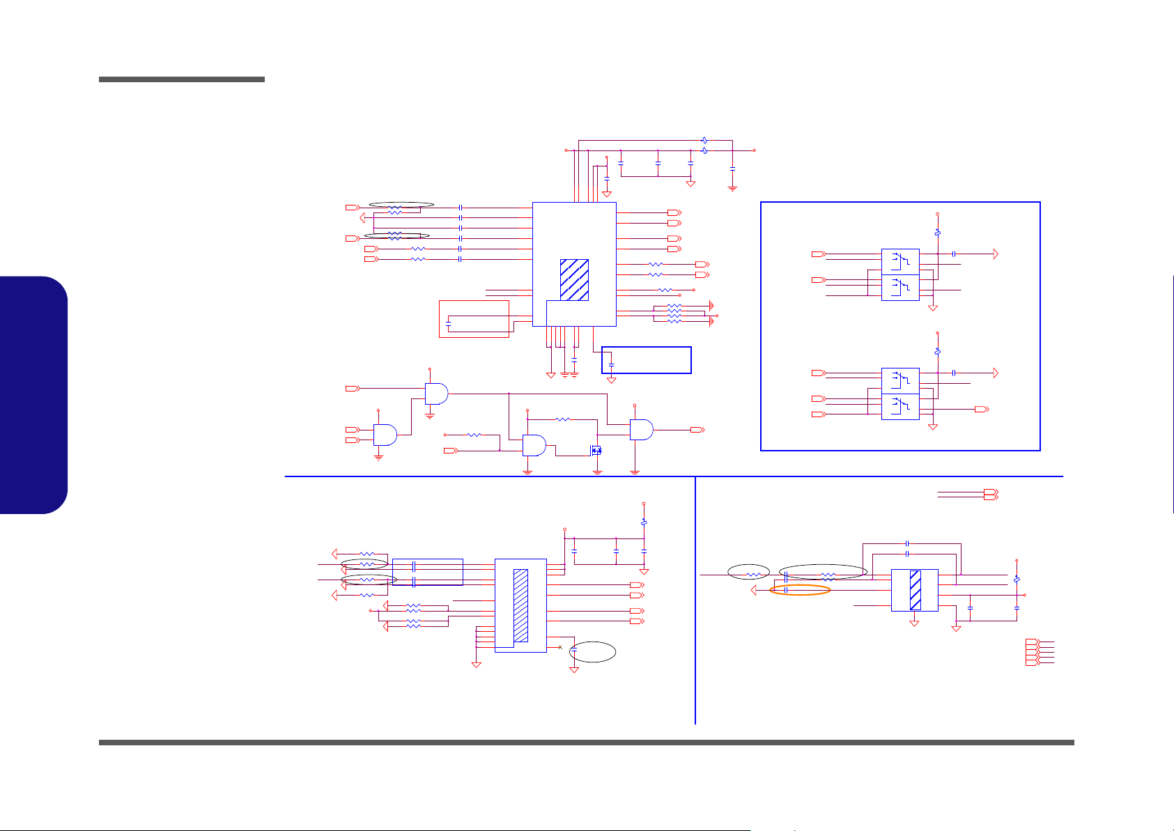
Schematic Diagrams
Z3222
CENTER_SPK+
CENTER_SPK-
Z3219
Z3221
U19C
74LVC08P W
9
10
8
147
U19D
74LVC0 8PW
12
13
11
147
D03
KBC_MUTE#
D03
D03
D03
Z3209
Z3207
C908 0.1u_16V_Y5V _04
U59
PI5A3158
0B0
2
1B0
11
S0
10
0B1
5
1B1
8
S1
7
VCC
12
A0
1
GND
3
VCC
9
GND
6
A1
4
C907 0.1u_16V_Y5V _04
C222 4.7u_6.3V_ Y5V _06
C209 4.7u_6.3V_ Y5V _06
Z3227
L97
HCB1005KF-121T20
Z3228
SPKOUTL+ 35
SPKOUTR- 35
SPKOUTR+ 35
SPKOUTL- 35
AUDG
AUDG
3VS
L98
HCB1005KF-121T20
3VS
SPK_EN 32
Q46
MTN7002ZH S3
G
DS
C249 0.01u_25V_X7R_06
U17
TPA6211A1DG NR
IN-
4
IN+
3
BYPASS
2
SD#
1
VO+
5
VO-
8
VDD
6
GND
7
THER NA L_P AD
9
C265 1200p_50V_X7R_06
C283
10u_10V_Y5V_08
C216
1u_16V_X5R_06
C251
10u_10V_Y 5V_08
C281 1u_16V_X5R_06
C248
1u_10V_06
C278
0.1u_16V _Y5V_04
R554 100K_04
C259 0 .047u_50V_Y5V _06
R220 10K_1%_04
C243
0.1u_16V _Y5V_04
L62
HCB1005KF-121 T20
R133 *100K_04
R555 100K_04
R121 *100K_04
Thermal Pad
U15
TPA6017A2PWPR
SD#
19
RIN-
17
LIN-
5
BYPASS
10
GND
11
GAIN 0
2
ROUT-
14
LOUT-
8
PVDD
6
LOUT+
4
GND
20
GAIN 1
3
ROUT+
18
PVDD
15
EXPOSED PAD
21
LIN+
9
GND
1
GND
13
NC
12
VDD
16
RIN+
7
C195 0.01u_25V_X7R_06
R120 100K_04
C201 0.01u_25V_X7R_06
CENTER_SPK-
CENTER_SPK+
CENTER_SPK+ 35
CENTER_SPK- 35
L59
HCB1 005KF-121T20
R215 10K_1%_04
C258 1200p_50V_X7R_06
C208 0.01u_25V_X7R_06
R147 100K_04
HEAD PHON E-L 36
HEAD PHON E-R 36
C272 0 .047u_50V_Y5V _06
AUDG
AUDG
AUDG
AUDG
AUDG
AUDG
AUDG
AUDG
AUDG
AUDG
3V6,12,13,15..17, 20,21, 25,28. .30,3 4,35, 37..41
5VS12,17,18,21 ..24, 26,27, 31,32, 34,36, 41
1.5VS11,13,1 5,17,31, 34,4 0,41
3VS7..9,1 2,13, 15..28 ,30..32,34, 36,37, 40,41
VDD316, 28,34.. 36,3 9,41..43
EAPD32
AMP_MUTE36
HDA_RSTB16 ,32
R125 * 0_04
AUDG
R139 0_04
R132 *0_04
AUDG
R141 0_04
FRONT_L
SIDE- L_C
FRONT_R
SIDE- R_C
DOLBY_SEL
FRONT_L
AUDIO_CEN_C
FRONT_R
LEF_OU T_C
DOLBY_SEL
DOLBY_SEL28
D03
AUDIO_C EN_C32
R203 2K_1%_04
1.5W
8ohm
8ohm
1.5W
SIDE_ LO+ 35
SIDE_ RO- 35
SIDE_ RO+ 35
SIDE_ LO- 35
3VS
3VS
3VS
5VS_CEN
5VS
3VS
5VS
5VS_REAR
REAR R/L
5VS
3VS
2000Hz High Pass Filter
Fcut(-3db)=1965Hz
FRONT R/L
KBC_MUTE#28
AUDG
AUDG
CENTER
LEF_OU T_C32
LEF_OUT 32
8ohm
1.5W
SIDE-L_C32
SIDE-R_C32
U60
PI5A3158
0B0
2
1B0
11
S0
10
0B1
5
1B1
8
S1
7
VCC
12
A0
1
GND
3
VCC
9
GND
6
A1
4
Z3225
Z3203
R195 39. 2K_1%_04
TPA6047A4
Thermal
Pad
U14
TPA6047A4RH BR
SPKR_LIN-
4
SPKR_LIN+
3
CPGND
11
HP_INR
26
HP_OUTR
15
HP_OUTL
16
HPVD D
17
LOUT-
7
SPKR_EN
23
LOUT+
6
OUTR-
19
OUTR+
20
SPKR_RIN-
1
CPVDD
9
HPVSS
14
HP_EN
22
SPKR_RIN+
2
HP_INL
27
VDD
30
SPVDD8SPVD D
18
C1P
10
C1N
12
SPGN D
5
GAIN0
31
GAIN1
32
CPVSS
13
SPGND
21
BYPASS
24
REG_EN
25
GND
28
REG_OUT
29
GND
33
FRONT_R32
AUDG
5VS
Z3229
Z3230
Z3231
L53 HC B1005KF-121T20
C199
1u_10V_06
Near CP+ and CP-
C238 0.01u_25V _X7R_06
FRONT_L32
6047GAIN 0
Z3226
C197
1u_16V_XR5_06
Z3205
SPK_EN
Z3210
C240 0. 01u_25V_X7R_06
SPEC=0.47U,
EVM=1U
R193 39. 2K_1%_04
6047GAIN 1
C241 0.01u_25V _X7R_06
C233
10u_10V_Y 5V_08
Z3206
AUDG
R194 *73 .2K_1%_04
5V_REGOU T
5VS_AMP
Z3204
C221
1u_16V_X5R_06
C239 0. 01u_25V_X7R_06
AUDG
5VS
Z3212
C205
0.1u_16V_Y 5V_04
AUDG
C179
0.1u_16V_ Y5V_04
R131 100K_04
L57 HC B1005KF-121T20
R129 100K_04
5VS_AMP
C189
10u_10V_Y 5V_08
C206
1u_16V_X5R_06
Z3224
AUDG
R196 *73 .2K_1%_04
R118 *100K_04
R130 *100K_04
5VS
R119 100K_04
HP_EN
D03
D03
HP_OU T_R32
HP_OUT_L32
AUDIO_CEN
LEF_OUT
SIDE-L
SIDE-R
R701 0_04
R702 0_04
SPKOUTL-
SPKOUTL+
SPKOUTR-
SPKOUTR+
SIDE-L
R703 0_0 4
SIDE-R
R704 0_0 4
SIDE_LO+
SIDE_LO-
SIDE_RO-
SIDE_RO+
0727 D03 BCN upated
NERA CODEC AL C8 88
Fcut(-3db)=1012.3Hz
2000Hz Low Pass Filter
Fcut(-3db)=1809.4Hz
1000Hz High Pass Filter
U19A
74LVC08P W
1
2
3
147
Z3208
HP_EN
Z3218
SPK_EN
Z3217
6017GAIN 1
Z3215
SPK_EN
Z3214
Z3216
6017GAIN 0
U19B
74LVC0 8PW
4
5
6
147
AUDIO_CEN
SPK_EN
Z3220
Z3223
Sheet 33 of 52
Audio AMP
TPA6047A4/
TPA6211
Audio AMP TPA6047A4/TPA6211
B.Schematic Diagrams
B - 34 Audio AMP TPA6047A4/TPA6211
Page 95

WLAN/HDMI-In/TV/ROBSON
3VS
1.5VS
1.5VS
3VS
3VS
3VS
3VS 7..9,12,1 3,15..28,30. .33, 36,3 7,40,41
SDATA 7..9,12,16,19,20,37,38
1.5VS 11,13,15,17,31,40,41
SCLK 7.. 9,12,16, 19,20,37, 38
PE_WAK E#16, 29,30
PE5_TX_ RO BSON#15
PE5_TX_ROBSON15
5VS 12,17,18,21..24,26,27,31..33,36,41
3V 6,12,13,15..17,20,21,25,28..30,35,37..41
ROBSON_DET#28
BUF_PLT_RST# 1 5,29..31
PCIE_CLK _ROBSON #20
PCIE_ CL K _ROB SON20
PE5_RX_ROBSON#15
PE5_RX_ROBSON15
USB_P11+ 15
USB_P11- 15
1.5V 4,5,7..9,29,39,41,42
HDMI_IN_SCL 23
HDMI_IN_SDA 23
HDMI_IN_CLK#
HDMI_IN_CLK
HDMI_IN_D1
HDMI_IN_D1#
3VS
HDMI_IN_D 2
HDMI_IN_D 0
HDMI_IN_D 0 #
HDMI_IN_D 2 #
HDMI_IN_HPD
C874
1u_6.3V_X5R_04
C873
0.1u_16V_Y5V_04
D18
*MSEA42510V12B0
10
398
7654
2
1
Z3302
Z3301
D19
*MSEA42510V12B0
10
398
7654
2
1
BUF _PLT_R ST# 15,29..31
HDMI_IN_C E C
TX_HDMI_SD A
TX_HDMI_D 0
TX_H DM I_ D2
HDMI_IN_HPD
TX_H DM I_ D2 #
TX_HDMI_D 0#
TX_HDMI_SC L
TX_HDMI_CLK#
TX_HDMI_D 1
TX_HDMI_CLK
TX_HDMI_D 1#
BT_EN28,35
BT_DET# 28,35
PCIE_CLK_HDMI_IN#20
PCI E_CLK_HD MI_I N20
R714 0_04
TX_HDM I_SC L 23
D03
R711 *0_04
C708
0.1u_1 6V_Y 5V_04
3IN1
D03
R468 *1 0mil_N P_04
C173 0.1u_10V_X7R_04
R84 *0_ 04
C717
10u_10V_Y5V_08
R477 *28m il_P_0 6
R162 10K_04
R86 *0_ 04
R488 0_04
C174 0.1u_10V_X7R_04
R93 *0_ 04
C719
0.1u_1 6V_Y 5V_0 4
Z3308
Z3307
R473 *1 0mil_N P_04
Z3316
Z3318
Z3315
Z3312
Z3311
Z3317
KEY
J_MINI1
88910-5204
BT_DA TA
3
BT_CH CLK
5
CLKREQ#
7
GND 0
9
REFCLK-
11
REFCLK+
13
WAKE#
1
GND 1
15
PETn0
23
PETp0
25
GND 2
21
GND 3
27
PERn0
31
PERp0
33
GND 4
29
NC3
17
NC4
19
W_DISABLE#
20
NC6
37
NC7
39
NC8
41
NC9
43
NC10
45
NC11
47
NC12
49
NC13
51
LED_W LAN #
44
NC(LED_WWAN#)
42
GND 6
18
UIM_VPP
16
UIM_RESET
14
3.3V_0
2
UIM_CLK
12
UIM_DATA
10
UIM_PWR
8
1.5V_0
6
GND 5
4
PERSET#
22
3.3VAUX
24
GND 7
26
1.5V_1
28
NC( SMB_CLK)
30
NC(SMB_DATA)
32
GND 8
34
NC(U SB_D-)
36
NC(USB_D+)
38
GND 9
40
NC (L ED_W PAN#)
46
1.5V_2
48
GND10
50
3.3V_1
52
GND 11
35
ROBSON_EN
C712
10u_10V_Y5V_08
3V
1.5VS
3V
1.5VSWLAN
3V
3VS
VDD 3
3V
PE3_TX_WAN#15
1.5VSWL AN
PE3_RX_WAN#15
PE3 _TX _WA N15
Z3313
Z3303
USB_P8+ 15
USB_P8- 15
PE3 _RX_W A N15
PCIE_CLK _WAN#19
WLAN_DE T #28
CL_RST12,15
CL_N_DATA12,15
WLAN_EN 28
D17
*TVN_ST23_02_AB0
3
2
1
CL_N_CLK12, 15
PC IE_CLK_WAN19
PE_WAKE#16,29,30
80CLK 28
3IN128
Z3304
80PORT_DET#28
Z3314
TV/ROBSON CARD 2 IN 1
Z3309
HDMI_IN_SC L
HDMI_IN_SDA
WLAN_EN# 28
D03
Z3322
Z3320
Z3319
Z3321
3VS
3VS
3VS
3VS
Z3305
Z3306
Z3310
TX_HDMI _D 223
TX_H DMI _D2 #23
TX_HDM I_D0 # 23
TX_HDMI_D 0 23
TX_HDM I_D1 # 23
TX_HDMI_D 1 23
TX_HDMI_SC L
TX_HDMI_SD A
J_HDMI_IN1
C12823-11908-L
SHIE L D2
2
TMDS DATA1+
4
TMDS DATA1-
6
SHIE L D0
8
TMDS CLOCK+
10
TMDS CLOCK-
12
RESERVED
14
SDA
16
+5V
18
TMDS DATA 2+
1
TMDS D ATA2 -
3
SHIELD1
5
TMDS DATA 0+
7
TMDS D ATA0 -
9
CLK SHIELD
11
CEC
13
SCL
15
DDC/CEC GND
17
HOT PLUG DETECT
19
GND1
GND1
GND2
GND2
GND3
GND3
GND4
GND4
TX_HDMI_CLK#23
TX_HDMI_C LK23
R716 *0_04
PCH_BT_EN#
TX_HDM I_SD A 23
D03
C875
0.1u_16V_Y5V_04
5A POWER PLAN
MIN I _D ATA 1
MIN I _C LK 1
C876
1u_6.3V_X5R_04
MIN I _R ST# 1
VDD3 16,28,3 5,36,39, 41..43
ROBS ON_ CL KREQ#20
PCH_BT_EN#15
R364 10K_04
Z3324
R690 0_04
R691 * 0_04
HDMI_IN_VCC
D03
HDMI_IN_CLKREQ#20
C451
22u_6. 3V_Y 5V_08
PE1_TX_HDMI-IN#15
PE1_TX_HD MI-IN15
R692 *0_04
1.5VS
PE1_RX_HDMI-IN15
1.5VS
R680 10K_0 4
PE1_RX_HDMI-IN#15
BT_EN
KEY
J_MINI_HDMI_IN1
BELLWETHER 80003-1021
BT_DATA
3
BT_CHCLK
5
CLKREQ#
7
GND0
9
REFCLK-
11
REFCLK+
13
WAKE#
1
GND1
15
PETn0
23
PETp0
25
GND2
21
GND3
27
PERn0
31
PERp0
33
GND4
29
NC3
17
NC419W_DISABLE#
20
NC6
37
NC7
39
NC8
41
NC9
43
NC10
45
NC11
47
NC12
49
NC13
51
LED_WLAN#
44
NC(LED_WWAN#)
42
GND6
18
UIM_VPP
16
UIM_RESET
14
3.3V_0
2
UIM_CLK
12
UIM_DATA
10
UIM_PW R
8
1.5V_0
6
GND5
4
PERSE T#
22
3.3VA UX
24
GND7
26
1.5V_1
28
NC(SMB_CLK)
30
NC(SMB_DATA)
32
GND8
34
NC(USB_D-)
36
NC(USB_D+)
38
GND9
40
NC(LED_WPAN#)
46
1.5V_2
48
GND10
50
3.3V_1
52
GND11
35
MINI-PCIE CARD for HDMI IN
HDMI_IN_D0 23
HDMI_IN_D1 23
HDMI_IN_D2 23
HDMI_IN_CLK# 23
HDMI_IN_CLK 23
HDMI_IN_D2# 23
HDMI_IN_D0# 23
HDMI_IN_D1# 23
HDMI_IN_VCC
5VS
C452
0.1u_16V_Y5V_04
BUF_PLT_RST# 15,29 ..31
MINI CARD for WAN& DEBUG CARD
KEY
J_MINI-ROBSON1
88910-5204
BT_DATA
3
BT_CHCLK
5
CLKREQ#
7
GND0
9
REFCLK-
11
REFCLK+
13
WAKE#
1
GND1
15
PETn0
23
PETp0
25
GND2
21
GND3
27
PERn0
31
PERp0
33
GND4
29
NC3
17
NC4
19
W_DISABLE#
20
NC6
37
NC7
39
NC8
41
NC9
43
NC10
45
NC11
47
NC12
49
NC13
51
LED_WLAN#
44
NC(LED_WWAN#)
42
GND6
18
UIM_VPP
16
UIM_RESET
14
3.3V_0
2
UIM_CLK
12
UIM_DATA
10
UIM_PWR
8
1.5V_0
6
GND5
4
PERSET#
22
3.3VA UX
24
GND7
26
1.5V_1
28
NC(SMB_CLK)
30
NC(SMB_DATA)
32
GND8
34
NC(USB_D-)
36
NC(USB_D+)
38
GND9
40
NC(LED_WPAN#)
46
1.5V_2
48
GND 10
50
3.3V_1
52
GND11
35
R455 *10mil_NP_04
R454 *10mil_NP_04
C700 0.1u_10V_X7R_04
C694
0.1u_16V_Y5V_04
R452 10K_04
WAN_CLKREQ#
C144
10u_10V _Y5V_08
C141
0.1u_1 6V_Y 5V_04
C140
10u_10V_Y5V_08
C701 0.1u_10V_X7R_04
Sheet 34 of 52
WLAN/HDMI-In/TV/
ROBSON
Schematic Diagrams
B.Schematic Diagrams
WLAN/HDMI-In/TV/ROBSON B - 35
Page 96

Z3402
Z3405
Z3404
H8_RST#
Z3401
Z3403
1
SPKOUTL-33
SPKOUTL+33
SPKOUTR+33
CENTER_SPK-33
CENTER_SPK+33
SIDE_RO+33
SPKOUTR-33
SIDE_LO-33
SIDE_LO+33
SIDE_RO-33
BT_EN#
CENTER_SPK+
Z3411
L33 FCM1005KF-121T03
Z3201
SIDE_LO+
Z3121
L74 FCM1005KF-121T03
L75 FCM1005KF-121T03
SIDE_LO-
L32 FCM1005KF-121T03
SIDE_RO+
Z3120
L26 FCM1005KF-121T03
Z3202
SIDE_RO-
Z3119
CENTER_SPK-
L27 FCM1005KF-121T03
Z3118
BT_EN
VDD3
L37
FCM1005KF-121T03
C132
*180p_50V_NPO_04
J_FRCENSPK
87213-0600 G
1
2
3
4
5
6
L40
FCM1005KF-121T03
C133
*180p_50V_NPO_04
USB_P4USB_P4+
L36
FCM1005KF-121T03
L39
FCM1005KF-121T03
Z3412 USB_P3-
BT_EN#
USB_P3+
BT_DET#
C146
*180p_50V_NPO_04
C147
*180p_50V_NPO_04
SATA_TX3_R
SATA_RX#3_R
SATA_RX3_R
J_SPKL1
85204-0200 1
1
2
J_SPKR1
85204-0200 1
1
2
Z3413
Z3407
Z3406
Z3409
SATA_TX#3_R
Z3408
Q54
MTN7002ZH S3
G
DS
+
-
U46A
LM358L
3
2
1
84
Q24
MTN7002ZHS3
G
DS
Q12
AO3409
G
DS
L81
HCB 2012KF- 121T30_08
R324
100K_04
R641
1.37K 1 %_ 0 6
C60
0.1u_16V_Y 5V_04
R628
100K_04
R638
10K_04
Q19
MTN7002ZH S3
G
DS
R323
100K_04
C722
0.1u_16V_Y5V_04
R627
100K_04
C73
10u_10V_Y5V_08
L24
HCB2012KF-121T30_08
R31
100K_04
C70 1u_6.3V_Y5V_04
R501
100K_04
C807
0.1u_16V_Y5V_04
R640 470K_04
C427
0.1u_16V_Y5V_04
R37 330K_04
C733
0.1u_16V_Y5V_04
D28
F01J2E
A C
J_RT1
ACES-85205-2P
1
2
R159 *100K _04
J_CCD1
85205-0500
1
2
3
4
5
J_BT1
88266-0800
+3.3 v
1
GND
2
USB-
3
USB+
4
DETECT#
5
BT_ON#
6
N.C
7
N.C
8
R24 10K_04
R637 *10mil_NP_04
C429 0.01 u_16V_X7R_04
C428
0.1u_16V_Y5V_04
D27
*F01J2E
AC
C726
10u_10V_Y5V_08
C62
10u_10V_Y5V_08
R48
68K_1 %_04
R146 10K_04
R325 *10mil_NP_04
VDD3
VDD3
5V_CC D 3V_BT
VDD3
C432 0.01 u_16V_X7R_04
3V
5V
3V_BT
3V
5V
VDD5
R319 *10mil_NP_04
CCD_DET#28
VDD5
5VS
3VS
CCD_EN28
BT_EN28, 34
USB_P4-15
VDD3 16,28,34,36,39,41..43
BT_DET#28,34
J_ESATA1
PSABT6- 07MLBS1 NN 4H2
GND1
1
TXP
2
TXN
3
GND2
4
RXN
5
RXP
6
GND3
7
5V 4,17,22, 25,2 9,36. .42
Shutdown_st b_power 42
H8_RST# 28
USB_P4+15
5VS 12,17,1 8,21. .24, 26,27 ,31..34,36,41
3VS 7..9, 12,13,15..28, 30.. 34,36,37,40,41
3V 6,12,13, 15.. 17,20 ,21, 25,28..30,34,37..41
VDD5 36,41,42
R335 *10mil_NP_04
C431 0.01 u_16V_X7R_04 R 331 *10mil_NP_04
C425 0.01 u_16V_X7R_04
SATA_RX515
SATA_RX#515
SATA_TX#515
SATA_TX515
J_SPK3
*85204-04001
1
2
3
4
1
J_CCD1
CCD
From H8 default HI
USB_P3-15
USB_P3+15
5
8
48 mil
NTC
Bluetoot h
--->design value
depends on the
temperature
Thermistor
Active : 1
--->
e-SATA
Normal : 0
PIN GND1~4=GND
L101 *FCM1005KF-121T03
L102 *FCM1005KF-121T03
L104 *FCM1005KF-121T03
L103 *FCM1005KF-121T03
SPKOUTL+
SPKOUTR+
SPKOUTLSPKOUTR-
SPKOUTR-_R
SPKOUTL-_R
SPKOUTL+
SPKOUTL-
SPKOUTR-
SPKOUTR+_R
SPKOUTL+_R
SPKOUTR+
Sheet 35 of 52 CCD/BT/SATA
B.Schematic Diagrams
Schematic Diagrams
B - 36 CCD/BT/SATA
CCD/BT/SATA
Page 97

Daughter Connector
TV-GND
TV-GND
TV-GND
J_SW1
85201-0405
1
2
3
4
TP_CLK
TP_DATA
H12
C315D165
10 mils
H13
C315D165
H14
C315D165
H15
C315D165
3VS
BLACK LED CON
J_SENSOR1
88242-2001
1 2
3 4
5 6
7 8
9 10
11 12
13 14
15 16
17 18
19 20
3VS
H30
HOLE2_6
3VS
TOUCH SENSOR
FINGERPRINT
SMC_BAT22,28,43
SMD_BAT22,28,43
3VS
C920 0.1u_16V_Y5V_04
LID_SW# 25, 28
H48
SQ-31G
H50
SQ-31G
H49
SQ-31G
GNDGND GN D
JD_SENSE_A32
JD_SENSE_B32
JD_SE NSE_B
H31
HOLE2_6
PWRS#
VDD5
CIR_RX
J_IR1
85201-0405
1
2
3
4
D03
USB_P9+ 15
USB_P9- 15
CIR_RX28
H11
H7_0D3_7
GND
H9
H7_0D3_7
GND
OC#1
H8
H7_0D3_7
GND
OC#0
H23
H7_0D3_7
OC#0 15
OC#1 15
GNDGND
H22
H7_0D3_7
GND
H21
H7_0D3_7
GND GNDGND
POWER LED BOARD
VDD3
H36
H7_0D2_7
GND
LED_BAT_CHG#
H35
H7_0D2_7
GND
LED_BAT_FULL#
J_LED1
85204-06001
1
2
3
4
5
6
LED_ACIN#
VDD3
LED_PWR#
LED_ACIN#28
LED_BAT_FULL#28
LED_BAT_CHG#28
LED_PWR#28
H4
C126D126
USB_P9-
GND
H39
H7_0D3_7
USB_P9+USB_P9+
H18
H7_0D3_7
GND
H16
C315D111
C165
0.1u_16V_Y5V_04
H25
C315D111
H27
H7_0D3_7
C159
47P_04
JADJ1
H19
H7_0D4_0
87151-1807
D03
CABLE_TV
H33
C315D111
J_AUDIO1
1
2
3
4
5
6
7
8
9
10
11
12
13
14
15
16
17
18
H28
C126D126
H1
C315D111
SWITCH BOARD
R91
10K_04
H32
H8_0D2_8
J_USB1
88242-2001
1 2
3 4
5 6
7 8
9 10
11 12
13 14
15 16
17 18
19 20
R90
10K_04
C160
47P_04
GNDGND GNDGND
5VS
5V
3V
5V
VDD5
3VS
H37
H8_0D2_8
3VS
VIN
GND
5VS
GND
GND
AUDG
GND
LED_SCROLL#28
16
TP_CLK 28
USB_ P0+15
USB_ P2+15
VIN 22,25,37..40,42,43
SPDIF-OU T21,32
LED_ CAP#28
USB_ P1+ 15 5VS 12,17,18,21..24,26,27,31..34,41
USB_ P0-15
HEA DPHONE- R33
5V 4,17,22,25,29,35,37..42
MIC1 - R32
USB_ P1- 15
3V 6,12,13,15. .17,20,21, 25,28..30, 34,35,37..41
3VS 7..9, 12,13,15..28, 30..34,37,40,41
LED_NUM#28
VDD5 35,41,42
TP_DATA 28
PWRS #39
HEA DPHO NE- L33
MIC1 - L32
USB_ P2-15
AMP_MUTE33
GND
SENSOR_I NT# 28
1
5VS
1.5VS 1.5VS 11,13,15, 17,31,34,40,41
USB_P0+
USB_ P1-USB_P0USB_ P1+
USB_P2USB_P2+
J_BLED1
85204-02001
1
2
J_TP1
85201-06051
1
2
3
4
5
6
SURR_R
SURR_L
SURR_L32
SURR _R32
5VS
PHONE JACK BOARD
USB BOARD
CLICK BOARD
LINE-IN_L32
LINE-IN_R32
H7
H7_0D4_0
GND
H6
H7_0D4_0
GND
H17
H7_0D4_0
VDD3 16,28,34,35,39,41..43
GND
TV TUNER
H47
H8_0D2_8
GNDGND
H29
H8_0D2_8
H44
SQ-31G
H45
SQ-31G
VDD3
H46
SQ-31G
H40
SQ-31G
H41
SQ-31G
H42
SQ-31G
GND
H43
SQ-31G
H10
H8_0D2_8H2H8_0D2_8
GND GND
H3
H8_0D2_8
GND
H5
H8_0D2_8
GND
GND
GND
H34
H8_0D2_8
GND GN D GN D
SATALED15
GND GND
5VS
J_FP1
85201-06051
1
2
3
4
5
6
AMP_MUTE
MIC1-R
MIC1-L
SPDIF -OUT
HEADPHONE- L
H38
C315D111
LINE-IN _R
JD_SE NSE_A
HEADPHONE- R
LINE-IN _L
H51
H7_0D4_0
GND
EMI
J_TC1
RF_HRS_UFL-R-SMT
1
2
3
GND
L25 HCB4532KF-800T60
C108 0.1u_16V_Y5V_04
CONSUMER IR
J_RCA1
FR-005D
1
2
3
4
Sheet 36 of 52
Daughter
Connector
Schematic Diagrams
B.Schematic Diagrams
Daughter Connector B - 37
Page 98

Schematic Diagrams
D03
D03
D03
Z3619
2.Vdroop=Io*DCR*R9/R8
ADDRESS
0: 7:h37
1: 7'h4E
Z3615
BOTTOM PAD
CONNECT TO GND
Through 8 VIAs
1.L/DCR=R9*C16
Z3617
Z3618
Z3612
3.100uA*R10=Ioc*DCR*R9/R8
4.Vapa=100uA*R11
6X6 QFN
PC234
0.1u_50V_Y5V_06
FS_VCC
25A
0727 D03 BCN upated
ISL6314CR POWER CKT
1.1V EN
Z3621
Z3620
CPUVTT_VID7
SDATA
VTT_VID4
VTT_VID6
SCLKZ3623
VTT_VID5
CPUVTT_VID2
VTT_VID1
VTT_VID2
VTT_VID7
CPUVTT_VID0
CPUVTT_VID6
Z3622
VTT_VID0
CPUVTT_VID5
1.1VS_CTRL0
CPUVTT_VID4
CPUVTT_VID1
CPUVTT_VID3 VTT_VID3
CPUVTT_VID2
CPUVTT_VID5
CPUVTT_VID0
CPUVTT_VID4
CPUVTT_VID3
CPUVTT_VID1
CPUVTT_VID6
CPUVTT_VID7
CPUVTT_VID6
CPUVTT_VID5
CPUVTT_VID7
ISEN
Z3602
CPUVTT_VID4
Z3603
PHASE
CPUVTT_VID3
1.1V EN
Z3601
ISEN
PHASE
CPUVTT_VID1
Z3605
Z3606
CPUVTT_VID0
CPUVTT_VID2
Z3607
Z3604
PR4
*2K_04
PL6 0.82UH_ 13*13*6.7
PC113
*0.01u_50V_X7R_0 4
PR183 243_04
PR5
*2K_04
PC1231000p_50V_X7R_04
PR37
2.2_06
PR152
2K_04
PR153
*2K_04
PR162 10K_04
PU10
ISL6314CRZ
ISEN+
16
FS
3
VCC
18
FB
9
PGOOD
1
VID2
29
VID1
30
VID3
28
COMP
7
VSEN
12
PVCC
19
OFS
5
RGND
11
OCSET
13
VID0
31
REF
4
APA
6
ISEN-
15
EN
17
VID5
26
GND
33
VID6
25
VID7
32
VID4
27
SS
2
BOOT
22
UGATE
23
PHASE
24
LGATE
21
NC
20
ISENNO
14
DVC
8
VDIFF
10
PR42
2.2_06
PR36
100K_04
FS_VCC
PQ40
IRFH7932
4
6257318
9
+
PC106
560U_2.5V
PQ8
NTS4001NT1G
G
DS
PC118
0.1u_16V_Y5V_04
PC14
0.01u_50V_X7R_04
PC4
4.7U_25V_X5R_0 8
PR48
*10K_04
PC114
0.1u_25V_X7R_06
PR3
*2K_04
PR143
2.2K_ 04
PU1
IT8268R
VIDIN0
4
VIDIN1
5
VIDIN2
6
VIDIN3
7
VIDIN4
8
VIDIN5
9
VIDIN6
25
VIDIN7
27
GPIO0
10
GPIO1
11
GPIO2
12
VIDOUT7
2
VIDOUT5
19
VIDOUT1
23
VIDOUT6
26
VIDOUT2
22
VIDOUT0
24
VIDOUT4
20
VIDOUT3
21
GPIO3
3
SDA
13
SCL
14
GND
16
RSTOUT#
15
SLOTOCC #
17
VBAT
18
ASEL
28
3VSB
1
PR6
2K_04
PC97
*0.1u_16V_Y5V_04
PR180
100K_04
PR1783K_04
PR130
*2.2K_04
PRN6
1K_8P4R_04
81726
5
3
4
PR127
2.2K_04
PR142
*2.2K_04
+
PC105
560U_2.5V
PC15
0.1u_16V_Y5V_04
PR189 20K_1%_04
PD3
SK34SA
A C
PR188 75K_1%_04
PC98 0.1u_25V_X7 R_0 6
PC11522p_50V_NPO_04
PR197
100_04
PR1682.2_06
PR44 22K_04
+
PC103
*330U
PR126
*2.2K_04
+
PC89
15u_25V_6.3*4.4_C
12
PR157 1_06
PC111
*0.1u_10V_X7R_ 04
PC102
1u_16V_X5R_06
PR161 *10K_04
PR33
100K_04
PR172 *12K_04
0727 D03 BCN upated
PR175
2.2_08
PJ13
*OPEN_40mil
SS_VCC
PC107
1u_16V_X5R_06
PQ37
IRFH7923
4
6257318
9
PR129
*2.2K_04
PR287
100K_04
PC108 1000p_50V_X7R_04
PQ10
NTS4001NT1G
G
DS
PJ14
JUMP-20MM
1 2
PR2
*2K_04
PC104
1000p_50V_X7R_04
5V
PRN2
*0_8P4R_04
81
72
653
4
PR154 10K_04
PC124 680P_5 0V_04
PC119
*0.1u_16V_Y5V_04
PR45 2K_04
PR1
2K_04
PR182 20K_ 04
PR281
*10K
PR181 2K_1%_04
PR49 0_04
PR27
1K_04
PC120
*0.1u_16V_Y5V_04
PC100
1000P_50V_X7R_04
PR198
100_04
PR131
*2.2K_04
PC9
0.1u_50V_Y5V_06
PC30
680P_50 V_04
PR41
22K_04
PR47 *0_04
PC1 0. 1u_16V_Y5V_04
PQ41
IRFH7932
4
6257318
9
PC117 0.01u_50V_X7R_04
PRN5
1K_8P4R_04
81726
5
3
4
PR185
100K_04
PRN1
*0_8P4R_04
81
72
653
4
PR167 *82K_04
PR155 10K_04
PC110
*0.1u_16V_Y 5V_04
PR128
*2.2K_04
V6314
V6314
VIN
5V
V6314
CPU_VTT
SYS3V
V1.1
V1.1
3VS
5V
5V
5V
V6314
VTT_PWROK38
PC233
0.1u_50V_Y5V_06
VTTPWR_O N28
1.1VPWGD40
CPU_VTT_FB4
5V4,17,22,25,29,35,36,38..42
CPU_VTT_FB-4
VIN22,25,38..40,42,43
Z3610
3VS7..9,12,13, 15..28,30..34,36,40,41
CPU_VTT4,5,15,38
SCLK 7. .9,12,16,19,20,34,38
SYS3V38,42,43
SDATA 7..9,12, 16,19,20,34,38
1.1VS_CTRL0 40
CPUVTT_VID34
CPUVTT_VID24
Z3611
CPUVTT_VID44
SS_VCC
Z3609
Z3608
VTT_VID 7
VTT_VID 6
VTT_VID 5
VTT_VID 4
VTT_VID 3
VTT_VID 2
Z3613
VTT_VID 1
VTT_VID 0
Z3616
3V6,12,13,15.. 17,20,21,25,28..30,34, 35,38..41
Z3614
3V
3V
3V
Sheet 37 of 52
Power CPU_VTT
B.Schematic Diagrams
B - 38 Power CPU_VTT
Power CPU_VTT
Page 99

Power VCORE
PR64 2. 2_06
PR199
33K_1%_04
PQ50
IRFH7 932
4
6257318
9
BOTTOM PAD
CONNECT TO
GND Through
4 VIAs
PR171
100_04
PR218
2.2_08
PL8 0.82U H_ 13*13*6.7
PU12
NCP5359DR2G
BST
1
VCC4DRVH
8
IN
2
PGND
6
DRVL
5
OD
3
SWN
7
PR91 2.2_0 6
PR14
2K_04
PR201
*56K_04
PR193 10k_06
PR7
2K_04
PR31
*10mil_NP_04
PR84
*10mil_NP_04
PR34 *10mil_NP_04
PR147 10K_04
PR223
4.7_08
PC51
4700P_50V_04
PR46
1K_04
CS4N
PC19
*0.1u _16V_Y5V_04
CS4
PC60
0.1u_50V_Y5V_06
PC122 0.47u_16V_Y5V_06
PR139
*680_04
PR29
12K_04
PC109
1500p_50V_04
PR1861K_1%_04
PC17
0.1u_10V_X5R_04
PQ49
IRFH7932
4
6257318
9
PR150 *10K_04
PR81 1 _06
PR82 2.2_0 6
PR205
1K_1%_04
PR209
4.7_08
Z3713
PQ45
IRFH7932
4
6257318
9
+
PC50
330u_2V_V_B
Work F=210Khz
PC121 0.47u_16V_Y5V_06
Z3755
+
PC138
560U_2.5V
PC96
1u_16V_X5R_06
03A-0416
PR71 1 _06
PR174
1K_1%_04
PC18
*0.1u_16V_Y 5V_04
PC140
4700P_50V_04
PRN8
1K_8P4R_04
81726
5
3
4
PC57
2.2u_16V_X5R_06
PR13
*2K_04
PR39 10_04
+
PC129
560U_2.5V
PR200 *100K_04
PR149 10K_04
PR1901K_1%_04
3 phase
option
PRTH3 Place
close to PL
10
IMON
PR50 680_04
PQ48
IRFH7932
4
6257318
9
H_PSI#
PC35
0.1u_50V_Y5V_06
PC28
22p_50V_NPO_04
PQ47
IRFH 7932
4
6257318
9
PRN3
*0_8P4R_04
81
72
653
4
PR184 680_04
PR163 2.2_06
PL7 0.82U H_ 13*13*6.7
PC127
0.1u_16V_Y5V_04
PR133
680_04
H_VID0
PC26 47P_50V_04
PR196
*680_04
PR54
*10mil_NP_04
EN
+
PC139
560U_2.5V
H_VID1
PR195 8.2K_1%_04
PR77
*10mil_NP_04
H_VID2
PQ39
2N3904
B
E C
PC67
0.1u_50V_Y5V_06
VR_VFB
PR1911K_1%_04
H_VID3
PC62
0.22u_16V_06
PR194 1_06
H_VID4
PRTH2
4.7K_THERMAL_06
PC34
4.7U_25V_X5R_08
H_VID5
PC99
4.7u_10V_X5R_08
PR86
2.2_08
H_VID6
PR219
4.7_08
+
PC56
*330U_2.5V_D3
H_VID7
PQ44
IRFH7932
4
6257318
9
PR89 10k _06
Z3761
PR8
2K_04
EN
PC116 0.47u_16V_Y5V_06
PR169
7.5K_1%_04
PQ46
IRFH7923
4
6257318
9
PR72 2.2_0 6
PR76
*10mil_NP_04
PR135
680_04
PR164
1K_04
PR203 0_04
PR83
*10mil_NP_04
PR134
680_04
PU13
NCP5359DR2G
BST
1
VCC4DRVH
8
IN
2
PGND
6
DRVL
5
OD
3
SWN
7
PR10
*2K_04
PR90 1 _06
PR137
680_04
PR204
9.1K_1%_04
+
PC137
560U_2.5V
+
PC136
560U_2.5V
Z3719
PR9
*2K_04
12V
CPU_VTTCPU_VTT
VIN
VIN
5V
D03
SYS3V
5V
Z3767
5V
5V
Z3754
5V
12V
VCORE
12V
VIN
VIN
Z3737
Z3706
12V
Z3742
Z3741
Z3743
VR_HOT
VR_HOT
VCORE
VIN
5V
5V
0727 D03 BCN upated
5V
5V
V1.1
CPU_VTT
CPU_VTT
VCC_SENSE4
Z3721
H_PSI#4
H_PROCHOT# 4,15
Z3701
H_VID44
VSS_SENSE4
H_VID64
PWRGD_ PS4,12 ,15,16,28
H_VID74
VRM_PWRGD16
Z3757
H_VID14
H_VID24
Z3758
H_VID54
IMON4
H_VID34
H_VID04
VTT_PWROK37
VCORE5
12V41
5V4,17,22 ,25,29,35.. 37,39..42
VIN22,25,37, 39,40,42,43
SYS3V37, 42,43
CPU_VTT4, 5,15,37
1.5V_CTRL1 39
1.5V_CTRL0 39
SCLK 7..9, 12,16,19,20,34 ,37 3VS7..9,12,13,15..28,3 0..34,36,37, 40,41
SDATA 7..9,12, 16,19,20,34, 37
Z3722Z3726
VR_COMP
Z3730
Z3702
H_VID4
H_VID2
H_VID3
H_VID5
H_VID1
H_VID0
Z3751
PD17
SK34SA
A C
Z3723Z3727
Z3731
Z3748
Z3703
Z3747
PSI
PD16
SK34SA
A C
EMI
EMI
EMI
EMI
Z3752
Z3725
3V
3V
Z3724Z3728
3V
Z3732
D03
D03
D03
Z3704
PD8
SK34SA
A C
Z3762
Z3729
Z3720
CS4N
Z3765
CS4
Z3740
PD7
SK34SA
A C
Z3744
H_VID4
H_VID2
H_VID1
H_VID3
H_VID7
H_VID6
H_VID5
H_VID0
D03
Z3714
Z3716
VID0
VID1
Z3746
VID2
VID3
D03
VID4
D03
D03
D03
VID6
Z3712
VID7
SDATA
SCLK
Z3774
Z3763
Z3771
Z3718
CS2
Z3705
1.5V_C TRL1
CS2N
1.5V_C TRL0
PRTH3
*4.7K_THERMAL_06
CS1
H_VID6
H_VID7
Z3764
CS1N
CS3
CS3N
Z3739
Z3717
Z3738
3V6,12,13,15..17,20, 21,25,28.. 30,34,35,37,39. .41
VR_COMP
Z3759
Z3756
VR_VFB
Z3708
CS2N
CS2
Z3750
CS3N
Z3710
CS3
VID0
VID1
VID2
VID3
VID4
VID5
VID6
CS1N
CS1
VID7
Z3773
OS-CON
PD15
RB0540S2
AC
Z3766
6X6 QFN
POC/MSID USE
0.8V~1.55V/125A
PD11
RB0540S2
AC
03A-0416
PD10
RB0540S2
AC
PC95
1u_16V_X5R_06
PR78
2.2_08
PC128
100p_50V_NPO_04
PC16
2.2u_16V_X5R_06
PU14
NCP5359DR2G
BST
1
VCC4DRVH
8
IN
2
PGND
6
DRVL
5
OD
3
SWN
7
PD9
RB0540S2
AC
PC59
1u_16V_X5R_06
Z3707
PC68
0.22u_16V_06
PC88 0.1u_16V_Y5V _04
PD4
RB0540S2
AC
PR53
*10mil_NP_04
PC112 0.033u_16V_X7R_04
PR11
*2K_04
PQ53
IRFH7932
4
6257318
9
PRN4
*0_8P4R_04
81
72
653
4
+
PC150
560U_2.5V
PR32 *0_04
Z3709
PC125 0.47u_16V_Y5V_06
PR87 2. 2_06
PR35
100_04
PJ1
*OPEN_40mil
+
PC171
15u_25V_6.3*4.4_C
12
Z3749
PR12
*2K_04
PR165 130_04
+
PC52
*330U_2.5V_D3
PC55
0.22u_16V_06
PR148
100K_04
PC48
4.7U_25V_X5R_08
>300us FILTER
PQ42
2N3904
B
E C
PR202 49.9K_1%_04
+
PC146
15u_25V_6.3*4.4_C
12
PC20
47NF_X7R_50V_04
+
PC126
15u_25V_6.3*4.4_C
12
PR22 0_04
+
PC133
560U_2.5V
PR132
*680_04
PR79 2. 2_06
03A-0416
PC65
1u_16V_X5R_06
PQ43
IRFH7923
4
6257318
9
VID5
Z3715
PC152
4700P_50V_04
Z3753
Z3745
PQ3
NTS4001NT1G
G
DS
PQ56
IRFH7923
4
6257318
9
Place
close to
hottest
MOSFET
Z3711
PR30
2K_04
PR141
100K_04
+
PC135
15u_25V_6.3*4.4_C
12
PR138
*680_04
+
PC151
560U_2.5V
PC53
1u_16V_X5R_06
PR136
680_04
PJ11
*OPEN_40m il
Z3768
PR166 330_04
PR28
2.2_08
PU11
NCP5359DR2G
BST
1
VCC4DRVH
8
IN
2
PGND
6
DRVL
5
OD
3
SWN
7
PC61
2.2u_16V_X5R_06
PR80 10k _06
PL10 0. 82U H_ 13*13*6.7
PRTH1
100K_06
PL9
0.82UH_ 13* 13*6. 7
PC64
2.2u_16V_X5R_06
PR38 2.2_0 6
PR146 10K_04
PRN7
1K_8P4R_04
81726
5
3
4
OCP ~ 100A
ADDRESS
0: 7:h37
1: 7'h4E
PU15 N CP5392MNR2G
CS2
24
ROSC
10
VCC
35
VFB
17
VR_RDY
39
VID2
4
VID1
3
VID3
5
COMP
16
VSP
13
G2
31
G1
30
CS1
22
DIFFOUT
15
VSN
14
VR_HOT
40
CS3
26
G3
32
CS4
28
G4
33
VID0
2
VDRP
18
CS3N
25
CS1N
21
CS2N
23
CS4N
27
VID5
7
PSI
37
VID6
8
VID7
9
VID4
6
NTC
38
IMON12ILIM
11
DRVON
29
AGND
41
12VMON
34
ENABLE
1
VDFB
19
CSSUM
20
DAC
36
NCP5392 Intel VRD11.1 POWER CKT
PR73
*10mil_NP_04
PR170
27K_1%_04
0727 D03 BCN upated
D03
PU2
IT8268R
VIDIN 0
4
VIDIN 1
5
VIDIN 2
6
VIDIN 3
7
VIDIN 4
8
VIDIN 5
9
VIDIN 6
25
VIDIN 7
27
GPIO0
10
GPIO1
11
GPIO2
12
VIDOUT7
2
VIDOUT5
19
VIDOUT1
23
VIDOUT6
26
VIDOUT2
22
VIDOUT0
24
VIDOUT4
20
VIDOUT3
21
GPIO3
3
SDA
13
SCL
14
GND
16
RSTOUT#
15
SLOTOCC#
17
VBAT
18
ASEL
28
3VSB
1
PQ2
NTS4001NT1G
G
DS
PJ15
*OPEN_40mil
D03
Z3769
PR177
3.3K_04
PR1921K_1%_04
PC131
4700P_50V_04
+
PC54
330u_2V_V_B
PC58
4.7U_25V_X5R_08
PC29
0.22u_16V_06
PR74
*10mil_NP_04
PR187 680_04
PC11
*0.1u_16V_Y5V _04
PR43 1K_1%_04
PC49
0.1u_50V_Y5V_06
PR173
7.5K_04
PQ51
IRFH7923
4
6257318
9
PC66
4.7U_25V_X5R_08
PR75 10k _06
03A-0416
PR176
2K_04
PQ54
IRFH7 932
4
6257318
9
PR151 *0_04
PR179
18K_04
PR63
4.7_08
PC22
0.1u_16V_Y5V_04
PC101 1000P_50V_04
Sheet 38 of 52
Power VCORE
Schematic Diagrams
B.Schematic Diagrams
Power VCORE B - 39
Page 100

Schematic Diagrams
PC232
0.1u_50V_Y5V_06
PR291 10K_04
VIN
1.5V,0.75VSM
PR51
4.7_08
12A
Z3813
0727 D03 BCN upated
1.70V0
01
11
1.60V
0
Voltage
1.55V
0
1.5_CTRL01.5V_CTRL1
1
1.65V
Z3827
Z3821
Z3826
VDD QSET
PC24 0
1u_6. 3V_X5R_ 04
D03
Z3824
PC239
1u_6.3V_X5R_04
VTTEN
D03
D03
PR56 2.2_06
Z3820Z3819
Z3806
VTTEN
VDDQSET
Z3810
0727 D03 BCN upated
Z3803
Z3815
Z3818
Z3822
Z3817
Z3808
Z3805
Z3814
1.5VEN
Z3802
Z3811
Z3804
1.5VEN
Z3812
Z3801
0727 D03 BCN upated
9/17' 09
D03
PC13 0 0. 1u_10V _X7R_04
PC36
10u_10 V_Y 5V_08
PR40
0_06
+
PC33
*470u_2.5V_V_A
PR280
10K_04
PU3
uP6163
VTTGND
1
VLDOIN
23
VTT
24
VTTSNS
2
GND
3
MODE
4
VTTREF5VCC5
14
PGOOD
13
S5
11
S3
10
VDDQSET
9
VDDQSNS
8
COMP
6
CS
16
PGND
18
DRVL
19
LL
20
DRVH
21
VBST
22
PVCC 5
15
CS_GND
17
NC7NC12GND
25
PJ10
*OPEN_40mil
PR208 *0_04
PQ84
NTS4001NT1G
G
DS
PR69 *0_04
PR59 *0_04
PC134
*1000p_X7R_04
PR216 220K_1%_04
PQ9
QM3002S/AP9408GM
4
6257318
PR210 6.8K_1%_06
PR207 0_04
PC3 14.7u_25V_X5R _08 _ A
PC24 0.1u_50V_Y5V_06
PR206
0_04
PR65
100K_04
PR214 0_04
PC45
0.1u_ 10V_X5R_ 04
PJ3
JU MP- 3MM
12
PR68 0_04
PR60 0_04
PC42
*10u_ 10V_Y 5V_ 08
PC21 0.1u_50V_Y5V_06
PR62
150K_ 1%_04
PD5
SK34SA
A C
PR55
100K_04
PR125 20K_1%_04
PR66
100K_0 4
PJ2
JUMP-10MM
1 2
PC43
1U_10V_06
PR67 * 0_04
PD6
RB0540S2
A C
PD1
RB0540S2
A C
PR58
10K_1%_04
PQ18
MTN700 2ZH S3
G
DS
PR217
*10K_1%_04
PR215 220K_1%_04
PR52
0_06
+
PC37
470u_2.5V_V_A
PQ35
NTS400 1NT1G
G
DS
PC32
2200p_X7R_06
PQ14
NTS4001NT1G
G
DS
PC40 0.1u_16V_Y5V_04
PC27 4.7u_25V _X 5 R _08_A
PQ11
QM3006S/AP9412GM
4
6257318
PR211 *0_04
PR61
75K_1% _04
PC44
1U_10V_06
PR57 10. 7K_1% _04
PQ15
MTN7002Z HS3
G
DS
PQ1
AO3409
G
DS
PD2
RB0540S2
A C
PQ36
NTS4001NT1G
G
DS
PR70 0_04
PC226
0.1u_10V_X7R _04
PQ16
MTN700 2ZH S3
G
DS
PC39 0.01u_16V_X7R_04
PR212
0_04
PR279
100K_04
PQ12
QM3006S/AP9412GM
4
6257318
PC38
10u_10V _Y5V_08
PR140
100K_04
PR213 *10_04
PL5
1.0UH_11.5*10.2*3.0
1 2
PC132 0.1u_10V_X7R_04
PC46
0.1u_ 10V_X5R _04
PQ17
MTN7002ZHS3
G
DS
PC47
*1000p_X7R_04
PC41
10u_10V_Y5V_08
PQ13
NTS4001NT1G
G
DS
VIN2
VIN1
VDD3
VA
VIN
3V
3V
VDDQ
5V
5V
VDDQ
5V
5V
VIN
5V
3V
5V
5V
1.5V
VDDQ
0.75V
3V6,12,13,15..17,20,21,25,28..30,34,35,37,38,40,41
0.75V7..9
VIN22,25,37,38,40,42,43
VIN142
1.5V4,5,7..9,29,41,42
VDD316,28,34..36,4 1. .4 3
PWRS#36
PWR_SW#28
5V4,17,22,25,29,35..38,40..42
PR29 0 2 00K_04
DD _ON 28,41 ,42
ICH_GPIO3015
1.5V_CTRL138
DD_ON#41
ICH_GPIO2915
1.5V_CTR L038
Z3823
1.5V_ PWR GD 16
SUSB40..42
DD_ON#41
Z3825
PQ85
DTA114EUA
CE
B
Sheet 39 of 52
Power 1.5V/0.75VS
Power 1.5V/0.75VS
B.Schematic Diagrams
B - 40 Power 1.5V/0.75VS
 Loading...