


Notebook Computer
W760T
Service Manual
Preface
Preface
I

Preface
Preface
Notice
The company reserves the right to revise this publication or to change its contents without notice. Information contained
herein is for reference only and does not constitute a commitment on the part of the manufacturer or any subsequent vendor. They assume no responsibility or liability for any errors or inaccuracies that may appear in this publication nor are
they in anyway responsible for any loss or damage resulting from the use (or misuse) of this publication.
This publication and any accompanying software may not, in whole or in part, be reproduced, translated, transmitted or
reduced to any machine readable form without prior consent from the vendor, manufacturer or creators of this publication, except for copies kept by the user for backup purposes.
Brand and product names mentioned in this publication may or may not be copyrights and/or registered trademarks of
their respective companies. They are mentioned for identification purposes only and are not intended as an endorsement
of that product or its manufacturer.
Version 1.0
June 2009
Trademarks
Intel and Intel Core are trademarks of Intel Corporation.
Windows
Other brand and product names are trademarks and /or registered trademarks of their respective companies.
II
®
is a registered trademark of Microsoft Corporation.

About this Manual
This manual is intended for service personnel who have completed sufficient training to undertake the maintenance and
inspection of personal computers.
It is organized to allow you to look up basic information for servicing and/or upgrading components of the W760T series
notebook PC.
The following information is included:
Chapter 1, Introduction, provides general information about the location of system elements and their specifications.
Chapter 2, Disassembly, provides step-by-step instructions for disassembling parts and subsystems and how to upgrade
elements of the system.
Preface
Appendix A, Part Lists
Appendix B, Schematic Diagrams
Appendix C, Updating the FLASH ROM BIOS
Preface
III

Preface
IMPORTANT SAFETY INSTRUCTIONS
Follow basic safety precautions, including those listed below, to reduce the risk of fire, electric shock and injury to persons when using any electrical equipment:
1. Do not use this product near water, for example near a bath tub, wash bowl, kitchen sink or laundry tub, in a wet
basement or near a swimming pool.
2. Avoid using a telephone (other than a cordless type) during an electrical storm. There may be a remote risk of electrical shock from lightning.
3. Do not use the telephone to report a gas leak in the vicinity of the leak.
4. Use only the power cord and batteries indicated in this manual. Do not dispose of batteries in a fire. They may
explode. Check with local codes for possible special disposal instructions.
5. This product is intended to be supplied by a Listed Power Unit with an AC Input of 100 - 240V, 50 - 60Hz, DC Output
of 19V, 3.42A or 18.5, 3.5A (65W) minimum AC/DC Adapter.
CAUTION
Always disconnect all telephone lines from the wall outlet before servicing or disassembling this equipment.
Preface
IV
TO REDUCE THE RISK OF FIRE, USE ONLY NO. 26 AWG OR LARGER,
TELECOMMUNICATION LINE CORD
This Computer’s Optical Device is a Laser Class 1 Product
Instructions for Care and Operation
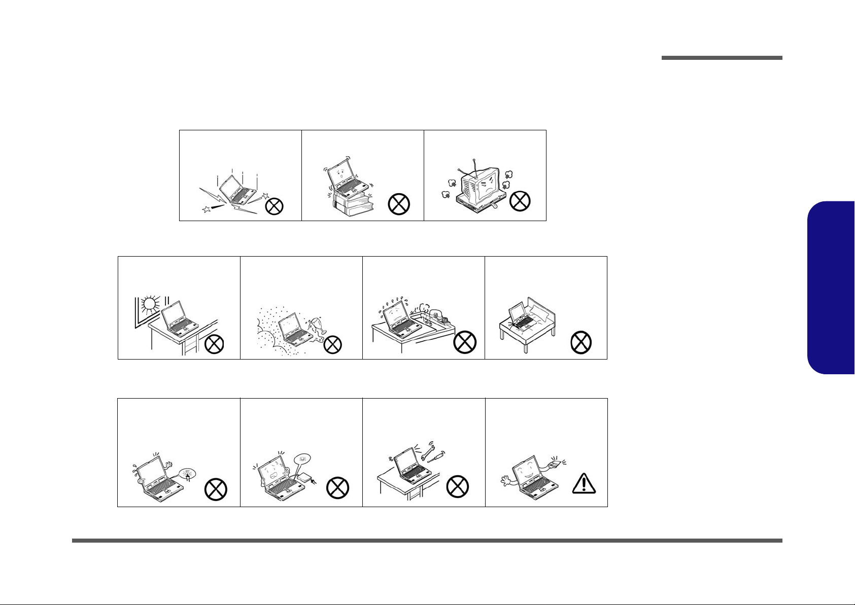
The notebook computer is quite rugged, but it can be damaged. To prevent this, follow these suggestions:
1. Don’t drop it, or expose it to shock. If the computer falls, the case and the components could be damaged.
Preface
Do not expose the computer
to any shock or vibration.
Do not place it on an unstable
surface.
Do not place anything heavy
on the computer.
2. Keep it dry, and don’t overheat it. Keep the computer and power supply away from any kind of heating element. This
is an electrical appliance. If water or any other liquid gets into it, the computer could be badly damaged.
Do not expose it to excessive
heat or direct sunlight.
Do not leave it in a place
where foreign matter or moisture may affect the system.
Don’t use or store the computer in a humid environment.
Do not place the computer on
any surface which will block
the vents.
3. Follow the proper working procedures for the computer. Shut the computer down properly and don’t forget to save
your work. Remember to periodically save your data as data may be lost if the battery is depleted.
Do not turn off the power
until you properly shut down
all programs.
Do not turn off any peripheral
devices when the computer is
on.
Do not disassemble the computer by yourself.
Perform routine maintenance
on your computer.
Preface
V
Preface
4. Avoid interference. Keep the computer away from high capacity transformers, electric motors, and oth er strong mag-
netic fields. These can hinder proper performance and damage your data.
5. Take care when using peripheral devices.
Preface
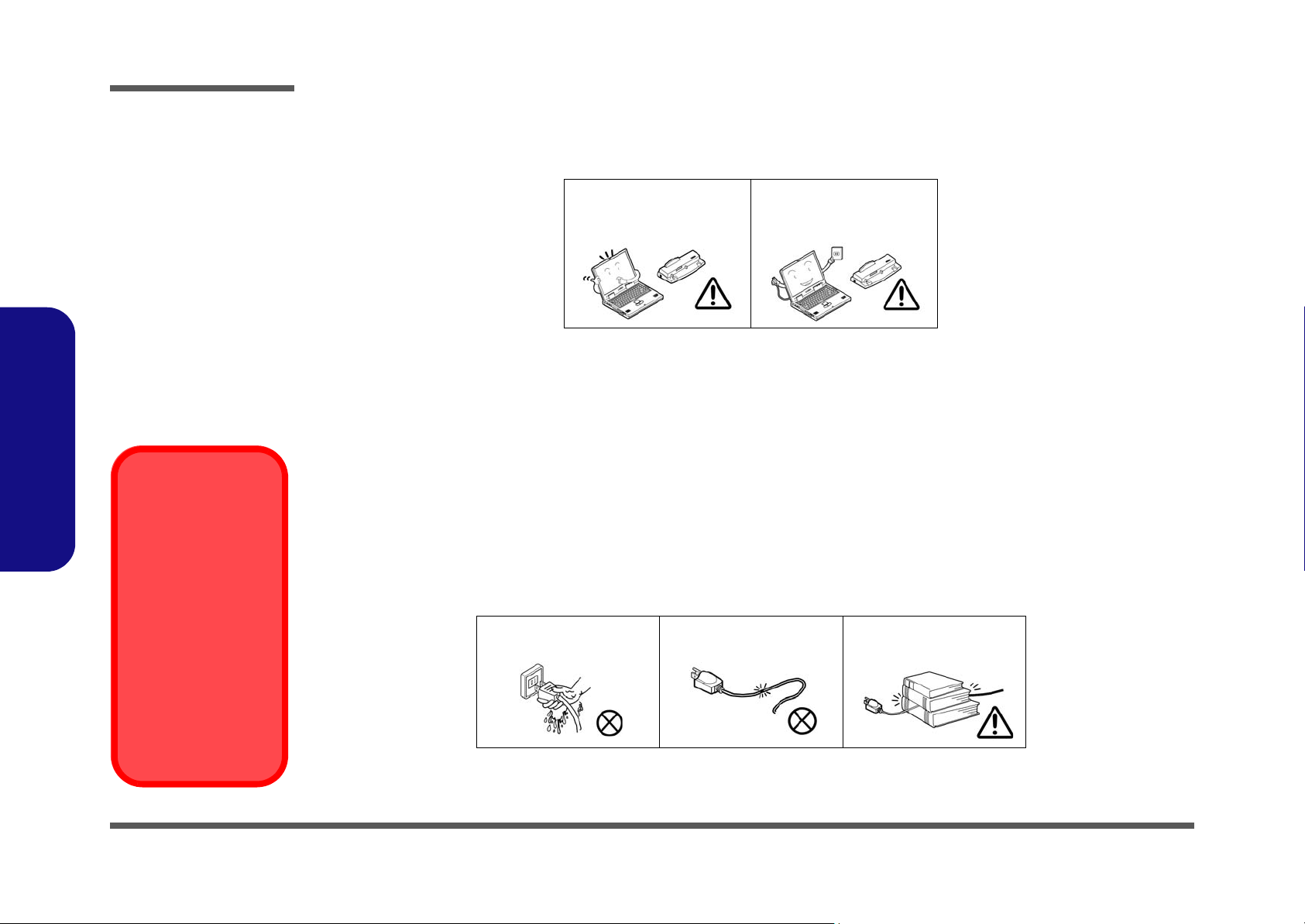
Power Safety
Warning
Before you undertake
any upgrade procedures, make sure that
you have turned off the
power, and disconnected all peripherals
and cables (including
telephone lines). It is
advisable to also remove your battery in
order to prevent accidentally turning the
machine on.
Use only approved brands of
peripherals.
Unplug the power cord befor e
attaching peripheral devices.
Power Safety
The computer has specific power requirements:
• Only use a power adapter approved for use with this computer.
• Your AC adapter may be designed for international travel but it still requires a stea dy, uninterrupted po wer supply. If you ar e
unsure of your local power specifications, consult your service representative or local power company.
• The power adapter may have either a 2-prong or a 3-prong grounded plug. The third prong is an important safety feature; do
not defeat its purpose. If you do not have access to a compatible outlet, have a qualified electrician install one.
• When you want to unplug the power cord, be sure to disconnect it by the plug head, not by its wire.
• Make sure the socket and any extension cord(s) you use can support the total current load of all the connected devices.
• Before cleaning the computer, make sure it is disconnected from any external power supplies.
Do not plug in the power
cord if you are wet.
Do not use the power cord if
it is broken.
Do not place heavy objects
on the power cord.
VI

Battery Precautions
• Only use batteries designed for this computer. The wrong battery type may explode, leak or damage the computer.
• Do not continue to use a battery that has been dropped, or that appears damaged (e.g. bent or twisted) in any way. Even if the
computer continues to work with a damaged battery in place, it may cause circuit damage, which may possibly result in fire.
• Recharge the batteries using the notebook’s system. Incorrect recharging may make the battery explode.
• Do not try to repair a battery pack. Refer any battery pack repair or replacement to your service representative or qualified service
personnel.
• Keep children away from, and promptly dispose of a damaged battery. Always dispose of batteries carefully. Batteries may explode
or leak if exposed to fire, or improperly handled or discarded.
• Keep the battery away from metal appliances.
• Affix tape to the battery contacts before disposing of the battery.
• Do not touch the battery contacts with your hands or metal objects.
Battery Guidelines
The following can also apply to any backup batteries you may have.
• If you do not use the battery for an extended period, then remove the battery from the computer for storage.
• Before removing the battery for storage charge it to 60% - 70%.
• Check stored batteries at least every 3 months and charge them to 60% - 70%.
Preface
Preface
Battery Disposal
The product that you have purchased contains a rechargeable battery. The battery is recyclable. At the end of its useful life, under various state and local laws, it may be illegal to dispose of this battery into the municipal waste stream. Check with your l ocal solid waste
officials for details in your area for recycling options or proper disposal.
Caution
Danger of explosion if battery is incorrectly replaced. Replace only with the same or equivalent type recommended by the manufacturer.
Discard used battery according to the manufacturer’s instructions.
Battery Level
Click the battery icon in the taskbar to see the current battery level and charge status. A battery that drops below a level of 10%
will not allow the computer to boot up. Make sure that any battery that drops below 10% is recharged within one week.
VII

Preface
Preface
Related Documents
You may also need to consult the following manual for additional information:
User’s Manual on CD
This describes the notebook PC’s features and the procedures for operating the computer and its ROM-based setup program. It also describes the installation and operation of the utility programs provided with the notebook PC.
VIII

Contents
Preface
Introduction ..............................................1-1
Overview .........................................................................................1-1
System Specifications ................................. 1-2
External Locator - Top View with LCD Panel Open ......................1-5
External Locator - Front & Right side Views .................................1-6
External Locator - Left Side & Rear View .....................................1-7
External Locator - Bottom View .....................................................1-8
Mainboard Overview - Top (Key Parts) .........................................1-9
Mainboard Overview - Bottom (Key Parts) ..................................1-10
Mainboard Overview - Top (Connectors) .....................................1-11
Mainboard Overview - Bottom (Connectors) ...............................1-12
Disassembly ...............................................2-1
Overview .........................................................................................2-1
Maintenance Tools ..........................................................................2-2
Connections .....................................................................................2-2
Maintenance Precautions .................................................................2-3
Disassembly Steps ...........................................................................2-4
Removing the Battery ......................................................................2-5
Removing the Hard Disk Drive .......................................................2-6
Removing the Optical (CD/DVD) Device ......................................2-8
Removing the System Memory (RAM) ..........................................2-9
Removing the Inverter Board ........................................................2-11
Removing and Installing the Processor .........................................2-12
Removing the Wireless LAN Module ...........................................2-15
Removing the Bluetooth Module ..................................................2-16
Removing the Keyboard ................................................................2-17
Removing the Modem ...................................................................2-18
Part Lists ..................................................A-1
Part List Illustration Location ........................................................A-2
Top with Fingerprint ...................................................................... A-3
Top without Fingerprint ................................................................. A-4
Bottom ........................................................................................... A-5
LCD ............................................................................................... A-6
SATA DVD SUPER-MULTI ........................................................ A-7
Schematic Diagrams.................................B-1
System Block Diagram ...................................................................B-2
Clock Generator ..............................................................................B-3
Penryn (Socket-P) CPU 1/2 ............................................................B-4
Penryn (Socket-P) CPU 2/2 ............................................................B-5
CANTIGA 1/7, Host .......................................................................B-6
CANTIGA 2/7, Graphics ................................................................B-7
CANTIGA 3/7 ................................................................................B-8
CANTIGA 4/7 ................................................................................B-9
CANTIGA 5/7 ..............................................................................B-10
CANTIGA 6/7 ..............................................................................B-11
CANTIGA 7/7 ..............................................................................B-12
DDRII SO-DIMM - 0 ...................................................................B-13
DDRII SO-DIMM - 1 ...................................................................B-14
Panel, Inverter, CRT .....................................................................B-15
ICH9M 1/4, SATA .......................................................................B-16
ICH9M 2/4, PCI, USB ..................................................................B-17
ICH9M 3/4 ....................................................................................B-18
ICH9M 4/4 ....................................................................................B-19
New Card, Mini PCIE ...................................................................B-20
3G, power ground .........................................................................B-21
USB, Fan, TP, FP, Multi CON .....................................................B-22
Card Reader ..................................................................................B-23
SATA ODD, LED, Hotkey, LID SW ...........................................B-24
PCI-E LAN RTL8111C ................................................................B-25
Preface
IX

Preface
Audio Codec ALC662 .................................................................. B-26
Audio AMP ..................................................................................B-27
KBC-ITE IT8512E ....................................................................... B-28
5VS, 3VS, 3.3VM, 1.05VS, VIN1 ...............................................B-29
Power 3.3V/5V .............................................................................B-30
Power 1.5VS/1.05VS ...................................................................B-31
Power 1.8V/0.9V ..........................................................................B-32
Power GPU/NVVDD ................................................................... B-33
AC-IN, Charger ............................................................................ B-34
VCORE ........................................................................................ B-35
NVVDD .......................................................................................B-36
HDMI ........................................................................................... B-37
ODD Board for M76 ....................................................................B-38
Click & Finger Board for M76 ..................................................... B-39
Multi Function Board ................................................................... B-40
Audio Board ................................................................................. B-41
Preface
Finger Sensor Board for M76 .......................................................B-42
Power Switch Board for M74 .......................................................B-43
Fingerprint Board for M74 ........................................................... B-44
Power Switch Board for M76 .......................................................B-45
ODD Board for W76 ....................................................................B-46
Updating the FLASH ROM BIOS......... C-1
Download the BIOS ........................................................................2-1
Unzip the downloaded files to a bootable CD/DVD/ or USB Flash
drive ................................................................................................. 2-1
Set the computer to boot from the external drive ............................2-1
Use the flash tools to update the BIOS ...........................................2-2
Restart the computer (booting from the HDD) ...............................2-2
X

Chapter 1: Introduction
Overview
This manual covers the information you need to service or upgrade the W760T series notebook computer. Information
about operating the computer (e.g. getting started, and the Setup utility) is in the User’s Manual. Information about drivers (e.g. VGA & audio) is also found in User’s Manual. That manual is shipped with the computer.
Operating systems (e.g. Windows XP, Windows Vista, etc.) have their own manuals as do application software (e.g. word
processing and database programs). If you have questions about those programs, you should consult those manuals.
Introduction
The W760T series notebook is designed to be upgradeable. See ?$paratext>? on page 2 - 1 for a detailed description of
the upgrade procedures for each specific component. Please note the warning and safety information indicated by the
“
” symbol.
The balance of this chapter reviews the computer’s technical specifications and features.
1.Introduction
Overview 1 - 1
Introduction
System Specifications
Feature Specification
1.Introduction
Processor Intel® Core™2 Duo Processor
(478-pin) Micro-FC-PGA Package, Socket P
T9400/ T9550/ T9600/ T9800
Intel® Core™2 Duo Processor
(478-pin) Micro-FC-PGA Package, Socket P
P9500/ P9600
Intel® Core™2 Duo Processor
(478-pin) Micro-FC-PGA Package, Socket P
P8400/ P8600/ P8700
Intel® Celeron® Processor
(478-pin) Micro-FC-PGA Package, Socket P
T1600/ T1700
Intel® Celeron® M Processor
(478-pin) Micro-FC-PGA Package, Socket P
575/ 585
Core Logic Intel(R) GM45 + ICH9M Chipset
LCD 15.6" HD TFT LCD
Video Adapter Intel GM45 Integrated Video (Internal On Chip)
Shared Memory Architecture up to 256MB
Memory 64-bit Wide DDRII (DDR2) Data Channel
Supports Dual Channel DDR2 SDRAM
Two 200 Pin SO-DIMM Sockets Supporting DDRII (DDR2) 667MHz/ 800MHz
Memory Expandable up to 4GB (1024MB/ 2048MB DDRII Modules)
45nm (45 Nanometer) Process Technology
6MB On-die L2 Cache & 1066MHz FSB
2.53/ 2.66/ 2.8/ 2.93 GHz
45nm (45 Nanometer) Process Technology
6MB On-die L2 Cache & 1066MHz FSB
2.53/ 2.66 GHz
45nm (45 Nanometer) Process Technology
3MB On-die L2 Cache & 1066MHz FSB
2.26/ 2.40/ 2.53 GHz
65nm (65 Nanometer) Process Technology
1MB On-die L2 Cache & 667MHz FSB
1.66/ 1.86 GHz
65nm (65 Nanometer) Process Technology
1MB On-die L2 Cache & 667MHz FSB
2.0/ 2.16 GHz
Security Security (Kensington® Type) Lock Slot
BIOS One 32Mb SPI Flash ROM Phoenix™ BIOS
Storage
1 - 2 System Specifications
Fingerprint ID Reader Module (Factory Option)
One Changeable 12.7mm(h)
Easy Changeable 2.5" 9.5 mm (h)
SA TA
Optical Device (CD/DVD) Type Drive (see
SA TA
(Serial) HDD
BIOS Password
?$paratext>? on page 1 - 4
)
Feature Specification
Introduction
Audio Intel® High Definition Audio (HDA) Interface
3D Enhanced Sound System
Keyboard &
Pointing Device
Interface Three USB 2.0 Ports
Card Reader Embedded 7-in-1 Card Reader (MS/ MS Pro/ SD/ Mini SD/ MMC/ RS MMC/ MS Duo)
Communication Built-In 56K MDC Modem, V.90 & V.92 Compliant
Winkey Keyboard Built-In TouchPad with Scrolling Function
One HDMI-Out Port (High-Definition Multimedia Interface)
One Headphone-Out Jack
One Microphone-In Jack
One S/PDIF-Out Jack
Note: MS Duo/ Mini SD/ RS MMC Cards require a PC adapter
Built-In Gigabit Ethernet LAN
Bluetooth 2.1 + EDR (Enhanced Data Rate) Module (Factory Option)
1.3M or 2.0M Pixel USB PC Camera Module (Factory Option)
S/PDIF Digital Output
2 * Built-In Speakers (1W, 8
Built-In Microphone
One eSATA Port
One RJ-1 1 Modem Jack
One RJ-45 LAN Jack
One DC-In Jack
One External Monitor Port
UMTS Modes
Note that UMTS
modes CAN
NOT be used in
North America.
Wireless LAN Module:
Intel® WiFi Link 5300 Series (3*3 - 802.11a/g/n) Wireless LAN Mini-Card Module (Option)
Intel® WiFi Link 5100 Series (1*2 - 802.11a/g/n) Wireless LAN Mini-Card Module (Option)
802.11b/g Wireless LAN Mini-Card Module (Option)
3.5G Module:
UMTS/HSPDA-based 3.75G Module with Mini-Card Interface (Factory Option)
Ω)
1.Introduction
ExpressCard Slot One ExpressCard/34(54) Slot
Mini-Card Slots
Power
Management
Power Full Range AC/DC Adapter AC input 100 - 240V, 50 - 60Hz, DC Output: 19V, 3.42A or 18.5, 3.5A (65W)
One Mini-Card Slot for
One Mini-Card Slot for
Supports ACPI 3.0
Supports Wa ke on LAN
Wireless LAN Module
3.5G Module
Supports Resume from Modem Ring
System Specifications 1 - 3
Introduction
Feature Specification
Battery 6 Cell Smart Lithium-Ion Battery Pack, 4000mAH OR 4400mAH
9 Cell Smart Lithium-Ion Battery Pack, 7200mAH (Option)
1.Introduction
Environmental
Spec
Dimensions
& Weight
Optional Optical Drive Module Options:
Temperature
Operating: 5
Non-Operating: -20°C - 60°C
374mm (w) * 256mm (d) * 25 - 37.9mm (h)
2.7 kg With 6 Cell Battery
Super Multi Device Module
Wireless LAN Module:
°C - 35°C
Intel® WiFi Link 5300/5100 Series (3*3/1*2 -
802.11a/g/n) Wireless LAN Mini-Card Module
802.11b/g Wireless LAN Mini-Card Module
9 Cell Smart Lithium-Ion Battery Pack
1.3M or 2.0M Pixel USB PC Camera Module (Factory
Option)
Fingerprint ID Reader Module (Factory Option)
Intel Turbo Memory (Robson) NAND Flash 2G/4G
Memory Card Module (Factory Option)
Relative Humidity
Operating: 20% - 80%
Non-Operating: 10% - 90%
Bluetooth 2.1 + EDR (Enhanced Data Rate) Module
(Factory Option)
UMTS/HSPDA-based 3.75G Module with Mini-Card
Interface (Factory Option)
UMTS Modes
Note that UMTS modes CAN NOT be used in
North America.
1 - 4 System Specifications
Introduction
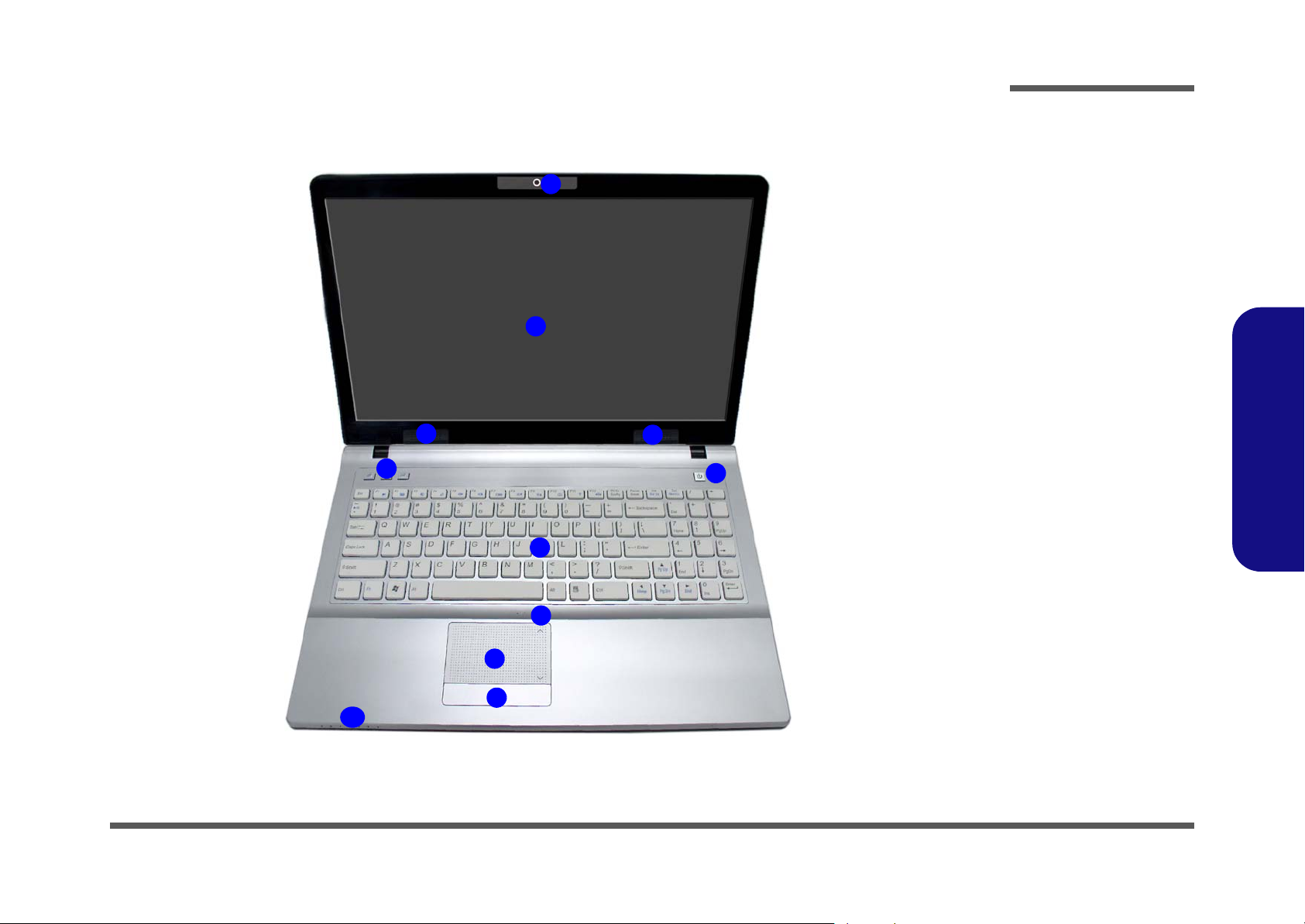
External Locator - Top View with LCD Panel Open
1
2
3
5
6
3
4
Figure 1
Top View
1. Optional Built-In
PC Camera
2. LCD
3. Speakers
4. Power Button
5. Hot Key Buttons
6. Keyboard
7. Built-In
Microphone
8. Touchpad &
Buttons
9. Fingerprint
Module (Optional)
10.LED Indicators
1.Introduction
10
7
8
9
External Locator - Top View with LCD Panel Open 1 - 5
Introduction
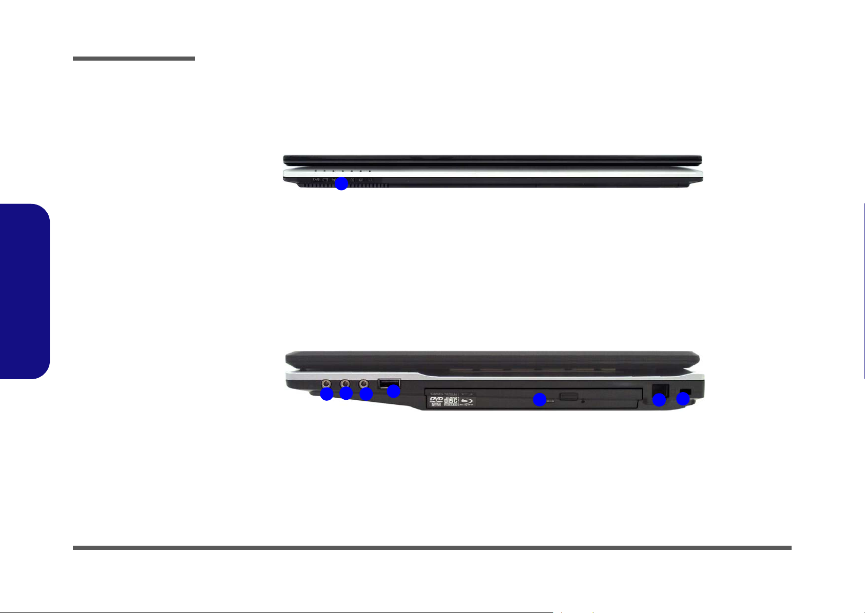
Figure 2
Front Views
1. LED Power &
Communication
Indicators
Figure 3
1.Introduction
Right Side Views
1. S/PDIF-Out Jack
2. Microphone-In
Jack
3. Headphone-Out
Jack
4. USB 2.0 Port
5. Optical Device
Drive Bay
6. RJ-11 Phone
Jack
7. Security Lock
Slot
External Locator - Front & Right side Views
1
2
1
4
3
5
7
6
1 - 6 External Locator - Front & Right side Views
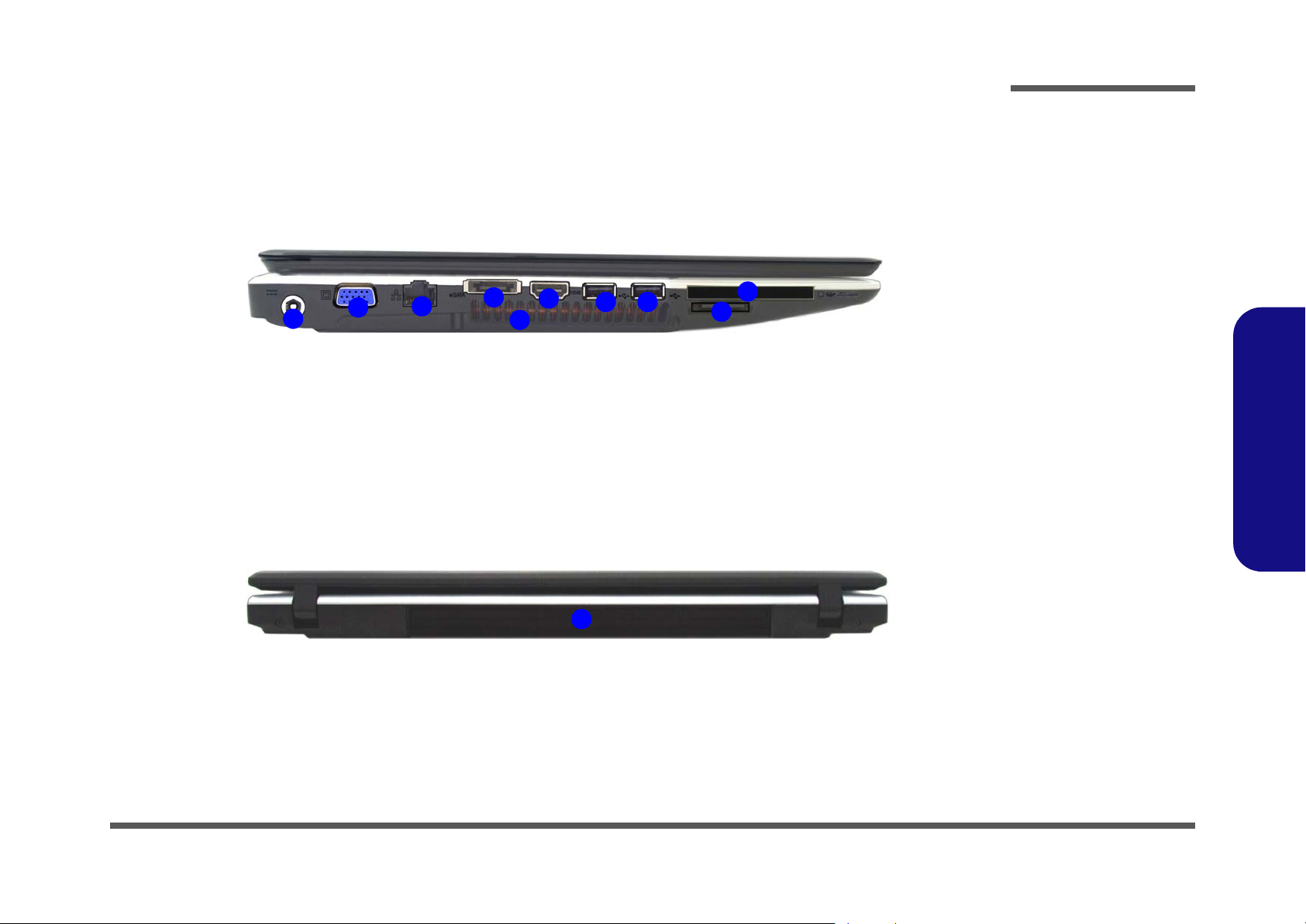
External Locator - Left Side & Rear View
1
2
3
4
5
6
7
Introduction
Figure 4
Left Side View
1. DC-In Jack
2. External Monitor
Port
3. RJ-45 LAN Jack
4. e-SATA Port
7
8
9
5. HDMI-Out Port
6. Vent/Fan Intake/
Outlet
7. 2 * USB 2.0 Ports
8. ExpressCard Slot
9. 7-in-1 Card
Reader
1.Introduction
Figure 5
Rear View
1
1. Battery
External Locator - Left Side & Rear View 1 - 7
Introduction
Figure 6
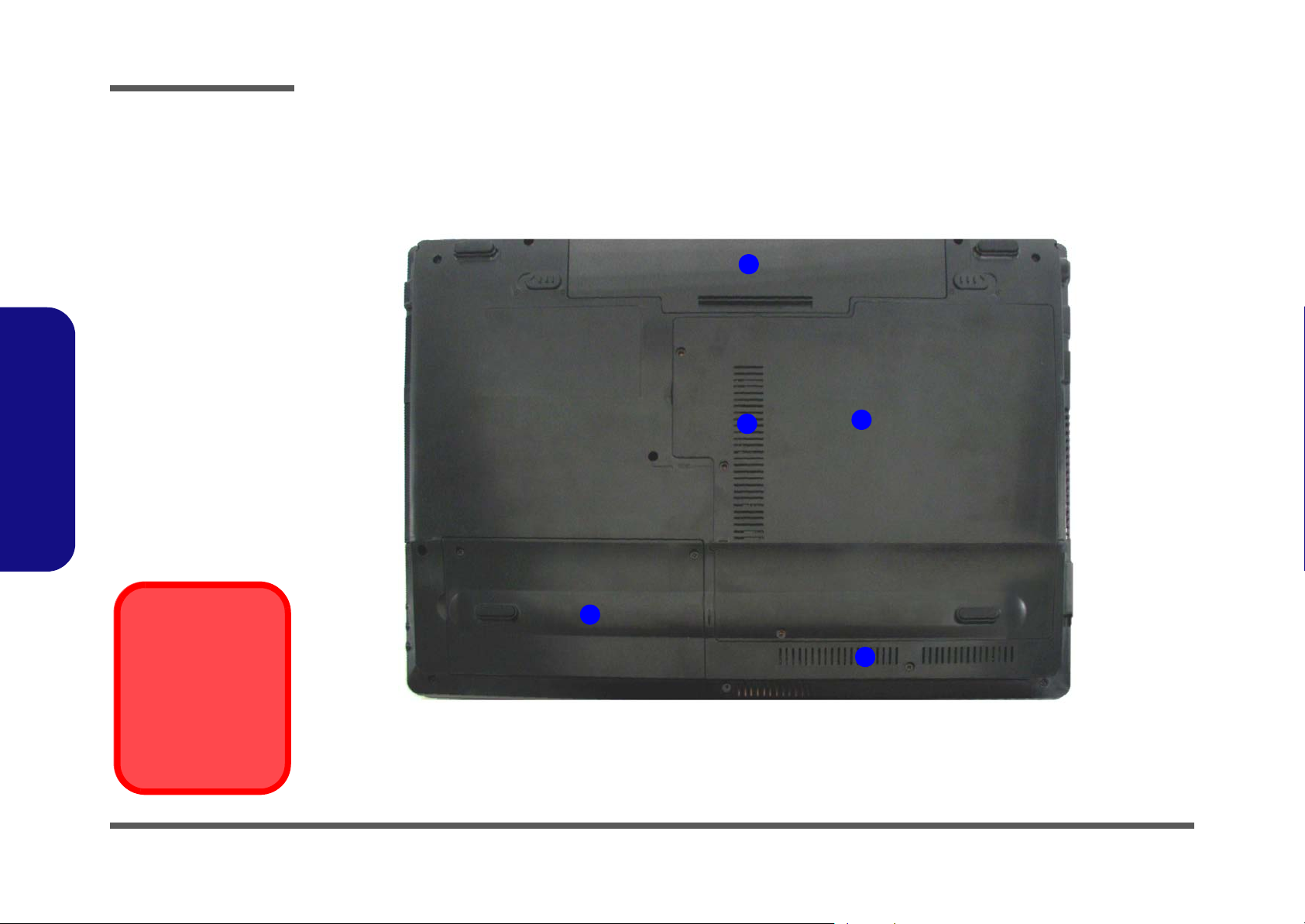
Bottom View
1. Battery
2. RAM & CPU Bay
Cover
3. Vent/Fan Intake/
Outlet
4. Hard Disk Bay
Cover
External Locator - Bottom View
1
1.Introduction
Overheating
To prevent your computer from overheating
make sure nothing
blocks the vent/fan intakes while the computer is in use.
1 - 8 External Locator - Bottom View
3
4
2
3
Introduction
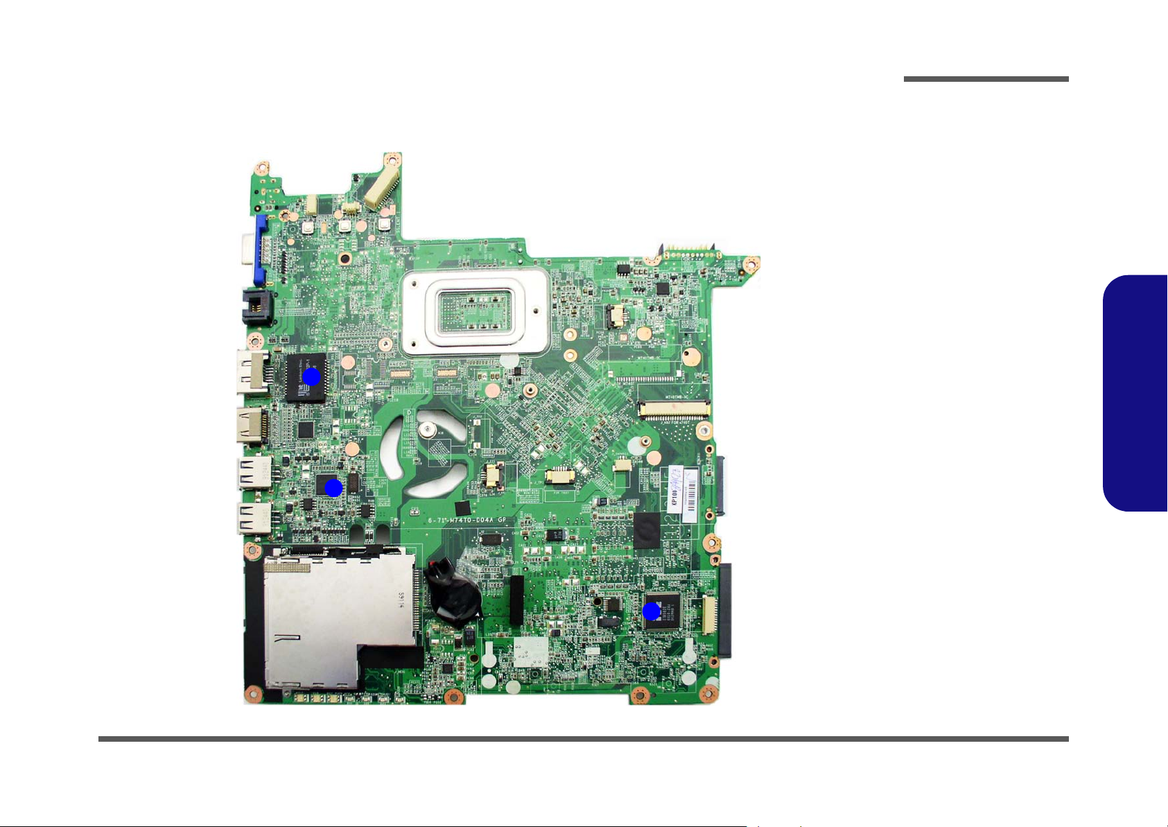
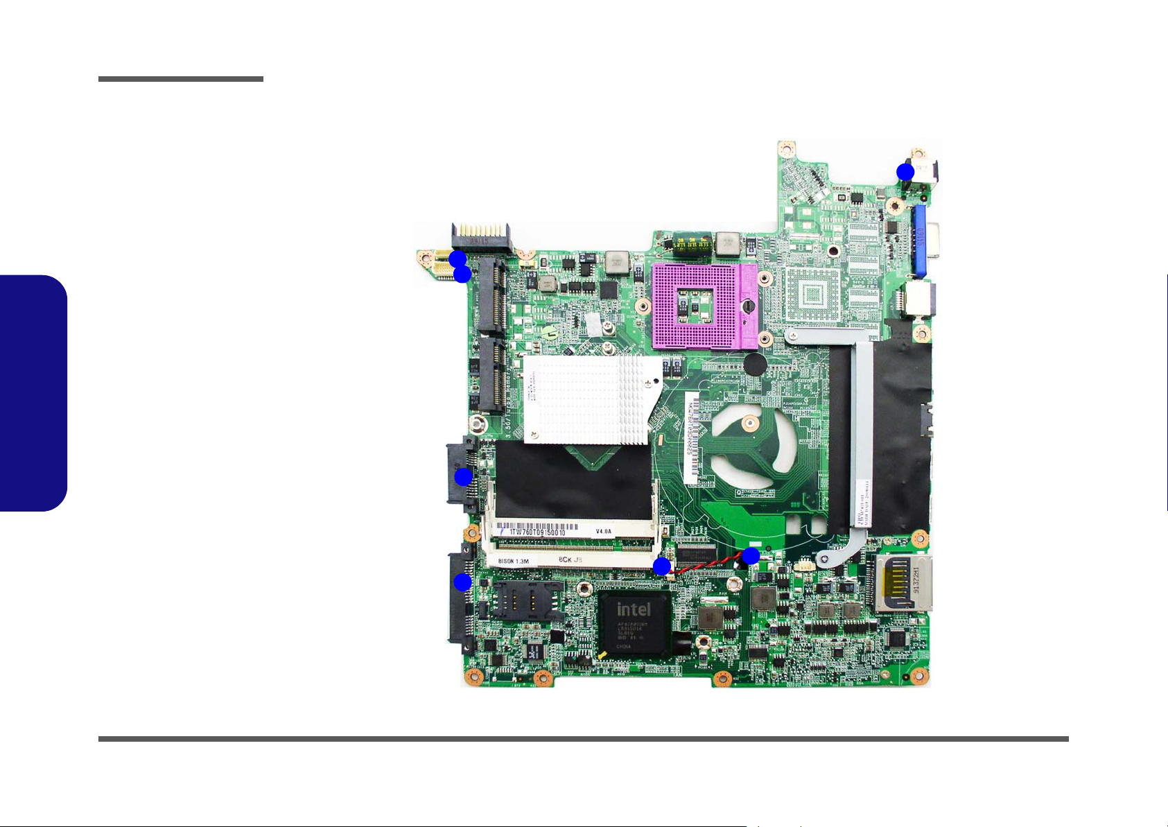
Mainboard Overview - Top (Key Parts)
1
2
Figure 7
Mainboard Top
Key Parts
1. Transformer
2. RTL81 11DL
3. ITE IT8502E
1.Introduction
3
Mainboard Overview - Top (Key Parts) 1 - 9
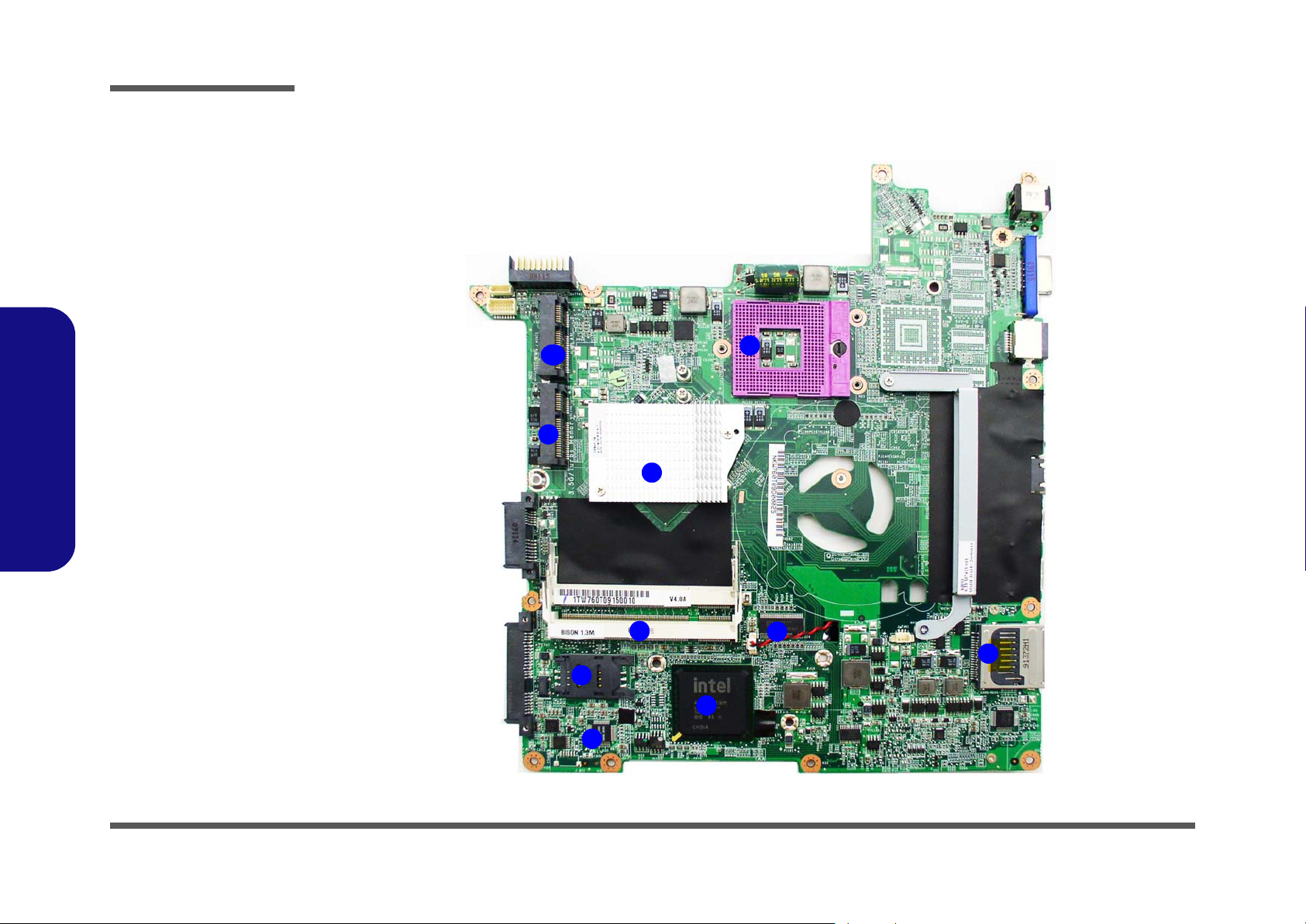
Introduction
Figure 8
Mainboard Bottom
Key Parts
1. CPU Socket (no
CPU installed)
2. North Bridge
3. Memory Slots
DDR2 SO-DIMM
4. ICS
5. Card Reader
Socket
6. South Bridge
7. Audio Codec
8. Simlock
9. Turbo Memory
Slot/ 3.5G Slot
10.Mini-Card Slot
(WLAN Module)
1.Introduction
Mainboard Overview - Bottom (Key Parts)
10
9
2
1
1 - 10 Mainboard Overview - Bottom (Key Parts)
3
8
6
7
4
5
Introduction
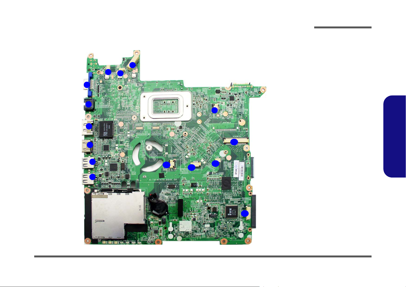
Mainboard Overview - Top (Connectors)
8
6
7
5
4
3
2
1
1
13
12
9
11
10
14
Figure 9
Mainboard Top
Connectors
1. USB Port
2. HDMI-Out Port
3. e-SATA Port
4. RJ-45 LAN Jack
5. External Monitor
Port
6. Inverter board
Connector
7. Speaker Cable
Connector
8. LCD Cable
Connector
9. Power Switch
Cable Connector
10.Keyboard Cable
Connector
11. Microphone
Cable Connector
12.TouchPad Cable
Connector
13.Fingerprint Cable
Connector
14.Audio Board
Connector
1.Introduction
Mainboard Overview - Top (Connectors) 1 - 11
Introduction
Figure 10
Mainboard Bottom
Connectors
1. BT Cable
Connector
2. Multi Board
Connector
3. CD-ROM
Connector
4. HDD Connector
5. CMOS Bat.
Connector
6. CPU Fan Cable
Connector
7. DC-In Jack
1.Introduction
Mainboard Overview - Bottom (Connectors)
7
1
2
3
4
1 - 12 Mainboard Overview - Bottom (Connectors)
5
6

Chapter 2: Disassembly
Overview
This chapter provides step-by-step instructions for disassembling the W760T series notebook’s parts and subsystems.
When it comes to reassembly, reverse the procedures (unless otherwise indicated).
We suggest you completely review any procedure before you take the computer apart.
Disassembly
Procedures such as upgrading/replacing the RAM, optical device and hard disk are included in the User’s Manual but are
repeated here for your convenience.
To make the disassembly process easier each section may have a box in the page margin. Information contained under
the figure # will give a synopsis of the sequence of procedures involved in the disassembly procedure. A box with a
lists the relevant parts you will have after the disassembly process is complete. Note: The parts listed will be for the disassembly procedure listed ONLY, and not any previous disassembly step(s) required. Refer to the part list for the previous disassembly procedure. The amount of screws you should be left with will be listed here also.
A box with a
An example of these types of boxes are shown in the sidebar.
will also provide any possible helpful information. A box with a contains warnings.
2.Disassembly
Information
Warning
Overview 2 - 1

Disassembly
2.Disassembly
NOTE: All disassembly procedures assume that the system is turned OFF, and disconnected from any power supply (the
battery is removed too).
Maintenance Tools
The following tools are recommended when working on the notebook PC:
• M3 Philips-head screwdriver
• M2.5 Philips-head screwdriver (magnetized)
• M2 Philips-head screwdriver
• Small flat-head screwdriver
• Pair of needle-nose pliers
• Anti-static wrist-strap
Connections
Connections within the computer are one of four types:
Locking collar sockets for ribbon connectors To release these connectors, use a small flat-head screwdriver to
gently pry the locking collar away from its base. When replacing the connection, make sure the connector is oriented in the
same way. The pin1 side is usually not indicated.
2 - 2 Overview
Pressure sockets for multi-wire connectors To release this connector type, grasp it at its head and gently
rock it from side to side as you pull it out. Do not pull on the
wires themselves. When replacing the connection, do not try to
force it. The socket only fits one way.
Pressure sockets for ribbon connectors To release these connectors, use a small pair of needle-nose pli-
ers to gently lift the connector away from its socket. When replacing the connection, make sure the connector is oriented in
the same way. The pin1 side is usually not indicated.
Board-to-board or multi-pin sockets To separate the boards, gently rock them from side to side as
you pull them apart. If the connection is very tight, use a small
flat-head screwdriver - use just enough force to start.

Maintenance Precautions
The following precautions are a reminder. To avoid personal injury or damage to the computer while performing a removal and/or replacement job, take the following precautions:
1. Don't drop it. Perform your repairs and/or upgrades on a stable surface. If the computer falls, the case and other
components could be damaged.
2. Don't overheat it. Note the proximity of any heating elements. Keep the computer out of direct sunlight.
3. Avoid interference. Note the proximity of any high capacity transformers, electric motors, and other strong mag-
netic fields. These can hinder proper performance and damage component s and/or data. You should also monitor
the position of magnetized tools (i.e. screwdrivers).
4. Keep it dry. This is an electrical appliance. If water or any other liquid gets into it, the computer could be badly
damaged.
5. Be careful with power. Avoid accidental shocks, discharges or explosions.
•Before removing or servicing any part from the computer, turn the computer off and detach any power supplies.
•When you want to unplug the power cord or any cable/wire, be sure to disconnect it by the plug head. Do no t pull on th e wir e.
6. Peripherals – Turn off and detach any peripherals.
7. Beware of static discharge. ICs, such as the CPU and main support chips, are vulnerable to static electricity.
Before handling any part in the computer, discharge any static electricity inside the computer. When handling a
printed circuit board, do not use gloves or other materials which allow static electricity buildup. We suggest that
you use an anti-static wrist strap instead.
8. Beware of corrosion. As you perform your job, avoid touching any connector leads. Even the cleanest hands produce oils which can attract corrosive elements.
9. Keep your work environment clean. Tobacco smoke, dust or other air-born particulate matter is often attracted
to charged surfaces, reducing performance.
10. Keep track of the component s. When re moving or replacing any p art, be careful not to le ave small part s, such as
screws, loose inside the computer.
Disassembly
Power Safety
Warning
Before you undertake
any upgrade procedures, make sure that
you have turned off the
power, and disconnected all peripherals
and cables (including
telephone lines). It is
advisable to also remove your battery in
order to prevent accidentally turning the
machine on.
2.Disassembly
Cleaning
Do not apply cleaner directly to the computer, use a soft clean cloth.
Do not use volatile (petroleum distillates) or abrasive cleaners on any part of the computer.
Overview 2 - 3

Disassembly
Disassembly Steps
The following table lists the disassembly steps, and on which page to find the related information. PLEASE PERFORM
THE DISASSEMBLY STEPS IN THE ORDER INDICATED.
2.Disassembly
To remove the Battery:
1. Remove the battery page 2 - 5
To remove the HDD:
1. Remove the battery page 2 - 5
2. Remove the HDD page 2 - 6
To remove the Optical Device:
1. Remove the battery page 2 - 5
2. Remove the Optical device page 2 - 8
To remove the System Memory:
1. Remove the battery page 2 - 5
2. Remove the system memory page 2 - 9
To remove the Inverter Board:
1. Remove the battery page 2 - 5
2. Remove the inverter board page 2 - 11
To remove and install a Processor:
To remove the Wireless LAN Module:
1. Remove the battery page 2 - 5
2. Remove the wireless LAN page 2 - 15
To remove the Bluetooth Module:
1. Remove the battery page 2 - 5
2. Remove the Bluetooth page 2 - 16
To remove the Keyboard:
1. Remove the battery page 2 - 5
2. Remove the keyboard page 2 - 17
To remove the Modem:
1. Remove the battery page 2 - 5
2. Remove the HDD page 2 - 6
3. Remove the Optical device page 2 - 8
4. Remove the processor page 2 - 12
5. Remove the keyboard page 2 - 17
6. Remove the modem page 2 - 18
1. Remove the battery page 2 - 5
2. Remove the processor page 2 - 12
3. Install the processor page 2 - 14
2 - 4 Disassembly Steps
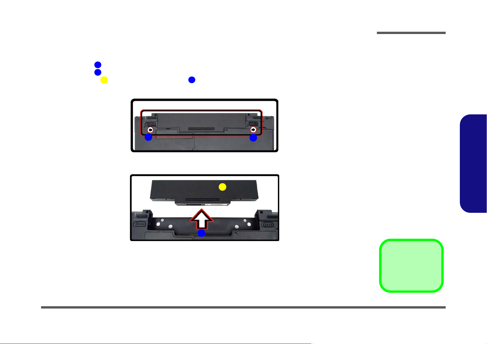
Removing the Battery
Disassembly
1. Turn the computer off, and turn it over.
2. Slide the latch in the direction of the arrow.
3. Slide the latch in the direction of the arrow, and hold it in place.
4. Slide the battery in the direction of the arrow .
1
2
3
6
a.
2
b.
4
3
Figure 1
Battery Removal
a. Slide the latch and hold in
place.
b. Slide the battery in the di-
rection of the arrow.
1
2.Disassembly
4
3. Battery
Removing the Battery 2 - 5
Disassembly
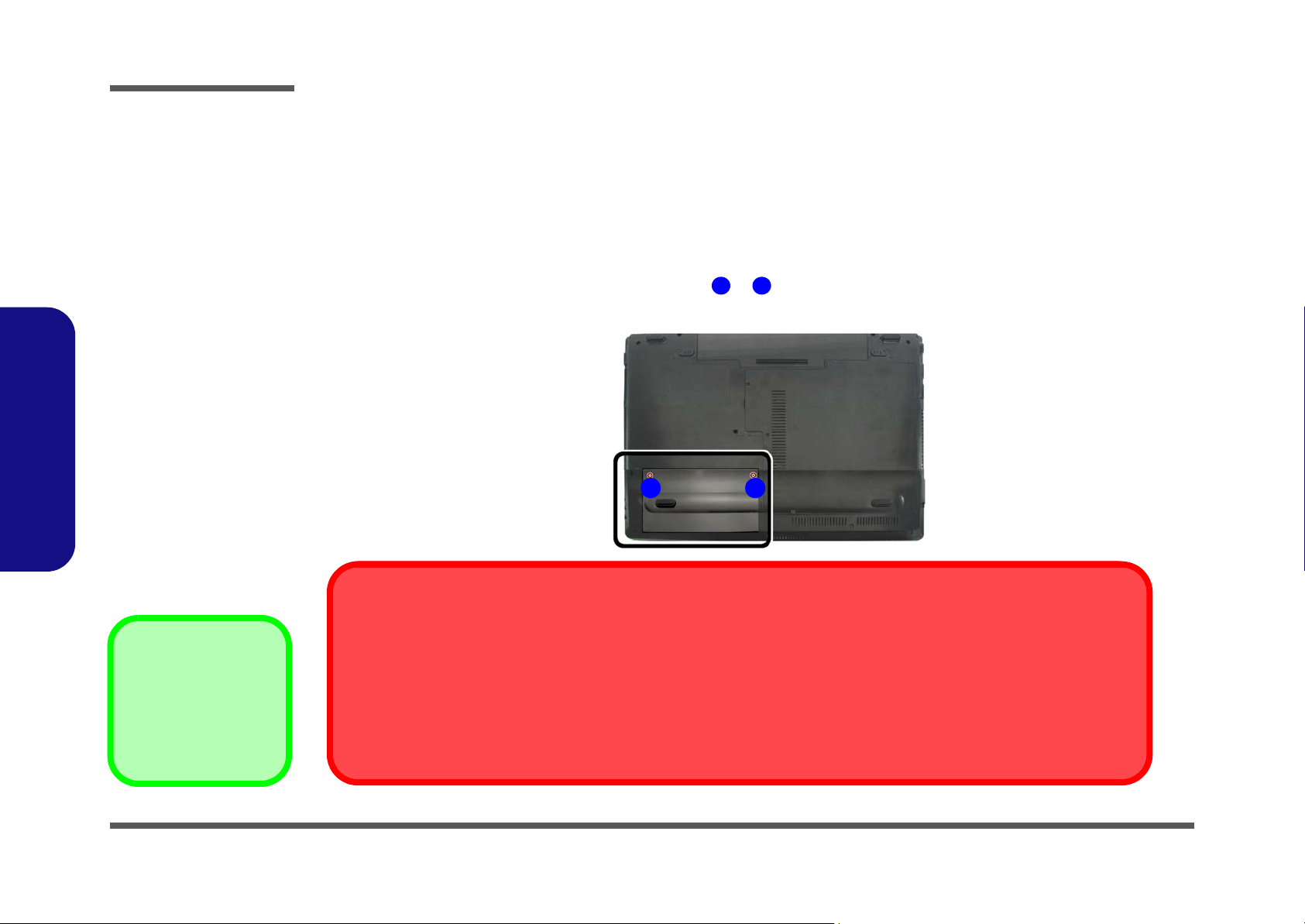
Removing the Hard Disk Drive
Figure 2
HDD Assembly
Removal
a. Locate the HDD bay
cover and remove the
screw(s).
2.Disassembly
The hard disk drive can be taken out to accommodate other 2.5" serial (SATA) hard disk drives with a height of 9.5mm
(h). Follow your operating system’s installation instructions, and install all necessary drivers and utilities (as outlined in
Chapter 4 of the User’s Manual) when setting up a new hard disk.
Hard Disk Upgrade Process
1. Turn off the computer, and remove the battery (page 2 - 5).
2. Locate the hard disk bay cover and remove screw & .
a.
1 2
21
HDD System Warning
•2 Screws
New HDD’s are blank. Before you begin make sure:
You have backed up any data you want to keep from your old HDD.
You have all the CD-ROMs and FDDs required to install your operating system and programs.
If you have access to the internet, download the latest application and hardware driver updates for the operating system you plan
to install. Copy these to a removable medium.
2 - 6 Removing the Hard Disk Drive

3
3. Remove the hard disk bay cover .
4. Grip the tab and slide the hard disk in the direction of arrow .
5. Lift the hard disk out of the bay .
6. Remove the screw and the adhesive cover from the hard disk .
6 6
6
4
5
7
8
6
7. Reverse the process to install a new hard disk (do not forget to replace all the screws and covers).
b.
3
Disassembly
Figure 3
HDD Assembly
Removal (cont’d.)
b. Remove the HDD bay
cover.
c. Grip the tab and slide the
HDD in the direction of
the arrow.
d. Lift the HDD assembly
out of the bay.
e. Remove the screws and
adhesive cover.
2.Disassembly
c.
d.
e.
4
6
7
8
5
3. HDD Bay Cover
7. Adhesive Cover
8. HDD
•2 Screws
Removing the Hard Disk Drive 2 - 7

Disassembly
Figure 4
Optical Device
Removal
a. Remove the screws.
b. Remove the HDD bay
cover.
c. Remove the screw.
d. Push the optical device
out off the computer at
point 6.
2.Disassembly
Removing the Optical (CD/DVD) Device
1. Turn off the computer, and remove the battery (page 2 - 5).
2. Locate the hard disk bay cover and remove screw & .
3
3. Remove the hard disk bay cover
4. Remove the screw at point , and use a screwdriver to carefully push out the optical device at point .
6
.
4
5. Insert the new device and carefully slide it into the computer (the device only fits one way. DO NOT FORCE IT; The
screw holes should line up).
6. Restart the computer to allow it to automatically detect the new device.
a.
1
2
b.
1 2
c.
d.
6
5
4
3
3. HDD Bay Cover
8. Optical Device
•3 Screws
2 - 8 Removing the Optical (CD/DVD) Device
6
5

Disassembly
Removing the System Memory (RAM)
The computer has two memory sockets for 200 pin Small Outline Dual In-line Memory Modules (SO-DIMM) supporting
DDR2 667/800MHz. The main memory can be expanded up to 4GB. The SO-DIMM modules supported are 1024MB,
and 2048MB and DDRII Modules. The total memory size is automatically detected by the POST routine once you turn
on your computer.
Memory Upgrade Process
1. Turn off the computer, remove the battery (page 2 - 5).
2. Locate the component bay cover , and remove screws - .
3. Carefully (a fan and cable are attached to the under side of the cover) lift up the bay cover.
4. Carefully disconnect the fan cable , and remove the cover
a.
2
3
1
5 1
b.
1
2 4
.
1
Figure 5
RAM Module
Removal
a. Remove the screws.
b. Remove the cover.
Contact Warning
Be careful not to touch
the metal pins on the
module’s connecting
edge. Even the cleanest hands have oils
which can attract particles, and degrade the
module’s performance.
2.Disassembly
4
5
1. Component Bay
Cover
•3 Screws
Removing the System Memory (RAM) 2 - 9

Disassembly
Figure 6
RAM Module
Removal (cont’d.)
c. Pull the release
latch(es).
d. Remove the module(s).
Single Memory
Module Installation
If your computer has a
single memory module,
then insert the module
into the Channel 0
(J_DIMM_1) socket. In
2.Disassembly
this case, this is the lower memory socket (the
socket closest to the
mainboard) as shown in
Figure 6d.
5. Gently pull the two release latches ( & ) on the sides of the memory socket in the direction indicated by the
6 7
arrows (Figure 6c).
c.
d.
8
6 7
6. The RAM module(s) will pop-up (Figure 6d), and you can then remove it.
8
7. Pull the latches to release the second module if necessary.
8. Insert a new module holding it at about a 30° angle and fit the connectors firmly into the memory slot.
9. The module’s pin alignment will allow it to only fit one way. Make sure the module is seated as far into the slot as it
will go. DO NOT FORCE the module; it should fit without much pressure.
10. Press the module in and down towards the mainboard until the slot levers click into place to secure the module.
11. Replace the bay cover and screws (make sure you reconnect the fan cable before screwing down the bay
cover).
12. Restart the computer to allow the BIOS to register the new memory configuration as it starts up.
8. RAM Module(s)
2 - 10 Removing the System Memory (RAM)

Disassembly
Removing the Inverter Board
1. Turn off the computer, and remove the battery (page 2 - 5).
2. Remove any rubber covers, screws - (Figure 7a), then run your finger around the middle of the frame to
carefully unsnap the LCD front panel module from the back.
3. Discharge the remaining system power (see ?$paratext>? below).
4. Remove screw (Figure 7b) from the inverter, and carefully lift the inverter board up slightly.
5. Disconnect cables & (Figure 7c) from the inverter, then remove the inverter (Figure 7d) from the LCD
8
9 10
back cover module.
a. b.
2 5
3
1
7
1
6
7
11
4
8
c.
6
9
10
Figure 7
Inverter Board
Removal
a. Remove the 6 screws
and unsnap the LCD
front panel module from
the back.
b. Remove the screw and
discharge the remaining
power from the inverter
board and lift the board
up slightly.
c. Disconnect the cables
from the inverter.
d. Remove the inverter.
2.Disassembly
Inverter Power Warning
In order to prevent a short circuit when removing the inverter it is necessary to discharge any remaining system power. To do
so, press the computer’s power button for a
few seconds before disconnecting the inverter cable.
d.
11
7. LCD Front Panel
11.Inverter Board
•6 Screws
Removing the Inverter Board 2 - 11

Disassembly
Removing and Installing the Processor
Figure 8
Processor Removal
a. Remove the cover and
Iocate the heat sink.
b. Remove the screws in
the order indicated.
c. Remove the heat sink.
2.Disassembly
B. Heat Sink
Processor Removal Procedure
1. Turn off the computer, remove the battery (page 2 - 5) and the component bay cover (page 2 - 9).
2. The CPU heat sink will be visible at point on the mainboard.
3. Loosen screws
4. Carefully lift up the heat sink (Figure 8c) off the computer.
a.
b.
3
, , (Figure 8b) the reverse order to that indicated on the label.
3 2 1
B
A
2
1
A
c.
B
•3 Screws
2 - 12 Removing and Installing the Processor

Disassembly
5. Turn the release latch towards the unlock symbol , to release the CPU (Figure 9d).
6. Carefully (it may be hot) lift the CPU up out of the socket (Figure 9e).
C
D
7. See page 2 - 14 for information on inserting a new CPU.
8. When re-inserting the CPU, pay careful attention to the pin alignment, it will fit only one way (DO NOT FORCE IT!).
d.
C
C
Unlock
Lock
e.
D
Caution
Figure 9
Processor Removal
(cont’d)
d. Turn the release latch to
unlock the CPU.
e. Lift the CPU out of the
socket.
2.Disassembly
The heat sink, and CPU area in
general, contains parts which are
subject to high temperatures. Allow the area time to cool before removing these parts.
Removing and Installing the Processor 2 - 13
D. CPU

Disassembly
Figure 10
Processor
Installation
a. Insert the CPU.
b. Turn the release la tch to-
wards the lock symbol.
c. Remove the sticker from
the heat sink and insert
the heat sink.
d. Tighten the screws.
2.Disassembly
Processor Installation Procedure
1. Insert the CPU , pay careful attention to the pin alignment, it will fit only one way (DO NOT FORCE IT!), and
turn the release latch towards the lock symbol (Figure 10b).
2. Remove the sticker (Figure 10c) from the heat sink.
3. Insert the heat sink
4. Tighten screws
5. Replace the component bay cover and tighten the screws (page 2 - 9).
a.
b.
A
B
C
D
as indicated in Figure 10c.
1 3
- in the order indicated on the label.
c.
A
d.
C
D
2
A. CPU
D. Heat Sink
•3 Screws
2 - 14 Removing and Installing the Processor
3
D
1
B

Disassembly
Removing the Wireless LAN Module
1. Turn off the computer, remove the battery (page 2 - 5) and the component bay cover (page 2 - 9).
2. The Wireless LAN module will be visible at point on the mainboard.
3. Carefully disconnect cables - , then remove screw from the module socket.
4. The Wireless LAN module will pop-up.
5. Lift the Wireless LAN module (Figure 11d) up and off the computer.
a.
1
c.
2
3 4
5
1
b.
2
3
4
Figure 11
Wireless LAN
Module Removal
a. Remove the cover.
b. Disconnect the cable
and remove the screw.
c. The WLAN module will
pop up.
d. Lift the WLAN module
out.
Note: Make sure you
reconnect the antenna
cable to ‘’1’’ +
‘’2’’socket (Figure
b).
2.Disassembly
d.
5
5
Removing the Wireless LAN Module 2 - 15
5. WLAN Module.
•1 Screw

Disassembly
Figure 12
Bluetooth Module
Removal
a. Remove the cover and Io-
cate the Bluetooth.
b. Remove the screw.
c. Disconnect the cable and
the connector.
d. Lift the Bluetooth module
up off the socket.
2.Disassembly
Removing the Bluetooth Module
1. Turn off the computer, remove the battery (page 2 - 5) and the component bay cover (page 2 - 9).
2. The Bluetooth will be visible at point on the mainboard.
3. Remove the screw and turn the module over.
2
4. Carefully separate the Bluetooth module from the connector
5. Lift the Bluetooth module
(Figure 12d) up and off the computer.
5
a.
1
b.
1
3 4
and disconnect the cable .
c.
d.
5
3
4
d.
5. Bluetooth Module
•1 Screw
2 - 16 Removing the Bluetooth Module
2

Removing the Keyboard
1. Turn off the computer.
2. Remove the battery
3. Remove the screws
4. Remove the top cover module and the screws - (Figure 13d),
5. Carefully lift the keyboard up, being careful not to bend the keyboard ribbon cable (Figure 13e).
6. Disconnect the keyboard ribbon cable from the locking collar socket .
2 3
- and use a screwdriver to carefully push out the top cover module at point .
5
11
12 13
6 10
7. Carefully lift up the keyboard (Figure 13f) off the computer.
a.
1
d.
e.
10
96 87
b.
4
5
5
11
13
12
Disassembly
Figure 13
4
Keyboard Removal
a. Remove the battery.
b. Remove the screws and
use a screwdriver to carefully push out the top cover
module at point .
c. Remove the Top cover
module.
d. Remove the screws.
e. Lift the keyboard up and
disconnect the cable from
the locking collar.
f. Remove the keyboard.
4
2.Disassembly
c.
2
3
f.
5
11
1. Battery
5. Top cover module
11.Keyboard
Removing the Keyboard 2 - 17

Disassembly
Figure 14
Modem Removal
a. Remove the screws.
b. Turn the computer over,
remove the screws and
disconnect the cable.
2.Disassembly
Removing the Modem
1. Turn off the computer, remove the battery (page 2 - 5), HDD (page 2 - 6), component bay cover ( page 2 - 9), optical device (page 2 - 8), CPU (page 2 - 12), bluetooth (page 2 - 16) and keyboard (page 2 - 17).
2. Remove screws - from the bottom case.
3. Turn the computer over, remove screws - and disconnect cables - (Figure 15b).
21
1
22 23 24 27
a.
1
17
3
2
16
4
5
20
19
18
15
21
6
7
8
14
10
9
11
12
13
b.
•23 Screws
2 - 18 Removing the Modem
22
27
23
26
24
25

Disassembly
28
28
e.
33
35
34
32
4. Carefully lift the top case up and off the computer (Figure 15c).
5. Remove screws - (Figure 15d) from the computer.
6. Remove screws - (Figure 15e) and disconnect the cable from the modem module.
29 31
32 33 34
7. Lift the modem up and separate the modem from the connector .
8. Lift the modem off the computer.
36
c.
27
f.
d.
31
35
30
36
Figure 15
Modem Removal
(cont’d.)
c. Lift the cover off the
computer.
d. Remove the screws.
e. Remove the screws and
disconnect the connec-
tor.
f. Lift the modem out.
2.Disassembly
28.Top Case
36.Modem
29
•5 Screws
Removing the Modem 2 - 19


Appendix A: Part Lists
This appendix breaks down the W760T series notebook’s construction into a series of illustrations. The component part
numbers are indicated in the tables opposite the drawings.
Note: This section indicates the manufacturer’s part numbers. Your organization may use a different system, so be sure
to cross-check any relevant documentation.
Note: Some assemblies may have parts in common (especially screws). However, the part lists DO NOT indicate the
total number of duplicated parts used.
Part Lists
Note: Be sure to check any update notices. The parts shown in these illustrations are appropriate for the system at the
time of publication. Over the product life, some parts may be improved or re-configured, resulting in new part numbers.
A.Part Lists
A-1

Part Lists
Table A- 1
Part List Illustration
A.Part Lists
Part List Illustration Location
The following table indicates where to find the appropriate part list illustration.
Location
Parts W760T
Top with Fingerprint page A - 3
Top without Fingerprint page A - 4
Bottom page A - 5
LCD page A - 6
DVD SUPER-MULTI page A - 7
A - 2 Part List Illustration Location

Top with Fingerprint
Part Lists
無鉛
無鉛
(白色) 無鉛
無鉛
(非耐落) 無 鉛
(非耐落) 無 鉛
藍天 互億 無鉛
藍天3 互億 無鉛
藍天6 互億 無鉛
無鉛
無鉛
無鉛
無鉛
無鉛
無鉛
無鉛
無鉛
無鉛
無鉛
無鉛
無鉛
無鉛
無鉛
Figure A - 1
Top with
Fingerprint
A.Part Lists
Top with Fingerprint A - 3

Part Lists
Figure A - 2
Top without
Fingerprint
A.Part Lists
Top without Fingerprint
A - 4 Top without Fingerprint
無鉛
無鉛
(白色) 無 鉛
無鉛
無鉛
無鉛
無鉛
無鉛
(非耐落) 無鉛
無鉛
(非耐落) 無鉛
藍天 互億 無鉛
無鉛
無鉛
無鉛
無鉛
無鉛
無鉛
無鉛

Bottom
Part Lists
導電布 無鉛
導電布 無鉛
導電布 無鉛
日東 無鉛
日東 無鉛
變更 (鼎緯)無鉛
海華 無鉛
全卡 無鉛
全卡 無鉛
非耐落 無鉛
(富士弘)無鉛
無鉛
凱碩 無鉛
亞旭 無鉛
日東 無鉛
無鉛
(無鉛)
無鉛
無鉛
無鉛
(黑色) 無鉛
無鉛
(黑色) 無鉛
無鉛
度,黑色 無鉛
無鉛
(黑色)無鉛
度 黑色無鉛
(鼎緯)無鉛
無鉛
無鉛
無鉛
無鉛
無鉛
無鉛
無鉛
無鉛
無鉛
無鉛
無鉛
無鉛
無鉛
無鉛
無鉛
無鉛
無鉛
無鉛
無鉛
無鉛
無鉛
無鉛
無鉛
無鉛
無鉛
無鉛
無鉛
無鉛
Figure A - 3
Bottom
A.Part Lists
Bottom A - 5

Part Lists
LCD
Figure A - 4
A.Part Lists
LCD
(富士弘)無鉛
(黑色亮面) 無鉛
無鉛
無鉛
頭徑 頭厚 號穴 鍍白鎳 頭 無鉛
(非耐落) 無鉛
中性 電鑄薄膜鍍亮鉻(字體連結) 無鉛
Ω 變更喇叭本體,將磁鐵外露 無鉛
Ω 無鉛
(新日興) 無鉛
無鉛
無鉛
無鉛
無鉛
(新日興) 無鉛
惠貿 無鉛
膠 惠貿 無鉛
(黑色)無鉛
(咬花) 無鉛
無鉛
無鉛
惠貿 無鉛
(富士弘)無鉛
(富士弘)無鉛
無鉛
無鉛
無鉛
無鉛
無鉛
無鉛
無鉛
無鉛
無鉛
無鉛
無鉛
無鉛
無鉛
A - 6 LCD

SATA DVD SUPER-MULTI
Part Lists
*(非耐落) 無鉛
(志精) 無鉛
無鉛
內縮 無鉛
黑色 無鉛
(太乙)無鉛
Figure A - 5
SATA DVD SUPER-
MULTI
A.Part Lists
SATA DVD SUPER-MULTI A - 7

Part Lists
A.Part Lists
A - 8 SATA DVD SUPER-MULTI

Appendix B: Schematic Diagrams
This appendix has circuit diagrams of the W760T notebook’s PCB’s. The following table indicates where to find the appropriate schematic diagram.
Schematic Diagrams
Diagram - Page Diagram - Page Diagram - Page
- Page B - 1 ICH9M 3/4 - Page B - 18 AC-IN, Charger - Page B - 34
Clock Generator - Page B - 3 ICH9M 4/4 - Page B - 19 VCORE - Page B - 35
Penryn (Socket-P) CPU 1/2 - Page B - 4 New Card, Mini PCIE - Page B - 20 NVVDD - Page B - 36
Penryn (Socket-P) CPU 2/2 - Page B - 5 3G, power ground - Page B - 21 HDMI - Page B - 37
CANTIGA 1/7, Host - Page B - 6 USB, Fan, TP, FP, Multi CON - Page B - 22 ODD Board for M76 - Page B - 38
CANTIGA 2/7, Graphics - Page B - 7 Card Reader - Page B - 23 Click & Finger Board for M76 - Page B - 39
CANTIGA 3/7 - Page B - 8 SATA ODD, LED, Hotkey, LID SW - Page B - 24 Multi Function Board - Page B - 40
CANTIGA 4/7 - Page B - 9 PCI-E LAN RTL8111C - Page B - 25 Audio Board - Page B - 41
CANTIGA 5/7 - Page B - 10 Audio Codec ALC662 - Page B - 26 Finger Sensor Board for M76 - Page B - 42
CANTIGA 6/7 - Page B - 11 Audio AMP - Page B - 27 Power Switch Board for M74 - Page B - 43
CANTIGA 7/7 - Page B - 12 KBC-ITE IT8512E - Page B - 28 Fingerprint Board for M74 - Page B - 44
DDRII SO-DIMM - 0 - Page B - 13 5VS, 3VS, 3.3VM, 1.05VS, VIN1 - Page B - 29 Power Switch Board for M76 - Page B - 45
DDRII SO-DIMM - 1 - Page B - 14 Power 3.3V/5V - Page B - 30 ODD Board for W76 - Page B - 46
Panel, Inverter, CRT - Page B - 15 Power 1.5VS/1.05VS - Page B - 31
ICH9M 1/4, SATA - Page B - 16 Power 1.8V/0.9V - Page B - 32
ICH9M 2/4, PCI, USB - Page B - 17 Power GPU/NVVDD - Page B - 33
Table B - 1
Schematic
Diagrams
B.Schematic Diagrams
Version Note
The schematic diagrams in this chapter
are based upon version 6-7P-M74TA-002.
If your mainboard (or
other boards) are a later version, please
check with the Service
Center for updated diagrams (if required).
B-1

Schematic Diagrams
System Block Diagram
Sheet 1 of 45
System Block
Diagram
B.Schematic Diagrams
AC-IN,CHARGER
MULTI I/O BOARD
SPK_R, RJ-11, LED
P OW ER KE Y,CCD ,LI D
AUDIO BOARD
P HO NE JA CK, USB
CRT CONNECTOR
LC D CON NEC TO R,
IVERTER
CLICK BOARD
TOUCH PAD
Synaptic
810602-1703
32.768 KHz
ITE 8512E
128pins LQFP
14*14*1.6mm
INT . K/B
SATA I/II 3.0Gb/s
SAT A ODD
SATA HDD
CLEVO M7X0T/M 7X0TUN/W760T /W760TUN System Block Diagram
14.318 MHz
C ol ck Gen er ato r
EC
THERMAL
SENSOR
EMC1402
eSATA
<15"
<8"
NVIDIA
NV N10M-GE1
533 balls BGA
23*23*2.5mm
SPI
EC SMBUS
SMART
FAN
PORT
USB0
ICS9LPR363
FOR TU ONLY
CR T SW IT CH
L VD S SW IT CH
LPC
0.5"~11"
SMART
BATTERY
PORT
USB1
INTERNAL
GRAPHICS
INTERNAL
GRAPHICS
BIOS
SPI
<12"
PORT
USB11
AUDIO
BOARD
1X16
PEG
33 MHz
32.768KHz
I ntel Penr yn
PROCESSOR
478pins uFCBGA
Soket P
FSB
0.5"~5. 5 "
667/800/1066 MHz
NORTH BRIDGE
Intel Cantiga
1329 Ball FCBGA
<=8 "
DMI
S OUTH BRID GE
ICH9-M
676 mBGA
USB2.0
480 Mbps
1"~16"
Bluetooth
(USB3)
CCD
(USB5)
Memory Termination
667/800 MHz
DDR2
SYSTEM SMBUS
0.1"~13
AZALIA LINK
PCIE
New Card
SOCKET
(USB8)
FINGER PRINTER BOARD
(USB7)
FingerPrint
(Optional)
24 MHz
100 MHz
3G CARD
(USB2)
(Optional)
12 MHz
DDRII
SO-DIMM0
DDRII
SO-DIMM1
RJ-11
AZALIA
MDC
MODULE
MDC CON
AUDIO BOARD
SPDIF
OUT
Azalia Codec
<12"
Min i PCI E
SOCKET
(USB4)
MIN I PCI E
GOLAN
MIC
IN
Realtek
ALC662
48pins LQFP
9 * 9* 1. 6m m
3V S, 5VS
POWER GPU, NVVDD
VDD3,VDD5,3.3V,5V,
3.3VS,5VS,3.3VM,
1.05VS
1.05VS,1.5VS
1.8V,0.9VS(VTT_MEM)
HP
OUT
A UDI O AMP .
TPA
6047A4
LAN
REALTEK
RTL8111C
SHEET31
25
MHz
RJ-45
INT SPK R
INT SPK L
INT MIC
CA RD RE ADE R
JMB385
7IN1
SOCKET
B - 2 System Block Diagram

Clock Generator
CLOCK GENERATOR
Layout note:
PLACE CRYSTAL WITHIN 500
MILS OF ICS9LPR363
X2
12
14.318MHz
C442
.1U_16V_04
C PU _BSEL03
C729
22P_50V_04
CLK_ICH4824
CLK_ICH1424
PM_STPCPU#24
PM_ STPPCI #24
P C LK _K BC34
PCLK_ICH23
ICH _ S MB CLK012,13,24
ICH _SMB DAT012,13,24
dGP U_RUN PWROK24
R 2 07 1K _0 4
CLK_PWRGD24
3. 3V S
C728
22P_50V_04
EMI
3.3VS
.
3. 3V M_ C L K
C741
10U_10V_08
XTAL_IN
XTAL_OUT
CLK_ IC H4 8
CLK_BSE L0
CLK_ IC H1 4
CLK_BSE L2
PCLK_KBC
R497 *10K_04
3.3VS
R606 10K _04
R219 100K_04
R220 0_04
R607 *0_04_+H
1.05VS
R214
*56_04
C L K_BSEL 0 CLK_BSEL1
R206
1K _0 4
Layout note:
Insatlled: Differential clock
level is higher
42
28
VD D PCIE X
VD DPC IEX
GN D
GND
GN D
2
6
132137
29
3.3VM_C LK3.3VM_CLK
R200
1K_1%_04
ICS VREF
50
4771
VRE F
VD DC PU
VDD PC IEX
P CIe T _ L8/C P U ITP T_L2
PC Ie C_ L 8/ CP U ITPC_ L 2
PCIeT_L 7/PER EQ1#
PC IeC_ L7 /PER EQ2#
27FIX/LCD_SSCGT/PC IeT_L0
27SS/LCD_SSCG C/PCIeC_L0
P CIeT_L9/DOTT_96MHzL
PCIeC_L9/DOTC_96MH zL
GND
GND
GN D
GN D
GNDA
53
46
59
1.05VS
R210
1K_04
R204
1K_04
R199 300_1%_04
56
U24
C PUT_L1F
CPUC_L1F
VD DPC I
VD DP CI
VDDREF
CPUT_L0
CPU C_ L 0
PC IeT_L6
PC IeC_ L6
PC IeT_L5
PC IeC_ L5
PC IeT_L4
PC IeC_ L4
SATACLKT_ L
SATAC L KC_L
PC IeT_L3
PC IeC_ L3
* PER EQ4#
PC IeT_L2
PC IeC_ L2
* PER EQ3#
PC IeT_L1
PC IeC_ L1
*P W R S AVE #
ICS9LPR 363DGLF
C431
.1U_10V_X7R_04
CLKM CH _ BCL K C LK _M C H_BC LK
49
CLKM CH _ BCL K #
48
CLKC PU_ BC L K
52
CLKC PU_ BC L K#
51
CLK_MINI_3G
44
43
CLK_ M INI
41
CLK_M INI# C LK _P CIE_M INI #
40
39
38
36
35
CLK_ N EW _ CA RD
30
CLK_ N EW _ CA RD #
31
CLKSA TA
26
CLKSA TA #
27
24
25
33
CLK_3GPLL
22
CLK_3GPLL# C LK _P CIE_3GPLL#
23
PER EQ3#
32
CLK_ IC H
19
CLK_ IC H#
20
34
17
CLKD REF SS
18
CLKD REF SS #
FSLB
14
CLKD REF
15
CLKD REF #
40mils
C46 1
.1U_10V_X7R_04
C462
1U _ 6 . 3V _0 4
C439
*.1U _10V _X7R_04
L29
H CB1608KF-121T25_06
C738
C430
10U_10V _08
*.1U_10V_X7R _04
D03-0221
20mils
C 440
C45 9
1U _6.3V_04
*.1U_10V_X7R_04
R212 33_04
R213 2.2K_04 RN8
R499 33_04
R498 10K_04
R 208 10K_04
R221 33_04
R509 33_04
R215 10K_04
11
VDD48
45
VDDA
58
X1
57
X2
FSLA
12
F SLA/USB_48MHz
REF_14.318M
60
R EF0_14.318M
FSLC
61
R EF1 /FS LC /TEST_ SEL
62
CPU_STOP#
63
PCI/PCIEX_STOP#
PC LK TP M
5
P CIC LK3/*SELPCIEX0_LCD#
PC LK KBC
4
PCICLK2
IC SP C ICLK1
3
PCICLK1
ICSR EQ _S EL
64
* *P C I C LK 0/ R E Q _ S E L
PC LK ICH
9
*SELLCD_27#/PCIC LK _F5
ICSP CIC L K_ F 4
8
P CIC LK_F4/ITP_EN
54
SCLK
55 16
S DATA FSLB/TEST_ M OD E
10
VTT_PW R_G D
C472
*.1U_10V_X7R_04
VTT_PWR_GD/PD#
CPU_BSEL13
R205 *0_04
C441
1U_6.3V_04
1 4
2 3
1 4
2 3
1 4
2 3
1 4
2 3
R211 0_04
CPU _ B SEL 23
30mils
C460
.1U_10V_X7R_04
RN28
4P2RX33_04
RN27
4P2RX33_04
RN29
4P2RX33_04
RN30
4P2RX33_04
14
23
*4P2RX33_04_+U
RN7
14
23
4P2RX33_04
RN37
14
23
4P2RX33_04
RN36
14
4P2RX33_04
23
RN35
14
23
4P2RX33_04
RN34
14
23
4P2RX33_04
R209 *475_1%_04
R203 475_1%_04
RN33
14
23
4P2RX33_04
RN32
14
23
4P2RX33_04_- U
RN31
14
23
4P2RX33_04_- U
R 494 *0_04
3.3VM_CLK
C73 6
*10U_10V_08
CLK_MCH_BCLK#
CLK_CPU_BCLK
CLK_CPU_BCLK#
C LK _P CIE_ M INI _3G
C LK _P CIE_ M INI _3G #CLK_MINI_3G#
C LK _P CIE_ M INI
VG A_PEXCL KVGA PEXCLK
VG A_PEXCL K#VGA PEXCL K#
C LK _PCIE_GLANCLK_ G LA N
C LK _PCIE_GLAN#CLK_ G LA N#
C LK _PCIE_NEW_C ARD
C LK _PCIE_NEW_C ARD#
CLK_SATA
CLK_SATA#
C LK _P CIE_C AR DR EAD ERCLK_ C ARD RE ADER
C LK _P CIE_C AR DR EAD ER#CLK_ C ARD RE ADER #
C LK _PCIE_3GPLL
CLK_PCIE_ICH
CLK_PCIE_ICH#
C L K_DR EF SS
C L K_DR EF SS #
CLK_BSEL1
C L K_DR EF
C L K_DR EF #
1.05VS
R49 5
1K_04
R49 6
1K_04
C L K_BSEL 2
M CH _ BSEL2 7MCH_BSEL0 7 MCH_BSEL1 7
CLK_MCH_BCLK 5
CLK_MCH_BCLK# 5
CLK_CPU_BCLK 3
CLK_CPU_BCLK# 3
C LK_PC IE_ M INI_ 3 G 2 7
C LK_PC IE_ M INI_ 3 G # 27
CLK_PCIE_MINI 26
C LK_PC IE_ M INI# 26
VG A_PEXCL K 15
VG A_PEXCL K# 15
CLK_PCIE_GLAN 31
C LK_PC IE_GLA N# 31
C LK_PC IE_N EW_ CA RD 2 6
C LK_PC IE_NEW_CA RD# 26
CLK_SATA 22
CLK_SATA# 22
C LK_PC IE_C ARD RE ADE R 29
C LK_PC IE_C ARD RE ADE R# 29
WLAN_CLKREQ# 26,27
C LK_PC IE_3GP LL 7
C LK_PC IE_3GP LL# 7
NEWCARD_CLKREQ# 26
MCH_CLKREQ# 7
CLK_ PC IE_ ICH 23
CLK_ PC IE_ ICH # 2 3
PWR SAVE # 24
CLK_DREFSS 7
CLK_DREFSS# 7
CLK_DREF 7
CLK_DREF# 7
FSC
FS B
BSEL1
BSEL2
0
1
0
1
0
000
CLK _ IC H1 4
CLK _ IC H4 8
PC LK _K BC
PC LK _IC H
Layout note:
Place terminationclose to
ICS9LPR363
C 432 *10P_50V_04
C 471 *10P_50V_04
C 473 *10P_50V_04
C 743 *10P_50V_04
PER E Q1 #: PC IECLK 0 , 6
PER E Q2 #: PC IECLK 1 , 8
PER E Q3 #: PC IECLK 2 , 4
PEREQ4#: PCIECLK 3, 5, 7
PE R E Q[ 1. .4 ]# h a ve
internal pu ll up
FS A
CK 50 5
Ho st Cl oc k
BS EL 0
Frequency
1 3 3 MH z
1
1
1 6 6 MH z
0
2 6 6 MH z
0
53 3 MH z
66 7 MH z
80 0 MH z2 0 0 MH z
10 66 M Hz
Schematic Diagrams
B.Schematic Diagrams
Sheet 2 of 45
Clock Generator
3.3VS 3,6,7,10,12,13,14,15,22,23,24,25,26,27, 28,29,30,31,32,33,34, 35,39,41,43
1.0 5 VS 3,4 ,5 ,7, 9,10,2 2 ,2 5, 37,39
Clock Generator B - 3

Schematic Diagrams
Penryn (Socket-P) CPU 1/2
Sheet 3 of 45
Penryn (Socket-P)
CPU 1/2
B.Schematic Diagrams
H_A #[35:3]5
H _ AD STB#05
H _ RE Q# [4 :0 ]5
H_A#[35:3]5
H_NMI
H_INTR
H_A20M#
H_DPSLP#
H_IGNNE#
H_INIT#
H_SMI#
H_STPCLK#
0.5" < L< 12"
CPU TO ICH with same
ground plane
H_F ER R #22
1.05VS
R57 56_04
R32 54.9_1% _04 R28
R60 56_04
R31 54.9_1% _04
R30 54.9_1% _04 R64
R33 54.9_1% _04
R34 649_1%_06
3.3VS
R56 *1K_04
H_TDI
Cir cu lt : 54. 9 oh m ch eck 150 ohm
<1 2i nch es
H_I ERR#
H_P REQ#
H_P ROCHOT#
H_TMS
H_TDI
H_TCK
H_TRST#
ITP_ D BRS T#
H_A # 3
H_A # 4
H_A # 5
H_A # 6
H_A # 7
H_A # 8
H_A # 9
H_A # 1 0
H_A # 1 1
H_A # 1 2
H_A # 1 3
H_A # 1 4
H_A # 1 5
H_A # 1 6
H_R EQ# 0
H_R EQ# 1
H_R EQ# 2
H_R EQ# 3
H_R EQ# 4
H_A # 1 7
H_A # 1 8
H_A # 1 9
H_A # 2 0 H_D#49
H_A # 2 1
H_A # 2 2
H_A # 2 3
H_A # 2 4
H_A # 2 5
H_A # 2 6
H_A # 2 7
H_A # 2 8
H_A # 2 9
H_A # 3 0
H_A # 3 1
H_A # 3 2
H_A # 3 3
H_A # 3 4
H_A # 3 5
H _ADSTB# 15
H_A20M#22
H_IGNNE#22
H _ST PCLK#22
H_INTR22
H_SMI#22
CPURSVD01
CPURSVD02
CPURSVD03
CPURSVD04
CPURSVD05
CPURSVD06
CPURSVD07
CPURSVD08
CPURSVD09
If P RO CHO T# i s rou te d be tw een C PU , IMV P an d MC H,
p ul l- up re si st or ha s to be 6 8 oh m ? 5%. If no t
us e, p ull -u p re sis to r ha s to be 5 6 ohm ? 5 %
Layout Note:
Within 2.0"
of the CPU
U22A
J4
A[3]#
L5
A[4]#
L4
A[5]#
K5
A[6]#
M3
A[7]#
N2
A[8]#
J1
A[9]#
N3
A[10]#
P5
A[11]#
P2
A[12]#
L2
A[13]#
P4
A[14]#
P1
A[15]#
R1
A[16]#
M1
AD STB[0]#
K3
REQ[0]#
H2
REQ[1]#
K2
REQ[2]#
J3
REQ[3]#
L1
REQ[4]#
Y2
A[17]#
U5
A[18]#
R3
A[19]#
W6
A[20]#
U4
A[21]#
Y5
A[22]#
U1
A[23]#
R4
A[24]#
T5
A[25]#
T3
A[26]#
W2
A[27]#
W5
A[28]#
Y4
A[29]#
U2
A[30]#
V4
A[31]#
W3
A[32]#
AA4
A[33]#
AB2
A[34]#
AA3
A[35]#
V1
AD STB[1]#
A6
A20M#
A5
FERR#
C4
IG NN E#
D5
STPC L K#
C6
LINT0
B4
LINT1
A3
SMI#
M4
RSVD[01]
N5
RSVD[02]
T2
RSVD[03]
V3
RSVD[04]
B2
RSVD[05]
D2
RSVD[06]
D22
RSVD[07]
D3
RSVD[08]
F6
RSVD[09]
Pen ryn
3.3V
C22 5
Z0302
*.01U _16V_04
R92
Z0303
*100K_04
TH E R M_ R S T #34
Layout Note:
Route H_THERMDA and
H_THERMDC on same layer.
10 mil trace on 10 mil spacing.
ADDR
GROUP_0
ADDR
GROUP_1
THERMAL
IC H
TH ERMTRIP #
H CLK
R70 * 20mil_short
Q3
*AO3409
G
R87
* 2 0K _0 4
DS
G
Q6
*2N 7002W
ADS #
BNR#
BPRI #
DE FER #
DRDY #
DBSY #
BR 0 #
IERR#
IN IT #
CONTROLXDP/ITP SIGNALS
LOCK #
RES ET#
RS [0] #
RS [1] #
RS [2] #
TRDY #
HITM #
BPM[0]#
BPM[1]#
BPM[2]#
BPM[3]#
PRD Y #
PR EQ #
TR ST#
DBR#
PR OC HO T#
THERM DA
TH E R MD C
BCLK[0]
BCLK[1]
RESERVED
DS
HIT#
TD O
TCK
TMS
H1
H_ADS# 5
E2
H_BNR# 5
G5
H_B PRI# 5
H5
H_DEFER# 5
F21
H_DRDY# 5
E1
H_DBSY# 5
F1
H_BR0# 5
D20
H_IERR#
B3
H_INIT# 22
H4
H_LOCK# 5
C1
H_CPURST# 5
F3
H_RS#0 5
F4
H_RS#1 5
G3
H_RS#2 5
G2
H_TRDY# 5
G6
H_HIT# 5
E4
H_HITM# 5
H_B PM0#
AD4
AD3
H_B PM1#
H_B PM2#
AD1
H_B PM3#
AC4
H_P RDY#
AC2
AC1
H_P REQ#
H_TCK
AC5
H_TDI
AA6
TDI
H_TDO
AB3
H_TMS
AB5
H_TRST#
AB6
ITP_ D BRS T#
C20
H_P ROCHOT#
D21
A24
H_THERMDA
H_THERMDC
B25
C7
PM _THR MTRI P# 7,22
A22
CLK _CPU_BCLK 2H_NMI22
A21
CLK _CPU_BCLK# 2
THERMAL SENSER
*100K_04
Layout Note:
Near to Thermal
IC
C20 1
1U _ 6 . 3V _0 4
C19 8
1000P_50V_04
D03-0221
H_T HER M DA
H_T HER M DC
Zo = 55 O? 5%
H_CPURST# 1"<L<5"
Zo = 55 O? 5%
10mils
no decoupling should be
placed on the
GTLREF pin
DESIGN GUIDE P.65
V_THRM
R65
10K_04
U6
1
VDD
2
D+
3
D-
5
GND
EMC1 4 02
H _D#[63:0]5
H_DSTBN#05
H_DSTBP#05
H_DINV#05
H_D #[ 63:0]5
H_DSTBN#15
H_DSTBP#15
R66
*1 0 m i l _sh o rt
R 67 *0_04
H_DINV#15
CPU_BSEL02
CPU_BSEL12
CPU_BSEL22
R 392 1K_1%_04
R39 4
2K _1 % _ 0 4
VDD3
R69
4.7K_04
R 62 *1K_04
R 416 *1K_04
C613 *.1U_10V_X7R_04
Layout note:
Zo=55 ohm, 0.5"max for GTLREF
CP U_GT L R EF
Z0306
4
TH ERM
Z0307
6
ALERT
7
SD ATA
8
SC L K
H_D #0
H_D #1
H_D #2
H_D #3
H_D #4
H_D #5
H_D #6
H_D #7
H_D #8
H_D #9
H_D #10
H_D #11
H_D #12
H_D #13
H_D #14
H_D #15
H_D #16
H_D #17
H_D #18
H_D #19
H_D #20
H_D #21
H_D #22
H_D #23
H_D #24
H_D #26
H_D #27
H_D #28
H_D #29
H_D #30
H_D #31
CPU _T ES T 1
CPU _T ES T 2
CPU _T ES T 3
CPU _T ES T 4
CPU _T ES T 5
CPU _T ES T 6
CPU _T ES T 7
NE AR EC
R68
4.7K _04
U22 B
E22
D[0]#
F24
D[1]#
E26
D[2]#
G22
D[3]#
F23
D[4]#
G25
D[5]#
E25
D[6]#
E23
D[7]#
K24
D[8]#
G24
D[9]#
J2 4
D[10]#
J2 3
D[11]#
H22
D[12]#
F26
D[13]#
K22
D[14]#
H23
D[15]#
J2 6
DSTBN[0]#
H26
DSTBP[0]#
H25
DINV[0]#
N22
D[16]#
K25
D[17]#
P26
D[18]#
R23
D[19]#
L2 3
D[20]#
M2 4
D[21]#
L2 2
D[22]#
M2 3
D[23]#
P25
D[24]#
P23
D[25]#
P22
D[26]#
T2 4
D[27]#
R24
D[28]#
L2 5
D[29]#
T2 5
D[30]#
N25
D[31]#
L2 6
DSTBN[1]#
M2 6
DSTBP[1]#
N24
DINV[1]#
AD26
GTLREF
C23
TES T1
D25
TES T2
C24
TES T3
AF26
TES T4
AF1
TES T5
A26
TES T6
C3
TES T7
B22
BSEL[0]
B23
BSEL[1]
C21
BSEL[2]
Penry n
1.05VS
R74
*1 0 K_ 0 4
D6 SCS75 1V-40
AC
SM D_ C PU_T H ERM 34
SM C_ C PU_T H ERM 34
D[32 ]#
D[33 ]#
D[34 ]#
D[35 ]#
D[36 ]#
DATA G RP 0 DATA G RP 1
D[37 ]#
D[38 ]#
D[39 ]#
D[40 ]#
D[41 ]#
D[42 ]#
D[43 ]#
DATA G RP 2DATA GRP 3
D[44 ]#
D[45 ]#
D[46 ]#
D[47 ]#
DSTBN [2]#
DSTBP[2]#
DIN V [2 ]#
D[48 ]#
D[49 ]#
D[50 ]#
D[51 ]#
D[52 ]#
D[53 ]#
D[54 ]#
D[55 ]#
D[56 ]#
D[57 ]#
D[58 ]#
D[59 ]#
D[60 ]#
D[61 ]#
D[62 ]#
D[63 ]#
DSTBN [3]#
DSTBP[3]#
DIN V [3 ]#
CO M P [0]
MIS C
CO M P [1]
CO M P [2]
CO M P [3]
DPRSTP#
D PSLP#
DPWR#
PWRGOOD
SLP#
PSI#
Layout note:
COMP0, COMP2: 0.5" Max, Zo=27.4 Ohms
COMP1, COMP3: 0.5" Max, Zo=55 Ohms
Best estimate is 18 mils wide trace for outer
layers and 14 mils wide trace if on internal
layers.
C221
*.1U_16V_04
THER M_AL ER T# 3 4
PM_THRM# 24
Y22
AB24
V24
V26
V23
T22
U25
U23
Y25
W22
Y23
W24
W25
AA23
AA24
AB25
Y26
AA26
U22
AE24
AD 24
AA21
AB22
AB21
AC 26
AD 20
AE22
AF23
AC 25
AE21
AD 21
AC 22
AD 23
AF22
AC 23
AE25
AF24
AC 20
R26
U26
AA1
Y1
E5
B5
D24
D6
D7
AE6
TO POWER PAGE
CO MP0
CO MP1
CO MP2
CO MP3
H_D#32
H_D#33
H_D#34
H_D#35
H_D#36
H_D#37
H_D#38
H_D#39
H_D#40
H_D#41
H_D#42
H_D#43
H_D#44
H_D#45
H_D#46
H_D#47
H_D#48
H_D#50
H_D#51
H_D#52
H_D#53
H_D#54
H_D#55
H_D#56
H_D#57H_D #25
H_D#58
H_D#59
H_D#60
H_D#61
H_D#62
H_D#63
COMP0
COMP1
COMP2
COMP3
54.9_1%_04
H_D# [ 6 3 :0 ] 5
H_DSTBN#2 5
H _D STBP# 2 5
H_DINV#2 5
H_D# [ 6 3 :0 ] 5
H_DSTBN#3 5
H _D STBP# 3 5
H_DINV#3 5
COMP[3:0]
traces should be at least 25 mils (> 50 mils
preferred) away from any other toggling
signal.
H_DPRSTP# 7,22,41
H_DPSLP# 22
H_DPWR# 5
H_PWRGD <12" (CPU TO ICH9M)
H_P WRGD 22
H_CPUSLP# 5
PSI # 41
R29
27.4_1% _04
R 395
54.9_1%_04
Zo= 55O ? 5%
R39 7
27.4_1% _04
3.3V14,15,22,23,24,25,26, 28,30,31,35,37,38
VD D322,30,34,35,36,40
1.05VS2,4,5,7,9,10,22,25,37, 39
3.3VS2,6,7,10,12,13,14, 15,22,23,24,25,26,27,28,29,30,31,32 ,33,34,35, 39,41,43
B - 4 Penryn (Socket-P) CPU 1/2

Penryn (Socket-P) CPU 2/2
Schematic Diagrams
VC OR E
AA 1 0
AA 1 2
AA 1 3
AA 1 5
AA 1 7
AA 1 8
AA 2 0
AC 1 0
AB 1 0
AB 1 2
AB 1 4
AB 1 5
AB 1 7
AB 1 8
A10
A12
A13
A15
A17
A18
A20
B10
B12
B14
B15
B17
B18
B20
C10
C12
C13
C15
C17
C18
D10
D12
D14
D15
D17
D18
E10
E12
E13
E15
E17
E18
E20
F10
F12
F14
F15
F17
F18
F20
AA 7
AA 9
AB 9
A7
A9
B7
B9
C9
D9
E7
E9
F7
F9
U22C
VCC[001]
VCC[002]
VCC[003]
VCC[004]
VCC[005]
VCC[006]
VCC[007]
VCC[008]
VCC[009]
VCC[010]
VCC[011]
VCC[012]
VCC[013]
VCC[014]
VCC[015]
VCC[016]
VCC[017]
VCC[018]
VCC[019]
VCC[020]
VCC[021]
VCC[022]
VCC[023]
VCC[024]
VCC[025]
VCC[026]
VCC[027]
VCC[028]
VCC[029]
VCC[030]
VCC[031]
VCC[032]
VCC[033]
VCC[034]
VCC[035]
VCC[036]
VCC[037]
VCC[038]
VCC[039]
VCC[040]
VCC[041]
VCC[042]
VCC[043]
VCC[044]
VCC[045]
VCC[046]
VCC[047]
VCC[048]
VCC[049]
VCC[050]
VCC[051]
VCC[052]
VCC[053]
VCC[054]
VCC[055]
VCC[056]
VCC[057]
VCC[058]
VCC[059]
VCC[060]
VCC[061]
VCC[062]
VCC[063]
VCC[064]
VCC[065]
VCC[066]
VCC[067]
Penryn
VCC [068]
VCC [069]
VCC [070]
VCC [071]
VCC [072]
VCC [073]
VCC [074]
VCC [075]
VCC [076]
VCC [077]
VCC [078]
VCC [079]
VCC [080]
VCC [081]
VCC [082]
VCC [083]
VCC [084]
VCC [085]
VCC [086]
VCC [087]
VCC [088]
VCC [089]
VCC [090]
VCC [091]
VCC [092]
VCC [093]
VCC [094]
VCC [095]
VCC [096]
VCC [097]
VCC [098]
VCC [099]
VCC [100]
VC C P[01 ]
VC C P[02 ]
VC C P[03 ]
VC C P[04 ]
VC C P[05 ]
VC C P[06 ]
VC C P[07 ]
VC C P[08 ]
VC C P[09 ]
VC C P[10 ]
VC C P[11 ]
VC C P[12 ]
VC C P[13 ]
VC C P[14 ]
VC C P[15 ]
VC C P[16 ]
VC C A[01 ]
VC C A[02 ]
VID [0]
VID [1]
VID [2]
VID [3]
VID [4]
VID [5]
VID [6]
VC CSE NSE
VSSSE NSE
VCO R E
C207
U22D
A4
V SS[001]
A8
V SS[002]
A11
V SS[003]
A14
VCOR E
AB20
AB7
AC 7
AC 9
AC 1 2
AC 1 3
AC 1 5
AC 1 7
AC 1 8
AD 7
AD 9
AD 1 0
AD 1 2
AD 1 4
AD 1 5
AD 1 7
AD 1 8
AE9
AE10
AE12
AE13
AE15
AE17
AE18
AE20
AF9
AF10
AF12
AF14
AF15
AF17
AF18
AF20
G21
V6
J6
K6
M6
J21
K21
M21
N21
N6
R21
R6
T21
T6
V21
W21
B26
C26
AD 6
AF5
AE5
AF4
AE3
AF3
AE2
AF7
AE7
.
VC OR E
VC CS ENS E
VSSSE NSE
R14
100_1%_06
80mils
1.5VS
20mils
C645
10U_10V_08
H_VID0 41
H_VID1 41
TO POWER PAGE
H_VID2 41
H_VID3 41
H_VID4 41
H_VID5 41
H_VID6 41
VC CSE NSE 4 1
VSS SEN SE 41
R13
Layout note:
100_1%_06
Route VCCSENSE and
VSSSENSE traces at 27.4Ohm
wit h 50 mi l spa ci ng .
Place PU and PD within 1
inc h of CP U.
1.05VS
Layout note:
P LA C E AS CL OS E
AS PO SSIBLE TO
C65 3
T HE CP U VC C A PI N
.01U _50V _X7R _04
V SS[004]
A16
V SS[005]
A19
V SS[006]
A23
V SS[007]
AF2
V SS[008]
B6
V SS[009]
B8
V SS[010]
B11
V SS[011]
B13
V SS[012]
B16
V SS[013]
B19
V SS[014]
B21
V SS[015]
B24
V SS[016]
C5
V SS[017]
C8
V SS[018]
C11
V SS[019]
C14
V SS[020]
C16
V SS[021]
C19
V SS[022]
C2
V SS[023]
C22
V SS[024]
C25
V SS[025]
D1
V SS[026]
D4
V SS[027]
D8
V SS[028]
D11
V SS[029]
D13
V SS[030]
D16
V SS[031]
D19
V SS[032]
D23
V SS[033]
D26
V SS[034]
E3
V SS[035]
E6
V SS[036]
E8
V SS[037]
E11
V SS[038]
E14
V SS[039]
E16
V SS[040]
E19
V SS[041]
E21
V SS[042]
E24
V SS[043]
F5
V SS[044]
F8
V SS[045]
F11
V SS[046]
F13
V SS[047]
F16
V SS[048]
F19
V SS[049]
F2
V SS[050]
F22
V SS[051]
F25
V SS[052]
G4
V SS[053]
G1
V SS[054]
G23
V SS[055]
G26
V SS[056]
H3
V SS[057]
H6
V SS[058]
H21
V SS[059]
H24
V SS[060]
J2
V SS[061]
J5
V SS[062]
J2 2
V SS[063]
J2 5
V SS[064]
K1
V SS[065]
K4
V SS[066]
K23
V SS[067]
K26
V SS[068]
L3
V SS[069]
L6
V SS[070]
L2 1
V SS[071]
L2 4
V SS[072]
M2
V SS[073]
M5
V SS[074]
M2 2
V SS[075]
M2 5
V SS[076]
N1
V SS[077]
N4
V SS[078]
N23
V SS[079]
N26
V SS[080]
P3 A25
V SS[081] VS S[162]
Penryn
VS S[08 2]
VS S[08 3]
VS S[08 4]
VS S[08 5]
VS S[08 6]
VS S[08 7]
VS S[08 8]
VS S[08 9]
VS S[09 0]
VS S[09 1]
VS S[09 2]
VS S[09 3]
VS S[09 4]
VS S[09 5]
VS S[09 6]
VS S[09 7]
VS S[09 8]
VS S[09 9]
VS S[10 0]
VS S[10 1]
VS S[10 2]
VS S[10 3]
VS S[10 4]
VS S[10 5]
VS S[10 6]
VS S[10 7]
VS S[10 8]
VS S[10 9]
VS S[11 0]
VS S[11 1]
VS S[11 2]
VS S[11 3]
VS S[11 4]
VS S[11 5]
VS S[11 6]
VS S[11 7]
VS S[11 8]
VS S[11 9]
VS S[12 0]
VS S[12 1]
VS S[12 2]
VS S[12 3]
VS S[12 4]
VS S[12 5]
VS S[12 6]
VS S[12 7]
VS S[12 8]
VS S[12 9]
VS S[13 0]
VS S[13 1]
VS S[13 2]
VS S[13 3]
VS S[13 4]
VS S[13 5]
VS S[13 6]
VS S[13 7]
VS S[13 8]
VS S[13 9]
VS S[14 0]
VS S[14 1]
VS S[14 2]
VS S[14 3]
VS S[14 4]
VS S[14 5]
VS S[14 6]
VS S[14 7]
VS S[14 8]
VS S[14 9]
VS S[15 0]
VS S[15 1]
VS S[15 2]
VS S[15 3]
VS S[15 4]
VS S[15 5]
VS S[15 6]
VS S[15 7]
VS S[15 8]
VS S[15 9]
VS S[16 0]
VS S[16 1]
VS S[16 3]
P6
P21
P24
R2
R5
R22
R25
T1
T4
T23
T26
U3
U6
U21
U24
V2
V5
V22
V25
W1
W4
W23
W26
Y3
Y6
Y21
Y24
AA2
AA5
AA8
AA11
AA14
AA16
AA19
AA22
AA25
AB1
AB4
AB8
AB11
AB13
AB16
AB19
AB23
AB26
AC 3
AC 6
AC 8
AC 1 1
AC 1 4
AC 1 6
AC 1 9
AC 2 1
AC 2 4
AD 2
AD 5
AD 8
AD 1 1
AD 1 3
AD 1 6
AD 1 9
AD 2 2
AD 2 5
AE1
AE4
AE8
AE11
AE14
AE16
AE19
AE23
AE26
A2
AF6
AF8
AF11
AF13
AF16
AF19
AF21
AF25
.
VCO R E
10U _10V_08
C13 4
22U_6.3V_08
C64 4
22 U _ 6. 3V _0 8
VC OR E
C54
1U_6.3V_04
VC OR E
C19 0
1U_6.3V_04
VC OR E
C52
.01U_50V_X7R _04
C209
10U_10V_08
1.05VS
1.05VS
PLA CE NEA R CPU
C60 8
22 U _ 6. 3V _0 8
C13 5
22 U _ 6. 3V _0 8
C61 5
1U _ 6 . 3 V _ 04
C10 5
1U _ 6 . 3 V _ 04
C18 9
.1U_1 0V_ X7R _ 04
+
C62 7
150U_4V_B2
C95
*.1U_10V _X7R_04
C681
10U_10V_08
C133
22U _6.3V_08
C618
22U _6.3V_08
C104
1U_6. 3V _04
C192
1U_6. 3V _04
C113
.1U_10V _X7R_04
C12 0
*.1U_10V_X7R_04
C21 0
C64 3
10 U _ 1 0 V _0 8
10U_10V_08
C86
22U_6.3V_08
C619
C88
22U_6.3V_08
22U_6.3V_08
C623
C191
1U _6.3V_04
1U_6.3V_04
C51
C193
1U_6.3V_04
1U _6.3V_04
C60 5
.1U_1 0V_ X7R_ 04
C639
.1U_10V_X7R_04
NEAR CPU PIN
C121
. 1U _10V_X7R _04
0.1UF*6 INSIDE CPU CENTER CAVITY IN 2 ROWS
C10 6
*.1U_10V _X7R_04
+VCCP = 1.05V (0.9 97V~ 1.102V)
C682
10U _10V_08
C89
1U_6.3V_04
C19 4
1U_6.3V_04
C621
.1U_10V_X7R_04
C10 3
.1U_10V_X7R _04
C130
*. 1U _10V_X7R_04
C609
*10U_10V _08
C12 7
.1U_1 0V_ X7R_ 04
C122
*.1U_10V_X7R _04
C62 0
*10U _1 0V_08
C53
.01U_50V_X7R_04
C117
.1U_10V_X7R_04
C20 8
*10U_10V_08
EMI
C87
*10U_10V_08
C102
.1U_10V_X7R_04
B.Schematic Diagrams
Sheet 4 of 45
Penryn (Socket-P)
CPU 2/2
1.5VS10,22,23,25,26,27,32,35
1.05VS2,3,5,7,9,10,22,25,37,39
VC OR E41
Penryn (Socket-P) CPU 2/2 B - 5

Schematic Diagrams
CANTIGA 1/7, Host
Sheet 5 of 45
CANTIGA 1/7, Host
B.Schematic Diagrams
1. 0 5V S
R445
1K _1 % _ 0 4
R449
2K _1 % _ 0 4
10mils
C669
.1U_10V_X7R_04
1.05VS
Layout Notice:
0.1uF should be placed
100mils or less from GMCH
pin.
Layout Notice:
MCH_HRCOMP a 10 mils traces
and 20 mils spacing
R439
221_1%_04
R436
100_1%_04
C655
.1U_10V_X7R_04
CLO SE TO PIN
H_D#[63:0]3
10mils
10mils
R444
24.9_1%_04
FOR QUAD CORE
16.9_1%_04
H_CPURST#3
H _CP US LP #3
H_D#0
H_D#1
H_D#2
H_D#3
H_D#4
H_D#5
H_D#6
H_D#7
H_D#8
H_D#9
H_D#10
H_D#11
H_D#12
H_D#13
H_D#14
H_D#15
H_D#16
H_D#17
H_D#18
H_D#19
H_D#20
H_D#21
H_D#22
H_D#23
H_D#24
H_D#25
H_D#26
H_D#27
H_D#28
H_D#29
H_D#30
H_D#31
H_D#32
H_D#33
H_D#34
H_D#35
H_D#36
H_D#37
H_D#38
H_D#39
H_D#40
H_D#41
H_D#42
H_D#43
H_D#44
H_D#45
H_D#46
H_D#47
H_D#48
H_D#49
H_D#50
H_D#51
H_D#52
H_D#53
H_D#54
H_D#55
H_D#56
H_D#57
H_D#58
H_D#59
H_D#60
H_D#61
H_D#62
H_D#63
MCH_HSWING
MCH_HRCOMP
SHORT BOTH PIN
BELOW GMCH
PACKAGE
Z0501
AD14
AA13
AA11
AD11
AD10
AD13
AE12
AD8
AD3
AD7
AE14
AC1
AC3
AE11
AG2
AD6
F2
G8
F8
E6
G2
H6
H2
F6
D4
H3
M9
M11
J1
J2
N12
J6
P2
L2
R2
N9
L6
M5
J3
N2
R1
N5
N6
P13
N8
L7
N10
M3
Y3
Y6
Y10
Y12
Y14
Y7
W2
AA8
Y9
AA9
AE9
AA2
AA3
AF3
AE3
AE8
C5
E3
C12
E11
A11
B11
U23A
H_D # _0
H_D # _1
H_D # _2
H_D # _3
H_D # _4
H_D # _5
H_D # _6
H_D # _7
H_D # _8
H_D # _9
H_D # _1 0
H_D # _1 1
H_D # _1 2
H_D # _1 3
H_D # _1 4
H_D # _1 5
H_D # _1 6
H_D # _1 7
H_D # _1 8
H_D # _1 9
H_D # _2 0
H_D # _2 1
H_D # _2 2
H_D # _2 3
H_D # _2 4
H_D # _2 5
H_D # _2 6
H_D # _2 7
H_D # _2 8
H_D # _2 9
H_D # _3 0
H_D # _3 1
H_D # _3 2
H_D # _3 3
H_D # _3 4
H_D # _3 5
H_D # _3 6
H_D # _3 7
H_D # _3 8
H_D # _3 9
H_D # _4 0
H_D # _4 1
H_D # _4 2
H_D # _4 3
H_D # _4 4
H_D # _4 5
H_D # _4 6
H_D # _4 7
H_D # _4 8
H_D # _4 9
H_D # _5 0
H_D # _5 1
H_D # _5 2
H_D # _5 3
H_D # _5 4
H_D # _5 5
H_D # _5 6
H_D # _5 7
H_D # _5 8
H_D # _5 9
H_D # _6 0
H_D # _6 1
H_D # _6 2
H_D # _6 3
H_SW I N G
H_R C OMP
H_CPURST#
H_C P U SL P#
H_AV RE F
H_D V R EF
CANTIGA
HOST
H_A#_3
H_A#_4
H_A#_5
H_A#_6
H_A#_7
H_A#_8
H_A#_9
H_A#_10
H_A#_11
H_A#_12
H_A#_13
H_A#_14
H_A#_15
H_A#_16
H_A#_17
H_A#_18
H_A#_19
H_A#_20
H_A#_21
H_A#_22
H_A#_23
H_A#_24
H_A#_25
H_A#_26
H_A#_27
H_A#_28
H_A#_29
H_A#_30
H_A#_31
H_A#_32
H_A#_33
H_A#_34
H_A#_35
H_AD S#
H_ AD STB#_0
H_ AD STB#_1
H_BNR#
H_ BPR I#
H_BREQ#
H_DEFER#
H_DBSY#
HPLL_CLK
HPLL_CLK#
H_DPWR#
H_DRDY#
H_HIT#
H_HITM#
H_LOC K#
H_TRDY#
H_DINV#_0
H_DINV#_1
H_DINV#_2
H_DINV#_3
H_DSTBN#_0
H_DSTBN#_1
H_DSTBN#_2
H_DSTBN#_3
H_DSTBP#_0
H_DSTBP#_1
H_DSTBP#_2
H_DSTBP#_3
H_REQ#_0
H_REQ#_1
H_REQ#_2
H_REQ#_3
H_REQ#_4
H_R S#_0
H_R S#_1
H_R S#_2
H_A#3
A14
H_A#4
C15
H_A#5
F16
H_A#6
H13
H_A#7
C18
H_A#8
M1 6
H_A#9
J13
H_A#10
P16
H_A#11
R16
H_A#12
N17
H_A#13
M1 3
H_A#14
E17
H_A#15
P17
H_A#16
F17
H_A#17
G2 0
H_A#18
B19
H_A#19
J16
H_A#20
E20
H_A#21
H16
H_A#22
J20
H_A#23
L1 7
H_A#24
A17
H_A#25
B17
H_A#26
L1 6
H_A#27
C21
H_A#28
J17
H_A#29
H20
H_A#30
B18
H_A#31
K17
H_A#32
B20
H_A#33
F21
H_A#34
K21
H_A#35
L2 0
H12
H_ AD S# 3
B16
H_ AD STB#0 3
G1 7
H_ AD STB#1 3
A9
H_BNR# 3
F11
H_BPRI# 3
G1 2
H_BR0# 3
E9
H_DEFER# 3
B10
H_DBSY# 3
AH7
CLK_MCH_ BCLK 2
AH6
CLK_MCH_BCLK # 2
J11
H_DPWR# 3
F9
H_DRDY# 3
H9
H_HIT# 3
E12
H_HITM# 3
H11
H_LOCK# 3
C9
H_TRDY# 3
J8
H_DINV#0 3
L3
H_DINV#1 3
Y13
H_DINV#2 3
Y1
H_DINV#3 3
L1 0
H_DSTBN#0 3
M7
H_DSTBN#1 3
AA5
H_DSTBN#2 3
AE6
H_DSTBN#3 3
L9
H_DSTBP#0 3
M8
H_DSTBP#1 3
AA6
H_DSTBP#2 3
AE5
H_DSTBP#3 3
H_REQ#0
B15
H_REQ#1
K13
H_REQ#2
F13
H_REQ#3
B13
H_REQ#4
B14
B6
H_RS#0 3
F12
H_RS#1 3
C8
H_RS#2 3
H_A#[35:3] 3
H_REQ#[4:0] 3
B - 6 CANTIGA 1/7, Host
1.05VS2,3,4,7, 9,10,22,25,37,39

CANTIGA 2/7, Graphics
Schematic Diagrams
Zo=
55O? 5%
3.3VS
P_DD C _ CL K14
P_DD C _ DAT A14
Zo=
5 0O? 5%
DAC_HSY NC14
DAC_VSYNC14
? ? ? ? DISABLE :L_CTR_CLK /LCTR_DATA
L11
*20mil_s hort
DA C_BL U E14
D AC _GR EEN14
DAC_RED14
R102
2.2K_04_-U
L_D DC _CL K /L _DD C_ DAT A NO CO NN ECT
Z0601
R122
R98
10K_04_- U
2.2K_04_-U
R480 2.37K_1%_04_-U
R114 0_04_-U
R120 0_04_-U
? ? DISABLE:
LVDS_VREFH/LVDS_VREFL/
LVDS_IBG/LVDS_VBG? ?
Zd iff =
10 0O? 0%
? ? ? ? ENABLE :75_1%_04 TO ? ?
D IS AB L E: 0_ 04 TO G N D
R99
150_1% _04_U
? ? ? ? E NA B LE : CH AN GE TO 15 0_ 1% _ 04
DIS A BL E: CH ANG E TO 0_ 04
D A C _DD CAC L K14
DAC_DDCADATA14
C226
30P_50V_04_-U
? ? ? ? DI SA B LE : D AC _D D CA CL K/ D AC _D D CA DA TA /
C R T_ HS /C RT _V S ? ?
CRT _T VO 1. 02 k_1 %_ 04 ch an ge 0_ 04? ?
C224
30P_50V_04_-U
1. 05V M_PEG
PEG_COMPI and the PEG_COMPO pins should be
R141
shorted at the package and then routed to one
end of a 49.9 O ? % pull-up resistor to
49.9_1%_04
VCC_PEG. Place the resistor within 500 mils
(1.27 cm) of the (G)MCH
FOR INTEL HDMI CONN
R39 0_04_- U
PLACE NEAR L40 PAD VIA
C865 .1U_10V_X7R_04_-U
C866 .1U_10V_X7R_04_-U
C867 .1U_10V_X7R_04_-U
C868 .1U_10V_X7R_04_-U
C870 .1U_10V_X7R_04_-U
C871 .1U_10V_X7R_04_-U
C872 .1U_10V_X7R_04_-U
1.05VM_PEG10
3. 3 V S2,3,7,10, 12 ,13,14,15,22, 23,24,25,26,27, 28,29,30,31,32, 33,34,35,39,41,43
R115
10K_04_-U
BLO N14
NB_ENAVDD14
LVDS -L CL KN14
LV DS-LCLKP14
LVDS -UCLKN14
LV DS-UC LKP14
LVDS-L0N14
LVDS-L1N14
LVDS-L2N14
LVDS-L0P14
LVDS-L1P14
LVDS-L2P14
LVDS-U0N14
LVDS-U1N14
LVDS-U2N14
LVDS-U0P14
LVDS-U1P14
LVDS-U2P14
R82 75_1%_04_U
R86 75_1%_04_U
R95 75_1%_04_U
R91
C66 8
150_1%_04_U
22P_50V_04_-U
R88 30.1_1%_04_-U
R 78 1.02K_1% _04_U C869 .1U_10V_X7R_04_-U
R94 30.1_1%_04_-U
C664
22P_50V_04_-U
R83
150_1%_04_U
L_BKLT_CTRL
Z0602
Z0603
LVDS _IBG
LVDS _VBG
Z0604
Z0605
LV DS A_ DA TA #3
LV DS A_ DA TA 3
LV DS B_ DA TA #3
LV DS B_ DA TA 3
TVA_D AC
TVB_D AC
TVC_DAC
DA C_BL U E
DA C_G REE N
DA C_R ED
C 673
22P_50V_04_-U
CR T _ HS
CRT_ TVO
CR T _ VS
MA X= 0. 5 "
M in im i ze R E FS ET
routing length and
sh ield wi th VS S
L3 2
G32
M3 2
M3 3
K33
J3 3
M2 9
C44
B43
E37
E38
C41
C40
B37
A37
H47
E46
G40
A40
H48
D45
F40
B40
A41
H38
G37
J3 7
B42
G38
F37
K37
F25
H25
K25
H24
C31
E32
E28
G28
J2 8
G29
H32
J3 2
J2 9
E29
L2 9
U23C
L_BKLT_CTRL
L_BKLT_EN
L_CTRL_CLK
L_CTRL_DATA
L_ D DC _ C L K
L_ D DC _ D A T A
L_ V D D _ E N
LV D S _ I B G
LV D S _ V B G
LV DS_V RE F H
LV DS_V RE F L
LV DSA _CL K #
LV DSA _CL K
LV DSB _CL K #
LV DSB _CL K
LV DSA _DA TA # _ 0
LV DSA _DA TA # _ 1
LV DSA _DA TA # _ 2
LV DSA _DA TA # _ 3
LV DSA _DA TA _ 0
LV DSA _DA TA _ 1
LV DSA _DA TA _ 2
LV DSA _DA TA _ 3
LV DSB _DA TA # _ 0
LV DSB _DA TA # _ 1
LV DSB _DA TA # _ 2
LV DSB _DA TA # _ 3
LV DSB _DA TA _ 0
LV DSB _DA TA _ 1
LV DSB _DA TA _ 2
LV DSB _DA TA _ 3
TV A _ D A C
TV B _ D A C
TV C_ D A C
TV _ R T N
TV _DC ONSEL_0
TV _DC ONSEL_1
CR T _B L UE
CR T _G R EEN
CR T _R ED
CRT_IRTN
CR T _D D C_ C LK
CR T _D D C_ D ATA
CR T _H SY NC
CRT_TVO_IR EF
CR T_V SYN C
CA NTIG A
LVDS
TV VGA
PCI-EXPRESS GRAPHICS
PEG _ CO M PI
PEG _CO MPO
PEG_R X#_0
PEG_R X#_1
PEG_R X#_2
PEG_R X#_3
PEG_R X#_4
PEG_R X#_5
PEG_R X#_6
PEG_R X#_7
PEG_R X#_8
PEG_R X#_9
P EG_R X#_10
P EG_R X#_11
P EG_R X#_12
P EG_R X#_13
P EG_R X#_14
P EG_R X#_15
PEG _RX_ 0
PEG _RX_ 1
PEG _RX_ 2
PEG _RX_ 3
PEG _RX_ 4
PEG _RX_ 5
PEG _RX_ 6
PEG _RX_ 7
PEG _RX_ 8
PEG _RX_ 9
PEG_R X_10
PEG_R X_11
PEG_R X_12
PEG_R X_13
PEG_R X_14
PEG_R X_15
PEG_TX#_0
PEG_TX#_1
PEG_TX#_2
PEG_TX#_3
PEG_TX#_4
PEG_TX#_5
PEG_TX#_6
PEG_TX#_7
PEG_TX#_8
PEG_TX#_9
PEG _ TX#_1 0
PEG _ TX#_1 1
PEG _ TX#_1 2
PEG _ TX#_1 3
PEG _ TX#_1 4
PEG _ TX#_1 5
PEG _ TX_0
PEG _ TX_1
PEG _ TX_2
PEG _ TX_3
PEG _ TX_4
PEG _ TX_5
PEG _ TX_6
PEG _ TX_7
PEG _ TX_8
PEG _ TX_9
PEG_TX_10
PEG_TX_11
PEG_TX_12
PEG_TX_13
PEG_TX_14
PEG_TX_15
PEG _CO M P
T37
T36
H44
J46
L44
L40
N41
P48
N44
T43
U43
Y43
Y48
Y36
AA43
AD37
AC47
AD39
H43
J44
L43
L41
N40
P47
N43
T42
U42
Y42
W47
Y37
AA42
AD36
AC48
AD40
J41
M46
M47
M40
M42
R48
N38
T40
U37
U40
Y40
AA46
AA37
AA40
AD43
AC46
J42
L46
M48
M39
M43
R47
N37
T39
U36
U39
Y39
Y46
AA36
AA39
AD42
AD46
PE G_R X#0 1 5
PE G_R X#1 1 5
PE G_R X#2 1 5
PE G_R X#3 1 5
PE G_R X#4 1 5
PE G_R X#5 1 5
PE G_R X#6 1 5
PE G_R X#7 1 5
PE G_R X#8 1 5
PE G_R X#9 1 5
PE G_R X#10 15
PE G_R X#11 15
PE G_R X#12 15
PE G_R X#13 15
PE G_R X#14 15
PE G_R X#15 15
PE G_R X0 15
PE G_R X1 15
PE G_R X2 15
PE G_R X3 15
PE G_R X4 15
PE G_R X5 15
PE G_R X6 15
PE G_R X7 15
PE G_R X8 15
PE G_R X9 15
PE G_R X10 1 5
PE G_R X11 1 5
PE G_R X12 1 5
PE G_R X13 1 5
PE G_R X14 1 5
PE G_R X15 1 5
C 241 * .1U_10V_X7R_04_+U
PEG_TX#_0
C 265 * .1U_10V_X7R_04_+U
PEG_TX#_1
C 278 * .1U_10V_X7R_04_+U
PEG_TX#_2
C 262 * .1U_10V_X7R_04_+U
PEG_TX#_3
C 280 * .1U_10V_X7R_04_+U
PEG_TX#_4
C 287 * .1U_10V_X7R_04_+U
PEG_TX#_5
C 276 * .1U_10V_X7R_04_+U
PEG_TX#_6
C 286 * .1U_10V_X7R_04_+U
PEG_TX#_7
C 298 * .1U_10V_X7R_04_+U
PEG_TX#_8
C 303 * .1U_10V_X7R_04_+U
PEG_TX#_9
C 317 * .1U_10V_X7R_04_+U
PEG_TX#_10
C 346 * .1U_10V_X7R_04_+U
PEG_TX#_11
C 316 * .1U_10V_X7R_04_+U
PEG_TX#_12
C 323 * .1U_10V_X7R_04_+U
PEG_TX#_13
C 332 * .1U_10V_X7R_04_+U
PEG_TX#_14
C 348 * .1U_10V_X7R_04_+U
PEG_TX#_15
C 244 * .1U_10V_X7R_04_+U
PEG _T X_0
C 257 * .1U_10V_X7R_04_+U
PEG _T X_1
C 272 * .1U_10V_X7R_04_+U
PEG _T X_2
C 255 * .1U_10V_X7R_04_+U
PEG _T X_3
C 275 * .1U_10V_X7R_04_+U
PEG _T X_4
C 295 * .1U_10V_X7R_04_+U
PEG _T X_5
C 267 * .1U_10V_X7R_04_+U
PEG _T X_6
C 281 * .1U_10V_X7R_04_+U
PEG _T X_7
C 293 * .1U_10V_X7R_04_+U
PEG _T X_8
C 299 * .1U_10V_X7R_04_+U
PEG _T X_9
C 313 * .1U_10V_X7R_04_+U
PEG_TX_10
C 343 * .1U_10V_X7R_04_+U
PEG_TX_11
C 312 * .1U_10V_X7R_04_+U
PEG_TX_12
C 321 * .1U_10V_X7R_04_+U
PEG_TX_13
C 330 * .1U_10V_X7R_04_+U
PEG_TX_14
C 353 * .1U_10V_X7R_04_+U
PEG_TX_15
PEG _RX315
PEG _ TX_0
PEG_TX#_0
PEG _ TX_1
PEG_TX#_1
PEG _ TX_2
PEG_TX#_2
PEG _ TX_3
PEG_TX#_3
PLACE NEAR AC COUPLING CAP'S BOTTOM
GET VIA DIRECT CONNECT THESE RESISTER
PEG _TX#0
PEG _TX#1
PEG _TX#2
PEG _TX#3
PEG _TX#4
PEG _TX#5
PEG _TX#6
PEG _TX#7
PEG _TX#8
PEG _TX#9
PEG_TX#10
PEG_TX#11
PEG_TX#12
PEG_TX#13
PEG_TX#14
PEG_TX#15
PEG _TX0
PEG _TX1
PEG _TX2
PEG _TX3
PEG _TX4
PEG _TX5
PEG _TX6
PEG _TX7
PEG _TX8
PEG _TX9
PEG _TX10
PEG _TX11
PEG _TX12
PEG _TX13
PEG _TX14
PEG _TX15
PEG _ TX#0 1 5
PEG _ TX#1 1 5
PEG _ TX#2 1 5
PEG _ TX#3 1 5
PEG _ TX#4 1 5
PEG _ TX#5 1 5
PEG _ TX#6 1 5
PEG _ TX#7 1 5
PEG _ TX#8 1 5
PEG _ TX#9 1 5
PEG_TX#10 15
PEG_TX#11 15
PEG_TX#12 15
PEG_TX#13 15
PEG_TX#14 15
PEG_TX#15 15
PEG_TX0 15
PEG_TX1 15
PEG_TX2 15
PEG_TX3 15
PEG_TX4 15
PEG_TX5 15
PEG_TX6 15
PEG_TX7 15
PEG_TX8 15
PEG_TX9 15
PEG _ TX10 1 5
PEG _ TX11 1 5
PEG _ TX12 1 5
PEG _ TX13 1 5
PEG _ TX14 1 5
PEG _ TX15 1 5
PO R TB_HPD # 43
HDMIB_D2BP 43
HDMIB_D2BN 43
HDMIB_D1BP 43
HDMIB_D1BN 43
HDMIB_D0BP 43
HDMIB_D0BN 43
H DM IB_ C L KBP 43
H DM IB_ C L KBN 4 3
B.Schematic Diagrams
Sheet 6 of 45
CANTIGA 2/7,
Graphics
CANTIGA 2/7, Graphics B - 7

Schematic Diagrams
CANTIGA 3/7
Sheet 7 of 45 CANTIGA 3/7
B.Schematic Diagrams
DM I X 2 se l ec t Lo w= DM I x 2
High=DMI x 4 (default)
iT PM HO ST IN TE R FA CE
Lo w= en ab l e
Hi gh = di sa b le ( d ef au lt )
ME T L S
Co nf i de nt i al it y
PCI express graphics lane
re ve r se o p ti on fo r la y ou t
co nv e ni en c e
MC H_ C FG _1 0
PC IE Lo op b ac k e na bl e
MC H_ C FG _1 2
MC H_ C FG _1 3
cl oc k u n- g at in g
FS B D yn am i c OD T
3.3VS
R 119 *4.02K_1%_06
R 113 *4.02K_1%_06
3.3VS
R605 10K_04
R131 10K_04
R136 10K_04
3. 3V S
R109 2.2K _04
R12 5 2.2K _04_-U
R10 5 2.2K _04_-U
MCH_CFG_5
MCH_CFG_6
MCH_CFG_7
MCH_CFG_9
MCH_CFG_10
MCH_CFG_12
MCH_CFG_13
MCH_CFG_16
H_DPRSTP#3,22,41
This "Daisy Chain" CMOS topology
should be routed from ICH9M to Intel
MVP, then to (G)MCH a nd CPU (in this
order exactly). CPU must be end agent
on the DPRSTP topolog y to avoid
signal integrity degr adation.
R 7 7 * 2. 21 K _1 % _ 0 4
R75 2.21K_1%_04
R 1 00 * 2. 21 K _1 % _ 0 4
R 7 3 * 2. 21 K _1 % _ 0 4
R 7 9 * 2. 21 K _1 % _ 0 4
R 9 3 * 2. 21 K _1 % _ 0 4
R 1 06 * 2. 21 K _1 % _ 0 4
R 8 4 * 2. 21 K _1 % _ 0 4
DMI lane reversal
MC H_ C F G _ 19 MC H_ C F G _ 14
SDVO/DP/iHDMI
Concurre nt with PCIe
MC H_ C F G _ 20
PM_BMBU SY #24
P M_EXTTS1#12 , 1 3
MCH_CLKREQ#
PM _EXT TS 0#
PM _EXT TS 1#
H DMI_CTRL CLK
HDMI_CTRLDATA
Hi gh : S DV O /i HD M I/ DP en ab l e
DDPC_CTRLDATA
Hi gh: iHD MI /DP enab le
DELAY_PWRGD24 , 4 1
PLT_RST#15 , 2 3
PM _THR MTR IP#3,22
PM _DPR SLPV R24,41
R 1 28 1 0 0 _0 4
R96 *10mil_short
R72 *10mil_short
MC H_ R S V D 1
MC H_ R S V D 2
MC H_ R S V D 3
MC H_ R S V D 4
MC H_ R S V D 5
MC H_ R S V D 6
MC H_ R S V D 7
MC H_ R S V D 8
MC H_ R S V D 9
MC H_ R S V D 1 0
MC H_ R S V D 1 1
MC H_ R S V D 1 2
MC H_ R S V D 1 3
MC H_ R S V D 1 4
MC H_ R S V D 1 5
MC H_ R S V D 1 6
MC H_ R S V D 1 7
MC H_ R S V D 2 0
MC H_ R S V D 2 2
MC H_ R S V D 2 3
MC H_ R S V D 2 4
MC H_ R S V D 2 5
MCH_ B SEL02
MCH_ B SEL12
MCH_ B SEL22
MC H_ C F G _ 3
MC H_ C F G _ 4
MC H_ C F G _ 5
MC H_ C F G _ 6
MC H_ C F G _ 7
MC H_ C F G _ 8
MC H_ C F G _ 9
MC H_ C F G _ 10
MC H_ C F G _ 11
MC H_ C F G _ 12
MC H_ C F G _ 13
MC H_ C F G _ 15
MC H_ C F G _ 16
MC H_ C F G _ 17
MC H_ C F G _ 18
MC H_ C F G _ 19
MC H_ C F G _ 20
PM_EXTTS0#
PM_EXTTS1#
MC H_ R S T IN #
Z0701
MCH_DPRSLPVR
MC H_ N C _ 1
MC H_ N C _ 2
MC H_ N C _ 3
MC H_ N C _ 4
MC H_ N C _ 5
MC H_ N C _ 6
MC H_ N C _ 7
MC H_ N C _ 8
MC H_ N C _ 9
MC H_ N C _ 1 0
MC H_ N C _ 1 1
MC H_ N C _ 1 2
MC H_ N C _ 1 3
MC H_ N C _ 1 4
MC H_ N C _ 1 5
MC H_ N C _ 1 6
MC H_ N C _ 1 7
MC H_ N C _ 1 8
MC H_ N C _ 1 9
MC H_ N C _ 2 0
MC H_ N C _ 2 1
MC H_ N C _ 2 2
MC H_ N C _ 2 3
MC H_ N C _ 2 4
MC H_ N C _ 2 5
MC H_ N C _ 2 6
AH10
AH12
AH13
AL34
AK34
AN35
AM35
AY21
BG23
BF23
BH18
BF18
AT40
AT11
BG48
BF48
BD48
BC48
BH47
BG47
BE47
BH46
BF46
BG45
BH44
BH43
M3 6
N36
R33
T3 3
AH9
K12
T2 4
B31
T2 5
R25
P25
P20
P24
C25
N24
M2 4
E21
C23
C24
N21
P21
T2 1
R20
M2 0
L2 1
H21
P29
R28
T2 8
R29
N33
P32
T2 0
R32
BH6
BH5
BG4
BH3
BF3
BH2
BG2
BE2
BG1
BF1
BD1
BC1
A47
B2
M1
B7
F1
U23B
CA NT IG A
RSV D1
RSV D2
RSV D3
RSV D4
RSV D5
RSV D6
RSV D7
RSV D8
RSV D9
RSV D10
RSV D11
RSV D12
RSV D13
RSV D14
RSV D15
RSV D16
RSV D17
RSV D20
RSV D22
RSV D23
RSV D24
RSV D25
CFG _0
CFG _1
CFG _2
CFG _3
CFG _4
CFG _5
CFG _6
CFG _7
CFG _8
CFG _9
CFG_10
CFG_11
CFG_12
CFG_13
CFG_14
CFG_15
CFG_16
CFG_17
CFG_18
CFG_19
CFG_20
PM_SY N C#
PM_D PR STP#
PM_EXT_TS#_0
PM_EXT_TS#_1
PWR OK
RSTIN #
TH ER MTR IP#
DPR SLP VR
NC _ 1
NC _ 2
NC _ 3
NC _ 4
NC _ 5
NC _ 6
NC _ 7
NC _ 8
NC _ 9
NC _ 10
NC _ 11
NC _ 12
NC _ 13
NC _ 14
NC _ 15
NC _ 16
NC _ 17
NC _ 18
NC _ 19
NC _ 20
NC _ 21
NC _ 22
NC _ 23
NC _ 24
NC _ 25
NC _ 26
RSVD
PM
NC
SM_RCOMP_VOH
SM_ RC O MP_VO L
D PLL_REF_CLK#
DPLL_REF_SSCLK
DPLL_R EF_SSC LK#
DDR CLK/ CONTROL/COMPENSATIONCLK
DMI
CFG
GRAPHICS VIDMEHDA
D D PC_C TRLCLK
DDPC_CTRLDATA
SDVO_CTRLCL K
SDV O_C TRL D AT A
MISC
SA_C K_0
SA_C K_1
SB_C K_0
SB_C K_1
SA _CK# _0
SA _CK# _1
SB _CK# _0
SB _CK# _1
SA_C KE_ 0
SA_C KE_ 1
SB_C KE_ 0
SB_C KE_ 1
SA _CS# _0
SA _CS# _1
SB _CS# _0
SB _CS# _1
SA_O DT_0
SA_O DT_1
SB_O DT_0
SB_O DT_1
SM_R CO M P
SM _RC OMP#
SM_ VRE F
SM _PW R O K
SM_R EXT
SM_D R AMR ST#
DPLL_R EF_CLK
PEG_CLK
PEG_CLK#
DMI_RXN_0
DMI_RXN_1
DMI_RXN_2
DMI_RXN_3
DMI_RXP_0
DMI_RXP_1
DMI_RXP_2
DMI_RXP_3
DM I_ T X N_ 0
DM I_ T X N_ 1
DM I_ T X N_ 2
DM I_ T X N_ 3
DMI_TXP_0
DMI_TXP_1
DMI_TXP_2
DMI_TXP_3
GF X_VI D_ 0
GF X_VI D_ 1
GF X_VI D_ 2
GF X_VI D_ 3
GF X_VI D_ 4
GF X_V R_ E N
CL_ C L K
CL_ D AT A
CL_ P W R O K
CL_RST#
CL_VREF
CLK REQ#
IC H_ SY NC #
TSA TN #
HD A _ BC L K
HDA_RST#
HD A _ SD I
HDA _SDO
HD A _ SY NC
AP24
AT21
AV24
AU20
AR24
AR21
AU24
AV20
BC28
AY28
AY36
BB36
BA17
AY16
AV16
AR13
BD17
AY17
BF15
AY13
BG22
BH21
BF28
BH28
AV42
AR36
BF17
BC36
B38
A38
E41
F41
F43
E43
AE41
AE37
AE47
AH39
AE40
AE38
AE48
AH40
AE35
AE43
AE46
AH42
AD35
AE44
AF46
AH43
B33
B32
G33
F33
E33
C34
AH37
AH36
AN36
AJ35
AH34
N28
M28
G36
E36
K36
H36
B12
B28
B30
B29
C29
A28
M_CLK_DDR0 12
M_CLK_DDR1 12
M_CLK_DDR2 13
M_CLK_DDR3 13
M_CLK_DDR0# 12
M_CLK_DDR1# 12
M_CLK_DDR2# 13
M_CLK_DDR3# 13
M_CKE0 12
M_CKE1 12
M_CKE2 13
M_CKE3 13
M_CS0# 12
M_CS1# 12
M_CS2# 13
M_CS3# 13
M_OD T0 12
M_OD T1 12
M_OD T2 13
M_OD T3 13
SM _R CO MP
SM _R CO MP #
SM _R CO MP _V OH
SM _R CO MP _V OL
M_VREF_MCH
SM _R EXT
DDR3_DRAMRST#
CLK_DREF
CLK_DREF#
CLK_DREFSS
CLK_DREFSS#
CLK_PCI E_3GPLL 2
CLK_PCI E_3GPLL# 2
DMI_TXN0 23
DMI_TXN1 23
DMI_TXN2 23
DMI_TXN3 23
DMI_TXP0 23
DMI_TXP1 23
DMI_TXP2 23
DMI_TXP3 23
DMI_RXN0 23
DMI_RXN1 23
DMI_RXN2 23
DMI_RXN3 23
DMI_RXP0 23
DMI_RXP1 23
DMI_RXP2 23
DMI_RXP3 23
D FGT_VID_0 39
D FGT_VID_1 39
D FGT_VID_2 39
D FGT_VID_3 39
D FGT_VID_4 39
DFGT_VR_EN 39
CL_CLK0 24
C L_D ATA0 24
MP W R O K 14, 2 4 ,3 4
CL_RST#0 24
DDPC_CTRLCLK
DDPC_CTRLDATA
H DMI_CTRLC LK
H DMI_CTRLD ATA
MCH_CLKREQ#
MCH_TSATN#
Z0704
R81 33_04_-U
Zdi ff=
70O ? 0 %
Zo=
55O ? 5 %
R483 *20_1%_06
R488 80.6_1%_06
R485 *20_1%_06
R482 80.6_1%_06
CLK_D REF 2
CLK_D REF # 2
CLK_D REF SS 2
CLK_D REF SS# 2
Zo= 55 O? 5%
HDMI_CTR LC LK 43
HD M I_CT R LD AT A 43
MCH _CL KR EQ # 2
MCH_ICH_SYNC# 24
R 446 54.9_1%_04
M CH _ HD A_ BC LK 2 2
M CH _ HD A_ RS T # 22
MCH_HDA_S DI 22
M CH _ HD A_ SD O 22
M CH _ HD A_ SY NC 2 2
SM_ RC O MP_V OH
C70 5
.01U _50V_X7R _04
SM_ RC O MP_V OL
C70 3
.01U _50V_X7R _04
R481
499_1%_04
C L K_ DR EF
C L K_ DR EF #
C L K_ DR EF S S
C L K_ DR EF S S#
? ? ? ? DISABLE :0_04 TO ? ?
1.05VS
R143
1. 05 V S
1K_1%_04
R144
511_1%_04
MC H _CL_VR EF
C28 4
.1U_10V_X7R_04
1.8V
C879
.01U_50V_X7R_04
R479 *0_04_+U
R478 *0_04_+U
R129 *0_04_+U
R133 *0_04_+U
Add 0.1uF capacitor on this
rail close to (G)MCH.
C70 7
2.2U _6.3V_06
C70 6
2.2U _6.3V_06
R 491 1K_1%_04
R489
3.01K_1%_04
R490
1K_1%_04
1.8V
R169
1K_1%_04
R170
1K_1%_04
1.8V
VDD 33, 22,3 0 ,3 4 ,3 5 ,3 6 ,4 0
1.05V S2, 3, 4,5,9,10,22,25,37,39
3.3V S2, 3,6,10,12,13,14,15, 22,23,24,25,26,27,28,29,30,31,32, 33,34,35,39,41,43
1.8V9,10, 12,13,14,16,37,38
B - 8 CANTIGA 3/7

CANTIGA 4/7
Schematic Diagrams
M_A_DQ[63:0]12
Zo= 55 O? 5%
U 23D
AJ3 8
M_ A_ D Q0
M_ A_ D Q1
M_ A_ D Q2
M_ A_ D Q4
M_ A_ D Q5
M_ A_ D Q6
M_ A_ D Q7
M_ A_ D Q8
M_ A_ D Q9 M_B_DQ10
M_ A_ D Q1 0
M_ A_ D Q1 1
M_ A_ D Q1 2
M_ A_ D Q1 3
M_ A_ D Q1 4
M_ A_ D Q1 5
M_ A_ D Q1 6
M_ A_ D Q1 7
M_ A_ D Q1 8
M_ A_ D Q1 9
M_ A_ D Q2 0
M_ A_ D Q2 1
M_ A_ D Q2 2
M_ A_ D Q2 3
M_ A_ D Q2 4
M_ A_ D Q2 5
M_ A_ D Q2 6
M_ A_ D Q2 7
M_ A_ D Q2 8
M_ A_ D Q2 9
M_ A_ D Q3 0
M_ A_ D Q3 1
M_ A_ D Q3 2
M_ A_ D Q3 3
M_ A_ D Q3 4
M_ A_ D Q3 5
M_ A_ D Q3 6
M_ A_ D Q3 7
M_ A_ D Q3 8
M_ A_ D Q3 9
M_ A_ D Q4 0
M_ A_ D Q4 1
M_ A_ D Q4 2
M_ A_ D Q4 3
M_ A_ D Q4 4
M_ A_ D Q4 5
M_ A_ D Q4 6
M_ A_ D Q4 7
M_ A_ D Q4 8
M_ A_ D Q4 9
M_ A_ D Q5 0
M_ A_ D Q5 1
M_ A_ D Q5 2
M_ A_ D Q5 3
M_ A_ D Q5 4
M_ A_ D Q5 5
M_ A_ D Q5 6
M_ A_ D Q5 7
M_ A_ D Q5 8
M_ A_ D Q5 9
M_ A_ D Q6 0
M_ A_ D Q6 1
M_ A_ D Q6 2
M_ A_ D Q6 3
AJ4 1
AN38
AM38
AJ3 6
AJ4 0
AM44
AM42
AN43
AN44
AU40
AT38
AN41
AN39
AU44
AU42
AV39
AY44
BA40
BD43
AV41
AY43
BB41
BC40
AY37
BD38
AV37
AT36
AY38
BB38
AV36
AW36
BD13
AU11
BC11
BA12
AU13
AV13
BD12
BC12
AU10
BA11
BD 9
AY 8
AN 8
AU 5
AU 6
AN10
AM11
AM 5
AN12
AM13
AJ1 1
AJ1 2
BB9
BA9
AV9
BA6
AV5
AV7
AT9
AT5
AJ9
AJ8
SA _D Q _0
SA _D Q _1
SA _D Q _2
SA _D Q _3
SA _D Q _4
SA _D Q _5
SA _D Q _6
SA _D Q _7
SA _D Q _8
SA _D Q _9
SA _D Q _10
SA _D Q _11
SA _D Q _12
SA _D Q _13
SA _D Q _14
SA _D Q _15
SA _D Q _16
SA _D Q _17
SA _D Q _18
SA _D Q _19
SA _D Q _20
SA _D Q _21
SA _D Q _22
SA _D Q _23
SA _D Q _24
SA _D Q _25
SA _D Q _26
SA _D Q _27
SA _D Q _28
SA _D Q _29
SA _D Q _30
SA _D Q _31
SA _D Q _32
SA _D Q _33
SA _D Q _34
SA _D Q _35
SA _D Q _36
SA _D Q _37
SA _D Q _38
SA _D Q _39
SA _D Q _40
SA _D Q _41
SA _D Q _42
SA _D Q _43
SA _D Q _44
SA _D Q _45
SA _D Q _46
SA _D Q _47
SA _D Q _48
SA _D Q _49
SA _D Q _50
SA _D Q _51
SA _D Q _52
SA _D Q _53
SA _D Q _54
SA _D Q _55
SA _D Q _56
SA _D Q _57
SA _D Q _58
SA _D Q _59
SA _D Q _60
SA _D Q _61
SA _D Q _62
SA _D Q _63
CANTIGA
DDR SYSTEM MEMORY A
SA_BS_0
SA_BS_1
SA_BS_2
SA_R AS#
SA_C AS#
SA_WE#
SA_D M_0
SA_D M_1
SA_D M_2
SA_D M_3
SA_D M_4
SA_D M_5
SA_D M_6
SA_D M_7
SA_DQS_0
SA_DQS_1
SA_DQS_2
SA_DQS_3
SA_DQS_4
SA_DQS_5
SA_DQS_6
SA_DQS_7
SA_DQS#_0
SA_DQS#_1
SA_DQS#_2
SA_DQS#_3
SA_DQS#_4
SA_DQS#_5
SA_DQS#_6
SA_DQS#_7
SA _MA_ 0
SA _MA_ 1
SA _MA_ 2
SA _MA_ 3
SA _MA_ 4
SA _MA_ 5
SA _MA_ 6
SA _MA_ 7
SA _MA_ 8
SA _MA_ 9
S A_MA_10
S A_MA_11
S A_MA_12
S A_MA_13
S A_MA_14
BD21
BG18
AT25
BB20
BD20
AY20
AM37
AT41
AY41
AU39
BB12
AY6
AT7
AJ5
AJ44
AT44
BA43
BC37
AW12
BC8
AU8
AM7
AJ43
AT43
BA44
BD37
AY12
BD8
AU9
AM8
BA21
BC24
BG24
BH24
BG25
BA24
BD24
BG27
BF25
AW24
BC21
BG26
BH26
BH17
AY25
M_ A_ A1
M_ A_ A2
M_ A_ A3
M_ A_ A4
M_ A_ A5
M_ A_ A6
M_ A_ A7
M_ A_ A8
M_ A_ A9
M_ A_ A1 0
M_ A_ A1 1
M_ A_ A1 2
M_ A_ A1 3
M_ A _ A1 4
M_ A_ B S 0 # 12
M_ A_ B S 1 # 12
M_ A_ B S 2 # 12
M_A_R AS# 1 2
M_A_C AS# 1 2
M_ A_ W E# 1 2
M_ A_ D M0 12
M_ A_ D M1 12
M_ A_ D M2 12
M_ A_ D M3 12
M_ A_ D M4 12
M_ A_ D M5 12
M_ A_ D M6 12
M_ A_ D M7 12
M_ A_ D QS 0 1 2
M_ A_ D QS 1 1 2
M_ A_ D QS 2 1 2 M_ B _ D QS 2 13
M_ A_ D QS 3 1 2
M_ A_ D QS 4 1 2
M_ A_ D QS 5 1 2
M_ A_ D QS 6 1 2
M_ A_ D QS 7 1 2
M_ A_ D QS 0 # 12
M_ A_ D QS 1 # 12
M_ A_ D QS 2 # 12
M_ A_ D QS 3 # 12
M_ A_ D QS 4 # 12
M_ A_ D QS 5 # 12
M_ A_ D QS 6 # 12
M_ A_ D QS 7 # 12
M_ A_ A [14 :0 ] 12
M_B _DQ [63:0]13
Z o= 55O ? 5%
Zo = 5 5O? 5%
M_B_DQ0
M_B_DQ1
M_B_DQ2
M_B_DQ3
M_B_DQ4M_ A_ D Q3
M_B_DQ5
M_B_DQ6
M_B_DQ7
M_B_DQ8
M_B_DQ9
M_B_DQ11
M_B_DQ12
M_B_DQ13
M_B_DQ14
M_B_DQ15
M_B_DQ16
M_B_DQ17
M_B_DQ18
M_B_DQ19
M_B_DQ20
M_B_DQ21
M_B_DQ22
M_B_DQ23
M_B_DQ24
M_B_DQ25
M_B_DQ26
M_B_DQ27
M_B_DQ28
M_B_DQ29
M_B_DQ30
M_B_DQ31
M_B_DQ32
M_B_DQ33
M_B_DQ34
M_B_DQ35
M_B_DQ36
M_B_DQ37
M_B_DQ38M_ A_ A0
M_B_DQ39
M_B_DQ40
M_B_DQ41
M_B_DQ42
M_B_DQ43
M_B_DQ44
M_B_DQ45
M_B_DQ46
M_B_DQ47
M_B_DQ48
M_B_DQ49
M_B_DQ50
M_B_DQ51
M_B_DQ52
M_B_DQ53
M_B_DQ54
M_B_DQ55
M_B_DQ56
M_B_DQ57
M_B_DQ58
M_B_DQ59
M_B_DQ60
M_B_DQ61
M_B_DQ62
M_B_DQ63
AK47
AH 46
AP47
AP46
AJ4 6
AJ4 8
AM 48
AP48
AU 47
AU 46
BA48
AY 4 8
AT47
AR 47
BA47
BC 47
BC 46
BC 44
BG 43
BF43
BE45
BC 41
BF40
BF41
BG 38
BF38
BH 35
BG 35
BH 40
BG 39
BG 34
BH 34
BH 14
BG 12
BH 11
BG 8
BH 12
BF11
BF8
BG 7
BC 5
BC 6
AY 3
AY 1
BF6
BF5
BA1
BD 3
AV2
AU 3
AR 3
AN 2
AY 2
AV1
AP3
AR 1
AH 1
AM 2
AM 3
AH 3
U23E
SB_D Q_0
SB_D Q_1
SB_D Q_2
SB_D Q_3
SB_D Q_4
SB_D Q_5
SB_D Q_6
SB_D Q_7
SB_D Q_8
SB_D Q_9
SB_DQ_10
SB_DQ_11
SB_DQ_12
SB_DQ_13
SB_DQ_14
SB_DQ_15
SB_DQ_16
SB_DQ_17
SB_DQ_18
SB_DQ_19
SB_DQ_20
SB_DQ_21
SB_DQ_22
SB_DQ_23
SB_DQ_24
SB_DQ_25
SB_DQ_26
SB_DQ_27
SB_DQ_28
SB_DQ_29
SB_DQ_30
SB_DQ_31
SB_DQ_32
SB_DQ_33
SB_DQ_34
SB_DQ_35
SB_DQ_36
SB_DQ_37
SB_DQ_38
SB_DQ_39
SB_DQ_40
SB_DQ_41
SB_DQ_42
SB_DQ_43
SB_DQ_44
SB_DQ_45
SB_DQ_46
SB_DQ_47
SB_DQ_48
SB_DQ_49
SB_DQ_50
SB_DQ_51
SB_DQ_52
SB_DQ_53
SB_DQ_54
SB_DQ_55
AL1
SB_DQ_56
AL2
SB_DQ_57
AJ1
SB_DQ_58
SB_DQ_59
SB_DQ_60
SB_DQ_61
SB_DQ_62
AJ3
SB_DQ_63
CANTIGA
DDR SYSTEM MEMORY B
SB_BS_0
SB_BS_1
SB_BS_2
SB_RA S#
SB_CA S#
SB _W E#
SB_DM _ 0
SB_DM _ 1
SB_DM _ 2
SB_DM _ 3
SB_DM _ 4
SB_DM _ 5
SB_DM _ 6
SB_DM _ 7
S B_DQS_0
S B_DQS_1
S B_DQS_2
S B_DQS_3
S B_DQS_4
S B_DQS_5
S B_DQS_6
S B_DQS_7
SB_DQS#_0
SB_DQS#_1
SB_DQS#_2
SB_DQS#_3
SB_DQS#_4
SB_DQS#_5
SB_DQS#_6
SB_DQS#_7
SB_M A_ 0
SB_M A_ 1
SB_M A_ 2
SB_M A_ 3
SB_M A_ 4
SB_M A_ 5
SB_M A_ 6
SB_M A_ 7
SB_M A_ 8
SB_M A_ 9
SB _M A_10
SB _M A_11
SB _M A_12
SB _M A_13
SB _M A_14
BC 16
BB 17
BB 33
AU 17
BG 16
BF 14
AM 47
AY 4 7
BD 40
BF 35
BG 11
BA 3
AP 1
AK 2
AL47
AV 48
BG 41
BG 37
BH 9
BB 2
AU 1
AN 6
AL46
AV 47
BH 41
BH 37
BG 9
BC 2
AT2
AN 5
AV 17
BA 25
BC 25
AU 25
AW 25
BB 28
AU 28
AW 28
AT33
BD 33
BB 16
AW 33
AY 3 3
BH 15
AU 33
M_B_A0
M_B_A1
M_B_A2
M_B_A3
M_B_A4
M_B_A5
M_B_A6
M_B_A7
M_B_A8
M_B_A9
M_B_A10
M_B_A11
M_B_A12
M_B_A13
M_B_A14
M_ B _ BS 0# 1 3
M_ B _ BS 1# 1 3
M_ B _ BS 2# 1 3
M_B_R AS# 13
M_B_C AS# 13
M_ B _ W E # 1 3
M_ B _ D M0 1 3
M_ B _ D M1 1 3
M_ B _ D M2 1 3
M_ B _ D M3 1 3
M_ B _ D M4 1 3
M_ B _ D M5 1 3
M_ B _ D M6 1 3
M_ B _ D M7 1 3
M_ B _ D QS 0 13
M_ B _ D QS 1 13
M_ B _ D QS 3 13
M_ B _ D QS 4 13
M_ B _ D QS 5 13
M_ B _ D QS 6 13
M_ B _ D QS 7 13
M_ B _ D QS 0 # 1 3
M_ B _ D QS 1 # 1 3
M_ B _ D QS 2 # 1 3
M_ B _ D QS 3 # 1 3
M_ B _ D QS 4 # 1 3
M_ B _ D QS 5 # 1 3
M_ B _ D QS 6 # 1 3
M_ B _ D QS 7 # 1 3
M_B_A[14:0] 13
Z o= 55O ? 5 %
B.Schematic Diagrams
Sheet 8 of 45
CANTIGA 4/7
CANTIGA 4/7 B - 9

Schematic Diagrams
CANTIGA 5/7
Sheet 9 of 45 CANTIGA 5/7
B.Schematic Diagrams
1.8V
C294
C322
*.1U_16V_04
*.1U_16V_04
VGFX_ CORE
R447
*0_04_+U
? ? ? ? DISABLE :VGFX_CORE TO ? ?
? ? ? ? ?
C708 .1U _10V_X7R_04
C277
*.1U_16V_04
U23G
VCC SM VCC GFX
POWER
VCC GFX NCTF
VCC_AXG _NCTF_ 1VCC_SM_1
VCC_AXG _NCTF_ 2
VCC_AXG _NCTF_ 3
VCC_AXG _NCTF_ 4
VCC_AXG _NCTF_ 5
VCC_AXG _NCTF_ 6
VCC_AXG _NCTF_ 7
VCC_AXG _NCTF_ 8
VCC_AXG _NCTF_ 9
VCC_AXG_N CTF_10
VCC_AXG_N CTF_11
VCC_AXG_N CTF_12
VCC_AXG_N CTF_13
VCC_AXG_N CTF_14
VCC_AXG_N CTF_15
VCC_AXG_N CTF_16
VCC_AXG_N CTF_17
VCC_AXG_N CTF_18
VCC_AXG_N CTF_19
VCC_AXG_N CTF_20
VCC_AXG_N
VCC_AXG_N CTF_22
VCC_AXG_N CTF_23
VCC_AXG_N CTF_24
VCC_AXG_N CTF_25
VCC_AXG_N CTF_26
VCC_AXG_N CTF_27
VCC_AXG_N CTF_28
VCC_AXG_N CTF_29
VCC_AXG_N CTF_30
VCC_AXG_N CTF_31
VCC_AXG_N CTF_32
VCC_AXG_N CTF_33
VCC_AXG_N CTF_34
VCC_AXG_N CTF_35
VCC_AXG_N CTF_36
VCC_AXG_N CTF_37
VCC_AXG_N CTF_38
VCC_AXG_N CTF_39
VCC_AXG_N CTF_40
VCC_AXG_N CTF_41
VCC_AXG_N CTF_42
VCC_AXG_N CTF_43
VCC_AXG_N CTF_44
VCC_AXG_N CTF_45
VCC_AXG_N CTF_46
VCC_AXG_N CTF_47
VCC_AXG_N CTF_48
VCC_AXG_N CTF_49
VCC_AXG_N CTF_50
VCC_AXG_N CTF_51
VCC
_AXG_NCTF_52
VCC_AXG_N CTF_53
VCC_AXG_N CTF_54
VCC_AXG_N CTF_55
VCC_AXG_N CTF_56
VCC_AXG_N CTF_57
VCC_AXG_N CTF_58
VCC_AXG_N CTF_59
VCC_AXG_N CTF_60
VCC_SM_LF1
VCC_SM_LF2
VCC_SM_LF3
VCC_SM_LF4
VCC_SM_LF5
VCC_SM_LF6
VCC_SM_LF7
VCC SM LF
AN3 3
VCC_SM_2
BH3 2
VCC_SM_3
BG32
VCC_SM_4
BF32
VCC_SM_5
BD3 2
VCC_SM_6
BC3 2
VCC_SM_7
BB32
VCC_SM_8
BA32
VCC_SM_9
AY3 2
VCC_SM_10
AW3 2
+
C749 *150U_4V_B 2
C300 22U_6.3V_08
C319 .22U_16V_X7R_06
? BGA
VCCSM_36
VCCSM_37
VCCSM_38
VCCSM_40
VCCSM_42
C263
C250
*.1U_16V_04
*.1U_16V_04
+
C2 40 .1U_10V_ X7R_04_-U
C242 .1U_10V_X 7R_04_ -U
C2 34 .1U_10V_X7R_04_-U
C223 .1U_10V_X7R_04_-U
C677 *220U_4V_D2
GPUVCC SENSE39
GPU VSSSEN SE39
AV32
AU3 2
AR3 2
AP32
AN3 2
BH3 1
BG31
BF31
BG30
BH2 9
BG29
BF29
BD2 9
BC2 9
BB29
BA29
AY2 9
AW2 9
AV29
AU2 9
AR2 9
AP29
BA36
BB24
BD1 6
BB21
AW1 6
AW1 3
AE25
AB25
AA25
AE24
AC2 4
AA24
AE23
AC2 3
AB23
AA23
AG21
AE21
AC2 1
AA21
AH2 0
AF20
AE20
AC2 0
AB20
AA20
AM15
AE15
AH1 5
AG15
AF15
AB15
AA15
AN1 4
AM14
AH1 4
AT32
AT29
AT13
Y26
Y24
AJ2 1
Y21
T17
T16
AL15
AJ1 5
Y15
V15
U15
U14
T14
AJ1 4
VCC_SM_11
VCC_SM_12
VCC_SM_13
VCC_SM_14
VCC_SM_15
VCC_SM_16
VCC_SM_17
VCC_SM_18
VCC_SM_19
VCC_SM_20
VCC_SM_21
VCC_SM_22
VCC_SM_23
VCC_SM_24
VCC_SM_25
VCC_SM_26
VCC_SM_27
VCC_SM_28
VCC_SM_29
VCC_SM_30
VCC_SM_31
VCC_SM_32
VCC_SM_33
VCC_SM_34
VCC_SM_35
VCC_SM_36/ NC
VCC_SM_37/ NC
VCC_SM_38/ NC
VCC_SM_39/ NC
VCC_SM_40/ NC
VCC_SM_41/ NC
VCC_SM_42/ NC
VCC_AX G_1
VCC_AX G_2
VCC_AX G_3
VCC_AX G_4
VCC_AX G_5
VCC_AX G_6
VCC_AX G_7
VCC_AX G_8
VCC_AX G_9
VCC_AX G_10
VCC_AX G_11
VCC_AX G_12
VCC_AX G_13
VCC_AX G_14
VCC_AX G_15
VCC_AX G_16
VCC_AX G_17
VCC_AX G_18
VCC_AX G_19
VCC_AX G_20
VCC_AX G_21
VCC_AX G_22
VCC_AX G_23
VCC_AX G_24
VCC_AX G_25
VCC_AX G_26
VCC_AX G_27
VCC_AX G_28
VCC_AX G_29
VCC_AX G_30
VCC_AX G_31
VCC_AX G_32
VCC_AX G_33
VCC_AX G_34
VCC_AX G_35
VCC_AX G_36
VCC_AX G_37
VCC_AX G_38
VCC_AX G_39
VCC_AX G_40
VCC_AX G_41
VCC_AX G_42
VCC_AX G_ S ENSE
VSS_ AXG_ SENSE
CTF_21
VGFX_ CORE
W28AP33
V28
W26
V26
W25
V25
W24
V24
W23
V23
AM21
AL21
AK21
W21
V21
U21
AM20
AK20
W20
U20
AM19
AL19
AK19
AJ19
AH 19
AG19
AF19
AE19
AB19
AA19
Y19
W19
V19
U19
AM17
AK17
AH 17
AG17
AF17
AE17
AC 17
AB17
Y17
W17
V17
AM16
AL16
AK16
AJ16
AH 16
AG16
AF16
AE16
AC 16
AB16
AA16
Y16
W16
V16
U16
? ? ? ? DISABLE :VGFX_CORE TO ? ?
? ? ? ? ?
AV44
VCCSM_LF1
BA37
VCCSM_LF2
AM40
VCCSM_LF3
AV21
VCCSM_LF4
AY5
VCCSM_LF5
AM10
VCCSM_LF6
BB13
VCCSM_LF7
1.05VS
VGFX_ CORE
VGFX_ CORE
+
C739 *220U_2 .5V_B
C3 07 22U_6.3V_08
PLACE CLOSE
TO THE GMCH
C2 31 .1U_10V_X7R_04_-U
C235 .1U_10V_X 7R_04_-U
C654 .22U_16V_X7R_06_-U
C6 66 1U_6.3V_ 04_-U
C656 22U_6.3V_08_-U
.47U_10V_04
C249 .1U_10V_X7R_04
C335 .22U_16V_X7R_06
C260 .22U_16V_X7R _06
U23F
AG34
VCC_1
AC 34
VCC_2
AB34
VCC_3
AA34
VCC_4
Y34
VCC_5
V34
VCC_6
U34
VCC_7
AM33
VCC_8
AK33
VCC_9
AJ3 3
VCC_10
AG33
VCC_11
AF33
VCC_12
AE33
VCC_13
AC 33
AA33
Y33
W33
V33
U33
AH 28
AF28
AC 28
AA28
AJ2 6
AG26
AE26
AC 26
AH 25
AG25
AF25
AG24
AJ2 3
AH 23
AF23
T32
VCC_14
VCC_15
VCC_16
VCC_17
VCC_18
VCC_19
VCC_20
VCC_21
VCC_22
VCC_23
VCC_24
VCC_25
VCC_26
VCC_27
VCC_28
VCC_29
VCC_30
VCC_31
VCC_32
VCC_33
VCC_34
VCC_35
CANTIGA
VCC CORE
POWER
VCC NCTF
VCC_NCTF_1
VCC_NCTF_2
VCC_NCTF_3
VCC_NCTF_4
VCC_NCTF_5
VCC_NCTF_6
VCC_NCTF_7
VCC_NCTF_8
VCC_NCTF_9
VCC_NCT F_10
VCC_NCT F_11
VCC_NCT F_12
VCC_NCT F_13
VCC_NCT F_14
VCC_NCT F_15
VCC_NCT F_16
VCC_NCT F_17
VCC_NCT F_18
VCC_NCT F_19
VCC_NCT F_20
VCC_NCT F_21
VCC_NCT F_22
VCC_NCT F_23
VCC_NCT F_24
VCC_NCT F_25
VC
C_N CTF _26
VCC_NCT F_27
VCC_NCT F_28
VCC_NCT F_29
VCC_NCT F_30
VCC_NCT F_31
VCC_NCT F_32
VCC_NCT F_33
VCC_NCT F_34
VCC_NCT F_35
VCC_NCT F_36
VCC_NCT F_37
VCC_NCT F_38
VCC_NCT F_39
VCC_NCT F_40
VCC_NCT F_41
VCC_NCT F_42
VCC_NCT F_43
VCC_NCT F_44
VGFX_ CORE39
1.05VS
AM32
AL32
AK32
AJ32
AH32
AG32
AE32
AC32
AA32
Y32
W32
U32
AM30
AL30
AK30
AH30
AG30
AF30
AE30
AC30
AB30
AA30
Y30
W30
V30
U30
AL29
AK29
AJ29
AH29
AG29
AE29
AC29
AA29
Y29
W29
V29
AL28
AK28
AL26
AK26
AK25
AK24
AK23
3.3VS2,3,6,7,10, 12,13,14,15,22, 23,24,25,26,27,28, 29,30,31,32,33, 34,35,39,41,43
1.8V7,10,12, 13,14,16,37,38
1.05VS2,3,4, 5,7,10,22,25, 37,39
B - 10 CANTIGA 5/7
CANT IG A
C318
C282 .22U_16V_X7R_06 C662 22U_6.3V _08_-U
C256 .1U_16V _04
C266 .1U_16V_04
C2 33 .22U_16V_X7 R_06
C336 1U_6.3V_04
C3 28 1U_6.3V_04

CANTIGA 6/7
? ? ? ? DISABLE: VCCA_CRT_DA C
/VCCA_DAC_BG /VC CA_DPLLA
/VCCA_DPLLB ? ?
3.3VS_TV_CRT_BG
L58
3.3VS
.
HCB1608KF-121T25_06 _-U
1.05VS
L14
BKP1 005HS121_04_-U
.
L19
.
1.05VS
.
L59
BKP1005HS1 21_04
10mils
1.05VS
L78
BKP1005 HS121_04
3.3VS
BKP1005 HS121_04
BKP10 05H S12 1_ 04_-U
10 mils
.
C687
4.7U_6.3V_06
VCCA_ M PLL
C692
10U_10V _08
? ? ? ? DISABLE:
VCCA_HDA ? ?
1.05VS
R600
*0_04
L20
1.5VS
.
C693
.1U_10V_X7R_04
C3 49
+
*100U_6.3V_B2
R71
0_04_-U
C220
.1U _10V_X7R_ 04
C325
+
*220U_6.3V_B2
R76
*0_04_+U
10mils
C314
1U_6.3V_04
R138
*0_04_+U
C8 78
10U_6.3V_X 5R_08_ -U
VCCA_HPLL
C689
.1U_10V_X 7R_ 04
1.5VS
1.5VM_PEG PLL
C2 96
10U_10V _08
C874
4. 7U _6 .3 V_X5 R_06_-U
3. 3VS_TV_CRT_BG
R153 0_04_ -U
C859
4.7U_6.3V_06_-U
C860
*4.7U_6.3V_06
+
C698
*220U_6.3V_B2
C678
.01 U_16V _04_-U
C672
.01 U_16V _04_-U
10mils
C292
.1U _10V _X 7R_ 04_-U
1.5VS
C702
.1U_10V_X7R_04
C261
10U_10V _08
C273
.1U_10V_X7R_04
? ? ? ? DISABLE:
VCCA_TV_D AC ? ?
R89
*0_04_+U
1.05VS
C246 .1U_10V_X7R_04
C301 .1U_10V_X7R_04
10mils
C243
.1U _1 0V_ X7R_04_-U
R152
*0_04_+U
1.5VM_P EGPLL
C268
1U_6.3V_04
C264
*2.2u_6.3V_06
C670
.01U_16V _04_-U
C686
.01U_16V_04_-U
C690
.01U_16V_04
1.8V
R134 0_04_-U
DISABLE
:VCCD_LVDS TO
??
C683
.1U _1 0V _X 7R_04_-U
C667
.1U _1 0V _X 7R_04_-U
1.8V_TX LV DS
10mil s
20mil s
VCCD_TVDA C
C688
.1U _1 0V_X7 R_04_-U
C691
.1U _10V _X7R_04
R455
*0_04_+U
VCC A_DPLLA
VCC A_DPLLB
VCC A_HPLL
VCC A_MPLL
C285
1000P_50V_04_-U
C304
.1U _1 0V_ X7R_04
C245
4.7U_6.3V_X5R_ 06
C283
10U_10V_08
C675
.1U _1 0V_ X7R_04_-U
MCH_VCC_ HDA
MCH_VCCD_LVDS
R139
*0_04_+U
U23H
B27
VCCA_CRT_DAC_1
A26
VCCA_CRT_DAC_2
A25
VCCA_DAC_BG
B25
VSSA_DAC_B G
F47
VCCA_DPLLA
L48
VCCA_DPLLB
AD1
VCCA_HPLL
AE1
VCCA_M PLL
J48
VCCA_LVDS
J47 C35
VSSA_LVDSVCC_HV_1
AD4 8
VCCA_PEG_BG
AA48
VCCA_PEG_PL L
AR2 0
VCCA_SM_1
AP20
VCCA_SM_2
AN2 0
VCCA_SM_3
AR1 7
VCCA_SM_4
AP17
VCCA_SM_5
AN1 7
VCCA_SM_6
AT16
VCCA_SM_7
AR1 6
VCCA_SM_8
AP16
VCCA_SM_9
AP28
VCCA_SM_CK_1
AN2 8
VCCA_SM_CK_2
AP25
VCCA_SM_CK_3
AN2 5
VCCA_SM_CK_4
AN2 4
VCCA_SM_CK_5
AM28
VCCA_SM_CK_NC TF_1
AM26
VCCA_SM_CK_NC TF_2
AM25
VCCA_SM_CK_NC TF_3
AL25
VCCA_SM_CK_NC TF_4
AM24
VCCA_SM_CK_NC TF_5
AL24
VCCA_SM_CK_NC TF_6
AM23
VCCA_SM_CK_NC TF_7
AL23
VCCA_SM_CK_NC TF_8
B24
VCCA_T V_DA C_ 1
A24
VCCA_T V_DA C_ 2
A32
VCC_HDA
M25
VCCD_TVDAC
L28
VCCD_Q DAC
AF1
VCCD_HPLL
AA47
VCCD_PEG_P L L
M38
VCCD_L VDS_1
L37
VCCD_L VDS_2
C248
CANT IG A
1U_6.3V_04_-U
PLL
A LVDS
A PEG
A SM TV
HDA
LVDS
CRT
POWER
A CK
D TV/CR T
HV
AXF
VCC_SM _ CK_1
VCC_SM _ CK_2
VCC_SM _ CK_3
VCC_SM _ CK_4
SM CK
VCC_TX_LVDS
PEG
DMI
VTT_1
VTT_2
VTT_3
VTT_4
VTT_5
VTT_6
VTT_7
VTT_8
VTT_9
VTT_ 10
VTT_ 11
VTT_ 12
VTT_ 13
VTT_ 14
VTT_ 15
VTT_ 16
VTT
VTT_ 17
VTT_ 18
VTT_ 19
VTT_ 20
VTT_ 21
VTT_ 22
VTT_ 23
VTT_ 24
VTT_ 25
VCC _HV_2
VCC _HV_3
VCC_AXF_1
VCC_AXF_2
VCC_AXF_3
VCC_PEG_1
VCC_PEG_2
VCC_PEG_3
VCC_PEG_4
VCC_PEG_5
VCC_DMI_1
VCC_DMI_2
VCC_DMI_3
VCC_DMI_4
VTTLF1
VTTLF2
VTTLF3
VTTLF
U13
T13
U12
T12
U11
T11
U10
T10
U9
T9
U8
T8
U7
T7
U6
T6
U5
T5
V3
U3
V2
U2
T2
V1
U1
B35
A35
B22
B21
A21
BF 21
BH20
BG20
BF 20
K47
V48
U48
V47
U47
U46
AH48
AF 48
AH47
AG47
A8
L1
AB2
MCH_VCC_ AXF
MCH_VCC_ SMCK
1.8V_TX LV DS
VTTLF _CAP1
VTTLF _CAP2
VTTLF _CAP3
C674
.47U_10V_04
C230
.1U _16V _04
1.05VM_PE G
1.05VM_DM I
1.05VM_P E G6
C671
2.2U_6.3V_06
C875
*.1U_16V_04
20mils
C679
1U_6.3V_04
25mils
C700
.1U_ 10V _X 7R_04
C699
22U_6.3V_08
20 mils
C704
.1U_ 10V _X 7R_04
C685
.47U _10V _04
1.8V7,9,12,13,14,16,37, 38
1.5VS4,22,23,25,26,27,32,35
3.3VS2,3,6,7,12,13,14,15,22,23, 24,25,26,27, 28,29,30,31 ,32,33,34, 35,39,41,43
1.05VS2,3, 4,5,7,9, 22,25,37, 39
C680
C676
4.7U_6.3V_06
4.7U_6.3V_06
C877
C876
*10U_10V_08
*.1U_16V_04
3.3VS
R101 10_06
C684
*10U_10V_08
C701
10U_6.3V_ X 5R_08
R1 48
*0_04_+ U
Z1001
R454 0_06
R484 0_06
C289
1000P_ 50V_ 04_-U
DI SABLE ? ? ? ? :1.8V_TXLVDS TO ? ?
L83
80mils
C862
.1U_10V_X7R_0 4
C308
.1U_10V_X7R_0 4
C665
.47U_10V_04
C863
.1 U_ 10 V_X7R_04
C326
10U_10V_08
C657
.47U_10V_04
.
HCB1608KF-1 21T25_0 6
L60
.
HCB1608KF-1 21T25_0 6
+
C6 63
150U_4V _B2
D7
SCS35 5V
AC
L17
BKP1 005HS121_04_-U
C2 74
10U_10V_08_-U
Schematic Diagrams
1.05V S
B.Schematic Diagrams
1.05VS
1.05VS
1.8V
.
1.05V S
1.05V S
Sheet 10 of 45
CANTIGA 6/7
CANTIGA 6/7 B - 11

Schematic Diagrams
CANTIGA 7/7
Sheet 11 of 45
CANTIGA 7/7
B.Schematic Diagrams
U23I
AW 4 7
AW 3 7
AU48
AR48
AL48
BB4 7
AN47
AJ47
AF 47
AD47
AB4 7
BD46
BA4 6
AY46
AV4 6
AR46
AM46
BF 44
AH44
AD44
AA4 4
BC43
AV4 3
AU43
AM43
BG42
AY42
AT42
AN42
AJ42
AE4 2
BD41
AU41
AM41
AH41
AD41
AA4 1
BG40
BB4 0
AV4 0
AN40
AT39
AM39
AJ39
AE3 9
BH38
BC38
BA3 8
AU38
AH38
AD38
AA3 8
BF 37
BB3 7
AT37
AN37
AJ37
BG36
BD36
AK1 5
AU36
VSS_1
VSS_2
VSS_3
VSS_4
VSS_5
VSS_6
VSS_7
VSS_8
VSS_9
VSS_10
Y47
VSS_11
T47
VSS_12
N47
VSS_13
L47
VSS_14
G47
VSS_15
VSS_16
VSS_17
VSS_18
VSS_19
VSS_20
VSS_21
V46
VSS_22
R46
VSS_23
P46
VSS_24
H46
VSS_25
F46
VSS_26
VSS_27
VSS_28
VSS_29
VSS_30
Y44
VSS_31
U44
VSS_32
T44
VSS_33
M44
F44
J43
C43
N42
L42
Y41
U41
T41
M41
G41
B41
H40
E40
N39
L39
B39
Y38
U38
T38
J38
F38
C38
H37
C37
VSS_34
VSS_35
VSS_36
VSS_37
VSS_38
VSS_39
VSS_40
VSS_41
VSS_42
VSS_43
VSS_44
VSS_45
VSS_46
VSS_47
VSS_48
VSS_49
VSS_50
VSS_51
VSS_52
VSS_53
VSS_54
VSS_55
VSS_56
VSS_57
VSS_58
VSS_59
VSS_60
VSS_61
VSS_62
VSS_63
VSS_64
VSS_65
VSS_66
VSS_67
VSS_68
VSS_69
VSS_70
VSS_71
VSS_72
VSS_73
VSS_74
VSS_75
VSS_76
VSS_77
VSS_78
VSS_79
VSS_80
VSS_81
VSS_82
VSS_83
VSS_84
VSS_85
VSS_86
VSS_87
VSS_88
VSS_89
VSS_90
VSS_91
VSS_92
VSS_93
VSS_94
VSS_95
VSS_96
VSS_97
VSS_98
VSS_99
CANTIGA
VSS
VSS_100
VSS_101
VSS_102
VSS_103
VSS_104
VSS_105
VSS_106
VSS_107
VSS_108
VSS_109
VSS_110
VSS_111
VSS_112
VSS_113
VSS_114
VSS_115
VSS_116
VSS_117
VSS_118
VSS_119
VSS_120
VSS_121
VSS_122
VSS_123
VSS_124
VSS_125
VSS_126
VSS_127
VSS_128
VSS_129
VSS_130
VSS_131
VSS_132
VSS_133
VSS_134
VSS_135
VSS_136
VSS_137
VSS_138
VSS_139
VSS_140
VSS_141
VSS_142
VSS_143
VSS_144
VSS_145
VSS_146
VSS_147
VSS_148
VSS_149
VSS_150
VSS_151
VSS_152
VSS_153
VSS_154
VSS_155
VSS_156
VSS_157
VSS_158
VSS_159
VSS_160
VSS_161
VSS_162
VSS_163
VSS_164
VSS_165
VSS_166
VSS_167
VSS_168
VSS_169
VSS_170
VSS_171
VSS_172
VSS_173
VSS_174
VSS_175
VSS_176
VSS_177
VSS_178
VSS_179
VSS_180
VSS_181
VSS_182
VSS_183
VSS_184
VSS_185
VSS_186
VSS_187
VSS_188
VSS_189
VSS_190
VSS_191
VSS_192
VSS_193
VSS_194
VSS_195
VSS_196
VSS_197
VSS_198
VSS_199
AM36
AE3 6
P36
L36
J36
F36
B36
AH3 5
AA3 5
Y35
U35
T35
BF 34
AM34
AJ3 4
AF 34
AE3 4
W34
B34
A34
BG33
BC3 3
BA3 3
AV3 3
AR3 3
AL33
AH3 3
AB3 3
P33
L33
H33
N32
K32
F32
C32
A31
AN2 9
T29
N29
K29
H29
F29
A29
BG28
BD2 8
BA2 8
AV2 8
AT28
AR2 8
AJ2 8
AG28
AE2 8
AB2 8
Y28
P28
K28
H28
F28
C28
BF 26
AH2 6
AF 26
AB2 6
AA2 6
C26
B26
BH2 5
BD2 5
BB2 5
AV2 5
AR2 5
AJ2 5
AC2 5
Y25
N25
L25
J25
G25
E25
BF 24
AD1 2
AY2 4
AT24
AJ2 4
AH2 4
AF 24
AB2 4
R24
L24
K24
J24
G24
F24
E24
BH2 3
AG23
Y23
B23
A23
AJ6
BG 21
AW 2 1
AU 21
AP21
AN 21
AH 21
AF21
AB21
BC 20
BA20
AW 2 0
AG 20
BG 19
BG 17
BC 17
AW 1 7
BA16
AU 16
AN 16
BG 15
AC 15
BG 14
AA14
BG 13
BC 13
BA13
AN 13
AE13
BF12
AV12
AM 12
AA12
BD 11
BB11
AY 1 1
AN 11
AH 11
BG 10
AV10
AE10
AA10
AT20
AJ20
AT17
W15
AJ13
AT12
AT10
AJ10
U23J
VSS_199
L12
VSS_200
VSS_201
VSS_202
VSS_203
VSS_204
VSS_205
VSS_206
VSS_207
R21
VSS_208
M21
VSS_209
J21
VSS_210
G21
VSS_211
VSS_212
VSS_213
VSS_214
VSS_215
VSS_216
VSS_217
Y20
VSS_218
N20
VSS_219
K20
VSS_220
F20
VSS_221
C20
VSS_222
A20
VSS_223
VSS_224
A18
VSS_225
VSS_226
VSS_227
VSS_228
VSS_229
R17
M17
H17
C17
N16
K16
G16
E16
A15
C14
N13
G13
E13
A12
Y11
N11
G11
C11
M10
BF9
BC 9
AN 9
AM 9
AD 9
BH 8
BB8
AV8
AT8
VSS
VSS_230
VSS_231
VSS_232
VSS_233
VSS_235
VSS_237
VSS_238
VSS_239
VSS_240
VSS_241
VSS_242
VSS_243
VSS_244
VSS_245
VSS_246
VSS_247
VSS_248
VSS_249
VSS_250
VSS_251
VSS_252
VSS_255
VSS_256
VSS_257
VSS_258
L13
VSS_259
VSS_260
VSS_261
VSS_262
VSS_263
VSS_264
VSS_265
VSS_266
J12
VSS_267
VSS_268
VSS_269
VSS_270
VSS_271
VSS_272
G9
B9
VSS_273
VSS_275
VSS_276
VSS_277
VSS_278
VSS_279
VSS_280
VSS_281
VSS_282
VSS_283
VSS_284
VSS_285
VSS_286
VSS_287
VSS_288
VSS_289
VSS_290
VSS_291
VSS_292
VSS_293
VSS_294
VSS_295
VSS_296
CANTIGA
VSS NCTF
VSS SCB
NC
VS S _297
VS S _298
VS S _299
VS S _300
VS S _301
VS S _302
VS S _303
VS S _304
VS S _305
VS S _306
VS S _307
VS S _308
VS S _309
VS S _310
VS S _311
VS S _312
VS S _313
VS S _314
VS S _315
VS S _316
VS S _317
VS S _318
VS S _319
VS S _320
VS S _321
VS S _322
VS S _323
VS S _324
VS S _325
VS S _327
VS S _328
VS S _329
VS S _330
VS S _331
VS S _332
VS S _333
VS S _334
VS S _335
VS S _336
VS S _337
VS S _338
VS S _339
VS S _340
VS S _341
VS S _342
VS S _343
VS S _344
VS S _345
VS S _346
VS S _347
VS S _348
VS S _349
VS S _350
VS S _351
VS S _352
VS S _353
VS S _354
VSS_NCTF_1
VSS_NCTF_2
VSS_NCTF_3
VSS_NCTF_4
VSS_NCTF_5
VSS_NCTF_6
VSS_NCTF_7
VSS_NCTF_8
VSS_NCTF_9
VSS_NCTF_10
VSS_NCTF_11
VSS_NCTF_12
VSS_NCTF_13
VSS_NCTF_14
VSS_NCTF_15
VSS_NCTF_16
VSS_SCB_1
VSS_SCB_2
VSS_SCB_3
VSS_SCB_4
VSS_SCB_5
NC_26
NC_27
NC_28
NC_29
NC_30
NC_31
NC_32
NC_33
NC_34
NC_35
NC_36
NC_37
NC_38
NC_39
NC_40
NC_41
NC_42
AH8
Y8
L8
E8
B8
AY7
AU7
AN7
AJ7
AE7
AA7
N7
J7
BG6
BD6
AV6
AT6
AM6
M6
C6
BA5
AH5
AD5
Y5
L5
J5
H5
F5
BE4
BC3
AV3
AL3
R3
P3
F3
BA2
AW 2
AU2
AR2
AP2
AJ2
AH2
AF 2
AE2
AD2
AC2
Y2
M2
K2
AM1
AA1
P1
H1
U24
U28
U25
U29
AF 32
AB3 2
V32
AJ3 0
AM29
AF 29
AB2 9
U26
U23
AL20
V20
AC1 9
AL17
AJ1 7
AA1 7
U17
BH4 8
BH1
A48
C1
A3
E1
D2
C3
B4
A5
A6
A43
A44
B45
C46
D47
B47
A46
F48
E48
C48
B48
Z1101
R 118 * 10mil_short
Z1102
R 127 * 10mil_short
Z1103
R 121 * 10mil_short
Z1104
R 132 * 10mil_short
B - 12 CANTIGA 7/7

DDRII SO-DIMM - 0
Schematic Diagrams
SO-DIMM 0
M _A_A[14 :0]8
Layout Note:
signal/space/signal:
8 / 4 / 8
M_ C L K _ DD R 07
M_CLK_DDR0#7
M_ C L K _ DD R 17
M_CLK_DDR1#7
ICH _ SM B C LK 02,13,24
ICH _SM BD AT 02,13,24
R19 8
R197
10K_04
10K_04
M_ A _ D QS 0#8
M_ A _ D QS 1#8
M_ A _ D QS 2#8
M_ A _ D QS 3#8
M_ A _ D QS 4#8
M_ A _ D QS 5#8
M_ A _ D QS 6#8
M_ A _ D QS 7#8
+VTT_ MEM RESISTORS
M_CKE0
1
M_A_BS2#
2
J_DIMM_1A
M_A_A0
102
A0
M_A_A1
101
A1
M_A_A2
100
A2
M_A_A3
99
A3
M_A_A4
98
A4
M_A_A5
97
A5
M_A_A6
94
A6
M_A_A7
92
A7
M_A_A8
93
A8
M_A_A9
91
A9
M_A_A10
105
A10/AP
M_A_A11
90
A11
M_A_A12
89
A12
M_A_A13
116
A13
M_A_A14
86
A14
84
A15
M_A_BS2#
M_A_BS0#
M_A_BS1#
M_CS 0#
M_CS 1#
M_CK E0
M_CK E1
M _A_CA S#
M _A_RA S#
M_A_WE#
SA0_D IM0_1
SA1_D IM0_1
M_ODT0
M_ODT1
85
107
106
110
115
30
32
164
166
79
80
113
108
109
198
200
197
195
114
119
10
26
52
67
130
147
170
185
13
31
51
70
131
148
169
188
11
29
49
68
129
146
167
186
A16_ BA2
BA0
BA1
S0#
S1#
CK 0
CK 0 #
CK 1
CK 1 #
CK E 0
CK E 1
CA S #
RA S #
WE#
SA0
SA1
SC L
SD A
OD T 0
OD T 1
DM 0
DM 1
DM 2
DM 3
DM 4
DM 5
DM 6
DM 7
DQ S0
DQ S1
DQ S2
DQ S3
DQ S4
DQ S5
DQ S6
DQ S7
DQ S0 #
DQ S1 #
DQ S2 #
DQ S3 #
DQ S4 #
DQ S5 #
DQ S6 #
DQ S7 #
2-1734073-1
M_A_BS 2#8
M_A_BS 0#8
M_A_BS 1#8
M_CS 0#7
M_CS 1#7
M_CK E07
M_CK E17
M_A _CAS#8
M_A _RAS#8
M_A_WE#8
M_ODT07
M_ODT17
M_A_DM08
M_A_DM18
M_A_DM28
M_A_DM38
M_A_DM48
M_A_DM58
M_A_DM68
M_A_DM78
M_A _DQS08
M_A _DQS18
M_A _DQS28
M_A _DQS38
M_A _DQS48
M_A _DQS58
M_A _DQS68
M_A _DQS78
DQ10
DQ11
DQ12
DQ13
DQ14
DQ15
DQ16
DQ17
DQ18
DQ19
DQ20
DQ21
DQ22
DQ23
DQ24
DQ25
DQ26
DQ27
DQ28
DQ29
DQ30
DQ31
DQ32
DQ33
DQ34
DQ35
DQ36
DQ37
DQ38
DQ39
DQ40
DQ41
DQ42
DQ43
DQ44
DQ45
DQ46
DQ47
DQ48
DQ49
DQ50
DQ51
DQ52
DQ53
DQ54
DQ55
DQ56
DQ57
DQ58
DQ59
DQ60
DQ61
DQ62
DQ63
M_ A_ D Q0
5
DQ 0
M_ A_ D Q1
7
DQ 1
M_ A_ D Q2
17
DQ 2
M_ A_ D Q3
19
DQ 3
M_ A_ D Q4
4
DQ 4
M_ A_ D Q5
6
DQ 5
M_ A_ D Q6
14
DQ 6
M_ A_ D Q7
16
DQ 7
M_ A_ D Q8
23
DQ 8
M_ A_ D Q9
25
DQ 9
M_ A_ D Q1 0
35
M_ A_ D Q1 1
37
20
M_ A_ D Q1 3
22
M_ A_ D Q1 4
36
M_ A_ D Q1 5
38
M_ A_ D Q1 6
43
M_ A_ D Q1 7
45
55
M_ A_ D Q1 9
57
M_ A_ D Q2 0
44
M_ A_ D Q2 1
46
M_ A_ D Q2 2
56
M_ A_ D Q2 3
58
M_ A_ D Q2 4
61
M_ A_ D Q2 5
63
M_ A_ D Q2 6
73
M_ A_ D Q2 7
75
M_ A_ D Q2 8
62
M_ A_ D Q2 9
64
74
M_ A_ D Q3 0
M_ A_ D Q3 1
76
M_ A_ D Q3 2
123
M_ A_ D Q3 3
125
M_ A_ D Q3 4
135
M_ A_ D Q3 5
137
M_ A_ D Q3 6
124
126
M_ A_ D Q3 7
M_ A_ D Q3 8
134
136
M_ A_ D Q3 9
141
M_ A_ D Q4 0
M_ A_ D Q4 1
143
151
M_ A_ D Q4 2
153
M_ A_ D Q4 3
M_ A_ D Q4 4
140
142
M_ A_ D Q4 5
152
M_ A_ D Q4 6
M_ A_ D Q4 7
154
157
M_ A_ D Q4 8
159
M_ A_ D Q4 9
173
M_ A_ D Q5 0
175
M_ A_ D Q5 1
M_ A_ D Q5 2
158
160
M_ A_ D Q5 3
174
M_ A_ D Q5 4
176
M_ A_ D Q5 5
179
M_ A_ D Q5 6
181
M_ A_ D Q5 7
189
M_ A_ D Q5 8
191
M_ A_ D Q5 9
180
M_ A_ D Q6 0
182
M_ A_ D Q6 1
192
M_ A_ D Q6 2
194
M_ A_ D Q6 3
M_ A _D Q [ 6 3: 0] 8
3.3VS
2.2U _6.3V_06
C402
2.2U_6.3V_06
20mils
20 mils
C72 7
.1U_16V_04
PM _EX TTS1 #7,13
C40 8
.1U_16V_04
1.8V
MVREF_DIM0_1
DI MM 0 _G N D0
DI MM 0 _G N D1
C401
10U_10V_08
112
111
117
96
95
118
81
82
87
103
88
104
199
83
120
50
69
163
1
201
202
47
133
183
77
12
48
184
78
71
72
121
122
196
193
8
VTT_ MEM
J_DIMM_1B
VDD1
VDD2
VDD3
VDD4
VDD5
VDD6
VDD7
VDD8
VDD9
VDD10
VDD11
VDD12
VDDSPD
NC1
NC2
NC3
NC4
NCTES T
VR EF
GND0
GND1
VS S1
VS S2
VS S3
VS S4
VS S5
VS S6
VS S7
VS S8
VS S9
VS S1 0
VS S1 1
VS S1 2
VS S1 3
VS S1 4
VS S1 5
2-1734073-1
C400
10U_10V_08
VSS 16
VSS 17
VSS 18
VSS 19
VSS 20
VSS 21
VSS 22
VSS 23
VSS 24
VSS 25
VSS 26
VSS 27
VSS 28
VSS 29
VSS 30
VSS 31
VSS 32
VSS 33
VSS 34
VSS 35
VSS 36
VSS 37
VSS 38
VSS 39
VSS 40
VSS 41
VSS 42
VSS 43
VSS 44
VSS 45
VSS 46
VSS 47
VSS 48
VSS 49
VSS 50
VSS 51
VSS 52
VSS 53
VSS 54
VSS 55
VSS 56
VSS 57
18
24
41
53
42
54
59
65
60
66
127
139
128
145
165
171
172
177
187
178
190
9
21
33
155
34
132
144
156
168
2
3
15
27
39
149
161
28
40
138
150
162
M_CKE1
3
4 5
M_A_A11
1
M_A_A14
2
M_A_A7
3
M_A_A6
4 5
M_A_A4
1
M_A_A2
2
M_A_A0
3
M_A_BS1#
4 5
M_A_RAS#M_ A_ D Q1 2
1
M_CS0#
2
M_ODT0
3
M_A_A13
4 5
M_A_A5
1
M_A_A8M_ A_ D Q1 8
2
M_A_A9
3
M_A_A12
4 5
M_A_BS0#
1
M_A_A10
2
M_A_A1
3
M_A_A3
4 5
M_ODT1
1
M_CS1#
2
M_A_CAS#
3
M_A_WE#
4 5
Layout note :
Place one cap close to every 2 pull-up resistors
terminated to +V TT_MEM
CLOSE TO SO-DIMM_0
R 190 1K_1%_04
1.8V
8
RN1
7
6
8P4RX56_04
8
RN2
7
6
8P4RX56_04
8
RN3
7
6
8P4RX56_04
8
RN4
7
6
8P4RX56_04
8
RN20
7
6
8P4RX56_04
8
RN21
7
8P4RX56_04
6
8
RN22
7
6
8P4RX56_04
VTT_ME M
C 397 .1U_10V_X7R_04
C 392 .01U_50V_X7R_04
C 717 .1U_10V_X7R_04
C 724 *.1U_10V _X7R _04
C 394 .1U_10V_X7R_04
C 393 *.1U_10V _X7R _04
C 391 .1U_10V_X7R_04
C 721 *.1U_10V _X7R _04C72 6
C 723 .1U_10V_X7R_04
C 716 .1U_10V_X7R_04
C 396 *.1U_10V _X7R _04
C 720 .1U_10V_X7R_04
C 725 .1U_10V_X7R_04
C 395 .1U_10V_X7R_04
C 719 .1U_10V_X7R_04
C 722 .01U_50V_X7R_04
C 718 *.1U_10V _X7R _04
MVREF_DIM0_1
R18 9
1K_1% _04
C40 7
1U _ 6 . 3 V _ 0 4
C40 9
.1U_1 0 V_X7 R_0 4
B.Schematic Diagrams
Sheet 12 of 45
DDRII SO-DIMM - 0
1.8V
C437
+
*150U_4V_B2
C435
10U_10V_08
1.8V
+
C385
150U_4V_B2
C446
10U_10V_08
C428
.1U _10V_ X7 R_0 4
C434
10U_10V_08
C416
.1U_10V_X7R_04
C433
4.7U_6.3V_X5R_06
C41 3
.1U_ 1 0 V _ X7 R_ 0 4
C418
4.7U _6.3V_X5R_06
1.8V
C417
.1U _ 10V_X7 R _ 04
C42 6
1U_6.3V_04
C41 4
1U_6.3V_04
C42 7
.1U _10 V_X7R_ 04
C42 9
1U_6.3V_04
C415
.1U_1 0 V_ X7 R_ 04
C40 5
.22U _ 16V_ X7R _ 06
C425
.1U _ 1 0V _ X7R _ 0 4
C404
.22U_16V_X7R_06
C41 2
.1U_1 0 V_ X7 R_ 04
C419
+
220U_4V_D2
1.8V7,9,10,13,14,16,37,38
VTT_ME M13,38
3.3VS2,3,6,7,10, 13,14,15,22,23,24,25,26,27,28,29, 30,31,32,33,34,35,39,41,43
DDRII SO-DIMM - 0 B - 13

Schematic Diagrams
DDRII SO-DIMM - 1
Sheet 13 of 45
DDRII SO-DIMM - 1
B.Schematic Diagrams
Layout Note:
signal/space/signal:
8 / 4 / 8
R217
10K_04
R218
10K_04
3.3VS
Layo u t not e:
SO-DIMM_1 is placed farthe r from
the GMCH than SO-DIMM_0
SO-DIMM 1
M_B_A[14:0]8
M_CLK_DDR27
M _C L K _ DD R2#7
M_CLK_DDR37
M _C L K _ DD R3#7
ICH _S MBC L K02,12,24
ICH _S MBD AT 02,12,24
M _B_ DQ S0#8
M _B_ DQ S1#8
M _B_ DQ S2#8
M _B_ DQ S3#8
M _B_ DQ S4#8
M _B_ DQ S5#8
M _B_ DQ S6#8
M _B_ DQ S7#8
M _B_ A0
M _B_ A1
M _B_ A2
M _B_ A3
M _B_ A4
M _B_ A5
M _B_ A6
M _B_ A7
M _B_ A8
M _B_ A9
M _B_ A10
M _B_ A11
M _B_ A12
M _B_ A13
M _B_ A14
M _B_ BS2#
M _B_ BS2#8
M _B_ BS0#
M _B_ BS0#8
M _B_ BS1#
M _B_ BS1#8
M_CS2#
M_ C S2 #7
M_CS3#
M_ C S3 #7
M _CKE2
M_C KE27
M _CKE3
M_C KE37
M _B_ CAS#
M _B_ CA S#8
M _B_ RAS#
M _B_ RA S#8
M_B_WE#
M_ B _ W E#8
SA0_DIM1_1
SA1_DIM1_1
M_OD T2
M_ O D T 27
M_OD T3
M_ O D T 37
M_ B _ D M08
M_ B _ D M18
M_ B _ D M28
M_ B _ D M38
M_ B _ D M48
M_ B _ D M58
M_ B _ D M68
M_ B _ D M78
M _B_ DQ S08
M _B_ DQ S18
M _B_ DQ S28
M _B_ DQ S38
M _B_ DQ S48
M _B_ DQ S58
M _B_ DQ S68
M _B_ DQ S78
10 2
10 1
10 0
99
98
97
94
92
93
91
10 5
90
89
11 6
86
84
85
10 7
10 6
11 0
11 5
30
32
16 4
16 6
79
80
11 3
10 8
10 9
19 8
20 0
19 7
19 5
11 4
11 9
10
26
52
67
13 0
14 7
17 0
18 5
13
31
51
70
13 1
14 8
16 9
18 8
11
29
49
68
12 9
14 6
16 7
18 6
J_DIMM_2A
A0
A1
A2
A3
A4
A5
A6
A7
A8
A9
A10/AP
A11
A12
A13
A14
A15
A16_ BA2
BA 0
BA 1
S0#
S1#
CK0
CK0#
CK1
CK1#
C KE0
C KE1
C AS#
R AS#
WE#
SA 0
SA 1
SC L
SD A
ODT0
ODT1
DM0
DM1
DM2
DM3
DM4
DM5
DM6
DM7
DQS 0
DQS 1
DQS 2
DQS 3
DQS 4
DQS 5
DQS 6
DQS 7
DQS 0#
DQS 1#
DQS 2#
DQS 3#
DQS 4#
DQS 5#
DQS 6#
DQS 7#
1734075-2
DQ 1 0
DQ 1 1
DQ 1 2
DQ 1 3
DQ 1 4
DQ 1 5
DQ 1 6
DQ 1 7
DQ 1 8
DQ 1 9
DQ 2 0
DQ 2 1
DQ 2 2
DQ 2 3
DQ 2 4
DQ 2 5
DQ 2 6
DQ 2 7
DQ 2 8
DQ 2 9
DQ 3 0
DQ 3 1
DQ 3 2
DQ 3 3
DQ 3 4
DQ 3 5
DQ 3 6
DQ 3 7
DQ 3 8
DQ 3 9
DQ 4 0
DQ 4 1
DQ 4 2
DQ 4 3
DQ 4 4
DQ 4 5
DQ 4 6
DQ 4 7
DQ 4 8
DQ 4 9
DQ 5 0
DQ 5 1
DQ 5 2
DQ 5 3
DQ 5 4
DQ 5 5
DQ 5 6
DQ 5 7
DQ 5 8
DQ 5 9
DQ 6 0
DQ 6 1
DQ 6 2
DQ 6 3
+VTT_MEM RESISTORS
M _B_ A9
M_ B _ D Q 0
5
DQ 0
M_ B _ D Q 1
7
DQ 1
M_ B _ D Q 2
17
DQ 2
M_ B _ D Q 3
19
DQ 3
M_ B _ D Q 4
4
DQ 4
M_ B _ D Q 5
6
DQ 5
M_ B _ D Q 6
14
DQ 6
M_ B _ D Q 7
16
DQ 7
M_ B _ D Q 8
23
DQ 8
M_ B _ D Q 9
25
DQ 9
M_ B _ D Q 1 0
35
M_ B _ D Q 1 1
37
M_ B _ D Q 1 2
20
M_ B _ D Q 1 3
22
M_ B _ D Q 1 4
36
M_ B _ D Q 1 5
38
M_ B _ D Q 1 6
43
M_ B _ D Q 1 7
45
M_ B _ D Q 1 8
55
M_ B _ D Q 1 9
57
M_ B _ D Q 2 0
44
M_ B _ D Q 2 1
46
M_ B _ D Q 2 2
56
M_ B _ D Q 2 3
58
M_ B _ D Q 2 4
61
M_ B _ D Q 2 5
63
M_ B _ D Q 2 6
73
M_ B _ D Q 2 7
75
M_ B _ D Q 2 8
62
M_ B _ D Q 2 9
64
M_ B _ D Q 3 0
74
M_ B _ D Q 3 1
76
123
M_ B _ D Q 3 2
M_ B _ D Q 3 3
125
M_ B _ D Q 3 4
135
M_ B _ D Q 3 5
137
M_ B _ D Q 3 6
124
M_ B _ D Q 3 7
126
134
M_ B _ D Q 3 8
M_ B _ D Q 3 9
136
M_ B _ D Q 4 0
141
M_ B _ D Q 4 1
143
M_ B _ D Q 4 2
151
M_ B _ D Q 4 3
153
M_ B _ D Q 4 4
140
M_ B _ D Q 4 5
142
M_ B _ D Q 4 6
152
M_ B _ D Q 4 7
154
M_ B _ D Q 4 8
157
M_ B _ D Q 4 9
159
M_ B _ D Q 5 0
173
M_ B _ D Q 5 1
175
M_ B _ D Q 5 2
158
M_ B _ D Q 5 3
160
M_ B _ D Q 5 4
174
M_ B _ D Q 5 5
176
M_ B _ D Q 5 6
179
M_ B _ D Q 5 7
181
M_ B _ D Q 5 8
189
M_ B _ D Q 5 9
191
M_ B _ D Q 6 0
180
M_ B _ D Q 6 1
182
M_ B _ D Q 6 2
192
M_ B _ D Q 6 3
194
1.8V
+
C470
* 150U _4V_B2
M_B_DQ[63:0] 8
C467
1U _6.3V_04
3.3V S
C457
2. 2U _ 6 . 3V _0 6
C443
2. 2U _ 6 . 3V _0 6
C449
1U_6.3V_04
20mils
20mils
C456
.1U_16V_04
PM_EXTTS1#7,12
C452
.1U_16V_04
C469
1U_6.3V_04
1.8V
MVR E F _ DI M1_ 1
DIMM1_GND0
DIMM1_GND1
C406
.22U _16V_X7R_06
J_DIMM_2B
112
VDD 1
111
VDD 2
117
VDD 3
96
VDD 4
95
VDD 5
118
VDD 6
81
VDD 7
82
VDD 8
87
VDD 9
103
VDD 1 0
88
VDD 1 1
104
VDD 1 2
199
VDD SPD
83
NC 1
120
NC 2
50
NC 3
69
NC 4
163
NC TEST
1
VRE F
201
GN D0
202
GN D1
47
VSS1
133
VSS2
183
VSS3
77
VSS4
12
VSS5
48
VSS6
184
VSS7
78
VSS8
71
VSS9
72
VSS10
121
VSS11
122
VSS12
196
VSS13
193
VSS14
8
VSS15
1734075-2
C438
.22U_16V_X7R_06
VSS16
VSS17
VSS18
VSS19
VSS20
VSS21
VSS22
VSS23
VSS24
VSS25
VSS26
VSS27
VSS28
VSS29
VSS30
VSS31
VSS32
VSS33
VSS34
VSS35
VSS36
VSS37
VSS38
VSS39
VSS40
VSS41
VSS42
VSS43
VSS44
VSS45
VSS46
VSS47
VSS48
VSS49
VSS50
VSS51
VSS52
VSS53
VSS54
VSS55
VSS56
VSS57
+
C436
*220U_4V_D2
18
24
41
53
42
54
59
65
60
66
127
139
128
145
165
171
172
177
187
178
190
9
21
33
155
34
132
144
156
168
2
3
15
27
39
149
161
28
40
138
150
162
M _B_ BS2#
M _B_ A12
7
M _CKE2
8
M _B_ A1
M _B_ A3
M _B_ A5
7
M _B_ A8
8
M_ODT3
M _B_ A10
M _B_ BS0#
7
M_B_WE#
8
8
M _B_ A13
7
M _B_ CAS#
M_CS3#
M _CKE3
1
M _B_ A14
2
M _B_ A11
3
M _B_ A7
4 5
M _B_ A6
1
M _B_ A4
2
M _B_ A2
3
M _B_ A0
4 5
M _B_ BS1#
1
M _B_ RAS#
2
M_CS2#
3
M_ODT2
4 5
Layout not e:
Place one cap close to every 2 pull-up resistors
terminated t o +VTT _MEM
CLOSE TO SO-DIMM_1
R 202 1K_1%_04
1.8V
VTT_MEM
C745
C 476
10U_10V _08
10U _10V_08
RN9
3456
8P4RX56_04
2
1
RN10
8P4RX56_04
3456
2
1
RN11
3456
8P4RX56_04
2
1
RN12
1
2
8P4RX56_04
3456
8
RN39
7
6
8P4RX56_04
8
RN40
7
6
8P4RX56_04
8
RN41
7
6
8P4RX56_04
R201
1K_1%_04
VTT_MEM
C477 *.1U_10V_X7R_04
C755 .1U_10V_X7R_04
C752 *.1U_10V_X7R_04
C485 *.1U_10V_X7R_04
C491 *.01U_50V_X7R_04
C492 .1U_10V_X7R_04
C489 .1U_10V_X7R_04
C753 .01U_50V_X7R _04
C478 *.1U_10V_X7R_04
C744 .1U_10V_X7R_04
C490 .1U_10V_X7R_04
C754 .1U_10V_X7R_04
C487 .1U_10V_X7R_04
C756 .1U_10V_X7R_04
C488 .1U_10V_X7R_04
C757 .1U_10V_X7R_04
C486 *.1U_10V_X7R_04
C 451
1U _6. 3V _04
MVREF_DIM1_1
C450
.1U_10V_X7R _04
B - 14 DDRII SO-DIMM - 1
1. 8 V
C421
+
*150U_4V_B2
C463
10 U _ 10 V _ 0 8
C458
10U_10V_08
C 453
10U _10V_08
C445
4.7U _6. 3V _X5R _06
C444
4.7U_6.3V_X5_06
C447
.1U_10V_X7R _04
C454
.1U _ 10V_X7R_0 4
C464
.1U_10V_X7R_04
C466
.1U_10V_X7R _04
C 465
.1U _ 10V_X7R_0 4
C448
.1U_10V_X7R_04
C455
.1U_10V_X7R _04
C 468
.1U _ 10V_X7R_0 4
3.3VS2,3,6,7,10,12,14,15,22,23,24,25,26,27,28,29,30,31,32, 33,34,35,39,41,43
1.8V7,9,10,12,14,16,37,38
VTT_MEM12,38

Panel, Inverter, CRT
Schematic Diagrams
PANEL
J_ LC D 1
1 2
12
3 4
LV D SU C L KN
34
5 6
LV D SU C L KP
56
7 8
78
9 10
LV D SU N 1
910
11 12
LV D SU P 1
11 12
13 14
13 14
15 16
LV D SL C LK N
15 16
17 18
LV D SL C LK P
17 18
19 20
19 20
21 22
LV D SL N 1
21 22
23 24
LV D SL P 1
23 24
25 26
25 26
27 28
LV D SL N 0
27 28
29 30
LV D SL P 0
29 30
8 810 7- 30 00 1
PLVDD
C591
*4 .7 U _2 5V _0 8
MPWRO K7, 24 , 34
defau lt: HYBRID
R334 *0_04_+U
VGA_ ENAVDD21
R333 0_04_-U
NB_ENAVD D6
CRT
FOR S INGLE GRAPHIC
VGA_R
R48 *0_04_+U
DAC_RED
R47 0_ 04_ - U
VGA_G
R49 *0_04_+U
DAC_GREEN
R50 0_ 04_ - U
VGA_B
R46 *0_04_+U
DAC_BLUE
R45 0_ 04_ - U
V_HSY
R472 *0_04_+U
DAC_HSYNC
R453 0_ 04_ - U
V_VSY
R452 *0_04_+U
DAC_VSYNC
R451 0_ 04_ - U
PLA CE NEAR PI 3 V512 QE UNDE R SI DE
2A
C592
.1U_50V_06
D 38 * S C S7 51 V- 4 0
AC
YRED
YGREEN
YBLUE
H_SYNC
V_ SY N C
DDC_DATA
DDC_CLK
LVDSUN2
LVDSUP2
LVDSUN0
LVDSUP0
LVDSLN2
LVDSLP2
Z1421
.1U_16V_04
B
R332
*1 00K_04
C3
101 1 ? ? FO R E XT -V GA ON LY
R 341 *0_ 04 _+U
R 340 *0_ 04 _+U
R4 0_ 0 4_ - U
R3 0_ 0 4_ - U
3. 3 VS
C
Q25
DTC114EUA
E
LVDSLP0
LVDSLN0
LVDSLN1
LVDSLP1
LVDSLCLKP
LVDSLCLKN
LVDSUN1
LVDSUP1
LVDSUCLKP
LVDSUCLKN
LVDSUP2
LVDSUN2
I2CC_SDA21
I2CC_SCL21
ED ID M ode
P_DDC_DATA 6
P_DDC_CLK 6
CP4
3456
*10P _ 12_ 8P 4C
2
7
1
8
CP3
LV D SL P2
LV D SL N 2
3456
2
7
1
8
*1 0P _1 2_8 P4 C
CP2
LVDSUP0
LVDSUN0
3456
2
7
1
8
*1 0P _1 2_8 P4 C
CP1
3456
*10P _ 12_ 8P 4C
2
7
1
8
3. 3 VSSYS15VSYS15V
R 339
R 337
1M_0 4
1M_0 4
Z1 40 4Z 140 3
DS
Q27
G
L : YN- ->1N0 (EXT ERNAL G RAPHIC)
H: YN- ->1N1 (INTERNA L G RAP HIC)
DAC_DDCADATA6
DAC_DDCACLK6
VGA_DDCDATA21
VGA_DDCCLK21
C 589
2N 70 02 W
.01U_X7R_25V_ 04
VGA_ R19
DAC_RED6
VGA_ G19
DAC_GREEN6
VGA_ B19
DAC_BLUE6
V_VSY19
V_HSY19
DAC_VSYNC6
DAC_HSYNC6
dGPU_SELECT#
R12 0_ 04 _- U
R348 0_ 04 _- U
R11 *0_ 04 _+U
R7 *0_04 _+U
FO R EX T-V GA ON LY
U17
1
D
2
D
3
G
S I 345 6B D V -T1-E3
24
23
22
21
14
13
18
17
16
15
12
1. 8 V
6
D
5
D
4
S
U3
IA0
IA1
IB0
IB1
IE0
IE1
IC0
ID0
IC1
ID1
SEL
*PI3 V512 Q E_+H
G
VD D 1
VD D 2
VD D 3
VD D 4
GND1
GND2
GND3
GND4
3. 3V S
C200 *. 1U _ 16V _0 4_ +H
C183 *.1 U _1 6V _0 4_+ H
+
YA
YB
YE
YC
YD
C187 *.1 U _1 6V _0 4_+ H
C203 *.1U_16V_04_+H
C186 *. 1U _ 16V _0 4_ +H
LV D S U N 0
LV D S U P0
LV D S U N 1
LV D S U P1
LV D S U N 2
LV D S U P2
LV D S U C LK N
LV D S U C LK P
C590
*10 0U _ 6. 3V _B 2
33 0_ 04
Z 140 5
DS
Q26
2N 7 002 W
C202
1
4
*.1 U _1 6V _0 4_+ H
9
19
2
YRED
5
YGREEN
YBLUE
11
V_ S Y N C
6
H_SYNC
8
3
7
10
20
R 3 46 2.2K _0 4
R 3 63 2.2K _0 4
Z1 41 8
Z1 41 9
H_SYNC
V_SYNC
U5
5
8
13
18
20
30
40
42
2
3
6
7
11
12
15
16
1
4
10
14
17
19
21
39
41
43
* PI 2P C I E 41 2- D _+ H
C4
.1 U _1 6V _0 4
R336
*200_04
5VS
VDD1
VDD2
VDD3
VDD4
VDD5
VDD6
VDD7
VDD8
A0
A1
A2
A3
A4
A5
A6
A7
GND1
GND2
GND3
GND4
GND5
GND6
GND7
GND8
GND9
GND10
C5
. 1U _ 16V _ 04
C180
*.1U_16V_04_+H
G
G
R10
1 50_ 1% _04
DS
DS
Q29
2 N 70 02W
0B 1
1B 1
2B 1
3B 1
4B 1
5B 1
6B 1
7B 1
0B 2
1B 2
2B 2
3B 2
4B 2
5B 2
6B 2
7B 2
SE L
Q28
2N 7 00 2W
38
NV_LVDS-U0N 20
37
NV_LVDS-U0P 20
36
NV_LVDS-U1N 20
35
NV_LVDS-U1P 20
29
NV_LVDS-U2N 20
28
NV_LVDS-U2P 20
27
NV_LVDS-UCLKN 20
26
NV_LVDS-UCLKP 20
34
LVDS-U0N 6
33
LVDS-U0P 6
32
LVDS-U1N 6
31
LVDS-U1P 6
25
LVDS-U2N 6
24
LVDS-U2P 6
23
LVDS-UCLKN 6
22
LVDS-UCLKP 6
R54 *8. 2 K_ 04 _+ H
9
Z 1 401 dGP U _S E LE C T#
L : A --> B 1 (EXTE RN AL GR A P HIC)
H: A-->B2 (INTERNAL G RAPHIC)
R55
*1 0K _0 4_+ H
V G A_ BK L T E N21
PL VD D
C593
10 U _10 V _08
C 178
*. 1U _1 6V _0 4_ +H
R347 4.7K_04
R360 4.7K_04
G
G
R354
1 50_ 1%_ 04
DS
de faul t: HYB RID
R 338
*100K_04
3.3VS3.3VS
C195
*. 1 U _16 V _04 _+ H
R349
1 50_ 1%_ 04
5VS
P LEA SE CL OS E T O CON NE CTO R
Q31
2N7002W
Z1 41 5
Z1 41 6
DS
Q30
Z1 41 7
2N 7 002 W
1. 8 V
U4
5
VD D 1
8
VD D 2
13
VD D 3
18
VD D 4
20
VD D 5
30
VD D 6
40
42
C184 *.1U_16V_04_+H
C182 *. 1 U _1 6V _04 _+ H
C 188 * . 1U _1 6V _0 4_ +H
C181 *. 1 U _1 6V _04 _+ H
C 185 * . 1U _1 6V _0 4_ +H
LV D SL C LK N
2
LV D SL C LK P
3
6
LV D SL N 1
7
LV D SL P 1
11
LV D SL N 2
12
LV D SL P 2
LV D SL N 0
15
LV D SL P 0
16
1
4
10
14
17
19
21
39
41
43
VD D 7
VD D 8
A0
A1
A2
A3
A4
A5
A6
A7
GND1
GND2
GND3
GND4
GND5
GND6
GND7
GND8
GND9
GND10
*PI2PCIE412-D_+H
38
0B 1
37
1B 1
36
2B 1
35
3B 1
29
4B 1
28
5B 1
27
6B 1
26
7B 1
34
0B 2
33
1B 2
32
2B 2
31
3B 2
25
4B 2
24
5B 2
23
6B 2
22
7B 2
9
Z1402
SEL
PL ACE NEA R PI 2PCI E41 2-D UNDE R SI DE
INVERTER C ONNECTOR
R 3 45 * 1 00 K_ 04
BKL _EN34
R 343 *0_ 04_ +U
R 344 0_04_-U
BLON6
R618 100K_04R335
R 3 42 * 100 K _04
SB_BLON24
A
C
A
C
D4
D5
BA V 99
BA V 99
AC
AC
C34
C27
22 P_ 50 V_ 04
22 P_ 50 V_ 04
L47 FCM1005KF-121T03
.
L42 FCM1005KF-121T03
.
L45 FCM1005KF-121T03
.
L43 FCM1005KF-121T03
.
A
Z 142 0
LI D _ SW #30,34
MPWROK7,2 4, 34
BRIGHTNESS34
A
C
D3
BAV99
AC
L 48 FC M 10 05 KF -12 1T 03
.
L 46 FC M 10 05 KF -12 1T 03
.
L 44 FC M 10 05 KF -12 1T 03
.
C22
22 P_ 50 V_ 0 4
D2
D24
AC
AC
BAV99
BAV99
C
A
A
C
5VS5VS 5V S
3.3V
1
2
D1
AC
*BAV99
C
U18A
147
74L V C 08P W
R8 1K_04
R6 1K_04
AC
A
5V S
D25
*BAV9 9
C
3
DDCDATAZ14 1 4
DDCLK
HSYNC
VSYNC
N V _L VDS - LC L K N 2 0
N V _L VDS - LC L K P 20
N V _L VDS - L1 N 20
N V _L VDS - L1 P 2 0
N V _L VDS - L2 N 20
N V _L VDS - L2 P 2 0
N V _L VDS - L0 N 20
N V _L VDS - L0 P 2 0
LVDS-LCLKN 6
LVDS-LCLKP 6
LVDS-L1N6
LVDS-L1P6
LVDS-L2N6
LVDS-L2P6
LVDS-L0N6
LVDS-L0P6
R53 *8. 2 K_ 04 _+H
R52
L : A -->B1 (EXTERNAL GRAPHIC)
H: A -->B2 (INTERNAL GRAPHIC)
*1 0K _0 4_+ H
3. 3 V
4
Z1 406
5
3. 3 V
12
13
C33
C26
22 P_ 5 0 V_ 04
22 P_ 50 V_ 04
147
147
U18B
74LVC08PW
6
U18D
74LVC08PW
11
dGP U _S E LE C T# 2 3, 4 3
FR E D
FG R N
FB LU E
C21
22 P_ 50 V_ 04
3. 3V S
FOR INTEGRAPHIC
LV D S LP 0
LV D S LN 1
LV D S LP 1
LV D S LN 2
LV D S LP 2
LV D S LC LK N
LV D S LC LK P
LV D S U N0
LV D S U P0
LV D S U N1
LV D S U P1
LV D S U N2LVDS-U2N
LV D S U P2
LV D S U CLKN
LV D S U CLKP
FOR EXT GRAPHIC
LV D S LN 0
LV D S LP 0
LV D S LN 1
LV D S LP 1
LV D S LN 2
LV D S LP 2
LV D S LC LK N
LV D S LC LK P
LV D S U N0
LV D S U P0
LV D S U N1
LV D S U P1
LV D S U N2
LV D S U P2
LV D S U CLKN
LV D S U CLKP
3.3V
VIN VIN_INV
L1
H C B1 608 K F- 1 21T 25 _06
C 588
C14
.1 U _5 0V _0 6
*. 1U _ 16V _0 4
U18C
147
74 LV C 08 PW
9
Z1407
8
10
Z1408
R5
*1M_04
J_ C R T1
C 1 05 09- 9 15 05- L
1
9
2
24 mil
10
3
11
4
12
5
13
6
14
7
15
8
GND2
GND1
1.8V 7,9,10,12,13,16,37,38
1.5VS 4,10,22,23,25,26,2 7, 3 2, 35
3.3V 3,15,22,23,24,25,2 6, 2 8, 30 ,3 1, 3 5, 37 , 38
3.3 VS 2,3,6,7,10,1 2, 1 3, 15 , 22, 2 3, 24 , 25, 2 6, 27 , 28, 2 9, 30 , 31 ,3 2, 3 3, 34 ,3 5, 3 9, 41 , 43
5V 25,28,32,35,36,37,38,39,41,42
5VS 22,25,28,30,3 2, 3 3, 35 , 43
SYS15V 16,35,36
VIN 30,35,36,37,3 8, 3 9, 40 , 41 , 4 2
RN47
2 3
1 4
2 3
1 4
1 4
2 3
1 4
2 3
2 3
1 4
2 3
1 4
1 4
2 3
2 3
1 4
1 4
2 3
1 4
2 3
2 3
1 4
2 3
1 4
1 4
2 3
1 4
2 3
2 3
1 4
1 4
2 3
.
R650
47 K _0 4
C2
.1 U _1 6V _0 4
C30
C23
1000P_50V_X7R_04
C1
.1U_50V_06
INV_BLONZ1409
220P_50V_04
4P 2R X 0_0 4_ -U
RN48
4P 2R X 0_0 4_ -U
RN49
4P 2R X 0_0 4_ -U
RN50
4P 2R X 0_0 4_ -U
RN51
4P 2R X 0_0 4_ -U
RN52
4P 2R X 0_0 4_ -U
RN53
4P 2R X 0_0 4_ -U
RN54
4P 2R X 0_0 4_ -U
RN55
*4P 2R X 0_0 4_ +U
RN56
*4P 2R X 0_0 4_ +U
RN57
*4P 2R X 0_0 4_ +U
RN58
*4P 2R X 0_0 4_ +U
RN59
*4P 2R X 0_0 4_ +U
RN60
*4P 2R X 0_0 4_ +U
RN61
*4P 2R X 0_0 4_ +U
RN62
*4P 2R X 0_0 4_ +U
4 0 mi l
C18
220 P _5 0 V_ 04
LVDS-L0NLV D S LN 0
LVDS-L0P
LVDS-L1N
LVDS-L1P
LVDS-L2N
LVDS-L2P
LVDS-LCLKN
LVDS-LCLKP
LVDS-U0N
LVDS-U0P
LVDS-U1N
LVDS-U1P
LVDS-U2P
LVDS-UCLK N
LVDS-UCLK P
NV_LVDS-L0N
NV_LVDS-L0P
NV_LVDS-L1N
NV_LVDS-L1P
NV_LVDS-L2N
NV_LVDS-L2P
NV_LVDS-LCLKN
NV_LVDS-LCLKP
NV_LVDS-U0N
NV_LVDS-U0P
NV_LVDS-U1N
NV_LVDS-U1P
NV_LVDS-U2N
NV_LVDS-U2P
NV_LVDS-UCLKN
NV_LVDS-UCLKP
J_ INV1
1
2
3
4
5
6
87 21 3- 06
6-20-41A10-106
J_ INV 1
1
6
C17
1000P_5 0V_X7R_04
DDCDATA
HSYNC
VSYNC
DDCLK
B.Schematic Diagrams
Sheet 14 of 45
Panel, Inverter,
CRT
Panel, Inverter, CRT B - 15

Schematic Diagrams
ICH9M 1/4, SATA
Sheet 15 of 45
ICH9M 1/4, SATA
B.Schematic Diagrams
10mils
R TC_ VBAT1
J_RTC1
2
1
S ATA HDD
J _ HD D1
S1
S2
S3
S4
S5
S6
S7
P1
P2
P3
P4
P5
P6
P7
P8
P9
P10
P11
P12
P13
P14
P15
C166N 5-X2205-X
PIN GND1~2=GND
VD D3
RTC_ VB AT_1
20mils
R529
1K_04
J_R TC1
1
2
85205-02R
SA TATXP0
SA TATXN 0
SA TAR XN0
SA TAR XP0
HDD_NC0
HDD_NC1
HDD_NC2
HDD_NC3
A C
D36
SCS 751V-40
A C
D35
SCS 751V-40
MC H_ HD A_ SDO7
C780
*.01U_16V_04
C479
*.1U_16V _04
1.5VS
AZ_SDOUT20,28, 32
RTCVCC
C499
.1U_16V_04
3.3VS
20mil s
C831
1U _ 6. 3V_ 0 4
R 557
20K_1%_04
R 555
20K_1%_04
R556
1M_04
R 233 24. 9_1% _04
M CH _ HD A_ BCLK7
3. 3 V S
3.3VS
C782
*10U _10V_08
C747
.1U_16V_04
C838
1U_6. 3V_04
C837
1U_6. 3V_04
AZ_BITC LK20,28,32
R309 *1K_04
R167 33_04
R549 *10K_04
C82 7
*.1U_16V_04
Zdi ff= 1 00O? 0%
C778
C474
1U _10V_06
*.1U_16V _04
C 785 15P_50V_04
C 783 15P_50V_04
12
RT C CL EA R
JOP EN2
*OPEN _10m il-1M M
12
TP M CL EA R
JOP EN1
*OPEN _10m il-1M M
R166 33_04_-U
AZ_SY NC20,28,32
M CH _ HD A_ SYN C7
AZ_R ST#20,28,32
M CH _ HD A_RS T#7
S A TA RXN0
SATARXP0
SATATXN0
SATATXP0
SATAR XN130
SATAR XP130
SATATXN130
SATATXP130
C776
10U_10V_08
14
2
X3
3
32.768KH z
Zo= 5 0O? 5 %
RTCVCC
3. 3 V
C 912 *22P_50V_04
MCH_ H DA_ SD I7
HDD
C795 .01U _50V_X7R_04
C792 .01U _50V_X7R_04
C798 .01U _50V_X7R_04
C799 .01U _50V_X7R_04
C713 .01U _50V_X7R_04
C712 .01U _50V_X7R_04
C714 .01U _50V_X7R_04
C715 .01U _50V_X7R_04
ODD
5V S
+
C75 8
100U_6.3V_B2
R517
10M_04
R24 4
332K_1%_06
R 5 37 10 K _ 0 4
R165 33_04_-U
R164 33_04_-U
AZ_SD IN032
AZ_SD IN128
HD A_SDIN 320
e SATA
RTC_ X1
RTC_ X2
RTCR ST#
SRTCR ST#
INTRU DE R#
ICH _IN T VRM EN
GLAN_CLK
LA N _ R S T S Y NC
LAN_RXD0
LAN_RXD1
LAN_RXD2
LAN_TXD0
LAN_TXD1
LAN_TXD2
ICH _G PIO 56
ICH _G L AN_ C OM P
L82
0_04
.
HD A_S DIN 3
HDA_DOCK_EN#_R
HDA_DOCK_RS T#
SATA_LED#
SATA _ RXN0 _ C
SATA_RXP0 _C
SATA_TXN0_C
SATA_TXP0_C
SATA _ RXN1 _ C
SATA_RXP1 _C
SATA1TXN
SATA1TXP
S ATA _TXP5
SATA_TXN5
SATA_RXN5
S ATA _R XP5
Z 2203
U25A
C23
RTCX1
C24
RTCX2
A25
RTCRST#
F20
SR TCR ST#
C22
IN T RU DER #
B22
IN T VRM EN
A22
LAN100_SLP
E25
GLAN_CLK
C13
LAN_R STSY NC
F14
LAN_R XD0
G13
LAN_R XD1
D14
LAN_R XD2
D13
LAN_TXD0
D12
LAN_TXD1
E13
LAN_TXD2
B10
GPIO56
B28
GLAN_COMPI
B27
GLAN_COMPO
AF6
HDA_BIT_CLK
AH4
HDA_SYNC
AE7
HDA_RST#
AF4
HDA_SDIN0
AG4
HDA_SDIN1
AH3
HDA_SDIN2
AE5
HDA_SDIN3
AG5
HDA_SDOUT
AG7
HDA_DOCK_EN#/GPIO33
AE8
H DA_D OC K_RST#/GPIO34
AG8
SATALED #
AJ16
SATA0R XN
AH16
SATA0R XP
AF17
SATA0T XN
AG17
SATA0T XP
AH13
SATA1R XN
AJ13
SATA1R XP
AG14
SATA1T XN
AF14
SATA1T XP
ICH9M-AF82801IBM
L9
*WCM2012F2S-161T03
3
2
3
2
L7
*WCM2012F2S-161T03
RTCLAN / GLA NIHDASATA
LPCCPU
FWH 0/LA D0
FWH 1/LA D1
FWH 2/LA D2
FWH 3/LA D3
FWH 4/LFRAME#
LDRQ0#
LDRQ1#/G PIO23
A20G AT E
A20M#
DPR S TP #
D PSL P#
FER R#
CPU P W R GD
IG NN E#
RCIN#
STP CLK#
TH RMTR IP#
SATA4R XN
SATA4RXP
SATA4TXN
SATA4TXP
SATA5R XN
SATA5RXP
SATA5TXN
SATA5TXP
SATA_CLKN
SATA_CLKP
SATAR BIAS#
SATARBI AS
K5
K4
L6
K2
K3
LPC_D RQ0#
J3
LDRQ1#
J1
N7
AJ2 7
ICH_DPRSTP#
AJ2 5
ICH_DPSLP#
AE23
ICH_FERR#
AJ2 6
<2inches <0.2inches
AD 2 2
AF25
AE22
INIT#
AG 25
IN TR
L3
AF23
NM I
Z2201
AF24
SM I#
AH 2 7
SB_THR MTR IP#
AG 26
ICH _ T P1 2
AG 27
TP12
SATA4RXN
AH 1 1
SATA4RXP
AJ1 1
SATA4TXN
AG 12
AF12
SATA4TXP
AH 9
SATA_RXN 5 _C SATA_RXN5
AJ9
SATA_RXP5_C
AE10
SATA_TXN5_C
AF10
SATA_TXP5_C
AH 1 8
AJ1 8
AJ7
Z2202
AH 7
LP C _ A D 0 3 4
LPC_A D1 34
LPC_A D2 34
LP C _ A D 3 3 4
LPC_FR AME# 34
GA20 34
H_A20M# 3
R 5 1 8 * 1 0m i l _s h o r t
R 2 4 6 * 1 0m i l _s h o r t
R 513 56_04
H_PWRGD 3
H_IGNNE# 3
H _IN IT # 3
H_INTR 3
KBC _ RST# 3 4
H_NMI 3
H_STPCLK# 3
R 243 54 .9_1%_04
C205 .01U _50V_X7R_04
C206 .01U _50V_X7R_04
C217 .01U _50V_X7R_04
C216 .01U _50V_X7R_04
CLK_SAT A# 2
CLK_SATA 2
Within 500mil
R547
24.9_1%_04
R 317 10K_04
R 514 56_04
R 2 47 * 5 6_ 0 4
R 5 15 * 5 6_ 0 4
R576 10K_04
R239 *10mil_short
R240 56_04
Layout note:
SATA_RXP5
SATA_TXN5
SATA_TXP5
3.3VS
H_DPRSTP# 3,7,41
H_DPSLP# 3
H_FERR# 3
1.05VS
3.3V S
H_SMI# 3
PM_THRMTRIP# 3,7
1.05V S
54 .9 _1 % ne ed s to pla ce d
w it hi n 2" of IC H8 , 56 Ohm
m us t be pla ce d wi th in 2" of
24 .9 _1 % w/ o st ub .
E-SATA
Zdi ff= 100O? 0%
SATA HDD & ODD LED
J_ ESATA1
1
4
1
4
1
GN D 1
2
TXP
3
TXN
4
GN D 2
5
RXN
6
RXP
7
GN D 3
PSABT4-07MLBS 4N NXN0
P IN G N D1 ~ 4 = G ND
RTCVCC25
3.3V3,14,15,23,24,25,26,28,30,31,35,37,38
VDD 33,30,34,35,36,40
3.3V S2,3,6,7,10,12,13,14,15,23,24,25,26,27,28,29,30, 31,32,33,34,35,39,41,43
5VS14,25,28,30,32,33,35,43
1.5V S4,10,23,25,26,27,32,35
1.05VS2 ,3,4, 5,7,9,10,25,37,39
SATA_L ED#
3.3VS
R54 2
*10K_04
SATA_LED# 30
B - 16 ICH9M 1/4, SATA

ICH9M 2/4, PCI, USB
C5 48 .1U _16V_ 04
PLT_ RST#
3.3VS
NC3
SHO RT
C8 46 .1U _16V_ 04
R573 3.3K_04
R587 3.3K_04
FWH(default)
3.3V
5
U14
74AHC1G08GW
1
4
2
3
16Mbit
U32
8
Z2310
VDD
SPI _
WP#
3
WP#
SPI _HOLD#
7
HOLD#
SST 25VF016B
3.3VS
J_SPI1
SPI _SCLK
SPI _SI
SPUFZ - 10S3-VB-0-B
J_SP I2 PIN ? ? M720SR JSPI DBG
Boot BIOS select
PCI_GNT#0
Strap SP I_CS# 1
Stuff St uff
11
10
PCI
SP I
Stuff Unstaff
01
BUF_ P LT_RST#26, 27,29,31,34
R285
100K_0 4
iTPM Enable
R254? ? 10K_04
SPI_*_R = 0.1"~0.5"
5
SI
SPI_ S O_R
2
SO
1
CE#
6
SCK
4
VSS
12
SPI _CS0#
34
SPI _SOSPI _HOLD#
56
SPI _WP#
78
910
StuffUnstaff
RN6 5
8P4RX10K _04
4
R534 15_1%_04
PCIRST#:
PLT_RST#:
BUF_PLT_RST#:
3.3VS
R255 *3.3K_04
R235 *3.3K_04
R254 *10K _04
R237 *10K _04
653
72
81
SPI_SI
SPI_SO
SPI_CS0#
SPI_SCLK
LAN,Cardbus,KBC
N/B,IDE,FWH
U25D
PCIE_RX N1_W LA N26
PCIE_RX P 1_WLAN26
PCIE_TX N1_W LA N26
PCIE_TX P 1_WLAN26
PCIE_RXN2_NEW_CARD26
PCIE_RXP 2_NEW_CARD26
PCI E _TXP2_NEW_C ARD26
PCI E_R XN3_3G27 DMI_RXN2 7
PCI E_R XP3_3G27
PCIE_TXN 3_3G27
PCIE_TXP 3_3G27
PCI E_R XN4_GLAN31
PCIE_RXP 4_GLAN31
PCI E_T XN4_GLAN31
PCIE_TX P 4_GLAN31
PCI E_R XN5_CARD29
PCIE_RXP 5_C ARD29
PCI E_T XN5_CARD29
PCIE_TX P 5_C ARD29
Zo= 55O? 5%
USB_ OC#0128
Z2307
3.3V3.3V
Z2308
Z2301
USB_ OC#926
Zo = 6 0O ? 5%
SPI _ WP# 2 4
NEW CARD,MINI CARD
C773 .1U _10V_X7R _04
C772 .1U _10V_X7R _04
C771 .1U _10V_X7R _04
C770 .1U _10V_X7R _04
C769 .1U _10V_X7R _04
C768 .1U _10V_X7R _04
C767 .1U _10V_X7R _04
C766 .1U _10V_X7R _04
C765 .1U _10V_X7R _04
C764 .1U _10V_X7R _04
R248 15_04
SPI _ SCLK
R256 15_04
SPI _ CS0#
SPI _ CS1#
R236 *1K_04
R257 15_04
SPI _ SI
SPI _ SO
RN64
8P4RX10K_04
4
653
72
81
R584 20_1%_06
3.3V
R315 10K_04
R310 10K_04
3.3V
Place wit hin 500
mils of I CH
PCI _AD 0
D11
PCI _AD 1
PCI _AD 2
E12
PCI _AD 3
PCI _AD 4
PCI _AD 5
PCI _AD 6
E10
PCI _AD 7
PCI _AD 8
PCI _AD 9
PCI _AD 10
G11
PCI _AD 11
PCI _AD 12
F11
PCI _AD 13
PCI _AD 14
PCI _AD 15
PCI _AD 16
F10
PCI _AD 17 PCI_D EV SEL#
PCI _AD 18
D10
PCI _AD 19
PCI _AD 20
PCI _AD 21
PCI _AD 22
PCI _AD 23
PCI _AD 24
PCI _AD 25
PCI _AD 26
PCI _AD 27
PCI _AD 28
PCI _AD 29
PCI _AD 30
PCI _AD 31
PCI _I N T#B
PCI _I N T#C
PCI _I N T#D
N29
PERN1
N28
PERP1
PCI E_T XN1_C
PCIE_TX P 1_C
PCI E_T XN2_C
PCIE_TX P 2_C
PCI E_T XN3_C
PCIE_TX P 3_C
PCI E_T XN4_C
PCIE_TX P 4_C
PCI E_T XN5_C
PCIE_TX P 5_C
PCI E_RXN6_C
PCI E_RXP 6_C
PCI E_T XN6_C
PCIE_TX P 6_C
SPIC LK
SPIC S0#
SPIMO SI
ICH_USBR BI A S
C8
D9
E9
C9
B7
C7
C5
F8
E7
A3
D2
D5
B3
F7
C3
F3
F4
C1
G7
H7
D1
G5
H6
G1
H3
J5
E1
J6
C4 G2
P27
PETN1
P26
PETP1
L29
PERN2
L28
PERP2
M27
PETN2
M26
PETP2
J29
PERN3
J28
PERP3
K27
PETN3
K26
PETP3
G29
PERN4
G28
PERP4
H27
PETN4
H26
PETP4
E29
PERN5
E28
PERP5
F27
PETN5
F26
PETP5
C29
PERN6/GLAN_RXN
C28
PERP6/GLAN_RXP
D27
PETN6/GLAN_TX N
D26
PETP6/GLAN_TXP
D23
SPI_CLK
D24
SPI_CS0#
F23
SPI_CS1#/GPIO58/C LGPIO6
D25
SPI_MOSI
E23
SPI_MISO
N4
OC0#/GPI O59
N5
OC1#/GPI O40
N6
Z2301
OC2#/GPI O
P6
Z2307
OC3#/GPI O42
M1
Z2302
OC4#/GPI O43
Z2303
N2
OC5#/GPI O29
M4
Z2304
OC6#/GPI O30
M3
Z2305
OC7#/GPI O31
N3
Z2306
OC8#/GPI O44
N1
OC9#/GPI O45
P5
Z2308
OC10#/GPIO46
P3
Z2309
OC11#/GPIO47
AG2
USBR BI AS
AG1
USBR BI AS#
ICH9M-AF82801IBM
U25B
AD0
PCI
AD1
AD2
REQ1#/GPIO50
AD3
GNT1#/GPI O51
AD4
REQ2#/GPIO52
AD5
GNT2#/GPI O53
AD6
REQ3#/GPIO54
AD7
GNT3#/GPI O55
AD8
AD9
AD1 0
AD1 1
AD1 2
AD1 3
AD1 4
AD1 5
AD1 6
AD1 7
AD1 8
AD1 9
AD2 0
AD2 1
AD2 2
AD2 3
AD2 4
AD2 5
AD2 6
AD2 7
AD2 8
AD2 9
AD3 0
AD3 1
Interrupt I/F
PIR QA#
PIR QB#
PIR QC#
PIR QD#PIRQH #/GPIO5
ICH9M-AF8280 1IBM
PCIRST#
DE VSEL#
PLTRST#
PIR QE#/GPIO2
PIR QF#/GPIO3
PI RQG#/GPIO4
REQ0#
GNT0#
C/ BE0#
C/ BE1#
C/ BE2#
C/ BE3#
IRDY#
PERR#
PLOCK#
SERR#
STOP#
TRDY#
FRAM E#
PCICLK
41
PAR
PME#
PCI-Express
SPI
USB
F1
G4
B6
A7
F13
F12
E6
F6
D8
B4
D6
A5
D3
E3
R1
C6
E4
C2
J4
A4
F5
D7
C14
D4
R2
H4
K6
F2
DMI0RXN
DMI0RX P
DMI0TXN
DMI0TXP
DMI1RXN
DMI1RX P
DMI1TXN
DMI1TXP
DMI2RXN
DMI2RX P
DMI2TXN
DMI2TXP
DMI3RXN
DMI3RX P
DMI3TXN
DMI3TXP
DMI_CLKN
DMI_C LKP
Direct Media Interface
DMI_ZCOMP
DMI_I RCOMP
USBP0 N
USBP 0P
USBP1 N
USBP 1P
USBP2 N
USBP 2P
USBP3 N
USBP 3P
USBP4 N
USBP 4P
USBP5 N
USBP 5P
USBP6 N
USBP 6P
USBP7 N
USBP 7P
USBP8 N
USBP 8P
USBP9 N
USBP 9P
USBP 10N
USBP 10P
USBP 11N
USBP 11P
PCI_REQ #0
PCI _GNT#0
PCI_REQ #1
PCI_GNT#1
dGPU _SEL EC T#
PCI_GNT#2
PCI _REQ#3
PCI_GNT#3
PCI_C/BE# 0
PCI_C/BE# 1
PCI_C/BE# 2
PCI_C/BE# 3
PCI_IRDY#
PCI_PAR
PCI_RST#
PCI_PERR#
PCI_LOCK#
PCI_SERR#
PCI_STOP#
PCI_TRDY#
PCI_FRAME#
PLT_R ST#
PCLK_ICH
PCI_INT#EPCI _ IN T# A
PCI_INT#F
PCI_INT#G
PCI_INT#H
V27
V26
U29
U28
Y27
Y26
W29
W28
AB27
AB26
AA29
AA28
AD27
AD26
AC29
AC28
T26
T25
AF29
DMI_COMP
AF28
AC5
AC4
AD3
AD2
AC1
AC2
AA5
AA4
AB2
AB3
AA1
AA2
W5
USB_PN6
W4
USB_PP6
Y3
Y2
W1
W2
V2
USB_PN11
V3
USB_PP11
U5
USB_PN10
U4
USB_PP10
U1
U2
R320 1K_04
R297 * 1K_04
PLT_ RST # 7, 15
PCLK_ICH 2
PME# 34
3.3VS2,3,6,7,10,12,13,14,15,22,24,25, 26,27,28,29,30, 31,32,33,34, 35,39, 41,43
3.3V3,14,15,22, 24,25,26,28,30, 31,35, 37,38
1.5VS4,10,22, 25,26,27, 32,35
5VS14,22,25, 28,30,32,33, 35,43
DMI_RXN0 7
DMI_RXP0 7
DMI_T XN 07
DMI _T XP0 7
DMI_RXN1 7
DMI_RXP1 7
DMI_T XN 17PCI E _TXN2_N EW_CARD26
DMI _T XP1 7
DMI_RXP2 7
DMI_T XN 27
DMI _T XP2 7
DMI_RXN3 7
DMI_RXP3 7
DMI_T XN 37
DMI _T XP3 7
CL K_PC IE _ICH# 2
CL K_PC IE _ICH2
R5 12 24.9_1%_04
USB_P N028
USB _ PP0 2 8
USB_P N128
USB _ PP1 2 8
USB_P N227
USB _ PP2 2 7
USB_P N330
USB _ PP3 3 0
USB_P N426
USB _ PP4 2 6
USB_P N528
USB _ PP5 2 8
USB_P N728
USB _ PP7 2 8
USB_P N926
USB _ PP9 2 6
USB_P N1130
USB _ PP11 3 0
USB_P N828
USB _ PP8 2 8
dGPU _SEL EC T# 14 ,4 3
Z o= 55 O? 5%
1.5VS
Place within 500
mils o f ICH
U SB0: Port 0
U SB1: Port 1
Zdiff=
U SB2: 3G
90O? 5%
U SB3: Bluetooth
U SB4: Mini Card
U SB5: CCD
U SB6:
U SB7: Finger Print
U SB9: New card
U SB11: Bluetooth
U SB10:
U SB8: Port 2
PCI_ST OP #
PCI_INT#D
PCI_IRDY#
PCI_ DEVS EL #
PCI_REQ# 1
PCI_FRAME#
dGPU _SELE CT#
PCI_REQ# 0
PCI_INT#G
PCI_INT#B
PCI_LOCK#
PCI_INT#F
PCI_INT#C
PCI_SERR#
PCI_INT#A
PCI_INT#E
PCI_TRDY#
PCI_PERR#
PCI_REQ# 3
PCI_INT#H
4
653
72
81
81
72
653
4
81
72
653
4
8 1
7 2
653
4
8 1
7 2
653
4
R319 8.2K_04
RN45
8P4R X8.2K _04
RN19
8P4R X8.2K _04
RN46
8P4R X8.2K _04
RN17
8P4R X8.2K _04
RN18
8P4R X8.2K _04
Schematic Diagrams
B.Schematic Diagrams
Sheet 16 of 45
ICH9M 2/4,
PCI, USB
3. 3VS
ICH9M 2/4, PCI, USB B - 17

Schematic Diagrams
ICH9M 3/4
Sheet 17 of 45
ICH9M 3/4
B.Schematic Diagrams
3.3V
R259 10K_04
R289 10K_04
R268 10K_04
R267 10K_04
R 538 * 10K_04
R286 10K_04
RN15
8P4RX10K_04
RN16
8P4RX10K_04
R 293 100K_04
R 275 100K_04
R 276 2.2K_04
R 277 2.2K_04
R 616 * 10K_04
R 612 * 10K_04
CLKEN#41 SM I#34
3.3VS
R 278 * 10K_04
R 266 * 10K_04
3.3VS
R 522 100K_04
R 521 100K_04
R520 *8.2K_04
R 318 8.2K_04
R316 10K_04
R575 10K_04
R253 10K_04
R 262 100K_04
R619 10K_04
RSM RST #
IC H_ SUS B #
SLP_ S4#
S4_STATE#
4
4
Q22
2N 7002W
4
5
PCIE _W AK E#
SB_BL ON
ICH _ SMBC L K 1
ICH _SMBD AT 1
ICH _ GPIO 5 7
S B _ S U S S TA T#
ICH _ GPIO 8
81
ICH _ GPIO 1 3
72
PM_SY SRS T#
653
SWI#
81
CL_ RS T# 1
72
ICH _ GPIO 6 0
653
ICH _ GPIO 1 1
ACPR ESEN T
SUSP W R_ AC K
ICH _ SMBC L K 0
ICH _SMBD AT 0
ICH _ SUS B#
SB_MU TE#
DS
G
PM_STPPC I#
PM_STPC P U#
SCI#
OD D_ DE TE CT #
PM_THR M#
PM_C LK RU N#
SERI RQ
PWR SAVE#_ R
SMI#
ICH _ GPIO 1 7
ICH _ GPIO 3 8
3. 3 V
U26 B
147
74LVC08PW
6
R272 *10mil_short
R269 *0_04
C493
*.1U_10V_X7R_04
0919
8.2-k Pull-up
to Vcc3_3 if
TEMP SENSOR
not used
C787
.1U _ 16V_0 4
R280
100K_04
DDR2, CLK GEN
NEW CARD, MINI CARD
3.3VS
R225
10K_04
R224
1M_04
SU SC# 3 4
OD D_ D E TEC T #30
SB_BL O N14
dGPU_PWR _EN#15
dGPU_HOLD_RST#15
SPI_W P #23
SB_M UTE#33
PWR SAVE#2
IC H_ GP IO4 931
SUSB# 2 6,34,37
IC H_SM BCLK02,12,13
IC H_SM BDAT02,12,13
IC H_SM BCLK126
IC H_SM BDAT126
SC I#34
MCH_ICH_SYNC#7
ICH_GPIO57:
Can be used as TPM Physical
Presence for iTPM. Refer to
the CRB Schematics for a
sample implementation.
SWI #34
PM_BM BUS Y#7
PM_STPPC I#2
PM _ST PCP U#2
PC IE_ WA K E#26,27,31
SER IRQ34
PM _TH RM #3
R613 *0_04
R574 *0_04
R 523 10K_04
ICH _GPIO49
R 536 100K_04
ICH _S PKR32
D EL AY_ PW RG D7,41
ICH _SMBC L K0
ICH _GPIO 6 0
ICH _SMBC L K1
ICH _SMBD AT 1
SWI#
SB_SU SSTAT#
PM_SY SR ST#
ICH _GPIO 1 1
PM_STPPC I#
PM_STPC P U#
PM_C L KRU N#
PCI E_W AK E#
SER IRQ
PM_TH RM #
Z2401
ICH _TP 11
SMI #
OD D_ D E T E CT #
SCI #
ICH _GPIO 8
SB_BL ON
ICH _GPIO 1 3
ICH _GPIO 1 7
GPO 2 2
SB_MU TE#
ICH _GPIO 2 8
PWR SAVE#_ R
ICH _GPIO 3 8
ICH _GPIO 3 9
ICH _GPIO 4 8
ICH _GPIO 5 7
ICH _TP 3
ICH _TP 8
ICH _TP 9
ICH _TP 10
3. 3 V
147
9
10
U25 C
G16
SM BCLK
A13
SM BDATA
E17
LINK ALE RT#/GPIO60/CLGP IO4
C17
SM LINK0
B18
SM LINK1
F19
RI#
R4
SU S_ STAT#/LPC PD#
G19
SY S_ RESE T#
M6
PM SYN C#/G PIO0
A17
SMBALERT#/G PIO11
A14
STP_PC I#
E19
STP_CP U#
L4
CLKRUN#
E20
WAKE#
M5
SER IRQ
AJ2 3
THRM#
D21
VR MPW RG D
A20
TP11
AG19
GPIO1
AH21
GPIO6
AG21
GPIO7
A21
GPIO8
C12
GPIO12
C21
GPIO13
AE18
GPIO17
K1
GPIO18
AF8
GPIO20
AJ2 2
SC LOCK /GPIO 22
A9
GPIO27
D19
GPIO28
L1
SATAC L KREQ # /GPIO 35
AE19
SLOA D/G PIO38
AG22
SD AT AOU T0/GPIO 39
AF21
SD AT AOU T1/GPIO 48
A8
GPIO57/CLGPIO5
M7
SPKR
AJ2 4
MCH_SYNC#
B21
TP3
AH20
TP8
AJ2 0
TP9
AJ2 1
TP10
IC H9M -AF82801IBM
U26 C
74LVC08PW
SY S_ PW RO K
8
R53 1
*1 0 0 K _ 04
1.8V_PW RGD38
SATA0GP/GPIO21
SATA1GP/GPIO19
SATA4GP/GPIO36
SATA5GP/GPIO37
SATA
GPIO
SMBSYS GPIO
Clocks
S4_STATE#/G PIO26
DPRSLPVR/GPIO16
Power MGTController Link
GPIO
MEM _ LE D/ G P I O2 4
GPIO10/SUS_PWR_ACK
G PIO 14/AC _PRES ENT
MISC
SYS_PWROK
CLK 1 4
CLK 4 8
SUS CL K
SLP_S3#
SLP_S4#
SLP_S5#
PWROK
BATLO W#
PWR BTN#
LA N _ R S T #
RSM RST #
CK_ PW R GD
CLPWROK
SLP_M#
CL_ CL K0
CL_ CL K1
CL_DATA0
CL_DATA1
CL_VREF0
CL_VREF1
CL_ RS T0#
CL_ RS T1#GPIO49
WOL_EN /GP IO9
AH 2 3
AF 19
AE 21
AD 2 0
H1
AF 3
P1
C16
E16
G17
C10
G20
M2
B13
R3
D20
D22
R5
R6
B16
F24
B19
F22
C19
C25
A19
F21
D18AH24
A16
C18
C11
C20
3.3V
147
1
2
SB_G PIO21
SB_G PIO19ICH _SMBD AT 0
dGPU _ PRS NT #
dGPU _ RU NPW ROK
CLK_IC H14
CLK_IC H48
SU SCL K
IC H_SU SB#
SLP_ S4#
SLP_ S5#
S4_STATE#
SB_PW R OK
D PRSL PVR
SB_BATL OW #
PWR _BT N#
LAN_R ST#
IC H_ RS MR ST#
MPWROK
SLP_ M#
CL_VREF0
CL_VREF1
Z o= 55 O? 5 %
CL_RST#1
IC H_ GP IO2 4
SU SPW R _A CK
AC PRES ENT
IC H_ GP IO9
U26A
74LVC08PW
3
R27 3
10K_04
dGPU_RUNP WROK 2
CLK_ICH14 2
CLK_ICH48 2
SLP_ S4# 3 8
R 578 *10mil_short
R 533 8.2K_04
R 583 *10K_04
R 252 10K_04
R 279 100_04
CLK_PW R GD 2
MPW ROK 7,14,34
CL_ CL K0 7
CL_ CL K1 2 6
CL_DATA07
CL_DATA1 26
CL_RST#0 7
CL_RST#1 26
R52 7 10K_ 0 4
R281 *10mil_short
R294 *10mil_short
R258 100K_04
SB_PW R OK
C53 4
*.1U_16V_04
R577 *100K_04
PM _D PR SLP VR 7,41
3.3V
3.3V
PW R_BT N# 34
RS MR ST# 3 4
Zo = 55 O? 5%
12mils
3. 3V
SU S_ PW R_AC K 34
AC _P RESEN T 34
dGPU_PR SNT#
L: W/ Ext_GRAPHIC
dG PU_ R UN PW R OK
SB_GPIO21
SB_GPIO19
Layout note:
I t" s fo r in te rn al tes ti ng
pu rp os es o nl y
R282 10K_04
C 54 3 10 0 P _ 5 0V _0 4
3.3VS
R229
3.24K_1%_06
R227
C76 2
453_1%_06
.1U_10V_X7R _04
C L_VRE T0/1 =0.40 5V
C 786
.1U_10V_X7R_04
1.05V M_PWR GD37
1. 8 V _ P W R G D38
12
13
R24 9 10K_04_-U
R25 1 * 1 0K _0 4 _ + U
R25 0 * 1 0K _0 4 _ + H
R51 9 10 K _ 0 4
R26 0 10 K _ 0 4
R 5 1 6 * 1 0K _0 4
R 2 6 1 * 1 0K _0 4
3.3V
12mils
3.3V
U26 D
147
74LVC 08PW
11
3.3VS
R26 4
3.24K_1%_06
R26 3
453_1%_06
MPWROK
R274
10K_04
B - 18 ICH9M 3/4
POWER OK
3.3VS
3
C556
*.1U_16V_04
U15
RST#
VC C
GND
*G690L293T73
(IMP809)
ICH9M
??
H36
C 276B146D126
R52 6
*100K_04
PM_ PWR OK
2
1
H37
C276B146D126
5VS14,22,25,28,30,32,33,35,43
3.3V3,14,15,22,23,25,26,28,30,31,35,37,38
3.3VS2,3,6,7,10,12,13,14,15,22,23,25,26,27,28,29, 30,31,32, 33,34,35,39,41,43

ICH9M 4/4
Schematic Diagrams
Layout note:
Place within 100 mils
of pin A16 and T7 of
IC H9M on th e b ot to m
side or 140 mil s on
th e t o p si d e
3.3VS
5VS
AC
R55 0
10 _ 0 4
C92 0
*1U _25V_ X5R _06
Layout note:
Place within 100 mils
of pin G4 of ICH9M on
th e bo tt om si d e of
14 0mi l s on th e top
5V
3.3V
AC
R58 5
10 _ 0 4
C92 1
*1U _25V_ X5R _06
1.5VS
R51 1
10 mils
10_04
VCCGLAN PLL
C76 3
.1U_ 1 6 V _ 0 4
3.3VS
R53 2
10_04
10 mils
VCC L AN 3 _ 3
C81 4
.1U_ 1 6 V _ 0 4
3.3VS
R23 8
10_04
10 mils
VC CG L AN 3_3
C50 1
.1U_ 1 6 V _ 0 4
20 mils
D34
SCS751V-40
VCC5REF
C82 8
.1U_1 0V_ X7 R_0 4
10 mils
D37
SCS751V-40
V5REF_SUS
C84 9
.1U_1 0V_ X7 R_0 4
RTCVCC
C516
.1U_16V_04
C496
*10U _10V _08
C505
.1U_10V_X7R_04
C LOS E TO pin AD25
1.5VS
C518
C519
C506
L81
.
HCB1608KF-121T25_06
Layout note:
Place above Caps within 100 mils of ICH on the bottom
side or 140 mils on the top near D28, T28, AD28
. 1U _1 0 V_X7 R_0 4
+
C760
*2 2 0 U _ 2. 5V _ B
L35
B KP1005HS121_04
1.5VS
Layout note:
Pla ce wi thi n 100 mil s
of ICH on the b ottom
side or 140 mils on
the top
Layout note:
Place within 100mils of ICH
on the bottom side or 140 mils
on the top near pin F1
.
1.5VS
Layout note:
Place within 100mils of
ICH on the bott om si de or
140 mil s on the top nea r
pin AE7
1.5VS
1.5VS
1.5VS_ PC IE_IC H
.1U_10V_X7R_04
C508
22U _6.3V_08
C527
10U_10V_08
C529
.1U _10V_ X 7 R _04
C504
.1U_16V_04
.1U _10V_X7R _ 04
C761
22U_6.3V_08
10 mils
C528
1U_6.3V_04
C810
1U_6.3V_04
C803
1U_6.3V_04
C804
.1U _10V_X7R _ 04
C546
.1U _10V_X7R _ 04
C818
.1U_16V_04
1.5VS_ PC IE_IC H
10mils
C503
.1U_16V_04
VC C5 R EF
V5R E F_ SU S
C 509
2.2U_6.3V _06
VCCSATAPLL
C52 6
.1U_16V_04
TP _VCC LAN 105_ICH
VCCLAN3_3
VCCGLANPLL
VCCGLAN3_3
U25F
A23
VC CR TC
A6
V5R E F
AE 1
V5R E F_ SU S
AA24
VCC1_5_B[1]
AA25
VCC1_5_B[2]
AB24
VCC1_5_B[3]
AB25
VCC1_5_B[4]
AC 2 4
VCC1_5_B[5]
AC 2 5
VCC1_5_B[6]
AD 2 4
VCC1_5_B[7]
AD 2 5
VCC1_5_B[8]
AE25
VCC1_5_B[9]
AE26
VCC1_5_B[10]
AE27
VCC1_5_B[11]
AE28
VCC1_5_B[12]
AE29
VCC1_5_B[13]
F25
VCC1_5_B[14]
G25
VCC1_5_B[15]
H24
VCC1_5_B[16]
H25
VCC1_5_B[17]
J24
VCC1_5_B[18]
J25
VCC1_5_B[19]
K24
VCC1_5_B[20]
K25
VCC1_5_B[21]
L23
VCC1_5_B[22]
L24
VCC1_5_B[23]
L25
VCC1_5_B[24]
M24
VCC1_5_B[25]
M25
VCC1_5_B[26]
N23
VCC1_5_B[27]
N24
VCC1_5_B[28]
N25
VCC1_5_B[29]
P24
VCC1_5_B[30]
P25
VCC1_5_B[31]
R24
VCC1_5_B[32]
R25
VCC1_5_B[33]
R26
VCC1_5_B[34]
R27
VCC1_5_B[35]
T24
VCC1_5_B[36]
T27
VCC1_5_B[37]
T28
VCC1_5_B[38]
T29
VCC1_5_B[39]
U24
VCC1_5_B[40]
U25
VCC1_5_B[41]
V24
VCC1_5_B[42]
V25
VCC1_5_B[43]
U23
VCC1_5_B[44]
W24
VCC1_5_B[45]
W25
VCC1_5_B[46]
K23
VCC1_5_B[47]
Y24
VCC1_5_B[48]
Y25
VCC1_5_B[49]
AJ19
VC CS ATAPL L
AC 1 6
VCC1_5_A[1]
AD 1 5
VCC1_5_A[2]
AD 1 6
VCC1_5_A[3]
AE15
VCC1_5_A[4]
AF15
VCC1_5_A[5]
AG 1 5
VCC1_5_A[6]
AH 1 5
VCC1_5_A[7]
AJ15
VCC1_5_A[8]
AC 1 1
VCC1_5_A[9]
AD 1 1
VCC1_5_A[10]
AE11
VCC1_5_A[11]
AF11
VCC1_5_A[12]
AG 1 0
VCC1_5_A[13]
AG 1 1
VCC1_5_A[14]
AH 1 0
VCC1_5_A[15]
AJ10
VCC1_5_A[16]
AC 9
VCC1_5_A[17]
AC 1 8
VCC1_5_A[18]
AC 1 9
VCC1_5_A[19]
AC 2 1
VCC1_5_A[20]
G10
VCC1_5_A[21]
G9
VCC1_5_A[22]
AC 1 2
VCC1_5_A[23]
AC 1 3
VCC1_5_A[24]
AC 1 4
VCC1_5_A[25]
AJ5
VC CU SB PLL
AA 7
VCC1_5_A[26]
AB 6
VCC1_5_A[27]
AB 7
VCC1_5_A[28]
AC 6
VCC1_5_A[29]
AC 7
VCC1_5_A[30]
A10
VCCLAN1_05[1]
A11
VCCLAN1_05[2]
A12
VCCLAN3_3[1]
B12
VCCLAN3_3[2]
A27
VCCGLAN PLL
D28
VCCGLAN 1_5[ 1]
D29
VCCGLAN 1_5[ 2]
E26
VCCGLAN 1_5[ 3]
E27
VCCGLAN 1_5[ 4]
A26
VCCGLAN 3_3
ICH9M-AF 82801IBM
CORE
VCCA3GP ATXARX USB CORE
VCCPSUSVCCPUSB
GLAN POWER
V CC1_05[1]
V CC1_05[2]
V CC1_05[3]
V CC1_05[4]
V CC1_05[5]
V CC1_05[6]
V CC1_05[7]
V CC1_05[8]
V CC1_05[9]
V C C 1 _ 0 5[ 10 ]
V C C 1 _ 0 5[ 11 ]
V C C 1 _ 0 5[ 12 ]
V C C 1 _ 0 5[ 13 ]
V C C 1 _ 0 5[ 14 ]
V C C 1 _ 0 5[ 15 ]
V C C 1 _ 0 5[ 16 ]
V C C 1 _ 0 5[ 17 ]
V C C 1 _ 0 5[ 18 ]
V C C 1 _ 0 5[ 19 ]
V C C 1 _ 0 5[ 20 ]
V C C 1 _ 0 5[ 21 ]
V C C 1 _ 0 5[ 22 ]
V C C 1 _ 0 5[ 23 ]
V C C 1 _ 0 5[ 24 ]
V C C 1 _ 0 5[ 25 ]
V C C 1 _ 0 5[ 26 ]
VCC D MIP LL
VCC_DMI[1]
VCC_DMI[2]
V_CPU_IO[1]
V_CPU_IO[2]
VC C 3_3[1]
VC C 3_3[2]
VC C 3_3[7]
VC C 3_3[3]
VC C 3_3[4]
VC C 3_3[5]
VC C 3_3[6]
VC C 3_3[8]
VCCP_CORE
VC C 3_3[9]
VCC3_3[10]
VCC3_3[11]
VCC3_3[12]
VCC3_3[13]
PCI
VCC3_3[14]
VCCHDA
VCCSUSHDA
VC C SU S1_05[1]
VC C SU S1_05[2]
VCC SUS1_5[1]
VCC SUS1_5[2]
VCC SUS3_3[1]
VCC SUS3_3[2]
VCC SUS3_3[3]
VCC SUS3_3[4]
VCC SUS3_3[5]
VCC SUS3_3[6]
VCC SUS3_3[7]
VCC SUS3_3[8]
VCC SUS3_3[9]
V C C S U S 3 _ 3[ 10 ]
V C C S U S 3 _ 3[ 11 ]
V C C S U S 3 _ 3[ 12 ]
V C C S U S 3 _ 3[ 13 ]
V C C S U S 3 _ 3[ 14 ]
V C C S U S 3 _ 3[ 15 ]
V C C S U S 3 _ 3[ 16 ]
V C C S U S 3 _ 3[ 17 ]
V C C S U S 3 _ 3[ 18 ]
V C C S U S 3 _ 3[ 19 ]
V C C S U S 3 _ 3[ 20 ]
VCCCL1_05
VCCC L1_5
VC CC L3_3[1]
VC CC L3_3[2]
A15
B15
C52 2
C15
D15
E15
.1U_ 1 0 V _ X7 R _04
F15
L11
L12
L14
L16
L17
L18
M11
M18
P11
P18
T11
T18
U11
U18
V11
V12
V14
V16
V17
V18
R29
W23
Y23
AB23
AC 2 3
AG 2 9
AJ6
AC 1 0
AD 1 9
AF20
AG 2 4
AC 2 0
B9
F9
G3
G6
J2
J7
K7
AJ4
AJ3
AC 8
F17
AD 8
F18
A18
D16
D17
E22
AF1
T1
T2
T3
T4
T5
T6
U6
U7
V6
V7
W6
W7
Y6
Y7
T7
G22
G23
A24
B24
Layout note:
Place at MCH edge
Layout note:
Pla ce wi thi n 100 mil s of ICH on the
bot to m side or 140 mi ls on th e top
10 mils
VCCDMIPLL
C49 8
10U_10V_08
20mils
VC C_D MI
C 514 4.7U_6.3V_X5R _06
C777 .1U_16V_04
C830 .1U_16V_04
C51 1
.1U_16V_04
VCC 3 .3_ 4
C570
.1U _16V _04
C83 5 .1 U _ 16V _0 4
VCC H DA
C84 0 .1 U _ 16V _0 4
VCCSUSHDA
TP _VCCSU S105_ICH 1
TP _VCCSU S105_ICH 2
TP _VCCSU S15_ICH1
TP _VCCSU S15_ICH2
C535 .1U_16V_04
VCC SU S3.3
10mils
C848
22n_16V_04
TP _VCCC L_105
C523 .1U_16V_04
TP _VCCCL_15
20mils
C91 4
.1U_ 1 0 V _ X7 R _04
C52 1
.1U_16V_04
C75 9
.01U _50V_X7R_04
L32
B KP1005HS121_04
.
C91 3
.1U_16V_04
C550
.1U_16V_04
L6 2
BKP1005HS 121_04
C55 4
22n_16V_04
3.3VS
+
C80 2
100U_6.3V _B
1.5VS
L31
B KP1005HS121_04
.
1.05VS
20mils
C51 5
C520
.1U_16V_04
.1U_16V_04
C55 2
.1U_16V_04
L40 BKP 1005H S121_0 4_-U
.
L73 *B KP1005H S121_04_+U
.
L75 *B KP1005H S121_04_+U
.
L76 BKP 1005H S121_0 4_-U
.
1.5V/VS: FOR MONTEVINA PLATFORM
GMCH HD_AUDIO USED
.
C85 0
.1U_ 1 0 V _ X7 R _04
C525
*.1U_1 0V _X7 R_ 04
1.5V28,35,37
5V2 8 ,3 2 ,3 5 ,3 6, 37,3 8 ,3 9 ,4 1 ,4 2
3.3V3,14,15,22,23,24,26,28, 30,31,35,37,38
1.5VS4,10,22,23,26, 27,32,35
RTCVCC22
3.3VS2,3,6,7,10,12,13,14,15,22,23,24,26,27, 28,29,30,31,32,33,34,35, 39,41,43
5VS14,22,28, 30,32,33,35,43
1.05VS2,3,4,5,7,9,10, 22,37,39
1.05V S
C513
4.7U_6.3V_X5R_06
3.3VS
3.3V
3.3V
C524
*1U_6.3V_04
1.05VS
1.5VS
3.3VS
3.3V
1.5V
AA26
AA27
AA23
AB28
AB29
AC 1 7
AC 2 6
AC 2 7
AD 1 0
AD 1 2
AD 1 3
AD 1 4
AD 1 7
AD 1 8
AD 2 1
AD 2 8
AD 2 9
AE12
AE13
AE14
AE16
AE17
AE20
AE24
AF13
AF16
AF18
AF22
AH 2 6
AF26
AF27
AG 1 3
AG 1 6
AG 1 8
AG 2 0
AG 2 3
AH 1 2
AH 1 4
AH 1 7
AH 1 9
AH 2 2
AH 2 5
AH 2 8
U25E
VS S[1 ]
VS S[2 ]
AA 3
VS S[3 ]
AA 6
VS S[4 ]
AB 1
VS S[5 ]
VS S[6 ]
VS S[7 ]
VS S[8 ]
AB 4
VS S[9 ]
AB 5
VS S[1 0]
VS S[1 1]
VS S[1 2]
VS S[1 3]
AC 3
VS S[1 4]
AD 1
VS S[1 5]
VS S[1 6]
VS S[1 7]
VS S[1 8]
VS S[1 9]
VS S[2 0]
VS S[2 1]
VS S[2 2]
VS S[2 3]
VS S[2 4]
AD 4
VS S[2 5]
AD 5
VS S[2 6]
AD 6
VS S[2 7]
AD 7
VS S[2 8]
AD 9
VS S[2 9]
VS S[3 0]
VS S[3 1]
VS S[3 2]
VS S[3 3]
VS S[3 4]
AE 2
VS S[3 5]
VS S[3 6]
VS S[3 7]
AE 3
VS S[3 8]
AE 4
VS S[3 9]
AE 6
VS S[4 0]
AE 9
VS S[4 1]
VS S[4 2]
VS S[4 3]
VS S[4 4]
VS S[4 5]
VS S[4 6]
VS S[4 7]
VS S[4 8]
AF 5
VS S[4 9]
AF 7
VS S[5 0]
AF 9
VS S[5 1]
VS S[5 2]
VS S[5 3]
VS S[5 4]
VS S[5 5]
VS S[5 6]
AG 3
VS S[5 7]
AG 6
VS S[5 8]
AG 9
VS S[5 9]
VS S[6 0]
VS S[6 1]
VS S[6 2]
VS S[6 3]
AH 2
VS S[6 4]
VS S[6 5]
VS S[6 6]
VS S[6 7]
AH 5
VS S[6 8]
AH 8
VS S[6 9]
AJ1 2
VS S[7 0]
AJ1 4
VS S[7 1]
AJ1 7
VS S[7 2]
AJ8
VS S[7 3]
B11
VS S[7 4]
B14
VS S[7 5]
B17
VS S[7 6]
B2
VS S[7 7]
B20
VS S[7 8]
B23
VS S[7 9]
B5
VS S[8 0]
B8
VS S[8 1]
C26
VS S[8 2]
C27
VS S[8 3]
E11
VS S[8 4]
E14
VS S[8 5]
E18
VS S[8 6]
E2
VS S[8 7]
E21
VS S[8 8]
E24
VS S[8 9]
E5
VS S[9 0]
E8
VS S[9 1]
F16
VS S[9 2]
F28
VS S[9 3]
F29
VS S[9 4]
G12
VS S[9 5]
G14
VS S[9 6]
G18
VS S[9 7]
G21
VS S[9 8]
G24
VS S[9 9]
G26
VSS[100]
G27
VSS[101]
G8
VSS[102]
H2
VSS[103]
H23
VSS[104]
H28
VSS[105]
H29
VSS[106]
IC H 9M
VS S[1 07 ]
VS S[1 08 ]
VS S[1 09 ]
VS S[1 10 ]
VS S[1 11 ]
VS S[1 12 ]
VS S[1 13 ]
VS S[1 14 ]
VS S[1 15 ]
VS S[1 16 ]
VS S[1 17 ]
VS S[1 18 ]
VS S[1 19 ]
VS S[1 20 ]
VS S[1 21 ]
VS S[1 22 ]
VS S[1 23 ]
VS S[1 24 ]
VS S[1 25 ]
VS S[1 26 ]
VS S[1 27 ]
VS S[1 28 ]
VS S[1 29 ]
VS S[1 30 ]
VS S[1 31 ]
VS S[1 32 ]
VS S[1 33 ]
VS S[1 34 ]
VS S[1 35 ]
VS S[1 36 ]
VS S[1 37 ]
VS S[1 38 ]
VS S[1 39 ]
VS S[1 40 ]
VS S[1 41 ]
VS S[1 42 ]
VS S[1 43 ]
VS S[1 44 ]
VS S[1 45 ]
VS S[1 46 ]
VS S[1 47 ]
VS S[1 48 ]
VS S[1 49 ]
VS S[1 50 ]
VS S[1 51 ]
VS S[1 52 ]
VS S[1 53 ]
VS S[1 54 ]
VS S[1 55 ]
VS S[1 56 ]
VS S[1 57 ]
VS S[1 58 ]
VS S[1 59 ]
VS S[1 60 ]
VS S[1 61 ]
VS S[1 62 ]
VS S[1 63 ]
VS S[1 64 ]
VS S[1 65 ]
VS S[1 66 ]
VS S[1 67 ]
VS S[1 68 ]
VS S[1 69 ]
VS S[1 70 ]
VS S[1 71 ]
VS S[1 72 ]
VS S[1 73 ]
VS S[1 74 ]
VS S[1 75 ]
VS S[1 76 ]
VS S[1 77 ]
VS S[1 78 ]
VS S[1 79 ]
VS S[1 80 ]
VS S[1 81 ]
VS S[1 82 ]
VS S[1 83 ]
VS S[1 84 ]
VS S[1 85 ]
VS S[1 86 ]
VS S[1 87 ]
VS S[1 88 ]
VS S[1 89 ]
VS S[1 90 ]
VS S[1 91 ]
VS S[1 92 ]
VS S[1 93 ]
VS S[1 94 ]
VS S[1 95 ]
VS S[1 96 ]
VS S[1 97 ]
VS S[1 98 ]
VSS_N C TF [1]
VSS_N C TF [2]
VSS_N C TF [3]
VSS_N C TF [4]
VSS_N C TF [5]
VSS_N C TF [6]
VSS_N C TF [7]
VSS_N C TF [8]
VSS_N C TF [9]
VSS_NCTF[10]
VSS_NCTF[11]
VSS_NCTF[12]
H5
J23
J26
J27
AC22
K28
K29
L13
L15
L2
L26
L27
L5
L7
M12
M13
M14
M15
M16
M17
M23
M28
M29
N11
N12
N13
N14
N15
N16
N17
N18
N26
N27
P12
P13
P14
P15
P16
P17
P2
P23
P28
P29
P4
P7
R11
R12
R13
R14
R15
R16
R17
R18
R28
T12
T13
T14
T15
T16
T17
T23
B26
U12
U13
U14
U15
U16
U17
AD23
U26
U27
U3
V1
V13
V15
V23
V28
V29
V4
V5
W26
W27
W3
Y1
Y28
Y29
Y4
Y5
AG28
AH6
AF2
B25
A1
A2
A28
A29
AH1
AH29
AJ1
AJ2
AJ28
AJ29
B1
B29
B.Schematic Diagrams
Sheet 18 of 45
ICH9M 4/4
ICH9M 4/4 B - 19

Schematic Diagrams
New Card, Mini PCIE
Sheet 19 of 45
New Card,
Mini PCIE
B.Schematic Diagrams
NEW CARD
BUF_PLT_RST#2 3 ,2 7 ,29,3 1 ,3 4
USB_OC#923
3. 3 V
M INI CARD
CL_CLK124
CL_DATA124
CL_RST#124
3. 3 V
3. 3 V S
1. 5 V S
B UF_PLT_RST#
WLAN _CLKREQ#2, 2 7
CLK_P CIE_MINI#2
C L K _ PCIE_ M INI2
WLAN_DET#34
PC IE_ RXN 1_WL AN23
PCIE_RXP1_WLAN23
PC IE_ TXN 1_WL AN23
PCIE_TXP1_WLAN23
3.3V
C84 3 .1U_ 1 6V _04
C80 7 .1U_ 1 6V _04
C80 6 .1U_ 1 6V _04
C84 1 .1U_ 1 6V _04
C84 2 .1U_ 1 6V _04
SUS B#24,34,37
R588 10K_04
For WLAN Device
U31
21
AU XIN
6
3.3VIN
5 8
3.3VIN 3.3V OUT
18
1.5VIN
19
1.5VIN
2
SY SR ST#
23
OC#
4
STBY #
1
NC
10
NC
12
NC
13
NC
24 25
NC GND
P2231THLFC1
EN E P2 23 1 pi n3 ,4 ,1 4, 15 ,2 2
ha s in te rn al ly p ul le d hi gh
( 17 0K o hmS )
3.3V S
R413 *10mil_short
R415 *10mil_short
R424 *10mil_short
PER ST#
AU XOU T
3.3V OUT
1.5V OUT
1.5V OUT
CPPE #
CPUSB#
RC L KEN
SH DN #
GN D
PC IE_W AKE #
R 3 88 10 K _ 0 4
L5 2
*H CB1608KF -121T25_06
3G-POWER
.
MINI_CLK1
MINI_DATA 1
MINI_RST#1
9
20
7
16
17
15
14
22
3
11
NC _ R ST #
NC _ R C LKE N
NC _ S HD N#
BUF _PLT_RST#
R 566 *100K_04
R 565 *100K_04
R586 *10K_04
R530 *10K_04
Add GND pin
J_M INI1
1
WAKE#
3
CO EX1
5
CO EX2
7
CLK RE Q#
11
REFC L K-
13
REFC L K+
9
GN D0
15
GN D1
KEY
21
GN D2
27
GN D3
29
GN D4
35
GN D1 1
23
PETn0
25
PETp0
31
PERn0
33
PERp0
17
Res erv ed0
19
Res erv ed1
37
GN D1 2
39
3. 3 V A U X_3
41
3. 3 V A U X_4
43
GN D1 3
45
Res erv ed2
47
Res erv ed3
49
Res erv ed4
51
Res erv ed5
88908-5204
3.3VS
C801 *.1U_16V_04
5
1
2
U27
74AHC 1G08GW
3
6-01-74108-Q61
3.3V
Port 9
2
3.3VAUX_0
6
1.5V_0
8
UIM_PWR
10
UIM_DATA
12
UIM _CL K
14
UIM_RESET
16
UIM _V PP
4
GN D 5
18
GN D 6
26
GN D 7
34
GN D 8
40
GN D 9
50
GN D1 0
20
W_ D ISABL E#
22
PER SET#
30
SMB_CL K
32
SMB_D AT A
36
USB_ D -
38
US B _ D+
24
3.3VAUX_1
28
1.5V_1
48
1.5V_2
52
3.3VAUX_2
42
LED_WWA N#
44
LED_W LA N#
46
LED_WPAN#
4
C LK _PCIE_ NE W _ CAR D#2
PC IE_ TXP2_ NE W _ CAR D23
PC I E_ T XN2 _N E W _ CA RD23
UIM_PWR_1
UIM_DATA_1
UIM_CLK _1
UIM_RST_1
UIM_VPP_1
N C_3.3V
N C_3.3VS
N C_1.5VS
N EW C ARD _ CLKR EQ#2
CLK_PCIE_NEW_CARD2
PCI E_RXP 2_N EW _C ARD23
PCI E_RXN2 _NEW _C AR D23
20 m i l
20 mil
B UF_PLT_RST#
MINI_SMBC LK1
MINI_SMBD AT1
Z2603
40 mil
20 mil
PC IE_ W AKE#24 ,27,31
USB_PP923
USB_PN923
ICH _ S MB DA T 124
ICH _ S MB CL K 124
WLAN1.5V S
20 mil
WLAN 1.5VS
3.3V
3.3V
R23 0_06
C73
.1U_16V_04
R37 *0_04
R38 *0_04
20 mil
40 mil
40 mil
3.3VS
R35
0_04
R242 10K _04
1.5VS
3.3V
C196
.1U_16V_04
C494 .1U_16V_04
C805 .1U_16V_04
C497 .1U_16V_04
C483 .1U_16V_04
C475 .1U_16V_04
WLAN_EN 30,34
IC H_SM BCLK1 2 4
IC H_SM BDAT1 2 4
USB_PN4 23
USB_PP4 23
1.5VS
C21 1
10U_10V _08
NC _ PE RS T#
NC _ CPP E #
NC _ CPU SB#
PC IE_ W AKE#
Port 4
3.3V
C112
.1U_16V_04
J_NEW1
13
PER ST #
12
+3.3VA UX
14
+3.3V
15
+3.3V
9
+1.5V
10
+1.5V
17
CPP E#
4
CPU SB#
11
WAKE#
16
CLK R EQ#
19
REF CL K+
18
22
21
25
24
3
2
8
7
REF CL KPER p0
PER n0
PETp0
PETn0
USB _D+
USB _D-
SMB _DATA
SMB _CL K
130801-1
NEW_RE SERVED1
5
RES ERVE D
NEW_RE SERVED2
6
RES ERVE D
1
GND
20
GND
23
GND
26
GND
GND1
GND
GND2
GND
GND3
GND
GND4
GND
1.5VS 4,10,22,23, 25,27,32,35
3.3V 3,14,15,22, 23,24,25,28,30,31,35,37,38
3. 3VS 2 ,3, 6,7,1 0 ,1 2,13,1 4 ,15,22 ,2 3 , 24,25 ,2 7,28 ,2 9 ,3 0,31,3 2 ,33,3 4 ,3 5, 39,4 1 ,4 3
5V 25,28,32,35,36,37,38,39,41,42
B - 20 New Card, Mini PCIE

3G, power ground
3G
PCI E_ W A KE #24,2 6, 31
GND
CLK_PCIE _MINI_ 3 G #2
CLK_PCIE_MIN I _3G2
C694
.1U_16V_04
R448 *0_04
3G_DET#34
PCIE_RXN3_3G23
PCIE_RXP3_3G23
PCIE_TXN3_3G23
PCIE_TXP3_3G23
C695
10U_10V _08
GND
WLAN_CLK REQ#2, 26
3.3VS
Schematic Diagrams
20 m il
C69 7 220U_4V _D2
+
J_3G 1
1
WAKE#
3
COEX1
5
COEX2
7
Z2701
CLKREQ #
11
REFCLK-
13
REFCLK+
9
GND0
15
GND
GND1
21
GND2
27
GND3
29
GND4
35
GND11
23
PETn0
25
PETp0
31
PERn0
33
PERp0
17
Reserved0
19
Reserved1
37
GND12
39
3.3 VAUX_3
41
3.3 VAUX_4
43
GND13
45
Reserved2
47
Reserved3
49
Reserved4
51
Reserved5
88908-5204
GND
KEY
LED_W WAN#
3.3VAUX_0
1. 5V_0
UIM_PWR
UIM_ DATA
UI M_CLK
UI M_RESET
UI M_VPP
GND5
GND6
GND7
GND8
GND9
GND10
W_DISABLE#
PERSET#
SMB _ CL K
SMB_DATA
USB_D-
USB_ D+
3.3VAUX_1
1. 5V_1
1. 5V_2
3.3VAUX_2
LED_WLAN#
LED_WPAN#
2
6
8
10
12
14
16
4
18
26
34
40
50
20
22
30
32
36
38
24
Z2704
28
48
52
42
44
46
C179 .1U_16V_0 4
UIM_ PWR
UIM_ DATA
UIM_ CLK
UIM_ RST
UIM_ VPP
GND
GND
R47 7 0_04
1. 5VS
3. 3VS
C696
+
220U_4V_D2
GND
3.3 VS
1.5 VS
GND
C199
. 1U_16V _04
3G_EN 34
BUF_ PLT_RST# 23,26,29, 31,34
3.3VS
C66
. 1U_16V _04
GND
USB_PN2 23
USB_PP2 23
Port 2
C213
. 1U_16V _04
GND
B.Schematic Diagrams
Sheet 20 of 45
3G, Power ground
3.3VS1.5V S
SIM CONN
UI M_CLK Z2702 Z2703 UIM_ DATA
UI M_RST
UI M_PWR
R503 0 _04
R507 *4. 7K_04
J_SIM1
LOCK
(TOP VIEW)
C3
UI M_CLK
C2
C735
*22P _50V_04
GND GND GND GN D
UI M_RST
OPEN
SIMLOC K 17706 61-1
Layout?
1. SIM? ? ? ? ? ? ? ? (10mil)
2. ????????GND
3. SIM hold ? ? ? ? ? GND? ?
4.SIM CONN ? ? MINI CARD
CONN
UIM_DATA
UIM_VPP
UI M_GNDUI M_PWR
C7
R508 0_04
C6
C5C1
C742
*22P _50V_04
GND
C740
*22P_5 0V_0 4
C737
*22P _50V _04
UIM_VPP
1 .5V S 4,10,22,2 3,25, 26, 32, 35
3.3V 3,1 4,15, 2 2,23, 24,25, 26,28 ,30,3 1,35, 3 7,38
3.3VS 2,3 ,6,7, 10,12, 13,14 , 15,2 2,23, 24,25, 26,28, 29,30 , 31,3 2,33, 34,35, 39,41, 43
5VS 14, 22,25, 28,30, 32,33,35,4 3
3G, power ground B - 21

Schematic Diagrams
USB, Fan, TP, FP, Multi CON
Sheet 21 of 45
USB, Fan, TP, FP,
Multi CON
B.Schematic Diagrams
USB PORT*2
U10
1
4
VO UT
VIN
3
VIN
RT9701-CPL
VO UT
5
2
GN D
R176
470K _04
R177
560K _04
C384
10U _10V_08
US B_OC #0123
Po rt 0
5V
C370
*.1U_16V_04
For ESD
US BVCC 01
C365
*.1U_16V_04
L2 5
HCB1608KF-121T25_06
Po rt 1
MULTI I/O CONN
FOR MULTI IO BOARD
1.5V:FOR MONTEVINA PLATFORM
GMCH HD_AUDIO USED
3.3V
1.5V
R20 * 0_04_+U
R21 0_04_-U
AZ_SD OU T20,22,32
AZ_SD IN122
AZ_RS T#20,22,32
C916 68P_50V _04_+U
C917 68P_50V _04_+U
C918 68P_50V _04_+U
C919 68P_50V _04_+U
AZ_BITCLK20,22,32
5V
Z2802
R624
FCM1005KF-121T03
C923
*.1U_16V_04_+U
12
34
56
78
910
11
13
15
87216-1606
Z2803
C882
68P_50V_04
USBV CC 01
.
CN 2
12
14
16
100 MIL
C355
.1U_16V_04
L22
H CB1608KF-121T25_06
U SB_ PN023
U SB_ PP023
U SB_ PN123
U SB_ PP123
.
3. 3 V
USB VCC 015V
C360
.1U_16V_04
+
C333
100U_6.3V_B2
*WC M2012F 2S-161T03
U SB_ VC C0 1_1
C387
+
100U_6.3V_B2
*WC M2012F 2S-161T03
C922
*.1U_16V_04_+U
CC D_ DE T# 34
CC D_ EN 3 4
SPKO UTR+ 33
SPKO UTR- 33AZ_SY NC20,22,32
U SB_ PN 5 23
U SB_ PP5 23
Port 5
C369
*10U _10V_08
US B_ VCC 01_0
R620 0_04
4
1
L23
R621 0_04
60 mil
R622 0_04
4
1
L27
R623 0_04
Po rt 8
60 mil
C334
.1U_16V_04
3
2
C389
.1U_16V_04
3
2
US B_ PN0_ R
US B_ PP0_R
US B_ PN1_ R
US B_ PP1_R
Port 0
J_U SB1
1
V+
2
DATA_L
3
DATA_H
4
GND
KS-001HL-ANBA
PIN G ND 3 ~4=G N D
Port 1
J_U SB2
1
V+
2
DATA_L
3
DATA_H
4
GND
KS-001HL-ANBA
PIN G ND 3 ~4=G N D
FOR PHONE JACK BOARD
MIC1-R32
MIC1-L32
H EAD PHO NE -R33
H EAD PHO NE -L33
JD_SENSE32
SPK_H P#33
JD _SE NSE_ B32
U SB_ PN823
U SB_ PP823
D03B-0329
L7 9
FCM1005KF-121T03
SPDI FO32
FOR P OW ER SWIT CH BO ARD
J_ S W 1
J_SW1
1
1
2
3
4
4
85201-04051_R
AU DG
.
GN D 1
GN D 2
GN D 1
GN D 2
GN D 1
GN D 2
GN D1
GN D2
5V
Z2804
C881
*1000P_50V _04
3.3VS
CN 1
1
2
3
4
5
6
7
8
9
10
11
12
13
87213-1300G _R
M_ B T N # 3 5
FAN CONTROL
C386
CPU _ F AN34
FA N_ DC _V OL
R 185
4.99K_1%_06
R 186
10K_1%_04
R188
100K_1%_04
C PU_ FAN SEN34
CPU _ F A N_ R
.1U_16V_04
FAN_DC_VOL_R
C410
.1U_10V_X7R_04
3.3VS
5
6
CLICK CONN FOR M760T
5VS
C375
R493
C374
1U _10V_06
R 492
10K_04
C 710
47P_50V_04
LED_CTRL 34
10K_04
C711
47P_50V_04
*10U _10V_08
J_TP1
1
2
3
4
5
6
85201-06R
CLICK CONN FOR M740T
J_TP2
TPBU T TO N _L
1
TP_SC ROLL_DOWN
J_TP2
12
6- 20 -9 4A 20 -1 12
2
TP_SC ROLL_UP
3
TPBU T TO N _R
4
NC_TP_5
5
NC_TP_6
6
7
8
TP_C LK
9
TP_D ATA
10
11
12
87151-1207G
1.5V 25,35,37
VIN 14,30,35,36,37,38,39,40,41,42
3.3V 3,14,15,22,23,24,25,26,30, 31,35,37,38
3.3VS 2,3,6,7,10, 12,13,14,15,22,23,24,25,26,27,29,30,31,32,33,34,35,39,41,43
5V 25,32,35,36,37,38,39,41,42
5VS 14,22,25,30,32,33,35,43
VDD5 35,36
C364
.1U_10V_X7R _04
5VS
5VS 5VS_F AN
L26
HCB1608KF-121T25_06
.
40MIL
Z2801
7
U12B
GM358
FAN_DC_VOL
R192 4.7K_04
D11 SCS551V-30
G
Q14
ND S352AP_N L
A C
D S
C746
+
100U_6.3V_B2
AC
+
-
FP CONN
J_FP1
1
2
3
4
85201-04L
TP_DATA 3 4
TP_CLK 34
SW 7
TJG-533-S-T/R
1
3
SW 8
* TJG -533-S -T/ R
1
3
RIGHT
KE Y
2
4
5
6
2
4
5
6
85201-06051
TPBU TTON_ R
J_FP2
J_FP1
41
6
5
4
3
2
1
SW6~9
2
113
D12
SC S5 51V -30
3.3VS_ FP
3.3VS_ FP
4
C39 0
10U_10V _08
J_ F A N 1
1
2
3
85205-03001
J_FAN1
3
1
L24
H CB1608K F-121T25_06
U SB_ PP7 2 3
U SB_ PN7 23
Po rt 7
C91 5
1U_10V_06
For W76
U SB_ PN7 23
U SB_ PP7 2 3
LIFT
KEY
SW6
TJ G-533-S-T/R
1
3
SW9
*TJG-533-S-T/R
1
3
.
5
5
11/26
6
6
5VS
84
3
+
2
-
U12A
3.3VS
2
TPBUTTON _L
4
2
4
For W76
1
GM358
C376
.1U_16V_04
11/27
B - 22 USB, Fan, TP, FP, Multi CON

Card Reader
Schematic Diagrams
3.3VS3.3VS
R524 10K_04
R562 10K_04
SD_CD#
MS_INS#
VCC_CARD
MDI O12
MDI O14
R559 4.7K_04 R525 10K_04
R558 10K_04
SDWP
MDI O13
Card Reader Pull
High/Low
Resistors
Card Reader
Connector
J_CARD-REV1
P1
CD_SD
P2
DAT2_SD
P3
CD/DA T 3 _ SD
P4
CMD_SD
P5
VSS _SD
P6
VDD _SD
P7
CLK_SD
P8
VSS _SD
P9
DAT0_SD
P10
DAT1_SD
P11
WP_SD
P12
VSS _MS
P13
VCC _MS
P14
SCL K_MS
P15
DAT3_M S
P16
INS _ MS
P17
DAT2_M S
P18
SD IO /DAT0_MS
P19
DAT1_M S
P20
BS_MS
P21
VSS _MS
MDR019-C0-0010(Reverse)
VCC_ CARD
VCC_ CARD
SD_ C D#
MDIO2
MDIO3
SDC MD/MSB S
SD/ MSCL K
MDIO0
MDIO1
SDWP
SD/ MSCL K
MDIO3
MS_INS#
MDIO2
MDIO0
MDIO1
SDC MD/MSB S
R540 200K_04
R561 200K_04
APV DD
C790
.1U_16V_04
3.3VS
C788
.1U_16V_04
BUF_PLT_RST#23,26, 27,31, 34
CLK_PCIE_CARDREADER#2
CLK_PCIE_CARDREADER2
C809
1000P_50V_04
P22
GND
P23
GND
MDIO7
3.3VS
MDIO7
SDWP
SD/M SC LK
SDCMD/MS BS
MDIO3
MDIO2
MDIO1
MDIO0
BU F_PLT_R ST#
C811
.1U_16V_04
37
38
39
40
41
42
43
44
45
46
47
48
C774
10P_50V_04
DV1 8
PCI E S_ EN
PCI E S
MDIO7
MDIO6
MDIO5
MDIO4
DV3 3
MDIO3
MDIO2
MDIO1
MDIO0
AGND_1
3635343332313029282726
1234567891011
C822
10U_10V_0 8
VDD A3 3
C812
.1U_16V_04
MDI O9
MDI O10
MDIO12
MDI O11
MDI O8
GND
GND
GND
TAV33
MDIO8
JMB3 85
APCL KP
APV DD
APGN D
APREXT
APRXP
PRE XT
PCI E _ TXP 5 _CAR D
R535
8.2K_04
AGND_1
C779
*10P_50V_04
MDI O9
MDIO10
RE G _ CTRL
CR1_PCTLN
CR1_CD0N
CR1_CD1N
APRXN
APV18
PCI E _T XN5_CARD
MDIO11
CR _LED N
AP TXN
APT XN
VC C_ CARD
25
MDIO12
GND
MDIO13
MDIO14
DV3 3
DV1 8
SE ECLK
SE EDAT
AP TXP
12
APT XP
PCIE_TXN5_ CARD 23
PCIE _ TXP5_C AR D 23
C824 .1U_10V_X7R _04
C821 .1U_10V_X7R _04
NCNCNC
XRS TN
XT EST
GND
SD/MSCLK
AP CLKN
N ear Card reader CO NN
C808
10U_10V_ 08
U29
24
MDIO1 3
23
MDIO1 4
22
CR 1_LE DN
21
20
19
18
17
16
SD_C D#
15
MS_IN S#
SEE C LK
14
SEE D AT
13
JMB38 5 -L GE Z0A
C775
.1U_16 V_04
L65
HCB1608KF-121T25_ 06
.
PCI E _ RXP5_CARD23
PCI E _ RXN5_CAR D 23
C817
.1U_16V_04
C784
C781
*10U_10V_08
.1U_16V_04
C789
.1U_16 V_0 4
3.3VS
C834
.1U_16 V_0 4
D39 *SCS751V-40A C
A PVDDAPV DD
AGN D_1
3.3VS
C819
10U_10V_08
C791
+
*100U_6.3V_B 2
C833
.1U_16V_04
AP VDD
VCC_CARD
Card Reader Power
JMB_D3 D 34
L71 * 10mil_short
AGND_1
SYS15V 14,16,35,36
3. 3VS 2,3,6,7, 10,12,13, 14,15,22,23, 24,25,26,27,28,30,31, 3 2,33 ,34, 35,39,41,43
B.Schematic Diagrams
Sheet 22 of 45
Card Reader
Card Reader B - 23

Schematic Diagrams
SATA ODD, LED, Hotkey, LID SW
Sheet 23 of 45
SATA ODD, LED,
Hotkey, LID SW
B.Schematic Diagrams
SATA ODD
J_ODD1
S1
S2
S3
S4
S5
S6
S7
P1
P2
P3
P4
P5
P6
91923-0137P
PIN GND1~4=GND
Z3001
SATATXP 1 22
SATATXN 1 22
SATARXN 1 22
SATARXP1 22
OD D_ DE TEC T # 24
C354
.1U_ 16 V_ 04
C35 0
.1U_ 16 V_ 04
C337
1 U _ 1 0V _0 6
C357
10U_10V_08
LED
3.3VS
E
B
C
Z3017
Z3002
AC
VDD 3 VDD 3 VD D3 VD D3 5V S5VS
R59 5
220_04
1
3
1
24
2
SATA_LED# 22
Q24
DTA114EUA
R32 5
220_04
HDD/
CD-ROM
D19
LED
RY-SP172YG34
R592
220_04
Z3009Z3008 Z301 0 Z3011 Z3013Z3012
POWER ON
3
LED
D15
Y
SG
RY -SP1 55H Y Y G4
4
LED_PWR# 34
LED_AC IN# 34
NUM
LOCK
LED
3. 3 V S3.3VS 3.3VS
R327
R326
220_04
220_04
Z3003
AC
AC
CAPS
LOCK
D20
D21
LED
RY-SP172YG34
R Y-SP17 2YG3 4
R59 4
R591
220_04
220_04
BAT LED
1
3
311
D16
Y
SG
42
RY -SP1 5 5 HY YG 4
2
4
LED_BAT_FULL# 34
LED_BAT_CHG# 34
5VS
+
LED_C AP# 34
C709
*100U_6.3V_B2
SCROLL
LOCK
LED
HOT KEY
MAIL
SW1
TJG-533-S- T/R
1
2
3
4
5
6
SW4
*TJ G-5 3 3 -S -T /R
1
2
3
4
5
6
M740TU USE
M760TU USE
C7
.1U _ 16V_ 0 4
INTERNET
SW2
TJG-533-S-T/R
1
3
SW5
*TJ G-5 3 3 -S -T /R
1
3
2
4
5
6
2
4
C9
.1U _ 16V_0 4
5
6
GN DGND GN D GND
VIN
R610
SILENT
100K_04
SW3
PSW1~5
3
4
W EB_WWW# 34W EB_EMAI L# 34
TJG-533-S -T/ R
1
Z3006
1
2
2
3
4
R611
5
6
100K_04
GND
GN D
GND
C8
.1U _ 16V_0 4
AP_KEY 35
Bluetooth
3.3V
R328
220_04
Z3005Z3004
AC
D22
RY-S P172Y G 34
LED_S CR OLL# 34LED_N UM# 34
R593
R590
470_04
470_04
WLAN/
1
3
Y
2
C
E
B
Q50
DTC 114EUA
D17
SG
RY-SP155HY YG4
4
Z3015
B
Q48
DTC114EUA
BT
LED
WLAN_EN 26,34
BT_EN 34
3
42
Z3014
C
E
Port 3
USB_PN323
USB_PP323
BT_DET#34
BT_EN34
From EC default HI
M740T
L4
H CB1608KF-121T25_06
.
C55
.1U_16V_04
R 381 10K_04
3. 3 V
VDD3 3,22,34,35,36,40
VIN 14,35,36,37,38, 39,40,41,42
1.5VS 4,10,22,23,25,26,27,32,35
3.3V 3,14,15,22,23,24,25,26,28,31,35,37,38
3.3VS 2,3,6,7,10,12,13,14,15,22, 23,24,25,26,27,28,29,31,32,33,34,35,39,41,43
5V 25,28,32,35,36, 37,38,39,41,42
5VS 14,22,25,28,32, 33,35,43
VD D5 35,3 6
3V_BT
50mil
C59
10U _10V_08
J_BT1
1
2
Po rt 11
3
4
5
BT_E N#
6
87212-06G0
Q32
DS
2N 700 2W
G
J_BT1
6
1
LID SWITCH IC
3.3V
R33 1 1 0 K_ 04
U1
1 2
VCC OU T
GN D
C58 7
MH -248
.1U_ 1 6 V _ 04
3
3.3V
U SB_ PN1123
U SB_ PP1 123
BT_DET#34
From EC default HI
LID_SW#
PSU1, PSU2
1
L77
*HCB1608KF-121T25_06
.
R599 *10K_04
3.3V
BT_EN34
LID_SW # 14,34
3
2
M760T
50mil
C857
* . 1U _ 1 6V _ 0 4
G
C858
*10U _10V_08
BT_EN#
Q52
DS
*2N 7 00 2W
3V_BT1
J_ B T 2
1
2
3
4
5
6
*87213-06L
J_BT2
61
B - 24 SATA ODD, LED, Hotkey, LID SW

PCI-E LAN RTL8111C
Schematic Diagrams
LAN (RTL8 111C)
3. 3 V
L28
H CB1608K F-121T25_06
.
C380
C399
.1U_16V _04
10 0M Hz/1 00 1A
LANVDD 18
FOR RTL 81 02 E
L16? ? ?
LANVDD 18
L16
HCB1608KF-121T25_06
*2 2 U_ 6 . 3 V _ 08
40 m il
C310
D03B
.
D03B
1112
PC IE_RXN4_G LA N23
D03-0221
3.3VS
IC H_ G PIO4 924
C34 1
*10U _10V_08
.1U _16V _ 0 4
.1 U_ 16 _0 4 ca pa cit an ce as cl os e
as possible to RTL8111C
40 m il
C309
*10U_10V_08
PCIE_TXP4_GLAN23
PCIE _TXN4_G LA N23
PCIE _R XP4 _G L AN23
CLK_PCIE_GLAN2
CLK _ P C IE_ GL AN #2
PC IE_W AKE #2 4 , 2 6, 27
BUF_ PLT_ R ST#23,2 6,2 7 ,29,34
R 184 1K_04
R651 *1K_04
LA N _ V D D3
FOR RTL8102E
R175? ? ?
C39 8
.1U _16V _ 0 4
.1U_ 1 6V _04
C34 2
C340
.1U _16V _ 0 4
.1U_ 1 6 V _ 0 4
LAN_EVD D18
C373
C36 2
.1U _16 V_ 0 4
.1U_16V_04
C 366 .1U _10V_X7R_04
C 368 .1U _10V_X7R_04
R 1 7 3 * 1 0m i l _s h o r t
R 171 2.49K_1%_04
Z3102
R180 15K_04
R175 0_04
Enable Switching
regulator
Hi: Enable
Low: Disable
40 mil
C383
C338
.1U_ 1 6 V _ 0 4
LAN _ AVD D1 8
PC IE_RXP2_ GLAN _ C
PC IE_RXN 2_G LA N_ C
LA N_ V D D 3
C38 8
C361
*.1U_16V _04
40 m i l
.1U_16V_04
.1U_16V_04
LAN_VDD3
C345
.1U _16V _ 0 4
2
C324
.1U_16V_04
Z3103
AVD D33
5
FB12
AVD D1 8
8
AVD D1 8
11
AVD D1 8
14
AVD D1 8
22
EVD D1 8
28
EVD D1 8
25
EG ND
31
EG ND
23
HS IP
24
HS IN
29
HS OP
30
HS ON
26
RE FCL K _ P
27
RE FCL K _ N
19
LANW AKEB
20
RSTB
PER ST B
64 63
Z3101
RS ET VC TRL1 5
36
ISOLATEB
62
GV DD
R174
*0_04
3.3V
C36 7
46
37
595853
VD D3 3
VDD 3 3
VDD 3 3
AVDD33
P CI -E LA N
RTL8111C-VB
NC
17
FOR RTL8 102E
? ? ? INDUCTOR
(600mA)
C37 9
.1U _16 V_ 0 4
LAN_VDD3
8
7
6
C 372 *.1U_16V_04
5
R631 * 0_06
R172 0_06
C35 2
22U_6.3V_08
R625 *0_06
L21
.
S W F 2 5 2 0C F - 4 R 7M -M
LAN_VDD15
>4 0M IL S
LAN_VDD3
must be within
0.5cm
LANVDD18
LANVDD15
L8
1
TC T1
2
TD 1+
3
TD 1-
4
TC T2
5
TD 2+
6
TD 2-
7
TC T3
8
TD 3+
9
TD 3-
10
TC T4
11
TD 4+
12 13
TD 4- MX4-
GS5019PLF
40 mil
C21 2
.01U _16V_04
FB12
R16 2 0_ 06
C331
C344
2 2U _ 6. 3V _0 8
.1U_ 1 6 V _ 04
RTL8111B RTL8111C
1.8V 1.2V
1.5V 1.2V
R 626 *49.9_1% _04
MD IO0 +
R 627 *49.9_1% _04
MD IO0 -
R 628 *49.9_1% _04
MD IO1 +
R 629 *49.9_1% _04
MD IO1 -
24
MCT1
23
MX1 +
22
MX1 -
21
MCT2
20
MX2 +
19
MX2 -
18
MCT3
17
MX3 +
16
MX3 -
15
MCT4
14
MX4 +
Z3106
Z3107
Z3108
Z3109
R80
*0 _ 0 4
Z3114
C204
C197
.01U_16V_04
.01 U _16V _ 0 4
LANVDD 18
must be with in
0.5cm (to pin
1)
CTR L 18
C377
.1U_ 1 6 V _ 04
C378
.1U_ 1 6 V_ 0 4
LA NV D D 1 5
C 371
.1U _16V _ 0 4
60 mil
C36 3
.1U_16V _04
LAN _ CLKR EQ#
32
16
4342
41
38
33
52
49
VD D1
VDD 1 5
VDD33
VD D1 5NC
VDD15
VDD 1 5
VD D1 5
VDD 1 5
VD D1 5
MDIN0
MDIN1
MDIN2
MDIN3
VC TRL1 8
CKTAL2
CKTAL1
NC
NC
NC
NC
NC
NC
NC
18
40
39
35
34
51
50
C382
.1U_ 1 6 V _ 04
R 630 * 0_04
U9
RTL8111C-V B-GR
21
15
PIN 65 ,GND1 ~9=GND
VD D1 5
VDD 1 5
44
EECS
48
EESK
47
EED I
45
EE DO
3
MD IP 0
4
6
MD IP 1
7
9
MD IP 2
10
12
MD IP 3
13
57
LED0
56
LED1
55
LED2
54
LED3
1
61
Z3104
60
Z3105
22P_ 50V_0 4
R 652 * 0_04
C33 9
.1U_ 1 6 V _ 04
EECS
MA2 / E ES K
MA1 / E ED I
MA0 / E ED O
R 183 10K_04
MD IO0 +
MD IO0 -
MD IO1 +
MD IO1 -
MD IO2 +
MD IO2 -
MD IO3 +
MD IO3 -
PO WE R PL AN F OR P IN 1
CTR L18
CTRL15/VDD33
X1
12
25MHz
C35 9
C35 8
C38 1
.1U_16V_04
.1U_1 6 V_ 0 4
LA N_ V D D 1 5
R 181 3.6K_06
U11
1
VC C
CS
2
SK
NC
3
DI
OR G
4
DO
GN D
HT93LC46-A18PB
F OR RT L8 102 E
>4 0M IL S >4 0M IL S
C35 1
.1U _16V_04
C35 6
22P_50V_04
LAN_OGPIOZ3113
LA N_ O G P I O 3 4
R16 3
0_06
+
C34 7
*100U_6.3V_B2
LP3
8P4R X0_06
1
2
346
LP2
*#9 4 4C M-0 0 5 1 =P 3
1
LMX1+
2
LMX1-
346
LMX2+
LMX2-
LP1
*#9 4 4C M-0 0 5 1 =P 3
1
LMX3+
2
LMX3-
346
LMX4+
LMX4-
LP4
8P4R X0_06
1
2
346
R44 75_1%_04
R43 75_1%_04
R42 75_1%_04
R41 75_1%_04
C218
.01U_16V_04
40 mil
+
C258
*100U_6.3V_B2
FOR RTL8102E
R163? ? ?
60 mil
C 8 83 * . 01 U _ 16 V _ 0 4
Z3111
C 8 84 * . 01 U _ 16 V _ 0 4
Z3112
8
7
5
8
DLMX1+
7
DLMX1DLMX2+
5
DLMX2-
8
DLMX3+
7
DLMX3DLMX4+
5
DLMX4-
8
7
5
LANVDD 18
C31 5
*2 2 U _6. 3 V _ 0 8
LANVDD15
C320
*22U_6.3V_08
J_ R J_ 1
1 GND1
DA+ shield
2
DA-
3
DB+
6
DB-
4
DC+
5
DC-
7
DD+
8
DD-
C10091-108A 4
Z3110
C30 2
.1U_ 1 6 V _ 04
C327
.1U _16V _ 0 4
shield
C17 1
1000p_2KV_12
B.Schematic Diagrams
Sheet 24 of 45
PCI-E LAN
RTL8111C
GND2
C42 2
*.1 U _16 V _ 0 4
C42 0
*.1U_16V_04
3. 3V S2,3,6,7,10,12,13,14,15,22,23,24,25,26,27,28,29,30,32,33,34,35,39,41,43
3. 3V3,14,15,22,23,24,25,26,28,30,35,37,38
PCI-E LAN RTL8111C B - 25

Schematic Diagrams
Sheet 25 of 45
Audio Codec
ALC662
B.Schematic Diagrams
Audio Codec ALC662
C ODEC ( AL C662- GR)
L41 H CB1608KF-121T25_06
.
C57 1
.1U_16V_04
C562 22P _50V_04
R 302 22_04
R 303 22_04
R 304 22_04
R 300 33_04
R 301 33_04
AZ_RST#20,22,28
C832 1U_10V _06
R 608 20K _1%_04
R 609 39.2K_1%_04
C839 4.7U _6.3V_06
C845 4.7U _6.3V_06
INT_ MIC
C574 4.7U _6.3V_06
MIC1_L_C
C582 4.7U _6.3V_06
MIC1_R _C
C577 *.1U _16V_04
MIC 2_ L
C576 *.1U _16V_04
MIC 2_ R
C575 *.1U _16V_04
MIC 1_ L
C580 *.1U _16V_04
MIC 1_ R
La yo ut No te :
Very close to Audio Codec
E APD_ M OD E33
SPD IFO28
BEEP PCBE EP_C
AU DG
MIC1-L
MIC 1- L28
MIC1-R
MIC 1- R28
AZ_SD OU T20,22,28
AZ_BITC LK20,22,28
AZ_SDIN022
AZ_SY NC20,22,28
R 553 10K_04
R554 1K_04
C 836 100P_50V_04
JD_SEN SE28
JD_SEN SE_B28
L_ HP _O UT _ A33
R _ HP _ O UT_ A33
R 312 75_1%_04 R168
R 323 75_1%_04
3.3V S_ AUD
C56 8
10 U _ 1 0 V _ 0 8
ALC_G PIO0
ALC_G PIO1
AZ_SD OU T_R
AZ_BITCL K_R
AZ_SD IN0_R
AZ_SY NC _R
AZ_RS T#_R
PCB EEP_ R
JD1
JD2
MIC 2 _L
MIC 2 _R
MIC 1 _L
MIC 1 _R
AUD G
1.5VS: FOR MONTEVINA PLATFORM
GMCH HD_AUDIO USED
1.5V S
R54 6 0_04_-U
R54 5 *0_04_+U
C561
C56 3
.1U_ 1 6V _04
.1U_16V _04
4
789
U35
2
GPIO 0
3
GPIO 1
D VSS1
DV SS2
5
SDA TA-OU T
6
BIT-CLK
SDA TA-IN
10
SYN C
DIGITAL
11
RES ET#
47
EAPD
48
SPD IFO
12
PCB EEP
13
Sense A(JD 1)
34
Sense B(JD 2)
14
LINE2-L
15
LINE2-R
16
MIC 2 - L
17
MIC 2 - R
18
CD -L
19
CD -GN D
20
CD -R
21
MIC 1 - L
22
MIC 1 - R
ALC66 2-GR
Z3202
1
DVDD2
DVD D1
ANALOG
C57 9
.1U_16V _04
38
25
AVD D2
AVDD 1
MIC 1 -V R E F O- L
MIC1-VREFO-R
MIC 2- VR E F O
LIN E2- VREFO
FRONT-OUT-L
FR ONT-OU T-R
SUR R-O UT-L
SU RR -OU T-R
CE N -O UT
LFE-OUT
JDREF
LINE1-L
LINE 1-R
AVSS1
AVS S2
26
42
AU DG
Lay ou t Not e:
Codec pin 1 ~ pin 11 and pin 47 and pin 48
are Digital signals.
T he o th er s ar e An al og s ig na ls .
PI N 13 JD_ SEN SE
????????
P IN 25 ,P IN 3 8 ? 1 ? 1 0u F/ .1 uF
C578
10U_10V_08
27
A LC _VREF
28
M IC 1-V RE F O -L
32
M IC 1-V RE F O -R
29
37
30
MIC2-VREFO
31
ALC-LINE2-VREFO
35
36
39
41
43
44
45
46
33
40
JDREF
23
24
C585
.1U_16V_04
AUD G
NEAR CODEC
R 321 20K_1%_04
VR EF
NC_1
NC_2
NC_3
NC_4
NC_5
AU DG
5VS_AUD3. 3V S
C855
10U_10V_08
D03-0221
C 856 10U_10V_08
FR ONT-L 33
FR ONT-R 33
AU DG
AU DG
AUD G
D14 *SCS551V-30_A
AC
L39 *HCB 1608KF-121T25_06
.
L61 HCB1608KF -121 T25_06
.
C569
*.1U_16V_04
L7 4 *1 0 m i l _ sh o r t
C586 *.1U_16V_04
C572 *.1U_16V_04
Layout Note:
Ve ry c lo se t o Au di o Co de c
MIC 2 -V R E F O
2.2K_04
INT_MIC
C329
330P_50V_X7R_04
5V
5VS
5V_REGOUT
C56 0
*1U _10V_06
J_INTMIC1
1
2
J_ I N TM I C 1
1
2
88266- 02001
PCB Footprint = 88266-2R
B - 26 Audio Codec ALC662
PC BEE P
BEE P34
IC H_SPKR24
C829 1U_10V _06
BE EP
MIC 1 - V RE FO- L
R322
MIC1-L
4.7K_04
C573
680P_50 V_X7R_ 04
AUDG AUDG
MI C1 -VRE F O-R
MIC1-R
R330
4.7K_04
C583
680P_50V_X7R _04
5V_REGOUT 33
1.5VS 4,10,22,23,25,26,27,35
3.3VS 2,3,6,7,10,12,13,14,15,22,23,24,25,26,27,28,29 ,30,31, 33,34,35,39,41,43
5V 25,28,35,36,37,38,39,41,42
5VS 14,22,25,28,30,33,35,43

Audio AMP
Schematic Diagrams
AUDIO AMP
FRON T-R32
FRON T-L32
R_HP_OUT_A32
L_HP_OUT_A32
SB _MU TE #24
EAPD_MODE32
KBC_MUTE#34
Low mute!
Default( L = Mute )
SB _M U TE #
EA PD _ MO DE
KB C_ M UT E#
5VS
L6 4
HCB1005KF-121T20
L6 3
HCB1005KF-121T20
C813
.1U_10V_X7R_04
L36 *10mil_short
C 796 *.1U_16V_04
AC
D13 *SCS355V
24.9K_1%_04
24.9K_1%_04
R 298 27K_1%_04
R 291 27K_1%_04
L -> H
L -> H
L -> H
5VS_AM P_ CP
5VS_AM P
C537
*1U _10V_06
AP UD G
3.3VS
SPK_H P#28
R283
100K_1%_04
C823 0.1U_25V _X7R _06
C826 0.1U_25V_X7R_06
C847 0.1U_25V _X7R _06
C815 0.1U_25V _X7R _06
C558 4.7U_6.3V_X5R__06
C559 4.7U_6.3V_X5R __06
3.3VS
147
1
2
3.3VS
U36A
74LVC08P W
R596
100K_1%_04
3
12
13
Z3301 R _IN_AMP_C
APUDG
Z3302
R 299 *73.2K_1%_04
R 292 * 73.2K_1%_04
AU DG
C 540 *.1U _10V _X7R_04
DEFAULT LOW--> SPEAKER
MUTEA PM#
SP KR_R IN
SP KR_L IN
L_IN_A MP _C
R_IN _ H P _C
L_IN_HP _C
SP KR_E N
C ne a r CP + and CP -
C 538
1U _16V_X5R _06
MUTEA PM#
R54 1
100K_04
3.3VS
U36D
147
74LVC08PW
HP_EN
11
HP _EN
Z3307
Z3308
5VS_A MP
5VS_A MP
APU DG
C545
*.1U_16V_04
C887
1U_10V_06
26
27
23
22
10
12
G
Q42
2N7002W
1
2
3
4
APU D G
U28
SPKR _ RIN SPKR _ RIN +
SPKR _ LIN+
SPKR _ LINHP_IN R
HP_IN L
SPKR _ EN
HP_E N
C1P
C1N
DS
40mils
C539
1U_10V_06
40mils
C885
.1U_16V_04
GND
282933
AP UD G
TP A6 047 A4
The rmal
Pad
CPGND
SPG N D
SPG ND
GND
11
5
S PKR _EN_R
M U TE APM #
17
30818
VD D
HP VDD
SPVD D
CPV SS
HP VSS
14
132124
Z3309
Z3309
C797
1U_16V_X5R_06
9
OUTR+
CPVDD
SPVD D
OUTR-
LOUT+
LOUT-
HP_O U TR
HP_OUTL
RE G_ EN
REG _ O UT
GAI N0
GAI N1
BYPA SS
TPA6047A4RH BR
Z3313
3.3VS
147
9
10
40mils
APU D G
20
19
6
7
15
16
25
31
32
C555
1U _10V _06
APU D G
U36C
74LVC08PW
C79 3
10U_10V_08
SPKO UTL+
SPKO UTL-
8
5V S_ AM P_CP
C544
.1U_16V_04
SP KOU T R + 28
SP KOU T R - 28
L3 FC M1005KF-121T03
L2 FC M1005KF-121T03
H EAD PH ON E-R 2 8
H EAD PH ON E-L 2 8
R 597 100K_1%_04
5V_REGOU T
R 598 100K_1%_04
R 602 * 100K _1%_04
R 603 * 100K _1%_04
R 601 100K_1%_04
SPEC=0.47U,
EV M =1 U
SPK R_ EN
.
.
5VS
5VS
GAIN0, GAIN1 = 0.8V 9 10 11
GAIN0 = 0.8V; GAIN1 = 2V 11 12 13
GAIN0 = 2V, GAIN1 = 0.8V 14.6 15.6 16.6
GAIN0, GAIN1 = 2V 20.6 21.6 22.
3.3VS
U36B
147
74LV C08PW
4
5
C6
180P_50V_04
6
FOR EMI
C10
180P_50V_04
J_SPK1
12
J_ SPK L 1
SP KOU T L+ _R
1
SP KOU T L-_R
2
85204-02001
PCB Footprint = 85204-02R
B.Schematic Diagrams
Sheet 26 of 45
Audio AMP
5V _ R E G O U T32
3.3VS2,3,6,7,10,12,13, 14,15,22,23,24,25,26,27,28,29,30,31,32,34,35,39,41,43
5V25,28,32,35,36,37,38,39,41,42
5VS14,22,25,28,30,32,35,43
Audio AMP B - 27

Schematic Diagrams
KBC-ITE IT8512E
Sheet 27 of 45
KBC-ITE IT8512E
B.Schematic Diagrams
VD D3
3.3VS
0_0 4 fo r M 76 0T/ TU
BKP1005HS121_04 for M740T/TU
EMI Solution
LPC _ FR AME#22
BU F_PLT_R ST#23,26,27,29,31
THERM_ALERT#3
E C_VG A_ALERT#21
SMC_CPU_THERM3
SMD_CPU_THERM3
SM C_VG A_ THE RM21
SM D_VG A_ THE RM21
C484 1U_10V_06
BEEP32
LOW ACTIVE
0_04 FOR IT8512CX/EX
0.1U_04 FOR ITE8512-J(ITE8502-J W/0 CIR)
EC Cost Do wn
BR IG HTN ESS14
C482
.1U_16V_04
L80
BKP1005H S121_04
.
LPC_AD022
LPC_AD122
LPC_AD222
LPC_AD322
PCLK_KBC2
SER IRQ24
GA2022
AC _IN#21,40
LED_ACIN#30
AP _K EY#35
WEB_EMAIL#30
CPU_FAN28
WLAN_EN26,30
KBC _ MU TE#33
JMB_D3D29
LAN_O GP IO31
3G_DET#27
CCD_DE T#28
SM C_BAT40
SM D_BAT40
PME#23
TP_C LK28
TP_DA TA28
TH ER M_RST#3
PWR _SW#35
LID_S W#14,30
WEB_W WW#30
BT_EN30
BK L_E N14
R231 0_04
C495 *.1U_16V_04
LED_S CROLL#30
LE D_NUM#30
LED_BAT_CHG#30
LED_BA T_FU LL#30
LED_PWR#30
C517
10 U _ 1 0V _ 08
P CLK_KBC
K BC_ W RES ET#
WLAN_PWR
SLP_M#_EC
BAT_DET
BAT_VOLT_R
CUR_SENSE_R
3G_DET#
CCD_DET#
MODEL_ID
S MC _ BAT
S MD _ BAT
SMC_CPU_THERM
SMD_CPU_THERM
SMC_VGA_THERM
SMD_VGA_THERM
LC D_BR IG HT N ESS
K BC_ BE EP
LE D _ C A P #30
80C LK
3IN1
80D ET#
LC D_ B RIG HTN ESS
C532
.1U _16V_04
C512
.1U _16V_04
Z3404
U13
10
LAD0
9
LAD1
8
LAD2
7
LAD3
13
LPCCLK
6
LFRAME#
5
SERIRQ
22
LPC RST# /W UI4/G PD 2( PU )
14
WRST#
126
GA20/GPB 5
4
KBR ST #/G PB6 ( PU )
16
PWU R EQ#/G PC 7( PU )
20
L80LLAT/GPE7( P U )
23
EC SC I# /GPD 3( PU )
15
EC SM I#/GPD 4( PU )
DAC
76
DAC0/GPJ0
77
DAC1/GPJ1
78
DAC2/GPJ2
79
DAC3/GPJ3
80
DAC4/GPJ4
81
DAC5/GPJ5
ADC
66
AD C0/G PI0
67
AD C1/G PI1
68
AD C2/G PI2
69
AD C3/G PI3
70
AD C4/G PI4
71
AD C5/G PI5
72
AD C6/G PI6
73
AD C7/G PI7
SMBUS
110
SM CLK0/G PB3
111
SM DA T0/GPB4
115
SM CLK1/G PC 1
116
SM DA T1/GPC 2
117
SM CLK2 /G PF 6( P U )
118
SM DA T2/G PF 7 ( P U )
PWM
24
PWM 0 /G PA0 ( PU )
25
PWM 1 /G PA1 ( PU )
28
PWM 2 /G PA2 ( PU )
29
PWM 3 /G PA3 ( PU )
30
PWM 4 /G PA4 ( PU )
31
PWM 5 /G PA5 ( PU )
32
PWM 6 /G PA6 ( PU )
34
PWM 7 /G PA7 ( PU )
PS/2
85
PS2CLK0/GPF0( PU )
86
PS2D AT 0/GP F 1( PU )
87
PS2CLK1/GPF2( PU )
88
PS2D AT 1/GP F 3( PU )
89
PS2CLK2/GPF4( PU )
90
PS2D AT 2/GP F 5( PU )
WAKE UP
125
PWR SW /GP E4( PU )
18
RI1#/WUI0/GPD0( PU )
21
RI2#/WUI1/GPD1( PU )
GP INTERRUPT
33
G INT/G PD 5( PU )
UART
108
R XD/G PB0 ( PU )
109
TXD/G PB1( P U )
IT8512E
R 664 *0_04
C924 .1U_16V_04
C 481
C 531
. 1U _16V_04
. 1U _16V_04
1126509211 4
VC C
LPC
IT8512E
( PD )RIN G #/ PWR FAIL#/LPCRS T#/GPB7
1122749122
Z3405
127
121374
VSTB Y
VSTBY
VS T BY
VSTB Y
VS T BY
VSTBY
K/B MATRIX
FLASH
( P D )FLRS T#/W UI7/T M /G PG0
GPIO
EXT GPIO
WAKE UP
( PD )LPC PD#/W UI6/G PE6
PWM/COUNTER
( PD )TMR I0 /W U I2 / G PC4
( PD )TMR I1 /W U I3 / G PC6
CIR
LPC/WAKE UP
( PD )L80HLAT/G PE0
VSS
VSS
VS S
VSS
VSS
VS S
VSS
113
91
NC1 SHORT
KB C_AG ND
KBC _ AVD D
KBC_AGND
KSI0/STB#
V BAT
AVC C
KSI1/A F D#
KS I2 /INI T#
KS I3 /S L IN#
KSO 0/PD0
KSO 1/PD1
KSO 2/PD2
KSO 3/PD3
KSO 4/PD4
KSO 5/PD5
KSO 6/PD6
KSO 7/PD7
KSO8/ACK#
KSO 9/BUS Y
KSO 10 /PE
KSO11/ER R#
KSO 12 /SLCT
FLFR AM E#/G PG2
FLAD0/S CE#
FLAD 1/SI
FLAD 2/S O
FLAD 3/G PG6
F LC LK/SC K
( PD )KSO16/G PC3
( PD )KSO17/G PC5
( P D )ID 0/ G PH0
( P D )ID 1/ G PH1
( P D )ID 2/ G PH2
( P D )ID 3/ G PH3
( P D )ID 4/ G PH4
( P D )ID 5/ G PH5
( P D )ID 6/ G PH6
( P D )ID 7/ G PG1
( PD )EGA D/G PE1
( PD )EG CS#/G PE2
( PD )EG CLK/G PE3
( P D )W UI 5 /G PE 5
( PD )TACH 0 /G PD6
( PD )TACH 1 /G PD7
( PD )CR X/G PC0
( PD )C TX/GPB2
CLOCK
C K32KE
A VSS
75
C500
.1U_16V_04
KSI4
KSI5
KSI6
KSI7
KSO 13
KSO 14
KSO 15
CK32K
58
59
60
61
62
63
64
65
36
37
38
39
40
41
42
43
44
45
46
51
52
53
54
55
100
101
102
103
104
105
106
56
57
93
94
95
96
97
98
99
107
82
83
84
35
17
47
48
120
124
119
123
19
112
2
128
L30
BKP1005H S121_04
.
C507
.1U_16V_04
KB- SI0
KB- SI1
KB- SI2
KB- SI3
KB- SI4
KB- SI5
KB- SI6
KB- SI7
KB- SO0
KB- SO1
KB- SO2
KB- SO3
KB- SO4
KB- SO5
KB- SO6
KB- SO7
KB- SO8
KB- SO9
KB- SO10
KB- SO11
KB- SO12
KB- SO13
KB- SO14
KB- SO15
KBC _ SPI_C E#
KBC _ SPI_S I
KBC _ SPI_S O
KBC _ SPI_S CLK
LEDTHROTTLE#
WDT_EN
M CH _ TS AT N_EC
LED_CTRL
CTX0
CK32KE
CK32K
R 265 *10M_04
X5 32.768KHz
C533
15P_50V_04
C510
*. 1U_16V_04
3 2
VDD3
FOR
M760T
J_KB2
85201-24051
4
5
6
8
11
12
14
15
1
2
3
7
9
10
13
16
17
18
19
20
21
22
23
24
CCD_EN 28
SUSB# 24,26,37
SUSC# 24
SUS_PWR_ACK 24
A C_ PR ESE NT 24
WLAN_DET# 26
BT_DET# 30
DD_ON 35
3G_EN 27
SMI# 24
SCI# 24
PWR_BTN# 24
RSMRST# 24
KBC_RST# 22
CPU_FANSEN 28
VCORE_ON 41
MPW RO K 7,14,24
LE D_CTRL 28
SWI# 24
CHG_EN 40
14
C530
15P_50V _04
1
KB-SI0
KB-SI1
KB-SI2
KB-SI3
KB-SI4
KB-SI5
KB-SI6
KB-SI7
KB-SO0
KB-SO1
KB-SO2
KB-SO3
KB-SO4
KB-SO5
KB-SO6
KB-SO7
KB-SO8
KB-SO9
KB-SO1 0
KB-SO1 1
KB-SO1 2
KB-SO1 3
KB-SO1 4
KB-SO1 5
J_KB1
FOR
M740T
4
5
6
8
11
12
14
15
1
2
3
7
9
10
13
16
17
18
19
20
21
22
23
24
J_SPI1
J_H8DBG1
2
10
VD D3
24
J_K B1
85201-24051
BAT_D ET40
BAT_VOLT40
C U R_SEN SE40
VD D3
NC2
SHORT
C 852 .1U_16V_04
R 552 1K_04
R 551 4.7K_04
WDT_EN
1
9
3IN1
S PUF Z-10S3-VB-0-B
1 107 CHA NGE FOO TPR INT
C 844
.1U _1 6V _04
KB-SI0
KB-SI1
KB-SI2
KB-SI3
KB-SI4
KB-SI5
KB-SI6
KB-SI7
KB-SO0
KB-SO1
KB-SO2
KB-SO3
KB-SO4
KB-SO5
KB-SO6
KB-SO7
KB-SO8
KB-SO9
KB-SO1 0
KB-SO1 1
KB-SO1 2
KB-SO1 3
KB-SO1 4
KB-SO1 5
J_H8DBG1
R570
10K_04
12
34
56
78
910
R568 10K_04
R569 10K_04
U34
3
Z 3401
MR #
RE SET#
5
VC C
WDI
2
GN D
AAT3510IGV-2.93-C-C-T1
C 888 *.1U_16V_04
C 889 *.1U_16V_04
C 890 *.1U_16V_04
C 891 *.1U_16V_04
C 892 *.1U_16V_04
C 893 *.1U_16V_04
C 894 *.1U_16V_04
C 895 *.1U_16V_04
C 896 *.1U_16V_04
C 897 *.1U_16V_04
C 898 *.1U_16V_04
C 899 *.1U_16V_04
C 900 *.1U_16V_04
C 901 *.1U_16V_04
C 902 *.1U_16V_04
C 903 *.1U_16V_04
C 904 *.1U_16V_04
C 905 *.1U_16V_04
C 906 *.1U_16V_04
C 907 *.1U_16V_04
C 908 *.1U_16V_04
C 909 *.1U_16V_04
C 910 *.1U_16V_04
C 911 *.1U_16V_04
R487 10K_04
R486 4.7K_04
R432 4.7K_04
SM C_B AT
SM D_B AT
D28
BA V9 9
D29
BA V9 9
BAT_DET
D31
BA V9 9
BA T_V OLT
D30
BA V9 9
CUR_SENSE
D32
BA V9 9
512Kbit
U33
Z34 03 KBC _S PI_SI_R
8
VD D
KB C_F LAS H
3
KB C_H OLD #
7
HOLD#
EN25P05-50G C P
VDD3
80CLK
80DET#
WDT_EN
VDD3
R567
100K_04
R543
W D_D ISABLE
100K_04
G
1
4
AC
AC
AC
AC
AC
DS
Z 3402
Q43
2N 7002W
3IN1
V1.0 3.3V
MODEL_ID
3G _ D E T#
CC D_ D ET#
PCLK_KBC
VD D3
BAT_VOLT
CU R_ SE NSE
C
A
C
A
C
A
C
A
C
A
KBC _ WR ESET#
C825
1U_10V_06
RX
X
26.7K
R230 10K_04
R23 2 *26.7K_04_+U
R226 10K_04
R228 10K_04
R245 *10_04
R 223 100_04
R 510 *100_04
VOLTAGEVER.
2.4V
RX
PC L K_KBC _R
BA T_VO LT_ R
CUR_SENSE_R
KBC_SPI_*_R = 0.1"~0.5"
R 306 47_04
R 307 15_1%_04
R 305 15_1%_04
R 308 47_04
KB C_ SPI _S I
KB C_ SPI _S O
KB C_ SPI _C E#
KB C_ SPI _S CLK
5
SI
KBC _S PI_SO _R
2
KBC _S PI_CE #_R
1
CE#SOWP #
KBC _S PI_SC LK _R
6
SC K
4
VSS
VDD 3 3,22,30,35,36,40
3.3V 3,14,15,22,23,24,25,26,28,30,31,35,37,38
3.3VS 2,3,6,7,10,12, 13,14,15,22,23,24,25,26,27,28,29,30,31,32,33,35,39,41,43
W D_D ISABLE
MODEL_ID
M740T
M740TU
*10P_50V_04
C 480 1U_10V_06
C 748 *1U_10V _06
C 565 *33P_50V_04
C 566 *33P_50V_04
C 564 *33P_50V_04
C 567 *33P_50V_04
C502
1 2
VDD3
VD D3
PJ2 3
40 m i l
B - 28 KBC-ITE IT8512E

5VS, 3VS, 3.3VM, 1.05VS, VIN1
Schematic Diagrams
VIN
M_BTN #28
5V
SYS 15V VD D5
3A 3A
PR63
1M_04
Z3506
PC76
2200P_50V_04
3.3V
VD D3SYS 15V 3.3 V
3A
PR140
1M_04
Z3508
PC153
2200P_50V_04
PWR _SW #34
PC72
.1U_50V_06
PR 5 7
10K_04
PQ39
SI4800BDY
8
7 3
6 2
5
PQ38
SI4800BDY
8
7 3
6 2
5
Z3505
1
4
PQ 13
DS
2N7002W
G
1
4
PQ 37
DS
2N7002W
G
VD D3 VIN
Q15
2N7002W
Z3504
CE
PQ 10
D TA 114EUA
B
5V
5V
Power Plane
DD _ ON #
12
PJ3
40mil
3A
Power Plane
DD _ ON #
DS
R191
10K_04
PR 5 8
100K_04
G
PW R-SW A
PMO S
Q2 1 A O 3 409GDS
R196
330K_04
Z 3501
R187
1 0 0K _0 4
5VS
VD D5SY S1 5V 5VS
R194
1M_04
Z3507
C423
2200P_50V_04
3.3VS
SY S1 5 V
VD D3
R500
1M_04
Z3509
C731
1000P_50V_X7R_04
R193
33K _1%_04
NM OS
Q40
SI4800BDY
8
7 3
6 2
5
NMO S
Q37
SI4800BDY
8
7 3
6 2
5
Q17
2N7002W
G
C 403
.1U_16V_04
1
4
DS
1
4
DS
DS
Q18
2N7002W
G
Q20
2N7002W
G
150mA
Z3502
Z3503
PD 7
SCS355V
A C
PD 6
SCS355V
A C
Q16
DS
2N 7002W
G
ON
DDON L T O H FROM EC
C733
.1U_16V_04
12
PJ21
40 m i l
ON
3.3VS
C732
C730
.1U_16V_04
10U_10V_08
SUS B
DD_ON 34
SUSB 15,37,38,39
R 501
*100_1%_04
Z3510
DS
Q36
*2N7002W
G
PC73
.1U_50V_06
Q53
DS
2N7002W
PR 6 0
100K_04
SY S5 V
PR 62
10K_04
DD _ ON #
DS
PQ 12
G
2N7002W
PC 7 5
*.1U_16V_04
DD_ON# 37,38
B.Schematic Diagrams
VIN 1VA
AP_KEY # 34
DS
Q54
G
G
2N7002W
A P_ KEY 30
DD_ON34
Sheet 28 of 45
5VS, 3VS, 3.3VM,
1.5VS
SY S1 5V 1.5VS
NMO S
1.5V
Q45
SI4800BD Y
8
R564
7 3
6 2
1M_04
5
1
C854
1.5VS_EN
C851
2200P_50V_04
4
.1U_ 1 6V _04
Q44
DS
2N7002W
SUSB
G
ON
1.5V 25,28,37
1.5VS 4,10,22,23,25,26,27, 32
1.05V S 2,3,4,5,7,9,10,22,25,37,39
SY S5 V 36,37 ,40,42
5V 25,28,32,36,37,38,39,41,42
3.3V 3,14,15,22,23,24,25, 26,28,30,31,37,38
VIN 1 36
VIN 14,30,36,37,38,39,40,41,42
VA 40
VD D5 36
VDD3 3,22,30,34,36,40
5VS 14,22,25,28,30,32,33,43
3.3VS 2,3,6,7,10,12,13,14,15,22,23,24,25,26,27,28, 29,30,31,32,33,34,39,41,43
SY S1 5V 1 4,1 6,36
C853
10U_10V_08
G
R589
*100_1%_04
Z3515
DS
Q49
*2N7002W
1.05VS, VIN1
ON
5VS, 3VS, 3.3VM, 1.05VS, VIN1 B - 29

Schematic Diagrams
Power 3.3V/5V
Sheet 29 of 45 Power 3.3V/5V
B.Schematic Diagrams
VDD5
VD D5
PC 1 5 5
.1U _ 10V_X7 R_04
PJ14
1 2
OPEN-5mm
PC215
.1U _ 25V_X7 R_06
PC219
.1U _ 25V_X7 R_06
PC 157
.1U_10V_X7R _04
VCORE4,41
SYS5V35,37,40,42
5V25, 28,32,35,37,38,39,41,42
1.5VS4, 10,22,23,25,26,27,32,35
VDD535
VDD33,22,30,34,35,40
VIN135
VIN14,30,35,37,38,39,40,41,42
1.05VS2,3,4,5,7,9,10,22,25,37,39
SY S1 5V14,16,35
5VS14, 22,25,28,30,32,33,35,43
5A
S YS5 V
+
PC220
.1U_ 2 5 V_ X7R _06
PC164
150u_6.3V_D2
25mohm_NEC
PC166
22P_50V_04
6-13-R0080-13B
PR 146
105K_1%_06
PR 152
20K _1%_06
SGND4
PC217
.1U _ 25V_X7 R_06
PC221
*.1U_25V_X7R _06
PC 18 4
4.7U_25V_08
PR 1 43
8m_12
SG N D4
P R163 *10mil_short
LDO5V
PC218
.1U_25V_X7R _06
PC222
.1U_25V_X7R _06
6-15-04800-7B1
PL9
4 . 7U H 5. 5A 6. 8* 7 . 3 * 3 . 5
6-19-41001-242
1 2
PD18
FM 5822
6-06-05822-061
Z3626
PR174 10_04
PR176 10_04
PR183 47K_04
PR160
*0 _ 04
SG N D4
VIN
VI N1
PR161 2.2_04
PD 20
FM0540-N
6-06-00540-021
PD21 FM0540-N
PC190
.1U _ 10V_X7 R_04
PC214
220P_50V_04
PC 199
1000P_50V_04
SG ND 4
Z3601
Z3602
Z3603
Z3604
LG ATE1
Z3605
Z3606
Z3607
Z3609
Z3610
Z3611
PR 1 69
3.32K_1%_06
SYS 5V
PR 186
*0 _ 0 4
PC185
*4 . 7 U_ 2 5 V _ 0 8
62573
PQ44
8
A O4468
A C
4
1
PQ45
62573
8
AO4468
4
1
P C206 220P_50V_04
Z3608
PC205 *100P_50V _04 PR147
LDO5V
PR 170 10K_0 4
VIN2VIN2
PR 172
*1 M _ 04
PC 197
1000P_50V_04
PR173
*1 M_ 0 4
PC198
22 0 0 P _ 5 0 V _ 04
PJ1 9
21
SH OR T
SGND 4
AC
AC
22
TG1
23
SW1
27
SEN SE1 +
28
SEN SE1 -
2
ITH1
3
VFB1
PG OO D
24
MO D E/P L L I N
25
FR EQ/P LLFLTR
PR 1 85
*0_04
SG ND 4
LDO5V
18
21
BO O ST1
IN T V C C
RUN2
TK/ SS1
RU N1
TK/SS 2
10
9
11226
6
Z3621
Z3622
Z3620
3V EN
5V EN
PC204 .01U_16V_04
PC209 .01U _16V _04
SG ND 4
SGN D4
PC188
4.7U _6.3V _06
VIN2
15
19
VIN
BOOST2
14
TG 2
13
SW2
1720
BG 2BG 1
8
SEN SE 2+
7
SENS E 2-
11
EXTV CC
5
ITH2
4
VFB2
16
PG ND
ILIM
PU9
LT C 3 85 0
PIN 29 = SGND4
6-02-03850-CQ0
DS
P R167 *10mil_short
PR168
*10K _04
PC187
. 1U _25V _X7R_06
Z 3612
Z 3613
LG ATE2
Z3614
PC203
1000P_50V_04
Z3615
Z 3616
P R177 *10mil_short
Z 3617
Z 3619
PQ 55
*2N 7002W
G
LD O5V
PC192
.1U_ 1 0 V _ X7R _04
PC 1 8 9
.1U _ 10V_X7 R_04
PC207 220P _50V_04
PC208 *100P _50V_04
DS
SG ND 4SGN D 4
Z3623
PR 188
*1 0 0 K _ 0 4
LD O5V
PR 1 6 4
*1M_04
62573
4
1
62573
PQ46
A O4468
4
1
P R175 10_04
P R178 10_04
5V
Z3618
PR184 47K_04
PQ 5 7
*2 N 7 002 W
G
12
PJ24
40 m il
4.7U_25V_08
8
PQ 47
AO4468
PD19
8
FM5822
PC 211
* . 1U _ 1 6V _0 4
PC 182
LG AT E1
.1U_ 1 6 V_ 04
.1U_16V_04
PL10
4. 7UH 5.5A 6.8*7.3*3.5
1 2
A C
Z3627
SGND4
LDO5V
5V
PR181
*10K_04
DS
PQ 56
*2N 7002W
G
PC202
PC200
PC 1 83
*4.7U_25V _08
PR 1 4 4
8m_12
PC 1 6 7
*100P_50V_04
PR 187
*10K_04
Z3628
Z3624
Z3625
6-06-00355-061
PD 2 5 SC S3 55V
A C
PD 2 4 SC S3 55V
PD 2 3 SC S3 55V
A C
PD 2 2 SC S3 55V
AC
AC
SY S3 V
5A5A
25mohm_NEC
+
PC165 150u_6.3V_D2
63.4K_1%_06
SYS5V
SYS10V
PC 2 01
2200P_50V_04
SYS15V
PC 2 10
2200P_50V_04
VDD3
PJ1 5
1 2
OPEN-5mm
PC158 .1U_10V_X7R_04
5A
SGN D4
VDD3
PR 151
20K _1%_04
B - 30 Power 3.3V/5V

Power 1.5VS/1.05VS
Schematic Diagrams
1 .05 V M_PWRGD24
DD_ON# FOR M7X0T 1.5V
SUS B FO R M7X0 TU 1 .5VS
5V
SUSB
SUSB15,35,38,39
DD_ON #35,38
PR148
100K_1%_04
3.3V
G
DS
G
PR149
220K_1% _04
PC171
.1 U _1 0V_ X7R _04
1.8V
5V
DS
PQ5 0
*2N7002W
Z3711
G
PC1 9 5
*1U_10V_06
EN_1.05VM
PQ4 2
2N7002W
2A
PR1 5 9
100K_1% _04
DS
PQ4 9
2N7002W
PC1 6 8
.1U_10V_X7R_04
PR1 5 3
*10mil_short
PC1 70
.01U_16V_04
? ? ? ? PIN1,2?
PC1 91
1U_1 0V_06
Z3709
PC1 80
.47U_10V_X7R_04
PC173
20P_50V_04
PC175
*4.7U_25V_08
PU8
SC339
1
IN
2
GND
3
EN
Z3702
Z3703
PR154
10K_1%_04
PGOOD
12
11
10
9
PR155
23. 7K_1%_06
PC176
4. 7U_25V_08
DRV
ADJ
PR145 5.1K _1%_04
Z3704
131415
N.C
ILIM
EN
PGD
VOUT
FB
N.C
N.C
8
1A
6
5
4
PC227 *4. 7U_25V_08
PC228 *4. 7U_25V_08
PD1 6
FM5822
A C
<N AME>
+
PC213 15U_25V_D
PL7
BCIHP1040-2R5M-NL
1 2
1.05VS
V1.05
8A
+
+
PC156 220U_4V_D2
PC172 .1U_16V_04
PC154 *220U_4V_D2
PJ13
1 2
8mm
1. 05VS
B.Schematic Diagrams
Sheet 30 of 45
5V
AC
PD1 7
FM0540-N
62738
5
4
PQ40
1
AO4474
62738
5
4
PQ43
AO4456
1
PC1 74
1U_10V_06
PC1 69
.1U_50V_06
Z3706
Z3705
PU7
SC412A
16
DH
1
N.C
LX
2
Z3707
BST
3
VCC
4
Z3708
DL
17
GND
RTN
PAD
567
Power 1.5VS/
1.05VS
Z3712
PR156
100_04
PQ48
AO4468
8
7 3
6 2
5
Z3713
Z3714
1
4
PC1 7 8
.47U_10V_04
PR1 5 7
20K_1%_04
PR1 5 8
10K_1%_04
PC1 7 9
*. 1 U_16V_04
2.5A
PC1 86
4.7U_25V_08
V1. 5
220U_2.5V _B
SYS5V35,36,40,42
1.8V7,9,10, 12,13,14,16,38
VIN14,30,35,36, 38,39,40,41,42
VDD 535,36
5V25,28,32,35, 36,38,39,41,42
3.3V3,14, 15,22,23,24,25,26, 28, 30,31,35,38
1.5V25,28,35
1.05VS2,3,4,5,7, 9,10,22,25,39
PC177
1 2
SUSB#24,26,34
PJ1 7
OPEN_3A
1.5V
1. 5V
SYS5V
PR171
10K_04
SUSB
SUSB 15,35, 38,39
DS
PQ51
G
2N7002W
PC196
.1U_16V_04
Power 1.5VS/1.05VS B - 31

Schematic Diagrams
Sheet 31 of 45
Power 1.8V/0.9V
B.Schematic Diagrams
Power 1.8V/0.9V
H14
SLP_S4 #24
1
H34
C 158D 158
VS SA
5V
9
8
7
VD D Q
PC91
100P_50V_04
PR73
10_06
Z3808
PC97
1U _ 1 0V _ 06
PJ1 8
O PEN _2A
+
PC181
150U_4V _B
PR182 *100K_04
G
SU SB15,35, 37,39
H28
2
3
1
4
5 6
MTH315D111
H15
H22
C237D146
C237D146
12
Z3819
DS
*2N7002W
Ra
PR 6 9
2.2K_1%_06
Rb
PR 7 0
10K_1%_06
PR 75
* 2 0K _1 % _ 0 6
DD _ ON #35,37
PQ54
9
8
7
H24
C217D111
12
PR179 *10mil_short
H29
2
3
4
5 6
MTH315D111
VTT_MEM
H10
C 158D 158
H11
2
3
1
4
5 6
MTH315D111
H9
C 158D 158
VTT_MEM
9
8
7
2
3
4
5 6
MTH315B217D 111
H35
C158D158
PR67 10_06
PC 94
1U_10V_06
PR 7 2
10_04
PC 9 8
*. 068U _50V_06
1.5A
PC 9 3
*10U _10V _08
PR166 47K_04
5V
DD_ON#
PR165
100K_04
PR180 *0_04
PJ2 2
40mil
2
9
3
8
1
4
7
5 6
H23
H21
C276D158
C217D111
PC 8 7
10U_10V_08
Z3810
H31
1
MTH315D111
PC 92
*.1U_16V_04
PR76
*15mil_s hort
PC 8 9
10U_10V_08
G
G
9
8
7
H19
C 276D158
VDD Q
DS
DS
PC88
1U _10V _06
PQ53
2N 7002W
PQ52
2N 7002W
H18
C 276D158
PR66
1.5M_04
PC86
1000P_50V_04
PC 9 5
*10U _10V_08
P C194
. 1U _16V _04
P C193
. 1U _16V _04
H12
2
3
1
4
5 6
MTH315D111
H26
C237D146
PC 9 6
1U _25V_08
1.8VE N
VTTEN
2
9
3
8
4
7
5 6
MTH315D111
H25
C 237D 146
PR 6 8
10_06
Z3801
Z3802
Z3803
Z3804
Z3805
Z3806
Z3807
PC 9 0
1U _10V_06
Z3809
H17
1
10
14
15
12
13
11
9
8
7
H13
C 67D 67
3
2
6
8
9
5
4
1
2
3
4 7
PU3
VD DQ S
TON
FB
RE F
CO M P
VTTS
VC CA
VSSA
VTT
VTT
VD DP2
VD DP2
EN /PSV
VTTEN
SC 4 86
H27
1
MTH315D111_N56
H30
C 67D67
PG D
BST
DH
ILIM
LX
DL
VD DP1
PGND2
PGND1
PGND1
PGND2
9
8
H6
C354B315D185
7
PR64
24
Z 3812
*32mil_short
P R150
23
Z 3814
*32mil_short
PR 6 5
21
Z 3816
4.02K_1%_06
22
Z 3817
19
Z 3818
20
25
18
16
17
H20
2
3
1
4
5 6
MTH315D111
H7
C 237
5V
PC 8 4
1U_10V_06
9
2
8
3
7
4
5 6
H8
C237
5V
AC
PD 9
FM0540-N
Z 3813
PC 8 5
.1U_10V_X7R_04
Z 3815
4
H33
1
MTH315D111
H5
C 237H4C237
62573
1
9
8
7
3.3VVIN
PR71
100K_04
1.8V_PW RGD
62573
4
1
8
PQ15
IRF7 832ZTR PBF
H32
2
3
1
4
5 6
MTH 315D 111
H3
H2
C237
C197
PQ 41
8
IRF7413ZPBF
4
1
H16
2
9
3 8
8
7
MTH315D111_N4567
H1
SMD79X177R
62573
*A O4456_+U
1
1. 8V _P W R G D 2 4
8
PQ 14
9
H38
C295D165
A C
PD8
FM5822
PC225 *4.7U_25V_08
PL8
.
2.5UH+/-20%
PC80 .1U_50V_06
PC226 4.7U_25V _08
+
PC82
220U _4V_D2
PR74 *15mil_s hort
+
PC83 *15U _25V _D
VD DQ
PC81 .1U_50V_06
PC159
.1U_16V_04
VIN
11A
V SSA
VIN14,30,35,36,37,39,40, 41,42
5V25,28,32,35,36,37,39, 41,42
3.3V3,14,15,22,23,24,25,26,28,30,31,35,37
1.8V7, 9,10,12,13,14, 16,37
VTT_ME M12,13
1 2
PC 160
.01U_16V_04
PJ16
OPEN _11A
1.8V
1.8V
B - 32 Power 1.8V/0.9V
M3
M-MARK1
M14
M-MARK1
M5
M-M AR K 1
M8
M-MARK1
M2
M-MA RK1
M7
M-M AR K 1
M1 1
M- MAR K 1
M1
M-MA RK1
M1 3
M-M AR K 1
M1 0
M-M AR K 1
M9
M-MA RK1
M12
M-MARK 1
M6
M-M AR K 1
M4
M-MA RK1
H39
C 276B146D126
H40
C276B146D126

Power GPU/NVVDD
PC61
*1U_25V_08
3. 3 V S
PR 114
PR115
12
PJ6
40 m i l
*22K_04_-U
1
DFG T_VID_47
DFG T_VID_37
DFG T_VID_27
DFG T_VID_17
DFG T_VID_07
8
RN 6 3
2
7
3
6
*8P4RX56_04_+H
4 5
PR 190 *0 _ 0 4_ + H
3.3VS
PR 1 91
*22K_04_-U
*2 2 K _ 0 4_- U
PR118
*22K_04_-U
PC142
*1000P_50V_04_-U
DFG TV ID_ 4
DFGTV ID_3 VGAPWR_EN
DFG TV ID_ 2
DFG TV ID_ 1
DFG TV ID_ 0
PR 116
PR117
*2 2 K _ 0 4_- U
*22K_04_ -U
GH Y S
PR121
*130K _1%_04_-U
PR122
PC65 *100P_50V_04_-U
*120K _1% _04_-U
PC 1 39
PC 135 * 100 0P_50V_04_-U
*1U_25V_08_-U
Z3904
PR 134
*10K_1%_04_-U
1
VI D4
2
VI D3
3
VI D2
4
VI D1
5
*SC472B_-U
VI D0
6
HYS
GND
25
PR124
PC 66 *100P_50V_04_-U
Z3901
24
TG
BST
PU2
CLSET
VR EF
7811
9
GCLSET
GVR E F
*130K_1% _04_-U
PR123
*100K_04_ -U
DR N
AGN D
10
E_OU T
Z3903
V5
BG
FB-
ER RO UT
PR53
* 20m il_short
PR128
*20mil_short
DRN
1920212223
PM O N
PG D
EN
RA MP
CS+
CSFB+
SS
12
PR54
*8.2K_1%_04_-U
Z3905
GVREF
PC137*560p _50V_X7R _04_-U
Schematic Diagrams
VI N
5V
AC
PD5
*FM0540-N_-U
Z3902
PC64
*1U _25V_08_-U
DR N
3. 3 V S
18
Z3906
17
16
RAMPRAMP
Z3907
15
Z3908
14
13
GPU+
GSS
GP U-
PC 6 8*.01U_50V_X7R_04_-U
PC138 *100P_50V_04
PR 1 32
*1000P _50V_04_-U
*10K_04_-U
PR133
*5.1K _1% _04_-U
PR 131 * 10_04_-U
PC 6 7 * 100P_50V_04_-U
PC140 *100P_50V_04_-U
PC141
PR126
*10K_04_-U
PR 125
*10_04_-U
Z3912
Z3913
62573
4
1
62573
4
1
PC 147
*100P_50V_04_ -U
PC 1 45
*100P_50V_04_-U
GPU
PR130 *10mil_short
PR129 *10mil_short
8
PQ 30
*A O4474_-U
8
A C
PQ35 *AO4456_-U
PD 15
*FM5822_-U
PR51
*100_1%_04_-U
PR 52
*100_1% _04_-U
PC223 4.7U_25V_08
PR47
*16.2K_1% _06_-U
PC 48 *.1U _50V_06_- U
PC224 *4.7U _25V_08
Z3909
G PUV CC S ENS E 9
G PUV SSSEN SE 9
PC52 *.01U_16V_04_-U
PC53 *.01U_16V _04_-U
PL6
12
*1.0U H+/-20%_-U
PR 50
*18.2K_1%_06_-U
PC62
*33n_50V_X7R_06_-U
PR 4 9
*33K_1%_06_-U
Z3911
VG APW R _E N
PC69
*.1U_16V_04_-U
DS
8A
+
PC 146 *220U_4V_D2_-U
PQ 8
*2 N 70 0 2 W _ - U
G
+
PC 1 36 * 220U_4V_D2_-U
PR135
*0 _ 04
GP U
PJ26
1 2
OPE N_5A
PJ11
1 2
OPE N_5A
PC 1 44 * .1U_16V _04_-U
PC143 * .01U _16V_04_-U
PR127 *10K_04_-U
Z3910
12
DS
PJ1 2
40mil
SUSB 15,35,37,38
1.05VS
VGFX_CORE
PC 7 0 .01U_16V_04_-U
PC150 .01U_16V_04_-U
PC148 .01U_16V_04_-U
PR138 *4 7 K _ 0 4_-U
PQ 9
*2N7002W_-U
G
PR 1 37
*100K_04
PC71 .01U _16V_04_-U
VG FX_ CO RE
PC149 .01U_1 6V_04_-U
5V
DFG T _VR _ EN 7
B.Schematic Diagrams
Sheet 32 of 45
Power GPU/NVVDD
No te: All Gr ound s Tied to gethe r at out put Cap s.
PR136
*32mil_short
1.05VS2,3,4,5,7,9,10,22,25, 37
NVVDD15 , 4 2
1.5VS4,10,22,23,25,26,27,32, 35
3.3V3,14,15,22,23,24,25,26 ,28,30,31,35,37, 38
VGFX_C OR E9
VIN14,30,35,36,37,38,40,41, 42
5V25,28,32,35,36,37,38,41, 42
3.3VS2,3,6,7,10,12,13,14,15,22, 23,24,25,26,27,28,29,30,31,32,33,34,35,41, 43
Power GPU/NVVDD B - 33

Schematic Diagrams
AC-IN, Charger
Sheet 33 of 45
AC-IN, Charger
B.Schematic Diagrams
DC_JACK
J_D C-JAC K1
2DC-G213-B200
Z4001
1
2
GND1
GND2
GND3
GND4
8
*A M4835P
7 3
6 2
5
1
VA
PQ 17
4
8
AM4835P
7 3
6 2
5
1
PQ 16
4
PD 1 0
UDZ16B
A C
Z4025
Z4024
PR 8 1
10K_06
PR 8 2
100K_06
VA
PQ 5
D TA1 14EU A
BAT
G
S YS5 V
PD1
UDZ16B
B
Z4033
DS
2N 7002W
PC2
.1U _50V_06
B
CE
PQ 4
AC
Z4032
PR4
100K_06
PR80
20K_06
Z4027Z4026
C
PQ20
2N3904
E
Z4002
PC 2 6
.1U_16V_04
PR 16
30K_1%_04
HCB4532KF -800T60_18
PC 3
.1U_50V_06
VDD 3
B
PR 15
6.04K _1%_04
PL1
.
PR 11
10K_04
C
PQ 3
DTD114E K
E
PC 101
.1U _50V_06
TU PR 93 ? 2 7 K_ 04
PR 12 ? 4 7 K_ 04
AC_IN# 21,34
BAT_VO LT 34
PC29
.1U _16V_04
VA
PR2
100K_04
PR 7 8
10K_08
PR1
20K_1%_04
PR93
51K_1%_04_U
PR 1 2
22.1K_1%_04_U
SG ND 5
PR 9 5
47K_1%_04
PR94
113K_1%_04
SY S5 V
BAT VIN
PC 22
.1U_50V_06
PR77 30m _20
C UR _SENS E34
PC 3 1
.022U_16V_X7R _04
+INE 2
PR42 100K_04
CH G_ EN34
PC117
.1U_50V_06
G
PC 2 1
.1U_50V_06
0614
PC12
.1U_50V_06
PR139 * 0_04
PC 2 7
6800P_50V_04
Z4012
PR 1 7
10K_1%_04
Z4028
DS
PQ 7
2N7002W
PC 9 9
.1U_50V_06
VIN
PQ 2 6A
SP 8K 10S FD5T B
2
1
PC 1 4
.1U_50V_06
PR 2 2
*20mil_s hort
PC30 .1U_25V_X7R_06
AC
Z4006
PD3 FM0540-N
Z4008
PU1
1
CB
VCC
2
-INC 1
3
Z4037
+INC1
4
Z4009
ACIN
TRERMAL PAD
5
ACOK
6
CVM
Z4011
7
+INE1
-IN E1
MB39A119
891011121314
Z4038
Z4039
PR21
100K_1%_04
S YS5 V
PR37
100K_04
DS
PQ6
G
2N7002W
PJ1
40 m i l
1 2
PC 4 6
.1U_50V_06
Z4003
8
Z4034
OUT-1
OUTC2
7
Z4004
PR25
Z4005
*20mil_s hort
PC41 1U _25V_08
Z4007
22232425262728
21
VB
VS
CTL
20
GND
PG ND
OUT-2
XAC OK
19
VR EF
18
RT
17
CS
16
OU T D
15
-I NE3
29
SG N D
+INC2
-IN C2
+INE2
-IN E2
FB123
SGND5
Z4013
PC 1 20
6800P_50V_04
Z4014
PR 9 6
10K_1%_04
Z4022
Z4023
SM C _B AT34
SM D _B AT34
CTL
BAT_D ET34
Battery Vol tage:
PC100
PC 4 7
.1U_50V_06
.1U_50V_06
VA
PL5
BCIH P-0735-4R7M-N L
5
6
3
PQ26B
SP8K10S FD5TB
4
SG ND 5
PR33 *10mil_short
Z4016
Z4017
PR32 39.2K_1%_04
Z4018
Z4019
PC55 .22U_16V_X7R_06
Z4020
Z4021
PC123
2200P_50V _04
Z4015
PR 9 7
33K_1%_04
12V~16.8V
4
4
.
PC234.7U _25V_08
PR 3 0
100K _1%_04
PR 9 8
PC122
200K_1%_04
22P_50V _04
PR89 10_04
PR88 10_04
PR87 100_04
PR34
*32mil_s hort
SGND5
PQ25
*AM4835P
5731
62
8
PQ2
AM4835P
5731
62
8
+
CTL
PC121
47P_50V_04
C ha r ge C ur r en t 2. 0 A
C ha r ge V ol t ag e 16 . 8V
T ot a l Po we r 60W
BAT
PR92
30m _20
PC244. 7U _ 2 5V _ 08
PC 1 1915U_25V_D
PC54
.1U_50V_06
SG ND 5
BAT
PC 1 74.7U_25V_08
PC16*4.7U_25V_08
PC115
*4.7U_25V_08
PC 2 0
.01U_16V_04
BAT_CON
PC113
PR90
*15mil_short
PR91
*15mil_short
PC112
30P_50V_04
30P_50V_04
VA 35
VIN 14,30,35,36,37,38,39,41,42
SYS5V 35,36,37,42
VDD 3 3,22,30,34, 35,36
PC19.1U_50V_06
PF1
5A
P C116
*4.7U_25V_08
PC25
.01U _16V_04
Z4035
Z4036
Z4029
Z4030
Z4031
P C114
30P_50V_04
V_BA T
P IN G N D1 ~ 2 = G N D
JBATTA1
1
2
3
4
5
6
7
8
9
BTJ-09O K1
B - 34 AC-IN, Charger

VCORE
PC33 1 00P_50V_04
PR23 47K_1%_04
PR 20
PC34 1 00P_50V_04
PC32 1 000P_50V_04
SGN D3
DEL AY _PW RG D7,24
VC CSEN SE4
VSSSEN SE4
VCORE_ON34
H_DPRS TP #3,7,22
PM _D PR SLPVR7,24
357K_1%_06
PSI#3
H_DPRSTP#
P M_DPR SLPVR
PR 13
13 0 K _ 1 % _0 6
PR 14
130K_1% _06
DELAY_PWRGD
VCC SEN SE
VSSSEN SE
PSI#
PR45 *10mil_short
PR31 10_04
PR35 10_04
PR99
*680_04
3.3VS
5V
G
PC 134
*.1U_16V_04
PR100 *0_04
PR 10 4 0_ 04
PR18 499_1%_04
close to IMVP6
3.3V S
CLKEN#24
VC ORE_ VREF
VC ORE_ HYS
VC ORE_ CLSET
H_VI D 64
H_VI D 54
H_VI D 44
H_VI D 34
H_VI D 24
H_VI D 14
H_VI D 04
P C45 *100P_50V_04
PC57 *100P_50V_04
SGN D3
SG ND3
PR44 10K_04
PR113
100K_04
Z4103
DS
PQ36
2N7002W
1 2
PR 102
680_04
CLKEN#
H_VID6
H_VID5
H_VID4
H_VID3
H_VID2
H_VID1
H_VID0
3.3VS
PR40
1K_04
Z4101
FB+
FB-
PC126 * 100P_50V _04
SG ND3SGND3
G
PJ10
40mil
VIN 5V
V- RC1
BST1
PR28 100_1%_04
PC40 1000P_50V_04
VPN 1
VIN1
VPN 1
DPR SL
SC452
VIN2
VPN 2
PWRG D
141312
VPN 2
PR19 100_1%_04
BG 1
TG 1
BS T1
DRN1
PU5
BS T2
TG 2
DRN2
BG 2
15161718192021
PC37 1000P _50V_04
V-RC2
BST2
DRN1
PR106
*10K_04
DRN2
PR 29
7.5K_1%_04
3435363738394041424344
EN
IS H
V5_1
PRS TP#
ER RO UT
V5_2
PSI #
FB+
FB -
22
PR36 7.5K_1%_04
TG2
BG 2
DRN2
PC35 1U_25V_08
PR 38
17.4K_1%_04
PR 109
17.4K_1%_04
DPRSL_STP
EN_VCORE
DPRSL
1
CLKEN#
2
VREF
3
HYS
4
CLSET
5
VID6
6
VID5
7
VID4
8
VID3
9
VID2
10
VID1
11
VID0
DRPDRP+
PC58 *100P_50V_04
EN_VCORE
DS
PQ34
2N 7002W
GND
45
VIN
DRN1
BG 1BG 1BG 1BG 1BG 1
CS1+
CS1CS2-
CS2+
VC CA
AGN D
DAC
DRP+
DRP-
SS
AC
AC
PD 4
FM0540-N
PC 39
1U_25V_08
Z4102
15n_10V_X7R _04
33
CS1N
32
CS2N
31
30
Z4109
29
VC CA
28
27
DAC
26
VC _SS
25
24
23
SGND3
PD 2
FM0540-N
PR 43
28K_1%_04
P C60 33n_16V _X7R_04
DCR_DR1
DCR_DR2
P C127 33n_16V _X7R_04
PR 107
28K_1%_04
PC 125
TG1
ISH
PC128 .01U_50V_04
CS2P
PC43 1U _25V_08
PC131 1000P_50V_04
VC ORE_ VREF
5V
DR P_L1
DR P_L2
PR 48
10_06
PR 24
1K_1% _04
E- RC
PC59 1U_25V_08
PC28 1500P_50V_06
PC56 .015U_50V_06
P R27 *20mil_short
RT2
CS1N
12
N TC _100K_06
PR103
47K_04
PR108 47K_04
PR46 47K_04
PR41
47K_04
RT1
12
CS2N
N TC_100K _06
PC 44
1U _25V_08
PR 10
*20mil_short
PC42
.1U _50V _06
PC36 100P_50V_04
Z 4110
Z4112
680P_50V_X7R _04
62573
4
IRF7413ZPBF
1
PQ 23
IRF7832ZTRPBF
62573
4
1
PC110 1000 p_50V_X7R _06
62573
4
PQ 27
IRF7413ZPBF
1
PQ28
IRF7832ZTRPBF
62573
4
1
PC 124
8
PQ22
8
4
8
8
4
PC10
.1U_50V_06
PQ24
IRF7832ZTR PBF
62573
1
PC 13
CAR400L16M
PQ29
IRF7832ZTR PBF
62573
1
DR P+
PR 39
13K_1% _06
DR P-
8
A C
8
PD 13
F M5822
.1U_ 50V _06
A C
CLKE N#
DP RSL
DP RSL _STP
PC15
PD 14
FM5822
Z4113
PR 85
10_06
PR112
*0_04
PR110
*0 _0 4
DR N1
CS1N
CS2 N
PC11
.1U_ 50V _06
DR N2
VC ORE4
3.3VS2,3, 6,7,10,12,13,14,15,22,23,24,25,26,27,28,29,30,31,32,33,34,35,39,43
5V25,28,32,35,36,37,38,39,42
VIN14,30,35,36,37,38,39,40,42
PC 7
.1U _50V _06
PL3
22A
.
0.5UH
PR84 *32mil_short
PR86 *32mil_short
VIN
PC 111
+
15U_25V _D
22A
PL4
.
0.5UH
PR26
10_06
PC 38
Z4108
1000p_50V_X7R_06
3.3VS
Z4105
DS
G
Z4104
PR 101
*10K_04
PQ 31
*AO3414
Schematic Diagrams
VIN
PC 9
PC 8
.1U_ 50V _06
.01U_25V_04
VCORE
VCOR E
44A
PC 152
PC 129
+
330U_2.5V_D
PC 151
+
330U_2.5V_D
+
330U_2.5V_D
Sheet 34 of 45
PC 118
+
330U_2.5V_D
PC 63 .1 U_16V_04
PU 6
53
*7 4A H CT 1 G0 2 GW
4
Z4107
PC130
+
*330U_2.5V_D
PR 111 * 32m il_s hort
PC132
*22n_16V _X7R_04
Z4111
DS
*2N 7002W
G
SG ND3
PC 133
*22n_16V_X7R _04
PQ33
SGND3
PC 108
+
330U_2.5V_D
VC_SS
5V
PR105
*1 0K _ 0 4
1
2
Z4106
DS
PQ32
*2N 7002W
G
VCORE
B.Schematic Diagrams
VCORE B - 35

Schematic Diagrams
NVVDD
FOR NV VGA
Sheet 35 of 45
NVVDD
B.Schematic Diagrams
NV_3.3VS
PR9
*100K_04_+U
PC6
*.01U_16V_04
FBVD DQ_EN#16
5V
12
PR6
*100K_04_+U
PR8
*100K_04_+ U
DS
Q2
*2N7002W_+UG
PJ2
40mil
PR3
*0_04_+U
PC4
*.01U_16V_04_+U
5VSY S5 V
PR7
*10K_04_+U
Z4209Z4208
DS
Q1
*2N7002W_+UG
PC109
*20P_50V_04
PC104
*20P_50V_04
PR5 *10K _1%_04_+U
Z4203
Z4204
PU4
*SC412A_+U
131415
16
12
EN
ILIM
11
PGD
Z4201
10
VOUT
Z4202 Z4206
9
FB
N.C
8
PR79
*5.1K_1%_04_+U
PR83
*11K_1%_04_+U
1
DH
N.C
N.C
LX
2
BST
3
VCC
4
DL
17
PAD
GND
RTN
N.C
567
5V
AC
Z4207
PC1 05
*1U_10V_06_+U
PD1 1
*FM0540-N_+U
PC5
*.1U_50V _06_+U
Z4205
62738
5
4
1
62738
5
4
PQ19
*IRF7413_+U
PQ1
*AO4456
1
62738
5
4
PQ1 8
*IR F7413_+U
1
62738
5
4
PQ2 1
*IR F7832_+U
1
*FM5822_+U
A C
<NAME>
PD1 2
PC229*4.7U_25V_08_+U
PC230 * 4.7U _25V_08
PL2
*B CIHP0735 - 1R0 M-N L_ +U
1 2
17A
PC106
+
*220U_4V _D2_+U
<NAME>
PC1 07
*.1U_16V_04_+U
NVVDD
PJ4
NVVDD
1 2
12mm
Intel?????????
SYS 5V35,36,37,40
NV_3.3VS15,21
VIN14,30,35,36,37,38, 39,40,41
5V25,28,32,35,36, 37,38,39,41
NVVDD15
B - 36 NVVDD

HDMI
Schematic Diagrams
HDMI CONNECTOR
R 653 0_04
R 654 0_04
4
TMD S_CLOCK#-R
TMDS_CLO CK-R
L12 *W CM2012F2S-161T03
L15 *W CM2012F2S-161T03
TMD S_DATA1 # -R
TMD S_DATA1 -R
HD M I_S DA-C I2C B_ SDA
1
2
3
R 657 0_04
R 658 0_04
Q19
*2N 7002 W_+U
3
2
1
4
D S
GND_HDMI
5VS
Q23
*2N7002W _+U
GND_HDMI
GND_HDMI
GND_HDMI
GND_HDMI
G
D S
R64 0 *4 9 9 _04 _ + U
R64 2 *4 9 9 _04 _ + U
R64 3 *4 9 9 _04 _ + U
R64 6 *4 9 9 _04 _ + U
DS
G
FOR INTEL GRAPHIC
PORTB_HPD#6
R107
7.5K_1%_04_-U
3.3VS
R155 4.7K_04_-U
R112 4.7K_04_-U
R111 *4.7K_04
???
C232
22U_6.3V_08
Q10
2N 7002 W_-U
G
I2CB_SCLHD M I_S CL -C
3.3VS
R108
20K_1%_04_- U
Q7
DS
2N 7002W _-U
G
DC C_ EN #
PC0
PC1
C22 9
22 U _ 6. 3 V _ 0 8
HDMI_SDA-C
3.3V S
Z4302
R97
20K_1% _04_-U
Z4308
Z4309
Z4310
Z4311
5VS
3. 3 V S
3.3VS
18
16
14
12
10
8
6
4
2
dGPU _ SELEC T#14,23
HOT PLUG DETECT
+5V
D D C/C EC GN D
SD A
RESERVED
TMDS CLOCK-
CLK SHIELD
TMDS CLOCK+
TMDS DATA0-
SH IEL D0
TM D S D A TA 0+
TMDS DATA1TMDS DATA1+
TMDS DATA2-
SH IEL D2
TM D S D A TA 2+
C12829-119A5-L
PI N G N D1~ 4 =G ND
H DMI_C TRLCLK7
HD MI_ C TR L D A TA7
R110 1K_04_-U
R154 *4.7K_04
R 158 * 0_04
???
R126 4 9 9 _1 % _ 0 4 _- U
R156 *4.7K_04
R157 *4.7K_04
???
J_H D MI1
19
17
15
SCL
13
CE C
11
9
7
5
SH IEL D1
3
1
R63 *0 _ 0 4 _+ H
HDMI_CTRLDATA7
H DMI_CTRLCLK7
HD MIB _D 2 BN6
HD MIB _D 2 BP6
HD MIB _D 1 BN6
HD MIB _D 1 BP6
HD MIB _D 0 BN6
HD MIB _D 0 BP6
HD MIB _C L KB N6
HD MIB _C L KB P6
HD MI _HP D -C
HD MI _SC L -C
HD MI _CE C
R641 *499_04_+U
Z4312
Z4313
R644 *499_04_+U
R645 *499_04_+U
Z4314 TM DS_D ATA2#- R
Z4315
R647 *499_04_+U
R61 *20K_04_+H
R51 *10K_04_+H
Z4301
U7
1
SEL
2
I2CB _S DA
1A0
3
1A1
5
I2CB _S CL
1B0
6
1B1
11
1C0
10 14
1C1 1D 0
15
E
*C BT3257AD S_+H
U8
39
IN_D 1+
38
IN_D 1-
42
IN_D 2+
41
IN_D 2-
45
IN_D 3+
44
IN_D 3-
48
IN_D 4+
47
Z4303
Z4304
DC C_ E N #
PC 0
PC 1
Z4305
Z4306
Z4307
9
8
7
25
32
10
3
4
6
34
35
PS81 01_-U
PIN 4 9 = G ND
IN_D 4-
SCL
SDA
HPD
OE#
DC C_ E N #
RT_ EN #
PC0
PC1
REXT
OE_ 1
QE_ 2
HD M I_CT RL C LK
HD M I_CT RL D AT A
GND_HDMI
GND_HDMI
GND_HDMI
GND_HDMI
VC C
YA
YB
YC
YD
1D 1
GN D
OUT_D1+
OUT_D1-
OUT_D2+
OUT_D2-
OUT_D3+
OUT_D3-
OUT_D4+
OUT_D4-
SC L_SI NK
SDA_SI NK
H P D_ SI NK
VC C[1]
VC C[2]
VC C[3]
VC C[4]
VC C[5]
VC C[6]
VC C[7]
VC C[8]
GN D[1 ]
GN D[2 ]
GN D[3 ]
GN D[4 ]
GN D[5 ]
GN D[6 ]
GN D[7 ]
GN D[8 ]
GN D[9 ]
GN D[ 10]
R655 0_04
R656 0_04
3
2
L13 *WCM2012F2S-161T03
L18 *WCM2012F2S-161T03
3
2
R659 0_04
R660 0_04
5V S
16
4
HDMI_SDA-C
7
HDMI_SCL-C
9
12
13
8
SEL :
1: YA= 1A1 INTE RNAL GRAPHIC
0: YA= 1A0 EXTERNAL GRAPHIC
HD M IB_ DAT A2 N
22
HD M IB_ DAT A2 P
23
HD M IB_ DAT A1 N
19
HD M IB_ DAT A1 P
20
HD M IB_ DAT A0 N
16
HD M IB_ DAT A0 P
17
HD M IB_ CL O CKN
13
HD M IB_ CL O CKP
14
HD M IB_ EXT1_SC L
28
HD M IB_ EXT1_SD A
29
HD M IB_ EXT1_H PD
30
2
11
15
21
26
33
40
46
1
5
12
18
24
27
31
36
37
43
4
TMDS_D ATA0#-R
1
TMDS_D ATA0-R
4
1
TMDS_D ATA2-R
C214 *.1U_16V_04_+H
C23 7
.1U _16V _04_-U
C30 5
.1U _16V _04_-U
FOR SINGLE GRAPHIC
TMD S_DATA0 # -R
TMD S_DATA0 -R
TMD S_DATA1 # -R
TMD S_DATA1 -R
TMD S_DATA2 # -R
TMD S_DATA2 -R
TMD S_CLOCK#-R
TMD S_CLOCK-R
HD MI_ SD A-C
HD MI_ SC L -C
HD MI_ H PD -C
5V S
R160
R15 9
1.5K_04_-U
1.5K_04_-U
C30 6
C238
.1U _16V _04_-U
.1U_16V _04_-U
C25 4
.1U _16V _04_-U
C253 *.1U _10V_X7R_04_+U
R137 0_04_-U
C259 *.1U _10V_X7R_04_+U
R140 0_04_-U
C271 *.1U _10V_X7R_04_+U
R142 0_04_-U
C279 *.1U _10V_X7R_04_+U
R149 0_04_-U
C288 *.1U _10V_X7R_04_+U
R150 0_04_-U
C297 *.1U _10V_X7R_04_+U
R151 0_04_-U
C239 *.1U _10V_X7R_04_+U
R130 0_04_-U
C247 *.1U _10V_X7R_04_+U
R135 0_04_-U
R116 * 33_0 4_+U
R117 0_04_-U
R123 * 33_0 4_+U
R124 0_04_-U
R103 *10K_04_+U
R104 0_04_-U
5VS
C
3.3VS
TMD S_DATA0 # 2 0
HDMIB_DATA0N
TMD S_DATA0 20
HDMIB_DATA0P
TMD S_DATA1 # 2 0
HDMIB_DATA1N
TMD S_DATA1 20
HDMIB_DATA1P
TMD S_DATA2 # 2 0
HDMIB_DATA2N
TMD S_DATA2 20
HDMIB_DATA2P
TMD S_CLOCK# 20
HDMIB_CLOCKN
TMD S_CLOCK 20
HDMIB_CLOCKP
I2CB _S DA 21
H DM IB_ EXT1 _S DA
I2CB _S CL 21
H DM IB_ EXT1 _S CL
H D MIB_EXT1_ HPD
R648
*100K_04_+U
PLACE NEAR PI3VDP411LS
For ESD
A
C
A
C
A
D10
D9
D8
B AV99_- U
AC
R161
20K_1%_04_- U
AC
BA V9 9_-U
AC
BAV99_-U
B.Schematic Diagrams
Sheet 36 of 45
HDMI
HDMI_HP D 21
3.3VS2,3,6,7,10,12, 13,14,15,22,23,24,25, 26,27,28,29,30,31,32,33,34,35,39,41
5VS14,22,25,28,30,32,33,35
HDMI B - 37

Schematic Diagrams
ODD Board for M76
OD D BO ARD
Sheet 37 of 45
ODD Board for M76
B.Schematic Diagrams
OJ_ODD1
S1
Z4401
S2
Z4402
S3
S4
Z4403
S5
Z4404
S6
S7
Z4405
P1
P2
O_5VS
P3
Z4406
P4
P5
P6
202001-1
PIN GN D1 ~2 =OG N D PIN GND1 ~3=OGND
OG N D OGND
OH1
C237D91
OH2
C237D91
O_5VS
OC1
.1U_16V_04
OH3
C67D67
OGNDOG N D
O_5VS
OGND
S1
S2
S3
S4
S5
S6
S7
P1
P2
P3
P4
P5
P6
OC2
.1U_16V_04
OH4
C67D67
OJ_ODD2
242001-1
B - 38 ODD Board for M76
OGND OGND

Click & Finger Board for M76
Schematic Diagrams
6-20-94A20-112
CTM ISO/ MO DE3
CTM OSI
CTM CS
CTM CL K
CCS2
S MD 75X276R
1
CGND CG ND
C5V
CJ_TP1
1
12
CT3.3V
CTD ATA 2
CTD ATA 1
CTD ATA 0
CTG PIO1
CTM ISO/MOD E3
1
CC 1 3
.1U _10V_ X7 R_0 4
CTP_ D A TA
CTP_ C L K
CGND
CC20
1U_10V_06
CU 2
5
2
1
6
4
M95128WMN6TP
CCS 4
S MD 75X276R
1
CGND
CJ_ TP 1
1
2
3
4
5
6
7
8
9
10
11
12
87151-1207G_L
CC22
.1U_1 0V_ X7R _ 04
CGND
CR8 47K_04
CR10 47K_04
CR9 47K_04
CR 7 3 3 0 K_ 04
CR5 47K_04
S
VD D
Q
CS#
SCK
WP#
VSS
HO L D#
CCS3
SM D15 8X276R
1
CG ND CG ND
CJ_ T P 2
1
2
3
4
5
6
85201-06051_S _R
CTPBU T TON _L
CTP_SCROLL_DOWN
CTP_SCROLL_UP
CTPB UT TON _ R
Z4501
Z4502
CTP_ C LK
CTP_ D AT A
CC 1 2
.1U_1 0V_X7R _04
CGND
CTTC_VDD
CG ND
CTTC_VDD
8
3
7
CGNDCGND
1
1
CLICK BOARD
CJ_TP2
1
6
CG ND
C5V
CH2
C55D55
C TGRID 0 /SEN SE
CTTC_VDD
CC3
.1U _10V_ X7R_0 4
CTDV DD 1
CCS1
SMD158X276R
1
1
M760XX?
M765XX?
RIGHT
KEY
CSW 1
TJG-533-S -T/R
1
2
3
4
5
6
CSW 3
*TJG-533-S-T/R
1
2
3
CG ND CGND
CH5
C55D55
CC 2
.1U_25V_X7R _06
Z4507
CQ1
N DS3 52 AP_NL
CTG_FET
CC 1 7
.022U _16V_X7R_0 4
CR 1 3
33_06
CC 1 6
1U_10V _06
CGND
D03 For
4
M765
5
6
CH 1
2
9
3
8
1
4
7
5 6
MTH237D91
CGND CG NDCGND CGNDCG N DCG ND CG NDCGND
CR2
100_ 06
CTESD _ RIN G
CR 1
330K_06
CGND
CT3.3V
CR14
G
*0_06
D S
CR12 15_06
E
CQ2
B
BTB11 98 N3
C
Z4503
CR 21
CC23
100 K_04
1U _10V_06
CG N D
2
3
4
5 6
CSW1, CSW2
CSW3, CSW4
CSW1~4
2
4
3
1
CH 3
1
MTH237D91
10mil
CC 1
*47P_50V_06
CC15
1U _10V_06
CT3.3V
CSW2
TJG-533-S-T/R
1
3
CSW4
*TJ G -533 -S -T /R
1
3
9
8
7
CTAVDD
CG N D
CGND
LIFT
KEY
5
6
5
6
2
3
4
5 6
MTH 23 7 D9 1
CU1
1
2
RCLAMP 0502B
TC S4 B
TC S4 C
CTUSB_PN7_R
CC 14
.1U_10V _X7R _04
CGND
CU3
1
A#
2
B
3
CLR #
SN74LVC1G123DCT
2
CTPBU T TO N_LCTPBUTTON _R
4
2
4
CH4
1
3
Un st u ff
47P_50V_06
C R15 27.4_1%_04
CR 1 6
100K_04
.1U _10V_X7 R_0 4
VC C
Rx/Cx
Cx
D03 For
M765
9
8
7
CC24
8
7
Z4504
6
Z4505
54
Z4506
QGN D
CH6
2
9
3
8
1
4
7
5 6
MTH237D91
CC18
47P_50V_04
CGNDCGND
CT3.3V
CR 2 0
330K_04
C C 21 2. 2U _ 6. 3V _0 6
C R19 10K_04
CTU SB_ PN 7
CTG _F ET
CG ND
CG ND
FINGER BOAR
CTMUXOUT
C T GR ID0/SEN SE
CTMCS
C T MISO/MO D E3
CTGPIO1
CTDATA0
CTDATA1
CTGPIO0/INT
C T USB_PN 7 _R
C T USB_PP 7_R
CJ_FP2
1
1
2
3
4
4
CJ_FP1
85201-04051_S_R
CR6 47K_04
CTN RESE T
CG ND
TC S 4B
CGND
TC S 4C
CC 7
33P_50V_04
CTM UX O UT
CJ_FP1
1 2
3 4
5 6
7 8
9 10
11 12
13 14
15 16
17 18
19 20
23 24
CON24A
CT3.3 V
CTU SB_ PP7
CTUSB_PN7
CGND
CC9
.1U _10V_ X7R_0 4
33P_50V_04
22P_50V_04
CTM OSI
CTPD_REG
CTNR ESET
CTD ATA 2
CTESD _ RIN G
CTM CL K
CTXIN
CTXO UT
2221
C T GP IO0 /IN T
CTUSB_PP7_R
TCS4B Unstuff
33 0K_04
TCS4C
CTTC_VDD
D
CGND
CTPD _R EG
D03D-0925
CTXIN
CTXOU T
CC 6
CC5
1U _ 1 0V _0 6
1U _10V_06
CGNDCGND
C R17 1.5K_04
C R18 27.4_1% _04
TCS4B Un st uf f
CT3.3V
TCS4C 1U _1 0V _0 6
CR3
CC 4
*330K_04
*1U _10V_06
CR4
*SCS551V-30
0_04
A C
CG ND CGND
C C10 22P_50V_04
CR11
CX1
12MH z F UJIC OM FSX-8L
*1 M _ 04
1 2
C C11 22P_50V_04
C T AVD D
C TTC_VD D
CTDVDD1
CC 8
1U_10V_06
CG N D
B.Schematic Diagrams
CTUS B_ PP7
CC19
47P_50V_04
CG ND
CD 1
CGND
CGND
Sheet 38 of 45
Click Finger Board
for M76
Click & Finger Board for M76 B - 39

Schematic Diagrams
Sheet 39 of 45
Multi Function
Board
Multi Function Board
SPEAKER CONNECTOR
ML4 FCM1005KF-121T03 MC 4
ML3 FCM1005KF-121T03
MC 7
180P_50V _04
MG ND
D03
RJ-11
Z4601MDD -SPKR +
Z4612MDD -SPKR -
MC8
180P_50V_04
FO R EM I
MJ _ SP K 1
1
2
3
85205-03001_L
MJ_SPK1
3
1
MULTI I/O CONN
20 M I L
Z4605
MAZ _ S D O U T
MAZ _ S Y NC
MAZ _ S D I N1
MAZ_BITC LK
M_5V
MGND
MJ _ F B 1
12
34
56
78
910
11
13
15
88107-16001
M_3.3V
MCCD_DET#
MCCD_EN
MDD-SPKR +
MDD-SPKR -
12
MUSB_PN1MAZ _ R ST #
14
MUSB_PP1
16
MG N D
?????????
? ? 2.5m m ? ?
M5 V_ CC D
AO 3409
G
MG ND
MQ 2
DS
DS
MR7
1 0 0K _0 4
MQ1
2N7002W
M_5V
MG ND
MC9
1U_6.3V_04
MR 6
100K_04
MC10
1U_6.3V_04
MG N D
MC 3
.1U _ 10V_ X7 R_0 4
48 mil
MGND
MUSB_PN1
MUSB_PP1
MCCD_DE T#
1U_6.3V _04
MGND
CCD
M_ 5 V M5V_CCD
ML 2 H CB 10 0 5 K F -1 2 1 T20
MC 5
1U _ 6. 3V _ 0 4
MGND
MCCD_EN
From H8 default HI
Z4602
MC6 .1U_10V_X7R _04
Z4603
MR8 330K _04
Z4604
G
MJ_CCD1
1
5
MJ_C CD1
1
2
3
4
5
85205-05001_R
B.Schematic Diagrams
B - 40 Multi Function Board
MDC MODULE
MH 5
2
3
1
4
5 6
MTH256D146-5P
MGND MGND MG ND MG ND
MH6
2
3
1
4
5 6
MTH256D146-5P
12
MJ_MDC1
11
12
MAZ_SDOUT
MAZ_SYNC
2
3
4
5 6
MJ_MODEM1
21
MH7
1
MTH315D 111
MOD EM
MJ _ MO DE M 1
ML5 BK1608H S121
Z4608
2
ML6 BK1608H S121
Z4609
1
85 2 0 5- 02 0 0 1_ L
PCB F ootprint = 85205- 02L
MR 5 33_04
MR 4 33_04
MR 3 22_04
MR 2 33_04
MAZ_SDOUT_R
MAZ_SYNC_R
MAZ_SDIN1_RMAZ_SDIN1
MAZ_RST#_RMAZ_ RST#
MG N D MGND
MH 8
9
2
3
1
4
5 6
MTH 315 D111
9
8
7
8
7
MG NDMGN D MGNDMGN D MG N D MGND
RJ-11
MJ_R J11
1
Z4610
TIP
2
Z4611
RING
C 1012 1 -1 020 4 -L
PIN GND 1~2=MGND
MJ_MDC1
1
GND
RESE RV ED
3
A z al i a _S D O
RESE RV ED
5
GND
3.3V Main/ aux
7
A z al i a _S Y N C
9
A z al i a _S D I
11 12
A z al i a _R S T # A z al i a _B C L K
88018-120G
MH3
2
3
4
5 6
MTH256D 111
GND
GND
9
8
1
7
2
4
6
8
10
MH2
C60D60
20 MIL
Z4605
Z4606
Z4607
MH1
C 52D 52
10mil
MC 2
.1U _10V_X7R_04
ML 1
H CB 1005KF-121T20
MR 1 0 _0 4
MC 1
*22P_50 V_04
M_3.3V
MAZ_BITC LKMA Z _ B I T C LK _R

Audio Board
Schematic Diagrams
A_5V
AG ND
AU1
50 mil 50 mil
4
3
AC 9
10U_10V_08
VIN
VIN
R T9701-CP L
VOU T
VOU T
GND
1
5
AC5
.1U _10V_X7R_ 04
AC6
.1U_10V _X7R_04
2
AGN D
USB PORT
A _U SBVC C
AC8
10U_10V_08
A_US B VCC A_U SBVC C2
AL5
H CB1608KF-121T25
AC1
+
100U_6.3V_B2
AG ND
AR1 *10m il_short
AL1
1
AU SB_ PN4
AU SB_ PP4
4
*WCM2012F2S-161T03
AR2 *10m il_short
2
3
60 mil
AC 7
.1U_1 0V_ X7R _ 04
AU SB_ PN 4 _R
AU SB_ PP4_ R
1
2
3
4
AJ_ USB1
V+
DATA_ L
DATA_ H
GN D
sh i e ld
GN D 1
GND2
shield
shield
shield
GN D 3
GND4
AGN DAGN D
B.Schematic Diagrams
C 107B3-10403-Y
Sheet 40 of 45
Audio Board
AUDIO JACK
AJ_SP DIF1
5
Z4701
4
Z4702
Z4708
Z4709
Z4703
Z4704
Z4705
Z4706
Z4707
R
3
2
L
6
1
2SJ-S351-S30
SPDIF OUT
BLACK
AJ_M IC1
5
4
R
3
2
L
6
1
2SJ-S351-S30
MIC IN
BLACK
AJ_H P1
5
4
R
3
2
L
6
1
2SJ-S351-S30
HEA DPHONE
BLACK
4635
21
AH5
C296D296N
AH1
C52D52
AH 3
C52D52
AH2
2
3
1
4
5 6
MTH276D111
AMIC1 -R
AMIC1 -L
AHEA DPH ON E-R
AHEA DPH ON E-L
AMIC_ SENS E
ASPK_HP #
AHP_SEN SE
AUSB _PN 4
AUSB _PP 4
ASPD IFO
9
8
7
AGN D AG ND AG NDAGN D
A_5V
AG ND
A_AUD G
D03B
AH 4
2
3
4
5 6
MTH 276D 111
AC 11
.01U_16V _X7R_04
AL7 FC M1005KF-102T02
AMIC_ SEN S E
AMIC1 -R
AMIC1 -L
AHP _SE NSE
ASPK_H P#
Z4710ASPD IFO
AL4 FCM1005KF-121T03
AL6 FCM1005KF-121T03
AR 9
1K_04
AR 8
1K_04
AR7
220_04
AC10
680P_50V _04
AC3
680P_50V _04
AC12
100 0P_50V_ 04
AC4
680P_50V _04
AC2
680P_50V _04
AG ND
A_AUDG
A_AUDG
AJ_ FB1
1
2
3
4
5
6
7
8
9
10
11
12
13
87212-13G0_L
AH EAD PHO NE- R
AR3 100_06
AH EAD PHO NE- L
AR5 100_06
9
8
1
7
AGN D A_AU DG
AL2 F CM1005KF-121T03
Z 4711
AL3 F CM1005KF-121T03
Z 4712
AC14 .1U_10V_X7R_04
AC15 .1U_10V_X7R_04
AC13 .1U_10V_X7R_04
AC16 .1U_10V_X7R_04
Audio Board B - 41

Schematic Diagrams
Finger Sensor Board for M76
Sheet 41 of 45 Finger Sensor Board for M76
B.Schematic Diagrams
FU1
EXT_R IN G2
PAD_VDD1B
EXT_R IN G1
TC S4 B
CRIDO
RI N G
MUXOU T
AVDD
MC S
MISO
DVDD
GPIO1
AGN D
DATA0
DATA1
GPIO0
MCLK
USB_D N
US B_DP
MOSI
PD_RE G
NRESE T
DGND
DATA2
PVDD
XT A L I N
PGN D
XTA LOU T
A1
FE SD_RING
B1
FGR ID0 /SENS E
C1
D1
FMUXOU T
E1
FMCS
F1
G1
H1
FMISO/MODE3
J1
FGPIO 1
A2
B2
C2
FD ATA0
FD ATA1
D2
E2
FGPIO 0/INT
FMCLK FU SB_PN7_R
F2
G2
FU SB_PN7_R
FU SB_PP7_R
H2
FMOSI
J2
FP D_R EG
A3
B3
FN R ESET
C3
FD ATA2
D3
FE SD_RING
E3
F3
G3
FXIN
H3
FXOUT
J3
FGND
FAVD D
FTC_VD D
FDVDD1
FGN D
FGND
FGN D
FGND
FTC_VD D
FGND
FMUXOUT
FGRID 0/SEN SE
FMCS
FMISO/ MODE3
FGPIO1
FD ATA0
FD ATA1
FGPIO0/INT
FU SB_PP7_R
FJ1
1 2
3 4
5 6
7 8
9 10
11 12
13 14
15 16
17 18
19 20
23 24
CON24
FJ1
1223
24
B OTT ON VI EW
23
TOP VIEW
FAVD D
FTC_VDD
FMOSI
FPD_R EG
FN R ESET
FD ATA2
FESD_R ING
FMCLK
FXIN
FXOUT
2221
1
224
FDVD D1
FGN D
B - 42 Finger Sensor Board for M76

Power Switch Board for M74
Schematic Diagrams
POWER BUTTON
1
3
SMS W 1
TJG- 5 33-S- T/ R
5
SMGN D
POWER SW & POWER LED FOR M74
POWER
SM_3.3VS
SWITCH
SM GND
Z4901
AC
LED
SMR1
220_04
SM C1
*.1U_04
SM GND
20mi l
2
SM _BTN#
4
6
20mi l
SMD 1
KPC-3216QBC-C
SM_3.3VS
SM _BT N#
SMGN D
2 0mil
Z4902
85201-04051 _L
SMJ _SW1
1
2
3
4
SJ_SW1
4
1
B.Schematic Diagrams
Sheet 42 of 45
Power Switch
Board for M74
SM H5
C237B52D 52N
SM H2
C52D52
SM H3
C52D52
SM H1
2
3
1
4
5 6
MTH237D87
2
9
3
8
4
7
5 6
SMGN D SM GN DSM GND
SMH4
1
MTH237D87
SM S1
9
8
7
C126
1
1
SMGN DSM GND
Power Switch Board for M74 B - 43

Schematic Diagrams
Fingerprint Board for M74
Sheet 43 of 45
Fingerprint Board
for M74
B.Schematic Diagrams
FCTMISO/MOD E3_F
FC TMO SI_F
FC TMC S_F
FC TMC LK_F
FCCT3.3V_F
FCC13
FC C14
1 U _ 1 0V _0 6
.1U_10V_X7R _04
FC GND
HO L D#
VDD
WP#
FCTTC_VDD_F
FCTTC_VDD_F
8
3
7
FCGN D
FCC20
. 1U _10V _X7R_04
FCC9
47P_50V_04
1
4
FCJ_FP1
F CTDATA2_F
FC R13 47K _04
F CTDATA1_F
FCR8 47K _04
F CTDATA0_F
FCR9 47K _04
FCTGPIO1_F
FCR10 330K_04
F CTMISO /MO DE3_F
FC R11 47K _04
FCU3
5
S
2
Q
1
CS#
6
SC K
4
VS S
M95128WM N6TP
FCGN D FCGN D
FCR6 27.4_1%_04
FCTU SB_PN 7_R _F F CTUSB_PN7_F
FCR7
100K_04
FCGN D FCGN D
FCJ_FP 1
1
2
3
4
85201-04051_R
F CTTC_VD D _F
FCTDVDD1_F
FCCT3.3V_F
FCTU SB_ PP7_ F
F CTUS B_PN7_F
FC G ND
FINGER BOARD FOR M7
Z5005
FC C4
1U_10V_06
Z5002
FCC1 8
1U _ 1 0 V _ 06
FCTTC_VDD_F
FC J_F P2
1 2
3 4
5 6
7 8
9 10
11 12
13 14
15 16
17 18
19 20
23 24
CON24A
FC R 16
100_06
FC TAVD D_F
FC GND
FCCT3.3V_F
2221
FC TESD _RING_F
FCR18
330K_06
FCGND
FCC7
.1U_10V_X7R _04
1
2
3
FC TMOSI_F
FCTPD_ REG_F
FC TNR ESET_ F
FC TDA TA 2_F
FC TE SD_R ING_F
FC TMCL K_F
FC TXIN_F
FC TXOUT_F
FC GND FCGND
10mil
FC C12
*47P_50V_06
FCGND
FC U 2
A#
B
CLR#
SN74LV C1G123DCT
FCTMUXO UT_F
.1U _10V_X7R _04
VCC
Rx/C x
Cx
FC C 16
1U _10V_06
FCC1
.1U_25V_X7R _06
FCTGRID0/SENSE_F
FCC T3.3V_F
FCQ1
NDS352AP_NL
FCTG_FET_F
G
FCR2
FC C5
.022U_16V_X7R _04
FC R19
33_06
FC C17
1U_10V_06
FC G ND
FCTNRE SET_F F CT U SB_ PP7 _R_F FCTU SB_PP7 _ F
FC GND
FC GND
*0 _ 0 6
D S
FCR3 15_06
E
FC Q 2
B
BTB1198N3
C
FCR2 0
100K_04
FC GND FCGN D
F CR12 4 7K_04
FC C10
.1U_1 0V_ X7R _ 04
FC G ND
F CTM UXOUT_F
F CTG RID 0 /SEN SE_ F
FCTMCS_F
FCTMISO/MODE3_F
FCTGPIO1_F
F CTD AT A0_ F
F CTD AT A1_ F
FCTGPIO0/INT_F
F CTUSB_PN7_R_F
F CTUSB_PP7_R _F
FC C2
8
7
Z5004
6
Z5001
F CC3 2.2U _6.3V_06
54
Z5003
QGND
FCC11
33P_5 0V_ 04
FC GN D
FC GND FCG N D
4
FC U1
1
3
2
R CLAMP0502B
TCS4B
Un st uf f
TCS4C 47 P_ 50 V_ 0 6
FCCT3.3V_F
FC R1
330K_04
FCR17 10K_04
33P_50V_04
TCS4B
22P_50V_04
TCS4C
FCC2 2
FC C19
1U _ 1 0V _0 6
1U_10V_06
FCTP D_RE G_F
FC TXIN_F
FC GND
FC TXOUT_F
FCGN D
FCR4 1.5K _04
FCR5 27.4_1%_04
FC H7
2
3
4
5 6
MTH 237D91
FC H5
FC H6
C237D237
C237D237
FCCT3.3V_F
FCR15
*330K _04
FCR14
0_04
FCGND FCGND
FCR21 *47K_04
FCC15
18P_50V_06
9
8
1
7
Un st u ff
TCS4B
TCS4C
33 0K _ 04
FCTG _FET_F
FCTGPIO0/INT_F
FC H 8
2
9
3
8
1
4
7
5 6
FC TAVD D_F
FC TTC_VD D_F
FC TDV DD 1_F
MTH237D91
FC GND FC GND FCG NDFCG N D FC G NDFC G ND FC GN DFC GN D
FCH3
FC H4
C44D44
C44D44
Unstuff
TC S4 B
1U_10V_06
TC S4 C
FCC6
*1U_10V_06
FCD1
*SC S551V- 30
A C
12
34
FCX1
12MHz-HS X531S
FCS 1
SMD79X197R
1
FC G ND FC GN D FCG ND FC G ND
FCGND
1
FCC8
47P_50V_04
FCH2
2
3
4
5 6
MTH 237D 91
FCS3
S MD 79X197R
1
1
1
FCGND
FC G ND
9
8
7
FC C21
18P_50V _06
FC S2
SMD79X197R
1
1
FC H1
2
3
1
4
5 6
MTH237D91
FCS4
SMD79X197R
9
8
7
1
1
B - 44 Fingerprint Board for M74

Power Switch Board for M76
Schematic Diagrams
POWER BUTTON
1
3
POWER SW & POWER LED FOR M76
POWER
SH_3.3 VS
SWITCH
Z5101
AC
SHGND
LED
SHR1
220_04
20mil
SHC1
*.1U_04
SHGND
SH SW1
TJG-5 33-S -T/R
5
SHGND
20 mil
2
4
SH_BTN#
6
20 mil
SHD1
KPC-3216QBC-C
SH_3.3VS
SH_BTN#
SH GN D
20m il
Z5102
85201-04051_L
SH J _SW1
1
2
3
4
SJ_S W1
4
1
B.Schematic Diagrams
Sheet 44 of 45
Power Switch
Board for M76
SHH5
C237B52D52N
SHH3
C52D52
SHH1
C52D52
SHH2
2
3
1
4
5 6
MTH237D87
9
2
8
3
7
4
5 6
SHGND SH GN DSHGND
SHH4
1
MTH237D87
9
8
7
SHS1
C126
SHGNDSHGND
1
1
Power Switch Board for M76 B - 45

Schematic Diagrams
W
ODD Board for W76
ODD BOARD FOR W76
Sheet 45 of 45
ODD Board for W76
B.Schematic Diagrams
WJ_ODD1
202001-1
PIN
GND1~2=WGND
W_5VS
S1
S2
S3
S4
S5
S6
S7
P1
P2
P3
P4
P5
P6
WC2
.1U_16V_04
WH4
C67D67
WJ_ODD2
242001-1
PIN
GND1~3=
S1
S2
S3
S4
S5
S6
S7
WGND
P1
P2
P3
P4
P5
P6
WGND
W_5VS
Z5201
Z5202
Z5203
Z5204
Z5205
Z5206
WH1
C237D91
WH2
C237D 91
W_5VS
WC1
.1U_16V_04
WH3
C67D67
WGND
WGND
WGND
WGND
WGND
B - 46 ODD Board for W76

Appendix C:Updating the FLASH ROM BIOS
To update the FLASH ROM BIOS you must:
• Download the BIOS update from the web site.
• Unzip the files onto a bootable CD/DVD/USB Flash Drive.
• Reboot your computer from an external CD/DVD/USB Flash Drive.
• Use the flash tools to update the flash BIOS using the commands indicated below.
• Restart the computer booting from the HDD and press F2 at startup enter the BIOS.
• Load setup defaults from the BIOS and save the default settings and exit the BIOS to restart the computer.
• After rebooting the computer you may restart the computer again and make any required changes to the default BIOS
settings.
Download the BIOS
1. Go to www.clevo.com.tw and point to E-Services and click E-Channel.
2. Use your user ID and password to access the appropriate download area (BIOS), and download the latest BIOS files
(the BIOS file will be contained in a batch file that may be run directly once unzipped) for your computer model
(see sidebar for important information on BIOS versions).
Unzip the downloaded files to a bootable CD/DVD/ or USB Flash drive
1. Insert a bootable CD/DVD/USB flash drive into the CD/DVD drive/USB port of the computer containing the
downloaded files.
2. Use a tool such as Winzip or Winrar to unzip all the BIOS files and refresh tools to your bootable CD/DVD/USB
flash drive (you may need to create a bootable CD/DVD with the files using a 3rd party software).
BIOS Update
BIOS Version
Make sure you download the latest correct
version of the BIOS appropriate for the computer model you are
working on.
You should only
download BIOS versions that are
V1.01.XX or higher as
appropriate for your
computer model.
Note that BIOS versions
are not backward compatible and therefore
you may not downgrade your BIOS to an
older version after up-
grading to a later version (e.g if you upgrade
a BIOS to ver 1.01.05,
you MAY NOT then go
back and flash the BIOS
to ver 1.01.04).
C:BIOS Update
Set the computer to boot from the external drive
1. With the bootable CD/DVD/USB flash drive containing the BIOS files in your CD/DVD drive/USB port, restart the
computer and press F2 (in most cases) to enter the BIOS.
2. Use the arrow keys to highlight the Boot menu.
3. Use the “+” and “-” keys to move boot devices up and down the priority order.
4. Make sure that the CD/DVD drive/USB flash drive is set first in the boot priority of the BIOS.
5. Press F10 to save any changes you have made and exit the BIOS to restart the computer.
C-1

C:BIOS Update
BIOS Update
Use the flash tools to update the BIOS
1. Make sure you are not loading any memory management programs such as HIMEM by holding the F8 key as you
see the message “Starting MS-DOS”. You will then be prompted to give “Y” or “N” responses to the programs
being loaded by DOS. Choose “N” for any memory management programs.
2. You should now be at the DOS prompt e.g: DISK C:\> (C is the designated drive letter for the CD/DVD drive/USB
flash drive).
3. Type the following command at the DOS prompt:
C:\> Flash.bat
4. The utility will then proceed to flash the BIOS.
5. You should then be prompted to press any key to restart the system or turn the power off, and then on again but
make sure you remove the CD/DVD/USB flash drive from the CD/DVD drive/USB port before the computer
restarts.
Restart the computer (booting from the HDD)
1. With the CD/DVD/USB flash drive removed from the CD/DVD drive/USB port the computer should restart from
the HDD.
2. Press F2 as the computer restarts to enter the BIOS.
3. Use the arrow keys to highlight the Exit menu.
4. Select Load Setup Defaults (or press F9) and select “Yes” to confirm the selection.
5. Press F10 to save any changes you have made and exit the BIOS to restart the computer.
Your computer is now running normally with the updated BIOS
You may now enter the BIOS and make any changes you require to the default settings.
C - 2
 Loading...