


Notebook Computer
TN70M/TN71M
Service Manual
Preface
Preface
I

Preface
Preface
Notice
The company reserves the right to revise this publication or to change its contents without notice. Information contained
herein is for reference only and does not constitute a commitment on the part of the manufacturer or any subsequent vendor. They assume no responsibility or liability for any errors or inaccuracies that may appear in this publication nor are
they in anyway responsible for any loss or damage resulting from the use (or misuse) of this publication.
This publication and any accompanying software may not, in whole or in part, be reproduced, translated, transmitted or
reduced to any machine readable form without prior consent from the vendor, manufacturer or creators of this publication, except for copies kept by the user for backup purposes.
Brand and product names mentioned in this publication may or may not be copyrights and/or registered trademarks of
their respective companies. They are mentioned for identification purposes only and are not intended as an endorsement
of that product or its manufacturer.
Version 1.0
December 2008
Trademarks
Intel and Atom are trademarks/registered trademarks of Intel Corporation.
Windows® is a registered trademark of Microsoft Corporation.
Other brand and product names are trademarks and./or registered trademarks of their respective companies.
II

About this Manual
This manual is intended for service personnel who have completed sufficient training to undertake the maintenance and
inspection of personal computers.
It is organized to allow you to look up basic information for servicing and/or upgrading components of the TN70M/
TN71M series notebook PC.
The following information is included:
Chapter 1, Introduction, provides general information about the location of system elements and their specifications.
Chapter 2, Disassembly, provides step-by-step instructions for disassembling parts and subsystems and how to upgrade
elements of the system.
Preface
Appendix A, Part Lists
Appendix B, Schematic Diagrams
Preface
III

Preface
IMPORTANT SAFETY INSTRUCTIONS
Follow basic safety precautions, including those listed below, to reduce the risk of fire, electric shock and injury to persons when using any electrical equipment:
1. Do not use this product near water, for example near a bath tub, wash bowl, kitchen sink or laundry tub, in a wet
basement or near a swimming pool.
2. Avoid using a telephone (other than a cordless type) during an electrical storm. There may be a remote risk of electrical shock from lightning.
3. Do not use the telephone to report a gas leak in the vicinity of the leak.
4. Use only the power cord and batteries indicated in this manual. Do not dispose of batteries in a fire. They may
explode. Check with local codes for possible special disposal instructions.
This product is intended to be supplied by a Listed Power Unit (DC Output 12V, 3A (36W) or 12V, 2.5A (30W) AC/DC
5.
Adapter
).
Preface
IV
CAUTION
Always disconnect all telephone lines from the wall outlet before servicing or disassembling this equipment.
TO REDUCE THE RISK OF FIRE, USE ONLY NO. 26 AWG OR LARGER,
TELECOMMUNICATION LINE CORD
This Computer’s Optical Device is a Laser Class 1 Product
Instructions for Care and Operation
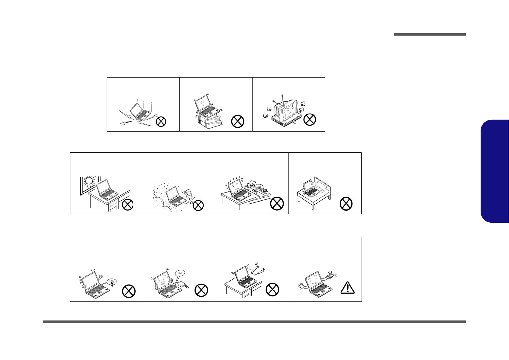
The notebook computer is quite rugged, but it can be damaged. To prevent this, follow these suggestions:
1. Don’t drop it, or expose it to shock. If the computer falls, the case and the components could be damaged.
Preface
Do not expose the computer
to any shock or vibration.
Do not place it on an unstable
surface.
Do not place anything heavy
on the computer.
2. Keep it dry, and don’t overheat it. Keep the computer and power supply away from any kind of heating element. This
is an electrical appliance. If water or any other liquid gets into it, the computer could be badly damaged.
Do not expose it to excessive
heat or direct sunlight.
Do not leave it in a place
where foreign matter or moisture may affect the system.
Don’t use or store the computer in a humid environment.
Do not place the computer on
any surface which will block
the vents.
3. Follow the proper working procedures for the computer. Shut the computer down properly and don’t forget to save
your work. Remember to periodically save your data as data may be lost if the battery is depleted.
Do not turn off the power
until you properly shut down
all programs.
Do not turn off any peripheral
devices when the computer is
on.
Do not disassemble the computer by yourself.
Perform routine maintenance
on your computer.
Preface
V
Preface
4. Avoid interference. Keep the computer away from high capacity transformers, electric motors, and oth er strong mag-
netic fields. These can hinder proper performance and damage your data.
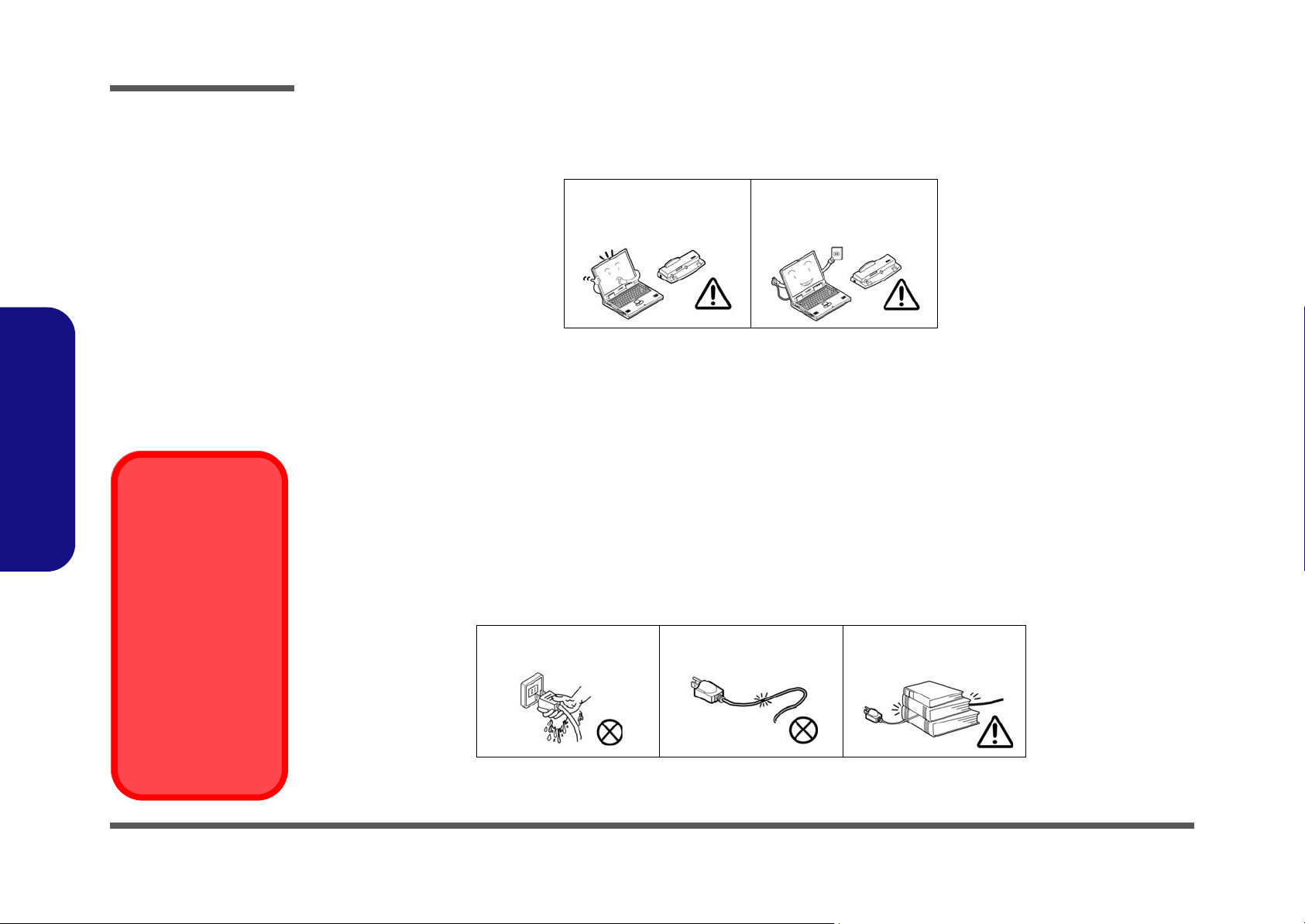
5. Take care when using peripheral devices.
Preface
Power Safety
Warning
Before you undertake
any upgrade procedures, make sure that
you have turned off the
power, and disconnected all peripherals
and cables (including
telephone lines). It is
advisable to also remove your battery in
order to prevent accidentally turning the
machine on.
Use only approved brands of
peripherals.
Unplug the power cord befor e
attaching peripheral devices.
Power Safety
The computer has specific power requirements:
• Only use a power adapter approved for use with this computer.
• Your AC adapter may be designed for international travel but it still requires a stea dy, uninterrupted po wer supply. If you ar e
unsure of your local power specifications, consult your service representative or local power company.
• The power adapter may have either a 2-prong or a 3-prong grounded plug. The third prong is an important safety feature; do
not defeat its purpose. If you do not have access to a compatible outlet, have a qualified electrician install one.
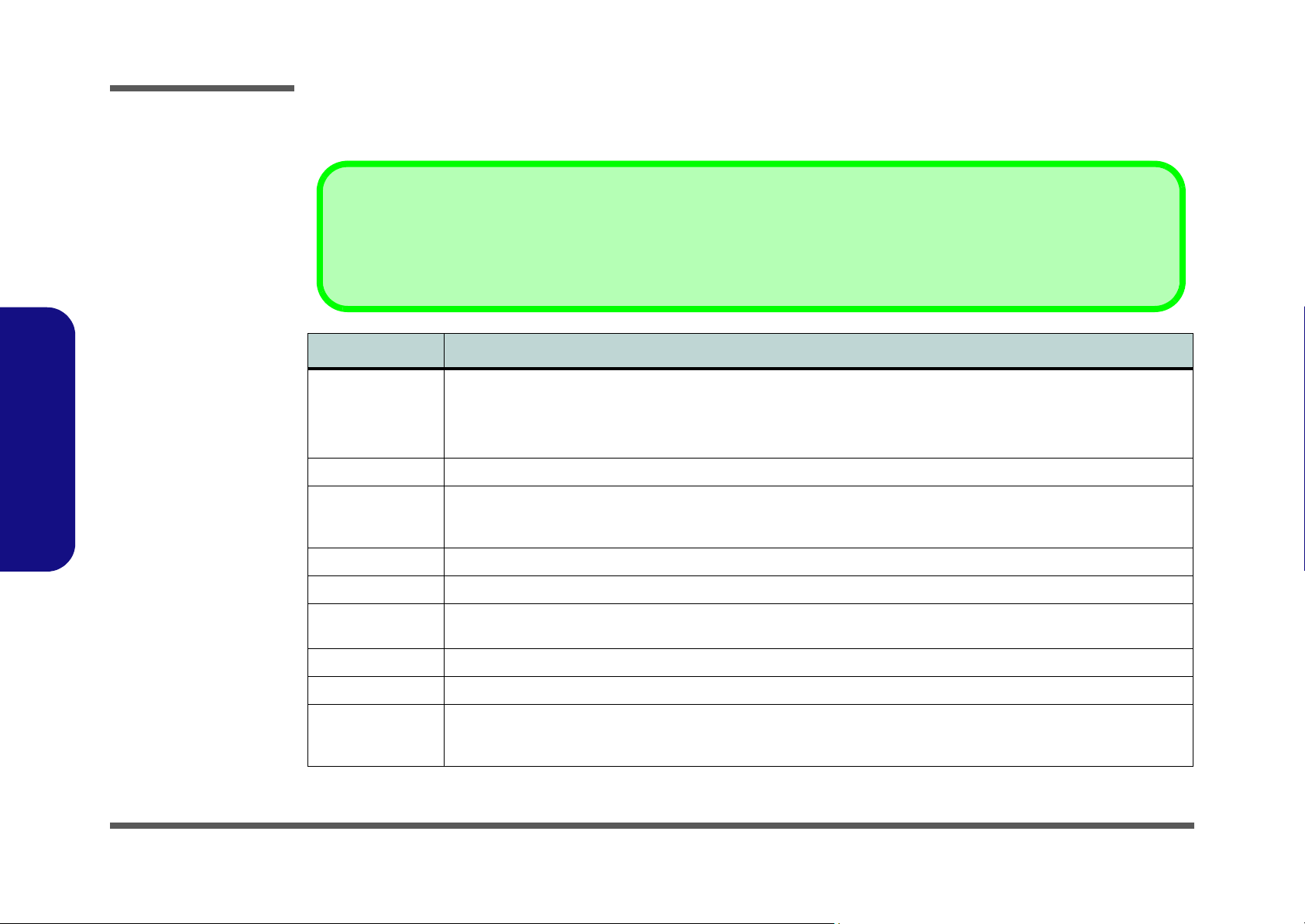
• When you want to unplug the power cord, be sure to disconnect it by the plug head, not by its wire.
• Make sure the socket and any extension cord(s) you use can support the total current load of all the connected devices.
• Before cleaning the computer, make sure it is disconnected from any external power supplies.
Do not plug in the power
cord if you are wet.
Do not use the power cord if
it is broken.
Do not place heavy objects
on the power cord.
VI

Battery Precautions
• Only use batteries designed for this computer. The wrong battery type may explode, leak or damage the computer.
• Do not continue to use a battery that has been dropped, or that appears damaged (e.g. bent or twisted) in any way. Even if the
computer continues to work with a damaged battery in place, it may cause circuit damage, which may possibly result in fire.
• Recharge the batteries using the notebook’s system. Incorrect recharging may make the battery explode.
• Do not try to repair a battery pack. Refer any battery pack repair or replacement to your service representative or qualified service
personnel.
• Keep children away from, and promptly dispose of a damaged battery. Always dispose of batteries carefully. Batteries may explode
or leak if exposed to fire, or improperly handled or discarded.
• Keep the battery away from metal appliances.
• Affix tape to the battery contacts before disposing of the battery.
• Do not touch the battery contacts with your hands or metal objects.
Battery Disposal
The product that you have purchased contains a rechargeab le battery. The battery is re cyclable. At the end of
its useful life, under various state and local laws, it may be illegal to dispose of this battery into the municipal
waste stream. Check with your local solid waste officials for details i n your area fo r recycling options or p roper
disposal.
Preface
Preface
Caution
Danger of explosion if battery is incorrectly replaced. Replace only with the same or equivalent type recommended by the manufacturer. Discard used battery according to the manufacturer’s instructions.
VII

Preface
Preface
Related Documents
You may also need to consult the following manual for additional information:
User’s Manual on CD
This describes the notebook PC’s features and the procedures for operating the computer and its ROM-based setup program. It also describes the installation and operation of the utility programs provided with the notebook PC.
VIII

Contents
Preface
Introduction ..............................................1-1
Overview .........................................................................................1-1
System Specifications .....................................................................1-2
External Locator - Top View with LCD Panel Open ......................1-5
External Locator - Front & Rear Views ..........................................1-6
External Locator - Right & Left Side Views ...................................1-7
External Locator - Bottom View .....................................................1-8
Mainboard Overview - Top (Key Parts) .........................................1-9
Mainboard Overview - Bottom (Key Parts) ..................................1-10
Mainboard Overview - Top (Connectors) .....................................1-11
Mainboard Overview - Bottom (Connectors) ...............................1-12
Disassembly ...............................................2-1
Overview .........................................................................................2-1
Maintenance Tools ..........................................................................2-2
Connections .....................................................................................2-2
Maintenance Precautions .................................................................2-3
Removing the Battery ......................................................................2-5
Removing the Hard Disk Drive .......................................................2-6
Removing the System Memory (RAM) ..........................................2-9
Removing the Wireless LAN Module ...........................................2-11
Removing the Bluetooth Module ..................................................2-12
Removing the Keyboard ................................................................2-13
Part Lists ..................................................A-1
Part List Illustration Location ........................................................A-2
Top .................................................................................................A-3
Bottom ............................................................................................ A-4
LCD-CPT .......................................................................................A-5
LCD-CPT-W/O FINGERPRINT ...................................................A-6
LCD-SAMSUNG ........................................................................... A-7
LCD-SAMSUNG W/O FINGERPRINT ....................................... A-8
LCD-TPO ...................................................................................... A-9
LCD-TPO W/O FINGERPRINT ................................................. A-10
Schematic Diagrams.................................B-1
SYSTEM BLOCK DIAGRAM ......................................................B-2
Silverthorne, Thermal IC-1/2 ..........................................................B-3
Silverthorne-2/2 ..............................................................................B-4
Poulsbo 1/6 HOST ..........................................................................B-5
Poulsbo 2/6 VGA, LVDS, RTC .....................................................B-6
Poulsbo 3/6 USB, PATA/ IDE ......................................................B-7
Poulsbo 4/6 DDR2 ..........................................................................B-8
Poulsbo 5/6 POWER ......................................................................B-9
Poulsbo 6/6 VSS ...........................................................................B-10
DDRII SO- DIMM .......................................................................B-11
ICS9UM9610 CLOCK GENERATOR ........................................B-12
KBC-ITE IT8513E & BIOS .........................................................B-13
PCI-E LAN RTL8102E ................................................................B-14
SDIO, MINI CARD, B/T, CCD, GPS ..........................................B-15
HDD, USB2.0, GSENSOR ...........................................................B-16
AZ CODEC ALC662, AMP .........................................................B-17
NEW CARD SOCKET ................................................................B-18
CH7317 SDVO TO CRT ..............................................................B-19
VGA CRT PORT ..........................................................................B-20
LVDS & LID SW & Touch Panel ................................................B-21
LED & VS Power .........................................................................B-22
LCD Right BD, F/P, POINTER ...................................................B-23
LCD Left BD Multi-Function Key............................................... B-24
CLICK ..........................................................................................B-25
FINGERPRINT B/D .....................................................................B-26
VCCNB, 1.5V, 1.05VS, M BTN ..................................................B-27
Preface
IX

Preface
AC IN, CHARGE ......................................................................... B-28
VCORE .......................................................................................B-29
VDD5, VDD3, 1.8V, 0.9V ...........................................................B-30
PWR BR ....................................................................................... B-31
LCD TF BOARD ......................................................................... B-32
Touch Panel ..................................................................................B-33
System Block Diagram 2/2 ..........................................................B-34
Preface
X

Chapter 1: Introduction
Overview
This manual covers the information you need to service or upgrade the TN70M/TN71M series notebook computer. Information about operating the computer (e.g. getting started, and the Setup utility) is in the User’s Manual. Information
about drivers (e.g. VGA & audio) is also found in User’s Manual. That manual is shipped with the computer.
Operating systems (e.g. Windows XP, Windows Vista, etc.) have their own manuals as do application software (e.g. word
processing and database programs). If you have questions about those programs, you should consult those manuals.
Introduction
The TN70M/TN71M series notebook is designed to be upgradeable. See “Disassembly” on page 2 - 1 for a detailed de-
scription of the upgrade procedures for each specific component. Please note the warning and safety information indicated by the “” symbol.
The balance of this chapter reviews the computer’s technical specifications and features.
1.Introduction
Overview 1 - 1
Introduction
System Specifications
Latest Specification Information
The specifications listed in this Appendix are correct at the time of going to press. Certain items (particularly processor types/speeds and
CD/DVD device types) may be changed, delayed or updated due to the manufacturer's release schedule. Check with your service center
for details.
Feature Specification
1.Introduction
Processor Intel® Atom® Processor Z520/ Z530
TDP 2W, BGA Package
Intel® Atom® Processor Z540
TDP 2.4W, BGA Package
Core Logic Intel® US15W Chipset
LCD 7" (800 * 480) WVGA 16:9 TFT LCD (with Touch Panel)
7" (1024 * 600) WSVGA 16:9 TFT LCD (with Touch Panel)
7" (800 * 480) WVGA 16:9 TFT LCD (without Touch Panel)
Video Adapter Intel® US15W Integrated Video
BIOS One 8Mb SPI Flash ROM Phoenix™ BIOS
Security Security (Kensington® Type) Lock Slot
BIOS Password
Storage One Changeable 1.8" 5.0 mm (h) PATA HDD
G-Sensor Portrait / Landscape Browsing Rotation
Audio Intel High Definition Audio Compliant Interface
3D Stereo Enhanced Sound System
Sound-Blaster PRO™ Compatible
ULV, 1.33GHz/ 1.60GHz, FSB533
ULV, 1.86GHz, FSB533
Fingerprint Reader Module (Factory Option)
2 * Built-In Speakers
Built-In Microphone
1 - 2 System Specifications
Feature Specification
Memory One 200 Pin SO-DIMM Socket Supporting DDRII (DDR2) 667 MHz Compatible Memory (Operating at 533 MHz Only)
Memory Expandable up to 1GB
Supported RAM Types
Note that ONLY the following RAM types are supported by the Menlow Chi pset. DO NOT use RAM types oth er
than those listed below:
HYNIX - DDR2-667 SO-DIMM 1GB/64M*16, CL=5 (HYNIX: HYMP112S64CP6-Y5) (CHIPS: HYNIX
HY5PS1G1631C) 200 PIN
NFINITY - DDR2-667 SO-DIMM 1GB/64M*16 CL=5 (INFINITY: 14701G08KX5U5S)(CHIPS: INFINITY:
I
64M16PC5300) 200 PIN
SAMSUNG - DDR2-667 SO-DIMM 1GB/64M*16, CL=5 (SAMSUNG: M470T2864QZ3-CE6)(CHIPS: SAM-
SUNG: K4T1G164QQ- HCE6) 200 PIN
Keyboard Winkey Keyboard
Introduction
1.Introduction
Pointing Devices Built-in TouchPad and buttons
Built-in mouse pointer and buttons
Interface Two USB 2.0 Ports
One External Monitor Port
One Headphone-Out Jack
Card Reader Embedded 5-in-1 Card Reader (SD/ Mini SD/ Micro SD/ MMC/ RS MMC)
Note: Mini SD/ Micro SD/ RS MMC Cards require a PC adapter
Card Slots One ExpressCard/34 Slot
One Mini-Card Slot with USB Interface for WLAN Module
Power
Management
Supports ACPI 2.0
Touch stylus
One Microphone-In Jack
One RJ-45 LAN Jack
One DC-in Jack
System Specifications 1 - 3
Introduction
Feature Specification
Communication 10Mb/100Mb Base-TX Ethernet LAN
Bluetooth 2.0 + EDR (Enhanced Data Rate) Module (with Chip Antenna) - (Option)
802.11 b/g MiniCard Wireless LAN Module (Option)
1.3M or 2.0M Pixel USB PC Camera Module (Factory Option)
GPS Module (Factory Option)
1.Introduction
Power Full Range AC/DC Adapter
AC Input: 100 - 240V, 50 - 60Hz
DC Output: 12V, 3A (36 Watts)
Environmental
Spec
Dimensions
& Weight
Optional External USB DVD Super Multi Drive Module
Temperature
Operating: 5
Non-Operating: -20°C ~ 60°C
227.5mm (w) * 170.7mm (d) * 25 - 29.9mm (h) Approximately 904g (with 4 Cell Battery w/o Optional
Bluetooth 2.0 + EDR (Enhanced Data Rate) Module (with
Chip Antenna)
802.11 b/g MiniCard Wireless LAN Module
°C ~ 35°C
4 Cell Smart Lithium-Ion Battery Pack, 5200mAh, 38W Battery Life 8 Hours
Relative Humidity
Operating: 20% ~ 80%
Non-Operating: 10% ~ 90%
Parts)
1.3M or 2.0M Pixel USB PC Camera Module (Factory
Option)
Fingerprint Reader Module (Factory Option)
GPS Module (Factory Option)
1 - 4 System Specifications
Introduction
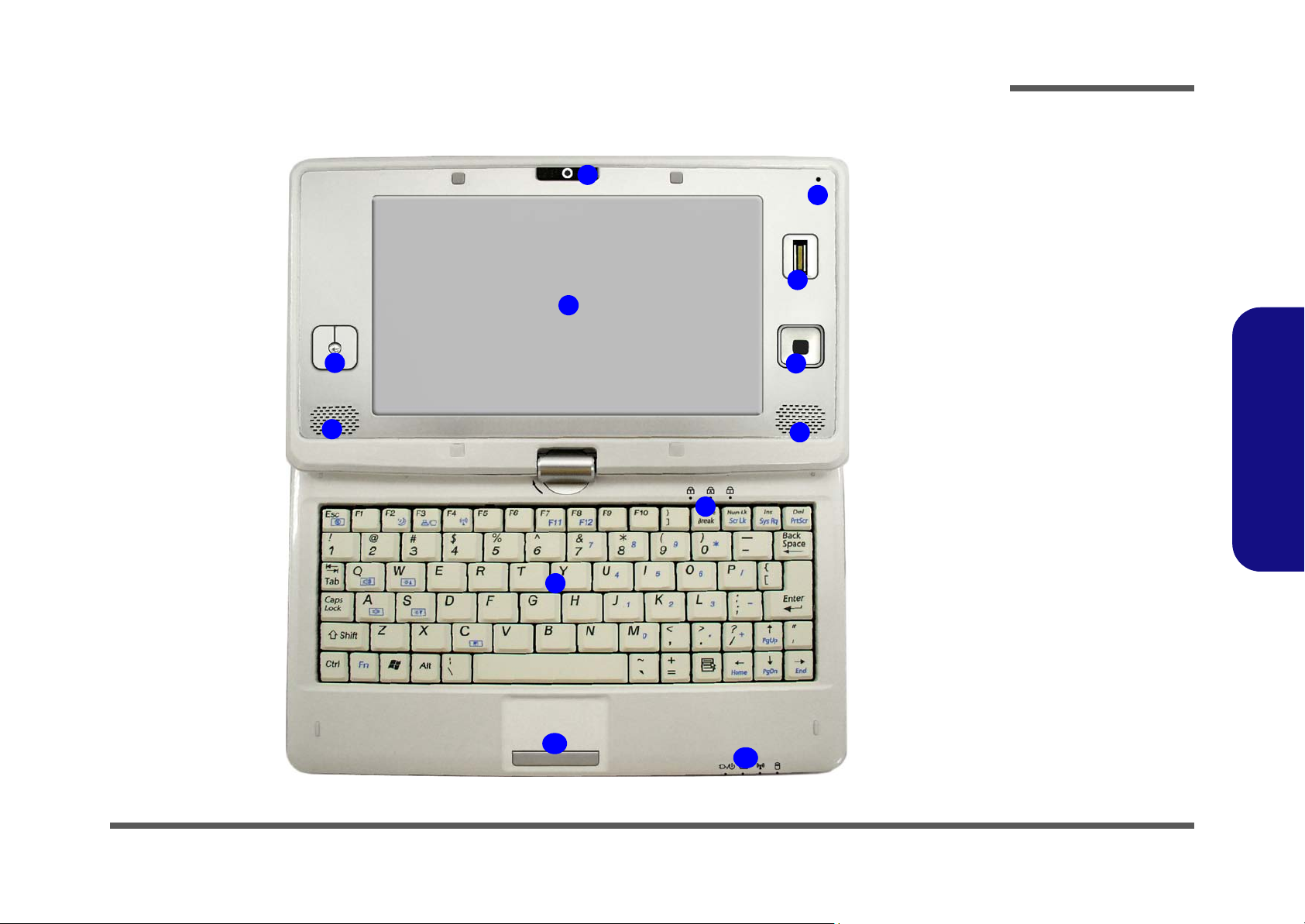
External Locator - Top View with LCD Panel Open
1
4
5
7
8
Figure 1
Top View with LCD
Panel Open
2
3
6
7
1. Built-In PC Camera
(Optional)
2. Microphone
3. Fingerprint Reader
Module (Optional)
4. LCD
5. Mouse Buttons
6. Mouse Pointer
7. Speakers
8. LED Status
Indicators
9. Keyboard
10.TouchPad &
Buttons
11. LED Power &
Communication
Indicators
1.Introduction
9
10
11
External Locator - Top View with LCD Panel Open 1 - 5
Introduction
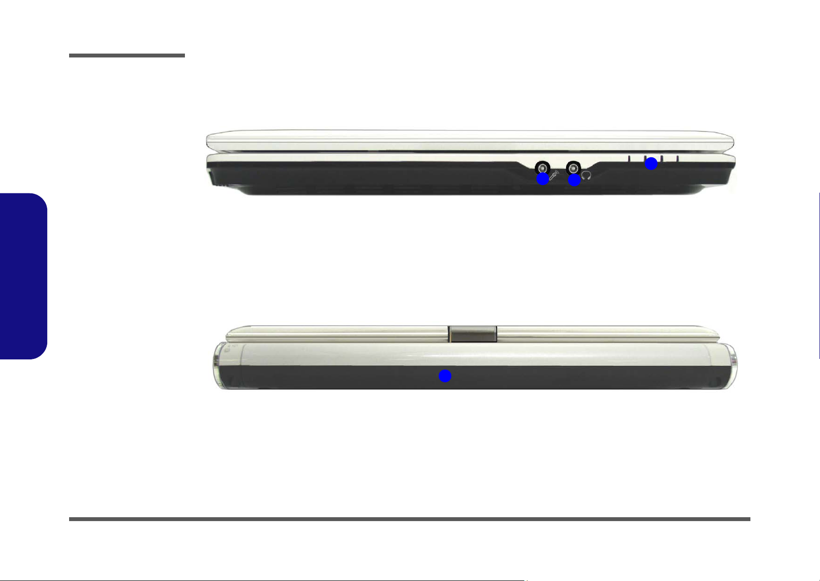
Figure 2
Front View
1. Microphone-In Jack
2. Headphone-Out Jack
3. LED Power &
Communication
Indicators
Figure 3
1.Introduction
Rear View
1. Battery
External Locator - Front & Rear Views
Front
3
1
2
1 - 6 External Locator - Front & Rear Views
Rear
1
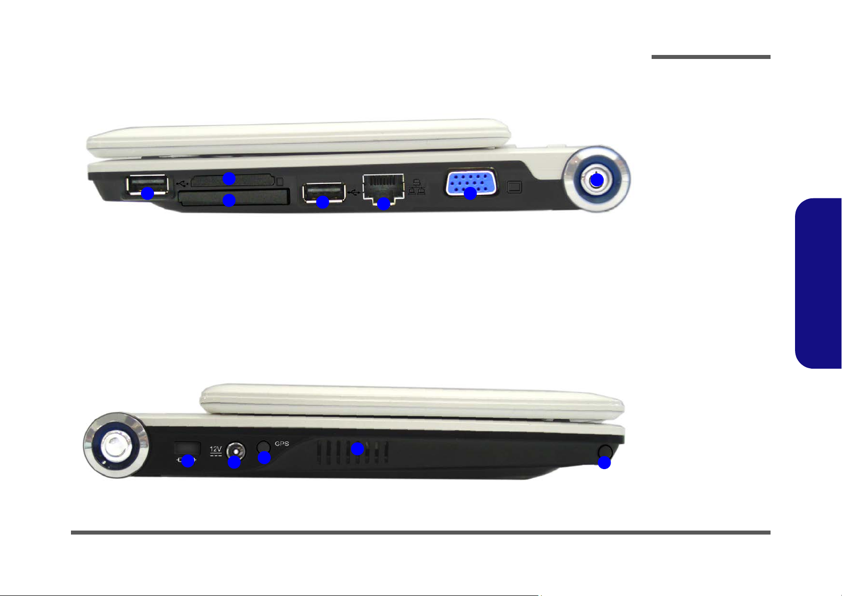
External Locator - Right & Left Side Views
2
1
3
1
4
Right
Introduction
Figure 4
Right Side View
1. 2 * USB 2.0 Ports
2. 5-in-1 Card Reader
3. ExpressCard/34
Slot
6
5
4. RJ-45 LAN Jack
5. External Monitor
Port
6. Power Button
1.Introduction
Figure 5
Left Side View
1. Security Lock Slot
2. DC-In Jack
3. GPS Antenna
(Optional)
4. Vent
1
2
3
4
Left
5
5. Stylus Pen Holder
External Locator - Right & Left Side Views 1 - 7
Introduction
Figure 6
Bottom View
1. Battery
2. Battery Latches
3. CPU cover module
4. Vent
External Locator - Bottom View
1
2
2
1.Introduction
Overheating
To prevent your computer from overheating
make sure nothing
blocks the vent/fan intakes while the computer is in use.
1 - 8 External Locator - Bottom View
3
4
4
4
Introduction
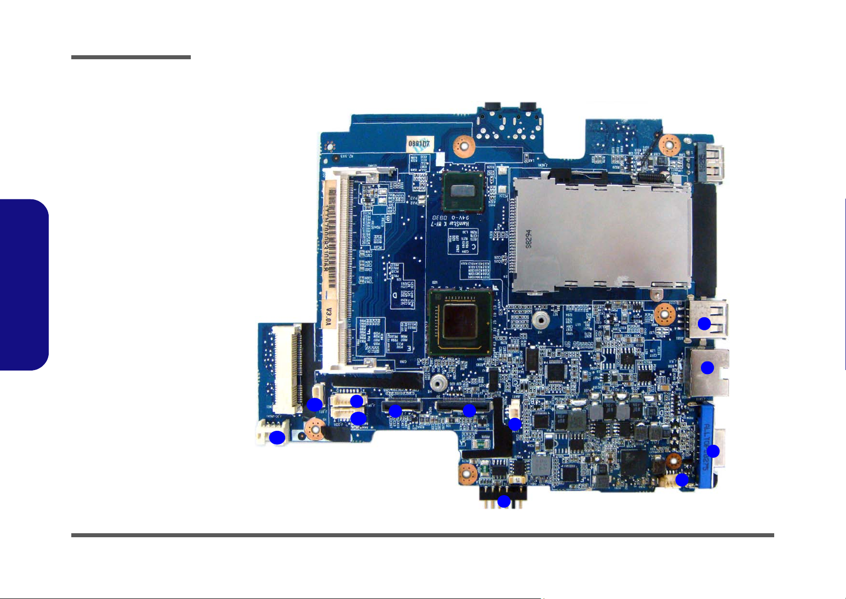
Mainboard Overview - Top (Key Parts)
Figure 7
Mainboard Top
Key Parts
1. Realtek ALC662
2. ITE 8513E
3. RTL 8102E
1.Introduction
3
2
1
Mainboard Overview - Top (Key Parts) 1 - 9
Introduction
Figure 8
Mainboard Bottom Key
1. ExpressCard
Assembly
2. Silverthorne
Processor
3. System Processor
POULSBO
4. Memory Slots DDRII
So-DIMM
5. WLAN Mini Card
Slot
1.Introduction
Mainboard Overview - Bottom (Key Parts)
Parts
2
1
4
3
5
1 - 10 Mainboard Overview - Bottom (Key Parts)
Introduction
Mainboard Overview - Top (Connectors)
3
Figure 9
Mainboard Top
Connectors
1. HDD Cable
Connector
2. Keyboard Cable
Connector
3. Touch Pad Cable
Connector
4. 5-in-1 Card
Reader
5. USB Port
6. Headphone-Out
Jack
7. Microphone-In
Jack
1.Introduction
2
1
7
6
4
5
Mainboard Overview - Top (Connectors) 1 - 11
Introduction
Figure 10
Mainboard Bottom
Connectors
1. USB 2.0 Port
2. RJ-45 LAN Jack
3. External Monitor Port
4. Power Cable
Connector
5. Battery Connector
6. Battery Cable
Connector
7. LCD Connector
8. LCD Mouse/Pointer
Buttons Board
Connector
9. GPS Cable
Connector
1.Introduction
10.CCD Cable
Connector
11. Bluetooth Cable
Connector
12.DC Jack Cable
Connector
Mainboard Overview - Bottom (Connectors)
1
2
1-12
12
11
9
10
8
7
6
3
4
5

Chapter 2: Disassembly
Overview
This chapter provides step-by-step instructions for disassembling the TN70M/TN71M series notebook’s parts and subsystems. When it comes to reassembly, reverse the procedures (unless otherwise indicated).
We suggest you completely review any procedure before you take the computer apart.
Disassembly
Procedures such as upgrading/replacing the RAM, CD device and hard disk are included in the User’s Manual but are
repeated here for your convenience.
To make the disassembly process easier each section may have a box in the page margin. Information contained under
the figure # will give a synopsis of the sequence of procedures involved in the disassembly procedure. A box with a
lists the relevant parts you will have after the disassembly process is complete. Note: The parts listed will be for the disassembly procedure listed ONLY, and not any previous disassembly step(s) required. Refer to the part list for the previous disassembly procedure. The amount of screws you should be left with will be listed here also.
A box with a will also provide any possible helpful information. A box with a contains warnings.
An example of these types of boxes are shown in the sidebar.
2.Disassembly
Information
Warning
Overview 2 - 1

Disassembly
2.Disassembly
NOTE: All disassembly procedures assume that the system is turned OFF, and disconnected from any power supply (the
battery is removed too).
Maintenance Tools
The following tools are recommended when working on the notebook PC:
• M3 Philips-head screwdriver
• M2.5 Philips-head screwdriver (magnetized)
• M2 Philips-head screwdriver
• Small flat-head screwdriver
• Pair of needle-nose pliers
• Anti-static wrist-strap
Connections
Connections within the computer are one of four types:
Locking collar sockets for ribbon connectors To release these connectors, use a small flat-head screwdriver to
gently pry the locking collar away from its base. When replacing the connection, make sure the connector is oriented in the
same way. The pin1 side is usually not indicated.
2 - 2 Overview
Pressure sockets for multi-wire connectors To release this connector type, grasp it at its head and gently
rock it from side to side as you pull it out. Do not pull on the
wires themselves. When replacing the connection, do not try to
force it. The socket only fits one way.
Pressure sockets for ribbon connectors To release these connectors, use a small pair of needle-nose pli-
ers to gently lift the connector away from its socket. When replacing the connection, make sure the connector is oriented in
the same way. The pin1 side is usually not indicated.
Board-to-board or multi-pin sockets To separate the boards, gently rock them from side to side as
you pull them apart. If the connection is very tight, use a small
flat-head screwdriver - use just enough force to start.

Maintenance Precautions
The following precautions are a reminder. To avoid personal injury or damage to the computer while performing a removal and/or replacement job, take the following precautions:
1. Don't drop it. Perform your repairs and/or upgrades on a stable surface. If the computer falls, the case and other
components could be damaged.
2. Don't overheat it. Note the proximity of any heating elements. Keep the computer out of direct sunlight.
3. Avoid interference. Note the proximity of any high capacity transformers, electric motors, and other strong mag-
netic fields. These can hinder proper performance and damage components and/or data. You should also monitor
the position of magnetized tools (i.e. screwdrivers).
4. Keep it dry. This is an electrical appliance. If water or any other liquid gets into it, the computer could be badly
damaged.
5. Be careful with power. Avoid accidental shocks, discharges or explosions.
•Before removing or servicing any part from the computer, turn the computer off and detach any power supplies.
•When you want to unplug the power cord or any cable/wire, be sure to disconnect it by the plug head. Do not pu ll on the wir e.
6. Peripherals – Turn off and detach any peripherals.
7. Beware of static discharge. ICs, such as the CPU and main support chips, are vulnerable to static electricity.
Before handling any part in the computer, discharge any static electricity inside the computer. When handling a
printed circuit board, do not use gloves or other materials which allow static electricity buildup. We suggest that
you use an anti-static wrist strap instead.
8. Beware of corrosion. As you perform your job, avoid touching any connector leads. Even the cleanest hands produce oils which can attract corrosive elements.
9. Keep your work environment clean. Tobacco smoke, dust or other air-born particulate matter is often attracted
to charged surfaces, reducing performance.
10. Keep track of the components. When removing or replacing any part, be careful not to leave small part s, such as
screws, loose inside the computer.
Disassembly
Power Safety
Warning
Before you undertake
any upgrade procedures, make sure that
you have turned off the
power, and disconnected all peripherals
and cables (including
telephone lines). It is
advisable to also remove your battery in
order to prevent accidentally turning the
machine on.
2.Disassembly
Cleaning
Do not apply cleaner directly to the computer, use a soft clean cloth.
Do not use volatile (petroleum distillates) or abrasive cleaners on any part of the computer.
Overview 2 - 3

Disassembly
Disassembly Steps
The following table lists the disassembly steps, and on which page to find the related information. PLEASE PERFORM
THE DISASSEMBLY STEPS IN THE ORDER INDICATED.
To remove the Battery:
1. Remove the battery page 2 - 5
To remove the HDD:
1. Remove the battery page 2 - 5
2. Remove the HDD page 2 - 6
To remove the System Memory:
1. Remove the battery page 2 - 5
2. Remove the system memory page 2 - 9
2.Disassembly
2 - 4 Overview
To remove the Wireless LAN Module:
1. Remove the battery page 2 - 5
2. Remove the Wireless LAN page 2 - 11
To remove the Bluetooth:
1. Remove the battery page 2 - 5
2. Remove the bluetooth page 2 - 12
To remove the Keyboard:
1. Remove the battery page 2 - 5
2. Remove the keyboard page 2 - 13

Removing the Battery
1. Turn the computer off, and turn it over.
2. Slide the latch in the direction of the arrow, and hold latch in place.
3. Slide the battery in the direction of the arrow .
1
4
6
3
a.
1
b.
2
Disassembly
Figure 1
Battery Removal
a. Slide the 2 latches and
hold latch in place.
b. Slide the battery in the di-
rection of the arrow.
2
2.Disassembly
2
4
3
4. Battery
Removing the Battery 2 - 5

Disassembly
Removing the Hard Disk Drive
Figure 2
HDD Assembly
Removal and
Installation
a. Locate the CPU cover
module and remove the
screws.
b. Remove the module cov-
er.
2.Disassembly
The hard disk drive can be taken out to accommodate other 1.8" serial (PATA) hard disk drives with a height of 5.0 mm
(h). Follow your operating system’s installation instructions, and install all necessary drivers and utilities (as outlined in
Chapter 4 of the User’s Manual) when setting up a new hard disk.
Hard Disk Upgrade Processl
1. Turn off the computer, and remove the battery (page 2 - 5).
2. Locate the CPU cover module and remove the screws (
5
6
3. Remove the bay cover
a.
2
1
4
.
b.
3
- ).
1 4
5
5. CPU cover
module
•4 Screws
New HDD’s are blank. Before you begin make sure:
You have backed up any data you want to keep from your old HDD.
You have all the CD-ROMs and FDDs required to install your operating system and programs.
If you have access to the internet, download the latest application and hardware driver updates for the operating system you plan
to install. Copy these to a removable medium.
2 - 6 Removing the Hard Disk Drive
HDD System Warning

Disassembly
4. Carefully lift the hard disk assembly up (DO NOT PULL THE HDD CABLE).
5. Carefully release the lock (the locking collar should be raised up and the cable should be able to be released
6
without resistance) in order to free the HDD cable.
6. Lift the HDD out of the computer .
c.
7
d.
7
6
6
7. Carefully lift up the locking collar on the new/replacement hard disk.
8. Make sure the cable is straight, align it with the hard disk socket, and fully insert the cable into the socket .
e.
8
9
f.
Figure 3
HDD Assembly
Removal and
Installation Sequence
c. Carefully lift the hard disk
assembly up. Carefully release the lock (the locking
collar should be raised up
and the cable should be
able to be released without
resistance) .
d. Remove the HDD.
e. Carefully lift up the locking
collar on the new/replace-
ment HDD.
f. Insert the HDD cable into
the socket.
2.Disassembly
9
8
9
7. HDD
Removing the Hard Disk Drive 2 - 7

Disassembly
Figure 4
HDD Assembly
Removal and
Installation Sequence
g. Press the locking collar
down fully.
h. Insert the hard disk as-
sembly into the slot in the
direction indicated by the
arrow, and then carefully
push the assembly down
into the bay.
i. Carefully bend the hard
disk cable to lie flat on the
surface of the hard disk,
and then secure the cable
by means of the doublesided tape.
2.Disassembly
9. Press the locking collar down flat to firmly secure the cable .
10
g.
10
10. Insert the hard disk assembly into the slot in the direction indicated by the arrow, and then carefully push the
assembly down into the bay .
11
1 1. Carefully bend the hard disk cable to lie flat on the surface of the hard disk, and then secure the cable by means of
the double-sided tape .
h.
12
i.
2 - 8 Removing the Hard Disk Drive
12
11

Disassembly
Removing the System Memory (RAM)
The computer has one memory sockets for 200 pin Small Outline Dual In-line Memory Modules (SO-DIMM) supporting
DDRII 667 MHz Compatible Memory (Operating at 533 MHz Only). The main memory can be expanded up to 1GB.
The SO-DIMM modules supported are 256MB, 512MB and 1024MB DDRII Modules. The total memory size is automatically detected by the POST routine once you turn on your computer.
Memory Upgrade Process
1. Turn off the computer, remove the battery (page 2 - 5).
6
1 4
5
2. Locate the CPU cover module, and remove screws - .
3. Remove the bay cover
4. The RAM will be visible at point on the mainboard.
a.
.
5
6
b.
2
1
3
4
Figure 5
RAM Module
Removal
a. Remove the screws.
b. Disconnect the fan
cable and the cover.
c. Locate the RAM
module.
2.Disassembly
Contact Warning
Be careful not to touch
the metal pins on the
module’s connecting
edge. Even the cleanest hands have oils
which can attract particles, and degrade the
module’s performance.
Supported RAM Types
Note that ONLY the following RAM types are supported by the Menlow Chipset. DO NOT use RAM types other than those listed below:
HYNIX - DDR2-667 SO-DIMM 1GB/64M*16, CL=5 (HYNIX: HYMP112S64CP6-Y5) (CHIPS: HYNIX HY5PS1G1631C) 200 PIN
INFINITY - DDR2-667 SO-DIMM 1GB/64M*16 CL=5 (INFINITY: 14701G08KX5U5S)(CHIPS: INFINITY: 64M16PC5300) 200 PIN
SAMSUNG - DDR2-667 SO-DIMM 1GB/64M*16, CL =5 (SAMSUNG: M470T2864QZ3-CE6)(CHIPS: SAMSUNG: K4T1G164QQ-
HCE6) 200 PIN
Removing the System Memory (RAM) 2 - 9
5. CPU cover mod-
ule
•4 Screws

Disassembly
Figure 6
Memory Removal
Sequence
d. Push the release
latch(es).
e. Remove the mo du l e .
2.Disassembly
5. Gently push the two release latches ( & ) on the sides of the memory socket in the direction indicated by the
arrows (Figure d).
6. The RAM module(s) will pop-up
9
d.
7 8
(Figure e), and you can then remove it.
e.
8
9
7
7. Insert a new module holding it at about a 30° angle and fit the connectors firmly into the memory slot.
8. The module will only fit one way as defined by its pin alignment. Make sure the module is seated as far into the slot
as it will go. DO NOT FORCE IT; it should fit without much pressure.
9. Press the module down towards the mainboard until the slot levers click into place to secure the module.
10. Replace the bay cover and the screws
11. Restart the computer to allow the BIOS to register the new memory configuration as it starts up.
9 RAM Module
2 - 10 Removing the System Memory (RAM)
.

Disassembly
Removing the Wireless LAN Module
1. Turn off the computer, remove the battery (page 2 - 5) and the CPU cover module (page 2 - 9).
2. The Wireless LAN module will be visible at point on the mainboard.
3. Carefully disconnect cable , then remove the screw from the module socket.
4. The Wireless LAN module will pop-up.
5. Lift the Wireless LAN module
2
4
(Figure d) up and off the computer.
a.
1
c.
1
3
b.
3
2
d.
Figure 7
Wireless LAN Module
Removal
a. Remove the cover and Io-
cate the WLAN module .
b. Disconnect the cable and
remove the screw.
c. The WLAN module will pop
up.
d. Remove the WLAN mod-
ule.
2.Disassembly
Note: Make sure you reconnect the antenna cable to the “Main” socket
(Figure b).
4
4. WLAN Module
•1 Screw
Removing the Wireless LAN Module 2 - 11

Disassembly
Figure 8
Bluetooth Removal
a. Remove the cover and
the WLAN module . The
Bluetooth module is located under the WLAN
module.
b. Remove the screw.
c. Carefully separate the
module from the connec-
tor.
d. Lift the Bluetooth module
out.
2.Disassembly
Removing the Bluetooth Module
1. Turn off the computer, remove the battery (page 2 - 5), and the CPU cover module (page 2 - 9).
2. Remove the Wireless LAN module .
3. The Bluetooth module is located under the Wireless LAN module .
4. Remove screw and turn it over.
2
5. Carefully separate the module from the connector .
6. Lift the Bluetooth module up and off the computer.
4
a.
1
b.
1
3
c.
3
d.
1. WLAN Module
4. Bluetooth Module
•1 Screw
2 - 12 Removing the Bluetooth Module
2
4

Disassembly
Removing the Keyboard
1. Turn off the computer, and remove the battery (page 2 - 5).
2. Press the four keyboard latches at the top of the keyboard to elevate the keyboard from its normal position (you
may need to use a small screwdriver to do this).
3. Carefully lift the keyboard up, being careful not to bend the keyboard ribbon cable.
4. Disconnect the keyboard ribbon cable from the locking collar socket .
5. Carefully lift up the keyboard (Figure c) off the computer.
6
a.
1
2
c.
4 5
b.
3
4
4
5
Figure 9
Keyboard Removal
a. Press the four latches to
release the keyboard.
b. Lift the keyboard up and
disconnect the cable
from the locking collar.
c. Remove the keyboard.
Re-Inserting the Key-
board
When re-inserting the
keyboard firstly align
the four keyboard tabs
at the bottom of the
keyboard with the slots
in the case.
2.Disassembly
6
6
6. Keyboard Module.
Keyboard Tabs
Removing the Keyboard 2 - 13

Disassembly
2.Disassembly
2-14

Appendix A:Part Lists
This appendix breaks down the TN70M/TN71M series notebook’s construction into a series of illustrations. The component part numbers are indicated in the tables opposite the drawings.
Note: This section indicates the manufacturer’s part numbers. Your organization may use a different system, so be sure
to cross-check any relevant documentation.
Note: Some assemblies may have parts in common (especially screws). However, the part lists DO NOT indicate the
total number of duplicated parts used.
Part Lists
Note: Be sure to check any update notices. The parts shown in these illustrations are appropriate for the system at the
time of publication. Over the product life, some parts may be improved or re-configured, resulting in new part numbers.
A.Part Lists
A-1

Part Lists
Table A - 1
Part List Illustration
Location
Part List Illustration Location
The following table indicates where to find the appropriate part list illustration.
Part Pages#
Top
page A - 3
A.Part Lists
Bottom
LCD-CPT
LCD-CPT-W/O FINGERPRINT
LCD-SUMSUNG
LCD-SUMSUNG-W/O FINGERPRINT
LCD-TPO
LCD-TPO-W/O FINGERPRINT
page A - 4
page A - 5
page A - 6
page A - 7
page A - 8
page A - 9
page A - 10
A - 2 Part List Illustration Location

Top
無鉛
型白色(無鉛)
型黑色 (無鉛)
無鉛
(非耐落) 無鉛
無鉛
無鉛
藍天2 互億 無鉛
頭徑 頭厚 號無鉛
海華 無鉛
無鉛
透明 無鉛
鋁箔 導電膠 無鉛
無鉛
無鉛
無鉛
無鉛
無鉛
祐宣 無鉛
無鉛
無鉛
華力 無鉛
無鉛
無鉛
非耐落 無鉛
無鉛
無鉛
無鉛
無鉛
無鉛
無鉛
無鉛
無鉛
無鉛
鴻呈 無鉛
無鉛
無鉛
華力 無鉛
信音無鉛
透明 無鉛
無鉛
無鉛
無鉛
無鉛
華力 無鉛
Part Lists
無鉛
無鉛
無鉛
無鉛
無鉛
無鉛
Figure A - 1
Top
A.Part Lists
Top A - 3

Part Lists
Figure A - 2
Bottom
Bottom
A.Part Lists
A - 4 Bottom
無鉛
無鉛
無鉛
度黑色 無鉛
度 黑色 無鉛
無鉛
無鉛
無鉛
無鉛
無鉛
無鉛
無鉛
無鉛
無鉛
無鉛

LCD-CPT
Part Lists
無鉛
無鉛
無鉛
無鉛
無鉛
無鉛
華力 無鉛
華力 無鉛
非耐落 無鉛
精乘 無鉛
灰色 無鉛
無鉛
無鉛
無鉛
無鉛
中性 電鑄薄膜鍍亮鉻(字體連結) 無鉛
無鉛
無鉛
度 外接式 慶陞 無鉛
無鉛
無鉛
無鉛
無鉛
無鉛
無鉛
無鉛
無鉛
無鉛
無鉛
無鉛
無鉛
無鉛
無鉛
無鉛
無鉛
無鉛
無鉛
無鉛
無鉛
無鉛
LCD-CPT
Figure A - 3
A.Part Lists
LCD-CPT A - 5

Part Lists
Figure A - 4
LCD-CPT-W/O FIN-
GERPRINT
A.Part Lists
LCD-CPT-W/O FINGERPRINT
無鉛
無鉛
無鉛
無鉛
無鉛
無鉛
華力 無鉛
華力 無鉛
非耐落 無鉛
精乘 無鉛
灰色 無鉛
無鉛
無鉛
無鉛
無鉛
中性 電鑄薄膜鍍亮鉻(字體連結) 無鉛
無鉛
無鉛
度 外接式 慶陞 無鉛
無鉛
無鉛
無鉛
無鉛
無鉛
無鉛
無鉛
無鉛
無鉛
無鉛
無鉛
無鉛
無鉛
無鉛
無鉛
無鉛
無鉛
無鉛
無鉛
無鉛
A - 6 LCD-CPT-W/O FINGERPRINT

LCD-SAMSUNG
Part Lists
無鉛
無鉛
無鉛
無鉛
無鉛
無鉛
無鉛
華力 無鉛
非耐落 無鉛
精乘 無鉛
灰色 無鉛
無鉛
無鉛
無鉛
無鉛
中性 電鑄薄膜鍍亮鉻(字體連結) 無鉛
無鉛
無鉛
無鉛
度 外接式 慶陞 無鉛
無鉛
無鉛
無鉛
無鉛
無鉛
無鉛
無鉛
無鉛
無鉛
無鉛
無鉛
無鉛
無鉛
無鉛
無鉛
無鉛
無鉛
無鉛
無鉛
無鉛
無鉛
無鉛
Figure A - 5
LCD-SAMSUNG
A.Part Lists
LCD-SAMSUNG A - 7

Part Lists
LCD-SAMSUNG W/O FINGERPRINT
LCD-SAMSUNG W/O
FINGERPRINT
A.Part Lists
Figure A - 6
無鉛
無鉛
無鉛
無鉛
無鉛
無鉛
無鉛
華力 無鉛
非耐落 無鉛
精乘 無鉛
灰色 無鉛
無鉛
無鉛
無鉛
無鉛
中性 電鑄薄膜鍍亮鉻(字體連結) 無鉛
無鉛
無鉛
無鉛
度 外接式 慶陞 無鉛
無鉛
無鉛
無鉛
無鉛
無鉛
無鉛
無鉛
無鉛
無鉛
無鉛
無鉛
無鉛
無鉛
無鉛
無鉛
無鉛
無鉛
無鉛
無鉛
無鉛
無鉛
A - 8 LCD-SAMSUNG W/O FINGERPRINT

LCD-TPO
Part Lists
無鉛
無鉛
無鉛
華力 無鉛
華力 無鉛
非耐落 無鉛
中性 電鑄薄膜鍍亮鉻(字體連結) 無鉛
精乘 無鉛
灰色 無鉛
無鉛
無鉛
無鉛
無鉛
無鉛
無鉛
度 外接式 慶陞 無鉛
無鉛
無鉛
無鉛
無鉛
Figure A - 7
LCD-TPO
無鉛
無鉛
無鉛
無鉛
無鉛
無鉛
無鉛
無鉛
無鉛
無鉛
無鉛
無鉛
無鉛
無鉛
無鉛
無鉛
無鉛
A.Part Lists
LCD-TPO A - 9

Part Lists
LCD-TPO W/O FIN-
A.Part Lists
Figure A - 8
GERPRINT
LCD-TPO W/O FINGERPRINT
無鉛
無鉛
無鉛
華力 無鉛
華力 無鉛
非耐落 無鉛
中性 電鑄薄膜鍍亮鉻(字體連結) 無鉛
精乘 無鉛
灰色 無鉛
無鉛
無鉛
無鉛
無鉛
無鉛
無鉛
度 外接式 慶陞 無鉛
無鉛
無鉛
無鉛
無鉛
無鉛
無鉛
無鉛
無鉛
無鉛
無鉛
無鉛
無鉛
無鉛
無鉛
無鉛
無鉛
無鉛
無鉛
無鉛
A - 10 LCD-TPO W/O FINGERPRINT

Appendix B:Schematic Diagrams
This appendix has circuit diagrams of the TN70M/TN71M notebook’s PCB’s. The following table indicates where to
find the appropriate schematic diagram.
Schematic Diagrams
Diagram - Page Diagram - Page Diagram - Page
SYSTEM BLOCK DIAGRAM - Page B - 2 KBC-ITE IT8513E & BIOS - Page B - 13 LCD Left BD Multi-Function K ey - Page B - 24
Silverthorne, Thermal IC-1/2 - Page B - 3 PCI-E LAN RTL8102E - Page B - 14 CLICK - Page B - 25
Silverthorne-2/2 - Page B - 4 SDIO, MINI CARD, B/T, CCD, GPS - Page B - 15 FINGERPRINT B/D - Page B - 26
Poulsbo 1/6 HOST - Page B - 5 HDD, USB2.0, GSENSOR - Page B - 16 VCCNB, 1.5V, 1.05VS, M BTN - Page B - 27
Poulsbo 2/6 VGA, LVDS, RTC - Page B - 6 AZ CODEC ALC662, AMP - Page B - 17 AC IN, CHARGE - Page B - 28
Poulsbo 3/6 USB, PATA/ IDE - Page B - 7 NEW CARD SOCKET - Page B - 18 VCORE - Page B - 29
Poulsbo 4/6 DDR2 - Page B - 8 CH7317 SDVO TO CRT - Page B - 19 VDD5, VDD3, 1.8V, 0.9V - Page B - 30
Poulsbo 5/6 POWER - Page B - 9 VGA CRT PORT - Page B - 20 PWR BR - Page B - 31
Poulsbo 6/6 VSS - Page B - 10 LVDS & LID SW & Touch Panel - Page B - 21 LCD TF BOARD - Page B - 32
DDRII SO- DIMM - Page B - 11 LED & VS Power - Page B - 22 Touch Panel - Page B - 33
ICS9UM9610 CLOCK GENERATOR - Page B - 12 LCD Right BD, F/P, POINTER - Page B - 23 System Block Diagram 2/2 - Page B - 34
Table B - 1
Schematic
Diagrams
B.Schematic Diagrams
Version Note
The schematic diagrams in this chapter
are based upon version 6-7P-TN706-004.
If your mainboard (or
other boards) are a later version, please
check with the Service
Center for updated diagrams (if required).
B-1

Schematic Diagrams
SYSTEM BLOCK DIAGRAM
Sheet 1 of 33
SYSTEM BLOCK
DIAGRAM
B.Schematic Diagrams
AC-IN,CHARG ER
SHEET 27
14.318 MHz
Clo ck Gener ato r
ICS9UMS9610
48pins QFN
6*6*0.8mm
CRT
RJ-45
ZIF HDD1.8"
CPU
POULSBO
PCIE LAN
NEW CARD
LCD
SDVO
CH7317
64pins LQFP
10*10*1.6 m m
10/100M LAN
RTL8102E
64pins QFN
9*9 * 0. 8m m
PATA-133
USB0
NEWCARD
CLEVO TN70M System Block Diagram
100 MHz
USB1
BLUE
TOOTH
LVDS
CRT
PCIEX1
25 MHz
USB2
FINGER
PRINTER
32.768KHz
USB3
TOUCH
PANEL
SILVERTHORNE
PROCESSOR
441balls
FCBGA8
1 3* 14 * 1. 4m m
FSB
400-533 MHz
ALL IN ONE
SYSTEM
PROCESSOR
POULSBO
1249balls
?BGA
22*22*?mm
USB2.0 X8
480 Mbps
USB4
USB
PORT1
USB5 USB6
USB
PORT2
Memory Termination
SHEET 10
DDR II
400-533 MHz
AZ LINK
CCD
(USB 2.0 ONLY)
2.5G Hz
LPC
USB7
WLAN
(USB 2.0 ONLY)
24 MHz
33 MHz
SDIO
DDRII
SO-DIMM0
SHEET 10
Azalia Codec
SD IO 1
CARD
READER
NEW CARD
Realtek
ALC662
48pins LQFP
9 * 9* 1. 6m m
K/B
SHEET 12
T/P
SHEET 24
G SEN SOR
SYSTEM POWER
+VCORE
VDD5,VDD3,1.8V,0.9V
1.5V,1.05VS
HP & AUDIO AMP
AN P E C
APA2057A
28pins TQFN
5.0*5.0*0.8mm
I TE 851 3E
128pins LQFP
14 * 14 * 1. 6m m
EC
INT SPK
EXT MIC
INT MIC
32.768 KHz
EC SMBU S
SPI
THERMAL
SENSOR
ADM1032
SMART
BATT ER Y
HP
OU T
B - 2 SYSTEM BLOCK DIAGRAM

Silverthorne, Thermal IC-1/2
Schematic Diagrams
CPU _ XDP_ TRS T#
CPU _ XDP_ TCK
CPU _ CO MP0
CPU _ CO MP1
CPU _ CO MP2
CPU _ CO MP3
DS
G
H_D#[63:0] 4
H_D STBN# 2 4
H_D ST BP#2 4H_DS TB P# 04
H_D INV #2 4
H_D #[63:0] 4
H_D STBN# 3 4
H_D ST BP#3 4H_DS TB P# 14
H_D INV #3 4
H_D PRST P# 4 ,2 8
H_D P SLP# 4
H_D PW R# 4
H_PW R GD 4
H_C PUSL P # 4
TP1
R 1 78 5 6 _ 04
R 1 91 5 6 _ 04
R 163 27.4_1%_04
R 162 54.9_1%_04
R 182 27.4_1%_04
R 181 54.9_1%_04
R176
10K_04
Z0211
Q21
2N7002
VG S + /-20V S O T23
G
H_A 2 0 M#
DS
Q22
2N7002
VGS +/-20V SOT23
Sheet 2 of 33
Silverthorne,
Thermal IC-1/2
B.Schematic Diagrams
H _D # [ 6 3: 0]4
TH ERM_RST#12
H_A# [3 1 :3 ]4
H_ADS TB#04
H_R EQ#[4 :0 ]4
H_A# [3 1 :3 ]4
H_AD STB#14
1.05VS_ C 6
R 195 0_04
CE
Q24
*DTA114EE
B
Z0202 Z0203
C
Q25
B
E
*D TC 1 1 4E E
Z0201
H_PBE#4
H_STPC LK#4
H_IN TR4
H_N MI4
H_S M I#4
H_A20M#
H_IGNNE#
R201 0_04
R171 0_04
R202 0_04
R192 0_04
R214
*0_04
R217
*100K_04
H_T HER M DA
H_T HER M DC
Layout Note:
on same layer. 10 mil trace on
10 mil spacing.
H_A # 3
H_A # 4
H_A # 5
H_A # 6
H_A # 7
H_A # 8
H_A # 9
H_A#10
H_A#11
H_A#12
H_A#13
H_A#14
H_A#15
H_A#16
H_R EQ# 0
H_R EQ# 2
H_R EQ# 3
H_R EQ# 4
H_A#17
H_A#18
H_A#19
H_A#20
H_A#21
H_A#22
H_A#23
H_A#24
H_A#25
H_A#26
H_A#27
H_A#28
H_A#29
H_A#30
H_A#31
Z0206
Z0207
Z0208
Z0209
U21 A
E22
A[3]#
A22
A[4]#
D21
ADDR GROUP
0
A[5]#
E24
A[6]#
B17
A[7]#
A18
A[8]#
B23
A[9]#
A16
A[10]#
E18
A[11]#
D15
A[12]#
B19
A[13]#
A20
A[14]#
D17
A[15]#
B15
A[16]#
D19
ADSTB[0]#
B25
REQ [0 ]#
D23
REQ [1 ]#
E20
REQ [2 ]#
A24
REQ [3 ]#
B21
REQ [4 ]#
B5
A[17]#
A12
A[18]#
ADDR GROUP
1
D5
A[19]#
E12
A[20]#
B9
A[21]#
A6
A[22]#
B13
A[23]#
E14
A[24]#
A10
A[25]#
B7
A[26]#
D13
A[27]#
A8
A[28]#
C4
A[29]#
A14
A[30]#
B11
A[31]#
D11
ADSTB[1]#
G30
A20M #
J28
FERR#
H27
IGN NE #
K1
STP CLK#
H31
LI N T 0
L28
LI N T 1
J26
SMI#
AE 16
RSVD 7
AF 17
RSVD 8
AD 15
RSVD 9
AD 17
RSVD 10
D9
RSVD 0
D7
RSVD 1
E8
RSVD 2
E10
RSVD 3
L30
RSVD 4
J30
RSVD 5
K29
RSVD 13
SILVERTHOR NE rev 0.8
D97 3 30-00 1
SI LV ER TH OR NE 1 . 33 GH Z
/1 .6 GH Z
V_THE RM3.3V
C 203
1U _6. 3V_04
C20 7
1000P_50V_04
Layout Note:
Close to Thermal ICRoute H_THERMDA and H_THERMDC
ADM1032 1000p
F75383M 2200p
C26
ADS #
H25
BN R #
G24
BPRI #
B27
DEFER #
W28
DRDY#
D29
D BSY #
C28
BR 0 #
H_IE R R#
H1
IER R #
H_INI T#
F31
IN IT #
D25
LO C K #
CON TR O LXDP/ IT P S I GN A LS
M5
RES ET#
H_RS #0
D27
RS [0] #
H_RS #1H_R EQ# 1
E28
RS [1] #
H_RS #2
E26
RS [2] #
F25
TRDY #
E30
HIT#
F29
HITM #
F1
BPM 0#
BPM [0] #
E2
BPM 1#
BPM [1] #
F5
BPM 2#
BPM [2] #
D3
BPM 3#
BPM [3] #
E4
PR DY #
PRD Y #
PR EQ #
F7
PR EQ #
CPU_XDP_TCK
L2
TCK
CPU_XDP_TDI
N2
TDI
CPU_XDP_TDO
M1
TD O
P1
CPU_XDP_TMS
TMS
J4
CPU_XDP_TRST#
TR ST#
G26
RSVD14
H5
TH RM DA
THRMD C
BCLK[0]
BCLK[1]
VSS 0
RSVD11
R SVD 6
RSVD15
TE ST 4
TE ST 3
.
T5
U4
T1
P29
R28
K31
A26
E6
G28
U30
V27
AE26
H_P R OC HO T#
H_T HER MD A
H_T HER MD C
PM _THRM T RIP# 4
CLK_CPU_BCLK 11
CLK_CPU_BCLK# 11
Z0205
PR OC HO T#
TH ERMTRIP #
H CLK THERM
NC
CMREF[1]
Thermal IC
4
6
7
8
R21 5 10 K _ 04
R21 8 0_ 04
R21 1 *0_ 0 4
Z0204
R213 *10K_04
R205 4.7K_04
R209 4.7K_04
U11
1
VDD
2
D+
3
D-
5
GN D
AD M10 32AR M
TH ERM
ALERT
SD AT A
SC L K
H_ADS# 4
H_BNR# 4
H _ BPRI # 4
H_DEFER# 4
H _ DR DY # 4
H_DBSY# 4
H_BREQ#0 4
H _ INIT # 4
H_LOCK# 4
H_CPURST# 4
H_TRDY # 4
H_HIT# 4
H_HITM# 4
1.05V S
C17 6
* . 1U _1 0V _X5 R _04
R185
56_04
1/16W
1%
0402
1.05 VS_C6
H_R S#[2:0] 4
R166
1K_1%_04
R165
1K_1%_04
V_THER M
THERM_ALERT# 6,12
VD D3
SM D_THE RM 1 2
SM C_THE RM 1 2
VD D3
C179
*.1U_10V_X5R _04
1.05 VS_C6
R164
1K_1%_04
R167
2K_1%_04
0. 5" m ax le ng th
CPU _ BSEL24,11
H_CP UR ST#
H_IE R R#
H_S TP C LK #
CPU _XD P _ T MS
CPU _XD P _ T DI
CPU _XD P _ T DO
H_CP USL P #
H_P W R GD
H_DP SL P #
H_DP RST P#
H_DS TB N# 04
H_DI NV#04
H _D # [ 6 3: 0]4
H_DS TB N# 14
H_DI NV#14
R326 *1K_04
R325 *1K_04
H _ INIT #
BPM0#
BPM1#
BPM2#
BPM3#
PRDY#
PRE Q#
H_IGNNE#
H _A20M#
H _ PBE#
GTL V RE F
ACLKPH
DC L K PH
R324 *0_04
R487
0_04
R 328 1K_1%_04
R333 *56_04
R332 *56_04
R329 *56_04
R330 *56_04
R331 *56_04
R193 56_04
R 186 1K_1%_04
R 327 1K_1%_04
R 179 1K_1%_04
R177 *56_04
R 174 1K_04
R184 *1K_1%_04
R 175 56_04
R 183 56_04
R197 *56_04
R 386 1K_1%_04
R 387 390_04
R 388 1K_1%_04
R 389 1K_1%_04
U21 B
H_D#0
Y27
D[0]#
H_D#1
AH 27
D[1]#
H_D#2
Y31
D[2]#
H_D#3
AC 30
D[3]#
H_D#4
AE 30
D[4]#
H_D#5
AF 29
D[5]#
H_D#6
AA 26
D[6]#
H_D#7
AB 31
D[7]#
H_D#8
W30
D[8]#
H_D#9
AC 28
D[9]#
H _D#10
AD 31
D[10 ]#
H _D#11
AF 27
D[11 ]#
H _D#12
AD 27
D[12 ]#
H _D#13
AG 28
D[13 ]#
H _D#14
AB 25
D[14 ]#
H _D#15
AC 26
D[15 ]#
AA 28
DSTBN [0]#
AA 30
DSTBP[0 ]#
AE 28
DIN V[0 ]#
H _D#16
AE 24
D[16 ]#
H _D#17
AC 24
D[17 ]#
H _D#18
AJ20
D[18 ]#
H _D#19
AE 20
D[19 ]#
H _D#20
AJ22
D[20 ]#
H _D#21
AF 25
D[21 ]#
H _D#22
AH 25
D[22 ]#
H _D#23
AH 23
D[23 ]#
H _D#24
AH 19
D[24 ]#
H _D#25
AF 23
D[25 ]#
H _D#26
AE 18
D[26 ]#
H _D#27
AH 17
D[27 ]#
H _D#28
AD 19
D[28 ]#
H _D#29
AJ24
D[29 ]#
H _D#30
AJ18
D[30 ]#
H _D#31
AF 19
D[31 ]#
AF 21
DSTBN [1]#
AH 21
DSTBP[1 ]#
AE 22
DIN V[1 ]#
AJ26
GTL RE F
P31
TE S T1
T31
TE S T2
R30
BSEL[0]
M31
BSEL[1]
U28
Z0210
BSEL[2]
SILVER THOR NE rev 0 .8
D97330-001
SI LV ER TH OR NE 1 . 33 GH Z
/1 .6 GH Z
1.05V S_C 6
J0 60 69 7
1. 05 VS -> 1. 05 VS _ C6
J0 60 69 7
56 -> 1K
1.05VS
J0 60 69 7
Fo r 1. 05 VS _C 6 l ea ka ge
J0 60 69 7
1. 05 VS _C 6- >1 .0 5 VS
H_D#3 2
AE8
D[32]#
H_D#3 3
AD7
D[33]#
H_D#3 4
AH15
D[34]#
H_D#3 5
AF9
DATA GRP 0 DATA GRP 1
D[35]#
H_D#3 6
AH9
D[36]#
H_D#3 7
AE10
D[37]#
H_D#3 8
AJ16
D[38]#
H_D#3 9
AF13
D[39]#
H_D#4 0
AF7
D[40]#
H_D#4 1
AF15
D[41]#
H_D#4 2
AH13
DA TA GR P 2DA TA G R P 3
D[42]#
H_D#4 3
AJ14
D[43]#
H_D#4 4
AJ12
D[44]#
H_D#4 5
AH7
D[45]#
H_D#4 6
AJ8
D[46]#
H_D#4 7
AJ10
D[47]#
AH11
DSTBN [2]#
AF11
DSTB P [2] #
AE12
DINV[2]#
H_D#4 8
AH5
D[48]#
H_D#4 9
AB5
D[49]#
H_D#5 0
AJ6
D[50]#
H_D#5 1
Y1
D[51]#
H_D#5 2
AF5
D[52]#
H_D#5 3
AG4
D[53]#
H_D#5 4
AF3
D[54]#
H_D#5 5
AC6
D[55]#
H_D#5 6
AE6
D[56]#
H_D#5 7
AE4
D[57]#
H_D#5 8
W4
D[58]#
H_D#5 9
AC2
D[59]#
H_D#6 0
AE2
D[60]#
H_D#6 1
AD1
D[61]#
H_D#6 2
AA2
D[62]#
H_D#6 3
AC4
D[63]#
AB1
DSTBN [3]#
AA4
DSTB P [3] #
Y5
DINV[3]#
CPU _ CO MP0
AE14
CO MP[0 ]
CPU _ CO MP1
CO MP[1 ]
CO MP[2 ]
CO MP[3 ]
DPRSTP#
DPS LP #
DPWR#
PW RG OO D
SLP#
R SVD 12
EC_A20M#
AD13
CPU _ CO MP2
E16
CPU _ CO MP3
F15
G2
G6
V31
G4
J2
PM_PSI#
K27
3.3V
R16 8
10K_04
MIS C
EC_A20M#12
Silverthorne, Thermal IC-1/2 B - 3

Schematic Diagrams
Silverthorne-2/2
Sheet 3 of 33
Silverthorne-2/2
B.Schematic Diagrams
U21D
A4
VS S1 / N C TF
A28
VS S2 / N C TF
AA6
VSS4
AA24
VSS5
AB3
VSS6
AB27
VSS7
AB29
VSS8
AC8
VSS9
AC10
VSS10
AC12
VSS11
AC14
VSS12
AC16
VSS13
AC18
VSS14
AC20
VSS15
AC22
VSS16
AD3
VSS17
AD5
VSS18
AD9
VSS19
AD11
VSS20
AD21
VSS21
AD23
VSS22
AD25
VSS23
AD29
VSS24
AF1
VS S25 / N C TF
AF31
VS S26 / N C TF
AG2
VS S27 / N C TF
AG6
VSS28
AG8
VSS29
AG10
VSS30
AG12
VSS31
AG14
VSS32
AG16
VSS33
AG18
VSS34
AG20
VSS35
AG22
VSS36
AG24
VSS37
AG26
VSS38
AG30
VS S39 / N C TF
AH3
VS S41 / N C TF
AH29
VS S42 / N C TF
AJ4
VS S45 / N C TF
AJ2 8
VS S46 / N C TF
B3
VS S48 / N C TF
B29
VS S49 / N C TF
C2
VS S51 / N C TF
C6
VSS52
C8
VSS53
C10
VSS54
C12
VSS55
C14
VSS56
C16
VSS57
C18
VSS58
C20
VSS59
C22
VSS60
C24
VSS61
C30
VS S62 / N C TF
D1
VS S63 / N C TF
D31
VS S64 / N C TF
F3
VSS65
F9
VSS66
F11
VSS67
F13
VSS68
F17
VSS69
F19
VSS70
F21
VSS71
F23
VSS72
F27
VSS73
G8
VSS74
G10
VSS75
G12
VSS76
G14
VSS77
G16
VSS78
G18
VSS79
G20
VSS80
G22
VSS81
H3
VSS82
H29
VSS83
J6
VSS84
SILVERTHORNE rev 0.8
D97330- 001
SILVERTHORNE 1.33 GHZ
/1.6GHZ
VSS 16 2
VSS 16 1
VSS 16 0
VSS 15 9
VSS 15 8
VSS 15 7
VSS 15 6
VSS 15 5
VSS 15 4
VSS 15 3
VSS 15 2
VSS 15 1
VSS 14 9
VSS 14 8
VSS 14 7
VSS 14 6
VSS 14 5
VSS 14 4
VSS 14 3
VSS 14 2
VSS 14 1
VSS 14 0
VSS 13 9
VSS 13 8
VSS 13 7
VSS 13 6
VSS 13 5
VSS 13 4
VSS 13 3
VSS 13 2
VSS 13 1
VSS 13 0
VSS 12 9
VSS 12 8
VSS 12 7
VSS 12 6
VSS 12 5
VSS 12 4
VSS 12 3
VSS 12 2
VSS 12 1
VSS 12 0
VSS 11 9
VSS 11 8
VSS 11 7
VSS 11 6
VSS 11 5
VSS 11 4
VSS 11 3
VSS 11 2
VSS 11 1
VSS 11 0
VSS 10 9
VSS 10 8
VSS 10 7
VSS 10 6
VSS 10 5
VSS 10 4
VSS 10 3
VSS 10 2
VSS 10 1
VSS 10 0
VSS 99
VSS 98
VSS 97
VSS 96
VSS 95
VSS 94
VSS 93
VSS 92
VSS 91
VSS 90
VSS 89
VSS 88
VSS 87
VSS 86
VSS 85
1.05VS_C6
1.05VS_C6
AA14
AA10
AA12
AA16
AA18
AA20
AA22
AB11
AB13
AB15
AB17
AB19
AB21
AB23
U21C
VCCP35
J16
VCCP36
M27
VCCPC60
H7
VCCPC61
H9
VCCPC62
J8
VCCPC63
AA8
VCCP1
VCCP2
VCCP3
VCCP4
VCCP5
VCCP6
VCCP7
AB7
VCCP8
AB9
VCCP9
VCCP10
VCCP11
VCCP12
VCCP13
VCCP14
VCCP15
VCCP16
H11
VCCP17
H13
VCCP18
H15
VCCP19
H17
VCCP20
H19
VCCP21
H21
VCCP22
H23
VCCP23
J10
VCCP24
J12
VCCP25
J14
VCCP26
J18
VCCP27
J20
VCCP28
J22
VCCP29
L26
VCCP30
N26
VCCP31
R26
VCCP32
U26
VC
CP33
W26
VCCP34
VCC S EN SE
VS SS EN SE
SILVERTHORNE rev 0.8
D97330-001
SILVERTHORNE 1.33GHZ
/1.6GHZ
Y29
Y25
Y23
Y21
Y19
Y17
Y15
Y13
Y11
Y9
Y7
Y3
W6
V29
V25
V23
V21
V19
V17
V15
V13
V11
V9
V7
V5
V3
T29
T27
T25
T23
T21
T19
T17
T15
T13
T11
T9
T7
T3
P27
P25
P23
P21
P19
P17
P15
P13
P11
P9
P7
P3
N28
M29
M25
M23
M21
M19
M17
M15
M13
M11
M9
M7
M3
L6
K25
K23
K21
K19
K17
K15
K13
K11
K9
K7
K3
J24
C185
1U_6. 3V_X5R_06
1.05VS
C192
.1U_10 V_X7R_ 0 4
C177
1U_6.3V_X5R_06
C404
.1U_10V_X7R_04
C186
.1U_10 V_X7R_04
C168
1U_6.3V _X5R _06
C405
.1U_10V _X7R_04
R172 0_04
C193
1U_6.3V _X5R_06
C406
. 1U _10 V_X7 R _0 4
CPU_VCCP
C169
.1U_10V_X7R_04
VCC 1
VCC 2
VCC 3
VCC 4
VCC 5
VCC 6
VCC 7
VCC 8
VCC 9
VCC1 0
VCC1 1
VCC1 2
VCC1 3
VCC1 4
VCC1 5
VCC1 6
VCC1 7
VCC1 8
VCC1 9
VCC2 0
VCC2 1
VCC2 2
VCC2 3
VCC2 4
VCC2 5
VCC2 6
VCC2 7
VCC2 8
VCC2 9
VCC3 0
VCC3 1
VCC3 2
VCC3 3
VCC3 4
VCC3 5
VCC3 6
VCC3 7
VCC3 8
VCC3 9
VCC4 0
VCC4 1
VCC4 2
VCC4 3
VCC4 4
VCC4 5
VCC4 6
VCC4 7
VCC4 8
VCCA
VID [ 0 ]
VID [ 1 ]
VID [ 2 ]
VID [ 3 ]
VID [ 4 ]
VID [ 5 ]
VID [ 6 ]
VCO R E
L8
L10
L12
L14
L16
L18
L20
L22
L24
N6
N8
N10
N12
N14
N16
N18
N20
N22
N24
R6
R8
R10
R12
R14
R16
R18
R20
R22
R24
U6
U8
U10
U12
U14
U16
U18
U20
U22
U24
W8
W10
W12
W14
W16
W18
W20
W22
W24
N30
P5
R4
N4
K5
L4
R2
U2
Z0301
W2
Z0302
V1
H_V ID 0 28
H_V ID 1 28
H_V ID 2 28
H_V ID 3 28
H_V ID 4 28
H_V ID 5 28
H_V ID 6 28
PJ12 * OPEN _25mil
PJ13 * OPEN _25mil
VCO RE
C315
10U_6 .3V_X 5R_06
VCO RE
C316
2.2U_16V_X5R_06
VCO RE
C317
2.2U_16V_X5R_06
C183
. 1U_10V_X7R_04
1.5VS
C376
10U_6.3V_X5R_06
VCCSEN SE 28
VSS SE N SE 28
C197
10U_6.3V _X5R_06
C318
2.2U_16V _X5R _06
C198
2.2U_16V _X5R _06
C196
2. 2U_16V_X5R_06
C184
2. 2U_16V_X5R_06
C314
2.2U_16V_X5R_06
C191
2.2U_16V_X5R_06
C319
2.2U_16V _X5R_06
C199
2.2U_16V _X5R_06
B - 4 Silverthorne-2/2

Poulsbo 1/6 HOST
Schematic Diagrams
1.05VS 1.05VS
R143
*60.4_1%_04
1.05VS
R133
221_1%_06
R138
100_1%_04
1.05VS
R132
56_04
H_TESTIN #
H_RC OM P O
R139
24.9_1%_04
1.05VS
R170
121_1%_04
PM_THRMTRIP #
CAD Note: Place near CPU
R140
*60.4_1%_04
H_PLLMON1
H_PLLMON1#
H_SWING
C153
.1U _10V _X 7R_04
H_D#[63:0 ]2
H_SMI#2
H_PBE#2
H_SWING
H_STPCLK#2
H_TEST IN#
H_RC OM P O
H_PL L M ON1
PM_TH RMTRIP#2
R390 24.9_1%_04
H_PL L M ON1#
H_THRMTRIP#
H_INIT#2
H_INTR2
U2 0A
H_D #0
V8
H_D #1
H_D #2
H_D #3
H_D #4
H_D #5
H_D #6
H_D #7
H_D #8
H_D #9
H_D #10
H_D #11
H_D #12
H_D #13
H_D #14
H_D #15
H_D #16
H_D #17
H_D #18
H_D #19
H_D #20
H_D #21
H_D #22
H_D #23
H_D #24
H_D #25
H_D #26
H_D #27
H_D #28
H_D #29
H_D #30
H_D #31
H_D #32
H_D
H_D #34
H_D #35
H_D #36
H_D #37
H_D #38
H_D #39
H_D #40
H_D #41
H_D #42
H_D #43
H_D #44
H_D #45
H_D #46
H_D #47
H_D #48
H_D #49
H_D #50
H_D #51
H_D #52
H_D #53
H_D #54
H_D #55
H_D #56
H_D #57
H_D #58
H_D #59
H_D #60
H_D #61
H_D #62
H_D #63
H_D0#
AF4
H_D1#
V2
H_D2#
AA1
H_D3#
AC1
H_D4#
AD2
H_D5#
V4
H_D6#
Y2
H_D7#
U1
H_D8#
Y8
H_D9#
AB2
H_D10#
AF2
H_D11#
AB4
H_D12#
AF8
H_D13#
AE1
H_D14#
AB8
H_D15#
AJ1
H_D16#
AH2
H_D17#
AM8
H_D18#
AN1
H_D19#
AK4
H_D20#
AG1
H_D21#
AH8
H_D22#
AK8
H_D23#
AP8
H_D24#
AK2
H_D25#
AR1
H_D26#
AT8
H_D27#
AT2
H_D28#
AH4
H_D29#
AP4
H_D30#
AP2
H_D31#
AV4
H_D32#
#33
BB6
H_D33#
AV6
H_D34#
AY8
H_D35#
BA1
H_D36#
AU1
H_D37#
AT6
H_D38#
AV8
H_D39#
BB4
H_D40#
AT4
H_D41#
AY6
H_D42#
AV10
H_D43#
AV2
H_D44#
BC1
H_D45#
BB2
H_D46#
AY2
H_D47#
BD2
H_D48#
BH4
H_D49#
BD10
H_D50#
BK10
H_D51#
BD6
H_D52#
BD4
H_D53#
BF2
H_D54#
BE1
H_D55#
BD8
H_D56#
BF4
H_D57#
BH10
H_D58#
BK6
H_D59#
BB8
H_D60#
BF6
H_D61#
BF10
H_D62#
BH6
H_D63#
AB10
H_NMI
AB6
H_SMI#
AH6
H_PBE#
V6
H_SWING
AD10
H_STPCLK#
AK6
H_TESTIN#
T10
H_RCO MP O
AT10
RE SERVE D5
AP10
RE SERVE D4
AM6
H_THRMTRIP#
AF10
H_I NIT #
AF6
H_I NTR
POU LSBO SCH BG A
J060697
POULSBO SCH BGA (QS)->POULSBO SCH BGA
6-03-00000-0F0
HOST
H_A3#
H_A4#
H_A5#
H_A6#
H_A7#
H_A8#
H_A9#
H_A10#
H_A11#
H_A12#
H_A13#
H_A14#
H_A15#
H_A16#
H_A17#
H_A18#
H_A19#
H_A20#
H_A21#
H_A22#
H_A23#
H_A24#
H_A25#
H_A26#
H_A27#
H_A28#
H_A29#
H_A30#
H_A31#
H_ADS#
H_ADSTB0#
H_ADSTB1#
H_GVREF
H_BNR#
H_B PRI#
H_ BREQ 0#
H_CPURST#
H_ CGVREF
H_CLK INN
H_CLKINP
H_D BSY#
H_D EF ER#
H_D INV0#
H_D INV1#
H_D INV2#
H_D INV3#
H_DPWR#
H_D RDY#
H_D STBN0#
H_D STBN1#
H_D STBN2#
H_D STBN3#
H_DSTBP0#
H_DSTBP1#
H_DSTBP2#
H_DSTBP3#
H_HIT#
H_HITM#
H_LOCK#
H_REQ 0 #
H_REQ 1 #
H_REQ 2 #
H_REQ 3 #
H_REQ 4 #
H_R S0#
H_R S1#
H_R S2#
H_C PUSL P #
H_TRDY#
H_CPUPW RG D
H_DPSLP#
H_D PRSTP #
BSEL 2
CFG0
CFG1
H_A#3
M2
H_A#4
M8
H_A#5
K4
H_A#6
P2
H_A#7
F4
H_A#8
G1
H_A#9
M4
H_A#10
F6
H_A#11
H6
D2
H_A#12
H_A#13
H2
J1
H_A#14
H_A#15
F2
D4
H_A#16
D12
H_A#17
H_A#18
H12
H_A#19
G11
A7
H_A#20
H_A#21
A9
A11
H_A#22
H_A#23
B6
H_A#24
H8
H_A#25
F10
H_A#26
B10
D6
H_A#27
D10
H_A#28
H_A#29
B12
H_A#30
B4
D8
H_A#31
K6
H4
B8
H_GVR EF
Y10
R1
P10
L1
M6
AD4
H_CGVREF
K10
M10
H10
AD6
AD8
AM2
AY1 0
BK8
P6
J9
Y4
AL1
AW1
BH8
W1
AM4
AY4
BF 8
V10
T6
Y6
P4
H_REQ#0
N1
H_REQ#1
K8
H_REQ#2
P8
H_REQ#3
K2
H_REQ#4
T4
H_RS#0
T2
H_RS#1
T8
H_RS#2
AH1 0
F12
AP6
F8
AK1 0
J27
SCH_CFG 0
B34
SCH_CFG 1
F28
H_HIT# 2
H_HITM#2
H_LOCK# 2
H_C PU SLP# 2
H_TRDY# 2
H_PWRGD2
H_DPSLP# 2
H_DPRSTP # 2,28
CPU _ BSE L2 2,11
H_A#[31 :3] 2
H_ADS# 2
H_ADSTB#02
H_ADSTB#12
H_BNR# 2
H_BPRI# 2
H_BREQ#0 2
H_CPURST# 2
CLK_SCH_BCLK# 1 1
CLK_SCH_BCLK 11
H_D BSY# 2
H_D EF ER# 2
H_DINV#0 2
H_DINV#1 2
H_DINV#2 2
H_DINV#3 2
H_DPWR# 2
H_DRDY# 2
H_DSTBN#0 2
H_DSTBN#1 2
H_DSTBN#2 2
H_DSTBN#3 2
H_DSTBP#0 2
H_DSTBP#1 2
H_DSTBP#2 2
H_DSTBP#3 2
Graphice Core Frequency Select
FSB CFG0
10010
133
H_CGVREF
H_REQ#[4:0] 2
H_RS#[2:0] 2H_NMI2
1.05VS 1.05V S
R160
1K_1%_0 4
R152
1K_1%_0 4
H_DINV#[3 :0 ] 2
H_DSTBN#[3:0] 2
H_DSTBP#[3:0] 2
SCH _CFG1
Default
R306
10K_04
Gfx Freq
200
200
H_GVREF
For 533 SKU STUFF
SCH_CFG 0
For 400 SKU STUFF
1.05VS
R1 59
1K_1% _04
R1 51
2K_1% _04
R126
100_04
R125
*10K_04
J061297
10K_04->100_04
for ? ?
B.Schematic Diagrams
Sheet 4 of 33
Poulsbo 1/6 HOST
Poulsbo 1/6 HOST B - 5

Schematic Diagrams
Sheet 5 of 33
Poulsbo 2/6 VGA,
LVDS, RTC
B.Schematic Diagrams
Poulsbo 2/6 VGA, LVDS, RTC
3.3VS
KBC_P CLK12
TP45
TP2
R298 10K_04
R307 8.2K_1%_04
R316 4.7K_1%_04
R107 4.7K_1%_04
WLAN_SD_CLK14
WLAN_SD_CMD14
3I N1_WLANP E N14
WLAN_SD_D014
WLAN_SD_D114
WLAN_SD_D214
WLAN_SD_D314
SD_ CD#14
SD_ CLK14
SD_ CMD#14
SD_ WP#14
SD1 PWR#14
SD_ D014
SD_ D114
SD_ D214
SD_ D314
BIOS_CLK
CLK_LPC_TP M
3.3VS
LPC_AD012
LPC_AD112
LPC_AD212
LPC_AD312
R299 22_04
R304 *22_04
R305 33_04
CLK_ RUN#12
INT_SER IRQ12
LPC_FRAME#12
R385 *0_04
L_BKLTCTL12,20
L_BKLTE N20
L_VDDEN20
LA_CLKP20
LA_CLKN20
LA_DATA N020
LA_DATA N120
LA_DATA N220
TP3
LA_DATA P020
LA_DATA P120
LA_DATA P220
TP4
WLAN_SD_CLK
WLAN_SD_CMD
3IN1_WLANPE N
R42 47_04
R45 47_04
R50 47_04
R57 47_04
R141 47_04
R146 47_04
R137 47_04
R154 47_04
R136 47_04
R96 10K_04
R313 10K_04
R314 75K_1%_04
LPC_AD0
LPC_AD1
LPC_AD2
LPC_AD3
CLK_ L PC0
CLK_ L PC1
CLK_ L PC2
L_CTLA_CLK
L_CTLB_DATA
L_DDC_CLK
L_DDC_DATA
L_DATAN3
L_DATAP3
SD0_CD#
SD0_WP
SD0_DATA0
SD0_DATA1
SD0_DATA2
SD0_DATA3
SD1_CLK
SD1_CMD
SD1_DATA0
SD1_DATA1
SD1_DATA2
SD1_DATA3
SD2_CD#
SD2_CMD
Z0518
U20B
K38
LPC_AD0
J39
LPC_AD1
A35
LPC_AD2
L39
LPC_AD3
F38
LPC_ CL KOUT0
B36
LPC_ CL KOUT1
D38
LPC_ CL KOUT2
D36
LPC_ CL KRUN#
B38
LPC_SER IRQ
K40
LPC_FRAM E#
A33
Z0507
L_BKLTC
A31
L_BK L TEN
D28
L_CTLA_CLK
K26
L_CTLB_DATA
A27
L_DDCCLK
H28
L_DDCDATA
D30
L_V DDEN
AF 48
LA_CLKP
AF 50
LA_CLKN
AJ43
LA_DAT AN 0
AK4 8
LA_DAT AN 1
AH4 8
LA_DAT AN 2
AG4 5
LA_DAT AN 3
AJ45
LA_DAT AP0
AK5 0
LA_DAT AP1
AH5 0
LA_DAT AP2
AG4 3
LA_DAT AP3
B18
SD0_CD#
D18
SD0_CLK
J15
SD0_CMD
H18
SD0_LED
F18
SD0_WP
H20
SD0_PWR#
H16
SD0_ DAT A0
A17
SD0_ DAT A1
K18
SD0_ DAT A2
F16
SD0_ DAT A3
K16
SD0_ DAT A4
B16
SD0_ DAT A5
D16
SD0_ DAT A6
K20
SD0_ DAT A7
B22
SD1_CD#
H22
SD1_CLK
F20
SD1_CMD
A21
SD1_LED
B20
SD1_WP
D20
SD1_PWR#
F22
SD1_ DAT A0
J19
SD1_ DAT A1
K22
SD1_ DAT A2
D22
SD1_ DAT A3
K24
SD2_CD#
D26
SD2_CLK
B24
SD2_CMD
D24
SD2_LED
B26
SD2_WP
A19
SD2_PWR#
J23
SD2_ DAT A0
A25
SD2_ DAT A1
F26
SD2_ DAT A2
A23
SD2_ DAT A3
F24
SD2_ DAT A4
H24
SD2_ DAT A5
H26
SD2_ DAT A6
E25
SD2_ DAT A7
G21
RESE RVE D1 8
POULS BO SCH BGA
J060697
POULSBO SCH BGA (QS)->POULSBO SCH BGA
6-03-00000-0F0
LPC BUS
TL
LVDS
SDIO / MMC
RESERVED8
RESERVED0
RESERVED1
MISC SIGNALSSYSTEM MGMTSDVOPCIE RTC
RESERVED2
RESERVED3
INTVRMEN
RTCRST#
SLPR DY#
DPRSLP VR
SLPMODE
RSMRST#
SDVO _C TRLCLK
SDVO _CTRLD ATA
SDVO B_C LK
SDVO B _CLK#
SDVOB_INT
SDVOB_INT#
SDVOB_ STA LL
SDVO B_STA L L#
SDVO B_TV CLKI N
SDVO B_TV CLK IN#
SDVOB_RED
SDVOB_RED#
SDVOB_GRE EN
SDVOB_GREEN#
SDVO B_BL UE
SDVO B_BLU E#
PCI E_PE R n1
PCI E_PE R p1
PCIE_PETn1
PCIE_PETp1
PCI E_PE R n2
PCI E_PE R p2
PCIE_PETn2
PCIE_PETp2
PCIE_CLKINN
PCIE_CLKINP
PCI E _I COMPI
PCI E_I C OMPO
RTC_X1
RTC_X2
EXTTS
PWROK
BK5 0
Z0517
E49
LPC_STR1_MAIN
B32
BE1 5
BA2 1
RTC_X1
F48
RTC_X2
F50
F46
SCH _I NTVRMEN
RTC_RST#
H48
PM_EXT TS#
D32
C49
SCH _PWROK
J49
D34
L45
PM_S LP MODE
L43
F30
A29
AV4 8
Z0515
AV5 0
Z0516
AU4 7
Z0501
Z0502
AU4 9
Z0503
AN4 5
Z0504
AN4 3
Z0505
AP4 8
AP5 0
Z0506
AM50
Z0509
AM48
Z0510
AT50
Z0511
AT48
Z0512
AR4 5
Z0513
AR4 3
Z0514
AW4 5
AW4 3
PEG_TXN_0
BB4 8
BB5 0
PEG_TXP_0
BA4 3
PEG_RXN1
PEG_RXP1
BA4 5
BE4 9
PEG_TXN_1
BD5 0
PEG_TXP_1
AY4 8
AY5 0
BA4 7
BA4 9
Route PEG_COMP less than 250 milliohm tra ce impedance
VCCRTC
R392 10K_04
SCH_PWROK12
PM_SLPRDY# 12
PM_DPRSLPVR 28
PM_SLPMO DE 12
PM_RSMRST # 12
C293 .1U_10V_X 7R_04
C292 .1U_10V_X 7R_04
TP5
TP6
TP7
TP8
TP9
TP10
C289 .1U_10V_X 7R_04
C288 .1U_10V_X 7R_04R149 47_04
C291 .1U_10V_X 7R_04
C290 .1U_10V_X 7R_04
C281 .1U_10V_X 7R_04
C280 .1U_10V_X 7R_04
C287 .1U_10V_X 7R_04
C286 .1U_10V_X 7R_04
C303 . 1 U_10V_X 7R_04
C302 . 1 U_10V_X 7R_04
PEG_ COMP
R89 24.9_1%_04
AC coup ling caps place the m near to
TX side (near to destinati on page 18 )
as per PCI-E guid elines
SDVO _C TRLCLK 18
SDVO _C TRLDATA 18
SDVO B_C LK+ 18
SDVO B_C LK- 1 8
SDVO B_R ED + 18
SDVO B_R ED - 18
SDVO B_G REEN + 18
SDVO B_G REEN - 18
SDVO B_B L UE+ 18
SDVO B_B L UE- 18
PEG_RXN0 13
PEG_RXP0 13
PEG_TXN0 13
PEG_TXP0 13
PEG_RXN1 17
PEG_RXP1 17
PEG _TXN1 17
PEG_TXP1 17
CLK_ PCIE _ IN#11
CLK_ PCIE _ IN 11
1. 5VS
LPC _STR 1_ MAI N
R310
10K_04
R309
*10K_04
RT C Cir cui try
VDD3 VCC R TC
D2 8 RB751V
D27
+R TC _BAT
RB751V
R262
1K_1%_04
+V_R TC BAT
JBAT1
2
1
ACES_85204-02001
SDVO _C TRLCLK
SDVO _C TRLDATA
PM_EXTTS#
L_DDC_CLK
L_DDC_DATA
SCH _PW ROK
SD0_WP
SD0_CD#
R269 20K_1%_04
R268
1K_04
SCH_INTVRMEN
R285 10M_04
132
C297
15P_50V_NP O_04
C283
1U_10V_06
32.768KHZ
4
R308 *1M_1%_04
R312 *1M_1%_04
R300 10K_04
R315 10K_1%_04
R311 10K_1%_04
R391 10K_04
R134 75K_1%_04
R319 1K_04
+V 3_RTC shou ld
ke ep clean.
RTC_RST#
C264
1U_10V_06
RTC_X1
RTC_X2
Y2
C296
15P_50V_N PO_04
3. 3VS3.3VS
J1
OPEN_25mil
B - 6 Poulsbo 2/6 VGA, LVDS, RTC

Poulsbo 3/6 USB, PATA/ IDE
U 20C
AE47
3.3V
R 72 10K_04
R 70 10K_04
R 73 10K_04
R 61 10K_04
R 69 10K_04
R 59 10K_04
R 60 10K_04
R 71 10K_04
3. 3 V S
R108 10K _04
R106 10K _04
R301 2.2K_1%_04
R302 2.2K_1%_04
U SB_ TP _P N3
U SB_ TP _P P3
USB_OC0#
USB_OC1#
USB_OC2#
USB_OC3#
USB_OC4#
USB_OC5#
USB_OC6#
USB_OC7#
SM B_ALE RT#
NC_CPPE#
SMB_DATA
SMB_CLK
? ? layout? ? chip
R 464 *0_04
R 465 *0_04
R 466 0_04
R 467 0_04
M9 70 71 6
Change
USB
P0&P7
R284 22.6_1%_06
USB_PN017
U SB_ PP017
US B_ BT_PN 114
US B_ BT_PP 114
US B_F P_ P N224
US B_ FP_ PP224
U SB_ PN415
U SB_ PP415
U SB_ PN515
U SB_ PP515
U SB _ CC D_P N 614
U SB _ CC D_P P 614
U SB_ W LAN_PN 714
USB_W LAN_PP714
U SB_ O C0 #17
U SB_ O C4 #15
U SB_ O C5 #15
PDDREQ15
PDIORDY15
IN T _ IRQ 1415
PDDACK#15
PDDIOW#15
PDDIOR#15
PDCS3#15
PDCS1#15
PDA215
PDA115
PDA015
PD D[ 15:0]15
USB _TP_PN 3_1 20
USB _TP_PP3_1 20
USB _TP_PN 3_2 32
USB _TP_PP3_2 32
U SB_ TP_ PN 3
U SB_ TP_ PP3
U SB_ O C0 #
U SB_ O C1 #
U SB_ O C2 #
U SB_ O C3 #
U SB_ O C4 #
U SB_ O C5 #
U SB_ O C6 #
U SB_ O C7 #
U SB_ RBIA S_ PN
PD D1 5
PD D1 4
PD D1 3
PD D1 2
PD D1 1
PD D1 0
PD D9
PD D8
PD D7
PD D6
PD D5
PD D4
PD D3
PD D2
PD D1
PD D0
U SB_ DN 0
AE49
U SB_ DP 0
AD48
U SB_ DN 1
AD50
U SB_ DP 1
AB50
U SB_ DN 2
AB48
U SB_ DP 2
AA49
U SB_ DN 3
AA47
U SB_ DP 3
Y48
U SB_ DN 4
Y50
U SB_ DP 4
V50
U SB_ DN 5
V48
U47
U49
T5 0
T4 8
R43
W45
R45
U43
AA45
AA43
W43
U45
AC45
AC43
J4 3
D46
G45
B46
A37
F44
C47
E47
K42
J4 5
H40
B40
E43
H42
D42
F40
A43
A41
J4 1
A39
B42
F42
D44
L4 1
B44
G43
D40
U SB_ DP 5
U SB_ DN 6
U SB_ DP 6
U SB_ DN 7
U SB_ DP 7
U SB_ OC 0 #
U SB_ OC 1 #
U SB_ OC 2 #
U SB_ OC 3 #
U SB_ OC 4 #
U SB_ OC 5 #
U SB_ OC 6 #
U SB_ OC 7 #
U SB_ RB IASN
U SB_ RB IASP
PA TA _D DR EQ
PA TA _IO RD Y
PA TA _ID EIR Q
PA TA _D DA CK#
PA TA _D IOW #
PA TA _D IOR #
P A T A _D CS 3#
P A T A _D CS 1#
PA TA _D A2
PA TA _D A1
PA TA _D A0
PA TA _D D1 5
PA TA _D D1 4
PA TA _D D1 3
PA TA _D D1 2
PA TA _D D1 1
PA TA _D D1 0
PA TA _D D9
PA TA _D D8
PA TA _D D7
PA TA _D D6
PA TA _D D5
PA TA _D D4
PA TA _D D3
PA TA _D D2
PA TA _D D1
PA TA _D D0
U SB I/F P ATA /ID E
JTAG
SYSTEM GPIOsHD AUD IOCLO CK I/ F
No-Connect
POULSBO SCH BGA
J0 60 69 7
POULSBO SCH BGA (QS)->POULSBO SCH BGA
SMB Termin ation Voltage
VTT_1
VTT_2
VTT_3
VTT_4
VTT_5
VTT_6
VTT_7
VTT_8
VTT_9
VTT_ 10
VTT_ 11
VTT_ 12
VTT_ 13
VTT_ 14
VTT_ 15
VTT_ 17
VTT_ 18
VTT_ 19
VTT_ 20
VTT_ 21
VTT_ 22
VTT_ 23
VTT_ 24
VTT_ 25
VTT_ 26
VTT_ 27
VTT_ 28
VTT_ 29
VTT_ 16
TRS T#
STPC PU#
RSTRDY#
RESE T#
RSTWARN
GPIOS US0
GPIOS US1
GPIOS US2
GPIOS US3
WAKE#
THR M#
G PE#
GPIO0
GPIO1
GPIO2
GPIO3
GPIO4
GPIO5
GPIO6
GPIO7
GPIO8
GPIO9
SPK R
HD A_ CL K
HDA _SYNC
HD A_ R S T#
HD A_ SDI0
HD A_ SDI1
HD A_ SD O
HD A _ DO CK E N#
HDA_DOCKRST#
RE S ERV ED6
RE S ERV ED7
DA_REFCLKINN
DA_ R EFCL KI N P
D B_ RE F CLKIN NSS C
DB_R EF C LK INPSS C
CLKR EQ#
CLK14
U SB_ C LK 48
SUS CL K
SM B_AL ER T#
SM B_D AT A
SM B_CL K
TD O
SMI#
TM S
TDI
TC K
AW13
AV12
AU13
AT12
AR13
AP12
AN13
AM12
AL13
AK12
AJ13
AH12
AG13
AF12
AE13
AC13
AB12
AA13
Y12
W13
V12
U13
T12
R13
P12
N13
M14
M12
AD12
N49
M50
K48
M48
N47
H30
H50
BA41
K50
U41
N43
N45
R41
N41
B30
F32
P50
G29
K30
F34
G33
K36
H36
F36
J31
H34
K28
J35
K14
E13
A13
F14
B14
D14
E15
H14
AU43
AU45
AL45
AL43
AE45
AE43
B28
H32
W41
J47
K32
G37
H38
1.05VS
C132
1U _6.3V_X5R_06
C410
.1U_16V_04
1.05VS
XDP_TR ST#
XDP_TM S
XDP_TD I
XDP_TD O
XDP_TC K
Z0603
RS T#
LAN_EN
Z0605
GP IOSU S3
PC IE_W AKE#
SM C_EXTSMI #
PM _TH RM#
SM C_R UN TIME _SC I#
SC H_G PIO0
Z0604
Z0601
SC H_G PIO3
LCDID0
LCDID1
LCDID2
SLPIO VR#
Z0606
Z0602
AC Z_BITCLK
AC Z_ SYN C
AC Z_RST#
AC Z_ SDATAO UT
SC H_H DA_D OC KEN#
SC H_H DA_D OC KRST#
D B _P LL M O N 1 #
D B _P LL M O N 1
US B_ CLK4 8
SU SCL K
SM B_AL ERT#
SM B_DATA
SM B_CL K
C130
1U_6.3V_X5R _06
C411
.1U_16V_04
J0 60 69 7
.1 U_ 04 -> . 1U _1 6V _0 4
R278
10K _04
TP41
TP42
TP43
TP44
R393 100_04
LA N_DE TE CT
R508 0_04
R517 0_04
R122 0_04
N C_ C PP E#
R504 0_04
R145 0_04
G SEN _I NT
R509 *0_04
R90 0 _04
G PS_ EN
R510 0_04
R321 39_1%_04
R323 39_1%_04
R322 39_1%_04
R320 39_1%_04
TP19
TP20
DRE FCLK# 11
DRE FCLK 11
D RE FSSC LK # 11
D RE FSSC LK 11
CLK_SCH_OE# 11
C L K_REF_ SC H 11
TP21
SMB_DATA 10,11,17
SMB_CLK 10,11,17
C113
1U _6.3V_X5R_06
C412
. 1U _16V_04
PM_ STPCP U# 11
C131
10U_6.3V_X5R _06
C413
.1U_16V_04
PM_R STRD Y# 12
RST# 12
PM_R STW AR N 12
TP11 TES TPAD
LAN_DETECT 13
PM_PW RBTN # 12
SWI # 12
PCIE_WAKE# 13,14,17
SMC_ EXTSMI# 12
THER M_AL ER T # 2,12
SMC_ RU NTIM E_ SCI # 12
N C_CP PE# 12,17
GSEN_IN T 12,15
LCDID0 20
LCDID1 20
LCDID2 20
SLPIO VR# 21
NC_RST# 17
GPS_EN 12,14
ISO LAT EB 13
SPK R 16
AC_BIT_C LK 16
AC_SYNC_CODEC 16
AC _RST# 16
AC Z _SDA TAI N0 16
AC_SDOUT_CODEC 16
CMC Base Address
J0 61 09 7
Fo r DS M Mo de
J 061097
F or DSM Mo de
Poulsbo strapping table
SCH_GPIO3
SCH_GPIO0
1 0xfffb00000
01
1
0 (Default)
0
1
3.3VS
SC H_G PIO0
SC H_G PIO3
PC IE_W AKE#
SM C_EXTSMI #
SMC_RUNTIME_SCI#
PM _P W RB TN #
DB_PLLMON1#
DB_PLLMON1
Address
0xfffc0000
0xfffd0000
0xfffe0000
R118
*10K_04
R119
10K_04
GPIO SU S3
SLPIOVR#
LA N_DE TE CT
SWI #
GPS_EN
GSEN _INT
LAN_EN
ACZ_BI TC LK
R94
10K _04
R95
*10K_04
R 283 1K_04
R103 10K_04
R282 10K_04
R281 10K_04
R104 10K_04
R379 10K_04
R105 10K_04
R495 10K_04
R380 10K_04
R381 10K_04
R303 10K_04
C 312 *2200P_50V_X7R_04
R 74 60.4_1% _04
R 75 60.4_1% _04
3.3V
VDD 3
1.5VS
Schematic Diagrams
B.Schematic Diagrams
Sheet 6 of 33
Poulsbo 3/6 USB,
PATA/ IDE
Poulsbo 3/6 USB, PATA/ IDE B - 7

Schematic Diagrams
Poulsbo 4/6 DDR2
Sheet 7 of 33
Poulsbo 4/6 DDR2
B.Schematic Diagrams
M_A_DQ0
M_A_DQ1
M_A_DQ2
M_A_DQ3
M_A_DQ4
M_A_DQ5
M_A_DQ6
M_A_DQ7
M_A_DQ8
M_A_DQ9
M_A_DQ10
M_A_DQ11
M_A_DQ12
M_A_DQ13
M_A_DQ14
M_A_DQ15
M_A_DQ16
M_A_DQ17
M_A_DQ18
M_A_DQ19
M_A_DQ20
M_A_DQ21
M_A_DQ22
M_A_DQ23
M_A_DQ24
M_A_DQ25
M_A_DQ26
M_A_DQ27
M_A_DQ28
M_A_DQ29
M_A_DQ30
M_A_DQ31
M_A_DQ32
M_A_DQ33
M_A_DQ34
M_A_DQ35
M_A_DQ36
M_A_DQ37
M_A_DQ38
M_A_DQ39
M_A_DQ40
M_A_DQ41
M_A_DQ42
M_A_DQ43
M_A_DQ44
M_A_DQ45
M_A_DQ46
M_A_DQ47
M_A_DQ48
M_A_DQ49
M_A_DQ50
M_A_DQ51
M_A_DQ52
M_A_DQ53
M_A_DQ54
M_A_DQ55
M_A_DQ56
M_A_DQ57
M_A_DQ58
M_A_DQ59
M_A_DQ60
M_A_DQ61
M_A_DQ62
M_A_DQ63
U20D
BG49
SM _ DQ0
BG47
SM _ DQ1
BE45
SM _ DQ2
BC43
SM _ DQ3
BE47
SM _ DQ4
BC47
SM _ DQ5
BC45
SM _ DQ6
BK44
SM _ DQ7
BK42
SM _ DQ8
BG41
SM _ DQ9
BK40
SM _ DQ10
BC41
SM _ DQ11
BG43
SM _ DQ12
BJ 43
SM _ DQ13
BJ 39
SM _ DQ14
BG39
SM _ DQ15
BC39
SM _ DQ16
BK38
SM _ DQ17
BG37
SM _ DQ18
BK36
SM _ DQ19
BJ 37
SM _ DQ20
BG35
SM _ DQ21
BJ 35
SM _ DQ22
BC35
SM _ DQ23
BK34
SM _ DQ24
BG31
SM _ DQ25
BG33
SM _ DQ26
BK30
SM _ DQ27
BC33
SM _ DQ28
BJ 33
SM _ DQ29
BJ 31
SM _ DQ30
BC31
SM _ DQ31
BJ 29
SM _ DQ32
BG29
SM _ DQ33
BK28
SM _ DQ34
BC29
SM _ DQ35
BE27
SM _ DQ36
BK26
SM _ DQ37
BG25
SM _ DQ38
BJ 25
SM _ DQ39
BC25
SM _ DQ40
BG23
SM _ DQ41
BK22
SM _ DQ42
BJ 21
SM _ DQ43
BK24
SM _ DQ44
BJ 23
SM _ DQ45
BG21
SM _ DQ46
BC21
SM _ DQ47
BK20
SM _ DQ48
BJ 19
SM _ DQ49
BG17
SM _ DQ50
BJ 17
SM _ DQ51
BG19
SM _ DQ52
BC19
SM _ DQ53
BC17
SM _ DQ54
BK16
SM _ DQ55
BG15
SM _ DQ56
BC15
SM _ DQ57
BJ 13
SM _ DQ58
BK12
SM _ DQ59
BK14
SM _ DQ60
BJ 15
SM _ DQ61
BC13
SM _ DQ62
BC11
SM _ DQ63
POUL SB O SC H BGA
DDR SYSTEM MEMORY
SM _RCVENOUT
SM_BS0
SM_BS1
SM_BS2
SM _CK0
SM _CK1
SM_C K0 #
SM_C K1 #
SM _CKE0
SM _CKE1
SM_DQS0
SM_DQS1
SM_DQS2
SM_DQS3
SM_DQS4
SM_DQS5
SM_DQS6
SM_DQS7
SM _M A0
SM _M A1
SM _M A2
SM _M A3
SM _M A4
SM _M A5
SM _M A6
SM _M A7
SM _M A8
SM _M A9
SM_M A1 0
SM_M A1 1
SM_M A1 2
SM_M A1 3
SM_M A1 4
SM_VREF
SM _RAS#
SM _CAS#
SM_W E#
SM_C S0 #
SM_C S1 #
SM _RCOMPO
SM _ RCVENIN
BC 2 7
BE25
BA35
BG45
BE11
BJ 45
BG11
BE39
BE37
BJ 47
BJ 41
BC 3 7
BK32
BG27
BE23
BK18
BG13
BJ 27
BA19
BA27
BA25
BE29
BC 2 3
BE31
BA31
BA33
BA29
BE17
BE35
BE33
BE19
BA37
BE43
BE21
BA13
BA17
BA23
BA15
BE13
BA39
BE41
M_CL K_DDR1
M_CL K_DDR#1
M _ A_DQS0
M _ A_DQS1
M _ A_DQS2
M _ A_DQS3
M _ A_DQS4
M _ A_DQS5
M _ A_DQS6
M _ A_DQS7
M _A_A0
M _A_A1
M _A_A2
M _A_A3
M _A_A4
M _A_A5
M _A_A6
M _A_A7
M _A_A8
M _A_A9
M _A_A10
M _A_A11
M _A_A12
M _A_A13
M _A_A14
M_ RC OMP0
M_RCVENIN
M_RCVENOUT
M _A_ BS0 10
M _A_ BS1 10
M _A_ BS2 10
M_CLK_DDR0 10
M_CLK_DDR1 10
M_CLK_DDR#0 10
M_CLK_DDR#1 10
M_C K E0 10
M_C K E1 10
R92 0_04
0.9VS
M_RCOMP0
R129
39._1%->30.1_1%
M970714
1.8V
R87
1K_1%_04
0P9_VR EF
M_A_R AS# 10
M_A_C AS# 10
M_A_WE# 10
M_CS#0 10
M_CS#1 10
The leng th of M_RC VENIN and M_RCV ENOUT max 1"
R91
1K_1%_04
M_A _D Q[ 63 : 0 ] 1 0
M_A_DQS[7:0] 10
M _ A_A[14:0] 10
R129
30.1_1%_04
C134
.1U_10V_ X7R _04
B - 8 Poulsbo 4/6 DDR2
J0606 97
POULSBO SCH BGA (QS)->POULSBO SCH BGA

Poulsbo 5/6 POWER
AK22
AK2 0
AK18
AK16
1.5VS
C89
1U _6 . 3V _ X 5R _0 6
1U_6.3V_X5R_ 06
Place CAPS next to CPU
pin AG35 a nd AG36
1.5VS
C29 8
1U _6 . 3V _ X 5R _0 6
1U_6.3V_X5R_ 06
1.5VS
C81
1U _6 . 3V _ X 5R _0 6
1U_6.3V_X5R_ 06
C87
C79
C301
U20E
AG 37
AF38
AF36
AE37
AD 36
AT34
AT32
AR 37
AP38
AP36
AN 37
AU 37
AT38
AT36
AM 36
AV38
AK36
AJ37
AH 38
AH 36
AK38
AL37
1.8V
C98
4. 7 U _ 6. 3 V _ X5 R _ 06
1U_6.3V_X5R_ 06
C377
.1U _10V_X7R_0 4
C382
.1U _10V_X7R_0 4
V22
VCC_79
VCCLVDS_101
VCCLVDS_100
VCCLVDS_1
VCCLVDS_2
VCCLVDS_3
VCCPCIE_4
VCCPCIE_5
VCCPCIE_6
VCCPCIE_7
VCCPCIE_8
VCCPCIE_9
VCCPCIE_1
VCCPCIE_2
VCCPCIE_3
VCCPCIE_100
VCCPCIE_101
VCCSDVO_11 0
VCCSDVO_10 0
VCCSDVO_10 1
VCCSDVO_10 3
VCCSDVO_10 6
VCCSDVO_10 5
VCCSM_100
VCCSM_43
AW3 5
AP16
C10 6
1U_6.3V_X5R_06
C37 8
. 1 U _ 10 V _ X7 R _ 04
C38 3
. 1 U _ 10 V _ X7 R _ 04
AB18
AB16
Y30
V20
V1 8
VCC _80
VC C_81
VCC_63
VCC _64
VCC SM_101
VC CSM _102
VCCSM_103
VCC SM_104
AW3 3
AW 3 1
AW29
AW2 7
AW2 5
C122
1U _6 . 3V _ X 5R _0 6
C379
.1U_1 0V_X7R_04
C384
.1U_1 0V_X7R_04
Y28
Y26
Y24
Y22
VC C_65
VCC_66
VCC_67
VCC _68
VCCSM_105
VCCSM_106
VCCSM_107
VCC SM_108
AW3 7
AW23
AW21
AW1 9
C112
C380
.1U _10V_X7R_0 4
C385
.1U _10V_X7R_0 4
T34
T32
T30
VCC_9
VCC_10
VC C_69
VCCSM_10
VCCSM_1
VCCSM_2
AW17
AV36
AV34
C38 1
.1U_ 10V_ X7R_04
C38 6
.1U_ 10V_ X7R_04
T28
VCC _8
VC C_ 7
VCC SM_3
VC CSM _4
AV32
AH 34
T26
T24
T22
T2 0
T18
T16
VCC_6
VCC_5
VCC _4
VC C_ 3
VCC_2
VCC _1
VC C_11
VC C_ 1 2
VCC_13
VCC _14
VC C_15
VCCSM_5
VCCSM_6
VCC SM_7
VC CSM _21
VCCSM_22
VCC SM_ 23
VCCSM_24
VC CS M _2 5
VCCSM_26
VCC SM_27
AV30
VCCSM_28
AV28
AV26
AV 2 4
AV22
AV20
AV18
AV1 6
AT30
AT28
AT26
3. 3 V
AH32
VCC_16
VCCSM_29
AT24
D31
RB7 51V
AH30
AH28
AH 26
VCC_17
VCC _18
VC C_19
VCCSM_30
VCC SM_31
VCCSM_32
AT22
AT20
AT18
TP27
TP28
AH24
AH22
AH20
AH 18
AH16
AF34
AF32
AF30
VCC_20
VCC_21
VCC _22
VC C_23
VCC_24
VCC _25
VCC _26
VC C_ 2 7
VCCSM_33
VCCSM_34
VCC SM_35
VC CSM _36
VCCSM_37
VCC SM_ 38
VCC SM_39
VC CS M _4 0
AT16
AP34
AP32
AP30
AP28
AP26
AP24
AP2 2
+ V 1P 0 5 _S U S BY P_S C H
+V1P05_SUSUSBBYP_SCH
C61
.1U _10V_X7R _04
USBAG2
3. 3 V S
C126
4 . 7U _6 . 3 V _X 5R _0 6
.1U _10V_X7R _04
AF28
AF26
AF24
AF22
AF20
AF18
VCC_28
VCC _29
VC C_30
VCC_31
VCC_32
VCC
VCCSM_41
VCC SM_42
RESERVED1 4
RESERVED1 5
AC37
AP20
AP18
N37
N35
Z0801
C51
.1U_ 10V_X7R_ 04
.1U_10V_X7R_04
C11 8
C120
. 1 U _ 10 V _ X7 R _ 04
AF16
VCC _33
VC C_34
RESER VED 16
R ESERVED17
AB36
C52
AD30
AD28
AD26
VCC_35
VCC_36
VCC _37
VCCP33USBSUS_1
VCCP33U SBSUS_2
VCC P33USBSUS_3
AA39
Y38
W39
.1U_ 1 0V_X7R_0 4
All decoupling should be placed on the backside
AM 34
AM32
AM30
AM 28
AM 26
AM24
AM 22
AM 20
AM 1 8
AM16
AK34
AK32
AK3 0
AK28
AK26
VCC_54
VCC33_3
N27
N25
C282
VCC_55
VCC _56
VC C_57
VCC 33_1
VCC33_2
VC C33_16
N29
A45
M1 6
Z0 8 0 4
C14 3
1U _6 . 3 V _X 5R _0 6
VCC_58
VCC _59
VCC33RTC
VCC HDA_1
K12
VC C_60
VC C_ 6 1
VCC_62
VC CHDA_ 2
VC CAUSB PL L
VCCDHPLL
J11
AC39
BB10
Z0805
C77
.1U_10V_X7R_04
AK24
VCC _120
VCC AHPLL
BA11
AD 24
AD22
AD20
AD 18
AD 16
VC C_38
VCC_39
VCC_40
VCC _41
VC C_42
VC C33_15
VCC33SUS_1
VCC33SU S_2
VC C33SUS_ 3
M1 8
R39
U37
T38
C60
.1U _10 V_ X7R _04
C119
.1U _10V_X7R _04
AB30
AB28
AB26
VCC_43
VCC _44
VC C_45
VC C33_12
VCC 33_13
VCC33_14
M24
M22
M2 0
.1U_10V_X7R _04
3.3VS
C13 3
AB24
AB22
AB20
VC C_49
VCC_46
VCC_47
VCC _48
VC C33_6
VCC 33_9
VCC33_10
VCC33_11
N19
N15
M30
M2 8
M2 6
VC CRTC
HCB2012K-121T30_08
L16
1U_6.3V_X5R_06
VCC_50
VCC_51
VCC _52
VCC 33_5
VCC33_7
VCC33_8
N21
N17
C27 9
1U_6.3V_06
C14 2
VC C_53
VC C33_4
N23
Y18
Y16
V34
V32
V30
V28
V16
VCC_71
VCC _72
VC C_73
VCC_74
VCC_75
VCC_82
VC C_121
RESERVED10
RESER VED9
VCC 15USB_1
VCC 15USB_2
VCC 15USB_3
VCC 15USB_4
VCC 15USB_5
VCC 15USB_6
RESERVED12
RESERVED11
RESERVED13
VC CAPCIEBG
VSSAPCIEBG
VCCAUSBBGSUS
VCCADPL LA
VCCAPCIEPLL
VSSAU SBBGSUS
AE41
AE39
AN49
AG39
AC41
Z0802
Z0803
C59
.1U_ 10V_X7R_04
L12
HCB2012K-121T30_08
Y20
V26
V24
VCC _76
VC C_77
VCC_78
VCC _70
VC C1 5_1
VC C1 5_2
VC C1 5_3
VC C1 5_4
VC C1 5_5
VC C1 5_6
VC C1 5_7
VC C1 5_8
VC C1 5_9
VCC15_10
VCC15_11
VCC15_12
VCC15_13
VCC15_14
VCC15_15
VCC15_16
VCC15_17
VCC15_18
VCC ADPLLB
VC C5RE F _1
VCC5REFSUS
K34
AA41
L10
H C B 20 1 2K - 1 2 1T 30 _ 08
USBAG2
1. 5 V S
1.05VS
Core Decoupling
C152
C138
C139
.1U_ 10V_X7R_04
. 1 U _ 10 V _ X7 R _ 04
.1U_ 10V_ X7R_04
1.5VS
R33
R31
R29
C88
R27
R25
R23
1U _6 . 3V _ X 5R _0 6
R21
R19
R17
R15
P34
P32
N33
N31
M38
M36
M34
M32
P38
P36
AD 34
AD 32
AB34
AB32
Y34
Y32
AB38
AA37
W37
AW41
AY 42
AG1
PO ULSBO SCH BGA
+V 5 _ R E F S U S
+V 5 S _ R E F _1
+V1P5S_HPLL_SCH
22U_6.3V_X5R_12
1U _6.3V_X5R _06
SCH_RSV D0
SC H_ RSV D1
Z0806
L 4 1 H C B20 12 K - 1 21 T 30 _0 8
FB1
H C B 2 01 2K - 1 2 1T 3 0_ 08
12 0ohm 2A 0805
J06 0697
POU LSBO SC H BG A ( QS)- >PO ULSB O S CH B GA
C65
3.3V
. 1 U _ 10 V _ X7 R _ 04
FB2
HC B20 1 2K -1 21 T 30 _ 08
USBAG2
HCB2012K-121T30_08
C141
C140
.1U_10V_X7R_04
C129
C116
2.2U_16V_X5R_06
2.2U_16V_X5R_06
C82
C91
1U_6.3V_X5R_06
TP25
C299
1U_6.3V_X5R_06
1U_6.3V_X5R_06
TP26
3.3VS
AG1
C66
.1U_10V_ X7R_ 04
Please place near SCH pin
1.5VS
FB3
10U_6.3V_X5R_06
Place between SCH and CPU
C90
4. 7 U _ 6 .3V_X5R_06
1. 5 V S
C300
C80
1U _6 . 3 V _X 5R _0 6
C45
.1U_10V_X7R_04
L1 1
HCB2012K-121T30_08
C67
.1U_10V_X7R_04
C117
10U_6.3V_X5R_06
C11 5
1.5VS
C127
C128
10U _6.3V_X5R _06
1 0U _6 . 3V _ X 5R _0 6
+V 5 S _ R E F _1
+V5_R EFSUS
C114
C136
+
4. 7 U _ 6. 3 V _ X5 R _ 06
220U_2.5V_B2
3. 3 V S 5VS
D13
RB751V
5VS LEAKAGE
3. 3 V 5V
D14
RB751V
D34
RB751V
C83
.1U_10V_X7R_04
D32
RB751V
C78
.1U_10V_X7R_04
Schematic Diagrams
B.Schematic Diagrams
Sheet 8 of 33
Poulsbo 5/6 POWER
Poulsbo 5/6 POWER B - 9

Schematic Diagrams
Sheet 9 of 33
Poulsbo 6/6 VSS
B.Schematic Diagrams
Poulsbo 6/6 VSS
U20F
BH3 0
VS S_1
BH2 8
VS S_2
BH2 6
VS S_3
BH2 4
VS S_4
BH2 2
VS S_5
BH2 0
VS S_6
BH1 8
VS S_7
BH1 6
VS S_8
BH1 4
VS S_9
BH1 2
VS S_1 0
BH2
VS S_1 1
BG9
VS S_1 2
BG7
VS S_1 3
BG5
VS S_1 4
BG3
VS S_1 5
BG1
VS S_1 6
BF50
VS S_1 7
BF48
VS S_1 8
BF46
VS S_1 9
BF44
VS S_2 0
BF42
VS S_2 1
BF40
VS S_2 2
BF38
VS S_2 3
BF36
VS S_2 4
BF34
VS S_2 5
BF32
VS S_2 6
BF30
VS S_2 7
BF28
VS S_2 8
BF26
VS S_2 9
BF24
VS S_3 0
BF22
VS S_3 1
BF20
VS S_3 2
BF18
VS S_3 3
BF16
VS S_3 4
BF14
VS S_3 5
BF12
VS S_3 6
BE9
VS S_3 7
BE7
VS S_3 8
BE5
VS S_3 9
BE3
VS S_4 0
BD4 8
VS S_4 1
BD4 6
VS S_4 2
BD4 4
VS S_4 3
BD4 2
VS S_4 4
BD4 0
BD3 8
BD3 6
BD3 4
BD3 2
BD3 0
BD2 8
BD2 6
BD2 4
BD2 2
BD2 0
BD1 8
BD1 6
BD1 4
BD1 2
BC4 9
BC9
BC7
BC5
BC3
BB46
BB44
BB42
BB40
BB38
BB36
BB34
BB32
BB30
BB28
BB26
BA9
BB12
BB14
BB16
BB18
BB20
AM44
AM42
AM40
AM38
AM14
AM10
AL4 9
AL4 7
AL4 1
AL3 9
AL3 5
AL3 3
AL3 1
AL2 9
AL2 7
AL2 5
AL2 3
AL2 1
AL1 9
AL1 7
AL1 5
AL1 1
AL9
AK46
VS S_4 5
VS S_4 6
VS S_4 7
VS S_4 8
VS S_4 9
VS S_5 0
VS S_5 1
VS S_5 2
VS S_5 3
VS S_5 4
VS S_5 5
VS S_5 6
VS S_5 7
VS S_5 8
VS S_5 9
VS S_6 0
VS S_6 1
VS S_6 2
VS S_6 3
VS S_6 4
VS S_6 5
VS S_6 6
VS S_6 7
VS S_6 8
VS S_6 9
VS S_7 0
VS S_7 1
VS S_7 2
VS S_7 3
VS S_7 4
VS S_7 5
VS S_8 3
VS S_8 2
VS S_8 1
VS S_8 0
VS S_7 9
VS S_7 8
VS S_4 20
VS S_4 21
VS S_4 22
VS S_4 23
VS S_4 24
VS S_4 25
VS S_4 26
VS S_4 27
VS S_5 21
VS S_5 20
VS S_5 23
VS S_5 19
VS S_5 18
VS S_5 17
VS S_5 16
VS S_5 15
VS S_5 14
VS S_4 16
VS S_4 17
VS S_4 18
VS S_4 19
VS S_4 14
VS S_4 15
VS S_5 13
POU LSB O SC H BGA
VSS
VSS_76
VSS_77
VSS_84
VSS_85
VSS_86
VSS_87
VSS_88
VSS_89
VSS_90
VSS_91
VSS_92
VSS_93
VSS_94
VSS_95
VSS_96
VSS_97
VSS_98
VSS_99
VSS_100
VSS_101
VSS_102
VSS_103
VSS_104
VSS_105
VSS_106
VSS_107
VSS_108
VSS_109
VSS_110
VSS_111
VSS_112
VSS_113
VSS_114
VSS_115
VSS_116
VSS_117
VSS_118
VSS_119
VSS_120
VSS_121
VSS_122
VSS_123
VSS_124
VSS_125
VSS_126
VSS_127
VSS_128
VSS_129
VSS_130
VSS_131
VSS_132
VSS_133
VSS_134
VSS_135
VSS_136
VSS_137
VSS_138
VSS_139
VSS_140
VSS_141
VSS_142
VSS_143
VSS_144
VSS_145
VSS_146
VSS_147
VSS_148
VSS_149
VSS_150
VSS_151
VSS_152
VSS_153
VSS_154
VSS_155
VSS_156
VSS_384
VSS_385
VSS_386
VSS_387
VSS_388
VSS_389
VSS_390
VSS_391
VSS_392
VSS_393
VSS_394
VSS_395
VSS_396
VSS_397
VSS_398
VSS_399
VSS_400
VSS_401
VSS_402
VSS_522
VSS_405
VSS_406
VSS_407
VSS_408
VSS_409
VSS_410
VSS_411
VSS_412
VSS_413
VSS_510
VSS_511VS S_5 12
BB24
BB22
BA7
BA5
BA3
AY46
AY44
AY40
AY38
AY36
AY34
AY32
AY30
AY28
AY26
AY24
AY22
AY20
AY18
AY16
AY14
AY12
AW49
AW47
AW39
AW15
AW11
AW9
AW7
AW5
AW3
AV46
AV44
AV42
AV40
AV14
AU41
AU39
AU35
AU33
AU31
AU29
AU27
AU25
AU23
AU21
AU19
AU17
AU15
AU11
AU9
AU7
AU5
AU3
AT46
AT44
AT42
AT40
AT14
AR49
AR47
AR41
AR39
AR35
AR33
AR31
AR29
AR27
AR25
AR23
AR21
AR19
AR17
AR15
AR11
AR9
AR7
AR5
AR3
AP46
AP44
AP42
AP40
AP14
AN47
AN41
AN39
AN35
AN33
AN31
AN29
AN27
AN25
AN23
AN21
AN19
AN17
AN15
AN11
AN9
AN7
AN5
AN3
AM46
AL7
AL5AL3
AJ3
AH46
AH44
AH42
AH40
AH14
AG49
AG47
U20G
W35
VSS_293
W33
VSS_294
W31
VSS_295
W29
VSS_296
W27
VSS_297
W25
VSS_298
W23
VSS_299
W21
VSS_300
W19
VSS_301
W17
VSS_302
W15
VSS_303
W11
VSS_304
W9
VSS_305
W7
VSS_306
W5
VSS_307
W3
VSS_308
V46
VSS_309
V44
VSS_310
V42
VSS_311
AJ41
VSS_163
AJ47
VSS_162
AJ49
VSS_161
AK 14
VSS_160
AK 40
VSS_159
AK 44
VSS_157
AJ5
VSS_179
AJ7
VSS_178
AJ9
VSS_177
AJ11
VSS_176
AJ15
VSS_175
AJ17
VSS_174
AJ19
VSS_173
AJ21
VSS_172
AJ23
VSS_171
AJ25
VSS_170
AJ27
VSS_169
AJ29
VSS_168
AJ31
VSS_167
AJ33
VSS_166
AJ35
VSS_165
AJ39
VSS_164
L9
VSS_323
L7
VSS_324
L5
VSS_325
L3
VSS_326
K46
VSS_327
K44
VSS_328
J37
VSS_329
J33
VSS_330
J29
VSS_331
J25
VSS_332
J21
VSS_333
U27
VSS_709
U25
VSS_710
G47
VSS_335
G41
VSS_336
G39
VSS_337
G35
VSS_338
G31
VSS_339
G27
VSS_340
G25
VSS_341
G23
VSS_342
C19
VSS_504
C17
VSS_503
C15
VSS_502
C13
VSS_501
G3
VSS_505
E45
VSS_506
BJ1
VSS_1014
BH50
VSS_1015
BH48
VSS_1016
BH46
VSS_1017
BH44
VSS_1018
BH42
VSS_1019
VSS _7 01
VS S_1 02 2
V38
V36
BH36
POUL SBO SC H BGA
J060697
POULSBO SCH BGA (QS)->POULSBO SCH BGA
AG41
VSS _1 80
VSS _1 81
VSS _1 82
VSS _1 83
VSS _1 84
VSS _1 85
VSS _1 86
VSS _1 87
VSS _7 02
VSS _7 03
VSS _7 04
VSS _7 05
VSS _7 06
VSS _7 07
VSS _7 08
VSS _7 36
VSS _7 37
VSS _7 38
V14
U39
U35
U33
U31
U29
P48
P46
P44
J17
AG35
AG33
VSS _1 88
VSS _1 89
VSS _8 00
VSS _8 01
J13J7J5J3H46
AG3 1
AG2 9
AG2 7
AG2 5
AG2 3
AG2 1
AG1 9
AG1 7
AG1 5
AG1 1
AG9
AG7
AG5
AG3
AF 46
AF 44
AF 42
AF 40
AF 14
AE 35
AE 33
AE 31
AE 29
AE 27
AE 25
AE 23
AE21
AE19
AE17
AE15
AE11
AE9
AE7
AE5
AE3
AD4 6
AD4 4
AD4 2
AD4 0
AD3 8
AD1 4
AC49
AC47
AC35
AC33
AC31
AC29
AC27
AC25
AC23
AC21
AC19
AC17
AC15
AC11
AC9
AC7
AC5
AC3
AB46
AB44
AB42
AB40
AB14
AA35
AA33
AA31
AA 29
AA 27
AA 25
AA 23
AA 21
VSS _1 90
VSS_191
VSS_192
VSS_193
VSS_194
VSS_195
VSS_196
VSS_197
VSS_198
VSS_199
VSS_200
VSS_201
VSS_202
VSS_203
VSS_204
VSS_205
VSS_206
VSS_207
VSS_208
VSS_209
VSS_210
VSS_211
VSS_212
VSS_213
VSS_214
VSS_215
VSS_216
VS S_2 17
VS S_2 18
VS S_2 19
VS S_2 20
VS S_2 21
VS S_2 22
VS S_2 23
VS S_2 24
VS S_2 25
VS S_2 26
VS S_2 27
VS S_2 28
VS S_2 29
VS S_2 30
VS S_2 31
VS S_2 32
VS S_2 33
VS S_2 34
VS S_2 35
VS S_2 36
VS S_2 37
VS S_2 38
VS S_2 39
VS S_2 40
VS S_2 41
VS S_2 42
VSS _2 43
VSS _2 44
VSS _2 45
VSS _2 46
VSS _2 47
VSS _2 48
VSS _2 49
VSS _2 50
VSS _2 51
VSS _2 52
VSS _2 53
VSS _2 54
VSS _2 55
VSS _2 56
VSS _2 57
VSS_258
VSS_259
VSS_260
VSS_261
VSS_262
VSS
VSS_711
VSS_712
VSS_713
VSS_714
VSS_715
VSS_716
VSS_717
V SS_7 18
V SS_7 19
V SS_7 20
V SS_7 21
V SS_7 22
V SS_7 23
V SS_7 24
V SS_7 25
V SS_7 26
V SS_7 27
V SS_7 28
V SS_7 29
V SS_7 30
V SS_7 31
VS S_7 32
VS S_7 33
VS S_7 34
VSS _8 02
VSS_803
VSS_804
VSS_805
VSS_806
VSS_807
U23
U21
U19
U17
U15
U11U9U7U5U3
T46
T44
T42
T40
H44
G49
T36
VS S_7 35
T14
R49
R47
R37
R35
R11R9R7R5R3
VS S_7 48
VS S_7 49
VS S_7 50
VS S_7 51
VS S_8 50
VS S_8 51
VS S_8 52
VS S_8 53
VS S_8 54
P18
P16
P14
N39
N11
E19
E17
E11E9E7
VS S_7 00
VS S_7 39
VS S_7 40
VS S_7 41
VS S_7 42
VS S_7 43
VS S_7 44
VS S_7 45
VS S_7 46
VS S_7 47
P20
VS S_8 55
VS S_8 56
VS S_8 57
VSS _8 58
VSS _8 59
VSS _8 60
VSS _8 61
VSS _8 62
VSS _8 63
VSS _8 64
VSS _8 65
VSS _8 66
VSS _8 67
VSS _8 68
VSS _8 69
VSS _8 70
VSS _8 71
VSS _8 72
VSS_873
VSS_874
VSS_875
VSS_876
V40
P42
P40
P30
P28
P26
P24
P22
E5E3E1
D50
D48
C45
C43
C41
C39
C37
C35
C33
C31
C29
VSS_877
C27
C25
C23
C21
C11C9C7C5C3C1B50
BH3 4
VS S_1 02 3
AA19
VSS_ 26 3
AA17
VSS_ 26 4
AA15
VSS_ 26 5
AA11
VSS_ 26 6
AA9
VSS_ 26 7
AA7
VSS_ 26 8
AA5
VSS_ 26 9
AA3
VSS_ 27 0
Y46
VSS_ 27 1
Y44
VSS_ 27 2
Y42
VSS_ 27 3
Y40
VSS_ 27 4
Y36
VSS_ 27 5
Y14
VSS_ 27 6
W49
VSS_ 27 7
W47
VSS_ 27 8
N9
VSS_ 29 2
N7
VSS_ 29 1
N5
VSS_ 29 0
N3
VSS_ 28 9
M46
VSS_ 28 8
M44
VSS_ 28 7
M42
VSS_ 28 6
M40
VSS_ 28 5
L49
VSS_ 28 4
L47
VSS_ 28 3
L37
VSS_ 28 2
L35
VSS_ 28 1
L33
VSS_ 28 0
L31
VSS_ 27 9
L29
VSS_ 31 2
L27
VSS_ 31 3
L25
VSS_ 31 4
L23
VSS_ 31 5
L21
VSS_ 31 6
L19
VSS_ 31 7
L17
VSS_ 31 8
L15
VSS_ 31 9
L13
VSS_ 32 0
L11
VSS_ 32 1
G19
VSS_ 34 3
G17
VSS_ 34 4
G15
VSS_ 34 5
G13
VSS_ 34 6
G9
VSS_ 34 7
G7
VSS_ 34 8
G5
VSS_ 34 9
AK42
VSS_ 15 8
E21
VSS_ 40 4
E23
VSS_ 40 3
E27
VSS_ 38 3
E29
VSS_ 37 8
E31
VSS_ 37 9
E33
VSS_ 38 0
E35
VSS_ 38 1
E37
VSS_ 38 2
E39
VSS_ 50 8
E41
VSS_ 50 7
A49
VSS_ 88 2
B2
VSS_ 88 1
A15
VS S_1 00 3
A5
VS S_1 00 0
A3
VS S_1 00 1
BK48
VS S_1 00 4
BK46
VS S_1 00 5
BK4
VS S_1 00 6
BK2
VS S_1 00 7
BJ4 9
VS S_1 00 8
BJ1 1
VS S_1 00 9
BJ9
VS S_1 01 0
BJ7
VS S_1 01 1
BJ5
VS S_1 01 2
BJ3
VS S_1 01 3
VSS_878
VSS_879
VSS_880
VSS_883
V SS_1 02 0
VSS_1021
VSS_1024
B48
A47
BH4 0
BH3 8
BH3 2
B - 10 Poulsbo 6/6 VSS

DDRII SO- DIMM
M_A_A[0:14]7
R 348 1 0K_06
R 353 1 0K_06
M_ A _D Q S [ 0 ..7 ]7
M _A_A[0:14 ]
M_A_BS27
M _A_BS07
M _A_BS17
M_CS #07
M_CS #17
M_CLK_DDR07
M_CLK_DDR#07
M_CLK_DDR17
M_CLK_DDR#17
M_CK E07
M_CK E17
M_A_CAS#7
M_A_RAS#7
M_A_WE#7
SMB_CLK6, 11 , 1 7
SM B_D AT A6,11,17
R 113 150_1%_06
M_A_D Q S[0..7]
R 112 150_1%_06
M _A_ A0
M _A_ A1
M _A_ A2
M _A_ A3
M _A_ A4
M _A_ A5
M _A_ A6
M _A_ A7
M _A_ A8
M _A_ A9
M _A_ A1 0
M _A_ A1 1
M _A_ A1 2
M _A_ A1 3
M _A_ A1 4
M _A_ BS2
M _A_ BS0
M _A_ BS1
M_CS #0
M_CS #1
M_CK E0
M_CK E1
M _A_ CA S#
M _A_ RA S#
M_A_WE#
Z1001
Z1002
M_ODT0
M_ O DT 1
M _A_ DQ S0
M _A_ DQ S1
M _A_ DQ S2
M _A_ DQ S3
M _A_ DQ S4
M _A_ DQ S5
M _A_ DQ S6
M _A_ DQ S7
Z1004
Z1005
JDIMM1A
102
A0
101
A1
100
A2
99
A3
98
A4
97
A5
94
A6
92
A7
93
A8
91
A9
105
A10 /AP
90
A11
89
A12
116
A13
86
A14
84
A15
85
A16 _BA2
107
BA 0
106
BA 1
110
S0#
115
S1#
30
CK0
32
CK0#
164
CK1
166
CK1#
79
CKE0
80
CKE1
113
CAS#
108
RAS#
109
WE #
198
SA 0
200
SA 1
197
SC L
195
SD A
114
ODT0
119
ODT1
10
DM0
26
DM1
52
DM2
67
DM3
130
DM4
147
DM5
170
DM6
185
DM7
13
DQS0
31
DQS1
51
DQS2
70
DQS3
131
DQS4
148
DQS5
169
DQS6
188
DQS7
11
DQS0#
29
DQS1#
49
DQS2#
68
DQS3#
129
DQS4#
146
DQS5#
167
DQS6#
186
DQS7#
C A0145-200N02
DQ 1 0
DQ 1 1
DQ 1 2
DQ 1 3
DQ 1 4
DQ 1 5
DQ 1 6
DQ 1 7
DQ 1 8
DQ 1 9
DQ 2 0
DQ 2 1
DQ 2 2
DQ 2 3
DQ 2 4
DQ 2 5
DQ 2 6
DQ 2 7
DQ 2 8
DQ 2 9
DQ 3 0
DQ 3 1
DQ 3 2
DQ 3 3
DQ 3 4
DQ 3 5
DQ 3 6
DQ 3 7
DQ 3 8
DQ 3 9
DQ 4 0
DQ 4 1
DQ 4 2
DQ 4 3
DQ 4 4
DQ 4 5
DQ 4 6
DQ 4 7
DQ 4 8
DQ 4 9
DQ 5 0
DQ 5 1
DQ 5 2
DQ 5 3
DQ 5 4
DQ 5 5
DQ 5 6
DQ 5 7
DQ 5 8
DQ 5 9
DQ 6 0
DQ 6 1
DQ 6 2
DQ 6 3
DQ0
DQ1
DQ2
DQ3
DQ4
DQ5
DQ6
DQ7
DQ8
DQ9
Schematic Diagrams
0. 9V S
R 437 121_1%_04
M_A_A13
R 439 56_1%_04
M_ODT0 M_CK E1
R 441 56_1%_04
M_ODT1
R 443 121_1%_04
M_A_DQ0
M_A_DQ1
M_A_DQ2
M_A_DQ3
M_A_DQ4
M_A_DQ5
M_A_DQ6
M_A_DQ7
M_A_DQ11
M_A_DQ12
M_A_DQ9
M_A_DQ15
M_A_DQ8
M_A_DQ13
M_A_DQ10
M_A_DQ14
M_A_DQ19
M_A_DQ22
M_A_DQ23
M_A_DQ21
M_A_DQ16
M_A_DQ18
M_A_DQ17
M_A_DQ20
M_A_DQ29
M_A_DQ24
M_A_DQ31
M_A_DQ25
M_A_DQ26
M_A_DQ28
M_A_DQ30
M_A_DQ27
M_A_DQ32
M_A_DQ34
M_A_DQ36
M_A_DQ38
M_A_DQ37
M_A_DQ39
M_A_DQ33
M_A_DQ35
M_A_DQ42
M_A_DQ43
M_A_DQ47
M_A_DQ46
M_A_DQ44
M_A_DQ45
M_A_DQ40
M_A_DQ41
M_A_DQ55
M_A_DQ51
M_A_DQ50
M_A_DQ54
M_A_DQ48
M_A_DQ49
M_A_DQ52
M_A_DQ53
M_A_DQ58
M_A_DQ59
M_A_DQ56
M_A_DQ57
M_A_DQ61
M_A_DQ60
M_A_DQ62
M_A_DQ63
M_A_D Q[0:63]
5
7
17
19
4
6
14
16
23
25
35
37
20
22
36
38
43
45
55
57
44
46
56
58
61
63
73
75
62
64
74
76
123
125
135
137
124
126
134
136
141
143
151
153
140
142
152
154
157
159
173
175
158
160
174
176
179
181
189
191
180
182
192
194
1.8V
M_A _D Q [0:6 3 ] 7
3.3VS
D29 RB 7 51V
A C
1. 8V
Z1003
C346
. 1U _50V_06
SDREFD
JDI MM 1B
112
VD D1
111
VD D2
117
VD D3
96
VD D4
95
VD D5
118
VD D6
81
VD D7
82
VD D8
87
VD D9
103
VD D1 0
88
VD D1 1
104
VD D1 2
199
VD DS PD
83
NC 1
120
NC 2
50
NC 3
69
NC 4
163
NC TEST
1
VR EF
201
GND0
202
GND1
47
VSS 1
133
VSS 2
183
VSS 3
77
VSS 4
12
VSS 5
48
VSS 6
184
VSS 7
78
VSS 8
71
VSS 9
72
VSS 10
121
VSS 11
122
VSS 12
196
VSS 13
193
VSS 14
8
VSS 15
C A0145-200N 02
VSS 16
VSS 17
VSS 18
VSS 19
VSS 20
VSS 21
VSS 22
VSS 23
VSS 24
VSS 25
VSS 26
VSS 27
VSS 28
VSS 29
VSS 30
VSS 31
VSS 32
VSS 33
VSS 34
VSS 35
VSS 36
VSS 37
VSS 38
VSS 39
VSS 40
VSS 41
VSS 42
VSS 43
VSS 44
VSS 45
VSS 46
VSS 47
VSS 48
VSS 49
VSS 50
VSS 51
VSS 52
VSS 53
VSS 54
VSS 55
VSS 56
VSS 57
18
24
41
53
42
54
59
65
60
66
127
139
128
145
165
171
172
177
187
178
190
9
21
33
155
34
132
144
156
168
2
3
15
27
39
149
161
28
40
138
150
162
M_CS#1
M _A_ BS0
M_A_A10
M_A_A3
M_A_A8
M _A_ BS2
M_CKE0
M _A_ BS1
M_A_A2
M_A_A7
R 445 121_1%_04
R 447 121_1%_04
R 449 121_1%_04
R 451 121_1%_04
R 453 121_1%_04
R 455 121_1%_04
R 457 121_1%_04
R 459 121_1%_04
R 461 121_1%_04
R 463 121_1%_04
1.8V
DDRVRE F GEN . & DE COU PLIN G
Trace Width 12 Mil
R100
Space 20 Mil
75_1%_06
R82
C47
75_1%_06
. 1U _16V_04
SDREFD
C64
C54
2.2U_6.3V_06
2.2U_6.3V_06
R 438 121_1%_04
R 440 121_1%_04
R 442 121_1%_04
R 444 121_1%_04
R 446 121_1%_04
R 448 121_1%_04
R 450 121_1%_04
R 452 121_1%_04
R 454 121_1%_04
R 456 121_1%_04
R 458 121_1%_04
R 460 121_1%_04
R 462 121_1%_04
M_A_A11
M_A_CAS#
M_A_WE#
M_A_A1
M_A_A5
M_A_A12
M_A_A9
M_CS #0
M_A_RAS#
M_A_A0
M_A_A4
M_A_A14M_A_A6
B.Schematic Diagrams
Sheet 10 of 33
DDRII SO-DIMM
0.9VS
C215
2. 2U_16V_X5R_06
L ayo ut note : Plac e cap aci to rs bet we en and
n ear DDR co nne cto r if pos si ble .
C15 8
C211
C155
2.2U_16V_X5R_06
2.2U_16V _X5R _06
C209
2.2U_16V _X5R_06
2. 2U_16V_X5R_06
C208
C15 6
.1U_ 1 0 V _ X 7 R_ 0 4
.1U _10 V _X 7 R _04
C163
C206
.1U_10V _X7R_04
.1U_10V_X7R_04
+ C375
150U_4V _B2
C374
+
150U_4V_B2
1.8V
C320
.1U_10V_X7R_04
C272
.01U_50V_X7R_04
C204
C313
.1U_10V _X7R_04
.1U _10V _X7 R _0 4
C12 3
.01U_50V_X7R_04
C201
C189
.1U_10V _X7R_04
.01U_16V_X7R_04
C329
.01U_50V _X7R _04
C171
C162
.1U _10V _X7 R _0 4
.1U_10V_X7R_04
C217
.01U_50V _X7R _04
C202
C178
.1U_10V_X7R_04
.1U _10V _X7 R _0 4
C328
C327
.1U_10V_X7R_04
.1U_10V_X7R_04
C323
C324
.1U_10V_X7R_04
.1U_10V_X7R_04
C322
.1U_10V_X7R_04
DDRII SO- DIMM B - 11

Schematic Diagrams
ICS9UM9610 CLOCK GENERATOR
Sheet 11 of 33
ICS9UM9610 CLOCK
GENERATOR
B.Schematic Diagrams
CLOCK GENERATOR
1.5VS
F1120
L27
HCB1608K F-121T25_06
C284
C271
1U _6.3V_06
C273
.1U_16V_04
1U _6.3V_06
C278
.1U_16V_04
C30 7
.1U_16V_04
C274
.01U_50V_X7R_04
CLK _ R EF_ S C H6
SMB _CL K6,10,17
SMB _DATA6,10,17
C L KEN #28
CLK_C PU_BC LK 2
CLK_C PU_BC LK# 2
CLK_SC H_BC LK 4
CLK_SC H_BC LK# 4
CLK_PC IE_IN 5
CLK_PC IE_IN # 5
CLK_PC IE_L AN 13
CLK_PC IE_L AN# 13
CLK_PC IE_N C 17
CLK_PC IE_N C# 17
DR EFSS CLK 6
DR EFSS CLK# 6
DR E FC L K 6
DR EFC LK# 6
3.3VS
R 433 10K_04
1.05VS1.05VS
CPU _ BSEL2 2,4
CPU Fr e qu e ncy Sele ct Ta bl e
0
1
1
3.3VS
R293
4.7K_04
3.3VS
3.3VS
R65
*4.7K_04
R 56 * 470_04
R62
4.7K_04
R291
*4.7K_04
R 290 * 470_04
R289
4.7K_04
R279 10K_04
FSLC
3. 3 V S
L30
HCB1608KF-121T25_06
VC C_ C LK
C306
.01U_50V_X7R _04
C270
10 U _ 6. 3V _X 5 R _0 6
R 280 22_04
R 288 1K_04 R 277 *470_04
R 275
10K_04
XIN _ CLK_ 14 _R
CLK _ TE ST _ M OD E
CLK_T EST_SEL
R27 6
10 K _ 0 4
R37 8
*0 _ 0 4
Z1102
Z1101
U17
5
VDD RE F_ 3.3
8
VDD CO RE _1.5
14
VDD CO RE _1.5
15
VDD IO_1.5
22
VDD IO_1.5
23
VDD CO RE _1.5
29
VDD CO RE _1.5
30
VDD IO_1.5
41
VDD IO_1.5
42
VDD CO RE _1.5
46
VDD IO_1.5
6
REF
10
TE ST _M OD E
11
TE ST_S EL
12
SCLK_3.3
13
SDATA_3 .3
2
CLK PW RGD# / PD
ICS9UMS9610
CLK_ CP U_BC LK_ R
CLK_ CP U_BC LK# _R
H_CL K _ R
H_CL K # _ R
Z1103
Z1104
CLK_ P C IE_ IN_ R
CLK_ P C IE_ IN# _ R
CLK_PC IE_L AN_R
CLK_PC IE_L AN#_R
CLK_ P C IE_ NC _ R
CLK_ P C IE_ NC # _R
FSLC
FSLB
Z1105
Z1106
Z1107
Z1108
Z1109
Z1111
Z1112
XTAL_IN
XTAL_OUT
12
C285
20P_50V_NPO_04
1 4
2 3
1 4
2 3
1 4
2 3
1 4
2 3
1 4
2 3
R 292 0_04
R 271 22_04
R 272 22_04
R 273 22_04
R 274 22_04
48
CPU T 0_LPR
47
CP UC 0_L PR
44
CPU T 1_LPR
43
CP UC 1_L PR
39
CPU T 2_LPR
38
CP UC 2_L PR
27
SRC T0_LPR
26
SR CC 0_LPR
32
SRC T1_LPR
31
SR CC 1_LPR
35
SRC T2_LPR
34
SR CC 2_LPR
9
FS C_L
37
FSB_L
1
CPU_STOP#
21
LC D100T_LPR
20
LC D100C_LPR
17
DOT96T_LPR
16
D OT96C_LPR
24
Z1110
*C R# 0
28
*C R# 1
36
*C R# 2
4
X1
3
GN DC PU
GNDCPU
45
401819
49
GND
PLACE CRYSTAL
WITHIN 500 MILS
OF ICS9UMS9610
X2
R287 1M_1%_04
X4
14.318M HZ
C304
20P_50V_N PO_04
GN DSR C
GNDSRC
GN DR EF
GNDDOT
GNDLC D
25337
RN5
4P2RX33_04
RN4
4P2RX33_04
RN1
4P2RX33_04
RN2
4P2RX33_04
RN3
4P2RX33_04
R501 0_04
0
1
R 294 *0_04
R 270
*4.7K_04
R 267
4.7K_04
C PU M HZFSLBFSLC
133
166001
100
200
Z1113
NC _C L KR EQ# 17
PM_STPCPU# 6
CLK_ S C H_ O E # 6
B - 12 ICS9UM9610 CLOCK GENERATOR

KBC-ITE IT8513E & BIOS
Schematic Diagrams
VD D3
C182
10U_6.3V_X5R_06
????????Pull
High to VD D3
L_B KLTCTL5,20
KBC_BE EP16
LOW ACTIVE
GS EN_ IN T6,15
NEAR EC PIN
KBC_PC L K5
LPC _ FRAM E#5
IN T_ SERIR Q5
LED_A CIN #21
SC H_ PW R OK5
PM _R STW AR N6
WLAN_PWR14
KBC_M UTE#16
THE RM _ALER T#2,6
P M_SLPRDY#5
P M_SLPMO DE5
PM_RSTRDY #6
TOTAL_CU R27
SM C_THE RM2
SM D_THE RM2
SM C_G SEN15
SM D_G SEN15
C173.1U_16V_04
LED_SCROLL#21
LED_BAT_CHG#21
LED_BAT_F ULL#21
LED_ P W R#21
EC_BU T TO M_R #24
UA RT _ RXD14
UA RT _ T XD14
K BC_ SPI_SC L K_R
K BC_ SPI_SI _R
C223
.1U_16V_04
LPC_AD05
LPC_AD15
LPC_AD25
LPC_AD35
PC IRS T#13,14,15,17,18
AC_IN #27
BLK _E N20
WLAN_EN14, 21
RST#6
SMC_ BAT27
SMD_ BAT27
LE D _ N U M#21
LE D _ C A P#21
BT_EN14,21
PS2_CLK24
PS2_D ATA24
TP _C L K24
TP _ D A T A24
PWR _S W #26
LI D _ S W #20
G SEN _INT
GA20
C 200
.1U_16V_04
R 156 0_04
C 170.1U_50V_06
R 169 *0_04
D 15 R B751V
*SP NZ-08S3-B-C -0-P
3.3V S
KBC _ PCLK
KBC _ WRE SET#
GA20
BLK_EN
3IN1
80DET#
RST#
BAT_DE T
BAT_VO LT_R
C UR _SE NSE_R
PM _S LP RD Y#
PM _S LP MO DE
PM _R ST RD Y#
TOTAL_CUR
SM C_BAT
SM D_BAT
BR IGH TNES S
Z1214
LED_SCRO LL#
LED_N UM#
LED_C AP#
80CLK
BT_EN
PS2_CLK
PS2_DA TA
EC _B UT T OM _ R#
LID_SW #
Z1202
UART_RXD
UART_TXD
JSPI1
12
34
56
78
C224
.1U _16V_04
C175
.1U _16V_04
10
9
8
7
13
6
5
22
14
12 6
4
16
20
23
15
76
77
78
79
80
81
66
67
68
69
70
71
72
73
11 0
11 1
11 5
11 6
11 7
11 8
24
25
28
29
30
31
32
34
85
86
87
88
89
90
12 5
18
21
33
10 8
10 9
EC_A20M# 2
KBC _ SPI_CE #_R
KBC _ SPI_SO _R
C172
C188
.1U_16V _04
.1U_ 16 V_ 04
1126509211 4
U10
LAD0
VC C
LAD1
LAD2
LAD3
LPCCLK
LFRAME#
SE RIR Q
LPCRST#/WU I4/GPD 2( PU )
WRST#
GA20/GPB5
KB RST# /GP B6( PU )
PW UR EQ#/G PC7( P U )
L80 LLAT/G PE7( PU )
EC SC I#/GPD 3 ( PU )
EC SM I# /GPD 4 ( PU )
DAC
DAC0/GPJ0
DAC1/GPJ1
DAC2/GPJ2
DAC3/GPJ3
DAC4/GPJ4
DAC5/GPJ5
ADC
AD C0/G PI0
AD C1/G PI1
AD C2/G PI2
AD C3/G PI3
AD C4/G PI4
AD C5/G PI5
AD C6/G PI6
AD C7/G PI7
SMBUS
SM CLK0/G PB3
SM DA T0/GPB4
SM CLK1/G PC1
SM DA T1/GPC2
SM CLK2 /G PF6 ( PU )
SM DA T2/G PF7( PU )
PWM
PW M0/G PA0( PU )
PW M1/G PA1( PU )
PW M2/G PA2( PU )
PW M3/G PA3( PU )
PW M4/G PA4( PU )
PW M5/G PA5( PU )
PW M6/G PA6( PU )
PW M7/G PA7( PU )
PS/2
PS2C LK0/GPF 0( PU )
PS 2D AT0/GPF 1( PU )
PS2C LK1/GPF 2( PU )
PS 2D AT1/GPF 3( PU )
PS2C LK2/GPF 4( PU )
PS 2D AT2/GPF 5( PU )
WAKE UP
PW RSW /GPE4( P U )
R I1 #/ W UI0 /G PD0( P U )
R I2 #/ W UI1 /G PD1( P U )
GP INTERRUPT
G INT /G P D5( P U )
( PD )RIN G#/PW RFA IL#/LPC RST#/G PB7
UART
R XD/G PB0 ( PU )
TXD/G PB1( PU )
IT8513E
SPI_VD D
R488
0_04
1122749122
127
121374
VSTB Y
VSTBY
VST BY
VSTBY
VSTB Y
VSTBY
K/B MATRIX
LPC
IT8513E
FLASH
( PD )FLR ST # /W UI7/ TM /GPG 0
GPIO
EXT GPIO
WAKE UP
( PD )LPC PD#/W UI6/G PE6
PWM/COUNTER
( P D )TM RI0 /W U I2/GPC 4
( P D )TM RI1 /W U I3/GPC 6
CIR
LPC/WAKE UP
VSS
VSS
VSS
VSS
VSS
VSS
VSS
113
91
Z 1215
NC2 NC_04
KBC _A GN D
K BC_ AVD D
C22 2
.1U_16V _04
KBC _A GN D
KSI0/STB#
VBAT
AVC C
KSI1/AFD #
KSI 2/IN IT#
KSI3/SLIN #
KSI4
KSI5
KSI6
KSI7
KSO0/PD 0
KSO1/PD 1
KSO2/PD 2
KSO3/PD 3
KSO4/PD 4
KSO5/PD 5
KSO6/PD 6
KSO7/PD 7
KSO8/ACK#
KSO9/BU SY
KSO 10/P E
KS O11 /ERR #
KSO 12/S LC T
KS O13
KS O14
KS O15
F LFR AM E# /GPG2
FLAD0/SC E#
FLAD 1/SI
FLA D2/SO
FLAD 3/GPG 6
FLCLK/SCK
( P D )KS O1 6 / GPC 3
( P D )KS O1 7 / GPC 5
( P D )ID 0 /GPH 0
( P D )ID 1 /GPH 1
( P D )ID 2 /GPH 2
( P D )ID 3 /GPH 3
( P D )ID 4 /GPH 4
( P D )ID 5 /GPH 5
( P D )ID 6 /GPH 6
( P D )ID 7 /GPG 1
( PD )EGAD /G PE1
( PD )EG CS#/G PE2
( PD )EG CLK/G PE3
( PD )W UI5/GPE5
( PD )TACH 0 /GPD 6
( PD )TACH 1 /GPD 7
( PD )CR X/GPC 0
( PD )CTX/G PB2
( PD )L80 HLAT/G PE0
CLOCK
CK32K E
C K32K
AVSS
75
L19
HCB1608KF -121T25_06
C221
.1U_16V_04
KB-SI0
58
KB-SI1
59
KB-SI2
60
KB-SI3
61
KB-SI4
62
KB-SI5
63
KB-SI6
64
KB-SI7
65
KB-SO0
36
37
KB-SO1
KB-SO2
38
KB-SO3
39
KB-SO4
40
41
KB-SO5
KB-SO6
42
KB-SO7
43
KB-SO8
44
KB-SO9
45
KB-SO1 0
46
KB-SO1 1
51
KB-SO1 2
52
KB-SO1 3
53
KB-SO1 4
54
KB-SO1 5
55
100
KBC _S PI_CE#
101
KBC _S PI_SI
102
KBC _S PI_SO
103
104
KBC _S PI_SCLK
105
106
THERM_R ST#
56
EC _BU TTOM _L#
57
93
GP S/BUTTO N
94
Z1201
95
WDT_EN
96
WL_DET#
97
BT_DET#
98
99
CC D_ D ET #
107
SM C_EXTSMI#
82
SM C_ RU NTIM E _ SCI#
83
84
35
Z1212
17
47
48
Z1216
120
124
119
VSPW R_EN
123
19
112
Z1203
2
Z1204
128
J_KB 124
R499 0_04
R498 *0_04
R511 0_04
R512
R147 10M_04
C165
15P_50V_NPO_04
VD D3
C228
.1U _16V _04
J_ KB1
17
18
19
20
21
22
23
24
1
2
3
4
5
6
7
8
9
10
11
12
13
14
15
16
85201-24051
CCD_EN 14
THE RM_R ST# 2
EC _BUTTOM _L# 24
CLK_RUN# 5
WL_DET# 14
BT_DET# 1 4
DD_ON 29
CCD_DET# 14
SM C_EXTSMI # 6
SM C_R UN TIME_ SC I# 6
PM _P W RBTN # 6
PM _R SM RST# 5
0_04
VC OR E_ ON 28
KBC_PWR GD 28
ALL_PWRGD 20,28
SWI # 6
CHG_EN 27
132
4
VD D3
BUTTOM_L# 24
NC_CPPE # 6,17
G PS_D ETECT# 14
C RT_ PWR _D IS# 18
2. 5VS DI SA BL E
X3
32.768KHZ
C154
15P_50V_N PO_04
RST#
R237
10K_04
C236
.1U_16V_04
G PS/BU T TO N
J061297
For GPS
J061297
SPI _VDD
???
J_H8DBG1
2
3.3V
5
U13
2
1
3
74A HC 1G 08GW
VSPW R_EN
R236 10K_04
R253 10K_04
Z1205
3
5
2
AAT3510IGV-2. 93-C-C-T1
CLO SE TO
IT8513E
R 483 *0_04
R 484 0_04
VD D 3
NC 1
NC _04
R224 1K_04
R198 4.7K_04
1
910
U15
MR #
VC C
GN D
BAT_DET27
BAT_VOLT27
CHG_CUR27
WDT_EN
3IN1
4
PCIR ST#
R220 0_04
RESE T#
WDI
C225.1U _16V _04
SPI _VDD
KBC_FLASH
Z1211
JH8D BG1
SPUFZ-10S3-VB-0-B
1
4
SM C_BAT
SM D_BAT
BAT_D ET
BAT_VO LT
CHG_CUR
GPS_EN 6,14
BUTTOM_R# 2 4
U12
8
VDD
3
7
HOLD#
W2 5X80 VSSIG
12
34
56
78
910
PCI RST# 13,14,15,17,18
WD_D ISABLE
G
Z1206
2N7002
D122 6
3IN1
8Mbit
SI
CE#SOWP#
SC K
VSS
80C LK
80D ET#
SU SB# 17 ,21,26
WDT_EN
VD D3
R227
100K_04
Q26
D17
BA V99
D16
BA V99
D18
BA V99
D20
BA V99
D19
BA V99
DS
AC
AC
AC
AC
AC
KBC _ PCLK
BAT_VO LT
CHG_CUR
VD D3
C
A
C
A
C
A
C
A
C
A
R228
100K_04
KBC _ WR ESET#
C231
1U_6.3V_X5R_06
KBC_SPI_*_R = 0.1"~0.5"
KBC _ SPI_SI_R
5
KBC _ SPI_SO_R
2
KBC _ SPI_CE#_ R
1
KBC _ SPI_SCLK_ R
6
4
VDD 3
VD D 5
R246 *0_04
R247 .0_04
5V
R246->R247
M970714
R248 10K _04
5V
R249 *0_04
VSPWR _EN
JD EBU G1
1
2
3
4
5
6
7
8
9
10
*H EADE R 10_R
PM_SLPMO DE
CCD_DET#
BAT_D ET
SM C_BAT
SM D_BAT
SM C_G SEN
SM D_G SEN
R157 *10_04
R221 100_04
R225 100_04
R 200 47_04
R 223 15_1%_04
R 222 15_1%_04
R 199 47_04
DEBUG PORT
WDT_EN
WDT_EN
3IN1
80C LK
80D ET#
J0 61 29 7
De le te
Z1210
BA T_VO LT_R
CUR_SENSE_R
K BC_ SPI_SI
K BC_ SPI_SO
K BC_ SPI_C E#
K BC_ SPI_SC L K
R242 *0_04
Z1207
1U_10V_06
C240
1M_1%_04
R250
Z1213
G
WD_DISABLE
R173 10K_04
R210 10K_04
R226 10K_04
R207 4.7K_04
R204 4.7K_04
R196 4.7K_04
R190 4.7K_04
DS
Q28
G
AO3409
Z1208
R251
47K_1%_04
Z1209
DS
Q27
2N 7002
25mil
25mil
8mil
J4
O PEN _25m il
VDD 3
R383
R384
10K_06
10K _06
VD D3
C174 *10P_50V_04
C220 1U_6.3V _X5R_06
C226 1U_6.3V _X5R_06
C216 *33P_50V_04
C212 *33P_50V_04
C218 *33P_50V_04
C210 *33P_50V_04
+5VTP
B.Schematic Diagrams
Sheet 12 of 33
KBC-ITE IT8513E &
BIOS
KBC-ITE IT8513E & BIOS B - 13

Schematic Diagrams
PCI-E LAN RTL8102E
Sheet 13 of 33
PCI-E LAN
RTL8102E
B.Schematic Diagrams
C10 8
C53
.1U_16V_04
22U_6.3V_X5R_08
.01U _50V_X7R _04
CLK_PCIE_LAN11
CLK_PCIE_LAN#11
PCI E_ W AKE #6,14, 17
PCI RST#12,14,15,17, 18
IS OL AT E B6
For DSM Mode
For
????EEPROM
R 144 *10K_04
R 131 3.6K_1%_04
EE CS
EE SK
EE DI
EE DO
R150
*10K _04
PEG_TXP05
PEG_TXN05
PE G_R XP 05
PE G_R XN 05
1
2
3
4
C 418
U6
CS
SK
DI
DO
H T93LC 46
40 mil
C387
.1U _16 V _ 04
C419
10U_6.3V_X5R_ 06
C74 .1U_10V_X7R_04
C73 .1U_10V_X7R_04
3.3V
R 513 0_04
8
VC C
7
NC
6
OR G
5
GN D
C101
.1U _1 6 V_ 0 4
LAN_EVDD12
R 101 0_04
R 135 2.49K_1%_04
R11 4 1 0 K _ 0 4
LA NVDD 3
C157
.1U _16V _04
J060697
Del R85 to fix 8102E
R85 *0_06
C109
C102
.1U _ 1 6V _ 04
.1U _ 16V _04
1. 2 A VD D
Z1330
Z1331
LA N_EGN D
PE G_TXP0
PE G_TXN 0
PC IE_R XP0_L AN_C
PC IE_R XN0_LAN _C
Z1301
RSET
Z1302
Z1307
R12 0
150K _1% _04
R491
*0 _ 0 4
J060697
150K_04->150K_1%_04
4342
49
VD D1 5
VDD 1 5
VDD15NC
NC
NC
40
Z1316
1.2DVDD
Z1337
21
32
41
38
33
VDD1
VDD 1 5
VD D 15
VDD15
VD D1 5
EEC S
EES K
EED I
EE DO
MDIP0
MDIN0
MDIP1
MDIN1
MDIP2
MDIN2
MDIP3
MDIN3
LED0
LED1
LED2
LED3
VC TRL1 8
CKTAL2
CKTAL1
NC
NC
RTL8102E
51
50
C389
.01U_16V_X7R_ 04
* 4 9. 9_ 1 % _ 0 4
LAN_EVDD 121.8V
U5
15
VD D1 5
20 m il
C69
1U _6 .3V_ X5 R_06
LANVDD3LA N_ AV DD 3
2
16
46
37
595853
52
VD D 15
VDD33
VD D3 3
VD D 33
VD D3 3
AVDD33
AV DD 33
5
AV DD 18
8
AV DD 18
11
AV DD 18
14
AV DD 18
22
EV DD 18
28
EV DD 18
25
EG N D
31
EG N D
PCI-E LAN
23
HSIP
24
HSIN
RTL8102E
29
HSOP
30
HSON
26
REFCLK_P
27
REFCLK_N
19
LANW A KEB
20
PE RS TB
64 63
R SET VC TRL15
36
IS OL ATEB
62
GVDD
NC
NC
NC
NC
18
39
35
34
17
Z1311
Z1312
LAN_EVDD12
R 394 * 0_04
R 395 * 0_04
R 4 0 0 * 4 9. 9_ 1 % _ 0 4
DMDIO0+
R 4 0 1 * 4 9. 9_ 1 % _ 0 4
DMDIO0-
R 4 0 2 * 4 9. 9_ 1 % _ 0 4
DMDIO1+
R403
DMDIO1-
C75
.1U_16V_04
R84 0_06
LA N _ E G N D
C76
.1U_16V_04
EEC S
44
EESK
48
EED I
47
EED O
45
DM D IO0+
3
DM D IO0-
4
DMDIO1+
6
7
DMDIO1-
9
Z1303
Z1304
10
12
Z1305
Z1306
13
57
56
55
54
1
61
LAN_C LKO
LAN_C LKI
60
LAN_DETECT 6
DM D IO0+
DM D IO0-
Z1322
Z1323
DM D IO1+
DM D IO1-
DRD_CT
DTD _CT
C39 0
.01U_16V_X7R_04
Z1327
C39 2 .*01U_ 1 6 V_ X7 R _04
Z1328
C39 3 *.01U_ 1 6 V_ X7 R _04
F or EM I
C423
M970716
.01U_16V_X7R_04
1. 2D VD D1.2AVDD
X2
25MH z
1 2
C14 9
18 P _5 0 V _ N P O _ 04
J061097J061097
F o r DS M Mo de
TF1
LF-H 80P -1
7
TD+
TX+
4 12
NC NC
5
NC
1
RD +
RX+
2
RD -
RX-
3 14
RD _ CT R X _C T
6
TD_C T
TX_C T
10
98
TX-TD-
13
NC
16
15
11
C150
18P_50V_N PO_04
DM L MX0+ _ R
DM L MX0-_ R
Z1324
Z1325
DM L MX1+ _ R
DM L MX1-_ R
DR X_ CT
DTX_ C T
M970714
3. 3 V
40 mil
L14
HCB1608KF-121T25_06
DEL Q20
C111
.1U _16 V_ 0 4
DMLMX1+_R
DMLMX1-_R DMLMX1DMLMX0+_R
DMLMX0-_R
DMLMX0-_R
DMLMX0+_R
DMLMX1-_R
DMLMX1+_R
R39 6
75_1% _04
LANVDD3
C105
* 10U _ 6.3 V_X5 R_0 6
C121
.1U _1 6V _04
?B4W????
6-19-41001-253
RN6
81
72
653
4
*0_04_8P4R
1
8
2
7
3
6
4 5
LN 1 B 4W
RN6->LN1 for EMI
M970715
R397
75_1%_04
Z1326
C39 1
1000P_2KV_12
LANVDD 3
40 mil
C10 4
.1U_ 1 6 V_ 0 4
C50
*10U_6.3V_X5R _06
40 mil
C72
.1U _1 6 V_ 0 4
J060697
0_08_8P4R->0_04_8P4R
DM L MX1 +
DM L MX0 +
DM L MX0 -
DM L MX0 DM L MX0 +
DM L MX1 DM L MX1 +
R398
*75_1%_04
C86
.1U _16V_ 0 4
C145
.1U_16V_04
DMLMX0+
DMLMX0DMLMX1+
DMLMX1-
DDC_NP
DDD_NP
R399
*75_1%_04
C85
.1U _ 16V _04
40 mil
C84
.1U _16V _04
C147
.1U_16V_04
J_RJ1
PJS- A8SN 3
1 GN D 1
2
3
6
4
5
7
8
C 103
.1U _1 6 V_ 04
DA+ shield
DA-
shield
DB+
DB-
DC+
DCDD+
DD-
R 490 0_06
C107
.1U _1 6V _ 04
C146
. 1U _16V_04
C92
.1U _1 6V _ 04
GN D 2
30 mil
C12 4
.1U_16V_04
C388
.1U_16V_04
J0 60 6 97
0603->0805
C148
.1U _ 1 6 V_ 0 4
1.2DVDD
LAN_AV DD3
C137
.1U_16V_04
C70
22U _6 .3V_X5R _08
B - 14 PCI-E LAN RTL8102E

SDIO, MINI CARD, B/T, CCD, GPS
Schematic Diagrams
MINI CARD
C148, C155:
>> >N ea r to J MIN I1 f o r N vi di a pl atf or m
>> >N ea r to S .B. f or I nt el p la tf orm
UART_RXD12
UAR T_TXD12
GPS_D ET ECT#12
L18
H CB1608K F-121T25_06
3.3V S
SD 1P W R#5
PCI E_W AKE#6,13,17
3.3VS
WL_DE T#12
3.3VS
For G PS
DEL LEVEL-SHIFT
M9 70 71 6
VX800 SDI O POWER OFF
"0" : ON
"1" : OFF
40 m i l
Z1434
R212
100K _04
R473 *0_04
R25 10K_04
R20 *0_ 04
WL_DET#
PC IE_RXN 1_W LAN
PCIE_RXP1_WLAN
PCIE_TXN 1_W LAN
PC IE_T XP 1_WL AN
G PS_ RXA
G PS_ TXA
G PS_ 3.3VS
VCC RTC
J_GPS1
R514
85205-0601
10K_04
Q23
AO3409
DS
G
SDIO CONN
JMINI1
Z1441
1
WAKE#
Z1401
3
BT_D AT A
Z1402
5
BT_C HC LK
Z1403
7
CLKR EQ#
Z1404
11
REFC L K-
Z1405
13
REFC L K+
9
GN D 0
15
GN D 1
21
GN D 2
27
GN D 3
29
GN D 4
35
GN D 1 1
23
PETn0
25
PETp0
31
PERn0
33
PERp0
17
NC 3
19
NC 4
37
NC 6
39
NC 7
Z1410
41
NC 8
Z1411
43
NC 9
GPSEN
45
NC 10
Z1413
47
NC 11
Z1414
49
NC 12
51
Z1415
NC 13
88911 -5204
R99
10K_04
3.3V
3. 3 V S
3IN1_WLANPE N5
From SB GPIO Pin default HI
Power Plane:Suspend
S3:Defined
WLAN_PW R12
VC C_ SD IO
R216
470_04
1
2
3
4
5
6
40 mil
C219
.1U_ 1 6 V _ 04
BT_EN
UIM_RESET
KE Y
W_ D ISABL E#
NC (SMB _C L K)
NC (SMB_ D AT A)
NC (USB _ D -)
NC (US B_D + )
NC (L ED_ W W AN # )
LED_W LAN #
NC(LED_WPAN#)
R43 * 0_12
R31 0_12
SD_D25
SD_D35
SD_C MD #5
VCC _SDIO
S D_CLK5
SD_D05
SD_D15
SD_C D#5
SD_WP#5
C213
.1U_16V_04
SD _ CM D#
SD _ CD #
SD _ W P#
3.3V_0
1.5V_0
UIM_PWR
UIM_DATA
UIM _C L K
UIM _VP P
GND 5
GND 6
GND 7
GND 8
GND 9
GN D1 0
PER SET #
3. 3 V A U X
1.5V_1
1.5V_2
3.3V_1
C25
10U _6.3V_X5R_06
2
6
WL AN _S D_ D0
8
WL AN _S D_ D1
10
WL AN _S D_ D2
12
WL AN _S D_ D3
14
Z1420
16
4
18
26
34
40
50
Z1409
20
22
Z1421
30
32
Z1423
36
Z1424
38
Z1438
24
28
48
52
42
Z1425
44
Z1426
46
Z1427
M9707 17
R 5 2 * 1K _0 4
R67 1 K_ 0 4
SD _C MD #
SD _C D#
SD _W P#
R20 6
39K_04
W LAN _ S D_ D0
W LAN _ S D_ D1
W LAN _ S D_ D2
W LAN _ S D_ D3
R 500 0_04
R63 0_04
R68 0_04
R77 0_04
R79 0_04
R55 0_06
1. 5 V S
WLAN3.3VS
M9 70 71 7
Z1428
C 20 1U_16V_06
R 47 100K_04
Z1431
SDC009-A0-0006
9
DAT2_SD
1
C D/DAT3_SD
2
CMD_SD
3
VSS_SD
4
VD D_ SD
5
C LK_SD
6
VSS_SD
7
DAT0_SD
8
DAT1_SD
10
SD _C DT
11
SD _W P
JSD1
3.3VS
R23 2
R238
10K_04
10K_04
WLAN_SD_D0 5
WLAN_SD_D1 5
WLAN_SD_D2 5
WLAN_SD_D3 5
1.5VS
C40
.1U_10V_04
C58
10U _6.3V_X5R _06
C10
10U _6.3V_X5R _06
3G ca rd u se d: P la ce t he C9 08 , C9 09
R 48 10K_04
>> >W LAN _E N: C on ne ct t o H8
>> >H igh l ev el ( O N ); L ow le ve l ( OF F )
WLAN_EN
PC IRST#
WLAN _SD_CLK
WLAN _SD_CMDZ14 22
US B_W LA N_ PN7
US B_ W LA N_ PP7
3. 3V
R 30 * 0_12
Q10
DS
G
AO 3409
Z1429
R51
20K_1% _04
Z1430
C
Q13
B
E
2N 3904
WLAN_PWR Signal default HI for WLAN
1.BIOS Setup HI for Intel PCIE WLAN
2.USB WLAN BIOS Setup LOW for
Fn+F10
3.3VS
WLAN _E N 12,21
PCIRST# 12,13,15,17,18
WL AN _S D_ CL K 5
WL AN _S D_ CM D 5
USB_WLAN_PN76
U SB_ W LAN_P P7 6
Ch ang e US BP 0- >U SB P7
M9707 16
12
C48
+
*220U_6.3V_V
WLAN3.3VS
R19
100K_04
Bluetooth
VDD 3
U SB_ BT_PN16
Shield
Shield
Shield
Shie ld
GND1
GN D2
GND3
GN D4
Fo r E MI
C424
.01U_16V _X7R_04
M970716
U SB_ BT_PP 16
BT_DET#12
12
+
C19
*220U _6.3V_V
GPS_3.3VS
C99
.1U_10V_04
M9 70 71 6
C9
.1U_10V_04
R32 10 0 K_ 04
R38 0_ 0 4
R36 0_ 0 4
WLAN3.3VS
3.3V
3.3VS
R 111 *0_12
R 121 0_12
M9 70 71 6
GPS_ E N6, 12
3VS_BT
Z1435
Z1436
BT_D ET #
BT_EN #
CCD CON
5V
L5
HCB2012KF-500T40_08
C16
10U_6.3V_X5R _06
From EC default HI
C97
10U _6.3V_X5R_06
3. 3 V S
48 mil
J_BT1
1
+3.3v
2
GND
3
USB-
4
USB+
5
DETECT#
6
BT_ON #
87212-06G0
J_BT1
6
1
40mil
CC D_ E N12
R474 1K_04
R 475 *10K_04
C22
.1U _ 10V_ 0 4
Z1437
Z1432
C15
.1U_16V _04
Z1433
R33
100K_04
Z1406
C71 1U _16V_06
R93 100K_04
Z1442
L8
HCB2012KF-500T40_08
1 2
C32
10U_6.3V _X5R_06
Q8
G
DS
G
USB _C CD _PN66
U SB_ CC D_ PP66
CCD_DET#12
R110 *0_12
Q18
G
Z1407
Z1416
C
B
E
50mil
BT_EN#
Q9
2N 7002W G
DS
AO3409
R35
20 K _ 1 % _0 4
Q1 1
2N 7002
DS
AO3409
R10 2
20 K _ 1 % _0 4
Q1 6
2N 3904
3.3VS
DS
5V_CC D
R29
10K_04
40mil
R404
100K_04
M9 70 71 7
R496 *0_06
R497 *0_06
3.3V S
Z1440
C394
.1U _16V_04
.01U _50V_X7R _04
5V_CCD
G PS_ 3.3VS
C68
R98
.1U _10V_04
100K_04
R476
10K_06
R477 0_06
C395
10U_6.3V_X5R _06
J_CCD1
C263
J_C CD1
85205-0501
Z1412
Z1419
J0 61 29 7
Ch an ge P /N
BT_EN 12,21
1
5
1
2
3
4
5
Sheet 14 of 33
B.Schematic Diagrams
SDIO, MINI CARD,
B/T, CCD, GPS
SDIO, MINI CARD, B/T, CCD, GPS B - 15

Schematic Diagrams
HDD, USB2.0, GSENSOR
Sheet 15 of 33
HDD, USB2.0,
GSENSOR
B.Schematic Diagrams
USB 2.0
USB_O C4 #6
C16 1
100 0P_50V _04
USB_PN46
USB_PP46
USB_O C5 #6
C36 6
1000P _50V_04
USB_PN56
USB_PP56
PATA HDD
PD D[15 :0]6
PDD REQ6
PD DIO W #6
IN T_IR Q1 46
R349 10K _04
3.3VS
PD A26
PD CS3 #6
MASTER
NEW PART
H=0.5mm
3.3V S
L17
HCB3216KF-800T30_12
VC CU SB VCC_USB0
R148 470K_04
R142 560K_04
L33
1
2
4
3
*W CM3216F2S-161T03
*0_06
R469
R 470 *0_06
M9 70 71 7
L38
HCB3216KF-800T30_12
VC CU SB
R371 470K_04
R358 560K_04
L39
1
2
4
3
*W CM3216F2S-161T03
R 471 *0_06
R 472 *0_06
M9 70 71 7
JH D D 1
1
2
3
4
Z1503
6
8
10
12
14
16
18
20
22
24
26
28
30
32
34
36
38
88197-40001
5
7
9
11
13
15
17
19
21
23
25
27
29
31
33
35
37
39
PD D8
PD D9
PD D1 0
PD D1 1
PD D1 2
PD D1 3
PD D1 4
PD D1 5
PDD RE Q
PDD IO W #
INT_ IR Q14
PDA 2
PDC S3 #
C310
+
100U_6.3V_B2
+
C369
100U_6.3V_B2
PC IRST# _R
PD D7
PD D6
PD D5
PD D4
PD D3
PD D2
PD D1
PD D0
PD DIO R#
PD IOR DY
PD DAC K#
PD A1
PD A0
PD CS1 #
U SB_ PN0_ R
U SB_ PP0 _R
C110
.1U_ 1 6 V _ 0 4
VCC_USB1
U SB_ PN1_ R
U SB_ PP1 _R
C360
.1U_ 1 6 V _ 0 4
R 352 0_04
PDD[15:0] 6
PDDIOR# 6
PDIORDY 6
PDDACK# 6
PDA1 6
PDA0 6
PDCS1# 6
HDD_LE D# 21
3.3VS
Standa rd USB
JUSB1
1
V+
2
DATA_L
3
DATA_H
4
GND
sh ield
GND1
GN D 2
Standa rd USB
JUSB2
1
V+
GND1DATA_L
GND2
3
DATA_H
GND3
GND4
4
GND
SK-10799
P CIR ST # 12,1 3 ,1 4,17 ,1 8
12
C373
+
*100U_6.3V_B
shield
sh ield
shield
C107B3-10403-Y
GND3
GN D 4
GN D 12
GN D 2
GN D 3
GN D 4
3.3V S
C34 9
10U_6.3V_X5R_06
5V
C16 7
1U _10V_06
Vo lt ag e K e ep 4 .9 V~ 5. 25 V .
R 345 4.7K_04
PD IOR DY
IN T _IR Q1 4
R 350 10K_04
PD D7
R 351 10K_04
PD DR EQ
R 346 5.6K_1%_04
C34 0
1U _ 6 . 3V _0 6
U7
1
GN D
2
VIN
3
VIN
4
EN
3.3VS
C344
1U _6.3V_06
RT9711P S
VOUT
VOUT
VOUT
FLG
8
7
6
5
5V
C35 0
.1U_16V_04
C16 4
10U_6.3V_X5R _06
Z1504
R507
10K_04
C35 1
.1U_16V_04
1.5A
C166
.1U _16V_ 0 4
VC CU SB
G Sensor
VD D3 VD D3
R 5 3 1 0K _0 4
R83 0 _04
GSE N_ IN T6,12
SMD_GSEN12
SMC_GSEN12
Z1501
Z1502
VD D3
U3
1
VD D_ IO
7
CS
8
IN T 1
9
IN T 2
12
SD O
13
SD A/SD I/SD O
14
SC L /SPC
LI S 30 2 D L
C36
.1U _16V_ 0 4
VD D
Res e rv e d
Res e rv e d
GN D
GN D
GN D
GN D
C35
.1U_16V_04
6
3
11
2
4
5
10
C34
10U_6.3V_X5R _06
B - 16 HDD, USB2.0, GSENSOR

AZ CODEC ALC662, AMP
Schematic Diagrams
ALC662
IN T_M IC24
MIC1_L
MIC1_R
Amplifer
SPKO UT_R
SPKO UT_L
HP OU T_R
HP OU T_L
3.3VS
C337
.1U_16V_04
AC _ S DO UT _ CO DE C6
A C _B I T_ C LK6
AC Z_ SDA TA IN06
AC_SY NC _CO DEC6
AC_RST#6
PC_BEEP
R347 1K_04
IN T_M IC Z1663
R 356 75_1% _04
R 357 75_1% _04
SPKR6
EC_BEE P
R229 8.2K_1%_04
R239 8.2K_1%_04
R231 0_04
R241 0_04
3. 3 V S _AU D
1
789
DVS S1
D VSS2
M UTEAM P#
Z1639
Z1640
Z1641
Z1642
Z1647
Z1657
Z1658
Z1659
C241
2.2U_16V _X5R_06
AU DG
5VS_AUD
38
25
DVD D1
DVDD2
AVD D2
AV DD 1
MIC 1 -V RE F O-R /H P O UT -R
LINE2-VREFO /CPVEE
AV SS1
AVSS2
26
42
AUD G
.1U_50V_06
U14
3
R_IN_AMP
5
L_IN_AMP
4
R_IN_HP
6
L_IN_HP
27
AM P_EN#
24
HP_EN
12
CP+
14
CP-
15
C PVSS
16
H PVSS
C368
.1U_ 1 6 V_ 0 4
VRE F
MIC 1-V REF O -L
NC / CB P
NC/MONO-OU T
MIC2-VREFO/CBN
FRONT-OUT-L
FR ONT-OUT-R
S UR R-O UT-L
SUR R-O UT -R
N C/S PDIF O 2
NC /D MIC -CL K1 /2
NC/HPOUT-L
JD R E F
LI N E 1 - L
LINE1-R
5VS_AUD
Z1602
26
28120
SD#
BE EP
APA2056A
GND
GND
2
29
S1
2 1
AU DG
SH OR T
C355
.1U_16V_04
27
28
32
29
37
30
31
35
36
39
41
43
CEN
44
LF E
45
46
33
40
23
24
10
VDD
PVD D
PVDD
R_HP_OUT
L_HP_OUT
PG ND
CPG ND
13
7
23
AU DG
C 23 2 1U-> 2. 2U
M9 70 71 4
Z1619
M IC1 -V R E F O -L
M IC1 -V R E F O -R
Z1622
Z1623
MIC2-VREF
Z1624
Z1625
Z1627
Z1628
Z1629
Z1630
Z1631
Z1632
Z1633
Z1634
Z1635
Z1636
Power Plane
C234
.1U_16V_04
R_O UT+
R_OU TL_ O UT +
L_OUT-
CP VDD
HP VDD
PG ND
B YPASS
A PA2 057A
25
Z1662
C232
2.2U_16V_X5R _06
10U _6.3V_X5R_06
C367
C35 8
*10U_10V_06
AU DG
C 364 .1U_10V_X7 R _04
C 365 10U_6.3V _X5R_06
R360 2.2K_1%_04
C 363 4.7U_6.3V_X5R_06
R 362 *10K_04C348 1U _6.3V_X5R_06
R 354 20K_1%_04
C 356 1U_6.3V_X5 R _06
C 357 1U_6.3V_X5 R _06
C237
10U_10V_08
AUD G
SPKR +
22
SPKR -
21
SPKL+
8
9
SPKL-
HEA DPH ON E-R
17
HEA DPH ON E-L
18
Z1660
11
C370
19
1U _1 0V_06
AUD G
Z1661
C233
.1U_16V_04
AU DG
AUD G
L35 H CB1608KF-121T25_06
C33 3
10U_6.3V _X5R_06
AU D_ M UT E#
SDATA-IN Max: 0.5inch
C 335 22P_50V_NP O_04
R 341 33_04
R338 10K_04
R339 1K_04 C 361 4.7U_6.3V_X5R_06
C 331 100P_50V_04
R 343 20K_1%_04
MI C_ SEN CE
R 3 63 3 9 . 2 K _ 1% _ 0 4
HP _S ENSE
C 3 4 1 4. 7U _ 6. 3 V _ X 5 R _ 0 6
HP OU T_L
C 3 4 2 4. 7U _ 6. 3 V _ X 5 R _ 0 6
HP OU T_R
C345 1U _6.3V_X5R_06
C 3 5 3 4. 7U _ 6. 3 V _ X 5 R _ 0 6
Z1615
Z1616
C 3 5 4 4. 7U _ 6. 3 V _ X 5 R _ 0 6
C 339 1U _6.3V_X5R_0 6
C 338 1U _6.3V_X5R_0 6
5VS_AU D
R243 *10K_04
R233 *10K_04
R240 *10K_04
R230 *10K_04
HP/AMP#
AU DG
20mil or Power Plane 20mil or Power Plane
C33 4
C336
.1U_16V _04
.1U_16V _04
U24
4
ALC662- GR
Z1643
Z1644
PC _ BEEP
R252
100K_04
Z1656
C
Q29
D TC114E UA
E
Z1620
Z1601
Z1621AU D_ M UT E#
Z1603
Z1605
Z1606
Z1607
Z1608
Z1609
Z1610
Z1611
Z1612
Z1613
Z1614
Z1617
Z1618
2
G P IO 0/ DM IC-1/2
3
GPIO1
5
SDATA-OUT
6
BIT-CLK
SDATA-IN
10
SYNC
11
R ESET#
47
E APD
48
SPDIFO
12
P CBEE P
13
Sense A
34
Sense B
14
LINE2-L
15
LINE2-R
16
MIC2-L
17
MIC2-R
18
C D- L/LIN E1 -VRE FO
19
CD-GND/MIC2-VREFO
20
CD-R/LINE2-VREFO
21
MIC1-L
22
MIC1-R
AUD G
R234 39K_04
R244 39K_04
R255
Z1655
100K_04
DS
G
Q30
2N7002
C n ea r CP + an d CP -
DIGITAL
ANALOG
C230
R254
10 K _ 0 4
C239
2.2U_16V _X5R_06
C 24 1 1U -> 2. 2U
C970707
R336 0_04
SD ATA-IN
AC _ RST#
R337 *0_04
C332
Z1604
1U _6.3V_X5R_06
R245
10K_04
B
L37
H CB1608KF-121T25_06
AU DG
IN T_M IC
SPK OU T_L
SPK OU T_RZ1626
5VS_AUD
AU DG
C229
10U_10V_08
SPKR + 24
SPKR - 24
SPKL+ 24
SPKL- 24
R 364 0_06
C238
.1U_16V_04
L40
HCB2012KF -500T40_08
C235
.1U_ 1 6V _04
12
5VS
C362
1U_10V_06
L36
HCB1608KF-121T25_06
AUD G
L42
HCB1608KF-121T25_06
AUD G
L43
HCB1608KF-121T25_06
AUD G
H EAD PHO NE-R
H EAD PHO NE-L
5VS_AUD
3.3VS_ AU D
AC _ RST#
AU D_M UTE#
R518 100_06
R519 100_06
AD D 10 0_ 06
C970707
M IC 1 -V R E F O -R
M IC 1 -V R E F O -L
KBC_BE EP12
3.3VS
53
U22
24
MC74VHC1G14DFT2G
1
KB C_ MUT E#12
5VS_AUD
147
9
8
Z1645
10
U16 C
74A HC08PW
L21 FC M1608K-121T06_06
L20 FC M1608K-121T06_06
R361 2.2K _1%_04
R359 2.2K _1%_04
MIC 1 _L
C359
470P_50V_X7R_06
3. 3V S
5
U23
2
KB C_ BEEP
1
Z1637
3
74AHC 1G08GW
R344 1M_1%_04
Z1638
C347
2200P _50V_X7R_04
5VS_AUD
U16B
147
74AHC 08P W
4
Z1646
6
5
147
12
13
C243
1000P_50V_X7R_04
C242
1000P_50V_X7R_04
1 2
L23 BKP1005H S121_04
1 2
L22 BKP1005H S121_04
C352
470P_50V_X7R_06
R257
R256
1K_04
C24 5
680P_50V_X7R _04
R235 0_04
11
U16D
74A HC08PW
1K_04
HP_SENSE
Z1648
HP/AMP#
Z1650
M IC_SEN CE
Z1651MIC 1 _R
Z1652
Z1653
C244
1000P_50V_04
4
1108
3.3VS
R35 5
10 K _ 0 4
EC_BEEP
5VS_AUD
R46 8
10K _04
MU TE A MP #
5VS_AUD5VS_AU D
1
2
5
4
3
6
2
1
HE ADPH ONE
5
4
3
6
2
1
147
74 A H C 0 8 P W
JHP1
2SJ-T351-018
JMIC1
2SJ-T351-018
EXT MIC
U16 A
B.Schematic Diagrams
Sheet 16 of 33
AZ CODEC
ALC662, AMP
3
AZ CODEC ALC662, AMP B - 17

Schematic Diagrams
Sheet 17 of 33
NEW CARD
SOCKET
B.Schematic Diagrams
NEW CARD SOCKET
R1 94 0_ 04
1
H8
C2 56D 146
1
2
SUSB#12 ,21 ,26
3.3 V
9
2
8
3
7
4
5 6
H6
C 256D 146
3.3 V
5
U27
4
*74A HC1 G08 GW
3
C195 .1U_ 10V _0 4
C194 .1U_ 10V _0 4
C180 .1U_ 10V _0 4
R1 80 * 10 K _04
R1 88 1 0K _04
H9
1
MTH315 D111
SY SR ST #
SU SB#
9
8
7
5 6
MTH315D 1 11- 7PB
H2
C 158D 158
H11
1
H1
C 158 D158
PCIRST#12, 13, 14, 15, 18
NC _RST#6
2
3
7
4
5 6
H15
C158 D15 8
H3
1
MTH315D111
H16
C158D158
PCIRST#
NC_RST#
H14
9
2
8
3
7
4
5 6
MTH315D1 11
H13
C67D67
SYSRST#
3. 3V
3.3 VS
1.5 VS
H5
2
3
1
4
5 6
MTH315D 1 11
NEW CARD
3.3 V
PC IR S T #
U8
21
AUXIN
6
3.3 VIN
5 8
3.3 VIN 3. 3VOUT
18
1.5 VIN
19
1.5 VIN
2
SYSRST#
23
OC#
4
STBY#
1
NC
10
NC
12
NC
13
NC
24 25
NC GND
P2 231T HLF C1
ENE P2231 pin 3,4, 15,2 2
has inter nall y
pull ed hi gh ( 170K ohm)
H12
2
9
3
8
1
4
7
5 6
MTH237 D91
PERST #
AUXOUT
3. 3VOUT
1. 5VOUT
1. 5VOUT
CPPE#
CPUSB#
RCLKEN
SH DN #
GND
9
8
7
9
20
7
16
17
15
14
22
3
11
H4
2
3
4
5 6
MTH2 37D 91
R 208 * 1 0K _04
R 203 0 _04
NC_RST#
R 161 *1 00K_0 4
R 155 *1 00K_0 4
Z1 703
R 187 *1 0K_04
R 189 *1 0K_04
Z1 704
9
8
1
7
Z1702
C190 .1U _10V_04
C187 .1U _10V_04
C181 .1U _10V_04
3.3V
10m il
C2 05 .1 U_1 0V _04
5
1
2
3. 3V
USB_PP06
USB_PN06
SM B_ DATA6,10,11
SMB_CLK6,10,11
U9
4
74AHC1 G08 GW
N C_3. 3VA UX
3
NC _3. 3V
PCIE_WAKE#6,13,1 4USB_OC0#6
NC _CLKREQ#11
CLK_PCIE_NC11
CLK_PCIE_NC#11
PEG_RXP15
PEG_RXN15
PEG_TXP15
PEG_TXN15
C hange USB P7-> USBP 0
M97 0716
C146 , C1 47:
>>>Ne ar t o J_ NEW1 for Nvid ia p latf orm
>>>Ne ar t o S. B. f or In tel plat form
NC _ P ER ST #
36 mil
48 mil
NC_1.5V
48 mil
NC_CPPE# 6,12
NC_CPPE#
NC_CPUSB#
PCIE_WAKE#USB_OC7#
NC_CLKREQ#
CLK_PCIE _NC
CLK_PCIE_NC#
M9 7071 7
PEG_RXP1
PEG_RXN1
PEG_TXP1
PEG_TXN1
USB_PP0
USB_PN0
SMB_DATA
SMB_CLK
C 325 .1 U_10 V _X7R _04
C 326 .1 U_10 V _X7R _04
R334 0_04
R335 0_04
Z1705
Z1706
Z1709
Z1710
13
12
14
15
10
17
11
16
19
18
22
21
25
24
J_NEW1
9
4
3
2
8
7
1 308 01- 1
PE RS T#
+3. 3V AU X
+3. 3V
+3. 3V
+1. 5V
+1. 5V
CPPE#
CPUSB#
WAKE#
CLKREQ#
REFCLK+
REFCLK-
PE Rp 0
PE Rn 0
PE Tp 0
PE Tn 0
USB_D+
USB_D-
SM B_ DA TA
SM B_ CL K
RESERVED
RESERVED
GND
GND
GND
GND
5
Z1711
6
Z1712
1
20
23
26
M4
M- MA RK1
B - 18 NEW CARD SOCKET
M7
M- MA RK1
M1 4
M- MA RK 1
M6
M- MA RK 1
M8
M-MARK1
M1
M-MARK1
M9
M-MARK 1
M5
M-M AR K1
M13
M-M AR K1
M11
M-M AR K1
M1 2
M- MA RK1
M3
M- MA RK 1
M2
M- MA RK 1
M1 0
M- MA RK 1

CH7317 SDVO TO CRT
Schematic Diagrams
SDV OB _ RED+5
SDV OB _ RED-5
C49
.1U_16V_04
C93
.1U_16V_04
4
GND
C42
.1U_16V_04
VGADDCDATA
VGADDCCLK
SD _ PR OM
SC _ PR OM
PCI RST#
AS
Z1803
C30
.1U_16V_04
SDV OB _ GREEN+5
SDV OB _ GREEN-5
SDV OB _ BL UE+5
SDV OB _ BL UE-5
SDV OB _ CLK+5
SDV OB _ CLK-5
C95
.1U_16V_04
Ra
R505
1K_1%_04
Z1812
Rb
R506
976_1% _04
Z1801
C63
.1U_16V_04
10
11
12
13
14
15
16
C 421
. 01U _50V_X7R _04
646362616059585756555453525150
U4
1
AV DD
AGND
AVD D
2
3
4
5
6
7
8
9
NC
SD _ D DC
SC _ D DC
SD _ PR OM
SC _ PR OM
DVDD
R ESE T*
AS
DGND
DGND
SP D
SP C
DVDD
BS CA N
NC
VD AC 2
SD V O _B -
SDV O_C LK-
SDVO _CLK+
GDA C2NCVD AC 1
DACA[2]NCNC
171819202122232425262728293031
SDVO_B+
CH7317
SD V O _ G-
GD A C 1
DACA[1]NCNC
AG N D
SD VO_G +
2.5VS
1A
C422
10U_10V_08
5/20
SDV O_ R -
VDA C0
AVD D
SD VO _ R+
DACA[0]NCNC
Z1813
Z1814
Z1815
NC
Z1802
R286
10 K_04
U18
1
A0
2
A1
3
A2
4 5
VSS SDA
*24 C16
49
48
RPLL
AG ND
NC
47
NC
46
NC
45
DGND
44
NC
43
NC
42
Z1805
DVD D
41
Z1806
DVD D
40
Z1811
XO
39
Z1807
XI /F IN
38
DGND
37
DGND
36
V SYN C
35
DVD D
34
C H SYN C
33
V3V
GDAC0
ISET
CH7317A
32
EMI1210
EMI1210
Note : Place them close to CH7317
Note : Place them close to CH7317
R88 0_04
( This trace should be short a nd
wide)
Z 1810
R54
1.2K_04
(+/- 1%)
VS YN C
CHS YNC
Z1808
Z1809
R81 0_04
C55
22P _50V_04
? ? 2 2p fo r EMI
M9 70 7 15
C96
.1U_16V_04
R66 0_04
C46
22P_50V_04
VCC
SCL
C26
.1U_16V _04
VSY NC 19
CH S Y NC 19
WP
.1U _1 6V _ 04
8
7
6
C27
.1U_16V_04
C31
.1U_16V_04
C44
C39
22P _50V_04
L31 HCB3216K F-800T30_12
2.5VS
SDV O_CTRLDATA5
2.5 VS
R117
5. 6K _1 % _ 0 4
SDV O_CTRLCLK5
C94
*56P_04
2.5VS
R123
10K_04
AS
R116
*10K_04
J061297
2.5VS DISABLE
3.3VS
C420
CRT_PWR_DIS#12
10U_10V_08
C305
10U _6.3V_X5R _06
2.5 VS
R 124
5.6K_1%_04
2.5VS
L32
H CB3216KF-800T30_12
3.3VS
R515
10K_04
1A
2
1
M ax ou tp ut cur re nt is 1A
V out = 1. 24V ( 1 + Ra / Rb )
VG AD DC D ATA19
VG AD DC C L K19
PCIRST#12,13,14,15, 17
C309
10U _6.3V_X5R _06
U 28 AME8816
VIN
EN
GND
GND
GND
635
7
VO U T
AD J
8
5VS
R 297
Z1804
0_04
L7 HC B3216K F-800T30_12
C24
10U_6.3V_X5R _06
L28 H C B3216K F-800T30_12
C 276
10U _6.3V _X5R _06
L29 H C B3216KF -800T30_12
C 277
10U _6.3V _X5R _06
L13 H C B3216KF -800T30_12
C100
C56
10U_6.3V_X5R_06
.1U_16V_04
RED_VGA
G REE N_VG A
BLU E_VG A
R295
5. 6k_1%_04
1 2
C 308
. 1U _16V_04
5VS
1 2
Y1
1 2
27MHZ
C29
18P_50V_NPO_04
RED_VGA 19
G REE N_VG A 19
BLUE_VGA 19
R296
5.6k_1%_04
SC _ PR OM
SD _ PR OM
2.5VS
C28
18P_50V_NPO_04
2.5VS
B.Schematic Diagrams
Sheet 18 of 33
CH7317 SDVO TO
CRT
3.3VS
3.3VS
CH7317 SDVO TO CRT B - 19

Schematic Diagrams
Sheet 19 of 33
VGA CRT PORT
VGA CRT PORT
B.Schematic Diagrams
B - 20 VGA CRT PORT

LVDS & LID SW & Touch Panel
Schematic Diagrams
C37 1
1U _10V_06
. 01U _50V_X7R_04
J_LCD1
130
LV DS CO NN
LVC -C 30LPM SG -C
VD D3
R373 2.7K_06
U25
1
C372
2
TLE 4917DS
VS
GN D
LID SWITCH
VLED PLVD D
J_LCD1
1
2
3
4
5
6
7
8
9
10
11
12
13
14
15
BK LTC TL
16
17
18
19
20
LC DID0
21
LC DID1
22
LC DID2
23
24
25
26
Z2011 L TP_Y +
27
Z2013
28
Z2012
29
Z2014
30
3
Q
46
GN DPRG
5
GN D
LC D ID 0
LC D ID 2
LC D ID 1
LA_CLKP 5
LA_CLKN 5
LA_DA TA P2 5
LA_DA TA N2 5
LA_DA TA P1 5
LA_DA TA N1 5
LA_DA TA P0 5
LA_DA TA N0 5
LCDID0 6
LCDID1 6
LCDID2 6
R374 0_04
R375 0_04
R376 0_04
R377 0_04
C260
.1U_10V_X7R _04
R 21 2.2K_1%_04
R 22 2.2K_1%_04
R 23 2.2K_1%_04
LTP_YLTP_X+
LTP_X-
C25 4
10U_6.3V_X5R _06
LID_SW #
3.3VS
VDD 3
C
AC
A
3. 3V S
R43 5
10 K _ 0 4
R 436 0_04
PLVD DVLED
C261
.1U_10V_X7R_04
D30
*BAV 99
LID_SW # 12
C258
10U_6.3V_X5R_06
L_BKLTCTL 5,12
L_VDDEN5
5VS
R28
100K_04
C18
.1U_50V_06
USB_TP_PN3_16
U SB_ TP_PP3 _16
L_VDDEN
C425
4. 7U _6.3V_X5R _06
F o r PA NA L TI M MI NG
M 9 70 71 5
L_BKLTEN5
R 34 10K_04
Q35
D TC 114EUA
LRES#Z2001
3. 3V S
R 44 33_04
R 49 33_04
5V
B
R 11 0_04
R405 0_04
R265
100K_04
Z2003
C
G
E
Q36
2N 7 0 02 W
R16
100K_04
5VS
C17
10U _6.3V_X5R_06
R37
1.5K_04
C21
22P _50V_NPO_04
5V
R266
10K_04
Z2004
DS
2.5VS
Q6
BS S1 38_N L
G
C27 5
.1U_16V_04
DS
BLK_EN12
ALL_ PW R GD12,28
LTP_ CLK2
X1
*12MH Z
LTP_ CLK1
1 2
LRES#
R406 *0_04
C38
1U _ 6 . 3V _X5 R _0 6
LUSB _TP_PN 3 _R
LUSB _TP_PP 3_R
C37
22P_50V _NPO _04
3.3VS
Q12
AO 340
D S
3.3VS
R10
2.2K_1%_04
Z2008 Z2009Z2007
LID_S W#
TOUCH PANEL
U2
*UTS6680
7
VC C2
20
OSC1
19
OSC0
18
#RES
TO UC H_ H OLD /GPI OH
#MEM CS /SDA /GPI OG
9
Z201 6Z 2015
V33O
11
U SBD- /DATA/R XD
10
USBD+/CLK/TXD
1
DCLK
31
DIN
32
N.C
29
DOUT
30
RTS/LED/GPIOJ
PLVD D
L6->R26
M970715
R26 0_12
Z2005
G
D10 RB751V
C23
.1U_10V_X7R _04
3 4
2
1
D11 R B7 31U
4.7U_10V_X5R_06
AC
+-
D3P
5
+
-
6
+
-
C256
3.3V S
5VS 5V
R13
10K_04
VCC 1
VCC 1
GPIOA
GPIOB
GPI OC
GPI OD
GPIOE
SCL/GPIOF
X+
Y+
Y-
#PENI RQ
VREF
IN 4
IN 3
GND
GND
C26 2
.1U_ 10 V_ X7R _ 04
R14
*10K_04
C426
4.7U_6 .3V_X5R _0 6
R12
82K_1%_04
5V S
3
24
27
26
2
5
6
15
28
LTOU CH_HOLD
16
Z2017
4
8
Z2018
Z2019
12
X-
13
Z2020
25
Z2002
23
22
21
14
17
R264
R26 3
100_08
100_08
Z2006
DS
Q34
2N 7 0 02 W
G
R15
100K_04
C
Q5
B
DTC 114 EU A
E
F or PA NA L TI MM I NG
M970715
C41
1U _10V_06
R41 3.3K_1%_04
??? ?
R 411 0_04
R 412 0_04
R 413 0_04
R 414 0_04
R 3 9 1 0K _0 4
5VS
Q4
G
AO 3409
Z2010
C14
.1U_16V_04
DS
LTP_X+
LTP_Y+
LTP_XLTP_Y-
5VS
VLED
C43
.1U _ 1 6V _04
C25 5
.1U_10V_X7R_04
LTP_X+ 24,32
LTP_Y+ 24,32
LTP_X- 24,32
LTP_Y- 24,32
B.Schematic Diagrams
Sheet 20 of 33
LVDS & LID SW &
Touch Panel
LVDS & LID SW & Touch Panel B - 21

Schematic Diagrams
LED & VS Power
Sheet 21 of 33
LED & VS Power
B.Schematic Diagrams
3
PC5 8
3
PC123
1
4
PC6 2
1
4
PC125
8
7 3
6 2
5
1
4
PC65
*. 1U_25V_X7R_06
PC59
.1U_16V _04
PC121
.1U_16V _04
1.5VS1. 5V
PC61
.1U_16V _04
PC126
.1U_16V _04
1.05VS_C61.05VS
PC6 4
. 1U_16V_04
5VS
PC120
10U_10V_08
PC122
10U_10V_08
PC60
10U_10V_08
PC127
10U_10V_08
G
PC6 7
10U_10V_08
J060697
24_08->20_08
R317
20_08
Z2122
DS
Q37
2N7002
R494
100_08
VDD5
6
5
2 4
1
PQ3 7
NTGS4141NT1G
Z2120
PQ18
1000P_25V_X7R_06
G
2N7002W
S D
VDD3 3.3VS
6
5
2 4
1
PQ3 9
NTGS4141NT1G
Z2121
PQ40
G
.1U_25V _X7R _06
2N7002W
S D
PL2
*HCB3216K-800T30
8
3A
7 3
6 2
5
PQ2 0
D1226
AO4468
Z2123EN _1 5VS
PQ21
G
2N7002W
.1U_X7R_0 6
S D
0. 9V 0.9V S
PL11
*HCB3216K-800T30
8
3A
7 3
6 2
5
PQ4 2
AO4468
Z2125
PQ41
G
2N7002W
.22U_25V _X7R_06
S D
PQ23
AO446 8
Z2124
PQ2 4
G
2N7002W
S D
J060697
Fix 1.05VS_C6 timing
S USB#
G
SYS15V
G
VDD5
PR7 9
10K_04
Z2119
PQ2 7
2N7002W
S D
PR7 4
100K_1%_04
PC6 3
2200P_50V_X7R_04
PC6 6
*. 1U_50V_04
VDD5
PR77
10K_04
Z2126
PQ22
2N7002W
S D
PR7 1
0_06
PR125
30K_1%_06
PR7 5
200K_1%_06
PR126
510K_06
5V
PR78
1K_5%_06
BATT/E mail
CHARGE FULL
GREEN
12
34
YELLOW
ACIN
GREEN
PWR/SUS
12
34
YELLOW
NUM LOCK LED
CAPS LOCK LED
SCROLL LOCK LED
HDD LED
M970716
D23 DLED
GREEN
Z2115
YELLOW
WLAN_EN12,14
WIRELESS LAN /BT
LED
12
Z2116
34
LED_BAT_FULL#12
LE D_ BAT_ CHG# 12
LED_PWR# 12
LED_ACIN # 12
LE D_ NUM# 12
LE D_ CAP# 12
LED_SCROLL# 12
HDD _LED# 15
C
Q39
B
DTC114EUA
E
J061697
For ? ? ? ?
SLP I OVR#6
SUS B#12,17,26
J060697
Fix 1.05VS _C6 timing
VDD3
3.3VS
R368 160_06
R367 160_06
R370 160_06
R369 160_06
R4 160_06
R7 160_06
R5 160_06
R516 160_06
3.3VS
BT_EN12, 14
D22 DLED
Z2101
Z2102
D21 DLED
Z2103
Z2104
D5 LED
Z2105
A C
D6 LED
Z2106
A C
D7 LED
Z2107
A C
D35 LED
Z2108
A C
R366 100 _06
R520 100_06
Q38
G
2N7002W
S D
B - 22 LED & VS Power

LCD Right BD, F/P, POINTER
Schematic Diagrams
R5V
RR27
4.7 K _ 04
RC32
.01U_16V_X7R_04
R5V
R5V
Z2206
RGN D
RGND
RGND
J_FP1
TOP VIEW
RXIN
RXOU T
RR29
4.7 K _0 4
RPS2_DATA
RPS2_CLK
RR26
10 0K _ 0 4
Z2205
RR23
10 K _0 4
RC28
.1U_1 0V_X7R_04
RMUXOUT
R GRID0/SENSE
RMCS
RMISO/MODE3
RGPIO1
RDATA0
RGPIO0/INT
RUSB_FP_PN 2_R
RUSB_FP_PP2_R
123
12423
2
BOTTON VIEW
RGND
RC24
18P_50V_NPO_04
RGN D
RU5
7
PC0/INT
8
PC1/TMR
5
PB0 /B2
9
RES
RJ_FP1
1 2
3 4
5 6
7 8
9 10
11 12
13 14
15 16
17 18
19 20
23 24
CON24A
242
12
34
RX1
H SX531S_12MHz
RR20 *47K_04
R5V
10
PA0
VDD
PA1
PA2
PA3
PA4
PA5
PA6
PA7
OSC 1
OSC 2
VS S
HT4 8F06E
6
RGND
RGND
RG ND
RG ND
4
3
2
1
Z2207
16
Z2208
15
Z2209
14
Z2210
13
Z2211
11
Z2212
12
Z2219
2221
R3.3 V
RC23
18P_50V_NPO _04
RC33
.1U _10V_X7R_04
R R 33 1 K _0 4
R R 32 1 K _0 4
R R 31 1 K _0 4
R R 30 1 K _0 4
R R28 140K_1%_04
RR34 *4.7K_04
RMOSI
RPD_RE G
RNRESET
RDATA2
RESD_R ING
RMCLKRDATA1
RXIN
RXO UT
RC10
1U _ 1 0V _ 06
RC29
1U_10V_06
RGN D
RG ND
RMUXOU T
RC4
33P_50V_N PO_04
RGND
RC 11
.1U_ 16V_04
RGN D
RD2
RB751-V
A C
R5V
J060 697
140K _1%0 4->1 40K_ 1%_0 4
RD ATA2
RAVDD
RTC_ VDD
RD ATA1
RDVD D1
RC 36
RC25
1U_10V_06
RTC_VD D
RDVDD 1
RGND
RG_FET
.0 1U _5 0V _ X7 R_ 04
RGND
MTP2303N3
RC20
.022U _16V_X7R_04
RR14
33 _1% _06
RC16
1U _1 0V _ 06
RG ND
RC 19
1U_10V_06
RQ1
G
B
R3.3V
RR19
*0 _0 6
D S
R R16 15_1%_06
E
RQ2
2SB1198K
C
RR24
100K_04
RGND
RD ATA0
RG PIO1
RM ISO/MODE3
J0 6069 7
ND S352 AP->M TP23 03N3
RC21
1U_10V_06
RC26
1U_10V_06
FINGERPRINT
R3.3V
R3.3V
A C
RD3
RB751-V
RD 4
RD5
RB751-V
R B751-V
A C
A C
RR15
1M_04
RG ND
Z2213
Z2214
Z2215
Z2216
Z2217
RC30
.1U_10V_X7R_04
RU3
1
MISO
3
MO SI
2
SCLK
16
NC S
4
MO TION
7
SHTDWN
10
ADBS-A000
AGND
RR12 47K_04
RR4 47K_ 04
RR5 47K_ 04
RR6 330K_1%_04
RR7 47K_ 04
RAVDD
RGND
Z2201
R3.3V
RR22
12_04
Z2218
RG NDRGND
VDD
AVDD
LE D _ G N D
XY_LED
G ND1
GND2
GND 3
ADBS-A000
1112131415
RGNDRGND
RC17
.1U_16V_04
RG ND
RC14
.1U _10V_X7R_04
LED(-)
LED(+)
RTC_VD D
RU4
1
A#
2
B
3
CLR#
SN74LVC1G123DCT
6
5
Z2220
9
8
Z2221
RGNDRGND
RGND
RC18
1U_10V_06
RNRESET
VC C
Rx/Cx
Cx
RGN D
QGND
R3.3 V
. 1 U _ 16 V _ 04
8
7
6
54
R R11 47K_04
RC 12
.1U_ 16V_04
RGND
R3.3 V
RC31
Z2202
R C27 2.2U_6.3V_06
Z2203
R R21 10K_04
Z2204
RC22
10 U _ 6.3 V _X 5 R _0 6
RR13
1_04
RTC_ VDD
RG RID0 /SENSE
RR 25
330K_1%_04
RG_FE T
RMISO/MODE3
RMOSI
RMCS
RMCLK
RU 1
5
S
VDD
2
Q
1
CS#
6
SCK
WP#
4
VSS
HO LD #
M95128W MN6TP
RGN D
Z2222
RC3
.1U_16V_04
RR17 1 00_04
RUSB_FP_PN2_ R
RGPIO0/INT
RUSB_FP_PP2_R
RGND
RESD_ RING
RR18
330K_1%_04
RR2 27.4_1%_04
RR3
100K_04
RGN D
R R8 1. 5 K _0 4
RR1 27.4_1%_04
RC13
*18P_50V_04
M97 0715DEL M970 715
RTC_VD D
8
3
RC 1
.1U_ 16V_04
7
RGND
RU 2
1
3
2
RCLAMP0502B
RUSB_ FP _PN2
RC7
47P_50V_NPO_04
RGN D
RU SB_FP_PP2
RC6
47P_50V_NPO _04
RGND
RGND
1A
R3.3V
RC 9
.01U_50V_X7R_04
RGND
RH1
2
9
3
8
1
4
7
5 6
MTH8_6D6_0
RGND RG ND RGN DRG ND
R3.3V
RR 9
330K_1%_04
RPD_RE G
RR 10
0_04
RGND
RC2 330P_50V_X7R_04
RINT_ MIC
DEL RR36
RUSB_ FP_PN2
RUSB_FP_PP2
RPS2_DATA
RPS2_CLK
R5V
RSPKR+
RSPKRRINT_MIC
RGND
RSPKR+
RSPKR-
RC 8
*22P_25V_04
RGND RGN D
RH2
2
9
3
8
1
4
7
5 6
MTH8_6D6_0
A C
RG ND
2
1
RC5
*22P_25V_04
RH3
C 48D48
RC15
1U_10V_06
RD1
*SCS551V
RJINTMIC1
2
1
ACES/CON2
RJ1
1
2
3
4
5
6
7
8
9
10
88 26 6-1 0
RSPKL1
1
2
85 20 4-2
1
2
RH4
C 48D48
B.Schematic Diagrams
Sheet 22 of 33
LCD Right BD, F/P,
POINTER
POINTER
LCD Right BD, F/P, POINTER B - 23

Schematic Diagrams
LCD Left BD Multi-Function Key
Sheet 23 of 33
LCD Left BD Multi-
Function Key
B.Schematic Diagrams
Rotate BUTTON
3
LGND
LSW2
TJ G-53 3-S-T/ R
PIN 5,6=LGND
14
2
Rotate BUTTON
LSW3
3
LGND
HC H_ ST S-0 5 -> TJG -5 33 -S- T/ R
C970707
TJ G-53 3-S-T/ R
PIN 5,6=LGND
14
2
LSW2_BUTTOM_R#
L_EC_BUTTOM_L#
LGND
L3.3VS
LGND
LGND
LGND
LH1
2
3
1
4
5 6
MTH 8_6 D6_ 0
*.0 1U_50V_X7R_0 4
LC3
L_EC_BUTTOM_L#
LSW2_BUTTOM_R#
LSPKL+
LSPKL-
LLTF_YLLTF_XLLTF_Y+
LLTF_X+
LLTF_YLLTF_X+
LLTF_Y+
LLTF_X-
LC4 *47P_50V_04
LSPKL+
LSPKL-
LC5 *47P_50V_04
9
8
7
2
3
4
5 6
LSPKL1
1
2
85204-2
LH2
1
MTH8_6D6 _0
LJ1
1
2
3
4
5
6
7
8
9
10
88266-10
LJ2
1
1
2
2
3
3
4
4
88287-04001
M970714
1
2
9
8
7
LGNDLGNDLGNDLGND
LH17
C48D48
LH3
C48D48
B - 24 LCD Left BD Multi-Function K ey

CLICK
Schematic Diagrams
SW1
3
TJ G -5 33- S -T /R
PIN 5,6=G N D
H CH _S TS -0 5 -> TJ G- 53 3- S - T/ R
C970707
SW2
3
TJ G -5 33- S -T /R
PIN 5,6=G N D
J_ FN 1
14
2
14
2
201
NSW1
NSW2
J_F N1
1
2
3
4
5
6
7
8
9
10
11
12
13
14
15
16
17
GND1
18
GND2
19
GND3
20GND4
LC D_ C ON
LVC -D2 0SFY GA
3. 3VS
EC_BUTTOM_L#
LSW 2_R#
SPKL+
SPKL-
LTP_Y LTP_XLTP_Y +
LTP_X+
USB_FP_PN2
USB_FP_PP2
PS2_DATA
PS2_CLK
SPKR+
SPKRINT_MIC
+5 VTP
+5 VTP
+5VTP
+5 VTP
DE L C2 57
M9 70 71 5
R478
47K_1%_04
NSW1
R408 10K_04
R479
47 K_1 % _0 4
NSW 2
R410 10K_04
EC_BUTTOM_L# 12
LTP_Y- 20,32
LTP_X- 20,32
LTP_Y+ 20,32
LTP_X+ 20,32
USB_FP_ PN2 6
USB_FP_ PP2 6
PS2_DATA 12
PS2_CLK 12
C13
.0 1U _5 0V_X 7R _0 4
R492
R493
LSW2_R#
C266
*47P_25V_04
*0_04
E C
B
*0_0 4
E C
B
C265
*47 P_2 5V _ 04
R407 10K_ 04
BUTTOM _L#
Q4 4
2N 39 04
NSW 2
R409 10K_ 04
BUTTOM _R#
Q4 5
2N 39 04
NSW 1
R4 85 *0 _0 4
R486 0_04
3. 3V
C259
.0 1U _5 0V_ X7 R_0 4
5V
C267
*47P_25V_04
+5VTP
BUTTOM_R#
C269
*4 7P_ 25 V _0 4
SPKR+ 1 6
SPKR- 1 6
INT_MIC 16
+5VTP
BUTTOM_L# 12
BUTTOM_R# 12
EC_BUTTOM_R# 12
C 268
*4 7P_2 5V _ 04
SPKL+ 16
SPKL- 16
J_TP1
1
2
3
4
5
6
88 70 7- 06 01
M970714
BU TT OM _R #
T/P
SC H_ GP IO 0 G PS _E N
TP_ DA TA
TP_ CLK
BUTTOM_L#
BUTTOM_R#
C144
.0 1U _50 V_X7R _0 4
LSW 2_ R#
SW1
BU TT OM_ R#
SW2
R90
LS W2LSW3
LCD L BD
J_FN1
E C_ BUT TO M_ L#
BUTTOM_L#
GPS/BUTTON
R484
C 414
C415
47P_50V_NPO_04
47P_50V_NPO_04
LS W2 _B UT TO M_ R#L_ EC _B UTT OM _L #
LS W2 _R #
EC _B UT TOM _R #
R4 86R4 85
R483
GP S_ EN
GPSPo ul sbo
TP_ DA T A 1 2
TP_CLK 12
+5 VTP
EC
B.Schematic Diagrams
Sheet 24 of 33
CLICK
PS2_DATA
PS2_CLK
C417
C 416
47 P_5 0V _ NP O _04
47P_50V_NPO_04
CLICK B - 25

Schematic Diagrams
Sheet 25 of 33
FINGERPRINT B/D
B.Schematic Diagrams
FINGERPRINT B/D
FU1
EXT_RING2
PAD_ VDD1B
EXT_RING1
TCS 4B
MUXOUT
USB_DN
USB_DP
PD_ REG
NRESET
XT A L O U T
CRIDO
RING
AVDD
MCS
MISO
DVDD
GPIO1
AGND
DATA0
DATA1
GPIO0
MCL K
MOSI
DGND
DATA2
PVDD
XTALIN
PGND
A1
FESD_RING
B1
FGRID0/SENS E
C1
D1
FMUXO UT
E1
F1
FMCS
G1
H1
FMISO /MODE3
J1
A2
FGPIO1 FMCS
B2
C2
FDATA0
D2
FDATA1
E2
FGPIO0/INT
F2
FMCLK
G2
FUSB_PN7_R
H2
FUSB_PP7_R
J2
FMOSI
A3
FPD_REG
B3
FNRESET
C3
D3
FDATA2
E3
FESD_RING
F3
G3
FXIN
H3
J3
FXOUT
FGND
FAVDD
FTC_VDD
FDVDD1 FTC_VDD
FGND
FGND
FTC_VDD
FGND
FGND
FGND
FMUXOUT
FGRID0/SENSE
FMISO/MODE3
FGPIO1
FDATA0
FDATA1
FGPIO0/INT
FUSB_PN7_R
FUSB_PP7_R
FJ1
1 2
3 4
5 6
7 8
9 10
11 12
13 14
15 16
17 18
19 20
23 24
CON24
FJ1
123
BOTTON VIEW
2221
23
24224
TOP VIEW
FMOS I
FPD_REG
FNRESET
FDATA2
FESD_RING
FMCLK
FXIN
FXOUT
1
2
FAVDD
FDVDD1
FGND
B - 26 FINGERPRINT B/D

VCCNB, 1.5V, 1.05VS, M BTN
Schematic Diagrams
PR36
0_0 4
PR39
*1 0 0K_ 0 4
PR97
0_0 4
PR100
*0_04
6/ 12
PR57 0_04
VREF
PR 99
*0 _04
3.3V
PR55
10 0 K _0 4
Z2621
EN _1.5V
V1.5
3.3V
PR51
10 0 K _0 4
Z2622
E N _1 . 0 5V
Z2603
V1.05_Adju st
3.3V
6/12
PR56
100 K_04
Z2604
Z2605
Z2606
PU 2B
M B 39 C 3 0 8F B G A 20 8
MB39C308FBGA208
F14
PG5
C13
CTL 5
L3
FB5
CH5: 1.5V
E14
PG6
B13
CTL 6
B11
DVSEL6
C10
FB6
CH6: 1.05V
D14
ALLPG
B16
SS1
B15
SS2
Commom
PVDD 5A
PVDD 5B
PVDD5C
PVDD5D
PVDD 5E
PVDD 5F
PVDD5G
PVDD5H
PGND5A
PGND5B
PG ND5C
PG ND5D
PGND5E
PGND5F
PG ND5G
PG ND5H
PGND 5I
PVDD 6A
PVDD 6B
PVDD6C
PVDD6D
PVDD 6E
PVDD 6F
PVDD6G
PVDD6H
PVDD 6I
PVD D6J
PGND6A
PGND6B
PG ND6C
PG ND6D
PGND6E
PGND6F
PG ND6G
PG ND6H
PGND 6I
PGN D6J
AVDD
AG ND
PVDD 7
PGND7
VREF
VIN
L1
M3
M2
M1
N3
N2
N1
P1
L2
CB5
H3
LX5A
H2
LX5B
H1
LX5C
J3
LX5D
J2
LX5E
J1
LX5F
K3
LX5G
K2
LX5H
K1
LX5I
E3
E2
E1
F3
F2
F1
G3
G2
G1
A10
A9
A8
A7
B10
B9
B8
B7
C9
C8
C7
CB6
A6
LX6A
A5
LX6B
A4
LX6C
B6
LX6D
B5
LX6E
B4
LX6F
C6
LX6G
C5
LX6H
C4
LX6I
C3
LX 6 J
A3
A2
B3
B2
B1
C2
C1
D3
D2
D1
A15
B14
A11
A13
A12
VB
B12
DIN
A14
Z2607
Z2609
Z2611
Z2613
Z2616
PC15
4 . 7U _2 5 V _X 5 R _ 08
PR85 0_04
PC20
4 . 7U _2 5 V _X 5 R _ 08
PR82 0_04
PC98 1U_25V_08
PC22 1U_25V_08
Z2615
PR30 0_04
PC13
4.7U _25V_X5R_08
Z2608
.1U_ 25V_ X7R_0 6
VIN
Z2612
.1U_ 25V_ X7R_0 6
VIN
VREF
VB
PR 12
*100K_04
G
PJ3
*O PE N_ 25 m il
G
DS
SYS5V
PQ11
2N7002W
PR 1 3
105K_1%_04
DS
PQ 2
2N 7002W
PC 8
.1U_16V_04
PC45
0.68U_10V_X5R_06
1/25
VR EF
DD_ON#29
SY S5V
PR61 68K_ 06
PR62
30 0 K _1 % _0 4
Z2601
DS
Z2602
PQ12
P R 63 0 _ 04
SUSB#12 , 1 7, 2 1
G
2N 70 0 2W
1.05V increases to 1.1V
VB VR EF
PR103
PR105
0_04
PR 104
*0_04
V1.05
PR132
0_0 4
V1.05_Adjust
PR133
*1 0 0K_ 1 % _04
1.05VS&1.5VO K28
*0 _ 04
VB
6/ 12
1. 5 V 1.05VS
.01U_50V_X7R_04
PL4
PC83
PCMB053T_1.5UH
1 2
PC81
PL3
PCMB053T_1.5U H
1 2
PR98
0_04
PWR _SW#12
PC92
1U _2 5 V _0 8
5VS
J_ P W B 1
1
2
3
CON 3_HO TKEY
C57
PC21
.1U_10V_X7R _04
PC93
.1U_ 10V_ X7R_0 4
VIN
For EM I
C427
M9 707 16
.01U_16V_X7R_04
M_ BT N #
C246
.01U_50V_X7R _04
PR2 0 _06
V1.05
2A2A
PC88
15 0U_4V_B2
PC 107
.1U _16 V_ 04
PR112 10K_04
Fo r E MI
C428
M 970 71 6
*.01U _16V_X7R_04
1
C250
. 01 U _ 5 0V _ X 7R _0 4
2
1. 5 V
V1.5
PJ2
4.5A4.5A
1 2
OPEN-4m m
PC17
15 0U_4V_B2
1.05VS
PJ6
1 2
OPE N -2m m
J 060 697
VDD 3 VAVIN VIN1
PR70
10 K _ 04
PQ17
DS
2N7002W
G
N DS3 52A P_N L-> MTP 230 3N 3
P R 25 10 0 K _0 4
PR 115 10 0K_04
CE
Z2610 Z2620
PQ34
DTA1 14EUA
B
Z2614
PQ3
MT P 23 0 3N 3
G
E10
F10
F11
G10
G11
G12
H10
H11
H12
K10
K11
K12
M1 0
J1 0
J1 1
J1 2
L1 0
L1 1
Z2618
E7
E8
E9
F6
F7
F8
F9
G5
G6
G7
G8
G9
H5
H6
H7
H8
H9
J5
J6
J7
J8
J9
K5
K6
K7
K8
K9
L6
L7
L8
L9
M7
M8
M9
PR117
10 0 K _0 4
PU2C
MB 3 9 C 3 08 F B G A 20 8
M B39 C 30 8F BGA20 8
Th e r m a l 1
Th e r m a l 2
Th e r m a l 3
Th e r m a l 4
Th e r m a l 5
Th e r m a l 6
Th e r m a l 7
Th e r m a l 8
Th e r m a l 9
Th e r m a l 10
Th e r m a l 11
Th e r m a l 12
Th e r m a l 13
Th e r m a l 14
Th e r m a l 15
Th e r m a l 16
Th e r m a l 17
Th e r m a l 18
Th e r m a l 19
Th e r m a l 20
Th e r m a l 21
Th e r m a l 22
Th e r m a l 23
Th e r m a l 24
Th e r m a l 25
Th e r m a l 26
Th e r m a l 27
Th e r m a l 28
Th e r m a l 29
Th e r m a l 30
Th e r m a l 31
Th e r m a l 32
Th e r m a l 33
Th e r m a l 34
Th e r m a l 35
Th e r m a l 36
Th e r m a l 37
Th e r m a l 38
Th e r m a l 39
Th e r m a l 40
Th e r m a l 41
Th e r m a l 42
Th e r m a l 43
Th e r m a l 44
Th e r m a l 45
Th e r m a l 46
Th e r m a l 47
Th e r m a l 48
Th e r m a l 49
Th e r m a l 50
Th e r m a l 51
Th e r m a l 52
Thermal Pad Block
500mA
PD1 FM05 40-N
A C
PD2 FM05 40-N
Z2617
A C
DS
PR26 20K_1%_04
PQ35
2N 7 00 2 W
G
PC111
. 1 U _ 16 V _ 04
Z2619
DS
A1
NC 1
A16
NC 2
T1
NC 3
T16
NC 4
B.Schematic Diagrams
Sheet 26 of 33
VCCNB, 1.5V,
1.05VS, M BTN
PQ36
DS
2N 7002W
G
DD_ON H 29
VCCNB, 1.5V, 1.05VS, M BTN B - 27

Schematic Diagrams
AC IN, CHARGE
Sheet 27 of 33
AC IN, CHARGE
B.Schematic Diagrams
AC IN & CHARGER
J_DC-JACK1
DC_JACK
1
2
3
4
SYS 5V
CHG_EN12
VA
Z2701
PC44
.1U _16V _04
P R69 100K_04
G
PD 8
AC
UD Z 9 .1 B
Z 2732
DS
PQ15
2N7002W
Z2733
PC 56
*.1U_16V_04
PL1
H CB4532KF-800T60
PC 4 7
.1U_16V_04
B
VA
PD 11
UDZ16B
A C
Z2740
PR130
10K_06
PC131.1U _50V_06
Z2741
G
PJ4
*OPEN _25mil
VD D3
PR 66
10K_04
C
PQ 13
E
D TD114EK
PC55
.1U_16V_04
PR131 100K_04
SYS 5V
DS
B
PR67
100K_04
PQ14
2N7002W
25mil
PR129510K_06
C
PQ43
E
2N 3 9 04
CTL 1
+INC 1
D1225
J0 60 69 7
AO 48 03 -> AO 4 81 3
VA
PR68
10K_08
Z2742
25mil
8mil
A C_IN# 12
PR 6 5
130K_1% _04
PR64
18K_1%_04
SGND5
TOTAL
POWER
ADJ
81
D1S1
D1G1
D2
P
S2
234
Z2746
Z2703
Z2743
DS
G
PR120
6.34K_1%_04
6/12
PR59
10 K_1%_04
TOTAL_CU R12
CH G_ C UR12
PQ5
DTA114E UA
B AT Z2734
G
SY S5 V
C3
.01U_50V_X7R _04
567
D2
P
PQ 16
AO4813
G2
PR 7 2
200K_1%_04
PR 1 19
100K_1%_04
PQ 44
2N7002W
CE
B
Z2735
DS
PQ 4
2N 7002W
C8
.01U_50V_X7R _04
PR 101
30m_20
1000P_50V_04
0.75V/1A
0.75V/1A
PR19
30 K_1%_04
J0 60 69 7
.1U_50V_X7R_04->.1U_25V_X7R_06
C11
. 1U _25V_X7R_ 06
PC 97
4.7U_25V_X5R _08
PD 3
FM0 540-N
VA
+INC 1
Z2706
Z2707
Z2708
Z2709
PR121
6/12
10K_1%_04
Z2710
PC 1 13
.01U_50V_X7R _04
SG ND 5
PC105 * C_5 0V_ 04
PC102
PR107 22K_1% _04
Z2730
PR118 *0_04
PR 116 0_ 04
PR 2 0
6.04K_1%_04
VIN
PC96
4.7U_25V_X5R_08
PC48
.1U _ 1 6V _04
AC
PU3
1
VCC
2
-INC 1
3
+I N C 1
4
ACIN
5
ACO K
6
-INE3
7
ADJ 1
8
CO MP1
MB39A132
PC14
.1U _ 1 6V _04
PQ28A
SP8K1 0SFD 5TB
2
1
Z2726
PR35
0_ 0 4
PC 4 6
1U _ 2 5V _ 0 8
Z 2713
Z2712
Z2711
32
CB
CTL 2
OU T -1
TRERMAL PAD
-INE 1
OUTC1
OU T C 2
9101112131415
Z 2722
Z2720
Z2721
BAT_VOLT 12
LX
+I N C 2
Z2714
VB
-IN C2
SGN D5
7
8
Z2715
25262728293031
PGND
OU T -2
ADJ 2
COMP 2
16
Z2724
Z2725
Z2723
Z2731
PC40
1000P_50V_04
6/12
3
Z2744
PQ28B
SP8K10S FD5 TB
PR29
0_ 0 4
6/12
SG ND 5
VA
24
VI N
23
CELLS
CTL1
22
GN D
Z2716Z2705
21
VR EF
Z2717
20
RT
Z2718
19
CS
Z2719
18
ADJ3
17
BATT
33
SGND
COMP3
Z2729
PC 4 9
100P_50V_04
P R110
10K_1% _04
Bttery Voltage:
VI N
6V~8.4V
PC24
.1U_16V_04
VA
PR43 0_04
10U H_6.8*7.3*3.5
1 2
PR128
5
6
10 _ 0 6
Z2745
PC130
4
1000P _50V_04
PC112 .1U _50V_06
PR109
PR114
1K_1%_04
0_04
SG ND 5
PC23
.01U_50V_X7R _04
PL5
PC103 .1U_16V_04
SG N D5
SMC_ BAT12
SMD_ BAT12
BA T_D ET12
PC51
.01U_50V_X7R _04
PR108
Z2728
4
PC194.7U _25V_X5R _08
SGN D5
39.2K_1%_04
PQ29
AM4835P
5731
62
8
PC844.7U_25V_X5R _0 8
PC184.7U_25V _X 5R _08
PC 7 94.7U_25V_X5R_08
PC 804.7U_25V_X5R_08
CTL1
PR111
CHARGE
49.9K_1%_04
CURRENT
ADJ
PR113
976_1%_04
Z2739
PR60
SG ND 5
33K_1%_04
PR 10 100 _04
PR 9 10 0_04
PR 8 10 0_04
PC 50
.1U_16V_04
0614
PR 9 0
30m_20
PC101 .1U _16V_04
SG ND 5
PC 6
30P_50V _N PO_04
PR58 0_06
BA T
PC 764.7U_25V_X5R_08
6/12
BA T
PC91
.1U_16V_04
PC 5
30 P_50V_NPO_04
SG ND 5
Ch ar ge C ur re n t 2. 6A
Ch ar ge V ol ta g e 8. 4V
To ta l Po we r 3 0W
BAT V_ BAT
PF 1
5A
PC82
. 1U _16V_04
PC 9
.1U _16V_ 0 4
PC78
.1U_16V_04
V_BAT
C1
.01U_50V_X7R _04
Z2736
Z2737
Z2738
PC7
30P _50V_NPO_04
6/12
PC 1
.1U_16V_04
PC 77
.1U_ 1 6 V _ 04
PMBAT1
5
4
3
2
1
BTD-05TI1G
B - 28 AC IN, CHARGE

VCORE
VCO R E
1
C12
.01U_50V_X7R _04
2
3.3VS3.3VS 3.3V S3.3 V S
1
1
C33
D12 25
1.05VS&1.5VOK26
3.3V
K BC_ PW RG D12
.01U _50V_X7R _04
2
VCOREOK
1.8VOK29
0.9V SOK29
R372 10K_04
.01U_50V_X7R _04
2
1
C31 1
.01U_50V_X7R_04
2
H_D PRS TP #2,4
C34 3
3.3V
147
1
2
3.3V
147
9
10
1
C321
.01U_25V_04
2
1
C135
.01U_50V_X7R_04
2
U1A
74AHC08PW
3
U1C
74AHC08PW
8
C40 9
.01U _ 0 4
1
C2
.01U_50V_X7R _04
2
Z2821
Z2822
H_VID63
H_VID53
H_VID43
H_VID33
H_VID23
H_VID13
H_VID03
PR 8 3 <V A L U E >
3. 3V
147
4
5
12
U1B
74 A H C 08 P W
6
CLKE N#11
3.3VS
PR 42
1 2
<V AL U E >
PR95
<VA LUE>
PR96 0_04
PR92 0_04
PR91 0_04
PR89 0_04
PR88 0_04
PR87 0_04
PR86 0_04
2
PR81
<V AL U E >
1
SGN D4
PR4
1
PC 75
2
*100P _50V_04
SGN D4
Z2823
Schematic Diagrams
VIN
5V
1
PC95
BS T
TG
DRN
PU1
AGND
VR EF
BG
VC CA
141312
AC
PD 9
2
FM0540-N
<VALUE >
Z2802
PR 45 <VALUE >
1
1 2
<V AL UE >
2
TG
DRN
BG
25262728293031
V5
PW RG D
C L KEN #
EN
RA MP
DPRSL
TTR IP
CS+
CSFB+
FB-
ERR O UT
DAC
SS
VC CA
SS
DA C
ERR OU T
1
PR 2 1
1
2
<VALUE >
2
Z2816
PC 2
180P_50V _N PO _04
ALL_PWR GD 12,20
VC OR E_ ON12
24
23
22
21
20
19
18
17
PC 94
PC 71
*100P_50V _04
3.3V
PR93
68_1% _04
Z2801
1
32
2
Z2803
Z2804
Z2805
Z2806
Z2807
Z2808
Z2809
Z2810
130K_1%_04
PR 3
30.1K_1%_04
12
13
3.3V
1
2
1000P_50V _04
147
1
VID 6
2
VID 5
3
VID 4
4
VID 3
5
VID 2
6
VID 1
7
VID 0
8
DPRSTP#
PC73
PC74
100P_50V _04
U1D
74AHC08PW
VRTT#
SC454
GND
HYS
910111516
33
HYS
CLS ET
VRE FVC
PR 6
130K _1% _04
1
PR 5
1 0 0K _0 4
2
11
BS T
CLSET
3.3V S
1
PR 1 6
<VALU E>
2
VC OR EO K
EN _ VCO R E
Z2815
VSS SEN SE
1
PC70
2
PR34
0_0 4
SG ND 4
VCC SEN SE
PC 6 9
.01U_50V_X7R _04
<VALUE>
VRE FVC
Z2824
1
PR 1 8
<VALUE>
2
VC C A
1
PC 7 2
1U_10V_06
2
PC90 <VA LU E>
1 2
PR37
10K_04
TTRIP
CS+
CS-
R153
100_1% _04
1/16W
1%
R158 100_1%_04
0402
PQ 7
G
2N 7 0 02 W
SG N D4
PM_D PRS LP VR 5
VC C SENS E 3
VS SSEN SE 3
V_C OR E
VD D5
Z2817
DS
PR38
10K_04
G
PJ1
*O PE N _25m il
PR31
<VALUE>
VD D5
PR41
10K_04
DS
PQ8
2N7002W
1 2
PR94 0_04
VCC A
12
PTH1
*100K_5%_06 N TC
1
2
SG ND 4
CS1N
PC 3
100P_50V _04
SG ND 4
DRN
PR11 17.4K_1%_04
PC 1 0
*3.3nF_50V_04
Z2820
2
1
EN_VCORE
4
1
2
PR1
<V AL U E >
62738
5
PC 89
<VALUE >
AO 4456
1
Z2813
PQ30
Z2818
5
4
5
4
PR 7 * 0_04
PR 17
28K _1%_04
PC4 .01U _50V_X7R _04
SG ND 4
62738
62738
PQ10
IRF 7413ZPBF
1
PQ 31
PD10
FM 5822
1
*A O4 4 5 6
A C
PTH 2
100K _5%_06 NTC
6/12
PR22 <V A L U E >
1 2
PC12
.1U_ 1 6 V_ 04
PR44
*1 0 _ 1%_ 0 6
Z2814
2
1
<VA LU E>
12
PC29
PR 1 4
1K_1%_04
PR 15
1K_1%_04
PC42
.1U _ 1 6V _04
6/12
PL8
1.5U H_11A 6.8*7.3*3. 5
DR N
CS1N
PR 1 060 _0 4
6/ 1 2
6/12
12
PC 41
+
15U _25V _V
1
PC86<VA LU E>
2
12
PC106
SGN D 4
V_C OR E
+
470U_2.5V_D
1
2
1
PC 8 5
<VALUE>
2
P C114
.1U _ 16V_ 0 4
<VALUE>
SGND4
PJ7
1 2
OPEN-6mm
12PR23
PC87
<V AL U E >
6/12
CS+Z2819
CS-
6A6A
6/12
VCO RE
12
PC124
+
B.Schematic Diagrams
*470U _2.5V_D
Sheet 28 of 33
VCORE
VCORE B - 29

Schematic Diagrams
VDD5, VDD3, 1.8V, 0.9V
Sheet 29 of 33
VDD5, VDD3, 1.8V,
0.9V
B.Schematic Diagrams
VIN2
25mil
SYS5V
SYS10V
PC57
2200P_50V_ X7R_04
SYS15V
PC54
2200P_50V_ X7R_04
3A
DD_ON#
DD_ON#
B
PJ5
*OPE N _25 mi l
25mil
8mil
SYS5V
E
PQ6
DTA1 14EUA
C
PC11
.1U_ 16V_04
PR124
10 0 K _ 0 4
PR76
100K_04
DD_ON #26
C408
.01U_04
3.3V
C21 4
. 0 1U _5 0 V _X 7 R _ 04
PR24
200K_1% _04
SY S3V
D D_ONH 26
SYS5V
PR 48
105K_1%_04
DS
PQ 9
2N7002W
G
PR134
0_ 0 4
SYS3V AD J
PR135
*1 00K _ 1% _ 04
7/15
C62
.01U_50V_X7R_04
DD_ON#26
DD_ON12
OU T1L
SY S15V 3.3VVD D3
DS
G
PQ1
2N 70 02 W
PR84
10 0 K _0 4
PC53
.01U_50V_X7R_04
PC52
. 0 1U _5 0 V_ X 7R _0 4
VD D5SY S15V 5V
PR73
10 K _ 04
Z2904
PC119
.1U _16V_04
PR80
10 0 K _0 4
Z2905
PC68
.1U _16V_04
D1226
AC
PD 6 FM 0540-N
Z29 02
A C
PD 7 FM 0540-N
AC
PD 5 FM 0540-N
Z29 03
A C
PD 4 FM 0540-N
PQ38
AO4468
8
7 3
3A
6 2
5
1
Pow er Pl ane
4
PQ19
DS
2N7002W
G
PQ26
AO4468
8
7 3
3A 3A
6 2
5
1
Power Plane
4
PQ25
DS
2N7002W
G
PC30
.1U_ 16V_04
VREF
.01U_50V_X7R_04
C151
PR33
0_04
PC26
.022U_16V_X7R_04
VIN2
PR32
0_04
PC25
.01U_50V_X7R_04
EN_1 .8V/0.9V
PR 49
100K_04
PR 50
*100K_04
C227
.01U_50V_X7R_04
0.9VSO K28
EN_3.3V
VREF
EN _5V
1. 8 V OK28
PR 46
15K_1%_04
PR 47
*100K_04
VIN 1
PR27
47K_1%_04
VIN2
PR28
470K_04
Z2922
SYS5V
Z2923
SYS3V ADJ
3. 3 V
PR54
10 0 K _ 0 4
Z2901
VDD Q
3. 3 V
PR127
10 0 K _ 0 4
Z2906
V0.9
PU 2A
MB 39 C 3 0 8F B G A 20 8
MB39C308FBGA208
K14
PG1
D15
CTL1
G15
FB1
CH1: 5V
J14
PG2
C15
CTL2
H15
FB2
CH2: 3.3V
H14
PG3
C14
CTL34
C11
VSEL34
P13
FB3
CH3: 1.8V
G14
PG4
C12
FSEL4
CH4: 0.9V
P7
FB4
PVDD1
OUT 1 H
OUT1L
PG ND1
PVDD2
OUT 2 H
OUT2L
PG ND2
PVDD3A
PVDD3B
PVD D3 C
PVD D3 D
PVDD3E
PVDD3F
PVD D3 G
PVD D3 H
PVDD3I
PG ND3A
PG ND3B
PGN D3C
PGN D3D
PG ND3E
PG ND3F
PGN D3G
PGN D3H
PG ND3I
PVDD4A
PVDD4B
PVD D4 C
PVD D4 D
PVDD 34E
PVDD4F
PVD D4 G
PG ND4A
PG ND4B
PGN D4C
PGN D4D
PG ND4E
PG ND4F
PGN D4G
PGN D4H
LX3A
LX3B
LX 3 C
LX 3 D
LX3E
LX3F
LX 3 G
LX 3 H
LX4A
LX4B
LX 4 C
LX 4 D
LX4E
LX4F
LX 4 G
LX 4 H
C16
E15
D16
CB1
E16
LX1
F15
F16
K16
K15
J16
CB2
H16
LX2
J15
G16
L16
L15
L14
M1 6
M1 5
M1 4
N16
N15
N14
P14
CB3
P16
P15
R16
R15
R14
R13
T15
T14
T13
LX3I
P12
P11
P10
R12
R11
R10
T12
T11
T10
P3
P2
R3
R2
R1
T3
T2
P4
CB4
P6
P5
R6
R5
R4
T6
T5
T4
P9
P8
R9
R8
R7
T9
T8
T7
Z29 07
Z29 08
Z29 10
OUT1L
Z29 11
Z29 12
Z29 14
Z29 15
Z29 16
Z29 18
Z29 19
Z29 21
PR 52
0_04
PR102
0_ 0 4
PR53
0_ 0 4
680P_50V_X7R_04
Z2909
.22U_16V_X7R_06
. 2 2U _1 6V _ X 7R _0 6
PC28
4.7U_25V_X5R_08
PC16
4.7U_25V_X5R_08
PR 40
0_04
PC 132
PC32
68 0P _ 5 0V _ X 7R _0 4
PC133
PC 99
Z2913
VIN
PC33
Z2917
0.1U_25V_X7R_06
VIN
Z2920
0.1U_25V_X7R_06
1
2
PQ33A
8
AO 4932
P C MB 0 5 3T _3 . 3 U H
1 2
7
5
6
7/15
PQ33B
3
AO4932
4
1
2
PQ32A
8
AO 4932
P C MB 0 5 3T _3 . 3 U H
1 2
7
5
6
7/15
PQ32B
3
AO4932
4
PL6
PCMB053T_1.5UH
1 2
.1U_ 1 6V_0 4
PC27
1 2
PL10
PC 117
.1U_ 1 6V_04
PL9
PC118
.1U_ 1 6V_0 4
PC115
PL7
PCMB053T_1.5UH
.1U_ 1 6V_04
SY S 5V
PJ10
3A
1 2
OPE N -3m m
12
15 0 U _ 6. 3 V _ V
+
PC109
SY S 3V VD D3
PJ11
3.5A 3.5A
1 2
OPE N -4m m
12
15 0 U _ 6. 3 V _ V
+
PC110
VD DQ
3.5A
PC108
150U_4V_B2
PC 104
PC116
150U _4V_B2
PJ8
1 2
OPEN-4 m m
VDD 5
3A
3.5A
PJ9
1A 1A
OPE N -1m m
.1U_ 1 6V_04
.1U_ 1 6V_04
12
PC100
.1U_ 16V_ 04
PC31
1.8V
PC128
PC129
.01U_50V_X7R_04
. 0 1U _5 0 V _X 7 R _0 4
0.9VV0.9
VIN
.1U_16V_04
PC 34
VIN
PC 37
PC36
*4.7 U_ 25V_ X5R_ 0 8
PC38
*4.7U _25V_X5R_08
B - 30 VDD5, VDD3, 1.8V, 0.9V

PWR BR
Schematic Diagrams
PPGN D
PPSW1
3
TJG-533-S-T/ R
HCH_STS-05 -> TJG-53 3-S-T/R
C970707
14
2
PPM_BTN#
PPC2
*.01U_50V_X7R_04
PP+5VS
PPM_BTN#
PPC1
.01U_50V_X7R_04
PJ_PWB1
1
2
3
CON3 A_HOTKEY
PP+5VS
PPR1
221_06
Z3001
AC
PPD1
LED_12
KPC-3216QBC-C
B.Schematic Diagrams
Sheet 30 of 33
PWR BR
PWR LED
PPGND
PPGND
PWR BR B - 31

Schematic Diagrams
LCD TF BOARD
TO SAMSUNG LCD TO LCD L BR
Sheet 31 of 33
LCD TF BOARD
B.Schematic Diagrams
TJ1
88296-4
TJ 2
1
2
3
4
LCD_TF_X+
LCD_TF_Y +
LCD_TF_XLCD_TF_Y -
TH1
2
3
4
5 6
1
LCD_TF_Y LCD_TF_X+
LCD_TF_Y +
LCD_TF_X-
9
8
7
1
2
3
4
TH18
C48D48
1
2
3
4
88288-04001
B - 32 LCD TF BOARD
TGND
MTH197D91
TGN D

Touch Panel
Schematic Diagrams
USB_TP _P P3_26
3. 3 VS
5V5V S
R502 0_06
R503 *0_06
US B_TP _P N3_26
C398
10U_6.3V_X5R_06
C401
10U_6.3V_X5R_06
R426 0_04R425 *0_04
C399
.1U _ 50V_ 0 6
C402
.1U _ 50V_ 0 6
Z3203VC33
R423 20K_1%_04
VC33
TOU CH PAN EL
Z3205
Z3204
TXDENLED
RXD
UL_CN
VBUS
RST
C2DLRLR_CP
891011121314
RST
Z3216
Z3219
Z3218
Z3217
C407
.1U_16V_04
J060697
->.1U_16V_04
22232425262728
UL
UL_CP
UR_CN
UR_C P
LR_CN
LL
LL_CN
Z3201
1
2
3
4
5
6
7
U26
SCL
SDA
GND
D+
DVDD
REGIN
?
Z3206
Z3207
Z3208
VREF
WIP
UR
LL _ C P
RCS110
Z3211
Z3202
21
20
Z3209
19
Z3210
18
17
Z3212
Z3213
16
Z3214
15
R 4 1 5 5. 1 _ 1% _04
R 4 1 6 5. 1 _ 1% _04
R 4 18 20 K _ 1% _04
R 4 19 20 K _ 1% _04
R420 5.1_1%_04
R421 5.1_1%_04
R427 5.1_1%_04
R428 5.1_1%_04
R 4 3 0 5. 1 _ 1% _04
R 4 3 1 5. 1 _ 1% _04
J060697
.01U_50V_04->.01U_50V_X7R_04
VC33
R417 0_04
C396
. 0 1U _ 5 0V _X7 R _0 4
R422 0_04
C397
. 0 1U _ 5 0V _X7 R _0 4
C400
. 0 1U _ 5 0V _X7 R _0 4
C403
. 0 1U _ 5 0V _X7 R _0 4
????
R429 0_04
R432 0_04
LTP_X+
LTP_Y+
LTP_X-
LTP_Y-
LTP _X+ 20,24
B.Schematic Diagrams
LTP_Y+ 20,24
Sheet 32 of 33
Touch Panel
LTP _X- 20,24
LTP_Y- 20,24
Touch Panel B - 33

Schematic Diagrams
d
System Block Diagram 2/2
Sheet 33 of 33
System Block Diagram
2/2
B.Schematic Diagrams
J_FN1
Speaker L
L CD L BD
LS PKL1
(CPT)
TRANSFROM_ BOA RD_TO_SUB _BO ARD-FFC_TN 70M
LJ 2
MUTIFUNCT ION _CABLE_TN7 0M
Blue_Tooth
Device
LJ 1
DC in 12 V
BLUE_TOOTH_CABLE_TN70M
J_D C_JACK 1
JDIMM1
J_B T1
JMINI1
JH D D1
HDD_FPC_TN70M
7" LCD Panel
(S AM SUN G)
TJ1
TJ2
CC D
CCD_CABLE_TN70M
SMART
BATTERY
PMBAT1
LJCCD1
Mainboard
J3
J1
THU CH_PAD_FFC_TN70M
LCD TF BOARD
LVDS_CAB LE_T N70M
JLCD1 J_FN1
JMIC 1
FINGER_PRINTER_CABLE_TN70M
PWB BD
PPS W1
PJ_PWB?
POWER_ BOARD _ TO_MB_ CABLE_ T N70M
J_ PWB?
JB A T 1
RTC
Battery
J_NEW 1
JHP1
Speaker R
J _CRT1
RJ-4 5
DJ -RJ1
JU SB1
JSD1
JU S B 2
J_LCD1
LCD R BD
RSPKL1
RJ1
RJINTMIC1
I n te r n al
M i cr o p ho n e
CRT
US B
Device
SD/Mini-SD
/SDIO/MMC/
RSM MC
USB
Device
Network
RJ_FP1
FJ 1
F ING ERP RINT ER B'
N EW CAR D
ZIF HDD1.8"
SHEET 15
Touchpad
Keyboard
Microphone
Headphone
B - 34 System Block Diagram 2/2
 Loading...