


T5100


Notebook Computer
T5100
Service Manual
Preface
Preface
I

Preface
Preface
Notice
The company reserves the right to revise this publication or to change its contents without notice. Information contained
herein is for reference only and does not constitute a commitment on the part of the manufacturer or any subsequent vendor. They assume no responsibility or liability for any errors or inaccuracies that may appear in this publication nor are
they in anyway responsible for any loss or damage resulting from the use (or misuse) of this publication.
This publication and any accompanying software may not, in whole or in part, be reproduced, translated, transmitted or
reduced to any machine readable form without prior consent from the vendor, manufacturer or creators of this publication, except for copies kept by the user for backup purposes.
Brand and product names mentioned in this publication may or may not be copyrights and/or registered trademarks of
their respective companies. They are mentioned for identification purposes only and are not intended as an endorsement
of that product or its manufacturer.
Version 1.0
August 2010
Trademarks
Intel, Intel Celeron and Intel Core are trademarks of Intel Corporation.
Windows® is a registered trademark of Microsoft Corporation.
Other brand and product names are trademarks and /or registered trademarks of their respective companies.
II

About this Manual
This manual is intended for service personnel who have completed sufficient training to undertake the maintenance and
inspection of personal computers.
It is organized to allow you to look up basic information for servicing and/or upgrading components of the T5100 series
notebook PC.
The following information is included:
Chapter 1, Introduction, provides general information about the location of system elements and their specifications.
Chapter 2, Disassembly, provides step-by-step instructions for disassembling parts and subsystems and how to upgrade
elements of the system.
Preface
Appendix A, Part Lists
Appendix B, Schematic Diagrams
Appendix C, Updating the FLASH ROM BIOS
Preface
III

Preface
IMPORTANT SAFETY INSTRUCTIONS
Follow basic safety precautions, including those listed below, to reduce the risk of fire, electric shock and injury to persons when using any electrical equipment:
1. Do not use this product near water, for example near a bath tub, wash bowl, kitchen sink or laundry tub, in a wet
basement or near a swimming pool.
2. Avoid using a telephone (other than a cordless type) during an electrical storm. There may be a remote risk of electrical shock from lightning.
3. Do not use the telephone to report a gas leak in the vicinity of the leak.
4. Use only the power cord and batteries indicated in this manual. Do not dispose of batteries in a fire. They may
explode. Check with local codes for possible special disposal instructions.
5. This product is intended to be supplied by a Listed Power Unit with an AC Input of 100 - 240V, 50 - 60Hz, DC Output
of 19V, 3.42A /18.5V, 3.5A (65W) minimum AC/DC Adapter.
CAUTION
Preface
IV
Always disconnect all telephone lines from the wall outlet before servicing or disassembling this equipment.
TO REDUCE THE RISK OF FIRE, USE ONLY NO. 26 AWG OR LARGER,
TELECOMMUNICATION LINE CORD
This Computer’s Optical Device is a Laser Class 1 Product
Instructions for Care and Operation
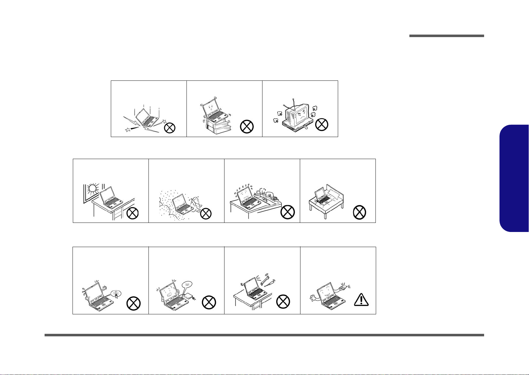
The notebook computer is quite rugged, but it can be damaged. To prevent this, follow these suggestions:
1. Don’t drop it, or expose it to shock. If the computer falls, the case and the components could be damaged.
Preface
Do not expose the computer
to any shock or vibration.
Do not place it on an unstable
surface.
Do not place anything heavy
on the computer.
2. Keep it dry, and don’t overheat it. Keep the computer and power supply away from any kind of heating element. This
is an electrical appliance. If water or any other liquid gets into it, the co mputer could be badly damaged.
Do not expose it to excessive
heat or direct sunlight.
Do not leave it in a place
where foreign matter or moisture may affect the system.
Don’t use or store the computer in a humid environment.
Do not place the computer on
any surface which will block
the vents.
3. Follow the proper working procedures for the computer. Shut the computer down properly and don’t forget to save
your work. Remember to periodically save your data as data may be lost if the battery is depleted.
Do not turn off the power
until you properly shut down
all programs.
Do not turn off any peripheral
devices when the computer is
on.
Do not disassemble the computer by yourself.
Perform routine maintenance
on your computer.
Preface
V
Preface
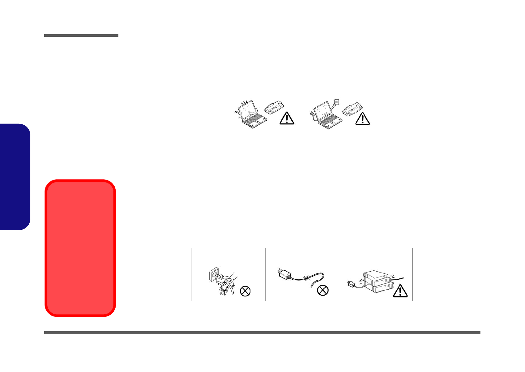
Power Safety
Warning
Before you undertake
any upgrade procedures, make sure that
you have turned off the
power, and disconnected all peripherals
and cables (including
telephone lines). It is
advisable to also remove your battery in
order to prevent accidentally turning the
machine on.
4. Avoid interference. Keep the computer away from high capacity transformers, electric motors, and oth er strong mag-
netic fields. These can hinder proper performance and damage your data.
5. Take care when using peripheral devices.
Preface
VI
Use only approved brands of
peripherals.
Unplug the power cord befor e
attaching peripheral devices.
Power Safety
The computer has specific power requirements:
• Only use a power adapter approved for use with this computer.
• Your AC adapter may be designed for international travel but it still requires a stea dy, uninterrupted po wer supply. If you ar e
unsure of your local power specifications, consult your service representative or local power company.
• The power adapter may have either a 2-prong or a 3-prong grounded plug. The third prong is an important safety feature; do
not defeat its purpose. If you do not have access to a compatible outlet, have a qualified electrician install one.
• When you want to unplug the power cord, be sure to disconnect it by the plug head, not by its wire.
• Make sure the socket and any extension cord(s) you use can support the total current load of all the connected devices.
• Before cleaning the computer, make sure it is disconnected from any external power supplies.
Do not plug in the power
cord if you are wet.
Do not use the power cord if
it is broken.
Do not place heavy objects
on the power cord.

Battery Precautions
Battery Disposal
The product that you have purchased contains a rechargeable battery. The battery is recyclable. At the end of its useful life, under various state and local laws, it may be illegal to dispose of this battery into the municipal waste stream. Check with your local solid waste
officials for details in your area for recycling options or proper disposal.
Caution
Danger of explosion if battery is incorrectly replaced. Replace only with the same or equivalent type recommended by the manufacturer.
Discard used battery according to the manufacturer’s instructions.
Battery Level
Click the battery icon in the taskbar to see the current battery level and charge status. A battery that drops below a level of 10%
will not allow the computer to boot up. Make sure that any battery that drops below 10% is recharged within one week.
• Only use batteries designed for this computer. The wrong battery type may explode, leak or damage the computer.
• Do not continue to use a battery that has been dropped, or that appears damaged (e.g. bent or twisted) in any way. Even if the
computer continues to work with a damaged battery in place, it may cause circuit damage, which may possibly result in fire.
• Recharge the batteries using the notebook’s system. Incorrect recharging may make the battery explode.
• Do not try to repair a battery pack. Refer any battery pack repair or replacement to your service representative or qualified service
personnel.
• Keep children away from, and promptly dispose of a damaged battery. Always dispose of batteries carefully. Batteries may explode
or leak if exposed to fire, or improperly handled or discarded.
• Keep the battery away from metal appliances.
• Affix tape to the battery contacts before disposing of the battery.
• Do not touch the battery contacts with your hands or metal objects.
Battery Guidelines
The following can also apply to any backup batteries you may have.
• If you do not use the battery for an extended period, then remove the battery from the computer for storage.
• Before removing the battery for storage charge it to 60% - 70%.
• Check stored batteries at least every 3 months and charge them to 60% - 70%.
Preface
Preface
VII
Preface
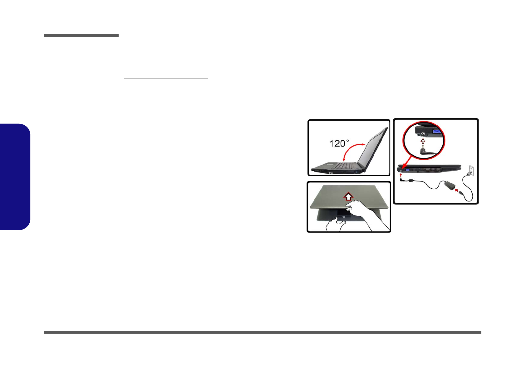
Figure 1 - Opening the Lid/
LCD/Computer with AC/DC
Adapter Plugged-In
Preface
Related Documents
You may also need to consult the following manual for additional information:
User’s Manual on CD/DVD
This describes the notebook PC’s features and the procedures for operating the computer and its ROM-based setup program. It also describes the installation and operation of the utility programs provided with the notebook PC.
System Startup
1. Remove all packing materials.
2. Place the computer on a stable surface.
3. Securely attach any peripherals you want to use with the computer (e.g.
keyboard and mouse) to their ports.
4. Attach the AC/DC adapter to the DC-In jack on the left of the computer,
then plug the AC power cord into an outlet, and connect the AC power
cord to the AC/DC adapter.
5. Use one hand to raise the
exceed 120 degrees)
support the base of the computer (Note: Never lift the computer by the
lid/LCD).
6. Press the power button to turn the computer “on”.
lid/LCD to a comfortable viewing angle
;
use the other hand (as illustrated in Figure 1) to
(do not
VIII

Contents
Preface
Introduction ..............................................1-1
Overview .........................................................................................1-1
Specifications ..................................................................................1-2
External Locator - Top View with LCD Panel Open ......................1-4
External Locator - Front & Right Side Views .................................1-5
External Locator - Left Side & Rear View .....................................1-6
External Locator - Bottom View .....................................................1-7
Mainboard Overview - Top (Key Parts) .........................................1-8
Mainboard Overview - Bottom (Key Parts) ....................................1-9
Mainboard Overview - Top (Connectors) .....................................1-10
Mainboard Overview - Bottom (Connectors) ...............................1-11
Disassembly ...............................................2-1
Overview .........................................................................................2-1
Maintenance Tools ..........................................................................2-2
Connections .....................................................................................2-2
Maintenance Precautions .................................................................2-3
Disassembly Steps ...........................................................................2-4
Removing the Battery ......................................................................2-5
Removing the Hard Disk Drive .......................................................2-6
Removing the System Memory (RAM) ..........................................2-8
Removing the Optical (CD/DVD) Device ....................................2-10
Removing and Installing the Processor .........................................2-11
Removing the Wireless LAN Module ...........................................2-14
Removing the Bluetooth Module ..................................................2-15
Removing the Keyboard ................................................................2-16
Removing the Modem ...................................................................2-17
Part Lists ..................................................A-1
Part List Illustration Location ........................................................A-2
Top with Fingerprint ......................................................................A-3
Bottom ........................................................................................... A-4
LCD ............................................................................................... A-5
SATA DVD Super-Multi ............................................................... A-6
SATA Blu-Ray Combo .................................................................. A-7
HDD ............................................................................................... A-8
Schematic Diagrams.................................B-1
System Block Diagram ...................................................................B-2
Clock Generator ..............................................................................B-3
CPU 1/7 (DMI, PEG, FDI) .............................................................B-4
CPU 2/7 (CLK, MISC) ...................................................................B-5
CPU 3/7 (DDR3) ............................................................................B-6
CPU 4/7 (Power) .............................................................................B-7
CPU 5/7 (VGFX Power) .................................................................B-8
CPU 6/7 (GND) ..............................................................................B-9
CPU 7/7 (RESERVED) ................................................................B-10
DDR3 SO-DIMM_0 .....................................................................B-11
DDR3 SO-DIMM_1 .....................................................................B-12
Panel, Inverter, CRT .....................................................................B-13
Docking Connector .......................................................................B-14
Intel Glan 82577LM/LC ...............................................................B-15
IBEXPEAK - M 1/9 ......................................................................B-16
IBEXPEAK - M 2/9 ......................................................................B-17
IBEXPEAK - M 3/9 ......................................................................B-18
IBEXPEAK - M 4/9 ......................................................................B-19
IBEXPEAK- M 5/9 .......................................................................B-20
IBEXPEAK - M 6/9 ......................................................................B-21
IBEXPEAK - M 7/9 ......................................................................B-22
IBEXPEAK - M 8/9 ......................................................................B-23
IBEXPEAK - M 9/9 ......................................................................B-24
New Card, Mini PCIE ...................................................................B-25
Preface
IX

Preface
3G, TPM 1,2, SATA-HDD .......................................................... B-26
USB, Fan, TP, Multi-Conn ...........................................................B-27
Card Reader (JMB 385) ............................................................... B-28
LED, Hotkey, LID, BT .................................................................B-29
HDMI, Modem .............................................................................B-30
Audio Codec ALC272 .................................................................. B-31
KBC-ITE IT8502E ....................................................................... B-32
5VS, 3VS, 1.5VS, 1.1VS_VTT, VIN1 .........................................B-33
Power VDD3, VDD5 ................................................................... B-34
Power 1.8VS, DK COM Port .......................................................B-35
Power 1.1V_LAN .........................................................................B-36
Power VGFX_Core ......................................................................B-37
V-Core ..........................................................................................B-38
AC_In, Charger ............................................................................ B-39
Power 1.5V/0.75V ........................................................................B-40
Audio Board ................................................................................. B-41
Preface
Finger Sensor Board TCS4X ........................................................B-42
Power Switch Board for M74 .......................................................B-43
External ODD Board for W76 .....................................................B-44
Click Finger Board for M77 .........................................................B-45
Multi I/O Board ............................................................................ B-46
Power Sequence ........................................................................... B-47
Power Block ................................................................................. B-48
Updating the FLASH ROM BIOS......... C-1
To update the FLASH ROM BIOS you must: C-1
Download the BIOS .......................................................................C-1
Unzip the downloaded files to a bootable CD/DVD/ or USB Flash
drive ................................................................................................C-1
Set the computer to boot from the external drive ...........................C-1
Use the flash tools to update the BIOS ..........................................C-2
Restart the computer (booting from the HDD) .............................. C-2
X

Chapter 1: Introduction
Overview
This manual covers the information you need to service or upgrade the T5100 series notebook computer. Information
about operating the computer (e.g. getting started, and the Setup utility) is in the User’s Manual. Information about drivers (e.g. VGA & audio) is also found in the User’s Manual. The manual is shipped with the computer.
Operating systems (e.g. Windows Vista/ Window 7, etc.) have their own manuals as do application softwares (e.g. word
processing and database programs). If you have questions about those programs, you should consult those manuals.
Introduction
The T5100 series notebook is designed to be upgradeable. See Disassembly on page 2 - 1 for a detailed description of
the upgrade procedures for each specific component. Please take note of the warning and safety information indicated
by the “” symbol.
The balance of this chapter reviews the computer’s technical specifications and features.
1.Introduction
Overview 1 - 1

Introduction
Latest Specification Information
The specifications listed here are correct at the
time of sending them to the press. Certain items
(particularly processor types/speeds) may be
changed, delayed or updated due to the manufacturer's release schedule. Check with your
service center for more details.
CPU
The CPU is not a user serviceable part. Accessing the CPU in any way may violate your
warranty.
Specifications
1.Introduction
Processor Options
Model A:
Intel® Core™ i7 Processor
i7-620M (2.66GHz)
4MB L3 Cache & 1066MHz FSB
Intel® Core™ i5 Processor
i5-540M (2.53GHz), i5-520M (2.4GHz)
3MB L3 Cache & 1066MHz FSB
Model B:
Intel® Core™ i7 Processor
i7-620M (2.66GHz)
4MB L3 Cache & 1066MHz FSB
Intel® Core™ i5 Processor
i5-540M (2.53GHz), i5-520M (2.4GHz),
i5-430M (2.26GHz)
3MB L3 Cache & 1066MHz FSB
Intel® Core™ i3 Processor
i3-350M (2.26GHz), i3-330M (2.13GHz)
3MB L3 Cache, 1066MHz FSB
Intel® Mobile Celeron Processor
P4500 (1.86GHz)
2MB L3 Cache & 1066MHz FSB
Core Logic
Model A:
Intel® QM57 Chipset
Model B:
Intel® HM55 Chipset
BIOS
Phoenix™ BIOS (One 32Mb SPI Flash ROM)
LCD
15.6" HD/ HD+ TFT LCD
Memory
Two 204 Pin SO-DIMM Sockets Supporting DDR3 1066/
1333MHz Memory
Memory Expandable up to 8GB
Video Adapter
Intel GMA HD
Shared Memory Architecture (DVMT) up to 1.7GB
Microsoft DirectX®10 Compatible
Security
BIOS Password
Security (Kensington® Type) Lock Slot
Fingerprint Reader/TPM
Supports Intel vPro (Model A Only)
Audio
High Definition Audio Compliant Interface
2 * Built-In Speakers
Built-In Microphone
Keyboard
Full-size “WinKey” keyboard (with numeric keypad)
Pointing Device
Built-in Touchpad
Storage
(Factory Option) One Changeable 12.7mm(h) Optical
Device Type Drive (Super Multi Drive Module or
Blu-Ray Combo Drive Module)
One Changeable 2.5" 9.5 mm (h) SATA (Serial) HDD
1 - 2 Specifications

Introduction
Interface
Three USB 2.0 Ports
One eSATA Port
One HDMI-Out Port
One Headphone-Out Jack
One Microphone-In Jack
One S/PDIF Out Jack
One RJ-11 Modem Jack
One RJ-45 LAN Jack
One DC-in Jack
One External Monitor Port
One ExpressCard/34(54) Slot
One Docking Port (cold plug)
Factory Option for Model A
Standard for Model B
Card Reader
Embedded 9-in-1 Card Reader
MMC (MultiMedia Card) / RS MMC
SD (Secure Digital) / Mini SD / SDHC/ SDXC
Compatible
MS (Memory Stick) / MS Pro / MS Duo
Mini Card Slots
Slot 1 for WLAN Half Mini-Card Module
(Factory Option) Slot 2 for 3.75G/HSPA Half Mini-Card
Module
Communication
Built-In Gigabit Ethernet LAN
2.0M Pixel USB PC Camera Module
(Factory Option) 56K MDC Modem, V.90 & V.92 Compliant
(Factory Option) Bluetooth 2.1 + EDR Module
(Factory Option) 3.75G/HSPA Half Mini-Card Module
Wireless LAN Module Options:
Model A:
(Factory Option) Intel® WiFi Link 6200 (802.11a/g/n) Wireless LAN Half Mini-Card Module
(Factory Option) Intel® WiFi Link 6300 (802.11a/g/n) Wireless LAN Half Mini-Card Module
Model B:
(Factory Option) Intel® WiFi Link 6200 (802.11a/g/n) Wireless LAN Half Mini-Card Module
(Factory Option) Intel® WiFi Link 6300 (802.11a/g/n) Wireless LAN Half Mini-Card Module
(Factory Option) Third-Party 802.11b/g/n Wireless LAN
Half Mini-Card Module
Power
Full Range AC/DC Adapter
AC Input: 100 - 240V, 50 - 60Hz
DC Output: 19V, 3.42A /18V, 3.5A (65W)
6 Cell Smart Lithium-Ion Battery Pack, 48.84WH
(Factory Option) 9 Cell Smart Lithium-Ion Battery Pack,
77.76WH
Environmental Spec
Temperature
Operating: 5
Non-Operating: -20°C - 60°C
Relative Humidity
Operating: 20% - 80%
Non-Operating: 10% - 90%
°C - 35°C
Dimensions & Weight
374mm (w) * 256mm (d) * 37.5mm (h)
2.5kg (with ODD and 48.84WH Battery)
1.Introduction
Specifications 1 - 3
Introduction
Figure 1
Top View
1. Built-In PC Camera
2. LCD
3. Speakers
4. Power Button
5. Hot Key Buttons
6. Keyboard
7. Built-In
Microphone
8. T o uchpad &
Buttons
9. Fingerprint Reader
10.LED Indicators
2
5
1
9
6
4
7
3
8
10
3
External Locator - Top View with LCD Panel Open
1.Introduction
1 - 4 External Locator - Top View with LCD Panel Open
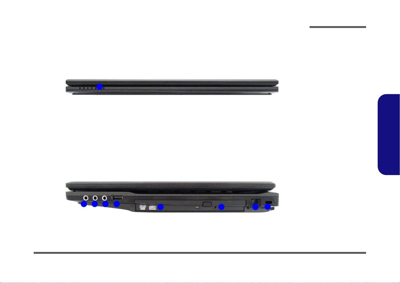
External Locator - Front & Right Side Views
Figure 2
Front View
1. LED Indicators
Figure 3
Right Side View
1. S/PDIF-Out Jack
2. Microphone-In
Jack
3. Headphone-Out
Jack
4. USB 2.0 Port
5. Optical Device
Drive Bay
6. Emergency Eject
Hole
7. RJ-11 Modem
Jack
8. Security Lock
Slot
1
FRONT VIEW
152 43
6 7
RIGHT SIDE VIEW
8
Introduction
1.Introduction
External Locator - Front & Right Side Views 1 - 5

Introduction
Figure 4
Left Side View
1. DC-In Jack
2. External Monitor
Port
3. RJ-45 LAN Jack
4. e-SATA Port
5. HDMI-Out Port
6. Vent
7. 2 * USB 2.0 Ports
8. ExpressCard/
54(34) Slot
9. 9-in-1 Card
Reader
1
3
2
6
8
9
7 7
LEFT SIDE VIEW
4 5
Figure 5
Rear View
1. Battery
REAR VIEW
1
1.Introduction
External Locator - Left Side & Rear View
/
1 - 6 External Locator - Left Side & Rear View
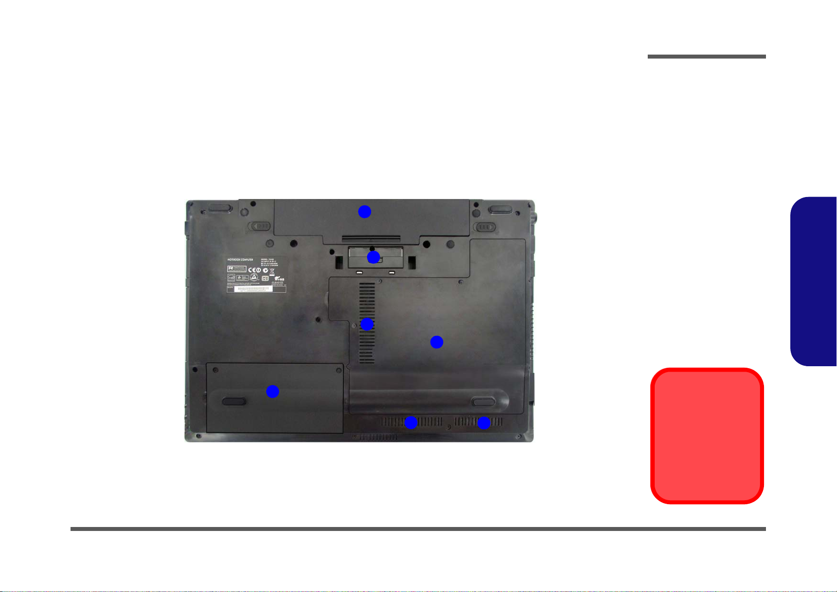
External Locator - Bottom View
Figure 6
Bottom View
1. Battery
2. Docking Port
3. Component Bay
Cover
4. Vent
5. Hard Disk Bay
Cover
Overheating
To prevent your computer from overheating, make sure nothing blocks any vent
while the computer is
in use.
3
4
1
5
4
4
2
Introduction
1.Introduction
External Locator - Bottom View 1 - 7
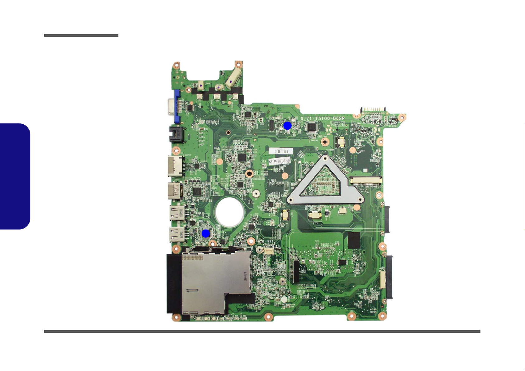
Figure 7
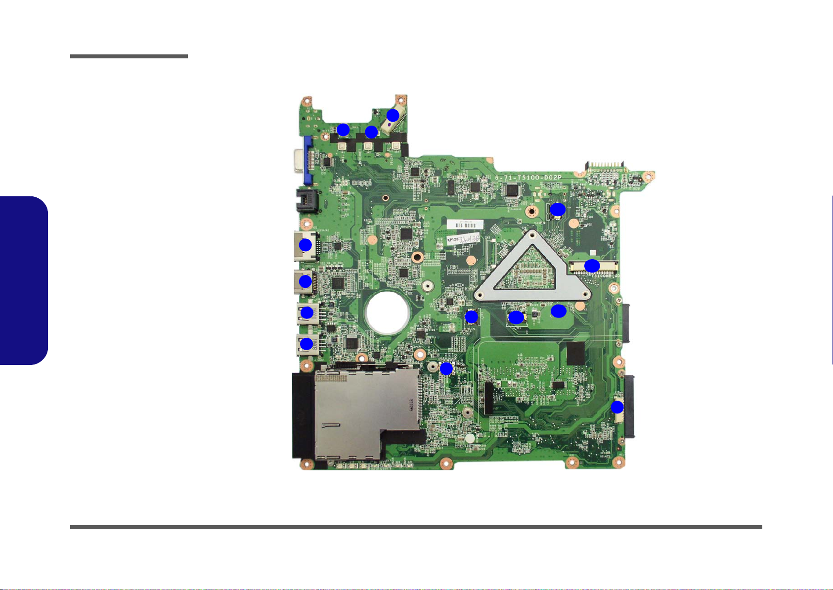
Mainboard Top
Key Parts
1. Intel Glan
2. JMB385
1
2
1.Introduction
Introduction
Mainboard Overview - Top (Key Parts)
1 - 8 Mainboard Overview - Top (Key Parts)
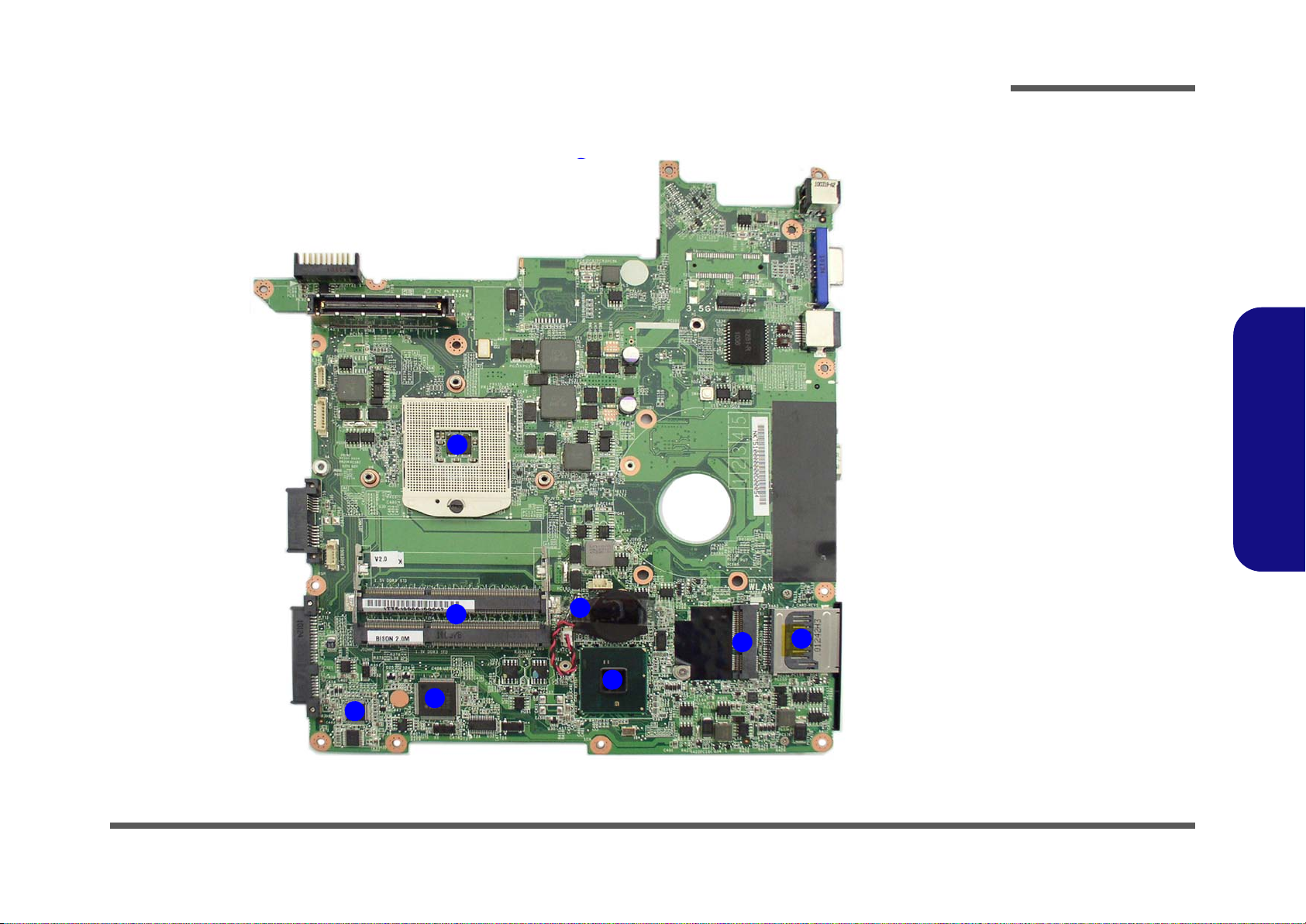
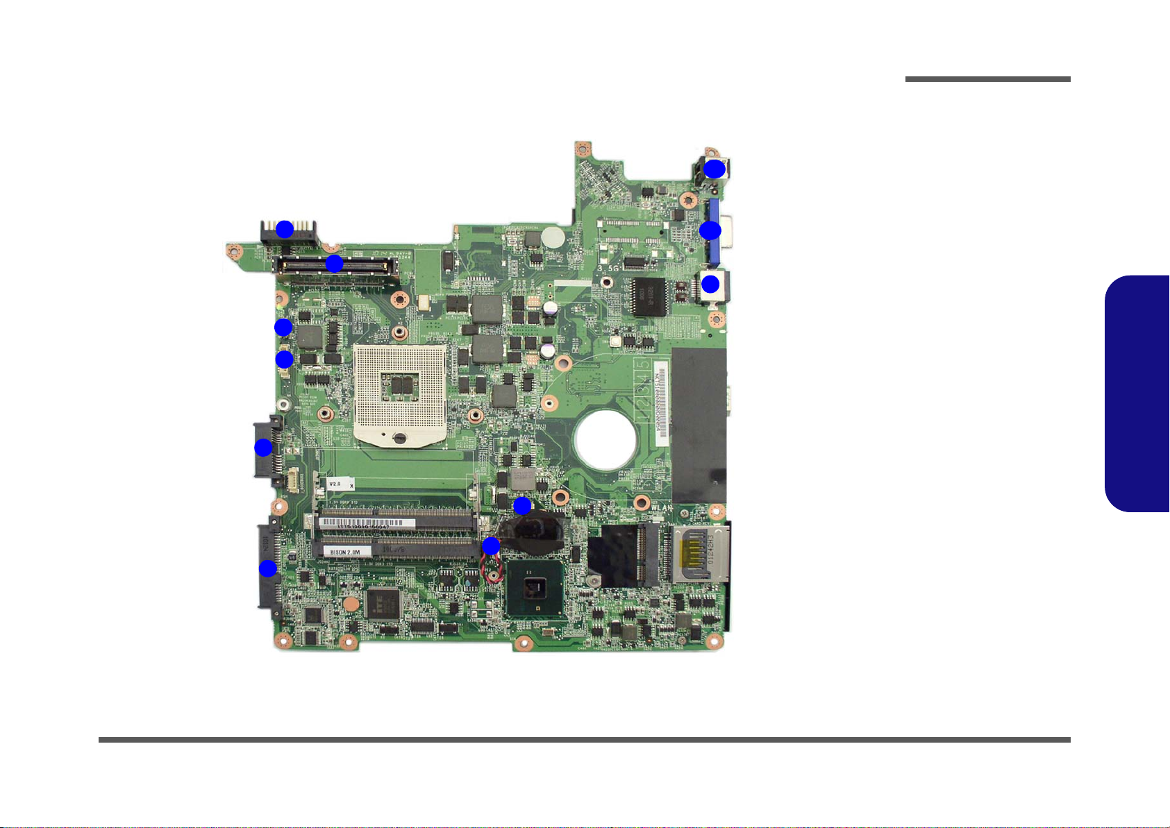
Mainboard Overview - Bottom (Key Parts)
1
2
5
4
6
1
2
7
8
3
Figure 8
Mainboard Bottom
Key Parts
1. CPU Socket (no
CPU installed)
2. Memory Slots
DDR3 SO-DIMM
3. Azalia Codec
4. KBC-ITE IT8502E
5. Platform Controller
Hub
6. Clock Generator
7. Mini-Card
Connector (WLAN
Module)
8. 9-in-1 Card
Reader
Introduction
1.Introduction
Mainboard Overview - Bottom (Key Parts) 1 - 9
Introduction
Figure 9
Mainboard Top
Connectors
1. LCD Cable
Connector
2. Speaker Cable
Connector
3. Inverter
Connector
4. eSATA Port
5. HDMI-Out Port
6. USB Ports
7. Modem
Connector
8. HDD Connector
9. Fingerprint Cable
Connector
10.TouchPad Cable
Connector
11. Microphone
Cable Connector
12.Keyboard Cable
Connector
13.Switch Board
Cable Connector
6
5
1
4
2
3
8
9
10
11
7
6
12
13
1.Introduction
Mainboard Overview - Top (Connectors)
1 - 10 Mainboard Overview - Top (Connectors)
Mainboard Overview - Bottom (Connectors)
Figure 10
Mainboard Bottom
Connectors
1. Battery
Connector
2. Docking Station
Connector
3. Bluetooth Cable
Connector
4. Multi-I/O
Connector
5. ODD Connector
6. HDD Connector
7. CMOS Battery
Connector
8. CPU Fan Cable
Connector
9. RJ-45 LAN Jack
10.External Monitor
Port
11. DC-In Jack
1
2
3
4
5
6
7
8
10
11
9
Introduction
1.Introduction
Mainboard Overview - Bottom (Connectors) 1 - 11

Introduction
1.Introduction
1-12

Chapter 2: Disassembly
Information
Warning
Overview
This chapter provides step-by-step instructions for disassembling the T5100 series notebook’s parts and subsystems.
When it comes to reassembly, reverse the procedures (unless otherwise indicated).
We suggest you completely review any procedure before you take the computer apart.
Disassembly
Procedures such as upgrading/replacing the RAM, optical device and hard disk are included in the User’s Manual but are
repeated here for your convenience.
To make the disassembly process easier each section may have a box in the page margin. Information contained under
the figure # will give a synopsis of the sequence of procedures involved in the disassembly procedure. A box with a
lists the relevant parts you will have after the disassembly process is complete. Note: The parts listed will be for the disassembly procedure listed ONLY, and not any previous disassembly step(s) required. Refer to the part list for the previous disassembly procedure. The amount of screws you should be left with will be listed here also.
A box with a will also provide any possible helpful information. A box with a contains warnings.
An example of these types of boxes are shown in the sidebar.
2.Disassembly
Overview 2 - 1

Disassembly
2.Disassembly
NOTE: All disassembly procedures assume that the system is turned OFF, and disconnected from any power supply (the
battery is removed too).
Maintenance Tools
The following tools are recommended when working on the notebook PC:
• M3 Philips-head screwdriver
• M2.5 Philips-head screwdriver (magnetized)
• M2 Philips-head screwdriver
• Small flat-head screwdriver
• Pair of need le-nose pliers
• Anti-static wrist-strap
Connections
Connections within the computer are one of four types:
Locking collar sockets for ribbon connectors To release these connectors, use a small flat-head screwdriver to
gently pry the locking collar away from its base. When replacing the connection, make sure the connector is oriented in the
same way. The pin1 side is usually not indicated.
2 - 2 Overview
Pressure sockets for multi-wire connectors To release this connector type, grasp it at its head and gently
rock it from side to side as you pull it out. Do not pull on the
wires themselves. When replacing the connection, do not try to
force it. The socket only fits one way.
Pressure sockets for ribbon connectors To release these connectors, use a small pair of needle-nose pli-
ers to gently lift the connector away from its socket. When replacing the connection, make sure the connector is oriented in
the same way. The pin1 side is usually not indicated.
Board-to-board or multi-pin sockets To separate the boards, gently rock them from side to side as
you pull them apart. If the connection is very tight, use a small
flat-head screwdriver - use just enough force to start.

Maintenance Precautions
Power Safety
Warning
Before you undertake
any upgrade procedures, make sure that
you have turned off the
power, and disconnected all peripherals
and cables (including
telephone lines). It is
advisable to also remove your battery in
order to prevent accidentally turning the
machine on.
The following precautions are a reminder. To avoid personal injury or damage to the computer while performing a removal and/or replacement job, take the following precautions:
1. Don't drop it. Perform your repairs and/or upgrades on a stable surface. If the computer falls, the case and other
components could be damaged.
2. Don't overheat it. Note the proximity of any heating elements. Keep the computer out of direct sunlight.
3. Avoid interference. Note the proximity of any high capacity transformers, electric motors, and other strong mag-
netic fields. These can hinder proper performance and damage component s and/or data. You should also monitor
the position of magnetized tools (i.e. screwdrivers).
4. Keep it dry. This is an electrical appliance. If water or any other liquid gets into it, the computer could be badly
damaged.
5. Be careful with power. Avoid accidental shocks, discharges or explosions.
•Before removing or servicing any part from the computer, turn the computer off and detach any power supplies.
•When you want to unplug the power cord or any cable/wire, be sure to disconnect it by the plug head. Do not pull on the wire.
6. Peripherals – Turn off and detach any peripherals.
7. Beware of static discharge. ICs, such as the CPU and main support chips, are vulnerable to static electricity.
Before handling any part in the computer, discharge any static electricity inside the computer. When handling a
printed circuit board, do not use gloves or other materials which allow static electricity buildup. We suggest that
you use an anti-static wrist strap instead.
8. Beware of corrosion. As you perform your job, avoid touching any connector leads. Even the cleanest hands produce oils which can attract corrosive elements.
9. Keep your work environment clean. Tobacco smoke, dust or other air-born particulate matter is often attracted
to charged surfaces, reducing performance.
10. Keep track of the components. When removing or replacing any part, be careful not to leave small p arts, such as
screws, loose inside the computer.
Cleaning
Do not apply cleaner directly to the computer, use a soft clean cloth.
Do not use volatile (petroleum distillates) or abrasive cleaners on any part of the computer.
Disassembly
2.Disassembly
Overview 2 - 3

Disassembly
Disassembly Steps
The following table lists the disassembly steps, and on which page to find the related information. PLEASE PERFORM
THE DISASSEMBLY STEPS IN THE ORDER INDICATED.
2.Disassembly
To remove the Battery:
1. Remove the battery page 2 - 5
To remove the HDD:
1. Remove the battery page 2 - 5
2. Remove the HDD page 2 - 6
To remove the System Memory:
1. Remove the battery page 2 - 5
2. Remove the system memory page 2 - 8
To remove the Optical Device:
1. Remove the battery page 2 - 5
2. Remove the Optical device page 2 - 10
To remove and install a Processor:
1. Remove the battery page 2 - 5
2. Remove the processor page 2 - 11
3. Install the processor page 2 - 13
To remove the Bluetooth Module:
1. Remove the battery page 2 - 5
2. Remove the Bluetooth page 2 - 15
To remove the Keyboard:
1. Remove the battery page 2 - 5
2. Remove the keyboard page 2 - 16
To remove the Modem:
1. Remove the battery page 2 - 5
2. Remove the HDD page 2 - 6
3. Remove the Optical device page 2 - 10
4. Remove the processor page 2 - 11
5. Remove the keyboard page 2 - 16
6. Remove the modem page 2 - 17
To remove the Wireless LAN Module:
1. Remove the battery page 2 - 5
2. Remove the wireless LAN page 2 - 14
2 - 4 Disassembly Steps
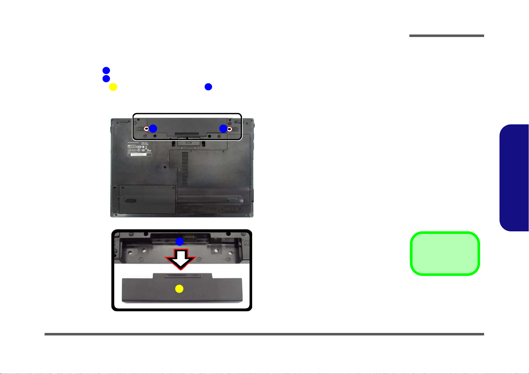
Removing the Battery
3. Battery
12634
a.
3
b.
2
4
1
Figure 1
Battery Removal
a. Slide the latch and hold in
place.
b. Slide the battery in the di-
rection of the arrow.
1. Turn the computer off, and turn it over.
2. Slide the latch in the direction of the arrow (Figure 1a
3. Slide the latch in the direction of the arrow, and hold it in place (Figure 1a
4. Slide the battery in the direction of the arrow (Figure 1b
).
).
Disassembly
).
2.Disassembly
Removing the Battery 2 - 5
Disassembly
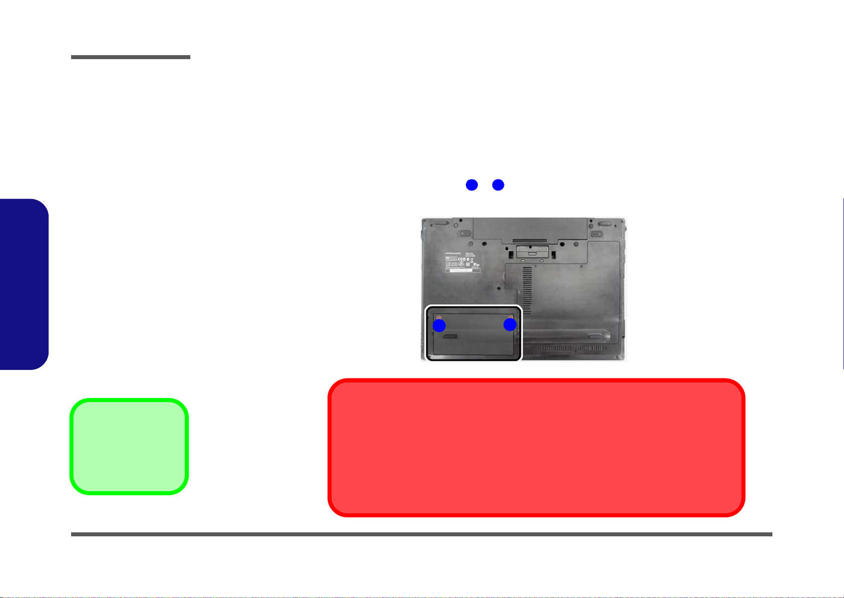
Figure 2
HDD Assembly
Removal
a. Locate the HDD bay co-
ver and remove the
screws.
•2 Screws
1
2
2
1
a.
HDD System Warning
New HDD’s are blank. Before you begin make sure:
You have backed up any data you want to keep from your old HDD.
You have all the CD-ROMs and FDDs required to install your operating system and programs.
If you have access to the internet, download the latest application and hardware driver updates for
the operating system you plan to install. Copy these to a removable medium.
Removing the Hard Disk Drive
The hard disk drive can be taken out to accommodate other 2.5" serial (SATA) hard disk drives with a height of 9.5mm
(h). Follow your operating system’s installation instructions, and install all necessary drivers and utilities (as outlined in
Chapter 4 of the User’s Manual) when setting up a new hard disk.
2.Disassembly
Hard Disk Upgrade Process
1. Turn off the computer, and remove the battery (page 2 - 5).
2. Locate the hard disk bay cover and remove screws & (Figure 2a
).
2 - 6 Removing the Hard Disk Drive

3. Remove the hard disk bay cover (Figure 3b).
63467
10
11
4
b.
c.
e.
6
d.
3
9 8
7
5
11
5
10
3. HDD Bay Cover
5. HDD
11.Adhesive Cover
•4 Screws
Figure 3
HDD Assembly
Removal (cont’d.)
b. Remove the HDD bay
cover.
c. Grip the tab and slide the
HDD in the direction of
the arrow.
d. Lift the HDD assembly
out of the bay.
e. Remove the screws and
adhesive cover.
4. Grip the tab and slide the hard disk in the direction of arrow (Figure 3c).
5. Lift the hard disk out of the bay (Figure 3d).
6. Remove the screws - and the adhesive cover from the hard disk
5
5
(Figure 3e).
7. Reverse the process to install a new hard disk (do not forget to replace all the screws and covers).
Disassembly
2.Disassembly
Removing the Hard Disk Drive 2 - 7

Disassembly
Figure 4
RAM Module
Removal
a. Remove the screws.
b. Disconnect the fan
cable and remove
the bay cover.
Contact Warning
Be careful not to touch
the metal pins on the
module’s connecting
edge. Even the cleanest hands have oils
which can attract particles, and degrade the
module’s performance.
12561
1. Component Bay Co-
ver
•4 Screws
2
4
3
a.
b.
1
1
6
5
6
2.Disassembly
Removing the System Memory (RAM)
The computer has two memory sockets for 204 pin Small Outline Dual In-line Memory Modules (SO-DIMM) supporting
DDR3 1066/1333MHz. The main memory can be expanded up to 8GB. The SO-DIMM modules supported are 1024MB,
and 2048MB and DDRIII Modules. The total memory size is automatically detected by the POST routine once you turn
on your computer.
Memory Upgrade Process
1. Turn off the computer, remove the battery (page 2 - 5).
2. Locate the component bay cover , and remove screws - (Figure 4a
3. Carefully (a fan and cable are attached to the under side of the cover) lift up the bay cover.
4. Carefully disconnect the fan cable , and remove the cover
(Figure 4b).
).
2 - 8 Removing the System Memory (RAM)

5. Gently pull the two release latches ( - ) on the sides of the memory socket in the direction indicated by the
6
7
Figure 5
RAM Module
Removal (cont’d.)
c. Pull the release latches.
d. Remove the module(s).
Single Memory
Module Installation
If your computer has a
single memory module,
then insert the module
into the Channel 0
(J_DIMM_1) socket. In
this case, this is the lower memory socket (the
socket closest to the
mainboard) as shown in
Figure 5e.
8. RAM Module(s)
d.
8
6 7
c. e.
8
arrows (Figure 5c).
Disassembly
2.Disassembly
6. The RAM module will pop-up (Figure 5d), and you can then remove it.
7. Pull the latches to release the second module if necessary (Figure 5c).
8. Insert a new module holding it at about a 30° angle and fit the connectors firmly into the memory slot.
9. The module’s pin alignment will allow it to only fit one way. Make sure the module is seated as far into the slot as it
will go. DO NOT FORCE the module; it should fit without much pressure.
10. Press the module in and down towards the mainboard until the slot levers click into place to secure the module.
11. Replace the bay cover and screws (make sure you reconnect the fan cable before screwing down the bay
cover).
12. Restart the computer to allow the BIOS to register the new memory configuration as it starts up.
Removing the System Memory (RAM) 2 - 9

Disassembly
Figure 6
Optical Device
Removal
a. Remove the screw.
b. Push the optical device
out off the computer at
point 3.
123
2. Optical Device
•1 Screw
2
1
3
a. b.
3
Removing the Optical (CD/DVD) Device
1. Turn off the computer, remove the battery (page 2 - 5) and the component bay cover (page 2 - 8).
2. Remove the screw at point
point
3. Insert the new device and carefully slide it into the computer (the device only fits one way. DO NOT FORCE IT; The
screw holes should line up).
4. Restart the computer to allow it to automatically detect the new device.
2.Disassembly
(Figure 6b).
(Figure 6a), and use a screwdriver to carefully push out the optical device at
2 - 10 Removing the Optical (CD/DVD) Device

Removing and Installing the Processor
A32
1
B
Figure 7
Processor Removal
a. Remove the cover and
Iocate the heat sink.
b. Remove the screws in
the order indicated.
c. Remove the heat sink.
B. Heat Sink
•3 Screws
a.
2
1
3
b.
c.
B
A
Processor Removal Procedure
1. Turn off the computer, remove the battery (page 2 - 5) and the component bay cover (page 2 - 8).
2. The CPU heat sink will be visible at point (Figure 7a) on the mainboard.
3. Remove screws
4. Carefully lift up the heat sink (Figure 7c) off the computer.
, , (Figure 7b), the reverse order indicated on the label.
Disassembly
2.Disassembly
Removing and Installing the Processor 2 - 11

Disassembly
C
D
Figure 8
Processor Removal
(cont’d)
d. Turn the release latch to
unlock the CPU.
e. Lift the CPU out of the
socket.
C
d. e.
D
Caution
The heat sink, and CPU area in general, contains parts which are subjected to high temperatures. Allow
the area time to cool before removing these parts.
Unlock
D. CPU
5. Turn the release latch towards the unlock symbol , to release the CPU (Figure 8d).
6. Carefully (it may be hot) lift the CPU up out of the socket (Figure 8e).
7. See page 2 - 13 for information on inserting a new CPU.
8. When re-inserting the CPU, pay careful attention to the pin alignment, it will fit only one way (DO NOT FORCE IT!).
2.Disassembly
2 - 12 Removing and Installing the Processor

Processor Installation Procedure
A
B
C
D
1
3
c.
3
D
b.
1
2
d.
B
A
a.
D
C
Lock
Figure 9
Processor
Installation
a. Insert the CPU.
b. Turn the release latch to-
wards the lock symbol.
c. Remove the stickers
from the heat sink and
insert the heat sink.
d. Replace and tighten the
screws in the order indicated on the label.
e. Replace the cover and
screws.
A. CPU
D. Heat Sink
•3 Screws
1. Insert the CPU (Figure 9a), pay careful attention to the pin alignment, it will fit only one way (DO NOT FORCE
IT!), and turn the release latch towards the lock symbol (Figure 9b).
2. Remove the stickers (Figure 9c) from the heat sink.
3. Insert the heat sink
4. Replace and tighten the screws
5. Replace the component bay cover and screws (page 2 - 8).
as indicated in (Figure 9c).
- (Figure 9d) in the order indicated on the label.
Disassembly
2.Disassembly
Removing and Installing the Processor 2 - 13

Disassembly
Figure 10
Wireless LAN
Module Removal
a. Remove the cover.
b. Disconnect the cables
and remove the screw.
c. The WLAN module will
pop up.
d. Lift the WLAN module
out.
Note: Make sure you
reconnect the antenna
cable to ‘’1’’ +
‘’2’’socket (Figure
b).
1
2
3
4
5
5
2
b.
c.a.
d.
3
4
5
1
5. WLAN Module.
•1 Screw
Removing the Wireless LAN Module
1. Turn off the computer, remove the battery (page 2 - 5) and the component bay cover (page 2 - 8).
2. The Wireless LAN module will be visible at point (Figure 10a) on the mainboard.
3. Carefully disconnect cables - , then remove screw from the module socket (Figure 10b
4. The Wireless LAN module (Figure 10c) will pop-up.
5. Lift the Wireless LAN module (Figure 10d) up and off the computer.
).
2.Disassembly
2 - 14 Removing the Wireless LAN Module

Removing the Bluetooth Module
Figure 11
Bluetooth Module
Removal
a. Locate the Bluetooth mo-
dule at point .
b. Remove the screw.
c. Turn the Bluetooth module
over and carefully discon-
nect it from the cable and
the connector.
d. Lift the Bluetooth module
up and off the computer.
1
1
234
5
a.
b.
1
5
c.
d.
2
4
3
5. Bluetooth Module
•1 Screw
1. Turn off the computer, remove the battery (page 2 - 5) and component bay cover (page 2 - 8).
1. Locate the Bluetooth module at point
2. Remove screw
(Figure 11b).
3. Turn the Bluetooth module over and carefully disconnect it from the connector and the cable (Figure 11c).
4. Lift the Bluetooth module (Figure 11d) up and off the computer.
(Figure 11a).
Disassembly
2.Disassembly
Removing the Bluetooth Module 2 - 15

Disassembly
1
24345
9
10
11
Figure 12
Keyboard Removal
a. Remove the screws and
use a screwdriver to carefully push out the top cover
module at point .
b. Remove the top cover
module and the screws.
c. Lift the keyboard up and
disconnect the cable from
the locking collar socket.
d. Remove the keyboard.
3
12
a.
b.
2
9
3
5
1
7
4
d.
8
6
Keyboard Tabs
c.
12
11
10
10
1. Battery
6. Keyboard
4. Top Cover Module
12.Keyboard
•7 Screws
Re-Inserting the Key-
board
When re-inserting the
keyboard, align first
the four keyboard tabs
(Figure 12d) that are
located at the bottom,
to the slots in the case.
Removing the Keyboard
1. Turn off the computer and remove the battery (page 2 - 5).
2. Remove screws
12a).
3. Remove the top cover module
4. Lift the keyboard up and disconnect the keyboard ribbon cable from the locking collar socket
5. Carefully lift up the keyboard
& and use a screwdriver to carefully push out the top cover module at point (Figure
and the screws - (Figure 12b).
(Figure 12d) off the computer.
(Figure 12c)
2.Disassembly
2 - 16 Removing the Keyboard

Removing the Modem
1
171819
202124
25. Top Case
•20 Screws
Figure 13
Modem Removal
a. Remove the screws from
the bottom case and rear
of the computer.
b. Remove the screw from
the top case and disconnect cables.
c. Lift the top case off the
computer. The modem
will be visible at point
.
26
3
a.
b.
11
1
2
4
6
5
7
8
9
12
13
10
14
15
19
20
25
c
.
21 22
23
26
18
17
16
24
25
26
1. Turn off the computer, remove the battery (page 2 - 5), HDD (page 2 - 6), component bay cover (page 2 - 8), optical device (page 2 - 10), CPU (page 2 - 10), bluetooth (page 2 - 15) and keyboard (page 2 - 16).
2. Remove screws - from the bottom case (Figure 13a).
3. Remove screws - from the rear of the computer (Figure 13a).
4. Remove screw from the top case and disconnect cables - (Figure 13b).
5. Carefully lift the top case off the computer. The modem will be visible at point (Figure 14c).
Disassembly
2.Disassembly
Removing the Modem 2 - 17

Disassembly
272829
30
30. Modem
•2 Screws
30
28
d.
27
e.
29
Figure 14
Modem Removal
(cont’d.)
d. Remove the screws and
disconnect cable from
the module.
e. Lift the modem off the
socket.
6. Remove screws & from the module and disconnect cable (Figure 14d).
7. Carefully lift the modem up and off the socket (Figure 14e).
2.Disassembly
2 - 18 Removing the Modem

Appendix A:Part Lists
This appendix breaks down the T5100 series notebook’s construction into a series of illustrations. The component part
numbers are indicated in the tables opposite the drawings.
Note: This section indicates the manufacturer’s part numbers. Your organization may use a different system, so be sure
to cross-check any relevant documentation.
Note: Some assemblies may have parts in common (especially screws). However, the part lists DO NOT indicate the
total number of duplicated parts used.
Part Lists
Note: Be sure to check any update notices. The parts shown in these illustrations are appropriate for the system at the
time of publication. Over the product life, some parts may be improved or re-configured, resulting in new part numbers.
A.Part Lists
A-1

Part Lists
Table A - 1
Part List Illustration
Location
Part List Illustration Location
The following table indicates where to find the appropriate part list illustration.
Part T5100
Top with Fingerprint
page A - 3
A.Part Lists
Bottom
LCD
SATA DVD Super-Multi
SATA Blu-Ray Combo
HDD
page A - 4
page A - 5
page A - 6
page A - 7
page A - 8
A - 2 Part List Illustration Location

Top with Fingerprint
Figure A - 1
Top with Finger-
print
(黑色)
修模)
增加背膠長度
(非耐落)
藍天 互億
(非耐落)
凱碩
Part Lists
A.Part Lists
Top with Fingerprint A - 3

Part Lists
Figure A - 2
Bottom
日東
度,黑色
(黑色)
導電布
(富士弘)
導電布
導電布
電容變更
頭徑3.5MM 頭厚0. 8MM 1 號穴 鍍白鎳 I頭
(非耐落)
(更換背膠)
非耐落
A.Part Lists
Bottom
A - 4 Bottom

LCD
Figure A - 3
LCD
(富士弘)
惠貿
(黑色亮面)
(今皓)
(非耐落)
Ω 將磁鐵高斯磁變更為外露
惠貿
(富士弘)
頭徑 頭厚 號穴 鍍白鎳 頭
Ω
(志精)
(志精)
(咬花)
(志精)
(志精)
Part Lists
A.Part Lists
LCD A - 5

Part Lists
Figure A - 4
SATA DVD Super-
Multi
(志精)
*(非耐落)
黑色
A.Part Lists
SATA DVD Super-Multi
A - 6 SATA DVD Super-Multi

SATA Blu-Ray Combo
Figure A - 5
SATA Blu-Ray
Combo
(志精) 無鉛
*(非耐落) 無鉛
黑色 無鉛
無鉛
Part Lists
A.Part Lists
SATA Blu-Ray Combo A - 7

Part Lists
Figure A - 6
HDD
無鉛
(無鉛)
A.Part Lists
HDD
A - 8 HDD

Appendix B: Schematic Diagrams
Table B - 1
SCHEMATIC
DIAGRAMS
Version Note
The schematic diagrams in this chapter
are based upon version 6-7P-T5107-003.
If your mainboard (or
other boards) are a later version, please
check with the Service
Center for updated diagrams (if required).
This appendix has circuit diagrams of the T5100 notebook’s PCB’s. The following table indicates where to find the appropriate schematic diagram.
Schematic Diagrams
System Block Diagram - Page B - 2 IBEXPEAK - M 4/9 - Page B - 19 Power 1.1V_LAN - Page B - 36
Clock Generator - Page B - 3 IBEXPEAK- M 5/9 - Page B - 20 Power VGFX_Core - Page B - 37
CPU 1/7 (DMI, PEG, FDI) - Page B - 4 IBEXPEAK - M 6/9 - Page B - 21 V-Core - Page B - 38
CPU 2/7 (CLK, MISC) - Page B - 5 IBEXPEAK - M 7/9 - Page B - 22 AC_In, Charger - Page B - 39
CPU 3/7 (DDR3) - Page B - 6 IBEXPEAK - M 8/9 - Page B - 23 Power 1.5V/0.75V - Page B - 40
CPU 4/7 (Power) - Page B - 7 IBEXPEAK - M 9/9 - Page B - 24 Audio Board - Page B - 41
CPU 5/7 (VGFX Power) - Page B - 8 New Card, Mini PCIE - Page B - 25 Finger Sensor Board TCS4X - Page B - 42
CPU 6/7 (GND) - Page B - 9 3G, TPM 1,2, SATA-HDD - Page B - 26 Power Switch Board for M74 - Page B - 43
CPU 7/7 (RESERVED) - Page B - 10 USB, Fan, TP, Multi-Conn - Page B - 27 External ODD Board for W76 - Page B - 44
DDR3 SO-DIMM_0 - Page B - 11 Card Reader (JMB 385) - Page B - 28 Click Finger Board for M77 - Page B - 45
DDR3 SO-DIMM_1 - Page B - 12 LED, Hotkey, LID, BT - Page B - 29 Multi I/O Board - Page B - 46
Panel, Inverter, CRT - Page B - 13 HDMI, Modem - Page B - 30 Power Sequence - Page B - 47
Docking Connector - Page B - 14 Audio Codec ALC272 - Page B - 31 Power Block - Page B - 48
Intel Glan 82577LM/LC - Page B - 15 KBC-ITE IT8502E - Page B - 32
IBEXPEAK - M 1/9 - Page B - 16 5VS, 3VS, 1.5VS, 1.1VS_VTT, VIN1 - Page B - 33
IBEXPEAK - M 2/9 - Page B - 17 Power VDD3, VDD5 - Page B - 34
IBEXPEAK - M 3/9 - Page B - 18 Power 1.8VS, DK COM Port - Page B - 35
Diagram - Page Diagram - Page Diagram - Page
B.Schematic Diagrams
B-1

Schematic Diagrams
Sheet 1 of 47
System Block
Diagram
T5100 System Block Diagr am
SPK_R, RJ-11 , CCD
FingerPrint
(USB2)
(USB4)
12 MHz
New Card
(USB11)
LCD CONNECTOR,
IVERTER
<8"
TOUCH PAD
CRT CONNECTOR
SHEET 27
LPC
CARD READER
SMART
BATTERY
SO-DIMM1
HP
OUT
INT SPK R
PJ_VDD3/PJ_VDD5
SOCKET
<=8"
Memory Termination
PCIE
27x27mm
1071 Ball FCBGA
480 Mbps
DDRIII
Synaptic
Mini PCIE
7IN1
EC
SPI ROM
0.5"~5.5"
1"~16"
DDRIII
INT MIC
Arrandale
USB0 Bluetooth
24 MHz
<12"
FDI
AZALIA
MDC MODULE
MIC
IN
INT SPK L
128pins LQFP
SO-DIMM0
32.768KHz
SLB9635TT
VCORE
EC SMBUS
AZALIA LINK
FINGER PRINTER BOARD
0.1"~13
SOCKET
CCD
SYSTEM SMBUS
EMI SAFETY :T51 00M B-0 D
BIOS
SPI
ITE 8502E
<12"
SATA HDD
Ibex Peak-M
Platform
Controller
Hub (PCH)
SPDIF
OUT
SATA ODD
AC-IN,CHARGER
Azalia CodecEC
0.5"~11"
RJ-11
SOCKET
CLICK BOARD
6-71-M77C2-D01
<15"
FINGER PRINTER BOARD
5V,3V,5VS,3VS,1.5VS,1.1VS_VTT
AC_IN,CHARGER
USB2.0
CRT SWITCH
LVDS SWITCH
RJ-45
USB1
PCIE*8
WLAN
VDD3,VDD5
DMI*4
rPGA989/988
ADM1032
32.768 KHz
JMICRO
SATA I/II 3.0Gb/s
(USB3)
800/1067/1333 MH z
DDR3 / 1.5V
(Optional)
Intel
1.8VS
1.1VS_VTT
REALTEK
ALC272
MULTI I/O BOARD
33 MHz
THERMAL
SENSOR
100 MHz
14*14*1.6mm
USB8
PROCESSOR
810602-1703
SMART
FAN
(USB5)
MINI PCIE
GLAN
82577LM/LC
VGFX_CORE
DOCKING
CONNECTOR
INT. K/B
JMB385
PJ_1.8VS
PHONE JACK, USB
AUDIO BOARD
AUDIO BOARD
AUDIO
BOARD
1.5V,0.75VS(VTT_MEM)
PJ_1.5V
HDMI CONNECTOR
eSATA
TI TPA6017A2
AMP
POWER SWITCH BOARD
SLG8SP585V
14.318 MHz
Clock Generator
PJ_VGFX_CORE
PJ_1.1VS_LAN
3G CARD
(USB9)
(Optional)
SHEET 14
TPM
M/B:6-71-T5100-D02.
6-71-M66UF-D03
6-71-M74SS-D03
6-71-T51001-D01A
6-71-T51008-D01
6-71-W760N-D01
INTERNAL
GRAPHICS
INTERNAL
GRAPHICS
System Block Diagram
B.Schematic Diagrams
B - 2 System Block Diagram

Clock Generator
CLOCK GENERATOR
SMBus
100MHz 100MHz
CPU_SEL_During CK_PEWGD Latch Pinl
CLK_SCLK
CLK_SDATA
CLK_SCLK
CLK_PWRGD
C375
0.1u_1 6V_04
CLK_SDATA
XOU T
REF_0/CPU_SEL
REF_0/CPU_SEL
0.1uF near the every power pin
CLKGEN POWER
0.1uF near the every power pin
VDD_I/O can be
ranging from
1.05V to 3.3V
CLK_SATA# 16
CLK_SATA 16
EMI Capactio r
EMI
XIN
9LRS3197
PR123 2.2K_04
C196
0.1u_16V_04
C376
33p_50V _04
C372 *10p_50V_04
Q10
MTN7002Z HS3
G
D S
C201
1u_10V_06
PR124 2.2K_04 X2 14.318MHz
12
PR177 *4.7 K_04
C377
1u_10V_ 06
PR178 10K_0 4
C195
0.1u_16V_04
C378
33p_50V_ 04
PR180 2.2 K_04
U20
SLG8SP585
VDD_DOT
1
VDD _27
5
VDD _SRC
17
VDD_CPU
24
VDD_REF
29
VSS_DOT
2
XTA L_ O U T
27
XTA L_ I N
28
REF_0/CPU_SEL
30
SDA
31
SCL
32
VSS_27
8
VSS_SATA
9
VSS_SRC
12
VSS_CPU
21
VSS_REF
26
VDD_SRC_I/O
15
VDD_CPU_I/O
18
DOT_96
3
DOT_96#
4
27M
6
27M_SS
7
SRC_1/SATA
10
SRC _1#/ SATA#
11
SRC _2
13
SRC_2#
14
CPU_STOP#
16
CPU_1
20
CPU_1#
19
CPU_0
23
CPU_0#
22
CKPWRGD/PD#
25
GND
33
Q9
MTN7002Z HS3
G
D S
PR179 33_04
3.3VS
CLK_VCC2CLK_VC C1
CLK_VCC2
3.3VS
CLK_VCC1
3.3VS3.3VS
1.1VS_VTT
3.3VS
CLK_BUF_DOT96_N 16
CLK_BUF_REF1416
CLK_BUF_DOT96_P 16
CLK_BUF_BCLK_N 16
CLK_BUF_BCLK_P 16
SMB_DATA10,11,16
SMB_CLK10,11,16
CPU_STOP#
REF_0/CPU_SEL
CPU_0 CPU_1PIN_30
0(default)
1(0.7V-1.5V)
CLK_PCIE_ICH 16
R302
10K_04
CLK_PCIE_ICH# 16
Q11
MTN7002Z HS 3
G
DS
R301
1M_04
CLKEN#37
3.3VS
XOU T
XIN
L14 *H C B1608KF-121T25_32mil_short
L33 *HC B1608 KF-12 1T25_32m il_s hort
133MHz 133MHz
Sheet 2 of 47
Clock Generator
Schematic Diagrams
B.Schematic Diagrams
Clock Generator B - 3

Schematic Diagrams
Sheet 3 of 47
CPU 1/7
(DMI, PEG, FDI)
PLACE NEAR U17
THER M_V OLT 3 1
3
2
1
3.3V
PEG_IRCOMP_R
EXP_RBIAS
R281 * 10m il_short
CR IT_ TEMP_R EP# 20
Analog Thermal Sensor
C33 0.1u_10V_X7R_04
C40 0.1u_10V_X7R_04
R258 750_1%_04
C41 0.1u_10V_X7R_04
C34 0.1u_10V_X7R_04
R257 49.9_1%_04
C344 0.1u_10V_X7R_04
C51 0.1u_10V_X7R_04
C52 0.1u_10V_X7R_04
C50 0.1u_10V_X7R_04
C42 0.1u_10V_X7R_04
C48 0.1u_10V_X7R_04
C346 0.1u_10V_X7R_04
C345 0.1u_10V_X7R_04
C39 0.1u_10V_X7R_04
C343 0.1u_10V_X7R_04
PCI EXPRESS -- GRAPHICS
DMI Intel(R) FDI
U16A
G989PIN UPGA
DMI_RX#[0]
A24
DMI_RX#[1]
C23
DMI_RX#[2]
B22
DMI_RX#[3]
A21
DMI_RX[0]
B24
DMI_RX[1]
D23
DMI_RX[2]
B23
DMI_RX[3]
A22
DMI_TX#[0]
D24
DMI_TX#[1]
G24
DMI_TX#[2]
F23
DMI_TX#[3]
H23
DMI_TX[0]
D25
DMI_TX[1]
F24
DMI_TX[3]
G23
DMI_TX[2]
E23
FDI_TX#[0]
E22
FDI_TX#[1]
D21
FDI_TX#[2]
D19
FDI_TX#[3]
D18
FDI_TX#[4]
G21
FDI_TX#[5]
E19
FDI_TX#[6]
F21
FDI_TX#[7]
G18
FDI_TX[0]
D22
FDI_TX[1]
C21
FDI_TX[2]
D20
FDI_TX[3]
C18
FDI_TX[4]
G22
FDI_TX[5]
E20
FDI_TX[6]
F20
FDI_TX[7]
G19
FDI_FSYNC[0]
F17
FDI_FSYNC[1]
E17
FDI_INT
C17
FDI_LSY NC [0]
F18
FDI_LSY NC [1]
D17
PEG_ICOMPI
B26
PEG_IC OMPO
A26
PEG_RBI AS
A25
PEG_RCOMPO
B27
PEG_RX#[0]
K35
PEG_RX#[1]
J34
PEG_RX#[2]
J33
PEG_RX#[3]
G35
PEG_RX#[4]
G32
PEG_RX#[5]
F34
PEG_RX#[6]
F31
PEG_RX#[7]
D35
PEG_RX#[8]
E33
PEG_RX#[9]
C33
PEG_RX#[10]
D32
PEG_RX#[11]
B32
PEG_RX#[12]
C31
PEG_RX#[13]
B28
PEG_RX#[14]
B30
PEG_RX#[15]
A31
PEG_RX[0]
J35
PEG_RX[1]
H34
PEG_RX[2]
H33
PEG_RX[3]
F35
PEG_RX[4]
G33
PEG_RX[5]
E34
PEG_RX[6]
F32
PEG_RX[7]
D34
PEG_RX[8]
F33
PEG_RX[9]
B33
PEG_RX[10]
D31
PEG_RX[11]
A32
PEG_RX[12]
C30
PEG_RX[13]
A28
PEG_RX[14]
B29
PEG_RX[15]
A30
PEG_TX#[0]
L33
PEG_TX#[1]
M35
PEG_TX#[2]
M33
PEG_TX#[3]
M30
PEG_TX#[4]
L31
PEG_TX#[5]
K32
PEG_TX#[6]
M29
PEG_TX#[7]
J31
PEG_TX#[8]
K29
PEG_TX#[9]
H30
PEG_TX#[10]
H29
PEG_TX#[11]
F29
PEG_TX#[12]
E28
PEG_TX#[13]
D29
PEG_TX#[14]
D27
PEG_TX#[15]
C26
PEG_TX[0]
L34
PEG_TX[1]
M34
PEG_TX[2]
M32
PEG_TX[3]
L30
PEG_TX[4]
M31
PEG_TX[5]
K31
PEG_TX[6]
M28
PEG_TX[7]
H31
PEG_TX[8]
K28
PEG_TX[9]
G30
PEG_TX[10]
G29
PEG_TX[11]
F28
PEG_TX[12]
E27
PEG_TX[13]
D28
PEG_TX[14]
C27
PEG_TX[15]
C25
Q23
*2N3904
B
E C
C56 0.1u_10V_X7R_04
U17
*W83L771AWG
VDD
1
D+
2
D-
3
THE RM
4
GND
5
ALERT
6
SDATA
7
SCLK
8
C49 0.1u_10V_X7R_04
3.3V
DMI_TXP217
DMI_TXP117
DMI_TXP017
DMI_TXN217
DMI_TXN117
DMI_TXN017
DMI_TXP317
DMI_RXN217
DMI_RXN117
DMI_RXN017
DMI_TXN317
DMI_RXP217
DMI_RXP117
DMI_RXP017
DMI_RXN317
FDI_INT17
FDI_FSYNC117
FDI_FSYNC017
DMI_RXP317
DK_PEG_RX#2 13
FDI_LSYNC117
FDI_LSYNC017
DK_PEG_RX7 13
DK_PEG_RX#4 13
DK_PEG_RX5 13
DK_PEG_RX#7 13
DK_PEG_RX#1 13
DK_PEG_RX4 13
DK_PEG_RX#0 13
DK_PEG_RX#3 13
DK_PEG_RX2 13
DK_PEG_RX#6 13
DK_PEG_RX3 13
DK_PEG_RX#5 13
DK_PEG_RX6 13
DK_PEG_RX0 13
DK_PEG_TX3 13
DK_PEG_TX6 13
DK_PEG_RX1 13
DK_PEG_TX#3 13
DK_PEG_TX0 13
DK_PEG_TX#2 13
DK_PEG_TX#5 13
DK_PEG_TX7 13
DK_PEG_TX4 13
DK_PEG_TX#7 13
DK_PEG_TX1 13
DK_PEG_TX#0 13
DK_PEG_TX5 13
DK_PEG_TX#1 13
DK_PEG_TX2 13
DK_PEG_TX#6 13
FDI_TXN117
FDI_TXN017
DK_PEG_TX#4 13
FDI_TXN517
FDI_TXN417
FDI_TXN317
FDI_TXN217
FDI_TXP117
FDI_TXP017
FDI_TXN717
FDI_TXN617
FDI_TXP517
FDI_TXP417
FDI_TXP317
FDI_TXP217
FDI_TXP717
FDI_TXP617
20 mil
THERM_ALERT# 17,31
D23 *RB751V
AC
1:2 (4mils:8mils)
PM_EXTTS#_EC 4
On Board DDR3 Thermal Sensor
PROCESSOR 1/7 ( DMI,PEG,FDI )
It applies to Auburndale and Clarksfield discrete graphic designs.
If discrete graphic chip is used for Auburndale, VAXG (GFX core) rail can be connected
to GND if motherboard only supports discrete grap hics and also in a common
motherboard design if GFX VR is not stuffed. On t he other hand, if the VR is stuffed,
VAXG can be left floating in a common motherboard design (Gfx VR keeps VAXG from
floating).
In addition, FDI_RXN_[7:0] and FDI_RXP_[7:0] can be left floating on the PCH.
FDI_TX[7:0] and FDI_TX#[7:0] can be left floating on the Auburndale.
The GFX_IMON, FDI_FSYNC[0], FDI_FSYNC[1], FDI_LSY NC[0], FDI_LSYNC[1], and
FDI_INT signals should be tied to GND (through 1K ? % resistors) in the common
motherboard design case. Please not that if these signals are left floating, there are no
functional impacts but a small amount of power (~15 mW) maybe wasted. VAXG_SENSE
and VSSAXG_SENSE on Auburndale can be left as no connect.
DPLL_REF_SSCLK and DPLL_REF_SSCLK# can be connect ed to GND on Auburndale
directly if motherboard only supports discrete graphics. In a common motherboard
design, these pins are driven via PCH (even if Gr aphics is disabled by BIOS) thus no
external termination is required.
C358
*0.1u_16V_04
C355
0.1u_16V_04
C356
0.1u_16V_04
Q22
G711ST9U
OUT
1
VCC
2
GND
3
SMC_CPU_THERM 16,31
SMD_CPU_THERM 16,31
PEG_TX_2
PEG_TX_1
PEG_TX#_3
PEG_TX_4
PEG_TX#_2
PEG_TX#_5
PEG_TX#_7
PEG_TX_6
PEG_TX#_6
PEG_TX#_1
PEG_TX#_4
PEG_TX_7
PEG_TX#_0
PEG_TX_0
PEG_TX_5
PEG_TX_3
CPU 1/7 (DMI, PEG, FDI)
B.Schematic Diagrams
B - 4 CPU 1/7 (DMI, PEG, FDI)

CPU 2/7 (CLK, MISC)
XDP _PR D Y #
ADD
VDDPWRGOO D_R
SM_DRAMRST#
H_CPURST#
XDP-SFF-24Pin
CN3
*87151-24X7X-XX
OBSFN_A0
1
OBSFN_A1
2
GND
3
OBSDATA_A0
4
OBSDATA_A1
5
GND
6
OBSFATA_A2
7
OBSFATA_A3
8
GND
9
HOOK0
10
HOOK2
11
HOOK4
12
HOOK5
13
VCCOBS_AB
14
HOOK6
15
HOOK7
16
GND
17
TDO
18
TRSTn
19
TDI
20
TMS
21
TCK1
22
GND
23
TCK0
24
XDP_TRST#
? ? IBEX CONTROL
R249 *10mil_shor t
H_PWRGD_XDP
R54 *10mil_short
H_PROCHOT#37
H_CPURST#
Q24
*RJU003N03T106
G
DS
DDR3 Compensation Signals
1.1VS_VTT
XDP _TC LK
H_PROCHOT#_D
XDP_PREQ#
Processor Pullups
XDP _TD O_ R
3.3V S
XDP_DBR#
XDP _TD I _M
XDP_TRST#
R280 0_04
PLT_RST#_R
H_PWRGD_XDP
H_CPURST#
XDP _TD O_ M
R55 *1K_04
SYS_AGENT_PWR OK
H_COMP3
XDP _TMS
XDP_TRST#
XDP _TC LK
XDP_PREQ#
XDP _TD O_ M
SM_DRAMRST#
H_COMP1
PM_EXTTS#[1]
H_COMP2
XDP_PREQ#
H_CATERR#
SM_RCOMP_2
VDDPWR GOOD_R
XDP _TD I _R
SM_RCOMP_1
SM_RCOMP_0
H_COMP0
XDP _TC LK
XDP _TD I _M
If PROCHOT# is not used, then it must be terminated
with a 50-O pull-up resistor to VTT_1.1 rail.
H_COMP2
H_COMP3
H_COMP1
H_COMP0
R259 *68_04
R80 *12. 4K_1%_04
R250 *51_04
R255 *51_04
R82 10K_04
R95 1.5K_1%_04
R74 49. 9_1%_04
R262 20_1%_ 04
R51 0_04
R97
1.1K_1%_04
R79 *0_04
R283 24.9_1%_04
R260 49.9_1%_04
BCLK_ITP#
BCLK_ITP
R247 51_04
R251 *51_04
R81 10K_04
CLOCKS
MISC THERMAL
PWR MANAGEMENT
DDR3
MISC
JTAG & BPM
U16B
G989PIN U PGA
SM_RCOMP[1]
AM1
SM_RCOMP[2]
AN1
SM_DRAMRST#
F6
SM_RCOMP[0]
AL1
BCLK#
B16
BCLK
A16
BCLK_ITP#
AT30
BCLK_ITP
AR30
PEG_CLK#
D16
PEG_CLK
E16
DPLL_REF_SSCLK#
A17
DPLL_REF_SSCLK
A18
CATERR#
AK14
COMP3
AT23
PECI
AT15
PROCHOT#
AN26
THE RM TRI P#
AK15
RESET_OBS#
AP26
VCCPWRGOOD_1
AN14
VCCPWRGOOD_0
AN27
SM_DRAMPWROK
AK13
VTTPWRGOOD
AM15
RSTIN#
AL14
PM_EX T_TS#[0]
AN15
PM_EX T_TS#[1]
AP15
PRDY #
AT28
PREQ#
AP27
TCK
AN28
TMS
AP28
TRST#
AT27
TDI
AT29
TDO
AR27
TDI _M
AR29
TDO _M
AP29
DBR#
AN25
BPM#[0]
AJ22
BPM#[1]
AK22
BPM#[2]
AK24
BPM#[3]
AJ24
BPM#[4]
AJ25
BPM#[5]
AH22
BPM#[6]
AK23
BPM#[7]
AH23
COMP2
AT24
PM_SYNC
AL15
TAPPWRGOOD
AM26
COMP1
G16
COMP0
AT26
SKTOCC#
AH24
R46 68_04
R266 20_1%_ 04
R83
3K_1%_04
R66 *0_04
R73 *0_04
TRACE WIDTH 10 MIL , LENGTH <500MILS
R284 100_1%_04
R75
750_1%_04
R269 49.9_1%_04
R254 51_04
R252 *51_04
R282 130_1%_04
XDP _TMS
1.1VS_VTT
1.1VS_VTT
1.1VS_VTT
1.5V
BCLK_CPU_P 20
CLK_DP_P 16
CLK_DP_N 16
H_CPUPWRGD20
BUF_PLT_RST#14,19,24,27,31,34
PM_DRAM_PWRGD17
H_VTTPWRGD17
BCLK_C PU _N 20
H_THRMTRIP#20
CLK_EXP_N 16
CLK_EXP_P 16
H_PECI20,31
PM_EXTTS#_EC 3
TS#_DIMM0_ 1 10, 11
XDP _TD I _R
DELAY_PWRGD17,37
H_PM_SYNC17
Intel change
4.75K -->1.1K
12K -->3K
DRAMRST_CTRL 9,20
PROCESSOR 2/7 ( CLK,MIS C,JT AG )
H_CPUPWRGD
DDR3_DRAMRST# 10,11
PM_EXTTS#[0]
R67 *10m il_short
H_PROCHOT#_D
BCLK_ITP
R96 *10m il_short
XDP _PR D Y #
R253 51_04
XDP _TD O_ R
R248 *10mil_short
Processor Compensation
Signals
Connect to the Processor (VTTPWRGOOD) VTT_1.1 VR power
good signal to processor. Signal voltage level is 1.1 V.
R279
*100K_04
Signal from PCH to Processor
Connect to PCH (PLT_RST#)
(needs to be level translated
from 3.3 V to 1.1 V).
R278
*1K_04
1.5V
C357
*0.047u_50V_04
BSS138 ( VGS 1.5V )
XD P_T D O_ M
BCLK_ITP#
XDP _TMS
XDP_DBR#
SM_RCOMP_2
SM_RCOMP_1
SM_RCOMP_0
XDP _TD O _R
H_CATERR#
XDP _TD I _ R
XDP CON
Sheet 4 of 47
CPU 2/7
(CLK, MISC)
Schematic Diagrams
B.Schematic Diagrams
CPU 2/7 (CLK, MISC) B - 5

Schematic Diagrams
M_A_DQ1
M_A_A7
M_A_A8
M_A_A9
M_A_DQ3
M_A_DQ2
M_A_DQ32
M_A_DQ31
M_A_DQ30
M_A_DQ29
M_A_DQ4
M_A_A4
M_A_A6
M_A_A5
M_A_DQ41
M_A_DQ40
M_A_DQ39
M_A_DQ37
M_A_DQ36
M_A_DQ35
M_A_DQ34
M_A_DQ33
M_A_DQ49
M_A_DQ38
M_A_DQ47
M_A_DQ46
M_A_DQ45
M_A_DQ44
M_A_DQ43
M_A_DQ42
M_A_DQ48
M_A_DQ55
M_A_DQ54
M_A_DQ53
M_A_DQ52
M_A_DQ51
M_A_DQ28
M_A_DQ50
M_A_A15
M_A_ D QS6
M_A_A0
M_A_ D QS7
M_A_A1
M_A_A2
M_A_A3
M_A_DQ5
M_A_DQ63
M_A_DQ62
M_A_DQ61
M_A_DQ60
M_A_DQ58
M_A_DQ57
M_A_DQ56
M_A_DQ6
M_A_ D QS0
M_A_ D QS2
M_A_ D QS1
M_A_ D QS3
M_A_ D QS4
M_A_ D QS5
M_A_DQ59
M_A_DQ9
M_A_A13
M_A_DQ8
M_A_DQ7
M_A_A14
M_A_DQ14
M_A_DQ13
M_A_DQ12
M_A_DQ11
M_A_A11
M_A_ D QS# 7
M_A_DQ10
M_A_DQ19
M_A_DQ18
M_A_DQ17
M_A_DQ16
M_A_DQ15
M_A_DQ21
M_A_ D QS# 0
M_A_ D QS# 2
M_A_ D QS# 1
M_A_ D QS# 3
M_A_ D QS# 4
M_A_ D QS# 5
M_A_ D QS# 6
M_A_DQ20
M_A_DQ27
M_A_DQ26
M_A_DQ25
M_A_DQ24
M_A_DQ23
M_A_DQ0
M_A_DQ22
M_A_ D M1
M_A_ D M3
M_A_ D M4
M_A_ D M5
M_A_ D M6
M_A_ D M7
M_A_A12
M_A_A10
M_A_ D M0
M_A_ D M2
M_B_DQ54
M_B_DQ53
M_B_DQ52
M_B_DQ51
M_B_DQ50
M_B_DQ49
M_B_DQ48
M_B_DQ47
M_B_DQS3
M_B_DQS4
M_B_DQS6
M_B_DQS5
M_B_DQ58
M_B_DQ57
M_B_DQ56
M_B_DQ55
M_B_DQ61
M_B_DQ60
M_B_DQ59
M_B_DQS7
M_B_DQS0
M_B_DQS1
M_B_DQS2
M_B_DQS#2
M_B_DQS#3
M_B_DQS#4
M_B_DQS#6
M_B_DQS#5
M_B_DQ11
M_B_DQ63
M_B_DQ62
M_B_DM3
M_B_DM4
M_B_DM6
M_B_DM5
M_B_DQ12
M_B_DQS#7
M_B_DQS#0
M_B_DQS#1
M_B_DM7
M_B_DM0
M_B_DM1
M_B_DM2
M_B_DQ0
M_B_DQ10
M_B_DQ13
M_B_A2
M_B_A3
M_B_A4
M_B_A6
M_B_A5
M_B_DQ14
M_B_A0
M_B_A1
M_B_DQ15
M_B_A7
M_B_A8
M_B_A9
M_B_A10
M_B_A11
M_B_A13
M_B_A12
M_B_DQ21
M_B_DQ20
M_B_DQ19
M_B_DQ18
M_B_DQ17
M_B_DQ16
M_B_A14
M_B_A15
M_B_DQ29
M_B_DQ28
M_B_DQ27
M_B_DQ26
M_B_DQ25
M_B_DQ24
M_B_DQ23
M_B_DQ22
M_B_DQ37
M_B_DQ36
M_B_DQ35
M_B_DQ34
M_B_DQ33
M_B_DQ32
M_B_DQ31
M_B_DQ30
M_B_DQ45
M_B_DQ44
M_B_DQ43
M_B_DQ42
M_B_DQ41
M_B_DQ40
M_B_DQ39
M_B_DQ38
M_B_DQ46
PROCESSOR 3/7 ( DDR3 )
DDR SYSTEM MEMORY A
U16C
G989PIN U PGA
SA_BS[0]
AC3
SA_BS[1]
AB2
SA_BS[2]
U7
SA_CAS#
AE1
SA_RAS#
AB3
SA_WE#
AE9
SA_CK[0]
AA6
SA_CK[1]
Y6
SA_CK#[0]
AA7
SA_CK#[1]
Y5
SA_CKE[0]
P7
SA_CKE[1]
P6
SA_CS#[0]
AE2
SA_CS#[1]
AE8
SA_ODT[0]
AD8
SA_ODT[1]
AF9
SA_DM[0]
B9
SA_DM[1]
D7
SA_DM[2]
H7
SA_DM[3]
M7
SA_DM[4]
AG6
SA_DM[5]
AM7
SA_DM[6]
AN10
SA_DM[7]
AN13
SA_DQS[0]
C8
SA_DQS#[0]
C9
SA_DQS[1]
F9
SA_DQS#[1]
F8
SA_DQS[2]
H9
SA_DQS#[2]
J9
SA_DQS[3]
M9
SA_DQS#[3]
N9
SA_DQS[4]
AH8
SA_DQS#[4]
AH7
SA_DQS[5]
AK10
SA_DQS#[5]
AK9
SA_DQS[6]
AN11
SA_DQS#[6]
AP11
SA_DQS[7]
AR13
SA_DQS#[7]
AT13
SA_MA[0]
Y3
SA_MA[1]
W1
SA_MA[2]
AA8
SA_MA[3]
AA3
SA_MA[4]
V1
SA_MA[5]
AA9
SA_MA[6]
V8
SA_MA[7]
T1
SA_MA[8]
Y9
SA_MA[9]
U6
SA_MA[10]
AD4
SA_MA[11]
T2
SA_MA[12]
U3
SA_MA[13]
AG8
SA_MA[14]
T3
SA_MA[15]
V9
SA_DQ[ 0]
A10
SA_DQ[ 1]
C10
SA_DQ[ 2]
C7
SA_DQ[ 3]
A7
SA_DQ[ 4]
B10
SA_DQ[ 5]
D10
SA_DQ[ 6]
E10
SA_DQ[ 7]
A8
SA_DQ[ 8]
D8
SA_DQ[ 9]
F10
SA_DQ[ 10]
E6
SA_DQ[ 11]
F7
SA_DQ[ 12]
E9
SA_DQ[ 13]
B7
SA_DQ[ 14]
E7
SA_DQ[ 15]
C6
SA_DQ[ 16]
H10
SA_DQ[ 17]
G8
SA_DQ[ 18]
K7
SA_DQ[ 19]
J8
SA_DQ[ 20]
G7
SA_DQ[ 21]
G10
SA_DQ[ 22]
J7
SA_DQ[ 23]
J10
SA_DQ[ 24]
L7
SA_DQ[ 25]
M6
SA_DQ[ 26]
M8
SA_DQ[ 27]
L9
SA_DQ[ 28]
L6
SA_DQ[ 29]
K8
SA_DQ[ 30]
N8
SA_DQ[ 31]
P9
SA_DQ[ 32]
AH5
SA_DQ[ 33]
AF5
SA_DQ[ 34]
AK6
SA_DQ[ 35]
AK7
SA_DQ[ 36]
AF6
SA_DQ[ 37]
AG5
SA_DQ[ 38]
AJ7
SA_DQ[ 39]
AJ6
SA_DQ[ 40]
AJ10
SA_DQ[ 41]
AJ9
SA_DQ[ 42]
AL10
SA_DQ[ 43]
AK12
SA_DQ[ 44]
AK8
SA_DQ[ 45]
AL7
SA_DQ[ 46]
AK11
SA_DQ[ 47]
AL8
SA_DQ[ 48]
AN8
SA_DQ[ 49]
AM10
SA_DQ[ 50]
AR11
SA_DQ[ 51]
AL11
SA_DQ[ 52]
AM9
SA_DQ[ 53]
AN9
SA_DQ[ 54]
AT11
SA_DQ[ 55]
AP12
SA_DQ[ 56]
AM12
SA_DQ[ 57]
AN12
SA_DQ[ 58]
AM13
SA_DQ[ 59]
AT14
SA_DQ[ 60]
AT12
SA_DQ[ 61]
AL13
SA_DQ[ 62]
AR14
SA_DQ[ 63]
AP14
DDR SYSTEM MEMORY - B
U16D
G989PIN UPGA
SB_BS[0]
AB1
SB_BS[1]
W5
SB_BS[2]
R7
SB_CAS#
AC5
SB_RAS#
Y7
SB_WE#
AC6
SB_CK[0]
W8
SB_CK[1]
V7
SB_CK#[0]
W9
SB_CK#[1]
V6
SB_CKE[0]
M3
SB_CKE[1]
M2
SB_CS#[0]
AB8
SB_CS#[1]
AD6
SB_ODT[0]
AC7
SB_ODT[1]
AD1
SB_DM[0]
D4
SB_DM[1]
E1
SB_DM[2]
H3
SB_DM[3]
K1
SB_DM[4]
AH1
SB_DM[5]
AL2
SB_DM[6]
AR4
SB_DM[7]
AT8
SB_DQS[4]
AG2
SB_DQS#[4]
AH2
SB_DQS[5]
AL5
SB_DQS#[5]
AL4
SB_DQS[6]
AP5
SB_DQS#[6]
AR5
SB_DQS[7]
AR7
SB_DQS#[7]
AR8
SB_DQS[0]
C5
SB_DQS#[0]
D5
SB_DQS[1]
E3
SB_DQS#[1]
F4
SB_DQS[2]
H4
SB_DQS#[2]
J4
SB_DQS[3]
M5
SB_DQS#[3]
L4
SB_MA[0]
U5
SB_MA[1]
V2
SB_MA[2]
T5
SB_MA[3]
V3
SB_MA[4]
R1
SB_MA[5]
T8
SB_MA[6]
R2
SB_MA[7]
R6
SB_MA[8]
R4
SB_MA[9]
R5
SB_MA[10]
AB5
SB_MA[11]
P3
SB_MA[12]
R3
SB_MA[13]
AF7
SB_MA[14]
P5
SB_MA[15]
N1
SB_DQ[0]
B5
SB_DQ[1]
A5
SB_DQ[2]
C3
SB_DQ[3]
B3
SB_DQ[4]
E4
SB_DQ[5]
A6
SB_DQ[6]
A4
SB_DQ[7]
C4
SB_DQ[8]
D1
SB_DQ[9]
D2
SB_DQ[10]
F2
SB_DQ[11]
F1
SB_DQ[12]
C2
SB_DQ[13]
F5
SB_DQ[14]
F3
SB_DQ[15]
G4
SB_DQ[16]
H6
SB_DQ[17]
G2
SB_DQ[18]
J6
SB_DQ[19]
J3
SB_DQ[20]
G1
SB_DQ[21]
G5
SB_DQ[22]
J2
SB_DQ[23]
J1
SB_DQ[24]
J5
SB_DQ[25]
K2
SB_DQ[26]
L3
SB_DQ[27]
M1
SB_DQ[28]
K5
SB_DQ[29]
K4
SB_DQ[30]
M4
SB_DQ[31]
N5
SB_DQ[32]
AF3
SB_DQ[33]
AG1
SB_DQ[34]
AJ3
SB_DQ[35]
AK1
SB_DQ[36]
AG4
SB_DQ[37]
AG3
SB_DQ[38]
AJ4
SB_DQ[39]
AH4
SB_DQ[40]
AK3
SB_DQ[41]
AK4
SB_DQ[42]
AM6
SB_DQ[43]
AN2
SB_DQ[44]
AK5
SB_DQ[45]
AK2
SB_DQ[46]
AM4
SB_DQ[47]
AM3
SB_DQ[48]
AP3
SB_DQ[49]
AN5
SB_DQ[50]
AT4
SB_DQ[51]
AN6
SB_DQ[52]
AN4
SB_DQ[53]
AN3
SB_DQ[54]
AT5
SB_DQ[55]
AT6
SB_DQ[56]
AN7
SB_DQ[57]
AP6
SB_DQ[58]
AP8
SB_DQ[59]
AT9
SB_DQ[60]
AT7
SB_DQ[61]
AP9
SB_DQ[62]
AR10
SB_DQ[63]
AT10
M_CKE0 10
M_CLK_D DR#1 10
M_CLK_D DR1 10
M_CKE1 10
M_A_BS110
M_ODT1 10
M_CS#1 10
M_CS#0 10
M_A_BS210
M_A_ D M[7 :0 ] 10
M_A_CAS#10
M_ODT0 10
M_CLK_D DR0 10
M_A_WE#10
M_A_A[15:0] 10
M_A_RAS#10
M_B_BS011
M_CLK_D DR#0 10
M_A_BS010
M_A_D Q[ 63: 0]10
M_B_BS211
M_B_WE#11
M_B_RAS#11
M_B_BS111
M_CKE3 1 1
M_CKE2 1 1
M_B_CAS#11
M_B_ DQ [6 3: 0]11
M_CS#3 11
M_CS#2 11
M_CLK_DDR#3 11
M_CLK_DDR3 11
M_CLK_DDR#2 11
M_CLK_DDR2 11
M_OD T2 11
M_OD T3 11
M_B_DQS[7:0] 11
M_B_DQS#[7:0] 11
M_B_A[15: 0] 11
M_B_DM[7:0] 11
M_A_DQS[ 7:0] 10
M_A_DQS#[7:0] 10
M_B_DQ3
M_B_DQ2
M_B_DQ1
M_B_DQ4
M_B_DQ6
M_B_DQ5
M_B_DQ9
M_B_DQ8
M_B_DQ7
Sheet 5 of 47
CPU 3/7
(DDR3)
CPU 3/7 (DDR3)
B.Schematic Diagrams
B - 6 CPU 3/7 (DDR3)

CPU 4/7 (Power)
VCOR E
R43
1K_04
C63
10u_6.3V_06
C72
10u_6.3V_06
1K PU to VTT and 1K PD to GND
for POC
C80
22u_6.3V_ X5R_08
1.1VS_VTT
R246
1K_04
1.1VS_ VTT
ICCMAX_VTT Max Current
for VTT Rail
SV 18
XE 21
C29
22u_6.3V_X5R_08
C86
22u_6.3V_X5R_08
VCORE
C348
22u_6.3V_X5R_08
C68
22u_6.3V_X5R_08
C38
22u_6.3V_X5R_08
C349
22u_6.3V_X5R_08
C82
22u_6.3 V_X5R_08
The decoupling capacitors, f ilter
recommendations and sense re sistors on the
CPU/PCH Rails are specific t o the CRB
Implementation. Customers ne ed to foll ow the
recommendations in the Calpe lla Platfo rm
Design Guide
R245
*1K_04
C84
22u_6.3 V_X5R_08
C83
22u_6.3V _X5R_08
C85
22u_6.3 V_X5R_08
Please note that the
VTT Rail Values are
Auburndale VTT=1.05V
Clarksfield VTT=1.1V
C62
10u_6.3 V_06
VCOR E
C81
22u_6.3V_X5R_08
VTT_SENSE
PROCESSOR 4/7 ( POWER )
C70
10u_6.3V _06
R42
*1K_04
R271 0_04
C99
10u_6.3V_06
C106
22u_6.3V_X5R_08
C354
22u_6.3V_X5R_ 08
C88
10u_6.3V_06
C74
10u_6.3V _06
+VTT_44
C352
22u_6.3V_X5R_08
POWER
CPU CORE SUPPLY
1.1V RAIL POWER
SENSE LINES
CPU VIDS
U16F
G989PIN UPGA
ISENSE
AN35
VTT_SENSE
B15
PSI#
AN33
VID[ 0]
AK35
VID[ 1]
AK33
VID[ 2]
AK34
VID[ 3]
AL35
VID[ 4]
AL33
VID[ 5]
AM33
VID[ 6]
AM35
PROC_DPRSLPVR
AM34
VTT_SELEC T
G15
VCC_SENSE
AJ34
VSS_SENSE_VTT
A15
VCC1
AG35
VCC2
AG34
VCC3
AG33
VCC4
AG32
VCC5
AG31
VCC6
AG30
VCC7
AG29
VCC8
AG28
VCC9
AG27
VCC10
AG26
VCC11
AF35
VCC12
AF34
VCC13
AF33
VCC14
AF32
VCC15
AF31
VCC16
AF30
VCC17
AF29
VCC18
AF28
VCC19
AF27
VCC20
AF26
VCC21
AD35
VCC22
AD34
VCC23
AD33
VCC24
AD32
VCC25
AD31
VCC26
AD30
VCC27
AD29
VCC28
AD28
VCC29
AD27
VCC30
AD26
VCC31
AC35
VCC32
AC34
VCC33
AC33
VCC34
AC32
VCC35
AC31
VCC36
AC30
VCC37
AC29
VCC38
AC28
VCC39
AC27
VCC40
AC26
VCC41
AA35
VCC42
AA34
VCC43
AA33
VCC44
AA32
VCC45
AA31
VCC46
AA30
VCC47
AA29
VCC48
AA28
VCC49
AA27
VCC50
AA26
VCC51
Y35
VCC52
Y34
VCC53
Y33
VCC54
Y32
VCC55
Y31
VCC56
Y30
VCC57
Y29
VCC58
Y28
VCC59
Y27
VCC60
Y26
VCC61
V35
VCC62
V34
VCC63
V33
VCC64
V32
VCC65
V31
VCC66
V30
VCC67
V29
VCC68
V28
VCC69
V27
VCC70
V26
VCC71
U35
VCC72
U34
VCC73
U33
VCC74
U32
VCC75
U31
VCC76
U30
VCC77
U29
VCC78
U28
VCC79
U27
VCC80
U26
VCC81
R35
VCC82
R34
VCC83
R33
VCC84
R32
VCC85
R31
VCC86
R30
VCC87
R29
VCC88
R28
VCC89
R27
VCC90
R26
VCC91
P35
VCC92
P34
VCC93
P33
VCC94
P32
VCC95
P31
VCC96
P30
VCC97
P29
VCC98
P28
VCC99
P27
VCC100
P26
VTT0_ 33
AF10
VTT0_ 34
AE10
VTT0_ 35
AC10
VTT0_ 36
AB10
VTT0_ 37
Y10
VTT0_ 38
W10
VTT0_ 39
U10
VTT0_ 40
T10
VTT0_ 41
J12
VTT0_ 42
J11
VTT0_1
AH14
VTT0_2
AH12
VTT0_3
AH11
VTT0_4
AH10
VTT0_5
J14
VTT0_6
J13
VTT0_7
H14
VTT0_8
H12
VTT0_9
G14
VTT0_ 10
G13
VTT0_ 11
G12
VTT0_ 12
G11
VTT0_ 13
F14
VTT0_ 14
F13
VTT0_ 15
F12
VTT0_ 16
F11
VTT0_ 17
E14
VTT0_ 18
E12
VTT0_ 19
D14
VTT0_ 20
D13
VTT0_ 21
D12
VTT0_ 22
D11
VTT0_ 23
C14
VTT0_ 24
C13
VTT0_ 25
C12
VTT0_ 26
C11
VTT0_ 27
B14
VTT0_ 28
B12
VTT0_ 29
A14
VTT0_ 30
A13
VTT0_ 31
A12
VTT0_ 32
A11
VSS_SENSE
AJ35
VTT0_ 43
J16
VTT0_ 44
J15
C101
10u_6.3V_06
C105
*10u_6. 3V_06
C108
*10u_6. 3V_06
C98
22u_6.3V_X5R_08
C104
10u_6.3V_0 6
C112
10u_6.3V_06
C353
22u_6.3V_X5R_08
R276 0_04
C111
10u_6.3V_0 6
C107
10u_6.3V_0 6
1.1VS_VTTVCORE
1.1VS_VTT
1.1VS_VTT
IMON 37
VSS_SENSE 37
VCC_SENSE 3 7
PM_DPRSLPVR 37
H_VID1 37
H_VID2 37
H_VID5 37
H_VID4 37
H_VID0 37
H_VID6 37
H_VID3 37
C55
10u_6.3V _06
TO VCORE POWE R CONTROL
PROCESSOR UNCORE POWER
C58
10u_6.3V _06
PROCESSOR CORE POWER
H_VTTVID1
PSI# 37
+VTT_43
C73
10u_6.3 V_06
C69
10u_6.3 V_06
C57
10u_6.3 V_06
C71
10u_6.3V_ 06
ICCMAX Maximum Processor SV 52
Core ICC XE 65
VTT_SENSE 35
C61
10u_6.3V_ 06
PSI#
VTT TOTAL 21A
52A
Sheet 6 of 47
CPU 4/7
(Power)
Schematic Diagrams
B.Schematic Diagrams
CPU 4/7 (Power) B - 7

Schematic Diagrams
VCCPLL 0.6A
TP_GFX_IMON
C79
22u_6.3V_X5R_08
C93
22u_6.3V_X5R_08
C134
22u_6.3V_X5R_08
R68
*0_04
Please note that the
VTT Rail Values are
Auburndale VTT=1.05V
Clarksfield VTT=1.1 V
GFX_IMON 36
R48 *1K_04
R47 100_04
PROCESSOR 5/7 ( GRAPHICS POWER )
GFXVR_DPRSLPVR
FOR DISABLE
GPUVSSSENSE 36
GPUVCCSENSE 36
1.1VS_VTT
VDDQ 6A
C124
1u_6.3V_X5R_04
C128
22u_6.3V_X5R_08
+
C133
100u_6.3V_B2
C66
2.2u_6.3V_X5R_04
+
C351
330u_2.5V_D
C78
10u_6.3V_06
C113
22u_6.3V_X5R_08
C118
1u_6.3V_X5R_04
C110
10u_6.3V_06
C64
1u_6.3V_X5R_04
R261 *1K_04
C119
1u_6.3V_X5R_04
C100
22u_6.3V_X5R_08
C347
22u_6.3V_X5R_08
C94
22u_6.3V_X5R_08
C76
4.7u_6.3V_X5R_06
C116
1u_6.3V_X5R_04
C350
22u_6.3V_X5R_08
C97
10u_6.3V_06
C59
22u_6.3V_X5R_08
C117
1u_6.3V_X5R_04
C75
1u_6.3V_X5R_04
C87
22u_6.3V_X5R_08
C129
22u_6.3V_X5R_08
C60
22u_6.3V_X5R_08
C65
22u_6.3V_X5R_08
C109
10u_6.3V_06
POWER
GRAPHICS VIDs
GRAPHICS
DDR3 - 1.5V R AILS
FDI PEG & DMI
SENSE
LINES
1.1V1.8V
U16G
G989PIN UPGA
GFX_VID[0]
AM22
GFX_VID[1]
AP22
GFX_VID[2]
AN22
GFX_VID[3]
AP23
GFX_VID[4]
AM23
GFX_VID[5]
AP24
GFX_VID[6]
AN24
GFX_VR_EN
AR25
GFX_DPRSLPVR
AT25
GFX_IMON
AM24
VAXG _SENSE
AR22
VSSAXG_SENSE
AT22
VAXG1
AT21
VAXG2
AT19
VAXG3
AT18
VAXG4
AT16
VAXG5
AR21
VAXG6
AR19
VAXG7
AR18
VAXG8
AR16
VAXG9
AP21
VAXG10
AP19
VAXG11
AP18
VAXG12
AP16
VAXG13
AN21
VAXG14
AN19
VAXG15
AN18
VAXG16
AN16
VAXG17
AM21
VAXG18
AM19
VAXG19
AM18
VAXG20
AM16
VAXG21
AL21
VAXG22
AL19
VAXG23
AL18
VAXG24
AL16
VAXG25
AK21
VAXG26
AK19
VAXG27
AK18
VAXG28
AK16
VAXG29
AJ21
VAXG30
AJ19
VAXG31
AJ18
VAXG32
AJ16
VAXG33
AH21
VAXG34
AH19
VAXG35
AH18
VAXG36
AH16
VTT1_45
J24
VTT1_46
J23
VTT1_47
H25
VTT1_48
K26
VTT1_49
J27
VTT1_50
J26
VTT1_51
J25
VTT1_52
H27
VTT1_53
G28
VTT1_54
G27
VTT1_55
G26
VTT1_56
F26
VTT1_57
E26
VTT1_58
E25
VDDQ1
AJ1
VDDQ2
AF1
VDDQ3
AE7
VDDQ4
AE4
VDDQ5
AC1
VDDQ6
AB7
VDDQ7
AB4
VDDQ8
Y1
VDDQ9
W7
VDDQ10
W4
VDDQ11
U1
VDDQ12
T7
VDDQ13
T4
VDDQ14
P1
VDDQ15
N7
VDDQ16
N4
VDDQ17
L1
VDDQ18
H1
VTT0_59
P10
VTT0_60
N10
VTT0_61
L10
VTT0_62
K10
VCCPLL1
L26
VCCPLL2
L27
VCCPLL3
M26
VTT1_63
J22
VTT1_64
J20
VTT1_65
J18
VTT1_66
H21
VTT1_67
H20
VTT1_68
H19
VGFX_CORE
1.5V
1.1VS_VTT
1.1VS_VTT
1.8VS
1.1VS_VTT
1.1VS_VTT
DFGT_VID_0 36
DFGT_VR_EN 36
DFGT_VID_4 36
DFGT_VID_3 36
DFGT_VID_2 36
DFGT_VID_1 36
DFGT_VID_6 36
DFGT_VID_5 36
Sheet 7 of 47
CPU 5/7
(VGFX Power)
CPU 5/7 (VGFX Power)
B.Schematic Diagrams
B - 8 CPU 5/7 (VGFX Power)

CPU 6/7 (GND)
PROCESSOR 6/7 ( GND )
VSS
U16H
G989PI N UPG A
VSS1
AT20
VSS2
AT17
VSS3
AR31
VSS4
AR28
VSS5
AR26
VSS6
AR24
VSS7
AR23
VSS8
AR20
VSS9
AR17
VSS10
AR15
VSS11
AR12
VSS12
AR9
VSS13
AR6
VSS14
AR3
VSS15
AP20
VSS16
AP17
VSS17
AP13
VSS18
AP10
VSS19
AP7
VSS20
AP4
VSS21
AP2
VSS22
AN34
VSS23
AN31
VSS24
AN23
VSS25
AN20
VSS26
AN17
VSS27
AM29
VSS28
AM27
VSS29
AM25
VSS30
AM20
VSS31
AM17
VSS32
AM14
VSS33
AM11
VSS34
AM8
VSS35
AM5
VSS36
AM2
VSS37
AL34
VSS38
AL31
VSS39
AL23
VSS40
AL20
VSS41
AL17
VSS42
AL12
VSS43
AL9
VSS44
AL6
VSS45
AL3
VSS46
AK29
VSS47
AK27
VSS48
AK25
VSS49
AK20
VSS50
AK17
VSS51
AJ31
VSS52
AJ23
VSS53
AJ20
VSS54
AJ17
VSS55
AJ14
VSS56
AJ11
VSS57
AJ8
VSS58
AJ5
VSS59
AJ2
VSS60
AH35
VSS61
AH34
VSS62
AH33
VSS63
AH32
VSS64
AH31
VSS65
AH30
VSS66
AH29
VSS67
AH28
VSS68
AH27
VSS69
AH26
VSS70
AH20
VSS71
AH17
VSS72
AH13
VSS73
AH9
VSS74
AH6
VSS75
AH3
VSS76
AG10
VSS77
AF8
VSS78
AF4
VSS79
AF2
VSS80
AE35
VSS81
AE34
VSS82
AE33
VSS83
AE32
VSS84
AE31
VSS85
AE30
VSS86
AE29
VSS87
AE28
VSS88
AE27
VSS89
AE26
VSS90
AE6
VSS91
AD10
VSS92
AC8
VSS93
AC4
VSS94
AC2
VSS95
AB35
VSS96
AB34
VSS97
AB33
VSS98
AB32
VSS99
AB31
VSS100
AB30
VSS101
AB29
VSS102
AB28
VSS103
AB27
VSS104
AB26
VSS105
AB6
VSS106
AA10
VSS107
Y8
VSS108
Y4
VSS109
Y2
VSS110
W35
VSS111
W34
VSS112
W33
VSS113
W32
VSS114
W31
VSS115
W30
VSS116
W29
VSS117
W28
VSS118
W27
VSS119
W26
VSS120
W6
VSS121
V10
VSS122
U8
VSS123
U4
VSS124
U2
VSS125
T35
VSS126
T34
VSS127
T33
VSS128
T32
VSS129
T31
VSS130
T30
VSS131
T29
VSS132
T28
VSS133
T27
VSS134
T26
VSS135
T6
VSS136
R10
VSS137
P8
VSS138
P4
VSS139
P2
VSS140
N35
VSS141
N34
VSS142
N33
VSS143
N32
VSS144
N31
VSS145
N30
VSS146
N29
VSS147
N28
VSS148
N27
VSS149
N26
VSS150
N6
VSS151
M10
VSS152
L35
VSS153
L32
VSS154
L29
VSS155
L8
VSS156
L5
VSS157
L2
VSS158
K34
VSS159
K33
VSS160
K30
VSS
NCTF
U16I
G989PIN UPGA
VSS161
K27
VSS162
K9
VSS163
K6
VSS164
K3
VSS165
J32
VSS166
J30
VSS167
J21
VSS168
J19
VSS169
H35
VSS170
H32
VSS171
H28
VSS172
H26
VSS173
H24
VSS174
H22
VSS175
H18
VSS176
H15
VSS177
H13
VSS178
H11
VSS179
H8
VSS180
H5
VSS181
H2
VSS182
G34
VSS183
G31
VSS184
G20
VSS185
G9
VSS186
G6
VSS187
G3
VSS188
F30
VSS189
F27
VSS190
F25
VSS191
F22
VSS192
F19
VSS193
F16
VSS194
E35
VSS195
E32
VSS196
E29
VSS197
E24
VSS198
E21
VSS199
E18
VSS200
E13
VSS201
E11
VSS202
E8
VSS203
E5
VSS204
E2
VSS205
D33
VSS206
D30
VSS207
D26
VSS208
D9
VSS209
D6
VSS210
D3
VSS211
C34
VSS212
C32
VSS213
C29
VSS214
C28
VSS215
C24
VSS216
C22
VSS217
C20
VSS218
C19
VSS219
C16
VSS220
B31
VSS221
B25
VSS222
B21
VSS223
B18
VSS224
B17
VSS225
B13
VSS226
B11
VSS227
B8
VSS228
B6
VSS229
B4
VSS230
A29
VSS_NCTF1
AT35
VSS_NCTF2
AT1
VSS_NCTF3
AR34
VSS_NCTF4
B34
VSS_NCTF5
B2
VSS_NCTF6
B1
VSS_NCTF7
A35
VSS231
A27
VSS232
A23
VSS233
A9
Sheet 8 of 47
CPU 6/7 (GND)
Schematic Diagrams
B.Schematic Diagrams
CPU 6/7 (GND) B - 9

Schematic Diagrams
RESERVED
U16E
G989PIN UPGA
CFG[0]
AM30
CFG[1]
AM28
CFG[2]
AP31
CFG[3]
AL32
CFG[4]
AL30
CFG[5]
AM31
CFG[6]
AN29
CFG[7]
AM32
CFG[8]
AK32
CFG[9]
AK31
CFG[10]
AK28
CFG[11]
AJ28
CFG[12]
AN30
CFG[13]
AN32
CFG[14]
AJ32
CFG[15]
AJ29
CFG[16]
AJ30
CFG[17]
AK30
RSVD34
AH25
RSVD35
AK26
RSVD38
AJ26
RSVD_NCTF_42
AT3
RSVD39
AJ27
RSVD_NCTF_40
AP1
RSVD_NCTF_41
AT2
RSVD_NCTF_43
AR1
RSVD_TP_86
H16
RSVD45
AL28
RSVD46
AL29
RSVD47
AP30
RSVD48
AP32
RSVD49
AL27
RSVD50
AT31
RSVD51
AT32
RSVD52
AP33
RSVD53
AR33
RSVD_NCTF_54
AT33
RSVD_NCTF_55
AT34
RSVD_NCTF_56
AP35
RSVD_NCTF_57
AR35
RSVD58
AR32
RSVD_NCTF_30
C35
RSVD_NCTF_31
B35
RSVD_NCTF_28
A34
RSVD_NCTF_29
A33
RSVD 27
J28
RSVD 26
J29
RSVD 16
A19
RSVD 15
B19
RSVD 17
A20
RSVD 18
B20
RSVD 20
T9
RSVD 19
U9
RSVD 22
AB9
RSVD 21
AC9
RSVD_NCTF_23
C1
RSVD_NCTF_24
A3
RSVD_TP_66
AA5
RSVD_TP_67
AA4
RSVD_TP_68
R8
RSVD_TP_71
AA2
RSVD_TP_72
AA1
RSVD_TP_73
R9
RSVD_TP_69
AD3
RSVD_TP_74
AG7
RSVD_TP_70
AD2
RSVD_TP_75
AE3
RSVD_TP_76
V4
RSVD_TP_77
V5
RSVD_TP_78
N2
RSVD_TP_81
W3
RSVD_TP_82
W2
RSVD_TP_83
N3
RSVD_TP_79
AD5
RSVD_TP_84
AE5
RSVD_TP_80
AD7
RSVD_TP_85
AD9
RSVD36
AL26
RSVD_NCTF_37
AR2
RSVD 1
AP25
RSVD 2
AL25
RSVD 3
AL24
RSVD 4
AL22
RSVD 5
AJ33
RSVD 6
AG9
RSVD 7
M27
RSVD 8
L28
RSVD 9
J17
RSVD 10
H17
RSVD 11
G25
RSVD 12
G17
RSVD 13
E31
RSVD 14
E30
RSVD32
AJ13
RSVD33
AJ12
RSVD_TP_59
E15
RSVD_TP_60
F15
KEY
A2
RSVD62
D15
RSVD63
C15
RSVD64
AJ15
RSVD65
AH15
VSS
AP34
R268 0_04
R277 *0_04R44 *3.01K_04
TP_RSVD 86
R265 0_04
VREF_CH_A_DI MM
? ? IBEX CONTROL
Q21
*AO3402L
G
DS
DRAMRST_CTRL 4,20
MVREF_DQ_DIM0
R272
*100K_04
CFG7
R270
*1K_1%_04
1.5V
R263
*1K_1%_04
VREF_CH_A_DIMM
VREF_CH_B_DIMM
AP2302GN
AP2302GN
CFG3
CFG4
MVREF_DQ_DIM111
MVREF_DQ_DIM010
R274 *0_04
VSS (AP34) can be left NC is
CRB im plementation ; EDS/DG
recommendation to GND
CFG4
CFG3
CFG0
CFG7
Clarksfield (only for earl y samples
pre-ES1) - Connect to GND with 3.01K Ohm/5%
resistor
PROCESSOR 7/7 ( RESERVED )
H_RSVD17 _R
H_RSVD18 _R
R267 *0_04
RSVD86
Connect to GND
R275
*1K_1%_04
R273
*1K_1%_04
1.5V
RSVD64_R
RSVD65_R
R50 *3.01K_04
CFG7
RSVD86
CFG0
? ? IBEX CONTROL
VREF_CH_B_DI MM
Q20
*AO3402L
G
DS
DRAMRST_CTRL 4,20
MVREF_DQ_DIM1
R264
*100K_04
1 : Single PEG
0 : Bifurca tion e nable
CFG0
CFG3
PCI-Expre ss Configu ration Selec t
CFG4
CFG3 - PC I-Expr ess St ati c Lane Revers al
1 : Normal Operation
0 : Lane Numbers Reversed
15 -> 0, 14 -> 1, .. .
CFG4 - Di splay Port P res ence
1 : Disablled; No physical Display Port
attach ed to Embe dde d Di spla y Por t
0 : Enabled; An external Display Port
device is connected to the Embedded
isplay Port
R49 *3.01K_04
R69 0_04
R94 0_04
R45 *3.01K_04
Sheet 9 of 47
CPU 7/7
(RESERVED)
CPU 7/7 (RESERVED)
B.Schematic Diagrams
B - 10 CPU 7/7 (RESERVED)

DDR3 SO-DIMM_0
R132 0_04
SO-DIMM A
M_A_DQ3
M_A_DQ2
M_A_DQ1
M_A_DQ32
M_A_DQ31
M_A_DQ30
M_A_DQ29
M_A_DQ4
M_A_DQ39
M_A_DQ37
M_A_DQ36
M_A_DQ35
M_A_DQ34
M_A_DQ33
M_A_DQ44
M_A_DQ43
M_A_DQ42
M_A_DQ41
M_A_DQ40
M_A_DQ49
M_A_DQ38
M_A_DQ47
M_A_DQ46
M_A_DQ45
M_A_DQ54
M_A_DQ53
M_A_DQ52
M_A_DQ51
M_A_DQ28
M_A_DQ50
M_A_DQ56
M_A_DQ6
M_A_DQ5
M_A_DQ48
M_A_DQ55
C172
1u_6.3V_04
M_A_DQ62
M_A_DQ61
M_A_DQ60
M_A_DQ58
M_A_DQ57
C182
0.1u_16V_04
C185
10u_6.3V_08
M_A_DQ11
M_A_DQ9
M_A_DQ8
M_A_DQ7
M_A_DQ59
M_A_DQ63
C171
1u_6.3V_04
C190
1u_6.3V_04
M_A_DQ16
M_A_DQ15
M_A_DQ14
M_A_DQ13
M_A_DQ12
M_A_DQ21
M_A_DQ10
M_A_DQ19
M_A_DQ18
M_A_DQ17
C199
0.1u_10V_X7R_04
C186
1u_6.3V_04
M_A_DQ26
M_A_DQ25
M_A_DQ24
M_A_DQ23
M_A_DQ0
M_A_DQ22
C180
0.1u_16V_04
+
C206
220u_4V_D
M_A_DQ20
M_A_DQ27
+
C198
*220u_4V_D
JDIMM1B
AS0A621-U2SN -7F
VDD1
75
VDD2
76
VDD3
81
VDD4
82
VDD5
87
VDD6
88
VDD7
93
VDD8
94
VDD9
99
VDD10
100
VDD11
105
VDD12
106
VDDSPD
199
NC1
77
NC2
122
NCTEST
125
VREF_DQ
1
VSS1
2
VSS2
3
VSS3
8
VSS4
9
VSS5
13
VSS6
14
VSS7
19
VSS8
20
VSS9
25
VSS10
26
VSS11
31
VSS12
32
VSS13
37
VSS14
38
VSS15
43
VSS16
44
VSS17
48
VSS18
49
VSS19
54
VSS20
55
VSS21
60
VSS22
61
VSS23
65
VSS24
66
VSS25
71
VSS26
72
VSS27
127
VSS28
128
VSS29
133
VSS30
134
VSS31
138
VSS32
139
VSS33
144
VSS34
145
VSS35
150
VSS36
151
VSS37
155
VSS38
156
VSS39
161
VSS40
162
VSS41
167
VSS42
168
VSS43
172
VSS44
173
VSS45
178
VSS46
179
VSS47
184
VSS48
185
VSS49
189
VSS50
190
VSS51
195
VSS52
196
G2
GND2
G1
GND1
VTT2
204
VTT1
203
VREF_CA
126
RESET#
30
EVENT#
198
VDD13
111
VDD14
112
VDD16
118
VDD15
117
VDD17
123
VDD18
124
C174
0.1u_16V_04
C168
10u_6.3V_08
C188
0.1u_16V_04
C173
0.1u_16V_04
C191
0.1u_16V_04
R126 10K _04
R133
1K_1%_04
C169 0.1u_16V_04
C189
1u_6.3V_04
R141 1K_1%_04
C200 0.1u_16V_04
R140
10K_04
C166
10u_6.3V_08
C183
10u_6.3V_08
C176
0.1u_16V_04
C179
1u_6.3V_04
JDIMM1A
AS0A621-U2SN-7F
A0
98
A1
97
A2
96
A3
95
A4
92
A5
91
A6
90
A7
86
A8
89
A9
85
A10/AP
107
A11
84
A12/BC#
83
A13
119
A14
80
A15
78
DQ0
5
DQ1
7
DQ2
15
DQ3
17
DQ4
4
DQ5
6
DQ6
16
DQ7
18
DQ8
21
DQ9
23
DQ10
33
DQ11
35
DQ12
22
DQ13
24
DQ14
34
DQ15
36
DQ16
39
DQ17
41
DQ18
51
DQ19
53
DQ20
40
DQ21
42
DQ22
50
DQ23
52
DQ24
57
DQ25
59
DQ26
67
DQ27
69
DQ28
56
DQ29
58
DQ30
68
DQ31
70
DQ32
129
DQ33
131
DQ34
141
DQ35
143
DQ36
130
DQ37
132
DQ38
140
DQ39
142
DQ40
147
DQ41
149
DQ42
157
DQ43
159
DQ44
146
DQ45
148
DQ46
158
DQ47
160
DQ48
163
DQ49
165
DQ50
175
DQ51
177
DQ52
164
DQ53
166
DQ54
174
DQ55
176
DQ56
181
DQ57
183
DQ58
191
DQ59
193
DQ60
180
DQ61
182
DQ62
192
DQ63
194
BA0
109
BA1
108
RAS#
110
WE#
113
CAS#
115
S0#
114
S1#
121
CKE0
73
CKE1
74
CK0
101
CK0#
103
CK1
102
CK1#
104
SDA
200
SCL
202
SA1
201
SA0
197
DM0
11
DM1
28
DM2
46
DM3
63
DM4
136
DM5
153
DM6
170
DM7
187
DQS0
12
DQS1
29
DQS2
47
DQS3
64
DQS4
137
DQS5
154
DQS6
171
DQS7
188
DQS0#
10
DQS1#
27
DQS2#
45
DQS3#
62
DQS4#
135
DQS5#
152
DQS6#
169
DQS7#
186
ODT0
116
ODT1
120
BA2
79
C175
0.1u_16V_04
R139
10K_04
C181
0.1u_16V_04
C177
0.1u_16V_04
C187
1u_6.3V_04
C192
0.1u_16V_04
3.3VS
3.3VS
1.5V
1.5V
VTT_MEM
VTT_MEM
M_A_BS15
M_CLK_D DR15
1.5V
1.5V
DDR3_DRAMRST#4,11
M_ODT15
M_A_RAS#5
M_CLK_D DR#15
SMB_CLK2, 11,16
M_ODT05
M_A_BS05
M_A_WE #5
M_A_CAS#5
M_CKE05
M_CLK_D DR05
M_CS#15
M_A_DQ[63:0] 5
M_CKE15
M_A_BS25
TS#_DIMM0_14,11
M_CS#05
M_CLK_D DR#05
M_A_DM [7 :0 ]5
M_A_DQ S# [7 :0 ]5
M_A_DQ S[ 7: 0]5
SMB_DATA2,11,16
M_A_ A[ 15 :0 ]5
CHANGE TO STANDARD
CLOSE TO SO-DIMM_0
SMB_DATA
SMB_CLK
MVREF_DIM0
20mils
signal/space/signal:
Layout Note:
8 / 4 / 8
C184
1u_6.3V_04
20mils
R127 *0_04
MVREF_DQ_DIM09
MVREF_DIM0
? ? CP U SUPPORT
[REWORK-16]
C167 1u_6.3V_04
SA0_DIM0
SA1_DIM0
M_A_ DM5
M_A_ DM6
M_A_ DM7
M_A_ DM0
M_A_ DM2
M_A_ DM1
M_A_ DM3
M_A_ DM4
SMB_CLK
SMB_DATA
M_A_A6
M_A_A5
M_A_A7
M_A_A8
M_A_A9
M_A_A0
M_A_A1
M_A_A2
M_A_A3
M_A_A4
M_A_A12
M_A_A11
M_A_A13
M_A_A14
M_A_A15
M_A_A10
M_A_DQS0
M_A_DQS1
C170
1u_6.3V_04
M_A_DQS2
M_A_DQS3
M_A_DQS4
M_A_DQS5
M_A_DQS6
M_A_DQS7
M_A_DQS#0
M_A_DQS#1
M_A_DQS#2
M_A_DQS#3
C194 1u_6.3V_04
M_A_DQS#4
C178
1u_6.3V_04
M_A_DQS#5
M_A_DQS#6
M_A_DQS#7
Sheet 10 of 47
DDR3 SO-DIMM_0
Schematic Diagrams
B.Schematic Diagrams
DDR3 SO-DIMM_0 B - 11

Schematic Diagrams
C237 1u_6.3V_04
C193
1u_6.3V_04
MVREF_DIM1
SO-DIMM B
CHANGE TO STANDARD
C235
1u_6.3V_04
Layout Note:
M_B_ DQ31
M_B_ DQ46
M_B_ DQ13
M_B_ DQ24
M_B_ DQ56
M_B_ DQ28
M_B_ DQ11
M_B_ DQ23
M_B_ DQ61
M_B_ DQ62
M_B_ DQ58
M_B_ DQ50
M_B_ DQ1
M_B_ DQ16
M_B_ DQ60
M_B_ DQ2
M_B_ DQ40
M_B_ DQ54
M_B_ DQ41
M_B_ DQ57
M_B_ DQ37
M_B_ DQ25
M_B_ DQ30
M_B_ DQ27
M_B_ DQ44
M_B_ DQ3
M_B_ DQ7
M_B_ DQ9
M_B_ DQ34
M_B_ DQ5
M_B_ DQ47
M_B_ DQ43
M_B_ DQ38
M_B_ DQ17
M_B_ DQ42
M_B_ DQ8
M_B_ DQ59
M_B_ DQ35
M_B_ DQ36
8 / 4 / 8
M_B_ DQ4
M_B_ DQ26
M_B_ DQ63
M_B_ DQ33
M_B_ DQ45
M_B_ DQ48
M_B_ DQ55
M_B_ DQ29
M_B_ DQ15
M_B_ DQ10
M_B_ DQ52
M_B_ DQ53
M_B_ DQ6
M_B_ DQ19
M_B_ DQ18
M_B_ DQ0
M_B_ DQ12
M_B_ DQ20
M_B_ DQ39
M_B_ DQ49
M_B_ DQ51
M_B_ DQ21
M_B_ DQ32
M_B_ DQ14
M_B_ DQ22
C227
0.1u_16V_04
C222
1u_6.3V_04
C207
1u_6.3V_04
C228
10u_6.3V_08
C203
1u_6.3 V_04
C211
0.1u_16 V_04
C232
0.1u_1 6V_04
C229
0.1u_1 6V_04
C209
0.1u_16V_04
C205
0.1u_1 6V_04
C226
10u_6.3V_08
C223
1u_6.3V_04
C231
0.1u_1 6V_04
R153
1K_1%_04
JDI MM2A
AS0A621-U ASN -7F
A0
98
A1
97
A2
96
A3
95
A4
92
A5
91
A6
90
A7
86
A8
89
A9
85
A10/AP
107
A11
84
A12/BC#
83
A13
119
A14
80
A15
78
DQ0
5
DQ1
7
DQ2
15
DQ3
17
DQ4
4
DQ5
6
DQ6
16
DQ7
18
DQ8
21
DQ9
23
DQ10
33
DQ11
35
DQ12
22
DQ13
24
DQ14
34
DQ15
36
DQ16
39
DQ17
41
DQ18
51
DQ19
53
DQ20
40
DQ21
42
DQ22
50
DQ23
52
DQ24
57
DQ25
59
DQ26
67
DQ27
69
DQ28
56
DQ29
58
DQ30
68
DQ31
70
DQ32
129
DQ33
131
DQ34
141
DQ35
143
DQ36
130
DQ37
132
DQ38
140
DQ39
142
DQ40
147
DQ41
149
DQ42
157
DQ43
159
DQ44
146
DQ45
148
DQ46
158
DQ47
160
DQ48
163
DQ49
165
DQ50
175
DQ51
177
DQ52
164
DQ53
166
DQ54
174
DQ55
176
DQ56
181
DQ57
183
DQ58
191
DQ59
193
DQ60
180
DQ61
182
DQ62
192
DQ63
194
BA0
109
BA1
108
RAS#
110
WE#
113
CAS#
115
S0#
114
S1#
121
CKE0
73
CKE1
74
CK0
101
CK0#
103
CK1
102
CK1#
104
SDA
200
SCL
202
SA1
201
SA0
197
DM0
11
DM1
28
DM2
46
DM3
63
DM4
136
DM5
153
DM6
170
DM7
187
DQS0
12
DQS1
29
DQS2
47
DQS3
64
DQS4
137
DQS5
154
DQS6
171
DQS7
188
DQS0#
10
DQS1#
27
DQS2#
45
DQS3#
62
DQS4#
135
DQS5#
152
DQS6#
169
DQS7#
186
ODT0
116
ODT1
120
BA2
79
C230
0.1u_16V_04
C234
0.1u_16V_04
SO-DIMM_ 1 is place d fa rthe r fr o m the GMC H t h an S O -D IMM_ 0
C233
0.1u_16V_04
C212
0.1u_10V_X7R_04
C221
1u_6.3V_04
C210
0.1u_16V_04
C204
1u_6.3V_04
R167
10K_04
C197
1u_6.3V_04
R166
10K_04
C202
10u_6.3V_08
JDIMM2B
AS0A621-UASN-7F
VDD1
75
VDD2
76
VDD3
81
VDD4
82
VDD5
87
VDD6
88
VDD7
93
VDD8
94
VDD9
99
VDD10
100
VDD11
105
VDD12
106
VDDSPD
199
NC1
77
NC2
122
NCTEST
125
VREF_DQ
1
VSS1
2
VSS2
3
VSS3
8
VSS4
9
VSS5
13
VSS6
14
VSS7
19
VSS8
20
VSS9
25
VSS10
26
VSS11
31
VSS12
32
VSS13
37
VSS14
38
VSS15
43
VSS16
44
VSS17
48
VSS18
49
VSS19
54
VSS20
55
VSS21
60
VSS22
61
VSS23
65
VSS24
66
VSS25
71
VSS26
72
VSS27
127
VSS28
128
VSS29
133
VSS30
134
VSS31
138
VSS32
139
VSS33
144
VSS34
145
VSS35
150
VSS36
151
VSS37
155
VSS38
156
VSS39
161
VSS40
162
VSS41
167
VSS42
168
VSS43
172
VSS44
173
VSS45
178
VSS46
179
VSS47
184
VSS48
185
VSS49
189
VSS50
190
VSS51
195
VSS52
196
G2
GND2
G1
GND1
VTT2
204
VTT1
203
VREF_CA
126
RESET#
30
EVENT#
198
VDD13
111
VDD14
112
VDD16
118
VDD15
117
VDD17
123
VDD18
124
C236
10u_6.3V_08
R148 1K_1%_04
3.3VS
1.5V
1.5V
1.5V
1.5V
VTT_MEM
VTT_MEM
DDR3_DRAMRST#4,10
3.3VS
TS#_DIMM0_14,10
SMB_CLK2,10,16
SMB_DATA2,10,16
M_B_ BS15
M_CLK_DDR35
M_B_A[ 15: 0]5 M_B_D Q[63 :0] 5
M_B_W E#5
M_B_CAS#5
M_CLK_DDR#35
M_B_RAS#5
M_B_ BS25
M_C KE25
M_CLK_DDR25
M_B_ BS05
M_C S#25
M_CLK_DDR#25
M_C S#35
M_C KE35
M_B_DQS[7:0]5
M_B_DM[7:0]5
M_OD T25
M_OD T35
M_B_D QS#[ 7: 0]5
M_B_A 4
M_B_A 6
M_B_A 5
M_B_A 13
M_B_A 12
M_B_A 0
M_B_A 1
M_B_A 2
M_B_A 3
M_B_A 7
M_B_A 8
M_B_A 9
M_B_A 10
M_B_A 11
M_B_A 14
20mils
Layout Note:
C208 1u_6.3V_04
SA1_DIM1
signal/space/signa l:
CLOSE TO SO-DIMM_1
M_B_A 15
M_B_D M5
M_B_D M6
M_B_D M7
M_B_D M0
M_B_D M2
M_B_D M1
M_B_D M3
M_B_D M4
M_B_DQS0
M_B_DQS6
M_B_DQS5
M_B_DQS4
M_B_DQS3
M_B_DQS2
M_B_DQS1
M_B_DQS#3
M_B_DQS#2
M_B_DQS#1
M_B_DQS#0
M_B_DQS7
M_B_DQS#7
M_B_DQS#6
M_B_DQS#5
M_B_DQS#4
C241
1u_6.3V_04
R160 0_ 04
C224 0.1u_16V_04
C238 0.1u_16V_04
MVREF_DIM1
R161 *0_04
MVREF_DQ_DIM19
SA0_DIM1
Sheet 11 of 47
DDR3 SO-DIMM_1
DDR3 SO-DIMM_1
B.Schematic Diagrams
B - 12 DDR3 SO-DIMM_1

Panel, Inverter, CRT
Sheet 12 of 47
Panel, Inverter,
CRT
3.3VS
FGRN
FRED
FBLUE
U2
IP4772CZ16
VCC_SYNC
1
VCC_VIDEO
2
VIDEO_1
3
VIDEO_2
4
VIDEO_3
5
GND
6
VCC_DDC
7
BYP
8
DDC_OUT1
9
DDC_IN1
10
DDC_IN211DDC_OUT2
12
SYNC_IN 113SYNC_OUT1
14
SYNC_IN 215SYNC_OUT2
16
5VS
VSYNC
3.3VS
3.3VS
C306
*1u_10V_ 06
NEAR PIN4 ,5
PLEASE CLOS E TO CO NNE CT OR
LVDS-UCLKN
LVDS-U1P
LVDS-U1N
LVDS-L1P
LVDS-L1N
LVDS-LCLKN
LVDS-LCLKP
LVDS-L0P
LVDS-L0N
LVDS-U 2N
LVDS-U 0P
LVDS-U 2P
LVDS-U 0N
LVDS-L2 N
LVDS-UCLKP
LVDS-L2 P
3.3VS
24 mil
NB_DAC_GREEN FGRN
DDCDATA
FBLUE
R217 2.2K_04_-DK
DDCLK
PLVDD
FRED
VSYNC
CRT
HSYNC
0305-J
PDA BUG U12
SI3456BDV-T1-E3?NTGS4141NT1G
DOCKING CRT PORT
DAC_VSYNC
2A
RN3 *0_4P 2R_04_+DK
1 4
2 3
U11
*G5243A
VIN
4
VIN
5
EN
3
VOUT
1
GND
2
DK_EN13 ,14,3 0,31
NB_ENAVDD
DK_DAC_GREEN
DK_DAC _RED 13
DK_DAC_HSYNC
DK_DAC_BLUE
DK_DAC_RED
DK_DAC_VSYNC
DK_DAC _BLUE 13
DK_DAC _HSY NC 13
DK_DAC_GREEN 13
DK_DAC _VSYN C 13
.
L26 FCM1005 MF-600T01_ 04
DAC_HSYNC
.
L28 FCM1005 MF-600T01_ 04
.
L29 FCM1005 MF-600T01_ 04
C322
10p_50V_04
C318
10p_50V_04
C315
10p_50V_04
3.3VS
C313
*0.1u_10V_X7R_04
R238
150_1%_04
U13A
74LVC08PW
1
2
3
147
U12
NTGS4141NT1G
G
3
D
2
D
1
S
4
D
5
D
6
J_CRT1
C10509-9 1505-L
8
7
6
5
4
3
2
1
9
10
11
12
13
14
15
GND2
GND1
.
L1
HCB1608 KF-121 T25
C320
22p_50V_04
PANEL
C323
1000p_50V_X7R _04
LVDS-U2N
LVDS-U0N
LVDS-LCLKP
LVDS-L1N
LVDS-L1P
LVDS-L2N
LVDS-LCLKN
LVDS-L2P
LVDS-U1N
LVDS-UCLKP
LVDS-U2P
LVDS-UCLKN
LVDS-U0P
C311
0.1u_16V_04
R229
4.7K_04
LVDS-U1P
LVDS-L0N
LVDS-L0P
CP3
*10p_12_8P4C
1
2
3456
7
8
CP2
*10p_12_8P4C
1
2
3456
7
8
CP4
*10p_12_8P4C
1
2
3456
7
8
CP1
*10p_12_8P4C
1
2
3456
7
8
C12
10p_50V_04
R224
1M_04
R233 * 100K_04
U13C
74LVC08P W
9
10
8
147
C314
1000p_50V_X7R_ 04
.
L27 FCM1005MF-600T01_04
C319
22p_50V_04
C308
0.1u_16V_04
R232 100K_04
R230
*1M_04
C2
0.1u_5 0V_06
C307
10u_10V_ 08
R226
*100K_04
C4
0.1u_5 0V_06
.
L30 FCM1005MF-600T01_04
C317
220p_50V_X7R _04
C1
0.1u_5 0V_06
C316
22p_50V_04
C9
10p_50V_04
R227
330_04
Q14
DTC114EUA
CE
B
DAC_RED18
DAC_BLUE18
DAC_GREEN18
C305
0.1u_25V_X7R_06
Q15
MTN7002 ZHS3
G
DS
DAC_DDCACLK18
DAC_DDCADATA18
DAC_VSYNC18
DAC_HSYNC18
DOCKING
OUTPUT
LVDS-U1N18
C321
220p_50V_X7R_04
NB_DAC_VSYNC
J_INV1
87213-06
1
2
3
4
5
6
R237
150_1%_04
C312
1u_6.3 V_X5R_04
R228
*200_04
C3
0.1u_16V_04
Q16
MTN7002ZHS3
G
DS
R223
100K_04
R235
150_1%_04
U13B
74LVC08PW
4
5
6
147
.
L31 FCM1005MF-600T01_04
R225
100K_04
NB_DAC_RED
NB_DAC_GREEN
NB_DAC _BLUE
J_LCD1
88107-30001
112
2
334
4
556
6
778
8
9910
10
111112
12
131314
14
151516
16
171718
18
191920
20
212122
22
232324
24
252526
26
272728
28
292930
30
NB_DAC_DDCADATA
NB_DAC_DDCACLK
R231 * 100K_04
C8
10p_50V_04
U13D
74LVC08PW
12
13
11
147
SYS15V SYS15V
3.3VS
PLVDD
NB_DAC_DDCACLK
3.3V
3.3V
NB_DAC_DDCADATA
VIN
3.3V
3.3V
VIN_INV
INT. CRT PORT
3.3VS
DK_DAC_DDCADATA
DK_DAC_DDCACLK
ALL_SYS_ PWRGD17,31
BKL_EN31
BRIGHTNESS31
LID_SW#28,31
SB_BLON20
DK_DAC_DDCADATA 13
DK_DAC_DDCACLK 13
LVDS-U 0P 18
LVDS-U 0N 18
LVDS-U 2P 18
LVDS-U 2N 18
LVDS-L2 N 18
LVDS-L2P 18
BLON18
NB_ENAVDD18
NB_DAC_BLUE
DDC_DATA18
DDC_C LK 18
R222
2.2K_04
R221
2.2K_04
LVDS-L1P18
LVDS-L1N18
LVDS-L0P18
LVDS-L0N18
0323-J
add
2A
2A
R422 2.2K_04_-DK
NB_DAC_BLUE
NB_DAC_GREEN
NB_DAC_RED
NB_DAC_VSYNC
NB_DAC_HSYNC
U14
PI3V512Q E_-DK
VDD
1
YA
2
GND
3
VDD
4
YB
5
YC
6
GND
7
YD
8
VDD
9
GND
10
YE
11
SEL
12
E1
13
E0
14
D1
15
C1
16
D0
17
C0
18
VDD
19
GND
20
B1
21
B0
22
A1
23
A0
24
D03A
CO-LAY
DOCKING
OUTPUT
HI
LOW
SEL
DK_EN
FUNCTION
NB
YN TO N1
YN TO N0
NB_DAC_RED
LVDS-U1P18
DDC_DATA
DDC_CLK
FUNCTION
SEL
DK_EN
YN TO N0HILOW
According to System Platform Design Guide Trace Length
over Spe c. It mu st add TS5V 330/PI 5V330 Re dr ive r.
D22
*BAV99
A
C
AC
YN TO N1
RN1 *0_4P 2R_04_+DK
1 4
2 3
R9
*0_04_+DK
RN2 *0_4P 2R_04_+DK
1 4
2 3
DAC_GREEN
DAC_BLUE
DAC_RED
DAC_DDCADATA
DAC_DDCACLK
NON-DOCKING ADD
FCM1005MF-600T01_04
3.3VS
INVERTER CONNECTOR
D34 RB751V
AC
J_INV1
40 mil
6
1
6-20-41A10-106
NB_DAC_HSY NC
Q18
MTN7002ZHS3_-DK
G
DS
Q5
MTN7002ZHS3_-DK
G
DS
NB
Q17
MTN7002ZHS3_-DK
G
DS
Q4
MTN7002ZHS3_-DK
G
DS
3.3V
5VS
LVDS-LCLKP18
LVDS-UCLKN18
LVDS-UCLKP18
INV_BLON
LVDS-LCLKN18
Q3
MTN7002ZHS3_-DK
G
DS
C13
0.22 u_10V_Y5 V_04
NB_DAC_HSYNC
C14
0.22 u_10V_Y5 V_04
R236 33_04
NB_DAC_VSYNC
HSYNC
DDCLKNB_DAC_DDCACLK
NB_DAC_DDCADATA
R243 10K_04_-DK
DDCDATA
RN6
2.2K_8P4R_04
8 1
7 265
3
4
C10
0.22 u_10V_Y5 V_04
R234 33_04
DK_EN13,14,30,31
Schematic Diagrams
B.Schematic Diagrams
Panel, Inverter, CRT B - 13

Schematic Diagrams
Sheet 13 of 47
Docking Connector
RXD34
DK_PEG_TX73
CTS# 34
DK_PEG_TX#73
0324-J
add DK SPK-R/L
0319-J
del docking NEW Card PCIE
DSR#34
SMD_DKVGA
SMC_DKVGA
VDD3
D3
*BAV99
A
C
AC
D4
*BAV99
A
C
AC
DK_PEG_RX#2 3
DK_PEG_RX2 3
DK_PEG_RX#3 3
DK_PEG_RX3 3
DK_AMP-R30
0309-J
Add DK_SENSE
DK_PEG_TX63
DK_PEG_TX#63
0309-J
change pin
MIC 1- L26,30
0324-J
change DK COM
0524-J
CHG to old
DK_AMP-L30
DCD#34
SPDI FO26, 30
SPK_EN 30
0309-J
Add DK_SENS E
RTS#34
DK_PEG_TX#13
DK_PEG_TX13
DK_DVI_DDCB_CLK18
TXD34
DTR# 34
DK_FAN_SEN31
JD_SENSE_MIC26,30
DK_EN12,14,30,31
DK_DET# 31
EGCS#
EGAD
VDD3
EGCLK
D7
*BAV99
A
C
AC
D1
*BAV99
A
C
AC
D2
*BAV99
A
C
AC
FOOTPRINT SOT23 ==> M-SC5 9L
0319-J
DK_EN
change pin 100?116
DK_PEG_TX2 3
DK_PEG_TX#3 3
DK_PEG_TX3 3
DK_PEG_TX#2 3
R462 *0_04
0324-J
add DK COM,AMP _EN
AUDG
0324-J
change DK COM
DK_DVI_TXN1 18
DK_DVI_TXCP 18
DK_DVI_TXP1 18
DK_DVI_TXN0 18
DK_PEG_CLK# 16
DK_DVI_TXCN 18
DK_DVI_TXP0 18
DK_PEG_CLK 16
DK_DVI_TXN2 18
DK_DVI_TXP2 18
DK_SENSE
DK_PEG_RX5 3
DK_PEG_RX#7 3
DK_PEG_RX#6 3
DK_PEG_RX7 3
DK_PEG_RX6 3
DK_PEG_RX#5 3
DK_PEG_TX#53
DK_PEG_TX53
DK_DVI_HPD18
R440
*1M_04_+DK
DK_SENSE
R441
*1M_04_+DK
VA_EN
VDD3
U34
*MC74VHC1G08DFT1G_+DK
1
2
5
4
3
R437
1M_04_-D K
VA_EN_EC 31
EGAD31
HEADPHONE-L26,30
VA
DK_PEG_TX03
DK_PEG_RX0 3
DK_SENSE
DK_USB_PP13 19
DK_LAN_MDIO0+14
JD_SENSE_HP26,30
SATA_TXP5 15
DK_PEG_RX1 3
DK_USB_PN13 19
DK_DAC_HSY NC12
EGCL K31
DK_USB_PP12 19
DK_DVI_DDCB_DAT18
VA
DK_DA C_BLU E12
SMD_DKVGA31
SMC_DKVGA31
DK_LAN_MDIO2+14
DK_LAN_MDIO3-14
RI# 34
J_DOCK1
WD2F144WB2_-DK
2
2
P2
P2
P3
P3
G2
G2
G4
G4
G6
G6
G8
G8
G1
G1
P1
P1
G3
G3
G7
G7
G9
G9
G10
G10
G5
G5
M2
M2
P6
P6
P5
P5
P7
P7
NC1
NC1
M1
M1
3
3
4
4
5
5
6
6
7
7
8
8
9
9
10
10
11
11
12
12
13
13
14
14
15
15
16
16
17
17
18
18
19
19
20
20
21
21
22
22
23
23
24
24
25
25
26
26
27
27
28
28
29
29
30
30
31
31
32
32
33
33
34
34
35
35
36
36
37
37
38
38
39
39
40
40
41
41
42
42
43
43
44
44
45
45
46
46
47
47
48
48
49
49
50
50
51
51
52
52
53
53
54
54
55
55
56
56
57
57
58
58
59
59
60
60
61
61
62
62
63
63
64
64
65
65
66
66
67
67
68
68
69
69
70
70
71
71
72
72
73
73
74
74
75
75
76
76
77
77
78
78
79
79
80
80
81
81
82
82
83
83
84
84
85
85
86
86
87
87
88
88
89
89
90
90
91
91
92
92
93
93
94
94
95
95
96
96
97
97
98
98
99
99
100
100
101
101
102
102
103
103
104
104
105
105
106
106
107
107
108
108
109
109
110
110
111
111
112
112
113
113
114
114
115
115
116
116
117
117
118
118
119
119
120
120
121
121
122
122
123
123
124
124
125
125
126
126
127
127
128
128
129
129
130
130
131
131
132
132
133
133
134
134
135
135
136
136
137
137
138
138
139
139
140
140
141
141
142
142
143
143
144
144
NC2
NC2
NC3
NC3
1
1
NC4
NC4
EGCS #31
DK_LAN_MDIO0-14
DK_DAC_DDCACLK12
VA
DK_USB_PN12 19
DK_PEG_RX#0 3
DK_LAN_MDIO1+14
DK_DAC_DDCADATA12
DK_LAN_MDIO1-14
VA_EN
DK_PEG_TX#03
DK_PEG_RX4 3
SATA_RXP5 15DK_LAN_MDIO3+14
DK_DAC_RED12
DK_SENSE
DK_PEG_CLKR EQ#16
DK_SENSE
SATA_RXN5 15
DK_DAC_GREEN12
MIC 1- R26,30
M_BTN#26,32
DK_PEG_RX#4 3
DK_PEG_TX#43
DK_LAN_MDIO2-14
USB_OC#1011
FOR DOCKING NEW CARD
DK_PEG_RX#1 3
VA
DK_DAC_VSYNC12
SATA_TXN5 15
HEADPHONE-R26, 30
DK_FAN_ON31
DK_PEG_TX43
0518-J
add for docking
B.Schematic Diagrams
B - 14 Docking Connector
Docking Connector

Intel Glan 82577LM/LC
3.3V_M
SML0_CLK16,24
C24 0.1u_16V_04
R25 3 .01K _04
NB_LAN_MDIN2
NB_LAN_MDIN3
NB_LAN_MDIP0
NB_LAN_MDIN1
NB_LAN_MDIP2
NB_LAN_MDIN0
NB_LAN_MDIP3
NB_LAN_MDIP1
H
R23 10K_04 R21 3 .01K _04
VDD3
R22 *10K_04
3.3V_LAN
LAN_JTAG_TDI
R19 *10mil_ short
LAN_JTAG_TDO
R5 * 20mil_short
R20 10K_04
R14 10K_04
SML0_DATA16,24
3.3V_LAN
C20
27p_5 0V_N PO_0 4
LAN_XTAL_OUT
LAN_XTAL_IN
LAN_TEST_EN
C25
27p_50V_NPO_04
RES_BIAS
3.3VS
X1 25MHz
12
C26 0.1u_10V_X7R_04
DK_EN12, 13,3 0,31
DLMX3-
DLMX4+
DLMX3+
DLMX2-
DLMX4-
DLMX1DLMX2+
DLMX1+
X
R15 *short_08
Hi-Z
PCIE
MDI
SMBUS
JTAG LED
U4
82577LM/LC
RSVD_VCC3P3_1
1
RSVD_VCC3P3_2
2
LAN_DISABLE_N
3
VDD3P3_OUT
4
VDD3P3_IN
5
VCT
6
CTRL_1P0
7
VDD1P0_8
8
XTA L_ O UT
9
XTA L_ I N
10
VDD1P0_11
11
RBIAS
12
MDI_ PLU S0
13
MDI_ MIN US0
14
VDD3P3_15
15
VDD1P0_16
16
MDI_ PLU S1
17
MDI_ MIN US1
18
VDD3P3_19
19
MDI_ PLU S2
20
MDI_ MIN US2
21
VDD1P0_22
22
MDI_ PLU S3
23
MDI_ MIN US3
24
LED2
25
LED0
26
LED1
27
SMB_CLK
28
VDD3P3_29
29
TEST _EN
30
SMB_DATA
31
JTAG_TDI
32
JTAG_TMS
33
JTAG_TDO
34
JTAG_TCK
35
PE_RST_ N
36
VDD1P0_37
37
PETp
38
PETn
39
VDD1P0_40
40
PERp
41
PERn
42
VDD1P0_43
43
PE_CLKP
44
PE_CLKN
45
VDD1P0_46
46
VDD1P0_47
47
CLK_REQ_N
48
VSS_EPAD
49
VDD3
LAN_JTAG_TCK
LAN_JTAG_TMS
0324-J
change short
0324-J
change shor t
C27 0.1u_10V_X7R_04
LMX1+
LMX3+
DLMX4-
NB_LAN_MDIP0
LP3
#944CM-0051=P3
1
2
346
5
7
8
DLMX3-
LMX2+
R32
*0_04
C23
1000p_2KV_12
C339
0.01u_16V_04
NMCT_3
NB_LAN_MDIN3
LMX3+
LMX4-
R30 75_1%_04
R29 75_1%_04
LMX1-
LMX1+
LMX2+
LMX2-
GLAN_C LKR EQ#16
C10091-108A4
J_RJ_1
DD-
8
DD+
7
DB-
6
DC-
5
DC+
4
DB+
3
DA-
2
DA+1shield
GND1
shield
GND2
LMX3-
C338
0.01u_16V_04
BUF_PL T_RST#4,19, 24, 27,31 ,34
CLK_PCIE_GLAN16
LMX4+
LMX2-
LMX4-
CLK_PCIE_GLAN#16
DLMX1+
DLMX2+
NB_LAN_MDIP2
LP4
*0_8P4R_06
1
2
346
5
7
8
PCIE_TXN6_GLAN16
LP2
#944CM-0051=P3
1
2
346
5
7
8
PCIE_RXN6_GLAN16
PCIE_TXP6_GLAN16
PCIE_R XP6_GLAN16
NB_LAN_MDIP1
NMCT_R
NB_LAN_MDIN1
NB_LAN_MDIN2
NMCT_1
LP1
*0_8P4R_06
1
2
346
5
7
8
LMX3-
0323-J
change
DLMX1DLMX2-
NB_LAN_MDIP3
DLMX3+
NMCT_2
LAN_MDIP1
LAN_MDIN0
LAN_MDIP3
LAN_MDIN3
LAN_MDIP0
DLMX4+
C341
0.01u_ 16V_0 4
LAN_MDIN1
LAN_MDIN2
LAN_MDIP2
NB_LAN_MDIN0
R13 *short_08
L32
LFE9261-R
TCT1
1
TD1+
2
TD1-
3
TCT2
4
TD2+
5
TD2-
6
TCT3
7
TD3+
8
TD3-
9
TCT4
10
TD4+
11
TD4-12MX4-
13
MX4+
14
MCT4
15
MX3-
16
MX3+
17
MCT3
18
MX2-
19
MX2+
20
MCT2
21
MX1-
22
MX1+
23
MCT1
24
LMX1-
R27 75_1%_04
1.1V_LAN_M
C340
0.01u_16V_04
LMX4+
R31 75_1%_04
NMCT_4
R26 0_04
PM_LANPHY_EN20
R28 *short_08
LAN_MDI P3
LAN_MDI N2
LAN_MDI N0
NB_LAN_MDIP3
NB_LAN_MDIN3LAN_MDI N3
NB_LAN_MDIN2
LAN_MDI P2
LAN_MDI P0
NB_LAN_MDIP2
NB_LAN_MDIP1
NB_LAN_MDIN1
NB_LAN_MDIP0
NB_LAN_MDIN0
RN10 *0_4P2R_04_+DK
1 4
2 3
RN8 *0_4P2R_04_+DK
1 4
2 3
RN9 *0_4P2R_04_+DK
1 4
2 3
RN7 *0_4P2R_04_+DK
1 4
2 3
LAN_MDI P1
LAN_MDI N1
NON DOCKING USE
R24 *short_08
0324-J
add
R290
*10K_04
C22 10p_50V_04
GND
PERICOM
U3
PI3L720ZHE_-DK
VDD
1
A0+
2
A0-
3
VDD
4
PD
5
A1+
6
A1-
7
VDD
8
A2+
9
A2-
10
A3+
11
A3-
12
SEL
13
VDD
14
LEDA0
15
LEDA1
16
LEDB017LEDB118LEDC 019LEDC1
20
VDD
21
C3-
22
C3+
23
B3-
24
B3+
25
C2-
26
C2+
27
B2-
28
B2+
29
VDD
30
C1-
31
C1+
32
B1-
33
B1+
34
C0-
35
C0+
36
B0-
37
B0+
38
VDD
39
LEDC240LEDB2
41
LEDA2
42
GND
GND
3.3V_M
C17
0.1u_16V_04
C16
0.1u_16V_04
R10 *10mil_ short
R450
10K_04
40 mil
DK_LAN_MDIO3- 13
DK_LAN_MDIO0+ 13
DK_LAN_MDIO1+ 13
DK_LAN_MDIO2- 13
DK_LAN_MDIO3+ 13
DK_LAN_MDIO1- 13
DK_LAN_MDIO2+ 13
DK_LAN_MDIO0- 13
3.3V_M
1.1V_LAN_M
C332
0.1u_16V_04
C331
10u_6.3V_X5R_06
1.1V_LAN
DOCKING RJ45
CHECK
R242 *s hort_08
NB RJ45
HLL
L
SELPD
Ax to Cx ,
LEDAx to LEDCx
Ax to Bx ,
LEDAx to LEDBx
FUNCTION
R12
3.01K_04
R11
1K_04
3.3V _LAN
C18
0.1u_16V_04
C15
10u_6.3V_X5R_06
3.3V_M
LAN_MDIP0
LAN_MDIN0
LAN_MDIP1
LAN_MDIN1
LAN_MDIP2
LAN_MDIN2
LAN_MDIP3
LAN_MDIN3
0324-J
change short
+VCT_LAN
R4 *short_08
+V3.3M_LAN_OUT
Sheet 14 of 47
Intel Glan 82577LM/
LC
Schematic Diagrams
B.Schematic Diagrams
Intel Glan 82577LM/LC B - 15

Schematic Diagrams
Sheet 15 of 47
IBEXPEAK - M 1/9
SATA_RXN2_C
SATA_TXN2_C
SATA_RXP2_C
SATA_TXP2_C
SPI_CS1#_RSPI_CS1#
0323
JSPI2
*ACA-SPI-004-T03
CE#
1
SO
2
WP#
3
VSS4SI
5
SCK
6
HOLD#
7
VDD
8
SPI_CS0#
SPI_SO
SPI_WP# SPI_SCLK
SPI_SI
SPI_H OLD#
SPI_VDD
6-02-75412-KQ0
SATA_RXN2_R
SATA_TXN2_R
SATA_RXP2_R
SATA_TXP2_R
SATA_TXP2_R
SATA_RXN2_R
SATA_RXP2
SATA_TXN2
SATA_RXN2
SATA_TXP2
SATA_RXP2_R
SATA_TXN2_R
JOPEN3
*OPEN_10mil-1MM
12
Closed to U4
Layout Note:
R36 *4. 7K_04
R33 *4. 7K_04
HOST
DEVIC E
U5
SN75LVCP412
D1
8
VDD
6
RX_0P
1
RX_0N
2
GND
3
VDD
10
TX_1N
4
TX_1P
5
VDD
16
D09GND
13
RX_1P
11
RX_1N
12
VDD
20
GND
17
TX_0N
14
TX_0P
15
EN
7
T-PAD21GND18GND
19
3.3VS
3.3VS
3.3VS
SPI_SO
R38
4.7K_04
R37 4.7K_04
Layout note:
R34 4.7K_04
SN75LVCP412RTJ
NEAR TO J_ESATA 1
C31
0.1u_16V_04
C54
1u_6.3V_04
C32
0.01U_16V_X7R_04
Zo= 50O? 5%
SATARXN0
C36 0.01u_50V_X7R_04
C44 0.01u_50V_X7R_04
C43 0.01u_50V_X7R_04
C53 0.01u_50V_X7R_04
ESATA REDRIVER
X3
32.768KHz
1 4
32
SATATXP2
SATARXN2
SATATXN2
SATARXP2
SATA_DET#1
SATARXP0
PCH_JTAG_TMS
RTC_X2
SPI_CS1#
SPI_SO
SPI_WP#
SPI_VDD
RTC_RST#
SPI_HOLD#
SPI_SCLK
SPI_SI
SPI_CS0#_RSPI_CS0#
SATATXN0
PCH_JTAG_TDI
ODD _DETEC T#
IBEXPEAK - M (HDA,JTAG,SATA)
SATA_RXN0 25
SATA_RXP0 25
SATA_TXN0 25
SATA_TXP0 25
JSPI1
*ACA-SPI-004-T03
CE#
1
SO
2
WP#
3
VSS4SI
5
SCK
6
HOLD#
7
VDD
8
SATATXP0
C47 0.01u_50V_X7R_04
C37 0.01u_50V_X7R_04
C45 0.01u_50V_X7R_04
C46 0.01u_50V_X7R_04
SPI_ SI
R152 10K_04
SPI_SCLK
PCH_JTAG_TDO
R304 *1K_04
R354 *1K_04
3.3V S
HDA_SPKR
SERI RQ
VDD3
HDA_SPKR
R333
200_04
R177 1K_04
PCH_JTAG_RST#
R345
200_04
SATA_RXN0
SRTC_RTC#
RTC_VBAT1
RTC_VBAT_1
C402,C400
B298585 W760C? X5R
20mils
RTC CLEAR
20mils
J_RTC1
2
TPM CLEAR
10mils
1
SPI_SI
ME_WE #31
SATA_RXP0
SATARXN5
SATA_TXN0
R322
100_04
PCH_JTAG_TCK_BUF
SATARXP5
SATATXN5
SATATXP5
C384 0. 01u_50V_X7R_04
C385 0. 01u_50V_X7R_04
SATA HDD
C387 0. 01u_50V_X7R_04
C386 0. 01u_50V_X7R_04
SATA_RXP5
SATA_RXN5
SATA_TXP5
SATA_TXN5
C217 0.01u_50V_X7R_04
L3
*WCM2012F2S-161 T03
1
4
2
3
R332 10K_04
C397
15p_50V_04
C420
0.1u_16V_04
R344
100_04
C398
15p_50V_04
JOPEN1
*OPEN_10mil-1MM
12
JOPEN2
*OPEN_10mil-1MM
12
C402
1u_6.3V_X5R_04
R303 10K_04
J_RTC1
85205-02R
1
2
D27
RB751V
A C
SATA_LED#
R362
20K_1%_04
R327
1K_04
R353
3.3K_04
C214 0.01u_50V_X7R_04
SATA_TXP0
R157 *10K_04
L2
*WCM2012F2S-161 T03
1
4
2
3
C220 0.01u_50V_X7R_04
R169 37.4_1%_04
R379
3.3K_04
C219 0.01u_50V_X7R_04
R359 330K_04
C216 0.01u_50V_X7R_04
R334
100_04
R355
10M_04
U24
MX25L3205DM2I-12G
CE#
1
SO
2
WP#
3
VSS
4
SI
5
SCK
6
HOLD#
7
VDD
8
D28
RB751V
A C
SPI_ SI
SATA_TXP5 13
SPI_WP#
C400
1u_6.3V_X5R_04
SATA_RXN5 13
SATA_RXP5 13
SATA_TXN5 13
SPI_ CS 1#
SPI_HOLD#
SPI_ SC LK
R324
*10K_04
SPI_ SO
R323
20K_04
R361
1M_04
RTCIHDA
SATA
LPC
SPI JTAG
U26A
IbexPeak-M_Rev0_9
RTCX1
B13
RTCX2
D13
INTVRMEN
A14
INTRUDER#
A16
HDA_BCLK
A30
HDA_SYNC
D29
HDA_RST#
C30
HDA_SDIN0
G30
HDA_SDIN1
F30
HDA_SDIN2
E32
HDA_SDO
B29
SATALED#
T3
FWH0 / LAD0
D33
FWH1 / LAD1
B33
FWH2 / LAD2
C32
FWH3 / LAD3
A32
LDRQ1# / GPIO23
F34
FWH4 / LFRAME#
C34
LDRQ0#
A34
RTCRST#
C14
HDA_SDIN3
F32
HDA_DOCK_EN# / GPIO33
H32
HDA_DOCK_RST # / GPIO13
J30
SRTCRST#
D17
SATA0RXN
AK7
SATA0RXP
AK6
SATA0TXN
AK11
SATA0TXP
AK9
SATA1RXN
AH6
SATA1RXP
AH5
SATA1TXN
AH9
SATA1TXP
AH8
SATA2RXN
AF11
SATA2RXP
AF9
SATA2TXN
AF7
SATA2TXP
AF6
SATA3RXN
AH3
SATA3RXP
AH1
SATA3TXN
AF3
SATA3TXP
AF1
SATA4RXN
AD9
SATA4RXP
AD8
SATA4TXN
AD6
SATA4TXP
AD5
SATA5RXN
AD3
SATA5RXP
AD1
SATA5TXN
AB3
SATA5TXP
AB1
SATAICOMPI
AF15
SPI_CLK
BA2
SPI_CS0#
AV3
SPI_CS1#
AY3
SPI_MOSI
AY1
SPI_MISO
AV1
SATA0GP / GPIO21
Y9
SATA1GP / GPIO19
V1
JTAG_TCK
M3
JTAG_TMS
K3
JTAG_TDI
K1
JTAG_TDO
J2
JTAG_RST#
J4
SERIRQ
AB9
SPKR
P1
SATAICOMPO
AF16
R369 33_04
R360
20K_1%_04
U23
MX25L3205DM2I-12G
CE#
1
SO
2
WP#
3
VSS
4
SI
5
SCK
6
HOLD#
7
VDD
8
J_ESATA1
PSABT4-07MLBS4NNXN0
GND1
1
TXP
2
TXN
3
GND2
4
RXN
5
RXP
6
GND3
7
SATARXP2
SATARXN2
SATATXP2
SATATXN2
C218 0.01u_50V_X7R_04
C413 1u_6.3V_04
C213 0.01u_50V_X7R_04
NC1
SHOR T
C215 0.01u_50V_X7R_04
1.1VS_VTT
RTCVCC
RTCVCC
VDD3
3.3V S
3.3V_M
3.3V S
HDA_SDIN030
HDA_RST#29,30
HDA_SDOUT29,30
HDA_BITCLK29,30
HDA_SYNC29,30
LPC_AD1 25,31,34
LPC_AD2 25,31,34
HDA_SPKR30
LPC_AD0 25,31,34
LPC_FRAME# 25,31,34
SERIRQ 25,31,34
LPC_AD3 25,31,34
SATA_RXN1 25
SPI_SO_R
SATA_TXP1 25
SATA_TXN1 25
SATA_RXP1 25
HDA_SDIN129
ODD_DETECT# 25
SATA_LED# 28
SPI_SI
SPI_WP#
SPI_VDD
SPI_CS0#
SPI_HOLD#
SPI_SCLK
SPI_SO
SATARXN1
SATARXP1
SATATXP1
SATATXN1
SATA_TXP1
SATA_TXN1
SATA_RXP1
SATA_RXN1
iTPM ENABLE/DISABLE
NO REBOOT STRAP: HDA_SPKR High Enable
TPM FUNCTION:SPI_SI High Enable
0305-J
0305-J
3.3V_M
SATA ODD
SATAICOMP
32Mbit
SPI_* = 1.5"~6.5 "
32Mbit
BIOS ROM
SERIRQ
Flash Descriptor
Security Overide
R320 4.7K_04
SM_INTRUDER#
D29 RB751V
AC
R321
200_04
PCH_INTVRMEN
0118-MIN
PCH_JTAG_TCK_BUF
SPI_VDD
HDA_DOCK_EN#
PCH_JTAG_TDI
TO DOCK HDD
PCH _JTAG_TMS
PCH_JTAG_TDO
PCH_JTAG_RST#
e-SATA PORT
RTC_X1
IBEXPEAK - M 1/9
B.Schematic Diagrams
B - 16 IBEXPEAK - M 1/9

IBEXPEAK - M 2/9
PCIE_RXN3_WLAN24
PCIE_RXP3_WLAN24
TO NEW CARD
GLAN
R429 10K_04
SMB_DATA
R149 10K_04
R146 *10K_04
90.9-O ? % pullup
to +VccIO
(1.05V, S0 rail)
SML0_CLK
SML0_DATA
IBEXPEAK - M (PCI-E,SMBUS,CLK)
R3 10K_04
CLK_48M_COM 34
CR_CLKREQ#
R305 10K_04
SML0_DATA
PCH_UPEK_INIT#
SML0_CLK
TO DRAM, DOCKING NEW CARD
0310-J
net name change 4?6
100-MHz differential clock from PCH to Processor.
Connect to PEG _CLK#/PEG_CLK pins of the
proces so
10K pull-d own t o
GND
LPD_SPI_INTR#
SML1_CLK
DK_PEG_CLK 13
DK_PEG_CLK# 13
SML0_CLK 14,24
SML0_DA TA 14,24
R137 0_04
R155 *10K_04
SML1_DATA
SMD_CPU_THERM 3,31
SML1_CLK
SML1_DATA
WLAN_CLKREQ#
WLAN_CLKREQ#24
CLK_PCIE_MINI24
CLK_PCIE_MINI #24
CLK_SLOT2_OE#
PCIE_TXN2_C
XTAL25_IN
PCI E_TXP2_C
PCH_BT_EN#
LPD_SPI_INTR #
PCH_BT_EN# 24,28
0319-J
del docking NEW Card PCIE
VDD3
VDD3
0319-J
power 3.3V?VDD3
GLAN_CLKREQ#14
Lane 1 CARD READER
Lane 2 NEW CARD
Lane 3 WLAN
Lane 4 X
Lane 5 DOCKING PCIE
Lane 6 GLAN
Lane 7 X
Lane 8 X
R143 10K_04
CR_CLKREQ#
0323-J
3.3V?VDD3
0323-J
3.3V?VDD3
PCI E_TXP6_C
PCIE_TXN6_C
PCIE_TXP6_GLAN14
PCIE_RXN6_GLAN14
PCIE_RXP6_GLAN14
PCIE_TXN6_GLAN14
PCI-E x1 Usage
C280 0.1u_1 0V_X7R_04
C274 0.1u_1 0V_X7R_04
PCH_CLK_DP_N_R
PCH_CLK_DP_P_R
PCIE_RXN1_CR27
PCIE_TXN1_CR27
PCIE_TXP1_CR27
PCIE_RXP1_CR27
CL_RST#1 24
CL_CLK1 24
CL_DATA1 24
XCLK_RC OMP
0308-J
Add pull Hi
R350 *10K_04
CLK_PCIE_GLAN#14
CLK_PCIE_GLAN14
PCH_UPEK_INIT#
DK_PEG_CLKREQ#
SMC_CPU_THERM 3,31
XTAL25_OUT
DK_PEG_CLKREQ# 13
CL_DATA1
CL_CLK1
0329-J
add
R313 2.2K_04
VDD3
R144 10K_04
R325 2.2K_04
R309 2.2K_04
PCI-E*
SMBus
Controller
From CLK BUFFER
PEG
Clock Flex
Link
U26B
IbexPeak-M_Rev0_9
PERN1
BG30
PERP1
BJ30
PERN2
AW30
PERP2
BA30
PERN3
AU30
PERP3
AT30
PERN4
BA32
PERP4
BB32
PERN5
BF33
PERP5
BH33
PERN6
BA34
PERP6
AW34
PERN7
AT34
PERP7
AU34
PERN8
BG34
PERP8
BJ34
PETN1
BF29
PETP1
BH29
PETN2
BC30
PETP2
BD30
PETN3
AU32
PETP3
AV32
PETN4
BD32
PETP4
BE32
PETN5
BG32
PETP5
BJ32
PETN6
BC34
PETP6
BD34
PETN7
AU36
PETP7
AV36
PETN8
BG36
PETP8
BJ36
SMBALERT# / GPIO11
B9
SMBCLK
H14
SMBDATA
C8
SML0CLK
C6
SML0DATA
G8
CLKOUT_PCIE0N
AK48
CLKOUT_PCIE0P
AK47
CLKOUT_PCIE1N
AM43
CLKOUT_PCIE1P
AM45
CLKOUT_PCIE2N
AM47
CLKOUT_PCIE2P
AM48
CLKOUT_PCIE3N
AH42
CLKOUT_PCIE3P
AH41
CLKOUT_PCIE4N
AM51
CLKOUT_PCIE4P
AM53
CLKOUT_PCIE5N
AJ50
CLKOUT_PCIE5P
AJ52
SML0ALERT# / GPIO60
J14
CL_CLK1
T13
CL_DATA1
T11
CL_RST1#
T9
CLKIN_BCLK_N
AP3
CLKIN_BC LK_P
AP1
CLKIN_DMI_N
AW24
CLKIN_DMI_P
BA24
CLKIN_DOT_96N
F18
CLKIN_DOT_96P
E18
CLKIN_ SATA_N / CKSSCD_N
AH13
CLKIN_SATA_P / C KSSCD_P
AH12
XTAL25 _I N
AH51
XTAL25_OUT
AH53
REFCLK14IN
P41
CLKIN_PCILOOPBACK
J42
CLKOUT_PEG_A_N
AD43
CLKOUT_PEG_A_P
AD45
PEG_A_ C LKR Q# / GPIO 4 7
H1
PCIE C LKRQ0# / GPIO7 3
P9
PCIE C LKRQ1# / GPIO1 8
U4
PCIE C LKRQ2# / GPIO2 0
N4
PCIE C LKRQ3# / GPIO2 5
A8
PCIE C LKRQ4# / GPIO2 6
M9
PCIE C LKRQ5# / GPIO4 4
H6
CLKOUTFLEX0 / GPIO64
T45
CLKOUTFLEX1 / GPIO65
P43
CLKOUTFLEX2 / GPIO66
T42
CLKOUTFLEX3 / GPIO67
N50
CLKOUT_DMI_N
AN4
CLKOUT_DMI_P
AN2
PEG_B_ C LKR Q# / GPIO56
P13
CLKOUT_PEG_B_P
AK51
CLKOUT_PEG_B_N
AK53
SML1ALERT# / GPIO74
M14
SML1CLK / GPIO58
E10
SML1DATA / GPIO75
G12
XCL K_ R C OMP
AF38
CLKOUT_DP_P / CLKOUT_BCLK1_P
AT3
CLKOUT_DP_N / CLKOUT_BCLK1_N
AT1
C468 22p_50V_NPO_04
GLAN_CLKREQ#_R
RN12
0_4P2R_04
1 4
2 3
R337 10K_04
R338 2.2K_04
C272 0.1u_1 0V_X7R_04
R176 90.9_1%_04
C469 22p_50V_NPO_04
R311 2.2K_04
C273 0.1u_1 0V_X7R_04
X6
XTA L_2 5 MH z
12
3 4
0319-J
del docking NEW Card PCIE
R335 *10K_04
R310 2.2K_04
R402
1M_04
1.1VS_VTT
R136 10K_04
SMB_CLK 2,10,11
SMB_DA TA 2,10,11
CLK_EXP_P 4
CLK_EXP_N 4
CLK_DP_N 4
CLK_DP_P 4
CLK_BUF_BCLK_N 2
CLK_BUF_BCLK_P 2
CLK_BUF_DOT96_N 2
CLK_BUF_DOT96_P 2
CLK_SATA# 2
NEWCARD_CLKREQ#24
CLK_SATA 2
CLK_BUF_REF14 2
CLK_PCI_FB 19
CLK_PCIE_ICH 2
CLK_PCIE_ICH# 2
PCIE_TXP2_NEW_CARD24
PCIE_TXN2_NEW_CARD24
PCIE_RXP2_NEW_CARD24
PCIE_RXN2_NEW_CARD24
PCH_BT_EN#
R307 0_04
DK_CLKREQ#
CLK_PCIE_NEW_CARD#24
CLK_PCIE_NEW_CARD24
CLK_PCIE_CR#27
CLK_PCIE_CR27
CL_R ST#1
C411 0.1u_1 0V_X7R_04
C410 0.1u_1 0V_X7R_04
PCIE_TXN1_C
PCI E_TXP1_C
SMB_CLK
GLAN_CLKREQ#_R
DK_CLKREQ#
SMB_CLK
WLAN_CLKREQ#
DK_PEG_CLKREQ#
VDD3
SMB_DATA
PCIE_TXN3_C
PCI E_TXP3_C
C286 0.1u_1 0V_X7R_04
PCIE_TXP3_WLAN24
PCIE_TXN3_WLAN24
C279 0.1u_1 0V_X7R_04
Sheet 16 of 47
IBEXPEAK - M 2/9
Schematic Diagrams
B.Schematic Diagrams
IBEXPEAK - M 2/9 B - 17

Schematic Diagrams
THERM_ALERT# 3, 31
Q36
MTN 70 02 ZH S 3
G
DS
SUS_PWR_ACK
PM_CLKRUN#
FDI_FSYNC0
SYS_ RESET#
R451 *0_04
AC_PRESENT
AUXPPWR OK_R
SLP_M#
IBEXPEA K - M (D MI ,FDI,GP IO )
0323-J
add
RSMRST#
PM_CLKRUN#
AUXPPWROK_ R
PCIE_WAKE#
PM_MPWROK_R
R445 0_04
FDI_TXN1
1.1V_ LAN_P WRGD
PM_BATLOW#
SLP_S5#
SUS_PWR_ACK
R452 *0_04
0310-J
Add
FDI_TXN2
0310-J
Add timing Adj
1.1V_LAN_PWRGD35
SB_PWROK
R103
10K_04
VDD3
3.3V_M
PM_MPWROK
U8A
74LVC08PW
1
2
3
147
DMI_COMP_R
SYSTEM-POWROK
ME-POWROK
SLP_M32
ALL_SYS_PWRGD
PWR_BTN#
PM_SLP_LAN#
SLP_M#
FDI_TXN3
R453 *0_04
SLP_M# 32
R432 470K_04
R454 *0_04
EC_SYS_RESET#
0518-J
CHG R432 430K?47 0K
06?04
R364 *10mil_short
FDI_LSYNC1
FDI_TXN5
R435 *10mil_short
FDI_TXN7
FDI_TXN6
FDI_TXN4
SLP_S5#
S4_STATE#
0311-J
Add
R291 *10mil_short
PCIE_WAKE#
FDI_FSYNC1
EXT-LAN
PM_SLP_LAN#
FDI_TXP1
FDI_TXP2
FDI_TXP5
FDI_TXP3
FDI_TXP6
FDI_TXP7
FDI_TXP4
FDI_TXP0
FDI_TXN2 3
FDI_TXN1 3
FDI_TXN0 3
FDI_TXN5 3
FDI_TXN4 3
FDI_TXN3 3
FDI_TXN7 3
FDI_TXN6 3
SYS_PWROK
0324-J
add PC H to EC pin
SUSB#
FDI_INT
D13 *SCS751V-40
AC
AC_PRESENT
SYS_PWROK
EC_SYS_RESET#31
C498
3300P_50V _04
S4_STATE# 25
C499
1U_6. 3V_04
SWI#
SB_PWROK
VDD3
FOR RESET P I N TO EC
FDI_FSYNC0 3
FDI_INT 3
FDI_LSYNC1 3
FDI_LSYNC0 3
FDI_FSYNC1 3
R438
1M_04
FDI_TXP2 3
FDI_TXP1 3
FDI_TXP0 3
FDI_TXP6 3
FDI_TXP5 3
FDI_TXP4 3
FDI_TXP3 3
FDI_TXP7 3
R336 0_04
R312 1K_04
R308 10K_04
DMI
FDI
System Power Management
U26C
IbexPeak-M_Rev0_9
DMI0RXN
BC24
DMI1RXN
BJ22
DMI2RXN
AW20
DMI3RXN
BJ20
DMI0RXP
BD24
DMI1RXP
BG22
DMI2RXP
BA20
DMI3RXP
BG20
DMI0TXN
BE22
DMI1TXN
BF21
DMI2TXN
BD20
DMI3TXN
BE18
DMI0TXP
BD22
DMI1TXP
BH21
DMI2TXP
BC20
DMI3TXP
BD18
DMI_ZCOMP
BH25
DMI_IRCOMP
BF25
FDI_RXN0
BA18
FDI_RXN1
BH17
FDI_RXN2
BD16
FDI_RXN3
BJ16
FDI_RXN4
BA16
FDI_RXN5
BE14
FDI_RXN6
BA14
FDI_RXN7
BC12
FDI_RXP0
BB18
FDI_RXP1
BF17
FDI_RXP2
BC16
FDI_RXP3
BG16
FDI_RXP4
AW16
FDI_RXP5
BD14
FDI_RXP6
BB14
FDI_RXP7
BD12
FDI_FSYNC0
BF13
FDI_FSYNC1
BH13
FDI_LSYNC0
BJ12
FDI_LSYNC1
BG14
FDI_INT
BJ14
PMSYNCH
BJ10
TP2 3
N2
SLP_M#
K8
SLP_S 3#
P12
SLP_S 4#
H7
SLP_S5# / GPIO63
E4
SYS _RESET#
T6
SYS _PW ROK
M6
PWRB TN#
P5
RI#
F14
WAKE#
J12
SUS_STAT# / GPIO61
P8
SUSCLK / GPI O62
F3
ACPRESENT / GPIO3 1
P7
LAN_RST#
A10
MEP WR O K
K5
BATLOW# / GPI O72
A6
PWRO K
B17
CLKRUN# / GPIO32
Y1
SUS_PWR_ACK / GPI O30
M1
RSMRST#
C16
DRAMPWROK
D9
SLP_L AN#
F6
R315 8.2K_04
U8D
74LVC08PW
12
13
11
147
U8B
74LVC08PW
4
5
6
147
R129 10K_04
R109
1K_04
U8C
74LVC08PW
9
10
8
147
R370 49.9_1%_04
R348 0_04
R326 10K_04
R110 2K_04
R319 10K_04
R347 8.2K_04
R112
10K_04
R363 10K_04
R135 10K_04
VDD3
1.1VS_VTT
VDD3 VDD3
PM_CLKRUN# 25
DMI_RXN13
DMI_RXN03
3.3VS
DMI_RXP13
DMI_RXP03
DMI_RXN33
DMI_RXN23
DMI_TXN13
DMI_TXN03
DMI_RXP33
DMI_RXP23
DMI_TXP13
DMI_TXP03
DMI_TXN33
DMI_TXN23
PM_DRAM_PWRGD4
RSMRST#31
DMI_TXP33
DMI_TXP23
SWI#31
AC_PRESENT19,31
SUS_PWR_ACK31
PWR_BTN#31
PCIE_WAKE# 24,27
H_PM_SYNC 4
DELAY_PWRGD4,37H_VTTPWRGD 4
1.8VS_PWRGD34
1.1V S_VTT_EN 32
SUSC # 31, 39
SUSB# 2 4,31 ,34
ALL_SYS_PWRGD 12,31
PWR_BTN#
PM_MPWROK
PM_SLP_LAN# 32, 35
PM_BATLOW#
SWI#
R349 *10K_04
FDI_TXN0
DDR1.5V_PWRGD39
ALL_SYS_PWRGD
FDI_LSYNC0
R134 10K_04
3.3VS
PM_SLP_LAN#
Sheet 17 of 47
IBEXPEAK - M 3/9
IBEXPEAK - M 3/9
B.Schematic Diagrams
B - 18 IBEXPEAK - M 3/9

IBEXPEAK - M 4/9
Sheet 18 of 47
IBEXPEAK - M 4/9
FOR LVDS DISABLE
LVD_VREFH/LVD_VRE FL DEL
0308-J
Add
DK_DVI_TXP2 13
DK_DVI_TXN2 13
External Graphics (PCH Integrated Graphics Disable)
LVDS_IBG
DPC_HPD_Q
R182 0_04
R191 0_04
DK_DVI_TXP0 13
DK_DVI_TXN0 13
L_CTRL_CLK
L_CTRL_DATA
IBEXPEAK - M (LVDS,DDI)
C490 .1U_10V_X7R_04_-DK
C491 .1U_10V_X7R_04_-DK
R203 2.2K_04
R202 2.2K_04
3.3VS
No Connect
C492 .1U_10V_X7R_04_-DK
C493 .1U_10V_X7R_04_-DK
C494 .1U_10V_X7R_04_-DK
C495 .1U_10V_X7R_04_-DK
C496 .1U_10V_X7R_04_-DK
Display Port D
C497 .1U_10V_X7R_04_-DK
Display Port C Display Port B
SDVO
0308-J
Add 0.1uF
0x?2x change
Q28
MTN7002ZHS3_-DK
G
DS
5VS
LVD_VREFL
LVD_VREFH
R385
100K_04_-DK
DAC_IREF_R
DK_DVI _HPD_ Q
DK_DVI_TXN1 13
DK_DVI_DDCB_CLK 13
DK_DVI_TXP1 13
DK_DVI_TXCN 13
DK_DVI_TXCP 13
DK_DVI_DDCB_DAT 13
R193
100K_04
0308-J
Del"#"
R430 2.2K_04_-DK
R431 2.2K_04_-DK
R208 10K_04
R403 150_1%_04
R404 150_1%_04
R205 1K_1%_04
R207 10K_04
LVDS
Digital Displ ay Interface
CRT
U26D
IbexPeak-M_Rev 0_9
L_BKLTCTL
Y48
L_BKLTEN
T48
L_CTRL_CLK
AB46
L_CTRL_DATA
V48
L_DDC_CLK
AB48
L_DDC_DATA
Y45
L_VDD_EN
T47
LVDSA_CLK#
AV53
LVDSA_CLK
AV51
LVDSA_DATA#0
BB47
LVDSA_DATA#1
BA52
LVDSA_DATA#2
AY48
LVDSA_DATA#3
AV47
LVDSA_DATA0
BB48
LVDSA_DATA1
BA50
LVDSA_DATA2
AY49
LVDSA_DATA3
AV48
LVDSB_CLK#
AP48
LVDSB_CLK
AP47
LVDSB_DATA#0
AY53
LVDSB_DATA#1
AT49
LVDSB_DATA#2
AU52
LVDSB_DATA#3
AT53
LVDSB_DATA0
AY51
DDPB_0N
BD42
DDPB_1N
BJ42
LVD_VREFH
AT43
LVD_VREFL
AT42
DDPD_2N
BF37
DDPD_3N
BE36
DDPB_2N
BB40
DDPB_3N
AW38
DDPC_0N
BE40
DDPC_1N
BF41
DDPC_2N
BD38
DDPC_3N
BB36
DDPD_0N
BJ40
DDPD_1N
BJ38
DDPB_0P
BC42
DDPB_1P
BG42
DDPD_2P
BH37
DDPD_3P
BD36
DDPB_2P
BA40
DDPB_3P
BA38
LVDSB_DATA1
AT48
LVDSB_DATA2
AU50
LVDSB_DATA3
AT51
LVD_IBG
AP39
LVD_VBG
AP41
DDPC_1P
BH41
DDPC_0P
BD40
DDPC_2P
BC38
DDPC_3P
BA36
DDPD_0P
BG40
DDPD_1P
BG38
CRT_BLUE
AA52
CRT_DDC_CLK
V51
CRT_DDC_DATA
V53
CRT_GREEN
AB53
CRT_HSYNC
Y53
CR T_I RTN
AB51
CRT_RED
AD53
CRT_VSYNC
Y51
DAC_IREF
AD48
SDVO_CTRLCLK
T51
SDVO_CTRLDATA
T53
DDPC_CTRLCLK
Y49
DDPC_CTRLDATA
AB49
DDPD_CTRLCLK
U50
DDPD_CTRLDATA
U52
DDPB_AUXN
BG44
DDPC_AUXN
BE44
DDPD_AUXN
BC46
DDPB_AUXP
BJ44
DDPC_AUXP
BD44
DDPD_AUXP
BD46
DDPB_HPD
AU38
DDPC_HPD
AV40
DDPD_HPD
AT38
SDVO_TVCLKI NP
BG46
SDVO_TVCLKINN
BJ46
SDVO_STALLP
BG48
SDVO_STALLN
BJ48
SDVO_IN TP
BH45
SDVO_INTN
BF45
R181 2.37K_1%_04
Q12
MTN7002ZHS3
G
DS
R405 150_1%_04
5VS
LVDS-LCLKN12
LVDS-LCLKP12
3.3VS
LVDS-L0N12
LVDS-UCLKN12
LVDS-L1N12
LVDS-L2N12
LVDS-U2N12
LVDS-UCLKP12
LVDS-U0N12
LVDS-U1N12
DAC_RED12
DAC_HSYNC12
DAC_GREEN12
DAC_BLUE12
LVDS-L0P12
DAC_VSYNC12
DAC_DDCACLK12
DAC_DDCADATA12
LVDS-L1P12
LVDS-L2P12
LVDS-U1P12
LVDS-U2P12
DDC_CLK12
DDC_DATA12
LVDS-U0P12
PORTC_HPD 29
BLON12
NB_ENAVDD12
HDMI_CTRLCLK 29
HDMI_CTRLDATA 29
HDMIB_CLKBP 29
HDMIB_CLKBN 29
HDMIB_D1BP 29
HDMIB_D0BN 29
HDMIB_D0BP 29
HDMIB_D1BN 29
HDMIB_D2BN 29
HDMIB_D2BP 29
3.3VS
DK_DVI_HPD 13
Connect to GND
External Graphics (PCH Integrated Graphics Disable)
Schematic Diagrams
B.Schematic Diagrams
IBEXPEAK - M 4/9 B - 19

Schematic Diagrams
RN14
8.2K_8P4R_04
81
72
653
4
R297
100K_04
R190 22_04
R368 22.6_1%_04
INT_PIRQE#
INT_PIRQF#
INT_PIRQG#
INT_PIRQH#
RN5
8.2K_8P4R_04
81
72
653
4
RN13
8.2K_8P4R_04
81
72
653
4
R189 *1K_04
R392 10K_04
R201 *1K_04
R128 10K_04
3.3VS
3.3VS
PLT_RST#25
CLK_PCI_FB16
USB_PN0 26
USB_PN1 26
USB_PN5 26
USB_PN8 26
USB_PN11 28
USB_PP0 26
USB_PP1 26
USB_PP5 26
USB_PP8 26
USB_PP11 28
USB_OC#01 26
BUF_PLT_RST# 4,14,24,27,31,34
R298 10K_04
USB_PN2 24
USB_PP2 24
USB_OC#45
USB_OC#67
0323-J
3.3V?VDD3
0323-J
3.3V?VDD3
PCI_IRDY#
PCI_DEVSEL#
PCI_FRAME#
USB_PN4 26
USB_PP4 26
R455 22_04_-DK
USB_PN3 24
USB_PP3 24
NEW CARD
DK_USB_PP12 13
R306 *10K_04
DK_USB_PN12 13
DK_USB_PP13 13
DK_USB_PN13 13
PLT_RST#
VDD3
USB_BIAS
NVRAM DEL
CLK_PCI_COM_R
CLK_PCI_FB_R
CLK_PCI_KBC_R
CLK_PCI_TPM_R
PCI_GNT#0
USB_OC#1011
PCI_LOCK#
PME#
PCI_STOP#
PCI_TRDY#
0329-J
add
Understand the RED FONT define
USB_OC#89
PCI_GNT#3
PCLK_TPM25
VDD3
INT_PIRQA#
RN11
10K_8P4R_04
8 1
7 2
653
4
DK
PLT_R ST#
PCI_SERR#
PCI_PERR#
BACKLIGHT CONTROL FROM IGPU/DGPU
USB_OC#89
PCLK_KBC31
PIN PLT_RST# to Buffer
INT_PIRQB#
USB_OC#45
SYSTEM-RESET
PCI_GNT#0 PCI_GNT#1 Boot BIOS Location
0 0 LPC
0 1 Reserved (NAND)
1 0 PCI
1 1 SPI
INT_PI RQG#
INT_PIRQH#
PCI_FRAME#
PCI_IRDY#
INT_PIRQA#
PCI_TRDY#
PCI_STOP#
PCI_SERR#
PCI_DEVSEL#
PCI_PERR#
PCI_LOCK#
PCI_REQ#0
PCI_REQ#1
PCI_REQ#3
INT_PIRQB#
INT_PIRQC#
INT_PIRQD#
INT_PIRQE#
INT_PIRQF#
AC_PRESENT 17,31
INT_PIRQC#
INT_PIRQD#
PME#
Boot BIOS Strap
USB_OC#23 24
PCLK_COM34
0319-J
del docking NEW Card USB
0319-J
del docking NEW Card USB
USB_PN9 25
USB_PP9 25
3G
R294 *0_04
USB_OC#67
PCI_GNT#1
GPIO14
PCI_REQ#0
PCI_REQ#1
DGPU_SELECT#
PCI_REQ#3
USB PORT0
USB PORT1
WLAN
FINGER
CCD
USB PORT2
BT
DGPU_SELECT#
USB_OC#1213
IBEXPEAK - M (PCI,USB,NVRAM)
PCI_GNT#0
PCI_GNT#1
DGPU_PWM_SELECT#
PCI_GNT#3
RN16
8.2K_8P4R_04
81
72
653
4
R188 22_04
RN15
8.2K_8P4R_04
81
72
653
4
R397 *1K_04
R299 10K_04
R197 22_04
C379 0.1u_16V_04
U21
MC74VHC1G08DFT1G
1
2
5
4
3
PCI
NVRAM
USB
U26E
IbexPeak-M_Rev 0_9
AD0
H40
AD1
N34
AD2
C44
AD20
C42
AD21
K46
AD22
M51
AD23
J52
AD24
K51
AD25
L34
AD26
F42
AD27
J40
AD28
G46
AD29
F44
AD3
A38
AD30
M47
AD31
H36
AD4
C36
AD5
J34
AD6
A40
AD7
D45
AD8
E36
AD9
H48
C/BE0#
J50
C/BE1#
G42
C/BE2#
H47
C/BE3#
G34
PCIRST#
K6
PERR#
E50
PIRQA#
G38
PIRQB#
H51
PIRQC#
B37
PIRQD#
A44
PLOCK#
D49
PLTRST#
D5
PME#
M7
REQ0#
F51
REQ1# / GP I O5 0
A46
REQ2# / GP I O5 2
B45
REQ3# / GP I O5 4
M53
SERR#
E44
STOP#
D41
TRDY#
C48
NV_ALE
BD3
NV_CE#0
AY9
NV_CE#1
BD1
NV_CE#2
AP15
NV_CE#3
BD8
NV_CLE
AY6
NV_DQS0
AV9
NV_DQS1
BG8
NV_DQ0 / NV_IO0
AP7
NV_DQ1 / NV_IO1
AP6
NV_DQ10 / NV_IO10
BD6
NV_DQ11 / NV_IO11
BB7
NV_DQ12 / NV_IO12
BC8
NV_DQ13 / NV_IO13
BJ8
NV_DQ14 / NV_IO14
BJ6
NV_DQ15 / NV_IO15
BG6
NV_DQ2 / NV_IO2
AT6
NV_DQ3 / NV_IO3
AT9
NV_DQ4 / NV_IO4
BB1
NV_DQ5 / NV_IO5
AV6
NV_DQ6 / NV_IO6
BB3
NV_DQ7 / NV_IO7
BA4
NV_DQ8 / NV_IO8
BE4
NV_DQ9 / NV_IO9
BB6
NV_RB#
AV7
NV_RCOMP
AU2
NV_WR#0_RE#
AY8
NV_WR#1_RE#
AY5
NV_WE#_CK0
AV11
NV_WE#_CK1
BF5
USBP0N
H18
USBP0P
J18
USBP10N
A22
USBP10P
C22
USBP11N
G24
USBP11P
H24
USBP12N
L24
USBP12P
M24
USBP13N
A24
USBP13P
C24
USBP1N
A18
USBP1P
C18
USBP2N
N20
USBP2P
P20
USBP3N
J20
USBP3P
L20
USBP4N
F20
USBP4P
G20
USBP5N
A20
USBP5P
C20
USBP6N
M22
USBP7N
B21
USBP7P
D21
USBP8N
H22
USBP8P
J22
USBP9N
E22
USBP9P
F22
USBRBI AS#
B25
USBRBI AS
D25
USBP6P
N22
AD10
E40
AD11
C40
AD12
M48
AD13
M45
AD14
F53
AD15
M40
AD16
M43
AD17
J36
AD18
K48
AD19
F40
DEVSEL#
F46
FRAME#
C46
GNT0#
F48
GNT1# / GPIO51
K45
GNT2# / GPIO53
F36
GNT3# / GPIO55
H53
PIRQE# / GPI O2
B41
PIRQF# / GPIO3
K53
PIRQG# / GP IO 4
A36
PIRQH# / GPIO5
A48
IRDY#
A42
PAR
H44
OC0# / GPIO59
N16
OC1# / GPIO40
J16
OC2# / GPIO41
F16
OC3# / GPIO42
L16
OC4# / GPIO43
E14
OC5# / GPIO9
G16
OC6# / GPIO10
F12
OC7# / GPIO14
T15
CLKOUT_PCI0
N52
CLKOUT_PCI1
P53
CLKOUT_PCI2
P46
CLKOUT_PCI3
P51
CLKOUT_PCI4
P48
Sheet 19 of 47
IBEXPEAK - M 5/9
IBEXPEAK- M 5/9
B.Schematic Diagrams
B - 20 IBEXPEAK- M 5/9

IBEXPEAK - M 6/9
DGPU_PWROK
DGPU_HOLD_RST#
HOST_ALERT#1
CRIT_TEMP_REP#_R
R165 1K_0 4
R150 10K_ 04
R159 10K_04
R162 10K_04
GPIO
MISC
NCTF
RSVD
CPU
U26F
IbexP eak-M_R ev 0_9
GPIO27
AB12
GPIO28
V13
MEM_LED / GP I O 2 4
H10
GPIO57
F8
LAN_PHY_PWR_C TRL / GPI O12
K9
VSS_NCTF_1
A4
VSS_NCTF_2
A49
VSS_NCTF_3
A5
VSS_NCTF_4
A50
VSS_NCTF_5
A52
VSS_NCTF_6
A53
VSS_NCTF_7
B2
VSS_NCTF_8
B4
VSS_NCTF_9
B52
VSS_NCTF_10
B53
VSS_NCTF_11
BE1
VSS_NCTF_12
BE53
VSS_NCTF_13
BF1
VSS_NCTF_14
BF53
VSS_NCTF_15
BH1
VSS_NCTF_16
BH2
VSS_NCTF_17
BH52
VSS_NCTF_18
BH53
VSS_NCTF_19
BJ1
VSS_NCTF_20
BJ2
VSS_NCTF_21
BJ4
VSS_NCTF_22
BJ49
VSS_NCTF_23
BJ5
VSS_NCTF_24
BJ50
VSS_NCTF_25
BJ52
VSS_NCTF_26
BJ53
VSS_NCTF_27
D1
VSS_NCTF_28
D2
VSS_NCTF_29
D53
VSS_NCTF_30
E1
VSS_NCTF_31
E53
TACH2 / GPIO6
D37
TACH0 / GPIO17
F38
TACH3 / GPIO7
J32
TP9
M18
TP10
N18
TP11
AJ24
TP12
AK41
SATA3GP / GPIO37
AB13
SATA5GP / GPIO49
AA4
SCLOCK / GPIO22
Y7
SLOAD / GP I O 38
V3
SDATAOU T0 / GPI O39
P3
SDATAOU T1 / GPI O48
AB6
A20GATE
U2
PROCPWRGD
BE10
RCIN#
T1
PECI
BG10
THR MTR IP #
BD10
GPIO8
F10
CLKOUT_PCIE6N
AH45
CLKOUT_PCIE6P
AH46
PCIECLKRQ6# / GPIO45
H3
CLKOUT_PCIE7N
AF48
CLKOUT_PCIE7P
AF47
PCIECLKRQ7# / GPIO46
F1
TP5
AY46
TP4
AY45
TP6
AV43
TP7
AV45
BMBUSY# / GPIO0
Y3
TP16
M30
TP17
N30
NC_1
AB45
NC_2
AB38
NC_3
AB42
NC_4
AB41
GPIO15
T7
TACH1 / GPIO1
C38
TP13
AK42
TP3
BB22
TP1
BA22
TP2
AW22
TP14
M32
TP15
N32
SATA2GP / GPIO36
AB7
NC_5
T39
INIT3_3V#
P6
STP_PCI# / GPIO34
M11
SATACLKR EQ # / G PI O3 5
V6
SATA4GP / GPIO16
AA2
TP24
C10
TP8
AF13
CLKOUT_BCLK0_N / CLKOUT_PCIE8N
AM3
CLKOUT_BCLK0_P / CLKOUT_PCIE8P
AM1
TP19
AA23
TP18
H12
R187 10K_04
R331 10K_04
SMI#
R178 *10K_04
R142 10K_04
R147
*0_04
R156 10K_04
R329 10K_04
R386 10K_04
R300 *10K_04
R317
*0_04
R186 10K_04
R158
*0_04
SCI#
R343
100K_04
R342 * 10K_04
R145 1K_0 4
R340 56_04
R164 10K_04
R339 56_04
R316 10K_04
R151 10K_04
R154 10K_04
R318 1K_1% _04
1.1VS_VTT
R168 *10K_04
3.3VS
3.3VS
3.3VS
3.3VS
3.3VS
LOW: DGPU PRESENT
SMI#31
3.3VS
3.3VS
SCI#31
BCLK _CPU_P 4
BCLK _CPU_N 4
GA20 31
BIOS_REC
DGPU_PRSNT#
STP_PCI#
H_CPUPWRGD 4
H_THRMTRIP# 4
H_PECI 4,31
KBC_RST# 31
SPI_CS#2
DRAMRST_CTRL4, 9
0323-J
pull 3.3V ?VDD3
Add"*"
DRAMRST_CTRL
CRB_SV_DET
CRIT_TEMP_REP#_R
R341 * 10K_04
1.1VS_VTT
MFG_MOD E
CRB_SV_DET
MFG_MOD E
SV_SET_UP
STP_PC I#
dGPU_PWR_EN#_R
SPI_CS#2
HOST_ALERT#1
PCH_MUTE#
DGPU_PWROK
R163 10K_04
GPIO35
PCH_GPIO57
BIOS RECOVERY
DISABLE----NO STUFF (DEFAULT)
ENABLE-----STUFF
BIOS_REC
DGPU_PRSNT#
R346 10K_ 04
DRAMRST_CTRL
PM_LAN PHY _EN14
Connected to PCH (T HRMTRIP#)
Routing g uidelines available in
Calpella De sig n Gui de .
NOTE: CRB uses a 54 .9 O ? %
series re sistor and 56-O pul l-up.
0213 S_ GPIO CHAN GE TO EDP_ CARD_DET #
SB_BLON12
SB_BLON
GPIO35
R328 0_04
R330 *0_04
CRIT_TEMP_REP#3
SV_SET_UP
SMI#
DGPU HDP (NV CONTR OL BYSELF)
dGPU_PWR_EN#_R
DGPU_HPD_INTR#
IBEXPEAK - M (GPIO,VSS_NCTF,RSVD)
VDD3
CRB/SV DETECT
NO STUFF [DETECT]
PCH_MUTE#
SCI#
PCH_MUTE#30
DGPU_HPD_IN TR #
DGPU_HOLD_RST#
H_PECI_R
EDP_CARD_DET#
EDP_CARD_DET#
PM_LANPHY_EN
Sheet 20 of 47
IBEXPEAK - M 6/9
Schematic Diagrams
B.Schematic Diagrams
IBEXPEAK - M 6/9 B - 21

Schematic Diagrams
C456
1u_6.3V_04
U30
SC156 3IS K-3. 3TRT
IN
5
SHDN
1
GND2ADJ
3
OUT
4
0521-J
Add Colay
R209 *0_06
C292
10u_6.3V_06
R179 0_04
C250
1u_6.3V_04
.
L16
*BKP100 5HS121_ 04
R172 0_04
R180
*0_04
C263
1u_6.3V_04
R173 *0_04
C457
0.1u_16V_04
POWER
VCC CORE
DMI
PCI E*
CRTLVDS
FDI
NAND / SPI
HVCMOS
U26G
IbexPeak-M_Rev0_9
VCCCORE[1]
AB24
VCCCORE[2]
AB26
VCCCORE[3]
AB28
VCCCORE[4]
AD26
VCCCORE[5]
AD28
VCCCORE[6]
AF26
VCCCORE[7]
AF28
VCCCORE[8]
AF30
VCCCORE[9]
AF31
VCCCORE[10]
AH26
VCCCORE[11]
AH28
VCCCORE[12]
AH30
VCCCORE[13]
AH31
VCCCORE[14]
AJ30
VCCCORE[15]
AJ31
VCCPNAND [4]
AK19
VCCPNAND [3]
AK20
VCCIO[27]
AN23
VCCIO[28]
AN24
VCCIO[29]
AN26
VCCIO[30]
AN28
VCCIO[54]
AN30
VCCIO[55]
AN31
VCCIO[33]
AT26
VCCIO[34]
AT28
VCCIO[35]
AU26
VCCIO[36]
AU28
VCCIO[37]
AV26
VCCIO[38]
AV28
VCCIO[39]
AW26
VCCIO[40]
AW28
VCCIO[41]
BA26
VCCIO[42]
BA28
VCCIO[43]
BB26
VCCIO[44]
BB28
VCCIO[45]
BC26
VCCIO[46]
BC28
VCCIO[47]
BD26
VCCIO[48]
BD28
VCCIO[49]
BE26
VCCIO[50]
BE28
VCCIO[51]
BG26
VCCIO[52]
BG28
VCCIO[53]
BH27
VCCIO[31]
BJ26
VCCIO[32]
BJ28
VCCADAC[1]
AE50
VCCADAC[2]
AE52
VCCTX_LVDS[1]
AP43
VCCTX_LVDS[2]
AP45
VCCALVDS
AH38
VCCVRM[2]
AT24
VCCVRM[1]
AT22
VCCAPLLEXP
BJ24
VCCFDIPLL
BJ18
VCCPNAND [6]
AK13
VCCPNAND [5]
AK15
VCCPNAND [7]
AM12
VCCPNAND [8]
AM13
VCCIO[24]
AK24
VCCTX_LVDS[4]
AT45
VCCTX_LVDS[3]
AT46
VSSA_DAC[1]
AF53
VSSA_LVDS
AH39
VSSA_DAC[2]
AF51
VCCIO[1]
AM23
VCC3_3[ 2]
AB34
VCC3_3[ 3]
AB35
VCC3_3[ 4]
AD35
VCC3_3[1]
AN35
VCCME3_3[1]
AM8
VCCME3_3[2]
AM9
VCCME3_3[3]
AP11
VCCME3_3[4]
AP9
VCCPNAND [2]
AK16
VCCPNAND [9]
AM15
VCCPNAND [1]
AM16
VCCDMI[1]
AT16
VCCDMI[2]
AU16
VCCIO[25]
AN20
VCCIO[26]
AN22
C243
0.1u_16 V_04
C285
0.01u_1 6V_04
C297
0.1u_16 V_04
R192
*0_04
C407
*10u_6 .3V_06
C298
10u_6.3V_06
C266
10u_6.3V_06
R204
*0_04
C260
1u_6.3V_04
C278
0.01u_16V_04
C277
0.1u_16 V_04
C264
1u_6.3V _04
C265
1u_6.3V_04
R174 0_04
C251
0.1u_16 V_04
.
L21
HCB16 08KF-12 1T25
.
L20
HCB1608KF-121T25
C296
0.01u_16V_04
C267
10u_6.3 V_06
C259
10u_6.3V_06
VCCA_DAC_1.2
1.1VS_VTT
3.3VS
3.3VS_VCCA_LVD 3.3VS
1.8VS
V_NVRAM_VCCQ
3.3VS
1.1VS_1. 5VS_1. 8VS
3.3V_M
1.8VS_VC CTX_LVD
1.1VS_VCCAPLL_FDI1.1VS_VTT
1.1VS_VCCAPLL_EXP
1.1VS_VTT
1.1VS_1.5VS_1. 8VS
1.1VS_VTT
1.8VS
1.1VS_VTT 1.8VS
1.1VS_1. 5VS_1. 8VS 3.3VS
3.3VS
1.1VS_VTT
1.1VS_VCCDPLL_FDI1.1VS_VTT
IBEXPEAK - M (POWER)
R411
17.4K_1%_04
5VS
APL5603- 33 B 6-0 2- 56 033-4C0
G9091-33 0T 11UF 6- 02 -9091 3-4 C0
R410
10K_1%_04
R171 0_04
R170 *0_04
C291
10u_6.3V_06
C254
1u_6.3V_04
L35
*HCB1005KF-121T20
C299
22u_6.3V_X 5R_08
U36
*APL5603- 33B
IN
1
SET4GND
2
SHDN#
3
OUT
5
Sheet 21 of 47
IBEXPEAK - M 7/9
IBEXPEAK - M 7/9
B.Schematic Diagrams
B - 22 IBEXPEAK - M 7/9

IBEXPEAK - M 8/9
VCCIO 3062mA
20.4mA
357mA
<1mA
C461
*0.1u_16V_04
C271
1u_6.3V_04
2mA
C255
0.1u_16V_04
C460
10u_6.3V_06
C383
*1u_6.3V_04
C252
0.1u_16V_04
C459
1u_6.3V_04
C244
0.1u_16V_04
C258
1u_6.3V_04
C382
*10u_6.3V_06
C256 1u_6.3V_04
R200 100_04
IBEXPEAK - M (POWER)
R175 *20m il_sh ort
C290
1u_6.3V _0 4
L18
HCB1005KF-121T20
C253
0.1u_16V_04
C395
0.1u_16V_04
C239 0.1u_10V_X7R_04
C245
0.1u_16V_04
C262
1u_6.3V_04
R194
*0_04
C246
0.1u_16V_04
D14 RB551V30
AC
R371 100_04
C268
1u_6.3V_04
C247
0.1u_16V_04
142.6mA
POWER
SATA
USB
Clock and Mi scel laneous
HDA
CPU
PCI/GPIO/LPC
RTC
PCI/GPIO/LPC
U26J
IbexPeak-M_Rev0_9
DCPSUSBY P
Y20
VCCME[1]
AD38
VCCME[2]
AD39
VCCME[3]
AD41
VCCME[5]
AF41
VCCME[6]
AF42
VCCS USH DA
L30
VCCSUS3_3[28]
U23
VCCIO[56]
V23
VCCIO[13]
AD19
VCCIO[14]
AF20
VCCIO[15]
AF19
VCCME[7]
V39
VCCME[8]
V41
VCCME[9]
V42
VCCME[10]
Y39
VCCME[11]
Y41
VCCME[12]
Y42
V5REF
K49
VCC3_3[8]
J38
VCC3_3[9]
L38
VCC3_3[10]
M36
VCC3_3[11]
N36
VCC3_3[12]
P36
VCC3_3[13]
U35
VCCRTC
A12
VCCSUS3_3[27]
A26
VCCSUS3_3[26]
A28
VCCSUS3_3[25]
B27
VCCSUS3_3[24]
C26
VCCSUS3_3[23]
C28
VCCSUS3_3[22]
E26
VCCSUS3_3[21]
E28
VCCSUS3_3[20]
F26
VCCSUS3_3[19]
F28
VCCSUS3_3[18]
G26
VCCSUS3_3[17]
G28
VCCSUS3_3[16]
H26
VCCSUS3_3[15]
H28
VCCSUS3_3[14]
J26
VCCSUS3_3[13]
J28
VCCSUS3_3[12]
L26
VCCSUS3_3[11]
L28
VCCSUS3_3[10]
M26
VCCSUS3_3[9]
M28
VCCSUS3_3[8]
N26
VCCSUS3_3[7]
N28
VCCSUS3_3[6]
P26
VCCSUS3_3[5]
P28
VCCSUS3_3[4]
U24
VCCSUS3_3[3]
U26
VCCSUS3_3[2]
U28
VCCSUS3_3[1]
V28
VCCIO[11]
AD20
VCCIO[20]
AD22
VCCIO[10]
AH19
VCCADPLLA[2]
BB53
VCCADPLLB[1]
BD51
VCCIO[22]
AJ35
V5REF_SUS
F24
VCCIO[16]
AH20
VCCIO[17]
AB19
VCCIO[18]
AB20
VCCIO[19]
AB22
VCCIO[12]
AF22
VCC3_3[14]
AD13
VCCIO[9]
AH22
VCCV RM[4 ]
AT20
DCPSUS
Y22
VCCIO[2]
AF34
VCCIO[3]
AH34
VCCLAN[1]
AF23
VCCLAN[2]
AF24
VCCADPLLA[1]
BB51
VCCADPLLB[2]
BD53
VCCVRM[3]
AU24
VCCACLK[1]
AP51
VCCACLK[2]
AP53
DCPRTC
V9
VCCIO[4]
AF32
VCCME[4]
AF43
VCCIO[23]
AH35
VCCIO[21]
AH23
DCPSST
V12
VCCSATAPLL[2]
AK1
VCCSATAPLL[1]
AK3
VCCME[13]
AA34
VCCME[14]
Y34
VCCME[15]
Y35
VCCME[16]
AA35
VCC3_3[5]
V15
VCC3_3[6]
V16
VCC3_3[7]
Y16
VCCSUS3_3[29]
P18
VCCSUS3_3[30]
U19
VCCSUS3_3[31]
U20
VCCSUS3_3[32]
U22
VCCIO[5]
V24
VCCIO[6]
V26
VCCIO[7]
Y24
VCCIO[8]
Y26
V_CPU_IO[1]
AT18
V_CPU_IO[2]
AU18
C248
0.1u_16V_04
D26 RB551V30
AC
C396
0.1u_16V_04
L17
HCB1005KF-121T20
L38
*HCB1005KF-121T20
C412
1u_6. 3V_04
C257 1u_6.3V_04
C442
1u_6.3V_04
C240 0.1u_16V_04
C276
1u_6.3V_04
C284
1u_6.3V_04
L34
*HCB1005KF-121T20
+
C451
*220u_4V_D
C270 1u_6.3V_04
C249 0.1u_16V_04
C242
0.1u_16V_04
1.1VS_VCCA_CLK
1.1VS_VC CA _B_DPL
1.1V_M
1.1VS_V TT
1.1VS_1.5VS_1.8VS
1.1V_M
VDD3
1.1VS_VTT
RTCVCC
3.3VS
5VS
3.3V_VCCPUSB
5V_PCH_VCC5REFSUS
VDD3
VDD5
1.1VS_V TT
3.3VS
3.3VS
VDD3
1.1V_M
1.1VS_VCCAPLL
3.3VS
VDD3 1.1VS_1.5VS_1.8VS
1.1VS_VTT
1.1VS_V TT
1.1VS_VC CA _A_DPL
1.1VS_V TT
1.1VS_VTT
VCC5REF
1.1VS_VTT
+
C437
*220u_4V_D
C458
22u_6.3V_X5R_08
C441
22u_6.3V_X5R_08
C261
1u_6.3V_04
320mA
52mA
1849mA
C269
22u_6.3V_X5R_08
Voltage Rail Voltage S0 Iccmax Current (A)
V_CPU_IO 1.1/1.05 < 1 (mA)
V5REF 5 < 1 (mA)
V5REF_Sus 5 < 1 (mA)
Vcc3_3 3.3 0.357
VccAClk 1.05 0.052
VccADAC 3.3 0.069
VccADPLLA 1.05 0.068
VccADPLLB 1.05 0.069
VccapllEXP 1.05 0.040
VccCore 1.05 1.432
VccDMI 1.05 0.058
VccDMI 1.1 0.061
VccFDIPLL 1.05 0.037
VccIO 1.05 3.062
VccLAN 1.05 0.320
VccME 1.05 1.849
VccME3_3 3.3 0.085
VccpNAND 1.8 0.156
VccRTC 3.3 2 (mA)
VccSATAPLL 1.05 0.031
VccSus3_3 3.3 0.163
VccSusHDA 3.3 0.006
VccVRM 1.8/1.5 0.196
VccVRM 1.05 < 1 (mA)
VccALVDS 3.3 < 1 (mA)
VccTX_LVDS 1.8 0.059
VCCRTCEXT
VCCSST
TP_PCH_VCCDSW
C275
22u_6.3V_X5R_08
1.1V_IN T_VC CSU S
68mA
69mA
Sheet 22 of 47
IBEXPEAK - M 8/9
Schematic Diagrams
B.Schematic Diagrams
IBEXPEAK - M 8/9 B - 23

Schematic Diagrams
U26I
IbexPeak-M_Rev 0_9
VSS[159]
AY7
VSS[160]
B11
VSS[161]
B15
VSS[162]
B19
VSS[163]
B23
VSS[164]
B31
VSS[165]
B35
VSS[166]
B39
VSS[167]
B43
VSS[168]
B47
VSS[169]
B7
VSS[170]
BG12
VSS[171]
BB12
VSS[172]
BB16
VSS[173]
BB20
VSS[174]
BB24
VSS[175]
BB30
VSS[176]
BB34
VSS[177]
BB38
VSS[178]
BB42
VSS[179]
BB49
VSS[180]
BB5
VSS[181]
BC10
VSS[182]
BC14
VSS[183]
BC18
VSS[184]
BC2
VSS[185]
BC22
VSS[186]
BC32
VSS[187]
BC36
VSS[188]
BC40
VSS[189]
BC44
VSS[190]
BC52
VSS[191]
BH9
VSS[192]
BD48
VSS[193]
BD49
VSS[194]
BD5
VSS[195]
BE12
VSS[196]
BE16
VSS[197]
BE20
VSS[198]
BE24
VSS[199]
BE30
VSS[200]
BE34
VSS[201]
BE38
VSS[202]
BE42
VSS[203]
BE46
VSS[204]
BE48
VSS[205]
BE50
VSS[206]
BE6
VSS[207]
BE8
VSS[208]
BF3
VSS[209]
BF49
VSS[210]
BF51
VSS[211]
BG18
VSS[212]
BG24
VSS[213]
BG4
VSS[214]
BG50
VSS[215]
BH11
VSS[216]
BH15
VSS[217]
BH19
VSS[218]
BH23
VSS[219]
BH31
VSS[220]
BH35
VSS[221]
BH39
VSS[222]
BH43
VSS[223]
BH47
VSS[224]
BH7
VSS[225]
C12
VSS[226]
C50
VSS[227]
D51
VSS[228]
E12
VSS[229]
E16
VSS[230]
E20
VSS[231]
E24
VSS[232]
E30
VSS[233]
E34
VSS[234]
E38
VSS[235]
E42
VSS[236]
E46
VSS[237]
E48
VSS[264]
K47
VSS[265]
K7
VSS[266]
L14
VSS[267]
L18
VSS[268]
L2
VSS[269]
L22
VSS[270]
L32
VSS[271]
L36
VSS[272]
L40
VSS[273]
L52
VSS[274]
M12
VSS[275]
M16
VSS[276]
M20
VSS[277]
N38
VSS[278]
M34
VSS[279]
M38
VSS[280]
M42
VSS[281]
M46
VSS[282]
M49
VSS[283]
M5
VSS[284]
M8
VSS[285]
N24
VSS[286]
P11
VSS[288]
P22
VSS[289]
P30
VSS[290]
P32
VSS[291]
P34
VSS[292]
P42
VSS[293]
P45
VSS[294]
P47
VSS[295]
R2
VSS[296]
R52
VSS[297]
T12
VSS[298]
T41
VSS[299]
T46
VSS[300]
T49
VSS[301]
T5
VSS[302]
T8
VSS[303]
U30
VSS[304]
U31
VSS[305]
U32
VSS[306]
U34
VSS[307]
P38
VSS[308]
V11
VSS[309]
P16
VSS[310]
V19
VSS[311]
V20
VSS[312]
V22
VSS[313]
V30
VSS[314]
V31
VSS[315]
V32
VSS[316]
V34
VSS[238]
E6
VSS[239]
E8
VSS[240]
F49
VSS[241]
F5
VSS[242]
G10
VSS[243]
G14
VSS[244]
G18
VSS[245]
G2
VSS[246]
G22
VSS[247]
G32
VSS[248]
G36
VSS[249]
G40
VSS[250]
G44
VSS[251]
G52
VSS[317]
V35
VSS[318]
V38
VSS[319]
V43
VSS[320]
V45
VSS[321]
V46
VSS[322]
V47
VSS[323]
V49
VSS[324]
V5
VSS[325]
V7
VSS[326]
V8
VSS[327]
W2
VSS[328]
W52
VSS[329]
Y11
VSS[330]
Y12
VSS[331]
Y15
VSS[332]
Y19
VSS[333]
Y23
VSS[334]
Y28
VSS[335]
Y30
VSS[336]
Y31
VSS[337]
Y32
VSS[338]
Y38
VSS[339]
Y43
VSS[340]
Y46
VSS[342]
Y5
VSS[343]
Y6
VSS[344]
Y8
VSS[341]
P49
VSS[345]
P24
VSS[287]
AD15
VSS[252]
AF39
VSS[253]
H16
VSS[254]
H20
VSS[255]
H30
VSS[256]
H34
VSS[257]
H38
VSS[258]
H42
VSS[346]
T43
VSS[347]
AD51
VSS[348]
AT8
VSS[349]
AD47
VSS[350]
Y47
VSS[351]
AT12
VSS[352]
AM6
VSS[353]
AT13
VSS[354]
AM5
VSS[355]
AK45
VSS[356]
AK39
VSS[366]
AV14
VSS[262]
K11
VSS[263]
K43
VSS[259]
H49
VSS[260]
H5
VSS[261]
J24
U26H
IbexPeak-M_Rev 0_9
VSS[1]
AA19
VSS[2]
AA20
VSS[3]
AA22
VSS[5]
AA24
VSS[6]
AA26
VSS[7]
AA28
VSS[8]
AA30
VSS[9]
AA31
VSS[10]
AA32
VSS[11]
AB11
VSS[12]
AB15
VSS[13]
AB23
VSS[14]
AB30
VSS[15]
AB31
VSS[16]
AB32
VSS[17]
AB39
VSS[18]
AB43
VSS[19]
AB47
VSS[20]
AB5
VSS[21]
AB8
VSS[22]
AC2
VSS[23]
AC52
VSS[24]
AD11
VSS[25]
AD12
VSS[26]
AD16
VSS[27]
AD23
VSS[28]
AD30
VSS[29]
AD31
VSS[30]
AD32
VSS[31]
AD34
VSS[33]
AD42
VSS[34]
AD46
VSS[35]
AD49
VSS[36]
AD7
VSS[37]
AE2
VSS[38]
AE4
VSS[39]
AF12
VSS[43]
AF35
VSS[44]
AP13
VSS[46]
AF45
VSS[47]
AF46
VSS[48]
AF49
VSS[49]
AF5
VSS[50]
AF8
VSS[51]
AG2
VSS[52]
AG52
VSS[53]
AH11
VSS[54]
AH15
VSS[55]
AH16
VSS[56]
AH24
VSS[57]
AH32
VSS[59]
AH43
VSS[60]
AH47
VSS[61]
AH7
VSS[62]
AJ19
VSS[63]
AJ2
VSS[64]
AJ20
VSS[65]
AJ22
VSS[66]
AJ23
VSS[67]
AJ26
VSS[68]
AJ28
VSS[69]
AJ32
VSS[70]
AJ34
VSS[71]
AT5
VSS[72]
AJ4
VSS[73]
AK12
VSS[76]
AK26
VSS[77]
AK22
VSS[78]
AK23
VSS[79]
AK28
VSS[80]
AK30
VSS[81]
AK31
VSS[82]
AK32
VSS[83]
AK34
VSS[84]
AK35
VSS[85]
AK38
VSS[86]
AK43
VSS[87]
AK46
VSS[88]
AK49
VSS[89]
AK5
VSS[90]
AK8
VSS[91]
AL2
VSS[92]
AL52
VSS[93]
AM11
VSS[96]
AM20
VSS[97]
AM22
VSS[98]
AM24
VSS[99]
AM26
VSS[100]
AM28
VSS[102]
AM30
VSS[103]
AM31
VSS[104]
AM32
VSS[105]
AM34
VSS[106]
AM35
VSS[107]
AM38
VSS[108]
AM39
VSS[109]
AM42
VSS[110]
AU20
VSS[111]
AM46
VSS[112]
AV22
VSS[113]
AM49
VSS[114]
AM7
VSS[116]
BB10
VSS[117]
AN32
VSS[118]
AN50
VSS[119]
AN52
VSS[120]
AP12
VSS[121]
AP42
VSS[122]
AP46
VSS[123]
AP49
VSS[124]
AP5
VSS[125]
AP8
VSS[126]
AR2
VSS[127]
AR52
VSS[128]
AT11
VSS[131]
AT32
VSS[132]
AT36
VSS[133]
AT41
VSS[134]
AT47
VSS[135]
AT7
VSS[136]
AV12
VSS[137]
AV16
VSS[138]
AV20
VSS[139]
AV24
VSS[140]
AV30
VSS[141]
AV34
VSS[142]
AV38
VSS[143]
AV42
VSS[144]
AV46
VSS[145]
AV49
VSS[146]
AV5
VSS[147]
AV8
VSS[148]
AW14
VSS[149]
AW18
VSS[150]
AW2
VSS[151]
BF9
VSS[152]
AW32
VSS[153]
AW36
VSS[154]
AW40
VSS[155]
AW52
VSS[156]
AY11
VSS[157]
AY43
VSS[158]
AY47
VSS[40]
Y13
VSS[42]
AU4
VSS[45]
AN34
VSS[115]
AA50
VSS[0]
AB16
VSS[58]
AV18
VSS[32]
AU22
VSS[4]
AM19
VSS[74]
AM41
VSS[75]
AN19
VSS[41]
AH49
VSS[129]
BA12
VSS[130]
AH48
VSS[101]
BA42
VSS[95]
AD24
VSS[94]
BB44
IBEXPEAK - M (GND)
Sheet 23 of 47
IBEXPEAK - M 9/9
B.Schematic Diagrams
B - 24 IBEXPEAK - M 9/9
IBEXPEAK - M 9/9

New Card, Mini PCIE
C369
*10u_6.3V _X5R_06
CL_C LK1_ R
R295 0_04
U18
MC74V HC1G08DFT1G
1
2
5
4
3
R287 *0_06
C381 *0.1u_16V_04
NC_RCLKEN
C392 0.1u_16V_04
C157 0.1u_16V_04
R356
10K_04
R288 0_04
R365 10K_04
PCH_BT_EN#
J_NEW1
130801 -1
CPPE#
17
GND
1
+1.5V
10
GND
26
GND
20
GND
23
CPUSB#
4
REFCLK+
19
REFCLK-
18
PERp0
22
PERn0
21
PETp0
25
PETn0
24
+3.3V
14
+3.3V
15
+3.3VAUX
12
+1.5V
9
PERST#
13
WAKE#
11
SMB_DATA
8
SMB_CLK
7
CLKREQ#
16
RESERVED
5
RESERVED
6
USB_D+
3
USB_D-
2
GND
GND1
GND
GND2
GND
GND3
GND
GND4
C380 0.1u_16V_04
R122 10K_04
C153 0.1u_16V_04
C371
*0.1u_16V_04
C393 *0.1u_16V_04
C388 0.1u_16V_04
R120 *10K_04
R117 *100K_04
C367 *0.1u_16V_04
R123 *10K_04
KEY
J_MINI1
88908-5204M-01
COEX1
3
COEX2
5
CLKREQ#
7
GND0
9
REFCLK-
11
REFCLK+
13
WAKE#
1
GND1
15
PETn0
23
PETp0
25
GND2
21
GND3
27
PERn0
31
PERp0
33
GND4
29
Reserved0
17
Reserved1
19
W_DISABLE#
20
GND12
37
3.3VAUX_3
39
3.3VAUX_4
41
GND13
43
Reserved2
45
Reserved3
47
Reserved4
49
Reserved5
51
LED_WLAN#
44
LED_W WAN#
42
GND 6
18
UIM_VPP
16
UIM_RESET
14
3.3VAUX_0
2
UIM_CLK
12
UIM_DATA
10
UIM_PWR
8
1.5V_0
6
GND 5
4
PERSET#
22
3.3VAUX_1
24
GND 7
26
1.5V_1
28
SMB_CLK
30
SMB_DATA
32
GND 8
34
USB_D-
36
USB_D+
38
GND 9
40
LED_WPAN#
46
1.5V_2
48
GND10
50
3.3VAUX_2
52
GND11
35
R116 *100K_04
C163 0.1u_16V_04
3.3VS
3.3V
WLAN 1.5VS
3.3VS
NC_3.3VS
VDD3
3.3V
VDD3
1.5VS
NC_1.5VS
NC_3.3V
3.3V
3.3V
VDD3
VDD3
VDD3
WLAN1.5VS
1.5VS
USB_PN2 19
WLAN_CLKREQ#16
USB_PP2 19
CLK_PCIE_MINI#16
CLK_PCIE_MINI16
WLAN_EN 28,31
SML0_DATA14,1 6
SML0_CLK14,1 6
USB_PP319
USB_PN319
NEWCARD_CLKREQ#16
PCIE_RXP2_NEW_CARD16
PCIE_RXN2_N EW_CARD16
USB_OC#2319
WLAN_DET#31
PCIE_TXN3_WLAN16
PCIE_TXP3_WLAN16
PCIE_WAKE#17,27
PCIE_TXN2_NEW_ CAR D16
BUF _PL T_RST#4,14,19,27,31,34
CLK_PCIE_NEW_CARD16
PCIE_TXP2_NEW_CARD16
CLK_P CIE_ NEW _CA RD#16
PCIE_RXN3_WLAN16
PCIE_RXP3_WLAN16
SUSB#17 ,31, 34
3IN131
80DET#31
80CLK 31
R444 *0_04
R289 0_04
CL_D ATA1_R
R296 0_04
40 mil
20 mil
Port 3
20 mil
MINI CARD
20 mil
20 mil
Port 2
20 mil
UIM_PWR_1
PCIE_WAK E #
UIM_CLK_1
UIM_RST_1
R292 *0_04
0323-J
3.3V?VDD3
VDD3
UIM_VPP_1
R293 0_04
NEW CARD
0323-J
3.3V?VDD3
40 mil
0519-J
add RF
0519-J
add RF
CL_RST#116
6-01-74108-Q61
40 mil
NC_SHDN#
0323-J
change 3. 3VS?3 .3V
PIN 45,47,49 FOR Intel WLAN6000
C370
*0.1u_16V_04
CL_R ST#1_R
R372 * 100K_ 04
BT_EN28,31
0323-J
RF check add "*"
NEW_RESERVED1
NEW_RESERVED2
0323-J
3.3V?V DD3
0323-J
RF add
PCH_BT_EN#16,28
BT_DET# 28,31
U10
P2231NF
SYSRST#
6
SHDN#
20
STBY#
1
AVCC_3.3V
2
VOUT_3.3V
3
PERST#
8
NC
4
GND
7
CPUSB#
9
CPPE#
10
VOUT_1.5V
11
AVCC_1.5V
12
AUXOUT
15
AVCC_AUX
17
RCLKEN
18
OC#
19
NC
5
NC
13
NC
14
NC16GND
21
NC_CPUSB#
BT_EN
NC_PERST#NC_RST#
3.3VAUX_1
R461 *0_04
BUF _PLT_RST#
BT_EN
BUF _PLT_RST#
NC_CPPE#
PCIE_WAKE#
PCH_BT_EN#
C443 0.1u_16V_04
0325-J
del
CL_DATA116
CL_CLK116
R460 *0_04
BU F_PLT_RST#
3.3V
CL_DATA1
CL_RST#1
CL_CLK1
R443 0_04
0323-J
3.3V?VDD3
Sheet 24 of 47
New Card, Mini
PCIE
Schematic Diagrams
B.Schematic Diagrams
New Card, Mini PCIE B - 25

Schematic Diagrams
R395 0_04
HDD_NC3
SATA_TXN0
SATA_TXP0
HDD_NC1
SATA_RXN0
HDD_NC2
SATA_RXP0
HDD_NC0
R394 *10K_04
SATA HDD
PIN GND1~2=G ND
ODD_DETECT# 15
SATA_R XN1 15
SATA_TXN1 15
PIN GND1~4=G ND
SATA_TXP1 15
+
C363
*100u_6.3V_B2
SATA ODD
SATA_R XP1 15
TPM_LPCPD#
J_ODD1
91923-0137P
S1
S2
S3
S4
S5
S6
S7
P1
P2
P3
P4
P5
P6
C361
0.1u_16V_04
0323-J
18p?15p
C360
10u_10V_08
C359
0.1u_16V_04
C362
1u_10V_06
5VS
R434 0_04
+
C328 220u_4V_D
VDD3
C327
10u_10V_08
KEY
J_3G1
88912-5204M-01
COEX1
3
COEX2
5
CLKREQ#
7
GND0
9
REFCLK-
11
REFCLK+
13
WAKE#
1
GND1
15
PETn0
23
PETp0
25
GND2
21
GND3
27
PERn0
31
PERp0
33
GND4
29
Reserved0
17
Reserved1
19
W_DISABLE#
20
GND12
37
3.3VA UX_3
39
3.3VA UX_4
41
GND13
43
Reserved2
45
Reserved3
47
Reserved4
49
Reserved5
51
LED_WLAN#
44
LED_W W AN #
42
GND6
18
UIM_VPP
16
UIM_RESET
14
3.3VAUX_0
2
UIM_CLK
12
UIM_DATA
10
UIM_PWR
8
1.5V_0
6
GND5
4
PERSET#
22
3.3VAUX_1
24
GND7
26
1.5V_1
28
SMB_C LK
30
SMB_DATA
32
GND8
34
USB_D-
36
USB_D+
38
GND9
40
LED_WPAN#
46
1.5V_2
48
GND10
50
3.3VAUX_2
52
GND11
35
C325
0.1u_16V_04
C11
0.1u_16V_04
C326 0.1u_16V_04
3G_3. 3V
3G_3.3V
3G_3. 3V3G_3.3V
GND
GND
GND
GND
GND
GND
GND
GND
USB_PN9 19
USB_PP9 19
3G_EN 31
3G_DET#31
UIM_DATA
UIM_VPP
UIM_PWR
91712-0090P
UIM_RST
UIM_CLK
SATA_RXP0 15
SATA_RXN0 15
SATA_TXN0 15
SATA_TXP0 15
+
C329
220u_4V_D
C477
15p_50V_04
XTA LO
X4 32.768KHz
14
3 2
C467
15p_50V_04
XTA LI
TPM_BAD D
PCLK _TPM
R211 *10K_04
TPM_PP
R212 *10K_04
R210 10K_04
R396 *33_04
LPC reset timing:
TPM 1.2
HI: 4E/ 4F H
LOW: 2E/ 2F H
Asserted before entering S3
TPM_PP
TPM_BADD
LPCPD# inacti ve to LRST# inactive 32~96us
HI: ACCESS
LOW: NORMAL ( In te r n al PD )
PLT_RST#19
LPC_AD315,31,34
LPC_AD115,31,34
PCLK_TPM19
LPC_FRAME#15, 31,34
LPC_AD215,31,34
S4_STATE#17
SERIRQ15,31,34
LPC_AD015,31,34
C449 *10p_50V_04
PM_CLKRUN#17
Port 9
C448
0.1u_16V_04
C450
0.1u_16V_04
3.3VS
C302
0.1u_16V_04
3.3VS
C303
1u_10V_06
TPM_LPCPD#
C301
0.1u_16V_04
TPM3005
TPM_BAD D
TPM
U32
SLB9635TT
LAD3
17
LAD0
26
LAD1
23
LAD2
20
VDD1
10
XTAL I
13
VDD3
24
VDD2
19
LFRAME#
22
LCLK
21
LRESET#
16
SERIRQ
27
CLKRUN#
15
GND_1
4
GND_2
11
GND_3
18
GND_4
25
GPIO
6
GPIO2
2
XTA LO
14
TESTI
8
TESTBI/BADD
9
PP
7
NC_1
1
NC_2
3
NC_3
12
LPCPD#
28
VSB
5
[PVT-1]
TPM3 00 2
TPM_PP
TPM3004
TPM3 00 3
TPM3 00 1
40 mil
3G
X8
*MC-146_32.768KHz
14
3 2
>48 mil
From H8 default HI
>48 mil
3G POWER
+
C391
100u_6.3V_B2
3.3V
Q1
AO3415
G
DS
C390
1u_10V_06
C19
10u_10V_08
C21 1u_6.3V_04
R17
10K_04
C330
0.1u_16V_04
Q2
MTN7002ZHS3
G
DS
R18 100K_04
3G_POWER31
3G_3.3V
J_HDD1
C16 6N5-X2205-X
S1
S2
S3
S4
S5
S6
S7
P1
P2
P3
P4
P5
P6
P7
P8
P9
P10
P11
P12
P13
P14
P15
C389
*0.1u_16V_04
3.3VS
5VS
C333
0.1u_1 6 V _ Y5V_ 04
UIM_VPP
SIM CONN
PN: 6-86-2B010-001
91712-0090P
(TOP VIEW)
J_SIM1
91712-0090P
UIM_DATA
7
UIM_VPP
4
UIM_GND
2
UIM_PWR
1
UIM_RST
3
UIM_CLK
5
GNG
GND 1
UIM_I/O
6
UIM_ MCMD
8
DETECT_SW
9
GND
GND2
GND
GND3
GND
GND4
12/28
MODIFY UI M_D_R
CONNECT TO 6TH
PIN
UIM_PWR
UIM_CLK UIM_C_R
UIM_RST
UIM_PWR UIM_DATA
C337
*22p_50V_NPO_04
C334
*22p_50V_NPO_04
C335
*22p_50V_NPO_04
C336
*22p_50V_NPO_04
R240 *10mil_short
R239 4.7K _04
R241 *10mil_short
UIM_D_R UIM_DATA
0310-J
TXT test fail change to VDD3
0518-J
add
R8 * 0_06
C324
0.1u_16V_04
3G_3.3V
GND
R433 *0_04
3.3VS
Sheet 25 of 47
3G, TPM 1,2, SATA-
HDD
3G, TPM 1,2, SATA-HDD
B.Schematic Diagrams
B - 26 3G, TPM 1,2, SATA-HDD

USB, Fan, TP, Multi-Conn
USB_FLG#
AUDG
C139
0.1u_16V_04
SPDIFO13,30
JD _SENS E_HP13,30
USB_PN819
USB_PP819
SPDI FO_R
CN1
87213- 1300G
1
2
3
4
5
6
7
8
9
10
11
12
13
D12 RB551V30
AC
C225
1000p_50V_04
+
C123
100u_6.3V_B2
USB_PP8_R
.
L15
FCM1005KF-121T03_04
R113 0_04
FOR EMI
USB_PN8_R
C138
*10u_1 0V_08
R99
10K_04
R352 *0 _04
J_FAN1
85205-03 001
1
2
3
C414 *0.1 u_16V_0 4
C364
10u_10V_08
C125
0.1u_16V_04
C146
0.1u_16V_04
5VS_FAN
3.3VS_FP
3.3VS
80MIL
5VS
3.3VS
USBVCC01
USB_VCC01_0
USB_VCC01_1
5V
USBVCC015V
5V
3.3VS
USBVCC01
5VS
TP_CLK 31
TP_DATA 3 1
USB_PP4 19
CPU_FANSEN31
USB_PN4 19
USB_PP119
USB_PN119
USB_OC#0119
USB_PP019
USB_PN019
M_BTN# 13,32
CPU_FAN 31
DD_ON#32,39
INPUT
NC_FON
USB_PN1_R
USB_PP1_R
CN2
85205-08001
1
2
3
4
5
6
7
8
USB_PN0_R
0323-J
change 3. 3V?VD D3
USB_PP0_R
100 MIL
A = B
0521-J
CHG"*"
0521-J
CHG"*"
CCD_DET#31
CCD_EN31
USB_PN519
USB_PP519
SPKOUTR+30
SPKOUTR-30
L
Port 8
U25
SN74C B3Q33 06APW R
2B
6
VCC
8
1B
3
1A22OE#
7
1OE#
1
GND42A
5
USB_PP8
USB_PN8
VDD 3
USB_PP8_RUSB_PN8_R
SN74CB3Q300APWR?SN74CB3Q3306APWR
USB_FLG#
PIN GND3~ 4=GND
PIN GND3~4=G ND
FOR POWER SWITCH BOARD
FOR PHONE JACK BOARD
C136
*0.1 u_16V_0 4
R102 0_04
J_USB2
KS-001HL-ANBA
V+
1
GND1
GND 1
DATA_L
2
DATA_H
3
GND
4
GND2
GND2
U7
RT9715BGS
VOUT1
6
VOUT38VIN2
3
VIN12VOUT2
7
GND1EN#
4
FLG#
5
FOR MULTI IO BOARD
C142
1u_10V_06
C143
0.1u_16V_04
.
L11
HC B1608K F-121T25
J_USB1
KS-001HL-ANBA
V+
1
GND 1
GND 1
DATA_L
2
DATA_H
3
GND
4
GND2
GND2
+
C147
100u_6.3V_B2
C135
10u_10V _08
USB8_PN_CTRL#
L9
*W CM2012F 2S-16 1T03
1
4
2
3
L12
*W CM2012F 2S-16 1T03
1
4
2
3
J_SW1
85201-04051_R
1
2
3
4
R98
10K_04
C132
47p_50V_04
R118 4. 7K_04
R115 0_04
C365
0.1u_1 6V_04
.
L10
HCB1 608KF -121T25
C131
47p_50V_04
C126
1u_10V_ 06
C145
0.1u_16V_04
C127
*10u_10V_08
J_FP1
85201- 04L
1
2
3
4
.
L8
HCB1608KF-121T25
U19
APE8872
VOUT
3
GND
5
VIN
2
FON
1
VSET
4
GND
6
GND
8
GND
7
R104
10K_04
R100 0_04
J_TP1
85201-06R
1
2
3
4
5
6
C137
*0.1u_16V_04
DISCONNECT
Port 0
60 mil
Port 1
For ESD
60 mil
MULTI I/O CONN
VDD5
USBVCC_AUD
C401
0.1u_10V_ X7R_0 4
C408
0.1u_10V_X7R_04
C403
10u_10V_0 8
R357
10K_04
U22
RT9715BGS
VOUT1
6
VOUT38VIN2
3
VIN12VOUT2
7
GND1EN#
4
FLG#
5
80 MIL
80mil
PORT3 POWER
VDD5
C404
10u_10V_08
near U25
CHECK EC PIN
J_FAN1
J_FP1
VDD3
4 1
FAN CONTROL
FP CONN
R106
10K_04
3.3V
1
3
CLICK CONN FOR M760T
USB8_PN_CTRL#31
USB8_PWR_EN#31
R358 *10mil_short
OE#
H
C366
4.7u_6.3V_06
Port 1
Port 0
Port 4
Port 5
J_SW1
1
4
USBVCC_AUD
FUNCTION
R351 *0 _04
CPU_FAN
USB PORT*2
R105
*0_04
A
6-20-41100-108
JD _SENS E_MIC13,30
HEADPHONE-R13,30
HEADPHONE-L13,30
MIC 1 -L13,30
MIC 1 -R13,30
B
Z
Sheet 26 of 47
USB, Fan, TP,
Multi-Conn
Schematic Diagrams
B.Schematic Diagrams
USB, Fan, TP, Multi-Conn B - 27

Schematic Diagrams
C148 0.1u_16V_Y5V_04
C155
0.1u_16V_Y5V_04
C152
1000p_50V_NPO_04
C140
0.1u_16V_Y5V_04
C162
4.7u_6.3V_X5R_06
R108 4.7K_04
RN4 10K_8P4R_04
81
72
653
4
R114 8.2K_1%_04
C149
0.1u_16V_Y5V_04
C151
0.1u_16V_Y5V_04
JMB385
U9
JMB385
XRSTN1XTEST2APCLKN3APCLKP4APVDD5APGND6APREXT7APRXP8APRXN9APV1810APTXN11APTXP
12
NC
14
CR1_CD1N
15
CR1_CD0N/WAKEN
16
CR1_PCTLN
17
DV18
18
DV33
19
DV33
20
CR1_LEDN
21
MDI O14
22
MDI O13
23
GND
24
CPPEN
13
DV18
37
PCIES_EN
38
PCIES
39
MDI O7
40
MDI O6
41
MDI O5
42
MDI O4
43
DV33
44
MDI O3
45
MDI O2
46
MDI O1
47
MDI O0
48
NC36NC35NC
34
GND33GND32GND
31
TAV33
30
MDIO829MDIO9
28
MDIO1027MDIO1126MDIO12
25
C144 0.1u_16V_Y5V_04
C154
0.1u_16V_Y5V_04
C161
0.1u_16V_Y5V_04
R111 200K_04
MS_INS #
R107 200K_04
SD_D3
SD_BS
SD_CLK
VCC_CARD
3.3VS
VCC_CARD
3.3VS
DV1.8V
SD_WP
SD_D3
SD_D2
SD_CLK
SD_D2
SD_CD#
SD_BS
DV1.8V
DV1.8V
SD_D0
SD_D0
SD_D1
SD_D1
3.3VS
DV1.8V
3.3VS
DV1.8V
3.3VS
3.3VS
VCC_CARD
CLK_PCIE_CR#16
CLK_PCIE_CR16
PCIE_TXP1_CR 16
PCIE_TXN1_CR 16
PCIE_RXP1_CR 16BUF_PLT_RST#4,14,19,24,31,34
PCIE_RXN1_CR 16
PCIE_WAKE# 17,24
C399
0.1u_16V_04
C394
0.1u_16V_04
SD_CD#
SD_CLK
MDI O12
MDI O14
SD_CLK
MDIO9
MS_IN S#
MDIO10
SD_D1
SD_D0
SD_CD#
SD_D2
SD_BS
MDIO12
MDI O14
SD_D3
CR1_LEDN
CR1_PCTLN
MDIO8
MDIO11
CR1_PCTLN
MDIO7
SD_WP
MDI O13
MDIO 13
SD_WP
MDIO 7
MS_I NS#
J_CARD-REV1
MDR019-C0-0010(Reverse)
DAT2_SD
P2
VSS_MS
P21
CD/DAT3_SD
P3
CMD_SD
P4
VSS_SD
P5
VDD_SD
P6
CLK_SD
P7
VSS_SD
P8
DAT0_SD
P9
DAT1_SD
P10
WP_SD
P11
VSS_MS
P12
VCC_MS
P13
SCLK_MS
P14
DAT3_MS
P15
INS_MS
P16
DAT2_MS
P17
SDIO/DAT0_MS
P18
DAT1_MS
P19
BS_MS
P20
CD_SD
P1
GND
P23
GND
P22
VCC_CARD
VCC_CARD
0518-J
CHG R121 150?100
C158
*10p_50V_NPO_04
Layout note:
CR1_LEDN
High Active
HIGH
Layout no te:
D11
*SCS751V-40
A C
SB GPIO Normal O/P
keep Hi/Hi- Z Wake
up 2ms pilse.
C160
0.1u_16V_Y5V_04
Near Ca rdread er CONN
MDIO7
CR1_LEDN
Low Acti ve
From ICH9M
PinAE19(GPIO38).
0318-J
change 10uF?4.7uF
spec. fall time<1ms
MDIO14
CR1_PCTLN
Low Acti ve
SD Card Remove Fall time less than 1 ms
when SD card remove.
R439
*150_1%_06
MDIO12
C156
10u_6.3V_X5R_06
MP version IC will provide card reader po wer by Pi n 17
CR1_PCTLN
High Active
R119 *short_08
30 mil
C533 near to pin30
Add-in Card
C159
0.1u_16V_Y5V_04
Card Reader Power
C141
0.1u_16V_Y5V_04
Very closed between
pin 5 and pin 10
C150
0.1u_16V_Y5V_04
LOW
Very closed to pin 5
R121
100_1%_06
On Borad
Card Reader
Connector
Sheet 27 of 47
Card Reader (JMB
385)
Card Reader (JMB 385)
B.Schematic Diagrams
B - 28 Card Reader (JMB 385)

LED, Hotkey, LID, BT
Port 11
LID_SW#
NLED_03
C28
*10u_10V_08
3.3V
Q6
*AO3409
G
DS
C30
*10u_1 0V_08
C35 * 1u_6. 3V_04
R40
*20K_0 4
3V_BT
R39 100K_04
CAPS
LOCK
LED
HDD/
CD-ROM
LED
NUM
LOCK
LED
LED
R41 0_04
SCROLL
LOCK
LED
SW2
TJG-533- S-T/R
3
1
4
2
5
6
C6
0.1u_16V_04
GND GND
WEB_WWW# 31
D04-0925
3
POWER ON
LED
1
2 4
BAT LED
BT_EN#
Bluetooth
From EC default HI
J_BT1
61
NLED_06
FOR W760CU (6-02-00248-LC1)
PCH_BT_EN#16,24
1
3
PSU1, PS U2
2
NLED_04 NLED_05
NLED_01
BT_EN #
W76 USE
1
INTERNETMAIL
HOT KEY
0518-J
del "*"
24
WLAN/
BT LED
3
C5
0.1u_1 6V_04
SW1
TJG-533-S-T/R
3
1
4
2
5
6
WEB_EMAIL# 31
GNDGND
NLED_02
PSW3~5
2
3
1
4
NLED_12
R35 0_06
R425
220_04
D19
RY-SP172YG34
AC
D20
RY-SP172YG34
AC
R428
220_04
D21
RY-S P1 72YG34
AC
Q35
DTC114EUA
CE
B
24
1 3
J_BT1
87212-06G0
1
2
3
4
5
6
R423
470_04
Q13
DTA114EUA
C E
B
C304
0.1u_16V_04
R426
470_04
U1
MH- 248
VCC1OUT
2
GND
3
SG
Y
D16
RY-SP155HYYG4
1
3
2
4
SG
Y
D17
RY-SP155HYYG4
1
3
2
4
50mil
R218
220_04
R427
220_04
R219
220_04
R215
220_04
R220 10K_04
D18
RY-SP172YG34
AC
SG
Y
D15
RY-SP155HYYG4
1
3
2
4
Q7
MTN7002ZHS3
G
DS
R216
220_04
R424
220_04
Q34
DTC114EUA
CE
B
3.3VS 3.3VS
3.3VS
3.3VS
VDD3VDD3 VDD3VDD3 5VS5VS
3.3V
3V_BT
50mil
LED_SCROLL# 31
LED_CAP# 31
LED_NUM# 31
LED_ACIN# 31
LID SWITCH IC
LED_BAT_CHG# 31
LED_P WR# 31
WLAN _EN 24,31
LED_B AT_FU LL# 31
BT_EN 24,31
LID_SW # 12,31
SATA_LED# 15
BT_DET#24,31
USB_PP1119
USB_PN1119
R244 *0_04
C342
0.1u_1 6V_04
BT_EN24,31
NLED_13
NSLIENT_1
SILENT
R2
100K_04
SW3
TJG-533-S-T/R
3
1
4
2
5
6
BT_EN#_R
R1
100K_0 4C70.1u_1 6V_04
GND
VIN
GND
GND
NLED_11
AP_KEY 32
NLED_10NLED_07 NLED_08 NLED_09
Sheet 28 of 47
LED, Hotkey, LID, BT
Schematic Diagrams
B.Schematic Diagrams
LED, Hotkey, LID, BT B - 29

Schematic Diagrams
Sheet 29 of 47 HDMI, Modem
J_MDC1
12
11
2
1
HDMI_HPD-C
D9
BAV99
A
C
AC
D10
BAV99
A
C
AC
D8
BAV99
A
C
AC
5VS
HDMI_SDA-C
HDMI_SDA-C
HDMI_SCL-C
R53 2.2K_04
R52 2.2K_04
5VS
C96 0.1 u_10V_X7R_04
HDMIGND
C95 0.1 u_10V_X7R_04
PIN GND1~4=GN D
C91 0.1 u_10V_X7R_04
C92 0.1 u_10V_X7R_04
HDMI CONNECTOR
PC1
H25
C295D165
HDMI_CTRLDATA
HDMIB_D1BN_C
HDMIB_D1BP_C
H23
C295D165
DCC_EN#
HDMI _CTRL CLK
MDC MODULE
MDC_3.3V
HDA_BITCLK_R
HDA_SDIN1_R
HDA_SDOUT_R
HDA_RST#_R
HDA_SYNC_R
HDMIB_CLKBN_C
HDMIB_D0BP_C
HDMIB_CLKBP_C
HDMIB_D0BN_C
R130 33_04
C165
*22p_50 V_04
L13 HCB1005KF-121T20
R124 33_04
C164
0.1u_10V_X7R_04
R138 33_04
R125 33_04
J_MDC1
88018-120G
GND
1
Azalia_SDO
3
GND
5
Azalia_SYNC
7
Azalia_SDI
9
Azalia_RST#11Azalia_BCLK
12
GND
10
GND
8
3.3V Main/aux
6
RESERVED
4
RESERVED
2
GND
GND
R131 22_04
3.3V3.3V
HDA_SDOUT15,3 0
HDMIB_D2BN_C
HDA_SYNC15, 30
HDA_RST#15,3 0
HDA_SDIN115
HDA_BITCL K 15, 30
GNDGN D
HDMIB_D2BP_C
HDMI_HPD-C
HDMIB_D0BP18
HDMIB_D2BP18
HDMIB_CLKBP18
HDMIB_D1BP18
HDMIB_D2BN18
HDMIB_D1BN18
HDMIB_D0BN18
HDMIB_CLKBN18
PC1
PC0
C114 0.1u_10V_X7R_04
C122 0.1u_10V_X7R_04
C102 0.1u_10V_X7R_04
C103 0.1u_10V_X7R_04
For ESD
PIN 49=GND
FOR INTEL GR APH IC
FORM
PCH
TMDS_D ATA0#-R
TMDS_CLOC K-R
HDMI_SDA-C
HDMI_SCL-C
TMDS_D ATA2-R
TMDS_D ATA1#-R
TMDS_CLOC K#-R
TMDS_D ATA0-R
TMDS_D ATA2#-R
TMDS_D ATA1-R
C77
22u_6.3V_X5R_08
R65 0_04
C120
0.1u _16V_ 04
L5 *WC M2012F 2S-161T03
1
4
2
3
U6
PS8101
IN_D1+
39
IN_D1-
38
IN_D2+
42
IN_D2-
41
IN_D3+
45
IN_D3-
44
IN_D4+
48
IN_D4-
47
SCL
9
SDA
8
HPD
7
OE#
25
DCC_EN#
32
RT_EN#
10
PC0
3
PC1
4
REXT
6
GND[6]
27
QE_2
35
OE_1
34
OUT_D1 +
22
OUT_D1-
23
OUT_D2 +
19
OUT_D2-
20
OUT_D3 +
16
OUT_D3-
17
OUT_D4 +
13
OUT_D4-
14
SCL_SINK
28
SDA_SINK
29
HPD_SINK
30
VCC[1]
2
VCC[2]
11
VCC[3]
15
VCC[4]
21
VCC[5]
26
VCC[6]
33
VCC[7]
40
VCC[8]
46
GND[1]
1
GND[2]
5
GND[3]
12
GND[4]
18
GND[5]
24
GND[7]
31
GND[8]
36
GND[9]
37
GND[10]
43
C89
0.1u _16V_ 04
J_HDMI1
C12829-119A5-L
SHI ELD2
2
TMDS DATA1+
4
TMDS DATA1-
6
SHI ELD0
8
TMDS CLOCK+
10
TMDS CLOCK-
12
RESERVED
14
SDA
16
+5V
18
TMDS D ATA 2+
1
TMDS DATA2-
3
SHIELD1
5
TMDS D ATA 0+
7
TMDS DATA0-
9
CLK SH I E LD
11
CEC
13
SCL
15
DDC/CEC GND
17
HOT PLUG DETECT
19
R64 0_04
R59 499_1%_04
Q8
*MTN7002ZHS3
G
DS
R58 0_04
R72 0_04
R92 *0_04
L6 *W CM2012F2S-161T03
1
4
2
3
R86 0_04
R76 *499_04
R70 *499_04
R87 0_04
R77 0_04 R85 *499_04
R71 *499_04
R62 *499_04
R63 *499_04
R91 *4.7K_04
R84 *499_04
R60 *4.7K_04
R78 0_04
C67
22u_ 6.3V _X5R_ 08
R56 *499_04
R61 4.7K_04
L7 *WC M2012F 2S-161T03
1
4
2
3
R93
100K_ 1%_04
R88 *4.7K_04
R89 4.7K_04
R57 0_04
R90 *4.7K_04
C90
0.1u_16V_04
L4 *W CM2012F2S-161T03
1
4
2
3
C121
0.1u_16 V_04
C115
0.1u_16 V_04
3.3V S
5VS
3.3V S
3.3VS
3.3VS
5VS
HDMI_CTRLCLK18
PORTC_HPD18
HDMI_CTRLDATA18
10mil
20mil
TMDS_DATA1-R
TMDS_CLOCK#-R
TMDS_D ATA0-R
HDMI_CEC
TMDS_D ATA2-R
TMDS_CLOC K-R
TMDS_D ATA0#-R
TMDS_D ATA2#-R
TMDS_DATA1#- R
HDMI_SCL-C
HDMI_SDA-C
HDMI_HPD-C
HDMI_SCL-C
HDMIGND
DCC_EN#
PC0
HDMI, Modem
B.Schematic Diagrams
B - 30 HDMI, Modem

Audio Codec ALC272
Sheet 30 of 47
Audio Codec
ALC272
HDA_SDOUT15,29
5VS
C446 22P_50V_04
C481 0.1u_10V_X7R_04
HDA_SYNC15,29
BEEP31
C415 0.1u_16V_04
C281
1u_6.3V_04
BEEP
L19 * 10mil_short
C282 0.1u_16V_04
PC BEEP
HDA_SPKR15
HDA_RST#15,29
D31 SCS355V
A C
C431 0.1u_16V_04
C474 0.1u_16V_04
MIC1-VREFO-L
R382
PIN 9 VIA1812 ? 10K
ALC272 ? 1K
DK_AMP-L 13
R399 22_04
R206 22_04
R393 22_04
R390 22_04
R387 22_04
EAPD_MODE
R101
2.2K_04
C130
330p_50V_X7R_04
R415
PIN 9 VIA1812 1.5V ? 5.1K
ALC272 3.3V ? 20K
AZ_BITCLK_R
AZ_RST#_R
AZ_SDOU T_R
AZ_SYNC_R
AZ_SDIN0_R
FRONT-R
FRONT-L
FOR EMI
INT_MIC
AMP (TPA6017)
FRONT-R
FRONT-L
DO312,13,14, 31
D33 * SCS355V
AC
Layout Note:
Codec pin 1 ~ pin 11 and pi n 44 ~ pin 48
are Digital sig na ls.
The others are An al og signa ls.
D32 SCS355V
A C
PCH_MUTE#20
DK_AMP-R 13
AUDG
R459
0_06
C444 2.2u_6.3V_X5R_04
INT_MIC_R
C293 4.7u_6.3V_06
C287 4.7u_6.3V_06
MIC2_R
MIC2_L
C423 *0.1u_16V_04
C425 *0.1u_16V_04
C426 *0.1u_16V_04
Very close to Audio Co de c
C424 *0.1u_16V_04
Layout Note:
MIC2_L
MIC1_R
MIC1_L
MIC2_R
AUDG
0518-J
add
DK_EN
NEAR CODEC
R415 20K_1%_04
AUDG
JDREF
Gain Settings
GAIN0 GAIN1 AV(inv) INPUT IMPEDANCE
0 0 6 dB 90 k
0 1 10 dB 70 k
1 0 15.6 dB 45 k
1 1 21.6 dB 25 k
C445 2.2u_6.3V_X5R_04
DIGITAL
ANALOG
U28
ALC272
DVDD
1
GPIO0/DMIC-DATA1/2
2
GPIO1/DMIC-DATA3/4
3
DVSS1
4
SDATA-OUT
5
BIT-CLK
6
DVSS2
7
SDATA-IN
8
DVDD-IO
9
SYNC
10
RESET#
11
PCBEEP-IN
12
Sense A(JD 1)
13
LINE2-L
14
LINE2-R
15
MIC2- L
16
MIC2- R
17
LINE1-VREF O
18
MIC2- VREF O
19
LINE2-VREF O
20
MIC1- L
21
MIC1- R
22
LINE1-L
23
LINE1-R
24
AVSS1
26
VREF
27
MIC1-VREFO
28
CBP
29
CBN
30
CPVEE
31
HPOUT-R
32
HPOUT-L
33
Sense B(JD 2)
34
LOUT1-L
35
LOUT1-R
36
MONO-OUT
37
LOUT2-L
39
JDREF
40
LOUT2-R
41
AVSS2
42
NC
43
DMIC-CLK3/4
44
SPDIFO2
45
DMIC-CLK1/2
46
EAPD
47
SPDIFO1
48
AVDD238AVDD 1
25
DK_AMP-L
AUDG
.
L37 HC B1608KF-121T25
SPKOUTL+
SPKOUTL-
C438 10u_10V _08
C472
0.1u_16V_04
C433
*0.1u_16V_04
C432
10u_10V_08
C283
*1u_10V_06
C462
10u_10V_08
C434
0.1u_16V_04
5VS_AUD
5V
D30 *SCS551V-30
AC
Layout Note:
R214 33K_04
Very close to Audi o Codec
AUDG
AUDGAU DG
0324-J
add DK output Ctrl
0308-J
PDA bug
CH355PT?SCS355V
R416 33K_04
R380 20K_1%_04
MIC2-VREFO
C471 0.1u_16V_04
R398 5.1K_1%_04
PCBEEP_C
C428 1u_10V_06
C427 100p_50V_04
R381 10K_04
R382 1K_04
BEEP PCBEEP_R
AUDG
1.5V
EAPD_MODE
MIC 1- VR EF O
R183 1K_04
SPDIF O13,26
DK_AMP-R
GAIN0
LIN-
RIN-
C485
10u_10V_08
C489
2.2u_6.3V_X5R_04
C484
*1u_10V_06
R414 *100K_04
R413 100K_04
R213 *100K_04
R419 100K_04
C483
0.1u_16V_04
Thermal Pad
U33
TPA6017A2PWPR
SD#
19
RIN-
17
LIN-
5
BYPAS S
10
GND
11
GAIN 0
2
ROUT-
14
LOUT-
8
PVDD
6
LOUT+
4
GND
20
GAIN 1
3
ROUT+
18
PVDD
15
EXPOSED PAD
21
LIN+
9
GND
1
GND
13
NC
12
VDD
16
RIN+
7
C473
*10u_10V_08
L39 HC B1005KF-121T20
5VS_REAR
AUDG
AUDG
AUDG
5VS
5VS
AUDG
AUDG
AUDG
AUDG
LIN+
RIN+
GAIN1
SPK_EN
AMP_BYPASS
C480 0.1u_10V_X7R_04
C447
*0.1u_10V_X7R_04
U29
MC74VHC1G08DFT1G
1
2
5
4
3
3.3VS
Low mute!
SPK_EN
KBC_MUTE#31
C310
180p_50V_04
R458 *0_06
.
L25 FCM1005KF-121T03_04
.
L24 FCM1005KF-121T03_04
C309
180p_50V_04
SPKOUTL-_R
J_SPKL1
85204-02001
PCB Footpr int = 85204-02R
2
1
FOR EMI
1
SPKOUTL+_R
J_SPK1
2
L23 *10mil_short
HEADPHONE-R 13,26
HEADPHONE-L 13,26
MIC2 -VR EFO
R184
4.7K_04
C295
680p_50V_X7R_04
C463
10u_10V_08
C439
0.1u_16V_04
C300
0.1u_16V_04
C452
0.1u_16V_04
3.3VS_AUD
3.3VS
.
L22 HCB1608KF-121T25
1
MIC1-L
C289
680p_50V_X7R_04
J_INTMIC1
88266-02001
PCB Footprint = 88266-2R
2
1
R185
4.7K_04
SPKOUTR- 26
SPKOUTR+ 26
2
J_INTMIC1
R196 75_1%_04
MIC1_L_C
C288 4.7u_6.3V_06
R199 75_1%_04 C294 4.7u_6.3V_06
MIC1_R
MIC1 -L
MIC1_R_CMIC1 -R
MIC1_L
ALC_VR EF
CODEC ( ALC272-GR )
MIC1- R13,26
MIC1- L13,26
AUDGAUDG
MIC1-V REF O-R
MIC1- R
ALC_GPIO1
JD_SENSE_MIC13,26
JD_SENSE_H P13,26
JD2
JD1
JD_SENSE_H P
JD_SENSE_MIC
AUDG
HDA_BITCLK15,29
INT_MIC
SPK_EN 13
C479 0.1u_10V_X7R_04
HDA_SDIN015
0324-J
add DK speaker out
C482 0.1u_10V_X7R_04
0324-J
add DK speaker
Schematic Diagrams
B.Schematic Diagrams
Audio Codec ALC272 B - 31

Schematic Diagrams
Sheet 31 of 47
KBC-ITE IT8502E
BAT_VOLT
RA
DK_EN12,13,14,30
DK_DET#13
0519-J
add,RN17 pin1~4mirror
PWR_BTN#17
SMI#20
AC_PRESENT 17,19
SCI#20
EGCL K 13
EGCS # 13
EGAD 13
DAC0_76
DAC3_79
DAC1_77
DAC2_78
VA_EN_EC13
3G_DET#
VCHG-SEL 38
SMD_DKVGA13
SMC_DKVGA13
PCLK_KBC
USB8_PWR_EN#26
DEBUG CARD USE
C418 1u_6.3V_04
R314 *0 _04
THERM_V OLT3
SMC_CPU_THERM
X9 *MC-146_32.768KHz
14
3 2
C464 *33p_50V_NPO_04
C453 *33p_50V_NPO_04
C475 *33p_50V_NPO_04
KB-SO 1
KB-SO 8
KB-SO 15
KB-SO 4
KB-SI 0
KB-SO 7
KB-SO 10
KB-SO 6
KB-SO 14
KB-SO 0
KB-SI 3
KB-SI 6
KB-SI 1
KB-SI 7
KB-SO 11
KB-SI 2
KB-SI 5
KB-SO 12
KB-SO 5
KB-SO 9
KB-SI 4
KB-SO 13
KB-SO 2
KB-SO 3
NA
RA
R378 *10K_04
C440
0.1u_16V_04
R400 15_1%_04
BAT_DET
X5 32 . 7 68 K Hz
1 4
32
SMC_BAT
SMD_BAT
VDD3
80DET#
80CLK
J_80DEBUG1
*85205-05001
1
2
3
4
5
3IN1
K/B MATRIX
FLASH
LPC
SMBUS
PS/2
PWM
UART
DAC
CLOCK
IT8502E
CIR
ADC
WAKE UP
PWM/COUNTER
LPC/WAKE UP
EXT GPIO
GP INTERRUPT
WAKE UP
GPIO
U27
IT8502E
WRST#
14
LPCCLK
13
LAD0
10
LAD1
9
LAD2
8
LAD3
7
LFRAME#
6
( PD )LPCPD#/W U I6/GPE6
17
SERI RQ
5
ECSMI#/GPD4( PU )
15
ECSCI#/GPD3( PU )
23
GA20/GPB5
126
KBRST#/GPB6( PU )
4
KSI0/STB#
58
KSI1/AFD#
59
KSI2/ IN IT#
60
KSI3/SLIN#
61
KSI4
62
KSI5
63
KSI6
64
KSI7
65
KSO0/ PD 0
36
KSO1/ PD 1
37
KSO2/ PD 2
38
KSO3/ PD 3
39
KSO4/ PD 4
40
KSO5/ PD 5
41
KSO6/ PD 6
42
KSO7/ PD 7
43
KSO8/ACK#
44
KSO9/ BU SY
45
KSO10/PE
46
KSO11/ERR#
51
KSO12/SLCT
52
KSO13
53
KSO14
54
KSO15
55
VCC
11
VSTBY26VSTBY50VSTBY92VSTBY
114
VSTBY
127
VSTBY
121
VBAT
3
AVCC
74
PS2CLK0/GPF0( PU )
85
PS2DAT0/GPF1( PU )
86
PS2CLK1/GPF2( PU )
87
( PD )TMRI0/WUI2/GPC4
120
( PD )TMRI1/WUI3/GPC6
124
LPCRST#/WUI4/GPD2( PU )
22
( PD )WUI5/ GPE5
35
PWRSW / GPE4( P U )
125
RI1#/WUI0/GPD0( PU )
18
RI2#/WUI1/GPD1( PU )
21
( PD )RING#/PWRFAIL#/LPCRST#/GPB7
112
TXD/ GP B1( PU )
109
RXD/GPB0( PU )
108
( PD )CTX/GPB2
123
PS2DAT1/GPF3( PU )
88
PS2CLK2/GPF4( PU )
89
PS2DAT2/GPF5( PU )
90
( PD )TACH0/GPD6
47
( PD )TACH1/GPD7
48
PWM0/GPA0( PU )
24
PWM1/GPA1( PU )
25
PWM2/GPA2( PU )
28
PWM3/GPA3( PU )
29
PWM4/GPA4( PU )
30
PWM5/GPA5( PU )
31
PWM6/GPA6( PU )
32
PWM7/GPA7( PU )
34
ADC0 /GPI 0
66
ADC1 /GPI 1
67
ADC2 /GPI 2
68
ADC3 /GPI 3
69
ADC4 /GPI 4
70
ADC5 /GPI 5
71
ADC6 /GPI 6
72
ADC7 /GPI 7
73
VSS1VSS12VSS27VSS49VSS
122
VSS
113
AVSS
75
CK32KE
2
CK32K
128
DAC3/GPJ3
79
DAC2/GPJ2
78
DAC1/GPJ1
77
DAC0/GPJ0
76
( PD )EGCS#/ GPE2
83
( PD )EGCLK/ GPE3
84
( PD )EGAD/GPE1
82
GINT/GPD5( PU )
33
L80LLAT/GPE7( PU )
20
VSS
91
DAC5/GPJ5
81
DAC4/GPJ4
80
PWUR EQ#/ G PC7( PU )
16
( PD )CRX/GPC0
119
( PD )KSO16/GPC 3
56
( PD )KSO17/GPC 5
57
( PD )ID 0/GPH0
93
( PD )ID 1/GPH1
94
( PD )ID 2/GPH2
95
( PD )ID 3/GPH3
96
( PD )ID 4/GPH4
97
( PD )ID 5/GPH5
98
( PD )ID 6/GPH6
99
( PD )ID 7/GPG1
107
SMCLK0/ GPB3
110
SMDAT0/ GPB4
111
SMCLK1/ GPC1
115
SMDAT1/ GPC2
116
SMCLK2/ GPF6 ( PU )
117
SMDAT2/ GPF 7( PU )
118
FLFRAME#/GPG2
100
FLAD0/SCE#
101
FLAD1/SI
102
FLAD2/SO
103
FLAD3/GPG6
104
FLCLK/SCK
105
( PD )FLRST#/ W UI7/TM/GPG0
106
( PD )L80HLAT/GPE0
19
C466
12p_50V_04
U31
SST25VF512A
CE#
1
SO
2
WP#
3
VSS
4
SI
5
SCK
6
HOLD#
7
VDD
8
R367 10K_04
R7 4.7K _04
C429
1u_10V_06
R406 15_1%_04
0_04 FOR IT8512CX/EX
0.1U_04 FOR ITE8512-J(ITE8502-J W/0 CIR)
EC Cost Down
D25
BAV99
A
C
AC
RB
R401 *10 M_04
AP_KEY#32
WEB_EMAIL#28
C455
0.1u_16V_04
NA
NC2 SHORT
C454 0.1u_16V_04
C406
0.1u_16V_04
D24
BAV99
A
C
AC
D6
BAV99
A
C
AC
C476
12p_50V_04
R388 *10_04
C435 0.1u_16V_04
R418 47_04
C416
*0.1u_16V_04
C419
10u_10V_08
3G_EN 25
R407 47_04
KBC_SPI_SO_R
KBC_SPI_SCLK_R
KBC_HOLD#
C430 * 0.1u_16V_04
SPI_ VDD _1
512Kbit
KBC_ FLA SH
R389
100K_04
KBC_SPI_SO
KBC_SPI_SI
KBC_SPI_SCLK
KBC_SPI_CE#_R
KBC_SPI_SI_R
KBC_SPI_CE#
J_KB1
85201-24051
24
23
22
14
12
11
21
8
20
19
6
5
18
4
17
10
9
7
3
2
1
16
15
13
R366 100_04
R6 4.7K _04
R391 *0_04
10K
R408 4.7K_04
R375 10K_04
BAT_VOL T
NC3
SHORT
C405 1u_10V_06
R377 10K_04
C436
*10p_50V_04
C409
0.1u_16V_04
R376 10K_04
R417 1K_0 4
D5
BAV99
A
C
AC
C417
0.1u_16V_04
KBC_AVDD
VDD3
VDD3
VDD3
VDD3
KBC_AGND
KBC_AGND
VDD3
10K
VDD3
3.3VS
DD_ON 32,33
VDD3
SWI# 17
KBC_RST# 20
VCORE_ON 37
CHG_EN 38
CCD_EN 26
RSMRST# 17
CPU_FANSEN 26
ALL_SYS_PWRGD 12,17
BT_DET# 24,28
WLAN_DET# 24
BRIGHTNESS12
SUSB# 17,24,34
SUSC# 17,39
SUS_P WR_AC K 17
BAT_VO LT38
BAT_DET38
WEB_WWW#28
THERM_ALERT#3, 17
TP_DATA26
CCD_DET#26
LID_SW#12, 28
SERIRQ15,25,34
LPC_AD 015,25,34
SMD_BAT38
SMC_BAT38
LPC_AD 115,25,34
LPC_AD 215,25,34
LED_PWR#28
TP_C LK26
LPC_AD 315,25,34
LPC_FRAME#15,25,34
LED_BAT_CHG#28
LED_CAP#28
LED_BAT_FULL#28
LED_NUM#28
BUF_PLT_RST#4,14,19,24,27,34
KBC_MUTE#30
BEEP30
LED_SCROLL#28
RN18 *0_8P4R_04
81
72
653
4
3G_DET#25
PWR_SW#32
PCLK_KBC19
AC_I N#38
LED_ACIN#28
80CLK24
GA2020
80DET#24
3IN124
PCLK_KBC_R
3G_DET#
DAC1_77
DAC2_78
BAT_VO LT_R
EC8518
VA_EN_EC
80DET#
DAC3_79
BAT_VOLT_R
DAC0_76
PCLK_KBC
KBC_WRESET#
LCD_BRIGH TNESS
KBC_BEEP
3IN1
USB8_PN_CTRL#
R409 100K_04
LOW ACTIVE
SMD_BAT
MODEL_ID
FLFRAM#
80CLK
SMC_BAT
8502 USE
CCD_DET#
BAT_DET
2.0V
0524-J
CHG R457 *0_04
EC MODULE CHOOSE (FOR DIFFERENCE K/B TYPE)
3G_POWER 25
CCD_DET#
KBC_SPI_*_R = 0.1"~0.5"
KBC_SPI_CE#
DK_F AN_SE N 13
L36
*HCB1005KF-121T20_ 10mil _short
LCD_BRIGH TNESS
CPU_FAN26
DK_FAN_ON13
ME_W E#15
WLAN_EN24,28
KBC_SPI_SI
USB8_PN_CTRL#26
KBC_SPI_SO
R383 *10mil_short
CK32K
CK32KE
BT_EN 24,28
KBC_SPI_SCLK
BKL_EN 12
MODEL _ID
0323-J
del US B8_PN_ CTRL# pull VDD3
H_PECI4, 20
1
MODEL_ID
3.3VV1.0
T5100
VER. VOLTAGE
J_KB1
EC_SYS_RESET# 17
0518-J
CHG
RN17 0_ 8P4R_ 04
81
72
653
4
C465 *33p_50V_NPO_04
SMC_CPU_THERM3,16
SMD_CPU_THERM3,16
SMD_CPU_THERM
SMC_CPU_THERM
SMD_DKVGA
SMC_DKVGA
24
R442 *100K_04
R198 *10mil_short
EC_V SS
RB
R195 *10mil_s hort
0308-J
PDA bug
EN25P05-50GCP?SST25VF512A
R457 *0_04
KBC_WRESET#
2800mAH CHANGE
8518 USE
0518-J
add
KBC-ITE IT8502E
B.Schematic Diagrams
B - 32 KBC-ITE IT8502E

Sheet 32 of 47
5VS, 3VS, 1.5VS,
1.1VS_VTT, VIN 1
0308-J
PDA bug
SI4800BDY?ME4410AD-G
DD_ON# 26,39
DD_ON#
Power Plane
SYS15V
PQ32
ME462 6-G
4
6 2
5
7 3
1
8
PR160
1M_04
PQ34
MTN7 002ZHS3
G
DS
PC130
0.01uF_50V_X7R_04
1.1VS_ VTT
1.1VS_VTT
1.1V_LAN
SYS5V
SLP_M
PC73
*0.1u_16V_04
PR118
10K_04
SLP_M#17
PQ12
MTN7002ZHS3
G
DS
0308-J
PDA bug
SI4800BDY?ME4410AD-G
0308-J
PC130
Use SUSB?0.01uF
1.1VS_VTT_EN?2200pF
0308-J
PDA bug
SI4800BDY?ME4410AD-G
SUSB
0325-J
change 04?06
VDD3
PR203
*10K_04
0310-J
Add
0308-J
PDA bug
SI4800B DY?ME 4410AD- G
NEAR COVER
0308-J
PDA bug
SI4800BDY?ME4410AD-G
3A
3A 3A
3A
Power Plane
0308-J
PDA bug
SI4800BDY?ME4410AD-G
Power Plane
3.3VS
5VS
3.3V
5V
PJ9
40mil
12
PQ54
ME44 10A D-G
4
6 2
5
7 3
1
8
R412
1M_04
Q29
ME4410AD-G
4
6 2
5
7 3
1
8
Q30
MTN7002ZHS3
G
DS
PQ47
MTN7002ZHS3
G
DS
C478
0.1u_16V_04
0305-J
Add
ON
PR196
1M_04
PQ49
MTN7002ZHS3
G
DS
PC166
2200p_50V_X7R_04
PR186
1M_04
Q33
MTN7002ZHS3
G
DS
R420
51_06
Q31
ME44 10AD -G
4
6 2
5
7 3
1
8
C488
2200p_ 50V_X7R_0 4
PC157
470p_50V_X7R_04
C486
0.1u_16V_04
R421
1M_04
C487
10u_10V_08
Q32
MTN7 002 ZH S3
G
DS
PJ7
40mil
12
C470
470p_5 0V_X7R_04
PR204
0_04
PQ53
ME44 10A D-G
4
6 2
5
7 3
1
8
1.1VS_VTT_EN 17
VDD 5
3.3VS
VDD3
SYS15V
5VSSYS15V
VDD3
VDD5SYS15V
5V
3.3VSY S15V
SUSB 34,39
0323-J
add ME4626
PQ57
*MTN7002ZHS3
G
DS
ON
SLP_M 1 7
PQ59
ME462 6-G
4
6 2
5
7 3
1
8
NMOS
NMOS
PC115
*0.1u_16V_04
PM_SLP_LAN
SYS5V
PQ24
MTN7002ZHS3
G
DS
PR152
10K_04
PM_SLP_LAN#17,35
Power Plane
3A
1.1V_M
PR195
1M_04
Power Plane
3A
PQ51
ME441 0A D-G
4
6 2
5
7 3
1
8
PQ48
MTN7002ZHS3
G
DS
SYS15V
PC162
1000p_50V_X7R_04
1.1V_M
SLP_M
1.1V_LAN
PC182
*0.1U_16V_X7R_04
0308-J
PDA bug
SI4800B DY?ME4 410AD- G
ON
1.5VS_EN
NMOS
SUSB
1.5VS
C373
0.1u _16V_04
C368
2200p_50V_X7R_04
Q27
MTN7002ZHS3
G
DS
Q26
ME44 10A D- G
4
6 2
5
7 3
1
8
R286
1M_04
C374
10u_10V_08
R285
100_04
Q25
MTN7002ZHS3
G
DS
1.5VSSYS15V
1.5V
5V
SUSB
3A 3A
VDD3
Power Plane
PQ29
ME441 0AD -G
4
6 2
5
7 3
1
8SY S15V
PR157
1M_04
3.3V_M
PQ28
MTN7002ZHS3
G
DS
PC118
2200p_50V_X7R_04
PM_SLP_LAN
3.3V_M
DD_ON#
DD_ON#
0305-J
Add for 1.1VS_VTT timing
VA
PWR_SW# 31
M_BTN #
AP_KE Y28
AP_KEY
Q19
MTN7002ZHS3
G
DS
VIN
PWR _SW#
VIN 1
U15
P2808A
VA
1
VIN
2
M_BTN #
3
INSTANT-ON4GND
5
PWR_SW#
6
DD_ON_LATCH
7
VIN1
8
VDD3
DD_ON_LATCH
R384
10K_04
M_BTN #13,26
DEBUG USE
AP_KEY# 31
SOP-8 (P2808A) type
DD_ON_LATCH FOR DC MODE
SHUTDOWN -->RESTART
SW4
TJG-533-S-T/R
3
1
4
2
5
6
PC151
*0.1u_16V_04
PR175
10K_04
PQ44
MTN7002ZHS3
G
DS
DD_ON31,33
SYS5V
PR17 6
100K_04
Schematic Diagrams
5VS, 3VS, 1.5VS, 1.1VS_VTT, VIN1
B.Schematic Diagrams
5VS, 3VS, 1.5VS, 1.1VS_VTT, VIN1 B - 33

Schematic Diagrams
5A
5A
Rb
Ra
EN_5V
EN_ALL
EN_5V
EN_3V
EN_3V
PC169
4.7u_25V_X5R_08
PD12
SK34SA
A C
PD15 RB 0540S2
A C
PC160
1000p_50V_NPO_04
PR184
100K_04
PJVDD3_1
*5mm
12
PR193 *0_04
PU7
uP6182
VREF
3
EN1
1
VFB1
2
TONSEL
4
LDO5
17
LGATE1
19
PHASE1
20
VFB2
5
UGATE2
10
VCLK
18
BOOT2
9
EN2
6
VO2
7
LDO3
8
PHASE2
11
LGATE2
12
EN013SKIPSEL14GND15VIN
16
UGATE1
21
BOOT1
22
POK
23
VO1
24
GND PAD
25
PR197
680K_1%_04
PQ50
P1203BV
4
6257318
PR182 0_06
PC154
0.1u_50V_Y5V_06
PJ8
*6mil
12
PC170
4.7u_25V_X5R_08
PD14 RB 0540S2
AC
PC178
2200p_50V_X7R_04
PQ45
2N7002W
G
DS
PR191
13K_1%_06
PC156
4.7u_25V_X5R_08
PQ52
P1203BV
4
6257318
PR190
100K_04
PQ56
P1203BV
4
6257318
PC159
1000p_50V_X7R_04
PR194 * 10K_04
PC176
0.1u_16V_Y5V_04
PC165
0.1u_25V_X7R_06
PC155
4.7u_25V_X5R_08
PC161
1000p_50V_X7R_04
PD16 RB 0540S2
AC
PD11
RB0540S2
AC
PD13
RB0540S2
AC
PR201
0_04
+
PC175
150u_6.3V_V_A
PQ46
2N7002W
G
DS
PC163 0.1u_10V_X7R_04
PR188 *0_06
PR200
*0_04
PR199 0_04
PR202 2.2_06
PD17 RB 0540S2
A C
PC180
0.1u_16V_Y5V_04
PL11
4.7UH_6.8*7.3*3. 5
1 2
PC168
1u_25V_08
PR181
20K_1%_06
PD10
RB0540S2
A C
PC153
1u_10V_06
PR192
20K_1%_04
PC173
0.01u_50V_X7R_04
PR185
30K_1%_06
+
PC177
150u_6.3V_V_A
PC152
100p_50V_NPO_04
PR189
10K_04
PQ55
P1203BV
4
6257318
PC172
10u_6.3V_06
PR198 *0_04
PL12
4.7UH_6.8* 7.3*3.5
12
PC171
4.7u_25V_X5R_08
PC158
10u_6.3V_06
PD9
SK34SA
A C
PR187 100K_04
PC179
2200p_50V_X7R_04
PR183 0_04
PJVDD5_1
*5mm
1 2
PC174
0.01u_50V_X7R_04
SYS5V
VDD3
SYS15V
VREF
SYS3V
VIN
SYS10V
VDD5
VIN
VREG5
VREG3
SYS5V
VREF
VREG5VIN1
VIN
VREG5
DD_ON31,32
VREG5 VREG5
SYS5V
AC_IN38
0519-J
CHG footprint
0519-J
CHG FP
PQ58
2N7002W
G
DS
03112-J
power change
Sheet 33 of 47
Power VDD3, VDD5
B.Schematic Diagrams
Power VDD3, VDD5
B - 34 Power VDD3, VDD5

Power 1.8VS, DK COM Port
SERIRQ 15,25,31
AVSS
3.3V AVCC
R448 0_04_-DK
C501
0.1u_10V_X7R_04_-DK
.
L40 HCB1 005KF-121T20 _-DK
C500
1000p_50V _X7R_04_-DK
RI#13
CTS#13
RXD13
DSR#13
R456 *0_04
DCD#13
0524-J
CHG 0O
CLK_48M_COM 16
0308-J
PDA bug
AP8953?AX6610AESA
PC71
*0.1u_16V_04
PR119
10K_04
SUSB 32,39
SYS 5V
PQ10
MTN7002ZHS3
G
DS
SUSB
SUSB #17,24,31
0329-J
add
NEAR OSC1
0324-J
add DK COM PORT
1.8VS_PWRGD17
Docking COM PORT
0520-J
ADJ FP
LPC_FRAME# 15,25,31
PC146
10u_10V _08
PJ18VS_1
OPEN_3A
1 2
PR122 10K_04
PC74
0.1u_16V_04
PQ11
MTN7002ZHS3
G
DS
PC75
1u_6.3V_04
PC144
10u_10V_Y5V_08
PR121 10K_04
PC143
*10u _10V_08
PC70 0.015u_10V_X7R_04
PR116
1K_1%_ 04
PC147
0.1u_16V_04
PR117
1.27K_1%_04
PC72
1u_10V_06
PC142
0.1u_16V_04
PR120 62K_1%_04
PU6
AX6610AESA
GND
1
VCNTL
6
VOUT
3
VIN
5
VOUT
4
VFB
2
POK
7
EN
8
VIN
9
VS1.8 1.8V S
3.3V
3.3V
5V
SUSB32,39
5V
1.8VS_PWRGD
OSC1
DSO751SV_48MHz_- DK
OE
1
GND
2
VCC
4
OUT
3
R446 100_1%_04_-DK
3.3V
AVSS
RXD
3.3V
R447 4.7K_04_-DK
CLKRUN#
EN1.8VS
R449 4.7K_04_-DK
LPCPD#
3A
2A
(15nF~48nF)
3.3V
1.8VS
U35
IT8709E_-DK
CTS# / GPIO26 / ED1
8
DTR# / GPIO30 / BADDR
10
RI # / G PI O27 / ED 0
9
STB# / GPIO00
18
FIRRX / GPIO31
11
FIRTX / GPIO32
12
FIRRX2(BW)/ GPIO33
14
VCC
36
VSS
1
PD0 / GPIO01
19
PD1 / GPIO02
20
PD2 / GPIO03
21
PD3 / GPIO04
22
PD4 / GPIO05
23
PD5 / GPIO06
24
LDRQ#
33
PD6 / GPI O07
25
PD7 / GPI O10
26
CLKRUN# / GPIO20
45
INIT# / GPIO11
27
LPCPD# / GPIO17
44
AFD# / GPIO12
28
AVSS
46
AVCC
48
LPCCLK
35
SLIN# / GPIO13
29
LPCRST#
42
SERIRQ
43
ACK # / GPIO14
30
LFRAME#
37
BUSY / GPI O15
31
LAD0
38
PE / GPIO16
32
VSS
34
VCC
15
LAD1
39
SOUT / WUINTR# / GPIO25
7
RTS# / CIR0RX / GPIO24
6
SIN / CIR0TX / GPIO23
5
DSR# / GPIO22 / CIR1RX
4
DCD# / GPIO21 / CIR1TX
3
CLKIN
47
VSS
13
VSTBY
2
LAD3
41
SLCT / GPIO35
17
LAD2
40
ERR# / GPIO34
16
AVSS
AVCC
3.3V
LDRQ#
3.3V
RI#
LPC_AD2 15,25,31
LPC_AD1 15,25,31
LPC_AD3 15,25,31
LPC_AD0 15,25,31
DSR#
DCD#
PCLK_COM 19
BUF_PLT_RST# 4,14,19,24, 27, 31
DTR#
CTS#
RTS#
TXD
DTR#13
0329-J
change CLK source
RTS#13
TXD13
Sheet 34 of 47
Power 1.8VS, DK
COM Port
Schematic Diagrams
B.Schematic Diagrams
Power 1.8VS, DK COM Port B - 35

Schematic Diagrams
0518-J
CHG PR20 add"*"
LAN_1.1V
0308-J
PDA bug
IRF8714?IRF7413ZPBF
0308-J
PDA bug
IRF7832?IRF7862PBF
PR20 *90.9K_04
PC119
0.1u_16V_04
PJ11V_1
*OPEN-12mm
1 2
PC 110 0.1u_50V_06
PR145
20K_04
PC103
0.1u_10V_X7R_04
PQ25
IRF7862PBF
4
62738
5
1
PC 107 *4.7u_25V_08
+
PC102
*15u_25V_6X4.5
PC 109 *4.7u_25V_08
PL7
BCIHP1040-0R5M
PQ21
IRF7413ZPBF
4
62738
5
1
PD2
RB0540S2
AC
PC111
0.1u_50V_06
PR19
24K_1%_04
PC104
20p_50V_04
PQ22
*IR F 7413ZPBF
4
62738
5
1
PR42
6.49K_1%_04
PD6
SK34SA
A C
PR144 10K_04
PC112
1u_10V_06
+
PC122
220u_4V_D2
PU5
SC412A
LX
1
BST
2
VCC
3
DL
4
GND5RTN6D17D0
8
FB
9
VOUT
10
PGD
11
EN
12
ILIM
13
G014G1
15
DH
16
PAD
17
PR146
10K_1%_04
PQ23
IRF 7862PBF
4
62738
5
1
VDD3
VDD5
VIN
VDD5
1.1V_LAN_PWRGD17
23A
1.1V_LAN
ON
OCP
VTT_SENSE 6
0316-J
power add
+
PC121
220u_4V_D2
PJ10
*6mil
12
0323-J
adj 1.05V
1.1V_LAN
PR206 10K_04
R256 *0_04
0308-J
PDA bug
SC475A?SC412A
FB
PM_SLP_LAN#
PR205
10K_04
PM_SLP_LAN#17,32
VDD3
Sheet 35 of 47
Power 1.1V_LAN
Power 1.1V_LAN
B.Schematic Diagrams
B - 36 Power 1.1V_LAN

Power VGFX_Core
0520-J
CHG FP
0518-J
CHG 402K?150K
GND_3211GND_3211
GND_3211
3.3VS
PR87
*10K_1%_04
GND_3211GND_3211 GND_3211
3211_DRVL
GPUVSSSENSE 7
PR90
0_06
PR75 10K_04
PR100
150K_1%_04
3.3VS
PC53
1500p_50V_04
PR66 10K_04
PC52
1000p_50V_04
PC51
1000p_50V_04
PC46
1000p_50V_04
PR67
*10K_1%_04
1.1VS_VTT
3.3VS
5VS
GPU
PC45 220p_50V_04
PC48
47p_50V_04
PC47
470p_50V_04
PC44
1u_10V_06
PC43
0.1u_16V_06
PR93
*0_04
PR85 100_04
PR91 100_04
PR92 20K_1%_04
GND_3211
PR95
7.5K_1%_04
PR84
5.62K_1%_04
DFGT_VID_37
DFGT_VID_27
PR97
200K_1%_04
PR96
80.6 K _1 % _0 4
DFGT_VID_67
DFGT_VID_57
DFGT_VID_47
PR98
332K_1%_06
DFGT_VID_17
DFGT_VID_07
3211_DRVH
PR99
453K_1%_04
PR88
10_06
PR103
180K_1%_04
VIN
PR101 1K_1%_04
DFGT_VR_EN7
PR102
0_04
3211_CSCOM P
DFGT_VR_EN_R
PQ35
MDS2 655
4
6257318
PL9
BCIHP1040-1R0M
1 2
PC49
0.22u_16V_06
PC50
2.2u_16V_06
PQ36
*MDS2655
4
6257318
PC54
220p_50V_04
PR94
0_04
PR89
1K_1%_04
PR86
10K_1%_04
PR104
110K_1%_04
PJVGFX_C ORE_1
OPEN_8A
1 2
PC135 *0.1u_16V_04+PC133 220u_4V_D 2
PC136 *0.01u_16V_04
VGFX_CORE
5VS
RT3
100K_NTC_06
12
5VS
PC134
*2200p_50V_06
PR161
*2.2_06
PR76
4.7K_04
PJ3 40mil
12
3211_CSCOM P
3.3V
GPU
3211_SW
3211_CSCOM P
PU3
ADP3211
GPU
7
PWRGD
1
IMON
2
CLKEN#
3
FBRTN
4
FB
5
COMP
6
ILIM
8
IREF9RPM10RT11RAMP12LLINE13CSREF14CSFB15CSCOMP
16
VCC
24
BST
23
DRVH
22
SW
21
PVCC
20
DRVL
19
PGND
18
AGND
17
EN
32
VID031VID130VID229VID328VID 427VID526VID6
25
AGND
33
PJ4 40mil
12
PC125 4.7u_25V_08
VIN
PC127 4.7u_25V_08
PC126 0.1u_50V_06
PC129 *0.01u_16V_04
PC128 *4.7u_25V_08
PQ33
MDS2659
4
6257318
CV test
GND_3211
GND_3211
DFGT_VID_5
DFGT_VID_4
DFGT_VID_3
DFGT_VID_0
DFGT_VID_2
DFGT_VID_1
PR81 1K_04
PR8 3 1K _0 4
PD7
SK34SA
A C
PR79 *1K_04
PR8 0 1K _0 4
PR78 *1K_04
PR82 *1K_04
PR72 *1K_04
PR7 7 *1 K _0 4
PR7 4 *1K _ 04
PR7 1 *1K _ 04
PR70 1K_04
PR69 1K_04
PR73 1K_04
PR6 8 1K_04
1.1VS_VTT
DFGT_VID_6
3211_CLKEN#
GFX_IMON7
Place RTH1 close to
inductor on the
same layer
0308-J
PDA bug
AP9408?MDS2659
GPU
App.
GPUVCCSENSE 7
1
CPU
VGFX_CORE
GPU
0
(0.7V~1.77V)
0308-J
PDA bug
AP9412?MDS2655
distribute evenly between N side and S side,
preferably on secondary side.
Sheet 36 of 47
Power VGFX_Core
Schematic Diagrams
B.Schematic Diagrams
Power VGFX_Core B - 37

Schematic Diagrams
LX2
5VS
CS_PH1
TTSN S
VR_ON
HDR1
CSSUM
CS_PH2
CSREF
TRDET#
TRDET#
CSCOMP
TTSN S
VR_ON
CSCOMP
CSREF
VCORE
RSP
RT1 clos e to PL6
26A
26A
BST2
CS_PH2
BST1
RSP
RSN
5VS
RSN
CS_PH2
PR55 80. 6 K _04
HDR2
PC99 0.1u_50 V_0 6
PC41 1000p_50V_X7R_04
PR63 1K_04
PJ2
40mil
1 2
PR155
100_1%_04
PC37
0.22u_5 0V_08
CS_PH1
PQ18
*IRFH7923
G
DS
+
PC106 330u_2.5V_D2
PD4
SK34SA
A C
PR37 1K_04
PC117
220p_50V _06
PC42
*1000p_50V_04
PR61
*47K_04
PC30
12p_50V_N PO_0 4
PQ8
MTN7 00 2ZH S3
G
DS
PC40 *4.7u_ 25V_0 8
PR32 1K_04
PR40 0_04
PR36 * 1K_04
PC167 0.1u_50V_06
PC101 *680u_25V_DIP
PR151
10_06
PC69 0. 1u_50 V _ 06
PR54
5.1K_1% _04
PC23 0. 1u_50V _06
PC96 0.1u_50V_06
PR156
5.1_06
PR59 47.5K _0 4
PR43
*10K_04
PC26
0.22u_5 0V_08
PC98 0. 1u_50V _06
PQ26
IRFH7932
G
DS
PR149
0_04
PR30 0_04
PC2 2 0 . 1u_50V_ 06
PC34
1u_6.3V_04
PR57
2.21K_1%_04
PR48
5.49K_1%_04
PR35 *1K_04
PR41
2_06
PC38
0.01u_ 25V_X7R_06
PC31
4.7u_25V _08
PR53
*R_04
PC16 4 0.1u_50V _06
PR39 0_04
PR44 10K_04
PR29
*R_04
PQ20
IRFH 7932
G
DS
PU2
ADP3212
EN
1
PWRGD
2
IMON
3
FBRTN
5
FB
6
RT
15
BST2
25
TTSN S
11
CSREF
18
AGND
12
SW2
27
SW1
34
SWFB1
33
LLIN E
17
TRD ET#
8
VCC37PH1
38
VRTT
10
PH0
39
PVCC
32
DRVH2
26
RAMP
16
BST1
36
VARFR
9
PGND
30
COMP
7
DPRSLP
40
CLKEN#
4
DRVH1
35
DRVL1
31
SWFB2
28
DRVL2
29
AGND
49
CSCOMP
20
CSSUM
19
IREF
13
RPM
14
ILIM
21
OD3#
22
PWM3
23
SWFB3
24
PSI#41VID642VID543VID444VID345VID246VID147VID0
48
PR148
5.1_06
PQ27
IRF H7932
G
DS
PR26 1K_04
PR65 120K_06
PR153
10_06
PC39 4.7u_2 5V _08
PR60 162K_06
PR62
7.32K_04
PR51
39.2K_04
PR49
100_1%_0 6
PQ30
IRFH7923
G
DS
PC 97 0.1u_50V _06
PR28 1K_04
PC100 4.7u_25V _0 8
PC9 5 0 . 1u_50V_ 06
PR50
1.65K_04
PR46
3K_1%_04
+
PC105 330 u _2 .5V_D 2
RT1
100K_NTC _06_B
12
PR147 649_04
PQ6
MTN7002ZH S3
G
DS
PL8
0.36U H_12. 9*13. 8*3.8
PR64 120K_06
RT2
100K_NTC_06_B
12
PC12 4 0.1u_50 V _06
PR150
0_04
PJ5
40mil
1 2
PR25 1K_04
PR1 54 100_1% _04
PR58
2_06
PR47
100K_04
PC28
0.1u_10 V_04
PR159 165K_ 04
+
PC116 330u_2. 5V_D 2
PR24 *1K_04
PR56 680K_04
PC32
150p_50V_ 06
PQ17
IRFH7923
G
DS
PR52
100_1%_0 6
PR31
10_04
PR33 1K_04
PQ19
IRFH7932
G
DS
PC33
*0.1u_16V_04
PC25 0. 1u_50V _06
PC114
220p_50V _06
PC36
470p_50V _X7R_04
PR23 *1K_04
PD5
SK34SA
A C
PR45
3K_1%_04
+
PC132 330 u _ 2.5V_ D 2
PC27
1000p_50V _X7R_04
PR34 1K_04
PC113
*1000p_ 50V_04
PC24
1u_16V_X5R_0 6
PR27 *1K_04
PQ31
*IRFH7923
G
DS
+
PC131 330u_2 . 5 V _D2
PC29
150p_50V _06
PL6
0.36U H_12.9*13. 8*3.8
PC35
1500p_50 V_04
PR38 *1K_04
PQ7
MTN7 002 ZHS3
G
DS
+
PC120 15u_25V_4.5*6
PR158
73.2K_1%_04
+
PC10 8 15 u_ 25V _4.5* 6
PR22 *1K_ 04
+
PC123 330u_ 2.5V_ D 2
SGND 2
SGND2
VIN
5VS
SGND2
PR17/PC24
FOR CU -->2_06 / 470P
FOR C -->5.1 _06 / 220P
VIN
3.3VS
5VS
3.3VS
5VS
5VS
LAN_1.1V
3.3VS
SGND2
SGND 2
SGND2
SGND2
VCORE
5VS
VIN
VCORE_ ON31
SGND 2
1.1VS_VTT
H_VID16
PSI#6
DELAY_PWRGD4,17
H_VID36
H_VID26
H_VID06
H_VID46
H_VID56
IMON6
VCC_ SENSE 6
VSS_SE NSE 6
CLKEN#2
H_VID66
H_PROCHOT#4
PM_DPRSLPVR6
LX1
CS_PH1
FOR EMI
Sheet 37 of 47
V-Core
V-Core
B.Schematic Diagrams
B - 38 V-Core

9V~12.6V
Battery Voltage:
CTL
VL=4.3V
VH=4.2V
VOLT-SEL
0518-J
change PU1 footp ri nt QF N32 -5X5MM
AC_IN 33
PC183
0.01U_16V_04
PC181
.33U_16V_06
0308-J
PDA bug
NTP3403N3?MTP3403N3
Charge Current 2.0A
Charge Voltage 12.6V
Total Power 60W
CTL
0521-J
ADJ FP ESR3216A
PC93
0.1u_50V_06
PC2
*0.1u_50V_06
PC19
4.7u_25V_08
PC10
0.1u_50V_06
PC78
0.1u_50V_06
PR132
0_04
PQ13
P2003EVG
4
6 2
5
7 3
1
8
TRERM AL PAD
PU1
MB39A132
VCC
1
-INC1
2
+IN C1
3
ACIN
4
ACOK
5
-INE3
6
ADJ 1
7
-INE19OUTC110OUTC 211+INC 212-IN C213ADJ 214COMP 2
15
BATT
17
ADJ3
18
CS
19
RT
20
VREF
21
GND
22
CTL1
23
CELLS
25
PGND
26
OUT-2
27
VB
28
LX
29
OUT-1
30
CB
31
COMP1
8
COMP3
16
VIN
24
CTL2
32
SGND
33
PR11
100K_1%_04
PR126
130K_04
PQ2
MT N7002ZHS3
G
DS
PR3 *10mil_s hort
PR135
20m_20
PQ16B
AP6901
4
3
5
6
PC840.1u_50V_06
PR141 *0_04
PC3
*0.1u_50V_06
PC4 0.1u_25V_X7R_06
PC80
100p_50V_04
PC76
0.1u_50V_06
PR7 22K_1%_04
PR134
20K_1%_04
PC14
0.1u_50V_06
PC814.7u_25V_08
PR1
10K_1% _04
0521-J
ADJ FP ESR3216A
PR10
*15mil_short
PR140
*2M_1%_04
PR143
0_04
PC18 0.1u_50V_06
PR9
*15mil_short
PR129 20m_20
PC21
0.1u_16V_04
PR131
100K_0 4
PR8
100K_04
PC88
0.1u_50V_06
PR4
10K_1%_04
PR5
21K_1%_04
PR2 *10mil_s hort
J_DC-JACK1
2DC-G213-B200
GND2
GND1
2
1
GND4
GND3
JBATTA1
BAT CON
1
2
3
4
5
6
7
8
9
GND1
GND2
PC8
30p_50V_04
PJ1
1mm
12
PR127
10K_08
PC90
100p_50V_04
PC854.7u_25V_08
PC834.7u_25V_08
PC16 0.1u_50V_06
PR17
200K_04
PQ14
*2N7002W
G
DS
PR137 * 0_04
PC94
0.1u_50V_06
PR14
60.4 K_1%_04
PR6
10K_1%_04
PR15 *15mil_s hort
PL5
4.7UH 5.5A 6.8*7.3*3.5
PR12
1K_1%_04
PR142 * 0_04
PC1
0.01u_50V_X7R_04
PL3 HCB1005KF-121T20
PC77
0.1u_50V_06
PD1
RB0540S2
AC
PR13 39.2K_1%_04
PR18 1M_04
PC824.7u_25V_08
PQ15
P2003EVG
4
62
5731
8
PC13
4.7u_ 25V_08
PR16
300K_1%_04
PC6 1u_25V_08
PC5
1000p_50V_04
PQ16A
AP6901
7
8
1
2
PC874.7u_25V_08
PC11
1000p_50V_ 04
PR106 100K_04
PC91
0.1u_50V_06
PC12 *22p_50V_04
PC79
0.1u_50V_06
PR138
0_04
PQ4
MTN70 02Z HS3
G
DS
PR133
10K_1% _04
PL4
HCB4532KF-800T60
PC204.7u_25V_08
PC17 0.1u_50V_06
VOLT-SEL
PC864.7u_25V_08
PR128
0_04
PQ5
MTN7002 ZHS3
G
DS
PR139
*76.8K_1%_04
PC7
30p_50V_04
PR130
200K_1%_04
PC15 0.1u_16V_04
PR125
10K_1%_04
PQ1
MTP3403N3
G
DS
PC89
0.1u_50V_06
PL2 HCB1005KF-121T20
PC924.7u_25V_08
PR21
10K_04
PQ3
MTN7002ZHS3
G
DS
PR136 * 0_04
PC9
30p_50 V_04
PL1 HCB1005KF-121T20
VA
VA
BAT
SGND 5
SGND5
VIN
VDD3
SGND5
SGND5
VA
SGND5
VA
SGND5
SGND5
VIN
VA
SGND5
SGND5SGND5SGND5
SYS3V
SYS3V
SMD_BAT31
AC_IN# 31
BAT_VOLT 31
SYS3V
SMC_BAT31
BAT_DET31
CHG_EN31
VCHG -SEL 31
0325-J
power add
0316-J
power Add
3A
AC_IN
FOR EMI
BAT
03112-J
power change
BAT
Sheet 38 of 47
AC_In, Charger
AC_In, Charger
Schematic Diagrams
B.Schematic Diagrams
AC_In, Charger B - 39

Schematic Diagrams
1
H18
MTH315D111
2
3
4
5 6
7
8
9
1
H21
MTH315D111
2
3
4
5 6
7
8
9
0309-J
PDA bug PQ43,41
IRF7832?IRF7862PBF
H8
H7_0B4_7D3_7
0520-J
CHG FP
H4
C276D186
FOR 3G
PC58 0.1u_10V_X7R_04
0520-J
ADJ FP
H15
C158D158
H24
C295D165
1
H17
MTH315B 217D111
2
3
4
5 6
7
8
9
H14
C158D 158
1
H32
MT H315D111_N56
2
3
4
5 6
7
8
9
1
H27
MTH315D111
2
3
4
5 6
7
8
9
H28
H7_0B4_7D3_7
M4
M-MAR K1
M5
M-MAR K1
M3
M-MARK1
1
H11
MTH315D 111
2
3
4
5 6
7
8
9
M11
M-MAR K1
H9
H7_0B4_7D3_7
1
H13
MTH315D111
2
3
4
5 6
7
8
9
H1
H4_0B6_0D2_8
M10
M-MAR K1
H30
C67D67
M6
M-MARK 1
M9
M-MARK 1
H33
C158D158
M13
M-MAR K1
1
H19
MTH315D111
2
3
4
5 6
7
8
9
1
H10
MTH315D111
2
3
4
5 6
7
8
9
H16
C67D67
M14
M-MARK 1
H2
C276D186
M7
M-MAR K1
1
H12
MTH315D111
2
3
4
5 6
7
8
9
1
H20
MTH315D111_N4567
2
3 8
9
1
H31
MTH315D111
2
3
4
5 6
7
8
9
H5
C276D186
H29
C158D158
M1
M-MAR K1
M8
M-MARK1
M12
M-MAR K1
H3
C295D165
1
H26
MTH315D111_N56
2
3
4 7
8
9
1
H22
MTH315 D1 11
2
3
4
5 6
7
8
9
M2
M-MARK 1
H7
C237
H6
C276D186
PC56
0.1u_16V_04
PR114
*15mil_short
PR167 10K_1%_06
PR173 *22_04
PR110
0_06
+
PC141
*15u_25V_4.5*6
PJ15V_1
OPEN_8A
1 2
PR170
*0_06
PC65
10u_10V_08
PR163 47K_04
PJVTT_MEM_1
OPEN_2A
12
PR107 *0_04
PQ39
MTN7002ZHS3
G
DS
PC148
0.01u_16V_04
PC62
10u_10V_08
PR113 0_06
PR108 *0_04
PC57
1u_10V_06
PR174
*5.1_06
PR111 0_06
PU4
uP6163
VTTGND
1
VLDO IN
23
VTT
24
VTTSNS
2
GND
3
MODE
4
VTTREF5VCC5
14
PGOOD
13
S5
11
S3
10
VDDQ SET
9
VDDQ SNS
8
COMP
6
CS
16
PGND
18
DRVL
19
LL
20
DRVH
21
VBST
22
PVCC5
15
CS_GND
17
NC7NC12GND
25
PJ6
40mil
12
PC67 *4.7u_25V_08
0309-J
PDA bug PQ 42
IRF8714?IRF7413ZPBF
PR16 9 0_04
DDR3 VDDQ -- > 1.5V ( V POWE R)
330uF*3 , 10 uF*6
VTT-->0.75V ( VS POWER)
10uF*3, 1uF *4
PR162 100K_04
PQ38
*MTN7002ZHS3
G
DS
PD3
RB0540S2
AC
PC61
*10u_10V_08
PC68 4.7u_25V_08
PC138
*1000p_X7R_06
PC63
0.1u_10V_X7R_04
PR109
*0_06
+
PC145
220u_4V_D2
PQ40
*MTN7002ZHS3
G
DS
PD8
SK34SA
A C
PC66 0.1u_50V_06
PR115
*32mil_short
PC64
*10u_10V_08
PC139
10u_10V_08
PC60
1u_10V_ 06
PC55
0.1u_16V_04
PR166 10K_1%_06
PR105 *0_04
PC140
*1000p_50V_06
PR164 100 K_04
PC59 *1000p_X7R_04
PQ37
MTN70 02Z HS3
G
DS
PR17 2
2.2_0 6
PQ43
IRF7862PBF
4
6257318
PQ42
IRF7413ZPBF
4
6257318
PR112 5.1K_1%_06
PR168
*20K_ 1%_06
PQ9
MTN7002 ZHS3
G
DS
+
PC150
220u_4V_D2
PR165
10_04
PC137
*1000p_X 7R_04
PR171 100K_04
PC149
0.1u_16V_04
PQ41
*IRF7862PBF
4
6257318
.
PL10
BCHI1040-2R5M
VDDQ
5V
5V
5V
VDDQ
VIN
VDDQ
VTT_MEM
3.3V
1.5V
5V
5V
5V
5V
DDR1.5V_PWRGD 17
VTT_MEM
DD_ON#26,32
SUSB32,34
SUSC #17,31
DDR1.5V_PWRGD
VTT_MEM
1.5V
8A
SUSB
SUSB
VTTEN
1.5VEN
1.5A
Sheet 39 of 47
Power 1.5V/0.75V
Power 1.5V/0.75V
B.Schematic Diagrams
B - 40 Power 1.5V/0.75V

Audio Board
60 mil
AMIC_SENSE
AMIC1-L
AHEADPHONE-L
AHEADPHONE-R
AMIC1-R
AR3/AR5/AR9/AR8
FOR CODEC ALC272
BOM -->6-77-M77CA-D03A
BLACK
BLACK
AUDIO JACK
AHEADPHONE-R
AMIC_SENSE
AHEADPHONE-L
AMIC1-R
AMIC1-L
AHP_SENSE
ASPDIFO
ASPDIFO
AUSB_PP8
USB PORT
AUSB_PN8
ASPK_HP#
AHP_SENSE
R
L
AJ_HP1
2SJ-S351-S30
2
5
3
1
4
6
HEADPH ONE
AL2 FCM1005KF-121T03
AC14 0.1u_10V_X7R_04
1
AH4
MTH 2 76 D 11 1
2
3
4
5 6
7
8
9
AR5 56_06
AJ_FB1
87212-13G0_L
1
2
3
4
5
6
7
8
9
10
11
12
13
AC15 0.1u_10V_X7R_04
AC16 0.1u_10V_X7R_04
AL7 FCM1005KF-102T02
AR8
*1K_04
AC11
0.01u_16V_X7R_04
AC2
680p_50V_04
AH5
C296D296N
AH1
C52D52
AH3
C52D52
AR3 56_06
AL4 FCM1005KF-121T03
AL6 FCM1005KF-121T03
AC10
680p_50V_04
AC13 0.1u_10V_X7R_04
AL3 FCM1005KF-121T03
R
L
AJ_MIC1
2SJ-S351-S30
2
5
3
1
4
6
R
L
AJ_SPDI F1
2SJ-S351-S30
2
6
5
3
1
4
1
AH2
MTH2 76D111
2
3
4
5 6
7
8
9
AC12
1000p_50V_04
AC4
680p_50V_04
AR7
220_04
AC3
680p_50V_04
AR9
*1K_04
AGND AGNDAGNDAGND
AGND
A_AU DG
A_AU DG
A_AU DG
A_USBVCC
AGND
SPDIF OUT
BLACK
A_AUDGAGND
364
12
5
MIC IN
60 mil
AUSB_PN8_R
AUSB_PN8
AUSB_PP8
AR2 *10mil_short
AUSB_PP8_R
+
AC1
100u_6.3V_B2
AC7
0.1u_10V_X7R_04
AL5
HCB1608KF-121T25
AR1 *10mil_short
60 mil
AJ_USB1
C107B3-10403-Y
V+
1
shield
GND1
DATA_L
2
DATA_H
3
GND
4
shield
GND2
shield
GND3
shield
GND4
A_USBVCC
AL1
*WCM2012F2S-161T03
1
4
2
3
A_USBVCC2
AGND
AGND AGND
Sheet 40 of 47
Audio Board
Schematic Diagrams
B.Schematic Diagrams
Audio Board B - 41

FESD_RING
FPD_REG
FDATA1
FXOUT
FGRI D 0/ SENSE
FUSB_PN7_RFMCLK
FMCS
FXOUT
FDATA0
FMUXOUT
FMCLK
FMOSI
FDATA2
FUSB_PP7_R
FMOSI
FGPIO1
FESD_RING
FGRID0/SENSE
FDATA0
FNRESET
FU SB_PN7_R
FPD_REG
FGPIO1
FMCS
FXIN
FNRESET
FUSB_PP7_R
FDATA2
FMISO/MODE3
FDATA1
FGPIO0/INT
FGPIO0/INT
FMUXOUT
FESD_RING
FXIN
FMISO/MODE3
23
2
1
BOTTON VI EW
23
FJ1
24
TOP VIEW
24 2
1
FJ1
CON24
1 2
3 4
5 6
7 8
9 10
11 12
13 14
15 16
17 18
19 20
2221
23 24
FU1
TCS4B
EXT_RING2
A1
CRIDO
B1
RING
C1
MUXOUT
D1
AVDD
E1
MCS
F1
PAD_VDD1B
G1
MISO
H1
DVDD
J1
GPIO1
A2
AGND
B2
DATA0
C2
DATA1
D2
GPIO0
E2
MCLK
F2
USB_DN
G2
USB_DP
H2
MOSI
J2
PD_R EG
A3
NRESET
B3
DGND
C3
DATA2
D3
EXT_RING1
E3
PVDD
F3
XTALIN
G3
PGND
H3
XTALOUT
J3
FAVDD
FTC_VDD
FGND
FGND
FGND
FTC_VDD
FGND
FAVDD
FGND
FTC_VDD
FGND
FDVDD1
FGND
FDVDD1
Sheet 41 of 47
Finger Sensor
Board TCS4X
B.Schematic Diagrams
Schematic Diagrams
Finger Sensor Board TCS4X
B - 42 Finger Sensor Board TCS4X

Power Switch Board for M74
POWER BUTTON
POWER SW & POWER LED FOR M74
SM_BTN#
SM_BTN#
1
20mil
POWER
SWITCH
LED
SJ_SW1
20mil
20mil
4
0308-J
PDA bug
KPC-3216QBC-C?RY-SP150DNB84-5/1X
SMD1
RY-SP150DNB84-5/1X
AC
SMH2
C52D52
SMSW1
TJG-533-S-T/R
3
1
4
2
5
6
1
SMH4
MTH237D87
2
3
4
5 6
7
8
9
SMH3
C52D52
SMS1
C126
1
1
SMC1
*0.1u_04
SMH5
C237B52D52N
1
SMH1
MTH237D87
2
3
4
5 6
7
8
9
SMR1
220_04
SMJ_SW1
85201-04051_L
1
2
3
4
SMGND SMGND
SMGND SMGNDSMGND
SMGND
SM_3.3VS
SM_3.3VS
SMGND
SMGND
SMGND
Sheet 42 of 47
Power Switch
Board for M74
Schematic Diagrams
B.Schematic Diagrams
Power Switch Board for M74 B - 43

Schematic Diagrams
PIN
GND1~3 =WG ND
ODD BOARD FOR W76
PIN
GND1~2=WGND
WH1
C237D91
WC1
0.1u_16V_04
WH3
C67D67
WJ_ODD1
202001-1
S1
S2
S3
S4
S5
S6
S7
P1
P2
P3
P4
P5
P6
WH4
C67D67
WH2
C237D91
WJ_ODD2
242001-1
S1
S2
S3
S4
S5
S6
S7
P1
P2
P3
P4
P5
P6
WC2
0.1u_16V_04
WGND
WGND WGND
W_5VS
WGND
WGND
W_5VS
WGND WGND
W_5VS
Sheet 43 of 47
External ODD
Board for W76
External ODD Board for W76
B.Schematic Diagrams
B - 44 External ODD Board for W76

Click Finger Board for M77
18p
BCN B29840 6
4
33P_50V_06TCS4EA
CTUSB_PP7
CJ_FP1
1
CTGPIO0/INT
CR22 10K_04
CTMISO/MODE3
CTG_FET
CTDATA2
CTMISO/MODE3
CTDATA0
CTMUXOUT
CTUSB_PN7_R
CTGPIO1
CTUSB_PP7_R
CTESD_RING
CTGPIO0/INT
CTNRESET
CTMOSI
CTMCS
CTMCLK
CTDATA1
CTGRID0/SEN SE
CTPD_REG
CTUSB_PN7
CTPBUTTON_R
CTP_DATA
CTP_CLK
CTG_FET
CTXOUT
TCS4C
CTUSB_PP7
CTUSB_PN7
CTXIN
CTGRID0/SENSE
CTDATA1
CTGPIO1
CTMCLK
TCS4B
10mil
TCS4B
CTMCS
CTGPIO0/INT
1U_10V_06TCS4C
Unstuff
FINGER BOAR
D
CLICK BOARD
Unstuff
47P_50V_06
CTESD_RING
CTNRESET
CTXIN
CTPD_REG
CTDATA2
CTDATA0
CTUSB_PP7_R
CTUSB_PN7_R
CTMUXO UT
22P_50V_04
CTXOUT
CTMISO/MODE3
CTMOSI
TCS4B
TCS4C
33P_50V_04
1
CJ_TP2
6
TCS4C
UnstuffTCS4B
330K_04
CTPBUTTON_L
CTP_SCROLL_UP
CTP_CLK
CTP_SCROLL_DOWN
CTP_DATA
CTPBUTTON_L
CTPBUTTON_R
CC25 0.1u_10V_X 7R_04
31
4
CSW1~4
CC7
33p_50V_04
1
CH3
MTH 23 7D 91
2
3
4
5 6
7
8
9
CC9
0.1u_ 10V_X7R_0 4
CQ2
BTB1 198N3
B
EC
CC18
47p_50V_04
CSW2
TJG -53 3- S- T/ R
3
1
4
2
5
6
2
CR16
*100K_04
CR12 *15_06
RIGHT
KEY
CCS3
SMD15 8X276R
1
1
CR1
330K_06
CR4
*0_04
CR2
220_06
CC16
10K_06
CC4
1u_10V_06
1
CH6
MTH237D91
2
3
4
5 6
7
8
9
CU2
*M95128 WMN6TP
CS#
1
Q
2
WP#
3
VSS
4
S
5
SCK
6
HOLD#
7
VDD
8
LIFT
KEY
CR3
330K_04
CR15 27. 4_1%_04
CJ_TP2
85201-06051_S_R
1
2
3
4
5
6
CR19 *10K_04
CC12
0.1u_ 10V_X7R_04
CR14
5.6_0 6
1
CH4
MTH23 7D 91
2
3
4
5 6
7
8
9
CC2
0.1u_2 5V_X7R_06
CR9 0_ 04
CR18 27. 4_1%_04
CCS1
SMD158X276R
1
1
CH5
C55D55
CC10 22p_50V_04
CD1
*SCS551V-30
A C
CR7 0_ 04
CC1
33p_50V_06
CC17
*0. 022u_1 6V_X7R_04
CC3
*0.1u_10V_X7R_04
CX1
12MHz FUJICOM FSX-8L
1 2
CCS4
SMD75X276R
1
1
CC21 *2.2u_6.3V_06
CJ_FP2
85201-04051_S_R
1
2
3
4
CSW3
*TJG-533-S-T/R
3
1
4
2
5
6
CR21
*100K_04
CR11
1M_04
CJ_FP1
CON24A
1 2
3 4
5 6
7 8
9 10
11 12
13 14
15 16
17 18
19 20
2221
23 24
1
CH1
MTH23 7D 91
2
3
4
5 6
7
8
9
CC6
2.2u_ 10V_06
CC20
1u_10V_0 6
CC11 22p_50V_04
CC24
*0.1u_10V_X7R_04
CCS2
SMD75X276R
1
1
CJ_TP1
87151-1207G_L
1
2
3
4
5
6
7
8
9
10
11
12
CSW1
TJG-533-S-T/R
3
1
4
2
5
6
CR6 47K_04
CC23
*1u_10V_06
CR20
*330K_04
CU3
*SN7 4LVC1G123DC T
VCC
8
Rx/Cx
7
Cx
6
Q
5
GND
4
CLR#
3
B
2
A#
1
CR8 0_ 04
CC15
1u_10V_ 06
CH2
C55D55
CR17 1.5K_04
CC19
47p_50V_04
CR10 0_04
CC14
0.1u_10V_X7R_04
CR13
*33_ 06
CC22
0.1u_10V_X7R_04
CU1
RCLAMP0502B
1
2
3
CQ1
*NDS352AP_NL
G
D S
CC8
2.2u_ 10V_06
CSW4
*TJG-533-S -T/R
3
1
4
2
5
6
CC5
2.2u_ 10V_06
CC13
0.1u_10V_X7R_04
CGND
CR5 10 K_04
CGND
CGND
CGND
CT3.3V
CT3.3V
CTTC_VDD
CT3.3V
CTTC_VDD
CGND
CGND
CTTC_VDD
C5V
CGND
CGND CGND
CGND
M760XX?
CTTC_VDD
CGND
CGND
CGND
M765XX?
CGND
CTDVDD1
CGND
CTAVDD
CGND
CGND
CT3.3V
CGND
CT3.3V
CSW3, CSW4
CSW1, CSW2
CGND
CGND
CT3.3V
CGND
CGND
CGND
CTAVDD
CTDVDD1
CGND
CTTC_VDD
CGND
CGND
CGND
CGND CGNDCGND CGNDCGND
CGND
CGNDCGND
CGND CGNDCGND
CGND
CGND
CGND
C5V
D03 For
M765
D03 For
M765
CGNDCGND
CGND
CTMOSI
6-20-94A20-112
1
D03D-0925
1U_10V_06TCS4E
CJ_TP1
12
330K_04TCS4E
Sheet 44 of 47
Click Finger Board
for M77
Schematic Diagrams
B.Schematic Diagrams
Click Finger Board for M77 B - 45

Schematic Diagrams
MJ_MOD EM1
85205-02001_L
PCB F oot pri nt = 8520 5-02 L
2
1
MR6
100K_04
MJ_ CC D 1
85205-05 001_R
1
2
3
4
5
MH2
C60D60
MC5
1u_6.3V_04
ML2 H CB1005K F-1 21T20
MGND
M5V_C CDM_5V
MGND
MGND
MGND
MGND
MGND
MGND MGND MGN D
MGND
M5V_CCD
M_5V
MGND
M_5V
MGND
MODEM
PIN GND1~2=MGND
D03
RJ-11
MUSB _P N 1
MUSB_PP1
MCCD_DET#
MCCD _EN
RJ-11
MDD-SPKR+
MUSB_PN1
MCCD _D ET#
MDD-SPKR-
MCCD _E N
MUSB_PP1
48 mil
From H8 default HI
5
MJ_CCD1
1
CCD
1
MR7 100K -->10K
MR8 330K -->100K
3
6-20-53100-008
6-20-43150-102
MH1 CHAN GE FP
MULTI I/O CONN
MJ_F B1
85204-08001
1
2
3
4
5
6
7
8
MJ_SPK1
FOR EMI
SPEAKER CO NN ECT OR
MQ1
MTN7002ZH S3
G
DS
MC4
1u_6.3 V_04
ML4 FCM1005 KF-12 1T03 MC6 0.1u_10V_X7R_04
1
MH8
MTH315D111
2
3
4
5 6
7
8
9
ML3 FCM1005 KF-12 1T03
MC8
180p_50V_04
MJ_MODE M1
12
MC7
180p_50V_04
MJ_R J11
C10121-10204-L
TIP
1
RING
2
MR7
100K_04
MQ2
AO3409
G
DS
ML5 BK1608HS121
MJ_SPK1
85205-03001_L
1
2
3
MC3
0.1u_10V_X7R_04
MC9
1u_6.3 V_04
1
MH7
MTH315D111
2
3
4
5 6
7
8
9
MH1
C60D60
MC1 0
1u_6.3 V_04
ML1 BK1608HS121
MR8 330K_04
MDD-SPKR-
MDD-SPKR+
Sheet 45 of 47
Multi I/O Board
Multi I/O Board
B.Schematic Diagrams
B - 46 Multi I/O Board

Power Sequence
RTCRST#
VCCRTC
5V
3V
PWRBTN#
SLP_S3#
SLP_S4#
1.675mS
DD_ON#
1.276mS
30mS
98.5mS
5VS
50uS
1.5V (VDDQ)
3.3VS
1.8mS1.1VS
1.882mS1.8VS
240mS
1.1VS_VTT
VDDPWRGOOD_R
H_VTTPWRGD(ALL_SYS_PWRGD)
VCORE_ON
350uS
512mS
VCORE
CLKIN_BCLK
1.056mS
5.64mS
SYS_PWRGD/SB_PWROK/PM_MPWROK
134.5mS
DDR1.5V_PWRGD
BCLK_CPU_N/P
H_CPUPWRGD
SPEC 0.0001mS ~ 500mS
SPEC MIN 9mS
SYS_PWRGD ->H_CPUPWRGD
SPEC100mS <146.87mS
1.1mS
SPEC MIN 99mS
SPEC MAX 200mS
SPEC MIN 10mS
SPEC MIN 1mS
SPEC MIN 1mS
SPEC MIN 30uS
SPEC MIN 100mS
SUS_STATE#
SPEC 0.03mS ~ 2mS
150uS
PLT_RST#
M770CU D01 POWER SEQUENCE
D02 890us
D02 38.8ms
D02 25.9ms
D02 5.918ms
D02 857.18msD02 231.16ms
D02 1.453ms
D02 1.5237ms
D02 732us
D02 54.1us
D02 4.0108ms
D02 2.109ms
D02 98.19ms
D02 1.2568ms
D02 418.23ms
D02 12.95us
D02 4.4099ms
D02 1.05315ms
D02 3.2857ms
D02 2.9632ms
D02 5.443ms
D02 1.2667ms
D02 1.2567ms
D02 DEL
D02 POWER SEQUENCE
D02 154.2us
D02 1.604ms
D02 100.605ms
ACPRESENT
RSMRST#
5.7mS
1.85mS
790uS
2.17mS
1.73mS
450mS
734mS
5mS
SUS_PWR_DN_ACK
36mS
H_CPUPWRGD --> PLT_RST#
SPEC MIN 1mS
SPEC MIN 60uS
50uS
VCORE ->H_CPUPWRGD
SPEC 0.05mS ~ 650mS
SPEC MIN 1mS
SPEC MAX 3mS
SPEC MAX 200mS
145.876mS
?mS
953uS
CLKEN#
Sheet 46 of 47
Power Sequence
Schematic Diagrams
B.Schematic Diagrams
Power Sequence B - 47

Schematic Diagrams
Vin
5V
DELAY_PWRGD
3.3V
VTT_MEM
SLP_S3#
DFGT_VR_EN
SUSB
DDR1.5V_PWRGD
SLP_LAN#
SLP_LAN#
SLP_S3#
SLP_S3#
PM_MPWROK
DELAY_PWRGD
3.3V
3.3V_LAN
1.1V_LAN_PWRGD
DD_ON#
DD_ON#
DDR1.5V_PWRGD
ALL_SYS_PWRGD
Vin
1.8VS_PWRGD
SLP_S4#
always
5VS
Vin
3.3VM
SLP_S3#
1.5V
3.3V_M
1.1VS
H_VTTPWRGD
VDD5
SLP_M#
SB_PWROK
1.1V_LAN_PWRGD
VCORE_ON
Vin
1.1V_LAN
SYS_PWROK
1.1V_M
Vin
VGFX_CORE
1.8VS_PWRGD
1.1V_LAN_PWRGD
Vin
1.8VS
always
VDD3
3.3VS
VCORE
Sheet 47 of 47
Power Block
Power Block
B.Schematic Diagrams
B - 48 Power Block

Appendix C:Updating the FLASH ROM BIOS
BIOS Version
Make sure you download the latest correct
version of the BIOS appropriate for the computer model you are
working on.
You should only
download BIOS versions that are
V1.01.XX or higher as
appropriate for your
computer model.
Note that BIOS versions
are not backward compatible and therefore
you may not downgrade your BIOS to an
older version after up-
grading to a later version (e.g if you upgrade
a BIOS to ver 1.01.05,
you MAY NOT then go
back and flash the BIOS
to ver 1.01.04).
To update the FLASH ROM BIOS you must:
• Download the BIOS update from the web site.
• Unzip the files onto a bootable CD/DVD/USB Flash Drive.
• Reboot your computer from an external CD/DVD/USB Flash Drive.
• Use the flash tools to update the flash BIOS using the commands indicated below.
• Restart the computer booting from the HDD and press F2 at startup enter the BIOS.
• Load setup defaults from the BIOS and save the default settings and exit the BIOS to restart the computer.
• After rebooting the computer you may restart the computer again and make any required changes to the default BIOS
settings.
Download the BIOS
1. Go to www.clevo.com.tw and point to E-Services and click E-Channel.
2. Use your user ID and password to access the appropriate download area (BIOS), and download the latest BIOS files
(the BIOS file will be contained in a batch file that may be run directly once unzipped) for your computer model
(see sidebar for important information on BIOS versions).
Unzip the downloaded files to a bootable CD/DVD/ or USB Flash drive
1. Insert a bootable CD/DVD/USB flash drive into the CD/DVD drive/USB port of the computer containing the
downloaded files.
2. Use a tool such as Winzip or Winrar to unzip all the BIOS files and refresh tools to your bootable CD/DVD/USB
flash drive (you may need to create a bootable CD/DVD with the files using a 3rd party software).
Set the computer to boot from the external drive
1. With the bootable CD/DVD/USB flash drive containing the BIOS files in your CD/DVD drive/USB port, restart the
computer and press F2 (in most cases) to enter the BIOS.
2. Use the arrow keys to highlight the Boot menu.
3. Use the “+” and “-” keys to move boot devices up and down the priority order.
4. Make sure that the CD/DVD drive/USB flash drive is set first in the boot priority of the BIOS.
5. Press F10 to save any changes you have made and exit the BIOS to restart the computer.
BIOS Update
C:BIOS Update
C-1

C:BIOS Update
BIOS Update
Use the flash tools to update the BIOS
1. Make sure you are not loading any memory management programs such as HIMEM by holding the F8 key as you
see the message “Starting MS-DOS”. You will then be prompted to give “Y” or “N” responses to the programs
being loaded by DOS. Choose “N” for any memory management programs.
2. You should now be at the DOS prompt e.g: DISK C:\> (C is the designated drive letter for the CD/DVD drive/USB
flash drive).
3. Type the following command at the DOS prompt:
C:\> Flash.bat
4. The utility will then proceed to flash the BIOS.
5. You should then be prompted to press any key to restart the system or turn the power off, and then on again but
make sure you remove the CD/DVD/USB flash drive from the CD/DVD drive/USB port before the computer
restarts.
Restart the computer (booting from the HDD)
1. With the CD/DVD/USB flash drive removed from the CD/DVD drive/USB port the computer should restart from
the HDD.
2. Press F2 as the computer restarts to enter the BIOS.
3. Use the arrow keys to highlight the Exit menu.
4. Select Load Setup Defaults (or press F9) and select “Yes” to confirm the selection.
5. Press F10 to save any changes you have made and exit the BIOS to restart the computer.
Your computer is now running normally with the updated BIOS
You may now enter the BIOS and make any changes you require to the default settings.
C - 2
 Loading...