


P640RF / P641RF


Notebook Computer
P640RF / P641RF
Service Manual
Preface
Preface
I
Preface
Preface
Notice
The company reserves the right to revise this publication or to change its contents without notice. Information contained
herein is for reference only and does not constitute a commitment on the part of the manufacturer or any subsequent vendor. They assume no responsibility or liability for any errors or inaccuracies that may appear in this publication nor are
they in anyway responsible for any loss or damage resulting from the use (or misuse) of this publication.
This publication and any accompanying software may not, in whole or in part, be reproduced, translated, transmitted or
reduced to any machine readable form without prior consent from the vendor, manufacturer or creators of this publication, except for copies kept by the user for backup purposes.
Brand and product names mentioned in this publication may or may not be copyrights and/or registered trademarks of
their respective companies. They are mentioned for identification purposes only and are not intended as an endorsement
of that product or its manufacturer.
Version 1.0
March 2016
Trademarks
Intel and Intel Core are trademarks of Intel Corporation.
Windows® is a registered trademark of Microsoft Corporation.
Other brand and product names are trademarks and /or registered trademarks of their respective companies.
II

About this Manual
This manual is intended for service personnel who have completed sufficient training to undertake the maintenance and
inspection of personal computers.
It is organized to allow you to look up basic information for servicing and/or upgrading components of the P640RF /
P641RF series notebook PC.
The following information is included:
Chapter 1, Introduction, provides general information about the location of system elements and their specifications.
Chapter 2, Disassembly, provides step-by-step instructions for disassembling parts and subsystems and how to upgrade
elements of the system.
Preface
Appendix A, Part Lists
Appendix B, Schematic Diagrams
Appendix C, Updating the FLASH ROM BIOS
Preface
III

Preface
IMPORTANT SAFETY INSTRUCTIONS
Follow basic safety precautions, including those listed below, to reduce the risk of fire, electric shock and injury to persons when using any electrical equipment:
1. Do not use this product near water, for example near a bath tub, wash bowl, kitchen sink or laundry tub, in a wet
basement or near a swimming pool.
2. Avoid using a telephone (other than a cordless type) durin g an ele ctrical sto rm. There may be a remote risk of electrical shock from lightning.
3. Do not use the telephone to report a gas leak in the vicinity of the leak.
4. Use only the power cord and batteries indicated in this manual. Do not dispose of batteries in a fire. They may
explode. Check with local codes for possible special disposal instructions.
5. This product is intended to be supplied by a Listed Power Unit as follows:
• AC Input of 100 - 240V, 50 - 60Hz, DC Output of 19.5V, 7.7A (150 Watts) minimum AC/DC Adapter.
Preface
IV
FCC Statement
This device complies with Part 15 of the FCC Rules. Operation is subject to the following two conditions:
This device may not cause harmful interference.
This device must accept any interference received, including interference that may cause undesired operation.
Instructions for Care and Operation
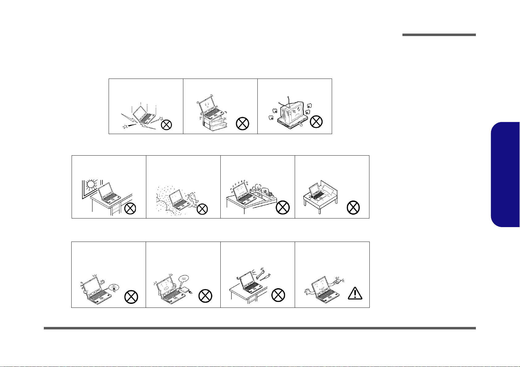
The notebook computer is quite rugged, but it can be damaged. To prevent this, follow these suggestions:
1. Don’t drop it, or expose it to shock. If the computer falls, the case and the components could be damaged.
Preface
Do not expose the computer
to any shock or vibration.
Do not place it on an unstable
surface.
Do not place anything heavy
on the computer.
2. Keep it dry, and don’t overheat it. Keep the computer and power supply away from any kind of heating element. This
is an electrical appliance. If water or any other liquid gets into it, the co mputer could be badly damaged.
Do not expose it to excessive
heat or direct sunlight.
Do not leave it in a place
where foreign matter or moisture may affect the system.
Don’t use or store the computer in a humid environment.
Do not place the computer on
any surface which will block
the vents.
3. Follow the proper working procedures for the computer. Shut the computer down properly and don’t forget to save
your work. Remember to periodically save your data as data may be lost if the battery is depleted.
Do not turn off the power
until you properly shut down
all programs.
Do not turn off any peripheral
devices when the computer is
on.
Do not disassemble the computer by yourself.
Perform routine maintenance
on your computer.
Preface
V
Preface
Power Safety
Warning
Before you undertake
any upgrade procedures, make sure that
you have turned off the
power, and disconnected all peripherals
and cables (including
telephone lines and
power cord). It is advisable to also remove
your battery in order to
prevent accidentally
turning the machine
on.
4. Avoid interference. Keep the computer away from high capacity transformers, electric moto rs, and other strong mag-
netic fields. These can hinder proper performance and damage your data.
5. Take care when using peripheral devices.
Preface
VI
Use only approved brands of
peripherals.
Unplug the power cord befor e
attaching peripheral devices.
Power Safety
The computer has specific power requirements:
• Only use a power adapter approved for use with this computer.
• Your AC adapter may be designed for international travel but it still requ ires a steady, uninterrupted power supply. If you are
unsure of your local power specifications, consult your service representative or local power company.
• The power adapter may have either a 2-prong or a 3-prong grounded plug. The third prong is an important safety feature; do
not defeat its purpose. If you do not have access to a compatible outlet, have a qualified electrician install one.
• When you want to unplug the power cord, be sure to disconn ect it by the plug head, not by its wire.
• Make sure the socket and any extension cord(s) you use can support the total current load of all the connected devices.
• Before cleaning the computer, make sure it is disconnected from any external power supplies.
Do not plug in the power
cord if you are wet.
Do not use the power cord if
it is broken.
Do not place heavy objects
on the power cord.

Battery Precautions
Battery Disposal
The product that you have purchased contains a rechargeable battery. The battery is recyclable. At the end of its useful life, under various state and local laws, it may be illegal to dispose of this battery into the municipal waste stream. Check with your local solid waste
officials for details in your area for recycling options or proper disposal.
Caution
Danger of explosion if battery is incorrectly replaced. Replace only with the same or equivalent type recommended by the manufacturer.
Discard used battery according to the manufacturer’s instructions.
Battery Level
Click the battery icon in the taskbar to see the current battery level and charge status. A battery that drops below a level of 10%
will not allow the computer to boot up. Make sure that any battery that drops below 10% is recharged within one week.
• Only use batteries designed for this computer. The wrong battery type may explode, leak or damage the computer.
• Do not continue to use a battery that has been dropped, or that appears damaged (e.g. bent or twisted) in any way. Even if the
computer continues to work with a damaged battery in place, it may cause circuit damage, which may possibly result in fire.
• Recharge the batteries using the notebook’s system. Incorrect recharging may make the battery explode.
• Do not try to repair a battery pack. Refer any battery pack repair or replacement to your service representative or qualified service
personnel.
• Keep children away from, and promptly dispose o f a damaged battery. Always dispose of batteries carefully. Batteries may explode
or leak if exposed to fire, or improperly handled or discarded.
• Keep the battery away from metal appliances.
• Affix tape to the battery contacts before disposing of the battery.
• Do not touch the battery contacts with your hands or metal objects.
Battery Guidelines
The following can also apply to any backup batteries you may have.
• If you do not use the battery for an extended period, then remove the battery from the computer for storage.
• Before removing the battery for storage charge it to 60% - 70%.
• Check stored batteries at least every 3 months and charge them to 60% - 70%.
Preface
Preface
VII
Preface
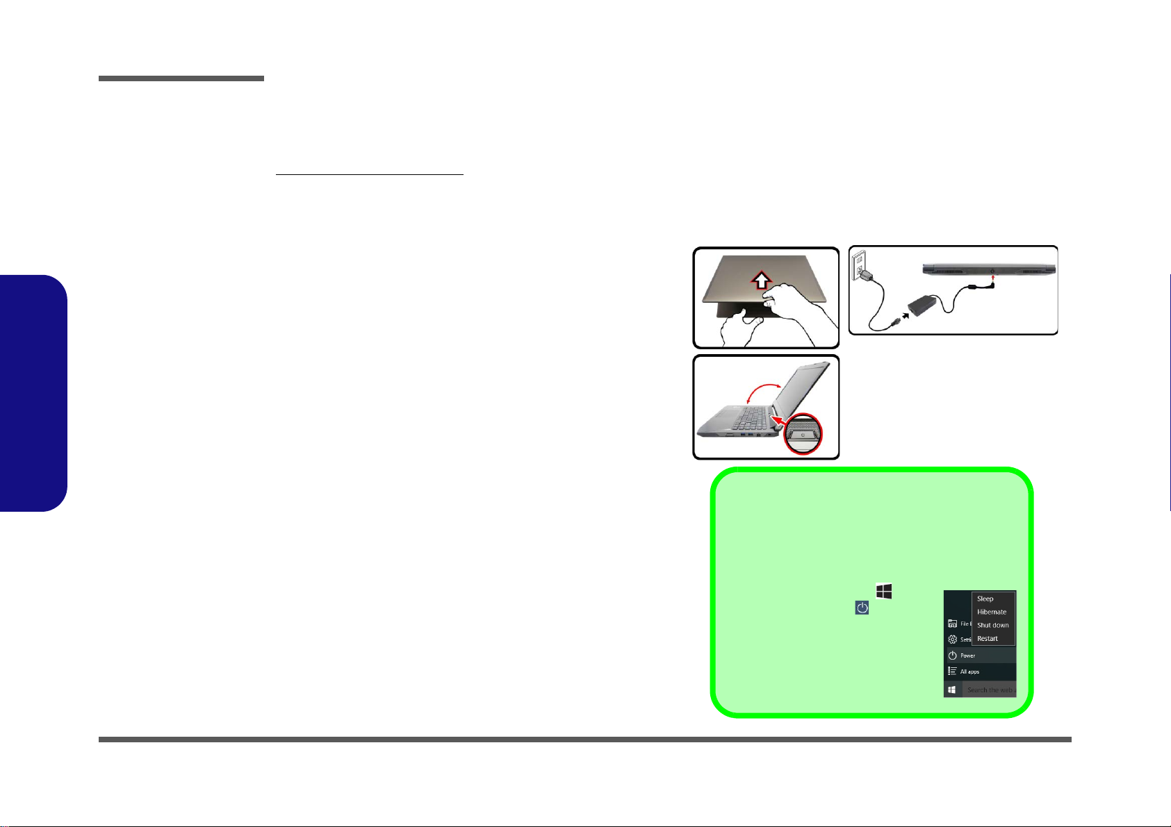
Figure 1
Opening the Lid/LCD/
Computer with AC/DC
Adapter Plugged-In
135°
Shut Down
Note that you should always shut your computer down by
choosing the Shut down command in Windows (see be-
low). This will help prevent hard disk or system problems.
1. Click the Start Menu icon .
2. Click the Power item .
3. Choose Shut Down from the menu.
Preface
Related Documents
You may also need to consult the following manual for additional information:
User’s Manual on CD/DVD
This describes the notebook PC’s features and the procedures for operating the computer and its ROM-based setup program. It also describes the installation and operation of the utility programs provided with the notebook PC.
System Startup
1. Remove all packing materials.
2. Place the computer on a stable surface.
3. Insert the battery and make sure it is locked in position.
4. Securely attach any peripherals you want to use with
the computer (e.g. keyboard and mouse) to their ports.
5. Attach the AC/DC adapter to the DC-In jack at the rear
of the computer, then plug the AC power cord into an
outlet, and connect the AC power cord to the AC/DC
adapter.
6. Use one hand to raise the
viewing angle
other hand (as illustrated in Figure 1) to support the
base of the computer (Note: Never lift the computer by
the lid/LCD).
7. Press the power button to turn the comp ut er “on ”.
lid/LCD to a comfortable
(do not exceed 135 degrees); use the
VIII

Contents
Preface
Introduction ..............................................1-1
Overview ......................................................................................... 1-1
Specifications ..................................................................................1-2
External Locator - Top View with LCD Panel Open ......................1-4
External Locator - Front & Right Side Views .................................1-5
External Locator - Left Side & Rear View .....................................1-6
External Locator - Bottom View .....................................................1-7
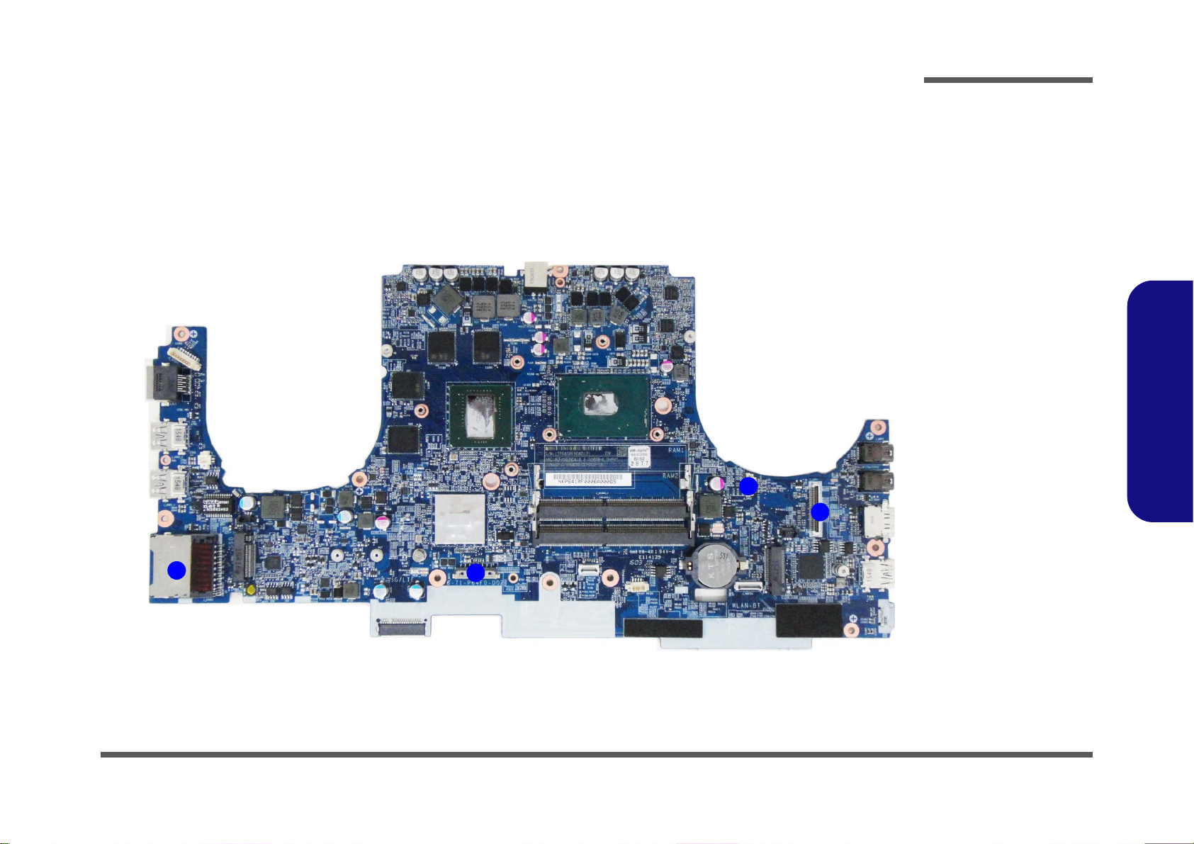
Mainboard Overview - Top (Key Parts) .........................................1-8
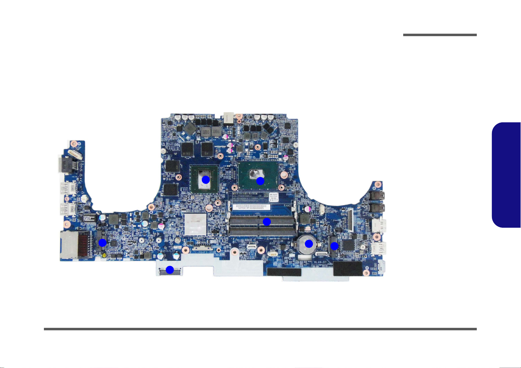
Mainboard Overview - Bottom (Key Parts) ....................................1-9
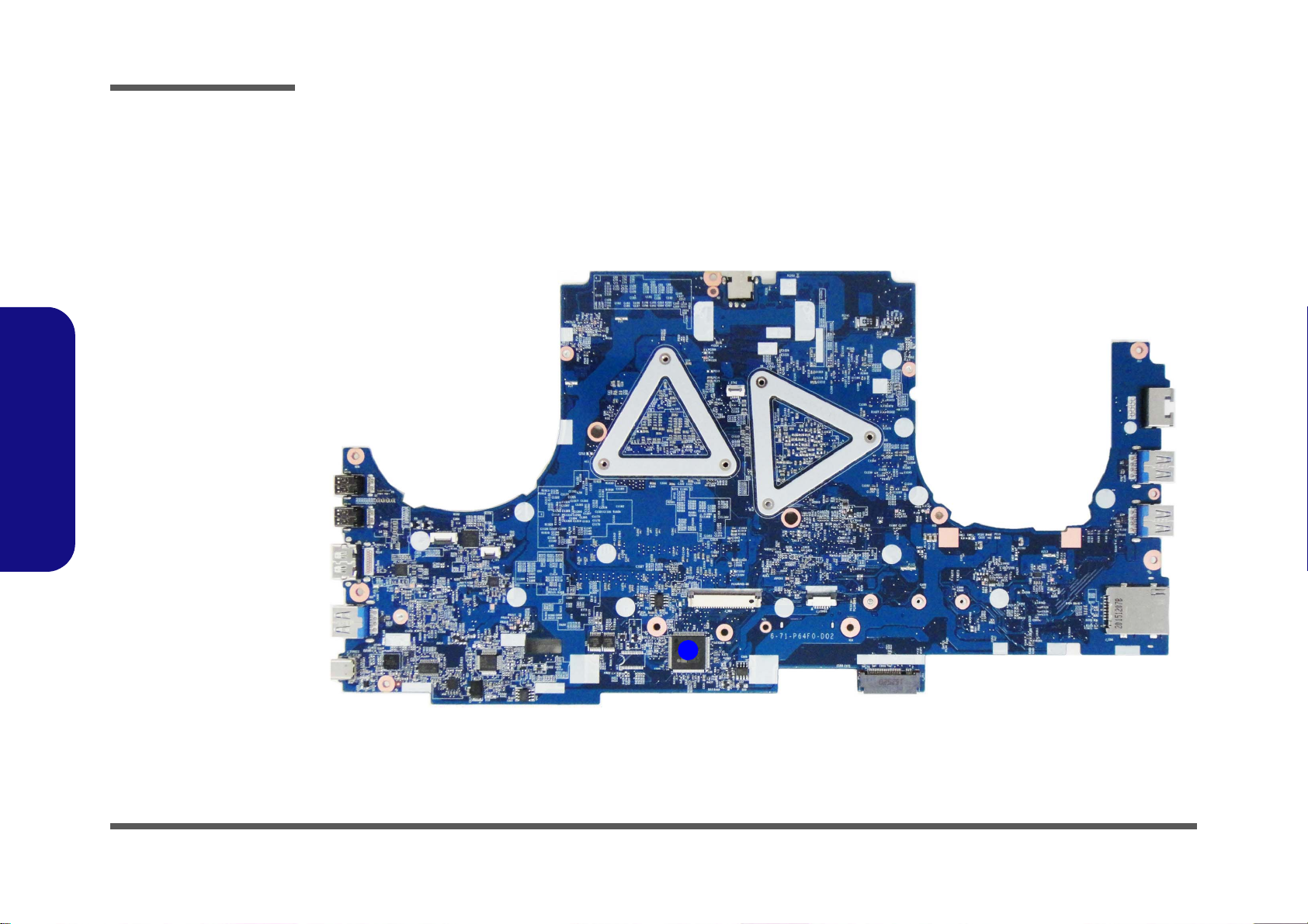
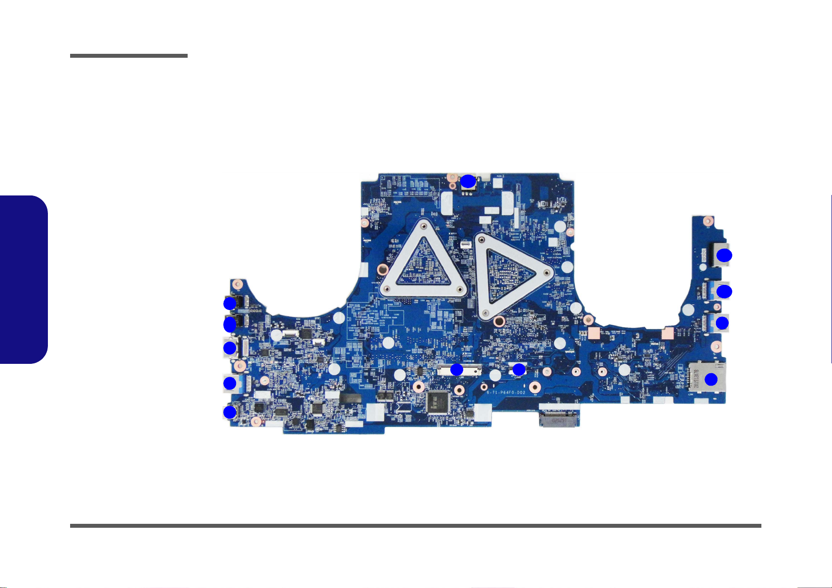
Mainboard Overview - Top (Connectors) .....................................1-10
Mainboard Overview - Bottom (Connectors) ...............................1-11
Disassembly ...............................................2-1
Overview ......................................................................................... 2-1
Maintenance Tools ..........................................................................2-2
Connections .....................................................................................2-2
Maintenance Precautions .................................................................2-3
Disassembly Steps ...........................................................................2-4
Removing the Keyboard ..................................................................2-5
Removing the Battery ......................................................................2-6
Removing the Hard Disk Drive .......................................................2-8
Removing the System Memory (RAM) ........................................2-10
Removing the M.2 SSD Module ...................................................2-11
Removing the Wireless LAN Module ...........................................2-12
Wireless LAN, Combo, 3G & LTE Module Cables .....................2-13
Removing the 3G Module .............................................................2-14
Part Lists ..................................................A-1
Part List Illustration Location ........................................................A-2
Top .................................................................................................A-3
Bottom ............................................................................................ A-4
Main Board ................................................................................... A-5
HDD .............................................................................................. A-6
LCD ............................................................................................... A-7
Schematic Diagrams.................................B-1
System Block Diagram ...................................................................B-2
Processor 1/7 ...................................................................................B-3
Processor 2/7 ...................................................................................B-4
Processor 3/7 - DDR4 .....................................................................B-5
Processor 4/7 ...................................................................................B-6
Processor 5/7- Power 1 ...................................................................B-7
Processor 6/7- Power 2 ...................................................................B-8
Processor 7/7 ...................................................................................B-9
DDR4 CHA SO-DIMM_0 ............................................................B-10
DDR4 CHB SO-DIMM_0 ............................................................B-11
Panel, Inverter, CRT .....................................................................B-12
Redriver ........................................................................................B-13
Mini DP Port E .............................................................................B-14
Mini DP Port F ..............................................................................B-15
HDMI Connector ..........................................................................B-16
VGA PCI Express .........................................................................B-17
VGA Frame Buffer Partition ........................................................B-18
Frame Buffer Partition A ..............................................................B-19
Frame Buffer Partition B ..............................................................B-20
Frame Buffer Partition A_B .........................................................B-21
GPU Frame Buffer Partition .........................................................B-22
Frame Buffer Partition C ..............................................................B-23
Frame Buffer Partition C ..............................................................B-24
GPU Decoupling ...........................................................................B-25
PCH 1/9 ........................................................................................B-26
PCH 2/9 ........................................................................................B-27
Preface
IX

Preface
PCH 3/9 ........................................................................................ B-28
PCH 4/9 ........................................................................................ B-29
PCH 5/9 ........................................................................................ B-30
PCH 6/9 ........................................................................................ B-31
PCH 7/9 ........................................................................................ B-32
PCH 8/9 ........................................................................................ B-33
PCH 9/9 ........................................................................................ B-34
DACA Interface and XTAL ......................................................... B-35
Power ............................................................................................B-36
TPS65982 ..................................................................................... B-37
USB Charger ...............................................................................B-38
USB 3.0 ........................................................................................B-39
LAN RTL8411B ..........................................................................B-40
M.2 3G .........................................................................................B-41
M.2 WLAN+BT, PCIE4X SSD ...................................................B-42
Realtek ALC892 ........................................................................... B-43
Preface
TPA2008D2 .................................................................................B-44
KBC-ITE IT8587 ......................................................................... B-45
TPM, CCD, TP .............................................................................B-46
Fan, LID, KB LED ....................................................................... B-47
DDR 1.35V / 0.75VS ................................................................... B-48
VDD3, VDD5 ...............................................................................B-49
5V, 5VS, 3.3V, 3.3VS, 3.3VA .....................................................B-50
Power 1.0V, VCCIO .................................................................... B-51
AC_In, Charger ............................................................................B-52
1.0DX_VCCSTG/VCCSFR_OC ................................................. B-53
PEX_VDD, 3V3_AON, 3V3_RUN .............................................B-54
NVVDD Phase 1 & 2 ...................................................................B-55
FBVDDQ .....................................................................................B-56
VCC_Core & VCCSA .................................................................B-57
VCore Output Stage .....................................................................B-58
VCCGT ........................................................................................ B-59
VCCGT Output Stage ...................................................................B-60
Power Board .................................................................................B-61
LED Board ....................................................................................B-62
Click Board ...................................................................................B-63
Audio Board ..................................................................................B-64
Updating the FLASH ROM BIOS......... C-1
Download the BIOS ........................................................................C-1
Unzip the downloaded files to a bootable CD/DVD or
USB Flash drive ..............................................................................C-1
Set the computer to boot from the external drive ...........................C-1
Use the flash tools to update the BIOS ...........................................C-2
Restart the computer (booting from the HDD) ...............................C-2
X

Chapter 1: Introduction
Overview
This manual covers the information you need to service or upgrade the P640RF / P641RF series notebook computer.
Information about operating the computer (e.g. getting started, and the Setup utility) is in the User’s Manual. Information
about dri-vers (e.g. VGA & audio) is also found in the User’s Manual. The manual is shipped with the computer.
Operating systems (e.g. Windows 8.1, etc.) have their own manuals as do application softwares (e.g. word processing and
database programs). If you have questions about those programs, you should consult those manuals.
Introduction
The P640RF / P641RF series notebook is designed to be upgradeable. See Disassembly on page 2 - 1 for a detailed description of the upgrade procedures for each specific component. Please take note of the warning and safety information
indicated by the “” symbol.
The balance of this chapter reviews the computer’s technical specifications and features.
1.Introduction
Overview 1 - 1

Introduction
Latest Specification Information
The specifications listed here are correct at the
time of sending them to the press. Certain items
(particularly processor types/speeds) may be
changed, delayed or updated due to the manufacturer's release schedule. Check with your
service center for more details.
CPU
The CPU is not a user serviceable part. Accessing the CPU in any way may violate your
warranty.
CPU Speed & Computer in DC
Mode
Note that when the computer is in
DC mode (powered by the battery
only) the CPU may not run at full
speed. This is a design feature implemented in order to protect the
battery.
SO-DIMM Memory Types
All SO-DIMM memory modules installed in the system should be identical (the same size and brand) in
order to prevent unexpected system
behavior.
Do not mix SO-DIMM memory module sizes and brands otherwise unexpected system problems may
occur
.
Specifications
1.Introduction
1 - 2 Specifications
Processor Options
i7-6820HK (2.70GHz)
8MB Smart Cache, 14nm, DDR4-2133MHz, TDP 45W
i7-6700HQ (2.60GHz)
8MB Smart Cache, 14nm, DDR4-2133MHz,
TDP 45W
Support Intel® XTU over-clocking technology on i7-6820HK
Core Logic
Intel® HM170 Express Chipset
BIOS
AMI BIOS (64Mb SPI Flash-ROM)
LCD Options
14.0" (35.56cm), 16:9, FHD (1920x1080)
Storage
One changeable 2.5" (6cm) 7.0mm (h) SATA (Serial) Hard
Disk Drive/Solid State Drive (SSD)
(Factory Option) One M.2 SATA/PCIe Gen3 x4 Solid State
Drive (SSD)
Memory
Two 260 Pin SO-DIMM Sockets Supporting DDR4 2 133MHz
Memory
Memory Expandable from 4GB (minimum) up to 32GB
(maximum)
Video Adapter
Intel® Integrated GPU and NVIDIA® Discrete GPU
Supports Microsoft Hybrid Graphics
Supports up to 4 Active Displays
Intel Integrated GPU
Intel® HD Graphics 530
Dynamic Frequency
Intel Dynamic Video Memory Technology
Microsoft DirectX®12 Compatible
NVIDIA® Discrete GPU
NVIDIA® GeForce GTX 965M
2GB GDDR5 Video RAM on board
Microsoft DirectX® 12 Compatible

Introduction
Audio
High Definition Audio Compliant Interface
S/PDIF Digital Output
Two Speakers
Sound Blaster Audio
ANSP™ 3D sound technology on headphone output
Built-In Array Microphone
Note: External 5.1CH Audio Output Supported by Headphone,
Microphone and S/PDIF Out Jacks
Security
Security (Kensington® Type) Lock Slot
BIOS Password
(Factory Option) TPM 2.0
Intel PTT for Systems Without TPM Hardware
Keyboard
Illuminated White-LED “WinKey” Keyboard (with embed-
ded numeric keypad)
Pointing Device
Built-in Touchpad
Card Reader
Embedded Multi-In-1 Push-Push Card Reader
MMC (MultiMedia Card) / RS MMC
SD (Secure Digital) / Mini SD / SDHC/ SDXC
M.2 Slots
Slot 1 for Combo WLAN and Bluetooth Module
Slot 2 for SATA or PCIe Gen3 x4 SSD
(Factory Option) Slot 3 for 3G/4G Module
Interface
One HDMI-Out Port
Two Mini DisplayPorts 1.2*
One S/PDIF Out Jack
One Headphone/Speaker-Out Jack
One Microphone-In Jack
One RJ-45 LAN Jack
One DC-In Jack
Virtual Reality ready (via Mini DisplayPort 1 )
Three USB 3.0
Powered USB port)
One USB 3.1
(USB 3.1 Gen 1) Ports (Including one AC/DC
(Gen 2 - Type C) Port
Communication
Built-In Gigabit Ethernet LAN
2.0M FHD PC Camera Module
(Factory Option) M.2 3G/4G Module
WLAN/ Bluetooth M.2 Modules:
(Factory Option) Intel® Wireless-AC 8260 Wireless LAN
(802.11ac) + Bluetooth 4.1
(Factory Option) Intel® Wireless-N 7265 Wireless LAN
(802.11b/g/n) + Bluetooth 4.0
(Factory Option) Intel® Wireless-AC 3165 Wireless LAN
(802.11ac) + Bluetooth 4.0
(Factory Option) Qualcomm® Atheros Killer™ Wireless-AC
1535 Wireless LAN (802.11ac) + Bluetooth 4.1
(Factory Option) Third-Party Wireless LAN 802.11b/g/n +
Bluetooth 4.0
Environmental Spec
Temperature
Operating: 5°C - 35°C
Non-Operating: -20°C - 60°C
Relative Humidity
Operating: 20% - 80%
Non-Operating: 10% - 90%
Power
Embedded 3-Cell Polymer Battery Pack, 45WH
Full Range AC/DC Adapter
AC Input: 100 - 240V, 50 - 60Hz
DC Output: 19.5V, 7.7A (150W)
Dimensions & Weight
349mm (w) * 247mm (d) * 25.4mm (h)
2.0kg (Barebone with 45WH Battery)
1.Introduction
Specifications 1 - 3
Introduction
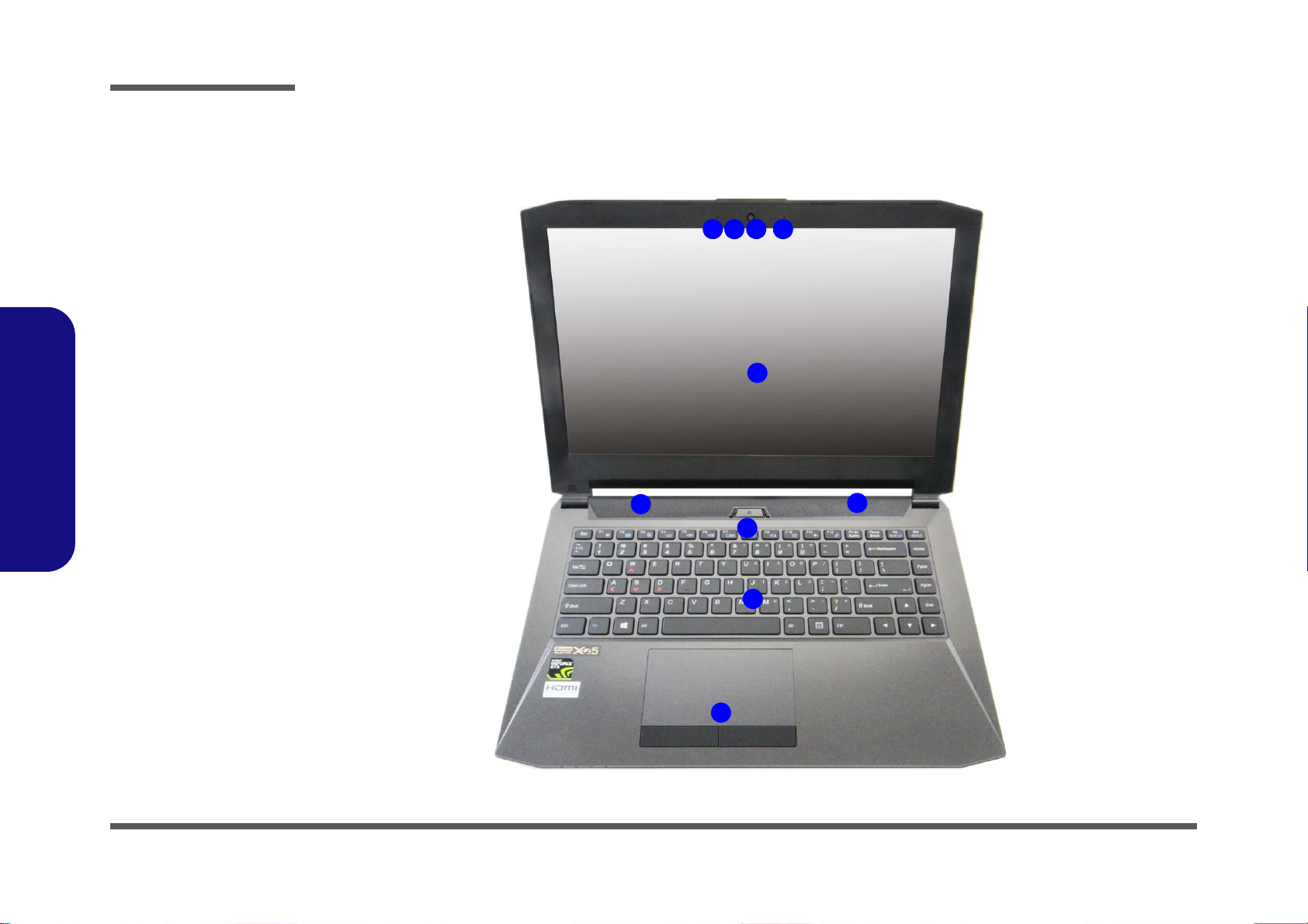
Figure 1
Top View
1. PC Camera
2. *PC Camera LED
*When the PC
camera is in use,
the LED will be
illuminated.
3. Built-In Array
Microphone
4. LCD
5. Speakers
6. Power Button
7. Keyboard
8. To uchpad &
Buttons
2 1
8
7
6
5
4
5
33
1.Introduction
External Locator - Top View with LCD Panel Open
1 - 4 External Locator - Top View with LCD Panel Open
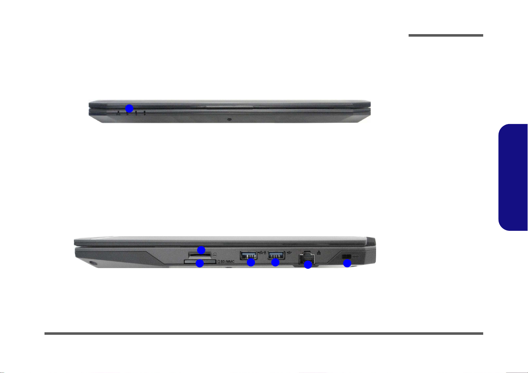
External Locator - Front & Right Side Views
Figure 2
Front View
1. LED Indicator
Figure 3
Right Side View
1. USIM Card
Reader (for 3G/
4G USIM Cards)
2. Multi-in-1 Card
Reader
3. USB 3.0 (USB
3.1 Gen 1) Port
4. Powered USB
3.0 (USB 3.1
Gen 1) Port
5. RJ-45 LAN Jack
6. Security Lock
Slot
FRONT VIEW
1
RIGHT SIDE VIEW
1
2
3
5
6
4
Introduction
1.Introduction
External Locator - Front & Right Side Views 1 - 5
1.Introduction
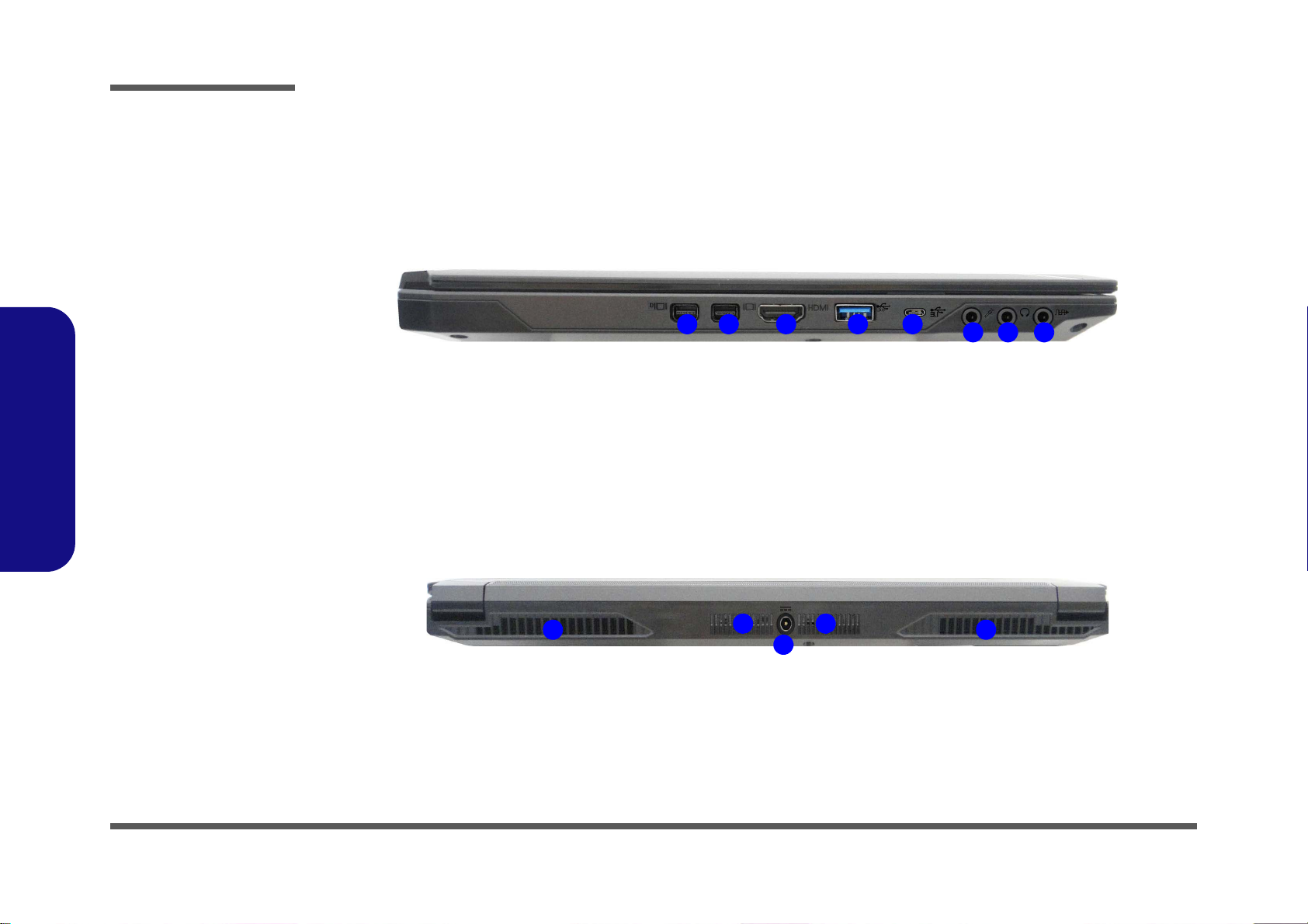
Figure 4
Left Side View
1. Mini Display Port 1
2. Mini Display Port 2
3. HDMI-Out Port
4. USB 3.0 (USB 3.1
Gen 1) Port
5. USB 3.1 (Gen 2 Type C) Port
6. Microphone-In
Jack
7. Headphone-Out
Jack
8. S/PDIF-Out Jack
LEFT SIDE VIEW
1 2 3 4
657 8
Figure 5
Rear View
1. Vent
2. DC-In Jack
REAR VIEW
1
2
1
1
1
Introduction
External Locator - Left Side & Rear View
/
1 - 6 External Locator - Left Side & Rear View
External Locator - Bottom View
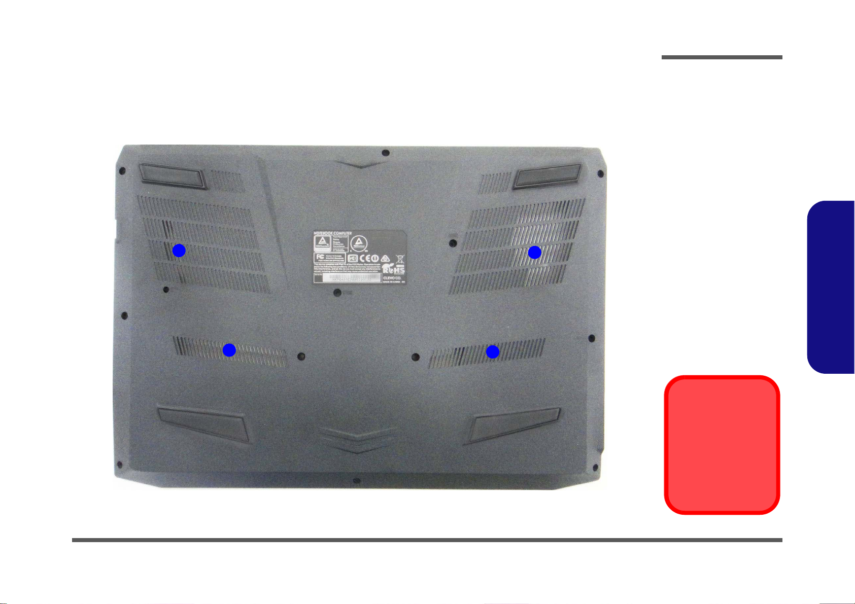
Figure 6
Bottom View
1. Vent
Overheating
To prevent your computer from overheating, make sure nothing blocks any vent
while the computer is
in use.
1
1
1
1
Introduction
1.Introduction
External Locator - Bottom View 1 - 7
Introduction
Figure 7
Mainboard Top
Key Parts
1. KBC-ITE IT8587
1
1.Introduction
Mainboard Overview - Top (Key Parts)
1 - 8 Mainboard Overview - Top (Key Parts)
1
2
3
7
4
5
6
Figure 8
Mainboard Bottom
Key Parts
1. Mini-Card
Connector (M.2
SSD Module)
2. Mini-Card
Connector (M.2
3G/4G Module)
3. CPU
4. GPU-GTX965M
5. Memory Slots
DDR3 SO-DIMM
6. CMOS Battery
7. Mini-Card
Connector (WLAN
Module)
Mainboard Overview - Bottom (Key Parts)
Introduction
1.Introduction
Mainboard Overview - Bottom (Key Parts) 1 - 9
Introduction
Figure 9
Mainboard Top
Connectors
1. Mini Display Port 1
2. Mini Display Port 2
3. HDMI-Out Port
4. USB Port 3.0
(USB 3.1 Gen 1)
Connector
5. USB Port 3.1 (Gen
2 -Type C)
Connector
6. Keyboard Cable
Connector
7. TP Connector
8. USIM Card
Reader
9. Powered USB
Port 3.0 (USB 3.1
Gen 1) Connector
10.RJ-45 LAN Jack
11. DC-In Jack
10
8
7
4
6
5
1
2
3
4
11
9
1.Introduction
Mainboard Overview - Top (Connectors)
1 - 10 Mainboard Overview - Top (Connectors)
Mainboard Overview - Bottom (Connectors)
Figure 10
Mainboard Bottom
Connectors
1. M u lti-in-1 Card
Reader
2. Battery Connector
3. Fan Connector
4. LCD Cable
Connector
11
5
4
3
1
2
Introduction
1.Introduction
Mainboard Overview - Bottom (Connectors) 1 - 11

1.Introduction
Introduction
1 - 12
Chapter 2: Disassembly
Information
Warning
Overview
This chapter provides step-by-step instructions for disassembling the P640RF / P641RF series notebook’s parts and subsystems. When it comes to reassembly, reverse the procedures (unless otherwise indicated).
We suggest you completely review any procedure before you take the computer apart.
Disassembly
Procedures such as upgrading/replacing the RAM, optical device and hard disk are included in the User’s Manual but are
repeated here for your convenience.
To make the disassembly process easier each section may have a box in the page margin. Information contained under
the figure # will give a synopsis of the sequence of procedures involved in the disassembly procedure. A box with a
lists the relevant parts you will have after the disassembly process is complete. Note: The parts listed will be for the disassembly procedure listed ONLY, and not any previous disassembly step(s) required. Refer to the part list for the previous disassembly procedure. The amount of screws you should be left with will be listed here also.
A box with a will also provide any possible helpful information. A box with a contains warnings.
An example of these types of boxes are shown in the sidebar.
2.Disassembly
Overview 2 - 1

Disassembly
2.Disassembly
NOTE: All disassembly procedures assume that the system is turned OFF, and disconnected from any power supply (the
battery is removed too).
Maintenance Tools
The following tools are recommended when working on the notebook PC:
• M3 Philips-head screwdriver
• M2.5 Philips-head screwdriver (magnetized)
• M2 Philips-head screwdriver
• Small flat-head screwdriver
• Pair of needle-nose pliers
• Anti-static wrist-strap
Connections
Connections within the computer are one of four types:
Locking collar sockets for ribbon connectors To release these connectors, use a small flat-head screwdriver to
gently pry the locking collar away from its base. When replacing the connection, make sure the connector is oriented in the
same way. The pin1 side is usually not indicated.
2 - 2 Overview
Pressure sockets for multi-wire connectors To release this connector type, grasp it at its head and gently
rock it from side to side as you pull it out. Do not pull on the
wires themselves. When replacing the connection, do not try to
force it. The socket only fits one way.
Pressure sockets for ribbon connectors To release these connectors, use a small pair of needle-nose pli-
ers to gently lift the connector away from its socket. When replacing the connection, make sure the connector is oriented in
the same way. The pin1 side is usually not indicated.
Board-to-board or multi-pin sockets To separate the boards, gently rock them from side to side as
you pull them apart. If the connection is very tight, use a small
flat-head screwdriver - use just enough force to start.

Maintenance Precautions
Power Safety
Warning
Before you undertake
any upgrade procedures, make sure that
you have turned off the
power, and disconnected all peripherals
and cables (including
telephone lines and
power cord). It is advisable to also remove
your battery in order to
prevent accidentally
turning the machine
on.
The following precautions are a reminder. To avoid personal injury or damage to the computer while performing a removal and/or replacement job, take the following precautions:
1. Don't drop it. Perform your repairs and/or upgrades on a stable surface. If the computer falls, the case and other
2. Don't overheat it. Note the proximity of any heating elements. Keep the computer out of direct sunlight.
3. Avoid interference. Note the proximity of any high capacity transformers, electric motors, and other strong mag-
4. Keep it dry. This is an electrical appliance. If water or any other liquid gets into it, the computer could be badly
5. Be careful with power. Avoid accidental shocks, discharges or explosions.
6. Peripherals – Turn off and detach any peripherals.
7. Beware of static discharge. ICs, such as the CPU and main support chips, are vulnerable to static electricity.
8. Beware of corrosion. As you perform your job, avoid touching any connector leads. Even the cleanest hands pro-
9. Keep your work environment clean. Tobacco smoke, dust or other air-born particulate matter is often attracted
10. Keep track of the components. When removing or replacing any p art, be careful not to leave small p arts, such as
Disassembly
components could be damaged.
netic fields. These can hinder proper performance and damage component s and/or data. You should also monitor
the position of magnetized tools (i.e. screwdrivers).
damaged.
2.Disassembly
•Before removing or servicing any part from the computer, turn the computer off and detach any power supplies.
•When you want to unplug the power cord or any cable/wire, be sure to disconnect it by the plug head. Do not pull on the wire.
Before handling any part in the computer, discharge any static electricity inside the computer. When handling a
printed circuit board, do not use gloves or other materials which allow static electricity buildup. We suggest that
you use an anti-static wrist strap instead.
duce oils which can attract corrosive elements.
to charged surfaces, reducing performance.
screws, loose inside the computer.
Cleaning
Do not apply cleaner directly to the computer, use a soft clean cloth.
Do not use volatile (petroleum distillates) or abrasive cleaners on any part of the computer.
Overview 2 - 3

Disassembly
Disassembly Steps
The following table lists the disassembly steps, and on which page to find the related information. PLEASE PERFORM
THE DISASSEMBLY STEPS IN THE ORDER INDICATED.
To remove the Keyboard:
1. Remove the keyboard page 2 - 5
To remove the Battery:
1. Remove the battery page 2 - 6
To remove the HDD:
1. Remove the battery page 2 - 6
2. Remove the HDD page 2 - 8
To remove the System Memory:
1. Remove the battery page 2 - 6
2. Remove the system memory page 2 - 10
2.Disassembly
2 - 4 Disassembly Steps
To remove the M.2 SSD:
1. Remove the battery page 2 - 6
2. Remove the SSD page 2 - 11
To remove the Wireless LAN Module:
1. Remove the battery page 2 - 6
2. Remove the WLAN page 2 - 12
To remove and install the 3G Module:
1. Remove the battery page 2 - 6
2. Remove the 3G page 2 - 14
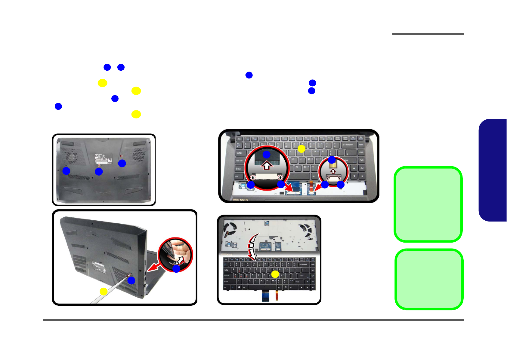
Removing the Keyboard
123456778
6
a.
b.
1
2
c.
6
7
7
8
6
3
4
8
5
838
4. Eject Stick
6. Keyboard
•2 Screws
Figure 1
Keyboard Removal
a. Remove the screws from
the bottom of the computer and then eject the
keyboard using a special
eject stick to push the
keyboard out while releasing the keyboard as
shown.
b. Lift the keyboard up and
disconnect the keyboard
ribbon cable from the
locking collar socket.
c. Remove the keyboard.
Re-inserting the Key-
board
When re-inserting the
keyboard firstly , align the
keyboard tabs at the bottom of the keyboard with
the slots in the case.
1. Turn off the computer, turn it over.
2. Remove screws
3. Open it up with the LCD on a flat surface before pressing at point
cial eject stick to do this) while releasing the keyboard in the direction of the arrow
4. Carefully lift the keyboard
board ribbon cable from the locking collar socket by using a flat-head screwdriver to pry the locking collar pins
away from the base (Figure 1b).
5. Carefully lift the keyboard off the computer (Figure 1c).
Disassembly
- from the bottom of the computer.
to release the keyboard module (use the spe-
as shown (Figure 1a).
up, being careful not to bend the keyboard ribbon cable . Disconnect the key-
2.Disassembly
Removing the Keyboard 2 - 5
Disassembly
612
1314151617
Figure 2
Battery Removal
a. Remove the SD cover
and screws.
b. Remove the bottom case.
c. Locate the battery.
2
a.
b.
1
3
4
5
14
13
17
6
7
15
8
9
11
12
10
c.
14
16
1. SD Card Cover
14.Bottom Case
•12 Screws
Removing the Battery
1. Turn the computer off, and turn it over.
2. Remove the SD card cover and screws - (Figure 2a).
3. Carefully lift the bottom case
4. The battery will be visible at point on the computer (Figure 2c
up in the direction of the arrow at points & and remove it (Figure 2b).
).
2.Disassembly
2 - 6 Removing the Battery

1819222324
Figure 3
Battery Removal
(cont’d.)
d. Disconnect the cable and
remove the screws.
e. Lift the battery off the
computer.
f. Reinsert the bottom case
and tighten the screws.
d.
e.
23
22
18
24
19
f.
2021
23. Battery
•4 Screws
5. Carefully disconnect the cable , then remove screws - (Figure 3b).
6. Lift the battery off the computer (Figure 3e
7. Reinsert the bottom case starting from point
).
as shown (Figure 3f) to avoid damaging the jack(s). Tighten the
screws to secure the bottom case in place.
Disassembly
2.Disassembly
Removing the Battery 2 - 7

Disassembly
Figure 4
HDD Assembly
Removal
a. Locate the HDD.
b. Remove the screw.
•1 Screw
1
2
1
a.
2
b.
HDD System Warning
New HDD’s are blank. Before you
begin make sure:
You have backed up any data you
want to keep from your old HDD.
You have all the CD-ROMs and
FDDs required to install your operating system and programs.
If you have access to the internet,
download the latest application and
hardware driver updates for the operating system you plan to install.
Copy these to a removable medium.
Removing the Hard Disk Drive
The hard disk drive can be taken out to accommodate other 2.5" serial (SATA) hard disk drives with a height of 9.5mm
or 7mm (h). Follow your operating system’s installation instructions, and install all necessary drivers and utilities (as
outlined in Chapter 4 of the User’s Manual) when setting up a new hard disk.
2.Disassembly
Hard Disk Disassembly Process
1. Turn off the computer, and remove the battery (page 2 - 6).
2. The HDD will be visible at point on the mainboard (Figure 4a
3. Remove screw
from the HDD assembly (Figure 4b).
).
2 - 8 Removing the Hard Disk Drive

4. Slightly lift and disconnect the hard disk and connector in the direction of arrow (Figure 5c).
3
45678
9
10
c.
7
5
6
e.
d.
8
10
3
4
9
5. HDD Assembly
9. HDD Bracket
10.HDD
•2 Screws
Figure 5
HDD Assembly
Removal (cont’d.)
c. Slightly lift and pull the
HDD in the direction of
the arrow.
d. Lift the HDD assembly
out of the bay.
e. Remove the screws and
bracket from the HDD.
5. Lift the hard disk assembly out of the bay (Figure 5d).
6. Remove screws - and bracket from the hard disk (Figure 5e).
7. Reverse the process to install a new hard disk (do not forget to replace the screws).
Disassembly
2.Disassembly
Removing the Hard Disk Drive 2 - 9

Disassembly
123
4
b.
c.
3
3
2
2
1
a.
4
4. RAM Module
Figure 6
RAM Module
Removal
a. The RAM modules
will be visible at point
on the main-
board.
b. Pull the release lat-
ches.
c. Remove the module.
Contact Warning
Be careful not to touch
the metal pins on the
module’s connecting
edge. Even the cleanest hands have oils
which can attract particles, and degrade the
module’s performance.
1
2.Disassembly
Removing the System Memory (RAM)
The computer has two memory sockets for 204 pin Small Outline Dual In-line Memory Modules (SO-DIMM) supporting
DDR4 Up to 2133 MHz. The main memory can be expanded up to 32GB. The total memory size is automatically detected by the POST routine once you turn on your computer.
Memory Upgrade Process
1. Turn off the computer, turn it over, remove the battery (page 2 - 6).
2. The RAM-2 modules will be visible at point
3. Gently pull the two release latches ( & ) on the sides of the memory socket in the direction indicated by the
arrows (Figure 6b).
The RAM module will pop-up (Figure 6c), and you can then remove it.
4. Pull the latches to release the second module if necessary.
5. Insert a new module holding it at about a 30° angle and fit the connectors firmly into the memory slot.
6. The module will only fit one way as defined by its pin alignment. Make sure the module is seated as far into the slot
as it will go. DO NOT FORCE IT; it should fit without much pressure.
7. Press the module in and down towards the mainboard until the slot levers click into place to secure the module.
8. Replace the bottom cover and the screws
9. Restart the computer to allow the BIOS to register the new memory configuration as it starts up.
on the mainboard (Figure 6a).
(see page 2 - 6).
2 - 10 Removing the System Memory (RAM)

Removing the M.2 SSD Module
1
2
3
b.
c.
a.
2
3
1
3
Hexagonal Screwdriver
Use a flat head or hexagonal socket screwdriver to tighten
the screw underneath the module respectively.
3.M2 SSD Module
•1 Screw
Figure 7
M.2 SSD Module
Removal
a. Locate the M.2 SSD.
b. Remove the screw.
c. The M.2 SSD module
will pop up.
1. Turn off the computer, turn it over, remove the battery (page 2 - 6).
2. The M.2 SSD module will be visible at point on the mainboard (Figure 7a).
3. Remove the screw
4. The M.2 SSD module (Figure 7c) will pop-up, and you can remove it from the computer.
(Figure 7b)
Disassembly
2.Disassembly
Removing the M.2 SSD Module 2 - 11

Disassembly
123
4
5
b.
c.
a.
2
3
5
1
5
4
5.Wireless LAN Module
•1 Screw
Figure 8
Wireless LAN
Module Removal
a. Locate the WLAN.
b. Disconnect the cables
and remove the screw.
c. The WLAN module will
pop up.
Note: Make sure you
reconnect the antenna
cable to the “1 + 2”
socket (Figure 8b).
Removing the Wireless LAN Module
1. Turn off the computer, turn it over, remove the battery (page 2 - 6).
2. The Wireless LAN module will be visible at point on the mainboard (Figure 8a).
3. Carefully disconnect the cables & , and then remove the screw
4. The Wireless LAN module (Figure 8c) will pop-up, and you can remove it from the computer.
(Figure 8b)
2.Disassembly
2 - 12 Removing the Wireless LAN Module

Wireless LAN, Combo, 3G & LTE Module Cables
Note that the cables for connecting to the antennae on WLAN, WLAN & Bluetooth Combo, 3G and LTE modules are
not labelled. The cables/covers (each cable will have either a black or transparent cable cover) are color coded for identification as outlined in the table below.
Disassembly
Module Type
WLAN/WLAN & Bluetooth
Combo
LTE Broadband
3G Broadband
Antenna
Type
WM 1 Black
WM 3 White
LTE 1 Black
LTE 2 Gray
3G 1 Black
3G 2 Gray
Cable Color
Cable Cover
Type
TransparentWM 2 Gray
Black
Black
Cable 1 is usually connected to antenna 1 (Main) on the module, and cable 2 to antenna 2 (Aux).
2.Disassembly
Wireless LAN, Combo, 3G & LTE Module Cables 2 - 13

Disassembly
Figure 9
3G Module Removal
a. Locate the module.
b. Disconnect the cables and
remove the screw.
c. The module will pop-up.
d. Lift the module up off the
socket.
1
234
3
5
a.
b.
1
2
5
c.
3
4
5
d.
5. 3G Module
•1 Screw
Removing the 3G Module
3G Module Removal Procedure
1. Turn off the computer, remove the battery (page 2 - 6).
2. Locate the module, it is visible at point
3. Carefully disconnect the cables & , and then remove the screw from the module
4. The module will pop-up
5. Lift the module up and off the computer
(Figure 9c).
(Figure 9a).
(Figure 9d).
(Figure 9b).
2.Disassembly
2 - 14 Removing the 3G Module

Appendix A:Part Lists
This appendix breaks down the P640RF / P641RF series notebook’s construction into a series of illustrations. The component part numbers are indicated in the tables opposite the drawings.
Note: This section indicates the manufacturer’s part numbers. Your organization may use a different system, so be sure
to cross-check any relevant documentation.
Note: Some assemblies may have parts in common (especially screws). However, the part lists DO NOT indicate the
total number of duplicated parts used.
Note: Be sure to check any update notices. The parts shown in these illustrations are appropriate for the system at the
time of publication. Over the product life, some parts may be improved or re-configured, resulting in new part numbers.
A.Part Lists
A - 1

Table A - 1
Part List Illustration
Location
Part List Illustration Location
The following table indicates where to find the appropriate part list illustration.
Part
Top
page A - 3
A.Part Lists
Bottom
Main Board
HDD
LCD
page A - 4
page A - 5
page A - 6
page A - 7
A - 2

Top
Figure A - 1
Top
A.Part Lists
Top A - 3

A.Part Lists
Figure A - 2
Bottom
Bottom
A - 4 Bottom

Main Board
Figure A - 3
Main Board
A.Part Lists
Main Board A - 5

A.Part Lists
Figure A - 4
HDD
HDD
A - 6 HDD

LCD
Figure A - 5
LCD
A.Part Lists
LCD A - 7

A.Part Lists
A - 8

Appendix B: Schematic Diagrams
Table B - 1
SCHEMATIC
DIAGRAMS
Version Note
The schematic diagrams in this chapter
are based upon version 6-7P-P64F5-001.
If your mainboard (or
other boards) are a later version, please
check with the Service
Center for updated diagrams (if required).
This appendix has circuit diagrams of the P640RF / P641RF notebook’s PCB’s. The following table indicates where to
find the appropriate schematic diagram.
System Block Diagram - Page B - 2 GPU Decoupling - Page B - 25 DDR 1.35V / 0.75VS - Page B - 48
Processor 1/7 - Page B - 3 PCH 1/9 - Page B - 26 VDD3, VDD5 - Page B - 49
Processor 2/7 - Page B - 4 PCH 2/9 - Page B - 27 5V, 5VS, 3.3V, 3.3VS, 3.3VA - Page B - 50
Processor 3/7 - DDR4 - Page B - 5 PCH 3/9 - Page B - 28 Power 1.0V, VCCIO - Page B - 51
Processor 4/7 - Page B - 6 PCH 4/9 - Page B - 29 AC_In, Charger - Page B - 52
Processor 5/7- Power 1 - Page B - 7 PCH 5/9 - Page B - 30 1.0DX_VCCSTG/VCCSFR_OC - Page B - 53
Processor 6/7- Power 2 - Page B - 8 PCH 6/9 - Page B - 31 PEX_VDD, 3V3_AON, 3V3_RUN - Page B - 54
Processor 7/7 - Page B - 9 PCH 7/9 - Page B - 32 NVVDD Phase 1 & 2 - Page B - 55
DDR4 CHA SO-DIMM_0 - Page B - 10 PCH 8/9 - Page B - 33 FBVDDQ - Page B - 56
DDR4 CHB SO-DIMM_0 - Page B - 11 PCH 9/9 - Page B - 34 VCC_Core & VCCSA - Page B - 57
Panel, Inverter, CRT - Page B - 12 DACA Interface and XTAL - Page B - 35 VCore Output Stage - Page B - 58
Redriver - Page B - 13 Power - Page B - 36 VCCGT - Page B - 59
Mini DP Port E - Page B - 14 TPS65982 - Page B - 37 VCCGT Output Stage - Page B - 60
Mini DP Port F - Page B - 15 USB Charger - Page B - 38 Power Board - Page B - 61
HDMI Connector - Page B - 16 USB 3.0 - Page B - 39 LED Board - Page B - 62
VGA PCI Express - Page B - 17 LAN RTL8411B - Page B - 40 Click Board - Page B - 63
VGA Frame Buffer Partition - Page B - 18 M.2 3G - Page B - 41 Audio Board - Page B - 64
Frame Buffer Partition A - Page B - 19 M.2 WLAN+BT, PCIE4X SSD - Page B - 42
Frame Buffer Partition B - Page B - 20 Realtek ALC892 - Page B - 43
Frame Buffer Partition A_B - Page B - 21 TPA2008D2 - Page B - 44
GPU Frame Buffer Partition - Page B - 22 KBC-ITE IT8587 - Page B - 45
Frame Buffer Partition C - Page B - 23 TPM, CCD, TP - Page B - 46
Frame Buffer Partition C - Page B - 24 Fan, LID, KB LED - Page B - 47
Schematic Diagrams
Diagram - Page Diagram - Page Diagram - Page
B.Schematic Diagrams
B - 1

Schematic Diagrams
Sheet 1 of 63
System Block
Diagram
5
5
4
4
3
3
2
2
1
1
D D
C C
B B
A A
P640RF Skylake System Block Diagram
SHEET 53
SHEET 37
USB3.0
PORT1
SHEET 49
TOUCH PAD
LPC
(USB2_1)
SMART
BATTERY
SHEET 52
Front R
HP
OUT
SHEET 43
<=7"
PCIE
23x23mm FCBGA
480 Mbps
24 MHz
SHEET 29
<8"
MIC
IN
SO-DIMM*2
AZALIA LINK
LAN
BIOS
SPI
SHEET 29
SPDIF
OUT
EC
SHEET 40
5V,3.3V,5VS,3VS,
GTX96XM 2GB
SHEET 16~28
RT1
32.768 KHz
SHEET 29~37
SHEET 2
SHEET 54
PEX_VDD/3V3_RUN/AON
REALTEK
ALC892
H-PROCESSOR
100 MHz
THERMAL
SENSOR
33 MHz
SHEET 45
SMART
FANx2
SHEET 47
(RESERVE)
SHEET 47
INT. Backlight K/B
SHEET 2~8
SPI(Option)
1"~12"
25
MHz
INT MIC
DDR 4
SHEET 9,10
SHEET 45
32.768KHz
EC SMBUS
SYSTEM SMBUS
ITE 8587A
(512KB ROM)
H Platform
Controller
Hub (PCH-H)
INT. K/B
Azalia Codec
SHEET 50
USB 2.0
DMI*4
VDD3,VDD5
42x28mm BGA1440
Realtek
VDD1.0,VCCIO
SATA III 6.0Gb/s
SHEET 46
1866/2133 MHz
DDR4 / 1.2V
PCIE*16
USB 3.0
5 Gbps
RTL8411B
(Charging)
SHEET 64
SHEET 40
SHEET 40
SOCKET
2IN1
RJ-45
<=4.5"
<=4.5"
3"~9"
NVVDD
SHEET 55
3D Surround
SATA HDD
7mm
Front L
TPM2.0
SHEET 46
(Option)
1.0DX_VCCSTG/VCCSFR_OC
SHEET 51
AC-IN
SHEET 41
SIM
SV3H612
SHEET46
SHEET 43
SHEET 31
B KEY
NGFF PCIE
SOCKET
SHEET 41
3G/LTE
<8"
SHEET 48
1.2V(VDDQ),VTT,2.5V
AC_IN,CHARGER
SHEET 52
FBVDDQ
SHEET 56
VCC_CORE & VCCSA
SHEET 57,58
VCCGT
SHEET 59,60
CARD
READER
2"~7"
(N16E-GR)
Mini DP
SHEET 13
Mini DP
SHEET 14
SHEET 37
USB3.0
PORT2
(USB2_3)
SHEET 39
USB3.1
PORT4
(USB2_9)
CCD
SOCKET
NGFF PCIE
SHEET 42
WLAN+BT
(USB2_8)
A+E KEY
<8"
M KEY
NGFF PCIE
SOCKET
SHEET 42
SSD PCIEX4
HDMI
SHEET 15
SHEET 62
SHEET 61
POWER SW BOARD
LED BOARD
CLICK BOARD
SHEET 63
PANEL
SHEET 11
PS8407A
(USB3_1) (USB3_3)
TYPE C
(USB3_2)
(USB2_6)
TPA2008D2
SHEET 44
SPEAKER
AUDIO BOARD
SHEET 64
<8"
1.5VS
SHEET 15
6-71-P64FS-D01
6-71-P64F4-D01
6-71-P64F2-D02
6-71-P64F8-D02
6-7P-P64F5-002
6-71-P64F0-D02
MAIN BOARD
SHEET 30
TPS65982
SHEET 28,29
Alpine Ridge
25
MHz
<8"
X4
(USB3_4)
USB3.0
PORT3
SHEET 38
(USB2_4)
Title
Size Document Number Re v
Date: S heet
of
6-71-P64F0-D02
D02
[01] BLOCK DIAGRAM
A3
163Friday, January 08, 2016
ᙔ!Ϻ!ႝ!တ!!DMFWP!DP/
P640RF-D02
Title
Size Document Number Re v
Date: S heet
of
6-71-P64F0-D02
D02
[01] BLOCK DIAGRAM
A3
163Friday, January 08, 2016
ᙔ!Ϻ!ႝ!တ!!DMFWP!DP/
P640RF-D02
Title
Size Document Number Re v
Date: S heet
of
6-71-P64F0-D02
D02
[01] BLOCK DIAGRAM
A3
163Friday, January 08, 2016
ᙔ!Ϻ!ႝ!တ!!DMFWP!DP/
P640RF-D02
System Block Diagram
B.Schematic Diagrams
B - 2 System Block Diagram

Processor 1/7
Sheet 2 of 63
Processor 1/7
5
5
4
4
3
3
2
2
1
1
D D
C C
B B
A A
PLACE NEAR CPU
P/N 6-17-10320-731
PEG_COMP
PEG_TX_0
PEG_TX#_0
PEG_TX_1
PEG_TX#_1
PEG_TX_2
PEG_TX#_2
PEG_TX_3
PEG_TX#_3
PEG_TX_4
PEG_TX#_4
PEG_TX_5
PEG_TX#_5
PEG_TX_6
PEG_TX#_6
PEG_TX_7
PEG_TX#_7
VCCIO
3.3V
DMI_MT_IR_0_DP 26
DMI_MT_IR_0_DN 26
DMI_MT_IR_1_DP 26
DMI_MT_IR_1_DN 26
DMI_MT_IR_2_DP 26
DMI_MT_IR_2_DN 26
DMI_MT_IR_3_DP 26
DMI_MT_IR_3_DN 26
DMI_IT_MR_0_DP26
DMI_IT_MR_0_DN26
DMI_IT_MR_1_DP26
DMI_IT_MR_1_DN26
DMI_IT_MR_2_DP26
DMI_IT_MR_2_DN26
DMI_IT_MR_3_DP26
DMI_IT_MR_3_DN26
THERM_VOLT 44
PEG_TX#2 16
PEG_TX#3 16
PEG_TX#5 16
PEG_TX#0 16
PEG_TX#7 16
PEG_TX#6 16
PEG_TX#1 16
PEG_TX#4 16
PEG_TX3 16
PEG_TX6 16
PEG_TX0 16
PEG_TX7 16
PEG_TX4 16
PEG_TX5 16
PEG_TX1 16
PEG_TX2 16
PEG_RX#416
PEG_RX#316
PEG_RX#716
PEG_RX#616
PEG_RX#516
PEG_RX516
PEG_RX716
PEG_RX416
PEG_RX316
PEG_RX216
PEG_RX616
PEG_RX016
PEG_RX116
PEG_RX#216
PEG_RX#116
PEG_RX#016
Title
Size Document Number Re v
Date: Sheet
of
6-71-P64F0-D02
D02
[02] Processor 1/7-DMI/PEG
A3
263Friday, January 08, 2016
ᙔ!Ϻ!ႝ!တ!!DMFWP!DP/
P640RF-D02
Title
Size Document Number Re v
Date: Sheet
of
6-71-P64F0-D02
D02
[02] Processor 1/7-DMI/PEG
A3
263Friday, January 08, 2016
ᙔ!Ϻ!ႝ!တ!!DMFWP!DP/
P640RF-D02
Title
Size Document Number Re v
Date: Sheet
of
6-71-P64F0-D02
D02
[02] Processor 1/7-DMI/PEG
A3
263Friday, January 08, 2016
ᙔ!Ϻ!ႝ!တ!!DMFWP!DP/
P640RF-D02
RT1
TH05-3H103FR
1 2
C765 0.22u_10V_X5R_04
SKYLAKE_HALO
BGA1440
3 OF 14
?
?
REV = 1
U24C
SKL_H_BGA_BGA
PEG_RXN[0]
D25
PEG_RXN[2]
D23
PEG_RXP[2]
E23
PEG_RXN[1]
F24
PEG_RXP[13]
F12
DMI_TXN[3]
B4
DMI_TXP[3]
D4
DMI_TXN[2]
A5
DMI_TXP[2]
B5
DMI_TXP[1]
C6
DMI_TXN[1]
B6
DMI_TXN[0]
A8
DMI_TXP[0]
B8
DMI_RXP[3]
J8
DMI_RXN[3]
J9
DMI_RXN[2]
E5
DMI_RXP[2]
D5
DMI_RXP[1]
E6
DMI_RXN[1]
F6
DMI_RXP[0]
D8
DMI_RXN[0]
E8
PEG_RCOMP
G2
PEG_RXP[15]
F10
PEG_RXP[14]
D11
PEG_RXN[15]
E10
PEG_RXP[8]
D17
PEG_RXN[7]
F18
PEG_RXP[7]
E18
PEG_RXN[3]
F22
PEG_RXP[1]
E24
PEG_RXP[3]
E22
PEG_RXP[4]
E21
PEG_RXN[4]
D21
PEG_RXP[5]
E20
PEG_RXP[6]
E19
PEG_RXP[10]
D15
PEG_RXN[10]
E15
PEG_RXP[11]
F14
PEG_RXN[11]
E14
PEG_RXP[12]
D13
PEG_RXN[13]
E12
PEG_RXN[14]
E11
PEG_TXP[0]
B25
PEG_TXN[0]
A25
PEG_TXP[1]
B24
PEG_TXN[1]
C24
PEG_TXN[2]
A23
PEG_TXP[2]
B23
PEG_TXN[3]
C22
PEG_TXP[3]
B22
PEG_TXP[4]
B21
PEG_TXN[5]
C20
PEG_TXN[4]
A21
PEG_TXP[5]
B20
PEG_TXN[6]
A19
PEG_TXP[6]
B19
PEG_TXP[7]
B18
PEG_TXP[8]
A17
PEG_TXN[10]
B15
PEG_TXP[10]
A15
PEG_TXN[9]
B16
PEG_TXP[11]
C14
PEG_TXN[11]
B14
PEG_TXN[12]
B13
PEG_TXP[12]
A13
PEG_TXN[13]
B12
PEG_TXP[13]
C12
PEG_TXN[14]
B11
PEG_TXP[14]
A11
PEG_TXP[15]
C10
PEG_TXN[15]
B10
PEG_RXN[12]
E13
PEG_RXN[9]
E16
PEG_RXN[8]
E17
PEG_TXP[9]
C16
PEG_TXN[8]
B17
PEG_RXP[9]
F16
PEG_TXN[7]
C18
PEG_RXN[5]
F20
PEG_RXN[6]
D19
PEG_RXP[0]
E25
C758 0.22u_10V_X5R_04
C770 0.22u_10V_X5R_04
C759 0.22u_10V_X5R_04
C746 0.22u_10V_X5R_04
C756 0.22u_10V_X5R_04
C762 0.22u_10V_X5R_04
C769 0.22u_10V_X5R_04
C757 0.22u_10V_X5R_04
C755 0.22u_10V_X5R_04
R50
24.9_1%_04
C768 0.22u_10V_X5R_04
C760 0.22u_10V_X5R_04
R343
10K_1%_04
C766 0.22u_10V_X5R_04
C745 0.22u_10V_X5R_04
C761 0.22u_10V_X5R_04
C751 0.22u_10V_X5R_04
Schematic Diagrams
B.Schematic Diagrams
Processor 1/7 B - 3

Schematic Diagrams
Sheet 3 of 63
Processor 2/7
5
5
4
4
3
3
2
2
1
1
D D
C C
B B
A A
Width = 20mil
Space = 25mil
lengh = 100mil(max)
CLOSE TO CPU
CLOSE TO CPU
ʼnŅŎŊ
ʼnŅŎŊʼnŅŎŊ
ʼnŅŎŊ
ŮŪůŪġ ġ ŅőŠŇ
ŮŪůŪġ ġ ŅőŠŇŮŪůŪġ ġ ŅőŠŇ
ŮŪůŪġ ġ ŅőŠŇ
EDP_RCOMP
EDP_DISP_UTIL
AUD_AZACPU_SDI_R
MDP_F3_RE_R
MDP_F#2_RE_R
MDP_F2_RE_R
MDP_F#1_RE_R
MDP_F1_RE_R
MDP_F#0_RE_R
MDP_F0_RE_R
MDP_F#3_RE_R
MDP_F_AUX#_RE_R
MDP_F_AUX_RE_R
VCCIO
AUD_AZACPU_SCLK 28
AUD_AZACPU_SDO_R 28
AUD_AZACPU_SDI 28
HDMI_DATA0P15
HDMI_DATA0N15
HDMI_DATA1N15
HDMI_DATA1P15
HDMI_CLOCKN15
HDMI_CLOCKP15
HDMI_DATA2P15
HDMI_DATA2N15
MDP_F0_RE12,14
MDP_F#0_RE12,14
MDP_F1_RE12,14
MDP_F#1_RE12,14
MDP_F2_RE12,14
MDP_F#2_RE12,14
MDP_F3_RE12,14
MDP_F#3_RE12,14
MDP_F_AUX_RE12,14
MDP_F_AUX#_RE12,14
DP_AUX 11
DP_AUX# 11
DP_TXN0 11
DP_TXN1 11
DP_TXP1 11
DP_TXP0 11
DP_TXN2 11
DP_TXP3 11
DP_TXN3 11
DP_TXP2 11
Title
Size
Document Number Re v
Date: Sheet
of
6-71-P64F0-D02
D02
[03] Processor 2/7-DISPLAY
A4
363Friday, January 08, 2016
ᙔ!Ϻ!ႝ!တ!!DMFWP!DP/
P640RF-D02
Title
Size
Document Number Re v
Date: Sheet
of
6-71-P64F0-D02
D02
[03] Processor 2/7-DISPLAY
A4
363Friday, January 08, 2016
ᙔ!Ϻ!ႝ!တ!!DMFWP!DP/
P640RF-D02
Title
Size
Document Number Re v
Date: Sheet
of
6-71-P64F0-D02
D02
[03] Processor 2/7-DISPLAY
A4
363Friday, January 08, 2016
ᙔ!Ϻ!ႝ!တ!!DMFWP!DP/
P640RF-D02
C688 0.1u_10V_X7R_04
C686 0.1u_10V_X7R_04
C49 0.1u_10V_X7R_04
C689 0.1u_10V_X7R_04
C50 0.1u_10V_X7R_04
SKYLAKE_HALO
BGA1440
4 OF 14
?
?
REV = 1
U24D
SKL_H_BGA_BGA
DDI1_TXN[3]
J38
EDP_TXN[1]
E28
EDP_TXN[2]
B29
EDP_TXP[2]
A29
DDI1_TXN[2]
H36
DDI1_TXP[3]
J37
EDP_TXP[0]
D29
EDP_TXN[0]
E29
EDP_TXP[1]
F28
EDP_TXN[3]
B28
EDP_TXP[3]
C28
EDP_AUXP
C26
EDP_AUXN
B26
EDP_DISP_UTIL
A33
EDP_RCOMP
D37
PROC_AUDIO_CLK
G27
PROC_AUDIO_SDI
G25
PROC_AUDIO_SDO
G29
DDI1_AUXP
D27
DDI2_TXN[2]
F35
DDI2_TXP[3]
E37
DDI2_TXP[2]
F34
DDI2_TXN[1]
G38
DDI2_TXP[1]
F37
DDI2_TXN[0]
H33
DDI2_TXP[0]
H34
DDI1_AUXN
E27
DDI2_TXN[3]
E36
DDI2_AUXN
E26
DDI2_AUXP
F26
DDI3_TXP[0]
C34
DDI3_TXN[0]
D34
DDI3_TXP[1]
B36
DDI3_TXN[1]
B34
DDI3_TXP[2]
F33
DDI3_TXN[2]
E33
DDI3_TXP[3]
C33
DDI3_TXN[3]
B33
DDI3_AUXN
B27
DDI3_AUXP
A27
DDI1_TXP[0]
K36
DDI1_TXN[0]
K37
DDI1_TXP[1]
J35
DDI1_TXN[1]
J34
DDI1_TXP[2]
H37
C684 0.1u_10V_X7R_04
C685 0.1u_10V_X7R_04
C729 0.1u_10V_X7R_04
R22 24.9_1%_04
C730 0.1u_10V_X7R_04
R33 20_1%_04
C687 0.1u_10V_X7R_04
Processor 2/7
B.Schematic Diagrams
B - 4 Processor 2/7

5
5
4
4
3
3
2
2
1
1
D D
C C
B B
A A
CLOSE TO CPU
DDR_RCOMP0
DDR_RCOMP1
DDR_RCOMP2
M_A_DQ9
M_A_DQ36
M_A_DQ25
M_A_DQ51
M_A_DQ10
M_A_DQ37
M_A_DQ26
M_A_DQ52
M_A_DQ11
M_A_DQ38
M_A_DQ27
M_A_DQ53
M_A_DQ12
M_A_DQ39
M_A_DQ28
M_A_DQ54
M_A_DQ13
M_A_DQ40
M_A_DQ29
M_A_DQ55
M_A_DQ14
M_A_DQ41
M_A_DQ30
M_A_DQ15
M_A_DQ56
M_A_DQ1
M_A_DQ42
M_A_DQ31
M_A_DQ16
M_A_DQ57
M_A_DQ43
M_A_DQ32
M_A_DQ17
M_A_DQ58
M_A_DQ0
M_A_DQ2
M_A_DQ44
M_A_DQ18
M_A_DQ59
M_A_DQ3
M_A_DQ45
M_A_DQ19
M_A_DQ60
M_A_DQ4
M_A_DQ46
M_A_DQ20
M_A_DQ61
M_A_DQ5
M_A_DQ47
M_A_DQ21
M_A_DQ6
M_A_DQ62
M_A_DQ33
M_A_DQ48
M_A_DQ22
M_A_DQ7
M_A_DQ63
M_A_DQ34
M_A_DQ49
M_A_DQ23
M_A_DQ8
M_A_DQ35
M_A_DQ50
M_A_DQ24
M_B_DQ0
M_B_DQ33
M_B_DQ18
M_B_DQ48
M_B_DQ34
M_B_DQ19
M_B_DQ49
M_B_DQ57
M_B_DQ35
M_B_DQ20
M_B_DQ50
M_B_DQ36
M_B_DQ58
M_B_DQ21
M_B_DQ2
M_B_DQ51
M_B_DQ37
M_B_DQ3
M_B_DQ22
M_B_DQ59
M_B_DQ52
M_B_DQ11
M_B_DQ4
M_B_DQ38
M_B_DQ23
M_B_DQ60
M_B_DQ53
M_B_DQ12
M_B_DQ5
M_B_DQ24
M_B_DQ39
M_B_DQ61
M_B_DQ54
M_B_DQ6
M_B_DQ25
M_B_DQ40
M_B_DQ62
M_B_DQ55
M_B_DQ26
M_B_DQ41
M_B_DQ63
M_B_DQ27
M_B_DQ42
M_B_DQ28
M_B_DQ43
M_B_DQ13
M_B_DQ29
M_B_DQ44
M_B_DQ14
M_B_DQ7
M_B_DQ30
M_B_DQ45
M_B_DQ15
M_B_DQ56
M_B_DQ1
M_B_DQ8
M_B_DQ31
M_B_DQ46
M_B_DQ16
M_B_DQ9
M_B_DQ32
M_B_DQ17
M_B_DQ47
M_B_DQ10
M_A_CB0
M_A_CB1
M_A_CB2
M_A_CB3
M_A_CB4
M_A_CB5
M_A_CB6
M_A_CB7
M_A_A0
M_A_A1
M_A_A2
M_A_A3
M_A_A4
M_A_A5
M_A_A6
M_A_A7
M_A_A8
M_A_A9
M_A_A10
M_A_A11
M_A_A12
M_A_A13
M_A_BG1
M_A_ACT#
M_A_DQS#0
M_A_DQS#1
M_A_DQS#2
M_A_DQS#3
M_A_DQS4
M_A_DQS5
M_A_DQS6
M_A_DQS7
M_A_DQS0
M_A_DQS1
M_A_DQS2
M_A_DQS3
M_A_DQS#4
M_A_DQS#5
M_A_DQS#6
M_A_DQS#7
M_A_DQS_DP8
M_A_DQS_DN8
M_B_DQS_DP8
M_B_DQS_DN8
DIMM_DQ_CPU_VREF_A
M_B_B0
M_B_B1
M_B_B2
M_B_B3
M_B_B4
M_B_B5
M_B_B6
M_B_B7
M_B_B8
M_B_B9
M_B_B10
M_B_B11
M_B_B12
M_B_B13
M_B_BG1
M_B_ACT#
DDR1_B_PARITY
DDR1_B_ALERT#
M_B_DQS#3
M_B_DQS#2
M_B_DQS#1
M_B_DQS#0
M_B_DQS3
M_B_DQS2
M_B_DQS1
M_B_DQS0
M_B_CB0
M_B_CB1
M_B_CB2
M_B_CB3
M_B_CB4
M_B_CB5
M_B_CB6
M_B_CB7
M_B_DQS#5
M_B_DQS#6
M_B_DQS#4
M_B_DQS#7
M_B_DQS5
M_B_DQS6
M_B_DQS4
M_B_DQS7
M_A_DQ[63:0]9 M_B_DQ[63:0]10
M_A_CLK_DDR0 9
M_A_CLK_DDR#0 9
M_A_CLK_DDR#1 9
M_A_CLK_DDR1 9
M_A_CKE0 9
M_A_CKE1 9
M_A_CS#0 9
M_A_CS#1 9
M_A_ODT0 9
M_A_ODT1 9
M_A_BA0 9
M_A_BA1 9
M_A_BG0 9
M_A_RAS# 9
M_A_WE# 9
M_A_CAS# 9
M_A_DQS#[7:0] 9
M_A_DQS[7:0] 9
M_B_CKE0 10
M_B_CKE1 10
M_B_CS#0 10
M_B_CS#1 10
M_B_ODT0 10
M_B_ODT1 10
M_B_RAS# 10
M_B_WE# 10
M_B_CAS# 10
M_B_BA0 10
M_B_BA1 10
M_B_BG0 10
DIMM_DQ_CPU_VREF_B 10
M_B_CLK_DDR0 10
M_B_CLK_DDR#0 10
M_B_CLK_DDR#1 10
M_B_CLK_DDR1 10
M_B_DQS#[7:0] 10
M_B_DQS[7:0] 10
DDR0_A_PARITY 9
DDR0_A_ALERT# 9
M_A_A0 9
M_A_A1 9
M_A_A2 9
M_A_A3 9
M_A_A4 9
M_A_A5 9
M_A_A6 9
M_A_A7 9
M_A_A8 9
M_A_A9 9
M_A_A10 9
M_A_A11 9
M_A_A12 9
M_A_A13 9
M_A_ACT# 9
M_A_BG1 9
DIMM_CA_CPU_VREF_A 9
M_B_A0 10
M_B_A1 10
M_B_A2 10
M_B_A3 10
M_B_A4 10
M_B_A5 10
M_B_A6 10
M_B_A7 10
M_B_A8 10
M_B_A9 10
M_B_A10 10
M_B_A11 10
M_B_A12 10
M_B_A13 10
M_B_BG1 10
M_B_ACT# 10
DDR1_B_PARITY 10
DDR1_B_ALERT# 10
Title
Size
Document Number R ev
Date: Sheet
of
6-71-P64F0-D02
D02
[04] Processor 3/7-DDR4
A2
463Friday, January 08, 2016
ᙔ!Ϻ!ႝ!တ!!DMFWP!DP/
P640RF-D02
Title
Size
Document Number R ev
Date: Sheet
of
6-71-P64F0-D02
D02
[04] Processor 3/7-DDR4
A2
463Friday, January 08, 2016
ᙔ!Ϻ!ႝ!တ!!DMFWP!DP/
P640RF-D02
Title
Size
Document Number R ev
Date: Sheet
of
6-71-P64F0-D02
D02
[04] Processor 3/7-DDR4
A2
463Friday, January 08, 2016
ᙔ!Ϻ!ႝ!တ!!DMFWP!DP/
P640RF-D02
DDR CHANNEL B
BGA1440
SKYLAKE_HALO
2 OF 14
REV = 1
?
?
U24B
SKL_H_BGA_BGA
DDR1_DQ[0]/DDR0_DQ[16]
BT11
DDR1_DQ[3]/DDR0_DQ[19]
BR8
DDR1_DQ[4]/DDR0_DQ[20]
BP11
DDR1_DQ[5]/DDR0_DQ[21]
BN11
DDR1_DQ[6]/DDR0_DQ[22]
BP8
DDR1_DQ[7]/DDR0_DQ[23]
BN8
DDR1_DQ[8]/DDR0_DQ[24]
BL12
DDR1_DQ[9]/DDR0_DQ[25]
BL11
DDR1_DQ[11]/DDR0_DQ[27]
BJ8
DDR1_DQ[12]/DDR0_DQ[28]
BJ11
DDR1_DQ[14]/DDR0_DQ[30]
BL7
DDR1_DQ[15]/DDR0_DQ[31]
BJ7
DDR1_DQ[2]/DDR0_DQ[18]
BT8
DDR1_DQ[1]/DDR0_DQ[17]
BR11
DDR1_ECC[3]
AW8
DDR1_ECC[4]
AY10
DDR1_ECC[5]
AW10
DDR1_ECC[6]
AY7
DDR1_ECC[7]
AW7
DDR1_DQ[61]
M10
DDR1_DQ[60]
L10
DDR1_DQ[59]
M8
DDR1_DQ[58]
L7
DDR1_DQ[57]
M11
DDR1_DQ[56]
L11
DDR1_DQ[55]
P8
DDR1_DQ[54]
R7
DDR1_DQ[53]
P10
DDR1_ODT[0]
AF7
DDR1_CS#[3]
AE10
DDR1_CS#[2]
AF10
DDR1_ODT[1]
AE8
DDR1_ODT[2]
AE9
DDR1_RAS#/DDR1_CAB[3]/DDR1_MA[16]
AH10
DDR1_BA[1]/DDR1_CAB[6]/DDR1_BA[ 1]
AH9
DDR1_MA[0]/DDR1_CAB[9]/DDR1_M A[0]
AJ9
DDR1_DQSN[6]
R9
DDR0_VREF_DQ
BP13
DDR_VREF_CA
BN13
DDR1_DQSN[5]/DDR1_DQSN[3]
W9
DDR1_PAR
AJ7
DDR1_MA[15]/DDR1_CAA[8]/DDR1_AC T#
AT9
DDR1_MA[14]/DDR1_CAA[9]/DDR 1_BG[1]
AR7
DDR1_MA[13]/DDR1_CAB[0]/DDR1_M A[13]
AF9
DDR1_MA[11]/DDR1_CAA[7]/DDR1_M A[11]
AN11
DDR1_MA[12]/DDR1_CAA[6]/DDR1_M A[12]
AR10
DDR1_MA[10]/DDR1_CAB[7]/DDR1_M A[10]
AH7
DDR1_MA[8]/DDR1_CAA[3]/DDR1_M A[8]
AN8
DDR1_MA[9]/DDR1_CAA[1]/DDR1_M A[9]
AR11
DDR1_MA[7]/DDR1_CAA[4]/DDR1_M A[7]
AN10
DDR1_MA[6]/DDR1_CAA[2]/DDR1_M A[6]
AN7
DDR1_MA[3]
AL5
DDR1_MA[4]
AL6
DDR1_MA[5]/DDR1_CAA[0]/DDR1_M A[5]
AM6
DDR1_MA[2]/DDR1_CAB[5]/DDR1_M A[2]
AK5
DDR1_MA[1]/DDR1_CAB[8]/DDR1_M A[1]
AK6
DDR1_BA[2]/DDR1_CAA[5]/DDR1_BG[ 0]
AR9
DDR1_BA[0]/DDR1_CAB[4]/DDR1_BA[ 0]
AH8
DDR1_WE#/DDR1_CAB[2]/DDR1_MA[14]
AH11
DDR1_CAS#/DDR1_CAB[1]/DDR1_MA[15]
AF8
DDR1_ODT[3]
AE11
DDR1_CS#[1]
AE7
DDR1_CKE[3]
AT11
DDR1_CS#[0]
AF11
DDR1_CKE[2]
AT7
DDR1_CKE[1]
AT10
DDR1_CKE[0]
AT8
DDR1_CLKN[3]
AJ11
DDR1_CLKP[3]
AJ10
DDR1_CLKN[2]
AM10
DDR1_CLKP[2]
AM11
DDR1_CKP[1]
AM7
DDR1_CKN[1]
AM8
DDR1_CKP[0]
AM9
DDR1_CKN[0]
AN9
DDR1_ECC[2]
AY8
DDR1_ECC[1]
AY11
DDR1_ECC[0]
AW11
DDR1_DQ[63]
L8
DDR1_DQ[62]
M7
DDR1_DQ[51]
R8
DDR1_DQ[52]
R10
DDR1_DQ[50]
P7
DDR1_DQ[49]
P11
DDR1_DQ[48]
R11
DDR1_DQ[46]/DDR1_DQ[30]
V7
DDR1_DQ[47]/DDR1_DQ[31]
V8
DDR1_DQ[45]/DDR1_DQ[29]
W10
DDR1_DQ[43]/DDR1_DQ[27]
V11
DDR1_DQ[44]/DDR1_DQ[28]
W11
DDR1_DQ[40]/DDR1_DQ[24]
W8
DDR1_DQ[42]/DDR1_DQ[26]
V10
DDR1_DQ[41]/DDR1_DQ[25]
W7
DDR1_DQ[39]/DDR1_DQ[23]
AC7
DDR1_DQ[38]/DDR1_DQ[22]
AC8
DDR1_DQ[37]/DDR1_DQ[21]
AA8
DDR1_DQ[29]/DDR0_DQ[61]
BB10
DDR1_DQ[23]/DDR0_DQ[55]
BF7
DDR1_DQ[20]/DDR0_DQ[52]
BF11
DDR1_DQ[21]/DDR0_DQ[53]
BF10
DDR1_DQ[17]/DDR0_DQ[49]
BG10
DDR1_DQ[18]/DDR0_DQ[50]
BG8
DDR1_DQ[16]/DDR0_DQ[48]
BG11
DDR1_DQ[13]/DDR0_DQ[29]
BJ10
DDR1_DQ[10]/DDR0_DQ[26]
BL8
DDR1_DQ[19]/DDR0_DQ[51]
BF8
DDR1_DQ[26]/DDR0_DQ[58]
BB8
DDR1_VREF_DQ
BR13
DDR1_DQSN[8]
AY9
DDR1_DQSP[8]
AW9
DDR1_DQSP[7]
L9
DDR1_DQSP[6]
P9
DDR1_DQSP[5]/DDR1_DQSP[3]
V9
DDR1_DQSP[4]/DDR1_DQSP[2]
AA9
DDR1_DQSP[3]/DDR0_DQSP[7]
BB9
DDR1_DQSP[2]/DDR0_DQSP[6]
BF9
DDR1_DQSP[1]/DDR0_DQSP[3]
BJ9
DDR1_DQSP[0]/DDR0_DQSP[2]
BR9
DDR1_DQSN[7]
M9
DDR1_DQSN[4]/DDR1_DQSN[2]
AC9
DDR1_DQSN[3]/DDR0_DQSN[7]
BC9
DDR1_DQSN[2]/DDR0_DQSN[6]
BG9
DDR1_DQSN[1]/DDR0_DQSN[3]
BL9
DDR1_DQSN[0]/DDR0_DQSN[2]
BP9
DDR1_ALERT#
AR8
DDR1_DQ[36]/DDR1_DQ[20]
AA7
DDR1_DQ[35]/DDR1_DQ[19]
AC10
DDR1_DQ[34]/DDR1_DQ[18]
AC11
DDR1_DQ[33]/DDR1_DQ[17]
AA10
DDR1_DQ[32]/DDR1_DQ[16]
AA11
DDR1_DQ[31]/DDR0_DQ[63]
BB7
DDR1_DQ[30]/DDR0_DQ[62]
BC7
DDR1_DQ[28]/DDR0_DQ[60]
BC10
DDR1_DQ[27]/DDR0_DQ[59]
BC8
DDR1_DQ[25]/DDR0_DQ[57]
BC11
DDR1_DQ[24]/DDR0_DQ[56]
BB11
DDR1_DQ[22]/DDR0_DQ[54]
BG7
DDR_RCOMP[0]
G1
DDR_RCOMP[1]
H1
DDR_RCOMP[2]
J2
DDR CHANNEL A
SKYLAKE_HALO
BGA1440
1 OF 14
?
?
REV = 1
U24A
SKL_H_BGA_BGA
DDR0_DQ[36]/DDR1_DQ[4]
AB5
DDR0_DQ[35]/DDR1_DQ[3]
AA5
DDR0_DQ[34]/DDR1_DQ[2]
AA4
DDR0_DQ[32]/DDR1_DQ[0]
AB1
DDR0_DQ[31]/DDR0_DQ[47]
BC2
DDR0_DQ[30]/DDR0_DQ[46]
BC1
DDR0_DQ[45]/DDR1_DQ[13]
V4
DDR0_ECC[6]
AY1
DDR0_DQ[63]/DDR1_DQ[47]
L1
DDR0_DQ[54]/DDR1_DQ[38]
R1
DDR0_DQ[55]/DDR1_DQ[39]
P1
DDR0_DQ[43]/DDR1_DQ[11]
U2
DDR0_DQ[28]/DDR0_DQ[44]
BD5
DDR0_DQ[20]/DDR0_DQ[36]
BG2
DDR0_DQ[19]/DDR0_DQ[35]
BF5
DDR0_DQ[16]/DDR0_DQ[32]
BG4
DDR0_ECC[4]
BA5
DDR0_DQ[60]/DDR1_DQ[44]
M5
DDR0_DQ[4]
BN5
DDR0_DQ[2]
BP3
DDR0_DQ[3]
BR3
DDR0_DQ[5]
BP6
DDR0_DQ[6]
BP2
DDR0_DQ[7]
BN3
DDR0_DQ[8]
BL4
DDR0_DQ[9]
BL5
DDR0_DQ[10]
BL2
DDR0_DQ[11]
BM1
DDR0_DQ[13]
BK5
DDR0_DQ[14]
BK1
DDR0_DQ[18]/DDR0_DQ[34]
BF4
DDR0_DQ[21]/DDR0_DQ[37]
BG1
DDR0_DQ[23]/DDR0_DQ[39]
BF2
DDR0_DQ[25]/DDR0_DQ[41]
BD1
DDR0_DQ[27]/DDR0_DQ[43]
BC5
DDR0_DQ[29]/DDR0_DQ[45]
BD4
DDR0_DQ[12]
BK4
DDR0_DQ[17]/DDR0_DQ[33]
BG5
DDR0_DQ[15]
BK2
DDR0_CKP[0]
AG1
DDR0_DQ[42]/DDR1_DQ[10]
U1
DDR0_DQ[41]/DDR1_DQ[9]
V2
DDR0_DQ[40]/DDR1_DQ[8]
V5
DDR0_DQ[37]/DDR1_DQ[5]
AB4
DDR0_DQ[33]/DDR1_DQ[1]
AB2
DDR0_DQ[26]/DDR0_DQ[42]
BC4
DDR0_DQ[22]/DDR0_DQ[38]
BF1
DDR0_ECC[3]
AY5
DDR0_DQ[58]/DDR1_DQ[42]
L4
DDR0_DQ[52]/DDR1_DQ[36]
R5
DDR0_DQ[47]/DDR1_DQ[15]
U4
DDR0_DQ[44]/DDR1_DQ[12]
V1
DDR0_DQ[39]/DDR1_DQ[7]
AA1
DDR0_DQSP[8]
AY3
DDR0_DQSN[8]
BA3
DDR0_DQSN[7]/DDR1_DQSN[5]
L3
DDR0_DQSN[6]/DDR1_DQSN[4]
P3
DDR0_DQSN[5]/DDR1_DQSN[1]
U3
DDR0_DQSN[4]/DDR1_DQSN[0]
AA3
DDR0_DQSP[3]/DDR0_DQSP[5]
BC3
DDR0_DQSP[2]/DDR0_DQSP[4]
BF3
DDR0_DQSP[1]
BK3
DDR0_DQSP[0]
BP5
DDR0_DQSP[7]/DDR1_DQSP[5]
M3
DDR0_DQSP[5]/DDR1_DQSP[1]
V3
DDR0_DQSP[6]/DDR1_DQSP[4]
R3
DDR0_DQSN[3]/DDR0_DQSN[5]
BD3
DDR0_DQSP[4]/DDR1_DQSP[0]
AB3
DDR0_DQSN[1]
BL3
DDR0_DQSN[2]/DDR0_DQSN[4]
BG3
DDR0_DQSN[0]
BR5
DDR0_PAR
AG3
DDR0_MA[14]/DDR0_CAA[9]/DDR 0_BG[1]
AU2
DDR0_MA[15]/DDR0_CAA[8]/DDR0_AC T#
AU3
DDR0_MA[13]/DDR0_CAB[0]/DDR0_M A[13]
AE3
DDR0_MA[12]/DDR0_CAA[6]/DDR0_M A[12]
AU4
DDR0_MA[11]/DDR0_CAA[7]/DDR0_M A[11]
AN2
DDR0_MA[8]/DDR0_CAA[3]/DDR0_M A[8]
AN3
DDR0_MA[9]/DDR0_CAA[1]/DDR0_M A[9]
AT4
DDR0_MA[10]/DDR0_CAB[7]/DDR0_M A[10]
AH2
DDR0_MA[6]/DDR0_CAA[2]/DDR0_M A[6]
AP3
DDR0_MA[7]/DDR0_CAA[4]/DDR0_M A[7]
AN1
DDR0_MA[5]/DDR0_CAA[0]/DDR0_M A[5]
AP1
DDR0_MA[4]
AP2
DDR0_MA[3]
AP5
DDR0_MA[2]/DDR0_CAB[5]/DDR0_M A[2]
AN4
DDR0_MA[1]/DDR0_CAB[8]/DDR0_M A[1]
AP4
DDR0_MA[0]/DDR0_CAB[9]/DDR0_M A[0]
AH3
DDR0_CAS#/DDR0_CAB[1]/DDR0_MA[15]
AD1
DDR0_WE#/DDR0_CAB[2]/DDR0_MA[14]
AG4
DDR0_RAS#/DDR0_CAB[3]/DDR0_MA[16]
AH4
DDR0_BA[2]/DDR0_CAA[5]/DDR0_BG[ 0]
AU1
DDR0_BA[1]/DDR0_CAB[6]/DDR0_BA[ 1]
AH1
DDR0_BA[0]/DDR0_CAB[4]/DDR0_BA[ 0]
AH5
DDR0_ODT[3]
AD4
DDR0_ODT[2]
AE1
DDR0_ODT[1]
AE4
DDR0_CS#[3]
AE5
DDR0_ODT[0]
AD3
DDR0_CS#[2]
AD2
DDR0_CS#[1]
AE2
DDR0_CKE[3]
AT5
DDR0_CS#[0]
AD5
DDR0_CKE[1]
AT2
DDR0_CKE[2]
AT3
DDR0_CKE[0]
AT1
DDR0_CLKN[3]
AL1
DDR0_CLKN[2]
AK3
DDR0_CLKP[3]
AL2
DDR0_CLKP[2]
AL3
DDR0_CKP[1]
AK2
DDR0_CKN[1]
AK1
DDR0_CKN[0]
AG2
DDR0_ECC[7]
AY2
DDR0_ECC[5]
BA4
DDR0_ECC[2]
AY4
DDR0_ECC[1]
BA1
DDR0_ECC[0]
BA2
DDR0_DQ[62]/DDR1_DQ[46]
L5
DDR0_DQ[61]/DDR1_DQ[45]
M2
DDR0_DQ[59]/DDR1_DQ[43]
L2
DDR0_DQ[56]/DDR1_DQ[40]
M4
DDR0_DQ[57]/DDR1_DQ[41]
M1
DDR0_DQ[53]/DDR1_DQ[37]
P2
DDR0_DQ[51]/DDR1_DQ[35]
P4
DDR0_DQ[50]/DDR1_DQ[34]
R4
DDR0_DQ[49]/DDR1_DQ[33]
P5
DDR0_DQ[48]/DDR1_DQ[32]
R2
DDR0_DQ[46]/DDR1_DQ[14]
U5
DDR0_DQ[38]/DDR1_DQ[6]
AA2
DDR0_DQ[24]/DDR0_DQ[40]
BD2
DDR0_ALERT#
AU5
DDR0_DQ[1]
BT6
DDR0_DQ[0]
BR6
R47 100_1%_04
R49 121_1%_04
R48 75_1%_04
Sheet 4 of 63
Processor 3/7 -
DDR4
Processor 3/7 - DDR4
Schematic Diagrams
B.Schematic Diagrams
Processor 3/7 - DDR4 B - 5

Schematic Diagrams
5
5
4
4
3
3
2
2
1
1
D D
C C
B B
A A
FLOAT FOR SKL
GND FOR CNL
NEAR CPU
CAD Note: Capacitor need to be placed
close to buffer output pin
CFG7
DEFENSIVE PULL DOWN SITE
1: (Default) PEG Train immediately following xxRESETB de assertion
0: PEG Wait for BIOS for training
CFG4
1: DISABLED;
NO PHYSICAL DISPLAY PORT ATTACHED
TO EMBEDDED DISPLAY PORT
0: ENABLED;
AN EXTERNAL DISPLAY PORT DEVICE
IS CONNECTED TO THE EMBEDDED
DISPLAY PORT
DISPLAY PORT PRESENCE STRAP
CFG2
1: (DEFAULT)NORMAL OPERATION;
LANE# DEFINITION MATCHES
SOCKET PIN MAP DEFINITION
0: LANE REVERSAL
PCI EXPRESS STATIC LANE REVERSAL FOR ALL PEG PORTS
CFG[6:5]
11: (Default) x16 - Device 1 functions 1 and 2 disabled
10: x8, x8 - Device 1 function 1 enabled ; function 2 disabled
01: Reserved - (Device 1 function 1 disabled ; function 2 enabled)
00: x8,x4,x4 - Device 1 functions 1 and 2 enabled
PCIE PORT BIFURCATION STRAPS
TO EC
VCCST_PWRGD
CFG[0]: Stall reset sequence after PCU
ɄɄɄɄ
PLL lock until de-asserted:
— 1 = (Default) Normal Operation;
No stall.
— 0 = Stall.
CFG[1]: Reserved configuration lane.
ɄɄɄɄ
CFG[2]: PCI Express* Static x16 Lane
ɄɄɄɄ
Numbering Reversal.
— 1 = Normal operation
— 0 = Lane numbers reversed.
CFG[3]: Reserved configuration lane.
ɄɄɄɄ
CFG[4]: eDP enable:
ɄɄɄɄ
— 1 = Disabled.
— 0 = Enabled.
CFG[6:5]: PCI Express* Bifurcation
ɄɄɄɄ
— 00 = 1 x8, 2 x4 PCI Express*
— 01 = reserved
— 10 = 2 x8 PCI Express*
— 11 = 1 x16 PCI Express*
CFG[7]: PEG Training:
ɄɄɄɄ
— 1 = (default) PEG Train
immediately following RESET# de
assertion.
— 0 = PEG Wait for BIOS for
training.
CFG[19:8]: Reserved configuration
ɄɄɄɄ
lanes.
CFG[2,5,6] = 0,1,1 for PEGx16 mirrow
H_PROCHOT#_RH_PROCHOT#
H_CATERR#
H_PM_DOWN_R
H_SKTOCC_N
CFG_RCOMP
CPU_VIDALERT_N
SKL_XDP_MBP_0
SKL_XDP_MBP_1
SKL_MBP_2
SKL_MBP_3
H_TDO
H_TDI
H_TMS
H_TCK
H_TRST#
H_PREQ#
H_PRDY#
CFG17
CFG16
CFG19
CFG18
CFG3
CFG4
CFG5
CFG6
CFG7
CFG0
VCCST_PWRGD_CPU
H_PROCHOT#
H_TDO
H_TCK
H_PECI_R
VCCST_PWRGD
VCCST_PWRGD
H_SKTOCC_N
1.0V_VCCST
1.0DX_VCCSTG
1.0V_VCCST
1.0V_VCCST
VDD3
3.3VA
H_PROCHOT#51,56,58
PCH_PECI27
PCH_CPU_BCLK_R_DN30
PCH_CPU_BCLK_R_DP30
PCH_CPU_PCIBCLK_R_DN30
PCH_CPU_PCIBCLK_R_DP30
CPU_24MHZ_R_DN30
CPU_24MHZ_R_DP30
H_PWRGD28
PLTRST_CPU_N27
H_PM_SYNC27
H_PM_DOWN27
PCH_THERMTRIP#27
H_SKTOCC_N29
H_CPU_SVIDCLK56,58
H_CPU_SVIDDAT56,58
H_CPU_SVIDALRT#56,58
H_PROCHOT_EC44
H_PECI44
ALL_SYS_PWRGD11,26,44,56,58
DDR_VTT_PG_CTRL47
Title
Size Document Number Re v
Date: Sheet
of
6-71-P64F0-D02
D02
[05]Processor 4/7-CLK/JTAG/MISC
A3
563Friday, January 08, 2016
ᙔ!Ϻ!ႝ!တ!!DMFWP!DP/
P640RF-D02
Title
Size Document Number Re v
Date: Sheet
of
6-71-P64F0-D02
D02
[05]Processor 4/7-CLK/JTAG/MISC
A3
563Friday, January 08, 2016
ᙔ!Ϻ!ႝ!တ!!DMFWP!DP/
P640RF-D02
Title
Size Document Number Re v
Date: Sheet
of
6-71-P64F0-D02
D02
[05]Processor 4/7-CLK/JTAG/MISC
A3
563Friday, January 08, 2016
ᙔ!Ϻ!ႝ!တ!!DMFWP!DP/
P640RF-D02
R491 51_04
R510 1K_04
R490 51_04
C775
*0.1u_10V_X7R_04
R38 60.4_1%_04
R480 20_1%_04
R32
100_04
R502 *1K_04
R838 0_04
R477 0_04
R478 *12.1_1%_04
R31
220_04
R485
49.9_1%_04
S
D
G
Q14B
MTDK3S6R
5
34
R528
100K_04
SKYLAKE_HALO
BGA1440
5 OF 14
REV = 1
?
?
U24E
SKL_H_BGA_BGA
PROC_SELECT#
BN1
CATERR#
BM30
SKTOCC#
BR33
PM_DOWN
BP31
PM_SYNC
BM34
RESET#
BP35
PROCPWRGD
BT31
VCCST_PWRGD
H13
CFG[17]
BN23
CFG[15]
BT19
CFG[16]
BP23
CFG[11]
BT22
CFG[12]
BM19
CFG[10]
BT23
CFG[9]
BR22
CLK24N
D31
CFG[1]
BN27
CFG[3]
BN28
CFG[18]
BN22
PROC_TDI
BL32
CFG[0]
BN25
CFG[2]
BN26
CFG[4]
BR20
CFG[6]
BT20
CFG[5]
BM20
CFG[7]
BP20
CFG[8]
BR23
CFG[13]
BR19
CFG[14]
BP19
CFG[19]
BP22
PROC_PREQ#
BL30
PROC_PRDY#
BP27
VIDSCK
BH32
PROC_TDO
BT28
CLK24P
E31
PCI_BCLKN
C36
PCI_BCLKP
D35
BCLKN
A32
VIDSOUT
BH29
PROCHOT#
BR30
DDR_VTT_CNTL
BT13
CFG_RCOMP
BT25
PROC_TRST#
BP30
PROC_TCK
BR28
PROC_TMS
BP28
VIDALERT#
BH31
THERMTRIP#
J31
PECI
BT34
BCLKP
B31
BPM#[0]
BR27
BPM#[1]
BT27
BPM#[2]
BM31
BPM#[3]
BT30
C990
*0.1u_10V_X7R_04
R489 *1K_04
R488 499_1%_04
R508 1K_04
R527
1K_04
R756 1K_04
R479 100K_04
R30
56.2_1%_04
R497 *1K_04
R526
100K_04
S
D
G
Q14A
MTDK3S6R
2
61
Q13
2SK3018S3
G
DS
R513 1K_04
C774
47P_50V_NPO_04
Sheet 5 of 63
Processor 4/7
Processor 4/7
B.Schematic Diagrams
B - 6 Processor 4/7

Processor 5/7- Power 1
5
5
4
4
3
3
2
2
1
1
D D
C C
B B
A A
őōłńņġłōōġŕʼnņġœņŔŊŔŕŐœŔġŊŏ
ŕʼnŊŔġőłňņġĮġŏņłœġńőŖ
PLACE CAPS AT BOARD EDGE
CPU_TOP_VCCCORE
PLACE CAPS AT BACK
CPU_BACK_VCCCORE
PLACE CAPS IN SOCKET EDGE TOP
CPU_TOP_EDRAM_1P8
PLACE CAP BACKSIDE
CPU_BACK_VCCEOPIO
INTEL
㰺㍍
INTEL
㰺㍍
INTEL
㰺㍍
VCC_EOPIO_SENSE
VSS_EOPIO_SENSE
VCCEOPIO_SENSE_ED2
VSS_EOPIO_ED2_SENSE
ZVM_N
MSM_N
CPU_EOPIO_RCOMP
EDRAM_OPIO_RCOMP
EDRAM_OPIO_RCOMP_ED2
VCC_VCORE_SENSE VSS_VCORE_SENSE
VCC_EDRAM_SENSE
VSS_EDRAM_SENSE
VCORE VCORE +VCCEDRAM
VCCEDRAM_ED2
+VCCEOPIO
VCCEOPIO_ED2
+V1.8S_EDRAM
+VCCEDRAM_FUSEPRG
V1.8S_EDRAM_ED2VCC_EDRAM_FUSEPRG_ED2
VCORE
VCORE
VCORE
VCORE
+VCCEOPIO
+V1.8S_EDRAM
VCC_VCORE_SENSE 56
VSS_VCORE_SENSE 56
Title
Size Document Number Re v
Date: Sheet of
6-71-P64F0-D02
D02
[06] Processor 5/7-POWER1
A3
663Friday, January 08, 2016
ᙔ!Ϻ!ႝ!တ!!DMFWP!DP/
P640RF-D02
Title
Size Document Number Re v
Date: Sheet of
6-71-P64F0-D02
D02
[06] Processor 5/7-POWER1
A3
663Friday, January 08, 2016
ᙔ!Ϻ!ႝ!တ!!DMFWP!DP/
P640RF-D02
Title
Size Document Number Re v
Date: Sheet of
6-71-P64F0-D02
D02
[06] Processor 5/7-POWER1
A3
663Friday, January 08, 2016
ᙔ!Ϻ!ႝ!တ!!DMFWP!DP/
P640RF-D02
C203
1u_6.3V_X5R_04
C131
22u_6.3V_X5R_06
C206
1u_6.3V_X5R_04
C34
1u_6.3V_X5R_04
C116
*22u_6.3V_X5R_06
BGA1440
SKYLAKE_HALO
?
?
10 OF 14
REV = 1
U24J
SKL_H_BGA_BGA
OPC_RCOMP
BT29
VCCOPC
BK20
VCCOPC
BL16
VCCOPC
BL18
VCCOPC
BL17
VCCOPC
BL19
VCCOPC
BM17
VCCOPC
BL21
RSVD
BJ27
RSVD
BK23
RSVD
BK27
RSVD
BL23
RSVD
BL25
RSVD
BL28
RSVD
BL27
VCCEOPIO
BP15
VCCEOPIO
BT15
RSVD
BT16
RSVD
BR16
RSVD
BP16
RSVD
BP17
VSSEOPIO_SENSE
BM15
VCCEOPIO_SENSE
BN15
VCC_OPC_1P8
BM14
VCC_OPC_1P8
BL14
RSVD
BN16
RSVD
BJ36
RSVD
BJ35
ZVM#
AT13
MSM#
AW13
MSM2#
AY13
ZVM2#
AU13
OPCE_RCOMP
BR25
OPCE_RCOMP2
BP25
RSVD
BM22
RSVD
BL22
VSSOPC_SENSE
BM16
RSVD
BM24
VCCOPC
BJ19
VCCOPC
BJ17
VCCOPC
BJ20
VCCOPC
BK17
VCCOPC
BK19
VCCOPC
BL20
VCCOPC
BN17
RSVD
BJ23
RSVD
BJ26
RSVD
BK26
RSVD
BL24
RSVD
BL26
VCCOPC_SENSE
BL15
VCCEOPIO
BR15
C139
1u_6.3V_X5R_04
C702
1u_6.3V_X5R_04
C199
10u_6.3V_X5R_04
C141
1u_6.3V_X5R_04
C700
10u_6.3V_X5R_04
C45
10u_6.3V_X5R_04
+
C656
EEFCX0J221YR
C140
1u_6.3V_X5R_04
C83
1u_6.3V_X5R_04
C135
1u_6.3V_X5R_04
C142
22u_6.3V_X5R_06
C673
22u_6.3V_X5R_08
C697
10u_6.3V_X5R_04
R487
*49.9_1%_04
C208
1u_6.3V_X5R_04
C674
22u_6.3V_X5R_08
C205
22u_6.3V_X5R_06
C85
1u_6.3V_X5R_04
C202
10u_6.3V_X5R_04
C198
1u_6.3V_X5R_04
C145
1u_6.3V_X5R_04
C703
10u_6.3V_X5R_04
C210
10u_6.3V_X5R_04
C144
1u_6.3V_X5R_04
C136
1u_6.3V_X5R_04
R486
*49.9_1%_04
C705
10u_6.3V_X5R_04
C86
1u_6.3V_X5R_04
C696
22u_6.3V_X5R_08
C138
22u_6.3V_X5R_06
C143
1u_6.3V_X5R_04
C33
22u_6.3V_X5R_06
C772
*22u_6.3V_X5R_06
C134
1u_6.3V_X5R_04
C699
10u_6.3V_X5R_04
R496
*49.9_1%_04
C82
22u_6.3V_X5R_06
C133
1u_6.3V_X5R_04
C132
1u_6.3V_X5R_04
C137
22u_6.3V_X5R_06
C80
1u_6.3V_X5R_04
C130
1u_6.3V_X5R_04
C207
1u_6.3V_X5R_04
C209
1u_6.3V_X5R_04
C704
10u_6.3V_X5R_04
BGA1440
SKYLAKE_HALO
?
7 OF 14
REV = 1 ?
U24G
SKL_H_BGA_BGA
VCC
P14
VCC
V31
VCC
V13
VCC
V14
VCC
U36
VCC
U32
VCC
U31
VCC
U33
VCC
U34
VCC
U35
VCC
T37
VCC
T36
VCC
U30
VCC
U29
VCC
T29
VCC
T35
VCC
T32
VCC
R38
VCC
R35
VCC
R36
VCC
R34
VCC
R37
VCC
R33
VCC
R31
VCC
R13
VCC
P36
VCC
R32
VCC
P31
VCC
P30
VCC
P29
VCC
Y30
VCC
Y31
VCC
Y29
VCC
W36
VCC
W35
VCC
W32
VCC
W38
VCC
W29
VCC
W31
VCC
W30
VCC
V35
VCC
V36
VCC
P13
VCC
N37
VCC
N38
VCC
N36
VCC
N35
VCC
N32
VCC
N31
VCC
N30
VCC
N14
VCC
N13
VCC
L13
VCC
AF38
VCC
K13
VCC
K14
VCC
AF37
VCC
AF36
VCC
AF35
VCC
AE38
VCC
AE37
VCC
AD32
VSS_SENSE
AG38
VCC_SENSE
AG37
VCC
AC36
VCC
AD13
VCC
AD14
VCC
AD31
VCC
AD33
VCC
AD34
VCC
AD35
VCC
AD36
VCC
AD37
VCC
AD38
VCC
AE13
VCC
AE14
VCC
AE30
VCC
AE31
VCC
AE32
VCC
AE36
VCC
AE35
VCC
T31
VCC
T30
VCC
L14
VCC
Y32
VCC
Y33
VCC
Y34
VCC
Y35
VCC
Y36
VCC
P32
VCC
P33
VCC
P34
VCC
P35
VCC
V34
VCC
V32
VCC
T38
VCC
W37
VCC
V33
VCC
W14
VCC
AB31
VCC
AB32
VCC
AC30
VCC
AC32
VCC
AC33
VCC
AC34
VCC
AC35
VCC
AB37
VCC
AB38
VCC
AC13
VCC
AC14
VCC
AC29
VCC
AC31
VCC
V38
VCC
V37
VCC
W13
VCC
AB30
VCC
AB29
VCC
AA38
VCC
AA37
VCC
AA35
VCC
AA34
VCC
AA33
VCC
AA32
VCC
AA31
VCC
AA13
VCC
AA36
VCC
AB36
VCC
AB35
C204
1u_6.3V_X5R_04
C701
1u_6.3V_X5R_04
C672
22u_6.3V_X5R_08
C201
10u_6.3V_X5R_04
C253
*22u_6.3V_X5R_06
C211
1u_6.3V_X5R_04
C46
1u_6.3V_X5R_04
C81
1u_6.3V_X5R_04
C44
22u_6.3V_X5R_06
C706
1u_6.3V_X5R_04
C35
10u_6.3V_X5R_04
R21
*49.9_1%_04
Sheet 6 of 63
Processor 5/7-
Power 1
Schematic Diagrams
B.Schematic Diagrams
Processor 5/7- Power 1 B - 7

Schematic Diagrams
5
5
4
4
3
3
2
2
1
1
D D
C C
B B
A A
AROUND_CPU
PLACE CAP BACKSIDE
PLACE CAP BACKSIDE
PLACE CAP IN BOARD EDGE
CPU_TOP_VCCSA
PLACE CAP IN BACK SIDE
CPU_BACK_VCCSA
NEAR TO CPU PIN
VCCIO_SENSE
VSS_IO_SENSE
TP_SKL_F30
TP_SKL_E30
CPU_2_PCH_TRIGGER_R
VCCSA VDDQ
VCCIO
VCCVDDQ_CLK
VCCSFR_OC
1.0V_VCCST
1.0DX_VCCSTG VCCFUSEPRG
1.0V_VCCSFR
VCCVDDQ_CLK VDDQ
VCCVDDQ_CLK
1.0DX_VCCSTG VCCSFR_OC
1.0V_VCCSFR 1.0V_VCCST
VDDQ VDDQ VCCIO
VCCSA
VCCSA
VCCSA
VCCSA VCCSA
VCCIO
CPU_2_PCH_TRIGGER33
PCH_2_CPU_TRIGGER33
VCCSA_SENSE 56
VSS_SA_SENSE 56
Title
Size
Document Number Re v
Date: Sheet
of
6-71-P64F0-D02
D02
[07] Processor 6/7-POWER2
B
763Friday, January 08, 2016
ᙔ!Ϻ!ႝ!တ!!DMFWP!DP/
P640RF-D02
Title
Size
Document Number Re v
Date: Sheet
of
6-71-P64F0-D02
D02
[07] Processor 6/7-POWER2
B
763Friday, January 08, 2016
ᙔ!Ϻ!ႝ!တ!!DMFWP!DP/
P640RF-D02
Title
Size
Document Number Re v
Date: Sheet
of
6-71-P64F0-D02
D02
[07] Processor 6/7-POWER2
B
763Friday, January 08, 2016
ᙔ!Ϻ!ႝ!တ!!DMFWP!DP/
P640RF-D02
+
C662
*EEFCX0J221YR
C332
10u_6.3V_X5R_04
C37
10u_6.3V_X5R_04
BGA1440
SKYLAKE_HALO
9 OF 14
?
?REV = 1
U24I
SKL_H_BGA_BGA
VCCSTG
G30
VCCIO
J21
VCCIO
J26
VCCIO
J27
VCCIO
J20
VCCIO
J17
VCCIO
J19
VCCIO
J15
VCCIO
J16
VCCIO
H27
VCCIO
H26
VCCIO
H21
VCCIO
H19
VCCIO
H20
VCCIO
H17
VCCIO
H16
VCCIO
H15
VCCIO
G19
VCCIO
G21
VCCIO
G17
VCCIO
G15
VCCIO
AG12
VCCSA
M34
VCCSA
M33
VCCSA
M32
VCCSA
M31
VCCSA
M30
VCCSA
L38
VCCSA
M29
VCCSA
L37
VCCSA
L36
VCCSA
L32
VCCSA
L35
VCCSA
L31
VCCSA
K35
VCCSA
K34
VCCSA
K29
VCCSA
J30
VCCIO_SENSE
H14
VSSIO_SENSE
J14
VSSSA_SENSE
M37
VCCSA_SENSE
M38
VCCPLL
J28
VCCPLL
H28
VDDQ
AJ12
VDDQ
AG9
VDDQ
AG5
VDDQ
AF6
VDDQ
AF5
VDDQ
AE12
VDDQ
AA6
VDDQ
AL11
VDDQ
AP6
VDDQ
AP7
VDDQ
AR6
VDDQ
AR12
VCCSA
K33
VCCSA
K32
VCCSA
K31
VCCSA
K30
VDDQ
AT12
VDDQ
AY6
VDDQ
AW6
VDDQ
J5
VDDQ
J6
VDDQ
K12
VDDQ
K6
VDDQ
L12
VDDQ
L6
VDDQ
R6
VDDQ
T6
VDDQ
W6
VDDQC
Y12
VCCPLL_OC
BH13
VCCST
H30
VCCSTG
H29
VCCPLL_OC
G11
VCCSA
M36
VCCSA
M35
C36
10u_6.3V_X5R_04
C147
10u_6.3V_X5R_04
C254
1u_6.3V_X5R_04
C349
22u_6.3V_X5R_06
C14
22u_6.3V_X5R_06
C256
10u_6.3V_X5R_04
C257
10u_6.3V_X5R_04
C47
1u_6.3V_X5R_04
C48
1u_6.3V_X5R_04
C88
1u_6.3V_X5R_04
C39
10u_6.3V_X5R_04
R2339 *28mil short-p
R25 30.1_1%_04
C264
10u_6.3V_X5R_04
PR54
100_1%_04
C261
10u_6.3V_X5R_04
C695
10u_6.3V_X5R_04
C669
22u_6.3V_X5R_06
C350
22u_6.3V_X5R_06
C260
10u_6.3V_X5R_04
C200
22u_6.3V_X5R_06
R476 0_04
C671
1u_6.3V_X5R_04
R1624 *28mil short-p
C691
1u_6.3V_X5R_04
C259
10u_6.3V_X5R_04
C693
10u_6.3V_X5R_04
C38
1u_6.3V_X5R_04
C694
10u_6.3V_X5R_04
C692
10u_6.3V_X5R_04
BGA1440
SKYLAKE_HALO
11 OF 14
?
?REV = 1
U24K
SKL_H_BGA_BGA
RSVD
BT17
RSVD
BR17
RSVD
BJ28
RSVD
BK28
RSVD_TP
BK16
RSVD_TP
BJ16
VSS
BJ18
RSVD
BL34
RSVD
BN33
RSVD_TP
BJ13
RSVD
AA14
RSVD
AE29
RSVD_TP
BT2
RSVD
BN35
RSVD
J24
RSVD_TP
E3
RSVD_TP
E2
RSVD_TP
BR1
RSVD
A36
NCTF
C38
NCTF
C1
NCTF
BR2
NCTF
BP1
NCTF
B2
NCTF
B38
PROC_TRIGOUT
J23
PROC_TRIGIN
H23
RSVD
A37
RSVD
R14
RSVD
N29
RSVD
H24
RSVD_TP
BJ14
RSVD
AJ8
RSVD_TP
D1
RSVD_TP
E1
RSVD_TP
BM33
RSVD_TP
BL33
RSVD_TP
BK24
RSVD_TP
BJ24
RSVD
BK21
RSVD
BJ21
VSS
BK18
RSVD_TP
BJ34
RSVD_TP
BJ33
RSVD
G13
RSVD
BL31
RSVD
F30
RSVD
E30
RSVD
B30
RSVD
C30
RSVD
G3
RSVD
J3
RSVD
BR35
RSVD
BR31
RSVD
BH30
C87
1u_6.3V_X5R_04
C255
10u_6.3V_X5R_04
C262
10u_6.3V_X5R_04
PR53
100_1%_04
C333
22u_6.3V_X5R_06
C212
10u_6.3V_X5R_04
C258
10u_6.3V_X5R_04
C146
10u_6.3V_X5R_04
C263
1u_6.3V_X5R_04
C334
10u_6.3V_X5R_04
Sheet 7 of 63
Processor 6/7 -
Power 2
Processor 6/7- Power 2
B.Schematic Diagrams
B - 8 Processor 6/7- Power 2

Processor 7/7
5
5
4
4
3
3
2
2
1
1
D D
C C
B B
A A
PLACE CAP IN BOARD EDGE
CPU_TOP_VCCGT
PLACE CAP IN BACK SIDE
CPU_BACK_VCCGT
VSSGTX_SENSE
VCCGTX_SENSE
VCCGTVCCGT
+VCCGTU
VCCGT
VCCGT
VCCGT
VCCGT
VCCGT
VSSGT_SENSE 58
VCCGT_SENSE 58
Title
Size
Document Number Re v
Date: Sheet
of
6-71-P64F0-D02
D02
[08] Processor 7/7-POWER/G ND
C
863Friday, January 08, 2016
ᙔ!Ϻ!ႝ!တ!!DMFWP!DP/
P640RF-D02
Title
Size
Document Number Re v
Date: Sheet
of
6-71-P64F0-D02
D02
[08] Processor 7/7-POWER/G ND
C
863Friday, January 08, 2016
ᙔ!Ϻ!ႝ!တ!!DMFWP!DP/
P640RF-D02
Title
Size
Document Number Re v
Date: Sheet
of
6-71-P64F0-D02
D02
[08] Processor 7/7-POWER/G ND
C
863Friday, January 08, 2016
ᙔ!Ϻ!ႝ!တ!!DMFWP!DP/
P640RF-D02
C126
1u_6.3V_X5R_04
C711
1u_6.3V_X5R_04
C120
22u_6.3V_X5R_06
C716
22u_6.3V_X5R_08
C720
10u_6.3V_X5R_04
C128
22u_6.3V_X5R_06
C726
10u_6.3V_X5R_04
C43
10u_6.3V_X5R_04
SKYLAKE_HALO
BGA1440
?
?
13 OF 14
REV = 1
U24M
SKL_H_BGA_BGA
VSS
BB4
VSS
BB3
VSS
BB2
VSS
BB1
VSS
BA38
VSS
BA37
VSS
BA12
VSS
BA11
VSS
BA10
VSS
BA9
VSS
BA8
VSS
BA7
VSS
BA6
NCTFVSS
B37
VSS
B9
NCTFVSS
B3
VSS
AY34
VSS
AY33
VSS
AY14
VSS
AY12
VSS
AW30
VSS
AW29
VSS
AW12
VSS
AW5
VSS
AW4
VSS
AW3
VSS
AW2
VSS
AW1
VSS
AV38
VSS
AV37
VSS
AU34
VSS
AU33
VSS
AU12
VSS
AU11
VSS
AU10
VSS
AU9
VSS
AU8
VSS
AU7
VSS
AU6
VSS
AT30
VSS
AT29
VSS
AT6
VSS
AR38
VSS
AR37
VSS
AR14
VSS
AR13
VSS
AR5
VSS
AR4
VSS
AR3
VSS
AR2
VSS
AR1
VSS
AP34
VSS
AP33
VSS
AP12
VSS
AP11
VSS
AP10
VSS
AP9
VSS
AP8
VSS
AN30
VSS
AN29
VSS
AN12
VSS
AN6
VSS
AN5
VSS
AM38
VSS
AM37
VSS
AM12
VSS
AM5
VSS
AM4
VSS
AM3
VSS
AM2
VSS
AM1
VSS
AL34
VSS
AL33
VSS
AL14
VSS
AL12
VSS
AL10
VSS
AL9
VSS
AL8
VSS
AL7
VSS
AL4
VSS
AK30
VSS
AK29
VSS
AK4
VSS
AJ38
VSS
AJ37
VSS
AJ6
VSS
AJ5
VSS
AJ4
VSS
AJ3
VSS
AJ2
VSS
AJ1
VSS
AH34
VSS
AH33
VSS
AH12
VSS
AH6
VSS
AG30
VSS
AG29
VSS
AG11
VSS
AG10
VSS
AG8
VSS
AG7
VSS
AG6
VSS
AF14
VSS
AF13
VSS
AF12
VSS
AF4
VSS
AF3
VSS
AF2
VSS
AF1
VSS
AE34
VSS
AE33
VSS
AE6
VSS
AD30
VSS
AD29
VSS
AD12
VSS
AD11
VSS
AD10
VSS
AD9
VSS
AD8
VSS
AD7
VSS
AD6
VSS
AC38
VSS
AC37
VSS
AC12
VSS
AC6
VSS
AC5
VSS
AC4
VSS
AC3
VSS
AC2
VSS
AC1
VSS
AB34
VSS
AB33
VSS
AB6
VSS
AA30
VSS
AA29
VSS
AA12
NCTFVSS
A34
VSS
A30
VSS
A28
VSS
A26
VSS
A24
VSS
A22
VSS
A20
VSS
A18
VSS
A16
VSS
A14
VSS
A12
VSS
A10
VSS
A9
VSS
A6
NCTFVSS
A4
NCTFVSS
A3
SKYLAKE_HALO
BGA1440
?
?REV = 1
6 OF 14
U24F
SKL_H_BGA_BGA
VSS
G9
VSS
F36
VSS
F23
VSS
F11
VSS
Y11
VSS
W34
VSS
V12
VSS
W3
VSS
T34
VSS
T5
VSS
T11
VSS
P12
VSS
R30
VSS
N11
VSS
N1
VSS
N6
VSS
L33
VSS
K10
VSS
K2
VSS
J25
VSS
J4
VSS
H18
VSS
G8
VSS
F21
VSS
F9
VSS
F2
VSS
D16
VSS
E4
VSS
D6
VSS
C31
VSS
D22
VSS
D12
VSS
E35
VSS
F5
VSS
F15
VSS
J36
VSS
K8
VSS
L29
VSS
M13
VSS
N9
VSS
N4
VSS
N34
VSS
R12
VSS
T3
VSS
T14
VSS
W1
VSS
U38
VSS
W12
VSS
Y37
VSS
Y9
VSS
D9
VSS
C27
VSS
H22
VSS
G26
VSS
G18
VSS
Y10
VSS
W33
VSS
Y38
VSS
W2
VSS
T4
VSS
T10
VSS
R29
VSS
P6
VSS
N10
VSS
M14
VSS
N5
VSS
K1
VSS
J22
VSS
H35
VSS
H12
VSS
G23
VSS
G14
VSS
G6
VSS
E38
VSS
D33
VSS
D14
VSS
D3
VSS
J7
VSS
L34
VSS
K3
VSS
J32
VSS
K11
VSS
N2
VSS
N7
VSS
N12
VSS
T1
VSS
P37
VSS
T7
VSS
U6
VSS
Y7
VSS
W4
VSS
Y13
VSS
D20
VSS
E34
VSS
C29
VSS
D10
VSS
F4
VSS
G4
VSS
G10
VSS
F13
VSS
F25
VSS
G20
VSS
J10
VSS
J33
VSS
G28
VSS
H25
VSS
K5
VSS
N33
VSS
N8
VSS
M6
VSS
K38
VSS
N3
VSS
U37
VSS
T13
VSS
T2
VSS
P38
VSS
T8
VSS
Y8
VSS
W5
VSS
V30
VSS
Y14
NCTFVSS
D38
VSS
F17
VSS
K4
VSS
M12
VSS
K7
VSS
C37
VSS
D24
VSS
D26
VSS
D30
VSS
D28
VSS
V29
VSS
T12
VSS
T33
VSS
V6
VSS
F8
VSS
F19
VSS
F29
VSS
L30
VSS
K9
VSS
G24
VSS
G16
VSS
F31
VSS
F27
VSS
G5
VSS
G12
VSS
G22
VSS
H11
VSS
H32
VSS
J18
VSS
T9
VSS
F3
VSS
E9
VSS
D18
SKYLAKE_HALO
BGA1440
?
?
12 OF 14
REV = 1
U24L
SKL_H_BGA_BGA
VSS
C25
VSS
C23
VSS
C21
VSS
C19
VSS
C17
VSS
C15
VSS
C13
VSS
C11
VSS
C9
VSS
C8
VSS
C5
NCTFVSS
C2
NCTFVSS
BT36
NCTFVSS
BT35
VSS
BT32
VSS
BT26
VSS
BT24
VSS
BT21
VSS
BT18
VSS
BT14
VSS
BT12
VSS
BT9
VSS
BT5
NCTFVSS
BT4
NCTFVSS
BT3
NCTFVSS
BR38
VSS
BR36
VSS
BR34
VSS
BR29
VSS
BR26
VSS
BR24
VSS
BR21
VSS
BR18
VSS
BR14
VSS
BR12
VSS
BR7
VSS
BP34
VSS
BP33
VSS
BP29
VSS
BP26
VSS
BP24
VSS
BP21
VSS
BP18
VSS
BP14
VSS
BP12
VSS
BP7
VSS
BN34
VSS
BN31
VSS
BN30
VSS
BN29
VSS
BN24
VSS
BN21
VSS
BN20
VSS
BN19
VSS
BN18
VSS
BN14
VSS
BN12
VSS
BN9
VSS
BN7
VSS
BN4
VSS
BN2
VSS
BM38
VSS
BM35
VSS
BM29
VSS
BM28
VSS
BM27
VSS
BM26
VSS
BM25
VSS
BM23
VSS
BM21
VSS
BM18
VSS
BM13
VSS
BM12
VSS
BM11
VSS
BM9
VSS
BM8
VSS
BM7
VSS
BM6
VSS
BM5
VSS
BM3
VSS
BM2
VSS
BL38
VSS
BL35
VSS
BL29
VSS
BL13
VSS
BL6
VSS
BK29
VSS
BK25
VSS
BK22
VSS
BK15
VSS
BK14
VSS
BK13
VSS
BK6
VSS
BJ32
VSS
BJ31
VSS
BJ30
VSS
BJ29
VSS
BJ25
VSS
BJ22
VSS
BJ15
VSS
BJ12
VSS
BH14
VSS
BH12
VSS
BH11
VSS
BH10
VSS
BH9
VSS
BH8
VSS
BH7
VSS
BH6
VSS
BH5
VSS
BH4
VSS
BH3
VSS
BH2
VSS
BH1
VSS
BG38
VSS
BG37
VSS
BG14
VSS
BG13
VSS
BG12
VSS
BG6
VSS
BF34
VSS
BF33
VSS
BF12
VSS
BF6
VSS
BE30
VSS
BE29
VSS
BE6
VSS
BE5
VSS
BE4
VSS
BE3
VSS
BE2
VSS
BE1
VSS
BD38
VSS
BD37
VSS
BD12
VSS
BD11
VSS
BD10
VSS
BD9
VSS
BD8
VSS
BD7
VSS
BD6
VSS
BC34
VSS
BC33
VSS
BC14
VSS
BC13
VSS
BC12
VSS
BC6
VSS
BB30
VSS
BB29
VSS
BB12
VSS
BB6
VSS
BB5
C186
1u_6.3V_X5R_04
C195
22u_6.3V_X5R_06
C191
10u_6.3V_X5R_04
C68
1u_6.3V_X5R_04
C710
1u_6.3V_X5R_04
C77
1u_6.3V_X5R_04
C714
1u_6.3V_X5R_04
C31
1u_6.3V_X5R_04
C718
10u_6.3V_X5R_04
C190
1u_6.3V_X5R_04
C123
22u_6.3V_X5R_06
C189
10u_6.3V_X5R_04
C676
22u_6.3V_X5R_08
C127
1u_6.3V_X5R_04
C25
1u_6.3V_X5R_04
C723
10u_6.3V_X5R_04
C708
1u_6.3V_X5R_04
C707
22u_6.3V_X5R_06
C74
10u_6.3V_X5R_04
C192
1u_6.3V_X5R_04
C76
1u_6.3V_X5R_04
C721
10u_6.3V_X5R_04
C71
1u_6.3V_X5R_04
C125
1u_6.3V_X5R_04
C41
1u_6.3V_X5R_04
C727
1u_6.3V_X5R_04
C119
22u_6.3V_X5R_06
C193
10u_6.3V_X5R_04
C70
1u_6.3V_X5R_04
C724
22u_6.3V_X5R_08
C197
10u_6.3V_X5R_04
C30
1u_6.3V_X5R_04
C69
1u_6.3V_X5R_04
C73
1u_6.3V_X5R_04
C717
10u_6.3V_X5R_04
C715
1u_6.3V_X5R_04
C712
1u_6.3V_X5R_04
C194
10u_6.3V_X5R_04
C75
1u_6.3V_X5R_04
C121
1u_6.3V_X5R_04
C72
1u_6.3V_X5R_04
C32
1u_6.3V_X5R_04
C27
10u_6.3V_X5R_04
C719
22u_6.3V_X5R_08
C122
1u_6.3V_X5R_04
C713
1u_6.3V_X5R_04
C196
10u_6.3V_X5R_04
SKYLAKE_HALO
BGA1440
?
?
14 OF 14
REV = 1
U24N
SKL_H_BGA_BGA
VCCGT
AU38
VCCGT
AU37
VCCGT
AU36
VCCGT
AU35
VCCGT
AU32
VCCGT
AU31
VCCGT
AU30
VCCGT
AU29
VCCGT
AU14
VCCGT
AT38
VCCGT
AT37
VCCGT
AT36
VCCGT
AT35
VCCGT
AT34
VCCGT
AT33
VCCGT
AT32
VCCGT
AT31
VCCGT
AT14
VCCGT
AR36
VCCGT
AR35
VCCGT
AR34
VCCGT
AR33
VCCGT
AR32
VCCGT
AR31
VCCGT
AR30
VCCGT
AR29
VCCGT
AP38
VCCGT
AP37
VCCGT
AP36
VCCGT
AP35
VCCGT
AP32
VCCGT
AP31
VCCGT
AP30
VCCGT
AP29
VCCGT
AP14
VCCGT
AP13
VCCGT
AN38
VCCGT
AN37
VCCGT
AN36
VCCGT
AN35
VCCGT
AN34
VCCGT
AN33
VCCGT
AN32
VCCGT
AN31
VCCGT
AN14
VCCGT
AN13
VCCGT
AM36
VCCGT
AM35
VCCGT
AM34
VCCGT
AM33
VCCGT
AM32
VCCGT
AM31
VCCGT
AM30
VCCGT
AM29
VCCGT
AM14
VCCGT
AM13
VCCGT
AL38
VCCGT
AL37
VCCGT
AL36
VCCGT
AL35
VCCGT
AL32
VCCGT
AL31
VCCGT
AL30
VCCGT
AL29
VCCGT
AL13
VCCGT
AK38
VCCGT
AK37
VCCGT
AK36
VCCGT
AK35
VCCGT
AK34
VCCGT
AK33
VCCGT
AK32
VCCGT
AK31
VCCGT
AJ36
VCCGT
AJ35
VCCGT
AJ34
VCCGT
AJ33
VCCGT
AJ32
VCCGT
AJ31
VCCGT
AJ30
VCCGT
AJ29
VCCGTX
AJ14
VCCGTX
AJ13
VCCGT_SENSE
AH38
VSSGT_SENSE
AH37
VCCGTX_SENSE
AH36
VSSGTX_SENSE
AH35
VCCGTX
AH32
VCCGTX
AH31
VCCGTX
AH30
VCCGTX
AH29
VCCGTX
AH14
VCCGTX
AH13
VCCGTX
AG36
VCCGTX
AG35
VCCGTX
AG34
VCCGTX
AG33
VCCGTX
AG32
VCCGTX
AG31
VCCGTX
AG14
VCCGTX
AG13
VCCGTX
AF34
VCCGTX
AF33
VCCGTX
AF32
VCCGTX
AF31
VCCGTX
AF30
VCCGTX
AF29
C124
1u_6.3V_X5R_04
C709
1u_6.3V_X5R_04
C185
1u_6.3V_X5R_04
BGA1440
SKYLAKE_HALO
REV = 1??
8 OF 14
U24H
SKL_H_BGA_BGA
VCCGT
BB37
VCCGT
BB35
VCCGT
BB34
VCCGT
BB32
VCCGT
BA31
VCCGT
BA30
VCCGT
BA29
VCCGT
BA14
VCCGT
AV30
VCCGT
AV29
VCCGT
AV31
VCCGT
AV32
VCCGT
AV33
VCCGT
AV35
VCCGT
AV34
VCCGT
AV36
VCCGT
AW14
VCCGT
AW31
VCCGT
AW33
VCCGT
AW32
VCCGT
AW34
VCCGT
AW35
VCCGT
AW36
VCCGT
AW37
VCCGT
AW38
VCCGT
AY38
VCCGT
BA13
VCCGT
BA33
VCCGT
BA35
VCCGT
BA36
VCCGT
BB13
VCCGT
BB31
VCCGT
BB14
VCCGT
BB33
VCCGT
BB36
VCCGT
BC29
VCCGT
BB38
VCCGT
BC30
VCCGT
BC31
VCCGT
BC32
VCCGT
BC35
VCCGT
BC36
VCCGT
BC37
VCCGT
BC38
VCCGT
BD13
VCCGT
BD29
VCCGT
BD14
VCCGT
BD30
VCCGT
BD31
VCCGT
BD32
VCCGT
BD33
VCCGT
BD34
VCCGT
BD35
VCCGT
BE31
VCCGT
BD36
VCCGT
BE32
VCCGT
BE33
VCCGT
BE34
VCCGT
BE36
VCCGT
BE35
VCCGT
AY29
VCCGT
AY30
VCCGT
AY31
VCCGT
AY35
VCCGT
BA34
VCCGT
BG35
VCCGT
BG34
VCCGT
BG36
VCCGT
BH33
VCCGT
BH34
VCCGT
BH36
VCCGT
BH35
VCCGT
BH38
VCCGT
BH37
VCCGT
BJ37
VCCGT
BL36
VCCGT
BJ38
VCCGT
BM36
VCCGT
BL37
VCCGT
BM37
VCCGT
BN37
VCCGT
BN36
VCCGT
BP37
VCCGT
BT37
VCCGT
BE38
VCCGT
BF14
VCCGT
BF13
VCCGT
BF29
VCCGT
BF30
VCCGT
BF31
VCCGT
BF35
VCCGT
BF32
VCCGT
BF36
VCCGT
BG32
VCCGT
BG31
VCCGT
BG33
VCCGT
BG29
VCCGT
BG30
VCCGT
BA32
VCCGT
BN38
VCCGT
BP38
VCCGT
BR37
VCCGT
AY32
VCCGT
AY36
VCCGT
AY37
VCCGT
BF38
VCCGT
BF37
VCCGT
BE37
C725
22u_6.3V_X5R_08
C78
10u_6.3V_X5R_04
C675
22u_6.3V_X5R_08
C187
1u_6.3V_X5R_04
C26
22u_6.3V_X5R_06
C29
1u_6.3V_X5R_04
C42
10u_6.3V_X5R_04
C117
1u_6.3V_X5R_04
C28
22u_6.3V_X5R_06
C118
1u_6.3V_X5R_04
C722
10u_6.3V_X5R_04
Sheet 8 of 63
Processor 7/7
Schematic Diagrams
B.Schematic Diagrams
Processor 7/7 B - 9

Schematic Diagrams
5
5
4
4
3
3
2
2
1
1
D D
C C
B B
A A
Channel A SO-DIMM 0[RAM1]
H=4mmRSV TYPE
PLACE THE CAP WITHIN 200 MILS FROM THE SODIMM
PLACE THE CAP CLOSE TO SODIMM
PLACE NEAR TO PIN
CHA_DIMM0=000
CHB_DIMM0=010
月月月月
DIMM
䪗䪗䪗䪗㒢㒢㒢㒢㓦㓦㓦㓦
6-86-24260-000
000
PCB
㔯㔯㔯㔯⫿⫿⫿⫿㧁㧁㧁㧁䣢䣢䣢䣢
:
RAM1
DDR4_DRAMRST#
DDR_VREFCA_CHA_DIMM
DDR_VREFCA_CHA_DIMM
M_A_DQS#4
M_A_DQS#3
M_A_DQS#7
M_A_DQS#2
M_A_DQS#5
M_A_DQS#6
M_A_DQS#0
M_A_DQS#1
M_A_DQS4
M_A_DQS1
M_A_DQS2
M_A_DQS6
M_A_DQS0
M_A_DQS5
M_A_DQS7
M_A_DQS3
DDR_VREFCA_CHA_DIMM
DDR4_DRAMRST#
VDDQ
VDDQ
VTT_MEM
2.5V
3.3VS
VDDQ
VDDQ
2.5V
VTT_MEM
VDDQ
DDR4_DRAMRST#10,28
DIMM_CA_CPU_VREF_A4
M_A_CS#14
M_A_CS#04
M_A_DQ57 4
M_A_DQ60 4
M_A_DQ58 4
M_A_DQ63 4
M_A_DQ29 4
M_A_DQ28 4
M_A_DQ0 4
M_A_DQ1 4
M_A_DQ2 4
M_A_DQ3 4
M_A_DQ4 4
M_A_DQ5 4
M_A_DQ6 4
M_A_DQ7 4
M_A_DQ8 4
M_A_DQ9 4
M_A_DQ10 4
M_A_DQ11 4
M_A_DQ12 4
M_A_DQ13 4
M_A_DQ14 4
M_A_DQ15 4
M_A_DQ16 4
M_A_DQ17 4
M_A_DQ18 4
M_A_DQ19 4
M_A_DQ20 4
M_A_DQ21 4
M_A_DQ22 4
M_A_DQ23 4
M_A_DQ24 4
M_A_DQ25 4
M_A_DQ26 4
M_A_DQ27 4
M_A_DQ30 4
M_A_DQ31 4
M_A_DQ32 4
M_A_DQ33 4
M_A_DQ34 4
M_A_DQ35 4
M_A_DQ36 4
M_A_DQ37 4
M_A_DQ38 4
M_A_DQ39 4
M_A_DQ40 4
M_A_DQ41 4
M_A_DQ42 4
M_A_DQ43 4
M_A_DQ44 4
M_A_DQ45 4
M_A_DQ46 4
M_A_DQ47 4
M_A_DQ48 4
M_A_DQ49 4
M_A_DQ50 4
M_A_DQ51 4
M_A_DQ52 4
M_A_DQ53 4
M_A_DQ54 4
M_A_DQ55 4
M_A_DQ56 4
M_A_DQ59 4
M_A_DQ61 4
M_A_DQ62 4
M_A_ODT14
M_A_ODT04
M_A_A14
M_A_A04
M_A_A24
M_A_A34
M_A_A54
M_A_A44
M_A_A64
M_A_A74
M_A_A94
M_A_A84
M_A_A104
M_A_A114
M_A_A134
M_A_A124
M_A_RAS#4
M_A_CAS#4
M_A_WE#4
M_A_CKE04
M_A_CKE14
M_A_BG14
M_A_BG04
M_A_BA04
M_A_BA14
M_A_DQS#[7:0] 4
M_A_DQS[7:0] 4
M_A_CLK_DDR14
M_A_CLK_DDR#14
M_A_CLK_DDR04
M_A_CLK_DDR#04
DDR0_A_PARITY4
SMB_DATA_R10,28
DDR0_A_ALERT#4
M_A_ACT#4
SMB_CLK_R10,28
Title
Size Document Number Rev
Date: Sh eet
of
6-71-P64F0-D02
D02
[09] DDR4 CHA SO-DIMM_0
A3
963Friday, January 08, 2016
ᙔ!Ϻ!ႝ!တ!!DMFWP!DP/
P640RF-D02
Title
Size Document Number Rev
Date: Sh eet
of
6-71-P64F0-D02
D02
[09] DDR4 CHA SO-DIMM_0
A3
963Friday, January 08, 2016
ᙔ!Ϻ!ႝ!တ!!DMFWP!DP/
P640RF-D02
Title
Size Document Number Rev
Date: Sh eet
of
6-71-P64F0-D02
D02
[09] DDR4 CHA SO-DIMM_0
A3
963Friday, January 08, 2016
ᙔ!Ϻ!ႝ!တ!!DMFWP!DP/
P640RF-D02
C1040
1u_6.3V_X5R_04
R1875
1K_1%_04
C1015
2.2u_6.3V_X5R_04
C1027
0.1u_10V_X7R_04
C1017
0.1u_10V_X7R_04
C1033
10u_6.3V_X5R_06
C1043
1u_6.3V_X5R_04
C1034
10u_6.3V_X5R_06
C1021
1u_6.3V_X5R_04
J_DIMMA_1A
D4AR0-26001-1P40
CK0_T
137
CK0_C
139
CK1_T
138
CK1_C
140
CKE0
109
CKE1
110
S0*
149
S1*
157
ODT0
155
ODT1
161
BG0
115
BG1
113
BA0
150
BA1
145
A0
144
A1
133
A2
132
A3
131
A4
128
A5
126
A6
127
A7
122
A8
125
A9
121
A10_AP
146
A11
120
A12
119
A13
158
A14_WE*
151
A15_CAS*
156
A16_RAS*
152
ACT*
114
PARITY
143
ALERT*
116
EVENT*
134
RESET*
108
VREFCA
164
SDA
254
SCL
253
SA2
166
SA1
260
SA0
256
CB0_NC
92
CB1_NC
91
CB2_NC
101
CB3_NC
105
CB4_NC
88
CB5_NC
87
CB6_NC
100
CB7_NC
104
DM0*/DBI0*
12
DM1*/DBI1*
33
DM2*/DBI2*
54
DM3*/DBI3*
75
DM4*/DBI4*
178
DM5*/DBI5*
199
DM6*/DBI6*
220
DM7*/DBI7*
241
DM8*/DBI8*
96
S2*/C0
162
S3*/C1
165
DQ0
8
DQ1
7
DQ2
20
DQ3
21
DQ4
4
DQ5
3
DQ6
16
DQ7
17
DQ8
28
DQ9
29
DQ10
41
DQ11
42
DQ12
24
DQ13
25
DQ14
38
DQ15
37
DQ16
50
DQ17
49
DQ18
62
DQ19
63
DQ20
46
DQ21
45
DQ22
58
DQ23
59
DQ24
70
DQ25
71
DQ26
83
DQ27
84
DQ28
66
DQ29
67
DQ30
79
DQ31
80
DQ32
174
DQ33
173
DQ34
187
DQ35
186
DQ36
170
DQ37
169
DQ38
183
DQ39
182
DQ40
195
DQ41
194
DQ42
207
DQ43
208
DQ44
191
DQ45
190
DQ46
203
DQ47
204
DQ48
216
DQ49
215
DQ50
228
DQ51
229
DQ52
211
DQ53
212
DQ54
224
DQ55
225
DQ56
237
DQ57
236
DQ58
249
DQ59
250
DQ60
232
DQ61
233
DQ62
245
DQ63
246
DQS0_T
13
DQS1_T
34
DQS2_T
55
DQS3_T
76
DQS4_T
179
DQS5_T
200
DQS6_T
221
DQS7_T
242
DQS8_T
97
DQS0_C
11
DQS1_C
32
DQS2_C
53
DQS3_C
74
DQS4_C
177
DQS5_C
198
DQS6_C
219
DQS7_C
240
DQS8_C
95
C1042
1u_6.3V_X5R_04
C1028
0.1u_10V_X7R_04
C1035
10u_6.3V_X5R_06
C1024
1u_6.3V_X5R_04
R1877 1.8_1%_04
C1045
1u_6.3V_X5R_04
C1029
10u_6.3V_X5R_06
C1036
10u_6.3V_X5R_06
C1023
10u_6.3V_X5R_06
C1014
0.1u_10V_X7R_04
R1878
24.9_1%_04
C1044
1u_6.3V_X5R_04
C1037
0.022u_16V_X7R_04
C1031
10u_6.3V_X5R_06
C1038
1u_6.3V_X5R_04
C1019
10u_6.3V_X5R_06
C1030
10u_6.3V_X5R_06
J_DIMMA_1B
D4AS0-26001-1P40
VDD19
163
VDD18
160
VDD17
159
VDD16
154
VDD15
153
VDD14
148
VDD13
147
VDD12
142
VDD11
141
VDD10
136
VDD9
135
VDD8
130
VDD7
129
VDD6
124
VDD5
123
VDD4
118
VDD3
117
VDD2
112
VDD1
111
VSS
251
VSS
247
VSS
243
VSS
239
VSS
235
VSS
231
VSS
227
VSS
223
VSS
217
VSS
213
VSS
209
VSS
205
VSS
201
VSS
197
VSS
193
VSS
189
VSS
185
VSS
181
VSS
175
VSS
171
VSS
167
VSS
107
VSS
103
VSS
99
VSS
93
VSS
89
VSS
85
VSS
81
VSS
77
VSS
73
VSS
69
VSS
65
VSS
61
VSS
57
VSS
51
VSS
47
VSS
43
VSS
39
VSS
35
VSS
31
VSS
27
VSS
23
VSS
19
VSS
15
VSS
9
VSS
5
VSS
1
VTT
258
VPP2
259
VPP1
257
VDDSPD
255
MT1
GND1
MT2
GND2
VSS
252
VSS
248
VSS
244
VSS
238
VSS
234
VSS
230
VSS
226
VSS
222
VSS
218
VSS
214
VSS
210
VSS
206
VSS
202
VSS
196
VSS
192
VSS
188
VSS
184
VSS
180
VSS
176
VSS
172
VSS
168
VSS
106
VSS
102
VSS
98
VSS
94
VSS
90
VSS
86
VSS
82
VSS
78
VSS
72
VSS
68
VSS
64
VSS
60
VSS
56
VSS
52
VSS
48
VSS
44
VSS
40
VSS
36
VSS
30
VSS
26
VSS
22
VSS
18
VSS
14
VSS
10
VSS
6
VSS
2
C1039
1u_6.3V_X5R_04
C1032
10u_6.3V_X5R_06
R1876
1K_1%_04
C1041
1u_6.3V_X5R_04
Sheet 9 of 63
DDR4 CHA SO-
DIMM_0
DDR4 CHA SO-DIMM_0
B.Schematic Diagrams
B - 10 DDR4 CHA SO-DIMM_0

5
5
4
4
3
3
2
2
1
1
D D
C C
B B
A A
Channel B SO-DIMM 0[RAM2]
H=8mm
RSV TYPE
PLACE NEAR TO PIN
PLACE THE CAP WITHIN 200 MILS FROM THE SODIMM
PLACE THE CAP CLOSE TO SODIMM
CHA_DIMM0=000
CHB_DIMM0=010
010
月月月月
DIMM
䪗䪗䪗䪗㒢㒢㒢㒢㓦㓦㓦㓦
6-86-24260-000
PCB
㔯㔯㔯㔯⫿⫿⫿⫿㧁㧁㧁㧁䣢䣢䣢䣢
:
RAM2
M_B_DQS0
M_B_DQS1
M_B_DQS2
M_B_DQS3
M_B_DQS4
M_B_DQS5
M_B_DQS6
M_B_DQS7
M_B_DQS#0
M_B_DQS#1
M_B_DQS#2
M_B_DQS#3
M_B_DQS#4
M_B_DQS#5
M_B_DQS#6
M_B_DQS#7
DIMM0_CHB_EVENT#
DDR4_DRAMRST#
DDR_VREFCA_CHB_DIMM
DDR4_DRAMRST#
DDR_VREFCA_CHB_DIMM
M_B_DQ5
M_B_DQ7
M_B_DQ3
M_B_DQ4
M_B_DQ27
M_B_DQ30
M_B_DQ26
M_B_DQ39
M_B_DQ35
M_B_DQ32
M_B_DQ37
M_B_DQ34
M_B_DQ38
M_B_DQ36
M_B_DQ41
M_B_DQ45
M_B_DQ46
M_B_DQ43
M_B_DQ40
M_B_DQ44
M_B_DQ42
M_B_DQ47
M_B_DQ33
M_B_DQ48
M_B_DQ49
M_B_DQ28
M_B_DQ51
M_B_DQ52
M_B_DQ54
M_B_DQ53
M_B_DQ50
M_B_DQ55
M_B_DQ2
M_B_DQ1
M_B_DQ61
M_B_DQ62
M_B_DQ60
M_B_DQ59
M_B_DQ57
M_B_DQ56
M_B_DQ63
M_B_DQ58
M_B_DQ6
M_B_DQ9
M_B_DQ14
M_B_DQ15
M_B_DQ8
M_B_DQ10
M_B_DQ11
M_B_DQ12
M_B_DQ16
M_B_DQ18
M_B_DQ21
M_B_DQ19
M_B_DQ13
M_B_DQ22
M_B_DQ23
M_B_DQ0
M_B_DQ20
M_B_DQ25
M_B_DQ31
M_B_DQ24
M_B_DQ29
M_B_DQ17
DDR_VREFCA_CHB_DIMM
VDDQ
VTT_MEM
2.5V
3.3VS
VDDQ
VDDQ
2.5V
3.3VS
VDDQ
VDDQ
VDDQ
VTT_MEM
SMB_DATA_R9,28
SMB_CLK_R9,28
M_B_ODT04
M_B_ODT14
M_B_CS#04
M_B_CS#14
M_B_CKE04
M_B_CKE14
M_B_CLK_DDR14
M_B_CLK_DDR#14
M_B_CLK_DDR04
M_B_CLK_DDR#04
M_B_RAS#4
M_B_CAS#4
M_B_WE#4
M_B_BG14
M_B_BG04
M_B_BA04
M_B_BA14
M_B_A14
M_B_A04
M_B_A24
M_B_A34
M_B_A54
M_B_A44
M_B_A64
M_B_A74
M_B_A94
M_B_A84
M_B_A104
M_B_A114
M_B_A134
M_B_A124
DDR1_B_PARITY4
M_B_ACT#4
DDR1_B_ALERT#4
DDR4_DRAMRST#9,28
M_B_DQ[63:0] 4
M_B_DQS[7:0] 4
M_B_DQS#[7:0] 4
DIMM_DQ_CPU_VREF_B4
Title
Size Document Number Re v
Date: S heet
of
6-71-P64F0-D02
D02
[10] DDR3 CHB SO-DIMM_0
A3
10 63Friday, January 08, 2016
ᙔ!Ϻ!ႝ!တ!!DMFWP!DP/
P640RF-D02
Title
Size Document Number Re v
Date: S heet
of
6-71-P64F0-D02
D02
[10] DDR3 CHB SO-DIMM_0
A3
10 63Friday, January 08, 2016
ᙔ!Ϻ!ႝ!တ!!DMFWP!DP/
P640RF-D02
Title
Size Document Number Re v
Date: S heet
of
6-71-P64F0-D02
D02
[10] DDR3 CHB SO-DIMM_0
A3
10 63Friday, January 08, 2016
ᙔ!Ϻ!ႝ!တ!!DMFWP!DP/
P640RF-D02
C1051
10u_6.3V_X5R_06
C1076
0.1u_10V_X7R_04
C1074
1u_6.3V_X5R_04
C1060
10u_6.3V_X5R_06
C1066
0.1u_10V_X7R_04
C1077
0.1u_10V_X7R_04
C1068
0.1u_10V_X7R_04
R1882
1K_1%_04
C1062
10u_6.3V_X5R_06
J_DIMMB_1B
D4AR0-26001-1P80
VDD19
163
VDD18
160
VDD17
159
VDD16
154
VDD15
153
VDD14
148
VDD13
147
VDD12
142
VDD11
141
VDD10
136
VDD9
135
VDD8
130
VDD7
129
VDD6
124
VDD5
123
VDD4
118
VDD3
117
VDD2
112
VDD1
111
VSS
251
VSS
247
VSS
243
VSS
239
VSS
235
VSS
231
VSS
227
VSS
223
VSS
217
VSS
213
VSS
209
VSS
205
VSS
201
VSS
197
VSS
193
VSS
189
VSS
185
VSS
181
VSS
175
VSS
171
VSS
167
VSS
107
VSS
103
VSS
99
VSS
93
VSS
89
VSS
85
VSS
81
VSS
77
VSS
73
VSS
69
VSS
65
VSS
61
VSS
57
VSS
51
VSS
47
VSS
43
VSS
39
VSS
35
VSS
31
VSS
27
VSS
23
VSS
19
VSS
15
VSS
9
VSS
5
VSS
1
VTT
258
VPP2
259
VPP1
257
VDDSPD
255
MT1
GND1
MT2
GND2
VSS
252
VSS
248
VSS
244
VSS
238
VSS
234
VSS
230
VSS
226
VSS
222
VSS
218
VSS
214
VSS
210
VSS
206
VSS
202
VSS
196
VSS
192
VSS
188
VSS
184
VSS
180
VSS
176
VSS
172
VSS
168
VSS
106
VSS
102
VSS
98
VSS
94
VSS
90
VSS
86
VSS
82
VSS
78
VSS
72
VSS
68
VSS
64
VSS
60
VSS
56
VSS
52
VSS
48
VSS
44
VSS
40
VSS
36
VSS
30
VSS
26
VSS
22
VSS
18
VSS
14
VSS
10
VSS
6
VSS
2
C1065
10u_6.3V_X5R_06
C1053
1u_6.3V_X5R_04
R1883
1K_1%_04
C1058
*0.1u_10V_X7R_04
C1064
10u_6.3V_X5R_06
R1884 1.8_1%_04
C1067
10u_6.3V_X5R_06
C1063
10u_6.3V_X5R_06
C1059
0.1u_10V_X7R_04
C1075
0.1u_10V_X7R_04
C1069
10u_6.3V_X5R_06
C1056
1u_6.3V_X5R_04
C1078
0.1u_10V_X7R_04
J_DIMMB_1A
D4AR0-26001-1P80
CK0_T
137
CK0_C
139
CK1_T
138
CK1_C
140
CKE0
109
CKE1
110
S0*
149
S1*
157
ODT0
155
ODT1
161
BG0
115
BG1
113
BA0
150
BA1
145
A0
144
A1
133
A2
132
A3
131
A4
128
A5
126
A6
127
A7
122
A8
125
A9
121
A10_AP
146
A11
120
A12
119
A13
158
A14_WE*
151
A15_CAS*
156
A16_RAS*
152
ACT*
114
PARITY
143
ALERT*
116
EVENT*
134
RESET*
108
VREFCA
164
SDA
254
SCL
253
SA2
166
SA1
260
SA0
256
CB0_NC
92
CB1_NC
91
CB2_NC
101
CB3_NC
105
CB4_NC
88
CB5_NC
87
CB6_NC
100
CB7_NC
104
DM0*/DBI0*
12
DM1*/DBI1*
33
DM2*/DBI2*
54
DM3*/DBI3*
75
DM4*/DBI4*
178
DM5*/DBI5*
199
DM6*/DBI6*
220
DM7*/DBI7*
241
DM8*/DBI8*
96
S2*/C0
162
S3*/C1
165
DQ0
8
DQ1
7
DQ2
20
DQ3
21
DQ4
4
DQ5
3
DQ6
16
DQ7
17
DQ8
28
DQ9
29
DQ10
41
DQ11
42
DQ12
24
DQ13
25
DQ14
38
DQ15
37
DQ16
50
DQ17
49
DQ18
62
DQ19
63
DQ20
46
DQ21
45
DQ22
58
DQ23
59
DQ24
70
DQ25
71
DQ26
83
DQ27
84
DQ28
66
DQ29
67
DQ30
79
DQ31
80
DQ32
174
DQ33
173
DQ34
187
DQ35
186
DQ36
170
DQ37
169
DQ38
183
DQ39
182
DQ40
195
DQ41
194
DQ42
207
DQ43
208
DQ44
191
DQ45
190
DQ46
203
DQ47
204
DQ48
216
DQ49
215
DQ50
228
DQ51
229
DQ52
211
DQ53
212
DQ54
224
DQ55
225
DQ56
237
DQ57
236
DQ58
249
DQ59
250
DQ60
232
DQ61
233
DQ62
245
DQ63
246
DQS0_T
13
DQS1_T
34
DQS2_T
55
DQS3_T
76
DQS4_T
179
DQS5_T
200
DQS6_T
221
DQS7_T
242
DQS8_T
97
DQS0_C
11
DQS1_C
32
DQS2_C
53
DQS3_C
74
DQS4_C
177
DQS5_C
198
DQS6_C
219
DQS7_C
240
DQS8_C
95
C1061
10u_6.3V_X5R_06
C1073
1u_6.3V_X5R_04
C1046
0.1u_10V_X7R_04
C1055
10u_6.3V_X5R_06
R1879
240_1%_04
C1071
1u_6.3V_X5R_04
C1047
2.2u_6.3V_X5R_04
R1885
24.9_1%_04
C1049
0.1u_10V_X7R_04
C1072
1u_6.3V_X5R_04
C1052
*10u_6.3V_X5R_06
C1070
0.022u_16V_X7R_04
Sheet 10 of 63
DDR4 CHB SO-
DIMM_0
DDR4 CHB SO-DIMM_0
Schematic Diagrams
B.Schematic Diagrams
DDR4 CHB SO-DIMM_0 B - 11

5
5
4
4
3
3
2
2
1
1
D D
C C
B B
A A
>80 mil
2A
PANEL POWER
PANEL CONNECTOR (For coaxial cable)
PANEL POWER
2A
2A
1A
DEFAULT SHORT
DEFAULT SHORT
PDA CHECK
PDA CHECK
6-06-75140-065
LVDD_EN#
SB_BLON
LID_SW#1
HPD_L
BLON1
BLON2
INV_BLON
PANEL_VCC_EN
BRIGHTNESS_R
INV_BLON
HPD_L
BRIGHTNESS_R
DRX0
DRX0#
DRX1
DRX1#
DRX2
DRX2#
DRX3
DRX3#
DAUX
DAUX#
DAUX#
DAUX
PANEL_VCC_EN
SUSB#
3.3VS
5VS
3.3VS
PLVDD
3.3V
VIN VLED
3.3V
3.3V
3.3V
3.3V
PLVDD
VLED
3.3VS
3.3VS
PLVDD
PANEL_VCC_EN27
EDP_HPD 29
ALL_SYS_PWRGD5,26,44,56,58
SB_BLON33
LID_SW#44,46
PANEL_PWM27
DP_TXP03
DP_TXN03
DP_TXP13
DP_TXN13
DP_TXP23
DP_TXN23
DP_TXN33
DP_TXP33
DP_AUX3
DP_AUX#3
BKL_EN44
BLON27
SUSB#15,26,28,34,37,43,44,49,50
Title
Size Document Number R ev
Date: Sheet
of
6-71-P64F0-D02
D02
[11]PANEL,INVERTER,CRT
A3
11 63Friday, January 08, 2016
ᙔ!Ϻ!ႝ!တ!!DMFWP!DP/
P640RF-D02
Title
Size Document Number R ev
Date: Sheet
of
6-71-P64F0-D02
D02
[11]PANEL,INVERTER,CRT
A3
11 63Friday, January 08, 2016
ᙔ!Ϻ!ႝ!တ!!DMFWP!DP/
P640RF-D02
Title
Size Document Number R ev
Date: Sheet
of
6-71-P64F0-D02
D02
[11]PANEL,INVERTER,CRT
A3
11 63Friday, January 08, 2016
ᙔ!Ϻ!ႝ!တ!!DMFWP!DP/
P640RF-D02
ER1 1K_04
C1087 0.1u_10V_X7R_04
Q39B
*MTS3572G6
S1
2
D1
6
G1
1
C1092 0.1u_10V_X7R_04
C839
10u_6.3V_X5R_06
R2345 *0_04
U10C
74LVC08APW
9
10
8
147
C841
1u_6.3V_X5R_04
ER3 100K_04
ED1
BAV99 RECTIFIER
A
C
AC
PJ41 3mm
1 2
C563
0.1u_10V_X7R_04
S
D
G
Q40A
*MTDK3S6R
2
61
C1091 0.1u_10V_X7R_04
D52 RB751S-40C2
AC
C840
1u_6.3V_X5R_04
R607
100K_04
C1090 0.1u_10V_X7R_04
R330 100K_04
PJ38 *3mm
1 2
C1088 0.1u_10V_X7R_04
R2343 *10K_04
R608
100K_04
C1089 0.1u_10V_X7R_04
C818
1u_6.3V_X5R_04
R329 100K_04
PJ50 2mm
12
R2344 *0402_short
R397 *100K_04
ER2 100K_04
C1094 0.1u_10V_X7R_04
C900
*0.1u_50V_Y5V_06
R2346 *0_04
U10A
74LVC08APW
1
2
3
147
EC10
0.1u_16V_Y5V_04
D53 RB751S-40C2
AC
C1095 0.1u_10V_X7R_04
J_LCD1
LVDFH-04008-TP00+
PCB Footprint = lvdfh-04008-tp
current = 0.3A
40
40
39
39
38
38
37
37
36
36
35
35
34
34
33
33
32
32
31
31
30
30
29
29
28
28
27
27
26
26
25
25
24
24
23
23
22
22
21
21
20
20
19
19
18
18
17
17
16
16
15
15
14
14
13
13
12
12
11
11
10
10
9
9
8
8
7
7
6
6
5
5
4
4
3
3
2
2
1
1
GND1
GND1
GND2
GND2
GND3
GND3
GND4
GND4
GND5
GND5
R731
*4.7K_06
R283
*150K_04
C884
0.1u_50V_Y5V_06
U29
UP7553
EN
3
VIN
5
VIN/SS
4
VOUT
1
GND
2
R730
*10K_04
U10B
74LVC08APW
4
5
6
147
S
D
G
Q40B
*MTDK3S6R
5
34
C491
*0.22u_50V_Y5V_06
R292
*100K_04
U10D
74LVC08APW
12
13
11
147
C885
0.01u_50V_X7R_04
R398
100K_04
C899
*0.1u_50V_Y5V_06
C1086 0.1u_10V_X7R_04
C1093 0.1u_10V_X7R_04
R282
*100K_04
Q39A
*MTS3572G6
S24D2
3
G2
5
Sheet 11 of 63
Panel, Inverter,
CRT
Schematic Diagrams
Panel, Inverter, CRT
B.Schematic Diagrams
B - 12 Panel, Inverter, CRT

5
5
4
4
3
3
2
2
1
1
D D
C C
B B
A A
Zdiff=100ȍ
Zdiff=90ȍ
CPU_DP_F (from CPU)
TO CON
FROM CPU
TO PCH
FROM CON
A_EQ
A_EQ
A_OC_1
A_OP_1
A_OP_0
A_EN
A_AUTO_EQ
A_CNTRL
A_CAD_SNK
3.3VS
3.3VS
3.3VS
3.3VS
3.3VS
3.3VS
3.3VS
3.3VS
3.3VS
3.3VS
MDP_F_AUX_RE3,14
MDP_F_AUX#_RE3,14
MDP_F#3_RE3,14
MDP_F3_RE3,14
MDP_F#2_RE3,14
MDP_F2_RE3,14
MDP_F1_RE3,14
MDP_F#1_RE3,14
MDP_F0_RE3,14
MDP_F#0_RE3,14
MDP_F_HPD 14
MDP_F_AUX 14
MDP_F_AUX# 14
MDP_F#0 14
MDP_F0 14
MDP_F1 14
MDP_F#1 14
MDP_F#2 14
MDP_F2 14
MDP_F#3 14
MDP_F3 14
MDP_F_HPD_RE14,29
MDP_F_CLK14,29
MDP_F_DATA14,29
G_MDPF_MODE 14
Title
Size
Document Number Re v
Date: Sheet
of
D02
[12] DP REDRIVER
A4
12 63Friday, January 08, 2016
ᙔ!Ϻ!ႝ!တ!!DMFWP!DP/
P640RF-D02
6-71-P64F0-D02
Title
Size
Document Number Re v
Date: Sheet
of
D02
[12] DP REDRIVER
A4
12 63Friday, January 08, 2016
ᙔ!Ϻ!ႝ!တ!!DMFWP!DP/
P640RF-D02
6-71-P64F0-D02
Title
Size
Document Number Re v
Date: Sheet
of
D02
[12] DP REDRIVER
A4
12 63Friday, January 08, 2016
ᙔ!Ϻ!ႝ!တ!!DMFWP!DP/
P640RF-D02
6-71-P64F0-D02
R601 0_04
R102 1M_04
R1907 0_04
C419 2.2u_6.3V_X5R_04
R814 100K_1%_04
R602 *4.7K_04
R105 *10K_04
C386 2.2u_6.3V_X5R_04
R829 100K_1%_04
C385 0.01u_16V_X7R_04
R604 *4.7K_04
R156 *4.7K_04
PERICOM(TI)(PARADA)
U5
PS8330B
OUT3N
13
OUT3P
14
DNC
15
OUT2N
16
OUT2P
17
OUT1N
19
OUT1P
20
DNC
21
OUT0P
23
GND
24
V3P3
25
ENABLE(ENABLE)(PD#)
26
AUX_SNKN
27
AUX_SNKP
28
AUX_SRCN
29
AUX_SRCP
30
GND
31
V3P3
32
SCL_DDC
33
SDA_DDC
34
AUTO-EQ(RSTN)(RST#)
35
V3P3
36
IN2N
45
IN3N
48
EQ(DNC)(CFG1)
40
IN1P
41
IN1N
42
IN2P
44
OC_0(DNC)(NC)
46
V3P3
1
HGND
49
DNC(VDDD_DREG)(CEXT)
2
OC_1(ADDR_EQ)(I2C_ADDR)
3
OP_0(SCL_CTL)(SCL_CTL/PEQ)
4
OP_1(SDA_CTL)(SDA_CTL/CFG0)
5
V3P36CNTRL(DNC)(REXT)
7
CAD_SRC8HPD_SRC9CAD_SNK10HPD_SNK11V3P3
12
GND
18
OUT0N
22
IN3P
47
DNC
43
IN0N
39
IN0P
38
DNC
37
R837 100K_04
C384
0.1u_10V_X5R_04
R159 *4.7K_04
R107 *4.7K_04
R651 10K_04
R606 4.99K_1%_04
R194 4.7K_04
C387
0.1u_10V_X5R_04
R106 *4.7K_04
C418
0.1u_10V_X5R_04
R108 *10K_04
C417
0.1u_10V_X5R_04
Sheet 12 of 63
Redriver
Redriver
Schematic Diagrams
B.Schematic Diagrams
Redriver B - 13

Sheet 13 of 63
Mini DP Port E
Schematic Diagrams
5
5
4
4
3
3
2
2
1
1
D D
C C
B B
A A
Close to Display PORT
mini-Display Port E (from Nvidia)
ᶵ⎗ⷞ
SY6288DAAC
㚫㺷暣
DP ESD W/O LEVELSHIFT
暨ᶲ
, NE T ⎗SWAP
0723
PDA check
PDA CHECK
MDP_E_HPD_R
D_MDP_E1
D_MDP_E#1
D_MDP_E#0
D_MDP_E0
D_MDP_E2
D_MDP_E#2
D_MDP_E3
D_MDP_E#3
D_MDP_E2J
D_MDP_E#2J
D_MDP_E3J
D_MDP_E#3J
D_MDP_E1J
MDP_E_HPD_R
D_MDP_E#0J
MDP_E_AUX#_R
MDP_E_AUX_R
G_MDPE_MODE
D_MDP_E#1J
D_MDP_E0J
G_MDPE_CEC
G_MDPE_MODE
D_MDP_E2J
D_MDP_E#2J
D_MDP_E#3J
D_MDP_E3J
D_MDP_E#3
D_MDP_E3
D_MDP_E#2
D_MDP_E2
D_MDP_E#1J
D_MDP_E1J
D_MDP_E#1
D_MDP_E1
D_MDP_E0J
D_MDP_E#0J
D_MDP_E0
D_MDP_E#0
MDP_E_AUX#_R
MDP_E_AUX_R
MDP_PWR
MDP_PWR
5VS
5VS
3.3VS MDP_PWR
MDP_PWR
MDP_PWR
SUSB15,47,49
MDP_E_HPD22,29
MDP_E022
MDP_E#022
MDP_E122
MDP_E#122
MDP_E#222
MDP_E222
MDP_E#322
MDP_E322
MDP_E_AUX22
MDP_E_AUX#22
Title
Size Document Number Rev
Date: Sheet
of
D02
[13] MINI DP PORT E(NV)
A3
13 63Friday, January 08, 2016
ᙔ!Ϻ!ႝ!တ!!DMFWP!DP/
P640RF-D02
6-71-P64F0-D02
Title
Size Document Number Rev
Date: Sheet
of
D02
[13] MINI DP PORT E(NV)
A3
13 63Friday, January 08, 2016
ᙔ!Ϻ!ႝ!တ!!DMFWP!DP/
P640RF-D02
6-71-P64F0-D02
Title
Size Document Number Rev
Date: Sheet
of
D02
[13] MINI DP PORT E(NV)
A3
13 63Friday, January 08, 2016
ᙔ!Ϻ!ႝ!တ!!DMFWP!DP/
P640RF-D02
6-71-P64F0-D02
A
A
C
D23
BAT54CW(lision)
1
2
3
S
D
G
Q22B
MTDK3S6R
5
34
S
D
G
Q21B
MTDK3S6R
5
34
L22 FCM1005KF-121T03
C801 0.1u_10V_X7R_04
C844
*10u_6.3V_X5R_06
C365 0.1u_10V_X7R_04
C369 0.1u_10V_X7R_04
R544
100K_1%_04
C363 0.1u_10V_X7R_04
C1672
0.01u_50V_X7R_04
C843
10u_6.3V_X5R_06
S
D
G
Q5A
MTDK3S6R
2
61
R564 1K_04
R658
10K_04
R545
100K_1%_04
S
D
G
Q5B
MTDK3S6R
5
34
C800 0.1u_10V_X7R_04
C370 0.1u_10V_X7R_04
C368 0.1u_10V_X7R_04
U34
uP7549UMA5-20
PCB Footprint = M-SOT23-5
VOUT
1
VIN
5
GND
2
EN#4OC#
3
12
20
13
15
10
8
4
3
16
2
6
14
18
1
5
7
9
11
19
17
COMMON
909JD20FSTC6M0CC
J_MDP1
PCB Footprint = c-909jd20fstc6-1
P/N = 6-21-11Y10-020
1
GND
HPD
2
3
LANE_0P
4
CONFIG1 LANE_0N
5
6
CONFIG2
7
GND
GND
8
9
LANE_1P
10
LANE_3P LANE_1N
11
12
LANE_3N
GND
13
GND
14
15
LANE_2P
AUX_CHP
16
17
LANE_2N
18
AUX_CHN
GND
19
PWR
20
SHIELD6
GND4
SHIELD5
GND3
GND2
SHIELD2
GND1
SHIELD1
S
D
G
Q22A
MTDK3S6R
2
6 1
C366 0.1u_10V_X7R_04
D6
BAV99 RECTIFIER
A
C
AC
S
D
G
Q21A
MTDK3S6R
2
6 1
D3
PUSB3F96
5
1
2
3
4
10
9
8
7
6
D2
PUSB3F96
5
1
2
3
4
10
9
8
7
6
C796
220p_50V_NPO_04
R659
10K_04
R563
1M_04
C367 0.1u_10V_X7R_04
C364 0.1u_10V_X7R_04
Mini DP Port E
B.Schematic Diagrams
B - 14 Mini DP Port E

Mini DP Port F
Sheet 14 of 63
Mini DP Port F
5
5
4
4
3
3
2
2
1
1
D D
C C
B B
A A
PLEASE CLOSE TO CONNECTOR
Close to Display PORT
mini-Display Port F (from CPU)
DP ESD W/O LEVELSHIFT 暨ᶲ, NE T ⎗SWAP
TO DP REDRIVER
0723
PDA check
D01 PDA CHECK BOM
D02 CHANGE
D02 CHANGE
D02 CHANGE
D02 CHANGE
D02 CHANGE
MDP_F#2
MDP_F#1
MDP_F#3
MDP_F2
MDP_F1
MDP_F3
MDP_F0
MDP_F#0 D_MDP_F#0
D_MDP_F0
D_MDP_F1
D_MDP_F#1
D_MDP_F2
D_MDP_F#2
D_MDP_F3
D_MDP_F#3
MDP_F_HPD_RMDP_F_HPD
D_MDP_F2J
D_MDP_F#2J
D_MDP_F3J
D_MDP_F#3J
D_MDP_F#0J
D_MDP_F0J
D_MDP_F#1J
D_MDP_F1J
MDP_F_AUX#
MDP_F_AUX
MDP_F_HPD_R
G_MDPF_CEC
G_MDPF_MODE
D_MDP_F2J
D_MDP_F#2J
D_MDP_F#3J
D_MDP_F3J
D_MDP_F#3
D_MDP_F3
D_MDP_F#2
D_MDP_F2
D_MDP_F#1J
D_MDP_F1J
D_MDP_F#1
D_MDP_F1
D_MDP_F0J
D_MDP_F#0J
D_MDP_F0
D_MDP_F#0
MDP_F_AUX
MDP_F_AUX#
MDP_PWR
MDP_PWR
MDP_PWR
MDP_F#012
MDP_F012
MDP_F#112
MDP_F112
MDP_F212
MDP_F#212
MDP_F#312
MDP_F312
MDP_F_HPD12
G_MDPF_MODE12
MDP_F_AUX12
MDP_F_AUX#12
Title
Size Document Number Re v
Date: Sheet
of
6-71-P64F0-D02
D02
[14] MINI DP PORT F(INTEL)
A3
14 63Friday, January 08, 2016
ᙔ!Ϻ!ႝ!တ!!DMFWP!DP/
Title
Size Document Number Re v
Date: Sheet
of
6-71-P64F0-D02
D02
[14] MINI DP PORT F(INTEL)
A3
14 63Friday, January 08, 2016
ᙔ!Ϻ!ႝ!တ!!DMFWP!DP/
Title
Size Document Number Re v
Date: Sheet
of
6-71-P64F0-D02
D02
[14] MINI DP PORT F(INTEL)
A3
14 63Friday, January 08, 2016
ᙔ!Ϻ!ႝ!တ!!DMFWP!DP/
C842
220p_50V_NPO_04
R609 1K_04
D8
PUSB3F96
5
1
2
3
4
10
9
8
7
6
12
20
13
15
10
8
4
3
16
2
6
14
18
1
5
7
9
11
19
17
COMMON
909JD20FSTC6M0CC
J_MDP2
PCB Footprint = c-909jd20fstc6-1
P/N = 6-21-11Y10-020
1
GND
HPD
2
3
LANE_0P
4
CONFIG1 LANE_0N
5
6
CONFIG2
7
GND
GND
8
9
LANE_1P
10
LANE_3P LANE_1N
11
12
LANE_3N
GND
13
GND
14
15
LANE_2P
AUX_CHP
16
17
LANE_2N
18
AUX_CHN
GND
19
PWR
20
SHIELD6
GND4
SHIELD5
GND3
GND2
SHIELD2
GND1
SHIELD1
C400 0.1u_10V_X7R_04
D5
BAV99 RECTIFIER
A
C
AC
C398 0.1u_10V_X7R_04
C802
10u_6.3V_X5R_06
C397 0.1u_10V_X7R_04
C382 0.1u_10V_X7R_04
C396 0.1u_10V_X7R_04
C381 0.1u_10V_X7R_04
C383 0.1u_10V_X7R_04
C399 0.1u_10V_X7R_04
D4
PUSB3F96
5
1
2
3
4
10
9
8
7
6
Schematic Diagrams
B.Schematic Diagrams
Mini DP Port F B - 15

Sheet 15 of 63
HDMI Connector
5
5
4
4
3
3
2
2
1
1
D D
C C
B B
A A
HDMI CONNECTOR
HDMI LEVEL SHIFT
ᶵ⎗ⷞ
SY6288DAAC
㚫㺷暣
LHM
6.5db 9.5dbEQ3db
0.2A
6-03-08407-030
1.5VS
1A
1A
Rb
Ra
Vout = 0.8V ( 1 + Ra / Rb )
天䦣月役
PIN4
儛
0724
PDA CHECK
0724
PDA CHECK
Pin#19Pin#19 Pin#20Pin#40
Pin#12 Pin#31
Pin#11 Pin#37
PDA CHECK
TMDS_DATA2#
TMDS_DATA0
TMDS_DATA1#
HDMI_CEC
HDMI_SCL-C
HDMI_SDA-C
HDMI_HPD-C
HDMI_HPD-C
HDMI_SDA-C
HDMI_SCL-C
TMDS_DATA2#-R
TMDS_DATA1#-R
TMDS_DATA1-R
TMDS_DATA0-R
TMDS_DATA0#-R
TMDS_CLOCK#-R
TMDS_CLOCK-R
TMDS_DATA2-R
HDMI_CLOCKN_C
HDMI_DATA2P_C
HDMI_DATA1N_C
HDMI_DATA0P_C
HDMI_CLOCKP_C
TMDS_DATA2-R
TMDS_DATA2#-R
TMDS_DATA1-R
HDMI_DATA2N_C
HDMI_DATA1P_C
TMDS_DATA0-R
TMDS_CLOCK-R
TMDS_CLOCK#-R
HDMI_DATA0N_C
TMDS_DATA1#-R
TMDS_DATA0#-R
HDMI_SCL-C
DDCBUF
HDMI_SDA-C
EQ
DCIN_EN
PRE
ISET
HDMI_HPD-C
DCIN_EN
CFG
DDCBUF
EQ
PRE
HDMI_HPD
CFG
ISET
1.5VS_EN
TMDS_CLOCK#
TMDS_DATA1
TMDS_CLOCK
TMDS_DATA2
TMDS_DATA0#
HDMI_5VS
HDMI_5VS
5VS
1.5VS
3.3VS
1.5VS
3.3VS
1.5VS
1.5VS
3.3VS
1.5VS
1.5VS
3.3VS
3.3VS
3.3VS
3.3VS
3.3VS
3.3VS
3.3VS
5V
1.5VS
V1.5S
VDD3
SUSB13,47,49
HDMI_CTRLDATA29
HDMI_CTRLCLK29
HDMI_HPD29
HDMI_DATA0P3
HDMI_DATA0N3
HDMI_DATA2P3
HDMI_DATA2N3
HDMI_DATA1P3
HDMI_CLOCKN3
HDMI_DATA1N3
HDMI_CLOCKP3
SUSB#11,26,28,34,37,43,44,49,50
Title
Size Document Number R ev
Date: Sheet
of
6-71-P64F0-D02
D02
[15] HDMI PS8407A
A3
15 63Friday, January 08, 2016
ᙔ!Ϻ!ႝ!တ!!DMFWP!DP/
P640RF-D02
Title
Size Document Number R ev
Date: Sheet
of
6-71-P64F0-D02
D02
[15] HDMI PS8407A
A3
15 63Friday, January 08, 2016
ᙔ!Ϻ!ႝ!တ!!DMFWP!DP/
P640RF-D02
Title
Size Document Number R ev
Date: Sheet
of
6-71-P64F0-D02
D02
[15] HDMI PS8407A
A3
15 63Friday, January 08, 2016
ᙔ!Ϻ!ႝ!တ!!DMFWP!DP/
P640RF-D02
R1898
*180_1%_04
C460 0.1u_10V_X7R_04
R276 *4.7K_04
R693
10K_04
R193
2.2K_04
C922
10u_6.3V_X5R_06
C487
0.1u_10V_X7R_04
C426
0.1u_10V_X7R_04
C458 0.1u_10V_X7R_04
C928
10u_6.3V_X5R_06
C427
0.01u_16V_X7R_04
C462 0.1u_10V_X7R_04
R695
8.87K_1%_04
C485
0.1u_10V_X7R_04
C429
0.01u_16V_X7R_04
R1896
*180_1%_04
R1895
*180_1%_04
R215 4.99K_1%_04
C924
1u_16V_X5R_06
C488
0.1u_10V_X7R_04
C870
22u_6.3V_X5R_08
U36
uP7549UMA5-20
PCB Footprint = M-SOT23-5
VOUT
1
VIN
5
GND
2
EN#4OC#
3
C431 0.1u_10V_X7R_04
J_HDMI1
16-A1030-1003-0
SHIELD2
2
TMDS DATA1+
4
TMDS DATA1-
6
SHIELD0
8
TMDS CLOCK+
10
TMDS CLOCK-
12
RESERVED
14
SDA
16
+5V
18
TMDS DATA2+
1
TMDS DATA2-
3
SHIELD1
5
TMDS DATA0+
7
TMDS DATA0-
9
CLK SHIELD
11
CEC
13
SCL
15
DDC/CEC GND
17
HOT PLUG DETECT
19
R732
*47K_04
PJ52 *CV-40mil
1 2
L2
*WCM2012F2S-SHORT
1
4
2
3
R665 *4.7K_04
PJ53
*OPEN-2mm
1 2
C923
0.1u_10V_X5R_04
PJ51 1mm
1 2
R677 *20K_04
L32
*WCM2012F2S-SHORT
1
4
2
3
C871
22u_6.3V_X5R_08
L31
*WCM2012F2S-SHORT
1
4
2
3
U43
G9661-25ADJF11U
GND
8
VCNTL
4
NC
5
VIN
3
VOUT
6
VFB
7
POK
1
EN
2
GND
9
C428
0.1u_10V_X7R_04
R667 *4.7K_04
R214
2.2K_04
R1897
*180_1%_04
R694
10K_1%_04
R218 *4.7K_04
C463 0.1u_10V_X7R_04
C927
82p_50V_NPO_04
C459 0.1u_10V_X7R_04
R668 *4.7K_04
L33
*WCM2012F2S-SHORT
1
4
2
3
C929
10u_6.3V_X5R_06
R217 *4.7K_04
C464 0.1u_10V_X7R_04
R669 *4.7K_04
R666 4.7K_04
C461 0.1u_10V_X7R_04
U6
PS8407ATQFN40GTR2-A1
GND15PRE16EQ/I2C_ADDR017REXT18VDDTA19VDDTX
20
OUT_CKn
21
OUT_CKp
22
CFG/I2C_ADDR1
23
OUT_D0n
24
OUT_D0p
25
OUT_D1n
26
OUT_D1p
27
HPD_SNK
28
SDA_SRC
39
SCL_SRC
38
VDD33
37
PD#
36
GND
35
ISET
34
SDA_SNK
33
SCL_SNK
32
VDDTX
31
OUT_D2p
30
OUT_D2n
29
IN_D2p
1
IN_D2n
2
HPD_SRC
3
IN_D1p
4
IN_D1n
5
IN_D0p
6
IN_D0n
7
I2C_CTL_EN
8
IN_CKp
9
IN_CKn
10
VDD3311VDDRX12DCIN_EN/SCL_CTL13DDCBUF/SDA_CTL
14
Epad
41
VDDRX
40
C930
0.1u_10V_X5R_04
C486
0.01u_16V_X7R_04
R275 *4.7K_04
R216 *4.7K_04
Schematic Diagrams
HDMI Connector
B.Schematic Diagrams
B - 16 HDMI Connector

Sheet 16 of 63
VGA PCI Express
1
1
2
2
3
3
4
4
5
5
A A
B B
C C
D D
210 mA total
PLACE NEAR BALLS
PLACE NEAR BGA
16mil
PLACE NEAR BALLS
3300 mA total
PLACE NEAR BGA
PLACE NEAR BALLS
PLACE NEAR BALLS
PLACE UNDER BALLS
12mil
16mil
47uF P/N : 6-07-47611-2C0
6-19-31001-024
6-22-27R00-1B8
6-22-27R00-1BF
NV suggest
CHANGE FOOT PRINT
PEX_CLKREQ#
PEX_RX6#
PEX_RX2#
PEX_RX3#
PEX_RX0#
PEX_RX5#
PEX_RX1#
PEX_RX4#
PEX_CLKREQ#
PEX_TERMP
PEX_PLLVDD
PEX_RX4
PEX_RX6
PEX_RX7
PEX_RX3
PEX_RX7#
PS1_VDD_SENSE
PS1_GND_SENSE
PEX_RX1
PEX_RX5
PEX_RX0
PEX_RX2
VGA_PEXCLK
VGA_PEXCLK#
PEX_TSTCLK_OUT#
PEX_TSTCLK_OUT
XTAL_IN
VID_PLLVDD
X_OUTBUFFX_SSIN
XTAL_OUT
SNN_PEXWAKE
GPU_TESTMODE
3V3_AON
3V3_AON
PEX_VDD
PEX_VDD
PEX_VDD
3V3_AON
3V3_RUN
PEX_VDD
PEX_VDD
PEG_CLKREQ#30
DGPU_PWRGD29,55
GPU_VDD_SENSE 53,54
GPU_VSS_SENSE 53,54
GPU_PEX_RST#22,23
PEG_TX12
PEG_TX22
PEG_TX#72
PEG_RX22
PEG_TX#02
PEG_TX32
PEG_TX#22
PEG_RX12
PEG_RX72
PEG_RX42
PEG_TX#12
PEG_TX#52
PEG_TX#42
PEG_RX#62
PEG_RX#02
PEG_RX62
PEG_RX32
PEG_RX#52
PEG_RX#12
PEG_TX62
PEG_RX#72
PEG_RX52
PEG_RX02
PEG_TX42
PEG_TX72
PEG_RX#22
PEG_RX#32
PEG_TX52
PEG_RX#42
PEG_TX02
PEG_TX#32
PEG_TX#62
VGA_PEXCLK30
VGA_PEXCLK#30
Title
Size
Document Number Rev
Date: Sheet
of
6-71-P64F0-D02
D02
[16] VGA PCI EXPRESS
A2
16 63Friday, January 08, 2016
ᙔ!Ϻ!ႝ!တ!!DMFWP!DP/
P640RF-D02
Title
Size
Document Number Rev
Date: Sheet
of
6-71-P64F0-D02
D02
[16] VGA PCI EXPRESS
A2
16 63Friday, January 08, 2016
ᙔ!Ϻ!ႝ!တ!!DMFWP!DP/
P640RF-D02
Title
Size
Document Number Rev
Date: Sheet
of
6-71-P64F0-D02
D02
[16] VGA PCI EXPRESS
A2
16 63Friday, January 08, 2016
ᙔ!Ϻ!ႝ!တ!!DMFWP!DP/
P640RF-D02
C1124 0.22u_10V_X5R_04
C1129 0.22u_10V_X5R_04
C1143
0.1u_10V_X7R_04
R53
10K_04
C1128
4.7u_6.3V_X5R_06
R52
*100K_04
C1122 0.22u_10V_X5R_04
C1114 0.22u_10V_X5R_04
C1126
0.1u_10V_X5R_04
C1142
22u_6.3V_X5R_06
C1112
1u_6.3V_X5R_04
C1132 0.22u_10V_X5R_04
C1115 0.22u_10V_X5R_04
C1120 0.22u_10V_X5R_04
18/19 NC/VDD33
U53F
BGA_0908_P080_P085_P100_290X290
COMMON
GM206-650-A1
V32
NC
T8
NC
H31
NC
D26
NC
D23
NC
D20
NC
D19
NC
C15
NC
AL11
NC
AJ5
NC
AJ4
NC
AJ28
NC
AC6
NC
M8
VDD33
L8
VDD33
K8
VDD33
J8
VDD33
C1150
4.7u_6.3V_X5R_06
R1913 10K_04
C1116
1u_6.3V_X5R_04
C1123 0.22u_10V_X5R_04
C1135
4.7u_6.3V_X5R_06
C1145
0.1u_10V_X5R_04
.
L48
HCB1608KF-300T60
C1118
10u_6.3V_X5R_06
1/19 PCI_EXPRESS
COMMON
BGA_0908_P080_P085_P100_290X290
U53A
GM206-650-A1
AM27
PEX_RX15
AN27
PEX_RX15
AK25
PEX_TX15
AL25
PEX_TX15
AP27
PEX_RX14
AP26
PEX_RX14
AJ24
PEX_TX14
AK24
PEX_TX14
AM26
PEX_RX13
AN26
PEX_RX13
AG23
PEX_TX13
AH23
PEX_TX13
AM24
PEX_RX12
AN24
PEX_RX12
AJ23
PEX_TX12
AK23
PEX_TX12
AP24
PEX_RX11
AP23
PEX_RX11
AK22
PEX_TX11
AL22
PEX_TX11
AM23
PEX_RX10
AN23
PEX_RX10
AJ21
PEX_TX10
AK21
PEX_TX10
AM21
PEX_RX9
AN21
PEX_RX9
AG20
PEX_TX9
AH20
PEX_TX9
AP21
PEX_RX8
AP20
PEX_RX8
AJ20
PEX_TX8
AK20
PEX_TX8
AM20
PEX_RX7
AN20
PEX_RX7
AK19
PEX_TX7
AL19
PEX_TX7
AM18
PEX_RX6
AN18
PEX_RX6
AJ18
PEX_TX6
AK18
PEX_TX6
AP18
PEX_RX5
AP17
PEX_RX5
AG17
PEX_TX5
AH17
PEX_TX5
AM17
PEX_RX4
AN17
PEX_RX4
AJ17
PEX_TX4
AK17
PEX_TX4
AM15
PEX_RX3
AN15
PEX_RX3
AK16
PEX_TX3
AL16
PEX_TX3
AP15
PEX_RX2
AP14
PEX_RX2
AJ15
PEX_TX2
AK15
PEX_TX2
AM14
PEX_RX1
AN14
PEX_RX1
AG14
PEX_TX1
AH14
PEX_TX1
AM12
PEX_RX0
AN12
PEX_RX0
AJ14
PEX_TX0
AK14
PEX_TX0
AK13
PEX_REFCLK
AL13
PEX_REFCLK
AK12
PEX_CLKREQ
AJ12
PEX_RST
AJ11
PEX_WAKE
AP29
PEX_TERMP
AK11
TESTMODE
AG26
PEX_PLLVDD
AK26
PEX_TSTCLK_OUT
AJ26
PEX_TSTCLK_OUT
P8
3V3AUX_NC
L5
GND_SENSE
L4
VDD_SENSE
AG12
PEX_SVDD_3V3
AH12
PEX_PLL_HVDD
AN28
PEX_IOVDDQ
AM28
PEX_IOVDDQ
AL27
PEX_IOVDDQ
AK27
PEX_IOVDDQ
AJ27
PEX_IOVDDQ
AH27
PEX_IOVDDQ
AH26
PEX_IOVDDQ
AH18
PEX_IOVDDQ
AH15
PEX_IOVDDQ
AG25
PEX_IOVDDQ
AG18
PEX_IOVDDQ
AG16
PEX_IOVDDQ
AG15
PEX_IOVDDQ
AG13
PEX_IOVDDQ
AH25
PEX_IOVDD
AH21
PEX_IOVDD
AG24
PEX_IOVDD
AG22
PEX_IOVDD
AG21
PEX_IOVDD
AG19
PEX_IOVDD
R1917
10K_04
R1914 2.49K_1%_04
R1908 0_04
C1149
1u_6.3V_X5R_04
C1117
10u_6.3V_X5R_06
12/19 XTAL_PLL
GF117GF108/GKx
NC
U53O
BGA_0908_P080_P085_P100_290X290
COMMON
GM206-650-A1
H1
XTALSSIN
AD7
VID_PLLVDD
AE8
SP_PLLVDD
AD8
PLLVDD
H2
XTALOUT
J4
XTALOUTBUFF
H3
XTALIN
C1111 0.22u_10V_X5R_04
C1104
22u_6.3V_X5R_06
C1101
4.7u_6.3V_X5R_06
R1916 0_06
C1121 0.22u_10V_X5R_04
R1915 0_06
R1910 0_04
.
L49
FCM1608KF-301T05
X6
C59-109_27MHZ
21
34
C1147
*0.1u_16V_Y5V_04
C1133
1u_6.3V_X5R_04
C1141
10u_6.3V_X5R_06
C1140
4.7u_6.3V_X5R_06
C1102
10u_6.3V_X5R_06
C1136
22u_6.3V_X5R_06
C1113
22u_6.3V_X5R_06
C1146
0.1u_10V_X5R_04
C1105 0.22u_10V_X5R_04
Q1
2SK3018S3
G
D S
C1110 0.22u_10V_X5R_04
C1144
0.1u_10V_X7R_04
C1109
22u_6.3V_X5R_06
C1108
4.7u_6.3V_X5R_06
C1131 0.22u_10V_X5R_04
C1139
1u_16V_X5R_06
C1148
0.1u_10V_X5R_04
R1912 0_04
C1151
27p_50V_NPO_04
C1119
22u_6.3V_X5R_06
C1134
0.1u_10V_X5R_04
C1130 0.22u_10V_X5R_04
C1125 0.22u_10V_X5R_04
C1137
0.1u_10V_X7R_04
C1138
0.1u_10V_X7R_04
C1103
10u_6.3V_X5R_06
C1107
1u_6.3V_X5R_04
R1911*200_1%_04
R1909
0_04
C1100
1u_6.3V_X5R_04
C1152
27p_50V_NPO_04
C1127
4.7u_6.3V_X5R_06
R1918
10K_04
C1106 0.22u_10V_X5R_04
VGA PCI Express
Schematic Diagrams
B.Schematic Diagrams
VGA PCI Express B - 17

Schematic Diagrams
Sheet 17 of 63
VGA Frame Buffer
Partition
1
1
2
2
3
3
4
4
5
5
6
6
7
7
8
8
A A
B B
C C
D D
Description
Term
PLACE UNDER BGA
PLACE UNDER BGA
PLACE NEAR BGA
PLACE UNDER BGA
PLACE NEAR BGA
PLACE NEAR BGA
DDR A
PLACE NEAR BALLS
DDR B
Frame Buffer Interface
EMI
Near GPU
Under GPU
The total trace length measured
from GPU ball to capacitor is
no more than 150 mil
The total trace length measured
from GPU ball to capacitor is no
more than 850 mil
N16P-GX FBA_DPLLAVDD
N16E-GR
PLACE NEAR BGA
FBA_D39
FBA_D22
FBA_D35
FBA_D21
FBA_D30
FBA_D31
FBA_D40
FBA_D24
FBA_D34
FBB_D53
FBB_D57
FBB_D61
FBB_D6
FBA_D59
FBA_D49
FBA_D58
FBA_D54
FBA_D60
FBA_D45
FBA_D55
FBA_D53
FBA_D51
FBA_D57
FBA_D50
FBA_D48
FBA_D43
FBA_D63
FBA_D47
FBA_D44
FBA_D52
FBA_D62
FBA_D61
FBA_D46
FBA_D56
FBA_D42
FBB_DBI7
FBB_DBI4
FBB_DBI5
FBB_DBI0
FBB_D47
FBB_DBI3
FBB_DBI2
FBB_DBI6
FBB_DBI1
FBB_D43
FBA_CMD4
FBA_CMD30
FBA_CMD27
FBB_D39
FBA_CMD19
FBA_CMD7
FBA_CMD8
FBA_CMD3
FBA_CMD13
FBA_CMD9
FBA_CMD26
FBA_CMD18
FBA_CMD21
FBA_CMD15
FBA_CMD2
FBB_EDC7
FBB_EDC4
FBB_EDC5
FBA_CMD12
FBA_CMD11
FBA_CMD14
FBA_CMD28
FBB_EDC3
FBB_EDC2
FBB_EDC6
FBB_EDC1
FBB_EDC0
FBA_CMD6
FBA_CMD20
FBA_CMD24
FBA_CMD0
FBA_CMD25
FBA_CMD16
FBA_CMD17
FBA_CMD5
FBA_CMD10
FBA_CMD29
FBA_CMD[31:0]
FBA_CMD23
FBA_CMD1
FBA_CMD22
FBB_D35
FBB_D4
FBB_D31
FBB_D27
FBB_D23
FBB_D0
FBB_D19
FBA_DBI[3:0]
FBB_D15
FBB_EDC[7:4]
FBB_DBI[7:4]
FBB_D11
FB_CAL_PD_VDDQ
FB_CAL_PU_GND
FB_CAL_TERM_GND
FBB_D54
FBB_D50
FBB_D58
FBB_D7
FBB_D62
FBA_D1
FBA_D3
FBA_D4
FBA_D0
FBA_D2
FBA_D5
FBA_D6
FBA_CMD31
FBA_EDC[7:4]
FB_PLLAVDD
FBB_EDC[3:0]
FBB_D48
FBB_D44
FBB_CLK0#
FBB_CLK0
FBB_CLK1
FBB_CLK1#
FBB_D40
FBB_D36
FBB_D5
FBB_D32
FBA_CLK0
FBA_CLK1
FBA_CLK0#
FBA_CLK1#
FBB_D28
FBB_D1
FBB_D24
FBB_D20
FBB_D[63:32]
FBB_D16
FB_CAL_PU_GND
FB_CAL_PD_VDDQ
FB_CAL_TERM_GND
FBA_D[63:32]
FBB_D12
FBA_DBI[7:4]
FBB_D8
FBB_D55
FBB_D51
FBB_D59
FBB_D63
FBB_D[31:0]
FBB_D49
FBA_D[31:0]
FBB_D45
FBB_D41
FBA_CMD29
FBA_CMD30
FBA_CMD14
FBA_CMD13
FBB_D37
FBB_D33
FBB_CMD[31:0]
FBA_DBI5
FBA_DBI0
FBA_DBI2
FBA_DBI6
FBA_DBI1
FBA_DBI7
FBA_DBI4
FBA_EDC6
FBA_EDC2
FBA_EDC3
FBA_EDC5
FBA_DBI3
FBB_D29
FBA_EDC[3:0]
FBA_EDC1
FBA_EDC7
FBA_EDC0
FBA_EDC4
FBB_D2
FBB_D25
FBB_D21
FBB_D17
FBB_CMD29
FBB_CMD30
FBB_CMD14
FBB_CMD13
FBB_D13
FBB_D9
FBB_D52
FBB_D56
FBB_D60
FBB_DBI[3:0]
FBB_D46
FBB_D42
FBB_D38
FBB_D34
FB_PLLAVDD
FBB_D30
FBB_D3
FBB_D26
FBA_D11
FBA_D9
FBA_D13
FBA_D12
FBA_D10
FBA_D8
FBA_D7
FBB_D22
FB_VREF_TP
FBB_CMD4
FBB_CMD31
FBB_CMD0
FBB_CMD2
FBB_CMD6
FBB_CMD7
FBB_CMD3
FBB_CMD14
FBB_CMD15
FBB_CMD9
FBB_CMD5
FBB_D18
FBB_CMD17
FBB_CMD13
FBB_CMD8
FBB_CMD12
FBB_CMD11
FBB_CMD10
FBB_CMD23
FBB_CMD21
FBB_CMD22
FBB_CMD18
FBB_CMD20
FBB_CMD28
FBB_CMD26
FBB_CMD25
FBB_CMD19
FBB_CMD16
FBB_CMD1
FBB_CMD24
FBB_CMD29
FBB_CMD30
FBB_CMD27
FBA_D19
FBA_D16
FBA_D20
FBA_D18
FBA_D15
FBA_D14
FBA_D17
FBB_D14
FBB_D10
FBA_D23
FBA_D37
FBA_D33
FBA_D36
FBA_D38
FBA_D32
FBA_D25
FBA_D26
FBA_D27
FBA_D29
FBA_D41
FBA_D28
FBVDDQ
FBVDDQ
FBVDDQ
FBVDDQ
FBVDDQ
FBVDDQ
FBVDDQ
FBVDDQ
FB_PLLAVDD
PEX_VDD
FBVDDQ FBVDDQ
3V3_RUN
FBB_CLK0 20
FBB_DBI[3:0]20
FBB_CLK1# 21
FBB_CLK1 21
FBA_D[31:0]18
FBB_CLK0# 20
FBA_CMD[31:0] 18,19
FBB_D[31:0]20
FBA_CLK1 19
FBA_CLK0 18
FBA_CLK1# 19
FBB_CMD[31:0] 20,21
FBB_EDC[3:0]20
FBA_CLK0# 18
FBB_WCK01 20
FBA_D[63:32]19
FBB_D[63:32]21
FBB_WCK23# 20
FBB_WCK23 20
FBB_WCK01# 20
FBB_WCK67# 21
FBB_WCK67 21
FBB_WCK45# 21
FBB_WCK45 21
FBA_WCK01 18
FBA_WCK67# 19
FBA_WCK67 19
FBA_WCK23# 18
FBA_WCK23 18
FBA_WCK01# 18
FBA_EDC[3:0]18
FBA_WCK45# 19
FBA_WCK45 19
FBA_EDC[7:4]19
FBA_DBI[7:4]19
FBA_DBI[3:0]18
FBB_DBI[7:4]21
FBB_EDC[7:4]21
FBA_CMD3019
FBA_CMD1418
FBA_CMD2919
FBA_CMD1318
FBB_CMD1420
FBB_CMD2921
FBB_CMD1320
FBB_CMD3021
Titl e
Size
Document Number Rev
Date: Sheet
of
6-71-P64F0-D02
D02
[17] VGA Frame Buffer Par tition
Custom
17 63Friday, January 08, 2016
ᙔ!Ϻ!ႝ!တ!!DMFWP!DP/
P640RF-D02
Titl e
Size
Document Number Rev
Date: Sheet
of
6-71-P64F0-D02
D02
[17] VGA Frame Buffer Par tition
Custom
17 63Friday, January 08, 2016
ᙔ!Ϻ!ႝ!တ!!DMFWP!DP/
P640RF-D02
Titl e
Size
Document Number Rev
Date: Sheet
of
6-71-P64F0-D02
D02
[17] VGA Frame Buffer Par tition
Custom
17 63Friday, January 08, 2016
ᙔ!Ϻ!ႝ!တ!!DMFWP!DP/
P640RF-D02
C1169
4.7u_6.3V_X5R_06
2/19 FBA
COMMON
BGA_0908_P080_P085_P100_290X290
U53B
GM206-650-A1
H26
FB_VREF
AF32
FBA_DQS_RN7
AM34
FBA_DQS_RN6
AK31
FBA_DQS_RN5
AF30
FBA_DQS_RN4
M34
FBA_DQS_RN3
E34
FBA_DQS_RN2
H30
FBA_DQS_RN1
M30
FBA_DQS_RN0
AF33
FBA_DQS_WP7
AN33
FBA_DQS_WP6
AK30
FBA_DQS_WP5
AE31
FBA_DQS_WP4
M33
FBA_DQS_WP3
E33
FBA_DQS_WP2
G31
FBA_DQS_WP1
M31
FBA_DQS_WP0
AF34
FBA_DQM7
AM32
FBA_DQM6
AL29
FBA_DQM5
AD31
FBA_DQM4
M32
FBA_DQM3
F34
FBA_DQM2
F31
FBA_DQM1
P30
FBA_DQM0
AG33
FBA_D63
AG32
FBA_D62
AG34
FBA_D61
AF31
FBA_D60
AD33
FBA_D59
AC30
FBA_D58
AD32
FBA_D57
AD34
FBA_D56
AK32
FBA_D55
AK33
FBA_D54
AL31
FBA_D53
AM33
FBA_D52
AP32
FBA_D51
AP30
FBA_D50
AN32
FBA_D49
AN31
FBA_D48
AM30
FBA_D47
AN29
FBA_D46
AM31
FBA_D45
AM29
FBA_D44
AK28
FBA_D43
AJ30
FBA_D42
AK29
FBA_D41
AJ29
FBA_D40
AD28
FBA_D39
AC29
FBA_D38
AD29
FBA_D37
AD30
FBA_D36
AF28
FBA_D35
AG29
FBA_D34
AF29
FBA_D33
AG28
FBA_D32
L33
FBA_D31
L32
FBA_D30
L34
FBA_D29
L31
FBA_D28
P33
FBA_D27
P31
FBA_D26
P32
FBA_D25
P34
FBA_D24
H32
FBA_D23
H33
FBA_D22
F32
FBA_D21
F33
FBA_D20
C33
FBA_D19
B33
FBA_D18
D32
FBA_D17
C34
FBA_D16
F30
FBA_D15
E32
FBA_D14
E31
FBA_D13
G29
FBA_D12
H28
FBA_D11
J29
FBA_D10
H29
FBA_D9
J28
FBA_D8
P28
FBA_D7
R29
FBA_D6
P29
FBA_D5
N31
FBA_D4
M28
FBA_D3
L29
FBA_D2
M29
FBA_D1
L28
FBA_D0
U27
FBA_PLL_AVDD
AJ33
FBA_WCKB67
AJ32
FBA_WCKB67
AJ31
FBA_WCKB45
AH31
FBA_WCKB45
J33
FBA_WCKB23
J32
FBA_WCKB23
J31
FBA_WCKB01
J30
FBA_WCKB01
AK34
FBA_WCK67
AJ34
FBA_WCK67
AG31
FBA_WCK45
AG30
FBA_WCK45
J34
FBA_WCK23
H34
FBA_WCK23
L30
FBA_WCK01
K31
FBA_WCK01
AC31
FBA_CLK1
AB31
FBA_CLK1
R31
FBA_CLK0
R30
FBA_CLK0
AC28
FBA_DEBUG1
R28
FBA_DEBUG0
AC32
FBA_CMD_RFU1
R32
FBA_CMD_RFU0
V31
FBA_CMD31
Y33
FBA_CMD30
Y34
FBA_CMD29
Y31
FBA_CMD28
AA34
FBA_CMD27
Y30
FBA_CMD26
W31
FBA_CMD25
Y29
FBA_CMD24
Y28
FBA_CMD23
AA33
FBA_CMD22
AA32
FBA_CMD21
AC33
FBA_CMD20
AC34
FBA_CMD19
AA28
FBA_CMD18
AA29
FBA_CMD17
AA31
FBA_CMD16
Y32
FBA_CMD15
V33
FBA_CMD14
V34
FBA_CMD13
U31
FBA_CMD12
U34
FBA_CMD11
V30
FBA_CMD10
V29
FBA_CMD9
V28
FBA_CMD8
U28
FBA_CMD7
U33
FBA_CMD6
U32
FBA_CMD5
R33
FBA_CMD4
R34
FBA_CMD3
U29
FBA_CMD2
T31
FBA_CMD1
U30
FBA_CMD0
K27
FB_DLL_AVDD
E1
FB_CLAMP
C1156
0.1u_10V_X7R_04
C1178
22u_6.3V_X5R_08
C1165
1u_6.3V_X5R_04
R1932 10K_04
C1181
0.1u_10V_X7R_04
C1174
10u_6.3V_X5R_06
C1179
22u_6.3V_X5R_06
C1163
1u_6.3V_X5R_04
C1170
4.7u_6.3V_X5R_06
C1182
0.1u_10V_X7R_04
C1157
0.1u_10V_X7R_04
C1164
1u_6.3V_X5R_04
C1160
*0.01u_50V_X7R_04
R1935 10K_04
C1167
4.7u_6.3V_X5R_06
R1933 40.2_1%_04
3/19 FBB
COMMON
BGA_0908_P080_P085_P100_290X290
U53C
GM206-650-A1
B23
FBB_DQS_RN7
A30
FBB_DQS_RN6
D28
FBB_DQS_RN5
D22
FBB_DQS_RN4
A9
FBB_DQS_RN3
B2
FBB_DQS_RN2
E4
FBB_DQS_RN1
D9
FBB_DQS_RN0
A23
FBB_DQS_WP7
B30
FBB_DQS_WP6
E28
FBB_DQS_WP5
E23
FBB_DQS_WP4
B9
FBB_DQS_WP3
C3
FBB_DQS_WP2
D5
FBB_DQS_WP1
D10
FBB_DQS_WP0
A24
FBB_DQM7
C30
FBB_DQM6
F27
FBB_DQM5
F23
FBB_DQM4
C9
FBB_DQM3
A3
FBB_DQM2
E3
FBB_DQM1
E11
FBB_DQM0
C26
FBB_D63
B26
FBB_D62
C24
FBB_D61
B24
FBB_D60
C21
FBB_D59
A21
FBB_D58
C23
FBB_D57
B21
FBB_D56
B29
FBB_D55
C29
FBB_D54
A29
FBB_D53
D29
FBB_D52
B32
FBB_D51
C32
FBB_D50
C31
FBB_D49
A32
FBB_D48
D30
FBB_D47
E30
FBB_D46
F29
FBB_D45
E29
FBB_D44
E27
FBB_D43
G26
FBB_D42
D27
FBB_D41
G27
FBB_D40
F21
FBB_D39
G21
FBB_D38
E21
FBB_D37
D21
FBB_D36
G24
FBB_D35
E24
FBB_D34
G23
FBB_D33
F24
FBB_D32
B8
FBB_D31
C8
FBB_D30
A8
FBB_D29
D8
FBB_D28
B11
FBB_D27
D11
FBB_D26
C11
FBB_D25
A11
FBB_D24
C5
FBB_D23
B5
FBB_D22
C4
FBB_D21
B3
FBB_D20
C1
FBB_D19
D3
FBB_D18
D4
FBB_D17
C2
FBB_D16
F3
FBB_D15
E2
FBB_D14
G4
FBB_D13
F4
FBB_D12
F6
FBB_D11
E6
FBB_D10
F5
FBB_D9
G6
FBB_D8
G12
FBB_D7
F12
FBB_D6
G11
FBB_D5
F11
FBB_D4
F9
FBB_D3
G8
FBB_D2
E9
FBB_D1
G9
FBB_D0
H17
FBB_PLL_AVDD
A27
FBB_WCKB67
A26
FBB_WCKB67
E26
FBB_WCKB45
F26
FBB_WCKB45
B6
FBB_WCKB23
C6
FBB_WCKB23
D7
FBB_WCKB01
D6
FBB_WCKB01
C27
FBB_WCK67
B27
FBB_WCK67
D25
FBB_WCK45
D24
FBB_WCK45
A6
FBB_WCK23
A5
FBB_WCK23
E8
FBB_WCK01
F8
FBB_WCK01
F20
FBB_CLK1
E20
FBB_CLK1
E12
FBB_CLK0
D12
FBB_CLK0
G20
FBB_DEBUG1
G14
FBB_DEBUG0
C20
FBB_CMD_RFU1
C12
FBB_CMD_RFU0
E17
FBB_CMD31
B17
FBB_CMD30
A17
FBB_CMD29
D17
FBB_CMD28
A18
FBB_CMD27
D16
FBB_CMD26
F17
FBB_CMD25
G17
FBB_CMD24
G18
FBB_CMD23
B18
FBB_CMD22
C18
FBB_CMD21
B20
FBB_CMD20
A20
FBB_CMD19
F18
FBB_CMD18
E18
FBB_CMD17
D18
FBB_CMD16
C17
FBB_CMD15
B15
FBB_CMD14
A15
FBB_CMD13
D14
FBB_CMD12
A14
FBB_CMD11
D15
FBB_CMD10
E15
FBB_CMD9
F15
FBB_CMD8
G15
FBB_CMD7
B14
FBB_CMD6
C14
FBB_CMD5
B12
FBB_CMD4
A12
FBB_CMD3
F14
FBB_CMD2
E14
FBB_CMD1
D13
FBB_CMD0
C1166
1u_6.3V_X5R_04
C1171
*4.7u_6.3V_X5R_06
R1929 10K_04
R1925 0_06
C1180
22u_6.3V_X5R_06
R1938 60.4_1%_04
15/19 FBVDDQ
U53D
BGA_0908_P080_P085_P100_290X290
COMMON
GM206-650-A1
Y27
FBVDDQ
W33
FBVDDQ
W30
FBVDDQ
W27
FBVDDQ
V27
FBVDDQ
T33
FBVDDQ
T30
FBVDDQ
T27
FBVDDQ
R27
FBVDDQ
P27
FBVDDQ
N27
FBVDDQ
M27
FBVDDQ
L27
FBVDDQ
H9
FBVDDQ
H8
FBVDDQ
H24
FBVDDQ
H23
FBVDDQ
H22
FBVDDQ
H21
FBVDDQ
H20
FBVDDQ
H19
FBVDDQ
H18
FBVDDQ
H16
FBVDDQ
H15
FBVDDQ
H14
FBVDDQ
H13
FBVDDQ
H12
FBVDDQ
H11
FBVDDQ
H10
FBVDDQ
E19
FBVDDQ
E16
FBVDDQ
E13
FBVDDQ
B19
FBVDDQ
B16
FBVDDQ
B13
FBVDDQ
AG27
FBVDDQ
AF27
FBVDDQ
AE27
FBVDDQ
AD27
FBVDDQ
AC27
FBVDDQ
AB33
FBVDDQ
AB27
FBVDDQ
AA30
FBVDDQ
AA27
FBVDDQ
H25
FB_CALTERM_GND
H27
FB_CAL_PU_GND
J27
FB_CAL_PD_VDDQ
F2
GND_PROBE
F1
FBVDDQ_PROBE
C1158
0.1u_10V_X7R_04
C1175
*10u_6.3V_X5R_06
R1934 10K_04
R1928 40.2_1%_04
.
L50
HCB1608KF-121T30
C1161
*1000p_50V_X7R_04
R1920 10K_04
C1155
0.1u_10V_X7R_04
R1931 10K_04
C1154
0.1u_10V_X7R_04
.
L51
HCB1608KF-300T60
C1172
*4.7u_6.3V_X5R_06
C1162
*1u_6.3V_X5R_04
C1183
22u_6.3V_X5R_06
C1153
22u_6.3V_X5R_06
R1926 0_04
C1159
*0.1u_10V_X7R_04
C1176
*10u_6.3V_X5R_06
R1930 10K_04
C1177
22u_6.3V_X5R_06
C1168
4.7u_6.3V_X5R_06
R1936 10K_04
C1173
10u_6.3V_X5R_06
R1937 10K_04
VGA Frame Buffer Partition
B.Schematic Diagrams
B - 18 VGA Frame Buffer Pa rtition

Frame Buffer Partition A
Sheet 18 of 63
Frame Buffer
Partition A
1
1
2
2
3
3
4
4
5
5
6
6
7
7
8
8
A A
B B
C C
D D
EMI
FBA_CMD0
FBA_CMD10
FBA_CMD11
FBA_CMD12
FBA_CMD13
FBA_CMD14
FBA_CMD15
FBA_CMD1
FBA_CMD2
FBA_CMD3
FBA_CMD4
FBA_CMD5
FBA_CMD6
FBA_CMD7
FBA_CMD8
FBA_CMD9
FBA_D0 FBA_D16
FBA_D17
FBA_D18
FBA_D19
FBA_D1
FBA_D20
FBA_D21
FBA_D22
FBA_D23
FBA_D2
FBA_D3
FBA_D4
FBA_D5
FBA_D6
FBA_D7
FBA_DBI0
FBA_DBI0
FBA_DBI1
FBA_DBI2
FBA_DBI2
FBA_DBI3
FBA_EDC0
FBA_EDC0
FBA_EDC1
FBA_EDC2
FBA_EDC2
FBA_EDC3
FBA_SEN0
FBA_SOE0
FBA_VREFC0
0.4
FBA_VREFD_L
FBA_VREF_FET_L
FBA_ZQ0
FBA_VREFD_L
FBA_D10
FBA_D11
FBA_D12
FBA_D13
FBA_D14
FBA_D15
FBA_D8
FBA_D9
FBA_D24
FBA_D25
FBA_D26
FBA_D27
FBA_D28
FBA_D29
FBA_D30
FBA_D31
FBA_DBI3
FBA_EDC3
FBA_DBI1
FBA_EDC1
GND
GND GND
GND
GND GND
GND GND
GND
GND
FBVDDQ
FBVDDQ
FBVDDQ
FBVDDQ
GND
GND
GND
GND
GND
FBVDDQ
FBVDDQ
FBVDDQ
FBVDDQ FBVDDQ
FBA_DBI[3:0]17
FBA_WCK23#17
FBA_WCK2317
FBA_D[31:0]17
FBA_EDC[3:0]17
FBA_WCK01#17
FBA_CLK017
FBA_WCK0117
FBA_CMD[31:0]17,19
FBA_CLK0#17
GPIO10_FBVREF_ALTV19,20,21,23
Title
Size
Document Number Rev
Date: Sheet of
6-71-P64F0-D02
D02
[18] Frame Buffer Partition A
A2
18 63Frid ay, January 08, 2016
ᙔ!Ϻ!ႝ!တ!!DMFWP!DP/
P640RF-D02
Title
Size
Document Number Rev
Date: Sheet of
6-71-P64F0-D02
D02
[18] Frame Buffer Partition A
A2
18 63Frid ay, January 08, 2016
ᙔ!Ϻ!ႝ!တ!!DMFWP!DP/
P640RF-D02
Title
Size
Document Number Rev
Date: Sheet of
6-71-P64F0-D02
D02
[18] Frame Buffer Partition A
A2
18 63Frid ay, January 08, 2016
ᙔ!Ϻ!ႝ!တ!!DMFWP!DP/
P640RF-D02
C1207
*0.1u_10V_X7R_04
R1940
*1.33K_1%_04
C1186
820p_50V_X7R_04
C1187
10u_6.3V_X5R_06
C1185
820p_50V_X7R_04
R1939
*549_1%_04
C1206
0.1u_10V_X7R_04
C1184
820p_50V_X7R_04
R1947
1K_04
C1188
*0.01u_50V_X7R_04
S
D
G
Q49A
MTDK3S6R
2
61
C1199
0.1u_10V_X7R_04
C1196
*1000p_50V_X7R_04
C1198
0.1u_10V_X7R_04
add 1k to VSS
Normal
COMMON
BGA170
INS124142357
U54C
K4G41325FC-HC03000
V3
VSSQ
V14
VSSQ
V12
VSSQ
V1
VSSQ
R4
VSSQ
R3
VSSQ
R14
VSSQ
R12
VSSQ
R11
VSSQ
R1
VSSQ
N3
VSSQ
N14
VSSQ
N12
VSSQ
N1
VSSQ
M5
VSSQ
M10
VSSQ
K2
VSSQ
K13
VSSQ
H2
VSSQ
H13
VSSQ
F5
VSSQ
F10
VSSQ
E3
VSSQ
E14
VSSQ
E12
VSSQ
E1
VSSQ
C4
VSSQ
C3
VSSQ
C14
VSSQ
C12
VSSQ
C11
VSSQ
C1
VSSQ
A3
VSSQ
A14
VSSQ
A12
VSSQ
A1
VSSQ
T5
VSS
T10
VSS
P10
VSS
L5
VSS
L10
VSS
K14
VSS
K1
VSS
H14
VSS
H1
VSS
G5
VSS
G10
VSS
D10
VSS
B5
VSS
B10
VSS
J1
MF_VSS/SOE*
T3
VDDQ
T14
VDDQ
T12
VDDQ
T1
VDDQ
P3
VDDQ
P14
VDDQ
P12
VDDQ
P1
VDDQ
N5
VDDQ
N10
VDDQ
M3
VDDQ
M14
VDDQ
M12
VDDQ
M1
VDDQ
L2
VDDQ
L13
VDDQ
K3
VDDQ
K12
VDDQ
H3
VDDQ
H12
VDDQ
G2
VDDQ
G13
VDDQ
F3
VDDQ
F14
VDDQ
F12
VDDQ
F1
VDDQ
E5
VDDQ
E10
VDDQ
D3
VDDQ
D14
VDDQ
D12
VDDQ
D1
VDDQ
B3
VDDQ
B14
VDDQ
B12
VDDQ
B1
VDDQ
R5
VDD
R10
VDD
P11
VDD
L4
VDD
L14
VDD
L11
VDD
L1
VDD
G4
VDD
G14
VDD
G11
VDD
G1
VDD
D11
VDD
C5
VDD
C10
VDD
NORMAL
x16
NC
NC
NC
NC
NC
NC
NC
NC
NC
NC
x32
COMMON
BGA170
INS124142920
U54A
K4G41325FC-HC03000
P5
WCK23
P4
WCK23
P2
DBI3
R2
EDC3
M2
DQ31
M4
DQ30
N2
DQ29
N4
DQ28
T2
DQ27
T4
DQ26
V2
DQ25
V4
DQ24
P13
DBI2
R13
EDC2
M13
DQ23
M11
DQ22
N13
DQ21
N11
DQ20
T13
DQ19
T11
DQ18
V13
DQ17
V11
DQ16
V10
VREFD
C1193
1u_6.3V_X5R_04
C1192
*1u_6.3V_X5R_04
C1204
*0.1u_10V_X7R_04
C1203
0.1u_10V_X7R_04
COMMON
BGA170
INS124142840
U54B
K4G41325FC-HC03000
J10
SEN
J13
ZQ
J14
VREFC
V5
NC_RFU_V5
A5
NC_RFU_A5
J11
CLK
J12
CLK
J3
CKE
J2
RESET
J5
RFU_A12
K4
A7_A8
K5
A6_A11
K10
A5_BA1
K11
A4_BA2
H10
A3_BA3
H11
A2_BA0
H5
A1_A9
H4
A0_A10
J4
ABI
G12
CS
L12
WE
L3
CAS
G3
RAS
C1195
1u_6.3V_X5R_04
C1201
0.1u_10V_X7R_04
R1942
80.6_1%_04
R1941
*931_1%_04
NC
x16
NORMAL
NC
NC
NC
NC
NC
NC
NC
x32
NC
GND
COMMON
BGA170
INS124142760
U54D
K4G41325FC-HC03000
D5
WCK01
D4
WCK01
D13
DBI1
C13
EDC1
F13
DQ15
F11
DQ14
E13
DQ13
E11
DQ12
B13
DQ11
B11
DQ10
A13
DQ9
A11
DQ8
D2
DBI0
C2
EDC0
F2
DQ7
F4
DQ6
E2
DQ5
E4
DQ4
B2
DQ3
B4
DQ2
A2
DQ1
A4
DQ0
A10
VREFD
C1208
0.1u_10V_X7R_04
R1944
931_1%_04
C1194
1u_6.3V_X5R_04
R1945
1.33K_1%_04
R1946
121_1%_04
C1200
0.1u_10V_X7R_04
C1190
1u_6.3V_X5R_04
R1943
549_1%_04
R1948
1K_04
Schematic Diagrams
B.Schematic Diagrams
Frame Buffer Partition A B - 19

Schematic Diagrams
1
1
2
2
3
3
4
4
5
5
6
6
7
7
8
8
A A
B B
C C
D D
FBA_D52
FBA_D51
FBA_D50
FBA_D49
FBA_D48
FBA_D55
FBA_D54
FBA_D53
FBA_DBI6
FBA_EDC6
FBA_D36
FBA_D35
FBA_D34
FBA_D33
FBA_D32
FBA_D39
FBA_D38
FBA_D37
FBA_DBI4
FBA_EDC4
FBA_D42
FBA_D41
FBA_D40
FBA_D47
FBA_D46
FBA_D45
FBA_D44
FBA_D43
FBA_D58
FBA_D57
FBA_D56
FBA_D62
FBA_D61
FBA_D60
FBA_D59
FBA_D63
FBA_DBI5 FBA_DBI7
FBA_EDC5 FBA_EDC7
FBA_CMD17
FBA_CMD16
FBA_CMD20
FBA_CMD19
FBA_CMD18
FBA_CMD22
FBA_CMD21
FBA_CMD25
FBA_CMD24
FBA_CMD23
FBA_CMD28
FBA_CMD27
FBA_CMD26
FBA_CMD30
FBA_CMD29
FBA_CMD31
FBA_DBI5
FBA_DBI4
FBA_EDC4
FBA_DBI6
FBA_EDC6
FBA_DBI7
FBA_EDC5
FBA_SEN2
FBA_EDC7
FBA_VREFC1
FBA_VREF_FET_H
FBA_VREFD_H
FBA_ZQ2
FBA_VREFD_H
FBA_SOE3
GND
GND
GNDGND
GND
GNDGND
FBVDDQ
FBVDDQ
GND
GND
GND
GND
GND GND
FBVDDQ FBVDDQ
FBVDDQ
FBVDDQ
FBVDDQ
GND
FBVDDQ
FBVDDQ
GND
FBVDDQ
FBA_CLK117
FBA_D[63:32]17
FBA_CLK1#17
FBA_CMD[31:0]17,18
GPIO10_FBVREF_ALTV18,20,21,23
FBA_DBI[7:4]17
FBA_EDC[7:4]17
FBA_WCK6717
FBA_WCK67#17
FBA_WCK45#17
FBA_WCK4517
Title
Size
Document Number Rev
Date: Sheet
of
6-71-P64F0-D02
D02
[19] Frame Buffer Partition B
A2
19 63Fr iday, January 08, 2016
ᙔ!Ϻ!ႝ!တ!!DMFWP!DP/
P640RF-D02
Title
Size
Document Number Rev
Date: Sheet
of
6-71-P64F0-D02
D02
[19] Frame Buffer Partition B
A2
19 63Fr iday, January 08, 2016
ᙔ!Ϻ!ႝ!တ!!DMFWP!DP/
P640RF-D02
Title
Size
Document Number Rev
Date: Sheet
of
6-71-P64F0-D02
D02
[19] Frame Buffer Partition B
A2
19 63Fr iday, January 08, 2016
ᙔ!Ϻ!ႝ!တ!!DMFWP!DP/
P640RF-D02
C1232
0.1u_10V_X7R_04
R1950
*1.33K_1%_04
R1949
*549_1%_04
R1958 1K_04
C1216
1u_6.3V_X5R_04
NC
NC
NC
NC
NC
NC
NC
NC
GND
x32 x16
MIRRORED
NC
COMMON
BGA170_MIRR
INS124149463
U55A
K4G41325FC-HC03000
D5
WCK23
D4
WCK23
D2
DBI3
C2
EDC3
F2
DQ31
F4
DQ30
E2
DQ29
E4
DQ28
B2
DQ27
B4
DQ26
A2
DQ25
A4
DQ24
D13
DBI2
C13
EDC2
F13
DQ23
F11
DQ22
E13
DQ21
E11
DQ20
B13
DQ19
B11
DQ18
A13
DQ17
A11
DQ16
A10
VREFD
S
D
G
Q49B
MTDK3S6R
5
34
R1951
80.6_1%_04
C1227
0.1u_10V_X7R_04
R1952
*931_1%_04
R1956
121_1%_04
R1957
1K_04
C1211
820p_50V_X7R_04
C1222
0.1u_10V_X7R_04
R1955
1.33K_1%_04
C1210
820p_50V_X7R_04
C1209
820p_50V_X7R_04
C1219
1u_6.3V_X5R_04
R1953
549_1%_04
C1231
0.1u_10V_X7R_04
add 1k to VDD
Mirrored
COMMON
BGA170_MIRR
INS124150366
U55C
K4G41325FC-HC03000
V3
VSSQ
V14
VSSQ
V12
VSSQ
V1
VSSQ
R4
VSSQ
R3
VSSQ
R14
VSSQ
R12
VSSQ
R11
VSSQ
R1
VSSQ
N3
VSSQ
N14
VSSQ
N12
VSSQ
N1
VSSQ
M5
VSSQ
M10
VSSQ
K2
VSSQ
K13
VSSQ
H2
VSSQ
H13
VSSQ
F5
VSSQ
F10
VSSQ
E3
VSSQ
E14
VSSQ
E12
VSSQ
E1
VSSQ
C4
VSSQ
C3
VSSQ
C14
VSSQ
C12
VSSQ
C11
VSSQ
C1
VSSQ
A3
VSSQ
A14
VSSQ
A12
VSSQ
A1
VSSQ
T5
VSS
T10
VSS
P10
VSS
L5
VSS
L10
VSS
K14
VSS
K1
VSS
H14
VSS
H1
VSS
G5
VSS
G10
VSS
D10
VSS
B5
VSS
B10
VSS
T3
VDDQ
T14
VDDQ
T12
VDDQ
T1
VDDQ
P3
VDDQ
P14
VDDQ
P12
VDDQ
P1
VDDQ
N5
VDDQ
N10
VDDQ
M3
VDDQ
M14
VDDQ
M12
VDDQ
M1
VDDQ
L2
VDDQ
L13
VDDQ
K3
VDDQ
K12
VDDQ
H3
VDDQ
H12
VDDQ
G2
VDDQ
G13
VDDQ
F3
VDDQ
F14
VDDQ
F12
VDDQ
F1
VDDQ
E5
VDDQ
E10
VDDQ
D3
VDDQ
D14
VDDQ
D12
VDDQ
D1
VDDQ
B3
VDDQ
B14
VDDQ
B12
VDDQ
B1
VDDQ
R5
VDD
R10
VDD
P11
VDD
L4
VDD
L14
VDD
L11
VDD
L1
VDD
G4
VDD
G14
VDD
G11
VDD
G1
VDD
D11
VDD
C5
VDD
C10
VDD
J1
SOE*/MF_VDD
C1212
10u_6.3V_X5R_06
COMMON
BGA170_MIRR
INS124149625
U55B
K4G41325FC-HC03000
J10
SEN
J13
ZQ
J14
VREFC
V5
NC_RFU_V5
A5
NC_RFU_A5
J11
CLK
J12
CLK
J3
CKE
J2
RESET
J5
RFU_A12
H4
A7_A8
H5
A6_A11
H10
A5_BA1
H11
A4_BA2
K10
A3_BA3
K11
A2_BA0
K5
A1_A9
K4
A0_A10
J4
ABI
L12
CS
G12
WE
G3
CAS
L3
RAS
C1226
0.1u_10V_X7R_04
C1218
1u_6.3V_X5R_04
C1225
0.1u_10V_X7R_04
R1959 *1K_04
NC
NC
NC
NC
NC
NC
NC
NC
NC
x16x32
MIRRORED
NC
COMMON
BGA170_MIRR
INS124149543
U55D
K4G41325FC-HC03000
P5
WCK01
P4
WCK01
P13
DBI1
R13
EDC1
M13
DQ15
M11
DQ14
N13
DQ13
N11
DQ12
T13
DQ11
T11
DQ10
V13
DQ9
V11
DQ8
P2
DBI0
R2
EDC0
M2
DQ7
M4
DQ6
N2
DQ5
N4
DQ4
T2
DQ3
T4
DQ2
V2
DQ1
V4
DQ0
V10
VREFD
C1223
0.1u_10V_X7R_04
R1954
931_1%_04
Sheet 19 of 63
Frame Buffer
Partition B
Frame Buffer Partition B
B.Schematic Diagrams
B - 20 Frame Buffer Partition B

Frame Buffer Partition A_B
1
1
2
2
3
3
4
4
5
5
6
6
7
7
8
8
A A
B B
C C
D D
FBB_D10
FBB_D11
FBB_D12
FBB_D13
FBB_D14
FBB_D15
FBB_D8
FBB_D9
FBB_DBI1
FBB_EDC1
FBB_D24
FBB_D25
FBB_D26
FBB_D27
FBB_D28
FBB_D29
FBB_D30
FBB_D31
FBB_DBI3
FBB_EDC3
FBB_VREFD_L
FBB_SOE0
FBB_CMD11
FBB_CMD10
FBB_CMD0
FBB_CMD14
FBB_CMD13
FBB_CMD12
FBB_CMD1
FBB_CMD15
FBB_CMD3
FBB_CMD2
FBB_CMD6
FBB_CMD5
FBB_CMD4
FBB_CMD8
FBB_CMD7
FBB_CMD9
FBB_D0 FBB_D16
FBB_D17
FBB_D18
FBB_D19
FBB_D1
FBB_D20
FBB_D21
FBB_D22
FBB_D23
FBB_D2
FBB_D3
FBB_D4
FBB_D5
FBB_D6
FBB_D7
FBB_DBI0
FBB_DBI0
FBB_DBI2
FBB_DBI1
FBB_DBI2
FBB_EDC0
FBB_EDC0
FBB_DBI3
FBB_EDC1
FBB_EDC2
FBB_EDC2
FBB_EDC3
FBB_SEN0
FBB_VREFC0
FBB_VREFD_L
FBB_VREF_FET_L
FBB_ZQ0
GND
GND
GND GND
GND
GND
GND GND
FBVDDQ
GND
GND
GND
GND
GND
FBVDDQ
FBVDDQ
FBVDDQ
FBVDDQ FBVDDQ
GND
GND
FBVDDQ
FBVDDQ
FBB_CLK0#17
FBB_D[31:0]17
FBB_CLK017
FBB_CMD[31:0]17,21
FBB_WCK23#17
FBB_WCK2317
FBB_WCK0117
FBB_WCK01#17
GPIO10_FBVREF_ALTV18,19,21,23
FBB_EDC[3:0]17
FBB_DBI[3:0]17
Title
Size
Document Number R ev
Date: Sheet
of
6-71-P64F0-D02
D02
[20] Frame Buffer Partition A_B
A2
20 63Friday, January 08, 2016
ᙔ!Ϻ!ႝ!တ!!DMFWP!DP/
P640RF-D02
Title
Size
Document Number R ev
Date: Sheet
of
6-71-P64F0-D02
D02
[20] Frame Buffer Partition A_B
A2
20 63Friday, January 08, 2016
ᙔ!Ϻ!ႝ!တ!!DMFWP!DP/
P640RF-D02
Title
Size
Document Number R ev
Date: Sheet
of
6-71-P64F0-D02
D02
[20] Frame Buffer Partition A_B
A2
20 63Friday, January 08, 2016
ᙔ!Ϻ!ႝ!တ!!DMFWP!DP/
P640RF-D02
R1969
1K_04
C1251
0.1u_10V_X7R_04
C1239
*1u_6.3V_X5R_04
C1237
10u_6.3V_X5R_06
R1965
931_1%_04
C1248
0.1u_10V_X7R_04
C1236
820p_50V_X7R_04
S
D
G
Q50A
MTDK3S6R
2
61
NC
x16
NORMAL
NC
NC
NC
NC
NC
NC
NC
x32
NC
GND
COMMON
BGA170
INS124156541
U56D
K4G41325FC-HC03000
D5
WCK01
D4
WCK01
D13
DBI1
C13
EDC1
F13
DQ15
F11
DQ14
E13
DQ13
E11
DQ12
B13
DQ11
B11
DQ10
A13
DQ9
A11
DQ8
D2
DBI0
C2
EDC0
F2
DQ7
F4
DQ6
E2
DQ5
E4
DQ4
B2
DQ3
B4
DQ2
A2
DQ1
A4
DQ0
A10
VREFD
C1254
0.1u_10V_X7R_04
C1242
10u_6.3V_X5R_06
C1257
0.1u_10V_X7R_04
C1244
1u_6.3V_X5R_04
C1252
0.1u_10V_X7R_04
R1967
121_1%_04
C1247
0.1u_10V_X7R_04
C1249
0.1u_10V_X7R_04
C1235
820p_50V_X7R_04
R1961
*1.33K_1%_04
C1243
1u_6.3V_X5R_04
C1256
0.1u_10V_X7R_04
R1968
1K_04
R1963
80.6_1%_04
C1234
820p_50V_X7R_04
COMMON
BGA170
INS124156389
U56B
K4G41325FC-HC03000
J10
SEN
J13
ZQ
J14
VREFC
V5
NC_RFU_V5
A5
NC_RFU_A5
J11
CLK
J12
CLK
J3
CKE
J2
RESET
J5
RFU_A12
K4
A7_A8
K5
A6_A11
K10
A5_BA1
K11
A4_BA2
H10
A3_BA3
H11
A2_BA0
H5
A1_A9
H4
A0_A10
J4
ABI
G12
CS
L12
WE
L3
CAS
G3
RAS
R1962
*931_1%_04
C1246
1u_6.3V_X5R_04
NORMAL
x16
NC
NC
NC
NC
NC
NC
NC
NC
NC
NC
x32
COMMON
BGA170
INS124154578
U56A
K4G41325FC-HC03000
P5
WCK23
P4
WCK23
P2
DBI3
R2
EDC3
M2
DQ31
M4
DQ30
N2
DQ29
N4
DQ28
T2
DQ27
T4
DQ26
V2
DQ25
V4
DQ24
P13
DBI2
R13
EDC2
M13
DQ23
M11
DQ22
N13
DQ21
N11
DQ20
T13
DQ19
T11
DQ18
V13
DQ17
V11
DQ16
V10
VREFD
R1964
549_1%_04
R1966
1.33K_1%_04
C1245
1u_6.3V_X5R_04
C1258
0.1u_10V_X7R_04
add 1k to VSS
Normal
COMMON
BGA170
INS124155852
U56C
K4G41325FC-HC03000
V3
VSSQ
V14
VSSQ
V12
VSSQ
V1
VSSQ
R4
VSSQ
R3
VSSQ
R14
VSSQ
R12
VSSQ
R11
VSSQ
R1
VSSQ
N3
VSSQ
N14
VSSQ
N12
VSSQ
N1
VSSQ
M5
VSSQ
M10
VSSQ
K2
VSSQ
K13
VSSQ
H2
VSSQ
H13
VSSQ
F5
VSSQ
F10
VSSQ
E3
VSSQ
E14
VSSQ
E12
VSSQ
E1
VSSQ
C4
VSSQ
C3
VSSQ
C14
VSSQ
C12
VSSQ
C11
VSSQ
C1
VSSQ
A3
VSSQ
A14
VSSQ
A12
VSSQ
A1
VSSQ
T5
VSS
T10
VSS
P10
VSS
L5
VSS
L10
VSS
K14
VSS
K1
VSS
H14
VSS
H1
VSS
G5
VSS
G10
VSS
D10
VSS
B5
VSS
B10
VSS
J1
MF_VSS/SOE*
T3
VDDQ
T14
VDDQ
T12
VDDQ
T1
VDDQ
P3
VDDQ
P14
VDDQ
P12
VDDQ
P1
VDDQ
N5
VDDQ
N10
VDDQ
M3
VDDQ
M14
VDDQ
M12
VDDQ
M1
VDDQ
L2
VDDQ
L13
VDDQ
K3
VDDQ
K12
VDDQ
H3
VDDQ
H12
VDDQ
G2
VDDQ
G13
VDDQ
F3
VDDQ
F14
VDDQ
F12
VDDQ
F1
VDDQ
E5
VDDQ
E10
VDDQ
D3
VDDQ
D14
VDDQ
D12
VDDQ
D1
VDDQ
B3
VDDQ
B14
VDDQ
B12
VDDQ
B1
VDDQ
R5
VDD
R10
VDD
P11
VDD
L4
VDD
L14
VDD
L11
VDD
L1
VDD
G4
VDD
G14
VDD
G11
VDD
G1
VDD
D11
VDD
C5
VDD
C10
VDD
C1253
0.1u_10V_X7R_04
C1255
*0.1u_10V_X7R_04
Sheet 20 of 63
Frame Buffer
Partition A_B
Schematic Diagrams
B.Schematic Diagrams
Frame Buffer Partition A_B B - 21

Schematic Diagrams
1
1
2
2
3
3
4
4
5
5
6
6
7
7
8
8
A A
B B
C C
D D
FBB_CMD30
FBB_CMD29
FBB_CMD31
FBB_D56
FBB_D57
FBB_D58
FBB_D59
FBB_D60
FBB_D61
FBB_D62
FBB_DBI7
FBB_EDC7
FBB_D63
FBB_D32
FBB_D33
FBB_D34
FBB_D35
FBB_D36
FBB_D37
FBB_D38
FBB_D39
FBB_D48
FBB_D49
FBB_D50
FBB_D51
FBB_D52
FBB_D53
FBB_D54
FBB_D55
FBB_DBI4
FBB_DBI6FBB_EDC4
FBB_EDC6
FBB_SEN2
FBB_VREFC1
0.4
FBB_VREFD_H
FBB_VREFD_H
0.4
FBB_VREF_FET_H
FBB_ZQ2
FBB_SOE3
FBB_DBI4
FBB_DBI5
FBB_DBI6
FBB_DBI7
FBB_EDC4
FBB_EDC5
FBB_EDC6
FBB_EDC7
FBB_D40
FBB_D41
FBB_D42
FBB_D43
FBB_D44
FBB_D45
FBB_D46
FBB_D47
FBB_DBI5
FBB_EDC5
FBB_CMD17
FBB_CMD16
FBB_CMD20
FBB_CMD19
FBB_CMD18
FBB_CMD22
FBB_CMD21
FBB_CMD25
FBB_CMD24
FBB_CMD23
FBB_CMD27
FBB_CMD26
FBB_CMD28
GND
GND
GND GND
GND GND
GND GND
FBVDDQ
FBVDDQ
GND
FBVDDQ
FBVDDQ
FBVDDQ
GND
GND
GND
GND
FBVDDQ
FBVDDQ
FBVDDQ
FBVDDQ
GPIO10_FBVREF_ALTV18,19,20,23
FBB_WCK4517
FBB_WCK45#17
FBB_CLK1#17
FBB_D[63:32]17
FBB_CLK117
FBB_CMD[31:0]17,20
FBB_WCK6717
FBB_WCK67#17
FBB_DBI[7:4]17
FBB_EDC[7:4]17
Title
Size
Document Number Re v
Date: Sheet
of
6-71-P64F0-D02
D02
[21] GPU Frame Buffer Partition
A2
21 63Friday, January 08, 2016
ᙔ!Ϻ!ႝ!တ!!DMFWP!DP/
P640RF-D02
Title
Size
Document Number Re v
Date: Sheet
of
6-71-P64F0-D02
D02
[21] GPU Frame Buffer Partition
A2
21 63Friday, January 08, 2016
ᙔ!Ϻ!ႝ!တ!!DMFWP!DP/
P640RF-D02
Title
Size
Document Number Re v
Date: Sheet
of
6-71-P64F0-D02
D02
[21] GPU Frame Buffer Partition
A2
21 63Friday, January 08, 2016
ᙔ!Ϻ!ႝ!တ!!DMFWP!DP/
P640RF-D02
R1977
121_1%_04
C1269
1u_6.3V_X5R_04
R1976
1.33K_1%_04
C1277
0.1u_10V_X7R_04
add 1k to VDD
Mirrored
COMMON
BGA170_MIRR
INS124160722
U57C
K4G41325FC-HC03000
V3
VSSQ
V14
VSSQ
V12
VSSQ
V1
VSSQ
R4
VSSQ
R3
VSSQ
R14
VSSQ
R12
VSSQ
R11
VSSQ
R1
VSSQ
N3
VSSQ
N14
VSSQ
N12
VSSQ
N1
VSSQ
M5
VSSQ
M10
VSSQ
K2
VSSQ
K13
VSSQ
H2
VSSQ
H13
VSSQ
F5
VSSQ
F10
VSSQ
E3
VSSQ
E14
VSSQ
E12
VSSQ
E1
VSSQ
C4
VSSQ
C3
VSSQ
C14
VSSQ
C12
VSSQ
C11
VSSQ
C1
VSSQ
A3
VSSQ
A14
VSSQ
A12
VSSQ
A1
VSSQ
T5
VSS
T10
VSS
P10
VSS
L5
VSS
L10
VSS
K14
VSS
K1
VSS
H14
VSS
H1
VSS
G5
VSS
G10
VSS
D10
VSS
B5
VSS
B10
VSS
T3
VDDQ
T14
VDDQ
T12
VDDQ
T1
VDDQ
P3
VDDQ
P14
VDDQ
P12
VDDQ
P1
VDDQ
N5
VDDQ
N10
VDDQ
M3
VDDQ
M14
VDDQ
M12
VDDQ
M1
VDDQ
L2
VDDQ
L13
VDDQ
K3
VDDQ
K12
VDDQ
H3
VDDQ
H12
VDDQ
G2
VDDQ
G13
VDDQ
F3
VDDQ
F14
VDDQ
F12
VDDQ
F1
VDDQ
E5
VDDQ
E10
VDDQ
D3
VDDQ
D14
VDDQ
D12
VDDQ
D1
VDDQ
B3
VDDQ
B14
VDDQ
B12
VDDQ
B1
VDDQ
R5
VDD
R10
VDD
P11
VDD
L4
VDD
L14
VDD
L11
VDD
L1
VDD
G4
VDD
G14
VDD
G11
VDD
G1
VDD
D11
VDD
C5
VDD
C10
VDD
J1
SOE*/MF_VDD
C1265
1u_6.3V_X5R_04
R1971
*1.33K_1%_04
R1973
*931_1%_04
C1282
0.1u_10V_X7R_04
C1274
0.1u_10V_X7R_04
NC
NC
NC
NC
NC
NC
NC
NC
GND
x32 x16
MIRRORED
NC
COMMON
BGA170_MIRR
INS124159696
U57A
K4G41325FC-HC03000
D5
WCK23
D4
WCK23
D2
DBI3
C2
EDC3
F2
DQ31
F4
DQ30
E2
DQ29
E4
DQ28
B2
DQ27
B4
DQ26
A2
DQ25
A4
DQ24
D13
DBI2
C13
EDC2
F13
DQ23
F11
DQ22
E13
DQ21
E11
DQ20
B13
DQ19
B11
DQ18
A13
DQ17
A11
DQ16
A10
VREFD
C1261
820p_50V_X7R_04
C1262
10u_6.3V_X5R_06
C1260
820p_50V_X7R_04
R1975
931_1%_04
R1979 1K_04
C1267
10u_6.3V_X5R_06
R1972
80.6_1%_04
C1268
1u_6.3V_X5R_04
C1281
0.1u_10V_X7R_04
S
D
G
Q50B
MTDK3S6R
5
34
NC
NC
NC
NC
NC
NC
NC
NC
NC
x16x32
MIRRORED
NC
COMMON
BGA170_MIRR
INS124161646
U57D
K4G41325FC-HC03000
P5
WCK01
P4
WCK01
P13
DBI1
R13
EDC1
M13
DQ15
M11
DQ14
N13
DQ13
N11
DQ12
T13
DQ11
T11
DQ10
V13
DQ9
V11
DQ8
P2
DBI0
R2
EDC0
M2
DQ7
M4
DQ6
N2
DQ5
N4
DQ4
T2
DQ3
T4
DQ2
V2
DQ1
V4
DQ0
V10
VREFD
R1970
*549_1%_04
C1259
820p_50V_X7R_04
R1974
549_1%_04
COMMON
BGA170_MIRR
INS124160043
U57B
K4G41325FC-HC03000
J10
SEN
J13
ZQ
J14
VREFC
V5
NC_RFU_V5
A5
NC_RFU_A5
J11
CLK
J12
CLK
J3
CKE
J2
RESET
J5
RFU_A12
H4
A7_A8
H5
A6_A11
H10
A5_BA1
H11
A4_BA2
K10
A3_BA3
K11
A2_BA0
K5
A1_A9
K4
A0_A10
J4
ABI
L12
CS
G12
WE
G3
CAS
L3
RAS
C1273
0.1u_10V_X7R_04
R1978
1K_04
C1264
1u_6.3V_X5R_04
Sheet 21 of 63
GPU Frame Buffer
Partition
GPU Frame Buffer Partition
B.Schematic Diagrams
B - 22 GPU Frame Buffer Partition

Frame Buffer Partition C
1
1
2
2
3
3
4
4
5
5
6
6
7
7
8
8
A A
B B
C C
D D
156mA
place at balls
6-19-31001-024
247mA
ŏŗġ ŅőŠņ
ŏŗġ ŅőŠņŏŗġ ŅőŠņ
ŏŗġ ŅőŠņ
NV suggest
D02 CHANGE
IFPEF_RSET
GPIO18_IFPE_HPD
GPIO18_IFPE_HPD
GPU_PEX_RST#
GPIO18_IFPE_HPD
MDP_E_HPD
IFPEF_IOVDD
PEX_VDD
3V3_RUN
3V3_AON
MDP_E0 13
MDP_E#0 13
MDP_E1 13
MDP_E#1 13
MDP_E2 13
MDP_E#2 13
MDP_E3 13
MDP_E#3 13
MDP_E_AUX# 13
MDP_E_AUX 13
MDP_E_HPD 13,29
GPU_PEX_RST# 16,23
Title
Size
Document Number Rev
Date: Sheet
of
6-71-P64F0-D02
D02
[22] Frame Buffer Partition C
A2
22 63Friday, January 08, 2016
ᙔ!Ϻ!ႝ!တ!!DMFWP!DP/
P640RF-D02
Title
Size
Document Number Rev
Date: Sheet
of
6-71-P64F0-D02
D02
[22] Frame Buffer Partition C
A2
22 63Friday, January 08, 2016
ᙔ!Ϻ!ႝ!တ!!DMFWP!DP/
P640RF-D02
Title
Size
Document Number Rev
Date: Sheet
of
6-71-P64F0-D02
D02
[22] Frame Buffer Partition C
A2
22 63Friday, January 08, 2016
ᙔ!Ϻ!ႝ!တ!!DMFWP!DP/
P640RF-D02
R1982 100K_04
C1285
0.1u_10V_X7R_04
C1289
0.1u_10V_X5R_04
R1984
100K_04
R1983 100K_04
DPDVI/HDMI
I2CW_SCL
I2CW_SDA
TXC
TXC
TXD0
TXD0
TXD1
TXD1
TXD2
TXD2
IFPC
ALL PINS NC FOR GF117
7/19 IFPC
COMMON
BGA_0908_P080_P085_P100_290X290
U53K
GM206-650-A1
AF6
IFPC_IOVDD
AF7
IFPC_PLLVDD
AF8
IFPC_RSET
P2
GPIO15
AK1
IFPC_L0
AJ1
IFPC_L0
AJ3
IFPC_L1
AJ2
IFPC_L1
AH3
IFPC_L2
AH4
IFPC_L2
AG5
IFPC_L3
AG4
IFPC_L3
AG3
IFPC_AUX
AG2
IFPC_AUX
ALL PINS NC FOR GF117
6/19 IFPAB
IFPAB
COMMON
BGA_0908_P080_P085_P100_290X290
U53J
GM206-650-A1
AG9
IFPB_IOVDD
AG8
IFPA_IOVDD
AH8
IFPAB_PLLVDD
AJ8
IFPAB_RSET
N4
GPIO14
AK8
IFPB_TXD7
AL8
IFPB_TXD7
AN8
IFPB_TXD6
AM8
IFPB_TXD6
AM7
IFPB_TXD5
AL7
IFPB_TXD5
AP6
IFPB_TXD4
AP5
IFPB_TXD4
AJ9
IFPB_TXC
AH9
IFPB_TXC
AJ6
IFPA_TXD3
AH6
IFPA_TXD3
AL6
IFPA_TXD2
AK6
IFPA_TXD2
AN5
IFPA_TXD1
AM5
IFPA_TXD1
AP3
IFPA_TXD0
AN3
IFPA_TXD0
AM6
IFPA_TXC
AN6
IFPA_TXC
C1288
4.7u_6.3V_X5R_06
DPD VI-SL/HDMIDVI-DL
TXD2
TXD2
TXD2
TXD1
TXD0
TXD0
TXD1
I2CZ_SCL
I2CZ_SDA
TXC
TXC
HPD_F
HPD_E
TXC
TXC
TXD0
TXD0
TXD1
TXD1
TXD2
I2CY_SDA
I2CY_SCLI2CY_SCL
I2CY_SDA
TXD2
TXD2
TXD0
TXD0
TXC
TXC
TXD1
TXD1
HPD_E
TXD3
TXD3
TXD4
TXD4
TXD5
TXD5
IFPE
IFPF
9/19 IFPEF
ALL PINS NC FOR GF117
U53M
BGA_0908_P080_P085_P100_290X290
COMMON
GM206-650-A1
AC8
IFPF_IOVDD
AC7
IFPE_IOVDD
AD6
IFPEF_RSET
AB8
IFPEF_PLLVDD
P3
GPIO19
AE3
IFPF_L0
AE4
IFPF_L0
AF4
IFPF_L1
AF5
IFPF_L1
AD4
IFPF_L2
AD5
IFPF_L2
AG1
IFPF_L3
AF1
IFPF_L3
AF3
IFPF_AUX
AF2
IFPF_AUX
R1
GPIO18
AD2
IFPE_L0
AD3
IFPE_L0
AD1
IFPE_L1
AC1
IFPE_L1
AC2
IFPE_L2
AC3
IFPE_L2
AC4
IFPE_L3
AC5
IFPE_L3
AB3
IFPE_AUX
AB4
IFPE_AUX
.
L52
FCM1608KF-301T05
C1284
0.1u_10V_X5R_04
I2CX_SCL
I2CX_SDA
TXC
TXC
DVI/HDMI
TXD2
TXD2
TXD1
TXD1
TXD0
TXD0
DP
IFPD
8/19 IFPD
ALL PINS NC FOR GF117
U53L
BGA_0908_P080_P085_P100_290X290
COMMON
GM206-650-A1
AG6
IFPD_IOVDD
AG7
IFPD_PLLVDD
AN2
IFPD_RSET
M6
GPIO17
AM1
IFPD_L0
AM2
IFPD_L0
AM3
IFPD_L1
AM4
IFPD_L1
AL3
IFPD_L2
AL4
IFPD_L2
AK4
IFPD_L3
AK5
IFPD_L3
AK3
IFPD_AUX
AK2
IFPD_AUX
U58
74AHC1G08GW
1
2
5
4
3
R1985
1K_1%_04
C1287
1u_6.3V_X5R_04
R1981 *0_04
Sheet 22 of 63
Frame Buffer
Partition C
Schematic Diagrams
B.Schematic Diagrams
Frame Buffer Partition C B - 23

Schematic Diagrams
1
1
2
2
3
3
4
4
5
5
6
6
7
7
8
8
A A
B B
C C
D D
6-04-25512-B71
6-04-25512-B70
6-04-25512-B72
6-04-25010-490
VBIOS ROM
GC6 2.0
FOR G-SYNC
H
䁢ᶵ旵柣
L
䁢昌柣
AC_IN 䁢H,
BATTERY
䁢
L
AC/BATL#
DGPIO12_AC_DETECT
EC Alway low,
⎒㚱
bio s
忂䞍ㇵ≽ ἄ
,
ᶵ䃞㯠怈 㗗
LOW
DEFAULT
DEFAULT
Unused I2C could pull-down both the I2Cx_SCL/I2Cx_SDA to ground by 1.8Kȍ resistors.
N16x GC6 2.0
NV
⺢嬘
PDA CHECK
D02 CHANGE
VGA_STRAP4
VGA_STRAP3
VGA_STRAP2
VGA_STRAP0
VGA_STRAP1
M_STRAP_REF0
VGA_ROM_SI
VGA_ROM_CS#
GPU_PEX_RST_HOLD#
GPU_PEX_RST#
SYS_PEX_RST_MON#
3V3_MAIN_EN
SYS_PEX_RST_MON#
V_JTAG_TRST
I2CC_SCLI2CC_SCL
I2CC_SDA
3V3_MAIN_EN
SMD_VGA_THERM1
SMC_VGA_THERM1 SMC_VGA_THERM
SMD_VGA_THERM
GPU_PEX_RST_HOLD#
GPIO12_AC_DETECT
GPIO9_ALERT_FAN
GPIO8_OVERT
GPIO10_FBVREF_ALTV
GPU_PWR_VID
NVVDD_PSI
FB_CLAMP_TGL_REQ#
I2CB_SDA
I2CB_SCL
GPU_PEX_RST#
SNN_A_SDA
SNN_A_SCL
VGA_STRAP3
VGA_STRAP4
VGA_ROM_SI
VGA_ROM_SO
VGA_ROM_SCLK
VGA_STRAP0
VGA_STRAP1
VGA_STRAP2
IVGA_ROM_SI
IVGA_ROM_CS#_R
IVGA_ROM_SCLKVGA_ROM_SCLK
VGA_ROM_SO IVGA_ROM_SO_R
I2CC_SDA
I2CC_SCL I2CB_SCL
I2CB_SDA SMD_VGA_THERM1
SMC_VGA_THERM1
GPIO12_AC_DETECT
GPIO8_OVERT
GPIO9_ALERT_FAN
GPU_PEX_RST#
GPU_PEX_RST#
SNN_A_SCL
SNN_A_SDA
NVVDD_PSI
GPIO9_ALERT_FAN
GPIO8_OVERT
FRAME_LOCK#
3V3_AON
3V3_AON
3V3_AON
3V3_AON
3V3_AON
3V3_RUN
3V3_AON
3V3_RUN
3V3_RUN
3V3_RUN
3V3_AON
3V3_AON
3V3_AON
3V3_AON
SYS_PEX_RST_MON#23
GPU_PEX_RST# 16,22
PERSTB# 29
GC6_FB_EN 29,55
GPU_EVENT# 29
SMD_VGA_THERM 44
SMC_VGA_THERM 44
GPU_PWR_VID 54
GPIO10_FBVREF_ALTV 18,19,20,21
3V3_MAIN_EN 53
VBATT_BOOST# 44
AC/BATL# 51
DGPU_GPIO8_OVERT 44
D_GPIO9_ALERT_FAN 44
NVVDD_PSI 54
SYS_PEX_RST_MON# 23
Title
Size
Document Number Rev
Date: Sheet
of
6-71-P64F0-D02
D02
[23] Frame Buffer Partition C
A2
23 63Friday, January 08, 2016
ᙔ!Ϻ!ႝ!တ!!DMFWP!DP/
P640RF-D02
Title
Size
Document Number Rev
Date: Sheet
of
6-71-P64F0-D02
D02
[23] Frame Buffer Partition C
A2
23 63Friday, January 08, 2016
ᙔ!Ϻ!ႝ!တ!!DMFWP!DP/
P640RF-D02
Title
Size
Document Number Rev
Date: Sheet
of
6-71-P64F0-D02
D02
[23] Frame Buffer Partition C
A2
23 63Friday, January 08, 2016
ᙔ!Ϻ!ႝ!တ!!DMFWP!DP/
P640RF-D02
R2030 *4.99K _1%_04
R1993 *33_04
R2019 4.99K_1%_04
R2002 10K_04
R2050 *0_04
R2034
0_04
S
D
G
Q51B
MTDK3S6R
5
34
R2004
40.2K_1%_04
R1991
*10K_04
R2027 *4.99K _1%_04
R2026 *4.99K _1%_04
R1999
10K_04
R1995 *0_04
R2009 10K_04
R2031 *10K_04
R2006 *10mil_short
R2008 10K_04
R2025 *4.99K _1%_04
R2045 *0_04
R2003 *10mil_short
RN1
2.2K_8P4R_04
123
4 5
678
INS124169517
SO8
U59
SO8
COMMON
*GD25D10BTIGR
6-04-02510-A91
1
CS
2
SO
3
WP
4
GND
5
SI
6
SCK
7
HOLD8VCC
R2000 *10K_04
U61
74AHC1G08GW
1
2
5
4
3
R2016 0_04
R2007 100K_04
R2015 *14.7K_1%_04
R2005 *10K_04
R1998 *10K_04
R2020 *15K_1%_04
R20392.2K_04
R2023 49.9K_1% _04
R2044 100K_04
R1997 10K_04
R2014
10K_04
4/19 DACA
TSEN_VREF
NC
GF117GF108/GKx
NC NC
NC
NC
NC
NC
NC
NC
GF117 GF108/GKx
U53N
BGA_0908_P080_P085_P100_290X290
COMMON
GM206-650-A1
AP8
DACA_RSET
AP9
DACA_VREF
AG10
DACA_VDD
AL9
DACA_BLUE
AL10
DACA_GREEN
AK9
DACA_RED
AN9
DACA_VSYNC
AM9
DACA_HSYNC
R5
I2CA_SDA
R4
I2CA_SCL
R2032 *45.3K _1%_04
R2022
0_04
R2041
1.8K_1%_04
R1986 0_04
R2042 *0_04
R20382.2K_04
R2013 10K_1%_04
R2046 10K_04
R2028 *15K _1%_04
R2010
10K_04
S
D
G
Q53A
*MTDN7002ZHS6R
2
61
R2040
1.8K_1%_04
13/19 MISC2
COMMON
BGA_0908_P080_P085_P100_290X290
U53P
GM206-650-A1
J1
MULTISTRAP_REF_GND
J3
STRAP4
J5
STRAP3
J6
STRAP2
J7
STRAP1
J2
STRAP0
L3
CEC
L2
BUFRST
H4
ROM_SCLK
H7
ROM_SO
H5
ROM_SI
H6
ROM_CS
R1994 *33_04
R2049
*10mil_short
R2011 15K_1%_04
11/19 MISC1
U53Q
BGA_0908_P080_P085_P100_290X290
COMMON
GM206-650-A1
AN11
JTAG_TRST
AP12
JTAG_TDO
AM11
JTAG_TDI
AP11
JTAG_TMS
AM10
JTAG_TCK
K3
THERMDP
K4
THERMDN
P1
GPIO21
P4
GPIO20
R8
GPIO16
M4
GPIO13
N3
GPIO12
M5
GPIO11
L1
GPIO10
M2
GPIO9
M1
GPIO8
N8
GPIO7
M7
GPIO6
L7
GPIO5
P7
GPIO4
P5
GPIO3
L6
GPIO2
M3
GPIO1
P6
GPIO0
R6
I2CB_SDA
R7
I2CB_SCL
R3
I2CC_SDA
R2
I2CC_SCL
T3
I2CS_SDA
T4
I2CS_SCL
R2029 *45.3K _1%_04
R2021
100K_04
R2036 0_04
R1996 *33_04
S
D
G
Q53B
*MTDN7002ZHS6R
5
34
R2024 *4.99K _1%_04
U60
74AHC1G32GW
4
53
1
2
R2012 *4.99K_1%_04
C1290
*0.1u_16V_Y5V_04
Q52
MTN7002ZHS3
G
DS
S
D
G
Q51A
MTDK3S6R
2
61
R2047 *0_04
Sheet 23 of 63
Frame Buffer
Partition C
Frame Buffer Partition C
B.Schematic Diagrams
B - 24 Frame Buffer Partition C

GPU Decoupling
1
1
2
2
3
3
4
4
5
5
6
6
7
7
8
8
A A
B B
C C
D D
EMI
NVVDD
NVVDD
Title
Size Document Number R e v
Date: S heet
of
6-71-P64F0-D02
D02
[24] GPU Decoupling
A3
24 63Friday, January 08, 2016
ᙔ!Ϻ!ႝ!တ!!DMFWP!DP/
P640RF-D02
Title
Size Document Number R e v
Date: S heet
of
6-71-P64F0-D02
D02
[24] GPU Decoupling
A3
24 63Friday, January 08, 2016
ᙔ!Ϻ!ႝ!တ!!DMFWP!DP/
P640RF-D02
Title
Size Document Number R e v
Date: S heet
of
6-71-P64F0-D02
D02
[24] GPU Decoupling
A3
24 63Friday, January 08, 2016
ᙔ!Ϻ!ႝ!တ!!DMFWP!DP/
P640RF-D02
C1314
4.7u_6.3V_X5R_06
C1325
*22u_6.3V_X5R_06
C1315
*4.7u_6.3V_X5R_06
NC for 4-Lyr cards
17/19 GND_2/2
Optional CMD GNDs (2)
COMMON
BGA_0908_P080_P085_P100_290X290
U53I
GM206-650-A1
AG11
GND
T22
GND
T20
GND
T2
GND
T18
GND
T17
GND
T15
GND
T13
GND
R23
GND
R21
GND
R19
GND
R16
GND
R14
GND
R12
GND
P22
GND
P20
GND
P18
GND
P17
GND
P15
GND
P13
GND
N7
GND
N5
GND
N33
GND
N32
GND
N30
GND
N28
GND
N23
GND
N21
GND
N2
GND
N19
GND
W32
GND_OPT
C16
GND_OPT
AH11
GND
Y23
GND
Y21
GND
Y19
GND
Y16
GND
Y14
GND
Y12
GND
W28
GND
W22
GND
W20
GND
W18
GND
W17
GND
W15
GND
W13
GND
V23
GND
V21
GND
V19
GND
V16
GND
V14
GND
V12
GND
U23
GND
U21
GND
U19
GND
U16
GND
U14
GND
U12
GND
T7
GND
T5
GND
T32
GND
T28
GND
C1317
4.7u_6.3V_X5R_06
C1291
1u_6.3V_X5R_04
C1321
22u_6.3V_X5R_06
14/19 NVVDD
COMMON
BGA_0908_P080_P085_P100_290X290
U53E
GM206-650-A1
Y22
VDD
Y20
VDD
Y18
VDD
Y17
VDD
Y15
VDD
Y13
VDD
W23
VDD
W21
VDD
W19
VDD
W16
VDD
W14
VDD
W12
VDD
V22
VDD
V20
VDD
V18
VDD
V17
VDD
V15
VDD
V13
VDD
U22
VDD
U20
VDD
U18
VDD
U17
VDD
U15
VDD
U13
VDD
T23
VDD
T21
VDD
T19
VDD
T16
VDD
T14
VDD
T12
VDD
R22
VDD
R20
VDD
R18
VDD
R17
VDD
R15
VDD
R13
VDD
P23
VDD
P21
VDD
P19
VDD
P16
VDD
P14
VDD
P12
VDD
N22
VDD
N20
VDD
N18
VDD
N17
VDD
N15
VDD
N13
VDD
M23
VDD
M21
VDD
M19
VDD
M16
VDD
M14
VDD
M12
VDD
AC23
VDD
AC21
VDD
AC19
VDD
AC16
VDD
AC14
VDD
AC12
VDD
AB22
VDD
AB20
VDD
AB18
VDD
AB17
VDD
AB15
VDD
AB13
VDD
AA23
VDD
AA21
VDD
AA19
VDD
AA16
VDD
AA14
VDD
AA12
VDD
C1292
1u_6.3V_X5R_04
C1316
4.7u_6.3V_X5R_06
C1299
4.7u_6.3V_X5R_06
C1318
4.7u_6.3V_X5R_06
C1293
1u_6.3V_X5R_04
C1300
4.7u_6.3V_X5R_06
16/19 GND_1/2
COMMON
BGA_0908_P080_P085_P100_290X290
U53G
GM206-650-A1
AM22
GND
AM19
GND
AM16
GND
AM13
GND
AL5
GND
AL33
GND
AL32
GND
AL30
GND
AL28
GND
AL26
GND
AL24
GND
AL23
GND
AL21
GND
AL20
GND
AL2
GND
AL18
GND
AL17
GND
AL15
GND
AL14
GND
AL12
GND
AK7
GND
AK10
GND
AJ7
GND
AH7
GND
AH5
GND
AH33
GND
AH32
GND
AH30
GND
AH29
GND
AH28
GND
AH24
GND
AH22
GND
AH2
GND
AH19
GND
AH16
GND
AH13
GND
AA15
GND
AH10
GND
AE7
GND
AE5
GND
AE33
GND
AE32
GND
AE30
GND
AE28
GND
AE2
GND
AC22
GND
AC20
GND
AA13
GND
AC18
GND
AC17
GND
AC15
GND
AC13
GND
AB7
GND
AB5
GND
AB32
GND
AB30
GND
AB28
GND
AB23
GND
A33
GND
AB21
GND
AB2
GND
AB19
GND
AB16
GND
AB14
GND
AB12
GND
AA22
GND
AA20
GND
AA18
GND
AA17
GND
A2
GND
N16
GND
N14
GND
N12
GND
M22
GND
M20
GND
M18
GND
M17
GND
M15
GND
M13
GND
K7
GND
K5
GND
K33
GND
K32
GND
K30
GND
K28
GND
K2
GND
G7
GND
G5
GND
G33
GND
G32
GND
G30
GND
G3
GND
G28
GND
G25
GND
G22
GND
G2
GND
G19
GND
G16
GND
G13
GND
G10
GND
F7
GND
F28
GND
E7
GND
E5
GND
E25
GND
E22
GND
E10
GND
D33
GND
D31
GND
D2
GND
C7
GND
C28
GND
C25
GND
C22
GND
C19
GND
C13
GND
C10
GND
B7
GND
B4
GND
B34
GND
B31
GND
B28
GND
B25
GND
B22
GND
B10
GND
B1
GND
AP33
GND
AP2
GND
AN7
GND
AN4
GND
AN34
GND
AN30
GND
AN25
GND
AN22
GND
AN19
GND
AN16
GND
AN13
GND
AN10
GND
AN1
GND
AM25
GND
C1308
*4.7u_6.3V_X5R_06
C1301
4.7u_6.3V_X5R_06
C1304
4.7u_6.3V_X5R_06
C1302
4.7u_6.3V_X5R_06
C1294
*1000p_50V_X7R_04
C1297
1u_6.3V_X5R_04
C1303
*4.7u_6.3V_X5R_06
C1309
*4.7u_6.3V_X5R_06
C1312
4.7u_6.3V_X5R_06
C1323
22u_6.3V_X5R_06
C1295
1u_6.3V_X5R_04
C1319
22u_6.3V_X5R_06
C1306
4.7u_6.3V_X5R_06
C1322
22u_6.3V_X5R_06
C1298
*0.01u_50V_X7R_04
C1320
22u_6.3V_X5R_08
C1305
4.7u_6.3V_X5R_06
C1311
4.7u_6.3V_X5R_06
C1310
4.7u_6.3V_X5R_06
C1324
22u_6.3V_X5R_06
C1307
4.7u_6.3V_X5R_06
10/19 XVDD
CONFIGURABL E
POWER
CHANNELS
COMMON
BGA_0908_P080_P085_P100_290X290
U53H
GM206-650-A1
AA8
XVDD
AA7
XVDD
AA6
XVDD
AA5
XVDD
AA4
XVDD
AA3
XVDD
AA2
XVDD
AA1
XVDD
Y8
XVDD
Y7
XVDD
Y6
XVDD
Y5
XVDD
Y4
XVDD
Y3
XVDD
Y2
XVDD
Y1
XVDD
W8
XVDD
W7
XVDD
W5
XVDD
W4
XVDD
W3
XVDD
W2
XVDD
V8
XVDD
V7
XVDD
V6
XVDD
V5
XVDD
V4
XVDD
V3
XVDD
V2
XVDD
V1
XVDD
U8
XVDD
U7
XVDD
U6
XVDD
U5
XVDD
U4
XVDD
U3
XVDD
U2
XVDD
U1
XVDD
C1313
4.7u_6.3V_X5R_06
C1296
1u_6.3V_X5R_04
Sheet 24 of 63
GPU Decoupling
Schematic Diagrams
B.Schematic Diagrams
GPU Decoupling B - 25

Schematic Diagrams
5
5
4
4
3
3
2
2
1
1
D D
C C
B B
A A
RTC Wake UP
For ITE IT8587B Test
BIOS + ME +NV VBIOS ROM 8MB
BOOT HALT
ENABLE:LOW
(INTERNAL WEAK PD)
CONSENT STRAP
ENABLE:LOW
(INTERNAL WEAK PU)
JTAG ODT
DISABLE:LOW
(INTERNAL WEAK PU)
PESONALITY STRAP
ENABLE:LOW
(INTERNAL WEAK PU)
ESPI FLASH SHARING MODE
MASTER ATTACHED FLASH SHARING:LOW
SLAVE ATTACEHD FLASH SHARING:HIGH
(INTERNAL WEAK PD)
GPP_G_14_GSXDIN:
DMI AC COUPLING FULL VOLTAGE MODE
WHEN SAMPLED LOW
SPI_* = 1"~6.5"
Modify(on TBT),6/13 Tim
D01 CHANHE
SPI_SI_M
SPI_SO_M
SPI_SCLK_M
SPI_SI_R
SPI_SO_R
SPI_SCLK_R
SPI_CS_0#
HSPI_CE#
HSPI_MSO
HSPI_SCLK
SPI_SI_R
SPI_SCLK_R
SPI_SO_R
HSPI_MSI
SPI_CS_0#
SPI_WP# SPI_CS0#
SPI_HOLD#
SPI_SI_R
SPI_SO_R
SPI_CS_0#
SPI_SCLK_R
SPI_IO2
SPI_IO3
SPI_WP#
SPI_HOLD#
SPI_SI_R
SPI_IO2
SPI_SO_R
SPI_IO3
GPP_H_12
GPP_H_12
SML3ALERT#
SML3DATA
SML3CLK
SML2CLK
EXTTS_SNI_DRV0_PCH
EXTTS_SNI_DRV1_PCH
TCH_PNL_INTR_N
BT_RF_KILL_R_N
TBCIO_PLUG_EVENT
TBT_FRC_PWR
TBCIO_PLUG_EVENT
VCC_RTC
VDD3
3.3VA
3.3VS
3.3VS
HSPI_CE#44
HSPI_MSI44
HSPI_MSO44
HSPI_SCLK44
PLT_RST# 29
LAN_WAKEUP#39,44
TBT_FRC_PWR 34
TBCIO_PLUG_EVENT 34
TBTA_ACE_GPIO336
TBTA_ACE_GPIO236
TBTA_ACE_GPIO036
TBTA_MRESET36
TBTA_ACE_GPIO736
Title
Size Document Number Rev
Date: Sheet
of
6-71-P64F0-D02
D02
[25] PCH 1/12-SPI/SMBUS
A3
25 63Friday, January 08, 2016
ᙔ!Ϻ!ႝ!တ!!DMFWP!DP/
P640RF-D02
Title
Size Document Number Rev
Date: Sheet
of
6-71-P64F0-D02
D02
[25] PCH 1/12-SPI/SMBUS
A3
25 63Friday, January 08, 2016
ᙔ!Ϻ!ႝ!တ!!DMFWP!DP/
P640RF-D02
Title
Size Document Number Rev
Date: Sheet
of
6-71-P64F0-D02
D02
[25] PCH 1/12-SPI/SMBUS
A3
25 63Friday, January 08, 2016
ᙔ!Ϻ!ႝ!တ!!DMFWP!DP/
P640RF-D02
C960
0.1u_16V_Y5V_04
R2132 *1K_04
R639
*4.7K_04
R244 8.2K_04
R265 330K_04
R728 33_04
R618
*4.7K_04
R743 33_04
SPT-H_PCH
REV = 1.31 OF 12
U37A
HM170
INTRUDER#
BE11
GPP_H10/SML2CLK
BD34
GPP_H11/SML2DATA
AW35
GPP_H12/SML2ALERT#
BD35
GPP_H13/SML3CLK
BC35
GPP_H14/SML3DATA
BA35
GPP_H15/SML3ALERT#
BB36
GPP_H16/SML4CLK
BD39
GPP_H17/SML4DATA
BE34
GPP_H18/SML4ALERT#
BC36
GPP_B4/CPU_GP3
BD24
GPP_B3/CPU_GP2
BC23
GPP_E7/CPU_GP1
AE44
GPP_E3/CPU_GP0
AF41
GPP_G14/GSXDIN
R42
GPP_G13/GSXSLOAD
R36
GPP_G12/GSXDOUT
R39
GPP_G16/GSXCLK
P43
GPP_B13/PLTRST#
BB27
GPP_D21/SPI1_IO2
AG44
GPP_D22/SPI1_IO3
AH43
GPP_D2/SPI1_MISO
AN38
GPP_D3/SPI1_MOSI
AN41
GPP_D0/SPI1_CS#
AL39
GPP_D1/SPI1_CLK
AN36
SPI0_CS2#
AT31
SPI0_IO3
BD30
SPI0_IO2
BC29
SPI0_CS1#
AW31
SPI0_CLK
BC31
SPI0_CS0#
BD31
SPI0_MISO
BE30
SPI0_MOSI
BB29
TP1
AN17
TP2
AR19
RSVD
AE17
RSVD
AF17
RSVD
AG14
RSVD
AG15
GPP_A11/PME#
BD17
GPP_G15/GSXSRESET#
R41
R129 10K_04
R748 0_04
R745 3.3K_1%_04
R769 0_04
R662 *0_04
R641
*4.7K_04
R746 3.3K_1%_04
R771 0_04
R638
*1K_04
R770 0_04
U46
GD25B64CSIGR
CE#
1
SO
2
WP#
3
VSS
4
SI
5
SCK
6
HOLD#
7
VDD
8
R132 8.2K_04
R643
*4.7K_04
R742 33_04
R791 0_04
R744 33_04
R2131 *10K_04
R747 33_04
Sheet 25 of 63
PCH 1/9
PCH 1/9
B.Schematic Diagrams
B - 26 PCH 1/9

PCH 2/9
5
5
4
4
3
3
2
2
1
1
D D
C C
B B
A A
EC DELAY 99ms(UP)
TO VR_ON & EC
USB3 PORT5
NGFF WLAN+BT
CCD
NGFF 3G+MSATA
USB2 COMP RES: PLACE WITHIN 1 INCH
DESIGN NOTE:
USB3 PORT1, c h a r g e r
USB3 PORT3
USB3 PORT4
GIGA LAN
WLAN
Alpine Ridge
D01 CHANHE
D02 CHANGE GEN3 0.22U
PCIECOMP_N
PCIECOMP_P
VISACH2_D3
USB_OC0#
USB_OC1#
USB_OC2#
USB2_COMP
USB2_VBUSSENSE
USB2_ID
TP_PCH_AB13
SYS_PWROK_R
USB_OC4#
USB_OC5#
USB_OC6#
USB_OC7#
ALL_SYS_PWRGD
ALL_SYS_PWRGD
DELAY_PWRGD
VDD3
VDD3
VDD3
3.3VA
VDD3
DMI_MT_IR_0_DN2
DMI_MT_IR_0_DP2
DMI_MT_IR_1_DN2
DMI_MT_IR_1_DP2
DMI_MT_IR_2_DN2
DMI_MT_IR_2_DP2
DMI_MT_IR_3_DN2
DMI_MT_IR_3_DP2
DMI_IT_MR_0_DN2
DMI_IT_MR_0_DP2
DMI_IT_MR_1_DN2
DMI_IT_MR_1_DP2
DMI_IT_MR_2_DN2
DMI_IT_MR_2_DP2
DMI_IT_MR_3_DN2
DMI_IT_MR_3_DP2
SUSB#11,15,28,34,37,43,44,49,50
PM_PCH_PWROK 28
PM_PWROK44
SYS_PWROK 28
USB_PP1 37
USB_PN1 37
USB_PN3 37
USB_PP3 37
USB_PP6 40
USB_PN6 40
USB_PN8 41
USB_PP8 41
VCCIO_PWRGD50
ALL_SYS_PWRGD 5,11,44,56,58
VCORE_PG56
VCCGT_PG58
USB_PN9 45
USB_PP9 45
PCIE_TXP3_GLAN39
PCIE_TXN3_GLAN39
PCIE_RXP3_GLAN39
PCIE_RXN3_GLAN39
PCIE_TXP4_WLAN41
PCIE_TXN4_WLAN41
PCIE_RXP4_WLAN41
PCIE_RXN4_WLAN41
PCIE_TXP5_TBT34
PCIE_TXN5_TBT34
PCIE_TXP6_TBT34
PCIE_TXN6_TBT34
PCIE_TXP7_TBT34
PCIE_TXN7_TBT34
PCIE_TXP8_TBT34
PCIE_TXN8_TBT34
PCIE_RXP5_TBT34
PCIE_RXN5_TBT34
PCIE_RXN6_TBT34
PCIE_RXP6_TBT34
PCIE_RXN7_TBT34
PCIE_RXP7_TBT34
PCIE_RXN8_TBT34
PCIE_RXP8_TBT34
USB_PP4 38
USB_PN4 38
Title
Size Document Number Rev
Date: Sheet of
6-71-P64F0-D02
D02
[26] PCH 2/12-DMI/PCIE/USB2.0
A3
26 63Friday, January 08, 2016
ᙔ!Ϻ!ႝ!တ!!DMFWP!DP/
P640RF-D02
Title
Size Document Number Rev
Date: Sheet of
6-71-P64F0-D02
D02
[26] PCH 2/12-DMI/PCIE/USB2.0
A3
26 63Friday, January 08, 2016
ᙔ!Ϻ!ႝ!တ!!DMFWP!DP/
P640RF-D02
Title
Size Document Number Rev
Date: Sheet of
6-71-P64F0-D02
D02
[26] PCH 2/12-DMI/PCIE/USB2.0
A3
26 63Friday, January 08, 2016
ᙔ!Ϻ!ႝ!တ!!DMFWP!DP/
P640RF-D02
R399
10K_04
C866 0.1u_10V_X7R_04
C1329 0.22u_10V_X5R_04
C1332 0.22u_10V_X5R_04
C1333 0.22u_10V_X5R_04
R253 100_1%_04
R135 10K_04
R585 10K_04
C1327 0.22u_10V_X5R_04
R270 1K_04
R143 10K_04
R331
*10K_04
C1326 0.22u_10V_X5R_04
R566 10K_04
R705 1K_04
R333
10K_04
R565 10K_04
U11D
74LVC08APW
12
13
11
147
R586 10K_04
C1331 0.22u_10V_X5R_04
U11C
74LVC08APW
9
10
8
147
U11A
74LVC08APW
1
2
3
147
U11B
74LVC08APW
4
5
6
147
DMI
USB 2.0
SPT-H_PCH
PCIe/USB 3
2 OF 12 REV = 1.3
U37B
HM170
USB2N_1
AF5
USB2P_1
AG7
USB2N_2
AD5
USB2P_2
AD7
USB2N_3
AG8
USB2P_3
AG10
USB2N_4
AE1
USB2P_4
AE2
USB2N_5
AC2
USB2P_5
AC3
USB2N_6
AF2
USB2P_6
AF3
USB2N_7
AB3
USB2P_7
AB2
USB2N_8
AL8
USB2P_8
AL7
USB2N_9
AA1
USB2P_9
AA2
USB2N_10
AJ8
USB2P_10
AJ7
USB2N_11
W2
USB2P_11
W3
USB2N_12
AD3
USB2P_12
AD2
USB2N_13
V2
USB2P_13
V1
USB2N_14
AJ11
USB2P_14
AJ13
GPP_E9/USB2_OC0#
AD43
GPP_E10/USB2_OC1#
AD42
GPP_E11/USB2_OC2#
AD39
GPP_E12/USB2_OC3#
AC44
GPP_F15/USB2_OCB_4
Y43
GPP_F16/USB2_OCB_5
Y41
GPP_F17/USB2_OCB_6
W44
GPP_F18/USB2_OCB_7
W43
USB2_COMP
AG3
USB2_VBUSSENSE
AD10
RSVD_AB13
AB13
USB2_ID
AG2
GPD7/RSVD
BD14
DMI_RXN0
L27
DMI_RXP0
N27
DMI_TXN0
C27
DMI_TXP0
B27
DMI_RXN1
E24
DMI_RXP1
G24
DMI_TXN1
B28
DMI_TXP1
A28
DMI_RXN2
G27
DMI_RXP2
E26
DMI_TXN2
B29
DMI_TXP2
C29
DMI_RXN3
L29
DMI_RXP3
K29
DMI_TXN3
B30
DMI_TXP3
A30
PCIE_RCOMPN
B18
PCIE_RCOMPP
C17
PCIE1_RXN/USB3_7_RXN
H15
PCIE1_RXP/USB3_7_RXP
G15
PCIE1_TXN/USB3_7_TXN
A16
PCIE1_TXP/USB3_7_TXP
B16
PCIE2_TXN/USB3_8_TXN
B19
PCIE2_TXP/USB3_8_TXP
C19
PCIE2_RXN/USB3_8_RXN
E17
PCIE2_RXP/USB3_8_RXP
G17
PCIE3_RXN/USB3_9_RXN
L17
PCIE3_RXP/USB3_9_RXP
K17
PCIE3_TXN/USB3_9_TXN
B20
PCIE3_TXP/USB3_9_TXP
C20
PCIE4_RXN/USB3_10_RXN
E20
PCIE4_RXP/USB3_10_RXP
G19
PCIE4_TXN/USB3_10_TXN
B21
PCIE4_TXP/USB3_10_TXP
A21
PCIE5_RXN
K19
PCIE5_RXP
L19
PCIE5_TXN
D22
PCIE5_TXP
C22
PCIE6_RXN
G22
PCIE6_RXP
E22
PCIE6_TXN
B22
PCIE6_TXP
A23
PCIE7_RXN
L22
PCIE7_RXP
K22
PCIE7_TXN
C23
PCIE7_TXP
B23
PCIE8_RXN
K24
PCIE8_RXP
L24
PCIE8_TXN
C24
PCIE8_TXP
B24
C868 0.1u_10V_X7R_04
R704 113_1%_04
C1330 0.22u_10V_X5R_04
C1328 0.22u_10V_X5R_04
R578 10K_04
C867 0.1u_10V_X7R_04
R583 10K_04
R332 1K_04
C865 0.1u_10V_X7R_04
Sheet 26 of 63
PCH 2/9
Schematic Diagrams
B.Schematic Diagrams
PCH 2/9 B - 27

5
5
4
4
3
3
2
2
1
1
D D
C C
B B
A A
BIOS RECOVERY
ENABLE :LOW
GFX SELECT TABLE
NORMAL GFX:LOW
CUSTOMER GFX:HIGH
PCH_RSVD
SATAGP0 & SATAGP1
H: SATA
L: PCIe
SSD
SSD
SSD
main HDD
SSD
MFG_MODE
H_PM_SYNC_R
PCH_PECI
PCH_THERMTRIP#_R PCH_THERMTRIP#
BIOS_REC
BIOS_REC
GP39_GFX_CRB_DETECT
GP39_GFX_CRB_DETECT
MFG_MODE
PCH_RSVD
PCH_RSVD
SATAGP0
PCH_SATAHDD_LED#
PCH_SATAHDD_LED#
SCI#_R
SCI#_R
MFG_MODE
SATAGP0
SATAGP2
SATAGP3
SATAGP2
SATAGP3
SATA_TXN2
SATA_TXP2
SATA_RXN2
SATA_RXP2
SATATXN2
SATATXP2
SATA_TXN2
SATA_TXP2
SATARXP2
SATARXN2
SATA_RXN2
SATA_RXP2
SWI#_R
SWI#_R
1.0V_VCCST
3.3VS 3.3VS
3.3VS
3.3VS
5VS
3.3VA
PLTRST_CPU_N 5
H_PM_DOWN 5
PCH_PECI 5
H_PM_SYNC 5
PCH_THERMTRIP# 5
PANEL_PWM 11
BLON 11
PANEL_VCC_EN 11
PCH_SATAHDD_LED# 46
SCI#44
PCIE_TXP9_SATA0A_TXP_SSD 41
PCIE_RXP9_SATA0A_RXP_SSD 41
PCIE_RXN9_SATA0A_RXN_SSD 41
PCIE_TXN9_SATA0A_TXN_SSD 41
PCIE_RXP11_SSD41
PCIE_RXN11_SSD41
PCIE_TXP11_SSD41
PCIE_TXN11_SSD41
PCIE_TXP12_SSD41
PCIE_TXN12_SSD41
PCIE_RXN12_SSD41
PCIE_RXP12_SSD41
PCIE_TXP10_SSD 41
PCIE_RXP10_SSD 41
PCIE_RXN10_SSD 41
PCIE_TXN10_SSD 41
SATAGP0 41
SWI#44
Title
Size Document Number R ev
Date: Sheet
of
6-71-P64F0-D02
D02
[27] PCH 3/12-PCIE/SATA/HOST
A3
27 63Friday, January 08, 2016
ᙔ!Ϻ!ႝ!တ!!DMFWP!DP/
P640RF-D02
Title
Size Document Number R ev
Date: Sheet
of
6-71-P64F0-D02
D02
[27] PCH 3/12-PCIE/SATA/HOST
A3
27 63Friday, January 08, 2016
ᙔ!Ϻ!ႝ!တ!!DMFWP!DP/
P640RF-D02
Title
Size Document Number R ev
Date: Sheet
of
6-71-P64F0-D02
D02
[27] PCH 3/12-PCIE/SATA/HOST
A3
27 63Friday, January 08, 2016
ᙔ!Ϻ!ႝ!တ!!DMFWP!DP/
P640RF-D02
C8590.22u_10V_X5R_04
C941 0.01u_16V_X7R_04
R579
10K_04
R708 30.1_1%_04
R587 10K_04
C856 0.22u_10V_X5R_04
C942 0.01u_16V_X7R_04
C944
0.1u_16V_Y5V_04
C8580.22u_10V_X5R_04
R131 10K_04
CLINK
FAN
PCIe/SATA
HOST
SPT-H_PCH
3 OF 12 REV = 1.3
U37C
HM170
CL_CLK
AV2
CL_DATA
AV3
CL_RST#
AW2
GPP_G8/FAN_PWM_0
R44
GPP_G9/FAN_PWM_1
R43
GPP_G10/FAN_PWM_2
U39
GPP_G11/FAN_PWM_3
N42
GPP_G0/FAN_TACH_0
U43
GPP_G1/FAN_TACH_1
U42
GPP_G2/FAN_TACH_2
U41
GPP_G3/FAN_TACH_3
M44
GPP_G4/FAN_TACH_4
U36
GPP_G5/FAN_TACH_5
P44
GPP_G6/FAN_TACH_6
T45
GPP_G7/FAN_TACH_7
T44
PCIE11_TXP
B33
PCIE11_TXN
C33
PCIE11_RXP
K31
PCIE11_RXN
L31
GPP_F10/SCLOCK
AB33
GPP_F11/SLOAD
AB35
GPP_F13/SDATAOUT0
AA44
GPP_F12/SDATAOUT1
AA45
PCIE14_TXN/SATA1B_TXN
B38
PCIE14_TXP/SATA1B_TXP
C38
PCIE14_RXN/SATA1B_RXN
D39
PCIE14_RXP/SATA1B_RXP
E37
PCIE13_TXN/SATA0B_TXN
C36
PCIE13_TXP/SATA0B_TXP
B36
PCIE13_RXN/SATA0B_RXN
G35
PCIE13_RXP/SATA0B_RXP
E35
PCIE12_TXP
A35
PCIE12_TXN
B35
PCIE12_RXP
H33
PCIE12_RXN
G33
PCIE20_TXP/SATA7_TXP
J45
PCIE20_TXN/SATA7_TXN
K44
PCIE20_RXP/SATA7_RXP
N38
PCIE20_RXN/SATA7_RXN
N39
PCIE19_TXP/SATA6_TXP
H44
PCIE19_TXN/SATA6_TXN
H43
PCIE19_RXP/SATA6_RXP
L39
PCIE19_RXN/SATA6_RXN
L37
PCIE9_RXN/SATA0A_RXN
G31
PCIE9_RXP/SATA0A_RXP
H31
PCIE9_TXN/SATA0A_TXN
C31
PCIE9_TXP/SATA0A_TXP
B31
PCIE10_RXN/SATA1A_RXN
G29
PCIE10_RXP/SATA1A_RXP
E29
PCIE10_TXN/SATA1A_TXN
C32
PCIE10_TXP/SATA1A_TXP
B32
PCIE15_RXN/SATA2_RXN
F41
PCIE15_RXP/SATA2_RXP
E41
PCIE15_TXN/SATA2_TXN
B39
PCIE15_TXP/SATA2_TXP
A39
PCIE16_RXN/SATA3_RXN
D43
PCIE16_RXP/SATA3_RXP
E42
PCIE16_TXN/SATA3_TXN
A41
PCIE16_TXP/SATA3_TXP
A40
PCIE17_RXN/SATA4_RXN
H42
PCIE17_RXP/SATA4_RXP
H40
PCIE17_TXN/SATA4_TXN
E45
PCIE17_TXP/SATA4_TXP
F45
PCIE18_RXN/SATA5_RXN
K37
PCIE18_RXP/SATA5_RXP
G37
PCIE18_TXN/SATA5_TXN
G45
PCIE18_TXP/SATA5_TXP
G44
GPP_E8/SATALED#
AD44
GPP_E0/SATAXPCIE0/SATAGP0
AG36
GPP_E1/SATAXPCIE1/SATAGP1
AG35
GPP_E2/SATAXPCIE2/SATAGP2
AG39
GPP_F0/SATAXPCIE3/SATAGP3
AD35
GPP_F1/SATAXPCIE4/SATAGP4
AD31
GPP_F2/SATAXPCIE5/SATAGP5
AD38
GPP_F3/SATAXPCIE6/SATAGP6
AC43
GPP_F4/SATAXPCIE7/SATAGP7
AB44
GPP_F21/EDP_BKLTCTL
W36
GPP_F20/EDP_BKLTEN
W35
GPP_F19/EDP_VDDEN
W42
THERMTRIP#
AJ3
PECI
AL3
PM_SYNC
AJ4
PLTRST_PROC#
AK2
PM_DOWN
AH2
R706 604_1%_04
R142
10K_04
C945
10u_6.3V_X5R_06
J_SATA1
FP225H-010S10M
1
2
3
4
5
6
7
8
9
10
C943
1u_6.3V_X5R_04
C940 0.01u_16V_X7R_04
R709
*10K_04
D27 RB751V-40(lision)
AC
C939 0.01u_16V_X7R_04
D26
RB751V-40(lision)
AC
R580
*10K_04
R576 10K_04
R139
10K_04
R130 10K_04
R707
1K_04
R133 10K_04
C864 0.22u_10V_X5R_04
R575 10K_04
C853 0.22u_10V_X5R_04
C852 0.22u_10V_X5R_04
C854 0.22u_10V_X5R_04
C855 0.22u_10V_X5R_04
Schematic Diagrams
Sheet 27 of 63
PCH 3/9
PCH 3/9
B.Schematic Diagrams
B - 28 PCH 3/9

PCH 4/9
5
5
4
4
3
3
2
2
1
1
D D
C C
B B
A A
CLOSE TO PCH
ijıŮŪŭŴ
ijıŮŪŭŴijıŮŪŭŴ
ijıŮŪŭŴ
ijıŮŪŭŴ
ijıŮŪŭŴijıŮŪŭŴ
ijıŮŪŭŴ
IJıŮŪŭŴ
IJıŮŪŭŴIJıŮŪŭŴ
IJıŮŪŭŴ
ESPI/LPC SELECT STARP
eSPI: LOW
LPC: HIGH
(INTERNAL WEAK PD)
TOP SWAP OVERRIDE STRAP
SWAP ENABLE: HIGH
SWAP DISABLE(DEFAULT): LOW
(INTERNAL WEAK PD)
EXI BOOT STALL BYPASS
ENABLE:HIGH
(INTERNAL WEAK PD)
Flash Descriptor Security Overide
Low = Disabled-(Default)
High = Enabled
TLS CONFIDENTITALITY
ENABLE: HIGH
(INTERNAL WEAK PD)
DRAM_RST#
AUD_AZACPU_SDO
AUD_AZACPU_SCLK_R
DDR4_DRAMRST#
SRTC_RST#
RTC_RST#
RTC_VBAT_1
HDA_SDOUT
ITP_PMODE
PCH_JTAGX
PCH_JTAG_TMS
PCH_JTAG_TDO
PCH_JTAG_TDI
PCH_JTAG_TCK
GPP_C5
GPP_C5
HDA_SDOUT
SPKR_SMC_EXTSMI
SPKR_SMC_EXTSMI
SKIN_THRM_SNSR_ALERT_N
PCH_HOT_GNSS_DISABLE
PCH_HOT_GNSS_DISABLE
RSMRST#
RSMRST#
AC_PRESENT
PWR_BTN#
PCIE_WAKE#
SUS_CLK
PM_CLKRUN#
DDR_VOLTAGE_SEL
AC_PRESENT
PCIE_WAKE#
ISH_GP_6_R
PM_CLKRUN#
LAN_DISABLE_N
SLP_WLAN#
VRALERTB#
GPP_B1
DDR_VOLTAGE_SEL
LAN_WAKE#
SLP_SUS#_R
SYS_RESET#
SYS_RESET#
SUSWARN#
SUS_PWR_ACK#_R
SMB_CLK
SMB_DATA
SLP_A#
SMD_CPU_THERM
SMC_CPU_THERM
SML0_CLK
SML0_DATA
SMD_CPU_THERM
SMC_CPU_THERM
SML0_DATA
SML0_CLK
SMB_DATA
SMB_CLK
DDR4_DRAMRST#
SUSWARN#
RSMRST#
RSMRST#
PCH_DPWROK
SKIN_THRM_SNSR_ALERT_N
SMB_CLK
SMB_DATA
SUSWARN#
SUS_PWR_ACK#_R
DDR_VOLTAGE_SEL
VCC_RTC
1.0V_VCCST
3.3VA
3.3VA
3.3VS 3.3VA
3.3VA
3.3VS
VDDQ
VDD3
VIN
VDD3
VDD3
VDD3
VDD3
RTC_VBAT
3.3VA
3.3VS
H_PWRGD 5
AUD_AZACPU_SCLK3
AUD_AZACPU_SDO_R3
AUD_AZACPU_SDI3
HDA_BITCLK42
HDA_SDOUT28,42
HDA_SYNC42
HDA_RST#42
HDA_SDOUT 28,42
ME_WE 44
HDA_SDIN042
SYS_PWROK 26
PM_PCH_PWROK26
AC_PRESENT 44
PWR_BTN# 44
PCIE_WAKE# 34,39,41
SUSC# 44,47,50
SUSB# 11,15,26,34,37,43,44,49,50
PM_CLKRUN# 45
SMB_CLK42,45
SMB_DATA42,45
SMD_CPU_THERM44
DDR4_DRAMRST# 9,10
PCH_SPKR 42
SUS_PWR_ACK#_EC 44
EC_RSMRST#44
SLP_SUS# 44,48,49,50
SMB_CLK_R9,10
SMB_DATA_R9,10
DDR_VOLTAGE_SEL 44,47,50
Title
Size Document Number Rev
Date: Sheet
of
6-71-P64F0-D02
D02
[28] PCH 4/12-HDA/SMBUS/RTC
A3
28 63Friday, January 08, 2016
ᙔ!Ϻ!ႝ!တ!!DMFWP!DP/
P640RF-D02
Title
Size Document Number Rev
Date: Sheet
of
6-71-P64F0-D02
D02
[28] PCH 4/12-HDA/SMBUS/RTC
A3
28 63Friday, January 08, 2016
ᙔ!Ϻ!ႝ!တ!!DMFWP!DP/
P640RF-D02
Title
Size Document Number Rev
Date: Sheet
of
6-71-P64F0-D02
D02
[28] PCH 4/12-HDA/SMBUS/RTC
A3
28 63Friday, January 08, 2016
ᙔ!Ϻ!ႝ!တ!!DMFWP!DP/
P640RF-D02
R177 499_1%_04
R248 8.2K_04
C643
0.1u_16V_Y5V_04
R664 10K_04
R674 8.2K_04
S
D
G
Q48A
MTDK3S6R
2
61
R200 0_04
R766
1K_04
R687 1K_04
S
D
G
Q48B
MTDK3S6R
5
34
R594 1K_04
R675 1K_04
C961
1u_6.3V_X5R_04
D33 RB751V-40(lision)
A C
R264
30.1K_1%_04
R717 10K_04
R764
45.3K_1%_04
R841 0_04
R440
47K_04
R1901 *0_04
R842 *4.7K_04
R713 51_04
R93 499_1%_04
R765
1.5K_1%_04
R2355 *8.2K_04
R637
150K_1%_04
R439
47K_04
R840
*0_04
R689 1K_04
R173
*4.7K_04
R94 1K_04
R1892
1K_04
JOPEN2
*OPEN_10mil-1MM
1 2
R712 30.1_1%_04
R122
*4.7K_04
J_RTC1
53011-00201-001
-2+
1
JTAG
SMBUS
AUDIO
SPT-H_PCH
4 OF 12 REV = 1.3
U37D
HM170
HDA_BCLK
BA9
HDA_RST#
BD8
HDA_SDI0
BE7
HDA_SDI1
BC8
HDA_SDO
BB7
HDA_SYNC
BD9
RSVD_BD1
BD1
RSVD_BE2
BE2
DISPA_SDO
AM1
DISPA_SDI
AN2
DISPA_BCLK
AM2
GPP_D8/I2S0_SCLK
AL42
GPP_D7/I2S0_RXD
AN42
GPP_D6/I2S0_TXD
AM43
GPP_D5/I2S0_SFRM
AJ33
GPP_D20/DMIC_DATA0
AH44
GPP_D19/DMIC_CLK0
AJ35
GPP_D18/DMIC_DATA1
AJ38
GPP_D17/DMIC_CLK1
AJ42
RTCRST#
BC10
SRTCRST#
BB10
PCH_PWROK
AW11
RSMRST#
BA11
DSW_PWROK
AV11
GPP_C2/SMBALERT#
BB41
GPP_C0/SMBCLK
AW44
GPP_C1/SMBDATA
BB43
GPP_C5/SML0ALERT#
BA40
GPP_C3/SML0CLK
AY44
GPP_C4/SML0DATA
BB39
GPP_B23/SML1ALERT#/PCHHOT#
AT27
GPP_C6/SML1CLK
AW42
GPP_C7/SML1DATA
AW45
GPP_A12/BMBUSY#/ISH_GP6/SX_EXIT_HO LDOFF#
BB17
GPP_A8/CLKRUN#
AW22
GPD11/LANPHYPC
AR15
GPD9/SLP_WLAN#
AV13
DRAM_RESET#
BC14
GPP_B2/VRALERT#
BD23
GPP_B1
AL27
GPP_B0
AR27
GPP_G17/ADR_COMPLETE
N44
GPP_B11
AN24
SYS_PWROK
AY1
WAKE#
BC13
GPD6/SLP_A#
BC15
SLP_LAN#
AV15
GPP_B12/SLP_S0#
BC26
GPD4/SLP_S3#
AW15
GPD5/SLP_S4#
BD15
GPD10/SLP_S5#
BA13
GPD8/SUSCLK
AN15
GPD0/BATLOW#
BD13
GPP_A15/SUSACK#
BB19
GPP_A13/SUSWARN#/SUSPW RDNACK
BD19
GPD2/LAN_WAKE#
BD11
GPD1/ACPRESENT
BB15
SLP_SUS#
BB13
GPD3/PWRBTN#
AT13
SYS_RESET#
AW1
GPP_B14/SPKR
BD26
PROCPWRGD
AM3
ITP_PMODE
AT2
JTAGX
AR3
JTAG_TMS
AR2
JTAG_TDO
AP1
JTAG_TDI
AP2
JTAG_TCK
AN3
R266
30.1K_1%_04
R239 *1K_04
C
A
A
D34
BAT54CW(lision)
1
2
3
C479
1u_6.3V_X5R_04
R1893
1K_04
R592 1K_04
U21
74AHC1G08GW
1
2
5
4
3
C492
1u_6.3V_X5R_04
R714 51_04
R1900
100K_04
R711 30.1_1%_04
JOPEN1
*OPEN_1mm
12
D20
ZD5231BS2
AC
R268 10K_04
Q10
BTN3904
B
E C
R725
470_04
R448 100K_04
Q9
2SK3018S3
G
DS
R203 *0_04
R593 1K_04
R238 1K_04
Sheet 28 of 63
PCH 4/9
Schematic Diagrams
B.Schematic Diagrams
PCH 4/9 B - 29

Sheet 29 of 63
PCH 5/9
Schematic Diagrams
5
5
4
4
3
3
2
2
1
1
D D
C C
B B
A A
24 Mhz
PERSTB#
BUF_PLT_RST#
USB3 PORT3
USB3 PORT1, c h a r g e r
USB3 PORT2
3G/LTE
D01 CHANHE
SERIRQ
CLK_PCI_KBC_R
LPC_PIRQA#
SB_KBCRST#
SERIRQ
SB_KBCRST#
CLK_PCI_TPM_R
SMI#_RR
DGPU_RESET# DGPU_RST#_PCH
PLT_RST#
PLT_RST#
SMI#_RR
DGPU_RST#_PCH
GPU_EVENT#
GC6_FB_EN
DGPU_PWRGD_R
DGPU_PRSNT#
DGPU_SELECT#
GPU_EVENT#
DGPU_PWRGD
GC6_FB_EN
DGPU_PRSNT#
DGPU_SELECT#
HDMI_CTRLCLK
HDMI_CTRLDATA HDMI_CTRLCLK
HDMI_CTRLDATA
HDMI_HPD
MDP_F_CLK
MDP_F_DATA
MDP_F_CLK
MDP_F_DATA
3.3VS
3.3VS 3.3VS
3.3VS
3V3_RUN
3.3VS
LPC_AD0 44,45
LPC_AD1 44,45
LPC_AD2 44,45
LPC_AD3 44,45
LPC_FRAME# 44,45
SERIRQ 44,45
PCLK_KBC 44
H_SKTOCC_N 5
SB_KBCRST# 44
PCLK_TPM 45
EDP_HPD11
PLT_RST# 25
PERSTB#23
BUF_PLT_RST# 34,39,41,44,45
USB3_RXP137
USB3_RXN137
USB3_TXP137
USB3_TXN137
USB3_TXP337
USB3_TXN337
USB3_RXP337
USB3_RXN337
PCH_MUTE# 43
SMI# 44
DGPU_PWR_EN# 54
GPU_EVENT# 23
GC6_FB_EN 23,55
DGPU_PWRGD 16,55
KBLED_DET 46
USB3_RXP240
USB3_RXN240
USB3_TXP240
USB3_TXN240
MDP_F_HPD_RE12,14
MDP_E_HPD13,22
HDMI_HPD15
HDMI_CTRLCLK 15
HDMI_CTRLDATA 15
MDP_F_CLK 12,14
MDP_F_DATA 12,14
USB3_TXP438
USB3_TXN438
USB3_RXP438
USB3_RXN438
Title
Size Document Number Re v
Date: Sheet
of
6-71-P64F0-D02
D02
[29] PCH 5_6/12-DPP/ESPI/USB3.0
A3
29 63Friday, January 08, 2016
ᙔ!Ϻ!ႝ!တ!!DMFWP!DP/
P640RF-D02
Title
Size Document Number Re v
Date: Sheet
of
6-71-P64F0-D02
D02
[29] PCH 5_6/12-DPP/ESPI/USB3.0
A3
29 63Friday, January 08, 2016
ᙔ!Ϻ!ႝ!တ!!DMFWP!DP/
P640RF-D02
Title
Size Document Number Re v
Date: Sheet
of
6-71-P64F0-D02
D02
[29] PCH 5_6/12-DPP/ESPI/USB3.0
A3
29 63Friday, January 08, 2016
ᙔ!Ϻ!ႝ!တ!!DMFWP!DP/
P640RF-D02
R571 10K_04
R145 0_04
R663 22_04
SPT-H_PCH
5 OF 12 REV = 1.3
U37E
HM170
GPP_I0/DDPB_HPD0
AW4
GPP_I1/DDPC_HPD1
AY2
GPP_I2/DDPD_HPD2
AV4
GPP_I3/DDPE_HPD3
BA4
GPP_I4/EDP_HPD
BD7
GPP_I7/DDPC_CTRLCLK
BB3
GPP_I8/DDPC_CTRLDATA
BD6
GPP_I5/DDPB_CTRLCLK
BA5
GPP_I6/DDPB_CTRLDATA
BC4
GPP_I9/DDPD_CTRLCLK
BE5
GPP_I10/DDPD_CTRLDATA
BE6
GPP_F14
Y44
GPP_F23
V44
GPP_F22
W39
GPP_G23
L43
GPP_G22
L44
GPP_G21
U35
GPP_G20
R35
GPP_H23
BD36
R181 *10K_04
R249 22_04
R1903 2.2K_04
R691 2.2K_04
R147
100K_04
R1904 2.2K_04
R690 2.2K_04
R843
100K_04
R573 10K_04
R182 *10K_04
R683
100K_04
R285 0_04
R615 10K_04
R718 100K_04
D28
RB751V-40(lision)
A C
U3
74AHC1G08GW
1
2
5
4
3
R235 10K_04
R1894 *0_04
R719 100K_04
R148
10K_04
R252 10K_04
R590 *0_04
C391 0.1u_10V_X7R_04
USB
SATA
LPC/eSPI
SPT-H_PCH
6 OF 12 REV = 1.3
U37F
HM170
USB3_1_TXN
C11
USB3_1_TXP
B11
USB3_1_RXN
B7
USB3_1_RXP
A7
USB3_2_TXN/SSIC_1_TXN
B12
USB3_2_TXP/SSIC_1_TXP
A12
USB3_2_RXN/SSIC_1_RXN
C8
USB3_2_RXP/SSIC_1_RXP
B8
USB3_6_TXN
B15
USB3_6_TXP
C15
USB3_6_RXN
K15
USB3_6_RXP
K13
USB3_5_TXN
B14
USB3_5_TXP
C14
USB3_5_RXN
G13
USB3_5_RXP
H13
USB3_3_TXP/SSIC_2_TXP
D13
USB3_3_TXN/SSIC_2_TXN
C13
USB3_3_RXP/SSIC_2_RXP
A9
USB3_3_RXN/SSIC_2_RXN
B10
USB3_4_TXP
B13
USB3_4_TXN
A14
USB3_4_RXP
G11
USB3_4_RXN
E11
GPP_A1/LAD0/ESPI_IO0
AT22
GPP_A2/LAD1/ESPI_IO1
AV22
GPP_A3/LAD2/ESPI_IO2
AT19
GPP_A4/LAD3/ESPI_IO3
BD16
GPP_A5/LFRAME#/ESPI_CS0#
BE16
GPP_A6/SERIRQ/ESPI_CS1#
BA17
GPP_A7/PIRQA#/ESPI_ALERT0#
AW17
GPP_A0/RCIN#/ESPI_ALERT1#
AT17
GPP_A14/SUS_STAT#/ESPI_RESET#
BC18
GPP_A9/CLKOUT_LPC0/ESPI_CLK
BC17
GPP_A10/CLKOUT_LPC1
AV19
GPP_G19/SMI#
M45
GPP_G18/NMI#
N43
GPP_E6/DEVSLP2
AE45
GPP_E5/DEVSLP1
AG43
GPP_E4/DEVSLP0
AG42
GPP_F9/DEVSLP7
AB39
GPP_F8/DEVSLP6
AB36
GPP_F7/DEVSLP5
AB43
GPP_F6/DEVSLP4
AB42
GPP_F5/DEVSLP3
AB41
U4
74AHC1G08GW
1
2
5
4
3
R574 10K_04
R183
100K_04
PCH 5/9
B.Schematic Diagrams
B - 30 PCH 5/9

Sheet 30 of 63
PCH 6/9
5
5
4
4
3
3
2
2
1
1
D D
C C
B B
A A
RTC (10 MOHM RES): DO NOT CHANGE TO 0402
5 GLAN
6 WLAN
8 PEG(NV)
9 SSD (X 4 LANE)
14 SSD (X 2 LANE)
PCI-E CLK Usage
PCIe* 100 MHz
32.768KHZ
6-22-32R76-0B2
6-22-32R76-0BJ
RTC_X2
RTC_X1
XCLK_RBIAS
PCH_XDP_CLK_DN
PCH_XDP_CLK_DP
PEG_CLKREQ#
SSD_CLKREQ#
LAN_CLKREQ#
WLAN_CLKREQ#
LAN_CLKREQ#
TBT_CLKREQ_N
PEG_CLKREQ#
WLAN_CLKREQ#
TBT_CLKREQ_N
TBT_CLKREQ_N
VDD1.0
3.3VS
PCH_CPU_PCIBCLK_R_DP 5
PCH_CPU_PCIBCLK_R_DN 5
PCH_CPU_BCLK_R_DP5
PCH_CPU_BCLK_R_DN5
CPU_24MHZ_R_DP5
CPU_24MHZ_R_DN5
VGA_PEXCLK# 16
VGA_PEXCLK 16
PEG_CLKREQ#16
SSD_CLKREQ#41
LAN_CLKREQ#39
CLK_PCIE_GLAN# 39
CLK_PCIE_GLAN 39
CLK_PCIE_MINI 41
CLK_P CIE_MIN I# 41
WLAN_CLKREQ#41
CLK_PCIE_SSD# 41
CLK_PCIE_SSD 41
TBT_CLKREQ_N34
TBT_REFCLK_100_P 34
TBT_REFCLK_100_N 34
Title
Size Document Number Re v
Date: Sheet
of
6-71-P64F0-D02
D02
[30] PCH 7/12-CLKOUT
A3
30 63Friday, January 08, 2016
ᙔ!Ϻ!ႝ!တ!!DMFWP!DP/
P640RF-D02
Title
Size Document Number Re v
Date: Sheet
of
6-71-P64F0-D02
D02
[30] PCH 7/12-CLKOUT
A3
30 63Friday, January 08, 2016
ᙔ!Ϻ!ႝ!တ!!DMFWP!DP/
P640RF-D02
Title
Size Document Number Re v
Date: Sheet
of
6-71-P64F0-D02
D02
[30] PCH 7/12-CLKOUT
A3
30 63Friday, January 08, 2016
ᙔ!Ϻ!ႝ!တ!!DMFWP!DP/
P640RF-D02
C881
5p_50V_NPO_04
R682 2.7K_1%_04
R673
10M_04
C882 5p_50V_NPO_04
R178 10K_04
X3
1TJS125DJ4A420P_32.768KHz
CM200S
14
3 2
R2051 *10K_04
R642 10K_04
R681
1M_1%_04
SPT-H_PCH
7 OF 12 REV = 1.3
U37G
HM170
GPP_A16/CLKOUT_48
AR17
CLKOUT_CPUNSSC_P
G1
CLKOUT_CPUNSSC
F1
CLKOUT_CPUBCLK_P
G2
CLKOUT_CPUBCLK
H2
XTAL24_OUT
A5
XTAL24_IN
A6
XCLK_BIASREF
E1
RTCX1
BC9
RTCX2
BD10
GPP_B5/SRCCLKREQ0#
BC24
GPP_B6/SRCCLKREQ1#
AW24
GPP_B7/SRCCLKREQ2#
AT24
GPP_B8/SRCCLKREQ3#
BD25
GPP_B9/SRCCLKREQ4#
BB24
GPP_B10/SRCCLKREQ5#
BE25
GPP_H0/SRCCLKREQ6#
AT33
GPP_H1/SRCCLKREQ7#
AR31
GPP_H2/SRCCLKREQ8#
BD32
GPP_H3/SRCCLKREQ9#
BC32
GPP_H4/SRCCLKREQ10#
BB31
GPP_H5/SRCCLKREQ11#
BC33
GPP_H6/SRCCLKREQ12#
BA33
GPP_H7/SRCCLKREQ13#
AW33
GPP_H8/SRCCLKREQ14#
BB33
GPP_H9/SRCCLKREQ15#
BD33
CLKOUT_PCIE_N15
R13
CLKOUT_PCIE_P15
R11
CLKOUT_PCIE_N14
P1
CLKOUT_PCIE_P14
R2
CLKOUT_PCIE_N13
W7
CLKOUT_PCIE_P13
Y5
CLKOUT_PCIE_N12
U2
CLKOUT_PCIE_P12
U3
CLKOUT_ITPXDP
L1
CLKOUT_ITPXDP_P
L2
CLKOUT_CPUPCIBCLK
J1
CLKOUT_CPUPCIBCLK_P
J2
CLKOUT_PCIE_N0
N7
CLKOUT_PCIE_P0
N8
CLKOUT_PCIE_N1
L7
CLKOUT_PCIE_P1
L5
CLKOUT_PCIE_N2
D3
CLKOUT_PCIE_P2
F2
CLKOUT_PCIE_N3
E5
CLKOUT_PCIE_P3
G4
CLKOUT_PCIE_N4
D5
CLKOUT_PCIE_P4
E6
CLKOUT_PCIE_N5
D8
CLKOUT_PCIE_P5
D7
CLKOUT_PCIE_N6
R8
CLKOUT_PCIE_P6
R7
CLKOUT_PCIE_N7
U5
CLKOUT_PCIE_P7
U7
CLKOUT_PCIE_N8
W10
CLKOUT_PCIE_P8
W11
CLKOUT_PCIE_N9
N3
CLKOUT_PCIE_P9
N2
CLKOUT_PCIE_N10
P3
CLKOUT_PCIE_P10
P2
CLKOUT_PCIE_N11
R3
CLKOUT_PCIE_P11
R4
C893
15p_50V_NPO_04
R620 100K_04
R250 *100K_04
X5
W76-147_24MHZ
fsx3m
2 1
3 4
C892
15p_50V_NPO_04
PCH 6/9
Schematic Diagrams
B.Schematic Diagrams
PCH 6/9 B - 31

Sheet 31 of 63
PCH 7/9
Schematic Diagrams
5
5
4
4
3
3
2
2
1
1
D D
C C
B B
A A
CLOSE TO PCH
(3-5 mm)
2.899A
0.0454A
0.021A
0.024A
0.137A
0.006A
CLOSE TO PCH
0.533A
0.0908A
0.0061A
0.0002A
0.2875A
0.0811A
0.403A
0.007A
0.114A
0.229A
0.065A
0.0002A
0.082A
0.075A
0.078A
0.029A
3.53A
0.030A
0.11A
eSPI:1.8V
LPC:3.3V
0.05A
CLOSE TO PCH
(1-3 mm)
CLOSE TO PCH
(3-5 mm)
CLOSE TO PCH
(3-5 mm)
CLOSE TO PCH
(3-5 mm)
CLOSE TO PCH
(3-5 mm)
CLOSE TO PCH
(3-5 mm)
CLOSE TO PCH
(1-3 mm)
CLOSE TO PCH
(1-3 mm)
CLOSE TO PCH
(1-3 mm)
CLOSE TO PCH
(3-5 mm)
CLOSE TO PCH
(1-3 mm)
CLOSE TO PCH
(3-5 mm)
0.012A
0.033A
CLOSE TO PCH
(3-5 mm)
DEFAULT SHORT
DEFAULT SHORT
place clost to ball AN19
D01 CHANHE
+VCCAPLLEBB_1P0
+VCCFHV_2P8
+VCCPDSW_3P3
+V3.3A_V1.8A_VCCPGPPA
+V3.3A_VCCPGPPBCH
+V3.3A_VCCPGPPEF
+V3.3A_VCCPGPPG
+VCCDTS_1P0
+V3.3S_VCCATS
+VCCPRTC3P3
+VCC_RTCEXT_CAP
+VCCDUSB_1P0
+VCCAMPHYPLL_1P0
+VCCF24_1P0_L
+VCCMPHY_1P0
+VCCPUSBDSW_3P3
+VCCPHVC_3P3
+VCCPRTCPRIM_3P3
+VCCDSW_1P0
+VCCPRIM_1P0
+VCCPFUSE_3P3
+V3.3A_V1.8A_VCCPGPPD
+V3.3A_V1.8A_VCCPSPI
+V3.3A_V1.8A_VCCPAZIO
VDD1.0
+VCCAAZPLL_1P0
VDD1.0
VDD1.0
VDD1.0
VDD1.0
VDD3
VDD1.0
VDD3
3.3VA
3.3VA
3.3VA
3.3VA
3.3VA
VDD1.0
3.3VS
3.3VA
+VCCPRIM_1P0
3.3VA
3.3VA
3.3VA
+V3.3A_V1.8A_VCCPAZIO
VCC_RTC
+VCCPRIM_1P0
VDD3
Title
Size Document Number Re v
Date: S heet
of
6-71-P64F0-D02
D02
[31] PCH 8/12-POWER
A3
31 63Friday, January 08, 2016
ᙔ!Ϻ!ႝ!တ!!DMFWP!DP/
P640RF-D02
Title
Size Document Number Re v
Date: S heet
of
6-71-P64F0-D02
D02
[31] PCH 8/12-POWER
A3
31 63Friday, January 08, 2016
ᙔ!Ϻ!ႝ!တ!!DMFWP!DP/
P640RF-D02
Title
Size Document Number Re v
Date: S heet
of
6-71-P64F0-D02
D02
[31] PCH 8/12-POWER
A3
31 63Friday, January 08, 2016
ᙔ!Ϻ!ႝ!တ!!DMFWP!DP/
P640RF-D02
C1096
0.1u_10V_X7R_04
VCCGPIO
CORE
MPHY
USB
SPT-H_PCH
REV = 1.38 OF 12
U37H
HM170
VCCPCIE3PLL_1P0
C44
VCCPRIM_3P3
BE4
VCCPRIM_3P3
BE3
VCCPGPPD
BB45
VCCPGPPD
BC45
VCCSPI
BE42
VCCSPI
BE43
VCCPGPPD
BA45
VCCPRIM_1P0
AJ23
VCCRTC
BA22
VCCRTCPRIM_3P3
BA20
VCCATS
AD13
VCCPRIM_1P0
AD15
VCCPRIM_3P3
AN5
VCCPGPPG
AD41
VCCPGPPEF
AL41
VCCPGPPEF
AJ41
VCCPGPPD
BC44
VCCPGPPBCH
BD40
VCCPGPPBCH
BC42
VCCPGPPA
BA31
VCCDSW_3P3
BA24
VCCPRIM_1P0
AL22
VCCPRIM_3P3
BD3
VCCSPI
BE41
VCCHDAPLL_1P0
AN19
VCCHDA
BA15
VCCDSW_3P3
W15
VCCUSB2PLL_1P0
AL5
VCCUSB2PLL_1P0
AJ5
VCCPRIM_1P0
AC17
VCCAPLLEBB_1P0
V28
VCCMPHYPLL_1P0
B43
VCCPCIE3PLL_1P0
C45
VCCMPHYPLL_1P0
A43
VCCMPHY_1P0
V26
VCCMPHY_1P0
U26
VCCMPHY_1P0
U25
VCCMPHY_1P0
U23
VCCMPHY_1P0
U21
VCCCLK5
K3
VCCCLK2
R17
VCCCLK2
V17
VCCCLK4
U20
VCCCLK3
R19
VCCCLK5
K2
DCPDSW_1P0
BA29
VCCPRIM_1P0
AA28
VCCPRIM_1P0
AA26
VCCPRIM_1P0
AA23
VCCPRIM_1P0
AJ25
VCCPRIM_1P0
AJ21
VCCPRIM_1P0
AJ20
VCCPRIM_1P0
AC23
VCCPRIM_1P0
AC26
VCCPRIM_1P0
AC28
VCCPRIM_1P0
AE23
VCCPRIM_1P0
AE26
VCCPRIM_1P0
Y23
VCCPRIM_1P0
Y25
DCPRTC
BA26
VCCCLK1
N17
C915
*22u_6.3V_X5R_06
C896
0.1u_10V_X7R_04
.
L29 HCB1608KF-121T30
R240 *20mil_Short-p
R2340 *20mil_Short-p
C414
0.1u_10V_X7R_04
R297 *20mil_Short-p
.
L34 HCB1608KF-121T30
R616 *20mil_Short-p
R241 *0402_short
C447
1u_6.3V_X5R_04
C894
*22u_6.3V_X5R_06
R672 *0402_short
R137 *20mil_Short-p
R685 *28mil short-p
C423
1u_6.3V_X5R_04
C863
22u_6.3V_X5R_08
C448
0.1u_10V_X7R_04
C452
1u_6.3V_X5R_04
.
L37 HCB1608KF-121T30
R245 *20mil_Short-p
C453
1u_6.3V_X5R_04
R176 *28mil short-p
C480
0.1u_10V_X7R_04
C833
1u_6.3V_X5R_04
C449
0.1u_10V_X7R_04
R212 *0402_short
R127 *20mil_Short-p
C415
0.1u_10V_X7R_04
R660 *0402_short
R720 *20mil_Short-p
PJ48 2mm
1 2
R684 *28mil short-p
R271 *28mil short-p
C413
0.1u_10V_X7R_04
C454
1u_6.3V_X5R_04
R171 *20mil_Short-p
C481
1u_6.3V_X5R_04
C914
1u_6.3V_X5R_04
C424
1u_6.3V_X5R_04
C450
1u_6.3V_X5R_04
R208 *28mil short-p
PJ45 2mm
1 2
R234 *20mil_Short-p
C831
*22u_6.3V_X5R_06
PCH 7/9
B.Schematic Diagrams
B - 32 PCH 7/9

PCH 8/9
Sheet 32 of 63
PCH 8/9
5 4 3 2 1
D
C
B
A
A
Title
Size
Document Number Rev
Date: Sheet
of
6-71-P64F0-D02
D02
[32] PCH 9_12/12-VSS
A4
32 63Friday, January 08, 2016
ᙔ!Ϻ!ႝ!တ!!DMFWP!DP/
P640RF-D02
Title
Size
Document Number Rev
Date: Sheet
of
6-71-P64F0-D02
D02
[32] PCH 9_12/12-VSS
A4
32 63Friday, January 08, 2016
ᙔ!Ϻ!ႝ!တ!!DMFWP!DP/
P640RF-D02
Title
Size
Document Number Rev
Date: Sheet
of
6-71-P64F0-D02
D02
[32] PCH 9_12/12-VSS
A4
32 63Friday, January 08, 2016
ᙔ!Ϻ!ႝ!တ!!DMFWP!DP/
P640RF-D02
SPT-H_PCH
12 OF 12
REV = 1.3
U37L
HM170
VSS
AB11
VSS
AB7
VSS
AB14
VSS
AB31
VSS
AB32
VSS
AB38
VSS
AB4
VSS
AB5
VSS
AC1
VSS
AC20
VSS
AC21
VSS
AC25
VSS
AC29
VSS
AC45
VSS
AB8
VSS
AD11
VSS
AD14
VSS
AB15
VSS
AD32
VSS
AD33
VSS
AD36
VSS
AD4
VSS
AD8
VSS
AE18
VSS
AE20
VSS
AE21
VSS
AE25
VSS
AE28
VSS
AL10
VSS
AL11
VSS
AL13
VSS
AL17
VSS
AL19
VSS
AL24
VSS
AL29
VSS
AL32
VSS
AL33
VSS
AL38
VSS
AM15
VSS
AM17
VSS
AM19
VSS
AM22
VSS
AM24
VSS
AM27
VSS
AM29
VSS
AM45
VSS
AN11
VSS
AN22
VSS
AN27
VSS
AN31
VSS
AN39
VSS
AN7
VSS
AN8
VSS
AP11
VSS
AP4
VSS
AR33
VSS
AR34
VSS
AR42
VSS
AR9
VSS
AT10
VSS
AT15
VSS
AT36
VSS
AT9
VSS
AU1
VSS
AU35
VSS
AU36
VSS
AU39
VSS
AU45
VSS
C4
VSS
C42
VSS
D10
VSS
D12
VSS
D15
VSS
D16
VSS
D17
VSS
D19
VSS
D21
VSS
D24
VSS
D25
VSS
D27
VSS
D29
VSS
D30
VSS
D31
VSS
D33
VSS
D35
VSS
D36
VSS
E13
VSS
E15
VSS
E31
VSS
E33
VSS
F44
VSS
F8
VSS
G42
VSS
G9
VSS
H17
VSS
H19
VSS
H22
VSS
H24
VSS
H27
VSS
H29
VSS
H3
VSS
H35
VSS
J10
VSS
J11
VSS
J3
VSS
J39
VSS
J5
VSS
T42
VSS
U10
VSS
U11
VSS
U14
VSS
U17
VSS
U18
VSS
U28
VSS
U29
VSS
U31
VSS
U32
VSS
U33
VSS
U38
VSS
U4
VSS
U8
VSS
V18
VSS
V20
VSS
V21
VSS
V23
VSS
V25
VSS
V29
VSS
V3
VSS
V45
VSS
W14
VSS
W31
VSS
W32
VSS
W33
VSS
W38
VSS
W4
VSS
W8
VSS
Y17
SPT-H_PCH
9 OF 12
REV = 1.3
U37I
HM170
VSS
AE29
VSS
AE4
VSS
AE42
VSS
AF18
VSS
AF20
VSS
AF21
VSS
AF23
VSS
AF25
VSS
AF26
VSS
AF28
VSS
AF29
VSS
AG11
VSS
AG13
VSS
AG31
VSS
AG32
VSS
AG33
VSS
AG38
VSS
AG4
VSS
AH1
VSS
AH17
VSS
AH18
VSS
AH20
VSS
AH21
VSS
AH23
VSS
AH25
VSS
AH26
VSS
AH28
VSS
AH29
VSS
AH45
VSS
AJ10
VSS
AJ14
VSS
AJ15
VSS
AJ17
VSS
AJ18
VSS
AJ26
VSS
AJ28
VSS
AJ29
VSS
AJ31
VSS
AJ32
VSS
AJ36
VSS
AK4
VSS
AK42
VSS
AU7
VSS
AV17
VSS
AV24
VSS
AV27
VSS
AV31
VSS
AV33
VSS
AV6
VSS
AW13
VSS
AW19
VSS
AW29
VSS
AW37
VSS
AW9
VSS
AY38
VSS
AY45
VSS
B25
VSS
B3
VSS
B37
VSS
B40
VSS
B6
VSS
BA1
VSS
BB11
VSS
BB16
VSS
BB21
VSS
BB25
VSS
BB30
VSS
BB34
VSS
BC2
VSS
BD43
VSS
BE14
VSS
BE18
VSS
BE23
VSS
BE28
VSS
BE32
VSS
BE37
VSS
BE40
VSS
BE9
VSS
C10
VSS
C2
VSS
C28
VSS
C37
VSS
J7
VSS
K10
VSS
K27
VSS
K33
VSS
K36
VSS
K4
VSS
K42
VSS
K43
VSS
L12
VSS
L13
VSS
L15
VSS
L4
VSS
L41
VSS
L8
VSS
M35
VSS
M42
VSS
N10
VSS
N15
VSS
N19
VSS
N22
VSS
N24
VSS
N35
VSS
N36
VSS
N4
VSS
N41
VSS
N5
VSS
P17
VSS
P19
VSS
P22
VSS
P45
VSS
R10
VSS
R14
VSS
R22
VSS
R29
VSS
R33
VSS
R38
VSS
R5
VSS
T1
VSS
T2
VSS
T4
VSS
Y18
VSS
Y20
VSS
Y21
VSS
Y26
VSS
Y28
VSS
Y29
VSS
A18
VSS
A25
VSS
A32
VSS
A37
VSS
AA17
VSS
AA18
VSS
AA20
VSS
AA21
VSS
AA25
VSS
AA29
VSS
AA4
VSS
AA42
VSS
AB10
VSS
AC18
VSS
AN10
VSS
AN4
VSS
AR5
VSS
AR7
VSS
U15
VSS
AL4
Schematic Diagrams
B.Schematic Diagrams
PCH 8/9 B - 33

Schematic Diagrams
Sheet 33 of 63
PCH 9/9
5 4 3 2 1
D
C
B
A
A
DFX TEST MODE QUALIFIER FOR OTHER
DFX STRAP WHEN SAMPLED LOW
(WEAK INTERNAL PU)
NO REBOOT STARP
ENABLE: HIGH
(INTERNAL WEAK PD)
BOOT STARP
ENABLE:LPC IS SELECT
(INTERNAL WEAK PD)
Board ID
PCH_2_CPU_TRIGGER_R
PCH_XDP_PREQ#_R
PCH_XDP_PRDY#_R
H_TRST#_R
LPSS_GSPI0_MOSI
LPSS_GSPI0_MOSI
LPSS_GSPI1_MOSI
LPSS_GSPI1_MOSI
UART2_TXD
UART2_RXD
UART2_CTS#
UART2_RTS#
SB_BLON
DGPU_PWM_SELECT#
SB_BLON
DGPU_PWM_SELECT#
BOARD_ID1
BOARD_ID2
GPP_B16
GPP_B15
3.3VS
3.3VA
VDD3
3.3VS
CPU_2_PCH_TRIGGER 7
PCH_2_CPU_TRIGGER 7
SB_BLON 11
TPM_DET 45
Title
Size
Document Number R ev
Date: Sheet
of
6-71-P64F0-D02
D02
[33] PCH 10_11/12-UART/I2C/GPIO
A4
33 63Friday, January 08, 2016
ᙔ!Ϻ!ႝ!တ!!DMFWP!DP/
P640RF-D02
Title
Size
Document Number R ev
Date: Sheet
of
6-71-P64F0-D02
D02
[33] PCH 10_11/12-UART/I2C/GPIO
A4
33 63Friday, January 08, 2016
ᙔ!Ϻ!ႝ!တ!!DMFWP!DP/
P640RF-D02
Title
Size
Document Number R ev
Date: Sheet
of
6-71-P64F0-D02
D02
[33] PCH 10_11/12-UART/I2C/GPIO
A4
33 63Friday, January 08, 2016
ᙔ!Ϻ!ႝ!တ!!DMFWP!DP/
P640RF-D02
R201
*4.7K_04
SPT-H_PCH
11 OF 12 REV = 1.3
U37K
HM170
GPP_B22/GSPI1_MOSI
AT29
GPP_B21/GSPI1_MISO
AR29
GPP_B20/GSPI1_CLK
AV29
GPP_B19/GSPI1_CS#
BC27
GPP_B18/GSPI0_MOSI
BD28
GPP_B17/GSPI0_MISO
BD27
GPP_B16/GSPI0_CLK
AW27
GPP_B15/GSPI0_CS#
AR24
GPP_C9/UART0_TXD
AV44
GPP_C8/UART0_RXD
BA41
GPP_C11/UART0_CTS#
AU44
GPP_C10/UART0_RTS#
AV43
GPP_C15/UART1_CTS#/ISH_UART1_CTS#
AU41
GPP_C14/UART1_RTS#/ISH_UART1_RTS#
AT44
GPP_C13/UART1_TXD/ISH_UART1_TXD
AT43
GPP_C12/UART1_RXD/ISH_UART1_RXD
AU43
GPP_C23/UART2_CTS#
AN43
GPP_C22/UART2_RTS#
AN44
GPP_C21/UART2_TXD
AR39
GPP_C20/UART2_RXD
AR45
GPP_C19/I2C1_SCL
AR41
GPP_C18/I2C1_SDA
AR44
GPP_C17/I2C0_SCL
AR38
GPP_C16/I2C0_SDA
AT42
GPP_D4/ISH_I2C2_SDA/ISH_I2C3_SDA
AM44
GPP_D23/ISH_I2C2_SCL/ISH_I2C3_SCL
AJ44
GPP_D9
AL44
GPP_D10
AL36
GPP_D11
AL35
GPP_D12
AJ39
GPP_D16/ISH_UART0_CTS#
AJ43
GPP_D15/ISH_UART0_RTS#
AL43
GPP_D14/ISH_UART0_TXD/SML0BCLK/I2C2_SCL
AK44
GPP_D13/ISH_UART0_RXD/SML0BDATA/I2C2_SDA
AK45
GPP_H20/ISH_I2C0_SCL
BC38
GPP_H19/ISH_I2C0_SDA
BB38
GPP_H22/ISH_I2C1_SCL
BD38
GPP_H21/ISH_I2C1_SDA
BE39
GPP_A23/ISH_GP5
BC22
GPP_A22/ISH_GP4
BD18
GPP_A21/ISH_GP3
BE21
GPP_A20/ISH_GP2
BD22
GPP_A19/ISH_GP1
BD21
GPP_A18/ISH_GP0
BB22
GPP_A17/ISH_GP7
BC19
SPT-H_PCH
REV = 1.310 OF 12
U37J
HM170
VSS
A44
VSS
BC1
VSS
BB1
VSS
B1
VSS
A2
VSS
B2
VSS
A3
VSS
A4
VSS
B44
VSS
B45
VSS
A42
VSS
D45
VSS
BE44
VSS
BD44
VSS
BD45
VSS
BD2
PCH_TRIGIN
AK1
PCH_TRIGOUT
AL2
CPU_TRST#
AY5
PRDY#
AT4
PREQ#
AT3
RSVD
P24
RSVD
R24
RSVD
AN29
RSVD
P29
RSVD
N29
RSVD
R27
RSVD
P31
RSVD
U13
RSVD
W13
RSVD
AR22
RSVD
C1
RSVD
D1
RSVD
P27
RSVD
N31
R246 *10K_04
R710 30.1_1%_04
R242 *10K_04
R120
*4.7K_04
R126
*10K_04
R591
*10K_04
PCH 9/9
B.Schematic Diagrams
B - 34 PCH 9/9

DACA Interface and XTAL
Sheet 34 of 63
DACA Interface and
XTAL
1
1
2
2
3
3
4
4
5
5
A A
B B
C C
D D
Add PU 10K,2/25 Tim
NOTE:
SNK0_DDC_data/clk ? connect to 2k PU only if SRC0 is connected and support HDMI (a.i HDMI or DP++ connector). Otherwise can be 100k PD.
SNK1_DDC_data ? connect to 100k PD. If SRC0 support HDMI, connect as SNK0_CFG1 to GPU and/or appropriate AUX/DDC demux control
SNK1_DDC_clk ? connect to 100k PD.
Modify,6/11 Tim
7/30
Modify,3/6 Tim
3/16 Tim
Add,3/6 Tim
CPU /
Policy
Manager
R973 check ,1/14
TBT USB TYPE C
NOTE:
DPSRC NOT IS USE:STUFF
DPSRC IS USE:NO STUFF.
XTAL
+/-0.5%
Modify,3/16 Tim
AR/PPS COMMON FLASH
CPU PCIE RX
CPU PCIE TX
DDI1(MUX)
IF SOME OF GPIOs ARE NOT IN USE FOLLOW TABLE BELOW:
GPIO | TERMINATION | Power Rail
---------------------------------------------------GPIO_0 | 10K PU | VCC3V3_LC
GPIO_1 | 10K PU | VCC3V3_LC
GPIO_2 | 100K PD |
GPIO_3 | 100k PD |
GPIO_4 | 10K PU | VCC3V3_LC
GPIO_5 | 10K PU | VCC3V3_LC
GPIO_6 | 100K PD |
GPIO_7 | 100K PD |
GPIO_8 | 100K PD |
POC_GPIO_0 | 10K PU | VCC3V3_TBT_SX
POC_GPIO_1 | 10K PU | VCC3V3_TBT_SX
POC_GPIO_2 | 100K PD |
POC_GPIO_3 | 100K PD |
POC_GPIO_4 | 10K PU | VCC3V3_TBT_SX
POC_GPIO_5 | 10K PU | VCC3V3_TBT_SX
POC_GPIO_6 | 100K PD |
DEBUG PINs:
PIN | TERMINATION
------------------------------MONDC_SVR | GND
MONDC_DPSNK_0 | GND
MONDC_DPSNK_1 | GND
MONDC_DPSRC | GND
MONDC_CIO_0 | GND
MONDC_CIO_1 | GND
TEST_EDM | GND
FUSE_VQPS_64 | GND
FUSE_VQPS_128 | GND
ATEST_P/N | FLOATING
USB2_ATEST | FLOATING
PCIE_ATEST | FLOATING
PCIe_RBIAS
PET0_P
PET0_N
TBT_BATLOW_N
TBT_FORCE_PWR
RTD3_USB_PWR_EN
RTD3_CIO_PWR_EN
TBT_SLP_S3_N
TBTA_I2C_INT
PET1_N
PET1_P
PET2_P
PET2_N
PET3_N
PET3_P
DPSRC_RBIAS
TBTB_I2C_INT
TBT_SNK0_DDC_CLK
TBT_SNK0_DDC_DATA
TBT_EE_CS_N
TBT_EE_DO
TBT_EE_DI
TBT_EE_CLK
TBT_SNK1_DDC_CLK
TBT_HOLD_N
SINK0_CFG1
TBT_SNK1_DDC_CLK
DPSNK_RBIAS
TBTA_AUX_N
TBTA_AUX_P
PA_USB2_RBIAS
TBTA_TX1_P
TBTA_TX1_N
TBT_TCK
TBT_SRC_HPD
TBTA_TX0_P
TBTA_TX0_N
TBT_BATLOW_N
TBT_SLP_S3_N
TBT_CIO_PLUG_EVENT_N
TBTB_I2C_INT
BUF_PLT_RST#_AR
NC_B4
NC_B5
NC_G2
TBT_HDMI_DDC_DATA
TBT_HDMI_DDC_CLK
DPSNK1_HPD
TBT_SRC_CFG1
TBT_SLP_S3_N
TBT_SNK0_DDC_DATA
TBT_SNK0_DDC_CLK
TBT_HDMI_DDC_CLK
TBT_HDMI_DDC_DATA
TBT_RESET_N
NC_B4
NC_B5
NC_G2
SINK0_CFG1
RTD3_CIO_PWR_EN
RTD3_USB_PWR_EN
RTD3_CIO_PWR_EN
RTD3_USB_PWR_EN
TBTA_HPD
TBTA_I2C_INT
TBT_I2C_SCL
TBT_I2C_SDA
OUT2_HPD
DPSNK1_HPD
TBT_FORCE_PWR
TBT_TMU_CLK_OUT
TBTA_I2C_INT
OUT2_HPD
TBT_EE_WP_N
TBT_I2C_SDA
TBT_SRC_HPD
TBT_I2C_SCL
TBT_EE_WP_N
TBT_TMU_CLK_OUT
TBT_PCIe_WAKE_N
TBT_CIO_PLUG_EVENT_N
BUF_PLT_RST#_AR
TBT_CLKREQ_N
TBT_PCIe_WAKE_N
TBT_SRC_CFG1
TBT_RSENSE
TBT_RBIAS
TBTA_LSTX
PB_USB2_RBIAS
TBTA_LSRX
TBT_XTAL_25_OUT
TBT_XTAL_25_IN
TBT_TDI
TBT_TDO
TBT_TMS
TBT_TEST_PWG
TBT_TEST_EN
TBT_XTAL_25_OUT
TBT_XTAL_25_IN
TBTA_HPD
TBT_I2C_SCL
TBT_I2C_SDA
VCC3V3_FLASH
VCC3V3_SX_SYS
VCC3V3_LC
VCC3V3_SX_SYS
VCC3V3_S0_SYS
VCC3V3_SX_SYS
PCIE_WAKE# 28,39,41
TBT_FRC_PWR 25
SUSB# 11,15,26,28,34,37,43,44,49,50
TBCIO_PLUG_EVENT 25
PCIE_TXP5_TBT26
PCIE_TXN5_TBT26
PCIE_TXP6_TBT26
PCIE_TXN6_TBT26
PCIE_TXP7_TBT26
PCIE_TXN7_TBT26
PCIE_RXP5_TBT 26
PCIE_RXN5_TBT 26
PCIE_RXP6_TBT 26
PCIE_RXN6_TBT 26
PCIE_RXP7_TBT 26
PCIE_RXN7_TBT 26
PCIE_RXP8_TBT 26
PCIE_RXN8_TBT 26
TBTA_HPD 34,36
TBTA_I2C_INT 36
TBT_I2C_SDA 36
TBT_I2C_SCL 36
PCIE_TXP8_TBT26
PCIE_TXN8_TBT26
TBT_REFCLK_100_P30
TBT_REFCLK_100_N30
TBTA_CA2HD_1_P36
TBTA_CA2HD_1_N36
TBTA_CA2HD_0_P36
TBTA_CA2HD_0_N36
TBTA_LSRX36
TBTA_HPD34,36
TBT_RESET_N 36
TBT_EE_DO 36
TBTA_USB2_D_P36
TBTA_USB2_D_N36
TBTA_DPSRC_AUX_P36
TBTA_DPSRC_AUX_N36
TBTA_HD2CA_1_P36
TBTA_HD2CA_1_N36
TBTA_HD2CA_0_P36
TBTA_HD2CA_0_N36
TBTA_LSTX36
TBT_EE_DI 36
TBT_EE_CS_N 36
TBT_EE_CLK 36
TBT_CLKREQ_N30
BUF_PLT_RST# 29,39,41,44,45
SUSB# 11,15,26,28,34,37,43,44,49,50
Title
Size
Document Number Rev
Date: Sheet
of
6-71-P6400-D01
D01
[25] DACA INTERFACE and XTAL
A2
34 63Friday, January 08, 2016
ᙔ!Ϻ!ႝ!တ!!DMFWP!DP/
P640RF-D02
Title
Size
Document Number Rev
Date: Sheet
of
6-71-P6400-D01
D01
[25] DACA INTERFACE and XTAL
A2
34 63Friday, January 08, 2016
ᙔ!Ϻ!ႝ!တ!!DMFWP!DP/
P640RF-D02
Title
Size
Document Number Rev
Date: Sheet
of
6-71-P6400-D01
D01
[25] DACA INTERFACE and XTAL
A2
34 63Friday, January 08, 2016
ᙔ!Ϻ!ႝ!တ!!DMFWP!DP/
P640RF-D02
R2056 3.01K_1%_04
C1337 0.22u_10V_X5R_04
R2095 100K_04
U64
TC7SZ08FU
1
2
5
4
3
R2062 *10K_04
R2088 100K_04
C1342 0.22u_10V_X5R_04
R2094 100K_04
R2100 1M_04
R2103 499_1%_04
R2093 1M_04
C1339
20p_50V_NPO_04
C1344
0.1u_10V_X7R_04
R2081 100K_04
C1347 0.22u_10V_X5R_04
C1338
20p_50V_NPO_04
R2076 100K_04
R2055
3.3K_1%_04
R2099 100K_04
R2102 499_1%_04
C1345 0.22u_10V_X5R_04
R2066 *10K_04
R2063 0_04
R2065 2.2K_1%_04
R2087 100K_04
R2089 4.75K_0.5%_04
C1336 0.22u_10V_X5R_04
C1343 0.22u_10V_X5R_04
U63
W25Q80DV
CE#
1
SO
2
WP#
3
VSS
4
SI
5
SCK
6
HOLD#
7
VDD
8
C1340 0.22u_10V_X5R_04
PCIe GEN3
Port A
SINK PORT 0
Misc
TBT PORTS
SOURCE PORT 0
SINK PORT 1
LC GPIOPOC GPIO
DEBUG
MISC
POC
U62A
DSL6540
Y
PA_TX0_P
A19
PA_TX0_N
B19
PA_TX1_P
A17
PA_TX1_N
B17
PCIE_RX1_P
T23
PCIE_RX1_N
T22
PCIE_RX0_P
Y23
PCIE_RX0_N
Y22
PCIE_TX1_P
P23
PCIE_TX1_N
P22
PCIE_TX0_P
V23
PCIE_TX0_N
V22
PCIE_REFCLK_100_IN_P
V19
PCIE_REFCLK_100_IN_N
T19
PA_RX1_N
B15
PA_RX1_P
A15
PA_RX0_P
B21
PA_RX0_N
A21
PCIE_CLKREQ_N
AC5
DPSNK0_ML0_P
AB7
DPSNK0_ML0_N
AC7
DPSNK0_ML1_P
AB9
DPSNK0_ML1_N
AC9
DPSNK0_ML2_P
AB11
DPSNK0_ML2_N
AC11
DPSNK0_ML3_P
AB13
DPSNK0_ML3_N
AC13
DPSNK0_AUX_P
Y11
DPSNK0_AUX_N
W11
DPSNK0_HPD
AA2
PERST_N
L4
DPSNK1_ML0_P
AB15
DPSNK1_ML0_N
AC15
DPSNK1_ML1_P
AB17
DPSNK1_ML1_N
AC17
DPSNK1_ML2_P
AB19
DPSNK1_ML2_N
AC19
DPSNK1_ML3_P
AB21
DPSNK1_ML3_N
AC21
DPSNK1_AUX_P
Y12
DPSNK1_AUX_N
W12
DPSNK1_HPD
Y6
DPSNK0_DDC_CLK
Y5
DPSNK0_DDC_DATA
R4
DPSNK1_DDC_CLK
Y8
DPSNK1_DDC_DATA
N4
PCIE_TX2_P
K23
PCIE_TX2_N
K22
PCIE_TX3_P
F23
PCIE_TX3_N
F22
PCIE_RX2_P
M23
PCIE_RX2_N
M22
PCIE_RX3_P
H23
PCIE_RX3_N
H22
DPSRC_ML0_P
R2
DPSRC_ML0_N
R1
DPSRC_ML1_P
N2
DPSRC_ML1_N
N1
DPSRC_ML2_P
L2
DPSRC_ML2_N
L1
DPSRC_ML3_P
J2
DPSRC_ML3_N
J1
DPSRC_AUX_P
W19
DPSRC_AUX_N
Y19
DPSRC_HPD
G1
NC_A9
A9
NC_B9
B9
NC_B7
B7
NC_A7
A7
NC_A11
A11
NC_B11
B11
NC_A13
A13
NC_B13
B13
POC_GPIO_1
E2
POC_GPIO_0
J4
PA_LSTX
A5
PA_DPSRC_HPD
M4
PA_USB2_D_P
E20
PA_USB2_D_N
D20
NC_B5
B5
NC_B4
B4
NC_G2
G2
GPIO_0
U1
GPIO_1
U2
GPIO_2
V1
GPIO_3
V2
GPIO_4
W1
GPIO_5
W2
GPIO_6
Y1
GPIO_7
Y2
GPIO_8
AA1
XTAL_25_IN
D22
XTAL_25_OUT
D23
PCIE_RBIAS
N16
EE_DI
AB3
EE_DO
AC4
EE_CS_N
AC3
EE_CLK
AB4
TDI
Y4
TMS
V4
TCK
T4
TDO
W4
TEST_EN
E1
TEST_PWR_GOOD
AB5
RESET_N
F4
PA_LSRX
A4
RBIAS
H6
RSENSE
J6
DPSRC_RBIAS
N6
POC_GPIO_2
D4
POC_GPIO_3
H4
POC_GPIO_4
F2
POC_GPIO_5
D2
POC_GPIO_6
F1
NC_E19
E19
NC_D19
D19
NC_F19
F19
PA_USB2_RBIAS
H19
DPSNK_RBIAS
Y18
PA_DPSRC_AUX_P
Y15
PA_DPSRC_AUX_N
W15
NC_Y16
Y16
NC_W16
W16
THERMDA
AC23
THERMDA
AB23
PCIE_ATEST
V18
TEST_EDM
AC1
FUSE_VQPS_64
L15
FUSE_VQPS_128
N15
MONDC_CIO_0
C23
NC_C22
C22
MONDC_SVR
D6
ATEST_P
A23
ATEST_N
B23
USB2_ATEST
E18
MONDC_DPSNK_0
W13
MONDC_DPSNK_1
W18
MONDC_DPSRC
AB2
R2084 *10K_04
C1341 0.22u_10V_X5R_04
R2086 *10K_04
R2078 100K_04
R2070 10K_04
R2097 1M_04
C1349 0.1u_10V_X7R_04
U65
TC7SZ08FU
1
2
5
4
3
R2053
3.3K_1%_04
R2090 100K_04
R2082 *10K_04
R2052
3.3K_1%_04
R2074 100_04
R2092 1M_04
R2071 10K_04
R2077 14K_1%_04
R2083 100K_04
C1350 0.1u_10V_X7R_04
X7
FSX3L 25MHZ
12
34
R2057 14K_1%_04
C1335 0.22u_10V_X5R_04
R2058 *10K_04
R2085 100K_04
R2080 *10K_04
R2079 100K_04
R2101 1M_04
R2072 *0_04
R2060 10K_04
R2067 10K_04
R2096 100K_04
R2061 0_04
R2075 100_04
R2064 2.2K_1%_04
C1346 0.22u_10V_X5R_04
R2054
3.3K_1%_04
C1348 0.22u_10V_X5R_04
R2091 100K_04
C1334 0.22u_10V_X5R_04
R2068 10K_04
R2073 10K_04
R2098 1M_04
R2069 0_04
R2059 *10K_04
Schematic Diagrams
B.Schematic Diagrams
DACA Interface and XTAL B - 35

Schematic Diagrams
Sheet 35 of 63
Power
1
1
2
2
3
3
4
4
5
5
6
6
7
7
8
8
A A
B B
C C
D D
follow intel,6/13 Tim
㧁㧁㧁㧁姣姣姣姣䵈䵈䵈䵈刚刚刚刚㟮㟮㟮㟮㟮㟮㟮㟮
: Share sam e GND plane with SV R_V SS of A R
120MIL
120MIL
DEFAULT SHORT
Modify circuit,
6/11 Tim
VCC0V9_SVR
VCC3V3_ANA_PCIE
VCC3V3_ANA_USB2
TBT_SVR_IND
VCC0V9_LVR_OUT
VCC0V9_DP
VCC0V9_USB
VCC0V9_PCIE
VCC0V9_CIO
VCC0V9_CIO VCC0V9_USB VCC0V9_PCIE VCC0V9_DP VCC3V3_LC VCC3V3_SX_SYS
VCC3V3_S0_SYS
VCC3V3_SX_SYS
3.3VS
3.3V
VCC3V3_S0 VCC3V3_S0_SYS
VCC3V3_S0
Title
Size Docum ent Number Rev
Date: Sheet
of
6-71-P64F0-D02
D02
[35] AR_Power
Custom
35 63Friday, January 08, 2016
ᙔ!Ϻ!ႝ!တ!!DMFWP!DP/
P640RF-D02
Title
Size Docum ent Number Rev
Date: Sheet
of
6-71-P64F0-D02
D02
[35] AR_Power
Custom
35 63Friday, January 08, 2016
ᙔ!Ϻ!ႝ!တ!!DMFWP!DP/
P640RF-D02
Title
Size Docum ent Number Rev
Date: Sheet
of
6-71-P64F0-D02
D02
[35] AR_Power
Custom
35 63Friday, January 08, 2016
ᙔ!Ϻ!ႝ!တ!!DMFWP!DP/
P640RF-D02
C1363
1u_6.3V_X5R_04
C1381
1u_6.3V_X5R_04
C1376
1u_6.3V_X5R_04
R2104 0_06
C1392
22u_6.3V_X5R_06
C1357
10u_6.3V_X5R_06
PJ67
*2mm
1 2
C1384
1u_6.3V_X5R_04
C1352
1u_6.3V_X5R_04
C1378
1u_6.3V_X5R_04
C1364
1u_6.3V_X5R_04
C1389
1u_6.3V_X5R_04
C1354
*1u_6.3V_X5R_04
C1377
1u_6.3V_X5R_04
C1380
1u_6.3V_X5R_04
C1375
1u_6.3V_X5R_04
GND VCC
U62B
DSL6540
N
VCC3P3_SX
F8
VCC3P3_SVR
A3
VCC3P3_SVR
B3
SVR_IND
C2
SVR_IND
D1
SVR_VSS
A1
SVR_VSS
B1
VCC3P3_SVR
A2
SVR_IND
C1
SVR_VSS
B2
VCC0P9_ANA_DPSNK
V13
VCC0P9_ANA_DPSNK
V12
VCC0P9_ANA_DPSNK
V11
VCC0P9_SVR_ANA
F11
VCC0P9_SVR_ANA
F12
VCC0P9_ANA_PCIE_2
L18
VCC0P9_DP
L11
VCC0P9_CIO
R9
VCC0P9_CIO
R11
VCC0P9_ANA_PCIE_2
M18
VCC0P9_PCIE
M16
VCC0P9_PCIE
M13
VCC0P9_USB
R15
VCC3P3_LC
R6
VCC0P9_ANA_DPSRC
L6
VCC0P9_ANA_DPSRC
M6
VCC0P9_SVR
M9
VCC0P9_PCIE
M15
VCC0P9_SVR
L9
VCC3P3_S0
R13
VCC3P3_ANA_PCIE
L16
VCC0P9_LVR_SENSE
H11
VCC0P9_LVR
J11
VCC0P9_LVR
H18
VCC0P9_USB
R16
VCC0P9_LVR
F18
VCC3P3_ANA_USB2
J16
VCC0P9_DP
L12
VCC0P9_DP
L8
VCC0P9_DP
T11
VCC0P9_ANA_PCIE_2
N18
VCC0P9_CIO
R12
VCC0P9_ANA_PCIE_1
L19
VCC0P9_ANA_PCIE_1
N19
VCC0P9_DP
T12
VCC0P9_DP
M8
VCC0P9_CIO
R8
VCC3P3A
H9
VCC0P9_SVR_SENSE
J9
VCC0P9_SVR_ANA
F13
VCC0P9_SVR_ANA
F15
VCC0P9_SVR_ANA
E12
VCC0P9_SVR_ANA
E13
VSS_ANA
A6
VSS_ANA
A8
VSS_ANA
A10
VSS_ANA
A12
VSS_ANA
A14
VSS_ANA
A16
VSS_ANA
A18
VSS_ANA
A20
VSS_ANA
A22
VSS_ANA
B6
VSS_ANA
B8
VSS_ANA
B10
VSS_ANA
B12
VSS_ANA
B14
VSS_ANA
B16
VSS_ANA
B18
VSS_ANA
B20
VSS_ANA
B22
VSS_ANA
E22
VSS_ANA
E23
VSS_ANA
F9
VSS_ANA
F20
VSS_ANA
F16
VSS_ANA
J5
VSS_ANA
J19
VSS_ANA
J20
VSS_ANA
L5
VSS_ANA
J18
VSS_ANA
J22
VSS_ANA
J23
VSS_ANA
K1
VSS_ANA
K2
VSS_ANA
L20
VSS_ANA
L22
VSS_ANA
L23
VSS_ANA
M1
VSS_ANA
M2
VSS_ANA
M5
VSS_ANA
M19
VSS_ANA
M20
VSS_ANA
N5
VSS_ANA
N20
VSS_ANA
N22
VSS_ANA
N23
VSS_ANA
AA22
VSS_ANA
AA23
VSS_ANA
AB6
VSS_ANA
AB8
VSS_ANA
AB10
VSS_ANA
AB12
VSS_ANA
AB14
VSS_ANA
AB16
VSS_ANA
AB18
VSS_ANA
AB20
VSS_ANA
AB22
VSS_ANA
AC6
VSS_ANA
AC8
VSS_ANA
AC10
VSS_ANA
AC12
VSS_ANA
AC14
VSS_ANA
AC16
VSS_ANA
AC18
VSS_ANA
AC20
VSS_ANA
AC22
VSS
D5
VSS
E4
VSS
E5
VSS
E6
VSS
F5
VSS
F6
VSS
H5
VSS
H8
VSS
J8
VSS
J12
VSS
J13
VSS
J15
VSS
L13
VSS
M12
VSS
N9
VSS
N8
VSS
N11
VSS
N12
VSS
N13
VSS
T6
VSS
T8
VSS
T9
VSS
T13
VSS
T15
VSS
T16
VSS
T18
VSS
AB1
VSS
AC2
VSS_ANA
D8
VSS_ANA
D9
VSS_ANA
D11
VSS_ANA
D12
VSS_ANA
D13
VSS_ANA
D15
VSS_ANA
D16
VSS_ANA
D18
VSS_ANA
E8
VSS_ANA
E9
VSS_ANA
E11
VSS_ANA
E15
VSS_ANA
E16
VSS_ANA
H1
VSS_ANA
H2
VSS_ANA
H12
VSS_ANA
H13
VSS_ANA
H15
VSS_ANA
H16
VSS_ANA
H20
VSS_ANA
G22
VSS_ANA
G23
VSS_ANAP1VSS_ANAP2VSS_ANAR5VSS_ANA
R18
VSS_ANA
R19
VSS_ANA
W5
VSS_ANA
W6
VSS_ANA
W8
VSS_ANA
W9
VSS_ANA
W20
VSS_ANA
W22
VSS_ANA
W23
VSS_ANA
Y9
VSS_ANA
Y13
VSS_ANA
Y20
VSS
M11
VSS_ANA
V5
VSS_ANA
V6
VSS_ANA
V8
VSS_ANA
V9
VSS_ANA
V15
VSS_ANA
V16
VSS_ANA
V20
VSS_ANA
R20
VSS_ANA
R22
VSS_ANA
R23
VSS_ANAT1VSS_ANAT2VSS_ANAT5VSS_ANA
T20
VSS_ANA
U23
VSS_ANA
U22
C1379
47uF_6.3V_X5R_08
C1373
1u_6.3V_X5R_04
C1366
1u_6.3V_X5R_04
.
L54
CPI160809UF-1R0M
PJ66
2mm
1 2
C1362
1u_6.3V_X5R_04
C1367
1u_6.3V_X5R_04
C1365
1u_6.3V_X5R_04
C1386
1u_6.3V_X5R_04
C1383
10u_6.3V_X5R_06
C1385
1u_6.3V_X5R_04
C1360
1u_6.3V_X5R_04
C1388
1u_6.3V_X5R_04
C1356
10u_6.3V_X5R_06
C1358
10u_6.3V_X5R_06
C1390
1u_6.3V_X5R_04
C1359
1u_6.3V_X5R_04
C1368
1u_6.3V_X5R_04
C1371
47uF_6.3V_X5R_08
C1353
1u_6.3V_X5R_04
C1355
10u_6.3V_X5R_06
C1374
1u_6.3V_X5R_04
C1393
22u_6.3V_X5R_06
C1351
0.1u_10V_X7R_04
C1391
1u_6.3V_X5R_04
C1382
10u_6.3V_X5R_06
L53
XFL4012-601MEC
PCB Footprint = XFL4012-2
C1674
22u_6.3V_X5R_06
C1387
1u_6.3V_X5R_04
C1370
1u_6.3V_X5R_04
C1372
47uF_6.3V_X5R_08
C1369
1u_6.3V_X5R_04
C1361
1u_6.3V_X5R_04
C1675
22u_6.3V_X5R_06
Power
B.Schematic Diagrams
B - 36 Power

TPS65982
1
1
2
2
3
3
4
4
5
5
A A
B B
C C
D D
TI⺢嬘,2/ 5 Tim
2/4 Tim
7/30
DEFAULT
80Ohm, 0.01Ohm DCR, 8A Idc
TO AP SPI ROM
3/16 Tim
close to pin,1/14
2/4 Tim
NOTE:
PAY ATTENTION SYMBOL
OF TPS65982 BASED ON DS R0.92
AND MIGHT BE FUTURE CHANGES.
2/4 Tim
WHEN CONNECT BUSPOWERZ TO GND,
CONNECT ALSO RPD_Gn to C_CCn
2/4 Tim
0.1%
Modify,4/9 Tim
Primary
Modify,3/18 Tim
Add,3/12 Tim
Modify value,8/6 Tim
2/5 Tim
USB connector_4
D02 change foorprint
TBTA_I2C_IRQ2Z
ACE_I2C_SDA2
ACE_I2C_SCL2
TBTA_I2C_IRQ2Z
ACE_I2C_SCL2
ACE_I2C_SDA2
GPIO_0
TBTA_DPSRC_AUX_N
TBTA_HD2CA_1_N
TBTA_CA2HD_0_N
TBTA_DPSRC_AUX_P
TBTA_HD2CA_1_P
TBTA_ACE_GPIO6
TBTA_SS
TBTA_CC2
TBTA_CC1
TBTA_CA2HD_0_N
TBTA_CA2HD_0_P
TBTA_HD2CA_0_N
TBTA_HD2CA_0_P
TBTA_HD2CA_1_P
TBTA_HD2CA_1_NTBTA_CA2HD_1_N
TBTA_CA2HD_1_P
TBTA_CC1_J
TBTA_CC2_J
TBTA_SBU2_J
TBTA_SBU1_J
VCC1V8A_TBTA_LDO
VCC1V8D_TBTA_LDO
TBTA_LDO_BMC
TBTA_HD2CA_0_P
TBTA_SBU2
TBTA_SBU1
TBTA_USB2_BP
TBTA_USB2_BN
TBTA_DIG_AUD_P
TBTA_USB2_TP
TBTA_USB2_TN
TBTA_DIG_AUD_N
TBTA_DEBUG1
TBTA_DEBUG2
TBTA_USB2_TP_J
TBTA_USB2_TN_J
TBTA_USB2_BN_J
TBTA_USB2_BP_J
VCC_HV_SYS
TBTA_ROSC
TBTA_DBG_CTL1
TBTA_DBG_CTL2
TBTA_CA2HD_0_P
GPIO_0
GPIO_7
TBTA_HD2CA_0_N
TBTA_CA2HD_1_N
TBTA_CA2HD_1_P
GPIO_7
TBTA_USB2_TN_J
TBTA_USB2_TP_J
TBTA_USB2_BP_J
TBTA_USB2_BN_JTBTA_USB2_BN
TBTA_USB2_BP
TBTA_USB2_TN
TBTA_USB2_TP
TBTA_ACE_GPIO6
TBTA_SBU2
TBTA_SBU1_J
TBTA_CC1_J
TBTA_CC2_JTBTA_CC2
TBTA_CC1
TBTA_SBU1
TBTA_SBU2_J
5V
VCC5V0_SYS
VCC3V3_SX_SYS
VCC5V0_SYS
TBTA_VBUS
VCC3V3_FLASH
VCC3V3_FLASH
VCC3V3_FLASH
VCC3V3_FLASH
VCC3V3_SX_SYS
VCC3V3_SX_SYS
TBT_I2C_SDA34
TBTA_I2C_INT34
TBT_I2C_SCL34
TBT_EE_DO34
TBT_EE_CS_N34
TBT_EE_CLK34
TBT_EE_DI34
TBTA_HPD34
TBTA_USB2_D_P34
TBTA_USB2_D_N34
TBTA_DPSRC_AUX_P34
TBTA_DPSRC_AUX_N34
TBTA_LSRX34
TBTA_LSTX34
TBTA_CA2HD_1_P34
TBTA_HD2CA_0_N34
TBTA_CA2HD_1_N34
TBTA_HD2CA_0_P34
TBTA_CA2HD_0_P34
TBTA_CA2HD_0_N34
TBTA_HD2CA_1_N34
TBTA_HD2CA_1_P34
TBTA_ACE_GPIO025
TBTA_ACE_GPIO225
TBTA_ACE_GPIO325
TBTA_ACE_GPIO725
TBTA_MRESET25
TBT_RESET_N 34
Title
Size Document Number Rev
Date: Sheet
of
6-71-P64F0-D02
D02
[36] TPS65982,TYPE C
Custom
36 63Friday, January 08, 2016
ᙔ!Ϻ!ႝ!တ!!DMFWP!DP/
P640RF-D02
Title
Size Document Number Rev
Date: Sheet
of
6-71-P64F0-D02
D02
[36] TPS65982,TYPE C
Custom
36 63Friday, January 08, 2016
ᙔ!Ϻ!ႝ!တ!!DMFWP!DP/
P640RF-D02
Title
Size Document Number Rev
Date: Sheet
of
6-71-P64F0-D02
D02
[36] TPS65982,TYPE C
Custom
36 63Friday, January 08, 2016
ᙔ!Ϻ!ႝ!တ!!DMFWP!DP/
P640RF-D02
D48
TEA10402V15A0
12
C1403
10u_25V_X5R_08
R2120
0_04
R2128 *3.3K_04
R2117 100K_04
R2112 *0_04
C1410
1u_16V_X5R_06
C1400
2.2u_16V_X5R_06
C1397
22u_6.3V_X5R_06
C1406
10u_6.3V_X5R_06
R2127 *10K_04
R2113 100K_04
R2108 *0_04
R2123 100K_04
C1401
2.2u_16V_X5R_06
D44
TEA10402V15A0
12
C1399
1u_25V_X5R_06
R2107 *0_04
R2114 10K_04
D43
TEA10402V15A0
12
R2122 100K_04
R2110 *0_04
C1411
10u_25V_X5R_08
C1413
220p_50V_NPO_04
R2115 10K_04
C1412
220p_50V_NPO_04
R2125 *10K_04
C1404 1u_25V_X5R_06
R2109 *0_04
R2111 1M_04
C1396
22u_6.3V_X5R_06
3A 3A
U66
TPS65982ABZQZ
Y
PP_5V0
A11
PP_5V0
B11
PP_5V0
C11
PP_HVA6PP_HVA7PP_HV
A8
VBUS
H11
VBUS
J10
VBUS
J11
VIN_3V3
H1
LDO_3V3
G1
LDO_1V8A
K1
LDO_1V8D
A2
LDO_BMC
E1
VOUT_3V3
H2
C_CC1
L9
C_CC2
L10
M_RESET
E11
RESETZ
F11
R_OSC
G2
SENSEP
B10
SENSEN
A10
HV_GATE1
B9
GPIO_0
B2
GPIO_1
C2
GPIO_2
D10
GPIO_3
G11
GPIO_4
C10
GPIO_5
E10
GPIO_6
G10
BUSPOWERZ
F10
I2C_SDA1
D1
I2C_SCL1
D2
I2C_IRQ1Z
C1
I2C_SDA2
A5
I2C_SCL2
B5
I2C_IRQ2Z
B6
I2C_ADDR
F1
SPI_CLK
A3
SPI_MOSI
B4
SPI_MISO
A4
SPI_SS_Z
B3
SWD_DAT
F4
SWD_CLK
G4
UART_RX
F2
UART_TX
E2
USB_RP_P
L5
USB_RP_N
K5
LSX_P2R
K4
LSX_R2P
L4
DEBUG3
L3
DEBUG4
K3
DEBUG_CTL1
E4
DEBUG_CTL2
D5
DEBUG1
L2
DEBUG2
K2
AUX_P
J1
AUX_N
J2
C_USB_TP
K6
C_USB_TN
L6
C_USB_BP
K7
C_USB_BN
L7
C_SBU1
K8
C_SBU2
L8
GND
A1
PP_CABLE
H10
PP_5V0
D11
PP_HV
B7
VBUS
K11
HV_GATE2
A9
RPD_G1
K9
RPD_G2
K10
GNDB8GNDD6GNDD8GNDE5GNDE6GNDE7GNDE8GNDF5GNDF6GNDF7GNDF8GNDG5GNDG6GNDG7GNDG8GNDH4GND
H5
SS
H7
GND
H8
GPIO_7
D7
GPIO_8
H6
GND
L1
VDDIO
B1
R2105
0_04
C1405 1u_25V_X5R_06
D45
TEA10402V15A0
12
R2129 *3.3K_04
C1402
0.1u_10V_X7R_04
D42
TEA10402V15A0
12
C1408
1u_16V_X5R_06
D50
PUSB3F96
5
1
2
3
4
10
9
8
7
6
R2124 0_04
R2121
15K_0.1%_04
D49
TEA10402V15A0
12
D46
TEA10402V15A0
12
C1409 1u_25V_X5R_06
D40
*CSOD140SH
A C
C1407 1u_25V_X5R_06
D51
PUSB3F96
5
1
2
3
4
10
9
8
7
6
R2130 *10K_04
C1398
2.2u_16V_X5R_06
L55
HCB2012KF-800T80
R2118 100K_04
D41
CSOD140SH
A C
C1394
22u_6.3V_X5R_06
R2119 100K_04
C1395
22u_6.3V_X5R_06
R2106 0_04
R2116 100K_04
J_TYPEC1
UCF3T-21S01-0P11
Y
GND
A1
TX0_P
A2
TX0_N
A3
VBUS
A4
CC1
A5
USB2_P_T
A6
USB2_N_T
A7
SBU1
A8
VBUS
A9
RX1_N
A10
RX1_P
A11
GND
A12
GND
B12
RX0_P
B11
RX0_N
B10
VBUS
B9
SBU2
B8
USB2_N_B
B7
USB2_P_B
B6
CC2
B5
VBUS
B4
TX1_N
B3
TX1_P
B2
GND
B1
CGND
GND1
CGND
GND2
CGND
GND3
CGND
GND4
C1414
0.22u_10V_X5R_04
R2126 *10K_04
PJ68
*3mm
1 2
D47
TEA10402V15A0
12
Sheet 36 of 63
TPS65982
Schematic Diagrams
B.Schematic Diagrams
TPS65982 B - 37

Schematic Diagrams
1
1
2
2
3
3
4
4
5
5
A A
B B
C C
D D
SLG55593VTR USB Charging PORT
Default Low
䚖䚖䚖䚖⇵⇵⇵⇵ἧἧἧἧ䓐䓐䓐䓐㬌㬌㬌㬌㕁㕁㕁㕁 SLG55593VTR
:6-02-55593-9D0
USB3.0 connector_1
USB3.0 Max Trace length
Follow Design Guide
From PCH
USB3.0 connector_2
2A/90mohm
100 mil
USB3.0 Max Trace length
Follow Design Guide
SWAP
PDA CHECK
PDA CHECK
PDA CHECK
PDA CHECK
PDA CHECK
PRE#
USB_DD_ON#
PRE#
USB_PP1_A
USB_PN1
USB_DD_ON#
USB_PN1_A
PRE#_R
USB_PP1
USB_DD_ON#
USB_PP1_RJ
USB3_RX1_NJ
USB3_TX1_NJ
USB3_RX1_PJ
USB3_TX1_PJ
USB_PN1_RJ
USB_PN1_RJ
USB_PP1_RJ
USB_PN1_CON
USB_PP1_CON
TXP1
TXN1
USB_PN1_A
USB_PP1_A
USB_PN3_RJ
USB_PP3_RJ
USB3_RX3_NJ
USB3_RX3_PJ
USB3_TX3_PJ
USB3_TX3_NJ
USB3_TX3_NJ
USB3_RX3_NJ
USB3_TX3_PJ
USB3_RX3_PJ
USB_PN3_RJ
USB_PP3_RJ
USB3_TX1_PJ
USB3_TX1_NJ
USB3_RX1_NJ
USB3_RX1_PJ
USB_PN3_CON
USB_PP3_CON
VDD5
VDD5
VDD5
USBVCC_CHVDD5
GND
GND
USBVCC3.0_2
5V
GNDGND
GNDGND
USBVCC3.0_2
GND
GND
GND
GNDGND
SUSB#11,15,26,28,34,43,44,49,50
USB_CHARGE_EN44,48,49
DD_ON44,48,49
USB_PP126
USB_PN126
USB3_RXP129
USB3_TXN129
USB3_TXP129
USB3_RXN129
DD_ON#38,47,49
USB3_TXP329
USB3_TXN329
USB3_RXP329
USB3_RXN329
USB_PP326
USB_PN326
Title
Size Document Number R ev
Date: Sheet
of
6-71-P64F0-D02
D02
[37] USB CHARGER
A3
37 63Friday, January 08, 2016
ᙔ!Ϻ!ႝ!တ!!DMFWP!DP/
Title
Size Document Number R ev
Date: Sheet
of
6-71-P64F0-D02
D02
[37] USB CHARGER
A3
37 63Friday, January 08, 2016
ᙔ!Ϻ!ႝ!တ!!DMFWP!DP/
Title
Size Document Number R ev
Date: Sheet
of
6-71-P64F0-D02
D02
[37] USB CHARGER
A3
37 63Friday, January 08, 2016
ᙔ!Ϻ!ႝ!တ!!DMFWP!DP/
Standard-A
J_USB3_1
377AH09FZT S4NVCB
PCB Footprint = 317AH09FZTS4T4CX
P/N = 6-20-B4Z40-109
VBUS
1
D-
2
D+
3
GND_D
7
SSRX-
5
SSRX+
6
GND
4
SSTX-
8
SSTX+9SHIELD
GND1
SHIELD
GND2
D7
PUSB3F96
5
1
2
3
4
10
9
8
7
6
S
D
G
Q23A
MTDK3S6R
2
61
R632 0_04
R613
100K_04
U26
uP7549UMA5-20
PCB Footprint = M-SOT23-5
VOUT1VIN
5
GND
2
EN#4OC#
3
C847
0.1u_16V_Y5V_04
C803
0.1u_16V_Y5V_04
C792 22u_6.3V_X5R_08
D21
PUSB3F96
5
1
2
3
4
10
9
8
7
6
C845
22u_6.3V_X5R_08
R190
10K_04
L21
*WCM2012F2S-161T03-short
1
4
2
3
C861
0.1u_16V_Y5V_04
D1
PUSB3F96
5
1
2
3
4
10
9
8
7
6
C785
0.1u_16V_Y5V_04
S
D
G
Q23B
MTDK3S6R
5
34
U39
uP7549UMA5-20
PCB Footprint = M-SOT23-5
VOUT1VIN
5
GND
2
EN#4OC#
3
R546 *0402_short
R633 *0_04
C348 0.1u_10V_X7R_04
Standard-A
J_USB3_2
377AH09FZT S4NVCB
PCB Footprint = 317AH09FZTS4T4CX
P/N = 6-20-B4Z40-109
VBUS
1
D-
2
D+
3
GND_D
7
SSRX-
5
SSRX+
6
GND
4
SSTX-
8
SSTX+9SHIELD
GND1
SHIELD
GND2
C846
22u_6.3V_X5R_08
R150
1M_04
C347 0.1u_10V_X7R_04
L28
*WCM2012F2S-161T03-short
1
4
2
3
R191
100K_04
D25
PUSB3F96
5
1
2
3
4
10
9
8
7
6
C786 22u_6.3V_X5R_08
C797
10u_6.3V_X5R_06
R614 *0_04
C393 0.1u_10V_X7R_04
C872
10u_6.3V_X5R_06
C392 0.1u_10V_X7R_04
U30
SLG55593VTR
PCB Footprint = TDFN8-2X2MM
PRE#
1
DM
2
DP
3
CDP4VCC
5
TDP
6
TDM
7
CB
8
GND
9
Sheet 37 of 63
USB Charger
USB Charger
B.Schematic Diagrams
B - 38 USB Charger

USB 3.0
Sheet 38 of 63
USB 3.0
5
5
4
4
3
3
2
2
1
1
D D
C C
B B
A A
USB3.0 connector_4
100 mil
USB3.0 Max Trace length
Follow Design Guide
From PCH
swap
D01 CHANHE
USB_PN4_RJ
USB_PP4_RJ
USB_PN_CON
USB_PP_CON
TXP_CUSB3_TXP4
TXN_CUSB3_TXN4
USB3_RXP4
USB3_RXN4
USB3_TX4_PJ
USB3_TX4_NJ
USB3_RX4_NJ
USB3_RX4_PJ
USB3_TX4_NJ
USB3_RX4_NJ
USB3_TX4_PJ
USB3_RX4_PJ
USB_PN4_RJ
USB_PP4_RJ
USBVCC3.0_3
5V
USBVCC3.0_3
GND
GND
GND
DD_ON#37,47,49
USB_PN426
USB_PP426
USB3_TXN429
USB3_TXP429
USB3_RXP429
USB3_RXN429
Title
Size Document Number Re v
Date: Sheet
of
6-71-P64F0-D02
D02
[38] USB3.0
A3
38 63Friday, January 08, 2016
ᙔ!Ϻ!ႝ!တ!!DMFWP!DP/
Title
Size Document Number Re v
Date: Sheet
of
6-71-P64F0-D02
D02
[38] USB3.0
A3
38 63Friday, January 08, 2016
ᙔ!Ϻ!ႝ!တ!!DMFWP!DP/
Title
Size Document Number Re v
Date: Sheet
of
6-71-P64F0-D02
D02
[38] USB3.0
A3
38 63Friday, January 08, 2016
ᙔ!Ϻ!ႝ!တ!!DMFWP!DP/
L39
*WCM2012F2S-161T03-short
1
4
2
3
C526 0.1u_10V_X7R_04
C948 22u_6.3V_X5R_08
C967
10u_6.3V_X5R_06
C925
0.1u_16V_Y5V_04
Standard-A
J_USB3_3
377AH09FZT S4NVCB
PCB Footprint = 317AH09FZTS4T4CX
P/N = 6-20-B4Z40-109
VBUS
1
D-
2
D+
3
GND_D
7
SSRX-
5
SSRX+
6
GND
4
SSTX-
8
SSTX+9SHIELD
GND1
SHIELD
GND2
D12
PUSB3F96
5
1
2
3
4
10
9
8
7
6
D38
PUSB3F96
5
1
2
3
4
10
9
8
7
6
U49
uP7549UMA5-20
PCB Footprint = M-SOT23-5
VOUT1VIN
5
GND
2
EN#4OC#
3
C949 22u_6.3V_X5R_08
R774 *0402_short
C527 0.1u_10V_X7R_04
Schematic Diagrams
B.Schematic Diagrams
USB 3.0 B - 39

Schematic Diagrams
1
1
2
2
3
3
4
4
5
5
6
6
7
7
8
8
A A
B B
C C
D D
LAN (RTL8411B)
TO EC8587 PIN123 LAN_WAKEUP#
TO SB PCH WAKE#.
FOR S5 WAKE UP ON LAN
capacitors must be close to pin side.
Remind that R109 using the
main power (S0 power).
LAN_CLKREQ#
⤪⤪⤪⤪ᶵᶵᶵᶵἧἧἧἧ䓐䓐䓐䓐⎗⎗⎗⎗㕟㕟㕟㕟攳攳攳攳,㕤㕤㕤㕤
PCH
䪗䪗䪗䪗䚜䚜䚜䚜㍍㍍㍍㍍
PULL DOWN
BIOS pulls high or low to GPO pin,
Pkease refer to LAN/PHY Disable
Application Note.
PIN12
40 mil
GIGA LAN
Ra
Ca
慷慷慷慷䓊䓊䓊䓊䡢䡢䡢䡢娵娵娵娵⼴⼴⼴⼴暣暣暣暣旣旣旣旣,㓡㓡㓡㓡
SHORT
暞暞暞暞ẞẞẞẞ
Switching Regulator close to PIN48
(>20mil)
(>20mil)
PULL HIGH: SWR Mode
PULL LOW: LDO Mode
LDO Mode㗪㗪㗪㗪: La,Ca,Cb ᶵᶵᶵᶵᶲᶲᶲᶲẞẞẞẞ,Ra ᶲᶲᶲᶲẞẞẞẞ
PIN11 PIN32 PIN48
VDD3 meet rising time
>1ms
LDO Mode
PIN20 PIN20
PIN32
60 mil
Pin#27
PIN3 PIN8 PIN46
40 mil
SD Card Remove
Fall time less than
1 ms when SD
card remove.
Near Cardreader CONN
Near Cardreader CONN
2 IN 1 SOCKET
⼭⼭⼭⼭
EMI
䡢䡢䡢䡢娵娵娵娵⬴⬴⬴⬴,㓡㓡㓡㓡
SHORT
崘崘崘崘ℏℏℏℏⰌⰌⰌⰌ .
Close to chip
旸旸旸旸檀檀檀檀
1028
PIN47
Pin#28
XTAL1
RTL8411B_HSOP
ISOLATEB
RTL8411B_HSON
ENSWREG
LAN_MDIP1
CLKREQB
LAN_MDIN1
REGOUT
SD_CD#
LAN_MDIP2
LAN_MDIN2
LAN_MDIP3
LAN_MDIN3
LED1/GPO
EECS
RSET
PERSTB
LAN_MDIP0
XTAL2
XTAL1
LED_CR
LAN_MDIN0
ENSWREG
LAN_MDIN1
LAN_MDIP3
LAN_MDIP0
LMX3-
LMX2LMX2+
LMX1LMX1+
LAN_MDIN3
LMX3+
LAN_MDIN0
LAN_MDIP2
LMX4+
DLMX4+
DLMX3+
DLMX3-
DLMX2+
DLMX2-
DLMX1-
DLMX4-
DLMX1+
LAN_MDIP1
LAN_MDIN2
DLMX4+
DLMX4-
DLMX2-
DLMX1+
DLMX3-
DLMX2+
DLMX1-
DLMX3+
NMCT_3
NMCT_RNMCT_4
NMCT_2
NMCT_1
LMX4-
LED2
REGOUT
XTAL2
SD_D1
SD_CMD/MS_D2
SD_CLK/MS_D0
SD_D0/MS_D1
SD_D3/MS_D3
SD_D2/MS_CLK
MS_BS/SD_WP#
SD_D3/MS_D3_R
SD_D1
SD_CLK/MS_D0 SD_CLK/MS_D0_R
SD_D2/MS_CLK_R
SD_D1_R
SD_D0/MS_D1_R
SD_D3/MS_D3
SD_D0/MS_D1
SD_D2/MS_CLK
SD_CMD/MS_D2 SD_CMD/MS_D2_R
MS_BS/SD_WP#
SD_CD#
SD_CLK/MS_D0_R
SD_D2/MS_CLK_R
SD_D3/MS_D3_R
SD_D0/MS_D1_R
SD_CMD/MS_D2_R
SD_D1_R
GND
GND
GND
GND
GND
GND GND GND GND
GND
GND GND
AVDD33
VDD10
VDD3
D3V3
VDD10 VDD10 VDD10VDD10
AVDD33
GND
VDD33/18
VDD10
EVDD10
GND
AVDD33
VDD10
VDD10
AVDD33
EVDD10
AVDD33
GND
GND
VDD10
REGOUT
D3V3
VDD10
VDD33/18
AVDD33
3.3VS
3.3VS
GND
GND
GND
GND
GND GND
GND
CARD_3V3
VCC_CARD
CARD_3V3 VCC_CARD
GND
GND
GND
VCC_CARD
GND
GND
GND
CARD_3V3
GND
VDD33/18
PCIE_WAKE# 28,34,41
PCIE_RXN3_GLAN 26
PCIE_RXP3_GLAN 26
CLK_PCIE_GLAN 30
CLK_PCIE_GLAN# 30
PCIE_TXP3_GLAN 26
PCIE_TXN3_GLAN 26
LAN_CLKREQ# 30
BUF_PLT_RST# 29,34,41,44,45
LAN_WAKEUP# 25,44
Title
Size Document Number Re v
Date: Sheet
of
6-71-P64F0-D02
D02
[39] LAN RTL8411B
A3
39 63Friday, January 08, 2016
ᙔ!Ϻ!ႝ!တ!!DMFWP!DP/
Title
Size Document Number Re v
Date: Sheet
of
6-71-P64F0-D02
D02
[39] LAN RTL8411B
A3
39 63Friday, January 08, 2016
ᙔ!Ϻ!ႝ!တ!!DMFWP!DP/
Title
Size Document Number Re v
Date: Sheet
of
6-71-P64F0-D02
D02
[39] LAN RTL8411B
A3
39 63Friday, January 08, 2016
ᙔ!Ϻ!ႝ!တ!!DMFWP!DP/
R304 0.2R
L17
*WCM2012F2S-161T03-short
1
4
2
3
L45 FCM1005MF-600T01
T175
L20
*WCM2012F2S-161T03-short
1
4
2
3
R696 1M_04
R188 75_1%_04
R288 0_06
L30
NS892402
TCT1
1
TD1+
2
TD1-
3
TCT2
4
TD2+
5
TD2-
6
TCT3
7
TD3+
8
TD3-
9
TCT4
10
TD4+
11
TD4-12MX4-
13
MX4+
14
MCT4
15
MX3-
16
MX3+
17
MCT3
18
MX2-
19
MX2+
20
MCT2
21
MX1-
22
MX1+
23
MCT1
24
L46 FCM1005MF-600T01
C953
0.1u_16V_Y5V_04
R316 1K_04
C904
0.1u_16V_Y5V_04
C935 0.1u_10V_X7R_04
C954
1u_6.3V_X5R_04
R317
15K_04
C910
0.1u_16V_Y5V_04
R699 *28mil short-p
L18
*WCM2012F2S-161T03-short
1
4
2
3
L47 FCM1005MF-600T01
C534
2.2u_6.3V_X5R_04
C934
0.1u_16V_Y5V_04
C906
0.1u_16V_Y5V_04
R755 0_06
J_CARD1
CS1R-201-H-N
PCB Footprint = CS1R-201-H-N
CD
CD
SD_DATA1
P8
SD_DATA0
P7
SD_VSS2
P6
SD_CLK
P5
SD_VDD
P4
SD_VSS1
P3
SD_CMD
P2
SD_DATA3
P1
GND1
GND1
GND2
GND2
SD_DATA2
P9
WP
WP
COM
COM
R698 10K_04
R303 2.49K_1%_04
C936 0.1u_10V_X7R_04
D32 RB751S-40C2
AC
C1680
*4.7u_6.3V_X5R_06
R319 0_04
T182
C532
0.1u_16V_Y5V_04
C932
0.1u_16V_Y5V_04
L42 FCM1005MF-600T01
R318 *0402_short
C937
0.1u_16V_Y5V_04
C819
MA1206CG-101J-202ER
C533
2.2u_6.3V_X5R_04
L19
*WCM2012F2S-161T03-short
1
4
2
3
C524
0.1u_16V_Y5V_04
130456-161
J_RJ1
DD-
8
DD+
7
DB-
6
DC-
5
DC+
4
DB+
3
DA-
2
DA+1shield
GND1
shield
GND2
R186 75_1%_04
L43 FCM1005MF-600T01
C1679
0.1u_16V_Y5V_04
R315 *0_04
C905
10p_50V_NPO_04
T176
C530
0.1u_16V_Y5V_04
R189 75_1%_04
C862
0.01u_16V_X7R_04
R302 0_04
R701 *28mil short-p
L44 FCM1005MF-600T01
C539
*5p_50V_NPO_04
X4 C286-001_25MHZ
PCB Footprint = FSX3M
1 2
34
C531
0.1u_16V_Y5V_04
C529
0.1u_16V_Y5V_04
R700 *28mil short-p
QFN48
U44
RTL8411B
MDIP0
1
MDIN0
2
MDIP1
4
MDIN1
5
MDIP2
6
MDIN2
7
AVDD10
8
MDIP3
9
MDIN3
10
HV_GIGA
11
VDD3
12
REG_OUT
36
VDDREG
35
VDD1
33
ISOLATEBPIN
31
PERSTBPIN
30
CLKREQBPIN
29
MS_BS/SD_WP#
28
DV33_18
27
HSON
26
HSOP
25
HV_GIGA
48
RSET
47
CKXTAL245CKXTAL1
44
MS_CD#
43
SD_CD#
42
LED0
41
LED_CR
40
LANWAKEB
39
LED1/GPO
38
LED2
37
CARD_3V313SD_D114SD_D0/MS_D115SD_CLK/MS_D016SD_CMD/MS_D217SD_D3/MS_D318SD_D2/MS_CLK19VDDTX20HSIP21HSIN22REFCLK_P23REFCLK_N
24
E_PAD
49
AVDD10
3
VD33
32
ENSWREG
34
LV_CEN
46
R697 *1K_04
R187 75_1%_04
C907
10p_50V_NPO_04
Sheet 39 of 63
LAN RTL8411B
LAN RTL8411B
B.Schematic Diagrams
B - 40 LAN RTL8411B

M.2 3G
5
5
4
4
3
3
2
2
1
1
D D
C C
B B
A A
PCB Footprint
婳婳婳婳䡢䡢䡢䡢娵娵娵娵㨇㨇㨇㨇㥳㥳㥳㥳ἧἧἧἧ䓐䓐䓐䓐䘬䘬䘬䘬
Connector
4G NGFF B KEY
>120 mil>120 mil
4G POWER
Windows 8 3G_POWEREN
Always hi.
80 mils
80 mils
HUAWEI MU736
⎗㍍⍿
3.3V
CURRENT2A
㗪
,DON'T DROP BELOW 3.135V
M.2 3G/4G-LTE module SIM Detect
Pin 66
炻ℏ⢾㓡
1 .8V w ith
Pull-up
暣旣
Ra
Qa
Rc
Ca
Rb
Qb
Default ᶵᶲẞ
普㷔溆
BOT
6-14-0003B-11D
MSMPS-S02
SIM CONN
Layout
㗪㗪㗪㗪
1. SIM
㚱㚱㚱㚱ᾉᾉᾉᾉ嘇嘇嘇嘇䶂䶂䶂䶂≈≈≈≈䰿䰿䰿䰿
(1 0m il )
2.
㚱㚱㚱㚱ᾉᾉᾉᾉ嘇嘇嘇嘇䶂䶂䶂䶂攻攻攻攻≈≈≈≈
GND
3. SIM hold
㛔㛔㛔㛔橼橼橼橼⚃⚃⚃⚃␐␐␐␐≈≈≈≈
GN D
⚵⚵⚵⚵丆丆丆丆
4.SIM CONN
月月月月役役役役
MIN I CAR D CONN
5. SIM
㭷㭷㭷㭷ᶨᶨᶨᶨᾉᾉᾉᾉ嘇嘇嘇嘇䶂䶂䶂䶂䘬䘬䘬䘬
Layou t
嵹嵹嵹嵹䶂䶂䶂䶂暨暨暨暨⮷⮷⮷⮷㕤㕤㕤㕤10℔℔℔℔↮↮↮↮
.
4G LTE
PCB
㔯㔯㔯㔯⫿⫿⫿⫿㧁㧁㧁㧁䣢䣢䣢䣢
:
3G/LTE
PCB footprint=91712-0090P
P/N = 6-86-2B010-003
3G_POWER_EN
UIM_DATA
UIM_PWR
UIM_RST
UIM_CLK
PWR_ON_OFF
3G_WAKE#
GPS_DISABLE#
SIM_DET
BODYSAR_N
PWR_ON_OFF
3G_POWER_EN
USB3_TXP2_R
USB3_TXN2_R
USB3_RXP2_R
USB3_RXN2_R
3G_EN
GPS_DISABLE#
3G_POWER_EN
3G_3.3V
UIM_CLK
UIM_RST
UIM_PWR
UIM_CLK_R
UIM_DATA_R UIM_DATA
SIM_DET
3.3V
3G_3.3V
GND
3G_3.3V
GND
3G_3.3V
GND
GNDGND
GND
GND
GND
GND
GND
3G_POWER_EN44
3G_EN 44
USB_PP626
USB_PN626
USB3_TXP229
USB3_TXN229
USB3_RXP229
USB3_RXN229
Title
Size Document Number Re v
Date: Sheet
of
6-71-P64F0-D02
D02
[40] M.2 3G
A3
40 63Friday, January 08, 2016
ᙔ!Ϻ!ႝ!တ!!DMFWP!DP/
P640RF-D02
Title
Size Document Number Re v
Date: Sheet
of
6-71-P64F0-D02
D02
[40] M.2 3G
A3
40 63Friday, January 08, 2016
ᙔ!Ϻ!ႝ!တ!!DMFWP!DP/
P640RF-D02
Title
Size Document Number Re v
Date: Sheet
of
6-71-P64F0-D02
D02
[40] M.2 3G
A3
40 63Friday, January 08, 2016
ᙔ!Ϻ!ႝ!တ!!DMFWP!DP/
P640RF-D02
C600
0.1u_16V_Y5V_04
R733
*100_06
+
C971 220u_6.3V_6.3*6.3*4.2
R735
100K_04
R757
*12K_06
C1671 0.01u_16V_X7R_04
C552 0.1u_10V_X7R_04
C912
1u_6.3V_X5R_04
B KEY
J_3G1
NASB0-M6701-TP21
SUSCLK(32Khz)(O)
68
CLKREQ#(IO)
52
GND9
71
REFCLKP
55
REFCLKN
53
PEWake#(IO)
54
CONFIG_1
69
PETp1/USB3.0-Tx+/SSIC-TxP
37
PETn1/USB3.0-Tx-/SSIC-TxN
35
ANTCTL0(I)1.8V
59
PERp1/USB3.0-Rx+/SSIC-RxP
31
PERn1/USB3.0-Rx-/SSIC-RxN
29
GND8
57
GND3
27
GPIO_9/DAS/DSS#(I)( OD)
10
GND10
73
GPIO_8(IO)1.8V
28
UIM_RESET(I)
30
3.3V2
70
UIM_CLK(I)
32
UIM_DATA(IO)
34
UIM_PWR(I)
36
Reset#(O)1.8V
67
SIM Detect(O)
66
NC1
58
GPIO_0(IO)1.8V
40
NC0
56
USB_D-
9
USB_D+
7
DEVSLP(O)
38
COEX1(I/O)1.8V
64
PERST#(O)
50
COEX3(I/O)1.8V
60
GND7
51
W_DISABLE#1(O)
8
GPIO_5(IO)1.8V
20
3.3V0
2
GPIO_11(IO)1.8V
23
CONFIG_3
1
Full_Card_Power_Off#(O)1.8V
6
GND0
3
CONFIG_0
21
3.3V1
4
GND1
5
GND2
11
GPIO_6(IO)1.8V
22
GPIO_7(IO)1.8V
24
GPIO_10(IO)1.8V
26
GPIO_12(IO)1.8V
25
GND4
33
PERp0/SATA-B-
43
PETp0/SATA-A+
49
PETn0/SATA-A-
47
PERn0/SATA-B+
41
GND5
39
GND6
45
ANTCTL1(I)1.8V
61
ANTCTL2(I)1.8V
63
ANTCTL3(I)1.8V
65
CONFIG_2
75
GPIO_1(IO)1.8V
42
GPIO_2(IO)1.8V
44
GPIO_3(IO)1.8V
46
GPIO_4(IO)1.8V
48
COEX2(I/O)1.8V
62
3.3V3
72
3.3V4
74
C551 0.1u_10V_X7R_04
R321
*0402_short
Q35
2SK3018S3
G
DS
R338 *4.7K_04
+
C970
220u_6.3V_6.3*6.3*4.2
(TOP VIEW)
J_SIM1 91712-0090P-001
UIM_DATA
7
UIM_VPP
4
UIM_GND
2
UIM_PWR
1
UIM_RST
3
UIM_CLK
5
GNG
GND1
UIM_I/O
6
UIM_MCMD
8
DETECT_SW
9
GND
GND2
GND
GND3
GND
GND4
C599 0.1u_16V_Y5V_04
C536
*22p_50V_NPO_04
C958
10u_6.3V_X5R_06
C957
0.1u_16V_Y5V_04
C938 0.1u_16V_Y5V_04
R680
10_06
R377 0_04
C975 0.1u_16V_Y5V_04
R734 330K_04
Q41A
MTS3572G6
S24D2
3
G2
5
C974
0.1u_16V_Y5V_04
R758 10K_04
R320
*0402_short
Q41B
MTS3572G6
S1
2
D1
6
G1
1
R339 0_04
C575
470p_50V_X7R_04
Sheet 40 of 63
M.2 3G
Schematic Diagrams
B.Schematic Diagrams
M.2 3G B - 41

Schematic Diagrams
5
5
4
4
3
3
2
2
1
1
D D
C C
B B
A A
WLAN+BT
>120 mil
40 mil
40 mil
32Khz
>120 mil
>120 mil
NGFF_M (M2) SSD (PCIE 4X)
>120 mil
80 mils
SATAGP0
L: PCIe
H: SATA
普㷔溆
BOT
PCB
㔯㔯㔯㔯⫿⫿⫿⫿㧁㧁㧁㧁䣢䣢䣢䣢
:
WLAN+BT
PCB
㔯㔯㔯㔯⫿⫿⫿⫿㧁㧁㧁㧁䣢䣢䣢䣢
:
SSD
PDA CHECK
SUSCLK
PCIE_SATA
M2M_SSD_LED#R
WLAN_EN
BT_EN
WLAN_PWR_EN
WLAN_3.3V
WLAN_3.3V
WLAN_3.3V
WLAN_3.3V
WLAN_3.3V
3.3V
VDD3
3.3VS
3.3VS
3.3VS
3.3VS
GND GNDGND
GND
GND GND
GND
GND
3.3VS
USB_PP826
USB_PN826
BT_EN 44
WLAN_EN 44
PCIE_TXP4_WLAN26
PCIE_TXN4_WLAN26
PCIE_RXN4_WLAN26
PCIE_RXP4_WLAN26
CLK_P CIE_MIN I30
CLK_P CIE_MIN I#30
WLAN_CLKREQ#30
PCIE_WAKE#28,34,39
BUF_PLT_RST# 29,34,39,41,44,45
WLAN_PWR_EN44
BUF_PLT_RST# 29,34,39,41,44,45
SSD_CLKREQ# 30
CLK_PCIE_SSD#30
CLK_PCIE_SSD30
PCIE_TXP10_SSD27
PCIE_TXN10_SSD27
PCIE_TXN11_SSD27
PCIE_TXP11_SSD27
PCIE_TXP12_SSD27
PCIE_TXN12_SSD27
SATAGP027
PCIE_TXN9_SATA0A_TXN_SSD27
PCIE_TXP9_SATA0A_TXP_SSD27
PCIE_RXP9_SATA0A_RXP_SSD27
PCIE_RXN9_SATA0A_RXN_SSD27
PCIE_RXP10_SSD27
PCIE_RXN10_SSD27
PCIE_RXP11_SSD27
PCIE_RXN11_SSD27
PCIE_RXN12_SSD27
PCIE_RXP12_SSD27
Title
Size Document Number R ev
Date: Sheet
of
6-71-P64F0-D02
D02
[41] M.2 WLAN+BT, PCIE4X SSD
A3
41 63Friday, January 08, 2016
ᙔ!Ϻ!ႝ!တ!!DMFWP!DP/
P640RF-D02
Title
Size Document Number R ev
Date: Sheet
of
6-71-P64F0-D02
D02
[41] M.2 WLAN+BT, PCIE4X SSD
A3
41 63Friday, January 08, 2016
ᙔ!Ϻ!ႝ!တ!!DMFWP!DP/
P640RF-D02
Title
Size Document Number R ev
Date: Sheet
of
6-71-P64F0-D02
D02
[41] M.2 WLAN+BT, PCIE4X SSD
A3
41 63Friday, January 08, 2016
ᙔ!Ϻ!ႝ!တ!!DMFWP!DP/
P640RF-D02
C946
0.1u_16V_Y5V_04
C931
0.1u_10V_X7R_04
R354
10K_04
M KEY
J_SSD1
NASM0-S6701-TS50
SUSCLK(32Khz)(O)
68
CLKREQ#(IO)
52
GND11
71
REFCLKP
55
REFCLKN
53
PEWake#(IO)
54
PEDET(NC-PCIe/GND-SATA)
69
GND10
57
DAS/DSS#(I)(OD)
10
GND12
73
3.3V2
12
NC18
67
NC1
8
NC0
6
DEVSLP(O)
38
PERST#(O)
50
GND9
51
3.3V0
2
GND0
1
3.3V1
4
GND1
3
GND2
9
PERp0/SATA-B-
43
PETp0/SATA-A+
49
PETn0/SATA-A-
47
PERn0/SATA-B+
41
GND7
39
GND8
45
GND13
75
3.3V3
14
3.3V4
16
PERn3
5
PERp3
7
3.3V5
18
GND3
15
PETn3
11
PETp3
13
GND5
27
PETn2
23
GND4
21
PERn2
17
PERp2
19
PETp2
25
NC3
22
NC2
20
NC5
26
NC4
24
NC7
30
NC9
34
NC6
28
NC8
32
NC10
36
NC12
42
NC13
44
NC15
48
NC14
46
NC11
40
PETp1
37
PETn1
35
PERp1
31
PERn1
29
GND6
33
NC16
56
NC17
58
3.3V6
70
3.3V7
72
3.3V8
74
R289 10K_04
C876
0.1u_10V_X7R_04
R313 10K_04
C951
0.1u_10V_X7R_04
C877
0.1u_10V_X7R_04
C921
*22u_6.3V_X5R_08
C875
10u_6.3V_X5R_06
C1678
*22u_6.3V_X5R_08
R294 10K_04
C950
10u_6.3V_X5R_06
C952
0.1u_10V_X7R_04
R293 0_04
C919
1u_6.3V_X5R_04
E KEY
A KEY
J_WLAN1
NASA0-S6701-TS50
SUSCLK(32Khz)(O)
50
CLKREQ0#(IO)
53
GND9
69
REFCLKP0
47
REFCLKN0
49
PEWake0#(IO)
55
Reserved/PERp1
65
Reserved/PERn1
67
Reserved/PETp1
59
Reserved/PETn1
61
GND8
63
GND3
33
GND10
75
3.3V2
72
NC7
34
I2C CLK(O)
60
NC6
32
USB_D-
5
USB_D+
3
I2C DATA(IO)
58
COEX1(I/O)1.8V
48
PERST0#(O)
52
COEX3(I/O)1.8V
44
GND7
57
LED#2(I)(OD)
16
3.3V0
2
VENDOR DEFINED0
38
GND0
1
LED#1(I)(OD)
6
NC0
17
W_DISABLE#1(O)
56
3.3V1
4
GND1
7
GND2
18
VENDOR DEFINED1
40
GND4
39
PETp0
35
PERp0
41
PERn0
43
PETn0
37
GND5
45
GND6
51
ALERT#(I)
62
COEX2(I/O)1.8V
46
3.3V3
74
NC1
19
NC3
21
NC5
23
NC2
20
NC4
22
NC8
36
VENDOR DEFINED2
42
Reserved/W_DISABLE#2(O)
54
Reserved1
64
UIM_SWP/PERST1#
66
UIM_Power_Out/CLKREQ1#
68
UIM_Power_In/Gpio1/PEWake1#
70
Reserved/REFCLKP1
71
Reserved/REFCLKN1
73
R295 *0_04
C546
22u_6.3V_X5R_08
U47
UP7553
EN
3
VIN
5
VIN/SS
4
VOUT
1
GND
2
PJ21 *2mm
12
Q42
2SK3018S3
G
DS
C920
0.1u_16V_Y5V_04
Sheet 41 of 63
M.2 WLAN+BT,
PCIE4X SSD
M.2 WLAN+BT, PCIE4X SSD
B.Schematic Diagrams
B - 42 M.2 WLAN+BT, PCIE4X SSD

5
5
4
4
3
3
2
2
1
1
D D
C C
B B
A A
40mil 40mil
Max: 0.5inch
SRUW$
SRUW%
SRUW'
SRUW)
SRUW(
SRUW+
SRUW*
SRUW&
Connect standby power(for
pop noise)
PC BEEP
ALC8 92
BluRay content
protection
U43 pin 1 ~ pin 11 and pin 47 and pin 48
are Digital signals.
The others are Analog signals.
Layout Note:
Layout Note:
␐␐␐␐⚵⚵⚵⚵⽭⽭⽭⽭枰枰枰枰⊭⊭⊭⊭央央央央
AUDG,
ᶼᶼᶼᶼ⃀⃀⃀⃀慷慷慷慷性性性性嶐嶐嶐嶐崲崲崲崲
+5VS & +VIN plane.
(1)MIC1-L (U13.21) (2)MIC1-R (U13.22)
(3)LINE-L (U13.23) (4)LINE-R (U13.24)
D04_Reflash_0902_Alex
ALC889
ᶲᶲᶲᶲẞẞẞẞ.
ALC889
ᶵᶵᶵᶵᶲᶲᶲᶲẞẞẞẞ .
3D HeadPhone AMP
SV3H612 SV3H615pin
13
14
15
SGND
JD
VDD
VDD
JD
LS-IN
Ra
Rc
SV3H612
SV3H615
Ra,Rc,Rf,Rg,Rh Rb,Rd,Ca,Cb, Ua
Mount
Mount
NC
NC
Rf
Cb
Re, Ri烉烉烉烉612炻炻炻炻 615䘮䘮䘮䘮ᶵᶵᶵᶵᶲᶲᶲᶲẞẞẞẞ
Rg
Rh
20 Mil
20 Mil
Near SB
0723
PDA CHECK
0723
PDA CHECK
220u_6.3V D SIZE
㕁㕁㕁㕁嘇嘇嘇嘇
6-11-227E1-AB 0
(HP_JSGND)
PDA CHECK
婧ῤ忶
D02 DEL
D02 DEL
FRONT_L
SIDE-L_R
MIC1-VREFO-L
SIDE-R_R
LDO_IN
MIC2-VREFO
FRONT_R
MIC1-VREFO-R
MIC1_L_M
MIC1_R_M
SPDIFO
BEEP
JDREF
CAP
MIC2_L
MIC2_R
MIC2-VREFO
INT_MIC _R
HEADPHONE_L
HEADPHONE_R
MIC_DATA
HP_INL
HP_SDA
HP_SCL
MIC_CLK
MIC_DATA
HP_L
HP_R HP_INR
HEADPHONE_L
HEADPHONE_R
PHONE_L
MIC1-VREFO-R
MIC1_R_M
MIC1_L_M
MIC1-VREFO-L
PHONE_R
EAR_PHONE_L
EAR_PHONE_R
PHONE_L
PHONE_R
INT_MIC _OUT
INT_MIC _OUT
EAPD_MODE
AUDG
AUDG
AUDG
AUDG
5VS_AUD3.3VS 3.3VS_AUD
VREF_CODEC
5VS
AUDG
AUDG
5V
AUDG
AUDG
AUDG
AUDG
AUDG
5V
AUDG
AUDG
AUDG
AUDG
AUDG
AUDG
AUDG
FRONT_R 43
HDA_RST#28
HDA_BITCLK28
HDA_SDOUT28
HDA_SYNC28
MIC1_R_M43
MIC1_L_M43
HDA_SDIN028
FRONT_L 43KBC_BEEP44
PCH_SPKR28
SPDIFO43
SENSE_B43
SENSE_A43
MIC_DATA45
MIC_CLK45
SMB_CLK 28,45
SMB_DATA 28,45
EAR_PHONE_L 43
EAR_PHONE_R 43
EAPD_MODE43
HP_AUDG 43
SIDE_L 43
SIDE_R 43
Title
Size Document Number R ev
Date: Sheet
of
6-71-P64F0-D02
D02
[42] Realtek ALC892
A3
42 63Friday, January 08, 2016
ᙔ!Ϻ!ႝ!တ!!DMFWP!DP/
P640RF-D02
Title
Size Document Number R ev
Date: Sheet
of
6-71-P64F0-D02
D02
[42] Realtek ALC892
A3
42 63Friday, January 08, 2016
ᙔ!Ϻ!ႝ!တ!!DMFWP!DP/
P640RF-D02
Title
Size Document Number R ev
Date: Sheet
of
6-71-P64F0-D02
D02
[42] Realtek ALC892
A3
42 63Friday, January 08, 2016
ᙔ!Ϻ!ႝ!တ!!DMFWP!DP/
P640RF-D02
R443 *0_04
C627
10u_6.3V_X5R_06
R418 4.7K_04
R410 22_1%_04
T116
R773 0_04
R357 1K_04
R396 1K_04
T120
C624 *4.7u_6.3V_X5R_06
R419 47K_04
R312 0_04
R394 *5.1K_1%_04
C640 *22p_50V_NPO_04
C620
0.1u_16V_Y5V_04
C556 *10u_10V_Y5V_08
C617
22u_6.3V_X5R_08
T121
C610 0.1u_16V_Y5V_04
L13 HCB1005KF-121T20
R420 *20mil_short-p
C588
1u_6.3V_X5R_04
L11HCB1005KF-121T20
1 2
C582 2200p_50V_X7R_04
R388 22_1%_04
C558 10u_6.3V_X5R_06
R444 22_04
C638 10u_6.3V_X5R_06
L3 *HCB1005KF-121T20
R447 22_04
C1098 10u_6.3V_X5R_06
D19
*ZD5231BS2
A C
R445 22_04
VSS
U19
SV3H612V
VREF
2
INR
4
REXT
3
INL
1
OUTA5SDA6SCL7C2_3DR
8
C2_3DL
12
C1_3DL
11
PGND
10
C1_SDR
9
OUTL
16
VDD
15
JD
14
SGND
13
VSS
17
C642
0.1u_16V_Y5V_04
C584 2200p_50V_X7R_04
R417 *1K_04
C561 4.7u_6.3V_X5R_06
C1099 10u_6.3V_X5R_06
C585 1u_16V_X7R_06
R442 22_04
C621 0.1u_16V_Y5V_04
R1906 75_1%_04
R389 390_04
C613 0.01u_16V_X7R_04
C586 1u_16V_X7R_06
C589 *100p_50V_NPO_04
R393 20K_1%_04
C547
22u_6.3V_X5R_08
R1905 75_1%_04
R391 390_04
R323 54.9_1%_04
C557 *0.1u_16V_Y5V_04
C
A
A
D15
BAT54CW(lision)
1
2
3
R356
2.2K_04
C528 0.1u_16V_Y5V_04
C609 10p_50V_NPO_04
C562 0.1u_16V_Y5V_04
C611 0.01u_16V_X7R_04
R395
2.2K_04
C615
2.2u_6.3V_X5R_04
R446 22_04
C637 47p_50V_NPO_04
R411 0_04
L5 HCB1005KF-121T20
C622 1u_6.3V_X5R_04
C560
*680p_50V_X5R_04
C614 0.01u_16V_X7R_04
C612 0.01u_16V_X7R_04
C639 47p_50V_NPO_04
C555
10u_6.3V_X5R_06
R416
*2.2K_04
C641
0.1u_16V_Y5V_04
T115
C623
*330p_50V_X7R_04
C590
*680p_50V_X5R_04
+
C618
EEFCX0J221YR
C619 0.1u_16V_Y5V_04
C559 0.1u_16V_Y5V_04
C608 10p_50V_NPO_04
C616
0.1u_16V_Y5V_04
L12HCB1005KF-121T20
1 2
C592 *4.7u_6.3V_X5R_06
C583 1u_6.3V_X5R_04
DIGITAL
ANALOG
U16
ALC892
DVDD1
1
GPIO0/DMIC-CLK
2
GPIO1/DMIC-DATA
3
DMIC_DAT
4
SDATA-OUT
5
BIT-CLK
6
DVSS2
7
SDATA-IN
8
DVDD2
9
SYNC
10
RESET#
11
PCBEEP
12
Sense A
13
FR_HP-L
14
FR_HP-R
15
MIC2-L
16
MIC2-R
17
CD-L
18
CD-GND
19
CD-R
20
MIC1-L
21
MIC1-R
22
LINE1-L
23
LINE1-R
24
AVSS1
26
VREF
27
VREFOOUT-B_L
28
LDO_IN
29
VREFOUT-F_L
30
VREFOUT-E
31
VREFOUT-B_R
32
CAP
33
Sense B
34
FRONT-OUT-L
35
FRONT-OUT-R
36
NC
37
SURR-OUT-L
39
JDREF
40
SURR-OUT-R
41
AVSS2
42
CENTER
43
LFE
44
SIDE-L
45
SIDE-R
46
SPDIFI/EAPD
47
SPDIFO
48
AVDD238AVDD1
25
R324 54.9_1%_04
C591 4.7u_6.3V_X5R_06
C625 *0.1u_10V_X5R_04
Realtek ALC892
Sheet 42 of 63
Realtek ALC892
Schematic Diagrams
B.Schematic Diagrams
Realtek ALC892 B - 43

5
5
4
4
3
3
2
2
1
1
D D
C C
B B
A A
AUDIO AMP Enable
20 Mil
20 Mil
Front Speaker R / L
20 Mil
20 Mil
4 Ohm 2W Speaker
20 Mil
On
20 Mil
The volume control.the gain range is from
-80db(Vvolume=5V) to +20db(Vvolume=0V) with
64 steps precise control.
TPA2008D2
P2P BA20550
(TSSOP24)
Speaker wire length less than 8000mils , It don't need LC Filter.
Speaker 4 ohm------> 30mils, Via hole----->C40D20.
SPKOUTR+,R-,L+,L- Trace width
Audio Jack BOARD
PWR OFF, HP_AUDG=0V
PWR ON, HP_AUDG=2.5V
QA
QB
RB
RC
㬌悐↮劍㚱⮷㜧婳㓦㕤
M/B
SV3H615 ARa
ᶲᶲᶲᶲ
0ohm (AUDIO/B)
SV3H612 QA,QB MTN7002ZHS3, RB,RC 1Mohm
0723
PDA CHECK DEL R441
0723
R322,R792,
⼭䡢娵䳬ῤ婧㔜
R309
旣ῤ⎴
P65
Ữ冯ℙ 䓐ᶵ⎴
0723
PDA CHECK
LOUTP
ROUTP
ROUTN
LOUTN LOUT-
AMP_EN
ROUT+
LOUT+
FRONT_R
FRONT_L
ROUT+
ROUTLOUT+
LOUT-
AMP_EN
ROUT-
HP_AUDG
HP_JSGND_EN
HP_AUDG
SIDE_R
SIDE_L
5VS
5VS
AMP_5VS
3.3VS
5VS
AUDG
VIN
AUDG
AMPGND
AMPGND AMPGND AMPGND
AMPGND
AMPGNDAMPGNDAMPGND
AMPGND
AMPGND
AMPGND
AMPGND
FRONT_R42
FRONT_L42
EAPD_MODE42
PCH_MUTE#29
SUSB#11,15,26,28,34,37,44,49,50
AMP_EN 42
KBC_MUTE#44
HP_AUDG 42
SENSE_A 42
SENSE_B 42
SPDIFO 42
MIC1_R_M 42
MIC1_L_M 42
EAR_PHONE_L 42
EAR_PHONE_R 42
SIDE_R 42
SIDE_L 42
Title
Size Document Number Re v
Date: Sheet
of
6-71-P64F0-D02
D02
[43] AUDIO AMP TPA2008D2
A3
43 63Friday, January 08, 2016
ᙔ!Ϻ!ႝ!တ!!DMFWP!DP/
P640RF-D02
Title
Size Document Number Re v
Date: Sheet
of
6-71-P64F0-D02
D02
[43] AUDIO AMP TPA2008D2
A3
43 63Friday, January 08, 2016
ᙔ!Ϻ!ႝ!တ!!DMFWP!DP/
P640RF-D02
Title
Size Document Number Re v
Date: Sheet
of
6-71-P64F0-D02
D02
[43] AUDIO AMP TPA2008D2
A3
43 63Friday, January 08, 2016
ᙔ!Ϻ!ႝ!တ!!DMFWP!DP/
P640RF-D02
R1866
15_1%_04
EMC16
*0.1u_16V_Y5V_04
Q46
MTN7002ZHS3
G
DS
R309 6.98K_1%_04
C963 0.1u_10V_X7R_04
R340 *20mil_Short-p
.
L25 FCM1005KF-121T03
C799 1000p_50V_X7R_04
C965
0.1u_10V_X7R_04
R793
120K_04
C982
0.1u_10V_X7R_04
C815 1000p_50V_X7R_04
EMC17
330p_50V_X7R_04
C964 2.2u_6.3V_X5R_04
L38
HCB1608KF-121T30
C817 1000p_50V_X7R_04
R421
100K_1%_04
J_AUDIO1
FP225H-016S10M
1
2
3
4
5
6
7
8
9
10
11
12
13
14
15
16
C538 0.1u_10V_X7R_04
R767 10K_1%_04
D17 *RB751V-40(lision)
AC
U52
TPA2008D2
LINN
1
LINP
2
SHUTDOWN
3
PVDDL2
4
LOUTP
5
PGNDL1
6
PGNDL2
7
LOUTN
8
PVDDL1
9
COSC
10
ROSC
11
AGND
12
VDD
13
VOLUME
14
NC
15
PVDDR2
16
ROUTN
17
PGNDR1
18
PGNDR2
19
ROUTP
20
PVDDR1
21
BYPASS
22
RINP
23
RINN
24
Thermal_Pad
25
U20
74AHC1G08GW
1
2
5
4
3
R1867
1M_04
J_SPK1
85205-04001
PCB Footprint = 85205-0400M
1
2
3
4
.
L26 FCM1005KF-121T03
C966
22u_6.3V_X5R_08
R415 *0_04
EMC5 1000p_50V_X7R_04
C981 0.1u_10V_X7R_04
R1868
1M_04
.
L23 FCM1005KF-121T03
EMC4 0.1u_16V_Y5V_04
R322 0_04
C816 1000p_50V_X7R_04
D18 RB751V-40(lision)
AC
EMC6 0.1u_16V_Y5V_04
.
L24 FCM1005KF-121T03
Q47
MTN7002ZHS3
G
DS
R1899 *20mil short-p
C980 0.1u_10V_X7R_04
C1677
0.1u_10V_X7R_04
R792 0_04
C983
220p_50V_NPO_04
Sheet 43 of 63
TPA2008D2
Schematic Diagrams
TPA2008D2
B.Schematic Diagrams
B - 44 TPA2008D2

5
5
4
4
3
3
2
2
1
1
D D
C C
B B
A A
RSMRST# PCH & EC
⎒⎒⎒⎒暨暨暨暨
PUL L DOWN
ᶨᶨᶨᶨ怲怲怲怲,㑯㑯㑯㑯
1
IT8587(Follow IT8987 PIN Define)
RA
RB
J_KB1124
OPTION (
⎗ẍ嬲≽ὅEC㍸ὃ䘬
EXECL堐)
㛒⛐
EXECL
堐䘬≇傥⎗ẍ冒埴␥⎵
DEFAULT
㓡㓡㓡㓡ᶲᶲᶲᶲẞẞẞẞ
, (
⤪⤪⤪⤪㰺㰺㰺㰺㚱㚱㚱㚱ᶲᶲᶲᶲẞẞẞẞ
, RT C
便便便便暣暣暣暣忶忶忶忶⣏⣏⣏⣏
)
GC6 2.0
AUTO_LOAD_MODE
POWER BTN BOARD CONN
6-53-31500-B40
DEBUG PORT
OPTION (
⎗ẍ怠㑯㗗⏎枸䔁
)
D02 Board ID
D02 CHANGE
D02 CHANHE
GA20
CPU_FAN
80CLK
3IN1
BAT_DET
BAT_VOLT
NUM#_LED
CAP#_LED
MODEL_ID
SMC_BAT
BAT_DET
SMD_BAT
BAT_VOLT
ALSPI_SCLK
ALSPI_MSO
ALSPI_MSI
ALSPI_CE#
SUS_PWR_ACK#_EC
KBC_WRESET#
KB-SI3
KB-SI2
KB-SO5
KB-SI1
KB-SO3
KB-SO4
KB-SO11
KB-SI6
KB-SI4
KB-SO8
KB-SO7
KB-SO6
KB-SO14
KB-SO2
KB-SO15
KB-SI0
KB-SI5
KB-SO12
KB-SO1
KB-SO10
KB-SO0
KB-SI7
KB-SO9
KB-SO13
SMC_BAT_EC
SMD_BAT_EC
EC_RTC_RESET
VBATT_BOOST#
EC_SLP_SUS#_R
MODEL_ID
M_BTN#
80CLK
3IN1
SCROLL#_LED
KBC_AGND
VDD3
VDD3
KBC_AGND
KBC_AVDD
VDD3
VDD3
VDD3
VDD3
VDD3
VDD3
3.3VS
VDD3
3.3VS
VDD3
CCD_EN 45
PWR_SW#49
LID_SW#11,46
TP_CLK45
TP_DATA45
KBC_BEEP42
LED_PWR46
LED_BAT_CHG46
H_PECI5
SMC_BAT44,51
SMD_BAT44,51
THERM_VOLT2
TOTAL_CUR51
SMD_CPU_THERM28
BKL_EN 11
H_PROCHOT_EC5
AIRPLAN_LED# 46
HSPI_CE# 25
BUF_PLT_RST#29,34,39,41,45
LPC_FRAME#29,45
SERIRQ29,45
PCLK_KBC29
LPC_AD329,45
LPC_AD229,45
LPC_AD129,45
LPC_AD029,45
AC_PRESENT28
LED_ACIN46
AC_IN#51
SMI#29
KBC_MUTE#43
CPU_FAN46
VGA_FAN146
SWI# 27
PMOSFET_CONTROL# 51
LOT6_CHG 51
LAN_WAKEUP# 25,39
CPU_FANSEN 46
EC_RSMRST# 28
SB_KBCRST# 29
SMC_VGA_THERM23
SMD_VGA_THERM23
VGA_FANSEN 46
SMC_BAT44,51
SMD_BAT44,51PWR_BTN#28
BAT_DET44,51
HSPI_MSI 25
HSPI_MSO 25
HSPI_SCLK 25
SCI#27
PM_PWROK 26
WLAN_PWR_EN 41
dGPU_GPIO8_OVERT 23
d_GPIO9_ALERT_FAN 23
WLAN_EN 41
ALL_SYS_PWRGD 5,11,26,56,58
LED_BAT_FULL46
VBATT_BOOST#23
USB_CHARGE_EN37,48,49
BT_EN41
3G_EN 40
DD_ON37,48,49
SUSB# 11,15,26,28,34,37,43,49,50
SUSC# 28,47,50
3G_POWER_EN 40
M_BTN#49
SUS_PWR_ACK#_EC28
SLP_SUS# 28,48,49,50
EC_SSD_LED#46
KBLIGHT_ADJ46
ME_WE28
A_COVER_BACKLIGHT46
BAT_VOLT51
BAT_DET44,51
Title
Size Document Number Re v
Date: Sheet
of
6-71-P64F0-D02
D02
[44] KBC 8587
A3
44 63Friday, January 08, 2016
ᙔ!Ϻ!ႝ!တ!!DMFWP!DP/
P640RF-D02
Title
Size Document Number Re v
Date: Sheet
of
6-71-P64F0-D02
D02
[44] KBC 8587
A3
44 63Friday, January 08, 2016
ᙔ!Ϻ!ႝ!တ!!DMFWP!DP/
P640RF-D02
Title
Size Document Number Re v
Date: Sheet
of
6-71-P64F0-D02
D02
[44] KBC 8587
A3
44 63Friday, January 08, 2016
ᙔ!Ϻ!ႝ!တ!!DMFWP!DP/
P640RF-D02
C570 0.1u_16V_Y5V_04
R365
*20mil_short-p
C569
0.1u_16V_Y5V_04
R781 47_04
C632
0.1u_16V_Y5V_04
IT8587
U14B
IT8587E/FX
GPA0/PWM0/5VT
24
GPA2/PWM2/5VT
28
GPA3/PWM3/5VT
29
GPA4/PWM4/5VT
30
GPI2/ADC2
68
GPI5/ADC5/DCD1#
71
GPI6/ADC6/DSR1#
72
GPJ0/TACH2
76
GPJ4/DAC4/DCD0#
80
GPJ5/DAC5/RIG0#
81
GPC1/SMCLK1/5VT
115
GPC2/SMDAT1/5VT
116
GPE4/PWRSW
125
CK32KE/GPJ7
2
TACH1/TMA1/GPD7
48
5VT/EGAD/GPE1
82
5VT/EGCS#/GPE2
83
5VT/EGCLK/GPE3
84
5VT/CLKRUN#/ID0/GPH0
93
5VT/ID3/GPH3
96
5VT/ID4/GPH4
97
5VT/ID5/GPH5
98
5VT/ID6/GPH6
99
5VT/SSCE0#/GPG2
100
5VT/CRX0/GPC0
119
CK32K/GPJ6
128
5VT/CRX1/SIN1/SMCLK3/ID1/GPH1
94
GPJ2/DAC2//TACH0B
78
GPF7/SMDAT2/PECIRQT#
118
KSO16/SMOSI/GPC3
56
KSO17/SMISO/GPC5
57
R2353 4.7K_04
C597
0.1u_16V_Y5V_04
C594 0.1u_16V_Y5V_04
R1871
0_04
SW1
T4BJB10-Q-T/R
3
1
4
2
J_80DEBUG1
85205-04001
1
2
3
4
C596
0.1u_16V_Y5V_04
J_BTN1
FP225H-006S10M
1
2
3
4
5
6
R2354 4.7K_04
R784 0_04
C634
10u_6.3V_X5R_06
R778 1.5K_04
R788 0_04
LPC
DAC
SMBUS
PWM
PS/2
WAKE UP
GP INTERRUPT
UART
K/B MATRIX
IT8587
ADC
U14A
IT8587E/FX
GPB6/KBRST#
4
GPM6/SERIRQ
5
GPM5/LFRAME#
6
GPM3/LAD3
7
GPM2/LAD2
8
GPM1/LAD1
9
GPM0/LAD0
10
GPM4/LPCCLK
13
WRST#
14
GPD4/ECSMI#
15
GPC7/PWUREQ#/BBO/SMCLK2ALT
16
GPD0/RI1#
18
GPE7/L80LLAT/5VT
20
GPD1/RI2#/5VT
21
GPD2/LPCRST#/5VT
22
GPD3/ECSCI#/5VT
23
GPA1/PWM1/5VT
25
GPA5/PWM5/5VT
31
GPA6/PWM6/SSCK/5VT
32
GPD5/GINT/CTS0#/5VT
33
GPA7/PWM7/RIG1#/5VT
34
GPJ1
77
GPJ3/DAC3/TACH1B
79
GPF0/PS2CLK0/TMB0/CEC/5VT
85
GPF2/PS2CLK1/DTR0#/5VT
87
GPF4/PS2CLK2/5VT
89
GPF5/PS2DAT2/5VT
90
GPB0/RXD/SIN0/5VT
108
GPB1/TXD/SOUT0/5VT
109
GPB3/SMCLK0/5VT
110
GPB4/SMDAT0/5VT
111
GPF6/SMCLK2/PECI
117
GPB5/GA20
126
5VT/LPCPD#/GPE6
17
5VT/L80HLAT/BAO/GPE0
19
5VT/RTS1#/GPE5
35
KSO0/PD0
36
KSO1/PD1
37
KSO2/PD2
38
KSO3/PD3
39
KSO4/PD4
40
KSO5/PD5
41
KSO6/PD6
42
KSO7/PD7
43
KSO8/ACK#
44
KSO9/BUSY
45
KSO10/PE
46
TACH0A/GPD6
47
KSO11/ERR#
51
KSO12/SLCT
52
KSO13
53
KSO14
54
KSO15
55
KSI0/STB#
58
KSI1/AFD#
59
KSI2/INIT#
60
KSI3/SLIN#
61
KSI4
62
KSI5
63
KSI6
64
KSI7
65
5VT/SSCE1#/VCEN/TM/GPG0
106
5VT/( PD )DTR1#/SBUSY/ID7/GPG 1
107
5VT/RING#/PWRFAIL#/CK32KOUT/LPCRST#/GPB7
112
TMRI0/GPC4
120
CTX0/TMA0/GPB2
123
TMRI1/GPC6
124
VBAT
3
VCC
11
VSTBY126VSTBY2
50
AVCC
74
VSTBY392VSTBY4
114
VSTBY5
121
VSTBY6
127
VSS11VCORE12VSS327VSS449AVSS
75
VSS591VSS6
113
VSS7
122
GPF1/PS2DAT0/TMB1/5VT
86
GPF3/PS2DAT1/RTS0#/5VT
88
GPI0/ADC0
66
GPI1/ADC1
67
GPI3/ADC3
69
GPI4/ADC4
70
GPI7/ADC7/CTS1#
73
5VT/CTX1/SOUT1/DAT3/ID2/GPH2
95
5VT/FSCE#/GPG3
101
5VT/FMOSI/GPG4
102
5VT/FMISO/GPG5
103
5VT/FSCK/GPG7
105
5VT/DSR0#/GPG6
104
R437
10K_04
R336 10K_04
R363 *10K_04
C633 10p_50V_NPO_04
C595
0.1u_16V_Y5V_04
R364 10K_04
R780 1.5K_04
R790 0_04
R434 *10K_04
R341 10K_1%_04
R1869 10K_04
R436 43_1%_04
R844
0_04
R371 100K_04
R433
10K_04
C549 1u_6.3V_X5R_04
J_KB1
85208-24051
24
23
22
14
12
11
21
8
20
19
6
5
18
4
17
10
9
7
3
2
1
16
15
13
R779 47_04
D13
BAV99 RECTIFIER
A
C
AC
R2342 0_04
D36
BAV99 RECTIFIER
A
C
AC
R786 0_04
D37
BAV99 RECTIFIER
A
C
AC
.
L8
HCB1005KF-121T20
C568
0.1u_16V_Y5V_04
Sheet 44 of 63
KBC-ITE IT8587
KBC-ITE IT8587
Schematic Diagrams
B.Schematic Diagrams
KBC-ITE IT8587 B - 45

Schematic Diagrams
5
5
4
4
3
3
2
2
1
1
D D
C C
B B
A A
SLB9665TT&NPCT650
LPC_SIRQ & PM_CLKRUN#
䡢䡢䡢䡢娵娵娵娵
PCH
䪗䪗䪗䪗暨暨暨暨
P ULL HIGH
PIN10 PIN19 PIN24
PIN5
6-20-41100-108
Port 9
From KBC default HI
48 mil
CCD
1A1A
TO CLICK BOARD
GPIO
H: W / TPM
L: W/O TPM
SMBUS address: 0x2C
FOR ESD
枸枸枸枸䔁䔁䔁䔁
0930
M2 CARD
戭㞙⢾⚵㶐䨢 ⋨
W/O TPM
暨暨暨暨ᶲᶲᶲᶲẞẞẞẞ
PIN5
PDA CHECK
PDA CHECK
D02
ᾖ㓡搥⫼
D02
ᾖ㓡搥⫼
LRESET#
CLKRUN#
BUF_PLT_RST#
TPM_PP
LRESET#
BUF_PLT_RST#
CCD_EN
USBPN9
USBPP9
TP_CLK
TP_DATA
SMB_CLK_T
SMB_DATA_T
TP_DATA
TP_CLK
SMB_DATA_T
SMB_CLK_T
TP_CLK
TP_DATA
SMB_CLK_T
SMB_DATA_T
3.3VS
3.3V
3.3VS
CCD_PWR
3.3VS
TP_VCC
3.3VS
TP_VCC
3.3VS
TPM_PWR
TP_VCC
TPM_PWR
PM_CLKRUN#28
LPC_FRAME#29,44
LPC_AD129,44
LPC_AD329,44
LPC_AD229,44
PCLK_TPM29
LPC_AD029,44
SERIRQ29,44
BUF_PLT_RST#29,34,39,41,44
CCD_EN44
MIC_DATA42
MIC_CLK42
USB_PN926
USB_PP926
TPM_DET 33
SMB_CLK 28,42
SMB_DATA 28,42
TP_DATA 44
TP_CLK 44
Title
Size Document Number Rev
Date: Sheet
of
6-71-P64F0-D02
D02
[45] TPM, CCD, TP
A3
45 63Friday, January 08, 2016
ᙔ!Ϻ!ႝ!တ!!DMFWP!DP/
P640RF-D02
Title
Size Document Number Rev
Date: Sheet
of
6-71-P64F0-D02
D02
[45] TPM, CCD, TP
A3
45 63Friday, January 08, 2016
ᙔ!Ϻ!ႝ!တ!!DMFWP!DP/
P640RF-D02
Title
Size Document Number Rev
Date: Sheet
of
6-71-P64F0-D02
D02
[45] TPM, CCD, TP
A3
45 63Friday, January 08, 2016
ᙔ!Ϻ!ႝ!တ!!DMFWP!DP/
P640RF-D02
R423
10K_04
C763
1u_6.3V_X5R_04
R425 0_04 C434
47p_50V_NPO_04
H21
*H4_5D2_2
H19
H6_0D3_7
M4
*M-MARK
H11
*H6_4D4_4
C566
0.1u_16V_Y5V_04
R225
10K_04
R109 0_04
L16
HCB1005KF-121T20
1 2
C1084
47p_50V_NPO_04
C564
*10u_6.3V_X5R_06
H3
*H4_5D2_2
1
H20
*MTH8_0D2_8
2
3
4
5
1
H2
*MTH8_0D2_8
2
3
4
5
H27
H6_0D3_7
1
H14
*MTH8_0D2_8
2
3
4
5
1
H24
*MTH7_0D2_3
2
3
4
5
C1085
47p_50V_NPO_04
C631
0.1u_16V_Y5V_04
C752
2.2u_6.3V_X5R_04
TPM
U17
SLB9665TT
LAD3
17
LAD0
26
LAD1
23
LAD2
20
VDD2
10
NC_6
13
VDD4
24
VDD3
19
LFRAME#
22
LCLK
21
LRESET#_1
16
SERIRQ
27
NC_8
15
GND_1
4
GND_2
11
GND_3
18
GND_4
25
GPIO
6
NC_2
2
NC_7
14
NC_4
8
LRESET#_2
9
PP
7
NC_1
1
NC_3
3
NC_5
12
NC_9
28
VDD1
5
H28
*H6_4D4_4
H4
*C110D110N
U23
UP7553
M-SOT23-5
VIN
4
VIN
5
EN
3
VOUT
1
GND
2
J_TP1
FP225H-006S10M
1
2
3
4
5
6
H25
*C110D110N
R161
2.2K_04
1
H10
*MTH7_0D2_3
2
3
4
5
J_CCD1
85205-08001
1
2
3
4
5
6
7
8
ED4
*V15AVLC0402
1 2
H29
*H8_0D5_5
R428 4.7K_04
C630
0.1u_16V_Y5V_04
L15
HCB1005KF-121T20
1 2
H1
*C110D110N
1
H15
*MTH8_0D2_8
2
3
4
5
H32
*H8_0D5_5
ED3
*V15AVLC0402
1 2
M6
*M-MARK
R429 *10K_04
ED5
*V15AVLC0402
1 2
ED2
*V15AVLC0402
1 2
S
D
G
Q4A
MTDK3S6R
2
61
H26
*C110D110N
C401 0.1u_10V_X7R_04
M2
*M-MARK
C1676
10u_6.3V_X5R_06
1
H5
*MTH7_0D2_3
2
3
4
5
H16
H6_0D3_7
H18
H6_0D3_7
H8
*H6_4D4_4
1
H13
*MTH7_0D2_3
2
3
4
5
H6
H6_0D3_2
H30
*H6_4D4_4
M5
*M-MARK
H9
*H6_4D4_4
S
D
G
Q4B
MTDK3S6R
5
34
M13
*M-MARK
R224
10K_04
M1
*M-MARK
L14
*WCM2012F2S-SHORT
1
4
2
3
H12
*H6_4D4_4
C402 1u_6.3V_X5R_04
R422
*100K_04
M3
*M-MARK
R424 *0_04
C388
*10u_6.3V_X5R_06
1
H22
*MTH8_0D2_8
2
3
4
5
R160
2.2K_04
R430 *0_04
H31
*H4_5D2_2
M14
*M-MARK
H17
H6_0D3_7
R362 *0_04
C435
47p_50V_NPO_04
1
H23
*MTH7_0D2_8
2
3
4
5
Sheet 45 of 63
TPM, CCD, TP
TPM, CCD, TP
B.Schematic Diagrams
B - 46 TPM, CCD, TP

Fan, LID, KB LED
5
5
4
4
3
3
2
2
1
1
D D
C C
B B
A A
CPU FAN CONTROL
CPU_FAN
VGA FAN1 CONTROL
VGA_FAN1
LED KEY BOARD
1
3
2
PSU1, PSU2
LID SWITCH IC
6-21-91A00-106
2ND:6-02-08251-LC0
6-02-09249-LC0
GPIO
H: W / KB_LED
L: W/O KB_LED
TO LED BOARD
0723
PDA CHECK
0723
PDA CHECK
A Cover Backlight
D02
FON1#VFAN1ON#
FON-KB
LED_HDD#
LED_HDD#
VFAN1ON#
CPU_FAN_5VS
3.3VS
5VS
3.3VS
VGA_FAN_5VS
5VS
5VS
KB_LED_PWR
VDD3
GND
GND GND
KB_LED_PWR
3.3VS
3.3VS
3.3VS
GND
BK_5V
VDD5
5VS
CPU_FANSEN44
CPU_FAN 44VGA_FAN1 44
KBLIGHT_ADJ 44
LID_SW# 11,44
KBLED_DET 29
EC_SSD_LED# 44
PCH_SATAHDD_LED# 27
VGA_FANSEN44
AIRPLAN_LED# 44
LED_BAT_FULL 44
LED_ACIN 44
LED_PWR 44
LED_BAT_CHG 44
A_COVER_BACKLIGHT 44
Title
Size Document Number R ev
Date: Sheet
of
6-71-P64F0-D02
D02
[46] FAN, LID, KB LED
A3
46 63Friday, January 08, 2016
ᙔ!Ϻ!ႝ!တ!!DMFWP!DP/
P640RF-D02
Title
Size Document Number R ev
Date: Sheet
of
6-71-P64F0-D02
D02
[46] FAN, LID, KB LED
A3
46 63Friday, January 08, 2016
ᙔ!Ϻ!ႝ!တ!!DMFWP!DP/
P640RF-D02
Title
Size Document Number R ev
Date: Sheet
of
6-71-P64F0-D02
D02
[46] FAN, LID, KB LED
A3
46 63Friday, January 08, 2016
ᙔ!Ϻ!ႝ!တ!!DMFWP!DP/
P640RF-D02
U22
NCT3940S-A
VOUT
3
GND
5
VIN
2
FON
1
VSET
4
GND
6
GND
8
GND
7
R141
10K_04
R255 4.7K_04
U1
YB8251 Hall-effect sensor
VCC1OUT
2
GND
3
R1 100K_04
J_LEDBK
85205-02701
1
2
U51
NCT3940S-A
VOUT
3
GND
5
VIN
2
FON
1
VSET
4
GND
6
GND
8
GND
7
U67
NCT3940S-A
VOUT
3
GND
5
VIN
2
FON
1
VSET
4
GND
6
GND
8
GND
7
R358 0_04
J_LEDKB1
FP215H-006S1AM
1
2
3
4
5
6
C1416
1u_6.3V_X5R_04
C1
*100p_50V_NPO_04
C902
1u_6.3V_X5R_04
R2352 0_04
C2
0.1u_16V_Y5V_04
C598
0.1u_16V_Y5V_04
R634 4.7K_04
J_LED1
FP225H-012S10M
PCB Footprint = fp225-012g
1
2
3
4
5
6
7
8
9
10
11
12
NC1
NC2
J_FAN1
50273-0037N-001
1
2
3
U42
NCT3940S-A
VOUT
3
GND
5
VIN
2
FON
1
VSET
4
GND
6
GND
8
GND
7
R2351 *0_04
U12
74AHC1G08GW
1
2
5
4
3
J_VFAN1
50273-0037N-001
1
2
3
C955
1u_6.3V_X5R_04
C1418
10u_6.3V_X5R_06
C848
10u_6.3V_X5R_06
C901
10u_6.3V_X5R_06
R138
*10K_04
Sheet 46 of 63
Fan, LID, KB LED,
Schematic Diagrams
B.Schematic Diagrams
Fan, LID, KB LED B - 47

5
5
4
4
3
3
2
2
1
1
D D
C C
B B
A A
DDR4
1.2V/0.6VS
⮔⹎≈⣏ 䁢
8mil
2A
1.2V
13A
VTT_MEM(0.6V)
ON
DEFAULT SHORT
DEFAULT SHORT
3A
3A
3A
Rb
Ra
Vout = 0.8V ( 1 + Ra / Rb )
天䦣月役
PIN6
儛
2.5V_LDO
A3
For CV test
LO 1.35V
暣⡻ὅ
TABLE
DDR GPIO OUTPUT VOLTAGE SELECT
GPIO DDR Vout
HI 1.2V
DDR4㗪㗪㗪㗪炻炻炻炻 UP6163
ᶵᶵᶵᶵ⎗⎗⎗⎗ⷞⷞⷞⷞ6-02- 0561 6- CQ0 䔞䔞䔞䔞2N D
1029 PDA bug add
BUS_SEL
Bus Address Selection
PR68=12K 1%
PR76=20K 1%
PR318=60k 1%(GPIO㍏⇞)
DEFAULT SHORT
DEFAULT SHORT
D02 CHANGE
D02 CHANGE
D02 CHANGE
VTTEN
VDDQSET
VTTEN_R
VTTEN_R
2.5V_PG
VDDQSET
VDDQSET_R
VDDQ_R
5V
5V
VDDQ_R
5V
5V
VIN
VDDQ_R
VDDQ
VTT_MEM
3.3V
5V
VTT_MEM
5V
5V
V2.5_LDO
5V
3.3V
2.5V
VDD3
3.3V
3.3V
VDDQ_PWRGD 50
DD_ON#37,38,49
SUSB13,15,49
DDR_VTT_PG_CTRL5
SUSC#28,44,47,50
SUSC#28,44,47,50
DDR_VOLTAGE_SEL28
Title
Size Document Number Rev
Date: Sheet
of
6-71-P64F0-D02
D02
[47] DDR 1.35V/0.75VS
Custom
47 63Friday, January 08, 2016
ᙔ!Ϻ!ႝ!တ!!DMFWP!DP/
P640RF-D02
Title
Size Document Number Rev
Date: Sheet
of
6-71-P64F0-D02
D02
[47] DDR 1.35V/0.75VS
Custom
47 63Friday, January 08, 2016
ᙔ!Ϻ!ႝ!တ!!DMFWP!DP/
P640RF-D02
Title
Size Document Number Rev
Date: Sheet
of
6-71-P64F0-D02
D02
[47] DDR 1.35V/0.75VS
Custom
47 63Friday, January 08, 2016
ᙔ!Ϻ!ႝ!တ!!DMFWP!DP/
P640RF-D02
PC237
82p_50V_NPO_04
PR310
47K_04
PJ60
OPEN_4mil
1 2
PR76 20K_1%_06
EMR6
2.2_06
PD9 CSOD140SH
A C
PC198
22u_6.3V_X5R_08
PU15
G9661-25ADJF11U
GND
8
VCNTL
4
NC
5
VIN
3
VOUT
6
VFB
7
POK
1
EN
2
GND
9
PQ27
MDU1516
ULTRASO-8
G
DS
PR80 *0402_short
PR311 0_04
PR275 *0_04
PQ47
MTN7002ZHS3
G
DS
PC236
1u_10V_Y5V_06
PQ29
2SK3018S3
G
DS
PQ34
2SK3018S3
G
DS
PJ11
*CV-40mil
12
PJ64
*CV-40mil
12
PC22
*100p_50V_NPO_04
PR79
47K_04
PC235
0.1u_10V_X5R_04
PR313 100K_04
PQ31
MDU1512
ULTRASO-8
G
DS
PR59 *0_04
PJ40
8mm
1 2
PR264
0_06
PR280 0_06
PQ24
*2SK3018S3
G
DS
PJ44
2mm
12
PC31
1u_10V_Y5V_06
PQ32
*MDU1512
ULTRASO-8
G
DS
PR316 0_04
PR273 0_06
PC27
10u_6.3V_X5R_06
PQ46
MTN7002ZHS3
G
DS
PR265 *22_04
PR317
0_04
PR64 100K_04
PR77 10K_04
PC29
0.1u_10V_X5R_04
PU1
UP6163
VTTGND
1
VLDOIN
23
VTT
24
VTTSNS
2
GND
3
MODE
4
VTTREF5VCC5
14
PGOOD
13
S5
11
S3
10
VDDQSET
9
VDDQSNS
8
COMP
6
CS
16
PGND
18
DRVL
19
LL
20
DRVH
21
VBST
22
PVCC5
15
CS_GND
17
NC7NC12GND
25
PC28
*0.1u_16V_Y5V_04
PR65 0_06
PR321
10K_04
PC23
*1000p_50V_X7R_04
EMR7
0_06
PR58 10K_04
PJ61 *CV-40mil
1 2
PR334 *0_04
PJ62
*CV-40mil
12
PQ35
*2SK3018S3
G
DS
PR312
21.5K_1%_04
PC238
22u_6.3V_X5R_06
PR81 2.2_04
C1012
0.01u_16V_X7R_04
PC240
0.1u_16V_Y5V_04
PR78 68K_1%_04
PC190
4.7u_25V_X5R_08
PQ28
BTN3904
B
E C
+
PC181
330uF_2.5V_12m_6.6*6.6*4.2
PC197
4.7u_25V_X5R_08
PC24 0.1u_10V_X7R_04
PC32
1u_10V_Y5V_06
PR318
60K_1%_04
PR274 *0_04
PJ59
2mm
1 2
PD1
RB0540S2
A C
PJ16
*CV-40mil
12
PR68 12K_1%_04
PR69
0_06
PL11
1.0UH_10*10*4.5
1 2
PC239
0.1u_16V_Y5V_04
EMR5
0_06
PR320
100K_04
PC21
*1000p_50V_X7R_04
EMC12
2200p_50V_X7R_04
PC189
0.1u_50V_Y5V_06
PR266 1K_04
PC30 0.1u_10V_X7R_04
PR314
10K_1%_04
PR319
100K_04
PR67 *10_04
PQ33
2SK3018S3
G
DS
PC234
10u_6.3V_X5R_06
PR82 5.1K_1%_06
Sheet 47 of 63
DDR 1.35V / 0.75VS
Schematic Diagrams
DDR 1.35V / 0.75VS
B.Schematic Diagrams
B - 48

5
5
4
4
3
3
2
2
1
1
D D
C C
B B
A A
10A
10 A
DMFWP!DP/!!ᙔ Ϻ ႝတ
VDD3 VDD5
Qpxfs! po! WEE40WEE6
Qpxfs! po! WEE40WEE6Qpxfs! po! WEE40WEE6
Qpxfs! po! WEE40WEE6
QXN
QXNQXN
QXN
for EMI
for EMI
R1
=2*(1+13K/20K)
=3.3
Vout=2*(1+R1/R2)
R2
R1
R2
Vout=2*(1+R1/R2)
=2*(1+30K/18.7K)
=5.208
DEFAULT SHORT
DEFAULT SHORT
EN_ALL
EN_3V EN_5V
EN_3V
EN_3V5V
DD_ON_EN_VDD
EN_5V
VDD3
VREF
VIN
SYS3V
VIN
VDD5
VREG3
VIN1
VREG5
VREF
SYS5V
VREG5
VIN
VREG5
SYS5V
DD_ON37,44,49
USB_CHARGE_EN37,44,49
VDD3_5_POK 50
SLP_SUS#28,44,49,50
Title
Size Document Number Re v
Date: Sheet
of
6-71-P64F0-D02
D02
[48] VDD3,VDD5
A3
48 63Friday, January 08, 2016
P640RF-D02
Title
Size Document Number Re v
Date: Sheet
of
6-71-P64F0-D02
D02
[48] VDD3,VDD5
A3
48 63Friday, January 08, 2016
P640RF-D02
Title
Size Document Number Re v
Date: Sheet
of
6-71-P64F0-D02
D02
[48] VDD3,VDD5
A3
48 63Friday, January 08, 2016
P640RF-D02
PC207 100p_50V_NPO_04
PC202
1000p_50V_X7R_04
PL9
BCIH1040-2R2M
12
+
PC233
*EEEFZ1E101P
PR73 0_04
PC19
0.1u_50V_Y5V_06
PQ49
MDU1512
ULTRASO-8
G
DS
PR272 10K_04
PQ1
2SK3018S3
G
DS
PD6FM5822
A C
PR60 *0_04
PR84
100K_04
PJ19
*CV-40mil
12
PR72 0_04
PU13
UP6182B
VREF
3
EN1
1
VFB1
2
TONSEL
4
LDO5
17
LGATE1
19
PHASE1
20
VFB2
5
UGATE2
10
VCLK
18
BOOT2
9
EN2
6
VO2
7
LDO3
8
PHASE2
11
LGATE2
12
EN013SKIPSEL14GND15VIN
16
UGATE1
21
BOOT1
22
POK
23
VO1
24
GND PAD
25
PD5
FM5822
A C
PC201
0.1u_10V_X7R_04
PC194
0.1u_10V_X7R_04
PJ47
5mm
12
PR268
0_04
PC186
4.7u_25V_X5R_08
PC203
1u_6.3V_X5R_04
+
PC188
220u_6.3V_6.3*6.3*4.2
S
D
G
PQ2B
MTDK3S6R
5
3
4
PR276
30K_1%_06
PC183
4.7u_25V_X5R_08
+
PC191220u_6.3V_6.3*6.3*4.2
PR71 *0_04
EMR1
*5.1_06
PC192
1u_6.3V_X5R_04
PC187
4.7u_25V_X5R_08
PC206
1u_10V_Y5V_06
PL10
BCIHP0730-4R7M
12
PQ45
*2SK3018S3
G
DS
PR83
10K_04
EMC1
*1000p_50V_X7R_04
PQ26
QM3004M3
4
5255315
PC20
0.1u_50V_Y5V_06
PC200
1000p_50V_X7R_04
PR277
18.7K_1%_06
EMR2
*5.1_06
PR269
2.2_06
PR61 *0_04
PJ13
*5mm
1 2
PR62 0_04
PC184
4.7u_25V_X5R_08
PQ21
QM3006M3
4
5255315
PC182
0.1u_16V_Y5V_04
PR270
*680K_1%_04
PR267
*0_04
+
PC185
*EEEFZ1E101P
PR75
84.5K
EMC2
*1000p_50V_X7R_04
PD7
RB751V-40(lision)
AC
PR279
13K_1%_06
PQ48
MDU1516
ULTRASO-8
G
DS
S
D
G
PQ2A
MTDK3S6R
2
6
1
PC193
4.7u_25V_X5R_08
PR70
82K_1%_04
PC205
*1000p_50V_X7R_04
PC175
0.1u_16V_Y5V_04
PR278
18.7K_1%_06
Sheet 48 of 63
VDD3, VDD5
VDD3, VDD5
Schematic Diagrams
B.Schematic Diagrams
VDD3, VDD5 B - 49

1
1
2
2
3
3
4
4
5
5
A A
B B
C C
D D
EMI EMI
ON
6A
5V
6A
5VS
ON
6A
3.3V
6A
3.3VS
Clost to P2808B0
3A
3.3VA
SUSB
DD_ON#
DD_ON
USB_CHARGE_EN
DD_ON DD_ON_EN
SUSB#
VDD3_R
SUSB#_EN
DD_ON_EN SUSB#_EN
VDD3_R
DD_ON#
SUSB
DD_ON#
3.3VS_ON
3.3VA_ON
3.3VA_ON
SUSB
VIN1
VDD3
VDD3
VIN
VDD3
VIN VINVIN
VDD5
5V
VDD3
VDD5
5VS
VDD5
VDD3
3.3V
VDD3
3.3VS
VDD3
VAVIN VIN1
VA
VIN
VDD3
VDD3
3.3VA
VDD3
PWR_SW# 44
DD_ON37,44,48
DD_ON# 37,38,47 SUSB 13,15,47
SUSB#11,15,26,28,34,37,43,44,50
M_BTN#44
SUSB#_EN 52
SLP_SUS#28,44,48,50
USB_CHARGE_EN37,44,48
Title
Size Document Number Rev
Date: Sh eet
of
6-71-P64F0-D02
D02
[49] 5V,5VS,3.3V,3.3VS,3.3VA
A3
49 63Friday, January 08, 2016
ᙔ!Ϻ!ႝ!တ!!DMFWP!DP/
P640RF-D02
Title
Size Document Number Rev
Date: Sh eet
of
6-71-P64F0-D02
D02
[49] 5V,5VS,3.3V,3.3VS,3.3VA
A3
49 63Friday, January 08, 2016
ᙔ!Ϻ!ႝ!တ!!DMFWP!DP/
P640RF-D02
Title
Size Document Number Rev
Date: Sh eet
of
6-71-P64F0-D02
D02
[49] 5V,5VS,3.3V,3.3VS,3.3VA
A3
49 63Friday, January 08, 2016
ᙔ!Ϻ!ႝ!တ!!DMFWP!DP/
P640RF-D02
R350 10K_04
C878
*0.1u_10V_X7R_04
C457
*0.1u_10V_X7R_04
C886
0.1u_16V_Y5V_04
C455
*0.1u_10V_X7R_04
PJ14 1mm
1 2
R272
10K_04
C880
*0.1u_10V_X7R_04
PR305
100K_04
U50
P2808B0
VA
1
VIN
2
M_BTN#
3
INSTANT-ON4GND
5
PWR_SW#
6
DD_ON_LATCH
7
VIN1
8
G5016U41
CT2
10
OUT2
8
EN2
5
VBIAS
4
IN2
6
GND
11
EN1
3
CT1
12
OUT1
13
IN1
1
IN1
2
OUT1
14
IN2
7
OUT2
9
GND
15
C891
0.1u_16V_Y5V_04
Q32
*2SK3018S3
G
DS
Q60
*2SK3018S3
G
DS
C888
330p_50V_NPO_04
PC226
*0.1u_16V_Y5V_04
C502
0.1u_16V_Y5V_04
PJ49
*2mm
12
PQ30
2SK3018S3
G
DS
C456
1u_6.3V_X5R_04
R351 10K_04
R380 *100K_04
S
D
G
Q36A
MTDK3S6R
2
61
PR63 10K_04
C499
0.1u_16V_Y5V_04
R776 1_1%_06
C482
0.1u_16V_Y5V_04
PJ15 *CV-40mil
1 2
R679
*100_04
C969
0.1u_50V_Y5V_06
S
D
G
Q36B
MTDK3S6R
5
34
C498
0.01u_50V_X7R_04
PQ44
2SK3018S3
G
DS
R274
10K_04
C483
0.1u_16V_Y5V_04
PJ17*CV-40mil
12
R692
100_04
C898
220p_50V_NPO_04
R702
*100_04
PR271
100K_04
C501
220p_50V_NPO_04
G5016U40
CT2
10
OUT2
8
EN2
5
VBIAS
4
IN2
6
GND
11
EN1
3
CT1
12
OUT1
13
IN1
1
IN1
2
OUT1
14
IN2
7
OUT2
9
GND
15
C918
*0.1u_10V_X7R_04
R353 100K_04
PR306
10K_04
R777 10K_04
C887
0.1u_16V_Y5V_04
PJ20 1mm
12
C897
0.1u_16V_Y5V_04
R736
100K_04
C889
220p_50V_NPO_04
C553
0.01u_50V_X7R_04
C968
0.1u_50V_Y5V_06
Q34
*2SK3018S3
G
DS
R670
*100_04
C879
1u_6.3V_X5R_04
R722
10K_04
PC199
*0.1u_16V_Y5V_04
Q31
*2SK3018S3
G
DS
C416
1000p_50V_X7R_04
R678
*100_04
C917
0.1u_16V_Y5V_04
C973
0.1u_50V_Y5V_06
R273 10K_04
C500
470p_50V_X7R_04
PR85
100K_04
R349 1K_1%_04
R381 1K_1%_04
C890
0.1u_16V_Y5V_04
G5016U7
CT2
10
OUT2
8
EN2
5
VBIAS
4
IN2
6
GND
11
EN1
3
CT1
12
OUT1
13
IN1
1
IN1
2
OUT1
14
IN2
7
OUT2
9
GND
15
C916
1u_6.3V_X5R_04
R254
10K_04
C425
1000p_50V_X7R_04
Sheet 49 of 63
5V, 5VS, 3.3V,
3.3VS, 3.3VA
Schematic Diagrams
5V, 5VS, 3.3V, 3.3VS, 3.3VA
B.Schematic Diagrams
B - 50 5V, 5VS, 3.3V, 3.3VS, 3.3VA

Power 1.0V, VCCIO
1
1
2
2
3
3
4
4
5
5
A A
B B
C C
D D
VTT_SELECT VTT VR Output Voltages
low 1.1 V
high (V1.1S_VTT) 1.05 V
VDD1.0
10A
For CV test
for EMI
1.0V
6A
VCCIO
1A
ON
DEFAULT SHORT
NOTE:
1.0V_VCCST Ton need <10ms
G5016 TURN-ON TIME=1.21ms
For CV test
DEFAULT SHORT
DEFAULT
DEFAULT SHORT
DEFAULT SHORT
Mirrow
20mil
20mil
DEFAULT SHORT
20mil
20mil
D02 CHANGE
VDD1.0_EN
VDD1.0_PWRGD
VCCIO_PWRGD
VCCIO_EN
VDD1.0_PWRGD
VCCIO_EN
SUSC#
SUSC#
VIN
VDD3
VDD1.0
VDD3
VDD1.0 VDD1.0
VCCIO
1.0V_VCCSFR
1.0V_VCCST
3.3V
VCCIO
3.3V
VDD3
VDD3
V1.0A
VDD3
G5602_5V
VDD5
VREG5
G5602_5V
G5602_5V
VDD3
VDD3_5_POK48
VCCIO_PWRGD 26
SUSB# 11,15,26,28,34,37,43,44,49
VDDQ_PWRGD 47
SLP_SUS#28,44,48,49
SUSC#28,44,47
VCCIO_EN 52
Title
Size Document Number Rev
Date: Sheet
of
6-71-P64F0-D02
D02
[50] POWER 1.0V,VCCIO
A3
50 63Friday, January 08, 2016
ᙔ!Ϻ!ႝ!တ!!DMFWP!DP/
P640RF-D02
Title
Size Document Number Rev
Date: Sheet
of
6-71-P64F0-D02
D02
[50] POWER 1.0V,VCCIO
A3
50 63Friday, January 08, 2016
ᙔ!Ϻ!ႝ!တ!!DMFWP!DP/
P640RF-D02
Title
Size Document Number Rev
Date: Sheet
of
6-71-P64F0-D02
D02
[50] POWER 1.0V,VCCIO
A3
50 63Friday, January 08, 2016
ᙔ!Ϻ!ႝ!တ!!DMFWP!DP/
P640RF-D02
PJ57 *1mm
1 2
G5016
U31
CT2
10
OUT2
8
EN25VBIAS
4
IN2
6
GND11EN1
3
CT1
12
OUT1
13
IN1
1
IN1
2
OUT1
14
IN2
7
OUT2
9
GND
15
PJ42
1mm
12
S
D
G
Q28A
*MTDK3S6R
2
61
C825
0.1u_16V_Y5V_04
PQ23
MDU1516
ULTRASO-8
G
DS
R636
*100_04
PJ101mm
12
PL12
BCIHP0730-1R0M
12
S
D
G
Q28B
*MTDK3S6R
5
34
PJ9 *CV-40mil
1 2
PJ65 1mm
12
PU12
G5602R41U
VOUT
1
EN_PSV
15
TON
16
VCC
2
VFB
3
PGOOD
4
AGND
6
BST
13
DH
12
LX
11
ILIM
10
VDD
9
DL
8
PGND
7
PGND
17
NC5NC
14
PD8
CSOD140SH
M-SOD123
A C
PC17
4.7u_25V_X5R_08
PJ36 *CV-40mil
1 2
C806
0.1u_16V_Y5V_04
PR259
2.2_04
S
D
G
Q43A
*MTDK5S6R
2
61
R83
10K_04
R185
68K_1%_04
PR55 100K_04
PC178
0.1u_10V_X7R_04
C804
0.1u_16V_Y5V_04
S
D
G
Q43B
*MTDK5S6R
5
34
C805
0.1u_10V_X7R_04
PC172 *15p_50V_NPO_04
C820
1u_6.3V_X5R_04
PJ12 6mm
1 2
C1013
0.022u_16V_X7R_04
Q3
2SK3018S3
G
DS
U38
74AHC1G08GW
1
2
5
4
3
C828
*22u_6.3V_X5R_08
PJ46 1mm
1 2
PR256 10K_04
PC18
4.7u_25V_X5R_08
R184
10K_04
PR262
2K_1%_04
Q17
BTN3904
B
E C
PJ39
3mm
1 2
PR257 39K_1%_04
PJ56 1mm
12
PJ37 *1mm
1 2
R646
*100_04
C826
220p_50V_NPO_04
PR260 0_06
PR258
100K_1%_04
C8690.1u_10V_X7R_04
C821
0.1u_10V_X7R_04
R645
*100K_04
C822
0.1u_16V_Y5V_04
PR56 820K_1%_06
PC174
*0.01u_16V_X7R_04
PC16
0.1u_50V_Y5V_06
PJ8
*CV-40mil
12
R548
100K_04
EMR3
*5.1_06
PC196
560u_2.5V_6.6*6.6*5.9
PC173
1u_6.3V_X5R_04
C376
*1u_6.3V_X5R_04
R96
10K_04
C827
220p_50V_NPO_04
PQ22
MDU1512
ULTRASO-8
G
DS
R1858
*100K_04
PC176
1u_6.3V_X5R_04
C829
*22u_6.3V_X5R_08
EMC3
*1000p_50V_X7R_04
Sheet 50 of 63
Power 1.0V, VCCIO
Schematic Diagrams
B.Schematic Diagrams
Power 1.0V, VCCIO B - 51

Schematic Diagrams
1
1
2
2
3
3
4
4
5
5
A A
B B
C C
D D
SMART CHARGER
Hi-----Battery in Charge
Low-----Battery remove no
charge EC GPIO PD pin
Battery Voltage:
12V~16.8V
4S / 390
3S / 2K
2S / 10K / NT1908
BAT DET(BATTERY INTERNAL) :
4S/2800mAH /7.15K
2S / 5K / NT1912
3S/2800mAH / 4.02K
6-19-41001-7 39
DTC114EUA CHANGE 2N3904
D02 CHANHE
D02 CHANHE
V_BAT
AC_IN
V_BAT
VDDP
VA1
IACP
AC AV
IACM
ICHM
ICHP
IAC1
VAC
SMC_BAT
BST
V_BAT
SMD_BAT
VDD3
VDD3
VDD3
VA
VIN
VA
VA
GND_SIGNAL
GND_SIGNAL
GND_SIGNAL
GND_SIGNAL
VA
1.0DX_VCCSTG
BAT_VOLT 44
AC_IN# 44
AC/BATL# 23
TOTAL_CUR 44
SMD_BAT 44
SMC_BAT 44
LOT6_CHG44
PSYS56
H_PROCHOT# 5,56, 58
BAT_DET44
PMOSFET_CONTROL#44
Title
Size
Document Number R ev
Date: Sheet
of
6-71-P64F0-D02
D02
[51] AC_IN,CHARGER
Custom
51 63Friday, January 08, 2016
ᙔ!Ϻ!ႝ!တ!!DMFWP!DP/
P640RF-D02
Title
Size
Document Number R ev
Date: Sheet
of
6-71-P64F0-D02
D02
[51] AC_IN,CHARGER
Custom
51 63Friday, January 08, 2016
ᙔ!Ϻ!ႝ!တ!!DMFWP!DP/
P640RF-D02
Title
Size
Document Number R ev
Date: Sheet
of
6-71-P64F0-D02
D02
[51] AC_IN,CHARGER
Custom
51 63Friday, January 08, 2016
ᙔ!Ϻ!ႝ!တ!!DMFWP!DP/
P640RF-D02
PR300
27K_1%_04
PQ41
MTN7002ZHS3
G
DS
PC211
1000p_50V_X7R_04
PQ11
EMB20P03V
4
6 2
5
7 3
1
8
9
PR284
60.4K_1%_04
PR287
100K_04
PQ40
MTE1K0P15KN3
G
DS
PC33
1500p_50V_04
PC223
4700p_50V_X7R_04
PL15
BCIHP-0730 8R2M
PD14
*MMSZ5232BS
A C
PC35
1u_25V_X5R_06
PR296
20K_04
PD15
ZD5245BS2
AC
PD13
SS1040WG
A C
PR301
*0_04
PR154
0_04
PR91 *0_04
PC219
4700p_50V_X7R_04
PC224
4.7u_25V_X5R_08
PC227
*4.7u_25V_X5R_08
PC213
0.1u_50V_Y5V_06
PR286
*0_04
PC225
4.7u_25V_X5R_08
PC126
0.1u_50V_Y5V_06
PR282
10K_04
PR295
*51_04
PR281
10K_04
PR322
10K_04
PR89
24.9K_1%_04
PC253
*0.1u_50V_Y5V_06
PQ37
2SK3018S3
G
DS
PR299
33_1%_04
PQ36
MTN7002ZHS3
G
DS
PD17 MDL914S2
AC
PR86
*10K_1%_04
EMC15 30p_50V_NPO_04
PD19 FMS3004-AS-H
AC
PR152
100K_04
PC262
*4.7u_25V_X5R_08
PR288 10_04
PC217
4.7u_6.3V_X5R_06
PC216
1000p_50V_X7R_04
PR304
0_04
PRS4
0.01_1%_32
PD18
SK540SB
A C
PQ39
MTE1K0P15KN3
G
DS
EMC13 30p_50V_NPO_04
PR298
470K_04
PR307 330_04
PR90
100K_1%_04
PC222
4700p_50V_X7R_04
PC36
4700p_50V_X7R_04
PC232
*4.7u_25V_X5R_08
EMC14 30p_50V_N PO_04
PC208
0.1u_16V_Y5V_04
PC212
1500p_50V_04
PR153 0_04
PR297 330_04
PQ42
EMB20P03V
4
62
5731
8
9
PR323
10K_04
PQ38
BTN3904
B
E C
PR92
2.2_04
PC220
4700p_50V_X7R_04
PR302
10_06
PR290
100K_1%_04
PRS6
*0.01_1%_32
PQ12
EMB20P03V
4
6 2
5
7 3
1
8
9
PR303 0_04
PU14
OZ8685LN-A3
BST
13
VAC
30
VDDP
29
IACM
32
SDA
11
ICHP
4
ICHM
1
SCL
10
IAC
6
IACP
31
ACAV
9
IBSET
5
PMON
3
PROCHOT#
12
PSYS
2
COMP
7
FBV
8
LX20LX21LX22LX23LX
27
VSYS14VSYS15VSYS16VSYS17VSYS18VSYS
19
GNDP24GNDP25GNDP
26
GNDA28GNDA
35
LX
33
VSYS
34
PD16
MDL914S2
A C
PR151
15K_1%_04
PR293
100K_04
J_BAT1
50458-00801-002
2
3
4
6
5
7
8
1
J_DC_JACK1
TDC-099DHSR2-L-005-J
PCB Footprint = TDC-099DHSR2-L-005-J-1
P/N = 6-20-B3810-003
1
2
3
3
45
EML2
HCB2012KF-800T80
PC215
4.7u_25V_X5R_08
PRS5
0.01_1%_32
PR289
*0_06
PC210
4.7u_25V_X5R_08
PR294 *0_04
PC228
4.7u_25V_X5R_08
PC34
0.1u_50V_Y5V_06
PC128
4.7u_25V_X5R_08
PRS3
0.01_1%_32
PC140
0.1u_50V_Y5V_06
PC229
0.22u_16V_X7R_06
PD12
*MMSZ5232BS
A C
PR292 0_04
PR291
470K_04
PC231
4.7u_25V_X5R_08
PC218
47p_50V_NPO_04
PC221
1u_25V_X5R_06
PD11
SS1040WG
A C
PQ17
EMB20P03V
4
6 2
5
7 3
1
8
9
PQ43
EMB20P03V
4
62
5731
8
9
PR283
300K_1%_04
EML1
HCB2012KF-800T80
PC108
0.1u_50V_Y5V_06
PR285
300K_1%_04
PL13 HC B1005KF-121T20
PC214
0.1u_10V_X7R_04
PR88
24K_1%_04
PC230
4.7u_25V_X5R_08
PL14 HC B1005KF-121T20
PQ8
MTN7002ZHS3
G
DS
PR87
*28mil_short-p
PC107
0.1u_50V_Y5V_06
Sheet 51 of 63
AC_In, Charger
AC_In, Charger
B.Schematic Diagrams
B - 52 AC_In, Charger

5
5
4
4
3
3
2
2
1
1
D D
C C
B B
A A
1.0DX_VCCSTG
VCCSFR_OC
1A
1A
*1 VOUT rising time can be speed up if adding
R1 & D1 network between EN and GATE
*2 VOUT rising time can be slow down if adding
C1 between GATE and GND
R1
D1
C1
R1
D1
C1
*1 VOUT rising time can be speed up if adding
R1 & D1 network between EN and GATE
*2 VOUT rising time can be slow down if adding
C1 between GATE and GND
NOTE:
1.0DX_VCCSTG TURN-ON need <65us
M5938 TURN-ON TIME=60us
6-15-59381-7B0
6-15-59381-7B0
DEFAULT SHORT
DEFAULT SHORT
1A
1A
SUSB#_EN
VCCSFROC_ENSUSB#_EN
VCCSTG_EN
VCCSFROC_EN
VCCSTG_EN
VDD1.0
1.0DX_VCCSTG
5V
VDDQ
VCCSFR_OC
5V
VDD3
VDD3
SUSB#_EN49
VCCIO_EN50
Title
Size Document Number R e v
Date: S heet
of
6-71-P64F0-D02
D02
[52]1.0DX_VCCSTG/VCCSFR_OC
A3
52 63Friday, January 08, 2016
ᙔ!Ϻ!ႝ!တ!!DMFWP!DP/
P640RF-D02
Title
Size Document Number R e v
Date: S heet
of
6-71-P64F0-D02
D02
[52]1.0DX_VCCSTG/VCCSFR_OC
A3
52 63Friday, January 08, 2016
ᙔ!Ϻ!ႝ!တ!!DMFWP!DP/
P640RF-D02
Title
Size Document Number R e v
Date: S heet
of
6-71-P64F0-D02
D02
[52]1.0DX_VCCSTG/VCCSFR_OC
A3
52 63Friday, January 08, 2016
ᙔ!Ϻ!ႝ!တ!!DMFWP!DP/
P640RF-D02
S
D
G
Q44B
*MTDK5S6R
5
34
R1902 4.7K_04
C823
10u_6.3V_X5R_06
U25
M5938BRD1U
EN
2
GATE
1
VIN
9
VOUT
8
VBIAS
4
GND
3
VOUT
7
VOUT
6
VOUT
5
S
D
G
Q45B
*MTDK5S6R
5
34
PJ35 1mm
1 2
R1864
*100K_04
C789
10u_6.3V_X5R_06
C851
10u_6.3V_X5R_06
C782
10u_6.3V_X5R_06
C1097
0.1u_10V_X7R_04
D30
RB0540S2
AC
C824
10u_6.3V_X5R_06
R534
*10K_04
R533 0_04
C783
1u_6.3V_X5R_04
R532
*100_04
R635
10K_04
R661
*100_04
C850
1u_6.3V_X5R_04
C790
10u_6.3V_X5R_06
D22
*RB0540S2
AC
C791
*0.01u_16V_X7R_04
C849
*0.01u_10V_X7R_04
PJ43 1mm
1 2
S
D
G
Q45A
*MTDK5S6R
2
61
S
D
G
Q44A
*MTDK5S6R
2
61
R213 *4.7K_04
U35
M5938BRD1U
EN
2
GATE
1
VIN
9
VOUT
8
VBIAS
4
GND
3
VOUT
7
VOUT
6
VOUT
5
R1865
*100K_04
Sheet 52 of 63
1.0DX_VCCSTG/
VCCSFR_OC
1.0DX_VCCSTG/VCCSFR_OC
Schematic Diagrams
B.Schematic Diagrams
1.0DX_VCCSTG/VCCSFR_OC B - 53

1
1
2
2
3
3
4
4
5
5
6
6
7
7
8
8
A A
B B
C C
D D
PEX_VDD
GC6 2.0 - VR Complex
1. GPU_PWR_EN
2. 3V3_MAIN_EN
3. GC6_FB_EN
GPU
GPU_PWR_EN
(SYSTEM)
3V3_AON
3V3_AON
3V3_MAIN_EN 3V3_MAIN
PEX&1.05V
NVVDD
FBVDD/Q
EN
EN
EN
EN
EN
PGOOD
PGOOD PGOOD
PGOOD
GC6_FB_EN
PGOOD
POWER RAIL State in GC6
3V3_AON
3V3_MAIN
PEX&1.05V
NVVDD
FBVDD/QONON
OFF
OFF
OFF
Cold boot/Optimus: 3V3_AONĺ 3 V3 _ RUN ĺ NVVD Dĺ PE X _ V DDĺ FBVDDQ
GC6 2.0 Exit: 3V3_RUNĺ NV VDD, PEX_VDD
1A
3V3_AON
1A
3V3_RUN
Cold boot/Optimus: 3V3_AONĺ 3V3_RUN ĺ NVV D Dĺ PE X _ V DDĺ FBVDDQ
GC6 2.0 Exit: 3V3_RUNĺ NV VDD, PEX_VDD
Rb
Rt
Vout= Vref * (1+(Rt/Rb))
1.05V= 0.6* (1+(15K/20K))
3A
1.05V
ℙ䓐䶂 嶗
GPU_VDD_SENSE
GPU_VSS_SENSE
3V3_MAIN_ENDGPU_PWR_EN
3V3_MAIN_EN
PS6_FB_PEXVDD
PS6_FB_MARGIN_PEXVDD
PS6_FB_RR_PEXVDD
PS6_FB_RC_PEXVDD
PS6_VCC_PEXVDD
PS6_SW_PEXVDD
3.3V
3V3_RUN
3V3_AON
3.3V 3.3V
VDD3
VDD3
VDD3
3V3_RUN
GND
GND
5V
GND
GND
GND
GND
PEX_VDD
GND
3V3_RUN
GPU_VDD_SENSE16,54
GPU_VSS_SENSE16, 54
3V3_MAIN_EN 23
DGPU_PWR_EN54
PS1_NVVDD_PGOOD54,55
PEXVDD_PWRGD55
Title
Size Document Number Rev
Date: Sheet
of
6-71-P64F0-D02
D02
[53] PEX_VDD, 3V3_AON, 3V3_RUN
Custom
53 63Friday, January 08, 2016
ᙔ!Ϻ!ႝ!တ!!DMFWP!DP/
P640RF-D02
Title
Size Document Number Rev
Date: Sheet
of
6-71-P64F0-D02
D02
[53] PEX_VDD, 3V3_AON, 3V3_RUN
Custom
53 63Friday, January 08, 2016
ᙔ!Ϻ!ႝ!တ!!DMFWP!DP/
P640RF-D02
Title
Size Document Number Rev
Date: Sheet
of
6-71-P64F0-D02
D02
[53] PEX_VDD, 3V3_AON, 3V3_RUN
Custom
53 63Friday, January 08, 2016
ᙔ!Ϻ!ႝ!တ!!DMFWP!DP/
P640RF-D02
PR330 15K_1%_04
PJ34
*OPEN-5mm
12
S
D
G
Q18B
MTDK3S6R
5
34
C838
0.1u_16V_Y5V_04
R549
100K_04
PJ5 1mm
12
C812
68p_50V_NPO_04
S
D
G
Q2A
MTDK3S6R
2
61
PR332 *10_1%_04
S
D
G
Q2B
MTDK3S6R
5
34
PC258
22u_6.3V_X5R_08
C834
0.1u_16V_Y5V_04
PR325 10K_04
OpenVReg
G5671RE1U
INS126008208
PU9
DFN10
G5671RE1U
6
FB
8
VCC
9
VIN
2
SW
3
SW
10
VIN
4
PGOOD
5
EN
11
THERM
1NC7
NC
PC255
0.1u_10V_X7R_04
PL16
BCIHP0730-2R2M
1 2
PC260
*0.1u_10V_X5R_04
R567 10K_04
PR327 *0_04
R82
100_04
C835
*0.1u_10V_X7R_04
C837
*0.1u_10V_X7R_04
R95
100_04
PC257
0.1u_10V_X7R_04
PR331 20K_1%_04
PC180
4.7u_6.3V_X5R_06
PC179
4.7u_6.3V_X5R_06
C836
1u_6.3V_X5R_04
PC254
22u_6.3V_X5R_08
PR324
10_06
PR328 100K_04
PJ6 *CV-40mil
1 2
S
D
G
Q18A
MTDK3S6R
2
61
G5016U33
CT2
10
OUT2
8
EN25VBIAS
4
IN2
6
GND11EN1
3
CT1
12
OUT1
13
IN1
1
IN1
2
OUT1
14
IN2
7
OUT2
9
GND
15
PC259 *22p_50V_X7R_04
PC256
22u_6.3V_X5R_08
PR329 0_04
PR263 10K_04
PR326 15K_04
R81
100K_04
C813
68p_50V_NPO_04
Sheet 53 of 63
PEX_VDD,
3V3,_AON,
3V3_RUN
Schematic Diagrams
PEX_VDD, 3V3_AON, 3V3_RUN
B.Schematic Diagrams
B - 54 PEX_VDD, 3V3_AON, 3V3_RUN
 Loading...