

Page 1

Page 2

Page 3

Notebook Computer
M740J/M740JU/M760J/M760JU
Service Manual
Preface
Preface
I
Page 4

Preface
Preface
Notice
The company reserves the right to revise this publication or to change its contents without notice. Information contained
herein is for reference only and does not constitute a commitment on the part of the manufacturer or any subsequent vendor. They assume no responsibility or liability for any errors or inaccuracies that may appear in this publication nor are
they in anyway responsible for any loss or damage resulting from the use (or misuse) of this publication.
This publication and any accompanying software may not, in whole or in part, be reproduced, translated, transmitted or
reduced to any machine readable form without prior consent from the vendor, manufacturer or creators of this publication, except for copies kept by the user for backup purposes.
Brand and product names mentioned in this publication may or may not be copyrights and/or registered trademarks of
their respective companies. They are mentioned for identification purposes only and are not intended as an endorsement
of that product or its manufacturer.
Version 1.0
June 2008
Trademarks
AMD Athlon™, AMD Sempron™ and AMD Turion™ are trademarks of Advanced Micro Devices, Inc.
Windows® is a registered trademark of Microsoft Corporation.
Other brand and product names are trademarks and./or registered trademarks of their respective companies.
II
Page 5

About this Manual
This manual is intended for service personnel who have completed sufficient training to undertake the maintenance and
inspection of personal computers.
It is organized to allow you to look up basic information for servicing and/or upgrading components of the M740J/
M740JU/M760J/M760JU series notebook PC.
The following information is included:
Chapter 1, Introduction, provides general information about the location of system elements and their specifications.
Chapter 2, Disassembly, provides step-by-step instructions for disassembling parts and subsystems and how to upgrade
elements of the system.
Preface
Appendix A, Part Lists
Appendix B, Schematic Diagrams
Preface
III
Page 6

Preface
IMPORTANT SAFETY INSTRUCTIONS
Follow basic safety precautions, including those listed below, to reduce the risk of fire, electric shock and injury to persons when using any electrical equipment:
1. Do not use this product near water, for example near a bath tub, wash bowl, kitchen sink or laundry tub, in a wet
basement or near a swimming pool.
2. Avoid using a telephone (other than a cordless type) durin g an ele ctrical sto rm. There may be a remote risk of electrical shock from lightning.
3. Do not use the telephone to report a gas leak in the vicinity of the leak.
4. Use only the power cord and batteries indicated in this manual. Do not dispose of batteries in a fire. They may
explode. Check with local codes for possible special disposal instructions.
5. This product is intended to be supplied by a Listed Power Unit with an AC Input of 100 - 240V, 50 - 60Hz, DC Output
of 19V, 3.42A (65 Watts) minimum AC/DC Adapter for M740J/M760J computers, OR 19V, 4.74A (90 Watts) minimum AC/DC Adapter for M740JU/M760JU computers.
CAUTION
Preface
IV
Always disconnect all telephone lines from the wall outlet before servicing or disassembling this equipment.
TO REDUCE THE RISK OF FIRE, USE ONLY NO. 26 AWG OR LARGER,
TELECOMMUNICATION LINE CORD
This Computer’s Optical Device is a Laser Class 1 Product
Page 7
Instructions for Care and Operation
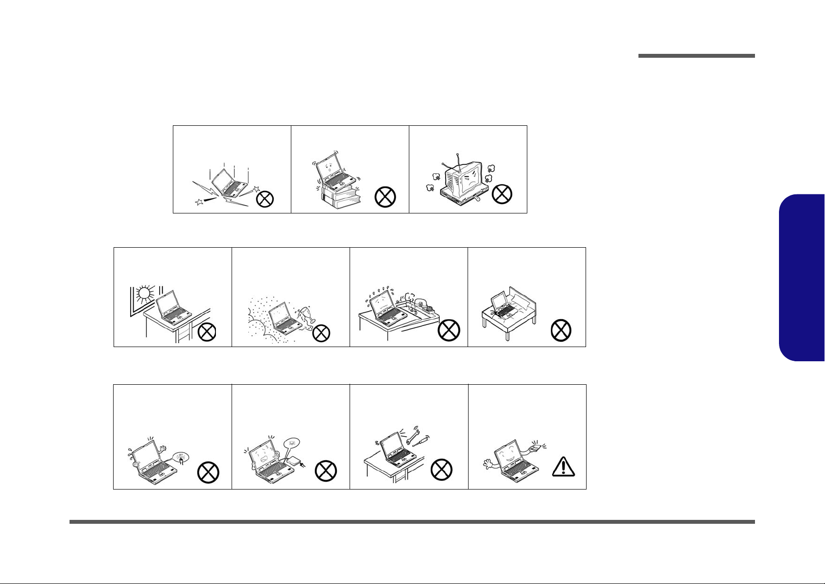
The notebook computer is quite rugged, but it can be damaged. To prevent this, follow these suggestions:
1. Don’t drop it, or expose it to shock. If the computer falls, the case and the components could be damaged.
Preface
Do not expose the computer
to any shock or vibration.
Do not place it on an unstable
surface.
Do not place anything heavy
on the computer.
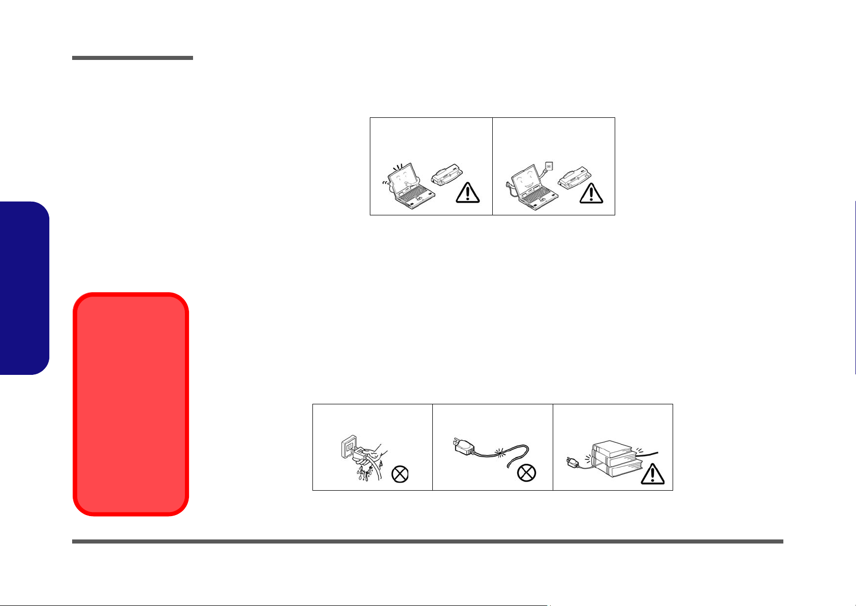
2. Keep it dry, and don’t overheat it. Keep the computer and power supply away from any kind of heating element. This
is an electrical appliance. If water or any other liquid gets into it, the co mputer could be badly damaged.
Do not expose it to excessive
heat or direct sunlight.
Do not leave it in a place
where foreign matter or moisture may affect the system.
Don’t use or store the computer in a humid environment.
Do not place the computer on
any surface which will block
the vents.
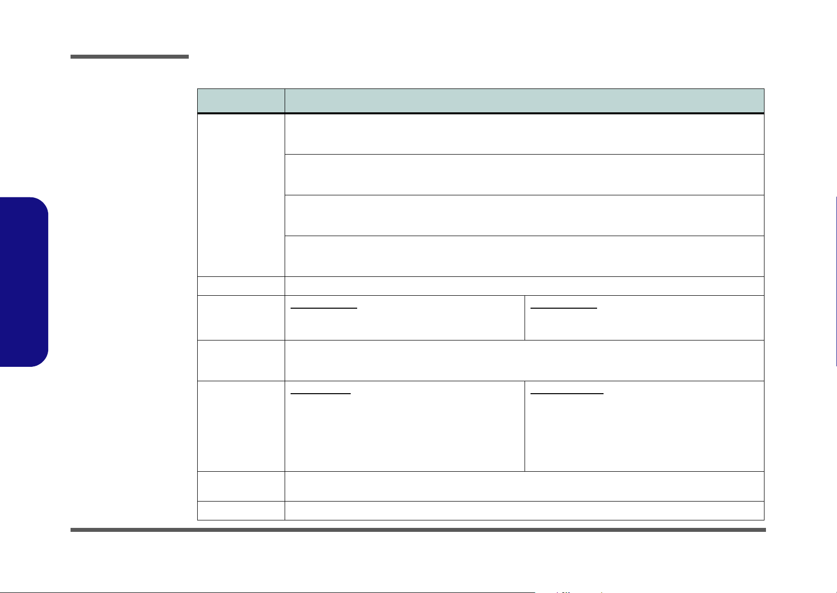
3. Follow the proper working procedures for the computer. Shut the computer down properly and don’t forget to save
your work. Remember to periodically save your data as data may be lost if the battery is depleted.
Do not turn off the power
until you properly shut down
all programs.
Do not turn off any peripheral
devices when the computer is
on.
Do not disassemble the computer by yourself.
Perform routine maintenance
on your computer.
Preface
V
Page 8
Preface
4. Avoid interference. Keep the computer away from high capacity transformers, electric motors, and oth er strong mag-
netic fields. These can hinder proper performance and damage your data.
5. Take care when using peripheral devices.
Preface
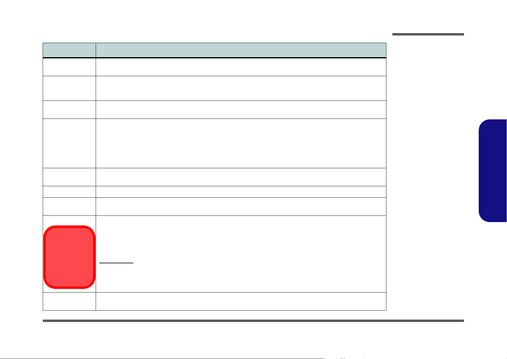
Power Safety
Warning
Before you undertake
any upgrade procedures, make sure that
you have turned off the
power, and disconnected all peripherals
and cables (including
telephone lines). It is
advisable to also remove your battery in
order to prevent accidentally turning the
machine on.
Use only approved brands of
peripherals.
Unplug the power cord befor e
attaching peripheral devices.
Power Safety
The computer has specific power requirements:
• Only use a power adapter approved for use with this computer.
• Your AC adapter may be designed for international travel but it still requ ires a steady, uninterru pted power supp ly. If you are
unsure of your local power specifications, consult your service representative or local power company.
• The power adapter may have either a 2-prong or a 3-prong grounded plug. The third prong is an important safety feature; do
not defeat its purpose. If you do not have access to a compatible outlet, have a qualified electrician install one.
• When you want to unplug the power cord, be sure to disconn ect it by the plug head, not by its wire.
• Make sure the socket and any extension cord(s) you use can support the total current load of all the connected devices.
• Before cleaning the computer, make sure it is disconnected from any external power supplies.
Do not plug in the power
cord if you are wet.
Do not use the power cord if
it is broken.
Do not place heavy objects
on the power cord.
VI
Page 9

Battery Precautions
• Only use batteries designed for this computer. The wrong battery type may explode, leak or damage the computer.
• Do not remove any batteries from the computer while it is powered on.
• Do not continue to use a battery that has been dropped, or that appears damaged (e.g. bent or twisted) in any way. Even if the
computer continues to work with a damaged battery in place, it may cause circuit damage, which may possibly result in fire.
• Recharge the batteries using the notebook’s system. Incorrect recharging may make the battery explode.
• Do not try to repair a battery pack. Refer any battery pack repair or replacement to your service representative or qualified service
personnel.
• Keep children away from, and promptly dispose of a damaged battery. Always dispose of batteries carefully. Batteries may explode
or leak if exposed to fire, or improperly handled or discarded.
• Keep the battery away from metal appliances.
• Affix tape to the battery contacts before disposing of the battery.
• Do not touch the battery contacts with your hands or metal objects.
Battery Disposal
The product that you have purchased contains a rechargeable b attery. The battery is recycl able. At the end of
its useful life, under various state and local laws, it may be illegal to dispose of this battery into the municipal
waste stream. Check with your local solid waste officials for details i n your area for recycling options or p roper
disposal.
Preface
Preface
Caution
Danger of explosion if battery is incorrectly replaced. Replace only with the same or equivalent type recommended by the manufacturer. Discard used battery according to the manufacturer’s instructions.
VII
Page 10

Preface
Preface
Related Documents
You may also need to consult the following manual for additional information:
User’s Manual on CD
This describes the notebook PC’s features and the procedures for operating the computer and its ROM-based setup program. It also describes the installation and operation of the utility programs provided with the notebook PC.
VIII
Page 11

Contents
Preface
Introduction ..............................................1-1
Overview .........................................................................................1-1
System Specifications ................................. 1-2
External Locator - Top View with LCD Panel Open ......................1-5
External Locator - Front & Right side Views .................................1-6
External Locator - Left Side & Rear View .....................................1-7
External Locator - Bottom View .....................................................1-8
Mainboard Overview - Top (M74J/M76J-Key Parts) .....................1-9
Mainboard Overview - Bottom (M74J/M76J-Key Parts) .............1-10
Mainboard Overview - Bottom (M74JU/M76JU-Key Parts) .......1-11
Mainboard Overview - Top (Connectors) .....................................1-12
Mainboard Overview - Bottom (Connectors) ...............................1-13
Disassembly ...............................................2-1
Overview .........................................................................................2-1
Maintenance Tools ..........................................................................2-2
Connections .....................................................................................2-2
Maintenance Precautions .................................................................2-3
Disassembly Steps ...........................................................................2-4
Removing the Battery ......................................................................2-5
Removing the Hard Disk Drive .......................................................2-6
Removing the Optical (CD/DVD) Device ......................................2-9
Removing the System Memory (RAM) ........................................2-11
Removing the Inverter Board ........................................................2-13
Removing and Installing the Processor .........................................2-14
Removing the Wireless LAN Module ...........................................2-17
Removing the Bluetooth Module ..................................................2-18
Removing the Keyboard ................................................................2-19
Removing the Modem ...................................................................2-20
Part Lists ..................................................A-1
Part List Illustration Location ........................................................ A-2
Top with Fingerprint (M740J/M740JU) ........................................ A-3
Top without Fingerprint (M740J/M740JU) ................................... A-4
Bottom (M740J) ............................................................................. A-5
Bottom (M740JU) .......................................................................... A-6
LCD (M740J/M740JU) ................................................................. A-7
HDD (M740J/M740JU) ................................................................. A-8
COMBO (M740J/M740JU) ........................................................... A-9
DVD-Dual Drive (M740J/M740JU) ............................................ A-10
Top with Fingerprint (M760J/M760JU) ...................................... A-11
Top without Fingerprint (M760J/M760JU) ................................. A-12
Bottom (M760J) ........................................................................... A-13
Bottom (M760JU) ........................................................................ A-14
LCD (M760J/M760JU) ............................................................... A-15
HDD (M760J/M760JU) ............................................................... A-16
COMBO (M760J/M760JU) ......................................................... A-17
DVD-Dual Drive (M760J/M760JU) ............................................ A-18
Schematic Diagrams.................................B-1
System Block Diagram ...................................................................B-2
Clock Generator ..............................................................................B-3
CPU-1 .............................................................................................B-4
CPU-2 .............................................................................................B-5
CPU-3 .............................................................................................B-6
CPU-4 .............................................................................................B-7
DDRII S0-DIMM 0 ........................................................................B-8
DDRII S0-DIMM 1 ........................................................................B-9
RS780M-1 .....................................................................................B-10
RS780M-2 .....................................................................................B-11
RS780M-3 .....................................................................................B-12
M82-XT-1 .....................................................................................B-13
Preface
IX
Page 12

Preface
M82-XT-2 .................................................................................... B-14
M82-XT-3 .................................................................................... B-15
DDRII 32MX16 ........................................................................... B-16
LVDS, INVERTER ...................................................................... B-17
HDMI, CRT ................................................................................. B-18
SB700-1 ........................................................................................B-19
SB700-2 ....................................................................................... B-20
SB700-3 ........................................................................................B-21
SB700-4 ........................................................................................B-22
New Card, Mini PCIE ..................................................................B-23
3G, PATA ODD, eSATA ............................................................. B-24
USB, FAN, TP, FP, MULTI CON ............................................... B-25
CARD READER ..........................................................................B-26
ISATA HDD, LED, HOTKEY, BT .............................................B-27
PCIE GIGALAN RTL8111C .......................................................B-28
AUDIO CODEC ALC662 ........................................................... B-29
Preface
AUDIO AMP2056 ....................................................................... B-30
KBC ITE IT8512E ....................................................................... B-31
1.8VS, 3,3VS, 5VS, 1.1VS, 3.3V .................................................B-32
VGA POWER & POWER GD .................................................... B-33
VCORE VDD CORE ................................................................... B-34
VCORE VDD CORE ................................................................... B-35
1.8V, 0.9V ....................................................................................B-36
1.1VS, 1.2V, 1.2VS, 2.5V ............................................................ B-37
VGA CORE 1.5VS ......................................................................B-38
VDD3, VDD5 ...............................................................................B-39
CHARGER, DC IN ......................................................................B-40
CLICK FINGER BOARD FOR M76 ..........................................B-41
MULTI FUNCTION BOARD .....................................................B-42
AUDIO BOARD ..........................................................................B-43
FINGER SENSOR BOARD ........................................................B-44
POWER SWITCH BOARD FOR M74 ....................................... B-45
FINGER BOARD FOR M74 ........................................................B-46
EXTERNAL ODD BOARD FOR M76 .......................................B-47
POWER SWITCH BOARD FOR M76 ........................................B-48
X
Page 13

Chapter 1: Introduction
Overview
This manual covers the information you need to service or upgrade the M740J/M740JU/M760J/M760JU series notebook computer. Information about operating the computer (e.g. getting started, and the Setup utility) is in the User’s
Manual. Information about drivers (e.g. VGA & audio) is also found in User’s Manual. That manual is shipped with the
computer.
Operating systems (e.g. Windows XP, Windows Vista, etc.) have their own manuals as do application software (e.g. word
processing and database programs). If you have questions about those programs, you should consult those manuals.
The M740J/M740JU/M760J/M760JU series notebook is designed to be upgradeable. See “Disassembly” on page 2 - 1
for a detailed description of the upgrade procedures for each specific component. Please note the warning and safety information indicated by the “” symbol.
The balance of this chapter reviews the computer’s technical specifications and features.
Introduction
1.Introduction
Overview 1 - 1
Page 14
Introduction
System Specifications
Feature Specification
1.Introduction
Processor AMD Turion™ X2 Ultra Dual Core Processor
(638-pin) Micro-PGA Package, Socket S1G2
ZM80/ ZM82/ ZM83/ ZM86
AMD Turion™X2 Dual Core Processor
(638-pin) Micro-PGA Package, Socket S1G2
RM70/ RM72/ RM74
AMD Turion™X2 Dual Core Processor
(638-pin) Micro-PGA Package, Socket S1G2
QL60/ QL62/ QL64
AMD Sempron™ Processor
(638-pin) Micro-PGA Package, Socket S1G2
SI40/ SI42/ SI44
Core Logic ATI® RS780MN + SB700
LCD M740J/M740JU:
14.1" WXGA (1280*800)/ WXGA+ (1440*900) TFT LCD
Memory 64-bit Wide DDRII (DDR2) Data Channel
Two 200 Pin SO-DIMM Sockets Supporting DDRII (DDR2) 667MHz/ 800MHz
Memory Expandable up to 4GB (1024MB/ 2048MB DDRII Modules)
Video Adapter M740J/M760J:
ATI® RS780M Integrated Video
High Preference 2D/3D Graphic Accelerator
Shared Memory Architecture of up to 256MB
Supports DirectX®10
65nm (65 Nanometer) Process Technology
2MB L2 Cache & 800MHz FSB, TDP: 35W
2.1/ 2.2/ 2.3/ 2.4 GHz
65nm (65 Nanometer) Process Technology
1MB L2 Cache & 800MHz FSB, TDP: 35W
2.0/ 2.1/ 2.2 GHz
65nm (65 Nanometer) Process Technology
1MB L2 Cache & 667MHz FSB, TDP: 35W
1.9/ 2.0/ 2.1 GHz
65nm (65 Nanometer) Process Technology
512KB L2 Cache & 667MHz FSB, TDP: 25W
2.0/ 2.1/ 2.2 GHz
M760J/M760JU:
15.4" WXGA (1280*800)/ WXGA+ (1440*900)/ WSXGA+
(1680*1050) TFT LCD
M740JU/M760JU:
A TI Mobility Radeon HD 3470 Hybird X2 Discrete
Video On-Board
256MB of GDDR2 Video Memory On-Board
Integrated HDMI & Unified Video Controller
Supports Cross Fire (In Windows Vista only)
Supports DirectX® 10
Security Security (Kensington® Type) Lock Slot
BIOS One 8Mb SPI Flash ROM Phoenix™ BIOS
1 - 2 System Specifications
BIOS Password
Fingerprint ID Reader Module (Factory Option)
Page 15
Feature Specification
Introduction
Storage
Audio High Definition Audio
Keyboard &
Pointing Device
Interface Three USB 2.0 Ports
Card Reader Embedded 7-in-1 Card Reader (MS/ MS Pro/ SD/ Mini SD/ MMC/ RS MMC/ MS Duo) Note: MS Duo/ Mini SD/ RS
ExpressCard Slot One ExpressCard/34(54) Slot
Mini-Card Slots
Communication 56K Fax Modem
UMTS Modes
Note that UMTS
modes CAN
NOT be used in
North America.
One Changeable 12.7mm(h)
Changeable 2.5" 9.5 mm (h)
3D Enhanced Sound System
Sound-Blaster PRO™ Compatible
Winkey Keyboard Built-In TouchPad with Scrolling Function
One External Monitor Port
One HDMI-Out Port (High-Definition Multimedia Interface)
One Headphone-Out Jack
One Microphone-In Jack
One S/PDIF-Out Jack
MMC Cards require a PC adapter
One Mini-Card Slot for
One Mini-Card Slot for
Built-in 10/100/1000Mb Base-TX Ethernet LAN
802.11b/g Wireless LAN Mini-Card Module
Bluetooth 2.0 + EDR (Enhanced Data Rate) Module (Factory Option)
1.3M or 2.0M Pixel PC Camera Module with USB Interface (Factory Option)
3.5G Module:
UMTS/HSPDA-based 3.5G Mini-Card Module with USB Interface (Factory Option)
Quad-band GSM/GPRS (850 MHz, 900 MHz, 1800 MHz, 1900 MHz)
UMTS WCDMA FDD (2100 MHz)
PATA
Optical Device (CD/DVD) Type Drive (see
SA TA
(Serial) HDD
Wireless LAN Module
3.5G Module
with USB/PCIe Interface (Option
“Optional” on page 1 - 4
S/PDIF Digital Output
2 * Built-In Speakers
Built-In Microphone
One eSATA Port (supported in
AHCI mode supports hot swapping
IDE mode does not support hot swapping
One RJ-1 1 Modem Jack
One RJ-45 LAN Jack
One DC-In Jack
)
Windows Vista
) Easy
only):
1.Introduction
Power
Management
Supports ACPI v2.0 Supports Wake on LAN
System Specifications 1 - 3
Page 16
Introduction
Feature Specification
1.Introduction
Power M740J/M760J:
Full Range AC/DC Adapter AC input 100 - 240V, 50 60Hz, DC Output 19V, 3.42A or 18.5V, 3.5A (65 Watts)
Battery 6 Cell Smart Lithium-Ion Battery Pack, 4000mAH OR 4400mAH
Environmental
Spec
Dimensions
& Weight
Optional P ATA Optical Drive Module Options:
Temperature
Operating: 5
Non-Operating: -20°C - 60°C
M740J/M740JU:
336mm (w) * 250mm (d) * 24.8-35.7mm (h)
Around 2.3 kg With 6 Cell Battery
DVD/CD-RW Combo Device Module
Super Multi Device Module
802.11b/g Wireless LAN Mini-Card Module
Interface
1.3M or 2.0M Pixel PC Camera Module with USB
Interface (Factory Option)
Fingerprint ID Reader Module (Factory Option)
Bluetooth 2.0 + EDR (Enhanced Data Rate) Module
(Factory Option)
°C - 35°C
with USB/PCIe
M740JU/M760JU:
Full Range AC/DC Adapter AC input 100 - 240V, 50 60Hz, DC Output 19V, 4.74A (90 Watts)
Relative Humidity
M760J/M760JU:
359mm (w) * 268mm (d) * 24.8-37mm (h)
2.6 kg With 6 Cell Battery
UMTS/HSPDA-based 3.5G Mini-Card Module with USB
Interface (Factory Option)
Operating: 20% - 80%
Non-Operating: 10% - 90%
Quad-band GSM/GPRS (850 MHz, 900 MHz, 1800
MHz, 1900 MHz)
UMTS WCDMA FDD (2100 MHz)
UMTS Modes
Note that UMTS modes CAN NOT be used in
North America.
1 - 4 System Specifications
Page 17
Introduction
External Locator - Top View with LCD Panel Open
1
2
33
4
5
6
7
8
5
8
Figure 1
Top View
1
2
33
4
6
7
1. Optional Built-In
PC Camera
2. LCD
3. Speakers
4. Power Button
5. Hot Key Buttons
6. Keyboard
7. Built-In
Microphone
8. Touchpad &
Buttons
9. Fingerprint
Module (Optional)
10.LED Indicators
1.Introduction
10
9
10
M740J/M740JU M760J/M760JU
10
9
10
External Locator - Top View with LCD Panel Open 1 - 5
Page 18
Introduction
Figure 2
Front Views
1. LED Indicators
Figure 3
1.Introduction
Right Side Views
1. S/PDIF-Out Jack
2. Microphone-In
Jack
3. Headphone-Out
Jack
4. USB 2.0 Port
5. Optical Device
Drive Bay
6. RJ-11 Phone
Jack
7. Security Lock
Slot
External Locator - Front & Right side Views
1
15243
6
7
1 - 6 External Locator - Front & Right side Views
Page 19
External Locator - Left Side & Rear View
1
2
3
4
5
7
6
Introduction
Figure 4
Left Side View
1. DC-In Jack
2. External Monitor
Port
3. RJ-45 LAN Jack
4. e-SATA Port
7
8
9
5. HDMI-Out Port
6. Vent
7. 2 * USB 2.0 Ports
8. ExpressCard Slot
9. 7-in-1 Card
Reader
1.Introduction
Figure 5
Rear View
1
1. Battery
External Locator - Left Side & Rear View 1 - 7
Page 20
Introduction
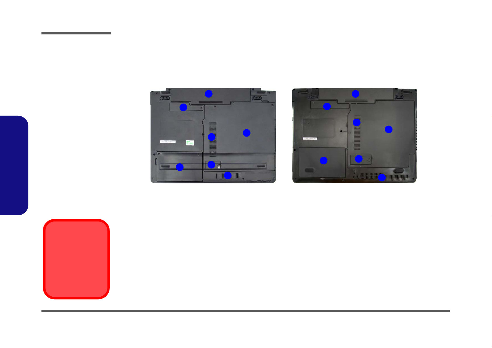
Figure 6
Bottom View
1. Battery
2. Bluetooth
Module Cover
3. RAM & CPU Bay
Cover
4. Vent
5. Hard Disk Bay
Cover
6. 3.5G USIM Card
Cover
1.Introduction
External Locator - Bottom View
1
2
4
5
M740J/M740JU M760J/M760JU
6
4
3
1
2
4
3
5
6
4
Overheating
To prevent your computer from overheating
make sure nothing
blocks the vent/fan intakes while the computer is in use.
1 - 8 External Locator - Bottom View
Page 21
Introduction
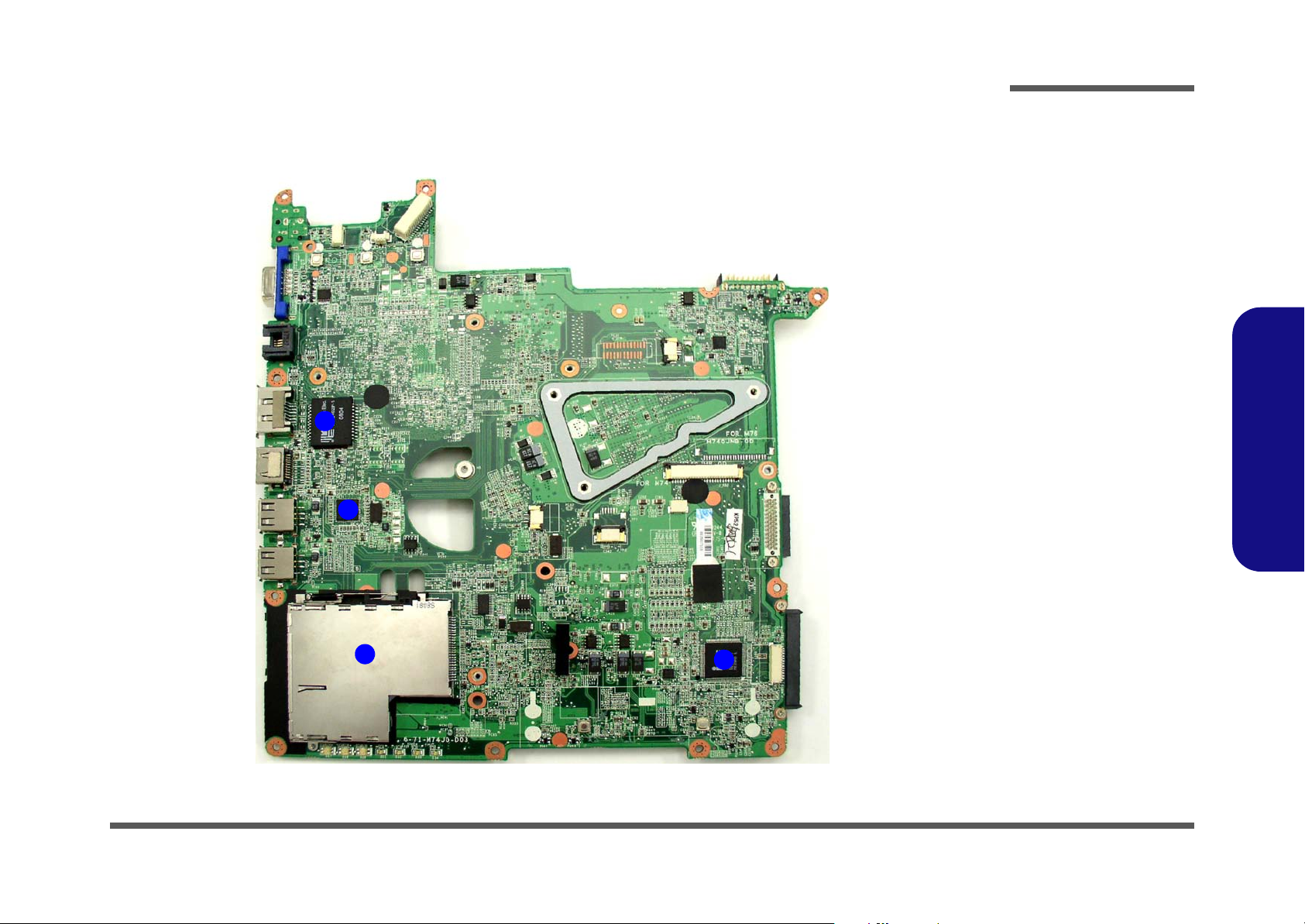
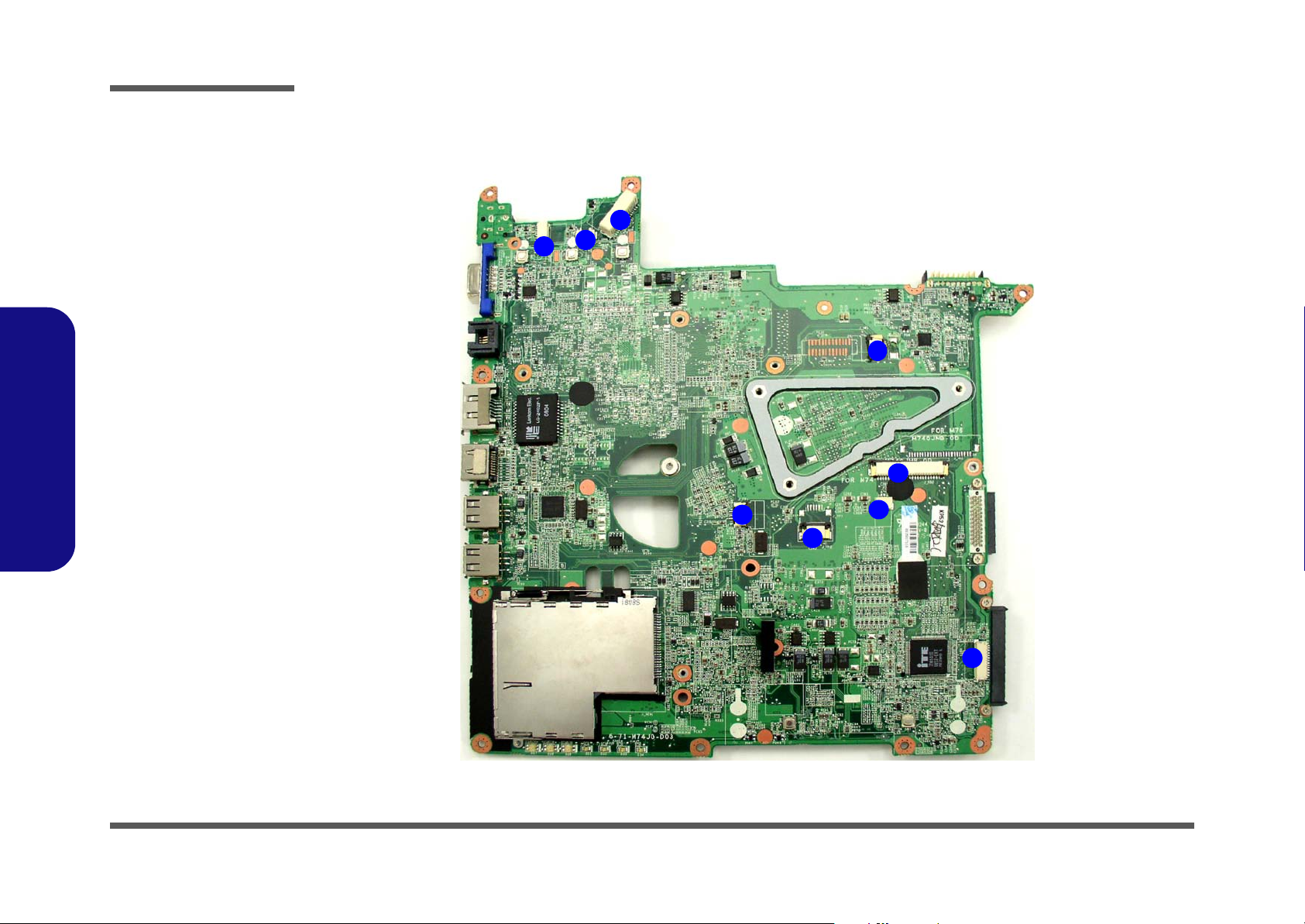
Mainboard Overview - Top (M74J/M76J-Key Parts)
1
2
Figure 7
Mainboard Top
Key Parts
1. LG-2402P-1
2. RTL81 11C
3. ExpressCard
Connector
4. ITE IT8512E
1.Introduction
3
4
Mainboard Overview - Top (M74J/M76J-Key Parts) 1 - 9
Page 22
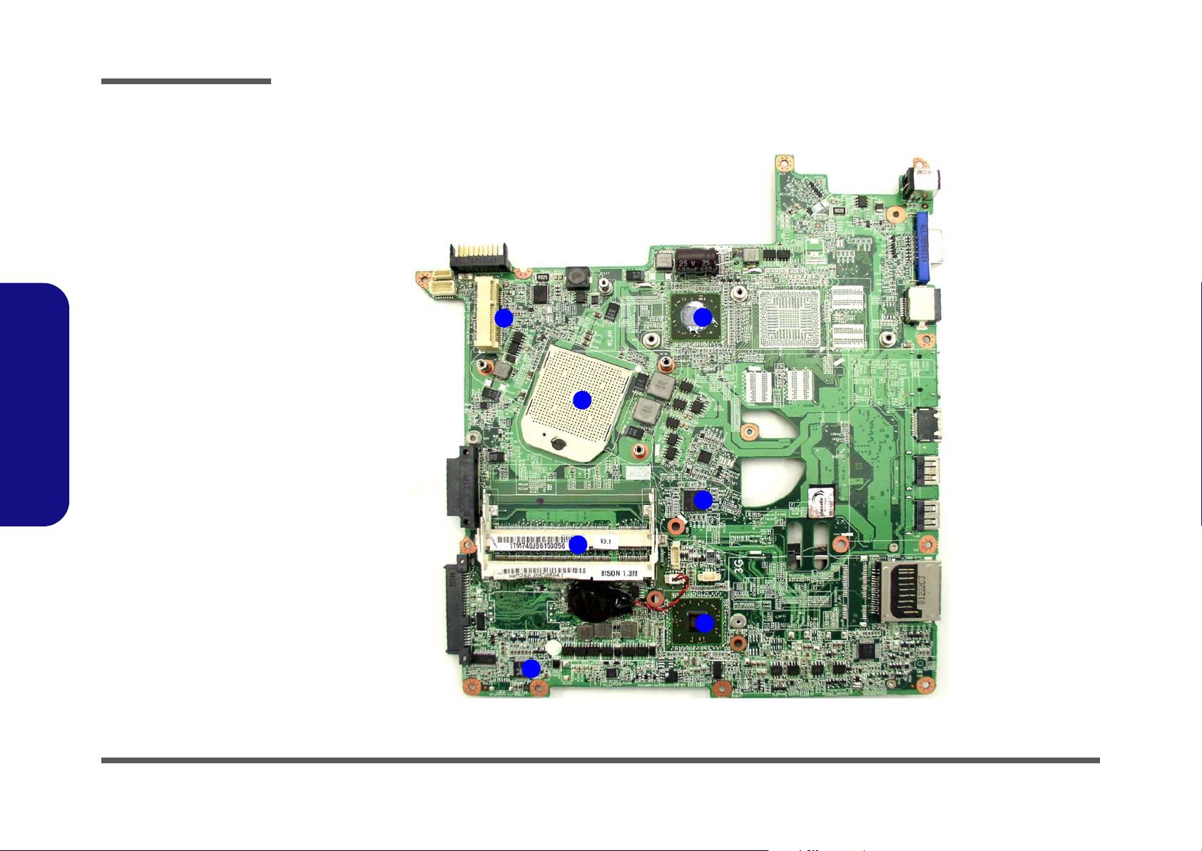
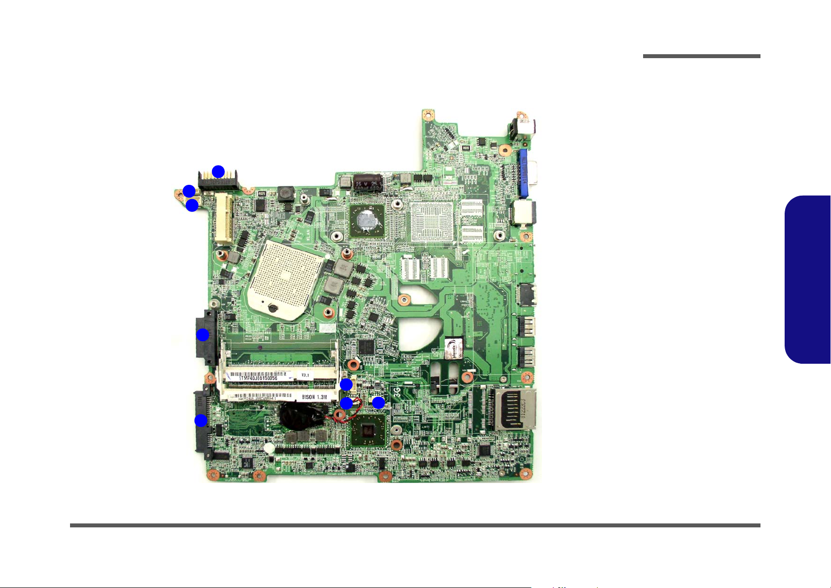
Introduction
Figure 8
Mainboard Bottom
Key Parts
1. Mini-Card
Connector (WLAN
Module)
2. CPU Socket (no
CPU installed)
3. Memory Slots
DDR2 SO-DIMM
4. ALC662
5. South Bridge
6. ICS
7. North Bridge
1.Introduction
Mainboard Overview - Bottom (M74J/M76J-Key Parts)
1
2
7
6
3
4
1 - 10 Mainboard Overview - Bottom (M74J/M76J-Key Parts)
5
Page 23
Introduction
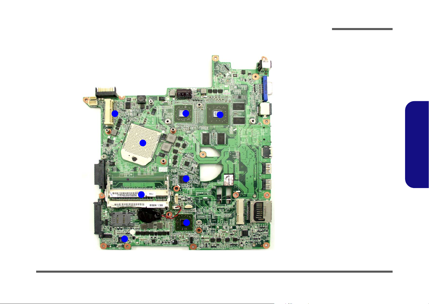
Mainboard Overview - Bottom (M74JU/M76JU-Key Parts)
1
2
7
6
8
Figure 9
Mainboard Bottom
Key Parts
1. Mini-Card
Connector (WLAN
Module)
2. CPU Socket (no
CPU installed)
3. Memory Slots
DDR2 SO-DIMM
4. ALC662
5. South Bridge
6. ICS
7. North Bridge
8. ATI -VGA on
Board
1.Introduction
3
5
4
Mainboard Overview - Bottom (M74JU/M76JU-Key Parts) 1 - 11
Page 24
Introduction
Figure 10
Mainboard Top
Connectors
1. LCD Cable
Connector
2. Speaker Cable
Connector
3. Inverter Cable
Connector
4. Fingerprint Cable
Connector
5. TouchPad Cable
Connector
6. Microphone
Cable Connector
7. Keyboard Cable
Connector
1.Introduction
8. Power board
Connector
9. Audio Board
Connector
Mainboard Overview - Top (Connectors)
1
2
3
4
5
8
7
6
1 - 12 Mainboard Overview - Top (Connectors)
9
Page 25
Introduction
Mainboard Overview - Bottom (Connectors)
1
2
3
4
Figure 11
Mainboard Bottom
Connectors
1. Battery
Connector
2. BT Cable
Connector
3. Multi Board
(Modem)
Connector
4. CD-ROM
Connector
5. HDD Connector
6. CMOS Bat.
Connector
7. Debug Cable
Connector
8. CPU Fan Cable
Connector
1.Introduction
7
6
5
8
Mainboard Overview - Bottom (Connectors) 1 - 13
Page 26

Page 27

Chapter 2: Disassembly
Overview
This chapter provides step-by-step instructions for disassembling the M740J/M740JU/M760J/M760JU series notebook’s parts and subsystems. When it comes to reassembly, reverse the procedures (unless otherwise indicated).
We suggest you completely review any procedure before you take the computer apart.
Disassembly
Procedures such as upgrading/replacing the RAM, optical device and hard disk are included in the User’s Manual but are
repeated here for your convenience.
To make the disassembly process easier each section may have a box in the page margin. Information contained under
the figure # will give a synopsis of the sequence of procedures involved in the disassembly procedure. A box with a
lists the relevant parts you will have after the disassembly process is complete. Note: The parts listed will be for the disassembly procedure listed ONLY, and not any previous disassembly step(s) required. Refer to the part list for the previous disassembly procedure. The amount of screws you should be left with will be listed here also.
A box with a will also provide any possible helpful information. A box with a contains warnings.
An example of these types of boxes are shown in the sidebar.
2.Disassembly
Information
Warning
Overview 2 - 1
Page 28

Disassembly
2.Disassembly
NOTE: All disassembly procedures assume that the system is turned OFF, and disconnected from any power supply (the
battery is removed too).
Maintenance Tools
The following tools are recommended when working on the notebook PC:
• M3 Philips-head screwdriver
• M2.5 Philips-head screwdriver (magnetized)
• M2 Philips-head screwdriver
• Small flat-head screwdriver
• Pair of needle-nose pliers
• Anti-static wrist-strap
Connections
Connections within the computer are one of four types:
Locking collar sockets for ribbon connectors To release these connectors, use a small flat-head screwdriver to
gently pry the locking collar away from its base. When replacing the connection, make sure the connector is oriented in the
same way. The pin1 side is usually not indicated.
2 - 2 Overview
Pressure sockets for multi-wire connectors To release this connector type, grasp it at its head and gently
rock it from side to side as you pull it out. Do not pull on the
wires themselves. When replacing the connection, do not try to
force it. The socket only fits one way.
Pressure sockets for ribbon connectors To release these connectors, use a small pair of needle-nose pli-
ers to gently lift the connector away from its socket. When replacing the connection, make sure the connector is oriented in
the same way. The pin1 side is usually not indicated.
Board-to-board or multi-pin sockets To separate the boards, gently rock them from side to side as
you pull them apart. If the connection is very tight, use a small
flat-head screwdriver - use just enough force to start.
Page 29

Maintenance Precautions
The following precautions are a reminder. To avoid personal injury or damage to the computer while performing a removal and/or replacement job, take the following precautions:
1. Don't drop it. Perform your repairs and/or upgrades on a stable surface. If the computer falls, the case and other
components could be damaged.
2. Don't overheat it. Note the proximity of any heating elements. Keep the computer out of direct sunlight.
3. Avoid interference. Note the proximity of any high capacity transformers, electric motors, and other strong mag-
netic fields. These can hinder proper performance and damage components and/or data. You should also monitor
the position of magnetized tools (i.e. screwdrivers).
4. Keep it dry. This is an electrical appliance. If water or any other liquid gets into it, the computer could be badly
damaged.
5. Be careful with power. Avoid accidental shocks, discharges or explosions.
•Before removing or servicing any part from the computer, turn the computer off and detach any power supplies.
•When you want to unplug the power cord or any cable/wire, be sure to disconnect it by the plug head. Do not pu ll on the wir e.
6. Peripherals – Turn off and detach any peripherals.
7. Beware of static discharge. ICs, such as the CPU and main support chips, are vulnerable to static electricity.
Before handling any part in the computer, discharge any static electricity inside the computer. When handling a
printed circuit board, do not use gloves or other materials which allow static electricity buildup. We suggest that
you use an anti-static wrist strap instead.
8. Beware of corrosion. As you perform your job, avoid touching any connector leads. Even the cleanest hands produce oils which can attract corrosive elements.
9. Keep your work environment clean. Tobacco smoke, dust or other air-born particulate matter is often attracted
to charged surfaces, reducing performance.
10. Keep track of the component s. When re moving or replacing any p art, be careful not to le ave small part s, such as
screws, loose inside the computer.
Disassembly
Power Safety
Warning
Before you undertake
any upgrade procedures, make sure that
you have turned off the
power, and disconnected all peripherals
and cables (including
telephone lines). It is
advisable to also remove your battery in
order to prevent accidentally turning the
machine on.
2.Disassembly
Cleaning
Do not apply cleaner directly to the computer, use a soft clean cloth.
Do not use volatile (petroleum distillates) or abrasive cleaners on any part of the computer.
Overview 2 - 3
Page 30

Disassembly
Disassembly Steps
The following table lists the disassembly steps, and on which page to find the related information. PLEASE PERFORM
THE DISASSEMBLY STEPS IN THE ORDER INDICATED.
2.Disassembly
To remove the Battery:
1. Remove the battery page 2 - 5
To remove the HDD:
1. Remove the battery page 2 - 5
2. Remove the HDD page 2 - 6
To remove the Optical Device:
1. Remove the battery page 2 - 5
2. Remove the Optical device page 2 - 9
To remove the System Memory:
1. Remove the battery page 2 - 5
2. Remove the system memory page 2 - 11
To remove the Inverter Board:
1. Remove the battery page 2 - 5
2. Remove the inverter board page 2 - 13
To remove and install a Processor:
1. Remove the battery page 2 - 5
2. Remove the processor page 2 - 14
3. Install the processor page 2 - 16
To remove the Wireless LAN Module:
1. Remove the battery page 2 - 5
2. Remove the wireless LAN page 2 - 17
To remove the Bluetooth Module:
:
1. Remove the battery page 2 - 5
2. Remove the Bluetooth page 2 - 18
To remove the Keyboard:
1. Remove the battery page 2 - 5
2. Remove the keyboard page 2 - 19
To remove the Modem:
1. Remove the battery page 2 - 5
2. Remove the HDD page 2 - 6
3. Remove the Optical device page 2 - 9
4. Remove the processor page 2 - 14
5. Remove the Wireless LAN Module page 2 - 17
6. Remove the Bluetooth Module page 2 - 18
7. Remove the keyboard page 2 - 19
8. Remove the modem page 2 - 20
2 - 4 Disassembly Steps
Page 31

Removing the Battery
Disassembly
1. Turn the computer off, and turn it over.
2. Slide the latch in the direction of the arrow.
3. Slide the latch in the direction of the arrow, and hold it in place.
4. Slide the battery in the direction of the arrow .
1
2
3
6
a.
2
b.
4
3
Figure 1
Battery Removal
a. Slide the latch and hold
in place.
b. Slide the battery in the di-
rection of the arrow.
1
2.Disassembly
4
3. Battery
Removing the Battery 2 - 5
Page 32

Disassembly
Removing the Hard Disk Drive
Figure 2
HDD Assembly
Removal
a. Locate the HDD bay
cover and remove the
screw(s).
2.Disassembly
The hard disk drive can be taken out to accommodate other 2.5" serial (SATA) hard disk drives with a height of 9.5mm
(h). Follow your operating system’s installation instructions, and install all necessary drivers and utilities (as outlined in
Chapter 4 of the User’s Manual) when setting up a new hard disk.
Hard Disk Upgrade Process
1. Turn off the computer, and remove the battery (page 2 - 5).
2. Locate the hard disk bay cover and remove screw & .
a.
21
M740J/M740JU M760J/M760JU
1 2
21
HDD System Warning
•2 Screws
New HDD’s are blank. Before you begin make sure:
You have backed up any data you want to keep from your old HDD.
You have all the CD-ROMs and FDDs required to install your operating system and programs.
If you have access to the internet, download the latest application and hardware driver updates for the operating system you plan
to install. Copy these to a removable medium.
2 - 6 Removing the Hard Disk Drive
Page 33

Disassembly
For M740J/M740JU computers:
3
3. Remove the hard disk bay cover .
4. Grip the tab and slide the hard disk in the direction of arrow .
5. Lift the hard disk out of the bay .
6. Remove the screw and the adhesive cover from the hard disk .
6 6
7. Reverse the process to install a new hard disk (do not forget to replace all the screws and covers).
b.
3
c.
4
6
4
5
7
8
6
e.
7
Figure 3
HDD Assembly
Removal (cont’d.)
b. Remove the HDD bay
cover.
c. Grip the tab and slide the
HDD in the direction of
the arrow.
d. Lift the HDD assembly
out of the bay.
e. Remove the screw and
adhesive cover.
2.Disassembly
6
8
d.
5
Removing the Hard Disk Drive 2 - 7
3. HDD Bay Cover
7. Adhesive Cover
8. HDD
•1 Screw
Page 34

Disassembly
Figure 4
HDD Assembly
Removal (cont’d.)
f. Remove the HDD Bay
Cover.
g. Grip the tab and slide the
HDD in the direction of
the arrow.
h. Lift the HDD assembly
out of the bay.
i. Remove the screw and
adhesive cover.
2.Disassembly
For M760J/M760JU computers:
3
8. Remove the hard disk bay Cover .
9. Grip the tab and slide the hard disk in the direction of arrow .
10. Lift the hard disk out of the bay .
11. Remove the screws & and the adhesive cover from the hard disk .
6 7 6
12. Reverse the process to install a new hard disk (do not forget to replace all the screws and covers).
f.
3
g.
4
6
4
5
8
9
6
i.
8
7
6
9
h.
3. HDD Bay Cover
8. Adhesive Cover
9. HDD
•2 Screws
2 - 8 Removing the Hard Disk Drive
5
Page 35

Disassembly
Removing the Optical (CD/DVD) Device
1. Turn off the computer, and remove the battery (page 2 - 5).
2. M740J/M740JU: (see over for M760J/M760JU)
Locate the component bay cover and remove screws - .
1
3. Carefully (a fan and cable are attached to the under side of the cover) lift up the bay cover.
4. Carefully disconnect the fan cable , and remove the cover
5. Remove the screw at point , and use a screwdriver to carefully push out the optical device at point .
6 8 7
5
1
.
6. Insert the new device and carefully slide it into the computer (the device only fits one way. DO NOT FORCE IT; The
screw holes should line up).
7. Restart the computer to allow it to automatically detect the new device.
a.
3
2
4
c.
1
6
M740J/M740JU
2 4
Figure 5
Optical Device
Removal
a. Remove the screws.
b. Disconnect the fan cable
and remove the cover.
c. Remove the screw.
d. Push the optical device
out off the computer at
point 7.
2.Disassembly
b.
c.
d.
1
8
7
5
Removing the Optical (CD/DVD) Device 2 - 9
1. Component Bay Cover
8. Optical Device
•4 Screws
Page 36

Disassembly
Figure 6
Optical Device
Removal (cont’d.)
e. Remove the screws.
f. Remove the cover.
g. Remove the screw.
h. Push the optical device
out off the computer at
point 7.
2.Disassembly
8. M760J/M760JU: Locate the hard disk bay cover and loosen screws & .
9. Remove the hard disk bay cover .
10. Remove the screw at point , and use a screwdriver to carefully push out the optical device
1
6
1
2
3
8
at point .
7
1 1. Insert the new device and carefully slide it into the computer (the device only fits one way. DO NOT FORCE IT ; Th e
screw holes should line up).
12. Restart the computer to allow it to automatically detect the new device.
e.
g.
6
1
32
7
M760J/M760JU
f.
h.
1. HDD Bay Cover
8. Optical Device
1
•3 Screws
2 - 10 Removing the Optical (CD/DVD) Device
8
7
Page 37

Disassembly
Removing the System Memory (RAM)
The computer has two memory sockets for 200 pin Small Outline Dual In-line Memory Modules (SO-DIMM) supporting
DDR2 667/800MHz. The main memory can be expanded up to 4GB. The SO-DIMM modules supported are 1024MB,
and 2048MB and DDRII Modules. The total memory size is automatically detected by the POST routine once you turn
on your computer.
Memory Upgrade Process
1. Turn off the computer, remove the battery (page 2 - 5).
2. Locate the component bay cover , and remove screws - .
3. Carefully (a fan and cable are attached to the under side of the cover) lift up the bay cover (page 2 - 9).
4. The RAM module(s) will be visible at point on the mainboard.
a.
3
2
1
1
5
2 4
b.
4
2
3
1
5
4
Figure 7
RAM Module
Removal
a. Remove the screws.
b. Remove the cover.
Contact Warning
Be careful not to touch
the metal pins on the
module’s connecting
edge. Even the cleanest hands have oils
which can attract particles, and degrade the
module’s performance.
2.Disassembly
M740J/M740JU
M760J/M760JU
1. Component Bay
Cover
•3 Screws
Removing the System Memory (RAM) 2 - 11
Page 38

Disassembly
Figure 8
RAM Module
Removal (cont’d.)
c. Pull the release
latch(es).
d. Remove the module(s).
e. Properly re-insert the
bay cover pins.
2.Disassembly
5. Gently pull the two release latches ( & ) on the sides of the memory socket in the direction indicated by the
6 7
arrows (Figure 8c).
c.
d.
6 7
8
6. The RAM module(s) will pop-up (Figure 8d), and you can then remove it.
8
7. Pull the latches to release the second module if necessary.
8. Insert a new module holding it at about a 30° angle and fit the connectors firmly into the memory slot.
9. The module’s pin alignment will allow it to only fit one way. Make sure the module is seated as far into the slot as it
will go. DO NOT FORCE the module; it should fit without much pressure.
10. Press the module in and down towards the mainboard until the slot levers click into place to secure the module.
11. Replace the bay cover and screws (make sure you reconnect the fan cable before screwing down the bay
cover).
Note for M760J/M760JU computers that there are four - cover pins which need to be aligned with slots in
the case, to insure a proper cover fit, before screwing down the bay cover .
9 12
1
8. RAM Module(s)
12. Restart the computer to allow the BIOS to register the new memory configuration as it starts up.
2 - 12 Removing the System Memory (RAM)
e.
9
1
10
11
12
Page 39

Disassembly
Removing the Inverter Board
1. Turn off the computer, and remove the battery (page 2 - 5).
2. Remove any rubber covers, screws - (Figure 9a), then run your finger around the middle of the frame to
carefully unsnap the LCD front panel module from the back.
3. Discharge the remaining system power (see “Inverter Power Warning” below).
4. Remove screw (Figure 9b) from the inverter, and carefully lift the inverter board up slightly.
5. Disconnect cables & (Figure 9c) from the inverter, then remove the inverter (Figure 9d) from the top
8
9 10 11
case assembly.
a. b.
2 5
3
1
7
1
6
7
4
8
c.
6
9
10
Figure 9
Inverter Board
Removal
a. Remove the 6 screws
and unsnap the LCD
front panel module from
the back.
b. Remove the screw and
discharge the remaining
power from the inverter
board and lift the board
up slightly.
c. Disconnect the cables
from the inverter.
d. Remove the inverter.
2.Disassembly
Inverter Power Warning
In order to prevent a short circuit when removing the inverter it is necessary to discharge any remaining system power. To do
so, press the computer’s power button for a
few seconds before disconnecting the inverter cable.
d.
11
7. LCD Front Panel
11.Inverter Board
•6 Screws
Removing the Inverter Board 2 - 13
Page 40

Disassembly
Removing and Installing the Processor
Figure 10
Processor Removal
a. Remove the cover and
Iocate the heat sink.
b. Remove the screws in
the order indicated.
c. Remove the heat sink.
2.Disassembly
B. Heat Sink
Processor Removal Procedure
1. Turn off the computer, remove the battery (page 2 - 5) and the component bay cover (page 2 - 9).
2. The CPU heat sink will be visible at point on the mainboard.
3. Remove screws
4. Carefully lift up the heat sink (Figure 10c) off the computer.
a.
A
b.
1
, , (Figure 10b) the reverse order as indicated on the label.
3 2 1
B
2
3
A
c.
B
M740J/M760J
B
•3 Screws
2 - 14 Removing and Installing the Processor
M740JU/M760JU
Page 41

Disassembly
5. Turn the release latch towards the unlock symbol , to release the CPU (Figure 11a).
6. Carefully (it may be hot) lift the CPU up out of the socket (Figure 1 1b).
C
D
7. See page 2 - 16 for information on inserting a new CPU.
8. When re-inserting the CPU, pay careful attention to the pin alignment, it will fit only one way (DO NOT FORCE IT!).
d.
C
Unlock
Lock
e.
D
Caution
Figure 11
Processor Removal
(cont’d)
d. Turn the release latch to
unlock the CPU.
e. Lift the CPU out of the
socket.
2.Disassembly
The heat sink, and CPU area in
general, contains parts which are
subject to high temperatures. Allow the area time to cool before removing these parts.
Removing and Installing the Processor 2 - 15
7. CPU
Page 42

Disassembly
Figure 12
Processor
Installation
a. Insert the CPU.
b. Turn the release latch to-
wards the lock symbol.
c. Remove the sticker from
the heat sink and insert
the heat sink.
d. Tighten the screws.
2.Disassembly
Processor Installation Procedure
1. Insert the CPU , pay careful attention to the pin alignment, it will fit only one way (DO NOT FORCE IT!), and
turn the release latch towards the lock symbol (Figure 12b).
2. Remove the sticker (Figure 12c) from the heat sink.
3. Insert the heat sink
4. Tighten screws
5. Replace the component bay cover and tighten the screws (page 2 - 9).
a.
b.
A
B
C
D
as indicated in Figure 12c.
1 3
- in the order indicated on the label.
c.
A
C
D
M740J/M760J
C
D
A. CPU
D. Heat Sink
•3 Screws
2 - 16 Removing and Installing the Processor
B
M740JU/M760JU
d.
Page 43

Disassembly
Removing the Wireless LAN Module
1. Turn off the computer, remove the battery (page 2 - 5) and the component bay cover (page 2 - 9).
2. The Wireless LAN module will be visible at point on the mainboard.
3. Carefully disconnect cables - , then remove screw from the module socket.
4. The Wireless LAN module will pop-up.
5. Lift the Wireless LAN module (Figure 13d) up and off the computer.
a.
1
b.
2
3 4
5
4
3
1
c.
5
d.
Figure 13
Wireless LAN
Module Removal
a. Remove the cover.
b. Disconnect the cable
and remove the screw.
c. The WLAN module will
pop up.
d. Lift the WLAN module
out.
Note: Make sure you
reconnect the antenna
cable to “1” + “2”
socket (Figure b).
2.Disassembly
2
5. WLAN Module.
•1 Screw
Removing the Wireless LAN Module 2 - 17
Page 44

Disassembly
Figure 14
Bluetooth Module
Removal
a. Remove the screw.
b. Lfit the cover and remove
the screw.
c. Disconnect the cable and
the connector.
d. Lift the Bluetooth module
up off the socket.
2.Disassembly
Removing the Bluetooth Module
1. Turn off the computer, remove the battery (page 2 - 5).
2. Locate the Bluetooth bay cover, and remove the screw and cover .
3. Remove the screw and turn the module over.
3
4. Carefully separate the Bluetooth module from the connector
5. Lift the Bluetooth module
6
(Figure 14c) up and off the computer.
a.
1
4 5
and disconnect the cable .
c.
1
b.
d.
2
2
5
4
6
2. Cover
6. Bluetooth Module
•2 Screws
2 - 18 Removing the Bluetooth Module
3
Page 45

Removing the Keyboard
Disassembly
1. Turn off the computer, and remove the battery (page 2 - 5).
2. Press the four keyboard latches at the top of the keyboard to elevate the keyboard from its normal position (you
may need to use a small screwdriver to do this).
3. Carefully lift the keyboard up, being careful not to bend the keyboard ribbon cable (Figure 15b).
4. Disconnect the keyboard ribbon cable from the locking collar socket .
a.
1
5
6 7
c.
2
3
4
b.
6
5
5
7
Figure 15
Keyboard Removal
a. Pre ss the four latches to
release the keyboard.
b. Lift th e keyboard up and
disconnect the cable
from the locking collar.
c. Remove the keyboard.
2.Disassembly
Re-Inserting the Key-
board
When re-inserting the
keyboard firstly align
the four keyboard tabs
at the bottom of the
keyboard with the slots
in the case.
5. Keyboard
Removing the Keyboard 2 - 19
Page 46

Disassembly
Figure 16
Modem Removal
a. Remove the screws.
b. Turn the computer over,
remove the screws and
disconnect the cables.
c. Remove the screws.
2.Disassembly
•20 Screws
(M740J/M740JU)/
26 Screws
(M760J/M760JU)
Removing the Modem
1. Turn off the computer, remove the battery (page 2 - 5), HDD (page 2 - 6), component bay cover (page 2 - 11),
optical device (page 2 - 9), CPU (page 2 - 14), bluetooth (page 2 - 18) and keyboard (page 2 - 19).
14
21
1
22 24 25 27
28 29
M760J/M760JUM740J/M740JU
16
3
7
14
8
21
20
22
23
4
5
6
19
18
15
25
24
26
27
2
10
9
11
12
13
3
4
5
6
1
8
7
18
23
17
15
27
13
12
25
22
26
10
11
9
17
c.
28 29
2. Remove screws - from the bottom case.
3. Turn the computer over, remove screws - and disconnect cables - (Figure 17b).
4. For M760J/M760JU only - remove screws - (Figure 17c) from the rear of the computer.
1
a.
2
16
b.
2 - 20 Removing the Modem
Page 47

Disassembly
5. Carefully lift the top case up and off the computer (Figure 17d).
6. Remove screws - from the computer.
7. Remove screws - from the modem module.
31 33
34 35
8. Lift the modem up and separate the modem from the connector .
9. Lift the modem off the computer.
37
30
36
d.
30
M740J/M740JU
M760J/M760JU
e.
33
32
31
32
f.
Figure 17
Modem Removal
(cont’d.)
d. Lift the cover off the
computer.
e. Remove the screws.
f. Remove the screws and
disconnect the connec-
tor.
g. Lift the modem out.
2.Disassembly
33
31
g.
36
35
34
37
36
35
34
37
30.Top Case
37.Modem
•5 Screws
Removing the Modem 2 - 21
Page 48

Page 49

Appendix A: Part Lists
This appendix breaks down the M740J/M740JU/M760J/M760JU series notebook’s construction into a series of illustrations. The component part numbers are indicated in the tables opposite the drawings.
Note: This section indicates the manufacturer’s part numbers. Your organization may use a different system, so be sure
to cross-check any relevant documentation.
Note: Some assemblies may have parts in common (especially screws). However, the part lists DO NOT indicate the
total number of duplicated parts used.
Part Lists
Note: Be sure to check any update notices. The parts shown in these illustrations are appropriate for the system at the
time of publication. Over the product life, some parts may be improved or re-configured, resulting in new part numbers.
A.Part Lists
A-1
Page 50

Part Lists
Table A- 1
Part List Illustration
Location
Part List Illustration Location
The following table indicates where to find the appropriate part list illustration.
Parts M740J M740JU M760J M760JU
Top with Fingerprint page A - 3 page A - 11
Top without Fingerprint page A - 4 page A - 12
Bottom page A - 5 page A - 6 page A - 13 page A - 14
LCD page A - 7 page A - 15
HDD page A - 8 page A - 16
COMBO page A - 9 page A - 17
A.Part Lists
A - 2 Part List Illustration Location
DVD-Dual Drive page A - 10 page A - 18
Page 51

Top with Fingerprint (M740J/M740JU)
Part Lists
白色 (無鉛)
無鉛
Figure A - 1
Top with
A.Part Lists
Fingerprint
(M740J/M740JU)
無鉛
無鉛
無鉛
無鉛
無鉛
無鉛
無鉛
無鉛
無鉛
無鉛
無鉛
無鉛
Top with Fingerprint (M740J/M740JU) A - 3
Page 52

Part Lists
Figure A - 2
Top without
Fingerprint
(M740J/M740JU)
A.Part Lists
Top without Fingerprint (M740J/M740JU)
A - 4 Top without Fingerprint (M740J/M740JU)
白色 (無鉛)
無鉛
無鉛
無鉛
無鉛
無鉛
無鉛
無鉛
無鉛
無鉛
無鉛
無鉛
無鉛
Page 53

Bottom (M740J)
外 無鉛
外 無鉛
海華 無鉛
無電鍍 無鉛
無電鍍 無鉛
無電鍍 無鉛
藍天3 互億 無鉛
無電鍍 無鉛
無鉛
無鉛
無鉛
無鉛
無鉛
無鉛
凱碩 無鉛
無鉛
無鉛
無鉛
導電布 無鉛
導電布 無鉛
無鉛
無鉛
無鉛
無鉛
無鉛
無鉛
無鉛
無鉛
無鉛
無鉛
無鉛
無鉛
無鉛
無鉛
無鉛
無鉛
無鉛
無鉛
無鉛
無鉛
無鉛
無鉛
無鉛
無鉛
無鉛
無鉛
無鉛
無鉛
無鉛
無鉛
無鉛
無鉛
無鉛
無鉛
無鉛
無鉛
Part Lists
Figure A - 3
Bottom (M740J)
A.Part Lists
Bottom (M740J) A - 5
Page 54

Part Lists
Figure A - 4
Bottom (M740JU)
A.Part Lists
Bottom (M740JU)
外 無鉛
外 無鉛
海華 無鉛
無鉛
無鉛
無鉛
無鉛
無鉛
導電布 無鉛
導電布 無鉛
無鉛
凱碩 無鉛
無鉛
藍天3 互億 無鉛
無鉛
無鉛
無鉛
無鉛
無鉛
無鉛
無鉛
無鉛
無鉛
無鉛
無鉛
無鉛
無鉛
無鉛
無鉛
無鉛
無鉛
無鉛
無鉛
無鉛
無鉛
無鉛
無鉛
無鉛
無鉛
無鉛
無鉛
無鉛
無鉛
無鉛
無鉛
無鉛
無鉛
無鉛
無鉛
無鉛
無鉛
無鉛
A - 6 Bottom (M740JU)
Page 55

LCD (M740J/M740JU)
Part Lists
無鉛
無鋁箔 無鉛
精乘 無鉛
精乘 無鉛
中性 電鑄薄膜鍍亮鉻) 無鉛
精乘 無鉛
精乘 無鉛
Figure A - 5
LCD (M740J/
A.Part Lists
M740JU)
無鉛
無鉛
無鉛
無鉛
無鉛
無鉛
無鉛
無鉛
無鉛
無鉛
無鉛
無鉛
無鉛
無鉛
無鉛
無鉛
無鉛
無鉛
無鉛
無鉛
無鉛
無鉛
無鉛
LCD (M740J/M740JU) A - 7
Page 56

Part Lists
Figure A - 6
(M74J/M740JU)
A.Part Lists
HDD
HDD (M740J/M740JU)
無鉛
(無鉛)
A - 8 HDD (M740J/M740JU)
Page 57

COMBO (M740J/M740JU)
Part Lists
*(非耐落) 無鉛
Figure A - 7
COMBO
A.Part Lists
(M740J/M740JU)
無鉛
無鉛
無鉛
無鉛
無鉛
COMBO (M740J/M740JU) A - 9
Page 58

Part Lists
Figure A - 8
DVD-Dual Drive
(M740J/M740JU)
A.Part Lists
DVD-Dual Drive (M740J/M740JU)
A - 10 DVD-Dual Drive (M740J/M740JU)
*(非耐落) 無鉛
無鉛
無鉛
無鉛
無鉛
Page 59

Top with Fingerprint (M760J/M760JU)
Part Lists
白色 (無鉛)
白色 無鉛
白色 設變 無鉛
無鉛(背膠變更)
頭徑 頭厚 號穴 鍍白鎳 I頭 無鉛
無鉛
無鉛
無鉛
無鉛
無鉛
無鉛
無鉛
無鉛
無鉛
無鉛
無鉛
無鉛
Figure A - 9
Top with
Fingerprint
(M760J/M760JU)
A.Part Lists
Top with Fingerprint (M760J/M760JU) A - 11
Page 60

Part Lists
Figure A - 10
Top without
Fingerprint
(M760J/M760JU)
A.Part Lists
Top without Fingerprint (M760J/M760JU)
A - 12 Top without Fingerprint (M760J/M760JU)
白色 (無鉛)
白色 無鉛
白色 設變 無鉛
無鉛
無鉛(背膠變更)
頭徑 頭厚 號穴 鍍白鎳 I頭 無鉛
無鉛
無鉛
無鉛
無鉛
無鉛
無鉛
無鉛
無鉛
無鉛
無鉛
Page 61

Bottom (M760J)
無鉛
無鉛
無鉛
無鉛
無鉛
無鉛
(黑色)(無鉛)
(黑色) 無鉛
藍天3 互億 無鉛
(黑色) 無鉛
度,黑色 無鉛
無鉛
無鉛
無鉛
無鉛
無鉛
無鉛
無鉛
無鉛
無鉛
無鉛
無鉛
無鉛
無鉛
無鉛
無鉛
無鉛
無鉛
無鉛
無鉛
無鉛
無鉛
無鉛
無鉛
無鉛
無鉛
導電布 無鉛
導電布 無鉛
外 無鉛
外 無鉛
非耐落 無鉛
海華 無鉛
無鉛
凱碩 無鉛
無鉛
無鉛
無鉛
無鉛
黑色 後設變咬花 無鉛
無鉛
無鉛
無鉛
無鉛
無鉛
Part Lists
Figure A - 11
Bottom (M760J)
A.Part Lists
Bottom (M760J) A - 13
Page 62

Part Lists
Figure A - 12
Bottom (M760JU)
A.Part Lists
Bottom (M760JU)
無鉛
無鉛
無鉛
無鉛
(黑色)(無鉛)
(黑色) 無鉛
藍天3 互億 無鉛
(黑色) 無鉛
度,黑色 無鉛
無鉛
無鉛
無鉛
無鉛
無鉛
無鉛
無鉛
無鉛
無鉛
無鉛
無鉛
無鉛
無鉛
無鉛
無鉛
無鉛
無鉛
無鉛
無鉛
無鉛
無鉛
無鉛
無鉛
無鉛
無鉛
無鉛
無鉛
無鉛
導電布 無鉛
導電布 無鉛
外 無鉛
外 無鉛
非耐落 無鉛
海華 無鉛
無鉛
凱碩 無鉛
無鉛
無鉛
無鉛
無鉛
黑色 後設變咬花 無鉛
無鉛
無鉛
無鉛
無鉛
無鉛
A - 14 Bottom (M760JU)
Page 63

LCD (M760J/M760JU)
Part Lists
(非耐落) 無鉛
頭徑 頭厚 號穴 鍍白鎳 頭 無鉛
無鉛
精乘 無鉛
黑色 惠貿 無鉛
黑色 惠貿 無鉛
中性 電鑄薄膜鍍亮鉻) (偉鎮)無鉛
后蓋保護 無鉛
Figure A - 13
無鉛
無鉛
無鉛
無鉛
無鉛
無鉛
無鉛
無鉛
無鉛
無鉛
無鉛
無鉛
無鉛
無鉛
無鉛
無鉛
無鉛
無鉛
無鉛
無鉛
無鉛
無鉛
無鉛
無鉛
無鉛
無鉛
LCD (M760J/
M760JU)
A.Part Lists
LCD (M760J/M760JU) A - 15
Page 64

Part Lists
Figure A - 14
(M760J /M760JU)
A.Part Lists
HDD (M760J/M760JU)
HDD
A - 16 HDD (M760J/M760JU)
無鉛
(無鉛)
Page 65

COMBO (M760J/M760JU)
Part Lists
*(非耐落) 無鉛
黑色 無鉛
Figure A - 15
COMBO
A.Part Lists
(M760J/M760JU)
無鉛
無鉛
無鉛
COMBO (M760J/M760JU) A - 17
Page 66

Part Lists
Figure A - 16
DVD-Dual Drive
(M760J/M760JU)
DVD-Dual Drive (M760J/M760JU)
A.Part Lists
A - 18 DVD-Dual Drive (M760J/M760JU)
*(非耐落) 無鉛
黑色 無鉛
無鉛
無鉛
無鉛
無鉛
Page 67

Appendix B: Schematic Diagrams
This appendix has circuit diagrams of the M740J/M740JU/M760J/M760JU notebook’s PCB’s. The following table indicates where to find the appropriate schematic diagram.
Schematic Diagrams
Diagram - Page Diagram - Page Diagram - Page
System Block Diagram - Page B - 2 HDMI, CRT - Page B - 18 VCORE VDD CORE - Page B - 34
Clock Generator - Page B - 3 SB700-1 - Page B - 19 VCORE VDD CORE - Page B - 35
CPU-1 - Page B - 4 SB700-2 - Page B - 20 1.8V, 0.9V - Page B - 36
CPU-2 - Page B - 5 SB700-3 - Page B - 21 1.1VS, 1.2V, 1.2VS, 2.5V - Page B - 37
CPU-3 - Page B - 6 SB700-4 - Page B - 22 VGA CORE 1.5VS - Page B - 38
CPU-4 - Page B - 7 New Card, Mini PCIE - Page B - 23 VDD3, VDD5 - Page B - 39
DDRII S0-DIMM 0 - Page B - 8 3G, PATA ODD, eSATA - Page B - 24 CHARGER, DC IN - Page B - 40
DDRII S0-DIMM 1 - Page B - 9 USB, FAN, TP, FP, MULTI CON - Page B - 25 CLICK FINGER BOARD FOR M76 - Page B - 41
RS780M-1 - Page B - 10 CARD READER - Page B - 26 MULTI FUNCTION BOARD - Page B - 42
RS780M-2 - Page B - 11 ISATA HDD, LED, HOTKEY, BT - Page B - 27 AUDIO BOARD - Page B - 43
RS780M-3 - Page B - 12 PCIE GIGALAN RTL8111C - Page B - 28 FINGER SENSOR BOARD - Page B - 44
M82-XT-1 - Page B - 13 AUDIO CODEC ALC662 - Page B - 29 POWER SWITCH BOARD FOR M74 - Page B - 45
M82-XT-2 - Page B - 14 AUDIO AMP2056 - Page B - 30 FINGER BOARD FOR M74 - Page B - 46
M82-XT-3 - Page B - 15 KBC ITE IT8512E - Page B - 31 EXTERNAL ODD BOARD FOR M76 - Page B - 47
DDRII 32MX16 - Page B - 16 1.8VS, 3,3VS, 5VS, 1.1VS, 3.3V - Page B - 32 POWER SWITCH BOARD FOR M76 - Page B - 48
Table B - 1
Schematic
Diagrams
B.Schematic Diagrams
Version Note
The schematic diagrams in this chapter
are based upon version 6-7P-M74J9-003.
If your mainboard (or
other boards) are a later version, please
check with the Service
Center for updated diagrams (if required).
LVDS, INVERTER - Page B - 17 VGA POWER & POWER GD - Page B - 33
B-1
Page 68

Schematic Diagrams
System Block Diagram
Sheet 1 of 47
System Block
Diagram
B.Schematic Diagrams
CLICK FINGER BOARD FOR M76
6-71-M76S2-D03C
MULTI FUNCTION BOARD
In tSPK- R+CCD +M DC
6-71-M74S1-D03
AUDIO Board
Head phon e+S PDIF+Ex t
M icr opho ne+US B X 1
6-71-M74SA-D 03A
FIN G ER S EN SO R B O ARD FO R M 76
6-71-M66UF-D03
POW E R SW IT CH BOA RD FOR M 74
6-71-M74SS-D03
FINGER BOARD FOR M74
6-71-M74SF-D03
EXTERNAL ODD BOARD FOR M76
6-71-M76SN-D03
POW E R SW IT CH BOA RD FOR M 76
6-71-M76SS-D02
PCIE4
MINIPCIE-3G
USB6
1.8V S,3.3V S,5VS ,1.1VS, 3.3 V,5V
VGA POEW R&PWRGD
3.3V S_V G A,1.8VS _V G A,1.1VS_VG A
VCORE_VDD_CORE
CPU_VDD0,CPU_VDDD1
VCORE_VDD_NB
1.8V , 0 .9V
1.1V S ,1.2V, 1.2 VS , 2.5V
VGA_CORE , 1.5VS
VDD3 , VDD5
CHARGER,DC IN
Ca r d R e ad er
EXTERNAL CLOCK GENERATOR
IC S9L PRS 480
LVDS CO N
HDMI CON
CR T C ON
GPP PCIE IN TERFACE
PCIE3
NEW CARD
USB4
64 PIN
LVDS MUX
M 82 X T-S
LVDS MUX
PCIE0
PC IE E THE RN ET MINIP CIE -W L
RTL81 11C
USB 2.0
USB#2
Port 2
USB#1
Port 1
B luet ooth
USB7
Finger Prin ter
USB11
CLEVO M740J(JU)/M760J(JU)
AM D S 1 G2 C PU
638-Pi n u FC PGA 638
HDT
OU T
RS780M(C)
PCIE x16
VGA
Temperature sen sor
PCIE1
USB#0
Port 0
CCD
USB9
DEBUG PORT
BATTERY CHAGER
USB8
Hype rTransport LINK0 CP U I/ F
D X10 IGP( R S780)
LV DS/T M D S
1 X 16 PCIE I/F
1 X4 PCIE I/F WITH SB
6 X1 PCIE I /F
PCIE2
USB 1.1
INT
KEYBOARD
SB700
US B 2. 0 (10)
SATA II (1 PORTS)
AZALIA HD AUDIO
ATA 66/100/133
SPI I/F
LP C I/F
AC P I 1.1
IN T RTC
( KBC )
KBC IT8512E
PS2
TO UC H P AD
Hype rTransport
IN
LINK0
PCIE
X4
LPC
DDR II, 800MT/S
SB-TSI
16 x 1 6
A TA 6 6/ 100/133 I/F
SPI I/F
SPI ROM
Channel A
Channel B
HD A UDIO I/F
S ATA II I/ F
CPU FAN
6-71-M74J0-D03A
UNBUFFERED DDR2
SODIMM 0
UNBUFFERED DDR2
SODIMM 1
MDC
SPI ROM
AUDIO AMP
A P205 6A
AZALIA CODEC
A LC 662
HDD x1
SA TA #1
PA TA O DD
CPU
Temperature sen sor
In t Speak er x 2
Headphone Jack
SPDIF J ack
MIC In Jack
e-SATA x1
SA TA#2
B - 2 System Block Diagram
Page 69

Clock Generator
Schematic Diagrams
CLK_VD D3.3VS
10U _6.3V_08
Layout note:
PLACE CRYSTAL WITHIN 500
MILS OF ICS9LPRS480
C343
27P_50V_04
C363
.1U _16V_0 4
X3
14.318MH z
.1U_16V_04
C348
12
C75 6
.1U _16V _04
C L K_ VD D
C L K_ VD D
C347
27P_50V _04
.1U_16V _04
C361
L41 HC B1608KF -121T25-06
L39 HC B1608KF -121T25-06
C753
.1U _16V_0 4
.1U_16V_04
C34 4
C35 0
.1U_16V_04
C33 9
.1U_16V_04
CLK_VDDIO
R474
*1 M _04
Z0205
CLK_VD D
SCLK07,8,19
SDATA07,8,19
C37 2
C755
1U_16V_06
Pl a c e ne xt to VDD 4 8
Place very
close to U1
CLK_VD D
R475
*0_0402_5m il_ short
PC IE_ EXPC AR D_C LKRE Q#
WLAN_CLKREQ#
R 469 8.2K_04
C908
*1 U _16 V _ 06
2008/03/18
CLK_VD D
R467
PC IE_ EXPC AR D_C LKRE Q#19,22
WLAN_C LKREQ#22
*8 . 2 K _ 0 4
R468
*8.2K_04
PC IE_EXPC AR D_C LKRE Q#
WLAN_CLK REQ #
1.2VS CLK_VDDIO
U30
Z0201
4
VDDA_27
7
GNDA_27
Z0202
56
VDDREF
60
GNDREF
63
VDD48
26
VDDATIG
48
VDDCPU
55
VDDHTT
35
V DD SB_ SR C
16
VDDSRC
40
VDDSATA
25
VDDATIG_IO
47
VDDCPU_IO
34
V DD SB_ SR C_IO
11
VDDSRC_IO1
17
VDDSRC_IO2
1
GND48
24
GNDATIG1
46
GNDCPU
52
GNDHTT
43
GNDSATA
33
GNDSB_SRC
10
GNDSRC1
18
GNDSRC2
Z0203
61
X1
Z0204
62
X2
Z0209
23
CLKREQ0#
45
CLKREQ1#
Z0210
44
CLKREQ2#
39
Z0211
CLKREQ3#
38
CLKREQ4#
51 59
Z0206
PD# REF0/SEL_HTT66
2
SMBCLK
3
SMBDAT
GND1
Therma l_G ND1
GND2
Therma l_G ND2
GND3
Therma l_G ND3
GND4
Therma l_G ND4
ICS9L PR S48 0
CP UK G 0T_ LP RS
CPUKG0C_LPRS
SRC7T_LPR S/27MH z_SS
SR C7 C _LPRS /27 M Hz _ NS
S B_SRC0T_LP RS
SB_SRC0C_LPRS
S B_SRC1T_LP RS
SB_SRC1C_LPRS
SR C 6T/S ATAT_LPRS
SRC6C/SATAC_LPRS
HTT0T/66M_LPRS
HTT 0 C/6 6 M _ LP RS
RE F1 /SEL_SATA
Therm al_GND 5
Therm al_GND 6
Therm al_GND 7
Therm al_GND 8
Therm al_GND 9
10 U _ 6. 3V _0 8
A TIG0T_LP RS
ATIG0C_LPRS
A TIG1T_LP RS
ATIG1C_LPRS
SRC 0 T_ LPRS
SR C0 C _LP RS
SRC 1 T_ LPRS
SR C1 C _LP RS
SRC 2 T_ LPRS
SR C2 C _LP RS
SRC 3 T_ LPRS
SR C3 C _LP RS
SRC 4 T_ LPRS
SR C4 C _LP RS
48MHz_0
REF 2/S EL _ 2 7
50
49
30
29
28
27
6
5
37
36
32
31
22
21
20
19
15
14
13
12
9
8
42
41
54
53
64
58
57
GND5
GND6
GND7
GND8
GND9
SEL_ H T66
SEL_ SATA
SEL_27MH z
.1U_ 1 6 V_ 0 4
C362
C754
.1U_ 1 6V _ 0 4
CPU_CLKP_R
CPU_CLKN_R
NBGFX_CLKP_R
NBGFX_CLKN_R
G FX_CLKP_ R
G FX_CLKN _R
Z0207
R477 33_04
N BSLIN K_ CLKP_R
N BSLIN K_ CLKN _ R
SBS RC _ CLKP_R
SBS RC _ CLKN _ R
N BGP P_ CLKP_R
N BGP P_ CLKN _ R
P CIE_E XP CAR D_C L KP_ R
PCIE_EXPCARD_CLKN_R
PC IE_PE1_ C LK P_R
PC IE_PE1_ C LK N_R
PC IE_PE2_ C LK P_R
PC IE_PE2_ C LK N_R
PC IE_PE3_ C LK P_R
PC IE_PE3_ C LK N_R
NBHTREF_CLKP_R
NBHTREF_CLKN_R
Z0208
SEL_H T66
SEL_SA TA
SEL_27MH z
CLK_VDD
R471
R473
*8 . 2 K _ 0 4
*8.2K_04
R472
R470
8.2K_04
*8 . 2 K _ 0 4
.1U _ 1 6 V_ 04
C34 9
C336
Place with in 0.5" o f
CLKG EN
RN48 *0_4P 2R _04_4m il_short1
2 3
RN50 *0_4P 2R _04_4m il_short1
2 3
RN52 *0_4P 2R _04_4m il_short1
2 3
RN47 *0_4P 2R _04_4m il_short1
2 3
RN49 *0_4P 2R _04_4m il_short1
2 3
RN53 *0_4P 2R _04_4m il_short1
2 3
RN56 *0_4P 2R _04_4m il_short1
2 3
RN55 *0_4P 2R _04_4m il_short1
2 3
RN54 *0_4P 2R _04_4m il_short1
2 3
RN51 *0_4P 2R _04_4m il_short1
2 3
R16 6
8.2K_04
R16 4
*8.2K_04
.1U _1 6V _04
C32 3
.1U_ 1 6V _ 0 4
4
4
4
EXT_VGA_27M 13
4
4
4
4
4
4
4
C358
C35 9
.1U _16V_0 4
CPU_ CLKP 5
CPU_ CLKN 5
NBG FX _CL KP10
NBG FX _CL KN1 0
GFX_CLK P 12
GFX_CLK N 1 2
SBLINK_ CLKP 1 0
SBLINK_ CLKN 10
SBSRC_C LKP 18
SBSRC_C LKN 18
PCI E_ EX PC A RD_CLK P 22
PCI E_ EX PC A RD_CLK N 22
PCIE_LAN_CLKP 27
PCIE_LAN_CLKN 27
PCI E_ C R_CLKP 2 5
PCI E_ C R_CLKN 25
PCI E_ W LA N _ CLKP 22
PCI E_ W LA N _ CLKN 22
NBHT_CLKP 10
NBHT_CLKN 10
CLK_48M _ USB1 9
NB_OS C 10
1.1 VRS780
R163
90.9_1%_06
1066 M H z 3.3V single ended H TT clock
SEL_HTT66
*0
100 MHz differential HTT clock
100 MH z non-spreading dif ferential S ATA clock
1
SEL_SATA
100 MH z spreading differ ential SRC clock
0 *
2 7 MH z si n g l ed c l o c k
1 *
SEL_27MHz
100 MH z spreading differ ential SRC clock
Clock chip has i ntern al seria l te rmi na tions
for di f fer en cia l p air s , exte rn al r e s is tor s ar e
rese rve d fo r de bu g pu rp os e .
* default
B.Schematic Diagrams
Sheet 2 of 47
Clock Generator
Clock Generator B - 3
Page 70

Schematic Diagrams
CPU-1
Sheet 3 of 47
CPU-1
B.Schematic Diagrams
HT_N B_CPU _C AD_ H09
HT_NB_CPU_CAD_L09
HT_N B_CPU _C AD_ H19
HT_NB_CPU_CAD_L19
HT_N B_CPU _C AD_ H29
HT_NB_CPU_CAD_L29
HT_N B_CPU _C AD_ H39
HT_NB_CPU_CAD_L39
HT_N B_CPU _C AD_ H49
HT_NB_CPU_CAD_L49
HT_N B_CPU _C AD_ H59
HT_NB_CPU_CAD_L59
HT_N B_CPU _C AD_ H69
HT_NB_CPU_CAD_L69
HT_N B_CPU _C AD_ H79
HT_NB_CPU_CAD_L79
HT_N B_CPU _C AD_ H89
HT_NB_CPU_CAD_L89
HT_N B_CPU _C AD_ H99
HT_NB_CPU_CAD_L99
HT_N B_CPU _C AD_ H1 09
HT_NB_CPU_CAD_L109
HT_N B_CPU _C AD_ H1 19
HT_NB_CPU_CAD_L119
HT_N B_CPU _C AD_ H1 29
HT_NB_CPU_CAD_L129
HT_N B_CPU _C AD_ H1 39
HT_NB_CPU_CAD_L139
HT_N B_CPU _C AD_ H1 49
HT_NB_CPU_CAD_L149
HT_N B_CPU _C AD_ H1 59
HT_NB_CPU_CAD_L159
HT_NB_CPU_CLK_H09
HT_NB_CPU_CLK_L09
HT_NB_CPU_CLK_H19
HT_NB_CPU_CLK_L19
HT_NB_CPU_CTL_H09
HT_NB_CPU_CTL_L09
HT_NB_CPU_CTL_H19
HT_NB_CPU_CTL_L19
1.2VS 1.2VS
1.5A
60MIL
U28A
D1
VLD T_A0
D2
VLD T_A1
D3
VLD T_A2
D4
VLD T_A3
E3
L0_CADIN_H0
E2
L0_CADIN_L0
E1
L0_CADIN_H1
F1
L0_CADIN_L1
G3
L0_CADIN_H2
G2
L0_CADIN_L2
G1
L0_CADIN_H3
H1
L0_CADIN_L3
J1
L0_CADIN_H4
K1
L0_CADIN_L4
L3
L0_CADIN_H5
L2
L0_CADIN_L5
L1
L0_CADIN_H6
M1
L0_CADIN_L6
N3
L0_CADIN_H7
N2
L0_CADIN_L7
E5
L0_CADIN_H8
F5
L0_CADIN_L8
F3
L0_CADIN_H9
F4
L0_CADIN_L9
G5
L0_CADIN_H10
H5
L0_CADIN_L10
H3
L0_CADIN_H11
H4
L0_CADIN_L11
K3
L0_CADIN_H12
K4
L0_CADIN_L12
L5
L0_CADIN_H13
M5
L0_CADIN_L13
M3
L0_CADIN_H14
M4
L0_CADIN_L14
N5
L0_CADIN_H15
P5
L0_CADIN_L15
J3
L0_CLKIN_ H0
J2
L0_CLKIN_ L0
J5
L0_CLKIN_ H1
K5
L0_CLKIN_ L1
N1
L0_CTLIN_H0
P1
L0_CTLIN_L0
P3
L0_CTLIN_H1
P4
L0_CTLIN_L1
SOCKET_638_PIN
HT LINK
VLDT_B0
VLDT_B1
VLDT_B2
VLDT_B3
L0_C AD OUT_H0
L0_CAD OUT_L0
L0_C AD OUT_H1
L0_CAD OUT_L1
L0_C AD OUT_H2
L0_CAD OUT_L2
L0_C AD OUT_H3
L0_CAD OUT_L3
L0_C AD OUT_H4
L0_CAD OUT_L4
L0_C AD OUT_H5
L0_CAD OUT_L5
L0_C AD OUT_H6
L0_CAD OUT_L6
L0_C AD OUT_H7
L0_CAD OUT_L7
L0_C AD OUT_H8
L0_CAD OUT_L8
L0_C AD OUT_H9
L0_CAD OUT_L9
L0_CADOUT_H10
L0_CAD OUT_L10
L0_CADOUT_H11
L0_CAD OUT_L11
L0_CADOUT_H12
L0_CAD OUT_L12
L0_CADOUT_H13
L0_CAD OUT_L13
L0_CADOUT_H14
L0_CAD OUT_L14
L0_CADOUT_H15
L0_CAD OUT_L15
L0_CLK OUT_H0
L0_CL KO UT_L0
L0_CLK OUT_H1
L0_CL KO UT_L1
L0_C TLOUT_H0
L0_C TLOUT_L0
L0_C TLOUT_H1
L0_C TLOUT_L1
AE2
AE3
AE4
AE5
AD1
AC1
AC2
AC3
AB1
AA1
AA2
AA3
W2
W3
V1
U1
U2
U3
T1
R1
AD4
AD3
AD5
AC5
AB4
AB3
AB5
AA5
Y5
W5
V4
V3
V5
U5
T4
T3
Y1
W1
Y4
Y3
R2
R3
T5
R5
1.5A
60M IL
HT_CPU_NB_CAD_H0 9
HT_CPU_NB_CAD_L0 9
HT_CPU_NB_CAD_H1 9
HT_CPU_NB_CAD_L1 9
HT_CPU_NB_CAD_H2 9
HT_CPU_NB_CAD_L2 9
HT_CPU_NB_CAD_H3 9
HT_CPU_NB_CAD_L3 9
HT_CPU_NB_CAD_H4 9
HT_CPU_NB_CAD_L4 9
HT_CPU_NB_CAD_H5 9
HT_CPU_NB_CAD_L5 9
HT_CPU_NB_CAD_H6 9
HT_CPU_NB_CAD_L6 9
HT_CPU_NB_CAD_H7 9
HT_CPU_NB_CAD_L7 9
HT_CPU_NB_CAD_H8 9
HT_CPU_NB_CAD_L8 9
HT_CPU_NB_CAD_H9 9
HT_CPU_NB_CAD_L9 9
HT_CPU_NB_CAD_H10 9
HT_CPU_NB_CAD_L1 0 9
HT_CPU_NB_CAD_H11 9
HT_CPU_NB_CAD_L1 1 9
HT_CPU_NB_CAD_H12 9
HT_CPU_NB_CAD_L1 2 9
HT_CPU_NB_CAD_H13 9
HT_CPU_NB_CAD_L1 3 9
HT_CPU_NB_CAD_H14 9
HT_CPU_NB_CAD_L1 4 9
HT_CPU_NB_CAD_H15 9
HT_CPU_NB_CAD_L1 5 9
HT_CPU_NB_CLK_H0 9
HT_CPU_NB_CLK_L0 9
HT_CPU_NB_CLK_H1 9
HT_CPU_NB_CLK_L1 9
HT_CPU_NB_CTL_H0 9
HT_CPU_NB_CTL _L0 9
HT_CPU_NB_CTL_H1 9
HT_CPU_NB_CTL _L1 9
B - 4 CPU-1
* If VLDT is connected only on one side,
one 4.7uF cap should be added to
the isla nd s ide
4.7U _6 .3V_0 6
C678
4.7U_6.3V_06
C706
4.7U _6 .3V_06
C702
.22U _1 0V_0 4
Place close to socket
.22U_10V_04
C681
C685
C709
180P_NPO_50 V_04
1.2VS
C705
180P_NPO_5 0V_ 04
Page 71

CPU-2
Schematic Diagrams
*1K_1%_04
*1K_1%_04
*4.7U_6.3V_06
R19 2
R190
PLACE T H EM C LO S E T O
CP U WI THIN 1"
1. 8V
MEM _ MA 0 _ O DT 07
MEM _ MA 0 _ O DT 17
MEM_MA0_CS#07
MEM_MA0_CS#17
MEM _ MA _ C K E 07
MEM _ MA _ C K E 17
MEM_MA_CLK1_P7
MEM_MA_CLK1_N7
MEM_MA_CLK7_P7
MEM_MA_CLK7_N7
MEM_MA_AD D[0..15]7
M EM_M A_ BAN K07
M EM_M A_ BAN K17
M EM_M A_ BAN K27
MEM_MA_RAS#7
MEM_MA_CAS#7
MEM_MA_WE#7
1. 8 V
1114
3.3V
Z0413
C390
*1000PF_50V_04
0.9V
4.7U_6.3V_06
C750
C 722
4.7U_6.3V_06
R 442 39.2_1% _04
R 432 39.2_1% _04
MEM_MA_ADD0
MEM_MA_ADD1
MEM_MA_ADD2
MEM_MA_ADD3
MEM_MA_ADD4
MEM_MA_ADD5
MEM_MA_ADD6
MEM_MA_ADD7
MEM_MA_ADD8
MEM_MA_ADD9
MEM_MA_ADD10
MEM_MA_ADD11
MEM_MA_ADD12
MEM_MA_ADD13
MEM_MA_ADD14
MEM_MA_ADD15
R 179 *0_04
C41 1
84
U10 A
*L M 35 83
+
1
2
-
Z0415
R 185 *0_04
R18 0 * 0_04
4.7U_6.3V_06
C72 5
VTT
750mA
0.9V
D10
C10
B10
AD10
AF10
M_ Z N
AE10 Y10
H16
MEM_MA_R ESET#
T1 9
V22
U21
MEM _ MA 1 _ O DT 0
V19
MEM _ MA 1 _ O DT 1
T2 0
Z0401
U20
Z0402
V20
J2 2
J2 0
Z0403
N19
Z0404
N20
E16
F16
Y16
AA16
Z0405
P19
Z0406
P20
N21
M2 0
N22
M1 9
M2 2
L2 0
M2 4
L2 1
L1 9
K22
R21
L2 2
K20
V24
K24
K19
R20
R23
J2 1
R19
T2 2
T2 4
*.1 U F_ 16 V_ 0 4
*1 0 _ 1% _ 0 4
Z0414
R 181
R17 8
*10K_04
Place close to s ocket
. 22U _10V_04
C73 8
C74 2
*.22U_10V_04
C739
*.22U_10V_04
U28B
VTT1
MEM:CMD/CTRL/CLK
VTT2
VTT3
VTT4
MEMZP
MEMZN VTT_S ENSE
RSVD_M1
MA0_ODT0
MA0_ODT1
MA1_ODT0
MA1_ODT1
MA0_CS_L0
MA1_CS_L0
MA1_CS_L1
MA_CKE0
MA_CKE1
MA_CLK_H5
MA_CLK_L5
MA_CLK_H1
MA_CLK_L1
MA_CLK_H7
MA_CLK_L7
MA_CLK_H4
MA_CLK_L4
MA_ADD0
MA_ADD1
MA_ADD2
MA_ADD3
MA_ADD4
MA_ADD5
MA_ADD6
MA_ADD7
MA_ADD8
MA_ADD9
MA_ADD10
MA_ADD11
MA_ADD12
MA_ADD13
MA_ADD14
MA_ADD15
M A_BAN K0
M A_BAN K1
M A_BAN K2
MA_RAS_L
MA_CAS_L
MA_WE_L
SOCK ET_638_PIN
VTT5
VTT6
VTT7
VTT8
VTT9
MEMVREF
RSVD_M2
MB0 _ OD T0
MB0 _ OD T1
MB1 _ OD T0
MB0_CS_L0MA0_CS_L1
MB0_CS_L1
MB1_CS_L0
MB_CKE0
MB_CKE1
MB_CLK_H5
MB_CLK_L5
MB_CLK_H1
MB_CLK_L1
MB_CLK_H7
MB_CLK_L7
MB_CLK_H4
MB_CLK_L4
MB_ADD0
MB_ADD1
MB_ADD2
MB_ADD3
MB_ADD4
MB_ADD5
MB_ADD6
MB_ADD7
MB_ADD8
MB_ADD9
MB_ADD10
MB_ADD11
MB_ADD12
MB_ADD13
MB_ADD14
MB_ADD15
M B_BAN K0
M B_BAN K1
M B_BAN K2
MB_R AS_L
MB_C AS_L
MB_WE_L
Width 20 mil ,l e ngth <6 inc h
C313
C315
*1000P_X7R _50V _04
*. 1 U _X 7 R _1 0 V _ 0 4
.22U _10V_04
C732
C730
*1000P_X7R_50V_04
VTT
750mA
0.9V
W10
AC 10
AB10
AA10
A10
Z0407
W17
B18
MEM_MB_RESET#
W26
W23
MEM_MB1_ODT0
Y26
V26U19
W25
Z0408
U22
J25
H26
Z0409
P22
Z0410
R22
A17
A18
AF18
AF17
Z0411
R26
Z0412
R25
P24
ME M_ M B_ A D D 0
ME M_ M B_ A D D 1
N24
P26
ME M_ M B_ A D D 2
ME M_ M B_ A D D 3
N23
ME M_ M B_ A D D 4
N26
L23
ME M_ M B_ A D D 5
ME M_ M B_ A D D 6
N25
ME M_ M B_ A D D 7
L24
ME M_ M B_ A D D 8
M26
ME M_ M B_ A D D 9
K26
ME M_ M B_ A D D 1 0
T26
ME M_ M B_ A D D 1 1
L26
L25
ME M_ M B_ A D D 1 2
W24
ME M_ M B_ A D D 1 3 MEM_MB_DATA49
ME M_ M B_ A D D 1 4
J23
J24
ME M_ M B_ A D D 1 5
R24
U26
J26
U25
U24
U23
CPU _M_VR EF_ SU S
C30 6
10U_10V_08
1000P_X7 R_5 0 V_04
C735
C717
*1000P_X7R_50V_04
1000P_X7R_50V_04
C718
ME M_ MB 0_ O DT 0 8
ME M_ MB 0_ O DT 1 8
ME M_ MB 0_ C S# 0 8
ME M_ MB 0_ C S# 1 8
ME M_ MB _C KE 0 8
ME M_ MB _C KE 1 8
ME M_ MB _C L K 1 _ P 8
ME M_ MB _C L K 1 _ N 8
ME M_ MB _C L K 7 _ P 8
ME M_ MB _C L K 7 _ N 8
MEM_MB_ADD[0..15] 8
ME M_ MB _B AN K0 8
ME M_ MB _B AN K1 8
ME M_ MB _B AN K2 8
ME M_ MB _R AS # 8
ME M_ MB _C AS # 8
ME M_ MB _W E # 8
1.8V
R45 3
1K_04_1%
Width 20 mil ,length <6 i nch
R457
1K_04_1%
.1U_ X7R _ 1 0V _04
180P_NPO _50V_04
C74 6
C72 4
180P_N PO_50V_04
CPU_M_VREF_SUS
CPU_M_VREF_SUS
C72 3
C72 8
*180P_NP O_50V _04
C721
1000P _X7R _50V_04
180P _N PO_50V_04
C727
C72 6
MEM_MB_D ATA[0..63]8
To SO-DI MM
MEM_MB_DM[0..7]8
MEM_MB_DQS0_P8
MEM_MB_DQS0_N8
MEM_MB_DQS1_P8
MEM_MB_DQS1_N8
MEM_MB_DQS2_P8
MEM_MB_DQS2_N8
MEM_MB_DQS3_P8
MEM_MB_DQS3_N8
MEM_MB_DQS4_P8
MEM_MB_DQS4_N8
MEM_MB_DQS5_P8
MEM_MB_DQS5_N8
MEM_MB_DQS6_P8
MEM_MB_DQS6_N8
MEM_MB_DQS7_P8
MEM_MB_DQS7_N8
0 socket
Processor Memory Interface
U28C
MEM_MB_DATA0
MEM_MB_DATA1
MEM_MB_DATA2
MEM_MB_DATA3
MEM_MB_DATA4
MEM_MB_DATA5
MEM_MB_DATA6
MEM_MB_DATA7
MEM_MB_DATA8
MEM_MB_DATA9
MEM_MB_DATA10
MEM_MB_DATA11
MEM_MB_DATA12
MEM_MB_DATA13
MEM_MB_DATA14
MEM_MB_DATA15
MEM_MB_DATA16
MEM_MB_DATA17
MEM_MB_DATA18
MEM_MB_DATA19
MEM_MB_DATA20
MEM_MB_DATA21
MEM_MB_DATA22
MEM_MB_DATA23
MEM_MB_DATA24
MEM_MB_DATA25
MEM_MB_DATA26
MEM_MB_DATA27
MEM_MB_DATA28
MEM_MB_DATA29
MEM_MB_DATA30
MEM_MB_DATA31
MEM_MB_DATA32
MEM_MB_DATA33
MEM_MB_DATA34
MEM_MB_DATA35
MEM_MB_DATA36
MEM_MB_DATA37
MEM_MB_DATA38
MEM_MB_DATA39
MEM_MB_DATA40
MEM_MB_DATA41
MEM_MB_DATA42
MEM_MB_DATA43
MEM_MB_DATA44
MEM_MB_DATA45
MEM_MB_DATA46
MEM_MB_DATA47
MEM_MB_DATA48
MEM_MB_DATA50
MEM_MB_DATA51
MEM_MB_DATA52
MEM_MB_DATA53
MEM_MB_DATA54
MEM_MB_DATA55
MEM_MB_DATA56
MEM_MB_DATA57
MEM_MB_DATA58
MEM_MB_DATA59
MEM_MB_DATA60
MEM_MB_DATA61
MEM_MB_DATA62
MEM_MB_DATA63
MEM_MB_DM0
MEM_MB_DM1
MEM_MB_DM2
MEM_MB_DM3
MEM_MB_DM4
MEM_MB_DM5
MEM_MB_DM6
MEM_MB_DM7
C11
A11
A14
B14
G1 1
E11
D12
A13
A15
A16
A19
A20
C14
D14
C18
D18
D20
A21
D24
C25
B20
C20
B24
C24
E23
E24
G2 5
G2 6
C26
D26
G2 3
G2 4
AA24
AA23
AD24
AE24
AA26
AA25
AD26
AE25
AC22
AD22
AE20
AF20
AF24
AF23
AC20
AD20
AD18
AE18
AC14
AD14
AF19
AC18
AF16
AF15
AF13
AC12
AB11
Y11
AE14
AF14
AF11
AD11
A12
B16
A22
E25
AB26
AE22
AC16
AD12
C12
B12
D16
C16
A24
A23
F26
E26
AC25
AC26
AF21
AF22
AE16
AD16
AF12
AE12
MB_DATA0
MB_DATA1
MB_DATA2
MB_DATA3
MB_DATA4
MB_DATA5
MB_DATA6
MB_DATA7
MB_DATA8
MB_DATA9
MB_DATA10
MB_DATA11
MB_DATA12
MB_DATA13
MB_DATA14
MB_DATA15
MB_DATA16
MB_DATA17
MB_DATA18
MB_DATA19
MB_DATA20
MB_DATA21
MB_DATA22
MB_DATA23
MB_DATA24
MB_DATA25
MB_DATA26
MB_DATA27
MB_DATA28
MB_DATA29
MB_DATA30
MB_DATA31
MB_DATA32
MB_DATA33
MB_DATA34
MB_DATA35
MB_DATA36
MB_DATA37
MB_DATA38
MB_DATA39
MB_DATA40
MB_DATA41
MB_DATA42
MB_DATA43
MB_DATA44
MB_DATA45
MB_DATA46
MB_DATA47
MB_DATA48
MB_DATA49
MB_DATA50
MB_DATA51
MB_DATA52
MB_DATA53
MB_DATA54
MB_DATA55
MB_DATA56
MB_DATA57
MB_DATA58
MB_DATA59
MB_DATA60
MB_DATA61
MB_DATA62
MB_DATA63
MB_DM0
MB_DM1
MB_DM2
MB_DM3
MB_DM4
MB_DM5
MB_DM6
MB_DM7
MB_DQS_H0
MB_DQS_L0
MB_DQS_H1
MB_DQS_L1
MB_DQS_H2
MB_DQS_L2
MB_DQS_H3
MB_DQS_L3
MB_DQS_H4
MB_DQS_L4
MB_DQS_H5
MB_DQS_L5
MB_DQS_H6
MB_DQS_L6
MB_DQS_H7
MB_DQS_L7
SOC KET_ 638_PIN
ME M:D AT A
MA _D AT A 0
MA _D AT A 1
MA _D AT A 2
MA _D AT A 3
MA _D AT A 4
MA _D AT A 5
MA _D AT A 6
MA _D AT A 7
MA _D AT A 8
MA _D AT A 9
MA_DATA10
MA_DATA11
MA_DATA12
MA_DATA13
MA_DATA14
MA_DATA15
MA_DATA16
MA_DATA17
MA_DATA18
MA_DATA19
MA_DATA20
MA_DATA21
MA_DATA22
MA_DATA23
MA_DATA24
MA_DATA25
MA_DATA26
MA_DATA27
MA_DATA28
MA_DATA29
MA_DATA30
MA_DATA31
MA_DATA32
MA_DATA33
MA_DATA34
MA_DATA35
MA_DATA36
MA_DATA37
MA_DATA38
MA_DATA39
MA_DATA40
MA_DATA41
MA_DATA42
MA_DATA43
MA_DATA44
MA_DATA45
MA_DATA46
MA_DATA47
MA_DATA48
MA_DATA49
MA_DATA50
MA_DATA51
MA_DATA52
MA_DATA53
MA_DATA54
MA_DATA55
MA_DATA56
MA_DATA57
MA_DATA58
MA_DATA59
MA_DATA60
MA_DATA61
MA_DATA62
MA_DATA63
MA_ D M0
MA_ D M1
MA_ D M2
MA_ D M3
MA_ D M4
MA_ D M5
MA_ D M6
MA_ D M7
MA_DQS_H0
MA_ D QS _ L 0
MA_DQS_H1
MA_ D QS _ L 1
MA_DQS_H2
MA_ D QS _ L 2
MA_DQS_H3
MA_ D QS _ L 3
MA_DQS_H4
MA_ D QS _ L 4
MA_DQS_H5
MA_ D QS _ L 5
MA_DQS_H6
MA_ D QS _ L 6
MA_DQS_H7
MA_ D QS _ L 7
G12
F12
H14
G14
H11
H12
C13
E13
H15
E15
E17
H17
E14
F14
C17
G17
G18
C19
D22
E20
E18
F18
B22
C23
F20
F22
H24
J19
E21
E22
H20
H22
Y24
AB 24
AB 22
AA 21
W22
W21
Y22
AA 22
Y20
AA 20
AA 18
AB 18
AB 21
AD 2 1
AD 1 9
Y18
AD 1 7
W16
W14
Y14
Y17
AB 17
AB 15
AD 1 5
AB 13
AD 1 3
Y12
W11
AB 14
AA 14
AB 12
AA 12
E12
C15
E19
F24
AC 2 4
Y19
AB 16
Y13
G13
H13
G16
G15
C22
C21
G22
G21
AD 2 3
AC 2 3
AB 19
AB 20
Y15
W15
W12
W13
MEM_MA_DATA0
MEM_MA_DATA1
MEM_MA_DATA2
MEM_MA_DATA3
MEM_MA_DATA4
MEM_MA_DATA5
MEM_MA_DATA6
MEM_MA_DATA7
MEM_MA_DATA8
MEM_MA_DATA9M_ Z P
ME M_ MA _D AT A 1 0
ME M_ MA _D AT A 1 1
ME M_ MA _D AT A 1 2
MEM_MA_DATA13
MEM_MA_DATA14
MEM_MA_DATA15
MEM_MA_DATA16
MEM_MA_DATA17
MEM_MA_DATA18
MEM_MA_DATA19
MEM_MA_DATA20
MEM_MA_DATA21
MEM_MA_DATA22
MEM_MA_DATA23
MEM_MA_DATA24
MEM_MA_DATA25
MEM_MA_DATA26
MEM_MA_DATA27
MEM_MA_DATA28
MEM_MA_DATA29
MEM_MA_DATA30
MEM_MA_DATA31
MEM_MA_DATA32
MEM_MA_DATA33
MEM_MA_DATA34
MEM_MA_DATA35
MEM_MA_DATA36
MEM_MA_DATA37
MEM_MA_DATA38
MEM_MA_DATA39
MEM_MA_DATA40
MEM_MA_DATA41
MEM_MA_DATA42
MEM_MA_DATA43
MEM_MA_DATA44
MEM_MA_DATA45
MEM_MA_DATA46
MEM_MA_DATA47
MEM_MA_DATA48
MEM_MA_DATA49
MEM_MA_DATA50
MEM_MA_DATA51
MEM_MA_DATA52
MEM_MA_DATA53
MEM_MA_DATA54
MEM_MA_DATA55
MEM_MA_DATA56
MEM_MA_DATA57
MEM_MA_DATA58
MEM_MA_DATA59
MEM_MA_DATA60
MEM_MA_DATA61
MEM_MA_DATA62
MEM_MA_DATA63
ME M_ MA _D M0
ME M_ MA _D M1
ME M_ MA _D M2
ME M_ MA _D M3
ME M_ MA _D M4
ME M_ MA _D M5
ME M_ MA _D M6
ME M_ MA _D M7
MEM_MA_DATA[0..63] 7
To SO-DI MM
1 soc ket
MEM _ MA _ D M[0 . .7 ] 7
MEM_MA_DQS0_P 7
MEM_MA_DQS0_N 7
MEM_MA_DQS1_P 7
MEM_MA_DQS1_N 7
MEM_MA_DQS2_P 7
MEM_MA_DQS2_N 7
MEM_MA_DQS3_P 7
MEM_MA_DQS3_N 7
MEM_MA_DQS4_P 7
MEM_MA_DQS4_N 7
MEM_MA_DQS5_P 7
MEM_MA_DQS5_N 7
MEM_MA_DQS6_P 7
MEM_MA_DQS6_N 7
MEM_MA_DQS7_P 7
MEM_MA_DQS7_N 7
B.Schematic Diagrams
Sheet 4 of 47
CPU-2
CPU-2 B - 5
Page 72

Schematic Diagrams
CPU-3
Sheet 5 of 47
CPU-3
B.Schematic Diagrams
CPU_PWRGD18
CPU_LDT_STOP#10, 1 8
CPU_LDT_RST#18
CPU_ LDT_REQ#10
SC L K 319
SDATA319
T he rma l IC
3. 3 V
TH E R M _ R ST #
THERM_RST#30
La you t N ote :
Ro ute H_ THE RMD A a nd
H_ THE RMD C o n s ame la yer .
10 mi l t race o n 1 0 m il
sp aci ng.
1. 8 VS
R 105
300_04
1. 8 VS
R 100
300_04
3. 3V S
1. 8 VS
R 391
300_04
CPU_LD T_REQ#
R 417
R 419
200 8/0 3/1 8
C719
*. 1U _ X7 R _1 0V _0 4
R459
*100K_1%_04
G
R108
PWRGD
*0_0402_5mil_short
R97
LDT_STOP#
*0_0402_5mil_short
R 39 8 20K _ 04
Z05 02
R 39 7 34.8 K _04
R392
*0 _0 40 2_ 5m i l_ sh ort
*0 _0 40 2_ 5m i l_ sh ort
G
G
DS
LDT_RST# LDT_RST#_HDT
*0 _04 02 _5 m i l_ sh ort
Q4 5
CPU_SIC
CPU_SID
DS
R455
*2 0K _1 % _ 04
Q49
*2 N70 02W
2N 700 2 W
1.8V
R418
R412
39 0_ 04
390_04
R456
*0 _0 4
Z0 5 0 9
20 mi l
R458
10 0K _0 4
H_THERMDA
H_THERMDC
C716
10 00 P _X7 R _5 0V _ 04
Ne ar to
AD M10 32
20 08/ 03/ 18
Q48
*AO34 09
Z05 10
Z05 11
DS
2.5VS
L25 FCM1608KT-300T07
C210
10 U _1 0V _ 08
Known low temperature PG issue,
Replace w ith another part
3. 3V S
R393
300_04
TH M _ V D D
R454
0_ 04
C720
1U_16V_06
U29
1
VDD
10 MI LE
2
D+
10 MI LE
3
D-
A D M1 0 32A R M
Z05 12
R 44 8 * 0 _0 40 2_ 5mi l _s hor t
C PU_VDD0 _ RUN_ F B_H33
C PU_VDD0 _ RUN_ F B_L33
C PU_VDD1 _ RUN_ F B_H33
C PU_VDD1 _ RUN_ F B_L33
SDATA
ALERT#
PWRGD
R426
R401
300 _0 4
300_04
* 0_ 040 2_ 5m il _s h o r t
CPU_ VDDNB
R406
1K_04
2N 3 90 4
H_THERMDC
H_THERMDA
1.8V
1. 8 V
R 404
*10K_04
Z0 5 0 3
B
Q47
E C
CPU_VDDNB_RUN_F B_H 34
CPU_VDDNB_RUN_F B_L 34
CLOSE TO SOCKET
1.8V
*2N390 4
10 K _0 4
Z05 05
B
3. 3 V
R387
Q46
EC
R386
*10K_04
CPU_PROCHOT# 18
CPU_MEMHOT# 7,8
CPU_THERMTRIP# 1 9,38
C220
C209
. 22U _ 16 V _06
4.7U_6.3V_06
K eep tr a ce fr o m re si s or to CPU within 0.6"
keep trace from caps to CPU within 1.2 "
LAYOUT : ROU T E VD DA TRAC E AP PROX.
50 m ils W ID E (USE 2 x 25 m il T R AC ES T O
EX IT BAL L FIELD) AND 50 0 m ils LO NG.
CPU_CLKP2
C241
3 900 P _X 7R _ 50V_ 04
AMD CHECK
CPU_CLKN2
PR37 2.2_1%_06
CPU_VDD0
PR38 2.2_1%_06
CLOSE TO SO CKET
C246
390 0P _ X7 R _50 V _0 4
tolerance 10% 1113
C242
390 0P _ X7 R _50 V _0 4
place them to CPU within 1.5"
CPU_ V DD1
CPU_ VDDA_RUN
R118
16 9_ 1%_ 04
C223 .1 U_X7R_10V_04
1.2VS
P R 13 5 2. 2_ 1% _06
PR 134 2 . 2_ 1% _ 06
R573
R574
R431
*0_04
CPU_CLKIN_SC_P
CPU_CLKIN_SC_N
LD T _R S T #
PWRGD
LD T _S T OP#
CPU_LDT_REQ#
CPU_SIC
CPU_SID
CPU_ALERT
R 4 00 44 . 2_ 1%_ 04
R 4 02 44 . 2_ 1%_ 04
CPU_DBRDY
CPU_TMS
CPU_TCK
CPU_TRST#
CPU_TDI
CPU_TEST23_ TSTUPD
CPU_T EST 18_PLLTEST1
CPU_T EST 19_PLLTEST0
CPU_TEST25 _H_BYPASSCL K_H
CPU_TEST25_L_BYPASSCLK_L
300_04
C P U _T ES T 21 _S C A N EN
CPU_TEST 20_SCANCLK2
CPU_TEST 24_SCANCLK1
300_04
CPU_TEST 22_SCANSHIF TEN
CPU_TEST 12_SCANSHIF TENB
C P U _T ES T 27 _S I N G LE C H A I N
CPU_TEST9_ ANAL OGIN
CPU_TEST 6_DIECRACKMON
VDDA
250mA
CPU_HTREF0
CPU_HTREF1
U28D
F8
VDDA1
F9
VDDA2
A9
CLKIN_ H
A8
CLKIN_ L
B7
RESET_L
A7
PWROK
F10
LD T S TO P _L
C6
LD T R E Q _L
AF 4
SIC
AF 5
SID
AE 6
ALERT_ L
R6
HT_REF0
P6
HT_REF1
F6
VDD0_ FB_H
E6
VDD0_ FB_L
Y6
VDD1_ FB_H
AB 6
VDD1_ FB_L
G10
DBRDY
AA 9
TMS
AC9
TC K
AD9
TR S T _L
AF 9
TD I
AD7
TE S T2 3
H10
TE S T1 8
G9
TE S T1 9
E9
TE S T2 5_ H
E8
TE S T2 5_ L
AB 8
TE S T2 1
AF 7
TE S T2 0
AE 7
TE S T2 4
AE 8
TE S T2 2
AC8
TE S T1 2
AF 8
TE S T2 7
C2
TE S T9
AA 6
TE S T6
A3
RSVD 1
A5
RSVD 2
B3
RSVD 3
B5
RSVD 4
C1
RSVD 5
THERMTRIP_L
PR O C H O T _L
MEMHOT _L
THERMDC
TH E R M D A
VD D I O _ F B_ H
VDDIO_FB_L
VDDNB_FB_H
VDDNB_FB_L
DBREQ_L
TEST28_H
TE S T28 _L
TE ST 1 7
TE ST 1 6
TE ST 1 5
TE ST 1 4
TEST7
TE ST 1 0
TEST8
TEST29_H
TE S T29 _L
RSVD10
RSVD9
RSVD8
RSVD7
RSVD6
S O C K ET _6 3 8 _P I N
M1 1
KEY1
W18
KEY2
A6
SVC
A4
SVD
AF6
AC7
AA8
W7
W8
W9
Y9
H6
G6
E10
AE9
TDO
J7
H8
D7
E7
F7
C7
C3
K8
C4
C9
C8
H18
H19
AA7
D5
C5
1.8V
CPU_SVC_R
CPU_SVD_R
CPU_THER MTRIP#_1.8V
CPU_PROCHOT#_ R
C P U _ME MH O T #_ 1.8V
R 4 49 *0_ 04 02 _1 0mi l _s hor t
CPU_THER MDC
R 4 51 *0_ 04 02 _1 0mi l _s hor t
CPU_THER MDA
Z05 06
Z05 07
PR35 2.2_1%_06
P R 3 6 2. 2 _1% _0 6
CPU_DBREQ#
R 5 72 30 0_ 04
CPU_TDO
CPU_TEST28_H_PLLCHRZ_P
C P U _T E S T 28 _L _P LL C H R Z _N
CPU_TEST17_BP3
CPU_TEST16_BP2
CPU_TEST15_BP1
CPU_TEST14_BP0
C P U _T E ST 7_ AN A L O G _T
CPU_TEST10_ANALOGOUT
CPU_TEST8_DIG_T
CPU_TEST29_H_FBCLKOUT_P
C P U _T E ST 29 _L _F BC LK O U T_ N
R399
30 0_ 04
R277
VID Override Circuit
3.3V
CPU_SVC
CPU_SVD
PWRGD 1
*220_04
1.8V
R103
R441
R434
*2 20 _04
*2 . 2K_04
1K _ 04
R420
R109
*220_04
1 K _04
R427
CPU_ SVC 33,34
CPU_ SVD 33,34
1.8V
R119
10 K_ 04
Z05 01
G
DS
Q14
2N7002W
R112 *0_04
C PU_PWRGD_SV ID_ REG
3. 3 VS
R115
4 . 7K _0 4
CPU_PW RGD_SVID_REG 33,34
VDD3
R452
R450
4.7K_04
4.7K_04
8
SCLK
7
R 4 46 *0 _0 4
6
Z05 13
54
GNDTHERM#
SMC_C PU_THERM 30
SMD_C PU_THERM 30
THERM_ALERT# 19,30
R 44 7 10K _ 04
THM_VDD
CPU_ SVC_ R
CPU_ SVD_ R
PWRGD
R430
R433
R106
*0 _0 40 2_ 5m i l _s hort
*0 _0 40 2_ 5m i l _s hort
*0 _0 40 2_ 5m i l _s hort
B - 6 CPU-3
HDT Conne ctor
LDT_R ST#
PWRGD
CPU_DBREQ#
CPU_DBRDY
CPU_TCK
CPU_TMS
CPU_TDI
CPU_TRST#
CPU_TDO
1.8V
J1
1
3
5
7
9
11
13
15
17
19
21
23
KEY
*ASP-68200-07
2
4
6
8
10
12
14
16
18
20
22
24
26
LDT_RST#_HDT
PW R G D
CPU_DBRE Q#
C909
.1U_X7R_10V_04
2008/03/24
C910
.1 U _X 7R_ 10 V _04
Page 73

CPU-4
Schematic Diagrams
VDD0 CORE
0. 37 5-1. 500V
18 A
CPU_VDDNB
3A
CPU_VDDNB
1.8V
VDDIO
2A
U28E
CP U_VD D0 CPU_VDD1
G4
VDD0_1
H2
VDD0_2
J9
VDD0_3
J11
VDD0_4
J13
VDD0_5
J15
VDD0_6
K6
VDD0_7
K10
VDD0_8
K12
VDD0_9
K14
VDD0_10
L4
VDD0_11
L7
VDD0_12
L9
VDD0_13
L11
VDD0_14
L13
VDD0_15
L15
VDD0_16
M2
VDD0_17
M6
VDD0_18
M8
VDD0_19
M1 0
VDD0_20
N7
VDD0_21
N9
VDD0_22
N11
VDD0_23
K16
VD DN B_ 1
M1 6
VD DN B_ 2
P16
VD DN B_ 3
T16
VD DN B_ 4
V16
VD DN B_ 5
H25
VD DIO 1
J17
VD DIO 2
K18
VD DIO 3
K21
VD DIO 4
K23
VD DIO 5
K25
VD DIO 6
L17
VD DIO 7
M1 8
VD DIO 8
M2 1
VD DIO 9
M2 3
VD DIO 1 0
M2 5
VD DIO 1 1
N17 P18
VD DIO 12 V DD IO1 3
SOCK ET_638_PIN
VDD1_1
VDD1_2
VDD1_3
VDD1_4
VDD1_5
VDD1_6
VDD1_7
VDD1_8
VDD1_9
V DD1_10
V DD1_11
V DD1_12
V DD1_13
V DD1_14
V DD1_15
V DD1_16
V DD1_17
V DD1_18
V DD1_19
V DD1_20
V DD1_21
V DD1_22
V DD1_23
V DD1_24
V DD1_25
V DD1_26
VDDIO27
VDDIO26
VDDIO25
VDDIO24
VDDIO23
VDDIO22
VDDIO21
VDDIO20
VDDIO19
VDDIO18
VDDIO17
VDDIO16
VDDIO15
VDDIO14
P8
P10
R4
R7
R9
R11
T2
T6
T8
T10
T12
T14
U7
U9
U11
U13
U15
V6
V8
V10
V12
V14
W4
Y2
AC 4
AD 2
Y25
V25
V23
V21
V18
U17
T25
T23
T21
T18
R17
P25
P23
P21
VD D1 CO RE
1.375-1.500V
18A
1.8V
VDD IO
2A
AA4
AA11
AA13
AA15
AA17
AA19
AB2
AB7
AB9
AB23
AB25
AC11
AC13
AC15
AC17
AC19
AC21
AD6
AD8
AD25
AE11
AE13
AE15
AE17
AE19
AE21
AE23
B4
B6
B8
B9
B11
B13
B15
B17
B19
B21
B23
B25
D6
D8
D9
D11
D13
D15
D17
D19
D21
D23
D25
E4
F2
F11
F13
F15
F17
F19
F21
F23
F25
H7
H9
H21
H23
J4
U28F
V SS1
V SS2
V SS3
V SS4
V SS5
V SS6
V SS7
V SS8
V SS9
V SS1 0
V SS1 1
V SS1 2
V SS1 3
V SS1 4
V SS1 5
V SS1 6
V SS1 7
V SS1 8
V SS1 9
V SS2 0
V SS2 1
V SS2 2
V SS2 3
V SS2 4
V SS2 5
V SS2 6
V SS2 7
V SS2 8
V SS2 9
V SS3 0
V SS3 1
V SS3 2
V SS3 3
V SS3 4
V SS3 5
V SS3 6
V SS3 7
V SS3 8
V SS3 9
V SS4 0
V SS4 1
V SS4 2
V SS4 3
V SS4 4
V SS4 5
V SS4 6
V SS4 7
V SS4 8
V SS4 9
V SS5 0
V SS5 1
V SS5 2
V SS5 3
V SS5 4
V SS5 5
V SS5 6
V SS5 7
V SS5 8
V SS5 9
V SS6 0
V SS6 1
V SS6 2
V SS6 3
V SS6 4
V SS6 5
SOC KET_638_PIN
VSS 66
VSS 67
VSS 68
VSS 69
VSS 70
VSS 71
VSS 72
VSS 73
VSS 74
VSS 75
VSS 76
VSS 77
VSS 78
VSS 79
VSS 80
VSS 81
VSS 82
VSS 83
VSS 84
VSS 85
VSS 86
VSS 87
VSS 88
VSS 89
VSS 90
VSS 91
VSS 92
VSS 93
VSS 94
VSS 95
VSS 96
VSS 97
VSS 98
VSS 99
VS S1 00
VS S1 01
VS S1 02
VS S1 03
VS S1 04
VS S1 05
VS S1 06
VS S1 07
VS S1 08
VS S1 09
VS S1 10
VS S1 11
VS S1 12
VS S1 13
VS S1 14
VS S1 15
VS S1 16
VS S1 17
VS S1 18
VS S1 19
VS S1 20
VS S1 21
VS S1 22
VS S1 23
VS S1 24
VS S1 25
VS S1 26
VS S1 27
VS S1 28
VS S1 29
J6
J8
J10
J12
J14
J16
J18
K2
K7
K9
K11
K13
K15
K17
L6
L8
L10
L12
L14
L16
L18
M7
M9
AC6
M17
N4
N8
N10
N16
N18
P2
P7
P9
P11
P17
R8
R10
R16
R18
T7
T9
T11
T13
T15
T17
U4
U6
U8
U10
U12
U14
U16
U18
V2
V7
V9
V11
V13
V15
V17
W6
Y21
Y23
N6
BOTTOM SIDE DECOUPLING
C PU_ V D D0
C208
C675
1.8VC PU_ V D DN B
C292
.22U_10V_04
C 234
22U__Y5V_6.3V_08
.22U_10V_04
C 660
22U_10V_12
C293
22U _10V_12
.22U_10V_04
C740
C302
.22U_10V_04
C249
.01U_16V_04
C231
.01U_16V_04
C307
.22U_10V_04
*.22U_10V_04
C259
C204
C250
22U __Y5V_6.3V_08
10U _6.3V_08
C PU_ V D D1
22 U _ 10 V _ 1 2
22 U _ 10 V _ 1 2
DECOUPLING BETWEEN PROCESSOR AND DIMMs
PLACE CLOSE TO PROCESSOR AS POSSIBLE
1.8V
4 . 7U _ 6 . 3V _0 6
C688
22U _10V _12
22U _10V_12
C711
4.7U_6.3V_06
C297
*4.7U_6.3V_06
C682
C 715
C741
22U__Y5V_6.3V_08
22U _10V_12
22U_10V_12
C298
4.7U _6.3V_06
C224
C218
.22U _10V _04
C752
*.22U_10V_04
180P_NP O_50V _04
C239
180P_NP O_50V _04
C237
C747
180P_X7R _50V _04
. 01U _16V_04
C 748
C253
C 303
. 01U _16V_04
180P_X7R_50V _04
C308
180P_NPO_50V _04
C751
C73 7
B.Schematic Diagrams
Sheet 6 of 47
CPU-4
CPU-4 B - 7
Page 74

Schematic Diagrams
DDRII S0-DIMM 0
Sheet 7 of 47
DDRII S0-DIMM 0
B.Schematic Diagrams
MEM_MA_ AD D[0..15]4
MEM_MA_B A N K [0.. 2 ]4
MEM_M A0_CS# 04
MEM_M A0_CS# 14
MEM_M A_CLK1 _P4
MEM_M A_CLK1 _N4
MEM_M A_CLK7 _P4
MEM_M A_CLK7 _N4
MEM_M A_C K E04
MEM_M A_C K E14
MEM_ MA _CA S #4
MEM_ MA _RA S #4
MEM _MA_WE #4
SCLK02,8,19
SDATA02,8,19
R189
R18 7
MEM_MA0 _OD T04
10K_04
10 K_ 04
MEM_MA0 _OD T14
MEM _MA_DM [0..7]4
M EM_MA _DQS 0 _P4
M EM_MA _DQS 1 _P4
M EM_MA _DQS 2 _P4
M EM_MA _DQS 3 _P4
M EM_MA _DQS 4 _P4
M EM_MA _DQS 5 _P4
M EM_MA _DQS 6 _P4
M EM_MA _DQS 7 _P4
M EM_MA _DQS 0 _N4
M EM_MA _DQS 1 _N4
M EM_MA _DQS 2 _N4
M EM_MA _DQS 3 _N4
M EM_MA _DQS 4 _N4
M EM_MA _DQS 5 _N4
M EM_MA _DQS 6 _N4
M EM_MA _DQS 7 _N4
3. 3 V S
C382
2.2U_6.3V_06
CPU_MEM HOT#5, 8
MVREF_DIM
20mils
C360
2.2U_6.3V_06
SO-DIMM 0
MEM_ MA_AD D 0
MEM_ MA_AD D 1
MEM_ MA_AD D 2
MEM_ MA_AD D 3
MEM_ MA_AD D 4
MEM_ MA_AD D 5
MEM_ MA_AD D 6
MEM_ MA_AD D 7
MEM_ MA_AD D 8
MEM_ MA_AD D 9
MEM_ MA_AD D 10
MEM_ MA_AD D 11
MEM_ MA_AD D 12
MEM_ MA_AD D 13
MEM_ MA_AD D 14
MEM_ MA_AD D 15
MEM_ MA_BAN K2
MEM_ MA_BAN K0
MEM_ MA_BAN K1
MEM_ MA0_CS# 0
MEM_ MA0_CS# 1
MEM_ MA_CLK1 _P
MEM_ MA_CLK1 _N
MEM_ MA_CLK7 _P
MEM_ MA_CLK7 _N
MEM_ MA_CK E 0
MEM_ MA_CK E 1
MEM_ MA_CA S #
MEM_ MA_RA S #
MEM_ MA_W E#
SA0_ DIM0_1
SA1_ DIM0_1
SCLK0
SDATA0
MEM_ MA0_OD T0
MEM_ MA0_OD T1
MEM_ MA_D M0
MEM_ MA_D M1
MEM_ MA_D M2
MEM_ MA_D M3
MEM_ MA_D M4
MEM_ MA_D M5
MEM_ MA_D M6
MEM_ MA_D M7
MEM_ MA_DQS 0_P
MEM_ MA_DQS 1_P
MEM_ MA_DQS 2_P
MEM_ MA_DQS 3_P
MEM_ MA_DQS 4_P
MEM_ MA_DQS 5_P
MEM_ MA_DQS 6_P
MEM_ MA_DQS 7_P
MEM_ MA_DQS 0_N
MEM_ MA_DQS 1_N
MEM_ MA_DQS 2_N
MEM_ MA_DQS 3_N
MEM_ MA_DQS 4_N
MEM_ MA_DQS 5_N
MEM_ MA_DQS 6_N
MEM_ MA_DQS 7_N
1.8V
20 mi ls
C36 6
.1U_X7R_10V_04
Z0701
R191
*0 _0 40 2_ 5m i l_s ho r t
MVREF_DIM
DIMM0_GND0
DIMM0_GND1
C42 1
. 1 U _X 7R _ 10 V_ 04
R195
1K_1%_04
R196
1K_1%_04
102
101
100
105
116
107
106
110
115
164
166
113
108
109
198
200
197
195
114
119
130
147
170
185
131
148
169
188
129
146
167
186
112
111
117
118
103
104
199
120
163
201
202
133
183
184
121
122
196
193
99
98
97
94
92
93
91
90
89
86
84
85
30
32
79
80
10
26
52
67
13
31
51
70
11
29
49
68
96
95
81
82
87
88
83
50
69
1
47
77
12
48
78
71
72
8
1. 8 V
J_ D IM M_1 A
A0
A1
A2
A3
A4
A5
A6
A7
A8
A9
A10/AP
A11
A12
A13
A14
A15
A16_BA2
BA0
BA1
S0#
S1#
CK0
CK0#
CK1
CK1#
CKE0
CKE1
CAS#
RAS#
WE#
SA0
SA1
SCL
SDA
OD T0
OD T1
DM 0
DM 1
DM 2
DM 3
DM 4
DM 5
DM 6
DM 7
DQ S0
DQ S1
DQ S2
DQ S3
DQ S4
DQ S5
DQ S6
DQ S7
DQ S0#
DQ S1#
DQ S2#
DQ S3#
DQ S4#
DQ S5#
DQ S6#
DQ S7#
2-1734073 -1
J_ D IM M_1 B
VDD1
VDD2
VDD3
VDD4
VDD5
VDD6
VDD7
VDD8
VDD9
VDD10
VDD11
VDD12
VDDSPD
NC 1
NC 2
NC 3
NC 4
NC TEST
VREF
GN D0
GN D1
VSS1
VSS2
VSS3
VSS4
VSS5
VSS6
VSS7
VSS8
VSS9
VSS10
VSS11
VSS12
VSS13
VSS14
VSS15
2-1734073 -1
Z070 3
7
R 197 *0_04
R204
*1 0_ 04 _1 %
MEM_MA_ D ATA[ 0..63 ] 4
R205
*1 0K_ 04
C412
*.1U_X7R_10V_04
Wi dt h 20 mil ,l en gth <6 inch
MVREF_ DIM
C368
.1U _X7R_ 10V_04
10 00 P _X 7R _ 50 V_ 04
C367
5
MEM_MA _DAT A0
DQ0
MEM_MA _DAT A1
7
DQ1
17
MEM_MA _DAT A2
DQ2
19
MEM_MA _DAT A3
DQ3
MEM_MA _DAT A4
4
DQ4
6
MEM_MA _DAT A5
DQ5
MEM_MA _DAT A6
14
DQ6
MEM_MA _DAT A7
16
DQ7
MEM_MA _DAT A8
23
DQ8
MEM_MA _DAT A9
25
DQ9
MEM_MA _DAT A10
35
DQ10
MEM_MA _DAT A11
37
DQ11
MEM_MA _DAT A12
20
DQ12
MEM_MA _DAT A13
22
DQ13
MEM_MA _DAT A14
36
DQ14
MEM_MA _DAT A15
38
DQ15
MEM_MA _DAT A20
43
DQ16
MEM_MA _DAT A17
45
DQ17
MEM_MA _DAT A18 M EM_MA _BA NK 0
55
DQ18
MEM_MA _DAT A21
57
DQ19
MEM_MA _DAT A23
44
DQ20
MEM_MA _DAT A22
46
DQ21
MEM_MA _DAT A19
56
DQ22
MEM_MA _DAT A16
58
DQ23
MEM_MA _DAT A24
61
DQ24
MEM_MA _DAT A25
63
DQ25
MEM_MA _DAT A27
73
DQ26
MEM_MA _DAT A26
75
DQ27
MEM_MA _DAT A28
62
DQ28
MEM_MA _DAT A29
64
DQ29
MEM_MA _DAT A30
74
DQ30
MEM_MA _DAT A31
76
DQ31
MEM_MA _DAT A32
12 3
DQ32
MEM_MA _DAT A38
12 5
DQ33
MEM_MA _DAT A33
13 5
DQ34
MEM_MA _DAT A34
13 7
DQ35
MEM_MA _DAT A36
12 4
DQ36
MEM_MA _DAT A37
12 6
DQ37
MEM_MA _DAT A35
13 4
DQ38
MEM_MA _DAT A39
13 6
DQ39
MEM_MA _DAT A40
14 1
DQ40
MEM_MA _DAT A41
14 3
DQ41
MEM_MA _DAT A42
15 1
DQ42
MEM_MA _DAT A43
15 3
DQ43
MEM_MA _DAT A44
14 0
DQ44
MEM_MA _DAT A45
14 2
DQ45
MEM_MA _DAT A46
15 2
DQ46
MEM_MA _DAT A47
15 4
DQ47
MEM_MA _DAT A48
15 7
DQ48
MEM_MA _DAT A49
15 9
DQ49
MEM_MA _DAT A50
17 3
DQ50
MEM_MA _DAT A51
17 5
DQ51
MEM_MA _DAT A52
15 8
DQ52
MEM_MA _DAT A53
16 0
DQ53
MEM_MA _DAT A54
17 4
DQ54
MEM_MA _DAT A55
17 6
DQ55
MEM_MA _DAT A56
17 9
DQ56
MEM_MA _DAT A57
18 1
DQ57
MEM_MA _DAT A62
18 9
DQ58
MEM_MA _DAT A58
19 1
DQ59
MEM_MA _DAT A60
18 0
DQ60
MEM_MA _DAT A61
18 2
DQ61
MEM_MA _DAT A63
19 2
DQ62
MEM_MA _DAT A59
19 4
DQ63
18
VSS16
24
VSS17
41
VSS18
53
VSS19
42
VSS20
54
VSS21
59
VSS22
65
VSS23
60
VSS24
66
VSS25
12 7
VSS26
13 9
VSS27
12 8
VSS28
14 5
VSS29
16 5
VSS30
17 1
VSS31
17 2
VSS32
17 7
VSS33
18 7
VSS34
17 8
VSS35
19 0
VSS36
9
VSS37
21
VSS38
33
VSS39
15 5
VSS40
34
VSS41
13 2
VSS42
14 4
VSS43
15 6
VSS44
16 8
VSS45
2
VSS46
3
VSS47
15
VSS48
27
VSS49
39
VSS50
14 9
VSS51
16 1
VSS52
28
VSS53
40
VSS54
13 8
VSS55
15 0
VSS56
16 2
VSS57
R202 0_04
3. 3 V
C41 8
*.1UF_1 6V_ 04
84
U10 B
Z0702
*LM358
5
+
6
-
C416
10 00 PF_ 50 V _04
Z0 70 4
R203 * 0_04
0. 9 V
RN9
1 4
2 3
1 4
2 3
1 4
2 3
1 4
2 3
1 4
2 3
1 4
2 3
1 4
2 3
14
23
14
23
14
23
14
23
14
23
14
23
14
23
4P2RX47_04
RN10
4P2RX47_04
RN11
4P2RX47_04
RN12
4P2RX47_04
RN13
4P2RX47_04
RN14
4P2RX47_04
4P2RX47_04
RN16
4P2RX47_04
RN17
4P2RX47_04
RN18
4P2RX47_04
RN19
4P2RX47_04
RN20
4P2RX47_04
RN21
4P2RX47_04
RN22
4P2RX47_04
C 39 4 * . 1U _ X7 R _1 0V_ 04
C395 .1U_X7 R_10V_04
C 39 6 * . 1U _ X7 R _1 0V_ 04
C377 .1U_X7 R_10V_04
C 39 8 * . 1U _ X7 R _1 0V_ 04
C393 .1U_X7 R_10V_04
C 37 4 * . 1U _ X7 R _1 0V_ 04RN15
C397 .1U_X7 R_10V_04
C 37 6 * . 1U _ X7 R _1 0V_ 04
C399 .1U_X7 R_10V_04
C 37 8 * . 1U _ X7 R _1 0V_ 04
C375 .1U_X7 R_10V_04
C 38 0 * . 1U _ X7 R _1 0V_ 04
C379 .1U_X7 R_10V_04
C 39 2 * . 1U _ X7 R _1 0V_ 04
C 38 1 . 01 U_1 6V_0 4
1. 8V
1. 8V
1. 8V
1. 8V
1. 8V
1. 8V
1. 8V
1. 8V
MEM_ MA _CK E 04
MEM_ MA _W E#4
MEM_ MA _CA S #4
MEM_ MA 0_ C S#14
MEM_ MA 0_ O D T14
MEM_ MA _CK E 14
MEM_ MA _RA S #4
MEM_ MA 0_ C S#04
MEM_ MA 0_ O D T04
M EM_MA _BA NK 2
M EM_MA _AD D 9
M EM_MA _AD D 1 2
M EM_MA _AD D 8
M EM_MA _AD D 1
M EM_MA _AD D 5
M EM_MA _AD D 3
M EM_MA _AD D 1 0
M EM_MA _AD D 1 5
M EM_MA _AD D 1 4
M EM_MA _AD D 7
M EM_MA _AD D 1 1
M EM_MA _AD D 6
M EM_MA _AD D 4
M EM_MA _AD D 2
M EM_MA _AD D 0
M EM_MA _BA NK 1
M EM_MA _AD D 1 3
C LO SE TO SO -DI MM_ 0
MVR EF_ D IM
MEM_MA_ CLK7 _P4
t ole ra nce 1 0% 111 3
MEM_MA_ CLK7 _N4
MEM_MA_ CLK1 _P4
t ole ra nce 1 0% 111 3
MEM_MA_ CLK1 _N4
0.9V
C405
10U_10V_08
1.8 V
+
C408
100U_6.3V_B2
1.8V
.1U_X7R_1 0V_04
C352
C388
.1U_X7 R _10V_04
*.1U_X7R_10V_04
PLAC E CLOSE TO S OCKET( PE R EM I/E M C)
C243
1.5P_X7R_50V_04
C256
1.5P_X7R_50V_04
1.8V
C385
1 0U _ 10 V_ 08
C365
C407
10 U _1 0V_ 08
1 0U _ 10 V_ 08
PLAC E CLOSE T O PRO CESSO R
W IT HIN 1.5 INCH
.1U_X7R_1 0V_04
C406
*10 U_1 0V_ 08
* .1U _ X7R _1 0V _0 4
. 01 U _1 6V_0 4
C391
.1 U _ X7R _1 0V _0 4
C401
.1 U _X 7R _1 0V _0 4
C356
4.7U _6.3 V _0 6
C404
C353
.1U_X7R_ 10V_04
C357
*4.7U _6.3V_06
C371
C370
C386
C364
C403
.1U_X7R_10V_04
C355
* .22U_X7R_06
C389
.1U_X7R_10V_04
+
C373
*2 20 U _4V _D
1.8V
.1U_X7R_ 10V_ 04
C387
*1 U_6 .3V_ 04
C402
1U _6 .3V_04
*. 1U _X 7R _ 10 V_ 04
C345
1U_6.3V_04
.01U_16V_0 4
C354
.22 U _X 7R _ 06
C346
C383
B - 8 DDRII S0-DIMM 0
Page 75

DDRII S0-DIMM 1
Schematic Diagrams
MEM_ MB _ADD [0 . .15 ]4
MEM_M B_B A N K [ 0..2 ]4
MEM_ MB 0_C S# 04
MEM_ MB 0_C S# 14
R488
4. 7 K _0 4
R484
0_ 04
CPU_M EM HOT#5,7
3. 3 V S
MVREF_ DIM
MEM_ MB _C LK1 _P4
MEM_ MB _C LK1 _N4
MEM_ MB _C LK7 _P4
MEM_ MB _C LK7 _N4
MEM_ MB _ CK E04
MEM_ MB _ CK E14
MEM_M B_C AS #4
MEM_M B_R AS #4
MEM_ MB _W E #4
SCLK02,7,19
SDATA02,7,19
MEM_MB0_ODT04
MEM_MB0_ODT14
MEM_ MB _DM [0..7]4
MEM_MB_ D QS 0 _P4
MEM_MB_ D QS 1 _P4
MEM_MB_ D QS 2 _P4
MEM_MB_ D QS 3 _P4
MEM_MB_ D QS 4 _P4
MEM_MB_ D QS 5 _P4
MEM_MB_ D QS 6 _P4
MEM_MB_ D QS 7 _P4
MEM_MB_ D QS 0 _N4
MEM_MB_ D QS 1 _N4
MEM_MB_ D QS 2 _N4
MEM_MB_ D QS 3 _N4
MEM_MB_ D QS 4 _N4
MEM_MB_ D QS 5 _N4
MEM_MB_ D QS 6 _N4
MEM_MB_ D QS 7 _N4
C440
2. 2 U _6 .3V _ 06
C430
2. 2 U _6 .3V _ 06
20mils
20mils
3. 3 VS
SO-DIMM 1
MEM_ MB _ADD 0
MEM_ MB _ADD 1
MEM_ MB _ADD 2
MEM_ MB _ADD 3
MEM_ MB _ADD 4
MEM_ MB _ADD 5
MEM_ MB _ADD 6
MEM_ MB _ADD 7
MEM_ MB _ADD 8
MEM_ MB _ADD 9
MEM_ MB _ADD 1 0
MEM_ MB _ADD 1 1
MEM_ MB _ADD 1 2
MEM_ MB _ADD 1 3
MEM_ MB _ADD 1 4
MEM_ MB _ADD 1 5
MEM_ MB _BA N K 2
MEM_ MB _BA N K 0
MEM_ MB _BA N K 1
MEM_ MB 0_C S #0
MEM_ MB 0_C S #1
MEM_ MB _CL K1_ P
MEM_ MB _CL K1_ N
MEM_ MB _CL K7_ P
MEM_ MB _CL K7_ N
MEM_ MB _CKE 0
MEM_ MB _CKE 1
MEM_ MB _CAS #
MEM_ MB _RAS #
MEM_ MB _W E #
SA0_DIM1_ 1
SA1_DIM1_ 1
SCLK0
SDATA0
MEM_ MB 0_O D T 0
MEM_ MB 0_O D T 1
MEM_ MB _DM 0
MEM_ MB _DM 1
MEM_ MB _DM 2
MEM_ MB _DM 3
MEM_ MB _DM 4
MEM_ MB _DM 5
MEM_ MB _DM 6
MEM_ MB _DM 7
MEM_ MB _DQS 0 _P
MEM_ MB _DQS 1 _P
MEM_ MB _DQS 2 _P
MEM_ MB _DQS 3 _P
MEM_ MB _DQS 4 _P
MEM_ MB _DQS 5 _P
MEM_ MB _DQS 6 _P
MEM_ MB _DQS 7 _P
MEM_ MB _DQS 0 _N
MEM_ MB _DQS 1 _N
MEM_ MB _DQS 2 _N
MEM_ MB _DQS 3 _N
MEM_ MB _DQS 4 _N
MEM_ MB _DQS 5 _N
MEM_ MB _DQS 6 _N
MEM_ MB _DQS 7 _N
1.8V
C420
.1U_X7R _10V_04
R207
Z0801
* 0_ 04 02 _ 5m il _s ho r t
MVREF_DIM
DIMM1_G ND0
C422
DIMM1_G ND1
.1U_ X7 R_10V_04
14
23
14
23
14
23
14
23
14
23
14
23
14
23
.1U_X7R_10V_04
C417
.1U_X7R _10V_04
C769
.22U_X7R_0 6
C770
*4 .7U _ 6. 3 V _0 6
RN 23
4P2RX47_04
RN 24
4P2RX47_04
RN 25
4P2RX47_04
RN 26
4P2RX47_04
RN 27
4P2RX47_04
RN 28
4P2RX47_04
RN 29
4P2RX47_04
RN 30
4P2RX47_04
RN 31
4P2RX47_04
RN 32
4P2RX47_04
RN 33
4P2RX47_04
RN 34
4P2RX47_04
RN 35
4P2RX47_04
RN 36
4P2RX47_04
0. 9 V
.1U_X7R_10V_04
C443
+
C429
220U_4V_D
C771
4. 7 U _6 . 3V _ 06
C446 * .1U_X7R_10V_04
C433 .1U_ X7R_10V_04
C434 * .1U_X7R_10V_04
C447 .1U_ X7R_10V_04
C436 * .1U_X7R_10V_04
C449 .1U_ X7R_10V_04
C438 * .1U_X7R_10V_04
C451 .1U_ X7R_10V_04
C448 * .1U_X7R_10V_04
C 4 53 .0 1U _1 6V _ 04
C450 * .1U_X7R_10V_04
C435 .1U_ X7R_10V_04
C432 * .1U_X7R_10V_04
C437 .1U_ X7R_10V_04
C452 * .1U_X7R_10V_04
C439 .1U_ X7R_10V_04
C444
C456
10 U _ 10 V_ 0 8
C426
.1U_X7R _10V_ 04
1.8V
1.8V
1.8V
1.8V
1.8V
1.8V
1.8V
1.8V
0.9V
C454
.1U _X7R_10 V_04
C419
10U _10V_08
C441
*. 1U _X 7R_ 10 V _0 4
C442
*.1U_X7R_10V_04
C409
.1U_X7R _10V_04
C425
.01U_16V_04
C410
.1U_X7R_10V_04
B.Schematic Diagrams
Sheet 8 of 47
DDRII S0-DIMM 1
C464
.1U_ X7 R_10V_04
J_D IMM_ 2A
102
A0
101
A1
100
A2
99
A3
98
A4
97
A5
94
A6
92
A7
93
A8
91
A9
105
A10/AP
90
A11
89
A12
116
A13
86
A14
84
A15
85
A16_BA2
107
BA0
106
BA1
110
S0#
115
S1#
30
CK0
32
CK0#
164
CK1
166
CK1#
79
CKE0
80
CKE1
113
CAS#
108
RAS#
109
WE#
198
SA0
200
SA1
197
SCL
195
SDA
114
ODT0
119
ODT1
10
DM0
26
DM1
52
DM2
67
DM3
130
DM4
147
DM5
170
DM6
185
DM7
13
DQS0
31
DQS1
51
DQS2
70
DQS3
131
DQS4
148
DQS5
169
DQS6
188
DQS7
11
DQS0#
29
DQS1#
49
DQS2#
68
DQS3#
129
DQS4#
146
DQS5#
167
DQS6#
186
DQS7#
17 34 0 75 -2
J_D IMM_ 2B
112
VDD 1
111
VDD 2
117
VDD 3
96
VDD 4
95
VDD 5
118
VDD 6
81
VDD 7
82
VDD 8
87
VDD 9
103
VDD 10
88
VDD 11
104
VDD 12
199
VDD SPD
83
NC1
120
NC2
50
NC3
69
NC4
163
NCTEST
1
VREF
201
G ND0
202
G ND1
47
VSS1
133
VSS2
183
VSS3
77
VSS4
12
VSS5
48
VSS6
184
VSS7
78
VSS8
71
VSS9
72
VSS10
121
VSS11
122
VSS12
196
VSS13
193
VSS14
8
VSS15
17 34 0 75 -2
MEM_ MB _D ATA 0
5
DQ0
MEM_ MB _D ATA 1
7
DQ1
17
MEM_ MB _D ATA 2
DQ2
MEM_ MB _D ATA 3
19
DQ3
4
MEM_ MB _D ATA 4
DQ4
MEM_ MB _D ATA 5
6
DQ5
MEM_ MB _D ATA 6
14
DQ6
MEM_ MB _D ATA 7
16
DQ7
23
MEM_ MB _D ATA 8
DQ8
25
MEM_ MB _D ATA 9
DQ9
35
MEM_ MB _D ATA 10
DQ10
MEM_ MB _D ATA 11
37
DQ11
20
MEM_ MB _D ATA 12
DQ12
22
MEM_ MB _D ATA 13
DQ13
36
MEM_ MB _D ATA 14
DQ14
38
MEM_ MB _D ATA 15
DQ15
43
MEM_ MB _D ATA 22
DQ16
45
MEM_ MB _D ATA 17
DQ17
MEM_ MB _D ATA 18
55
DQ18
57
MEM_ MB _D ATA 16
DQ19
44
MEM_ MB _D ATA 20
DQ20
46
MEM_ MB _D ATA 21
DQ21
MEM_ MB _D ATA 23
56
DQ22
58
MEM_ MB _D ATA 19
DQ23
MEM_ MB _D ATA 24
61
DQ24
63
MEM_ MB _D ATA 25
DQ25
73
MEM_ MB _D ATA 26
DQ26
75
MEM_ MB _D ATA 27
DQ27
62
MEM_ MB _D ATA 28
DQ28
64
MEM_ MB _D ATA 29
DQ29
74
MEM_ MB _D ATA 30
DQ30
76
MEM_ MB _D ATA 31
DQ31
123
MEM_ MB _D ATA 32
DQ32
125
MEM_ MB _D ATA 33
DQ33
135
MEM_ MB _D ATA 34
DQ34
137
MEM_ MB _D ATA 35
DQ35
124
MEM_ MB _D ATA 36
DQ36
126
MEM_ MB _D ATA 37
DQ37
134
MEM_ MB _D ATA 38
DQ38
136
MEM_ MB _D ATA 39
DQ39
141
MEM_ MB _D ATA 40
DQ40
143
MEM_ MB _D ATA 41
DQ41
151
MEM_ MB _D ATA 42
DQ42
153
MEM_ MB _D ATA 43
DQ43
140
MEM_ MB _D ATA 44
DQ44
142
MEM_ MB _D ATA 45
DQ45
152
MEM_ MB _D ATA 46
DQ46
154
MEM_ MB _D ATA 47
DQ47
157
MEM_ MB _D ATA 48
DQ48
159
MEM_ MB _D ATA 49
DQ49
173
MEM_ MB _D ATA 50
DQ50
175
MEM_ MB _D ATA 51
DQ51
158
MEM_ MB _D ATA 52
DQ52
160
MEM_ MB _D ATA 53
DQ53
174
MEM_ MB _D ATA 54
DQ54
176
MEM_ MB _D ATA 55
DQ55
179
MEM_ MB _D ATA 56
DQ56
181
MEM_ MB _D ATA 57
DQ57
189
MEM_ MB _D ATA 58
DQ58
191
MEM_ MB _D ATA 59
DQ59
180
MEM_ MB _D ATA 60
DQ60
182
MEM_ MB _D ATA 61
DQ61
192
MEM_ MB _D ATA 63
DQ62
194
MEM_ MB _D ATA 62
DQ63
18
VS S 1 6
24
VS S 1 7
41
VS S 1 8
53
VS S 1 9
42
VS S 2 0
54
VS S 2 1
59
VS S 2 2
65
VS S 2 3
60
VS S 2 4
66
VS S 2 5
127
VS S 2 6
139
VS S 2 7
128
VS S 2 8
145
VS S 2 9
165
VS S 3 0
171
VS S 3 1
172
VS S 3 2
177
VS S 3 3
187
VS S 3 4
178
VS S 3 5
190
VS S 3 6
9
VS S 3 7
21
VS S 3 8
33
VS S 3 9
155
VS S 4 0
34
VS S 4 1
132
VS S 4 2
144
VS S 4 3
156
VS S 4 4
168
VS S 4 5
2
VS S 4 6
3
VS S 4 7
15
VS S 4 8
27
VS S 4 9
39
VS S 5 0
149
VS S 5 1
161
VS S 5 2
28
VS S 5 3
40
VS S 5 4
138
VS S 5 5
150
VS S 5 6
162
VS S 5 7
MEM_ MB _DAT A [63 :0] 4
MEM_ MB_C KE 04
MEM_ MB_W E#4
MEM_ MB_C AS #4
MEM_ MB0_ C S # 14
MEM_ MB0_ O D T 14
MEM_ MB_C KE 14
MEM_ MB_R AS #4
MEM_ MB0_ C S # 04
MEM_ MB0_ O D T 04
MEM_M B_CL K7_ P4
t ol er anc e 10 % 11 13
MEM_M B_CL K7_ N4
MEM_M B_CL K1_ P4
t ol er anc e 10 % 11 13
MEM_M B_CL K1_ N4
1.8V
C46 7
C466
1U_6.3V_04
1U _6 . 3V _ 04
1.8V
+
C45 7
100U_6.3V_B2
MEM_M B_B A N K2
MEM_M B_A DD 1 2
MEM_M B_A DD 9
MEM_M B_A DD 8
MEM_M B_A DD 5
MEM_M B_A DD 3
MEM_M B_A DD 1
MEM_M B_A DD 1 0
MEM_M B_B A N K0
MEM_M B_A DD 1 4
MEM_M B_A DD 1 5
MEM_M B_A DD 7
MEM_M B_A DD 1 1
MEM_M B_A DD 6
MEM_M B_A DD 4
MEM_M B_A DD 2
MEM_M B_A DD 0
MEM_M B_B A N K1
MEM_M B_A DD 1 3
1.8V
.1U_X 7R_10V_04
C424
.1U_X7R_10V_04
PLA CE CLOSE TO SOC KET( PER EMI /EM C)
C22 8
1. 5 P _X 7R_ 50 V _0 4
C26 1
1. 5 P _X 7R_ 50 V _0 4
C465
1U _ 6. 3 V _0 4
C458
C427
10U_10V_08
*10U_10V_08
1 4
2 3
1 4
2 3
1 4
2 3
1 4
2 3
1 4
2 3
1 4
2 3
1 4
2 3
C445
C428
.1U_X7R_10V_04
PLACE CLOSE TO PROCESS OR
WITHIN 1.5 INCH
C768
.22U_X7R_06
C45 9
10U _10V_08
DDRII S0-DIMM 1 B - 9
Page 76

Schematic Diagrams
Sheet 9 of 47
RS780M-1
B.Schematic Diagrams
RS780M-1
HT_CPU_NB_CAD_H03
HT_CPU_NB_CAD_L03
HT_CPU_NB_CAD_H13
HT_CPU_NB_CAD_L13
HT_CPU_NB_CAD_H23
HT_CPU_NB_CAD_L23
HT_CPU_NB_CAD_H33
HT_CPU_NB_CAD_L33
HT_CPU_NB_CAD_H43
HT_CPU_NB_CAD_L43
HT_CPU_NB_CAD_H53
HT_CPU_NB_CAD_L53
HT_CPU_NB_CAD_H63
HT_CPU_NB_CAD_L63
HT_CPU_NB_CAD_H73
HT_CPU_NB_CAD_L73
HT_CPU_NB_CAD_H83
HT_CPU_NB_CAD_L83
HT_CPU_NB_CAD_H93
HT_CPU_NB_CAD_L93
HT_CPU_NB_CAD_H103
HT_CPU_NB_CAD_L103
HT_CPU_NB_CAD_H113
HT_CPU_NB_CAD_L113
HT_CPU_NB_CAD_H123
HT_CPU_NB_CAD_L123
HT_CPU_NB_CAD_H133
HT_CPU_NB_CAD_L133
HT_CPU_NB_CAD_H143
HT_CPU_NB_CAD_L143
HT_CPU_NB_CAD_H153
HT_CPU_NB_CAD_L153
H T _CPU _NB _C LK_ H03
H T _CPU _NB _C LK_ L03
H T _CPU _NB _C LK_ H13
H T _CPU _NB _C LK_ L13
H T_CPU _NB_C TL_H 03
H T_CPU _NB_C TL_L03
H T_CPU _NB_C TL_H 13
H T_CPU _NB_C TL_L13
P CIE_MXM_NB_RX0P12
P CIE_MXM_NB_RX0N12
P CIE_MXM_NB_RX1P12
P CIE_MXM_NB_RX1N12
P CIE_MXM_NB_RX2P12
P CIE_MXM_NB_RX2N12
P CIE_MXM_NB_RX3P12
P CIE_MXM_NB_RX3N12
P CIE_MXM_NB_RX4P12
P CIE_MXM_NB_RX4N12
P CIE_MXM_NB_RX5P12
P CIE_MXM_NB_RX5N12
P CIE_MXM_NB_RX6P12
P CIE_MXM_NB_RX6N12
P CIE_MXM_NB_RX7P12
P CIE_MXM_NB_RX7N12
P CIE_MXM_NB_RX8P12
P CIE_MXM_NB_RX8N12
P CIE_MXM_NB_RX9P12
P CIE_MXM_NB_RX9N12
P CIE_MXM_NB_RX10P12
P CIE_MXM_NB_RX10N12
P CIE_MXM_NB_RX11P12
P CIE_MXM_NB_RX11N12
P CIE_MXM_NB_RX12P12
P CIE_MXM_NB_RX12N12
P CIE_MXM_NB_RX13P12
P CIE_MXM_NB_RX13N12
P CIE_MXM_NB_RX14P12
P CIE_MXM_NB_RX14N12
P CIE_MXM_NB_RX15P12
P CIE_MXM_NB_RX15N12
PCIE_N B_MIN ICA RD_RXP22
PCIE_N B_MIN ICA RD_RXN22
PCIE_NB_GIGALAN_RXP27
PCIE_NB_GIGALAN_RXN27
PCI E_NB_C ARDR EADER_R XP25
PCI E_NB_C ARDR EADER_R XN25
PC IE_N B_ EXPCA RD _ RXP22
PC IE_N B_ EXPCA RD _ RXN22
PCIE_SB_NB_RX0P18
PCIE_SB_NB_RX0N18
PCIE_SB_NB_RX1P18
PCIE_SB_NB_RX1N18
PCIE_SB_NB_RX2P18
PCIE_SB_NB_RX2N18
PCIE_SB_NB_RX3P18
PCIE_SB_NB_RX3N18
AC 2 4
AC 2 5
AB25
AB24
AA24
AA25
W21
W20
AB23
AA22
Y25
Y24
U24
U25
N24
N25
Y22
Y23
U20
U21
U19
U18
M22
M23
R21
R20
C23
AE 3
AD 4
AE 2
AD 3
AD 1
AD 2
AA 8
AA 7
AA 5
AA 6
V22
V23
V25
V24
T25
T24
P22
P23
P25
P24
V21
V20
T22
T23
A24
D4
C4
A3
B3
C2
C1
E5
F5
G5
G6
H5
H6
M8
P7
M7
P5
M5
R8
P8
R6
R5
P4
P3
V5
W6
U5
U6
U8
U7
Y8
Y7
W5
Y5
J6
J5
J7
J8
L5
L6
L8
T4
T3
U22A
HT_ R XC AD 0P
HT_ R XC AD 0N
HT_ R XC AD 1P
HT_ R XC AD 1N
HT_ R XC AD 2P
HT_ R XC AD 2N
HT_ R XC AD 3P
HT_ R XC AD 3N
HT_ R XC AD 4P
HT_ R XC AD 4N
HT_ R XC AD 5P
HT_ R XC AD 5N
HT_ R XC AD 6P
HT_ R XC AD 6N
HT_ R XC AD 7P
HT_ R XC AD 7N
HT_ R XC AD 8P
HT_ R XC AD 8N
HT_ R XC AD 9P
HT_ R XC AD 9N
HT_ R XC AD 10P
HT_ R XC AD 10N
HT_ R XC AD 11P
HT_ R XC AD 11N
HT_ R XC AD 12P
HT_ R XC AD 12N
HT_ R XC AD 13P
HT_ R XC AD 13N
HT_ R XC AD 14P
HT_ R XC AD 14N
HT_ R XC AD 15P
HT_ R XC AD 15N
HT_RXC LK0P
HT_RXC LK0N
HT_RXC LK1P
HT_RXC LK1N
HT_ R XC TL 0 P
HT_ R XC TL 0 N
HT_ R XC TL 1 P
HT_ R XC TL 1 N
HT_ R XC AL P
HT_ R XC AL N
R S780(RX780)
U22B
GF X_ R X0P
GF X_ R X0N
GF X_ R X1P
GF X_ R X1N
GF X_ R X2P
GF X_ R X2N
GF X_ R X3P
GF X_ R X3N
GF X_ R X4P
GF X_ R X4N
GF X_ R X5P
GF X_ R X5N
GF X_ R X6P
GF X_ R X6N
GF X_ R X7P
GF X_ R X7N
GF X_ R X8P
GF X_ R X8N
GF X_ R X9P
GF X_ R X9N
GF X_ R X10P
GF X_ R X10N
GF X_ R X11P
GF X_ R X11N
GF X_ R X12P
GF X_ R X12N
GF X_ R X13P
GF X_ R X13N
GF X_ R X14P
GF X_ R X14N
GF X_ R X15P
GF X_ R X15N
GP P_RX 0 P
GP P_RX 0 N
GP P_RX 1 P
GP P_RX 1 N
GP P_RX 2 P
GP P_RX 2 N
GP P_RX 3 P
GP P_RX 3 N
GP P_RX 4 P
GP P_RX 4 N
GP P_RX 5 P
GP P_RX 5 N
SB_R X0P
SB_R X0N
SB_R X1P
SB_R X1N
SB_R X2P
SB_R X2N
SB_R X3P
SB_R X3N
R S780(RX780)
PART 1 O F 6
HT_TXCAD0N
HT_TXCAD1N
HT_TXCAD2N
HT_TXCAD3N
HT_TXCAD4N
HT_TXCAD5N
HT_TXCAD6N
HT_TXCAD7N
HT_TXCAD8N
HT_TXCAD9N
HT_TXCAD 1 0P
HT_TXCAD10N
HT_TXCAD 1 1P
HT_TXCAD11N
HT_TXCAD 1 2P
HT_TXCAD12N
HT_TXCAD 1 3P
HT_TXCAD13N
HT_TXCAD 1 4P
HT_TXCAD14N
HT_TXCAD 1 5P
HT_TXCAD15N
HYPER TRANSPOR T C PU
I/F
P ART 2 OF 6
PCIE I/F
GFX
P C IE I/ F GP P
P C IE I/ F S B
PC E_CA LRP(P CE_BC ALR P)
P CE_C ALRN (PC E_BC ALRN )
HT_ T XCA D 0P
HT_ T XCA D 1P
HT_ T XCA D 2P
HT_ T XCA D 3P
HT_ T XCA D 4P
HT_ T XCA D 5P
HT_ T XCA D 6P
HT_ T XCA D 7P
HT_ T XCA D 8P
HT_ T XCA D 9P
H T_TXCLK0P
H T_TXCLK0N
H T_TXCLK1P
H T_TXCLK1N
HT_TXCTL0P
H T_TXCTL0N
HT_TXCTL1P
H T_TXCTL1N
H T_TXCAL P
HT_TXCALN
GFX _ T X0 P
GFX_TX0N
GFX _ T X1 P
GFX_TX1N
GFX _ T X2 P
GFX_TX2N
GFX _ T X3 P
GFX_TX3N
GFX _ T X4 P
GFX_TX4N
GFX _ T X5 P
GFX_TX5N
GFX _ T X6 P
GFX_TX6N
GFX _ T X7 P
GFX_TX7N
GFX _ T X8 P
GFX_TX8N
GFX _ T X9 P
GFX_TX9N
GFX_TX10P
GFX _ T X10N
GFX_TX11P
GFX _ T X11N
GFX_TX12P
GFX _ T X12N
GFX_TX13P
GFX _ T X13N
GFX_TX14P
GFX _ T X14N
GFX_TX15P
GFX _ T X15N
GPP_TX0P
GPP_TX0N
GPP_TX1P
GPP_TX1N
GPP_TX2P
GPP_TX2N
GPP_TX3P
GPP_TX3N
GPP_TX4P
GPP_TX4N
GPP_TX5P
GPP_TX5N
SB_TX0P
SB_TX0N
SB_TX1P
SB_TX1N
SB_TX2P
SB_TX2N
SB_TX3P
SB_TX3N
D24
D25
E24
E25
F24
F25
F23
F22
H23
H22
J25
J24
K24
K25
K23
K22
F21
G21
G20
H21
J20
J21
J18
K17
L19
J19
M19
L18
M21
P21
P18
M18
H24
H25
L21
L20
M24
M25
P19
R18
B24
B25
A5
B5
A4
B4
C3
B2
D1
D2
E2
E1
F4
F3
F1
F2
H4
H3
H1
H2
J2
J1
K4
K3
K1
K2
M4
M3
M1
M2
N2
N1
P1
P2
AC 1
AC 2
AB 4
AB 3
AA 2
AA 1
Y1
Y2
Y4
Y3
V1
V2
AD 7
AE 7
AE 6
AD 6
AB 6
AC 6
AD 5
AE 5
AC 8
Z0901
Z0902
AB 8
R 403 301_1%_04R 405 301_1%_04
HT_TXCALPHT_R XCALP
HT_TXCALNHT_R XCALN
TMD S0_DA TA 0P
TMD S0_DA TA 0N
TMD S0_DA TA 1P
TMD S0_DA TA 1N
TMD S0_DA TA 2P
TMD S0_DA TA 2N
TMD S0_DA TA 3P
TMD S0_DA TA 3N
GFX_TX4P_CGFX_TX4P_C
GFX_TX4N _CGFX_TX4N_C
GFX_TX5P_CGFX_TX5P_C
GFX_TX5N _CGFX_TX5N_C
GFX_TX6P_CGFX_TX6P_C
GFX_TX6N _CGFX_TX6N_C
GFX_TX7P_CGFX_TX7P_C
GFX_TX7N _CGFX_TX7N_C
GFX_TX8P_CGFX_TX8P_C
GFX_TX8N _CGFX_TX8N_C
GFX_TX9P_C
GFX_TX9N _C
G FX_TX10P_C
GFX_TX10N_C
G FX_TX11P_C
GFX_TX11N_C
G FX_TX12P_C
GFX_TX12N_C
G FX_TX13P_C
GFX_TX13N_C
G FX_TX14P_C
GFX_TX14N_C
G FX_TX15P_C
GFX_TX15N_C
GPP_TX0P_C
GPP_TX0N_C
GPP_TX1P_C
GPP_TX1N_C
GPP_TX2P_C
GPP_TX2N_C
GPP_TX3P_C
GPP_TX3N_C
A_TX0P_CA_TX0P_C
A_TX0N_CA_TX0N_C
A_TX1P_CA_TX1P_C
A_TX1N_CA_TX1N_C
A_TX2P_C
A_TX2N_C
A_TX3P_C
A_TX3N_C
R25 1.27K_1%_04
R27 2K_ 1%_ 0 4
HT_NB_CPU_CAD_H0 3
HT_NB_CPU_CAD_L0 3
HT_NB_CPU_CAD_H1 3
HT_NB_CPU_CAD_L1 3
HT_NB_CPU_CAD_H2 3
HT_NB_CPU_CAD_L2 3
HT_NB_CPU_CAD_H3 3
HT_NB_CPU_CAD_L3 3
HT_NB_CPU_CAD_H4 3
HT_NB_CPU_CAD_L4 3
HT_NB_CPU_CAD_H5 3
HT_NB_CPU_CAD_L5 3
HT_NB_CPU_CAD_H6 3
HT_NB_CPU_CAD_L6 3
HT_NB_CPU_CAD_H7 3
HT_NB_CPU_CAD_L7 3
HT_NB_CPU_CAD_H8 3
HT_NB_CPU_CAD_L8 3
HT_NB_CPU_CAD_H9 3
HT_NB_CPU_CAD_L9 3
HT_NB_CPU_CAD_H10 3
HT_NB_CPU_CAD_L10 3
HT_NB_CPU_CAD_H11 3
HT_NB_CPU_CAD_L11 3
HT_NB_CPU_CAD_H12 3
HT_NB_CPU_CAD_L12 3
HT_NB_CPU_CAD_H13 3
HT_NB_CPU_CAD_L13 3
HT_NB_CPU_CAD_H14 3
HT_NB_CPU_CAD_L14 3
HT_NB_CPU_CAD_H15 3
HT_NB_CPU_CAD_L15 3
HT_NB_CPU_CLK_H0 3
HT_NB_CPU_CLK_L0 3
HT_NB_CPU_CLK_H1 3
HT_NB_CPU_CLK_L1 3
HT_NB_CPU_CTL_H0 3
HT_NB_CPU_CTL_L0 3
HT_NB_CPU_CTL_H1 3
HT_NB_CPU_CTL_L1 3
C695 .1U_X7R_16V_04+K
C697 .1U_X7R_16V_04+K
C699 .1U_X7R_16V_04+K
C701 .1U_X7R_16V_04+K
C689 .1U_X7R_16V_04+K
C687 .1U_X7R_16V_04+K
C683 .1U_X7R_16V_04+K
C680 .1U_X7R_16V_04+K
C676 .1U_X7R_16V_04+K
C674 .1U_X7R_16V_04+K
C671 .1U_X7R_16V_04+K
C670 .1U_X7R_16V_04+K
C665 .1U_X7R_16V_04+K
C662 .1U_X7R_16V_04+K
C655 .1U_X7R_16V_04+K
C656 .1U_X7R_16V_04+K
C642 .1U_X7R_16V_04
C639 .1U_X7R_16V_04
C647 .1U_X7R_16V_04
C645 .1U_X7R_16V_04
C650 .1U_X7R_16V_04
C649 .1U_X7R_16V_04
C651 .1U_X7R_16V_04
C653 .1U_X7R_16V_04
C630 .1U_X7R_16V_04
C631 .1U_X7R_16V_04
C634 .1U_X7R_16V_04
C635 .1U_X7R_16V_04
C633 .1U_X7R_16V_04
C632 .1U_X7R_16V_04
C637 .1U_X7R_16V_04
C636 .1U_X7R_16V_04
VD D_PC IE
C694 .1U_X7R_16V_04+K
C696 .1U_X7R_16V_04+K
C698 .1U_X7R_16V_04+K
C700 .1U_X7R_16V_04+K
C686 .1U_X7R_16V_04+K
C684 .1U_X7R_16V_04+K
C679 .1U_X7R_16V_04+K
C677 .1U_X7R_16V_04+K
C673 .1U_X7R_16V_04+K
C672 .1U_X7R_16V_04+K
C669 .1U_X7R_16V_04+K
C666 .1U_X7R_16V_04+K
C661 .1U_X7R_16V_04+K
C658 .1U_X7R_16V_04+K
C657 .1U_X7R_16V_04+K
C654 .1U_X7R_16V_04+K
PCIE_NB_MXM _TX0P 12
PCIE_NB_MXM _TX0N 12
PCIE_NB_MXM _TX1P 12
PCIE_NB_MXM _TX1N 12
PCIE_NB_MXM _TX2P 12
PCIE_NB_MXM _TX2N 12
PCIE_NB_MXM _TX3P 12
PCIE_NB_MXM _TX3N 12
PCIE_NB_MXM _TX4P 12
PCIE_NB_MXM _TX4N 12
PCIE_NB_MXM _TX5P 12
PCIE_NB_MXM _TX5N 12
PCIE_NB_MXM _TX6P 12
PCIE_NB_MXM _TX6N 12
PCIE_NB_MXM _TX7P 12
PCIE_NB_MXM _TX7N 12
PCIE_NB_MXM _TX8P 12
PCIE_NB_MXM _TX8N 12
PCIE_NB_MXM _TX9P 12
PCIE_NB_MXM _TX9N 12
PCIE_NB_MXM _TX10P 12
PCIE_NB_MXM _TX10N 12
PCIE_NB_MXM _TX11P 12
PCIE_NB_MXM _TX11N 12
PCIE_NB_MXM _TX12P 12
PCIE_NB_MXM _TX12N 12
PCIE_NB_MXM _TX13P 12
PCIE_NB_MXM _TX13N 12
PCIE_NB_MXM _TX14P 12
PCIE_NB_MXM _TX14N 12
PCIE_NB_MXM _TX15P 12
PCIE_NB_MXM _TX15N 12
PCIE_NB_MINICARD_TXP 22
PCIE_NB_MINICARD_TXN 22
PCIE_NB_GIGALAN_TXP 27
PCIE_NB_GIGALAN_TXN 27
P CIE _N B_C ARD RE ADE R_TXP 25
P CIE _N B_C ARD RE ADE R_TXN 2 5
P CIE _N B_EXPC A R D_ TXP 2 2
P CIE _N B_EXPC A R D_ TXN 2 2
P CIE _N B_SB_T X0P 1 8
P CIE _N B_SB_T X0N 1 8
P CIE _N B_SB_T X1P 1 8
P CIE _N B_SB_T X1N 1 8
P CIE _N B_SB_T X2P 1 8
P CIE _N B_SB_T X2N 1 8
P CIE _N B_SB_T X3P 1 8
P CIE _N B_SB_T X3N 1 8
CL OS E TO U5
FOR INTERNA L HDMI
R83 0_04-K
TMDS 0_D ATA0P
R84 0_04-K
TMDS 0_D ATA0N
R81 0_04-K
TMDS 0_D ATA1P
R82 0_04-K
TMDS 0_D ATA1N
R79 0_04-K
TMDS 0_D ATA2P
R80 0_04-K
TMDS 0_D ATA2N
R77 0_04-K
TMDS 0_D ATA3P
R78 0_04-K
TMDS 0_D ATA3N
TX2P _DPB3N _NB
TX2M _DP B3P_NB
TX1P _DPB2N _NB
TX1M _DP B2P_NB
TX0P _DPB1N _NB
TX0M _DP B1P_NB
TXCP_D PB0N _N B
T X C M _ DP B 0P _N B
TX2P_DPB3N_NB 17
TX2M_D PB3P_NB 17
TX1P_DPB2N_NB 17
TX1M_D PB2P_NB 17
TX0P_DPB1N_NB 17
TX0M_D PB1P_NB 17
TXCP_DP B0N_N B 17
TXCM_DPB0P_NB 17
B - 10 RS780M-1
Page 77

RS780M-2
RX7 40/RS740/RS 780 dif ference table
NB_ P W RGD
IN
AL LO W _ LD T S TO P
OUT(default)/IN
LD T _S T O P#
IN(def ault)/IN
*, CLMC m ode: NB se nd LDT_STOP#, A LLOW_LDTST OP will bec ome input
C911
10 U _ 6 . 3V _ 06
3. 3 V IN
1.1VS
1.8VS
C191
10 U _ 6 . 3V _ 08
RX780RS740
1. 8 V IN3.3 V IN 1.8V IN
OCOC
1. 8 V IN
L76 HCB1608KF-121T25
L19 HCB1608KF-121T25
L14 HCB1608KF-121T25
L79 HCB1608KF-121T25
VSYNC#
HSYNC#
COMMON
R422 3K _04
R421 *3K_04DNI
R423 3K _04RS780
R438 *3K_04DNI
RS780
OC/1.8V IN
*
3.3V IN/OC
*
NB_ V GA_R17
NB_ V GA_G17
NB_ V GA_B17
2.2U_6.3V_06
NB_ HDMI_ DDC_ CLK17
NB_ HDMI_ DDC_ DA TA17
N B_ C R T _D D C _C L K17
N B_ C R T _D D C _D A T A17
NB_ L CD_DDC _CLK16
NB_ L CD_DDC _DATA16
3. 3V S
L1 5 H C B 16 08 KF - 1 21 T2 5
1.8VS
R94
*0_0402_20mil_short
1. 8 VS
3. 3 V S
L1 7 H C B 16 08 KF - 1 21 T2 5
3. 3 V S
15 0R termin ati on < 1 inch trac e
R 75 140_1%_04
R 70 150_1%_04
R 69 150_1%_04
HSYNC#17
VSYNC #17
C691
C175
2.2U_6.3V_06
2.2U_6.3V_06
1.1VS
R55 4.7K_04
3.3VS
R425 4.7K_04
R416 4.7K_04
R414 4.7K_04
R424 4.7K_04
CK_AVDD
C140
2. 2 U_6 . 3V _ 06
AVD DDI
C178
2. 2 U_6 . 3V _ 06
C165
2. 2 U_6 . 3V _ 06
C155 22P_50V_04
C150 22P_50V_04
C143 22P_50V_04
R 95 *0_ 04 02 _5 mi l _s ho r t
R 85 *0_ 04 02 _5 mi l _s ho r t
C707
C134
2. 2U _6 . 3V _0 6
NB_PWRGD _IN32
NBHT_CLKP2
NBHT_CLKN2
NB_OS C2
R59
Z1 0 0 5
*0_0402_5mil_short
R60 4.7K_04
R61
PLLVDD
PLLVDD 18
VDDA18HTPL L Z1074
VDDA18 PC IEPLL
*0 _0 40 2_ 5m il_s ho r t
A_RST#
A_RST#16 ,18,20,23
NB_LDT_STOP#
NB_ALLOW_LDTSTOP
NBHT_ CL KP
NBHT_ CL KN
R413
*0 _0 40 2_ 5mi l _s ho rt
NBGFX_CLKP2
NBGFX_CLKN2
NB_LCD_DDC_CLK
NB_LCD_DDC_DATA
NB_HDMI_DDC_ CLK
NB_HDMI_DDC_ DATA
3. 3 V
SBLINK_C LKP
SBLINK_C LKN
R439 10K_04
SBLINK_CLKP2
SBLINK_CLKN2
Z10 73
Z10 76
Z10 77
Z10 78
HSYNC#
VSYNC#
Z10 01
Z10 02
Z10 03
715_1%_04
R415
Z10 04
NB_R EFCL K_P
NB_R EFCL K_N
NBGFX_CLKP
NBGFX_CLKN
Z10 06
Z10 07
Z10 08
Z10 09
Z10 75
Z10 11
Z10 12
U22C
F12
AV DD 1(NC)
E12
AV DD 2(NC)
F14
AVDD DI(NC)
G15
AV SSDI (NC)
H15
AVDD Q(NC)
H14
AV SSQ(NC)
E17
C_Pr(DFT_ GPIO5)
F17
Y(DFT_GPIO2)
F15
COMP_Pb (DFT _ GPIO4)
G18
RED(DFT_GPIO 0)
G17
REDb(NC)
E18
GREEN(DFT _G PIO1)
F18
GREENb(NC)
E19
BL U E ( D F T _ GP I O 3 )
F19
BL U E b ( N C )
A11
DAC_HSYNC(PWM_ GPIO4)
B11
DAC_VSYNC(PW M_GPIO6)
F8
DAC_SCL(PCE _ RCALRN )
E8
DAC_SDA(PCE_TCALRN)
G14
DAC_RSET(PW M_ GPIO1)
A12
PL L VD D (NC)
D14
PL L VD D 18 (NC)
B12
PL L VS S ( N C )
H17
VD D A 18 H TP LL
D7
VD D A 18 PC I E P L L 1
E7
VD D A 18 PC I E P L L 2
D8
SY SR ES E Tb
A10
PO WERGOO D
C10
LD T S TO P b
C12
AL L O W_ LD T S TO P
C25
HT_ REF CLKP
C24
HT_ REF CLKN
E11
REFC LK_P/OSCIN(OSCIN)
F11
REFC LK_N(PW M_GPIO3)
T2
GFX_REFCLKP
T1
GFX_REFCLKN
U1
GPP_R EF CLKP
U2
GPP_R EF CLKN
V4
GPPSB_REFCLKP(SB_ REF CLKP)
V3
GPPSB_REFCLKN(SB_REF CLKN)
B9
I2C_CLK
A8
DDC_CLK0/AUX0P(NC)
B8
DDC_DATA0/AUX0N(NC)
B7
DDC_CLK1/AUX1P(NC)
A7
DDC_DATA1/AUX1N(NC)
B10
ST R P _D AT A
G11
RSVD
C8
AU X_ CA L(NC)
RS780(RX780)
P ART 3 OF 6
TXOUT_ U1P(PCIE_RESET_GPIO3)
TXOU T_U1N(PCIE_RESET_GPIO2)
TXOUT_ U3P(PCIE_RESET_GPIO5)
CR T/TVOUT
TXC LK_UP(PCIE_RESET_GPIO4)
TXCL K_UN(PCIE_RESET_ GPIO1)
LVTM
PMCLOCKs PLL PWR
MIS.
TXOUT_L0P(NC)
TX OUT_L0N(NC)
TXOUT_L1P(NC)
TX OUT_L1N(NC)
TXOUT_L2P(NC)
TXOUT_L2N(DBG_GPIO0)
TXOUT_L3P(NC)
TXOUT_L3N(DBG_GPIO2)
TX O U T_ U 0P ( N C)
TXOUT_U0N(NC)
TX O U T_ U 2P ( N C)
TXOUT_U2N(NC)
TXOUT_U3N(NC)
TXCL K_LP(DBG_GPIO1)
TXCL K_ LN(DBG_GPIO3)
VDDLTP1 8(NC)
VSSLTP18(NC)
V D D L T1 8_ 1( N C )
V D D L T1 8_ 2( N C )
V D D L T3 3_ 1( N C )
V D D L T3 3_ 2( N C )
VSSLT1(VSS)
VSSLT2(VSS)
VSSLT3(VSS)
VSSLT4(VSS)
VSSLT5(VSS)
VSSLT6(VSS)
VSSLT7(VSS)
LV DS_DIGON(PCE_ TCALR P)
LV DS_BLON(PC E_ RCALR P)
LVDS_ENA_BL(PWM_GPIO2)
TMDS_HPD(NC)I2C_DA TA
HPD(NC)
SUS_STAT# (PWM_GPIO5)
TH ER M AL D I O D E _P
TH E R MA L D I O D E _ N
TESTMODE
Schematic Diagrams
A22
B22
A21
B21
B20
A20
A19
B19
B18
A18
A17
B17
D20
D21
D18
D19
B16
A16
D16
D17
Z1013
A13
B13
A15
Z1014
B15
Z1015
A14
B14
C14
D15
C16
C18
C20
E20
C22
Z1016
E9
F7
Z1079
Z1018
G1 2
*1 .27K_04
D9A9
D10
Z1020
D12
Z1021
AE8
Z1022
AD8
TE S T_ E N
D13
N B _L VD S_ TX _L 0P 1 6
N B _L VD S_ TX _L 0N 1 6
N B _L VD S_ TX _L 1P 1 6
N B _L VD S_ TX _L 1N 1 6
N B _L VD S_ TX _L 2P 1 6
N B _L VD S_ TX _L 2N 1 6
N B _L VD S_ TX _U 0P 16
N B _L VD S_ TX _U 0N 16
N B _L VD S_ TX _U 1P 16
N B _L VD S_ TX _U 1N 16
N B _L VD S_ TX _U 2P 16
N B _L VD S_ TX _U 2N 16
N B _L VD S_ TX _ C L K L P 1 6
N B _L VD S_ TX _ C L K L N 1 6
N B _L VD S_ TX _ C L K U P 16
N B _L VD S_ TX _ C L K U N 16
C174
2.2U_6.3V_06
L78 HCB1608KF-121T25
C693
.1U _1 6V_0 4
R605
R92
R87
1.27K_04
1.27K_04
R437
10K_04
R64
1. 8 K _1 % _ 04
C690
4.7U_6.3V_06
R 8 6 * 0 _0 4 02 _5 mi l_ sh ort
R575 * 0_04
R93
*0 _0 40 2_ 5m i l_ sh ort
TMD S_ H P D 0 1 7
R 4 43 *0 _0 4
L20 H CB1608KF-121T25
600mA
NB_LCD_PWR_EN 16
NB_LCD_BKL_EN 16
SUS_ST AT # 19
1. 8 VS
1. 8 VS
Sheet 10 of 47
RS780M-2
B.Schematic Diagrams
U22D
Z1023
Z1024
Z1025
Z1026
Z1027
Z1028
Z1029
Z1030
Z1031
Z1032
Z1033
Z1034
Z1035
Z1036
Z1037
Z1038
Z1039
Z1040
Z1041
Z1042
Z1044
Z1045
Z1046
Z1047
Z1048
Z1049
R101
*0 _0 40 2_ 5m il_s h or t
NB_LDT_STOP#
1.8VS
R99
300_04
NB_ A LLOW_ LD TSTOP
CPU_LDT_ST OP#5, 1 8
CPU_ LDT_R EQ#5
ALLOW_LDTSTOP18
R440
*0 _0 40 2_ 5m il_s ho rt
R 1 0 2 * 0 _0 40 2_ 5m il _s ho rt
2008/ 03/18
PAR 4 OF 6
AB12
AE16
V11
AE15
AA12
AB16
AB14
AD14
AD13
AD15
AC16
AE13
AC14
Y14
AD16
AE17
AD17
W12
Y12
AD18
AB13
AB18
V14
V15
W14
AE12
AD12 AE1 8
M EM_DQ0 /DVO_VSYNC(NC)
MEM_A0 ( NC )
MEM_DQ1/DVO_HS YNC(NC)
MEM_A1 ( NC )
MEM_A2 ( NC )
MEM_A3 ( NC )
MEM_A4 ( NC )
MEM_A5 ( NC )
MEM_A6 ( NC )
MEM_A7 ( NC )
MEM_A8 ( NC )
MEM_A9 ( NC )
MEM_A1 0(N C )
MEM_A1 1(N C )
MEM_A1 2(N C )
MEM_A1 3(N C )
MEM_BA 0(NC )
MEM_BA 1(NC )
MEM_BA 2(NC )
MEM_RA Sb (NC)
MEM_CA Sb (NC)
MEM_W E b(NC)
MEM_CS b (N C )
MEM_CK E( NC )
MEM_OD T(NC)
MEM_CK P( NC )
MEM_CKN(NC)
MEM_CO MPP(NC)
MEM_CO MPN (N C) MEM_VR EF (NC)
RS780(RX780)
M EM_DQ2/DVO_DE(NC)
MEM_DQ 3/D VO_ D0(NC)
MEM_D Q4(NC)
MEM_DQ 5/D VO_ D1(NC)
MEM_DQ 6/D VO_ D2(NC)
MEM_DQ 7/D VO_ D4(NC)
MEM_DQ 8/D VO_ D3(NC)
MEM_DQ 9/D VO_ D5(NC)
MEM_DQ10/DVO_D6(NC)
MEM_DQ11/DVO_D7(NC)
MEM_DQ12(NC)
MEM_DQ13/DVO_D9(NC)
MEM_DQ 14 /D VO_D1 0(NC)
MEM_DQ 15 /D VO_D1 1(NC)
MEM_DQS0P/DVO_IDC KP(NC)
M EM_DQS0 N/DVO _IDCKN(NC)
MEM_DQS1P(NC)
MEM_D QS1N(NC)
MEM_D M0(NC)
MEM_DM 1/DV O_D 8(NC)
SBD_MEM /DVO_I/F
IOPLLVDD18(NC)
IOPLLVDD(NC)
IOPLLV SS(NC)
Z10 50
AA1 8
Z10 51
AA2 0
Z10 52
AA1 9
Z10 53
Y19
Z10 54
V17
Z10 55
AA1 7
Z10 56
AA1 5
Z10 57
Y15
Z10 58
AC20
Z10 59
AD19
Z10 60
AE2 2
Z10 61
AC18
Z10 62
AB2 0
Z10 63
AD22
Z10 64
AC22
Z10 65
AD21
Z10 66
Y17
Z10 67
W18
Z10 68
AD20
Z10 69
AE2 1
Z10 70Z1043
W17
Z10 71
AE1 9
1. 8 V S
AE2 3
1. 1 V S
AE2 4
AD23
Z10 72
R20 0_04
ST RAP_ DEBUG _BU S_GPIO_ENABLEb
En ables the Test Deb ug Bus us ing GPIO .
RX 780:NB_TV _C; RS740 :RS740_DF T_GPIO5; RS780:VS YNC#
R S740/RS78 0 RX78 0
1 Disable Enab le
0 Enable Disa ble
RS 740/R S 7 80: Enab le s Sid e po rt m emor y
RS 740:RS740 _DFT_GPIO 0
RS 780:HSYNC #
Se lects if Memory SI DE PORT i s availa ble or n o t
1 = Memory Side port Not avai lable
0 = Memory Side port availabl e
Re gister Re adback of strap:
NB _CLKCFG:C LK_TOP_SP ARE_D[1]
RS780M-2 B - 11
Page 78

Schematic Diagrams
RS780M-3
Sheet 11 of 47
RS780M-3
B.Schematic Diagrams
1.1VS
1.2VS
L70 HCB1608KF -121T 25
1.8VS
L67 HCB1608KF-121T25
1.8VS
L71 HCB1608KF-121T25
4.7U_6.3V_06
L77 HCB1608KF-121T25
4.7U_6.3V_06
R377 * 0_0603_32mil_short
1.2V(RS740) 1.1V(RX780;RS780) 1.2V(RS740) 1.1V(RX780;RS780)
C622
C7084.7U_6.3V_06
C6294.7U_6.3V_06
.1U_16V _0 4
C607
4.7U_6.3V_06
1.8VS
C623
.1U_16V_04
C126
.1U_16V_04
C76
.1U_16V_04
C72
C6211U_10V_06
C66*1U_10V_06
.1U_16V_04
C604
.1U_16V_04
C624
.1U_16V_04
C692
.1U_16V_04
C641
VDDHTTX
VDDA18PCIE
C606
Z1101
VDDHT RX
C59
.1U_16V_04
C63
.1U_16V_04
RS7 4 0/RX 780 /R S7 80 P OW ER DI FF EREN CE TAB LE
PIN NAME
VDDHT
VDDHTR X
VDDHTTX
VDDA18PCIE
VDDG18
VDD18_MEM
VDDPCIE
VDDC
VDD_ME M
VDDG33
IOPLLVDD18 VDDLT33NC
RS 740
RX780
NC
+1.1V
NC
+1.1V
+1. 2V
+1.2V NC
NC
+1.8V
+1.8V
+1. 8V
NC +1.8V
NC
+1.1V
+1. 2V
+1. 2V
+1.1V
+1.8V/1.5V
NC
+3. 3V
NC
+1. 8V
U22E
J17
VDDHT_1
K16
VDDHT_2
L16
C625
.1U_16V_04
C138
.1U_16V_04
C69
.1U_16V_04
C605
.1U_16V_04
RS780
+1.1V
+1.1V
+1.2V
+1.8V
+1.8V
+1.8V
+1.1V +1.2V
+1.1V
+1.8V/1.5V
+3.3V
+1.8V
M16
P16
R16
T16
H18
G19
F20
E21
D22
B23
A23
AE25
AD2 4
AC2 3
AB22
AA21
Y20
W19
V18
U17
T17
R17
P17
M17
J10
P10
K10
M10
L10
W9
H9
T10
R10
Y9
AA9
AB9
AD9
AE9
U10
F9
G9
AE11
AD1 1
PIN NAME
AVDD
AVDD DI
AVDD Q
PLLVDD
PLLVDD 18
VDDA18PCIEPLL
VDDA18HTPLL
VDDLTP18
VDDLT18
VDDHT_3
VDDHT_4
VDDHT_5
VDDHT_6
VDDHT_7
VDDHTR X_1
VDDHTR X_2
VDDHTR X_3
VDDHTR X_4
VDDHTR X_5
VDDHTR X_6
VDDHTR X_7
VDDHTTX_1
VDDHTTX_2
VDDHTTX_3
VDDHTTX_4
VDDHTTX_5
VDDHTTX_6
VDDHTTX_7
VDDHTTX_8
VDDHTTX_9
VDDHTTX_10
VDDHTTX_11
VDDHTTX_12
VDDHTTX_13
VDDA18PCIE _ 1
VDDA18PCIE _ 2
VDDA18PCIE _ 3
VDDA18PCIE _ 4
VDDA18PCIE _ 5
VDDA18PCIE _ 6
VDDA18PCIE _ 7
VDDA18PCIE _ 8
VDDA18PCIE _ 9
VDDA18PCIE_10
VDDA18PCIE_11
VDDA18PCIE_12
VDDA18PCIE_13
VDDA18PCIE_14
VDDA18PCIE_15
VDD18_1
VDD18_2
VDD18_M EM1(N C)
VDD18_M EM2(N C)
RS780(RX78 0)
RS740
+1.2VIO PLLVDD
+3.3V
+1.8V
+1.8V
+1.2V
+1.8V
+1.8V
+1.8V
+1.8V
+3.3V
PART 5/6
VDDP CIE_10
VDDP CIE_11
VDDP CIE_12
VDDP CIE_13
VDDP CIE_14
VDDP CIE_15
VDDP CIE_16
VDDP CIE_17
POWER
VDD _MEM1( NC )
VDD _MEM2( NC )
VDD _MEM3( NC )
VDD _MEM4( NC )
VDD _MEM5( NC )
VDD _MEM6( NC )
VDD33_1(NC)
VDD33_2(NC)
RX780
NC
NC
NC
NC
NC
+1.8V
+1.8V
NC
NC
NC
VDDPCIE_1
VDDPCIE_2
VDDPCIE_3
VDDPCIE_4
VDDPCIE_5
VDDPCIE_6
VDDPCIE_7
VDDPCIE_8
VDDPCIE_9
VDDC_1
VDDC_2
VDDC_3
VDDC_4
VDDC_5
VDDC_6
VDDC_7
VDD
VDDC_9
VDDC_10
VDDC_11
VDDC_12
VDDC_13
VDDC_14
VDDC_15
VDDC_16
VDDC_17
VDDC_18
VDDC_19
VDDC_20
VDDC_21
VDDC_22
C_8
RS780
+1.1V
+3.3V
+1.8V
+1.8V
+1.1V
+1.8V
+1.8V
+1.8V
+1.8V
NC
A6
B6
C6
D6
E6
F6
G7
H8
J9
K9
M9
L9
P9
R9
T9
V9
U9
K12
J14
U16
J11
K15
M12
L14
L11
M13
M15
N12
N14
P11
P13
P14
R12
R15
T11
T15
U12
T14
J16
AE10
AA11
Y11
AD10
AB10
AC10
H11
H12
VDD_PCIE
Z1102Z1103
C120
.1U_16V_04
C119
.1U_16V_04
VDD_PCIE
.1U_16V_04
C100
C139
.1U_16V_04
C96
.1U_16V_04
C91
.1U_16V_04
C149
1U_10V_0 6
.1U_16V_04
C130
.1U_16V_04
1.1VS
L11
C105
4.7U_6.3V_06
.1U_16V_04
C7 5
.1U_16V_04
R71
*0_0603_32mil_short
HCB1608KF-121T25
10U_6.3V_06
C4 0
C8 4
1.1VS
C57
10U_6.3V_06
3.3VS
C1 57
1U_10V _06
C9 3
C1 09
.1U_16V_04
AE14
A2
B1
D3
D5
E4
G1
G2
G4
H7
J4
R7
L1
L2
L4
L7
M6
N4
P6
R1
R2
R4
V7
U4
V8
V6
W1
W2
W4
W7
W8
Y6
AA4
AB5
AB1
AB7
AC3
AC4
AE1
AE4
AB2
D11
G8
E14
E15
J15
J12
K14
M11
L15
VSSA PC IE1
VSSA PC IE2
VSSA PC IE3
VSSA PC IE4
VSSA PC IE5
VSSA PC IE6
VSSA PC IE7
VSSA PC IE8
VSSA PC IE9
VSSA PC IE1 0
VSSA PC IE1 1
VSSA PC IE1 2
VSSA PC IE1 3
VSSA PC IE1 4
VSSA PC IE1 5
VSSA PC IE1 6
VSSA PC IE1 7
VSSA PC IE1 8
VSSA PC IE1 9
VSSA PC IE2 0
VSSA PC IE2 1
VSSA PC IE2 2
VSSA PC IE2 3
VSSA PC IE2 4
VSSA PC IE2 5
VSSA PC IE2 6
VSSA PC IE2 7
VSSA PC IE2 8
VSSA PC IE2 9
VSSA PC IE3 0
VSSA PC IE3 1
VSSA PC IE3 2
VSSA PC IE3 3
VSSA PC IE3 4
VSSA PC IE3 5
VSSA PC IE3 6
VSSA PC IE3 7
VSSA PC IE3 8
VSSA PC IE3 9
VSSA PC IE4 0
VSS1
VSS2
VSS3
VSS4
VSS5
VSS6
VSS7
VSS8
VSS9
VSS1 0
RS780(RX780)
PART 6/6
U22F
A25
VSSAHT1
D23
VSSAHT2
E22
VSSAHT3
G22
VSSAHT4
G24
VSSAHT5
G25
VSSAHT6
H19
VSSAHT7
J22
VSSAHT8
L17
VSSAHT9
L22
VSSAHT10
L24
VSSAHT11
L25
VSSAHT12
M20
VSSAHT13
N22
VSSAHT14
P20
VSSAHT15
R19
VSSAHT16
R22
VSSAHT17
R24
VSSAHT18
R25
VSSAHT19
H20
VSSAHT20
U22
VSSAHT21
VSSAHT22
VSSAHT23
VSSAHT24
VSSAHT25
VSSAHT26
VSSAHT27
VSS11
VSS12
VSS13
VSS14
VSS15
VSS16
VSS17
VSS18
VSS19
VSS20
VSS21
VSS22
VSS23
VSS24
VSS25
VSS26
VSS27
VSS28
VSS29
VSS30
VSS31
VSS32
VSS33
VSS34
V19
W22
W24
W25
Y21
AD2 5
L12
M14
N13
P12
P15
R11
R14
T12
U14
U11
U15
V12
W11
W15
AC1 2
AA14
Y18
AB11
AB15
AB17
AB19
AE20
AB21
K11
GROUND
B - 12 RS780M-3
Page 79

M82-XT-1
PCIE_N B_ MXM_TX15P9
PCIE_N B_ MXM_TX15N9
PCIE_N B_ MXM_TX14P9
PCIE_N B_ MXM_TX14N9
PCIE_N B_ MXM_TX13P9
PCIE_N B_ MXM_TX13N9
PCIE_N B_ MXM_TX12P9
PCIE_N B_ MXM_TX12N9
PCIE_N B_ MXM_TX11P9
PCIE_N B_ MXM_TX11N9
PCIE_N B_ MXM_TX10P9
PCIE_N B_ MXM_TX10N9
PCIE_N B_ MXM_TX9P9
PCIE_N B_ MXM_TX9N9
PCIE_N B_ MXM_TX8P9
PCIE_N B_ MXM_TX8N9
PCIE_N B_ MXM_TX7P9
PCIE_N B_ MXM_TX7N9
PCIE_N B_ MXM_TX6P9
PCIE_N B_ MXM_TX6N9
PCIE_N B_ MXM_TX5P9
PCIE_N B_ MXM_TX5N9
PCIE_N B_ MXM_TX4P9
PCIE_N B_ MXM_TX4N9
PCIE_N B_ MXM_TX3P9
PCIE_N B_ MXM_TX3N9
PCIE_N B_ MXM_TX2P9
PCIE_N B_ MXM_TX2N9
PCIE_N B_ MXM_TX1P9
PCIE_N B_ MXM_TX1N9
PCIE_N B_ MXM_TX0P9
PCIE_N B_ MXM_TX0N9
GF X_ C LK P2
GF X_ C LK N2
MXM_RS T#
D19
PC IE_ RST#18,20
PE_G PIO018
C A
D18 RB751V-40+K
C A
AC 30
AC 31
AC 29
AB 29
AB 31
AB 30
AA 31
AA 30
W30
W31
W29
V29
V31
V30
U31
U30
P30
P31
P29
N29
N31
N30
M31
M30
K30
K31
K29
J29
J31
J30
H31
H30
AD 29
AD 30
AC 28
AC 27
AG 25
RB751V-40+K
U23 A
PCIE_RX0P
PCIE_RX0N
PCIE_RX1P
PCIE_RX1N
PCIE_RX2P
PCIE_RX2N
PCIE_RX3P
PCIE_RX3N
PCIE_RX4P
PCIE_RX4N
PCIE_RX5P
PCIE_RX5N
PCIE_RX6P
PCIE_RX6N
PCIE_RX7P
PCIE_RX7N
PCIE_RX8P
PCIE_RX8N
PCIE_RX9P
PCIE_RX9N
P CIE_RX1 0P
P CIE_RX1 0N
P CIE_RX1 1P
P CIE_RX1 1N
P CIE_RX1 2P
P CIE_RX1 2N
P CIE_RX1 3P
P CIE_RX1 3N
P CIE_RX1 4P
P CIE_RX1 4N
P CIE_RX1 5P
P CIE_RX1 5N
Clock
P CIE_R EFCLKP
P CIE_R EFCLKN
SM BUS
NC_SMBCLK
NC_SMBDA TA
PERSTB
M8 2 XT -S + K
3.3VS_VGA
R 174
10K_04+K
MXM_RST#
PAR T 1 OF 6
P
C
I
E
X
P
R
E
S
S
I
N
T
E
R
F
A
C
E
LVDDR
LPVDD
LPVSS
LV D D C
PCIE_TX0P
PC IE_ TX0N
PCIE_TX1P
PC IE_ TX1N
PCIE_TX2P
PC IE_ TX2N
PCIE_TX3P
PC IE_ TX3N
PCIE_TX4P
PC IE_ TX4N
PCIE_TX5P
PC IE_ TX5N
PCIE_TX6P
PC IE_ TX6N
PCIE_TX7P
PC IE_ TX7N
PCIE_TX8P
PC IE_ TX8N
PCIE_TX9P
PC IE_ TX9N
PCIE_TX1 0P
PC IE_TX10N
PCIE_TX1 1P
PC IE_TX11N
PCIE_TX1 2P
PC IE_TX12N
PCIE_TX1 3P
PC IE_TX13N
PCIE_TX1 4P
PC IE_TX14N
PCIE_TX1 5P
PC IE_TX15N
Calibration
PCIE_CALRN
PCI E_C ALRP
NC _ 1
NC _ 2
AG 2 0
AH 2 0
AG 1 8
AH 1 8
AF20
AJ18
AF23
AF21
AL18
AJ22
AJ25
AK18
AK23
AK25
AJ21
AL23
AL25
AA28
AA27
AA25
AA24
Y28
Y27
Y25
Y24
V28
V27
V25
V24
T28
T27
T25
T24
P28
P27
P25
P24
M2 8
M2 7
M2 5
M2 4
L28
L27
L25
L24
J28
J27
G2 8
G2 7
AF25
AE25
AE23
AH30
U23F
LV DD R_ 1
LV DD R_ 2
LV DD C_ 1
LV DD C_ 2
LV SSR_ 1
LV SSR_ 2
LV SSR_ 3
LV SSR_ 4
LV SSR_ 5
LV SSR_ 6
LV SSR_ 7
LV SSR_ 8
LV SSR_ 9
LV SSR_ 10
LV SSR_ 11
LP V D D
LP VSS
M8 2 XT-S +K
Z1213
Z1214
Z1215
Z1216
Z1217
Z1218
Z1219
Z1220
Z1221
Z1222
Z1223
Z1224
Z1225
Z1226
Z1227
Z1228
Z1229
Z1230
Z1231
Z1232
Z1233
Z1234
Z1235
Z1236
Z1237
Z1238
Z1239
Z1240
Z1241
Z1242
Z1243
Z1244
Z1201
Z1202
P AR T 6 OF 6
PCIE BUS Mirr orPCIE BUS Mirror
C92 .1U _X7R _10V_04+K
C97 .1U _X7R _10V_04+K
C98 .1U _X7R _10V_04+K
C104 .1U _X7R _10V_04+K
C103 .1U _X7R _10V_04+K
C106 .1U _X7R _10V_04+K
C107 .1U _X7R _10V_04+K
C112 .1U _X7R _10V_04+K
C111 .1U _X7R _10V_04+K
C117 .1U _X7R _10V_04+K
C118 .1U _X7R _10V_04+K
C122 .1U _X7R _10V_04+K
C121 .1U _X7R _10V_04+K
C123 .1U _X7R _10V_04+K
C124 .1U _X7R _10V_04+K
C129 .1U _X7R _10V_04+K
C128 .1U _X7R _10V_04+K
C135 .1U _X7R _10V_04+K
C136 .1U _X7R _10V_04+K
C142 .1U _X7R _10V_04+K
C141 .1U _X7R _10V_04+K
C147 .1U _X7R _10V_04+K
C148 .1U _X7R _10V_04+K
C154 .1U _X7R _10V_04+K
C153 .1U _X7R _10V_04+K
C158 .1U _X7R _10V_04+K
C159 .1U _X7R _10V_04+K
C169 .1U _X7R _10V_04+K
C168 .1U _X7R _10V_04+K
C176 .1U _X7R _10V_04+K
C177 .1U _X7R _10V_04+K
C183 .1U _X7R _10V_04+K
2K_1%_04+KR370
R36 9
1.27K_1%_04+K
AA7
VAR Y_BL
Control
AC 6
DIG ON
LVDS channel
AD 2 1
TXCLK_U P
AE21
TXCL K _ UN
AJ2 4
TXOUT_U0P
AJ2 3
TXO UT_U0N
AK24
TXOUT_U1P
AL2 4
TXO UT_U1N
AG 2 1
TXOUT_U2P
AH 2 1
TXO UT_U2N
AG 2 3
TXOUT_U3P
AH 2 3
TXO UT_U3N
AL1 9
TXCLK_LP
AK19
TX C L K _L N
AJ2 0
TXO UT_L0P
AJ1 9
TX O U T _ L 0 N
AK20
TXO UT_L1P
AL2 0
TX O U T _ L 1 N
AK21
TXO UT_L2P
AL2 1
TX O U T _ L 2 N
AK22
TXO UT_L3P
AL2 2
TX O U T _ L 3 N
Z1209
Z1210
Z1211
Z1212
1.1VS_ VGA
Z1245
P CIE_MXM _NB_R X15P 9
P CIE_MXM _NB_R X15N 9
P CIE_MXM _NB_R X14P 9
P CIE_MXM _NB_R X14N 9
P CIE_MXM _NB_R X13P 9
P CIE_MXM _NB_R X13N 9
P CIE_MXM _NB_R X12P 9
P CIE_MXM _NB_R X12N 9
P CIE_MXM _NB_R X11P 9
P CIE_MXM _NB_R X11N 9
P CIE_MXM _NB_R X10P 9
P CIE_MXM _NB_R X10N 9
P CIE_MXM _NB_R X9P 9
P CIE_MXM _NB_R X9N 9
P CIE_MXM _NB_R X8P 9
P CIE_MXM _NB_R X8N 9
P CIE_MXM _NB_R X7P 9
P CIE_MXM _NB_R X7N 9
P CIE_MXM _NB_R X6P 9
P CIE_MXM _NB_R X6N 9
P CIE_MXM _NB_R X5P 9
P CIE_MXM _NB_R X5N 9
P CIE_MXM _NB_R X4P 9
P CIE_MXM _NB_R X4N 9
P CIE_MXM _NB_R X3P 9
P CIE_MXM _NB_R X3N 9
P CIE_MXM _NB_R X2P 9
P CIE_MXM _NB_R X2N 9
P CIE_MXM _NB_R X1P 9
P CIE_MXM _NB_R X1N 9
P CIE_MXM _NB_R X0P 9
P CIE_MXM _NB_R X0N 9
0_04+KR45
*10K_04R39
MXM_LC D_PW R _EN 1 6
OD TA 015
OD TA 115
RASA0 #15
RASA1 #15
CASA0 #15
CASA1 #15
WEA0#15
WEA1#15
CKEA015
CKEA115
CSA0_0#15
CSA1_0#15
CLK A015
CLK A0 #15
CLK A115
CLK A1 #15
WDQSA[ 7..0]15
RD QS A[7 ..0 ]15
DQMA#[7..0]15
MD A[63..0]15
MAA[11..0]15
BA015
BA115
A1215
P LA CE MVREF DIV IDERS
A ND C APS CL OS E TO
ASIC
MXM_LCD_BKL_EN 13,16
1.8VS_VGA
R436
100_1% _04+K
R429
100_1% _04+K
MXM_ L VD S_ TX_ C L KU P 1 6
MXM_ L VD S_ TX_ C L KU N 16
MXM_ L VD S_ TX_ U 0 P 16
MXM_ L VD S_ TX_ U 0 N 1 6
MXM_ L VD S_ TX_ U 1 P 16
MXM_ L VD S_ TX_ U 1 N 1 6
MXM_ L VD S_ TX_ U 2 P 16
MXM_ L VD S_ TX_ U 2 N 1 6
MXM_ L VD S_ TX_ C L KL P 16
MXM_ L VD S_ TX_ C L KL N 1 6
MXM_ L VD S_ TX_ L 0 P 1 6
MXM_ L VD S_ TX_ L 0 N 1 6
MXM_ L VD S_ TX_ L 1 P 1 6
MXM_ L VD S_ TX_ L 1 N 1 6
MXM_ L VD S_ TX_ L 2 P 1 6
MXM_ L VD S_ TX_ L 2 N 1 6
100_1% _04+K
ODTA0
ODTA1
R ASA0 #
R ASA1 #
C ASA0 #
C ASA1 #
WE A0#
WE A1#
C KEA0
C KEA1
C SA0 _0#
C SA1 _0#
CLKA0
CLKA0#
CLKA1
CLKA1#
WDQ SA[7 ..0]
RD QSA [7 ..0 ]
DQMA#[7..0]
MD A[6 3 ..0 ]
MAA[11 ..0]
BA0
BA1
A12
1.8VS_VGA
100_1% _04+K
R42 8
C704
.1U _16V_04+K
R62
4.7K _04+K
R43 5
. 1U _16V_04+K
R66
MD A0
E29
MD A1
E30
MD A2
E31
MD A3
D31
MD A4
C29
MD A5
B29
MD A6
B30
MD A7
A29
MD A8
E26
D26
MD A9
E25
MD A10
MD A11
D25
G23
MD A12
G21
MD A13
MD A14
E21
MD A15
D21
C28
MD A16
MD A17
B28
B27
MD A1 8
A27
MD A1 9
MD A20
C25
MD A21
A25
MD A22
C24
B24
MD A23
C23
MD A24
MD A25
B23
MD A26
A23
MD A27
B22
MD A28
C20
B20
MD A29
MD A30
A20
MD A31
C19
MD A32
C8
MD A33
C7
MD A34
B7
MD A35
A7
MD A36
A5
C4
MD A37
B4
MD A38
MD A39
A3
MD A40
G9
MD A41
E9
MD A42
D9
G7
MD A43
MD A44
G5
MD A45
F5
MD A46
G4
MD A47 C L KA0
F4
MD A48
B3
MD A49
B2
MD A50
C2
MD A51
C1
MD A52
E3
MD A53
F3
MD A54
F2
F1
MD A55
G2
MD A56
MD A57
G1
MD A58
C70 3
4.7K _04+K
MD A59
MD A60
MD A61
MD A62
MD A63
Z1203
Z1204
Z1205
Z1206
Z1207
R76
240_1% _06+K
H3
H2
K2
L3
L2
L1
F30
F31
L5
L7
J7
DIV IDER RESI STORS DD R2 D DR3
MVREF TO GND
U23 C
DQ_0
DQ_1
DQ_2
DQ_3
DQ_4
DQ_5
DQ_6
DQ_7
DQ_8
DQ_9
DQ_10
DQ_11
DQ_12
DQ_13
DQ_14
DQ_15
DQ_16
DQ_17
DQ_18
DQ_19
DQ_20
DQ_21
DQ_22
DQ_23
DQ_24
DQ_25
DQ_26
DQ_27
DQ_28
DQ_29
DQ_30
DQ_31
DQ_32
DQ_33
DQ_34
DQ_35
DQ_36
DQ_37
DQ_38
DQ_39
DQ_40
DQ_41
DQ_42
DQ_43
DQ_44
DQ_45
DQ_46
DQ_47
DQ_48
DQ_49
DQ_50
DQ_51
DQ_52
DQ_53
DQ_54
DQ_55
DQ_56
DQ_57
DQ_58
DQ_59
DQ_60
DQ_61
DQ_62
DQ_63
MVREFD
MVREFS
TEST_MCLK
TEST_Y CLK
MEMTES T
M8 2 XT-S + K
Part 3 of 6
MEM OR Y
INTERFACE
100RM VR EF T O 1. 8V 40 .2 R
100R
write strobe read strobe
DR A M_R ST
10 0R
MA_0
MA_1
MA_2
MA_3
MA_4
MA_5
MA_6
MA_7
MA_8
MA_9
MA_ 1 0
MA_ 1 1
MA_BA0
MA_BA1
MA_A12
MA_BA2
DQ Mb_ 0
DQ Mb_ 1
DQ Mb_ 2
DQ Mb_ 3
DQ Mb_ 4
DQ Mb_ 5
DQ Mb_ 6
DQ Mb_ 7
QS_0
QS_1
QS_2
QS_3
QS_4
QS_5
QS_6
QS_7
QS_0B
QS_1B
QS_2B
QS_3B
QS_4B
QS_5B
QS_6B
QS_7B
ODT0
ODT1
CLK0
CLK1
CLK0 b
CLK1 b
R AS0 b
R AS1 b
C AS0 b
C AS1 b
CS0b_0
CS0b_1
CS1b_0
CS1b_1
CKE0
CKE1
WE0b
WE1b
FOR DUAL RANK CONNECTIONS
USE T HE CSx B_1 CH IP SELECT
PINS
MA A0
B14
MA A1
A14
MA A2
B13
MA A3
E14
MA A4
B17
MA A5
A17
MA A6
C15
MA A7
G16
MA A8
E16
C14
MA A9
A12
MA A10
B12
MA A11
BA0
C12
BA1
D14
A12
B15
BA2
G14
DQ MA# 0
D30
DQ MA# 1
G25
C26
DQ MA# 2
DQ MA# 3
C21
C5
DQ MA# 4
DQ MA# 5
D6
D2
DQ MA# 6
DQ MA# 7
K3
RD QS A0
C30
RD QS A1
D23
RD QS A2
B26
B21
RD QS A3
RD QS A4
B6
RD QS A5
E7
E2
RD QS A6
J2
RD QS A7
WD QSA0
C31
WD QSA1
E23
WD QSA2
A26
WD QSA3
A21
WD QSA4
A6
WD QSA5
D7
WD QSA6
E1
WD QSA7
J1
E20
ODTA0
ODTA1
C11
A18
A11
C L KA1
B18
C L KA0 #
C L KA1 #
B11
G20
R ASA0 #
R ASA1 #
D12
C ASA0 #
D20
C ASA1 #
E12
E18
CSA0_0#
CSA0_1#
G18
CSA1_0#
G11
CSA1_1#
E11
C KEA0
D18
C KEA1
G12
WEA0#
D16
C10
WEA1#
MEM_RST
J5
Schematic Diagrams
B.Schematic Diagrams
Sheet 12 of 47
M82-XT-1
1.8VS_VGA
4 . 7K _0 4 + KR65
M82-XT-1 B - 13
Page 80

Schematic Diagrams
Sheet 13 of 47
M82-XT-2
B.Schematic Diagrams
M82-XT-2
D7
AC/BATT#
C A
499_1%_04+K
249_1%_06+K
AC_IN30,39
1. 8 VS _ VGA
R26
R29
1 K _0 4+K
VREFG VOLTAGE DIVIDER IS
(VREFG = VDDR4,5(1.8V) / 3 = .6V )
Z1367
C88
.1U _16V_0 4+K
R33
C646
.1U _16V_0 4+K
Z13 68
1.1V
GP IO 15
01 1
GP IO 20
PL AC E VREF DIVIDER
AN D CAP CLOSE TO
AS I C
EX T_ V G A_ 27 M2
3. 3 V S_V GA
R B 75 1V- 40 +K
0.95V00.9V
0
4
2
3. 3 VS _ VGA
X1
VCC
GND
R54
10 0K _0 4+ K
GPIO17 _INT #
0
*27. 00 0MHz+K
05 02
MXM_ LCD_ B KL_EN12,16
11
3.3VS_VGA
GPIO_23_CLKREQ B
DRIVES LOW
D URI NG RESET
Z1341
3
OUT
1
E/D
CHECK PIN IF
NO USED
JUST DEL IT
*1 0K _0 4R5 7
TMDS DET
GPIO15_PSW_037
GPIO20_PSW_137
GPIO22
10 K _0 4+ KR42
ENSURE XTAL IN VOLTAGE
LEVEL O F 1.8V
1 24_ 1% _0 4+ KR375
*1 24 _1 %_ 04
R376
*0_04R58
10 0K _0 4+ KR4 9
0_ 04 +KR4 08
D P LL _PV DD
DPL L_PVSS
PCIE_PVDD
R378
22 0_ 1% _0 4+ K
GPIO17_IN T#
10 K_ 04 +KR52
GPI O_ C LKREQ#
DPLL_VDDC
Z1 3 0 1
Z1 3 0 2
Z1 3 0 3
Z1 3 0 4
Z1 3 0 5
Z1 3 0 6
Z1 3 0 7
Z1 3 0 8
DVA L ID
PS Y N C
GPIO0
GPIO1
GPIO2
GPIO3
GPIO4
GPIO5
GPIO6
GPIO7
SO U T
SI N
SC L K
GPIO1 1
GPIO1 2
GPIO1 3
Z1 3 2 9
TE M P _ F A IL #
1K _0 4+ KR5 6
MPVDD
MPVS S
1K _0 4+ KR16
Z130 9
Z131 0
Z131 1
Z131 2
Z131 3
Z131 4
Z131 5
Z131 6
Z131 7
Z131 8
Z131 9
Z132 0
Z132 1
Z132 2
Z132 3
Z132 4
Z132 5
Z132 6
Z132 7
Z132 8
D VPDATA20
D VPDATA21
D VPDATA22
D VPDATA23
SCS#
Z133 8
Z133 9
Z134 0
Z1330
Z1331
Z1332
Z1333
Z1334
Z1335
Z1336
Z1337
Z1371
U23B
AJ4
TX C M_D P A0P
AJ5
TX C P _D P A 0N
AL5
TX0M_DPA1P
AK5
TX 0P _D P A 1 N
AL6
TX1M_DPA2P
AK6
TX 1P _D P A 2 N
AK8
TX2M_DPA3P
AL8
TX 2P _D P A 3 N
AD9
DVALID
AE7
PS Y N C _ N E W
AK4
DVPCNTL_MVP_0
AL3
DVPCNTL_MVP_1
V2
DVPCNTL_0
V1
DVPCNTL_1
W3
DVPCNTL_2
W1
DVPCLK
Y1
D V PD A T A_ 0
Y2
D V PD A T A_ 1
Y3
D V PD A T A_ 2
AA2
D V PD A T A_ 3
AA3
D V PD A T A_ 4
AB1
D V PD A T A_ 5
AB2
D V PD A T A_ 6
AB3
D V PD A T A_ 7
AC1
D V PD A T A_ 8
AC3
D V PD A T A_ 9
AD1
D V PD A T A_ 10
AD2
D V PD A T A_ 11
AD3
D V PD A T A_ 12
AF3
D V PD A T A_ 13
AG3
D V PD A T A_ 14
AH3
D V PD A T A_ 15
AG1
D V PD A T A_ 16
AH2
D V PD A T A_ 17
AH1
D V PD A T A_ 18
AJ3
D V PD A T A_ 19
AJ1
D V PD A T A_ 20
AJ2
D V PD A T A_ 21
AK2
D V PD A T A_ 22
AK3
D V PD A T A_ 23
Y4
GPIO_0
V3
GPIO_1
V4
GPIO_2
V5
GPIO_3
U3
GPIO_4
U2
GPIO_5
T4
GPIO_6
T5
GPIO _7_ B LO N
T7
GPIO _8_ R OM S O
T8
GPIO _9_ R OM S I
R1
GPIO _10 _R O MSC K
R2
GPIO _11
R3
GPIO _12
P1
GPIO _13
P3
GPIO _14 _H PD2
N1
GPIO _15 _P W RC N T L0
N2
GPIO _16 _S S I N
P4
GPIO _17 _T H E R M A L_ IN T
P7
GPIO _18 _H PD3
P8
GPIO _19 _C TF
P5
GPIO _20 _P W RC N T L1
V7
GPIO _21 _B B _E N
N3
GPIO _22 _R O MC S B
Y5
GPIO _23 _C LK R E Q B
M4
GPIO _24 _J M O D E
M5
GPIO _25 _T D I
M7
GPIO _26 _T C K
M8
GPIO _27 _T M S
L8
GPIO _28 _T D O
Y8
GEN_A
Y7
GEN_B
V8
GEN_C
AH6
GEN_D_HPD4
AG6
GEN_E
AC11
VR EF G
AH12
D P LL _PV DD
AG12
D P LL _PV SS
AH31
PC IE_PVDD
A9
MPVDD
B9
MPVSS
AE 1 2
D P LL _VD D C
AJ31
XT AL I N
AJ30
XT AL O U T
AH26
TESTEN
AD12
PL LT E ST
M8 2XT-S+K
GENERAL
PUR P OSE
I/O
EXT TM DS
DVO
PL L &
XT AL
TEST
INTEGRATED
TMD S/ D P P OR T
PA R T 2 OF 6
DAC1 / CRT
DAC2 (TV/CRT2)
SE RIAL
BUSE S
DDC3DATA_DP3_AUXN
D DC3CLK_DP3_AUXP
DDC4DATA_DP4_AUXN
D DC4CLK_DP4_AUXP
THER MA L
T XC M _D P B 0P
TXCP_DPB0N
T X0M _D P B 1P
TX0P_DPB1N
T X1M _D P B 2P
TX1P_DPB2N
T X2M _D P B 3P
TX2P_DPB3N
DPA_PVDD
DPA_ PVSS
DPB_PVDD
DPB_ PVSS
DPA_ V DDR_1
DPA_ V DDR_2
DPB_ V DDR_1
DPB_ V DDR_2
D PB_VSSR_5
D PB_VSSR_4
D PB_VSSR_3
D PB_VSSR_2
D PB_VSSR_1
D PA_VSSR_5
D PA_VSSR_4
D PA_VSSR_3
D PA_VSSR_2
D PA_VSSR_1
DP_CALR
HSYNC
VSYNC
AVSSQ
VD D 1D I
VSS1DI
V2SYNC
H2SYNC
A2VDD
A2 V D D Q
A2VSSQ
VD D 2D I
VSS2DI
R2SET
DDC1DATA
DDC1CLK
DDC2DATA
DDC2CLK
TS_FDO
DPLUS
DMINUS
HPD1
RSET
AVDD
COMP
Z137 2
C912 .1U_X7 R_10V_04+K
AK 9
C913 .1U_X7 R_10V_04+K
AL 9
Z137 3
C914 .1U_X7 R_10V_04+K
AJ 9
Z137 4
C915 .1U_X7 R_10V_04+K
AJ 10
Z137 5
C916 .1U_X7 R_10V_04+K
AL 10
Z137 6
C917 .1U_X7 R_10V_04+K
AK 1 0
Z137 7
C918 .1U_X7 R_10V_04+K
AL 11
Z137 8
C919 .1U_X7 R_10V_04+K
AK 1 1
Z137 9
AL 7
DPA_ P VDD
AK 7
DPA_ P VSS
AE 1 1
DPB_ P VDD
AF 1 1
DPB_ P VSS
AJ 12
DPA_ V DDR
AJ 13
AK 1 3
DPB_ V DDR
AL 13
AL 12
AK 1 2
AJ 11
AH 9
AH 1 1
AJ 8
AF 7
AG 7
AJ 7
AH 7
AG 1 1
AA 8
AL 28
R
AK 2 8
RB
AL 27
G
AK 2 7
GB
AL 26
B
AK 2 6
BB
AK 2 9
AK 3 0
Z134 6
AJ 28
AL 29
AH 2 8
AJ 27
AJ 26
Z134 7
AL 17
R2
Z134 8
AK 1 7
R2B
Z134 9
AL 15
G2
AK 1 5
Z135 0
G2B
Z135 1
AL 14
B2
Z135 2
AK 1 4
B2B
AJ 17
Z135 3
C
Z135 4
AJ 15
Y
Z135 5
AJ 14
Z135 6
AE 1 6
Z135 7
AF 1 6
AH 1 4
AH 1 6
AG 1 6
AF 1 8
AE 1 8
Z135 8
AG 1 4
AA 5
SC L
AA 4
SDA
AJ 29
AH 2 9
AC 5
AC 4
Z135 9
AF 4
Z136 0
AH 4
AF 9
AG 9
Z136 1
AE 1 4
AE 5
AE 4
M8 x
STRAPPING
Z1342
Z1343
15 0_ 1% _0 4+ KR3 74
Z1344
4 99_ 1% _0 4+ KR22
AVDD
VDDDI
VSSD I
A2VDD
A2VDDQ
VDDDI
VSSD I
715_1%_04+KR28
10 K _0 4+ KR32
D+
D-
TXCM_DPB0P_VGA 17
TXCP_DPB0N_VGA 1 7
TX0 M_DPB1P_VGA 17
TX0P_DPB1N_VGA 17
TX1 M_DPB2P_VGA 17
TX1P_DPB2N_VGA 17
TX2 M_DPB3P_VGA 17
TX2P_DPB3N_VGA 17
WITH M 8x ASIC
INSTALL M8x STRAP RE SISTORS
AND
DO NOT INSTALL M7x STRAP
RESISTORS
0_ 04 +KR371
IF HOT PL UG DETECT IS NOT REQ UIRED
REMO VE ALL THIS LOGIC EXC EPT
2008/03/18
A2VSSQ
MXM_LCD_ DDC_CLK 1 6
MXM_LCD_ DDC_DATA 1 6
MXM_C RT_DD C_DATA 17
MXM_C RT_DD C_CLK 17
MXM_H D MI_DDC _ D A TA 17
MXM_H D MI_DDC _ C LK 17
3. 3 VS _ VG A
FOR 100K PULL DOWN
C899 22P_ 50V_04+K
C900 22P_ 50V_04+K
C901 22P_ 50V_04+K
OPTIONAL 0 OH M STRAPS TO GROUND
FOR RB,GB,BB AND R2B,G2B,B2B
SE E D AC1_RGB AND DAC2_RGB
SH E ET S
PL AC E O R RESISTORS CLOSE TO ASIC
150_1%_04+KR606
150_1%_04+KR607
150_1%_04+KR608
DAC1_HSY 17
DAC1_VSY 1 7
SMC_VGA_THERM30
SMD_VGA_THERM30
DAC1_RB 17
DAC1_GB 17
DAC1_BB 17
CLOSE TO CHIP
SMC_VGA_THERM
SMD_VGA_THERM
R47
*100K_0 4
3.3VS_VGA
0_0 4+ K
041 1
R48
HDMI DET
N ON-HDC P
R355
0_04+K
R360
0_04+K
R356
4 . 7K _0 4+ K
Z1363
Z1364
ROM C FG
GPIO2 2
<REFERENCE>
10K_04+K
SIN
EXT BIO S ROM ENABLE
EXT BIO S ROM DISABLE
MEM config
DVPDATA22
DVPDATA23
DVPDATA22
DVPDATA23
HPD 1 7
10K_04+KR410
HDC P
VDD3
R361
4.7K_04+K
U20
8 1
SCLK VDD
7
SDATA
6
ALER T
5
GND
ADM1032ARM/ASC7511M8+K
Z1365
2. 2 K _0 4+ KR364
GPIO13
GPIO1 2
10
Qimonda
1
HYB18T512161B2F-20
*
Samsung
*
K4N51163QG-ZC20
1
SIN
SCLK
SCS#
Z13 62
C668
. 1U _ 16 V_ 04 +K
C591
. 1U _ 16 V_ 04 +K
D+
D-
TH E R M
3. 3 VS _ VGA
0
F LASH ROM
U24
5
D
6
C
1
S
7
HOLD
3
W
8
VCC
AT 2 5 F 5 1 2A N +K
3.3VS_VGA
2
3
4
0415
GPIO0
GPIO1
GPIO2
GPIO3
GPIO4
GPIO5
GPIO6
SOUT
SIN
GPIO1 1
GPIO11
GPIO1 2
GPIO1 3
0
SCLK
1
GPIO2 2
0
DVALID
PSYNC
DAC1_VSY
DAC1_HSY
DVPDATA22
DVPDATA23
2
Q
TYPE 1
4
VS S
Z1 36 6
3.3VS_VGA
10 K _ 0 4+ KR38
*1 0K _0 4R3 82
*1 0K _0 4R5 0
*1 0K _0 4R4 6
*1 0K _0 4R3 83
*1 0K _0 4R3 84
*1 0K _0 4R3 85
10 K _ 0 4+ KR409
10 K _ 0 4+ KR395
*1 0K _0 4R3 88
*1 0K _0 4R3 90
10 K _ 0 4+ KR396
*1 0K _0 4R3 94
10 K _ 0 4+ KR407
*1 0K _0 4R3 4
*1 0K _0 4R3 5
10 K _ 0 4+ KR19
10 K _ 0 4+ KR23
1.8VS_VGA
*1 0K _0 4R373
*1 0K _0 4R372
SOUT
2200P_50V_04+KC9 0
D+
D-
*0 _04R366
VGA_AL ERT# 30
0_04+KR3 63
B - 14 M82-XT-2
OPTIONAL 3V /5V LEVEL SHIFT ERS
3. 3 V T O 5V L E V E L S H I FT LO GIC REQ UIRED
DDC1,DDC2 USE D ON M 8 x
DDC3,DDC4 ARE 5 V T O LERA NT ON M 8 x
Page 81

M82-XT-3
Schematic Diagrams
1. 8 V S_ V GA
1. 8 V S_ V GA
1. 8 V S_ V GA
1. 8 V S_ V GA
3.3VS_VGA
1. 8 V S_ V GA
U23E
AA2 6
PCIE_VSS_1
AA2 9
PCIE_VSS_2
AC26
PCIE_VSS_3
AD31
PCIE_VSS_4
AE2 9
PCIE_VSS_5
AE3 0
PCIE_VSS_6
AE3 1
PCIE_VSS_7
F2 8
PCIE_VSS_8
G26
PCIE_VSS_9
G29
PCIE_VSS_10
G30
PCIE_VSS_11
G31
PCIE_VSS_12
H29
PCIE_VSS_13
J2 5
PCIE_VSS_14
J2 6
PCIE_VSS_15
L2 6
PCIE_VSS_16
L2 9
PCIE_VSS_17
L3 0
PCIE_VSS_18
L3 1
PCIE_VSS_19
M2 6
PCIE_VSS_20
M2 9
PCIE_VSS_21
P2 6
PCIE_VSS_22
R29
PCIE_VSS_23
R30
PCIE_VSS_24
R31
PCIE_VSS_25
T2 6
PCIE_VSS_26
U29
PCIE_VSS_27
V2 6
PCIE_VSS_28
Y26
PCIE_VSS_29
Y29
PCIE_VSS_30
Y30
PCIE_VSS_31
Y31
PCIE_VSS_32
A1 3
VSS_1
A2
VSS_2
C18
VSS_3
A2 4
VSS_4
A3 0
VSS_5
AA1
VSS_6
AA1 1
VSS_7
AA1 4
VSS_8
AA1 7
VSS_9
AA2 0
VSS_10
AA6
VSS_11
AC2
VSS_12
AC7
VSS_13
AE3
VSS_15
AL 4
VSS_16
AD14
VSS_17
AF1 2
VSS_18
AF1 4
VSS_19
AD16
VSS_20
AD18
VSS_21
AE6
VSS_22
AG2
VSS_23
AE9
VSS_24
AH25
VSS_25
AK1
VSS_26
AK3 1
VSS_27
AJ 6
VSS_28
AL 2
VSS_29
AL30
VSS_30
B1
VSS_31
C13
VSS_32
CORE GND
M82XT-S +K
400 mA
L62
HCB1608KF-121_06+K
10 U _1 0V _ 08 +K
10 U _1 0 V_ 08 +K
40m A
L8
HCB1005KF-121T20_04+K
52m A
L5
HCB1005KF-121T20_04+K
68m A
10 U _1 0 V_ 08 +K
L73
HCB1005KF-121T20_04+K
100 mA
L6
HCB1005KF-121T20_04+K
48m A
L7
HCB1005KF-121T20_04+K
Part 5 of 6
VSS_33
VSS_34
VSS_35
VSS_36
VSS_37
VSS_38
VSS_39
VSS_40
VSS_41
VSS_42
PCI-Express GND
VSS_43
VSS_44
VSS_45
VSS_46
VSS_47
VSS_48
VSS_49
VSS_50
VSS_51
VSS_52
VSS_53
VSS_54
VSS_55
VSS_56
VSS_57
VSS_58
VSS_59
VSS_60
VSS_61
VSS_62
VSS_63
VSS_64
VSS_65
VSS_66
VSS_67
VSS_68
VSS_69
VSS_70
VSS_71
VSS_72
VSS_73
VSS_74
VSS_75
VSS_76
VSS_77
VSS_78
VSS_79
VSS_80
VSS_81
VSS_82
VSS_83
VSS_84
VSS_85
VSS_86
VSS_87
VSS_88
VSS_89
VSS_90
VSS_91
VSS_92
VSS_93
VSS_94
VSS_95
VSS_96
VSS_97
VSS_98
VSS_99
VSS_ 100
VSS_ 101
VSS_ 102
FOR M8x
INSTALL LVDDR AND LVDDC TO +1.8V
WITH THE ON E L V DDC F ILTER
DO NOT INST A LL L V DDR FI LT ER
INSTA LL STRA P RESISTO R
C593
C592
C46
C43
C652
10 U _ 10 V_ 08 + K
C44
10 U _ 10 V_ 08 + K
C45
10 U _ 10 V_ 0 8+ K
C598
1U_16V_06+K
C597
1U_16V_06+K
C55
1U_16V_06+K
C52
1U_16V_06+K
C643
1U_16V_06+K
C64
.1U_10V_04+K
C54
1U_16V_06+K
C612
.1U_10V_04+K
.1U_10V_04+K
C71
.1U_10V_04+ K
C67
.1U_10V_04+ K
C648
C53
C70
C611
.1U_10V_04+ K
B25
J8
B5
D11
C17
C22
C27
D29
C3
C6
D3
D28
F29
D4
F11
F12
F14
F16
F18
F20
F21
F23
F25
F7
F9
G3
G6
H23
J3
J4
J6
K1
L1 2
L1 5
L1 8
L2 1
L6
M1 1
M1 4
M1 7
M2 0
M6
P12
P15
P18
P21
P6
AC21
R14
R17
R20
T6
U1
U12
U15
U18
U21
AE20
V14
V17
V20
P2
V6
W2
Y12
Y15
Y18
Y21
Y6
M9
.1U_10V_04+ K
1U_16V_06+K
. 0 1U _ 16 V _X 7R _0 4+ K
LV D D R
R358
0_08+K
(1.8V @ 400MA LVDDC,LVDDR)
LV D D C
LPVDD
(1.8V @ 40MA LPVD D )
*
LPVSS
D P LL _P VD D
*
D P LL _P VS S
PCIE_PVDD
A2VDD
(3.3V @ 13 5M A A2V D D)
A2VDDQ
(1.8V @ 2M A A2VDDQ)
*
A2VSSQ
1.8VS_VG A
C200
*10U_10V_08
C58
1U _ 16 V _0 6+ K
C170
1U _ 16 V _0 6+ K
3.3 V_ D E LA Y
C235
10 U _1 0V _ 08 +K
HCB1005KF-121T20_04+KL66
10 U _ 10 V_ 0 8+ K
HCB1005KF-121T20_04+KL72
1U_16V_06+K
1U _1 6V _0 6 +K
Q15 AO 3409+K
3.3VS_ VGA
R120
C248
(1.8V @ 40MA DPLL_PVDD)
(1.8 V @ 40M A PC I E_PVD D )
10U_10V_08+K
C222
1U_16V_06+K
1U_16V_06+K
1U_16V_06+K
C616
C596
1.8VS_VGA
VGA_C ORE
75K_04+K
Z14 05
C62
C36
C213
C30
D S
G
1.1VS_VGA
1.1VS_VGA
1.8VS_VGA
1.8VS_VGA
1.8VS_VGA
1.8VS_VGA
1.8VS_VGA
10U _10V_08 +K
*1U_16V_06
*1U_16V_06
1U_16V_06+K
C600
.1U_10 V_04+K
C594
1U_16V_06+K
G
Z1 4 0 4
DS
Q16
2N7002W +K
C179
C145
10 U _ 10 V_ 0 8+ K
1U _1 6V _0 6 +K
C219
C133
C187
C185
*1 U _16V _ 06
VDD_CT
( 3.3V @ 50 M A VDDR3)
C226
C99
1U _1 6V _ 06 +K
C609
1U_16V_06+K
VD D_MEM_ CL K0
VD D_MEM_ CL K1
VSS _ ME MC LK_ 0
VSS _ ME MC LK_ 1
C50
1U _ 16 V _0 6+ K
R116
10 0K _ 04 +K
200mA
L6 4
HCB1005KF-121T20_04+K
200mA
L6 3
HCB1005KF-121T20_04+K
40mA
L6 5
HCB1005KF-121T20_04+K
64mA
L1 3
HCB1005KF-121T20_04+K
472mA
104mA
L6 9
HCB1005KF-121T20_04+K
96mA
L6 8
HCB1005KF-121T20_04+K
Z1402
Z1403
3.3VS_VGA
FOR M8x
INSTALL DPA _V DDR T O +1.1V AND
DPB_VDD R TO +1.1V
WIT H SEPARATE FI LTERS
DO NOT INSTALL STRAP
RESISTOR
C602
10U_10V_08+K
C601
10U _10V_08 +K
C603
10U _10V_08+K
C131
10U _10V_08+K
C195
*10U_10V_08
C47
10U _10V_08+K
C610
10U _10V_08+K
U23D
A15
VDDR 1_1
A22
VDDR 1_2
A28
VDDR 1_3
A4
VDDR 1_4
A8
VDDR 1_5
B8
VDDR 1_6
C9
VDDR 1_7
D1
VDDR 1_8
H1
VDDR 1_9
H11
VDDR 1_10
H12
VDDR 1_11
H14
VDDR 1_12
H16
VDDR 1_13
H18
VDDR 1_14
H20
VDDR 1_15
H21
VDDR 1_16
B31
VDDR 1_17
M1
VDDR 1_18
AA9
VDD_CT _1
Y9
VDD_CT _2
V9
VDD_CT _3
T9
VDD_CT _4
J11
VDD_CT _5
J20
VDD_CT _6
J21
VDD_CT _7
L9
VDD_CT _8
AC 18
VDDR 3_1
AC 16
VDDR 3_2
AC 14
VDDR 3_3
AC 12
VDDR 3_4
AF1
VDDR 4_1
AF2
VDDR 4_2
AE1
VDDR 5_1
AE2
VDDR 5_2
M2
RSVD_1
M3
RSVD_2
L4
RSVD_3
AD 11
RSVD_4
A10
VDDR H_1
A19
VDDR H_2
B10
VSSRH_1
B19
VSSRH_2
V11
BBN_1
U11
BBN_2
R11
BBP_1
P11
BBP_2
C614
1U_16V_06+K
C613
1U_ 16 V _0 6+ K
C615
C125
C161
1U_16V_06+K
C83
C626
M8 2XT-S + K
.1U_10V_04 +K
1U_16V_0 6+K
.1U_10V_04+ K
.1U_10V_04+ K
.1U_10V_04+ K
Clock
C619
C620
C108
C164
C627
PART 4 OF 6
I/O Intern a l
Memor y
I/ O
.1U_10V_04+KC618
.1U_10V_04+K
1U_16V_06+K
.1U_10V_04+K
1U_16V_06+KC4 9
1U_16V_06+K
P
O
W
E
R
Memo ry I/O
Back B ias
0_ 08 +K
R359
DPA_VD DR
DPB_VD DR
DPA_PVDD
*
DPA_PVSS
VDD_CT
VDDDI
VSSDI
AVDD
PCIE_VDDR _1
PCIE_VDDR _2
PCIE_VDDR _3
PCIE_VDDR _4
PCIE_VDDR _5
PCIE_VDDR _6
PCIE_VDDR _7
PCIE_VDDR _8
PCIE_VDDC _1
PCIE_VDDC _2
PCIE_VDDC _3
PCIE_VDDC _4
PCIE_VDDC _5
PCIE_VDDC _6
PCIE_VDDC _7
PCIE_VDDC _8
PCIE_VDDC _9
PC IE_VDDC_10
PC IE_VDDC_11
PCI-Ex press
PC IE_VDDC_12
VDDC _1
VDDC _2
VDDC _3
VDDC _4
VDDC _5
VDDC _6
VDDC _7
VDDC _8
VDDC _9
VDDC_10
VDDC_11
VDDC_12
VDDC_13
VDDC_14
VDDC_15
Core
VDDC_16
VDDC_17
VDDC_18
VDDC_19
VDDC_20
VDDC_21
VDDC_22
VDDC_23
VDDC_24
VDDC_25
VDDC_26
VDDC_27
VDDC_28
VDDC_29
VDDC_30
VDDC_31
VDDC_32
VDDC_33
VDD CI_1
VDD CI_2
VDD CI_3
VDD CI_4
( 1.8V@ 20mA )
(VDD_CT 1.8V
@ 11 0MA
(VDD_CT)
(1. 8V @ 40 0 M A P CIE _VD D R )
( 1.8V @ 100M A VDD 1 D I ,VDD2DI)
(1.8V @ 65MA AVDD)
AF30
1.8VS_VG A
AF31
AF29
AF27
AF28
AG29
AG30
AG31
AA23
1. 1 V S_ V GA
AC24
AC25
AE26
AE27
AE28
L23
M2 3
P23
T23
V23
Y23
L11
L14
C24
*10U_10V_08
C23
10 U _ 10 V_ 0 8+ K
C26
10 U _ 10 V_ 0 8+ K
C27
10 U _ 10 V_ 0 8+ K
C173
10U_10V_08+K
C31
*1 U_ 16 V_0 6
C68
1U_16V_06+K
C94
1U_16V_06+K
C34
1U_16V_06+K
C182
1U_16V_06+K
L17
L20
M1 2
M1 5
M1 8
M2 1
AC20
P14
P17
P20
R12
R15
R18
R21
AD20
U14
U17
U20
V12
V15
V18
V21
Y11
Y14
Y17
Y20
AA12
AA15
AA18
AA21
P9
Z1 40 1
J12
J14
J16
J18
PLACE ALL DECOUPLING AS CLOSE TO ASIC AS POSSIBLE
40mA
L10
1. 8 V S_ V GA
HCB1005KF-121T20_04+K
L23
1. 8 V S_ V GA
HCB1005KF-121T20_04+K
1. 8 V S_ V GA
L24
HCB1005KF-121T20_04+K
1.1VS_VG A
400mA
H CB1005KF-121T20_04+KL410 U _1 0 V_ 08 +K
230mA
VGA_CORE MPVDD
C590
1U _ 16 V _0 6+ K
C32
1U _ 16 V _0 6+ K
C33
*1U_16V_06
C22
1U _ 16 V _0 6+ K
C180
1U_16V_06+K
C198
10 U _ 10 V_ 08 + K
C199
C38
10 U _1 0V _ 08 +K
C89
1U_16V_06+K
C42
10 U _1 0V _ 08 +K
HCB1005KF -121T20_04+KL22
10 U _1 0V _ 08 +K
C588
*1 U _1 6V_ 06
C25
*1 U _1 6V_ 06
C114
1U _1 6V _ 06 +K
C101
1U _1 6V _ 06 +K
C81
10 U _ 10 V _0 8+ K
10 U _ 10 V_ 0 8+ K
1U_16V_06+K
1U_16V_06+K
1U_16V_06+K
C197
C589
1U_16V_06+K
C166
1U_16V_06+K
C29
1U_16V_06+K
C167
1U_16V_06+K
L16
HCB2012KF-121T30_06+K
C181
*1U_16V_06
C80
1U_16V_06+K
C193
1 U _1 6V _ 06 +K
C194
1U_16V_06+K
C56
.1U_10V_04+K
C28
C51
C192
1 U _1 6V _ 06 +K
C189
C190
C41
C65
1U_16V_06+K
C73
.1U_10V_04+K
VGA_CORE
C82
.1U_10V_04+ K
.1U_10V_04+ K
.1U_10V_04+K
(PCIE_VDDC 1.1V @ 1A )
DPLL_VDDC
C188
.1U_10V_04+K
S5 S H O R T
S1 S H O R T
S4 S H O R T
S2 S H O R T
S8 S H O R T
S7 S H O R T
S6 S H O R T
S9 S H O R T
S3 S H O R T
PLA CE ALL DECOUPLIN G CAPS
CLO SE TO THE ASIC
AND RUN DEDICATED T RACES
FRO M ASIC PINS
TO JOIN THE GROUND PLANE
WIT H ONE VIA AT THE CAP
DPB_PVDD
( 1.8V@ 20mA)
*
DPB_PVSS
VDD_MEM _CLK0
(1.8V @ MA VDDRHA_1
INCLUDED IN VDDR1)
VSS_ MEMCLK_0
VDD_MEM _CLK1
(1.8V @ MA VDDRHA_2
INCLUDED IN VDDR1)
VSS_ MEMCLK_1
(DPLL_VDDC 1.1V @ 100 MA)
*
DPLL _PVSS
( .95 V-1. 1V @ 230MA MPVDD)
*
MPVSS
21
DPB_PVSS
21
DPLL _PVSS
21
VSSD I
21
A2VSSQ
21
VSS_ MEMCLK_1
21
VSS_ MEMCLK_0
21
MPVSS
21
DPA_PVSS
21
LPVSS
B.Schematic Diagrams
Sheet 14 of 47
M82-XT-3
M82-XT-3 B - 15
Page 82

Schematic Diagrams
DDRII 32MX16
Sheet 15 of 47 DDRII 32MX16
B.Schematic Diagrams
4.99K_1%_04+K
4.99K_1%_04+K
U26
L2
BA0
BA0
L3
BA1
BA1
R2
A12
A12
P7
MAA 11
A11
M2
MAA 10
A10/AP
P3
MAA 9
A9
P8
MAA 8
A8
P2
MAA 7
A7
N7
MAA 6
A6
N3
MAA 5
A5
N8
MAA 4
A4
N2
MAA 3
A3
M7
MAA 2
A2
M3
MAA 1
A1
M8
MAA 0
A0
K8
CLKA 0 #
CK
J8
CLKA 0
CK
K2
CKE A0
CK E
L8
CSA0_0#
CS
K3 G9
WEA0#
WE VDD Q 10
K7
RAS A0 #
RA S
L7
CAS A0 #
CA S
F3
DQ MA #2
LDM
B3
DQ MA #0
UD M
K9
OD T A 0
OD T
F7
RD QS A 2
LDQS
1.8VS_VGA 1.8VS_ VG A
R11 3
4.99K_1%_04+K
R117
1.8VS_VGA
1.8VS_ VGA
R73
4.99K_1%_04+K
R72
1.8VS_VGA
C205
10U_10V_08+K
WDQSA2
E8
LDQS
RD QS A 0
B7
UD Q S
A8
WDQSA0
UD Q S
J2
Z1501
VR EF
A2
NC #A 2
E2
C23 8
.1U_1 6 V_ 04+K
C221
*10U_10V_08
10U _10V_08+K
( SSTL- 1.8) VREF = .5*VDDQ
C152
.1U_16V_04+K
*10U_10V_08
C162
C202
NC #E 2
L1
NC #L 1
R3
NC #R 3
R7
NC #R 7
R8
NC #R 8
HYB18T512161B2F-20+K
C132
1U _10V_06+K
.01U_16V_04+K
U25
L2
BA0
BA0
BA1
L3
BA1
A12
R2
A12
P7
MAA 11
A11
MAA 10
M2
A10/AP
MAA 9
P3
A9
MAA 8
P8
A8
MAA 7
P2
A7
MAA 6
N7
A6
MAA 5
N3
A5
MAA 4
N8
A4
MAA 3
N2
A3
MAA 2
M7
A2
MAA 1
M3
A1
MAA 0
M8
A0
CLKA 1 #
K8
CK
CLKA 1
J8
CK
CKE A1
K2
CK E
CSA1_0#
L8
CS
WEA1#
K3 G9
WE VDD Q 10
RAS A1 #
K7
RA S
CAS A1 #
L7
CA S
DQ MA #6
F3
LDM
DQ MA #4
B3
UD M
OD T A 1
K9
OD T
RD QS A 6
F7
LDQS
WDQSA6
E8
LDQS
RD QS A 4 RD QSA 5
B7
UD Q S
WDQSA4
A8
UD Q S
Z1506
J2
VR EF
A2
NC #A 2
E2
NC #E 2
L1
NC #L 1
R3
NC #R 3
R7
NC #R 7
R8
NC #R 8
HYB18T512161B2F-20+K
C87
1U_10V_06+K
. 1U _16V_04+K
C127
C86
.1U_16V_04+K
DQ15
DQ14
DQ13
DQ12
DQ11
DQ10
DQ9
DQ8
DQ7
DQ6
DQ5
DQ4
DQ3
DQ2
DQ1
DQ0
VDDQ1
VDDQ2
VDDQ3
VDDQ4
VDDQ5
VDDQ6
VDDQ7
VDDQ8
VDDQ9
VD D1
VD D2
VD D3
VD D4
VD D5
VD DL
VS SDL
VS SQ1
VS SQ2
VS SQ3
VS SQ4
VS SQ5
VS SQ6
VS SQ7
VS SQ8
VS SQ9
V SSQ 10
VSS1
VSS2
VSS3
VSS4
VSS5
*.1U_16V_04
DQ15
DQ14
DQ13
DQ12
DQ11
DQ10
DQ9
DQ8
DQ7
DQ6
DQ5
DQ4
DQ3
DQ2
DQ1
DQ0
VDDQ1
VDDQ2
VDDQ3
VDDQ4
VDDQ5
VDDQ6
VDDQ7
VDDQ8
VDDQ9
VD D1
VD D2
VD D3
VD D4
VD D5
VD DL
VS SDL
VS SQ1
VS SQ2
VS SQ3
VS SQ4
VS SQ5
VS SQ6
VS SQ7
VS SQ8
VS SQ9
V SSQ 10
VSS1
VSS2
VSS3
VSS4
VSS5
C21 7
C244
B9
B1
D9
D1
D3
D7
C2
C8
F9
F1
H9
H1
H3
H7
G2
G8
A9
C1
C3
C7
C9
E9
G1
G3
G7
A1
E1
J9
M9
R1
J1
J7
A7
B2
B8
D2
D8
E7
F2
F8
H2
H8
A3
E3
J3
N1
P9
*.1U_16V_04
B9
B1
D9
D1
D3
D7
C2
C8
F9
F1
H9
H1
H3
H7
G2
G8
A9
C1
C3
C7
C9
E9
G1
G3
G7
A1
E1
J9
M9
R1
J1
J7
A7
B2
B8
D2
D8
E7
F2
F8
H2
H8
A3
E3
J3
N1
P9
C216
.1U_16V_04+K
Z1502
C137
MDA34
MDA39
MDA32
MDA36
MDA38
MDA33
MDA37
MDA35
MDA54
MDA49
MDA53
MDA48
MDA51
MDA55
MDA50
MDA52
Z1507
MD A 0
MD A 2
MD A 7
MD A 1
MD A 4
MD A 5
MD A 3
MD A 6
MD A 2 1
MD A 1 6
MD A 2 2
MD A 1 8
MD A 1 9
MD A 2 3
MD A 1 7
MD A 2 0
C236
.1U_16V_04+K
C171
.1U_16V_04+K
.1U_16V _04+K
1.8VS _V GA
C211
.1U_16V_04+K
1.8VS _V GA
C156
<VALUE>L2 7
C230
1U_10V_06+K
R444
4. 99K_1%_04+K
R445
4.99K_1%_04+K
1.8VS_ VG A
C14 4
* . 1U _ 1 6V _0 4
GD DR2 32MX16
MEMORY
<VALUE>L1 8
C172
1U_10V_06+K
R389
4.99K_1%_04+K
R36
4.99K_1%_04+K
C196
*10U_10V _08
*10U_10V_08
(SSTL-1.8) VREF = .5*VD DQ(SST L-1.8) VREF = .5 *VDDQ
C71 4
.1U _16V _04+K
C203
*.1U_16V_04
1.8VS_VGA
(SSTL-1.8) VREF = .5*VD DQ
C66 7
.1U _16V _04+K
1.8VS_VGA
C245
*.1U_16V_04
BA 0
BA 1
A12
MAA 11
MAA 10
MAA 9
MAA 8
MAA 7
MAA 6
MAA 5
MAA 4
MAA 3
MAA 2
MAA 1
MAA 0
CLKA0#
CLKA0
CKE A 0
CSA0_0#
WEA0#
RAS A 0 #
CAS A 0 #
DQ MA# 1
DQ MA# 3
OD T A 0
RD QSA 1
WDQSA1
RD QSA 3
WDQSA3
C710
BA 0
BA 1
A12
MAA 11
MAA 10
MAA 9
MAA 8
MAA 7
MAA 6
MAA 5
MAA 4
MAA 3
MAA 2
MAA 1
MAA 0
CLKA1#
CLKA1
CKE A 1
CSA1_0#
WEA1#
RAS A 1 #
CAS A 1 #
DQ MA# 7
DQ MA# 5
OD T A 1
RD QSA 7
WDQSA7
WDQSA5
10U_10V_08+K
L2
L3
R2
P7
M2
P3
P8
P2
N7
N3
N8
N2
M7
M3
M8
K8
J8
K2
L8
K3 G9
K7
L7
F3
B3
K9
F7
E8
B7
A8
J2
Z1503
A2
E2
L1
R3
R7
R8
C201
1U_10V_06+K
L2
L3
R2
P7
M2
P3
P8
P2
N7
N3
N8
N2
M7
M3
M8
K8
J8
K2
L8
K3 G9
K7
L7
F3
B3
K9
F7
E8
B7
A8
Z1508
J2
A2
E2
L1
R3
R7
R8
C214
1U_10V_06+K
U27
BA0
BA1
A12
A11
A10/AP
A9
A8
A7
A6
A5
A4
A3
A2
A1
A0
CK
VDDQ1
CK
VDDQ2
VDDQ3
CKE
VDDQ4
VDDQ5
VDDQ6
VDDQ7
CS
VDDQ8
VDDQ9
WE VDDQ10
RAS
CAS
LDM
UD M
VS SDL
OD T
LDQS
VS SQ1
LDQS
VS SQ2
VS SQ3
VS SQ4
VS SQ5
UD QS
VS SQ6
UD QS
VS SQ7
VS SQ8
VS SQ9
VRE F
VSSQ10
NC # A2
NC # E2
NC # L1
NC # R3
NC # R7
NC # R8
HYB18T512161B2F-20+K
C151
.1U _16V _04 +K
U21
BA0
BA1
A12
A11
A10/AP
A9
A8
A7
A6
A5
A4
A3
A2
A1
A0
CK
VDDQ1
CK
VDDQ2
VDDQ3
CKE
VDDQ4
VDDQ5
VDDQ6
VDDQ7
CS
VDDQ8
VDDQ9
WE VDDQ10
RAS
CAS
LDM
UD M
VS SDL
OD T
LDQS
VS SQ1
LDQS
VS SQ2
VS SQ3
VS SQ4
VS SQ5
UD QS
VS SQ6
UD QS
VS SQ7
VS SQ8
VS SQ9
VRE F
VSSQ10
NC # A2
NC # E2
NC # L1
NC # R3
NC # R7
NC # R8
HYB18T512161B2F-20+K
C23 2
C212
.1U_16V _04+K
DQ15
DQ14
DQ13
DQ12
DQ11
DQ10
DQ9
DQ8
DQ7
DQ6
DQ5
DQ4
DQ3
DQ2
DQ1
DQ0
VD D1
VD D2
VD D3
VD D4
VD D5
VD DL
VSS1
VSS2
VSS3
VSS4
VSS5
C215
.01U _16V _04+K
DQ15
DQ14
DQ13
DQ12
DQ11
DQ10
DQ9
DQ8
DQ7
DQ6
DQ5
DQ4
DQ3
DQ2
DQ1
DQ0
VD D1
VD D2
VD D3
VD D4
VD D5
VD DL
VSS1
VSS2
VSS3
VSS4
VSS5
B9
B1
D9
D1
D3
D7
C2
C8
F9
F1
H9
H1
H3
H7
G2
G8
A9
C1
C3
C7
C9
E9
G1
G3
G7
A1
E1
J9
M9
R1
J1
J7
A7
B2
B8
D2
D8
E7
F2
F8
H2
H8
A3
E3
J3
N1
P9
B9
B1
D9
D1
D3
D7
C2
C8
F9
F1
H9
H1
H3
H7
G2
G8
A9
C1
C3
C7
C9
E9
G1
G3
G7
A1
E1
J9
M9
R1
J1
J7
A7
B2
B8
D2
D8
E7
F2
F8
H2
H8
A3
E3
J3
N1
P9
C61
.1U_16V_04+K
Z 1504
C22 7
.1U_16V_04+K
MDA40
MDA45
MDA42
MDA47
MDA46
MDA41
MDA44
MDA43
MDA60
MDA59
MDA62
MDA56
MDA57
MDA61
MDA58
MDA63
Z 1509
MD A 2 8
MD A 2 4
MD A 3 0
MD A 3 1
MD A 2 6
MD A 2 9
MD A 2 5
MD A 2 7
MD A 1 2
MD A 9
MD A 1 3
MD A 8
MD A 1 1
MD A 1 5
MD A 1 0
MD A 1 4
C713
C110
C78
.1U_16V_04+K
.1U _16V _0 4+K
C206
*.1U_16V_04
.1U _16V _0 4+K
1.8VS_VGA
1.8VS_VGA
C60
.1U_16V_04+K
<VALUE>L80
C186
<V A L U E >L74
C712
1U_10V_06+K
*10U_1 0V_08
C664
1U_10V_06+K
C79
10U_10V_08+K
CLKA012
CLKA0#12
56.2_1%_04+K
RASA0#12
RASA1#12
CASA0#12
CASA1#12
WE A0#12
WE A1#12
CKEA012
CKEA112
CSA0_0#12
CSA1_0#12
ODTA012
ODTA112
WD Q SA[7..0]12
RDQSA[7..0]12
DQMA#[7..0]12
MDA[ 63..0]12
MAA[11..0]12
BA 112
BA 012
A1212
CLKA 112
CLKA 1#12
56.2_1%_04+K
CLKA0
CLKA0#
R110
R111
56.2_1%_04+K
Z1505
C23 3
470P_X7R_50V_04+K
RAS A0 #
RAS A1 #
CAS A0 #
CAS A1 #
WEA0#
WEA1#
CKE A0
CKE A1
CSA 0_0#
CSA 1_0#
ODTA0
ODTA1
WDQSA[7..0]
R DQ SA[7 ..0]
DQMA#[7..0]
MD A[63 ..0 ]
M AA[1 1 ..0]
BA1
BA0
A12
CLKA1
CLKA1#
R41
R40
Z 1510
56.2_1%_04+K
C116
470P_X7R _50V _04+K
B - 16 DDRII 32MX16
Page 83

LVDS, INVERTER
PANEL CONNECTOR
EDID Mode
MXM_L C D_DDC_CLK13
NB_LCD_DDC_CLK10
MXM_L CD_DDC_DATA13
NB_LCD_DDC_DATA10
A_R ST#10,18,20,23
MXM_L CD _PW R_EN12
NB_LCD_PWR_EN10
IN VER TE R CO NN ECTOR
A_RST#10 , 18 , 20,23
MXM_LC D _BK L_E N12 , 13
J_LCD1
1 2
12
3 4
LVDSUCLKN
34
5 6
LVDSUCLKP
56
7 8
78
9 10
LVDSUN1
910
11 12
LVDSUP1
11 1 2
13 14
13 1 4
15 16
LVDSLCLKN
15 1 6
17 18
LVDSLCLKP
17 1 8
19 20
19 2 0
21 22
LVDSLN1
21 2 2
23 24
LVDSLP1
23 2 4
25 26
25 2 6
27 28
LVDSLN0
27 2 8
29 30
LVDSLP0
29 3 0
88107-30001
2A
PL V D D
C574
4.7U_6.3V_08C7.1U_16V_ 04C5.1U_16V _04
AMD CHECK
3.3VS_VGA
R9
2.2K_04+K
R5 0_04-K
3.3VS_VGA
R11
2.2K_04+K
R 1 0 0 _0 4- K
PANEL POWER
D36 * RB7 51V
C A
DS
G
R345
2 . 7K _0 4+ K
DS
G
R343
*2 . 7K_04
D9 *RB751V
C A
0412
0412
NB_LCD_BKL_EN
G
G
Z1 6 0 2
Q36
2N 7 002 W +K
Q35
2N 7 002 W
R15
*2.7K_04
050 7
Q1
2N70 02 W+ K
Q2
2N70 02 W+ K
R68
2. 7K _ 04+ K
LCD_DD C_DATA
LCD_DD C_CLK
LVDSUN 2
LVDSUP2
LVDSUN 0
LVDSUP0
LVDSLN2
LVDSLP2
DS
DS
SYS15V
G
DS
G
3.3VS
SY S1 5V
R348
1M_ 04
G
4. 7K _ 04
DS
Q13
2N 7 00 2W +K
Z 160 5
Q6
*2N 700 2W
DS
R350
1M_04
Q38
2 N 70 02 W
3.3VS
LCD_DDC_CLK
LCD_DDC_DATA
3.3 VS
Z 1 603
R63
4 . 7K _0 4
G
1
2
3
C572
. 1U _ 16 V_04
3. 3 VS
R13
DS
Q12
R 14 0_0 4-K
U19
D
D
G
SI 3 45 6D V
BKL_EN30
2N 7 002 W +K
6
D
5
D
4
S
C573
+
*1 00 U _6 . 3V _B 2
R347
200_04
Z1604
DS
G
C907
.47U_16V_06
R609 10K_04
R 7 10 0K _0 4
SB_BLON20
BRIGHTNESS30
Q37
2N7002W
SB_PWRGD19 , 30 ,32NB_LCD_BKL_EN10
Schematic Diagrams
FOR INTERNAL L VDS
RN40
23
NB_LVDS_TX_CLKUP10
NB_LVDS_TX_CLKUN10
NB_LVDS_TX_U2P10
NB_LVDS_TX_U2N10
NB_LVDS_TX_U1P10
NB_LVDS_TX_U1N10
NB_LVDS_TX_U0P10
NB_LVDS_TX_U0N10
MXM_L VDS_ TX_CLKUP12
MXM_L VDS_ TX_CLKUN12
MXM_L VDS_ TX_ U 2P12
MXM_L VDS_ TX_ U 2N12
MXM_L VDS_ TX_ U 1P12
MXM_L VDS_ TX_ U 0P12
MXM_L VDS_ TX_ U 0N12
C577
.1U_16V_04
R346
20 0_ 04
R8
10 0K _0 4
Z1601
BLON
LI D_ S W #1 9,2 6,30
C576
.1U_16V_04
3.3V
147
1
2
U4A
74 LV C 0 8P W
C575
10U_10V_08
3
PLVDD
R349
100K_04
U4B
74 LV C 08 P W
U4D
74 LV C 08 P W
3. 3V
6
147
9
Z1607
10
Z1608
11
3. 3 V
147
4
Z 1 606
5
3. 3 V
147
12
13
LVDSUCLKP
LVDSUCLKN
4 P2 R X0 _0 4-K
14
LVDSUP2
RN39
23
LVDSUN2
4 P2 R X0 _0 4-K
14
LVDSUP1
RN38
23
LVDSUN1
4 P2 R X0 _0 4-K
14
RN37
23
LVDSUP0
LVDSUN0
4 P2 R X0 _0 4-K
14
FOR M82-EXTERNAL LVDS
LVDSUCLKP
RN57
14
LVDSUCLKN
4 P2 R X0 _0 4+ K
23
RN59
14
LVDSUP2
4 P2 R X0 _0 4+ K
23
LVDSUN2
RN61
14
LVDSUP1
4 P2 R X0 _0 4+ K
23
LVDSUN1
RN63
14
LVDSUN0
4 P2 R X0 _0 4+ K
23
VI N
L1
HCB2012KF-500T40_08
.
C3
C37
.1U_50V_06
*.1 U _1 6V _0 4
U4C
74LVC08PW
8
INV_ B LON
R1
C4
1M_ 04
.1U_10V_04
C2
. 1U_ 50 V _06
VIN_INV
N B _L V D S_ TX_L 2N10
N B _L V D S_ TX_L 2P10
N B _L V D S_ TX_L 0N10
N B _L V D S_ TX_L 0P10
NB_LVDS_TX_CLKLN10
NB_LVDS_TX_CLKLP10
N B _L V D S_ TX_L 1N10
N B _L V D S_ TX_L 1P10
MXM_LVDS_TX_L2N12
MXM_LVDS_TX_L2P12
MXM_LVDS_TX_L0N12
MXM_LVDS_TX_L0P12
MXM_LV D S_TX_CLKLN12
MXM_LV D S_TX_CLKLP12MXM_L VDS_ TX_ U 1N12
MXM_LVDS_TX_L1N12
MXM_LVDS_TX_L1P12
40 mil
J_INV1
1
2
3
4
5
6
87213-0600G
6-20-4 1A10-106
J_INV1
1
6
RN43
14
4P2RX0_04-K
23
RN44
23
4P2RX0_04-K
14
RN41
14
4P2RX0_04-K
23
RN42
14
4P2RX0_04-K
23
RN58
23
4P2RX0_04+K
14
RN60
14
4P2RX0_04+K
23
RN62
23
4P2RX0_04+K
14
RN64
23
4P2RX0_04+K
14
LVDSLN2
LVDSLP2
LVDSLN0
LVDSLP0
LVDSLCLKN
LVDSLCLKP
LVDSLN1
LVDSLP1
LVDSLN2
LVDSLP2
LVDSLN0
LVDSLP0
LVDSLCLKN
LVDSLCLKP
LVDSLN1LVDSUP0
LVDSLP1
B.Schematic Diagrams
Sheet 16 of 47
LVDS, INVERTER
LVDS, INVERTER B - 17
Page 84

Schematic Diagrams
HDMI, CRT
Sheet 17 of 47
HDMI, CRT
B.Schematic Diagrams
HDMI
NB_HDMI_DDC_CLK10
MXM_HDMI _DDC_CL K13
NB_HDMI_DDC_DATA10
MXM_HDMI_DDC_DATA13
HPD13
TMD S _H PD 010
23
14
23
14
23
14
23
14
R139
7 50_ 1%_ 04
C13
100 0P_5 0V _04
3.3VS
Q24
G
2N7 002 W
Z1716
D S
R137
R135
FOR M740J/M760J ? 750R
FOR M740JU/M760JU ? 499R
TX2P_DPB3N_H
75 0_1 %_0 4
7 50_ 1%_ 04
TX2M _ DPB 3P_H
TX1P_DPB2N_H
TX1M _ DPB 2P_H
TX0P_DPB1N_H
TX0M _ DPB 1P_H
TXCP_DPB0N_H
TXC M_D P B0P _H
L31
*WC M20 12F2 S- 16 1T 03_ P
3
3
*WC M20 12F2 S- 16 1T 03_ P
H_SYNC
V_ SY N C
H_SYNC
V_ SY N C
T X0M_ D PB1P _H
142
TX0P _D PB 1N _H
T X2M_ D PB3P _H
142
TX2P _D PB 3N _H
L33
DDCDATA
HSYNC
VSYNC
DDCLK
C12
100 0P_50 V _04
FRED
FGRN
FBLUE
FRED
FGRN
FBLUE
3.3 VS
R136
2.2K _0 4-K
RS740(3230 03 930 0G) ; RX78 0(32 300 472 00 G );R S7 80 (323 00 47200G )
R128
Z171 7
*0 _04 02_ 5mi l _sh ort
3.3VS_VGA
R618
*2.2K_04+K
RS740(3230 03 930 0G) ; RX78 0(32 300 472 00 G );R S7 80 (323 00 47200G )
R132 0_04+K
3.3 VS
R126
2.2K _0 4-KRS740(3230 03 930 0G) ;R X78 0(32 300 472 00 G );RS 780 ( 323 00 472 00G)
R127
Z1718 HDM I_D DC _D ATA
* 0_0 402 _5m il _s hort
3.3V S _V GA
R619
*2 . 2K_04 +K
RS7 40(32 30 039 300 G );RX780(3230047200G);RS780(3230047200G)
R134 0_04+K
RB 751 V-40 +K
R121 0_04
3.3V S3.3VS_VGA
C
D10
Z1711
R125 200 K_04
B
E
CA
Q17
2N3 904
Z1710
R123
1K_ 0 4
3. 3V S_ VG A
R357
4.7K_04+K
G
3.3V S
R598
G
6.8K _0 4-K
R354 0_04-K
3. 3V S_ VG A
R368
4.7K_04+K
G
3.3V S
R600
G
6.8K_04-K
R362 0_04- K
R114
10K_04+K
MXM_CRT_DDC_DATA13
NB_CRT_ DDC_DAT A10
MXM_CRT_DDC_CLK13
NB_CRT_DDC_CLK10
3.3 VS
G
3.3VS_VGA
G
3.3 VS
G
3.3VS_VGA
G
Q41
2N7 002 W+ K
DS
Q75
*2N7002W
DS
Q42
2N7 002 W+ K
DS
Q76
*2N7002W
DS
DS
DS
DS
DS
HDMI_ HPD
R124
Q23
2N70 02 W- K
Q77
*2N 7 002 W+ K
Q18
2N70 02 W- K
Q78
*2N 7 002 W+ K
20 0K_04
5VS
5VS
6.8K_04
R597
6.8K_04+K
R599
6.8K_04+K
5VS
5VS
R133
5VS
C
AC
D11
A
*BAV99
RS7 40(3 160 150 20 0G ); RX78 0( 31 500 682 00 G);R S 780 (315 006 82 00G )
R131
6.8K _0 4
AC
D12
*BAV9 9
RS7 40(3 160 150 20 0G ); RX78 0( 31 500 682 00 G);R S 780 (315 006 82 00G )
FRED
FGRN
FBLUE
CRT_DDC_DATA
CRT_DDC_CLK
5VS
H_SYNC
V_SYNC
HD MI _DD C _CL K
5VS
C
A
R352
R353
15 0_1 %_0 4
140 _1 %_04
G
DS
Q39
G
2N70 02W
R351
1 50_ 1%_ 04
DS
Q40
2N7002W
TX2P _D PB3 N _VG A13
TX2M _DP B 3P_V G A13
TX1P _D PB2 N _VG A13
TX1M _DP B 2P_V G A13
TX0P _D PB1 N _VG A13
TX0M _DP B 1P_V G A13
TX CP_ DPB 0N _ VG A13
TXCM_DPB0P_VGA13
TX2P _D PB3 N _NB9
TX 2M_ DPB3P _N B9
TX1P _D PB2 N _NB9
TX 1M_ DPB2P _N B9
TX0P _D PB1 N _NB9
TX 0M_ DPB1P _N B9
TX CP_ DPB 0N _ N B9
TXCM_DPB0P_NB9
3.3 VS
A
C
A
C
D4
D39
BA V 99
BAV99
AC
AC
C19
C21
22 P_50V _0 4
22P_50V_04
PLE ASE CLO SE TO CONN ECT OR
L5 9 F CM 16 08K- 121 T0 6
.
L5 5 F CM 16 08K- 121 T0 6
.
L5 7 F CM 16 08K- 121 T0 6
.
L5 6 F CM 16 08K- 121 T0 6
Z170 6
.
RN7
1 4
2 3
4P2RX0_04+K
RN5
1 4
2 3
4P2RX0_04+K
RN2
1 4
2 3
4P2RX0_04+K
RN1
1 4
2 3
4P2RX0_04+K
M740J/M760J ? ? ?
TX2P _D P B3 N_N B
C268 .1U _ X7R_ 16V _0 4- K
C267 .1U _ X7R_ 16V _0 4- K
TX2M _D PB 3P _N B
TX1P _D P B2 N_N B
C266 .1U _ X7R_ 16V _0 4- K
C265 .1U _ X7R_ 16V _0 4- K
TX1M _D PB 2P _N B
C264 .1U _ X7R_ 16V _0 4- K
TX0P _D P B1 N_N B
TX0M _D PB 1P _N B
C263 .1U _ X7R_ 16V _0 4- K
C262 .1U _ X7R_ 16V _0 4- K
TX CP_ D PB 0N _ NB
C260 .1U _ X7R_ 16V _0 4- K
TX CM _D PB0 P_ NB
M740JU/M760JU ? ? ?
5VS
L29 HCB2012KF-121T30
L30
L61 F CM1608K-121T06
.
L60 F CM1608K-121T06
.
L58 F CM1608K-121T06
.
D38
D2
D1
AC
AC
*BAV99
BAV99
A
C
A
C
C
5VS 5V S
*WC M20 12 F2 S-16 1T 03_ P
3
3
L32
*WC M20 12 F2 S-16 1T 03_ P
R6 1K_0 4
R4 1K_0 4
AC
A
C
TXCM_DPB0P_H
TXCP_DPB0N_H
T X1M_ DPB 2P_H
T X1P_D PB 2N _H
A
C
D3
BAV99
AC
C16
22P_50V_04
AC
BAV99
A
5VS 5VS
C258
*22U_6.3V_08
C20
22P_5 0V _0 4
EMI
22P- ->47P
DDCDATA
DDCLK
HSYNCZ 170 5
VSYNC
D5
*BAV99
142
142
TX2 P_DPB 3N _H
TX2 M_ D PB 3P_H
TX1 P_DPB 2N _H
TX1 M_ D PB 2P_H
TX0 P_DPB 1N _H
TX0 M_ D PB 1P_H
TXCP_DPB0N_H
T XCM_ DP B 0P _H
C257
22 U_6 .3V _0 8
HDMI_ DDC_DATA
C18
2 2P_50 V_ 04
Z170 7
???
R145
750_1%_04
J_HDM I1
CLK SHI ELD
TMDS DATA0-
SHIELD1
TMDS DATA2-
R140
R143
R142
75 0_1 %_0 4
750_1%_04
75 0_1 %_0 4
19
HDMI_HPD
17
15
HD MI _DD C _CLK
SCL
13
Z1720
CEC
11
9
7
5
3
1
R146
H DMI CONN ECTO R
Z1 71 9
HOT PLUG DETECT
18
+5V
16
SDA
14
RESERVED
12
TMDS CLOCK-
10
TMDS CLOCK+
8
SHIEL D0
6
TMDS DATA1-
4
TMDS DATA1+
2
SHIEL D2
PIN GND1 ~ 4=GN D
75 0_1 %_0 4
DDC/CEC GND
TMD S D AT A0 +
TMD S D AT A2 +
SK -C 12 8 41
CRT
J_CRT1
C1 050 9- 91 505 -L
1
Z1708
9
2
Z1709
24 mil
10
3
Z1712
11
4
C15
2 2P_50 V_ 04
D37
RB751V
12
5
13
6
14
7
15
8
C17
10 00P_ 50V _0 4
C14
1000P_50V_04
RN45 4P2RX0_04-K
R381 0_04_-K
RN46 4P2RX0_04-K
RN65 4P2RX0_04+K
R611 0_04_+K
RN66 4P2RX0_04+K
GND2
GND1
AC
5VS
FOR INTERNAL CRT(M74J/M76J? ? ? )
NB_VGA_R10
NB_VGA_G10
NB_VGA_B10
HSYNC#10
VSYNC#10
FOR M82 EXTERNAL CRT(M74JU/M76JU? ? ? )
DAC1_RB13
DAC1_GB13
DAC1_BB13
DAC1_HSY13
DAC1_VSY13
B - 18 HDMI, CRT
Page 85

SB700-1
Schematic Diagrams
PLACE THESE PCIE AC COUPLING
CAPS C LOSE T O SB700
IGP only mode
MXM only mode
Power Exp ress m ode
IGP + MXM
A_R ST#10,16,20,23
PCI E_SB _NB_ RX0 P9
PCI E_SB _NB_ RX0 N9
PCI E_SB _NB_ RX1 P9
PCI E_SB _NB_ RX1 N9
PCI E_SB _NB_ RX2 P9
PCI E_SB _NB_ RX2 N9
PCI E_SB _NB_ RX3 P9
PCI E_SB _NB_ RX3 N9
PCI E_N B_SB _T X0P9
PCI E_N B_SB _T X0N9
PCI E_N B_SB _T X1P9
PCI E_N B_SB _T X1N9
PCI E_N B_SB _T X2P9
PCI E_N B_SB _T X2N9
PCI E_N B_SB _T X3P9
PCI E_N B_SB _T X3N9
AMD CHECK
1.2VS
L49 BK1608HS601
C608 AN D C609 CLOSE
TO SB700
PLACE TH ESE COMPONENTS CLOSE TO U600, A ND
USE GROUND GUARD FOR 32K_X1 AND 32K_X 2
X6 32. 768KHz
3 2
R530
*20M_06
R529 20M_06
C848
18P_NPO_04
32K_ X1
14
32K_ X2
C847
18P_NPO_04
DISPLAY SUPPORT TABLE
PX_EN
0
0
PE _G P I O2
X
0/1
X
R293 33_04
C797 .1U_X7R_10V _04
C790 .1U_X7R_10V _04
C798 .1U_X7R_10V _04
C796 .1U_X7R_10V _04
C801 .1U_X7R_10V _04
C799 .1U_X7R_10V _04
C802 .1U_X7R_10V _04
C800 .1U_X7R_10V _04
PCIE_VDDR
R263 562_1%_04
R265 2. 05K_1%_06
C516
C807
1U_10V_06
10U_10V _08
SBSRC_CLKP2
SBSRC_CLKN2
R273 *0_04
ALLOW _LDTSTOP10
CPU_PR OC HO T#5
CPU_PWRGD5
CPU_LDT_S T OP#5, 10
CPU_LDT_RS T#5
CP U_P RO C HOT # P U 3. 3v BE CAU SE F OR F AN C O NTR OL.
OTHERWI SE , PU TO VDDIO.
INT_VGA_TV_EN#
0X
1
X
0
DISPLAY OUTPUT
IGP( LV DS,VGA,HDMI ,TV)
MXM( L VDS, VGA,HDMI,T V)0
*MXM (VGA,H DMI,TV,D P); MXM/IGP (LV DS)1
IGP( LV DS,VGA,HDMI ,TV)
A_R X0P_C
A_R X0N_C
A_R X1P_C
A_R X1N_C
A_R X2P_C
A_R X2N_C
A_R X3P_C
A_R X3N_C
SBSRC _CLKP
SBSRC _CLKN
25M _X 1
32K_ X1
32K_ X2
1.8VS
Z1805
Z1806
Z1807
Z1808
Z1809
Z1810
Z1811
Z1812
Z1813
Z1814
Z1815
Z1816
Z1817
Z1818
Z1819
Z1820
Z1821
Z1822
Z1801
Z1802
Z1803
Z1804
R295
*1K_04
U31A
N2
A_R ST#
V23
PCI E_TX0 P
V22
PCI E_TX0 N
V24
PCI E_TX1 P
V25
PCI E_TX1 N
U2 5
PCI E_TX2 P
U2 4
PCI E_TX2 N
T23
PCI E_TX3 P
T22
PCI E_TX3 N
U2 2
PCI E_R X0P
U2 1
PCI E_R X0N
U1 9
PCI E_R X1P
V19
PCI E_R X1N
R2 0
PCI E_R X2P
R2 1
PCI E_R X2N
R1 8
PCI E_R X3P
R1 7
PCI E_R X3N
T25
PCI E_C ALR P
T24
PCI E_C ALR N
P24
PCI E_PV DD
P25
PCI E_PV SS
N2 5
PCI E_R CLKP/NB_LNK_CLK P
N2 4
PCI E_R CLKN/NB_LNK_CL KN
K23
NB_DISP_CL KP
K22
NB_DISP_CL KN
M24
NB_HT_C LKP
M25
NB_HT_C LKN
P17
CPU_H T_CLKP
M18
CPU_H T_CLKN
M23
SLT_ GFX_CLKP
M22
SLT_ GFX_CLKN
J1 9
GPP_C LK0 P
J1 8
GPP_C LK0 N
L20
GPP_C LK1 P
L19
GPP_C LK1 N
M19
GPP_C LK2 P
M20
GPP_C LK2 N
N2 2
GPP_C LK3 P
P22
GPP_C LK3 N
L18
25M _48M_66M_OSC
J2 1
25M _X 1
J2 0
25M _X 2
A3
X1
B3
X2
F23
ALLOW _LD TST P
F24
PROCHOT#
F22
LDT_PG
G25
LDT_STP#
G24
LDT_RST#
SB700
SB700
Par t 1 o f 5
PCI CLK5/GPIO41
PCI CLKS
PCI EXPR ESS I NTER FACE
PCI INTERF AC E
REQ3#/GPIO70
REQ4#/GPIO71
GNT3#/GPIO72
GNT4#/GPIO73
CLKRUN#
CLOCK GENERAT OR
INTE#/GPIO33
TF# /GPIO34
IN
INTG#/GPIO35
INTH#/GPIO36
LPCRTC
RTC XTAL
CPU
LDRQ1 #/GNT5#/GPIO68
BMREQ#/REQ5#/G PIO65
INTRUDER_ALERT#
PCICLK0
PCICLK1
PCICLK2
PCICLK3
PCICLK4
PCIRST#
AD10
AD11
AD12
AD13
AD14
AD15
AD16
AD17
AD18
AD19
AD20
AD21
AD22
AD23
AD24
AD25
AD26
AD27
AD28
AD29
AD30
AD31
CBE0 #
CBE1 #
CBE2 #
CBE3 #
FRAM E#
DE VSEL#
IRDY#
TRDY #
STOP#
PERR#
SERR#
REQ0#
REQ1#
REQ2#
GNT0#
GNT1#
GNT2#
LOCK#
LPC CLK0
LPC CLK1
LAD0
LAD1
LAD2
LAD3
LFRAME #
LDRQ 0#
SERI RQ
RTCCLK
VBAT
AD0
AD1
AD2
AD3
AD4
AD5
AD6
AD7
AD8
AD9
PAR
LPC_ CLK1_R
P4
Z1823
P3
PCI _C LK2
P1
PCI _C LK3
P2
Z1824
T4
PCI CL K5
T3
N1
PCI _AD 0
U2
PCI _AD 1
P7
PCI _AD 2
V4
PCI _AD 3
T1
PCI _AD 4
V3
PCI _AD 5
U1
PCI _AD 6
V1
PCI _AD 7
V2
PCI _AD 8
T2
PCI _AD 9
W1
PCI _AD 10
T9
PCI _AD 11
R6
PCI _AD 12
R7
PCI _AD 13
R5
PCI _AD 14
U8
PCI _AD 15
U5
PCI _AD 16
Y7
PCI _AD 17
W8
PCI _AD 18
V9
PCI _AD 19
Y8
PCI _AD 20
AA8
PCI _AD 21
Y4
PCI _AD 22
Y3
PCI _AD 23
Y2
PCI _AD 24
AA2
PCI _AD 25
AB4
PCI _AD 26
AA1
PCI _AD 27
AB3
PCI _AD 28
AB2
PCI _AD 29
AC1
PCI _AD 30
AC2
PCI _AD 31
AD1
PCI _C BE#0
W2
U7
PCI _C BE#1
PCI _C BE#2
AA7
PCI _C BE#3
Y1
PCI _FR AME#
AA6
PCI _D EVS EL#
W5
PCI_IRDY#
AA5
PCI _TR DY#
Y5
PCI _PA R
U6
PCI _STO P#
W6
PCI _PE RR#
W4
PCI _SE RR#
V7
PCI _R EQ# 0
AC3
PCI _R EQ# 1
AD4
PCI _R EQ# 2
AB7
PCI _R EQ# 3
AE6
PCI _R EQ# 4
AB6
PCI _G NT#0
AD2
Z1827
AE4
Z1828
AD5
PCI _G NT#3
AC6
PCI _G NT#4
AE5
PCI _C LKR UN#
AD6
Z1829
V5
PCI_INTA#
AD3
PCI_INTB#
AC4
Z1830
AE2
Z1831
AE3
LPC_ CLK0
G22
Z1832
E22
H24
H23
J25
J24
H25
LDRQ#0
H22
LDRQ#1
AB8
GPIO65
AD7
V15
RTC_CLK
C3
INTRUDER_ALERT#
C2
B2
VBAT _I N
A_R ST#
R240 0_04
R490
R2190_04
R29622_04
C552
1U_10V_06
RTC_CLK
R261 * 22_04
R249 *10K_04
PX_EN
*0_0402_5 mil_short
R248 * 0_04
R524 *1M_04
R523 51 0_04
C549
.1U _16V _04
R303 * 0_04
R282 0_04
PCI E_R ST#12, 20
RTC CLEAR
3. 3V
R3 14
10K_04
R3 13
*10K _04
LPC_ CLK1
3.3VS
*0_04
R175
PE_GPI O1 32
PE_GPI O0 12
LPC_CLK 1
LAD0 30
LAD1 30
LAD2 30
LAD3 30
LFRAME # 30
SB_C R_WAKE # 25
SERI RQ 30
12
3.3V
5
Z1826PC IR ST#
2
1
3
74AHC1G08GW
VDD3
R482
470_04
A_VB AT
JO PEN1
*OPEN_10mil-1MM
U15
4
? ? ? straps page
PCI _CLK2
PCI _CLK3
LPC _CLK0
LPC _CLK1
GPIO65
PCI _REQ#0
PCI _REQ#1
PCI _REQ#2
PCI _REQ#3
PCI _REQ#4
LDRQ# 0
LDRQ# 1
PE_GPI O1
PE_GPI O0
PX_EN
GPIO65
LPC_ CLK1 30
R483 *1K_04
Z1837
AC
D43
RB751V
AC
D42
RB751V
BUF_PLT _RST # 22,25,27,30
R2 57 10K_04
R2 50 10K_04
R2 74 10K_04
R2 98 10K_04
R246 * 8.2K_04
R232 * 8.2K_04
R213 * 8.2K_04
R221 * 8.2K_04
R220 * 8.2K_04
R212 * 8.2K_04
R279 * 8.2K_04
R234 * 8.2K_04
R231 8. 2K_04COMMO N
R239 *8.2K _04
R218 *2.2K _04
R487 *2.2K _04
R253 100K_04COMMO N
R481 0_04
Z1833
85205-02R
J_R TC1
B.Schematic Diagrams
3.3VS
Z1834
1
2
Sheet 18 of 47
SB700-1
SB700-1 B - 19
Page 86

Schematic Diagrams
Sheet 19 of 47
SB700-2
B.Schematic Diagrams
SB700-2
R 526 0_04
RSM R ST#30
SC LK0,S DA TA 0= >Cl oc k Ge n,D DR 2,VG A
SC LK1,S DA TA 1= >PC I- E Mi ni Ca rd (WL AN ,L AN )
M/B USB PORT 0,1
AZ_BITC LK24,28
3.3VS
R 235 20K_04
R 260 20K_04
R 242 2.2K_04
R 251 2.2K_04
3.3V
R 531 1K_04
R 275 2.2K_04
R 264 2.2K_04
R 271 10K_04
R 518 2.2K_04
R519 *2.2K_04
R517 *2.2K_04
R 520 2.2K_04
R266 10K_04
3.3V
R527
*22K_04
RSMRST#_R
C854
* 2. 2 U _ 6. 3V _0 6
PCIE_EXPCARD _CLKREQ#2,22
PC IE_EXPCA RD _ PW R EN#22
NEW CARD
SBGPIO6
SBGPIO0
SCLK0
S DATA0
PWR_BTN#
SCLK1
S DATA1
SUS_STAT#
GP16
GP17
STR AP pin to define
us e L P C or S PI RO M
AZ_RST#
CP U_ T HE RM TR IP #5,38
to CPU Thermal IC
U SB_ OC P8 _ 9#22
U SB_ OC P0 _ 1#24
R602 33_04
C902
* 6 8P _5 0 V _ 0 4
LID_SW#1 6 , 2 6, 30
HD _ A UX_ R ST#23
SWI#30
SUS B#22,30,31,32,36
SUS C#30
PWR_BTN#30
PCI E_EXPCA RD _P W R EN#22
3.3V
TH ERM _ AL ER T#5, 3 0
SB_CR_CPPE#25
R579 *0_04
R580 *0_04
R604 0_04
R31 7
*0_0402_5mil_short
R31 9
*0_0402_5mil_short
C90 6
22 P_5 0V_0 4
SB_CR_CPPE#25
R318 *0_04
R576 0_04
SB_PWR GD16,30,32
S US_ STAT#10
GA2 030
KBC_RST#30
SCI#30
SMI#30
SYS _RST#32
PC IE_ W AK E#22,27
SWI #30
R 577 0_04
WD_PWRGD32
IC H _S PK R28
SC L K02,7,8
SD AT A02,7,8
SC L K122
SD AT A122
3.3V
A Z _ SDO UT24, 28
AZ _ SDIN 028
AZ _ SDIN 124
AZ_SY N C24,28
AZ_R ST#24,28
Z1901
R306 *0_040 2_5mil_short
R305 *0_040 2_5mil_short
PWR _BTN#
R281 *0_040 2_5mil_short
2008/03/18
R267 *0_040 2_5mil_short
R268 *0_040 2_5mil_short
R578 *10K_04
RSM R ST#_R
2008/03/18
R304 10K_04
R 243 10K _04
3.3V
3.3V S
R28 8
*0_0402_5mil_short
PME#30
R601 *0_04
R528 *0_04
CPU_THERMTRIP#SB
R254
*0_040 2_5mil_short
R276 *0_04
R272 *0_04
R 522 *10K_04
R 316 10K _04
R 521 *10K_04
R 294 *10K_04
R 307 *10K_04
AZ_SDIN2
AZ_SDIN3
AZ_RST#
R270 *0_04
R292
10K_04
COMMON
35mil
Z1902
Z1903
Z1904
Z1905
SB _ TE ST2
SB _ TE ST1
SB _ TE ST0
Z1971
Z1972
Z1906
Z1973
SBG PIO10
SB GPI O6
SB GPI O4
SB GPI O0
Z1910
Z1911
Z1912
SBG PIO9
SBG PIO8
SBG PIO66
SBG PIO5
Z1914
Z1915
Z1916
Z1917
Z1918
Z1974
Z1920
Z1921
Z1907
Z1923
Z1924
Z1925
Z1926
Z1927
Z1928
Z1929
Z1930
Z1975
AE 1 8
AD 1 8
AA 1 9
AA 1 8
AA 2 0
Y15
W15
K24
W14
W17
V17
W20
W21
W18
Y18
Y19
H19
H20
H21
F25
D22
E24
E25
D23
U31 D
E1
E2
H7
F5
G1
H2
H1
K3
H5
H4
H3
K4
F1
J2
H6
F2
J6
D3
K1
K2
C1
G5
B9
B8
A8
A9
E5
F8
E4
M1
M2
J7
J8
L8
M3
L6
M4
L5
SB700
PCI _P ME#/G EVEN T 4#
RI#/E XT E V NT0 #
SLP_ S2/GP M9#
SLP_ S3#
SLP_ S5#
PWR _BTN#
PWR _GO OD
SUS_STAT#
TEST2
TEST1
TEST0
GA2 0 IN /GE VEN T0#
KBR ST #/GEV ENT1#
LPC_PM E#/G EVEN T3#
LPC_SMI#/EXTEVN T1#
S3_ STATE/GE VEN T5#
SYS _R ESE T# /G PM 7 #
WAKE #/ GEVE NT8#
BLINK /GPM 6 #
SMB ALERT#/TH RMTRIP#/GEVENT2#
NB_ PW RG D
RSM R ST#
SATA_IS0#/GPIO10
CLK_R EQ3# /SA TA_IS1 #/G PIO 6
SMA RTVO L T/SAT A_IS2 #/GP IO4
CLK_R EQ0# /SA TA_IS3 #/G PIO 0
CLK_R EQ1#/SATA _I S4#/F ANOU T3/G PIO39
CLK _ R EQ2# /S A TA _I S5 #/F ANI N3 /G PIO40
SPKR /G PIO2
SCL0/G P O C0 #
SDA 0/ GPO C1 #
SCL1/G P O C2 #
SDA 1/ GPO C3 #
DD C1 _ SC L/GPI O9
DD C1 _ SD A/G P IO 8
LLB #/GPIO66
SHU TDO WN # /GP IO5
DD R3 _ R ST#/ GEV ENT 7 #
USB _O C 6#/IR _TX 1/GE VE NT6 #
USB _O C 5#/IR _TX0/GPM5#
USB _O C 4#/IR _RX0 /G PM4#
USB _O C 3#/IR _RX1 /G PM3#
USB _O C 2# /G PM 2 #
USB _O C 1# /G PM 1 #
USB _O C 0# /G PM 0 #
AZ_BITC LK
AZ_SD OU T
AZ_SD IN0/G PIO 4 2
AZ_SD IN1/G PIO 4 3
AZ_SD IN2/G PIO 4 4
AZ_SD IN3/G PIO 4 6
AZ_SY NC
AZ_RS T#
AZ_DO C K_RST# /G PM8#
IMC _ GP IO0
IMC _ GP IO1
SPI_CS2#/ IMC _GPIO 2
IDE_RST#/F_RST#/IMC_GPO3
IMC _ GP IO4
IMC _ GP IO5
IMC _ GP IO6
IMC _ GP IO7
SB70 0
USB OC
HD AUDIO
INTEGRATED uC
USB CLK/14M_25M_48M _O SC
USB MISC
USB 1.1
ACPI / WA KE U P EVEN TS
USB 2.0
GPIO
IMC _ P W M 0 /I MC _ GPI O10
SC L 2 /IMC_ GPI O11
SD A2 /IMC _GPI O12
SCL3_LV/IMC _GPIO13
SD A3 _ LV /IMC _ GPI O1 4
IMC _ P W M 1 /I MC _ GPI O15
IMC _ P W M 2 / IMC _ GP O16
IMC _ P W M 3 / IMC _ GP O17
INTEGRAT ED uC
Par t 4 of 5
USB_R COM P
USB_FSD13P
US B _ F S D 13 N
USB_FSD12P
US B _ F S D 12 N
US B _ HS D 11 P
USB_HSD11N
US B _ HS D 10 P
USB_HSD10N
USB_HSD9P
USB_HSD9N
USB_HSD8P
USB_HSD8N
USB_HSD7P
USB_HSD7N
USB_HSD6P
USB_HSD6N
USB_HSD5P
USB_HSD5N
USB_HSD4P
USB_HSD4N
USB_HSD3P
USB_HSD3N
USB_HSD2P
USB_HSD2N
USB_HSD1P
USB_HSD1N
USB_HSD0P
USB_HSD0N
IMC_GPIO8
IMC_GPIO9
IMC _GPI O18
IMC _GPI O19
IMC _GPI O20
IMC _GPI O21
IMC _GPI O22
IMC _GPI O23
IMC _GPI O24
IMC _GPI O25
IMC _GPI O26
IMC _GPI O27
IMC _GPI O28
IMC _GPI O29
IMC _GPI O30
IMC _GPI O31
IMC _GPI O32
IMC _GPI O33
IMC _GPI O34
IMC _GPI O35
IMC _GPI O36
IMC _GPI O37
IMC _GPI O38
IMC _GPI O39
IMC _GPI O40
IMC _GPI O41
When Exter nal Clock Gen , us ed as 48 M Clock inp u t
When I n ternal C lo ck Gen, u sed as 4 8M Clock
ou tp u t
Z193 1
R 283 *0_0402_5mil_sho rt
C8
Z193 2
G8
R299 11.8K_1%_06
Z193 3
E6
Z193 4
E7
F7
E8
H11
J10
E11
F11
A11
B11
C10
D10
G11
H12
E12
E14
C12
D12
B12
A12
G12
G14
H14
H15
A13
B13
B14
A14
A18
B18
F21
D21
F19
E20
E21
E19
D19
E18
G20
G21
D25
D24
C25
C24
B25
C23
B24
B23
A23
C22
A22
B22
B21
A21
D20
C20
A20
B20
B19
A19
D18
C18
Z193 5
Z193 6
Z193 7
Z193 8
Z194 1
Z194 2
Z194 3
Z194 4
Z194 5
Z194 6
GP1 6
GP1 7
Z194 7
Z194 8
Z194 9
Z195 0
Z195 1
Z195 2
Z195 3
Z195 4
Z195 5
Z195 6
Z195 7
Z195 8
Z195 9
Z196 0
Z196 1
Z196 2
Z196 3
Z196 4
Z196 5
Z196 6
Z196 7
Z196 8
Z196 9
Z197 0
USBP12 24
USBN12 24
US B P9 2 4
US B N9 24
US B P8 2 2
US B N8 22
US B P7 2 6
US B N7 26
US B P6 2 6
US B N6 26
US B P5 2 2
US B N5 22
US B P4 2 3
US B N4 23
US B P2 2 4
US B N2 24
US B P1 2 4
US B N1 24
US B P0 2 4
US B N0 24
CLK _48M_USB 2
USB13 N.C
USB 12 Fi ng er P r i nt er
USB11 N.C
USB10 N.C
USB9 CCD
USB8 New Card
USB7 Buletooth(For M740J/K)
USB6 Buletooth(For M760J/K)
US B 5 W L AN (PCIE M ini Card)
US B 4 3 G(PCIE Mini Card)
USB3 N.C
USB2 US B Por t 2 (Aud io/B)
USB1 US B Por t 1 (M/B)
USB0 US B Por t 0 (M/B)
3.3V
2.2K _04
R51 5
2. 2 K _ 0 4
SCLK2,SDATA2=>PCI Express Card(NEW CARD)
R51 6
SCLK3,SDATA3=>CPU
SCLK2 22
SDA TA 2 2 2
SCLK3 5
*SCLK3,SDATA3=>CPU
SDA TA 3 5
CPU? PULL HIGH
B - 20 SB700-2
Page 87

SB700-3
SATA_TX0 +_C26
SATA_TX0 -_C26
SATA_TX1 +_C23
SATA_TX1 -_C23
SATA_TX0 +_C
SATA_TX0 -_C
SATA_RX0-_C26
SATA_RX0+ _C26
SATA_TX1 +_C
SATA_RX1-_C23
SATA_RX1+ _C23
PL A C E SA TA_CAL
RE S VERY C LOSE TO
BALL OF SB700
NOTE:
R6 50 IS 1 K 1% FOR 25 MHz
XTAL, 4 .99K 1% FOR 100MH z
INTERNAL CL OCK
0417
1.2VS
3.3VS
S ATA PORT S DI STRIBUTION:
0 - 2.5" H DD
1 - eSA TA CONN .
2,3,4 ,5 - NOT USED
PLACE SATA AC CO UPLING
CAPS CLOSE TO SB7 00
C 783 . 01U _16V _04
C 782 . 01U _16V _04
SA TA _RX 0-_C
SA TA _RX 0+_C
C 779 . 01U _16V _04
C 778 . 01U _16V _04
SA TA _RX 1-_C
SA TA _RX 1+_C
R 256 1.0K_1%_04
0104
C 471 15P_N PO_04
12
X4
C 472 15P_N PO_04
L46 HC B1608KF-121T25-06
CLO SE TO T HE
BA LL OF S B700 HWM_AGND TRACE AT LEAST
L48 H CB 1608KF-121T25-06
CL O SE TO THE BALL
OF SB7 00
SPI ROM =>base on AMD, change net name
SPI CONN.=>base on LV220
R22 2
Z202 7
R22 3
Z202 8
C780 .01U_16V_04
C781 .01U_16V_04
R22 4
Z202 9
R22 5
Z203 0 SATA_TX1-SATA_TX1 -_C
C777 .01U_16V_04
C776 .01U_16V_04
S ATA_LED#23
25MH z
*1 U _ 10 V _ 0 6
*0_0402_5m il_short
*0_0402_5m il_short
*0_0402_5m il_short
*0_0402_5m il_short
SATA_CA L
SATA_X1
SATA_X2
PLLVDD _ATA
XTLVDD_ATA
SATA_X1
R21 0
10M_04
SATA_X2
PLLVDD _ATA
C77 3
C774
1U_10V_06
XTLVDD_ATA
C496
1U _10V_06
SATA_TX0 +
SATA_TX0 -
SATA_R X0SATA_R X0+
Z2001
Z2002
Z2003
Z2004
SATA_TX1 +
SATA_R X1SATA_R X1+
Z2005
Z2006
Z2007
Z2008
Z2009
Z2010
Z2011
Z2012
Z2013
Z2014
Z2015
Z2016
2.2U_6.3V_06
C772
AC 1 0
AD 1 0
AD 1 1
AC 1 2
AD 1 2
AD 1 3
AC 1 4
AD 1 4
AD 1 5
AC 1 6
AD 1 6
AD 9
AE9
AB10
AE10
AE11
AB12
AE12
AE13
AB14
AE14
AE15
AB16
AE16
Y12
AA12
W11
AA11
W12
V12
U31B
SA TA _TX0P
SA TA _TX0N
SA TA _R X0 N
SA TA _R X0 P
SA TA _TX1P
SA TA _TX1N
SA TA _R X1 N
SA TA _R X1 P
SA TA _TX2P
SA TA _TX2N
SA TA _R X2 N
SA TA _R X2 P
SA TA _TX3P
SA TA _TX3N
SA TA _R X3 N
SA TA _R X3 P
SA TA _TX4P
SA TA _TX4N
SA TA _R X4 N
SA TA _R X4 P
SA TA _TX5P
SA TA _TX5N
SA TA _R X5 N
SA TA _R X5 P
SA TA _C AL
SA TA _X1
SA TA _X2
SA TA _A CT# /G PIO67
PLLVD D_SA TA
XTLVDD _ SATA
SB70 0
Part 2 of 5
SAT A PWR SERIA L ATA
SB 7 00
J_SPI? PIN ? ? LV220 JSPIDBG
3.3V_SPI
SPI_H OLD #_R SPI _D ATAIN
SPI_C LK
SPI_D ATAOU T
J_SPI1
1
9
*S PUF Z-1 0 S 3 -V B -0 -B _ N
2
10
AT A 66/10 0/133
SPI_H OLD #/G PIO 3 1
LA N_RST#/GPIO 13
ROM_RST#/GPIO14
SPI ROM
FAN OU T1/GPIO 48
FAN OU T2/GPIO 49
TE MPI N3/TALERT#/GPIO64
HW MONITOR
J_ SPI 1
12
34
56
78
910
IDE_ IO RD Y
IDE _IR Q
ID E_A0
ID E_A1
ID E_A2
IDE_ D AC K#
ID E _DR Q
IDE _IOR #
ID E _IOW #
IDE_CS1#
IDE_CS3#
ID E _D 0/G P IO 15
ID E _D 1/G P IO 16
ID E _D 2/G P IO 17
ID E _D 3/G P IO 18
ID E _D 4/G P IO 19
ID E _D 5/G P IO 20
ID E _D 6/G P IO 21
ID E _D 7/G P IO 22
ID E _D 8/G P IO 23
ID E _D 9/G P IO 24
IDE_D10/GPIO25
IDE_D11/GPIO26
IDE_D12/GPIO27
IDE_D13/GPIO28
IDE_D14/GPIO29
IDE_D15/GPIO30
S PI_DI/G PIO 12
SPI_D O/GPIO11
S P I_ CL K/G P IO 4 7
S P I_ CS #/G PIO 3 2
FANOUT0/GPIO3
FANIN0/GPIO50
FANIN1/GPIO51
FANIN2/GPIO52
TEMP_C OMM
TEMPIN 0/G PIO 61
TEMPIN 1/G PIO 62
TEMPIN 2/G PIO 63
VIN 0/G PIO 5 3
VIN 1/G PIO 5 4
VIN 2/G PIO 5 5
VIN 3/G PIO 5 6
VIN 4/G PIO 5 7
VIN 5/G PIO 5 8
VIN 6/G PIO 5 9
VIN 7/G PIO 6 0
AVD D
AVSS
SPI _C S#_SEL
SPI _F LA SH
AA24
AA25
Y22
AB23
Y23
AB24
AD 2 5
AC 2 5
AC 2 4
Y25
Y24
AD 2 4
ID E _ PD D0
AD 2 3
ID E _ PD D1
AE22
ID E _ PD D2
AC 2 2
ID E _ PD D3
AD 2 1
ID E _ PD D4
AE20
ID E _ PD D5
AB20
ID E _ PD D6
AD 1 9
ID E _ PD D7
AE19
ID E _ PD D8
AC 2 0
ID E _ PD D9
AD 2 0
ID E _ PD D10
AE21
ID E _ PD D11
AB22
ID E _ PD D12
AD 2 2
ID E _ PD D13
AE23
ID E _ PD D14
AC 2 3
ID E _ PD D15
G6
SP I_DAT AIN
D2
SP I_DAT AO UT
D1
SP I_CL K
F4
SP I_HO LD #
F3
SP I_CS#
U15
LAN_RST#
J1
S B700_ROM_RS T#
M8
Z2017
M5
Z2018
M7
Z2019
P5
Z2020
P8
Z2021
R8
Z2022
C6
Z2023
B6
Z2024
A6
Z2025
A5
Z2026
B5
TEMPIN 3
A4
B4
C4
Z2031
Z2032
D4
D5
Z2033
D6
A7
B7
F6
G7
ID E _ P DI OR DY 2 3
ID E _ IR Q 23
ID E _ P DA 0 23
ID E _ P DA 1 23
ID E _ P DA 2 23
ID E _ P DD AC K# 2 3
ID E_PDD R EQ 23
ID E _ P DI OR # 2 3
ID E _ P DI OW# 2 3
ID E _ P DC S1 # 23
ID E _ P DC S3 # 23
NOTE:
IF THERE IS NO IDE, TEST
POINT S FOR DEBUG BUS
IS M ANDATORY
ID E _ PDD [15:0 ]
R494
C53 3
.1U_16V_04
C53 2
2.2U_6.3V_06
R506
1K _0 4
SPI_CS #_S EL
R495
*0 _ 0 4
R50 5
10K_04
*0_0402_5mil_shor t
R297 * 0_0402_5m il_short
BD _ ID0
BD _ ID1
R535 * 0_0402_5m il_short
R542 * 0_0402_5m il_short
R624 * 0_04
VIN _5
VIN _6
VIN _7
3.3V
NC2 NC_04
SPI_CS#_SEL
S PI_DA TA IN SPI_ H OLD #_R
SPI_FLASH
IDE _P DD [15: 0] 23
NOTE:
ALL HWM CIR CU I TS ARE ONL Y FOR SB6 00
ALL HWM VALUES AR E TBD
NOTE: ROUTE TE MP_COMM
AS A 10MIL TRACE
SB_BLO N 16
SB_M UTE# 2 9
SB_D PS_ LAN 27
3. 3V
10 MIL WIDE
3.3V_SPI
8Mbit
U32
1
2
3
4
CE#
SO
HO L D#
WP #
GND
*SST25VF080B
SST SPI ROM
8
VD D
7
SPI_C LK
6
SC K
SPI_D ATAOU T
5
SI
3.3V
R 315
20K_04
C832
*. 1U _16V _04
A_R ST#10,1 6,18,2 3
R511
10K_04
R514 *0_04
TEMP IN3
BD_ID 1
BD_ID 0
LAN_R ST#
3.3V 3.3V
R54 1
*10K_04
R54 0
10K _04
SPI_H OLD #
D20 RB751V
R 184
*1K_04
R 538
*10K_04
R 539
10K_04
AC
D21 RB 751 V
Schematic Diagrams
B.Schematic Diagrams
Sheet 20 of 47
3.3VS
R176
20K_04
PCIE _R ST# 12 ,18
AC
BD_ID1HBD _ID 0
L
M7 40J
M7 40K
L
H
SB700-3
SB700-3 B - 21
Page 88

Schematic Diagrams
SB700-4
Sheet 21 of 47
SB700-4
B.Schematic Diagrams
.1U_16V_04
3.3V
H CB 1608KF-121T25_06
3.3VS
C49 9
C495
.1U_16V_04
1. 2V S
L83
H CB 1608KF -121T25_06
L9 2
1U_10V_06
22U_6.3V _08
C50 4
.1U_16V_04
2A
2 2 U _ 6. 3V _ 08
1.2VS
HCB1608K F-121T25_06
C878
*1U_10V_06
C501
C80 6
1U_10V_06
L82
C877
C857
.1U_16V_04
C503
1U_10V_06
3.3VS
C803
1U _10V_06
2A
22U_6.3V_08
2A
.1U _16V _04
C500
C49 3
*1U_10V_06
1.8V=>FLAS H MEMORY M ODE(DEFAULT)
3.3 V=>ID E M OD E
PC IE_ VD D R
C805
1U _10V_06
C759
1U _10V_06
C83 7
C83 8
.1U_16V_04
*1U _10V_06
C 470
C502
22U_6.3V _08
.1U _1 6 V_ 0 4
C51 2
1U_10V_06
AVD D_ SA TA
C76 0
1U _10V_06
C876
*. 1U _16V_04
3.3VS
L87
H CB1005K F-121T20_04
1.2VS
L51
H CB1608KF-121T25_06
L50
H CB 1005KF -121T20_04
C492
1U _10V _06
C48 8
.1U_ 1 6 V _ 0 4
C804
C762
C85 6
200mA
2.2U_6.3V_06
C82 5
1U_10V_06
C51 7
.1U_16V_04
C514
.1U_ 1 6 V _ 0 4
C764
.1U_ 1 6 V _ 0 4
C862
.1U _1 6V _ 04
AVDDCK_3.3V
C82 8
2A
C523
.1U_ 1 6 V _ 0 4
*1U_10V_06
200mA
1U_10V_06
C814
C479
C51 1
.1U_16V_04
C76 7
.1U_16V_04
10U_10V_08
C866
10U _10V_08
C808
1U _10V _06
2.2U_6.3V _06
1.2V_CK VDD
C811
10U_10V _08
AV DD CK _1.2V
C823
PLACE ALL THE DECOUPL ING CAPS ON
THI S SHEET C L OSE TO S B AS
POS SI BLE.
U31C
SB700
L9
VD DQ _ 1
M9
T15
U9
U16
U17
V8
W7
Y6
AA4
AB5
AB 21
Y20
AA 21
AA 22
AE 25
VD DQ _ 2
VD DQ _ 3
VD DQ _ 4
VD DQ _ 5
VD DQ _ 6
VD DQ _ 7
VD DQ _ 8
VD DQ _ 9
VD DQ _ 1 0
VD DQ _ 1 1
VD DQ _ 1 2
VDD33_18_1
VDD33_18_2
VDD33_18_3
VDD33_18_4
Pa r t 3 o f 5
PCI/GPIO I/O
IDE/FLSH I/O
POWER
P18
PCIE_VDDR_1
P19
PCIE_VDDR_2
P20
PCIE_VDDR_3
P21
PCIE_VDDR_4
R22
PCIE_VDDR_5
R24
PCIE_VDDR_6
R25
AA 14
AB 18
AA 15
AA 17
AC 18
AD 17
AE 17
A16
B16
C16
D16
D17
E17
F15
F17
F18
G15
G17
G18
C52 1
.1U _16V_ 0 4
PCIE_VDDR_7
AVD D_ S ATA_1
AVD D_ S ATA_4
AVD D_ S ATA_2
AVD D_ S ATA_3
AVD D_ S ATA_5
AVD D_ S ATA_6
AVD D_ S ATA_7
AVD DT X_0
AVD DT X_1
AVD DT X_2
AVD DT X_3
AVD DT X_4
AVD DT X_5
AVDDRX_0
AVDDRX_1
AVDDRX_2
AVDDRX_3
AVDDRX_4
AVDDRX_5
SB700
1.2V
A-L INK I/O
USB I/O
R 543 * 0_0603_32m il_short
C839
.1U_16V_04
CORE S0
CKVDD_1.2V_1
CKVDD_1.2V_2
CKVDD_1.2V_3
CKVDD_1.2V_4
3.3 V_S5 I/OCORE S5
S ATA I/O
USB _PHY_1.2V_1
USB _PHY_1.2V_2
AV DD CK _3. 3V
AV DD CK _1. 2V
PLL CLKGEN I/O
C858
.1U_16V_04
VDD_1
VDD_2
VDD_3
VDD_4
VDD_5
VDD_6
VDD_7
VDD_8
VDD_9
S5_3 .3V_1
S5_3 .3V_2
S5_3 .3V_3
S5_3 .3V_4
S5_3 .3V_5
S5_3 .3V_6
S5_3 .3V_7
S5_1 .2V_1
S5_1 .2V_2
V5_VREF
AVDDC
1. 2V _ U S B _ P H Y _ R
C87 3
22U_6.3V_08
L15
M12
M14
N13
P12
P14
R11
R15
T16
L21
L22
L24
L25
A17
A24
B17
J4
J5
L1
L2
G2
G4
A10
B10
AE 7
J16
K17
E9
Z2102
Z2101
HCB1608KF-121T25_06
1.2V_USB_PHY _R
V5_VR EFAVD D_U SB
C455
1U_10V_06
SB700 (A11) 1.2V
SB700 (A12) 1.2VS
C518
1U _10V _06
C813
.1U_16V_04
1.2V_CKVDD
C515
.1U_16V_04
C484
1U _10V_06
C86 4
C812
.1U_ 1 6 V _ 0 4
R20 6
C51 9
1U _10V_06
L84
C 850
.1U_16V_04
AVDDCK_3.3V
AVDDCK_1.2V
3.3V_A VDDC
? ? ? ? M540SE? ? ? ?
L91
H CB1005K F-121T20_04
C853
C846
2.2U_6.3V_06
.1U_ 1 6 V_ 0 4
C51 0
22U _6.3V_08
1U_10V_06
1K_04
D22
FM5822
200mA
1U _10V _06
C527
AC
C509
1U _10V _06
3.3V3. 3V _A V D D C
2.5A
22U_6.3V_08
3.3V
C80 9
C48 6
.1U_16V_04
5V S
3. 3V S
C50 6
1.2V
1.2VS
R216
*0_0805_50mil_short
.1U_ 1 6 V_ 0 4
U10
U11
U12
Y11
Y14
Y17
AA 9
AB 9
AB11
AB13
AB15
AB17
AC 8
AD 8
AE 8
C14
D11
D13
D14
D15
H17
H18
M16
M17
M21
T10
V11
V14
W9
A15
B15
E15
F12
F14
J11
J12
J14
J15
K10
K12
K14
K15
J17
J22
K25
P16
Y9
D8
D9
G9
H9
J9
F9
U31 E
AVS S_ SATA_1
AVS S_ SATA_2
AVS S_ SATA_3
AVS S_ SATA_4
AVS S_ SATA_5
AVS S_ SATA_6
AVS S_ SATA_7
AVS S_ SATA_8
AVS S_ SATA_9
AVS S_ SATA_10
AVS S_ SATA_11
AVS S_ SATA_12
AVS S_ SATA_13
AVS S_ SATA_14
AVS S_ SATA_15
AVS S_ SATA_16
AVS S_ SATA_17
AVS S_ SATA_18
AVS S_ SATA_19
AVS S_ SATA_20
AVSS_USB_1
AVSS_USB_2
AVSS_USB_3
AVSS_USB_4
AVSS_USB_5
AVSS_USB_6
AVSS_USB_7
AVSS_USB_8
AVSS_USB_9
AVSS_USB_10
AVSS_USB_11
AVSS_USB_12
AVSS_USB_13
AVSS_USB_14
AVSS_USB_15
AVSS_USB_16
AVSS_USB_17
AVSS_USB_18
AVSS_USB_19
AVSS_USB_20
AVSS_USB_21
AVSS_USB_22
AVSS_USB_23
AVSS_USB_24
PC IE_C K_VSS_1
PC IE_C K_VSS_2
PC IE_C K_VSS_3
PC IE_C K_VSS_4
PC IE_C K_VSS_5
PC IE_C K_VSS_6
PC IE_C K_VSS_7
PC IE_C K_VSS_8
AVS SC
SB 700
SB700
PCI E_CK_V SS_10
PCI E_CK_V SS_11
PCI E_CK_V SS_12
PCI E_CK_V SS_13
PCI E_CK_V SS_14
PCI E_CK_V SS_15
PCI E_CK_V SS_16
PCI E_CK_V SS_17
PCI E_CK_V SS_18
PCI E_CK_V SS_19
PCI E_CK_V SS_20
PCI E_CK_V SS_21
Par t 5 o f 5
VS S_ 1
VS S_ 2
VS S_ 3
VS S_ 4
VS S_ 5
VS S_ 6
VS S_ 7
VS S_ 8
VS S_ 9
VSS_10
VSS_11
VSS_12
VSS_13
VSS_14
VSS_15
VSS_16
VSS_17
VSS_18
VSS_19
VSS_20
VSS_21
VSS_22
VSS_23
VSS_24
VSS_25
VSS_26
VSS_27
VSS_28
VSS_29
VSS_30
VSS_31
VSS_32
VSS_33
VSS_34
VSS_35
VSS_36
VSS_37
VSS_38
VSS_39
VSS_40
VSS_41
VSS_42
VSS_43
GR OUN D
VSS_44
VSS_45
VSS_46
VSS_47
VSS_48
VSS_49
VSS_50
P CIE _ CK_VS S_ 9
AVS SCK
A2
A25
B1
D7
F20
G19
H8
K9
K11
K16
L4
L7
L10
L11
L12
L14
L16
M6
M10
M11
M13
M15
N4
N12
N14
P6
P9
P10
P11
P13
P15
R1
R2
R4
R9
R10
R12
R14
T11
T12
T14
U4
U14
V6
Y21
AB 1
AB 19
AB 25
AE 1
AE 24
P23
R16
R19
T17
U18
U20
V18
V20
V21
W19
W22
W24
W25
L17
B - 22 SB700-4
Page 89

New Card, Mini PCIE
Schematic Diagrams
NEW CARD(Port 8)
C 431 .1U _16V_04
C 414 .1U _16V_04
C 423 * .1U_16V _04
C 415 .1U _16V_04
C 413 * .1U_16V _04
BU F_P LT_R ST#18,25,27,30
USB_OCP8_9#19
BU F_PLT_R ST#
SU SB#19,30,31,32,36
3. 3 V
R198 *10K_04
R 200 10K_04
WLAN PO WER
3.3V
C 85 * 10 0 0 P _ 50 V _ 0 4
C77
*10U _10V_08
2008/03/24
From SB GPIO Pin default HI
Power Plane:Suspend
S3:Defined
R 31 *100K_04
WLAN _P WR30
WLAN_PWR Signal default HI for WLAN
1.BIOS Setup HI for Intel PCIE WLAN
2.USB WLAN BIOS Setup LOW for
Fn+F10
3.3V
U12
21
AU XIN
3.3VS
6
3.3VIN
5 8
3.3VIN 3.3VOU T
1.5VS
18
1.5VIN
19
1.5VIN
2
SY SR ST#
23
OC#
4
STBY #
1
NC
10
NC
12
NC
13
NC
24 25
NC GND
P 2231THLFC1
E NE P 2 23 1 pi n3 ,4 ,1 4, 15 ,2 2
ha s int er na ll y pu ll ed h ig h
( 17 0K oh mS )
PCIE_EXPCARD_PWREN#19
R44 *0_0805_50m il_short
Q9
DS
G
*AO 3409
Z2205
R30
*20K _04
Z2206
DS
Q10
G
*2N7002W
20MIL20MIL
PER ST #
AU XOU T
3.3VOUT
1.5VOUT
1.5VOUT
CPP E#
CPUSB#
RC L KEN
SH DN #
GND
NC_RST#
9
20
7
16
17
15
14
N C_ RC L KEN
22
NC_SHDN#
3
11
R 244 * 0_0402_5mil_short
R 245 * 0_0402_5mil_short
WLAN _3.3V
R37
100K_04
BU F_PLT_R ST#
R194 *100K_04
R193 *100K_04
R199 *10K_04
R201 *10K_04
Ad d GN D pi n
C 102
.1U_16V_04
3.3VS
C481 *.1U_16V_04
5
1
4
2
U13
74AHC 1G08GW
3
6-01-74108-Q61
3.3V
NC _CPPE#
NC _CPU SB#
NC_3.3V
NC_3.3VS
NC_1.5VS
PC IE_ WAK E #19,27
P CIE_EXPCARD_CLKREQ#2,19
P CIE_EXPCARD_CLKP2
P CIE_EXPCARD_CLKN2
PCIE _N B_EXPCA RD _R XP9
PCIE _N B_EXPCA RD _R XN9
PCIE_NB_EXPCARD_TXP9
PCIE_NB_EXPCARD_TXN9
SD AT A219
SC L K219
20 mil
40 mil
40 mil
3.3V S
USBP819
USBN819
1
4
*W CM2012F2S-161T03_P
C 480 .1U _16V_04
C 490 .1U _16V_04
C 487 .1U _16V_04
C 468 .1U _16V_04
C 473 .1U _16V_04
R 241 10K_04
R 262 * 0_0402_5mil_shor t
R 259 * 0_0402_5mil_shor t
L45
2
3
R 209 *0_0402_5mil_short
R 208 *0_0402_5mil_short
MINI CARD (WLAN,Port 5)
J_ M IN I 1
3G - P O W ER
Z2207
Z2208
1
3
5
7
11
13
9
15
21
27
29
35
23
25
31
33
17
19
37
39
41
43
45
47
49
51
C644
.1U_16V_04
W AKE#
COEX1
COEX2
CLKREQ#
REFCLKREFCLK+
GND0
GND1
GND2
GND3
GND4
GND11
PETn0
PETp0
PERn0
PERp0
Reserved0
Reserved1
GND12
3.3VAU X_3
3.3VAU X_4
GND13
Reserved2
Reserved3
Reserved4
Reserved5
88908-5204
PCIE_NB_MINICARD_RXN9
PCIE_NB_MINICARD_RXP9
PCIE _N B_MIN IC ARD _TXN9
PCIE_NB_MINICARD_TXP9
WLAN _3.3V
WLAN_1.5VS
WLAN_DET#30
R74
*0_0805_50 mil_short
C14 6
.1U_16V_04
WLAN_C LK REQ#2
PCIE _W LA N_CL KN2
PCIE _W LA N_CL KP2
L75
*H CB1608KF-121T25
1.5VS
C163
10U_10V_08
PC IE_ WAK E#
C659 .1U_X7R _10V _04
C663 .1U_X7R _10V _04
.
C113
.1U_ 1 6 V _ 0 4
NC_PERST#
NC_CPPE#
N C_ CP USB#
PC IE_ WAKE #
KEY
WLAN_3.3V
C640
10U_10V_08
Z2201
Z2202
Z2203
Z2204
3.3VAU X_0
1. 5V _0
UIM_PW R
UIM _D A T A
UIM _ CL K
UIM_RESET
UIM _ V PP
GN D5
GN D6
GN D7
GN D8
GN D9
GN D 10
W_ D ISABL E#
PERSET#
SMB_ CLK
SM B_DAT A
US B_DU SB_ D+
3.3VAU X_1
1. 5V _1
1. 5V _2
3.3VAU X_2
LED_W W AN#
LED_W LAN#
LED_WP AN#
2
6
8
10
12
14
16
4
18
26
34
40
50
20
22
30
32
36
38
24
28
48
52
42
44
46
J_ N E W 1
13
12
14
15
9
10
17
4
11
16
19
18
22
21
25
24
3
2
8
7
130801- 1
UIM _ P W R_ 1
UIM _ DA T A_ 1
UIM _ CL K_ 1
UIM _ RS T _ 1
UIM_ VPP_ 1
PERST#
+3.3VAUX
+3.3V
+3.3V
+1.5V
+1.5V
C PPE#
CPUSB#
W AKE#
CLKREQ#
REFCLK+
REFCLK-
PERp0
PERn0
PETp0
PETn0
U SB_ D +
U SB_ D -
SMB_DATA
SMB_CLK
20 mil
20 mil
BU F_P LT_R ST#
MIN I_ S C LK1
MIN I_ S D ATA 1
Z2209
N EW _ R ESER VED1
5
R ESER VED
N EW _ R ESER VED2
6
R ESER VED
1
GND
20
GND
23
GND
26
GND
GND1
GND
GND2
GND
GND3
GND
GND4
GND
Layout? ? ? ?
"WLAN(Wimax, 802.11N)"
WLAN_3.3V
WL AN _1.5VS
R51 *0_04
R53 *0_04
WLAN_3.3V
R43
*0_0603_32mil_sh ort
WL AN_1 .5VS
WLAN_3.3V
20 08 /0 3/ 18
L1 2
2
3
*WC M2012F2S-161T03_P
1
4
WLAN_EN 26,30
SCLK1 1 9
SDATA1 1 9
USB N5 19
USB P 5 1 9
B.Schematic Diagrams
Sheet 22 of 47
New Card, Mini
PCIE
New Card, Mini PCIE B - 23
Page 90

Schematic Diagrams
3G, PATA ODD, eSATA
Sheet 23 of 47
3G, PATA ODD,
eSATA
B.Schematic Diagrams
MINI CARD 3G(Port 6)
3G_DET#30
3.3VS
C81 6
.1U_ 16 V_ 04
GND
GND
PATA ODD
A_RST#10,16,18,20
HD _ AUX_ R ST#19
IDE_PDIORDY20
5V S
R 462 10K_04
R463
*0_0402_5mil_short
ID E_ PD IOW #20
IDE_IRQ20 HD _LED # 26
IDE_PD A120
ID E_ PD CS1 #20
D14 RB751V
C A
D13 RB751V
C A
C337 * .01U_16V _04
CD_CABSEL
3.3VS
R16 5
20 K _ 0 4
Z2302
Z2303
CD _R ESET#
IDE_PD D7
IDE_PD D6
IDE_PD D5 IDE _P DD 11
IDE_PD D4
IDE_PD D3 IDE _P DD 13
IDE_PD D2
IDE_PD D1
IDE_PD D0
ID E_PDI OW #
ID E_PDI OR DY
ID E _IRQ
ID E_PDA 1
ID E_PDA 0
ID E_PDC S1 #
C D_ D AS P#
Z2304
C734
*.1U _16V_04
.1U_ 1 6 V _ 04
C817
10U_10V _08
J_ODD 1
C12434-15A1-B
6-21-11D00-050
PIN GND1~2=GND
C73 6
.1U _16V_ 0 4
GN D
GND
IDE_PDD[15:0]20
12
34
56
78
910
11 12
13 14
15 16
17 18
19 20
21 22
23 24
25 26
27 28
29 30
31 32
33 34
35 36
37 38
39 40
41 42
43 44
45 46
47 48
49 50
C733
C73 1
.1U_ 1 6 V _ 04
J_3G1
1
WAKE#
3
CO EX 1
5
CO EX 2
7
CLKR EQ#
11
REF CLK-
13
REF CLK+
9
GN D0
15
GN D1
21
GN D2
27
GN D3
29
GN D4
35
GN D1 1
23
PETn0
25
PETp0
31
PER n0
33
PER p0
17
Res e rv e d0
19
Res e rv e d1
37
GN D1 2
39
3. 3VAUX_3
41
3. 3VAUX_4
43
GN D1 3
45
Res e rv e d2
47
Res e rv e d3
49
Res e rv e d4
51
Res e rv e d5
88910-5204
Z2305
IDE _P DD 8
IDE _P DD 9
IDE _P DD 10
IDE _P DD 12
IDE _P DD 14
IDE _P DD 15
IDE _P DD REQ
IDE _P DIO R#
IDE _P DD ACK#
Z2306
IDE _P DD IAG#
IDE _P DA2
IDE _P DC S3#
Z2307
1U_16V_06
C749
ID E _ PDD [15 :0]
2 008 /0 3/ 24
C74 3
10U _6.3V_08
3. 3 V A U X _ 0
1.5V_0
UIM _ PW R
UIM _ D AT A
UIM_CLK
UIM _ RESE T
UIM_VPP
KEY
GND 10
W_ DISA BLE #
PER SET#
SM B_CL K
SM B_DATA
USB_D-
USB_D+
3. 3 V A U X _ 1
1.5V_1
1.5V_2
3. 3 V A U X _ 2
LED_W WAN #
LE D _ W L A N #
LED_W PAN #
IDE_P D DR E Q 20
IDE_P D IOR # 20
IDE_P D DAC K# 20
R466 10K_04
IDE_P D A2 2 0IDE_PD A020
IDE_P D CS3# 20
5V S
+
GND5
GND6
GND7
GND8
GND9
C729
100U_10V_D2
20 mil
2
6
8
10
12
14
16
4
18
26
34
40
50
20
22
30
32
36
38
24
28
48
52
42
44
46
Z2310
3.3V S
C822 330U _4V_D 2
+
C763 .1U_16V_04
UIM_PWR
UIM_DATA
UIM_CLK
UIM_RST
GN D
GND
R501
*0_0603_32m il_short
3.3VS
C82 1
+
*220U_4V_D2
GND
e SATA
SA TA _TX1 +_C20
SA TA _TX1 -_C20
SA TA _R X1-_C20
SA TA _R X1+_C20
3. 3V S
C81 5
.1U_16V_04
3G_EN 30
3.3VS
GND
SATA_TX1+_C
SATA_TX1-_C
SATA_RX1-_C
SATA_RX1+_C
Layout? ? ? ?
"3.5G(HSDPA) "
L85
4
3
1
2
*WCM 3216F2S-161T03
C761
*.1U_16V_04
GN D
L26
*W CM2012F2S- 161T03_P
4
3
1
2
4
3
1
2
L21
*W CM2012F2S- 161T03_P
SIM CONN
R49 3 *4.7 K _ 04
J_SIM1
LO CK
UIM _ R ST
UIM _ P W RUIM_VPP
C793
*22P_50V_04
C3
UIM_CLK
C2
UIM_RST
OPEN
SIMLOC K 1770661-1
Layout?
1. SIM? ???? ???(10mil)
2. ? ??????? GND
3. SIM hold ? ? ???GND??
4. SIM CONN ? ? MINI CARD
CONN
R49 1
UIM _C L K Z2 3 08 Z 2 30 9 U I M _D A T A
*0_0402_10mil_short
GN D GN D GND GN D
USBN4 19
U SBP4 19
3.3VS
(TOP VIEW)
UIM_DATA
UIM_VPP
UIM_GNDUIM_PWR
*22P_50V_04
C7
C6
C5C1
GND
R492
*0_0402_10mil_short
C789
*22P_50V_04
C78 7
UIM_VP P
C795
*22P _50V_04
SATA HDD & PATA ODD LED
J_ESATA1
1
GN D1
2
TX P
3
TX N
4
GN D2
5
RXN
6
RXP
7
GN D3
PSABT4 -07MLBS4 NN XN0
PIN G ND 1 ~4=G N D
SATA_LE D#20
SATA_LED#
CD _ DA SP #
3.3VS
R46 0
10 K _ 0 4
D 40 S CS355V
AC
AC
D 41 S CS355V
3.3VS
R461
100K_04
B - 24 3G, PATA ODD, eSATA
Page 91

USB, FAN, TP, FP, MULTI CON
Schematic Diagrams
USB PORT*2(Port 0,Port1)
5V
C 331
10U _10V_08
USB_O CP 0_1#19
5V
C 325
*.1U_16V_0 4
For ESD
06/15
U7
4
VIN
3
VIN
R T9701-CPL
VOUT
VOUT
GND
C322
*.1U_16V_04
1
5
2
R167
27K_04
R168
51K_04
0410
USBV CC 01
U SBN119
U SBP119
100 MIL
C340
.1U_16V_04
USB N019
USB P019
POWER SWITCH CONN.
J_S W1
SJ_SW 1
1
R 621 100K_06
1
2
Z2412
3
4
4
85201-04R
M_ B TN # 3 1
0501
FOR POWER SWITCH BOARD
MULTI I/O CONN.(Port 9)
R18
3. 3 V
C904
*0 _0 4 0 2 _1 0 m i l_ s h ort
R17 33_04
L1 0 1
.
FCM1005KF-121T01
C903
47P_50V_04
AZ_SD OUT19 , 2 8
AZ_SY NC19 ,2 8
AZ_SDIN119
AZ_RST#19,28
AZ_BITCL K19 , 2 8
*47P_50V_04
USBVC C01
C335
.1U_ 1 6 V_ 04
11/14
L40
HCB2012KF-500T40_08
.
+
C290
100U_6.3V_B 2
*W CM2012F2S-161T03
+
C351
100U_6.3V_B 2
*W CM2012F2S-161T03
3.3VS 3.3VS3.3VS_FP
PC192 .01U_50V_04
J_MU LTI
12
Z24 06
34
56
78
910
Z24 07
11
12
13
14
Z24 11
15
16
87216-1606
C333
10U_10V _08
USB_VCC01_0
60 mil
C280
.1U_ 1 6V _04
R568 0_04
4
1
R 569 0_04
R 570 0_04
4
1
R 571 0_04
L3 5
USB_VCC01_0
C338
.1U_ 1 6V _04
L4 2
3
2
60 mil
3
2
Z2402
Z2403
Z2408
Z2409
FP CONN
J_FP1
HCB1608KF-121T25_ 06
1
2
3
4
85201-04L
J_FP1
41
FOR MULTI IO BOARD
3.3V5V
CCD_DET# 30
CCD_EN 30
US B N9 19
US BP9 19
5V 3. 3 V
C924
.01U_16V_04
Port 0
J_ USB1
1
V+
2
DATA _ L
3
DATA _ H
4
GN D
KS -001 HL-AN BC
Port 1
J_ USB2
1
V+
2
DATA _ L
3
DATA _ H
4
GN D
KS -001 HL-AN BC
L37
.
USBP12 1 9
USBN12 19
47P_50V_04
C925
.01U _16V_04
GND1
GND1
GND1
GN D2
GND1
GN D2
GN D2
GN D4
GND3
GN D4
GND3
GN D2
GN D4
GND3
GN D4
GND3
C316
.1U_16V_04
C891
C89 2
47P_50V_04
FAN CONTROL
FAN_D C_VOL
FOR M760J CLICK CONN
FOR M74OJ CLICK CONN
1
12
6- 20 -9 4A 20 -11 2
Audio/B CONN.(Port 2)
USBN 219
USBP219
SPKO UTR + 29
SPKO UTR - 29
SPDIFO28
J_ T P 2
TPBU T TO N_L
1
TP_SC ROLL_DO WN
2
TP_SC ROLL_UP
3
TPBU T TO N_R
4
Z2404
5
Z2405
6
7
8
TP_CLK
9
TP_DA TA
10
11
12
87151-1207G
L100
1
U SBN 2
4
U SBP2
*WC M2012F2S-161T03_NP
L9 9
F CM1005KF-121T01
SPDI FO JD_ SEN SEB
.
C893
680P_50V_04
R479
4.99K_1% _06
R478
10K_1%_04
CPU _F AN30
CPU_FA NSEN30
R 154 * 0_0603_32mil_short
5VS
R 155 *0_06
5V
J_ T P 1
1
2
3
4
5
6
85 2 0 1- 06 0 5 1
5VS_TP
C342
.1U_10V_X7R_04
2
USBN 2 _R
3
USBP 2_R
MIC1-R28
MIC1-L28
HEA DPH ONE-R29
HEA DPH ONE-L29
JD _S ENSEA28
SPK_HP#29
JD _S ENSEB28
C40 0
.1U_16V _04
FAN _DC _VO L _R
LED_CTRL 30
11/14
MIC 1- R
MIC 1- L
HEA DPH ONE-R
HEA DPH ONE-L
SPK_HP #
L81
H CB2012KF-500T40-08
.
Z240 1
7
U11 B
GM 358
FAN_DC_VOL
R480 4.7K_04
AC
D45 S CS5 5 1 V -30
5VS_TP
R464
10K_04
C744
47P_50V _04
2
4
5
6
G
R465
10K_04
C745
47P_50V_04
D S
+
SW?
3.3VS
5
+
6
-
C 288
1U _10V_06
RIGHT
KEY
SW7
TJG-533-S-T/R
1
3
FOR PHONE JACK BOARD
5V
J_AUD IO
C922
1
.01U_16V_04
2
3
AU DG
4
5
6
7
8
9
USBN2_R
10
11
US B P2 _R
12
Z 2410
13
87213-1300G_R
40MIL
Q50
NDS352A P_N L
C757
100U _6.3V_B2
C28 9
*10U_10V _08
4
3
5V
5VS_F A N5VS
D44
S CS5 51 V-30
A C
TP _D A T A 3 0
TP _C LK 30
C758
10U_10V_08
J_ F A N 1
1
2
3
85205-03001
J_FAN1
3
1
LIFT
KEY
SW 6
TJG-533-S-T/R
1
3
AUD G
2
4
5
6
C920 * .1U_16V_04
C921 * .1U_16V_04
5V S
84
3
+
1
2
-
U11A
GM358
B.Schematic Diagrams
Sheet 24 of 47
USB, FAN, TP, FP,
MULTI CON
TPBUTTO N_ LTPBU TTON_ R
USB, FAN, TP, FP, MULTI CON B - 25
Page 92

Schematic Diagrams
CARD READER
Sheet 25 of 47
CARD READER
B.Schematic Diagrams
3.3VS
R547 4. 7K_04
R546 4. 7K_04
R49910K_04
SDWP
R55010K_04
MDIO13
Card Reader Pull
High/Low
Resistors
Card Reader
Connector
SD_ CD#
MDIO2
MDIO3
SDCMD/ MSBS
VCC_CARD
SD/ MSCLK
MDIO0
MDIO1
SDWP
VCC_CARD
SD/ MSCLK
MDIO3
MS_INS#
MDIO2
MDIO0
MDIO1
SDCMD/ MSBS
SD_CD#
MS_INS#
VCC_CARD
J_CARD-REV 1
P1
CD_SD
P2
DAT 2 _ SD
P3
CD/DAT3_SD
P4
CMD_SD
P5
VSS_ SD
P6
VDD_SD
P7
CLK_ SD
P8
VSS_ SD
P9
DAT 0 _ SD
P10
DAT 1 _ SD
P11
WP_SD
P12
VSS_ MS
P13
VCC_MS
P14
SCLK_MS
P15
DAT 3 _ M S
P16
INS_MS
P17
DAT 2 _ M S
P18
SDIO/DAT 0 _ MS
P19
DAT 1 _ M S
P20
BS_MS
P21
VSS_ MS
MDR019-C0-0010(Reverse)
3.3VS
R500 10K_04
MDIO12
MDIO14
3.3VS
C875
.1U_16V _04
P22
GND
P23
GND
R532 200K_04
R549 200K_04
APVDD
C820
.1U_16V_04
SD/MSCL K
R498 22_04
BUF_P LT_RST#18,22,27,30
PCI E_C R_CLKN2
PCI E_C R_CLKP2
MDIO7
VDDA33
MDIO 12
MDIO 11
MDIO8
MDIO9
NCNCNC
XRST N
GND
XTES T
GND
GND
JMB385
APCLKN
AP CLKP
AP VDD
ARG ND
GND
TAV33
MDIO 8
APGN D
APREXT
APRXP
PREX T
R512
8.2K_04
VCC_CARD
MDIO10
MDIO9
MDIO10
CR_LEDN
REG_C TRL
CR1_PCTLN
CR1 _ CD0N
CR1 _ CD1N
AP RXN
APV 18
APTXN
C794
.1U_16V_04
25
MDIO11
MDIO13
MDIO14
SEEC LK
SEED AT
APTX N
12
APT XP
3635343332313029282726
3.3VS
37
DV18
38
PCI E S_EN
39
PCI E S
40
MDIO7
MDIO7
SDWP
41
MDIO6
42
Z2503
MDIO5
43
SDCMD /MSBS
C8 52
1000P_50V_04
MDIO4
44
DV33
MDIO3
45
MDIO3
46
MDIO2
MDIO2
MDIO1 SEECLK
47
MDIO1
48
MDIO0
MDIO0
1234567891011
BUF_P LT_RST#
PCI E_C R_CLKN
PCI E_C R_CLKP
APVDD
C830
C829
10U_10V _08
.1U_16V_04
ARGND
SD/ MSC LK
C788
C775
10P_50V_0 4
*10P_50V _04
Near Cardreader CONN
2008/03/27
HCB2012KF-500T 40_08
C835
C849
10U_10V _08
.1U_16V_04
U33
24
MDIO 12
GND
23
MDIO13
22
MDIO14
21
CR1_LEDN
20
DV33
19
18
DV18
17
CARD_P WRE N#
16
SD_CD#
15
MS_INS#
14
Z2502
13
APTXP
JM385
C863 .1U_X7R_16V_04
C861 .1U_X7R_16V_04
PCIE_NB_CARDREADER_T XN 9
PCIE_NB_CARDREADER_T XP 9
C784
.1U_16V_04
L90
.
PCIE_NB_CAR DREADER_RXP 9
PCIE_NB_CAR DREADER_RXN 9
C8 33
.1U_16V _04
C826
*10U_ 10V_08
C818
.1U_16V _04
APVDD
C874
.1U_16V_04
ARGND
D51
RB751V
APVDD
3.3VS
CA
C831
10U_10V_08
3.3VS
+
C827
*100U_6.3V_B2
C819
.1U_16V_04
Card Reader Power
CARD_PWREN#
U se 0 805 type and over 20 m ils trac e wid th o n
b oth side
????, JMB??????
CR1_PCTLN? ? ? ? VCC_CARD? ?
3.3VS
CARD _PWREN#
SB_C R_WAKE# 18
Q62
2N7002W
SB_C R_C PPE# 19
DS
G
R560 *0_0805_50mil_short
Q66
*AO3409
DS
G
R548
*100K_04
G
ARG ND
R507 * 0_0603_32mil_short
VCC_CARD
R496
*100K_04
VCC_CARD
C824
R564
*.1U_16V_04
*470_04
Z2501
DS
Q65
*2N7002W
B - 26 CARD READER
Page 93

ISATA HDD, LED, HOTKEY, BT
Schematic Diagrams
SATA HDD
J_HDD1
S1
S2
S3
S4
S5
S6
S7
P1
P2
P3
P4
P5
P6
P7
P8
P9
P10
P11
P12
P13
P14
P15
SAT-22RC1AA
PIN GND1~2=GND
LED
3.3VS
R338
120_04
Z260 1
AC
HDD/
D31
CD-ROM
LED
KP-2012SG C
VD D5 VD D5
R33 2
470_04
Z2607
Z2606
1
3
1
2
SG
Y
2
4
HD_LED# 23
R33 1
47 0 _ 04
POWER ON
LED
D27
KPB -3025YSGC
LED_ PW R# 30
LED_ACIN# 30
SATA_ TX0+_C
SATA_ TX0-_C
SATA_ RX0-_C
SATA_ RX0+ _C
HD D_ N C0
HD D_ N C1
HD D_ N C2
HD D_ N C3
Z2602
AC
R33 9
220_04
C79 1
.01U_16V_04
C477
.1U_16V_04
NUM
D32
LOCK
LED
KP-2012SGC
470_04
3. 3V S
C47 6
.1U_ 1 6V _04
LED_N UM# 30
VDD 5 VD D5
R33 4
1
2
SATA_ TX0+_C 20
SATA_ TX0-_C 2 0
SATA_ RX0-_C 2 0
SATA_ RX0+_C 20
C79 2
10U _10V_08
C475
.1U_ 1 6 V_ 0 4
3.3VS
R333
470_04
Z26 09Z2608
3
D28
SG
Y
KPB-3025Y SGC
4
C47 4
1U _10V_06
R34 0
220_04
Z2603
AC
CAPS
D33
LOCK
LED
KP-2012SGC
BAT LED
LED _BAT_FULL# 30
LED_BAT_CHG # 30
C78 6
20U_6.3V _08
LED_CAP# 30
5VS
3.3VS3.3V S
Z2604
AC
+
C78 5
*100U _6.3V_B2
R341
220_04
SCROLL
D34
LOCK
LED
KP-2012S GC
HOT KEY
WEB_WWW#
SW 2
TJG-533-S-V-T/R
1
3
SW 5
* TJG -533-S-V -T/ R
1
3
GN D
LED_SCROLL# 30
5
6
FOR 7 60 J
5
6
BT
LE D
WEB_EMAIL#
SW1
TJG-533- S-V-T/R
1
2
3
4
5
PSW1~8
1
3
4
2
2
4
2
4
WEB_WWW# 30
C9
.1U _ 16V_0 4
GN D
GND
SW4
*TJG- 533-S-V-T/R
1
3
AP_KEY#
SW 3
TJG-533-S-V-T/R
1
3
5
6
5
6
2
4
6
2
4
FO R 76 0J
Bluetooth(Port7)
5VS5VS
R33 6
3
42
1
SG
Y
2
Z2612 Z2613
C
E
DTC 114EU A
B
Q6 9
DTC1 1 4 EUA
R335
470_04
Z2611Z2 610
3
4
B
Q70
D29
KPB-302 5Y SGC
WLAN_EN 22,30
BT_E N 30
Bluetooth(Port5)
WLAN
LED
470_04
1
C
E
WE B_EMAIL# 30
C10
.1U_16V_04
GN D
AP_KEY # 3 0
C11
.1U_16V_04
GN DGN D
Layout? ? ? ?
"B lu et oot h For
M740J/M760J"
Layo ut ? ? ? ?
"Bluetooth For
M760 J"
LID SWITCH IC
3. 3 V
R344 100K _04
U1
1 2
VCC OUT
GN D
C1
MH -248
.1U_ 1 6 V_04
3
3. 3 V
L9
HCB2012KF-500T40_08
.
USBN719
USBP719
BT_DET#30
R 12 10K_04
3.3V
BT_EN30
From EC default HI
3.3V
L54
H CB2012KF-500T40_08
.
USBN 619
USBP 619
BT_DET#30
R33 0 1 0K _ 04
3.3V
BT_EN30
From EC default HI
C35
.1U_ 1 6 V_04
C570
.1U _16V_0 4
LID_SW #
C571
100P _50V_04
50mil
G
50 mi l
G
C39
10U _10V_08
BT_DET #
BT_EN#
Q5
DS
2N 7002W
C569
10U_10V_08
BT_DET#
BT_EN#
Q33
DS
2N7002W
LID_SW# 16,19,30
PSU1, PS U2
3VS_BT1
J_BT1
1
2
3
4
5
6
87212-06G0
3VS_BT2
J_BT2
1
2
3
4
5
6
* 8 72 1 3 -0 6L
3
21
B.Schematic Diagrams
Sheet 26 of 47
SATA HDD, LED,
HOTKEY, BT
ISATA HDD, LED, HOTKEY, BT B - 27
Page 94

Schematic Diagrams
PCIE GIGALAN RTL8111C
Sheet 27 of 47
PCIE GIGALAN
RTL8111C
B.Schematic Diagrams
LAN (RTL8111C)
3.3V LANVDD15
L38
.
H CB2012K F-500T40_08
100MHz/100 1A
C324
22U_6.3V_08
C279
.1U_16V_04
C296
.1U _1 6 V _ 0 4
40 mil
C321
*.1U_16V _04
40 m il
C317
.1U_16V_04
LA N V D D 1 8
R147
*0_0805_50m il_short
FOR RTL 81 01 E
L34? 0_06
LANVDD 18
L3 4
.
FCM2012VF-121T08
SH 1 SHO RT_1A
PCIE_NB_GIGALAN_TXP9
PCIE_NB_GIGALAN_TXN9
PCIE_NB_GIGALAN_RXP9
PCIE_NB_GIGALAN_RXN9
3. 3 V S
SB_D PS_ LA N20
40 mil
C27 7
C272
.1U_ 1 6V _04
10U _10V_08
.1 U_ 16_0 4 ca pa ci ta nc e as clo se as
possible to RTL8111C
40 mil
C270
10U_10V_08
21
PCIE_LAN _C LKP2
PC IE_ LAN_C LK N2
PCIE _W AKE#19,22
B UF_PLT_RST#18,22,25,30
R161 1K_04
R622 *1K_04
0501
LAN_ EV DD 18
C291
.1U_16V_04
C301 .1U_X7R_10V_04
C305 .1U_X7R_10V_04
R159 15K _04
LAN_VDD3
LAN_AVDD18
C27 3
C274
.1U_16V_04
. 1U _16V_04
C295
.1U _1 6 V _ 0 4
R151 *0_0402_5mil_short
R149 2.49K_1%_04
R153 0_04
Enable Switching
regulator
Hi: Enable
Low: Disable
3.3V
C33 4
*.1U_16V_04
PC IE_ RXP2_G LAN _C
PCIE_RXN2_GLAN_C
LA N_ VD D3
C276
C 304
.1U _16V_ 04
.1U _16V_0 4
LAN_VDD3
C320
.1U _16V_ 04
2
16
46
37
C275
* .1 U _ 1 6V _0 4
C327
* .1 U _ 1 6V _0 4
595853
VDD 3 3
VDD33
VD D3 3
VD D3 3
AVD D3 3
FB12
Z2701
RSTB
Z2702
Z2703
Z2704
AVDD 3 3
5
AVD D18
8
AVD D18
11
AVD D18
14
AVD D18
22
EVD D18
28
EVD D18
25
EG ND
31
EG ND
PCI-E L AN
23
HSIP
24
HSIN
RTL81 11 C- V B
29
HSOP
30
HSON
26
REFCLK_P
27
REFCLK_N
19
LANW AKEB
20
PER STB
64 63
R SET VC TRL 15
36
ISO LATEB
62
GVDD
NC
NC
NC
18
35
34
17
R15 0
*0_04
VDD 1 5
NC
52
39
49
VD D1 5
VDD 1 5
NC
NC
40
C311
.1U_ 1 6 V_ 04
60 mil
C31 8
.1U_ 1 6 V _04
4342
41
38
VD D1
VD D 15NC
NC
51
50
LA N _ CL K R E Q #
33
VDD 15
VD D1 5
VC TRL 18
NC
C31 9
.1U_16V_04
C31 4
.1U_16V_04
FOR RTL8101E
R 582 *0_04
U6
RTL 8111C-V B or VC
21
32
15
PIN 65 ,G N D1~ 9=GND
VD D1 5
VDD 1 5
VDD 1 5
44
EECS
48
EESK
47
EED I
45
EE DO
3
MD IP0
4
MDIN 0
6
MD IP1
7
MDIN 1
9
MD IP2
10
MDIN 2
12
MD IP3
13
MDIN 3
57
LED0
56
LED1
55
LED2
54
LED3
1
Z2705
61
CKTAL2
60
CKTAL1
Z2706
22P _50V_04
R 623 *0_04
Z2714
must be within
0.5cm (to pin
1)
C310
.1U_16V_04
C271
C328
.1U_16V_04
*.1U_16V_04
R 158 3.6K_06
EECS
M A2/EESK
M A1/EED I
M A0/EED O
R 160 10K_04
MD IO0 +
MD IO0 -
MD IO1 +
MD IO1 -
MD IO2 +
MD IO2 -
MD IO3 +
MD IO3 -
P OW ER P LA N FO R PI N1
CTR L1 8
CTR L1 5 /V D D33
X2
12
25MH z
C29 4
CTRL18
LAN_V DD15
U8
1
CS
2
SK
3
DI
4
DO
A T93C46DN-SH -T
>4 0MILS
C28 7
22 P _ 5 0 V _ 04
FOR RTL8101E
? ? ? INDUCTOR
(600mA)
C282
.1U_ 1 6 V _ 04
8
VCC
7
NC
6
ORG
5
GND
FOR RT L8 10 1E
C278
C269
22U _6.3V_08
.1U_ 1 6 V _ 04
NEAR U27
0501
LAN_DSP_EC 30
R 581 *0_06
L36
.
4.7uH_+/-10%_2520
C32 9
C299
*. 1U _16V_04
.1U_16V_04
LA N_VD D3
C 341 *. 1U _16V_04
R587 *0_06
R 148 0_06
???
must be within
0.5cm
RTL8101E RTL8111C
1.8V 1.2V
LANVDD18
LANVDD15
1.5V 1.2V
FOR RTL8101E
LAN_VDD15
>40MILS
LAN_VDD3
>40MILS
V_DAC
C240
.01U _16V_04
C300
22U_6.3V_08
L28
1
TCT1
2
TD1+
3
TD1-
4
TCT2
5
TD2+
6
TD2-
7
TCT3
8
TD3+
9
TD3-
10
TCT4
11
TD4+
12 13
TD4- MX4-
GS5019PLF
FB12
R 156 0_06
C312
.1U_16V_04
MD I O0 + Z2 71 2
MD I O0 -
MD I O1 +
MD I O1 -
24
MC T1
23
MX1 +
22
MX1-
21
MC T2
20
MX2 +
19
MX2-
18
MC T3
17
MX3 +
16
MX3-
15
MC T4
14
MX4 +
R122
*0_06
40 mil
C247
C229
.01U_16V_04
.01U_16V_04
40 mil
C283
+
C309
22U_6.3V _08
*100U_6.3V_B2
R15 7
F OR RTL 8101E
0_06
R157? ? ?
60 mil
+
C32 6
C332
*100U_6.3V_B2
22U_6.3V_08
R583 *49.9_1%_04
R584 *49.9_1%_04
R585 *49.9_1%_04
R586 *49.9_1%_04
RP1
LMX1+
DLMX1+
5
LMX1-
DLMX1-
346
LM X 2+
DLMX2+
2
7
LMX2-
DLMX2-
1
8
8P4RX0_06
LP 2 * #9 4 4 CM - 0 0 51 = P3
DLMX1+
LMX1+
5
DLMX1-
LMX1-
346
DLMX2+
LM X 2+
2
7
DLMX2-LMX2-
1
8
LP 1 * #9 4 4 CM - 0 0 51 = P3
DLMX3+
LMX3+
5
LMX3-
DLMX3-
346
LM X 4+
DLMX4+
2
7
LMX4-
DLMX4-
1
8
RP2
LMX3+
DLMX3+
5
DLMX3-
LMX3-
346
DLMX4+
LM X 4+
2
7
LMX4-
DLMX4-
1
8
8P4RX0_06
R91 75_1%_04
Z2707
Z2708
R90 75_1%_04
R89 75_1%_04
Z2709
R88 75_1%_04
Z2710
LANV DD18
F OR RTL 8101E
C207
.01U_16V_04
LA NV DD 18
C28 4
.1U_16V_04
LANVD D15
C330
.1U_16V_04
C 894 *.01U_16V_04
Z2713
C 895 *.01U_16V_04
J_RJ45
1 GN D 1
DA+ shiel d
2
DA-
3
DB+
6
DB-
4
DC +
5
DC -
7
DD +
8
DD -
C 10091-108A4
Z2711
*.01U_16V_04
shie ld
C16 0
1 0 00 p _ 2K V _ 12
*.01U_16V _04
C286
GN D 2
C285
B - 28 PCIE GIGALAN RTL8111C
Page 95

AUDIO CODEC ALC662
CODEC ( ALC66 2)
3.3VS
L53 HCB1608KF -121T 25_06
.
C513 *22P _50V _04
AZ_BI TC LK19,24
MIC1 -L24
MIC1 -R24
check to jack,VGA
BEEP
AUDG
MIC1-R
AZ_SDOUT19, 24
AZ_S DIN019
AZ_SY NC19,24
AZ _RST#19,24
R321 10K_04
R320 1K_04
C551 10 0P_ 50V _04
L_HP_OUT_A29
R_HP_OUT_A29
R510 1K_04
R509 75_04
R508 75_04
C56 2
.1U_16V _04
R325 33_04
R324 0_04
R537 22_04
R323 33_04
R326 33_04
PCBEE P_C
C553 1U_10V_06
JD _SEN SEA24
JD _SEN SEB24
C845 4.7U_X5R_ 0 6
C844 4.7U_X5R_ 0 6
C843 4.7U_X5R_ 0 6
C842 4.7U_X5R_ 0 6
Z2817INT_MIC
MIC1_L_C
C841 4.7U_X5R_ 0 6
MIC1_R_C
C840 4.7U_X5R_ 0 6
MIC2_L
C544 .1U_16V_04
MIC2_R
C545 .1U_16V_04
MIC1_L
C546 .1U_16V_04
MIC1_R
C547 .1U_16V_04
Layout Note:
Very close to Audio Codec
C882
10U_10V _08
EAPD_ MODE29
SPDIFO24
R590 20K_1%_04
R591 39.2K_1%_04
AUDG
ALC_GPIO0
ALC_GPIO1
AZ_SD OUT_R
AZ_BI TC LK_ R
AZ _ SDI N0_R
AZ_SY N C_R
AZ_R ST# _R
PCBEEP _R
Z2801
Z2818
HP_L
HP_R
MIC2_L
MIC2_R
Z2802
Z2803
Z2804
MIC1_LMIC1-L
MIC1_R
C881
.1U_16V_0 4
10
11
47
48
12
13
34
14
15
16
17
18
19
20
21
22
U35
2
3
5
6
ALC662
C869
.1U_16V _04
GPIO0
GPIO1
SDATA -OUT
BIT-C LK
SDATA -I N
SYNC
RESET#
EAPD
SPDIFO
PCBE EP
Sense A(JD1)
Sense B(JD2)
LINE2-L
LINE2-R
MIC2 -L
MIC2 -R
CD-L
CD-G ND
CD-R
MIC1 -L
MIC1 -R
3.3VS_A UD
4
789
DVSS1
DVS S2
DIGITAL
ANALOG
Schematic Diagrams
AUDG
FRONT-L29
FRONT-R29
D24 * SCS551V-30
AC
U16
OUTVIN
SHDN#
*G924
.
5V
1
23
GNDBY P
R152
2.2K_04
C281
330P_X 7R_ 04
L52 HCB 1608K F -121T2 5_06
.
4 5
Z2805
C540
*.1U_16V_04
L98
FCM2012VF-121T0 8
AUDG
Layout Note:
V er y clos e to Aud io Co dec
MIC2-VREFO
INT_MIC
5VS
C5 41
1U_10V _06
J_INTMIC1
1
2
J_INTMIC1
1
2
88266-02001
PCB Foo t pr in t = 88266-2R
PCB FOOTPRINT 2L-->2R
B.Schematic Diagrams
Sheet 28 of 47
AUDIO CODEC
ALC662
PI N25,PIN38 ? 1? 10uF/.1uF
C865
C5 68
10U_10V_08
.1U_ 16 V _04
AUD G
1
38
25
VREF
AVDD2
AVDD1
DVDD 2
DVDD1
MIC1-VREFO-L
MIC1-VREFO-R
LINE1-VREFO-L
LINE1-VREF-R
MIC2-VREF O
LINE2-VREFO
FRONT-OUT-L
FRONT-OUT-R
SURR-OU T-L
SURR-OU T-R
CEN- OUT
LFE-OUT
SID ESUR R-L
SI DES URR-R
JDREF
LINE1 -L
LINE1-R
AVSS1
AVSS2
26
42
AUDG
Layout Note:
Codec pin 1 ~ pin 11 and pin 47 and pin 48
are Digital signals.
The others are Ana log signals.
PIN 13 JD_SENSE
????????
NC
ALC_VREF
27
MI C1 -VR EFO- L
28
MI C1 -VR EFO- R
32
Z2806
29
Z2807
37
MI C2 -VR EFO
30
ALC-LINE2-VREFO
31
FRONT_L
35
FRONT_R
36
Z2808
39
Z2809
41
Z2810
43
Z2811
44
Z2812
45
Z2813
46
Z2814
33
JDREF
40
Z2815
23
Z2816
24
C556
.1U_16V_04
AUDG
C5664.7U_X5R_06
C5674.7U_X5R_06
NEAR CODEC
R329 20K_1%_04
5VS_AUD
C890
10U_10V _08
C561 . 1U_16V _04
C872 10U_10V_08
AUDG
PC BEEP
BEEP30
ICH_ SPKR19
C555 1U_10V_06
MIC1-VREF O-L
MIC1-L
BEEP
AUDG
R327
4.7K_04
C560
680P_X7R_04
MIC1-VREFO-R
MIC1- R
AUDG
R3 28
4.7K_04
C5 64
680P_X 7R_04
AUDIO CODEC ALC662 B - 29
Page 96

Schematic Diagrams
AUDIO AMP2056
Sheet 29 of 47
AUDIO AMP2056
B.Schematic Diagrams
AUDIO AMP
Low mute!
SB_MU T E#20
EAPD _ MO DE28
KBC _MU TE#30
R 290 4.7K_04
FR ON T-R28
R 287 4.7K_04
FR ON T-L28
R_HP_OUT_A28
L_HP_OUT_A28
R 284 0_04
R 497 0_04
SPK_HP #24
D26 SC S355V
D25 SC S355V
Z2901
Z2902
Z2903
Z2904
R285 *10K_04
R 503 *10K_04
5VS
MUT EAPM #
C 554 *.1U_X7R_10V_04
AC
OP MU T E A PM #
AC
C 536 1U _10V_06
C 537 1U _10V_06
C 531 4.7U _6.3V_06
C 538 4.7U _6.3V_06
R 286 *10K_04
R291 *10K_04
AP UD G
R59 3
10 K _ 0 4
C
B
DTC 114EU A
E
5VS
5
1
2
3
R592
100K _04
R59 4
100K_04
Z2915
Q74
Z2916
4
U38
74 A H C 1 G 0 8G W
3.3VS
R_IN _HP _ L
L_IN_HP_L
G
Q73
2N 7002W
C89 6
.1U_ X7 R_ 0 4
R595
10K_04
R322
10K_04
DS
5V S
5
1
4
2
U18
74AHC 1G08GW
3
R 3 00 39 K _ 0 4
R 3 10 39 K _ 0 4
Z2914
C ne ar CP + an d CP -
2008/03/24
AMP_EN #
C897
1U _10V_06
C530
*.1U_X7R_10V_04
R551
10K_04
C55 0
2.2U _X5R _10V_06
APU DG
MUT EAPM #
C868 .1U_16V_04
APU DG
R_IN _A MP_C
3
L_ I N _ A MP _C
5
R_IN _H P _ C
4
6
AMP_EN#
27
24
Z2907
12
Z2908
14
15
Z2909
16
APA2056A/AP A2057A
C87 1
2. 2U _X5R _10V_06
C90 5
.1U_16V_04
U34
R_IN_AMP
L_IN_A MP
R_IN_HP
L_IN_H P
AMP_EN#
HP_EN
CP+
CPCPVSS
HPVSS
5VS
L89 HC B2012KF-500T40_08
C81 0
.1U_X7 R_1 0V_ 0 4
L97 FCM 1608 K-121T06
C 887 .1U _16V _04
C 926 *.1U_16V_04
5VS_AMP
R55 3
100K_04
Z2910
26
28120
10
SD#
VDD
BEEP
PVD D
A PA20 56
GN D
PG ND
GN D
CPGND
13
2
7
29
.
.
R_O UT+
PVDD
R_O UTL_ O U T +
L_OUT-
R _ HP _ O UT
L_ HP _ O UT
C PVDD
H PVDD
B YPAS S
PG ND
25
23
AP UD G
C565
1U _10V_06
22
21
8
9
17
18
11
19
Z2913
C880
1U _10V_06
40 mi ls
C548
.1U _16V_0 4
APUD G
R_O UT + _C
R_O UT -_C
L_ O U T + _ C
L_ O U T -_ C
R_HP_OUT_C
L_HP_OUT_C
Z2911
Z2912
AP UD G
C539
1U_10V_06
APU DG
C88 8
.1U_16V_04
C834
C851
10U_10V_08
10U_10V_08
C53 5
.1U _ 1 6V _04
R 612 *0_0402_10m il_short
R 613 *0_0402_10m il_short
R 614 *0_0402_10m il_short
R 615 *0_0402_10m il_short
R 616 *0_0402_10m il_short
R 617 *0_0402_10m il_short
R30 1
*0_0603_32 mil_short
C543
.1U_16V_04
R55 7
*0_0402_20 mil_short
C879
.1U_16V_04
APUDGAPU DG
5VS_AMP
C883
*.1U_16V_04
5VS_AMP
3. 3V S
C557
C534
.1U _16V_ 0 4
.1U_16V_04
SPKO UTR +
SPKO UTR -
SPKO UTL+
SPKO UTL-
SPKO UTR + 24
SPKO UTR - 24
L2 FCM1608K-121T06
L3 FCM1608K-121T06
H EAD PHO N E-R 24
H EAD PHO N E-L 2 4
R_IN _H P _ C
C559 68 P_50V_04
L_ I N _ HP _ C
C558 68 P_50V_04
Fo r Vi st a Aud io fid el it y tes t
J_SPK1
2
1
J_ S P K L 1
C6
180P_50V_04
R _ HP _ O UT_C
L_HP_O UT_C
S PKOU TL+_R
1
S PKOU T L-_RL_ I N _ H P _ C
2
85204- 02R
PCB Footprint = 85204-02R
.
.
C8
180P_50V_04
B - 30 AUDIO AMP2056
Page 97

KBC ITE IT8512E
Schematic Diagrams
BU F_PLT_R ST#18,22,25,27
VD D3
R228
10K_04
R233
* 1 0K _0 4
SM C_ C PU_ THE RM5
SM D_ C PU_ THE RM5
B EEP28
LOW ACTIVE
WEB0--->AP KE Y
WEB1--->EMAILKEY
WEB2 --->W WW K E Y
BR IGH T NESS16
VDD 3
3.3VS
LAD018
LAD118
LAD218
LAD318
LPC_C LK 118
LFRAME#18
SE RIR Q18
GA2 019
AC_IN13,39
LED_ACIN#26
THER M_AL ER T#5,19
AP_KEY #26
WEB_ EM AIL#26
C927 .1U_16V_04
CPU_FAN24
WLAN_PWR22
WLAN_EN22,26
VGA_ALERT#13
KBC_M UTE#29
EC _MOD EL _ID
3G _ D E T #23
CCD_DET#24
SMC_B AT39
SMD_B AT39
SM C_VG A_TH ERM13
SM D_VG A_TH ERM13
C483 1U _16V_06
PM E#19
TP_C L K24
TP _D A T A24
TH ERM_RST#5
PWR _S W#31
LI D _ S W #16,19,26
WEB_ WW W #26
BT_EN26
BKL_EN16
M7 60 JE C MO DE L _I D M7 40 J
0V3. 3V
R236
*0_0402_5m il_short
C 485 *.1U _16V_04
C 507
10U _10V_08
LPC_CLK1
Z3001
R 247 *0_0402_5mil_short
KBC _ WRE SET#
SY S_ FAN
BAT_DE T
BAT_VO LT_R
CUR_SENSE_R
TOTAL_CU R_R
3G_DET#
CCD_DET#
MOD EL_ID
SM C_BAT
SM D_BAT
SM C_ C PU_ THE R M
SM D_ C PU_ THE R M
SM C_VG A_ TH ER M
SM D_VG A_ TH ER M
LCD _ BRIG HTN ESS
KBC _ BEEP
LED_SCRO LL#26
LED_NU M#26
LED_CAP #26
LED_BAT_CH G#26
LED_BAT_FU LL#26
LED_ P W R#26
80CLK
3IN1
80DET#
M7 40 K M7 60 K
?V ? V
LCD _ BRIG HTN ESS
C528
.1U _16V _04
C508
.1U _16V _04
12 6
11 0
11 1
11 5
11 6
11 7
11 8
12 5
10 8
10 9
10
9
8
7
13
6
5
22
14
4
16
20
23
15
76
77
78
79
80
81
66
67
68
69
70
71
72
73
24
25
28
29
30
31
32
34
85
86
87
88
89
90
18
21
33
C529
C52 5
.1U_16V_04
.1U_16V_04
11265092114
U14
LAD0
VC C
LAD1
LAD2
LAD3
LPCCLK
LFRAM E#
SERIRQ
LPCRS T#/WU I4/GP D2( PU )
WRST#
GA20/GPB 5
K BRST# /G PB6 ( PU )
PWUREQ#/GPC7( PU )
L80LLA T/GPE7( PU )
E CSC I# /GPD 3 ( PU )
E CSM I#/GPD 4 ( PU )
DAC
DAC0/GPJ0
DAC1/GPJ1
DAC2/GPJ2
DAC3/GPJ3
DAC4/GPJ4
DAC5/GPJ5
ADC
ADC0/GPI0
ADC1/GPI1
ADC2/GPI2
ADC3/GPI3
ADC4/GPI4
ADC5/GPI5
ADC6/GPI6
ADC7/GPI7
SMBUS
S MC LK 0/G PB3
S MD AT0/GPB4
SMCLK1/GPC1
SMDAT1/GPC2
S MC LK2/GPF 6( PU )
S MD AT2/GPF7 ( PU )
PWM
P W M0/G PA0 ( PU )
P W M1/G PA1 ( PU )
P W M2/G PA2 ( PU )
P W M3/G PA3 ( PU )
P W M4/G PA4 ( PU )
P W M5/G PA5 ( PU )
P W M6/G PA6 ( PU )
P W M7/G PA7 ( PU )
PS/2
P S2C LK0/GP F0( PU )
P S2D AT0 /GP F 1( PU )
P S2C LK1/GP F2( PU )
P S2D AT1 /GP F 3( PU )
P S2C LK2/GP F4( PU )
P S2D AT2 /GP F 5( PU )
WAKE UP
PWRSW /GPE4( PU )
R I1#/WUI0/GPD 0( P U )
R I2#/WUI1/GPD 1( P U )
GP INTERRUPT
G INT/G PD 5( PU )
( PD )RI NG #/P W RFA IL#/L PC RS T# /G PB7
UART
R XD/G PB0 ( PU )
TXD/GPB1( PU )
IT8512E/IT8502-J
0507
C928
.1U _16V_04
1122749122
127
121374
VST BY
VSTBY
VS T BY
VSTBY
VST BY
VSTBY
K/B MATRIX
LP C
IT8512E
FLASH
( PD )F LR ST# /WUI 7/TM /GP G0
GPIO
EXT GPIO
WAKE UP
( PD )LPC PD #/W UI6 /G PE6
PWM/COUNTER
( PD )T M RI0 /WU I2 /GP C4
( PD )T M RI1 /WU I3 /GP C6
CIR
LPC/WAKE UP
( PD )L80HLAT/GPE0
VSS
VSS
VS S
VSS
VSS
VSS
VSS
113
91
Z3008
NC1 NC_04
KBC _ AGN D
KBC_AVD D
KBC _ AGN D
KSI0/STB#
VBAT
AVC C
KSI1/AF D#
KS I2/ INIT#
KS I3/S LI N#
KSO0/P D0
KSO1/P D1
KSO2/P D2
KSO3/P D3
KSO4/P D4
KSO5/P D5
KSO6/P D6
KSO7/P D7
KSO8/ACK#
KSO 9/B USY
KSO 1 0/ PE
KS O11 /ER R#
KSO12/ SLCT
KSO13
KSO14
KSO15
FLF RAME#/GP G2
FLAD0 /SC E#
FLAD 1/SI
FLAD2/SO
FL AD 3 / GP G6
F LC LK/SC K
( PD )KS O16 /GP C3
( PD )KS O17 /GP C5
( PD )ID 0 /GP H0
( PD )ID 1 /GP H1
( PD )ID 2 /GP H2
( PD )ID 3 /GP H3
( PD )ID 4 /GP H4
( PD )ID 5 /GP H5
( PD )ID 6 /GP H6
( PD )ID 7 /GP G1
( PD )EGA D/G PE1
( PD )EG CS#/G PE2
( PD )EG CLK/G PE3
( PD )W UI5/G PE5
( PD )TACH 0 /GP D6
( PD )TACH 1 /GP D7
( PD )CR X /GP C0
( PD )C TX/G PB2
CLOCK
C K32KE
C K32K
AVSS
75
FOR IT8512E R620 --> 0
FOR IT8502-J R620 --> 0.1UF
C498
.1U_16V_04
KSI4
KSI5
KSI6
KSI7
H CB1608KF-121T25_06
C497
.1U_16V_04
KB-S I0
58
59
KB-S I1
KB-S I2
60
KB-S I3
61
KB-S I4
62
KB-S I5
63
KB-S I6
64
KB-S I7
65
36
KB-S O0
KB-S O1
37
KB-S O2
38
KB-S O3
39
KB-S O4
40
KB-S O5
41
KB-S O6
42
KB-S O7
43
KB-S O8
44
KB-S O9
45
KB-S O10
46
KB-S O11
51
KB-S O12
52
KB-S O13
53
KB-S O14
54
KB-S O15
55
100
KBC _ SPI_CE#
101
KBC _ SPI_SI
102
KBC _ SPI_SO
103
104
KBC _ SPI_SC LK
105
106
56
57
CLKRUN#
93
Z3007
94
M CH _TSATN _ EC
95
WDT_EN
96
97
98
99
107
Z 3003
82
Z 3004
83
84
35
17
47
SY S_ FANS EN
48
120
Z3002
124
LED_ C TRL
119
CTX0
123
19
112
CK32KE
2
CK32K
128
C526
15P_50V_04
L47
.
SUSB# 19,22, 31,32,36
SU SC # 19
R 252 *0_0402_5mil_short
R 258 *0_0402_5mil_short
R 596 0_04
R278 * 10M_04
X5 32.768KHz
3 2
VD D3
C491
*.1U _16V _04
1
FOR M760J/K
J_ KB1
*85202-24051
4
5
6
8
11
12
14
15
1
2
3
7
9
10
13
16
17
18
19
20
21
22
23
24
CCD_EN 24
LAN_D SP_EC
R 625 * 0_04
WL AN _ DET# 2 2
BT_D ET# 2 6
DD_ON31
3G_EN 23
PW R_BTN# 1 9
RSMRST# 19
KB C_RS T# 19
C PU_ F A NSEN 2 4
VC OR E_ON 33
SB_PW R GD 1 6,1 9,32
LE D _CTRL 24
SW I# 19
CHAG_EN 39
14
C522
15P_50V _04
KB -SI0
KB -SI1
KB -SI2
KB -SI3
KB -SI4
KB -SI5
KB -SI6
KB -SI7
KB -SO0
KB -SO1
KB -SO2
KB -SO3
KB -SO4
KB -SO5
KB -SO6
KB -SO7
KB -SO8
KB -SO9
KB -SO10
KB -SO11
KB -SO12
KB -SO13
KB -SO14
KB -SO15
*10P_50V_04
SMI# 19
SCI# 19
to SB
C898
24
J_KB1
FOR M740J/K
J_ KB2
85202-24051
4
5
6
8
11
12
14
15
1
2
3
7
9
10
13
16
17
18
19
20
21
22
23
24
BAT_D ET39
BAT_VOLT39
CUR_SENSE39
TO TA L_C UR39
LAN_DSP_EC 27
0507
VD D3
NC3 NC_04
SPI_VDD
J_SPI1
1
2
9
10
J_H8DBG1
1
2
9
10
VDD 3
SPI_VDD
KB C_ SPI_C E#_R
KB C_ SPI_SO _R
WDT_EN
3IN1
R309
10K_04
Z3005
C563
.1U_16V_04
R489 10K_04
R280 4.7K_04
R289 4.7K_04
SMC_ BAT
SMD_ BAT
BAT_DET
BAT_VOLT
CU R_SEN SE
TOTAL_CUR
C870 .1U_16V_04
SP I_VDD
R 544 1K_04
R 552 4.7K_04
J_ SPI2
1 2
3 4
5 6
7 8
* S P N Z- 0 8S 3-B -C-0 -P
J_H8DBG1
12
34
56
78
910
*SPUFZ-10S3-VB-0-B
R302 10K_04
R308 10K_04
U17
3
MR#
RES ET#
5
VC C
WDI
2
GND
AT3510IGV -2. 93-C-C-T1
VDD 3
C
AC
D50
A
BAV99
C
AC
D49
A
BAV99
C
AC
D46
A
BAV99
C
AC
D47
A
BAV99
C
AC
D48
A
BAV99
C
AC
D23
A
BAV99
U36
8
KBC _F LA SH
3
HOLD#
7
W2 5X80VS SIG
KBC _SP I_SCLK_ R
KBC _SP I_SI_R
11/14
VDD 3
80C LK
80D ET#
8Mbit
VDD
WP#
HO L D#
Z 3006
1
4
3IN1
5
SI
2
SO
1
CE #
6
SCK
4
VSS
WDT_EN
VD D3
R312
100K_04
WD _D ISABLE
G
Q56
2N7002W
3G_DE T#
CC D_ D ET#
LPC_C LK 1
BAT_VOLT
CU R_ S EN SE
TOTAL_CUR
DS
V1 .0
MOD EL_ID
R31 1
100K_04
KBC_WR ESET#
C54 2
1U _10V_06
MO DE L_ ID
HI GH
R 255 *10_04
R211 100_04
R215 *100_04
R217 *100_04
WD _DISABLE
R 238 10K_04
R 229 *10K_04
R227 10K_04
R226 10K_04
KBC_SPI_*_R = 0.1"~0.5"
K BC_ SPI_SI_R
R561 47_04
K BC_ SPI_SO _ R
R513 15_1%_04
K BC_ SPI_C E# _R
R525 15_1%_04
K BC_ SPI_SC L K_R
R555 47_04
VDD 3
J_ 80D EBU G1
1
3IN1
2
80CLK
3
80DET#
4
5
85205-05001
VO LT AG EVE R.
3.3V
RX
PCLK_KBC _R
BAT_VOLT_ R
CU R_SEN SE_R
TOTAL_CU R_R
KB C_ SPI_SI
KB C_ SPI_SO
KB C_ SPI_C E#
KB C_ SPI_SC LK
PJ13
1 2
20mil
VD D 3
VD D3
C505
*1 0 P _ 5 0V _0 4
C 469 1U _10V_06
C 478 1U _10V_06
C 482 1U _10V_06
C886 *33P_50V _04
C836 *33P_50V _04
C855 *33P_50V _04
C884 *33P_50V _04
B.Schematic Diagrams
Sheet 30 of 47
KBC ITE IT8512E
KBC ITE IT8512E B - 31
Page 98

Schematic Diagrams
1.8VS, 3,3VS, 5VS, 1.1VS, 3.3V
Sheet 31 of 47
1.8VS, 3,3VS, 5VS,
1.1VS, 3.3V
B.Schematic Diagrams
M_ BT N #24
PO WE R CO NN .
To H8
PWR _S W#30
EC
PR173 10K_06
M_ B T N #
SW 8
* TJG -533-S -V-T /R
1
3
DE BUG US E
1.8V 1.8VS
SY S1 5 V
R536
200K_1%_04
Z3108
C867
2200p_50V_06
1.1V 1.1VS
S YS1 5V
R36 5
1M _ 0 4
Z311 3
C595
2200p_50V_06
S YS1 5V 3. 3 VVD D3
R48 6
1M _ 0 4
Z310 6
C766
2200p_50V_06
VDD 3
5
Q4
AO4456
8
7 3
6 2
5
6
Q61
SI 4800
8
7 3
6 2
5
NMO S
PR172 10K_06
PWR _SW #
PC 2 15
.1U_50V_06
Z3114
B
PQ33
DTA114EUA
2
4
NMOS
1
4
Q57
DS
2N 7002W
1
4
Q4 3
DS
2N7002W
G
NMOS
Q54
SI4800
8
7 3
6 2
5
DS
PD 2 0
AC
FM0 540-N
VIN
E
C
20 08/0 3/ 2 8
SU SB
G
SU SB
1
4
Power Plane
Q5 1
2N 7 0 02 W
G
C860
.1U _10 V_ 0 4
C11 5
.1U _ 1 0V _04
DD _ ON #
DS
PQ 32
2N7002W
G
VIN
Z3102
Z3104
Z3105
C859
10U_10V_08
C74
10U_6.3V_06
PR 167
100K_04
200K_06
5A
8A
5A
E C
PR166
PQ 34
2SB1198K R
B
.1U _50V_ 0 6
VA
A C
PD27 FM0540-N
A C
Z310 1
PD23 FM0540-N
PR 168 10K_ 06
G
PR 1 74
PC 205
100K_04
SY S1 5V
SYS 15V
R48 5
1M_04
Z3107
2200p_50V_06
VIN1
Z3103
PQ 3 1
DS
2N 7002W
PQ 3 0
DS
2N7002W
G
DD_ON
NM OS
VDD 3
SYS15 V
R23 7
1 0 0K _1 % _ 0 4
Z3112
2200p_50V_06
C76 5
Q2 9
SI4800
8
7 3
R230
6 2
5
Q30
SI480 0
8
7 3
6 2
5
NM OS
Q5 3
SI4800
8
7 3
6 2
5
DS
NMOS
1
4
DS
DS
1
4
Q32
2N 7002W
1
4
680K_1% _04
Z3111
C489
2200p_50V_06
VD D5
C49 4
VD D5 5V
From H8
DD_ON 30
3.3VS
Q31
2N7002W
SUS B
G
5V S
SUS B
G
Power Plane
Q52
2N7002W
DD_ON#
G
C46 3
.1U _ 1 0V _04
C46 2
.1U_10V_04
12
J2
OPEN-3mm
5A
C461
10U_10V_08
5A
C46 0
10U _10V _08
5A
5V S
5V
1. 8V S
SU SB#19 , 2 2 , 3 0 , 3 2,3 6
DD _ ON30
. 01U _50V_04
*.01U_50V_04
*.01U_50V_04
PC 5 2
.01U_50V_04
PC 1 91
*.01U _50V _04
PC 1 90
.01U_50V_04
PC115
*.01U_50V_04
PC 6 3
PC 4 6
PC 1 21
SUSB #
DD _ON
EMI
R545
1 0 0K _0 4
R567
1 0 0K _0 4
G
G
SY S5 V
SY S5 V
DS
DS
R55 9
10K _04
Q6 7
2N7002W
R56 6
10K _04
Q72
2N7002W
3.3VS
C88 5
30p_50V_06
DD_ON#
C88 9
.1U_ 1 0V _04
PC238 *.01U_50V_04
PC255 *.01U_50V_04
PC37 .01U_50V_04
PC62 *.01U _50V_04
PC210 .01U_50V_04
PC67 *.01U _50V_04
PC24 .01U_50V_04
PC88 *.01U _50V_04
12
SUS B
J3
OPE N-3 m m
SU S B 3 2 ,3 5,36 ,3 7
DD_ON# 32,3 5,36
3. 3V
PC64 .01U_50V_04
PC209 .01U_50V_04
PC89 *.01U _50V _04
P C 1 00 * . 0 1U _ 5 0V _0 4
PC97 *.01U _50V _04
PC43 .01U_50V_04
PC87 *.01U _50V_04
B - 32 1.8VS, 3,3VS, 5VS, 1.1VS, 3.3V
Page 99

VGA POWER & POWER GD
Schematic Diagrams
CP U_ VCO RE & VD D_ NB
4
3.3V
9
8
1
7
H4
C23 7
3.3V5V
R562
100_1%_06
DS
Q68
2N 7002W
G
CP U_ VD D_EN 33
R 269
20K_04
SY S_ RST#
C 520
.1U_50V_06
H17
2
3 8
1
MTH315D111_N4567
H10
H3
C237
C 237
9
H9
C23 7
SYS_RST# 19
H13
2
3
1
4
5 6
MTH315D111
H8
C237
H1
C19 7 NP
9
8
7
H16
C 315B217D111
B.Schematic Diagrams
Sheet 32 of 47
VGA POWER &
POWER GD
SU SB
PC25 * .01U _50V _04
PC36 * .01U _50V _04
2
9
3
8
4
7
5 6
H34
C276D146
G
G
PW RG D_VC O RE33 ,3 4
EMI
H35
MTH315D111
5VS
Z3204
DS
1.8VS
Z3207
DS
1.1V_PG36
1.2VS_PG36
SU SB#19,22,30,31,36
WD_PW RGD19
1
H33
C276D146
R534
100_1% _06
Q6 0
2N 7 0 02 W
R558
100_1% _06
Q6 4
2N 7 0 02 W
9
8
7
NMO S
3.3V 3.3VS_VGA
SYS 1 5V
SYS 1 5V
SYS 1 5V
PE_GP IO118
Q19
SI4800+K
8
7 3
6 2
R13 0
5
1
G
R188
100K_04+K
Q20
SI4800+K
8
7 3
6 2
5
Q3
SI4800+K
8
7 3
6 2
5
SYS5V
DS
4
DS
NMO S
1
4
DS
NMO S
1
4
DS
R186
10K_04+K
Q28
2N 7002W +K
Q22
2N 7 0 02 W +K
G
Q21
2N 7 0 02 W +K
G
Q44
2N 7 0 02 W +K
G
1M_04+K
Z3201
C25 5
2200p_50V_04+K
1.8V 1.8VS_VGA
R12 9
1M_04+K
Z3202
C25 4
2200p_50V_04+K
1.1V 1.1VS_VGA
R36 7
1M_04+K
Z3203
C59 9
2200p_50V_04+K
PE_GP IO1
1A
C25 2
.1U _ 1 0 V_ 04+ K
EXT_VGA_POWER_ON#
? ? PIN ? ? GPIO PIN
6A
C22 5
.1U _ 1 0 V_ 04+ K
EXT_VGA_POWER_ON#
? ? PIN ? ? GPIO PIN
3A
C48
.1U _ 1 0 V_ 04+ K
EXT_VGA_POWER_ON#
? ? PIN ? ? GPIO PIN
EXT_ V GA_PO WER _ ON # 37
C38 4
.1U _ 1 0 V_ 04+ K
H12
C15 8 D1 5 8
C251
10U_10V_08+K
C18 4
10 U _ 10 V _ 0 8 + K
C95
10 U _ 10 V _ 0 8 + K
H11
C158D158
H41
C158D158
SU SB3 1 , 3 5, 36 ,3 7
H40
C158D158
1.8VS_VGA
H31
2
3
1
4
5 6
MTH315D111
H21
C27 6 D1 4 6
SYS _ RST#
H37
2
3
1
4
5 6
MTH315D111
H19
C23 7 D1 1 1
G
G
H27
C276D186
3.3VS
R563
100_1%_06
Z3205
DS
Q63
2N 7002W
1.5VS
R533
100_1%_06
Z3208
DS
Q58
2N 7002W
R 171 22_04
R 170 22_04
R 610 22_04
D16 RB 751V
C A
D17 RB 751V
C A
9
8
7
H24
C276D186
G
H14
2
3
1
4
5 6
M TH3 1 5 D1 1 1
H25
C276D186
2.5VS
3.3VS
DS
Z3206
9
8
7
R55 6
100_1%_06
Q59
2N7002W
R16 9
10K _04
R18 3
C36 9
*2.2U_6.3V_06
R182 *0_04
*0_0402_5mil_short
H18
2
3
1
4
5 6
MTH315D111
H20
H22
C276D146
C27 6 D1 46
Z3213
Z3214
H29
9
2 9
8
1
7
5
MTH315D111_N34678
H15
C67 D 67
DD_ON#31,35,36
2.5V POWER GOOD
R177 *0_0402_5m il_short
1.8VS
U9
5
2
4
1
3
*74AHC1G08GW
R172
*0_0402_5mil_short
2
3
4
5 6
H36
H26
C67D67
C276D186
SUSB#19,22,30,31, 36
H23
1
MTH315D111
DD _ ON #
H6
C237
9
8
7
2.5VS
R55 4
100K_04
Z3209
SB_PW RGD 16,19,30
1.8V S
R173
300_04
H39
2
3
1
4
5 6
M TH3 1 5 D1 1 1
H2
SM D7 9 X177 R NP
R565
100_1%_06
Z3210 Z3211
DS
Q71
2N 7002W
G
3.3VS
U37
5
2
1
3
74 A H C 1G 0 8 G W
NB_PW RG D_IN 1 0
H38
2
9
3
8
4
7
5 6
MTH315D111
H7
C237
M3
M-M AR K1
M1 4
M- MA R K1
M5
M-MARK1
M8
M-M A R K1
M2
M- MAR K1
M7
M-MARK1
M1 1
M-M A R K1
M1
M- MA R K1
M13
M-MARK1
M1 0
M-M AR K1
M9
M- MA R K1
M12
M-MARK1
M6
M-M A RK 1
M4
M-M AR K1
H42
C118NP
H43
C118NP
H44
SMD98X178R N P
H30
C276D146
H32
C27 6 D1 4 6
H28
C276D146
H5
C296D166
VGA POWER & POWER GD B - 33
Page 100

Schematic Diagrams
VCORE VDD CORE
Sheet 33 of 47
VCORE VDD CORE
B.Schematic Diagrams
VCORE_O N30
C PU_VD D_EN32
C P U _P W RG D_SV I D_RE G5,34
3.3VS
5V
PR150 0_ 04
PR 1 4 8
*1M_1%_04
CP U_ PW R GD _ SV ID_ R EG
PR52
51K_1%_06
PJ8
C PU_ SVD5, 3 4
3m m
1 2
C PU_ SVC5, 3 4
VFIX_OZ838
PW RGD_VC ORE32,34
PR143
10 K _ 0 6
output voltage offset
setting resistors
PR154
RS N1
34 . 8 K _ 1 % _0 6
6-13-34821-28B
PR141
RS N2
34 . 8 K _ 1 % _0 6
KB CVR ON
G
PC187
.1U_50V_06
SC
VR EF
PR147 10K_04
PR 146
100K_04
Z3301
DS
PQ 27
2N7002W
EN_VCORE
PR5016.2K_1%_06
CPU_SVD
CPU_SVC
PWR GD _ VCO RE
VIN
27.4K_1%_06
DS
G
PJ9
3m m
1 2
VERY IMPORTANT
PWR_OK signal shoukd not be
accidentally de-asserted due to noise
or induced glitches. To avoid any
parasitic de-assertion, the use of an
RC filter is mandatory
PC261 *.1U_X7R_10V_06
PR208 0_ 0 6
PR48
22 _ 0 6
VD DA
PC59
1U _ 1 0V _ 0 6
TSE T
VR EF
PR 46
PC56.22U _16V_06
2.49K_1%_06
PR44
PC55.1U_ 2 5V _06
51K_1%_06
PR41
*0_0402_5mil_shor t
PR 39
PC48
1000P_50V_06
Single point ground connection
Signal Ground
EN _ VCO RE
PQ 28
2N7002W
PC 6 1
.01U_50V_06
ILIM
PR 45
43 . 2 K _ 1 % _0 6
PR 4 320.5K_1%_06
PR155
*0_0603_32mil_shor t
EN_VC OR E 34
Z3302
PU 6
25
CO MPV 1
26
VDD A
27
VRE F
28
TS E T
29
ILIM
30
SVD
31
SVC
32
CO MPV 2
GNDA
Z3304
PC5310 0 0 P _ 50 V _ 0 6
PC49
. 01U _50V_06
Power Ground
RSP1
RSN 1
24
RS N1
RS N 2
133234
RSP2
RSN 2
PR 49
200_06
OZ838
RSP2
100P_50V_04
3. 3V S
CSP1
CSN1
20
CSP1SCRSP1
VFIX
CSP2
CSP2
CSN2
Z3313
19
CSN1
CSN2
Z330 5
R SP1
RSN1
CSP1
PC60
PR47
*100K_04
PC57
Z3303
1718212223
EN
PWR_OK
PG
VIN
756
8
Z3306
220P_50V _04
1000P_50V_06
HDR1
GND P
HDR2
BST1
LD R1
VDD P
LD R2
BST2
3.3VS
LX 1
LX 2
PR 42
1.91K_06
CSP2
RSP2
PC 181
RSN 2
16
15
14
13
12
11
10
9
5.6K_1%_06
PR152 348_06
PC185
220P_50V_04
PR153 348_06
PR 1 51
5.6K_1%_06
2.2_1%_06
Z3308
Z3309
PR40
PC50
100P_50V_04
PR 144
P R 14 2 2 . 2 _1 % _ 0 6
.1U _ 5 0V_0 6
CSN 2
PR139
348_06
PR140
348_06
HDR1
LX1
BST2
PC180
. 2 2U _ 1 6V _ 0 6
PR 51
10K_1%_06
PC 18 6
0.1U_50V_06
CS N1
PC 183
.22U_16V_06
PD15
BST1
FM0540-N
PC182
1U _10V_06
PD 14
FM0540-N
HDR2
LX2
PR 138
10K_1%_06
PC 17 9
PC 51
PC58
6800PF_50V _06
5V
AC
AC
PQ 23
AO 4 456
P R137
2.2_1%_06
6800P_50V _06
CPU_VDD0_RUN_FB_H
CPU_VDD0_RUN_FB_L
PR149
2.2_1%_06
PQ 2 4
IR F 7 413ZPBF
678
DDD
SSS
GD
LD R 1
123
4 5
PQ 2 2
IR F 7 413ZPBF
678
DDD
SSS
GD
123
4 5
C PU_ VD D1_ R U N_FB _ H
C PU_ VD D1_ R U N_FB _ L
Z3307
VIN
678
PC175
DDD
<VALUE>
SSS
GD
123
4 5
678
DDD
PQ 26
AO4456
PQ 25
GD
AO 44 56
4 5
678
PC172
DDD
<VALUE>
SSS
GD
123
4 5
678
DDD
PQ 21
AO4456
GD
LDR2
4 5
Z3310
C P U_ VD D0_ RU N_F B _H 5
C P U_ VD D0_ RU N_F B _L 5
PC176
<VALUE>
PD 8
FM5822
SSS
A C
123
PC171
<VALUE>
PD 7
FM5822
SSS
A C
123
CPU_VDD1_RUN_FB_H 5
C P U_ VD D1_ RU N_F B _L 5
VIN
12
PC 4 0
+
15U_25V_D2
PR145
10_08
Z3311
PC 1 8 4
1000P _50V_06
CLOSE TO P D4
12
PC 44
+
15U_25V _D2
P L7 .56U_10*10*4.1
PR 136
10_08
Z3312
PC169
1000P_50V _06
CLOSE TO P D7
PTH3
12
100K_06
PL8 .56U _10* 10*4. 1
PC260
CAR 400L1 6M
PTH 2
12
100K_06
18 A
CPU_V DD0
CPU_VDD0
12
PC 177
+
330UF _2.5V_D 3
Rth1 and Rth2 must be placed as close as
possible to L1 respectively L2, preferably
on the same side of the PCB. Sensing lines
towards the controller can be routed on
internal layers to provide shielding from
the inductors' noise
18 A
CPU _ VD D 1
CP U_ V D D1
12
PC 166
+
3 3 0U F _ 2 . 5V _D 3
EMI
PC31 *.01U _50V _04
PC162* .01U _50V _04
12
PC42
+
330U F_2.5V_D3
12
PC157
+
330UF_2.5V_D3
12
PC41
+
*470U_2.5V_D
CPU_V DD1
12
PC39
+
*470U_2.5V_D
B - 34 VCORE VDD CORE
 Loading...