

Page 1

Page 2

Page 3

Notebook Computer
M450C
Service Manual
Preface
Preface
I
Page 4

Preface
Preface
Notice
The company reserves the right to revise this publication or to change its contents without notice. Information contained
herein is for reference only and does not constitute a commitment on the part of the manufacturer or any subsequent vendor. They assume no responsibility or liability for any errors or inaccuracies that may appear in this publication nor are
they in anyway responsible for any loss or damage resulting from the use (or misuse) of this publication.
This publication and any accompanying software may not, in whole or in part, be reproduced, translated, transmitted or
reduced to any machine readable form without prior consent from the vendor, manufacturer or creators of this publication, except for copies kept by the user for backup purposes.
Brand and product names mentioned in this publication may or may not be copyrights and/or registered trademarks of
their respective companies. They are mentioned for identification purposes only and are not intended as an endorsement
of that product or its manufacturer.
Version 1.0
December 2004
Trademarks
Intel® and Pentium® are registered trademarks of Intel Corporation.
Windows® is a registered trademark of Microsoft Corporation.
Other brand and product names are trademarks and./or registered trademarks of their respective companies.
II
Page 5

About this Manual
This manual is intended for service personnel who have completed sufficient training to undertake the maintenance and
inspection of personal computers.
It is organized to allow you to look up basic information for servicing and/or upgrading components of the M450C series
notebook PC.
The following information is included:
Chapter 1, Introduction, provides general information about the location of system elements and their specifications.
Chapter 2, Disassembly, provides step-by-step instructions for disassembling parts and subsystems and how to upgrade
elements of the system.
Preface
Appendix A, Part Lists
Appendix B, Schematic Diagrams
Preface
III
Page 6

Preface
IMPORTANT SAFETY INSTRUCTIONS
Follow basic safety precautions, including those listed below, to reduce the risk of fire, electric shock and injury to persons when using any electrical equipment:
1. Do not use this product near water, for example near a bath tub, wash bowl, kitchen sink or laundry tub, in a wet
basement or near a swimming pool.
2. Avoid using a telephone (other than a cordless type) during an electrical storm. There may be a remote risk of electrical shock from lightning.
3. Do not use the telephone to report a gas leak in the vicinity of the leak.
4. Use only the power cord and batteries indicated in this manual. Do not dispose of batteries in a fire. They may
explode. Check with local codes for possible special disposal instructions.
5. This product is intended to be supplied by a Listed Power Unit (DC Output 20V, 3.5A).
CAUTION
Preface
IV
Always disconnect all telephone lines from the wall outlet before servicing or disassembling this equipment.
TO REDUCE THE RISK OF FIRE, USE ONLY NO. 26 AWG OR LARGER,
TELECOMMUNICATION LINE CORD.
This computer’s optical device is a Class I Laser product.
Page 7
Instructions for Care and Operation
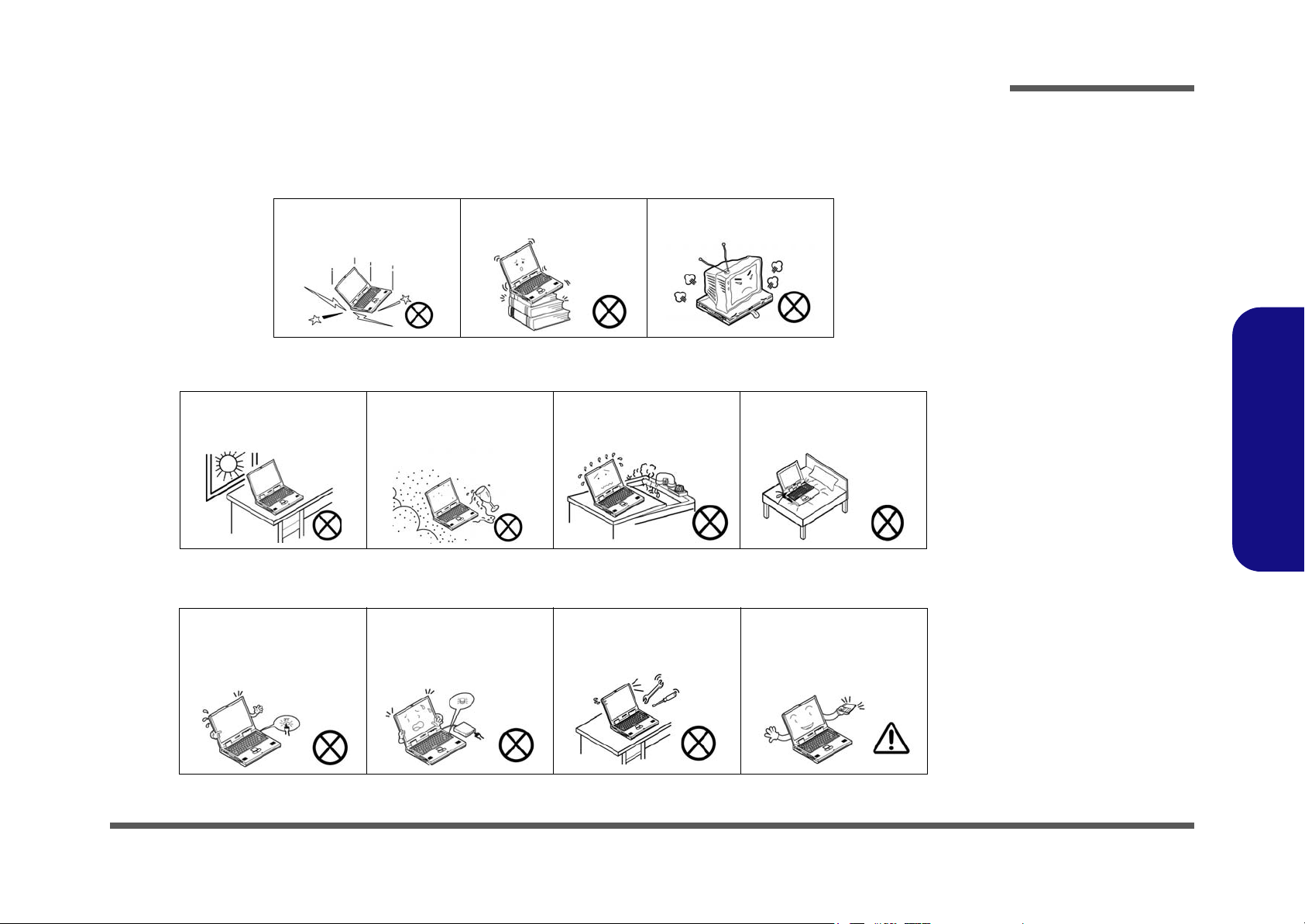
The notebook computer is quite rugged, but it can be damaged. To prevent this, follow these suggestions:
1. Don’t drop it, or expose it to shock. If the computer falls, the case and the components could be damaged.
Preface
Do not expose the computer
to any shock or vibration.
Do not place it on an unstable
surface.
Do not place anything heavy
on the computer.
2. Keep it dry, and don’t overheat it. Keep the computer and power supply away from any kind of heating element. This
is an electrical appliance. If water or any other liquid gets into it, the computer could be badly damaged.
Do not expose it to excessive
heat or direct sunlight.
Do not leave it in a place
where foreign matter or moisture may affect the system.
Don’t use or store the computer in a humid environment.
Do not place the computer on
any surface which will block
the vents.
3. Follow the proper working procedures for the computer. Shut the computer down properly and don’t forget to save
your work. Remember to periodically save your data as data may be lost if the battery is depleted.
Do not turn off the power
until you properly shut down
all programs.
Do not turn off any peripheral
devices when the computer is
on.
Do not disassemble the computer by yourself.
Perform routine maintenance
on your computer.
Preface
V
Page 8

Preface
4. Avoid interference. Keep the computer away from high capacity transformers, electric motors, and other strong mag-
netic fields. These can hinder proper performance and damage your data.
5. Take care when using peripheral devices.
Preface
Power Safety
Warning
Before you undertake
any upgrade procedures, make sure that
you have turned off the
power, and disconnected all peripherals
and cables (including
telephone lines). It is
advisable to also remove your battery in
order to prevent accidentally turning the
machine on.
Use only approved brands of
peripherals.
Unplug the power cord before
attaching peripheral devices.
Power Safety
The computer has specific power requirements:
• Only use a power adapter approved for use with this computer.
• Your AC adapter may be designed for international travel but it still requires a steady, uninterrupted power supply. If you are
unsure of your local power specifications, consult your service representative or local power company.
• The power adapter may have either a 2-prong or a 3-prong grounded plug. The third prong is an important safety feature; do
not defeat its purpose. If you do not have access to a compatible outlet, have a qualified electrician install one.
• When you want to unplug the power cord, be sure to disconnect it by the plug head, not by its wire.
• Make sure the socket and any extension cord(s) you use can support the total current load of all the connected devices.
• Before cleaning the computer, make sure it is disconnected from any external power supplies.
Do not plug in the power
cord if you are wet.
Do not use the power cord if
it is broken.
Do not place heavy objects
on the power cord.
VI
Page 9

Battery Precautions
• Only use batteries designed for this computer. The wrong battery type may explode, leak or damage the computer.
• Do not continue to use a battery that has been dropped, or that appears damaged (e.g. bent or twisted) in any way. Even if the
computer continues to work with a damaged battery in place, it may cause circuit damage, which may possibly result in fire.
• Recharge the batteries using the notebook’s system. Incorrect recharging may make the battery explode.
• Do not try to repair a battery pack. Refer any battery pack repair or replacement to your service representative or qualified service
personnel.
• Keep children away from, and promptly dispose of a damaged battery. Always dispose of batteries carefully. Batteries may explode
or leak if exposed to fire, or improperly handled or discarded.
• Keep the battery away from metal appliances.
• Affix tape to the battery contacts before disposing of the battery.
• Do not touch the battery contacts with your hands or metal objects.
Battery Disposal
The product that you have purchased contains a rechargeable battery. The battery is recyclable. At the end of
its useful life, under various state and local laws, it may be illegal to dispose of this battery into the municipal
waste stream. Check with your local solid waste officials for details in your area for recycling options or proper
disposal.
Preface
Preface
Caution
Danger of explosion if battery is incorrectly replaced. Replace only with the same or equivalent type recommended by the manufacturer. Discard used battery according to the manufacturer’s instructions.
VII
Page 10

Preface
Preface
Related Documents
You may also need to consult the following manual for additional information:
User’s Manual on CD
This describes the notebook PC’s features and the procedures for operating the computer and its ROM-based setup program. It also describes the installation and operation of the utility programs provided with the notebook PC.
VIII
Page 11

Contents
Preface
Introduction ..............................................1-1
Overview .........................................................................................1-1
System Specifications .....................................................................1-2
External Locator - Top View with LCD Panel Open ......................1-5
External Locator - Front & Rear Views ..........................................1-6
External Locator - Right Side & Left Side Views ..........................1-7
External Locator - Bottom View ..................................................... 1-8
Mainboard Overview - Top (Key Parts) .........................................1-9
Mainboard Overview - Bottom (Key Parts) .................................. 1-10
Mainboard Overview - Top (Connectors) ..................................... 1-11
Mainboard Overview - Bottom (Connectors) ...............................1-12
Disassembly ...............................................2-1
Overview .........................................................................................2-1
Maintenance Tools ..........................................................................2-2
Connections ..................................................................................... 2-2
Maintenance Precautions .................................................................2-3
Disassembly Steps ...........................................................................2-4
Removing the Battery ......................................................................2-6
Removing the Hard Disk Drive ....................................................... 2-7
Removing the System Memory (RAM) ..........................................2-9
Removing the Optical (CD/DVD) Device .................................... 2-11
Removing the Processor ................................................................2-12
Removing the Modem ................................................................... 2-14
Removing the Wireless LAN Module ........................................... 2-15
Removing the Keyboard ................................................................2-16
Removing the LCD & Top Case Assembly ..................................2-18
Removing the Speaker & Microphone ..........................................2-19
Removing the Mainboard ..............................................................2-20
Removing the TouchPad and Click Board .................................... 2-21
Removing the Inverter .................................................................. 2-22
Removing the LCD Panel ............................................................. 2-23
Removing the PC Camera Module ............................................... 2-23
Part Lists ..................................................A-1
Part List Illustration Location ........................................................ A-2
Top (M450C) ................................................................................. A-3
Bottom (M450C) ........................................................................... A-4
LCD (M450C) ............................................................................... A-5
HDD (M450C) ............................................................................... A-6
CD-ROM Drive - SAMSUNG (M450C) ...................................... A-7
Combo Drive - QSI (M450C) ........................................................ A-8
Combo Drive - TEAC (M450C) .................................................... A-9
DVD-Dual Drive - LITEON (M450C) ........................................ A-10
DVD-Dual Drive - Panasonic (M450C) ...................................... A-11
DVD-ROM Drive - MKE (M450C) ............................................ A-12
DVD-ROM Drive - QSI (M450C) ............................................... A-13
DVD-ROM Drive - Toshiba (M450C) ........................................ A-14
Schematic Diagrams................................. B-1
System Block Diagram ...................................................................B-2
Socket 479 - 1 of 2 ..........................................................................B-3
Socket 479 - 2 of 2 ..........................................................................B-4
Montania GM-1 ..............................................................................B-5
Montania GM-2 ..............................................................................B-6
Montania GM-3 ..............................................................................B-7
DDRAM .........................................................................................B-8
DDR Termination ...........................................................................B-9
Clock Generator ............................................................................B-10
LVDS, Inverter Board, LED .........................................................B-11
ICH4-1 (1 of 3) .............................................................................B-12
Preface
IX
Page 12

Preface
ICH4-2 (2 of 3) ............................................................................. B-13
ICH4-3 (3 of 3) ............................................................................. B-14
USB 2.0 ........................................................................................ B-15
Mini PCI ....................................................................................... B-16
HDD, CDROM ............................................................................. B-17
LAN RTL8110S (B)-32 ............................................................... B-18
LPC S I/O, Flash ROM ................................................................ B-19
LPT CON .................................................................................... B-20
H8S ............................................................................................... B-21
Audio Codec ALC202 .................................................................. B-22
WOW ........................................................................................... B-23
PCMCIA (PCI1620) ..................................................................... B-24
PCMCIA Socket ........................................................................... B-25
TI1394 (TSB43AB21) .................................................................. B-26
CH7011, TV-Out .......................................................................... B-27
+2.5VS, +1.25VS, +5VS, +3VS .................................................. B-28
Preface
+VDD3, +VDD5, +12V, +3V, +5V ............................................. B-29
+VCCP, +1.5V, +1.8VS ............................................................... B-30
Charger ......................................................................................... B-31
V_CORE ...................................................................................... B-32
MDC Modem Board ..................................................................... B-33
Click Board .................................................................................. B-34
LED Board ................................................................................... B-35
RJ11 Board ................................................................................... B-36
X
Page 13

1: Introduction
Overview
This manual covers the information you need to service or upgrade the M450C series notebook computer. Information
about operating the computer (e.g. getting started, and the Setup utility) is in the User’s Manual. Information about drivers (e.g. VGA & audio) is also found in User’s Manual. That manual is shipped with the computer.
Operating systems (e.g. DOS, Windows 9x, Windows NT 4.0, Windows 2000, Windows XP, OS/2 Warp, UNIX, etc.) have
their own manuals as do application software (e.g. word processing and database programs). If you have questions about
those programs, you should consult those manuals.
The M450C series notebook is designed to be upgradeable. See “Disassembly” on page 2 - 1 for a detailed description
of the upgrade procedures for each specific component. Please note the warning and safety information indicated by the
“” symbol.
The balance of this chapter reviews the computer’s technical specifications and features.
Introduction
1.Introduction
Overview 1 - 1
Page 14
Introduction
System Specifications
Latest Specification Information
The specifications listed in this Appendix are correct at the time of going to press. Certain items (particularly processor types/speeds
and CD/DVD device types) may be changed or updated due to the manufacturer's release schedule. Check with your service center
for details.
Feature Specification
Processor Types Intel Pentium® M - (478-pin) Micro-FCPGA package (µ0.13) 0.13 Micron Process Technology,
1MB On-die L2 Cache & 400MHz FSB
- 1.4/ 1.5/ 1.6/ 1.7 GHz
1.Introduction
Video Memory
The system allocates
or “shares” a portion of
system memory for
video use. “Shared”
memory is user-configurable via the SCU.
The default setting is
set to 8MB.
1 - 2 System Specifications
Intel Pentium® M - (478-pin) Micro-FCPGA package (
Intel Celeron® M - (478-pin) Micro-FCPGA package (µ0.13) 0.13 Micron Process Technology,
Intel Celeron® M - (478-pin) Micro-FCPGA package (
Core Logic Intel 855GME + ICH4-M
Security Security (Kensington® Type) Lock Slot
Memory Two 200-Pin SODIMM Sockets, Supporting DDR 266 /
DDR 333 MHz Modules Only
(Note: Do Not Use Other Module Types)
BIOS One 512KB Flash ROM Insyde BIOS
µ0.09) 0.09 Micron Process Technology,
2MB On-die L2 Cache & 400MHz FSB
- 715/ 725/ 735/ 745/ 755/ 765
512KB On-die L2 Cache & 400MHz FSB
- 320/ 330/ 340
µ0.09) 0.09 Micron Process Technology,
1MB On-die L2 Cache & 400MHz FSB
- 350/ 360/ 370
Memory Expandable up to 2GB (128/ 256/ 512/ 1024 MB
DDR Modules)
Page 15
Feature Specification
LCD Options 15.0" XGA Flat Panel TFT (1024*768) 15.0" SXGA Flat Panel TFT (1400 * 1050)
Introduction
Display Dynamic Video Memory Technology (Shared Memory up
to 64MB)
128 bit 2D/3D Graphics Engine
Motion Compensation for DVD Accelerator
Storage One changeable 12.7mm(h) Optical Device (CD/DVD) Type Drive (see “Optional” on page 1 - 4 for drive options)
Easy changeable 2.5" 9.5 mm (h) IDE HDD
Supports LBA Mode, Master Mode IDE, PIO Mode 4
Audio AC’97 2.2 Compliant
Advanced Wavetable Synthesizer
DirectSound™ 3D Accelerator
Keyboard &
Pointing Device
PCMCIA One Type-II PCMCIA 3.3V/5V Socket
Interface Four USB 2.0/1.1 Ports
Card Reader Embedded 4-in-1 Card Reader (MS/ MS Pro/ SD/ MMC)
Communication 56K Plug & Play Fax/Modem V.90/92 Compliant
Winkey Keyboard Built-In TouchPad with Scrolling Function
One Mini-IEEE1394a Port
One External VGA Monitor Port
One Parallel Port (LPT1) Supporting ECP/EPP
One S/PDIF Output Jack
One S-Video-Out Jack
10/100M Fast Ethernet (IEEE 802.3 and 802.3u Standard
Compliant)
PC Camera with USB Interface
(Factory Option)
Fully DirectX 7/8 Compliant Graphics Engine
Supports VESA DDCI, DDC2B and DDC 3.0
Specifications
Full-Duplex
S/PDIF Digital Output
Built-In Microphone
2 Built-In Stereo Speakers
One Headphone-Out Jack
One Microphone-In Jack
One Line-In Jack
One RJ-11 Jack for Plug & Play Fax/Modem
One RJ-45 Jack for 100M (Max) Fast Ethernet
One DC-in Jack
Bluetooth & MDC Modem Combo Module (Factory
Option)
Intel PRO/Wireless LAN Module with Mini-PCI Interface
(see “WLAN Module Options” on page 1 - 4 for
available options)
1.Introduction
System Specifications 1 - 3
Page 16
Introduction
Feature Specification
1.Introduction
Power
Management
Power Full Range AC Adapter
Environmental
Spec
Physical
Dimensions &
Weight
Optional Optical Drive Module Options:
WLAN Module
Options
Supports ACPI 2.0
Power Button as Sleep/Resume Key
Supports Hibernate Mode
Supports Standby Mode
AC-Input 100~240V, 47~63Hz
DC Output 65 Watts
One 6 Cell, Smart Lithium-Ion Battery Pack - Approx 4.5 Hours battery life
Temperature
Operating: 5
Non-Operating: -20°C ~ 60°C
329mm (w) * 275mm (d) * 25mm (h) Min 3.1 kg With Battery
CD-ROM Drive Module
Combo Drive Module
DVD-ROM Drive Module
DVD-Dual Drive Module
Intel PRO/Wireless 2100 (802.11b) Wireless LAN Module
with Mini-PCI Interface
OR
Intel PRO/Wireless 2200BG (802.11b/g) Wireless LAN
Module with Mini-PCI Interface
OR
Intel PRO/Wireless 2915ABG (802.11a/b/g) Wireless LAN
Module with Mini-PCI Interface
°C ~ 35°C
Supports Battery Low Sleep Mode
Supports Resume From Modem Ring
Supports Wake on LAN
Relative Humidity
Operating: 20% ~ 80%
Non-Operating: 10% ~ 90%
Bluetooth & MDC Modem Combo Module
PC Camera with USB Interface
Software DVD Player
1 - 4 System Specifications
Page 17
Introduction
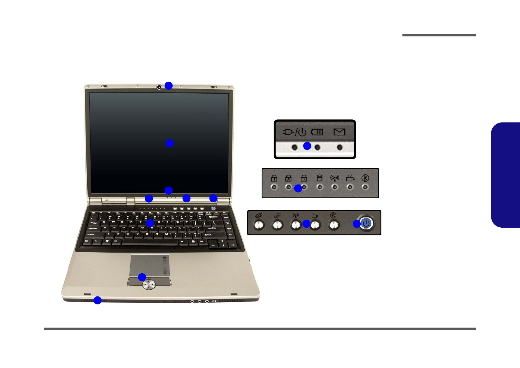
External Locator - Top View with LCD Panel Open
1
2
3
4
7
5
6
4
Figure 1
Top View
1. Optional Built-In
PC Camera
2. LCD
3. LED Power &
Communication
Indicators
4. LED Status
Indicators
3
5
6
5. Quick-Key Button
6. Power Button
7. Keyboard
8. TouchPad and
Buttons
9. Speakers
1.Introduction
8
9
External Locator - Top View with LCD Panel Open 1 - 5
Page 18
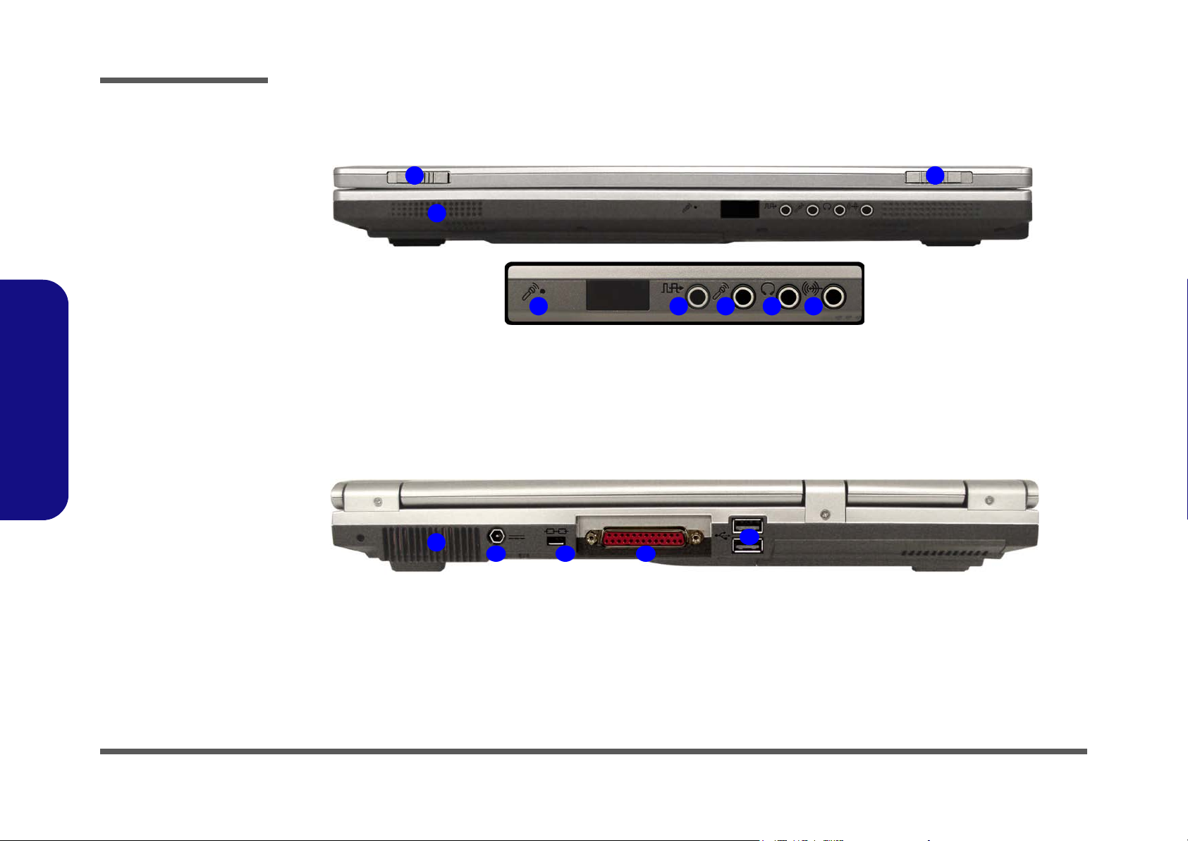
Introduction
Figure 2
Front View
1. LCD Latches
2. Speaker
3. Built-In
Microphone
4. S/PDIF-Out Jack
5. Microphone-In
Jack
6. Headphone-Out
Jack
7. Line-In Jack
Figure 3
1.Introduction
Rear View
1. Vent
2. DC-In Jack
3. Security Lock Slot
4. Parallel Port
5. 2 * USB 2.0 Ports
External Locator - Front & Rear Views
1
2
1
2
3 4
1
5 6 743
5
1 - 6 External Locator - Front & Rear Views
Page 19
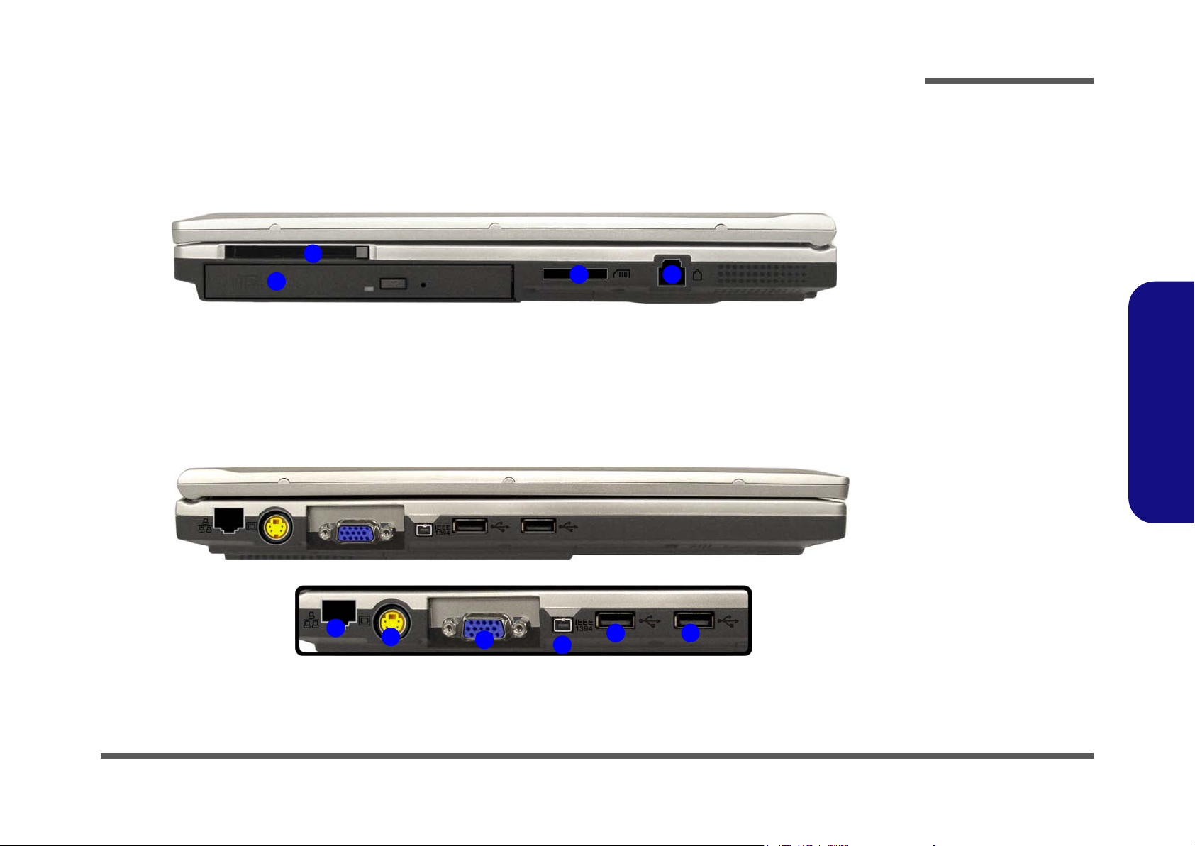
External Locator - Right Side & Left Side Views
2
1
3 4
Introduction
Figure 4
Right Side View
1. Optical Device
Drive Bay
2. PC Card Slot
3. 4-in-1 Card
Reader (reads
SD/ MMC/ MS &
MS Pro formats)
4. RJ-11 Phone Jack
1.Introduction
Figure 5
Left Side View
1. RJ-45 LAN Jack
2. S-Video-Out Jack
3. External Monitor
(VGA) Port
4. Mini-IEEE 1394a
Port
5. 2 * USB 2.0 Ports
1
2
3
4
5
5
External Locator - Right Side & Left Side Views 1 - 7
Page 20
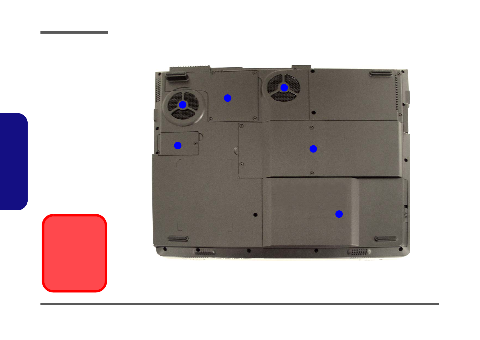
Introduction
Figure 6
Bottom View
1. Vent/Fan Intakes
2. Modem/
Bluetooth &
Modem Combo
Module Cover
3. CPU Bay Cover
4. Hard Disk/
Memory (RAM)/
WLAN Cover
5. Battery
1.Introduction
External Locator - Bottom View
3
1
2
1
4
Overheating
To prevent your computer from overheating
make sure nothing
blocks the vent/fan intakes while the computer is in use.
1 - 8 External Locator - Bottom View
5
Page 21
Introduction
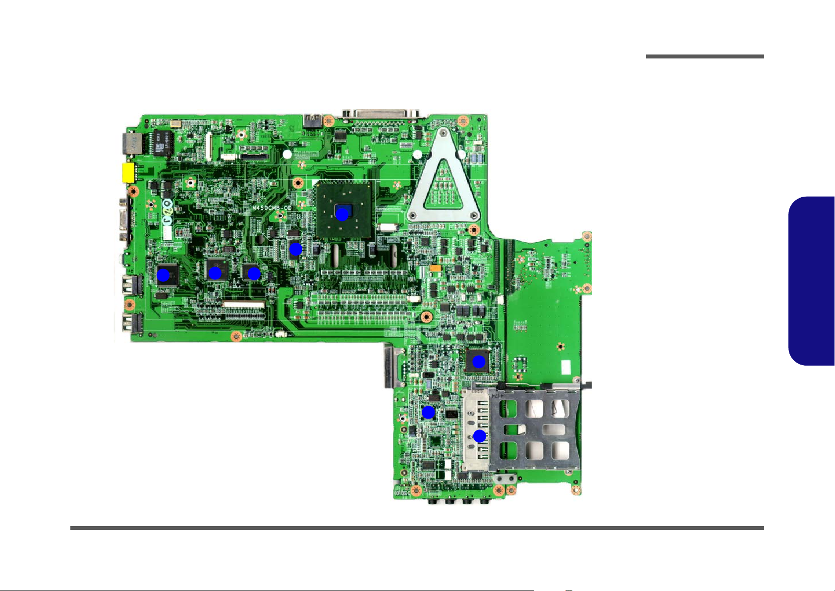
Mainboard Overview - Top (Key Parts)
1
2
5
4
3
Figure 7
Mainboard Top
Key Parts
1. Northbridge - Intel
855GME
2. Clock Generator
3. LPC Super I/O
NS PC87383
4. H8
5. 1394 PHY
TSB41LV01
6. PCI1620 Cardbus
Controller
7. ALC202 - Audio
Codec
8. PC Card
Assembly
6
1.Introduction
7
8
Mainboard Overview - Top (Key Parts) 1 - 9
Page 22
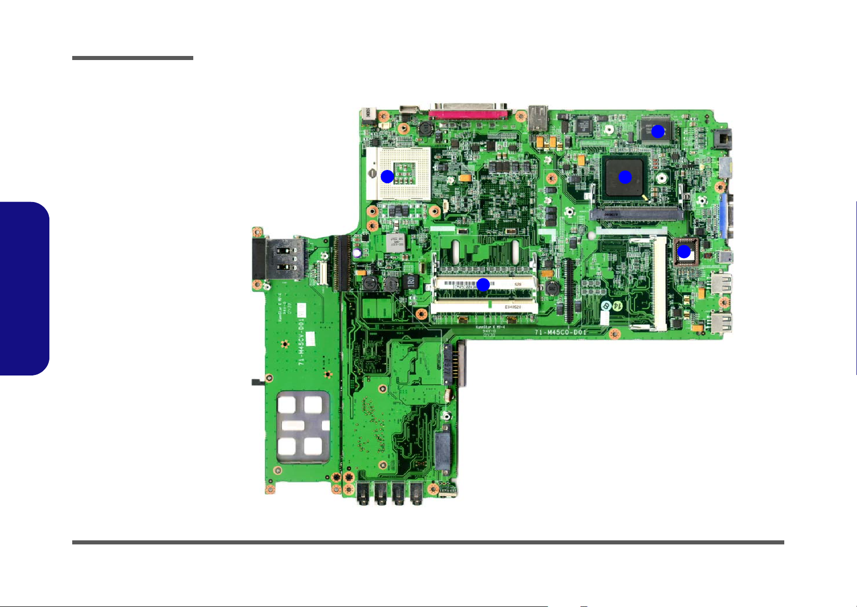
Introduction
Figure 8
Mainboard Bottom
Key Parts
1. CPU Socket (no
CPU installed)
2. Memory Slots (no
memory installed)
3. Southbridge 82801DBM
4. LAN Controller
RTL8110S-32
5. Flash BIOS ROM
1.Introduction
Mainboard Overview - Bottom (Key Parts)
1
2
4
3
5
1 - 10 Mainboard Overview - Bottom (Key Parts)
Page 23
Introduction
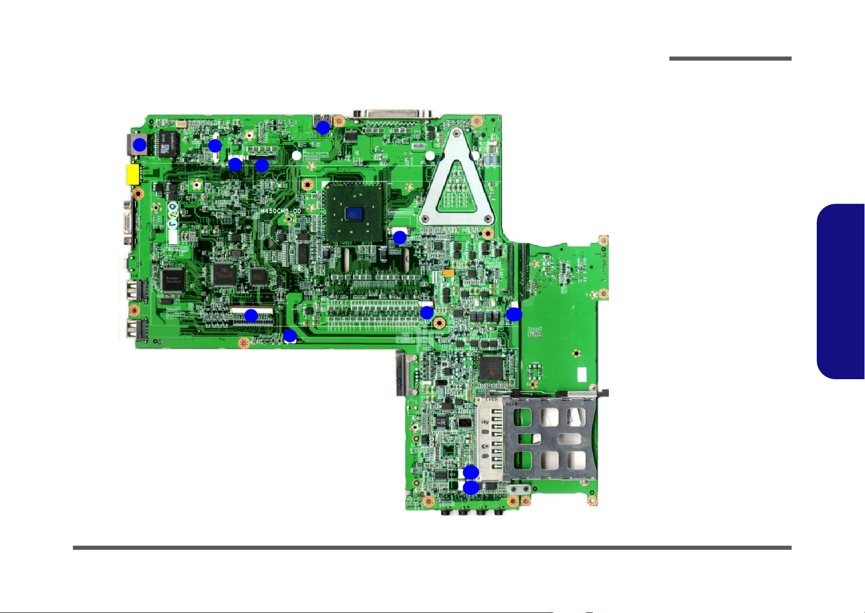
Mainboard Overview - Top (Connectors)
7
1
2
3
4
8
5
6
Figure 9
Mainboard Top
Connectors
1. LAN Connector
(JMLAN1)
2. Inverter Connector
(JINV1)
3. CCD Cable
Connector
(JCCD1)
4. LCD Panel Cable
Connector
(JLCD1)
5. Keyboard Cable
Connector (JKB1)
6. CMOS Battery
Cable Connector
9
11
12
10
(JBAT1)
7. USB Connector
(JUSB1)
8. LED Cable
Connector
(JLED1)
9. TouchPad Cable
Connector (JTP1)
10. Speaker Cable
Connector
(JSPK1)
11. Microphone Cable
Connector
(JINTMIC1)
12. Speaker Cable
Connector
(JSPK2)
1.Introduction
Mainboard Overview - Top (Connectors) 1 - 11
Page 24
Introduction
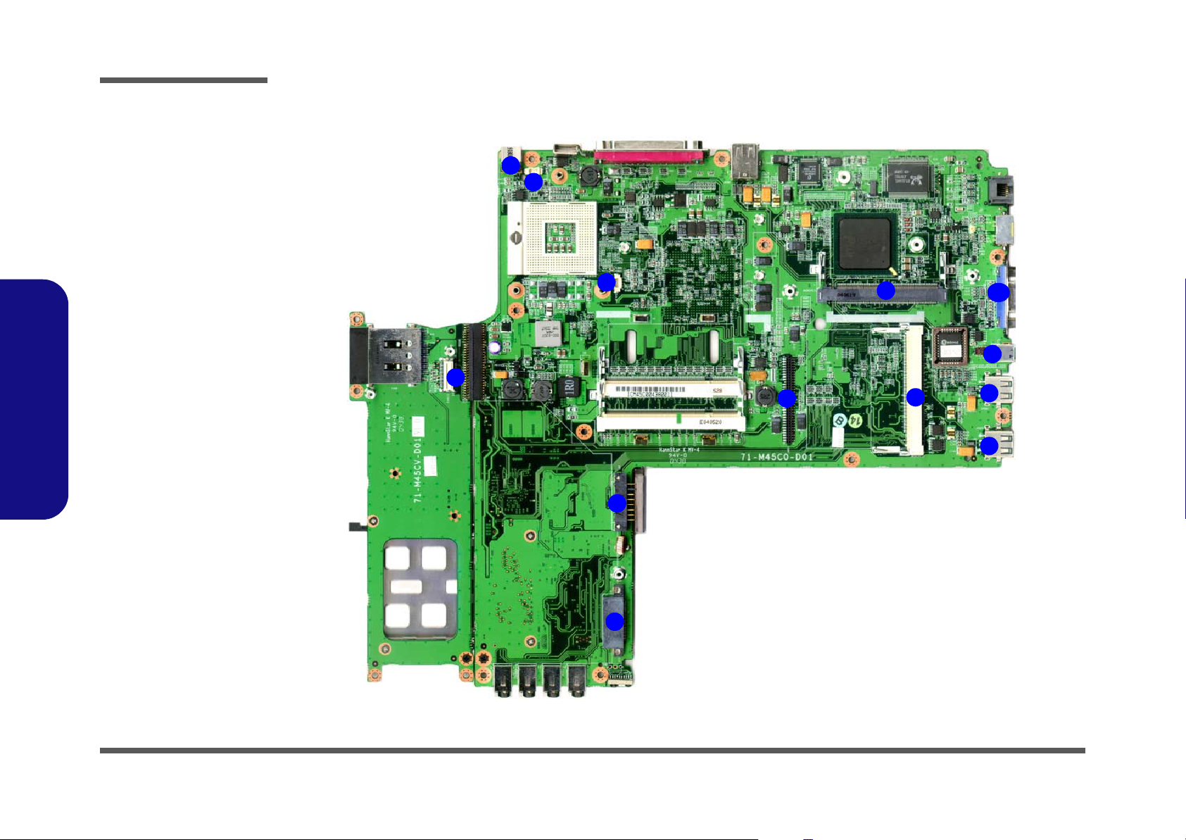
Figure 10
Mainboard Bottom
Connectors
1. Power Cable
Connector
(JPWR1)
2. Fan Cable
Connector (JFAN1
& JFAN2)
3. Modem Module
Connector
(RJMDC2)
4. Battery Connector
(CN2)
5. CD-ROM
Connector (JCD1)
6. Hard Disk
Connector
1.Introduction
(JHDD1)
7. Mini-PCI (Wireless
Lan Module)
Connector
(JMINIPCI1 &
JMINIPCI2)
8. USB Connector
(JUSB2 & JUSB3)
9. 1394 Connector
10. VGA-Out
Connector
(JVGA1)
Mainboard Overview - Bottom (Connectors)
1
2
2
3
6
4
5
7
7
10
9
8
8
1 - 12 Mainboard Overview - Bottom (Connectors)
Page 25

2: Disassembly
Overview
This chapter provides step-by-step instructions for disassembling the M450C series notebook’s parts and subsystems.
When it comes to reassembly, reverse the procedures (unless otherwise indicated).
We suggest you completely review any procedure before you take the computer apart.
Disassembly
Procedures such as upgrading/replacing the RAM, CD device and hard disk are included in the User’s Manual but are
repeated here for your convenience.
To make the disassembly process easier each section may have a box in the page margin. Information contained under
the figure # will give a synopsis of the sequence of procedures involved in the disassembly procedure. A box with a
lists the relevant parts you will have after the disassembly process is complete. Note: The parts listed will be for the disassembly procedure listed ONLY, and not any previous disassembly step(s) required. Refer to the part list for the previous disassembly procedure. The amount of screws you should be left with will be listed here also.
A box with a will also provide any possible helpful information. A box with a contains warnings.
An example of these types of boxes are shown in the sidebar.
2.Disassembly
Information
Warning
Overview 2 - 1
Page 26

Disassembly
2.Disassembly
NOTE: All disassembly procedures assume that the system is turned OFF, and disconnected from any power supply (the
battery is removed too).
Maintenance Tools
The following tools are recommended when working on the notebook PC:
• M3 Philips-head screwdriver
• M2.5 Philips-head screwdriver (magnetized)
• M2 Philips-head screwdriver
• Small flat-head screwdriver
• Pair of needle-nose pliers
• Anti-static wrist-strap
Connections
Connections within the computer are one of four types:
Locking collar sockets for ribbon connectors To release these connectors, use a small flat-head screwdriver to
gently pry the locking collar away from its base. When replacing the connection, make sure the connector is oriented in the
same way. The pin1 side is usually not indicated.
2 - 2 Overview
Pressure sockets for multi-wire connectors To release this connector type, grasp it at its head and gently
rock it from side to side as you pull it out. Do not pull on the
wires themselves. When replacing the connection, do not try to
force it. The socket only fits one way.
Pressure sockets for ribbon connectors To release these connectors, use a small pair of needle-nose pli-
ers to gently lift the connector away from its socket. When replacing the connection, make sure the connector is oriented in
the same way. The pin1 side is usually not indicated.
Board-to-board or multi-pin sockets To separate the boards, gently rock them from side to side as
you pull them apart. If the connection is very tight, use a small
flat-head screwdriver - use just enough force to start.
Page 27

Maintenance Precautions
The following precautions are a reminder. To avoid personal injury or damage to the computer while performing a removal and/or replacement job, take the following precautions:
1. Don't drop it. Perform your repairs and/or upgrades on a stable surface. If the computer falls, the case and other
components could be damaged.
2. Don't overheat it. Note the proximity of any heating elements. Keep the computer out of direct sunlight.
3. Avoid interference. Note the proximity of any high capacity transformers, electric motors, and other strong mag-
netic fields. These can hinder proper performance and damage components and/or data. You should also monitor
the position of magnetized tools (i.e. screwdrivers).
4. Keep it dry. This is an electrical appliance. If water or any other liquid gets into it, the computer could be badly
damaged.
5. Be careful with power. Avoid accidental shocks, discharges or explosions.
•Before removing or servicing any part from the computer, turn the computer off and detach any power supplies.
•When you want to unplug the power cord or any cable/wire, be sure to disconnect it by the plug head. Do not pull on the wire.
6. Peripherals – Turn off and detach any peripherals.
7. Beware of static discharge. ICs, such as the CPU and main support chips, are vulnerable to static electricity.
Before handling any part in the computer, discharge any static electricity inside the computer. When handling a
printed circuit board, do not use gloves or other materials which allow static electricity buildup. We suggest that
you use an anti-static wrist strap instead.
8. Beware of corrosion. As you perform your job, avoid touching any connector leads. Even the cleanest hands produce oils which can attract corrosive elements.
9. Keep your work environment clean. Tobacco smoke, dust or other air-born particulate matter is often attracted
to charged surfaces, reducing performance.
10. Keep track of the components. When removing or replacing any part, be careful not to leave small parts, such as
screws, loose inside the computer.
Disassembly
Power Safety
Warning
Before you undertake
any upgrade procedures, make sure that
you have turned off the
power, and disconnected all peripherals
and cables (including
telephone lines). It is
advisable to also remove your battery in
order to prevent accidentally turning the
machine on.
2.Disassembly
Cleaning
Do not apply cleaner directly to the computer, use a soft clean cloth.
Do not use volatile (petroleum distillates) or abrasive cleaners on any part of the computer.
Overview 2 - 3
Page 28

Disassembly
Disassembly Steps
The following table lists the disassembly steps, and on which page to find the related information. PLEASE PERFORM
THE DISASSEMBLY STEPS IN THE ORDER INDICATED.
2.Disassembly
To remove the Battery:
1. Remove the battery page 2 - 6
To remove the HDD:
1. Remove the battery page 2 - 6
2. Remove the HDD page 2 - 7
To remove the System Memory:
1. Remove the battery page 2 - 6
2. Remove the system memory page 2 - 9
To remove the Optical Device:
1. Remove the battery page 2 - 6
2. Remove the optical device page 2 - 11
To remove the Processor:
1. Remove the battery page 2 - 6
2. Remove the processor page 2 - 12
To remove the Modem:
1. Remove the battery page 2 - 6
2. Remove the modem page 2 - 14
To remove the Wireless LAN module:
1. Remove the battery page 2 - 6
2. Remove the HDD page 2 - 7
3. Remove the wireless LAN module page 2 - 15
To remove the Keyboard:
1. Remove the battery page 2 - 6
2. Remove the keyboard page 2 - 16
To remove the Top Case:
1. Remove the battery page 2 - 6
2. Remove the HDD page 2 - 7
3. Remove the system memory page 2 - 9
4. Remove the optical device page 2 - 11
5. Remove the processor page 2 - 12
6. Remove the keyboard page 2 - 16
7. Remove the top case page 2 - 18
To remove the Speaker & Microphone:
1. Remove the battery page 2 - 6
2. Remove the HDD page 2 - 7
3. Remove the optical device page 2 - 11
4. Remove the processor page 2 - 12
5. Remove the top case page 2 - 18
6. Remove the speaker & microphone page 2 - 19
2 - 4 Disassembly Steps
Page 29

Disassembly
To remove the Mainboard:
1. Remove the battery page 2 - 6
2. Remove the HDD page 2 - 7
3. Remove the system memory page 2 - 9
4. Remove the optical device page 2 - 11
5. Remove the modem page 2 - 14
6. Remove the processor page 2 - 12
7. Remove the keyboard page 2 - 16
8. Remove the top case page 2 - 18
9. Remove the speaker & microphone page 2 - 19
10. Remove the mainboard page 2 - 20
To remove the TouchPad & Click Board:
1. Remove the battery page 2 - 6
2. Remove the HDD page 2 - 7
3. Remove the system memory page 2 - 9
4. Remove the optical device page 2 - 11
5. Remove the modem page 2 - 14
6. Remove the processor page 2 - 12
7. Remove the keyboard page 2 - 16
8. Remove the top case page 2 - 18
9. Remove the speaker & microphone page 2 - 19
10. Remove the mainboard page 2 - 20
11. Remove the touchpad & click board page 2 - 21
To remove the LCD Panel:
1. Remove the battery page 2 - 6
2. Remove the HDD page 2 - 7
3. Remove the optical device page 2 - 11
4. Remove the processor page 2 - 12
5. Remove the top case page 2 - 18
6. Remove the inverter page 2 - 22
7. Remove the LCD panel page 2 - 23
To remove the PC Camera:
1. Remove the battery page 2 - 6
2. Remove the inverter page 2 - 22
3. Remove the PC Camera page 2 - 23
2.Disassembly
To remove the Inverter:
1. Remove the battery page 2 - 6
2. Remove the inverter page 2 - 22
Disassembly Steps 2 - 5
Page 30
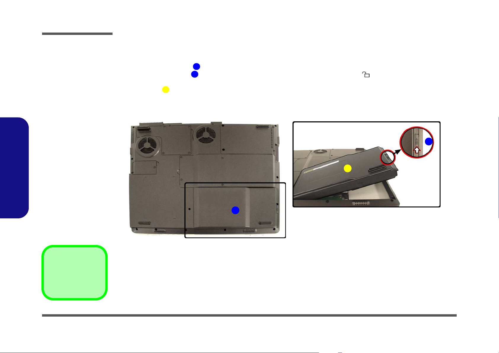
Disassembly
Figure 1
Battery Removal
a. Locate the battery re-
lease latch.
b. Release the latch and re-
move the battery out of
the computer.
2.Disassembly
Removing the Battery
1. Turn the computer off, and turn it over.
2. Locate the battery bay
3. Slide the battery latch
shown in Figure 1b)
4. The Battery will pop up to allow you to lift it out of the bay (Figure 1b).
a.
3
1
(Figure 1a).
2
in the direction of the arrow (towards the unlock symbol ), and hold it in place (as
.
b.
2
3
3. Battery
2 - 6 Removing the Battery
1
Page 31

Removing the Hard Disk Drive
Disassembly
The hard disk drive is mounted in a removable case and can be taken out to accommodate other 2.5" IDE hard disk drives
with a height of 9.5mm (h). Follow your operating system’s installation instructions, and install all necessary drivers and
utilities (as outlined in Chapter 5 of the User’s Manual) when setting up a new hard disk.
Hard Disk Upgrade Process
1. Turn off the computer, turn it over and remove the battery (page 2 - 6).
2. Locate the hard disk/memory bay cover .
3. Remove screws - and remove the bay cover .
2 5 1
a.
1
b.
HDD System Warning
New HDD’s are blank. Before you begin make sure:
You have backed up any
data you want to keep from
your old HDD.
You have all the CD-ROMs
and FDDs required to install your operating system
and programs.
2 3
1
45
Figure 2
HDD Assembly
Removal
a. Locate the HDD bay cov-
er and remove the
screws.
b. Lift the cover off the com-
puter.
2.Disassembly
If you have access to the
internet, download the latest application and hardware driver updates for the
operating system you plan
to install. Copy these to a
removable medium.
1
1. HDD/RAM Bay
Cover
•4 Screws
Removing the Hard Disk Drive 2 - 7
Page 32

Disassembly
Figure 3
HDD Assembly
Removal (Cont.)
a. Slide out the HDD as-
sembly.
b. Lift the HDD assembly
out of the bay and remove the screws.
c. Separate the bracket and
HDD.
2.Disassembly
4. Pull the tab in the direction of the arrow in order to release the hard disk assembly from the connector.
5. Carefully lift the hard disk assembly up out off the computer.
6. Remove screws from points - on the side of the hard disk assembly in order to separate the bracket from
the hard disk (Figure 3b).
1 2
3
4 7 8
9
7. Reverse the process to install a new hard disk (pay careful attention to the orientation of the disk under the cover).
a.
c.
1
2
3
9
b.
8. Bracket
9. Hard Disk
•4 Screws
2 - 8 Removing the Hard Disk Drive
4
5
8
6
7
Page 33

Removing the System Memory (RAM)
The computer has two memory sockets for 200 pin Small Outline Dual In-line Memory Modules (SO-DIMM) supporting
DDR 266/333MHz. The main memory can be expanded up to 2GB. The SO-DIMM modules supported are 128MB,
256MB, 512MB and 1024MB. The total memory size is automatically detected by the POST routine once you turn on
your computer.
Disassembly
Figure 4
Memory Socket
Cover Removal
Memory Upgrade Process
1. Turn off the computer, turn it over and remove the battery (page 2 - 6).
2. Locate the hard disk/memory bay cover .
3. Remove screws - and remove the bay cover .
2 5 1
a.
2 3
1
b.
1
45
a. Remove the screws.
b. Lift the cover off the com-
puter.
2.Disassembly
1
1. HDD/RAM Bay
Cover
•4 Screws
Removing the System Memory (RAM) 2 - 9
Page 34

Disassembly
Figure 5
Removing/
Installing a RAM
Module
a. Pull the release
latche(s).
b. Remove the mod-
ule(s).
Contact Warning
Be careful not to touch
the metal pins on the
module’s connecting
edge. Even the cleanest hands have oils
2.Disassembly
which can attract particles, and degrade the
module’s performance.
4. Gently pull the two release latches ( & ) on the sides of the memory socket in the direction indicated by the
1 2
arrows (Figure 5a).
5. The RAM module(s) will pop-up
3
(Figure 5b), and you can then remove it.
a. b.
3
1
1
3
2
2
3
6. Pull the latches to release the second module if necessary.
7. Insert a new module holding it at about a 30° angle and fit the connectors firmly into the memory slot.
8. The module will only fit one way as defined by its pin alignment. Make sure the module is seated as far into the slot
as it will go. DO NOT FORCE IT; it should fit without much pressure.
3. RAM Module
9. Press the module down towards the mainboard until the slot levers click into place to secure the module.
10. Replace the hard disk/memory bay cover and the 4 screws (see page 2 - 9).
11. Restart the computer to allow the BIOS to register the new memory configuration as it starts up.
2 - 10 Removing the System Memory (RAM)
Page 35

Removing the Optical (CD/DVD) Device
Disassembly
1. Turn off the computer, turn it over and remove the battery (page 2 - 6).
2. Locate the hard disk/memory bay cover and remove screws
3. Remove the hard disk/memory bay cover (Figure 6b).
4. Use a screwdriver to apply presure at point to push the optical device out of the computer (Figure 6c).
6
7 8
1 5
- (Figure 6a).
5. Insert the new device and carefully slide it into the computer (the device only fits one way. DO NOT FORCE IT; The
screw holes should line up.
6. Restart the computer to allow it to automatically detect the new device.
a.
b.
1 2
34
5
6
c.
7
Figure 6
Optical Device
Removal
a. Remove the screws.
b. Carefully lift the cover off
the computer.
c. Push the optical device
out off the computer at
point 7.
2.Disassembly
8
6. HDD/RAM Bay
Cover
8. Optical Device
•5 Screws
Removing the Optical (CD/DVD) Device 2 - 11
Page 36

Disassembly
Removing the Processor
Figure 7
Processor Removal
a. Remove the screws.
b. Carefully lift the cover off
the computer.
c. Remove the screws in
the order indicated.
d. Remove the heat sink.
2.Disassembly
1. Turn off the computer, turn it over and remove the battery (page 2 - 6).
2. Remove screws - from the CPU cover
3. Carefully lift up the CPU cover off the computer.
4. Remove screws
5. Carefully lift up the heat sink (Figure 7d) off the computer.
a.
b.
1 4
5
- (Figure 7c) from the heat sink in the order indicated.
6 8
9
1
3
.
c.
2
4
d.
5
7
6
8
9
7. CPU Cover
11. Heat Sink
•7 Screws
2 - 12 Removing the Processor
9
10
Page 37

Disassembly
6. Turn the release latch towards the unlock symbol , to release the CPU (Figure 8a).
7. Carefully (it may be hot) lift the CPU up out of the socket (Figure 8b).
1
2
8. Reverse the process to install a new CPU.
9. When re-inserting the CPU, pay careful attention to the pin alignment, it will fit only one way (DO NOT FORCE IT!).
a.
1
Unlock
Lock
b.
Caution
2
The heat sink, and
CPU area in general,
contains parts which
are subject to high
temperatures. Allow
the area time to cool
before removing these
parts.
Figure 8
Processor Removal
(cont’d)
a. Turn the release latch to
unlock the CPU.
b. Lift the CPU out of the
socket.
2.Disassembly
2. CPU
Removing the Processor 2 - 13
Page 38

Disassembly
Figure 9
Modem Removal
a. Remove the screw.
b. Lift the cover off the
computer and remove
the screws.
c. Remove the module
from the connector and
and disconnect the cables.
2.Disassembly
Removing the Modem
1. Turn off the computer, turn it over and remove the battery (page 2 - 6).
2. Locate the socket cover and remove screw (Figure 9a).
3. Lift the cover off the computer and remove screws - (Figure 9b).
4. Lift the modem
2 3 4
5
(Figure 9c) up and off the computer (be careful as the cables are still connected).
5. Carefully separate the modem from the connector
a.
1
1
and disconnect cables - .
6 7 8
b.
2
c.
3
4
2. Socket Cover
8. Modem
.
•3 Screws
2 - 14 Removing the Modem
8
5
7
6
Page 39

Disassembly
Removing the Wireless LAN Module
1. Turn off the computer, remove the battery (page 2 - 6) and HDD (page 2 - 7).
2. Carefully disconnect the cable , then gently pull the two release latches ( - ) on the sides of the module
1
socket.
3. The wireless LAN module (Figure 10b) will pop-up, and you can remove it.
4
a.
2
1
3
b.
2 3
Figure 10
Wireless LAN
Module Removal
a. Disconnect the cable
and pull the release
latches.
b. Remove the wireless
LAN module.
Note: Make sure you re-
connect the antenna cable to the “Main” socket
(Figure 10a).
2.Disassembly
4
4. Wireless LAN Mod-
.
ule
Removing the Wireless LAN Module 2 - 15
Page 40

Disassembly
Removing the Keyboard
Figure 11
Keyboard Removal
a. Press the three latches
to release the keyboard.
b. Disconnect the cable
from the locking collar.
c. Remove the keyboard.
Re-Inserting the Key-
board
2.Disassembly
When re-inserting the
keyboard firstly align
the keyboard tabs at
the bottom of the keyboard with the slots in
the case.
1. Turn off the computer, and remove the battery (page 2 - 6).
2. Press the three keyboard latches at the top of the keyboard to elevate the keyboard from its normal position (you
may need to use a small screwdriver to do this).
3. Carefully lift the keyboard up, being careful not to bend the keyboard ribbon cable (Figure 11c).
4. Disconnect the keyboard ribbon cable from the locking collar socket .
a.
4 5
5 6
c.
1 2 3
4
b.
5
4
4. Keyboard
2-16
6
Page 41

Disassembly
5. Remove screws - from the keyboard shielding plate (Figure 11a).
6. Carefully lift the keyboard shielding plate off the computer (Figure 11b).
7. Remove screws - from the rear of the computer (Figure 11c).
8. Remove screw and then disconnect the cables & connectors - from the mainboard and remove the hinge
covers (Figure 11d).
19
a.
1
2
b.
1 7 8
8
9
11
12 13 18
c.
3
5
4
8
6
9
7
d.
10
11
19
19 19
12
Figure 12
Keyboard Shielding
Plate Removal
a. Remove the screws.
b. Remove the shielding
plate.
c. Remove the screws.
d. Disconnect the cable
and connectors. Re-
move the hinge covers.
2.Disassembly
13
14
15
16
8
17
18
8. Keyboard Shielding Plate
19. Hinge Covers
.
•11 Screws
Removing the Keyboard 2 - 17
Page 42

Disassembly
Removing the LCD & Top Case Assembly
Figure 13
LCD & Top Case
Assembly Removal
a. Remove the screws from
the bottom of the computer and disconnect the
cables.
b. Lift theLCD and top case
off the bottom case assembly.
2.Disassembly
1. Turn off the computer, remove the battery (page 2 - 6), hard disk (page 2 - 7), RAM (page 2 - 9), Optical Device
(page 2 - 11), CPU (page 2 - 12), and keyboard (page 2 - 16).
2. Remove screws
3. Carefully lift the LCD and top case
a.
1
13
12
11
- (Figure 13a) from the bottom of the computer and disconnect cable .
1 16 17
18 19
off the bottom case assembly (Figure 13b).
10
2
17
9
3
14
15
16
8
4
5
6
7
b.
19
18
18. LCD & Top Case
19. Bottom Case
•16 Screws
2 - 18 Removing the LCD & Top Case Assembly
Page 43

Removing the Speaker & Microphone
Disassembly
1. Turn off the computer, remove the battery (page 2 - 6), hard disk (page 2 - 7), RAM (page 2 - 9), Optical Device
(page 2 - 11), CPU (page 2 - 12), and top case (page 2 - 18).
2. Remove screw
3. Lift the speaker and microphone off the mainboard assembly (Figure 15b).
1 2 3
and disconnect cables & .
4 5
a.
b.
4
2
3
1
Figure 14
Speaker &
Microphone
Removal
a. Remove the screw and
disconnect the cables.
d. Lift the speaker and mi-
crophone off the mainboard.
2.Disassembly
5
4. Speaker
5. Microphone
•1 Screw
Removing the Speaker & Microphone 2 - 19
Page 44

Disassembly
Removing the Mainboard
Figure 15
Mainboard Removal
a. Remove screws and dis-
connect the cable.
d. Separate the mainboard,
and bottom case.
2.Disassembly
1. Turn off the computer, remove the battery (page 2 - 6), hard disk (page 2 - 7), RAM (page 2 - 9), Optical Device
(page 2 - 11), modem (page 2 - 14), CPU (page 2 - 12), keyboard (page 2 - 16), LCD & top case (page 2 - 18),
and speaker (page 2 - 19).
2. Remove screws
3. Separate the mainboard , and bottom case (Figure 15b).
a. b.
1 2 3
- and disconnect cable (Figure 15a).
4 5
1
3
2
4
5
4. Mainboard
5. Bottom case
•2 Screws
2 - 20 Removing the Mainboard
Page 45

Removing the TouchPad and Click Board
Disassembly
1. Turn off the computer, remove the battery (page 2 - 6), hard disk (page 2 - 7), RAM (page 2 - 9), Optical Device
(page 2 - 11), modem (page 2 - 14), CPU (page 2 - 12), keyboard (page 2 - 16), LCD & top case (page 2 - 18),
speaker (page 2 - 19), and mainboard (page 2 - 20).
2. Remove screws - and disconnect cable (Figure 16a).
3. Disconnect cable from the click board assembly
a.
b.
1 4 5
6 7
5
1
4
2
3
and lift the assembly off the top case (Figure 16c).
c.
7
Figure 16
TouchPad and Click
Board Removal
a. Remove the screws.
b. Disconnect the cables.
c. Separate the click board
from the top case.
2.Disassembly
6
7
7. Click Board
•4 Screws
Removing the TouchPad and Click Board 2 - 21
Page 46

Disassembly
Removing the Inverter
Figure 17
Inverter Removal
a. Remove the rubber cov-
ers and screws.
b. Unsnap the frame from
the LCD front panel
module.
c. Remove the screw from
the inverter and disconnect the cables.
c. Lift the inverter off the
LCD assembly.
2.Disassembly
1. Turn off the computer, remove the battery (page 2 - 6).
2. Remove the rubber covers and screws - from the LCD (Figure 17a).
3. Run your finger around the middle of the frame to carefully unsnap the LCD front panel module from the back.
4. Remove screw
5. Lift the inverter off the LCD assembly (Figure 17d).
a.
1
8 9
from the inverter and disconnect cables & from the rear of the inverter .
11
2
3
1 6
4
7
10
b.
7
5
c.
6
d.
10
11
7. LCD Front Panel
11. Inverter
• 6 Rubber covers
•7 Screws
2 - 22 Removing the Inverter
8
9
Page 47

Removing the LCD Panel
Disassembly
1. Turn off the computer, remove the battery (page 2 - 6), hard disk (page 2 - 7), Optical Device (page 2 - 11), CPU
(page 2 - 12), LCD & top case (page 2 - 18), mainboard (page 2 - 20), and inverter (page 2 - 22).
2. Remove screws - from the side of the LCD panel (Figure 18a).
3. Gently lift the LCD panel off the LCD assembly (Figure 18b).
a. b.
1
2
3
1 6
7
4
7
5
6
Removing the PC Camera Module
1. Turn off the computer, remove the battery (page 2 - 6), and inverter (page 2 - 22).
2. Disconnect cable from the PC camera module (Figure 19a).
3. Lift the PC camera module (Figure 19b) off the LCD assembly.
a.
1
2
b.
2
1
Figure 18
LCD Panel Removal
a. Remove screws from the
side of the LCD panel.
b. Lift the LCD panel off the
LCD assembly.
7. LCD Panel
•6 Screws
Figure 19
PC Camera Removal
a. Disconnect the cable.
b. Lift the PC Camera off
the LCD assembly.
2.Disassembly
2. PC Camera
Removing the LCD Panel 2 - 23
Page 48

Disassembly
2.Disassembly
2-24
Page 49

Appendix A:Part Lists
This appendix breaks down the M450C series notebook’s construction into a series of illustrations. The component part
numbers are indicated in the tables opposite the drawings.
Note: This section indicates the manufacturer’s part numbers. Your organization may use a different system, so be sure
to cross-check any relevant documentation.
Note: Some assemblies may have parts in common (especially screws). However, the part lists DO NOT indicate the
total number of duplicated parts used.
Part Lists
Note: Be sure to check any update notices. The parts shown in these illustrations are appropriate for the system at the
time of publication. Over the product life, some parts may be improved or re-configured, resulting in new part numbers.
A.Part Lists
A-1
Page 50

Part Lists
Table 1 - 1
Part List Illustration
Location
Part List Illustration Location
The following table indicates where to find the appropriate part list illustration.
Part M450C
Top
page A - 3
A.Part Lists
Bottom
LCD
HDD
CD-ROM Drive - Samsung
Combo Drive - QSI
Combo Drive - TEAC
DVD-Dual Drive - LITEON
DVD-Dual Drive - PANASONIC
DVD-ROM Drive - MKE
DVD-ROM Drive - QSI
DVD-ROM Drive - Toshiba
page A - 4
page A - 5
page A - 6
page A - 7
page A - 8
page A - 9
page A - 10
page A - 11
page A - 12
page A - 13
page A - 14
A - 2 Part List Illustration Location
Page 51

Top (M450C)
Part Lists
無鉛
(香檳銀) 無鉛
(香檳銀+銀黑色) 無鉛
(香檳銀) 無鉛
漢保 無鉛
無鉛
(香檳銀)無鉛
漢保 無鉛
漢保 無鉛
Figure 1
A.Part Lists
Top (M450C)
無鉛
Top (M450C) A - 3
Page 52

Part Lists
Bottom (M450C)
無鉛
( ㄈ形 )絕緣用 無鉛
無鉛
(熱處理)
遮羞鐵片
無鉛
無鉛
Bottom (M450C)
A.Part Lists
Figure 2
絕緣用 無鉛
華力
外
外
(銀黑色) 無鉛
(銀黑色) 無鉛
(銀黑色) 無鉛
(銀黑色) 無鉛
無鉛
絕緣用 無鉛
無鉛
無鉛
(銀黑色) 無鉛
祐宣 ,M400A 無鉛
無鉛
無鉛
A - 4 Bottom (M450C)
Page 53

LCD (M450C)
Part Lists
Figure 3
LCD (M450C)
A.Part Lists
LCD (M450C) A - 5
Page 54

Part Lists
HDD (M450C)
A.Part Lists
HDD (M450C)
Figure 4
A - 6 HDD (M450C)
Page 55

CD-ROM Drive - SAMSUNG (M450C)
Part Lists
Figure 5
CD-ROM Drive -
SAMSUNG
(M450C)
A.Part Lists
CD-ROM Drive - SAMSUNG (M450C) A - 7
Page 56

Part Lists
Combo Drive - QSI
A.Part Lists
Combo Drive - QSI (M450C)
Figure 6
(M450C)
A - 8 Combo Drive - QSI (M450C)
Page 57

Combo Drive - TEAC (M450C)
Part Lists
Figure 7
Combo Drive -
TEAC (M450C)
A.Part Lists
Combo Drive - TEAC (M450C) A - 9
Page 58

Part Lists
DVD-Dual Drive -
LITEON (M450C)
A.Part Lists
DVD-Dual Drive - LITEON (M450C)
Figure 8
A - 10 DVD-Dual Drive - LITEON (M450C)
Page 59

DVD-Dual Drive - Panasonic (M450C)
Part Lists
Figure 9
DVD-Dual Drive -
Panasonic
(M450C)
A.Part Lists
DVD-Dual Drive - Panasonic (M450C) A - 11
Page 60

Part Lists
Figure 10
DVD-ROM Drive -
MKE (M450C)
A.Part Lists
DVD-ROM Drive - MKE (M450C)
A - 12
Page 61

DVD-ROM Drive - QSI (M450C)
Part Lists
Figure 11
DVD-ROM Drive -
QSI (M450C)
A.Part Lists
DVD-ROM Drive - QSI (M450C) A - 13
Page 62

Part Lists
Figure 12
DVD-ROM Drive -
Toshiba (M450C)
A.Part Lists
DVD-ROM Drive - Toshiba (M450C)
A - 14
Page 63

Appendix B:Schematic Diagrams
This appendix has circuit diagrams of the M450C notebook’s PCB’s. The following table indicates where to find the appropriate schematic diagram.
Schematic Diagrams
Diagram - Page Diagram - Page Diagram - Page
System Block Diagram - Page B - 2 USB 2.0 - Page B - 15 +2.5VS, +1.25VS, +5VS, +3VS - Page B - 28
Socket 479 - 1 of 2 - Page B - 3 Mini PCI - Page B - 16 +VDD3, +VDD5, +12V, +3V, +5V - Page B - 29
Socket 479 - 2 of 2 - Page B - 4 HDD, CDROM - Page B - 17 +VCCP, +1.5V, +1.8VS - Page B - 30
Montania GM-1 - Page B - 5 LAN RTL8110S (B)-32 - Page B - 18 Charger - Page B - 31
Montania GM-2 - Page B - 6 LPC S I/O, Flash ROM - Page B - 19 V_CORE - Page B - 32
Montania GM-3 - Page B - 7 LPT CON - Page B - 20 MDC Modem Board - Page B - 33
DDRAM - Page B - 8 H8S - Page B - 21 Click Board - Page B - 34
DDR Termination - Page B - 9 Audio Codec ALC202 - Page B - 22 LED Board - Page B - 35
Clock Generator - Page B - 10 WOW - Page B - 23 RJ11 Board - Page B - 36
LVDS, Inverter Board, LED - Page B - 11 PCMCIA (PCI1620) - Page B - 24
ICH4-1 (1 of 3) - Page B - 12 PCMCIA Socket - Page B - 25
ICH4-2 (2 of 3) - Page B - 13 TI1394 (TSB43AB21) - Page B - 26
ICH4-3 (3 of 3) - Page B - 14 CH7011, TV-Out - Page B - 27
Table 1
Schematic
Diagrams
B.Schematic Diagrams
Version Note
The schematic diagrams in this chapter
are based upon version 71-M45C0-D02A.
If your mainboard (or
other boards) are a later version, please
check with the Service
Center for updated diagrams (if required).
B-1
Page 64

Schematic Diagrams
System Block Diagram
Sheet 1 of 35
System Block
Diagram
B.Schematic Diagrams
CLEVO M450C System Block Diagram
Banias
Processor-M
479 uFCPGA
PG3,4
SHEET
3,4
INTEL855GMCH
MCH 593 uFCBGA
SHEET
5,6,7
HUB LINK
INTEL
ICH4-M
421
mBGA
SHEET
12,13,14
LPC BUS
KB CTRL.
H8
SHEET 21
NS87383
SHEET 18
IRDA
SHEET 18
+VCCP(1.05V),+1.2VS
V_CORE,+VDD3,+VDD5
+12V,+1.25VS,+2.5V
SHEET 33,34,35
VIDEO CAMERA
USB0
USB2
TOUCH PAD CONN
SHEET 31
KBC CONN
SHEET 20
DC/DC
ICS950812/TSSOP
USB2
TV OUT
SHEET 28
CLOCK
GEN.
SHEET 10
USB2
TEMP
SENSOR
USB2
SHEET 14
CH7011
SHEET
27
SHEET 28
CRT OUT
LVDS
LCD CONN(LVDS)
SHEET 29
USB3USB1
USB3
SYSTEM
FWH
BIOS
SHEET 18
SM BUS
CPU
FAN
SHEET 21
USB2.0
USB4
CCD
CIR
BATTERY
CPU
CORE
POEWR
(VCORE)
SHEET 33
SHEET 9
SO-DIMM0
SHEET 8
DDR VR
SHEET 35
SM BUS
AC'97 LINK
PCI BUS
Pri. IDE
33MHz
ATA-100
Sec. IDE
(50 Pin)
SHEET 16
CD-ROM/DVD/CD-RW
LPT PORT
SHEET 38
MEMORY
TERMINATIONS
SHEET 9
DDR SDRAM SOCKET
USB5
MINI PCI
(40 Pin)
H.D.D.
SHEET 16
SO-DIMM1
SHEET 8
RJ-11
MDC &
BT
MODULE
SHEET 22
MDC CONN.
SHEET 15
INTEL PRO/Wireless
network
ACIN;POWER
BUTTON
SHEET 36,31
Charger
SHEET 36
SHEET 31
SPDIF
OUT
AC'97
CODEC
(ALC202)
SHEET 21
(PCI-1)
LAN
RTL8110S
SHEET 17
RJ-45
SHEET 17
PCMCIA SOCKET*1
SHEET 23
MIC
IN
(PCI-2)
CARD BUS
PCI1620
SHEET 22
SPK
OUT
AUDIO
AMP.
SHEET 21,31
(PCI-3)
TI-43AB21
SHEET 24
1394
4-Pin
SHEET 24
B - 2
Page 65

Socket 479 - 1 of 2
Schematic Diagrams
+VCCP
THRMTRIP#21
H_REQ#[4:0]6
H_A#[31:3]6
H_ADSTB#06
H_A#[31:3]6
H_ADSTB#16
R382 56(0402)
+3VH8
E C
2004/08/15
R353
330(0402)
Q8
*2N3904
B
PROCHOT#
H_THERMDA
H_THERMDC
PM_THRMTRIP#
R38
*1.2K
Z0301
Q22
*2N3904
E C
+3VS
H_REQ#0
H_REQ#1
H_REQ#2
H_REQ#3
H_REQ#4
H_A#3
H_A#4
H_A#5
H_A#6
H_A#7
H_A#8
H_A#9
H_A#10
H_A#11
H_A#12
H_A#13
H_A#14
H_A#15
H_A#16
H_A#17
H_A#18
H_A#19
H_A#20
H_A#21
H_A#22
H_A#23
H_A#24
H_A#25
H_A#26
H_A#27
H_A#28
H_A#29
H_A#30
H_A#31
B
Z0302
C513
.1u(0402)
+3VS
U35A
R2
REQ0#
P3
REQ1#
T2
REQ2#
P1
REQ3#
T1
REQ4#
P4
A3#
U4
A4#
V3
A5#
R3
A6#
V2
A7#
W1
A8#
T4
A9#
W2
A10#
Y4
A11#
Y1
A12#
U1
A13#
AA3
A14#
Y3
A15#
AA2
A16#
U3
ADSTB#0
AF4
A17#
AC4
A18#
AC7
A19#
AC3
A20#
AD3
A21#
AE4
A22#
AD2
A23#
AB4
A24#
AC6
A25#
AD5
A26#
AE2
A27#
AD6
A28#
AF3
A29#
AE1
A30#
AF1
A31#
AE5
ADSTB#1
B18
THERMDA
A18
THERMDC
C17
THERMTRIP#
Banias CPU
R350
*330
R417 *0(0402)
R53 0(0402)
H_THERMDA
H_THERMDC
R362 1K(0402)
R419 1K(0402)
ADDR GROUP0 ADDR GROUP1
THERM
D05_07/22
JUMPER WIRE
SB_THRM# 13
PM_THRMTRIP#
CPU 110
度動作
C751
.1u
2004/10/04_Alex
Z0317
C50
2200PF
Z0318
Z0319
C2
A20M#
D3
FERR#
A3
IGNNE#
C6
STPCLK#
D1
LINT0
D4
LINT1
B4
SMI#
B5
INIT#
N2
ADS#
L1
BNR#
J3
BPRI#
L4
DEFER#
H2
DRDY#
M2
DBSY#
N4
BR0#
A4
IERR#
J2
LOCK#
B11
RESET#
H1
RS0#
K1
RS1#
L2
RS2#
M3
TRDY#
K3
HIT#
K4
HITM#
C8
BPM#0
B8
BPM#1
A9
BPM#2
C9
BPM#3
A10
PRDY#
B10
PREQ#
ITP CONTROL
A13
TCK
C12
TDI
A12
TDO
C11
TMS
B13
TRST#
A7B17
DBR#PROCHOT#
B15
BCLK0
B14
BCLK1
A16
ITPCLK0
A15
ITPCLK1
CLK
U28
2
STBY#
VCC
SMBDATADXP
SMBCLK
ALERT#
4
DXN
10
ADD0
N/C1
6
N/C2
ADD1
N/C3
7
N/C4
GND1
8
N/C5
GND2
MAX1617/AD1021/MAX1619
H_FERR#
H_IERR#
H_CPURST#
Z0326
Z0327
Z0328
Z0329
Z0330
Z0314
H_TCK
H_TDI
H_TDO
H_TMS
H_TRST#
ITP_DBRESET#
CLK_CPU_BCLK
CLK_CPU_BCLK#
CLK_ITP_CPU
CLK_ITP_CPU#
CLK_ITP_CPU#
15
123
14
11
1
5
9
13
16
H_A20M# 12
H_FERR# 12
H_IGNNE# 12
H_STPCLK# 12
H_INTR 12
H_NMI 12
H_SMI# 12
H_INIT# 12
H_ADS# 6
H_BNR# 6
H_BPRI# 6
H_DEFER# 6
H_DRDY# 6
H_DBSY# 6
H_BR0# 6
R374 56(0402)
H_LOCK# 6
H_CPURST# 6
H_RS#0 6
H_RS#1 6
H_RS#2 6
H_TRDY# 6
H_HIT# 6
H_HITM# 6
T
T
T
+3V
T
T
T
CLK_ITP_CPU
R379
*10(0402)
Z0303
C493
*10PF
+3VS
+3VH8
81726
5
3
4
Z0320
Z0321
Z0322
Z0323
T
Z0324
T
Z0325
T
PM_THRMTRIP#
H_FERR#
+VCCP
R387
150(0402)
CLK_CPU_BCLK 10
CLK_CPU_BCLK# 10
CLK_ITP_CPU 10
CLK_ITP_CPU# 10
CLK_CPU_BCLK
CLK_CPU_BCLK#
R377
*10(0402)
R380
Z0305
*10(0402)
Z0304
C491
C494
*10PF
*10PF
RP3
8P4RX2.2K
THERMAL_SDA1
THERMAL_SCLK1
R54
*4.7K(0402)
R416 *0(0402)
R418 *10K(0402)
R52
*4.7K(0402)
THERMAL_SDA1 21
THERMAL_SCLK1 21
PM_THRM# 13
D05_07/22
R369 *680
R373 56(0402)
H_CPURST#
H_TDO
H_TMS
H_TDI
H_TCK
H_TRST#
8/29
R378
*10(0402)
Z0306
C492
*10PF
+3VS
BSEL0#4,10,13
1=133
0=100
R385
54.9_1%
C503
10PF
+VCCP
R352
*54.9_1%(0402)
R475
1K(0402) 1%
2K_1%
+VCCP
R368
R376
39
150(0402)
R366
R367
680
27
+VCCP
0.5" max Length
R97
1u
+3VH8
R37
*1.2K
R591
*0
B
Q7
*2N3904
E C
2004/10/06_Alex
C598
PM_PSI#32
Z0311
H_DSTBN#06
H_DSTBP#06
H_DINV#06
C133
.1u(0402)
2004/8/17_ALEX
S1 4
R351
*100
H_D#[63:0]
U35B
A19
H_D#0
D0#
H_D#1
A25
D1#
H_D#2
A22
D2#
B21
H_D#3
D3#
H_D#4
A24
DATA GRP 0 DATA GRP 1
D4#
B26
H_D#5
D5#
A21
H_D#6
D6#
H_D#7
B20
D7#
C20
H_D#8
D8#
B24
H_D#9
D9#
D24
H_D#10
D10#
E24
H_D#11
D11#
H_D#12
C26
D12#
B23
H_D#13
D13#
H_D#14
E23
D14#
C25
H_D#15
D15#
C23
DSTBN0#
C22
DSTBP0#
D25
DINV0#
H_D#16
H23
D16#
H_D#17
G25
D17#
H_D#18
L23
D18#
H_D#19
M26
D19#
H24
H_D#20
D20#
F25
H_D#21
D21#
G24
H_D#22
D22#
H_D#23
J23
D23#
M23
H_D#24
D24#
H_D#25
J25
D25#
H_D#26
L26
D26#
N24
H_D#27
D27#
H_D#28
M25
D28#
H_D#29
H26
D29#
N25
H_D#30
D30#
K25
H_D#31
D31#
T
T
T
T
T
T
Z0307
Z0308
Z0309
GTLREF0
Z0310
2004/08/13
BSEL1
Z0312
Z0313
BSEL0
R381
*1K(0402)
+VCCP
AD26
K24
L24
J26
AC1
G1
E26
B2
C14
C3
AF7
C16
E1
DSTBN1#
DSTBP1#
DINV1#
GTLREF3/RSVD
GTLREF2/RSVD
GTLREF1/RSVD
GTLREF0
NC1
RSVD1
RSVD2
RSVD3
RSVD4
PSI#
Banias CPU
MISC
0=133
1=100
2004/08/18_Alex
H_DSTBN#16
H_DSTBP#16
H_DINV#16
C602
.01u
Y26
D32#
AA24
D33#
T25
D34#
U23
D35#
V23
D36#
R24
D37#
R26
D38#
R23
D39#
AA23
D40#
U26
D41#
V24
D42#
U25
D43#
V26
D44#
Y23
D45#
AA26
D46#
Y25
D47#
DATA GRP 2DATA GRP 3
W25
DSTBN2#
W24
DSTBP2#
T24
DINV2#
AB25
D48#
AC23
D49#
AB24
D50#
AC20
D51#
AC22
D52#
AC25
D53#
AD23
D54#
AE22
D55#
AF23
D56#
AD24
D57#
AF20
D58#
AE21
D59#
AD21
D60#
AF25
D61#
AF22
D62#
AF26
D63#
AE24
DSTBN3#
AE25
DSTBP3#
AD20
DINV3#
P25
COMP0
P26
COMP1
AB2
COMP2
AB1
COMP3
B7
DPSLP#
C19
DPWR#
E4
PWRGOOD
A6
SLP#
C5
TEST1
F23
TEST2
H_D#32
H_D#33
H_D#34
H_D#35
H_D#36
H_D#37
H_D#38
H_D#39
H_D#40
H_D#41
H_D#42
H_D#43
H_D#44
H_D#45
H_D#46
H_D#47
H_D#48
H_D#49
H_D#50
H_D#51
H_D#52
H_D#53
H_D#54
H_D#55
H_D#56
H_D#57
H_D#58
H_D#59
H_D#60
H_D#61
H_D#62
H_D#63
COMP0
COMP1
COMP2
COMP3
Z0315
Z0316
R59
*1K(0402)
H_D#[63:0] 6
H_DSTBN#2 6
H_DSTBP#2 6
H_DINV#2 6
H_DSTBN#3 6
H_DSTBP#3 6
H_DINV#3 6
H_DPSLP# 5,12
H_DPWR# 5
H_CPUSLP# 12
COMP0
COMP1
COMP2
R386
COMP3
*1K(0402)
COMP[0:3] Trace
length less than 0.5
inches
+VCCP
R77
54.9_1%
R47
330
R80
27.4_1%
H_PWRGD 12
R457
R461
54.9_1%
27.4_1%
B.Schematic Diagrams
Sheet 2 of 35
Socket 479
1 of 2
Socket 479 - 1 of 2 B - 3
Page 66

Schematic Diagrams
Sheet 3 of 35
Socket 479
2 of 2
B.Schematic Diagrams
Socket 479 - 2 of 2
H_VID0
H_VID1
H_VID2
H_VID3
H_VID4
H_VID5
R486
1.4G-1.7G
2004/08/15
2.5A
2004/08/15
TP_VCCSENSE
TP_VSSSENSE
R485
*54.9_1%(0402)
2004/08/15
V_CORE
27A
U35C
D6
VCC0
D8
VCC1
D18
VCC2
D20
VCC3
D22
VCC4
E5
VCC5
E7
VCC6
E9
VCC7
E17
VCC8
E19
VCC9
E21
VCC10
F6
VCC11
F8
VCC12
F18
VCC13
F20
VCC14
F22
VCC15
G5
VCC16
G21
VCC17
H6
VCC18
H22
VCC19
J5
VCC20
J21
VCC21
K22
VCC22
U5
VCC23
V6
VCC24
V22
VCC25
W5
VCC26
W21
VCC27
Y6
VCC28
Y22
VCC29
AA5
VCC30
AA7
VCC31
AA9
VCC32
AA11
VCC33
AA13
VCC34
AA15
VCC35
AA17
VCC36
AA19
VCC37
AA21
VCC38
AB6
VCC39
AB8
VCC40
AB10
VCC41
AB12
VCC42
AB14
VCC43
AB16
VCC44
AB18
VCC45
AB20
VCC46
AB22
VCC47
AC9
VCC48
AC11
VCC49
AC13
VCC50
AC15
VCC51
AC17
VCC52
AC19
VCC53
AD8
VCC54
AD10
VCC55
AD12
VCC56
AD14
VCC57
AD16
VCC58
Banias CPU
VID
Vcc
5
4
0
0
0
0
0
0
0
0
0
0
0
0
0
0
0
0
0
0
0
0
0
0
00
0
0
0
0
0
0
0
0
1
0
1
0
1
0
1
0
1
0
0
1
1
0
1
0
0
1
1
0
1
0
1
0
0
1
1
01
1
0
1
0
V
3
0
1
2
0
0
0
0
1.708
1.692
0
0
1
0
1.676
0
0
0
1
0
1.660
1
1
0
0
0
1
0
1.644
1.628
0
1
1
0
1.612
0
1
1
0
1
1.596
1
1
0
0
0
1.580
0
1
1
1.5641
1.564
0
0
1.548
0
0
1
1
0
1.532
1
1
1
0
0
1
1.516
1
1
0
1
1
1.500
1.484
1
1
0
1
1.468
1
1
1
1
0
0
0
0
1.452
1
1.436
0
0
0
1.420
0
0
0
1
1.404
1
0
1
0
0
0
1.388
1
0
1.372
1
0
0
1
0
1.356
0
1
1
1
0
1.340
1
1
0
0
1
1.324
0
0
1
1.308 0
0
1
0
1.292
0
1
1
10
1
0
1.276
1
0
0
1.260
1
1
1.244
1
0
1
0
1.228
1
1
1
1
1
1.212
1
1
POWER
VID
3
5
4
1
0
0
0
1
0
1
0
0
1
0
0
0
0
1
0
1
0
0
0
1
1
0
0
1
01
11
0
1
0
1
1
0
1
1
1
0
1
0
1
1
0
0
1
1
1
1
0
1
0
1
1
1
0
1
1
0
1
1
0
1
0
1
1
1
0
1
0
1
1
1
1
1
1
1
1
1
1
1
1
1
1
1
1
1
1
1
1
1
1
1
1
2
0
0
0
0
1
1
1
1
0
0
0
0
1
1
1
1
0
0
0
0
1
110
1
1
0
0
0
0
1
1
1
1
AD18
VCC59
AE9
VCC60
AE11
VCC61
AE13
VCC62
AE15
VCC63
AE17
VCC64
AE19
VCC65
AF8
VCC66
AF10
VCC67
AF12
VCC68
AF14
VCC69
AF16
VCC70
AF18
VCC71
F26
VCCA0
B1
VCCA1
N1
VCCA2
AC26
VCCA3
D10
VCCP0
D12
VCCP1
D14
VCCP2
D16
VCCP3
E11
VCCP4
E13
VCCP5
E15
VCCP6
F10
VCCP7
F12
VCCP8
F14
VCCP9
F16
VCCP10
K6
VCCP11
L5
VCCP12
L21
VCCP13
M6
VCCP14
M22
VCCP15
N5
VCCP16
N21
VCCP17
P6
VCCP18
P22
VCCP19
R5
VCCP20
R21
VCCP21
T6
VCCP22
T22
VCCP23
U21
VCCP24
P23
VCCQ0
W4
VCCQ1
E2
VID0
F2
VID1
F3
VID2
G3
VID3
G4
VID4
H4
VID5
AE7
VCCSENSE
AF6
VSSSENSE
*54.9_1%(0402)
Vcc
V
0
1
1.196
0
0
1.180
0
1
0
1.164
1
1.148
1
1
0
0
1.132
0
1.116
1
0
1.100
1
1.084
1
1
0
1.068
0
1.052
1
0
0
1
1.036
1.020
1
1
0
1.004
0
0.988
0
1
0.9721
1
0
1
0.956
1
0.940
0
0
1
0.924
0
0.908
1
0
1
0.892
1
0
0.876
0
0.860
1
0
0.844
1
0.828
1
1
0
0.812
0
1
0
0.796
0.780
1
1
0.764
1
0
0.748
0.732
1
0
0
0.716
1
0.700
1
1
+1.8VS_PROC
120mA
C520
C62
10uF/10V(1206)
0.01UF
C59
C58
0.01UF
10uF/10V(1206)
C76
C89
10uF/10V(1206)
0.01UF
C119
C120
0.01UF
10uF/10V(1206)
+VCCP
H_VID[5:0] 32
TP_VCCSENSE 32
TP_VSSSENSE 32
VCORE
ICHPWROK11,12,13,14
SUSB#13,28,30
+1.5VS
+1.8VS
R430 0_0805
R425 *0_0805
+1.8VS FOR BANIAS CPU
+1.5VS FOR DOTHAN CPU
G
BSEL0#3,10,13
Q35
NDS352
+1.5VS
SW1
1
1
2 3
S13
23
SW
10ms
1.2V
R346 0(0402)
R35 *0(0402)
0.956V
VR_ON
+1.8VS
+1.8VS_PROC
D S
4
4
FSB 533
SW1-1 ON
SW1-2 ON
2004/10/06_Alex
VR_ON 32
+1.8VS_PROC
BSEL0#
1.484V
U35D
A2
VSS0
A5
VSS1
A8
VSS2
A11
VSS3
A14
VSS4
A17
VSS5
A20
VSS6
A23
VSS7
A26
VSS8
B3
VSS9
B6
VSS10
B9
VSS11
B12
VSS12
B16
VSS13
B19
VSS14
B22
VSS15
B25
VSS16
C1
VSS17
C4
VSS18
C7
VSS19
C10
VSS20
C13
VSS21
C15
VSS22
C18
VSS23
C21
VSS24
C24
VSS25
D2
VSS26
D5
VSS27
D7
VSS28
D9
VSS29
D11
VSS30
D13
VSS31
D15
VSS32
D17
VSS33
D19
VSS34
D21
VSS35
D23
VSS36
D26
VSS37
E3
VSS38
E6
VSS39
E8
VSS40
E10
VSS41
E12
VSS42
E14
VSS43
E16
VSS44
E18
VSS45
E20
VSS46
E22
VSS47
E25
VSS48
F1
VSS49
F4
VSS50
F5
VSS51
F7
VSS52
F9
VSS53
F11
VSS54
F13
VSS55
F15
VSS56
F17
VSS57
F19
VSS58
F21
VSS59
F24
VSS60
G2
VSS61
G6
VSS62
G22
VSS63
G23
VSS64
G26
VSS65
H3
VSS66
H5
VSS67
H21
VSS68
H25
VSS69
J1
VSS70
J4
VSS71
J6
VSS72
J22
VSS73
J24
VSS74
K2
VSS75
K5
VSS76
K21
VSS77
K23
VSS78
K26
VSS79
L3
VSS80
L6
VSS81
L22
VSS82
L25
VSS83
M1
VSS84
M4
VSS85
M5
VSS86
M21
VSS87
M24
VSS88
N3
VSS89
N6
VSS90
N22
VSS91
N23
VSS92
N26
VSS93
P2
VSS94
P5
VSS95
Banias CPU
2004/9/27_Alex
LESR
需使用
+VCCP
P21
VSS96
P24
VSS97
R1
VSS98
R4
VSS99
R6
VSS100
R22
VSS101
R25
VSS102
T3
VSS103
T5
VSS104
T21
VSS105
T23
VSS106
T26
VSS107
U2
VSS108
U6
VSS109
U22
VSS110
U24
VSS111
V1
VSS112
V4
VSS113
V5
VSS114
V21
VSS115
V25
VSS116
W3
VSS117
W6
VSS118
W22
VSS119
W23
VSS120
W26
VSS121
Y2
VSS122
Y5
VSS123
Y21
VSS124
Y24
VSS125
AA1
VSS126
AA4
VSS127
AA6
VSS128
AA8
VSS129
AA10
VSS130
AA12
VSS131
AA14
VSS132
AA16
VSS133
AA18
VSS134
AA20
VSS135
AA22
VSS136
AA25
VSS137
AB3
VSS138
AB5
VSS139
AB7
VSS140
AB9
VSS141
AB11
VSS142
AB13
VSS143
AB15
VSS144
AB17
VSS145
AB19
VSS146
AB21
VSS147
AB23
VSS148
AB26
VSS149
AC2
VSS150
AC5
VSS151
AC8
VSS152
AC10
VSS153
AC12
VSS154
AC14
VSS155
AC16
VSS156
AC18
VSS157
AC21
VSS158
AC24
VSS159
AD1
VSS160
AD4
VSS161
AD7
VSS162
AD9
VSS163
AD11
VSS164
AD13
VSS165
AD15
VSS166
AD17
VSS167
AD19
VSS168
AD22
VSS169
AD25
VSS170
AE3
VSS171
AE6
VSS172
AE8
VSS173
AE10
VSS174
AE12
VSS175
AE14
VSS176
AE16
VSS177
AE18
VSS178
AE20
VSS179
AE23
VSS180
AE26
VSS181
AF2
VSS182
AF5
VSS183
AF9
VSS184
AF11
VSS185
AF13
VSS186
AF15
VSS187
AF17
VSS188
AF19
VSS189
AF21
VSS190
AF24
VSS191
C551
C554
.1u(0402)
.1u(0402)
C537
.1u(0402)
+
C548
220U(D)
10U(0805)/6.3V
V_CORE
10U/10V(1206)
CT1
+
+
C130
1u
C652
1u
C83
10U/10V(1206)
C546
.1u(0402)
10U(0805)/6.3V
C614
22U/16V(1206)
C653
1u
C539
1u
C582
10U/10V(1206)
C535
.1u(0402)
CT2
+
CT9
+
10U(0805)/6.3V
10U(0805)/6.3V
+
C581
22U/16V(1206)
PLEASE NEAR CPU
C122
C150
1u
1u
C123
C152
1u
1u
C566
C68
10U/10V(1206)
10U/10V(1206)
C553
.1u(0402)
CT6
+
+
C533
1u
C103
1u
C579
10U/10V(1206)
C534
.1u(0402)
CT8
+
10U(0805)/6.3V
C580
22U/16V(1206)
C121
1u
C129
1u
C158
10U/10V(1206)
C570
.1u(0402)
V_CORE
CT4
+
10U(0805)/6.3V
+
C84
10U/10V(0805)
C648
1u
C128
1u
C86
10U/10V(1206)
C532
.1u(0402)
10U(0805)/6.3V
C131
1u
C151
1u
C67
10U/10V(1206)
CT3
+
V_CORE
C101
1u
C153
1u
C545
10U/10V(1206)
C536
.1u(0402)
CT7
+
10U(0805)/6.3V
+
C85
10U/10V(0805)
2004/10/19_Alex
C651
1u
C649
1u
C565
10U/10V(1206)
C567
.1u(0402)
機構限制
C102
1u
C124
1u
C634
10U/10V(1206)
C561
.1u(0402)
C549
1u
C104
1u
C66
PLEASE NEAR CPU
B - 4 Socket 479 - 2 of 2
Page 67

Montania GM-1
Schematic Diagrams
M_DATA[63:0]9
M_CB[7:0]9
+2.5V
R161
10K_1%
R156
10K_1%
2004/08/15
0.05mA
R167 *0
M_DATA0
M_DATA1
M_DATA2
M_DATA3
M_DATA4
M_DATA5
M_DATA6
M_DATA7
M_DATA8
M_DATA9
M_DATA10
M_DATA11
M_DATA12
M_DATA13
M_DATA14
M_DATA15
M_DATA16
M_DATA17
M_DATA18
M_DATA19
M_DATA20
M_DATA21
M_DATA22
M_DATA23
M_DATA24
M_DATA25
M_DATA26
M_DATA27
M_DATA28
M_DATA29
M_DATA30
M_DATA31
M_DATA32
M_DATA33
M_DATA34
M_DATA35
M_DATA36
M_DATA37
M_DATA38
M_DATA39
M_DATA40
M_DATA41
M_DATA42
M_DATA43
M_DATA44
M_DATA45
M_DATA46
M_DATA47
M_DATA48
M_DATA49
M_DATA50
M_DATA51
M_DATA52
M_DATA53
M_DATA54
M_DATA55
M_DATA56
M_DATA57
M_DATA58
M_DATA59
M_DATA60
M_DATA61
M_DATA62
M_DATA63
M_CB0
M_CB1
M_CB2
M_CB3
M_CB4
M_CB5
M_CB6
M_CB7
Z0501
C171
0.1uF
BGA1E
AF2
SDQ0
AE3
SDQ1
AF4
SDQ2
AH2
SDQ3
AD3
SDQ4
AE2
SDQ5
AG4
SDQ6
AH3
SDQ7
AD6
SDQ8
AG5
SDQ9
AG7
SDQ10
AE8
SDQ11
AF5
SDQ12
AH4
SDQ13
AF7
SDQ14
AH6
SDQ15
AF8
SDQ16
AG8
SDQ17
AH9
SDQ18
AG10
SDQ19
AH7
SDQ20
AD9
SDQ21
AF10
SDQ22
AE11
SDQ23
AH10
SDQ24
AH11
SDQ25
AG13
SDQ26
AF14
SDQ27
AG11
SDQ28
AD12
SDQ29
AF13
SDQ30
AH13
SDQ31
AH16
SDQ32
AG17
SDQ33
AF19
SDQ34
AE20
SDQ35
AD18
SDQ36
AE18
SDQ37
AH18
SDQ38
AG19
SDQ39
AH20
SDQ40
AG20
AF22
AH22
AF20
AH19
AH21
AG22
AE23
AH23
AE24
AH25
AG23
AF23
AF25
AG25
AH26
AE26
AG28
AF28
AG26
AF26
AE27
AD27
AG14
AE14
AE17
AG16
AH14
AE15
AF16
AF17
AJ24
DDR SYSTEM MEMORY
SDQ41
SDQ42
SDQ43
SDQ44
SDQ45
SDQ46
SDQ47
SDQ48
SDQ49
SDQ50
SDQ51
SDQ52
SDQ53
SDQ54
SDQ55
SDQ56
SDQ57
SDQ58
SDQ59
SDQ60
SDQ61
SDQ62
SDQ63
SDQ64
SDQ65
SDQ66
SDQ67
SDQ68
SDQ69
SDQ70
SDQ71
SMVREF
Montara-GMCH
SM_VREF_DIMM 8
SDQS0
SDQS1
SDQS2
SDQS3
SDQS4
SDQS5
SDQS6
SDQS7
SDQS8
SMA_A0
SMA_A1
SMA_A2
SMA_A3
SMA_A4
SMA_A5
SMA_A6
SMA_A7
SMA_A8
SMA_A9
SMA_A10
SMA_A11
SMA_A12
SMA_B1
SMA_B2
SMA_B4
SMA_B5
SCKE0
SCKE1
SCKE2
SCKE3
SCS0#
SCS1#
SCS2#
SCS3#
SRAS#
SCAS#
SCMDCLK0
SCMDCLK0#
SCMDCLK1
SCMDCLK1#
SCMDCLK2
SCMDCLK2#
SCMDCLK3
SCMDCLK3#
SCMDCLK4
SCMDCLK4#
SCMDCLK5
SCMDCLK5#
SRCVENOUT#
SRCVENIN#
SMRCOMP
SMVSWINGL
SMVSWINGH
SBA0
SBA1
SWE#
SDM0
SDM1
SDM2
SDM3
SDM4
SDM5
SDM6
SDM7
SDM8
MCH_SMVSWINGH
AG2
AH5
AH8
AE12
AH17
AE21
AH24
AH27
AD15
AC18
AD14
AD13
AD17
AD11
AC13
AD8
AD7
AC6
AC5
AC19
AD5
AB5
AD16
AC12
AF11
AD10
AC7
AB7
AC9
AC10
AD23
AD26
AC22
AC25
AD22
AD20
AC21
AC24
AD25
AB2
AA2
AC26
AB25
AC3
AD4
AC2
AD2
AB23
AB24
AA3
AB4
AE5
AE6
AE9
AH12
AD19
AD21
AD24
AH28
AH15
AC15
AC16
AB1
AJ22
AJ19
M_DQS0
M_DQS1
M_DQS2
M_DQS3
M_DQS4
M_DQS5
M_DQS6
M_DQS7
M_DQS8
M_DM0
M_DM1
M_DM2
M_DM3
M_DM4
M_DM5
M_DM6
M_DM7
M_DM8
TP_M_RCVO#
TP_M_RCVI#
M_AA0
M_AA1
M_AA2
M_AA3
M_AA4
M_AA5
M_AA6
M_AA7
M_AA8
M_AA9
M_AA10
M_AA11
M_AA12
M_AB1
M_AB2
M_AB4
M_AB5
R494 *0
MCH_SMRCOMP
MCH_SMVSWINGL
MCH_SMVSWINGH
C170
C176
0.1uF
0.1uF
+2.5V
R159
150_1%
R155
604_1%
M_DQS[8:0] 9
M_AA0 8,9
M_AA[2:1] 8,9
M_AA3 8,9
M_AA[5:4] 8,9
M_AA[12:6] 8,9
+1.5VS
M_AB[2:1] 8,9
M_AB[5:4] 8,9
M_CKE0 8,9
M_CKE1 8,9
M_CKE2 8,9
M_CKE3 8,9
M_CS0# 8,9
M_CS1# 8,9
M_CS2# 8,9
M_CS3# 8,9
M_BS0# 8,9
M_BS1# 8,9
M_RAS# 8,9
M_CAS# 8,9
M_WE# 8,9
M_CLK_DDR0 8
M_CLK_DDR0# 8
M_CLK_DDR1 8
M_CLK_DDR1# 8
M_CLK_DDR2 8
M_CLK_DDR2# 8
M_CLK_DDR3 8
M_CLK_DDR3# 8
M_CLK_DDR4 8
M_CLK_DDR4# 8
M_CLK_DDR5 8
M_CLK_DDR5# 8
M_DM[8:0] 9
R84 100K
MCH_GRCOMP
+1.5VS
MCH_SMVSWINGL
R102 100K
R477 100K
R88 *100K
R72 40.2_1%
R78
1K_1%
DPMS_CLK
R79
*1K_1%
+2.5V
R160
604_1%
R146
150_1%
DVOBCCCLKINT
DVOCFLDSTL
DVOCBLANK#
10/8
DVOBCINTRB
+1.5VS
2004/08/15
40mA
+1.5VS
4
R81
1K_1%
R471
1K_1%
MCH_SMRCOMP
RP63
8P4RX2.2K
C115
0.1uF
+2.5V
DVOBCCLKINT27
81
72
653
R120
60.4_1%
R121
60.4_1%
DVOBCINTRB27
DVOCD[11:0]27
R100 100K
DVOCCLK27
DVOCCLK#27
DVOCHSYNC27
DVOCVSYNC27
DVOCFLDSTL27
MI2CCLK27
MI2CDATA27
R476 1K
ADDDETECT6
DPMS_CLK13
AGP_BUSY#13
CLK_MCH6610
GST26
GST16
GST06
2004/08/15
C142
0.1uF
DVOBCINTRB
DVOBCCCLKINT
DVOCD0
DVOCD1
DVOCD2
DVOCD3
DVOCD4
DVOCD5
DVOCD6
DVOCD7
DVOCD8
DVOCD9
DVOCD10
DVOCD11
DVOCBLANK#
DVOCFLDSTL
MI2CCLK
MI2CDATA
DPMS_CLK
MCH_GRCOMP
BGA1B
Z0502
R3
T
DVOBD0
Z0503
R5
T
DVOBD1
Z0504
R6
T
DVOBD2
Z0505
R4
T
DVOBD3
Z0506
P6
T
DVOBD4
P5
Z0507
T
DVOBD5
N5
Z0508
T
DVOBD6
Z0509
P2
T
DVOBD7
Z0510
N2
T
DVOBD8
Z0511
N3
T
DVOBD9
Z0512
M1
T
DVOBD10
Z0513
M5
T
DVOBD11
Z0514
P3
T
DVOBCLK
Z0515
P4
T
DVOBCLK#
Z0516
T6
T
DVOBHSYNC
Z0517
T5
T
DVOBVSYNC
Z0518
L2
T
DVOBBLANK#
M2
Z0519
DVOBFLDSTL
G2
DVOBCINTRB
M3
DVOBCCLKINT
K5
DVOCD0
K1
DVOCD1
K3
DVOCD2
K2
DVOCD3
J6
DVOCD4
J5
DVOCD5
H2
DVOCD6
H1
DVO
DVOCD7
H3
DVOCD8
H4
DVOCD9
H6
DVOCD10
G3
DVOCD11
J3
DVOCCLK
J2
DVOCCLK#
K6
DVOCHSYNC
L5
DVOCVSYNC
L3
DVOCBLANK#
H5
DVOCFLDSTL
K7
MI2CCLK
N6
MI2CDATA
Z0520
N7
MDVICLK
Z0521
Z0521
M6
MDVIDATA
Z0522
Z0522
Z0522
P7
MDDCCLK
Z0523
Z0523
Z0523
Z0523
T7
MDDCDATA
Z0524
E5
ADDID0
T
Z0525
F5
ADDID1
T
Z0526
E3
ADDID2
T
Z0527
E2
ADDID3
T
Z0528
G5
ADDID4
T
Z0529
F4
ADDID5
T
Z0530
G6
ADDID6
T
Z0531
F6
ADDID7
L7
ADDDETECT
D5
DPMS
Z0532
F1
GVREF
F7
AGPBUSY#
D1
GRCOMP
Y3
66IN
Z0533
AA5
RVSD0
T
Z0534
F2
RVSD1
T
Z0535
F3
RVSD2
T
Z0536
B2
RVSD3
T
Z0537
B3
RVSD4
T
GST2
C2
RVSD5
GST1
C3
RVSD6
GST0
C4
RVSD7
Z0538
D2
RVSD8
T
Z0542
D3
RVSD9
T
Z0543
D7
RVSD10
T
Z0544
L4
Montara-GMCH
RVSD11
T
BLUE#
GREEN
GREEN#
HSYNC
VSYNC
DACLVDSCLKSMISCNC
REFSET
DDCACLK
DDCADATA
IYAM0
IYAM1
IYAM2
IYAM3
IYAP0
IYAP1
IYAP2
IYAP3
IYBM0
IYBM1
IYBM2
IYBM3
IYBP0
IYBP1
IYBP2
IYBP3
ICLKAM
ICLKAP
ICLKBM
ICLKBP
DDCPCLK
DDCPDATA
PANELBKLTCTL
PANELBKLTEN
PANELVDDEN
LVREFH
LVREFL
DREFCLK
DREFSSCLK
LCLKCTLA
LCLKCTLB
DPWR#
DPSLP#
RSTIN#
PWROK
EXTTS0
MCHDETECTVSS
C9
BLUE
D9
C8
D8
A7
RED
A8
RED#
H10
J9
E8
DAC_REFSET
B6
G9
LVDS-L0N
G14
LVDS-L1N
E15
C15
LVDS-L2N
C13
LVDS-L3N
F14
LVDS-L0P
E14
LVDS-L1P
C14
LVDS-L2P
LVDS-L3P
B13
H12
LVDS-U0N
LVDS-U1N
E12
C12
LVDS-U2N
G11
LVDS-U3N
G12
LVDS-U0P
E11
LVDS-U1P
LVDS-U2P
C11
G10
LVDS-U3P
LVDS-LCLKN
D14
LVDS-LCLKP
E13
E10
LVDS-UCLKN
F10
LVDS-UCLKP
B4
C5
Z0545
G8
F8
A5
TP_LVDS_REFH
D12
TP_LVDS_REFL
F12
B12
LVDS_LVBG
LVBG
Z0546
A10
LIBG
B7
B17
H9
C6
AA22
Y23
AD28
J11
D6
Z0539
Z0547
AJ1
B1
NC0
AH1
NC1
A2
NC2
AJ2
NC3
A28
NC4
AJ28
NC5
A29
NC6
B29
NC7
AH29
NC8
AJ29
NC9
AA9
NC10
AJ4
NC11
Z0548
R449 2.2K
Z0549
R440 2.2K
R429 1.5K(0402)
R448 10K_1%
R149 0
TP_MCH_NC0
TP_MCH_NC1
TP_MCH_NC2
TP_MCH_NC3
TP_MCH_NC4
TP_MCH_NC5
TP_MCH_NC6
TP_MCH_NC7
TP_MCH_NC8
TP_MCH_NC9
TP_MCH_NC10
TP_MCH_NC11
T
T
T
T
T
T
T
T
T
T
T
T
DAC_BLUE 11
DAC_GREEN 11
DAC_RED 11
DAC_HSYNC 11
DAC_VSYNC 11
DAC_DDCACLK 11
DAC_DDCADATA 11
LVDS-L0N 11
LVDS-L1N 11
LVDS-L2N 11
LVDS-L0P 11
LVDS-L1P 11
LVDS-L2P 11
LVDS-U0N 11
LVDS-U1N 11
LVDS-U2N 11
LVDS-U0P 11
LVDS-U1P 11
LVDS-U2P 11
LVDS-LCLKN 11
LVDS-LCLKP 11
LVDS-UCLKN 11
LVDS-UCLKP 11
T37
BLON# 11,12
ENAVDD 11
T
T
T
DREFCLK 10
DREFSSCLK 10
LCLKCTLA 10
LCLKCTLB 6,10
H_DPWR# 3
H_DPSLP# 3,12
PCIRST# 6,12,16,17,18,24,25
PG_VGATE 13,32
DAC_REFSET
T33
T34
T35
T36
+3VS
+3VS
R439
137_1%
B.Schematic Diagrams
Sheet 4 of 35
Montania GM-1
Montania GM-1 B - 5
Page 68

Schematic Diagrams
Montania GM-2
Sheet 5 of 35
Montania GM-2
B.Schematic Diagrams
External Thermal Sensor Header
Layout note: MCH_HXSWING and
MCH_HYSWING should be 10mil traces
with 20mil spacing
+VCCP
MCH_HXSWING
+VCCP
R478
C594
0.1uF
+VCCP
HUB_HLZCOMP
301_1%
R479
150_1%
R464 27.4_1%
R472 27.4_1%
MCH_HCCVREF
MCH_HAVREF
C592
1u
R473
49.9_1%
R474
100_1%
R487 37.4_1%
MCH_HCCVREF
MCH_HYSWING
MCH_HXRCOMP
MCH_HYRCOMP
MCH_HDVREF
R467
301_1%
R468
150_1%
MCH_HYSWING
MCH_HXSWING
C637
0.1uF
+VCCP
+1.2VS
C607
0.1uF
C635
C636
0.1uF
0.1uF
R491
49.9_1%
R492
100_1%
2004/09/22_Alex
+5VS
STRAP_J_CTLB
STRAP_J_PAR
STRAP_J_ST0
STRAP_J_ST1
STRAP_J_ST2
Z0612
Z0613
Z0614
Z0615
Z0616
C470
*0.1uF
T
T
T
T
T
Board Default
No JMP for 1.05V
No JMP for DVO
NO JMP
NO JMP
NO JMP
+3VS
R358
R356
R357
*1K
*1K
*1K
H_A#[31:3]3
H_REQ#[4:0]3
CLK_MCH_BCLK#10
CLK_MCH_BCLK10
C583
0.1uF
HUB_PD[10:0]12
HUB_PSTRB12
HUB_PSTRB#12
MCH_HAVREF
H_ADSTB#03
H_ADSTB#13
H_DSTBN#03
H_DSTBN#13
H_DSTBN#23
H_DSTBN#33
H_DSTBP#03
H_DSTBP#13
H_DSTBP#23
H_DSTBP#33
H_DINV#03
H_DINV#13
H_DINV#23
H_DINV#33
H_CPURST#3
HUB_HLZCOMP
MCH_PSWING
MCH_HLVREF
+VCCP
H_A#3
H_A#4
H_A#5
H_A#6
H_A#7
H_A#8
H_A#9
H_A#10
H_A#11
H_A#12
H_A#13
H_A#14
H_A#15
H_A#16
H_A#17
H_A#18
H_A#19
H_A#20
H_A#21
H_A#22
H_A#23
H_A#24
H_A#25
H_A#26
H_A#27
H_A#28
H_A#29
H_A#30
H_A#31
H_REQ#0
H_REQ#1
H_REQ#2
H_REQ#3
H_REQ#4
MCH_HYRCOMP
MCH_HXRCOMP
MCH_HDVREF
HUB_PD0
HUB_PD1
HUB_PD2
HUB_PD3
HUB_PD4
HUB_PD5
HUB_PD6
HUB_PD7
HUB_PD8
HUB_PD9
HUB_PD10
R490
49.9_1%
R489
100_1%
BGA1A
P23
HA3#
T25
HA4#
T28
HA5#
R27
HA6#
U23
HA7#
U24
HA8#
R24
HA9#
U28
HA10#
V28
HA11#
U27
HA12#
T27
HA13#
V27
HA14#
U25
HA15#
V26
HA16#
Y24
HA17#
V25
HA18#
V23
HA19#
W25
HA20#
Y25
HA21#
AA27
HA22#
W24
HA23#
W23
HA24#
W27
HA25#
Y27
HA26#
AA28
HA27#
W28
HA28#
AB27
HA29#
Y26
HA30#
AB28
HA31#
R28
HREQ0#
P25
HREQ1#
R23
HREQ2#
R25
HREQ3#
T23
HREQ4#
T26
HADSTB0#
AA26
HADSTB1#
AD29
HCLKN
AE29
HCLKP
H28
HYRCOMP
K28
HYSWING
B20
HXRCOMP
B18
HXSWING
J28
HDSTBN0#
C27
HDSTBN1#
E22
HDSTBN2#
D18
HDSTBN3#
K27
HDSTBP0#
D26
HDSTBP1#
E21
HDSTBP2#
E18
HDSTBP3#
J25
DINV0#
E25
DINV1#
B25
DINV2#
G19
DINV3#
F15
CPURST#
K21
HDVREF0
J21
HDVREF1
J17
HDVREF2
Y28
HCCVREF
Y22
HAVREF
U7
HI_0
U4
HI_1
U3
HI_2
V3
HI_3
W2
HUB I/F
HI_4
W6
HI_5
V6
HI_6
W7
HI_7
T3
HI_8
V5
HI_9
V4
HI_10
W3
PSTRBS
V2
PSTRBF
T2
HLZCOMP
U2
PSWING
W1
HLVREF
Montara-GMCH
C618
C630
PIN A1=TZ0611
0.1UF
0.1UF
MCH_PSWING
+1.2VS
R109
68.1_1%
2004/09/22_Alex
R110
100_1%
Layout Note :Route MCH_HXSWING &
MCH_HYSWING w/ 10mil trace & 20mil
space.
HOST
HTRDY#
DRDY#
DEFER#
HLOCK#
BREQ0#
DBSY#
HD10#
HD11#
HD12#
HD13#
HD14#
HD15#
HD16#
HD17#
HD18#
HD19#
HD20#
HD21#
HD22#
HD23#
HD24#
HD25#
HD26#
HD27#
HD28#
HD29#
HD30#
HD31#
HD32#
HD33#
HD34#
HD35#
HD36#
HD37#
HD38#
HD39#
HD40#
HD41#
HD42#
HD43#
HD44#
HD45#
HD46#
HD47#
HD48#
HD49#
HD50#
HD51#
HD52#
HD53#
HD54#
HD55#
HD56#
HD57#
HD58#
HD59#
HD60#
HD61#
HD62#
HD63#
HITM#
BPRI#
K22
HD0#
H27
HD1#
K25
HD2#
L24
HD3#
J27
HD4#
G28
HD5#
L27
HD6#
L23
HD7#
L25
HD8#
J24
HD9#
H25
K23
G27
K26
J23
H26
F25
F26
B27
H23
E27
G25
F28
D27
G24
C28
B26
G22
C26
E26
G23
B28
B21
G21
C24
C23
D22
C25
E24
D24
G20
E23
B22
B23
F23
F21
C20
C21
G18
E19
E20
G17
D20
F19
C19
C17
F17
B19
G16
E16
C16
E17
D16
C18
L28
ADS#
M25
N24
M28
N28
N27
HIT#
P27
M23
N25
BNR#
P28
M26
N23
RS0#
P26
RS1#
M27
RS2#
H_D#0
H_D#1
H_D#2
H_D#3
H_D#4
H_D#5
H_D#6
H_D#7
H_D#8
H_D#9
H_D#10
H_D#11
H_D#12
H_D#13
H_D#14
H_D#15
H_D#16
H_D#17
H_D#18
H_D#19
H_D#20
H_D#21
H_D#22
H_D#23
H_D#24
H_D#25
H_D#26
H_D#27
H_D#28
H_D#29
H_D#30
H_D#31
H_D#32
H_D#33
H_D#34
H_D#35
H_D#36
H_D#37
H_D#38
H_D#39
H_D#40
H_D#41
H_D#42
H_D#43
H_D#44
H_D#45
H_D#46
H_D#47
H_D#48
H_D#49
H_D#50
H_D#51
H_D#52
H_D#53
H_D#54
H_D#55
H_D#56
H_D#57
H_D#58
H_D#59
H_D#60
H_D#61
H_D#62
H_D#63
System Memory
H_D#[63:0] 3
LCLKCTLB5,10
ADDDETECT5
GST05
GST15
GST25
2004/08/15
H_ADS# 3
H_TRDY# 3
H_DRDY# 3
H_DEFER# 3
H_HITM# 3
H_HIT# 3
H_LOCK# 3
H_BR0# 3
H_BNR# 3
H_BPRI# 3
H_DBSY# 3
H_RS#0 3
H_RS#1 3
H_RS#2 3
MCH_HLVREF
R361 *0
R360 *0
R359 *0
PCIRST#5,12,16,17,18,24,25
2004/10/04_Alex
+1.2VS
Z0605
Z0606
R56
R57
R58
R59
R60
C141
*470PF
R117
*56.2_1%
R112
*0
C140
*0.01uF
T
T
T
T
T
FUNCTION
PSB Voltage Select
DVO Strap AGP
CLOCK
Configuration
Straps
GMCH Strapping Options
2004/10/04_Alex
U2
3
24
1A1
VCC
4
1A2
Z0601
7
2
1A3
8
1A4
11
1A5
14
2A1
17
2A2
18
2A3
21
2A4
22
2A5
1
1OE#
13
2OE#
*SN74CBTD3384
2004/10/04_Alex
R113
287_1%
2004/09/22_Alex
R118
100_1%
1B1
5
1B2
6
1B3
9
1B4
10
1B5
15
2B1
16
2B2
19
2B3
20
2B4
23
2B5
12
GND
Z0602
Z0603
Z0607
Z0608
Z0609
Z0610
Z0611
Z0604
R341
*10K
+1.5VS
R355
R354
*1K
*1K
Optional Override
JUMP FOR 1.2V
B - 6 Montania GM-2
Page 69

Montania GM-3
>
Schematic Diagrams
BGA1C
C1
G1
L1
U1
AA1
AE1
R2
AG3
AJ3
D4
G4
K4
N4
T4
W4
AA4
AC4
AE4
B5
U5
Y5
Y6
AG6
C7
E7
G7
J7
M7
R7
AA7
AE7
AJ7
H8
K8
P8
T8
V8
Y8
AC8
E9
L9
N9
R9
U9
W9
AB9
AG9
C10
J10
AA10
AE10
D11
F11
H11
AB11
AC11
AJ11
J12
AA12
AG12
A13
D13
F13
H13
N13
R13
U13
AB13
AE13
J14
P14
T14
AA14
AC14
D15
H15
N15
R15
U15
AB15
AG15
F16
J16
Montara-GMCH
VSS0
VSS1
VSS2
VSS3
VSS4
VSS5
VSS6
VSS7
VSS8
VSS9
VSS10
VSS11
VSS12
VSS13
VSS14
VSS15
VSS16
VSS17
VSS18
VSS19
VSS20
VSS21
VSS22
VSS23
VSS24
VSS25
VSS26
VSS27
VSS28
VSS29
VSS30
VSS31
VSS32
VSS33
VSS34
VSS35
VSS36
VSS37
VSS38
VSS39
VSS40
VSS41
VSS42
VSS43
VSS44
VSS45
VSS46
VSS47
VSS48
VSS49
VSS50
VSS51
VSS52
VSS53
VSS54
VSS55
VSS56
VSS57
VSS58
VSS59
VSS60
VSS61
VSS62
VSS63
VSS64
VSS65
VSS66
VSS67
VSS68
VSS69
VSS70
VSS71
VSS72
VSS73
VSS74
VSS75
VSS76
VSS77
VSS78
VSS79
VSS80
VSS81
VSS82
AJ26
VSS180
VSS181
VSS178
VSS179
E28L6T9
D28
VSS176
VSS177
C22
AJ20
VSS
VSS173
VSS174
AJ18
AJ12
VSS171
VSS172
AJ10
AA29
VSS169
VSS170
W29
VSS84
VSS85
VSS86
VSS87
VSS88
VSS89
VSS90
VSS91
VSS92
VSS93
VSS94
VSS95
VSS96
VSS97
VSS98
VSS99
VSS100
VSS101
VSS102
VSS103
VSS105
VSS106
VSS107
VSS108
VSS109
VSS110
VSS111
VSS112
VSS113
VSS114
VSS115
VSS116
VSS117
VSS118
VSS119
VSS120
VSS121
VSS122
VSS123
VSS124
VSS125
VSS126
VSS127
VSS128
VSS129
VSS130
VSS131
VSS132
VSS133
VSS134
VSS135
VSS136
VSS137
VSS138
VSS139
VSS140
VSS141
VSS142
VSS143
VSS144
VSS145
VSS146
VSS147
VSS148
VSS149
VSS150
VSS151
VSS152
VSS153
VSS154
VSS155
VSS156
VSS157
VSS158
VSS159
VSS160
VSS161
VSS162
VSS163
VSS164
VSS165
VSS166
VSS167
VSS168VSS83
T16
AA16
AE16
A17
D17
H17
N17
R17
U17
AB17
AC17
F18
J18
AA18
AG18
A19
D19
H19
AB19
AE19
F20
J20
AA20
AC20
A21
D21
H21
M21
P21
T21
V21
Y21
AA21
AB21
AG21
B24
F22
J22
L22
N22
R22
U22
W22
AE22
A23
D23
AA23
AC23
AJ23
F24
H24
K24
M24
P24
T24
V24
AA24
AG24
A25
D25
AA25
AE25
G26
J26
L26
N26
R26
U26
W26
AB26
A27
F27
AC27
AG27
AJ27
AC28
AE28
C29
E29
G29
J29
L29
N29
U29P16
+1.2VS
+1.2VS
35mA
C623
0.1uF
+1.2VS
+1.5VS
+2.5V
2004/08/15
1.29A
C631
C611
C626
0.1uF
0.1uF
0.1uF
2004/08/15
0.09A
L70 HCB1608K-121T25
L73 HCB1608K-121T25
L66 HCB1608K-121T25
L67
HCB1608K-121T25
2004/08/15
0.09A
C606
0.07A
0.07A
0.04A
C541
47uF/6.3V_D
C542
10uF
2004/08/15
+3VS
2004/08/15
L65 HCB1608K-121T25
2004/08/15
L64 HCB1608K-121T25
2004/08/15
L17 HCB1608K-121T25
L16 HCB1608K-121T25
47uF/6.3V_D
+
+
C638
C620
C647
150uF
0.1uF
C625
C601
C616
10uF
0.1uF
0.1uF
C589
0.1uF
C143
0.1uF
C544
C559
220uF
0.1uF
C538
C540
0.1uF
220uF
C597
C591
150uF
0.1uF
Z0706
C558
C543
C577
0.1uF
220uF
0.01uF
Z0707
C557
C569
0.01uF
0.1uF
Z0708
C61
C515
0.1uF
22uF
0.05A
C60
C516
C588
0.1uF
22uF
0.1uF
0.02A
R441
Z0710
0
C584
10uF
150uF
C586
0.1uF
C587
0.1uF
Z0701
Z0702
Z0703
Z0704
C560
0.1uF
BGA1D
J15
VCC0
P13
VCC1
T13
VCC2
N14
VCC3
R14
VCC4
U14
VCC5
P15
VCC6
T15
VCC7
AA15
VCC8
N16
VCC9
R16
VCC10
U16
VCC11
P17
VCC12
T17
VCC13
AA17
VCC14
AA19
VCC15
W21
VCC16
H14
VCC17
V1
VCCHL0
Y1
VCCHL1
W5
VCCHL2
U6
VCCHL3
U8
VCCHL4
W8
VCCHL5
V7
VCCHL6
V9
VCCHL7
D29
VCCAHPLL
Y2
VCCAGPLL
A6
VCCADPLLA
B16
VCCADPLLB
E1
VCCDVO_0
J1
VCCDVO_1
N1
VCCDVO_2
E4
VCCDVO_3
J4
VCCDVO_4
M4
VCCDVO_5
E6
VCCDVO_6
H7
VCCDVO_7
J8
VCCDVO_8
L8
VCCDVO_9
M8
VCCDVO_10
N8
VCCDVO_11
R8
VCCDVO_12
K9
VCCDVO_13
M9
VCCDVO_14
P9
VCCDVO_15
A9
VCCADAC0
B9
VCCADAC1
B8
VSSADAC
A11
VCCALVDS
B11
VSSALVDS
G13
VCCDLVDS0
B14
VCCDLVDS1
J13
VCCDLVDS2
B15
VCCDLVDS3
F9
VCCTXLVDS0
B10
VCCTXLVDS1
D10
VCCTXLVDS2
A12
VCCTXLVDS3
A3
VCCGPIO_0
A4
VCCGPIO_1
Montara-GMCH
2004/08/15
POWER
VCCSM10
VCCSM11
VCCSM12
VCCSM13
VCCSM14
VCCSM15
VCCSM16
VCCSM17
VCCSM18
VCCSM19
VCCSM20
VCCSM21
VCCSM22
VCCSM23
VCCSM24
VCCSM25
VCCSM26
VCCSM27
VCCSM28
VCCSM29
VCCSM30
VCCSM31
VCCSM32
VCCSM33
VCCSM34
VCCSM35
VCCSM36
VCCQSM0
VCCQSM1
VCCASM0
VCCASM1
VTTLF0
VTTLF1
VTTLF2
VTTLF3
VTTLF4
VTTLF5
VTTLF6
VTTLF7
VTTLF8
VTTLF9
VTTLF10
VTTLF11
VTTLF12
VTTLF13
VTTLF14
VTTLF15
VTTLF16
VTTLF17
VTTLF18
VTTLF19
VTTLF20
VTTHF0
VTTHF1
VTTHF2
VTTHF3
VTTHF4
VCCSM0
VCCSM1
VCCSM2
VCCSM3
VCCSM4
VCCSM5
VCCSM6
VCCSM7
VCCSM8
VCCSM9
G15
H16
H18
J19
H20
L21
N21
R21
U21
H22
M22
P22
T22
V22
Y29
K29
F29
AB29
A26
A20
A18
A22
A24
H29
M29
V29
AC1
AG1
AB3
AF3
Y4
AJ5
AA6
AB6
AF6
Y7
AA8
AB8
Y9
AF9
AJ9
AB10
AA11
AB12
AF12
AA13
AJ13
AB14
AF15
AB16
AJ17
AB18
AF18
AB20
AF21
AJ21
AB22
AF24
AJ25
AF27
AC29
AF29
AG29
AJ6
AJ8
AD1
AF1
Resistor provided for
power measurement (plane
underneath resistor will
have to be cut).
C617
0.1uF
MCH_PWR_VTTHF0
MCH_PWR_VTTHF1
MCH_PWR_VTTHF2
MCH_PWR_VTTHF3
MCH_PWR_VTTHF4
C665
0.1uF
C663
0.1uF
C628
10uF
C575 0.1uF
C595 0.1uF
C624 0.1uF
2004/08/15
1.8A
C664
0.1uF
C639
0.1uF
C183
150uF
Z0711
C178
4.7uF(0603)
Z0712
R171 1
C576
470uF
C177
0.1uF
+VCCP
C660
0.1uF
C640
0.1uF
C609
0.1uF
L25
HCB1608K-121T25
2004/08/15
0.69A
C573
0.1uF
Plsce these caps on the top side
C574 0.1uF
C608 0.1uF
C643
0.1uF
C642
0.1uF
C185
150uF
2004/08/15
0.24A
Z0713Z0709
L23 HCB1608K-121T25
C657
C154
47uF/6.3V
0.1uF
C600
C604
0.1uF
0.1uF
+2.5V
C655
C644
0.1uF
0.1uF
2004/08/15
0.18A
高度限制
+2.5V
+VCCP
C666
0.1uF
C593
0.1uF
C605 *0.1uF
C610 *0.1uF
C619 *0.1uF
2004/09/22_Alex
+1.2VS
855GME
+1.2VS=
C596
0.1uF
B.Schematic Diagrams
+1.2VS
Sheet 6 of 35
Montania GM-3
Montania GM-3 B - 7
Page 70

Schematic Diagrams
DDRAM
Sheet 7 of 35
DDRAM
B.Schematic Diagrams
+2.5V
91021223334364546575869708182929394113
M_AA_FR_09
M_AA_FR_39
M_AA_FR_[12:6]9
M_DM_R_[8:0]9
M_DQS_R[8:0]9
M_CLK_DDR0#5
M_CLK_DDR1#5
M_CLK_DDR2#5
M_CB_R[7:0]9
+3VS
M_AA_FR_0
M_AA1
M_AA2
M_AA[2:1]5,9
M_AA_FR_3
M_AA4
M_AA5
M_AA[5:4]5,9
M_AA_FR_6
M_AA_FR_7
M_AA_FR_8
M_AA_FR_9
M_AA_FR_10
M_AA_FR_11
M_AA_FR_12
M_BS0_FR#9
M_BS1_FR#9
M_CLK_DDR05
M_CLK_DDR15
M_CLK_DDR25
SMB_ICHDATA10,12,14,18
M_DM_R_0
M_DM_R_2
M_DM_R_3
M_DM_R_5
M_DM_R_6
M_DM_R_7
M_DM_R_8
M_DQS_R0
M_DQS_R1
M_DQS_R2
M_DQS_R3
M_DQS_R4
M_DQS_R5
M_DQS_R6
M_DQS_R7
M_DQS_R8
M_RAS_FR#9
M_WE_FR#9
M_CAS_FR#9
M_CS0#5,9
M_CS1#5,9
M_CKE05,9
M_CKE15,9
SMB_ICHDATA
SM_VREF_DIMM
C221
0.1uF
SMB_ICHCLK
M_CB_R0
M_CB_R1
M_CB_R2
M_CB_R3
M_CB_R4
M_CB_R5
M_CB_R6
M_CB_R7
SMB_ICHCLK10,12,14,18
JDIM1 DDR SO-DIMM_R
VDD
VDD
VDD
VDD
VDD
VDD
VDD
VDD
112
A0
111
A1
110
A2
109
A3
108
A4
107
A5
106
A6
105
A7
102
A8
101
A9
115
A10/AP
100
A11
99
A12
117
BA0
116
BA1
12
DM0
26
DM1
48
DM2
62
DM3
134
DM4
148
DM5
170
DM6
184
DM7
78
DM8
11
DQS0
25
DQS1
47
DQS2
61
DQS3
133
DQS4
147
DQS5
169
DQS6
183
DQS7
77
DQS8
118
RAS#
119
WE#
120
CAS#
121
S0#
122
S1#
96
CKE0
95
CKE1
35
CK0
37
CK0#
160
CK1
158
CK1#
89
CK2
91
CK2#
193
SDA
195
SCL
71
CB0
73
CB1
79
CB2
83
CB3
72
CB4
74
CB5
80
CB6
84
CB7
1
VREF
2
VREF
197
VDDSPD
199
VDDID
Z0805
C222
C224
R200
0.1uF
0.1uF
10K
VDD
VSS
VSS
VSS
VSS
VSS
VSS
VSS
VSS
VSS
3415162728383940515263647576878890103
VDD
VDD
VDD
VDD
DDRAM
VSS
VSS
VSS
VSS
114
131
132
143
144
155
156
157
167
168
VDD
VDD
VDD
VDD
VDD
VDD
VSS
VSS
VSS
VSS
VSS
VSS
104
179
VDD
VDD
VDD
VDD
VDD
VDD
VDD
VDD
VDD
VDD
VSS
VSS
VSS
VSS
VSS
VSS
VSS
VSS
VSS
VSS
125
126
137
138
149
150
159
161
162
173
180
VDD
VSS
174
191
192
VDD
VDD
DU/RESET#
VSS
VSS
185
186
VDD
VSS
DU/A13
DU/BA2
DQ10
DQ11
DQ12
DQ13
DQ14
DQ15
DQ16
DQ17
DQ18
DQ19
DQ20
DQ21
DQ22
DQ23
DQ24
DQ25
DQ26
DQ27
DQ28
DQ29
DQ30
DQ31
DQ32
DQ33
DQ34
DQ35
DQ36
DQ37
DQ38
DQ39
DQ40
DQ41
DQ42
DQ43
DQ44
DQ45
DQ46
DQ47
DQ48
DQ49
DQ50
DQ51
DQ52
DQ53
DQ54
DQ55
DQ56
DQ57
DQ58
DQ59
DQ60
DQ61
DQ62
DQ63
DQ0
DQ1
DQ2
DQ3
DQ4
DQ5
DQ6
DQ7
DQ8
DQ9
DU
DU
DU
DU
SA0
SA1
SA2
M_DATA_R_[63:0]
5
7
13
17
6
8
14
18
19
23
29
31
20
24
30
32
41
43
49
53
42
44
50
54
55
59
65
67
56
60
66
68
127
129
135
139
128
130
136
140
141
145
151
153
142
146
152
154
163
165
171
175
164
166
172
176
177
181
187
189
178
182
188
190
Z0801
85
Z0802
123
Z0807
124
Z0808
200
Z0809
86
Z0810
97
Z0811
98
194
196
198
M_DATA_R_[63:0] 9
157
167
168
179
180
191
192
VDD
VDD
VDD
VDD
VDD
VDD
VDD
M_DATA_R_0
M_DATA_R_1
M_DATA_R_2
M_DATA_R_3
M_DATA_R_4
M_DATA_R_5
M_DATA_R_6
M_DATA_R_7
M_DATA_R_8
M_DATA_R_9
M_DATA_R_10
M_DATA_R_11
M_DATA_R_12
M_DATA_R_13
M_DATA_R_14
M_DATA_R_15
M_DATA_R_16
M_DATA_R_17
M_DATA_R_18
M_DATA_R_19M_DM_R_1
M_DATA_R_20 M_DM_R_2
M_DATA_R_21
M_DATA_R_22M_DM_R_4
M_DATA_R_23
M_DATA_R_24
M_DATA_R_25
M_DATA_R_26
M_DATA_R_27
M_DATA_R_28
M_DATA_R_29
M_DATA_R_30
M_DATA_R_31
M_DATA_R_32
M_DATA_R_33
M_DATA_R_34
M_DATA_R_35
M_DATA_R_36
M_DATA_R_37
M_DATA_R_38
M_DATA_R_39
M_DATA_R_40
M_DATA_R_41
M_DATA_R_42
M_DATA_R_43
M_DATA_R_44
M_DATA_R_45
M_DATA_R_46
M_DATA_R_47
M_DATA_R_48
M_DATA_R_49
M_DATA_R_50
M_DATA_R_51
M_DATA_R_52
M_DATA_R_53
M_DATA_R_54
M_DATA_R_55
M_DATA_R_56
M_DATA_R_57
M_DATA_R_58
M_DATA_R_59
M_DATA_R_60
M_DATA_R_61
M_DATA_R_62
M_DATA_R_63
M_CKE15,9
T
T
M_CS1#5,9
T
T
M_CKE05,9
T
M_CS0#5,9
T
T
+3VS
5
DQ0
7
DQ1
13
DQ2
17
DQ3
6
DQ4
8
DQ5
14
DQ6
18
DQ7
19
DQ8
23
DQ9
29
DQ10
31
DQ11
20
DQ12
24
DQ13
30
DQ14
32
DQ15
41
DQ16
43
DQ17
49
DQ18
53
DQ19
42
DQ20
44
DQ21
50
DQ22
54
DQ23
55
DQ24
59
DQ25
65
DQ26
67
DQ27
56
DQ28
60
DQ29
66
DQ30
68
DQ31
127
DQ32
129
DQ33
135
DQ34
139
DQ35
128
DQ36
130
DQ37
136
DQ38
140
DQ39
141
DQ40
145
DQ41
151
DQ42
153
DQ43
142
DQ44
146
DQ45
152
DQ46
154
DQ47
163
DQ48
165
DQ49
171
DQ50
175
DQ51
164
DQ52
166
DQ53
172
DQ54
176
DQ55
177
DQ56
181
DQ57
187
DQ58
189
DQ59
178
DQ60
182
DQ61
188
DQ62
190
DQ63
85
DU
Z0803
123
DU
T
124
DU
Z0812
200
T
DU
86
DU/RESET#
97
DU/A13
Z0813
98
T
DU/BA2
Z0804
194
SA0
196
SA1
198
R570
10K
SA2
VSS
VSS
VSS
VSS
VSS
VSS
VSS
159
161
162
173
174
185
186
+2.5V
JDIM2
DDR SO-DIMM
114
131
132
143
144
155
156
VDD
VDD
VDD
VDD
VDD
VDD
VDD
VDD
VDD
VDD
VDD
VDD
VDD
VDD
VDD
DDRAM
VSS
VSS
VSS
VSS
VSS
VSS
VSS
VSS
VSS
VSS
VSS
VSS
VSS
VSS
VSS
104
125
126
137
138
149
150
91021223334364546575869708182929394113
VDD
VDD
VDD
VDD
VDD
VDD
VDD
VDD
VDD
VDD
VDD
VSS
VSS
VSS
VSS
A0
A1
A2
A3
A4
A5
A6
A7
A8
A9
A10/AP
A11
A12
BA0
BA1
DM0
DM1
DM2
DM3
DM4
DM5
DM6
DM7
DM8
DQS0
DQS1
DQS2
DQS3
DQS4
DQS5
DQS6
DQS7
DQS8
RAS#
WE#
CAS#
S0#
S1#
CKE0
CKE1
CK0
CK0#
CK1
CK1#
CK2
CK2#
SDA
SCL
CB0
CB1
CB2
CB3
CB4
CB5
CB6
CB7
VREF
VREF
VDDSPD
VDDID
VSS
VSS
VSS
VSS
VSS
VSS
VSS
3415162728383940515263647576878890103
M_AA0
M_AB1
M_AB2
M_AA3
M_AB4
M_AB5
M_AA6
M_AA7
M_AA8
M_AA9
M_AA10
M_AA11
M_AA12
SM_VREF_DIMM
C726
0.1uF
M_AA0 5,9
M_AB[2:1] 5,9
M_AA3 5,9
M_AB[5:4] 5,9
M_AA[12:6] 5,9
M_BS0# 5,9
M_BS1# 5,9
M_DM_R_[8:0] 9
M_DQS_R[8:0] 9
M_RAS# 5,9
M_WE# 5,9
M_CAS# 5,9
M_CS2# 5,9
M_CS3# 5,9
M_CKE2 5,9
M_CKE3 5,9
M_CLK_DDR3 5
M_CLK_DDR3# 5
M_CLK_DDR4 5
M_CLK_DDR4# 5
M_CLK_DDR5 5
M_CLK_DDR5# 5
SMB_ICHDATA 10,12,14,18
SMB_ICHCLK 10,12,14,18
M_CB_R[7:0] 9
+3VS
C728
0.1uF
112
111
110
109
108
107
106
105
102
101
115
100
99
117
116
12
M_DM_R_0
M_DM_R_1
26
48
M_DM_R_3
62
134
M_DM_R_4
M_DM_R_5
148
170
M_DM_R_6
184
M_DM_R_7
78
M_DM_R_8
11
M_DQS_R0
25
M_DQS_R1
M_DQS_R2
47
61
M_DQS_R3
M_DQS_R4
133
147
M_DQS_R5
M_DQS_R6
169
183
M_DQS_R7
77
M_DQS_R8
118
119
120
121
122
96
95
35
37
160
158
89
91
193
195
M_CB_R0
71
M_CB_R1
73
M_CB_R2
79
M_CB_R3
83
72
M_CB_R4
M_CB_R5
74
80
M_CB_R6
84
M_CB_R7
1
2
197
199
Z0806
R571
C733
10K
0.1uF
B - 8 DDRAM
+2.5V
R225
1K 1%
R224
1K 1%
SM_VREF_DIMM
C278
C281
1u
0.01uF
SM_VREF_DIMM 5
C245
C242
C243
0.1uF
0.1uF
0.1uF
+2.5V
C232
C231
C742
0.1uF
C244
0.1uF
0.1uF
0.1uF
C736
C699
C700
0.1uF
0.1uF
0.1uF
C234
10uF/10V(1206)
C745
10uF/10V(1206)
C734
0.1uF
C701
C740
C743
0.1uF
0.1uF
0.1uF
+2.5V
C246
C737
C741
0.1uF
0.1uF
0.1uF
C738
C739
C247
0.1uF
0.1uF
0.1uF
C235
C735
C236
10uF/10V(1206)
0.1uF
10uF/10V(1206)
Page 71

DDR Termination
Schematic Diagrams
M_CB3
RP72 8P4RX1081
M_AA12
M_AA9
M_AA7
M_DATA7
M_DATA13
M_DATA12
M_DM1
M_AA11
M_AA6
M_AA8
M_CB7
M_DATA14
M_DATA15
M_DATA20
M_DATA21
M_DATA25
M_DQS3
M_DATA26
M_DATA27
M_DM0
M_DATA6
M_DATA4
M_DATA5
M_DQS2
M_DATA18
M_DATA19
M_DATA24
M_DM2
M_DATA22
M_DATA23
M_DATA28
M_DATA35
M_DATA40
M_DATA41
M_DQS5
M_DATA29
M_DM3
M_DATA31
M_DATA30
M_DATA42
M_DATA43
M_DATA48
M_DATA49
M_DATA46
M_DATA47
M_DATA53
M_DATA52
M_DQS6
M_DATA50
M_DATA51
M_DATA56
M_DATA54
M_DM6
M_DATA55
M_DATA60
M_DATA57
M_DQS7
M_DATA58
M_DATA59
M_DATA62
M_DATA63
M_DATA61
M_DM7
M_DATA3
M_DATA8
M_DATA9
M_DQS1
M_CB0
M_CB1
M_DQS8
M_CB2
M_AA3
M_AA35,8
M_AA10
M_BS0#5,8
M_WE#5,8
M_CB5
M_CB4
M_CB6
M_DM8
M_DATA39
M_DATA45
M_DM5
M_DATA44
M_AA0
M_AA05,8
M_BS1#5,8
M_RAS#5,8
M_CAS#5,8
M_DATA10
M_DATA11
M_DATA16
M_DATA17
M_DATA0
M_DATA1
M_DQS0
M_DATA2
M_DATA32
M_DATA33
M_DQS4
M_DATA34
M_DATA36
M_DATA37
M_DATA38
M_DM4
72
653
4
RP16 8P4RX108 1
7 2
653
4
RP21 8P4RX1081
72
653
4
RP17 8P4RX108 1
7 2
653
4
RP74 8P4RX1081
72
653
4
RP15 8P4RX10
4
653
7 2
8 1
RP75 8P4RX1081
72
653
4
RP18 8P4RX108 1
7 2
653
4
RP69 8P4RX1081
72
653
4
RP19 8P4RX108 1
7 2
653
4
RP68 8P4RX1081
72
653
4
RP25 8P4RX108 1
7 2
653
4
RP67 8P4RX1081
72
653
4
RP26 8P4RX108 1
7 2
653
4
RP66 8P4RX1081
72
653
4
RP27 8P4RX10
4
653
7 2
8 1
RP77 8P4RX1081
72
653
4
RP73 8P4RX1081
72
653
4
RP71 8P4RX1081
72
653
4
RP20 8P4RX108 1
7 2
653
4
RP24 8P4RX108 1
7 2
653
4
RP22 8P4RX108 1
7 2
653
4
RP76 8P4RX1081
72
653
4
RP78 8P4RX1081
72
653
4
RP70 8P4RX1081
72
653
4
RP23 8P4RX108 1
7 2
653
4
Place these damping resistors close to SO-DIMM
Modify damping resistors from 22 ohm to 10 ohm
2004_08_26_alex
M_CB_R3
M_AA_FR_12
M_AA_FR_9
M_AA_FR_7
M_DATA_R_7
M_DATA_R_13
M_DATA_R_12
M_DM_R_1
M_AA_FR_11
M_AA_FR_6
M_AA_FR_8
M_CB_R7
M_DATA_R_14
M_DATA_R_15
M_DATA_R_20
M_DATA_R_21
M_DATA_R_25
M_DQS_R3
M_DATA_R_26
M_DATA_R_27
M_DATA_R_6
M_DATA_R_4
M_DATA_R_5
M_DQS_R2
M_DATA_R_18
M_DATA_R_19
M_DATA_R_24
M_DM_R_2
M_DATA_R_22
M_DATA_R_23
M_DATA_R_28
M_DATA_R_35
M_DATA_R_40
M_DATA_R_41
M_DQS_R5
M_DATA_R_29
M_DM_R_3
M_DATA_R_31
M_DATA_R_30
M_DATA_R_42
M_DATA_R_43
M_DATA_R_48
M_DATA_R_49
M_DATA_R_46
M_DATA_R_47
M_DATA_R_53
M_DATA_R_52
M_DQS_R6
M_DATA_R_50
M_DATA_R_51
M_DATA_R_56
M_DATA_R_54
M_DM_R_6
M_DATA_R_55
M_DATA_R_60
M_DATA_R_57
M_DQS_R7
M_DATA_R_58
M_DATA_R_59
M_DATA_R_62
M_DATA_R_63
M_DATA_R_61
M_DM_R_7
M_DATA_R_3
M_DATA_R_8
M_DATA_R_9
M_DQS_R1
M_CB_R0
M_CB_R1
M_DQS_R8
M_CB_R2
M_AA_FR_3
M_AA_FR_10
M_CB_R5
M_CB_R4
M_CB_R6
M_DM_R_8
M_DATA_R_39
M_DATA_R_45
M_DM_R_5
M_DATA_R_44
M_AA_FR_0
M_DATA_R_10
M_DATA_R_11
M_DATA_R_16
M_DATA_R_17
M_DATA_R_0
M_DATA_R_1
M_DQS_R0
M_DATA_R_2
M_DATA_R_32
M_DATA_R_33
M_DQS_R4
M_DATA_R_34
M_DATA_R_36
M_DATA_R_37
M_DATA_R_38
M_DM_R_4
M_AA_FR_3 8
M_BS0_FR# 8
M_WE_FR# 8
M_AA_FR_0 8
M_BS1_FR# 8
M_RAS_FR# 8
M_CAS_FR# 8
M_CB_R5
M_CB_R4
M_DM_R_8
M_CB_R6
M_CB_R3
M_CKE15,8
M_CKE35,8
M_CS0#5,8
M_CB_R7
M_CKE05,8
M_CKE25,8
M_AA6
M_AA8
M_AA11
M_AA0
M_AA05,8
M_BS1#5,8
M_CAS#5,8
M_RAS#5,8
M_CS1#5,8
M_CS3#5,8
M_WE#5,8
M_AA10
M_BS0#5,8
M_CS2#5,8
M_DATA_R_3
M_DATA_R_8
M_DATA_R_9
M_DQS_R1
M_DATA_R_11
M_DATA_R_10
M_DATA_R_17
M_DATA_R_16
M_DATA_R_25
M_DQS_R3
M_DATA_R_26
M_DATA_R_27
M_AA12
M_AA9
M_AA7
M_AA3
M_AA35,8
M_DATA_R_7
M_DATA_R_12
M_DATA_R_13
M_DM_R_1
M_DATA_R_0
M_DATA_R_1
M_DQS_R0
M_DATA_R_2
M_DATA_R_14
M_DATA_R_15
M_DATA_R_21
M_DATA_R_20
M_DATA_R_22
M_DM_R_2
M_DATA_R_23
M_DATA_R_29
M_DATA_R_4
M_DATA_R_5
M_DM_R_0
M_DATA_R_6
M_DATA_R_18
M_DQS_R2
M_DATA_R_19
M_DATA_R_24
VTT_MEM RESISTORS
M_DM_R_[8:0]
M_DATA[63:0]
M_DATA_R_[63:0]
M_CB[7:0]
M_CB_R[7:0]
M_AA[12:6]
M_AA_FR_[12:6]
M_DM_R_[8:0]
M_DM[8:0]
M_DQS[8:0]
M_DQS_R[8:0]
RP49 8P4RX56
8 1
7 2
653
4
81
72
653
4
RP36 8P4RX56
RP50 8P4RX56
8 1
7 2
653
4
8 1
7 2
653
4
RP51 8P4RX56
RP53 8P4RX56
8 1
7 2
653
4
81
72
653
4
RP38 8P4RX56
RP31 8P4RX56
81
72
653
4
81
72
653
4
RP32 8P4RX56
RP34 8P4RX56
81
72
653
4
81
72
653
4
RP37 8P4RX56
RP45 8P4RX56
8 1
7 2
653
4
81
72
653
4
RP30 8P4RX56
RP46 8P4RX56
8 1
7 2
653
4
8 1
7 2
653
4
RP47 8P4RX56
RP44 8P4RX56
8 1
7 2
653
4
81
72
653
4
RP33 8P4RX56
M_DM_R_[8:0] 8
M_DATA[63:0] 5
M_DATA_R_[63:0] 8
M_CB[7:0] 5
M_CB_R[7:0] 8
M_AA[12:6] 5,8
M_AA_FR_[12:6] 8
M_DM_R_[8:0] 8
M_DM[8:0] 5
M_DQS[8:0] 5
M_DQS_R[8:0] 8
+1.25VS
+1.25VS
C305 0.1UF
C274 0.1UF
C299 0.1UF
C308 0.1UF
C306 0.1UF
C301 0.1UF
C269 0.1UF
C304 0.1UF
C277 0.1UF
C272 0.1UF
C309 0.1UF
C300 0.1UF
C307 0.1UF
NOTE: Place these decoupling
capacitors close to VTT_MEM
termination resistors. (one
decoupling capacitor for each
two R-packs)
R216 *10_2512
C273 0.1UF
C265 0.1UF
C270 0.1UF
C268 0.1UF
C267 0.1UF
C266 0.1UF
C271 0.1UF
C275 0.1UF
C303 0.1UF
C302 0.1UF
C310 0.1UF
C298 0.1UF
C276 0.1UF
+1.25VS
Place these
decoupling
capacitors on
VTT_MEM trace
C322 0.1UF
C314 0.1UF
C255 0.1UF
C261 0.1UF
C251 0.1UF
C263 0.1UF
C318 0.1UF
C257 0.1UF
C259 0.1UF
C256 0.1UF
C321 0.1UF
C253 0.1UF
C319 0.1UF
C313 0.1UF
C254 0.1UF
C258 0.1UF
C252 0.1UF
C312 0.1UF
C317 0.1UF
C316 0.1UF
C264 0.1UF
C262 0.1UF
C320 0.1UF
C315 0.1UF
C260 0.1UF
C311 0.1UF
B.Schematic Diagrams
Sheet 8 of 35
DDR Termination
8 1
7 2
653
653
7 2
8 1
8 1
7 2
653
4
8 1
7 2
653
4
8 1
7 2
653
4
8 1
7 2
653
4
8 1
7 2
653
4
8 1
7 2
653
4
+1.25VS
4
4
4
81
72
653
4
81
72
653
4
81
72
653
4
81
72
653
4
81
72
653
4
81
72
653
RP29 8P4RX56
M_AA1
M_AA15,8
M_AA5
M_AA55,8
M_AA2
M_AA25,8
M_AA4
M_AA45,8
M_AB1
M_AB15,8
M_AB2
M_AB25,8
M_AB4
M_AB45,8
M_AB5
M_AB55,8
M_DATA_R_28
M_DM_R_3
M_DATA_R_31
M_DATA_R_30
M_CB_R0
M_CB_R1
M_DQS_R8M_DM_R_0
M_CB_R2
M_DATA_R_37
M_DATA_R_36
M_DATA_R_38
M_DM_R_4
M_DATA_R_32
M_DATA_R_33
M_DQS_R4
M_DATA_R_34
M_DATA_R_44
M_DATA_R_39
M_DM_R_5
M_DATA_R_45
M_DATA_R_35
M_DATA_R_40
M_DATA_R_41
M_DQS_R5
M_DATA_R_47
M_DATA_R_46
M_DATA_R_53
M_DATA_R_52
M_DATA_R_42
M_DATA_R_43
M_DATA_R_48
M_DATA_R_49
M_DATA_R_54
M_DM_R_6
M_DATA_R_60
M_DATA_R_55
M_DQS_R6
M_DATA_R_50
M_DATA_R_51
M_DATA_R_56
M_DM_R_7
M_DATA_R_61
M_DATA_R_63
M_DATA_R_62
M_DATA_R_57
M_DQS_R7
M_DATA_R_58
M_DATA_R_59
RP52 8P4RX56
RP48 8P4RX56
RP35 8P4RX56
RP54 8P4RX56
RP39 8P4RX56
RP55 8P4RX56
RP40 8P4RX56
RP56 8P4RX56
RP41 8P4RX56
RP57 8P4RX56
RP42 8P4RX56
RP58 8P4RX56
RP43 8P4RX56
DDR Termination B - 9
Page 72

Schematic Diagrams
Clock Generator
Sheet 9 of 35
Clock Generator
B.Schematic Diagrams
FREQUENCY SETUP TABLE
(FS2)
0 66.66
0
0
0
1
1
1
1
Mid
Mid
Mid
Mid
+3VS
L77
L_1206
C672
C669
+
150U_POS(D)
4.7U(0805)
VREG FEATURE
CLKEN#32
D05_07/22
D05A_2004/07/23
D05A_R61_Layout
(FS0)
(FS1)
0
0
1
1 66.66
0
0
1
1
0
0
1
1
C677
.1u(0402)
R188 *10K(0402)
+3VS
R189 *0(0402)
Z1040
T
CPU
(MHz)
0
1
100
0
200
133
1
0
66.66 66MHz_IN
100
1
0
200
133
1
0
1
0
1
C671
C670
.1u(0402)
.1u(0402)
+3VS
147
11 10
U8E
74AHC04
短路線 切斷
3V66
(MHz)
66.66
66.66
66.66
66.66
66.66
66.66
66.66
66.66
C678
.1u(0402)
R187
0(0402)
D05_07/22
BSEL0#3,4,13
2004/08/13
Z1041
C674
.1u(0402)
+3VS
66MHz OUT
(MHz)
66.66
66.66
66.66
66MHz_IN
66MHz_IN
66MHz_IN
C668
1000PF(0402)
SUSA#13,21
PCI_STP#13
PM_STPCPU#13,32
2004/10/06_Alex
T
T
L80
L_0805(159)
POSCAP
Z1042
PCI
(MHz)
33.33
33.33
33.33
33.33
66MHz_IN/2
66MHz_IN/2
66MHz_IN/2
66MHz_IN/2
C675
1000PF(0402)
+3VS
SMB_ICHCLK8,12,14,18
SMB_ICHDATA8,12,14,18
R504
4.7K(0402)
+3VS
+3VS
147
13 12
CT5
10U(0805)/6.3V
T
2004/08/15
147
5 6
U8F
74AHC04
C683
.1u(0402)
C667
1000PF(0402)
Z1038
8 1
7 2
653
R173 0(0402)
R182 0(0402)
R179 0(0402)
+3VS
R507
1K(0402)
U8C
74AHC04
Z1043
C684
.1u(0402)
VDD48
C682
1000PF(0402)
VDDCPU
RP10*8P4RX1K
Z1039
4
SMB_ICHCLK
SMB_ICHDATA
R505 2.7K
CONNECT TO PIN 41 GND
Iref=2.32mA
R506
475_1%
+3VS
Z1007
2004/10/08_Alex
T
L81
1 2
+3VS
L_0805(159)
L78
1 2
+3VS
L_0805(159)
U11
Z1001
26
VDDA
37
VDD48
Z1002
1
VDDREF
8
VDDPCI
14
VDDPCI
19
VDD3V66
32
VDD3V66
46
VDDCPU
50
VDDCPU
Z1036
28
VTT_PWRGD#
T
Z1003
25
PD#
34
Z1004
PCI_STOP#
Z1005
53
CPU_STOP#
30
SCLK
29 39
SDATA 48MHz_USB
54
Z1006
FS0
55
FS1
Z1008
40
FS2
42
Z1009
IREF
4
GND
3V66_2/66MHz_OUT0
9
GND
3V66_3/66MHz_OUT1
15
GND
3V66_4/66MHz_OUT2
20
GND
27
GND
31
GND
36
GND
41
GND
47
GND
ICS950812/TSSOP
U8D
147
9 8
Z1037
74AHC04
VDDCPU
C206
10U(0805)/6.3V
VDD48
C199
10U(0805)/6.3V
CPUCLKT0
CPUCLKC0
CPUCLKT1
CPUCLKC1
CPUCLKT2
CPUCLKC2
PCICLK0
PCICLK1
PCICLK2
PCICLK3
PCICLK4
PCICLK5
PCICLK6
PCICLK_F0
PCICLK_F1
PCICLK_F2
MULTSEL0/REF0
48MHz_DOT
3V66_5/66MHz_IN
3V66_0
VCH_CLK/3V66_1
R132 *10
1/6
R130
2004/08/15
*10
REF
X1
X2
C673
.1u(0402)
C681
.1u(0402)
52
Z1010
51
Z1011
49
Z1012
Z1013
48
45
Z1014
Z1015
44
10
Z1016
11
Z1017
Z1018
12
Z1019
13
16
Z1020
Z1021
17
Z1022
18
F0
5
Z1044
6
7
F2
43
Z1023
56
Z1024
Z1025
Z1026
38
24
Z1027
33
Z1028
35
Z1029
21
Z1030
22
Z1031
Z1045
23
2
Z1033
3
Z1034
C163
5PF
2/24
C157
*33PF
F0
C166 10PF
F2
C169 10PF
RN1 4P2RX331 4
2 3
RN2 4P2RX331 4
2 3
RN3 4P2RX331 4
2 3
RP9 8P4RX33
4
R172 33(0402)
R144 33(0402)
T
R148 *33(0402)
R508 10K(0402)
R139 10
R174 10
R180 10
R133 10
T
11/10
T
T
R138 1M
20PPM
Y1
12
14.318MHz
14.3M 22
C161
*33PF
2004/08/15
653
72
81
CLK_ICHPCI 12
INT_APICCLK 12
+3VS
11/10
C162
5PF
2/24
14.3MH 27
R165
R169
49.9_1%
49.9_1%
C175
10PF
10PF
C164
C191
33PF
10PF
R181 33(0402)
R183 33(0402)
R511 10(0402)
2004/8/26_Alex
14.3MHZ 19
C159
*33PF
DREFSSCLK_D
R158
49.9_1%
C186
C180
10PF
R177 33(0402)
C196
*10PF
R150
49.9_1%
C680
10PF
+3VS
R125
*10K
2004/08/31_Alex
R145
R142
49.9_1%
49.9_1%
CLK_CPU_BCLK 3
CLK_CPU_BCLK# 3
CLK_ITP_CPU 3
CLK_ITP_CPU# 3
CLK_MCH_BCLK 6
CLK_MCH_BCLK# 6
PCLK_LAN 18
PCLKPCM 24
PCLK_IO 19
PCLK_H8 21
C198
10PF
CLK_ICH66 12
CLK_MCH66 5
DREFCLK 5
2004/8/26_Alex
2004/8/31_Alex
C662
1uF
8
PD#
7
SCLK
6
SDATA
5
REF_OUT
PCLK1394 26
R170 22(0402)
R166 22(0402)
PCLK_FWH 19
CLK_ICH14 13
CLK_ICH48 13
CB_ICH48 24
R131 33
C160
10P
SUSA# 13,21
SSC_SCLK
SSC_SDATA
Z1035
R124 *10K
2004/08/31_Alex
C195
C190
10PF
10PF
C200
C204
10PF
10PF
C661
1uF
U7
1
CLKIN
2
VDD
3
GND
4
CLKOUT
ICS91718
C187 10PF
DREFSSCLK_D
R501*0
*0
R498
PCLKMINI1 16
PCLKMINI2 16
C181
10PF
R129 *10
R502
R497 0
+3VS
DREFSSCLK 5
LCLKCTLA 5
SMB_ICHCLK 8,12,14,18
0
LCLKCTLB 5,6
SMB_ICHDATA 8,12,14,18
B - 10 Clock Generator
Page 73

LVDS, Inverter Board, LED
Schematic Diagrams
DAC_RED5
DAC_GREEN5
DAC_BLUE5
PANEL CONNECTOR
JLCD1
30
29
28
27
26
25
24
23
22
21
20
19
18
17
16
15
14
13
12
11
10
9
8
7
6
5
4
3
2
1
CON30
PIN GND1,2,3,4=GND
92/02/24
C517
0.1uF
LVDS-L0N
LVDS-L0P
LVDS-L1N
LVDS-L1P
LVDS-L2N
LVDS-L2P
LVDS-LCLKN
LVDS-LCLKP
LVDS-U0N
LVDS-U0P
LVDS-U1N
LVDS-U1P
LVDS-U2N
LVDS-U2P
LVDS-UCLKN
LVDS-UCLKP
LCDID0
LCDID1
LCDID2
LEDDATA21
T
OUT
OUT
+3VS
Z1124
8
7
IN
6
54
INGATE
R51
10K
R399
82K
T
+5VS
Z1125
U37A
14
1
74HCT125
23
7
DAC_HSYNC 5
DAC_VSYNC 5
+3VS
Z1108
C531 0.1uF
VIN
L15
+
C514
C57
10uF/25V
0.1uF
BRIGHTNESS21
Z1126
T
INVERTER CONNECTOR
1 2
HCB2012K-500T40
FCM1608K-121T06
L14
1 2
BLON
L13 FCM1608K-121T061 2
L12
1 2
EMAIL_LED
1
2
3456
Z1123
Z1101
Z1102
Z1103
01-07414-A70
C650
0.1uF
CCD_EN13,21,30
WLAN_EN16,21
BT_EN12,13,21,24
CCD_SW21
BT_SW21
HD_PD_LED#17
LID_RSUM#21
R496
*15K
T
WLAN_SW21
+5VS
C645
+
10uF/10V(1206)
WEB0#21
WEB1#21
M_BTN#29
+5VS
8/21
D54
RB751V_0
R50 0
R57 *0
+3VH8
14
1 2
7
+5VS
R493
*15K
VGADATA
R500
4.7K
U6A
74HC14
+5VS
AC
Z1105
ENAVDD5
LID_RSUM#21
ICHPWROK4,12,13,14
L74
D S
HCB1608K-121T25
HD_PD_LED#
SCROLLOCK
CAP_LED#
NUM_LED#
D52 RB751V
VC
JVGA1
VGA DSUB
1
FRED
FGRN
FBLU
Z1120
C641
1000PF
123
45
678
CP8
8P4CX10PF
Z1131
T
Z1133
T
Z1135
T
2
3
4
5
6
7
8
GND2
GND1
LVDS-L0N 5
LVDS-L0P 5
LVDS-L1N 5
LVDS-L1P 5
LVDS-L2N 5
LVDS-L2P 5
LVDS-LCLKN 5
LVDS-LCLKP 5
LVDS-U0N 5
LVDS-U0P 5
LVDS-U1N 5
LVDS-U1P 5
LVDS-U2N 5
LVDS-U2P 5
LVDS-UCLKN 5
LVDS-UCLKP 5
+3VH8
U6D
14
9 8
7
74HC14
+3VH8
U6E
14
11 10
7
74HC14
+3VH8
U6F
14
13 12
7
74HC14
BATT_FULL
BATT_CHARGE
ACIN_LED
PWR/SUS_LED
EMAIL_LED
9
10
Z1119
11
MID1
12
HS
VS
13
14
MID3
15
C646
220PF
Z1132
T
Z1134
T
Z1136
T
DAC_RED
DAC_GREEN
DAC_BLUE
R116
R119
R111
75
PLVDD
C622
75
75
47PF
2004/10/19_Alex
LVDS-L0N
C527
LVDS-L0P
*470uF
LVDS-L1N
(D)
LVDS-L1P
LVDS-L2N
LVDS-L2P
LVDS-LCLKN
LVDS-LCLKP
LVDS-U0N
LVDS-U0P
LVDS-U1N
LVDS-U1P
LVDS-U2N
LVDS-U2P
LVDS-UCLKN
LVDS-UCLKP
D46
F01J2E
LEDCLK21
H8_RESET#21
+3VH8
T
C629
C633
47PF
EMI
92/03/03
+3VS
R462
10K(0402)
Z1121
AC
H8_RESET#
R66 100K(0402)
Z1122
47PF
8P4CX10PF
653
7 2
8 1
8P4RX4.7K
LEDCLK
123
CP5
RP4
LP1 8P4LXFCM1608K-121T06
1
8
2
7
3
6
4 5
C615
47PF
2004/10/19_Alex
45
123
45
678
678
CP6
8P4CX10PF
LCDID0
4
LCDID1
LCDID2
Z1130
T
+3VH8
R69
10K(0402)
147
U5
1
A
QA
2
B
QB
VCCGND
QC
QD
QE
8
CLK
QF
QG
9
CLR
QH
74LV164
C81
4.7U(0805)
C621
C632
47PF
47PF
EMI
123
45
678
CP7
8P4CX10PF
LCDID0 13
LCDID1 13
LCDID2 13
C74
0.1uF
SCROLLOCK
3
CAP_LED#
4
NUM_LED#
5
6
BATT_FULL
BATT_CHARGE
10
ACIN_LED
11
PWR/SUS_LED
12
EMAIL_LED
13
+3VS
C612
1000PF
C656
220PF
BLON#5,12
L75
HCB1608K-121T25
AC
8/21
C627
1000PF
LP2
8
7
8P4LXFCM1608K-121T06
L76
1 2
FCM1608K-121T06
C658
1000PF
C100 0.1uF
SWBKON13
2004/08/15
C654
0.1uF
+3VS
Q34
2N7002
8/20
Z1116
CCD_EN
WLAN_EN
BT_EN
WEB0#
WEB1#
CCD_SW
WLAN_SW
BT_SW
Z1117
M_BTN#
10
+3VS
G
C568
1000PF
Z1109
Z1110
+3V
+5VS
R499
4.7K
Z1104
U37C
14
74HCT125
98
14
13
7
1211
7
R503
4.7K
DAC_DDCACLK 5
U33
1
CTL
Z1107
2
FLG
3
GND
Z1118
MIC2505
D3
RB751V
AC
3 4
D3P
2
5
++--
1
6
+
-
D4 IMN10
0.2v
更換壓降
2004/10/19_Alex
JLED1
1
2
3
4
5
6
7
8
9
10
11
12
13
14
15
16
17
18
CON18
U37D
74HCT125
C659
0.1uF
DAC_HSYNC
DAC_VSYNC
Z1127
T
VGADATA
L62
HCB3216K-800T30
C523
0.1uF
BATT_CHARGE
BATT_FULL
ACIN_LED
PWR/SUS_LED
+5VS
8/21
R122
4.7K
1 2
HCB2012K-500T40
+5VH8
R40 0
AC
Z1106
+5VS
Z1128
4
D53
RB751V_0
D S
T
14
7
Q33
2N7002
8/20
+3VS
U37B
74HCT125
Z1129
56
G
C519
10uF/10V(1206)
Z1111
Z1112
Z1113
Z1114
Z1115
T
+3VS
R123
4.7K
DAC_DDCADATA 5
PLVDD
C518
0.1uF
C63 0.1uF
C56 *0.1uF
C51 *0.1uF
C45 0.1uF
JINV1
1
2
3
4
5
6
7
8
9
10
11
12
CON12
B.Schematic Diagrams
Sheet 10 of 35
LVDS, Inverter
Board, LED
LVDS, Inverter Board, LED B - 11
Page 74

Schematic Diagrams
Sheet 11 of 35
ICH4-1
(1 of 3)
B.Schematic Diagrams
ICH4-1 (1 of 3)
PCI_AD[15:0]
PCI_AD[15:0]16,18,24,26
PCI_AD[31:16]
PCI_AD[31:16]16,18,24,26
PCI_C/BE0#16,18,24,26
PCI_C/BE1#16,18,24,26
PCI_C/BE2#16,18,24,26
PCI_C/BE3#16,18,24,26
PCI_GNT0#24
PCI_GNT1#26
PCI_GNT2#18
PCI_GNT3#14,16
PCI_GNT4#16
PCI_REQ0#14,24
PCI_REQ1#14,26
PCI_REQ2#14,18
PCI_REQ3#14,16
R89 10K(0402)
+3V
PCIRST#5,6,16,17,18,24,25
PCIRST#119,21,26,27
2004/0815
U36
1
VCC
IN
2
IN
3
GND
*TC7S32F
AC_IN#
PQ46 2N7002
PCI_REQ4#14,16
PCI_DEVSEL#14,16,18,24,26
PCI_FRAME#14,16,18,24,26
AC_IN#21
FLASH#13,19
PCI_IRDY#14,16,18,24,26
PCI_PAR16,18,24,26
PCI_PERR#14,16,18,24,26
PCI_LOCK#14
PCI_PME#16,18,24,26
PCI_SERR#14,16,18,24,26
PCI_STOP#14,16,18,24,26
PCI_TRDY#14,16,18,24,26
PCIRST#
PCIRST#1
+VDD5
5
4
OUT
AC_IN# 21
SD
AC_IN
G
PR3
100K(0402)
CLK_ICHPCI10
SUSB+28
BLON#5,11
+3VH8
CLOSED TO U13
PR2 330(0402)
PR93 330K
VA
+3VS
C73
10PF
PCI_AD0
PCI_AD1
PCI_AD2
PCI_AD3
PCI_AD4
PCI_AD5
PCI_AD6
PCI_AD7
PCI_AD8
PCI_AD9
PCI_AD10
PCI_AD11
PCI_AD12
PCI_AD13
PCI_AD14
PCI_AD15
PCI_AD16
PCI_AD17
PCI_AD18
PCI_AD19
PCI_AD20
PCI_AD21
PCI_AD22
PCI_AD23
PCI_AD24
PCI_AD25
PCI_AD26
PCI_AD27
PCI_AD28
PCI_AD29
PCI_AD30
PCI_AD31
PCI_GNT0#
PCI_REQB#
Z1201
PCI_PAR
R465 10K(0402)
2004/09/22_Alex
R152 0(0402)
Z1202
A C
Z1203
74AHC08
D50
*1N4148
H5
J3
H3
K1
G5
J4
H4
J5
K2
G2
L1
G4
L2
H2
L3
F5
F4
N1
E5
N2
E3
N3
E4
M5
E2
P1
E1
P2
D3
R1
D2
P4
J2
K4
M4
N4
C1
E6
A7
B7
D6
B1
A2
B3
C7
B6
P5
M3
F1
B5
A6
E8
C5
L5
G1
L4
M2
W2
U5
K5
F3
F2
U4A
3
14 7
C585
.1u(0402)
R463 *0(0402)
2004/0815
UB1A
ICH4-M PART A
PCI_AD0
PCI_AD1
PCI_AD2
PCI_AD3
PCI_AD4
PCI_AD5
PCI_AD6
PCI_AD7
PCI_AD8
PCI_AD9
PCI_AD10
PCI_AD11
PCI_AD12
PCI_AD13
PCI_AD14
PCI_AD15
PCI_AD16
PCI_AD17
PCI_AD18
PCI_AD19
PCI_AD20
PCI_AD21
PCI_AD22
PCI_AD23
PCI_AD24
PCI_AD25
PCI_AD26
PCI_AD27
PCI_AD28
PCI_AD29
PCI_AD30
PCI_AD31
PCI_C/BE0#
PCI_C/BE1#
PCI_C/BE2#
PCI_C/BE3#
PCI_GNT0#
PCI_GNT1#
PCI_GNT2#
PCI_GNT3#
PCI_GNT4#
PCI_REQ0#
PCI_REQ1#
PCI_REQ2#
PCI_REQ3#
PCI_REQ4#
PCI_CLK
PCI_DEVSEL#
PCI_FRAME#
PCI_GPIO0/REQA#
PCI_GPIO1/REQB_L/REQ5#
PCI_GPIO16/GNTA#
PCI_GPIO17/GNTB_L/GNT5#
PCI_IRDY#
PCI_PAR
PCI_PERR#
PCI_LOCK#
PCI_PME#
PCI_RST#
PCI_SERR#
PCI_STOP#
PCI_TRDY#
ICH4-M
2
1
+3V
C572
.1u(0402)
INT_APICCLK
INT_APICD0
INT_APICD1
PCI I/F
System Manamement I/F
SMB_ALERT#/GPIO11
CPU I/FHUB I/F
INT_PIRQE#/GPIO2
INT_PIRQF#/GPIO3
INT_PIRQG#/GPIO4
INT_PIRQH#/GPIO5
INTERRUPT I/F
EEPROM
LAN I/F
R68
R73
10K(0402)
10K(0402)
SM_INTRUDER#
SMLINK0
SMLINK1
SMB_CLK
SMB_DATA
CPU_A20GATE
CPU_A20M#
CPU_DPSLP#
CPU_FERR#
CPU_IGNNE#
CPU_INIT#
CPU_INTR
CPU_NMI
CPU_PWRGOOD
CPU_RCIN#
CPU_SLP#
CPU_SMI#
CPU_STPCLK#
HUB_PD0
HUB_PD1
HUB_PD2
HUB_PD3
HUB_PD4
HUB_PD5
HUB_PD6
HUB_PD7
HUB_PD8
HUB_PD9
HUB_PD10
HUB_PD11
HUB_CLK
HUB_PSTRB#
HUB_PSTRB
HUB_RCOMP
HUB_VREF
HUB_VSWING
INT_APICCLK
INT_APICD0
INT_APICD1
INT_PIRQA#
INT_PIRQB#
INT_PIRQC#
INT_PIRQD#
INT_IRQ14
INT_IRQ15
INT_SERIRQ
EEP_CS
EEP_DIN
EEP_DOUT
EEP_SHCLK
LAN_RXD0
LAN_RXD1
LAN_RXD2
LAN_TXD0
LAN_TXD1
LAN_TXD2
LAN_JCLK
LAN_RSTSYNC
LAN_RST#
R67
0(0402)
W6
Z1204
AC3
AB1
AC4
AB4
AA5
Y22
AB23
U23
AA21
W21
V22
AB22
V21
Y23
U22
U21
W23
V23
HUB_PD0
L19
HUB_PD1
L20
HUB_PD2
M19
M21
HUB_PD3
HUB_PD4
P19
HUB_PD5
R19
HUB_PD6
T20
HUB_PD7
R20
HUB_PD8
P23
L22
HUB_PD9
HUB_PD10
N22
K21
HUB_PD11
T21
N20
P21
R23
HUB_RCOMP_ICH
HUB_VREF_ICH
M23
HUB_VSWING_ICH
R22
J19
INT_APICCLK
INT_APICD0
H19
INT_APICD1
K20
D5
C2
B4
A3
C8
D7
C3
C4
Z1225
AC13
AA19
J22
Z1206
D10
Z1207
D11
A8
Z1208
C12
Z1209
A10
Z1210
A9
A11
Z1211
B10
Z1212
C10
Z1213
Z1214
A12
C11
Z1215
Z1216
B11
Y5
Z1217
+VCCRTC
SMBALT#
H_A20GATE
H_A20M#
H_DPSLP#
FERR#
H_IGNNE#
H_INIT#
H_INTR
H_NMI
H_PWRGD
H_RCIN#
H_CPUSLP#
H_SMI#
H_STPCLK#
INT_PIRQE#
R60
10K(0402)
+1.8VS
R61
100K
SMB_ICHCLK
SMB_ICHDATA
R408 10K(0402)
R431 56(0402)
HUB_PD[10:0] 6
R71 56(0402)
CLK_ICH66 10
HUB_PSTRB# 6
HUB_PSTRB 6
R447 48.7_1%
INT_APICCLK 10
INT_PIRQA# 14,16,24
INT_PIRQB# 14,16,24,26
INT_PIRQC# 14,18,24
INT_PIRQD# 14,16
INT_PIRQE# 16
IDE_PATADET 14
IDE_SATADET 14
*0(0402)
R90
INT_IRQ14 14,17
2004/08/31_Alex
INT_IRQ15_SB 13,14
INT_SERIRQ 19,21,24
T
T
EEP_DOUT
R93 *1K(0402)
T
T
T
T
T
T
T
T
T
+3VS
R101
10K(0402)
PCI_REQB#
PCI_PAR
R74
100
Q28
R454 1K(0402)
2SC4672
Z1218
+1.5VS
R453 10K
SMB_ICHCLK 8,10,14,18
SMB_ICHDATA 8,10,14,18
H_A20GATE 21
H_A20M# 3
H_DPSLP# 3,5
H_FERR# 3
H_IGNNE# 3
H_INTR 3
H_NMI 3
H_PWRGD 3
H_RCIN# 21
H_CPUSLP# 3
H_SMI# 3
H_STPCLK# 3
+1.5VS
R460
0(0402)
Z1205
11/1
C71
2004/0815
.01u
BT_EN
INT_PIRQE#
BT_EN11,13,21,24
+2.5V
R455
1K(0402)
Z1219
2 4
1
Z1222
T
B
E C
R456
180K
+3VS
R445
1.5K(0402)
Z1223
R458
*0(0402)
BT_EN
C77
.1u(0402)
+3V
R443
330(0402)
2004/09/22_Alex
C80
.1u(0402)
+1.8VS
187(0402) 1%
2004/09/22_Alex
150(0402) 1%
R92 8.2K(0402)
R91 8.2K(0402)
Z1224
B
E C
+1.8VS
C90
.1u(0402)
11/10
HUB_VREF and HUB_VSWING
R62
circuits for internal
testing need 10 mil traces
w/ 20 mil spacing
R63
+3VS
B
Q27
E C
2N3904
H_INIT# 3
11/10
R65
604(0402) 1%
R64
150(0402) 1%
-SOE => Auto Reboot Select
0 - Enable
1 - Disable (Default)
SPEAK => CPU FREQ STRAPPING
0 - Enable
1 - Disable
-ROMCS => LPC ROM Select
HUB INTERFACE VSWING VOLTAGE
HUB INTERFACE LAYOUT: Route singnals
with 4/8 trace/space routing .Singals
must match +/-0.1" of HUB_STB/STB#
SIGNALS
This bus Swith prevents
leakage of the SMBus into
devices powered on the
switched rall.
+3V
U31
53
74AHC1G04
+5VS
22uF
ICHPWROK
Z1220
R438
1K(0402)
U32
3
MR#
Z1221
4
RST-IN
5
VCC
+
C562
C563
.1u(0402)
取代原先 之線路
PRST#16,18,21,24,26
R452
330(0402)
Q29
2N3904
2004/09/22_Alex
RESET#
GND
MAX6306
U40
FWH_INIT# 19
DE-Glitch
+3VS
R432
10K(0402)
ICHPWROK
1
2
R470 10K(0402)
D S
Q30
BSS138
G
+3V
PCIRST#
C525
*10U(0805)/6.3V
D05_07/22
PRSTEN 13
ICHPWROK 4,11,13,14
B - 12 ICH4-1 (1 of 3)
Page 75

ICH4-2 (2 of 3)
Schematic Diagrams
+3VS
SUSC#21
+VDD5
R413 10K(0402)
R75 *1K(0402)
R70 *10K(0402)
R76 *1K(0402)
R235
750_1%
+VCCRTC
R241
15K
2004/09/22_Alex
2004/9/26_Alex
R582
0
Z1318
C326
1u
PM_CLKRUN#
AC_SPKR
AC_SDATOUT
Z1334
R236
560
R242
2K_1%
Z1320
0.047u
RTC_VBIAS
11
74AHC08
C324
21
Z1323
SUSA#10,21
R469 0(0402)
2004/09/22_Alex
FLASH# 12,19
SUSB#4,28,30
U4D
13
12
14 7
+3V
R466
*0
D33
A C
Z1332
RB751V
2004/08/15
R239 1K(0402)
RTC_RST#
J7
JOPEN
R237
1K(0402)
R436 68
+3V
R395 10K(0402)
R409 10K(0402)
SUS_ST#19,21
7/01
R98 *0(0402)
R86 *0(0402)
8/29
2004/08/13
8/29
DPMS_CLK 5
PG_VGATE5,32
2004/8/26_alex
+3V
PM_CLKRUN#21,24,26
PM_DPRSLPVR32
PWR_BTN#21
ICHPWROK4,11,12,14
2004/9/26_Alex
AC_SDATOUT22,24
AC_SYNC22,24
R578 *0
R393
10K(0402)
AGP_BUSY#5
R583 *0
FWH_TBL#19
LCDID011
LCDID111
LCDID211
PM_RSMRST#14,21
PM_STPCPU#10,32
PCI_STP#10
PM_THRM#3
DELAY_PG_VGATE
AC_BITCLK22,24
AC_RST#22,24
AC_SDATAIN022
AC_SDATAIN124
LPC_AD019,21
LPC_AD119,21
LPC_AD219,21
LPC_AD319,21
LPC_DRQ#019
LPC_FRAME#19,21
USB_PP015
USB_PP115
USB_PP215
USB_PP315
USB_PP430
USB_PP524
USB_PN015
USB_PN115
USB_PN215
USB_PN315
USB_PN430
USB_PN524
USB_OC0#15
USB_OC1#15
USB_OC2#15
USB_OC3#15
R96 22(0402)
2004/09/22_Alex
SWBKON11
7/01
R427 0(0402)
2004/09/22_Alex
U4B
5
PM_RSMRST#
ICH_SUSB#
+VCCRTC
21
J3
JOPEN
RTC CLEAR
G
72
653
14 7
+1.5VS
+3V
CCD_EN11,21,30
BT_EN11,12,21,24
DS
SLP_S1#_D
ICH_SUSB#
4
+3V
R99 10K(0402)
+3V
R87 10K(0402)
+3V
1=133
0=100
BSEL0#3,4,10
R39
*1K
Q9
*BSS138
SUSA#
Z1311
SUSB#
SUSC#
+3V
R420
10K(0402)
PM_SYSRST#
2004/8/26_Alex
6
Z1301 Z1302
74AHC08
U4C
10
8
9
74AHC08
14 7
+3V
PM_RSMRST#
ICH_SUSC#
D34
RB751V
A C
Z1319
JBAT1
2
2
1
C325
1
1u
CON_BAT
SYS_CLK
RP6 8P4RX10K81
+3VS
4
+3V
PM_CLKRUN#
Z1335
AC_SDATOUT
LCDID0
LCDID1
LCDID2
AGP_BUSY#
PM_SYSRST#
T
R414 0(0402)
PM_RI#
ICH_SUSB#
ICH_SUSC#
SYS_CLK
2004/08/15
T
T
T
R94 33(0402)
T
USB_PP0
USB_PP1
USB_PP2
USB_PP3
USB_PP4
USB_PP5
USB_PN0
USB_PN1
USB_PN2
USB_PN3
USB_PN4
USB_PN5
USB_OC0#
USB_OC1#
USB_OC2#
USB_OC3#
USB_OC4#
USB_OC5#
T112
T
T
T
T
T
SWBTEN
SWBKON
Z1303
Z1304
Z1305
Z1306
Z1307
Z1308
Z1309
Z1310
Z1311
Z1312
Z1313
Z1314
Z1333
Z1315
Z1316
Z1317
Z1324
PM_RI#
R2
Y3
AB2
T3
AC2
V20
AA1
AB6
Y1
AA6
W18
Y4
Y2
AA2
W19
Y21
AA4
AB3
V1
J21
Y20
V19
B8
C13
D13
A13
B13
D9
C9
T2
R4
T4
U2
U3
U4
T5
C20
A21
C18
A19
C16
A17
D20
B21
D18
B19
D16
B17
B15
C14
A15
B14
A14
D14
A23
B23
J20
G22
F20
G20
F21
H20
F23
H22
G23
H21
F22
E23
Q26
2N3906
R421
10K(0402)
UB1B
PM_AGPBUSY#/GPIO6
PM_SYSRST#
PM_BATLOW#
PM_C3_STAT#/GPIO21
PM_CLKRUN#/GPIO24
PM_DPRSLPVR
PM_PWRBTN#
PM_PWROK
PM_RI#
PM_RSMRST#
PM_SLP_S1#/GPIO19
PM_SLP_S3#
PM_SLP_S4#
PM_SLP_S5#
PM_STPCPU#/GPIO20
PM_STPPCI#/GPIO18
PM_SUS_CLK
PM_SUS_STAT#/LPCPD#
PM_THRM#
PM_GMUXSEL/GPIO23
PM_CPUPERF#/GPIO22
PM_VGATE/VRMPWRGD
AC_BITCLK
AC_RST#
AC_SDATAIN0
AC_SDATAIN1
AC_SDATAIN2
AC_SDATAOUT
AC_SYNC
LPC_AD0
LPC_AD1
LPC_AD2
LPC_AD3
LPC_DRQ0#
LPC_DRQ1#
LPC_FRAME#
USB_PP0
USB_PP1
USB_PP2
USB_PP3
USB_PP4
USB_PP5
USB_PN0#
USB_PN1#
USB_PN2#
USB_PN3#
USB_PN4#
USB_PN5#
USB_OC0#
USB_OC1#
USB_OC2#
USB_OC3#
USB_OC4#
USB_OC5#
USB_RBIAS
USB_RBIAS#
GPIO32
GPIO33
GPIO34
GPIO35
GPIO36
GPIO37
GPIO38
GPIO39
GPIO40
GPIO41
GPIO42
GPIO43
ICH4-M
+3V
R435
100K(0402)
Z1325
EC
B
+3V
AGP_BUSY#
Power Management
AC'97 I/F
C552
1u
R450
10K(0402)
ICH4-M PART B
Unmaxed
GPIO
IST
LPC I/F USB I/F GPIO
IDE I/F
IDE_PDDACK#
IDE_SDDACK#
Clocks
Misc
+3V
C547
.1u(0402)
R444
1K(0402)
52
U34
LVM331
1
+
VCCGND
Z1326
3
-
R451
2K_1%
+3VS
GPIO_7
GPIO_8
GPIO_12
GPIO_13
GPIO_25
GPIO_27
GPIO_28
IDE_PDCS1#
IDE_PDCS3#
IDE_SDCS1#
IDE_SDCS3#
IDE_PDA0
IDE_PDA1
IDE_PDA2
IDE_SDA0
IDE_SDA1
IDE_SDA2
IDE_PDD0
IDE_PDD1
IDE_PDD2
IDE_PDD3
IDE_PDD4
IDE_PDD5
IDE_PDD6
IDE_PDD7
IDE_PDD8
IDE_PDD9
IDE_PDD10
IDE_PDD11
IDE_PDD12
IDE_PDD13
IDE_PDD14
IDE_PDD15
IDE_SDD0
IDE_SDD1
IDE_SDD2
IDE_SDD3
IDE_SDD4
IDE_SDD5
IDE_SDD6
IDE_SDD7
IDE_SDD8
IDE_SDD9
IDE_SDD10
IDE_SDD11
IDE_SDD12
IDE_SDD13
IDE_SDD14
IDE_SDD15
IDE_PDDREQ
IDE_SDDREQ
IDE_PDIOR#
IDE_SDIOR#
IDE_PDIOW#
IDE_SDIOW#
IDE_PIORDY
IDE_SIORDY
CLK_14
CLK_48
RTCRST#
CLK_RTCX1
CLK_RTCX2
CLK_VBIAS
THRMTRIP#
4
O
SPKR
+3VS
R3
V4
Z1327
V5
Z1328
W3
Z1329
Z1337
V2
Z1330
W1
Z1331
W4
Y13
AB14
AB21
AC22
AA13
AB13
W13
AA20
AC20
AC21
AB11
AC11
Y10
AA10
AA7
AB8
Y8
AA8
AB9
Y9
AC9
W9
AB10
W10
W11
Y11
W17
AB17
W16
AC16
W15
AB15
W14
AA14
Y14
AC15
AA15
Y15
AB16
Y16
AA17
Y17
Y12
AB19
AA11
AB18
AC12
Y18
W12
AA18
AB12
AC19
J23
F19
W7
AC7
AC6
Y6
H23
W20
R442
10K(0402)
DELAY_PG_VGATE
C550
.1u(0402)
LPC_PME# 21
T
R423 0(0402)
SDCS1#
SDCS3#
S_DA0
S_DA1
S_DA2
IDE_PDD0
IDE_PDD1
IDE_PDD2
IDE_PDD3
IDE_PDD4
IDE_PDD5
IDE_PDD6
IDE_PDD7
IDE_PDD8
IDE_PDD9
IDE_PDD10
IDE_PDD11
IDE_PDD12
IDE_PDD13
IDE_PDD14
IDE_PDD15
SDD0
SDD1
SDD2
SDD3
SDD4
SDD5
SDD6
SDD7
SDD8
SDD9
SDD10
SDD11
SDD12
SDD13
SDD14
SDD15
SDDACK#
IDE_PDDREQ
SDDREQ
SDIOR#
SDIOW#
IDE_PIORDY
SIORDY
RTC_RST#
CLK_32X1
CLK_32X2
RTC_VBIAS
AC_SPKR
R434 56(0402)
D05_07/22
+3V
81726
3
2004/8/17_ALEX
PRSTEN
IDE_PDCS1# 17
IDE_PDCS3# 17
IDE_PDA0 17
IDE_PDA1 17
IDE_PDA2 17
RP81
8P4RX10
RP80
8P4RX10
T
RP79
8P4RX10
RP85
8P4RX10
RP84
8P4RX10
RP83
8P4RX10
INT_IRQ15_SB12,14
RP82
8P4RX10
IDE_PDDACK# 17
IDE_PDDREQ 17
IDE_PDIOR# 17
IDE_PDIOW# 17
IDE_PIORDY 17
CLK_ICH14 10
CLK_ICH48 10
AC_SPKR 22
+3VS
R407 4.7K(0402)
R405 4.7K(0402)
R402 5.6K
R403 5.6K
5
8P4RX10K
Z1336
4
SDD1
SDD8
SDD13
SDD4
SDD15
SDD6
SDIOR#
Z1338
SIORDY
S_DA0
SDCS3#
S_DA1
SDD12
SDD5
SDD10
SDD7
SDDREQ
SDD11
SDD14
SDD2
SDIOW#
SDD0
SDDACK#
S_DA2
SDCS1#
SDD9
SDD3
RP62
2004/08/31_Alex
+VCCP
D45
T
1N4148
A C
D44 1N4148A C
PRSTEN 12
R422 *10K(0402)
R424
10K(0402)
81
IDE_SDD1
72
IDE_SDD8
653
IDE_SDD13
IDE_SDD4
4
IDE_SDD15
81
72
IDE_SDD6
653
Z1339
4
81
72
653
4
IDE_SDD12
81
IDE_SDD5
72
IDE_SDD10
653
4
IDE_SDD7
81
72
IDE_SDD11
653
IDE_SDD14
IDE_SDD2
4
81
72
IDE_SDD0
653
4
81
72
IDE_SDD9
653
4
IDE_SDD3
2004/09/22_Alex
D05_07/22
SB_THRM# 3
IDE_PIORDY
SIORDY
SDDREQ
IDE_PDDREQ
D43 1N4148A C
+3V
IDE_SDD[0:15]
IDE_PDD[0:15]
T
RTC_VBIAS
CLK_32X1
CLK_32X2
SMI# 21
SCI# 21
SWI# 21
IDE_SDD[0:15] 17
IDE_PDD[0:15] 17
IDE_SDIOR# 17
IDE_SIORDY 17
IDE_SDA0 17
IDE_SDCS3# 17
IDE_SDA1 17
IDE_SDDREQ 17
IDE_SDIOW# 17
IDE_SDDACK# 17
INT_IRQ15 17
IDE_SDA2 17
IDE_SDCS1# 17
R404 10M
R389 10M
Z1321
T
132
Z1322
C511
4
T
32.768KHZ
12PF
Y7
B.Schematic Diagrams
Sheet 12 of 35
ICH4-2
(2 of 3)
C510
12PF
ICH4-2 (2 of 3) B - 13
Page 76

Schematic Diagrams
Sheet 13 of 35
ICH4-3
(3 of 3)
B.Schematic Diagrams
ICH4-3 (3 of 3)
+1.5V
2004/08/16
+
C599
22uF
C126
.01u
C106
.1u(0402)
+5V
+5V +3V
C69
.1u(0402)
C99
.1u(0402)
C98
.1u(0402)
C72
+
10U(0805)/6.3V
+VCCP
L19 L_0603(129)
優先
R83
1K(0402)
R398 100K
R437 100K
R415 2.2K(0402)
R396 2.2K(0402)
C111
4.7U(0805)
+1.5VS
L21 L_0603(129)
+3V
L20 L_0603(129)
+1.5VS
+1.5VS
L22 L_0603(129)
+5VS
AC
D48
RB751V
Z1406
+3VS
R82
AC
1K
C105
1u
+
C590
22uF
L18 L_0603(129)
C125
.1u(0402)
D47
RB751V
VCC5REF
4.78V
C116
.1u(0402)
ICHPWROK4,11,12,13
PM_RSMRST#13,21
SMB_ICHCLK8,10,12,18
SMB_ICHDATA8,10,12,18
C97
10U(0805)/6.3V
C113
.1u(0402)
C117
.1u(0402)
132MA
C75
.1u(0402)
+3V
C118
1u
UB1D
ICH4-M
Z1401
Z1402
Z1403
Z1404
Z1405
AA23
E12
E13
E20
F14
G18
R6
T6
U6
F6
F7
E9
F9
E7
V6
E15
L23
M14
P18
T22
C22
P14
U18
G19
VSS52
VSS0
A1A4A16
UB1C
VCCSUS1.5_0
VCCSUS1.5_1
VCCSUS1.5_2
VCCSUS1.5_3
VCCSUS1.5_4
VCCSUS1.5_5
VCCSUS1.5_6
VCCSUS1.5_7
VCCLAN1.5_0
VCCLAN1.5_1
VCCLAN3.3_0
VCCLAN3.3_1
VCC5REF1
VCC5REF2
VCC5REFSUS1
VCCHI_0
VCCHI_1
VCCHI_2
VCCHI_3
VCCPLL
VCC_CPU_IO_0
VCC_CPU_IO_1
VCC_CPU_IO_2
ICH4-M
G21H1J6K3K11
VSS53
VSS54
VSS55
VSS1
VSS2
VSS3
A18
A5
VCC3.3_0
B2
VCC3.3_1
H6
VCC3.3_2
H18
VCC3.3_3
J1
VCC3.3_4
J18
VCC3.3_5
K6
VCC3.3_6
M10
VCC3.3_7
P6
VCC3.3_8
P12
VCC3.3_9
ICH-4
POWER
K13
K19
K23
L10
L11
L12
L13
L14
L21M1M11
M12
M13
M20
M22N5N10
N11
N12
N13
N14
N19
N21
VSS56
VSS57
VSS58
VSS59
VSS60
VSS61
VSS62
VSS63
VSS64
VSS65
VSS66
VSS67
VSS68
VSS69
VSS70
VSS71
VSS72
VSS73
VSS74
VSS75
VSS76
VSS77
VSS78
VSS79
VSS80
VCC3.3_10
VCC3.3_11
VCC3.3_12
VCC3.3_13
VCC3.3_14
VCC3.3_15
VCC1.5_0
VCC1.5_1
VCC1.5_2
VCC1.5_3
VCC1.5_4
VCC1.5_5
VCC1.5_6
VCC1.5_7
VCCRTC
VCCSUS3.3_0
VCCSUS3.3_1
VCCSUS3.3_2
VCCSUS3.3_3
VCCSUS3.3_4
VCCSUS3.3_5
VCCSUS3.3_6
VCCSUS3.3_7
VCCSUS3.3_8
VCCSUS3.3_9
N23P3P11
P13
VSS81
VSS82
VSS83
U1
V10
V16
V18
AC8
AC17
K10
K12
K18
K22
P10
T18
U19
V14
AB5
E11
F10
F15
F16
F18
K14
V7
V8
V9
F17
P20
P22R5R18
R21T1T19
VSS84
VSS85
VSS86
VSS87
VSS88
VSS89
VSS90
T23
VSS91
VSS92
150U_POS(D)
+
U20V3V15
VSS93
VSS94
+
C155
22uF
550MA
5uA
165MA
C134
22uF
V17W5W8
VSS95
VSS96
528MA
+
W22Y7Y19
VSS97
VSS98
C578
VSS99
+
C107
.1u(0402)
VSS100
C156
22uF
2004/11/18_Alex
+
C79
22uF(0805)
+3V
C87
.1u(0402)
VSS101
C132
.1u(0402)
+VCCRTC
C93
.1u(0402)
C95
.1u(0402)
C91
.1u(0402)
C65
.1u(0402)
+1.5VS
C78
.1u(0402)
C92
.1u(0402)
ICH-4
VSS
VSS4
VSS5
VSS6
VSS7
VSS8
VSS9
VSS10
VSS11
VSS12
VSS13
VSS14
VSS15
VSS16
VSS17
VSS18
VSS19
VSS20
VSS21
VSS22
VSS23
VSS24
VSS25
VSS26
VSS27
VSS28
VSS29
VSS30
VSS31
VSS32
VSS33
VSS34
VSS35
VSS36
VSS37
VSS38
VSS39
VSS40
VSS41
VSS42
VSS43
VSS44
VSS45
VSS46
VSS47
VSS48
VSS49
VSS50
A20
A22
AA3
AA9
AA12
AA16
AA22
AB7
AB20
AC1
AC5
AC10
AC14
AC18
AC23B9B12
B16
B18
B20
B22C6C15
C17
C19
C21
C23D1D4D8D12
D15
D17
D19
D21
D22
D23
E10
E14
E16
VSS51
E17
E18
E19
E21
E22F8G3
G6
C96
.1u(0402)
INT_IRQ15_SB12,13
+3VS
C127
C88
.1u(0402)
.1u(0402)
INT_IRQ1412,17
PCI_LOCK#12
PCI_STOP#12,16,18,24,26
PCI_TRDY#12,16,18,24,26
PCI_FRAME#12,16,18,24,26
PCI_SERR#12,16,18,24,26
PCI_IRDY#12,16,18,24,26
PCI_DEVSEL#12,16,18,24,26
PCI_PERR#12,16,18,24,26
PCI_REQ4#12,16
PCI_REQ2#12,18
PCI_REQ1#12,26
PCI_REQ0#12,24
PCI_GNT3#12,16
PCI_REQ3#12,16
INT_PIRQA#12,16,24
INT_PIRQC#12,18,24
INT_PIRQD#12,16
INT_PIRQB#12,16,24,26
IDE_PATADET12
IDE_SATADET12
*10K(0402)
R392 8.2K(0402)
R406 8.2K(0402)
RP5 10P8RX8.2K10
RP7 10P8RX8.2K10
Z1407
T
Z1408
T
RP8 8P4RX8.2K
R103
R85
10K(0402)
1
2
3
4
6
7
8
9
1
2
3
4
6
7
8
9
4
653
7 2
8 1
R95 *8.2K(0402)
R104 8.2K(0402)
+3VS
5
5
68MA
C110
.1u(0402)
13MA
22MA
VCC5REF
+5VA
C82
.1u(0402)
2.5MA
C94
C70
.1u(0402)
.1u(0402)
AC
D5
RB751V
+5VA
C114
.1u(0402)
+3V
B - 14 ICH4-3 (3 of 3)
Page 77

USB 2.0
Schematic Diagrams
Z1511
Z1512
Z1513
Z1514
Z1515
Z1516
C489
Z1505
Z1506
Z1507
Z1508
Z1509
Z1510
0.1uF
C722
0.1uF
JUSB1
1
VCC0
2
DATA0-
3
DATA0+
4
GND0
5
VCC1
6
DATA1-
7
DATA1+
8
GND1
USB_8P
GND1
S
GND2
S
GND3
S
GND4
S
B.Schematic Diagrams
Sheet 14 of 35
USB 2.0
JUSB2
1
VCC
2
DATA-
3
DATA+
4
GND
USB_4P
JUSB3
1
VCC
2
DATA-
3
DATA+
4
GND
USB_4P
GND1
S
GND2
S
GND3
S
GND4
S
GND1
S
GND2
S
GND3
S
GND4
S
R43 560K
USB_OC0#13
2004/08/10
+5V
USB_OC1#13
2004/08/10
USB_OC3#13
2004/08/10
+5V
L30
1 2
FCM1608K-221T06
TPADCLK21
TPADDATA21
TPADCLK
TPADDATA
Z1517
C233
0.1uF
USB_OC2#13
2004/08/10
+5V
JTP1
1
1
2
2
3
3
4
4
CON1
+5V
+5V
R45 470K
R44 560K
R46 470K
1 2
F2 1.1A
R567 560K
R562 470K
R568 560K
R569 470K
1 2
F5 1.1A
1 2
F3 1.1A
1 2
F4 1.1A
POLY SWITCH
26-11101-501
Z1504
HCB1608K-121T25
Z1501
Z1502
HCB1608K-121T25
Z1503
HCB1608K-121T25
L87
L56
HCB1608K-121T25
L55
L86
C747
C748
+
0.1uF
100uF/10V
C483
0.1uF
C482
0.1uF
C723
0.1uF
+5V Power trace >= 60mil
USB_PN013
C499
+
USB_PP013
100uF/10V
+5V Power trace >= 60mil
USB_PN113
USB_PP113
C498
+
100uF/10V
+5V Power trace >= 60mil
USB_PN213
C721
+
USB_PP213
100uF/10V
+5V Power trace >= 60mil
USB_PN313
USB_PP313
L52
L53
L84
L88
4
1
PWC1206ST161T
4
1
PWC1206ST161T
4
1
PWC1206ST161T
4
1
PWC1206ST161T
3
2
3
2
C488
0.1uF
3
2
3
2
C746
0.1uF
USB 2.0 B - 15
Page 78

Schematic Diagrams
Mini PCI
PCI_AD[31:0]
PCI_AD[31:0]12,18,24,26
Sheet 15 of 35
Mini PCI
B.Schematic Diagrams
+3VH8
2004/8/17_Alex
C284
.1u(0402)
2004/0813
WL_DE#21
C249
.1u(0402)
WLAN_EN11,21
C226
C692
.1u(0402)
.1u(0402)
WLAN_EN
INT_PIRQA#12,14,24
R565 100K(0402)
WL_DE#
PCLKMINI110
PCI_REQ3#12,14
PCI_C/BE3#12,18,24,26
PCI_C/BE2#12,18,24,26
PCI_IRDY#12,14,18,24,26
PCI_SERR#12,14,18,24,26
PCI_PERR#12,14,18,24,26
PCI_C/BE1#12,18,24,26
+5VS
C687
.1u(0402)
C214
.1u(0402)
C220
.1u(0402)
R228 0(0402)
PCLKMINI1
PCI_AD31
PCI_AD29
PCI_AD27
PCI_AD25
Z1634
T
PCI_C/BE3#
PCI_AD23
PCI_AD21
PCI_AD19
PCI_AD17
PCI_C/BE2#
PCI_IRDY#
Z1637
T
PCI_SERR#
PCI_PERR#
PCI_C/BE1#
PCI_AD14
PCI_AD12
PCI_AD10
PCI_AD8
PCI_AD7
PCI_AD5
T
PCI_AD3
PCI_AD1
T
T
T
T
T
T
T
+5V
C676
.1u(0402)
C724
.1u(0402)
Z1638
Z1641
Z1643
Z1645
Z1647
Z1648
Z1651
Z1653
+3VS
Z1623
T
Z1624
Z1625
T
Z1626
T
Z1627
T
Z1628
T
Z1675
Z1631
T
Z1632
T
JMINIPCI2
12
34
56
78
910
11 12
13 14
15 16
17 18
19 20
21 22
23 24
25 26
27 28
29 30
31 32
33 34
35 36
37 38
39 40
42
41
44
43
46
45
48
47
50
49
51 52
53 54
55 56
57 58
59 60
61 62
63 64
65 66
67 68
69 70
71 72
73 74
75 76
77 78
79 80
81 82
83 84
85 86
87 88
89 90
91 92
93 94
95 96
97 98
99 100
101 102
103 104
105 106
107 108
109 110
111 112
113 114
115 116
117 118
119 120
121 122
123 124
Mini-PCI CON
FOR WLAN
+3VS
+3VS
+5VS
Z1654
T
Z1608
T
Z1609
Z1610
Z1611
Z1612
Z1615
Z1616
+3V
C291
T
T
.1u(0402)
T
T
T
T
Z1601
Z1618
Z1603
R115 0(0402)
Z1606
Z1620
PCI_AD30
PCI_AD28 PCI_AD28
PCI_AD26
PCI_AD24
Z1677
R209 100
PCI_AD22
PCI_AD20
PCI_PAR
PCI_AD18
PCI_AD16
PCI_FRAME#
PCI_TRDY#
PCI_STOP#
PCI_DEVSEL#
PCI_AD15
PCI_AD13
PCI_AD11
PCI_AD9
PCI_C/BE0#
PCI_AD6
PCI_AD4
PCI_AD2
PCI_AD0
Z1656
T
Z1659
T
Z1661
T
Z1662
T
Z1665
T
Z1666
T
Z1669
T
Z1671
T
Z1672
T
+3V
C184
.1u(0402)
R227 *33(0402)
R226 33(0402)
T
2004/10/04_Alex
R223 *10(0402)
PCI_GNT3# 12,14
PCI_PME# 12,18,24,26
T
PCI_AD19
PCI_PAR 12,18,24,26
PCI_FRAME# 12,14,18,24,26
PCI_TRDY# 12,14,18,24,26
PCI_STOP# 12,14,18,24,26
PCI_DEVSEL# 12,14,18,24,26
PCI_C/BE0# 12,18,24,26
C148
C145
C137
.1u(0402)
.1u(0402)
.1u(0402)
INT_PIRQD# 12,14
2004/0813
INT_PIRQB# 12,14,24,26
PRST# 12,18,21,24,26
PCIRST# 5,6,12,17,18,24,25
R222 10
2004/10/04_Alex
C135
.1u(0402)
C136
.1u(0402)
2004/0813
C147
.1u(0402)
TV_EN21
C149
.1u(0402)
+5VS
TV_EN
INT_PIRQA#12,14,24
2004/8/17_Alex
T147
PCLKMINI210
PCI_REQ4#12,14
PCI_C/BE3#12,18,24,26
PCI_C/BE2#12,18,24,26
PCI_IRDY#12,14,18,24,26
PCI_SERR#12,14,18,24,26
PCI_PERR#12,14,18,24,26
PCI_C/BE1#12,18,24,26
C146
.1u(0402)
2004/08/13
T
CIRA21
SVC27
SVY27
R495 0(0402)
Z1676
PCLKMINI2
PCI_AD31
PCI_AD29
PCI_AD27
PCI_AD25
Z1635
T
PCI_C/BE3#
PCI_AD23
PCI_AD21
PCI_AD19
PCI_AD17
PCI_C/BE2#
PCI_IRDY#
Z1636
T
PCI_SERR#
PCI_PERR#
PCI_C/BE1#
PCI_AD14
PCI_AD12
PCI_AD10
PCI_AD8
PCI_AD7
PCI_AD5
T
PCI_AD3
PCI_AD1
T
T
T
T
T
T
T
+5V
C144
.1u(0402)
T
T
T
Z1639
Z1640
Z1642
Z1644
Z1646
Z1649
Z1650
Z1652
Z1622
T
Z1629
Z1674
Z1630
Z1633
Mini-PCI CON_H
FOR TV
JMINIPCI1
12
34
56
78
910
11 12
13 14
15 16
17 18
19 20
21 22
23 24
25 26
27 28
29 30
31 32
33 34
35 36
37 38
39 40
42
41
44
43
46
45
48
47
50
49
51 52
53 54
55 56
57 58
59 60
61 62
63 64
65 66
67 68
69 70
71 72
73 74
75 76
77 78
79 80
81 82
83 84
85 86
87 88
89 90
91 92
93 94
95 96
97 98
99 100
101 102
103 104
105 106
107 108
109 110
111 112
113 114
115 116
117 118
119 120
121 122
123 124
+3VS
2004/08/13
Z1655
T
Z1607
TT
AUDIO_R 22
AUDIO_L 22
Z1613
T
Z1614
T
Z1617
T
Z1602
Z1619
T
+3V
Z1604
R114 0(0402)
Z1605
Z1621
T
PCI_AD30
PCI_AD26
PCI_AD24
Z1678
R105 100
PCI_AD22
PCI_AD20
PCI_PAR
PCI_AD18
PCI_AD16
PCI_FRAME#
PCI_TRDY#
PCI_STOP#
PCI_DEVSEL#
PCI_AD15
PCI_AD13
PCI_AD11
PCI_AD9
PCI_C/BE0#
PCI_AD6
PCI_AD4
PCI_AD2
PCI_AD0
Z1657
T
Z1658
T
Z1660
T
Z1663
T
Z1664
T
Z1667
T
Z1668
T
Z1670
T
Z1673
T
+3V
C138
.1u(0402)
+5VS
C139
.1u(0402)
R107 33(0402)
R108 *33(0402)
R106 10(0402)
PCI_GNT4# 12
PCI_PME# 12,18,24,26
PCI_AD20
2004/0813
PCI_PAR 12,18,24,26
PCI_FRAME# 12,14,18,24,26
PCI_TRDY# 12,14,18,24,26
PCI_STOP# 12,14,18,24,26
PCI_DEVSEL# 12,14,18,24,26
PCI_C/BE0# 12,18,24,26
D05_07/22
2004/0813
INT_PIRQB# 12,14,24,26
INT_PIRQE# 12
PCIRST# 5,6,12,17,18,24,25
B - 16 Mini PCI
Page 79

HDD, CDROM
Schematic Diagrams
IDE_PDD[0:15]
JHDD1
Z1701
1
2
1
2
IDE_PDD8
IDE_PDD9
IDE_PDD10
IDE_PDD11
IDE_PDD12
IDE_PDD13
IDE_PDD14
IDE_PDD15
10K
T
R560
T
P66CBLID
C727
0.1UF
IDE_PDA2
IDE_PDCS3#
T
T
T
T
T
T
T
T
12
C730
+
150U_POS(D)
IDE_PDA213
IDE_PDCS3#13
C729
0.1UF
Z1709
Z1710
4
6
8
10
12
14
16
18
20
22
24
26
28
30
32
34
36
38
40
42
Z1711
44
Z1714
Z1715
Z1716
54
Z1712
Z1717
Z1718
Z1719
CON66
C286
0.1UF
+5VS
12
C732
+
150U_POS(D)
PDLED#
SDACT#
IDE_PDD7
3
3
4
IDE_PDD6
5
5
6
IDE_PDD5
7
7
8
IDE_PDD4
9
9
10
IDE_PDD3
11
11
12
IDE_PDD2
13
13
14
IDE_PDD1
15
15
16
IDE_PDD0
17
17
18
19
19
20
22
24
26
28
30
32
34
36
38
40
42
44
54
D16
D15
21
23
25
27
29
31
33
35
37
39
41
43
4546
4748
4950
5152
53
5556
5758
5960
6162
6364
6566
1N4148
AC
1N4148
AC
C725
0.1UF
IDE_PDDREQ
21
23
IDE_PDIOW#
25
IDE_PDIOR#
IDE_PIORDY
27
IDE_PDDACK#
29
31
INT_IRQ14
IDE_PDA1
33
35
IDE_PDA0
37
IDE_PDCS1#
39
41
43
4546
4748
4950
5152
53
5556
5758
5960
6162
6364
6566
+5VS
2004/8/17_Alex
R528 33
Z1720
Z1721
Z1722
Z1723
Z1724
Z1725
Z1726
C283
0.1UF
R204
4.7K(0402)
HD_PD_LED#
2004/8/17_Alex
IDE_PDD[0:15] 13
PCIRST#
PCIRST# 5,6,12,16,18,24,25
R530
10K
IDE_PDDREQ 13
IDE_PDIOW# 13
IDE_PDIOR# 13
IDE_PIORDY 13
IDE_PDDACK# 13
INT_IRQ14 12,14
IDE_PDA1 13
IDE_PDA0 13
IDE_PDCS1# 13
T
T
T
T
T
2004/8/17_Alex
T
T
R213
2.2K 1%
+5VS
C282
0.1UF
IDE_SDD2
IDE_SDD0
IDE_SDD1
Z1708
T
92/03/03
IDE_SDD8
IDE_SDD9
IDE_SDD10
IDE_SDD11
HD_PD_LED# 11
IDE_SDD[0:15]
T
T
T
T
INT_CD_R
Z1705
IDE_SDD8
IDE_SDD9
IDE_SDD10
IDE_SDD11
IDE_SDD12
IDE_SDD13
IDE_SDD14
IDE_SDD15
IDE_SDDREQ
IDE_SDIOR#
Z1706
Z1707
IDE_SDA2
IDE_SDCS3#
Z1704
+5VS
INT_CD_L
INT_CD_R
CD_GND
C409
10U(0805)/6.3V
+3VS
R559
*10K
INT_IRQ14
IDE_SDDREQ13
IDE_SDIOR#13
IDE_SDDACK#13
IDE_SDA213
IDE_SDCS3#13
RP60
6
7
8
9
10
10P8RX10K
RP61
6
7
8
9
10
10P8RX10K
+5VS
+5VS
5
4
IDE_SDD3
IDE_SDD4
3
2
IDE_SDD5
1
IDE_SDD6
5
4
IDE_SDD12
IDE_SDD14
3
2
IDE_SDD13
1
IDE_SDD15
IDE_SDD[0:15] 13
TO CD ROM
JCD1
12
34
56
78
910
1112
1314
1516
1718
1920
2122
2324
2526
2728
2930
3132
3334
3536
3738
3940
4142
4344
4546
4748
4950
JAE_KX15-50K5
PIN GND1~GND2=GND
C406
C407
.1u(0402)
.1u(0402)
C394
150U_POS(D)
INT_CD_L 22
INT_CD_R 22
CD_GND 22
INT_CD_L
CD_GND
RESETN
IDE_SDD7
IDE_SDD6
IDE_SDD5
IDE_SDD4
IDE_SDD3PDLED#
IDE_SDD2
IDE_SDD1
IDE_SDD0
IDE_SDIOW#
IDE_SIORDY
INT_IRQ15
IDE_SDA1
IDE_SDA0
IDE_SDCS1#
SDACT#
Z1702
Z1703
R296
2.2K 1%
C408
.1u(0402)
AUDIO
CODEC
R313 0(0402)
IDE_SDIOW# 13
IDE_SIORDY 13
INT_IRQ15 13
IDE_SDA1 13
IDE_SDA0 13
IDE_SDCS1# 13
R289 0(0402)
T
2004/08/15
PCIRST#
PCIRST# 5,6,12,16,18,24,25
R312
10K(0402)
B.Schematic Diagrams
Sheet 16 of 35
HDD, CDROM
HDD, CDROM B - 17
Page 80

Schematic Diagrams
LAN RTL8110S (B)-32
Sheet 17 of 35
LAN
RTL8110S(B)-32
B.Schematic Diagrams
+3V Power trace >= 60mil
+VDD3
+3V
LANVDD33
C38
+
LANVDD33
GND1
GND2
22uF
2004/08/15
JMLAN1
GND
GND
PJS-28VL3
CTRL25
10U(0805)/6.3V
LANVDD3
C474
33PF
DA+
DADB+
DC+
DC-
DBDD+
DD-
2004/08/15
B
C33
L1 *L_0805(159)
1 2
1 2
L3 L_0805(159)
+
C1
10U(0805)/6.3V
CTRL18
C471
33PF
Z1814
1
Z1815
2
Z1841
3
Z1816
4
Z1817
5
Z1818
6
Z1819
7
8
Z1820
C487
33PF
E
C
LK
Q6
2SB1188
+
+VDD3 Power trace >= 60mil
D37 F01J2E
A C
A C
D36 *F01J2E
LANVCC2.5
C42
.1u(0402)
E
Q3
2SB1188
C
+
C481
33PF
2004/08/15
L46 0
L49 0
L50 0
L51 0
L54 *0
L58 *0
L60 *0
L61 *0
R371 0(0402)
LB
R370 75(0402)
C41
.1u(0402)
AVDDH
+
C5
10U(0805)/6.3V
LANVCC1.8
C25
.1u(0402)
2004/9/26_Alex
LANVCC2.5
L8
*L_0805(159)
1 2
C40
.1u(0402)
Z1806
B
C16
22uF
R391 0(0402)
R390 75(0402)
2/24
Z1839
C461
10U(0805)/6.3V
AVDDH
C29
*.1u(0402)
LANVCC2.5
LK
R345 75(0402)
+
L45
*L_0805(159)
1 2
LK
C2
*.1u(0402)
L10
L_0805(123)
C12
.1u(0402)
Z1830
Z1831
Z1823
Z1832
Z1833
Z1824
Z1834
Z1835
Z1825
Z1836
Z1837
Z1821
R383 75(0402)
R365 75(0402)
R394 75(0402)
Z1827
C512
1000p/2KV
C465
.1u(0402)
LANVDD33
L7
L_0805(123)
2004/10/04_Alex
C459
+
*22uF
7/01
LJ
DVDD
C47
C10
.1u(0402)
.1u(0402)
U3
14
MX4+
15
MCT4
16
MX3-
17
MX3+
18
MCT3
19
MX2-
20
MX2+
21
MCT2
22
MX1-
23
MX1+
24
MCT1
2ST0023-3
2004/10/04_ALEX
C749 22p
AVDDL
LJ
L6
L_0805(123)
C7
+
22uF
MDI0+
MDI0-
V_DAC0
MDI1+
MDI1-
V_DAC
MDI2+
MDI2-
V_DAC
MDI3+
MDI3-
V_DAC
VDD33
C11
.1u(0402)
AVDDL
C19
.1u(0402)
C17 .1u(0402)
R7 *0(0402)
R6 0(0402)
2004/09/01_ALEX
C477
LE
*.01u
C490
LE
*.01u
PCI_AD[15:0]12,16,24,26
PCI_AD[31:16]12,16,24,26
LANVDD33
C462
+
10U(0805)/6.3V
C468
+
22uF
C21 .01u
C22 .01u
C23 *.01u
C24 *.01u
+3VS
C502
LD
.1u
R586
2004/10/4_Alex
*0
L48 *0(0402)
C506
LE
*.01u
2004/09/01_ALEX
DVDD
Z1808
Z1809
2004/09/01_ALEX
R29 *0(0402)
LG
Z1810
LG
Z1811
R23 1K(0402)
R22 *15K(0402)
INT_PIRQC#12,14,24
PCLK_LAN10
PCI_GNT2#12
PCI_REQ2#12,14
PCI_PME#12,16,24,26
AVDDL
LM
PCI_AD[15:0]
PCI_AD[31:16]
2004/10/06_Alex
OSC
C26
.1u(0402)
R8 49.9_1%
R9 49.9_1%
R10 49.9_1%
R11 49.9_1%
LI
LF
R12 *49.9_1%
R13 *49.9_1%
LF
LF
R14 *49.9_1%
R15 *49.9_1%
LF
ISOLATEB
PCI_AD31
PCI_AD30
PCI_AD29
PCI_AD28
PCI_C/BE3#12,16,24,26
PCI_AD1612,16,24,26
線路移除
LH
2004/10/04_ALEX
MDI0+
MDI0-
AVDDL
MDI1+
MDI1AVDDL
CTRL25
AVDDH
HSDAC+
V_12P
MDI2+
MDI2AVDDL
MDI3+
MDI3AVDDL
DVDD
VDD33
Z1807
DVDD
PCI_C/BE3#
CTRL18
DVDD
RSET
R336
5.6K 1%
U25
123
124
125
126
127
128
HG
LV2
LG2
VSS
RSET
1
CTRL18
MDI0+
2
MDI0-
3
AVDDL
4
VSS
5
MDI1+
6
MDI1-
7
AVDDL
8
CTRL25
9
VSS
10
AVDDH
11
HSDAC+
12
HSDAC-
13
VSS
14
MDI2+
15
MDI2-
16
AVDDL
17
VSS
18
MDI3+
19
MDI3-
20
AVDDL
21
VSSPST
22
GND
23
ISOLATEB
24
VDD18
25
INTAB
26
VDD33
27
RSTB
28
CLK
29
GNTB
30
REQB
31
PMEB
32
VDD18
33
AD31
34
AD30
35
GND
36
AD29
37
AD28
38
VSSPST
AD27
AD26
VDD33
AD25
AD24
CBE3B
39404142434445464748495051525354555657585960616263
R28 0(0402)
PCI_AD27
PCI_AD26
PCI_AD25
PCI_AD24
PCI_AD23
PCI_AD22
PCI_AD21
PCI_AD20
PCI_AD19
PCI_AD18
PCI_AD17
PCI_AD16
VDD33
L44
L_1206
9/12
LJ
C18
.1u(0402)
LANVCC2.5
PCIRST#5,6,12,16,17,24,25
PRST#12,16,21,24,26
1213
TD4-MX4-
11
TD4+
10
TCT4
9
TD3-
8
TD3+
7
TCT3
6
TD2-
5
TD2+
4
TCT2
3
TD1-
2
TD1+
1
TCT1
Z1840
122
DVDD
Z1801
Z1802
AVDDH
117
118
119
120
121
HV
GND
XTAL1
XTAL2
VSSPST
VDD18
IDSEL
AD23
GND
AD22
Z1826
Y8
25MHz
C750 22p
T
T
T
T
Z1843
Z1842
Z1844
DVDD
DVDD
110
111
112
113
114
115
116
GND
LED3
LED2
LED1
LED0
EESK
VDD18
RTL8110S(B)/8100C
AD21
VSSPST
GND
AD20
VDD18
AD19
VDD33
VDD33
DVDD
108
109
EEDI
VDD18
AD18
AD17
R400 5.6K
T
VDD33
Z1803
104
105
106
107
EECS
EEDO
VDD33
LWAKE
SMBDATA
CLKRUNB
AD16
CBE2B
FRAMEB
GND
2004/9/26_Alex
LANVDD3
U30
EECS
1
CS
PCI_AD0
PCI_AD1
102
101
100
99
98
97
96
95
94
93
92
91
90
89
88
87
86
85
84
83
82
81
80
79
78
77
76
75
74
73
72
71
70
69
68
67
66
65
BOT VIEW
2
3
2
SK
3
DI
4 5
DO GND
9346
DVDD
VDD33
DVDD
PCI_C/BE1#
PCI_PAR
PCI_SERR#
Z1828
Z1829
VDD33
PCI_PERR#
PCI_STOP#
PCI_DEVSEL#
PCI_TRDY#
Z1838
6
4
7
5
VCC
ORG
PCI_C/BE0#
VDD33
EESK
EEDI/AUX
EEDO
R401 *10K(0402)
IF R272 10K 93C56 IS USED.
IF R272 NC 93C46 IS USED.
103
AD1
AD0
AD2
VSSPST
GND
VDD18
AD3
AD4
AD5
AD6
VDD33
AD7
CBE0B
VSSPST
AD8
AD9
M66EN
AD10
AD11
AD12
VDD33
AD13
AD14
VSSPST
GND
AD15
VDD18
CBE1B
PAR
SERRB
GND
SMBCLK
VDD33
PERRB
STOPB
DEVSELB
TRDYB
VSSPST
IRDYB
VDD18
64
DVDD
PCI_IRDY#
PCI_FRAME#
PCI_C/BE2#
1
LANVDD33
8
VDD33
Z1804
7
DC
6
VDD33
Transformer
PCI_AD2
PCI_AD3
PCI_AD4
PCI_AD5
PCI_AD6
PCI_AD7
PCI_AD8
PCI_AD9
Z1822
PCI_AD10
PCI_AD11
PCI_AD12
PCI_AD13
PCI_AD14
PCI_AD15
R412 *0(0402)
R411 *0(0402)
LI
LJ
LK
LL
LM
PCI_IRDY# 12,14,16,24,26
PCI_FRAME# 12,14,16,24,26
PCI_C/BE2# 12,16,24,26
C528
T
.1u(0402)
GND
8100C
2ST0022-3
LB
LC
LD
LE
LF
LG
LH
0
NC
0.1UF
NC
NC
NC
5.9K
PCI_C/BE0# 12,16,24,26
LL
R42 *1K(0402)
7/01
PCI_C/BE1# 12,16,24,26
PCI_PAR 12,16,24,26
PCI_SERR# 12,14,16,24,26
SMB_ICHDATA 8,10,12,14
SMB_ICHCLK 8,10,12,14
PCI_PERR# 12,14,16,24,26
PCI_STOP# 12,14,16,24,26
PCI_DEVSEL# 12,14,16,24,26
PCI_TRDY# 12,14,16,24,26
R410 10K(0402)
8100C
NC
BEAD
NC
NC
NC
8
8110S
24HST-1041A-3
NC
0.01UF
0.01UF
49.9
0.01UF
2.49K
8110S
0
NC
BEAD
1K
0
0
B - 18 LAN RTL8110S (B)-32
Page 81

LPC S I/O, Flash ROM
L37
+3VS
*L_0805(159)
IRRX
IRMODE
IRTX
CLKRUN#
R534
11/1
10K(0402)
2004/8/27_Alex
SUS_ST#13,21
14.3MHZ10
R526 *0(0402)
PCLK_IO
Z1905
2 1
Close to PC87383
RP13
1
LPC_AD3
2
LPC_AD2
3
LPC_AD1
LPC_AD0
4
5
+3VS
LPC
10P8RX4.7K
Close to PC87383
1 2
SHORT-A
C688
*10PF
R333
*4.7K(0402)
R330
*4.7K(0402)
JA1
10
9
8
7
6
R195
*10K(0402)
*8P4RX18
R329
*47K
FIRGND
+3V
PCIRST#112,21,26,27
INT_SERIRQ12,21,24
LPC_DRQ#013
LPC_FRAME#13,21
R540 0(0402)
+3VS
Z1906
T
Z1907
T
LPC_DRQ#0
Z1908
T
FIRVCC
182736
45
RXD
FIR_SEL
TXD
GNDPAD
NC
Z1911
T
C702
.1u(0402)
10
LEAD
AGNDD
GND
276
C458 *.1u(0402)
C455 *0.047u
C440 *4.7U(0805)
CLKRUN#
PCLK_IO
PCIRST#1
INT_SERIRQ
LPC_DRQ#0
LPC_FRAME#
393-48M
T
T
T
T
T
T
T
T
T
0603
*HSDL-360
LPC_AD0
LPC_AD1
LPC_AD2
LPC_AD3
Z1926
Z1903
45
Z1918
Z1919
Z1920
Z1921
Z1922
Z1923
Z1924
Z1925
MDO
RN5
8
3
9
11
LPC_AD013,21
LPC_AD113,21
LPC_AD213,21
LPC_AD313,21
PCLK_IO10
2004/10/04_Alex
C437 *4.7U(0805)
182736
RN4
*8P4RX18
Z1904
C457 *1000PF(0402)
U44
4
5
MD1
VCC
1
GPIO35
FWH_TBL#13
42
LAD0
46
LAD1
51
LAD2
53
LAD3
27
GPIO22/CLKRUN#
29
GPIO21/LPCPD#
33
LCLK
35
LRESET#
36
SERIRQ
22
LDRQ#/XOR_OUT
38
LFRAME#
58
CLKIN
15
GPIO0
16
GPIO1
19
GPIO2
20
GPIO3
21
GPIO4
40
GPIO5
7
GPIO6
41
GPIO7
23
GPIO20
13
VCORF
Z1909
R332 *2.2K(0402)
Z1910
R331 *2.2K(0402)
GPIO16
FLASH#12,13
+3VS
FIRVCC
INTERNAL PULL HI
PVT
FIRGND
FIRGND
+3VS
FIRGND
147
U8B
3 4
74AHC04
T
T
Z1927
Z1928
2
1
NC
NC
不裝
11
PCIRST#112,21,26,27
147
U8A
1 2
74AHC04
+3VS
T
T
T
T
Z1929
Z1930
Z1931
Z1932
17
18
32
VDD
48
45
47
NC
NC
NC
NC
VDD
VDD
POWER
LPC
GPIO PORT
Z1933
49
Schematic Diagrams
+3VS
C173
C174
C189
C197
0603
0603
.1u(0402)
.1u(0402)
SOCKET PLCC32
U39
1
VPP
PCIRST#1
R153 8.2K(0402)
R154 8.2K(0402)
R164 8.2K(0402)
R168 8.2K(0402)
LPC_AD0
LPC_AD013,21
LPC_AD1
LPC_AD113,21
LPC_AD2
LPC_AD213,21
T
T
Z1934
12
64
NC
NC
VSS
31
44
VSS
VSS
DTR1#_BOUT1/BADDR
COM
AFD#_DSTRB#/TRIS#
LPTIR
STB#_WRITE#/TEST#
IRRX2_IRSL0/GPIO17
U13
CTS1#/GPIO11
DCD1#/GPIO16
DSR1#/GPIO15
RI1#/GPIO10
RTS1#/GPIO13
SIN1/GPIO14
SOUT1/GPIO12
GPIO24/ACK#
BUSY_WAIT#
GPIO23/PD7
SLIN#_ASTRB#
Z1901
Z1912
Z1913
Z1914
Z1915
Z1916
10
11
12
13
14
15
16 17
+3VS
3
59
60
4
5
62
61
63
28
57
26
54
ERR#
56
INIT#
52
PD0
50
PD1
43
PD2
6
PD3
39
PD4
37
PD5
34
PD6
30
25
PE
24
SLCT
55
14
8
IRRX1
10
9
IRTX
2
RST#
3
FGPI3
4
FGPI2
5
FGPI1
6
FGPI0
7
WP#
8
TBL#
9
ID3
ID2
ID1
ID0
FWH0
FWH1
FWH2
GND FWH3
FWH32
SOCKET PLCC32
CLOSE TO PC87383
C686
C689
.1u(0402)
.1u(0402)
CTSA#
DCDA#
DSRA#
DTRA#
RIA#
RTSA#
SINA
SOUTA
PACK#
PATFD#
PBUSY
PPERR#
PINIT#
PD0
PD1
PD2
PD3
PD4
PD5
PD6
PD7
PPE
PSLCT
PSLIN#
PSTB#
IRRX
IRMODE
IRTX
32
VCC
31
CLK
30
FGPI4
29
IC
28
GNDA
27
VCCA
26
GND
25
VCC
24
INIT#
23
FWH4
22
RFU
21
RFU
20
RFU
19
RFU
18
RFU
C710
C711
.1u(0402)
.1u(0402)
T
T
T
T
T
T
T
PACK# 20
PATFD# 20
PBUSY 20
PPERR# 20
PINIT# 20
PD0 20
PD1 20
PD2 20
PD3 20
PD4 20
PD5 20
PD6 20
PD7 20
PPE 20
PSLCT 20
PSLIN# 20
PSTB# 20
Z1902
Z1917
Z1935
Z1936
Z1937
Z1938
Z1939
C201
4.7uF(0603)
PCLK_FWH
R151 8.2K(0402)
R163 8.2K(0402)
LPC_FRAME#
T
T
T
T
T
LPC_AD3
C708
4.7uF(0603)
R579 4.7K
2004/09/22_Alex
Base Address :2E
0603
0603
.1u(0402)
.1u(0402)
PCLK_FWH 10
FWH_INIT# 12
LPC_FRAME# 13,21
LPC_AD3 13,21
B.Schematic Diagrams
Sheet 18 of 35
LPC S I/O,
Flash ROM
PC87383
LPC S I/O, Flash ROM B - 19
Page 82

Schematic Diagrams
Sheet 19 of 35
LPT CON
B.Schematic Diagrams
LPT CON
Z2018
PPE
PSLCT
PD4
PD5
PINIT#
PD2
PD3
PSLIN#
RP1
1
1
2
2
3
3
4
4
5
5
10P8RX4.7K
R340 2K
RP2
1
1
2
2
3
3
4
4
5
5
10P8RX4.7K
10
9
8
7
6
10
10
9
8
7
6
10
9
9
8
8
7
7
6
6
+5VS
AC
D2
RB751V
PBUSY
PACK#
PD7
PD6
PPERR#
PD1
PD0
PATFD#
PSTB#
PACK# 19
PATFD# 19
PBUSY 19
PPERR# 19
PINIT# 19
PD0 19
PD1 19
PD2 19
PD3 19
PD4 19
PD5 19
PD6 19
PD7 19
PPE 19
PSLCT 19
PSLIN# 19
PSTB# 19
PD1
PINIT#
PD2
PD3
PD4
PD5
PD6
PD7
PBUSY
PPE
PSLCT
PSTB#
PATFD#
PD0
PPERR#
PSLIN#
RN7 8P4RX220
5 4
6 3
7 2
8 1
5 4
6 3
7 2
8 1
RN8 8P4RX220
RN9 8P4RX220
5 4
6 3
7 2
8 1
5 4
6 3
7 2
8 1
RN6 8P4RX220
Z2009PACK#
Z2010
Z2011
Z2012
Z2013
Z2014
Z2015
Z2016
Z2001
Z2002
Z2003
Z2004
Z2005
Z2006
Z2007
Z2008
8P4C_180P
8P4C_180P
CP2
1 8
2 7
3 6
4 5
182736
45
CP1
R339 L_0603(101)
1 8
182736
CP3
8P4C_180P
2 7
3 6
4 5
45
CP4
8P4C_180P
Z2017
24
25
C27
180PF
GND
20
22
23
21
BOT VIEW
17
18
19
15
14
16
1
14
2
15
3
16
4
17
5
18
6
19
7
20
8
21
9
22
10
23
11
24
12
25
13
LPT CON
JPRT1
GND2
GND1
B - 20 LPT CON
12
11
13
10
9 3
6
7
8
4
5
1
2
Page 83

H8S
Schematic Diagrams
2.2K(0402)
2004/09/01_ALEX
R175 1M
2004/8/17_Alex
+3VH8
9/11
+3VH8
R518
SRS_EN23
TV_EN16
R547 10K(0402)
SUSA#10,13
BT_WAKE_UP24
PM_RSMRST#13,14
H_RCIN#12
LEDCLK11
LEDDATA11
+3VH8
PCLK_H810
+3VH8
Z2128
+3VH8
R557
10K
2004/09/22_Alex
R517
2.2K(0402)
SCLK0
SDA0
SCLK031
SDA031
BAT0_V31
BATTEMP31
SENSE_I31
TOTAL-PW127,31
BRIGHTNESS11
R552 0(0402)
PM_CLKRUN#13,24,26
SUS_ST#13,19
LPC_AD013,19
LPC_AD113,19
LPC_AD213,19
LPC_AD313,19
LPC_FRAME#13,19
PCIRST#112,19,26,27
PCLK_H810
INT_SERIRQ12,19,24
PRST#12,16,18,24,26
H8_RESET#11
+3VH8
R531 0(0402)
R550 10K(0402)
PLACE NEAR H8
R558
10K(0402)
U15
MAX823S_SOT23
3
MR#
5
VCC
2
GND
D05_07/22
SMI#13
SCI#13
BT_WAKE_UP
BT_WAKE_UP
PM_RSMRST#
H_RCIN#
LEDCLK
LEDDATA
PCLK_H8
BOOT_FLASH#
RESET#
C228
.1u(0402)
+3VH8
BOOT_FLASH#
SCLK0
SDA0
C209 0.1U(0805)/25V
BAT0_V
R537 10K(0402)
2004/0813
R542 10K(0402)
PCIRST#1
PCLK_H8
INT_SERIRQ
R532 *0(0402)
R509 47K
HEARTBEAT
1
4
WDI
R515
47K
Z2155
BATTEMP
WEB2#
BRIGHTNESS
SMI#
SCI#
Z2156
H8_PME#
H/W GA20
PM_CLKRUN#
TXD1
RXD1
LPC_AD0
LPC_AD1
LPC_AD2
LPC_AD3
LPC_FRAME#
R536 0(0402)
H8_RESET#
T
REMOTE_IR
EXT_GPI
R543 0(0402)
R544 0(0402)
T
A C
D56 RB751V
R533
10
Z2107
C698
10PF
Z2129
S D
HEARTBEAT
C685
.1u(0402)
G
Z2101
Z2102
Z2153
Z2138
Z2105
Z2106
Z2157
Z2143
Q15
2N7002
C718
.1u(0402)
Z2151
+3VH8
D14
*RB751V
C179
10U(0805)/6.3V
5
6
14
13
12
16
38
39
40
41
42
43
44
45
52
53
54
93
94
95
96
97
98
82
83
84
85
86
87
88
89
1
100
7
8
91
90
81
80
69
68
58
57
H8_RESET#
AC
MD0
MD1
P50/TXD0
P51/RXD0
P52/SCK0
P97/SDA0
P70/AN0
P71/AN1
P72/AN2
P73/AN3
P74/AN4
P75/AN5
P76/AN6
P77/AN7
P43/HIRQ11
P44/HIRQ1
P45/HIRQ12
P80/PME
P81/CS2
P82/CLKRUN#
P83/LPCPD#
P84/IRQ3#
P85/IRQ4#
P30/LAD0
P31/LAD1
P32/LAD2
P33/LAD3
P34/LFRAME
P35/LRESET
P36/LCLK
P37/SERIRQ
RESET#
RESET_OUT
NMI
STBY#
PB0/LSMI
PB1/LSCI
PB2/CS3
PB3/CS4
PB4/WUE4
PB5/WUE5
PB6/WUE6
PB7/WUE7
R556
150K
+3VH8_1
L26
L_0805(159)
59
9
VCL
VCC
2004/8/17_Alex
FAN_ON
HI SPEED:FAN_ON LOW
LOW SPEED:FAN_ON HI
+5V
D10 RB751V
AC
R176 *0(0402)
C182
.1u(0402)
+3VH8
R522
10K(0402)
FANDET
RI_WKUP#
PWR_SW#
SUSC#
WL_DE#
BT_DE#
CCD_DET#
80CLK
80DATA
KB-CTL1
KB-CTL2
KB-CTL3
WLAN_EN
BT_EN
DDON
KB-SCAN0
KB-SCAN1
KB-SCAN2
KB-SCAN3
KB-SCAN4
KB-SCAN5
KB-SCAN6
KB-SCAN7
R514 100K(0402)
P92
D11
THRMTRIP#
R520 0(0402)
R519 10K(0402)
Z2111
SWI#
AC_IN#
R551 0(0402)
Z2112
FAN_ON
THERMAL_SDA1
THERMAL_SCLK1
P80IN
PA1
TPADCLK
TPADDATA
MS_CLK2
MS_DATA2
KB_CLK1
KB_DATA1
Z2113
R178
10M
Z2114
L71
PA1
R484 1K(0402)
LOW SPEED:PA1 LOW
LOW SPEED:PA1 LOW
1/6
FAN0
D51
RB751V
A C
+5VS
+3VH8
LID_RSUM#
PWR_SW#
RB751V
AC
REMOTE_IR_EN
H8BEEP
SYS_MODEL
Y2
10MHz
12
C193
22PF(0402)
L72
L_0805(159)
Z2125
Q32
NDS352
R482
18(0805)
C603
0.1U(0805)/25V
G
Z2109
Z2108
C693
C690
.1u(0402)
.1u(0402)
U12
4
36
37
H8S/2149 LPC
VCCB
AVCC
AVREF
AVSS
VSS
VSS
VSS
VSS
4692717015
D49
AC
RB751V
P90/IRQ2
P91/IRQ1
P92/IRQ0
P93/IOR
P94/IOW
P95/CS1
P96/EXCL
P40/TMCIO
P41/TMO0
P46/PWX0
P47/PWX1
P42/SDA1
P86/SCK1
PA2/PS2AC
PA3/PS2AD
PA4/PS3BC
PA5/PS2BD
PA6/PS2CC
PA7/PS2CD
R480 10K(0402)
Z2123
Q31
NDS352
R481
0(0805)
(D SIZE)
26
P60
27
P61
28
P62
29
P63
32
P64
33
P65
34
P66
35
P67
79
P10
78
P11
77
P12
76
P13
75
P14
74
P15
73
P16
72
P17
67
P20
66
P21
65
P22
64
P23
63
P24
62
P25
61
P26
60
P27
25
24
23
22
19
18
17
10/2
49
50
55
56
51
99
48
PA0
47
PA1
31
30
21
20
11
10
2
XTAL
3
EXTAL
+5VS
12
L_0805(159)
Z2124
G
Z2116
D S
C613
10U(0805)/6.3V
+3VS
+3VH8
R523
10K(0402)
H/W GA20
E C
Q12
2N3904
R524
100K(0402)
2004/8/17_Alex
2004/8/17_Alex
SUSC# 13
WL_DE# 16
BT_DE# 24
CCD_DET# 30
2004/0813
R529 100K(0402)
T210
T
T211
T
T212
T
2004/0813
WLAN_EN 11,16
BT_EN 11,12,13,24
CCD_EN 11,13,30
DDON 29
P92
R512 10K(0402)
D05_07/22
LID_RSUM# 11
PWR_BTN#
THRMTRIP# 3
T
+3VH8
SWI# 13
AC_IN# 12
PWM594_ON 31
THERMAL_SDA1 3
THERMAL_SCLK1 3
TPADCLK 15
TPADDATA 15
RP64 8P4RX4.7K
12
C194
22PF(0402)
.1u(0402)
+5VS
12
Z2126
Z2142
D S
7.5 ohm VI=3.07V
6.8 ohm VI=3.19V
1/6
FANDET
+3VS
R513
1K(0402)
Z2110
R521
B
10K(0402)
H_A20GATE
KB-SCAN0
KB-SCAN1
KB-SCAN2 SCAN14
KB-SCAN3
RP65
80CLK
WEB2#
WEB1#
WEB0#
4
2004/09/22_Alex
*8P4RX10K
PIN2
PIN1
TOP VIEW
R527 100K(0402)
+3VH8
PWR_BTN# 13
+3VH8
11/1
+5V
4
653
7 2
8 1
+VDD5
C439
C454
10U(0805)/6.3V
CIRA16
2004/0813
C.I.R
R483 0(0805)
FANDET1
R488 0(0402)
MAIN CPU FAN
+3VS
LPC_PME#13
H_A20GATE 12
RP28
10P8RX10K
1
2
3
4
5
+3VH8
81
72
653
D6
R127 47K
1N4148
Z2152
PIN10
A C
R134
D7
PIN9
1N4148
A C
BT_SW11
WLAN_SW11
PWR_SW# 29
CCD_SW11
+3VH8
+5VH8
L27
0(0402)
P80IN
2004/10/04_Alex (Layout
移至板下露孔位置
FAN_ON
PA1
U43
C
C
B
B
A
A
D9 1N4148
AC
CIRA
R510
100K(0402)
JFAN2
Z2150
1
2
3
CPU_CON3
R525
10K(0402)
A C
10
9
8
7
6
+3VH8
+5VS
Z2136
10K_1%
L28
*0(0402)
+3VH8
R197
100
D12
RB751V
H8_PME#
KB-SCAN7
KB-SCAN6
KB-SCAN5
KB-SCAN4
WEB2#
2004/0813
Z2144
80DATA
80CLK
H8_DEBUG
PCB Footprint = SPUFZ-10B
)
+5VS
5
U26
2
1
3
TC7SZ08
+3VH8
C.IR
2004/0813
R516
10K(0402)
S D
REMOTE_IR
Q11
2N7002
2004/0813
G
REMOTE_IR_EN
2004/0815
U6C
7
56
14
74HC14
R135
10K_1%
R126
20K_1%
R128
40.2K_1%
R137
60K_1%
R136
200K
CN1
12
34
56
78
910
4
80DATA
KB-CTL1
KB-CTL2
Z2145
WEB0# 11
WEB1# 11
+3VH8
+3VH8
R198
10K(0402)
RXD1
TXD1
BOOT_FLASH#
H8_RESET#
C225
.1u(0402)
R375 1K(0402)
Z2146
1/6
H8BEEP
Z2130
+3VH8
Z2154
R141 1M
C165
2200PF
Z2103
KB-CTL3
2004/8/17_Alex
G
Q24
NDS352
R348
18(0805)
C478
.1u(0402)
+3V
5
U10
2
1
3
TC7SZ08
+5VS
1
2
3
6
4
5
74LVC138
1
2
3
6
4
5
74LVC138
12
Z2147
Z2148
D S
RB751V
A C
+3VH8
168
U41
A
Y0
B
Y1
VCCGND
C
Y2
Y3
Y4
G1
Y5
G2A
Y6
G2B
Y7
+3VH8
168
U42
A
Y0
B
Y1
VCCGND
C
Y2
Y3
Y4
G1
Y5
G2A
Y6
G2B
Y7
2004/0815
D8
RB751V
C168
10U(0805)/6.3V
L57
L_0805(159)
SECOND FAN
Z2149
D39
+3V
4
Z2104
C731
.1u(0402)
Z2115
15
14
Z2117
13
Z2118
12
11
Z2119
Z2120
10
9
7
Z2121
Z2122
Z2127
Z2131
C744
.1u(0402)
15
14
13
Z2132
Z2133
12
Z2137
11
10
Z2139
Z2140
9
7
Z2141
+3VH8
14
3 4
7
+VDD5
AC
Z2134
FANDET
R347 *0(0402)
R140
10K(0402)
H8_BEEP 22
D17 1SS355
D18 1SS355
D19 1SS355
D20 1SS355
D21 1SS355
D22 1SS355
D23 1SS355
D24 1SS355
D25 1SS355
D26 1SS355
D27 1SS355
D28 1SS355
D29 1SS355
D30 1SS355
D31 1SS355
D32 1SS355
U6B
01-07414-A70
74HC14
U9
1
VIN
2
GND
3 4
SD BP
SI9183-30.3
AC
AC
AC
AC
AC
AC
AC
AC
AC
AC
AC
AC
AC
AC
AC
AC
FANDET2
LPC_AD0
LPC_AD2
LPC_FRAME#
PCIRST#1
VO
+3V
SCAN0
SCAN1
SCAN2
SCAN3
SCAN4
SCAN5
SCAN6
SCAN7
SCAN8
SCAN9
SCAN10
SCAN11
SCAN12
SCAN13
SCAN14
SCAN15
5
Z2135
PCB Footprint = SPUFZ-10B
KB-SCAN7
KB-SCAN6
KB-SCAN5
KB-SCAN4
KB-SCAN3
KB-SCAN2
KB-SCAN1
KB-SCAN0
SCAN15
SCAN13
SCAN12
SCAN11
SCAN10
SCAN9
SCAN8
SCAN7
SCAN6
SCAN5
SCAN4
SCAN3
SCAN2
SCAN1
SCAN0
2004/0813
+3VH8_1
C172
10U(0805)/6.3V
C167
.1u(0402)
JFAN1
1
2
3
SYS_CON3
CN3
12
34
56
78
910
*H8_test
2004/10/06_Alex
JKB1
15
14
12
11
8
6
5
4
24
23
22
21
20
19
18
17
16
13
10
9
7
3
2
1
SFW-24S
Sheet 20 of 35
B.Schematic Diagrams
H8S
LPC_AD1
LPC_AD3
PCLK_H8
+12V
01-07414-A70
H8S B - 21
Page 84

Schematic Diagrams
t
d
Sheet 21 of 35
Audio Codec
ALC202
B.Schematic Diagrams
Audio Codec ALC202
2004/10/04_Alex
INSTALL R536 IF EXT 14.3MHZ CLK
*0(0402)
R271
1/6
T
Z2227
Z2222
Z2225
Z2224
Z2226
Z2223
4344454647
48
ID0#
XTLSEL
SPDIFO
EAPD/SPDIFI
TEST1/GPIO1
JD/SDIN1/GPIO0
ALC650/ALC202
PC_BEEP
PHONE
AUX_L
AUX_R
VIDEO_L
VIDEO_R
CD_L
CD_GND_REF
CD_R
MIC1
MIC2
MONO_OUT
HP_OUT_L NC/HP_OUT_C
39 40
1213141516171819202122
*.1u
41
37
Z2214
Z2208
Z2210
Z2212
Z2211
Z2209
Z2213
Z2215
MIC1
C368 1u
C365
1u
C370
1u
2004/9/26_Alex
R306 13.5K
C424 6PF
U21 TPA0202
RLINEIN
RHPIN ROUT-
RBYPASS
MUTE IN SE/BTL
9
MUTE OUT
8
SHUTDOWN
6
LBYPASS
5
LHPIN
4 2
LLINEIN TJ
C423
0.1uF
AUD_AGND
GND/HS
GND/HS
GND/HS
GND/HS
THREM/GND
THREM/GND
1
1213242526272829303132
C369
0.1uF
ROUT+
HP/LINE
LOUT+
LOUT-
THREM/GND
THREM/GND
THREM/GND
THREM/GND
THREM/GND
THREM/GND
33
AUD_AGND
+3VS
LINE_OUT_R_A23
LINE_OUT_L_A23
PLEASE PLACE CLOSE THE
POWER INPUT PINS
12
+
C363
10U(0805)/6.3V
14.3M10
AC_BITCLK13,24
AC_SDATAIN013
AC_SYNC13,24
AC_RST#13,24
C342
*10PF
MODEM_SPK24
AC_SPKR13
H8_BEEP21
PCMSPK24
VR_ON#28,30,32
+5VS
L35
1 2
HCB3216K-800T30
L32
1 2
HCB3216K-800T30
REMOVE M/E POSITION
C359
.1u(0402)
AUD_AGND
C353 22PF(0402)
24.576MHz
C352 22PF(0402)
AC_SDATOUT13,24
R265 22(0402)
R263 22(0402)
BEEP
R260 10K(0402)
C343
C346
.1u(0402)
10PF
1/6
AUDIO_L16
AUDIO_R16
7/9
C345 .1u(0402)
C340 .1u(0402)
C341 .1u(0402)
2004/10/06_Alex
C420 1UF
C421 *1UF
EAPD_MUTE
C430 *1UF
C429 1UF
AUD_VDD
C419
10uF/10V(1206)
AUD_AGND
EAPD_MUTE
+3VS
L33
L_0603(164)
1 2
C351 .1u(0402)
AUD_VDD
12
Y5
Z2205
R264
10K(0402)
C348 1u
C357
*.1u
AUD_AGND
BEEP
*0(0402)
R590
Z2266
R307 10K
Z2267
R308 *10K
MUTE
R319 *0
R318 2M
R317 0
AUD_AGND
Z2268
R316 *10K
Z2269
R315 10K
C427
2.2UF_16V
PLEASE PLACE CLOSE CODEC &
AMP THE POWER INPUT PINS
C415
C431
10uF/10V(1206)
0.1uF
Z2201
Z2202
AUD_AGND
R314
13.5K
AUD_AGND
Z2203
Z2204
C347
C422
0.1uF
D35
A C
*RB751V
1
4
7
9
25
26
38
42
2
3
5
6
8
10
11
ALC202
1u
Z2206
Z2207
C358 .1u
C361 *.1u
C364 *.1u
C366
C376 *.1u
AUD_AGND
Z2237
Z2238
Z2239
Z2241
Z2242
Z2243
C428
6PF
C384
0.1uF
SPDIFO
U18
DVdd1
DVss1
DVss2
DVdd2
AVdd1
AVss1
AVdd2
AVss2
XTL_IN
XTL_OUT
SDATA_OUT
BIT_CLK
SDATA_IN
SYNC
RESET#
C360 .1u
21
20 15
19
11 14
9/17
T214
CAP1/CAP3
VRDA/CAP2
VRAD/CAP1
V_REFOUT
LINE_OUT_R
LINE_OUT_L
LINE_IN_R
LINE_IN_L
HP_OUT_R
Z2216
Z2217
Z2218
1.5K(0402)
AUD_AGND
AUD_AGND
RVdd
LVdd
NC
NC
THREM/GND
NC/CAP4
AUD_AGND
T
R273 10K(0402)
T
AFILT2
AFILT1
VREF
T
Z2219
Z2220
R274
Z2221
22
18
16
7
3
10
Z2244
Z2245
17
Z2246
23
AUD_AGND
USE ALC203 MUST BE REMOVE R240,C387,C384,C757
Z2265
C382 *1u
Z2228
34
Z2229
33
Z2230
32
Z2231
31
Z2232
30
Z2233
29
28
Z2234
27
Z2235
36
35
24
23
R270
1.5K(0402)
R280 0(0402)
Z2236
R278 0(0402)
LINE1-R
LINE1-L
2004/8/11
1.5K(0402)
R272
1.5K(0402)
R268
R267
1.5K(0402)
AUD_AGND
AUD_AGND
1.5K(0402)
R269
Speaker Trace>14
mil(TPA0202 JSPK1,JSPK2 )
AUD_VDD
SEL
AUD_AGND
SPKR1
SPKR2
SPKL1
SPKL2
T R328
T
T
T
C381 1u
C380 1u
C379 1u
C378 1000PF(0402)
C377 1000PF(0402)
C385 10U(0805)/6.3V
V_REFOUT
2/24
INT_CD_R 17
INT_CD_L 17
CD_GND 17
DGND
Tied at one point only under the
codec or near the codec
到之間
Z2270
R327 0
L36
8
7
BK32164S600
2/24
R281 *0(0402)
R279 *0(0402)
MIC1
+
1 2
C435 47uF/6.3V_D
1
2
3456
123
678
1 2
+
C436
47uF/6.3V_D
C383
.1u(0402)
AUD_AGND
AUD_AGND
S2 SHORT
C416 0.1uF
C414 0.1uF
C413 0.1uF
C411 0.1uF
R321
1K
Z2248
RO+
ROLO+
LO-
45
CP9
8P4CX180PF
Z2247
AUD_AGND
21
R325
1K
LINE_OUT_R
LINE_OUT_L
AGND
AUD_AGND
AUD_AGND
C451
680PF
1 2
L39 FCM1608K-121T06
L40
1 2
FCM1608K-121T06
C452
680PF
AUD_AGND
JSPK1
JSPK2
CON2
1
2
CON2
1
2
AUD_AGND
C450
0.1uF
C444
680PF
LINE_OUT_R 23
LINE_OUT_L 23
7/8-04
V_REFOUT
MIC1
R320
1K
SEL
R323
1K
AUD_VDD
R326
C373 1UF
C371
0.1uF
AUD_AGND
R324 100K
SPDIFO
C441
0.1uF
2004/10/19_Alex
FOR TV
2004/10/19_Alex
R277 *7.5K
2.2K
Z2256
AUD_VDD
R322
100K
SPDIFGND
C410
0.1uF
AUD_AGND
C447*1U
AUDIO_R
Z2249
JLINE1
Z2251
LINE1-L
AUDIO_L
C362
Z2255
*10uF/10V(1206)
R276*7.5K
HCB1608K-121T25
L42
1 2
C374
330PF
AUD_AGND
+5VS
4.7K
5
Z2260
2
1
3
U22
TC7SZ08
C395
0.1uf
L41 FERB
C432 1u
C433*1U
Z2250
C449 330PF
C453
1000PF
C426
0.1uF
Z2264
4
AUD_AGND
L43
1 2
FCM1608K-102T06
INTMICSEL
C372
0.1uF
7/8-04
C446
100P
AUD_AGND
7/8-04
7/8-04
SPKOUTR
HPSEL
SPKOUTL
L38 FERB
C448 1u
LINE1-R
3
3
Z2252
5
5
T
Z2253
4
4
T
Z2254
2
2
1
100P
C456
1000PF
JINTMIC1
1
2
ACES/CON2
SPDIF
C438
0.1uF
1
AUDIO JACK
7/8-04
1
2
Z2271
T
Z2258
T
Z2259
T
C443
100P
Z2272
T
Z2262
T
Z2263
T
AUD_AGND
C434
100P
MIC
C445
JMIC1
3
5
4
2
1
AUDIO JACK
JSPKOUT1
3
5
4
2
1
AUDIO JACK
JSPDIF1
3
5
4
2
1
AUDIO JACK
(A)
Line In
/Surround Out
(C)
3
5
Mic In
4
2
/Cen/LEF Ou
1
3
5
4
2
1
3
5
4
2
1
(D)
SPK OUT
/Front Out
(B)
SPDIF OUT
/Back Surronn
OUT
C442
0.1uF
AUD_AGND
B - 22 Audio Codec ALC202
Page 85

WOW
Schematic Diagrams
LINE_OUT_L_A 22
LINE_OUT_R_A 22
+5VS
2004/09/01_ALEX
R303
R309
0(0402)
Z2310
2004/08/19_Alex
+
PC84
10U/10V(0805)
T
T
Z2352
Z2307
Z2351
TP2
OUTR
BASSOUT
PCINC1C2
Z2333
Z2330
Z2353
2526272829303132333435
MODE1
MODE2
MODE3
VREF
VREFIN
SVOL1
SVOL2
SFIL3
SFIL2
SFIL2
Z2347
12
Z2332
C387
1u(0402)
T
NC
NC
V+
GND
NC
NC
R305
*0(0402)
Z2312
2004/09/01_ALEX
1K(0402) 1%
R304
Z2311
PC82
10U/10V
Z2349
24
Z2335
23
Z2336
22
21
Z2337
20
19
18
Z2343
17
Z2338
16
Z2339
15
Z2340
14
Z2348
13
C397
.01u(0402)
T
Z2334Z2323
PC75
+
10U/10V
C393
.33u
0(0402)
PC83
T
T
C402
.47u
+
10U/10V(0805)
+
+
PC76
10U/10V(0805)
.33u
VREF
10U/10V(0805)
+
PC81
2004/08/19_Alex
+
PC78 10U/10V(0805)
2004/08/19_Alex
C392 220p(0402)
R286
C399
6.04k(0402) 1%
1 2
12
VR1 *10k
+5VS
R292
10K(0402) 1%
R293
10K(0402) 1%
2004/08/19_Alex
3
3
R310
0(0402)
2004/08/19_Alex
R294 *0(0402)
R291 *0(0402)
PC79 10U/10V(0805)
+
LINE_OUT_R22
LINE_OUT_L22
2004/08/19_Alex
2004/10/19_Alex
3.3n(0402)
R283
47K(0402) 1%
C391
Z2316
PC77 10U/10V(0805)
+
Z2317
2004/10/19_Alex
R288
130K(402) 1%
C390
Z2328
3.3n(0402)
2004/10/19_Alex
R285
9.1K(0402) 1%
2004/10/19_Alex
C403
1n(0402)
2004/10/19_Alex
2004/10/19_Alex
2004/10/19_Alex
36K 1%
T
C412
C389
3.3n(0402)
R284
Z2344
.1u(0402)
C404
4.7n(0402)
C400
3.3n(0402)
T
C398
R287
82K(0402) 1%
C418
.1u(0402)
Z2313
Z2314
Z2315
Z2318
Z2319
Z2320
Z2321
Z2322
Z2345
T
3.3n(0402)
Z2329
2004/10/19_Alex
37
38
39
40
41
42
43
44
45
46
47
48
Z2346
Z2324
Z2325
Z2326
Z2327
U20
C388
3.3n(0402)
R282
6.2K 1%
PC85
10U/10V(0805)
C417.1u(0402)
C425.1u(0402)
T
Z2301
Z2303
Z2304
Z2302
Z2350
36
NC
FFL4
FFR2
FFR1
NC
FFL3
FFL2
FFL1
INR
INL
NJM2700
C3
C4
FILOUT
FIL1
FIL2
NC
NC
FIL3
FIL4
FIL5
1234567891011
2004/10/08_Alex
1 2
12
VR2 *10k
Z2309
+
Z2306
Z2305
FFR4
FFR3
OUTL
FIL6
FIL7
PCOUT
Z2331
3
3
R290
*10k(0402) 1%
2004/09/01_ALEX
R302 1K(0402) 1%
R297 1K(0402) 1%
MODE
BYPASS L
TruBass
3D-STEREO
WOW
Z2341
Z2342
VREF
+5VS
+
10U/10V(0805)
PC80
MODE1
+5VS
L
L
H
R301
*0(0402)
MODE2
L
H
L
H
R299
0(0402)
MODE3
L
L
H
H
SRS_EN 21
R298
*0(0402)
R300
0(0402)
2004/09/01_ALEX
B.Schematic Diagrams
Sheet 22 of 35
WOW
WOW B - 23
Page 86

Schematic Diagrams
PCMCIA (PCI1620)
Sheet 23 of 35
PCMCIA (PCI1620)
B.Schematic Diagrams
2
4
6
8
2
SM_D3/MS_BS
4
SM_D2
6
SM_D1
8
MC_CD#
10
12
SM_D0
SD_CLK
14
SD_CD/DATA3
16
SD_CMD
18
SD_DATA0
20
SD_DATA1
22
24
26
28
30
32
34
36
38
40
42
44
SQRYDRV
SQRY3
SQRY4
Z2432
Z2433
BT_EN
+3V
3
L29
PWC1206ST161T
930505
VCCCB 25
AC_BITCLK 13,22
142
USB_PP5 13
USB_PN5 13
BT_EN 11,12,13,21
2004/08/15
+3VS
2004/08/16
+3V
L31
1 2
PCUVCC
C338
C339
C337
C331
0.1uF
0.1uF
0.1uF
PCI_AD[31:0]
PCI_AD[31:0]12,16,18,26
PCI_C/BE3#12,16,18,26
PCI_C/BE2#12,16,18,26
PCI_C/BE1#12,16,18,26
PCI_C/BE0#12,16,18,26
R255
R254
0
.1u(0402)
C332
R248 *22(0402)
930427
+3V
PCI_AD25
PRST#12,16,18,21,26
PCI_FRAME#12,14,16,18,26
PCI_IRDY#12,14,16,18,26
PCI_TRDY#12,14,16,18,26
PCI_DEVSEL#12,14,16,18,26
PCI_STOP#12,14,16,18,26
PCI_PERR#12,14,16,18,26
PCI_SERR#12,14,16,18,26
PCI_PAR12,16,18,26
PCI_REQ0#12,14
PCI_GNT0#12
PCLKPCM10
+3V
R247 100
R251 *10
R252 *10
R259 *10
R253 10
CLOCK25
R258 33
R250 0
PCIRST#5,6,12,16,17,18,25
+3V
8 1
7 2
653
8P4RX10K
Y4
CNT
GND
*48MHZ-OSC
18K
2004/09/22_Alex
INT_PIRQA#12,14,16
INT_PIRQC#12,14,18
INT_PIRQB#12,14,16,26
INT_SERIRQ12,19,21
PM_CLKRUN#13,21,26
RP59
MFUNC5
MFUNC4
MFUNC1
MFUNC2
4
4
VCC
Z2424
3
OUT
PCI_PME#12,16,18,26
R246
Z2422
PCLKPCM
75
C327
15P
+3V
Z2423
1
T
2
C330
C336
0.1uF
0.1uF
0.1uF
VCCCB25
VCCCA25
+3V
A10
E12
PCI_AD31
AD31
C12
PCI_AD30
AD30
A11
PCI_AD29
PCI_AD28
PCI_AD27
PCI_AD26
PCI_AD25
PCI_AD24
PCI_AD23
PCI_AD22
PCI_AD21
PCI_AD20
PCI_AD19
PCI_AD18
PCI_AD17
PCI_AD16
PCI_AD15
PCI_AD14
PCI_AD13
PCI_AD12 CAD18
PCI_AD11
PCI_AD10
PCI_AD9
PCI_AD8
PCI_AD7
PCI_AD6
PCI_AD5
PCI_AD4
PCI_AD3
PCI_AD2
PCI_AD1
PCI_AD0
PCI_C/BE3#
PCI_C/BE2#
PCI_C/BE1#
PCI_C/BE0#
Z2417
PCI_FRAME#
PCI_IRDY#
PCI_TRDY#
PCI_DEVSEL#
PCI_STOP#
PCI_PERR#
PCI_SERR#
PCI_PAR
PCI_REQ0#
PCI_GNT0#
PCLKPCM
MFUNC1
MFUNC2
MFUNC3
MFUNC4
MFUNC5
PM_CLKRUN#
R249
0
Z2425
C328
10PF
VCCP
AD29
B11
AD28
E11
AD27
F11
AD26
F12
AD25
B10
AD24
F10
AD23
B9
AD22
C9
AD21
F9
AD20
E9
AD19
A8
AD18
B8
AD17
C8
AD16
B5
AD15
E6
AD14
C5
AD13
A4
AD12
B12
AD11
D1
AD10
E3
AD9
F5
AD8
E2
AD7
F3
AD6
F2
AD5
G5
AD4
F1
AD3
H6
AD2
G3
AD1
G2
AD0
B14
CBE3#
F8
CBE2#
F6
CBE1#
G6
CBE0#
C11
G_RST#
C13
PCIRST#
E8
FRAME#
B7
IRDY#
C7
TRDY#
F7
DEVSEL#
B6
STOP#
E7
PERR#
C6
SERR#
A5
PAR
A13
PCIREQ#
B13
PCIGNT#
C10
PCICLK
Z2418
E13
RI_OUT#/PME#
Z2419
C15
SUSPEND#
Z2420
E10
IDSEL
Z2421
D19
MFUNC0
A16
MFUNC1
E14
MFUNC2
F13
MFUNC3
B15
MFUNC4
A15
MFUNC5
C14
MFUNC6/CLKRUN#
A6
GND1
A9
GND2
A14
GND3
E1
GND4
F19
GND5
K1
GND6
P1
GND7
R19
GND8
W6
GND
W14
GND
SDCLKI
F15
DATA25
LATCH25
CB_ICH48 10
HCB2012K-121T30
C329
C333
0.1uF
10uF/10V(1206)
SM_CE#
SQRYDRV
T
T
PCUVCC
Z2401
A7
A12G1G19
R1
P19
E5
NC
VCC1
VCC2
VCCB
VCCA
T
Z2404
Z2403
Z2402
J19N1N19
W8
W13
R8M1V10
R10
V11
VCC3
VCC4
VCC5
VCC6
VCC7
VCC8
VCC9
B_CAD28
B_CAD30
B_CAD27
B_CAD29
B_CAD31
T
T
T
T
T
T
T
T
T
T
Z2409
Z2408
Z2413
Z2410
Z2412
Z2405
Z2406
B_CAD26
B_CAD25
B_CAD24
Z2416
Z2407
Z2411
W4
R6K3U6L2P8L6W7M2W10M3U10
U5
V5K6V6L3V7
L5
B_CAD15
B_CAD17
B_CAD19
B_CAD21
B_CAD23
B_CAD12
B_CAD14
B_CAD16
B_CAD18
B_CAD20
B_CAD22
B_CAD13
PCI1620
B_CCLK/A16
B_CGNT#
B_CPAR
B_RSVD/D14
B_CAUDIO
B_CCD1#
B_CVS1
B_RSVD/A18
B_CCD2#
B_CVS2
B_RSVD/D2
DATA
LATCH
VR_OUT
VR_EN#
CLK48
J6
V9U9H5U8M5N3P9
P7R9V8
P10
E17
E18
K19L1W11
Z2427
Z2426
Z2428
T
C334
.1u(0402)
+3V
R243
*10K
UM_DETECT
R244
0
SM_D7
B_CREQ#
B_CSTSCHG
B_CBLOCK#
B_CCLKRUN#
B_CINT#
N5W5P5
N2R7P2R2R3
Z2429
T
W9P3P6
B_CAD10
B_CAD11
B_CSERR#
B_CPERR#
N6
J3
K2
B_CAD6
B_CAD8
B_CAD7
B_CAD9
B_CDEVSEL#
B_CIRDY#
B_CSTOP#
B_CTRDY#
SM_R/B#
SM_WP#
SM_LVD
SM_D1
SM_D6
SM_D2
SM_D5
SM_D3/MS_BS
SM_D4
T
T
Z2414
Z2415
H2J1H1J2J5
H3K5T1M6U7
B_CAD2
B_CAD4
B_CAD1
B_CAD3
B_CAD5
B_CAD0
B_CCBE3#
CAD15/IOWR#
CAD13/IORD#
CCBE3#/REG#
CCBE0#/CE1#
CRST#/RESET
CFRAME#/A23
CTRDY#/A22
CDEVSEL#/A21
CPERR#/A14
CSERR#/WAIT#
CREQ#/INPACK#
CSTSCHG/BVD1/STSCHG#
CCLKRUN#/WP/IOIS16#
CBLOCK#/A19
CINT#/READY/IREQ#
CAUDIO/BVD2/SPKR#
CCD2#/CD2#
CCD1#/CD1#
B_CRST#
B_CFRAME#
Z2430
MC_WP#
MC_CD#
SD_DATA2
SD_CMD
SD_DATA1
SQRY3
SM_WE#
SQRY4
SM_ALE
MS_SCLK
SD_CLK
SD_DATA0
SD_CD/DATA3
MS_RFU5
MS_SDIO
MS_BS
B_CCBE2#
B_CCBE1#
CAD31/D10
CAD30/D9
CAD29/D1
CAD28/D8
CAD27/D0
CAD26/A0
CAD25/A1
CAD24/A2
CAD23/A3
CAD22/A4
CAD21/A5
CAD20/A6
CAD19/A25
CAD18/A7
CAD17/A24
CAD16/A17
CAD14/A9
CAD12/A11
CAD11/OE#
CAD10/CE2#
CAD9/A10
CAD8/D15
CAD7/D7
CAD6/D13
CAD5/D6
CAD4/D12
CAD3/D5
CAD2/D11
CAD1/D4
CAD0/D3
CCBE2#/A12
CCBE1#/A8
CIRDY#/A15
CSTOP#/A20
CPAR/A13
CGNT#/WE#
CCLK/A16
SPKROUT
CVS2/VS2
CVS1/VS1
RSVD/D2
RSVD/A18
RSVD/D14
T
B_CCBE0#
U17
PCI1620
SM_CLE
SM_RE#
SM_D0
R245 43K
MS_RFU7
E19
G15
F18
G14
G17
J14
J17
J18
K15
K18
L14
L17
L19
M19
M18
W16
R14
U15
V15
P14
W15
U14
R13
P13
U13
P12
R12
V12
U12
R11
W12
P11
K14
M17
T19
V14
L15
M15
N18
N17
N15
P17
R18
H18
P15
K17
P18
M14
H14
H15
N14
H19
F14
H17
G18
U11
L18
J15
F17
R17
V13
CAD31
CAD30
CAD29
CAD28
CAD27
CAD26
CAD25
CAD24
CAD23
CAD22
CAD21
CAD20
CAD19
CAD17
CAD16
CAD15
CAD14
CAD13
CAD12
CAD11
CAD10
CAD9
CAD8
CAD7
CAD6
CAD5
CAD4
CAD3
CAD2
CAD1
CAD0
CCBE#3
CCBE#2
CCBE#1
CCBE#0
CARST#
CFRAME#
CIRDY#
CTRDY#
CDEVSEL#
CSTOP#
CPERR#
CSERR#
CPAR
CREQ#
CGNT#
R256 47
Z2431
CSTSCHG
CCLKRUN#
CBLOCK#
CINT#
PCMSPK
CAUDIO#
CCD2#
CCD1#
CVS2
CVS1
RSVD/D2
RSVD/A18
RSVD/D14
BT_DE#21
CAD[0:31]
CCBE#[0:3]
C335 *0.1U
+3VH8
R211
10K
AC_SDATOUT13,22
MODEM_SPK22
AC_SDATAIN113
AC_RST#13,22
BT_WAKE_UP21
CARST# 25
CFRAME# 25
CIRDY# 25
CTRDY# 25
CDEVSEL# 25
CSTOP# 25
CPERR# 25
CSERR# 25
CPAR 25
CREQ# 25
CGNT# 25
CCLK 25
CSTSCHG 25
CCLKRUN# 25
CBLOCK# 25
CINT# 25
PCMSPK 22
CAUDIO# 25
CCD2# 25
CCD1# 25
CVS2 25
CVS1 25
RSVD/D2 25
RSVD/A18 25
RSVD/D14 25
PCMSPK
VCCCB25
AC_SYNC13,22
930408
CAD[0:31] 25
CCBE#[0:3] 25
R257
43K
CON1
1
1
SM_R/B#
3
3
SM_RE#
5
5
SM_CE#
7
7
SM_CLE
9
9
SM_ALE
SM_WE#
SM_WP#
SM_D0
SM_D1
SM_D2
SM_D3/MS_BS SD_DATA2
SM_D4
SM_D5
SM_D6
SM_D7
MC_WP#
BT_WAKE_UP
10
11
11
12
13
13
14
15
15
16
17
17
18
19
19
20
21
21
22
23
23
24
25
25
26
27
27
28
29
29
30
31
31
32
33
33
34
35
35
36
37
37
38
39
39
40
41
41
42
43
43
44
45 46
45 46
47 48
47 48
49 50
49 50
51 52
51 52
53 54
53 54
55 56
55 56
57 58
57 58
59 60
59 60
CON60
B - 24 PCMCIA (PCI1620)
Page 87

PCMCIA Socket
Schematic Diagrams
M1
M-MARK1
VPPCB
VCCCA
0.1uF
M2
M-MARK1
L34
1 2
HCB1608K-121T25
C349
C350
1000PF
M3
M-MARK1
M4
M-MARK1
C375
0.1uF
10uF/25V
CAD[0:31]24
CCBE#[0:3]24
C396
M5
M-MARK1
C386
10uF/25V
C401
0.1uF
M6
M-MARK1
C405
1000PF
CAD[0:31]
CCBE#[0:3]
M7
M-MARK1
M8
M-MARK1
CAD0
CAD1
CAD3
CAD5
CAD7
CAD9
CAD11
CAD12
CAD14
CAD18
CAD20
CAD21
CAD22
CAD23
CAD24
CAD25
CAD26
CAD27
CAD29
CAD2
CAD4
CAD6
CAD8
CAD10
CAD13
CAD15
CAD16
CAD17
CAD19
CAD28
CAD30
CAD31
M9
M-MARK1
M10
M-MARK1
CCD1#
M11
M-MARK1
CPAR24
CPERR#24
CGNT#24
CINT#24
CCLK24
CIRDY#24
RSVD/D224
CCLKRUN#24
CCD1#24
RSVD/D1424
CVS124
RSVD/A1824
CBLOCK#24
CSTOP#24
CDEVSEL#24
CTRDY#24
CFRAME#24
CVS224
CARST#24
CSERR#24
CREQ#24
CAUDIO#24
CSTSCHG24
CCD2#24
C344
270PF
CCD2#
M12
M-MARK1
CCBE#0
CCBE#1
CPAR
CPERR#
CGNT#
CINT#
Z2501
CCLK
CIRDY#
CCBE#2
RSVD/D2
CCLKRUN#
CCD1#
RSVD/D14
CVS1
RSVD/A18
CBLOCK#
CSTOP#
CDEVSEL#
CTRDY#
CFRAME#
CVS2
CARST#
CSERR#
CREQ#
CCBE#3
CAUDIO#
CSTSCHG
CCD2#
PCCARD SOCKET
M13
M14
M-MARK1
S5
BGG-25X70X120A
M-MARK1
P1
1
GND
2
D3 - CAD0
3
D4 - CAD1
4
D5 - CAD3
5
D6 - CAD5
6
D7 - CAD7
7
CE1- CCBE0
8
A10- CAD9
9
OE - CAD11
10
A11- CAD12
11
A9 - CAD14
12
A8 - CCBE1
13
A13- CPAR
14
A14- CPERR
15
WE/PGM - CGNT
16
RDY/BSY,IRQ*INT
17
VCC
18
VPP1
19
A16- CCLK
20
A15- CIRDY
21
A12- CCBE2
22
A7 - CAD18
23
A6 - CAD20
24
A5 - CAD21
25
A4 - CAD22
26
A3 - CAD23
27
A2 - CAD24
28
A1 - CAD25
29
A0 - CAD26
30
D0 - CAD27
31
D1 - CAD29
32
D2 - RFU
33
WP,IOIS16-CKRUN
34
GND
35
GND
36
CD1- CCD1
37
D11- CAD2
38
D12- CAD4
39
D13- CAD6
40
D14- RFU
41
D15- CAD8
42
CE2- CAD10
43
RFSH,VS*1-CVS1
44
IORD-CAD13
45
IOWR-CAD15
46
A17- CAD16
47
A18- RFU
48
A19- CBLOCK
49
A20- CSTOP
50
A21- CDEVSEL
51
VCC
52
VPP2
53
A22- CTRDY
54
A23- CFRAME
55
A24- CAD17
56
A25- CAD19
57
NC - CVS2
58
RESET-CRST
59
WAIT-CSERR
60
INPACK-CREQ
61
REG- CCBE3
62
BVD2,SP-CAUDIO
63
BVD1,STSCHG-C*
64
D8 - CAD28
65
D9 - CAD30
66
D10- CAD31
67
CD2- CCD2
68
GND
R2-CARDBUS
S4
BGG-25X70X120A
S6
BGG-25X70X120A
69
GND
70
GND
71
GND
72
GND
73
GND
74
GND
S7
BGG-25X70X120A
+3V
CCD1#
R311 43K_NF
CCD2#
R262 43K_NF
R295 43K_NF
CVS1
R275 43K_NFCVS2
CCLKRUN#
VCCCB
R261 43K
B.Schematic Diagrams
Sheet 24 of 35
SHDN
AVCC
AVCC
AVPP
BVCC
BVCC
BVPP
DATA
CLOCK
LATCH
RESET#
22
Z2507
OC
NC
23
Z2508
T
T
H18
C315D162
9
10
8
17
18
19
3
4
5
12
15
VCCCA
Z2503
Z2509
Z2504
H3
C158D158
VPPCB
T
VCCCA 24
C354 .1u(0402)
VCCCB
VCCCB 24
DATA 24
CLOCK 24
LATCH 24
T
R587
2004/10/04_Alex
0
PCIRST# 5,6,12,16,17,18,24
H29
H4
C158D158
C158D158
H30
C158D158
PCMCIA Socket
CLOSED TO PCI1620 & CARDBUS CONN
R266 0
+12V
+5V
+3V
S3
S8
B3G-30X60X100
BGG-25X70X120A
Z2502
C355
.1u(0402)
C356
.1u(0402)
C367
.1u(0402)
7
20
1
2
24
13
14
H10
C315D162
U19
TPS2224A
12V
12V
5V
5V
5V
3.3V
3.3V
NCNCNC
6
16
Z2505
Z2506
T
GND
GND
11
25
T
H19
C315D162
21
+3V
H7
2
3
1
4
5 6
MTH315D111
H12
2
3
1
4
5 6
MTH256D107_MK
9
2
8
3
7
4
5 6
H13
1
MTH315D111
H11
2
3
4
5 6
MTH335D201_MK
2
9
3
8
4
7
5 6
1
H22
1
MTH315D111
H5
9
2
8
3
7
4
5 6
MTH315D111
H36
2
3
4
5 6
MTH335D201_MK
2
9
3
8
1
4
7
5 6
H26
2
3
1
4
5 6
MTH335D178_MK
H31
MTH315D111
1
H24
9
2
8
3
7
4
5 6
MTH315D111
H16
2
3
1
4
5 6
MTH256D107_MK
H15
9
2
8
3
1
7
4
5 6
MTH315D111
H23
2
9
3
8
1
4
7
5 6
MTH315D111
1
9
8
1
7
H14
2
3
1
4
5 6
MTH256D107_MK
H32
2
3
1
4
5 6
MTH315D111
2
9
3
8
4
7
5 6
H17
2
3
4
5 6
MTH335D158_MKP
H27
MTH315D111
1
H25
2
3
1
4
5 6
MTH315D111
H20
2
3
4
5 6
MTH335D158_MKP
9
8
7
1
9
8
1
7
H28
C79D79
H21
C79D79
H2
C158D158
H6
C79D79
H8
C158D158
H34
C158D158
H1
C158D158
H33
C158D158
H35
C158D158
H9
C158D158
PCMCIA Socket B - 25
Page 88

Schematic Diagrams
Sheet 25 of 35
TI1394
(TSB43AB21)
B.Schematic Diagrams
TI1394 (TSB43AB21)
CHASSIS_GND
C679
4.7U(0805)
SDA
SCL
5
6
+3V1394
J9
GND
GND
1394_CON
C192
C705
4.7U(0805)
+3V1394
R143
R157
R147
2.7K
*4.7K(0402)
2.7K
Z2619
R162
0(0402)
Z2626
4
TPA+
Z2627
3
TPA-
Z2628
2
TPB+
Z2629
1
TPB-
+3V1394
5
6
7
8
8
7
4.7U(0805)
U38
SDA
SCLK
WC
VCC
24C02
B4W
L79
C712
.1u(0402)
L82
L_0603(164)
1 2
4
GND
3
A2
2
A1
1
A0
1
2
3456
CLOSE TO CHIP
C237
C694
.1u(0402)
.1u(0402)
TPA0+
TPA0TPB0+
TPB0-
R541 56.2
R546 56.2
C707
4.7U(0805)
C713
1u
Z2621
C703
.1u(0402)
R545 5.1K
C704 220PF
C215
.1u(0402)
C716
*.1u
R548
56.2
C714
.01u
C696
C717
.1u(0402)
.1u(0402)
R538 1K(0402)
R203 *1K(0402)
R202 *1K(0402)
6.34K_1%
C241 12PF
C240 12PF
C719 .1u(0402)
R549
56.2
4
+3V1394
T
T
R199
RP14
8P4RX220
C720
.1u(0402)
SDA
SCL
12
81
72
653
Z2606
Z2607
Z2608
Z2609
Z2610
Z2611
Z2612
Z2613
Z2614
Z2615
Y3
24.576MHz
Z2616
Z2617
Z2618
Z2620
TEST9
TEST10
Z2622
Z2623
Z2624
Z2625
R535
8P4RX4.7K
653
7 2
8 1
RP11
15
27
39
51
59
72
88
100
7
1
2
107
108
120
106
125
124
123
122
121
118
119
6
5
3
4
92
91
99
98
97
116
115
114
113
112
94
95
101
102
104
105
TSB43AB21
4.7K(0402)
Z2602
4
Z2603
Z2604
Z2605
101186
U14
DVDD
DVDD
TEST16
DVDD
DVDD
DVDD
DVDD
DVDD
DVDD
PLLVDD
TSB43AB21
AVDD
AVDD
AVDD
AVDD
AVDD
CPS
TPBIAS1
TPA1+
TPA1TPB1+
TPB1-
BIAS CURRENT
R0
R1
X0
X1
FILTER0
FILTER1
EEPROM 2 WIRE BUS
SDA
SCL
POWER CLASS
PC0
PC1
PC2
TPBIAS0
TPA0+
TPA0TPB0 +
TPB0 -
TEST9
TEST8
TEST3
TEST2
TEST1
TEST0
Z2601
96
TEST7
TEST17
CYCLEOUT
PHY PORT 2
OSCILLATOR
FILTER
PHY PORT 1
DGND
DGND
DGND
DGND
68
758393
103
87
VDDP
VDDP
VDDP
CYCLEIN
PCI BUS INTERFACE
DGND
DGND
DGND
DGND
DGND
DGND
DGND
DGND
445564
128
172330
33
C238
.1u(0402)
2035486278
VDDP
VDDP
AGND
AGND
127
+3V1394
+3V1394
C697
.1u(0402)
22
24
25
26
28
29
31
32
37
38
40
41
42
43
45
46
61
63
65
66
67
69
70
71
74
76
77
79
80
81
82
84
34
47
60
73
16
18
19
36
49
50
52
53
54
56
13
21
57
58
12
85
14
89
90
PCI_AD31
PCI_AD30
PCI_AD29
PCI_AD28
PCI_AD27
PCI_AD26
PCI_AD25
PCI_AD24
PCI_AD23
PCI_AD22
PCI_AD21
PCI_AD20
PCI_AD19
PCI_AD18
PCI_AD17
PCI_AD16
PCI_AD15
PCI_AD14
PCI_AD13
PCI_AD12
PCI_AD11
PCI_AD10
PCI_AD9
PCI_AD8
PCI_AD7
PCI_AD6
PCI_AD5
PCI_AD4
PCI_AD3
PCI_AD2
PCI_AD1
PCI_AD0
PCI_C/BE3#
PCI_C/BE2#
PCI_C/BE1#
PCI_C/BE0#
Z2630
Z2631
Z2632
C695
.1u(0402)
PCI_C/BE3# 12,16,18,24
PCI_C/BE2# 12,16,18,24
PCI_C/BE1# 12,16,18,24
PCI_C/BE0# 12,16,18,24
PCLK1394 10
PCI_GNT1# 12
PCI_REQ1# 12,14
PCI_FRAME# 12,14,16,18,24
PCI_IRDY# 12,14,16,18,24
PCI_TRDY# 12,14,16,18,24
PCI_DEVSEL# 12,14,16,18,24
PCI_STOP# 12,14,16,18,24
PCI_PERR# 12,14,16,18,24
INT_PIRQB# 12,14,16,24
PCI_SERR# 12,14,16,18,24
PCI_PAR 12,16,18,24
PM_CLKRUN# 13,21,24
Z2633
Z2634
653
7 2
TEST9
TEST10
8 1
RP12
8P4RX220
C239
.1u(0402)
+3V1394
PCI_AD31
PCI_AD30
PCI_AD29
PCI_AD28
PCI_AD27
PCI_AD26
PCI_AD25
PCI_AD24
PCI_AD23
PCI_AD22
PCI_AD21
PCI_AD20
PCI_AD19
PCI_AD18
PCI_AD17
PCI_AD16
PCI_AD15
PCI_AD14
PCI_AD13
PCI_AD12
PCI_AD11
PCI_AD10
PCI_AD9
PCI_AD8
PCI_AD7
PCI_AD6
PCI_AD5
PCI_AD4
PCI_AD3
PCI_AD2
PCI_AD1
PCI_AD0
PCI_C/BE3
PCI_C/BE2
PCI_C/BE1
PCI_C/BE0
PCI_CLK
PCI_GNT
PCI_REQ
PCI_IDSEL
PCI_FRAME
PCI_IRDY
PCI_TRDY
PCI_DEVSEL
PCI_STOP
PCI_PERR
PCI_INTA
PCI_PME
PCI_SERR
PCI_PAR
PCI_CLKRUN
PCI_RST
G_RST
GPIO3
GPIO2
AGND
AGND
AGND
AGND
AGND
PLLGND1
PLLGND2
109
110
111
117
126
8
9
L24
L_0603(164)
1 2
C188
C706
.1u(0402)
4.7U(0805)
PCI_AD[15:0]
PCI_AD[31:16]
2004/08/16
PRST# 12,16,18,21,24
4
+3V
PCI_AD[15:0] 12,16,18,24
PCI_AD[31:16] 12,16,18,24
R553 33
0(0402)
R184
PCI_AD18
R554 *4.7K(0402)
R555 0(0402)
PCIRST#1 12,19,21,27
+3V1394
PCI_PME# 12,16,18,24
B - 26 TI1394 (TSB43AB21)
Z2635
Z2636
T
T
Page 89

CH7011, TV-Out
Schematic Diagrams
Z2711
TOTAL-PW121,31
T
C486
0.1uF
R592
75
C34
0.1U(0805)/25V
Z2735
R459
75
C756 33p
L89
1 2
FCM1608K-221T06
C757
100PF
C36
0.1U(0805)/25V
TOTAL-PW1
VA
7
U27B
LM358
2004/8/17
C556 33P
L69
1 2
FCM1608K-121T06
C564
100PF
C758
270PF
F1 7A
Z2712
C46
0.1U(0805)/25V
R364 10K_1%
84
Z2736
5
T
+
Z2737
6
-
T
2004/09/22_Alex
JKBC1
MINI_DIN6
56
GND2
GND1
Z2708
Z2709
C571
270PF
L11
HCB4532K-800(1812)
R41
100K
JTC1
1
2
3
CABLE CON
3
1
2
4
CVBS
1
U27A
LM358
Z2716
C52
1000PF
2004/08/17_Alex
2004/10/08_Alex
Z2713
C48
0.1U(0805)/25V
VA
84
Z2714
3
+
Z2715
2
-
R363 100K_1%
C479
CABLE_TV
TV_GND
L68
FCM1608K-121T06
R55 100m(2512)
R56 100m(2512)
R384
10K_1%
R388
100K_1%
*1U(0805)
R372
10K_1%
2004/10/08_Alex
CVBS
TV_GND
2004/08/17_Alex
VA
C495
*1U(0805)
B.Schematic Diagrams
Sheet 26 of 35
M11
CH7011, TV-Out
T
T
T
T
T
T
T
T
Z2723
Z2726
Z2719
Z2722
Z2724
Z2720
Z2721
Z2725
21222425272830
31
T
DVOBCCLKINT
DVOCHSYNC
DVOCVSYNC
PCIRST#1
12CDATA_T
12CCLK_T
DVOBCINTRB
T
+1.5VS
R349
10K
Empty
R36
10K
C35
+3VS
G
G
DVOCD11
DVOCD10
DVOCD9
DVOCD8
DVOCD7
DVOCD6
DVOCD5
DVOCD4
DVOCD3
DVOCD2
DVOCD1
DVOCD0
DVOCCLK#
DVOCCLK
Z2717
GPIO0
Z2702
Z2718
8/20
R25
1.5K(0402)
Q2
2N7002LT1
Q1
2N7002LT1
DS
DS
U24
50
D11
51
D10
52
D9
53
D8
54
D7
55
D6
58
D5
59
D4
60
D3
61
D2
62
D1
63
D0
56
XCLK*
57
XCLK
2
NC
46
Pout
4
H
5
V
13
RESET*
14
SD
15
SC
7
GPIO1
8
GPIO0
10
AS
35
ISET
19
NC
3
VREF
CH7011(11)
R21
4.7k
42
+3VS
R17
4.7k
NCNCNCNCNCNCNC
XI/FIN
Y6
XI
14.31818MHz
(20PPM)
C467
22P
8/20
XO
12CDATA_P
12CDATA_T
12CCLK_P
12CCLK_T
Z2727
9
NC
C/H Sync
XO
43
CVBS/B
DVDD0
DVDD1
DVDD2
DGND0
DGND1
DGND2
DVDDV
AVDD0
AVDD1
AGND0
AGND1
AGND2
T
47
DVOCFLDSTL
T
2004/11/18_Alex
T
T
T
T
T
C28
0.1uF
VDD
C8
0.1uF
DVOCFLDSTL 5
C476
C497
0.1uF
0.1uF
HCB1608K-121T25
AVDD
C6
C500
0.1uF
47uF
L2 HCB1608K-121T25
C460
47uF
HCB1608K-121T25
L5
C19, C26, and C33 have
a stuffing option for
47 uF or 10 uF
R584 0
R446
C
Y
R433 *0
R585 0
+3VS
2003.8.5 MCON1.2 to MGND
JPWR1
1
2
3
C475
GND1
GND2
0.1U(0805)/25V
POWER JACK
Bypass Capacitors
+1.5VS
C39
0.1uF
C524 33P
*0
Z2706
L63
Z2707
1 2
FCM1608K-221T06
R428
C526
75
100PF
C30
0.1uF
C480
0.1U(0805)/25V
C530
270PF
C466
C463
47uF
0.1uF
+1.5VS
+3VS
L9
+3VS
SVY16
SVC16
BCO
Z2728
48
36
CVBS
Y
37
Y/G
C
38
C/R
Z2704
39
Z2705
1
12
49
6
11
64
45
Z2730
23
NC
Z2731
29
NC
Z2732
20
NC
Z2733
26
NC
Z2734
32
NC
18
44
16
17
41
33
VDD
34
GND0
40
GND1
C472
22P
NC
DVOCD[11:0]5
DVOCCLK#5
14.3MH10
2004/08/16
DVOCCLK5
DVOBCCLKINT5
DVOCHSYNC5
DVOCVSYNC5
PCIRST#112,19,21,26
I2C Address = 1110110X
R18
140
C473
C469
*0.1uF
*0.1uF
Z2703
0.1uF
2004/10/08_Alex
+1.5VS
R3
4.7k
R1
1k
Z2710
R20
1k
+3VS
+3VS
R342
+3VS
R24
*8.2k
R30
*8.2k
DVOBCINTRB5
*8.2k
Z2701
R27
330
R19
R32
330
330
Level Shifting
MI2CDATA5
MI2CCLK5
PS:2N7002's Vgs(th) < 1.8V
2004/10/04_Alex
CH7011, TV-Out B - 27
Page 90

Schematic Diagrams
+2.5VS, +1.25VS, +5VS, +3VS
Sheet 27 of 35
+2.5VS, +1.25VS,
+5VS, +3VS
B.Schematic Diagrams
VIN
C230
C227
10uF_1206
10uF_1206
C211
J4
*220U/4V_D
OPEN_8A
12
+2.5V
+
C216
220U/4V_D
9A
Z2811
L83 4.7UH
+
R201
R210
*3.3
3.3_1206
Z2812
C250
R230
1000P
0
CGND
D13
*20QS04_D4526
AO4408
578
Q16
3 6
241
578
A C
Q17
3 6
241
AO4410
+2.5V&+1.25VS
C279 0.1U
Z2816
R221 2
+5V
+VDD5
R214
5.1K
R212 0
R215 *0
R563 *0
CGND
C280 4.7uF_0805
U16
Z2805
20 1
19
Z2806
Z2807
18
Z2808
17
16
Z2809
15
14
Z2810
Z2821
13
T
2.5_SD#
12
1.25_SD#
11
Z2817
S1
21
SHORT
VBST VLDOIN
DRVH
LL
DRVL
PGND
CS
V5IN
PGOOD
S5
S3
21
R564 0
CGND
VTTGND
VTTSNS
GND
MODE
VTTREF
COMP
VDDQSNS
VDDQSET
PWPD
TPS51116_HTTSOP20
Z2815
R566 0_1206
C290
R232
*0
C294
0.033U
R231 0
R229 *5.1K
C323 *1500P
C295 *1000P
4.7uF_0805
R561 *0_1206
C285
4.7uF_0805
J6
OPEN_3A
C287
C289
C288
4.7uF_0805
4.7uF_0805
4.7uF_0805
T258
Z2820
2
Z2813
VTT
3
4
Z2819
5
6
7
Z2814
CGND
CGND
8
9
10
Z2818
CGND
+2.5V
+1.5V
3A
12
+1.25VS
SUSB+12
VR_ON#22,30,32
2004/09/22_Alex
R238 *0
R240 0
OPEN_10mil
DD_ON#29
OPEN_10mil
+VDD3
R234
R233
10K
*10K
1.25_SD#
DS
Z2822
J14
J15
Q21
2N7002
G
12
+VDD3
R218
R217
10K
*10K
2.5_SD#
DS
Q20
2N7002
G
12
+3VS&+1.5VS&+5VS
+3V
PR64
Z2801
330K
+1.5V
3A
2004/09/22_Alex
PQ31
AO4422
PQ45
AO4422
+3VS
4A?
3
2
1
4
PC48
.1u(0402)
S D
2A
3
2
1
4
PC86
.1u(0402)
S D
PC47
10U(0805)/6.3V
+1.5VS
PC1
4.7U(0805)
PR66
100K
PR1
100K
4A
8
7
6
5
G
PQ30
2N7002
8
7
6
5
Z2802
G
PQ1
2N7002
SUSB#4,13,30
2004/11/18_Alex
2004/09/22_Alex
SUSB#
PC113
.1u
PQ28
2N7002
PQ33
+5V
4A
8
+12V
+5VH8
PR61
10K
G
S D
DS
5
PR63 330K
G
PQ29
2N7002
PQ27
TEST
G
*2N7002
2004/10/04_Alex PR92 100K
TEST
AO4422
4
S D
Z2803
1A
376
2
1
PC49
.1u(0402)
2004/10/19_Alex
+5VS
PC46
10U(0805)/6.3V
1
PC45
0.1u
2
SUSB+
+12V
PR62
100K
+12V
B - 28 +2.5VS, +1.25VS, +5VS, +3VS
Page 91

+VDD3, +VDD5, +12V, +3V, +5V
PQ26
2N7002
G
PC35
PL4
GND_F
PR103 0
VIN1
PR102
PR59
100K
S D
VIN
4A
PQ17B
AO4900
PR43 15K
PC108
*0
GND_F
Z2933
PR54
100K
5
6
PQ17A
AO4900
4
3
7
8
2
1
Z2940
Z2908
33PF
PR104 *0
VL
PC32
*.01u
+3V
Z2934
G
S D
+3VH8
2004/10/19_Alex
M_BTN#11
2004/10/19_Alex
CA
PD8 1SS355
PR51 10K
VIN
VIN
G
PR52 100K
PWSEN
R219
100K
G
R580
100K
2004/10/06_Alex
+VDD3
PQ20
2N7002
S D
VIN
S D
R220
100K
Q19
2N7002_0
PJ2
6mm
220U/4V(D)
2004/10/04_Alex
+3VH8
PR106
0
5A
+
+
PC41
PC42
220U/4V(D)
60.4K_1%
18.7K_1%
PWR_SW# 21
PD6 1SS355
VA
Z2929
PD7 1SS355
E C
PQ19
2SB1198K
B
Z2930
PR49 100K
PQ21
2N7002
10 mil
PC40
.1u(0402)
2004/10/19_Alex
R581
100K
2004/10/19_Alex
10U/25V(1206)
PR47
CDRH-1205-4R7
10m(2010)
PC38
PR45
*100PF
PR46
GND_F
G
PR33 0
+5VH8
PR35 120K
VIN1
VIN1
CA
CA
2004/10/04_Alex
J11 OPEN_10mil
Z2931
1 2
PQ22
2N7002
G
S D
S D
DD_ONH
PR55
1M
PQ14
DTB114EK
Z2912
E C
Z2913
B
PR60 100K
B
E C
Z2914
PQ15
DTD114EK
Z2932
VL
PR58
10(0805)
PQ25
2N7002
VIN1
PC25
.1u(0402)
PC31
T
PR105
0
G
1/6
DEL PR13(0 ohm)
PD26 RB751V
A C
AC
PD28
RB751V
PU2
Z2901
24
BOOST1
Z2902
26
TG1
Z2903
25
SW1
Z2904
22
BG1
Z2905
PC29
30
SENSE1+
31
1000PF
SENSE1-
Z2906
1
VOSENSE1
Z2942
3
T
PLLIN
Z2907
5
1000PF
ITH1
7
3.3VOUT
Z2943
Z2909
21
EXTVCC
Z2910
4
FCB
Z2911
2
PLLFLTR
6
SGND
PR41 0
GND_F
GND_F
+2.5V
+5V
PR57
PR56
10(0805)
10(0805)
Z2936
Z2935
G
PQ23
2N7002
S D
PQ24
2N7002
S D
V+
23
VIN
INTVCC
BOOST2
SENSE2+
SENSE2-
VOSENSE2
PGOOD
RUN/SS1
RUN/SS2
2004/10/19_Alex
PGND
LTC3728LXCUH
VL
PC104
0.1U(0805)/25V
20
A C
Z2915
17
Z2916
14
TG2
Z2917
15
SW2
Z2918
18
BG2
Z2919
12
11
Z2920
9
Z2921
8
ITH2
Z2944
27
Z2945
10
NC
Z2946
16
NC
Z2947
29
NC
Z2948
32
NC
Z2923
28
Z2924
13
PC27
19
.1u(0402)
+VDD3 +3V
+12V
4A
PR67
100K
Z2937
PC52
0.33U/25V
PC106
10U/10V(1206)
PD27
RB751V
PC28
1000PF
T
T
T
T
T
GND_F
PQ32
AO4422
8
7 3
6 2
5
PC24
.1u(0402)
PC33
PR100 1M
PR99 1M
PC26
.1u(0402)
1
4
PQ37
DS
2N7002
G
PC105
.1u(0402)
Z2922
1000PF
4A
DD_ON#
VIN
PC109
PC37
10U/25V(1206)
PQ18
3
D1
S1
4
D1
G1
7
G2
D2
8
S2
D2
AO4900
PR44 15K
33PF
GND_F
V+
2004/9/22_Alex
+12V
PD29
11FS2
6
5
2
1
11/1
+VDD5
PR65
100K
PC50
0.1U(0805)
2004/10/04_Alex
A C
Z2925
PL3 SDT-1205P/4R7
4 3
4A
Z2938
VL
PQ34
AO4422
8
7 3
6 2
5
12VIN
+
PC107
10U/35V_C
21
2004/10/04_Alex
DDON21
2004/10/04_Alex
1
4
PQ35
DS
2N7002
G
4A
PR48
10m(2010)
DD_ON#
PR101 1K
2SD1782
+5V
PQ47 2SC4672
B
PQ16
B
E C
A C
PR50
20K_1%
GND_F
R589 100K
D05_07/22
Z2939
Z2928
EC
PZD1
PR53
105K_1%
PR69
*100K
Schematic Diagrams
+12V
1.2K(0805)
G
Z2926
PR40
11.5K_1%
PR39
10K_1%
PC39
2200PF
2004/10/19Alex
R588 10
B
S D
C753
0.1uF
PC30
10U/10V(1206)
5A
+
CE
PQ39
*DTA114EUA
PQ36
2N7002
PJ1
2mm
PC44
150U/6.3V_D
+5VH8
DD_ONH
C754
0.1uF
PR107
0
+
PC43
150U/6.3V_D
DD_ON#
2004/10/06_Alex
+VDD5
PJ3
6mm
DD_ON# 28
B.Schematic Diagrams
Sheet 28 of 35
+VDD3, +VDD5,
+12V, +3V, +5V
100mA
Z2927
PR42
5.1V
Z2941
+VDD3, +VDD5, +12V, +3V, +5V B - 29
Page 92

Schematic Diagrams
Sheet 29 of 35
+VCCP, +1.5V,
+1.8VS
+VCCP, +1.5V, +1.8VS
+VCCP&+1.5V&+1.8VS
Package:
TO252AB
Q25
3 2
+3V
C54
C55
0.1U
0.01U
C53
10U_0805
VIN VOUT
ADJ
AP1084
1
Z3006
Z3005
R49
510_1%
R48
118_1%
3A
C505
0.1U_X7R
C49
0.01U
+3VS
2004/08/15
D40
A C
*FS1J3
SUSB#4,13,28
C504
10U_0805
D41
Z3007
A C
*FS1J3
+2.5V
U29 MIC37101-1.8BM
2 3
IN OUT
1
EN
C64
0.1U_X7R
J8
1 2
OPEN_3A
Z3008
02-37101-320
GND
GND
GND
5
FLG
GND
876
+1.5V
D42
A C
*FS1J3
*2.2(0805)
4
R426
Z3025
T
Z3009
+1.8VS
C521
.1u
2004/8/26_Alex
1A
C522
10U_0805
C755
+
R58
*470
220U/4V
2004/10/08_Alex
USB_PN413
USB_PP413
CCD_DET#21
CCD_EN11,13,21
2004/08/16
2004/09/22_Alex
PWC1206ST161T
L59
4
1
FOR EMI
CCD_EN
D02-930706
G
C508
*33PF
CCD_DET#
+5VS
NDS352
R397
10K
+5V
R343
R31
*0
0
Z3001
G
Q23
D S
Z3002
+
C501
C507
0.1uF
10uF/10V(1206)
JCCD1
1
Z3003
2
Z3004
3
4
5
CON5_M
+12V
R344
1K
Z3010
DS
Q10
2N7002
3
2
C509
*33PF
+3VH8
B.Schematic Diagrams
B - 30 +VCCP, +1.5V, +1.8VS
VR_ON#22,28,32
2004/8/26_Alex
2N7002
Q4
G
+VDD5
VIN1
12
DS
J1
OPEN_10mil
+3V
C15
0.1uF
1
2
R335
1M
C20
0.1UF
C14
0.1uF
R334 10K
C9
*0.1uF
R4 10
R337
270K
1
Z3014
2
Z3015
3
4
Z3020
Z3021
5
Z3011
6
7 8
R16 0
U23
EN/PSV
VIN
VOUT
VCCA
FBK
VDDP
PGOOD
GND PGND
SC1470
R2 0
Z3022
2
2
C44
0.1uF/50V
1
L47 1.5UH
D1
20QS04
2004/10/4_Alex
A C
2
C496
10U_1206(25V)
1
C484
+
220U/4V
93/01/05
C484 LESR
需使用
C43
0.1uF/50V
D38
AC
RB751V
Z3016
14
BST
13
DH
12
LX
11
ILIM
10
9
DL
C464 0.1uF
Z3023
R338 0
Z3017
Z3018
Z3019
C13
2.2UF(0805)
7/8-04
Z3024
15.8K
R5
C4
*0.1uF
1
5
6
Q5A
AO4900
4
3
7
8
2
Q5B
AO4900
1
7/8-04
C485
+
220U/4V
1
C31
10U_1206(25V)
2
3A
C32
220pF
VIN
1
2
VCCP
C37
10U_1206(25V)
R34
10K 1%
R33
9.09K 1%
J2
1 2
8mm(8A)
+VCCP
Page 93

Charger
Schematic Diagrams
+VDD3
PR70
10K
VB
DTC114EUA
Z3121
VA
PC97
0.1U(0805)/25V
PQ38
B
10U/25V(1206)
PQ41
DTA114EUA
CE
B
Z3120
CE
PD25
SBM1040
A1A2C
PC112
Z3119
PC18
.1u(0402)
PC71
10U/25V(1206)
.1u
PWM594_ON21
PR71 30K_1%
PR72
6.8K_1%
VIN
PC99
10U/25V(1206)
PC72
PC54
1u
VA
10U/25V(1206)
+VDD3
PC102
10U/25V_DIP
PC68
+VDD3
PR80
*10K
PR77
10K
PD11
1SS355
A C
PD12
1SS355
A C
PC34
10U/25V(1206)
PC70
.1u
AC
PD23
1SS355
Z3101
PR85
2K(0805)
Z3102
DS
PQ42
G
2N7002
BAT0_V 21
PC36
PC100
10U/25V(1206)
10U/25V(1206)
2.5A
PD21
1SS355
SENSE_I21
PR86
2K(0805)
2SD1782
AC
PQ43
VB
PD19
1SS355
PC63
0.1U(0805)
PD16
1SS355
PD15
1SS355
PR814.7K
VB
PC60
.1u
PC101
0.1U(0805)/25V
PD2
Z3109
AC
PR19 5.1
1SS355
2004/10/04_Alex
Z3114
PC65
0.1U(0805)/25V
Z3115
Z3116
Z3117
PC62
30PF
VIN
PC103
0.1U(0805)
CN2
1
2
3
4
5
6
7
GND1
GND2
BAT_CON
C10376-X-07L
VA
B.Schematic Diagrams
Sheet 30 of 35
Charger
PMOS
8
7 3
6 2
5
1
PQ9
AO4407
4
PR24
2004/10/04
*510K
Z3108
PR21
*200K
Z3110
DS
PQ5
G
+VDD5
PR74
10K
A C
PR76 330
A C
PF1
7A
30PF
PR83 330
PR82 330
PC59
PC57
*2N7002
30PF
VIN
C218
0.1U
Z3106
PC66
PC73
10U/25V(1206)
10U/25V(1206)
VA
84
5
+
6
-
PR79 49.9K_1%
PC58
PD9
RB751V
A C
PD10
RB751V
A C
VIN
C202
0.1U
100m(2512)
PC74
10U/25V(1206)
PR88
1K_1%
Z3111
PC64
*.1u
*1U(1206)
PC51
1u
PR89
PR84
49.9K_1%
C219
0.1U
PR87
1K_1%
PC56
.1u(0402)
SCLK021
SDA021
BATTEMP21
PR68
*40.2K_1%
Z3107
Z3112
A C
PR78
4.7K
PD18
1SS355
PD22
03A04
PC61
*1U(1206)
+VDD3
PD17
1SS355
A C
A C
PD20
1SS355
A C
A C
TOTAL-PW1 21,27
VIN VIN
C203
0.1U
PMOS
PQ44
AO4407
8
1 2
Z3105
62
47uH_BCRH124
5731
4
PC53
1u
PU3A
LM358
1
PD24
F1AJ4
A C
0.1U(0805)/25V
PR75 30K_1%
PR73
7.5K_1%
VA
84
3
+
2
-
PR90
100K
PR91
Z3103
Z3104
5.1
PC69
B
.01u
E C
+VDD3
PD13
1SS355
A C
PD14
1SS355
A C
Z3122
T
Z3123
Z3124
PL1
PC55
PC67
10U/25V(1206)
7
PU3B
LM358
Z3113
T
T
2.5A
+VDD3
Charger B - 31
Page 94

Schematic Diagrams
V_CORE
Sheet 31 of 35
V_CORE
B.Schematic Diagrams
CPU_5V
SGND1
DS
PQ4
2N7002
SGND1
PR16 0
Q14
G
PR22 13.3K
Z3207
Z3208
PR17
2.32K
SGND1
PC8
100PF
+VDD5
VIN1
Q13
2N7002
Z3235
G
12
DS
A C
PD1 FS1J3
2004/8/26_Alex
PR27 2.2K
PC16 1u
Z3204
Z3205
Z3206
SGND1
PC98
1000PF
Z3209
Z3210
Z3211
Z3212
Z3213
SGND1
DS
J5
OPEN_10mil
+3V
Z3201
Z3202
Z3203
32
PSIB
1
VOA+
2
VOA-
3
OAOUT
4
STP_CPUB
5
SGND
6
SENSE+
7
SENSE-
8
RDPRSLP
RDPSLP
9101112131415
PR13
1M
Z3214
PC9
3300PF
SGND1
PC7
2200PF
VR_ON 4
1
C217
0.1UF
2
C205
C212
0.1uF
0.1uF
SGND6
SGND6
R191 10K
R192
1M
+5V
PM_DPRSLPVR13
PM_PSI#3
PC12
100PF
S1+
S1-
VR_ON4
VR_ON#
2004/8/26_Alex
2004/10/06_Alex
+5V
+3VS
PR23
787K_1%
PR10 13.3K
+5VH8
PR97
100K
C752
0.1uF
R208
10K
2004/10/04_Alex
+VDD5
PR98 10
PR20 10
PR15 56.2K_1%
PR14 1.3M
PR11 12.7K_1%
PR12 499K_1%
G
DS
PQ3
2N7002
G
R207 100K
2N7002
Z3236
VOS-
PM_STPCPU#10,13
VR_ON#22,28,30
+VDD5
J12
12
OPEN_10mil
+VDD3
J13
12
OPEN_10mil
PR31
10K
FREQSET
RUN/SS
SGND1
C210
*0.1uF
SVCC
DPRSLPVR
PU1
LTC3734EUH
ITH
RBOOT
CPU_5V
PR6
*0
PR8
2.2K
Z3215
PC6
470PF
Z3216
R190
560K
Z3230
Z3231
Z3232
Z3233
Z3234
SGND6
SGND6
PR30
10
MCH_PG
Z3222
Z3223
25262728293031
VFB
BOOST
PGOOD
MCH_PG
PVCC
PGND
VID5
VID4
VID3
VID0
VID1
VID2
N/C
16
Z3221
+3VS
7/01
PR9
*10K
SGND1
R185 0
R186 10
U40
1
EN/PSV
2
VIN
3
VOUT
4
VCCA
5
FBK
6
PGOOD
7 8
GND PGND
SC1470
R539 0
R194
MCH_PG
0
PR26 10K
TG
SW
BG
T
PR4
249K
Z3217
PR7
80.6K
BST
DH
LX
ILIM
VDDP
DL
24
23
22
21
20
19
18
17
DAN202U
CPU_VCORE
+3VS
AC
PD3
RB751V
PC15
0.22u/10V
Z3224
PR25 0
Z3226
Z3227
PC14
1u
PR18 0
H_VID5
H_VID4
H_VID3
H_VID2
H_VID1
H_VID0
+3VS
PR5
1M
Z3218
B
PQ2
G
2N3904
E C
PD5
PR28 *0
A1
A2C
62738
5
4
Z3225
7/01
PC13
62738
5
4.7U(0805)
4
PC42,PC54 CLOSED TO PIN22
PR141,PC135 CLOSED TO PD15
H_VID[5:0] 4
+3VS
PR37
2K
DS
PR36
PQ12
4.12K
2N7002
Z3219
PC23
SGND1
1u
SGND1
PQ11
IRF7821
1
IRF7831
1
PR38
43.2K_1%
62738
5
4
62738
5
PQ8
4
Z3228
Z3220
B
1
IRF7831
1
+3VS
SGND1
PQ10
IRF7821
PQ6
E C
PC20
10U_1206(25V)
4
PR29
1.91K
PQ13
2N3904
24-20021-001
62738
5
PQ7
*IRF7831
1
PC21
10U_1206(25V)
PL2 0.5UH
1 2
PD4
Z3229
F1AJ4
A C
*3300PF
S1+
S1-
CLKEN# 10
PG_VGATE 5,13
DAN202U
C
A1
A2
+1.2VS
VIN
2
2
C292
Z3242
D55
AC
RB751V
Z3237
14
C208 0.1uF
Z3238
Z3239
Z3240
Z3241
C691
2.2UF(0805)
SGND6
4
15.8K
R196
2
C213
*0.1uF
13
12
11
10
9
C293
10U_1206(25V)
0.1uF/50V
1
1
5
6
Q18A
AO4900
L85 2.5UH
3
7
8
1
Q18B
AO4900
C715
4.7uF_0805
93/01/05
1
C296
10U_1206(25V)
2
C709
+
3A(PK6.5)
330U/3V
1
C297
10U_1206(25V)
2
C229
220pF
1.2VS
R206
SGND6
V_CORE
PC5
PC95
.1u(0402)
.1u(0402)
VIN
PC110
PC111
PC22
10U_1206(25V)
PC92
*470U/2.5V(D)
470U/2.5V(D)
PR34 0
SGND1
R572 *0
R573 *0
R574 *0
R575 *0
R576 *0
R577 *0
*470U/2.5V(D)
PC89
吃
吃
PC91
0.1U(0805)/25V
470U/2.5V(D)
PC87
*470U/2.5V(D)
H_VID5
H_VID4
H_VID3
H_VID2
H_VID1
H_VID0
PC88
470U/2.5V(D)
10U_1206(25V)
30A
PR96
1m(2512)
PR32
*22
PC17
855GME +1.35VS R205 =>11.8K 1%
855GM +1.2VS R205=>10K 1%
2004/8/17_Alex
+1.2VS
J10
1 2
6mm
R205
10K 1%
6.98K 1%
+2.5V
V_CORE
+1.2VS
+VCCP
PC94
PC96
.1u(0402)
.1u(0402)
V_CORE
VOS+
PC93
.1u(0402)
VOS-
PC90
2004/09/22_Alex
PR95 10
PR94 10
PC3
.1u(0402)
PC2
.1u(0402)
TP_VCCSENSE
TP_VSSSENSE
PC4
.1u(0402)
TP_VCCSENSE 4
TP_VSSSENSE 4
PC19 .1u(0402)
PC10 .1u(0402)
PC11 .1u(0402)
SGND1
B - 32 V_CORE
Page 95

MDC Modem Board
Schematic Diagrams
D02-930618
RVCCC_B
RAZ_SDO
RMODEM_SPK
RAZ_SYNC
RAZ_SDI
RAZ_RST#
RMC_WP#
RBT_DET#
RBT_WAKE_UP
HCB1608K-121T25
R3VS
RC10
0.1uF
RGND
2
3
4
5 6
RGND
RVCCCB
RL1
1 2
HCB2012K-121T30
RC2
RC1
0.1uF
RGND
R3VS
RSM_R/B#
RSM_RE#
RSM_CE#
RSM_CLE
RSM_ALE
RSM_WE#
RSM_WP#
RSM_D0
RSM_D1
RSM_D2
RSM_D3/MS_BS
RSM_D4
RSM_D5
RSM_D6
RSM_D7
RR15 0
RGND
RZ3205
R+3V
T
RZ3206
RL4
T
RZ3207
T
RZ3208
T
RZ3209
T
RZ3210
T
RZ3211
RAZ_SDO
RAZ_RST#
RZ3212
T
RC11
0.1uF
RGND
RH2
MTH276D111
2
9
3
8
1
4
7
5 6
RGND RGND
RC5
0.1uF
10uF/10V(1206)
RCON1
1
1
3
3
5
5
7
7
9
9
11
11
13
13
15
15
17
17
19
19
21
21
23
23
25
25
27
27
29
29
31
31
33
33
35
35
37
37
39
39
41
41
RZ3202
43
43
45 46
45 46
47 48
47 48
49 50
49 50
51 52
51 52
53 54
53 54
55 56
55 56
57 58
57 58
59 60
59 60
CON60_SPNZ-60R4D
RJMDC2
12
34
56
78
910
11 12
13 14
15 16
17 18
19 20
21 22
23 24
25 26
27 28
29 30
AMP/CON30
MDC MODEM
RGND
RH11
MTH276D111
2
9
3
8
1
4
7
5 6
RGND
2
2
4
4
6
6
8
8
10
10
12
12
14
14
16
16
18
18
20
20
22
22
24
24
26
26
28
28
30
30
32
32
34
34
36
36
38
38
40
40
42
42
44
44
RH1
1
MTH276D111
MS_VSS1
MS_BS
MS_SDIO
MS_INS#
MS_SCLK
MS_VCC
MS_VSS2
SD_CMD
SD_VSS1
SD_VDD
SD_CLK
SD_VSS2
SD_DAT0
SD_DAT1
SD_DAT2
SD_WP#
SD_CD
A4-010
RZ3225
RRP1
10P8RX43K
RR9 0
RQ1
2N3904
RZ3219
E C
RSM_D3/MS_BS
RZ3218
RSM_D2
RSM_D1
RSM_D0
RSD_CLK
RGND
RMC_WP#
RGND
10
9
8
7
6
RR2 43K
RR3 43K
RR1 43K
RR10 47
RC12
0.1uF
1
2
3
4
5
MS1
MS2
MS3
MS4
MS5
MS6
MS7
MS8
MS9
MS10
SD1
SD2
SD3
SD4
SD5
SD6
SD7
SD8
SD9
SD10
SD11
B
RVCCC_B
RMC_CD#
RSQRYDRV
RR12 8.2K
RSQRY3
RR7 8.2K
R3V
RSM_D3/MS_BS
RSM_D2
RSM_D1
RMC_CD# RMC_CD#
RSM_D0
RSD_CLK
RSD_CD/DATA3
RSD_CMD
RSD_DATA0
RSD_DATA1
RSD_DATA2
RSQRYDRV RSD_WP
RSQRY3
RSQRY4
RZ3204
RR16 0
RUSB_PP5
RUSB_PN5
RBT_EN
RGND
RMODEM_SPK
RBT_EN
RZ3213
RUSB_PP5
RUSB_PN5
RZ3214
RBT_WAKE_UP
RBT_DET#
RAZ_SYNC
RZ3215
RZ3216
RR17 22
RZ3217
RR18 22
RC8
*0.1uF
RGND
RGND
RH5
9
2
8
3
1
7
4
5 6
MTH276D111
RGND
RVCCC_B
D02-930618
T
T
2004/8/17_Alex
RH10
2
9
3
8
4
7
5 6
MTH276D111
RSQRY4
RAZ_BCLK
D02-930618
RAZ_SDI
RAZ_SDI
T
RAZ_BCLK
9
8
1
7
RGND
RAZ_SDO
RAZ_SYNC
RR14 0
RAZ_RST#
RH8
2
3
1
4
5 6
MTH276D107_MK
RD3 RB751V
A C
RD4 RB751V
A C
RD2 RB751V
A C
RD1 RB751V
A C
RZ3220
MDC MODEM
RGND
RM1
RM3
M-MARK1
M-MARK1
RH9
9
2
8
3
7
4
5 6
MTH276D107_MK
RGND
RJMDC1
12
34
56
78
910
11 12
AMP/CON12
RM2
M-MARK1
9
8
1
7
RGND
RM4
M-MARK1
R+3V
RR4
8.2K
RVCCCB
RZ3221
T
RZ3222
T
RZ3223
RZ3224
RGND
RGND
RM6
M-MARK1
RH7
2
3
1
4
5 6
MTH276D107_MK
R+3V
RR5
8.2K
RSM_R/B#
RSM_RE#
RSM_CE#
RSM_CLE
RSM_ALE
RSM_WE#
RSM_WP#
RSM_D0
RSM_D1
RSM_D2
RSM_D3/MS_BS
RSM_D4
RSM_D5
RSM_D6
RSM_D7
R+3V
RC9
*0.1uF
RGND
9
8
7
RGND
R+3V
RR6
*8.2K
RSM_CD#
RGND
RL3
HCB1608K-121T25
RR19 0
RC7
0.1uF
RM5
M-MARK1
RH3
2
3
4
5 6
MTH276D107_MK
XD1
XD2
XD3
XD4
XD5
XD6
XD7
XD8
XD9
XD10
XD11
XD12
XD13
XD14
XD15
XD16
XD17
XD18
XD19
XD20
RVCCCB
RAZ_BCLK
D02-930618
9
8
1
7
RGND
RPP1
xD_CD1
GND
xD_R/B#
xD_RE#
xD_CE#
xD_CLE
xD_ALE
xD_WE#
xD_WP#
xD_GND1
xD_D0
xD_D1
xD_D2
xD_D3
xD_D4
xD_D5
xD_D6
xD_D7
xD_VCC1
xD_VCC2
GND1
RGND
RR8 43K
RH6
C237D91
RGND
RSM_D0
RSM_D7
RSM_D6
RSM_CLE
RSM_D4
RSM_D3/MS_BS
RSM_D5
VCC/MS_DATA1
RESV/MS_DATA2
RESV/MS_DATA3
CD/SD_DAT3
4 IN 1
GND4
GND3
GND2
GND1
GND4
GND3
GND2
RH4
C237D91
RGND
RSM_D2
RSM_D1
RSM_ALE
RZ3226
RR11 0
RSD_CD/DATA3
RSD_CMD
RSD_CLK
RSD_DATA0
RSD_DATA1
RSD_DATA2
RSD_CD#
RC6
0.1uF
MS_BS
MS_SDIO
MS_RFU5
MS_RFU7
MS_SCLK
RR13
*8.2K
T
R+3V
RC3
0.1uF
RGND
RVCCCB
RVCCCB
R+3V
RL2
1 2
HCB2012K-121T30
RC4
*10uF/10V(1206)
B.Schematic Diagrams
Sheet 32 of 35
MDC Modem Board
R3V
MDC Modem Board B - 33
Page 96

Schematic Diagrams
Click Board
Sheet 33 of 35
Click Board
B.Schematic Diagrams
TGND
TSW1
3
HCH STS-05
PIN5,6=TGND
14
2
TPBUTTON_L
TGND
TSW4
3
HCH STS-05
PIN5,6=TGND
Default
TJ2
1
2
3
4
5
6
7
8
9
10
CON10_85201-1005
PIN NC1~2=TGND
Synaptics Touch Pad 10 pin connector
VENDOR PART NUMBER : TM42PD-353
CLEVO PART NUMBER : 49-M40A2-010
T+5VS
TTP_DATA
TTP_CLK
TPBUTTON_R
TPBUTTON_L
TSCROLL_UP
TSCROLL_DOWN
TSCROLL_L
TSCROLL_R
TGND
D02-930618
TSW2
3
HCH STS-05
PIN5,6=TGND
TGND
14
TSCROLL_L
2
TSW6
3
HCH STS-05
PIN5,6=TGND
TGND
2004/10/04_Alex
14
2
TGND
14
2
TSCROLL_UP
TSW5
3
HCH STS-05
PIN5,6=TGND
TSCROLL_DOWN
TH1
C237D87
TGND
TM2
M-MARK1
14
2
TH3
C237D87
TGND
TM3
M-MARK1
TSCROLL_R
TH6
C237D87
TGND
TM4
M-MARK1
3
TGND
TH2
C237D87
TGND
TM1
M-MARK1
TSW3
HCH STS-05
PIN5,6=TGND
TH4
C63D63
TM5
M-MARK1
14
2
TH5
C63D63
TM6
M-MARK1
TPBUTTON_R
TH7
C44D44
B - 34 Click Board
TJ1
1
1
2
2
3
3
4
4
CON1
PIN NC1~2=TGND
TTP_DATA
TTP_CLK
TGND
T+5VS
Page 97

LED Board
Schematic Diagrams
EMAIL SWITCH
MSW5
14
3
2
HCH STS-02
PIN 5,6=MGND
MGND
M+3VS
M+3VH8
MR3
MR10
*0
10K
B
10K
MGND
NUM LED
GREEN LED
+
MC1
MC3
10uF/10V(1206)
0.1uF
MGND
MC2
0.1uF
D02-930618
MGND
0
MR8
390
MZ3403
AC
MD7
LED
MZ3402
C
DTC114EUA
E
M+5VS
D02-930618
MNUM_LED
MGND
M+3VS
MWEB1#
D02-930618
MZ3401
MQ7
M+3VH8
MGND
WWW SWITCH
MSW4
3
HCH STS-02
PIN 5,6=MGND
MGND
MCAP_LED
GREEN LED
MCCD_EN
MWLAN_EN
MBT_EN
MWEB0#
MWEB1#
MCCD_SW
MWLAN_SW
MBT_SW
MHD_PD_LED#
MSCROLL_LED
MCAP_LED
MNUM_LED
MM_BTN#
MLID_RSUM#
14
2
10K
B
10K
MGND
CAP LED
D02-930618
MJLED1
1
2
3
4
5
6
7
8
9
10
11
12
13
14
15
16
17
18
CON18_87151-18L
PIN NC1~2=MGND
MR7
390
MZ3405
AC
MD6
LED
MZ3404
C
DTC114EUA
E
WLAN SWITCH
MWEB0#
MGND
MSCROLL_LED
MQ6
MSW3
3
HCH STS-02
PIN 5,6=MGND
MZ3407
AC
MZ3406
C
DTC114EUA
10K
B
10K
E
MGND
SCROLL LED
GREEN LED
CCD SWITCH
MGND
MHD_PD_LED#
MH1
C237D87
MGND
MH2
C237D87
MGND
MSW2
3
HCH STS-02
PIN 5,6=MGND
14
2
E
47K
B
47K
C
MZ3408
MR9
390
MZ3409
AC
MD4
LED
MGND
HDD/PD LED
GREEN LED
MH3
MH4
C237D87
C237D87
MGND
MGND
MQ4
DTA114EUA
MH7
C63D63
MWLAN_SW
14
2
MR6
390
MD5
LED
MQ5
MH6
C237D87
MGND
MCCD_SW
MH5
C63D63
BT SWITCH
MSW1
3
HCH STS-02
PIN 5,6=MGND
MGND
10K
B
MWLAN_EN
Wireless LAN LED
GREEN LED
MM2
MM3
M-MARK1
M-MARK1
14
2
10K
MGND
MZ3410
AC
MZ3413
C
DTC114EUA
E
MBT_SW
MR5
390
MD3
LED
MQ3
MM1
M-MARK1
PWR SWITCH
MSW6
14
3
2
HCH STS-02
PIN 5,6=MGND
MGND
MR2
390
MZ3411
AC
MD2
LED
MZ3414
C
DTC114EUA
10K
MCCD_EN
B
10K
MQ2
E
MGND
CCD LED
GREEN LED
MM_BTN#
LID SWITCH
M+3VH8
MC4
0.1U
10K
MBT_EN
B
BT_EN LED
GREEN LED
MR11 2.7K
MU1
1
VS
6
PRG
2
GND
MZ3412
AC
MZ3415
C
10K
E
MGND
GND
GND
TEL_4917
MR1
390
MD1
LED
DTC114EUA
3
Q
4
5
MQ1
MLID_RSUM#
MGND
M+5VS
MR4
220
MZ3416
AC
MD8
LED_1206
MGND
PWR LED
B.Schematic Diagrams
Sheet 34 of 35
LED Board
LED Board B - 35
Page 98

Schematic Diagrams
RJ11 Board
Sheet 35 of 35
RJ11 Board
B.Schematic Diagrams
HH3
2
3
4
5 6
MTH276D111
HGND1
HMDCC1
PJS
PIN GND1
=HGND1
PIN GND2
=HGND
1
TIP
RING
9
8
7
HGND1
1
2
HGND
HZ3501
HZ3502
HH2
2
3
4
5 6
MTH276D111
1 2
1 2
1
HL1
HL2
9
8
7
HGND
MLB-3216-70P
HZ3503
HZ3504
MLB-3216-70P
HH1
C79D79
HJMODEM1
2
2
1
1
85204-2
B - 36 RJ11 Board
 Loading...