

Page 1

Notebook Computer
M400A / M40AE / M400G / M40GE
Service Manual
Preface
Preface
I
Page 2

Preface
Preface
Notice
The company reserves the right to revise this publication or to change its contents without notice. Information contained
herein is for reference only and does not constitute a commitment on the part of the manufacturer or any subsequent vendor. They assume no responsibility or liability for any errors or inaccuracies that may appear in this publication nor are
they in anyway responsible for any loss or damage resulting from the use (or misuse) of this publication.
This publication and any accompanying software may not, in whole or in part, be reproduced, translated, transmitted or
reduced to any machine readable form without prior consent from the vendor, manufacturer or creators of this publication, except for copies kept by the user for backup purposes.
Brand and product names mentioned in this publication may or may not be copyrights and/or registered trademarks of
their respective companies. They are mentioned for identification purposes only and are not intended as an endorsement
of that product or its manufacturer.
Version 1.0
May 2005
Trademarks
Intel® and Pentium® are US registered trademarks of Intel Corporation.
is a trademark of SRS Labs, Inc.
Windows® is a registered trademark of Microsoft Corporation.
Other brand and product names are trademarks and./or registered trademarks of their respective companies.
II
WOW
technology is incorporated under license from SRS Labs, Inc.
Page 3

About this Manual
This manual is intended for service personnel who have completed sufficient training to undertake the maintenance and
inspection of personal computers.
It is organized to allow you to look up basic information for servicing and/or upgrading components of the M400A/
M400G/M40AE/M40GE series notebook PC.
The following information is included:
Chapter 1, Introduction, provides general information about the location of system elements and their specifications.
Chapter 2, Disassembly, provides step-by-step instructions for disassembling parts and subsystems and how to upgrade
elements of the system.
Appendix A, Part Lists
Appendix B, Schematic Diagrams
Appendix C, Switches
Preface
Preface
III
Page 4

Preface
IMPORTANT SAFETY INSTRUCTIONS
Follow basic safety precautions, including those listed below, to reduce the risk of fire, electric shock and injury to persons when using any electrical equipment:
1. Do not use this product near water, for example near a bath tub, wash bowl, kitchen sink or laundry tub, in a wet
basement or near a swimming pool.
2. Avoid using a telephone (other than a cordless type) durin g an ele ctrical sto rm. There may be a remote risk of electrical shock from lightning.
3. Do not use the telephone to report a gas leak in the vicinity of the leak.
4. Use only the power cord and batteries indicated in this manual. Do not dispose of batteries in a fire. They may
explode. Check with local codes for possible special disposal instructions.
5. This product is intended to be supplied by a Listed Power Unit (M400A/M40AE by a DC Output 20V, 4.5A minimum
AC Adapter and M400G/M40GE by a DC Output 20V, 3.25A minimum AC Adapter - see “Power” on page 1 - 6).
CAUTION
Always disconnect all telephone lines from the wall outlet before servicing or disassembling this equipment.
Preface
IV
TO REDUCE THE RISK OF FIRE, USE ONLY NO. 26 AWG OR LARGER,
TELECOMMUNICATION LINE CORD
This Computer’s Optical Device is a Laser Class I Product
Page 5
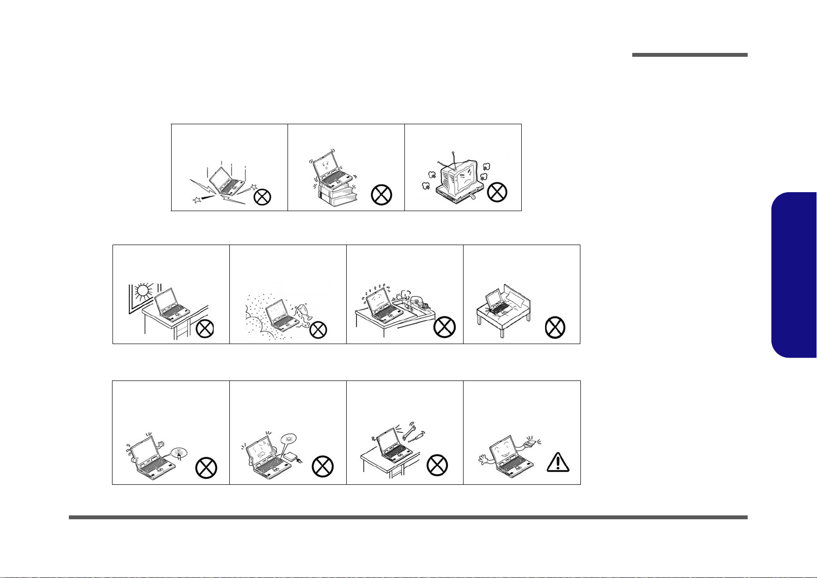
Instructions for Care and Operation
The notebook computer is quite rugged, but it can be damaged. To prevent this, follow these suggestions:
1. Don’t drop it, or expose it to shock. If the computer falls, the case and the components could be damaged.
Preface
Do not expose the computer
to any shock or vibration.
Do not place it on an unstable
surface.
Do not place anything heavy
on the computer.
2. Keep it dry, and don’t overheat it. Keep the computer and power supply away from any kind of heating element. This
is an electrical appliance. If water or any other liquid gets into it, the co mputer could be badly damaged.
Do not expose it to excessive
heat or direct sunlight.
Do not leave it in a place
where foreign matter or moisture may affect the system.
Don’t use or store the computer in a humid environment.
Do not place the computer on
any surface which will block
the vents.
3. Follow the proper working procedures for the computer. Shut the computer down properly and don’t forget to save
your work. Remember to periodically save your data as data may be lost if the battery is depleted.
Do not turn off the power
until you properly shut down
all programs.
Do not turn off any peripheral
devices when the computer is
on.
Do not disassemble the computer by yourself.
Perform routine maintenance
on your computer.
Preface
V
Page 6
Preface
4. Avoid interference. Keep the computer away from high capacity transformers, electric moto rs, and other strong mag-
netic fields. These can hinder proper performance and damage your data.
5. Take care when using peripheral devices.
Preface
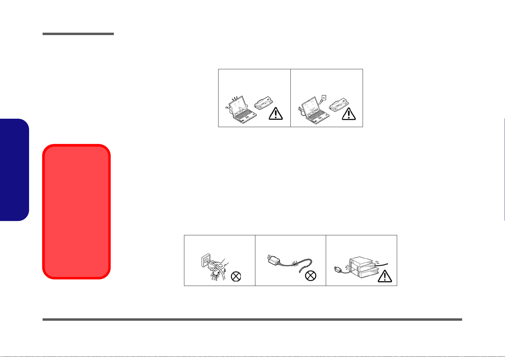
Power Safety
Warning
Before you undertake
any upgrade procedures, make sure that
you have turned off the
power, and disconnected all peripherals
and cables (including
telephone lines). It is
advisable to also remove your battery in
order to prevent accidentally turning the
machine on.
Use only approved brands of
peripherals.
Unplug the power cord befor e
attaching peripheral devices.
Power Safety
The computer has specific power requirements:
• Only use a power adapter approved for use with this computer.
• Your AC adapter may be designed for international travel but it still requ ires a steady, uninterrupte d power supp ly. If you are
unsure of your local power specifications, consult your service representative or local power company.
• The power adapter may have either a 2-prong or a 3-prong grounded plug. The third prong is an important safety feature; do
not defeat its purpose. If you do not have access to a compatible outlet, have a qualified electrician install one.
• When you want to unplug the power cord, be sure to disconn ect it by the plug head, not by its wire.
• Make sure the socket and any extension cord(s) you use can support the total current load of all the connected devices.
• Before cleaning the computer, make sure it is disconnected from any external power supplies.
Do not plug in the power
cord if you are wet.
Do not use the power cord if
it is broken.
Do not place heavy objects
on the power cord.
VI
Page 7

Battery Precautions
• Only use batteries designed for this computer. The wrong battery type may explode, leak or damage the computer.
• Recharge the batteries using the notebook’s system. Incorrect recharging may make the battery explode.
• Do not try to repair a battery pack. Refer any battery pack repair or replacement to your service representative or qualified service
personnel.
• Keep children away from, and promptly dispose of a damaged battery. Always dispose of batteries carefully. Batteries may explode
or leak if exposed to fire, or improperly handled or discarded.
• Keep the battery away from metal appliances.
• Affix tape to the battery contacts before disposing of the battery.
• Do not touch the battery contacts with your hands or metal objects.
Battery Disposal
The product that you have purchased contains a rechargeable b attery. The battery is recycl able. At the end of
its useful life, under various state and local laws, it may be illegal to dispose of this battery into the municipal
waste stream. Check with your local solid waste officials for details i n your area for recycling options or p roper
disposal.
Caution
Danger of explosion if battery is incorrectly replaced. Replace only with the same or equivalent type recommended by the manufacturer. Discard used battery according to the manufacturer’s instructions.
Preface
Preface
Related Documents
You may also need to consult the User’s Manual on CD as this describes the notebook PC’s features, the procedures for
operating the computer, and its ROM-based setup program. It also describes the installation and operation of the utility
programs provided with the notebook PC.
VII
Page 8

Preface
Preface
VIII
Page 9

Contents
Preface
Introduction ..............................................1-1
Overview ......................................................................................... 1-1
Model Differences ........................................................................... 1-2
Specifications ..................................................................................1-3
Processor .........................................................................................1-3
Core Logic .......................................................................................1-3
Memory ...........................................................................................1-4
Security ............................................................................................1-4
BIOS ................................................................................................ 1-4
LCD Options ...................................................................................1-4
Video Adapter .................................................................................1-4
Storage ............................................................................................. 1-5
Audio ............................................................................................... 1-5
Keyboard & Pointing Device ..........................................................1-5
PCMCIA ..........................................................................................1-5
Interface ...........................................................................................1-5
Card Reader .....................................................................................1-5
Communication ...............................................................................1-5
Power Management .........................................................................1-5
Power ............................................................................................... 1-6
Environmental Spec ........................................................................1-6
Physical Dimensions & Weight ......................................................1-6
Optional ...........................................................................................1-6
External Locator - Top View with LCD Panel Open ......................1-7
External Locator - Front & Rear Views ..........................................1-8
External Locator - Right Side & Left Side Views ..........................1-9
External Locator - Bottom View ...................................................1-10
Mainboard Overview - Top (Key Parts) .......................................1-11
Mainboard Overview - Bottom (Key Parts) ..................................1-12
Mainboard Overview - Top (Connectors) .................................... 1-13
Mainboard Overview - Bottom (Connectors) ............................... 1-14
Disassembly ...............................................2-1
Overview ......................................................................................... 2-1
Maintenance Tools .......................................................................... 2-2
Connections .................................................................................... 2-2
Maintenance Precautions ................................................................ 2-3
Cleaning .......................................................................................... 2-3
Disassembly Steps .......................................................................... 2-4
Removing the Battery ..................................................................... 2-5
Removing the Hard Disk Drive ...................................................... 2-6
Changing Serial and Parallel Hard Disk Cables .............................2-8
Upgrading the System Memory (RAM) .........................................2-9
Removing the Optical (CD/DVD) Device .................................... 2-11
Removing the Processor ............................................................... 2-12
Removing the Modem .................................................................. 2-14
Removing the Wireless LAN Module .......................................... 2-15
Removing the Keyboard ............................................................... 2-16
Removing the Keyboard Shielding Plate ...................................... 2-17
Removing the PCI Express VGA Card ........................................ 2-18
Part Lists ..................................................A-1
Part List Illustration Location ........................................................ A-2
Top (M400A/M40AE/M400G/M40GE) ....................................... A-3
Bottom (M400A) ........................................................................... A-4
Bottom (M400AE) ......................................................................... A-5
Bottom (M400G) ........................................................................... A-6
Bottom (M400GE) ......................................................................... A-7
Preface
IX
Page 10

Preface
LCD (M400A/M40AE/M400G/M40GE) ......................................A-8
CD-ROM Drive - SAMSUNG
(M400A/M40AE/M400G/M40GE) ...............................................A-9
Combo Drive - QSI (M400A/M40AE/M400G/M40GE) .............A-10
Combo Drive - TEAC (M400A/M40AE/M400G/M40GE) .........A-11
DVD-DUALRW Drive - LITEON
(M400A/M40AE/M400G/M40GE) .............................................A-12
DVD-DUALRW Drive - PIONEER
(M400A/M40AE/M400G/M40GE) .............................................A-13
DVD Drive - QSI (M400A/M40AE/M400G/M40GE) ................A-14
Hard Disk Drive (M400A/M40AE/M400G/M40GE) ..................A-15
Schematic Diagrams.................................B-1
System Block Diagram ...................................................................B-2
CLOCK GENERATOR .................................................................B-3
CPU - 1 ...........................................................................................B-4
Preface
CPU - 2 ...........................................................................................B-5
ALVISO - 1 .................................................................................... B-6
ALVISO - 2 .................................................................................... B-7
ALVISO - 3 .................................................................................... B-8
ALVISO - 4 .................................................................................... B-9
VGA CARD CONNECTOR ........................................................ B-10
DDR2 - DIMM1 ...........................................................................B-11
DDR2 - DIMM2 ...........................................................................B-12
ICH6 - 1 ........................................................................................ B-13
ICH6 - 2 ........................................................................................ B-14
ICH6 - 3 ........................................................................................ B-15
HDD & CD ROM ........................................................................B-16
USB & CCD CONN ....................................................................B-17
MDC, BT, CCD ...........................................................................B-18
PCI-E LAN ................................................................................... B-19
TI - 1394A (43AB21) ................................................................... B-20
CON; MINIPCI ............................................................................B-21
PCMCIA (1620) ...........................................................................B-22
PCMCIA SOCKET ......................................................................B-23
HITACHI H8 ................................................................................B-24
AUDIO .........................................................................................B-25
+VS; PWRBTN ............................................................................B-26
LED; NS87383 .............................................................................B-27
FAN CONN, LPC ROM ...............................................................B-28
5V, 3.3V, +1.5V ...........................................................................B-29
CHARGER ...................................................................................B-30
TPS51116 .....................................................................................B-31
VCORE+ 1.05V ............................................................................B-32
CARD READER BOARD ...........................................................B-33
CLICK BOARD ...........................................................................B-34
LED BOARD ................................................................................B-35
RJ11 BOARD ...............................................................................B-36
SRS AP8202 .................................................................................B-37
Switches .................................................... C-1
Locating the Jumper Switch ...........................................................C-1
Settings ...........................................................................................C-2
CPU Clock Setup (Switch SW1) ....................................................C-2
X
Page 11

Introduction
Overview
This manual covers the information you need to service or upgrade the M400A/M400G/M40AE/M40GE series notebook
computer. Information about operating the computer (e.g. getting started, and the Setup utility) is in the User’s Manual.
Information about drivers (e.g. VGA & audio) is also found in User’s Manual. That manual is shipped with the computer.
Operating systems (e.g. DOS, Windows 9x, Windows NT 4.0, Windows 2000, Windows XP, OS/2 Warp, UNIX, etc.) have
their own manuals as do application software (e.g. word processing and database programs). If you have questions about
those programs, you should consult those manuals.
The M400A/M400G/M40AE/M40GE series notebook is designed to be upgradeable. See “Disassembly” on page 2 - 1
for a detailed description of the upgrade procedures for each specific component. Please note the warning and safety information indicated by the “” symbol.
The balance of this chapter reviews the computer’s technical specifications and features.
Introduction
1.Introduction
Overview 1 - 1
Page 12
Introduction
Model Differences
This notebook series includes four different model types.The models differ in video support, system memory (RAM)
supported, and AC adapter supplied. Models M400A & M40AE include ATI X700 (ATI M26) PCI Express video
cards, models M400G & M40GE include built-in Intel (Intel GMA 900) video. Models M400A & M40AE are sup-
plied with a 90W power adapter, models M400G & M40GE are supplied with a 65W power adapter. Models M400A
& M400G support DDR RAM; models M40AE & M40GE support DDRII (DDR2) RAM.
Feature M400A M40AE M400G M40GE
1.Introduction
Table 1 - 1
Model Differences
Video Adapter
Power Adapter
RAM (Memory) Supported
AT I X700 PCI Express Video Card Intel GMA 900 On-Board
90W 65W
DDR DDRII (DDR2) DDR DDRII (DDR2)
RAM Modules Supported
If you need to upgrade or replace the memory (RAM) modules, make sure you are using the appropriate module type for
the computer.
1 - 2 Model Differences
Page 13

Specifications
The specifications listed in this Appendix are correct at the time of going to press. Certain items (particularly processor types/speeds and CD/DVD device types) may be changed or updated due to the manufacturer's release schedule. Check with your service center for details.
Feature Specification
Introduction
Latest Specification Information
Table 1 - 2
Specifications
1.Introduction
Processor Intel Pentium® M Processor
(478-pin) Micro-FC-PGA Package
Models 730/ 740/ 750/ 760/ 770
Intel Pentium® M Processor
(478-pin) Micro-FCPGA Package
Intel Pentium® M Processor
(478-pin) Micro-FC-PGA Package
Models 725/ 735/ 745/ 755
Intel Celeron® M Processor
(478-pin) Micro-FCPGA Package
Models 320/ 330/ 340
Intel Celeron® M Processor
(478-pin) Micro-FCPGA Package
Models 350/ 360/ 370
Core Logic Intel 915PM + ICH6-M (Models M400A & M40AE) Intel 915GM + ICH6-M (Models M400G & M40GE)
(µ0.09) 0.09 Micron Process Technology
2MB On-die L2 Cache & 533MHz FSB
1.6/ 1.73/ 1.86/ 2/ 2.13 GHz
(µ0.13) 0.13 Micron Process Technology
1MB On-die L2 Cache & 400MHz FSB
1.3/ 1.4/ 1.5/ 1.6/ 1.7 GHz
(
µ0.09) 0.09 Micron Process Technology
2MB On-die L2 Cache & 400MHz FSB
1.6 / 1.7/ 1.8/ 2.0 GHz
µ0.13) 0.13 Micron Process Technology
(
512KB On-die L2 Cache & 400MHz FSB
1.3/ 1.4/ 1.5 GHz
(µ0.09) 0.09 Micron Process Technology
1MB On-die L2 Cache & 400MHz FSB
1.3/ 1.4/ 1.5 GHz
Specifications 1 - 3
Page 14
Introduction
Feature Specification
1.Introduction
Memory Models M400A & M400G
Two SO-DIMM Sockets Supporting DDR Memory
Single Channel
Speed up to 333 MHz
(Note: Do Not Use Other Module Types)
Memory Expandable up to 2GB (128/ 256/ 512/ 1024
MB DDR Modules)
Models M40AE & M40GE:
Two SO-DIMM Sockets Supporting DDRII (DDR2)
Memory
Dual Channel
Speed up to 533 MHz
(Note: Do Not Use Other Module Types)
Memory Expandable up to 2GB (128/ 256/ 512/ 1024
MB DDRII Modules)
RAM Modules Supported
If you intend to upgrade or replace your memory (RAM) modules, make sure you are using
the appropriate module type for your computer. Model M400A & M400G computers support DDR RAM modules; Model M40AE * M40GE computers support DDRII (DDR2) RAM
modules. These types of RAM modules are not interchangeable, and they differ in size
very slightly. If you are unsure which module type your computer supports then consult
your service center.
Security Security (Kensington® Type) Lock Slot
BIOS One 512KB Flash ROM Phoenix BIOS, Plug and Play
LCD Options 15.0" XGA Flat Panel TFT (1024*768) 15.0" SXGA Flat Panel TFT (1400 * 1050)
1 - 4 Specifications
Video Adapter Models M400A & M40AE:
ATI M26(X700) PCI-E 16X
128MB/256MB(M26) DDR-DRAM
Pure Hardware DirectX 9
128-bit Memory Interface
Models M400G & M40GE:
Intel® Graphics Media Accelerator 900 (Intel® GMA
900)
Dynamic Video Memory Technology DVMT 3.0 Supports up to 224MB of Video Memory (dynamically
allocated from system memory where needed)
Supports Dual Independent Displays
Motion Compensation for Smooth DVD Playback
Page 15
Feature Specification
Storage One Changeable 12.7mm(h) Optical Device (CD/DVD) Type Drive (see “Optional” on page 1 - 6 for drive
options)
Easy Changeable 2.5" 9.5 mm (h) IDE HDD
Supports P ATA (Parallel)
/ SATA (Serial) HDDs. Supporting ATA 100/66/33 or SATA 1.5G
Introduction
Audio 7.1 Channel High Definition Audio Codecs with UAA
(Universal Audio Architecture)
EAX™ 1.0 & 2.0 Compatible
Direct Sound™ 3D Compatible
I3DL2 Compatible
Keyboard & Pointing
Device
PCMCIA One Type-II PCMCIA CardBus PC Card Slot
Interface Four USB 2.0 Ports
Card Reader Embedded 3-in-1 Card Reader (MS/ SD/ MMC)
Communication 56K Plug & Play Fax/Modem v.90/92 Compliant
Winkey Keyboard Built-In TouchPad with Scrolling Function
One Mini-IEEE 1394 Port
One External Monitor Port
One Parallel Port (LPT1) Supporting ECP/EPP
One S/PDIF Output Jack
One S-Video-Out Port
One Infrared Transceiver
1Gbit PCI-Express Fast Ethernet Card
(Option) Intel® PRO/Wireless 2200BG Mini PCI Wireless LAN Module
(Option) Intel® PRO/Wireless 2915ABG Mini PCI Wireless LAN Module
(Factory Option) Bluetooth Version 1.2 with Azalia Modem Combo
(Factory Option) PC Camera with USB Interface
A3D™ Compatible
16/20/24-bit S/PDIF-OUT Supporting 44.1/48/96kHz
Sample Rates
Built-In 2 Hi-Fi Speakers
(Factory Option) SRS WOW Surround Sound
(3D Surround\ True Bass\ Focus Enhancement)
1.Introduction
One Headphone-Out Jack
One Microphone-In Jack
One Line-In Jack
One RJ-11 Jack for Plug & Play Fax/Modem
One RJ-45 Jack for 10M/100M/1000M Fast Ethernet
One DC-in Jack
Power Management Supports ACPI 2.0
Power Button as Sleep/Resume Key
Supports Hibernate Mode
Supports Standby
Supports Battery Low Suspend
Supports Resume from Alarm Time
Supports Resume from Modem Ring
Supports Wake on LAN
Specifications 1 - 5
Page 16
Introduction
Feature Specification
1.Introduction
Power Models M400A & M40AE - AC Adapter:
Full Range AC Adapter 90W 100~240V, 47~63Hz
6 Cell Smart Lithium-Ion Battery Pack, 4.4AH
12 Cell Smart Lithium-Ion Battery Pack, 6.6AH (Optional)
Environmental Spec Temperature
Operating: 5
Non-Operating: -20°C ~ 60°C
Physical Dimensions &
Weight
Optional Optical Drive Module Options:
329mm (w) * 275mm (d) * 25-37mm (h) Min
Models M400A & M40AE:
3.2 kg With 6 cell Battery
CD-ROM Drive Module
Combo Drive Module
DVD-ROM Drive Module
DVD-Dual Drive Module
6 Cell Smart Lithium-Ion Battery Pack, 4.4AH
12 Cell Smart Lithium-Ion Battery Pack, 6.6AH
PC Camera with USB Interface
°C ~ 35°C
Models M400G & M40GE - AC Adapter:
Full Range AC Adapter 65W 100~240V, 47~63Hz
Relative Humidity
Operating: 20% ~ 80%
Non-Operating: 10% ~ 90%
Models M400G & M40GE:
3.0 kg With 6 cell Battery
Wireless LAN Module Options:
Intel® PRO/Wireless 2200BG Mini-PCI Wireless LAN
Module
Intel® PRO/Wireless 2915ABG Mini-PCI Wireless
LAN Module
Bluetooth Version 1.2 with Azalia Modem Combo
Roxio CD Creator Software
Power DVD 6.0 Software
1 - 6 Specifications
Page 17
Introduction
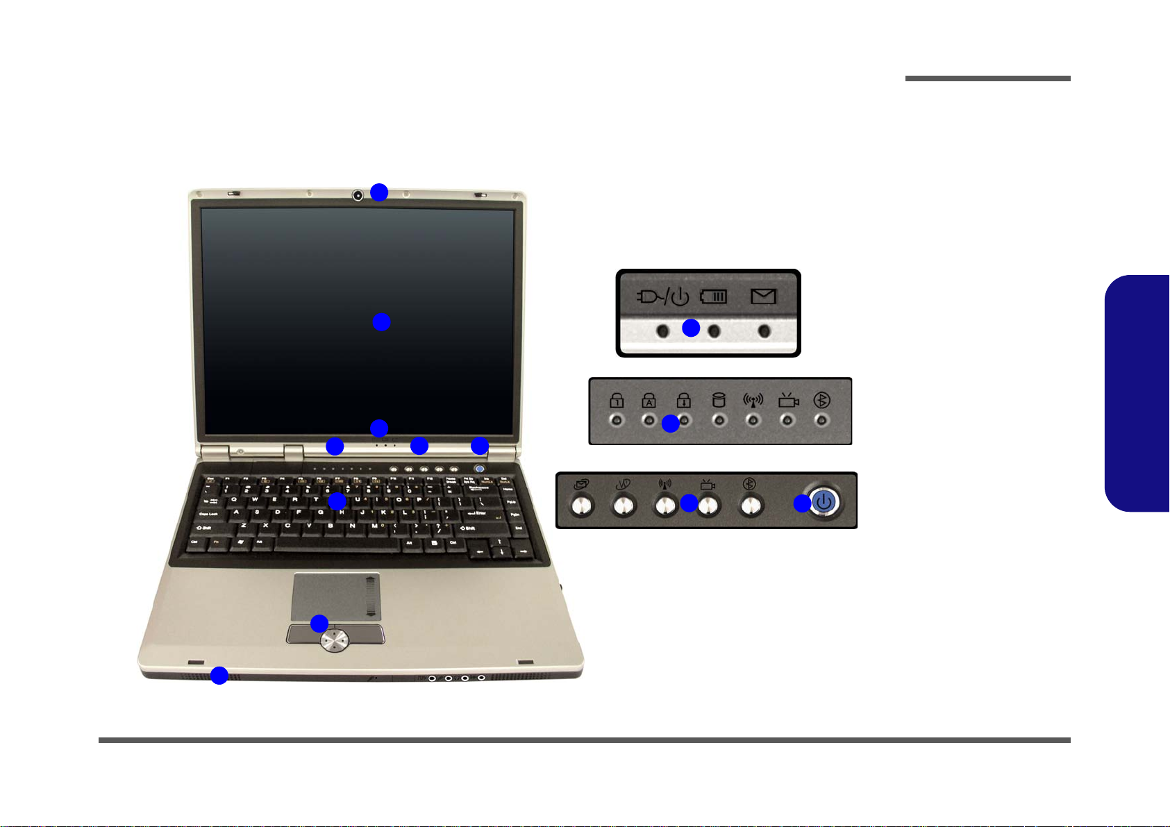
External Locator - Top View with LCD Panel Open
1
2
3
4
7
5
6
4
Figure 1 - 1
Top View
1. Optional Built-In
PC Camera
2. LCD
3. LED Power &
Communication
Indicators
4. LED Status
Indicators
3
5
6
5. Quick-Key Button
6. Power Button
7. Keyboard
8. TouchPad and
Buttons
9. Speakers
1.Introduction
8
9
External Locator - Top View with LCD Panel Open 1 - 7
Page 18
Introduction
1.Introduction
Figure 1 - 2
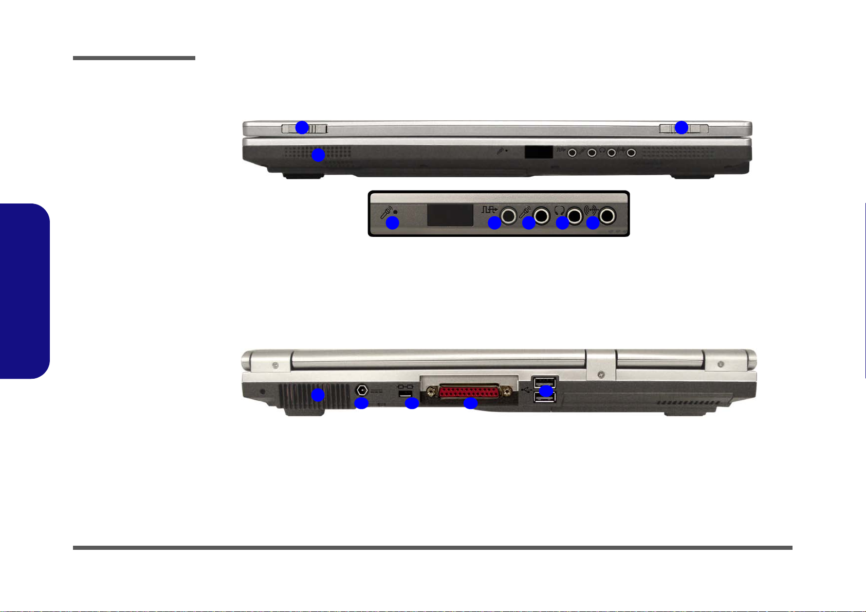
Front View
1. LCD Latches
2. Speaker
3. Built-In
Microphone
4. S/PDIF-Out Jack
5. Microphone-In
Jack
6. Headphone-Out
Jack
7. Line-In Jack
Figure 1 - 3
Rear View
1. Vent
2. DC-In Jack
3. Security Lock Slot
4. Parallel Port
5. 2 * USB 2.0 Ports
External Locator - Front & Rear Views
1
2
1
2
3 4
1
5 6 743
5
1 - 8 External Locator - Front & Rear Views
Page 19
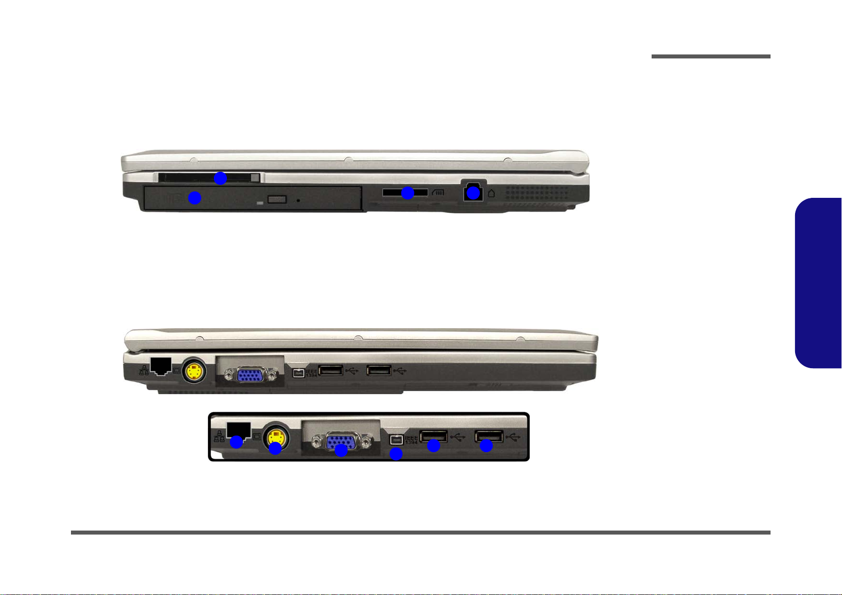
External Locator - Right Side & Left Side Views
2
1
3 4
Introduction
Figure 1 - 4
Right Side View
1. Optical Device
Drive Bay
2. PC Card Slot
3. 4-in-1 Card
Reader (reads
SD/ MMC/ MS &
MS Pro formats)
4. RJ-11 Phone Jack
1.Introduction
Figure 1 - 5
Left Side View
1. RJ-45 LAN Jack
2. S-Video-Out Jack
3. External Monitor
(VGA) Port
4. Mini-IEEE 1394a
Port
5. 2 * USB 2.0 Ports
1
2
3
4
5
5
External Locator - Right Side & Left Side Views 1 - 9
Page 20
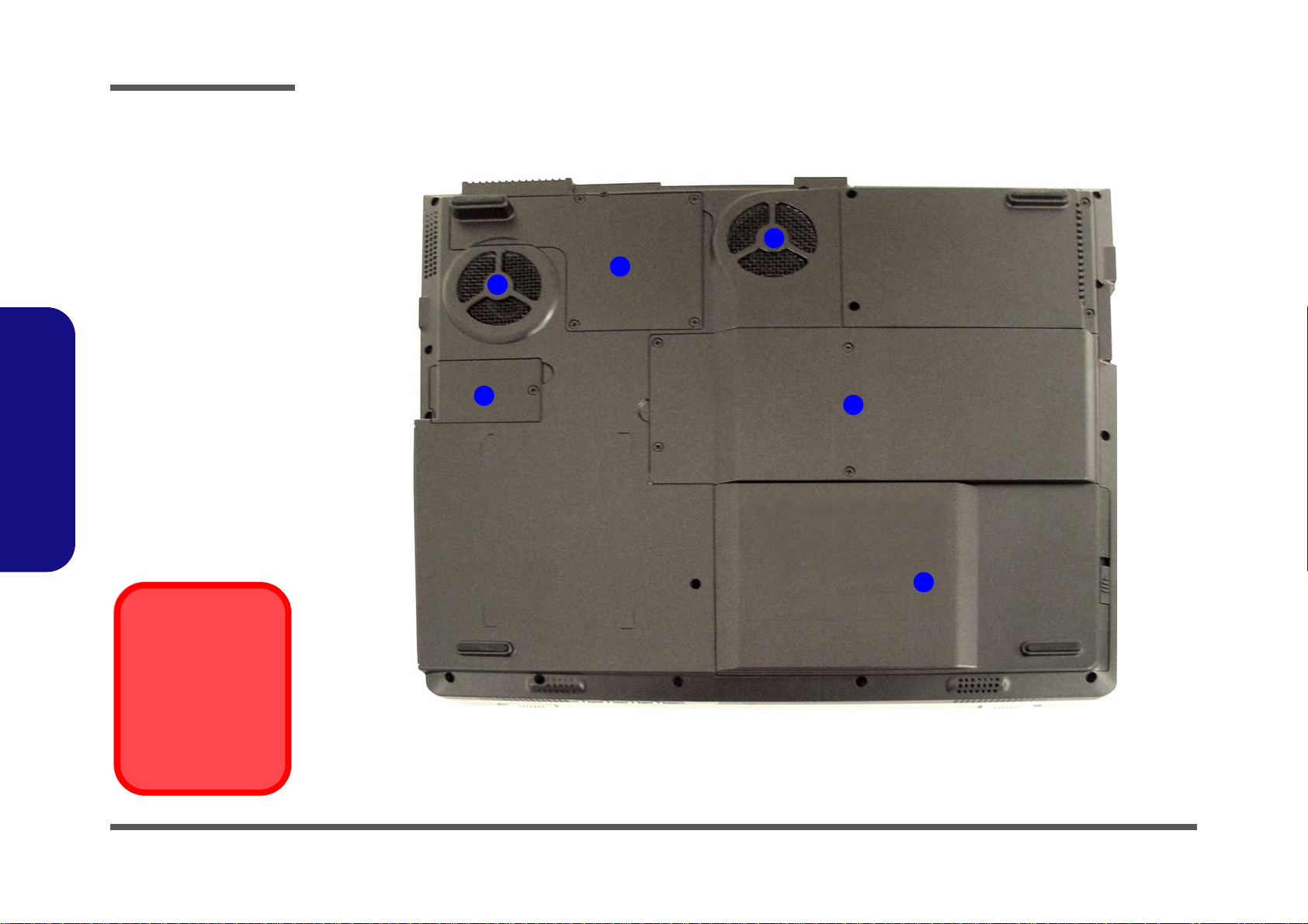
1.Introduction
Introduction
Figure 1 - 6
Bottom View
1. Vent/Fan Int ake s
2. Modem/
Bluetooth &
Modem Combo
Module Cover
3. CPU Bay Cover
4. Hard Disk/
Memory (RAM)/
WLAN Cover
5. Battery
External Locator - Bottom View
3
1
2
1
4
Overheating
To prevent your computer from overheating
make sure nothing
blocks the vent/fan intakes while the computer is in use.
1 - 10 External Locator - Bottom View
5
Page 21
Introduction
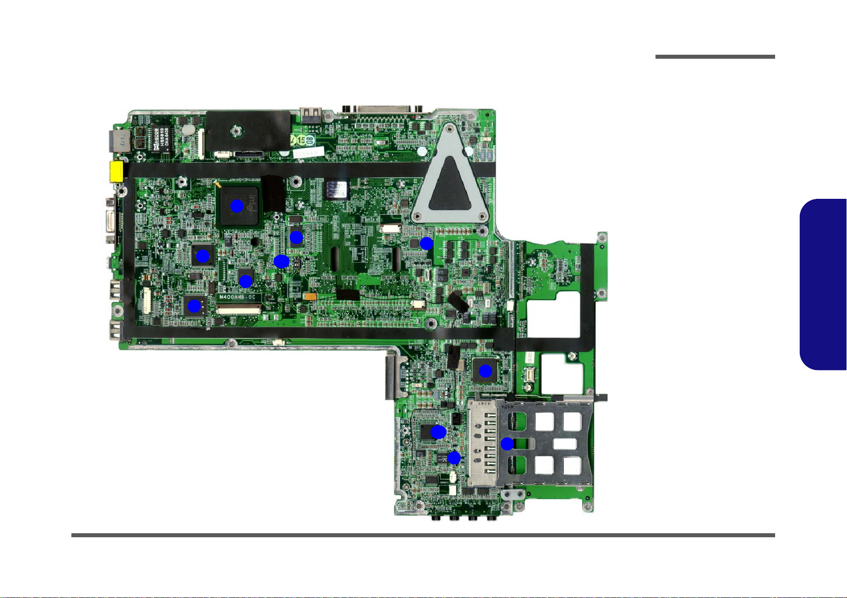
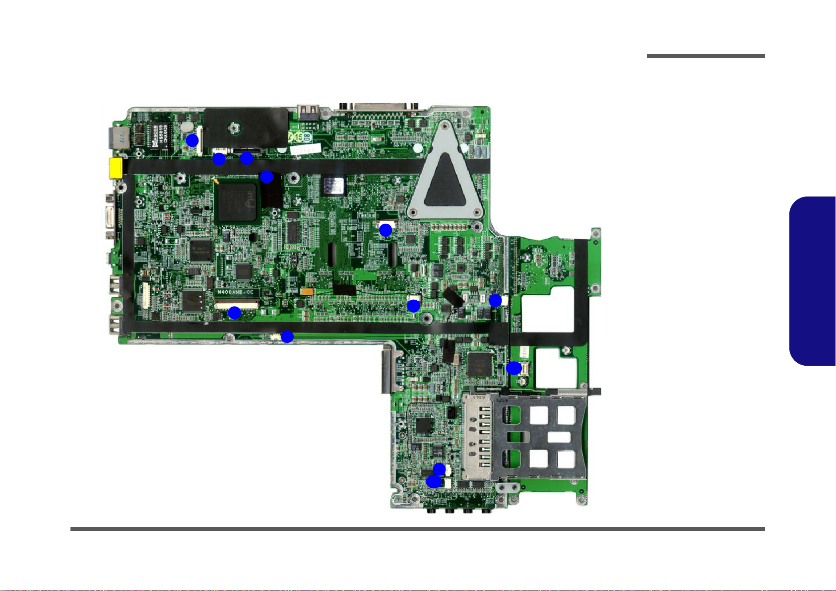
Mainboard Overview - Top (Key Parts)
1
2
3
7
5
11
Figure 1 - 7
Mainboard Top
Key Parts
1. ICH6-M I/O
Controller Hub
2. Clock Generator
3. TI - 1394A
(43AB21)
4. PCMCIA (1620)
5. Hitachi H8
6. Audio - ALC880
7. LED; NS87383
9
8. TPS51116
9. VCORE+ 1.05V
10. SRS AP8202
11. DIP Switch (see
“Switches” on
page C - 1)
1.Introduction
10
4
8
6
Mainboard Overview - Top (Key Parts) 1 - 11
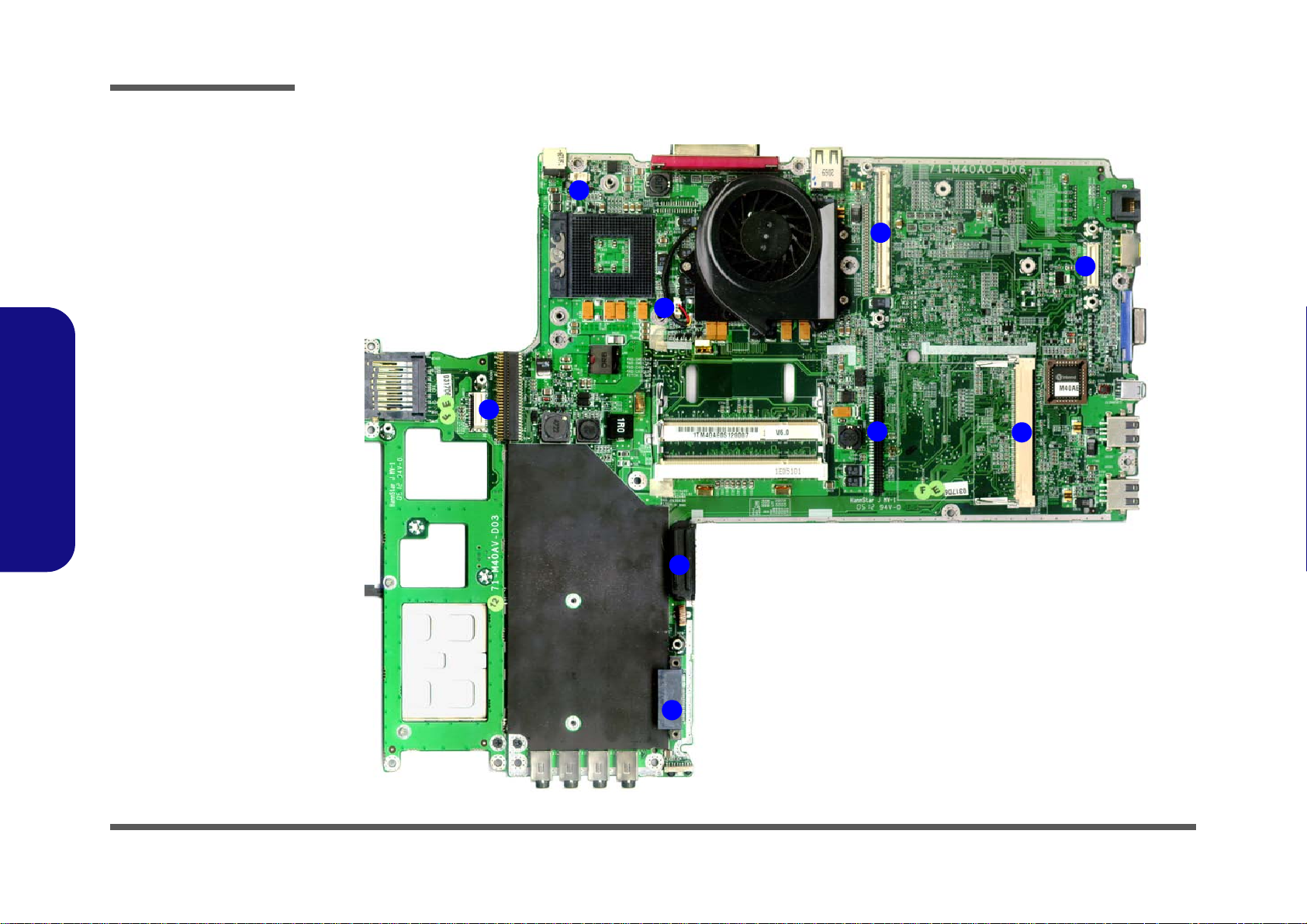
Page 22
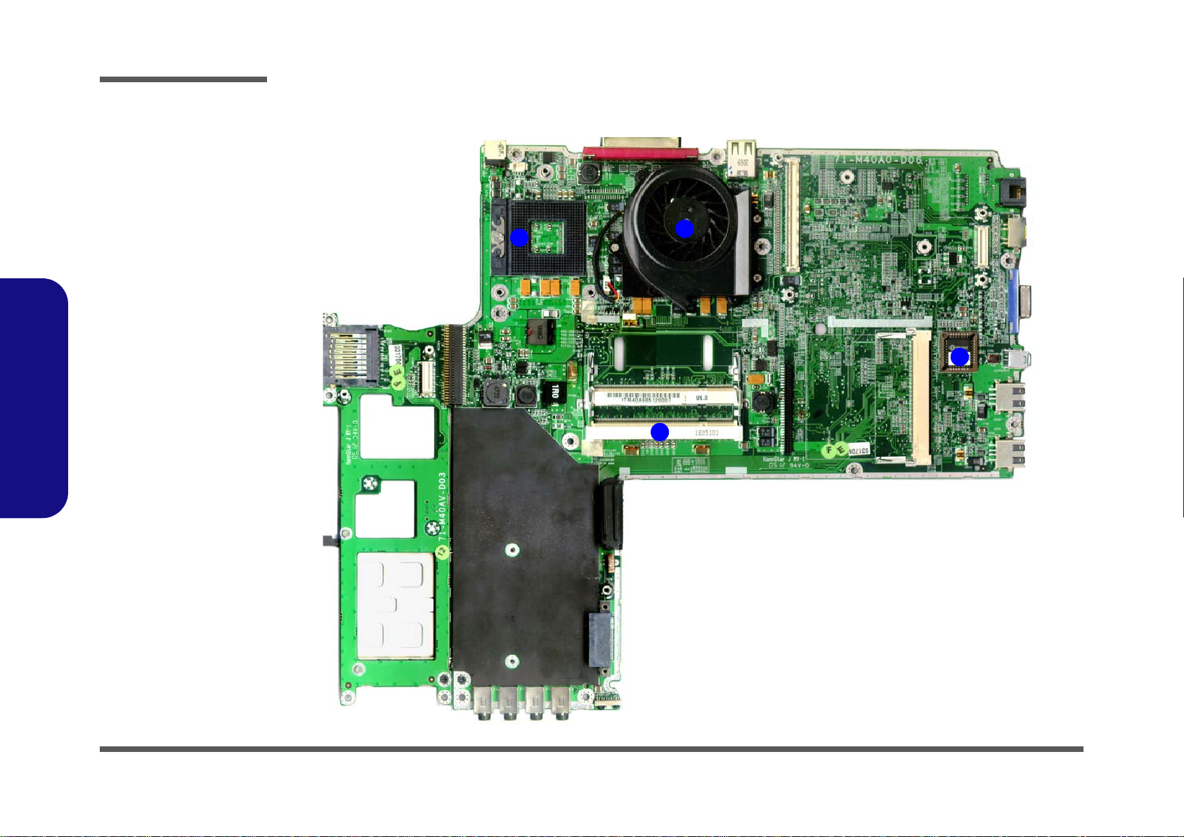
Introduction
1.Introduction
Figure 1 - 8
Mainboard Bottom
Key Parts
1. CPU Socket (no
CPU installed)
2. Memory Slots
(M40AE & M40GE
Support DDR2
Memory Modules)
3. Alviso 915PM
(located under the
fan unit)
4. Flash BIOS ROM
Mainboard Overview - Bottom (Key Parts)
1
3
2
4
1 - 12 Mainboard Overview - Bottom (Key Parts)
Page 23
Mainboard Overview - Top (Connectors)
1
3
2
9
4
5
Introduction
Figure 1 - 9
Mainboard Top
Connectors
1. Inverter (JINV1)
2. Camera (JCCD1)
3. LCD (JLCD1
4. LED (JLED1)
5. Keyboard (JKB1)
6. CMOS Battery
Cable (JBAT1)
7. TouchPad (JTP1)
8. Speaker (JSPK1)
9. Microphone Cable
(JINTMIC1)
10. Speaker (JSPK2)
11. Modem (RJMDC1)
7
8
1.Introduction
6
11
9
10
Mainboard Overview - Top (Connectors) 1 - 13
Page 24
Introduction
1.Introduction
Figure 1 - 10
Mainboard Bottom
Connectors
1. VGA Card
Connectors (CON1
& CON2) - M400A
& M400AE Only
2. Hard Disk (JHDD1)
3. Mini-PCI Connector
(JMINIPCI1)
4. Fan (JFAN1)
5. Modem (MDC2)
6. Fan (JFAN2)
7. Battery
8. CD/DVD Optical
Device (JCD1)
Mainboard Overview - Bottom (Connectors)
4
6
5
7
1
1
2
3
1 - 14 Mainboard Overview - Bottom (Connectors)
8
Page 25

2: Disassembly
Overview
This chapter provides step-by-step instructions for disassembling the M400A/M400G/M40AE/M40GE series notebook’s parts and subsystems. When it comes to reassembly, reverse the procedures (unless otherwise indicated).
We suggest you completely review any procedure before you take the computer apart.
Disassembly
Procedures such as upgrading/replacing the RAM, CD device and hard disk are included in the User’s Manual but are
repeated here for your convenience.
To make the disassembly process easier each section may have a box in the page margin. Information contained under
the figure # will give a synopsis of the sequence of procedures involved in the disassembly procedure. A box with a
lists the relevant parts you will have after the disassembly process is complete. Note: The parts listed will be for the disassembly procedure listed ONLY, and not any previous disassembly step(s) required. Refer to the part list for the previous disassembly procedure. The amount of screws you should be left with will be listed here also.
A box with a will also provide any possible helpful information. A box with a contains warnings.
An example of these types of boxes are shown in the sidebar.
2.Disassembly
Information
Warning
Overview 2 - 1
Page 26

Disassembly
2.Disassembly
NOTE: All disassembly procedures assume that the system is turned OFF, and disconnected from any power supply (the
battery is removed too).
Maintenance Tools
The following tools are recommended when working on the notebook PC:
• M3 Philips-head screwdriver
• M2.5 Philips-head screwdriver (magnetized)
• M2 Philips-head screwdriver
• Small flat-head screwdriver
• Pair of needle-nose pliers
• Anti-static wrist-strap
Connections
Connections within the computer are one of four types:
Locking collar sockets for ribbon connectors To release these connectors, use a small flat-head screwdriver to gently pry the
locking collar away from its base. When replacing the connection, make sure
the connector is oriented in the same way. The pin1 side is usually not indicated.
2 - 2 Overview
Pressure sockets for multi-wire connectors To release this connector type, grasp it at its head and gently rock it from side
to side as you pull it out. Do not pull on the wires themselves. When replacing
the connection, do not try to force it. The socket only fits one way.
Pressure sockets for ribbon connectors To release these connectors, use a small pair of needle-nose pliers to gently lift
the connector away from its socket. When replacing the connection, make sure
the connector is oriented in the same way. The pin1 side is usually not indicated.
Board-to-board or multi-pin sockets To separate the boards, gently rock them from side to side as you pull them
apart. If the connection is very tight, use a small flat-head screwdriver - use
just enough force to start.
Page 27

Maintenance Precautions
The following precautions are a reminder. To avoid personal injury or damage to the computer while performing a removal and/or replacement job, take the following precautions:
1. Don't drop it. Perform your repairs and/or upgrades on a stable surface. If the computer falls, the case and other
components could be damaged.
2. Don't overheat it. Note the proximity of any heating elements. Keep the computer out of direct sunlight.
3. Avoid interference. Note the proximity of any high capacity transformers, electric motors, and other strong mag-
netic fields. These can hinder proper performance and damage components and/or data. You should also monitor
the position of magnetized tools (i.e. screwdrivers).
4. Keep it dry. This is an electrical appliance. If water or any other liquid gets into it, the computer could be badly
damaged.
5. Be careful with power. Avoid accidental shocks, discharges or explosions.
•Before removing or servicing any part from the computer, turn the computer off and detach any power supplies.
•When you want to unplug the power cord or any cable/wire, be sure to disconnect it by the plug head. Do not pu ll on the wir e.
6. Peripherals – Turn off and detach any peripherals.
7. Beware of static discharge. ICs, such as the CPU and main support chips, are vulnerable to static electricity.
Before handling any part in the computer, discharge any static electricity inside the computer. When handling a
printed circuit board, do not use gloves or other materials which allow static electricity buildup. We suggest that
you use an anti-static wrist strap instead.
8. Beware of corrosion. As you perform your job, avoid touching any connector leads. Even the cleanest hands produce oils which can attract corrosive elements.
9. Keep your work environment clean. Tobacco smoke, dust or other air-born particulate matter is often attracted
to charged surfaces, reducing performance.
10. Keep track of the components. When removing or replacing any part, be careful not to leave small part s, such as
screws, loose inside the computer.
Disassembly
Power Safety
Warning
Before you undertake
any upgrade procedures, make sure that
you have turned off the
power, and disconnected all peripherals
and cables (including
telephone lines). It is
advisable to also remove your battery in
order to prevent accidentally turning the
machine on.
2.Disassembly
Cleaning
Do not apply cleaner directly to the computer, use a soft clean cloth.
Do not use volatile (petroleum distillates) or abrasive cleaners on any part of the computer.
Overview 2 - 3
Page 28

Disassembly
Disassembly Steps
The following table lists the disassembly steps, and on which page to find the related information. PLEASE PERFORM
THE DISASSEMBLY STEPS IN THE ORDER INDICATED.
2.Disassembly
To remove the Battery:
1. Remove the battery page 2 - 5
To remove the HDD:
1. Remove the battery page 2 - 5
2. Remove the HDD page 2 - 6
To remove the System Memory:
1. Remove the battery page 2 - 5
2. Remove the system memory page 2 - 9
To remove the Optical Device:
1. Remove the battery page 2 - 5
2. Remove the Optical device page 2 - 11
To remove the Processor:
1. Remove the battery page 2 - 5
2. Remove the processor page 2 - 12
To remove the Modem:
To remove the Wireless LAN Module:
1. Remove the battery page 2 - 5
2. Remove the HDD page 2 - 6
3. Remove the Wireless LAN module page 2 - 15
To remove the Keyboard:
1. Remove the battery page 2 - 5
2. Remove the keyboard page 2 - 16
To remove the Keyboard Shielding Plate:
1. Remove the battery page 2 - 5
2. Remove the keyboard page 2 - 16
3. Remove the shielding plate page 2 - 17
To remove the PCI Express VGA Card:
1. Remove the battery page 2 - 5
2. Remove the PCI Express VGA card page 2 - 18
1. Remove the battery page 2 - 5
2. Remove the modem page 2 - 14
2 - 4 Disassembly Steps
Page 29
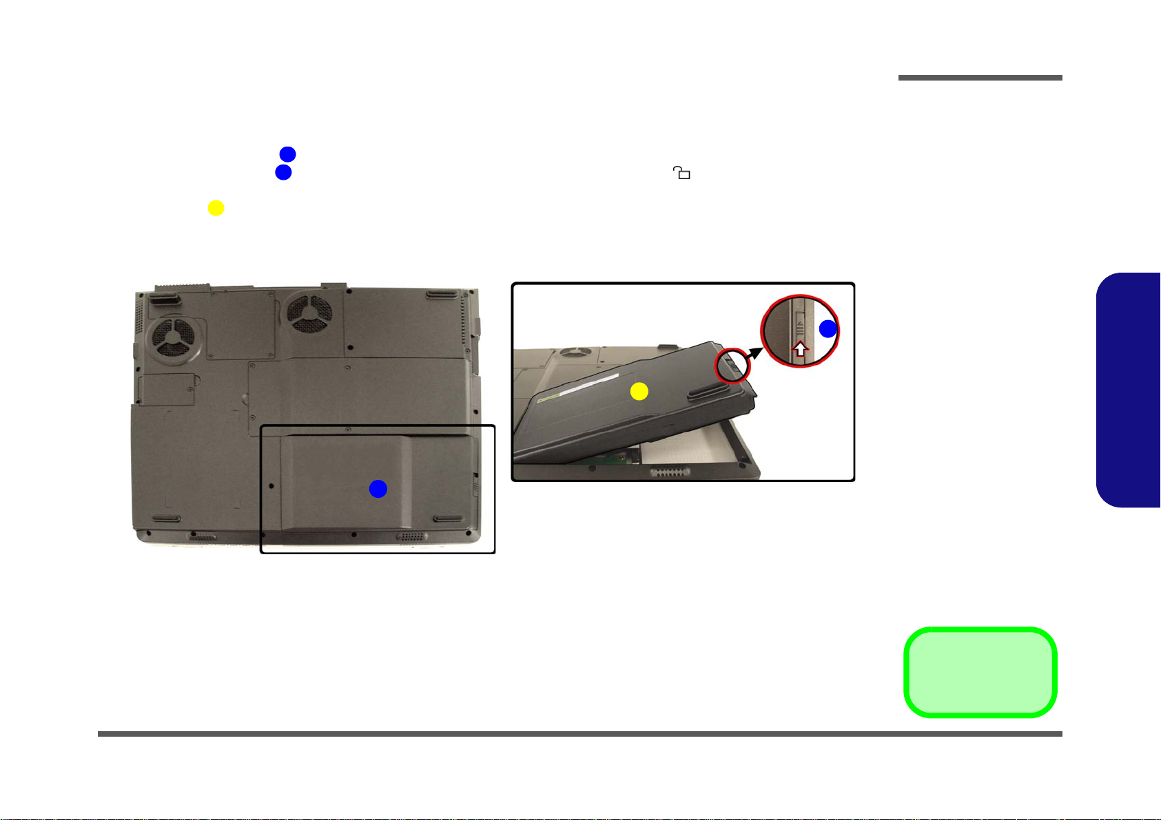
Removing the Battery
1. Turn the computer off, and turn it over.
1
2. Locate the battery bay
3. Slide the battery latch
shown in Figure 2 - 1b)
4. The Battery will pop up to allow you to lift it out of the bay (Figure 2 - 1b).
a.
3
(Figure 2 - 1a).
2
in the direction of the arrow (towards the unlock symbol ), and hold it in place (as
.
b.
Disassembly
Figure 2 - 1
Battery Removal
a. Locate the battery re-
2
3
lease latch.
b. Release the latch and re-
move the battery out of
the computer.
2.Disassembly
1
3. Battery
Removing the Battery 2 - 5
Page 30
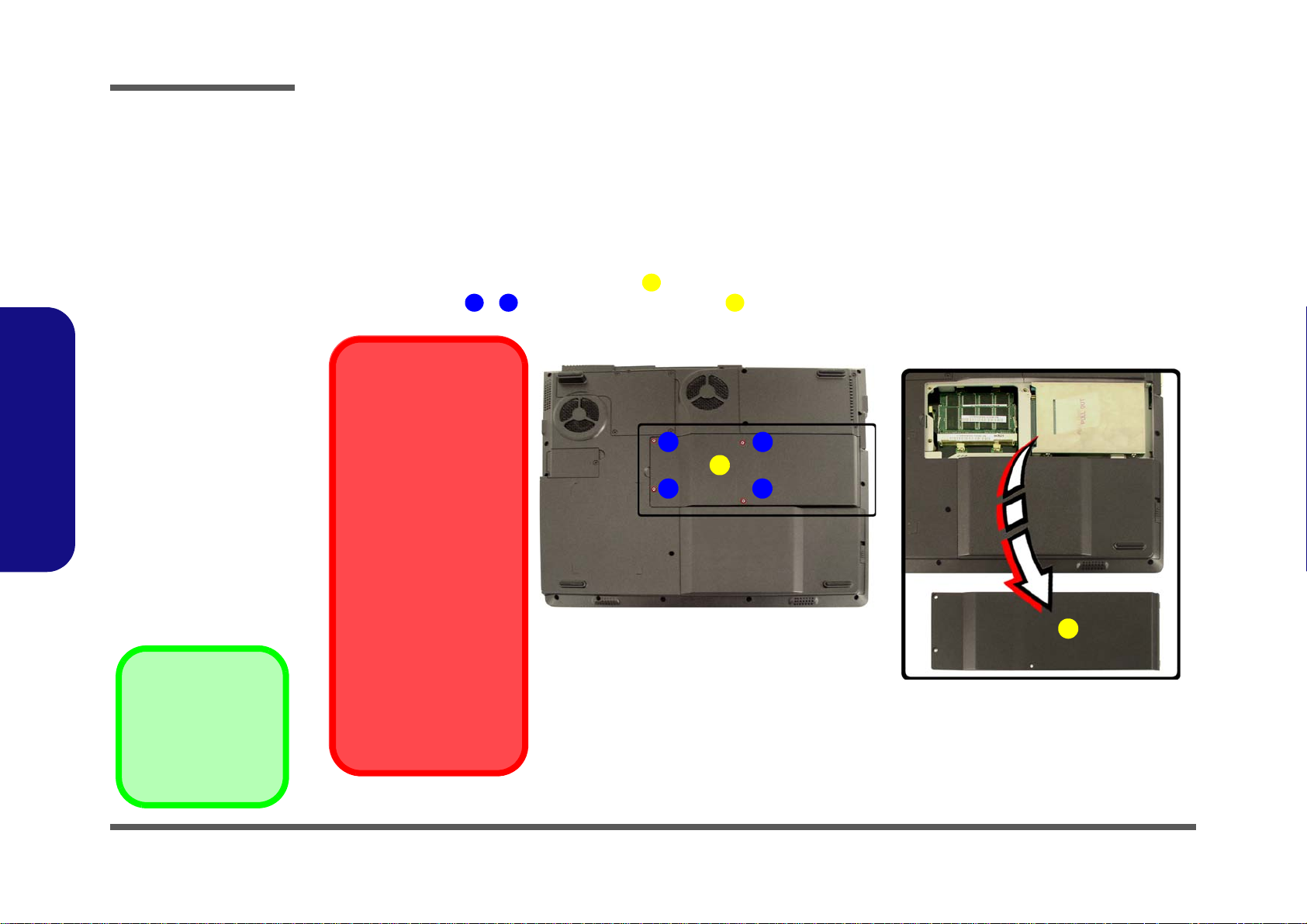
Disassembly
Removing the Hard Disk Drive
The hard disk drive can be taken out to accommodate other 2.5" serial (SATA) or parallel (PATA) hard disk drives (see
“Changing Serial and Parallel Hard Disk Cables” on page 2 - 8) with a height of 9.5mm (h). Follow your operating
system’s installation instructions, and install all necessary drivers and utilities (as outlined in Chapter 4 of the User’s
Manual), when setting up a new hard disk.
1. Turn off the computer, turn it over and remove the battery (page 2 - 5).
2. Locate the hard disk/memory bay cover .
3. Remove screws - and remove the bay cover .
2 5 1
1
Figure 2 - 2
HDD Assembly
Removal
a. Locate the HDD bay cov-
er and remove the
screws.
b. Lift the cover off the com-
puter.
2.Disassembly
1. HDD/Memory Bay
Cover
•4 Screws
HDD System Warning
New HDD’s are blank. Before you begin make sure:
You have backed up any
data you want to keep from
your old HDD.
You have all the CD-ROMs
and FDDs required to install your operating system
and programs.
If you have access to the
internet, download the latest application and hardware driver updates for the
operating system you plan
to install. Copy these to a
removable medium.
a.
b.
2 3
1
45
1
2 - 6 Removing the Hard Disk Drive
Page 31

Disassembly
4. Pull the tab in the direction of the arrow in order to release the disk assembly from the connector (see page
1 2
2 - 8 for instructions on changing hard disk cable types).
5. Carefully lift the hard disk assembly up out off the computer.
6. Remove screws from points - on the side of the hard disk assembly in order to separate the bracket from the
hard disk (Figure 2 - 3b).
8
4 7
3
7. Reverse the process to install a new hard disk (pay careful attention to the orientation of the disk under the co ver).
a.
c.
8
2
1
b.
4
3
6
5
If you wish to change
your hard disk type,
you will also need to
7
change the cable (see
page 2 - 8 for details).
Parallel & Serial
Cables
8
Parallel
8
Serial
Figure 2 - 3
HDD Assembly
Removal (Cont.)
a. Slide out the HDD as-
sembly.
b. Lift the HDD assembly
out of the bay and remove the screws.
c. Separate the bracket and
HDD.
8. Hard Disk
•4 Screws
2.Disassembly
Removing the Hard Disk Drive 2 - 7
Page 32

Disassembly
Figure 2 - 4
Changing Serial &
Parallel HDD Cables
Changing Serial and Parallel Hard Disk Cables
The system can support either serial (SATA) OR parallel (PATA) hard disks, however different cables are used to support each hard disk type. If you are changing hard disk types then you will be required to change the cable.
1. Remove the hard disk assembly (see page 2 - 6).
1 2
2. Remove screws
3. Carefully remove the cable .
4. Remove any cable protector from the new cable.
5. Insert the new cable (be careful of the connector orientation) and re-insert screws
6. Insert the new hard disk (ensure it is attached to the bracket) and make sure it is firmly connected.
a. b.
& .
3
4
1 2
& .
a. Remove the screws.
b. Remove the cable.
c. Remove any cable pro-
tector from the new cable, and insert the cable.
2.Disassembly
3. Hard Disk Cable
4. Cable Protector
•2 Screws
2 - 8 Removing the Hard Disk Drive
1
2
HDD Cable
You will need to bend the cable back and ensure that the connector is facing the
correct direction in order to connect to the hard disk.
Be careful when pushing the cable down into the mainboard connector. Make
certain that the cable and connector are correctly aligned in order to avoid damaging the mainboard.
c.
3
4
3
Page 33

Upgrading the System Memory (RAM)
The computer has two memory sockets for 200 pin Small Outline Dual In-line (SO-DIMM) DDR, OR DDRII (DDR2)
type memory modules (see “Model Differences” on page 1 - 2 for details of supported module types).
Models M400A & M400G support DDR RAM; Models M40AE & M40GE support DDRII (DDR2) RAM. The total
memory size is automatically detected by the POST routine once you turn on your computer.
1. Turn off the computer, turn it over and remove the battery (page 2 - 5).
2. Locate the hard disk and memory bay cover .
3. Remove screws - and remove the bay cover .
2 5 1
1
Disassembly
a.
2 3
1
b.
45
1
Figure 2 - 5
Memory Socket
Cover Removal
a. Remove the screws.
b. Lift the cover off the com-
puter.
2.Disassembly
1. HDD/MemoryBay
Cover
•4 Screws
Upgrading the System Memory (RAM) 2 - 9
Page 34

Disassembly
Figure 2 - 6
Removing/
Installing a RAM
Module
a. Pull the release
latche(s).
b. Remove the mod-
ule(s).
Contact Warning
Be careful not to touch
the metal pins on the
module’s connecting
edge. Even the cleanest hands have oils
2.Disassembly
which can attract particles, and degrade the
module’s performance.
4. Gently pull the two release latches ( & ) on the sides of the memory socket in the direction indicated by the
1 2
arrows (Figure 2 - 6a).
5. The RAM module(s) will pop-up
3
(Figure 2 - 6b), and you can then remove it.
a. b.
3
1
1
3
2
2
3
6. Pull the latches to release the second module if necessary.
7. Insert a new module holding it at about a 30° angle and fit the connectors firmly into the memory slot.
8. The module will only fit one way as defined by its pin alignme nt. Make sure the module is seated as far into the slot
as it will go. DO NOT FORCE IT; it should fit without much pressure.
9. Press the module down towards the mainboard until the slot levers click into place to secure the module.
10. Replace the memory socket cover and the 4 screws (see page 2 - 9).
3. RAM Module
11. Restart the computer to allow the BIOS to register the new memory configuration as it starts up.
2 - 10 Upgrading the System Memory (RAM)
Page 35

Removing the Optical (CD/DVD) Device
1. Turn off the computer, turn it over and remove the battery (page 2 - 5).
1 5
2. Locate the hard disk/memory bay cover and remove screws
3. Remove the bay cover (Figure 2 - 7b).
4. Use a screwdriver to apply pressure at point to push the optical device out of the computer (Figure 2 - 7c).
6
7 8
5. Insert the new device and carefully slide it into the computer (the device only fits one wa y. DO NOT FORCE IT; The
screw holes should line up).
6. Restart the computer to allow it to automatically detect the new device.
a.
- (Figure 2 - 7a).
b.
Disassembly
Figure 2 - 7
Optical Device
Removal
c.
2.Disassembly
1 2
a. Remove the screws.
b. Carefully lift the cover off
the computer.
34
c. Push the optical device
out off the computer at
point 7.
5
6
7
8
6. HDD/Memory Bay
Cover
8. Optical Device
•5 Screws
Removing the Optical (CD/DVD) Device 2 - 11
Page 36

Disassembly
Removing the Processor
1. Turn off the computer, turn it over and remove the battery (page 2 - 5).
2. Remove screws - from the CPU cover
3. Carefully lift up the CPU cover off the computer.
4. Remove screws
5. Carefully lift up the heat sink (Figure 2 - 8d) off the computer.
1 4
5
- (Figure 2 - 8c) from the heat sink in the order indicated.
6 8
9
.
Figure 2 - 8
Processor Removal
a. Remove the screws.
b. Carefully lift the cover off
the computer.
c. Remove the screws in
the order indicated.
d. Remove the heat sink.
2.Disassembly
5. CPU Cover
9. Heat Sink
a.
b.
1
2
3
c.
7
4
6
8
d.
9
5
9
10
•7 Screws
2 - 12 Removing the Processor
Page 37

Disassembly
6. Turn the release latch towards the unlock symbol , to release the CPU (Figure 2 - 9a).
7. Carefully (it may be hot) lift the CPU up out of the socket (Figure 2 - 9b).
1
2
8. Reverse the process to install a new CPU.
9. When re-inserting the CPU, pay careful attention to the pin alignment, it will fit only one way (DO NOT FORCE IT!).
a.
1
Unlock
b.
Lock
Caution
Figure 2 - 9
Processor Removal
(cont’d)
a. Turn the release latch to
unlock the CPU.
b. Lift the CPU out of the
socket.
2.Disassembly
The heat sink, and
2
CPU area in general,
contains parts which
are subject to high
temperatures. Allow
the area time to cool
before removing these
parts.
2. CPU
Removing the Processor 2 - 13
Page 38

Disassembly
Removing the Modem
1. Turn off the computer, turn it over and remove the battery (page 2 - 5).
2. Locate the socket cover and remove screw (Figure 2 - 10a).
3. Lift the cover off the computer and remove screws - (Figure 2 - 10b).
2 3 4
4. Carefully separate the modem from the connector
8
5. Lift the modem
(Figure 2 - 10c) up and off the computer.
1
and disconnect the cables - .
5 6 7
Figure 2 - 10
Modem Removal
a. Remove the screw.
b. Lift the cover off the
computer and remove
the screws.
c. Disconnect the cable
and connector. Remove
the module.
2.Disassembly
2. Socket Cover
8. Modem
.
•3 Screws
a.
b.
3
2
1
4
c.
7
8
6
5
2 - 14 Removing the Modem
Page 39

Disassembly
Removing the Wireless LAN Module
1. Turn off the computer, remove the battery (page 2 - 5) and HDD (page 2 - 6).
2. Carefully disconnect cable , then gently pull the two release latches ( - ) on the sides of the module socket.
3. The wireless LAN module (Figure 2 - 11b) will pop-up, and you can remove it.
1
4
a.
2
1
3
b.
2 3
Figure 2 - 11
Wireless LAN
Module Removal
a. Disconnect the cable
and pull the release
latches.
b. Remove the WLAN
module.
Note: Make sure you
connect the antenna
cable to the “Main”
socket (Figure 11a).
2.Disassembly
4
4. Wireless LAN
Module
Removing the Wireless LAN Module 2 - 15
Page 40

Disassembly
Figure 2 - 12
Keyboard Removal
a. Press the three latches
to release the keyboard.
b. Disconnect the cable
from the locking collar.
c. Remove the keyboard.
Re-Inserting the
Keyboard
Removing the Keyboard
1. Turn off the computer, and remove the battery (page 2 - 5).
2. Press the three keyboard latches at the top of the keyboard to elevate the keyboard from its normal position (you
may need to use a small screwdriver to do this).
3. Carefully lift the keyboard up, being careful not to bend the keyboard ribbon cable (Figure 2 - 12c).
4. Disconnect the keyboard ribbon cable from the locking collar socket .
a. c.
1 2 3
4 5
5 6
4
2.Disassembly
When re-inserting the
keyboard firstly align
the five keyboard tabs
at the bottom of the
keyboard with the slots
in the case.
4. Keyboard
2 - 16 Removing the Keyboard
b.
5
4
6
Page 41

Removing the Keyboard Shielding Plate
1. Turn off the computer, remove the battery (page 2 - 5) and keyboard (page 2 - 16).
2. Remove screws - from the keyboard shielding plate (Figure 2 - 13a).
3. Carefully lift the keyboard shielding plate off the computer (Figure 2 - 13b).
4. Disconnect the cable and connectors & from the mainboard (Figure 2 - 13c).
1 7 8
8
9
10 11
Disassembly
a.
c.
b.
Figure 2 - 13
Keyboard Shielding
2
1
4
3
5
6
8
Plate Removal
a. Remove the screws.
b. Remove the shielding
plate.
c. Disconnect the cable
and connectors.
2.Disassembly
7
8
10
11
9
8. Shielding Plate
.
•7 Screws
Removing the Keyboard Shielding Plate 2 - 17
Page 42

Disassembly
Removing the PCI Express VGA Card
1. Turn off the computer, turn it over and remove the battery (page 2 - 5).
2. Remove screws - from the VGA card cover
3. Carefully lift up the VGA card cover off the computer.
4. Remove screws
1 4
5
- (Figure 2 - 14c) from the PCI Express VGA card.
6 9
5. Slide the PCI Express VGA card in the direction indicated by the arrow (Figure 2 - 14d), and lift the card off the
computer.
.
10
Figure 2 - 14
PCI Express VGA
Card Removal
a. Remove the screws.
b. Lift the cover off the
computer.
c. Remove the screws.
d. Slide the VGA card in the
direction of the arrow.
e. Remove the PCI Ex-
2.Disassembly
press VGA Card.
5. CPU Cover
9. PCI Express VGA
Card
a.
d.
1
3
b.
5
2
4
c.
6
9
8
e.
7
11
10
•8 Screws
2 - 18 Removing the PCI Express VGA Card
Page 43

Appendix A: Part Lists
This appendix breaks down the M400A/M400G/M40AE/M40GE series notebook’s construction into a series of illustra-
tions. The component part numbers are indicated in the tables opposite the drawings.
Note: This section indicates the manufacturer’s part numbers. Your organization may use a different system, so be sure
to cross-check any relevant documentation.
Note: Some assemblies may have parts in common (especially screws). However, the part lists DO NOT indicate the
total number of duplicated parts used.
Part Lists
Note: Be sure to check any update notices. The parts shown in these illustrations are appropriate for the system at the
time of publication. Over the product life, some parts may be improved or re-configured, resulting in new part numbers.
A.Part Lists
A-1
Page 44

Part Lists
Table A - 1
Part List Illustration
Location
Part List Illustration Location
The following table indicates where to find the appropriate part list illustration.
Part M400A M40AE M400G M40GE
Top
page A - 3
A.Part Lists
Bottom
LCD
CD-ROM Drive - SAMSUNG
Combo Drive - QSI
Combo Drive - TEAC
DVD-DUALRW Drive - LITEON
DVD-DUALRW Drive - PIONEER
DVD Drive - QSI
Hard Disk Drive
page A - 4 page A - 5 page A - 6 page A - 7
page A - 8
page A - 9
page A - 10
page A - 11
page A - 12
page A - 13
page A - 14
page A - 15
A - 2 Part List Illustration Location
Page 45

Top (M400A/M40AE/M400G/M40GE)
Part Lists
無鉛
(香檳銀) 無鉛
(香檳銀+銀黑色) 無鉛
(香檳銀) 無鉛
漢保 無鉛
無鉛
(香檳銀)無鉛
漢保 無鉛
漢保 無鉛
(香檳銀)
Figure A - 1
A.Part Lists
Top
(M400A/M40AE/
M400G/M40GE)
無鉛
Top (M400A/M40AE/M400G/M40GE) A - 3
Page 46

Part Lists
Figure A - 2
A.Part Lists
Bottom
(M400A)
Bottom (M400A)
無鉛
無鉛
無鉛
( ㄈ形 )絕緣用 無鉛
無鉛
(熱處理)
遮羞鐵片
無鉛
絕緣用 無鉛
絕緣用 無鉛
(銀黑色) 無鉛
無鉛
(銀黑色) 無鉛
(銀黑色) 無鉛
(銀黑色) 無鉛
無鉛
無鉛
華力
外
外
(銀黑色) 無鉛
A - 4 Bottom (M400A)
祐宣 ,M400A 無鉛
祐宣 ,M400A 無鉛
無鉛
無鉛
無鉛
無鉛
Page 47

Bottom (M400AE)
Part Lists
無鉛
無鉛
無鉛
( ㄈ形 )絕緣用 無鉛
無鉛
(熱處理)
遮羞鐵片
無鉛
絕緣用 無鉛
華力
外
外
(銀黑色) 無鉛
絕緣用 無鉛
(銀黑色) 無鉛
無鉛
(銀黑色) 無鉛
(銀黑色) 無鉛
(銀黑色) 無鉛
無鉛
Figure A - 3
無鉛
Bottom
(M400AE)
A.Part Lists
祐宣 ,M400A 無鉛
祐宣 ,M400A 無鉛
無鉛
無鉛
無鉛
無鉛
Bottom (M400AE) A - 5
Page 48

Part Lists
Figure A - 4
A.Part Lists
Bottom
(M400G)
Bottom (M400G)
無鉛
無鉛
無鉛
( ㄈ形 )絕緣用 無鉛
無鉛
(熱處理)
遮羞鐵片
無鉛
絕緣用 無鉛
(銀黑色) 無鉛
(銀黑色) 無鉛
無鉛
絕緣用 無鉛
無鉛
(銀黑色) 無鉛
無鉛
(銀黑色) 無鉛
(銀黑色) 無鉛
華力
外
外
A - 6 Bottom (M400G)
祐宣 ,M400A 無鉛
祐宣 ,M400A 無鉛
無鉛
無鉛
無鉛
無鉛
華力
Page 49

Bottom (M400GE)
Part Lists
無鉛
無鉛
無鉛
( ㄈ形 )絕緣用 無鉛
無鉛
(熱處理)
遮羞鐵片
無鉛
絕緣用 無鉛
(銀黑色) 無鉛
(銀黑色) 無鉛
(銀黑色) 無鉛
絕緣用 無鉛
無鉛
(銀黑色) 無鉛
(銀黑色) 無鉛
無鉛
無鉛
Figure A - 5
Bottom
A.Part Lists
(M400GE)
華力
外
外
祐宣 ,M400A 無鉛
祐宣 ,M400A 無鉛
無鉛
無鉛
無鉛
無鉛
華力
Bottom (M400GE) A - 7
Page 50

Part Lists
Figure A - 6
(M400A/M40AE/
M400G/M40GE)
A.Part Lists
LCD (M400A/M40AE/M400G/M40GE)
LCD
A - 8 LCD (M400A/M40AE/M400G/M40GE)
Page 51

CD-ROM Drive - SAMSUNG (M400A/M40AE/M400G/M40GE)
Part Lists
Figure A - 7
CD-ROM Drive -
SAMSUNG
(M400A/M40AE/
M400G/M40GE)
A.Part Lists
CD-ROM Drive - SAMSUNG (M400A/M40AE/M400G/M40GE) A - 9
Page 52

Part Lists
Figure A - 8
Combo Drive - QSI
(M400A/M40AE/
M400G/M40GE)
A.Part Lists
Combo Drive - QSI (M400A/M40AE/M400G/M40GE)
A - 10 Combo Drive - QSI (M400A/M40AE/M400G/M40GE)
Page 53

Combo Drive - TEAC (M400A/M40AE/M400G/M40GE)
Part Lists
Figure A - 9
Combo Drive -
TEAC
(M400A/M40AE/
M400G/M40GE)
A.Part Lists
Combo Drive - TEAC (M400A/M40AE/M400G/M40GE) A - 11
Page 54

Part Lists
Figure A - 10
DVD-DUALRW
Drive - LITEON
(M400A/M40AE/
M400G/M40GE)
A.Part Lists
DVD-DUALRW Drive - LITEON (M400A/M40AE/M400G/M40GE)
A - 12 DVD-DUALRW Drive - LITEON (M400A/M40AE/M400G/M40GE)
Page 55

DVD-DUALRW Drive - PIONEER (M400A/M40AE/M400G/M40GE)
Part Lists
Figure A - 11
DVD-DUALRW
Drive - PIONEER
(M400A/M40AE/
M400G/M40GE)
A.Part Lists
DVD-DUALRW Drive - PIONEER (M400A/M40AE/M400G/M40GE) A - 13
Page 56

Part Lists
Figure A - 12
DVD Drive - QSI
(M400A/M40AE/
M400G/M40GE)
A.Part Lists
DVD Drive - QSI (M400A/M40AE/M400G/M40GE)
A - 14 DVD Drive - QSI (M400A/M40AE/M400G/M40GE)
Page 57

Hard Disk Drive (M400A/M40AE/M400G/M40GE)
Part Lists
Figure A - 13
HDD Drive
(M400A/M40AE/
M400G/M40GE)
A.Part Lists
Hard Disk Drive (M400A/M40AE/M400G/M40GE) A - 15
Page 58

Part Lists
A.Part Lists
A - 16
Page 59

Appendix B: Schematic Diagrams
This appendix has circuit diagrams of the M400A/M400G/M40AE/M40GE notebook’s PCB’s. The following table in-
dicates where to find the appropriate schematic diagram.
Schematic Diagrams
Diagram - Page Diagram - Page
System Block Diagram - Page B - 2 TI - 1394A (43AB21) - Page B - 20
CLOCK GENERATOR - Page B - 3 CON; MINIPCI - Page B - 21
CPU - 1 - Page B - 4 PCMCIA (1620) - Page B - 22
CPU - 2 - Page B - 5 PCMCIA SOCKET - Page B - 23
ALVISO - 1 - Page B - 6 HITACHI H8 - Page B - 24
ALVISO - 2 - Page B - 7 AUDIO - Page B - 25
ALVISO - 3 - Page B - 8 +VS; PWRBTN - Page B - 26
ALVISO - 4 - Page B - 9 LED; NS87383 - Page B - 27
VGA CARD CONNECTOR - Page B - 10 FAN CONN, LPC ROM - Page B - 28
DDR2 - DIMM1 - Page B - 11 5V, 3.3V, +1.5V - Page B - 29
DDR2 - DIMM2 - Page B - 12 CHARGER - Page B - 30
ICH6 - 1 - Page B - 13 TPS51116 - Page B - 31
ICH6 - 2 - Page B - 14 VCORE+ 1.05V - Page B - 32
ICH6 - 3 - Page B - 15 CARD READER BOARD - Page B - 33
HDD & CD ROM - Page B - 16 CLICK BOARD - Page B - 34
Table B - 1
Schematic
Diagrams
B.Schematic Diagrams
USB & CCD CONN - Page B - 17 LED BOARD - Page B - 35
MDC, BT, CCD - Page B - 18 RJ11 BOARD - Page B - 36
PCI-E LAN - Page B - 19 SRS AP8202 - Page B - 37
(71-M40A0-D06A) B - 1
Page 60

Schematic Diagrams
System Block Diagram
*VGA-Daughter Card*
VRAM 2
CHANNEL
VRm
9.0
BLOCK DIAGRA M
Dothan
Processor
478 uFCBGA
2MB Cache
FSB533
CLOCK
GENERATOR
CK-410M
Sheet 1 of 42
System Block
Diagram
B.Schematic Diagrams
LCD
TV OUT
DVI PORT
CCD Cam era
Blue Toot h
MARVELL
8040
CD-ROM
(IDE)
VGA
INTERNAL VGA(915GM)
USB Port 1
USB Port 2
USB Port 3
USB Port 4
SATA Interf a c e ( 1 50M )
SATA0SATA2
HDD(MASTER) or
SATA-HDD
CD-ROM(SATA)
CARD READER(TI1620)
PCI-Express
x16
USB 2.0/1.1
ULTRA-DMA33/66/100
MASTER
MDC or
MBC
Alviso
915PM
1257 PCBGA
DMI
ICH6-M
I/O Controller Hub
609 BGA
Azalia
Audio
Codec
LPC
LPC
LPC
MARVELL
88E8053
CARD BUS
PCI-1620
H8 KBC
FWH
NS87383
LINE IN
SPK. OUT
MIC. IN
SPDIF
SPEAKER x2
DDR2
SO-DIMM
x2
PCI/ PC I-E BUS
MINI PCI SLOT
FOR
Wireless LAN
1394
TSB43AB21
Keyboard
FAN X 2
BATT. X1
DEBUGB
PORT
LPT PORT
IRDA
B - 2 System Block Diagram (71-M40A0-D06A)
Page 61

CLOCK GENERATOR
L88
+3VS
HCB2012K-121T30
+3VS
L25
HCB3216K-800T30
C723
+
47uF/6.3V_D
ICHPWROK12,13,17, 31
CLKEN#13,31
DPG_VGATE6,13, 31
C150
4.7uF
FS_A
FS_B
FS_C
FSB 400
FSB 533
C152
0.1u_X7R
+3VS
+3VS
OFF OFF
ON ON
R691
10K
R666
0
1-4
R204
R153
+1.05VS
C698
0.1u_X7R
+3V S
R683
10K
*0
*0
D05-940126
R134
1K_1%
R655
2-3
C154
0.1u_X7R
L80
1 2
HCB2012K-121T30
Z0208
0
3
SW1
LSM7
1 4
2
C684
C663
0.1u_X7R
0.1u_X7R
VDDCPU
C651
10u/10V
R203
R151
0
*0
Z0207
DS
Q11
G
2N7002
+1. 05 VS
1K_1%
R668
XDP_OBS2
XDP_OBS1
R7751KR776
R128
1K
R11
*10K
R8
10K
CT1
POSCAP
10u/10V
C151
C705
C689
1000PF
1000PF
1000PF
C692
0.1uF_0402
D05-940126
R675
*0
XDP_OBS0 6
XDP_OBS2 6
XDP_OBS1 6
1K
CPU_BSEL1 3
CPU_BSEL0 3
+3VS
R16
R9
*10K
*10K
R21
R12
10K
10K
+3VS
PM_STPCPU#13
PM_STPPCI#13
SMB_ ICHCLK10,11,13,14,18
SMB_ ICHDA TA10,11,13,14,18
C700
0.1u_X7R
C153
1000PF
C102
22P
C101
22P
CLK_SS_IN
Z0203
Z0206
Z0221
SMB_ICH CLK
SMB_ICHDATA
VTT_PWRGD#
R486 10K
C703
0.1u_X7R
12
Y2
14.318MHZ
VTT_PWRGD#
PM_STPCPU#
PM_STPPCI#
Iref=2 .32mA
R195
475_1%
Z0222
VDD48
11
37
Z0201
Z0202
48
1
7
42
21
28
34
50
Z0204
R121
1M
49
Z0205
10
16
FS_B
53
FS_C
54
55
46
SMB_ICHCLK
47
SMB_ICHDATA
39
Z0209
2 3
6
13
29
38
45
51 52
U36
1
CLKIN
2
S3
3
S2
4
S1
7
SSC_SCLK
8
SSC_SDATA
5
PWRDWN
6
REFOUT/SEL
mk1493
+3VS
U12
VDD48
VDDA
VDDREF
VDDPCI
VDDPCI
VDDCPU
VDDSRC
VDDSRC
VDDSRC
X1
X2
VTT_PWRGD#/PD
FS_B/TST_MDE
FS_C/TST_SEL
CPU_STOP#
PCI/SR C_STOP#
SCLK
SDATA
IREF
GND PCICLK3
GND
GND
GND
GND
GND
GND REF OUT
C_ITPCLK_2/SRC_
C_ITPCLK#2/SRC#
SRCCLK_4_SATA
SRCCLK#4_SATA
DOT_96MHZ
DOT#96MHZ
PCICLK_F0(ITP_E)
USB_48MHZ/FS_A
ICS954 20 1
+3VS
CPUCLK_0
CPUCLK#0
CPUCLK_1
CPUCLK#1
SRCCLK_0
SRCCLK#0
SRCCLK_1
SRCCLK#1
SRCCLK_2
SRCCLK#2
SRCCLK_3
SRCCLK#3
SRCCLK_5
SRCCLK#5
SRCCLK_6
SRCCLK#6
PCICLK_F1
PCIC LK2
PCIC LK4
PCIC LK5
930415
16
VDDA
9
VDD
12
Z0223
CLKOUT
11
Z0224
CLKOUT#
14
Z0225
IREF
13
VSSIREF
10
VSS
15
VSSA
L81
1 2
HCB2012K-121T30
44
43
41
40
36
35
17
18
19
20
22
23
24
25
26
27
31
30
33
32
14
15
8
9
56
4
5
12
C461
0.1U
VDD48
C652
C691
10u/10V
0.1uF_0402
RN1
1 4
Z0210
2 3
Z0211
RN2
1 4
2 3
Z0213
RN3
1 4
Z0214
2 3
Z0215
R696 33_0402
SRCCLK_0 Z0216
R705 33_0402
SRCCLK#0
R196 33_0402
SRCCLK_1
R205 33_0402
SRCCLK#1
R213 33_0402
SRCCLK_2
R220 33_0402
SRCCLK#2
R224 33_0402
SRCCLK_3
R233 33_0402
SRCCLK#3
R242 33_0402
SRCCLK_4
R246 33_0402
SRCCLK#4
R229 33_0402
SRCCLK_5
R235 33_0402
SRCCLK#5
R214 33_0402
SRCCLK_6
R221 33_0402
SRCCLK#6
R182 33_0402
DREF_CLK
R189 33_0402
DREF_CLK#
930414
R669 33_0402
ITP_E
R157 33_0402
PCICLK_ PCM
R127 33_0402
PCICLK_ H8
R125 33_0402
PCICLK_1394
R138 12.1_1%_0402
PCICLK_ MPCI
R130 12.1_1%_0402
R148 33_0402
PCICLK_ FWH
R168 33_0402
FS_A
R674 12.1_1%_0402
Z0220
R141 12.1_1%_0402
R682 12.1_1%_0402
R167 *10K
CLK_ICH48
R671 *10K
CLK_ICH14
R677 *10K
14318M
R667 10 K
ITP_E
R496 33
R489 33
R501
C10
C12
10P_0402
10P_0402
475
+3VS
4P2RX33
CLK_CPU_BCLK
CLK_CPU_BCLK#
4P2RX33
CLK_MCH_BCLKZ0212
CLK_MCH_BCLK#
4P2RX33
CLK_I TP_CPU
CLK_I TP_CPU#
Z0217
Z0218
Z0219
CLK_ICH48
CLK_ICH14
14318M
CLK_SS_IN
+3VS
DREFSSCLK 6
DREFSSCLK# 6
C99
0.1u_X7R
CLK_ICHPCI
+3VS +3VS
C793
0.1u_X7R
CLK_CPU_BCLK 3
CLK_CPU_BCLK# 3
CLK_MCH _BCLK 5
CLK_MCH _BCLK# 5
CLK_ITP_CPU 3
CLK_ITP_CPU# 3
CLK_PCI E_LAN 18
CLK_PCI E_LAN# 18
CLK_PCIE_ICH 13
CLK_PCIE_ICH# 13
CLK_PC IE_SATA 12
CLK_PC IE_SATA# 12
CLK_MCH_3GPLL 6
CLK_MCH_3GPLL# 6
CLK_PCIE_REG 9
CLK_PCIE_REG# 9
DREFCLK 6
DREFC LK# 6
CLK_ICHPCI 13
PCLKPCM 21
PCLK_H8 23
PCLK1394 19
PCLK_IO 26
PCLKMPCI 20
PCLK_FWH 27
CLK_ICH48 13
CLK_ICH14 13
14318M 26
+3VS
R670
*10K
R133
*10K
+3V
C770
0.1u_X7R
+1.5V S
+3V
C702
0.1u_X7R
Z0216
Z0217
Z0218
Z0219
CLK_PCIE_LAN
CLK_PCIE_LAN #
CLK_PCIE_I CH
CLK_PCIE_I CH#
CLK_PCIE_SATA
CLK_PCIE_SATA#
CLK_MCH_3GPLL
CLK_MCH_3GPLL#
CLK_PCIE_R EG
CLK_PCIE_R EG#
CLK_MCH_BCLK
CLK_MCH_BCLK#
CLK_ITP_CPU
CLK_ITP_CPU#
CLK_CPU_BCLK
CLK_CPU_BCLK#
PCICLK_PCM
PCICLK_H8
PCICL K_1394
PCICLK_MPCI
PCICLK_FWH
DREF_CLK
DREF_CLK#
FS_A
14318M
CLK_ICH14
SRCCLK_1
SRCCLK#1
SRCCLK_2
SRCCLK#2
SRCCLK_3
SRCCLK#3
SRCCLK_4
SRCCLK#4
SRCCLK_5
SRCCLK#5
SRCCLK_6
SRCCLK#6
R697 49.9_1%
R706 49.9_1%
R193 49.9_1%
R200 49.9_1%
R212 49.9_1%
R219 49.9_1%
R225 49.9_1%
R237 49.9_1%
R245 49.9_1%
R259 49.9_1%
R231 49.9_1%
R240 49.9_1%
R217 49.9_1%
R222 49.9_1%
R185 49.9_1%
R192 49.9_1%
R199 49.9_1%
R208 49.9_1%
R158 49.9_1%
R169 49.9_1%
10P_0402
C690
10P_0402
C104
10P_0402
C653
10P_0402
C671
10P_0402
C683
10P_0402
C694
10P_0402
C697
10P_0402
C693
10P_0402
C121
10P_0402
C669
10P_0402
C699
10P_0402
C701
10P_0402
C704
10P_0402
C707
10P_0402
C711
10P_0402
C714
10P_0402
C716
10P_0402
C720
10P_0402
C712
10P_0402
C715
10P_0402
C706
10P_0402
C708
Schematic Diagrams
B.Schematic Diagrams
Sheet 3 of 36
CLOCK
GENERATOR
CLOCK GENERATOR (71-M40A0-D06A) B - 3
Page 62

Schematic Diagrams
s
CPU - 1
+3VS 2,5, 9.. 15,17, 19.. 21,23. .27, 31
+3VH8 17,20,23,25..27,29
+3V 2,9,12..14,17..26,28,30,31
Sheet 4 of 36
CPU - 1
B.Schematic Diagrams
H_REQ#[4:0]5
H_A#[31:3]5
H_ADSTB#05
H_A#[31:3]5
H_ADSTB#15
R527
+1.05 VS
THRMTRIP#6,12
R48
R802
R803
C81
10UF/16V
H_THERMDA
H_THERMDC
R800
R801
C86
0.1UF
Address is strapped to 1001 000
56
PROCHOT#
H_THERMDA
H_THERMDC
PM_THRM TRIP#
330
1805_EN
1805_EN23
0
0
H_REQ#0
H_REQ#1
H_REQ#2
H_REQ#3
H_REQ#4
H_A#3
H_A#4
H_A#5
H_A#6
H_A#7
H_A#8
H_A#9
H_A#10
H_A#11
H_A#12
H_A#13
H_A#14
H_A#15
H_A#16
H_A#17
H_A#18
H_A#19
H_A#21
H_A#22
H_A#23
H_A#24
H_A#25
H_A#26
H_A#27
H_A#28
H_A#29
H_A#30
H_A#31
*0
Z0318
Z0319
R91
10K
Z0317
2
C53
2200PF
4
10
6
7
8
U38A
R2
REQ0#
P3
REQ1#
T2
REQ2#
P1
REQ3#
T1
REQ4#
P4
A3#
U4
A4#
V3
A5#
R3
A6#
V2
A7#
W1
A8#
T4
A9#
W2
A10#
Y4
A11#
Y1
A12#
U1
A13#
AA3
A14#
Y3
A15#
AA2
A16#
U3
ADSTB#0
AF4
A17#
AC4
A18#
AC7
A19#
AC3
A20#
AD3
A21#
AE4
A22#
AD2
A23#
AB4
A24#
AC6
A25#
AD5
A26#
AE2
A27#
AD6
A28#
AF3
A29#
AE1
A30#
AF1
A31#
AE5
ADSTB#1
B18
THER MDA
A18
THER MDC
C17
THER MTRI P#
Dothan CPU
+3VH8
1805_EN
G
U6
STBY#
VCC
SMBDATADXP
SMBCLK
ALERT#
DXN
ADD0
N/C1
N/C2
ADD1
N/C3
N/C4
GND1
N/C5
GND2
MAX1617/AD1021/MAX 1619
+12V
DS
15
123
14
11
1
5
9
13
16
ADDR GROUP0 ADDR GRO UP1
THERM
R124
1K
Z0326
Q72
2N7002
THERMAL_SD A1
THERMAL_SCLK1
Z0325
Z0320
Z0321
Z0322
Z0323
Z0324
NDS352
H_DPSL P# 12,31
H_DPWR# 5
H_CPUSLP# 5,12
R50
*1K
R79
27.4_1%
R36
27.4 1 %
H_DSTBN#2 5
H_DSTBP#2 5
H_DINV#2 5
H_DSTBN#3 5
H_DSTBP#3 5
H_DINV#3 5
R78
54.9_1%
R37
680
H_D#[0:63] 5
H_D#[0:63] 5
R77
27.4_1%
+1.05VS
R52
200
H_PWRGD 12
COMP0
COMP1
COMP2
COMP3
R76
54.9_1%
C2
D3
A3
C6
D1
D4
B4
B5
N2
L1
J3
L4
H2
M2
N4
A4
J2
B11
H1
K1
L2
M3
K3
K4
C8
B8
A9
C9
A10
B10
A13
C12
A12
C11
B13
A7B17
B15
B14
A16
A15
10K
H_FERR#
H_IERR#
H_CPURST#
H_BPM0_ITP#
H_BPM2_ITP#
H_BPM3_ITP#
H_BPM4_PRDY#
H_BPM5_PREQ#
H_TCK
H_TDI
H_TDO
H_TMS
H_TRST#
Z0315
R49
CLK_CPU_BCLK
CLK_CPU_BCLK#
CLK_ITP_ CPU
CLK_ITP_CPU#
R102
*0
+3VH8
R101
R51
R100
10K
R83
R82
H_A20M# 12
H_FERR# 12
H_IGNNE# 12
H_STPCLK# 12
H_INTR 12
H_NMI 12
H_SMI# 12
H_INIT# 12
H_ADS# 5
H_BNR# 5
H_BPRI # 5
H_DEFER# 5
H_DRDY# 5
H_DBSY# 5
H_BREQ0# 5
56
H_LOCK# 5
H_CPURST# 5
H_RS#0 5
H_RS#1 5
H_RS#2 5
H_TRDY# 5
H_HIT# 5
H_HITM# 5
ITP_DBRESET#
*150
R99
10K
0
V_THERMDA
0
V_THERMDC
+1.0 5VS
CLK_CPU_BCLK 2
CLK_CPU_BCLK# 2
CLK_ITP_ CPU 2
CLK_ITP_ CPU# 2
D67
AC
RB751V
+3VS
R436
10K
V_THERMDA 9
V_THERMDC 9
+1.0 5VS
PM_THRMTRIP#
CLK_CPU_BCLK
R549
*10
C472
*10P
THERMAL_SD A1 23
THER MAL _SC LK1 2 3
PM_THRM# 9,1 3,23
R629
1K_1%
0.5" max Length
R630
2K_1%
IN-Target Probe
JITP1
CON28
A20M#
FERR#
IGNNE#
STPCLK#
LINT0
LINT1
SMI#
INIT#
ADS#
BNR#
BPRI#
DEFER#
DRDY#
DBSY#
BR0#
IERR#
LOCK#
RESET#
RS0#
RS1#
RS2#
TRD Y#
HIT#
HITM#
BPM#0
BPM#1
BPM#2
BPM#3
PRDY #
PREQ#
ITP CONTROL
TCK
TDI
TDO
TMS
TRST#
DBR#PROCHOT#
BCLK0
BCLK1
ITPCLK0
ITPCLK1
CLK
+3VH8
R659
0
Z0327
G
Q8
D S
Z0328
H_D#[0:63]5
H_DSTBN#05
H_DSTBP#05
H_DINV#05
H_D#[0:63]5
H_DSTBN#15
H_DSTBP#15
H_DINV#15
H_DPRSTP#12
C591
C590
C592
1u_X7R
0.1UF
0.01UF
CPU_BSEL12
CPU_BSEL02
PM_PSI#31
+1.05VS
75
R28
1
2
3
4
5
6
7
8
9
10
11
12
13
14
15
16
17
18
19
20
21
22
23
24
25
26
27
28
CLK_CPU_BCLK#
R548
*10
Z0312
C471
*10P
H_TDI
H_TMS
H_TRST#
Z0301
H_TCK
Z0302
H_TDO
CLK_ITP_CPU#
CLK_ITP_CPU
H_TCK
H_CPURST#
H_BPM5_PRE Q#
H_BPM4_PRD Y#
H_BPM3_ITP#
H_BPM2_ITP#
H_BPM1_ITP#
H_BPM0_ITP#
Z0316
ITP_DBRESET#
Z0329
Z0330
CLK_ITP_CPU
R551
*10
Z0313
C474
*10P
+3VS
R29
R26
150
150
R243
R35
0
R24
0
U38B
A19
H_D#0
D0#
A25
H_D#1
D1#
H_D#2
A22
D2#
H_D#3
B21
D3#
H_D#4
A24
B26
H_D#5
H_D#6
A21
H_D#7
B20
H_D#8
C20
B24
H_D#9
D24
H_D#10
H_D#11
E24
H_D#12
C26
H_D#13
B23
E23
H_D#14
C25
H_D#15
C23
C22
D25
H23
H_D#16
G25
H_D#17
L23
H_D#18
H_D#19
M26
H_D#20
H24
F25
H_D#21
G24
H_D#22H_A#20
H_D#23
J23
H_D#24
M23
J25
H_D#25
L26
H_D#26
H_D#27H_BPM1_ITP#
N24
H_D#28
M25
H_D#29
H26
N25
H_D#30
H_D#31
K25
K24
L24
J26
Z0303
AC1
T
Z0304
E26
T
Z0305
AD26
Z0306
T
C14
Z0307
T
Z0308
AF7
T
C16
R44
R25
51_1%
51_1%
0
+1.0 5VS
G1
B2
C3
E1
R550
*10
Z0314Z0311
C473
*10P
R43
51_1%
D4#
D5#
D6#
D7#
D8#
D9#
D10#
D11#
D12#
D13#
D14#
D15#
DSTBN0#
DSTBP0#
DINV0#
D16#
D17#
D18#
D19#
D20#
D21#
D22#
D23#
D24#
D25#
D26#
D27#
D28#
D29#
D30#
D31#
DSTBN1#
DSTBP1#
DINV1#
GTLREF3/RSVD
DPRSTP#
GTLREF1/RSVD
GTLREF0
NC1
BSEL1
RSVD2
RSVD3
BSEL0
PSI#
Dothan CPU
CLK_ITP_ CPU#
R42
51_1%
PM_SYSRST# 13
R41
51_1%
DATA GRP 0 DATA GRP 1
MISC
R40
51_1%
Y26
H_D#32
D32#
AA24
H_D#33
D33#
H_D#34
T25
D34#
H_D#35
U23
D35#
H_D#36
V23
D36#
H_D#37
R24
D37#
R26
H_D#38
D38#
R23
H_D#39
D39#
AA23
H_D#40
D40#
U26
H_D#41
D41#
H_D#42
V24
D42#
H_D#43
U25
D43#
H_D#44
V26
D44#
H_D#45
Y23
D45#
H_D#46
AA26
D46#
H_D#47
Y25
D47#
DATA GRP 2D ATA GRP 3
W25
DSTBN2#
W24
DSTBP2#
T24
DINV2#
H_D#48
AB25
D48#
H_D#49
AC23
D49#
H_D#50
AB24
D50#
H_D#51
AC20
D51#
H_D#52
AC22
D52#
H_D#53
AC25
D53#
AD23
H_D#54
D54#
AE22
H_D#55
D55#
AF23
H_D#56
D56#
H_D#57
AD24
D57#
H_D#58
AF20
D58#
H_D#59
AE21
D59#
H_D#60
AD21
D60#
H_D#61
AF25
D61#
H_D#62
AF22
D62#
H_D#63
AF26
D63#
AE24
DSTBN3#
AE25
DSTBP3#
AD20
DINV3#
COMP0
P25
COMP0
COMP1
P26
COMP1
COMP2
AB2
COMP2
COMP3
AB1
COMP3
B7
DPSLP#
C19
DPWR#
E4
PWRGOOD
A6
SLP#
Z0309
C5
TEST1
Z0310
F23
TEST2
R69
*1K
COMP[0:3] Trace length less than 0.5 inche
+1.05VS
R46
R39
51_1%
R45
R38
150
75
39.2
B - 4 CPU - 1 (71-M40A0-D06A)
Page 63

CPU - 2
V_CORE
U38C
D6
VCC0
D8
VCC1
D18
VCC2
D20
VCC3
D22
VCC4
E5
VCC5
E7
VCC6
E9
VCC7
E17
VCC8
E19
VCC9
E21
VCC10
F6
VCC11
F8
VCC12
F18
VCC13
F20
VCC14
F22
VCC15
G5
VCC16
G21
VCC17
H6
VCC18
H22
VCC19
J5
VCC20
J21
VCC21
K22
VCC22
U5
VCC23
V6
VCC24
V22
VCC25
W5
VCC26
W21
VCC27
Y6
VCC28
Y22
VCC29
AA5
VCC30
AA7
VCC31
AA9
VCC32
AA11
VCC33
AA13
VCC34
AA15
VCC35
AA17
VCC36
AA19
VCC37
AA21
VCC38
AB6
VCC39
AB8
VCC40
AB10
VCC41
AB12
VCC42
AB14
VCC43
AB16
VCC44
AB18
VCC45
AB20
VCC46
AB22
VCC47
AC9
VCC48
AC11
VCC49
AC13
VCC50
AC15
VCC51
AC17
VCC52
AC19
VCC53
AD8
VCC54
AD10
VCC55
AD12
VCC56
AD14
VCC57
AD16
VCC58
Dothan CPU
Vcc
VID
0
5
3
2
4
1
0
0
0
0
0
0
0
0
0
0
1
0
0
0
0
0
1
0
0
1
1
0
0
0
0
0
1
0
0
0
1
0
1
0
0
0
0
1
0
1
0
0
1
1
1
0
0
0
0
0
0
0
1
0
1
1
0
0
0
0
0
1
1
0
0
0
1
1
0
1
0
0
0
1
0
0
0
1
1
0
1
1
0
0
1
1
0
0
1
0V1
1
0
1
1
0
1
1
0
0
0
0
0
1
0
0
0
0
1
0
0
0
0
1
1
1
1
0
0
0
1
1
0
0
0
1
00
1
0
1
0
0
1
0
1
1
0
1
0
1
1
1
0
0
1
0
0
0
0
1
1
1
0
0
1
0
1
0
1
0
0
1
1
1
0
1
1
0
1
1
0
0
1
0
1
1
0
1
1
0
1
1
0
0
1
1
1
1
1
1
1
1
0
5
4
1
0
1.70810
1.692
0
1
1.676
0
1
1
1.660
0
1.644
1
0
1.628
0
1
1.612
0
1
1.596
1
0
1
1.580
0
1
1.564
1.564
0
1.548
1
0
1.532
1
0
1
1.516
0
1.500
0
1
1.484
0
1
1.468
0
1
1
1.452
1.436
1
1
1
1.420
1
1.404
1
1
1.388
1
1
1
1.372
1
1.356
1
1
1.340
1
1
1
1
1.324
1
1.308
1
1.292
1
1
1
1.276
1
1
1.260
1
1.244
1
1
1.228
1
1
1.212
1
1
VID
2
1
3
0
0
0
0
0
0
0
1
0
0
1
0
1
0
1
0
0
1
0
1
1
1
0
0
0
1
1
0
0
0
1
1
1
0
1
1
0
1
0
1
1
1
1
1
1
1
1
00
0
0
0
0
0
1
0
0
0
1
0
1
0
0
1
1
0
1
0
1
0
0
1
0
0
1
0
1
1
1
0
1
0
1
1
0
1
1
1
1
1
1
1
1
0
0
1
0
1
0
0
1
0
1
0
1
0
1
0
1
0
1
0
1
0
1
0
11
0
1
0
1
0
1
0
1
POWER
Vcc
V
1.196
1.180
1.164
1.148
1.132
1.116
1.100
1.084
1.068
1.052
1.036
1.020
1.004
0.988
0.972
0.956
0.940
0.924
0.908
0.892
0.876
0.860
0.844
0.828
0.812
0.796
0.780
0.764
0.748
0.732
0.716
0.700
VCC59
VCC60
VCC61
VCC62
VCC63
VCC64
VCC65
VCC66
VCC67
VCC68
VCC69
VCC70
VCC71
VCCA0
VCCA1
VCCA2
VCCA3
VCCP0
VCCP1
VCCP2
VCCP3
VCCP4
VCCP5
VCCP6
VCCP7
VCCP8
VCCP9
VCCP10
VCCP11
VCCP12
VCCP13
VCCP14
VCCP15
VCCP16
VCCP17
VCCP18
VCCP19
VCCP20
VCCP21
VCCP22
VCCP23
VCCP24
VCCQ0
VCCQ1
VCCSEN SE
VSSSENSE
Schematic Diagrams
L18
+1.5VS
1 2
FCM 1608K- 121T06
C512
C518
0.01UF
AD18
AE9
AE11
AE13
AE15
AE17
AE19
AF8
AF10
AF12
AF14
AF16
AF18
Z0404
F26
Z0401
B1
Z0402
N1
Z0403
AC26
D10
D12
D14
D16
E11
E13
E15
F10
F12
F14
F16
K6
L5
L21
M6
M22
N5
N21
P6
P22
R5
R21
T6
T22
U21
P23
W4
E2
H_VID0
VID0
F2
H_VID1
VID1
F3
H_VID2
VID2
G3
H_VID3
VID3
H_VID4
G4
VID4
H4
H_VID5
VID5
AE7
AF6
10uF/10V
+1.5VS FOR DOTHAN CPU
T
T
T
+1.05VS
H_VID[5:0] 31
TP_VCCSENSE
T
TP_VSSSENSE
T
R81
R80
*54.9_1%
*54.9_1%
U38D
A2
VSS0
A5
VSS1
A8
VSS2
A11
VSS3
A14
VSS4
A17
VSS5
A20
VSS6
A23
VSS7
A26
VSS8
B3
VSS9
B6
VSS10
B9
VSS11
B12
VSS12
B16
VSS13
B19
VSS14
B22
VSS15
B25
VSS16
C1
VSS17
C4
VSS18
C7
VSS19
C10
VSS20
C13
VSS21
C15
VSS22
C18
VSS23
C21
VSS24
C24
VSS25
D2
VSS26
D5
VSS27
D7
VSS28
D9
VSS29
D11
VSS30
D13
VSS31
D15
VSS32
D17
VSS33
D19
VSS34
D21
VSS35
D23
VSS36
D26
VSS37
E3
VSS38
E6
VSS39
E8
VSS40
E10
VSS41
E12
VSS42
E14
VSS43
E16
VSS44
E18
VSS45
E20
VSS46
E22
VSS47
E25
VSS48
F1
VSS49
F4
VSS50
F5
VSS51
F7
VSS52
F9
VSS53
F11
VSS54
F13
VSS55
F15
VSS56
F17
VSS57
F19
VSS58
F21
VSS59
F24
VSS60
G2
VSS61
G6
VSS62
G22
VSS63
G23
VSS64
G26
VSS65
H3
VSS66
H5
VSS67
H21
VSS68
H25
VSS69
J1
VSS70
J4
VSS71
J6
VSS72
J22
VSS73
J24
VSS74
K2
VSS75
K5
VSS76
K21
VSS77
K23
VSS78
K26
VSS79
L3
VSS80
L6
VSS81
L22
VSS82
L25
VSS83
M1
VSS84
M4
VSS85
M5
VSS86
M21
VSS87
M24
VSS88
N3
VSS89
N6
VSS90
N22
VSS91
N23
VSS92
N26
VSS93
P2
VSS94
P5
VSS95
Dothan C PU
VSS96
VSS97
VSS98
VSS99
VSS100
VSS101
VSS102
VSS103
VSS104
VSS105
VSS106
VSS107
VSS108
VSS109
VSS110
VSS111
VSS112
VSS113
VSS114
VSS115
VSS116
VSS117
VSS118
VSS119
VSS120
VSS121
VSS122
VSS123
VSS124
VSS125
VSS126
VSS127
VSS128
VSS129
VSS130
VSS131
VSS132
VSS133
VSS134
VSS135
VSS136
VSS137
VSS138
VSS139
VSS140
VSS141
VSS142
VSS143
VSS144
VSS145
VSS146
VSS147
VSS148
VSS149
VSS150
VSS151
VSS152
VSS153
VSS154
VSS155
VSS156
VSS157
VSS158
VSS159
VSS160
VSS161
VSS162
VSS163
VSS164
VSS165
VSS166
VSS167
VSS168
VSS169
VSS170
VSS171
VSS172
VSS173
VSS174
VSS175
VSS176
VSS177
VSS178
VSS179
VSS180
VSS181
VSS182
VSS183
VSS184
VSS185
VSS186
VSS187
VSS188
VSS189
VSS190
VSS191
P21
P24
R1
R4
R6
R22
R25
T3
T5
T21
T23
T26
U2
U6
U22
U24
V1
V4
V5
V21
V25
W3
W6
W22
W23
W26
Y2
Y5
Y21
Y24
AA1
AA4
AA6
AA8
AA10
AA12
AA14
AA16
AA18
AA20
AA22
AA25
AB3
AB5
AB7
AB9
AB11
AB13
AB15
AB17
AB19
AB21
AB23
AB26
AC2
AC5
AC8
AC10
AC12
AC14
AC16
AC18
AC21
AC24
AD1
AD4
AD7
AD9
AD11
AD13
AD15
AD17
AD19
AD22
AD25
AE3
AE6
AE8
AE10
AE12
AE14
AE16
AE18
AE20
AE23
AE26
AF2
AF5
AF9
AF11
AF13
AF15
AF17
AF19
AF21
AF24
10u/10V_1206
C82
10u/10V_120 6
+1.05VS
C555
150U/D
C43
+
10u/10V_ 1206
C118
+
10u/10V_1 206
10u/10V_1 206
V_CORE 31
+1.5VS 2, 5, 6,12.. 14,25
C647
+
+
10u/10V_1 206
C44
C55
10u/10V_1206
10u/10V_120 6
PLEASE NEAR CP U
C113
C119
10u/10V_120 6
C550
C564
0.1UF
0.1UF
PLEASE NEAR CP U
C116
10u/10V_120 6
C485
10u/10V_1 206
V_CORE
C84
C646
C83
+
+
+
10u/10V_120 6
10u/10V_120 6
10u/10V_1 206
C56
C526
10u/10V _1206
10u/10V_08 05
C662
10u/10V_120 6
C54
C487
10u/10V_ 1206
10u/10V_12 06
C661
10u/10V_120 6
C45
C114
10u/10V_1206
C528
10u/10V_0805
C486
+
10u/10V_ 1206
10u/10V_ 1206
C681
10u/10V_120 6
C117
C525
+
10u/10V_08 05
10u/10V_120 6
C120
10u/10V_1206
C527
10u/10V _0805
C57
C488
10u/10V_120 6
C115
10u/10V_12 06
B.Schematic Diagrams
Sheet 5 of 36
CPU - 2
C41
C42
C563
0.1UF
0.1UF
C522
C538
C523
C539
0.1UF
0.1UF
C549
0.1UF
0.1UF
0.1UF
0.1UF
CPU - 2 (71-M40A0-D06A) B - 5
Page 64

Schematic Diagrams
2
ALVISO - 1
Sheet 6 of 36
ALVISO - 1
B.Schematic Diagrams
+1.5VS
+2.5VS
12
R533
+1.05VS
L13
L56
L61
L12
L15
HCB1608 K-121T 25
L55
HCB160 8K-121 T25
HCB1608K- 121T25
L54
+1.05VS
10
C48
10uF
C61
C62
0.1uF
0.1uF
HCB1608K-121 T2 5
HCB1608K-121 T2 5
C481
47uF/6. 3V_D
HCB1608K-121 T2 5
C482
47uF/6. 3V_D
HCB1608K-121 T2 5
Z0509
C60
0.1uF
H_D#[63:0]3
+3VS
L4
1 2
HCB1608K -121T 25
C22
+2.5V S
C476
0.1uF
L82
HCB1608K- 121T25
L68
HCB1608K- 121T25
L72
HCB1608K- 121T25
C21
0.1uF
C495
0.1uF
C26
0.1uF
C29
0.1uF
C17
10uF
1 2
C475
0.1uF
0.1uF
1 2
C496
0.1uF
1 2
C27
0.1uF
1 2
C28
0.1uF
L2
1 2
C18
0.1uF
L49
HCB160 8K-121 T25
+1.5VS+2.5VS
+1.5VS
+1.5VS
L58
HCB1608K -121T 25
L59
HCB1608K -121T 25
L8
HCB1608K -121T 25
HCB1608 K-121 T25
+1.5VS
+1.5V S
Plsce these caps on the top side
U39E
T29
VCC0
R29
VCC1
C46
C59
C502
C63
+
0.1uF
0.1uF
0.1uF
150uF
C497
0.1uF
C36
0.1uF
C579
C67
0.1uF
220uF
C597
C71
0.1uF
220uF
+1.05V S
D42
AC
RB751V
C464
C462
0.1uF
22uF
C477
0.1uF
C38
C509
0.1UF
0.1UF
N29
C542
+
150uF
Z0531
Z0532
Z0533
C52
0.1UF
VCC2
M29
VCC3
K29
VCC4
J29
VCC5
V28
VCC6
U28
VCC7
T28
VCC8
R28
VCC9
P28
VCC10
N28
VCC11
M28
VCC12
L28
VCC13
K28
VCC14
J28
VCC15
H28
VCC16
G28
VCC17
V27
VCC18
U27
VCC19
T27
VCC20
R27
VCC21
P27
VCC22
N27
VCC23
M27
VCC24
L27
VCC25
K27
VCC26
J27
VCC27
H27
VCC28
K26
VCC29
H26
VCC30
K25
VCC31
J25
VCC32
K24
VCC33
K23
VCC34
K22
VCC35
K21
VCC36
W20
VCC37
U20
VCC38
T20
VCC39
K20
VCC40
V19
VCC41
U19
VCC42
K19
VCC43
W18
VCC44
V18
VCC45
T18
VCC46
K18
VCC47
K17
VCC48
Z0501
AC2
VCCH_MPLL1
AC1
VCCH_MPLL0
Z0502
B23
VCCA_D PLLA
Z0503
C35
VCCA_D PLLB
Z0504
AA1
VCCA_HPLL
Z0505
AA2
VCCA_MPLL
Z0506
F19
VCCA_CRTDAC0
E19
VCCA_CRTDAC1
G19
VSSA_CRTDAC
Z0508
H20
VCC_SYNC
K13
VTT0
J13
VTT1
K12
VTT2
W11
VTT3
V11
VTT4
U11
VTT5
T11
VTT6
R11
VTT7
P11
VTT8
N11
VTT9
M11
VTT10
L11
VTT11
K11
VTT12
W10
VTT13
V10
VTT14
U10
VTT15
T10
VTT16
R10
VTT17
P10
VTT18
N10
VTT19
M10
VTT20
K10
VTT21
J10
VTT22
Y9
VTT23
W9
VTT24
U9
VTT25
R9
VTT26
P9
VTT27
N9
VTT28
M9
VTT29
L9
VTT30
J9
VTT31
N8
VTT32
M8
VTT33
N7
VTT34
M7
VTT35
N6
VTT36
M6
VTT37
A6
VTT38
N5
VTT39
M5
VTT40
N4
VTT41
M4
VTT42
N3
VTT43
M3
VTT44
N2
VTT45
M2
VTT46
B2
VTT47
V1
VTT48
N1
VTT49
M1
VTT50
Z0534
G1
VTT51
ALVISO_90
C521
0.1UF
VCCA_TVDACA0
VCCA_TVDACA1
VCCA_TVDACB0
VCCA_TVDACB1
VCCA_TVDACC0
VCCA_TVDACC1
POWER
VCCA_TVBG
VSSA_TVBG
VCCD_TVDAC
VCCDQ_TVDAC
VCCD_LVDS0
VCCD_LVDS1
VCCD_LVDS2
VCCA_LVDS
VCCHV0
VCCHV1
VCCHV2
VCCSM0
VCCSM1
VCCSM2
VCCSM3
VCCSM4
VCCSM5
VCCSM6
VCCSM7
VCCSM8
VCCSM9
VCCSM10
VCCSM11
VCCSM12
VCCSM13
VCCSM14
VCCSM15
VCCSM16
VCCSM17
VCCSM18
VCCSM19
VCCSM20
VCCSM21
VCCSM22
VCCSM23
VCCSM24
VCCSM25
VCCSM26
VCCSM27
VCCSM28
VCCSM29
VCCSM30
VCCSM31
VCCSM32
VCCSM33
VCCSM34
VCCSM35
VCCSM36
VCCSM37
VCCSM38
VCCSM39
VCCSM40
VCCSM41
VCCSM42
VCCSM43
VCCSM44
VCCSM45
VCCSM46
VCCSM47
VCCSM48
VCCSM49
VCCSM50
VCCSM51
VCCSM52
VCCSM53
VCCSM54
VCCSM55
VCCSM56
VCCSM57
VCCSM58
VCCSM59
VCCSM60
VCCSM61
VCCSM62
VCCSM63
VCCSM64
VCCTX_LVDS0
VCCTX_LVDS1
VCCTX_LVDS2
VCCA_SM0
VCCA_SM1
VCCA_SM2
VCCA_SM3
VCC3G0
VCC3G1
VCC3G2
VCC3G3
VCC3G4
VCC3G5
VCC3G6
VCCA_3GPLL0
VCCA_3GPLL1
VCCA_3GPLL2
VCCA_3GBG
VSSA_3GBG
Z0510
F17
E17
Z0511
D18
C18
Z0512
F18
E18
Z0513
H18
G18
Z0515
D19
Z0516
H17
B26
B25
+1.5V
A25
Z0530
A35
Z0517
B22
B21
A21
Z0518
AM37
Z0519
AH37
Z0520
AP29
AD28
AD27
AC27
AP26
AN26
AM26
AL26
AK26
AJ26
AH26
AG26
AF26
AE26
AP25
AN25
AM25
AL25
AK25
AJ25
AH25
AG25
AF25
AE25
AE24
AE23
AE22
AE21
AE20
AE19
AE18
AE17
AE16
AE15
AE14
AP13
AN13
AM13
AL13
AK13
AJ13
AH13
AG13
AF13
AE13
AP12
AN12
AM12
AL12
AK12
AJ12
AH12
AG12
AF12
AE12
AD11
AC11
AB11
AB10
AB9
C642
Z0521
AP8
Z0522
AM1
Z0523
AE1
B28
A28
A27
Z0524
AF20
AP19
AF19
AF18
Z0525
AE37
W37
U37
R37
N37
L37
J37
Z0526
Y29
Y28
Y27
Z0527
F37
G37
0_0402
R636
+2.5VS
*0_0402
R681
+2.5V
C644
C605
C600
0.1uF
0.1uF
0.1uF
L3
1 2
C19
0.1uF
C72
C66
C658
0.1uF
0.1uF
150uF
C87
0.1uF
0.1uF
0.1uF
C70
C643
0.1uF
C535
0.1uF
+2.5V S
L67
HCB1608K -121T 25
C516
0.1uF
HCB1608 K-121T 25
C20
0.1uF
+1.8V
C657
150uF
C556
C530
47uF/6.3V
0.1uF
°ª«×--¨î
C574
C582
4.7uF
0.1uF
H_D#0
H_D#1
H_D#2
H_D#3
H_D#4
H_D#5
H_D#6
H_D#7
H_D#8
H_D#9
H_D#10
H_D#11
H_D#12
H_D#13
H_D#14
H_D#15
H_D#16
H_D#17
H_D#18
H_D#19
H_D#20
H_D#21
H_D#22
H_D#23
H_D#24
H_D#25
H_D#26
H_D#27
H_D#28
H_D#29
H_D#30
H_D#31
H_D#32
H_D#33
H_D#34
H_D#35
H_D#36
H_D#37
H_D#38
H_D#39
H_D#40
H_D#41
H_D#42
H_D#43
H_D#44
H_D#45
H_D#46
H_D#47
H_D#48
H_D#49
H_D#50
H_D#51
H_D#52
H_D#53
H_D#54
H_D#55
H_D#56
H_D#57
H_D#58
H_D#59
H_D#60
H_D#61
H_D#62
H_D#63
HXRCOMP
HXSCOMP
HXSWING
HYRCOMP
HYSCOMP
HYSWING
U39A
E4
HD0#
E1
HD1#
F4
HD2#
H7
HD3#
E2
HD4#
F1
HD5#
E3
HD6#
D3
HD7#
K7
HD8#
F2
HD9#
J7
HD10#
J8
HD11#
H6
HD12#
F3
HD13#
K8
HD14#
H5
HD15#
H1
HD16#
H2
HD17#
K5
HD18#
K6
HD19#
J4
HD20#
G3
HD21#
H3
HD22#
J1
HD23#
L5
HD24#
K4
HD25#
J5
HD26#
P7
HD27#
L7
HD28#
J3
HD29#
P5
HD30#
L3
HD31#
U7
HD32#
V6
HD33#
R6
HD34#
R5
HD35#
P3
HD36#
T8
HD37#
R7
HD38#
R8
U8
R4
T4
T5
R1
T3
V8
U6
W6
U3
V5
W8
W7
U2
U1
Y5
Y2
V4
Y7
W1
W3
Y3
Y6
W2
C1
C2
D1
T1
L1
P1
HD39#
HD40#
HD41#
HD42#
HD43#
HD44#
HD45#
HD46#
HD47#
HD48#
HD49#
HD50#
HD51#
HD52#
HD53#
HD54#
HD55#
HD56#
HD57#
HD58#
HD59#
HD60#
HD61#
HD62#
HD63#
HXRCOMP
HXSCOMP
HXSWING
HYRCOMP
HYSCOMP
HYSWING
ALVISO_90
HOST INTERFACE
Close to Chip
HA10#
HA11#
HA12#
HA13#
HA14#
HA15#
HA16#
HA17#
HA18#
HA19#
HA20#
HA21#
HA22#
HA23#
HA24#
HA25#
HA26#
HA27#
HA28#
HA29#
HA30#
HA31#
HADS#
HADSTB#0
HADSTB#1
HVREF
HBNR#
HBPRI#
HBREQ0#
HCPURST#
HCLKINN
HCLKINP
HDBSY#
HDEFER#
HDINV#0
HDINV#1
HDINV#2
HDINV#3
HDPWR#
HDRDY#
HDSTBN#0
HDSTBN#1
HDSTBN#2
HDSTBN#3
HDSTBP#0
HDSTBP#1
HDSTBP#2
HDSTBP#3
HEDRDY#
HHIT#
HHITM#
HLOCK#
HPCREQ#
HREQ#0
HREQ#1
HREQ#2
HREQ#3
HREQ#4
HRS#0
HRS#1
HRS#2
HCPUSLP#
HTRDY#
HXRCOMP
R571
24.9_1%
HYRCOMP
R72
24.9_1%
HA3#
HA4#
HA5#
HA6#
HA7#
HA8#
HA9#
H_A#3
G9
H_A#4
C9
H_A#5
E9
H_A#6
B7
H_A#7
A10
H_A#8
F9
H_A#9
D8
H_A#10
B10
H_A#11
E10
H_A#12
G10
H_A#13
D9
H_A#14
E11
F10
H_A#15
H_A#16
G11
G13
H_A#17
C10
H_A#18
H_A#19
C11
D11
H_A#20
C12
H_A#21
H_A#22
B13
H_A#23
A12
F12
H_A#24
G12
H_A#25
H_A#26
E12
C13
H_A#27
B11
H_A#28
D13
H_A#29
A13
H_A#30
F13
H_A#31
F8
B9
E13
Z0528
J11
A5
D5
E7
H10
AB1
AB2
C6
E6
H8
K3
T7
U5
G6
F7
G4
K1
R3
V3
G5
K2
R2
W4
Z0507
F6
T
D4
D6
B3
Z0514
A11
T
A7
H_REQ#0
D7
H_REQ#1
B8
H_REQ#2
C7
H_REQ#3
A8
H_REQ#4
A4
C5
B4
Z0529
R68
G8
B5
+1.05V S
R574
54.9_1%
HXSCOMP
+1.05V S +1.05V S
R588
54.9_1%
HYSCOMP
H_A#[31:3] 3
H_ADS# 3
H_ADSTB#0 3
H_ADSTB#1 3
H_BNR# 3
H_BPRI# 3
H_BREQ0# 3
H_CPURST# 3
CLK_MCH_BCLK# 2
CLK_MCH_BCLK 2
H_DBSY# 3
H_DEFER# 3
H_DINV#0 3
H_DINV#1 3
H_DINV#2 3
H_DINV#3 3
H_DPWR# 3
H_DRDY# 3
H_DSTBN#0 3
H_DSTBN#1 3
H_DSTBN#2 3
H_DSTBN#3 3
H_DSTBP#0 3
H_DSTBP#1 3
H_DSTBP#2 3
H_DSTBP#3 3
H_HIT# 3
H_HITM# 3
H_LOCK# 3
0
+1.05V S
HXSWING
HYSWING
+1.05V S
R33
100_1%
R32
200_1%
C30
0.1uF
H_REQ#[4:0] 3
H_RS#0 3
H_RS#1 3
H_RS#2 3
H_CPUSLP# 3,1
H_TRDY# 3
R573
221_1%
R570
100_1%
C508
0.1uF
R587
221_1%
R580
100_1%
C517
0.1uF
B - 6 ALVISO - 1 (71-M40A0-D06A)
Page 65

ALVISO - 2
Schematic Diagrams
DMI_TXN[ 0..3]13
DMI_TXP[0..3]13
DMI_RXN[0..3]13
DMI_RXP[0..3]13
M_CLK_DDR011
M_CLK_DDR111
M_CLK_DDR310
M_CLK_DDR410
M_CLK_DDR#011
M_CLK_DDR#111
M_CLK_DDR#310
M_CLK_DDR#410
M_CKE011
M_CKE111
M_CKE210
M_CKE310
Route as short as possale
R84
R654
R652
+1.8V
R653
SM_VREF_DIMM
U39G
H24
R555
R56 2.2K
R58 2.2K
Z0611
Z0612
Z0613
Z0621
SDVOCTRL_DATA
H25
Z0622
SDVOCTRL_CLK
AB29
GCLKN
AC29
GCLKP
A15
Z0609
TVD AC _ A
C16
TVD AC _ B
A17
Z0623
Z0624
Z0625
LIBG
Z0614
Z0615
Z0616
Z0610
Z0626
Z0627
J18
B15
B16
B17
E24
E23
E21
D21
C20
B20
A19
B19
H21
G21
J20
E25
F25
C23
C22
F23
F22
F26
C33
C31
F28
F27
B30
B29
C25
C24
B34
B33
B32
A34
A33
B31
C29
D28
C27
C28
D27
C26
TVD AC _ C
TV_REFSET
TV_INTNA
TV_INTNB
TV_INTNC
DDCCLK
DDCDATA
BLUE
BLUE#
GREEN
GREEN#
RED
RED#
VSYN C
HSYNC
REFSET
LBKLT_CRTL
LBKLT_EN
LCTLA_CLK
LCTLB_DATA
LDDC_CLK
LDDC_DATA
LVDD _EN
LIBG
LVBG
LVRE FH
LVRE FL
LACLKN
LACLKP
LBCLKN
LBCLKP
LADA TAN0
LADA TAN1
LADA TAN2
LADA TAP0
LADA TAP1
LADA TAP2
LBDA TAN0
LBDA TAN1
LBDA TAN2
LBDA TAP0
LBDA TAP1
LBDA TAP2
ALVISO_ 90
4.99K
MISCTV
VGA
LVDS
U39B
AA31
DMI_TXN0
DMI_TXN1
DMI_TXN2
DMI_TXN3
DMI_TXP0
DMI_TXP1
DMI_TXP2
DMI_RXN0
DMI_RXN1
DMI_RXN2
DMI_RXN3
DMI_RXP0
DMI_RXP1
DMI_RXP2
DMI_RXP3
M_CS 0#11
M_CS 1#11
M_CS 2#10
M_CS 3#10
*40.2_1%
*40.2_1%
M_OD T011
M_OD T111
M_OD T210
M_OD T310
80.6_1%
M_RC OMPN
80.6_1%
M_RC OMPP
SMXSLEW
SMYSLEW
Z0601
Z0602
AC31
AD35
AC35
AC33
AD37
AC37
AM33
AN33
AM21
AH21
AN16
AM14
AH15
AG16
AM11
AN10
AB35
AA35
AB31
AA33
AB37
AA37
AB33
AJ34
AJ33
AP21
AK21
AF22
AF16
AP14
AL15
AK10
AK11
AF37
AE27
AE28
AF10
Y31
Y33
AL1
AF6
AK1
AF5
AD1
AF9
DMIRXN0
DMIRXN1
DMIRXN2
DMIRXN3
DMIRXP0
DMIRXP1
DMIRXP2
DMIRXP3
DMITXN 0
DMITXN 1
DMITXN 2
DMITXN 3
DMITXP0
DMITXP1
DMITXP2
DMITXP3
SM_CK0
SM_CK1
SM_CK3
SM_CK4
SM_CK0#
SM_CK1#
SM_CK3#
SM_CK4#
SM_CKE0
SM_CKE1
SM_CKE2
SM_CKE3
SM_CS0#
SM_CS1#
SM_CS2#
SM_CS3#
SM_OCDCOMP0
SM_OCDCOMP1
SM_ODT0
SM_ODT1
SM_ODT2
SM_ODT3
SMRCOMPN
SMRCOMPP
SMVREF0
SMVREF1
SMXSLEWIN
SMXSLEWOUT
SMYSLEWIN
SMYSLEWOUT
ALVI SO_90
DMIDDR MUXING
RSVD21
CFG/RSVD
RSVD22
RSVD23
RSVD24
RSVD25
RSVD26
RSVD27
RSVD28
RSVD29
RSVD30
RSVD31
BM_BUSY#
EXT_TS0#
EXT_TS1#
THRMTRIP#
PWROK
PMCLK
RSTIN#
DREF_CLKN
DREF_CLKP
DREF _SSCLKN
DREF_SSCLKP
NC
CFG0
CFG1
CFG2
CFG3
CFG4
CFG5
CFG6
CFG7
CFG8
CFG9
CFG10
CFG11
CFG12
CFG13
CFG14
CFG15
CFG16
CFG17
CFG18
CFG19
CFG20
NC10
NC11
XDP_OBS0
G16
H13
XDP_OBS1
G14
XDP_OBS2
F16
CFG3
F15
CFG4
G15
CFG5
E16
CFG6
CFG7
D17
J16
CFG8DMI_TXP3
D15
CFG9
E15
CFG10
D14
CFG11
E14
CFG12
H12
CFG13
C14
CFG14
H15
CFG15
CFG16
J15
H14
CFG17
CFG18
G22
G23
CFG19
CFG20
D23
RSVD21
G25
G24
RSVD22
J17
RSVD23
A31
RSVD24
A30
RSVD25
D26
RSVD26
RSVD27
D25
AE11
TP_ALV_RSVD28
TP_ALV_RSVD29
AE10
AC10
TP_ALV_RSVD30
AD10
TP_ALV_RSVD31
J23
R55
Z0620
PM_EXTTS#0
J21
PM_EXTTS#1
H22
F5
NB_PWROK
AD30
Z0608
AE29
*100
R622
100
A24
R836
A23
C37
D37
TP_NC1
AP37
NC1
TP_NC2
AN37
NC2
TP_NC3
AP36
NC3
TP_NC4
AP2
NC4
TP_NC5
AP1
NC5
TP_NC6
AN1
NC6
TP_NC7
B1
NC7
TP_NC8
A2
NC8
TP_NC9
B37
NC9
TP_NC10
A36
TP_NC11
A37
XDP_OBS0 2
XDP_OBS1 2
XDP_OBS2 2
NB_PWROK
R812
R813
0
THRMTRIP# 3,12
PLT_RST# 9,13,15,18..21,26,27
PCIRST# 9, 13,15,19. .23, 26,27
DREFCLK# 2
DREFCLK 2
DREFSSCLK# 2
DREFSSCLK 2
TV_DACB_ OU T9
TV_DACC_OUT9
R61
R535
R558
0
*0
BMBUSY# 13
150_1%
150_1%
150_1%
CRT_VSYNC9
CRT_HSYNC9
D06-940224
CLK_MCH_3GPLL#2
CLK_MCH_3GPLL2
150_1%
R557
150_1%
R534
150_1%
R556
CRT_DDC_CLK9
CRT_DDC_DATA9 PEG_RXP[0..15] 9
CRT_BLUE9
CRT_GREEN9
CRT_RED9
L_BKLTEN17
DPG_VGATE 2,13,31
DELAY_PG_VGATE 13
L_VDDEN9
39
R59
39
R60
255_1%
R62
+2.5VS
LA_CLKN9
LA_CLKP9
LB_CLKN9
LB_CLKP9
LA_DATAN09
LA_DATAN19
LA_DATAN29
LA_DATAP09
LA_DATAP19
LA_DATAP29
LB_DATAN09
LB_DATAN19
LB_DATAN29
LB_DATAP09
LB_DATAP19
LB_DATAP29
EXP_COMPI
EXP_ICOMPO
EXP_RXN0
EXP_RXN1
EXP_RXN2
EXP_RXN3
EXP_RXN4
EXP_RXN5
EXP_RXN6
EXP_RXN7
EXP_RXN8
EXP_RXN9
EXP_RXN10
EXP_RXN11
EXP_RXN12
EXP_RXN13
EXP_RXN14
EXP_RXN15
EXP_RXP0
EXP_RXP1
EXP_RXP2
EXP_RXP3
EXP_RXP4
EXP_RXP5
EXP_RXP6
EXP_RXP7
EXP_RXP8
EXP_RXP9
EXP_RXP10
EXP_RXP11
EXP_RXP12
EXP_RXP13
EXP_RXP14
EXP_RXP15
EXP_TX N0
EXP_TX N1
EXP_TX N2
EXP_TX N3
EXP_TX N4
EXP_TX N5
EXP_TX N6
EXP_TX N7
EXP_TX N8
EXP_TX N9
EXP_TXN10
EXP_TXN11
EXP_TXN12
PCI-EXPR ES S GR APH IC S
EXP_TXN13
EXP_TXN14
EXP_TXN15
EXP_TXP0
EXP_TXP1
EXP_TXP2
EXP_TXP3
EXP_TXP4
EXP_TXP5
EXP_TXP6
EXP_TXP7
EXP_TXP8
EXP_TXP9
EXP_TX P10
EXP_TX P11
EXP_TX P12
EXP_TX P13
EXP_TX P14
EXP_TX P15
D36
Z0617
D34
E30
PEG_RXN0
F34
PEG_RXN1
G30
PEG_RXN2
H34
PEG_RXN3
J30
PEG_RXN4
K34
PEG_RXN5
PEG_RXN6
L30
M34
PEG_RXN7
N30
PEG_RXN8
P34
PEG_RXN9
R30
PEG_RXN10
T34
PEG_RXN11
U30
PEG_RXN12
V34
PEG_RXN13
W30
PEG_RXN14
Y34
PEG_RXN15
D30
PEG_RXP0
E34
PEG_RXP1
F30
PEG_RXP2
G34
PEG_RXP3
H30
PEG_RXP4
J34
PEG_RXP5
K30
PEG_RXP6
L34
PEG_RXP7
M30
PEG_RXP8
N34
PEG_RXP9
P30
PEG_RXP10
R34
PEG_RXP11
T30
PEG_RXP12
U34
PEG_RXP13
V30
PEG_RXP14
PEG_RXP15
W34
E32
PEG_TXN0
PEG_TXN1
F36
PEG_TXN2
G32
PEG_TXN3
H36
PEG_TXN4
J32
PEG_TXN5
K36
PEG_TXN6
L32
PEG_TXN7
M36
PEG_TXN8
N32
PEG_TXN9
P36
PEG_TXN10
R32
PEG_TXN11
T36
PEG_TXN12
U32
PEG_TXN13
V36
PEG_TXN14
W32
PEG_TXN15
Y36
PEG_TXP0
D32
PEG_TXP1
E36
PEG_TXP2
F32
PEG_TXP3
G36
PEG_TXP4
H32
PEG_TXP5
J36
PEG_TXP6
K32
PEG_TXP7
L36
PEG_TXP8
M32
PEG_TXP9
N36
PEG_TXP10
P32
PEG_TXP11
R36
PEG_TXP12
T32
PEG_TXP13
U36
PEG_TXP14
V32
PEG_TXP15
W36
R569
PEG_RXN[0..15] 9
PEG_TXN[0..15] 9
PEG_TXP[0..15] 9
+1.5VS
24.9_1%
B.Schematic Diagrams
Sheet 7 of 36
ALVISO - 2
D06-940218
+1.8V
R110
1K_1%
R111
1K_1%
10K
10K
1.5K
CFG6
PM_EXTTS#0
PM_EXTTS#1
LIBG
R852
2.2K_04
+5V
U8
52
Z0607
3
+
SM_VREF_DIMM
1
4
C97
1uF
0.01uF
0
R105
C96
-
*TLV2461
SM_VREF_DIMM 10,11
(Default)
DDR/DDRII Select
Low = DDR II
High = DDR
+2.5VS
R31
R57
R67
ALVISO - 2 (71-M40A0-D06A) B - 7
Page 66

Schematic Diagrams
0
ALVISO - 3
Sheet 8 of 36
ALVISO - 3
B.Schematic Diagrams
M_A_DQ[0..63]11
M_A_D Q0
M_A_D Q1
M_A_D Q2
M_A_D Q3
M_A_D Q4
M_A_D Q5
M_A_D Q6
M_A_D Q7
M_A_D Q8
M_A_D Q9
M_A_DQ10
M_A_DQ11
M_A_DQ12
M_A_DQ13
M_A_DQ14
M_A_DQ15
M_A_DQ16
M_A_DQ17
M_A_DQ18
M_A_DQ19
M_A_DQ20
M_A_DQ21
M_A_DQ22
M_A_DQ23
M_A_DQ24
M_A_DQ25
M_A_DQ26
M_A_DQ27
M_A_DQ28
M_A_DQ29
M_A_DQ30
M_A_DQ31
M_A_DQ32
M_A_DQ33
M_A_DQ34
M_A_DQ35
M_A_DQ36
M_A_DQ37
M_A_DQ38
M_A_DQ39
M_A_DQ40
M_A_DQ41
M_A_DQ42
M_A_DQ43
M_A_DQ44
M_A_DQ45
M_A_DQ46
M_A_DQ47
M_A_DQ48
M_A_DQ49
M_A_DQ50
M_A_DQ51
M_A_DQ52
M_A_DQ53
M_A_DQ54
M_A_DQ55
M_A_DQ56
M_A_DQ57
M_A_DQ58
M_A_DQ59
M_A_DQ60
M_A_DQ61
M_A_DQ62
M_A_DQ63
AG35
AH35
AL35
AL37
AH36
AJ35
AK37
AL34
AM36
AN35
AP32
AM31
AM34
AM35
AL32
AM32
AN31
AP31
AN28
AP28
AL30
AM30
AM28
AL28
AP27
AM27
AM23
AM22
AL23
AM24
AN22
AP22
AP11
AP10
U39C
SADQ0
SADQ1
SADQ2
SADQ3
SADQ4
SADQ5
SADQ6
SADQ7
SADQ8
SADQ9
SADQ10
SADQ11
SADQ12
SADQ13
SADQ14
SADQ15
SADQ16
SADQ17
SADQ18
SADQ19
SADQ20
SADQ21
SADQ22
SADQ23
SADQ24
SADQ25
SADQ26
SADQ27
SADQ28
SADQ29
SADQ30
SADQ31
AM9
SADQ32
AL9
SADQ33
AL6
SADQ34
AP7
SADQ35
SADQ36
SADQ37
AL7
SADQ38
AM7
SADQ39
AN5
SADQ40
AN6
SADQ41
AN3
SADQ42
AP3
SADQ43
AP6
SADQ44
AM6
SADQ45
AL4
SADQ46
AM3
SADQ47
AK2
SADQ48
AK3
SADQ49
AG2
SADQ50
AG1
SADQ51
AL3
SADQ52
AM2
SADQ53
AH3
SADQ54
AG3
SADQ55
AF3
SADQ56
AE3
SADQ57
AD6
SADQ58
AC4
SADQ59
AF2
SADQ60
AF1
SADQ61
AD4
SADQ62
AD5
SADQ63
ALVISO_90
DDR SYSTEM MEMORY A
SA_RCVENOUT#
SA_BS0#
SA_BS1#
SA_BS2#
SA_DM0
SA_DM1
SA_DM2
SA_DM3
SA_DM4
SA_DM5
SA_DM6
SA_DM7
SA_DQS0
SA_DQS1
SA_DQS2
SA_DQS3
SA_DQS4
SA_DQS5
SA_DQS6
SA_DQS7
SA_DQS0#
SA_DQS1#
SA_DQS2#
SA_DQS3#
SA_DQS4#
SA_DQS5#
SA_DQS6#
SA_DQS7#
SA_MA0
SA_MA1
SA_MA2
SA_MA3
SA_MA4
SA_MA5
SA_MA6
SA_MA7
SA_MA8
SA_MA9
SA_MA10
SA_MA11
SA_MA12
SA_MA13
SA_CAS#
SA_RAS#
SA_RCVENIN#
SA_WE#
AK15
M_A_BS#1
AK16
M_A_BS#2
AL21
M_A_DM0
AJ37
M_A_DM1
AP35
M_A_DM2
AL29
M_A_DM3
AP24
M_A_DM4
AP9
M_A_DM5
AP4
M_A_DM6
AJ2
M_A_DM7
AD3
M_A_DQS0
AK36
M_A_DQS1
AP33
M_A_DQS2
AN29
M_A_DQS3
AP23
M_A_DQS4
AM8
M_A_DQS5
AM4
M_A_DQS6
AJ1
M_A_DQS7
AE5
M_A_DQS#0
AK35
M_A_DQS#1
AP34
M_A_DQS#2
AN30
M_A_DQS#3
AN23
M_A_DQS#4
AN8
M_A_DQS#5
AM5
M_A_DQS#6
AH1
M_A_DQS#7
AE4
M_A_A0
AL17
M_A_A1
AP17
M_A_A2
AP18
M_A_A3
AM17
M_A_A4
AN18
M_A_A5
AM18
M_A_A6
AL19
M_A_A7
AP20
M_A_A8
AM19
M_A_A9
AL20
M_A_A10
AM16
M_A_A11
AN20
M_A_A12
AM20
M_A_A13
AM15
AN15
AP16
TP_MA_RCVENIN#
AF29
TP_MA_RCVENOUT#
AF28
AP15
M_A_BS#0 11
M_A_BS#1 11
M_A_BS#2 11
M_A_DM[0..7] 11
M_A_D QS[ 0.. 7] 11
M_A_D QS#[ 0.. 7] 11
M_A_A[0..13] 11
M_A_C AS# 11
M_A_R AS# 11
M_A_W E# 11
M_B_DQ[0..63]10
M_B_D Q0M_A_BS#0
M_B_D Q1
M_B_D Q2
M_B_D Q3
M_B_D Q4
M_B_D Q5
M_B_D Q6
M_B_D Q7
M_B_D Q8
M_B_D Q9
M_B_D Q10
M_B_D Q11
M_B_D Q12
M_B_D Q13
M_B_D Q14
M_B_D Q15
M_B_D Q16
M_B_D Q17
M_B_D Q18
M_B_D Q19
M_B_D Q20
M_B_D Q21
M_B_D Q22
M_B_D Q23
M_B_D Q24
M_B_D Q25
M_B_D Q26
M_B_D Q27
M_B_D Q28
M_B_D Q29
M_B_D Q30
M_B_D Q31
M_B_D Q32
M_B_D Q33
M_B_D Q34
M_B_D Q35
M_B_D Q36
M_B_D Q37
M_B_D Q38
M_B_D Q39
M_B_D Q40
M_B_D Q41
M_B_D Q42
M_B_D Q43
M_B_D Q44
M_B_D Q45
M_B_D Q46
M_B_D Q47
M_B_D Q48
M_B_D Q49
M_B_D Q50
M_B_D Q51
M_B_D Q52
M_B_D Q53
M_B_D Q54
M_B_D Q55
M_B_D Q56
M_B_D Q57
M_B_D Q58
M_B_D Q59
M_B_D Q60
M_B_D Q61
M_B_D Q62
M_B_D Q63
AE31
AE32
AG32
AG36
AE34
AE33
AF31
AF30
AH33
AH32
AK31
AG30
AG34
AG33
AH31
AJ31
AK30
AJ30
AH29
AH28
AK29
AH30
AH27
AG28
AF24
AG23
AJ22
AK22
AH24
AH23
AG22
AJ21
AG10
AH11
AH10
U39D
SBDQ0
SBDQ1
SBDQ2
SBDQ3
SBDQ4
SBDQ5
SBDQ6
SBDQ7
SBDQ8
SBDQ9
SBDQ10
SBDQ11
SBDQ12
SBDQ13
SBDQ14
SBDQ15
SBDQ16
SBDQ17
SBDQ18
SBDQ19
SBDQ20
SBDQ21
SBDQ22
SBDQ23
SBDQ24
SBDQ25
SBDQ26
SBDQ27
SBDQ28
SBDQ29
SBDQ30
SBDQ31
SBDQ32
AG9
SBDQ33
AG8
SBDQ34
AH8
SBDQ35
SBDQ36
SBDQ37
AJ9
SBDQ38
AK9
SBDQ39
AJ7
SBDQ40
AK6
SBDQ41
AJ4
SBDQ42
AH5
SBDQ43
AK8
SBDQ44
AJ8
SBDQ45
AJ5
SBDQ46
AK4
SBDQ47
AG5
SBDQ48
AG4
SBDQ49
AD8
SBDQ50
AD9
SBDQ51
AH4
SBDQ52
AG6
SBDQ53
AE8
SBDQ54
AD7
SBDQ55
AC5
SBDQ56
AB8
SBDQ57
AB6
SBDQ58
AA8
SBDQ59
AC8
SBDQ60
AC7
SBDQ61
AA4
SBDQ62
AA5
SBDQ63
ALVISO_90
SB_BS0#
SB_BS1#
SB_BS2#
SB_DM0
SB_DM1
SB_DM2
SB_DM3
SB_DM4
SB_DM5
SB_DM6
SB_DM7
SB_DQS 0
SB_DQS 1
SB_DQS 2
SB_DQS 3
SB_DQS 4
SB_DQS 5
SB_DQS 6
SB_DQS 7
SB_DQS0#
SB_DQS1#
SB_DQS2#
SB_DQS3#
SB_DQS4#
SB_DQS5#
SB_DQS6#
SB_DQS7#
SB_MA0
SB_MA1
SB_MA2
SB_MA3
SB_MA4
SB_MA5
SB_MA6
SB_MA7
SB_MA8
SB_MA9
SB_MA10
SB_MA11
SB_MA12
SB_MA13
DDR SYSTEM MEMORY B
SB_CAS#
SB_RAS#
SB_RCVENIN #
SB_RCVENOUT#
SB_WE#
M_B_BS #0
AJ15
M_B_BS #1
AG17
M_B_BS #2
AG21
M_B_D M0
AF32
M_B_D M1
AK34
M_B_D M2
AK27
M_B_D M3
AK24
M_B_D M4
AJ10
M_B_D M5
AK5
M_B_D M6
AE7
M_B_D M7
AB7
M_B_D QS0
AF34
M_B_D QS1
AK32
M_B_D QS2
AJ28
M_B_D QS3
AK23
M_B_D QS4
AM10
M_B_D QS5
AH6
M_B_D QS6
AF8
M_B_D QS7
AB4
M_B_D QS#0
AF35
M_B_D QS#1
AK33
M_B_D QS#2
AK28
M_B_D QS#3
AJ23
M_B_D QS#4
AL10
M_B_D QS#5
AH7
M_B_D QS#6
AF7
M_B_D QS#7
AB5
M_B_A0
AH17
M_B_A1
AK17
M_B_A2
AH18
M_B_A3
AJ18
M_B_A4
AK18
M_B_A5
AJ19
M_B_A6
AK19
M_B_A7
AH19
M_B_A8
AJ20
M_B_A9
AH20
M_B_A1 0
AJ16
M_B_A1 1
AG18
M_B_A1 2
AG20
M_B_A1 3
AG15
M_B_C AS#
AH14
M_B_R AS#
AK14
TP_MB_RCVEN IN#TP_MB_RC VENIN #
AF15
TP_MB_R CV ENOUT#TP_MB_R CV ENOUT#
AF14
M_B_W E#
AH16
M_B_B S#0 10
M_B_B S#1 10
M_B_B S#2 10
M_B_D M[ 0.. 7] 10
M_B_D QS [0.. 7] 10
M_B_DQS#[0..7] 1
M_B_A[0..13] 10
M_B_CAS# 10
M_B_RAS# 10
M_B_WE# 10
B - 8 ALVISO - 3 (71-M40A0-D06A)
Page 67

ALVISO - 4
AB27
AA27
W27
G27
E27
J26
G26
E26
A26
AN24
AL24
VSS126
VSS127
VSS128
VSS129
VSS262
VSS263
VSS264
VSS265
VSS266
VSS267
Schematic Diagrams
AG37
Y37
V37
T37
P37
M37
K37
H37
E37
AN36
AL36
AJ36
AF36
AE36
AD36
AC36
AB36
AA36
C36
AE35
Y35
W35
V35
U35
T35
R35
P35
N35
M35
L35
K35
J35
H35
G35
F35
E35
D35
B35
AN34
AH34
AD34
AC34
AB34
AA34
C34
AL33
AF33
AD33
W33
V33
U33
T33
R33
P33
N33
M33
L33
K33
J33
H33
G33
F33
E33
D33
AN32
AJ32
AD32
AC32
AB32
AA32
Y32
C32
A32
AL31
AG31
AD31
W31
V31
U31
T31
R31
P31
N31
M31
L31
K31
J31
H31
G31
F31
E31
D31
AP30
AE30
AC30
AB30
AA30
Y30
C30
AM29
AJ29
AG29
AD29
AA29
W29
V29
U29
P29
L29
H29
G29
F29
E29
D29
A29
AC28
AB28
AA28
W28
E28
AN27
AL27
AJ27
AG27
AF27
VSS7
VSS8
VSS9
VSS10
VSS11
VSS12
VSS13
VSS14
VSS15
VSS16
VSS17
VSS18
VSS19
VSS20
VSS21
VSS22
VSS23
VSS24
VSS25
VSS26
VSS27
VSS28
VSS29
VSS30
VSS31
VSS32
VSS33
VSS34
VSS35
VSS36
VSS37
VSS38
VSS39
VSS40
VSS41
VSS42
VSS43
VSS44
VSS45
VSS46
VSS47
VSS48
VSS49
VSS50
VSS51
VSS52
VSS53
VSS54
VSS55
VSS56
VSS57
VSS58
VSS59
VSS60
VSS61
VSS62
VSS63
VSS64
VSS65
VSS66
VSS67
VSS68
VSS69
VSS70
VSS71
VSS72
VSS73
VSS74
VSS75
VSS76
VSS77
VSS78
VSS79
VSS80
VSS81
VSS82
VSS83
VSS84
VSS85
VSS86
VSS87
VSS88
VSS89
VSS90
VSS91
VSS92
VSS93
VSS94
VSS95
VSS96
VSS97
VSS98
VSS125
VSS108
VSS109
VSS110
VSS111
VSS112
VSS113
VSS114
VSS115
VSS116
VSS117
VSS118
VSS119
VSS120
VSS121
VSS122
VSS123
VSS124
VSS99
VSS100
VSS101
VSS102
VSS103
VSS104
VSS105
VSS106
VSS107
VSS
U39F
ALVISO_90
VSS0
VSS1
VSS2
VSS3
VSS4
VSS5
VSS6
VSSALVDS
B36
Y1
AE2
AD2V2T2P2L2 B27
J2G2D2
AJ3
AC3
AB3
AA3C3A3
AN2
AL2
AH2
AL5W5E5
AN4
AF4Y4U4P4L4H4C4
AK7
AG7
AA7V7G7
AJ6
AE6
AC6
AA6T6P6L6J6B6AP5
D10
AN9
AH9
AE9
AC9
AA9V9T9K9H9A9AL8Y8P8L8E8C8AN7
AG11
AF11
AA11
Y11
H11
F11
AA10
Y10
L10
F14
B14
A14
J12
D12
B12
AN11
AL11
AJ11
A16
K15
C15
AN14
AL14
AJ14
AG14
K14
J14
AN17
AJ17
AF17
G17
C17
AL16
K16
H16
D16
W19
T19
J19
H19
C19
AL18
U18
B18
A18
AK20
V20
G20
F20
E20
D20
A20
AN19
AG19
AH22
J22
E22
D22
A22
AN21
AF21
F21
C21
AJ24
AG24
J24
F24
D24
B24
AF23
H23
AL22
Sheet 9 of 36
VSS130
VSS131
VSS132
VSS133
VSS134
VSS135
VSS136
VSS137
VSS138
VSS139
VSS140
VSS141
VSS142
VSS143
VSS144
VSS145
VSS146
VSS147
VSS148
VSS149
VSS150
VSS151
VSS152
VSS153
VSS154
VSS155
VSS156
VSS157
VSS158
VSS159
VSS160
VSS161
VSS162
VSS163
VSS164
VSS165
VSS166
VSS167
VSS168
VSS169
VSS170
VSS171
VSS172
VSS173
VSS174
VSS175
VSS176
VSS177
VSS178
VSS179
VSS180
VSS181
VSS182
VSS183
VSS184
VSS185
VSS186
VSS187
VSS188
VSS189
VSS190
VSS191
VSS192
VSS193
VSS194
VSS195
VSS196
VSS197
VSS198
VSS199
VSS200
VSS201
VSS202
VSS203
VSS204
VSS205
VSS206
VSS207
VSS208
VSS209
VSS210
VSS211
VSS212
VSS213
VSS214
VSS215
VSS216
VSS217
VSS218
VSS219
VSS220
VSS221
VSS222
VSS223
VSS224
VSS225
VSS226
VSS227
VSS228
VSS229
VSS230
VSS231
VSS232
VSS233
VSS234
VSS235
VSS236
VSS237
VSS238
VSS239
VSS240
VSS241
VSS242
VSS243
VSS244
VSS245
VSS246
VSS247
VSS248
VSS249
VSS250
VSS251
VSS252
VSS253
VSS254
VSS255
VSS256
VSS257
VSS258
VSS259
VSS260 VSS261
VSS268
VSS269
VSS270
VSS271
B.Schematic Diagrams
ALVISO - 4
+1.8V
W25
V25
U25
T25
R25
P25
N25
M25
L25
W24
V24
U24
T24
R24
P24
N24
M24
L24
W23
V23
U23
T23
R23
P23
N23
M23
L23
W22
V22
U22
T22
R22
P22
N22
M22
L22
W21
V21
U21
T21
P21
N21
M21
L21
Y20
R20
P20
N20
M20
L20
Y19
R19
P19
N19
M19
L19
Y18
R18
P18
N18
M18
L18
W17
V17
U17
T17
P17
N17
M17
L17
AD26
AC26
AD25
AC25
AD24
AC24
AD23
AC23
AD22
AC22
AD21
AC21
AD20
AC20
AD19
AC19
AD18
AC18
AD17
AC17
AD16
AC16
AD15
AC15
AD14
AC14
AD13
AC13
AB13
AD12
AC12
AB12
VCC_NCTF10
VCC_N C T F11
VCC_NC TF12
VCC_N C T F13
VCC_NCTF14
VCC_NC TF15
VCC_N C T F16
VCC_NCTF17
VCC_NCTF18
VCC_N C T F19
VCC_NC TF20
VCC_N C T F21
VCC_NCTF22
VCC_NC TF23
VCC_N C T F24
VCC_NC TF25
VCC_N C T F26
VCC_NCTF27
VCC_NC TF28
VCC_N C T F29
VCC_NCTF30
VCC_NCTF31
VCC_N C T F32
VCC_NC TF33
VCC_N C T F34
VCC_NCTF35
VCC_NC TF36
VCC_N C T F37
VCC_NC TF38
VCC_NCTF39
VCC_NCTF40
VCC_NC TF41
VCC_N C T F42
VCC_NCTF43
VCC_NC TF44
VCC_N C T F45
VCC_NC TF46
VCC_N C T F47
VCC_NCTF48
VCC_NC TF49
VCC_N C T F50
VCC_NCTF51
VCC_NCTF52
VCC_N C T F53
VCC_NC TF54
VCC_N C T F55
VCC_NCTF56
VCC_NC TF57
VCC_N C T F58
VCC_NC TF59
VCC_NCTF60
VCC_NCTF61
VCC_NC TF62
VCC_N C T F63
VCC_NCTF64
VCC_NCTF65
VCC_N C T F66
VCC_NC TF67
VCC_N C T F68
VCC_NCTF69
VCC_NC TF70
VCC_N C T F71
VCC_NCTF72
VCC_NCTF73
VCC_N C T F74
VCC_NC TF75
VCC_N C T F76
VCC_NCTF77
VCC_NC TF78
VCCSM_N C TF0
VCCSM_N CTF1
VCCSM_NCTF2
VCCSM_N C TF3
VCCSM_N CTF 4
VCCSM_NCTF5
VCCSM_NCTF6
VCCSM_N CTF 7
VCCSM_N C TF8
VCCSM_NCTF31
VCCSM_NCTF27
VCCS M_NC TF2 8
VCCSM_NCTF29
VCCSM_NCTF30
VCCSM_NCTF18
VCCSM_NCTF19
VCCS M_NC TF20
VCCSM_NCTF21
VCCSM_NCTF22
VCC SM_NC TF2 3
VCCSM_NCTF24
VCCSM _NC TF25
VCCSM_NCTF26
+1.05VS
VCCSM_N CTF9
VCCSM_NCTF10
VCCSM_NCTF11
VCCS M_NC TF12
VCCSM_NCTF13
VCCSM_NCTF14
VCCS M_NC TF1 5
VCCSM_NCTF16
VCCSM _NC TF17
VSS_NCTF5 4
VSS_NCTF 55
VSS_NCTF56
VSS_NCTF5 7
VSS_NCTF 58
VSS_NCTF5 9
VSS_NCTF 60
VSS_NCTF 61
VSS_NCTF6 2
VSS_NCTF 63
VSS_NCTF64
VSS_NCTF 65
VSS_NCTF 66
VSS_NCTF6 7
VSS_NCTF 68
VTT_NCTF0
VTT_NCTF1
VTT_NCTF2
VTT_NC TF3
VTT_NCTF4
VTT_NCTF5
VTT_NCTF6
VTT_NCTF7
VTT_NCTF8
VTT_NCTF9
VTT_NCTF10
VTT_NCTF11
VTT_NCTF12
VTT_NC T F13
VTT_NCTF14
VTT_NCTF15
VTT_NCTF16
VTT_NCTF17
W12
V12
U12
T12
R12
P12
N12
M12
L12
W13
V13
U13
T13
R13
P13
N13
M13
L13
M14
L14
AA13
Y13
AA12
Y12
AA14
Y14
W14
V14
U14
T14
R14
P14
N14
NCTF
VSS_NCTF 10
VSS_NCTF 11
VSS_NCTF1 2
VSS_NCTF 13
VSS_NCTF14
VSS_NCTF1 5
VSS_NCTF 16
VSS_NCTF17
VSS_NCTF 18
VSS_NCTF 19
VSS_NCTF2 0
VSS_NCTF 21
VSS_NCTF22
VSS_NCTF 23
VSS_NCTF 24
VSS_NCTF2 5
VSS_NCTF 26
VSS_NCTF 27
VSS_NCTF2 8
VSS_NCTF 29
VSS_NCTF30
VSS_NCTF 31
VSS_NCTF 32
VSS_NCTF3 3
VSS_NCTF 34
VSS_NCTF35
VSS_NCTF3 6
VSS_NCTF 37
VSS_NCTF3 8
VSS_NCTF 39
VSS_NCTF 40
VSS_NCTF4 1
VSS_NCTF 42
VSS_NCTF43
VSS_NCTF 44
VSS_NCTF 45
VSS_NCTF4 6
VSS_NCTF 47
VSS_NCTF 48
VSS_NCTF4 9
VSS_NCTF 50
VSS_NCTF51
VSS_NCTF 52
VSS_NCTF 53
V15
U15
T15
R15
P15
N15
M15
L15
AB14
R16
P16
N16
M16
L16
AB15
AA15
Y15
W15
Y17
R17
AB16
AA16
Y16
W16
V16
U16
T16
R21
AB20
AA20
AB19
AA19
AB18
AA18
AB17
AA17
AB23
AA23
Y23
AB22
AA22
Y22
AB21
AA21
Y21
+1.05VS
W26
V26
U26
T26
R26
P26
N26
M26
L26
VCC_N CTF 5
VCC _NCT F6
VCC_N CTF 7
VCC_N CTF 8
VCC_NCTF9
VSS_NCTF 5
VSS_NCTF 6
VSS_NCTF7
VSS_NCTF 8
VSS_NCTF9
AA25
Y25
AB24
AA24
Y24
U39H
ALVISO_90
VCC_N CTF 0
VCC_NCTF1
VCC_N CTF 2
VCC_N CTF 3
VCC_N CTF 4
VSS_NCTF 0
VSS_NCTF1
VSS_NCTF2
VSS_NCTF 3
VSS_NCTF4
AB26
AA26
Y26
AB25
ALVISO - 4 (71-M40A0-D06A) B - 9
Page 68

Schematic Diagrams
VGA CARD CONNECTOR
Sheet 10 of 36
VGA CARD
CONNECTOR
B.Schematic Diagrams
D06A-9403 27
CRT_BLUE6
DAC1_B
CRT_GREEN6
DAC1_G
CRT_RED6
DAC1_R
R106
75_1%
D06A 940425
FOR M400A LCD MONITOR
CON2
1
21
2
22
3
23
4
24
5
25
6
26
7
27
8
28
9
29
10
30
11
31
12
32
13
33
14
34
15
35
16
36
17
37
18
38
19
39
20
40
CON40
0
*0
*0
0
R575
75_1%
8
OUT
7
IN
6
OUT
54
INGA TE
AC
C645
1000PF
8
7
8P4LXFCM 1608K-121 T06
L83
1 2
FCM160 8K-121T 06
C672
1000PF
VIN
C541
0.1UF /50V(060 3)
+VDD 5
0.1UF
C50
VGA_SUSB#
LVDS_I2C DATA
LVDS_I2C CLK
+3V
R216
10K
VGA_SUSB#
DS
Q83
2N7002
G
+3VS
R634
10K
PANELID1
Z0907
Z0908
C519
C552
R601
68PF
68PF
75_1%
+3VS
Z0924
0.1uF
C478
RB751V
R689
*15K
LP5
1
Z0917
T
2
3456
L71
+5VS
Z0959
VIN1
1 2
+5VS
D53
RB751V_0
0.1UF
C58
R260
10K
Z0971
DS
Q82
2N7002
G
FCM1608K-121T07
L69
1 2
FCM1608K-121T07
C562
68PF
L60
1 2
HCB3216K- 800T30
C490
0.1uF
+2.5VS
+2.5VS
A
C
D54
BAV99
AC
HSYNC
R144
*15K
VGADATA
HSYNC
VSYNC
+5VS
AC
Z0925
R690
4.7K
Q74
D S
2N7002
SUSB# 13,23,25,30,31
Z0960
Z0961
C532
68PF
A
C
D55
BAV99
AC
VSYNC
10
+2.5VS
+3VS
G
PIN GND1,2,3 ,4=GND
JSVIDEO1
2
MINI_DIN4
C494
10uF/10V
+5VS
R710
4.7K
Z0962
U15C
14
74HCT 125
98
14
13
7
7
R709
2.2K
R711
R708
C498
PLVDD
0.1UF
JLCD1
30
29
28
LVDSLN0
27
LVDSLP0
26
25
LVDSLN1
24
LVDSLP1
23
22
LVDSLN2
21
LVDSLP2
20
19
18
LVDSLCLKP
17
16
LVDSUN 0
15
LVDSUP0
14
13
LVDSUN 1
12
LVDSUP1
11
10
LVDSUN 2
9
LVDSUP2
8
7
LVDSUC LKN
6
LVDSUC LKP
5
4
PANELID0
3
PANELID1
2
PANELID2
1
CON30
34
1
+5VS
AC
PLVDD
C506
0.1uF
R143
4.7K
VGADATA
Z0918
T
C137
0.1uF
Z0963
U15D
74HCT125
1211
Z0964
*0
DDC1CLKZ0910
0
CRT_DDC_CLK 6
Z0926
R165
R166
R184
R183
D11
RB751V_0
D S
+5VS
Z0968
1
C505
4.7U_1210
+2.5VS
+3VS
R679
2.2K
G
R692
Z0909
R688
Q73
2N7002
T
U15A
14
74HCT 125
23
Z0919
7
*0
0
0
*0
T
T
DAC1_HSYNC
CRT_HSYNC 6
CRT_VSYNC 6
DAC1_VSYNC
Z0969
Z0920
+3VS
+3VH8
LVDSUP1
LVDSUN1
LVDSUP0
LVDSUN0
LVDSUCLKP
LVDSUCLKN
LVDSUP2
LVDSUN2
LVDSLP1
LVDSLN1
LVDSLP0
LVDSLN0
LVDS_UP3
LVDS_UN 3
LVDS_LN3
LVDS_LP3
LVDSLCLKP
LVDSLCLKN
LVDSLP2
LVDSLN2
LVDS_LN0
LA_DATAN06
LVDS_LP0
LA_DATAP06
LVDS_LN1
LA_DATAN16
LVDS_LP1
LA_DATAP16
LVDS_LN2
LA_DATAN26
LVDS_LP2
LA_DATAP26
LVDS_LCLKN
LA_CLKN6
LVDS_LCLKP
LA_CLKP6
*0
DDC1DATA
0
T
+5VS
U15B
14
4
74HCT 125
56
7
Z0921
CP7
1
8
2
7
3456
1
2
8P4CX10PF
3
4 5
CP10
1
8
2
7
3
6
4 5
1
2
8P4CX10PF
3
CP8
4 5
1
8
2
7
3
6
4 5
8P4C
R490
R491
R497
R498
R502
R503
R507
R508
R512
R513
R518
R519
R528
R529
R537
R538
R492
LVDSUN 0
R493
R499
LVDSUP0
R500
LVDSUN 1
R504
R505
LVDSUP1
R509
R510
LVDSUN 2
R514
R515
LVDSUP2
R520
R521
R530
LVDSUC LKN
R531
R539
LVDSUC LKP
R540
PANELID0
R568
R567
PANELID1
R560 *0
R561
PANELID2
R566 *0
R565 0
CRT_DDC_DATA 6
T
+3VS 2,3, 5,10.. 15,17,19..2 1,23.. 27,31
+3VH8 3, 17,20,23, 25..27,2 9
CP6
8P4CX10PF
CP9
8P4CX10PF
*0
0
*0
0
*0
0
*0
0
*0
0
*0
0
*0
0
*0
0
*0
0
*0
0
*0
0
*0
0
*0
0
*0
0
*0
0
*0
0
*0
0
0
8
7
6
8
7
6
LVDS_UN 0
LVDS_UP0
LVDS_UN 1
LVDS_UP1
LVDS_UN2
LVDS_UP2
LVDS_UCLK N
LVDS_UCLK P
PANEL_ID0
PANEL_ID1
PANEL_ID2
LVDSLN0
LVDSLP0
LVDSLN1
LVDSLP1
LVDSLN2
LVDSLP2
LVDSLCLKN
LVDSLCLKP
LB_DATAN0 6
LB_DATAP0 6
LB_DATAN1 6
LB_DATAP1 6
LB_DATAN2 6
LB_DATAP2 6
LB_CLKN 6
LB_CLKP 6
LCD_I D0 13
LCD_I D1 13
LCD_I D2 13
TXM0
TXP0
TXM1
TXP1
TXM2
TXP2
TV-COMP
TV-Y
TV-C
LVDS_UN0
LVDS_UP0
DDC1CLK
LVDS_UN1
LVDS_UP1
LVDS_UN2
LVDS_UP2
LVDS_UN3
LVDS_UP3
LVDS_UCLKN
LVDS_UCLKP
DDC1DATA
PEG_RXP0
PEG_RXN0
PEG_RXP1
PEG_RXN1
PEG_RXP2
PEG_RXN2
PEG_RXP3
PEG_RXN3
PEG_RXP4
PEG_RXN4
DVI_HPD
PEG_RXP5
PEG_RXN5
R774
10K
PEG_RXP6
PEG_RXN6
PEG_RXP7
PEG_RXN7
Z0901
PEG_RXP8
PEG_RXN8
PEG_RXP9
PEG_RXN9
PEG_RXP10
PEG_RXN10
PLT_RST#6,13,15,18 ..21,26, 27
PCIRST#6,13,15,19..23 ,26,27
R620
75_1%
R855
R856
PEG_RXP11
PEG_RXN11
PEG_RXP12
PEG_RXN12
PEG_RXP13
PEG_RXN13
PEG_RXP14
PEG_RXN14
PEG_RXP15
PEG_RXN15
0
R116
*0
R115
0
R617
*0
R614
0
R108
*0
R107
L77
Z0967
Z0914
Z0915
R117
75_1%
1 2
L74
1 2
L78
1 2
C595
C100
C93
10PF
10PF
10PF
1
161163
2
3
4
5
6
7
8
9
10
11
12
13
14
15
16
17
18
19
20
21
22
23
24
25
26
27
28
29
30
31
32
33
34
35
36
37
38
39
40
41
42
43
44
45
46
47
48
49
50
51
52
53
54
55
56
57
58
59
60
61
62
63
64
0
65
Z0972
*0
66
67
68
69
70
71
72
73
74
75
76
77
78
79
80
+2.5VS
A
C
A
C
930409
AC
AC
D47
D48
BAV99
BAV99
47ohm@100Mhz
Z0911
47ohm@100Mhz
Z0912
47ohm@100Mhz
Z0913
C608
C629
22PF
22PF
PLEASE CLOSE TO CONNECTOR
TXCM
81
TXCP
162
82
83
DAC1_HSYNC
84
DAC1_VSYNC
85
86
DAC1_R
87
DAC1_G
88
DAC1_B
89
90
LVDS_LN0
91
LVDS_LP0
92
93
LVDS_LN1
94
LVDS_LP1
95
96
ENABKL
97
LVDS_LN2
98
LVDS_LP2
99
100
LVDS_LN3
101
LVDS_LP3
102
103
LVDS_LCLKN
104
LVDS_LCLKP LVDSLCLKN
105
106
ENAVDD
107
CLK_PCIE_REG
108
CLK_PCIE_REG #
109
164
164
+2.5VS+2.5VS
110
111
112
113
114
115
116
117
118
119
120
121
122
123
124
125
126
127
128
129
130
131
132
133
134
135
136
137
138
139
140
141
142
143
144
145
146
147
148
149
150
151
152
153
154
155
156
157
158
159
160
CON160
C
AC
C636
A
D52
BAV99
L76
1 2
L75
1 2
L79
1 2
22PF
0.1UF
C479
C483
C489
C491
C499
C500
C501
C503
C507
C510
C511
C513
C515
C520
C524
C531
C534
C540
C543
C544
C551
C557
C561
C565
C567
C571
C576
C581
C588
C594
C596
C601
47ohm@100Mhz
47ohm@100Mhz
47ohm@100Mhz
0.1UF
0.1UF
0.1UF
0.1UF
0.1UF
0.1UF
0.1UF
0.1UF
0.1UF
PANEL_ID0
0.1UF
0.1UF
0.1UF
0.1UF
0.1UF
0.1UF
PANEL_ID1
0.1UF
0.1UF
0.1UF
0.1UF
0.1UF
0.1UF
PANEL_ID2
0.1UF
0.1UF
0.1UF
0.1UF
0.1UF
0.1UF
0.1UF
0.1UF
0.1UF
0.1UF
C621
10PF
ENAVDD
C616
10PF
PEG_TXP0
PEG_TXN0
PEG_TXP1
PEG_TXN1
PEG_TXP2
PEG_TXN2
PEG_TXP3
PEG_TXN3
PEG_TXP4
PEG_TXN4
PEG_TXP5
PEG_TXN5
PEG_TXP6
PEG_TXN6
PEG_TXP7
PEG_TXN7
PEG_TXP8
PEG_TXN8
PEG_TXP9
PEG_TXN9
PEG_TXP10
PEG_TXN10
PEG_TXP11
PEG_TXN11
PEG_TXP12
PEG_TXN12
PEG_TXP13
PEG_TXN13
PEG_TXP14
PEG_TXN14
PEG_TXP15
PEG_TXN15
C632
10PF
L_VDDEN6
FRED
FGRN
FBLU
T
Z0927
Z0928
Z0929
Z0930
Z0931
Z0932
Z0933
Z0934
Z0935
Z0936
Z0937
Z0938
Z0939
Z0940
Z0941
Z0942
Z0943
Z0944
Z0945
Z0946
Z0947
Z0948
Z0949
Z0950
Z0951
Z0952
Z0953
Z0954
Z0955
Z0956
Z0957
Z0958
ENABKL 17
Z0970
0.1UF/ 50V(06 03)
V_THERMDA3
V_THERMDC3
PM_THRM#3,13,23
CLK_PCIE_RE G 2
CLK_PCIE_RE G # 2
R494
R495
JVGA1
VGA DSUB
1
2
3
4
5
6
7
8
GND2
GND1
C533
C47
PEG_TXP[0..15]6
PEG_TXN[0..15]6
PEG_RXP[0.. 15]6
PEG_RXN[0..15]6
+3V
TV_DAC B_OU T6
TV_DAC C_O UT6
*0
0
9
10
11
12
13
14
15
162
161163
CON1
VIN
C529
0.1UF/50V(060 3)
+3VS +5VS
0.1UF
Z0902
Z0903
V_THERMDA
V_THERMDC
Z0904
R154
0
PEG_TXP[0..15]
PEG_TXN[0..15]
PEG_RXP[0..15]
PEG_RXN[0. .15]
RP49
PANELID2
81
Z0905
72
653
PANELID0
Z0906
4
8P4RX10K
R564
TV-Y
R572
R589
TV-C
R600
U37
1
Z0965
CTL
2
Z0922
FLG
3
GND
Z0923
MIC2505
C458
1000PF
D15
VC
C637
1000PF
Z0916
MID 1
HS
VS
MID 3
C650
C664
220PF
220PF
B - 10 VGA CARD CONNECTOR (71-M40A0-D06A)
Page 69

DDR2 - DIMM1
Schematic Diagrams
D06A 940425
+3VS
R330
10K
M_B_ A[ 13 :0 ]7
R322
10K
M_B_A[ 13: 0]
M_B _A 0
M_B _A 1
M_B _A 2
M_B _A 3
M_B _A 4
M_B _A 5
M_B _A 6
M_B _A 7
M_B _A 8
M_B _A 9
M_B _A 10
M_B _A 11
M_B _A 12
M_B _A 13
M_B_BS #27
M_B_BS #07
M_B_BS #17
M_CS2 #6
M_CS3 #6
M_CLK_DDR36
M_CLK_DDR#36
M_CLK_DDR46
M_CLK_DDR#46
M_CKE 26
M_CKE 36
M_B_CAS#7
M_B_RAS#7
M_B_W E#7
SMB_ICH CLK2,11, 13,14 ,18
SMB_IC HD ATA2,11,13,14 ,18
M_OD T26
M_OD T36
M_B_DM[0..7]7
M_B_DQS[0. .7]7
M_B_DQS#[0..7]7
M_B _B S# 2
M_B _B S# 0
M_B _B S# 1
M_C S2 #
M_C S3 #
M_C KE 2
M_C KE 3
M_B_CAS#
M_B_RAS#
M_B _W E#
Z1001
Z1002
SMB_ICHCLK
SMB_ICHDATA
M_OD T2
M_OD T3
M_B_DM0
M_B_DM1
M_B_DM2
M_B_DM3
M_B_DM4
M_B_DM5
M_B_DM6
M_B_DM7
M_B_DQS0
M_B_DQS1
M_B_DQS2
M_B_DQS3
M_B_DQS4
M_B_DQS5
M_B_DQS6
M_B_DQS7
M_B_DQS# 0
M_B_DQS# 1
M_B_DQS# 2
M_B_DQS# 3
M_B_DQS# 4
M_B_DQS# 5
M_B_DQS# 6
M_B_DQS# 7
102
101
100
99
98
97
94
92
93
91
105
90
89
116
86
84
85
107
106
110
115
30
32
164
166
79
80
113
108
109
198
200
197
195
114
119
10
26
52
67
130
147
170
185
13
31
51
70
131
148
169
188
11
29
49
68
129
146
167
186
JDIMM-1A
A0
A1
A2
A3
A4
A5
A6
A7
A8
A9
A10/AP
A11
A12
A13
A14
A15
A16_BA2
BA0
BA1
S0#
S1#
CK0
CK0#
CK1
CK1#
CKE0
CKE1
CAS#
RAS#
WE#
SA0
SA1
SCL
SDA
ODT0
ODT1
DM0
DM1
DM2
DM3
DM4
DM5
DM6
DM7
DQS0
DQS1
DQS2
DQS3
DQS4
DQS5
DQS6
DQS7
DQS0#
DQS1#
DQS2#
DQS3#
DQS4#
DQS5#
DQS6#
DQS7#
CA0145-200N02
DQ10
DQ11
DQ12
DQ13
DQ14
DQ15
DQ16
DQ17
DQ18
DQ19
DQ20
DQ21
DQ22
DQ23
DQ24
DQ25
DQ26
DQ27
DQ28
DQ29
DQ30
DQ31
DQ32
DQ33
DQ34
DQ35
DQ36
DQ37
DQ38
DQ39
DQ40
DQ41
DQ42
DQ43
DQ44
DQ45
DQ46
DQ47
DQ48
DQ49
DQ50
DQ51
DQ52
DQ53
DQ54
DQ55
DQ56
DQ57
DQ58
DQ59
DQ60
DQ61
DQ62
DQ63
DQ0
DQ1
DQ2
DQ3
DQ4
DQ5
DQ6
DQ7
DQ8
DQ9
M_B_DQ 1
7
M_B_DQ 2
17
M_B_DQ 3
19
M_B_DQ 4
4
M_B_DQ 5
6
M_B_DQ 6
14
M_B_DQ 7
16
M_B_DQ 8
23
M_B_DQ 9
25
M_B_D Q10
35
M_B_D Q11
37
M_B_D Q12
20
M_B_D Q13
22
M_B_D Q14
36
M_B_D Q15
38
M_B_D Q16
43
M_B_D Q17
45
M_B_D Q18
55
M_B_D Q19
57
M_B_D Q20
44
M_B_D Q21
46
56
M_B_D Q22
M_B_D Q23
58
M_B_D Q24
61
M_B_D Q25
63
M_B_D Q26
73
M_B_D Q27
75
M_B_D Q28
62
M_B_D Q29
64
M_B_D Q30
74
M_B_D Q31
76
M_B_D Q32
123
M_B_D Q33
125
M_B_D Q34
135
M_B_D Q35
137
M_B_D Q36
124
M_B_D Q37
126
M_B_D Q38
134
M_B_D Q39
136
M_B_D Q40
141
M_B_D Q41
143
M_B_D Q42
151
M_B_D Q43
153
M_B_D Q44
140
M_B_D Q45
142
M_B_D Q46
152
M_B_D Q47
154
157
M_B_D Q48
159
M_B_D Q49
M_B_D Q50
173
M_B_D Q51
175
M_B_D Q52
158
M_B_D Q53
160
M_B_D Q54
174
M_B_D Q55
176
M_B_D Q56
179
M_B_D Q57
181
M_B_D Q58
189
M_B_D Q59
191
M_B_D Q60
180
M_B_D Q61
182
M_B_D Q62
192
M_B_D Q63
194
M_B_DQ 0
5
M_B_D Q[0. . 63] 7
M_B_A 4
RP9
M_B_A 0
M_B_A 2
M_B_B S#1
M_CK E3
+1.8V
JDIMM-1B
112
VDD1
111
VDD2
117
VDD3
96
VDD4
95
VDD5
118
VDD6
81
VDD7
82
VDD8
87
VDD9
103
VDD10
88
VDD11
104
VDD12
+3VS
SM_VREF_DIMM6,11
199
C214
0.1UF
SDREFD
VDDSPD
83
NC1
120
NC2
50
NC3
69
NC4
163
NCTEST
1
VREF
201
GND0
202
GND1
R104
*0
47
VSS1
133
VSS2
183
VSS3
77
VSS4
12
VSS5
48
VSS6
184
VSS7
78
VSS8
71
VSS9
72
VSS10
121
VSS11
122
VSS12
196
VSS13
193
VSS14
8
VSS15
CA0145-200N02
+1.8 V
DDRVREF GEN. & DECOUPLING
Trace Width 12 Mil
R300
Space 20 Mil
75_1%
SDREFD
C218
R299
C220
0.1UF
75_1%
0.1UF
18
VSS16
24
VSS17
41
VSS18
53
VSS19
42
VSS20
54
VSS21
59
VSS22
65
VSS23
60
VSS24
66
VSS25
127
VSS26
139
VSS27
128
VSS28
145
VSS29
165
VSS30
171
VSS31
172
VSS32
177
VSS33
187
VSS34
178
VSS35
190
VSS36
9
VSS37
21
VSS38
33
VSS39
155
VSS40
34
VSS41
132
VSS42
144
VSS43
156
VSS44
168
VSS45
2
VSS46
3
VSS47
15
VSS48
27
VSS49
39
VSS50
149
VSS51
161
VSS52
28
VSS53
40
VSS54
138
VSS55
150
VSS56
162
VSS57
C219
0.1UF
M_B_A 11
M_B_A 6
M_B_A 7
M_B_A 12
M_B_A 9
M_B_A 8
M_B_A 5
M_CS 2#
M_B_R AS#
M_B_A 13
M_OD T2
M_B_W E#
M_B_C AS#
M_CS 3#
M_OD T3
M_B_A 3
M_B_A 1
M_B_A 10
M_B_B S#0
M_CK E2
M_B_B S#2
4
RP21
4
RP22
8 1
7 2
653
RP62
4
RP63
8 1
7 2
653
RP55
8 1
7 2
653
RP56
8 1
7 2
653
+0.9VS
81
72
653
81
72
653
4
81
72
653
4
4
4
8P4RX56_0402
8P4RX56_0402
8P4RX56_0402
8P4RX56_0402
8P4RX56_0402
8P4RX56_0402
8P4RX56_0402
0.1UF
C74
0.1UF
C75
0.1UF
C77
0.1UF
C80
0.1UF
C89
0.1UF
C227
0.1UF
C677
0.1UF
C679
0.1UF
C680
0.1UF
C887
0.1UF
C888
0.1UF
C889
0.1UF
C798
Sheet 11 of 36
B.Schematic Diagrams
DDR2 - DIMM1
+1.8V
0.1UF
C277
0.1UF
C281
0.1UF
C796
0.1UF
C275
0.1UF
C270
0.1UF
C800
0.1UF
C279
10UF_0805
C797
10UF_0805
C268
10UF_0805
C799
10UF_0805
C278
C659
470UF/4V
1 2
+
C660
470UF/4V
1 2
+
10UF_0805
C893
DDR2 - DIMM1 (71-M40A0-D06A) B - 11
Page 70

Schematic Diagrams
DDR2 - DIMM2
Sheet 12 of 36
DDR2 - DIMM2
B.Schematic Diagrams
D06A 940425
R308
R769
10K
10K
81
72
653
81
72
653
4
81
72
653
4
4
4
C762
C808
C801
C806
C764
C805
C761
C760
C802
C804
C807
C803
C655
C656
C892
8P4RX56_0402
8P4RX56_0402
8P4RX56_0402
8P4RX56_0402
8P4RX56_0402
8P4RX56_0402
8P4RX56_0402
1 2
+
1 2
+
+0.9V S
0.1UF
0.1UF
0.1UF
0.1UF
0.1UF
0.1UF
0.1UF
0.1UF
10UF_0805
10UF_0805
10UF_0805
10UF_0805
10UF_0805
470UF/4V
470UF/4V
0.1UF
C640
0.1UF
C641
0.1UF
C678
0.1UF
C666
0.1UF
C674
0.1UF
C686
0.1UF
C673
0.1UF
C685
0.1UF
C665
0.1UF
C746
0.1UF
C747
0.1UF
C748
0.1UF
C751
M_A_A[ 13:0 ]
M_A_A0
M_A_A1
M_A_A2
M_A_A3
M_A_A4
M_A_A5
M_A_A6
M_A_A7
JDIMM-2A
M_A_A8
102
A0
M_A_A9
101
A1
M_A_A10
100
A2
M_A_A11
99
A3
M_A_A12
98
A4
M_A_A13
97
A5
M_A_D M0
M_A_D M1
M_A_D M2
M_A_D M3
M_A_D M4
M_A_D M5
M_A_D M6
M_A_D M7
M_A_DQS0
M_A_DQS1
M_A_DQS2
M_A_DQS3
M_A_DQS4
M_A_DQS5
M_A_DQS6
M_A_DQS7
M_A_DQS#0
M_A_DQS#1
M_A_DQS#3
M_A_DQS#2
M_A_DQS#4
M_A_DQS#5
M_A_DQS#6
M_A_DQS#7
94
92
93
91
105
90
89
116
86
84
85
107
106
110
115
30
32
164
166
79
80
113
108
109
198
200
197
195
114
119
10
26
52
67
130
147
170
185
13
31
51
70
131
148
169
188
11
29
49
68
129
146
167
186
A6
A7
A8
A9
A10/AP
A11
A12
A13
A14
A15
A16_BA2
BA0
BA1
S0#
S1#
CK0
CK0#
CK1
CK1#
CKE0
CKE1
CAS#
RAS#
WE#
SA0
SA1
SCL
SDA
ODT0
ODT1
DM0
DM1
DM2
DM3
DM4
DM5
DM6
DM7
DQS0
DQS1
DQS2
DQS3
DQS4
DQS5
DQS6
DQS7
DQS0#
DQS1#
DQS2#
DQS3#
DQS4#
DQS5#
DQS6#
DQS7#
CA0115-200N02
M_A_ BS# 27
M_A_ BS# 07
M_A_ BS# 17
M_CS 0#6
M_CS 1#6
M_CLK_DDR06
M_CLK_DDR#06
M_CLK_DDR16
M_CLK_DDR#16
M_CK E06
M_CK E16
M_A_ CA S#7
M_A_ RA S#7
M_A_ WE#7
SMB_ICHCLK2,10,1 3,14,18
SMB_ICHDATA2,10,1 3,14,18
M_ODT06
M_ODT16
M_A_DM[0..7]7
M_A_DQS[0..7]7
M_A_ DQ S#[ 0. .7 ]7
M_A_ BS #2
M_A_ BS #0
M_A_ BS #1
M_C S0#
M_C S1#
M_CKE0
M_CKE1
M_A_ CA S#
M_A_ RA S#
M_A_ W E#
SMB_ICH CLK
SMB_ICH DATA
M_OD T0
M_OD T1
Z1101
Z1102
DQ10
DQ11
DQ12
DQ13
DQ14
DQ15
DQ16
DQ17
DQ18
DQ19
DQ20
DQ21
DQ22
DQ23
DQ24
DQ25
DQ26
DQ27
DQ28
DQ29
DQ30
DQ31
DQ32
DQ33
DQ34
DQ35
DQ36
DQ37
DQ38
DQ39
DQ40
DQ41
DQ42
DQ43
DQ44
DQ45
DQ46
DQ47
DQ48
DQ49
DQ50
DQ51
DQ52
DQ53
DQ54
DQ55
DQ56
DQ57
DQ58
DQ59
DQ60
DQ61
DQ62
DQ63
M_A_DQ 0
M_A_DQ 1
5
DQ0
M_A_DQ 2
7
DQ1
M_A_DQ 3
17
DQ2
M_A_DQ 4
19
DQ3
M_A_DQ 5
4
DQ4
M_A_DQ 6
6
DQ5
M_A_DQ 7
14
DQ6
M_A_DQ 8
16
DQ7
M_A_DQ 9
23
DQ8
M_A_DQ 10
25
DQ9
M_A_DQ 11
35
M_A_DQ 12
37
M_A_DQ 13
20
M_A_DQ 14
22
M_A_DQ 15
36
M_A_DQ 16
38
M_A_DQ 17
43
M_A_DQ 18
45
M_A_DQ 19
55
M_A_DQ 20
57
M_A_DQ 21
44
M_A_DQ 22
46
M_A_DQ 23
56
M_A_DQ 24
58
M_A_DQ 25
61
M_A_DQ 26
63
M_A_DQ 27
73
M_A_DQ 28
75
M_A_DQ 29
62
M_A_DQ 30
64
M_A_DQ 31
74
M_A_DQ 32
76
M_A_DQ 33
123
M_A_DQ 34
125
M_A_DQ 35
135
M_A_DQ 36
137
M_A_DQ 37
124
M_A_DQ 38
126
M_A_DQ 39
134
M_A_DQ 40
136
M_A_DQ 41
141
M_A_DQ 42
143
M_A_DQ 43
151
M_A_DQ 44
153
M_A_DQ 45
140
M_A_DQ 46
142
M_A_DQ 47
152
M_A_DQ 48
154
M_A_DQ 49
157
M_A_DQ 50
159
M_A_DQ 51
173
M_A_DQ 52
175
M_A_DQ 53
158
M_A_DQ 54
160
M_A_DQ 55
174
176
179
M_A_DQ 56
181
M_A_DQ 57
189
M_A_DQ 58
191
M_A_DQ 59
180
M_A_DQ 60
182
M_A_DQ 61
192
M_A_DQ 62
194
M_A_DQ 63
M_A_DQ[0..63] 7M_A_A[ 13:0 ]7
+3VS
SM_VREF _DIMM6, 10
+1.8V
R339
75_1%
R338
75_1%
+1.8V
C232
0.1UF
SDREFC
R103
*0
112
111
117
96
95
118
81
82
87
103
88
104
199
83
120
50
69
163
201
202
47
133
183
77
12
48
184
78
71
72
121
122
196
193
JDIMM-2B
VDD1
VDD2
VDD3
VDD4
VDD5
VDD6
VDD7
VDD8
VDD9
VDD10
VDD11
VDD12
VDDSPD
NC1
NC2
NC3
NC4
NCTEST
1
VREF
GND0
GND1
VSS1
VSS2
VSS3
VSS4
VSS5
VSS6
VSS7
VSS8
VSS9
VSS10
VSS11
VSS12
VSS13
VSS14
8
VSS15
CA0115-200N02
Layout Note:Place these Caps near So-Dimm0
DDRVREF G E N. & DECOUPLING
Trace Width 12 Mil
Space 20 Mil
SDREFC
C809
C267
C266
0.1UF
0.1UF
0.1UF
VSS16
VSS17
VSS18
VSS19
VSS20
VSS21
VSS22
VSS23
VSS24
VSS25
VSS26
VSS27
VSS28
VSS29
VSS30
VSS31
VSS32
VSS33
VSS34
VSS35
VSS36
VSS37
VSS38
VSS39
VSS40
VSS41
VSS42
VSS43
VSS44
VSS45
VSS46
VSS47
VSS48
VSS49
VSS50
VSS51
VSS52
VSS53
VSS54
VSS55
VSS56
VSS57
18
24
41
53
42
54
59
65
60
66
127
139
128
145
165
171
172
177
187
178
190
9
21
33
155
34
132
144
156
168
2
3
15
27
39
149
161
28
40
138
150
162
M_A_A4
M_A_A0
M_A_A2
M_A_BS#1
M_CKE 1
M_A_A11
M_A_A7
M_A_A6
M_A_A12
M_A_A9
M_A_A8
M_A_A5
M_CS0#
M_A_RAS#
M_A_A13
M_ODT0
M_A_WE#
M_A_CAS#
M_CS1#
M_ODT1
M_A_A3
M_A_A1
M_A_A10
M_A_BS#0
M_CKE 0
M_A_BS#2
RP58
RP59
RP60
RP27
RP38
RP39
RP40
4
4
8 1
7 2
653
4
8 1
7 2
653
8 1
7 2
653
8 1
7 2
653
+1.8V
D06-940222
B - 12 DDR2 - DIMM2 (71-M40A0-D06A)
Page 71

ICH6 - 1
Schematic Diagrams
+VDD5
R132
750 1%
Z1203
R126
H_DPSLP#
+1.05VS
R135
*56
+1.05VS
R202
56
56
+1.05VS
56
H_FERR# 3
Sheet 13 of 36
R66
75
THRMTR IP# 3,6
ICH6 - 1
B.Schematic Diagrams
Z1208
Z1209
Z1210
Z1211
Z1212
Z1213
Z1214
Z1215
Z1216
Z1217
Z1218
33
33
33
33
33
T
33
Z1233
Z1234
Z1235
Z1236
Z1241
Z1242
Z1243
Z1244Z1248
U7A
Y1
RTCX1
Y2
RTCX2
AA2
RTCRST#
AA3
INTRUDER#
AA5
INTVRMEN
D12
EE_CS
B12
EE_SHCLK
D11
EE_DOUT
F13
EE_DIN
F12
LAN_CLK
B11
LAN_RSTSYNC
E12
LAN_RXD_0
E11
LAN_RXD_1
C13
LAN_RXD_2
C12
LAN_TXD_0
C11
LAN_TXD_1
E13
LAN_TXD_2
C10
Z1230
ACZ_BIT_CLK
B9
Z1231
ACZ_SYNC
A10
Z1232
ACZ_RST#
F11
Z1237
ACZ_SDIN_0
F10
Z1238
ACZ_SDIN_1
B10
Z1219
ACZ_SDIN_2
C9
Z1239
ACZ_SDOUT
AC19
SATALED#
AE3
SATA_0RXN
AD3
SATA_0RXP
AG2
SATA_0TXN
AF2
SATA_0TXP
AD7
SATA_2RXN
AC7
SATA_2RXP
AF6
SATA_2TXN
AG6
SATA_2TXP
AC2
SATA_CLKN
AC1
SATA_CLKP
AG11
SATARBIAS#
AF11
SATARBIAS
AF16
IORDY
AB16
IDEIRQ
AB15
DDACK#
AC14
DIOW#
AE16
DIOR#
ICH6_M
-SOE => Auto Reboot Select
0 - Enable
1 - Disable (Defau lt)
SPEAK => CPU FREQ STRAPPING
0 - Enable
+3VS
1 - Disable
-ROMCS => LPC ROM Select
R120
10K
ICHPWROK
1
2
LAD_0/F B0
LAD_1/F B1
LAD_2/F B2
LAD_3/F B3
LDRQ_0#
RTC
LDR Q_1#/ GPI41
LPC
LFRAME#
A20GATE
CPUSLP#
DPRSTP#/TP_4
DPSLP#/TP_2
FERR#
CPUPWRGD/GPO49
(VCORE)
IGNNE#
INIT3_3V#
CPU
RCIN#
STPCLK#
THRMTRIP#
AC97/AZALIA LAN
DCS1#
DCS3#
IDE
Serial ATA
DD_10
DD_11
DD_12
DD_13
DD_14
DD_15
DDREQ
ICHPW ROK 2,13, 17,31
A20M#
INIT#
INTR
SMI#
DD_0
DD_1
DD_2
DD_3
DD_4
DD_5
DD_6
DD_7
DD_8
DD_9
P2
N3
N5
N4
N6
P4
Z1221
P3
AF22
H_A20GATE
AF23
H_A20M#
Z1240
AE27
AE24
R180
Z1222
AD27
H_DPSLP#
AF24
FERR#
AG25
H_PWRGD
AG26
H_IGNNE#
AE22
AF27
H_INIT#
AG24
H_INTR
AD23
AF25
H_NMI
NMI
AG27
Z1223
AE26
H_STPCLK#
AE23
Z1224
AC16
DA0
AB17
DA1
AC17
DA2
AD16
AE17
AD14
IDE_PDD0
AF15
IDE_PDD1
AF14
IDE_PDD2
AD12
IDE_PDD3
AE14
IDE_PDD4
AC11
IDE_PDD5
AD11
IDE_PDD6
AB11
IDE_PDD7
AE13
IDE_PDD8
AF13
IDE_PDD9
AB12
IDE_PDD10
AB13
IDE_PDD11
AC13
IDE_PDD12
AE15
IDE_PDD13
AG15
IDE_PDD14
AD13
IDE_PDD15
AB14
IDE_PDDR EQ
R147 *0
R177
T
*0
LPC_A D0 23,26 ,27
LPC_A D1 23,26 ,27
LPC_A D2 23,26 ,27
LPC_A D3 23,26 ,27
LPC_DRQ#0 26
LPC_FRAME# 23,26,27
H_A20GATE 23
H_A20M# 3
H_CPUSLP#
H_DPSLP# 3,31
H_PWRGD 3
H_IGNNE# 3
FWH_INIT# 27
H_INIT# 3
H_INTR 3
KB_RESET# 14,23
H_NMI 3
0
H_SMI#
H_SMI# 3
H_STPCLK# 3
IDE_PDA0 15
IDE_PDA1 15
IDE_PDA2 15
IDE_PDCS1# 15
IDE_PDCS3# 15
IDE_PDD[15:0] 15
IDE_PDDR EQ 15
H_CPUSLP# 3,5
H_DPRSTP# 3
R181
R693
+VCCRTC
CLK_32X1
10M
R109
C95
6.8PF
SM_INTRUDER#
R118
2K 1%
D9
A C
RB751V
560
+1.05VS
R660
1K
Z1225
+1.5VS
CLK_32X2
Z1201
T
Y1
132
32.768KHZ
Z1202
4
T
C94
6.8PF
R119
R123
1M
D10
RB751V_0
Z1206
A C
R388
1K
Z1207
C318
1uF
+1.8V
B
10K
+VCCRTC
R131
Z1205Z1204
0_1206
JBAT1
2
2
1
1
CON2_B AT
+3V
R665
Z1226
C
E
1K
Q69
2SC4672
53
2 4
R122
180K
U43
7404_UMT5
1
Z1228
R142
180K
0.1uF
Azalia-BCLK21,24
Azalia-SYNC21,24
Azalia-RESET#21,24
Azalia-SDIN024
Azalia-SDIN121
Azalia-SDOUT21,24
SATALED#26
SATARXN015
SATARXP015
SATATXN 015
SATATXP015
Z1245
Z1246
Z1247
CLK_PCIE_SATA#2
CLK_PCIE_SATA2
R170
IDE_PIORDY15
INT_IRQ1414, 15
IDE_PDDACK#15
IDE_PDIOW#15
IDE_PDIOR#15
+3VS
Z1227
R664
1K
T
Z1229
+5VS
C675
0.1UF
U9
3
MR#
4
RST-IN
5
VCC
C112
R597
C129
C130
C128
C127
C830
C831
C832
C833
R207
R707
CLK_32X1
CLK_32X2
RTC_RST#
21
SM_INTRUDER#
J5
JOPEN
RTC CLEAR
*1K
R594
R583
R582
R596
R598
R599
3900P
3900P
3900P
3900P
3900P
3900P
3900P
3900P
CLK_PCIE_SATA#
CLK_PCIE_SATA
24.9_1%
IDE_PIORD Y
INT_IRQ14
4.7K
IDE_PIORD Y
4.7K
SATALED#
RESET#
MAX6306
T
T
EEP_DO UT
T
T
T
T
T
T
T
T
T
SATALED#
Z1220
GND
ICH6 - 1 (71-M40A0-D06A) B - 13
Page 72

Schematic Diagrams
3
Sheet 14 of 36
ICH6 - 2
B.Schematic Diagrams
ICH6 - 2
PCI_AD[ 31:0]19..21
PCI_FRAME#14,19..2 1
INT_ PIR QA#14
INT_ PIR QB#14
INT_PIRQC#14
INT_PIRQD#14
DPG_VGATE2, 6,31
R810
*0
+3V
10K
U7B
PCI_AD0
E2
AD_0
PCI_AD1
E5
AD_1
PCI_AD2
C2
AD_2
PCI_AD3
F5
AD_3
PCI_AD4
F3
AD_4
PCI_AD5
E9
AD_5
F2
AD_6
PCI_AD7
D6
AD_7
E6
AD_8
PCI_AD9
D3
AD_9
PCI_AD10
A2
AD_10
PCI_AD11
D2
AD_11
PCI_AD12
D5
AD_12
PCI_AD13
H3
AD_13
PCI_AD14
B4
AD_14
PCI_AD15
J5
AD_15
PCI_AD16
K2
AD_16
PCI_AD17
K5
AD_17
PCI_AD18
D4
AD_18
PCI_AD19
L6
AD_19
PCI_AD20
G3
AD_20
PCI_AD21
H4
AD_21
PCI_AD22
H2
AD_22
PCI_AD23
H5
AD_23
PCI_AD24
B3
AD_24
PCI_AD25
M6
AD_25
PCI_AD26
B2
AD_26
PCI_AD27
K6
AD_27
PCI_AD28
K3
AD_28
PCI_AD29
A5
AD_29
PCI_AD30
L1
AD_30
PCI_AD31
K4
AD_31
J3
FRAME#
Interrupt I/F
N2
PIRQ[A] #
L2
PIRQ[B] #
M1
PIRQ[C]#
L3
PIRQ[D]#
RESERVED
Z1301
AC5
RSVD[1]
Z1302
AD5
RSVD[2]
Z1303
AF4
RSVD[3]
Z1304
AG4
RSVD[4]
Z1305
AC9
RSVD[5]
ICH6_M
R637
+3V
R633
PCIRST#
PCIRST#6, 9,15,19. .23,26,2 7
R635
ICHPWROK2,12,17, 31
+3V
B
R437
R439
DPG_VGATE2, 6,31
E
Q21
C
3906_PNP
R227
100K
R228
1K_1%
Z1318
R449
Z1319Z1339
R772
R230
2K_1%
C148
1UF
PCI
REQ[4]#/GPI[40]
GNT[4]#/ G PO[48]
REQ[5]#/ GP1[1]
GNT[5]#/ G PO[17]
REQ[6] #/GPI[0]
GNT[6]#/ G PO[16]
PIRQ[E]#/GPI[2]
PIRQ[F]#/GPI[3]
PIRQ[G]#/GPI[4]
PIRQ[H]#/GPI[5]
10K
*0
C614
0.1UF
0
*0
0
0
0
C/BE[0]#
C/BE[1]#
C/BE[2]#
C/BE[3]#
PCIRST#
DEVSEL#
PLTRST#
RSVD[6]
RSVD[7]
RSVD[8]
RSVD[9]
Z1310
74AHC1G0 8
C834
0.1UF
Z1343
Z1340
Z1341
REQ[0]#
GNT[0]#
REQ[1]#
GNT[1]#
REQ[2]#
GNT[2]#
REQ[3]#
GNT[3]#
IRDY#
PERR#
PLOCK#
SERR#
STOP#
TRD Y#
PCICLK
L5
C1
B5
B6
M5
F1
B8
C8
F7
E7
E8
F6
B7
D8
J6
H6
G4
G2
A3
E1
PAR
R2
C3
E3
C5
G5
J1
J2
R5
G6
P6
PME#
D9
C7
C6
M3
AD9
AF8
AG8
U3
+3V
4
+3V
5
1
2
3
+3V
C617
0.1UF
52
1
+
VCCGND
3
-
DELAY_PG_VGATE6
Z1323
PCI_REQ4#PCI_AD8
PCI_GNT4#
PCI_GNT5#
PCI_REQ6#
PCI_GNT6#
PCI_PAR
PCIRST
PLTRST#
Z1306
Z1307
Z1308
Z1309
5
3
U30
74AHC1G 08
O
PCIRST
U13
U41
1
2
Z1346
4
C879
1U
LVM331
4
PCI_REQ0# 14,21
PCI_GNT0# 21
PCI_REQ1# 14,19
PCI_GNT1# 19
PCI_REQ2# 14
PCI_REQ3# 14,20
PCI_GNT3# 20
PCI_REQ4# 14
PCI_REQ5# 14
PCI_REQ6# 14
PCI_C/ BE0# 19. .21
PCI_C/ BE1# 19. .21
PCI_C/ BE2# 19. .21
PCI_C/ BE3# 19. .21
PCI_IR DY# 14,1 9..21
PCI_PAR 19..21
PCI_DE VSEL# 14,19..21
PCI_PERR# 14,19..21
PCI_LOCK# 14
PCI_SERR# 14,19..21
PCI_STOP# 14,19. .21
PCI_TRDY# 1 4,19..21
CLK_ICHPCI 2
PCI_PME# 19..21
INT_PIRQE# 14,20,21
INT_PIRQF# 14,19..21
INT_PIRQG# 14,20,21
INT_PIRQH# 14,20
Z1345
0
R269
ICH_PWROK
R845
+3VS
R173
10K
Z1342
C142
*0.1U
R443
*0
SUS_ST#
10K
D04
PLTRST#
PCI_GNT5#
R585
PCI_GNT6#
PCI_REQ4#
PCI_REQ6#
SMLINK0
R647
SMLINK1
R644
+3VS
R174
+3V
R98
10K
R641
+3V
C882
0.1U
53
PLT_R ST#
2 4
1
DPG_VGATE2,6,31
PLT_RST# 6, 9,15,18. .21,26, 27
CLKEN#2,31
D06A-940427
+3V
R773
4.7K
Q68
R663
BSS138
Z1344
0
DS
G
PRSTEN
R715
*0
R584
R618
R70
10K
U57
7404_UMT 5
10K
PM_SYSRST#
PCIE_WAKE#
+3VS
Z1348
*1K
*1K
100
100
+3V
10K
10K
MCH_SYNC#
R172
*10K
R176
10K
R854
SUSB#9,23, 25,30,31
+3VS
R639
*10K
R646
10K
R853
0
*0
SUSC#23
R95
PM_RI#
PM_RI#14
R171
R678
R226
R206
SMB_ICHCLK
SMB_ICHCLK2,10,11,1 4,18
SMB_ICHDATA2,10, 1 1,14,18
LINKALER T#14
BMBUSY#6
PM_STPPCI#2
PM_STPCPU#2
SMB_ICHDATA
LINKALERT#
SMLINK0
SMLINK1
PM_THRM#3,9,23
R661
+3V
C676
0.1UF
U44
74AHC1G 08
R676
C566
0.1UF
U45
74AHC1G 08
R687
PRSTEN
PWR_BTN#23
PM_RSMRST#14,23
R146
MCH_SYNC#
SUS_ST#
PM_SYSRST#
PM_STPPCI#
PM_STPCPU#
PM_CPUPERF#
T
R642
PM_CLKRUN #
BOARD_ID0
BOARD_ID1
PCIE_WAKE#
T
+3V
ICH_SUSB#
ICH_SUSC#
*10K
R631
PM_DPRSLPVR
R97
10K
R673
PM_DPRSLPVR
100K
+3V
5
4
3
*0
+3V
5
4
3
*0
AC_SPKR24
SUS_ST#23,26
PM_SYSRST#3
LCD_ID 19
LCD_ID 09
FLASH#27
SWBKON17
FWH_TBL#27
LCD_ID 29
PM_CLKRUN#14, 19,21,26
PCIE_WAKE#14,18
INT_SERIRQ14,21,23,26
CLK_ICH142
CLK_ICH482
PM_DPRSLPVR31
PLT_R ST#6 ,9,15,1 8..21,26 ,27
10K
10K
10K
10K
SCI_#
SMI_#
SWI_#
Z1326
T
*10K
Z1347
SUS_CLK
ICH_PWROK
10K
*0
1
PM_RSMRST#
2
ICH_SUSB#
1
2
Z1311
AF17
Z1312
AE18
Z1313
AF18
Z1314PCI_AD6
AG18
AG21
AD19
AE19
AC21
AB21
AD22
AD20
AD21
Z1315
AF19
AF20
AC18
AB20
AC20
AF21
Z1316
AE20
Z1317
Z1322
PM_RSMRST#
ICH_SUSC#
U7C
T2
RI#
SATA[0]GP/GPIO[26]
SATA[1]GP/GPIO[29]
SATA[2]GP/GPIO[30]
SATA[3]GP/GPIO[31]
Y4
SMBCLK
W5
SMBDATA
Y5
LINKALER T#
W4
SMLINK_0
U6
SMLINK_1
MCH_S YN C#
F8
SPKR
W3
SUS_STAT#/LPCPD#
U2
SYS_RESET#
BM_BUSY#/G PI 6
GPI7
R1
GPI8
W6
SMBALERT#/GPI11
M2
GPI12
R6
GPI13
STP_PCI#/GPO18
GPIO19
STP_CPU#/GPO20
GPIO21
GPIO23
V3
GPIO24
P5
GPIO25
R3
GPIO27
T3
GPIO28
CLKRUN #/GPIO 32
GPIO33
GPIO34
U5
WAKE#
SERIRQ
THR M#
VRMPWRGD
E10
CLK14
A27
CLK48
V6
SUSCLK
T4
SLP_S3#
T5
SLP_S4#
T6
SLP_S5#
AA1
PWROK
DPRSLPVR/TP_1
V2
BATLOW#
U1
PWRBTN#
V5
LAN_RST#
Y3
RSMRST#
ICH6_M
(+3VS)
(+3V)
(+3VS)
(+3V)
(+3VS)
(+3VS)
(+3VS)
(+3V)
(+3V)
(+3V)
(+3V)
(+3VS)
(+3VS)
H25
HSIN[0]
H24
HSIP[0]
Z1325
G27
HSON[0]
Z1324
G26
HSOP[0]
Z1327
K25
HSIN[1]
Z1328
K24
HSIP[1]
Z1329
J27
HSON[1]
Z1330
J26
HSOP[1]
Z1331
M25
HSIN[2]
Z1332
M24
HSIP[2]
Z1333
L27
GPIO
HSON[2]
Z1334
L26
HSOP[2]
Z1335
P24
HSIN[3]
Z1336
P23
HSIP[3]
Z1337
N27
PCI-EXPRESSDirect Media InterfaceUSB
HSON[3]
Z1338
N26
HSOP[3]
(+3VS)
(+3V)
(+3VS)
(+3VS)
(+3VS)
CLOCKSPOWER MGT
SMI_#
SCI_#
SWI_#
DMI[0]RXN
DMI[0]RXP
DMI[0]TXN
DMI[0]TXP
DMI[1]RXN
DMI[1]RXP
DMI[1]TXN
DMI[1]TXP
DMI[2]RXN
DMI[2]RXP
DMI[2]TXN
DMI[2]TXP
DMI[3]RXN
DMI[3]RXP
DMI[3]TXN
DMI[3]TXP
DMI_CLKN
DMI_CLKP
DMI_ZCOMP
DMI_IRCOMP
OC[4]#/GPI[9]
OC[5]# /GPI[10]
OC[6]# /GPI[14]
OC[7]# /GPI[15]
OC[0]#
OC[1]#
OC[2]#
OC[3]#
USB[0]N
USB[0]P
USB[1]N
USB[1]P
USB[2]N
USB[2]P
USB[3]N
USB[3]P
USB[4]N
USB[4]P
USB[5]N
USB[5]P
USB[6]N
USB[6]P
USB[7]N
USB[7]P
USBRBIAS#
USBRBIAS
+3V
R92
10K
DMI_RXN0
T25
DMI_RXP0
T24
DMI_TXN0
R27
DMI_TXP0
R26
DMI_RXN1
V25
DMI_RXP1
V24
DMI_TXN1
U27
DMI_TXP1
U26
DMI_RXN2
Y25
DMI_RXP2
Y24
DMI_TXN2
W27
DMI_TXP2
W26
DMI_RXN3
AB24
DMI_RXP3
AB23
DMI_TXN3
AA27
DMI_TXP3
AA26
AD25
AC25
Z1321
F24
F23
USB_OC4#
C23
USB_OC5#
D23
USB_OC6#
C25
USB_OC7#
C24
C27
B27
B26
C26
C21
D21
A20
B20
D19
C19
A18
B18
E17
D17
B16
A16
USB_PN6
C15
USB_PP6
D15
A14
USB_PN7
USB_PP7
B14
A22
Z1320
B22
+3VS
+3V
R241
10K
C572
C573
R592
22.6_1%
R198
10K
A C
D6
.1U
.1U
T
T
T
T
T
T
T
T
T
T
T
T
DMI_RXN0 6
DMI_RXP0 6
DMI_TXN0 6
DMI_TXP0 6
DMI_RXN1 6
DMI_RXP1 6
DMI_TXN1 6
DMI_TXP1 6
DMI_RXN2 6
DMI_RXP2 6
DMI_TXN2 6
DMI_TXP2 6
DMI_RXN3 6
DMI_RXP3 6
DMI_TXN3 6
DMI_TXP3 6
CLK_PCIE_ICH# 2
CLK_PCIE_ICH 2
R578
R577
R590
R576
USB_OC0# 16
USB_OC1# 16
USB_OC2# 16
USB_OC3# 16
USB_PN0 16
USB_PP0 16
USB_PN1 16
USB_PP1 16
USB_PN2 16
USB_PP2 16
USB_PN3 16
USB_PP3 16
USB_PN4 27
USB_PP4 27
USB_PN5 21
USB_PP5 21
R405
R412
R593
R581
1N4148
A C
D18
HSIN0 18
HSIP0 18
HSON0 18
HSOP0 18
10K
10K
10K
10K
A C
D13
+1.5VS
R591
24.9_1%
+3V
+3V
+3V
+3V
*15K
*15K
*15K
*15K
SMI# 23
1N4148
SCI# 23
1N4148
SWI# 2
B - 14 ICH6 - 2 (71-M40A0-D06A)
Page 73

ICH6 - 3
S
+1.5VS
+5VS +3V S
AC
R586
D65
*100
RB751V
C560
1uF
+5V
AC
D66
RB751V
L19
1 2
HCB160 8K-121 T25
C635
10UF
+3VS
C682
0.1UF
+1.5V S
+3VS
C633
0.1UF
AC
D46
*RB751V
VCC5REF
C537
0.1uF
*10
1 2
HCB1608K-121T25
+3V
+1.5VS
L21
Schematic Diagrams
+3V
PM_RI#
PM_RI#13
LINKALERT#
LINKALERT#13
SMB_ICHCLK
SMB_ICHCLK2,10,11, 13,18
SMB_ICHD ATA2,10,11,13,18
PCI_FRAME#1 3,19.. 21
PCI_IRD Y #13,19.. 21
PCI_TRDY#13,19. .21
PCI_STOP#13,19..21
PCI_SERR#1 3,19. .21
PCI_DEVSEL#13,19. .21
PCI_PERR#1 3,19. .21
PCI_LOCK#13
PCI_REQ0#13,21
PCI_REQ1#13,19
PCI_REQ2#13
PCI_REQ3#13,20
PCI_REQ4#13
PCI_REQ5#13
PCI_REQ6#13
INT_PIRQA#13
INT_PIRQB#13
INT_PIRQC#13
INT_PIRQD#13
INT_PIRQE#13,20, 21
INT_PIRQF#13,19. .21
INT_PIRQG#13 ,20,2 1
INT_PIRQH#13,20
PM_CLKR U N#13,19,2 1,2 6
KB_RESET#12,23
INT_SERIRQ1 3,21,23 ,26
PM_RSMRST#13,23
SMB_ICH CLK2,10,11,13,18
SMB_ICH DATA2,10,11,13,18
PCIE_W AKE#13,1 8
INT_IRQ1412,15
SMB_ICH DATA
PM_CLKRUN#
KB_RESET#
C639
0.1UF
L73
1 2
HCB160 8K-121 T25
C618
0.1UF
L70
1 2
+VCC RTC
C110
0.1UF
C606
0.1UF
C611
0.1UF
+1.5VS
+
+1.5V
HCB1608K-121T25
+3V
C631
0.1UF
CA1
220U
+1.5V S
C585
0.1UF
U7E
AA22
VCC1 _5_1
AA23
+
CA2
C620
*RB751V
C612
0.1UF
0.1UF
+5VA
C536
0.1uF
+1.5VS
C630
C613
0.1UF
*0.1UF
+1.5VS
C598
C654
*0.1UF
0.1UF
C138
0.1UF
C553
0.1UF
+3V
C147
0.1UF
220U
+3V
AC
D45
C580
1uF
C103
0.01UF
C584
0.1UF
VCC1 _5_2
AA24
VCC1 _5_3
AA25
C634
VCC1 _5_4
0.1UF
AB25
VCC1 _5_5
AB26
VCC1 _5_6
AB27
VCC1 _5_7
F25
VCC1 _5_8
F26
VCC1 _5_9
F27
VCC1 _5_10
G22
VCC1 _5_11
G23
VCC1 _5_12
G24
VCC1 _5_13
G25
VCC1 _5_14
H21
VCC1 _5_15
H22
VCC1 _5_16
J21
VCC1 _5_17
J22
VCC1 _5_18
K21
VCC1 _5_19
K22
VCC1 _5_20
L21
VCC1 _5_21
L22
VCC1 _5_22
M21
VCC1 _5_23
M22
VCC1 _5_24
N21
VCC1 _5_25
N22
VCC1 _5_26
N23
VCC1 _5_27
N24
VCC1 _5_28
N25
VCC1 _5_29
P21
VCC1 _5_30
P25
VCC1 _5_31
P26
VCC1 _5_32
P27
VCC1 _5_33
R21
VCC1 _5_34
R22
VCC1 _5_35
T21
VCC1 _5_36
T22
VCC1 _5_37
U21
VCC1 _5_38
U22
VCC1 _5_39
V21
VCC1 _5_40
V22
VCC1 _5_41
W21
VCC1 _5_42
W22
VCC1 _5_43
Y21
VCC1 _5_44
Y22
VCC1 _5_45
AA6
VCC1 _5_46
AB4
VCC1 _5_47
AB5
VCC1 _5_48
AB6
C619
VCC1 _5_49
*0.1UF
AC4
VCC1 _5_50
AD4
VCC1 _5_51
AE4
VCC1 _5_52
AE5
VCC1 _5_53
AF5
VCC1 _5_54
AG5
VCC1 _5_55
AA7
VCC1 _5_56
AA8
VCC1 _5_57
AA9
VCC1 _5_58
AB8
C615
VCC1 _5_59
*0.1UF
AC8
VCC1 _5_60
AD8
VCC1 _5_61
AE8
VCC1 _5_62
AE9
VCC1 _5_63
AF9
VCC1 _5_64
AG9
VCC1 _5_65
Z1401
AC27
VCCDIMPLL
E26
VCC3 _3_1
Z1402
AE1
VCCSATAPLL
AG10
VCC3 _3_22
A13
VCCL AN3_3/ VCCS US3_3_ 1
F14
VCCL AN3_3/ VCCS US3_3_ 2
G13
VCCL AN3_3/ VCCS US3_3_ 3
G14
VCCL AN3_3/ VCCS US3_3_ 4
A11
VCCSUS3_3_1
U4
VCCSUS3_3_2
V1
VCCSUS3_3_3
V7
VCCSUS3_3_4
W2
VCCSUS3_3_5
Y7
VCCSUS3_3_6
A17
VCCSUS3_3_7
B17
VCCSUS3_3_8
C17
VCCSUS3_3_9
F18
VCCSU S3_3_10
G17
VCCSU S3_3_11
G18 C16
VCCSUS3_3_12 VCCSUS3_3_13
ICH6_M
PCIE
SATA
VCCLAN1_5/VCCSUS1_5_2
VCCLAN1_5/VCCSUS1_5_1
VCC1 _5_98
VCC1 _5_97
VCC1 _5_96
VCC1 _5_95
VCC1 _5_94
VCC1 _5_93
VCC1 _5_92
VCC1 _5_91
VCC1 _5_90
VCC1 _5_89
VCC1 _5_88
VCC1 _5_87
VCC1 _5_86
VCC1 _5_85
VCC1 _5_84
VCC1 _5_83
VCC1 _5_82
VCC1 _5_81
VCC1 _5_80
VCC1 _5_79
VCC3 _3_21
VCC3 _3_20
VCC3 _3_19
VCC3 _3_18
VCC3 _3_17
VCC3 _3_16
VCC3 _3_15
VCC3 _3_14
VCC3 _3_13
VCC3 _3_12
VCC3 _3_11
VCC3 _3_10
VCCSUS1_5_3
VCCSUS1_5_2
VCCSUS1_5_1
VCC1 _5_78
VCC1 _5_77
VCC1 _5_76
VCC1 _5_75
VCC1 _5_74
VCC1 _5_73
USB CORE USB PCI IDE CORE
VCC1 _5_72
VCC1 _5_71
VCC1 _5_70
VCC1 _5_69
VCC1 _5_68
VCC1 _5_67
PCI/IDE RE F
5VREF_SUS
VCCUSBPLL
VCCSUS3_3_20
V_CPU_I O _3
V_CPU_I O _2
V_CPU_I O _1
VCCSUS3_3_19
VCCSUS3_3_18
VCCSUS3_3_17
VCCSUS3_3_16
VCCSUS3_3_15
VCCSUS3_3_14
VCC 3_3_9
VCC 3_3_8
VCC 3_3_7
VCC 3_3_6
VCC 3_3_5
VCC 3_3_4
VCC 3_3_3
VCC 3_3_2
VCC 2_5_4
VCC 2_5_2
5VREF_2
5VREF_1
VCCRTC
F9
U17
U16
U14
U12
U11
T17
T11
P17
P11
M17
M11
L17
L16
L14
L12
L11
AA21
AA20
AA19
AA10
AG19
AG16
AG13
AD17
AC15
AA17
AA15
AA14
AA12
P1
M7
L7
L4
J7
H7
H1
E4
B1
A6
U7
R7
G19
G20
F20
E24
E23
E22
E21
E20
D27
D26
D25
D24
G8
AB18
P7
AA18
A8
F21
A25
A24
AB3
G11
G10
AG23
AD26
AB22
G16
G15
F16
F15
E16
D16
C667
C570
C607
0.1UF
0.1UF
C649
C648
0.1UF
0.1UF
+3VS
C589
C670
0.1UF
0.1UF
+3VS
C610
C586
0.1UF
0.1UF
Z1405
+1.5 VS
VCC5REF
+5VA
Z1403
Z1406
Z1404
C578
0.1UF
R848
C583
0.1UF
1 2
C688
0.1UF
C558
0.1UF
+1.5VS
C603
0.1UF
0
L85
HCB160 8K-121 T25
C569
0.1UF
+1.5 V
+1.5 V
+1.0 5VS
C668
0.1UF
0.1UF
C568
C602
0.1UF
0.1UF
C638
0.1UF
C604
0.1UF
C577
0.1UF
+2.5VS
C609
0.1UF
C111
0.1UF
+3V
C559
C554
0.1UF
0.1UF
10K
R96
10K
R645
2.2K
R648
2.2K
R651
+3V
8.2K
R624
8.2K
R74
8.2K
R86
8.2K
R88
8.2K
R621
8.2K
R75
8.2K
R612
8.2K
R610
8.2K
R623
8.2K
R73
8.2K
R632
8.2K
R595
8.2K
R619
8.2K
R616
8.2K
R71
8.2K
R94
8.2K
R90
8.2K
R93
8.2K
R628
8.2K
R611
8.2K
R615
8.2K
R613
8.2K
R627
8.2K
R175
+3VS
8.2K
R694
8.2K
R695
10K
R662
+3V
2.2K
R649
2.2K
R650
680
R640
+3VS
8.2K
R643
Sheet 15 of 36
ICH6 - 3
B.Schematic Diagrams
F4
VSS10
VSS11
VSS12
VSS13
VSS14
VSS15
VSS16
VSS17
VSS18
VSS19
VSS20
VSS21
VSS22
VSS23
VSS24
VSS25
VSS26
VSS27
VSS28
VSS29
VSS30
VSS31
VSS32
VSS33
VSS34
VSS35
VSS36
VSS37
VSS38
VSS39
VSS40
VSS41
VSS42
VSS43
VSS44
VSS45
VSS46
VSS47
VSS48
VSS49
VSS50
VSS51
VSS52
VSS53
VSS54
VSS55
VSS56
VSS57
VSS58
VSS59
VSS60
VSS61
VSS62
VSS63
VSS64
VSS65
VSS66
VSS67
VSS68
VSS69
VSS70
VSS71
VSS72
VSS73
VSS74
VSS75
VSS76
VSS77
VSS78
VSS79
VSS80
VSS81
VSS82
VSS83
VSS84
VSS85
VSS86
VSS146
VSS147
VSS148
VSS149
VSS150
VSS151
VSS152
VSS153
VSS154
VSS155
VSS156
VSS157
VSS158
VSS159
VSS160
VSS161
VSS162
VSS163
VSS164
VSS165
VSS166
VSS167
VSS168
VSS169
VSS170
VSS171
VSS172
Y26
Y27Y6E27
U25
V23
V26
V27V4W1
W23
W24
W25W7Y23
T15
T16
T23
T26
T27T7U13
U15
U23
U24
VSS138
VSS139
VSS140
VSS141
VSS142
VSS143
VSS144
VSS145
R15
R16
R17
R23
R24
R25R4T1
T12
T13
T14
VSS
VSS96
VSS97
VSS98
VSS99
VSS100
VSS101
VSS102
VSS103
VSS104
VSS105
VSS106
VSS107
VSS108
VSS109
VSS110
VSS111
VSS112
VSS113
VSS114
VSS115
VSS116
VSS117
VSS118
VSS119
VSS120
VSS121
VSS122
VSS123
VSS124
VSS125
VSS126
VSS127
VSS128
VSS129
VSS130
VSS131
VSS132
VSS133
VSS134
VSS135
VSS136
VSS137
P15
P16
P22
R11
R12
R13
R14
N11
N12
N13
N14
N15
N16
N17N7P12
P13
P14
L24
L25
M12
M13
M14
M15
M16
M23
M26
M27M4N1
J24
J25J4K1
K23
K26
K27K7L13
L15
L23
U7D
ICH6_M
VSS1
VSS2
VSS3
VSS4
VSS5
VSS6
VSS7
VSS8
VSS9
VSS87
VSS88
VSS89
VSS90
VSS91
VSS92
VSS93
VSS94
VSS95
G1
G12
G21G7G9
H23
H26
H27
J23
A1
A12
A15
A19
A21
A23
A26A4A7A9AA11
AA13
AA16
AA4
AB1
AB10
AB19
AB2
AB7
AB9
AC10
AC12
AC22
AC23
AC24
AC26
AC3
AC6
AD1
AD10
AD15
AD18
AD2
AD24
AD6
AE10
AE11
AE12
AE2
AE21
AE25
AE6
AE7
AF1
AF10
AF12
AF26
AF3
AF7
AG1
AG12
AG14
AG17
AG20
AG22
AG3
AG7
B13
B15
B19
B21
B23
B24
B25
C14
C18
C20
C22C4D1
D10
D13
D14
D18
D20
D22D7E14
E15
E18
E19
E25
F17
F19
F22
ICH6 - 3 (71-M40A0-D06A) B - 15
Page 74

Schematic Diagrams
Sheet 16 of 36
HDD& CD-ROM
B.Schematic Diagrams
HDD & CD ROM
+5VS 9,12,14,17,20,23..28,31,36
+3VS 2,3,5,9..14,17,19..21,23..27,31
JHDD1
1
2
1
Z1519
+5VS
C781
0.1UF
6
7
8
9
10
6
7
8
9
10
2
4
4
6
6
8
8
10
10
12
12
14
14
16
16
18
18
20
20
22
22
24
24
26
26
28
28
30
30
32
32
34
34
36
36
38
38
40
40
42
42
44
44
54
54
CON66
RP47
10P8RX10K
RP48
10P8RX10K
3
3
5
5
7
7
9
9
11
11
13
13
15
15
17
17
19
19
21
21
23
23
25
25
27
27
29
29
31
31
33
33
35
35
37
37
39
39
41
41
43
43
4546
4546
4748
4748
4950
4950
5152
5152
53
53
5556
5556
5758
5758
5960
5960
6162
6162
6364
6364
6566
6566
C780
0.1UF
5
4
3
2
1
5
4
3
2
1
IDE_PDD8
IDE_PDD9
IDE_PDD10
IDE_PDD11
IDE_PDD12
IDE_PDD13
IDE_PDD14
IDE_PDD15
*10K
Z1502
T
Z1503
R336
T
P66CBLID
IDE_PD A212
IDE_PDC S3#12
IDE_PDA2
IDE_PDCS3 #
Z1504
T
+5VS
T
+12V
C785
C265
0.1UF
0.1UF
IDE_PDD 3
IDE_PDD 2
IDE_PDD 1
IDE_PDD 0
IDE_PDD 12
IDE_PDD 13
IDE_PDD 14
IDE_PDD 15
IDE_PDD [0:15]
Z1505
+5VS
R275 33
IDE_PDD7
IDE_PDD6
IDE_PDD5
IDE_PDD4
IDE_PDD3
IDE_PDD2
IDE_PDD1
IDE_PDD0
IDE_PDD REQ
IDE_PDIOW#
IDE_PDIOR#
IDE_PIORDY
IDE_PDDACK#
INT_IRQ14
IDE_PDA1
IDE_PDA0
IDE_PDCS1#
PDLED#
SATA TXP0
SATA TXN0
SATARXN0
SATARXP0
C264
0.1UF
IDE_PDD4
IDE_PDD5
IDE_PDD6
Z1517
IDE_PDD1 1
IDE_PDD1 0
IDE_PDD9
IDE_PDD8
IDE_PDD[ 0:15] 12
PCIRST#
R749
10K
C271
0.1UF
T
R287
10K
IDE_PDD REQ 12
IDE_PD I OW# 12
IDE_PD I OR# 12
IDE_PIOR D Y 12
IDE_PDD ACK# 12
INT_IRQ14 12,14
IDE_PDA1 12
IDE_PDA0 12
IDE_PDC S1# 12
PDLED# 26
SATATXP0 12
SATATXN0 12
SATARXN0 12
SATARXP0 12
+5VS
INT_CD_L
INT_CD_R
CD_GND
+3VS
INT_IRQ14
12
C791
+
220uF/6.3V
PIN GND1~GND2=GND
INT_CD_L 24
INT_CD_R 24
CD_GND 24
+5VS
12
C795
+
220uF/6.3V
+3VS
R739
*10K
TO CD ROM
+5VS
INT_CD_R
Z1506
T
IDE_PDD8
IDE_PDD9
IDE_PDD1 0
IDE_PDD1 1
IDE_PDD1 2
IDE_PDD1 3
IDE_PDD1 4
IDE_PDD1 5
IDE_PDD REQ12
IDE_PDI OR #12
IDE_PDD ACK#12
IDE_PDA212
IDE_PDCS3#12
IDE_PDDR EQ
IDE_PDI OR #
IDE_PDDAC K# I DE_PIORD Y
Z1507
T
P66CBLID
R846
0
IDE_PDA2
IDE_PDCS3 #
T
Z1501
Z1516
JCD1
JAE_KX15-50K5
PIN GND1~GND2=GND
C402
0.1uF
C403
10uF/10 V
12
34
56
78
910
1112
1314
1516
1718
1920
2122
2324
2526
2728
2930
3132
3334
3536
3738
3940
4142
4344
4546
4748
4950
C395
220uF/ 6.3V
C401
0.1uF
INT_CD_L
CD_GND
CRESETN
IDE_PDD7
IDE_PDD6
IDE_PDD5
IDE_PDD4
IDE_PDD3
IDE_PDD2
IDE_PDD1
IDE_PDD0
IDE_PDI OW #
INT_IRQ14
IDE_PDA1
IDE_PDA0
IDE_PDCS1 #
SDACT#
R807
Z1509
Z1510
R458
4.7K
C400
0.1uF
AUDIO CODEC
R468
R456
T
*0
0
R847
4.7K
R282 *0
PCIRST#
R467
10K
IDE_PDI OW# 12
IDE_PIOR DY 12
INT_IRQ14 12,14
IDE_PDA1 12
IDE_PDA0 12
IDE_PDC S1# 12
SDACT# 26
0
+5VS
PDLED#
PLT_RST# 6,9,13,18..21,26,27
PCIRST# 6,9,13,19..23,26,27
B - 16 HDD & CD ROM (71-M40A0-D06A)
Page 75

USB & CCD CONN
+3VS 2,3, 5,9..15, 17,19..21,23..27,31
+5VS 9,12, 14, 15,17,20,23. .28,31,36
USB_OC0#13
+5V
USB_OC1#13
+5V
USB_OC2#13
+5V
USB_OC3#13
+5V
R770
R771
1 2
F7
1.1A
R517
R511
1 2
R563
R562
1 2
R740
R738
1 2
470K
Schematic Diagrams
Z1611
Z1612
Z1613
Z1614
Z1615
Z1616
C469
0.1uF
Z1605
Z1606
Z1607
Z1608
Z1609
Z1610
C771
JUSB1
1
2
3
4
5
6
7
8
VCC0
DATA0-
DATA0+
GND0
VCC1
DATA1-
DATA1+
GND1
USB_ 8P
GND1
S
GND2
S
GND3
S
GND4
S
Sheet 17 of 36
B.Schematic Diagrams
USB & CCD CONN
0.1uF
JUSB2
1
VCC
2
DATA-
3
DATA+
4
GND
USB_ 4P
JUSB3
1
VCC
2
DATA-
3
DATA+
4
GND
USB_ 4P
GND1
S
GND2
S
GND3
S
GND4
S
GND1
S
GND2
S
GND3
S
GND4
S
560K
470K
1.1A
F4
560K
470K
1.1A
F5
560K
470K
1.1A
F6
560K
Z1604
HCB1608K- 121T25
Z1601
Z1602
HCB1608K- 121T25
Z1603
HCB1608K-121T25
L96
L48
HCB1608K-121T25
L51
L95
C815
C814
+
0.1uF
100uF/10V
C465
0.1uF
C470
0.1uF
C774
0.1uF
C493
+
100uF/10V
C484
+
100uF/10V
C775
+
100uF/10V
L52
USB_PN013
USB_PP013
USB_PN113
USB_PP113
USB_PN213
USB_PP213
USB_PN313
USB_PP313
4
1
L53
4
1
L92
4
1
L97
4
1
PWC1206ST161T
PWC1206ST161T
PWC1206ST161T
PWC1206ST161T
3
2
3
2
3
2
3
2
USB & CCD CONN (71-M40A0-D06A) B - 17
Page 76

Schematic Diagrams
Sheet 18 of 36
MDC, BT, CCD
MDC, BT, CCD
+3VS 2,3,5,9..15,19..21,23..27,31
+3V 2,9,12..14,18..26,28,30,31
930330
L_BKLTEN6
R516
100K
G
+2.5VS
Q63
BSS138
L22
HCB1608K-121T25
Z1701
CCD_EN
WLAN_EN
BT_EN
WEB0#
WEB1#
CCD_SW
WLAN_SW
BT_SW
Z1702
HD_PD_LED#
SCROLL_LED #
CAP_LED#
NUM_LED#
LID_RSUM#
+3V
JLED1
1
2
3
4
5
6
7
8
9
10
11
12
13
14
15
16
17
18
CON18
C140
C136
+
0.1uF
10uF/10V
+3VS
R13
2.2K
Z1718
DS
R18
*0
+3VS
+3VS
+5VS
L20
HCB1608K-121T25
C132
0.1uF
CCD_EN23,27
WLAN_EN20,23
BT_EN21,23
WEB0#23
WEB1#23
CCD_SW23
WLAN_SW23
BT_SW23
HD_PD_LED#26
SCROLL_LED #26
CAP_LED#26
NUM_LED#26
M_BTN#25
+5VS
LID_RSUM#23
B.Schematic Diagrams
B - 18 MDC, BT, CCD (71-M40A0-D06A)
ENABKL9
0.1uF
+3VH8
C9
14
1 2
7
ENABKL
SWBKON13
U1A
Z1704Z1703
74LVC14
0
R22
R850
1K
D4
3 4
+-
D3P
2
+
-
1
+
-
D2
D5
RB75 1 V
TT
T
T
RB75 1 V
AC
5
6
RB73 1 U
AC
Z1709
14
5 6
7
+3VS
14
9 8
7
Z1711
Z1712
0
R7
LID_R SUM#23
ICHPWROK2,12,13,31
U1B
14
3 4
7
74LVC14
U25C
14
5 6
7
74LVC14
H8ENBKL
Z1708
H8ENBKL23
+3VH8 +3VH8 +3VH8
Z1719 Z1720 Z1722Z1721 Z1724Z1723
+3VS
Z1707
T
R552
10K
R543
82K
U1C
74LVC14
U25D
74LVC14
R27
*10K
+
C33
10uF/25V
BRIGHTNESS23
Z1710
VIN
L10
1 2
HCB2012K-500T40
C37
0.1uF
BLON
EMAIL_LED26
TT T
T
T T TT
INVERTER CONNECTOR
FCM16 08K-1 21T06
L64
1 2
L63
1 2
L7
1 2
14
+3VS +3VS
BATT_CHARGE26
BATT_FULL26
ACIN_LED26
PWR/ SUS_LED26
U1D
9 8
7
74LVC14
U25E
14
11 10
7
74LVC14
FCM 1608K- 121T06
HCB2012K-500T40
+5VH 8
R34
Z1713
Z1714
Z1715
Z1716
0
Z1717
T
Z1726Z1725 Z1728Z1727
0.1uF
C35
*0.1uF
C34
*0.1uF
C31
0.1uF
C24
JINV1
1
2
3
4
5
6
7
8
9
10
11
12
CON12
U25F
14
13 12
7
74LVC14
Page 77

PCI-E LAN
A/B
+3V 2,9,12. .14,17,19..26, 28,30,31
JLAN1
GND1
GND
GND2
GND
PJS-28VL3
+3V
4.7K
E C
R446
C51
10UF/10V(0805)
Q6
BCP691T1
Z1808
1
DA+
2
Z1809
DA-
Z1810
3
DB+
4
Z1811
DC+
Z1812
5
DC-
Z1813
6
DB-
7
Z1814
DD+
Z1815
8
DD-
MDI0+
MDI0-
R608
R609
49.9
C548
0.01UF
CRTL25
LANVCC2.5
B
C1
C65
10UF/10V(0805)
R23
R19
R14
R10
R54
R53
R47
R547
R532
49.9
C64
0.1UF
R30
*0
*0
R546
R536
*75
*75
MDI2+
MDI1+
MDI1-
R605
R606
R607
49.9
49.9
49.9
Z1843
Z1842Z1841 Z1844
C547
0.01UF
L16
+3V
+2.5V
L17
CRTL12
8
7
FRC-1394- 201
L1
FRC-1394- 201
L5
8
7
MDI2-
R604
49.9
C546
0.01UF
HCB1608K-121T25
1 2
1 2
*HCB1608K-121T25
R447
Schematic Diagrams
*0
*0
*0
*0
1
2
3456
1
2
3456
*0
*0
*0
*0
75
Z1828
C454
1000PF/2KVF
MDI3-
MDI3+
R602
R603
49.9
49.9
C545
0.01UF
CRTL12
B
Z1846
C1
E C
4.7K
Q7
BCP691T1
C92
10UF/10V(0805)
LANVCC2.5
U3
24
Z1818
TCT1
MCT1
Z1816
23
TD1 +
MX1+
22
Z1817
TD1 -
MX1-
Z1821
21
TCT2
MCT2
Z1819
20
TD2 +
MX2+
Z1820
19
TD2 -
MX2-
Z1824
18
TCT3
MCT3
17
Z1822
TD3 +
MX3+
Z1823
16
TD3 -
MX3-
15
Z1827
TCT4
MCT4
14
Z1825
TD4 +
MX4+
Z1826
TD4 -MX4-
24HST1041A-3
75
75
75
R522
R506
R559
R541
C504
0.1UF
LANVCC1.2
C88
C90
10UF/10V(0805)
0.1UF
L9
1 2
HCB1608K-121T25
1
V_DA C
MDI 0+
2
MDI 0-
3
4
V_DA C
MDI 1+
5
6
MDI 1V_DA C
7
8
MDI 2+
MDI 2-
9
V_DA C0
10
11
MDI 3+
MDI 3-
1213
HSON013
HSOP013
CLK_PCIE_LAN2
CLK_PCIE_LAN#2
V_DAC
R17
C13
0.01UF
Note: Nearly
88E8052
HSIP013
HSIN013
For 88E8052 Ctrl12
For 88E8001 Ctrl15
+3V
LAN_VDD33
L14
1 2
12
Z1806
Z1807
4.7K
4.7K
T
333435363738394041424344454647
SPI_DO
XTALI
16
Z1845
Y7
CRYSTAL 25MHz
VDD
RSET
AVDDL
MDIN [3]
MDIP[ 3]
AVDDL
MDIN [2]
MDIP[ 2]
HSDACN
HSDACP
AVDDL
MDIN [1]
MDIP[ 1]
AVDDL
MDIN [0]
MDIP[ 0]
88E8052
TSTPT
AVDD
+
C69
22UF/6.3V
32
31
30
29
28
27
26
25
24
23
22
21
20
19
18
17
R89 5K_1%
6
5
12
+
C587
22UF/6.3V
U42
SCL
SDA
24C08
C575
27PF
LANVCC2.5
C73
0.1UF
C599
0.1UF
U5
Vcc
*OSC 25MHz
GNDOUT
C76
0.1UF
LAN_VDD33
NC
C85
0.1UF
Sheet 19 of 36
B.Schematic Diagrams
PCI-E LAN
23
Z1803
1
T
C78
C79
0.1UF
0.1UF
8
VCC
1
A0
2
A1
3
A2
7
WC
4
VSS
MDI 3-Z1805
MDI 3+
Z1849
T
MDI 2MDI 2+
Z1850
T
Z1851
T
MDI 1MDI 1+
MDI 0MDI 0+
*22
R85
+3V
Z1801
L11
4
Z1802
*HCB1608K-121T25
C49
*0.1UF
FERRITE BEAD
C16
C32
0
.1U
C623
.1U
C624
T
T
T
T
LAN_VDD33
0.01UF
0.01UF
C23
0.01UF
SMB_ICHCLK2,10,11,13,14
SMB_ICHDATA2,10,11,13,14
LANVCC1.2
LANVCC2.5
48
U40
49
Z1804
TX_P
VDD
50
TX_N
51
52
53
54
55
56
57
58
Z1833
59
Z1834
60
61
Z1835
62
Z1836
63
64
65
CRTL12
CRTL25
PLT_RST#6, 9,13,15,19..21, 26,27
PCIE_WAKE#13,14
VMAIN_AVAL
AVDDL
AVDDL
RX_N
RX_P
REFCLKP
REFCLKN
AVDDL
VDD
LED_ACTn
LED_LINK10/100n
VDDO_TTL
LED_LINK1000n
LED_LINKn
VDD25
EPAD
VDDO_TTL
VDD
123456789101112131415
R638
VDD
VDDO_TTL
TESTMODE
CTRL12
CTRL25
PERSTn
Z1832
0
LAN_VDD33
SMCLK
SMDAT A
VDDO_TTL
VPD_DATA
88E8052
WAKEn
VDD
VDDO_TTL_MAIN
SWITCH_VAUX
Z1837
Z1829
T
R626
R625
T
T
T
Z1847
Z1840
Z1839
Z1848
VDD
SPI_ DI
SPI_CS
SPI_CLK
VPD_CLK
LOM_DISABLEn
SWITCH_VCC
VAUX_AVLBL
VDD
XTAL O
Z1831
Z1830
Z1838
T
R87
510K
C593
27PF
C890
1U
2 1
PCI-E LAN (71-M40A0-D06A) B - 19
Page 78

Schematic Diagrams
TI - 1394A (43AB21)
Sheet 20 of 36
TI 1394A (43AB21)
B.Schematic Diagrams
+3V 2,9,12..14,17,18,20..26,28,30,31
R186
C157
10uF/10V
2.7K
SDA
SCL
+3V139 4
J1394PORT1
GND
GND
1394_C ON
4
TPA+
3
TPA-
2
TPB+
1
TPB-
GND1
GND2
10uF/10V
+3V139 4
Z1939
Z1940
Z1941
Z1942
C198
R187
2.7K
L27
1 2
R684
*4.7K
Z1919
R155
0
8
7
B4W
C738
C131
0.1uF
10uF/10V
HCB1608K- 121T25
+3V13 94
U10
24C02
SDA
SCLK
WC
VCC
4
GND
3
A2
2
A1
1
A0
1
2
3456
5
6
7
8
L89
CLOSE TO CHI P
0.1uF
R244
R258
C739
C203
10uF/10V
HCB1608K- 121T25
+3VS
+3V
L23
1 2
+3V13 94
R713
4.7K
+3V1394
C726
C725
0.1uF
0.1uF
C195
0.01uF
C163
1uF
Z1925
56.2
R257
56.2
C158
C740
C728
C133
0.1uF
0.1uF
C177
*0.1uF
R262
R267
56.2
56.2
5.1K
220PF
C721
0.1uF
0.1uF
R236
Z1907
1K
Z1908
Z1909
T
Z1910
T
*1K
4
12PF
12PF
*1K
C188
RP4
8P4RX220
Z1911
Z1912
Z1913
R266
6.34K 1%
Z1914
Z1915
12
Y3
24.576MHz
Z1916
0.1uF
Z1917
Z1918
SDA
SCL
Z1920
Z1921
Z1922
Z1923
Z1924
220
Z1926
220
Z1927
Z1928
81
Z1929
72
Z1930
653
Z1931
R272
R273
C190
C189
R194
R201
653
7 2
8 1
RP3
100
Z1906
107
108
120
106
125
124
123
122
121
118
119
116
115
114
113
112
101
102
104
105
U16
15
27
39
51
59
72
88
7
1
2
6
5
3
4
92
91
99
98
97
94
95
TSB4 3A B21
4
DVDD
DVDD
DVDD
DVDD
DVDD
DVDD
DVDD
DVDD
PLLVDD
AVDD
AVDD
AVDD
AVDD
AVDD
CPS
TPBIAS1
TPA1+
TPA1TPB1+
TPB1-
R0
R1
X0
X1
FILTER0
FILTER1
SDA
SCL
PC0
PC1
PC2
TPBIAS0
TPA0+
TPA0TPB0 +
TPB0 -
TEST9
TEST8
TEST3
TEST2
TEST1
TEST0
Z1902
Z1903
Z1904
Z1905
101186
96
TEST7
TEST17
TEST16
CYCLEOUT
TSB43AB21
PHY PORT 2
BIAS CURRENT
OSCILLATOR
FIL TER
EEPRO M 2 W IRE B US
POWER CLASS
PHY PORT 1
DGND
DGND
DGND
DGND
68
758393
103
Z1932
T
87
VDDP
VDDP
CYCLEIN
PCI BUS INTERFACE
DGND
DGND
DGND
DGND
DGND
DGND
DGND
445564
172330
33
Z1933
T
+3V1394
2035486278
VDDP
VDDP
VDDP
PCI_FRAME
PCI_DEVSEL
PCI_CLKRUN
AGND
AGND
AGND
AGND
AGND
AGND
PLLGND1
PLLGND2
AGND
DGND
109
110
111
117
126
127
8
9
128
Z1901
8P4RX4.7K
PCI_AD31
PCI_AD30
PCI_AD29
PCI_AD28
PCI_AD27
PCI_AD26
PCI_AD25
PCI_AD24
PCI_AD23
PCI_AD22
PCI_AD21
PCI_AD20
PCI_AD19
PCI_AD18
PCI_AD17
PCI_AD16
PCI_AD15
PCI_AD14
PCI_AD13
PCI_AD12
PCI_AD11
PCI_AD10
PCI _AD9
PCI _AD8
PCI _AD7
PCI _AD6
PCI _AD5
PCI _AD4
PCI _AD3
PCI _AD2
PCI _AD1
PCI _AD0
PCI_C/BE3
PCI_C/BE2
PCI_C/BE1
PCI_C/BE0
PCI _CLK
PCI_GNT
PCI_REQ
PCI_IDSEL
PCI_IRDY
PCI_TRDY
PCI_STOP
PCI_PERR
PCI_INTA
PCI_PME
PCI_SERR
PCI_PAR
PCI _RST
G_RST
GPIO3
GPIO2
C134
0.1uF
PCI_ AD[31 :0]
22
PCI_A D31
24
PCI_A D30
25
PCI_A D29
26
PCI_A D28
28
PCI_A D27
29
PCI_A D26
31
PCI_A D25
32
PCI_A D24
37
PCI_A D23
38
PCI_A D22
40
PCI_A D21
41
PCI_A D20
42
PCI_A D19
43
PCI_A D18
45
PCI_A D17
46
PCI_A D16
61
PCI_A D15
63
PCI_A D14
65
PCI_A D13
66
PCI_A D12
67
PCI_A D11
69
PCI_A D10
PCI_A D9
70
71
PCI_A D8
74
PCI_A D7
76
PCI_A D6
77
PCI_A D5
PCI_A D4
79
80
PCI_A D3
81
PCI_A D2
82
PCI_A D1
84
PCI_A D0
34
PCI_C/BE3#
47
PCI_C/BE2#
PCI_C/BE1#
60
PCI_C/BE0#
73
16
18
19
Z1934
36
49
50
52
53
54
56
13
Z1935
21
57
58
12
Z1936
R152
85
14
Z1937
89
Z1938
90
R685
R686
220
220
C722
C135
0.1uF
0.1uF
PCI_AD[31:0] 13,20,21
PCI_C/BE3# 13,20,21
PCI_C/BE2# 13,20,21
PCI_C/BE1# 13,20,21
PCI_C/BE0# 13,20,21
PCLK1 394 2
PCI_GNT1# 13
PCI_REQ1# 13,14
PCI_FRAME# 13,14,20,21
PCI_IRDY# 13,14,20,21
PCI_TRDY# 13,14,20,21
PCI_DEVSEL# 13,14,20,21
PCI_STOP# 13,14,20,21
PCI_PERR# 13,14,20,21
INT_P IRQF # 13,14, 20,21
PCI_SERR# 13,14,20,21
PCI_PAR 13,20,21
PM_CLKRUN # 13,14,21,26
0
PCIRST# 6,9,13,15,20..23,26,27
PLT_RST# 6,9, 13,1 5,18, 20,21,26, 27
C196
0.1uF
+3V1394
C713
0.1uF
33
R717
R291
PCI_AD18
*4.7K
R292
0
*HCB16 08K-121T2 5
L24
1 2
C156
10uF/10V
+3V1394
PCI_PME# 13,20,21
B - 20 TI - 1394A (43AB21) (71-M40A0-D06A)
Page 79

CON; MINIPCI
Schematic Diagrams
C783
0.1U
C759
0.1U
PCI_AD[31:0]13,19,21
C199
0.1U
INT_PIRQF#13,14,19,21
INT_PIRQG#13,14,21
PCI_ A D[31:0]
C767
C776
0.1U
WLAN_EN17,23
+3VH8
+5VS
+5V +3V
WLAN_DET#23
PCLKMPCI2
PCI_REQ3#13,14
PCI_C/BE3#13,19,21
PCI_C/BE2#13,19,21
PCI_IRDY#13,14,19, 21
PCI_PERR#13,14,19,21
PCI_C/BE1#13,19,21
0.1U
R741
C784
0.1U
WLAN_EN
R762
R763
R445
C792
0.1U
C145
*220uF(D)
C769
0.1U
*0
T
T
T
T
T
T
T
T
T
C788
0.1U
10
*10
10K
WLAN_DET#
PCLKMPCI
PCI_AD31
PCI_AD29
PCI_AD27
PCI_AD25
CDL
PCI_AD23
PCI_AD21
PCI_AD19
PCI_AD17
PCI_IRDY#
PCI_SERR#
PCI_PERR#
PCI_AD14
PCI_AD12
PCI_AD10
PCI_AD8
PCI_AD7
PCI_AD5
Z2011
PCI_AD3
PCI_AD1
Z2012
Z2013
Z2014
Z2015
Z2016
Z2017
Z2018
C717
0.1U
+3VS
JMINIPCI1
Z2001
Z2002
Z2003
Z2004
Z2005
Z2006
Z2007
Z2008
Z2009
Z2010
12
34
56
78
910
11 12
13 14
15 16
17 18
19 20
21 22
23 24
25 26
27 28
29 30
31 32
33 34
35 36
37 38
39 40
42
41
44
43
46
45
48
47
50
49
51 52
53 54
55 56
57 58
59 60
61 62
63 64
65 66
67 68
69 70
71 72
73 74
75 76
77 78
79 80
81 82
83 84
85 86
87 88
89 90
91 92
93 94
95 96
97 98
99 100
101 102
103 104
105 106
107 108
109 110
111 112
113 114
115 116
117 118
119 120
121 122
123 124
T
T
T
T
T
T
T
Min i-PCI C ON.
Z2019
Z2020
Z2021
Z2022
Z2023
Z2024
Z2025
Z2026
Z2027
Z2028
Z2039
Z2029
CCL
+3VS +5VS
T
TT
T
T
T
T
T
T
T
PCI_PME#
PCI_AD30
PCI_AD28
PCI_AD26
PCI_AD24
IDSEL
PCI_AD22
PCI_AD20
PCI_PAR
PCI_AD18
PCI_AD16
PCI_F RAME#
PCI_TRDY#
PCI_STOP#
PCI_D EVSEL#
PCI_AD15
PCI_AD13
PCI_AD11
PCI_AD9
PCI_AD6
PCI_AD4
PCI_AD2
PCI_AD0
Z2030
Z2031
Z2032
Z2033
Z2034
Z2035
Z2036
Z2037
Z2038
Z2040
C718
0.1U
T
T
T
T
T
T
T
T
T
R314
R768
R783
C743
0.1U
PCI_GNT3# 13
PCI _PME# 13,19,21
R742
PCI_AD19
33
PCI _PAR 13,1 9,21
PCI _FRAME# 13,14,19,21
PCI _TRDY# 13,14,19,21
PCI _STOP# 13,14,19,21PCI_SERR#13,14,19,21
PCI _DEVSEL# 13,14,19,21
PCI_C/ BE0# 13,19,21
C290
*220 uF(D)
R758
R757
R751
R752
R785
R784
C180
*220uF(D)
*0
+VDD3
0
+3V
10
*10
0
*10
*0
*0
0
INT_PIRQE# 13,14,21
INT_PIRQH# 13,14
*4.7K
R754
PCIRST# 6,9,13,15,19,21..23,26,27
PLT_RST# 6,9,13,15,18,19,21,26,27
+VDD3
Sheet 21 of 36
CON; MINIPCI
B.Schematic Diagrams
CON; MINIPCI (71-M40A0-D06A) B - 21
Page 80

Schematic Diagrams
3
3
3
Sheet 22 of 36
PCMCIA (1620)
B.Schematic Diagrams
PCMCIA (1620)
+3V 2,9,12.. 14,17..2 0,22..2 6, 28,30,31
C338
C349
0.1uF
0.1uF
PCI_AD[31 : 0 ]13,19,20
PCI_C/BE3#13,19, 20
PCI_C/BE2#13,19, 20
PCI_C/BE1 #13,1 9,20
PCI_C/BE0#13,19,20
PLT_R ST#6,9,13,15,18.. 20,26,27
0
R409
PCIRST#6,9,13,1 5, 19,20,22 , 23,26,27
+3V
PCI_PME#13, 19,20
INT_PIRQE#13,14,20
8 1
7 2
653
8P4RX10K
Y5
CNT
GND
48MHZ-OSC
INT_PIRQG#13,14,20
INT_PIRQF#13,14 , 19,20
INT_SERIRQ13,14,23,26
PM_CLKRUN#13, 14,19,26
RP46
MFUNC5
MFUNC4
MFUNC1
4
MFUNC2
4
VCC
Z2108
3
OUT
R403
Z2106
PCLKPCM
75
C329
15P
+3V
Z2107
1
T
2
PCI_FRAME#13,14,19,2 0
PCI_IRDY #13,14,19,20
PCI_TRDY#13,14,19,20
PCI_DEVSEL#13,14,19,20
PCI_STOP#13,14,19,20
PCI_PERR#13,14,19,20
PCI_SERR#13,14,19,20
R428
18K
PCI_PAR13,19,20
PCI_REQ0#13,14
PCI_GNT0#13
PCLKPCM2
R427
0
PCI_AD20
R424
R425
R432
D05-940128
R426
CLOCK22
.1u
C345
+3V
22
R407
C350
0.1uF
PCI_AD[31: 0]
+3V
R415
2
SM_D3/MS_BSSM_R/B#
4
SM_D2
6
SM_D1
8
MC_CD#
10
12
SM_D0
SD_CLK
14
SD_CD/DATA3
16
SD_CMD
18
SD_DATA0
20
SD_DATA1
22
SD_DATA2
24
26
28
30
32
34
36
38
40
42
44
SQRYDRV
SQRY3
SQRY4
Z2134
Z2135
BT_ENZ2136
+3V+3VS
VCCCB 22
L29
1
2
3
PWC1206ST161T
930505
USB_PP5 1
4
USB_PN5 1
BT_EN 17,2
CON3
1
1
2
3
3
11
13
15
17
19
21
23
25
27
29
31
33
35
37
Z2133
39
41
43
45 46
47 48
49 50
51 52
53 54
55 56
57 58
59 60
5
7
9
5
7
9
11
13
15
17
19
21
23
25
27
29
31
33
35
37
39
41
43
45 46
47 48
49 50
51 52
53 54
55 56
57 58
59 60
CON60
4
6
8
10
12
14
16
18
20
22
24
26
28
30
32
34
36
38
40
42
44
SM_RE#
SM_CE#
SM_CLE
SM_ALE
VCCCB22
930408
CAD[0:31] 22
CCBE#[0:3] 22
R430
43K
SM_WE#
SM_WP#
SM_D0
SM_D1
SM_D2
SM_D3/MS_BS
SM_D4
SM_D5
SM_D6
SM_D7
T
MC_W P#
T
+3V
L31
1 2
PCUVCC
HCB2012K-121T30
C346
10uF/ 10V
SM_CE#
SQRYDRV
T
T
T
PCUVCC
A7
A12G1G19
J19N1N19
R1
P19
NC
VCC1
VCC2
VCC3
VCC4
VCC5
VCC6
VCCB
VCCA
T
Z2120
Z2118
Z2119
W8
W13
R8M1V10
R10
V11
VCC7
VCC8
VCC9
B_CAD 26
B_CAD28
B_CAD30
B_CAD27
B_CAD29
B_CAD 31
Z2132
T
T
Z2121
Z2122
B_CAD25
B_CAD24
T
T
T
T
T
T
T
Z2129
Z2124
Z2128
Z2123
Z2125
Z2126
Z2127
W4
R6K3U6L2P8L6W7M2W10M3U10
U5
V5K6V6L3V7
L5
B_CAD 15
B_CAD17
B_CAD19
B_CAD 21
B_CAD 23
B_CAD12
B_CAD14
B_CAD16
B_CAD 18
B_CAD20
B_CAD22
B_CAD 13
PCI1620
B_CCLK/A16
B_CGNT#
B_CPAR
B_RSVD/D14
B_CAUDIO
B_CCD1#
B_CVS1
B_RSVD/A18
B_CCD2#
B_CVS2
DATA
CLK48
E17
E18
+3V
R396
*10K
R394
0
B_RSVD/D2
LATCH
VR_OUT
VR_EN#
J6
V9U9H5
U8
M5N3P9
P7R9V8
P10
K19L1W11
Z2111
Z2112
Z2113
T
C347
.1u(0402)
UM_DETECT
SM_D7
B_CREQ#
B_CSTSCHG
B_CBLOCK#
B_CCLKRUN#
B_CINT#
W9P3P6
N5W5P5
N2R7P2R2R3
Z2114
T
B_CAD9
B_CAD 10
B_CAD11
B_CSERR#
B_CSTOP#
B_CPERR#
N6
J3
K2
B_CAD6
B_CAD8
B_CAD7
B_CAD4
B_CAD3
B_CAD5
CSTSCHG/BVD1/STSCHG#
B_CDEVSEL#
B_CRST#
B_CIRDY#
B_CTRD Y#
B_CFRAM E#
Z2115
MC_W P#
MC_CD#
SD_DATA2
SD_CMD
SD_DATA1
SQRY3
SM_WE#
SQRY4
SM_ALE
SD_CLK
SD_DATA0
SD_CD/DATA3
SM_R/B#
SM_WP#
SM_LVD
MS_RFU5
SM_D1
SM_D6
MS_SDIO
SM_D2
SM_D5
MS_BS
SM_D3/MS_BS
SM_D4
T
T
Z2131
Z2130
H2J1H1J2J5
H3K5T1M6U7
B_CAD2
B_CAD1
B_CAD0
B_CCBE0#
B_CCBE2#
B_CCBE1#
B_CCBE3#
CAD31/D10
CAD30/D9
CAD29/D1
CAD28/D8
CAD27/D0
CAD26/A0
CAD25/A1
CAD24/A2
CAD23/A3
CAD22/A4
CAD21/A5
CAD20/A6
CAD19/A25
CAD18/A7
CAD17/A24
CAD16/A17
CAD15/IOWR#
CAD14/A9
CAD13/IORD#
CAD12/A11
CAD11/OE#
CAD10/CE2#
CAD9/A10
CAD8/D15
CAD7/D7
CAD6/D13
CAD5/D6
CAD4/D12
CAD3/D5
CAD2/D11
CAD1/D4
CAD0/D3
CCBE3#/REG#
CCBE2#/A12
CCBE1#/A8
CCBE0#/CE1#
CRST#/RESET
CFRAME#/A23
CIRDY#/A15
CTRDY#/A22
CDEVSEL#/A2 1
CSTOP#/A20
CPERR#/A14
CSERR#/WAIT#
CPAR/A13
CREQ#/I N PACK#
CGNT#/WE#
CCLK/A16
CCLKRU N #/WP/I OI S16#
CBLOCK#/A19
CINT#/READY/IREQ#
SPKROUT
CAUDIO/BVD2/SPKR#
CCD2#/CD2#
CCD1#/CD1#
CVS2/VS2
CVS1/VS1
RSVD/D 2
RSVD/A18
RSVD/D14
T
MS_SCLK
U27
PCI1620
SM_CLE
SM_RE#
SM_D0
R400 43K
MS_RFU7
E19
G15
F18
G14
G17
J14
J17
J18
K15
K18
L14
L17
L19
M19
M18
W16
R14
U15
V15
P14
W15
U14
R13
P13
U13
P12
R12
V12
U12
R11
W12
P11
K14
M17
T19
V14
L15
M15
N18
N17
N15
P17
R18
H18
P15
K17
P18
M14
H14
H15
N14
H19
F14
H17
G18
U11
L18
J15
F17
R17
V13
CAD31
CAD30
CAD29
CAD28
CAD27
CAD26
CAD25
CAD24
CAD23
CAD22
CAD21
CAD20
CAD19
CAD18
CAD17
CAD16
CAD15
CAD14
CAD13
CAD12
CAD11
CAD10
CAD9
CAD8
CAD7
CAD6
CAD5
CAD4
CAD3
CAD2
CAD1
CAD0
CCBE#3
CCBE#2
CCBE#1
CCBE#0
CARST#
CFRAME#
CIRDY#
CTRDY#
CDEVSEL#
CSTOP#
CPERR#
CSERR#
CPAR
CREQ#
CGNT#
R429
Z2116
CSTSCHG
CCLKRUN#
CBLOCK#
CINT#
PCMSPK
CAUDIO#
CCD2#
CCD1#
CVS2
CVS1
RSVD/D 2
RSVD/A18
RSVD/D 14
Azalia-SDOUT12,24
Azalia-SYNC12,24
Azalia-SDIN112
Azalia-RESET#12 , 24 Azalia-BCLK 12, 24
BT_DET#23
CAD[0:31]
CCBE#[0:3]
CARST# 22
CFRAME# 22
CIRDY# 22
CTRDY# 22
CDEVSEL# 22
CSTOP# 22
CPERR# 22
CSERR# 22
CPAR 22
CREQ# 22
CGNT# 22
47
CCLK 22
*0.1U
C348
CSTSCHG 22
CCLKRUN# 22
CBLOCK# 22
CINT# 22
PCMSPK 24
CAUDIO# 22
CCD2# 22
CCD1# 22
CVS2 22
CVS1 22
RSVD/D 2 22
RSVD/A18 22
RSVD/D 14 22
PCMSPK
+3V
C341
0.1uF
E12
C12
A11
B11
E11
F11
F12
B10
F10
B9
C9
F9
E9
A8
B8
C8
B5
E6
C5
A4
B12
D1
E3
F5
E2
F3
F2
G5
F1
H6
G3
G2
B14
F8
F6
G6
C11
C13
E8
B7
C7
F7
B6
E7
C6
A5
A13
B13
C10
E13
C15
E10
D19
A16
E14
F13
B15
A15
C14
A6
A9
A14
E1
F19
K1
P1
R19
W6
W14
DATA22
LATCH22
C351
0.1uF
Z2117
A10
E5
AD31
AD30
VCCP
AD29
AD28
AD27
AD26
AD25
AD24
AD23
AD22
AD21
AD20
AD19
AD18
AD17
AD16
AD15
AD14
AD13
AD12
AD11
AD10
AD9
AD8
AD7
AD6
AD5
AD4
AD3
AD2
AD1
AD0
CBE3#
CBE2#
CBE1#
CBE0#
G_RST#
PCIRST#
FRAME#
IRDY#
TRDY #
DEVSEL#
STOP#
PERR#
SERR#
PAR
PCIREQ#
PCIGNT#
PCICLK
RI_OUT#/PME#
SUSPEND#
IDSEL
MFUNC0
MFUNC1
MFUNC2
MFUNC3
MFUNC4
MFUNC5
MFUNC6/CLKRUN#
GND1
GND2
GND3
GND4
GND5
GND6
GND7
GND8
GND
GND
SDCLKI
F15
Z2110
C352
C337
0.1uF
0.1uF
VCCCB22
VCCCA22
PCI_A D31
PCI_A D30
PCI_A D29
PCI_A D28
PCI_A D27
PCI_A D26
PCI_A D25
PCI_A D24
PCI_A D23
PCI_A D22
PCI_A D21
PCI_A D20
PCI_A D19
PCI_A D18
PCI_A D17
PCI_A D16
PCI_A D15
PCI_A D14
PCI_A D13
PCI_A D12
PCI_A D11
PCI_A D10
PCI_A D9
PCI_A D8
PCI_A D7
PCI_A D6
PCI_A D5
PCI_A D4
PCI_A D3
PCI_A D2
PCI_A D1
PCI_A D0
PCI_C/BE3#
PCI_C/BE2#
PCI_C/BE1#
PCI_C/BE0#
Z2101
PCI_FRAME#
PCI_IRDY #
PCI_TRDY#
PCI_DEVSEL#
PCI_STOP#
PCI_PERR #
PCI_SERR #
PCI_PAR
PCI_REQ0#
PCI_GNT0#
PCLKPCM
Z2102
Z2103
33
R431
100
Z2104
*10
Z2105
*0
10
MFUNC1
MFUNC2
10
MFUNC3
MFUNC4
MFUNC5
PM_CLKRUN#
R411
0
Z2109
C335
10PF
B - 22 PCMCIA (1620) (71-M40A0-D06A)
Page 81

PCMCIA SOCKET
8
Schematic Diagrams
VPPCB
VCCCA
1 2
C405
0.1uF
H30
2
3
1
4
5 6
MTH315D111
H26
2
3
1
4
5 6
MTH315D111
H23
2
3
1
4
5 6
MTH335D158_MK
C382
1000PF
L36
HCB1608K- 121T25
M9
M-MARK1M5M-MARK1M4M-MARK1
9
8
7
H35
9
2
8
3
7
4
5 6
MTH315D111
C387
0.1uF
C397
10uF/25V
CAD[0..31]21 CAD[0..31]21
CCBE#[0..3]21
9
2
8
3
1
7
4
5 6
H13
2
3
1
4
5 6
MTH335D158_MK
C378
10uF/25V
C388
0.1uF
H27
1
MTH315D111
C389
1000PF
CAD[0..31]
CCBE#[0..3]
M3
M-MARK1
H5
9
2
8
3
1
7
4
5 6
MTH315D111
H19
2
3
1
4
5 6
MTH335D158_MK
CAD0
CAD1
CAD3
CAD5
CAD7
CAD9
CAD11
CAD12
CAD14
CAD18
CAD20
CAD21
CAD22
CAD23
CAD24
CAD25
CAD26
CAD27
CAD29
CAD2
CAD4
CAD6
CAD8
CAD10
CAD13
CAD15
CAD16
CAD17
CAD19
CAD28
CAD30
CAD31
M14
M-MARK1M7M-MAR K1
H7
2
9
3
8
4
7
5 6
MTH315 D111
CCD1#
M6
M-MARK1
9
2
8
3
1
7
4
5 6
H8
2
3
1
4
5 6
MT H3 35 D1 5 8_ MK
CPAR21
CPERR#21
CGNT#21
CINT#21
CCLK21
CIRDY#21
RSVD/D221
CCLKRUN#21
CCD1#21
RSVD/D1421
CVS121
RSVD/A1821
CBLOCK#21
CSTOP#21
CDEVSEL#21
CTRDY#21
CFRAME#21
CVS221
CARST#21
CSERR#21
CREQ#21
CAUDIO#21
CSTSCHG21
CCD2#21
C364
270PF
M2
M1
M-MARK1
M-MARK1
H16
1
MTH315 D111A
CCD2#
M8
M-MARK1
H28
9
2
8
3
1
7
4
5 6
MTH3 15 D111
H12
2
3
1
4
5 6
MTH335D201_MK
CCBE#0
10
11
CCBE#1
CPAR
CPERR#
CGNT#
CINT#
Z2201
CCLK
CIRDY#
CCBE#2
RSVD/D2
CCLKRUN#
CCD1#
RSVD/D14
CVS1
RSVD/A18
CBLOCK#
CSTOP#
CDEVSEL#
CTRDY#
CFRAME#
CVS2
CARST#
CSERR#
CREQ#
CCBE#3
CAUDIO#
CSTSCHG
CCD2#
12
13
14
15
16
17
18
19
20
21
22
23
24
25
26
27
28
29
30
31
32
33
34
35
36
37
38
39
40
41
42
43
44
45
46
47
48
49
50
51
52
53
54
55
56
57
58
59
60
61
62
63
64
65
66
67
68
PCCARD SOCKET
M12
M13
M-MARK1
9
8
7
M-MARK1
H34
2
3
1
4
5 6
MTH315D111
H15
2
3
4
5 6
MTH335D201_MK
M11
M-MARK1
2
9
3
8
4
7
5 6
1
P1
1
GND
2
D3 - CAD0
3
D4 - CAD1
4
D5 - CAD3
5
D6 - CAD5
6
D7 - CAD7
7
CE1- CCBE0
8
A10- CA D 9
9
OE - CAD11
A11- CA D 12
A9 - C AD14
A8 - C CBE 1
A13- CP AR
A14- CP ER R
WE/PGM - CGNT
RDY/BSY,IRQ*INT
VCC
VPP1
A16- CCLK
A15- CI RD Y
A12- CC BE2
A7 - C AD18
A6 - C AD20
A5 - C AD21
A4 - C AD22
A3 - C AD23
A2 - C AD24
A1 - C AD25
A0 - C AD26
D0 - CAD27
D1 - CAD29
D2 - RFU
WP,IOIS16-CKRUN
GND
GND
CD1- CCD1
D11- CAD2
D12- CAD4
D13- CAD6
D14- RF U
D15- CAD8
CE2- CAD10
RFSH,VS*1-CVS1
IORD-CAD13
IOWR-CAD15
A17- CA D 16
A18- RF U
A19- CBLOC K
A20- CS TOP
A21- CDEVSEL
VCC
VPP2
A22- CTR D Y
A23- CF RAME
A24- CA D 17
A25- CA D 19
NC - CVS2
RESET-CRST
WAIT-CSERR
INPACK-CREQ
REG- CCBE3
BVD2, SP-CA UD IO
BVD1,STSCHG-C*
D8 - CAD28
D9 - CAD30
D10- CAD31
CD2- CCD2
GND
R2-CARDBUS
M10
M-MARK1
H39
1
MTH315D111
H11
C315D16 2
H25
9
2
8
3
1
7
4
5 6
MTH315D111
H29
2
3
1
4
5 6
MT H33 5D1 78_M K
GND
GND
GND
GND
GND
GND
H22
C315D16 2
9
8
7
MTH256D107_MKB
69
70
71
72
73
74
+12V
H21
C315D16 2
H17
2
3
4
5 6
MTH256D107_MK
H14
2
3
1
4
5 6
CLOSED TO PCI1620 & CARDBUS CONN
0
R440
1
+5V
+3V
H24
C79D79
C372
.1u(0402)
C365
.1u(0402)
C375
.1u(0402)
H6
H31
C79D79
C79D 79
H10
H32
C158D15 8
C158 D15 8
H18
2
3
1
4
5 6
MT H2 56 D1 0 7_ MKA
Z2202
+3V 2,9,12..14,17..21,23..26,28,30,31
+5V 6 ,14,1 6,20,23 ,25,27, 28,3 0
+12V 3,15,25,27,28
CCD1#
CCD2#
CVS1
CVS2
CCLKRUN#
U29
TPS2224A
7
12V
20
12V
1
5V
2
5V
24
5V
13
3.3V
14
3.3V
GND
NC
NCNCNC
GND
11
21
6
16
25
+3V
Z2206
Z2205
T
T
S3
SMD118X295R
H36
H20
C158D15 8
C111D11 1
H9
H3
C158D15 8
C158D158
RESET#
SHDN
CLOCK
AVCC
AVCC
AVPP
BVCC
BVCC
BVPP
DATA
LATCH
OC
22
23
Z2208
Z2207
T
T
S4
SMD118X295R
H38
C158D158
9
10
8
17
18
19
3
4
5
12
15
H2
C158D158
R435
R466 43K_NF
R434 43K_NF
R460 43K_NF
R444 43K_NF
VCCC B
43K
VCCC A
VPPCB
C373
VCCCB
Z2203
T
DATA 21
CLOCK 21
LATCH 21
PCIR ST# 6, 9,13, 15,19. .21,23 ,26,2 7
Z2204
T
S6
S5
SMD118X295R
SMD118X295R
H1
H4
C158D15 8
C158D15 8
+3V
VCCCA 21
.1u(0402)
VCCC B 21
H33
C158D158
H37
C158D15
Sheet 23 of 36
PCMCIA SOCKET
B.Schematic Diagrams
PCMCIA SOCKET (71-M40A0-D06A) B - 23
Page 82

Schematic Diagrams
HITACHI H8
Sheet 24 of 36
HITACHI H8
B.Schematic Diagrams
+5VS
C194
0.1u
JTP1
1
1
2
2
3
3
4
4
CON1
I_CHG29
PWR_SW#
SCI#
H8 DEBUG PORT
JDEBUG2
HEADER 10_R
1 2
F2
PS2_CLK2
PS2_DATA2
PS2_DATA1
PS2_CLK1
Z2308
80CLK
+3VH8
1
2
3
4
5
6
7
8
9
10
+5VS
R315
R743
930402
R765
10K
1.1A
R329
0
TP_CLK
TP_DATA
C231
0.1uF
I_CHG
R313
10K
+3VH8
+5V
100K
10K
Z2324
H8MD-0
H8_TXD1
H8MD1
Z2332
H8_RXD1
3IN1
80CLK
R324
*0
C927
*22PF_0402_E
+3VH8
AC
+3VH8
3
5
2
T
LPCDETECT
R837
0
D21
A C
SM140A
D27
A C
+3VH 8
U50
MAX823S_SOT23
MR#
VCC
GND
L28
Z2302Z2301 Z2303
FH50ACB321611T
BATTEMP29
BATVOLT29
TOTAL_CUR29
C928
*22PF_0402_E
+3VH8
A C
DAN217
A C
BATTEMP
A C
H8MD1
1
RESET#
4
WDI
+3VH8
R343
10K
D64
1N4148(SOD323A)
BATVOLT
D26
1N4148(SOD323A)
D24
1N4148(SOD323A)
G
Z2325
S D
3IN1
R348
10K
I_CHG
Q79
2N7002
WLAN_SW17
CCD_SW17
C794
0.1uF
C206 0.1u
JPS1
4
6
2
1
5
3
MS_KB
TOTAL_CUR
WEB0-2
R744
WEB0#17
WEB1#17
BT_SW17
+3VH 8
R767
150K
H8_RESET#
+3VH8
R363
*10K
10K
100(0402)
WEB0#
WEB1#
BT_SW
WLAN_SW
CCD_SW
FOR H8 ID
R361
H/W GA20
RP31
4
8P4R
R358
10K_1%
R359
20K_1%
R764
40.2K_1%
R761
60K_1%
R759
200K
H8_RESET# 26
+3VH 8
CPU-FAN_SEN27
VGA-FAN _SEN27
81
72
653
+3VH8
PM_THRM#3,9,13
BT_DET#21
A C
WLAN_DET#20
+3VH8
LID_RSUM#17
DAN217
R356
47K
WEB0-2
R357
10K
AC
+3VS
R311
+3VS
1K
Z2309
R323
R328
B
10K
10K
H_A20GATE
E C
C778
0.1UF
D28
TOTA L_C U R
+3VH8
+3VH8
Q32
2N3904
+3VH8
KB_RESET#12,14
C786
C787
0.1UF
D30
1N4148 (SO D323A )
A C
D29
1N4148 (SO D323A )
A C
R377 10K
C782
0.1UF
0.1UF
R753
THERMA L_SCLK 13
THERMAL_SDA13
+3V
R371
PWR_BTN#13
+3V
R368
10K
D31
RB751V
A C
LPCDETECT
Z2326
CPU-FAN_SEN Z2327
VGA-FAN _SEN
WLAN_DET#
BT_DET#
H_A20GATE 12
C777
0.1U F
0
LPC_AD 012,26,27
LPC_AD 112,26,27
LPC_AD 212,26,27
LPC_AD 312,26,27
LPC_FRAME#12,26,27
PCIRST#6,9,13,15,19..22,26,27
PCLK_H82
INT_SERIRQ13,14,21,26
10K
+5VS
H8_PME#Z2322
R364
R362
10K
10K
C773
+3VH8
0.1U
R321
R766
10K
10K
RB751V
D70
A C
H8_MUTE24
R331
R327
R317
R318
R319
R306
4
3
2
1
15
14
13
12
R374
R811
+3VH8
WOWO_CNTL#36
BRIGHTNESS17
SWI#13
SUS_ST#13, 26
THERMAL_SCLK1 Z2317
THERMAL_SDA1
LPC_AD0
LPC_AD1
LPC_AD2
LPC_AD3
LPC_FRAME#
PCIRST#
PCLK_H8
INT_SERIRQ
1805_EN3
A C
D32
10K
10K
10K
10K
4.7K
4.7K
H8_RESET#
+3VH8
R305
10K
U26
16
VCC
D0
D1
5
D2
Y
6
D3
W
D4
7
D5
G
11
AD7D6
10
B
9
C
8
GND
74HC151
+3VH 8
H8MD-0
H8MD1
H8_PME#
BRIGH TNESS
H/W GA20
Z2307
H8_TXD1
H8_RXD1
R334
R369
PS2_CLK2
PS2_DATA2
PS2_CLK1
PS2_DATA1
TP_CLK
TP_DATA
+3VH8
C789
0.1uF
0
10K
SWI#
22
22
RB751V
T
R320
10K
C286
0.1u
C790
10uF/ 10V
Z2333
Z2310
Z2311
Z2312
Z2313
Z2314
Z2315
Z2318
Z2319PWR_BTN#
Z2320
Z2321
Z2323
EXT_GPI0
EXTGPI_CTL0
EXTGPI_CTL1LID_RSUM#
3IN1
6
MD0
5
MD1
14
P50/TxD0
13
P51/RxD0
38
P70/AN0
39
P71/AN1
40
P72/AN2
41
P73/AN3
42
P74/AN4
43
P75/AN5
44
P76/AN6/D A0
45
P77/AN7/D A1
93
P80/HA0/PME#
94
P81//CS2# /GA20
95
P82/CLKRU N#/HI FSD
96
P83/LPCPD#
97
P84/IRQ3#/TxD1
98
P85/IRQ4#/RxD1
99
P86/IRQ5#/ SCK1/SCL1
51
P42/SCK2/SD A1
82
P30/D8/HDB0/LAD0
83
P31/D9/HDB1/LAD1
84
P32/D10/HDB2/LAD2
85
P33/D11/HDB3/LAD3
86
P34/D12/HDB4/LFRAME#
87
P35/D13/H DB5/LRESET#
88
P36/D14/HDB6/LCLK
89
P37/D15/HDB7/SERIRQ
48
PA0/A16/CI N8/KI N8#
47
PA1/A17/CI N9/KI N9#
31
PA2/PS2AC/TPADC LK
30
PA3/PS2AD/TPADD ATA
21
PA4/PS2BC/MCLK
20
PA5/PS2BD/MDATA
11
PA6/PS2CC/K BCLK
10
PA7/PS2CD/KB DATA
100
RESET_OUT#
1
RESET#
8
STBY#
7
NMI
+5VH8
4599
VCL
VCC
VCCB
VSS
PCLK_H82
PLACE NEAR H8
C772
0.1uF
VSS
VSS
PCLK_H8
VSS
37
36
U22
AVref
AVCC
P67/SENSE7
P66/SENSE6
P65/SENSE5
P64/SENSE4
P63/SENSE3
P62/SENSE2
P61/SENSE1
P60/SENSE0
P27/SCAN15
P26/SCAN14
P25/SCAN13
P24/SCAN12
P23/SCAN11
P22/SCAN10
P21/SCAN9
P20/SCAN8
P17/SCAN7
P16/SCAN6
P15/SCAN5
P14/SCAN4
P13/SCAN3
P12/SCAN2
P11/SCAN1
P10/SCAN0
P90/IRQ2#
P91/IRQ1#
P92/IRQ0#
P93/RD#/IOR#
P94/HWR#/IOW#
P95/AS#/IOS#/CS1#
P97/WAIT#/SD A0
P52/SCK0/SC L0
P40/TxD2/IRTxD
P41/RxD2/IRRxD
P43/HIRQ11/HSYNCI
P44/HIRQ1/HSYNCO
P45/HIRQ12/CSYNCI
P47/PWX1
P46/PWX0
PB0/D0/HI RQ3/LSMI#
PB1/D1/HIRQ4/LSCI
PB2/D2/CS3#
PB3/D3/CS4#
PB4/D 4
PB5/D 5
PB6/D 6
PB7/D 7
AVSS
H8S/2149 LPC
4692717015
R344
10
Z2328
C779
10P
EXTAL
Z2329
C296
0.1uF
35
34
33
32
29
28
27
26
60
61
62
63
64
65
66
67
72
73
74
75
76
77
78
79
25
24
23
22
19
18
17
P96
Z2330
16
Z2331
12
49
50
52
53
54
56
PWM594_ON
55
91
90
81
80
Z2304
69
68
58
57
2
XTAL
3
L30
C295
HCB2012K-121T30
0.1uF
KB-SI3
KB-SI2
KB-SI1
KB-SI0
KB-SI7
KB-SI6
KB-SI5
KB-SI4
KB-SI3
KB-SI2
KB-SI1
KB-SI0
KB-SO15
KB-SO14
KB-SO13
KB-SO12
KB-SO11
KB-SO10
KB-SO9
KB-SO8
KB-SO7
KB-SO6
KB-SO5
KB-SO4
KB-SO3
KB-SO2
KB-SO1
KB-SO0
80CLK
AC_IN #
PWR_SW #
EXT_GPI0
3IN1
LEDCLK
EXTGPI_CTL0
EXTGPI_CTL1
CPU_FAN_ON
JKB1
15
14
12
11
8
6
5
4
24
23
22
21
20
19
18
17
16
13
10
9
7
3
2
1
SFW-24S
AC_IN # 25
PWR_SW # 25
WLAN_EN 17,20
BT_EN 17,2 1
CCD_EN 17,27
22
R316
R304
SMI#
SCI#
R370
SUSC#
Z2305
Z2306
+3VH8 3,17, 20, 25.. 27, 29
+5VH8 17 ,25
+5VS 9,12,14,15,17,20,24..28,31, 36
+3VS 2,3,5,9..15,17, 19..21,24..27,31
+3V 2,9,12..14,17. .22,24..26,28,30,31
BAT_SMDATA 29
22
BAT_SMCLK 29
3IN1 26
LEDCLK 26
H8ENBKL 17
CPU_FAN_ON 27
0
R373
R372
10K
SMI# 13
SCI# 13
H8BEEP
0
R375
R312
10M
Y4
10MHz
12
12
C212
22P
+3VH8
RP32
1
2
3
4
5
10P8RX10K
VGA_FAN_ON 27
PWM594_ON 29
DDON 25,28,30
H8BEEP 26
PM_RSMRST# 13,14
CCD_DET# 27
SUSB # 9, 13, 25, 30,3 1
SUSC# 13
100K
C228
22P
+3VH 8
10
9
KB-SI4
KB-SI5
8
KB-SI6
7
6
KB-SI7
B - 24 HITACHI H8 (71-M40A0-D06A)
Page 83

AUDIO
d
C421
10u
Reserved for 3 Sens e Pin mode
Reserved :
R41 for sen se referen ce
+5VS
L37
1 2
HCB3216K- 800T30
L44
1 2
HCB3216K-8 00T30/0603
REMOVE M/E POSITION
R441
0
C416
C417
MUTE
C431
C430
H8_MUTE23
PRE_ROUT36
PRE_LOUT36
+5VS
+
D06A 940425
EAPD_MUTE
1UF
*1UF
*1UF
1UF
AUD_VDD
C438
10uF/10V
AUD_AGND
Not Support UAJ
R465
*x/20K,1%
Spilt by DGND
SPDIF_O
+3V
R849
10K
5
2
Z2431
1
3
R442
10K
R462
Z2426
Z2427
R463
R474
R473
D05-940204
R472
AUD_AGND
R471
Z2461
Z2462
R470
2.2UF_16 V
PLEASE PLACE CLOSE CODEC &
AMP THE POWER INPUT PINS
C439
10uF/10V
Schematic Diagrams
+3VS 2,3, 5,9..15,17, 19..21,23, 2 5..27,31
+5VS
R464
Sens e B
0
FRONT-L36
(D)
FRONT-R36
Z2415
37
38
Z2417
39
Z2407
40
Z2418
41
42
Z2419
43
Z2420
44
SideSurr-L
45
(B)
SideSurr-R
46
EAPD_MUTE
47
48
+3V
C390
+
10u
C880
0.1UF
MUTE
4
U56
7SH32
10K
*10K
0
*2M
*0
*10K
10K
C427
Z2456
R469
33K
AUD_AGND
C432
C426
0.1uF
0.1uF
R461
21
Z2428
Z2429
20 15
19
Z2457
11 14
Z2458
9
8
6
Z2459
5
Z2460
4 2
C429
6PF
C425
0.1uF
Z2410
Z2411
36
DCVOL
Sense B
FRONT-L
FRONT-R
LINE1-VREFO-R
AVDD2
SURR-L
JDREF/NC
SURR-R
AVSS2
CEN
LFE
SIDESURR-L
SIDESURR-R
SPDIFI/EAPD
SPDIFO
T
GPIO1
C420
U33
RLINEIN
RHPIN ROUTRBYPASS
MUTE IN SE/BTL
MUTE OUT
SHUTDOWN
LBYPASS
LHPIN
LLINEIN TJ
C418
0.1uF
AUD_AGND
MIC1-VREFO-R
ALC880/ALC860
DVDD1
GPIO0
GPIO1
DVSS1
SDATA-OUT
1234567891011
Z2455
Z2405
0
R455
+3VS
39K
6PF
TPA0202
ROUT+
RVdd
HP/LINE
LOUT+
LOUT-
GND/HS
GND/HS
GND/HS
GND/HS
THREM/GND
THREM/GND
THREM/GND
THREM/GND
THREM/GND
THREM/GND
THREM/GND
THREM/GND
1
1213242526272829303132
33
AUD_AGND
C428
0.1uF
MIC1-VRE FO-L
+5VS
10u
C423
+
Z2412
Z2413
Z2414
Z2401
VREF
MIC2-VREFO
LINE2-VREFO
MIC1-VREFO-L
LINE1-VREFO-L
BIT-CLK
DVSS2
SDATA-IN
DVDD2
SYNC
Z2406
R453
22
C392
22P
R454
10K
22
Z2430
18
SEL
16
7
LVdd
3
10
Z2463
Z2464
17
NC
Z2465
23
NC
THREM/GND
AVSS1
RESET#
AUD_AGND
2526272829303132333435
AVDD1
LINE1-R
CD-GND
LINE2-R
PCBEEP
12
LINE1-L
MIC1-R
MIC1-L
CD-R
CD-L
MIC2-R
MIC2-L
LINE2-L
Sense A
Z2408
Azalia-RESET# 12,21
Azalia-SYNC 12,21
Azalia-SDIN0 12
Azalia-BCLK 12,21
Azalia-SDOUT 12,21
Azalia-SYNC 12,21
D06A 940425
R438
L104
1 2
*HCB3216 K -800T30
T
T
T
C422
+
10u
U32
24
23
Z2416
22
21
Z2402
20
Z2403
19
Z2404
18
Z2421
17
Z2471
16
Z2472
15
Z2473
14
Sen se A
13
C391
0
SPKR1
SPKR2
SPKL1
SPKL2
+5VS 9,12, 14,15,17,20,23, 25..28,3 1,36
LINE1-R
(A)
LINE1-L
LFE
1u
C419
(C)
MIC 1-L
1u
C412
1u
C409
1u
C407
C396
C398
0.01U
1u
C399
0.01U
0.01U
10K
R452
Z2409
C383
100P
Tied at on e point on ly under t he
codec or nea r the codec
AUD_V DD
+VDD5
8
7
BK32164S600
L38
1
2
3456
BEEP
R451
1K
Z2469
1 2
+
C436 47uF/6. 3V_D
RO+
ROLO+
LO-
123
45
678
1 2
+
C437
47uF/6.3V_D
C410
0.1uF
INT_CD_R 15
CD_GND 15
INT_CD_L 15
Not Suppor t UAJ
C406
0.01U
C384
C385
C386
C141
1UF
DGND
R476
1K
C449
680PF
1 2
L41
CP5
8P4CX180PF
L42
1 2
Z2470
FCM1608 K-121T06
C450
R481
680PF
1K
AUD_AGND
C852
0.1uF
AUD_AGND
0.1uF
0.1uF
0.1uF
AUD_AGND
C448
0.1uF
FCM1608K- 121T06
JSPK1
1
2
CON2
JSPK2
1
2
CON2
C443
680PF
AC_SPKR 13
H8_BEEP 26
PCMSPK 21
S1
21
SHORT
0.1uF
C846
0.1uF
C847
0.1uF
C848
0.1uF
C849
C424
0.1uf
+5VS
R448
R450
10K
GPIO1
Q60
2N7002
G
SPDIF _O
SD
C161
Side Surr - L
Side Surr - R
LINE1-R
LINE1-L
C404
*7.5K
R457
Z2466
SPDIF O
SPDIF GND
AUD_AGND
Z2474
*10uF/10V
R459
*7.5K
HCB1608K-1 21T25
L40
1 2
C411
330PF
AUD_AGND
+5VS
R482
4.7K
5
Z2467
2
1
3
U34
*TC7SZ08
0
R838
C408
0.1uF
AGND
AUD_VDD
R479
2.2K
MIC 1-V REF O- L
1UF
C413
MIC 1-L
R475
C414
1K
0.1uF
AUD_AGND
AUD_ VDD
R477
100K
100K
R480
SEL
R478
1K
C441
0.1uF
AUD_AGND
C446
1000PF
C440
AUD_AGND
0.22UF
C164
0.22UF
1u
C434
1u
C433
C447
0.1uF
Z2468
1 2
4
Z2477
CHSEL
Z2478
L39
Z2423 Z2425
L43
330PF
INTMICSEL
L45
FCM1608 K-102T06
C415
0.1uF
G
S D
AUD_AGND
G
S D
Q61
2N7002
FERB
FERB
G S
Q62
2N7002
C445
100P
10K
AGND
Z2424Z2422
SPKOUTR
HPSEL
SPKOUTL
SSurr-R
CHSEL
D
Q59
2N7002
SPDIF/SurrB-L
SSur r- R
T
T
C435
100P
1
2
JINTMIC1
ACES/CON2
HCB1608K- 121T25
L100
1 2
MIC
C444
100P
1 2
SPDIF
C451
1000PF
Z2440
Z2441
1
2
C442
100P
L101
HCB1608K- 121T25
(B)
0.22U
SPDIFO
C394
Sheet 25 of 36
B.Schematic Diagrams
AUDIO
JLINE1
3
3
5
5
4
4
2
2
1
1
AUDIO JAC K
C850
680PF
Z2475LFE
Z2451
T
Z2452
T
Z2476
Z2453
T
Z2454
T
(A)
Line In
/REAL
Surround Out
JMIC1
3
5
4
2
1
AUDIO JAC K
JSPKOUT1
3
5
4
2
1
AUDIO JAC K
C851
680PF
JSPDIF1
3
5
4
2
1
AUDIO JAC K
(C)
3
5
Mic In
4
2
/Cen/LEF Out
1
3
5
4
2
1
3
5
4
2
1
(D)
SPK OUT
/Front Out
(B)
SPDIF OUT
/Si de Surr onn
OUT
AUDIO (71-M40A0-D06A) B - 25
Page 84

Schematic Diagrams
7
Sheet 26 of 36
+VS; PWRBTN
B.Schematic Diagrams
+VS; PWRBTN
+3VS 2, 3,5,9. .15, 17,19. .21,23, 24,26, 27,31
VA 29
+2.5V 5,18,30
VIN 9,17,28..31
+3V 2, 9,12.. 14,17. .24,2 6,28,30, 31
+3VH8 3,17,20,23, 26,27,29
+5VH8 17,23
+5V 6, 14,16,20 ,22,23, 27,28, 30
+5VS 9, 12,14,1 5,17, 20,23,24, 26.. 28,31, 36
+12V 3, 15,22,2 7,28
DDON
C
Q54
DTD114EK
E
Z2502
10K
R360
33
U20
VIN
GND
SD BP
SI9183-3.3
G
R347
200K
PD1
RB751V
A C
PD2
RB751V
A C
Z2503
5
VO
DDON23,28,30
+3VH8
VA
0
Z2501
R402
+5VH8
SUSB#9,13, 23,30, 31
R285
0
C186
10uF/10V
B
R397
R404
100K
SUSB# SUSB
Z2504
1
2
3 4
+VDD3
R335
1K
DS
Q38
2N7002
+3VH8
14
11 10
7
Z2505
+3VH8
R398
U1E
74LVC14
DD_ON#
VIN
C201
0.1uF
Q48
9410
8
7
6
5
Z2506
DDON
D7
A C
1N4148
A C
Z2515
C202
10uF/10V
D8
1N4148
+3VS
3
2
1
4
C
E
G
R112
100K
C323
C326
0.1uF
Z2517
DS
Q17
2N7002
R129
Z2516
0_1206
+12V
R382
R296
100K
SUSB
10uF/10V
330K
+5V
R239
DTD114EK
R385
R386
100K
*100K_1206
+5V
Q12
1198
E C
Z2518
B
10K
Z2519
8
C122
Z2520
7
1uF
6
Z2521
5 4
T
+3VH8
C98
1uF_0603
Q46
+5VS
9410
8
7
3
6
5
2
1
4
Z2510
C316
0.1uF
C
B
Q44
E
C319
C322
10U
10U
U11
INPUT
OUTPUT
FB
SENSE
VCC
ERROR GND
AS2951
R114
10K
Z2509
R113
68K
R383
C320
100K
10uF/10V
S.D
G
1
2
3
Z2522
DS
R384
*100K_1206
Q10
2N7002
DDON
+5VH8
T
PWR_SW # 23
PWRSW# H TO L
TO H8
5VON L TO H
3VON L TO H
+12V
R284
330K
SUSB
VIN
D62
A C
RB751V
D61
A C
RB751V
+2.5V
Z2511
B
Q26
DTD114EK
8
7
6
5
Q78
DTA114EUA
CE
VIN1
Q77
Z2507
DTC114EUA
B
C
Z2508
B
E
+5VH8
D51
C687
ZD5.6V
10uF/10V
A C
Q28
+2.5VS
9410
3
2
1
4
C179
0.1UF
C
E
C205
10UF/25
R30
100K
+3V
C321
2.2U
+1.5V
M_BTN#17
DTD114EK
Q31
1SS355
Z2512
B
VSOURCE
Q30
9410
8
7
6
5
+12V
R392
330K
SUSB
B
Q52
DTD114EK
VA
Q9
1198
E C
R145
56K
B
Z2514
R156
10K
+1.5VS
3
2
1
4
C217
0.1uF
C
E
DD_ON # 28
0
AC_IN # 23
D14
Z2513
0
R215
C230
10uF/10V
A C
+12V
R310
357K
SUSB
B - 26 +VS; PWRBTN (71-M40A0-D06A)
Page 85

LED; NS87383
E
Schematic Diagrams
+3V
5
U23
H8BEEP
RP2
8P4RX4.7K
PCIRST#
Z2601
Z2602
C288
2200PF
A C
R270 *0
5
3
4
2
1
3
7S08
R365
D68
RB751V
PM_CLKRUN#
81726
RP1
8P4RX4.7K
H8BEEP23
+3VH8
U1F
14
1312
7
74LVC14
PCIRST#6, 9,13, 15,19. .23, 27
PLT_RST#6,9,13, 15,18. .21,2 7
+5VS
AC
D1
1N4148
Z2603
81726
5
R6
4.7K
3
4
LPTSLCTIN#
LPTI NI T#
LPTERROR#
LPTAFD#
LPTS TB#
LPTSLCT#
LPTPE#
LPTBUSY#
LPTACK#
LPTD0
LPTD1
LPTD2
LPTD3
LPTD4
LPTD5
LPTD6
LPTD7
BLA3216A121SG4 BEAD ARRAY
+3V
R378
10K
1M
LRESET#
R729
*10K( 0402)
4
H8_BEEP 24
+3VS
R268
INT_SERIRQ
8.2K
LPC_AD0
LPC_AD012,23,27
LPC_AD1
LPC_AD112,23,27
LPC_AD2
LPC_AD212,23,27
LPC_AD3
LPC_AD312,23,27
PM_CLKRUN#
PM_CLKRUN#13,14, 19,21
SUS_ST#
SUS_ST#13,23
PCLK_IO
PCLK_IO2
LRESET#
INT_SERIRQ13, 14,21, 23
14318M2
BLA3216A121SG4 BEAD ARRAY
L46
LP1
LP4
LP2
LP3
INT_SER IRQ
LPC_DR Q#0
LPC_DRQ#012
LPC_FR AME#
LPC_FR AME#12, 23,27
14318M
*0(0402)
R271
PCLK_IO
2 1
Close to PC87393
14318M
R298
10K(04 02)
1 2
8
7
8
7
7
8
7
8
T
T
T
T
T
T
T
C225
.1u(0402)
0603
180P CAP
ARRAY
HCB1608K-1 21T
1
8P4LXBLA3216A121SG4
2
3456
1
8P4LXBLA3216A121SG4
2
3456
8P4LXBLA3216A121SG4
3456
2
1
8P4LXBLA3216A121SG4
3456
2
1
CP2
8P4CX180PF
Z2615
Z2616
Z2617
Z2618
Z2619
Z2620
Z2621
Z2622
Z2623
Z2624
Z2614
C160
*10PF
123
180P CAP ARRAY
42
LAD0
46
LAD1
51
LAD2
53
LAD3
27
GPIO22/C LKRU N#
29
GPIO21/L PCPD#
33
LCLK
35
LRESET#
36
SERIRQ
22
LDRQ#/ XOR_OUT
38
LFRAME#
58
CLKIN
15
GPIO0
16
GPIO1
19
GPIO2
20
GPIO3
21
GPIO4
40
GPIO5
7
GPIO6
41
GPIO7
23
GPIO20
13
VCORF
678
4 5
+3VH8
C7
0.1uF
147
U2
3IN1
3IN123
LEDCLK23
H8_RESE T#23
HCB1608K-1 21T25
L26
1 2
+3VS
Z2605
T
T
T
Z2606
Z2604
Z2607
11
32
45
2
1
NC
NC
VDD
VDD
VDD
POWER
C184
C178
0.1UF
T
TTTTT
T
T
Z2610
Z2613
Z2612
Z2609
Z2611
Z2608
17
18
12
64
48
47
49
NC
NC
NC
NC
NC
NC
C191
C166
0.1UF
0.1UF
0.1UF
U21
31
44
VSS
VSS
VSS
LPC
CTS1#/GPI O11
DCD1#/GPIO16
DSR1#/ GPIO15
DTR1#_BOUT1/BADDR
RI1#/ GPIO10
RTS1#/GPI O13
SIN1/ GPIO14
SOUT1/GPI O12
COM
GPIO24/ ACK#
AFD#_DSTRB#/TRIS#
BUSY_W AIT#
GPIO PORT
LPTIR
STB#_WRI TE#/TEST#
IRRX2_I RSL0/ GPIO17
GPIO23/PD 7
SLIN#_ASTRB#
C176
C167
4.7U_0805
4.7U_0805
BASE ADD RESS C ONFIGU RATI ON
XBUS RESET CONFIGURATION
DTRA# PULL-UP : 4E
DTRA# PULL-DOWN:
2E (DEFAULT)
RTS#
R301
DTR#
R325
R326
CTS#
3
DCD#
59
DSR#
60
DTR#
4
RING#
5
RTS#
62
RXD#
61
TXD#
63
LPTACK#
28
LPTAFD#
57
26
LPTBUSY#
LPTERROR#
54
ERR#
56
LPTINIT#
INIT#
52
LPTD0
PD0
50
LPTD1
PD1
43
LPTD2
PD2
6
LPTD3
PD3
39
LPTD4
PD4
37
LPTD5
PD5
34
LPTD6
PD6
30
LPTD7
25
LPTPE#
PE
24
LPTSLCT#
SLCT
55
LPTSLCTIN#
14
LPTSTB#
8
IRRX
IRRX1
IRMODE
10
9
IRTX
IRTX
*4.7K(0402)
*4.7K(0402)
4.7K(0402)
+3VS
+3VS
IRTX
R781
+5VS
1
2
LEDCLK
8
H8_RESET#
9
74LV164
PDLED#15
SATALED#12
SDACT#15 HD_ PD_LED# 1 7
*47K
R777
IRRX
R780
Z2244
*0
IRMODE
*4.7K
Z2245
Z2263
R782
T
*4.7K
PC87383
JPRN1
LPSLCT#
LPSLCTIN #
LPINIT#
LPERROR#
LPAFD#
LPSTROBE#
LPSLCT#
LPPE#
LPBUSY #
LPACK#
LPD0
LPD1
LPD2
LPD3
LPD4
LPD5
LPD6
123
CP4
8P4CX180PF
LPD7
C8
180PF
CP3
8P4CX180PF
123
4 5
CP1
8P4CX180 PF
4 5
123
4 5
678
678
678
LPPE#
LPBUSY#
LPACK#
LPD7
LPD6
LPD5
LPD4
LPD3
LPSLCTIN#
LPD2
LPINIT#
LPD1
LPERROR#
LPD0
LPAFD#
LPSTROBE#
13
25
12
24
11
23
10
22
9
21
8
20
7
19
6
18
5
17
4
16
3
15
2
14
1
CEN/PRINT PORT
GND1
GND2
SCROLLOCK
3
A
QA
CAP_LED#
4
B
QB
VCCGND
NUM_LED#
5
QC
BATT_FULL
6
QD
BATT _CHARGE
10
QE
ACIN_L ED
11
CLK
QF
PWR/SU S_LED
12
QG
EMAIL_LED
13
CLR
QH
D25
1
6
+
-
D3P
2
5
++--
3 4
IMN10
U51
8
1
RXD
VCC
9
TXD
10
LEDA
3
FIR_ SEL
7
GND
4
MD0
5
MD1
2
AGND
6
NC
*HSD L-3600
+3VS +3VS +3V S +3 VS +3 VS
+5VS
R340
4.7K
HD_FD_LED#SDACT#
R778
*4.3/.25W
(1206)(1206)
Z2246
IR_AGND
C922
0.1UF_E
R779
*4.3/.25W
L98
1 2
C923
0.1UF_E
R733
R732
R731
R730
R727
R722
R720
R718
SCROLL_LE D# 17
CAP_LED# 17
NUM_LED# 17
BATT_FULL 17
BATT _CHARGE 17
ACIN_ LED 17
PWR/SU S_LED 17
EMAIL_LED 1 7
C816
*0.47UF
(X7R)
*HCB 1608K-12 1T25
C924
0.1UF _E
47K
47K
4.7K
*10K
47K
*4.7K
47K
47K
+3VS
RING#
DCD#
TXD#
RXD#
DTR#
RTS#
DSR#
CTS#
+3VS
JDEBUG1
CON10
Sheet 27 of 36
B.Schematic Diagrams
LED; NS87383
C817
*10UF/25
C925
C926
0.1UF_E
0.1UF_
+3VS
1
2
3
4
5
6
7
8
9
10
LED; NS87383 (71-M40A0-D06A) B - 27
Page 86

Schematic Diagrams
Sheet 28 of 36
FAN CONN, LPC
ROM
B.Schematic Diagrams
FAN CONN, LPC ROM
HCB201 2K- 500T4 0(080 5)
L50
R526
R525
Z2701 Z27 03
DS
Q64
2N7002
AC
D43
SCS551V
+5VS +5V
R544
R545
0
Z2708
D S
Z2709
Z2710
Z2711
1 2
4.7K
1K
*0
C514
0.1uF
JCCD1
1
2
3
4
5
CON5_M
+5V
R524
+3VS
G
*PWC120 6ST16 1T
L66
4
1
CCD_DET#
Z2702
G
470
R523
470
+12V
R554
1K
Z2707
G
DS
Q66
Q67
NDS352
2N7002
3
2
+3VH8
R553
10K
CPU_FAN_ON23
CCD_DET#23
CPU_FAN_ON
CPU-FAN_SEN23
CCD_EN17,23
CCD_EN
USB_PN413
USB_PP413
G
+
C68
0.1UF
C492
10uF/10V
CPU-FAN_VCC
Q65
NDS352AP
D S
12
C480
+
*47u/6.3V(7473)
D44
SCS551V
A C
CPU-FAN
CPU-FAN_SEN
GPIO16
FLASH#13
GPIO35
FWH_TBL#13
CPU FAN
JFAN1
1
2
3
FI-S03P-HF
Z2712
T
Z2713
T
PCIR ST#6, 9,13,15,19..23, 26
PLT_R ST#6,9,13,15,18.. 21,26
+3VS
53
U47
74AHC1 G14
2 4
1
+3VS
53
U46
74AHC1 G14
2 4
1
HCB2012K-500T40(0805)
L84
+5V
R672
Z2704
VGA_FAN_ON23
VGA-FA N_SEN23
+3VS
PCIR ST#
R704 0
R703 *0
G
470
R656
470
SOCKET PLCC32
ROM
1
Z2727
2
8.2K
LPC_AD0
LPC_AD1
LPC_AD2
Z2714
3
8.2K
Z2715
4
Z2716
8.2K
5
Z2717
8.2K
6
Z2718
7
Z2719
8
9
10
11
12
13
14
15
16 17
R702
R701
R700
R699
LPC_AD012, 23,26
LPC_AD112, 23,26
LPC_AD212, 23,26
1 2
R658
R657
Z2705
1K
DS
Q71
2N7002
AC
D49
SCS551V
U48
VPP
RST#
FGPI3
FGPI2
FGPI1
FGPI0
WP#
TBL#
ID3
ID2
ID1
ID0
FWH0
FWH1
FWH2
GND FWH3
FWH32
SOCKET PLCC32
4.7K
Z2706
G
D S
12
C91
0.22U
X7R
32
VCC
31
CLK
Z2720
30
FGPI4
Z2721
29
IC
28
GNDA
27
VCCA
26
GND
25
VCC
24
INIT#
LPC_FR AME#
23
FWH4
Z2722
22
RFU
Z2723
21
RFU
Z2724
20
RFU
Z2725
19
RFU
Z2726
18
RFU
LPC_AD3
+3VS 2,3,5,9.. 15,17,19..21,23.. 26,31
VGA-FAN_VC C
Q70
NDS352AP
+
C622
*100u/10V(7473)
+3VS
PCLK_FWH
R698
R712
T
T
T
T
T
D50
SCS551V
A C
VGA-FAN
VGA-FA N_SEN
C695
.1U
8.2K
8.2K
FWH_INIT# 12
LPC_FRAME# 12,23,26
LPC_AD3 12,23,26
C696
.1U
VGA FAN
JFAN2
1
2
3
FI-S03P-HF A
C719
.1U
PCLK_FWH 2
C724
.1U
B - 28 FAN CONN, LPC ROM (71-M40A0-D06A)
Page 87

5V, 3.3V, +1.5V
C223
10U/25V_12 10
5A
J13
+VDD3
1 2
OPEN_5A
C282
C283
+
+
220U/4V_D
*220U/4V_D
+12V
R391
100K
DD_ON#
DD_ON#25
+VDD5
+12V
R390
100K
DD_ON#
Z2801
C317
C315
0.1U_X7R
0.01U
Q45
+3V+VDD 3
AO4422
8
376
5
2
1
4
Z2832
C328
0.1U_X7R
DS
Q51
G
2N7002
Q47
+5V
AO4422
8
376
5
2
1
4
Z2833 Z2839
C327
0.1U_X7R
DS
Q49
G
2N7002
C247
R350
*100P
60.4K_1%
R349
19.1K_1%
FCB:0V for continuous mode
Open for burst mode
5V for constant mode
C324
R387
10U/25V_1210
100K
C325
10U/25V_1210
10m_2512
C224
10U/25V_121 0
R341
R389
100K
Schematic Diagrams
J9
12
VIN
C175
0.1U
C182
0.1U
15K
R723
R726
C187
0.1U
R724
R721
U49
EN/ PSV
VIN
VOUT
VCC A
FBK
PGOOD
GND PGND
SC1470
R728
*0
VIN
C221
C226
+
+
10U/25V_1210
Z2841
C742
Z2842
Z2843
Z2844
Z2845
C185
2.2UF( 0805)
4 3
D59
RB751V
SGND 6
10U/25V_1210
Z2817
1:2.2
L90
21
AC
0.1uF
4
15.8K
R719
2
C169
*0.1uF
2A
5
6
Q35A
AO4914
4
3
4A
Q35B
7
8
AO4914
2
1
1M
V+
1M
0
10
Z2840
14
BST
13
DH
12
LX
11
ILIM
10
VDDP
9
DL
0
MCH_PG 31
R281
0
VL
C168
C174
0.1U
INTVCC
BOOST2
TG2
SW2
BG2
SENSE2+
SENSE2-
ITH2
PGOOD
NC
NC
NC
NC
RUN/SS1
RUN/SS2
PGND
C736
0.1UF
C741
0.1uF
SGND6 SGND6
R294
10U_0805
D63
A C
20
SR140
Z2812
17
Z2813
14
15
Z2814
Z2815
18
Z2816
12
C197
1000P
11
Z2848
Z2818
9
R303
C211
100P
Z2819
8
Z2820
C766
33P
Z2850
27
T
Z2851
10
T
Z2852
16
T
Z2853
29
T
Z2854
32
T
28
Z2821
Z2822
13
C193
19
0.1U
R283
R278
1M
560K
Z2836
1
2
Z2837
3
4
Z2838
Z2847
5
6
7 8
SGND6
R293
10K
C749
*0.1uF
SGND6
C208
C207
0.1U
0.01U
L93
4.7UH
0
R735
VL
R734
*0
DDON23,25,30
2A
5
6
Q34A
AO4914
4
3
4A
Q34B
7
8
AO4914
2
1
*15K
Z2807
R302
T
R277
+5VS
R736
C210
VL
*0.01U
PLLFLTR:0V for 220KHZ
5V for 640KHZ
+VDD5
R265
10K
C183
0.1U
C200
1000P
T
C209
*1000P
C765
33P
Z2849
*0
0
R737
*0
100K
R716
Q22
2N7002
Z2835
G
V+
AC
D60
SR140
U19
23
LTC3728LX
Z2802
24
VIN
BOOST1
26
Z2803
TG1
Z2804
25
SW1
22
Z2805
BG1
Z2806
30
SENSE1+
31
SENSE1-
1
Z2846
VOSENSE1
Z2856
3
VOSENSE2
PLLIN
5
Z2808
ITH1
7
3.3VOUT
21
Z2809
EXTVCC
Z2810
4
FCB
Z2811
2
PLLFLTR
6
SGND
0
R297
+VDD5
VIN1
DS
Q75
1
2N7002
Z2834
G
2
DS
12
J15
OPEN_10mil
C181
0.1uF
+3V
5
3
7
1
10m_2512
0.1A
D23
11FS2
A C
R342
R352
105K_1%
2200P
R354
19.6K_1%
C911
C912
0.1UF_E
0.1UF_E
2
2
C280
C810
0.1uF/50V
10U_1210( 25V)
1
1
6
Q39A
AO4900
L94 2.5U H
8
4.7uF_0805
Q39B
AO4900
OPEN_10mil
Q29
DTA114E UA
Z2823
CE
C213
10U/25V_1210
B
Z2825
Q76
DTC114EU A
C
B
DDON23, 25,30
5A
C248
VIN VIN+1.5V +1. 5V VIN VI N VIN VIN VINVI N VIN
0.1U
C913
0.1UF_E
C294
47U/6.3V_D
C289
0.01U
VIN
1
C287
10U_1210( 25V)
2
C285
C914
0.1UF_E
+
E
47U/6.3V_D
C284
+
C915
0.1UF_E
1
C293
10U_1210( 25V)
2
3A(PK6.5)
C745
C763
+
C768
220pF
330U/3V
1 2
OPEN_5A
1.5V
SGND6
J12
DD_ON#
R289
4.99K 1%
R295 1K
C916
0.1UF_E
1 2
R290
10.5K 1%
Q36
2SD1782K
J16
6mm
2SC4672
Q27
Z2826
Z2827
B
+VDD5
+5V
Z2831
DS
G
C917
0.1UF_E
+1.5V
D05-940126
EC
R286 0
Z2828
0.1A
R288
11.5K_1%
B
C744
10U/25V_1210
R725
C
1.2K_1%_0805
E
Z2830
R332
10K_1%
ZD1
5.1V
A C
R393
*22
Q50
*2N7002
C918
C919
0.1UF_E
0.1UF_E
C920
0.1UF_E
J7
Z2829Z2824
1 2
+12VVIN1
OPEN
Sheet 29 of 36
B.Schematic Diagrams
5V, 3.3V, +1.5V
C921
0.1UF_ E
5V, 3.3V, +1.5V (71-M40A0-D06A) B - 29
Page 88

Schematic Diagrams
7
CHARGER
Sheet 30 of 36
CHARGER
B.Schematic Diagrams
JPWR1
1
2
3
GND1
GND2
POWER_JACK
2DC-G026X201
C
B
E
Z2902
AC
(0~3V--->0A~3A)
C25
0.1U
TOTAL _C UR23
Q58
SI4835
4
C334
0.1U
L57
HCB4532K-80 0(1812)
L6
HCB4532K-80 0(1812)
C39
1uF(0805)
8
Z2903
62
5731
1 2
1 2
1 2
47uH_BCRH1 24
CA
D40
SM340B
R418
40.2K_1%
R419
10K_1%
*40.2K / 1 %
10U/25V_1210
R542
*10K_0805
R64
R63
VB
R433
Q55
R843
100K
Z2905
R422
49.9K_1%
B
Z2909
Z2910
DS
*0
R399
10K
Q53
2N7002
2.5A
R421
1K_1%
C339
*C
R842
10K
100m_2512
R414
VBB
30K_1 %
C875
*0.1U
Z2907
Z2906
C342
*0.01U
R211
10K_0805
D38
CA
SM340B
T
C143
0.1U
AO4407
Z2916
Q18
Q23
AO4407
VA
84
1
U28A
LM358
C344
1U
D58
SM1040D1(TO-252)
A1A2C
R210
*10K_0805
5
6 2
7 3
8
8
7 3
6 2
5
3
+
2
-
BATVOLT 23
4
1
1
4
Z2917
Z2918
R420
1K_1%
BAT_SMCLK23
BAT_SMDATA23
BATTEMP23
R416
6.8K_1%
C144
0.1U
VB
L32
Z2904
C358
C356
C362
Z2908
10K
10U/25V_1210
C332
0.1U
7
U28B
LM358
C40
1uF(0805)
Z2914
C361
C363
10U/25V_1210
VA
84
+
-
R417
C340
+VDD5
C468
0.1U
1
U55A
LM358
5
6
10U/25V_1210
VB
VA
84
+
-
3
2
49.9K_1%
*0.01U
R395
10K
Z2913Z2915
11/11-04'
R844
100K
C876
*0.1U
C357
10U/25V_1210
Z2912
Z2919
Z2920
10U/25V_1210
R410
R406
100K
G
R65
10m_2512
R840
10m_2512
R841
10K
AO3401
E C
F3
7A
C343
0.1U
T
T
D36
R408
R413
2.2K
2.2K
1SS355
A C
C333
C336
C331
33P
33P
33P
VINVA
D37
1SS355
A C
VB VB VB VB VB
C900
C901
0.1UF_E
0.1UF_E
VA VA VA VA VA VA
C905
C906
0.1UF_E
0.1UF_E
C173
C216
C172
0.1U
0.1U
0.1U
C354
C353
0.1U
0.1U
+3VH 8
D35
1SS355
A C
D34
1SS355
A C
C902
0.1UF_E
C907
0.1UF_E
C149
C215
0.1U
0.1U
VA 25
+3VH8 3,17,20,23,25..27
+VDD5 9,12,24,28,30,31
Z2911
R401
10K
CN1
1
2
3
4
5
6
7
GND1
GND2
BAT_CON
C10376-X-07L
D33
1SS355
A C
C903
C904
0.1UF_E
0.1UF_E
C910
C909
C908
0.1UF_E
C159
C155
0.1U
0.1U
0.1UF_E
0.1UF_E
C72
C735
C737
0.1U
0.1U
0.1U
VA
C330
C355
0.1U
10U/25V_1210
PWM594_ON23
VA+
C15
C463
10U/25V_1206
10U/25V_1206
2 1
2 1
C359
10U/25V_1210
C14
0.1U
C360
*10U/25V_1210
DS
Q56
2N7002
G
PIN4
PIN1
C459
0.1U
2.5A
R423
2K_0805
Q57
2SD1782K
Z2901
D39
1N4148
I_CHG23
PIN3
BOTTOM VIEW
PIN2
F1
7A
C11
0.1U
B - 30 CHARGER (71-M40A0-D06A)
Page 89

TPS51116
V
V
Schematic Diagrams
+1.8V +1. 8V +1.8V +1. 8V
C894
0.1UF_E
+1.8 V
DDON23,25,28
SUSB#9,13,23,25,31
C895
0.1UF_E
J8
OPEN_8A
C896
0.1UF_E
12
R353
10K
R381
*220U /4V_D
10K
C192
Z3012
C897
0.1UF_E
DGND
Z3014
+
2N7002
G
R351
*10K
Q40
2N7002
*10K
Z3007
+
C891
*330P
C204
220U/ 4V_D
Z3013
DS
Q43
G
R380
Z3015
DS
R747
VIN
10K
CGND
G
12
J11
OPEN_10mil
R748
10K
G
12
R309
*3.3
R367
*3.3
+VDD 3
R746
DS
+VDD 3
DS
J14
OPEN_10mil
10K
Q41
2N7002
L91
1.8_SD#
R745
10K
Q42
2N700 2
DGND
1.0U H
0.9_SD#
C229
10uF_121 0
R333
3.3_1206
C234
1000P
*20QS04_D4526
C222
10uF_1210
AO4408
Z3008
D22
C843
C844
C845
C929
578
0.1U
C262
0.1uF/50V
12
0.1uF/50V
12
0.1uF/50V
12
0.1uF/50V
12
241
241
DGND
3 6
3 6
DGND
Z3016
2
R355
+5V
+VDD5
578
Q37
AO4410
R337 0
R755 0
CGND
DGND
T
R345
6.04K
R346 *0
4.7uF _0805
C263
PU1
8
GND
7
GND
6
GND
SC1565
Q33
A C
U24
Z3001
20 1
VBST VLDOIN
19
DRVH
Z3003
18
LL
Z3004
17
DRVL
16
PGND
Z3005
15
CS
Z3006
14
V5IN
Z3021
13
PGOOD
1.8_SD #
12
S5
0.9_SD #
11
S3
R756 0
Z3017
S2
21
SHORT
CGND
R85110K
Z3022
1
EN
2
VIN
3
VO
Z3023
45
ADJGND
21
PR1
51K_1%
PR2
100K_1%
PWPD
+3V
VTT
VTTGND
VTTSNS
GND
MODE
VTTREF
COMP
VDDQSNS
VDDQSET
TPS51116_HTTSOP20
Z3011
PC1
10u_08
PC4
10u_08
C276
Z3020
Z3009Z3002
2
3
4
5
6
7
8
9
10
1A
DGND
R376 0
Z3019
R379
*0
Z3010
CGNDCGND
C291
0.033U
DGND
R366 *5.1K
Z3018
*1500P
C314
CGND
+2.5 V
PC3
PC2
1u
0.1u
4.7uF_0805
C269
4.7uF_0805
DGND
C274
C273
C272
4.7uF_0805
DGND
+2.5V +2.5V
4.7uF_0805
4.7uF_0805
C898
0.1UF_E
T292
*1000P
C292
R750
R760
J10
OPEN _3A
C899
0.1UF_E
0_1206
+1.8
*0_1206
+1.5
12
+0.9 VS
Sheet 31 of 36
B.Schematic Diagrams
TPS51116
TPS51116 (71-M40A0-D06A) B - 31
Page 90

Schematic Diagrams
9
VCORE+ 1.05V
Sheet 32 of 36
VCORE+ 1.05V
B.Schematic Diagrams
Z3109
Z3108
VID5
DRVLSD3#
DRVLSD2#
DRVLSD1#
RAMP
Z3139
Z3140
C124
10pF
R161
R484
1M
10K
C2
*0.1uF
Z3110
123456789
PSI#
HYSSET
TSYNC
DRV3
DRV2
DRV1
CS-
CS+
30
C106
10pF
200 1%
R248
23.7K 1%
40
Z3119
Z3168
39
38
Z3169
Z3120
37
Z3121
36
35
Z3122
Z3123
34
Z3125
33
CS3
32
CS2
31
Z3126
CS1
Z3141
137 1%
R162
7/8-04
R160
196K
2.7
R164
R485
270K
Z3146
1
Z3147
2
3
Z3163
4
Z3164
5
6
7 8
VCCP_PG
+3VS
R255
33K
R232
22K 1%
C146
T
T
T
T
T
+3VS
R136
C107
R139
R140
7.32K 1%
C108
0.1uF
R4
R2
U35
EN/PSV
VIN
VOUT
VCCA
FBK
PGOOD
GND PGND
SC1470
R1
+5VS
100pF
196 1%
470pF
5.49K 1%
7/8- 04
SD#
0
Z3165
10
D41
RB751V
Z3155
14
BST
DH
LX
ILIM
VDDP
DL
0
13
12
11
10
9
0.1uF
C452
Z3172 Z3175
R809
Z3157
Z3158
R3
Z3159
C3
2.2UF(0805)
0
PM_PSI#3
H_VID5
H_VID4
H_VID3
H_VID2
H_VID1
H_VID[5:0]4
H_VID0
R150
750K
C105
0.1uF
AC
D12
ISS35 5
Z3118
VCCP_PG
ICHPWROK2,12,13,17
R247
0
R249
0
R250
0
R251
0
R252
0
R253
0
R254
R159
PM_DPRSLPVR13
H_DPSLP#3,12
MCH_ PG28
VCCP_P G
+3VS
CLKEN#2,13
DPG_VGATE2,6, 13
+3VS
300K
R149
SUSB#9,13,23,25,30
ICHPWROK2,12, 13,17
0
R209
*0
R197
R179
*0
3K
R191
R178
0
3K
R190
C123
0.047 uF
R279
Q24
2N7002
*10K
G
Z3143
R280
10K
R276
100K
+VDD5
R15
R20
5.36K 1%
0
R218
Z3117
Z3142
DS
.0
*0
R263
10K
J6
OPEN_10mil
Z3111
R234
3.9K 1%
R223
6.34K 1%
11
Z3112
12
Z3113
13
14
Z3114
Z3115
15
16
Z3116
17
SD#
18
19
20
Z3166
T
+3VS
R137
+VDD 3
R264
10K
DS
Q25
2N7002
G
12
R839
100K
+VDD 5
VIN1
Q1
2N7002
100K
Z3144
R5
G
Q4
12
DS
2N7002
Z3145
G
U14
DPRSET
DPRSLP
DPSLP#
PWRGD
CLKEN#
TPWRGD
DPWRGD
SD#
SS
CLAMP
2.7
C126
0.1uF
DS
J1
OPEN_10mil
+3V
Z3103
Z3102
Z3101
10
VREF
BOOTSET
ADP3205
GND
VCC
212223242526272829
Z3134
Z3133
C109
1uF
1
2
C5
0.1uF
Z3107
Z3106
Z3104
Z3105
VID4
VID3
VID2
VID1
VID0
COREFB
DACREFFB
DACREF
DSHIFT
REG
Z3138
Z3136
Z3135
Z3137
R163
698K 1%
C125
0.1uF
C6
0.1UF
C4
0.1uF
R483
J3 OPEN _10mil
1 2
+VDD 5+5VS
J4 OPEN _10mil
1 2
+3VS
R274
0
Z3124
C165
4.7uF
U18
1
IN
2
SD#
3
DRVLSD#
Z3154
4
CROWBAR
5
VCC
ADP3419
R714
0
AC
62738
5
4
2
15.8K
62738
5
4
C1
*0.1uF
D20
A C
RB751V
DRVH
DRVL
2
0.1uF/ 50V
1
Q3
AO4408
1
Q2
IF7831
1
+VDD 3
C734
C709
C710
10uF_1206
C170
10uF_1206
10uF_1206
0.1uF
R680
0.001
Z3162
+
R188
10
C628
22nF
C139
470U/2.5V_D
V_CORE
C836
C835
C837
C838
C83
2
2
2
2
+
+
+
+
C626
C730
C627
C625
470U/2.5V_D
1
470U/2.5V_D
470U/2.5V_D
470U/2. 5V_D
2
1
1
1
1
0.1uF/50V
0.1uF/50V
0.1uF/50 V
0.1uF/50V
R256
0
0.1uF/50 V
C729
VIN
4
4
VIN
1
C457
10U_1210( 25V)
2
5
123
5
123
678
678
J2
1 2
8mm(8A)
L86
+1.05VS
10uF_1206
0.56uH
Z3171
Z3160
5
678
Q20
IR7821
R261
0
R808
2
C162
1uF
Z3150
10
9
8
6
7
2
0.1uF/50V
1
A C
Z3174
Z3152
A C
C840
L47 1.5UH
D3
20QS04
R238
0
Z3153
D17
*RB75 1 V
2
0.1uF/50V
1
7/8- 04
Q16
IR7831
2
2
C841
C842
0.1uF/50V
1
1
C466
C467
+
+
220U/4V
220U/4V
BST
SW
GND
C455
4
Z3161
4
C460
10U_1210( 25V)
8A
123
5
123
C456
220pF
678
A C
D57
20QS04_D4526
1
C453
10U_1210( 25V)
2
1.05V
Q19
IR7821
Q15
IR7831
R487
10K 1%
R488
9.09K 1%
B - 32 VCORE+ 1.05V (71-M40A0-D06A)
Page 91

CARD READER BOARD
Schematic Diagrams
HCB1608K-121T25
RC10
0.1uF
RH2
2
3
4
5 6
MTH276D111
RGND
R+3VS
RGND
RVCCCB
RC1
RC2
0.1uF
0.1uF
R+3VR+3V
RGND
RR5
RR4
8.2K
8.2K
RVCCC_B
RAZ_SDO
RAZ_SYNC
RAZ_SDI
RAZ_RST# RZ3204
RMC_WP#
RBT_DET#
RZ3205
R+3V
T
RZ3206
RL4
T
RZ3207
T
RZ3208
T
RZ3209
T
RZ3210
T
RZ3211
RAZ_SDO
RAZ_RST#
RZ3212
T
RC11
0.1uF
RGND
RGND
RH11
9
2
8
3
1
7
4
5 6
MTH276 D111
RGND
R+3VS
RCON1
1
RSM_R/B#
3
RSM_RE#
5
RSM_CE#
7
RSM_CLE
9
RSM_ALE
11
RSM_WE#
13
RSM_WP#
15
RSM_D0
17
RSM_D1
19
RSM_D2
21
RSM_D3/MS_BS
23
RSM_D4
25
RSM_D5
27
RSM_D6
29
RSM_D7
31
33
35
37
RZ3201
39
T
41
RZ3202
0
RZ3203
T
RJMDC2
12
34
56
78
910
11 12
13 14
15 16
17 18
19 20
21 22
23 24
25 26
27 28
29 30
AMP/C ON30
RH1
2
3
1
4
5 6
MTH276D111
43
45 46
47 48
49 50
51 52
53 54
55 56
57 58
59 60
CON60_ SP NZ-60R 4D
RGND
9
8
7
RR15
RGND
MDC MODEM
9
8
1
7
RGND RGND RGND RGNDRGND RGNDRGNDRGND
RL1
1 2
HCB2012K-121T30
RC5
10uF/10V
1
2
3
4
5
6
7
8
9
10
11
12
13
14
15
16
17
18
19
20
21
22
23
24
25
26
27
28
29
30
31
32
33
34
35
36
37
38
39
40
41
42
43
44
45 46
47 48
49 50
51 52
53 54
55 56
57 58
59 60
RMODEM_SPK
RBT_EN
RZ3213
RUSB_PP5
RUSB_PN5
RZ3214
RBT_WAKE_UP
RBT_DET#
RAZ_SYNC
RZ3215
RZ3216
RR17
RZ3217
RR18
RC8
*0.1uF
RGND
RH5
2
3
1
4
5 6
MTH276D111
RVCCC_B
2
RSM_D3/MS_BS
4
RSM_D2
6
RSM_D1
8
RMC_CD#
10
RSM_D0
12
RSD_CLK
14
RSD_CD/DATA3
16
RSD_CMD
18
RSD_DATA0
20
RSD_DATA1
22
RSD_DATA2
24
26
28
30
32
34
36
38
40
42
44
RGND
T
T
T
T
RBT_DET#
2
9
3
8
4
7
5 6
RSQRYDRV
RSQRY3
RSQRY4
RUSB_PP5
RUSB_PN 5
RBT_EN
22
T
22
RH10
1
MTH276D11 1
R3V
RR16
RAZ_SDI
RAZ_SDI
RAZ_BCLK
RR20
10K
9
8
7
RMC_CD#
RSQRY3
RSQRY4
RVCCC_B
0
RAZ_BCLK
RAZ_SDO
RAZ_SYNC
0
RR14
RAZ_RST#
R+3VS
RH8
2
3
1
4
5 6
MTH276D 107_MK
8.2K
8.2K
RR7
RZ3220
MDC MODEM
RGND
RM1
RM3
M-MARK1
M-MARK1
RH9
2
9
3
8
4
7
5 6
MTH276D107_MK
RJMDC1
12
34
56
78
910
11 12
AMP/C ON12
RM2
M-MARK1
9
8
1
7
RD3
A C
RD4
A CRR12
RD2
A C
RD1
A C
RZ3221
RZ3222
RZ3223
RM4
M-MARK1
RH7
2
3
4
5 6
MTH276D107_MK
RB751V
RB751V
RB751V
RB751V
RZ3224
RM6
M-MARK1
1
R+3V
RR6
8.2K
RZ32 27
CR1
TAI
TWUN
3 IN 1
REVERSE
SD-WP GND
GND1
RGND
R+3V
RL3
HCB1608K- 121T25
T
T
0
RR19
RC7
RC9
*0.1uF
0.1uF
RGNDRGNDRGND
RM5
M-MARK1
RH3
2
9
3
8
1
4
7
5 6
MTH276D107_MK
RVCCCB
RAZ_BCLK
9
8
7
RR8
RH6
C237D91
RGND RGND
SD-CD GND
GND2
SD-CD-SW
R009-120- XX
RH4
C237D91
WP-SW
MS#10
43K
SD#8
SD#7
SD#6
MS#1
MS#2
SD#5
MS#3
MS#4
SD#4
MS#5
SD#3
MS#6
MS#7
SD#2
MS#8
MS#9
SD#1
SD#9
RZ3225
SDWP
SD8
SD7
SD6
MS1
MS2
SD5
MS3
MS4
SD4
MS5
SD3
MS6
MS7
SD2
MS8
MS9
SD1
MS10
SD9
SDCD
B
C
RQ1
E
RGND
RR9
2N3904
RZ3219
RSM_D0
RSM_D7
RSM_D6
RSM_CLE
RSM_D4
RSM_D3/MS_BS
RSM_D5
RSM_D3/MS_BS
RZ3218
RSM_D2
RSM_D1
RMC_CD#
RSM_D0
RSD_CLK
RMC_WP#
RGND
RSD_WP
RSD_DATA1
RSD_DATA0
RSD_CLK
RSD_CMD
RSD_CD/DATA3
RSD_DATA2
RSD_CD#
0
RR10
RC12
0.1uF
RR11 0
0
1
2
3
4
5
RRP1
10P8RX43K
MS_BS
MS_SDIO
MS_RFU5
MS_RFU7
MS_SCLK
RC6
0.1uF
RR13
*8.2K
R+3V
10
9
8
7
6
RC3
0.1uF
RR2
RR3
RR1
RVCCCB
RVCCCB
R+3V
RSM_D2
RSM_D1
RSM_ALE
RZ3226RSQRYDRV
43K
43K
43K
RL2
1 2
HCB2012K- 121T30
RC4
10uF/10V
T
RGND
Sheet 33 of 36
B.Schematic Diagrams
CARD READER
BOARD
R3V
CARD READER BOARD (71-M40A0-D06A) B - 33
Page 92

Schematic Diagrams
CLICK BOARD
Sheet 34 of 36
CLICK BOARD
B.Schematic Diagrams
TGND
TSW3
3
HCH STS- 05
PIN5,6=TGND
14
2
TJ2
1
2
3
4
5
6
7
8
9
10
CON10_85201-1005
PIN NC1~2 =TGND
TPBUTTON _L
TSW1
3
HCH STS-05
PIN5,6=TGND
TGND TGND
T+5VS
TTP_DATA
TTP_CLK
TPBUTTON_R
TPBUTTON_L
TSCROLL_UP
TSCROLL_DOWN
TSCROLL_L
TSCROLL_R
TGND
Synaptics Touch Pad 10 pin connector
VENDOR PART NUMBER : TM42PD-353
CLEVO PART NUMBER : 49-M40A2 -010
TGND
TH2
C237 D 8 7
TGNDTGND
TM1
M-MARK1
TSW6
3
HCH STS-05
PIN5,6=TGND
TM5
M-MARK1
TH4
C63D63
14
2
TH5
C63D63
TM6
M-MARK1
TPBUTTON_R
TH7
C44D 4 4
TSW4
3
HCH STS -05
PIN5,6=TGND
TGND
14
TSCROLL_L
2
TSW2
3
HCH STS -05
PIN5,6=TGND
TGND
14
2
14
2
TSCROLL_UP
TSW5
3
HCH STS-05
PIN5,6=TGND
TSCROLL_DOWN
TH1
C237D87
TGND TGND
TM2
M-MARK1
14
2
TH3
C237 D 8 7
TM3
M-MARK1
TSCROLL_R
TH6
C237D87
TM4
M-MARK1
TJ1
1
1
2
2
3
3
4
4
CON1
PIN NC1~2 =TGND
B - 34 CLICK BOARD (71-M40A0-D06A)
TTP_DATA
TTP_CLK
TGND
T+5VS
Page 93

LED BOARD
Schematic Diagrams
MZ3401
M+3VH 8
MCC D_ EN
MWL AN_ EN
MBT_E N
MWEB 0#
MWEB 1#
MCC D_ SW
MWL AN_ SW
MBT_S W
MHD_PD_LED#
MSCROLL_LED
MCAP _LE D
MNU M_LE D
MM_BTN #
MLID _R SU M#
MGND
MSW 4
3
HCH STS-02
B
MCA P_LE D
CAP LED CCD LED
GREEN LED
MJLE D1
1
2
3
4
5
6
7
8
9
10
11
12
13
14
15
16
17
18
CON18_87151-18L
PIN NC1 ~2 =M GN D
MWEB0#
14
2
MR9
390
MZ3405MZ3 403
AC
MD6
LED
MZ3404
C
DTC11 4EUA
10K
10K
MQ6
E
MGND
MSW5
14
3
2
HCH STS-02
PIN 5,6=MGN D PIN 5,6= MGND PIN 5,6= MGND PIN 5,6=MGN D PIN 5,6= MGND PIN 5 ,6=MGND
MGN D MGND MGND MGNDMGND MGND
M+3V S
M+3VH 8
MR4
MR1 2
*0
0
MR1 0
390
AC
MD7
LED
MZ3 402
C
DTC114EUA
10K
B
MNU M_LE D
10K
MQ7
E
MGND
NUM LED
GREEN LED
+
MC3
MC1
0.1uF
10uF/10V(0805)
MGND
MGND
M+3VS
MGND
MC2
0.1uF
M+5VS
MSCROLL_LED
MSW3
3
HCH STS-02
MZ3 407
AC
C
DTC114EUA
10K
B
10K
E
MGND
SCROLL LED
MHD_PD _LED#
MSW2
3
HCH STS-02
MCCD_SW
14
2
E
47K
MQ4
DTA114EUA
B
47K
C
MZ3408
MR11
390
MZ3409
AC
MD4
LED
MGN D
MWLA N_ SW MBT_S WMWEB1#
14
2
MR8
390
MD5
LED
MQ5
HDD/PD LED
MH2
MH3
MH6
C237D87
MH1
C237D87
C237D87
C237D87
MGND MGNDMGNDMGN D MG N D
MH4
C237D87
MH7
C63D63
MWLA N_ EN
Wireless LAN LED
MH5
C63D63
MSW1
3
HCH STS-02
MM3
M-MARK1
14
2
10K
B
10K
MGND
GREEN LED
MM2
M-MARK1
MR7
390
MZ3410
AC
MZ3413
C
DTC114EUA
E
MD3
LED
MQ3
MM1
M-MARK1
PWR SWITCHWWW SWITCH CCD SWITCHEMAIL SWITCH WLAN SWITCH BT SWITCH
3
MCCD_E N
GREEN LED
MSW6
HCH STS-02
10K
B
10K
MGND
14
2
MR2
390
MZ3411
AC
MZ3414MZ3 406
C
DTC11 4EUA
E
MM_BTN#
M+3VH 8
MC4
0.1U
MD2
LED
MBT_ EN
MQ2
BT_EN LED
GREEN LEDGREEN LEDGREEN LED
2.7K
MR13
MU1
1
VS
6
PRG
2
GND
MZ3 41 2
AC
MZ3 41 5
C
DTC114EUA
10K
B
10K
E
MGN D
TEL_4917
MR1
390
MD1
LED
Q
GND
GND
MQ1
MLID _RSUM #
3
4
5
MGND
PWR LED
M+5VS
MGND
MZ3416
AC
MR6
220
MD8
LED_1206
Sheet 35 of 36
LED BOARD
B.Schematic Diagrams
LID SWITCH
LED BOARD (71-M40A0-D06A) B - 35
Page 94

Schematic Diagrams
Sheet 36 of 36
RJ11 BOARD
RJ11 BOARD
HMD CC1
TIP
RING
PJS
P IN G ND1 =HG ND1
P IN G ND2 =HG ND
1
2
HZ3501
HZ3502
HL1
1 2
1 2
HL2
MLB-3216-70P
MLB-3216-70P
HZ3503
HZ3504
HJMODEM1
2
2
1
1
85204-2
B.Schematic Diagrams
B - 36 RJ11 BOARD (71-M40A0-D06A)
HH3
2
3
4
5 6
MTH276D111
HGND1
HH2
9
8
1
7
HGND1
2
3
4
5 6
1
MTH276D111
9
8
7
HGNDHGND
HH1
C79D79
Page 95

SRS AP8202
Schematic Diagrams
10UF(0805)
Z3636
U54
LFOUT
LFOCUS
CB3
CB3B
CB2
CB2B
CB1
CB1B
FOUT
MIXOU T
BP2
R833
C872
0.1UF_0402
10UF(0805)
Z3625
15K
Z3650
Z3601
Z3602
R816
R815
51K
51K
Z3637
Z3638
4344394041
RFOUT
353637
38
42
LIN
RIN
NC4
VCC
BUFL
BUFR
FWRIN
RFOCUS
AP8202Q
NC1
BP2B
BP1B
BP1
MODE
VREF
VREFB
TBGAIN
1213141516171819202122
LWO
Z3632
Z3630
Z3627
Z3628
Z3633
Z3634
Z3629
Z3631
C874
4.7UF(0805)
R814
*10K
Z3639
Z3640
Z3641
Z3642
34
NC3
GAININ
FOCUSBYPB
COMPC2
BASSBYPB
GND
COMPI
ROUT
LOUT
LWNI
LWPI
RWNI
RWPI
NC2
RWO
Z3635
WOWO_VDD
10UF( 0805)
Z3643
33
Z3644
32
Z3645
31
30
Z3646
29
Z3647
28
Z3648Z3618
27
Z3649
26
25
Z3651
24
Z3652
23
C859
C856
0.1UF_0402
0.018UF
R828
8.66K
Z3653
C868
C857
10UF( 0805)
R829
5.1K
VR2
Sheet 37 of 36
B.Schematic Diagrams
SRS AP8202
VR3
5.1K
4.7UF(0805)
C861
22PF_0402
R831
VR5
30.1K
Z3655
C870
0.082UF
VR6
C873
L102
HCB3216K-800T 30
L103
HCB3216K-800T 30
C863
62K
62K
22PF_0402
WOWO_VDD
R830
15K
10K
Z3654
C869
0.001UF
+5VS
R823
R825
R826
R827
*0
*0
0
0
C877
C878
0.1U
0.1U
PRE_ROUT 24
PRE_LOUT 24
FRONT-R24
FRONT-L24
Z3603
6.8K
VR1
R819
R820
VR4
62K
TR2
0.1UF_0402
Z3614 Z3616
22K
TR1
TR3
TR4
TR6
TR7
TR9
C860
4.7K
Z3623
18K
C864
3K
Z3624
15K
C866
2.2K
C862
0.1UF_0402
C865
0.1UF _0402
C871
0.1UF _0402
TR5
0.1UF _0402
TR8
0.1UF _0402
39K
30K
Z3604
2.2K
Z3609
2.2K
Z3610
6.8K
WOWO_VDD
R824
R818
10K
R821
10K
R817
C855
C858
R832
8.87K
R834
20K
WOWO_CNTL#23
0.1UF _0402
0.1UF _0402
10K
R835
15K
G
C853
C854
Z3605
10K
Z3606
Z3607
Z3608
R822
10K
Z3612
1
Z3611
2
Z3613
3
Z3615
4
5
Z3617
6
7
Z3619
8
Z3620
9
Z3621
10
Z3622
11
AP8202Q
C867
0.1UF _0402
Z3626
Q80
CE
DTA114EU A
Z3656
B
DS
Q81
2N7002
HIGH BYPASS
LOW WOWO
SRS AP8202 (71-M40A0-D06A) B - 37
Page 96

Schematic Diagrams
B.Schematic Diagrams
B - 38
Page 97

Appendix C: Switches
This appendix is about the system’s switch setting. The switch (SW1) is used to change the CPU Clock Front Side Bus
speed setting to either 400MHz or 533 MHz. Be sure to turn OFF the system before you perform any maintenance/upgrade procedure
Locating the Jumper Switch
1. Remove the keyboard and shielding plate (see page 2 - 16 and page 2 - 17).
2. The Dip Switch (SW1) is at point on the mainboard.
1
BIOS Update
Figure C - 1
Mainboard Switch
and Jumper
Location
1. SW1
C.Switches
1
Locating the Jumper Switch C - 1
Page 98

BIOS Update
Figure C - 2
Mainboard Jumper
1. SW1
C.Switches
Settings
The following figure shows the location of the DIP Switch used for setting the CPU Clock Front Side Bus Speed.
Switch
1
Table C - 1
CPU Clock Setup
C - 2 Settings
CPU Clock Setup (Switch SW1)
SW1 1 2
FSB 400 OFF OFF
FSB 533 ON ON
 Loading...