

Page 1

Page 2

Page 3

Notebook Computer
E4105/E4105-C
Service Manual
Preface
Preface
I
Page 4

Preface
Preface
Notice
The company reserves the right to revise this publication or to change its contents without notice. Information contained
herein is for reference only and does not constitute a commitment on the part of the manufacturer or any subsequent vendor. They assume no responsibility or liability for any errors or inaccuracies that may appear in this publication nor are
they in anyway responsible for any loss or damage resulting from the use (or misuse) of this publication.
This publication and any accompanying software may not, in whole or in part, be reproduced, translated, transmitted or
reduced to any machine readable form without prior consent from the vendor, manufacturer or creators of this publication, except for copies kept by the user for backup purposes.
Brand and product names mentioned in this publication may or may not be copyrights and/or registered trademarks of
their respective companies. They are mentioned for identification purposes only and are not intended as an endorsement
of that product or its manufacturer.
Version 1.0
July 2010
Trademarks
Intel, Intel Pentium, Intel Celeron and Intel Core are trademarks of Intel Corporation.
Windows® is a registered trademark of Microsoft Corporation.
Other brand and product names are trademarks and /or registered trademarks of their respective companies.
II
Page 5

About this Manual
This manual is intended for service personnel who have completed sufficient training to undertake the maintenance and
inspection of personal computers.
It is organized to allow you to look up basic information for servicing and/or upgrading components of the E4105/E4105-
C series notebook PC.
The following information is included:
Chapter 1, Introduction, provides general information about the location of system elements and their specifications.
Chapter 2, Disassembly, provides step-by-step instructions for disassembling parts and subsystems and how to upgrade
elements of the system.
Preface
Appendix A, Part Lists
Appendix B, Schematic Diagrams
Appendix C, Updating the FLASH ROM BIOS
Preface
III
Page 6

Preface
IMPORTANT SAFETY INSTRUCTIONS
Follow basic safety precautions, including those listed below, to reduce the risk of fire, electric shock and injury to persons when using any electrical equipment:
1. Do not use this product near water, for example near a bath tub, wash bowl, kitchen sink or laundry tub, in a wet
basement or near a swimming pool.
2. Avoid using a telephone (other than a cordless type) during an electrical storm. There may be a remote risk of electrical shock from lightning.
3. Do not use the telephone to report a gas leak in the vicinity of the leak.
4. Use only the power cord and batteries indicated in this manual. Do not dispose of batteries in a fire. They may
explode. Check with local codes for possible special disposal instructions.
5. This product is intended to be supplied by a Listed Power Unit with an AC Input of 100 - 240V, 50 - 60Hz, DC Output
of 19V, 3.42A or 18.5V, 3.5A (65W) minimum AC/DC Adapter.
CAUTION
Preface
IV
This Computer’s Optical Device is a Laser Class 1 Product
Page 7
Instructions for Care and Operation
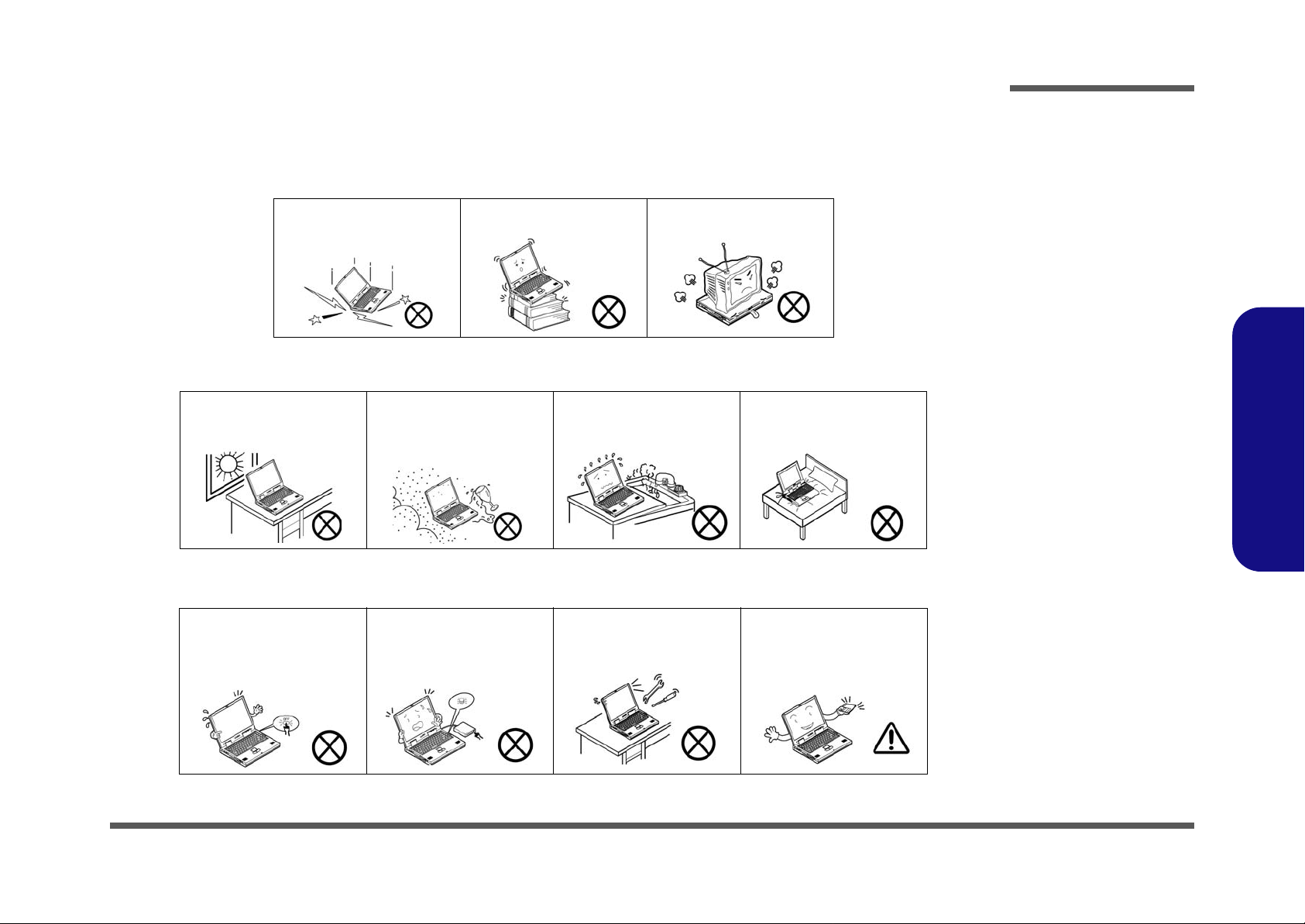
The notebook computer is quite rugged, but it can be damaged. To prevent this, follow these suggestions:
1. Don’t drop it, or expose it to shock. If the computer falls, the case and the components could be damaged.
Preface
Do not expose the computer
to any shock or vibration.
Do not place it on an unstable
surface.
Do not place anything heavy
on the computer.
2. Keep it dry, and don’t overheat it. Keep the computer and power supply away from any kind of heating element. This
is an electrical appliance. If water or any other liquid gets into it, the co mputer could be badly damaged.
Do not expose it to excessive
heat or direct sunlight.
Do not leave it in a place
where foreign matter or moisture may affect the system.
Don’t use or store the computer in a humid environment.
Do not place the computer on
any surface which will block
the vents.
3. Follow the proper working procedures for the computer. Shut the computer down properly and don’t forget to save
your work. Remember to periodically save your data as data may be lost if the battery is depleted.
Do not turn off the power
until you properly shut down
all programs.
Do not turn off any peripheral
devices when the computer is
on.
Do not disassemble the computer by yourself.
Perform routine maintenance
on your computer.
Preface
V
Page 8
Preface
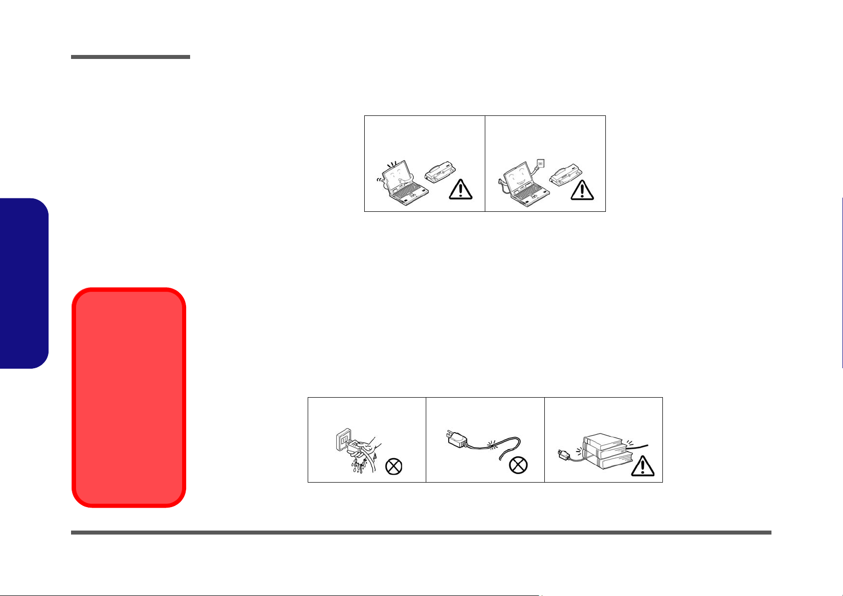
Power Safety
Warning
Before you undertake
any upgrade procedures, make sure that
you have turned off the
power, and disconnected all peripherals
and cables (including
telephone lines). It is
advisable to also remove your battery in
order to prevent accidentally turning the
machine on.
4. Avoid interference. Keep the computer away from high capacity transformers, electric motors, and oth er strong mag-
netic fields. These can hinder proper performance and damage your data.
5. Take care when using peripheral devices.
Preface
VI
Use only approved brands of
peripherals.
Unplug the power cord befor e
attaching peripheral devices.
Power Safety
The computer has specific power requirements:
• Only use a power adapter approved for use with this computer.
• Your AC adapter may be designed for international travel but it still requires a stea dy, uninterrupted po wer supply. If you ar e
unsure of your local power specifications, consult your service representative or local power company.
• The power adapter may have either a 2-prong or a 3-prong grounded plug. The third prong is an important safety feature; do
not defeat its purpose. If you do not have access to a compatible outlet, have a qualified electrician install one.
• When you want to unplug the power cord, be sure to disconnect it by the plug head, not by its wire.
• Make sure the socket and any extension cord(s) you use can support the total current load of all the connected devices.
• Before cleaning the computer, make sure it is disconnected from any external power supplies.
Do not plug in the power
cord if you are wet.
Do not use the power cord if
it is broken.
Do not place heavy objects
on the power cord.
Page 9

Battery Precautions
Battery Disposal
The product that you have purchased contains a rechargeable battery. The battery is recyclable. At the end of its useful life, under various state and local laws, it may be illegal to dispose of this battery into the municipal waste stream. Check with your local solid waste
officials for details in your area for recycling options or proper disposal.
Caution
Danger of explosion if battery is incorrectly replaced. Replace only with the same or equivalent type recommended by the manufacturer.
Discard used battery according to the manufacturer’s instructions.
Battery Level
Click the battery icon in the taskbar to see the current battery level and charge status. A battery that drops below a level of 10%
will not allow the computer to boot up. Make sure that any battery that drops below 10% is recharged within one week.
• Only use batteries designed for this computer. The wrong battery type may explode, leak or damage the computer.
• Do not continue to use a battery that has been dropped, or that appears damaged (e.g. bent or twisted) in any way. Even if the
computer continues to work with a damaged battery in place, it may cause circuit damage, which may possibly result in fire.
• Recharge the batteries using the notebook’s system. Incorrect recharging may make the battery explode.
• Do not try to repair a battery pack. Refer any battery pack repair or replacement to your service representative or qualified service
personnel.
• Keep children away from, and promptly dispose of a damaged battery. Always dispose of batteries carefully. Batteries may explode
or leak if exposed to fire, or improperly handled or discarded.
• Keep the battery away from metal appliances.
• Affix tape to the battery contacts before disposing of the battery.
• Do not touch the battery contacts with your hands or metal objects.
Battery Guidelines
The following can also apply to any backup batteries you may have.
• If you do not use the battery for an extended period, then remove the battery from the computer for storage.
• Before removing the battery for storage charge it to 60% - 70%.
• Check stored batteries at least every 3 months and charge them to 60% - 70%.
Preface
Preface
VII
Page 10
Preface
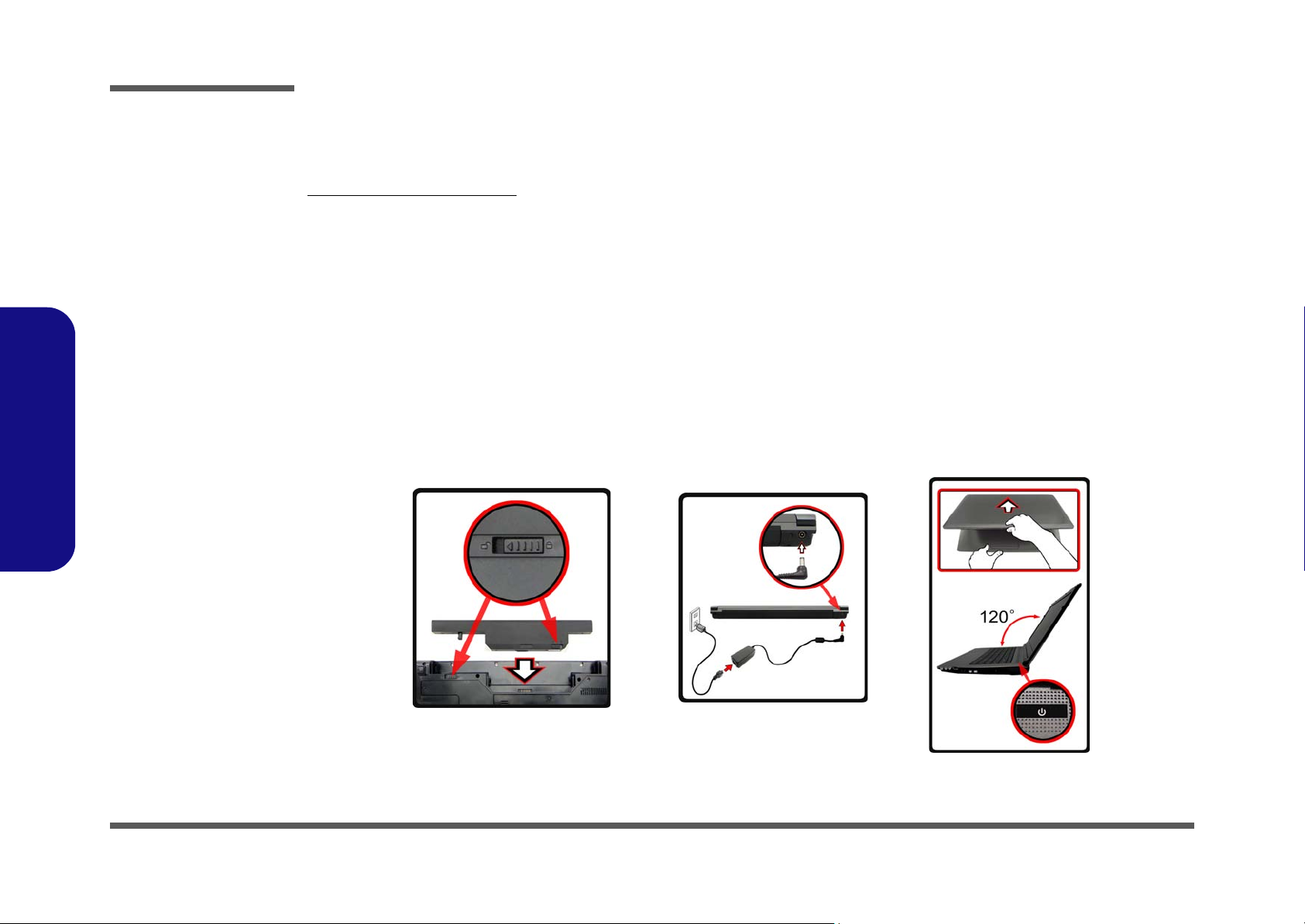
Figure 1 - Opening the Lid/LCD/Computer with AC/DC Adapter Plugged-
In
Preface
Related Documents
You may also need to consult the following manual for additional information:
User’s Manual on CD/DVD
This describes the notebook PC’s features and the procedures for operating the computer and its ROM-based setup program. It also describes the installation and operation of the utility programs provided with the notebook PC.
System Startup
1. Remove all packing materials.
2. Place the computer on a stable surface.
3. Insert the battery and make sure it is locked in position.
4. Securely attach any peripherals you want to use with the computer (e.g. keyboard and mouse) to their ports.
5. Attach the AC/DC adapter to the DC-In jack at the rear of the computer, then plug the AC power cord into an outlet, and connect the AC power cord to
the AC/DC adapter.
6. Use one hand to raise the
I>Figure 1) to support the base of the computer (Note: Never lift the computer by the lid/LCD).
7. Press the power button to turn the computer “on”.
lid/LCD to a comfortable viewing angle
(do not exceed 120 degrees); use the other hand (as illustrated in <Hyperlink B n
VIII
Page 11

Contents
Preface
Introduction ..............................................1-1
Overview .........................................................................................1-1
Specifications ..................................................................................1-2
External Locator - Top View with LCD Panel Open ......................1-4
External Locator - Front & Right Side Views .................................1-5
External Locator - Left Side & Rear View .....................................1-6
External Locator - Bottom View .....................................................1-7
Mainboard Overview - Top (Key Parts) .........................................1-8
Mainboard Overview - Bottom (Key Parts) ....................................1-9
Mainboard Overview - Top (Connectors) .....................................1-10
Mainboard Overview - Bottom (Connectors) ...............................1-11
Disassembly ...............................................2-1
Overview .........................................................................................2-1
Maintenance Tools ..........................................................................2-2
Connections .....................................................................................2-2
Maintenance Precautions .................................................................2-3
Disassembly Steps ...........................................................................2-4
Removing the Battery ......................................................................2-5
Removing the Hard Disk Drive .......................................................2-6
Removing the System Memory (RAM) ..........................................2-8
Removing the Optical (CD/DVD) Device ....................................2-10
Removing and Installing the Processor .........................................2-11
Removing the Wireless LAN Module ...........................................2-14
Removing the Bluetooth Module ..................................................2-15
Removing the Keyboard ................................................................2-16
Part Lists ..................................................A-1
Part List Illustration Location ........................................................A-2
Top without Fingerprint .................................................................A-3
Bottom ............................................................................................ A-4
LCD ............................................................................................... A-5
SATA DVD Super-Multi ............................................................... A-6
Schematic Diagrams.................................B-1
System Block Diagram ...................................................................B-2
Clock Generator ..............................................................................B-3
CPU 1/7 (DMI, PEG, FDI) .............................................................B-4
CPU 2/7 (CLK, MISC) ...................................................................B-5
CPU 3/7 (DDR3) ............................................................................B-6
CPU 4/7 (Power) .............................................................................B-7
CPU 5/7 (VGFX Power) .................................................................B-8
CPU 6/7 (GND) ..............................................................................B-9
CPU 7/7 (RESERVED) ................................................................B-10
DDR3 SO-DIMM_0 .....................................................................B-11
DDR3 SO-DIMM_1 .....................................................................B-12
Panel, Inverter, CRT .....................................................................B-13
VGA PCI-E Interface ....................................................................B-14
VGA Frame Buffer Interface ........................................................B-15
VGA Frame Buffer A ...................................................................B-16
VGA Frame Buffer C ...................................................................B-17
VGA I/O .......................................................................................B-18
VGA NVVDD Cecoupling ...........................................................B-19
IBEXPEAK- M 1/9 .......................................................................B-20
IBEXPEAK - M 2/9 ......................................................................B-21
IBEXPEAK - M 3/9 ......................................................................B-22
IBEXPEAK - M 4/9 ......................................................................B-23
IBEXPEAK - M 5/9 ......................................................................B-24
IBEXPEAK - M 6/9 ......................................................................B-25
IBEXPEAK - M 7/9 ......................................................................B-26
IBEXPEAK - M 8/9 ......................................................................B-27
IBEXPEAK - M 9/9 ......................................................................B-28
Preface
IX
Page 12

Preface
New Card, Mini PCIE .................................................................. B-29
3G, CCD, TPM .............................................................................B-30
USB, Fan, TP, FP, Multi-Conn .................................................... B-31
JMC 251 Card Reader ..................................................................B-32
SATA ODD, LED, Hotkey, LID SW ...........................................B-33
RJ45, Modem ...............................................................................B-34
Audio Codec ALC272 .................................................................. B-35
KBC-ITE IT8502E ....................................................................... B-36
5VS, 3.3VS, 1.5VS, VIN1 ...........................................................B-37
VDD3, VDD5 ...............................................................................B-38
Power 1.8V, PEX_VDD ...............................................................B-39
Power 1.5V/0.75V ........................................................................B-40
Power 1.1VS_VTT .......................................................................B-41
Power VGFX_Core ......................................................................B-42
V-Core ..........................................................................................B-43
Power VGA NVVDD ...................................................................B-44
Preface
AC_IN, Charger ...........................................................................B-45
HDMI ........................................................................................... B-46
Audio Board ................................................................................. B-47
B4100 Fingerprint Board .............................................................B-48
B4100 Power Switch Board ......................................................... B-49
Sequence .......................................................................................B-50
Updating the FLASH ROM BIOS......... C-1
To update the FLASH ROM BIOS you must: C-1
Download the BIOS .......................................................................C-1
Unzip the downloaded files to a bootable CD/DVD/ or USB Flash
drive ................................................................................................C-1
Set the computer to boot from the external drive ...........................C-1
Use the flash tools to update the BIOS ..........................................C-2
Restart the computer (booting from the HDD) .............................. C-2
X
Page 13

Chapter 1: Introduction
Overview
This manual covers the information you need to service or upgrade the E4105/E4105-C series notebook computer. Information about operating the computer (e.g. getting started, and the Setup utility) is in the User’s Manual. Information
about dri-vers (e.g. VGA & audio) is also found in the User’s Manual. The manual is shipped with the computer.
Operating systems (e.g. Windows Vista/ Window 7, etc.) have their own manuals as do application softwares (e.g. word
processing and database programs). If you have questions about those programs, you should consult those manuals.
Introduction
The E4105/E4105-C series notebook is designed to be upgradeable. See Disassembly on page 2 - 1 for a detailed description of the upgrade procedures for each specific component. Please take note of the warning and safety information
indicated by the “” symbol.
The balance of this chapter reviews the computer’s technical specifications and features.
1.Introduction
Overview 1 - 1
Page 14
Introduction
Latest Specification Information
The specifications listed here are correct at the
time of sending them to the press. Certain items
(particularly processor types/speeds) may be
changed, delayed or updated due to the manufacturer's release schedule. Check with your
service center for more details.
CPU
The CPU is not a user serviceable part. Accessing the CPU in any way may violate your
warranty.
Specifications
1.Introduction
Processor Options
Intel® Core™ i7 Processor
i7-620M (2.66GHz)
4MB L3 Cache & 1066MHz FSB
Intel® Core™ i5 Processor
i5-540M (2.53GHz), i5-520M (2.4GHz), i5-450M (2.4GHz),
i5-430M (2.26GHz)
3MB L3 Cache & 1066MHz FSB
Intel® Core™ i3 Processor
i3-370M (2.4GHz), i3-350M (2.26GHz),
i3-330M (2.13GHz)
3MB L3 Cache & 1066MHz FSB
Intel® Pentium® Processor
P6000 (1.86GHz)
3MB L3 Cache & 1066MHz FSB
Intel® Celeron® Processor
P4500 (1.86GHz)
2MB L3 Cache & 1066MHz FSB
Core Logic
Intel® HM55 Chipset
BIOS
One 32Mb SPI Flash ROM
Phoenix™ BIOS
LCD
14" (35.56cm) HD TFT LCD
Memory
Two 204 Pin SO-DIMM Sockets Supporting DDR3 1066MHz
Memory
Memory Expandable up to 8GB
Video Adapter
Intel® GMA HD
Shared Memory Architecture (DVMT) up to 1.7GB
Microsoft DirectX®10 Compatible
Security
BIOS Password
Security (Kensington® Type) Lock Slot
Audio
High Definition Audio Compliant Interface
2 * Built-In Speakers
Built-In Microphone
Storage
One Changeable 12.7mm(h) Super MultiOptical Device Drive
One Changeable 2.5" 9.5 mm (h) SATA HDD
Keyboard
“WinKey” keyboard (with embedded numeric keypad)
Pointing Device
Built-in Touchpad (scrolling key functionality integrated)
Interface
Four USB 2.0 Ports
One eSATA Port
One HDMI-Out Port
One External Monitor Port
One Headphone-Out Jack
One Microphone-In Jack
One S/PDIF Out Jack
One RJ-45 LAN Jack
One DC-in Jack
1 - 2 Specifications
Page 15

Introduction
Half Mini Card Slots
Slot 1 for WLAN Module
(Factory Option) Slot 2 for 3.75G/HSPA Module
Card Reader
Embedded 3-in-1 Card Reader
MMC (MultiMedia Card) / RS MMC
SD (Secure Digital) / Mini SD / SDHC/ SDXC Compatible
MS (Memory Stick) / MS Pro / MS Duo
Communication
Built-In Gigabit Ethernet LAN
1.3M Pixel USB PC Camera Module
(Factory Option) Bluetooth 2.1 + EDR Module
(Factory Option) 3.75G/HSPA Half Mini-Card Module
Wireless LAN Module Options:
(Factory Option) Intel® WiFi Link 1000 (802.11b/g/n) Wireless LAN Half Mini-Card Module
(Factory Option) Third-Party 802.11b/g/n Wireless LAN Half
Mini-Card Module
Environmental Spec
Temperature
Operating: 5
Non-Operating: -20°C - 60°C
Relative Humidity
Operating: 20% - 80%
Non-Operating: 10% - 90%
°C - 35°C
Power
Full Range AC/DC Adapter
AC Input: 100 - 240V, 50 - 60Hz
DC Output: 19V, 3.42A or 18.5V, 3.5A (65W)
6 Cell Smart Lithium-Ion Battery Pack, 48.84WH
(Factory Option) 6 Cell Smart Lithium-Ion Battery Pack,
62.16WH
Dimensions & Weight
346mm (w) * 238mm (d) * 24.8 - 33.8mm (h)
2.3 kg with ODD & 48.84WH Battery
1.Introduction
Specifications 1 - 3
Page 16
Introduction
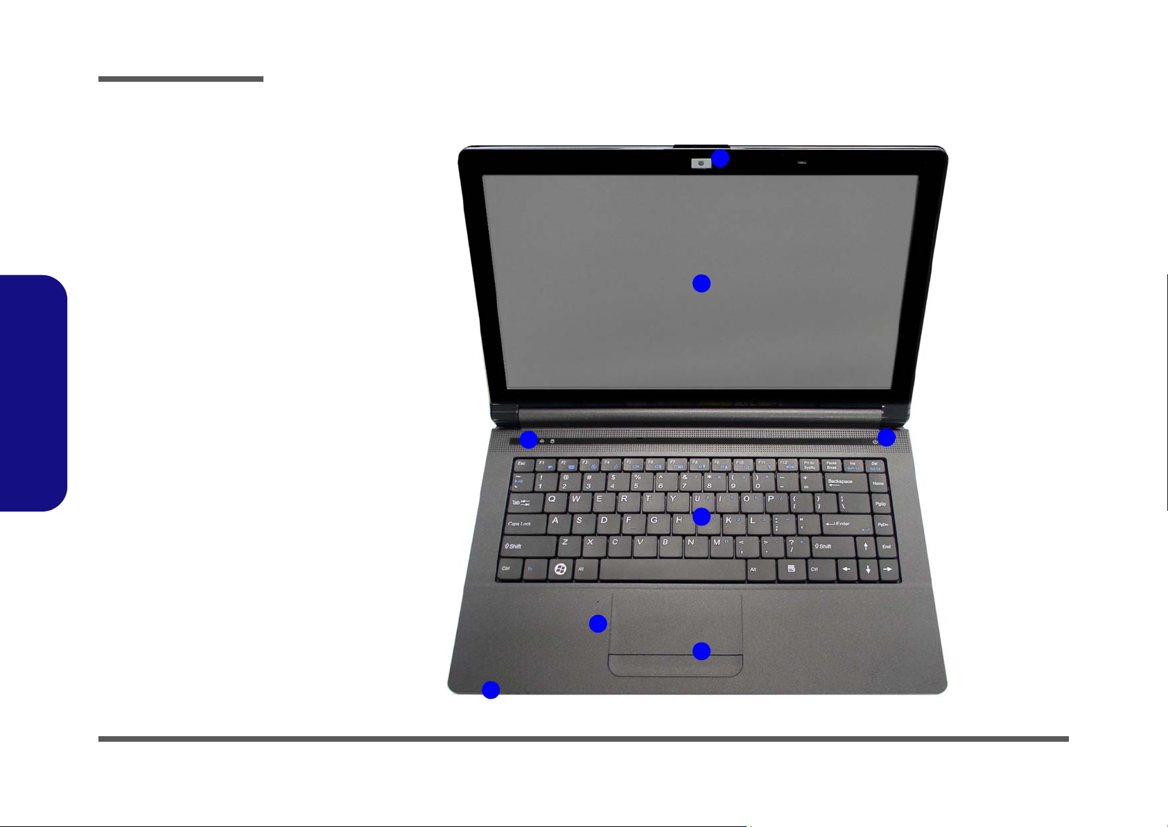
Figure 1
Top View
1. Built-In PC Camera
2. LCD
3. Power Button
4. LED Indicators
5. Keyboard
6. Built-In
Microphone
7. T o uchpad &
Buttons
2
5
1
7
4
6
3
4
External Locator - Top View with LCD Panel Open
1.Introduction
1 - 4 External Locator - Top View with LCD Panel Open
Page 17
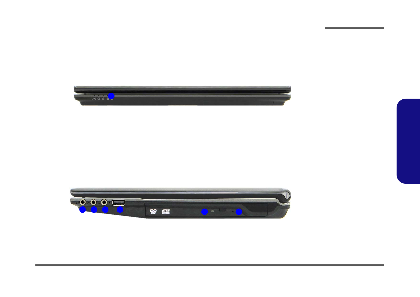
External Locator - Front & Right Side Views
Figure 2
Front View
1. LED Indicators
Figure 3
Right Side View
1. Headphone-Out
Jack
2. Microphone-In
Jack
3. S/PDIF-Out Jack
4. USB 2.0 Port
5. Optical Device
Drive Bay
6. Emergency Eject
Hole
1
FRONT VIEW
1 2 43
5 6
RIGHT SIDE VIEW
Introduction
1.Introduction
External Locator - Front & Right Side Views 1 - 5
Page 18
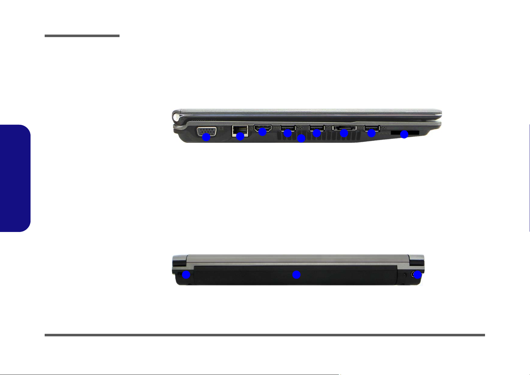
Introduction
Figure 4
Left Side View
1. External Monitor
Port
2. RJ-45 LAN Jack
3. HDMI-Out Port
4. 3 * USB 2.0 Ports
5. eSATA Port
6. Vent
7. 3-in-1 Card
Reader
1
3
2
4 6
7
44
5
LEFT SIDE VIEW
Figure 5
Rear View
1. Security Lock Slot
2. Battery
3. DC-In Jack
1
REAR VIEW
2 3
1.Introduction
External Locator - Left Side & Rear View
/
1 - 6 External Locator - Left Side & Rear View
Page 19
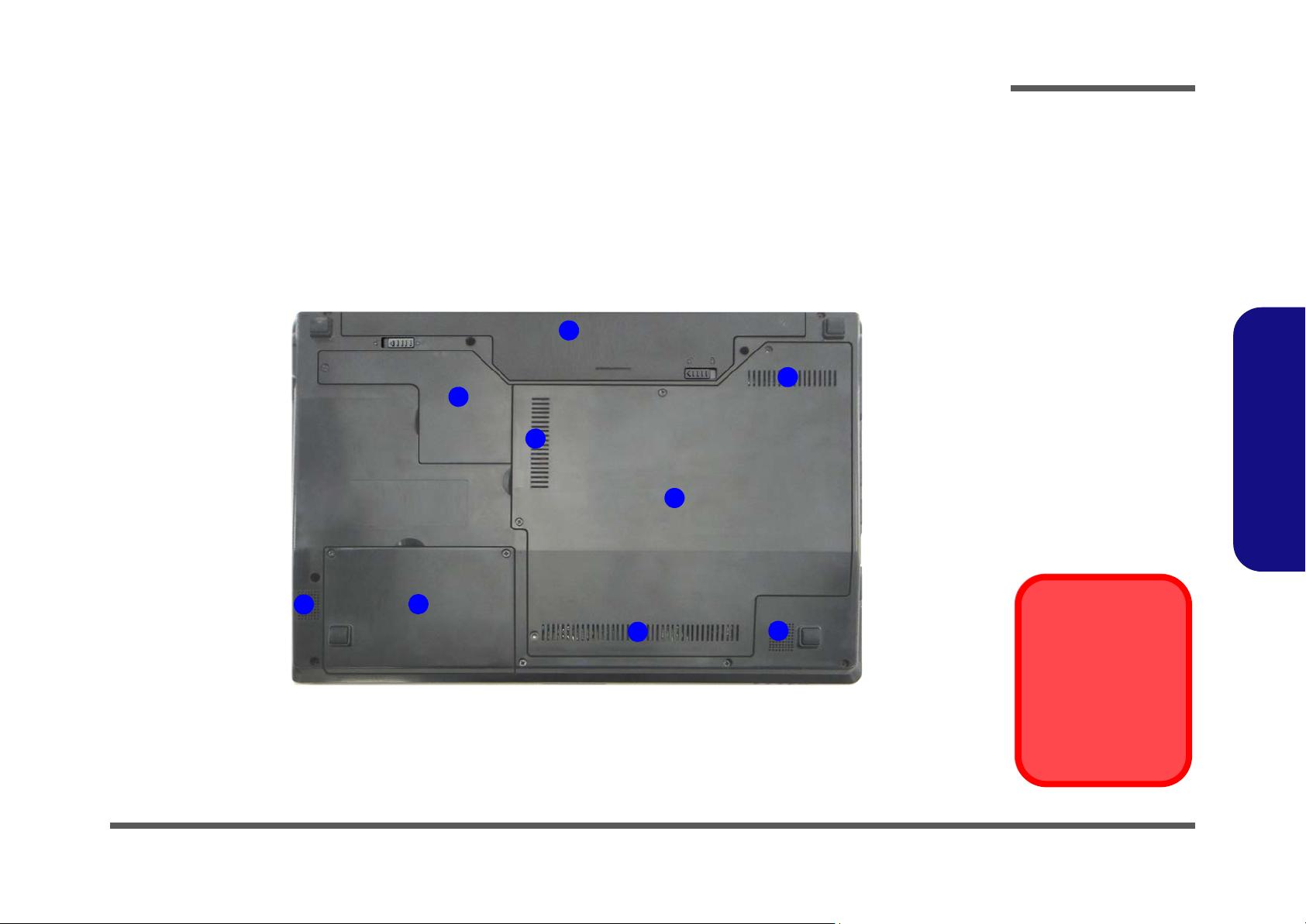
External Locator - Bottom View
Figure 6
Bottom View
1. Battery
2. Component Bay
Cover
3. Vent
4. Hard Disk Bay
Cover
5. Bluetooth
Module Cover
6. Speakers
Overheating
To prevent your computer from overheating, make sure nothing blocks any vent
while the computer is
in use.
2
3
1
4
3
3
5
6
6
Introduction
1.Introduction
External Locator - Bottom View 1 - 7
Page 20
Introduction
Figure 7
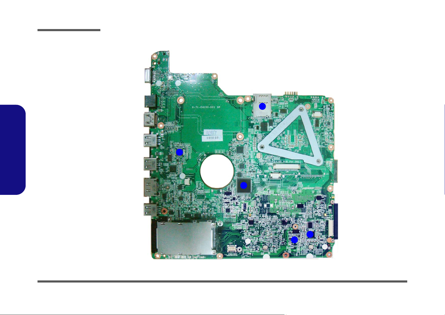
Mainboard Top
Key Parts
1. JMC251
2. KBC-ITE IT8502E
3. Clock Generator
4. Azalia Codec
5. USIM Card
1
2
3
4
5
1.Introduction
Mainboard Overview - Top (Key Parts)
1 - 8 Mainboard Overview - Top (Key Parts)
Page 21
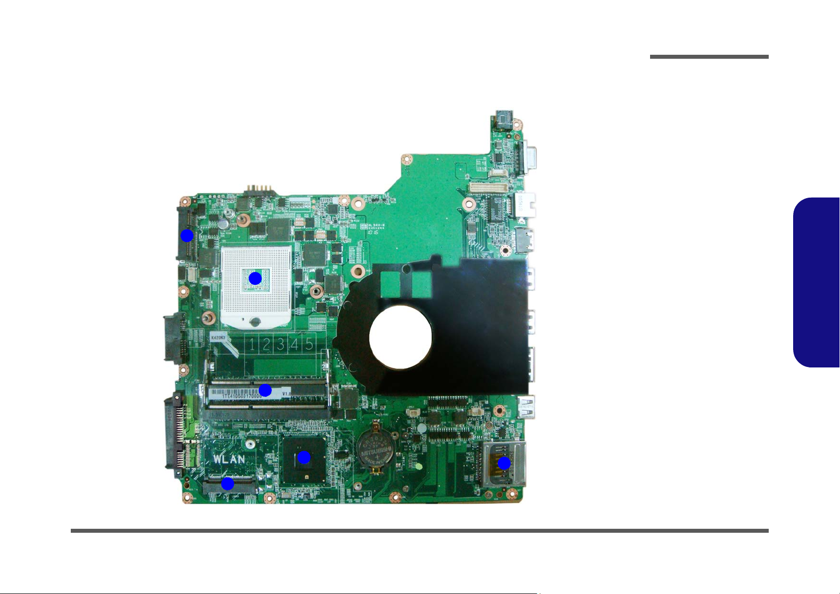
Mainboard Overview - Bottom (Key Parts)
1
2
3
5
6
4
Figure 8
Mainboard Bottom
Key Parts
1. Mini-Card
Connector (3.5G
Module)
2. CPU Socket (no
CPU installed)
3. Memory Slots
DDR3 SO-DIMM
4. Mini-Card
Connector (WLAN
Module)
5. Platform Controller
Hub
6. 3-in-1 Card
Reader
Introduction
1.Introduction
Mainboard Overview - Bottom (Key Parts) 1 - 9
Page 22
Introduction
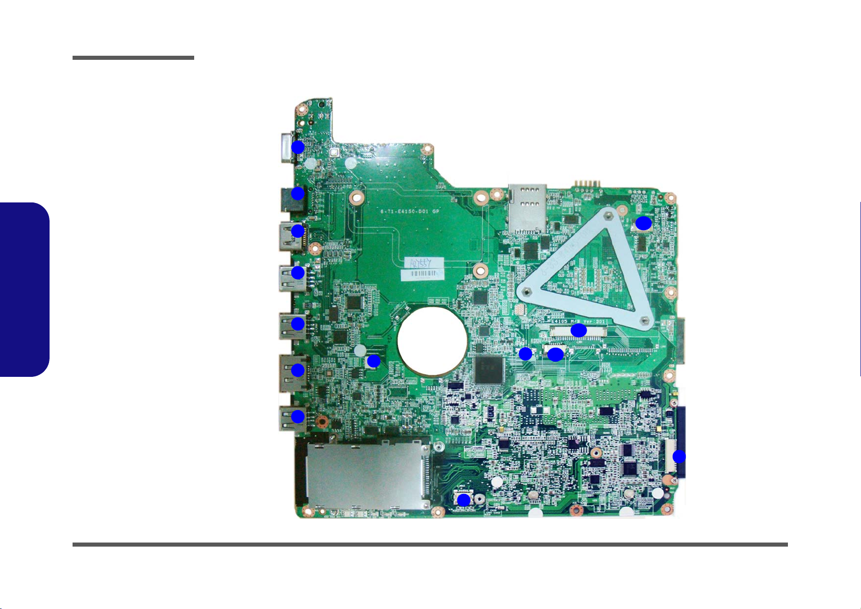
Figure 9
Mainboard Top
Connectors
1. External Monitor
Port
2. RJ-45 LAN Jack
3. HDMI-Out Port
4. USB Ports
5. eSATA Port
6. Microphone
Cable Connector
7. Multi-board
Connector 1
8. Audio Board
Connector
9. Fingerprint Cable
Connector
10.TouchPad Cable
Connector
11. Keyboard Cable
Connector
12.Switch Board
Cable Connector
6
5
7
1
4
2
3
8
9
10
11
4
4
12
1.Introduction
Mainboard Overview - Top (Connectors)
1 - 10 Mainboard Overview - Top (Connectors)
Page 23
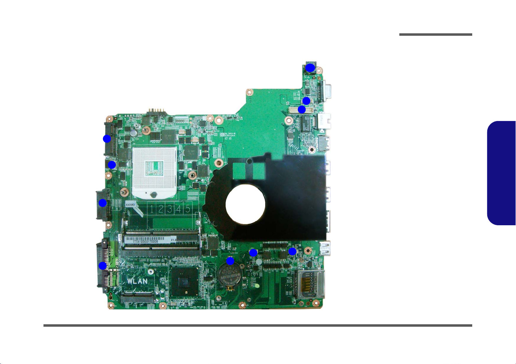
Mainboard Overview - Bottom (Connectors)
Figure 10
Mainboard Bottom
Connectors
1. 3G Connector
2. Bluetooth Cable
Connector
3. CD-ROM
Connector
4. HDD Connector
5. CMOS Battery
Connector
6. Speaker Cable
Connector
7. CPU Fan Cable
Connector
8. LCD Cable
Connector
9. CCD Cable
Connector
10.DC-In Jack
1
2
3
4
5
6
7
8
9
10
Introduction
1.Introduction
Mainboard Overview - Bottom (Connectors) 1 - 11
Page 24

Introduction
1.Introduction
1-12
Page 25
Chapter 2: Disassembly
Information
Warning
Overview
This chapter provides step-by-step instructions for disassembling the E4105/E4105-C series notebook’s parts and subsystems. When it comes to reassembly, reverse the procedures (unless otherwise indicated).
We suggest you completely review any procedure before you take the computer apart.
Disassembly
Procedures such as upgrading/replacing the RAM, optical device and hard disk are included in the User’s Manual but are
repeated here for your convenience.
To make the disassembly process easier each section may have a box in the page margin. Information contained under
the figure # will give a synopsis of the sequence of procedures involved in the disassembly procedure. A box with a
lists the relevant parts you will have after the disassembly process is complete. Note: The parts listed will be for the disassembly procedure listed ONLY, and not any previous disassembly step(s) required. Refer to the part list for the previous disassembly procedure. The amount of screws you should be left with will be listed here also.
A box with a will also provide any possible helpful information. A box with a contains warnings.
An example of these types of boxes are shown in the sidebar.
2.Disassembly
Overview 2 - 1
Page 26

Disassembly
2.Disassembly
NOTE: All disassembly procedures assume that the system is turned OFF, and disconnected from any power supply (the
battery is removed too).
Maintenance Tools
The following tools are recommended when working on the notebook PC:
• M3 Philips-head screwdriver
• M2.5 Philips-head screwdriver (magnetized)
• M2 Philips-head screwdriver
• Small flat-head screwdriver
• Pair of need le-nose pliers
• Anti-static wrist-strap
Connections
Connections within the computer are one of four types:
Locking collar sockets for ribbon connectors To release these connectors, use a small flat-head screwdriver to
gently pry the locking collar away from its base. When replacing the connection, make sure the connector is oriented in the
same way. The pin1 side is usually not indicated.
2 - 2 Overview
Pressure sockets for multi-wire connectors To release this connector type, grasp it at its head and gently
rock it from side to side as you pull it out. Do not pull on the
wires themselves. When replacing the connection, do not try to
force it. The socket only fits one way.
Pressure sockets for ribbon connectors To release these connectors, use a small pair of needle-nose pli-
ers to gently lift the connector away from its socket. When replacing the connection, make sure the connector is oriented in
the same way. The pin1 side is usually not indicated.
Board-to-board or multi-pin sockets To separate the boards, gently rock them from side to side as
you pull them apart. If the connection is very tight, use a small
flat-head screwdriver - use just enough force to start.
Page 27

Maintenance Precautions
Power Safety
Warning
Before you undertake
any upgrade procedures, make sure that
you have turned off the
power, and disconnected all peripherals
and cables (including
telephone lines). It is
advisable to also remove your battery in
order to prevent accidentally turning the
machine on.
The following precautions are a reminder. To avoid personal injury or damage to the computer while performing a removal and/or replacement job, take the following precautions:
1. Don't drop it. Perform your repairs and/or upgrades on a stable surface. If the computer falls, the case and other
components could be damaged.
2. Don't overheat it. Note the proximity of any heating elements. Keep the computer out of direct sunlight.
3. Avoid interference. Note the proximity of any high capacity transformers, electric motors, and other strong mag-
netic fields. These can hinder proper performance and damage component s and/or data. You should also monitor
the position of magnetized tools (i.e. screwdrivers).
4. Keep it dry. This is an electrical appliance. If water or any other liquid gets into it, the computer could be badly
damaged.
5. Be careful with power. Avoid accidental shocks, discharges or explosions.
•Before removing or servicing any part from the computer, turn the computer off and detach any power supplies.
•When you want to unplug the power cord or any cable/wire, be sure to disconnect it by the plug head. Do not pull on the wire.
6. Peripherals – Turn off and detach any peripherals.
7. Beware of static discharge. ICs, such as the CPU and main support chips, are vulnerable to static electricity.
Before handling any part in the computer, discharge any static electricity inside the computer. When handling a
printed circuit board, do not use gloves or other materials which allow static electricity buildup. We suggest that
you use an anti-static wrist strap instead.
8. Beware of corrosion. As you perform your job, avoid touching any connector leads. Even the cleanest hands produce oils which can attract corrosive elements.
9. Keep your work environment clean. Tobacco smoke, dust or other air-born particulate matter is often attracted
to charged surfaces, reducing performance.
10. Keep track of the components. When removing or replacing any part, be careful not to leave small p arts, such as
screws, loose inside the computer.
Cleaning
Do not apply cleaner directly to the computer, use a soft clean cloth.
Do not use volatile (petroleum distillates) or abrasive cleaners on any part of the computer.
Disassembly
2.Disassembly
Overview 2 - 3
Page 28

Disassembly
Disassembly Steps
The following table lists the disassembly steps, and on which page to find the related information. PLEASE PERFORM
THE DISASSEMBLY STEPS IN THE ORDER INDICATED.
2.Disassembly
To remove the Battery:
1. Remove the battery page 2 - 5
To remove the HDD:
1. Remove the battery page 2 - 5
2. Remove the HDD page 2 - 6
To remove the System Memory:
1. Remove the battery page 2 - 5
2. Remove the system memory page 2 - 8
To remove the Optical Device:
1. Remove the battery page 2 - 5
2. Remove the Optical device page 2 - 10
To remove and install a Processor:
1. Remove the battery page 2 - 5
2. Remove the processor page 2 - 11
3. Install the processor page 2 - 13
To remove the Bluetooth Module:
1. Remove the battery page 2 - 5
2. Remove the Bluetooth page 2 - 15
To remove the Keyboard:
1. Remove the battery page 2 - 5
2. Remove the keyboard page 2 - 16
To remove the Wireless LAN Module:
1. Remove the battery page 2 - 5
2. Remove the wireless LAN page 2 - 14
2 - 4 Disassembly Steps
Page 29
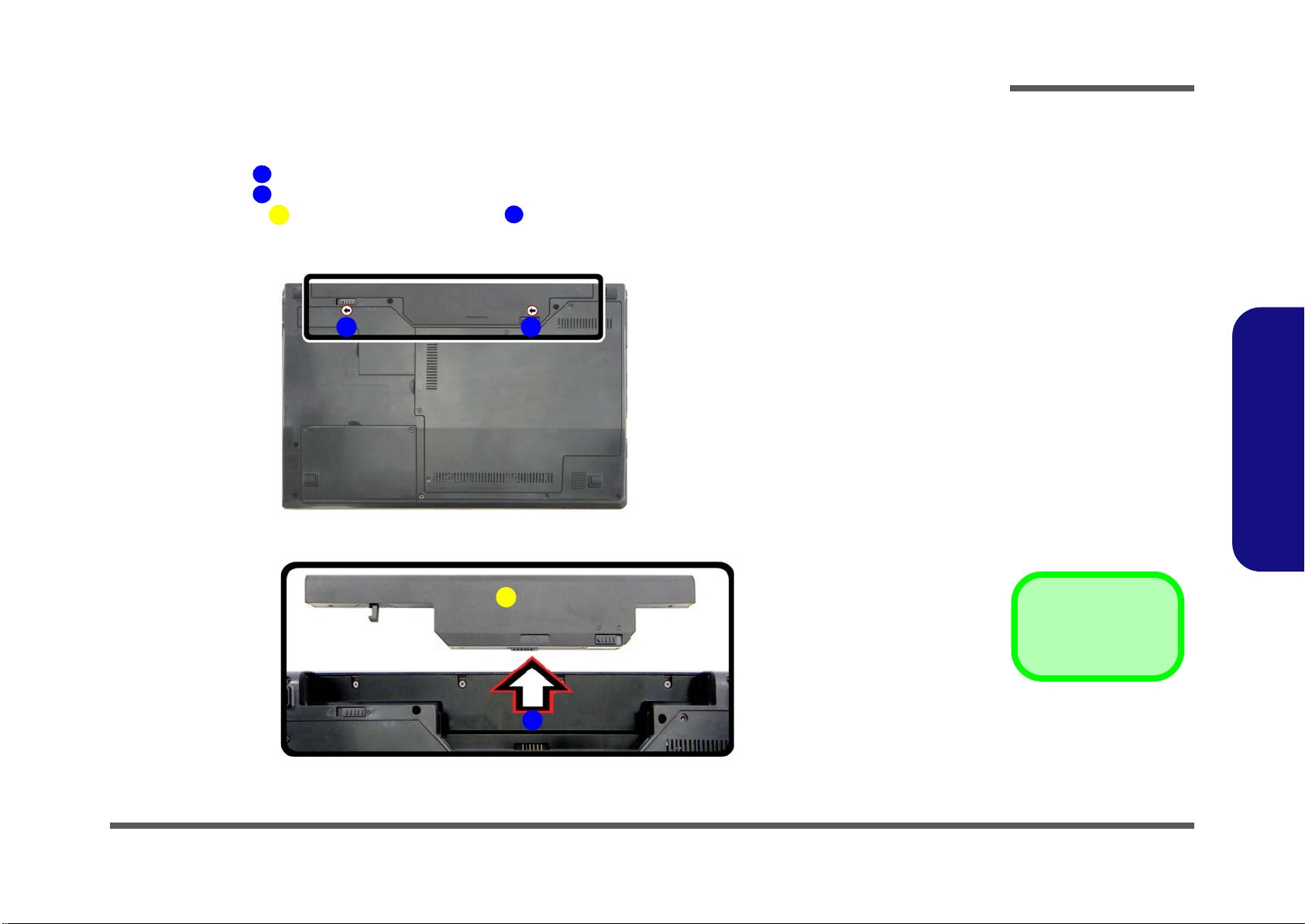
Removing the Battery
3. Battery
12634
a.
3
b.
2
4
1
Figure 1
Battery Removal
a. Slide the latch and hold in
place.
b. Slide the battery in the di-
rection of the arrow.
1. Turn the computer off, and turn it over.
2. Slide the latch in the direction of the arrow (Figure 1a
3. Slide the latch in the direction of the arrow, and hold it in place (Figure 1a
4. Slide the battery in the direction of the arrow (Figure 1b
).
).
Disassembly
).
2.Disassembly
Removing the Battery 2 - 5
Page 30
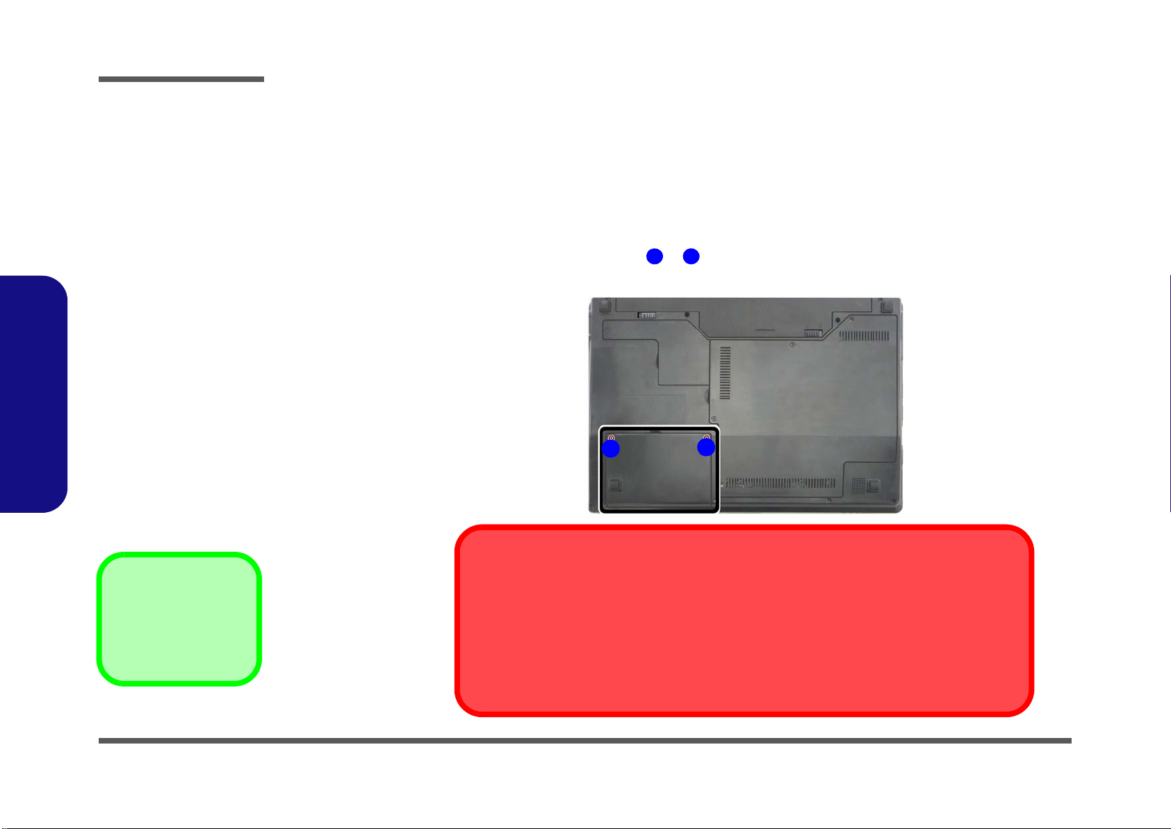
Disassembly
Figure 2
HDD Assembly
Removal
a. Locate the HDD bay co-
ver and remove the
screws.
•2 Screws
1
2
2
1
a.
HDD System Warning
New HDD’s are blank. Before you begin make sure:
You have backed up any data you want to keep from your old HDD.
You have all the CD-ROMs and FDDs required to install your operating system and programs.
If you have access to the internet, download the latest application and hardware driver updates for
the operating system you plan to install. Copy these to a removable medium.
2.Disassembly
Removing the Hard Disk Drive
The hard disk drive can be taken out to accommodate other 2.5" serial (SATA) hard disk drives with a height of 9.5mm
(h). Follow your operating system’s installation instructions, and install all necessary drivers and utilities (as outlined in
Chapter 4 of the User’s Manual) when setting up a new hard disk.
Hard Disk Upgrade Process
1. Turn off the computer, and remove the battery (page 2 - 5).
2. Locate the hard disk bay cover and remove screws & (Figure 2a
).
2 - 6 Removing the Hard Disk Drive
Page 31

3. Remove the hard disk bay cover (Figure 3b).
63467
10
11
4
b.
c.
e.
6
d.
3
9 8
7
5
11
5
10
3. HDD Bay Cover
5. HDD
11.Mylar Cover
•4 Screws
Figure 3
HDD Assembly
Removal (cont’d.)
b. Remove the HDD bay
cover.
c. Grip the tab and slide the
HDD in the direction of
the arrow.
d. Lift the HDD assembly
out of the bay.
e. Remove the screws and
mylar cover.
4. Grip the tab and slide the hard disk in the direction of arrow (Figure 3c).
5. Lift the hard disk out of the bay (Figure 3d).
6. Remove the screws - and the mylar cover from the hard disk
5
5
(Figure 3e).
7. Reverse the process to install a new hard disk (do not forget to replace all the screws and covers).
Disassembly
2.Disassembly
Removing the Hard Disk Drive 2 - 7
Page 32

Disassembly
Figure 4
RAM Module
Removal
a. Remove the screws.
b. Disconnect the fan
cable and remove
the bay cover.
Contact Warning
Be careful not to touch
the metal pins on the
module’s connecting
edge. Even the cleanest hands have oils
which can attract particles, and degrade the
module’s performance.
12561
1. Component Bay Co-
ver
•4 Screws
2
4
3
a.
b.
1
1
6
5
6
2.Disassembly
Removing the System Memory (RAM)
The computer has two memory sockets for 204 pin Small Outline Dual In-line Memory Modules (SO-DIMM) supporting
DDR3 1066MHz. The main memory can be expanded up to 8GB. The SO-DIMM modules supported are 1024MB, and
2048MB and DDRIII Modules. The total memory size is automatically detected by the POST routine once you turn on
your computer.
Memory Upgrade Process
1. Turn off the computer, remove the battery (page 2 - 5).
2. Locate the component bay cover , and remove screws - (Figure 4a
3. Carefully (a fan and cable are attached to the under side of the cover) lift up the bay cover.
4. Carefully disconnect the fan cable , and remove the cover
(Figure 4b).
).
2 - 8 Removing the System Memory (RAM)
Page 33

5. Gently pull the two release latches ( - ) on the sides of the memory socket in the direction indicated by the
6
7
Figure 5
RAM Module
Removal (cont’d.)
c. Pull the release latches.
d. Remove the module(s).
Single Memory
Module Installation
If your computer has a
single memory module,
then insert the module
into the Channel 0
(J_DIMM_1) socket. In
this case, this is the lower memory socket (the
socket closest to the
mainboard) as shown in
Figure 5e.
8. RAM Module(s)
d.
8
6 7
c. e.
8
arrows (Figure 5c).
Disassembly
2.Disassembly
6. The RAM module will pop-up (Figure 5d), and you can then remove it.
7. Pull the latches to release the second module if necessary (Figure 5c).
8. Insert a new module holding it at about a 30° angle and fit the connectors firmly into the memory slot.
9. The module’s pin alignment will allow it to only fit one way. Make sure the module is seated as far into the slot as it
will go. DO NOT FORCE the module; it should fit without much pressure.
10. Press the module in and down towards the mainboard until the slot levers click into place to secure the module.
11. Replace the bay cover and screws (make sure you reconnect the fan cable before screwing down the bay
cover).
12. Restart the computer to allow the BIOS to register the new memory configuration as it starts up.
Removing the System Memory (RAM) 2 - 9
Page 34

Disassembly
Figure 6
Optical Device
Removal
a. Remove the screw.
b. Push the optical device
out off the computer at
point 3.
123
2. Optical Device
•1 Screw
2
1
3
a.
b.
Removing the Optical (CD/DVD) Device
1. Turn off the computer, remove the battery (page 2 - 5) and the component bay cover (page 2 - 8).
2. Remove the screw at point
point
3. Insert the new device and carefully slide it into the computer (the device only fits one way. DO NOT FORCE IT; The
screw holes should line up).
4. Restart the computer to allow it to automatically detect the new device.
(Figure 6b).
(Figure 6a), and use a screwdriver to carefully push out the optical device at
2.Disassembly
2 - 10 Removing the Optical (CD/DVD) Device
Page 35

Removing and Installing the Processor
A32
1
B
Figure 7
Processor Removal
a. Remove the cover and
Iocate the heat sink.
b. Remove the screws in
the order indicated.
c. Remove the heat sink.
B. Heat Sink
•3 Screws
a.
1
2
3
b.
c.
B
A
Processor Removal Procedure
1. Turn off the computer, remove the battery (page 2 - 5) and the component bay cover (page 2 - 8).
2. The CPU heat sink will be visible at point (Figure 7a) on the mainboard.
3. Remove screws
4. Carefully lift up the heat sink (Figure 7c) off the computer.
, , (Figure 7b), the reverse order indicated on the label.
Disassembly
2.Disassembly
Removing and Installing the Processor 2 - 11
Page 36

Disassembly
C
D
Figure 8
Processor Removal
(cont’d)
d. Turn the release latch to
unlock the CPU.
e. Lift the CPU out of the
socket.
C
d. e.
D
Caution
The heat sink, and CPU area in general, contains parts which are subjected to high temperatures. Allow
the area time to cool before removing these parts.
Unlock
D. CPU
5. Turn the release latch towards the unlock symbol , to release the CPU (Figure 8d).
6. Carefully (it may be hot) lift the CPU up out of the socket (Figure 8e).
7. See page 2 - 13 for information on inserting a new CPU.
8. When re-inserting the CPU, pay careful attention to the pin alignment, it will fit only one way (DO NOT FORCE IT!).
2.Disassembly
2 - 12 Removing and Installing the Processor
Page 37

Processor Installation Procedure
A
B
C
D
1
3
c.
3
D
b.
2
1
d.
B
A
a.
D
Lock
C
Figure 9
Processor
Installation
a. Insert the CPU.
b. Turn the release latch to-
wards the lock symbol.
c. Remove the stickers
from the heat sink and
insert the heat sink.
d. Replace and tighten the
screws in the order indicated on the label.
A. CPU
D. Heat Sink
•3 Screws
1. Insert the CPU (Figure 9a), pay careful attention to the pin alignment, it will fit only one way (DO NOT FORCE
IT!), and turn the release latch towards the lock symbol (Figure 9b).
2. Remove the stickers (Figure 9c) from the heat sink.
3. Insert the heat sink
4. Replace and tighten the screws
5. Replace the component bay cover and screws (page 2 - 8).
as indicated in (Figure 9c).
- (Figure 9d) in the order indicated on the label.
Disassembly
2.Disassembly
Removing and Installing the Processor 2 - 13
Page 38

Disassembly
Figure 10
Wireless LAN
Module Removal
a. Remove the cover.
b. Disconnect the cables
and remove the screw.
c. The WLAN module will
pop up.
d. Lift the WLAN module
out.
Note: Make sure you
reconnect the antenna
cable to ‘’1’’ +
‘’2’’socket (Figure
b).
1
2
3
4
5
5
4
b.
c.a. d.
2 3
5
1
5. WLAN Module.
•1 Screw
Removing the Wireless LAN Module
1. Turn off the computer, remove the battery (page 2 - 5) and the component bay cover (page 2 - 8).
2. The Wireless LAN module will be visible at point (Figure 10a) on the mainboard.
3. Carefully disconnect cables - , then remove screw from the module socket (Figure 10b
4. The Wireless LAN module (Figure 10c) will pop-up.
5. Lift the Wireless LAN module (Figure 10d) up and off the computer.
).
2.Disassembly
2 - 14 Removing the Wireless LAN Module
Page 39

Removing the Bluetooth Module
Figure 11
Bluetooth Module
Removal
a. Locate the Bluetooth bay
cover and remove the
screw at point
.
b. Remove the cover and Io-
cate the Bluetooth module.
c. Remove the screw, discon-
nect the cable and the
connector.
d. Lift the Bluetooth module
up off the socket.
1
1
234
5
6
7
a.
b.
1
7
c.
6
d.
5
2
3
4
2. Bluetooth Bay Cover
7. Bluetooth Module
•2 Screws
1. Turn off the computer, remove the battery (page 2 - 5).
1. Locate the Bluetooth bay cover and remove the screw at point
2. Remove the Bluetooth bay cover and the Bluetooth module will be visible at point
3. Remove the screw (Figure 11c).
4. Carefully separate the Bluetooth module from the connector
5. Lift the Bluetooth module
(Figure 11d) up and off the computer.
and disconnect the cable (Figure 11c).
(Figure 11a).
Disassembly
(Figure 11b).
2.Disassembly
Removing the Bluetooth Module 2 - 15
Page 40

Disassembly
1
456
6
7
Figure 12
Keyboard Removal
a. Press the four latches to
release the keyboard.
b. Lift the keyboard up and
disconnect the cable from
the locking collar.
c. Remove the keyboard.
5
a.
b.
2 3 41
7
5
5
c.
6
6
Keyboard Tabs
1. Battery
6. Keyboard
5. Keyboard
Re-Inserting the Key-
board
When re-inserting the
keyboard, align first
the four keyboard tabs
(Figure 12c) that are
located at the bottom,
to the slots in the case.
Removing the Keyboard
1. Turn off the computer and remove the battery (page 2 - 5).
2. Press the four keyboard latches
(Figure 12a) *You may need to use a small screwdriver to do this.
3. Carefully lift the keyboard
up, being careful not to bend the keyboard ribbon cable (Figure 12b).
4. Disconnect the keyboard ribbon cable from the locking collar socket
5. Carefully lift up the keyboard
- at the top of the keyboard to elevate the keyboard from its normal position
(Figure 12c) off the computer.
(Figure 12b)
2.Disassembly
2 - 16 Removing the Keyboard
Page 41

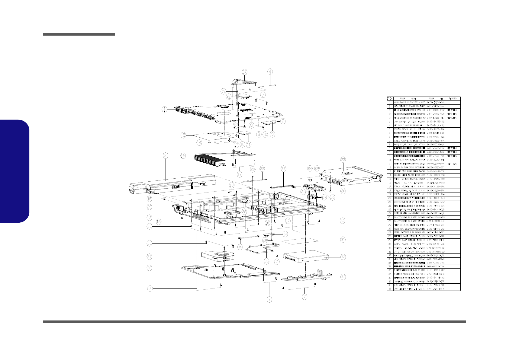
Appendix A:Part Lists
This appendix breaks down the E4105/E4105-C series notebook’s construction into a series of illustrations. The component part numbers are indicated in the tables opposite the drawings.
Note: This section indicates the manufacturer’s part numbers. Your organization may use a different system, so be sure
to cross-check any relevant documentation.
Note: Some assemblies may have parts in common (especially screws). However, the part lists DO NOT indicate the
total number of duplicated parts used.
Part Lists
Note: Be sure to check any update notices. The parts shown in these illustrations are appropriate for the system at the
time of publication. Over the product life, some parts may be improved or re-configured, resulting in new part numbers.
A.Part Lists
A-1
Page 42

Part Lists
Table A - 1
Part List Illustration
Location
Part List Illustration Location
The following table indicates where to find the appropriate part list illustration.
Part E4105/E4105-C
Top without Fingerprint
page A - 3
A.Part Lists
Bottom
LCD
SATA DVD Super-Multi
page A - 4
page A - 5
page A - 6
A - 2 Part List Illustration Location
Page 43

Top without Fingerprint
Figure A - 1
Top without Fin-
gerprint
黑色
非耐落
~
Part Lists
A.Part Lists
Part List Illustration Location A - 3
Page 44
Part Lists
Figure A - 2
Bottom
A.Part Lists
Bottom
A - 4 Part List Illustration Location
Page 45

LCD
Figure A - 3
LCD
非耐落
銘板
Part Lists
A.Part Lists
Part List Illustration Location A - 5
Page 46

Part Lists
Figure A - 4
SATA DVD Super-
Multi
A.Part Lists
SATA DVD Super-Multi
A - 6 Part List Illustration Location
Page 47

Appendix B: Schematic Diagrams
Table B - 1
SCHEMATIC
DIAGRAMS
Version Note
The schematic diagrams in this chapter
are based upon version 6-7P-E4154-001.
If your mainboard (or
other boards) are a later version, please
check with the Service
Center for updated diagrams (if required).
This appendix has circuit diagrams of the E4105/E4105-C notebook’s PCB’s. The following table indicates where to
find the appropriate schematic diagram.
Schematic Diagrams
System Block Diagram - Page B - 2 VGA NVVDD Cecoupling - Page B - 19 KBC-ITE IT8502E - Page B - 36
Clock Generator - Page B - 3 IBEXPEAK- M 1/9 - Page B - 20 5VS, 3.3VS, 1.5VS, VIN1 - Page B - 37
CPU 1/7 (DMI, PEG, FDI) - Page B - 4 IBEXPEAK - M 2/9 - Page B - 21 VDD3, VDD5 - Page B - 38
CPU 2/7 (CLK, MISC) - Page B - 5 IBEXPEAK - M 3/9 - Page B - 22 Power 1.8V, PEX_VDD - Page B - 39
CPU 3/7 (DDR3) - Page B - 6 IBEXPEAK - M 4/9 - Page B - 23 Power 1.5V/0.75V - Page B - 40
CPU 4/7 (Power) - Page B - 7 IBEXPEAK - M 5/9 - Page B - 24 Power 1.1VS_VTT - Page B - 41
CPU 5/7 (VGFX Power) - Page B - 8 IBEXPEAK - M 6/9 - Page B - 25 Power VGFX_Core - Page B - 42
CPU 6/7 (GND) - Page B - 9 IBEXPEAK - M 7/9 - Page B - 26 V-Core - Page B - 43
CPU 7/7 (RESERVED) - Page B - 10 IBEXPEAK - M 8/9 - Page B - 27 Power VGA NVVDD - Page B - 44
DDR3 SO-DIMM_0 - Page B - 11 IBEXPEAK - M 9/9 - Page B - 28 AC_IN, Charger - Page B - 45
DDR3 SO-DIMM_1 - Page B - 12 New Card, Mini PCIE - Page B - 29 HDMI - Page B - 46
Panel, Inverter, CRT - Page B - 13 3G, CCD, TPM - Page B - 30 Audio Board - Page B - 47
VGA PCI-E Interface - Page B - 14 USB, Fan, TP, FP, Multi-Conn - Page B - 31 B4100 Fingerprint Board - Page B - 48
VGA Frame Buffer Interface - Page B - 15 JMC 251 Card Reader - Page B - 32 B4100 Power Switch Board - Page B - 49
VGA Frame Buffer A - Page B - 16 SATA ODD, LED, Hotkey, LID SW - Page B - 33 Sequence - Page B - 50
VGA Frame Buffer C - Page B - 17 RJ45, Modem - Page B - 34
VGA I/O - Page B - 18 Audio Codec ALC272 - Page B - 35
Diagram - Page Diagram - Page Diagram - Page
B.Schematic Diagrams
B-1
Page 48

Schematic Diagrams
Sheet 1 of 49
System Block
Diagram
B4100M System Block Di agram
FingerPrint
(USB2)
(USB4)
12 MHz
LCD CONNECTOR
<8"
TOUCH PAD
CRT CONNECTOR
LPC
CARD
READER
GPU NVDIDA N11x NVVDD
SMART
BATTERY
SO-DIMM1
HP
OUT
INT SPK R
CLICK BOARD
SOCKET
<=8"
PCIE
27x27mm
1071 Ball FCBGA
480 Mbps
DDRIII
SENTELIC
Mini PCIE
SPI
0.5"~5.5"
1"~16"
DDRIII
INT MIC
25
MHz
Arrandale
24 MHz
<12"
FDI
MIC
IN
B4100 (INT SPK L)
128pins LQFP
SO-DIMM2
32.768KHz
(USB11)
Bluetooth
VCORE, 1.1VS_VTT
EC SMBUS
USB PORT
AZALIA LINK
FINGER PRINTER BOARD
(USB10)(USB0)
USB PORT
(USB1)
USB PORT
0.1"~13
eSATA
SYSTEM SMBUS
SATA ODDSATA HDD
BIOS
SPI
LAN
ITE 8502E
<12"
Ibex Peak-M
Platform
Controller
Hub (PCH)
SPDIF
OUT
INT. K/B
Azalia Codec
EC
0.5"~11"
<15"
5V,3V,5VS,3VS,1.5VS,
1.8VS,+1.5S_CPU
1.5V,0.75VS(VTT_MEM)
USB2.0
969 Balls
Nvidia
Optimus N11x
VDD3,VDD5
DMI*4
rPGA989/988
W83L771AWG
32.768 KHz
JMICRO
1.8V, PEX_VDD
MDC CON
AZALIA
MDC
MODULE
RJ-11
SATA I/II 3.0Gb/s
800/1067/1333 MHz
DDR3 / 1.5V
(Optional)
CCD
(USB5)
B4100
(USB9)
NEW CARD
B4100-D03a
REALTEK
ALC272
33 MHz
THERMAL
SENSOR
100 MHz
14*14*1.6mm
PROCESSOR
6-49-C4102-010
SMART
FAN
SLG8SP585
14.318 MHz
Clock Generator
PCIE*8
JMC251
AUDIO BOARD
RJ-45 7IN1
SOCKET
B5100
B4100
(USB8)USB PORTHDMI Connector
TI TPA6017A2
AMP
3G CARD
(USB3)
(Optional)
FBVDDQ
PHONE JACK x3, USB x1,
INT SPK L, RJ-11
AUDIO BOARD
WLAN
VGFX_CORE
Optional
TPM 1.2
AC-IN
FINGER PRINTER BOARD
POWER SWITCH BOARD
System Block Diagram
B.Schematic Diagrams
B - 2 System Block Diagram
Page 49

Clock Generator
CLK_SCLK
CLK_SDATA
CLK_SCLK
3.3VS
REF_0/CPU_SEL
CPU_STOP#
REF_0/CPU_SEL
CLK_SDATA
XOU T
REF_0/C PU_SEL
XIN
PR121 2.2K_04
CLK_PWRG D
C483
1U_10V_06
C482
.1U_16V_04
R328
10K_04
X4 FSX8L_14.31818MHz
12
L33 *HCB1608KF -121T25_32mil_short
PR120 2.2K_04
C436
33p_50V_NPO_04
C435
33p_50V_NPO_04
R322
1M_04
C491
.1U_16V_04
Q37
MTN7002ZHS3
G
DS
L31
*HCB1608KF-121T25_32mil_short
PR117 33_04
PR118 *4.7k_04
PR122 2.2K_04
Q38
MTN7002ZHS3
G
D S
C467
1U_10V_06
C475
.1U_16V_04
U29
SLG8SP585
VDD_DOT
1
VDD_27
5
VDD_SRC
17
VDD_CPU
24
VDD_REF
29
VSS_DOT
2
XTAL_ OU T
27
XTAL_ IN
28
REF_0/CPU_SEL
30
SDA
31
SCL
32
VSS_27
8
VSS_SATA
9
VSS_SRC
12
VSS_CPU
21
VSS_REF
26
VDD_SRC_I/O
15
VDD_CPU_I/O
18
DOT_96
3
DOT_96#
4
27M
6
27M_SS
7
SRC_1/SATA
10
SRC_1#/SATA#
11
SRC_2
13
SRC_2#
14
CPU_STOP#
16
CPU_1
20
CPU_1#
19
CPU_0
23
CPU_0#
22
CKPWRGD/PD#
25
GND
33
PR119 10k_04
Q36
MTN7002ZHS3
G
D S
C437 *10P_50V_04
3.3VS
CLK_VCC1
CLK_VCC2CLK_VCC 1
XOU T
XIN
3.3VS
3.3VS3.3VS
1.1VS_VTT
CLK_VCC2
CLK_BUF_BCLK_N 20
CLK_BUF_BCLK_P 20
CLK_BUF_DOT96_N 20
CLK_BUF_REF1420
CLK_BUF_DOT96_P 20
3.3VS
CLKEN#42
1.1VS_VTT 4,6, 7,19,20,21,24, 25,26,38,40,41, 42
SMB_DATA10, 11,20
SMB_CLK10,11,20
CLKGEN POWER
CLK_SATA# 20
CLK_SATA 20
CLK_PCIE_ICH# 20
CLK_PCIE_IC H 20
1(0.7V-1.5V)
0(default)
PIN_30 CPU_1CPU_0
EMI
EMI Capactior
VDD_I/O can be
ranging from
1.05V to 3.3V
0.1uF near the every power pin
0.1uF near the every power pin
??
9LRS3197
CLOCK GENERATOR
CPU_SEL_During CK_PEWGD Latch Pinl
SMBus
100MHz100MHz
133MHz133MHz
3.3VS 10,11,12, 13,19,20,21,22, 23,24,25,26,28, 29,30,31,32,34,35, 36,41,42,45
Sheet 2 of 49
Clock Generator
Schematic Diagrams
B.Schematic Diagrams
Clock Generator B - 3
Page 50

Schematic Diagrams
Sheet 3 of 49
CPU 1/7
(DMI, PEG, FDI)
PLACE NEAR U29
H17
H8_0D4_4
H10
H8_0D4_4
H18
H8_0D4_4
Cost down
THERM_VOLT 35
3
2
1
3.3V
PEG_IRCOMP_R
EXP_RBIAS
R221 *10mil_short
CRIT_TEMP_REP# 24
Analog Thermal Sensor
C538 .1U_10V_X7R_04
C550 .1U_10V_X7R_04
R429 750_1%_04
C548 .1U_10V_X7R_04
C547 .1U_10V_X7R_04
R427 49.9_1%_04
C546 .1U_10V_X7R_04
C542 .1U_10V_X7R_04
C543 .1U_10V_X7R_04
C541 .1U_10V_X7R_04
C540 .1U_10V_X7R_04
C549 .1U_10V_X7R_04
C536 .1U_10V_X7R_04
C537 .1U_10V_X7R_04
C539 .1U_10V_X7R_04
C545 .1U_10V_X7R_04
PCI EXPRESS -- GRAPHICS
DMI Intel(R) FDI
U40A
MOLEX 479890142
DMI_R X#[0]
A24
DMI_R X#[1]
C23
DMI_R X#[2]
B22
DMI_R X#[3]
A21
DMI_RX[0]
B24
DMI_RX[1]
D23
DMI_RX[2]
B23
DMI_RX[3]
A22
DMI_TX#[0]
D24
DMI_TX#[1]
G24
DMI_TX#[2]
F23
DMI_TX#[3]
H23
DMI_TX[0]
D25
DMI_TX[1]
F24
DMI_TX[3]
G23
DMI_TX[2]
E23
FDI_ TX#[0]
E22
FDI_ TX#[1]
D21
FDI_ TX#[2]
D19
FDI_ TX#[3]
D18
FDI_ TX#[4]
G21
FDI_ TX#[5]
E19
FDI_ TX#[6]
F21
FDI_ TX#[7]
G18
FDI_TX[0]
D22
FDI_TX[1]
C21
FDI_TX[2]
D20
FDI_TX[3]
C18
FDI_TX[4]
G22
FDI_TX[5]
E20
FDI_TX[6]
F20
FDI_TX[7]
G19
FDI_FSYNC[0]
F17
FDI_FSYNC[1]
E17
FDI_INT
C17
FDI_ LSY NC [0]
F18
FDI_ LSY NC [1]
D17
PEG_ICOMPI
B26
PEG_ICOMPO
A26
PEG_RBIAS
A25
PEG_RCOMPO
B27
PEG_RX#[0]
K35
PEG_RX#[1]
J34
PEG_RX#[2]
J33
PEG_RX#[3]
G35
PEG_RX#[4]
G32
PEG_RX#[5]
F34
PEG_RX#[6]
F31
PEG_RX#[7]
D35
PEG_RX#[8]
E33
PEG_RX#[9]
C33
PEG_RX#[10]
D32
PEG_RX#[11]
B32
PEG_RX#[12]
C31
PEG_RX#[13]
B28
PEG_RX#[14]
B30
PEG_RX#[15]
A31
PEG_RX[0]
J35
PEG_RX[1]
H34
PEG_RX[2]
H33
PEG_RX[3]
F35
PEG_RX[4]
G33
PEG_RX[5]
E34
PEG_RX[6]
F32
PEG_RX[7]
D34
PEG_RX[8]
F33
PEG_RX[9]
B33
PEG_RX[10]
D31
PEG_RX[11]
A32
PEG_RX[12]
C30
PEG_RX[13]
A28
PEG_RX[14]
B29
PEG_RX[15]
A30
PEG_TX#[0]
L33
PEG_TX#[1]
M35
PEG_TX#[2]
M33
PEG_TX#[3]
M30
PEG_TX#[4]
L31
PEG_TX#[5]
K32
PEG_TX#[6]
M29
PEG_TX#[7]
J31
PEG_TX#[8]
K29
PEG_TX#[9]
H30
PEG_TX#[10]
H29
PEG_TX#[11]
F29
PEG_TX#[12]
E28
PEG_TX#[13]
D29
PEG_TX#[14]
D27
PEG_TX#[15]
C26
PEG_TX[0]
L34
PEG_TX[1]
M34
PEG_TX[2]
M32
PEG_TX[3]
L30
PEG_TX[4]
M31
PEG_TX[5]
K31
PEG_TX[6]
M28
PEG_TX[7]
H31
PEG_TX[8]
K28
PEG_TX[9]
G30
PEG_TX[10]
G29
PEG_TX[11]
F28
PEG_TX[12]
E27
PEG_TX[13]
D28
PEG_TX[14]
C27
PEG_TX[15]
C25
Q28
*2N3904
B
E C
C552 .1U_10V_X7R_04
U19
*W83L771AW G
VDD
1
D+
2
D-
3
THER M
4
GND
5
ALERT
6
SDATA
7
SCLK
8
C551 .1U_10V_X7R_04
3.3V
DMI_TXP221
DMI_TXP121
DMI_TXP021
DMI_TXN221
DMI_TXN121
DMI_TXN021
DMI_TXP321
DMI_RXN221
DMI_RXN121
DMI_RXN021
DMI_TXN321
DMI_RXP221
DMI_RXP121
DMI_RXP021
DMI_RXN321
FDI_INT21
FDI_FSYNC121
FDI_FSYNC021
DMI_RXP321
PEG_RX#2 1 3
FDI_LSYNC121
FDI_LSYNC021
PEG_RX7 13
PEG_RX#4 1 3
PEG_RX5 13
PEG_RX#7 1 3
PEG_RX#1 1 3
PEG_RX4 13
PEG_RX#0 1 3
PEG_RX#3 1 3
PEG_RX2 13
PEG_RX#6 1 3
PEG_RX3 13
PEG_RX#5 1 3
PEG_RX6 13
PEG_RX0 13
PEG_TX3 13
PEG_TX6 13
PEG_RX1 13
PEG_TX#3 13
PEG_TX0 13
PEG_TX#2 13
PEG_TX#5 13
PEG_TX7 13
PEG_TX4 13
PEG_TX#7 13
PEG_TX1 13
PEG_TX#0 13
PEG_TX5 13
PEG_TX#1 13
PEG_TX2 13
PEG_TX#6 13
FDI_TXN121
FDI_TXN021
PEG_TX#4 13
FDI_TXN521
FDI_TXN421
FDI_TXN321
FDI_TXN221
FDI_TXP121
FDI_TXP021
FDI_TXN721
FDI_TXN621
FDI_TXP521
FDI_TXP421
FDI_TXP321
FDI_TXP221
3.3V4,12,13,17,19,20,21,23,24,26,28, 29, 31, 32,33, 36, 38,39, 40, 43
FDI_TXP721
FDI_TXP621
20 mil
D11 * RB751V
AC
1:2 (4mils:8mils)
PM_EXTTS#_EC 4
On Board DDR3 Thermal Sensor
PROCESSOR 1/7 ( DMI,PEG,FDI )
It applies to Auburndale and Clarksfie ld discrete graphic designs.
If discrete graphic chip is used for Auburndale, VAXG (GFX core) rail can be connected
to GND if motherboard only supports disc rete graphics and also in a common
motherboard design if GFX VR is not stuffed. On th e other hand, if the VR is stuffed,
VAXG can be left floating in a common mothe rboard design (Gfx VR keeps VAXG from
floating).
In addition, FDI_RXN_[7:0] and FDI _RXP_[7:0] can be left floating on the PC H.
FDI_TX[7:0] and FDI_TX#[7:0] can b e left floating on the Auburndale.
The GFX_IMON, FDI_FSYNC[0], FDI_F SYNC[1], FDI_LSYNC[0], FDI_LSY NC[1], and
FDI_INT signals should be tied to GND (thr ough 1K ? % re sistors) in the common
motherboard design case. Please no t that if these signals are left floating , there are no
functional impacts but a small amount of power (~15 mW) maybe wasted. VAXG_SENS E
and VSSAXG_SENSE on Auburndale can be left as no connect.
DPLL_REF_SSCLK and DPLL_R EF_SSCLK# can be connecte d to GND on Auburndale
directly if motherboard only suppo rts discrete graphics. In a common mothe rboard
design, these pins are dr iven via PCH (even if Gra phics is disabled by BIO S) thus no
external termination is required.
PULL HIGH? ? ? IBEX? PAGE21
C328
*.1U_1 6V_04
CPU
C321
.1U_16V_04
C303
.1U_16V_04
Q27
G711ST9U
OUT1VCC
2
GND
3
SMC_CPU_THER M 20,35
SMD_CPU_THER M 20,35
PEG_TX_2
PEG_TX_1
PEG_TX#_3
PEG_TX_4
PEG_TX#_2
PEG_TX#_5
PEG_TX#_7
PEG_TX_6
PEG_TX#_6
PEG_TX#_1
PEG_TX#_4
PEG_TX_7
PEG_TX#_0
PEG_TX_0
PEG_TX_5
PEG_TX_3
CPU 1/7 (DMI, PEG, FDI)
B.Schematic Diagrams
B - 4 CPU 1/7 (DMI, PEG, FDI)
Page 51

CPU 2/7 (CLK, MISC)
+1.5S_ CPU 7,36
1.1VS_VTT_PWRGD21,40
Q13
*MTN7002ZHS3
G
DS
R162
*10K_04
3.3V
3.3V
+1.5S_CP U
U11
*74AHC1G08GW
1
2
5
4
3
DRAMPWRGD_CPU
Q12
*2N3904
B
E C
+1.5S_CPU_PWRGD 39
3.3V
C222 *.1u_10V_X7R_04
R163
*10K_04
SYS_AGENT_PWROK
H_CPURST#
DDR3 Compensation Signals
H_PROCHOT#_D
Processor Pullups
XDP _ TD I _M
XDP_TRST#
1.5V 10,11,36, 39
H_PROCHOT#42
If PROCHOT# is not used, then it must be terminated
with a 50-O pull-up resistor to VTT_1.1 rail.
PROCESSOR 2/7 ( CLK,MISC,JTAG )
H_COMP2
H_COMP3
H_COMP1
H_COMP0
R107 *68_04
R128 *12.4K_1%_04
R67 *51_04
R69 *51_04
R130 10K_04
R159 1.5K_1%_04
R125 49.9_1%_04
R421 20_1%_04
R110 0_04
R153 *0_04
R440 24.9_1%_04
R419 49.9_1%_04
R418 51_04
R60 *51_04
R131 10K_04
CLOCKS
MISC THERMAL
PWR MANAGEMENT
DDR3
MISC
JTAG & BPM
U40B
MOLEX 479890142
SM_RCOMP[1]
AM1
SM_RCOMP[2]
AN1
SM_DRAMRST#
F6
SM_RCOMP[0]
AL1
BCLK#
B16
BCLK
A16
BCLK_ITP#
AT30
BCLK_ITP
AR30
PEG_CLK#
D16
PEG_CLK
E16
DPLL_REF_SSCLK#
A17
DPLL_REF_SSCLK
A18
CATERR#
AK14
COMP3
AT23
PECI
AT15
PROCHOT#
AN26
THE RMTR IP #
AK15
RESET_OBS#
AP26
VCCPWRGOOD_1
AN14
VCCPWRGOOD_0
AN27
SM_DRAMPWR OK
AK13
VTTPWRGOOD
AM15
RSTIN#
AL14
PM_EXT_TS#[0]
AN15
PM_EXT_TS#[1]
AP15
PRDY#
AT28
PREQ#
AP27
TCK
AN28
TMS
AP28
TRST#
AT27
TDI
AT29
TDO
AR27
TDI_M
AR29
TDO_ M
AP29
DBR#
AN25
BPM#[0]
AJ22
BPM#[1]
AK22
BPM#[2]
AK24
BPM#[3]
AJ24
BPM#[4]
AJ25
BPM#[5]
AH22
BPM#[6]
AK23
BPM#[7]
AH23
COMP2
AT24
PM_SYNC
AL15
TAPPWRGOOD
AM26
COMP1
G16
COMP0
AT26
SKTOCC#
AH24
R109 68_04
R424 20_1%_04
R115 *0_04
R129 *0_04
TRACE WIDTH 10MIL, LENGTH <500MILS
R441 100_1%_04
R155
750_1%_04
R433 49.9_1%_04
R108 51_04
R68 *51_04
R439 130_1%_04
XDP _T MS
1.1VS_VTT
1.1VS_VTT
1.1VS_VTT
BCLK_CPU_P 24
CLK_DP_P 20
CLK_DP_N 20
H_CPUPWRGD24
BUF _PL T_RS T#23,28,31,35
PM_DRAM_PWR GD21
H_VTTPWRGD21
BCLK_CPU_N 24
H_THRMTRIP#24
CLK_EXP_N 20
CLK_EXP_P 20
1.1VS_VTT 2, 6,7,19,20, 21,24,25, 26,38,40,41, 42
H_PECI24,35
PM_EXTTS#_EC 3
TS#_DIMM0_1 10,11
DELAY_PWRGD21,42
H_PM_SYNC21
R134
1.1K_1%_04
VDDPW RGOOD_R
R158
3K_1%_04
+1.5S_C PU
R157
*1.5K_1%_04
DRAMPWRGD_CPU
R114 *10mil_short
H_PROCHOT#_D
R156 *10mil_short
C1126
.1u_10V_X7R_04
R416 * 10mil_short
XDP _T DO _ M
H_CPURST#
Processor Compensation
Signals
H_PWRGD_XDP
PLT_R ST#_R
XDP_PREQ#
XDP _T CL K
XDP_TRST#
XDP _T MS
Connect to the Processor (VTTPWRGOOD) VTT_1.1 VR power
good signal to processor. Signal voltage level is 1.1 V.
H_COMP3
SYS_AGENT_PWROK
H_COMP2
PM_EXTTS#[1]
H_COMP1
Signal from PCH to Processor
Connect to PCH (PLT_RST#)
(needs to be level translated
from 3.3 V to 1.1 V).
CPU_DRAMRST#
SM_RCOMP_0
XDP _T DO _ M
3.3V 3,12,13, 17,19,20,21,23,24,26,28, 29,31,32,33, 36,38,39, 40,43
XDP _T DI _ R
SM_RCOMP_1
VDDPWRGOOD_R
SM_RCOMP_2
H_CATERR#
XDP _P R EQ #
XDP _T CL K
R246
*1K_04
Q32
*MTN7002ZHS3
G
D S
R241
*100K_04
R250 0_04
XDP _T DI _ R
R234 *0_04
DDR3_D RAMRST#10,11
1.5V
DDR3_DRAMRST#
DRAMRST_CNTRL_PCH24
CPU_DRAMRST#
C360
*470p_50V_X7R_04
PM_EXTTS#[0]
DRAMRST_CNTRL9
H_COMP0
XDP _T DI _ M
XDP _T DO _M
R121 0_04
SM_RCOMP_2
SM_RCOMP_1
SM_RCOMP_0
H_CATERR#
Sheet 4 of 49
CPU 2/7
(CLK, MISC)
Schematic Diagrams
CPU 2/7 (CLK, MISC) B - 5
B.Schematic Diagrams
Page 52

Schematic Diagrams
PROCESSOR 3/7 ( DDR3 )
M_A_D Q1
M_A_D Q2
M_A_D Q3
M_A_A6
M_A_A5
M_A_A7
M_A_A8
M_A_A9
M_A_D Q29
M_A_D Q4
M_A_A4
M_A_D Q32
M_A_D Q31
M_A_D Q30
M_A_D Q37
M_A_D Q36
M_A_D Q35
M_A_D Q34
M_A_D Q33
M_A_D Q42
M_A_D Q41
M_A_D Q40
M_A_D Q39
M_A_D Q47
M_A_D Q46
M_A_D Q45
M_A_D Q44
M_A_D Q43
M_A_D Q51
M_A_D Q28
M_A_D Q50
M_A_D Q49
M_A_D Q38
M_A_D Q48
M_A_D Q55
M_A_D Q54
M_A_D Q53
M_A_D Q52
M_A_A3
M_A_D Q5
M_A_A0
M_A_DQS7
M_A_A1
M_A_A2
M_A_A1 5
M_A_DQS6
M_A_D Q58
M_A_D Q57
M_A_D Q56
M_A_D Q6
M_A_D Q59
M_A_D Q63
M_A_D Q62
M_A_D Q61
M_A_D Q60
M_A_DQS4
M_A_DQS5
M_A_DQS0
M_A_DQS2
M_A_DQS1
M_A_DQS3
M_A_D Q7
M_A_A1 4
M_A_A1 3
M_A_D Q8
M_A_D Q9
M_A_D Q13
M_A_D Q12
M_A_D Q11
M_A_A1 1
M_A_D Q19
M_A_D Q18
M_A_D Q17
M_A_D Q16
M_A_D Q15
M_A_D Q14
M_A_DQS#5
M_A_DQS#6
M_A_DQS#7
M_A_D Q10
M_A_DQS#2
M_A_DQS#1
M_A_DQS#3
M_A_DQS#4
M_A_DQS#0
M_A_D Q22
M_A_D Q21
M_A_D Q26
M_A_D Q25
M_A_D Q24
M_A_D Q23
M_A_D Q0
M_A_A1 2
M_A_D Q20
M_A_D Q27
M_A_D M4
M_A_D M5
M_A_D M6
M_A_D M7
M_A_D M0
M_A_D M2
M_A_D M1
M_A_D M3
M_A_A1 0
DDR SYSTEM MEMORY A
U40C
MOLEX 479890142
SA_BS[0]
AC3
SA_BS[1]
AB2
SA_BS[2]
U7
SA_CAS#
AE1
SA_RAS#
AB3
SA_WE#
AE9
SA_CK[0]
AA6
SA_CK[1]
Y6
SA_CK#[0]
AA7
SA_CK#[1]
Y5
SA_CKE[0]
P7
SA_CKE[1]
P6
SA_CS#[0]
AE2
SA_CS#[1]
AE8
SA_ODT[0]
AD8
SA_ODT[1]
AF9
SA_DM[0]
B9
SA_DM[1]
D7
SA_DM[2]
H7
SA_DM[3]
M7
SA_DM[4]
AG6
SA_DM[5]
AM7
SA_DM[6]
AN10
SA_DM[7]
AN13
SA_DQS[0]
C8
SA_DQS#[0]
C9
SA_DQS[1]
F9
SA_DQS#[1]
F8
SA_DQS[2]
H9
SA_DQS#[2]
J9
SA_DQS[3]
M9
SA_DQS#[3]
N9
SA_DQS[4]
AH8
SA_DQS#[4]
AH7
SA_DQS[5]
AK10
SA_DQS#[5]
AK9
SA_DQS[6]
AN11
SA_DQS#[6]
AP11
SA_DQS[7]
AR13
SA_DQS#[7]
AT13
SA_MA[0]
Y3
SA_MA[1]
W1
SA_MA[2]
AA8
SA_MA[3]
AA3
SA_MA[4]
V1
SA_MA[5]
AA9
SA_MA[6]
V8
SA_MA[7]
T1
SA_MA[8]
Y9
SA_MA[9]
U6
SA_MA[10]
AD4
SA_MA[11]
T2
SA_MA[12]
U3
SA_MA[13]
AG8
SA_MA[14]
T3
SA_MA[15]
V9
SA_DQ[0]
A10
SA_DQ[1]
C10
SA_DQ[2]
C7
SA_DQ[3]
A7
SA_DQ[4]
B10
SA_DQ[5]
D10
SA_DQ[6]
E10
SA_DQ[7]
A8
SA_DQ[8]
D8
SA_DQ[9]
F10
SA_DQ[10]
E6
SA_DQ[11]
F7
SA_DQ[12]
E9
SA_DQ[13]
B7
SA_DQ[14]
E7
SA_DQ[15]
C6
SA_DQ[16]
H10
SA_DQ[17]
G8
SA_DQ[18]
K7
SA_DQ[19]
J8
SA_DQ[20]
G7
SA_DQ[21]
G10
SA_DQ[22]
J7
SA_DQ[23]
J10
SA_DQ[24]
L7
SA_DQ[25]
M6
SA_DQ[26]
M8
SA_DQ[27]
L9
SA_DQ[28]
L6
SA_DQ[29]
K8
SA_DQ[30]
N8
SA_DQ[31]
P9
SA_DQ[32]
AH5
SA_DQ[33]
AF5
SA_DQ[34]
AK6
SA_DQ[35]
AK7
SA_DQ[36]
AF6
SA_DQ[37]
AG5
SA_DQ[38]
AJ7
SA_DQ[39]
AJ6
SA_DQ[40]
AJ10
SA_DQ[41]
AJ9
SA_DQ[42]
AL10
SA_DQ[43]
AK12
SA_DQ[44]
AK8
SA_DQ[45]
AL7
SA_DQ[46]
AK11
SA_DQ[47]
AL8
SA_DQ[48]
AN8
SA_DQ[49]
AM10
SA_DQ[50]
AR11
SA_DQ[51]
AL11
SA_DQ[52]
AM9
SA_DQ[53]
AN9
SA_DQ[54]
AT11
SA_DQ[55]
AP12
SA_DQ[56]
AM12
SA_DQ[57]
AN12
SA_DQ[58]
AM13
SA_DQ[59]
AT14
SA_DQ[60]
AT12
SA_DQ[61]
AL13
SA_DQ[62]
AR14
SA_DQ[63]
AP14
DDR SYSTEM MEMORY - B
U40D
MOLEX 479890142
SB_BS[0]
AB1
SB_BS[1]
W5
SB_BS[2]
R7
SB_CAS#
AC5
SB_RAS#
Y7
SB_WE#
AC6
SB_CK[0]
W8
SB_CK[1]
V7
SB_CK#[0]
W9
SB_CK#[1]
V6
SB_CKE[0]
M3
SB_CKE[1]
M2
SB_CS#[0]
AB8
SB_CS#[1]
AD6
SB_ODT[0]
AC7
SB_ODT[1]
AD1
SB_DM[0]
D4
SB_DM[1]
E1
SB_DM[2]
H3
SB_DM[3]
K1
SB_DM[4]
AH1
SB_DM[5]
AL2
SB_DM[6]
AR4
SB_DM[7]
AT8
SB_DQS[4]
AG2
SB_DQS#[4]
AH2
SB_DQS[5]
AL5
SB_DQS#[5]
AL4
SB_DQS[6]
AP5
SB_DQS#[6]
AR5
SB_DQS[7]
AR7
SB_DQS#[7]
AR8
SB_DQS[0]
C5
SB_DQS#[0]
D5
SB_DQS[1]
E3
SB_DQS#[1]
F4
SB_DQS[2]
H4
SB_DQS#[2]
J4
SB_DQS[3]
M5
SB_DQS#[3]
L4
SB_MA[0]
U5
SB_MA[1]
V2
SB_MA[2]
T5
SB_MA[3]
V3
SB_MA[4]
R1
SB_MA[5]
T8
SB_MA[6]
R2
SB_MA[7]
R6
SB_MA[8]
R4
SB_MA[9]
R5
SB_MA[10]
AB5
SB_MA[11]
P3
SB_MA[12]
R3
SB_MA[13]
AF7
SB_MA[14]
P5
SB_MA[15]
N1
SB_DQ[0]
B5
SB_DQ[1]
A5
SB_DQ[2]
C3
SB_DQ[3]
B3
SB_DQ[4]
E4
SB_DQ[5]
A6
SB_DQ[6]
A4
SB_DQ[7]
C4
SB_DQ[8]
D1
SB_DQ[9]
D2
SB_DQ[10]
F2
SB_DQ[11]
F1
SB_DQ[12]
C2
SB_DQ[13]
F5
SB_DQ[14]
F3
SB_DQ[15]
G4
SB_DQ[16]
H6
SB_DQ[17]
G2
SB_DQ[18]
J6
SB_DQ[19]
J3
SB_DQ[20]
G1
SB_DQ[21]
G5
SB_DQ[22]
J2
SB_DQ[23]
J1
SB_DQ[24]
J5
SB_DQ[25]
K2
SB_DQ[26]
L3
SB_DQ[27]
M1
SB_DQ[28]
K5
SB_DQ[29]
K4
SB_DQ[30]
M4
SB_DQ[31]
N5
SB_DQ[32]
AF3
SB_DQ[33]
AG1
SB_DQ[34]
AJ3
SB_DQ[35]
AK1
SB_DQ[36]
AG4
SB_DQ[37]
AG3
SB_DQ[38]
AJ4
SB_DQ[39]
AH4
SB_DQ[40]
AK3
SB_DQ[41]
AK4
SB_DQ[42]
AM6
SB_DQ[43]
AN2
SB_DQ[44]
AK5
SB_DQ[45]
AK2
SB_DQ[46]
AM4
SB_DQ[47]
AM3
SB_DQ[48]
AP3
SB_DQ[49]
AN5
SB_DQ[50]
AT4
SB_DQ[51]
AN6
SB_DQ[52]
AN4
SB_DQ[53]
AN3
SB_DQ[54]
AT5
SB_DQ[55]
AT6
SB_DQ[56]
AN7
SB_DQ[57]
AP6
SB_DQ[58]
AP8
SB_DQ[59]
AT9
SB_DQ[60]
AT7
SB_DQ[61]
AP9
SB_DQ[62]
AR10
SB_DQ[63]
AT10
M_CKE0 10
M_CLK_DDR#1 10
M_CLK_DDR1 10
M_CKE1 10
M_A_BS110
M_ODT1 10
M_CS#1 10
M_CS#0 10
M_A_BS210
M_A_DM[7:0] 10
M_A_CAS#10
M_ODT0 10
M_CLK_DDR0 10
M_A_WE#10
M_A_A[15:0] 10
M_A_RAS#10
M_A_D Q[63: 0]10
M_B_BS011
M_CLK_DDR#0 10
M_A_BS010
M_B_BS211
M_B_W E#11
M_B_RAS#11
M_B_BS111
M_B_DQ[63:0]11
M_CKE3 11
M_CKE2 11
M_B_CAS#11
M_CS#3 11
M_CS#2 11
M_CLK_DDR#3 11
M_CLK_DDR3 11
M_CLK_DDR#2 11
M_CLK_DDR2 11
M_ODT2 11
M_ODT3 11
M_B_DQS[7:0] 11
M_B_DQS#[7:0] 11
M_B_A[15 :0] 11
M_B_DM[7:0] 11
M_A_DQS[7:0] 10
M_A_DQS#[7:0] 10
M_B_D Q48
M_B_D Q47
M_B_D Q54
M_B_D Q53
M_B_D Q52
M_B_D Q51
M_B_D Q50
M_B_D Q49
M_B_D QS5
M_B_D Q58
M_B_D Q57
M_B_D Q56
M_B_D Q55 M_B_D QS7
M_B_D QS0
M_B_D QS1
M_B_D QS2
M_B_D QS3
M_B_D QS4
M_B_D QS6
M_B_D Q61
M_B_D Q60
M_B_D Q59
M_B_D QS#4
M_B_D QS#6
M_B_D QS#5
M_B_D Q11
M_B_D Q63
M_B_D Q62
M_B_D M6
M_B_D M5
M_B_D Q12
M_B_D QS#7
M_B_D QS#0
M_B_D QS#1
M_B_D QS#2
M_B_D QS#3
M_B_D M7
M_B_D M0
M_B_D M1
M_B_D M2
M_B_D M3
M_B_D M4
M_B_D Q3
M_B_D Q2
M_B_D Q1
M_B_D Q4
M_B_D Q6
M_B_D Q5
M_B_D Q9
M_B_D Q8
M_B_D Q7
M_B_D Q0
M_B_D Q10
M_B_D Q13
M_B_A2
M_B_A3
M_B_A4
M_B_A6
M_B_A5
M_B_A0
M_B_A1
M_B_A8
M_B_A9
M_B_A10
M_B_A11
M_B_A13
M_B_A12
M_B_D Q14
M_B_D Q18
M_B_D Q17
M_B_D Q16
M_B_A14
M_B_A15
M_B_D Q15
M_B_A7
M_B_D Q23
M_B_D Q22
M_B_D Q21
M_B_D Q20
M_B_D Q19
M_B_D Q28
M_B_D Q27
M_B_D Q26
M_B_D Q25
M_B_D Q24
M_B_D Q34
M_B_D Q33
M_B_D Q32
M_B_D Q31
M_B_D Q30
M_B_D Q29
M_B_D Q39
M_B_D Q38
M_B_D Q37
M_B_D Q36
M_B_D Q35
M_B_D Q44
M_B_D Q43
M_B_D Q42
M_B_D Q41
M_B_D Q40
M_B_D Q46
M_B_D Q45
Sheet 5 of 49
CPU 3/7
(DDR3)
CPU 3/7 (DDR3)
B.Schematic Diagrams
B - 6 CPU 3/7 (DDR3)
Page 53

CPU 4/7 (Power)
VCORE
R105
1K_04
C563
10U_6.3V_06
C559
10U_6.3V_06
1K PU to VTT and 1K PD to GND
for POC
C150
22U_6.3V_X5R_08
1.1VS_VTT
R70
1K_04
1.1VS_VTT
ICCMAX_VTT Max Current
for VTT Rail
SV 18
XE 21
PSI# 42
PSI#
C157
22U_6.3V_X5R_08
C165
22U_6.3V_X5R_08
VCORE
C145
22U_6.3V_X5R_08
C171
22U_6.3V_X5R_08
C163
22U_6.3V_X5R_08
C183
22U_6.3V_X5R_08
C156
22U_6.3V_X5R_08
The decoupling capacitors, filt er
recommendations and sense resistors on the
CPU/PCH Rails are specific to t he CRB
Implementation. Customers need to follow the
recommendations in the Calpella Platform
Design Guide
C144
22U_6.3V_X5R_08
C584
22U_6.3V_X5R_08
C149
22U_6.3V_X5R_08
Please note that the
VTT Rail Values are
Auburndale VTT=1.05V
Clarksfield VTT=1.1V
C560
10U_6.3V_06
VCORE
C173
22U_6.3V_X5R_08
R434 *10mil_short
Cost down
PROCESSOR 4/7 ( POWER )
C573
10U_6.3V_06
R104
*1K_04
C170
10U_6.3 V_06
C586
22U_6.3V_X5R_08
C187
22U_6.3V_X5R_08
C179
10U_6.3V_06
C569
10U_6.3V_06
+VTT_44
C585
22U_6.3V_X5R_08
POWER
CPU CORE SUPP LY
1.1V RAIL POWER
SENSE LINES
CPU VIDS
U40F
MOLEX 479890142
ISENSE
AN35
VTT_SENSE
B15
PSI#
AN33
VID[0]
AK35
VID[1]
AK33
VID[2]
AK34
VID[3]
AL35
VID[4]
AL33
VID[5]
AM33
VID[6]
AM35
PROC_D PRSLPVR
AM34
VTT_SELECT
G15
VCC_SENSE
AJ34
VSS_SENSE_VTT
A15
VCC1
AG35
VCC2
AG34
VCC3
AG33
VCC4
AG32
VCC5
AG31
VCC6
AG30
VCC7
AG29
VCC8
AG28
VCC9
AG27
VCC10
AG26
VCC11
AF35
VCC12
AF34
VCC13
AF33
VCC14
AF32
VCC15
AF31
VCC16
AF30
VCC17
AF29
VCC18
AF28
VCC19
AF27
VCC20
AF26
VCC21
AD35
VCC22
AD34
VCC23
AD33
VCC24
AD32
VCC25
AD31
VCC26
AD30
VCC27
AD29
VCC28
AD28
VCC29
AD27
VCC30
AD26
VCC31
AC35
VCC32
AC34
VCC33
AC33
VCC34
AC32
VCC35
AC31
VCC36
AC30
VCC37
AC29
VCC38
AC28
VCC39
AC27
VCC40
AC26
VCC41
AA35
VCC42
AA34
VCC43
AA33
VCC44
AA32
VCC45
AA31
VCC46
AA30
VCC47
AA29
VCC48
AA28
VCC49
AA27
VCC50
AA26
VCC51
Y35
VCC52
Y34
VCC53
Y33
VCC54
Y32
VCC55
Y31
VCC56
Y30
VCC57
Y29
VCC58
Y28
VCC59
Y27
VCC60
Y26
VCC61
V35
VCC62
V34
VCC63
V33
VCC64
V32
VCC65
V31
VCC66
V30
VCC67
V29
VCC68
V28
VCC69
V27
VCC70
V26
VCC71
U35
VCC72
U34
VCC73
U33
VCC74
U32
VCC75
U31
VCC76
U30
VCC77
U29
VCC78
U28
VCC79
U27
VCC80
U26
VCC81
R35
VCC82
R34
VCC83
R33
VCC84
R32
VCC85
R31
VCC86
R30
VCC87
R29
VCC88
R28
VCC89
R27
VCC90
R26
VCC91
P35
VCC92
P34
VCC93
P33
VCC94
P32
VCC95
P31
VCC96
P30
VCC97
P29
VCC98
P28
VCC99
P27
VCC100
P26
VTT0_33
AF10
VTT0_34
AE10
VTT0_35
AC10
VTT0_36
AB10
VTT0_37
Y10
VTT0_38
W10
VTT0_39
U10
VTT0_40
T10
VTT0_41
J12
VTT0_42
J11
VTT0_1
AH14
VTT0_2
AH12
VTT0_3
AH11
VTT0_4
AH10
VTT0_5
J14
VTT0_6
J13
VTT0_7
H14
VTT0_8
H12
VTT0_9
G14
VTT0_10
G13
VTT0_11
G12
VTT0_12
G11
VTT0_13
F14
VTT0_14
F13
VTT0_15
F12
VTT0_16
F11
VTT0_17
E14
VTT0_18
E12
VTT0_19
D14
VTT0_20
D13
VTT0_21
D12
VTT0_22
D11
VTT0_23
C14
VTT0_24
C13
VTT0_25
C12
VTT0_26
C11
VTT0_27
B14
VTT0_28
B12
VTT0_29
A14
VTT0_30
A13
VTT0_31
A12
VTT0_32
A11
VSS_SENSE
AJ35
VTT0_43
J16
VTT0_44
J15
C174
10U_6.3 V_06
C190
*10U_6.3V_06
C204
*10U_6.3V_06
C175
22U_6.3V_X5R_08
C626
10U_6.3V_06
C186
10U_6.3V_06
C188
22U_6.3 V_X5R_08
C177
10U_6.3V_06
C180
10U_6.3V_06
1.1VS_VTTVCORE
1.1VS_VTT
1.1VS_VTT
IMON 42
VSS_SENSE 42
VCC_SENSE 42
1.1VS_VTT 2,4, 7,19,20,21,24, 25,26,38,40,41, 42
VCORE 42
PM_DPRSLPVR 42
H_VTTV ID 1 40
H_VID1 42
H_VID2 42
H_VID5 42
H_VID4 42
H_VID0 42
H_VID6 42
H_VID3 42
VTT_SENSE 40,41
C565
10U_6.3V_06
TO VCORE POWER CONTROL
PROCESSOR UNCORE POWER
C564
10U_6.3V_06
PROCESSOR CORE POWER
+VTT_43
C570
10U_6.3V_06
C574
10U_6.3V_06
C580
10U_6.3V_06
C566
10U_6.3V_06
R435 *10mil_short
ICCMAX Maximum Processor SV 52
Core ICC XE 65
C579
10U_6.3V_06
VTT TOTAL 21A
52A
Sheet 6 of 49
CPU 4/7
(Power)
Schematic Diagrams
B.Schematic Diagrams
CPU 4/7 (Power) B - 7
Page 54

Schematic Diagrams
VCCPLL 0.6A
TP_GFX_I MON
C146
22U_6.3V_X5R_08
C158
22U_6.3V_X5R_08
R120
*0_04
Please note that the
VTT Rail Values are
Auburndale VTT=1.05V
Clarksfield VTT=1.1V
R112 *1K_04
C266
10U_6.3V_06
C267
10U_6.3V_06
C268
10U_6.3V _06
C1133
10U_6.3V_06
+1.5S_CPU
R113 100_04
+1.5S_CPU 4,36
PROCESSOR 5/7 ( GRAPHICS POWER )
FOR DISABLE
GPUVSSSENSE 41
GPUVCCSENSE 41
VDDQ 6A
GFX_IMON 41
C193
1U_6.3V_X5R_04
C561
2.2u_6.3V_X5R_04
+
C567
330u_2.5V_V_A
C152
10U_6.3V_06
C588
22U_6.3V_X5R_08
C196
1U_6.3V_X5R_04
C555
10U_6.3V_06
C135
1U_6.3V_X5R_04
C264
1U_6.3V_X5R_04
C160
22U_6.3V_X5R_08
C143
22U_6.3V_X5R_08
C189
22U_6.3V_X5R_08
C142
4.7U_6.3V_X5R_06
C265
1U_6.3V_X5R_04
C587
22U_6.3V_X5R_08
C153
10U_6.3V_06
C161
22U_6.3V_X5R_08
C197
1U_6.3V_X5R_04
C562
1U_6.3V_X5R_04
C600
22U_6.3V_X5R_08
C601
22U_6.3V_X5R_08
C147
22U_6.3V_X5R_08
C210
10U_6.3V_06
POWER
GRAPHICS VIDs
GRAPHICS
DDR3 - 1.5V RAILS
FDI PEG & DMI
SENSE
LINES
1.1V1.8V
U40G
MOLEX 479890142
GFX_VID[ 0]
AM22
GFX_VID[ 1]
AP22
GFX_VID[ 2]
AN22
GFX_VID[ 3]
AP23
GFX_VID[ 4]
AM23
GFX_VID[ 5]
AP24
GFX_VID[ 6]
AN24
GFX_VR_EN
AR25
GFX_DPRSLPVR
AT25
GFX_IMON
AM24
VAXG_SENSE
AR22
VSSAXG_SENSE
AT22
VAXG1
AT21
VAXG2
AT19
VAXG3
AT18
VAXG4
AT16
VAXG5
AR21
VAXG6
AR19
VAXG7
AR18
VAXG8
AR16
VAXG9
AP21
VAXG10
AP19
VAXG11
AP18
VAXG12
AP16
VAXG13
AN21
VAXG14
AN19
VAXG15
AN18
VAXG16
AN16
VAXG17
AM21
VAXG18
AM19
VAXG19
AM18
VAXG20
AM16
VAXG21
AL21
VAXG22
AL19
VAXG23
AL18
VAXG24
AL16
VAXG25
AK21
VAXG26
AK19
VAXG27
AK18
VAXG28
AK16
VAXG29
AJ21
VAXG30
AJ19
VAXG31
AJ18
VAXG32
AJ16
VAXG33
AH21
VAXG34
AH19
VAXG35
AH18
VAXG36
AH16
VTT1_45
J24
VTT1_46
J23
VTT1_47
H25
VTT1_48
K26
VTT1_49
J27
VTT1_50
J26
VTT1_51
J25
VTT1_52
H27
VTT1_53
G28
VTT1_54
G27
VTT1_55
G26
VTT1_56
F26
VTT1_57
E26
VTT1_58
E25
VDDQ1
AJ1
VDDQ2
AF1
VDDQ3
AE7
VDDQ4
AE4
VDDQ5
AC1
VDDQ6
AB7
VDDQ7
AB4
VDDQ8
Y1
VDDQ9
W7
VDDQ10
W4
VDDQ11
U1
VDDQ12
T7
VDDQ13
T4
VDDQ14
P1
VDDQ15
N7
VDDQ16
N4
VDDQ17
L1
VDDQ18
H1
VTT0_59
P10
VTT0_60
N10
VTT0_61
L10
VTT0_62
K10
VCCPLL1
L26
VCCPLL2
L27
VCCPLL3
M26
VTT1_63
J22
VTT1_64
J20
VTT1_65
J18
VTT1_66
H21
VTT1_67
H20
VTT1_68
H19
VGFX_CORE
1.1VS_VTT
1.1VS_VTT
1.8VS
1.1VS_VTT
1.1VS_VTT
DFGT_VID_0 41
DFGT_VR_EN 41
DFGT_VID_4 41
DFGT_VID_3 41
DFGT_VID_2 41
DFGT_VID_1 41
1.1VS_VTT 2,4,6,19,20,21,24,25,26,38,40,41,42
VGFX_CORE 41
1.8VS 25,36,38
DFGT_VID_6 41
DFGT_VID_5 41
Sheet 7 of 49
CPU 5/7
(VGFX Power)
CPU 5/7 (VGFX Power)
B.Schematic Diagrams
B - 8 CPU 5/7 (VGFX Power)
Page 55

CPU 6/7 (GND)
PROCESSOR 6/7 ( GND )
VSS
U40H
MOLEX 479890142
VSS1
AT20
VSS2
AT17
VSS3
AR31
VSS4
AR28
VSS5
AR26
VSS6
AR24
VSS7
AR23
VSS8
AR20
VSS9
AR17
VSS10
AR15
VSS11
AR12
VSS12
AR9
VSS13
AR6
VSS14
AR3
VSS15
AP20
VSS16
AP17
VSS17
AP13
VSS18
AP10
VSS19
AP7
VSS20
AP4
VSS21
AP2
VSS22
AN34
VSS23
AN31
VSS24
AN23
VSS25
AN20
VSS26
AN17
VSS27
AM29
VSS28
AM27
VSS29
AM25
VSS30
AM20
VSS31
AM17
VSS32
AM14
VSS33
AM11
VSS34
AM8
VSS35
AM5
VSS36
AM2
VSS37
AL34
VSS38
AL31
VSS39
AL23
VSS40
AL20
VSS41
AL17
VSS42
AL12
VSS43
AL9
VSS44
AL6
VSS45
AL3
VSS46
AK29
VSS47
AK27
VSS48
AK25
VSS49
AK20
VSS50
AK17
VSS51
AJ31
VSS52
AJ23
VSS53
AJ20
VSS54
AJ17
VSS55
AJ14
VSS56
AJ11
VSS57
AJ8
VSS58
AJ5
VSS59
AJ2
VSS60
AH35
VSS61
AH34
VSS62
AH33
VSS63
AH32
VSS64
AH31
VSS65
AH30
VSS66
AH29
VSS67
AH28
VSS68
AH27
VSS69
AH26
VSS70
AH20
VSS71
AH17
VSS72
AH13
VSS73
AH9
VSS74
AH6
VSS75
AH3
VSS76
AG10
VSS77
AF8
VSS78
AF4
VSS79
AF2
VSS80
AE35
VSS81
AE34
VSS82
AE33
VSS83
AE32
VSS84
AE31
VSS85
AE30
VSS86
AE29
VSS87
AE28
VSS88
AE27
VSS89
AE26
VSS90
AE6
VSS91
AD10
VSS92
AC8
VSS93
AC4
VSS94
AC2
VSS95
AB35
VSS96
AB34
VSS97
AB33
VSS98
AB32
VSS99
AB31
VSS100
AB30
VSS101
AB29
VSS102
AB28
VSS103
AB27
VSS104
AB26
VSS105
AB6
VSS106
AA10
VSS107
Y8
VSS108
Y4
VSS109
Y2
VSS110
W35
VSS111
W34
VSS112
W33
VSS113
W32
VSS114
W31
VSS115
W30
VSS116
W29
VSS117
W28
VSS118
W27
VSS119
W26
VSS120
W6
VSS121
V10
VSS122
U8
VSS123
U4
VSS124
U2
VSS125
T35
VSS126
T34
VSS127
T33
VSS128
T32
VSS129
T31
VSS130
T30
VSS131
T29
VSS132
T28
VSS133
T27
VSS134
T26
VSS135
T6
VSS136
R10
VSS137
P8
VSS138
P4
VSS139
P2
VSS140
N35
VSS141
N34
VSS142
N33
VSS143
N32
VSS144
N31
VSS145
N30
VSS146
N29
VSS147
N28
VSS148
N27
VSS149
N26
VSS150
N6
VSS151
M10
VSS152
L35
VSS153
L32
VSS154
L29
VSS155
L8
VSS156
L5
VSS157
L2
VSS158
K34
VSS159
K33
VSS160
K30
VSS
NCTF
U40I
MOLEX 479890142
VSS161
K27
VSS162
K9
VSS163
K6
VSS164
K3
VSS165
J32
VSS166
J30
VSS167
J21
VSS168
J19
VSS169
H35
VSS170
H32
VSS171
H28
VSS172
H26
VSS173
H24
VSS174
H22
VSS175
H18
VSS176
H15
VSS177
H13
VSS178
H11
VSS179
H8
VSS180
H5
VSS181
H2
VSS182
G34
VSS183
G31
VSS184
G20
VSS185
G9
VSS186
G6
VSS187
G3
VSS188
F30
VSS189
F27
VSS190
F25
VSS191
F22
VSS192
F19
VSS193
F16
VSS194
E35
VSS195
E32
VSS196
E29
VSS197
E24
VSS198
E21
VSS199
E18
VSS200
E13
VSS201
E11
VSS202
E8
VSS203
E5
VSS204
E2
VSS205
D33
VSS206
D30
VSS207
D26
VSS208
D9
VSS209
D6
VSS210
D3
VSS211
C34
VSS212
C32
VSS213
C29
VSS214
C28
VSS215
C24
VSS216
C22
VSS217
C20
VSS218
C19
VSS219
C16
VSS220
B31
VSS221
B25
VSS222
B21
VSS223
B18
VSS224
B17
VSS225
B13
VSS226
B11
VSS227
B8
VSS228
B6
VSS229
B4
VSS230
A29
VSS_NCTF1
AT35
VSS_NCTF2
AT1
VSS_NCTF3
AR34
VSS_NCTF4
B34
VSS_NCTF5
B2
VSS_NCTF6
B1
VSS_NCTF7
A35
VSS231
A27
VSS232
A23
VSS233
A9
Sheet 8 of 49
CPU 6/7 (GND)
Schematic Diagrams
B.Schematic Diagrams
CPU 6/7 (GND) B - 9
Page 56

Schematic Diagrams
RESERVED
U40E
MOLEX 479890142
CFG[0]
AM30
CFG[1]
AM28
CFG[2]
AP31
CFG[3]
AL32
CFG[4]
AL30
CFG[5]
AM31
CFG[6]
AN29
CFG[7]
AM32
CFG[8]
AK32
CFG[9]
AK31
CFG[10]
AK28
CFG[11]
AJ28
CFG[12]
AN30
CFG[13]
AN32
CFG[14]
AJ32
CFG[15]
AJ29
CFG[16]
AJ30
CFG[17]
AK30
RSVD34
AH25
RSVD35
AK26
RSVD38
AJ26
RSVD_NCTF_42
AT3
RSVD39
AJ27
RSVD_NCTF_40
AP1
RSVD_NCTF_41
AT2
RSVD_NCTF_43
AR1
RSVD_TP_86
H16
RSVD45
AL28
RSVD46
AL29
RSVD47
AP30
RSVD48
AP32
RSVD49
AL27
RSVD50
AT31
RSVD51
AT32
RSVD52
AP33
RSVD53
AR33
RSVD_NCTF_54
AT33
RSVD_NCTF_55
AT34
RSVD_NCTF_56
AP35
RSVD_NCTF_57
AR35
RSVD58
AR32
RSVD_NCTF_30
C35
RSVD_NCTF_31
B35
RSVD_NCTF_28
A34
RSVD_NCTF_29
A33
RSVD27
J28
RSVD26
J29
RSVD16
A19
RSVD15
B19
RSVD17
A20
RSVD18
B20
RSVD20
T9
RSVD19
U9
RSVD22
AB9
RSVD21
AC9
RSVD_NCTF_23
C1
RSVD_NCTF_24
A3
RSVD_TP_66
AA5
RSVD_TP_67
AA4
RSVD_TP_68
R8
RSVD_TP_71
AA2
RSVD_TP_72
AA1
RSVD_TP_73
R9
RSVD_TP_69
AD3
RSVD_TP_74
AG7
RSVD_TP_70
AD2
RSVD_TP_75
AE3
RSVD_TP_76
V4
RSVD_TP_77
V5
RSVD_TP_78
N2
RSVD_TP_81
W3
RSVD_TP_82
W2
RSVD_TP_83
N3
RSVD_TP_79
AD5
RSVD_TP_84
AE5
RSVD_TP_80
AD7
RSVD_TP_85
AD9
RSVD36
AL26
RSVD_NCTF_37
AR2
RSVD1
AP25
RSVD2
AL25
RSVD3
AL24
RSVD4
AL22
RSVD5
AJ33
RSVD6
AG9
RSVD7
M27
RSVD8
L28
RSVD9
J17
RSVD10
H17
RSVD11
G25
RSVD12
G17
RSVD13
E31
RSVD14
E30
RSVD32
AJ13
RSVD33
AJ12
RSVD_TP_59
E15
RSVD_TP_60
F15
KEY
A2
RSVD62
D15
RSVD63
C15
RSVD64
AJ15
RSVD65
AH15
VSS
AP34
R432 *0_04
R102 *3.01k_04
TP_RSVD 86
????, ????
CFG7
DR AMR ST_CN TRL4
DR AMR ST_CN TRL4
R238 0_04
Q31
*AO3402L
G
D S
Q30
*AO3402L
G
D S
MVREF_DQ_DIM111
MVREF_DQ_D IM010
R233
*100K_04
VREF_CH_B_DIMMVREF_C H _B_DIMM
R242
*100K_04
R249 0_04
VREF_CH_A_DIMM
R431 *10mil_short
CFG3
CFG4
Cost down
R154 *10m il_short
Cost down
VSS (AP34) can be left NC i
CRB implementation ; EDS/DG
recommendation to GND
CFG4
CFG3
CFG0
CFG7
Clarksfield (only for early samples
pre-ES1) - Connect to GND with 3.01 K Ohm/5%
resistor
PROCESSOR 7/7 ( RESERVED )
H_RSVD17_R
H_RSVD18_R
RSVD86
Connect to GND
RSVD64_R
RSVD65_R
R62 *3.01k_04
CFG7
R122 *10m il_short
RSVD86
R430 *10mil_short
CFG0
1 : Single PEG
0 : Bifurcation enable
CFG0
CFG3
PCI-Express Configuration Select
CFG4
CFG3 - PCI-Express Static Lane Reversal
1 : Normal Operation
0 : Lane Numbers Reversed
15 -> 0, 14 -> 1, ...
CFG4 - Display Port Presence
1 : Disablled; No physical Display Port
attached to Embedd ed Displ ay Port
0 : Enabled; An ext ernal Di splay Po rt
device is connected to the Embedded
isplay Port
R106 *3.01k_04
R61 *3.01k_04
Sheet 9 of 49
CPU 7/7
(RESERVED)
CPU 7/7 (RESERVED)
B.Schematic Diagrams
B - 10 CPU 7/7 (RESERVED)
Page 57

DDR3 SO-DIMM_0
C285
.1U_16V_04
C287
.1U_16V_04
+
C334
*220u_4V_V_A
C284
1U_6.3V_04
C323
.1U_16V_04
C337 . 1U_16V_04
C365 1U _6.3V_04
C313
10U_6.3V_08
C342
1U_6.3V_04
C336 1U _6.3V_04
C301
.1U_16V_04
C319
1U_6.3V_04
RN14
8P4RX10K_04
1
2
3456
7
8
C282
.1U_16V_04
C343
1U_6.3V_04
C316
.1U_16V_04
C318
1U_6.3V_04
C283
.1U_16V_04
C312
.1U_16V_04
C288
10U_6.3V_06
C290
1U_6.3V_04
R232 0_04
R220 10K_04
C279
10U_6.3V_06
SO-DIMM A
JD IMM1A
AS0A621-U2SN-7F
A0
98
A1
97
A2
96
A3
95
A4
92
A5
91
A6
90
A7
86
A8
89
A9
85
A10/AP
107
A11
84
A12/BC#
83
A13
119
A14
80
A15
78
DQ0
5
DQ1
7
DQ2
15
DQ3
17
DQ4
4
DQ5
6
DQ6
16
DQ7
18
DQ8
21
DQ9
23
DQ10
33
DQ11
35
DQ12
22
DQ13
24
DQ14
34
DQ15
36
DQ16
39
DQ17
41
DQ18
51
DQ19
53
DQ20
40
DQ21
42
DQ22
50
DQ23
52
DQ24
57
DQ25
59
DQ26
67
DQ27
69
DQ28
56
DQ29
58
DQ30
68
DQ31
70
DQ32
129
DQ33
131
DQ34
141
DQ35
143
DQ36
130
DQ37
132
DQ38
140
DQ39
142
DQ40
147
DQ41
149
DQ42
157
DQ43
159
DQ44
146
DQ45
148
DQ46
158
DQ47
160
DQ48
163
DQ49
165
DQ50
175
DQ51
177
DQ52
164
DQ53
166
DQ54
174
DQ55
176
DQ56
181
DQ57
183
DQ58
191
DQ59
193
DQ60
180
DQ61
182
DQ62
192
DQ63
194
BA0
109
BA1
108
RAS#
110
WE#
113
CAS#
115
S0#
114
S1#
121
CKE0
73
CKE1
74
CK0
101
CK0#
103
CK1
102
CK1#
104
SDA
200
SCL
202
SA1
201
SA0
197
DM0
11
DM1
28
DM2
46
DM3
63
DM4
136
DM5
153
DM6
170
DM7
187
DQS0
12
DQS1
29
DQS2
47
DQS3
64
DQS4
137
DQS5
154
DQS6
171
DQS7
188
DQS0#
10
DQS1#
27
DQS2#
45
DQS3#
62
DQS4#
135
DQS5#
152
DQS6#
169
DQS7#
186
ODT0
116
ODT1
120
BA2
79
R229 *0_04
C315
1U_6.3V_04
C289
1U_6.3V_04
C607 . 1U_16V_04
C311
1U_6.3V_04
C298 *10p_50V_NPO_04
C363
.1U_10V_X7R_04
R237
1K_1%_04
C310 *10p_50V_NPO_04
+
C346
220u_4V_V_A
C280
10U_6.3V_06
C286
.1U_16V_04
R247 1K_1%_04
C322
.1U_16V_04
M_A_D Q1
M_A_D Q2
M_A_D Q3
M_A_D Q4
M_A_D Q29
M_A_D Q30
M_A_D Q31
M_A_D Q32
M_A_D Q33
M_A_D Q34
M_A_D Q35
M_A_D Q36
M_A_D Q37
M_A_D Q39
M_A_D Q40
M_A_D Q41
M_A_D Q42
M_A_D Q43
M_A_D Q44
M_A_D Q45
M_A_D Q46
M_A_D Q47
M_A_D Q38
M_A_D Q49
JDIMM1B
AS0A621-U2SN-7F
VDD1
75
VDD2
76
VDD3
81
VDD4
82
VDD5
87
VDD6
88
VDD7
93
VDD8
94
VDD9
99
VDD10
100
VDD11
105
VDD12
106
VDDSPD
199
NC1
77
NC2
122
NCTEST
125
VREF_D Q
1
VSS1
2
VSS2
3
VSS3
8
VSS4
9
VSS5
13
VSS6
14
VSS7
19
VSS8
20
VSS9
25
VSS10
26
VSS11
31
VSS12
32
VSS13
37
VSS14
38
VSS15
43
VSS16
44
VSS17
48
VSS18
49
VSS19
54
VSS20
55
VSS21
60
VSS22
61
VSS23
65
VSS24
66
VSS25
71
VSS26
72
VSS27
127
VSS28
128
VSS29
133
VSS30
134
VSS31
138
VSS32
139
VSS33
144
VSS34
145
VSS35
150
VSS36
151
VSS37
155
VSS38
156
VSS39
161
VSS40
162
VSS41
167
VSS42
168
VSS43
172
VSS44
173
VSS45
178
VSS46
179
VSS47
184
VSS48
185
VSS49
189
VSS50
190
VSS51
195
VSS52
196
G2
GND2
G1
GND1
VTT2
204
VTT1
203
VREF_C A
126
RESET#
30
EVENT#
198
VDD13
111
VDD14
112
VDD16
118
VDD15
117
VDD17
123
VDD18
124
M_A_D Q50
M_A_D Q28
M_A_D Q51
M_A_D Q52
M_A_D Q53
M_A_D Q54
1.5V
C325
1U_6.3V_04
C299
.1U_16V_04
M_A_D Q55
M_A_D Q48
M_A_D Q5
M_A_D Q6
M_A_D Q56
3.3VS
3.3VS
M_A_D Q57
M_A_D Q58
M_A_D Q60
M_A_D Q61
M_A_D Q62
VTT_MEM
VTT_MEM
M_A_D Q63
M_A_D Q59
M_A_D Q7
M_A_D Q8
M_A_D Q9
M_A_D Q11
1.5V
1.5V
1.5V
M_A_D Q12
M_A_D Q13
M_A_D Q14
M_A_D Q15
M_A_D Q16
3.3VS
M_CLK_DDR15
M_A_BS15
M_A_D Q17
M_A_D Q18
M_A_D Q19
M_A_D Q10
M_A_D Q21
M_A_R AS#5
M_ODT15
DDR3_DRAMRST#4,11
SMB_CLK2,11,20
M_A_D Q22
M_A_D Q0
M_A_D Q23
M_A_D Q24
M_A_D Q25
M_A_D Q26
M_CLK_DDR#15
M_A_C AS#5
M_A_W E#5
M_A_D Q27
M_A_D Q20
M_A_BS05
M_ODT05
VTT_MEM11,39
1.5V4,11,36,39
M_CLK_DDR05
M_CKE05
M_A_BS25
M_CKE15
M_A_D Q[ 63: 0] 5
M_CS#15
M_CLK_DDR#05
M_CS#05
TS#_DIMM0_14,11
SMB_DATA2,11,20
M_A_DQS[7:0]5
M_A_D QS# [7 :0]5
M_A_D M[7 :0 ]5
M_A_A[ 15: 0]5
MVREF _D Q_D IM09
3.3VS2,11,12,13, 19,20,21,22, 23,24,25,26, 28,29,30,31, 32,34,35,36, 41,42,45
SA0_DIM1 11
SA1_DIM1 11
CHANGE TO STANDARD
CLOSE TO SO-DIMM _0
MVREF _D IM0
20mils
signal/space/signal:
Layout Note:
8 / 4 / 8
20mils
MVREF_DIM0
SA0_DIM0
SA1_DIM0
M_CLK_DDR0
M_CLK_DDR#1M_CLK_DDR1
M_A_D M7
M_A_D M6
M_A_D M5
M_CLK_DDR#0
M_A_D M4
M_A_D M3
M_A_D M1
M_A_D M2
M_A_D M0
ME issue
Cost down
M_A_A9
M_A_A8
M_A_A7
M_A_A5
M_A_A6
M_A_A4
M_A_A3
M_A_A2
M_A_A1
M_A_A0
M_A_A15
M_A_A14
M_A_A13
M_A_A11
M_A_A12
M_A_A10
M_A_D QS0
M_A_D QS1
M_A_D QS2
ME issue
M_A_D QS3
M_A_D QS4
M_A_D QS5
M_A_D QS6
M_A_D QS7
M_A_D QS# 0
M_A_D QS# 1
M_A_D QS# 2
M_A_D QS# 3
M_A_D QS# 4
M_A_D QS# 5
M_A_D QS# 6
M_A_D QS# 7
Sheet 10 of 49
DDR3 SO-DIMM_0
Schematic Diagrams
B.Schematic Diagrams
DDR3 SO-DIMM_0 B - 11
Page 58

Schematic Diagrams
MVREF_DIM1
SO-DIMM B
CHANGE TO STANDARD
C338
1U_6.3V_04
R244 *0_04
C320
1U_6.3V_04
C332
1U_6.3V_04
C356
.1U_16V_04
JDIMM2B
AS0A621-UASN -7F
VDD1
75
VDD2
76
VDD3
81
VDD4
82
VDD5
87
VDD6
88
VDD7
93
VDD8
94
VDD9
99
VDD10
100
VDD11
105
VDD12
106
VDDSPD
199
NC1
77
NC2
122
NCTEST
125
VREF_DQ
1
VSS1
2
VSS2
3
VSS3
8
VSS4
9
VSS5
13
VSS6
14
VSS7
19
VSS8
20
VSS9
25
VSS10
26
VSS11
31
VSS12
32
VSS13
37
VSS14
38
VSS15
43
VSS16
44
VSS17
48
VSS18
49
VSS19
54
VSS20
55
VSS21
60
VSS22
61
VSS23
65
VSS24
66
VSS25
71
VSS26
72
VSS27
127
VSS28
128
VSS29
133
VSS30
134
VSS31
138
VSS32
139
VSS33
144
VSS34
145
VSS35
150
VSS36
151
VSS37
155
VSS38
156
VSS39
161
VSS40
162
VSS41
167
VSS42
168
VSS43
172
VSS44
173
VSS45
178
VSS46
179
VSS47
184
VSS48
185
VSS49
189
VSS50
190
VSS51
195
VSS52
196
G2
GND2
G1
GND1
VTT2
204
VTT1
203
VREF_CA
126
RESET#
30
EVENT#
198
VDD13
111
VDD14
112
VDD16
118
VDD15
117
VDD17
123
VDD18
124
Layout Note:
M_B_D Q31
M_B_D Q46
M_B_D Q13
M_B_D Q24
M_B_D Q56
M_B_D Q28
M_B_D Q11
M_B_D Q23
M_B_D Q61
M_B_D Q62
M_B_D Q58
M_B_D Q50
M_B_D Q1
M_B_D Q16
M_B_D Q60
M_B_D Q2
M_B_D Q40
M_B_D Q54
M_B_D Q41
M_B_D Q57
M_B_D Q37
M_B_D Q25
M_B_D Q30
M_B_D Q27
M_B_D Q44
JDIMM2A
AS0A621-UASN-7F
A0
98
A1
97
A2
96
A3
95
A4
92
A5
91
A6
90
A7
86
A8
89
A9
85
A10/AP
107
A11
84
A12/BC#
83
A13
119
A14
80
A15
78
DQ0
5
DQ1
7
DQ2
15
DQ3
17
DQ4
4
DQ5
6
DQ6
16
DQ7
18
DQ8
21
DQ9
23
DQ10
33
DQ11
35
DQ12
22
DQ13
24
DQ14
34
DQ15
36
DQ16
39
DQ17
41
DQ18
51
DQ19
53
DQ20
40
DQ21
42
DQ22
50
DQ23
52
DQ24
57
DQ25
59
DQ26
67
DQ27
69
DQ28
56
DQ29
58
DQ30
68
DQ31
70
DQ32
129
DQ33
131
DQ34
141
DQ35
143
DQ36
130
DQ37
132
DQ38
140
DQ39
142
DQ40
147
DQ41
149
DQ42
157
DQ43
159
DQ44
146
DQ45
148
DQ46
158
DQ47
160
DQ48
163
DQ49
165
DQ50
175
DQ51
177
DQ52
164
DQ53
166
DQ54
174
DQ55
176
DQ56
181
DQ57
183
DQ58
191
DQ59
193
DQ60
180
DQ61
182
DQ62
192
DQ63
194
BA0
109
BA1
108
RAS#
110
WE#
113
CAS#
115
S0#
114
S1#
121
CKE0
73
CKE1
74
CK0
101
CK0#
103
CK1
102
CK1#
104
SDA
200
SCL
202
SA1
201
SA0
197
DM0
11
DM1
28
DM2
46
DM3
63
DM4
136
DM5
153
DM6
170
DM7
187
DQS0
12
DQS1
29
DQS2
47
DQS3
64
DQS4
137
DQS5
154
DQS6
171
DQS7
188
DQS0#
10
DQS1#
27
DQS2#
45
DQS3#
62
DQS4#
135
DQS5#
152
DQS6#
169
DQS7#
186
ODT0
116
ODT1
120
BA2
79
M_B_D Q3
M_B_D Q7
M_B_D Q9
M_B_D Q34
M_B_D Q5
C367
.1U_16V_04
C354 1U_6.3V_04
M_B_D Q47
M_B_D Q43
M_B_D Q38
M_B_D Q17
C324
10U_6.3V_08
R235
1K_1%_04
M_B_D Q42
M_B_D Q8
M_B_D Q59
M_B_D Q35
M_B_D Q36
C349
10U_6.3V_08
C371
.1U_16V_04
8 / 4 / 8
M_B_D Q4
M_B_D Q26
M_B_D Q63
M_B_D Q33
C369
.1U_16V_04
C373
.1U_16V_04
M_B_D Q45
M_B_D Q48
M_B_D Q55
M_B_D Q29
M_B_D Q15
C341
.1U_16V_04
C359
1U_6.3V_04
M_B_D Q10
M_B_D Q52
M_B_D Q53
R243 0_04
C358
.1U_10V_X7R_04
M_B_D Q6
M_B_D Q19
M_B_D Q18
M_B_D Q0
M_B_D Q12
C339
.1U_16V_04
R248 1K_1%_04
M_B_D Q20
M_B_D Q39
M_B_D Q49
M_B_D Q51
M_B_D Q21
C355 *10p_50V_NPO_04
C372
.1U_16V_04
M_B_D Q32
M_B_D Q14
M_B_D Q22
C353
.1U_16V_04
C374
1U_6.3V_04
C361 *10p_50V_NPO_04
C357
.1U_16V_04
C368
1U_6.3V_04
C376 1U_6.3V_04
C330
1U_6.3V_04
C317
1U_6.3V_04
C335
1U_6.3V_04
C362 . 1U_16V_04
C377 . 1U_16V_04
C348
10U_6.3V_08
C340
1U_6.3V_04
C370
.1U_16V_04
C366
10U_6.3V_08
1.5V
VTT_M EM
3.3VS
1.5V
1.5V
1.5V
DDR3_DRAMRST#4,10
1.5V4,10,36,39
VTT_M EM
SMB_CLK2,10,20
SMB_DATA2,10,20
VTT_MEM10,39
M_B_A[ 15: 0]5 M_B_DQ[63:0] 5
TS#_DIMM0_14,10
M_B_R AS#5
M_B_ BS 15
M_CLK_DDR35
M_B_W E#5
M_B_C AS#5
M_CLK_DDR#35
M_B_ BS 25
M_C KE25
M_CLK_DDR25
M_B_ BS 05
M_CLK_DDR#25
M_C S#35
M_C KE35
M_OD T25
M_OD T35
M_C S#25
M_B_DQS#[7:0]5
M_B_DQS[7:0]5
M_B_D M[7: 0]5
SA0_DI M110
3.3VS2,10,12,13,19,20,21,22,23,24, 25,26,28,29,30, 31,32,34,35,36, 41,42,45
MVR EF _D Q_ DI M19
SA1_DI M110
SO-DIMM_1 is placed farther from the GMCH than SO-DIMM_0
M_B_A4
M_B_A6
M_B_A5
M_B_A1 3
M_B_A1 2
M_B_A0
M_B_A1
M_B_A2
M_B_A3
M_B_A7
M_B_A8
M_B_A9
M_B_A1 0
M_B_A1 1
M_B_A1 4
20mils
Layout Note:
Cost down
SA1_DIM1
signal/space/signal:
CLOSE TO SO-DIMM_1
M_B_A1 5
M_B_D M5
M_B_D M6
M_B_D M7
M_B_D M0
M_B_D M2
M_B_D M1
M_B_D M3
M_B_D M4
M_B_D QS0
M_B_D QS6
M_B_D QS5
M_B_D QS4
M_B_D QS3
M_B_D QS2
M_B_D QS1
M_B_D QS#3
M_B_D QS#2
M_B_D QS#1
M_B_D QS#0
M_B_D QS7
M_B_D QS#7
M_B_D QS#6
M_B_D QS#5
M_B_D QS#4
M_CLK_DDR2 M_CLK_DDR#2
M_CLK_DDR3 M_CLK_DDR#3
CU? ?
MVREF_DIM1
SA0_DIM1
Sheet 11 of 49
DDR3 SO-DIMM_1
DDR3 SO-DIMM_1
B.Schematic Diagrams
B - 12 DDR3 SO-DIMM_1
Page 59

Panel, Inverter, CRT
Sheet 12 of 49
Panel, Inverter,
CRT
NB_ENAVDD
J_CRT1
108AH15F ST04N1C3
8
7
6
5
4
3
2
1
9
10
11
12
13
14
15
GND2
GND1
DDCDATA
24 mil
FGRN
FBLUE
VSYNC
DDCLK
HSYNC
FRED
C3
220P_50V_X7R_04
C5
1000P_50V_X7R_04
C1
1000P_50V_X7R_04
C2
220P_50V_X7R_04
R387
*10K_04
CRT
L52
*WCM3216 F2S-161T03
1
4
2
3
D24
BAV99 RECTI FIER
A
C
AC
BRIGHTNESS35
.
L48 FCM1005MF-600T01_04
.
L50 FCM1005MF-600T01_04
.
L49 FCM1005MF-600T01_04
L54
*WCM3216 F2S-161T03
1
4
2
3
L56
*WCM3216 F2S-161T03
1
4
2
3
L58
*WCM3216 F2S-161T03
1
4
2
3
.
L36 F CM1005MF-600T01_04
.
L37 F CM1005MF-600T01_04
LVDS-U2P
.
L38 F CM1005MF-600T01_04
C504
22P_50V_04
C506
22P_50V_04
C508
22P_50V_04
LVDS-U2N
C17
.1U_16V_04
NB_ENAVD D22,35
PANEL
RLVDS-LC LKP
RLVDS-U CLKN
RLVDS-U 1N
RLVDS-U 1P
RLVDS-L1P
RLVDS-L1N
RLVDS-LC LKN
RLVDS-U 2N
RLVDS-L0N
RLVDS-L0P
RLVDS-U 2P
RLVDS-U 0N
RLVDS-U CLKP
RLVDS-L2N
RLVDS-L2P
RLVDS-U 0P
INV_BLON
2A
C502
0.22u_10V_Y5V_04
C6
0.22u_10V_Y5V_04
R1 33_04
DDCLK
HSYNC
R388
0_04
DDCDATA
RN1
2.2K_8P4R_0 4
8 1
7 265
3
4
R7 33_04
C4
0.22u_10V_Y5V_04
DAC_DDCADATA22
DAC_HSYNC22
DAC_VSYNC22
DAC_DDCACLK22
3.3VS
FGRN
FRED
FBLUE
U30
IP4772CZ16
VCC_SYNC
1
VCC_VIDEO
2
VIDEO_1
3
VIDEO_2
4
VIDEO_3
5
GND
6
VCC_DDC
7
BYP
8
DDC_OUT1
9
DDC_IN1
10
DDC_IN211DDC_OUT2
12
SYNC_IN113SYNC _OUT1
14
SYNC_IN215SYNC _OUT2
16
5VS
VSYNC
5VS
DAC_GREEN
DAC_RED
C514
22P_50V_04
C532
22P_50V_04
DAC_BLUE
C503
22P_50V_04
C665
22P_50V_04
R372
150_1%_04
R370
150_1%_04
R371
150_1%_04
C505
22P_50V_04
C507
22P_50V_04
DAC_BLUE22
DAC_GREEN22
DAC_RED22
LVDS-U1P 2 2
LVDS-U1N
LVDS-U1P
LVDS-U1N 22
C510
*1U_10V_06
NEAR PIN4,5
LVDS-U0P 2 2
LVDS-U0P
LVDS-U0N
LVDS-U0N 22
U32
G5243A
VIN
4
VIN
5
EN
3
VOUT
1
GND
2
C511
.1U_16V_ 04
C512
10U_10V_08
R376
*100K_04
R377
100K_04
LVDS-UCLKN 22
LVDS-UCLKP 22
PLVDD
3.3VS
LVDS-UCLKN
LVDS-UCLKP
2A
RLVDS-U 1N
RLVDS-U2N
RLVDS-U 0P
RLVDS-U CLKP
RLVDS-U CLKN
RLVDS-U 1P
RLVDS-U 0N
RLVDS-U2P
L53
*WCM3216F2S-161T03
1
4
2
3
BKL_EN
L57
*WCM3216F2S-161T03
1
4
2
3
BLON
L55
*WCM3216F2S-161T03
1
4
2
3
L51
*WCM3216F2S-161T03
1
4
2
3
3.3VS
P_DDC_CLK
P_DDC_DATA
LVDS-L2N
LVDS-L2P
.
L2
HCB1608KF-121T25
C513
.1U_50V_06
R411 100K_04
C15
.1U_50V_06
C16
.1U_50V_06
U35B
74LVC08PW
4
5
6
147
U35D
74LVC08PW
12
13
11
147
C509
.1U_16V_04
R401
*1M_04
PLEASE CLOSE TO CONNECTOR
R358
2.2K_04
U35A
74LVC08PW
1
2
3
147
.
L1
HCB1608KF-121T25
R353
2.2K_04
C529
1U_6.3V_X5R_04
R409 * 100K_04
C14
10u_25V_NPO_12
R400
4.7K_04
C11
10u_25V_NPO_12
U35C
74LVC08PW
9
10
8
147
J_LCD1
87216-4006
1
3
5
7
9
11
13
15
17
19
21
23
25
27
29
31
33
35
37
39
2
4
6
8
10
12
14
16
18
20
22
24
26
28
30
32
34
36
38
40
Gnd 1G1Gnd 2
G2
R410 *100K_04
3.3V
3.3V
LVDS-L1N 22
3.3V
3.3V
LVDS-L1N
LVDS-L0N 22
LVDS-L1P 22
3.3VS
LVDS-L1P
LVDS-L0P 22
PLVDD
VIN
PLVDD
3.3VS
LVDS-L0N
LVDS-LCLKN 22
LEDPL_VIN
LVDS-L0P
LVDS-LCLKP 22
LVDS-LCLKN
LVDS-LCLKP
VIN 36,37, 39,40,4 1,42,43, 44
LEDPL_VIN
5VS 19, 22,25,2 6,30,32 ,34,36, 41,42, 45
ALL_SYS_PW RGD21,35
BKL_EN35
3.3V 3, 4,13,17,19,20,21, 23,24,26,28,29, 31,32,33,36,38, 39,40,43
SB_BLON24
LID_SW#30,35
LVDS-U2N 22
3.3VS 2,10,11,13,19,20,21,22, 23,24,25,26,28,29, 30,31,32,34,35, 36,41,42,45
LVDS-L2P 22
LVDS-L2N 22
LVDS-U2P 2 2
RLVDS-LC LKP
RLVDS-LC LKN
RLVDS-L2N
RLVDS-L0N
RLVDS-L1P
RLVDS-L2P
BLON22
RLVDS-L0P
RLVDS-L1N
P_DDC_CLK 22
P_DDC_DATA 22
D33
*RB751V
A C
INVERTER CONNECTOR
INV_BLON
3.3V
For 71
hannstar
LCD issue
Schematic Diagrams
B.Schematic Diagrams
Panel, Inverter, CRT B - 13
Page 60

Sheet 13 of 49
VGA PCI-E
Interface
3V3_RUN
PLACE NEAR BALL S
3V3_RUN
PEX_VDD_SVDD
PEX_PLLVDD
1
R32
10K_04
C37
4.7U_6. 3V_06
PEG_CLKREQ#
PERSTB#
3V3_RUN
3V3_RUN17,43
PLACE NEAR BALLS
2200 mA
C51
10U_6.3V_06
PLACE NEAR BGAPLACE NEAR BALL S
VGA_ROM_SI
C52
1U_6.3V_04
PEX_RX2#
PEX_RX4
PEG_RX#0
PEG_RX2
PEG_RX3
PEG_RX#5
PEX_RX6#
PEX_RX5#
PEX_RX1#
PEX_RX4#
PEG_RX#2
PEX_RX6
PEX_RX3
PEX_RX7
PEG_RX0
PEX_RX0#
PEG_RX4
PEX_RX7#
VGA_ROM_SO
PEG_RX1
PEG_RX#1
PEX_RX3#PEG_RX#3
PEG_RX5
PEX_RX1
PEX_RX5
PEG_RX#4
PEX_RX2
PEX_RX0
VGA_ROM_SCLK
VGA_STRAP0
VGA_STRAP1
VGA_STRAP2
VGA_PEXCLK
VGA_PEXCLK#
PEG_TX0
PEG_TX#0
PEG_TX1
PEG_TX#1
PEG_TX2
PEG_TX#2
PEG_TX3
PEG_TX#3
PEG_TX4
PEG_TX#4
B4100
PEG_TX5
PEG_TX#5
PEG_TX6
PEX_TERM P
PEG_TX#6
PEG_TX7
PEG_TX#7
GPU_TESTMODE
B5100
PS1_GND_SEN SE
3.3VS2,10,11, 12,19, 20,21,22, 23,24,25 ,26,28, 29,30,3 1,32,34, 35,36,4 1,42,45
C26
10U_6.3V_06
0
PLACE NEAR BALLS
C34
4.7U_6. 3V_06
PLACE NEAR BGA
R375
10K_04
R19 * 20K_1%_04
R380 *34.8K_1 %_04
C97 . 1U_10V_X7R_04
C101
.1U_16V_04
C515
20P_50V_04
C57
1U_6.3V_04
C77 . 1U_10V_X7R_04
C72 . 1U_10V_X7R_04
C107
.1U_16V_04
C42
.1U_16V_04
R66 2.49K_1%_04
R43 * 10K_1%_04
Q2
AO3409
G
DS
C67 . 1U_10V_X7R_04
R34 2.2K_04
R16 34. 8K_1%_04
.
L5
HCB1005KF -121T20
C84
1U_6.3V_04
C33
22n_10V_Y 5V_04
C73 . 1U_10V_X7R_04
R40 15K_1%_04
R42 34. 8K_1%_04
6-03-00011-0FA N11M-OP1--B-B1 B 4100 512M
C66 . 1U_10V_X7R_04
C70
.1U_16V_04
R390
10K_04
R50
10K_04
R52 *0 _04
C43
.1U_16V_04
14/16 XTAL_PLL
U36D
U_GPU_GB1_128_1
D2
XTAL SS IN
AF9
SP_PLLVDD
AD9
VID_PLLVD D
AE9
PLLVDD
B2
XTALOU T
D1
XTAL OU TBU F F
B1
XTAL IN
U33
SST25VF512A
1
CS
2
SO
3
WP
4
GND
5
SI
6
SCK
7
HOLD8VCC
C109
1U_6.3V_04
C35
.01U_16V_04
C64
1U_6.3V_04
HDA_SYNC
HDA_SDO
DACB_CSYNC
G96
GT216
GT216
G96
G96
HDA_SDI
HDA_RST
PGOOD_OUT*
13/16 MISC2
HDA_BCLK
U36K
U_GPU_GB1_128_1
M9
MULTI_STRAP_REF 1_GND
N9
MULTI_STRAP_REF 0_GND
AB5
CEC
A7
RFU
B7
RFU
C7
RFU
D6
RFU
D7
RFU
J25
RFU
J26
RFU
K9
GND
AK14
GND
C5
RFU
A4
BUFRST
A5
SPDIF
G6
I2CH_SDA
F6
I2CH_SCL
D4
ROM_SCLK
C4
ROM_SO
D3
ROM_SI
C3
ROM_CS
R33 100K_04
H13
H8_0D4_4
R26 *4. 99K_1%_04
U4
74AHC1G08GW
1
2
5
4
3
H11
H8_0D4_4
H15
H8_0D4_4
C61
4.7U_6. 3V_06
C32
.1U_16V_04
GPU
R373 10K_1%_04
C63 . 1U_10V_X7R_04
C122
4.7U_6. 3V_06
R41 *10K_1%_04
C103
.1U_16V_ 04
.
L4
HCB1005KF-121T20
R379 20K_1%_04
C95
.1U_16V_04
R18
22K_1%_04
R56 40.2K_1%_04
.
L3 HCB1005KF-121T20
C75
.1U_16V_ 04
R57
100K_04
C85 . 1U_10V_X7R_04
R39 0_04
12mil
16mil
16mil
16mil
GT21x
G9x
GND_SENSE
VDD_SENSE
NC
NC
NC
NC
NC
G9x
GT21xG9x
GT21x
PEX_CAL_PD_VDDQ
1/16 PCI_EXPRESS
PEX_CAL_PU_GN D
U36A
U_GPU_GB1_128 _1
AP34
PEX_RX15
AR34
PEX_RX15
AP32
PEX_TX15
AN32
PEX_TX15
AR32
PEX_RX14
AR31
PEX_RX14
AM32
PEX_TX14
AM31
PEX_TX14
AP31
PEX_RX13
AN31
PEX_RX13
AM30
PEX_TX13
AM29
PEX_TX13
AN29
PEX_RX12
AP29
PEX_RX12
AL29
PEX_TX12
AK29
PEX_TX12
AR29
PEX_RX11
AR28
PEX_RX11
AK28
PEX_TX11
AL28
PEX_TX11
AP28
PEX_RX10
AN28
PEX_RX10
AM28
PEX_TX10
AM27
PEX_TX10
AN26
PEX_RX9
AP26
PEX_RX9
AM26
PEX_TX9
AL26
PEX_TX9
AR26
PEX_RX8
AR25
PEX_RX8
AK25
PEX_TX8
AL25
PEX_TX8
AP25
PEX_RX7
AN25
PEX_RX7
AM25
PEX_TX7
AM24
PEX_TX7
AN23
PEX_RX6
AP23
PEX_RX6
AM23
PEX_TX6
AL23
PEX_TX6
AR23
PEX_RX5
AR22
PEX_RX5
AK22
PEX_TX5
AL22
PEX_TX5
AP22
PEX_RX4
AN22
PEX_RX4
AM22
PEX_TX4
AM21
PEX_TX4
AN20
PEX_RX3
AP20
PEX_RX3
AM20
PEX_TX3
AL20
PEX_TX3
AR20
PEX_RX2
AR19
PEX_RX2
AK19
PEX_TX2
AL19
PEX_TX2
AP19
PEX_RX1
AN19
PEX_RX1
AM19
PEX_TX1
AM18
PEX_TX1
AN17
PEX_RX0
AP17
PEX_RX0
AM17
PEX_TX0
AL17
PEX_TX0
AR17
PEX_REFCLK
AR16
PEX_REFCLK
AJ18
PEX_TSTCLK_OUT
AJ17
PEX_TSTCLK_OUT
AR13
PEX_CLKREQ
AM16
PEX_RST
AP35
TESTMODE
AG21
PEX_TERMP
AG20
RFU
AG14
PEX_PLLVDD
E35
GND_SEN SE
R7
GND_SEN SE
AD19
GND_SEN SE
AD20
VDD_SENSE
P7
VDD_SENSE
D35
VDD_SENSE
J9
VDD33_5
J13
VDD33_4
J12
VDD33_3
J11
VDD33_2
J10
VDD33_1
Y4
NC_23
V6
NC_22
U7
NC_21
P6
NC_18
M7
NC_17
H32
NC_16
E7
NC_14
AL7
NC_11
AK15
NC_10
AJ5
NC_9
AG6
NC_8
AF6
NC_7
AD6
NC_6
AC5
NC_5
AB7
NC_4
AB4
NC_3
AA4
NC_2
A2
NC_1
F7
PEX_SVDD_3V3
AG19
PEX_SVDD_3V3
AL16
PEX_IOVDDQ
AK26
PEX_IOVDDQ
AK23
PEX_IOVDDQ
AK20
PEX_IOVDDQ
AK18
PEX_IOVDDQ
AJ27
PEX_IOVDDQ
AJ25
PEX_IOVDDQ
AJ24
PEX_IOVDDQ
AJ22
PEX_IOVDDQ
AJ21
PEX_IOVDDQ
AJ19
PEX_IOVDDQ
AJ15
PEX_IOVDDQ
AJ14
PEX_IOVDDQ
AG26
PEX_IOVDDQ
AG25
PEX_IOVDDQ
AG24
PEX_IOVDDQ
AG23
PEX_IOVDDQ
AG22
PEX_IOVDDQ
AG18
PEX_IOVDDQ
AG17
PEX_IOVDDQ
AG16
PEX_IOVDDQ
AG15
PEX_IOVDDQ
AG13
PEX_IOVDDQ
AG12
PEX_IOVDDQ
AG11
PEX_IOVDDQ
AK27
PEX_IOVDD
AK24
PEX_IOVDD
AK21
PEX_IOVDD
AK17
PEX_IOVDD
AK16
PEX_IOVDD
C98 . 1U_10V_X7R_04
1
C83
1U_6.3V_04
R374 *4. 99K_1%_04
C53
.1U_16V_ 04
R58 *220_1%_ 04
X5
HSX840GA_27MHZ
1 2
C76 . 1U_10V_X7R_04
C86
1U_6.3V_04
R25 45.3K_1%_04
C518
.1U_16V_04
.
L6
HCB1005KF-121T20
C38
4.7U_6. 3V_06
C41
10u_10V_08
C104 . 1U_10V_X7R_04
R22 2.2K_04
R30
1M_04
Q6
MTN70 02Z HS3
G
DS
C62
1U_6.3V_04
Q3
MTN7002ZHS3
G
DS
C516
20P_50V_04
C92 . 1U_10V_X7R_04
C87 . 1U_10V_X7R_04
C47
.1U_16V_04
R54 40.2K_1%_04
C110 . 1U_10V_X7R_04
C93 . 1U_10V_X7R_04
R389
10K_
C105 . 1U_10V_X7R_04
C44
4.7U_6.3V_06
C40
.1U_16V_04
R417 10K_04
3V3_RUN
C31
10U_6.3V_ 06
PEX_VDD
3.3V
PEX_VDD
PEX_VDD
PEX_VDD
3.3VS
PEG_TX#63
PEG_TX43
PEG_TX53
PEG_TX#43
PEG_TX13
PEG_TX#53
PEG_TX#73
PEG_TX33
PEG_TX23
PEG_TX#23
PEG_TX#13
PEG_TX73
PEG_TX#33
PLACE NEAR BALLS
dGPU_RST#35
PLT_RST#23,29
PEG_TX63
VGA_PEXCLK#20
3.3V3,4,12, 17,19, 20,21,23, 24,26, 28,29,31, 32,33,3 6,38,39, 40,43
PEG_RX33
PEG_RX23
VGA_PEXCLK20
PEG_RX#43
PEG_RX43
PEG_RX#33
PEG_RX#63
PEG_RX63
PEG_RX#53
PEG_RX53
PEG_RX#73
PEG_RX73
PEG_RX#23
PEG_RX#13
PEG_RX13
PEG_RX03
PEG_TX03
PEG_TX#03
PEG_RX#03
1
PS1_GND_SEN SE 43
PS1_VDD_SEN SE 43
PEG_CLKREQ#20
dGPU_PWR_EN #17 ,35,38
PEX_VDD14,38
dGPU_PWR_EN #
C28
4.7U_6. 3V_06
1
VGA_STRAP0 17
VGA_STRAP0
VGA_STRAP1 17
VGA_STRAP1
VGA_STRAP2 17
VGA_STRAP2
C30
.1U_16V_04
0
VGA_ROM_SCLK
PEX_TSTCLK_OUT#
VGA_ROM_SO
0
VGA_ROM_SI
2009/12/01_Alex
PEX_TSTCLK_OUT
6-03-00011-0F3 N11P-GE1-A3 B5100 1G
0
C25
10U_6.3V_ 06
BIOS ROM
0
C24
.1U_16V_04
PEG_RX#6
PEG_RX7
PEG_RX6
0
PEG_RX#7
VGA_ROM_CS#
PLACE NEAR BALL S
1
PLACE NEAR BGA
3V3_RUN
C23
4.7U_6. 3V_06
3V3_RUN
3V3_RUN
PS1_VDD_SEN SE
3V3_RUN
1
3V3_RUN
B.Schematic Diagrams
Schematic Diagrams
B - 14 VGA PCI-E Interface
VGA PCI-E Interface
Page 61
FBA_D11
FBA_D12
FBA_D13
FBA_D9
FBA_D10
FBA_D8
FBA_D7
FB_CAL_PD_VDDQ
FB_CAL_TERM_GND
FB_CAL_PU_GND
FBA_D18
FBA_D19
FBA_D20
FBA_D16
FBA_D17
FBA_D15
FBA_D14
FBA_D33
FBA_D23
FBA_D37
FBA_D36
FBA_D25
FBA_D29
FBA_D41
FBA_D26
FBA_D28
FBA_D38
FBA_D27
FBA_D32
FBA_D24
FBA_D40
FBA_D30
FBA_D22
FBA_D39
FBA_D21
FBA_D31
FBA_D35
FBA_D34
FBA_D60
FBA_D49
FBA_D54
FBA_D55
FBA_D45
FBA_D59
FBA_D58
FBA_D43
FBA_D53
FBA_D57
FBA_D47
FBA_D51
FBA_D63
FBA_D48
FBA_D50
FBA_D56
FBA_D46
FBA_D62
FBA_D52
FBA_D44
FBA_D61
C593
.047U_16V_04
FBADQM[7:0]
FBA_D42
FBADQS_RN[7:0]
FBADQS_WP[7:0]
FBA_CMD4
FBA_CMD27
FBA_CMD30
FBA_CLK1#
FBA_CMD19
FBA_CMD8
FBA_CMD3
FBA_CLK0#
FBA_CMD7
FBA_CMD13
FBA_CMD21
FBA_CMD26
FBA_CMD15
FBA_CMD9
FBA_CMD2
FBA_CMD18
PEX_VDD13, 38
FBA_CMD28
FBA_CLK1
FBA_CMD12
FBA_CMD14
FBA_CMD11
FBA_CMD6
FBA_CMD20
FBA_CMD16
FBA_CMD24
FBA_CMD25
FBA_CMD0
FBA_CMD17
FBA_CMD10
FBA_CLK0
FBA_CMD29
FBA_CMD5
FBA_CMD[30:0]
FBA_CMD23
FBA_CMD22
FBA_CMD1
FBA_PLLAVDD_GPU
C74
4.7U_6.3V_06
15mil
<500mil
16mil
FBC_D15
FBC_D56
FBC_D59
FBC_D2
FBC_D16
FBC_D33
FBC_D42
FBC_D43
FBC_D41
FBC_D49
C544
.047U_16V_04
FBC_D61
FBC_D50
FBC_D29
FBC_D37
FBC_D36
FBC_D38
FBC_D12
FBC_D60
FBC_D28
FBC_D44
FBC_D63
FBC_D6
FBC_D25
FBC_D34
FBC_D45
FBC_D11
FBC_D35
FBC_D52
FBC_D48
FBC_D23
FBC_D5
FBC_D22
FBC_D7
FBC_D17
FBC_D30
FBC_D62
FBC_D32
FBC_D4
FBC_D26
FBC_D8
FBC_D51
FBC_D20
FBC_D46
FBC_D27
FBC_D0
FBC_D55
FBC_D31
FBC_D10
FBC_D47
FBC_D14
FBC_D19
FBC_D9
FBC_D58
FBC_D1
FBC_D21
FBC_D57
FBC_D18
FBC_D40
FBC_D13
FBC_D3
FBC_D39
FBC_D24
FBC_D53
FBC_D54
FBADQS_WP4
FBADQS_WP3
FBADQS_WP5
FBADQS_WP6
FBADQS_WP7
FBADQS_WP1
FBADQS_WP0
FBADQS_WP2
PEX_VDD
FBADQS_RN1
FBADQS_RN0
FBADQS_RN2
FBADQS_RN4
FBADQS_RN3
FBADQS_RN5
FBADQS_RN6
FBADQS_RN7
PLACE NEAR BGA
FBC_CLK0
FBC_CLK1#
FBC_CLK0#
FBC_CLK1
FBC_CMD[30:0]
FBA_D4
FBA_D0
FBA_D1
FBA_D3
FBA_D2
FBA_D5
FBA_D6
FBA_DEBUG
FBA_CMD28
FBA_CMD30
FBA_CMD18
FBA_CMD15
FBA_CMD7
FBCDQM7
FBCDQM6
FBCDQM5
FBCDQM1
FBCDQM0
FBCDQM2
FBCDQM4
FBCDQM3
FBA_ODT
FBA_CKE
FBA_CKE
FBA_RST#
FBA_ODT
PLACE NEAR BGA
C99
4.7U_ 6.3V_06
FB_VREF
FBADQM2
FBADQM1
FBC_CKE
FBADQM4
FBC_CMD30
FBC_ODT
FBC_CMD18
FBC_ODT
FBC_CMD28
FBADQM6
FBC_CMD7
FBADQM7
FBC_RST#
FBC_CMD15
FBC_CKE
FBADQM5
FBADQM0
FBADQM3
PLACE NEAR BGA
C94
4.7U_6.3V_06
FBC_D[63:0]
FBA_D[63:0]
Frame Buf fer Interface
C572
.047U_16V_04
C577
.047U_16V_04
C568
.047U_16V_04
R438 10K_04
R74
*1.1K_1%_04
.
L7 HC B1005KF-121T20
R407 10K_04
C116
1U_6. 3V_04
R412 10K_04
R420 10K_04
R77 *10K_04
R75
*1.1K_1%_04
FBC_D13
FBC_D2
FBC_D20
FBC_D53
FBC_DQM4
FBAC_DL L AV D D 1
FBAC_PL LA VD D1
G96
GT216
FBC_DQS_RN5
FBC_DQS_RN7
FBC_DQS_RN6
FBC_DQS_RN4
FBC_DQS_RN2
FBC_DQS_RN0
FBC_DQS_RN1
FBC_DQS_RN3
FBC_DQS_WP 5
FBC_DQS_WP 7
FBC_DQS_WP 6
FBC_DQS_WP 4
FBC_DQS_WP 2
FBC_DQS_WP 0
FBC_DQS_WP 1
FBC_DQS_WP 3
FBC_DQM5
FBC_DQM7
FBC_DQM6
FBC_DQM2
FBC_DQM0
FBC_DQM1
FBC_DQM3
FBC_D40
FBC_D41
FBC_D42
FBC_D43
FBC_D44
FBC_D46
FBC_D45
FBC_D47
FBC_D62
FBC_D63
FBC_D60
FBC_D61
FBC_D58
FBC_D57
FBC_D59
FBC_D56
FBC_D48
FBC_D50
FBC_D49
FBC_D52
FBC_D51
FBC_D54
FBC_D55
FBC_D34
FBC_D32
FBC_D35
FBC_D33
FBC_D37
FBC_D38
FBC_D36
FBC_D39
FBC_D18
FBC_D21
FBC_D19
FBC_D22
FBC_D23
FBC_D17
FBC_D16
FBC_D1
FBC_D0
FBC_D3
FBC_D7
FBC_D5
FBC_D4
FBC_D6
FBC_D12
FBC_D11
FBC_D15
FBC_D10
FBC_D14
FBC_D8
FBC_D9
FBC_D31
FBC_D29
FBC_D30
FBC_D28
FBC_D27
FBC_D25
FBC_D24
FBC_D26
G96
FBC_WDS2_N_NC
FBC_WDS3_N_NC
FBC_WDS2_NC
GT216
FBC_WDS1_NC
FBC_WDS1_N_NC
FBC_WDS0_NC
FBC_WDS3_NC
FBC_WDS0_N_NC
3/16 FBC
U36C
U_GPU_GB1_128_1
G25
FBC_WCK3
G24
FBC_WCK3
G28
FBC_WCK2
G27
FBC_WCK2
G12
FBC_WCK1
G11
FBC_WCK1
G15
FBC_WCK0
G14
FBC_WCK0
A26
FBC_DQS_RN7
A31
FBC_DQS_RN6
D31
FBC_DQS_RN5
F26
FBC_DQS_RN4
E14
FBC_DQS_RN3
D9
FBC_DQS_RN2
B10
FBC_DQS_RN1
B14
FBC_DQS_RN0
B26
FBC_DQS_WP7
A32
FBC_DQS_WP6
D32
FBC_DQS_WP5
E26
FBC_DQS_WP4
D14
FBC_DQS_WP3
E10
FBC_DQS_WP2
A10
FBC_DQS_WP1
C14
FBC_DQS_WP0
D28
FBC_DQM7
A34
FBC_DQM6
D34
FBC_DQM5
D27
FBC_DQM4
D15
FBC_DQM3
F11
FBC_DQM2
D10
FBC_DQM1
A16
FBC_DQM0
A25
FBC_D63
B25
FBC_D62
D25
FBC_D61
C26
FBC_D60
C28
FBC_D59
A28
FBC_D58
B28
FBC_D57
A29
FBC_D56
B34
FBC_D55
B35
FBC_D54
B32
FBC_D53
C32
FBC_D52
B31
FBC_D51
C29
FBC_D50
C31
FBC_D49
B29
FBC_D48
E29
FBC_D47
D30
FBC_D46
F29
FBC_D45
C33
FBC_D44
E31
FBC_D43
D33
FBC_D42
F32
FBC_D41
E32
FBC_D40
E25
FBC_D39
D24
FBC_D38
F25
FBC_D37
D26
FBC_D36
E28
FBC_D35
F28
FBC_D34
F27
FBC_D33
D29
FBC_D32
F17
FBC_D31
F16
FBC_D30
E16
FBC_D29
F15
FBC_D28
F14
FBC_D27
F13
FBC_D26
E13
FBC_D25
D12
FBC_D24
E11
FBC_D23
D11
FBC_D22
D8
FBC_D21
F12
FBC_D20
F9
FBC_D19
F10
FBC_D18
F8
FBC_D17
E8
FBC_D16
A8
FBC_D15
B8
FBC_D14
C8
FBC_D13
C10
FBC_D12
A11
FBC_D11
C11
FBC_D10
B11
FBC_D9
C13
FBC_D8
D16
FBC_D7
A17
FBC_D6
B16
FBC_D5
C16
FBC_D4
A14
FBC_D3
A13
FBC_D2
D13
FBC_D1
B13
FBC_D0
M27
FBCAL_TERM_GND
L27
FBCAL_PU_GN D
K27
FBCAL_PD_VDDQ
J18
RFU
J19
RFU
G19
FBC_DEBUG
E23
FBC_CLK1
D23
FBC_CLK1
D17
FBC_CLK0
E17
FBC_CLK0
A20
FBC_CMD30
B20
FBC_CMD29
C23
FBC_CMD28
F22
FBC_CMD27
C19
FBC_CMD26
F18
FBC_CMD25
D19
FBC_CMD24
E19
FBC_CMD23
D20
FBC_CMD22
D22
FBC_CMD21
A19
FBC_CMD20
B22
FBC_CMD19
C20
FBC_CMD18
E22
FBC_CMD17
C25
FBC_CMD16
F24
FBC_CMD15
B17
FBC_CMD14
C22
FBC_CMD13
A22
FBC_CMD12
F23
FBC_CMD11
F19
FBC_CMD10
F20
FBC_CMD9
G21
FBC_CMD8
E20
FBC_CMD7
B23
FBC_CMD6
D21
FBC_CMD5
A23
FBC_CMD4
F21
FBC_CMD3
D18
FBC_CMD2
B19
FBC_CMD1
C17
FBC_CMD0
Y27
FBVDDQ
W27
FBVDDQ
V34
FBVDDQ
V29
FBVDDQ
V27
FBVDDQ
U29
FBVDDQ
U27
FBVDDQ
T27
FBVDDQ
R27
FBVDDQ
P27
FBVDDQ
N27
FBVDDQ
R64 10K_04
C120
*.01U_16V_04
R65 *10K_04
R71 10K_04
R89 10K_04
R422 10K_04
C118
.1U_16V_04
R72 40.2_1%_04
C71
4.7U_6 .3V_06
C119
.1U_16V_04
PLACE NEAR BGA
CLOSE TO CAPS
G96GT 216
FBA_DQM1
FBA_DQM3
FBA_DQM2
FBA_DQM0
FBA_DQM4
FBA_DQM6
FBA_DQM7
FBA_DQM5
FBA_DQS_WP1
FBA_DQS_WP3
FBA_DQS_WP2
FBA_DQS_WP0
FBA_DQS_WP4
FBA_DQS_WP6
FBA_DQS_WP7
FBA_DQS_WP5
FBA_DQS_RN1
FBA_DQS_RN3
FBA_DQS_RN2
FBA_DQS_RN0
FBA_DQS_RN4
FBA_DQS_RN6
FBA_DQS_RN7
FBA_DQS_RN5
FBA_WDS0_NC
FBA_WDS0_N_NC
FBA_WDS1_NC
FBA_WDS1_N_NC
FBA_WDS3_NC
FBA_WDS3_N_NC
FBA_WDS2_NC
FBA_WDS2_N_NC
FBA_D14
FBA_D15
FBA_D13
FBA_D12
FBA_D10
FBA_D11
FBA_D27
FBA_D31
FBA_D30
FBA_D29
FBA_D23
FBA_D22
FBA_D18
FBA_D17
FBA_D16
FBA_D4
FBA_D7
FBA_D5
FBA_D3
FBA_D6
FBA_D2
FBA_D1
FBA_D0
FBA_D32
FBA_D34
FBA_D33
FBA_D35
FBA_D36
FBA_D39
FBA_D38
FBA_D37
FBA_D48
FBA_D52
FBA_D51
FBA_D50
FBA_D53
FBA_D49
FBA_D54
FBA_D55
FBA_D57
FBA_D58
FBA_D60
FBA_D59
FBA_D63
FBA_D62
FBA_D61
FBA_D56
FBA_D41
FBA_D40
FBA_D42
FBA_D43
FBA_D45
FBA_D44
FBA_D47
FBA_D46
FBA_D20
FBA_D21
FBA_D19
FBA_D24
FBA_D28
FBA_D26
FBA_D25
FBA_D9
FBA_D8
2/16 FBA
U36B
U_GPU_GB1_128_1
J27
FB_VREF
AE29
FBA_WCK3
AD29
FBA_WCK3
AH29
FBA_WCK2
AG29
FBA_WCK2
M29
FBA_WCK1
L29
FBA_WCK1
R29
FBA_WCK0
P29
FBA_WCK0
AC34
FBA_DQS_RN7
AJ35
FBA_DQS_RN6
AJ31
FBA_DQS_RN5
AD32
FBA_DQS_RN4
N32
FBA_DQS_RN3
H31
FBA_DQS_RN2
G35
FBA_DQS_RN1
L35
FBA_DQS_RN0
AC33
FBA_DQS_WP7
AJ34
FBA_DQS_WP6
AJ32
FBA_DQS_WP5
AE31
FBA_DQS_WP4
N31
FBA_DQS_WP3
J32
FBA_DQS_WP2
H35
FBA_DQS_WP1
L34
FBA_DQS_WP0
AF35
FBA_DQM7
AL34
FBA_DQM6
AL32
FBA_DQM5
AF32
FBA_DQM4
P30
FBA_DQM3
J30
FBA_DQM2
H34
FBA_DQM1
P32
FBA_DQM0
AC35
FBA_D63
AB32
FBA_D62
AE33
FBA_D61
AE34
FBA_D60
AE35
FBA_D59
AF34
FBA_D58
AE32
FBA_D57
AF33
FBA_D56
AM35
FBA_D55
AM34
FBA_D54
AL35
FBA_D53
AJ33
FBA_D52
AH32
FBA_D51
AH34
FBA_D50
AH35
FBA_D49
AH33
FBA_D48
AH30
FBA_D47
AJ30
FBA_D46
AK32
FBA_D45
AK30
FBA_D44
AL33
FBA_D43
AM33
FBA_D42
AL31
FBA_D41
AN33
FBA_D40
AD30
FBA_D39
AC32
FBA_D38
AE30
FBA_D37
AF30
FBA_D36
AF31
FBA_D35
AH31
FBA_D34
AG32
FBA_D33
AG30
FBA_D32
R30
FBA_D31
R32
FBA_D30
P31
FBA_D29
M30
FBA_D28
N30
FBA_D27
M32
FBA_D26
L30
FBA_D25
L31
FBA_D24
K31
FBA_D23
H30
FBA_D22
K32
FBA_D21
K30
FBA_D20
G32
FBA_D19
G30
FBA_D18
F30
FBA_D17
G31
FBA_D16
E33
FBA_D15
E34
FBA_D14
G33
FBA_D13
G34
FBA_D12
H33
FBA_D11
K34
FBA_D10
K33
FBA_D9
K35
FBA_D8
P34
FBA_D7
P33
FBA_D6
P35
FBA_D5
N35
FBA_D4
N34
FBA_D3
L33
FBA_D2
N33
FBA_D1
L32
FBA_D0
AF27
FB_PLLAVDD
AG27
FB_DLLAVDD
T30
FBA_DEBUG
AC30
FBA_CLK1
AC31
FBA_CLK1
T31
FBA_CLK0
T32
FBA_CLK0
W29
FBA_CMD30
T33
FBA_CMD29
AB33
FBA_CMD28
AB30
FBA_CMD27
U33
FBA_CMD26
U30
FBA_CMD25
U35
FBA_CMD24
V30
FBA_CMD23
W34
FBA_CMD22
Y35
FBA_CMD21
U34
FBA_CMD20
Y31
FBA_CMD19
U32
FBA_CMD18
Y33
FBA_CMD17
AA32
FBA_CMD16
AA30
FBA_CMD15
W32
FBA_CMD14
Y34
FBA_CMD13
Y30
FBA_CMD12
AB31
FBA_CMD11
T35
FBA_CMD10
T34
FBA_CMD9
W30
FBA_CMD8
W33
FBA_CMD7
W35
FBA_CMD6
AB34
FBA_CMD5
AB35
FBA_CMD4
Y32
FBA_CMD3
U31
FBA_CMD2
W31
FBA_CMD1
V32
FBA_CMD0
J22
FBVDDQ
J21
FBVDDQ
J20
FBVDDQ
J17
FBVDDQ
J16
FBVDDQ
J15
FBVDDQ
J14
FBVDDQ
H29
FBVDDQ
G9
FBVDDQ
G8
FBVDDQ
G22
FBVDDQ
G18
FBVDDQ
G17
FBVDDQ
E21
FBVDDQ
B18
FBVDDQ
AJ28
FBVDDQ
AE27
FBVDDQ
AD27
FBVDDQ
AC27
FBVDDQ
AB29
FBVDDQ
AB27
FBVDDQ
AA31
FBVDDQ
AA29
FBVDDQ
AA27
FBVDDQ
J29
FBVDDQ
J24
FBVDDQ
J23
FBVDDQ
PLACE NEAR BALLS
C125
4.7U_6.3V_06
C114
.1U_16V_04
C113
.1U_16V_04
C115
.1U_16V_04
R408 10K_04
C124
.1U_16V_04
R78 10K_04
C121
4.7U_6.3V_06
R76 40.2_1%_04
R73 40.2_1%_04
C117
1U_6.3V_04
C69
.1U_16V_04
FBVDDQ
FBVDDQ
FBVDDQ
FBVDDQ
FBVDDQ
FBVDDQ
FBADQS_RN[7:0]15
FBC_D[63:0]16
FBA_D[63:0]15
FBCDQS_W P[7:0]16
FBADQM[7:0]15
FBADQS_WP[7:0]15
FBA_CMD[30:0] 15
FBCDQS_RN[7:0]16
FBCDQM[7:0]16
FBA_CLK1 15
FBA_CLK0# 15
FBA_CLK0 15
FBC_CLK0 16
FBC_CLK1 16
FBA_CLK1# 15
FBVDDQ15, 16,39
FBC_CMD[30:0] 16
FBC_CLK1# 16
FBC_CLK0# 16
FBC_CMD4
FBC_CMD6
FBC_CMD2
FBC_CMD1
FBC_CMD0
FBC_CMD7
FBC_CMD3
FBC_CMD5
C581
.047U_16V_04
FBC_CMD15
FBC_CMD9
FBC_CMD14
FBC_CMD10
FBC_CMD12
FBC_CMD11
FBC_CMD13
FBC_CMD8
FBC_CMD17
FBC_CMD18
FBC_CMD16
FBC_CMD23
FBC_CMD20
FBC_CMD22
FBC_CMD19
FBC_CMD21
FBCDQM[7:0]
FBC_CMD26
FBC_CMD25
FBC_CMD27
FBC_CMD28
FBC_CMD30
FBC_CMD24
FBC_CMD29
FBCDQS _WP[7:0]
FBC_DEBUG
FBCDQS_WP1
FBCDQS_WP2
FBCDQS_WP6
FBCDQS_WP3
FBCDQS_WP0
FBCDQS_WP4
FBCDQS_WP7
FBCDQS_WP5
FBCDQS_RN[7:0]
FBCDQS_RN5
FBCDQS_RN1
FBCDQS_RN2
FBCDQS_RN6
FBCDQS_RN3
FBCDQS_RN0
FBCDQS_RN4
FBCDQS_RN7
Sheet 14 of 49
VGA Frame Buffer
Interface
Schematic Diagrams
VGA Frame Buffer Interface
VGA Frame Buffer Interface B - 15
B.Schematic Diagrams
Page 62

Schematic Diagrams
Sheet 15 of 49
VGA Frame Buffer
A
FBVDDQ
R123
243_1%_04
R145
1.1K_1%_04
R135
243_1%_04
R143
1.1K_1%_04
16mil
<500mil
16mil
<500mil
16mil
<500mil
R138
243_1%_0 4
U38
K4W1G1646E-H C12
RAS
J3
CAS
K3
WE
L3
CS
L2
A0
N3
A1
P7
A2
P3
A3
N2
A4
P8
A5
P2
A6
R8
A7
R2
A8
T8
A9
R3
A10
L7
A11
R7
BA0
M2
BA1
N8
NC4
L9
CKE
K9
CK
J7
CK
K7
NC1
J1
NC2
J9
ODT
K1
VDD
B2
VDD
D9
VDD
G7
VDD
K2
VDD
K8
VDD
N1
VDD
N9
VDD
R1
VDD
R9
VDDQ
A1
VDDQ
C1
VDDQ
C9
VDDQ
D2
VDDQ
E9
VDDQ
F1
VSS
M1
VSS
M9
VSS
P1
VSS
P9
VSS
T1
VSS
T9
VSSQ
B1
VSSQ
B9
VSSQ
D1
VSSQ
D8
VREFDQ
H1
VSS
A9
VSS
B3
VSS
E1
VSS
J2
VSS
J8
VREFCA
M8
A12
N7
A13
T3
NC3
L1
NC6
T7
DQL0
E3
DQL1
F7
DQL2
F2
DQL3
F8
DQL4
H3
DQL5
H8
DQL6
G2
DQL7
H7
DMU
D3
DQSU
C7
DQSU
B7
DQU0
D7
DQU1
C3
DQU2
C8
DQU3
C2
DQU4
A7
DQU5
A2
DQU6
B8
DQU7
A3
DML
E7
DQSL
F3
DQSL
G3
VDDQ
H2
VDDQ
H9
VDDQ
A8
VSSQ
E2
VSSQ
E8
VSSQ
F9
VSSQ
G1
VSSQ
G9
VSS
G8
BA2
M3
NC5
M7
RESET
T2
ZQ
L8
R132
243_1%_04
R436
243_1%_04
R133
1.1K_1%_04
C195
.01U_16V_04
R124
243_1%_04
C184
.01U_16V_04
C589
1U_6.3V_04
U8
K4W1G1646E-HC12
RAS
J3
CAS
K3
WE
L3
CS
L2
A0
N3
A1
P7
A2
P3
A3
N2
A4
P8
A5
P2
A6
R8
A7
R2
A8
T8
A9
R3
A10
L7
A11
R7
BA0
M2
BA1
N8
NC4
L9
CKE
K9
CK
J7
CK
K7
NC1
J1
NC2
J9
ODT
K1
VDD
B2
VDD
D9
VDD
G7
VDD
K2
VDD
K8
VDD
N1
VDD
N9
VDD
R1
VDD
R9
VDDQ
A1
VDDQ
C1
VDDQ
C9
VDDQ
D2
VDDQ
E9
VDDQ
F1
VSS
M1
VSS
M9
VSS
P1
VSS
P9
VSS
T1
VSS
T9
VSSQ
B1
VSSQ
B9
VSSQ
D1
VSSQ
D8
VREFDQ
H1
VSS
A9
VSS
B3
VSS
E1
VSS
J2
VSS
J8
VREFCA
M8
A12
N7
A13
T3
NC3
L1
NC6
T7
DQL0
E3
DQL1
F7
DQL2
F2
DQL3
F8
DQL4
H3
DQL5
H8
DQL6
G2
DQL7
H7
DMU
D3
DQSU
C7
DQSU
B7
DQU0
D7
DQU1
C3
DQU2
C8
DQU3
C2
DQU4
A7
DQU5
A2
DQU6
B8
DQU7
A3
DML
E7
DQSL
F3
DQSL
G3
VDDQ
H2
VDDQ
H9
VDDQ
A8
VSSQ
E2
VSSQ
E8
VSSQ
F9
VSSQ
G1
VSSQ
G9
VSS
G8
BA2
M3
NC5
M7
RESET
T2
ZQ
L8
U7
K4W1G1646E-HC 12
RAS
J3
CAS
K3
WE
L3
CS
L2
A0
N3
A1
P7
A2
P3
A3
N2
A4
P8
A5
P2
A6
R8
A7
R2
A8
T8
A9
R3
A10
L7
A11
R7
BA0
M2
BA1
N8
NC4
L9
CKE
K9
CK
J7
CK
K7
NC1
J1
NC2
J9
ODT
K1
VDD
B2
VDD
D9
VDD
G7
VDD
K2
VDD
K8
VDD
N1
VDD
N9
VDD
R1
VDD
R9
VDDQ
A1
VDDQ
C1
VDDQ
C9
VDDQ
D2
VDDQ
E9
VDDQ
F1
VSS
M1
VSS
M9
VSS
P1
VSS
P9
VSS
T1
VSS
T9
VSSQ
B1
VSSQ
B9
VSSQ
D1
VSSQ
D8
VREFDQ
H1
VSS
A9
VSS
B3
VSS
E1
VSS
J2
VSS
J8
VREFCA
M8
A12
N7
A13
T3
NC3
L1
NC6
T7
DQL0
E3
DQL1
F7
DQL2
F2
DQL3
F8
DQL4
H3
DQL5
H8
DQL6
G2
DQL7
H7
DMU
D3
DQSU
C7
DQSU
B7
DQU0
D7
DQU1
C3
DQU2
C8
DQU3
C2
DQU4
A7
DQU5
A2
DQU6
B8
DQU7
A3
DML
E7
DQSL
F3
DQSL
G3
VDDQ
H2
VDDQ
H9
VDDQ
A8
VSSQ
E2
VSSQ
E8
VSSQ
F9
VSSQ
G1
VSSQ
G9
VSS
G8
BA2
M3
NC5
M7
RESET
T2
ZQ
L8
R139
1.1K_1%_04
U39
K4W1G 1646E-H C12
RAS
J3
CAS
K3
WE
L3
CS
L2
A0
N3
A1
P7
A2
P3
A3
N2
A4
P8
A5
P2
A6
R8
A7
R2
A8
T8
A9
R3
A10
L7
A11
R7
BA0
M2
BA1
N8
NC4
L9
CKE
K9
CK
J7
CK
K7
NC1
J1
NC2
J9
ODT
K1
VDD
B2
VDD
D9
VDD
G7
VDD
K2
VDD
K8
VDD
N1
VDD
N9
VDD
R1
VDD
R9
VDDQ
A1
VDDQ
C1
VDDQ
C9
VDDQ
D2
VDDQ
E9
VDDQ
F1
VSS
M1
VSS
M9
VSS
P1
VSS
P9
VSS
T1
VSS
T9
VSSQ
B1
VSSQ
B9
VSSQ
D1
VSSQ
D8
VREFDQ
H1
VSS
A9
VSS
B3
VSS
E1
VSS
J2
VSS
J8
VREFCA
M8
A12
N7
A13
T3
NC3
L1
NC6
T7
DQL0
E3
DQL1
F7
DQL2
F2
DQL3
F8
DQL4
H3
DQL5
H8
DQL6
G2
DQL7
H7
DMU
D3
DQSU
C7
DQSU
B7
DQU0
D7
DQU1
C3
DQU2
C8
DQU3
C2
DQU4
A7
DQU5
A2
DQU6
B8
DQU7
A3
DML
E7
DQSL
F3
DQSL
G3
VDDQ
H2
VDDQ
H9
VDDQ
A8
VSSQ
E2
VSSQ
E8
VSSQ
F9
VSSQ
G1
VSSQ
G9
VSS
G8
BA2
M3
NC5
M7
RESET
T2
ZQ
L8
FBVDDQ
FBVDDQFBVDDQ
FBVDDQ
FBVDDQ FBVDDQ
FBADQM[7:0]14
FBA_CMD[30:0]14
FBA_D[63:0]14
FBA_CLK114
FBA_CLK1#14
FBADQS_RN[7:0]14
FBADQS_WP[7:0]14
FBVDDQ14,16,39
FBA_CLK0#14
FBA_CLK014
FBA_CLK1 #
FBA_D[63:0]
FBA_CMD[30: 0]
FBADQS_RN[7:0]
FBADQM[7:0]
FBADQS_WP[ 7:0]
FBA_CMD0
FBA_CMD9
FBA_CMD19
FBA_CMD2
FBA_CMD1
FBADQS_RN2
FBA_CMD29
FBA_CMD17
FBA_CMD27
FBA_CLK1
FBA_ZQ0
FBA_CMD16
FBA_CMD24
FBA_CLK0
FBADQM2
FBA_CMD11
FBA_CLK0#
FBA_CMD22
FBADQS_WP1
FBA_CMD12
FBA_CMD15
FBA_CMD25
FBA_CMD3
FBADQS_WP2
FBA_CMD23
FBA_CMD14
FBA_CMD26
FBA_CMD21
FBADQS_RN1
FBADQM1
FBA_D21
FBA_D22
FBA_D18
FBA_D23
FBA_D20
FBA_D16
FBA_CMD10
FBA_CMD30
FBA_CMD18
FBA_CMD20
FBADQM0
FBA_CLK0
FBA_CLK0#
FBA_D14
FBA_D12
FBA_D9
FBA_D15
FBA_D8
FBA_D11
FBA_D10
FBA_D13
FBA_D19
FBA_D17
FBA_D6
FBA_D0
FBA_D3
FBA_CMD29
FBA_CMD11
FBA_CMD2
FBA_D4
FBA_CMD26
FBA_CMD15
FBA_D26
FBADQS_RN0
FBA_CMD0
FBA_CMD17
FBA_CMD3
FBA_CLK0
FBA_CLK0#
FBA_D30
FBA_D29
FBADQS_WP0
FBADQS_RN3
FBA_CMD22
FBA_D27
FBA_CMD1
FBA_CMD9
FBA_D7FBA_D25
FBADQS_WP3
FBA_CMD12
FBADQM3
FBA_CMD10
FBA_CMD24
FBA_CMD16
FBA_VREF0
FBA_D5
FBA_CMD23
FBA_CMD20
FBA_VREF0
FBA_CMD19
FBA_CMD18
FBA_D1
FBA_CMD21
FBA_CMD30
FBA_D24
FBA_CMD25
FBA_D2
FBA_D28
FBA_D31
FBA_CMD27
FBA_D63
FBA_CMD14
FBA_ZQ1
FBADQS_WP6
FBA_CMD10
FBA_D43FBA_D36
FBA_D50
FBA_CMD14
FBA_VREF1
FBA_D44 FBA_D55
FBA_VREF1
FBA_ZQ3
FBA_CMD25
FBA_CMD1
FBADQM5
FBA_CMD21
FBA_D35
FBA_D56
FBA_D41
FBA_CMD19
FBADQM4
FBA_CMD27
FBA_D37
FBA_D58
FBA_D62 FBA_D46
FBA_D61
FBA_D47
FBA_D60
FBA_D57
FBA_D42
FBA_CMD20
FBADQS_WP7
FBA_CMD23
FBA_D52
FBA_D38
FBADQS_WP5
FBA_CMD28
FBA_CMD6
FBA_CMD16
FBA_CMD3
FBA_CMD12
FBA_CMD7
FBA_ZQ2
FBA_CMD28
FBA_CMD8
FBA_CMD12
FBA_D32
FBA_CMD9
FBA_D59
FBA_D39
FBA_CMD5
FBA_CMD4
FBADQS_WP4
FBA_D33
FBADQS_RN5
FBADQM6FBADQM7
FBA_CMD3
FBA_D49
FBADQS_RN4
FBA_CMD17
FBA_CMD15
FBA_CMD11
FBADQS_RN6
FBA_CMD26
FBA_D48
FBA_CMD7
FBA_D40
FBA_D54
FBA_D45 FBA_D51
FBA_CMD13
FBA_D53
FBA_CMD27
FBA_D34
FBADQS_RN7
FBA_CMD15
FBA_CMD14
FBA_CMD6
FBA_CMD1
FBA_CMD19
FBA_CMD11
FBA_CMD10
FBA_CMD4
FBA_CMD25
FBA_CMD13
FBA_CMD16
FBA_CMD9
FBA_CMD26
FBA_CLK1
FBA_CLK1#
FBA_CLK1
FBA_CLK1#
FBA_CMD21
FBA_CMD20
FBA_CMD5
FBA_CMD17
FBA_CMD23
FBA_CMD8
C594
.1U_16V_04
C598
.1U_16V_04
C167
.1U_16V_04
C168
.1U_16V_04
C201
.1U_16V_04
C169
1U_6.3V_04
C596
.1U_16V_04
C590
.1U_16V_04
C595
.1U_16V_04
C194
.1U_ 16V_04
C151
1U_6.3V_04
C599
1U_6.3V_04
BA0
A4
CMD4
A11
A3
A1
BA1
CMD30
WE*
CMD21
CMD9
Frame Buffer Partition A
CS0*
CMD14
CMD1
A5
RST/ ODT
DDR3 CMD MAPPING (MODE A)
RAS*
0..31
CMD24
CMD20
CMD15
A5
A6
RST/O DT
CMD8
A7
CMD28 ODT/ CS1*
CMD7
CMD13
A7
CMD18
A11
A13
A1
BA2
A10
BA1
CAS*
A4CMD0
A10
CMD11
CMD10
WE*
A2
ODT/CS1*
A9
A12
CMD22
BA0
32..63
CAS*
BA2
A12
A0
A8
CMD2
C576
.1U_16V_04
CMD5
CKE
CMD19
CMD23
CMD12
RAS*
A13
A9
CMD29
CMD17
A6
CMD6
CMD27
A2
A0
CMD25
C192
.1U_16V_04
C571
.1U_16V_04
CS*/CS0*
A8
CKE
CMD3
CMD26
A3
CMD16
C578
.1U_16V_04
C162
1U_6.3V_04
C199
.1U_16V_04
C176
.1U_16V_04
C202
.1U_16V_04
C164
1U_6.3V_04
C200
1U_6.3 V_04
C583
1U_6.3V_04
C597
.1U_16V_04
C185
.1U_16V_04
C155
1U_6.3V_04
C592
.1U_16V_04
C159
.1U_16V_04
FBVDDQ FBVDDQ FBVDDQ FBVDDQ
C191
1U_6.3V_04
C182
1U_6.3V_04
C591
1U_6.3V_04
C172
1U_6.3V_04
C575
1U_6.3V_04
C582
1U_6.3V_04
C166
1U_6.3V_04
16mil
<500mil
VGA Frame Buffer A
B.Schematic Diagrams
B - 16 VGA Frame Buffer A
Page 63

VGA Frame Buffer C
C534
1U_6. 3V_04
C524
.1U_16V_04
C55
.1U_16V_04
C48
1U_6.3V_04
C134
.1U_16V_04
C535
1U_6.3V_04
C27
.1U_16V_04
C111
.1U_16V_04
C140
1U_6.3V_04
C531
.1U_16V_04
C123
1U_6.3V_04
C558
.1U_16V_04
C519
.1U_16V_04
C553
.1U_16V_04
C557
.1U_16V_04
C136
.1U_16V_04
C133
.1U_16V_04
C130
.1U_16V_04
C556
1U_6. 3V_04
C108
.1U_16V_04
FBC_D60
FBC_CMD10
FBC_D42FBC_D39
FBCDQS_WP6
FBC_D47
FBC_CMD14
FBC_VREF1
FBC_CMD1
FBC_D50
FBC_CMD25
FBC_ZQ3
FBC_D55
FBC_VREF1
C523
.1U_16V_04
C60
.1U_16V_04
C517
1U_6.3V_04
C102
1U_6.3V_04
C526
.1U_16V_04
C554
.1U_16V_04
C530
.1U_16V_04
C521
.1U_16V_04
FBVDDQ
FBC_D59
FBC_D43
FBVDDQFBVDDQ FBVDDQ
FBC_D32
FBCDQM5
FBC_CMD21
FBCDQM4
FBC_D37
FBC_D46
FBC_CMD19
FBC_D58
FBC_D57
FBC_D53
FBC_D38
FBC_D61 FBC_D45
FBCDQS_WP7
FBC_D63
FBC_CMD23
FBC_D40
FBC_D56
FBC_CMD20
FBC_CMD16
FBC_CMD6
FBC_D34
FBCDQS_WP5
FBC_CMD28FBC_CMD28
FBC_CMD8
FBC_CMD12
FBC_CMD7
FBC_ZQ2
FBC_D62
FBC_CMD9
Frame Buffer Partition C
FBCDQS_RN5
FBCDQS_WP4
FBC_D35
FBC_D36
FBC_CMD5
FBC_CMD4
FBC_CMD15
FBC_CMD11
FBCDQS_RN4
FBC_CMD17
FBC_CMD3
FBC_D51
FBCDQM6FBCDQM7
FBC_D48
FBC_CMD7
FBCDQS_RN6
FBC_CMD26
FBC_CMD13
FBC_D52
FBC_D49
FBC_D41
FBC_D54
FBC_D44
FBC_CMD15
FBC_D33
FBCDQS_RN7
FBC_CMD27
FBCDQM[7:0]
FBCDQS_WP[7:0]
FBCDQS_RN[7:0]
A3
A1
BA1
CMD30
WE*
CMD21
CMD9
R395
243_1%_04
A6
RST/ ODT
CMD8
A7
BA0
A4
CMD4
A11
R88
243_1%_04
R414
1.1K_1%_04
RST/ ODT
DDR3 CMD MAPPING (MODE A)
RAS*
0..31
CMD24
CMD20
CMD15
A5
FBC_D[63:0]
CAS*
A4CMD0
A10
CS0*
CMD14
CMD1
A5
C126
.01U_16V_04
A7
CMD18
A11
A13
A1
BA2
A10
BA1
A12
A0
A8
CMD2
CMD28 O DT/CS1*
CMD7
CMD13
ODT/CS1*
A9
A12
CMD22
BA0
32.. 63
CAS*
BA2
CMD27
A2
A0
CMD25
CMD11
CMD10
WE*
A2
CMD12
RAS*
A13
A9
CMD29
CMD17
A6
CMD6
CMD26
A3
CMD16
CMD5
CKE
CMD19
CMD23
CS*/ CS0*
A8
CKE
CMD3
U34
K4W1G1646E-HC 12
RAS
J3
CAS
K3
WE
L3
CS
L2
A0
N3
A1
P7
A2
P3
A3
N2
A4
P8
A5
P2
A6
R8
A7
R2
A8
T8
A9
R3
A10
L7
A11
R7
BA0
M2
BA1
N8
NC4
L9
CKE
K9
CK
J7
CK
K7
NC1
J1
NC2
J9
ODT
K1
VDD
B2
VDD
D9
VDD
G7
VDD
K2
VDD
K8
VDD
N1
VDD
N9
VDD
R1
VDD
R9
VDDQ
A1
VDDQ
C1
VDDQ
C9
VDDQ
D2
VDDQ
E9
VDDQ
F1
VSS
M1
VSS
M9
VSS
P1
VSS
P9
VSS
T1
VSS
T9
VSSQ
B1
VSSQ
B9
VSSQ
D1
VSSQ
D8
VREFD Q
H1
VSS
A9
VSS
B3
VSS
E1
VSS
J2
VSS
J8
VREFCA
M8
A12
N7
A13
T3
NC3
L1
NC6
T7
DQL0
E3
DQL1
F7
DQL2
F2
DQL3
F8
DQL4
H3
DQL5
H8
DQL6
G2
DQL7
H7
DMU
D3
DQSU
C7
DQSU
B7
DQU0
D7
DQU1
C3
DQU2
C8
DQU3
C2
DQU4
A7
DQU5
A2
DQU6
B8
DQU7
A3
DML
E7
DQSL
F3
DQSL
G3
VDDQ
H2
VDDQ
H9
VDDQ
A8
VSSQ
E2
VSSQ
E8
VSSQ
F9
VSSQ
G1
VSSQ
G9
VSS
G8
BA2
M3
NC5
M7
RESET
T2
ZQ
L8
U37
K4W1G1646E-HC12
RAS
J3
CAS
K3
WE
L3
CS
L2
A0
N3
A1
P7
A2
P3
A3
N2
A4
P8
A5
P2
A6
R8
A7
R2
A8
T8
A9
R3
A10
L7
A11
R7
BA0
M2
BA1
N8
NC4
L9
CKE
K9
CK
J7
CK
K7
NC1
J1
NC2
J9
ODT
K1
VDD
B2
VDD
D9
VDD
G7
VDD
K2
VDD
K8
VDD
N1
VDD
N9
VDD
R1
VDD
R9
VDDQ
A1
VDDQ
C1
VDDQ
C9
VDDQ
D2
VDDQ
E9
VDDQ
F1
VSS
M1
VSS
M9
VSS
P1
VSS
P9
VSS
T1
VSS
T9
VSSQ
B1
VSSQ
B9
VSSQ
D1
VSSQ
D8
VREFD Q
H1
VSS
A9
VSS
B3
VSS
E1
VSS
J2
VSS
J8
VREFCA
M8
A12
N7
A13
T3
NC3
L1
NC6
T7
DQL0
E3
DQL1
F7
DQL2
F2
DQL3
F8
DQL4
H3
DQL5
H8
DQL6
G2
DQL7
H7
DMU
D3
DQSU
C7
DQSU
B7
DQU0
D7
DQU1
C3
DQU2
C8
DQU3
C2
DQU4
A7
DQU5
A2
DQU6
B8
DQU7
A3
DML
E7
DQSL
F3
DQSL
G3
VDDQ
H2
VDDQ
H9
VDDQ
A8
VSSQ
E2
VSSQ
E8
VSSQ
F9
VSSQ
G1
VSSQ
G9
VSS
G8
BA2
M3
NC5
M7
RESET
T2
ZQ
L8
R79
243_1%_04
R397
1.1K_1%_04
R47
1.1K_1%_04
R415
243_1%_04
R59
243_1%_04
R31
243_1%_04
U3
K4W1G1646E-HC12
RAS
J3
CAS
K3
WE
L3
CS
L2
A0
N3
A1
P7
A2
P3
A3
N2
A4
P8
A5
P2
A6
R8
A7
R2
A8
T8
A9
R3
A10
L7
A11
R7
BA0
M2
BA1
N8
NC4
L9
CKE
K9
CK
J7
CK
K7
NC1
J1
NC2
J9
ODT
K1
VDD
B2
VDD
D9
VDD
G7
VDD
K2
VDD
K8
VDD
N1
VDD
N9
VDD
R1
VDD
R9
VDDQ
A1
VDDQ
C1
VDDQ
C9
VDDQ
D2
VDDQ
E9
VDDQ
F1
VSS
M1
VSS
M9
VSS
P1
VSS
P9
VSS
T1
VSS
T9
VSSQ
B1
VSSQ
B9
VSSQ
D1
VSSQ
D8
VREFDQ
H1
VSS
A9
VSS
B3
VSS
E1
VSS
J2
VSS
J8
VREFCA
M8
A12
N7
A13
T3
NC3
L1
NC6
T7
DQL0
E3
DQL1
F7
DQL2
F2
DQL3
F8
DQL4
H3
DQL5
H8
DQL6
G2
DQL7
H7
DMU
D3
DQSU
C7
DQSU
B7
DQU0
D7
DQU1
C3
DQU2
C8
DQU3
C2
DQU4
A7
DQU5
A2
DQU6
B8
DQU7
A3
DML
E7
DQSL
F3
DQSL
G3
VDDQ
H2
VDDQ
H9
VDDQ
A8
VSSQ
E2
VSSQ
E8
VSSQ
F9
VSSQ
G1
VSSQ
G9
VSS
G8
BA2
M3
NC5
M7
RESET
T2
ZQ
L8
C39
.01U_16V_04
R413
1.1K_1%_04
U5
K4W1G1646E-HC12
RAS
J3
CAS
K3
WE
L3
CS
L2
A0
N3
A1
P7
A2
P3
A3
N2
A4
P8
A5
P2
A6
R8
A7
R2
A8
T8
A9
R3
A10
L7
A11
R7
BA0
M2
BA1
N8
NC4
L9
CKE
K9
CK
J7
CK
K7
NC1
J1
NC2
J9
ODT
K1
VDD
B2
VDD
D9
VDD
G7
VDD
K2
VDD
K8
VDD
N1
VDD
N9
VDD
R1
VDD
R9
VDDQ
A1
VDDQ
C1
VDDQ
C9
VDDQ
D2
VDDQ
E9
VDDQ
F1
VSS
M1
VSS
M9
VSS
P1
VSS
P9
VSS
T1
VSS
T9
VSSQ
B1
VSSQ
B9
VSSQ
D1
VSSQ
D8
VREFDQ
H1
VSS
A9
VSS
B3
VSS
E1
VSS
J2
VSS
J8
VREFCA
M8
A12
N7
A13
T3
NC3
L1
NC6
T7
DQL0
E3
DQL1
F7
DQL2
F2
DQL3
F8
DQL4
H3
DQL5
H8
DQL6
G2
DQL7
H7
DMU
D3
DQSU
C7
DQSU
B7
DQU0
D7
DQU1
C3
DQU2
C8
DQU3
C2
DQU4
A7
DQU5
A2
DQU6
B8
DQU7
A3
DML
E7
DQSL
F3
DQSL
G3
VDDQ
H2
VDDQ
H9
VDDQ
A8
VSSQ
E2
VSSQ
E8
VSSQ
F9
VSSQ
G1
VSSQ
G9
VSS
G8
BA2
M3
NC5
M7
RESET
T2
ZQ
L8
FBVDDQ
FBVDDQ
FBVDDQFBVDDQ
FBVDDQ
FBVDDQ
Unstuff for B4100
16mil
<500mil
16mil
<500mil
16mil
<500mil
16mil
<500mil
FBC_D[63:0]14
FBCDQS_WP[7:0]14
FBCD QM[7:0]14
FBC_CMD[30:0]14
FBC_CLK014 FBC_CLK114
FBC_CLK1#14
FBCDQS_RN[7:0]14
FBVDDQ14,15,39
FBC_CLK0#14
FBC_CLK1
FBC_CLK1#
FBC_CMD30
FBC_CMD18
FBC_CMD15
FBC_ZQ1
FBC_CMD[30:0]
FBCDQM3
FBCDQS_RN3
FBC_D30
FBC_D31
FBC_D26
FBC_D24
FBC_D28
FBC_D29
FBCDQS_WP3
FBC_D27
FBC_D25
FBC_D21
FBC_D19
FBC_D18
FBC_D20
FBC_D17
FBC_D22
FBCDQS_WP2
FBCDQM2
FBCDQS_RN2
FBC_D7
FBC_D3
FBCDQS_WP0
FBCDQS_RN0
FBCDQM0
FBC_D15
FBC_D9
FBC_D13
FBC_D10
FBC_D8
FBC_D14
FBC_D23
FBC_D16
FBCDQM1
FBCDQS_RN1
FBCDQS_WP1
FBC_D5
FBC_D6
FBC_D4
FBC_D0
FBC_D1
FBC_D2
FBC_D12
FBC_D11
FBC_ZQ0
FBC_VREF0
FBC_CMD12
FBC_CMD3
FBC_CMD27
FBC_CLK0
FBC_CLK0#
FBC_VREF0
FBC_CLK0
FBC_CLK0#
FBC_CMD18
FBC_CMD9
FBC_CMD29
FBC_CMD12
FBC_CMD25
FBC_CMD11
FBC_CLK0#
FBC_CMD17
FBC_CMD10
FBC_CMD26
FBC_CMD21
FBC_CLK0
FBC_CMD1
FBC_CMD20
FBC_CMD15
FBC_CMD22
FBC_CMD3
FBC_CMD14
FBC_CMD16
FBC_CMD0
FBC_CMD2
FBC_CMD30
FBC_CMD23
FBC_CMD24
FBC_CMD19
FBC_CMD27
FBC_CLK1#
FBC_CLK1
FBC_CLK1#
FBC_CMD21
FBC_CMD19
FBC_CMD25
FBC_CMD22
FBC_CMD17
FBC_CMD11
FBC_CMD14
FBC_CMD26
FBC_CMD2
FBC_CMD0
FBC_CMD24
FBC_CMD20
FBC_CMD1
FBC_CMD23
FBC_CMD10
FBC_CMD16
FBC_CMD29
FBC_CMD9
FBC_CMD14
FBC_CMD10
FBC_CMD4
FBC_CMD12
FBC_CMD16
FBC_CMD27
FBC_CMD25
FBC_CMD6
FBC_CMD13
FBC_CLK1
FBC_CMD19
FBC_CMD3
FBC_CMD1
FBC_CMD11
FBC_CMD8
FBC_CMD26
FBC_CMD5
FBC_CMD23
FBC_CMD9
FBC_CMD21
FBC_CMD20
FBC_CMD17
Sheet 16 of 49
VGA Frame Buffer
C
Schematic Diagrams
B.Schematic Diagrams
VGA Frame Buffer C B - 17
Page 64

Schematic Diagrams
VGA_STRAP0
VGA_STRAP1
VGA_STRAP2
AC_DET
VGA_THERMDC
VGA_THERMDA
R55
1K_04
3.3V3,4,12,13,19,20,21,23, 24,26,28,29,31,32,33,36, 38,39,40,43
SNN_HSYNC
SNN_VSYNC
SNN_RED
SNN_GREEN
SNN_BLUE
VGA_THERM_SHDWN#
SMC_VGA_THERM
SMD_VGA_THERM
Q41
*2N7002W
G
D S
Test Point
R381
2.2K_04
R35 100K_04
A
DVI-S L
LVDS
DVI-DL
IFPAB_TXD0*
IFPAB_TXD0
IFPAB_TXD1*
IFPAB_TXD1
IFPAB_TXD2*
IFPAB_TXD2
IFPAB_TXD4*
IFPAB_TXD4
IFPAB_TXD5*
IFPAB_TXD5
HPD
B
IFPAB_TXC*
IFPAB_TXC
7/16 IFPAB
IFPAB_TXD3
IFPAB_TXD3*
U36L
U_GPU_GB1_128_1
AG10
IFPB_IOVDD
AG9
IFPA_IOVDD
AJ11
IFPAB_ RSET
AK9
IFPAB_ PLLVDD
GPIO0
IFPB_TXC
IFPB_TXC
IFPB_TXD7
IFPB_TXD7
IFPB_TXD6
IFPB_TXD6
IFPB_TXD5
IFPB_TXD5
IFPB_TXD4
IFPB_TXD4
IFPA_TXC
IFPA_TXC
IFPA_TXD3
IFPA_TXD3
IFPA_TXD2
IFPA_TXD2
IFPA_TXD1
IFPA_TXD1
IFPA_TXD0
IFPA_TXD0
R28
10K_04
DVI-SL
GT216
DP
C
TXD0
TXD1
TXD1
TXD2
TXD2
TXD0
SDA
SCL
HDMI
HPD
G96
IFPCD _PLLVDD
IFPCD_RSET
TXC
TXC
8/16 IFPC
U36H
U_GPU_GB1_128_1
AJ8
IFPC_IOVDD
AK7
IFPC_RSET
AJ9
IFPC_PLL VDD
K2
GPIO1
AM7
IFPC_L0
AM6
IFPC_L0
AL5
IFPC_L1
AM5
IFPC_L1
AM3
IFPC_L2
AM4
IFPC_L2
AP1
IFPC_L3
AR2
IFPC_L3
AP2
IFPC_AUX
AN3
IFPC_AUX
R23
10K_04
R10 100K_04
R382
2.2K_04
R48 100K_04
R20 2.2K_04
R13 0_04
R396
10K_04
10/16 MIOA
U36O
U_GPU_GB1_128_1
N5
MIOA_V REF
T5
MIOACAL_PU_GND
U5
MIOAC AL_PD _VDD Q
U9
MIOA_V DDQ
T9
MIOA_V DDQ
R9
MIOA_V DDQ
P9
MIOA_V DDQ
N4
MIOA_CLKIN
T4
MIOA_CLKOUT
R4
MIOA_CLKOUT
N2
MIOA _D E
L3
MIOA_VSYNC
N3
MIOA _H SY NC
P5
MIOA _CTL 3
N6
MIOA D14
T6
MIOA D13
R6
MIOA D12
U3
MIOA D11
U2
MIOA D10
U1
MIOA D9
U4
MIOA D8
T1
MIOA D7
T2
MIOA D6
T3
MIOA D5
P3
MIOA D4
P2
MIOA D3
P1
MIOA D2
P4
MIOA D1
N1
MIOA D0
E
TXD1
TXD1
TXC
SCL
9/16 IFPEF
HDMI
DVI-SL
DP
TXC
TXD2
TXD2
TXC
TXD1
TXD1
TXD0
TXD0
SDASDA
SCL
TXD0
TXD0
TXD1
TXC
TXC
TXD1
TXD3
TXD3
TXD4
TXD4
TXD5
TXD5
HPD
TXD2
TXD2
F
SCL
SDA
HPD
DVI-DL
TXC
TXD0
TXD0
TXD2
TXD2
U36I
U_GPU_GB1_128_1
AD7
IFPF_IOVDD
AE7
IFPE_IOVDD
AL1
IFPEF _RSET
AJ6
IFPEF _PLLVDD
GPIO21
IFPF_L0
IFPF_L0
IFPF_L1
IFPF_L1
IFPF_L2
IFPF_L2
IFPF_L3
IFPF_L3
IFPF_AUX
IFPF_AUX
GPIO15
IFPE_L0
IFPE_L0
IFPE_L1
IFPE_L1
IFPE_L2
IFPE_L2
IFPE_L3
IFPE_L3
IFPE_AUX
IFPE_AUX
R394
10K_04
C21
1000P_50V_04
R11 *0_04
R27
10K_04
R49 *0_04
R21 2.2K_04
R398
10K_04
C54
.1U_16V_04
C36
.1U_16V_04
C525
.1U_16V_04
R391
10K_04
R526 10K_04
Q4
2N7002W
G
DS
R527 10K_04
6/16 DA CB
(G96 DACC)
U36E
U_GPU_GB1_128_1
AH7
DACB_RSET
AK6
DACB_VREF
AG7
DACB_VDD
AJ4
DACB_BLUE
AL4
DACB_GREEN
AK4
DACB_RED
AM2
DACB_VSYNC
AM1
DACB_HSYNC
G2
I2CB_SDA
G3
I2CB_SCL
R9 100K_04
R405
10K_04
R45 10K_04
R399
10K_04
R402
10K_04
R17
10K_04
C20 .1U_16V_04
11/16 M IOB
U36P
U_GPU_GB1_128_1
AF1
MIOB _VR EF
AA6
MIOBCAL_PU_GND
AA7
MIOB CAL _PD_ VDD Q
Y9
MIOB _VD DQ
W9
MIOB _VD DQ
AB9
MIOB _VD DQ
AA9
MIOB _VD DQ
AE1
MIOB_C LKI N
W4
MIOB_C LKOU T
V4
MIOB_C LKOU T
Y5
MIOB_ DE
W2
MIOB_ VSY NC
W1
MIOB _H SY NC
W3
MIOB_ CTL 3
V7
MIOB D1 7
W7
MIOB D1 6
W5
MIOB D1 5
Y6
MIOB D1 4
W6
MIOB D1 3
U6
MIOB D1 2
AE2
MIOB D1 1
AE3
MIOB D1 0
AC3
MIOBD 9
AC2
MIOBD 8
AC1
MIOBD 7
AC4
MIOBD 6
AB1
MIOBD 5
AB2
MIOBD 4
AB3
MIOBD 3
Y3
MIOBD 2
Y2
MIOBD 1
Y1
MIOBD 0
4/16 DA CA
U36F
U_GPU_GB1_128_1
AK13
DACA_RSET
AK12
DACA_VREF
AJ12
DACA_VDD
AL14
DACA_BLUE
AM14
DACA_GREEN
AM15
DACA_RED
AL13
DACA_VSYNC
AM13
DACA_HSYNC
G4
I2CA_SDA
G1
I2CA_SCL
U2
G781P8
SCLK
8
SDATA
7
ALERT#
6
GND5THER M#
4
D-
3
D+
2
VDD
1
R36 *0_04
R29
10K_04
12/16 MISC1
I2CD_SDA
I2CD_SCL
I2CE_SCL
I2CE_SDA
GT216
GT216
G96
G96
HPD-D
U36J
U_GPU_GB1_128_1
AP16
JTAG_TRST
AN16
JTAG_TDO
AN14
JTAG_TDI
AR14
JTAG_TMS
AP14
JTAG_TCK
B5
THER MDP
B4
THER MDN
M6
STEREO/GPI O23
L6
SWAP_RDY_A/ GPIO22
L5
GPIO20
M4
GPIO18
L4
GPIO17
L2
GPIO16
J6
GPIO14
J4
GPIO13
H7
GPIO12
K5
GPIO11
K4
GPIO10
J7
GPIO9
H6
GPIO8
H5
GPIO7
H4
GPIO6
H1
GPIO5
H2
GPIO4
H3
GPIO3
K3
GPIO2
E5
RFU
D5
RFU
G5
RFU
F4
RFU
E4
I2CC_SDA
E3
I2CC_SCL
E1
I2CS_SDA
E2
I2CS_SCL
R12 *10mil_short
3.3V
3V3_RU N
3V3_RU N
3.3V
3V3_RUN
3V3_RUN
AC_IN #21,3 5,44
NVVDD_VID0 43
NVVDD_VID1 43
3V3_RUN13,43
EC_VGA_ALERT# 35
VGA_STRAP1 13
VGA_STRAP2 13
VGA_STRAP0 13
SMC_VGA_THERM 35
SMD_VGA_THERM 35
SMD_VGA_THERM
SMC_VGA_THERM
3V3_RU N 3V3_RUN
C45
.1U_16V_04
C46
.1U_16V_04
dGPU_PWR_EN#13,35,38
Q40
*2N7002W
G
D S
R386
2.2K_04
R385
2.2K_04
3V3_RU N
R384
2.2K_04
SNN_A_SCL
R383
2.2K_04
3V3_RUN
SNN_A_SDA
3V3_RUN
R404
*0_04
R406
*124_1%_04
AC_DET
AC_IN #
C533
*.1U_16V_04
EC_VGA_ALERT#
VGA_THERM_SHDWN#
D
TXC
TXC
SCL
DP
HDMI
SDA
TXD0
TXD1
TXD2
TXD2
(USE GPIO20 FOR HPD ON G96)
HPD
GT216
TXD0
HDMI- SL
TXD1
5/16 IFPD
DACB_VDD
DACB_RSET
G96
U36G
U_GPU_GB1_128_1
AK8
IFPD_IOVDD
AB6
IFPD_ RSET
AC6
IFPD_ PLLVDD
L7
GPIO19
AR8
IFPD_L0
AR7
IFPD_L0
AP7
IFPD_L1
AN7
IFPD_L1
AN5
IFPD_L2
AP5
IFPD_L2
AR5
IFPD_L3
AR4
IFPD_L3
AP4
IFPD_AUX
AN4
IFPD_AUX
NVVDD_VID0
NVVDD_VID1
VGA_THERMDA
VGA_THERMDC
Sheet 17 of 49
VGA I/O
VGA I/O
B.Schematic Diagrams
B - 18 VGA I/O
Page 65

Sheet 18 of 49
VGA NVVDD
Cecoupling
PLACE IN THE BAC KPLATE AREA
C81
4.7U_6.3V_06
C68
4700p_50V_X7R_04
C59
.022U_16V_04
C90
.047U_16V_04
C79
.01U_16V_04
C96
.022U_16V_04
C50
1U_6. 3V_04
C88
.01U_16V_04
C89
4700p_50V_X7R_04
C82
0.22u_10V_Y5V_04
15/16 GND
U36M
U_GPU_GB1_128_1
E12
GND
C34
GND
C2
GND
B9
GND
B6
GND
B33
GND
B30
GND
B3
GND
B27
GND
B24
GND
B21
GND
B15
GND
B12
GND
AP9
GND
AP6
GND
AP33
GND
AP30
GND
AP3
GND
AP27
GND
AP24
GND
AP21
GND
AP18
GND
AP15
GND
AP12
GND
AN34
GND
AN2
GND
AL9
GND
AL6
GND
AL30
GND
AL27
GND
AL24
GND
AL21
GND
AL18
GND
AL15
GND
AL12
GND
AK5
GND
AK34
GND
AK31
GND
AK2
GND
AG5
GND
AG34
GND
AG31
GND
AG2
GND
AE25
GND
AE24
GND
AE23
GND
AE22
GND
AE21
GND
AE20
GND
AE19
GND
AE18
GND
AE17
GND
AE16
GND
AE15
GND
AE14
GND
AE13
GND
AE12
GND
AE11
GND
AD5
GND
AD34
GND
AD31
GND
AD25
GND
AD23
GND
AD21
GND
AD2
GND
AD17
GND
AD15
GND
AD13
GND
AD11
GND
AC9
GND
AB24
GND
AB22
GND
AB20
GND
AB18
GND
AB16
GND
AB14
GND
AB12
GND
AA5
GND
AA34
GND
AA25
GND
AA24
GND
AA23
GND
AA22
GND
AA21
GND
AA20
GND
AA2
GND
AA19
GND
AA18
GND
AA17
GND
AA16
GND
AA15
GND
AA14
GND
AA13
GND
AA12
GND
AA11
GND
Y25
GND
Y23
GND
Y21
GND
Y19
GND
Y17
GND
Y15
GND
Y13
GND
Y11
GND
V9
GND
V5
GND
V31
GND
V24
GND
V22
GND
V20
GND
V2
GND
V18
GND
V16
GND
V14
GND
V12
GND
U25
GND
U24
GND
U23
GND
U22
GND
U21
GND
U20
GND
U19
GND
U18
GND
U17
GND
U16
GND
U15
GND
U14
GND
U13
GND
U12
GND
U11
GND
T25
GND
T23
GND
T21
GND
T19
GND
T17
GND
T15
GND
T13
GND
T11
GND
R5
GND
R34
GND
R31
GND
R2
GND
P24
GND
P22
GND
P20
GND
P18
GND
P16
GND
P14
GND
P12
GND
N25
GND
N24
GND
N23
GND
N22
GND
N21
GND
N20
GND
N19
GND
N18
GND
N17
GND
N16
GND
N15
GND
N14
GND
N13
GND
N12
GND
N11
GND
M5
GND
M34
GND
M31
GND
M25
GND
M23
GND
M21
GND
M2
GND
M19
GND
M17
GND
M15
GND
M13
GND
M11
GND
L9
GND
J5
GND
J34
GND
J31
GND
J2
GND
F5
GND
F34
GND
F31
GND
F2
GND
E9
GND
E6
GND
E30
GND
E27
GND
E24
GND
E18
GND
E15
GND
C112
.022U_16V_04
C100
.01U_16V_04
C106
.022U_16V_04
C58
.01U_16V_04
C80
.01U_16V_04
C65
.01U_16V_04
C91
.047U_16V_04
16/16 NVVDD
U36N
U_GPU_GB1_128_1
P19
VDD
P17
VDD
P15
VDD
P13
VDD
P11
VDD
M24
VDD
M22
VDD
M20
VDD
M18
VDD
M16
VDD
M14
VDD
M12
VDD
L25
VDD
L24
VDD
L23
VDD
L22
VDD
L21
VDD
L20
VDD
L19
VDD
L18
VDD
L17
VDD
L16
VDD
L15
VDD
L14
VDD
L13
VDD
L12
VDD
L11
VDD
AD24
VDD
AD22
VDD
AD18
VDD
AD16
VDD
AD14
VDD
AD12
VDD
AC25
VDD
AC24
VDD
AC23
VDD
AC22
VDD
AC21
VDD
AC20
VDD
AC19
VDD
AC18
VDD
AC17
VDD
AC16
VDD
AC15
VDD
AC14
VDD
AC13
VDD
AC12
VDD
AC11
VDD
AB25
VDD
AB23
VDD
AB21
VDD
AB19
VDD
AB17
VDD
AB15
VDD
AB13
VDD
AB11
VDD
Y24
VDD
Y22
VDD
Y20
VDD
Y18
VDD
Y16
VDD
Y14
VDD
Y12
VDD
W25
VDD
W24
VDD
W23
VDD
W22
VDD
W21
VDD
W20
VDD
W19
VDD
W18
VDD
W17
VDD
W16
VDD
W15
VDD
W14
VDD
W13
VDD
W12
VDD
W11
VDD
V25
VDD
V23
VDD
V21
VDD
V19
VDD
V17
VDD
V15
VDD
V13
VDD
V11
VDD
T24
VDD
T22
VDD
T20
VDD
T18
VDD
T16
VDD
T14
VDD
T12
VDD
R25
VDD
R24
VDD
R23
VDD
R22
VDD
R21
VDD
R20
VDD
R19
VDD
R18
VDD
R17
VDD
R16
VDD
R15
VDD
R14
VDD
R13
VDD
R12
VDD
R11
VDD
P25
VDD
P23
VDD
P21
VDD
C78
.047U_16V_04
C49
0.22u_10V_Y 5V_04
NVVDD
NVVDD NVVDD
NVVDD43
VGA NVVDD Cecoupling
Schematic Diagrams
B.Schematic Diagrams
VGA NVVDD Cecoupling B - 19
Page 66

Schematic Diagrams
SATA_TXN2_C
SATA_RXN2_C
SATA_RXP2_C
SATA_TXP2_C
2009/11/23_Alex
HM55 chipset SATA2 & SATA3
SPI_CS1# _RSPI_CS1#
SATATXP2
R239 0_04
R540 0_04
R515 0_04
R542 0_04
R541 0_04
HDD_NC3
HDD_NC1
HDD_NC2
HDD_NC0
SATA_TXP2_R
SATA_TXN2_R
6-02-75412-KQ0
PIN GND1 ~2 = G ND
SATA HDD
SATA_TXP2_R
SATA_TXN2_R
SATA_RXN2_R
SATA_RXP2_R
SATA_TXN0_C
SATA_RXP2
SATA_TXN2
SATA_RXN2
SATA_TXP2
Closed to U4
Layout Note:
SPI_SO
Layout note:
SN75LVCP412RTJ
NEAR TO J_ESATA1
Zo= 50O? 5%
Flash Descriptor
Security Overide
SATA_RXN0
SATARXN0
SATAICOMP
Cost down
ESATA REDRIVER
ESATA
X11
32.768KHz
14
3 2
SATA_DET#1
R210 0_04
SATARXP0
PCH_JTAG_TMS
RTC_X2
SATARXN2
RTC_RST#
SPI_CS0# _RSPI_CS0#
C269 . 01U_50V_X7R_04
C261 * .01U_50V_ X7R_04
R195 *4.7K_04
R495 330K_04
R493 0_04
R266 10K_04
J_ESATA1
SSK_C129XX-100A
GND1
1
TXP
2
TXN
3
GND2
4
RXN
5
RXP
6
GND3
7
R447 10K_04
C271 . 01U_50V_X7R_04
C258 * .01U_50V_ X7R_04
R299
3.3K_1%_04
SATATXN0
R378
*10K_04
R466
200_04
L19 *WCM2012F2S-161T03
1
4
2
3
C636
1u_6.3V_X5R_04
R489 0_04
R491 0_04
R457
200_04
C375
1U_10V_06
BIOS ROM
C260 . 01U_50V_X7R_04
C263 * .01U_50V_ X7R_04
R207 0_04
U25
MX25L3205DM2I-12G
CE#
1
SO
2
WP#
3
VSS
4
SI
5
SCK
6
HOLD#
7
VDD
8
R503
1K_04
R444
100_04
R486 0_04
+
C352
100U_6.3 V_B2
R451
100_04
JOPEN1
*OPEN_10mil-1MM
12
C382 . 01U_50V_X7R_04
R469
*10K_04
R209 0_04
C387 . 01U_50V_X7R_04
C627 15p_50 V _NPO_04C637 1U _6.3V_04R528 *10m il_s hort
J_CBAT1
*85205-02701
1
2
PCH_JTAG_TDI
C273
*.1U_16V _04
R199 0_04
C389 . 01U_50V_X7R_04
ODD_DETECT#
R452
100_04
C256
*.01U_ 16V_X 7R _04
L18 *WCM2012F2S-161T03
1
4
2
3
C394
.1U_16V_04
R494
10M_04
R497
1M_04
C274
*1U_6.3V_04
R473 *10K_04
R467
200_04
D30
RB751V
A C
JOPEN2
*OPEN_ 10mil-1MM
12
R196 *4.7K_04
RTCIHDA
SATA
LPC
SPI JTAG
U43A
IbexPeak-M_Rev 0 _9
RTCX1
B13
RTCX2
D13
INTVRMEN
A14
INTRUDER#
A16
HDA_BC LK
A30
HDA_SY NC
D29
HDA_RST#
C30
HDA_SD IN0
G30
HDA_SD IN1
F30
HDA_SD IN2
E32
HDA_SD O
B29
SATALED#
T3
FWH0 / LAD0
D33
FWH1 / LAD1
B33
FWH2 / LAD2
C32
FWH3 / LAD3
A32
LDRQ1# / GPI O23
F34
FWH4 / LFRAME#
C34
LDRQ0#
A34
RTCRST#
C14
HDA_SD IN3
F32
HDA_DOCK_EN# / GPIO33
H32
HDA_DOCK_RST# / GPIO13
J30
SRTC R ST#
D17
SATA0RXN
AK7
SATA0RXP
AK6
SATA0TXN
AK11
SATA0TXP
AK9
SATA1RXN
AH6
SATA1RXP
AH5
SATA1TXN
AH9
SATA1TXP
AH8
SATA2RXN
AF11
SATA2RXP
AF9
SATA2TXN
AF7
SATA2TXP
AF6
SATA3RXN
AH3
SATA3RXP
AH1
SATA3TXN
AF3
SATA3TXP
AF1
SATA4RXN
AD9
SATA4RXP
AD8
SATA4TXN
AD6
SATA4TXP
AD5
SATA5RXN
AD3
SATA5RXP
AD1
SATA5TXN
AB3
SATA5TXP
AB1
SATAICOMPI
AF15
SPI_CLK
BA2
SPI_CS0#
AV3
SPI_CS1#
AY3
SPI_MOSI
AY1
SPI_MISO
AV1
SATA0GP / GPIO21
Y9
SATA1GP / GPIO19
V1
JTAG_TCK
M3
JTAG_TMS
K3
JTAG_TDI
K1
JTAG_TDO
J2
JTAG_RST#
J4
SERIRQ
AB9
SPKR
P1
SATAICOMPO
AF16
R197
*4.7K_04
C386 . 01U_50V_X7R_04
R468
20K_04
C384 . 01U_50V_X7R_04
D15 R B751V
AC
C625 15p_50 V _NPO_04
J_CBAT2
AAA-BAT-022-K01
1
2
R194 *4.7K_04
R403
10K_04
C364
*.1U _16V_04
R268 10K_04
JOPEN3
*OPEN_ 10mil-1MM
12
D31
RB751V
A C
U26
*MX25L3205DM2I-12G
CE#
1
SO
2
WP#
3
VSS
4
SI
5
SCK
6
HOLD#
7
VDD
8
R300
3.3K_1%_04
C381 . 01U_50V_X7R_04
IBEXPEAK - M (HDA,JTAG,SATA)
R264 *1K_04
R204 0_04
C1128
1u_6.3V_X5R_04
R274 33_04
NC2
SHORT
R331 1K_04
X6
32.768KHz
14
3 2
J_HDD1
ACES-91907-02 20A-H01
S1
S2
S3
S4
S5
S6
S7
P1
P2
P3
P4
P5
P6
P7
P8
P9
P10
P11
P12
P13
P14
P15
R290 *1K_04
R193 *4.7K_04
R305 37.4_1%_04
J_SATA1
88014-30001
1
1
2
2
3
3
4
4
5
5
6
6
7
7
8
8
9
9
10
10
11
11
12
12
13
13
14
14
15
15
16
16
17
17
18
18
19
19
20
20
21
21
22
22
23
23
24
24
25
25
26
26
27
27
28
28
29
29
30
30
R498
20K_1%_04
C257 . 01U_50V_X7R_04
HOST
DEVIC E
U15
*SN75LV CP412
D1
8
VDD
6
RX_0P
1
RX_0N
2
GND
3
VDD
10
TX_1N
4
TX_1P
5
VDD
16
D09GND
13
RX_1P
11
RX_1N
12
VDD
20
GND
17
TX_0N
14
TX_0P
15
EN
7
T-PAD21GND18GND
19
C270 * .01U_50V_ X7R_04
R465 4.7K_04
SATATXP0
C634
1u_6.3V_X5R_04
C383 . 01U_50V_X7R_04
SATA_RXN0_C
C388 . 01U_50V_X7R_04
R500
20K_1%_04
RTCVCC
1.1VS_VTT
RTCVCC
5VS
3.3VS
3.3VS
3.3VS
3.3V
3.3VS
3.3VS
3.3VS
3.3VS
3.3VS
3.3VS
HDA_BITCLK33,34
HDA_SDIN034
VDD3
SPI_SI
iTPM ENABLE/DISABLE
HDA_SPKR34
HDA_SDOUT33,34
HDA_RST#33,34
HDA_SYNC33,34
SPI_SCLK
PCH_JTAG_TDO
NO REBOOT STRAP: HDA _SPKR High Enable
LPC_AD 2 2 9,35
LPC_AD 1 2 9,35
LPC_AD 0 2 9,35
SERIRQ 29,35
LPC_FRAME# 29,35
LPC_AD 3 2 9,35
TPM FUNCTION:SPI_SI High Enable
SATA_TXN1 32
SATA_RXP1 32
SATA_RXN1 32
SERIRQ
HDA_SPKR
SATA_LED# 32
5VS12,22,25, 26,30, 32,34,36, 41,42,45
SATA_TXP1 32
ME_W E#35
RTCVCC26
ODD_DETECT# 32
1.1VS_VTT2,4,6, 7,20,21, 24,25,2 6,38,40, 41,42
3.3VS2,10,11,12,13, 20,21,22, 23,24, 25,26,28, 29,30, 31,32,34, 35,36,4 1,42,45
3.3V3,4,12, 13,17,20 ,21,23, 24,26,28, 29,31,3 2 ,33,36, 38,39,40, 43
HDA_SDIN133
SATA_TXP1 32
ODD_DETECT# 32
VDD328,30,32,35,36,3 7,43,44
SATA_RXP1 32
SATA_RXN1 32
SATA_TXN1 32
SATA_RXN0_C
HDA_SPKR
SATA_TXN0
PCH_J TAG_RST#
Board ID
SATA_RXN0
SR TC_R TC #
RTC_VBAT_1
20mils
RTC CLEAR
20mils
TPM CLEAR
10mils
R225 0_04
SPI_SI
SATA_RXP0
SATA_TXN0
PCH_JTAG_TCK_BUF
RTC_VBAT1
SATA_TXP0
SATA_RXP0
SATA_TXN0
SATA_RXN0
PCH_JTAG_TDO
SATA_LED#
PCH_JTAG_RST#
PCH_JTAG_TMS
SATA_TXP0
SPI_SI
32Mbit
SPI_WP#
SPI_SCLK
SPI_HOLD#
SPI_CS1#
SPI_SO
SATARXP2
SATARXN2
SATATXP2
SATATXN2
SATA_RXP0_C
SATA_TXN0_C
SPI_SO_R
Board ID
SATA_TXP0
SPI_SI
SPI_WP#
32Mbit
SPI_VDD
SPI_CS0#
SPI_HOL D#
SPI_SCLK
SPI_* = 1.5"~6.5"
SPI_SO
SATATXP1
SATATXN1
SATARXP1
SATARXN1
SATARXN2
SATATXP2
SATATXN2
SATARXP2
SATA_RXP0_C
SATA_TXP2_R
SATA_RXP2_R
SATA_TXN2_R
SATA_RXN2_R
? ? ? ? , ESATA REDRIVER? ? ? ? ? ?
SATATXN2
SATARXP2
R226 0_04
SERIRQ
SATA_RXN2_R
SATA_RXP2_R
SATA_TXP0_C
SM_INTRUDER#
PCH_IN TVRMEN
SATA_TXP0_C
PCH_JTAG_TCK_BUF
SPI_VDD
HDA_DOCK_EN#SATA_RXP0
PCH_JTAG_TDI
RTC_X1
B4100 R403
B5100 R378
0324
Sheet 19 of 49
IBEXPEAK - M 1/9
IBEXPEAK- M 1/9
B.Schematic Diagrams
B - 20 IBEXPEAK- M 1/9
Page 67

IBEXPEAK - M 2/9
R477 2.2K_04
R488 2.2K_04
R449 10K_04
R487 10K_04
R286 2.2K_04
X7
HSX531S_25MHZ
12
3 4
R278 10K_04
C638 .1U_10V_X7R_04
R485 2.2K_04
PCI-E*
SMBus
Controller
From CLK BUFFER
PEG
Clock Flex
Link
U43B
IbexPeak-M_Rev0_9
PERN1
BG30
PERP1
BJ30
PERN2
AW30
PERP2
BA30
PERN3
AU30
PERP3
AT30
PERN4
BA32
PERP4
BB32
PERN5
BF33
PERP5
BH33
PERN6
BA34
PERP6
AW34
PERN7
AT34
PERP7
AU34
PERN8
BG34
PERP8
BJ34
PETN1
BF29
PETP1
BH29
PETN2
BC30
PETP2
BD30
PETN3
AU32
PETP3
AV32
PETN4
BD32
PETP4
BE32
PETN5
BG32
PETP5
BJ32
PETN6
BC34
PETP6
BD34
PETN7
AU36
PETP7
AV36
PETN8
BG36
PETP8
BJ36
SMBALERT# / GPIO11
B9
SMBCLK
H14
SMBDATA
C8
SML0CLK
C6
SML0DATA
G8
CLKOUT_PCIE0N
AK48
CLKOUT_PCIE0P
AK47
CLKOUT_PCIE1N
AM43
CLKOUT_PCIE1P
AM45
CLKOUT_PCIE2N
AM47
CLKOUT_PCIE2P
AM48
CLKOUT_PCIE3N
AH42
CLKOUT_PCIE3P
AH41
CLKOUT_PCIE4N
AM51
CLKOUT_PCIE4P
AM53
CLKOUT_PCIE5N
AJ50
CLKOUT_PCIE5P
AJ52
SML0ALERT# / GPIO60
J14
CL_CLK1
T13
CL_DATA1
T11
CL_RST1#
T9
CLKIN_BCLK_N
AP3
CLKIN_BCLK_P
AP1
CLKIN_DMI_N
AW24
CLKIN_DMI_P
BA24
CLKIN_DOT_96N
F18
CLKIN_DOT_96P
E18
CLKIN _SATA_N / C KSSC D _N
AH13
CLKIN _S ATA_P / CK SSC D _P
AH12
XTAL25_IN
AH51
XT AL25_OUT
AH53
REFCLK14IN
P41
CLKIN_PCILOOPBACK
J42
CLKOUT_PEG_A_N
AD43
CLKOUT_PEG_A_P
AD45
PEG_A_CLKRQ# / GPIO47
H1
PCIECLKRQ0# / GPIO73
P9
PCIECLKRQ1# / GPIO18
U4
PCIECLKRQ2# / GPIO20
N4
PCIECLKRQ3# / GPIO25
A8
PCIECLKRQ4# / GPIO26
M9
PCIECLKRQ5# / GPIO44
H6
CLKOUTFLEX0 / GPIO64
T45
CLKOUTFLEX1 / GPIO65
P43
CLKOUTFLEX2 / GPIO66
T42
CLKOUTFLEX3 / GPIO67
N50
CLKOUT_DMI_N
AN4
CLKOUT_DMI_P
AN2
PEG_B_CLKRQ# / GPIO56
P13
CLKOUT_PEG_B_P
AK51
CLKOUT_PEG_B_N
AK53
SML1ALERT# / GPIO74
M14
SML1CLK / GPIO58
E10
SML1DATA / GPIO75
G12
XCL K_ R CO MP
AF38
CLKOUT_DP_P / C LKOU T_BCLK1_P
AT3
CLKOUT_DP_N / CLKOUT_BCLK1_N
AT1
C653 22P_50V_NPO_04
C639 .1U_10V_X7R_04
1.1VS_VTT
R462 *10K_04
3.3V
3.3V
3.3V
3.3VS
SMB_CLK 2,10, 11
SMB_DATA 2,10, 11
CLK_EXP_P 4
CLK_EXP_N 4
CLK_DP_N 4
CLK_DP_P 4
CLK_BUF_BCLK_N 2
SMB_DATA
CLK_BUF_BCLK_P 2
CLK_BUF_DOT96_N 2
CLK_BUF_DOT96_P 2
CLK_SATA# 2
CLK_SATA 2
CLK_BUF_REF14 2
CLK_PCI _FB 23
CLK_PCI E_ICH 2
CLK_PCI E_ICH# 2
1.1VS_VTT 2,4,6,7,19,21,24,25,26,38,40,41,42
3.3V 3,4,12,13,17,19,21,23,24,26,28,29,31,32,33,36,38,39,40,43
PCH_BT_EN# 28,32
SMD_CPU_THERM 3,35
SMC_CPU_THERM 3,35
VGA_PEXCLK 13
VGA_PEXCLK# 13
PCIE_TXP3_WLAN28
PCIE_TXN3_WLAN28
PCIE_RXN3_WLAN28
PCIE_RXP3_WLAN28
WLAN_CLKREQ#28
CLK_PCIE_MINI28
CLK_PCIE_MINI#28
CL_CLK1 28
CL_DATA1 28
CL_RST#1 28
SML0_DATA 28
SML0_CLK 28
PCIE_TXP2_GLAN31
PCIE_TXN2_GLAN31
PCIE_RXN2_GLAN31
PCIE_RXP2_GLAN31
CLK_PCI E_GLAN#31
CLK_PCIE_GLAN31
PEG_CLKREQ# 13
PCIE_TXP1_NEW_CARD28
PCIE_TXN1_NEW_CARD28
PCIE_RXN1_NEW_CARD28
PCIE_RXP1_NEW_CARD28
NEWCARD_CLKREQ#28
CLK_PCIE_NEW_CARD28
CLK_PCIE_NEW_CARD#28
3.3VS 2,10,11,12, 13,19, 21,22,23,24,25,26,28, 29,30, 31,32, 34,35, 36,41,42,45
90.9-O ? % pullup
to +VccIO
(1.05V, S0 rail)
SML0_CLK
SML0_DATA
100-MHz Gen2 differential clock to PCIe Graphics
device.
IBEXPEAK - M (PCI-E,SMBUS,CLK)
LAN_CLKREQ#
SML0_DATA
PCH_UPEK_INIT#
SML0_CLK
PCIE_TXP2_C
PCIE_TXN2_C
LAN_CLKREQ#
100-MHz differential clock from PCH to Processor.
Connect to PEG_CLK#/PEG_CLK pins of the
processo
10K pull-down to
GND
LPD_SPI_INTR#
SML1_CLK
51-O series Resisto
Connect to any one of the CLKOUT_PCI[4:0] pins
SML1_CLK
SML1_DATA
Cost down
XTAL25_IN
PCH_BT_EN#
LPD_SPI_I NTR#
Lane 1 New card
Lane 2 GLAN
Lane 3 WLAN
Lane 4 USB 3.0
Lane 5 X
Lane 6 X
Lane 7 X
Lane 8 X
3.3V
PCI-E x1 Usage
PCH_CLK_DP_N_R
PCH_CLK_DP_P_R
VGA_PEXCLK#
XCLK _ R COM P
PCH_UPEK_INIT#
PEG_CLKREQ#
XTAL25_OUT
CL_DATA1
CL_CLK1
VGA_PEXCLK
PCH_BT_EN#
SML1_DATA
CL_RST#1
SMB_CLK
HM55 Chipset
SMB_CLK
PEG_CLKREQ#
PCIE_TXP4_C
PCIE_TXN4_C
SMB_DATA
R262 10K_04
R337 90.9_1%_04
C462 .1U_10V_X7R_04
R275 2.2K_04
C652 22P_50V_NPO_04
C457 .1U_10V_X7R_04
R360 *10mil_short
R481 10K_04
R464 0_04
C461 .1U_10V_X7R_04
R298 10K_04
R508
1M_04
R359 *10mil_short
C460 .1U_10V_X7R_04
R272 10K_04
PCIE_TXN3_C
PCIE_TXP3_C
R475 2.2K_04
R474 0_04
R492 10K_04
Sheet 20 of 49
IBEXPEAK - M 2/9
Schematic Diagrams
B.Schematic Diagrams
IBEXPEAK - M 2/9 B - 21
Page 68

Schematic Diagrams
SUS_PWR_ACK
PM_CLKRUN#
SYS_RESET#
AC_PRESENT
SB_PWROK
IBEXPEAK - M (DMI,FDI,GPIO)
RSMRST#
PM_CLKRUN#
AUXPPWROK_R
PCIE_WAKE#
PM_MPWROK
3.3V
FDI_TXN1
SUSB#
PM_BATLOW#
S4_S TATE# 29
SUS_PWR _ACK
FDI_TXN2
DMI_COMP_R
U23A
74LVC08PW
1
2
3
147
3.3V
PWR_BTN#
PM_SLP_LAN#
FDI_TXN3
R253 *10mil_short
R255 *10mil_short
FDI_TXN1 3
FDI_TXN0 3
FDI_TXN4 3
FDI_TXN3 3
FDI_TXN2 3
FDI_TXN7 3
FDI_TXN6 3
FDI_TXN5 3
FDI_TXP3 3
FDI_TXP2 3
FDI_TXP1 3
FDI_TXP0 3
FDI_TXP6 3
FDI_TXP5 3
FDI_TXP4 3
FDI_TXN5
FDI_TXP7 3
FDI_TXN7
FDI_TXN6
FDI_TXN4
S4_STATE#
R254 *10mil_short
PCIE_WAKE#
EXT-LAN
FDI_TXP1
FDI_TXP2
PM_MPWROK
FDI_TXP5
FDI_TXP3
FDI_TXP6
FDI_TXP7
FDI_TXP4
FDI_TXP0
SYS_PWROK
SUSB#
AC_PRESE NT
SYS_PWROK
ALL_SYS_PWRGD
C293
.1U_16V_04
AC_IN#17,35, 44
Q24
2N7002W
G
DS
AC_IN#
AC_PRESENT
R218 10K_04
3.3VS 2,10,11, 12,13,19, 20,22,23, 24,25,26, 28,29,30, 31,32,34, 35,36,41, 42,45
SWI#
SB_PWROK
1.1VS_VTT_EN 40
1.8VS_PWRGD38
FOR RESET SWITCH
R297 1K_04
R273 *10 K_04
DMI
FDI
System Power Mana geme nt
U43C
IbexPe ak-M_Rev 0_ 9
DMI0RXN
BC24
DMI1RXN
BJ22
DMI2RXN
AW20
DMI3RXN
BJ20
DMI0RXP
BD24
DMI1RXP
BG22
DMI2RXP
BA20
DMI3RXP
BG20
DMI0TXN
BE22
DMI1TXN
BF21
DMI2TXN
BD20
DMI3TXN
BE18
DMI0TXP
BD22
DMI1TXP
BH21
DMI2TXP
BC20
DMI3TXP
BD18
DMI_ZCOMP
BH25
DMI_IRCOMP
BF25
FDI_RXN0
BA18
FDI_RXN1
BH17
FDI_RXN2
BD16
FDI_RXN3
BJ16
FDI_RXN4
BA16
FDI_RXN5
BE14
FDI_RXN6
BA14
FDI_RXN7
BC12
FDI_RXP0
BB18
FDI_RXP1
BF17
FDI_RXP2
BC16
FDI_RXP3
BG16
FDI_RXP4
AW16
FDI_RXP5
BD14
FDI_RXP6
BB14
FDI_RXP7
BD12
FDI_FSYNC0
BF13
FDI_FSYNC1
BH13
FDI_LSYNC0
BJ12
FDI_LSYNC1
BG14
FDI_INT
BJ14
PMSYN CH
BJ10
TP23
N2
SLP_M#
K8
SLP_S3#
P12
SLP_S4#
H7
SLP_S5# / GPIO63
E4
SYS_RESET#
T6
SYS_PWROK
M6
PWRBTN#
P5
RI#
F14
WAKE#
J12
SUS_STAT# / GPIO61
P8
SUSCLK / GPIO62
F3
ACPRESENT / GPI O31
P7
LAN_RST#
A10
MEPWR OK
K5
BATLOW# / GPIO72
A6
PWROK
B17
CLKRUN# / GPIO32
Y1
SUS_PWR_ACK / GPI O30
M1
RSMRST#
C16
DRAMPWROK
D9
SLP_LAN#
F6
R459 8.2K_04
U23D
74LVC08PW
12
13
11
147
U23B
74LVC08PW
4
5
6
147
R281 *10 K_04
R258
1K_04
U23C
74LVC08PW
9
10
8
147
R496 49.9_1%_04
R490 10K_04
R301 10K_0 4
R257 2K_04
R276 10K_0 4
R450 10K_0 4
R484 8.2K_04
R256
10K_04
R304 10K_04
R277 *10 K_04
3.3V
1.1VS_VTT
3.3V
3.3VS
3.3V
DMI_RXN13
DMI_RXN03
3.3VS
3.3V
DMI_RXP13
DMI_RXP03
DMI_RXN33
DMI_RXN23
DMI_TXN13
DMI_TXN03
DMI_RXP33
DMI_RXP23
DMI_TXP13
DMI_TXP03
DMI_TXN33
DMI_TXN23
PM_DRAM_PWRGD4
RSMRST#35
DMI_TXP33
DMI_TXP23
SWI#35
SUS_PWR_ACK35
FDI_INT 3
FDI_LSYNC1 3
FDI_LSYNC0 3
FDI_FSYNC1 3
FDI_FSYNC0 3
PWR_BTN#35
PCIE_WAKE# 28,31
H_PM_SYNC 4
DELAY_PWRGD4,42
3.3V 3,4, 12,13,17, 19,20,23, 24,26,28, 29,31,32,3 3,36,38,3 9,40,43
1.1VS_VTT 2, 4,6,7,19 ,20,24,25, 26,38,40, 41,42
1.1 VS_V TT_PW RGD4,40
H_VTTPWRGD 4
SUSC# 35, 39
SUSB# 28,34,35,3 8
ALL_SYS_PWRGD 12, 35
PWR_BTN#
PM_BATLOW#
SWI#
FDI_TXN0
DDR1.5V_PWRGD39
ALL_SYS_PWRGD
PM_CLKRUN# 29
PM_SLP_LAN#
Sheet 21 of 49
IBEXPEAK - M 3/9
IBEXPEAK - M 3/9
B.Schematic Diagrams
B - 22 IBEXPEAK - M 3/9
Page 69

IBEXPEAK - M 4/9
FOR LVDS DISABLE
LVD_VREFH/LVD_VREFL DE L
LVDS_IBG
FOR DISABLE
150_1%_04 --> ? ? ?
L_CTRL_DATA
L_CTRL_CLK
IBEXPEAK - M (LVDS,DDI)
Display Port D Display Port C Display Port B
SDVO
LVD_VREF L
LVD_VREF H
R509 150_1%_04
Q39
MTN7002ZHS3
G
DS
R357 10K_04
R349 1K_1%_04
R510 150_1%_04
RN7
2.2K_4P2R_04
1 4
2 3
R356 10K_04
R335 *10mil_short
LVDS
Digital Display Interface
CRT
U43D
IbexPeak-M_Rev0_9
L_BK LTC TL
Y48
L_BKLTEN
T48
L_CTRL_CLK
AB46
L_CTRL_DATA
V48
L_DDC_CLK
AB48
L_DDC_DATA
Y45
L_VDD_EN
T47
LVDSA_CLK#
AV53
LVDSA_CLK
AV51
LVDSA_DATA#0
BB47
LVDSA_DATA#1
BA52
LVDSA_DATA#2
AY48
LVDSA_DATA#3
AV47
LVDSA_DATA0
BB48
LVDSA_DATA1
BA50
LVDSA_DATA2
AY49
LVDSA_DATA3
AV48
LVDSB_CLK#
AP48
LVDSB_CLK
AP47
LVDSB_DATA#0
AY53
LVDSB_DATA#1
AT49
LVDSB_DATA#2
AU52
LVDSB_DATA#3
AT53
LVDSB_DATA0
AY51
DDPB_0N
BD42
DDPB_1N
BJ42
LVD_VREFH
AT43
LVD_VREFL
AT42
DDPD_2N
BF37
DDPD_3N
BE36
DDPB_2N
BB40
DDPB_3N
AW38
DDPC_0N
BE40
DDPC_1N
BF41
DDPC_2N
BD38
DDPC_3N
BB36
DDPD_0N
BJ40
DDPD_1N
BJ38
DDPB_0P
BC42
DDPB_1P
BG42
DDPD_2P
BH37
DDPD_3P
BD36
DDPB_2P
BA40
DDPB_3P
BA38
LVDSB_DATA1
AT48
LVDSB_DATA2
AU50
LVDSB_DATA3
AT51
LVD_IBG
AP39
LVD_VBG
AP41
DDPC_1P
BH41
DDPC_0P
BD40
DDPC_2P
BC38
DDPC_3P
BA36
DDPD_0P
BG40
DDPD_1P
BG38
CRT_BLUE
AA52
CRT_DDC_CLK
V51
CRT_DDC_DATA
V53
CRT_GREEN
AB53
CRT_HSYNC
Y53
CRT_ IR TN
AB51
CRT_RED
AD53
CRT_VSYNC
Y51
DAC_IREF
AD48
SDVO_CTRLCLK
T51
SDVO_CTRLDATA
T53
DDPC_CTRLCLK
Y49
DDPC_CTRLDATA
AB49
DDPD_CTRLCLK
U50
DDPD_CTRLDATA
U52
DDPB_AUXN
BG44
DDPC_AUXN
BE44
DDPD_AUXN
BC46
DDPB_AUXP
BJ44
DDPC_AUXP
BD44
DDPD_AUXP
BD46
DDPB_HPD
AU38
DDPC_HPD
AV40
DDPD_HPD
AT38
SDVO_TVCLKINP
BG46
SDVO_TVCLKIN N
BJ46
SDVO_STALLP
BG48
SDVO_STALLN
BJ48
SDVO_I NTP
BH45
SDVO_INTN
BF45
R344 *10mil_short
R343
100K_04
R329 2.37K_1%_04
R511 150_1%_04
5VS
Cost down
LVDS-LCLKN12
3.3VS
3.3VS
LVDS-L1N12
LVDS-L0N12
LVDS-LCLKP12
LVDS-UCLKP12
LVDS-UCLKN12
LVDS-L2N12
DAC_BLUE12
LVDS-U2N12
LVDS-U1N12
LVDS-U0N12
DAC_HSYNC12
DAC_RED12
DAC_GREEN12
DAC_DDCADATA12
DAC_DDCACLK12
DAC_VSYNC12
LVDS-L2P12
LVDS-L1P12
LVDS-L0P12
LVDS-U0P12
LVDS-U2P12
LVDS-U1P12
BLON12
P_DDC_DATA12
P_DDC_CLK12
PORTC_HPD 45
HDMI_CTRLDATA 45
HDMI_CTRLCLK 45
NB_ENAVDD12, 35
HDMIB_D0BN 45
HDMIB_CLKBP 45
HDMIB_CLKBN 45
HDMIB_D1BP 45
HDMIB_D1BN 45
HDMIB_D0BP 45
3.3VS 2,10,11,12,13,19,20,21,23,24,25,26,28,29,30,31,32,34,35,36,41,42,45
HDMIB_D2BP 45
HDMIB_D2BN 45
5VS 12,19,25,26,30,32,34,36,41,42,45
Cost down
DAC_IREF_R
DPC_HPD_Q
Connect to GND
Sheet 22 of 49
IBEXPEAK - M 4/9
Schematic Diagrams
B.Schematic Diagrams
IBEXPEAK - M 4/9 B - 23
Page 70

Schematic Diagrams
RN9
8P4RX8.2K_04
81
72
6
5
3
4
R267
100K_04
R341 22_04
R499 22.6_1%_04
INT_PIRQH#
INT_PIRQG#
INT_PIRQF#
INT_PIRQE#
RN4
8P4RX8.2K_04
81
72
6
5
3
4
RN8
8P4RX8.2K_04
81
72
6
5
3
4
R345 *1K_04
R504 10K_04
R351 *1K_04
R279 10K_04
3.3VS
3.3VS
3.3V
PLT_RS T#13,29
PME#35
USB_PN1 30
USB_PN0 30
CLK_PCI_FB20
USB_PN5 29
USB_PP0 30
USB_PN11 32
USB_PN8 30
USB_PP1 30
USB_PP8 30
USB_PP5 29
USB_PP11 32
BUF_PLT_RST# 4,28, 31,35
3.3V3,4,12, 13,17, 19,20, 21,24, 26,28, 29,31, 32,33, 36,38, 39,40,43
HM55 chipset??? USB6 & USB7
USB_OC#23 28
USB_PP2 29
USB_PN2 29
USB_OC#45
USB_OC#67
PCI_FR AME#
PCI_DEVSEL#
PCI_IRD Y#
Understand the RED FONT d efine
USB_PP4 30,32
USB_PN4 30,32
PLT_RST#
USB_BIAS
CLK_PCI _KBC_R
CLK_PCI _FB_R
PCI_GNT#0
CLK_PCI _TPM_R
R211 22_04
USB_PP3 28
USB_PN3 28
USB_OC#23
PCI_TRDY #
PCI_STOP#
PCI_LOCK#
USB_OC#89
PCI_GN T#3
USB_OC#67
INT_PIRQA#
RN3
8P4RX10K_04
8 1
7 2
6
5
3
4
PCI_PER R#
PCI_SER R#
PLT_RST#
BACKLIGHT CONTROL FROM IGPU/DGPU
NEW CARD
USB_OC#89
PCLK_KBC35
PIN PLT_RST# to Buffer
INT_PIRQB#
USB_OC#1011
USB_OC#45
PCI_GNT#0 PCI_GNT#1 Boot BIOS Location
0 0 LPC
0 1 Reserved (NAND)
1 0 PCI
1 1 SPI
3.3V
PCI_FRAME#
INT_PIRQH#
INT_PIRQG#
PCI_SERR#
PCI_STOP#
PCI_TRDY#
INT_PIRQA#
PCI_IRDY #
PCI_R EQ#1
PCI_R EQ#0
PCI_LOC K#
PCI_PERR#
PCI_DEVSEL#
USB PORT2
USB_PP10 30
USB_PN10 30
INT_PIRQF#
INT_PIRQE#
INT_PIRQD#
INT_PIRQC#
INT_PIRQB#
PCI_R EQ#3
INT_PIRQD#
INT_PIRQC#
USB_OC#01
Boot BIOS Strap
R314 10K_04
PCLK_TPM29
USB_PN9 28
3G
USB_PP9 28
3.3VS2,10,11, 12,13, 19,20, 21,22, 24,25, 26,28, 29,30, 31,32, 34,35,36,41,42,45
USB_OC#23
PCI_GNT#1
USB_OC#01
R263 10K_04
PCI_REQ#3
DGPU_SELEC T#
PCI_REQ#1
PCI_REQ#0
BT
CCD
FINGER
WLAN
USB PORT1
USB PORT0
DGPU_SELEC T#
IBEXPEAK - M (PCI,USB,NVRAM)
USB PORT3
PCI_GNT#3
DGPU_PWM_SELECT#
PCI_GNT#1
PCI_GNT#0
USB_OC#1213
USB_OC#1011
RN11
8P4RX8.2K_04
81
72
6
5
3
4
RN10
8P4RX8.2K_04
81
72
6
5
3
4
R505 22_04
R350 *1K_04
R293 10K_04
C380 . 1U_16V_04
U22
MC74VHC1G08DF T1G
1
2
5
4
3
PCI
NVRAM
USB
U43E
IbexPeak-M_Rev 0_9
AD0
H40
AD1
N34
AD2
C44
AD20
C42
AD21
K46
AD22
M51
AD23
J52
AD24
K51
AD25
L34
AD26
F42
AD27
J40
AD28
G46
AD29
F44
AD3
A38
AD30
M47
AD31
H36
AD4
C36
AD5
J34
AD6
A40
AD7
D45
AD8
E36
AD9
H48
C/BE0#
J50
C/BE1#
G42
C/BE2#
H47
C/BE3#
G34
PCIRST#
K6
PERR#
E50
PIRQA#
G38
PIRQB#
H51
PIRQC #
B37
PIRQD #
A44
PLOCK#
D49
PLTRST#
D5
PME#
M7
REQ0#
F51
REQ1# / GPIO50
A46
REQ2# / GPIO52
B45
REQ3# / GPIO54
M53
SERR#
E44
STOP#
D41
TRD Y #
C48
NV_ALE
BD3
NV_CE#0
AY9
NV_CE#1
BD1
NV_CE#2
AP15
NV_CE#3
BD8
NV_CLE
AY6
NV_DQS0
AV9
NV_DQS1
BG8
NV_DQ0 / NV_IO0
AP7
NV_DQ1 / NV_IO1
AP6
NV_DQ10 / N V_I O10
BD6
NV_DQ11 / N V_I O11
BB7
NV_DQ12 / N V_I O12
BC8
NV_DQ13 / N V_I O13
BJ8
NV_DQ14 / N V_I O14
BJ6
NV_DQ15 / N V_I O15
BG6
NV_DQ2 / NV_IO2
AT6
NV_DQ3 / NV_IO3
AT9
NV_DQ4 / NV_IO4
BB1
NV_DQ5 / NV_IO5
AV6
NV_DQ6 / NV_IO6
BB3
NV_DQ7 / NV_IO7
BA4
NV_DQ8 / NV_IO8
BE4
NV_DQ9 / NV_IO9
BB6
NV_RB#
AV7
NV_RCOMP
AU2
NV_WR#0_RE#
AY8
NV_WR#1_RE#
AY5
NV_WE#_C K0
AV11
NV_WE#_C K1
BF5
USBP0N
H18
USBP0P
J18
USBP10N
A22
USBP10P
C22
USBP11N
G24
USBP11P
H24
USBP12N
L24
USBP12P
M24
USBP13N
A24
USBP13P
C24
USBP1N
A18
USBP1P
C18
USBP2N
N20
USBP2P
P20
USBP3N
J20
USBP3P
L20
USBP4N
F20
USBP4P
G20
USBP5N
A20
USBP5P
C20
USBP6N
M22
USBP7N
B21
USBP7P
D21
USBP8N
H22
USBP8P
J22
USBP9N
E22
USBP9P
F22
USBRBI AS#
B25
USBRBIAS
D25
USBP6P
N22
AD10
E40
AD11
C40
AD12
M48
AD13
M45
AD14
F53
AD15
M40
AD16
M43
AD17
J36
AD18
K48
AD19
F40
DEVSEL#
F46
FRAME#
C46
GNT0#
F48
GNT1# / GPIO51
K45
GNT2# / GPIO53
F36
GNT3# / GPIO55
H53
PIRQE# / GPI O2
B41
PIRQF# / GPIO3
K53
PIRQG# / GPIO4
A36
PIRQH# / GPIO5
A48
IRDY#
A42
PAR
H44
OC0# / GPIO59
N16
OC1# / GPIO40
J16
OC2# / GPIO41
F16
OC3# / GPIO42
L16
OC4# / GPIO43
E14
OC5# / GPIO9
G16
OC6# / GPIO10
F12
OC7# / GPIO14
T15
CLKOUT_PCI0
N52
CLKOUT_PCI1
P53
CLKOUT_PCI2
P46
CLKOUT_PCI3
P51
CLKOUT_PCI4
P48
Sheet 23 of 49
IBEXPEAK - M 5/9
IBEXPEAK - M 5/9
B.Schematic Diagrams
B - 24 IBEXPEAK - M 5/9
Page 71

IBEXPEAK - M 6/9
DGPU_PWROK
DGPU_HOLD_RST#
HOST_ALERT#1
DGPU_PRSNT#
CRIT_TEMP_REP#_R
R261 1K_04
R471 10K_04
R252 10K_04
R472 10K_04
GPIO
MISC
NCTF
RSVD
CPU
U43F
IbexPeak-M_Rev 0_9
GPIO27
AB12
GPIO28
V13
MEM_LED / GPIO24
H10
GPIO57
F8
LAN_PHY_PWR_CTRL / GPIO12
K9
VSS_NCTF_1
A4
VSS_NCTF_2
A49
VSS_NCTF_3
A5
VSS_NCTF_4
A50
VSS_NCTF_5
A52
VSS_NCTF_6
A53
VSS_NCTF_7
B2
VSS_NCTF_8
B4
VSS_NCTF_9
B52
VSS_NCTF_10
B53
VSS_NCTF_11
BE1
VSS_NCTF_12
BE53
VSS_NCTF_13
BF1
VSS_NCTF_14
BF53
VSS_NCTF_15
BH1
VSS_NCTF_16
BH2
VSS_NCTF_17
BH52
VSS_NCTF_18
BH53
VSS_NCTF_19
BJ1
VSS_NCTF_20
BJ2
VSS_NCTF_21
BJ4
VSS_NCTF_22
BJ49
VSS_NCTF_23
BJ5
VSS_NCTF_24
BJ50
VSS_NCTF_25
BJ52
VSS_NCTF_26
BJ53
VSS_NCTF_27
D1
VSS_NCTF_28
D2
VSS_NCTF_29
D53
VSS_NCTF_30
E1
VSS_NCTF_31
E53
TACH2 / GPIO6
D37
TACH0 / GPIO17
F38
TACH3 / GPIO7
J32
TP9
M18
TP10
N18
TP11
AJ24
TP12
AK41
SATA3GP / GPIO 37
AB13
SATA5GP / GPIO 49
AA4
SCLOCK / GPIO22
Y7
SLOAD / GPIO38
V3
SDATAOUT0 / GPIO39
P3
SDATAOUT1 / GPIO48
AB6
A20GATE
U2
PROCPW RGD
BE10
RCIN#
T1
PECI
BG10
THRMTRIP#
BD10
GPIO8
F10
CLKOUT_PCIE6N
AH45
CLKOUT_PCIE6P
AH46
PCIECLKRQ6# / GPIO45
H3
CLKOUT_PCIE7N
AF48
CLKOUT_PCIE7P
AF47
PCIECLKRQ7# / GPIO46
F1
TP5
AY46
TP4
AY45
TP6
AV43
TP7
AV45
BMBUSY # / GPI O0
Y3
TP16
M30
TP17
N30
NC_1
AB45
NC_2
AB38
NC_3
AB42
NC_4
AB41
GPIO15
T7
TACH1 / GPIO1
C38
TP13
AK42
TP3
BB22
TP1
BA22
TP2
AW22
TP14
M32
TP15
N32
SATA2GP / GPIO 36
AB7
NC_5
T39
INIT3_3V#
P6
STP_PCI# / GPIO34
M11
SATACLKREQ# / GPI O35
V6
SATA4GP / GPIO 16
AA2
TP24
C10
TP8
AF13
CLKOUT_BCLK0_N / CLKOUT_PCIE8N
AM3
CLKOUT_BCLK0_P / CLKOUT_PCIE8P
AM1
TP19
AA23
TP18
H12
R330 10K_04
R463 10K_04
SMI#
R327 *10K_04
R271 10K_04
R291
*0_04
R455 10K_04
R456 10K_04
R502 10K_04
R289 10K_04
R445
*0_04
R319 10K_04
R251
*0_04
SCI#
R454
100K_04
R453 *10K_04
R265 1K_04
R292 56_04
R270 10K_04
R282 56_04
R448 10K_04
R280 10K_04
R294 10K_04
R446 1K_1%_04
1.1VS_VTT
3.3V
R269 *10K_04
3.3VS
3.3VS
3.3VS
3.3VS
3.3VS
LOW: DGPU PRESENT
SMI#35
3.3VS
3.3VS
SCI#35
BCLK_CPU_P 4
BCLK_CPU_N 4
GA20 35
BIOS_REC
DGPU_PRSNT#
STP_PCI#
H_CPUPWRGD 4
H_THRMTRIP# 4
H_PECI 4,35
KBC_RST# 35
SPI_CS#2
1.1VS_VTT2,4,6,7,19,20,21,25,26,38,40, 41, 42
3.3V3,4,12,13,17,19,20,21, 23, 26,28,29,31,32,33,36,38,39,40,43
CRB_SV_DET
CRIT_TEMP_REP#_R
3.3VS2,10,11,12,13,19,20, 21,22, 23,25,26,28,29,30,31,32,34,35,36,41,42,45
R303 *10K_04
1.1VS_VTT
MFG_ MODE
CRB_SV_DET
MFG_MOD E
SV_SET_UP
STP_PCI#
dGPU_PWR_EN#_R
SPI_CS#2
PCH_MUTE#
HOST_ALERT#1
DGPU_PWROK
R458 10K_04
GPIO35
DRAMRST_CNTRL_PCH4
DRAMRST_CNTRL_PCH
PCH_GPIO57
BIOS RECOVERY
DISABLE----NO STUFF (DEFAULT)
ENABLE-----STUFF
BIOS_REC
Connected to PCH (THRMTRIP#)
Routing guidelines available in
Calpella Design Guide.
NOTE: CRB uses a 54.9 O ? %
series resistor and 56-O pull-up.
0213 S_GPIO CHANGE TO EDP_CARD_DET#
SB_BLON12
SB_BLON
GPIO35
R302 0_04
R443 *0_04
R283 10K_04
EDID_SELECT#
CRIT_TEMP_REP#3
SV_SET_UP
SMI#
DGPU HDP (NV CONTROL BYSELF)
dGPU_PWR_EN#_R
DGPU_HPD_INTR#
IBEXPEAK - M (GPIO,VSS_NCTF,RSVD)
R470 10K_04
DRAMRST_CNTRL_PCH
CRB/SV DETECT
NO STUFF [DETECT]
PCH_MUTE#
SCI#
PCH_MUTE#34
DGPU_HPD_INTR#
DGPU_HOLD_RST#
H_PECI_R
EDP_CARD_DET#
EDP_CARD_DET#
EDID_SELECT#
Sheet 24 of 49
IBEXPEAK - M 6/9
Schematic Diagrams
B.Schematic Diagrams
IBEXPEAK - M 6/9 B - 25
Page 72

Schematic Diagrams
5VS12,19,22,26,30, 32,34,36,41,42,45
C1127
*1U_6.3V_04
U44
*SC1563ISK-3.3TRT
IN
5
SHDN
1
GND2ADJ
3
OUT
4
R525
*10k_1%_04
R524
*17.5k_1%_04
5VS
1.1VS_1.5VS_1.8VS26
R361 0_04
C448
1U_6.3V_04
.
L42
*BKP1005HS121_04
R315 0_04
R354
*0_04
C454
1U_6.3V_04
R309 *0_04
POWER
VCC CORE
DMI
PCI E*
CRTLVDS
FDI
NAND / SPI
HVCMOS
U43G
IbexPeak-M_Rev0_9
VCCCORE[1]
AB24
VCCCORE[2]
AB26
VCCCORE[3]
AB28
VCCCORE[4]
AD26
VCCCORE[5]
AD28
VCCCORE[6]
AF26
VCCCORE[7]
AF28
VCCCORE[8]
AF30
VCCCORE[9]
AF31
VCCCORE[10]
AH26
VCCCORE[11]
AH28
VCCCORE[12]
AH30
VCCCORE[13]
AH31
VCCCORE[14]
AJ30
VCCCORE[15]
AJ31
VCCPNAND[4]
AK19
VCCPNAND[3]
AK20
VCCIO[27]
AN23
VCCIO[28]
AN24
VCCIO[29]
AN26
VCCIO[30]
AN28
VCCIO[54]
AN30
VCCIO[55]
AN31
VCCIO[33]
AT26
VCCIO[34]
AT28
VCCIO[35]
AU26
VCCIO[36]
AU28
VCCIO[37]
AV26
VCCIO[38]
AV28
VCCIO[39]
AW26
VCCIO[40]
AW28
VCCIO[41]
BA26
VCCIO[42]
BA28
VCCIO[43]
BB26
VCCIO[44]
BB28
VCCIO[45]
BC26
VCCIO[46]
BC28
VCCIO[47]
BD26
VCCIO[48]
BD28
VCCIO[49]
BE26
VCCIO[50]
BE28
VCCIO[51]
BG26
VCCIO[52]
BG28
VCCIO[53]
BH27
VCCIO[31]
BJ26
VCCIO[32]
BJ28
VCCADAC[1]
AE50
VCCADAC[2]
AE52
VCCTX_LVDS[1]
AP43
VCCTX_LVDS[2]
AP45
VCCALVD S
AH38
VCCVRM[2]
AT24
VCCVRM[1]
AT22
VCCAPLLEXP
BJ24
VCCFDIPLL
BJ18
VCCPNAND[6]
AK13
VCCPNAND[5]
AK15
VCCPNAND[7]
AM12
VCCPNAND[8]
AM13
VCCIO[24]
AK24
VCCTX_LVDS[4]
AT45
VCCTX_LVDS[3]
AT46
VSSA_DAC[1]
AF53
VSSA_LVDS
AH39
VSSA_DAC[2]
AF51
VCCIO[1]
AM23
VCC3_3[2]
AB34
VCC3_3[3]
AB35
VCC3_3[4]
AD35
VCC3_3[1]
AN35
VCCME3_3[1]
AM8
VCCME3_3[2]
AM9
VCCME3_3[3]
AP11
VCCME3_3[4]
AP9
VCCPNAND[2]
AK16
VCCPNAND[9]
AM15
VCCPNAND[1]
AM16
VCCDMI[1]
AT16
VCCDMI[2]
AU16
VCCIO[25]
AN20
VCCIO[26]
AN22
C466
.1U_16V_04
C497
.01U_16V_04
C651
.1U_16V_04
R352
*0_04
C629
*10U_6.3V_06
C657
10U_6.3V_06
C421
10U_6.3V_06
R507
*0_04
C440
1U_6.3V_04
C498
.01U_16V_04
C463
.1U_16V_04
C446
1U_6.3V_04
C445
1U_6.3V_04
R310 0_04
C415
.1U_16V_04
.
L34
HCB1608KF-121T25
C656
.01U_16V_04
C630
10U_6.3V_06
C443
10U_6.3V_06
VCCA_DAC _1.2
1.1VS_VTT
3.3VS_VCCA_LVD 3.3VS
1.8VS
V_NVRAM_VCCQ
3.3VS
1.1VS_1.5VS_1.8VS
3.3VS
1.8VS_VCC TX_LVD
1.1VS_VCC APLL_FDI1.1VS_VTT
1.1VS_VCC APLL_EXP
1.1VS_VTT
1.1VS_1.5VS_1.8VS
1.1VS_VTT
1.8VS
1.1VS_V TT 1.8VS
1.1VS_1.5VS_1.8VS 3.3VS
3.3VS
1.1VS_VTT
1.1VS_VCC DPLL_FDI1.1VS_V TT
1.1VS_VTT2,4,6,7,19,20,21,24,26,38,40,41, 42
1.8VS7,36,38
IBEXPEAK - M (POWER)
+
C666
100U_6.3V_B2
.
L47
HCB1608KF-121T25
3.3VS2,10,11,12,13,19,20,21,22, 23,24,26, 28,29,30, 31,32,34,35,36,41,42,45
R307 0_04
R306 *0_04
C494
22U_6.3V_X5R_08
3.3VS
C418
1U_6. 3V_04
L43
*HCB 1005KF-121T20
Sheet 25 of 49
IBEXPEAK - M 7/9
B.Schematic Diagrams
B - 26 IBEXPEAK - M 7/9
IBEXPEAK - M 7/9
Page 73

IBEXPEAK - M 8/9
VCCIO 3062mA
20.4mA
357mA
<1mA
C654
*.1U _16V_04
C444
1U_6.3V_04
RTCVCC19
2mA
C429
.1U_16V_04
C655
10U_6.3V_06
C611
*1u_6.3V_04
C451
.1U_16V_04
C495
1U_6.3V_04
C441
.1U_16V_04
C455
1U_6.3V _04
C610
*10U_6.3V_06
C419 1U_6.3V_04
R355 100_04
IBEXPEAK - M (POWER)
R311 *20mil_short
C496
1U_6.3 V_04
L44
HCB1005KF-121T20
C431
.1U_16V_04
C411
.1U_16V_04
C390 .1U_10V_X7R_04
C423
.1U_16V_04
C434
1U_6.3V _04
R506
*0_04
C406
.1U_16V_04
D18 SCS551V-30
AC
R317 100_04
C450
1U_6.3V _04
C430
.1U_16V_04
142.6mA
POWER
SATA
USB
Clock and Miscellaneous
HDA
CPU
PCI/GPIO/LPC
RTC
PCI/GPIO/LPC
U43J
IbexPeak-M_Rev0_9
DCPSUSBYP
Y20
VCCME[1]
AD38
VCCME[2]
AD39
VCCME[3]
AD41
VCCME[5]
AF41
VCCME[6]
AF42
VCCSUSHDA
L30
VCCSUS3_3[28]
U23
VCCIO[56]
V23
VCCIO[13]
AD19
VCCIO[14]
AF20
VCCIO[15]
AF19
VCCME[7]
V39
VCCME[8]
V41
VCCME[9]
V42
VCCME[10]
Y39
VCCME[11]
Y41
VCCME[12]
Y42
V5REF
K49
VCC3_3[8]
J38
VCC3_3[9]
L38
VCC3_3[10]
M36
VCC3_3[11]
N36
VCC3_3[12]
P36
VCC3_3[13]
U35
VCCRTC
A12
VCCSUS3_3[27]
A26
VCCSUS3_3[26]
A28
VCCSUS3_3[25]
B27
VCCSUS3_3[24]
C26
VCCSUS3_3[23]
C28
VCCSUS3_3[22]
E26
VCCSUS3_3[21]
E28
VCCSUS3_3[20]
F26
VCCSUS3_3[19]
F28
VCCSUS3_3[18]
G26
VCCSUS3_3[17]
G28
VCCSUS3_3[16]
H26
VCCSUS3_3[15]
H28
VCCSUS3_3[14]
J26
VCCSUS3_3[13]
J28
VCCSUS3_3[12]
L26
VCCSUS3_3[11]
L28
VCCSUS3_3[10]
M26
VCCSUS3_3[9]
M28
VCCSUS3_3[8]
N26
VCCSUS3_3[7]
N28
VCCSUS3_3[6]
P26
VCCSUS3_3[5]
P28
VCCSUS3_3[4]
U24
VCCSUS3_3[3]
U26
VCCSUS3_3[2]
U28
VCCSUS3_3[1]
V28
VCCIO[11]
AD20
VCCIO[20]
AD22
VCCIO[10]
AH19
VCCADPLLA[2]
BB53
VCCADPLLB[1]
BD51
VCCIO[22]
AJ35
V5REF_SUS
F24
VCCIO[16]
AH20
VCCIO[17]
AB19
VCCIO[18]
AB20
VCCIO[19]
AB22
VCCIO[12]
AF22
VCC3_3[14]
AD13
VCCIO[ 9]
AH22
VCCVRM[4]
AT20
DCPSUS
Y22
VCCIO[2]
AF34
VCCIO[3]
AH34
VCCLAN[1]
AF23
VCCLAN[2]
AF24
VCCADPLLA[1]
BB51
VCCADPLLB[2]
BD53
VCCVRM[3]
AU24
VCCACLK[1]
AP51
VCCACLK[2]
AP53
DCPRTC
V9
VCCIO[4]
AF32
VCCME[4]
AF43
VCCIO[23]
AH35
VCCIO[21]
AH23
DCPSST
V12
VCCSATAPLL[2]
AK1
VCCSATAPLL[1]
AK3
VCCME[13]
AA34
VCCME[14]
Y34
VCCME[15]
Y35
VCCME[16]
AA35
VCC3_3[5]
V15
VCC3_3[6]
V16
VCC3_3[7]
Y16
VCCSU S3_3[ 29]
P18
VCCSU S3_3[ 30]
U19
VCCSU S3_3[ 31]
U20
VCCSU S3_3[ 32]
U22
VCCIO[ 5]
V24
VCCIO[ 6]
V26
VCCIO[ 7]
Y24
VCCIO[ 8]
Y26
V_CPU_IO[1]
AT18
V_CPU_IO[2]
AU18
C417
.1U_16V_04
D14 SCS551V-30
AC
C410
.1U_16V_04
L45
HCB1005KF-121T20
L46
*HCB1005KF-121T20
C428
1U_6.3V _04
C464 1U_6.3V_04
C493
1U_6.3V_04
C391 .1U_16V_04
C438
1U_6.3V_04
C484
1U_6.3V_04
L41
*HCB1005KF-121T20
+
C648
*220U_4V_D
C426 1U_6.3V_04
C425 .1U_16V_04
C401
.1U_16V_04
1.1VS_VCCA_CLK
1.1VS_VCCA_B_DPL
1.1VS_VTT
1.1VS_VTT
1.1VS_1.5VS_1.8VS
1.1VS_VTT
3.3V
1.1VS_VTT
RTCVCC
3.3VS
5VS
3.3V_VCCPUS B
5V_PCH_VCC5R EFSUS
3.3V
5V
1.1VS_VTT
3.3VS
3.3VS
3.3V
1.1VS_VTT
1.1VS_VCCAPLL
3.3VS
3.3V 1.1VS_1.5VS_1.8VS
1.1VS_VTT
1.1VS_VTT
1.1VS_VCCA_A_DPL
1.1VS_VTT
1.1VS_VTT
VCC5REF
1.1VS_VTT
1.1VS_VTT2,4,6,7,19,20,21,24,25 ,38,40,41,42
5V29,30,34,36,38,39,40,43
5VS12,19,22,25,30, 32,34,36,41, 42,45
3.3V3,4,12,13,17, 19,20,21,23, 24,28,29,31, 32,33,36,38, 39,40,43
+
C647
*220U_4V_D
C643
*22U_6.3V_X5R_08
C650
*22U_6.3V_X5R_08
1.1VS_1.5VS_1.8VS25
C422
1U_6.3V_04
320mA
52mA
1849mA
C453
22U_6.3V_X5R_08
Voltage Rail Voltage S0 Iccmax Current (A)
V_CPU_IO 1.1/1.05 < 1 (mA)
V5REF 5 < 1 (mA)
V5REF_Sus 5 < 1 (mA)
Vcc3_3 3.3 0.357
VccAClk 1.05 0.052
VccADAC 3.3 0.069
VccADPLLA 1.05 0.068
VccADPLLB 1.05 0.069
VccapllEXP 1.05 0.040
VccCore 1.05 1.432
VccDMI 1.05 0.058
VccDMI 1.1 0.061
VccFDIPLL 1.05 0.037
VccIO 1.05 3.062
VccLAN 1.05 0.320
VccME 1.05 1.849
VccME3_3 3.3 0.085
VccpNAND 1.8 0.156
VccRTC 3.3 2 (mA)
VccSATAPLL 1.05 0.031
VccSus3_3 3.3 0.163
VccSusHDA 3.3 0.006
VccVRM 1.8/1.5 0.196
VccVRM 1.05 < 1 (mA)
VccALVDS 3.3 < 1 (mA)
VccTX_LVDS 1.8 0.059
VCCR TCEXT
VCCSS T
TP_PCH _VCC DSW
C432
22U_6.3V_X5R_08
1.1V_INT_VCCSU S
3.3VS2,10,11,12,13,19,20,21,22,23,24,25,28,29,30,31,32,34,35,36,41,42,45
68mA
69mA
Sheet 26 of 49
IBEXPEAK - M 8/9
Schematic Diagrams
B.Schematic Diagrams
IBEXPEAK - M 8/9 B - 27
Page 74

Schematic Diagrams
U43I
IbexPeak-M_Rev0_9
VSS[159]
AY7
VSS[160]
B11
VSS[161]
B15
VSS[162]
B19
VSS[163]
B23
VSS[164]
B31
VSS[165]
B35
VSS[166]
B39
VSS[167]
B43
VSS[168]
B47
VSS[169]
B7
VSS[170]
BG12
VSS[171]
BB12
VSS[172]
BB16
VSS[173]
BB20
VSS[174]
BB24
VSS[175]
BB30
VSS[176]
BB34
VSS[177]
BB38
VSS[178]
BB42
VSS[179]
BB49
VSS[180]
BB5
VSS[181]
BC10
VSS[182]
BC14
VSS[183]
BC18
VSS[184]
BC2
VSS[185]
BC22
VSS[186]
BC32
VSS[187]
BC36
VSS[188]
BC40
VSS[189]
BC44
VSS[190]
BC52
VSS[191]
BH9
VSS[192]
BD48
VSS[193]
BD49
VSS[194]
BD5
VSS[195]
BE12
VSS[196]
BE16
VSS[197]
BE20
VSS[198]
BE24
VSS[199]
BE30
VSS[200]
BE34
VSS[201]
BE38
VSS[202]
BE42
VSS[203]
BE46
VSS[204]
BE48
VSS[205]
BE50
VSS[206]
BE6
VSS[207]
BE8
VSS[208]
BF3
VSS[209]
BF49
VSS[210]
BF51
VSS[211]
BG18
VSS[212]
BG24
VSS[213]
BG4
VSS[214]
BG50
VSS[215]
BH11
VSS[216]
BH15
VSS[217]
BH19
VSS[218]
BH23
VSS[219]
BH31
VSS[220]
BH35
VSS[221]
BH39
VSS[222]
BH43
VSS[223]
BH47
VSS[224]
BH7
VSS[225]
C12
VSS[226]
C50
VSS[227]
D51
VSS[228]
E12
VSS[229]
E16
VSS[230]
E20
VSS[231]
E24
VSS[232]
E30
VSS[233]
E34
VSS[234]
E38
VSS[235]
E42
VSS[236]
E46
VSS[237]
E48
VSS[264]
K47
VSS[265]
K7
VSS[266]
L14
VSS[267]
L18
VSS[268]
L2
VSS[269]
L22
VSS[270]
L32
VSS[271]
L36
VSS[272]
L40
VSS[273]
L52
VSS[274]
M12
VSS[275]
M16
VSS[276]
M20
VSS[277]
N38
VSS[278]
M34
VSS[279]
M38
VSS[280]
M42
VSS[281]
M46
VSS[282]
M49
VSS[283]
M5
VSS[284]
M8
VSS[285]
N24
VSS[286]
P11
VSS[288]
P22
VSS[289]
P30
VSS[290]
P32
VSS[291]
P34
VSS[292]
P42
VSS[293]
P45
VSS[294]
P47
VSS[295]
R2
VSS[296]
R52
VSS[297]
T12
VSS[298]
T41
VSS[299]
T46
VSS[300]
T49
VSS[301]
T5
VSS[302]
T8
VSS[303]
U30
VSS[304]
U31
VSS[305]
U32
VSS[306]
U34
VSS[307]
P38
VSS[308]
V11
VSS[309]
P16
VSS[310]
V19
VSS[311]
V20
VSS[312]
V22
VSS[313]
V30
VSS[314]
V31
VSS[315]
V32
VSS[316]
V34
VSS[238]
E6
VSS[239]
E8
VSS[240]
F49
VSS[241]
F5
VSS[242]
G10
VSS[243]
G14
VSS[244]
G18
VSS[245]
G2
VSS[246]
G22
VSS[247]
G32
VSS[248]
G36
VSS[249]
G40
VSS[250]
G44
VSS[251]
G52
VSS[317]
V35
VSS[318]
V38
VSS[319]
V43
VSS[320]
V45
VSS[321]
V46
VSS[322]
V47
VSS[323]
V49
VSS[324]
V5
VSS[325]
V7
VSS[326]
V8
VSS[327]
W2
VSS[328]
W52
VSS[329]
Y11
VSS[330]
Y12
VSS[331]
Y15
VSS[332]
Y19
VSS[333]
Y23
VSS[334]
Y28
VSS[335]
Y30
VSS[336]
Y31
VSS[337]
Y32
VSS[338]
Y38
VSS[339]
Y43
VSS[340]
Y46
VSS[342]
Y5
VSS[343]
Y6
VSS[344]
Y8
VSS[341]
P49
VSS[345]
P24
VSS[287]
AD15
VSS[252]
AF39
VSS[253]
H16
VSS[254]
H20
VSS[255]
H30
VSS[256]
H34
VSS[257]
H38
VSS[258]
H42
VSS[346]
T43
VSS[347]
AD51
VSS[348]
AT8
VSS[349]
AD47
VSS[350]
Y47
VSS[351]
AT12
VSS[352]
AM6
VSS[353]
AT13
VSS[354]
AM5
VSS[355]
AK45
VSS[356]
AK39
VSS[366]
AV14
VSS[262]
K11
VSS[263]
K43
VSS[259]
H49
VSS[260]
H5
VSS[261]
J24
U43H
IbexPeak-M_Rev0_9
VSS[1]
AA19
VSS[2]
AA20
VSS[3]
AA22
VSS[5]
AA24
VSS[6]
AA26
VSS[7]
AA28
VSS[8]
AA30
VSS[9]
AA31
VSS[10]
AA32
VSS[11]
AB11
VSS[12]
AB15
VSS[13]
AB23
VSS[14]
AB30
VSS[15]
AB31
VSS[16]
AB32
VSS[17]
AB39
VSS[18]
AB43
VSS[19]
AB47
VSS[20]
AB5
VSS[21]
AB8
VSS[22]
AC2
VSS[23]
AC52
VSS[24]
AD11
VSS[25]
AD12
VSS[26]
AD16
VSS[27]
AD23
VSS[28]
AD30
VSS[29]
AD31
VSS[30]
AD32
VSS[31]
AD34
VSS[33]
AD42
VSS[34]
AD46
VSS[35]
AD49
VSS[36]
AD7
VSS[37]
AE2
VSS[38]
AE4
VSS[39]
AF12
VSS[43]
AF35
VSS[44]
AP13
VSS[46]
AF45
VSS[47]
AF46
VSS[48]
AF49
VSS[49]
AF5
VSS[50]
AF8
VSS[51]
AG2
VSS[52]
AG52
VSS[53]
AH11
VSS[54]
AH15
VSS[55]
AH16
VSS[56]
AH24
VSS[57]
AH32
VSS[59]
AH43
VSS[60]
AH47
VSS[61]
AH7
VSS[62]
AJ19
VSS[63]
AJ2
VSS[64]
AJ20
VSS[65]
AJ22
VSS[66]
AJ23
VSS[67]
AJ26
VSS[68]
AJ28
VSS[69]
AJ32
VSS[70]
AJ34
VSS[71]
AT5
VSS[72]
AJ4
VSS[73]
AK12
VSS[76]
AK26
VSS[77]
AK22
VSS[78]
AK23
VSS[79]
AK28
VSS[80]
AK30
VSS[81]
AK31
VSS[82]
AK32
VSS[83]
AK34
VSS[84]
AK35
VSS[85]
AK38
VSS[86]
AK43
VSS[87]
AK46
VSS[88]
AK49
VSS[89]
AK5
VSS[90]
AK8
VSS[91]
AL2
VSS[92]
AL52
VSS[93]
AM11
VSS[96]
AM20
VSS[97]
AM22
VSS[98]
AM24
VSS[99]
AM26
VSS[100]
AM28
VSS[102]
AM30
VSS[103]
AM31
VSS[104]
AM32
VSS[105]
AM34
VSS[106]
AM35
VSS[107]
AM38
VSS[108]
AM39
VSS[109]
AM42
VSS[110]
AU20
VSS[111]
AM46
VSS[112]
AV22
VSS[113]
AM49
VSS[114]
AM7
VSS[116]
BB10
VSS[117]
AN32
VSS[118]
AN50
VSS[119]
AN52
VSS[120]
AP12
VSS[121]
AP42
VSS[122]
AP46
VSS[123]
AP49
VSS[124]
AP5
VSS[125]
AP8
VSS[126]
AR2
VSS[127]
AR52
VSS[128]
AT11
VSS[131]
AT32
VSS[132]
AT36
VSS[133]
AT41
VSS[134]
AT47
VSS[135]
AT7
VSS[136]
AV12
VSS[137]
AV16
VSS[138]
AV20
VSS[139]
AV24
VSS[140]
AV30
VSS[141]
AV34
VSS[142]
AV38
VSS[143]
AV42
VSS[144]
AV46
VSS[145]
AV49
VSS[146]
AV5
VSS[147]
AV8
VSS[148]
AW14
VSS[149]
AW18
VSS[150]
AW2
VSS[151]
BF9
VSS[152]
AW32
VSS[153]
AW36
VSS[154]
AW40
VSS[155]
AW52
VSS[156]
AY11
VSS[157]
AY43
VSS[158]
AY47
VSS[40]
Y13
VSS[42]
AU4
VSS[45]
AN34
VSS[115]
AA50
VSS[0]
AB16
VSS[58]
AV18
VSS[32]
AU22
VSS[4]
AM19
VSS[74]
AM41
VSS[75]
AN19
VSS[41]
AH49
VSS[129]
BA12
VSS[130]
AH48
VSS[101]
BA42
VSS[95]
AD24
VSS[94]
BB44
IBEXPEAK - M (GND)
Sheet 27 of 49
IBEXPEAK - M 9/9
B.Schematic Diagrams
B - 28 IBEXPEAK - M 9/9
IBEXPEAK - M 9/9
Page 75

New Card, Mini PCIE
BT_EN32,35
3.3VS 2,10,11,12,13, 19,20,21,22,23,24,25,26,29,30,31, 32,34,35,36,41,42,45
BT_EN32,35
R103 *0_06
R63 0_04
R392 10K_04
C138
*.1U_16V_04
R529 *0_04
BT_DET# 32,35
R53 *0_04
WLAN1.5VS
3.3V
3.3V
3.3V
3.3V
3.3VS
WLAN1.5VS
1.5VS
USB_PN3 23
WLAN_CLKREQ#20
USB_PP3 23
CLK_PCIE_MINI#20
CLK_PCIE_MINI20
WLAN_EN 30,35
U41
MC74VHC1G08DFT1G
1
2
5
4
3
1.5VS 36
C635 .1U_16V_04
C631 .1U_16V_04
3.3V 3,4,12,13,17,19,20,21, 23,24,26,29, 31,32,33,36,38,39,40, 43
C620 .1U_16V_04
R501
10K_04
J_NEW1
130801-02
CPPE#
17
GND
1
+1.5V
10
GND
26
GND
20
GND
23
CPUSB#
4
REFCLK+
19
REFCLK-
18
PERp0
22
PERn0
21
PETp0
25
PETn0
24
+3.3V
14
+3.3V
15
+3.3VAUX
12
+1.5V
9
PERST#
13
WAKE#
11
SMB_DATA
8
SMB_CLK
7
CLKREQ#
16
RESERVED
5
RESERVED
6
USB_D+
3
USB_D-
2
GND
GND1
GND
GND2
GND
GND3
GND
GND4
R480 *10K_04
C628 .1U_16V_04
WLAN_D ET#35
C621 .1U_16V_04
PCIE_TXN3_WLAN20
C633 .1U_16V_04
C641 .1U_16V_04
PCIE_TXP3_WLAN20
R483 *10K_04
R479 *100K_04
R476 *10K_04
C613 * .1U_16V_04
R482 *100K_04
C614 .1U_16V_04
PCIE_R XN3_WLAN20
3.3VS
3.3VS
PCIE_RXP3_WLAN20
1.5VS
3.3V
NC_3.3VS
3.3VS
NC_3.3V
3.3V
NC_1.5VS
3.3V
USB_PN923
SML0_CLK20
SML0_DATA20
3IN135
80DET#35
PCIE_RXN1_NEW_CARD20
NEWCARD_CLKREQ#20
USB_PP923
80CLK 35
PCIE_TXN1_N EW_CAR D20
PCIE_WAKE#21,31USB_OC#2323
PCIE_RXP1_NEW_CAR D20
CLK_PCIE_NEW_CARD#20
BUF_PLT_RST#4,23,31,35
CLK_PCIE_NEW_CARD20
Port 9
SUSB#21,34,35,38
PCIE_TXP1_NEW_CARD20
20 PIN QFN ? ?
20 mil
40 mil
6-01-74108-Q61
40 mil
NEW CARD
NEW_RESERVED1
NEW_RESERVED2
U42
P2231NF E2
SYSRST#
6
SHDN#
20
STBY#
1
AVCC_3. 3V
2
VOUT_3.3V
3
PERST#
8
NC
4
GND
7
CPUSB#
9
CPPE#
10
VOUT_1.5V
11
AVCC_1. 5V
12
AUXOUT
15
AVCC_AU X
17
RCLKEN
18
OC#
19
NC
5
NC
13
NC
14
NC
16
GND
21
BUF_PLT_R ST#
BUF _PL T_RST#
KEY
J_MINI2
88910-5204M-01
COEX1
3
COEX2
5
CLKREQ#
7
GND0
9
REFCLK-
11
REFCLK+
13
WAKE#
1
GND1
15
PETn0
23
PETp0
25
GND2
21
GND3
27
PERn0
31
PERp0
33
GND4
29
Reserved0
17
Reserved1
19
W_DI SABLE#
20
GND12
37
3.3VAUX_3
39
3.3VAUX_4
41
GND13
43
Reserved2
45
Reserved3
47
Reserved4
49
Reserved5
51
LED_WLAN#
44
LED_WWAN#
42
GND6
18
UIM_VPP
16
UIM_RESET
14
3.3VAU X_0
2
UIM_CLK
12
UIM_DATA
10
UIM_PWR
8
1.5V_0
6
GND5
4
PERSET#
22
3.3VAU X_1
24
GND7
26
1.5V_1
28
SMB_CLK
30
SMB_DATA
32
GND8
34
USB_D-
36
USB_D+
38
GND9
40
LED_WPAN#
46
1.5V_2
48
GND10
50
3.3VAU X_2
52
GND11
35
40 mil
20 mil
MINI CARD
20 mil
20 mil
20 mil
UIM_PWR_1
PCIE_WAKE#
UIM_DATA_1
UIM_CLK_1
UIM_RST_1
R423 *0_04
VDD3
R393
10K_04
3.3VS
UIM_VPP_1
PCIE_WAKE#21,31
R531 0_04
Port 3
BUF _PL T_RST# 4 ,23,3 1,3 5
R530 0_04
3.3VAUX_1
VDD3
H12
H6D2_8
GND
CL_RST#120
R425 *0_04
CL_DATA120
R426 *0_04
R428 *0_04
CL_CLK120
BUF_PLT_RST#
PCH_BT_EN #20,32
VDD3 19, 30,32,35,36,37,43,44
Sheet 28 of 49
New Card, Mini PCIE
Schematic Diagrams
New Card, Mini PCIE B - 29
B.Schematic Diagrams
Page 76

Sheet 29 of 49
3G, CCD, TPM
UIM_CLK
UIM_RST
J_CCD1
85204-05001
1
2
3
4
5
C344
18p_50V_04
XTAL O
X3 32.768KH z
14
3 2
XTAL I
C345
18p_50V_04
R227 *10K_04
TPM_PP
PCLK_TPM
R223 10 K_04
R212 * 33_04
R222 *10K_04
LPC reset timing:
TPM 1.2
HI: 4E/ 4F H
LOW: 2E/ 2F H
TPM_PP
TPM_BA DD
LPCPD# inac tive to LRST# inactive 32~96us
Asserted before entering S3
PLT_RST#13,23
LPC_AD319,35
LPC_AD119,35
HI: ACCESS
LOW: NORM A L ( Inte r nal PD )
LPC_FRAME#19,35
LPC_AD219,35
S4_STATE#21
SERIRQ19,35
LPC_AD019,35
PCLK_TPM23
C276 *10p_50V_04
PM_CLKRUN#21
C277
.1U_16V_04
3.3VS
C327
.1U_16V_04
3.3VS
3.3VS
C499
1U_10V_06
C326
.1U_16V_04
C275
.1U_16V_04
TPM3005
TPM_B AD D
TPM
U18
SLB9635TT
LAD3
17
LAD0
26
LAD1
23
LAD2
20
VDD1
10
XTA LI
13
VDD3
24
VDD2
19
LFRAME#
22
LCLK
21
LRESET#
16
SERIRQ
27
CLKRUN#
15
GND_1
4
GND_2
11
GND_3
18
GND_4
25
GPIO
6
GPIO2
2
XTAL O
14
TESTI
8
TESTBI/BADD
9
PP
7
NC_1
1
NC_2
3
NC_3
12
LPCPD#
28
VSB
5
TPM3002
TPM_P P
TPM3001
TPM3004
TPM_BADD
TPM3003
UIM_DATA_R
+
C649 220u_4V_V_A
UIM_CLK_R
UIM_DATA
C661
10U_10V_08
2009/11/30_Alex
R347 4.7K_04
UIM_VPP
C489
.1U_16V_04
C492
.1U_16V_04
CCD_EN
U1
G5243A
VIN
4
VIN
5
EN
3
VOUT
1
GND
2
C659
.1U_16V_04
1A
1A
C490 .1U_16V_04
C617
*22P_50V_04
C486
*22P_50V_04
C487
*22P_50V_04
X10
32.768KHz
14
3 2
C488
*22P_50V_04
3G_3.3V
3G_3.3V
3G_3.3V
3G_3.3V3G_3.3V
GND
GND
GND
GND
GND
GND
GND
GND
GND
GND
GND
GND
USB_PN2 23
USB_PP2 23
C1129
.1U_16V_04
3G_EN 35
3G_DET#35
3.3V 3,4,12,13,17,19,20,21, 23,24,26,28,31, 32,33,36,38,39, 40,43
GND
UIM_DATA
UIM_VPP
R8
100K_04
C9
1U_6.3V_04
UIM_PWR
C10
1U_6.3V_04
C13
1U_6.3V_04
C12
.1U_10V_X7R_04
5V_CCD
5V_CCD
48 mil
From KBC default HI
CCD
UIM_RST
UIM_CLK
KEY
J_3G2
88908-5204M-01
COEX1
3
COEX2
5
CLKREQ#
7
GND0
9
REFCLK-
11
REFCLK+
13
WAKE#
1
GND1
15
PETn0
23
PETp0
25
GND2
21
GND3
27
PERn0
31
PERp0
33
GND4
29
Reserved0
17
Reserved1
19
W_DISABLE#
20
GND12
37
3.3VAUX_3
39
3.3VAUX_4
41
GND13
43
Reserved2
45
Reserved3
47
Reserved4
49
Reserved5
51
LED_WL AN#
44
LED_WWAN#
42
GND6
18
UIM_VPP
16
UIM_RESET
14
3.3VAUX_0
2
UIM_CLK
12
UIM_DATA
10
UIM_PWR
8
1.5V_0
6
GND5
4
PERSET#
22
3.3VAUX_1
24
GND7
26
1.5V_1
28
SMB_CLK
30
SMB_DATA
32
GND8
34
USB_D-
36
USB_D+
38
GND9
40
LED_WPAN#
46
1.5V_2
48
GND10
50
3.3VAUX_2
52
GND11
35
R478 *10mil_short
+
C660
220u_4V_V_A
C8
1U_6.3V_04
5V
USB_PP523
USB_PN523
Port 5
Port 2
40 mil
(TOP VIEW)
J_SIM2
91712-0090P
UIM_DATA
7
UIM_VPP
4
UIM_GND
2
UIM_PWR
1
UIM_RST
3
UIM_CLK
5
GNG
GND1
UIM_I/O
6
UIM_MCMD
8
DETECT_SW
9
GND
GND2
GND
GND3
GND
GND4
3G
Layout?
1. SIM? ? ? ? ? ? ? ? (10mil)
2. ????????GND
3. SIM hold ? ? ? ? ? GND? ?
4.SIM CONN ? ? MINI CARD CONN
R346
*10mil_short
UIM_PWR
3.3VS 2,10,11, 12, 13,19,20,21,22 , 23,24,25,26,28, 30,31,32,34, 35, 36,41,42,45
3G POWER
3.3V
Q48
AO3415
G
DS
From H8 default HI
>48 mil
C663
10U_10V_08
C664 1U_6.3V_04
R513
10K_04
C662
.1U_16V_04
Q47
MTN70 02Z HS 3
G
DS
R514 10 0K_04
3G_POWER35
3G_3.3V
>48 mil
SIM CONN
CCD_EN35
CCD_DET#35
5V 26,30,34,36,38,39,40, 43
UIM_DATAUIM_PWR
B.Schematic Diagrams
Schematic Diagrams
B - 30 3G, CCD, TPM
3G, CCD, TPM
Page 77

Sheet 30 of 49
USB, Fan, TP, FP,
Multi-Conn
R228 * 10mil_short
R230 * 10mil_short
R137 * 10mil_short
SPT2
SMD79X138
1
1
R136 * 10mil_short
R172 * 10mil_short
R171 * 10mil_short
INT1635
SPT3
SMD79X138
1
1
D29 SCS551V- 30
AC
R521 *0_04
J_FAN2
85205-03701
1
2
3
C350
10U_10V_08
SPT5
SMD79X138
1
1
5VS_FAN
3.3VS
2009/12/03_Alex
WLAN_SW#35
MUTE _SW #35
CCD_SW#35
5V
SPDIFO34
AUDG
FOR PHONE JACK BOARD
SPDIF O_R
.
L23
FCM1005KF-121T03_04
C385
1000P_50V_04
5VS
CPU_FANSEN35
5V 26,29, 34,36,38, 39,40,43
5VS 12, 19,22,25, 26,32,34, 36,41,42, 45
CPU_FAN 35
FON
FON
SPKOUTR-_R34
SPKOUTR+_R34
DD_ON#36,39
USB_PP023
USB_PN4 23,32
Port 2
L17
*WCM2012F2S-161T03
1
4
2
3
L13
*WCM2012F2S-161T03
1
4
2
3
+
C141
*100U_6.3V_B 2
.
L12
HCB1608KF -121T25
C139
.1U_16V_04
J_USB2
C10770-104A3
V+
1
GND1
GND1
DATA_L
2
DATA_H
3
GND
4
GND2
GND2
.
L14
HCB1608KF- 121T25
J_USB1
C10770-104A3
V+
1
GND1
GND1
DATA_L
2
DATA_H
3
GND
4
GND2
GND2
C211
.1U_16V_04
+
C206
100U_6.3V_B2
USB_VCC01_0
USBVCC01
USBVCC01 USB_VCC 01_1
USB_PN1_R
USB_PN0_R
USB_PP1_R
USB_PP0_R
USB_PP1
USB_PP0
USB_PN0
USB_PN1
PIN GN D3 ~4= GND
PIN GND3~4 =GND
Port 1
Port 0
60 mil
60 mil
LID_SW#12,35
USB_PP823
USB_PN823
R442 4.7K_04
C347
.1U_16V_04
U20
APE8872
VOUT
3
GND
5
VIN
2
FON
1
VSET
4
GND
6
GND
8
GND
7
SMD_BAT35,44
SMC_BAT35,44
USB_PN123
SMC_BAT
SMD_BAT
J_CN1
87213-1600G
1
2
3
4
5
6
7
8
9
10
11
12
13
14
15
16
USB_PP123
FOR POWER SWITCH BOARD
3.3VS 2, 10,11,12, 13,19,20, 21,22,23, 24,25,26, 28,29,31, 32,34,35, 36,41,42, 45
R236
*10K_04
J_FAN1
CPU FAN CONTR OL
R231
*0_04
1
3
3.3VS
WLAN_EN28,35
VDD3 19,28,32,3 5,36,37,43, 44
R520 0_04
C351
4.7U_6.3V_06
B4100 R520
USB_PN023
U17
RT9715BGS
VOUT1
6
VOUT3
8
VIN2
3
VIN12VOUT2
7
GND
1
EN#
4
FLG#
5
C302
.1U_16V_04
C309
10U_10V_08
USBVCC015V
100 MIL
B5100 R521
USB_PP4 23, 32
C329
.1U_16V_04
+
C314
100U_6.3V_B2
5V
USB_VCC01_2
USBVCC01
USB_PN1023
USB_PP1023
USB_PN6_R
USB_PP6_R
PIN GN D3 ~4= GND
C297
*.1U_16V_04
J_USB3
C10770-104A3
V+
1
GND1
GND1
DATA_L
2
DATA_H
3
GND
4
GND2
GND2
.
L21
HCB1608KF -121T25
L22
*WCM2012F2S-161T03
1
4
2
3
C292
*.1U_16V_04
60 mil
For ESD
USB PORT
CPU_FAN
VDD3
3.3VS_FP
3.3VS
.
L16
HCB1608KF- 121T25
C241
1U_10V_06
J_FP1
85201-04051
1
2
3
4
C240
.1U_16V_04
J_FP1
FP CONN
14
Port 4
J_SW1
87151-1207G
1
2
3
4
5
6
7
8
9
10
11
12
MIC 1-L34
JD_SENSE_B34
HEADPHONE-L34
JD_SENSE34
MIC 1-R34
HEADPHONE-R34
SPK_HP#
3.3V 3,4,12, 13,17,19, 20,21,23, 24,26,28,29,31,32,33,36,38, 39,40,43
SPT1
SMD79X138
1
1
M_BTN #36
C308
.1U_16V_04
C291
*10U_10V_08
USBVCC01
100 MIL
USB, Fan, TP, FP, Multi-Conn
Schematic Diagrams
B.Schematic Diagrams
USB, Fan, TP, FP, Multi-Conn B - 31
Page 78

Schematic Diagrams
Sheet 31 of 49
JMC 251 Card
Reader
Near Cardreader CONN
SD_CLK
MS_I NS#
SD_BS
SD_CLK
SD_D3
SD_D2
SD_D3
SD_WP
SD_CD#
SD_D2
SD_CLK
SD_BS
SD_D1
SD_D0
SD_D0
SD_D1
C214
.1U_16V_04
Card Reader
Connector
MDI O1 4
SD_CD#
MS_IN S#
MDI O1 2
MDI O7
SD_WP
C226
10U_10V_08
R149 4. 7K_04
C645
.1U_16V_04
R142 4. 7K_04
C224
.1U_16V_04
R141 *200K_04
R161 1 M_04
R144 4.7K_04
C181
.1U_16V_04
C416
10U_10V_08
C198
.1U_16V_04
.
L15
SWF2520CF-4R7M-M
C221
22P_50V_04
C646
.1U_16V_04
C178
.1U_16V_04
R512 75_04
C213 * .1U_16V_04
X1
FSX-8L_25MHz
12
R160 0_04
C658
4.7U_25V_08
R150 *0_04
R152
12K_1%_04
C215
22P_50V_04
C220
10U_10V_08
R146 10 K_04
C209
.1U_16V_04
R151 *100K_04
C205
.1U_16V_04
R126 22 _04
C218 . 1U_10V_X7R_04
C227
10U_6.3V_08
J_CARD-REV1
MDR019-C0-1042
DAT2_SD
P2
VSS_MS
P21
CD/DAT3_SD
P3
CMD_SD
P4
VSS_SD
P5
VDD_SD
P6
CLK_SD
P7
VSS_SD
P8
DAT0_SD
P9
DAT1_SD
P10
WP_SD
P11
VSS_MS
P12
VCC_MS
P13
SCLK_MS
P14
DAT3_MS
P15
INS_MS
P16
DAT2_MS
P17
SDIO/DAT0_MS
P18
DAT1_MS
P19
BS_MS
P20
CD_SD
P1
GND
P23
GND
P22
C216
.1U_16V_04
RN2
8P4RX10K_04
1
2
3456
7
8
C644
.1U_16V_04
C219 . 1U_10V_X7R_04
C452
.1U_16V_04
C217
.1U_16V_04
C632
*10P_50V_04
R140 *200K_04
(LQFP 64)
JMC251
JMC261
U9
JMC251
REXT1VDDX332XIN3XOUT4GND5LX6FB127VDDREG8CLKN9CLKP10AVDDH11RXP12GND14TXN15TXP
16
AVDDX
17
RSTN
18
WAKEN
19
MPD
20
CREQN
21
SMB_SCL/LED2
22
CR_CD1N
23
CR_CD0N
24
RXN
13
MDIO837VDDI O38MDIO739MDIO6
40
GND
41
MDIO542MDIO443MDIO344VDDI O45MDIO246MDIO147MDIO0
48
MDIO9
36
MDIO1035MDIO1134MDIO12
33
GND
32
MDI O13
31
MDI O14
30
SMB_SDA/CR_LEDN
29
TESTN
28
VDDIO
27
VDD
26
VCC3O
25
LED0
49
LED1
50
VDD
51
GND
52
VIP_1
53
VIN_1
54
AVDD12
55
VIP_2
56
VIN_2
57
GND
58
AVDD33
59
VIP_3(NC)
60
VIN_3(NC)
61
AVDD12(NC)
62
VIP_4(NC)
63
VIN_4(NC)
64
C642
.1U_16V_04
C203
.1U_16V_04
C640
.1U_16V_04
R127 *10K_04
VCC_CARD
VCC_CARD
VCC_CARD
3.3V
3.3VS
VCC_CARD
VCC_CARD
VCC_CARD
3.3V
3.3V
3.3V3.3V
3.3V3.3V
DVDD
DVDD
DVDD
DVDD
DVDD
3.3V
DVDD
3.3VS
3.3V
DVDD
DVDD
3.3V
3.3V
LAN_MDIP133
LAN_MDIN033
LAN_MDIP033
3.3V
3.3V3,4,12,13, 17,19,20,21,23,24,26, 28,29,32,33, 36,38,39,40,43
LAN_MDIN133
CLK_PCIE_GLAN 20
PCIE_W AKE# 21, 28
BUF_PLT_R ST# 4,23, 28,35
CLK_PCIE_GLAN# 20
PCIE_TXN2_GL AN 20
PCIE_TXP2_GLAN 20
LAN_MDIP233
PCIE_RXN2_GLAN 20
PCIE_RXP2_GLAN 20
Card Reader
Power
LAN_MDIN333
LAN_MDIP333
LAN_MDIN233
CR1_LEDN
LAN_LED2
LANXOUT
Card Reader Pull
High/Low
Resistors
Pin#26
Pin#51
Place all capacitors closed to chip.
The subscript in each CAP incicates the pin
number o f JM C251/JM C261 th at should be
closed to.
Pin#55
Pin#38
Reserved
Pin#55Pin#62
Pin#27
Pin#2
Reserved
Pin#11Pin#59Pin#59
SD_BS
Pin#7Pin#7
ARFB12
For JMC251/261
only
Switching Regulator
REGLX
(>20mil)
SD_D0
MDI O1 3
SD_D2
SD_D1
SD_CD#
MS_INS#
CR1_PCTLN
SD_CLK
LAN_LED0
LAN_LED1
LAN_MDI N2
LAN_MDI P3
LAN_MDI N3
LAN_MDI P2
Pin#8Pin#8
NC
FunctionC566
NC Enable D3E(2)
NCNCNC
100K
NC
R178
NC
Enable D3E(1)0
R188
NC
0.1u
0 Disable D3E
R432
SD_D3
For JMC251/261
only
MDIO8
SD_WP
MDIO7
SD_BS
1. For JMC251/JMC261 only.
2. MPD connect to Main Power or
RS TN for D3E a p plicaion, to AUX
power otherwise.
MDIO12
MDIO10
MDIO9
MDIO11
LAN_LED2
CR1_PCTLN
MDI O13
MDI O14
CR1_LEDN
MDIO Single
End = 50
Ohm
PCIe Differential
Pairs = 100 Ohm
REGLX
ARFB12
LANXOUT
LANXIN
(>20mil)
JMC251
LANXIN
3.3VS2,10,11,12, 13,19,20,21,22,23,24, 25,26,28,29, 30,32,34,35,36,41,42,45
JMC 251 Card Reader
B.Schematic Diagrams
B - 32 JMC 251 Card Reader
Page 79

SATA ODD, LED, Hotkey, LID SW
Sheet 32 of 49
SATA ODD, LED,
Hotkey, LID SW
VGA_SW# 35
SW1
TJG-533-S-T/R
3
1
4
2
5
6
Q50
DTC114EUA
CE
B
OPTI MUS _MOD E
LED_IGPU#
J_TP2
85201-10051
1
2
3
4
5
6
7
8
9
10
3.3VS
TP_D ATA
TP_CLK
R536
220_04
Port 11
Bluetooth
From EC default HI
OPTIMUS_MODE35
R517 0_04
J_BT1
87212-06G0
1
2
3
4
5
6
SG
Y
D19
KPB-3025YSGC
1
3
2
4
LED
R363
220_04
LED_PWR# 35
VDD3 VDD3
R364
220_04
AC IN/POWER ON LED
LED_ACIN #35
R116
*10K_04
J_LED1
87151-0807G
1
2
3
4
5
6
7
8
R367
220_04
D20
KP-2012SGC
AC
LED_NUM# 35
3.3VS
NUM LOCK
LED
LED_NUM#
OPTIMUS_MODE
D3
KP-2012SGC
AC
3.3VS
R6
220_04
5VS
TPBU TTON_L
LIFT
KEY
TPBUTTON_R
1
RIGHT
KEY
3
4
CSW1~2
Green
Green
White
Red
Green
2
Green
SW2
TJG- 533- S-T/ R
3
1
4
2
5
6
SW3
TJG-533-S-T/R
3
1
4
2
5
6
TPBUTTO N_L
TPBUTTO N_R
J_TP1
85201-06051
1
2
3
4
5
6
C244
.1u_10V_X7R_04
5VS
VDD3 19,2 8,30,35,36, 37,43,44
R519 0_04
R518 0_04
Q49
AO3409
G
D S
SATA_RXN1 19
SATA_TXN1 19
SATA_TXP1 19
SATA_RXP1 19
LED_SCROLL#
R369
220_04
SCROLL
LOCK
LED
D22
KP-2012SGC
AC
LED_SCROLL# 35
3.3VS
BT_EN
LED_DGPU#
3.3VS
D21
KP-2012SGC
AC
R368
220_04
LED_CAP# 35
3.3VS
CAPS LOCK
LED
LED_CAP#
PIN GND1 ~4 =GND
3.3VS
R2
220_04
C245
47P_50V_04
C243
47P_50V_04
C238
*10U_10V_08
TP_C LK 35
TP_D ATA 35
TP_DA TA
TP_CLK
R170
10K_04
5VS
R169
10K_04
USB_PP1123
USB_PN1123
BT_DET#28, 35
C154
*10U_10V_08
3V_BT3. 3V
C137
10U_10V_08
BT_EN#
R111 0_06
R100
10K_04
50mil
Q11
MTN7002ZHS3
G
DS
50mil
BT_EN28, 35
C148
.1U_16V_04
U6
*G5243A
VIN
4
VIN
5
EN
3
VOUT
1
GND
2
C235
.1U_16V_04
R516 0_04
C229
10U_10V_08
+
C223
*100U_6.3V_B2
C231
1U_10V_06
VGA_SW#
J_ODD1
C18553-11305-L
S1
S2
S3
S4
S5
S6
S7
P1
P2
P3
P4
P5
P6
C234
.1U_16V_04
SG
Y
D1
RY_SP195
1
3
2
4
5VS
LED_DGPU#
R3
220_04
DGPU LED
3.3VS
D2
KP-2012SGC
AC
GreenRED
LED_DGPU# 35
D5
KP-2012SGC
AC
LED_IGPU# 35
3.3V 3, 4,12,13, 17,19,20,21, 23,24,26, 28,29,31,33, 36,38,39, 40,43
3.3VS
R5
220_04
5VS 12,19, 22,25,26,30, 34,36,41, 42,45
LED_IGPU#
IGPU LED
3.3VS 2,10, 11,12,13, 19,20,21,22, 23,24,25,26,28,29,30, 31,34,35, 36,41,42,45
VGA_SW#
ODD_DETECT# 19 USB_PP4 23, 30
USB_PN4 23,30
SATA_LED#
BT_EN#
3V_BT
BT_DET#
For B4100M For B5100M
For B4100M
For B4100M
For B5100M
BAT CHARGE/FULL LED
SG
Y
D23
KPB-3025YSGC
1
3
2
4
R365
220_04
R366
220_04
VDD3VDD3
LED_BAT_CHG#35 LED_BAT_FULL# 35
3.3VS
?????????
R101 * 0_04
PCH_BT_EN#20,28
Q1
DTC114EUA
CE
B
BT_EN28,35
SATA ODD
SATA_LED#
D4
KP-2012SGC
AC
R4
220_04
HDD/CD-ROM
LED
SATA_LED# 19
3.3VS
Schematic Diagrams
SATA ODD, LED, Hotkey, LID SW B - 33
B.Schematic Diagrams
Page 80

Schematic Diagrams
L39
GST5009 LF
TCT1
1
TD1+
2
TD1-
3
TCT2
4
TD2+
5
TD2-
6
TCT3
7
TD3+
8
TD3-
9
TCT4
10
TD4+
11
TD4-12MX4-
13
MX4+
14
MCT4
15
MX3-
16
MX3+
17
MCT3
18
MX2-
19
MX2+
20
MCT2
21
MX1-
22
MX1+
23
MCT1
24
LAN_MDIP2
LAN_MDIN3
C527
0.01u_16V_X7R_04
C522
.01u_16V_X7R_04
C520
.01u_16V_X7R_0 4
LAN_MDIN2
LAN_MDIN0
LAN_MDIN1
LAN_MDIP1
LAN_MDIP0
LAN_MDIP3
20 MIL
11
1
J_MDC1
12
2
10mil
HDA_SD OUT_R
HDA_SD IN1_R
HDA_RST#_R
HDA_SY NC _R
R324 33_04
C500
*22P_50V_0 4
L35 HCB1005KF-121T20
R362 33_04
GND
C501
.1U_10V_X7R_04
R320 33_04
R325 33_04
GND
GND
J_MDC1
88018-120G
GND
1
Azalia_SDO
3
GND
5
Azalia_SYNC
7
Azalia_SDI
9
Azalia_RST#11Azalia_BCLK
12
GND
10
GND
8
3.3V Main/aux
6
RESERVED
4
RESERVED
2
3.3V
R323 22_04
3.3V
HDA_SDIN119
HDA_RST#19,34
HDA_SYNC19,34
HDA_SDOUT19,34
HDA_BITCLK 19,34
HDA_BITCLK_R
MDC_3. 3V
H22
H6_0D3_7
H7
mth7_0d2_8_O
H24
H6_0B4_7D3_7
H23
C146D110
M8
M-MAR K
M5
M-MARK
M9
M-MARK
M12
M-MAR K
M11
M-MARK
M10
M-MAR K
M4
M-MAR K
M6
M-MAR K
M3
M-MARK
M1
M-MARK
M16
M-MAR K
M7
M-MARK
M2
M-MAR K
M13
M-MARK
M15
M-MARK
M14
M-MAR K
H1
C158D158
GND
H2
C158D158
H28
C146D110
LAN_MDIN031
LAN_MDIP031
LAN_MDIP231
LAN_MDIN131
LAN_MDIP131
LAN_MDIN331
LAN_MDIP331
LAN_MDIN231
H6
C146D110
GND
C528
.01u_16V_X7R_0 4
GND
H3
C158D158
GNDGND GNDGND GNDGND
1
H19
MTH7_0D2_8
2
3
4
5 6
7
8
9
1
H8
MTH7_0D2_8
2
3
4
5 6
7
8
9
1
H31
MTH7_0 D2_8
2
3
4
5 6
7
9
1
H27
MTH7_0D2_8
2
3
4
5 6
7
9
MDC
1
H9
MTH7_0D2_8
2
3
4
5 6
7
8
9
H21
H6_0B4_7D3_7
PJS-08SL3B
J_RJ_1
DD-
8
DD+
7
DB-
6
DC-
5
DC+
4
DB+
3
DA-
2
DA+1shield
GND1
shield
GND2
DLMX3DLMX4-
DLMX3+
DLMX1+
DLMX2+
DLMX2-
DLMX1-
DLMX4+
3.3V 3,4,12,13,17,19,20,21,23,24,26,28,29,31,32,36,38,39,40,43
GND
H4
C158D158
H25
C158D158
GNDGND
1
H16
MTH7_0D2_8
2
3
4
5 6
7
8
9
GNDGND
1
H5
MTH7_0D2_8
2
3
4
5 6
7
8
9
DLMX2-
DLMX4-
DLMX4+
DLMX3+
DLMX1DLMX2+
DLMX3-
DLMX1+
R14 75_1%_04
R38 75_1%_04
C56
1000p_2KV_X7R_12_H125
R24 75_1%_04
R15 75_1%_04
LP2
SB0402TL-040
1
2
346
5
7
8
LP1
SB0402TL-040
1
2
346
5
7
8
RN5
*0_8P4R_04
81
72
653
4
RN6
*0_8P4R _04
81
72
653
4
D03 LP16 CHANGE
TO RN22
LMX1-
LMX1+
1
H30
MTH7_0D2_8
2
3
4
5 6
7
8
9
LMX2-
LMX2+
LMX3+
1
H14
MTH7_0D2_8
2
3
4
5 6
7
8
9
LMX4+
LMX3LMX4-
1
H20
MTH7_0 D2_8
2
3
4
5 6
7
9
NMCT_2
1
H29
MTH7_0D2_8
2
3
4
5 6
7
9
NMCT_3
NMCT_1
NMCT_RNMCT_4
Sheet 33 of 49
RJ45, Modem
RJ45, Modem
B.Schematic Diagrams
B - 34 RJ45, Modem
Page 81

Audio Codec ALC272
HDA_SDOUT19,33
5VS
C404 1U_6.3V_04
3.3VS 2,10,11,12,13,19,20,21,22,23,24,25,26,28,29,30,31,32,35,36,41,42,45
HDA_SYNC19,33
C408
4.7U_6.3V_06
FOR EMI
L26 FCM1005KF -121T03
L29 FCM1005KF -121T03
C405
180P_50V_04
C395
180P_50V_04
BEEP35
C413 .1U_16V_04
C468
1U_6.3V_04
MIC 1-R30
MIC 1-L30
BEEP
L32 *10m il_short
C615 .1U_16V_04
PC BEEP
HDA_SPKR19
HDA_RST#19,33
C608
180P_50V_04
D17 CH355PT
A C
C409 .1U_16V_04
C616 .1U_16V_04
MIC1-VREFO-L
R313 22_04
R316 22_04
R318 22_04
R321 22_04
R326 22_04
EAPD_MODE
R348
2.2K_04
C485
330p_50V_X7R_04
SPKOUTR-_R
AZ_BITC LK_R
AZ_RST#_R
AZ_SDO UT_R
AZ_SY NC_R
AZ_SDI N0_R
FRONT-R
FRONT-L
INT_MIC
J_INTMIC1
88266-02001
PCB Footprint = 88266-2R
2
1
AMP (TPA6017)
FRONT-R
FRONT-L
C609
180P_50V_04
D13 *SCS355V
AC
PIN 13 ,PIN34 JD_SENSE
????????
Layout Note:
Codec pin 1 ~ pin 11 and pin 44 ~ pin 48
are Digital signals.
The others are Analog signals.
Very close to Audio Codec
D16 CH355PT
A C
PCH_MUTE#24
Very close to Audio Codec
D32 *SCS355V
AC
R539 0_04
R537
100K_04
R538
*100K_04
3.3VS
3.3VS
C1132 . 1U_16V_04
U21
*G924
SHDN #
1
GND2BYP
3
OUT4VIN
5
AUDG
C392
*0.1u_ 16V_Y5V_04
SPKOUTR-_R 30
C433 2.2u_6.3V_X5R_04
SUSB#21, 28,35, 38
C477 4.7U_6.3V_06
C476 4.7U_6.3V_06
MIC 2_R
MIC 2_L
J_SPKL2
85205-02701
1
2
C472 *.1U _16V_04
C470 *.1U _16V_04
C469 *.1U _16V_04
Very close to Audio Codec
C471 *.1U _16V_04
Layout Note:
MIC2_L
MIC1_R
MIC1_L
MIC2_R
AUDG
ALC_GPIO0
NEAR CODEC
R308 20K_1%_04
AUDG
JDREF
C427 22P_50V_04
Gain Settings
GAIN0 GAIN1 AV(inv) INPUT IMPEDANCE
0 0 6 dB 90 k
0 1 10 dB 70 k
1 0 15.6 dB 45 k
1 1 21.6 dB 25 k
C442 2.2u_6.3V_X5R_04
DIGITAL
ANALOG
U28
ALC272
DVDD
1
GPIO0/DMIC-DATA1/2
2
GPIO1/DMIC-DATA3/4
3
DVSS1
4
SDATA-OUT
5
BIT-CLK
6
DVSS2
7
SDATA-IN
8
DVDD-IO
9
SYN C
10
RESET#
11
PCBEEP-IN
12
Sense A(J D 1)
13
LINE2-L
14
LINE2-R
15
MIC2 -L
16
MIC2 -R
17
LINE1-VREFO
18
MIC2-VREFO
19
LINE2-VREFO
20
MIC1 -L
21
MIC1 -R
22
LINE1- L
23
LINE1-R
24
AVSS1
26
VREF
27
MIC1-VREFO
28
CBP
29
CBN
30
CPVEE
31
HPOUT-R
32
HPOUT-L
33
Sense B(J D 2)
34
LOUT1-L
35
LOUT1-R
36
MON O-O UT
37
LOUT2-L
39
JDREF
40
LOUT2-R
41
AVSS2
42
NC
43
DMIC-C LK3/4
44
SPDIF O2
45
DMIC-C LK1/2
46
EAPD
47
SPDIF O1
48
AVDD238AVDD1
25
5VS 12,19,22,25,26,30,32,36,41,42,45
5V 26, 29,30, 36,38 ,39,40 ,43
PIN25,PIN38 ? 1? 10uF/.1uF
AUDG
.
L24 HCB1608KF-121T25
SPKOUTL+
SPKOUTL-
C449 10U_10V_08
C473
.1U_16V_04
C474
*.1U_16V_04
C420
10U_10V_08
C402
*1U_10V_06
C458
10U_10V_0 8
C412
.1U_16 V_04
5VS_AUD
5V
D12 * SCS551V-30
AC
Layout Note:
R295 0_04
Very close to Audio Codec
AUDG
AUDG
AUDG
R296 0_04
R338 20K_1%_04
MIC2-VREFO
C424 .1U_16V_04
SPKOUTR+_R
R312 5. 1K_1%_04
PCBEEP_C
C465 1U_10V_0 6
C480 100P_50V_04
R339 10K_04
R336 1K_04
BEEP PCBEEP_R
AUDG
MIC1-VREFO
R333 75_04
SPDIF O30
10/16 change
footprinter
GAIN0
LIN-
RIN-
C399
10U_10V_08
C403
*1U_10 V_06
R285 100K_0 4
R288 *100 K_04
R287 100K_0 4
R284 *100 K_04
C400
.1U_16V_04
Thermal Pad
U27
TPA6017A2PWPR
SD#
19
RIN-
17
LIN-
5
BYPASS
10
GND
11
GAIN0
2
ROUT-
14
LOUT-
8
PVDD
6
LOUT+
4
GND
20
GAIN1
3
ROUT+
18
PVDD
15
EXPOSED PAD
21
LIN+
9
GND
1
GND
13
NC
12
VDD
16
RIN+
7
C398
*10U_10V_08
L27 HCB1005KF -121T20
5VS_REAR
AUDG
AUDG
AUDG
5VS
5VS
AUDG
AUDG
AUDG
AUDG
LIN+
RIN+
GAIN1
SPK_EN
AMP_BYPASS
C397 1U_6.3V_04
C393
*.1U _10V_X7R_04
U24
MC74VHC 1G08DF T1G
1
2
5
4
3
3.3VS
Low mute!
SPK_EN
KBC_MUTE#35
EAPD_MODE
.
L25 FC M1005KF-121 T03_04
.
L28 FC M1005KF-121 T03_04
SPKOUTL+_R
SPKOUTL-_R
HEADPH ONE-R 30
HEADPH ONE-L 30
MIC2-VREFO
R342
4.7K_04
C459
*680P_50V _X7R_04
C414
10U_10V_08
C447
.1U_16 V_04
C456
.1U_16V_04
C439
.1U_16V_04
3.3VS_AUD
3.3VS
.
L30 HCB1608KF-121T25
MIC1-L
C481
*680P_50V_X7R_04
R332
4.7K_04
SPKOUTR-
SPKOUTR+
R340 1K_1%_04
MIC1_L_C
C479 4.7U_6.3V_06
R334 1K_1%_04 C478 4.7U_6.3V_06
INT_MIC_R
MIC 1_R
MIC1-L
MIC 1_R _CMIC 1-R
MIC 1_L
ALC_VREF
CODEC ( ALC272-GR )
AUDGAUDG
MIC1-VREFO-R
MIC1-R
ALC_GPIO1
JD_SENSE30
JD_SEN SE_B30
JD2
JD1
HP_SENSE
MIC _SE NSE
AUDG
HDA_BITCLK19,33
INT_MIC
C396 1U_6.3V_04
HDA_SDIN019
SPKOUTR+_R 30
C407 1U_6.3V_04
Sheet 34 of 49
Audio Codec
ALC272
Schematic Diagrams
B.Schematic Diagrams
Audio Codec ALC272 B - 35
Page 82

Schematic Diagrams
BAT_VOLT
0V
RX
VSHG_SEL 44
WLAN_SW# 30
KB-SO15
KB-SO7
KB-SO13
KB-SI0
KB-SI1
KB-SO9
KB-SI6
KB-SI4
KB-SO2
KB-SI3
KB-SO11
KB-SO8
KB-SO6
KB-SO14
KB-SI7
KB-SO12
KB-SO4
KB-SO1
KB-SO10
KB-SO5
KB-SI2
KB-SO3
KB-SI5
KB-SO0
MUTE _SW # 3 0
0_04 for M760T/TU
BKP1005HS121_04 for M740T/TU
EMI Solution
ME_WE# 19
CCD_SW# 30
3G_DET#
EC_VCC
PCLK_KBC
R208 *0_04
THER M_VOLT3
SMC_CPU_THERM
LED_IGPU#32
KB-SO1
KB-SO8
KB-SO15
KB-SO4
KB-SI0
3.3VS 2,10,11,12, 13,19,20,21, 22,23,24,25, 26,28,29,30, 31,32,34,36, 41,42,45
KB-SO7
KB-SO10
KB-SO6
KB-SO14
KB-SO0
KB-SI3
X9
32.768KHz
1 4
32
KB-SI6
KB-SI1
KB-SI7
KB-SO11
KB-SI2
KB-SI5
KB-SO12
KB-SO5
KB-SO9
KB-SI4
KB-SO13
KB-SO2
KB-SO3
R185 *10K_04_C
C296
.1U_16V_04
R192 15_1%_04
BAT_DET
X2 32.768KHz
1 4
32
SMC_BAT
SMD_BAT
K/B MATRIX
FLASH
LPC
SMBUS
PS/2
PWM
UART
DAC
CLOCK
IT8502E
CIR
ADC
WAKE UP
PWM/COUNTER
LPC/WAKE UP
EXT GPIO
GP INTERRUPT
WAKE UP
GPIO
U14
IT8502E-J
WRST#
14
LPCCLK
13
LAD0
10
LAD1
9
LAD2
8
LAD3
7
LFRAME#
6
( PD )LPCPD#/WU I 6/GPE6
17
SERIRQ
5
ECSMI#/GPD4( PU )
15
ECSCI#/GPD3( PU )
23
GA20/GPB5
126
KBRST#/GPB6( PU )
4
KSI0/STB#
58
KSI1/AFD#
59
KSI2/INI T#
60
KSI3/SLIN#
61
KSI4
62
KSI5
63
KSI6
64
KSI7
65
KSO0/PD0
36
KSO1/PD1
37
KSO2/PD2
38
KSO3/PD3
39
KSO4/PD4
40
KSO5/PD5
41
KSO6/PD6
42
KSO7/PD7
43
KSO8/ACK#
44
KSO9/BUSY
45
KSO10/PE
46
KSO11/ERR#
51
KSO12/SLCT
52
KSO13
53
KSO14
54
KSO15
55
VCC
11
VSTBY26VSTBY50VSTBY92VSTBY
114
VSTBY
127
VSTBY
121
VBAT
3
AVCC
74
PS2CLK0/GPF0( PU )
85
PS2DAT0/GPF1( PU )
86
PS2CLK1/GPF2( PU )
87
( PD )TMRI0/WU I 2/GPC4
120
( PD )TMRI1/WU I 3/GPC6
124
LPCRST#/WUI4/GPD2( PU )
22
( PD )WUI5/ GPE5
35
PWRSW/ GPE4( PU )
125
RI1#/WUI0/GPD0( PU )
18
RI2#/WUI1/GPD1( PU )
21
( PD )RING#/PWRF AI L#/LPCR ST#/GPB7
112
TXD/GPB1( PU )
109
RXD/GPB0( PU )
108
( PD )CTX/GPB2
123
PS2DAT1/GPF3( PU )
88
PS2CLK2/GPF4( PU )
89
PS2DAT2/GPF5( PU )
90
( PD )TACH0/GPD6
47
( PD )TACH1/GPD7
48
PWM0/GPA0( PU )
24
PWM1/GPA1( PU )
25
PWM2/GPA2( PU )
28
PWM3/GPA3( PU )
29
PWM4/GPA4( PU )
30
PWM5/GPA5( PU )
31
PWM6/GPA6( PU )
32
PWM7/GPA7( PU )
34
ADC0/GPI0
66
ADC1/GPI1
67
ADC2/GPI2
68
ADC3/GPI3
69
ADC4/GPI4
70
ADC5/GPI5
71
ADC6/GPI6
72
ADC7/GPI7
73
VSS1VSS12VSS27VSS49VSS
122
VSS
113
AVSS
75
CK32KE
2
CK32K
128
DAC3/GPJ3
79
DAC2/GPJ2
78
DAC1/GPJ1
77
DAC0/GPJ0
76
( PD )EGCS#/GPE2
83
( PD )EGCLK/GPE3
84
( PD )EGAD/GPE1
82
GINT/GPD5( PU )
33
L80LLAT/GPE7( P U )
20
VSS
91
DAC5/GPJ5
81
DAC4/GPJ4
80
PWUREQ#/GPC7( PU )
16
( PD )CRX/GPC0
119
( PD )KSO16/GPC3
56
( PD )KSO17/GPC5
57
( PD )ID0/GPH 0
93
( PD )ID1/GPH 1
94
( PD )ID2/GPH 2
95
( PD )ID3/GPH 3
96
( PD )ID4/GPH 4
97
( PD )ID5/GPH 5
98
( PD )ID6/GPH 6
99
( PD )ID7/GPG1
107
SMCLK0/GPB3
110
SMDAT0/GPB4
111
SMCLK1/GPC1
115
SMDAT1/GPC2
116
SMCLK2/GPF6 ( P U )
117
SMDAT2/GPF7( PU )
118
FLFRAME#/GPG2
100
FLAD0/ SCE#
101
FLAD1/SI
102
FLAD2/SO
103
FLAD3/GPG6
104
FLCLK/SCK
105
( PD )FL R ST#/WUI 7/TM/GPG0
106
( PD )L80HLAT/GPE0
19
C278
12P_50V_NPO_04
U13
EN25P05-50GCP
CE#
1
SO
2
WP#
3
VSS
4
SI
5
SCK
6
HOLD#
7
VDD
8
C305 1U_10V_06
R178 10K_04
R198 4.7K_04
C307
1U_10V_06
R191 15_1%_04
0_04 FOR IT8512CX/EX
0.1U_04 FOR ITE8512-J(ITE8502-J W/0 CIR)
EC Cost Down
C294
.1U_16V_04
D7
BAV99
A
C
AC
R215 0_04
R213 *10M_04
C272
.1U_16V_04
J_KB2
85201-24051
24
23
22
14
12
11
21
8
20
19
6
5
18
4
17
10
9
7
3
2
1
16
15
13
NC3 SHORT
C251 .1U_16V_04
C605
.1U_16V_04
D8
BAV99
A
C
AC
D9
BAV99
A
C
AC
C281
12P_50V_NPO_04
R216 *10_04
C295 .1U_16V_04
R175 47_04
C603
*.1U_16V_04
LED_DGPU# 32
C249
10U_10V_08
R188 47_04
KBC_SPI_SO_R
KBC_SPI_SC LK_R
KBC_HOLD#
C306 *.1U_16V_04
.
L20 HCB1005KF-121T20
SPI_VDD _1
.
L40
HCB1005KF-121T20
512Kbit
C602
*.1U_16V_04
KBC_FLASH
R217
100K_04
KBC_SPI_SCLK
KBC_SPI_SO
KBC_SPI_C E#_R
KBC_SPI_SI _R KBC_SPI_SI
KBC_SPI_CE#
J_KB1
85201-24051
24
23
22
14
12
11
21
8
20
19
6
5
18
4
17
10
9
7
3
2
1
16
15
13
R177 100_04
R206 4.7K_04
R219 *0_04
R174 4.7K_04
R179 10K_04
BAT_VOLT
NC1
SHORT
C253 1U_10V_06
R186 10K_04
C304 *10P_50V_04
C606
.1U_16V_04
R187 10K_04
R190 1K_04
D10
BAV99
A
C
AC
C604
.1U_16V_04
KBC_AVDD
VDD3
VDD3
VDD3
VDD3
KBC_AGND
KBC_AG ND
VDD3
VDD3
3.3VS
SCI# 24
DD_ON 36,37
VDD3
SWI# 21
SMI# 2 4
KBC_RST# 24
VCORE_ON 42
CHG_EN 44
PWR_BTN# 21
3G_EN 29
CCD_EN 29
RSMRST# 21
CPU_FANSEN 30
VDD3 19,28,30, 32,36,37,43, 44
ALL_SYS_PWRGD 12, 21
BT_DET# 28, 32
WLAN_DET# 28
BRIGHTNESS12
SUSB# 21,28, 34,38
SUSC# 21,39
SUS_PWR_ ACK 21
BAT_VOLT44
BAT_DET44
VGA_SW#32
OPTI MUS_ MODE32
DD_ON_LATCH
TP_DA TA32
CCD_DET#29
LID_SW#12,30
SERIRQ19,29
LPC_AD019,29
SMD_BAT30,44
SMC_BAT30,44
LPC_AD119,29
LPC_AD219,29
LED_PWR#32
TP_CLK32
LPC_AD319,29
LPC_FR AME#19, 29
LED_BAT_CHG#32
LED_CAP#32
LED_BAT_FULL#32
LED_NUM#32
BUF_PLT_RST#4,23,28,31
KBC_MUTE#34
BEEP34
LED_SCROLL#32
3G_DET#29
PWR_SW#36
PCLK_KBC23
CPU_FAN30
AC_IN#17,21,44
LED_ACIN#32
BKL_EN12
BT_EN28,32
PME#23
WLAN_EN28, 30
80CLK28
GA2024
80DET#28
3IN128
PCLK_KBC_R
INT16 30
dGPU_PWR_EN#
3G_DET#
BAT_VOLT_R
80DET#
BAT_VOLT_R
PCLK_KBC
KBC_WRESET#
CUR_SENSE_R
LCD_BRIGHTNESS
KBC_BEEP
3IN1
LOW ACTIVE
SMD_BAT
MODE L_I D
80CLK
SMC_BAT
CCD_DET#
BAT_DET
dGPU_RST#13
EC MODULE CHOOSE (FOR DIFFERENCE K/B TYPE)
CCD_DET#
KBC_SPI_*_R = 0.1"~0.5"
KBC_SPI_C E#
NB_ENAVDD12,22
LCD_BRIGHTNESS
B5100B4100
EC_VGA_ALERT#17
dGPU_PWR_EN#13,17, 38
KBC_SPI_SI
80CLK
3IN1
80DET#
J_80DEBUG1
88266-05001
1
2
3
4
5
VDD3
KBC_SPI_SO
CK32K
CK32KE
KBC_SPI_SCLK
3G_POWER29
MODEL_ID
H_PECI4, 24
1
MODEL_ID
3.3VV1.0
R163 10K/ R171 X
VER.
VOLTAGE
J_KB1
R163 X /R171 10K
SMC_CPU_THERM3, 20
SMD_CPU_THERM3, 20
SMD_CPU_THERM
SMC_CPU_THERM
SMD_VGA_THERM17
SMC_VGA_THERM17
SMD_VGA_THERM
SMC_VGA_THERM
24
R240 *0_04
EC_VSS
RX
dGPU_RST#
KBC_WRESET#
? ? BAT?
Sheet 35 of 49
KBC-ITE IT8502E
KBC-ITE IT8502E
B.Schematic Diagrams
B - 36 KBC-ITE IT8502E
Page 83

5VS, 3.3VS, 1.5VS, VIN1
+1.5S_CPU_EN
SUSB
EMI
NMOS
ON
1.8VS_EN
SUSB
1.8VS
SUSB
NMOS
ON
1.5VS_EN
SUSB
1.5VS
3A
3A 3A
3A
Power Plane
Power Plane
3.3VS
5VS
3.3V
5V
ON
ON
NMOS
NMOS
R259
1M_04
R205
*220_04
PR105
1M_04
Q45
P1203BV
4
6 2
5
7 3
1
8
PQ17
*MTN7002ZHS3
G
DS
Q26
MTN7002ZHS3
G
DS
C618
10U_10V_08
C29
.1U_50V_06
C18
.1U_50V_06
R245
1M_04
C622
.1U_16V_04
Q19
*MTN7002ZHS3
G
DS
R460
*1M_04
C300
2200P_50V_04
C22
.1U_50V_06
PQ26
MTN7002ZHS3
G
DS
R260
*100_04
PQ56
P1203BV
4
6 2
5
7 3
1
8
C612
*2200P_50V_04
PQ25
MTN7002ZHS3
G
DS
Q44
*P1203BV
4
6 2
5
7 3
1
8
PJ10
*40mil
12
C7
.1U_50V_06
PQ27
MTN7002ZHS3
G
DS
PR112
10K_04
PR107
1M_04
Q29
MTN7002ZHS3
G
DS
C378
470P_50V_04
PQ57
P1203BV
4
6 2
5
7 3
1
8
Q42
*MTN7002ZHS3
G
DS
C623
.1U_16V_04
Q20
*P1203BV
4
6 2
5
7 3
1
8
C624
.1U_16V_04
PC102
470P_50V_04
C19
.1U_50V_06
PR75
*100K_04
Q34
MTN7002ZHS3
G
DS
R461
*100_04
Q43
*MTN7002ZHS3
G
DS
Q35
*MTN7002ZHS3
G
DS
Q46
P1203BV
4
6 2
5
7 3
1
8
C331
10U_10V_08
C379
2200P_50V_X7R_04
Q33
MTN7002ZHS3
G
DS
R214
1M_04
PC70
*0.01u_50V_X7R_04
PJ12
*40mil
12
R224
100_04
PC106
*.1U_16V_04
C333
.1U_16V_04
PJ7
*OPEN-12mm
1 2
Q25
P1203BV
4
6 2
5
7 3
1
8
C619
10U_10V_08
C262
*470p_50V_X7R_04
PC103
2200P_50V_04
PR113
100K_04
3.3VS
VDD3
SYS15V
5VSSYS15V VDD 5
VDD3
VDD5SYS15V
5V
3.3VSYS15V
SYS5V
1.5VSSYS15V
1.5V
1.8VS
SYS15V
1.8V
PWR_SW#35
+1.5S_CPU
SYS15V
M_BTN #30
1.5V
+1.5S_ CPU
U16
P2808
VA
1
VIN
2
M_BTN #
3
INSTAN T-ON4GND
5
PWR_SW#
6
DD_ON_LATCH
7
VIN1
8
VIN1
VIN
VA
VIN
VAVA VA
VIN
DD_ON
R2.6
VIN 12,37,39, 40,41,42, 43,44
VDD3 19,28,30, 32,35,37,43,44
VA 44
M_BTN # PWR_SW#
VIN1 37
VDD5 37
SYS15V 3 7,38,39
SUSB 38,39
SYS5V 37,38
5V 26,29,30,34, 38,39,40, 43
3.3V 3,4,12,13,17, 19,20,21, 23,24,26, 28,29,31, 32,33,38, 39,40,43
1.5VS 28
DD_ON# 30,39
DD_ON35,37
DD_ON#
5VS 12,19,22,25, 26,30,32, 34,41,42,45
1.8V 38
1.8VS 7, 25,38
1.5V 4,10,11, 39
3.3VS 2,10,11,12,13,19, 20,21,22,23,24,25,26,28,29,30,31,32,34, 35,41,42, 45
+1.5S_CPU 4 ,7
Cost down
DD_ON#
DD_ON#
Sheet 36 of 49
5VS, 3.3VS, 1.5VS,
VIN1
Schematic Diagrams
B.Schematic Diagrams
5VS, 3.3VS, 1.5VS, VIN1 B - 37
Page 84

Schematic Diagrams
Z2403
Z2411
PC90
4.7u_25V_X5R_08
PC76
1u_10V_06
PR104
20K_1%_06
PD11 RB0540S2
AC
PR109
20K_1%_04
PJ8
*40mil
12
PC71
1000p_50V_X7R_04
PC91
4.7u_25V_X5R_08
PC186
0.1u_16V_Y5V_04
PD9 RB0540S2
AC
PQ20
MTN7002ZHS3
G
DS
PC73
0.01u_50V_X7R_04
PR89
*680K_1%_04
PC85
0.1u_25V_X7R_06
PQ21
MTN 7002ZH S3
G
DS
PC74
0.01u_50V_X7R_04
PC81
1000p_50V_X7R_04
PR94
10K_04
PC84
10u_6.3V_06
Z2410
PR 90 100K _04
PR79 *0_04
PQ48
P1203BV
4
6257318
PD12 RB0540S2
A C
PC187
0.1u_16V_Y5V_04
PC72
1u_25V_08
PC87
4.7u_25V_X5R_08
PR86 0_04
PC105
100p_50V_NPO _04
PR88
100K_04
PC79
4.7u_25V_X5R_08
PL12
4.7UH_6. 8* 7.3*3.5
1 2
PR87 *0_04
PD13
RB0540S2
AC
PC82 .1u_10V_X7R_04
PD14
RB0540S2
A C
PD20
*SK34SA
A C
PR108
30K_1%_06
PR111
13K_1%_06
+
PC107
150u_6.3V_V_A
PC89
0.1u_50V_Y5V_06
PQ51
P1203BV
4
6257318
PC77
10u_6.3V_06
PQ49
P1203BV
4
6257318
PU4
uP6182
VREF
3
EN1
1
VFB1
2
TONSEL
4
LDO 5
17
LGATE1
19
PHASE1
20
VFB2
5
UGATE2
10
VCLK
18
BOOT2
9
EN2
6
VO2
7
LDO3
8
PHASE2
11
LGATE2
12
EN013SKIPSEL14GND15VIN
16
UGATE1
21
BOOT1
22
POK
23
VO1
24
GND PAD
25
PC75
2200p_50V_X7R_04
PD10 RB0540S2
A C
PC104
1000p_50V_NPO_04
PR84 *0_04
PD8
RB0540S2
AC
PR77 0_04
PC78
2200p_50V_X7R_04
PL13
4.7UH_6.8*7.3*3.5
12
PJ21
*5mm
1 2
PR78
100K_04
PC88
4.7u_25V_X5R_08
PR80 0_04
PQ50
P1203BV
4
6257318
PD21
*SK34SA
A C
PR85 2.2_06
PJ22
*5mm
12
PR76 * 10K_04
EN_ALL
+
PC108
150u_6.3V_V_A
SYS5V
VDD3
SYS15V
VREF
5A
SYS3V
VIN
SYS10V
VDD5
VIN
VREG5
VREG3
SYS5V
VREF
VREG5VIN1
VIN
VREG5
DD_ON35,36
VREG5 VREG5
SYS5V
5A
VDD5 36
SYS5V 36,38
VDD3 19,28,30,32,35,36,43,44
VIN 12, 36,39,40,41,42, 43,44
SYS15V 36,38,39
VIN1 36
Rb
Ra
Z2413
Z2401
EN_3V
EN_5V
Z2405
Z2406
Z2414
Z2408
Z2417
Z2419
Z2418
Z2412
COPY C48
C980917
Z2416
Z2415
PR222
0_04
EN_3V
Z2404
PR229
*0_04
Z2407
PR223
*0_04
EN_5V
Z2420
Z2421
PD24
CSOD140SH
A C
PD23
CSOD140SH
A C
Sheet 37 of 49
VDD3, VDD5
B.Schematic Diagrams
VDD3, VDD5
B - 38 VDD3, VDD5
Page 85

Power 1.8V, PEX_VDD
C128
.1U_16V_04
Q10
MTN700 2ZH S3
G
DS
PJ28
*OPEN_2A
1 2
PU8
AX6610/AP8953
GND
1
VCNTL
6
VOUT
3
VIN
5
VOUT
4
VFB
2
POK
7
EN
8
VIN
9
PC189
*1u_6.3V_Y5V_04
PR217 1M_04
C131
6800P_50V_04
PQ55
MTN7002ZHS3
G
DS
PC192
10u_10V_Y5V_08
R98
1M_04
PC195
.1U_16V_04
PR219 10K_04
PQ54
2N7002
G
DS
C127
10U_10V_08
PR218 10K_04
PC184
*.1U_16V_04
PR220
1.27K_1%_04
PC193
*10U_10V_08
PR221
1K_1%_04
PR216
10K_04
PC185
2200p_50V_04
PC188
.1U_16V_04
PC191
1u_10V_06
R99
100_04
PC190 82p_50V_NPO_04 PC194
10u_10V_Y5V_08
PJ5
*OPEN_5A
1 2
Q9
MTN7002ZHS3
G
DS
Q7
P1203BV
4
6 2
5
7 3
1
8
1.1VS_VTT
SYS15V
SYS5V
V1.8
1.8V
PEX_VDD
3.3V
5V
3.3V
5V
SUSB 36,39
5V26,29,30,34, 36,39,40,43
VIN12,36,37,39,40,41,42,43,44
1.8VS7,25,36
1.8V36
SYS5V36,37
SUSB#21,28,34, 35
PEX_VDD13,14
SYS15V36,37,39
dGPU_PWR_EN# 13,17,35
3.3V3,4,12,13,17,19,20,21,23,24,26,28,29,31,32,33,36,39,40,43
SUSB36,39
1.1VS_VTT2,4,6,7,19,20,21,24,25,26,40,41,42
PJ24
*40mil
12
1.05V@4A
PJ23
*OPEN_2A
1 2
dGPU_PWR_EN#
1.1V_1.0V_PWR_EN
NMOS
EN1.8VS
2A
2A
1.8VS_PWRGD
1.8V
? ? ? ? PIN6?
1.8VS_PWRGD21
SUSB
ON
1.8VS
R117 *10mil_short
250 MIL
Sheet 38 of 49
Power 1.8V,
PEX_VDD
Schematic Diagrams
B.Schematic Diagrams
Power 1.8V, PEX_VDD B - 39
Page 86

1.5VEN
Z2618
PS_NVVDD_PGOOD#
240MIL
FBVDDQ_PWR_EN
ON
NMOS
Z2614
Z2603
Z2605
PR96
*10K_1%_04
PR82 *100K_04
PR100 *0_04
PJ11
*OPEN_2A
12
PR93 0_06
C225
10U_10V_08
PR213 9.76K_1%_06
PC112
10U_10V_08
C250
6800P_50V_04
PC109
10U_10V_08
+
PC92
220u_2.5V_B_A
PC181 .1U _50V_06
PR115
0_06
PL11
2.5U_ 20%_BCI HP1040-2R5M
1 2
C232
.1U_16V_04
PR83 100K_04
PR102 *0_04
PC99 .1U_1 6V_04
PR212
0_06
PR97
9.53K_1%_06
PC98 0.1u_10V_X7R_04
PR99 2.2_04
+
PC83
220u_2.5V_B_A
PC93
*1000p_X7R _04
PC95 .1U _50V _0 6
PQ22
*MTN7002ZHS3
G
DS
PR101 10K_1%_06
PC100
1U_10V_06
Q17
MTN7002ZHS3
G
DS
PJ6
*OPEN_11A
1 2
PJ20
*OPEN_8A
1 2
PC80
.1U_16V_04
PQ19
*MTN7002ZHS3
G
DS
PU5
uP6163
VTTGND
1
VLDOIN
23
VTT
24
VTTSNS
2
GND
3
MODE
4
VTTREF5VCC5
14
PGOOD
13
S5
11
S3
10
VDDQSET
9
VDDQSNS
8
COMP
6
CS
16
PGND
18
DRVL
19
LL
20
DRVH
21
VBST
22
PVCC5
15
CS_GND
17
NC7NC12GND
25
PR103
*5.1_06
PC86
.1U_16V_04
R168
100_04
PR91 47K_04
Q14
P1203BV
4
6 2
5
7 3
1
8
PC182 0. 1u_10V_X7R_04
PR95
100K_04
PC97
1U_10V_06
R173
1M_04
PR215
*10_06
Q16
MTN7002ZHS3
G
DS
PD22
CSOD 1 40SH
A C
PC178 .1U_16V _04
PC96
*1000p_X7R _0 4
PD15
*SK34SA
A C
PC94 4.7 U _25V_08
PR81 *22_04
PC180 4. 7U _25V_08
PR92 100K_04
PC110
*10U_10V_08
PC111
10U_10V_08
PJ9
*40mil
12
PC101
*1000p_X7R _ 06
PD16
RB0540S2
A C
PC179
*1000p_X7R _0 6
PR114
0_06
PR214
*0_04
PR116
0_06
Z2609
PR106 0_06
PQ24
MTN70 02Z HS 3
G
DS
Q15
*P1203BV
4
6 2
5
7 3
1
8
PQ18
MTN7002ZHS3
G
DS
PR110 0_06
PQ23
MTN7002ZHS3
G
DS
PR98 *10_04
5V
VDDQ
5V
VDDQ
5V
5V
5V
1.5V
VDDQ
VIN
3.3V
VTT_MEM
5V
5V
SYS15V
FBVDDQ
VTT_MEM
DDR1.5V_PWRGD 21
1.5V
SUSB36,38
SUSC#21,35
DD_ON#30,36
SUSB
3.3V3,4,12,13,17,19,20,21, 23,24,26,28,29,31,32,33,36,38,40,43
5V26,29,30,34,36, 38,40,43
PS_NVVDD_PGOOD# 43
VTTEN
VIN12,36,37,40,41,42,43,44
1.5V4,10, 11,36
FBVDDQ14,15, 16
SYS15V36,37,38
+1.5S_CPU_PWRGD4
VTT_MEM10,11
SUSB
Z2616
PQ52
IR7923
G
DS
Z2613
PQ53
IR7932
G
DS
Z2611
Z2620
8A
1.5V
Z2608
Z2602 Z2621
Z2601
Z2604
Z2617
DDR1.5V_PWRGD
Z2606
Z2612
Z2615
Z2610
Z2607
Sheet 39 of 49
Power 1.5V/0.75V
Schematic Diagrams
B.Schematic Diagrams
Power 1.5V/0.75V
B - 40 Power 1.5V/0.75V
Page 87

Power 1.1VS_VTT
R535 *10mil_short
+1.1V
H
L
H_VTT V ID1
+1.05V
Q5
2N3904
B
E C
R46
100K_04
PQ11
IR7832
4
62738
5
1
PC23
*1U_6.3V_04
PJ2
*40mil
12
PQ37
*IR7413Z
4
62738
5
1
PR21
0_04
PD3
RB0540S2
AC
PQ9
*MTN7002ZHS3
G
DS
PQ10
*MTN7002Z HS3
G
DS
PC162 4.7U_25V_08
PC34
470P_50V_04
R37
100K_04
PC33
1U_10V_06
PC35
1000p_X7R_06
PD4
SK34SA
A C
PQ38
IR7413Z
4
62738
5
1
PR11
10K_04
PR18 10K_04
PC29
.1U_10V_X7R_04
PR20 *90.9K_1%_04
PL9
BCIHP1040-0R5M
PC163
.1U_16V_04
PR17 10K_04
PR26
25.5K_1%_04
R51 10K_04
PR23
64.9K_1%_06
PU1
SC475A
LX
1
BST
2
VCC
3
DL
4
GND5RTN6D17D0
8
FB
9
VOUT
10
PGD
11
EN
12
ILIM
13
G014G1
15
DH
16
PAD
17
PQ43
*IR7832
4
62738
5
1
+
PC166
220u_4V_V_A
PC28
.1U_50 V_06
PR14
*10K_04
PJ4
*40mil
1 2
PR24
64.9K_1%_04
PQ8
MTN7002ZH S3
G
DS
+
PC158
15u_25V_6.3*4.4_C
PR13
*100K_04
+
PC169
220u_4V_V_A
PC32
20p_50V_NPO_04
PR27
5.1_06
PC161 4.7 U _25V_08
PR22
10K_1%_04
PC27
*.1U _16V_04
R44
*100K_04
PJ15
*OPEN-12mm
1 2
PR19
4.99K_1%_04
VTT1.1VS
5V
VIN
3.3V
5V
1.1VS_VTT
3.3V
3.3V
5V
5V
VIN12,36,37, 39,41,42,43,44
1.1VS_VTT2 ,4,6, 7,19, 20,21, 24,25,26,3 8,41,4 2
5V26,29,30, 34,36, 38,39, 43
H_VTTVID16
3.3V3,4,12 ,13,17,19, 20,21, 23,24, 26,28, 29,31,32,33,36,38 ,39,43
1.1VS_VTT_PWRGD4,21
1.1VS_VTT_EN21
VTT_SENSE 6,41
H_VTTVID1 = LOW, 1.1V
H_VTTVID1 = HIGH, 1.05V
CONTROL 1.1VS_VTT
VTT1.1VS6,41
R534 0_04
FB
ON
1.1VS_VTT_EN_R
1.1VS_VTT
23A
Clarksfield --> 1.1V
Auburndale -->1.05V
1.1VS_VTT_EN_R
Sheet 40 of 49
Power 1.1VS_VTT
Schematic Diagrams
B.Schematic Diagrams
Power 1.1VS_VTT B - 41
Page 88

Schematic Diagrams
VTT1.1VS6,40
PQ47
MDU2657
G
DS
PQ14
MDU2654
G
DS
PQ46
*MDU2654
G
DS
VGFX_CORE
distribute evenly betw een N side and S side
preferably on secondary side.
PJ25 *40mil
1 2
PC64
2.2u_6.3V_X5R_04
PC175
47P_50V_04
PC173 220P_50V_04
PR201 1K_04
PR208
0_04
PC164 *.1U_16V_04
PR70
332K_1%_04
PR193 *1K_04
PC48 *4.7U _25V_08
PC171
0.1u_25V_X7R_06
PJ14
*OPEN_8A
1 2
PR211 100_04
PR60
0_06
PC174
1000P_50V_04
PR194 1K_04
PR199 *1K_04
PU3
ADP3211
GPU
7
PWRGD
1
IMON
2
CLKEN#
3
FBRTN
4
FB
5
COMP
6
ILIM
8
IREF9RPM10RT11RAMP12LLINE13CSREF14CSFB15CSCOMP
16
VCC
24
BST
23
DRVH
22
SW
21
PVCC
20
DRVL
19
PGND
18
AGND
17
EN
32
VID031VID130VID229VID328VID427VID526VID6
25
AGND
33
PR62
*10K_1%_04
PC176
470P_50V_04
PR69
200K_1%_04
PJ19 40mil
12
PC66
1500p_50V_04
PR200 1K_04
PR64
0_04
PC170
2200P_50V_06
PC45 4.7U_25V_08
PC52 .1U_50V_06
PR19 1 1K_04
PC43 4.7U_25V_08
PC67
1000P_50V_04
PR198 1K_04
PR61
180K_1%_04
PR206
5.62K_1%_04
+
PC167 *220u_4V_V_A
PR189 10K_04
PD19
*SK34SA
A C
PR192 *1K_04
PC62
1U_10V_06
PJ18 40mil
12
PR190 *1K_04
PC165 *.01U_16V_04
PR204 *1K_04
PR58
10_06
PC172
1000P_50V_04
PR72 1K_1%_04
+
PC168 220u_4V_V_A
PC53 *.01U_16V_04
PR66
*0_04
RT3
100K_NTC_06_A
12
PR188 10K_0 4
PR71
442K_1%_04
PC65
220P_50V_04
PR207 100_04
PC63
0.22u_16V_ 06
PR67
8.66K_1%_04
PR203 *1K_04
PR59
10K_1%_04
PR63
243K_1%_04
PL10
1.0UH BCI H P1040-1R0M
1 2
PR195 1K_04
PR202 *1K_04
PR170
5.1_06
PR209 20K_1%_04
PR205
*10K_1%_04
PR196 1K_04
PR197
4.7K_04
PR68
80.6K_1%_04
PR210
1K_1%_04
PR65
110K_1%_06
3.3VS
GPU
5VS
3.3VS
1.1VS_VTT
5VS
5VS
VGFX_CORE
VIN
GPU
VTT1.1 VS
GND_3211
VIN
GND_3211
GND_3211
GND_3211GND_3211GND _3211
GND_3211
1.1VS_VTT
3.3VS
GND_3211
3211_DRVL
VGFX_COR E7
VIN12,36,37,39,40,42,43,44
5VS12,19,22,25,26, 30,32,34,36, 42,45
1.1VS_VTT2,4,6,7,19,20,21,24,25, 26,38,40,42
DFGT_VR_EN7
3.3V3,4,12,13,17,19,20,21,23,24, 26,28,29,31, 32,33,36,38,39, 40,43
1.5V4,10,11,36,39
CPU
GPUVSSSENSE 7
GPUVCCSENSE 7
GFX_IMON7
GPU1
DFGT_VID_27
DFGT_VID_17
DFGT_VID_07
GPU
0
DFGT_VID_57
DFGT_VID_47
DFGT_VID_37
App.
3.3VS2,10,11,12,13,19,20,21, 22,23,24,25,26, 28,29,30,31,32, 34,35,36,42, 45
DFGT_VID_67
PD25
CSOD 140SH
A C
Place RTH1 close to
inductor on the same layer
3211_DRVH
??JUMP??
FOR CV? ? ?
3211_CSCOMP
DFGT_VR_EN_R
3211_CSC O M P
3211_SW
3211_CSC O M P
(0.7V~1.77V)
DFGT_VID_3
DFGT_VID_4
DFGT_VID_5
DFGT_VID_0
DFGT_VID_1
DFGT_VID_2
DFGT_VID_6
3211_CLKEN#
Sheet 41 of 49
Power VGFX_Core
Power VGFX_Core
B.Schematic Diagrams
B - 42 Power VGFX_Core
Page 89

V-Core
DEL
PC139,PC140
PQ36
MDU26 57
G
DS
PQ35
*MDU26 57
G
DS
FOR EMI
LX2
5VS
CS_PH1
TTSNS
VR_ON
HDR1
CSSUM
CS_PH2
CSREF
TRD ET#
TRDET#
CSCOMP
TTSNS
VR_ON
CSCOMP
CSREF
VCORE
RSP
RT1 close to choke
26A
26A
BST2
CS_PH2
BST1
RSP
RSN
5VS
RSN
CS_PH2
HDR2
CS_PH1
PR184
3K_1%_04
PR187 * 1K_04
PC56
12p_50V_NPO_04
PR57
0_04
PR35
2_06
PR32
1K_06
PC21 .1U_50V_06
PC51
1U_6.3V _04
PR173 *1K_04
PR49
1.65K_1%_06
PR36 165K _1%_06
PC26
220pF_50V_06
PR16
5_06
PQ45
MDU2654
G
DS
PR53
39.2K_1%_04
PC42
1u_10V_06
PR30 150K_06
PR175 *1K_04
+
PC36 330U_2.5V_D 2
PR33
1K_06
PR48
5.1K_1%_04
PR180 10K_04
PC155 4.7U_25V_08
PC41
0.22u_50V_08
PC54
*.1U_16V_04
PR167 649_1% _04
PC22 4.7U_2 5V _08
PR171 1K_ 04
PC156 4.7U_2 5V _08
PR183 1K_04
PR179
*10K_04
PC18 .1U_50V_06
PC60
150p_50V_06
PD2
SK34SA
A C
PC61
*1000P_50V_04
+
PC31 330U_2.5V_D 2
PC15 4.7 U_25V_08
PC58
0.01u_25V_X7R_06
PR38
73.2K_1%_04
PR45 47.5K_04
PC37
220pF_50V_06
PR178 1K_04
PR51
7.32K_1%_04
PR42 0 _04
PQ44
MDU2654
G
DS
PR169 *1K_04
PU2
ADP3212
EN
1
PWRGD
2
IMON
3
FBRTN
5
FB
6
RT
15
BST2
25
TTSN S
11
CSREF
18
AGND
12
SW2
27
SW1
34
SWFB1
33
LLINE
17
TRD ET#
8
VCC37PH1
38
VRTT
10
PH0
39
PVCC
32
DRVH2
26
RAMP
16
BST1
36
VARFR
9
PGND
30
COMP
7
DPRSLP
40
CLKEN#
4
DRVH1
35
DRVL1
31
SWFB2
28
DRVL2
29
AGND
49
CSCOMP
20
CSSU M
19
IREF
13
RPM
14
ILIM
21
OD3#
22
PWM3
23
SWFB3
24
PSI#41VID642VID543VID444VID345VID246VID147VID0
48
PR15
10_06
RT2
100K_NTC_06 _A
12
PC148 4.7U_25V_08
PC55
0.1u_10V_X7R_04
PC151 .1U_50V_06
PR29 150K_06
PC157 .1U_50V_06
PR52
100_1%_04
PC47
470p_50V_X7R_04
+
PC159 330U_2.5V_D2
PR44 680K_1%_06
PC57
1000p_50V_X7R_04
PQ42
*MDU2657
G
DS
PC50 1000p_50V_X7R_04
PR28
10_06
PR174 1K_04
PJ16
*6mil
1 2
PR40 0 _04
PC44
4.7U_25V _08
PR39
*47K_04
PQ13
MTN7002ZHS3
G
DS
PR55
*R_04
PC49
1500p_50V_06
RT1
100K_NTC_06_A
12
+
PC30 330U_2.5V_D2
PR185
3K_1%_04
PD5
SK34SA
A C
+
PC160 330U_2.5V_ D 2
PR176 1K _04
PR54
0_04
PR50
5.1K_1%_04
PR168 1K _04
PQ41
MDU 2657
G
DS
PC177 .1U_50V_06
PJ17
40mil
1 2
PR172 *1K_04
PC133 .1U_50V_06
PC144 4.7U_25V_08
PR43 1K_04
PR181
100K_04
PR186 1K_04
PR37
10_04
+
PC25 330U_2.5V_D2
PQ15
MTN7 002 ZH S3
G
DS
PQ12
MTN7002Z H S3
G
DS
PC40
0.22u_50V_0 8
PR46 162K_1%_06
PC39 4.7U_ 25V _08
PL7
0.33UH_13*13* 3. 8
PC19 .1U_50V_06
PC153 .1U_50V_06
PR31
2.21K_1%_04
PR47 80.6K _1% _ 04
PR56 100 _1% _0 4
PR41
*R_04
PC59
150p_50V_06
PR25
5_06
PC17 4. 7U _25V_08
PL8
0.33UH _13*13* 3.8
PR182 *1K_04
PC46
*1n_50V_04
PR177 *1K_04
PC20 .1U_50V_06
PR34
2_06
PR166 0_04
VIN
SGND2
SGND2
3.3VS
5VS
5VS
5VS
5VS
VIN
V1.8
3.3VS
SGND2
SGND2
SGND2
SGND2
VCORE
5VS
VIN
3.3VS
SGND2
1.1VS_VTT
VCORE6
VIN12, 36,37, 39,40,41,43,44
5VS12,19,22, 25,26,3 0,32,34, 36,41, 45
PSI#6
DELAY_PWRGD4,21
VCORE_ON35 1.1VS_VTT2,4,6, 7,19, 20,21,24,25,26, 38,40, 41
H_VID26
H_VID06
H_VID16
H_VID56
IMON6
H_VID36
CLKEN#2
H_VID66
H_VID46
PM_DPR SLPVR6
VCC_SENSE 6
VSS_SENSE 6
3.3VS2,10,11 ,12,13,19,20, 21,22, 23,24, 25,26,28,29,30, 31,32, 34,35, 36,41,45
H_PROCHOT#4
PC198 4.7U _25V _08
PQ39
MDU26 54
G
DS
PC201 *4.7U _25V_08
LX1
PQ40
MDU265 4
G
DS
CS_PH1
PC202 *4.7U_25V_08
PC197 4.7U_25V_0 8
PC199 4.7U_ 25V _08
+
PC196
*330U_25V
PC200 4.7U_25V_08
Sheet 42 of 49
V-Core
Schematic Diagrams
B.Schematic Diagrams
V-Core B - 43
Page 90

Schematic Diagrams
20K_1%
15K_1% 6.8K_1%
2K_1%
20K_1%
4.99K_1%
PR132
PJ26
*6mil
12
ON
1
0.90V
0
0.85V
0
GPIO6_NVVDD_VID1
0.95V
0
0
PS_NVVDD_PGOOD#
0.95V1.03V
10
GPIO5_NVVDD_VID0
1
NVIDIA N11P-GE1
1
1
0.80V
10
0
0.85V
0
0.80V
1
GPIO5_NVVDD_VID0
NVIDIA N11M-OP1
1
GPIO6_NVVDD_VID1
N11P-GE1
N11M-OP1
100K_1%
30K_1%
PR131 PR139
Frequency adj.
25A
VCORE_VGA
10K_1%
PQ29
MDU2657
G
DS
PC126
1u_10V_06
PC125
1000p_50V_X7R_04
PC3
*4.7u_25V_X5R_08
10K_1%
PC122
20p_50V_NPO_04
PR128 100_04
PR132 75K_1%_04
PR127
*90.9K_1%_04
PC119
0.01u_50V_X7R_04
+
PC118
15u_25V_6.3*4.4_C
PR135
4.99K_1%_04
PC1
220pF_50V_06
PJ13
*12mm
1 2
PR141
100K_04
PR139
6.8K_1%_04
PR1
5_06
PC121
*2200p_50V_X7R_06
PR140 *10K_04
PR136
0_04
PR129
10K_04
PL5
1.0uH_12.9*13.8*3.8
1 2
PC4
4.7u_25V_X5R_08
PU6
SC471A
LX
1
BST
2
VCC
3
DL
4
GND5RTN6D17D0
8
FB
9
VOUT
10
PGD
11
EN
12
ILIM
13
G014G1
15
DH
16
PAD
17
PR130 10K_04
PD17
RB0540S2
AC
PR131
15_1%_04
PQ28
MTN7002ZHS3
G
DS
+
PC127 560u_2.5 V_6. 6*6. 6*5. 9
PR137 *10K_04
PR142
20K_1%_04
PR144 10K_1%_04
+
PC123 560u_2.5 V_6. 6*6. 6*5. 9
PC124
0.1u_50V_Y 5V_06
PR2 100_04
PR144
PC120
*100p_50V_NPO_04
PR126
10K_04
PR138
100K_04
PD1
SK34SA
A C
PC2
4.7u_25V_X5R_08
PC117 .1u_10V _X7R _04
PC116
470p_50V_X7R_04
PR134 0_04
PR133 0_04
PR143
100K_1%_04
PR143
VIN5V
VGA_VCORE
3.3V
NVVDD
SGND
5V
3V3_RUN
SGND
SGND
SGND
VIN12,36,37,39,40,41,42,44
5V26,29,30,34,36,38,39,40
VDD3
3V3_RUN
NVVDD_VID017
NVVDD_VID117
NVVDD18
PS1_VDD_SENSE 13
PS1_GND_SENSE 13
3.3V3,4,12, 13,17,19,20,21,23,24,26,28,29,31,32,33,36,38, 39,40
VDD319,28,30,32,35,36,37,44
3V3_RUN13,17
PS_NVVDD_PGOOD#39
SC471A_FB
75K_1%
NVVDD_VID1
B4100
NVVDD_VID0
EN_VGA_C ORE
B5100
10K_1%
PQ1
*MDU2657
G
DS
PR142
PQ2
MDU2654
G
DS
PQ30
*MDU2654
G
DS
Sheet 43 of 49
Power VGA NVVDD
Power VGA NVVDD
B.Schematic Diagrams
B - 44 Power VGA NVVDD
Page 91

9V~12.6V
Battery Voltage:
Total Power : 80W
PR32 = 10K for W760C
CTL
PD18 RB0540S2
AC
PR145 *10mil_short
PR160
15.4K_1%_04
PR227
0_04
PQ32B
AO4932
4
3
5
6
PQ5
MTN7002ZHS3
G
DS
PR224
102K_1%_04
PR228 *0_04
PQ7
MTN7002Z HS3
G
DS
PC38
.1U_50V_06
PC138 *22P_50V_04
TRERMAL PAD
PU7
MB39A132
VCC
1
-INC 1
2
+INC 1
3
ACIN
4
ACOK
5
-INE3
6
ADJ 1
7
-INE 19OUTC110OUTC 211+INC212-INC 213ADJ 214COMP 2
15
BATT
17
ADJ3
18
CS
19
RT
20
VREF
21
GND
22
CTL1
23
CELLS
25
PGND
26
OUT-2
27
VB
28
LX
29
OUT-1
30
CB
31
COMP1
8
COMP3
16
VIN
24
CTL2
32
SGND
33
PQ32A
AO4932
7
8
1
2
PR3
30K_1%_04
PR147
21K_1%_04
PR226
2M_1%_04
PR157
10K_1%_04
PR164
0_04
PC129
.1U_50V_06
PR154
*10mil_s hort
PC141
1000P_50V_04
PC9
.1U_50V_06
PC134
1000P_50V_04
PC142 .1U_16V_04
PC135
100P_50V_04
PR161
0_04
PR125
10K_1%_04
PC145 .1U_50V_06
PR12 *15mil_s hort
PC6
30P_50V_04
PR6 1M_04
PC150 0.1u_2 5V_X7R_06
PR4
6.04K_1%_04
PC149
*.1U_50V_06
PQ6
MTN7002ZHS3
G
DS
PR5
200K_04
PC7
30P_50V_04
PC132 4.7U _25V_08
PR162 0_04
PC146 .1U_50V_06
PC8
30P_50V_04
PC136 4.7U _25V_08
PR163 * 0_04
PC128
.1U_50V_06
PR158 39.2K_1%_04
PR148
10K_1%_04
PJ1
*1mm
12
PR9
100K_04
C1131
.1U_16 V_ 04
PC12 4.7U_25V_08
PC115
.1U_50V_06
PR7
10K_04
PC16 4.7U _25V_08
PC131 4.7U _25V_08
PR156
100K_04
PQ31
P2003EVG
4
6 2
5
7 3
1
8
PC114
.1U_50V_06
PR165 * 0_04
PL1 HCB1005KF -121T20
PR153 22K_1%_04
PL3 HCB1005KF -121T20
PQ3
MTN7002ZHS3
G
DS
PC113
.1U_50V_06
PC152 .1U_50V_06
PC154 1u_25V_08
PL4
HCB4532KF -800T60
C1130
1000p_16V_04
PR225
76.8K_1%_04
PC13
.1U_5 0V _06
J_DC-JACK1
50932-00301-001
GND2
GND1
2
1
PC10
.1U_16V_04
PL2 HCB1005KF -121T20
PR159
20K_1%_04
PQ4
PDTA114EU
CE
B
JBATTA2
BTD-05TI1G
1
2
3
4
5
PC24
.1U_50V_06
PC5
.1U_50V_06
PC147
*.1U_50V_06
PR155
200K_1%_04
PC143
.01U_50V_X7R_04
PR146
10K_1%_04
PR124
130K_1%_04
PR152 20m_20
PQ34
P2003EVG
4
62
5731
8
PC183
.1U_50V_06
JBATTA1
BTD-05TI1G
1
2
3
4
5
PR149
1K_1%_04
PR8 100K_04
PC11 4.7U _25V_08
PL6
4.7UH_6.8*7.3*3. 5
PC130 4.7U _25V_08
PC14 4.7U _25V_08
PR123
10K_08
PQ58
MTN7002ZHS3
G
DS
PR10
20m_20
BAT
SYS3V
VIN
VDD3
VA
VA
SGND5
SGND5
SGND5
VA
SYS3V
SYS3V
SGND5
SGND5
VA
SGND5
SGND5
VIN
VA
SGND5
AC_IN# 17,21,35
BAT_VOLT 35
CHG_EN35
VDD3 19, 28,30,32, 35,36,37,43
SYS5V 36,37,38
SMD_BAT30,35
VA 36
VIN 12,36,37,39,40,41,42,43
VSHG_SEL 35
SMC_BAT30,35
BAT_DET35
VOLT-SEL
FOR B5100
DEL
PQ33
Charge Current 3.0A
Charge Voltage 12.6V
Total Power 60W
BAT
CTL
PC137
0.33U _X7R_16V_06
FOR B4100
Charge Current : 3.0A
BAT
3A
FOR EMI
VOLT-SEL
Sheet 44 of 49
AC_IN, Charger
AC_IN, Charger
Schematic Diagrams
B.Schematic Diagrams
AC_IN, Charger B - 45
Page 92

Schematic Diagrams
2009/11/28 _Alex
C129
22U_6.3V_X5R_08
C237
.1U_16V_04
R92 *0_04
C254
.1U_16V_04
R90 *0_04
R184 *4.7K_04
J_HDMI1
C12817-119A5-L
SHIELD2
2
TMDS D A TA1 +
4
TMDS D A TA1 -
6
SHIELD0
8
TMDS C LO CK +
10
TMDS C LO CK -
12
RESERVED
14
SDA
16
+5V
18
TMDS D ATA2 +
1
TMDS D ATA 2 -
3
SHIELD1
5
TMDS D ATA0 +
7
TMDS D ATA 0 -
9
CLK SHIELD
11
CEC
13
SCL
15
DDC/CEC GND
17
HOT PLUG DETECT
19
R82 *499_04
L9 WCM2012F2S-161T03
1
4
2
3
R176 *4.7K_04
L11 WCM2012F2S-161T03
1
4
2
3
R97 *0_04
R523 1_04
D27
BAV99
A
C
AC
C248 .1U_10V_X7R_04
C255
.1U_16V_04
R80 *499_04
R96 *0_04
R93 *0_04
R94 *0_04
R189 *0_04
R81 *499_04
R532
2.2K_04
C239 .1U_10V_X7R_04
R91 *0_04
C132
22U_6.3V_X5R_08
C246
.1U_16V_04
R522 1_04
C247 .1U_10V_X7R_04
R533
2.2K_04
R95 *0_04
C230 .1U_10V_X7R_04
C233 .1U_10V_X7R_04
R167 4.7K_04
C228
.1U_16V_04
R182 4.7K_04
R165 499_1%_04
U12
PS8101
IN_D1+
39
IN_D1-
38
IN_D2+
42
IN_D2-
41
IN_D3+
45
IN_D3-
44
IN_D4+
48
IN_D4-
47
SCL
9
SDA
8
HPD
7
OE#
25
DCC_EN#
32
RT_EN#
10
PC0
3
PC1
4
REXT
6
GND[6]
27
QE_2
35
OE_1
34
OUT_D1+
22
OUT_D1-
23
OUT_D2+
19
OUT_D2-
20
OUT_D3+
16
OUT_D3-
17
OUT_D4+
13
OUT_D4-
14
SCL_SINK
28
SDA_SINK
29
HPD_SINK
30
VCC[1]
2
VCC[2]
11
VCC[3]
15
VCC[4]
21
VCC[5]
26
VCC[6]
33
VCC[7]
40
VCC[8]
46
GND[1]
1
GND[2]
5
GND[3]
12
GND[4]
18
GND[5]
24
GND[7]
31
GND[8]
36
GND[9]
37
GND[10]
43
D25
BAV99
A
C
AC
R85 *499_04
C236 .1U_10V_X7R_04
Q8
*MTN7002ZHS3
G
DS
D26
BAV99
A
C
AC
R86 *499_04
L8 WCM2012F2S-161 T03
1
4
2
3
L10 WCM2012F2S-161T03
1
4
2
3
R164 0_04
R84 *499_04
R181
*20K_1%_04
R183 *4.7K_04
C242 .1U_10V_X7R_04
R87 *499_04
C252 .1U_10V_X7R_04
R83 *499_04
R166 *4.7K_04
3.3VS
3.3VS
3.3VS
5VS_HDMI
5VS
3.3VS
PORTC_HPD22
HDMI_CTRLCLK22
5VS_HDMI
5VS
HDMIB_D0BP22
HDMIB_D2BP22
HDMI_CTRLDATA22
HDMIB_D2BN22
HDMIB_D1BP22
HDMIB_CLKBP22
HDMIB_CLKBN22
HDMIB_D0BN22
HDMIB_D1BN22
5VS 12,19,22,25,26,30,32,34,36,41,42
3.3VS 2,10,11, 12,13,19,20,21,22, 23, 24,25,26,28,29,30,31,32,34,35,36,41,42
HDMIGND
TMDS _D ATA 2- R
TMDS_DATA1#-R
HDMI_SCL-C
TMDS_CLOCK#-R
TMDS_DATA2#-R
TMDS_DATA0#-R
TMDS_CLOCK-R
TMDS_DATA1-R
HDMI_CEC
HDMIB_D1BN_C
HDMI_CTRLCLK
PC0
TMDS _D ATA 0- R
HDMI_HPD-C
HDMI_SDA-C
HDMIB_D2BN_C
HDMIB_D1BP_C
PC1
HDMIB_D0BN_C
DCC_EN#
HDMIB_D0BP_C
PC0
HDMIB_CLKBN _C
DCC_EN#
HDMIB_D2BP_C
HDMI_HPD-C
HDMI_CTRLDATA
PC1
HDMIB_CLKBP_C
Cost down
HDMIGND
HDMI_HPD-C
HDMI_SDA-C
HDMI_SCL-C
TMDS_CLOCK-R
TMDS_CLOCK#-R
TMDS_DATA0-R
TMDS_DATA0#-R
TMDS_DATA1-R
TMDS_DATA1#-R
TMDS_DATA2-R
TMDS_DATA2#-R
HDMI_SDA-C
HDMI_SCL-C
For ESD
PIN 49 = G ND
PIN GND1~4=GND
FOR INTEL GRAPHIC
HDMI CONNECTOR
Cost down
Cost down
Sheet 45 of 49
HDMI
HDMI
B.Schematic Diagrams
B - 46 HDMI
Page 93

Audio Board
AUSB_PP8
2 1
MJ_MODEM1
ASPKOUTR+_R
ASPKOUTR-_R
MODEM
PIN GND1=AG N D
2.5mm
RJ-11
RJ-11
AUSB_PN8
AUDIO JACK
BLACK
BLACK
ASPDIF O
ASPK_HP#
AUSB_PN8
AUSB_PP8
AHEADPH ONE-L
AHEADPH ONE-R
AMIC1-R
AMIC1-L
AHP_SENSE
AMIC_SENSE
ASPDIF O
60 mil
AMIC1-L
AMIC1-R
AMIC_SENSE
ASPK_HP#
AUSB_PP4_R
AUSB_PN4_R
HEADPHONE
2009/11/28_Alex
PIN GND2=MGND
AHEADPHONE-L
AHEADPHONE-R
SPDIF OUT
BLACK
AHP_SENSE
USB PORT
50 mil50 mil
ASPKOUTR-_R
ASPKOUTR+_R
MIC IN
MJ_RJ1
C10181-10205-L
TIP
1
RING
2
AL4 F CM1005KF-121T03
AR6 *10mil_short
AC8
.01U_50V_X7R_04
ML1 HCB1608KF-121T25
AC6
680P_50V_04
AC5
680P_50V_04
ML2 HCB1608KF-121T25
AC2
680P_50V_04
+
AC11
100U_6.3V_B2
AR7 *10mil_short
MJ_MOD EM1
85205-02
2
1
AL2 FCM1005KF-121T03
AU1
RT9701-CPL
VOUT
1
GND
2
VIN
3
VIN
4
VOUT
5
AC12 .1U_10V_X7R_04
AR1
*1K_04
AJ_AUD 1
87213-1600G
1
2
3
4
5
6
7
8
9
10
11
12
13
14
15
16
R
L
AJ_MIC1
2SJ-T351-S23
2
5
3
1
4
6
AR5 56_06
1
AH5
mth6_0d2_2
2
3
4
5 6
7
8
9
AC3
.1U_10V_X7R_04
AJ_SPKL1
85205-02701
1
2
AJ_USB1
C10770-104A3
V+
1
GND1
GND1
DATA_L
2
DATA_H
3
GND
4
GND2
GND2
AH3
C56D56
AC16
.1U_10V_X7R_04
1
AH4
MTH7_0D2_8
2
3
4
5 6
7
8
9
R
L
AJ_HP1
2SJ-T351-S23
2
5
3
1
4
6
AC18
180P_50V_04
AR4 56_06
1
AH1
MTH7_0D2_8
2
3
4
5 6
7
8
9
R
L
AJ_SPDI F1
2SJ-T351-S23
2
6
5
3
1
4
AC15
.1U_10V_X7R_04
AH2
C56D56
AC14
180P_50V_04
AC7
680P_50V_04
AC1 .1U_10V_X7R_04
AL6
HCB1608KF-121T25
AL7 *WCM2012F2S-161T03
1
4
2
3
AL5 FCM1005KF-102T02
AC17
10U_10V_08
AL3 F CM1005KF-121T03
AC9
1000P_50V_04
AL1 FCM1005KF-121T03
AC4 .1U_10V_X7R_04
AC13
10U_10V_08
AR3
220_04
AC10 .1U_10V_X7R_04
AR2
*1K_04
AGND
AGND
AGND
A_USBVCC 2A_USBVCC
A_AUDGAGND
A_AUDG
A_AUDG
AGND
AGND
AGND
A_AUDG AGND
A_5V
AGNDAGND
AGNDAGN DAGND
AGND
A_USBVCC
A_5V
AGND
Sheet 46 of 49
Audio Board
Schematic Diagrams
B.Schematic Diagrams
Audio Board B - 47
Page 94

Schematic Diagrams
FCREF_OSC
FCC3
1u_10V_06
FCC1
18p_50V_NPO_04
FCX1
HSX531S_12MHZ
12
3 4
FCC13
0.1u_16V_Y5V_04
FCR10 *4. 7K_04
FCR12 27.4_1%_04
FCC9 22p_50V_NPO_04
FCC11
47p_50V_NPO_04
FCJ_FP1
85201-04051
1
2
3
4
FCC4
1u_10V_06
FCC7 1u_6.3V_X5R_04
FCPU1
TCS5BF
BDRIVE1
B11
BDRIVE2
B10
REF_OSC
C11
REG_OUT
A10
AVDD
C10
MCS
B2
ESD_GND 3
C9
MISO
C6
DVDD1
A1
ESD_GND 1
A3
AGND
A8
BEZEL1B
A7
BEZEL2B
C7
ESD_GND 2
C3
MCL K
B3
USB_DN
B1
USB_DP
C1
MOSI
B4
PD_REG
A4
NRESET
A2
DGND1
C4
BEZEL1A
A5
BEZEL2A
C5
DVDD2
A11
XTALI N
B6
DGND2
C8
XTAL OUT
A6
ESD_G ND 4
A9
NC1
B7
NC2
B8
NC3
B9
NC4
C2
USB_CONNEC T
B5
FCC2
18p_50V_NPO_04
FCR6 47K_04
FCC10
47p_50V_NPO_04
FCR14 1.5K_1%_04
TR15
*32mil_short
FCR5 330K_04
FCU1
RCLAMP0502B
1
2
3
FCR4 4.7K_04
FCR13 27.4_1%_04
FCR9 100_1%_04
FCC5
0.1u_16V_Y 5V_04
FCR3
2.2_1%_06
SPT4
SMD177X355
1
1
FCR11 *4. 7K_04
FCC12
0.1u_16V_Y5V_04
FCC15
1u_6.3V_X5R_04
FCR1 470_04
FCH2
C68D68
FCR2
1M_04
FCC8
33p_50V_NPO_04
FCR8 100_1%_04
FCC6 1u_6.3V_X5R_04
FCH1
C68D68
FCC14
1u_6.3V_X5R_04
FCU2
M95128WMN6TP
CS#
1
Q
2
WP#
3
VSS
4
S
5
SCK
6
HOLD#
7
VDD
8
FCESD_GND
FCGND
FC3.3V
FCGND
FCGND
FCGND
FCGND
FC3.3V
FC3.3V
FCGND
FCGND
FCGND
FCGND
FCGND
FCAVDD
FCGND
FCGND
FCGND
FCGND
FC3.3V
FCGND
FCGND
FCAVD D
FC3. 3V
FC3.3V
FCGND
FCGND
FCGND
FCGND
FCGND
FCGND
FCGND
FCGND
FC3.3V
FCREF_OSC
FCBEZEL2
FCUSB_CONN
FCBDRIVE1
FCBEZEL1
FCBDRIVE2
FCREG_OUT
FCUSB_PP_R
FCMISO
FCMOSI
FCXIN
FCPD_REG
FCXOUT
FCMCLK
FCUSB_PN_R
FCMCS
RED
FCNRESET
The path be marked in
Th e T ESD_GN D trace h as t o b e wid e ( > 20m i l )
951206
needs to be design to be short and at low impedance.
HSX531S+-20ppm
FCPD _REG
FCXIN
FCUSB_PN10
FCUSB_PP10
B4100M ONLY
FCXIN_R
FCBDRIVE2
FCBEZEL1
FCBEZEL2
FCUSB_PN10
FCMCLK
FCMOSI
FCMISO
FCXOUT
FCMOSI
FCUSB_PP10
FCNRESET
FCUSB_PN_R
FCUSB_PP_R
FCBDRIVE1
FCREG_OUT
FCMCS
FCUSB_CONN
FCMISO
Sheet 47 of 49
B4100 Fingerprint
Board
B4100 Fingerprint Board
B.Schematic Diagrams
B - 48 B4100 Fingerprint Board
Page 95

B4100 Power Switch Board
20mil
E-MAIL LED
SC4
*0.01u_16V_X7R_04
1
SH2
MTH6_0D2_3
2
3
4
5 6
7
8
9
SH5
C79D79
SHR1
220_04
SH3
C79D79
Pad_3
SC3
.1U_16V_04
SHC1
*.1U_16V_04
SHD1
HT_SV116BP
AC
SHR4
10K_04
SHSW1
TJG-533-S-T/R
3
1
4
2
5
6
Pad_2
SHR2
*10K_04
SU1
IT7230BFN_QFN24
CIN 01
1
CIN 02
2
CIN 03
3
CIN 04
4
CIN 07
5
CIN 09
6
CIN 117VSHIELD8VBIAS9AVSS10AVCC11GPIO 11
12
DVCC
13
GPIO 09
14
I2C_SCLK
15
I2C_SDA
16
INT#
17
GPIO 07
18
GPIO 04
19
DVSS
20
GPIO 0321GPIO 02
22
OTP
23
THD1/LED 14
24
GND
25
Pad_1
SHJ_SW1
87151-1207G
1
2
3
4
5
6
7
8
9
10
11
12
SC5
.1U_16V_04
1
SH1
MTH6_0 D2_ 8
2
3
4
5 6
7
8
9
SC1
0.01u_16V_X7R_04
SC2
.1U_16V_04
1
SH4
MTH6_0D2_3
2
3
4
5 6
7
8
9
SHR3
*10K_04
U31
MH-248
VCC1OUT
2
GND
3
SHD3
HT_SV116BP
AC
SHD4
KP-2012SGC
AC
SR1 10K_04
SHD2
HT_SV116BP
AC
SHGND SHGNDSHGND
SVDD3
SHGND
SHGNDSHGND
SVDD3SH_3.3VSSH_3.3VSSH_3.3VS
SHGND
SVDD3
SHGND
SH_3.3VS
SHGNDSHGND
SHGND
SHGND
SHGND
SVDD3
SVDD3
SH_3.3VS
SHGND
SHGND
SHGND
SHGND
1
2
3
PSU1, PSU2
LID SWITCH IC
SSMC_BAT
SSMD_BAT
SLID_SW#
SH_BTN#
SKAP_KEY
SKWWW_KEY
SKEMAIL_KEY
IT7230 IC Pin out
SINT#
SSMD_BAT
SSMC_BAT
VSHIELD
THD 1
SKEMA IL_LED
SKWWW_LED
DVSS
SKAP_LED
VBIAS
20mil
20mil
POWER
SWITCH
LED
POWER BUTTON
20mil
20mil
WWW LED
20mil
AP LED
SINT#
SKEMAIL_LED
POWER SW & POWER LED
SKAP_LED SKWWW_LED
SKEMAIL_KEY
SKAP_KEY
SKWWW_KEY
SVDD3
SLID_SW#
SH_BTN#
B4100M ONLY
Sheet 48 of 49
B4100 Power
Switch Board
Schematic Diagrams
B.Schematic Diagrams
B4100 Power Switch Board B - 49
Page 96

Schematic Diagrams
RTCRST#
VCCRTC
5V
3V
PWRBTN#
SLP_S3#
SLP_S4#
1.675mS
DD_ON#
1.276mS
30mS
98.5mS
5VS
50uS
1.5V (VDDQ)
3.3VS
1.8mS1.1VS
1.882mS1.8VS
240mS
1.1VS_VTT
VDDPWRGOOD_R
H_VTTPWRGD(ALL_SYS_PWRGD)
VCORE_ON
350uS
512mS
VCORE
CLKIN_BCLK
1.056mS
5.64mS
SYS_PWRGD/SB_PWROK/PM_MPWROK
134.5mS
DDR1.5V_PWRGD
BCLK_CPU_N/P
H_CPUPWRGD
SPEC 0.0001mS ~ 500mS
SPEC MIN 9mS
SYS_PWRGD ->H_CPUPWRGD
SPEC100mS <146.87mS
1.1mS
SPEC MIN 99mS
SPEC MAX 200mS
SPEC MIN 10mS
SPEC MIN 1mS
SPEC MIN 1mS
SPEC MIN 30uS
SPEC MIN 100mS
SUS_STATE#
SPEC 0.03mS ~ 2mS
150uS
PLT_RST#
B4100 D01 POWER SEQUENCE
C671 470P ->650uS
C646 2200P ->1.276mS
PC187 470P ->650uS
ACPRESENT
RSMRST#
5.7mS
1.85mS
790uS
2.17mS
1.73mS
450mS
734mS
5mS
SUS_PWR_DN_ACK
36mS
H_CPUPWRGD --> PLT_RST#
SPEC MIN 1mS
SPEC MIN 60uS
50uS
VCORE ->H_CPUPWRGD
SPEC 0.05mS ~ 650mS
SPEC MIN 1mS
SPEC MAX 3mS
SPEC MAX 200mS
145.876mS
953uS
CLKEN#
Sheet 49 of 49
Sequence
B.Schematic Diagrams
B - 50 Sequence
Sequence
Page 97

Appendix C:Updating the FLASH ROM BIOS
BIOS Version
Make sure you download the latest correct
version of the BIOS appropriate for the computer model you are
working on.
You should only
download BIOS versions that are
V1.01.XX or higher as
appropriate for your
computer model.
Note that BIOS versions
are not backward compatible and therefore
you may not downgrade your BIOS to an
older version after up-
grading to a later version (e.g if you upgrade
a BIOS to ver 1.01.05,
you MAY NOT then go
back and flash the BIOS
to ver 1.01.04).
To update the FLASH ROM BIOS you must:
• Download the BIOS update from the web site.
• Unzip the files onto a bootable CD/DVD/USB Flash Drive.
• Reboot your computer from an external CD/DVD/USB Flash Drive.
• Use the flash tools to update the flash BIOS using the commands indicated below.
• Restart the computer booting from the HDD and press F2 at startup enter the BIOS.
• Load setup defaults from the BIOS and save the default settings and exit the BIOS to restart the computer.
• After rebooting the computer you may restart the computer again and make any required changes to the default BIOS
settings.
Download the BIOS
1. Go to www.clevo.com.tw and point to E-Services and click E-Channel.
2. Use your user ID and password to access the appropriate download area (BIOS), and download the latest BIOS files
(the BIOS file will be contained in a batch file that may be run directly once unzipped) for your computer model
(see sidebar for important information on BIOS versions).
Unzip the downloaded files to a bootable CD/DVD/ or USB Flash drive
1. Insert a bootable CD/DVD/USB flash drive into the CD/DVD drive/USB port of the computer containing the
downloaded files.
2. Use a tool such as Winzip or Winrar to unzip all the BIOS files and refresh tools to your bootable CD/DVD/USB
flash drive (you may need to create a bootable CD/DVD with the files using a 3rd party software).
Set the computer to boot from the external drive
1. With the bootable CD/DVD/USB flash drive containing the BIOS files in your CD/DVD drive/USB port, restart the
computer and press F2 (in most cases) to enter the BIOS.
2. Use the arrow keys to highlight the Boot menu.
3. Use the “+” and “-” keys to move boot devices up and down the priority order.
4. Make sure that the CD/DVD drive/USB flash drive is set first in the boot priority of the BIOS.
5. Press F10 to save any changes you have made and exit the BIOS to restart the computer.
BIOS Update
C:BIOS Update
C-1
Page 98

C:BIOS Update
BIOS Update
Use the flash tools to update the BIOS
1. Make sure you are not loading any memory management programs such as HIMEM by holding the F8 key as you
see the message “Starting MS-DOS”. You will then be prompted to give “Y” or “N” responses to the programs
being loaded by DOS. Choose “N” for any memory management programs.
2. You should now be at the DOS prompt e.g: DISK C:\> (C is the designated drive letter for the CD/DVD drive/USB
flash drive).
3. Type the following command at the DOS prompt:
C:\> Flash.bat
4. The utility will then proceed to flash the BIOS.
5. You should then be prompted to press any key to restart the system or turn the power off, and then on again but
make sure you remove the CD/DVD/USB flash drive from the CD/DVD drive/USB port before the computer
restarts.
Restart the computer (booting from the HDD)
1. With the CD/DVD/USB flash drive removed from the CD/DVD drive/USB port the computer should restart from
the HDD.
2. Press F2 as the computer restarts to enter the BIOS.
3. Use the arrow keys to highlight the Exit menu.
4. Select Load Setup Defaults (or press F9) and select “Yes” to confirm the selection.
5. Press F10 to save any changes you have made and exit the BIOS to restart the computer.
Your computer is now running normally with the updated BIOS
You may now enter the BIOS and make any changes you require to the default settings.
C - 2
 Loading...