


DS100


DS100
Service Manual
Preface
Preface
I

Preface
Preface
Notice
The company reserves the right to revise this publication or to change its contents without notice. Information contained
herein is for reference only and does not constitute a commitment on the part of the manufacturer or any subsequent vendor. They assume no responsibility or liability for any errors or inaccuracies that may appear in this publication nor are
they in anyway responsible for any loss or damage resulting from the use (or misuse) of this publication.
This publication and any accompanying software may not, in whole or in part, be reproduced, translated, transmitted or
reduced to any machine readable form without prior consent from the vendor, manufacturer or creators of this publication, except for copies kept by the user for backup purposes.
Brand and product names mentioned in this publication may or may not be copyrights and/or registered trademarks of
their respective companies. They are mentioned for identification purposes only and are not intended as an endorsement
of that product or its manufacturer.
Version 1.0
September 2010
II

About this Manual
This manual is intended for service personnel who have completed sufficient training to undertake the maintenance and
inspection of personal computers.
It is organized to allow you to look up basic information for servicing and/or upgrading components of the DS100 series
device.
The following information is included:
Chapter 1, Introduction, provides general information about the location of system elements and their specifications.
Chapter 2, Disassembly, provides step-by-step instructions for disassembling parts and subsystems and how to upgrade
elements of the system.
Preface
Appendix A, Part Lists
Appendix B, Schematic Diagrams
Preface
III

Preface
Preface
Instructions for Care and Operation
The docking station is quite rugged, but it can be damaged. To prevent this, follow these suggestions:
• Don’t drop it, or expose it to shock. If the device falls, the case and the components could be damaged.
• Keep it dry, and don’t overheat it. Keep th e devi ce and powe r sup ply a way from any kind o f hea ting elemen t. This is an e lec-
trical appliance. If water or any other liquid gets into it, the device could be badly damaged.
• Avoid interference. Keep the device away from high capacity transformers, electric motors, and other strong magnetic fields.
These can hinder proper performance and damage your data.
• Follow the proper working procedures for the device.
Servicing
Do not attempt to service the device yourself. Doing so may violate your warranty and expose you and the device to electric shock. Refer all servicing to authorized service personnel. Unplug the device from the power supply. Then refer servicing to qualified service personnel under any of the following conditions:
• When the power cord or AC/DC adapter is damaged or frayed.
• If the device has been exposed to any liquids.
• If the device does not work normally when you follow the operating instructions.
• If the device has been dropped or damaged.
• If there is an unusual odor, heat or smoke coming from your device.
IV
Safety Information
• Only use an AC/DC adapter approved for use with this device.
• Before cleaning the device, make sure it is disconnected from any external power supplies, peripherals and cables.
• Use a soft clean cloth to clean the device, but do not apply cleaner directly to the device. Do not use volatile (petroleum distillates) or abrasive cleaners on any part of the device.
FCC Statement
This device complies with Part 15 of the FCC Rules. Operation is subject to the following two conditions:
This device may not cause harmful interference.
This device must accept any interference received, including interference that may cause undesired operation.

Related Documents
You may also need to consult the following manual for additional information:
User’s Manual on CD/DVD
This describes the device’s features.
Preface
Preface
V

Preface
Preface
VI

Contents
Preface
Introduction ..............................................1-1
Overview .........................................................................................1-1
Compatibility ...................................................................................1-1
Specifications ..................................................................................1-2
External Locator - Front & Right Side Views .................................1-3
External Locator - Left Side & Rear View .....................................1-4
Mainboard Overview - Top (Key Parts) .........................................1-5
Mainboard Overview - Bottom (Key Parts) ....................................1-6
Mainboard Overview - Top (Connectors) .......................................1-7
Mainboard Overview - Bottom (Connectors) .................................1-8
Disassembly ...............................................2-1
Overview .........................................................................................2-1
Maintenance Tools ..........................................................................2-2
Maintenance Precautions .................................................................2-3
Removing the Hard Disk Drive .......................................................2-4
Removing the Video Card ...............................................................2-6
Part Lists ..................................................A-1
Part List Illustration Location ........................................................A-2
Top and Bottom with VGA ............................................................A-3
Top and Bottom Without VGA ......................................................A-4
HDD ...............................................................................................A-5
USB 2.0 HUB-2 ..............................................................................B-8
Ext. GPIO, Key Lock ......................................................................B-9
Main Power, Power OK ................................................................B-10
VDD3, VDD5 ...............................................................................B-11
COM Port, Audio AMP ................................................................B-12
Docking CONN (144 Pins) ...........................................................B-13
dGPU Output B’d, HDMI, DVI ...................................................B-14
dGPU Output B’d, DP ..................................................................B-15
Power BTN, LED B’d ..................................................................B-16
Preface
Schematic Diagrams.................................B-1
System Block Diagram ...................................................................B-2
MXM 3.0 ........................................................................................B-3
SATA HDD, MXM VGA Out .......................................................B-4
System DVI-D, CRT ...................................................................... B-5
RJ-45, Fan, Phone Jack ..................................................................B-6
USB 2.0 HUB-1 ............................................................................. B-7
VII

Preface
Preface
VIII

Chapter 1: Introduction
Overview
The docking station provides your computer with an easy connectable desktop environment when portability is not required. This allows for easy connections to external displays, USB devices (with a full range of extra USB ports), audio devices and provides a battery
charging facility.
The DS100 series device is designed to be upgradeable. See Disassembly on page 2 - 1 for a detailed description of the
upgrade procedures for each specific component. Please take note of the warning and safety information indicated by the
“” symbol.
The balance of this chapter reviews the device’s technical specifications and features.
Compatibility
Note that this docking station is compatible with particular compatible computer models with the appropriate docking connector only.
Please contact your service center for full details.
Introduction
1.Introduction
Overview 1 - 1
Introduction
Latest Specification Information
The specifications listed here are correct at the
time of sending them to the press. Certain items
(particularly processor types/speeds) may be
changed, delayed or updated due to the manufacturer's release schedule. Check with your
service center for more details.
Specifications
1.Introduction
Interface
Seven USB 2.0 Ports
(Model B Only) One External Monitor Port
(Model B Only) One DVI-D Out Port
One Headphone-Out Jack
One Microphone-In Jack
One S/PDIF-Out Jack
One RJ-45 LAN Jack
One Serial (COM) Port
One Docking Port
One DC-In Jack
=======================================
The Following Ports are included with the NVIDIA® Video
Adapter
(Model A Only) One DVI-D Out Port
(Model A Only) One HDMI Out Port
(Model A Only) One Display Port
Storage
(Model A Only) One Changeable 2.5" 9.5 mm (h) SATA
HDD
Video Adapter
(Model A Only) NVIDIA® Quadro FX 880M Video Card
1GB GDDR3 Video RAM
Supports Microsoft DirectX
® 10.1
Power
Model A:
Full Range AC/DC Adapter
AC Input: 100 - 240V, 50 - 60Hz
DC Output: 19V, 6.3A (120W)
Model B:
Full Range AC/DC Adapter
AC Input: 100 - 240V, 50 - 60Hz
DC Output: 19V, 4.74A (90W)
Environment a l Spec
Temperature
Operating: 5
Non-Operating: -20°C - 60°C
Relative Humidity
Operating: 20% - 80%
Non-Operating: 10% - 90%
°C - 35°C
Dimensions & Weight
300mm (w) * 195mm (d) * 39.5mm (h)
Model A:
974g (Included VGA card and HDD)
808g (With VGA card and Without HDD)
Model B:
634g
1 - 2 Specifications
Security
Security (Kensington® Type) Lock Slot
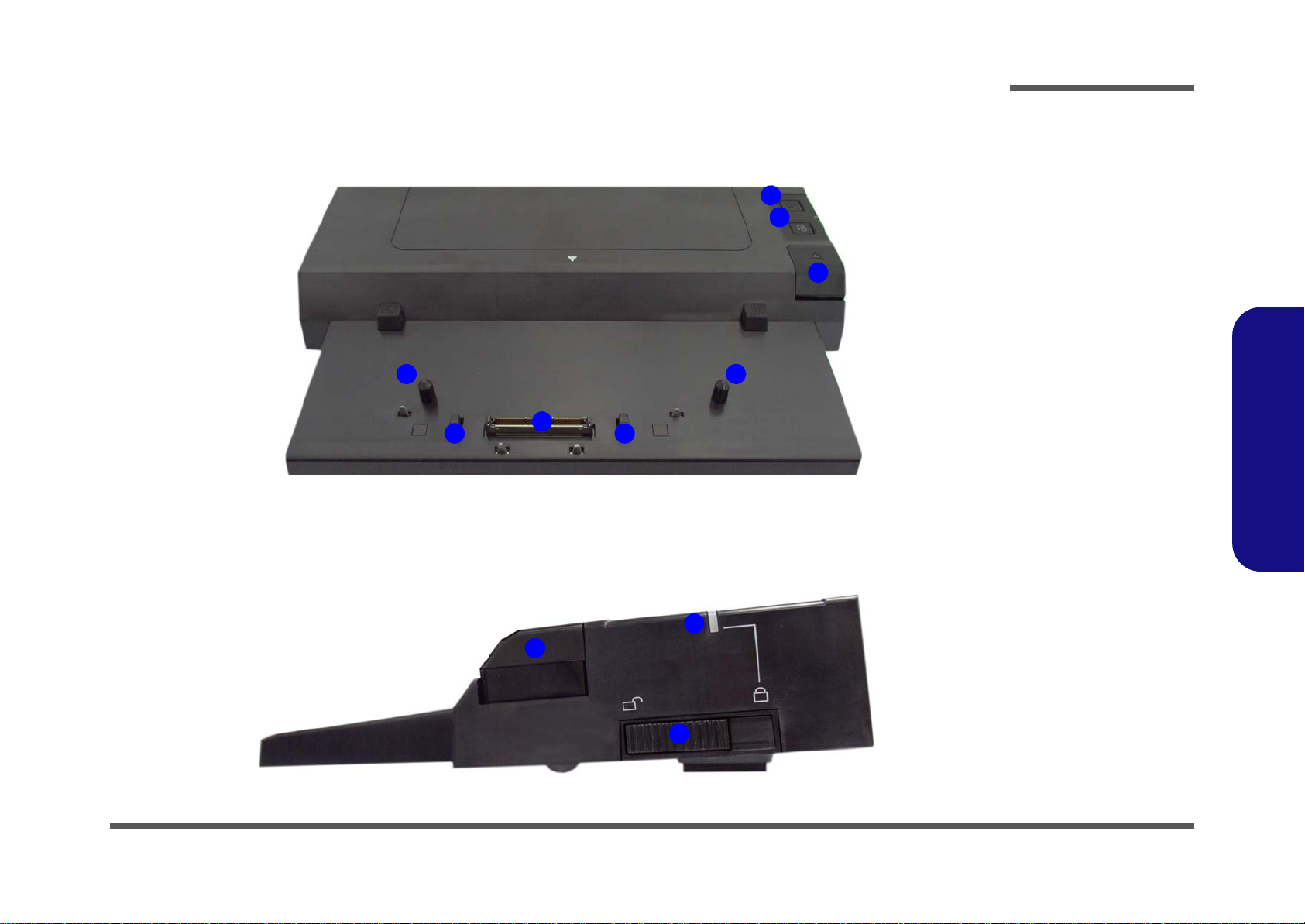
External Locator - Front & Right Side Views
FRONT VIEW
2
5
1
4
6
3
5
6
Figure 1
Front View
1. Power Button LED
2. Backup Button
(Model A Only)
3. Eject Button
4. Docking Port
5. Retaining Pins
6. Eject Pins
RIGHT SIDE VIEW
2
3
1
Figure 2
Right Side View
1. Eject Button
2. Lock Switch LED
3. Lock Switch
Introduction
1.Introduction
External Locator - Front & Right Side Views 1 - 3
Introduction
Figure 3
Left Side View
1. Vent
2. USB 2.0 Ports
LEFT SIDE VIEW
2
1
2
2
Figure 4
Rear View
1. Security Lock Slot
2. USB 2.0 Ports
3. Headphone Jack
4. Microphone Jack
5. S/PDIF-Out Jack
6. DVI-D Out Port
(Digital) - (Model
B Only)
7. External Monitor
Port (Model B
Only)
8. Serial (COM) Port
9. RJ-45 LAN Jack
10.DC-In Jack
The following ports are
provided with the
NVIDIA video adapter:
11. Display Port
12.DVI-D Out Port
(Digital)
13.HDMI-Out Port
2
1
3
11
12
13
Model A (Rear View with Video Controller)
2
2
2
4 5
8
9
10
6
7
2
1
3
6
7
2
2
2
4 5
8
9
10
Model B (Rear View without Video Controller)
1.Introduction
1 - 4 External Locator - Left Side & Rear View
External Locator - Left Side & Rear View
/
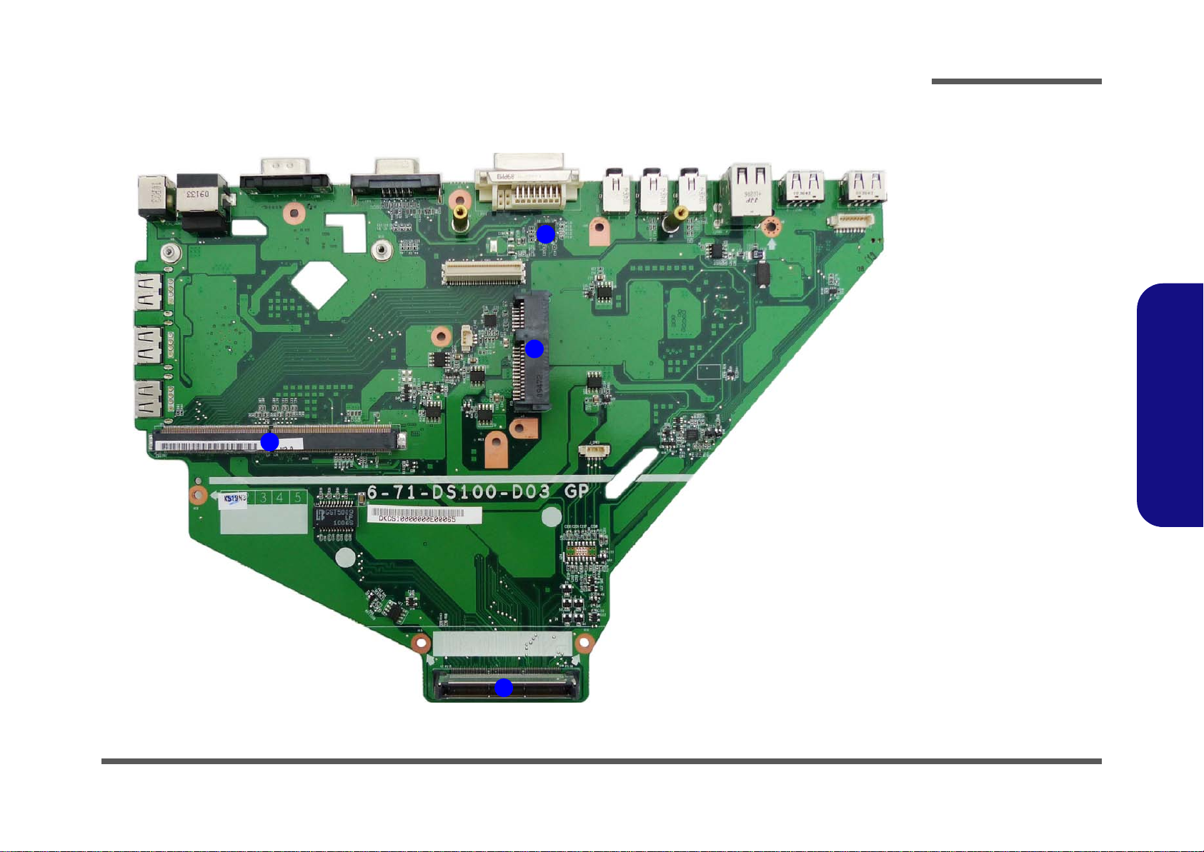
Mainboard Overview - Top (Key Parts)
Figure 5
Mainboard Top
Key Parts
1. VGA Card
Connector
2. System DVI-D
3. Hard Disk
Connector
4. Docking
Connector
1
2
3
4
Introduction
1.Introduction
Mainboard Overview - Top (Key Parts) 1 - 5

Introduction
1
2
4
3
Figure 6
Mainboard Bottom
Key Parts
1. USB 2.0 HUB-1
2. System CRT
3. COM Port
4. USB 2.0 HUB-2
1.Introduction
Mainboard Overview - Bottom (Key Parts)
1 - 6 Mainboard Overview - Bottom (Key Parts)

Mainboard Overview - Top (Connectors)
Figure 7
Mainboard Top
Connectors
1. DC-In Jack
2. RJ-45 LAN Jack
3. Serial (COM) Port
4. External Monitor
Port (Model B
Only)
5. DVI-D Out Port
(Digital) - (Model
B Only)
6. S/PDIF-Out Jack
7. Microphone Jack
8. Headphone Jack
9. USB 2.0 Ports
10.Power Connector
11. VGA Connector
12.Fan Connector
6
5
1
4
2
3
7 98
10
12
11
9
9
Introduction
1.Introduction
Mainboard Overview - Top (Connectors) 1 - 7

Introduction
Figure 8
Mainboard Bottom
Connectors
1. USB 2.0 Ports
1
1
1
1.Introduction
Mainboard Overview - Bottom (Connectors)
1 - 8 Mainboard Overview - Bottom (Connectors)

Chapter 2: Disassembly
Information
Warning
Overview
This chapter provides step-by-step instructions for disassembling the DS100 series device’s parts and subsystems. When
it comes to reassembly, reverse the procedures (unless otherwise indicated).
We suggest you completely review any procedure before you take the device apart.
Disassembly
Procedures such as upgrading/replacing the hard disk are included in the User’s Manual but are repeated here for your
convenience.
To make the disassembly process easier each section may have a box in the page margin. Information contained under
the figure # will give a synopsis of the sequence of procedures involved in the disassembly procedure. A box with a
lists the relevant parts you will have after the disassembly process is complete. Note: The parts listed will be for the disassembly procedure listed ONLY, and not any previous disassembly step(s) required. Refer to the part list for the previous disassembly procedure. The amount of screws you should be left with will be listed here also.
A box with a will also provide any possible helpful information. A box with a contains warnings.
An example of these types of boxes are shown in the sidebar.
2.Disassembly
Overview 2 - 1

Disassembly
2.Disassembly
NOTE: All disassembly procedures assume that the system is turned OFF, and disconnected from any power supply.
Maintenance Tools
The following tools are recommended when working on the device:
• M3 Philips-head screwdriver
• M2.5 Philips-head screwdriver (magnetized)
• M2 Philips-head screwdriver
• Small flat-head screwdriver
• Pair of needle-nose pliers
• Anti-st atic wrist-strap
2 - 2 Overview

Maintenance Precautions
Power Safety
Warning
Before you undertake
any upgrade procedures, make sure that
you have turned off the
power, and disconnected all peripherals
and cables (including
telephone lines). It is
advisable to also remove your battery in
order to prevent accidentally turning the
machine on.
The following precautions are a reminder. To avoid personal injury or damage to the device while performing a removal
and/or replacement job, take the following precautions:
1. Don't drop it. Perform your repairs and/or upgrades on a stable surface. If the device falls, the case and other
components could be damaged.
2. Don't overheat it. Note the proximity of any heating elements. Keep the device out of direct sunlight.
3. Avoid interference. Note the proximity of any high capacity transformers, electric motors, and other strong mag-
netic fields. These can hinder proper performance and damage component s and/or data. You sho uld a lso mon itor
the position of magnetized tools (i.e. screwdrivers).
4. Keep it dry. This is an electrical appliance. If water or any other liquid gets into it, the device could be badly damaged.
5. Be careful with power. Avoid accidental shocks, discharges or explosions.
•Before removing or servicing any part from the device, turn the device off and detach any power supplies.
•When you want to unplug the power cord or any cable/wire, be sure to disconnect it by the plug head. Do not pull on the wire.
6. Peripherals – Turn off and detach any peripherals.
7. Beware of static discharge. ICs, such as the CPU and main support chips, are vulnerable to static electricity.
Before handling any part in the device, discharge any static electricity inside the device. When handling a printed
circuit board, do not use gloves or other materials which allow static electricity buildup. We suggest that you use an
anti-static wrist strap instead.
8. Beware of corrosion. As you perform your job, avoid touching any connector leads. Even the cleanest hands produce oils which can attract corrosive elements.
9. Keep your work environment clean. Tobacco smoke, dust or other air-born particulate matter is often attracted
to charged surfaces, reducing performance.
10. Keep track of the components. When removing or replacing any part, be careful not to leave small part s, such as
screws, loose inside the device.
Cleaning
Do not apply cleaner directly to the device, use a soft clean cloth.
Do not use volatile (petroleum distillates) or abrasive cleaners on any part of the device.
Disassembly
2.Disassembly
Overview 2 - 3

Disassembly
Figure 1
HDD Assembly
Removal
a. Remove the screws.
b. Turn it over, remove the
top cover and disconnect
the cable.
c. Remove the screws.
5.Top cover
•8 Screws
1
456710
2
1
a.
c.
b.
7
9
4
3
6
8
5
10
Removing the Hard Disk Drive
The hard disk drive can be taken out to accommodate other 2.5" serial (SATA) hard disk drives with a height of 9.5mm
(h). Follow your operating system’s installation instructions, and install all necessary drivers and utilities (as outlined in
User’s Manual) when setting up a new hard disk.
Hard Disk Upgrade Process
1. Turn off the device, and remove screws - from the bottom case.
2. Turn it over, remove the top cover and carefully disconnect cable (cable is attached to the under side of
the cover)
3. Remove screws - .
2.Disassembly
2 - 4 Removing the Hard Disk Drive

4. Carefully separate the Display output board from the connector .
Figure 2
HDD Assembly
Removal (cont’d.)
d. Separate the VGA board
from the connector.
e. Remove screws and
slide the hard disk in the
direction of arrow.
f. Lift the HDD assembly
out of the bay.
g. Remove the screws to
separate the hard disk
from the bracket
11.Display Output
Board
22 HDD
23 Bracket
•8 Screws
11
12131516171821
22
23
d.
HDD System Warning
New HDD’s are blank. Before
you begin make sure:
You have backed up any data
you want to keep from your old
HDD.
You have all the CD-ROMs
and FDDs required to install
your operating system and
programs.
If you have access to the internet, download the latest application and hardware driver
updates for the operating system you plan to install. Copy
these to a removable medium.
g.
f.
e.
11
12
15
14
13
16
21
20
19
18
23
22
17
5. Remove screws - and slide the hard disk in the direction of arrow
6. Lift the hard disk assembly out of the compartment.
7. Remove the screws - to separate the hard disk
8. Reverse the process to install a new hard disk (do not forget to replace all the screws and covers).
Disassembly
.
from the bracket .
2.Disassembly
Removing the Hard Disk Drive 2 - 5

Disassembly
5. Fan Unit
•8 Screws
Caution
The heat sink, and video
card area in general,
contains parts which are
subject to high temperatures. Allow the area
time to cool before removing these parts.
Figure 3
Video Card
Removal Procedure
a. Remove the fan screws
and fan cable.
b. Remove the fan unit.
c. Remove the screws in
the correct order.
13456
10
3
a.
2
1
9
6
8
7
c.
b.
5
Screw 3
Screw 4
Screw 1
Screw 2
Heat Sink Screw Removal and Insertion
Remove the screws from the heat sink in the order
indicated here:
4-3-2-1
.
When tightening the screws, make sure that they
are tightened in the order:
1-2-3-4
.
4
10
Screw 5
Removing the Video Card
Video Card Removal Procedure
1. Turn off the device, turn it over and remove the hard disk (page 2 - 4).
Remove screws - (Figure 3a).
2.
Disconnect fan cable and remove the fan unit (Figure 3b).
3.
4. Remove screws - from the heat sink unit in the order indicated on the label (i.e screw 4 first through to screw
1 last
Figure 3c).
2.Disassembly
2 - 6 Removing the Video Card

5. Carefully (it may be hot) remove the heat sink unit (Figure 4d).
10
11
12
131313
10.Heatsink Unit
13.Video Card
•2 Screws
Caution
The heat sink, and video
card area in general,
contains parts which are
subject to high temperatures. Allow the area
time to cool before removing these parts.
e. f.
15
13
13
10
d.
12
11
Figure 4
Video Card
Removal (cont’d)
d. Carefully remove the
heat sink unit. Remove
the video card screws.
e. The video card will pop
up.
f. Remove the video card.
Remove screws & from the video card (Figure 4d).
6.
7. The video card will pop up (Figure 4e).
8. Remove the video card (Figure 4f).
Disassembly
2.Disassembly
Removing the Video Card 2 - 7

Disassembly
2.Disassembly
2-8

Appendix A:Part Lists
This appendix breaks down the DS100 series device’s construction into a series of illustrations. The component part
numbers are indicated in the tables opposite the drawings.
Note: This section indicates the manufacturer’s part numbers. Your organization may use a different system, so be sure
to cross-check any relevant documentation.
Note: Some assemblies may have parts in common (especially screws). However, the part lists DO NOT indicate the
total number of duplicated parts used.
Part Lists
Note: Be sure to check any update notices. The parts shown in these illustrations are appropriate for the system at the
time of publication. Over the product life, some parts may be improved or re-configured, resulting in new part numbers.
A.Part Lists
A-1

Part Lists
Table A - 1
Part List Illustration
Location
Part List Illustration Location
The following table indicates where to find the appropriate part list illustration.
Part DS100
Top and Bottom with VGA
page A - 3
A.Part Lists
Top and Bottom without VGA
HDD
page A - 4
page A - 5
A - 2 Part List Illustration Location

Top and Bottom with VGA
Figure A - 1
Top and Bottom
with VGA
Part Lists
A.Part Lists
Top and Bottom with VGA A - 3

Part Lists
Figure A - 2
Top and Bottom
Without VGA
A.Part Lists
Top and Bottom Without VGA
A - 4 Top and Bottom Without VGA

HDD
Figure A - 3
HDD
Part Lists
A.Part Lists
HDD A - 5

Part Lists
A.Part Lists
A - 6 HDD

Appendix B: Schematic Diagrams
Table B - 1
SCHEMATIC
DIAGRAMS
Version Note
The schematic diagrams in this chapter
are based upon version 6-7P-DS104-004.
If your mainboard (or
other boards) are a later version, please
check with the Service
Center for updated diagrams (if required).
This appendix has circuit diagrams of the DS100 device’s PCBs. The following table indicates where to find the appropriate schematic diagram.
Diagram - Page Diagram - Page Diagram - Page
Schematic Diagrams
System Block Diagram - Page B - 2 USB 2.0 HUB-2 - Page B - 8 dGPU Output B’d, HDMI, DVI - Page B - 14
MXM 3.0 - Page B - 3 Ext. GPIO, Key Lock - Page B - 9 dGPU Output B’d, DP - Page B - 15
SATA HDD, MXM VGA Out - Page B - 4 Main Power, Power OK - Page B - 10 Power BTN, LED B’d - Page B - 16
System DVI-D, CRT - Page B - 5 VDD3, VDD5 - Page B - 11
RJ-45, Fan, Phone Jack - Page B - 6 COM Port, Audio AMP - Page B - 12
USB 2.0 HUB-1 - Page B - 7 Docking CONN (144 Pins) - Page B - 13
B.Schematic Diagrams
B-1

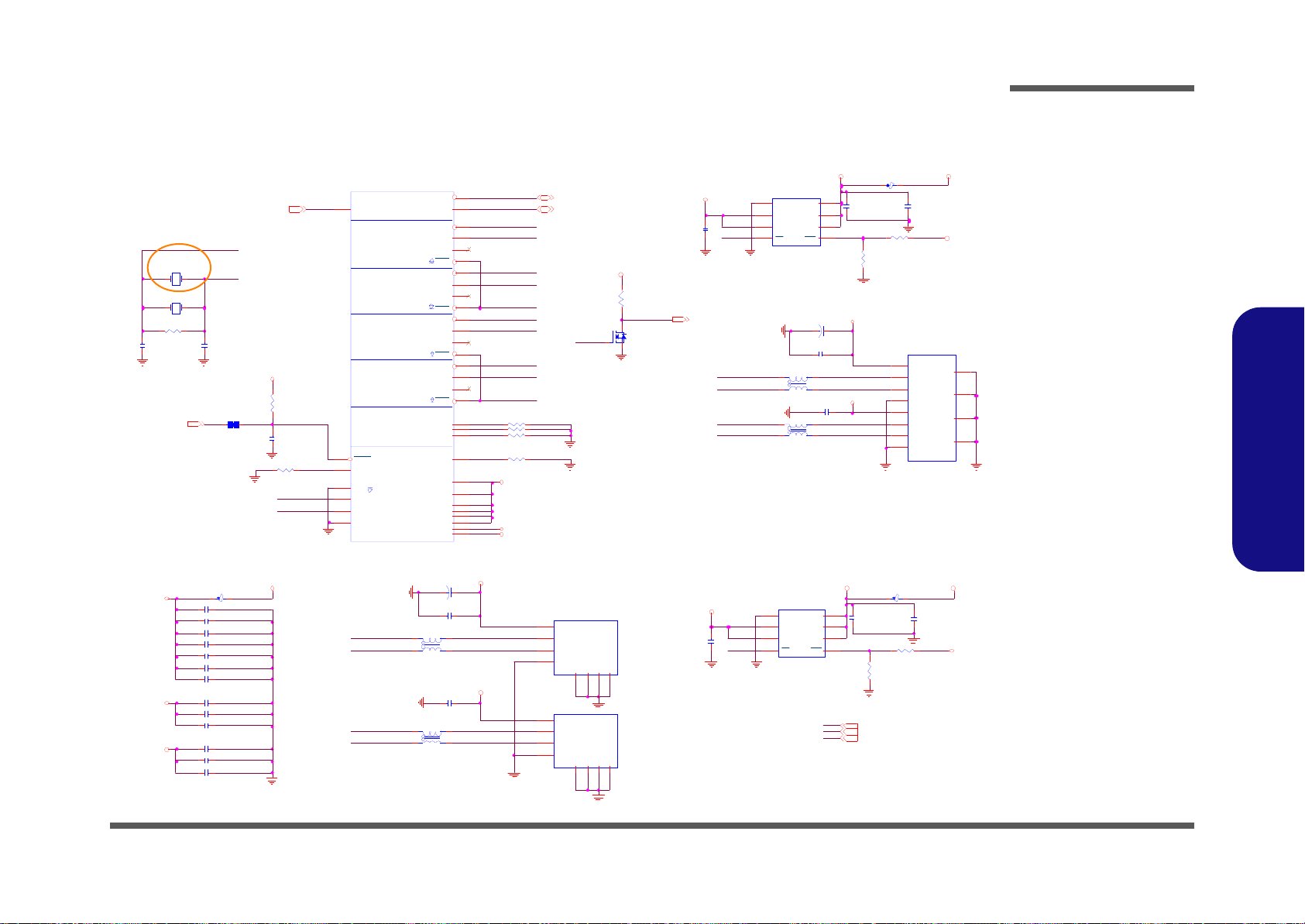
Schematic Diagrams
Sheet 1 of 18
System Block
Diagram
5VS
D_SUSB#
NMOS
D_SUSB#
NMOS
3.3VS
NMOS
NMOS
SUSB#
D_SUSC#
D_SUSC#
D_SUSB#
DK_EN
DK_EN
SUSC#
VA
D_SUSC#
SYSTEM
POWER
3.3V VDD3
VDD55V
50 ohms
SE
RJ-45
DIFF
10 0 oh ms
DIFF
TI
90 Ohms
SATA
SATA
HDD
SN75LVCP412RTJ
REDRIV E
90 Ohms
DIFF
US B PO RT
USB PO RT
USB HUB 4 PORTS
USB2514-AEZG
USB PO RT
USB
USB
USB_0
SMSC
85 oh ms
USB_2
DIFF
USB
Proprietary-bus
USB
DIFF
85 ohms
NVIDIA GRAPHIC CARD
MXM 3.0 Type A
PCIE x 8
HDMI
90 ohms
DP
DIFF
50 ohmsSE(DDC)
DVI
Dual
DVI-D
20
Mils
SMBU S
TRACE
WIDTH
SPDIF
SPDI F
OUT
SPDIF
IN
MICHP
Microphone in
Head ph on e o ut
OUT
SE
CRT
ANALOG
SYSTEM
Repeater
50
ohms
5 0 oh ms
SE(DDC)
8 5 oh ms
DIFF
DVI
Single
HDMI/DVI
GST500 9 L F
Factory Option
DIFF
100 ohms
Bothhand
TRANSF OR M ER
D S100 BLOCK DIAG RAM
DIFF
CLOCK
9 0 oh ms
US B P OR T
144 pins
Docking Connector
SYSTEM
DVI-D
5 0 ohm s
SE(DDC)
8 5 ohm s
DIFF
SATA
DVI
Single
COM
PORT
MAX3243ECDBR
TI
TRANSCEIVER
USB PO RT
USB HUB 4 PORTS
USB POR T
USB
USB
USB
SMSC
USB2514-AEZG
USB
CAT6351
8 mi ls
COM
port
signals
IT8302FN
EXT . GP IO
ITE
U S B PO RT
System Block Diagram
B.Schematic Diagrams
B - 2 System Block Diagram

MXM 3.0
3.3 V [6 ,7 ,9 ,11,12 ]
C180
0 . 1u _ 5 0V _Y 5V _0 6
Q3 1
MTN7002ZH S3
G
DS
R 178 2.2K_04
C95
0. 1u _ 1 6V _ Y 5V _0 4
C94
0.1u_16V_Y5V_04
C18 4
*10u_10V_08
C 6 9 0 .1u_10V_X7R_04
3VRU N [3]
C 8 4 0 .1u_10V_X7R_04
C 8 5 0 .1u_10V_X7R_04
1A
3VRU N
C 6 7 0 .1u_10V_X7R_04
C96
0.1u_16V_Y5V_04
C 6 8 0 .1u_10V_X7R_04
C 8 2 0 .1u_10V_X7R_04
C 8 3 0 .1u_10V_X7R_04
ACES
C181
0.1u_50V_Y5V_06
C 7 4 0 .1u_10V_X7R_04
R 179 2.2K_04
DP_CEC[3]
MXM_ALER T#
R41
1K_04
PRSNT_L#
5VRU N [3]
C190
0.1u_50V_Y5V_06
C80
0.1u_16V_Y5V_04
C79
0. 1u _ 1 6V _ Y 5V _0 4
C78
0.1u_16V_Y5V_04
C17 4
*10u_10V_08
2. 5 A
5VRU N
VIN _MXM [3]
R151 *0_04
C 7 3 0 .1u_10V_X7R_04
C18 9
0.1u_50V_Y 5V _06
R180 *2.2K_04
C 7 0 0 .1u_10V_X7R_04
L L H
R127
1M_04
MXM_PWRGD [8]
PEG_TXN6
PEG_TXN7
PRS NT_ R#
PEG_TXP7
PEG_TXP6C 8 9 0 .1u_10V_X7R_04
PEG_TXP5
PEG_TXP4
PEG_TXN4
PEG_TXN5
PEG_TXN0
PEG_TXN1
PEG_TXP1
PEG_TXP0
VIN _MXM
C188
10u_25V _12
CLOSE T O MXM PIN E 1
C187
*10u_25V _12
PEG_TXP2
PEG_TXN3
PEG_TXP3
PEG_TXN2
3VRUN
M X M1 _ S MC
M X M1 _ S MD
M XM_ALERT#
TH _O VER T#
P EG_RXP1
PEG_RXN2
PEX_STD _SW# 1
PEG_RXN5
P EG_RXP5
PEG_RXN6
H L L
H H L
L H L
PEG_RXN7
P EG_RXP6
PEG _ RXP[0..7]
P EG_RXP4
P EG_RXP3
P EG_RXP0
P EG_RXP2
P EG_RXP7
PEG_RXN0
PEG_RXN1
PEG_RXN3
PEG _ RXN[0..7]
PEG_RXN4
MXM1_SMC
MXM _PW R EN
TH_OVE RT#
MXM1_SMD
PEG _ TXP[0..7]
PEG _ TXN [0. .7]
C97
0.01u_50V_X7R _04
MXM 3.0
5VRUN(2.5A)--5V
3VRUN(1A)--3.3V
PW R_SRC(10A)--7-20V
TH _A LE R T # [ 8]
R181 *2.2K_04
5V R U N
MXM 3.0 MO DULE BOARD CON NE CTO R
J_MXM1A
91781-31408-NV -01
GN D
E3-10
5V
1
5V
3
5V
5
5V
7
5V
9
GN D
11
GN D
13
GN D
15
GN D
17
PEX_STD_SW #
19
VG A_DISABL E#
21
PN L_PWR _ EN
23
PN L_BL_EN
25
PN L_BL_PW M
27
HD MI_C EC
29
DV I_H PD
31
LVDS_D DC_D AT
33
LVDS_D DC_C LK
35
GN D
37
OE M
39
OE M
41
OE M
43
OE M
45
GN D
47
PEX_RX15 #
49
PEX_RX15
51
GN D
53
PEX_RX14 #
55
PEX_RX14
57
GN D
59
PEX_RX13 #
61
PEX_RX13
63
GN D
65
PEX_RX12 #
67
PEX_RX12
69
GN D
71
PEX_RX11 #
73
PEX_RX11
75
GN D
77
PEX_RX10 #
79
PEX_RX10
81
GN D
83
PEX_RX9#
85
PEX_RX9
87
GN D
89
PEX_RX8#
91
PEX_RX8
93
GN D
95
PEX_RX7#
97
PEX_RX7
99
GN D
10 1
PEX_RX6#
10 3
PEX_RX6
10 5
GN D
10 7
PEX_RX5#
10 9
PEX_RX5
11 1
GN D
11 3
PEX_RX4#
11 5
PEX_RX4
11 7
GN D
11 9
PEX_RX3#
12 1
PEX_RX3
12 3
GN D
12 5
PWR _SR C
E2-5
GN D
E4-10
PRSNT_R#
2
WAKE #
4
PWR _GOO D
6
PW R_EN
8
R SVD
10
R SVD
12
R SVD
14
R SVD
16
PWR _LEVE L
18
TH _ OV E R T #
20
TH _ALER T#
22
TH _ P W M
24
GPIO0
26
GPIO1
28
GPIO2
30
SMB_DA T
32
SMB_CLK
34
GN D
36
OEM
38
OEM
40
OEM
42
OEM
44
GN D
46
PEX_TX1 5#
48
PEX_TX1 5
50
GN D
52
PEX_TX1 4#
54
PEX_TX1 4
56
GN D
58
PEX_TX1 3#
60
PEX_TX1 3
62
GN D
64
PEX_TX1 2#
66
PEX_TX1 2
68
GN D
70
PEX_TX1 1#
72
PEX_TX1 1
74
GN D
76
PEX_TX1 0#
78
PEX_TX1 0
80
GN D
82
PEX_TX9 #
84
PE X_ T X9
86
GN D
88
PEX_TX8 #
90
PE X_ T X8
92
GN D
94
PEX_TX7 #
96
PE X_ T X7
98
GN D
10 0
PEX_TX6 #
10 2
PE X_ T X6
10 4
GN D
10 6
PEX_TX5 #
10 8
PE X_ T X5
11 0
GN D
11 2
PEX_TX4 #
11 4
PE X_ T X4
11 6
GN D
11 8
PEX_TX3 #
12 0
PE X_ T X3
12 2
GN D
12 4
GN D
13 3
PEX_RX2#
13 5
PEX_RX2
13 7
GN D
13 9
PEX_RX1#
14 1
PEX_RX1
14 3
GN D
14 5
PEX_RX0#
14 7
PEX_RX0
14 9
GN D
13 4
PEX_TX2 #
13 6
PE X_ T X2
13 8
GN D
14 0
PEX_TX1 #
14 2
PE X_ T X1
14 4
GN D
14 6
PEX_TX0 #
14 8
PE X_ T X0
15 0
GN D
15 2
GN D
15 1
PWR _SR C
E2-1
PWR _SR C
E2-2
PWR _SR C
E2-3
PWR _SR C
E2-4
PWR _SR C
E2-6
PWR _SR C
E2-7
PWR _SR C
E2-8
PWR _SR C
E2-9
PWR _SR C
E2-10
GN D
E4-1
GN D
E4-2
GN D
E4-3
GN D
E4-4
GN D
E4-5
GN D
E4-6
GN D
E4-7
GN D
E4-8
GN D
E4-9
PWR _ SRC
E1-1
PWR _ SRC
E1-2
PWR _ SRC
E1-3
PWR _ SRC
E1-4
PWR _ SRC
E1-5
PWR _ SRC
E1-6
PWR _ SRC
E1-7
PWR _ SRC
E1-8
PWR _ SRC
E1-9
PWR _ SRC
E1-10
GN D
E3-1
GN D
E3-2
GN D
E3-3
GN D
E3-4
GN D
E3-5
GN D
E3-6
GN D
E3-7
GN D
E3-8
GN D
E3-9
C191
4.7u_25V_X5R _08
C182
10u_25V_12
R 5 5 1 0K _0 4
C81
0.01u_50V_X7R _04
C177
*10u_25V_12
C179
4.7u_25V_X5R _08
Q32
AO3415
G
D S
C 8 8 0 .1u_10V_X7R_04
C178
4.7u_25V _X5R_08
VIN _ MXM
5VRU N
3VRU N
VIN _ MXM
VIN _ MXM
R42
47 K _ 0 4
MXM_PWREN [8]
R126
10K_04
MXM _P R SN T [ 8]
3. 3V
SPD IF-OU T[5]
R57
47K_04
PEG _ RXP[0..7] [12]
PEG _ RXN[0..7] [12 ]
PEG _ TXN[ 0..7] [12 ]
PEG _ TXP[0..7] [12 ]
3VRUN
C18 6
*4.7u_6.3V_X5R _06
CLOSE TO MXM CONN .
C18 5
4.7u_6. 3V_X5R_06
CLOSE T O MX M P I N E2
EC_SMB _D AT [12]
Q34
MTN 7 0 0 2ZH S3
G
DS
RA
wi th in 50 0m i ls
MXM1 _ SM C
MXM1 _ SM D
Stuff
Low swing
EC_SMB _C L K [12]
Q33
MTN 7 0 0 2ZH S3
G
DS
RA
High swing
Unstuff
C 7 2 0 .1u_10V_X7R_04
R40 *10m il_04
PR SN T_ R# PRS NT _L # M XM _PR SN T
Q36
MTN7002ZHS3
G
DS
5V R U N
5V R U N
C17 5
4.7u_6. 3V_X5R_06
CLOSE TO MXM CONN .
C17 6
*4.7u_6.3V_X5R _06
C 7 1 0 .1u_10V_X7R_04
R150 *0_04
3/04 D02 CHG for Optimus
MXM_ C LKR E Q # [ 12 ]
C 8 7 0 .1u_10V_X7R_04
M XM_CLKR EQ#_R
R56
1K_04
PRSNT_R#
M_D P_D2 [3]
M_D P_D#0 [3]
M_D P_D#3 [3]
MXM_R ST# [8]
M_DP_DHPD [3]
M_D P_D3 [3]
M_ HD MI_ C 0#[3]
M_ HD MI_ C 1[3 ]
M_ HD MI_ C 1#[3]
M_ HD MI_ C _S DA[3 ]
M_ HD MI_ C LK #[3]
M_ HD MI_ C 0[3 ]
M_ HD MI_ C 2#[3]
M_ HD MI_ C _S CL[3]
M_ HD MI_ C LK[3]
M_D P_D0 [3]
M_ HD MI_ C 2[3 ]
PR SN T_L#
M_D P_D_AUX# [3]
M_D P_D#1 [3]
MXM 3.0 M ODU L E B OARD C ONNE CTOR
J_MXM1B
91781-31408-NV-01
PEX_REF CL K#
15 3
PEX_REF CL K
15 5
GND
15 7
R SVD
15 9
R SVD
16 1
R SVD
16 3
R SVD
16 5
R SVD
16 7
LVDS _U CLK#
16 9
LVDS _U CLK
17 1
GND
17 3
LVDS _U TX3#
17 5
LVDS _U TX3
17 7
GND
17 9
LVDS _U TX2#
18 1
LVDS _U TX2
18 3
GND
18 5
LVDS _U TX1#
18 7
LVDS _U TX1
18 9
GND
19 1
LVDS _U TX0#
19 3
LVDS _U TX0
19 5
GND
19 7
DP_C_L0#
19 9
DP_C_L0
20 1
GND
20 3
DP_C_L1#
20 5
DP_C_L1
20 7
GND
20 9
DP_C_L2#
21 1
DP_C_L2
21 3
GND
21 5
DP_C_L3#
21 7
DP_C_L3
21 9
GND
22 1
DP_C_AUX#
22 3
DP_C_AUX
22 5
R SVD
22 7
R SVD
22 9
R SVD
23 1
R SVD
23 3
R SVD
23 5
R SVD
23 7
R SVD
23 9
R SVD
24 1
R SVD
24 3
R SVD
24 5
R SVD
24 7
R SVD
24 9
GND
25 1
D P _A _L 0 #
25 3
D P _A _L 0
25 5
GND
25 7
D P _A _L 1 #
25 9
D P _A _L 1
26 1
GND
26 3
D P _A _L 2 #
26 5
D P _A _L 2
26 7
GND
26 9
D P _A _L 3 #
27 1
D P _A _L 3
27 3
GND
27 5
D P _A _A U X #
27 7
D P _A _A U X
27 9
PR SNT_ L#
28 1
CLK_ REQ #
15 4
PEX_R ST #
15 6
VGA_DD C_ D AT
15 8
VGA_DD C_ C LK
16 0
VG A_ VSYN C
16 2
VG A_HSYN C
16 4
GN D
16 6
VG A_RED
16 8
VG A_ GR EEN
17 0
VGA_BLUE
17 2
GN D
17 4
LVDS_LC LK#
17 6
LVDS _LC LK
17 8
GN D
18 0
LVDS_LTX3#
18 2
LVDS_LTX3
18 4
GN D
18 6
LVDS_LTX2#
18 8
LVDS_LTX2
19 0
GN D
19 2
LVDS_LTX1#
19 4
LVDS_LTX1
19 6
GN D
19 8
LVDS_LTX0#
20 0
LVDS_LTX0
20 2
GN D
20 4
DP_D_L0#
20 6
D P_D_L0
20 8
GN D
21 0
DP_D_L1#
21 2
D P_D_L1
21 4
GN D
21 6
DP_D_L2#
21 8
D P_D_L2
22 0
GN D
22 2
DP_D_L3#
22 4
D P_D_L3
22 6
GN D
22 8
DP_D _A U X #
23 0
DP_D_AUX
23 2
DP_C _H PD
23 4
DP_D _H PD
23 6
R SVD
23 8
R SVD
24 0
R SVD
24 2
GN D
24 4
DP_B_L0#
24 6
DP_B_L0
24 8
GN D
25 0
DP_B_L1#
25 2
DP_B_L1
25 4
GN D
25 6
DP_B_L2#
25 8
DP_B_L2
26 0
GN D
26 2
DP_B_L3#
26 4
DP_B_L3
26 6
GN D
26 8
D P _B _A U X #
27 0
DP_B_AU X
27 2
DP_B_HPD
27 4
DP_A_HPD
27 6
3V3
27 8
3V3
28 0
C L K_P CIE_PEG #[12 ]
C L K_PCIE_PEG[12]
3V R U N
M _D VI_ D3 [3]
M_D VI_D#4 [3]
M_D VI_HPD [3]
M _D VI_ D4 [3]
M _D VI_ D5 [3]
M_D VI_D#5 [3]
M_ DVI _ D #2[3]
M_ DVI _ D #1[3]
M_D VI_D#3 [3]
M_ DVI _ D #0[3]
M_ D V I_ D0[3]
M_ D V I_ D1[3]
M_DVI_DDC_DAT[3 ]
M_ D V I_ CL K[3]
M_DVI_CLK#[3]
M_ D V I_ D2[3]
M_D P_D_AUX [3]
M_DVI_DDC_CLK[3]
M XM_CLKR EQ#_R
M_H DMI_C HP D [3]
ACES
M_D P_D#2 [3]
M_D P_D1 [3]
C 8 6 0 .1u_10V_X7R_04
5V R U N
Q35
MTN 7002ZHS 3
G
DS
Sheet 2 of 18
MXM 3.0
Schematic Diagrams
B.Schematic Diagrams
MXM 3.0 B - 3

Schematic Diagrams
Sheet 3 of 18
SATA HDD, MXM
VGA Out
3VRU N [2]
5V [6,7 ,9]
SI NGLE SA TA HD D
R134 * 0_08
3. 3V S 3VRUN
Q39
MTN 7002ZHS3
G
DS
R14 2
20 K _ 0 4
R14 4
100K_04
R146
1M _0 4
dG P U_ P W R O N
C19 7
0.1u_16V_Y5V_04
Q37
AO 3415
G
DS
dGPU_PWR ON[8]
VA [9,10]
C63
0. 1 u _ 16 V _ Y 5 V _ 04
2. 5 A1A
5VRU N [2]
VIN _MXM [2 ]
1A 2.5A
M_DP_DHPD [2]
M_ DV I_ H PD [2 ]
M_ H D MI_ C_ S CL[2]
M_HDMI_C _SDA[2 ]
DP_CEC[2 ]
M_ H DMI _ C HP D [ 2]
M_DP_D_AUX [2]
M_DP_D_AUX# [2]
3VRU N
C58
*0.1u_16V_ Y5V_ 04
M _H D M I _C 2#[2]
M_ H D MI _ C 1[2]
M _H D M I _C 1#[2]
M_ H D MI _ C 2[2]
M_ HD MI_ C L K[2 ]
M_ H D MI_ C LK#[2]
M_ H D MI _ C 0[2]
M _H D M I _C 0#[2]
M_DVI_ D 5 [2]
M_ D VI_ D #5 [2 ]
M_ D VI_ D #3 [2 ]
M_DVI_ D 4 [2]
M_ D VI_ D #4 [2 ]
M_DVI_ D 3 [2]
M_DP_D0 [2]
M_DP_D#0 [2]
M_DP_D1 [2]
M_DP_D#1 [2]
M_DP_D3 [2]
M_DP_D#3 [2]
M_DP_D2 [2]
M_DP_D#2 [2]
5VRU N
M_D VI_CLK[2]
M_DVI_D2[2]
M_ DV I_ D# 2[2]
M_ D VI_ C L K #[2]
M_DVI_D0[2]
M_ DV I_ D# 0[2]
M_DVI_D1[2]
M_ DV I_ D# 1[2]
M_D VI_DDC _DAT[2]
M_DVI_DD C_CLK[2 ]
J_ VGA1
88011-60071
112
2
334
4
556
6
778
8
9910
10
111112
12
131314
14
151516
16
171718
18
191920
20
212122
22
232324
24
252526
26
272728
28
292930
30
313132
32
333334
34
353536
36
373738
38
393940
40
414142
42
434344
44
454546
46
474748
48
494950
50
515152
52
535354
54
555556
56
575758
58
595960
60
R152 *0_08
C45
* 0.1u _16V_Y5 V_04
R125 *0_08
1
D0
Function
1
1
CH 0 & C H1 -> 0 dB
0
CH 0 - > 0 dB CH 1 - > 5 d B
1D1CH 0 - > 5 dB CH 1 - > 5 d B
CH 0 - > 5 dB CH 1 - > 0 d B
0
0
5V
R30 * 100K_ 04
Q3
MTN 700 2Z HS3
G
DS
V
0 ohm
C56 C57
C58
VX
0
VX0.01U
R16 R17
R18 R19
RN1
RN2
Q9
SI4835BDY
4
62
5731
8
5A
X
U1 R15 R20
R21
W/O Re-d rive
5A
X
VW/ Re-drive
3.3VS
R35
10 0 K _ 04
VA
R39
*22_1%_04
R34
20K _04
HOST
DE VICE
U6
SN 75LVCP41 2
D1
8
VDD
6
RX_0P
1
RX_0N
2
GND
3
VD D
10
TX_1 N
4
TX_1 P
5
VDD
16
D09GN D
13
RX_1 P
11
RX_1N
12
VD D
20
GND
17
TX_0 N
14
TX_0 P
15
EN
7
T- PAD21GND18GND
19
Q5
*MTN7002ZH S3
G
DS
3.3VS
R43
100K _04
C66
*0.01u_50V_X7R_04
VIN_MXM
C56
0. 0 1 u_ 1 6 V _X 7 R _ 0 4
C46
1u _ 6. 3 V _ X 5R _ 04
3. 3 V S
C62
10 u_10V_ Y5V_ 08
C 52 0.01u_16V_X7R_04
C59
10 u _ 10 V _ Y 5 V _ 08
C 49 0.01u_16V_X7R_04
C 54 0.01u_16V_X7R_04
C44
*1 0 u_ 1 0V_ 0 8
5V S 5VRUN
C 47 0.01u_16V_X7R_04
R14 3
20 K _ 0 4
Q40
MTN 7002ZHS3
G
DS
SATA_ TXN 0 _R
SATA_ TXP0 _R
R145
100K_04
SATA_ RXP0_ R
SATA_ RXN 0_R
+
C57
*1 00u_6.3V_B2
dG P U _ P W R O N
SA TA_RXN 0_C
SA TA_RXP0_ C
C198
0.1u_16V_Y5V_04
SATA_ TXP0 _R
SATA_ TXN 0_R
Q38
AO 3415
G
DS
SATA_ RXP0_R
SATA_ RXN0_R
R26
4.7K_04
R28 *4.7K_04
R27 *4.7K_04
5VS
3.3VS
Layout Note:
La yo ut no te:
Cl ose to J _HDD 1
1. 5A
Closed TO U1
1. 0A
P IN G ND 1 ~ 2 = I_ G ND
SA TA_TXP0_C
SA TA_TXN0 _C
J_H DD1
C16623-12205- L
S1
S2
S3
S4
S5
S6
S7
P1
P2
P3
P4
P5
P6
P7
P8
P9
P10
P11
P12
P13
P14
P15
R25 4.7 K_ 04
R24 4.7 K_ 04
C61
10u_10V_Y5V_08
C55
0.1u_16V_Y 5V_04
SATA_ RXP0[12]
SATA_RXN0[12]
SATA _TXN0[1 2]
SATA _TXP0[1 2]
5VS [4,5,9,11]
3.3VS [4,5,9]
MX M VGA OUT & PO WER S WITCH
SATA HDD, MXM VGA Out
B.Schematic Diagrams
B - 4 SATA HDD, MXM VGA Out

System DVI-D, CRT
U28
*T HS 737 3IP W R
CVBS IN
1
HD CH 1 IN
2
HD CH 2 IN
3
HD CH 3 IN
4
GN D
5
DISAB LE
6
NC
7
NC
8
H D BYP ASS
9
VD D 3V/5V
10
HD CH3 O UT
11
HD CH2 O UT
12
HD CH1 O UT
13
CVBS O UT
14
R175 100K_04
SY ST EM DV I- D
PC SDA
L33H CB1608KF-121T25
3.3VS_R GB
5VS [3,5,9,11]
3.3VS [3,5,9]
R74 *2.2K_04
C AT6351_OE #
C232
10u_6.3V_X5 R_06
CR T_ G RE EN[12]
CR T_ R ED[12]
CR T_ BL UE[12]
R70 4 .7 K_ 04
3. 3 V S _ DV I
C RT_ GREEN
CRT_BLUE_R
CRT_RED_R
DD CDAT
CRT_RED
PLEASE CLO SE TO C ONNECTOR
HSY NC
J_CRT1
108AH15FST01N1CC
8
7
6
5
4
3
2
1
9
10
11
12
13
14
15
GND2
GN D 1
.
L5 0_04
.
L6 0_04
.
L4 0_04
VSYN C
FB LU E
FG RN
C20
*10p _50V_NPO_04
FR ED
CRT_GREE N_R
C9
22p_50V_NPO_04
CRT_BLUE
C11000p_50V_X7R _04
C51000p_50V_X7R_04
R4
150_1%_04
C730p_50V_NPO_04
R6
150_1%_04
.
L3 FCM1005MF-600T01
C11
22p_50V_NPO_04
.
L1 FCM1005MF-600T01
.
L2 FCM1005MF-600T01
D S_EXT1_H PD
R5
150_1%_04
C230p_50V_N PO_04
C19
*10p _50V_NPO_04
C6
10p_50V_NPO _04
R75
*47K_04
C3
10p_50V_NPO _04
R 138 1K_04
C4
10p_50V_N PO_04
C10
22p_50V_N PO_04
C196
470p_50V_X7R_04
C21
*10p _50V_NPO_04
DVI_HPD[12]
5VS_ D VI_PW R
D7
B AV99
A
C
AC
DD CCLK
CRT_RED
D S_EXT1_SCL
D9
BAV99
A
C
AC
DS_DATA2N
C234
0.1u_16V_Y5V_04
D S_EXT1_HPD
D S_EXT1_SDA
5VS_ DVI_PW R 5VS_DVI _PWR
DS_DATA0P
Close to DVI PORT
DS_DATA0N
DS_CLOCKP
DS_CLOCKN
DS_DATA1N
DS_DATA1P
DS_DATA2P
3.3VS_R GB
D SU B
DVI
J_ D V I 1
QH11121-ND W03-4F
TMDS DATA 2-
1
TMDS DATA 2+
2
TMDS 2/4 S hield
3
TMDS DATA 4-
4
TMDS DATA 4+
5
DDC Clk
6
DDC Data
7
V SY NC
8
TMDS DATA 1-
9
TMDS DATA 1+
10
TMDS DATA 1/3 Shield
11
TMDS DATA 3-
12
TMDS DATA 3+
13
+5 V P O W E R
14
GND (ANALOG)
15
HOT PLUG DETECT
16
TMDS DATA 0-
17
TMDS DATA 0+
18
TMDS DATA 0/5 Shield
19
TMDS DATA 5-
20
TMDS DATA5+
21
TMD S CL K Sh ield
22
TMDS CLK +
23
TMDS Clk -
24
CASE
M1
RED
C1
GREEN
C2
BLU E
C3
H SYN C
C4
CASE
M2
D8
BAV99
A
C
AC
C 126 0.1u_16V_Y5V_04
D 6 R B 55 1 V - 3 0S 2
A C
5VS_ DVI_PW R
5VS
3.3VS
DVI_DDCB_DAT
DVI_DDCB_CLK
CRT_GREEN
CRT_ BL UE_ R
CRT_ GR E EN_ R
CRT_ RE D _ R
CRT_BLUE
3.3VS_D VI
C13
0.1u_16V_Y5V_04
C132
0.1u_16V_Y 5V_04
5VS_DVI_PW R
C30
0.1u_16V_Y5V_04
C12
0.1u_16V_Y5V_04
C31
0.1u_16V_Y5V_04
3.3VS_DVI
R71 4 .7 K_ 04
D S_EXT1_SD A
C AT6351_I2CEN
3.3VS_DVI
3. 3 V S
DS_ DAT A2 P
DVI_TXP2[1 2]
DVI_DDCB_CLK[12]
3. 3 V S _ D V I
DVI_TXN2[1 2]
DVI_TXP1[1 2]
DVI_TXP0[1 2]
DVI_TXN0[1 2]
DVI_TXN1[1 2]
DVI_DDCB_DAT[12]
3.3V S_D VI3.3VS_DVI
DS_ DAT A0 N
DS_ DAT A1 P
DS_ EXT1_ SDA
DS_ DAT A2 N
DS_ CL OC K P
DS_ DAT A1 N
DS_ DAT A0 P
DS_ EXT1_ SCL
DS_ CL OC K N
3.3VS_D VI
U21
CAT6351
RX2 M1RX 2P2VSS3VCC4I2C EN5OEB6PC SDA7VSS8TX2P9TX2M
10
VC C
11
TX1 P
12
TX 1 M
13
VSS
14
TX0 P
15
TX 0 M
16
VC C
17
TXCP
18
TXC M
19
VSS
20
VSS
21
TXSC L
22
TXSDA
23
VC C
24
PCSC L
25
VS S
26
VCC
27
RXSDA28RX SCL
29
REXT
30
VSS
31
RXCM
32
RXCP
33
VCC
34
RX0 M
35
RX0 P
36
VSS
37
RX1 M
38
RX1 P
39
VCC
40
PAD
41
PCSD A
D VI_ DDC B_ CL K
R 135 499_1%_04
DVI_TXCN[12]
PCSC L
R173 1K_04
DVI_TXCP[12]
D VI_ DDC B_ DAT
C AT6351_I2CEN CAT6351_OE#
3.3VS
R 1 32 *2 0 mi l _ P _0 4
C233
0.01u_16V_X 7R _04
R174 *1 K _ 04
U22 *CM1117
Vin
3
Gn d/ Adj
1
Out
2
GND
4
C194
*1 0 u _6 .3 V _ X5R _ 0 6
R13 9
*1 2 1 _1 % _ 04
R14 0
*2 0 0 _1 % _ 04
C195
10u_6.3V_X5R_06
1A
L24 HC B1608KF-121T25
D S_EXT1_SC L
5V S
FG RN
FBLUE
DDCDAT
HSYNC
DDCCLK
VSY NC
5VS
CR T_D AT[12]
3.3VS
3.3VS
C129
0.22u_10V_Y5V_04
C130
0.22 u_10V_ Y5V_ 04
C123
0.22u_10V_Y5V_04
CR T_C LK[1 2]
R2 33_04
CRT_HSY NC[1 2]
C RT_ VSYN C[12]
R69 33_04
3.3VS 5VS
U13
IP4 772CZ16
VCC_ SY NC
1
VCC_ VID EO
2
VIDEO _1
3
VIDEO _2
4
VIDEO _3
5
GN D
6
VCC_ D DC
7
BYP
8
DD C_ OU T1
9
DDC _ IN1
10
DDC _ IN211DD C_ OU T2
12
SYNC _ IN113SYNC_OUT1
14
SYNC _ IN215SYNC_OUT2
16
RN 1
2.2K_8P4R_04
8 1
7 265
3
4
FR ED
Close to DVI PORT
R130 * 4.7K_04
R131 47_04
H
NO TE :
L
H
PCSCL
H
S/W
H/W
PCS DA
R129 4.7K_04
PC SCL
SY ST EM CR T
R76 *2.2K_04
R 1 33 *2 0 mi l _ P _0 4
3.3VS_RGB
Sheet 4 of 18
System DVI-D, CRT
Schematic Diagrams
B.Schematic Diagrams
System DVI-D, CRT B - 5

Schematic Diagrams
AU DG
3.3VS [3,4,9]
C10091-108A4
J_R J_45
DD-
8
DD+
7
DB-
6
DC-
5
DC+
4
DB+
3
DA-
2
DA+1shield
G ND1
shield
G ND2
6-21-B 4Y20-108
C100 0.01u_16V_X7R_04
C102 0.01u_16V_X7R_04
C101 0.01u_16V_X7R_04
C99 0.01u_16V_X7R_04
MIC -R[12]
MDIO1-[12 ]
LP4
*W CM2012F2S-161T03-SHOR T
1
4
2
3
MIC -L[12]
AU DG
30MIL
AUD G
C 192 0.1u_16V_Y5V_04
DLMX2-
DLMX2+
MDIO0+[12]
AUD G
C 193 0.1u_16V_Y5V_04
LMX0+
DLMX3-
DLMX3+
DLMX0+
DLMX0-
MDIO3+[12]
For EMI
AU DG
LMX0-
FAN
MDIO0-[12 ]
AU DG
LMX2+
DLMX1-
DLMX1+
MDIO3-[12 ]
M IC_ S ENS E[12]
AUD G
LMX3LMX3+
3
30MIL
1
5VS [3,4,9,11]
J_FAN1
J_FAN1
85205-03701
1
2
3
R19 4.7K_04
DK _FA N _SEN[12]
3.3VS
U5
G990
VOUT
3
GND
5
VIN
2
FON
1
VSET
4
GND
6
GND
7
GND
8
5VS_ FAN 5VS
DK_ FA N _O N[12 ]
5V S _F A N
C35
10u_10V_Y5V_08
R13
*0 _ 04
DOCK_FON#
DO CK_ F ON #
AUD G
5VS
C38
1u _6 .3V_X5 R_04
LMX1+
LMX1-
LMX1+
LP1
*W CM2012F2S-161T03-SHOR T
1
4
2
3
R 60 75_1% _04
AUD G
LMX1-
R 59 75_1% _04 C98
1000p_2K V_X7R_12_H125
R 58 75_1% _04
R 61 75_1% _04
HP_SEN SE[12 ]
HP-L[12]
HP-R[12]
C18
680p_50V_X7R_04
HP OUT
C17
680p_50V_X7R_04
C26
680p_50V_X7R_04
R
L
J_ H P
2S J-S351-S01
6
2
5
3
1
4
C25
680p_50V_X7R_04
.
L10 F CM1005KF-121T03
.
L11 F CM1005KF-121T03
MDIO2+[12]
C22
1000p_50V_X7R _04
LMX0LMX0+
LMX3-
LMX3+
LMX2-
LMX2+
L14
GS T5009 LF
TCT1
1
2
TD1+
3
TD1-
TCT2
4
5
TD2+
6
TD2-
TCT3
7
8 TD3+
9
TD3-
TCT4
10
11
TD4+
12
TD4-13MX4 -
14MX 4 +
MCT4
15
16
MX3-
17
MX3 +
MCT3
18
19
MX2 -
20
MX2+
MCT2
21
22
MX1-
23
MX1+
MCT1
24
RJ-45
.
L7
FCM1005KF-102T02
AUDIO PHONE JACK
SPDIF OUT
R3
*220_1%_04
C14
180p_50V_NPO _04
MIC IN
C15
680p_50V_X7R _04
C16
680p_50V_X7R _04
SPDI FO[12]
SPD IF-OU T[2 ]
.
L9 FC M1005KF-121T03
.
L8 FC M1005KF-121T03
R
L
J_ M I C
2SJ-S351-S 01
6
2
5
3
1
4
R
L
J_ S P D I F
2SJ-S351-S 01
6
2
5
3
1
4
MDIO2-[12 ]
LP2
*W CM2012F2S-161T03-SHOR T
1
4
2
3
LMX2-
MDIO1+[12]
LP3
*W CM2012F2S-161T03-SHOR T
1
4
2
3
Sheet 5 of 18
RJ-45, Fan, Phone
Jack
RJ-45, Fan, Phone Jack
B.Schematic Diagrams
B - 6 RJ-45, Fan, Phone Jack
USB 2.0 HUB-1
DK_ EN
DXTAL1_1
Q3 0
MTN 7002ZH S3
G
DS
U SB_ EN #
VC C _U SB 34
C28
0.1u_16V_Y 5V_04
+
C 134
100u_6.3V_B2
D USB _PP_DO C3 _R
LP 7
*W CM2012F 2S -161T03-SHORT
1
4
2
3DU SB_ PN _ DO C3 DUSB_PN_DOC3_R
DU SB_ PP_D OC 3
VC C _U SB 34
C24
0.1u_16V_Y 5V_04
DU SB_ PN _ DO C4
LP 8
*W CM2012F 2S -161T03-SHORT
1
4
23D USB _PP_DO C4 _RDU SB_ PP_D OC 4
DUSB_PN_DOC4_R
D U SB_OC 12 #
C149
27p_50V_N PO_04
R89 1M_04
C 152
27p_50V _N PO_04
X1 24MH z_FS X8L
1 2
R 94 *10mil_short
U SB1 _VD DA18
VD D5
USB1_VD D18
DK_ E N[7,8,9 ,12]
PCIE _RST #[7 ,8 ]
L13
H CB1608KF-121T25
3.3V [2,7, 9, 11,12]
5V [3,7, 9]
DXTAL1_2
USB2.0 HUB
J_U SB2
U SB-04 RB 4G
V+
1
GND2
GND2
DATA _ L
2
DATA _ H
3
GN D
4
GND3
GN D 3
GND1
GN D 1
GN D 4
GN D 4
LP5
*WCM2012F2S -161T03-SHO R T
1
4
2
3
+
C133
100u_6.3V_B2
DU SB_ PN _D O C1
DU SB_ PP_D OC 1 D USB _P P_ DO C1_ R
C23
0.1u_16V_Y5V_04
VC C_ U SB1 2
DUSB _P N_DOC1_R
C 157
*0.1u_10V_X7R_04
J_U SB6
U SB-04 RB 4G
V+
1
GND2
GND2
DATA _ L
2
DATA _ H
3
GN D
4
GND3
GN D 3
GND1
GN D 1
GN D 4
GN D 4
QF N3 6
C27
0.1u_16V _Y 5V_04
VC C_ U SB1 2
DU SB_ PP_D OC 2
DUSB _P N_DOC2_RDU SB_ PN _D O C2
D USB _P P_ DO C2_ R
LP6
*W CM2012F2S-161T03-S HORT
1
4
2
3
X2 *24MHz_HSX530G
1 2
R99
100K_04
D U SB_PP_D OC 2
D U SB_PN _D O C2
DXTAL1_2
DXTAL1_1
D U SB_PP_D OC 1
D U SB_PP_D OC 3
D U SB_PN _D O C3
D U SB_PN _D O C1
D U SB_PP_D OC 4
D USB_ PN _D O C4
DK_EN
R 96 100K_04
R 98 100K_04
R 97 100K_04
R 88 12K_1%_04
R95
*100K_04
Upstream
Dow nstream 1
Dow nstream 2
Dow nstream 3
Dow nstream 4
EEPROM/ Config
Common
U17
USB2514
USB UP_ D P
31
U SBU P_DM
30
U SBD N 1_D P
2
U SBD N 2_D P
4
U SBD N 3_D P
7
U SBD N 4_D P
9
U SBD N1_DM
1
U SBD N2_DM
3
U SBD N3_DM
6
U SBD N4_DM
8
VBU S_ DET
27
PRTPWR1
12
PRTPWR2
16
PRTPWR3
18
PRTPWR4
20
OC S 1
13
OC S 2
17
OC S 3
19
OC S 4
21
RBI A S
35
S DA/S MBD ATA/N ON _ RE M1
22
S CL/SM BC LK /CF G_SEL0
24
HS _I ND /CF G_ SE L 1
25
XTA L1/C L KIN
33
XTA L2/C L KIN _E N
32
RES ET
26
LOC AL_PWR /NO N_REM 0/S USP _I ND
28
TEST
11
VDD33IO
23
VDDA18PLL
34
VD DA3 3
29
VDDA33/VDD33PLL
36
VDD 33 REG
15
VD D1 8CR
14
VSS(F LA G)
37
VD DA3 3
5
VD DA3 3
10
R 93 10K_04
3.3V
U SB_ N 0 [12 ]
USB 1_V DD A18
USB 1_V DD 18
USB 1_V DD 3
HI
U SB_ P0 [1 2]
5/3 CHG
VDD 5 [8,9, 10]
DUSB _OC34#
R18
*15K _1% _04
U4
R T9715BG S
GN D
1
VIN
2
VIN
3
EN
4
VOUT
8
VOUT
7
VOUT
6
FLG
5
C34
*10u_6.3V_X5R_06
C37
1u_6.3V_X5R_04
R16 *10K_1%_04
C40
0. 1u_16V_Y5V_0 4
5V
VC C_U SB_3 4
3. 3 V
2A
Volta ge Ke ep 4.9V~5.25V .
VC C_ US B3 4
DUSB_OC12#
R17
*15K_1%_04
U3
RT9715BGS
GND
1
VI N
2
VI N
3
EN
4
VOU T
8
VOU T
7
VOU T
6
FLG
5U SB_ EN #
C33
*10u_6.3V_X5 R_0 6
R 15 *10K _1%_04
C153 0.1u_10V_X7R_04
C159 10u_6.3V_X5R_06
C145 0.1u_10V_X7R_04
C139 10u_6.3V_X5R_06
C146 2.2u_6.3V_X5R_04
2/22 D02 Cost down
U SB1 _V DD 3
C158 0.1u_10V_X7R_04
C143 10u_6.3V_X5R_06
L15
H C B1608KF-121T25
C156 0.1u_10V_X7R_04
C36
1u_6.3V _X5R _04
C140 0.1u_10V_X7R_04
3.3V
C150 0.1u_10V_X7R_04
C147 2.2u_6.3V_X5R_04
C138 0.1u_10V_X7R_04
C136 0.1u_10V_X7R_04
C39
0.1u_16V_Y 5V _04
J_US B1
U B1112C -8ED 2- 4F
VC C0
1
DATA0-
2
DATA0+
3
GND0
4
GND
GND1
GND
GND2
VC C1
5
DATA1-
6
DATA1+
7
GND1
8
GND
GND3
GND
GND4
5V
VCC_USB_12
3.3V
2A
V ol ta g e Ke ep 4. 9V ~5 .2 5 V .
D U SB_OC 34 #
VC C_ U SB1 2
US B_ EN#
HSX530G
L1 2
HCB1608KF -121T25
U SB_ EN # [7]
Sheet 6 of 18
USB 2.0 HUB-1
Schematic Diagrams
B.Schematic Diagrams
USB 2.0 HUB-1 B - 7

DUSB_PP _D O C6_R
DU SB_ PN _DO C6 _ R
DUSB_PN_DOC7
+
C23 1
*100u_6.3V_B2
VCC _ US B5 67
3.3 V [2,6 ,9 , 1 1 ,1 2 ]
DXTAL1_22
USB 1_ V D D A18_1
USB1_V DD 18_1
C226 10u_ 6. 3V _X5R _06
C228 0.1u_10V _X7R_04
C227 2.2u_6.3V _X5R _04
C225 0.1u_10V _X7R_04
C223 10u_ 6. 3V _X5R _06
C224 2.2u_6.3V _X5R _04
U SB_EN #[6]
+
C21 0
100u_6.3V_B2
LP9
*WC M2012F2S-16 1T03-S HORT
1
4
23DUSB_PP _D O C5_R
DU SB_ PN _DO C5 _ RDUSB_PN_DOC5
DU SB _ P P _DO C5
C21 3
0.1u_16V _Y 5V_04
VCC _ US B5 67
DUSB_PN_DOC6
DU SB _ P P _DO C6
C22 2
0.1u_16V _Y 5V_04
DU SB_ O C5 6 7 #
R162
*15K_1%_04
U27
RT9 71 5B GS
GND
1
VIN
2
VIN
3
EN
4
VO UT
8
VO UT
7
VO UT
6
FLG
5
U S B_EN # R161 *10K_1% _04
R 172 *1 0K_04
C209
1u_6. 3V _X5R _04
C207
* 10u _6 .3V_ X5R _0 6
3. 3V
5V
VC C_U SB_567
C20 8
0. 1u_16V_Y5V_04
2A
V ol ta g e Ke ep 4. 9V ~5. 25 V .
LP10
*WC M2012F2S-161T03-SH OR T
1
4
2
3
VC C_ U SB5 6 7
L31
H CB16 08KF-121T25
J_US B3
US B-0 4 W E4 B
V+
1
GN D 1
GND1
DATA_L
2
DATA_H
3
GND
4
GND2
GND2
GN D 3
GN D 3
GND4
GND4
C214 10u_ 6. 3V _X5R _06
C216 0.1u_10V _X7R_04
C215 0.1u_10V _X7R_04
USB1_VDD3_1
L32
HCB1608KF -121T25
3.3V
C217 0.1u_10V _X7R_04
C218 0.1u_10V _X7R_04
C221 0.1u_10V _X7R_04
C219 0.1u_10V _X7R_04
HSX530G
5/3 CHG
X3 *24M Hz _HSX530G
1 2
J_US B4
US B-0 4 W E4 B
V+
1
GN D 1
GND1
DATA_L
2
DATA_H
3
GND
4
GND2
GND2
GN D 3
GN D 3
GND4
GND4
+
C22 9
100u_6.3V_B2
LP11
*WC M2012F2S-16 1T03-S HORT
1
4
2
3DUSB_PN_DOC7
DU SB _ P P _DO C7
VCC _ US B5 67
C23 0
0.1u_16V _Y 5V_04
DU SB_ PN _DO C7 _ R
DUSB_PP _D O C7_R
J_US B5
US B-0 4 W E4 B
V+
1
GN D 1
GND1
DATA_L
2
DATA_H
3
GND
4
GND2
GND2
GN D 3
GN D 3
GND4
GND4
3. 3 V
5V [3,6 , 9 ]
DUSB_OC567#
R 16 5 * 1 0m i l _ s ho rt
DK_EN[6,8 ,9 ,1 2 ]
USB2.0 HUB
PC IE_RS T#[6,8]
C220
* 0.1 u_10V_ X7 R_0 4
QFN36
D U SB_ PP_D OC 6
DUSB_PN_DOC6
DXTAL1_11
DXTAL1_22
D U SB_ PP_D OC 5
DUSB_PN_DOC5
R 168 100K_04
DK_E N
R 167 100K_04
R 166 100K_04
R 169 12K_1% _04
R17 0 1 0K _04
R164
*100K_04
3. 3V
Upstream
Downstr eam 1
Downstr eam 2
Downstr eam 3
Downstr eam 4
EE PROM/Conf ig
Common
U26
USB2 51 4
USBUP_DP
31
USBUP_DM
30
USBDN1_DP
2
USBDN2_DP
4
USBDN3_DP
7
USBDN4_DP
9
US B DN 1_ DM
1
US B DN 2_ DM
3
US B DN 3_ DM
6
US B DN 4_ DM
8
VBUS_DET
27
PRTPWR1
12
PRTPWR2
16
PRTPWR3
18
PRTPWR4
20
OC S 1
13
OC S 2
17
OC S 3
19
OC S 4
21
RBIA S
35
SD A/SM BD ATA/N ON _ REM 1
22
SC L/SM BCL K/ CFG _ SEL 0
24
HS_IND/ CFG _SEL 1
25
XTAL1 /C LK IN
33
XTAL2 /C LK IN_EN
32
RESE T
26
LOCA L_PW R/NON_REM0/SUSP_IND
28
TES T
11
VD D 33IO
23
VD DA18 PLL
34
VDD A3 3
29
VDD A3 3 /VD D3 3 PLL
36
VDD33REG
15
VDD 1 8 CR
14
VSS(FLAG)
37
VDD A3 3
5
VDD A3 3
10
US B 1 _V DD 1 8_1
US B 1 _V DD 3 _1
USB_P1 [12]
USB _N 1 [12 ]
US B 1 _V DD A 1 8 _ 1
HI
DXTAL1_11
R163 1M_04
C21 1
27p_50V_N PO_04
X4 2 4 M H z _ F S X 8 L
1 2
C212
27p_50V _N PO _04
D U SB_ PP_D OC 7
Sheet 7 of 18
USB 2.0 HUB-2
B.Schematic Diagrams
Schematic Diagrams
B - 8 USB 2.0 HUB-2
USB 2.0 HUB-2
Ext. GPIO, Key Lock
3/0 4 D02 CHG for Optimus
R141 *1M_04
DK_A CIN#
VDD3 [9,10, 12]
VDD3_GPI OVDD3
V DD5 [6,9 ,10]
R45 * 0_04
R182 *0_04
R51 *0_04
J_PWR1
85205-08001
1
2
3
4
5
6
7
8
R46 * 0_04
DK_OT B#
U2
74AHC1G08GW
1
2
5
4
3
DOCK READY
VDD3
DK _ RDY [9]
DK _ SE NSE2[12]
R12 10 K_ 0 4
VDD3
KEY_LOCK
R7
1M_04
R14
1M_04
KEY LOCK SWitch
DK_SENSE2
R147 10K_04
VDD5
SW1
TE-MRRC-V-T/R
112
2
G2
GND2
G1
GND1
DK_SENSE2
C91
0. 1u_16V_Y5V_04
V DD3 _G PIO
C90
0. 1u_16V_Y5V_04
MXM_PRSNT [2 ]
DK_SUSB# [9]
TH_ALE RT# [2]
V DD3_ G PI O
VDD3_GPI O
U9
IT8302NF_V 0.2
VSS
1
GPIO _DATA
2
CY C LE_ STA RT
3
GPIO _CLK
4
RESE T#
5
GPIO 4
6
GPIO57GPIO78GPIO99GPIO1110GPIO1311VS S
12
VSTBY
13
GPIO18
14
GPIO20
15
GPIO22
16
GPIO24
17
GPIO26
18
GPIO2719GPIO2920GPIO3121GPIO3322GPIO35
23
VST BY
24
MXM_PW REN [2]
PCIE _RST# [6, 7]
DK_SUSC#[9]
MXM_PW RG D [ 2]
EGAD[12]
EGCS#[12]
DK_PWRGD [9]
EGCLK[12]
GPIO_RESET#
DK_P WRBTN#
DK _EN
R47 * 0_04
DK_OT B#
Ext. GPIO
2/24 D02 Reserved
Q14
MTN7002ZHS3
G
DS
Q42
DTA114EUA
CE
B
DK _BT N# [12]
V DD3_ G PI O
C92
0. 1u_10V_X 7R_04
R52
4.7K_04
VDD3_GP IO [9]
V DD3
R149
10 0K_04
DK _RDY
DK_PWRBTN#
DK_P RO C
R53
20K_04
R54
100K_04
R48
1M_04
DK _ EN
C93
0.1u_16V_Y 5V_04
DK_PROC
DK_RDY
GPIO _RESET#
R148
100K_04
Q41
MTN7002ZHS3
G
DS
MXM_RST#[2]
C29
0.1u_16V_Y5V_04
KEY_LOCK
KEY_LOCK
DK_A CIN#
dGPU_PWRON [ 3]
U23
74AHC1G08GW
1
2
5
4
3
V DD3
KEY_LOCK
Q13
AO3415
G
DS
DK _ EN[6,7,9,12]
Sheet 8 of 18
Ext. GPIO, Key
Lock
Schematic Diagrams
Ext. GPIO, Key Lock B - 9
B.Schematic Diagrams

Schematic Diagrams
5VS
3.3VS
3.3VS [3,4,5]
5VS [3,4,5,11]
3.3 V [2 ,6,7 ,11,1 2 ]
5V [3 ,6 ,7 ]
DK_PWRGD [8]
C107
0.1u_16V_Y5V_04
U8
74AHC 1G 08G W
1
2
5
4
3
DK_SUSB#[8]
VD D3 _GPIO
DK _EN[6 ,7 ,8,12]
D_SUSB#
Q1 5
MT N 7 0 0 2ZH S 3
G
DS
3.3V
DK_VA [12]
5V
C41
0.1u_16V_Y5V_04
VDD3_GPIO [8]
Q1 7
MT N 700 2Z HS 3
G
DS
Q1 6
MT N 700 2Z HS 3
G
DS
C64
0.1u_16V_Y5V_04
D_SUSB D_S USB
D_S USC
D_SUSC#
D_SUSC
D_S USB #
D_S U S B
R44
*100K_04
Q7
AO4468
4
6 2
5
7 3
1
8
Q1 1
MT N 7 0 0 2Z H S3
G
DS
Q1
AO 44 68
4
6 2
5
7 3
1
8
C109
*0.01u_50V_X7R _04
R36
1M_04
Q26
MTN 7002ZHS3
G
DS
Q4
M T N7 0 02Z HS 3
G
DS
Q2 5
MT N 7 0 02 ZH S 3
G
DS
C43
2200p_50V_X7R _04
R33
10 0 K_ 04
C75
1000p_50V_X7R _04
Q10
MTN7002ZHS3
G
DS
4A
C42
10u_10V_Y5V_08
C10 4
2200p_50V_X7R _04
R22
10 0 K_ 04
R63
10 0 K_ 04
Q27
SI4835BD Y
4
62
5731
8
R62
1M_ 04
Q22
AO 44 68
4
6 2
5
7 3
1
8
R67
20K_04
C103
10u_10V_Y5V_08
Q2
MTN 7002ZHS3
G
DS
R65
1M_04
R23
1M_04
C60
10 u_10V_ Y5V_ 08
R29
*1 0 0K_ 0 4
R38
1M_04
R64 1K_04
R66
100K_04
R31
1M_04
3. 3V SVDD 3
R50
100K_04
SYS15 V
SYS15 V
SYS15 V 5VS
3. 3VVD D3
DK _VA
VDD 5
SY S15VSYS15 V
VA
VA_EN[12]
DK_RD Y[8]
4A
VA CONTROLMAIN POWER
P OWE R OK
3A 3A
3A 3A3A 3A
R49
10 0 K_ 04
D_SUSC
VD D3 [8 ,1 0 ,12]
VD D5 [6 ,8 ,1 0]
U7
74AHC 1G 08G W
1
2
5
4
3
DK_SUSC#[8]
VD D3 _GPIO
D_SUSC#
VA [3,1 0 ]
SY S1 5V [10]
C76
0.1u_16V_Y5V_04
R32
1M_04
Q8
AO4468
4
6 2
5
7 3
1
8
R37
10 0 K_ 04
C65
1000p_50V_X7R _04
C77
10 u_10V_ Y5V_ 08
Q6
MTN7002ZHS3
G
DS
VDD 5SYS1 5V 5V
5A 5A
Sheet 9 of 18
Main Power, Power
OK
Main Power, Power OK
B.Schematic Diagrams
B - 10 Main Power, Power OK

PC11
100p_50V_N PO_04
PC 25
4. 7u_25V_X5R _08
5/3 CH G
5/4 CHG
P D3 R B0540S2
AC
P D6 R B0540S2
A C
PR19
*0_04
P D4 R B0540S2
A C
PC 19
2200p_50V _X7R_04
PC18
0.01u_50V_X7R_04
PR15
0_ 0 4
PC20
0.01u_50V_X7R_04
P D5 R B0540S2
AC
SY S 5V
PC 21
2200p_50V _X7R_04
SY S 10 V
SY S 15 V
EN _ ALL
8A4A
PC 27
0.1u_50V_Y5V_06
Ra
Rb
5/6 5 V OCP
PQ 3
QM3002S
4
6257318
PC17
0.1u_25V_X7R_06
PR6
13K_1%_06
PC 33
0.1u_16V_Y 5V_04
PR1 8 0_04
PC 24
4. 7u _ 2 5 V _X 5 R _0 8
PC12
*1000p_50V_X7R _04
PC 28
0.1u_50V_Y5V_06
PD 2
RB0540S2
AC
PR14 * 10K_04
PC23
1u_10V_06
PC30
4.7u _25 V_X5 R_08
PU2
uP6182
VR EF
3
EN1
1
VFB1
2
TO NS EL
4
LDO5
17
LGATE1
19
PHAS E1
20
VFB2
5
UGATE2
10
VCLK
18
BOOT2
9
EN2
6
VO2
7
LD O3
8
P HASE 2
11
LGATE2
12
EN013SKIPSEL14GND15VIN
16
UG A TE 1
21
BOO T1
22
POK
23
VO 1
24
GN D PA D
25
PR 7
30K_1%_06
PD1
R B0540S2
A C
PC 1 5
1u_10V_06
PR17 * 0 _04
PR13 68K_04
PR11 0_04
PR8 140K _04
PR 1 6
680K_1%_04
PC34
0.1u_16V_Y 5V_0 4
PR10 * 0_0 4
PL2
4.7UH _6.8*7.3*3.5
12
PL1
H C B4532KF-800T80
PQ 2
QM 3006S
4
6257318
PR 1 2
19.1K_1%_04
PR9
20K_1%_04
PD 7
SK34SA
A C
PJ3
*3 m m
12
PC29
4.7u_25V_X5R _08
VDD3
VRE F
VD D5
VA
SYS3V
VREF
VR EG 5
VR EG3
VREG5
SYS 5V
VREG5
SYS5V
VA
VR EG 5
6-20-B3470-103
PC16 0.1u_2 5V_X7R_06
EN _3V
PC26
4.7u_25V_X5R_08
EN_5V
PQ1A
AP69 01G SM
7
8
1
2
PQ1B
AP69 01G SM
4
3
5
6
5/6 CHG
VA
5/3 CHG
PC14
1000p_50V _X7R_04
J_DC _JACK1
2DC-G2 13-B49
GN D2
GN D1
2
1
GN D4
GN D3
5V [3,6 ,7, 9]
PR 20
2.2_06
+
PC32
220u_6.3V_6.3(D )*4.2(H)
VD D5 [6 ,8,9]
VA [3,9]
SY S15V [9]
VD D3 [8 ,9,12]
PC22 1u_10V_06
PC 3
0.1u_50V_Y5V_06
PC 1
0.1u_50V _Y 5V_06
PR 1
10K _08
PC 2
0.1u_50V_Y5V_06
VA
+
PC31
220u_6.3V_6.3(D )*4.2(H)
PL3
B CIH P1040-4R7M
1 2
PJ4
*5 m m
1 2
PC13
1000p_50V_X7R_04
5/3 CHG
PD9 RB 0540S2
A C
PD8 RB 0540S2
AC
5/ 4 3V OCP
Sheet 10 of 18
VDD3, VDD5
VDD3, VDD5
Schematic Diagrams
B.Schematic Diagrams
VDD3, VDD5 B - 11

.
L17 FC M1005KF-121T03
.
L18 FC M1005KF-121T03
.
L19 FC M1005KF-121T03
RXD-R C
RTS- TC
TXD-TC
.
L23 FC M1005KF-121T03
.
L21 FC M1005KF-121T03
.
L20 FC M1005KF-121T03
.
L22 FC M1005KF-121T03
20 Mil
Thermal Pad
18
19
20
21 22
23 24
17
U24 *APA2603KAI-TRG
GN D
5
VDD
10
LOU TN
11
BYP ASS
2
ROUTN
14
MU TE
8
LINN
6
GN D
4
RIN N
3
VDD
15
LO UTP
9
SD
1
GND
13
GND
12
RO UTP
16
VOLU ME
7
GND17GN D18GND19GN D20GND21GND22GND23GND24GN D25GND26GN D27GND28GN D29GND30GN D31GND32GN D
33
AM P_EN#
Ne ar CO M1 ( For EMI )
5V S
R154 10K_04
R155 * 10K_ 0 4
DK _AM P_R[1 2]
5V S
C202 2.2u_16V_X5R_06
20 Mil
C203 0.1u_10V_X7R_04
R153 10K_04
DK _AM P_L[12]
C204 0.1u_10V_X7R_04
AMP GND
AMPGND
R156 * 10K_ 0 4
AUDIO AMP
20 Mil
20 Mil
LOU TP
C200
0.1u_16V_Y5V_04
LOU TN
J_ S P K 1
85 2 0 5- 0 4 0 01
1
2
3
4
.
L28 F CM1005KF-121T03
LOU T-
.
L29 F CM1005KF-121T03
L2 5
H CB1608KF-121T25
ROUT+
C20 1
10u_6.3V_X5R_06
20 Mil
ROUT-
LOU T+
.
L26 F CM1005KF-121T03
.
L27 F CM1005KF-121T03
RO UT P
5VS
RO UT N
C199
0.1u_16V_Y 5V_0 4
20 Mil
DCD -RC
DSR- RC
R 171 * 20m il_P_04
AMPGND
AMPG ND
5VS_A MP
C 235 *180p_50V_NPO _04
3.3 V [2 ,6 ,7,9, 1 2 ]
AM P_EN #
R177
*100K_04
Q4 3
MT N 7 0 0 2ZH S 3
G
DS
R17 6
100K_04
5VS
C131
0.1u_16V_Y5V_04
C12 4
0.1u_50V_Y5V_06
RI-R C
RTS-TC
C2-
C2+
C1-
DCD -RC
DTR-TC
TX D - TC
CTS-RC
RXD-R C
V-
C1+
V+
3. 3 V
R1 0 10 0 K_ 04
U14
MAX3243ECD BR
C1+
28
C1-
24
C2+
1
C2-
2
T1IN
14
T2IN
13
T3IN
12
R2OUTB
20
R1OUT
19
R2OUT
18
R3OUT
17
R4OUT
16
R5OUT
15
FO RC EON
23
FO RC EOFF
22
INVA LID
21
V+
27
V-
3
T1 O U T
9
T2 O U T
10
T3 O U T
11
R1IN
4
R2IN
5
R3IN
6
R4IN
7
R5IN
8
GND
25
VCC
26
3. 3 V
DSR -RC
C125
0.1u_50V_Y5V_06
C127
0.1u_50V_Y5V_06
C12 8
0.1u_50V_Y5V_06
C114 180p_50V_NPO _04
DTR-T C- R
DC D-RC -R
CTS- RC -R
DSR -RC - R
J_C OM 1
DZ10191-NB201-4F
5
9
4
8
3
7
2
6
1
GND1
GND2
TXD -TC-R
RI- R C-R
RXD-R C- R
RTS- TC-R
C115 180p_50V_NPO _04
C116 180p_50V_NPO _04
C117 180p_50V_NPO _04
CTS- RC -R
DSR -RC - R
C120 180p_50V_NPO _04
DC D-R C-R
C118 180p_50V_NPO _04
RI- R C-R
RXD-R C- R
RTS- TC-R
DTR-TC -R
C121 180p_50V_NPO _04
TXD-TC-R
C122 180p_50V_NPO _04
C 236 *180p_50V_NPO _04
4/13 CHG GND
C 237 *180p_50V_NPO _04
Closed TO U 24
C 238 *180p_50V_NPO _04
AM P_EN[12]
CTS-R[12]
RI-R[12]
DCD-R[1 2]
DSR-R[12]
RXD-R[12]
CO M PO R T
DTR-T[12]
TXD-T[12]
RTS-T[12]
RI- RC
DTR-T C
CTS- RC
5VS [3,4,5,9]
.
L16 FC M1005KF-121T03
Sheet 11 of 18
COM Port, Audio
AMP
B.Schematic Diagrams
Schematic Diagrams
COM Port, Audio AMP
B - 12 COM Port, Audio AMP

Sheet 12 of 18
Docking CONN
(144 Pins)
US B_N 1
U10
CM1293A-02SO
NC
1
VN
2
CH 13CH2
4
VP
5
C10 5
*0.1u_10V_X7R_04
3.3V
U SB_ P1
FOR USB ESD
H7
MT HU 7_0x10_0B7_0D 3_0
H6
H7_ 0 B2 _0D 1_7
DVI_D DC B _ DAT [4 ]
D K _E N [ 6, 7, 8 , 9 ]
H9
H9_ 0 B4 _5D 4_2
DK_SEN SE2[8]
D K_ SEN SE2
DK_S E NSE2
3/ 9 D02 Add DK_ SENS E1
EGC S#
VD D3
EGA D
D1
BAV99
A
C
AC
D5
BAV99
A
C
AC
EGC LK
D3
B AV9 9
A
C
AC
2/24 D02 CHG Footprint
CLK_PCI E_P EG#[2]
CLK_PCI E_P EG[2]
H4
H7_ 0 B2 _0D 1_7
H1
C15 8 D1 5 8H2C158D 158
H18
C 158D 158
M1
M-M A R K
H17
C158D158
M4
M-MARK
M2
M-M A RK
M6
M-M A R K
M5
M-MARK
M3
M-MARK
EC_SM B_DAT [2]
DK_VA [9]
VD D3 [8,9, 10]
DK_FAN _ SEN [5]
DK_SEN SE2
DTR-T[11]
1
H8
MTH7_0D3_0
2
3
4
5 6
7
8
9
VD D3
DK_SEN SE1
R68 10K_04
H13
H7_ 0 D3 _ 0
H5
H8_0D3_0
AMP_EN[1 1]
DVI_ T X CN[4]
DVI_ T X CP[4]
AU DG
SPD IFO [5]
USB_P1[7]
USB_N 1[7]
DVI_ T X N1[4]
DVI_ T X P1[4]
DVI_ T X N2[4]
DVI_ T X P0[4]
DVI_ T X N0[4]
DVI_ T X P2[4]
US B_N 0
U12
CM1293A-02SO
NC
1
VN
2
CH 13CH2
4
VP
5
C11 0
*0.1u_10V_X7R_04
H16
H7_0D 3_0
FOR USB ESD
3.3V
U SB_ P0
H20
MTHU 7_0x10_0B7_0D3_0
DCD-R [11]
DSR-R [11]
RXD-R [11]
RTS-T [11]
H3
H8_0D3_0
3.3 V [2 ,6, 7,9,1 1 ]
USB_P0
USB_N 0
USB_P1
USB_N 1
CRT_HSYNC [4]
PEG _TXP0
PEG _TXN0
CRT_BLUE [4]
H15
H 7_0D 3_0
DK_AMP_L [11]
PEG_RXN5
DK_VA
DK_ VA
PEG_RXP5
CR T_D AT [4]
J_DOCK1
WD 2M 144WB 1
1
1
3
3
5
5
7
7
9
9
11
11
13
13
15
15
17
17
19
19
21
21
23
23
25
25
27
27
29
29
31
31
33
33
35
35
37
37
39
39
41
41
43
43
45
45
47
47
49
49
P1
P1
P3
P3
G1
G1
G3
G3
G5
G5
G7
G7
G2
G2
P2
P2
2
2
4
4
6
6
8
8
10
10
12
12
14
14
16
16
18
18
20
20
22
22
24
24
26
26
28
28
30
30
32
32
34
34
36
36
38
38
40
40
42
42
44
44
46
46
48
48
50
50
G4
G4
G8
G8
G9
G9
G1 0
G10
51
51
53
53
55
55
57
57
59
59
61
61
63
63
65
65
67
67
69
69
71
71
73
73
75
75
77
77
79
79
81
81
83
83
85
85
87
87
89
89
91
91
93
93
52
52
54
54
56
56
58
58
60
60
62
62
64
64
66
66
68
68
70
70
72
72
74
74
76
76
78
78
80
80
82
82
84
84
86
86
88
88
90
90
92
92
94
94
G6
G6
95
95
97
97
99
99
101
101
103
103
105
105
107
107
109
109
111
111
113
113
115
115
117
117
119
119
121
121
123
123
125
125
127
127
129
129
131
131
133
133
135
135
137
137
139
139
141
141
143
143
96
96
98
98
100
10 0
102
10 2
104
10 4
106
10 6
108
10 8
110
11 0
112
11 2
114
11 4
116
11 6
118
11 8
120
12 0
122
12 2
124
12 4
126
12 6
128
12 8
130
13 0
132
13 2
134
13 4
136
13 6
138
13 8
140
14 0
142
14 2
144
14 4
M1
M1
M2
M2
M3
M3
M4
M4
P4
P4
P5
P5
P6
P6
DK_FAN_ON [5]
DVI_DDCB_CLK [4]
MIC _ S EN SE [ 5 ]
MIC -L [5]
DK_VADK_ VA
EC _S MB_C LK [2]
PEG_R XP 0
PEG_R XN 0
CRT_RED [4]
CRT_CLK [4]
PEG _TXP6
PEG _TXN6
PEG _R XP7
MXM_CLKR EQ# [2]
PEG_RXN7
M7
M-MA RK
M8
M-M A RK
MIC -R [ 5]
HP-R [5]
PEG _TXP4
PEG _TXN4
VA_EN [9]
PEG_RXP1
PEG_RXN1
SATA_ TXN 0[3]
SATA_ TXP0[3]
PEG_TXP3
PEG_TXN3
M DIO 0- [5]
EG CS# [8]
USB_P0[6]
M DIO 0+ [5]
USB HUB2.0- 1
USB_N 0[6]
SATA_ RXN0[3]
SATA_ RXP0[3]
PEG_RXN3
PEG_RXP3
PEG_TXP[0..7] [2 ]
PEG_TXP2
H12
H7_0D3_0
PEG_TXN[0..7] [2]
DK_AMP_R [11]
PEG _TXN7
PEG _TXP7
PEG _TXN5
PEG _TXP5
PEG_RXP4
PEG_RXN4
EG CLK [8]
PEG_TXN2
DK_BTN# [8]
CRT_GREEN [4]
M DIO 2- [5]
DVI_HPD [4]
M DIO 1+ [5]
M DIO 3- [5]
M DIO 2+ [5]
PEG_RXP6
PEG_RXN6
EG AD [8]
M DIO 1- [5]
M DIO 3+ [5]
PEG _TXN1
HP_SEN SE [5]
PEG _TXP1
HP-L [5]
PEG_R XP [0.. 7][2]
PEG_RXN2
PEG_RXP2
CRT_VSYNC [4]
PEG_R XN [0..7][2]
5/3 Add
DK_SEN SE1
USB HUB2.0- 2
H10
H9_ 0 B4 _5D 4_2
VDD 3
D4
BAV 99
A
C
AC
D2
BAV99
A
C
AC
EC_SMB_CLK
EC _SMB_DAT
H19
H8_0D3_0
R183 *0_04
TXD-T [11]
RI-R[11]
CTS -R[1 1]
DK _SE NSE1
R184 * 20m il_P_04
Docking CONN (144 Pins)
Schematic Diagrams
Docking CONN (144 Pins) B - 13
B.Schematic Diagrams

Schematic Diagrams
Sheet 13 of 18
dGPU Output B’d,
HDMI, DVI
GR 17 499_1%_04
GR 18 499_1%_04
GR 12 499_1%_04
GR 14 499_1%_04
GR 2 499_1% _04
GR 15 499_1%_04
GQ1
MTN7002ZH S3
G
DS
GR 10 499_1%_04
G_D V I_ C LK _ R
GR 20 499_1%_04
GR 16 499_1%_04
G_D V I_ D 0_ R
G_D V I_ D #4 _ R
GR47 0_04
G_D V I_ D #0 _ R
G_D V I_ D #1 _ R
G_D V I_ D 1_ R
G_D V I_ D 5_ R
G_D V I_ D 4_ R
G_D V I_ D 3_ R
G_D V I_ D #5 _ R
G_D V I_ D 2_ R
G_D V I_ D #3 _ R
G_D V I_ D #2 _ R
G_D V I_ C LK # _ R
G_ 5V S_D V I_ PW R
Ve ry close to DVI connect or
G_D V I_ D CLK
G_D V I_ D DAT
5/6 CHG
GC17 0.1u_10V_X7R _04
G_5VS
GR48 0_04
GD5
BAV99
A
C
AC
G_ HD MI_C 1 _ R
GR49 0_04
GC16 0.1u_10V_X7R _04
5/6 For EMI
GR50 0_04
G_ G ND
G_ 5VS _H DMI
GC9 0.1u_10V_X7R _04
G C40 0.1u_10V_X7R _04
GR51 0_04
GC8 0.1u_10V_X7R _04
GC 6 0.1u_16V_Y 5V_04
G_ G ND
G_HDMI_CCLK#_R
GR 43 1_04
GJ _H DM I1
C12817-119A5-L
SH IELD 2
2
TMD S DATA1+
4
TMDS DAT A1-
6
SH IELD 0
8
TMD S CLOCK+
10
TMDS CLOCK -
12
RES ERVED
14
SDA
16
+5V
18
TMD S DATA2+
1
TMDS DAT A2-
3
SH IELD 1
5
TMD S DATA0+
7
TMDS DAT A0-
9
CLK SHIELD
11
CEC
13
SC L
15
D DC/C EC G ND
17
H O T P L U G D E TE C T
19
GND 1
GN D1
G ND2
GND2
GND 3
GN D3
GN D 4
G ND4
GC4 3
0.1u_16V_Y5V_04
G C39 0.1u_10V_X7R _04
GR52 0_04
GC 4 4
0.1u_16V_Y 5V_04
GC15 0.1u_10V_X7R _04
G C38 0.1u_10V_X7R _04
GR53 0_04
G_ HD MI_C 1 # _R
GC14 0.1u_10V_X7R _04
G C36 0.1u_10V_X7R _04
GD6 * BAV 9 9
A
C
AC
GC19 0.1u_10V_X7R _04
GC13 0.1u_10V_X7R _04
G C35 0.1u_10V_X7R _04
GC18 0.1u_10V_X7R _04
GC12 0.1u_10V_X7R _04
G C33 0.1u_10V_X7R _04
GR30 1M_04
For EMI
GD 1
BAV99
A
C
AC
GC4
10p_50V_NPO _04
D SU B
DVI
GJ_DVI1
Q H11121-ND W03-4F
TMD S DATA 2-
1
TMD S DATA 2+
2
TMD S 2/4 Shield
3
TMD S DATA 4-
4
TMD S DATA 4+
5
D DC C lk
6
D DC D ata
7
V SY NC
8
TMD S DATA 1-
9
TMD S DATA 1+
10
TMD S DATA 1/3 Shield
11
TMD S DATA 3-
12
TMD S DATA 3+
13
+5 V P O W E R
14
G ND ( ANA L OG )
15
HOT PLUG DETECT
16
TMD S DATA 0-
17
TMD S DATA 0+
18
TMD S DATA 0/5 Shield
19
TMD S DATA 5-
20
TMD S DATA5+
21
TMD S CLK Shield
22
TMD S CLK +
23
TMD S Clk -
24
CASE
M1
RED
C1
G REEN
C2
BLUE
C3
H SYNC
C4
CASE
M2
GR9 33_04
GD 2 RB551V-30S2
A C
G_HDMI_SDA_R
G_D DCD AT
GL1
FCM1005KF-121T03
GC3
220p_50V_N PO_04
GR7 33_04
G_ 5 V S
GC5
470p_50V_X7R_04
GC3 7
10u_10V_Y5V_08
GC 3 4
10u_10V_Y 5V_08
G_ 5 V S
G_5 VS _ DV I_ PW R
GR 3
10K_04
G_DVI_HPD[14]
G_ 5V S_D V I_ PW R
G_DVI_D0[14]
G_DVI_D2[14]
G_DVI_D#1[1 4 ]
G_DVI_D#2[1 4 ]
G_ D V I_C LK #[14 ]
G_DVI_D#3[1 4 ]
G_DVI_D3[14]
G_DVI_D1[14]
G_DVI_D4[14]
G_DVI_D#0[1 4 ]
G_DVI_D#5[1 4 ]
G_DVI_D5[14]
GC7
10p_50V_NPO _04
G_DVI_D#4[1 4 ]
G_DVI_CLK[14]
G_GND
GR39 499_1%_04
GR33 499_1%_04
GR37 499_1%_04
GR35 499_1%_04
GR34 499_1%_04
GQ 4
MTN 7002Z HS3
G
DS
GR31 499_1%_04
GR36 499_1%_04
G_HDMI_CCLK#_R
GR32 499_1%_04
G_HDMI_C2_R
G_HDMI_C1_R
G_HDMI_C1#_R
G_ HD MI_C C LK _R
G_HDMI_C0#_R
G_HDMI_C2#_R
G_HDMI_C0_R
GC2 0.1u_10V_X7R _04
GC11 0.1u_10V_X7R _04
G_DVI_D #4_R
G_ DV I_ D 4_ R
G _D VI_ DCL K
DV I POR T
G_DVI_D #3_R
G _D VI_ DDA T
G_D DCC L K
G_ DV I_ D 5_ R
G_DVI_D #5_R
G_ DV I_ D 3_ R
GR 38 4.7K_04
GQ 5
MTN7002ZH S3
G
DS
GR42 4.7K_04
GR40 4.7K_04
G C32 0.1u_10V_X7R _04
G_ 5 V S _ HDM I
GQ 6
MT N 70 02 Z H S3
G
DS
G_5VS
GR 41 4.7K_04
G_3.3VS
G_HD MI_C_ SDA[1 4]
G_HD MI_C_ SCL[14]
G_HDMI_SCL_R
G_ HD MI_S D A _R
G _3.3VS [14]
G_5VS [14]
G_GND
G_GND
G_DVI_ D DCD A T
G_DVI_ D DCC LK
G _D VI_ HPD_ R
C los e to DVI co nn ector
Very clo se t o HDMI co nn ector
G_ GN D
G_GN D
G_GND
G_ GN D
GL3
FCM1005KF-121T03
GL5
FCM1005KF-121T03
GC42
470p_50V_X7R_04
GR 44
10 K _ 04
GC41
220p_50V_NPO_04
G_5VS_H DMI
G_ H DMI_ C HPD[1 4 ]
G_HDM I_CHP D_R
GR 5 4.7K_04
GR11 4.7K_04
G_ GN D
GQ2
MTN7002ZH S3
G
DS
GD7 * BAV 9 9
A
C
AC
GQ 3
MTN7002ZH S3
G
DS
GR8 4 .7 K_ 04
G_5VS
G_5V S_D VI_PW R
GR 6 4.7K_04
G _D V I_ DDC _ DA T[14 ]
G_3.3VS
G _D V I_ DDC _ CL K[14 ]
G_D DCD AT
G_D DCC L K
G_ H DMI_C 1#[14]
G_ H DMI_C 0[14]
G_ H DMI_C 0#[14]
G_ H DMI_C CL K[14]
G_ H DMI_C 2[14]
G_ H DMI_C 2#[14]
G_ H DMI_C 1[14]
G_ H DMI_C CL K #[14]
GL2
FCM1005KF-121T03
HDMI OUT
G_ DV I_ D 1_ R
G_ DV I_ C LK _ R
G_DVI_D #2_R
G_DVI_D #1_R
G_DVI_C LK#_R
G_ DV I_ D 0_ R
G_ DV I_ D 2_ R
G_DVI_ H PD_R
G_DVI_D #0_R
GR46 0_04
G_ HD MI_C 0 # _R
GC1 0.1u_10V_X7R _04
GC10 0.1u_10V_X7R _04
G_ HD MI_C 0 _ R
G_ HD MI_C H PD_ R
G_ HD MI_C 2 _ R
G_ HD MI_C 2 # _R
G_HDMI_SCL_R
G_GND
G_GND
G C31 0.1u_10V_X7R _04
G_ G ND
GR45
1_04
G_5VS
G_ HD MI_C C LK _ R
GR 1 1 M _04
G_GND
G_ GN D
G_5VS
GR 21 499_1%_04
G_ G ND
GR 22 499_1%_04
GR 13 499_1%_04
GR 4 499_1% _04
GR 19 499_1%_04
dGPU Output B’d, HDMI, DVI
B.Schematic Diagrams
B - 14 dGPU Output B’d, HDMI, DVI

G _ D P _H P D _R
GQ12
MTN7 002Z HS3
G
DS
dGPU DISPLAY PORT
dGPU OUT PORT
G_ G ND
G _ 3. 3V S [1 3]
G_ 5VS [1 3]
GL 4
FCM1005KF-121T03
GC3 0
220p_50V_NPO_04
GR29
4.7K_04
G_D P _ H PD _ R
GR2 8
* 100 K _0 4
G_3 .3VS
G_3.3VS_FUSE
G_3 .3VS_FUSE
GR25
100 K _1 % _0 4
G C 2 3 0. 1 u_1 0V _ X7R _ 04
G_GN D
G_3 .3VS
G_ D P_A UX#_R
GR23
10 K_ 04
12
20
13
15
10
8
4
3
16
2
6
14
18
1
5
7
9
11
19
17
DP1RD2 0JS1
GJ_DP1
LA NE_0P
1
GND
2
LA NE_0N
3
LA NE_1P
4
GND
5
LA NE_1N
6
LA NE_2P
7
GND
8
LA NE_2N
9
LA NE_3P
10
GND
11
LA NE_3N
12
MODE
13
CEC
14
AUXP
15
GND
16
AUXN
17
HPD
18
PWR_RET
19
PWR
20
SHIELD6
GND4
SHIELD5
GND3
SHIELD2
GND2
SHIELD1
GND1
G_5 VS
G_ GND G_GND
GR2 4
10K_04
G_ 5VS
G_DP _MODE
GR27
100 K _1 % _0 4
A
A
C
GD3
BAT5 4CS3
1
2
3
G_ D P_A UX_R
G_ D P_MODE _R
G C 2 4 0. 1 u_1 0V _ X7R _ 04
G_DP _CEC
G_DP_D_AUX
G_DP_D_AUX#
G_ DP _AUX_ R
G_GND
G _3. 3 VS G_3.3VS_FUSE
GH2
H7_0D3_0
G_DVI_ DDC_CL K[13]
GQ8
MT N70 02 ZHS 3
G
DS
GQ1 0
MT N70 02 ZHS 3
G
DS
G_ GND
G_ D VI_H PD [ 1 3]
G_ DP _AUX# _R
G_H DMI_ C1#[13]
G_H DMI_ C2#[13]
GH 1
H7 _0 D3_0
G_ GN D
For EMI
GD4
BAV9 9
A
C
AC
GR26
1M_ 04
G_DP _MO DE
G_GN D
5/6 For EMI
G_ H D MI_CCL K#[13 ]
GQ1 1
MT N 70 02 ZH S 3
G
DS
G_H DMI_ C0#[13]
GC46
10 u_ 6. 3V _ X5R_ 06
G_H DMI_ C0[1 3]
GC4 5
*1 0u_6 .3 V _X 5R _0 6
G_3.3VS_FUSE
GR5 6 0_ 04
GR5 5 0_ 04
GR5 8 0_ 04
GR5 7 0_ 04
GR5 9 0_ 04
GR6 0 0_ 04
GR5 4 0_ 04
GR6 1 0_ 04
2/ 24 D02 CH G L oca tion
G_GN DG_ G ND
GPF 1
SMD08 05P1 00 TF
G_ D P_DH P D
G_ D P_D_AUX
G_ D P_D_AUX#
G_J V GA1
88 03 0- 60 70 1
112
2
334
4
556
6
778
8
9910
10
111112
12
131314
14
151516
16
171718
18
191920
20
212122
22
232324
24
252526
26
272728
28
292930
30
313132
32
333334
34
353536
36
373738
38
393940
40
414142
42
434344
44
454546
46
474748
48
494950
50
515152
52
535354
54
555556
56
575758
58
595960
60
G_GN DG_ GND
G_ 5VS
G_ D P_D1
G_ D P_D#1
G_ 3.3VS
G_ D P_D2
G_ D P_D#2
G_DVI_CL K#[1 3]
G_DV I_ CLK[1 3]
G_DVI_ DDC_DAT[13]
G_DV I_ D1[1 3]
G_DVI_D# 0[1 3]
G_DV I_ D0[1 3]
GQ9
MT N70 02 ZHS 3
G
D S
G_DVI_D# 1[1 3]
G_ D P_D0
G_ D P_D#0
G_ D VI_D #5 [1 3]
G_ H D MI_CHP D [13]
G_DVI_ D4 [13 ]
G_ D VI_D #4 [1 3]
G_DVI_ D5 [13 ]
G_DVI_ D3 [13 ]
G_ D VI_D #3 [1 3]
G_ D P_D3
G_ D P_D#3
G_ H D MI_C_ SCL[13]
G_ H D MI_C_ SDA[13 ]
G_ H D MI_CCL K[13 ]
G _ D P _D #2
G_ D VI_ D2[1 3]
G_ D VI_ D#2[13]
G _ D P _D #3
G _ D P _D #0
G_ DP _D1
G _ D P _D #1
G_ DP _D2
G C 29 0 . 1u _10 V _X7 R _0 4
G_ HD MI_C2[13]
G_ DP _D3
G_ DP _D0
G C 28 0 . 1u _10 V _X7 R _0 4
G C 27 0 . 1u _10 V _X7 R _0 4
G_DP _CEC
G C 25 0 . 1u _10 V _X7 R _0 4
G C 26 0 . 1u _10 V _X7 R _0 4
G C 21 0 . 1u _10 V _X7 R _0 4
G C 22 0 . 1u _10 V _X7 R _0 4
G C 20 0 . 1u _10 V _X7 R _0 4
G _DP_DHPD
GQ7
MT N70 02 ZHS 3
G
D S
G_H DMI_ C1[1 3]
Sheet 14 of 18
dGPU Output B’d,
DP
dGPU Output B’d, DP
Schematic Diagrams
B.Schematic Diagrams
dGPU Output B’d, DP B - 15

Sheet 15 of 18
Power BTN, LED
B’d
2/25 D02 Add LED
ZH3
H7_0D 3_0
ZC 2
0.1u_16V_Y5V_04
ZH1
H7_0D3_0
Z_GND Z_G N D
ZH2
H7_0D3_0
Z_GND
SG
Y
ZD 3
KPB-3025YSGC
1
3
2
4
ZR8
220_04
ZR 9
22 0 _ 04
Z_V DDZ_VD D
Z_DK_LO CKZ_DK _P ROC
Z_DK_BTN#
Z_D K_L O CK
Z_DK_ON
Z_DK_OTB# Z_DK_BTN#
Z_D K_O TB#
Z_D K_O N
Z_DK_PROC
ZQ2
MTN7002ZHS3
G
DS
ZR7
220_04
ZSW1
TJG-533-V -T/R
3
1
4
2
5
6
ZR 2
22 0 _ 04
SG
Y
ZD 2
KPB-3025Y SGC
1
3
2
4
ZQ1
MTN7002Z H S3
G
DS
ZR4
1M_04
ZR5
10K_04
ZQ4
MTN7002ZHS3
G
DS
ZD 1
KP-2012S GC
AC
ZS W2
TJG-533-V-T/R
3
1
4
2
5
6
ZR1
1M_04
ZR6
220_04
ZJ_PWR1
85205-08001
1
2
3
4
5
6
7
8
ZQ3
MTN7002Z HS3
G
DS
ZR3
1M_04
ZC1
0.1u_16V _Y5V_04
Z_VD D
Z_VDD
Z_GNDZ_GNDZ_GN DZ_GND
Z_GND Z_GND
Z_GNDZ_GND
Z_GND Z_GND
Z_VDD
Z_VDD
OTB Button
AC IN/ RE AD Y/PROCESSING LE D DOCKING LOC K/UNLOCK LED
Z_GND
Z_GND
Z_VDD
POWER Button
Schematic Diagrams
Power BTN, LED B’d
B.Schematic Diagrams
B - 16 Power BTN, LED B’d
 Loading...