

Page 1
Page 2

Notebook Computer
D400E/D410E
Service Manual
Preface
Preface
I
Page 3

Preface
Preface
Notice
The company reserves the right to revise this publication or to change its contents without notice. Information contained
herein is for reference only and does not constitute a commitment on the part of the manufacturer or any subsequent vendor. They assume no responsibility or liability for any errors or inaccuracies that may appear in this publication nor are
they in anyway responsible for any loss or damage resulting from the use (or misuse) of this publication.
This publication and any accompanying software may not, in whole or in part, be reproduced, translated, transmitted or
reduced to any machine readable form without prior consent from the vendor, manufacturer or creators of this publication, except for copies kept by the user for backup purposes.
Brand and product names mentioned in this publication may or may not be copyrights and/or registered trademarks of
their respective companies. They are mentioned for identification purposes only and are not intended as an endorsement
of that product or its manufacturer.
Version 1.0
June 2003
Trademarks
Intel® and Pentium® are registered trademarks of Intel Corporation.
Windows® is a registered trademark of Microsoft Corporation.
Other brand and product names are trademarks and./or registered trademarks of their respective companies.
II
Page 4

About this Manual
This manual is intended for service personnel who have completed sufficient training to undertake the maintenance and
inspection of personal computers.
It is organized to allow you to look up basic information for servicing and/or upgrading components of the D400E/
D410E series notebook PC.
The following information is included:
Chapter 1, Introduction, provides general information about the location of system elements and their specifications.
Chapter 2, Disassembly, provides step-by-step instructions for disassembling parts and subsystems and how to upgrade
elements of the system.
Preface
Appendix A, Part Lists
Appendix B, Schematic Diagrams
Appendix C, Updating the FLASH ROM BIOS
Preface
III
Page 5

Preface
IMPORTANT SAFETY INSTRUCTIONS
When using your telephone equipment, basic safety precautions should always be followed to reduce the risk of fire, electric shock and injury to persons, including the following:
1. Do not use this product near water, for example near a bath tub, wash bowl, kitchen sink or laundry tub, in a wet
basement or near a swimming pool.
2. Avoid using a telephone (other than a cordless type) during an electrical storm. There may be a remote risk of electrical shock from lightning.
3. Do not use the telephone to report a gas leak in the vicinity of the leak.
4. Use only the power cord and batteries indicated in this manual. Do not dispose of batteries in a fire. They may
explode. Check with local codes for possible special disposal instructions.
5. This product is intended to be supplied by a Listed Power Unit (DC Output 20V, 6A).
CAUTION
Always disconnect all telephone lines from the wall outlet before servicing or disassembling this equipment.
Preface
IV
TO REDUCE THE RISK OF FIRE, USE ONLY NO. 26 AWG OR LARGER,
TELECOMMUNICATION LINE CORD
Page 6

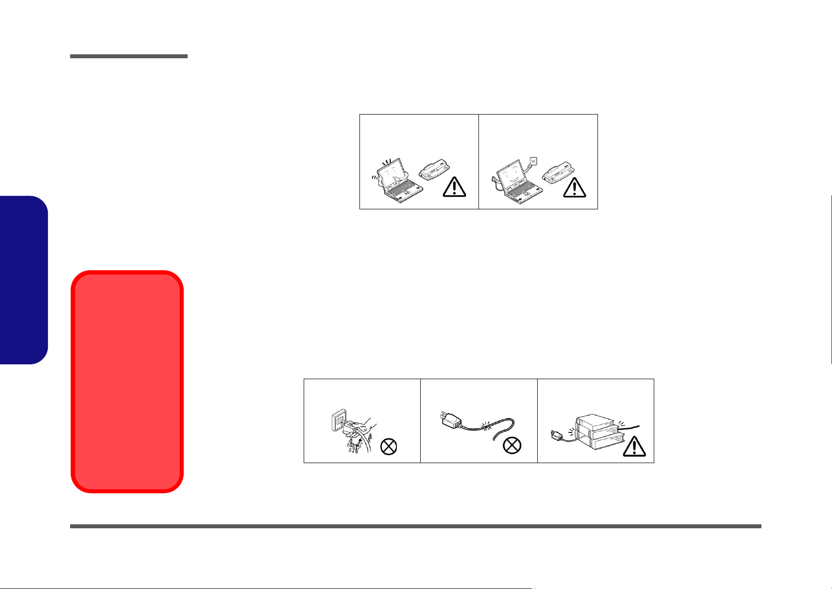
Instructions for Care and Operation
The notebook computer is quite rugged, but it can be damaged. To prevent this, follow these suggestions:
1. Don’t drop it, or expose it to shock. If the computer falls, the case and the components could be damaged.
Preface
Do not expose the computer
to any shock or vibration.
Do not place it on an unstable
surface.
Do not place anything heavy
on the computer.
2. Keep it dry, and don’t overheat it. Keep the computer and power supply away from any kind of heating element. This
is an electrical appliance. If water or any other liquid gets into it, the computer could be badly damaged.
Do not expose it to excessive
heat or direct sunlight.
Do not leave it in a place
where foreign matter or moisture may affect the system.
Don’t use or store the computer in a humid environment.
Do not place the computer on
any surface which will block
the vents.
3. Follow the proper working procedures for the computer. Shut the computer down properly and don’t forget to save
your work. Remember to periodically save your data as data may be lost if the battery is depleted.
Do not turn off the power
until you properly shut down
all programs.
Do not turn off any peripheral
devices when the computer is
on.
Do not disassemble the computer by yourself.
Perform routine maintenance
on your computer.
Preface
V
Page 7
Preface
4. Avoid interference. Keep the computer away from high capacity transformers, electric motors, and other strong mag-
netic fields. These can hinder proper performance and damage your data.
5. Take care when using peripheral devices.
Preface
Power Safety
Warning
Before you undertake
any upgrade procedures, make sure that
you have turned off the
power, and disconnected all peripherals
and cables (including
telephone lines). It is
advisable to also remove your battery in
order to prevent accidentally turning the
machine on.
Use only approved brands of
peripherals.
Unplug the power cord before
attaching peripheral devices.
Power Safety
The computer has specific power requirements:
• Only use a power adapter approved for use with this computer.
• Your AC adapter may be designed for international travel but it still requires a steady, uninterrupted power supply. If you are
unsure of your local power specifications, consult your service representative or local power company.
• The power adapter may have either a 2-prong or a 3-prong grounded plug. The third prong is an important safety feature; do
not defeat its purpose. If you do not have access to a compatible outlet, have a qualified electrician install one.
• When you want to unplug the power cord, be sure to disconnect it by the plug head, not by its wire.
• Make sure the socket and any extension cord(s) you use can support the total current load of all the connected devices.
• Before cleaning the computer, make sure it is disconnected from any external power supplies.
Do not plug in the power
cord if you are wet.
Do not use the power cord if
it is broken.
Do not place heavy objects
on the power cord.
VI
Page 8

Battery Precautions
• Only use batteries designed for this computer. The wrong battery type may explode, leak or damage the computer.
• Recharge the batteries using the notebook’s system. Incorrect recharging may make the battery explode.
• Do not try to repair a battery pack. Refer any battery pack repair or replacement to your service representative or qualified service
personnel.
• Keep children away from, and promptly dispose of a damaged battery. Always dispose of batteries carefully. Batteries may explode
or leak if exposed to fire, or improperly handled or discarded.
• Keep the battery away from metal appliances.
• Affix tape to the battery contacts before disposing of the battery.
• Do not touch the battery contacts with your hands or metal objects.
Battery Disposal
The product that you have purchased contains a rechargeable battery. The battery is recyclable. At the end of
its useful life, under various state and local laws, it may be illegal to dispose of this battery into the municipal
waste stream. Check with your local solid waste officials for details in your area for recycling options or proper
disposal.
Caution
Danger of explosion if battery is incorrectly replaced. Replace only with the same or equivalent type recommended by the manufacturer. Discard used battery according to the manufacturer’s instructions.
Preface
Preface
VII
Page 9

Preface
Preface
Related Documents
You may also need to consult the following manual for additional information:
User’s Manual on CD
This describes the notebook PC’s features and the procedures for operating the computer and its ROM-based setup program. It also describes the installation and operation of the utility programs provided with the notebook PC.
VIII
Page 10

Contents
Preface
Introduction ..............................................1-1
Overview .........................................................................................1-1
System Specifications .....................................................................1-2
Processor .........................................................................................1-2
Core Logic .......................................................................................1-2
Security ............................................................................................1-2
Memory ...........................................................................................1-2
BIOS ................................................................................................1-2
LCD Options ...................................................................................1-2
Display ............................................................................................1-3
Storage Devices ...............................................................................1-3
Audio ...............................................................................................1-3
Keyboard .........................................................................................1-4
Interface ...........................................................................................1-4
PC Card ...........................................................................................1-4
Communication ...............................................................................1-4
Power Management .........................................................................1-5
Power ...............................................................................................1-5
Environmental Spec ........................................................................1-5
Physical Dimensions .......................................................................1-5
Weight .............................................................................................1-5
Optional ...........................................................................................1-6
Design Differences .......................................................................... 1-6
External Locator - Top View ..........................................................1-7
External Locator - Front & Left Side Views ...................................1-8
External Locator - Right Side & Rear Views .................................. 1-9
External Locator - Bottom View ................................................... 1-10
Mainboard Overview - Top (Key Parts) .......................................1-11
Mainboard Overview - Bottom (Key Parts) .................................. 1-12
Mainboard Overview - Top (Connectors) ..................................... 1-13
Mainboard Overview - Bottom (Connectors) ............................... 1-14
Disassembly ...............................................2-1
Overview ......................................................................................... 2-1
Maintenance Tools .......................................................................... 2-2
Connections .................................................................................... 2-2
Maintenance Precautions ................................................................ 2-3
Cleaning .......................................................................................... 2-3
Disassembly Steps .......................................................................... 2-4
Removing the Battery ..................................................................... 2-8
Removing the Hard Disk Drive ...................................................... 2-9
Hard Disk Upgrade Process ............................................................ 2-9
Removing the System Memory (RAM) ....................................... 2-10
Memory Upgrade Process ............................................................. 2-10
Removing the CD Device ............................................................. 2-12
Removing the Bluetooth Module .................................................. 2-14
Removing the Wireless LAN Module .......................................... 2-15
Removing the Processor ............................................................... 2-16
Removing the Keyboard ............................................................... 2-18
Removing the Keyboard Shielding Plate ...................................... 2-19
Removing the LCD and Top Case ................................................ 2-20
Removing the TouchPad and Click Board ................................... 2-22
Removing the Switch Board ......................................................... 2-23
Removing the Modem .................................................................. 2-24
Removing the Speakers ................................................................ 2-25
Removing the Mainboard ............................................................. 2-26
Removing the Fan Unit ................................................................. 2-27
Removing the Floppy Disk Drive Assembly ................................ 2-28
Removing the PC Card Assembly ................................................ 2-29
Removing the LCD Front Panel Module ...................................... 2-30
Removing the Inverter .................................................................. 2-31
Preface
IX
Page 11

Preface
Removing the PC Video Camera Module .....................................2-32
Removing the LCD Module .......................................................... 2-33
Part Lists ..................................................A-1
Part List Illustration Location ........................................................A-2
Top (D400E) ..................................................................................A-3
Bottom (D400E) ............................................................................. A-4
LCD 14" (D400E) .......................................................................... A-5
LCD 15" (D400E) .......................................................................... A-6
CD-ROM Drive (D400E) ............................................................... A-7
CD-RW Drive (D400E) .................................................................A-8
Combo Drive (D400E) ................................................................... A-9
DVD-ROM Drive (D400E) .......................................................... A-10
Floppy Disk Drive (D400E) ......................................................... A-11
Hard Disk Drive (D400E) ............................................................ A-12
Top (D410E) ................................................................................A-13
Bottom (D410E) ........................................................................... A-14
Preface
LCD 14" (D410E) ........................................................................ A-15
LCD 15" (D410E) ........................................................................ A-16
CD-ROM Drive (D410E) ............................................................. A-17
CD-RW Drive (D410E) ...............................................................A-18
Combo Drive (D410E) .................................................................A-19
DVD-ROM Drive (D410E) .......................................................... A-20
Floppy Disk Drive (D410E) ......................................................... A-21
Hard Disk Drive (D410E) ............................................................ A-22
Schematic Diagrams................................. B-1
System Block Diagram ................................................................... B-2
Socket 478 1 of 2 ............................................................................ B-3
Socket 478 & ITP 2 of 2 ................................................................. B-4
Clock Generator ............................................................................. B-5
M645DX (Host/AGP) 1 of 4 .......................................................... B-6
M645DX (Memory for DDR) 2 of 4 .............................................. B-7
M645DX (& CRT Out) 3 of 4 ........................................................B-8
M645DX (Power) 4 of 4 .................................................................B-9
DDR Memory DIMM ...................................................................B-10
DDR SSTL-2 Termination ...........................................................B-11
LVDS Interface (SiS302LV) ........................................................B-12
Panel Con & LED Indicator .........................................................B-13
962 (PCI/IDE/HyperZip) 1 of 4 ....................................................B-14
962 (Misc Signals) 2 of 4 ..............................................................B-15
962 (USB I/F) 3 of 4 .....................................................................B-16
962 (Power & RTC) 4 of 4 ...........................................................B-17
HDD/Combo Connector ...............................................................B-18
USB Port .......................................................................................B-19
PCMCIA ENE CB1410 ................................................................B-20
PCMCIA Power ............................................................................B-21
1394 PHY TSB41LV01 ................................................................B-22
LPC Super I/O ..............................................................................B-23
LPT/COM Port .............................................................................B-24
LPC H8 .........................................................................................B-25
LAN RTL8100BL ........................................................................B-26
Audio Codec ALC201A ...............................................................B-27
Audio Out & Off Board Connectors .............................................B-28
System Power Control ..................................................................B-29
Fan Control and SpeedStep ..........................................................B-30
Mobility M9-P ..............................................................................B-31
Mobility M9-P MEM A/B ............................................................B-32
VGA DRAM 1 of 2 ......................................................................B-33
VGA DRAM 1 of 2 - Termination ...............................................B-34
VGA DRAM 2 of 2 ......................................................................B-35
Mobility M9-P POW ....................................................................B-36
VCORE .........................................................................................B-37
DDR Power ...................................................................................B-38
System Power ...............................................................................B-39
X
Page 12

Charger ......................................................................................... B-40
SW Board and HotKey ................................................................. B-41
TouchPad and Switch Board ........................................................ B-42
Updating the FLASH ROM BIOS......... C-1
Preface
Preface
XI
Page 13

Preface
Preface
XII
Page 14

1: Introduction
Overview
This manual covers the information you need to service or upgrade the D400E/D410E series notebook computer. Information about operating the computer (e.g. getting started, and the Setup utility) is in the User’s Manual. Information
about drivers (e.g. VGA & audio) is also found in User’s Manual. That manual is shipped with the computer.
Operating systems (e.g. DOS, Windows 9x, Windows NT 4.0, Windows 2000, Windows XP, OS/2 Warp, UNIX, etc.) have
their own manuals as do application software (e.g. word processing and database programs). If you have questions about
those programs, you should consult those manuals.
The D400E/D410E series notebook is designed to be upgradeable. See “Disassembly” on page 2 - 1 for a detailed description of the upgrade procedures for each specific component. Please note the warning and safety information indicated by the “” symbol.
The balance of this chapter reviews the computer’s technical specifications and features.
Introduction
1.Introduction
Overview 1 - 1
Page 15

Introduction
1.Introduction
System Specifications
Processor
• Intel Pentium 4 Processor - (478-pin) FC-PGA2 package
µ0.13) 0.13 Micron Process Technology, 512KB L2 Cache & 400MHz FSB - 2.0/ 2.2/ 2.4/ 2.5 /2.6 GHz
(
(
µ0.13) 0.13 Micron Process Technology, 512KB L2 Cache & 533MHz FSB - 2.26/ 2.4/ 2.53/ 2.66/ 2.8/ 3.06 GHz
• Intel Celeron Processor - (478-pin) FC-PGA2 package
µ0.18) 0.18 Micron Process Technology, 128KB L2 Cache & 400MHz FSB - 1.7/ 1.8/ 2.0/ 2.1/ 2.2 GHz
(
Core Logic
• SIS M645DX + 962 Chipset + ATI M9
Security
• Security (Kensington® Type) Lock
• BIOS Password
Memory
• Two 200-pin DDR SODIMM sockets, supporting DDR SDRAM SODIMM (2.5V) - DDR 200/ DDR 266 compliant
• Memory expandable up to 1024MB (128/256/512MB SODIMM Modules)
BIOS
• One 512KB Flash ROM
•Phoenix BIOS
LCD Options
• 14.1" XGA TFT (1024*768)
• 15.0" XGA TFT (1024*768)
• 15.0" SXGA+ TFT (1400*1050)
1 - 2 System Specifications
Page 16

Display
• ATI Mobility Radeon 9000 high performance chip
• Support AGP™ 4X
• Integrated 128-bit 2D/3D Graphics Accelerator
Advanced HW accelerator for DVD playback
Fully Direct X 8.0 compliant graphics engine
• External memory up to 64MB DDR SGRAM on-board
• Dual-View display monitor
Storage Devices
•3.5" 3-mode Floppy Disk Drive
Introduction
Video Memory
The system allocates
or "shares" a portion of
system memory for
video use. "Shared"
memory is user-configurable via the SCU.
The default setting is
set to 32MB.
• Easy changeable 2.5" 9.5 mm (h) Hard Disk Drive
Supporting Master mode IDE
Supports PIO mode 4
ATA-33/66/100/133
Ultra DMA
• 12.7mm(h) Device Bay for ONE of the following drive configuration options:
•CD-ROM
•DVD-ROM
•CD-RW
•DVD-RW
• Combo CD-RW + DVD-ROM
Audio
• AC'97 2.1 compliant interface
• 3D stereo enhanced sound system
• Compatible with Sound-Blaster PRO™
• S/P DIF Digital output (5.1 CH) for DVD content and stereo audio
• Microphone-in jack
• Headphone-out jack
• Built-in microphone
• 2 built-in speakers (1 watt 35 * 16 mm)
1.Introduction
System Specifications 1 - 3
Page 17

Introduction
1.Introduction
Keyboard
• “Win Key” keyboard
Interface
• Built-in TouchPad (scrolling key functionality integrated)
• Three USB 2.0/1.1 ports
• One Mini-IEEE 1394 port
• One S-Video jack for TV output
• One serial port
• One parallel port (LPT1), supporting ECP / EPP
• Infrared transceiver IrDA 1.1 FIR/SIR/ASKIR
• One external CRT monitor port
• One PS/2 port
• One speaker-out/headphone-out jack
• One microphone-in jack
• One RJ-11 jack for modem
• One RJ-45 jack for 100M/10M LAN
• One S/P DIF out port
• One DC-in jack
• Wireless Device On/Off switch
PC Card
• One type II PCMCIA 3.3V/5V socket supporting CardBus
Communication
• Wireless Infrared transfer IrDA 1.1 compliant, 1cm - 1M operating distance, 115.2K bps SIR/ 4Mbps FIR
• 10/100Mb Ethernet LAN built-in
• V.90 & V.92 compliant 56K MDC modem
• 802.11b wireless LAN module (available as a factory option)
• Bluetooth module (available as a factory option)
• Built-in PC Video Camera module (available as a factory option)
1 - 4 System Specifications
Page 18

Power Management
• Supports ACPI v1.0b
• Supports Hibernate mode
• Supports Standby mode
• Supports battery low sleep
• Supports resume from modem ring
Power
• Full range AC adapter
• AC-Input 100~240V, 50~60Hz
• DC Output 20V, 6A (120W)
• Supports one removable Smart Li-Ion battery 220mAh/8 cell
Environmental Spec
• Temperature
Operating: 5
Non-Operating: -20
• Relative Humidity
Operating: 20% ~ 80%
Non-Operating: 10% ~ 90%
°C ~ 35°C (w/o packing)
°C ~ 60°C (packing)
Introduction
1.Introduction
Physical Dimensions
• 329 (w) x 275 (d) x 36.5 (h) mm
Weight
• 2.8 Kg (-50/+250g) w/o battery
System Specifications 1 - 5
Page 19
Introduction
Figure 1
Design Differences
1.Introduction
Optional
• DVD-ROM Drive
• CD-RW Drive
• Combination Drive
• Software DVD player
• Wireless LAN module
• Bluetooth module
• PC Video Camera
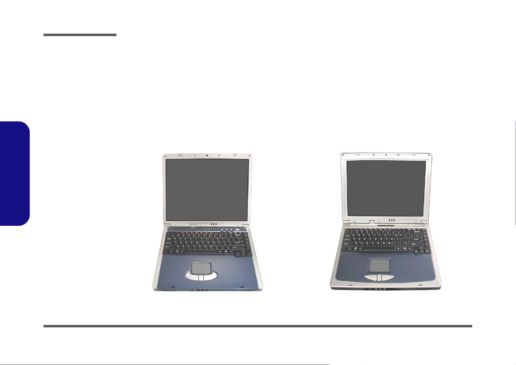
Design Differences
This manual refers to the two notebook designs pictured below. The designs vary slightly in external design. Photographs
used throughout this manual are of Design I.
1 - 6 System Specifications
Design I
Design II
Page 20
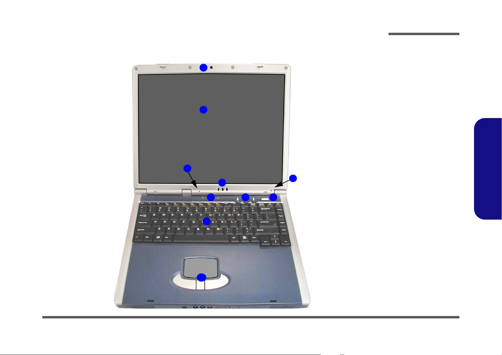
External Locator - Top View
Introduction
Figure 2
1
2
3
4
5
6
8
7
Top View
1. Optional Built-in
PC Camera
2. LCD
3. Built-In
Microphone
4. LED Power &
Communication
Indicators
5. LED Status
Indicators
6. AP-Key buttons
7. Close Cover/Lid
Switch
8. Power Button
9. Keyboard
10. TouchPad and
Buttons
1.Introduction
10
9
External Locator - Top View 1 - 7
Page 21
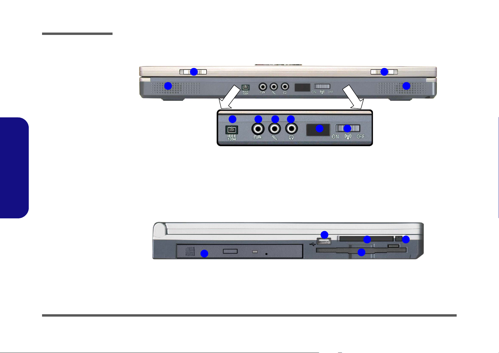
Introduction
Figure 3
Front View
1. LCD Latches
2. Mini IEEE 1394
Port
3. S/P DIF Out Port
4. Microphone Jack
5. Headphone Jack
6. Infrared
Transceiver
7. Wireless Device
ON/OFF Switch
8. Built-In Speakers
1.Introduction
Figure 4
Left Side View
External Locator - Front & Left Side Views
1
8 8
2
4 5
3
6 7
1
1. CD-ROM Bezel or
CD-ROM Device
2. USB 2.0/1.1 Port
3. Floppy Disk Drive
4. PC Card/ PCMCIA
Slot
5. PC Card/PCMCIA
Slot Eject Buttons
1 - 8 External Locator - Front & Left Side Views
2
1
4
3
5
Page 22
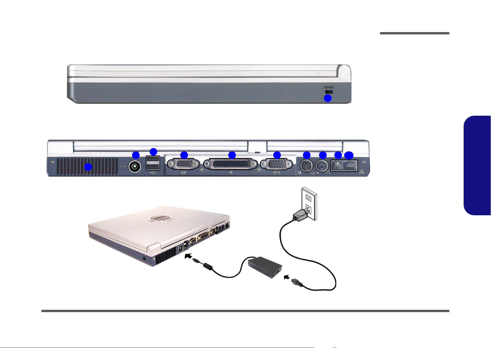
External Locator - Right Side & Rear Views
2
3
4 5 6 7 8 9
Introduction
Figure 5
Right Side View
1. Security Lock Slot
1
1.Introduction
Figure 6
10
Rear View
1
1. Vent
2. DC-In Jack
3. 2 * USB 2.0/1.1
Ports
4. External Monitor
(CRT) Port
5. Parallel Port
6. Serial Port
7. S-Video-Out Port
8. PS/2 Type Port
9. RJ-11 Phone Jack
10. RJ-45 LAN Jack
External Locator - Right Side & Rear Views 1 - 9
Page 23
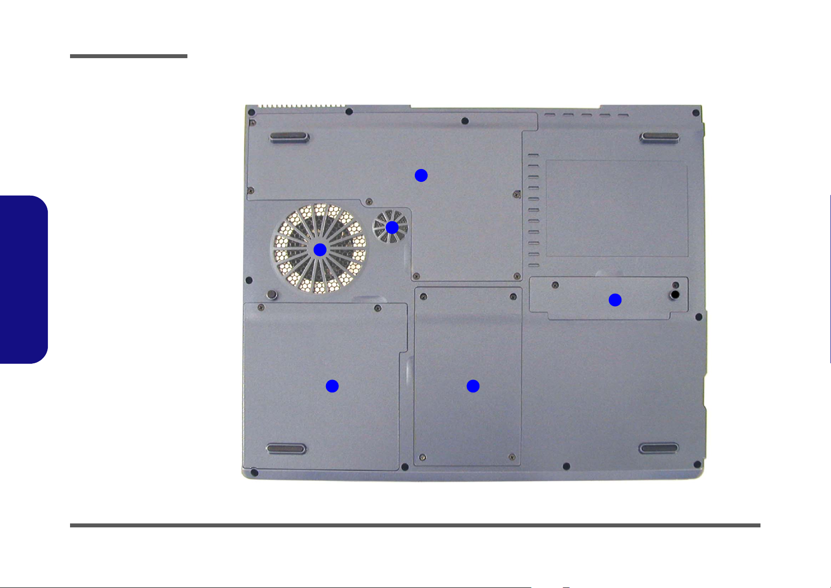
Introduction
Figure 7
Bottom View
1. Vent/Fan Intake
2. Battery Cover
3. Hard Disk Cover
4. Bluetooth
Module Cover
5. CPU, Heatsink,
DDR, Wireless
LAN Cover
External Locator - Bottom View
5
1
Note: The RAM and
optional Wireless
LAN module are located under the CPU
Heatsink Cover
1.Introduction
1 - 10 External Locator - Bottom View
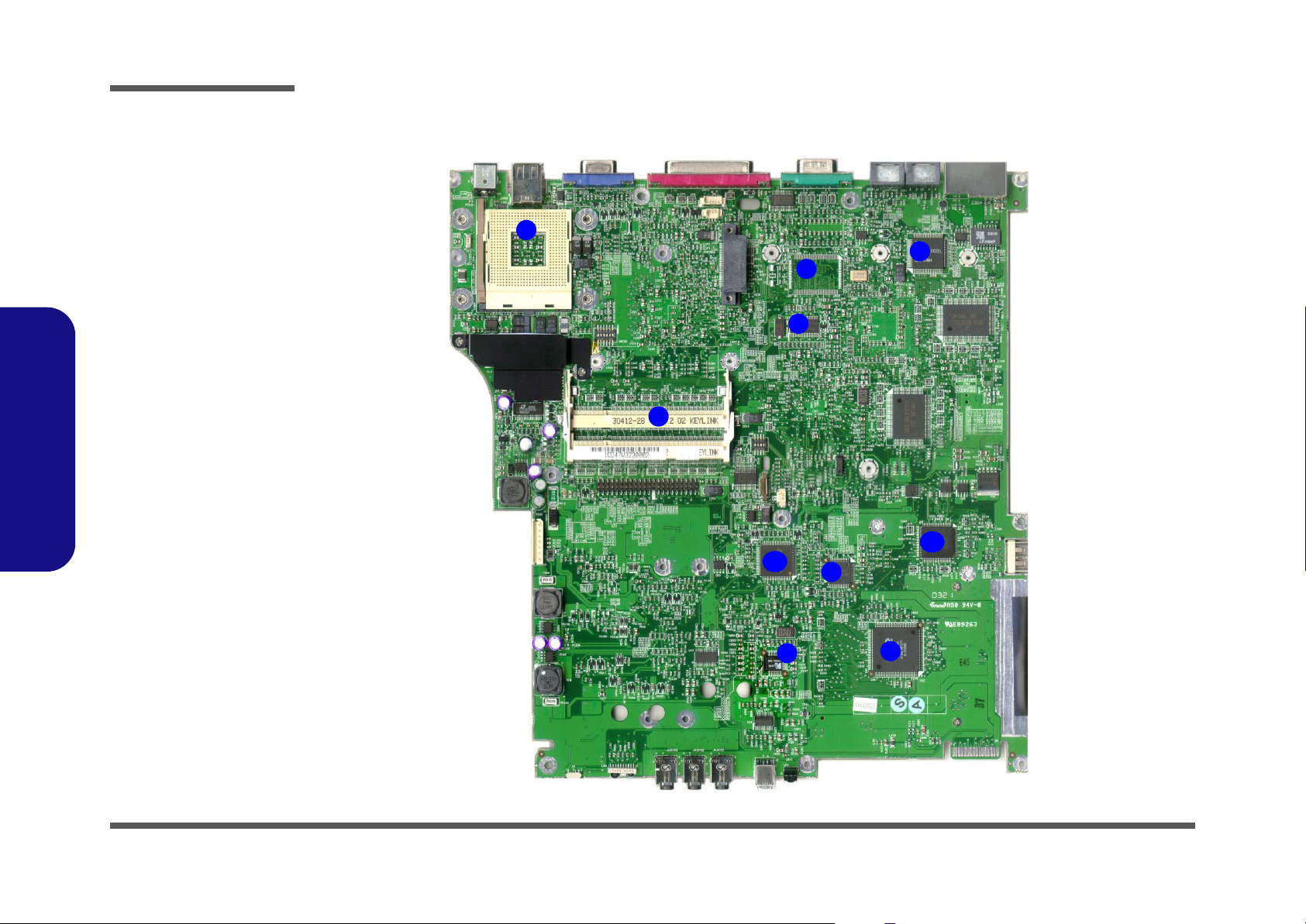
1
4
2
3
Page 24
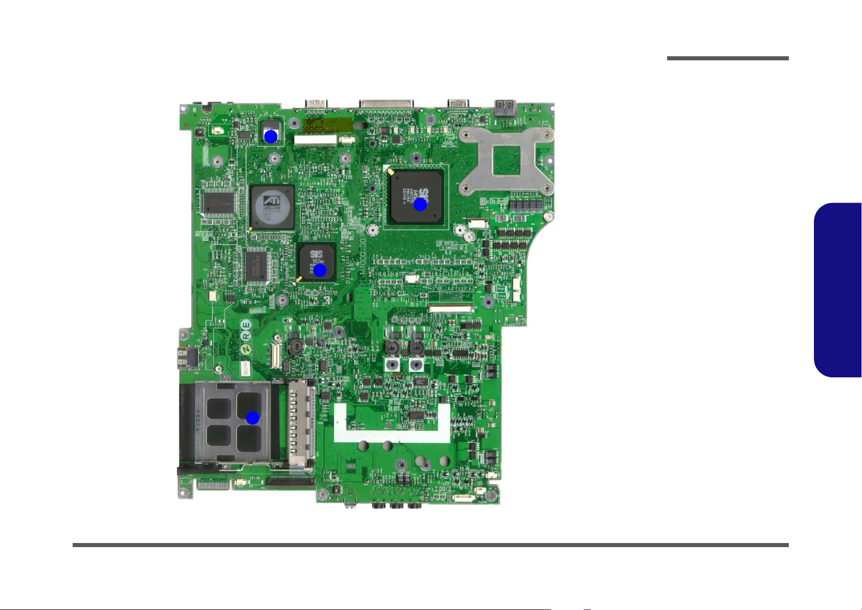
Introduction
Mainboard Overview - Top (Key Parts)
4
3
Figure 8
Mainboard Top
Key Parts
1. PC Card
Assembly
2. Northbridge - SiS
M650
3. Southbridge - SiS
2
962
4. Flash BIOS ROM
1.Introduction
1
Mainboard Overview - Top (Key Parts) 1 - 11
Page 25
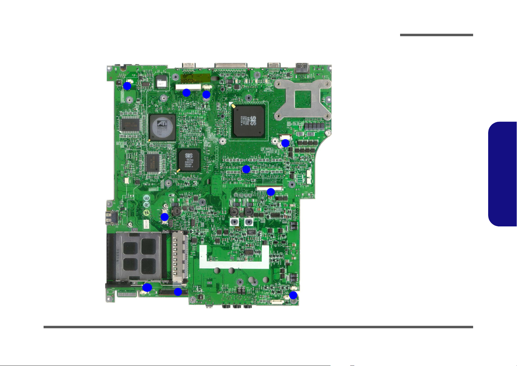
Introduction
Figure 9
Mainboard Bottom
Key Parts
1. CPU Socket (no
CPU installed)
2. Memory Slots (no
memory installed)
3. SiS 302LV TVOut Controller
4. LAN Controller
RTL8100BL
5. CardBus ENE
CB1410
6. ALC202 - Audio
Codec
7. 1394 PHY
TSB41AB1
1.Introduction
8. Clock Generator
9. Keyboard
Controller - KBC
H8 H8S-2149 HM
10. LPC Super I/O
NS PC87393
Mainboard Overview - Bottom (Key Parts)
1
3
8
2
9
7
4
10
1 - 12 Mainboard Overview - Bottom (Key Parts)
6
5
Page 26
Introduction
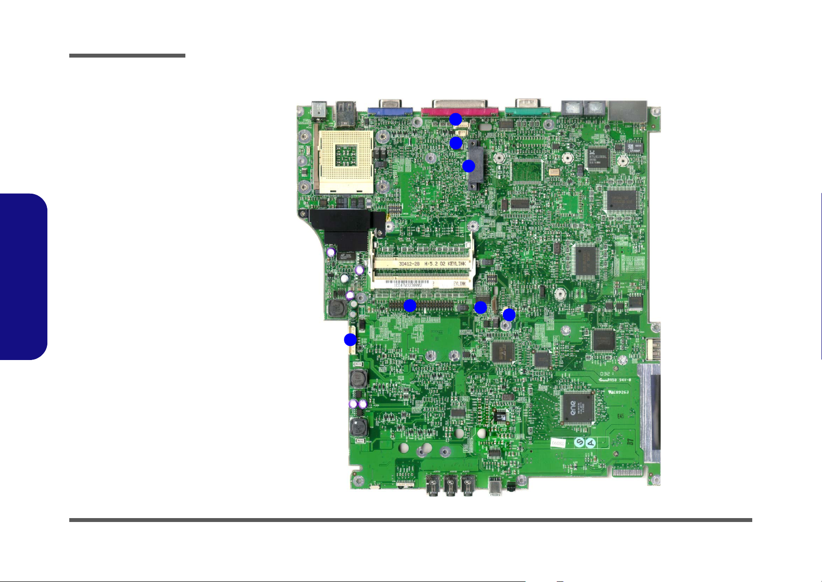
Mainboard Overview - Top (Connectors)
1
10
2
7
9
3
5
Figure 10
Mainboard Top
Connectors
1. Modem Cable
Connector (CN1)
2. LCD (and Inverter)
Connector
(JLCD1)
3. Video Camera
Cable Connector
(JCCD1)
4
6
8
4. Power Switch
Board Cable
Connector (JSW1)
5. TouchPad Cable
Connector (JTP1)
6. Keyboard Cable
Connector (JKB1)
7. Modem Module
Connector
(JMDC1)
8. Speaker Cable
Connector
(JSPK1)
9. Floppy Disk
Connector
(JFDD1)
10. Speaker Cable
Connector
(JSPK2)
1.Introduction
Mainboard Overview - Top (Connectors) 1 - 13
Page 27
Introduction
Figure 11
Mainboard Bottom
Connectors
1. Wireless LAN
Connector
(JWL1)
2. DDR Fan Cable
Connector
(JFAN2)
3. CD-ROM Device
Connector
(JCDROM1)
4. Hard Disk Cable
Connector
(JHDD1)
5. Bluetooth Module
Connector (JBT1)
1.Introduction
6. CMOS Battery
Cable Connector
(JBAT1)
7. Battery Cable
Connector (CN5)
Mainboard Overview - Bottom (Connectors)
1
2
3
4
7
5
6
1 - 14 Mainboard Overview - Bottom (Connectors)
Page 28

2: Disassembly
Overview
This chapter provides step-by-step instructions for disassembling the D400E/D410E series notebook’s parts and subsystems. When it comes to reassembly, reverse the procedures (unless otherwise indicated).
We suggest you completely review any procedure before you take the computer apart.
Disassembly
Component Parts
Procedures such as upgrading/replacing the RAM, CD device and hard disk are included in the User’s Manual but are
repeated here for your convenience.
To make the disassembly process easier each section may have a box in the page margin. Information contained under
the figure # will give a synopsis of the sequence of procedures involved in the disassembly procedure. A box with a
lists the relevant parts you will have after the disassembly process is complete. Note: The parts listed will be for the disassembly procedure listed ONLY, and not any previous disassembly step(s) required. Refer to the part list for the previous disassembly procedure. The amount of screws you should be left with will be listed here also.
A box with a
An example of these types of boxes are shown in the sidebar.
5 will provide any possible helpful information. A box with a contains warnings.
2.Disassembly
5
Information
Warning
Overview 2 - 1
Page 29

Disassembly
2.Disassembly
NOTE: All disassembly procedures assume that the system is turned OFF, and disconnected from any power supply (the
battery is removed too).
Maintenance Tools
The following tools are recommended when working on the notebook PC:
• M3 Philips-head screwdriver
• M2.5 Philips-head screwdriver (magnetized)
• M2 Philips-head screwdriver
• Small flat-head screwdriver
• Pair of needle-nose pliers
• Anti-static wrist-strap
Connections
Connections within the computer are one of four types:
Locking collar sockets for ribbon connectors To release these connectors, use a small flat-head screwdriver to gently pry
the locking collar away from its base. When replacing the connection, make
sure the connector is oriented in the same way. The pin1 side is usually not
indicated.
2 - 2 Overview
Pressure sockets for multi-wire connectors To release this connector type, grasp it at its head and gently rock it from side
to side as you pull it out. Do not pull on the wires themselves. When replacing
the connection, do not try to force it. The socket only fits one way.
Pressure sockets for ribbon connectors To release these connectors, use a small pair of needle-nose pliers to gently
lift the connector away from its socket. When replacing the connection, make
sure the connector is oriented in the same way. The pin1 side is usually not
indicated.
Board-to-board or multi-pin sockets To separate the boards, gently rock them from side to side as you pull them
apart. If the connection is very tight, use a small flat-head screwdriver - use
just enough force to start.
Page 30

Maintenance Precautions
The following precautions are a reminder. To avoid personal injury or damage to the computer while performing a removal and/or replacement job, take the following precautions:
1. Don't drop it. Perform your repairs and/or upgrades on a stable surface. If the computer falls, the case and other
components could be damaged.
2. Don't overheat it. Note the proximity of any heating elements. Keep the computer out of direct sunlight.
3. Avoid interference. Note the proximity of any high capacity transformers, electric motors, and other strong mag-
netic fields. These can hinder proper performance and damage components and/or data. You should also monitor
the position of magnetized tools (i.e. screwdrivers).
4. Keep it dry. This is an electrical appliance. If water or any other liquid gets into it, the computer could be badly
damaged.
5. Be careful with power. Avoid accidental shocks, discharges or explosions.
•Before removing or servicing any part from the computer, turn the computer off and detach any power supplies.
•When you want to unplug the power cord or any cable/wire, be sure to disconnect it by the plug head. Do not pull on the wire.
6. Peripherals – Turn off and detach any peripherals.
7. Beware of static discharge. ICs, such as the CPU and main support chips, are vulnerable to static electricity.
Before handling any part in the computer, discharge any static electricity inside the computer. When handling a
printed circuit board, do not use gloves or other materials which allow static electricity buildup. We suggest that
you use an anti-static wrist strap instead.
8. Beware of corrosion. As you perform your job, avoid touching any connector leads. Even the cleanest hands produce oils which can attract corrosive elements.
9. Keep your work environment clean. Tobacco smoke, dust or other air-born particulate matter is often attracted
to charged surfaces, reducing performance.
10. Keep track of the components. When removing or replacing any part, be careful not to leave small parts, such as
screws, loose inside the computer.
Disassembly
Power Safety
Warning
Before you undertake
any upgrade procedures, make sure that
you have turned off the
power, and disconnected all peripherals
and cables (including
telephone lines). It is
advisable to also remove your battery in
order to prevent accidentally turning the
machine on.
2.Disassembly
Cleaning
Do not apply cleaner directly to the computer, use a soft clean cloth.
Do not use volatile (petroleum distillates) or abrasive cleaners on any part of the computer.
Overview 2 - 3
Page 31

Disassembly
Disassembly Steps
The following table lists the disassembly steps, and on which page to find the related information. PLEASE PERFORM
THE DISASSEMBLY STEPS IN THE ORDER INDICATED.
2.Disassembly
To remove the Battery:
1. Remove the battery page 2 - 8
To remove the HDD:
1. Remove the battery page 2 - 8
2. Remove the HDD page 2 - 9
To remove the System Memory:
1. Remove the battery page 2 - 8
2. Remove the system memory page 2 - 10
To remove the CD Device:
1. Remove the battery page 2 - 8
2. Remove the CD Device page 2 - 12
To remove the Bluetooth Module:
1. Remove the battery page 2 - 8
2. Remove the Bluetooth module page 2 - 14
To remove the Wireless LAN Module:
1. Remove the battery page 2 - 8
2. Remove the Wireless LAN module page 2 - 15
To remove the Processor:
1. Remove the battery page 2 - 8
2. Remove the processor page 2 - 16
To remove the Keyboard:
1. Remove the battery page 2 - 8
2. Remove the keyboard page 2 - 18
To remove the Keyboard Shielding Plate:
1. Remove the battery page 2 - 8
2. Remove the keyboard page 2 - 18
3. Remove the keyboard shielding plate page 2 - 19
To remove the LCD and Top Case:
1. Remove the battery page 2 - 8
2. Remove the HDD page 2 - 9
3. Remove the system memory page 2 - 10
4. Remove the CD Device page 2 - 12
5. Remove the Bluetooth module page 2 - 14
6. Remove the Wireless LAN module page 2 - 15
7. Remove the processor page 2 - 16
8. Remove the keyboard page 2 - 18
9. Remove the keyboard shielding plate page 2 - 19
10. Remove the LCD & top case page 2 - 20
2 - 4 Disassembly Steps
Page 32

Disassembly
To remove the TouchPad and Click Board:
1. Remove the battery page 2 - 8
2. Remove the HDD page 2 - 9
3. Remove the system memory page 2 - 10
4. Remove the CD Device page 2 - 12
5. Remove the Bluetooth module page 2 - 14
6. Remove the Wireless LAN module page 2 - 15
7. Remove the processor page 2 - 16
8. Remove the keyboard page 2 - 18
9. Remove the keyboard shielding plate page 2 - 19
10. Remove the LCD & top case page 2 - 20
11. Remove the TouchPad and Click Boardpage 2 - 22
To remove the Switch Board:
1. Remove the battery page 2 - 8
2. Remove the HDD page 2 - 9
3. Remove the system memory page 2 - 10
4. Remove the CD Device page 2 - 12
5. Remove the Bluetooth module page 2 - 14
6. Remove the Wireless LAN module page 2 - 15
7. Remove the processor page 2 - 16
8. Remove the keyboard page 2 - 18
9. Remove the keyboard shielding plate page 2 - 19
10. Remove the LCD & top case page 2 - 20
11. Remove the switch board page 2 - 23
To remove the Modem:
1. Remove the battery page 2 - 8
2. Remove the HDD page 2 - 9
3. Remove the system memory page 2 - 10
4. Remove the CD Device page 2 - 12
5. Remove the Bluetooth module page 2 - 14
6. Remove the Wireless LAN module page 2 - 15
7. Remove the processor page 2 - 16
8. Remove the keyboard page 2 - 18
9. Remove the keyboard shielding plate page 2 - 19
10. Remove the LCD & top case page 2 - 20
11. Remove the modem page 2 - 24
To remove the Speakers:
1. Remove the battery page 2 - 8
2. Remove the HDD page 2 - 9
3. Remove the system memory page 2 - 10
4. Remove the CD Device page 2 - 12
5. Remove the Bluetooth module page 2 - 14
6. Remove the Wireless LAN module page 2 - 15
7. Remove the processor page 2 - 16
8. Remove the keyboard page 2 - 18
9. Remove the keyboard shielding plate page 2 - 19
10. Remove the LCD & top case page 2 - 20
11. Remove the speakers page 2 - 25
2.Disassembly
Disassembly Steps 2 - 5
Page 33

Disassembly
2.Disassembly
To remove the Mainboard:
1. Remove the battery page 2 - 8
2. Remove the HDD page 2 - 9
3. Remove the system memory page 2 - 10
4. Remove the CD Device page 2 - 12
5. Remove the Bluetooth module page 2 - 14
6. Remove the Wireless LAN module page 2 - 15
7. Remove the processor page 2 - 16
8. Remove the keyboard page 2 - 18
9. Remove the keyboard shielding plate page 2 - 19
10. Remove the LCD & top case page 2 - 20
11. Remove the speakers page 2 - 25
12. Remove the mainboard page 2 - 26
To remove the Fan Unit:
1. Remove the battery page 2 - 8
2. Remove the HDD page 2 - 9
3. Remove the system memory page 2 - 10
4. Remove the CD Device page 2 - 12
5. Remove the Bluetooth module page 2 - 14
6. Remove the Wireless LAN module page 2 - 15
7. Remove the processor page 2 - 16
8. Remove the keyboard page 2 - 18
9. Remove the keyboard shielding plate page 2 - 19
10. Remove the LCD & top case page 2 - 20
11. Remove the speakers page 2 - 25
12. Remove the mainboard page 2 - 26
13. Remove the fan unit page 2 - 27
To remove the Floppy Disk Drive Assembly:
1. Remove the battery page 2 - 8
2. Remove the HDD page 2 - 9
3. Remove the system memory page 2 - 10
4. Remove the CD Device page 2 - 12
5. Remove the Bluetooth module page 2 - 14
6. Remove the Wireless LAN module page 2 - 15
7. Remove the processor page 2 - 16
8. Remove the keyboard page 2 - 18
9. Remove the keyboard shielding plate page 2 - 19
10. Remove the LCD & top case page 2 - 20
11. Remove the speakers page 2 - 25
12. Remove the mainboard page 2 - 26
13. Remove the floppy disk drive page 2 - 28
To remove the PC Card Assembly:
1. Remove the battery page 2 - 8
2. Remove the HDD page 2 - 9
3. Remove the system memory page 2 - 10
4. Remove the CD Device page 2 - 12
5. Remove the Bluetooth module page 2 - 14
6. Remove the Wireless LAN module page 2 - 15
7. Remove the processor page 2 - 16
8. Remove the keyboard page 2 - 18
9. Remove the keyboard shielding plate page 2 - 19
10. Remove the LCD & top case page 2 - 20
11. Remove the speakers page 2 - 25
12. Remove the mainboard page 2 - 26
13. Remove the PC Card assembly page 2 - 29
2 - 6 Disassembly Steps
Page 34

Disassembly
To remove the LCD Front Panel Module:
1. Remove the battery page 2 - 8
2. Remove the HDD page 2 - 9
3. Remove the system memory page 2 - 10
4. Remove the CD Device page 2 - 12
5. Remove the Bluetooth module page 2 - 14
6. Remove the Wireless LAN module page 2 - 15
7. Remove the processor page 2 - 16
8. Remove the keyboard page 2 - 18
9. Remove the keyboard shielding plate page 2 - 19
10. Remove the LCD & top case page 2 - 20
11. Remove the front panel module page 2 - 30
To remove the Inverter:
1. Remove the battery page 2 - 8
2. Remove the HDD page 2 - 9
3. Remove the system memory page 2 - 10
4. Remove the CD Device page 2 - 12
5. Remove the Bluetooth module page 2 - 14
6. Remove the Wireless LAN module page 2 - 15
7. Remove the processor page 2 - 16
8. Remove the keyboard page 2 - 18
9. Remove the keyboard shielding plate page 2 - 19
10. Remove the LCD & top case page 2 - 20
11. Remove the front panel module page 2 - 30
12. Remove the inverter page 2 - 31
To remove the PC Video Camera Module:
1. Remove the battery page 2 - 8
2. Remove the HDD page 2 - 9
3. Remove the system memory page 2 - 10
4. Remove the CD Device page 2 - 12
5. Remove the Bluetooth module page 2 - 14
6. Remove the Wireless LAN module page 2 - 15
7. Remove the processor page 2 - 16
8. Remove the keyboard page 2 - 18
9. Remove the keyboard shielding plate page 2 - 19
10. Remove the LCD & top case page 2 - 20
11. Remove the front panel module page 2 - 30
12. Remove the PC Video Camera page 2 - 32
To remove the LCD Module:
1. Remove the battery page 2 - 8
2. Remove the HDD page 2 - 9
3. Remove the system memory page 2 - 10
4. Remove the CD Device page 2 - 12
5. Remove the Bluetooth module page 2 - 14
6. Remove the Wireless LAN module page 2 - 15
7. Remove the processor page 2 - 16
8. Remove the keyboard page 2 - 18
9. Remove the keyboard shielding plate page 2 - 19
10. Remove the LCD & top case page 2 - 20
11. Remove the front panel module page 2 - 30
12. Remove the inverter page 2 - 31
13. Remove the LCD module page 2 - 33
2.Disassembly
Disassembly Steps 2 - 7
Page 35

Disassembly
Figure 1
Battery Removal
a. Remove the 2 screws
and the battery cover.
b. Carefully disconnect the
battery cable and remove
the battery.
2.Disassembly
Removing the Battery
1. Turn the computer off, and turn it over.
2. Remove screws
3. Carefully (use a small screwdriver) disconnect the battery cable at point
4. Lift the battery out of the computer.
5. When replacing the battery, connect the cable first.
a.
1 2 3
& (Figure 1a) from the battery cover , and remove the cover.
5
b.
3
4
(Figure 1b).
4
3. Battery Cover
5. Battery
•2 Screws
2 - 8 Removing the Battery
1 2
5
Page 36

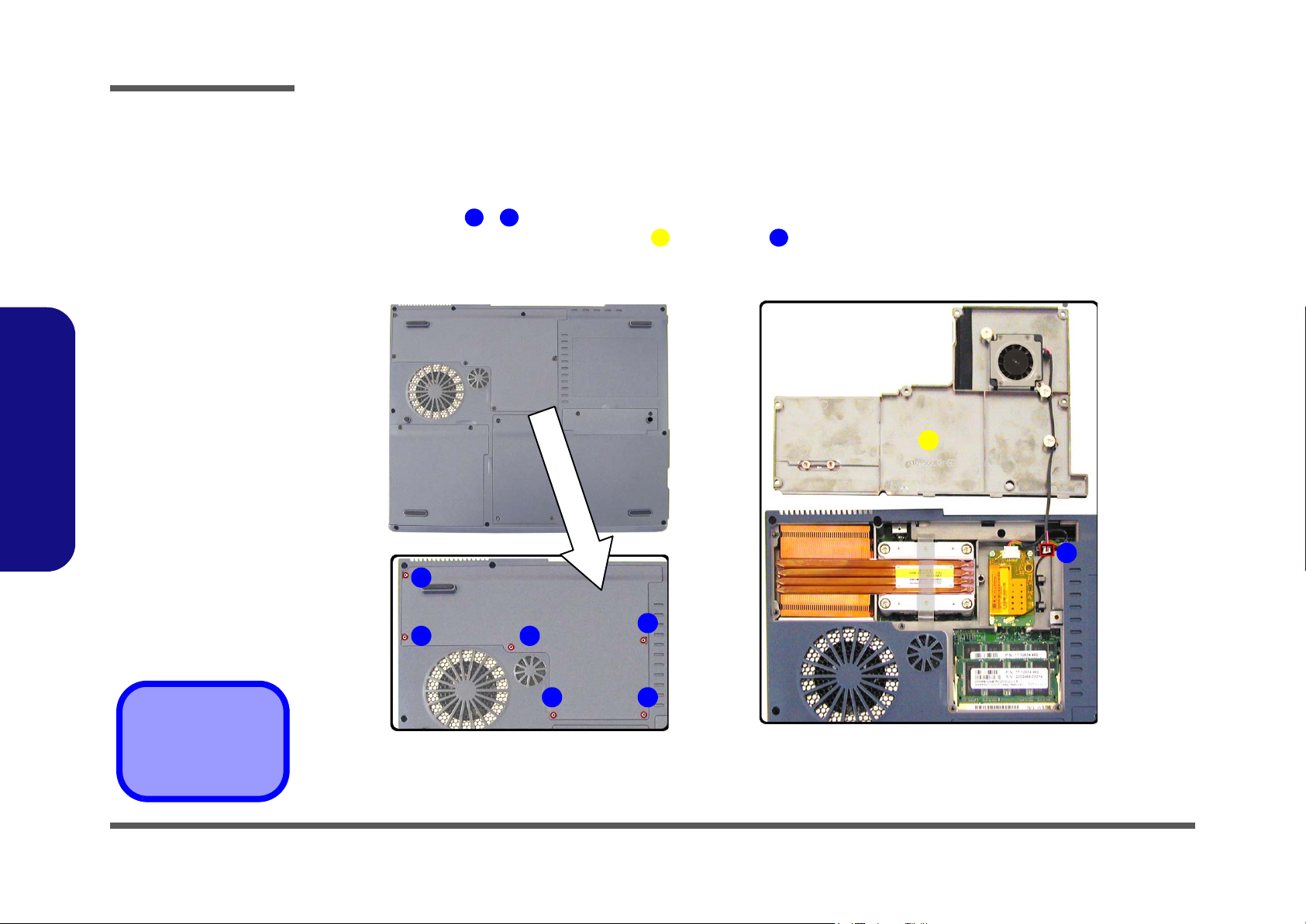
Removing the Hard Disk Drive
The hard disk drive is mounted in a removable case and can be taken out to accommodate other 2.5" IDE hard disk drives
with a height of 9.5mm (h). Follow your operating system’s installation instructions, and install all necessary drivers and
utilities (as outlined in
Chapter 4 of the User’s Manual) when setting up a new hard disk.
Hard Disk Upgrade Process
1. Turn off the computer, remove the battery (page 2 - 8) and turn it over.
1 4 5
2. Remove screws
3. Carefully (use a small screwdriver) disconnect the battery cable at point
4. Lift the HDD assembly out of the computer.
5. Reverse the process to install a new hard disk.
- (Figure 2a) from the hard disk cover , and remove the cover.
6
(Figure 2b).
7
a. b.
HDD System Warning
New HDD’s are blank. Before
you begin make sure:
You have backed up any data
you want to keep from your old
HDD.
5
6
Disassembly
2.Disassembly
Figure 2
HDD Assembly
Assembly Removal
a. Remove the 4 screws.
b. Disconnect the HDD ca-
ble and lift the HDD assembly out of the bay.
You have all the CD-ROMs
and FDDs required to install
your operating system and
programs.
If you have access to the internet, download the latest application and hardware driver
updates for the operating system you plan to install. Copy
these to a removable medium.
1
2
5. Hard Disk Cover
7
4
3
Removing the Hard Disk Drive 2 - 9
7. Hard Disk
•4 Screws
Page 37

Disassembly
Figure 3
Memory Socket
Cover Removal
a. Remove the screws.
b. Carefully lift the cover off
the computer.
Removing the System Memory (RAM)
The computer has two memory sockets for 200 pin Small Outline Dual In-line Memory Modules (SO-DIMM) supporting
DDR 200/266 MHz. The main memory can be expanded up to 1024MB. The SO-DIMM modules supported are 128Mb,
256Mb, and 512Mb. The total memory size is automatically detected by the POST routine once you turn on your computer.
Memory Upgrade Process
1. Turn off the computer, remove the battery (page 2 - 8) and turn it over.
2. Remove screws - (Figure 3a) from the memory socket cover
3. Carefully lift up the memory socket cover (Figure 3b) (a fan cable is still attached to the mainboard and you
can disconnect it).
4. If there is a module currently installed which needs to be upgraded/replaced then remove it.
a.
1 6
7 8
b.
.
2.Disassembly
7. Socket Cover
•6 Screws
2 - 10 Removing the System Memory (RAM)
7
8
1
2
3
6
54
Page 38
Disassembly
5. Gently pull the two release latches ( & ) on the sides of the memory socket toward the sides of the computer.
1 2
a.
3
12
6. The module (Figure 4b) will pop-up, and you can remove it.
3
7. Repeat the process for the second module if necessary.
8. Insert a new module holding it at about a 30° angle and fit the connectors firmly into the memory slot.
9. The module will only fit one way as defined by its pin alignment. Make sure the module is seated as far into the slot
as it will go. DO NOT FORCE IT; it should fit without much pressure.
b.
Figure 4
Removing/
Installing a RAM
Module
a. Pull the release
latches.
b.Remove the module.
Contact Warning
Be careful not to touch
the metal pins on the
module’s connecting
edge. Even the cleanest hands have oils
which can attract particles, and degrade the
module’s performance.
2.Disassembly
3 3
10. Press the module down towards the mainboard until the slot levers click into place to secure the module.
11. Replace the memory socket cover (be careful with the fan cable) and the 6 screws (see page 2 - 10).
12. Restart the computer.
13. The BIOS will register the new memory configuration as it starts up.
Removing the System Memory (RAM) 2 - 11
3. RAM Module
Page 39
Disassembly
Removing the CD Device
The easy changeable CD device may be upgraded or changed.
1. Turn off the computer, remove the battery (page 2 - 8) and turn it over.
2. Remove screws - (Figure 5a) from the memory socket cover
3. Carefully lift up the memory socket cover (a fan cable is still attached to the mainboard and you can disconnect it).
1 6
7 8
.
Figure 5
Memory Socket
Cover Removal
a. Remove the screws.
b. Carefully lift the cover off
the computer.
2.Disassembly
7. Socket Cover
a.
b.
7
8
1
2
3
6
54
•6 Screws
2 - 12 Removing the CD Device
Page 40
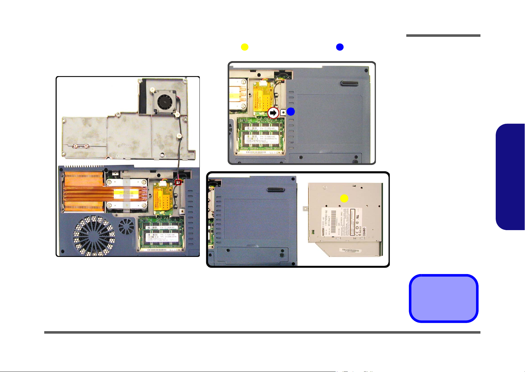
Disassembly
4. Use a screwdriver to carefully push the CD device assembly out of the computer at point .
1 2
2
Figure 6
CD Device Removal
Push the CD device out
off the computer at point
2.
2.Disassembly
1
5. Insert the new device and carefully slide it into the computer (the device only fits one way. DO NOT FORCE IT; The
screw holes should line up.
6. Replace the memory socket cover (be careful with the fan cable) and the 6 screws (see page 2 - 12 ).
7. Restart the computer to allow it to automatically detect the new device.
Removing the CD Device 2 - 13
1. CD Device
Page 41
Disassembly
Figure 7
Bluetooth Module
Removal
Removing the Bluetooth Module
1. Turn off the computer, remove the battery (page 2 - 8) and turn it over.
2. Remove screws - (Figure 7a) from the Bluetooth module cover
3. Carefully lift up the Bluetooth module cover off the computer.
4. Remove screws - (Figure 7c) and carefully disconnect cables -
10
(Figure 7d).
a.
1 2
3
3 6 8 9
.
b.
, then remove the Bluetooth module
a. Remove the screws.
b. Carefully lift the cover off
the computer.
c. Remove the screws and
disconnect the cables.
d. Remove the Bluetooth
module.
2.Disassembly
3. Bluetooth Cover
10. Bluetooth Module
•6 Screws
c.
1
3
2
d.
43
8
6
9
5
10
2 - 14 Removing the Bluetooth Module
Page 42
Removing the Wireless LAN Module
1. Turn off the computer, remove the battery (page 2 - 8) and turn it over.
2. Remove screws - from the memory socket cover
3. Carefully lift up the memory socket cover (a fan cable is still attached to the mainboard and you can disconnect it).
4. Remove screws
5. Lift the Wireless LAN module
1 6
7 8
- (Figure 8c), and carefully disconnect cables & .
9 10 11 12
13
(Figure 8d) off the computer.
.
Disassembly
Figure 8
Wireless LAN
Module Removal
a.
1
6
2
3
54
c. d.
11
9
10
12
b.
8
7
a. Remove the screws.
b. Carefully lift the cover off
the computer.
Antenna Cable
Connection
When re-inserting a
Wireless LAN module,
make sure the antenna
cable connects to the
connector J1 which is
indicated as point 12
in Figure 8c.
2.Disassembly
13
7. Socket Cover
13. WLAN Module
.
•8 Screws
Removing the Wireless LAN Module 2 - 15
Page 43

Disassembly
Figure 9
Processor Removal
a. Remove the screws.
b. Carefully lift the cover off
the computer.
c. Remove the screws in
the order indicated.
d. Remove the heat sink.
Removing the Processor
1. Turn off the computer, remove the battery (page 2 - 8) and turn it over.
2. Remove screws - from the memory socket cover
3. Carefully lift up the memory socket cover (a fan cable is still attached to the mainboard and you can disconnect it).
4. Remove screws
5. Carefully lift up the heat sink (Figure 9d) off the computer.
a.
1 6
7 8
- (Figure 9c) from the heat sink, in the order indicated on the label.
9 12
13
1
b.
.
8
6
2
3
Reassembly Screw
Order
2.Disassembly
When replacing the
heat sink, make sure
you insert the screws
in the same order indicated on the label.
7. Socket Cover
13. Heat Sink
•10 Screws
2 - 16 Removing the Processor
54
c. d.
12
9
10
11
7
13
Page 44

Disassembly
6. Unlock the processor by raising lever (Figure 10a).
7. Lift the CPU (Figure 10b) off the computer.
3
1
a.
1
c.
b.
3
Figure 10
Processor Removal
(cont’d)
a. Raise the lever to unlock
the CPU.
b. Lift the CPU off the sock-
et.
2.Disassembly
Caution
3
The heat sink, and
CPU area in general,
contains parts which
are subject to high
temperatures. Allow
the area time to cool
before removing these
parts.
3. CPU
Removing the Processor 2 - 17
Page 45
Disassembly
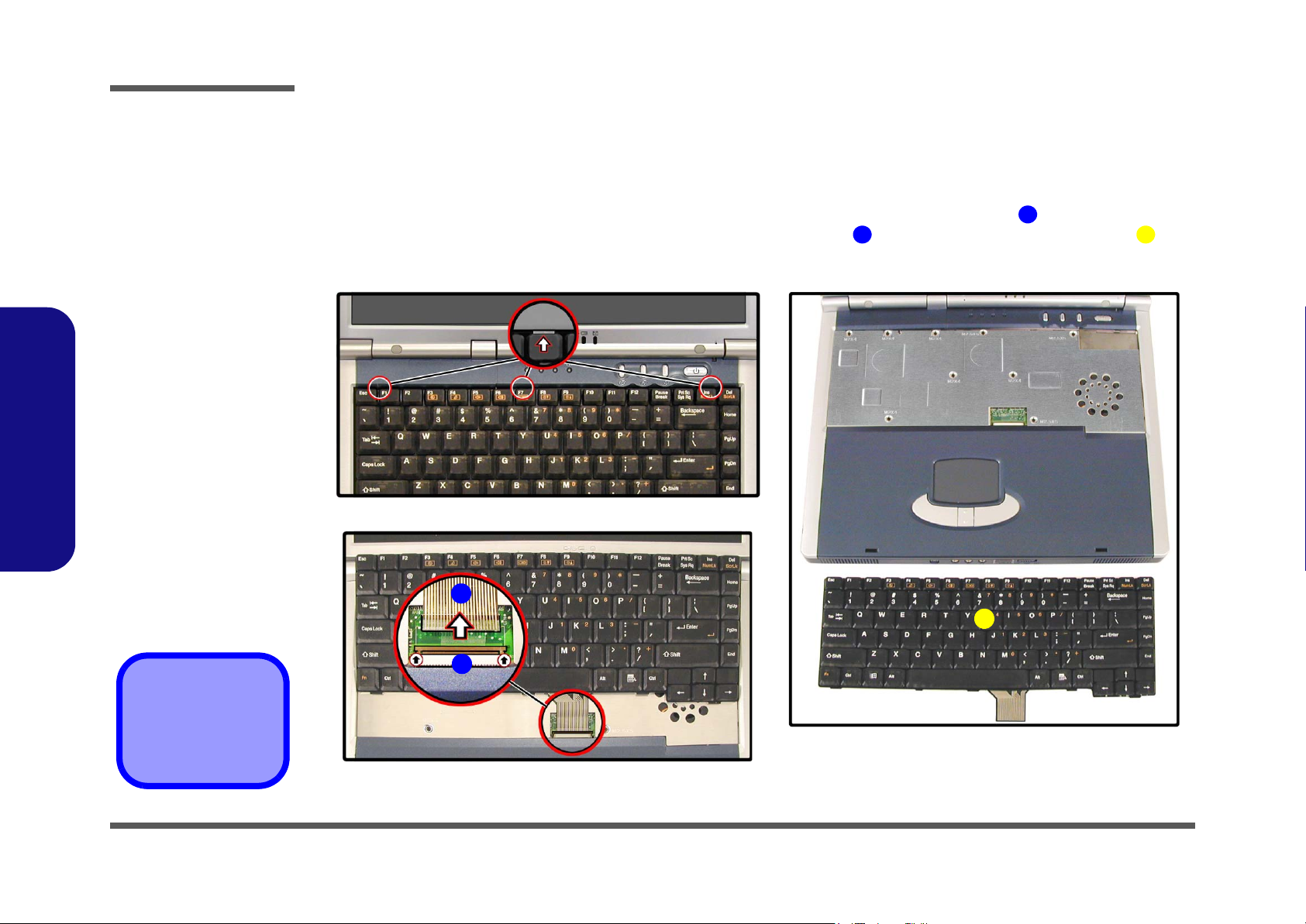
Removing the Keyboard
1. Turn off the computer, remove the battery (page 2 - 8).
2. Press the three keyboard latches at the top of the keyboard to elevate the keyboard from its normal position (you
may need to use a small screwdriver to do this).
3. Carefully lift the keyboard up and out, being careful not to bend the keyboard ribbon cable (Figure 11b).
4. Disconnect the keyboard ribbon cable from the locking collar socket (Figure 11b) and lift the keyboard up
out of the computer.
2 3
1
Figure 11
Keyboard Removal
a. Press the latches to ele-
vate the keyboard.
b. Disconnect the keyboard
cable form the locking
collar.
c. Remove the keyboard.
2.Disassembly
3. Keyboard
a.
c.
b.
1
3
2
2 - 18 Removing the Keyboard
Page 46
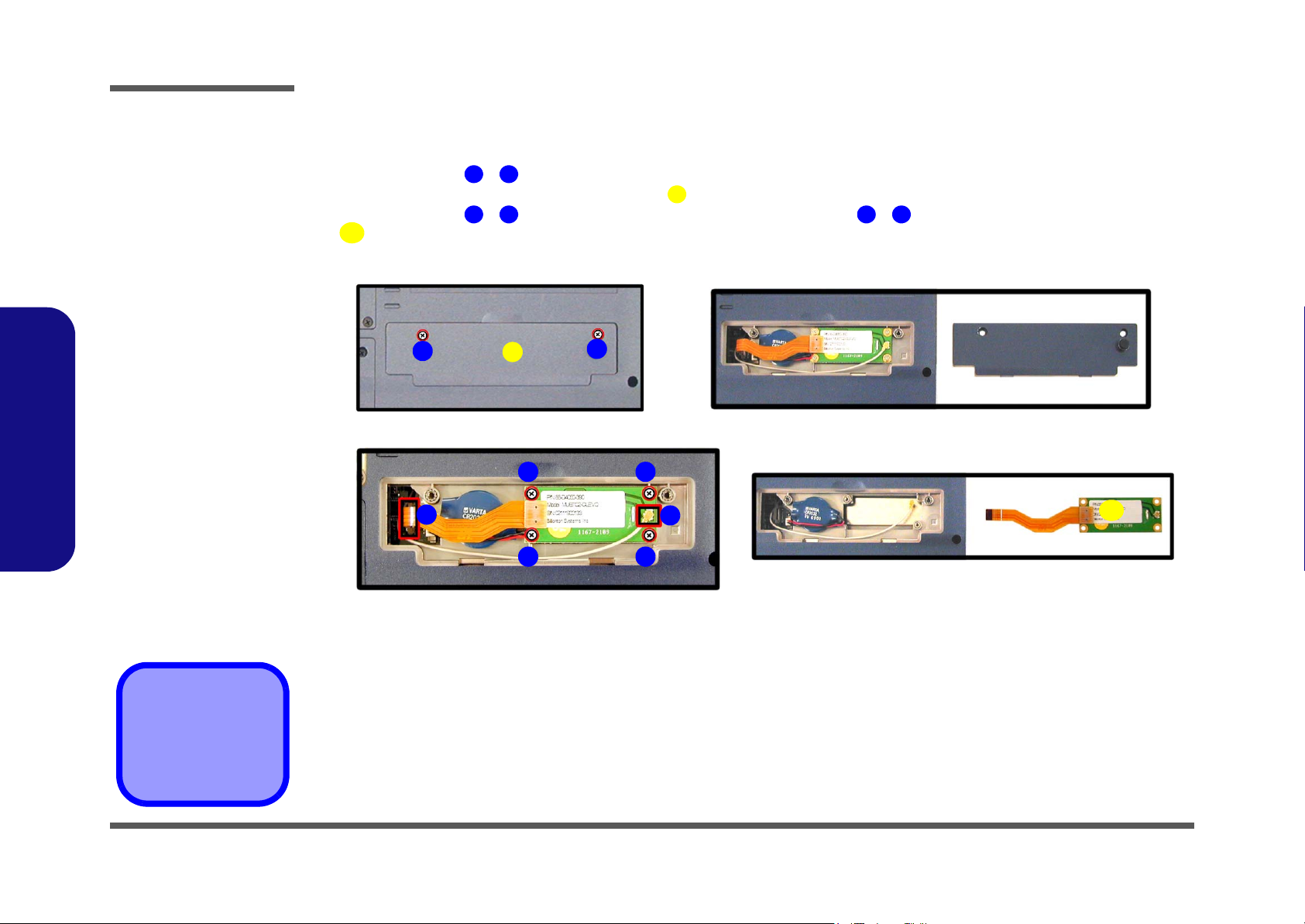
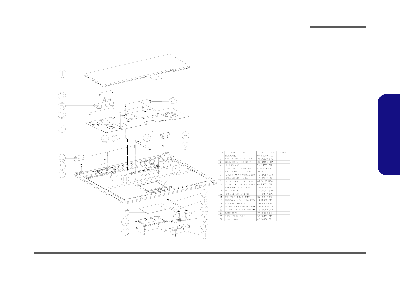
Removing the Keyboard Shielding Plate
1. Turn off the computer, remove the battery (page 2 - 8) and keyboard (page 2 - 18).
2. Remove screws - (Figure 12a) from the keyboard shielding plate and lift the plate off the computer.
a.
1 2 543
1 9 10
b.
Disassembly
Figure 12
Keyboard Shielding
Plate Removal
a. Remove the screws from
the shielding plate.
b. Lift the plate off the com-
puter.
2.Disassembly
6
8
7
9
10
10. Shielding Plate
•9 Screws
Removing the Keyboard Shielding Plate 2 - 19
Page 47
Disassembly
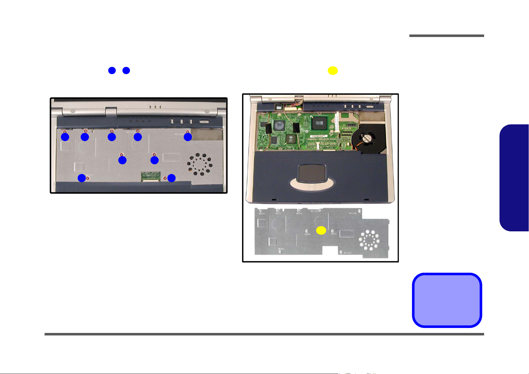
Removing the LCD and Top Case
1. Turn off the computer, remove the battery (page 2 - 8), hard disk (page 2 - 9), RAM (page 2 - 10), CD Device (page
2 - 12), Bluetooth module (page 2 - 14), Wireless LAN module (page 2 - 15), CPU (page 2 - 16), keyboard (page 2 -
18) and keyboard shielding plate (page 2 - 19).
2. Remove screws
3. Remove screws
4. Remove the LCD cable shielding cover , screws
- , and disconnect cable (Figure 13a) from the bottom off the computer.
1 11 12
- (Figure 13b) from the rear off the computer.
13 16
21
- and disconnect cables - (Figure 13c).
17 18 19 20
Figure 13
LCD & Top Case
Removal
a. Remove the screws from
the bottom of the computer.
b. Remove the screws from
the rear of the computer.
c. Remove the LCD cable
shielding cover and disconnect the cables.
2.Disassembly
a.
1 2
10
9
b.
b.
13
c.
3
21
12
4
11
17
18
19 20
7
8
6
5
16
26. LCD cable cover
•14 Screws
2 - 20 Removing the LCD and Top Case
14 15
Page 48

Disassembly
5. Slide the LCD hinge covers & (Figure 14a) out of the computer.
6. Remove screws
assembly (Figure 14c) off the computer.
5
7. Remove screws
& (Figure 14b) then carefully (pay careful attention to the antenna cables) lift the LCD
3 4
& (Figure 14d) and disconnect cables & , then lift the top case assembly off the
6 7 8 9
1 2
computer.
a.
21
b.
3 4
c.
10
Figure 14
LCD & Top Case
Removal Cont’d
5
a. Remove the hinge cov-
ers.
b. Remove the screws from
the LCD.
c. Lift the LCD top case as-
sembly.
d. Remove the screws and
disconnect the cables.
e. Lift the top case assem-
bly off the computer.
2.Disassembly
d.
6
7
e.
1&2. Hinge covers
8
10
9
Removing the LCD and Top Case 2 - 21
5. LCD Assembly
10. Top Case
•4 Screws
Page 49

Disassembly
Figure 15
TouchPad and Click
Board Removal
a. Remove the screws.
b. Separate the assembly
from the top case.
c. Disconnect the cable.
d. Remove the screws.
e. Separate the TouchPad
and click board.
2.Disassembly
Removing the TouchPad and Click Board
1. Turn off the computer, remove the battery (page 2 - 8), hard disk (page 2 - 9), RAM (page 2 - 10), CD Device (page
2 - 12), Bluetooth module (page 2 - 14), Wireless LAN module (page 2 - 15), CPU (page 2 - 16), keyboard (page 2 -
18), keyboard shielding plate (page 2 - 19) and the top case and LCD (page 2 - 20).
2. Remove screws - (Figure 15a) from the TouchPad and click board assembly, and lift the assembly off the
top case.
3. Disconnect cable (Figure 15c) and remove screws
4. Separate the TouchPad and click board
a.
1
8
7
1 8
9
2
6
12
- (Figure 15d).
10 11
13
(Figure 15e).
b.
c.
3
4
5
d.
12. TouchPad
13. Click Board
10
•10 Screws
2 - 22 Removing the TouchPad and Click Board
11
9
e.
12
13
Page 50

Removing the Switch Board
1. Turn off the computer, remove the battery (page 2 - 8), hard disk (page 2 - 9), RAM (page 2 - 10), CD Device (page
2 - 12), Bluetooth module (page 2 - 14), Wireless LAN module (page 2 - 15), CPU (page 2 - 16), keyboard (page 2 -
18), keyboard shielding plate (page 2 - 19) and the top case and LCD (page 2 - 20).
2. Remove screws & (Figure 16a) from the switch board assembly.
3. Lift the switch board assembly
1 2
3
(Figure 16b) off the top case.
10
Disassembly
a. b.
1
2
Figure 16
Switch Board
Removal
2.Disassembly
a. Remove the screws.
b. Lift the switch board as-
sembly off the top case.
3
3. Switch Board
•2 Screws
Removing the Switch Board 2 - 23
Page 51

Disassembly
Figure 17
Modem Removal
Remove the screws, disconnect the cable, and
remove the modem
module.
2.Disassembly
Removing the Modem
1. Turn off the computer, remove the battery (page 2 - 8), hard disk (page 2 - 9), RAM (page 2 - 10), CD Device (page
2 - 12), Bluetooth module (page 2 - 14), Wireless LAN module (page 2 - 15), CPU (page 2 - 16), keyboard (page 2 -
18), keyboard shielding plate (page 2 - 19) and the top case and LCD (page 2 - 20).
2. Remove screws & (Figure 17) from the modem and disconnect cable .
3. Remove the modem module .
1 2 3
4
3
4. Modem
•2 Screws
2 - 24 Removing the Modem
2
4
1
Page 52

Removing the Speakers
1. Turn off the computer, remove the battery (page 2 - 8), hard disk (page 2 - 9), RAM (page 2 - 10), CD Device (page
2 - 12), Bluetooth module (page 2 - 14), Wireless LAN module (page 2 - 15), CPU (page 2 - 16), keyboard (page 2 -
18), keyboard shielding plate (page 2 - 19) and the top case and LCD (page 2 - 20).
2. Disconnect cables & (Figure 18a) from the speakers to the mainboard.
3. Remove the speakers (Figure 18b).
a.
1 2
3
Disassembly
Figure 18
Speakers Removal
b.
2
1
3
3
a. Disconnect the cables.
b. Remove the speakers.
2.Disassembly
3. Speakers
Removing the Speakers 2 - 25
Page 53

Disassembly
Figure 19
Mainboard Removal
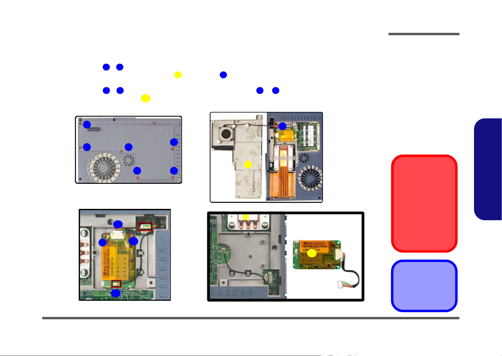
Removing the Mainboard
1. Turn off the computer, remove the battery (page 2 - 8), hard disk (page 2 - 9), RAM (page 2 - 10), CD Device (page
2 - 12), Bluetooth module (page 2 - 14), Wireless LAN module (page 2 - 15), CPU (page 2 - 16), keyboard (page 2 -
18), keyboard shielding plate (page 2 - 19), the top case and LCD (page 2 - 20) and speakers (page 2 - 25).
2. Disconnect cables & (Figure 19a) and remove screws .
3. Remove screws
a. b.
1 2 3
4
- , separate the mainboard , rear bracket and bottom case (Figure 19b).
9
10 11 12
a. Disconnect the cables
and remove the screws.
b. Remove screws, sepa-
rate the mainboard, rear
bracket and bottom
case.
2.Disassembly
10. Mainboard
11. Rear Bracket
12. Bottom Case
•8 Screws
4
5
10
6
11
7
8
2
9
3
12
1
2 - 26 Removing the Mainboard
Page 54

Removing the Fan Unit
1. Turn off the computer, remove the battery (page 2 - 8), hard disk (page 2 - 9), RAM (page 2 - 10), CD Device (page
2 - 12), Bluetooth module (page 2 - 14), Wireless LAN module (page 2 - 15), CPU (page 2 - 16), keyboard (page 2 -
18), keyboard shielding plate (page 2 - 19), the top case and LCD (page 2 - 20), speakers (page 2 - 25) and main-
board (
2. Remove screws - (Figure 20a) and lift out the fan unit .
page 2 - 26).
1 4 5
Disassembly
a.
b.
Figure 20
2
1
Fan Unit Removal
a. Remove the screws
b. Lift out the fan unit.
2.Disassembly
34
5
5. Fan Unit
•4 Screws
Removing the Fan Unit 2 - 27
Page 55

Disassembly
Figure 21
Floppy Disk Drive
Assembly Removal
a. Remove the screws
b. Lift out the FDD assem-
bly
c. Separate the brackets,
FDD and cable.
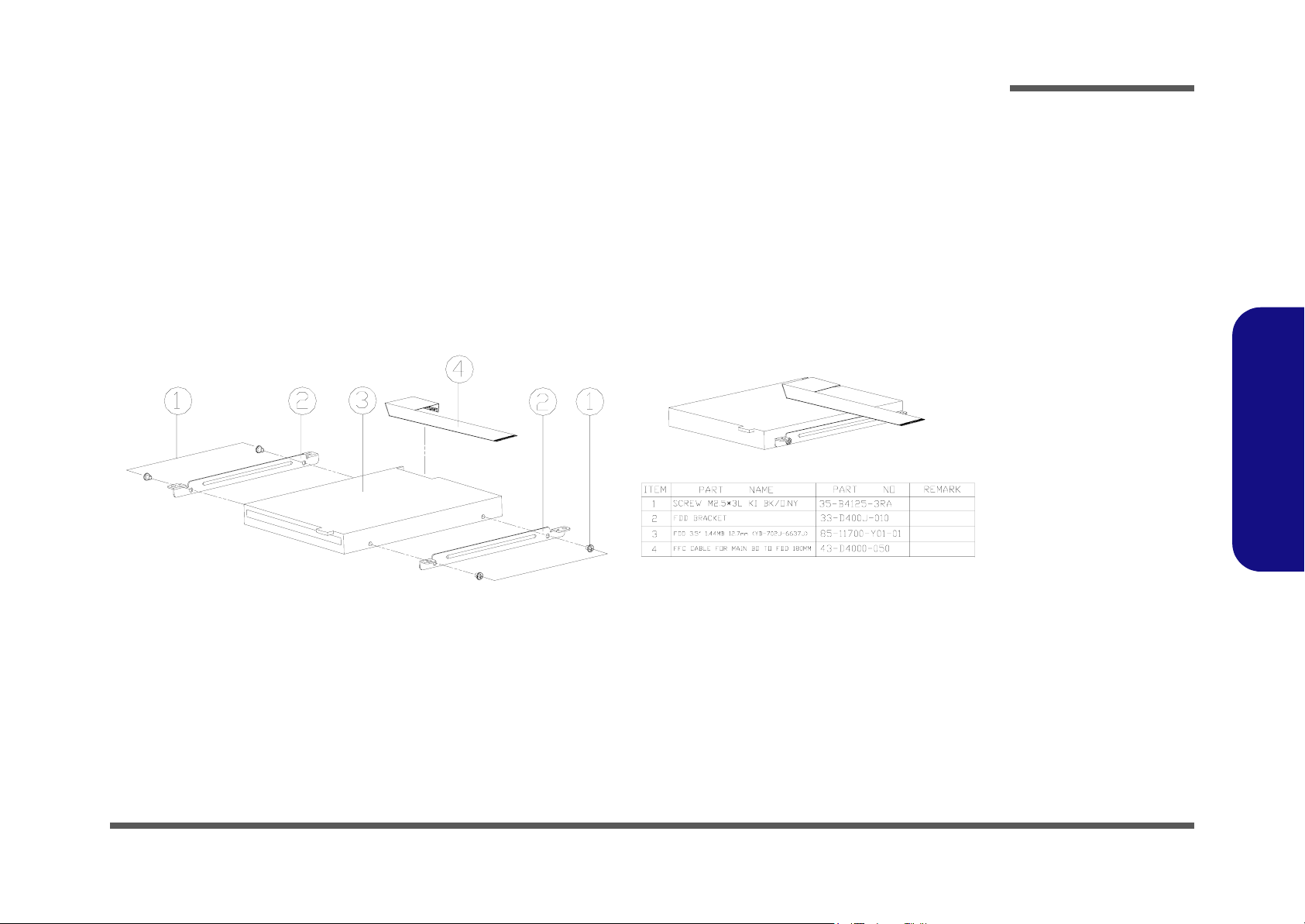
Removing the Floppy Disk Drive Assembly
1. Turn off the computer, remove the battery (page 2 - 8), hard disk (page 2 - 9), RAM (page 2 - 10), CD Device (page
2 - 12), Bluetooth module (page 2 - 14), Wireless LAN module (page 2 - 15), CPU (page 2 - 16), keyboard (page 2 -
18), keyboard shielding plate (page 2 - 19), the top case and LCD (page 2 - 20), speakers (page 2 - 25) and main-
board (
2. Remove screws - (Figure 21a) and lift out the floppy disk drive assembly.
3. Remove screws - (Figure 21c) and you can then separate the brackets , floppy disk drive unit , and
cable .
a. b.
page 2 - 26).
1 4
5 8
11
1 2
9 10
2.Disassembly
9. Brackets
10. Floppy Disk Drive
11. Cable
•8 Screws
2 - 28 Removing the Floppy Disk Drive Assembly
c.
34
11
6
9
5
10
9
7
8
Page 56

Removing the PC Card Assembly
1. Turn off the computer, remove the battery (page 2 - 8), hard disk (page 2 - 9), RAM (page 2 - 10), CD Device (page
2 - 12), Bluetooth module (page 2 - 14), Wireless LAN module (page 2 - 15), CPU (page 2 - 16), keyboard (page 2 -
18), keyboard shielding plate (page 2 - 19), the top case and LCD (page 2 - 20), speakers (page 2 - 25) and main-
board (
2. Remove screws & (Figure 22a).
3. Carefully ease (use a small screwdriver) the metal pins which hold the PC Card assembly in place, at points &
4
4. Lift off the PC Card assembly (Figure 22c) off the mainboard.
a. b.
page 2 - 26).
1 2
(Figure 22b) off the black plastic unit.
5
1
3
4
Disassembly
Figure 22
PC Card Assembly
Removal
a. Remove the screws.
b. Separate the metal pins
from the black plastic
unit.
c. Lift the PC Card assem-
bly off the mainboard.
2.Disassembly
c.
2
5
3
5. PC Card Assembly
•2 Screws
Removing the PC Card Assembly 2 - 29
Page 57
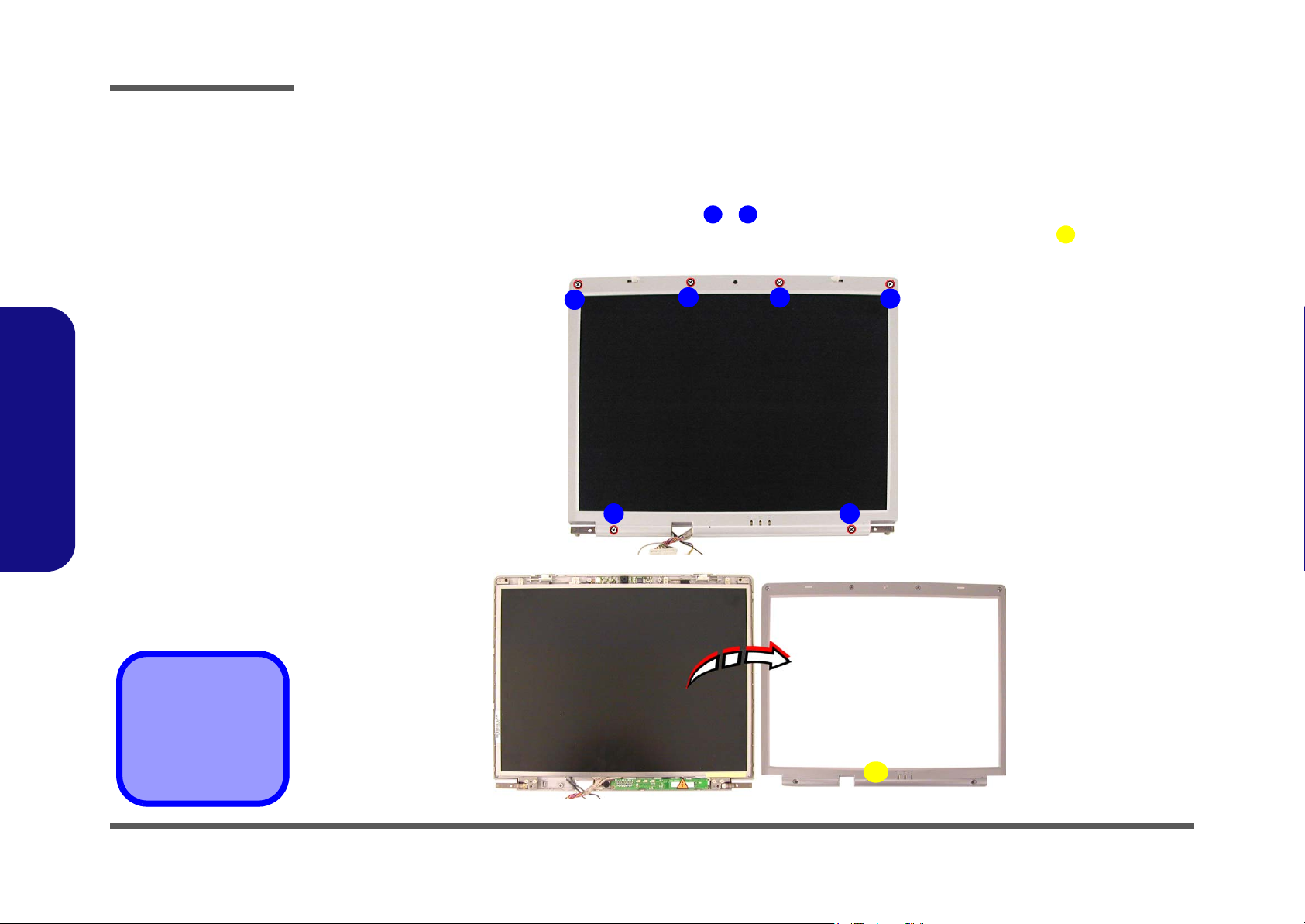
Disassembly
Removing the LCD Front Panel Module
1. Turn off the computer, remove the battery (page 2 - 8), hard disk (page 2 - 9), RAM (page 2 - 10), CD Device (page
2 - 12), Bluetooth module (page 2 - 14), Wireless LAN module (page 2 - 15), CPU (page 2 - 16), keyboard (page 2 -
18), keyboard shielding plate (page 2 - 19), and the top case and LCD (page 2 - 20).
2. Remove the rubber covers and screws at points - (Figure 23a).
3. Run your finger around the middle of the frame to carefully unsnap the LCD front panel module (Figure 23b)
from the back.
1 6
7
Figure 23
LCD Front Panel
Module Removal
a. Remove the rubber cov-
wers and screws.
b. Unsnap the LCD front
panel from the back.
2.Disassembly
7. LCD Front Panel
a.
b.
1
2
3
4
56
•6 Screws &
Rubber Covers
2-30
7
Page 58
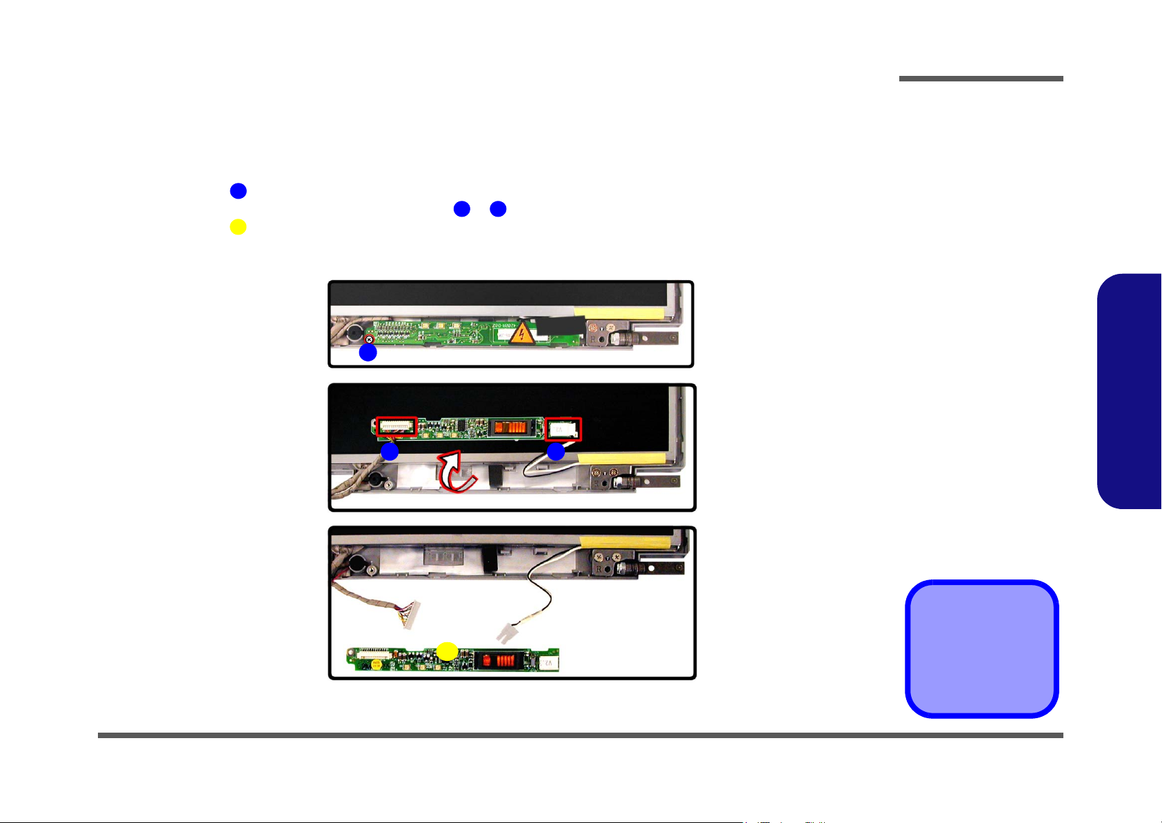
Removing the Inverter
1. Turn off the computer, remove the battery (page 2 - 8), hard disk (page 2 - 9), RAM (page 2 - 10), CD Device (page
2 - 12), Bluetooth module (page 2 - 14), Wireless LAN module (page 2 - 15), CPU (page 2 - 16), keyboard (page 2 -
18), keyboard shielding plate (page 2 - 19), the top case and LCD (page 2 - 20) and LCD front panel (page 2 - 30).
2. Remove screw (Figure 24a).
3. Turn the inverter over and disconnect the cables & (Figure 24b).
4. Lift the inverter (Figure 24c) off the LCD assembly.
1
2 3
4
Disassembly
Figure 24
Inverter Removal
a.
b.
c.
a. Remove the screw.
b. Turn the inverter over
and disconnect the ca-
1
2
3
bles.
c. Lift the inverter off the
LCD assembly.
2.Disassembly
4. Inverter
4
•1 Screw
Removing the Inverter 2 - 31
Page 59

Disassembly
Figure 25
PC Camera Module
Removal
a. Disconnect the cable.
b. Lift the PC Camera off
the LCD assembly.
c. If you need to remove
the antenna first remove
the LCD module then the
screw, and the antenna
2.Disassembly
cable.
Removing the PC Video Camera Module
1. Turn off the computer, remove the battery (page 2 - 8), hard disk (page 2 - 9), RAM (page 2 - 10), CD Device (page
2 - 12), Bluetooth module (page 2 - 14), Wireless LAN module (page 2 - 15), CPU (page 2 - 16), keyboard (page 2 -
18), keyboard shielding plate (page 2 - 19), the top case and LCD (page 2 - 20) and LCD front panel (page 2 - 30).
2. Disconnect cable (Figure 25a).
3. Lift the PC camera module (Figure 25b) off the LCD assembly.
4. If you need to remove the antenna cable, first remove the LCD module (
the antenna cable (Figure 25c).
a.
1
1
2
page 2 - 33), then remove screw and
4
3
c.
3
4
b.
2
2. PC Camera
4. Antenna Cable
•1 Screw
2 - 32 Removing the PC Video Camera Module
Page 60
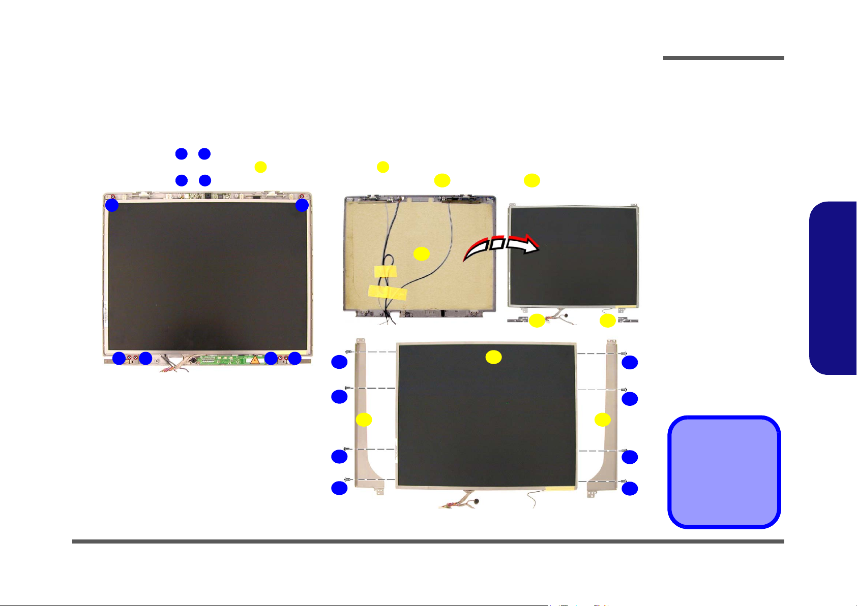
Removing the LCD Module
1. Turn off the computer, remove the battery (page 2 - 8), hard disk (page 2 - 9), RAM (page 2 - 10), CD Device (page
2 - 12), Bluetooth module (page 2 - 14), Wireless LAN module (page 2 - 15), CPU (page 2 - 16), keyboard (page 2 -
18), keyboard shielding plate (page 2 - 19), the top case and LCD (page 2 - 20), LCD front panel (page 2 - 30) and
inverter (
2. Remove screws - (Figure 26a).
3. Separate the display back panel (Figure 26b), hinges and LCD module assembly.
4. Remove screws
a. b.
page 2 - 31).
1 6
7 8
- (Figure 26c) and separate the LCD module and brackets .
9 16
1 2
17
18
Disassembly
Figure 26
LCD Module
Removal
a. Remove the screws.
7
b. Separate the back pan-
el, hinges and LCD module assembly.
c. Remove the screws and
separate the brackets
and LCD module.
2.Disassembly
8 8
c.
56
34
9
10
17
13
14
1818
11
12
15
16
7. Back Panel
8. Hinges
17. LCD module
18. Brackets
•14 Screws
Removing the LCD Module 2 - 33
Page 61

Disassembly
2.Disassembly
2-34
Page 62

Appendix A:Part Lists
This appendix breaks down the D400E/D410E series notebook’s construction into a series of illustrations. The component part numbers are indicated in the tables opposite the drawings.
Note: This section indicates the manufacturer’s part numbers. Your organization may use a different system, so be sure
to cross-check any relevant documentation.
Note: Some assemblies may have parts in common (especially screws). However, the part lists DO NOT indicate the
total number of duplicated parts used.
Part Lists
Note: Be sure to check any update notices. The parts shown in these illustrations are appropriate for the system at the
time of publication. Over the product life, some parts may be improved or re-configured, resulting in
new part numbers.
A.Part Lists
A-1
Page 63

Part Lists
Table 1 - 1
Part List Illustration
Location
Part List Illustration Location
The following table indicates where to find the appropriate part list illustration.
Part D400E D410E
Top
page A - 3 page A - 13
A.Part Lists
Bottom
LCD 14”
LCD 15"
CD-ROM Drive
CD-RW Drive
Combo Drive
DVD-ROM Drive
Floppy Disk Drive
Hard Disk Drive
page A - 4 page A - 14
page A - 5 page A - 15
page A - 6 page A - 16
page A - 7 page A - 17
page A - 8 page A - 18
page A - 9 page A - 19
page A - 10 page A - 20
page A - 11 page A - 21
page A - 12 page A - 22
A - 2 Part List Illustration Location
Page 64

Top (D400E)
Part Lists
Figure 1
Top (D400E)
A.Part Lists
Top (D400E) A - 3
Page 65

Part Lists
Bottom (D400E)
A.Part Lists
Bottom (D400E)
Figure 2
A - 4 Bottom (D400E)
Page 66

LCD 14" (D400E)
Part Lists
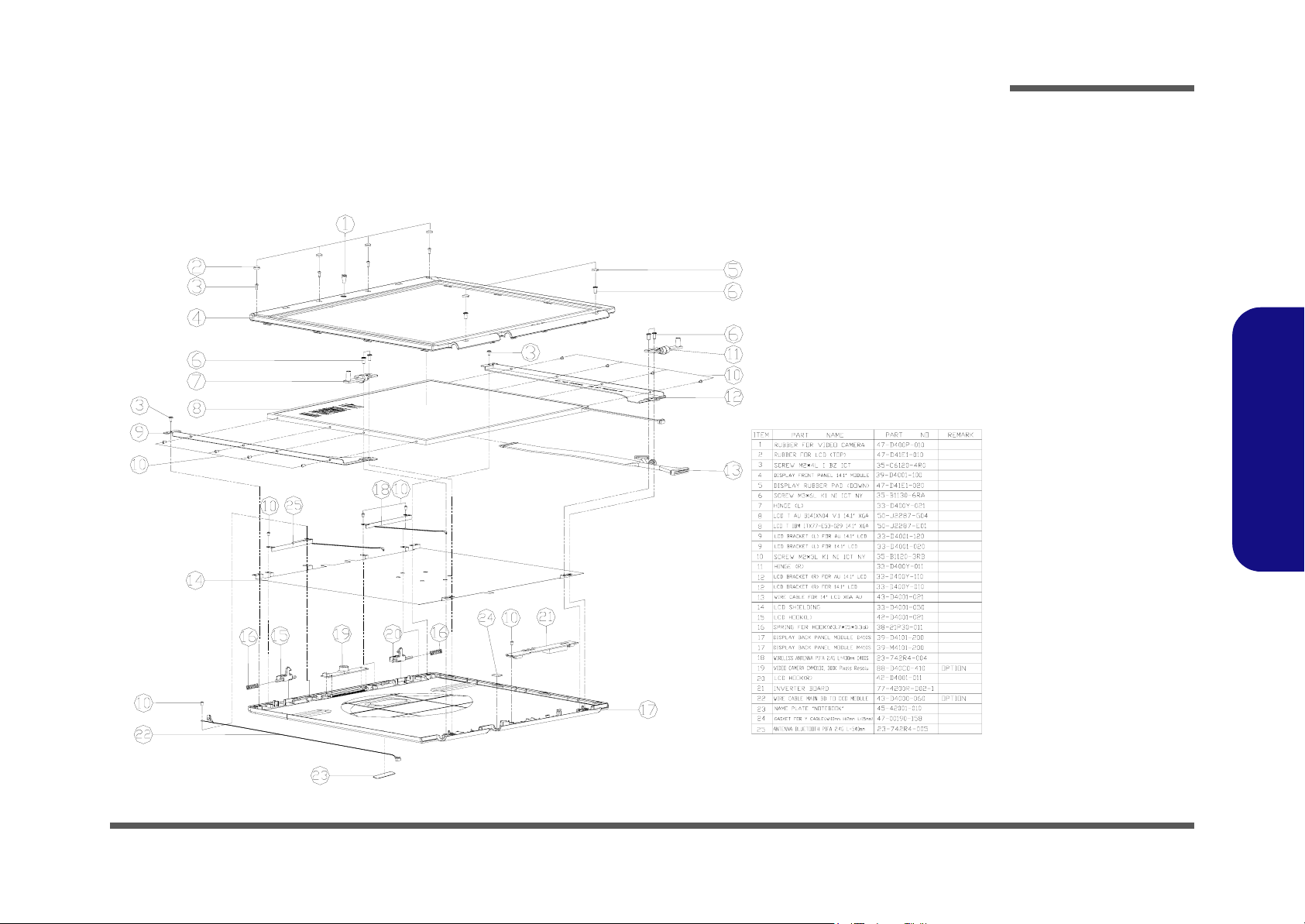
Figure 3
LCD 14" (D400E)
A.Part Lists
LCD 14" (D400E) A - 5
Page 67

Part Lists
LCD 15" (D400E)
A.Part Lists
LCD 15" (D400E)
Figure 4
A - 6 LCD 15" (D400E)
Page 68

CD-ROM Drive (D400E)
Part Lists
Figure 5
CD-ROM Drive
(D400E)
A.Part Lists
CD-ROM Drive (D400E) A - 7
Page 69

Part Lists
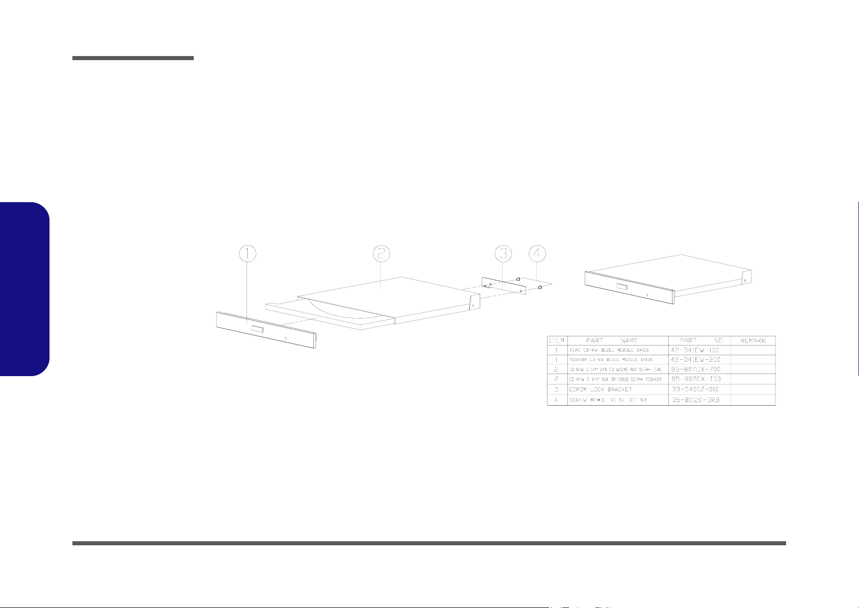
CD-RW Drive
A.Part Lists
CD-RW Drive (D400E)
Figure 6
(D400E)
A - 8 CD-RW Drive (D400E)
Page 70

Combo Drive (D400E)
Part Lists
Figure 7
Combo Drive
(D400E)
A.Part Lists
Combo Drive (D400E) A - 9
Page 71

Part Lists
DVD-ROM Drive
A.Part Lists
DVD-ROM Drive (D400E)
Figure 8
(D400E)
A - 10 DVD-ROM Drive (D400E)
Page 72
Floppy Disk Drive (D400E)
Part Lists
Figure 9
Floppy Disk Drive
(D400E)
A.Part Lists
Floppy Disk Drive (D400E) A - 11
Page 73

Part Lists
Figure 10
HDD Drive (D400E)
A.Part Lists
Hard Disk Drive (D400E)
A - 12 Hard Disk Drive (D400E)
Page 74
Top (D410E)
Part Lists
Figure 11
Top (D410E)
A.Part Lists
Top (D410E) A - 13
Page 75

Part Lists
Bottom (D410E)
A.Part Lists
Bottom (D410E)
Figure 12
A - 14 Bottom (D410E)
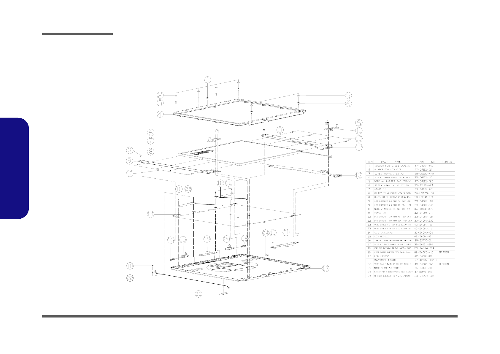
Page 76
LCD 14" (D410E)
Part Lists
Figure 13
LCD 14" (D410E)
A.Part Lists
LCD 14" (D410E) A - 15
Page 77
Part Lists
LCD 15" (D410E)
A.Part Lists
LCD 15" (D410E)
Figure 14
A - 16 LCD 15" (D410E)
Page 78

CD-ROM Drive (D410E)
Part Lists
Figure 15
CD-ROM Drive
(D410E)
A.Part Lists
CD-ROM Drive (D410E) A - 17
Page 79
Part Lists
Figure 16
CD-RW Drive
A.Part Lists
CD-RW Drive (D410E)
(D410E)
A - 18 CD-RW Drive (D410E)
Page 80

Combo Drive (D410E)
Part Lists
Figure 17
Combo Drive
(D410E)
A.Part Lists
Combo Drive (D410E) A - 19
Page 81

Part Lists
Figure 18
DVD-ROM Drive
A.Part Lists
DVD-ROM Drive (D410E)
(D410E)
A - 20 DVD-ROM Drive (D410E)
Page 82

Floppy Disk Drive (D410E)
Part Lists
Figure 19
Floppy Disk Drive
(D410E)
A.Part Lists
Floppy Disk Drive (D410E) A - 21
Page 83

Part Lists
Figure 20
HDD Drive (D410E)
A.Part Lists
Hard Disk Drive (D410E)
A - 22 Hard Disk Drive (D410E)
Page 84

Appendix B:Schematic Diagrams
This appendix has circuit diagrams of the D400E/D410E notebook’s PCB’s. The following table indicates where to find
the appropriate schematic diagram.
Schematic Diagrams
Diagram - Page Diagram - Page Diagram - Page
System Block Diagram - Page B - 2 962 (USB I/F) 3 of 4 - Page B - 16 Fan Control and SpeedStep - Page B - 30
Socket 478 1 of 2 - Page B - 3 962 (Power & RTC) 4 of 4 - Page B - 17 Mobility M9-P - Page B - 31
Socket 478 & ITP 2 of 2 - Page B - 4 HDD/Combo Connector - Page B - 18 Mobility M9-P MEM A/B - Page B - 32
Clock Generator - Page B - 5 USB Port - Page B - 19 VGA DRAM 1 of 2 - Page B - 33
M645DX (Host/AGP) 1 of 4 - Page B - 6 PCMCIA ENE CB1410 - Page B - 20 VGA DRAM 1 of 2 - Termination - Page B - 34
M645DX (Memory for DDR) 2 of 4 - Page B - 7 PCMCIA Power - Page B - 21 VGA DRAM 2 of 2 - Page B - 35
M645DX (& CRT Out) 3 of 4 - Page B - 8 1394 PHY TSB41LV01 - Page B - 22 Mobility M9-P POW - Page B - 36
M645DX (Power) 4 of 4 - Page B - 9 LPC Super I/O - Page B - 23 Mobility M9-P - Page B - 31
DDR Memory DIMM - Page B - 10 LPT/COM Port - Page B - 24 DDR Power - Page B - 38
DDR SSTL-2 Termination - Page B - 11 LPC H8 - Page B - 25 System Power - Page B - 39
LVDS Interface (SiS302LV) - Page B - 12 LAN RTL8100BL - Page B - 26 Charger - Page B - 40
Panel Con & LED Indicator - Page B - 13 Audio Codec ALC201A - Page B - 27 SW Board and HotKey - Page B - 41
962 (PCI/IDE/HyperZip) 1 of 4 - Page B - 14 Audio Out & Off Board Connectors - Page B - 28 TouchPad and Switch Board - Page B - 42
962 (Misc Signals) 2 of 4 - Page B - 15 System Power Control - Page B - 29
Table 1
Schematic
Diagrams
B.Schematic Diagrams
B-1
Page 85

Schematic Diagrams
System Block Diagram
Sheet 1 of 41
System Block
Diagram
B.Schematic Diagrams
PANEL
TV-OUT
PANEL
HDD/CD-ROM CON
BLUE BOOTH
USB PORT
Video Camera
Wireless LAN
2/16/32
DDRAM
VGATV-OUT
ATI M9
2/16/32
DDRAM
SiS 302LV
CRT PORT
MODEM
AGP Bus
66MHz
AB
VB-LINK
RGB
Ultra 66/100/133
USB 2.0 I/F
AC ' 97 I/F
AUDIOMDC CODEC
ALC201A RTL8100BL
NORTHWOOD
SOCKET - 478
Host Bus
GTL+ & AGTL
SiS M645DX
702 mBGA
MuTIOL
SiS 962
371 mBGA
LPC I/F
GENERATOR
Realtek
CLOCK
DDR INTERFACE
DIMM1
M I II/F
PCI I/F
CardBus
ENE 1410
Rtt
DIMM2
1394 PHY
TSB41LV01
B - 2
INT.KB
EXT.KB
EXT.PS2
KBC H8
H8S-2149 HM
TOUCH PAD
LPC Super I/O
NS PC87393
XBUS
FLASH ROM
FDD CONCOM/PRT PORT IR
Page 86
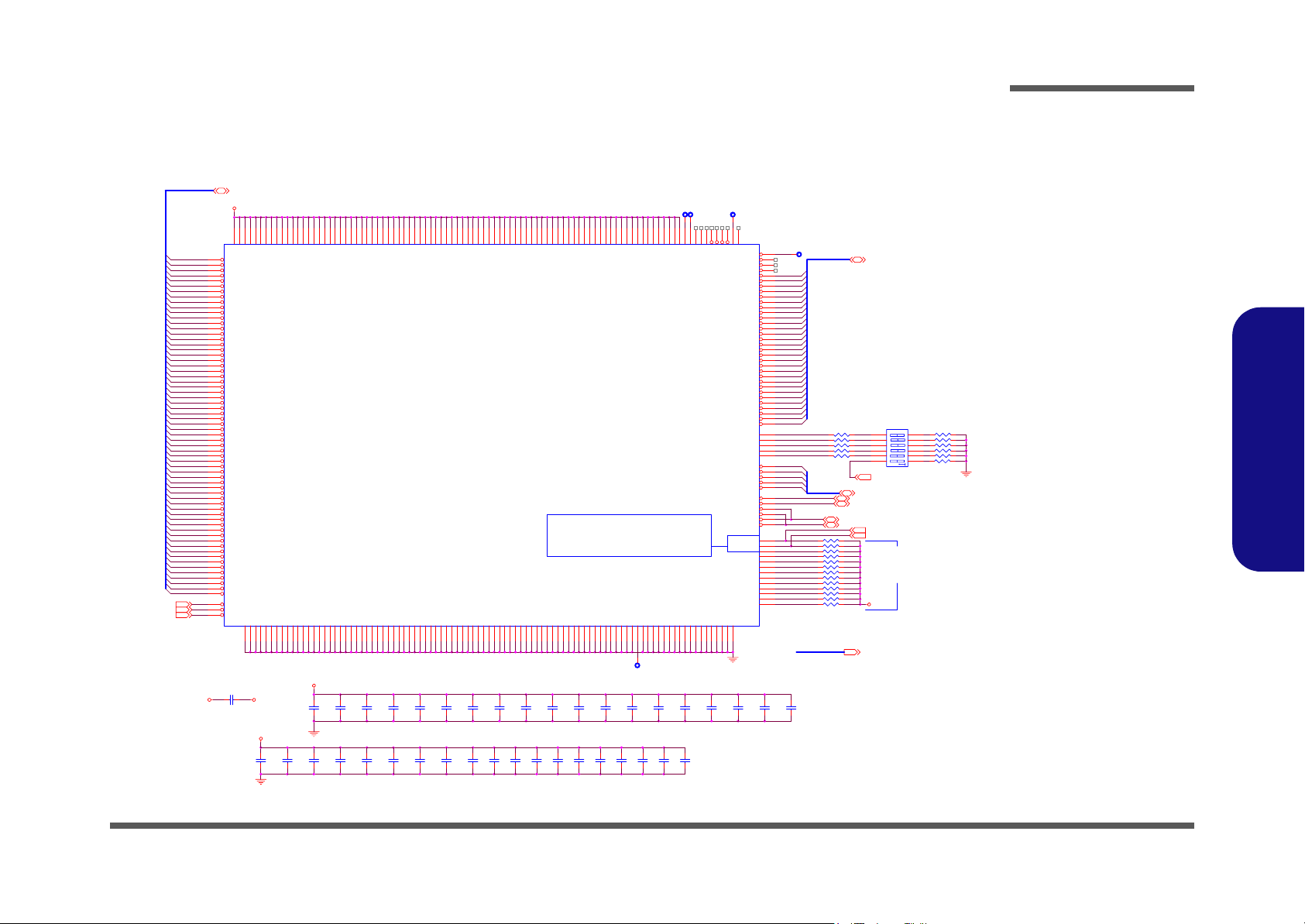
Socket 478 1 of 2
Schematic Diagrams
HD#[0..63]
VCC_CORE
JCPU1A
HD#0
B21
D0
HD#1
B22
D1
HD#2
A23
D2
HD#3
A25
D3
HD#4
C21
D4
D22
HD#5
D5
HD#6
B24
D6
HD#7
C23
D7
HD#8
C24
D8
HD#9
B25
D9
HD#10
G22
D10
HD#11
H21
D11
HD#12
C26
D12
D23
HD#13
D13
J21
HD#14
D14
HD#15
D25
D15
H22
HD#16
D16
HD#17
E24
D17
HD#18
G23
D18
F23
HD#19
D19
F24
HD#20
D20
E25
HD#21
D21
F26
HD#22
D22
HD#23
D26
D23
L21
HD#24
D24
HD#25
G26
D25
HD#26
H24
D26
M21
HD#27
D27
L22
HD#28
D28
HD#29
J24
D29
K23
HD#30
D30
HD#31
H25
D31
M23
HD#32
D32
N22
HD#33
D33
P21
HD#34
D34
M24
HD#35
D35
N23
HD#36
D36
M26
HD#37
D37
N26
HD#38
D38
N25
HD#39
D39
R21
HD#40
D40
P24
HD#41
D41
R25
HD#42
D42
R24
HD#43
D43
T26
HD#44
D44
T25
HD#45
D45
T22
HD#46
D46
T23
HD#47
D47
U26
HD#48
D48
U24
HD#49
D49
U23
HD#50
D50
V25
HD#51
D51
U21
HD#52
D52
V22
HD#53
D53
V24
HD#54
D54
W26
HD#55
D55
Y26
HD#56
D56
W25
HD#57
D57
Y23
HD#58
D58
Y24
HD#59
D59
Y21
HD#60
D60
AA25
HD#61
D61
AA22
HD#62
D62
AA24
HD#63
D63
RS#0
RS#1
RS#2
F1
RS0
G5
RS1
F4
RS2
RS#05
RS#15
RS#25
VCC_CORE +2.5V
HD#[0..63]5
A10
A12
A14
VCC
VCC
H1H4H23
C683
0.1UF
VCC_CORE
A16
A18
A20A8AA10
AA12
AA14
AA16
AA18
AA8
AB11
AB13
AB15
AB17
AB19
AB7
AB9
AC10
AC12
AC14
AC16
AC18
AC8
AD11
AD13
AD15
AD17
AD19
AD7
AD9
AE10
AE12
AE14
AE16
AE18
AE20
AE6
AE8
AF11
AF13
AF15
AF17
AF19
AF2
AF21
AF5
AF7
AF9
B11
B13
B15
B17
B19B7B9
C10
C12
C14
C16
C18
C20C8D11
D13
D15
D17
D19D7D9
E10
E12
VCC
VCC
VCC
VCC
VCC
VCC
VCC
VCC
VCC
VCC
VCC
VCC
VCC
VCC
VCC
VCC
VCC
VCC
VCC
VCC
VCC
VCC
VCC
VCC
VCC
VCC
VCC
VCC
VCC
VCC
VCC
VCC
VCC
VCC
VCC
VCC
VCC
VCC
VCC
VCC
VCC
VCC
VCC
VCC
VCC
VCC
VCC
VCC
VCC
VCC
VCC
VCC
VCC
VCC
VCC
VCC
VCC
VCC
VCC
VCC
VCC
VCC
VCC
VCC
VCC
VCC
VCC
VCC
VCC
VCC
VCC
VCC
INTEL P4 CPU SOCKET 478 PART 1
MOBIL CPU
AD25=DPSLP(H_DPSLP#)
A6=GHI#(PM_CPUPERF#)
VSS
VSS
VSS
VSS
VSS
VSS
VSS
VSS
VSS
VSS
VSS
VSS
VSS
VSS
VSS
VSS
VSS
VSS
VSS
VSS
VSS
VSS
VSS
VSS
VSS
VSS
VSS
VSS
VSS
VSS
VSS
VSS
VSS
VSS
VSS
VSS
VSS
VSS
VSS
VSS
VSS
VSS
VSS
VSS
VSS
VSS
VSS
VSS
VSS
VSS
VSS
VSS
VSS
VSS
VSS
VSS
VSS
VSS
VSS
VSS
VSS
VSS
VSS
VSS
VSS
VSS
VSS
VSS
VSS
VSS
VSS
H26
A11
A13
A15
A17
A19
A21
A24
A26A3A9
AA1
AA11
AA13
AA15
AA17
AA19
AA23
AA26
AA4
AA7
AA9
AB10
AB12
AB14
AB16
AB18
AB20
AB21
AB24
AB3
AB6
AB8
AC11
AC13
AC15
AC17
AC19
AC2
AC22
AC25
AC5
AC7
AC9
AD1
AD10
AD12
AD14
AD16
AD18
AD21
AD23
AD4
AD8
AE11
AE13
AE15
AE17
AE19
AE22
VCC_CORE
C348
C312
10U(0805)
C416
10U(0805)
C389
10U(0805)
C328
10U(0805)
C315
10U(0805)
C314
10U(0805)
C325
10U(0805)
C340
10U(0805)
C347
10U(0805)
10U(0805)
C345
10U(0805)
VSS
AE24
AE26
AE7
AE9
AF1
AF10
AF12
AF14
AF16
C324
C391
10U(0805)
10U(0805)
T
T
E14
E16
E18
E20E8F11
F13
F15
F17
F19
F9
A7
A22
VCC
VSS
AF6
AF8
C126
10U(0805)
VCC
VCC
VSS
VSS
B10
B12
VCC
VSS
B14
VCC
VCC
VSS
VSS
B16
C111
10U(0805)
VCC
VSS
B18
B20
NCNCNCNCNCNCNC
VCC
VSS
VSS
B23
B26B4B8
VCC
VCC
VCC
VSS
VSS
SKTOCC#
AF18
AF20
AF26
T
AD2
AD3
VSS
VSS
C98
10U(0805)
T
J26
K25
K26
L25
AE21
AF24
AF25
AB1
A35
DEP0
DEP1
DEP2
DEP3
A34
A33
A32
A31
A30
A29
A28
A27
A26
A25
A24
A23
A22
A21
A20
A19
A18
A17
A16
A15
A14
A13
A12
A11
A10
A9
A8
A7
A6
A5
A4
A3
VID0
VID1
VID2
VID3
VID4
REQ4
REQ3
REQ2
REQ1
REQ0
BPM5
BPM4
BPM3
BPM2
BPM1
BPM0
DPSLP#
GHI#
TESTHI10
TESTHI9
TESTHI8
TESTHI7
TESTHI6
TESTHI5
TESTHI4
TESTHI3
TESTHI2
TESTHI1
TESTHI0
VSS
VSS
VSS
VSS
VSS
VSS
VSS
NORTHWOOD478
C11
C13
C15
C17
C19
C2
C99
C31
10U(0805)
10U(0805)
T
HA#31
HA#30
HA#29
HA#28
HA#27
HA#26
HA#25
HA#24
HA#23
HA#22
HA#21
HA#20
HA#19
HA#18
HA#17
HA#16
HA#15
HA#14
HA#13
HA#12
HA#11
HA#10
HA#9
HA#8
HA#7
HA#6
HA#5
HA#4
HA#3
HREQ#4
HREQ#3
HREQ#2
HREQ#1
HREQ#0
HBPRM5#
HBPRM4#
C45
10U(0805)
HA#[3..31]
HREQ#[0..4]
HBPM1#
HBPM0#
H_DPSLP#
PM_CPUPERF#
R245
R279
R320
R326
R325
R259
R260
R246
R248
R261
R262
R321
R247
VID[0..4]
R518
R519
R520
R521
R522
0
0
0
0
0
HREQ#[0..4]5
HBPRM5# 3
HBPRM4# 3
HBPM1# 3
HBPM0# 3
51
51
51
51
51
51
51
51
51
51
51
51
51
HA#[3..31] 3,5
SWEB8
VID0
6
VID1
5
VID2
4
VID3
3
VID4
2
1
SW DIP-6
Vup 36
H_DPSLP#29,36
PM_CPUPERF#15
Design Guide
updates for
P4P/845
VCC_CORE
VID[0..4] 15,36
7
8
9
10
11
12
R523 51
R524 51
R525 51
R526 51
R527 51
R648 51
B.Schematic Diagrams
Sheet 2 of 41
Socket 478 1 of 2
Y1
W2
V3
U4
T5
W1
R6
V2
T4
U3
P6
U1
T2
R3
P4
P3
R2
T1
N5
N4
N2
M1
N1
M4
M3
L2
M6
L3
K1
L6
K4
K2
AE5
AE4
AE3
AE2
AE1
H3
J3
J4
K5
J1
AB4
AA5
Y6
AC4
AB5
AC6
AD25
A6
Y3
W4
U6
AB22
AA20
AC23
AC24
AC20
AC21
AA2
AD24
C341
0.1UF
C417
0.1UF
C418
0.1UF
C343
0.1UF
C388
0.1UF
C300
0.1UF
C342
0.1UF
C327
0.1UF
C329
0.1UF
C344
0.1UF
C311
0.1UF
C310
0.1UF
C326
0.1UF
C339
0.1UF
C350
0.1UF
C109
0.1UF
C386
0.1UF
C390
0.1UF
C110
0.1UF
Socket 478 1 of 2 (71-M4000-D03) B - 3
Page 87

Schematic Diagrams
Sheet 3 of 41
Socket 478 & ITP
2 of 2
B.Schematic Diagrams
Socket 478 & ITP 2 of 2
VCC_CORE
HCLK-CPU
HCLK-CPU#
DBI#[0..3]5
L69
4.7uH_SMD_30%
1 2
1 2
L71
4.7uH_SMD_30%
RP40 4P2R-0(R)
HCLK-CPU4
HCLK-CPU#4
HDSTBP#35
HDSTBP#25
HDSTBP#15
HDSTBP#05
HDSTBN#35
HDSTBN#25
HDSTBN#15
HDSTBN#05
C318
47U/16V
4
DBI#[0..3]
HASTB#15
HASTB#05
NMI15
INTR15
R42
R243 51.1_1%
HCLK-ITP0
1
HCLK-ITP0#
23
DBI#3
DBI#2
DBI#1
DBI#0
HASTB#1
HASTB#0
DBRESET
NMI
INTR
HCLK-CPU
HCLK-CPU#
51.1_1%
HDSTBP#3
HDSTBP#2
HDSTBP#1
HDSTBP#0
HDSTBN#3
HDSTBN#2
HDSTBN#1
HDSTBN#0
C317
47U/16V
JCPU1B
AE23
AD20
AD22
AC26
AD26
V21
P26
G25
E21
R5
AE25
E5
D1
AF22
AF23
P1
L24
W23
P23
J23
F21
W22
R22
K22
E22
A5
T
A4
T
E11
E13
E15
E17
E19
E23
E26
E4
E7
E9
F10
F12
F14
F16
F18
F2
F22
F25
F5
F8
G21
G24
G3 R4
CPURST#
C25C5C7C9D10
D12
D14
D16
D18
D20
D21
D24D3D6
VSS
VSS
VSS
VSS
VSS
VSS
VSS
VSS
VSS
VSS
VSS
VSS
VSS
+3V
VSS
VSS
VSS
L26L4M2
R686
2N7002(R)
1K(R)
C
Q37
E
MMBT3904(R)
VSS
VSS
VSS
VSS
M22
M25M5N21
Q36
G
VCCIOPLL
VCCA
VSSA
ITP_CLK0
ITP_CLK1
DB#3
DB#2
DB#1
DB#0
ADSTB1
L5
ADSTB0
DBRESET
LINT1
LINT0
BCLK0
BCLK1
COMP1
COMP0
STBP3
STBP2
STBP1
STBP0
STBN3
STBN2
STBN1
STBN0
VCC_SENSE
VSS_SENSE
VSS
VSS
VSS
VSS
VSS
VSS
VSS
VSS
VSS
VSS
VSS
VSS
VSS
VSS
VSS
VSS
VSS
VSS
VSS
VSS
VSS
VSS
VSS VSS
VSS
VSS
VSS
VSS
VSS
VSS
K24K3K6L1L23
J2
J22
J25J5K21
G6
B
R687 4.7K(R)
D8
E1
VSS
VSS
VSS
VSS
VSS
VSS
VSS
VSS
N24N3N6P2P22
Disable HT function
DS
L< 0.1 inch
C22
VSS
VSS
VSS
VSS
VSS
F6
F20
AA6
AA21
GTLREF2
GTLREF1
GTLREF0
VSS
VSS
VSS
P25
P5
R1
HA#31 2,5
CPUGTLVREFA
CPUGTLVREFB
IERR
MCERR
FERR
GTLREF3
STPCLK
BINIT
INIT
RSP
DBSY
DRDY
TRDY
ADS
LOCK
BR0
BNR
HITM
BPRI
DEFER
TCK
TMS
TRST
TDO
PROCHOT
IGNNE
A20M
SLP
PWRGOOD
RESET
THERMDA
THERMDC
THERMTRIP
BSEL0
BSEL1
AP0
AP1
VCCVID
VCCVIDPRG
VSS
VSS
VSS
VSS
VSS
VSS
VSS
VSS
VSS
VSS
VSS
VSS
VSS
VSS
VSS
VSS
VSS
VSS
VSS
VSS
VSS
VSS
VSS
R23
R26
VCC_CORE
49.9_1%
R275
R63 49.9_1%
C316
C313
220P
220P
IERR
AC3
V6
FERR#
B6
STPCLK#
Y4
AA3
INIT#
W5
AB2
DBSY#
H5
DRDY#
H2
HTRDY#
J6
ADS#
G1
HLOCK#
G4
BREQ0#
H6
BNR#
G2
HIT#
F3
HIT
HITM#
E3
BPRI#
D2
DEFER#
E2
HTCK
D4
HTDI
C1
TDI
HTMS
F7
HTRST#
E6
HTDO
D5
PROCHOT#
C3
IGNNE#
B2
SMI#
B5
SMI
A20M#
C6
CPUSLP#
AB26
CPUPWRGD
AB23
CPURST#
AB25
THERMDA
B3
THERMDC
C4
THERMTRIP#
A2
AD6
AD5
AC1
V5
AF4
AF3
T
Y5
Y25
Y22
Y2
W6
W3
W24
W21
V4
V26
V23
V1
U5
U25
U22
U2
T6
T3
T24
T21
ALERT#27
C330
1UF
T
T
T
VCCVID
THERMDA
THERMDC
+3V
BSEL0 4
BSEL1 4
1 2
C385 0.1UF
ALERT#
R317 10K
R276
100_1%
FERR# 15
STPCLK# 15
INIT# 15
DBSY# 5
DRDY# 5
HTRDY# 5
ADS# 5
HLOCK# 5
BREQ0# 5
BNR# 5
HIT# 5
HITM# 5
BPRI# 5
DEFER# 5
IGNNE# 15
SMI# 15
A20M# 15
CPUSLP# 15
CPUPWRGD 5
CPURST# 5
20
mils
C80
2200P
C346
220P
SENSE_VCC
U27
2
VCC
3
DXP
4
DXN
11
ALERT#
7
GND
8
GND
EN1617
C349
220P
VCC_CORE
C323
0.1UF
C113
0.1UF
R319 200
STBY#
SMBDATA
SMBCLK
ADD1
ADD0
NC/CRIT1
NC/CRIT0
NC/OS#
NC
NC
R64
C112
100_1%
1UF
C376
0.1UF
VCC_CORE
C387
0.1UF
R316
4.7K
T
T
T
T
T
C301
0.1UF
+3V VDD3
R156
R318
1K
4.7K
NEAR U18
R157
1K
HBPM0#2
HBPM1#2
HBPRM4#2
HBPRM5#2
TMP_SMDATA24
TMP_SMCLK24
C302
0.1UF
15
12
14
6
10
1
5
9
13
16
CPU SIGNAL TERMINALION
CLOSE TO CPU
FERR#
BREQ0#
PROCHOT#
CPUPWRGD
THERMTRIP#
A20M#
STPCLK#
CPUSLP#
SMI#
INIT#
IGNNE#
INTR
NMI
CPURST#
HTDO
IERR
DBRESET
HTMS
HCLK-ITP0
HCLK-ITP0#
ITP_STPWR
T
HBPM0#
HBPM1#
HBPRM4#
HBPRM5#
HTCK
ITP/TAP TERMINATION
CLOSE TO ITP PORT
ITP/TAP TERMINATION
CLOSE TO CPU
HTDI
HTRST#
NORTHWOOD478
R274
R56
R293
R270
R302
R273
R327
R256
R292 56_1%
R328 56_1%
R303 56_1%
R57 56_1%
R58 56_1%
R258 51_1%
R280
R297 10K
R257 150
R52
R219 51_1%
R218 51_1%
R244 1.5K
R284 51
R285
R298 51
R299 51
R50
R306
R51 680
62_1%
51_1%
62_1%
51_1%
62_1%
56_1%
56_1%
56_1%
75
40.2_1%
51
27.4_1%
VCC_CORE
150
VCC_CORE
B - 4 Socket 478 & ITP 2 of 2 (71-M4000-D03)
Page 88

Clock Generator
+3VS
L84
FCM2012V121
1 2
C401
C76
0.1UF
10UF/10V
R59
VTT
10K
R62
10K
PLEASE PLACE IN COMP SIDE
AND NEAR TOGETHER
C
B
E
+2.5VS
10U(0805)
+3VS
Frequency
Selection
R67 4.7K
R66 4.7K
R65 4.7K(R)
R61 4.7K(R)
R60 4.7K(R)
+3VS
R283
4.7K
BSEL1 BSEL0 Function
L L
L H
H L
H H
Q20
2N3904
C208
R296
4.7K
C85
0.1UF
+3VS+3VS
R43
10K
B
Clock Buffer (DDR)
C565
0.01UF
C84
0.1UF
C
E
FS0
FS1
FS2
FS3
FS4
BSEL0 3
BSEL1 3
C81
0.1UF
Q19
2N3904
+3VS
L33
1 2
FCM2012V121
C207
0.1UF
+2.5VS
C102
0.1UF
CPUSTP#15,29
1 2
C90
0.1UF
+3VS
C77
10UF/10V
L94
1 2
FCM1608K121
Main Clock Generator
U28
CLK_VCC3
C105
C103
C104
0.1UF
0.1UF
0.1UF
+3VS
R37
10K
D10
AC
1SS355
R45
475_1%
L21
FCM1608K121
C83
0.1UF
C78
C86
0.01UF
0.1UF
BUFFERVCC
C532
C523
0.1UF
10U(0805)
BUF_2.5VS
C560
C549
10U(0805)
0.01UF
FWDSDCLKO6
+2.5V
+1.8VS
FS4 FS3 FS2 FS1 FS0
0 0 0 1 1
FWDSDCLKO
C684
0.1UF
0 0 0 0 1 100M 100M 66M 66M 33M
1
11
13
19
28
29
42
48
12
5
8
18
24
25
32
41
46
45
33
38
36
C82
0.01UF
37
ICS 952001
CY 28342
C550
C557
0.1UF
0.1UF
C556
0.1UF
SMBCLK
SMBDAT
FB_IN
T
T
T
CLOCK GEN (650)
VDDREF
VDDZ
VDDPCI
VDDPCI
VDD48
VDDAGP
VDDCPU
VDDSD
PCI_STOP#
VSSREF
VSSZ
VSSPCI
VSSPCI
VSS48
VSSAGP
VSSCPU
VSSSD
CPU_STOP#
PD#/VTT_PWRGD
IREF
VDDA
VSSA
24_48M/MULTISEL
XIN
6
Y5
1 2
14.318MHz
C92
10PF
U29
CLOCK BUFFER (DDR48)
3
VDD
12
VDD
23
VDD
10
AVDD
7
SCLK
22
SDATA
8
CLK_IN
20
FB_IN
9
NC
18
NC
21
NC
ICS 93722
CY28352
CPU SDRAM ZCLK AGP PCI
100M 133M 66M 66M 33M
CPUCLK0
CPUCLK#0
CPUCLK1
CPUCLK#1
SDCLK
AGPCLK0
AGPCLK1
ZCLK0
ZCLK1
PCICLK_F0/FS3
PCICLK_F1/FS4
PCICLK0
PCICLK1
PCICLK2
PCICLK3
PCICLK4
PCICLK5
REF0/FS0
REF1/FS1
REF2/FS2
SDATA
XOUT
7
CLK0
CLK#0
CLK1
CLK#1
CLK2
CLK#2
CLK3
CLK#3
CLK4
CLK#4
CLK5
CLK#5
FB_OUT
GND
GND
GND
GND
SCLK
40
39
44
43
47
31
30
9
10
14
15
16
17
20
21
22
23
2
3
4
27
48M
MULTISEL
26
SMBCLK
35
SMBDAT
34
C91
10PF
2
1
4
5
13
14
17
16
24
25
26
27
FB_OUT
19
28
15
11
6
CPU-1
RP44
CPU-2
CPU-3
RP43
CPU-4
SD-1
AGP-1
AGP-2
ZIP-1
ZIP-2
FS3
FS4
PCI-2
PCI-3
PCI-4
PCI-5
PCI-6
FS0
FS1
FS2
USB-1
RP75 4P2R-0123
4
RP76 4P2R-01
4
RP77 4P2R-0
2 3
1
RP62 4P2R-01
2 3
RP61 4P2R-0
2 3
1
RP60 4P2R-0
2 3
1
NEAR DDR SODIMM
Damping Resistors
Place near to the
Clock Outputs
1
4
2 3
4P2R-33
1
4
2 3
4P2R-33
R309 22
R310
22
R311 22
R334 22
R335 22
R336
33
R337 33
R338 33
R339 33
R340 33
R341 33
R342 33
T
R331
33
R332 33
R333 33
R312
22
R313
22
SMBCLK 7,15
SMBDAT 7,15
R44
MULTISEL
DDRCLK3
DDRCLK#3
DDRCLK0
DDRCLK#0
23
DDRCLK2
DDRCLK#2
4
DDRCLK4
4
DDRCLK#4
DDRCLK1
DDRCLK#1
4
DDRCLK5
DDRCLK#5
4
R384
22
FB_IN
By-Pass Capacitors
Place near to the Clock Buffer
C533 10PF(R)
FB_IN
HCLK-CPU
HCLK-CPU#
HCLK-650
HCLK-650#
SDCLK
AGPCLK
AGPCLKATI
ZCLK0
ZCLK1
PCICLK961
PCICLK1394
PCICLKPCMPCI-1
PCICLKLAN
PCICLKIO
PCICLKH8
PCLK_80P
REFCLK0
REFCLK1
CLKAPIC
UCLK48M
SIO48M
T
0(R)
DDRCLK37
DDRCLK#37
DDRCLK07
DDRCLK#07
DDRCLK27
DDRCLK#27
DDRCLK47
DDRCLK#47
DDRCLK17
DDRCLK#17
DDRCLK57
DDRCLK#57
HCLK-CPU 3
HCLK-CPU# 3
HCLK-650 5
HCLK-650# 5
SDCLK 6
AGPCLK 5
AGPCLKATI 30
ZCLK0 9
ZCLK1 13
PCICLK961 13
PCICLKPCM 19
PCICLKLAN 25
PCICLKIO 22
PCICLKH8 24
PCLK_80P 20
14.381MHZ
REFCLK0 9
REFCLK1 15
CLKAPIC 15
48 MHZ
UCLK48M 16
SIO48M 22
By-Pass Capacitors
Place near to the Clock
Outputs
HCLK-CPU
R34
HCLK-CPU#
R33
HCLK-650
R36
HCLK-650#
R35
C75
SDCLK
C74
AGPCLK
C688
AGPCLKATI
C121 10PF(R)
ZCLK0
C120 10PF(R)
ZCLK1
C119
PCICLK961
C118 10PF(R)
PCICLK1394
C117 10PF(R)
PCICLKPCM
C116 10PF(R)
PCICLKLAN
C115 10PF(R)
PCICLKIO
C114
PCICLKH8
C73 10PF(R)
UCLK48M
10PF(R)
10PF(R)
10PF(R)
10PF(R)
10PF(R)
49.9_1%
49.9_1%
49.9_1%
49.9_1%
Schematic Diagrams
B.Schematic Diagrams
Sheet 4 of 41
Clock Generator
Clock Generator (71-M4000-D03) B - 5
Page 89

Schematic Diagrams
M645DX (Host/AGP) 1 of 4
Sheet 5 of 41
M650 (Host/AGP)
1 of 4
B.Schematic Diagrams
AAD18/AHSYNC30 AAD30/BHSYNC30
VTT
R264
20_1%
R263
113_1%
HPCVERF = 2/3 VCCP
HCLK-6504
HCLK-650#4
HLOCK#3
DEFER#3
HTRDY#3
CPURST#3
CPUPWRGD3
BPRI#3
BREQ0#3
RS#22
RS#12
RS#02
ADS#3
HITM#3
HIT#3
DRDY#3
DBSY#3
BNR#3
HREQ#42
HREQ#32
HREQ#22
HREQ#12
HREQ#02
HASTB#13
HASTB#03
HA#[3..31]2,3
VTT
C29
R272
150_1%
0.01UF
HNCVREF
C30
R271
75_1%
0.01UF
VTT
place this
C303
capacitor
R249
under 650 solder
75_1%
0.01UF
side
HVREF
C365
C304
R250
150_1%
C1XAVDD C4XAVDD
C1XAVSS C4XAVSS
0.01UF
FCM1608K121
9.06mA
C447
0.1UF
0.1UF
L89
1 2
C448
0.01UF
AAD17/AVSYNC30
HNCOMP
Rds-on(n) = 10 ohm
HNCVERF = 1/3 VCCP
HPCOMP
Rds-on(p) = 56 ohm
HCLK-650
HCLK-650#
HLOCK#
DEFER#
HTRDY#
CPURST#
CPUPWRGD
BPRI#
BREQ0#
RS#2
RS#1
RS#0
ADS#
HITM#
HIT#
DRDY#
DBSY#
BNR#
HREQ#4
HREQ#3
HREQ#2
HREQ#1
HREQ#0
HASTB#1
HASTB#0
HA#[3..31]
N19 N18 N13 N14
20MIL 20MIL 20MIL 20MIL
AJ26
AH26
U24
U26
V26
C20
D19
T27
U25
T24
T26
U29
V28
T28
U28
W26
V24
V27
W28
W29
W24
W25
Y27
AD24
AA24
HA#31
AF26
HA#30
AE25
HA#29 AGPCLK
AH28
HA#28
AD26
HA#27
AG29
HA#26
AE26
HA#25 A1XAVDD
AF28
HA#24 A1XAVSS
AC24
HA#23
AG28
HA#22 A4XAVDD
AE29
HA#21 A4XAVSS
AD28
HA#20
AC25
HA#19 AVREFGC
AD27
HA#18
AE28
HA#17
AF27
HA#16
AB24
HA#15 HDSTBN#3
AB26
HA#14 HDSTBN#2
AC28
HA#13 HDSTBN#1
AC26
HA#12 HDSTBN#0
AC29
HA#11
AA26
HA#10 HDSTBP#3
AB28
HA#9 HDSTBP#2
AB27
HA#8 HDSTBP#1
AA25
HA#7 HDSTBP#0
AA29
HA#6
AA28
HA#5
Y26
HA#4
Y24
HA#3
Y28
+3VS
C474
10UF/10V
R26 22(R)
AAD18/AHSYNC
AAD17/AVSYNC
CPUCLK
CPUCLK#
HLOCK#
DEFER#
HTRDY#
CPURST#
CPUPWRGD
BPRI#
BREQ0#
RS#2
RS#1
RS#0
ADS#
HITM#
HIT#
DRDY#
DBSY#
BNR#
HREQ#4
HREQ#3
HREQ#2
HREQ#1
HREQ#0
HASTB#1
HASTB#0
HA#31
HA#30
HA#29
HA#28
HA#27
HA#26
HA#25
HA#24
HA#23
HA#22
HA#21
HA#20
HA#19
HA#18
HA#17
HA#16
HA#15
HA#14
HA#13
HA#12
HA#11
HA#10
HA#9
HA#8
HA#7
HA#6
HA#5
HA#4
HA#3
HD#63
HD#62
B21
F19
A21
HD#61
HD#62
HD#63
10mA 10mA
C445
0.1UF
22(R)
R28
C1XAVSS
C1XAVDD
C4XAVDD
HPCOMP
C4XAVSS
AH25
AJ25
AH27
AJ27
C1XAVSS
C4XAVSS
C1XAVDD
HNCOMP
HVREF
U21
T21
P21
N21
J17
B20
B19
HVREF0
HVREF1
HVREF2
HVREF3
HVREF4
HPCOMP
HNCOMP
C4XAVDD
HOST
HD#61
HD#60
HD#59
HD#58
HD#57
HD#56
HD#55
HD#54
HD#53
HD#52
HD#51
HD#50
HD#49
HD#48
E19
D22
D20
B22
HD#58
HD#60
HD#59
FCM1608K121
1 2
C446
0.01UF
C22
HD#57
HD#56
L88
HD#47
B23
A23
D21
F22
D24
D23
C24
B24
E25
HD#51
HD#50
HD#53
HD#55
HD#54
HD#47
HD#52
HD#48
HD#49
+3VS +3VS +3VS
C473
10UF/10V
R17 22(R)
VAHSYNC 10
VAVSYNC 10
HNCVREF
ST2
ST1
ST0
AAD0
A19A7F9B7M6M5M4L3L6L4K6L2K3J3K4J2J6J4J1H6F4F1G6E3F5E2E4E1D3D4C2F7C3E6B2D5D6A3D7C5A5C6D8
ST0
ST1
ST2
VBD7/AAD0
HNCOMPVREF
AAD1
VBD6/AAD1
AAD2
VBD5/AAD2
AAD3
VBD4/AAD3
AAD4
VBD3/AAD4
AAD5
VBD2/AAD5
AAD6
CBD1/AAD6
AAD7
CBD0/AAD7
AAD8
VAD6/AAD8
AAD31/BVSYNC30
AAD9
VAD5/AAD9
AAD10
AAD30/BHSYNC
R25 22(R)
AAD31/BVSYNC
SBA7
SBA3
SBA4
SBA6
SBA5
AAD18/AHSYNC
AAD16/VADE
AAD13
AAD11
AAD17/AVSYNC
AAD14
AAD12
AAD15
AAD19
VAD4/AAD10
VAD7/AAD11
VAD8/AAD12
VAD9/AAD13
VADE/AAD16
VAD10/AAD14
VAD11/AAD15
VBD11/AAD19
VAVSYNC/AAD17
VAHSYNC/AAD18
AAD29/VBCTL1
AAD28/VBCTL0
AAD27/VBDE
AAD26
AAD22
AAD25
AAD24
AAD23
AAD21
AAD20
VBD10/AAD20
AAD30/BHSYNC
AAD31/BVSYNC
SBA7
SBA6
SBA5
SBA4
SBA3
VBD8/AAD21
VBD9/AAD22
VAD1/AAD23
VAD0/AAD24
VAD2/AAD25
VAD3/AAD26
VBDE/AAD27
VBCTL0AAD28
VBCTL1/AAD29
VBVSYNCAAD31
VBHSYNC/AAD30
AGP
M650-1
HD#46
HD#45
HD#44
HD#43
HD#42
HD#41
HD#40
HD#39
HD#38
HD#37
HD#36
HD#35
HD#34
HD#33
HD#32
HD#31
HD#30
HD#29
HD#28
HD#27
HD#26
HD#25
HD#24
HD#23
HD#22
HD#21
HD#20
HD#19
HD#18
HD#17
HD#16
HD#15
HD#14
HD#13
HD#12
HD#11
HD#10
HD#9
HD#8
HD#7
HD#6
HD#5
E23
D25
A25
C26
B26
B27
D26
B28
E26
F28
G25
F27
F26
G24
H24
G29
J26
G26
J25
H26
G28
H28
J24
K28
J29
K27
J28
M24
HD#37
HD#33
HD#34
HD#42
HD#45
HD#46
HD#43
HD#44
HD#41
A1XAVDD A4XAVDD
A1XAVSS
HD#31
HD#35
HD#36
HD#38
HD#30
HD#28
HD#29
HD#27
HD#26
HD#25
HD#24
C305
10UF/10V
HD#21
HD#20
HD#22
HD#23
HD#32
HD#40
HD#39
L72
FCM1608K121
1 2
C333
C332
0.1UF
0.01UF
L26
HD#18
HD#19
A4XAVSS
K26
L25
L28
M26
P26
HD#13
HD#14
HD#16
HD#17
HD#15
L29
HD#12
N24
N26
HD#10
HD#11
10mA
C335
0.1UF
M27
N28
P27
N29
HD#8
HD#9
HD#7
HD#6
FCM1608K121
1 2
C334
0.01UF
HD#4
R24
R28
HD#5
HD#4
L73
VBHSYNC 10
VBVSYNC 10
SBA0
SBA1
SBA2
C7
AC/BE#3
SBA2
SBA1
AC/BE#2
AC/BE#1
AC/BE#0
VBCLK/SBA0
VBCAD/AREQ#
AFRAME#
AIRDY#
ATRDY#
ADEVSEL#
ASERR#
ASTOP#
VBHCLK/RBF#
VGPIO2/WBF#
VGPIO3/PIPE#
SB_STB
SB_STB#
VAGCLK/AD_STB0
VAGCLKN/AD_STB#0
VBGCLK/AD_STB1
VBGCLKN/AD_STB#1
AGPCLK
AGPRCOMP
A1XAVDD
A1XAVSS
A4XAVDD
A4XAVSS
AGPVREF
AGPVSSREF
HDSTBN#3
HDSTBN#2
HDSTBN#1
HDSTBN#0
HDSTBP#3
HDSTBP#2
HDSTBP#1
HDSTBP#0
DBI#3
HD#3
HD#2
HD#1
HD#0
M28
P28
R26
R29
E21
A27
DBI#3
DBI#2
HD#0
HD#3
HD#1
HD#2
C306
10UF/10V
DBI#2
AGNT#
APAR
H27
DBI#1
BGA1A
NC
NC
NC
DBI#1
DBI#0
R25
DBI#0
HD#[0..63]
R18 22(R)
C26
NEAR SISM650
10PF(R)
F6
F3
H4
K5
C9
A6
G2
G1
G3
G4
H5
H1
H3
E8
F8
D9
D10
B3
C4
B5
A4
K1
L1
C1
D1
B10
AGPRCOMP
M1
B9
A9
B8
A8
M3
M2
F20
F23
K24
P24
F21
F24
L24
N25
SIS M650
DBI#[0..3]
AC/BE#3
AC/BE#2
AC/BE#1
AC/BE#0
AREQ#
AGNT#
AFRAME#
AIRDY#
ATRDY#
ADEVSEL#
ASERR#
ASTOP#
APAR
RBF#
WBF#
PIPE#
T
T
T
SB_STB
SB_STB#
AD_STB0
AD_STB#0
AD_STB1
AD_STB#1
VBCLK 10
R253 0(R)
AGNT# 30
AFRAME# 30
AIRDY# 30
ATRDY# 30
ADEVSEL# 30
ASTOP# 30
APAR 30
R265 0(R)
R266 0(R)
R252 0(R)
SB_STB 30
SB_STB# 30
22(R)
R40
22(R)
R21
AGPCLK 4
R41 60_1%
HDSTBN#[0..3]
HDSTBP#[0..3]
DBI#[0..3] 3
HD#[0..63] 2
VBCAD
VBCAD 10
R254 4.7K(R)
R251 4.7K(R)
PIN D1 CH7017 CONNECT TO VBGCLKN
SIS301LV NC BUT SIS301LV PULL
GND
VAGCLK
VBGCLK
VBHCLK
VBCAD
C383 0603(R)
C24 0603(R)
+3VS
VBHCLK 10
VBCAD 10
+3VS
VAGCLK 10
VBGCLK 10
SiS_AGP1.5/3.3
HDSTBN#[0..3] 3
HDSTBP#[0..3] 3
SiS_AGP1.5/3.3
R546 8.2K
R548 8.2K
R550 8.2K
R552 8.2K
R553 8.2K
R555 8.2K
R689 8.2K
R558 8.2K
R559 8.2K
R560 8.2K
R561 8.2K
R563 8.2K
R565 8.2K
R567 8.2K
R568 8.2K
R569 8.2K
R572 8.2K
R573 8.2K
Close M650
AAD16/VADE
AAD27/VBDE
AAD28/VBCTL0
AAD29/VBCTL1
ST[0..2]
AAD[0..15]
AAD[19..26]
SBA[0..7]
AC/BE#[0..3]
AREQ#
RBF#
WBF#
AD_STB[0..1]
AD_STB#[0..1]
SiS_AGP1.5/3.3
R38
200_1%
10mA
R39
300_1%
AFRAME#
ATRDY#
AIRDY#
ADEVSEL#
ASTOP#
ASERR#
AGNT#
RBF#
PIPE#
SB_STB
AD_STB0
AD_STB1
AREQ#
WBF#
APAR
SB_STB#
AD_STB#0
AD_STB#1
AAD16 10,30
AAD27 10,30
AAD28 10,30
AAD29 10,30
ST[0..2] 30
AAD[0..15] 10,30
AAD[19..26] 10,30
SBA[0..7] 30
AC/BE#[0..3] 30
AREQ# 30
RBF# 30
WBF# 30
AD_STB[0..1] 30
AD_STB#[0..1] 30
AVREFGC
C830
C79
10UF
0.1UF
Near SiSM650
B - 6 M645DX (Host/AGP) 1 of 4 (71-M4000-D03)
Page 90

M645DX (Memory for DDR) 2 of 4
Schematic Diagrams
Rs place close to DIMM1
MD4
RP46
MD5
DQM0
MD6
8P4R-10
MD13
RP47
DQM1
MD14
MD15
8P4R-10
MD3
RP16
MD8
MD12
MD7
8P4R-10
MD17
RP14
MD16
MD20
MD21
8P4R-10
DQM2
RP48
MD22
MD23
MD28
8P4R-10
MD29
RP49
DQM3
MD30
MD31
8P4R-10
MD36
RP52
MD37
DQM4
MD38
8P4R-10
MD39
RP53
MD44
MD45
DQM5
8P4R-10
MD46
RP54
MD47
MD52
MD53
8P4R-10
DQM6
RP55
MD54
MD55
MD60
8P4R-10
MD61
RP56
DQM7
MD62
MD63
8P4R-10
MD0
RP17
MD1 /RMD1
DQS0
MD2
8P4R-10
MD10
RP15
MD11
DQS1
MD9
8P4R-10
MD24
MD19
RP13
MD18
DQS2
8P4R-10
MD27
MD26
RP12
DQS3
MD25
8P4R-10
MD34
DQS4
RP9
MD33
8P4R-10
MD41
RP8
MD40
MD35
8P4R-10
MD48
MD49
RP7
MD43
MD42
8P4R-10
MD56
MD51
RP6
MD50
DQS6
8P4R-10
MD59
MD58
RP5
DQS7
MD57
8P4R-10
18
27
36
45
/RMD13
18
/RDQM1
27
/RMD14
36
/RMD15
45
18
27
36
45
/RMD17
18
/RMD16
27
/RMD20
36
/RMD21
45
18
27
36
45
/RMD29
18
/RDQM3
27
/RMD30
36
/RMD31
45
18
27
36
45
/RMD39
18
/RMD44
27
/RMD45
36
/RDQM5
45
18
27
36
45
/RDQM6
18
/RMD54
27
/RMD55
36
/RMD60
45
18
27
36
45
/RMD0
45
36
/RDQS0
27
/RMD2
18
18
27
36
45
18
27
36
45
18
27
36
45
18
27
36
45
18
27
36
45
18
27
36
45
18
27
36
45
18
27
36
45
/RMD[0..63]
/RDQM[0..7]
/RDQS[0..7]
/RMA[0..14]
/RCS#[0..5]
CKE[0..5]
/RMD4
/RMD5 MD1
/RDQM0
/RMD3
/RMD8
/RMD12
/RMD7
/RDQM2
/RMD22
/RMD23
/RMD28
/RMD36
/RMD37
/RDQM4
/RMD38
/RMD46
/RMD47
/RMD52
/RMD53
/RMD61
/RDQM7
/RMD62
/RMD63
/RMD10
/RMD11
/RDQS1
/RMD9
/RMD24
/RMD19
/RMD18
/RDQS2
/RMD27
/RMD26
/RDQS3
/RMD25
/RMD34
/RDQS4
/RMD33
/RMD32MD32
/RDQS5DQS5
/RMD41
/RMD40
/RMD35
/RMD48
/RMD49
/RMD43
/RMD42
/RMD56
/RMD51
/RMD50
/RDQS6
/RMD59
/RMD58
/RDQS7 DQM7
/RMD57
MD0
MD2
MD3/RMD6
MD4
MD5
MD6
MD7
DQM0
DQS0 MA0
MD8 MA1
MD9 MA2
MD10 MA3
MD11 MA4
MD12 MA5
MD13 MA6
MD14 MA7
MD15 MA8
DQM1 MA9
DQS1 MA10
MD16 MA11
MD17 MA12
MD18 MA13
MD19 MA14
MD20
MD21 SRAS#
MD22 SCAS#
MD23 SWE#
DQM2
DQS2
MD24
MD25
MD26
MD27
MD28
MD29
MD30
MD31
DQM3
DQS3
MD32 CKE0
MD33 CKE1
MD34 CKE2
MD35 CKE3
MD36 CKE4
MD37 CKE5
MD38 S3AUXSW#
MD39
DQM4
DQS4
MD40 SDCLK
MD41
MD42
MD43
MD44
MD45
MD46
MD47
DQM5 SDAVDD
DQS5
MD48 SDAVSS
MD49
MD50
MD51 DDRAVDD
MD52
MD53 DDRAVSS
MD54
MD55
DQM6
DQS6 DDRVREFA
MD56 DDRVREFB
MD57
MD58
MD59
MD60
MD61
MD62
MD63
DQS7
AJ23
AG22
AH21
AJ21
AD23
AE23
AF22
AF21
AD22
AH22
AD21
AG20
AE19
AF19
AE21
AD20
AD19
AH19
AF20
AH20
AF18
AG18
AH17
AD16
AD18
AD17
AF17
AJ17
AE17
AH18
AD14
AG14
AJ13
AE13
AJ15
AF14
AD13
AF13
AH13
AH14
AD10
AH10
AG10
AF10
AE9
AD8
AH9
AF9
AD9
AJ9
AH5
AG4
AE5
AH3
AG6
AF6
AF5
AF4
AH4
AJ3
AE4
AD6
AE2
AC5
AG2
AG1
AF3
AC6
AD4
AF2
AB6
AD3
AA6
AB3
AC4
AE1
AD2
AC1
AB4
AC2
/RMD[0..63] 7,8
/RDQM[0..7] 7,8
/RDQS[0..7] 7,8
/RMA[0..14] 7,8
/RCS#[0..5] 7,8
CKE[0..5] 7
BGA1B
MD0
MD1
MD2
MD3
MD4
MD5
MD6
MD7
DQM0
DQS0/CSB#0
MD8
MD9
MD10
MD11
MD12
MD13
MD14
MD15
DQM1
DQS1/CSB#1
MD16
MD17
MD18
MD19
MD20
MD21
MD22
MD23
DQM2
DQS2/CSB#2
MD24
MD25
MD26
MD27
MD28
MD29
MD30
MD31
DQM3
DQS3/CSB#3
MD32
MD33
MD34
MD35
MD36
MD37
MD38
MD39
DQM4
DQS4/CSB#4
MD40
MD41
MD42
MD43
MD44
MD45
MD46
MD47
DQM5
DQS5/CSB#5
MD48
MD49
MD50
MD51
MD52
MD53
MD54
MD55
DQM6
DQS6/CSB#6
MD56
MD57
MD58
MD59
MD60
MD61
MD62
MD63
DQM7
DQS7/CSB#7
SIS M650
M650-2
SRAS#
SCAS#
S3AUXSW#
SDCLK
FWDSDCLKO
SDRCLKI
SDAVDD
SDAVSS
DDRAVDD
DDRAVSS
DDRVREFA
DDRVREFB
DRAM_SEL
MA10
MA11
MA12
MA13
MA14
SWE#
CS#0
CS#1
CS#2
CS#3
CS#4
CS#5
CKE0
CKE1
CKE2
CKE3
CKE4
CKE5
+2.5V
R343
Rs place close to DIMM1
SDAVDD
SDAVSS
DDRAVDD
DDRAVSS
DDRVREFA
DDRVREFB
5.69mA
C108
0.1UF
8.76mA
C124
0.1UF
RP50 8P4R-08 1
T
10PF(R)
MA13
MA8
MA6
MA4
MA2
MA0
MA12
MA7
MA9
MA14
MA11
MA10
MA1
MA3
0
0
R330
SDCLK 4
FWDSDCLKO
R55 4.7K
7 2
653
RP51 8P4R-08 1
7 2
653
RP11 8P4R-0
8 1
7 2
653
RP10
8 1
7 2
653
/RSRAS#
/RSCAS#
/RSWE#
/RCS#0
/RCS#1
/RCS#2
/RCS#3
/RCS#4
/RCS#5
10K
+3V
AH11
MA0
AF12
MA1
AH12
MA2
AG12
MA3
AD12
MA4
AH15
MA5
AF15
MA6
AH16
MA7
AE15
MA8
AD15
MA9
AF11
AG8
AJ11
AG16
AF16
AH8
AJ7
AH7
AE7
AF7
AH6
AJ5
AF8
AD7
AB2
AA4
AB1
Y6
AA5
Y5
Y4
AA3
AD11
AE11
Y1
Y2
AA1
AA2
AJ19
AH2
W3
CS#0
CS#1
CS#2
CS#3
CS#4
CS#5
R329 22
C424
R355
R356 0
R106 0
R105
R357 0
R140 0
R116 0
R119 0
R120 0
R111 0
R110 0
T
4
4
4
8P4R-0
4
/RSRAS# 7,8
/RSCAS# 7,8
/RSWE# 7,8
S3AUXSW# 13,28
+3V
FWDSDCLKO 4
/RMA13
/RMA8
/RMA6
/RMA4
/RMA2
/RMA0
/RMA12
SRAS#
SCAS#
SWE#
/RMA5MA5
/RMA7
/RMA9
/RMA14
/RMA11
/RMA10
/RMA1
/RMA3
C454 10PF(R)
C455 10PF(R)
C471 10PF(R)
C450
0.01UF
C470
0.01UF
C457
0.01UF
C472
0.01UF
L25
FCM1608K121
1 2
C107
0.01UF
20MIL
L26
FCM1608K121
1 2
C125
0.01UF
20MIL
150_1%
B.Schematic Diagrams
R345
150_1%
Sheet 6 of 41
+2.5V
R344
150_1%
R346
150_1%
+3VS
C106
10UF/10V
N8
+3VS
C123
10UF/10V
N9
(Memory for DDR)
M650
2 of 4
M645DX (Memory for DDR) 2 of 4 (71-M4000-D03) B - 7
Page 91

Schematic Diagrams
Sheet 7 of 41
M650 & CRT Out
3 of 4
B.Schematic Diagrams
M645DX (& CRT Out) 3 of 4
BGA1C
SIS M650
C87
10UF/10V
+1.8VS
R30
G30
B30
+3VS
+3VS
ZAD[0..15]13
L22
FCM1608K121
1 2
N6
FCM1608K121
1 2
C93
10UF/10V
N7
FCM1608K121
1 2
C415
10UF/10V
N15
R
G
B
ROUT
GOUT
BOUT
+3VS
ZCLK04
ZUREQ13
ZDREQ13
ZSTB013
ZSTB#013
ZSTB113
ZSTB#113
+1.8VS
R47
150_1%
R46
150_1%
C95
0.1UF
20MIL
L24
10MIL
L85
10MIL
R693 0
R694 0
R695 0
R696 0(R)
R697 0(R)
R698 0(R)
A
ZCLK0
ZUREQ
ZDREQ
ZSTB0
ZSTB#0
ZSTB1
ZSTB#1
ZAD[0..15]
C399
0.1UF
ZVREF
C400
0.1UF
35.4mA
56
C94
R48
56
R49
0.01UF
6.49mA
C96
0.1UF
7.92mA
C413
C414
0.1UF
AC
AC
D2
DA204U
A
C
ZAD0
ZAD1
ZAD2
ZAD3
ZAD4
ZAD5
ZAD6
ZAD7
ZAD8
ZAD9
ZAD10
ZAD11
ZAD12
ZAD13
ZAD14
ZAD15
VDDZCMP
ZCMP_N
ZCMP_P
VSSZCMP
Z1XAVDD
C97
0.01UF
Z4XAVDD
0.01UF
Z4XAVSS
C7
22P
C
Z1XAVSS
R200
75
D3
DA204U
V3
ZCLK
U6
ZUREQ
U1
ZDREQ
T3
ZSTB0
T1
ZSTB#0
P1
ZSTB1
P3
ZSTB#1
T4
ZAD0
R3
ZAD1
T5
ZAD2
T6
ZAD3
R2
HyperZip
ZAD4
R6
ZAD5
R1
ZAD6
R4
ZAD7
P4
ZAD8
N3
ZAD9
P5
ZAD10
P6
ZAD11
N1
ZAD12
N6
ZAD13
N2
ZAD14
N4
ZAD15
U3
ZVREF
M650-3
V5
VDDZCMP
U4
ZCMP_N
U2
ZCMP_P
V6
VSSZCMP
W1
Z1XAVDD
W2
Z1XAVSS
V2
Z4XAVDD
V1
Z4XAVSS
C8
R199
R201
C6
22P
22P
75
75
AC
D21
DA204U
C
A
VGA
DACAVDD1
DACAVDD2
DACAVSS1
DACAVSS2
DCLKAVDD
DCLKAVSS
ECLKAVDD
ECLKAVSS
TESTMODE0
TESTMODE1
TESTMODE2
R4 FCM1608K121
R5 FCM1608K121
R3 FCM1608K121
HSYNC
VSYNC
VGPIO0
VGPIO1
CSYNC
RSYNC
PCIRST#
PWROK
VCOMP
VVBWN
DLLEN#
ENTEST
C243
22P
VOSCI
ROUT
GOUT
BOUT
LSYNC
INT#A
AUXOK
VRSET
TRAP0
TRAP1
C242
22P
C15
A12
B13
A13
F13
E13
D13
D12
E12
A11
F12
B11
Y3
W4
W6
E14
F14
B12
C13
C12
C14
D14
B15
A15
B14
A14
E11
C11
F11
A10
E10
D11
F10
C245
22P
FRED_10
FGRN_10
FBLU_10
R-OUT
G-OUT
B-OUT
Z0801
Z0802
DACAVDD
DACAVSS
DCLKAVDD
ECLKAVDD
ECLKAVSS
DLLEN#
TMODE0
TMODE1
TMODE2
TRAP0
TRAP1
ENTEST
REFCLK0
R690 0(R)
R691 0(R)
R692 0(R)
R232
R230
R231 100(R)
R229 100(R)
CSYNC
T
RSYNC
T
LSYNC
T
INTA#
PCIRST#
PWRGD
AUXOK
C19
VCOMP
C20
VVBWN
C18
0.1UF
VRSET
C21
0.01UF
C287
0.01UF
T
T
T
T
T
T
T
VJVGA1
CEN/VGA DSUB
1
2
3
4
T
5
6
7
8
REFCLK0 4
ROUT
GOUT
BOUT
33(R)
HSYNC
33(R)
VSYNC
DDC1CLK
DDC1DATA
INTA# 10,13,30
PCIRST# 10,13,14,20,22,24,30
PWRGD 15,26,29
AUXOK 15,24,27,28
0.1UF
0.1UF
L9
1 2
FCM1608K121
C17
1UF
R16
130_1%
L10
1 2
FCM1608K121
C22
0.1UF
1 2
FCM1608K121
C271
0.1UF
9
10
11
12
13
14
15
16
7.57mA
L52
18.07mA
10MIL
T
MID1_10
HS_10
VS_10
MID3_10
10MIL
17
84.8mA
N1
20MIL
+3VS
+3VS
N12
D1 F01J2E
C244
220P
+1.8VS
C13
10UF/10V
C265
10UF/10V
AC
NOTE: This page is for universal PCB design( suitable for both 645 or 650)
NB Hardware Trap Table
DLLEN#
DRAM_SEL
TRAP0
TRAP1
CSYNC
RSYNC
LSYNC
0
enable PLL
SDR
normal
TV selection, NTSC/PAL(0/1)
enable VB
enable VGA interface
enable panel link
RSYNC
ENTEST
PWRGD
AUXOK
C266
10UF/10V
R528
HSY30
R529
VSY30
+3VS
R530
4.7K
VGADDCDATA30
VGADDCCLK30
R207
2.2K(R)
R209
2.2K(R)
+5VS
R210
4.7K(R)
+5VS
FCM1608K121
L6
1 2
FCM1608K121
L45
1 2
FCM1608K121
L43
1 2
FCM1608K121
L44
1 2
C4
C3
C5
220P
220P
220P
disable PLL
DDR
NB debug mode
R233
R234 4.7K
C428
C442 0.1UF
+3VS
Q25
G
2N7002
S D
33
S D
33
G
+3VS
+3VS
R531
4.7K
R532
R533
R208
4.7K(R)
DDC1DATA
DDC1CLK
1
4.7K
0.1UF
Q26
2N7002
33
33
HSYNC
VSYNC
1(DDR)
+3VS
+5VS +5VS
1
D34
DA221(R)
3 2
+3VS
Q27
G
2N7002
S D
S D
G
Q28
2N7002
+3VS
embedded pull-low
(30~50K Ohm)Default
0
0 yes
0
0
1
0
1
D35
DA221(R)
3 2
HSYNC
VSYNC
R753 0
R754 0(R)
R534
6.8K
DDC1DATA
DDC1CLK
yes
yes
+5V+5VS
R535
6.8K
B - 8 M645DX (& CRT Out) 3 of 4 (71-M4000-D03)
Page 92
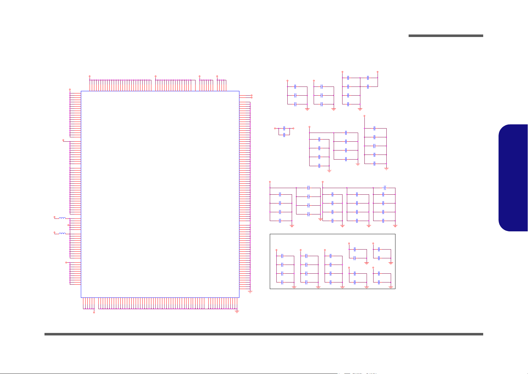
M645DX (Power) 4 of 4
Schematic Diagrams
+2.5V
+3VS
L131
BK2125HS121(R)
SiS_AGP1.5/3.3
+1.5VS
L132
BK2125HS121
+1.8VS
C449
1UF
C425
1UF
C436
0.1UF
C441
0.1UF
+1.8VS
C360
0.1UF
C374
0.1UF
10U(0805)
+1.5VS
+3VS
C382
0.1UF
C380
0.1UF
C398
C421
1UF
C371
0.1UF
+
C500 220U(D)
C451
1UF
C433
1UF
C434
0.1UF
C439
0.1UF
C407
0.1UF
C408
0.1UF
C397
0.1UF
C61
0.1UF
B.Schematic Diagrams
Sheet 8 of 41
M650 (Power)
4 of 4
C410
10UF/10V
C423
1UF
C395
0.1UF
+2.5V
C452
10U(0805)
C411
10U(0805)
C456
10U(0805)
C422
10U(0805)
C438
0.1UF
C435
0.1UF
C453
0.1UF
C437
0.1UF
+3VS
C27
10UF/10V
C44
1UF
C381
0.1UF
C367
0.1UF
C363
1UF
C357
1UF
C405
1UF
C366
1UF
+1.8VS +3V
C396
0.1UF
C378
10U(0805)
+1.5VS
C23
0.1UF
C28
0.1UF
VTT +1.8VS +3VS +3V
VTT
12
12
H21
H22
J16
J20
J21
J22
K16
K17
K18
K19
K20
K21
L20
M20
N20
P20
R20
R21
T20
U20
V20
W20
Y20
Y21
AA20
AA21
AA22
AB21
AB22
L12
L14
L15
L16
L18
M11
M19
N11
P19
R11
T19
U11
V19
W11
W13
W15
W17
P11
J14
J15
K15
K10
K12
K14
M10
W10
Y11
A16
VTT
A17
VTT
VTT
VTT
VTT
VTT
VTT
VTT
VTT
VTT
VTT
VTT
VTT
VTT
VTT
VTT
VTT
VTT
VTT
VTT
VTT
VTT
VTT
VTT
VTT
VTT
VTT
VTT
VTT
VSS
VSS
VSS
VSS
VSS
P15
P16
P17
P18
R12
VTT
IVDD
IVDD
IVDD
IVDD
M650-4
Power
VSS
VSS
VSS
VSS
VSS
VSS
VSS
VSS
VSS
R13
R14
R15
R16
R17
R18
T12
T13
T14
IVDD
IVDD
IVDD
IVDD
IVDD
IVDD
IVDD
IVDD
IVDD
IVDD
IVDD
IVDD
IVDD
OVDD
PVDDZ
VSS
VSS
VSS
VSS
VSS
VSS
VSS
VSS
VSS
VSS
VSS
VSS
VSS
VSS
VSS
VSS
T15
T16
T17
T18
U12
U13
U14
VSS
U15
U16
U17
U18
V12
V13
V14
V15
V16
V17
VTT
A18
VTT
B16
VTT
B17
VTT
B18
VTT
C16
VTT
C17
VTT
C18
VTT
D15
VTT
D16
VTT
D17
VTT
D18
VTT
E15
VTT
E16
VTT
E17
VTT
E18
VTT
F15
VTT
F16
VTT
F17
VTT
F18
VTT
AB5
VDDM
AD5
VDDM
AE6
VDDM
AE8
VDDM
AE10
VDDM
AE12
VDDM
AE14
VDDM
AE16
VDDM
AE18
VDDM
AE20
VDDM
AE22
VDDM
V10
VDDM
V11
VDDM
W18
VDDM
Y9
VDDM
Y10
VDDM
Y12
VDDM
Y14
VDDM
Y16
VDDM
Y18
VDDM
Y19
VDDM
AA8
VDDM
AA9
VDDM
AA10
VDDM
AA13
VDDM
AA14
VDDM
AA15
VDDM
AA16
VDDM
AA17
VDDM
AB8
VDDM
AB9
VDDM
AB13
VDDM
AB17
VDDM
E5
VDDQ
E7
VDDQ
E9
VDDQ
G5
VDDQ
J5
VDDQ
L5
VDDQ
H8
VDDQ
H9
VDDQ
J8
VDDQ
J9
VDDQ
J10
VDDQ
J13
VDDQ
K9
VDDQ
K11
VDDQ
K13
VDDQ
L10
VDDQ
N9
VDDQ
N10
VDDQ
N5
VDDZ
R5
VDDZ
U5
VDDZ
W5
VDDZ
P9
VDDZ
P10
VDDZ
R9
VDDZ
R10
VDDZ
T9
VDDZ
T10
VDDZ
T11
VDDZ
PVDDP
PVDDP
PVDDP
PVDDP
PVDDP
PVDDP
VSS
VSS
VSS
VSS
VSS
VSS
VSS
VSS
VSS
VSS
VSS
VSS
VSS
VSS
VSS
L17
L19
N19
R19
U19
W19
M12
M13
M14
M15
M16
M17
M18
N12
VSS
N13
N14
N15
N16
N17
N18
P12
P13
P14
OVDD
VSS
Y13
PVDD
PVDD
PVDD
PVDD
OVDD
PVDDM
PVDDM
VSS
VSS
VSS
VSS
VSS
VSS
VSS
V18
B25
C28
C29
D27
D28
E28
E29
Y15
PVDDM
PVDDM
VSS
VSS
AF23
Y17
AF24
PVDDM
VSS
VSS
AF25
AG24
AUX1.8
AUX3.3
VSS
AG26
BGA1D
U10
+1.8V
U9
+3V
A20
VSS
A22
VSS
A24
VSS
A26
VSS
C19
VSS
C21
VSS
C23
VSS
C25
VSS
C27
VSS
E20
VSS
E22
VSS
E24
VSS
F25
VSS
H25
VSS
K25
VSS
M25
VSS
P25
VSS
T25
VSS
V25
VSS
Y25
VSS
AB25
VSS
AD25
VSS
E27
VSS
G27
VSS
J27
VSS
L27
VSS
N27
VSS
R27
VSS
U27
VSS
W27
VSS
AA27
VSS
AC27
VSS
AE27
VSS
D29
VSS
F29
VSS
H29
VSS
K29
VSS
M29
VSS
P29
VSS
T29
VSS
V29
VSS
Y29
VSS
AB29
VSS
AD29
VSS
AF29
VSS
AE24
VSS
AG25
VSS
B4
VSS
B6
VSS
C8
VSS
C10
VSS
D2
VSS
F2
VSS
H2
VSS
K2
VSS
P2
VSS
T2
VSS
V4
VSS
AD1
VSS
AF1
VSS
AC3
VSS
AE3
VSS
AG3
VSS
AG5
VSS
AG7
VSS
AG9
VSS
AG11
VSS
AG13
VSS
AG15
VSS
AG17
VSS
AG19
VSS
AG21
VSS
AG23
VSS
AJ4
VSS
AJ6
VSS
AJ8
VSS
AJ10
VSS
AJ12
VSS
AJ14
VSS
AJ16
VSS
AJ18
VSS
AJ20
VSS
AJ22
VSS
AJ24
VSS
AG27
VSS
VSS
VSS
VSS
SIS M650
AH23
AH24
SiS_AGP1.5/3.3
+1.8V
10U(0805)
C681 0.1UF
+3VS
C682 0.1UF
C370
0.1UF
C25
0.1UF
C372
0.1UF
C373
10U(0805)
Place these capacitors under 650 solder
side
VTT
C392
0.1UF
C419
0.1UF
C364
0.1UF
C352
0.1UF
C412
C427
1UF
C426
0.1UF
+1.8VS
+1.8VS
C394
0.1UF
C409
0.1UF
C379
0.1UF
C393
0.1UF
VTT
+3V
C368
0.1UF
C358
0.1UF
C359
0.1UF
C369
10U(0805)
C377
10U(0805)
C331
10U(0805)
C420
10U(0805)
C353
10U(0805)
+2.5V
+1.8VS
M645DX (Power) 4 of 4 (71-M4000-D03) B - 9
Page 93
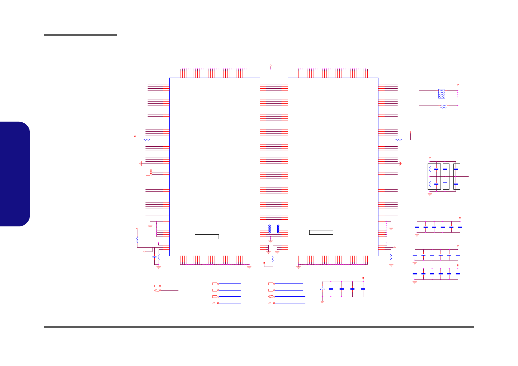
Schematic Diagrams
Sheet 9 of 41
DDR Memory DIMM
B.Schematic Diagrams
DDR Memory DIMM
91021223334364546575869708182929394113
CN3
VDD
VDD
VDD
VDD
VDD
VDD
VDD
VDD
VDD
VDD
VDD
VDD
VDD
VDD
VDD
VDD
VDD
VDD
VSS
VSS
VSS
VSS
VSS
VSS
VSS
VSS
VSS
/RMA[0..14]6,8
/RDQM[0..7]6,8
/RCS#[0..5]6,8
/RDQS[0..7]6,8 CKE[0..5]6
+2.5V
/RSRAS#6,8
/RSCAS#6,8
+3VS
VDDSPD
/RMA0
112
/RSRAS#
/RSWE#
/RSCAS#
A0
111
A1
110
A2
109
A3
108
A4
107
A5
106
A6
105
A7
102
A8
101
A9
115
A10/AP
100
A11
99
A12
117
BA0
116
BA1
12
DM0
26
DM1
48
DM2
62
DM3
134
DM4
148
DM5
170
DM6
184
DM7
78
DM8
11
DQS0
25
DQS1
47
DQS2
61
DQS3
133
DQS4
147
DQS5
169
DQS6
183
DQS7
77
DQS8
118
RAS#
119
WE#
120
CAS#
121
S0#
122
S1#
96
CKE0
95
CKE1
35
CK0
37
CK0#
160
CK1
158
CK1#
89
CK2
91
CK2#
193
SDA
195
SCL
71
CB0
73
CB1
79
CB2
83
CB3
72
CB4
74
CB5
80
CB6
84
CB7
1
VREF
2
VREF
197
VDDSPD
199
VDDID
R114
10K
3415162728383940515263647576878890103
DDR SO-DIMM
SMBCLK
SMBDAT
addr =1010000b
VSS
VSS
VSS
VSS
VSS
VSS
VSS
VSS
VSS
/RMA1
/RMA2
/RMA3
/RMA4
/RMA5
/RMA6
/RMA7
/RMA8
/RMA9
/RMA10
/RMA13
/RMA14
/RMA11
/RMA12
/RDQM0
/RDQM1
/RDQM2
/RDQM3
/RDQM4
/RDQM5
/RDQM6
/RDQM7
R354
8.2K
/RDQS0
/RDQS1
/RDQS2
/RDQS3
/RDQS4
/RDQS5
/RDQS6
/RDQS7
/RSWE#6,8
/RCS#0
/RCS#1
CKE0
CKE1
DDRCLK0
DDRCLK#0
DDRCLK1
DDRCLK#1
DDRCLK2
DDRCLK#2
SMBDAT
SMBCLK
R115
DDRVREF
0
VDDSPD
C152
0.1UF
SMBCLK4,15
SMBDAT4,15
114
131
132
VDD
VDD
VDD
VDD
VSS
VSS
VSS
VSS
104
125
126
/RMA[0..14]
/RDQM[0..7]
/RCS#[0..5]
/RDQS[0..7]
+2.5V
CN4
VDD
VSS
VDD
VDD
VSS
VSS
C137
10U(0805)
VDD
VSS
VDD
VDD
VDD
VSS
VSS
VSS
+2.5V
91021223334364546575869708182929394113
VDD
VDD
VDD
A10/AP
DQS0
DQS1
DQS2
DQS3
DQS4
DQS5
DQS6
DQS7
DQS8
RAS#
WE#
CAS#
CKE0
CKE1
CK0#
CK1#
CK2#
VREF
VREF
VDDSPD
VDDID
VSS
VSS
VSS
DDR SO-DIMM_H
3415162728383940515263647576878890103
C534
10U(0805)
/RMA0
112
A0
111
A1
/RMA2
110
A2
/RMA3
109
A3
/RMA4
108
A4
/RMA5
107
A5
106
A6
/RMA7
105
A7
/RMA8
102
A8
/RMA9
101
A9
/RMA10
115
/RMA13
100
A11
/RMA14
99
A12
/RMA11
117
BA0
/RMA12
116
BA1
/RDQM0
12
DM0
/RDQM1
26
DM1
/RDQM2
48
DM2
/RDQM3
62
DM3
/RDQM4
134
DM4
/RDQM5
148
DM5
/RDQM6
170
DM6
/RDQM7
184
DM7
R126 8.2K
78
DM8
/RDQS0
11
/RDQS1
25
/RDQS2
47
/RDQS3
61
/RDQS4
133
/RDQS5
147
/RDQS6
169
/RDQS7
183
77
/RSRAS#
118
/RSWE#
119
/RSCAS#
120
/RCS#2
121
S0#
/RCS#3
122
S1#
CKE2
96
CKE3
95
DDRCLK3
35
CK0
DDRCLK#3
37
DDRCLK4
160
CK1
DDRCLK#4
158
DDRCLK5
89
CK2
DDRCLK#5
91
SMBDAT
193
SDA
SMBCLK
195
SCL
71
CB0
73
CB1
79
CB2
83
CB3
72
CB4
74
CB5
80
CB6
84
CB7
DDRVREF
1
2
197
VDDSPD
199
R136
10K
CKE4
CKE2
CKE3
CKE5
CKE0
CKE1
+2.5V
DDRVREF GEN. & DECOUPLING
+2.5V
R92
75_1%
R108
75_1%
NEAR M650
DIMM
DECOUPLING
C487
C174
0.1UF
0.1UF
C142
C173
0.1UF
0.1UF
C183
C169
0.1UF
0.1UF
4
R112 470
R107 470
C184
0.1UF
C175
0.1UF
+2.5V
RP20
81
72
653
8P4R-470
C138
C139
0.1UF
0.01UF
C144
C149
0.01UF
0.1UF
NEAR DIMM0 NEAR DIMM1
C158
C168
C488
0.1UF
0.1UF
0.1UF
+2.5V
C172
C176
0.1UF
0.1UF
+2.5V
C143
C181
0.1UF
0.1UF
C171
0.01UF
DDRVREF
C170
0.01UF
+2.5V
C136
0.1UF
C182
0.1UF
C535
0.1UF
114
131
132
143
144
155
156
157
167
168
179
180
191
127
129
135
139
128
130
136
140
141
145
151
153
142
146
152
154
163
165
171
175
164
166
172
176
177
181
187
189
178
182
188
190
123
124
200
194
196
198
13
17
14
18
19
23
29
31
20
24
30
32
41
43
49
53
42
44
50
54
55
59
65
67
56
60
66
68
85
86
97
98
5
7
6
8
DQ0
DQ1
DQ2
DQ3
DQ4
DQ5
DQ6
DQ7
DQ8
DQ9
DQ10
DQ11
DQ12
DQ13
DQ14
DQ15
DQ16
DQ17
DQ18
DQ19
DQ20
DQ21
DQ22
DQ23
DQ24
DQ25
DQ26
DQ27
DQ28
DQ29
DQ30
DQ31
DQ32
DQ33
DQ34
DQ35
DQ36
DQ37
DQ38
DQ39
DQ40
DQ41
DQ42
DQ43
DQ44
DQ45
DQ46
DQ47
DQ48
DQ49
DQ50
DQ51
DQ52
DQ53
DQ54
DQ55
DQ56
DQ57
DQ58
DQ59
DQ60
DQ61
DQ62
DQ63
DU
DU
DU
DU
DU/RESET#
DU/A13
DU/BA2
SA0
SA1
SA2
192
VDD
VDD
VDD
VDD
VDD
VDD
VDD
VDD
VDD
VDD
VDD
VDD
VDD
VDD
VDD
VDD
VDD
VDD
VDD
VDD
VDD
VDD
VDD
addr =1010001b
VSS
VSS
VSS
VSS
VSS
VSS
VSS
VSS
VSS
VSS
VSS
VSS
VSS
VSS
VSS
VSS
VSS
VSS
VSS
VSS
VSS
VSS
VSS
162
173
174
185
186
104
125
126
137
138
149
150
159
161
C519
220U(D)
+
C141
10U(0805)
C180
10U(0805)
143
144
155
156
157
167
168
179
180
191
192
VDD
VDD
VDD
VDD
VDD
VDD
VDD
VDD
VDD
VDD
VDD
DU/RESET#
DU/A13
DU/BA2
VSS
VSS
VSS
VSS
VSS
VSS
VSS
VSS
VSS
VSS
137
138
VSS
149
150
159
161
162
173
174
185
186
/RMD0
5
DQ0
/RMD1 /RMA1
7
DQ1
/RMD2
13
DQ2
/RMD3
17
DQ3
/RMD4
6
DQ4
/RMD5
8
DQ5
/RMD6 /RMA6
14
DQ6
/RMD7
18
DQ7
/RMD8
19
DQ8
/RMD9
23
DQ9
/RMD10
29
DQ10
/RMD11
31
DQ11
/RMD12
20
DQ12
/RMD13
24
DQ13
/RMD14
30
DQ14
/RMD15
32
DQ15
/RMD16
41
DQ16
/RMD17
43
DQ17
/RMD18
49
DQ18
/RMD19
53
DQ19
/RMD20
42
DQ20
/RMD21
44
DQ21
/RMD22
50
DQ22
/RMD23
54
DQ23
/RMD24
55
DQ24
/RMD25
59
DQ25
/RMD26
65
DQ26
/RMD27
67
DQ27
/RMD28
56
DQ28
/RMD29
60
DQ29
/RMD30
66
DQ30
/RMD31
68
DQ31
/RMD32
127
DQ32
/RMD33
129
DQ33
/RMD34
135
DQ34
/RMD35
139
DQ35
/RMD36
128
DQ36
/RMD37
130
DQ37
/RMD38
136
DQ38
/RMD39
140
DQ39
/RMD40
141
DQ40
/RMD41
145
DQ41
/RMD42
151
DQ42
/RMD43
153
DQ43
/RMD44
142
DQ44
/RMD45
146
DQ45
/RMD46
152
DQ46
/RMD47
154
DQ47
/RMD48
163
DQ48
/RMD49
165
DQ49
/RMD50
171
DQ50
/RMD51
175
DQ51
/RMD52
164
DQ52
/RMD53
166
DQ53
/RMD54
172
DQ54
/RMD55
176
DQ55
/RMD56
177
DQ56
/RMD57
181
DQ57
/RMD58
187
DQ58
/RMD59
189
DQ59
/RMD60
178
DQ60
/RMD61
182
DQ61
/RMD62
188
DQ62
/RMD63
190
DQ63
85
123
124
200
86
97
98
194
196
198
VDDSPD
T
T
T
T
DDRST
T
T
T
T
R121
1K
DDRCLK[0..5]
DDRCLK#[0..5]
/RMD[0..63]
DU
DU
DU
DU
SA0
SA1
SA2
DDRCLK[0..5]4
DDRCLK#[0..5]4
/RMD[0..63]6,8
CKE[0..5]
B - 10 DDR Memory DIMM (71-M4000-D03)
Page 94

DDR SSTL-2 Termination
SSTL-2 Termination Resistors
Schematic Diagrams
MD/DQM(/DQS)RsSSTL-2
MA/Control
CS
CKE
SSTL-2
SSTL-2
OD 2.5V
/RSCAS#6,7
/RSWE#6,7
DDR
10
0
0
/RMD0
/RMD1
/RDQS0
/RMD2
/RMD3
/RMD8
/RMD9
/RDQS1
/RMD10
/RMD11
/RMD16
/RMD17
/RDQS2
/RMD18
/RMD19
/RMD24
/RMD25
/RDQS3
/RMD26
/RMD27
/RMA14
/RMA9
/RMA7
/RMA5
/RMA3
/RMA1
/RMA10
/RMA11
/RMD32
/RMD33
/RDQS4
/RMD34
/RMD35
/RMD40
/RMD41
/RDQS5
/RMD42
/RMD43
/RMD48
/RMD49
/RDQS6
/RMD50
/RMD51
/RMD56
/RMD57
/RDQS7
/RMD58
/RMD59
/RSCAS#
/RSWE#
Rtt
33
33
47
8 1
7 2
653
4
RP63 8P4R-33
8 1
7 2
653
4
RP64 8P4R-33
8 1
7 2
653
4
RP65 8P4R-33
8 1
7 2
653
4
RP66 8P4R-33
8 1
7 2
653
4
RP67 8P4R-33
8 1
7 2
653
4
RP68 8P4R-33
8 1
7 2
653
4
RP69 8P4R-33
8 1
7 2
653
4
RP70 8P4R-33
8 1
7 2
653
4
RP71 8P4R-33
8 1
7 2
653
4
RP72 8P4R-33
8 1
7 2
653
4
RP73 8P4R-33
8 1
7 2
653
4
RP74 8P4R-33
R137 33
R396 33
+1.25VS
/RMD[0..63]
+1.25VS
/RMA2
/RMA0
/RMA12
/RSRAS#6,7
/RSRAS#
/RMD6
/RDQM0
/RMD5
/RMD4
/RDQM1
/RMD13
/RMD12
/RMD7
/RMD20
/RMD21
/RMD15
/RMD14
/RDQM2
/RMD22
/RMD23
/RMD28
/RMD29
/RDQM3
/RMD30
/RMD31
/RMA8
/RMA13
/RMA4
/RMA6
/RMD37
/RMD36
/RDQM4
/RMD38
/RMD44
/RMD45
/RDQM5
/RMD39
/RMD47
/RMD46
/RMD52
/RMD53
/RDQM6
/RMD54
/RMD55
/RMD60
/RMD61
/RDQM7
/RMD62
/RMD63
/RCS#1
/RCS#0
/RCS#3
/RCS#2
/RCS#4
/RCS#5
4
653
7 2
8 1
RP34 8P4R-33
81
72
6
3
5
4
RP31 8P4R-33
81
72
6
3
5
4
RP30 8P4R-33
81
72
6
3
5
4
RP29 8P4R-33
5
4
6
3
72
81
RP28 8P4R-33
5
4
6
3
72
81
RP27 8P4R-33
5
4
6
3
72
81
RP25 8P4R-33
4
653
7 2
8 1
RP33 8P4R-33
81
72
6
3
5
4
RP24 8P4R-33
5
4
6
3
72
81
RP23 8P4R-33
5
4
6
3
72
81
RP22 8P4R-33
5
4
6
3
72
81
RP21 8P4R-33
81
72
6
3
5
4
RP26 8P4R-47
R138 47
R139 47
+1.25VS
+1.25VS
+1.25VS
/RDQM[0..7]
/RDQS[0..7]
/RMA[0..14]
/RCS#[0..5]
DECOUPLING CAPACITOR FOR SSTL-2 END TERMIANTION VTT ISLAND
0603 Package placed within 200mils of VTT Termination R-packs
C154 0.1UF
C189 0.1UF
C162 0.1UF
C536 0.1UF
C160 0.1UF C192 0.1UF
C187 0.1UF
C538 0.1UF
C541 0.1UF
C156 0.1UF
C537 0.1UF
C159 0.1UF
C164 0.1UF
C186 0.1UF
C546 0.1UF
C542 0.1UF
/RMD[0..63]6,7
/RDQM[0..7]6,7
/RDQS[0..7]6,7
/RMA[0..14] 6,7
/RCS#[0..5]6,7
C185 0.1UF
C193 0.1UF
C166 0.1UF
C157 0.1UF
C191 0.1UF
C153 0.1UF
C544 0.1UF
C540 0.1UF
B.Schematic Diagrams
Sheet 10 of 41
DDR SSTL-2
Termination
C188 0.1UF
C161 0.1UF
C165 0.1UF
C163 0.1UF
C190 0.1UF
C155 0.1UF
C543 0.1UF
C545 0.1UF
DDR SSTL-2 Termination (71-M4000-D03) B - 11
Page 95

Schematic Diagrams
LVDS Interface (SiS302LV)
Sheet 11 of 41
LVDS interface
(SiS302LV)
B.Schematic Diagrams
COMPOSITE Z1301
D23
A
R213
75
DVDD
AAD16/VADE
DGND
T
VBCAD
VBHCLK
DGND
DVDD
VREF2
T
T
R19 100
R20 100
V5V
INTA#
PCIRST#
T
ENAVDD
ENABKL
R211 0(R)
R212 0
L47
1 2
2.7UH
C250 33PF(R)
C262
C251
330PF
330PF
VAGCLK5
VAHSYNC5
VAVSYNC5
103
104
105
106
107
108
109
110
111
112
113
114
115
116
117
118
119
120
121
122
123
124
125
126
127
128
DVDD/DVDD4
DE2/VADE
FLD/STL2/DVSS4
AS/RESERVED
SPD/VBCAD
SPC/VBHCLK
HIN/DVSS5
VIN/DVDD5
VREF2/OVDD
SDD/GPIOA(GPI)
SDC/GPIOB(GPI)
DD1/GPIOC(GPI)
DC1/GPIOD(GPI)
DD2/LDDCDATA
DC2/LDDCCLK
V5V/V5V
HOUT/V2HSYNC
VOUT/V2VSYNC
HPD/LCDSENSE
HPINT*/INTA#
GPIO[0]/EXTRSTN
GPIO[1]/PFTEST1
GPIO[2]/PFTEST2
GPIO[3]/PFTESTO
ENAVDD/GPIOG(GP
ENABKL/GPIOH(GP
COMPOSITE30
Y
Y30
C
C30
D22
AC
AC
DA204U(R)
DA204U(R)
C
C
A
+3VS
AAD[0..15]
AAD[0..15]5,30
AAD[19..26]
AAD[19..26]5,30
AAD165,30
VBCAD5
VBHCLK5
LDDCDATA
T
LDDCCLK
INTA#9,13,30
PCIRST#9,13,14,20,22,24,30
ENAVDD11,30
ENABKL11,30
LDC0-
LDC0-11,30
LDC0+
LDC0+11,30
LDC1-
LDC1-11,30
LDC1+
LDC1+11,30
LDC2-
LDC2-11,30
LDC2+
LDC2+11,30
LDC3-
LDC3-11,30
LDC3+
LDC3+11,30
LL1C-
LL1C-11,30
LL1C+
LL1C+11,30
LDC4-
LDC4-11,30
LDC4+
LDC4+11,30
LDC5-
LDC5-11,30
LDC5+
LDC5+11,30
LDC6-
LDC6-11,30
LDC6+
LDC6+11,30
LDC7-
LDC7-11,30
LDC7+
LDC7+11,30
LL2C+
LL2C+11,30
LL2C-
LL2C-11,30
C248 33PF(R)
L46
1 2
FCM1608K-121T07
R202
C261
75
330PF
VAGCLK
DGND
AAD18/AHSYNC
AAD17/AVSYNC
AAD15
AAD14
100
101
102
DGND/OVSS
V2/VAVSYNC
D2[10]/VAD10
D2[11]/VAD11
H2/VAHSYNC
LVDSPLLVDD/LPLL
RESERVED/LPLLCA
LVDSPLLVSS/LPLL
LAVSS/LGND
RESERVED/LL2C
12345678910111213141516171819202122232425262728293031323334353637
LL2C+
LPLLGND
LPLLVDD
LPLLCAP
LGND
C49
NC
301LV/302LV:R894/R895
C249
330PF
AAD8
AAD12
AAD13
AAD11
D2[7]/VAD7
D2[8]/VAD8
D2[9]/VAD9
RESERVED/LL2C*
LAVDD/LVDD
RESERVED/LDC7
LL2C-
LDC7-
LVDD1
LDC7+
LPLLVDD
LVDD1
D2[6]/VAD6
RESERVED?LDC7*
LGND
DGND
DGND/DVSS3
XCLK2/VAGCLK
LAVSS/LGND
RESERVED/LDC6
LDC6+
JTV1
2
SVIDEO CON
PIN(GND1,GND2)=GND
DVDD
AAD9
AAD26
AAD10
AAD25
D2[3]/VAD3
D2[4]/VAD4
D2[5]/VAD5
XCLK2*/DVDD3
RESERVED/LDC6*
LAVDD/LVDD
RESERVED/LDC5
RESERVED/LDC5*
LDC6-
LVDD1
LDC5-
LGND
LDC5+
NC
R23
R22 0
6
D2[2]/VAD2
LVDSPLLVSS/LGND
AAD23
LDC4+
D2[1]/VAD1
RESERVED/LDC4
5
AAD24
D2[0]/VAD0
RESERVED/LDC4*
LDC4-
34
1
T
AAD20
AAD22
AAD19
AAD21
D1[8]/VBD8
D1[9]/VBD9
D1[10]/VBD10
D1[11]/VBD11
DVDD/RESERVED
DVDD/RESERVED
LVDSPLLVDD/LVDD
LAVDD/LVDD
LX3P/LDC3
LX3N/LDC3*
LAVSS/LGND
LXC1P/LL1C
LL1C+
LVDD2
LDC3+
LDC3-
LGND
AAD0
D1[7]/VBD7
LXC1N/LL1C*
LL1C-
AAD1
D1[6]/VBD6
LAVDD/LVDD
LVDD2
DGND
XCLK1/VBGCLK
LX2P/LDC2
LDC2-
LDC2+
DVDD
AAD2
D1[5]/VBD5
DGND/DVSS2
XCLK1*/DVDD2
LX2N/LDC2*
LAVSS/LGND
LX1P/LDC1
LDC1+
LGND
AAD3
D1[4]/VBD4
LX1N/LDC1*
LDC1-
AAD4
D1[3]/VBD3
LAVDD/LVDD
LVDD2
AAD5
LDC0+
D1[2]/VBD2
LX0P/LDC0
AAD6
D1[1]/VBD1
LX0N/LDC0*
LDC0-
AAD7
D1[0]/VBD0
LAVSS/LGND
LGND
VBGCLK
AAD28/VBCTL0
AAD31/BVSYNC
AAD30/BHSYNC
6566676869707172737774757678798081828384858687888990919293949596979899
V1/VBVSYNC
H1/VBHSYNC
DGND/VBCTL0
VBCTL1/FLD/STL1
DVSS0/RESET*
TVCLKO/GPIO[5]
DVDD0/TVPLL_VDD
PLL1VDD/TVPLL_V
VBRCLK(XIN)/XIN
PLL1GND/TVPLL_G
RESERVED/BOC/VS
IOCS/C/HSYNC
DAC_GND/DAC_GND
DAC_VDD/DACA3
RESERVED/DACB3
RESERVED/DACB2
RESERVED/DACB1
IOCOMP/DACA0
V2COMP/DACB0
DAC_GND/DAC_GND
EXTSWING/VSWING
DACVDD/DACVDD
V2RSET/ISET
38
ISET
R267 147
VSWING
DAC_VDD
R268 6K
R269 2K
DVDD1/DVDD
VBDE/DE1
DVSS1/VREF1
OVDD/VDDV
VBCLK/P-OUT
TSCLKI/GPIO4
VBOSCO/XO
IOC/DACA2
IOY/DACA1
C321 1UF
VBGCLK 5
AAD28 5,30
VBHSYNC 5
VBVSYNC 5
U22
64
63
62
61
60
59
58
57
56
55
54
53
52
51
50
49
48
47
46
45
44
43
42
41
40
39
SIS302LV(R)
+3VS
DVDD
AAD27/VBDE
AAD29/VBCTL1
DGND
VDDV
VBCLK
DGND
T
DVDD
TVPLLVDD
VBOSCO
VBRCLK
TVPLLGND
DAC_GND
DAC_VDD
T
C
T
Y
T
COMPOSITE
V2COMP
DAC_GND
Choose clock source:main board/crystal
Spread range:R120:+-1.5%/+-2.5%
VBOSCO
C52
22P
R242 2.2K
R241 2.2K
AAD27 5,30
AAD29 5,30
VBCLK 5
R1 :NC/22
Y3
14.318MHZ(R)
+5VS
C48
10U/10V(R)
+3VS
FCM1608K121(R)
R24 10
C43
22P
LDDCDATA
LDDCCLK
L15
V5V
C47
0.1UF
VREF2
VBRCLK
C46
0.1UF
+3VS
FCM1608K121(R)
+3VS
FCM1608K121(R)
+3VS
FCM1608K121(R)
+3VS
FCM1608K121(R)
N5
+3VS
L14
FCM1608K121(R)
N3
+3VS
+3VS
+3VS
L17
FCM1608K121(R)
L12
L13
L20
L18
L11
FCM1608K121(R)
C32
0.1UF
L19
FCM1608K121(R)
C69
0.1UF
C37
10U/10V(R)
C38
10U/10V(R)
C60
10U/10V(R)
C67
10U/10V(R)
C50
10U/10V(R)
N2
N4
C65
10U/10V(R)
C59
0.1UF
C42
NC/0.1uF
C41
0.1UF
C33
10U/10V(R)
C58
10U/10V(R)
C56
0.1UF
LVDD1
C36
0.1UF
LVDD2
C39
0.1UF
VDDV
C66
0.1UF
V2COMP
DAC_VDD
LPLLVDD
C34
0.1UF
LPLLGND
TVPLLVDD
C57
0.1UF
TVPLLGND
C35
0.1UF
LGND
C40
0.1UF
LGND
DVDD
C68
0.1UF
DGND
C51
0.1UF
DAC_GND
DVDD
C55
0.1UF
DGND
B - 12 LVDS Interface (SiS302LV) (71-M4000-D03)
Page 96

Panel Con & LED Indicator
Schematic Diagrams
L68
LCDVCC
FCM2012V-121
TXOUT-LN0
TXOUT-LP0
TXOUT-LN1
TXOUT-LP1
TXOUT-LN2
TXOUT-LP2
TXOUT-LN3
TXOUT-LP3
TXCLK-LN
TXCLK-LP
LCDID015,30
LCDID115,27,30
LCDID215,27,30
L70
VIN
BK3216HS800
C294
C292
C290
10PF
10PF
10PF
C291
C293
10PF
10PF
LCDID0
LCDID1
LCDID2
E-MAIL
CHA/BATLOW
PANEL
WL_LED
C289
0.1UF
C296
10PF
C295
C297
10PF
10PF
0.1UF
C298
10PF
C322
C299
10PF
JLCD1
1
1
3
3
5
5
7
7
9
9
11
11
13
13
15
15
17
17
19
19
21
21
23
23
25
25
27
27
29
29
31
31
33
33
35
35
37
37
39
39
41
41
43
43
45
45
47
47
49
49
CON50
L83 0
L82 0
L81 0
L80 0
L79 0
L78 0
L77 0
L76 0
L75 0
L74 0
L63 0
L62 0
L61 0
L60 0
L59 0
L58 0
L57 0
L56 0
L55 0
L54 0
2
4
6
8
10
12
14
16
18
20
22
24
26
28
30
32
34
36
38
40
42
44
46
48
50
R746
100K
8
7
6
5
5
2
1
3
U48
TC7SZ08
SCROLLOCK
CAPSLOCK
NUMLOCK
A C
SML_010MT_G
Q16
4800
3
2
1
4
D4
C286
C285
4.7U(0805)
0.1UF
LEDPWR24
PANEL
4
R749
100K(R)
LEDPWR
12V
R656
100K
G S
Q32
D
G S
2N7002
R657
10K
TXOUT-LN0
TXOUT-LP0
TXOUT-LN1
TXOUT-LP1
TXOUT-LN2
TXOUT-LP2
TXOUT-LN3
TXOUT-LP3 LDC3+
TXCLK-LN
TXOUT-UN0 LDC4-
TXOUT-UP0
TXOUT-UN1
TXOUT-UP1
TXOUT-UN2
TXOUT-UP2
TXOUT-UN3
TXOUT-UP3
TXCLK-UN
TXCLK-UP
D
2N7002
C274
10PF
VDD5
R655
100K
Q30
D
G S
Q31
2N7002
LEDVDD
C282
C280
C278
C276
10PF
C275
C277
10PF
10PF
10PF
10PF
10PF
C279
C281
C283
10PF
10PF
10PF
D
2N7002
5
2
1
3
147
R278
47K
VCCGND
Q17
U23
TC7SZ08
QA
QB
QC
QD
QE
QF
QG
QH
AC
AC
AC
Q15
2N3906
+3VS
C337
C338
4.7U(0805)
0.1UF
Z245
C336
0.1UF
4
C288
0.1UF
SCROLLOCK
3
CAPSLOCK
4
NUMLOCK
5
BAT_FULL
6
CHA/BATLOW
10
WL_LED
11
PWR/SUS_LED
12
E-MAIL
13
R11 220(0805)
R10 220(0805)
R9 220(0805)
R8 220(0805)
12V LCDVCC
+3VS
R301
10K
G S
Q18
G S
R747 0
R748 0(R)
D52
F01J2E
D53
F01J2E
R724 100K
IDE_LED#
R288
0.1U
R728
10K
AC
AC
+5VS
R220 4.7K
D
2N7002
C852
0.1U
D8
F01J2E
D9
F01J2E
R729
10K
74HCT164
R289
100K
1
2
8
9
C851
4.7U(0805)
D6
D5
AC
AC
LEDVDD
U3
A
B
CLK
CLR
D7
SML_010MT_G
SML_010MT_G
SML_010MT_G
Z511
ENAVDD10,30
GATE_LID_SW15
LID_SW#27
ENABKL10,30
LEDDATA/WD24
LEDCLK24
164_RESET#24
ENAVDD
+3VS
+5VS
GATE_LID_SW
C856 0.1U(R)
R752 4.7K(R)
LID_SW#
ENABKL
LEDDATA/WD
LEDCLK
164_RESET#
LEDVDD
IDE_LED#14
2
4
6
8
10
12
14
16
18
20
22
24
26
28
30
32
34
36
38
40
42
44
46
48
50
L65
FCM2012V-121
C284
0.1UF
TXOUT-UN0
TXOUT-UP0
TXOUT-UN1
TXOUT-UP1
TXOUT-UN2
TXOUT-UP2
TXOUT-UN3
TXOUT-UP3
TXCLK-UN
TXCLK-UP
L67 FCM2012V-121
BAT_FULL
PWR/SUS_LED
INTMIC
BRIGADJ
ACIN_LED
C272
C273
0.1UF(R)
0.1UF(R)
LDC0-
LDC0+
LDC1-
LDC1+
LDC2-
LDC2+
LDC3-
LL1C-
LL1C+TXCLK-LP
LDC4+
LDC5-
LDC5+
LDC6-
LDC6+
LDC7-
LDC7+
LL2C-
LL2C+
LCDVCC
INTMIC 27
BRIGADJ 24
ACIN_LED24
LDC0- 10,30
LDC0+ 10,30
LDC1- 10,30
LDC1+ 10,30
LDC2- 10,30
LDC2+ 10,30
LDC3- 10,30
LDC3+ 10,30
LL1C- 10,30
LL1C+ 10,30
LDC4- 10,30
LDC4+ 10,30
LDC5- 10,30
LDC5+ 10,30
LDC6- 10,30
LDC6+ 10,30
LDC7- 10,30
LDC7+ 10,30
LL2C- 10,30
LL2C+ 10,30
SYS5V
B.Schematic Diagrams
Sheet 12 of 41
Panel Con & LED
Indicator
Panel Con & LED Indicator (71-M4000-D03) B - 13
Page 97

Schematic Diagrams
962 (PCI/IDE/HyperZip) 1 of 4
Sheet 13 of 41
962 (PCI/IDE/
HyperZip)
1 of 4
B.Schematic Diagrams
+3VS
FRAME#
REQ2#
SERR#
STOP#
SUSB#24,28
RP32
1
10
1
10
TRDY#
9
2
9
IRDY#
8
3
8
PLOCK#
7
4
7
DEVSEL#
6
5
6
+3VS
4
4
C460
0.1UF
SZVREF ZUREQ
C459
0.1UF
+3V
R365
R366
10K
330K
INTD#
INTA#
INTB#
INTC#
8P4R-2.2K
REQ0#
REQ3#
REQ4#
REQ1#
8P4R-4.7K
GNT1#
GNT3#
GNT4#
+1.8VS
2
3
4
5
8 1
7 2
653
8 1
7 2
653
R390 4.7K
R388 4.7K
R389 4.7K
R76
150_1%
R77
150_1%
N10
10MIL
10P8R-2.7K
RN5
RN6
SUSB#
T
4
C513
0.1UF(R)
13
12
11
10
G
C514 0.1UF
PCIRST#
PCIRST# PRST#
PCICLK9614
U7
VCCCLR1#
Q1D1
Q1#CLK1
PR1#
Q2
CLR2#
Q2#
D2
GND
CLK2
PR2#
74LVC74
Q35
DSR684 0(R) R685 0(R)
2N7002(R)
S3AUXSW#
PCIRST#9,10,14,20,22,24,30
141
52
63
9
8
7
DEVSEL#19,25
PCIRST#
+3V
C146
0.1UF
T
T
PRST#
T
S3AUXSW# 6,28
REQ2#25
REQ0#19
GNT2#25
GNT0#19
C/BE#319,20,25
C/BE#219,20,25
C/BE#119,20,25
C/BE#019,20,25
INTA#9,10,30
INTC#19
INTD#25,30
FRAME#19,20,25
IRDY#19,20,25
TRDY#19,20,25
STOP#19,25
SERR#19,25
PAR19,25
PCICLK961
R125
ZCLK14
ZSTB09
ZSTB#09
ZSTB19
ZSTB#19
ZUREQ9
ZDREQ9
PRST# 19,24,25
REQ4#
REQ3#
REQ2#
REQ1#
REQ0#
GNT4#
GNT3#
GNT2#
GNT1#
GNT0#
C/BE#3
C/BE#2
C/BE#1
C/BE#0
INTA#
INTB#
INTC#
INTD#
FRAME#
IRDY#
TRDY#
STOP#
SERR#
PAR
DEVSEL#
PLOCK#
33
ZCLK1
ZSTB0
ZSTB#0
ZSTB1
ZSTB#1
ZDREQ
AD[0..31]
BGA2A
F1
PREQ#4
F2
PREQ#3
E1
PREQ#2
H5
PREQ#1
F3
PREQ#0
H3
PGNT#4
G1
PGNT#3
G2
PGNT#2
G3
PGNT#1
H4
PGNT#0
K3
C/BE#3
M4
C/BE#2
P1
C/BE#1
R4
C/BE#0
E3
INT#A
F4
INT#B
E2
INT#C
G4
INT#D
M3
FRAME#
M1
IRDY#
M2
TRDY#
N4
STOP#
M5
SERR#
N3
PAR
N1
DEVSEL#
N2
PLOCK#
Y2
PCICLK
C3
PCIRST#
V20
ZCLK
N19
ZSTB0
N20
ZSTB0#
K20
ZSTB1
K19
ZSTB1#
N16
ZUREQ
N17
ZDREQ
R19
VDDZCMP
N18
ZCMP_N
R18
ZCMP_P
P18
VSSZCMP
U20
Z1XAVDD
U19
Z1XAVSS
T20
Z4XAVDD
T19
Z4XAVSS
R20
VZREF
P20
ZVSSREF
AD[0..31]19,20,25
SZCMP_N
SZCMP_P
SVSSZCMP
SZ1XAVDD
SZ1XAVSS
SZ4XAVDD
SZ4XAVSS
SZVREF
ZAD[0..15]9
Analog Power supplies of Transzip
function for 96X Chip.
L27
+3VS
FCM1608K121
1 2
C122
10UF/10V
10MIL
N11
AD18
AD17
AD18
AD17
AD10
AD12
AD9
AD15
AD14
AD13
AD11
AD16
AD9
AD16
AD15
AD14
AD13
AD12
AD11
AD10
AD29
AD30
AD28
AD31
J5J4H2H1J3K4J2J1K5K2L3K1L1L4L5L2N5P2P3P4R2R3R1T1P5T2U1U2T3R5U3
AD31
AD30
AD29
AD28
AD19
AD24
AD27
AD21
AD20
AD25
AD22
AD26
AD23
AD27
AD26
AD25
AD24
AD23
AD22
AD21
AD20
AD19
PCI
962-1
HyperZip
ZAD0
ZAD1
ZAD2
ZAD3
ZAD4
ZAD5
ZAD6
ZAD7
ZAD8
ZAD9
ZAD10
ZAD11
ZAD12
ZAD13
ZAD14
ZAD15
M18
6.49mA
ZAD0
C129
0.1UF
M19
ZAD1
M17
ZAD2
M16
ZAD3
M20
ZAD4
L16
L20
L18
K18
ZAD8
ZAD5
ZAD6
ZAD7
SZ1XAVDD
C128
0.01UF
SZ1XAVSS
J20
ZAD9
K17
K16
H20
J18
ZAD13
ZAD12
ZAD10
ZAD11
L87
H19
H18
+1.8VS
FCM1608K121
1 2
ZAD14
ZAD15
C462
10UF/10V
N17
L86
+3VS
FCM1608K121
1 2
C440
10UF/10V
N16
AD8
AD6
AD7
AD5
AD8
AD7
AD6
IDE
10MIL
10MIL
AD5
AD4
AD4
AD3
AD2
AD3
AD2
35.64mA
C461
0.1UF
7.92mA
C458
0.1UF
IDESAA[0..2]
IDECS#A[0..1]
AD1
AD0
IDESAB[0..2]
IDECS#B[0..1]
V1
AD1
AD0
IDEAVDD
IDEAVSS
ICHRDYA
IDREQA
IIRQA
CBLIDA
IIOR#A
IIOW#A
IDACK#A
IDSAA2
IDSAA1
IDSAA0
IDECSA#1
IDECSA#0
ICHRDYB
IDREQB
IIRQB
CBLIDB
IIOR#B
IIOW#B
IDACK#B
IDSAB2
IDSAB1
IDSAB0
IDECSB#1
IDECSB#0
IDA0
IDA1
IDA2
IDA3
IDA4
IDA5
IDA6
IDA7
IDA8
IDA9
IDA10
IDA11
IDA12
IDA13
IDA14
IDA15
IDB0
IDB1
IDB2
IDB3
IDB4
IDB5
IDB6
IDB7
IDB8
IDB9
IDB10
IDB11
IDB12
IDB13
IDB14
IDB15
SIS962
SVDDZCMP
R75
C444
R74
0.01UF
SVSSZCMP
Y3
Y4
W10
V10
Y11
U12
V11
Y9
Y10
T11
U11
W11
T12
V12
W17
Y17
T16
U17
T14
W16
V16
Y18
T15
V17
U16
W18
U10
V9
W8
T9
Y7
V7
Y6
Y5
W6
U8
W7
V8
U9
Y8
T10
W9
Y16
V15
U14
W14
V13
T13
Y13
Y12
W12
W13
U13
Y14
V14
W15
Y15
U15
56
SZCMP_N
56
SZCMP_P
MIDEIOR#A
MIDEIOW#A
MIDACK#A
MIDESAA1
MIDESAA0
MIDECS#A1
MIDECS#A0
MIDEIOR#B
MIDEIOW#B
MIDACK#B
MIDESAB2
MIDESAB1
MIDESAB0
MIDECS#B1
MIDECS#B0
IDESAA[0..2] 14
IDECS#A[0..1] 14
IDESAB[0..2] 14
IDECS#B[0..1] 14
C150
0.01UF
ICHRDYA
IDEREQA
IDEIRQA
CBLIDA
R98
R104
R103
R360
R363
R97
R358
R91
ICHRDYB
IDEREQB
IDEIRQB
CBLIDB
R352 10
R90 22
R87
R80
R351
R86
R349
R79
IDEDA0
IDEDA1
IDEDA2
IDEDA3
IDEDA4
IDEDA5
IDEDA6
IDEDA7
IDEDA8
IDEDA9
IDEDA10
IDEDA11
IDEDA12
IDEDA13
IDEDA14
IDEDA15
IDEDB0SVDDZCMP
IDEDB1
IDEDB2
IDEDB3
IDEDB4
IDEDB5
IDEDB6
IDEDB7
IDEDB8
IDEDB9
IDEDB10
IDEDB11
IDEDB12
IDEDB13
IDEDB14
IDEDB15
R118 0
C151
0.1UF
IDEIOR#A
10
IDEIOW#A
22
IDACK#A
22
33
33
33
33
33
IDEIOR#B
IDEIOW#B
22
IDACK#B
33
33
33
33
33
+1.8VS
ICHRDYA 14
IDEREQA 14
IDEIRQA 14
CBLIDA 14
IDESAA2MIDESAA2
IDESAA1
IDESAA0
IDECS#A1
IDECS#A0
ICHRDYB 14
IDEREQB 14
IDEIRQB 14
CBLIDB 14
IDESAB2
IDESAB1
IDESAB0
IDECS#B1
IDECS#B0
IDEIOR#A 14
IDEIOW#A 14
IDACK#A 14
IDEIOR#B 14
IDEIOW#B 14
IDACK#B 14
IDEDA[0..15] 14
IDEDB[0..15] 14
SZ4XAVDD
C443
0.01UF
SZ4XAVSS
B - 14 962 (PCI/IDE/HyperZip) 1 of 4 (71-M4000-D03)
Page 98

962 (Misc Signals) 2 of 4
Schematic Diagrams
Programable on-die pull-high strength for CPU_S:
( Infinite, 150, 110, 56 Ohm)
INIT#3
A20M#3
SMI#3
INTR3
NMI3
IGNNE#3
FERR#3
STPCLK#3
CPUSLP#3
LPC_FRAME#22,24
LPC_DRQ#22
Y7
32.768KHZ
1 2
BATOK18
PWRGD9,26,29
SMBDAT4,7
SMBCLK4,7
10K
PM_DPRSLPVR
PM_CPUPERF#
LPC_AD022,24
LPC_AD122,24
LPC_AD222,24
LPC_AD322,24
SERIRQ19,22,24
REFCLK14
PCBEEP29
PWRBTN#
C167
0.1UF
+3V
EXTSMI#
GMUXSEL
+3V
VGATE
+3VS
R134
CLKAPIC
SMBDAT
SMBCLK
AC_SDIN0
AC_SDIN1
AC_RST#
AC_BCLK
R361 4.7K
C178
C179
+3V
FROM H8
PWRBTN#24
AUXOK9,24,27,28
PM_DPRSLPVR36
EXTSMI#24
PM_CPUPERF#2
VGATE29
CLKAPIC4
15PF
20PF
AC_SDIN026
AC_SDIN120,26
AC_SDOUT20,26
AC_SYNC20,26
AC_RST#20,26
AC_BCLK20,26
R96
PSON#28,29
PCBEEP( LPC addr mapping)
SB Hardware Trap
PCBEEP
INIT#
A20M#
SMI#
INTR
NMI
IGNNE#
FERR#
STPCLK#
CPUSLP#
LPC_AD0
LPC_AD1
LPC_AD2
LPC_AD3
LPC_FRAME#
LPC_DRQ#
SERIRQ
R132
10M
BATOK
PWRGD
C196
0.1UF
R130 0
R129 0
R135 0
R387 0
R537
R398
D17 1SS355
A C
D36 1SS355
R84
R353 4.7K
GPIO18
+3VS
4.7K
OSC32KHI
OSC32KHO
RTCVDD
C177
0.1UF
REFCLK1
SENTEST
PCBEEP
961PME#
PSON#
AUXOK
T
FOR C4
DPERSLP
0
4.7K
AC
0(R)
T18
INIT#
P16
A20M#
R17
SMI#
R16
INTR
Y20
NMI
U18
IGNNE#
T17
FERR#
W20
STPCLK#
V19
CPUSLP#
Y19
APICCK
V18
APICD0
W19
APTCD1
V5
LAD0
T7
LAD1
U6
LAD2
W5
LAD3
W4
LFRAME#
U7
LDRQ#
V6
SIRQ
C2
OSC32KHI
D2
OSC32KHO
D3
BATOK
D1
PWROK
C1
RTCVDD
E4
RTCVSS
B2
GPIO20
A1
GPIO19
A2
AC_SDIN0
D5
AC_SDIN1
W2
AC_SDOUT
T5
AC_SYNC
D6
AC_RESET#
Y1
AC_BIT_CLK
W3
OSCI
G5
ENTEST
V3
SPK
A14
PWRBTN#
B14
PME#
D14
PSON#
A3
AUXOK
A15
ACPILED
B1
GPIO13/DPRSLPVR
E5
GPIO14
E13
GPIO15
A16
GPIO16
D13
GPIO17
B15
GPIO18/PMCLK
BGA2B
(AUX)
(AUX)
(AUX)
(AUX)
/geyserville
(AUX)
CPU_S
APIC
LPC
RTC
962-2
GPIO
AC97
(AUX)
ACPI
(AUX)
(AUX)
/others
(AUX)
KBC
(AUX)
MII
GPIO
(MAIN)
(MAIN)
(MAIN)
(MAIN)
(MAIN)
(MAIN)
(AUX)
(AUX)
(AUX)
(MAIN)
GPIO4/CLKRUN#
(AUX)
(AUX)
GPIO9/AC_SDIN2
GPIO10/AC_SDIN3
(AUX)
GPIO12/CPUSTP#
OSC25MHI
OSC25MHO
MIITXCLK
MIITXEN
MIITXD0
MIITXD1
MIITXD2
MIITXD3
MIIRXCLK
MIIRXDV
MIIRXER
MIIRXD0
MIIRXD1
MIIRXD2
MIIRXD3
MIICOL
MIICRS
MIIMDC
MIIMDIO
MIIAVDD
MIIAVSS
GPIO0
GPIO1/LDRQ1#
GPIO2/THERM#
GPIO3/EXTSMI#
GPIO5/PREQ5#
GPIO6/PGNT5#
GPIO7
GPIO8/RING
GPIO11
SIS962
A8
A9
A6
B6
E8
D7
C6
B4
A7
C7
C8
D8
A5
B5
A4
B7
E9
C5
E7
B9
B8
V2
GATE_LID_SW
T8
T4
T6
W1
U5
U4
C4
C14
LAN_PWRON
E6
B3
HWSUS_CB#
F5
CPUSTP#
D4
T
ATF_INT#
ID0
ID1
ID2
V_ADJ
R102 4.7K
1
2
3
4
5
RP19
10
9
8
7
6
10P8R-10K
R369 10K
R368 10K
R394
A C
D16 1N4148(R)
R699 0(R)
R700 0(R)
R701 0(R)
R123
A C
D14
A C
D13 1SS355
RP18
10
10
1
9
9
2
8
8
3
7
7
4
6
6
5
10P8R-10K
1
10
1
2
9
2
3
8
3
4
7
4
5
6
5
GATE_LID_SW 11
4.7K(R)
1SS355
R362
V_ADJ 36
HWSUS_CB#19
CPUSTP# 4,29
4.7K
EXTSMI#
LCDID0
LCDID1
LCDID2
+3V
SCI#
4.7K
WAKE-UP
+3V
C518
C510
0.1UF
0.01UF
+3VS
LCDID0 11,30
LCDID1 11,27,30
LCDID2 11,27,30
SCI# 24
+3V
WAKE-UP24
It will change next
verison
GMUXSEL
DPERSLP
AC_SDIN0
AC_SDIN1
LAN_PWRON
VID12,36
NEED NOT to place
close to 96X
GPIO pins
NEED NOT to place
close to 96X
HWSUS_CB#
RN11
LPC_AD1
LPC_AD3
LPC_AD2
LPC_AD0
8P4R-4.7K
R364 4.7K
LPC_DRQ#
R109
SERIRQ
R399 0
SENTEST
ATF_INT#
R395
CPUSTP#
R141
SMBDAT
R391
SMBCLK
R392
GPIO18
R94
LCDID0
R133 10K
LCDID1
R385 10K
LCDID2
R386 10K
R101 4.7K(R)
R131 4.7K
R124 100K
R370 100K
R371 100K
V_ADJ
R117 100K
961PME#
R95 4.7K
VGATE
R100 4.7K
R375 4.7k
D15
VID1 ATF_INT#
F01J2E
+3VS
18
27
36
45
4.7K
4.7K
4.7K(R)
4.7K
4.7K
4.7K
+3VS
Sheet 14 of 41
B.Schematic Diagrams
962 (Misc Signals)
2 of 4
+3V
AC
962 (Misc Signals) 2 of 4 (71-M4000-D03) B - 15
Page 99

Schematic Diagrams
962 (USB I/F) 3 of 4
BGA2C
Sheet 15 of 41
962 (USB I/F)
3 of 4
B.Schematic Diagrams
UV0+
UV0-
UV1+
UV1-
UV2+
UV2-
UV3+
UV3-
UV4+
UV4-
UV5+
UV5-
OC0#
OC1#
OC2#
OC4#
OC3#
OC5#
V4
B18
C18
D18
D19
E14
D15
E18
F18
E16
E15
G18
G19
G20
G17
J16
H17
H16
G16
D16
F17
D17
E17
B17
E19
B19
F19
B16
A17
F16
A18
C15
C16
C17
USBREFAVDD
B20
UCLK48M
UV0+
UV0UV1+
UV1UV2+
UV2UV3+
UV3UV4+
UV4UV5+
UV5-
OC0#
OC1#
OC2#
R78 10K
R347 10K
R85 10K
C478
0.1UF
OSC12MHI
OSC12MHO
USBREF
USBPVDD
USBPVSS
IVDD_AUX
C134
0.1UF
C484
0.1UF
12 mil
UCLK48M4
UV0+ 17
UV0- 17
UV1+ 17
UV1- 17
UV2+ 17
UV2- 17
C479
1UF
C131
15PF
C130
0.1UF
OC0# 17
OC1# 17
OC2# 17
1 2
FCM2012V121
1 2
FCM2012V121(R)
C480
10UF/10V
R89 10M
Y6 12MHz
L29
1 2
FCM2012V121
JA3
1 2
SHORT-A
L143
L144
C135
20PF
C496
10UF/10V
+3VS
+3V
+3VS
UV3-
UV3+
C465
22P
Place these components
near to SiS96X
UV4+ +DATA4
C468
22P
Place these components
near to SiS96X
UV5+ +DATA5
C464
22P(R)
Place these components
near to SiS96X
1394_EECS
1394_MA2/EESK
1394_MA1/EEDI
1394_MA0/EEDO
R113 47K
+3VS
R71
R70
C466
22P
R68
R69
C467
22P
R72
R73
C463
22P(R)
22
22
22
22
0
0
U6
1
CS
VCC
2
SK
NC
3
DI
NC
4
DO
GND
9346
R239
15K
R222
15K
R401
15K(R)
-DATA3
+DATA3
R240
15K
-DATA4UV4-
R221
15K
-DATA5UV5-
R402
15K(R)
+3VS
8
7
6
5
C145
T
T
0.1UF
-DATA3 17
+DATA3 17
-DATA4 17
+DATA4 17
-DATA5 17
+DATA5 17
1394_MA2/EESK
1394_MA1/EEDI
1394_MA0/EEDO
1394_EECS
PHY_LPS21
PHY_REQ21
PHY_LKON21
PHY_D021
PHY_D121
PHY_D221
PHY_D321
PHY_D421
PHY_D521
PHY_D621
PHY_D721
PHY_CTL021
PHY_CTL121
PHY_CLK21
PHY_LPS
PHY_REQ
PHY_LKON
PHY_D0
PHY_D1
PHY_D2
PHY_D3
PHY_D4
PHY_D5
PHY_D6
PHY_D7
PHY_CTL0
PHY_CTL1
PHY_CLK
F20
EESK(GPI21)
D20
EEDI(GPI22)
E20
EEDO(GPI23)
C20
EECS(GPI24)
A20
LPS
A19
LREQ
C19
LINKON
A12
D0
B12
D1
C12
D2
D12
D3
E12
D4
A13
D5
B13
D6
C13
D7
D11
CTL0
C11
CTL1
E11
SCLK
A10
T
T
T
T
T
T
T
T
T
IPB_OUT1
B10
IPB_OUT0
A11
NC
E10
NC
D9
NC
B11
NC
C9
NC
C10
NC
D10
NC
SIS962
USBCLK48M
USBVDD
USBVDD
USBVDD
USBVDD
USBVSS
USBVSS
USBVSS
USBVSS
OSC12MHI
OSC12MHO
USBREF
USBPVDD
USBPVSS
IVDD_AUX
IVDD_AUX
USBREFAVDD
C132
0.1UF
L30
1 2
FCM2012V121
JA1
1 2
SHORT-A
20 mil 20 mil
C133
0.1UF
B - 16 962 (USB I/F) 3 of 4 (71-M4000-D03)
+1.8V
C140
10UF/10V
L146
1 2
FCM2012V121
C485
0.1UF
L90
1 2
FCM2012V121(R)
JA4
1 2
SHORT-A
USBREFIVDD_AUX
C486
0.1UF
L28
1 2R88 412_1%
4.7uH_SMD_30%
C498
10UF/10V
USBPVDD
C497
0.1UF
USBPVSS
+3VS
+3V
C503
10UF/10V
Page 100

962 (Power & RTC) 4 of 4
Schematic Diagrams
+3VS
10UF/10V
C526
C489
10UF/10V
C490
0.1UF
C505
0.1UF
C508
0.1UF
C469
1UF
Put under 96X solder side
+1.8VS
0.1UF
C495
0.1UF
C517
+3V
R408
51K
10K
R407
C509
0.1UF
C516
0.1UF
E C
B
Q22
0.1UF
0.1UF
B
C492
C483
R406
10K
C
Q5
E
MMBT3904
0.1UF
0.1UF
MMBT3906
C493
C502
+3V
+2.5V
VTT
C351
0.1UF
C527
10UF/10V
BATOK 15
1UF
C406
+3V
C520
0.1UF
+1.8V
+3VS
C528
0.1UF
G15
N15
P17
K15
H15
M15
R10
R14
P15
R15
R11
R13
R12
F12
F10
F11
F14
F15
F13
J15
J17
L15
L17
G6
L6
R6
H6
K6
M6
P6
R7
R9
J6
N6
R8
F9
F7
F8
BGA2D
VDDZ
VDDZ
VDDZ
VDDZ
VDDZ
VDDZ
VDDZ
PVDDZ
IVDD
IVDD
IVDD
IVDD
IVDD
IVDD
IVDD
VTT
VTT
OVDD
OVDD
OVDD
OVDD
OVDD
OVDD
OVDD
OVDD
PVDD
PVDD
PVDD
PVDD
IVDD_AUX
IVDD_AUX
OVDD_AUX
OVDD_AUX
OVDD_AUX
OVDD_AUX
OVDD_AUX
PVDD_AUX
PVDD_AUX
SIS962
H8
VSS
H9
VSS
H10
VSS
H11
VSS
H12
VSS
H13
VSS
J8
VSS
J9
VSS
J10
VSS
J11
VSS
J12
-4
VSS
K8
VSS
K9
VSS
K10
VSS
K11
VSS
L8
VSS
L9
VSS
L10
VSS
L11
VSS
M8
VSS
962
M9
VSS
M10
VSS
M11
VSS
N8
VSS
N9
VSS
N10
VSS
N11
VSS
N12
VSS
N13
VSS
J13
Power
VSSZ
J19
VSSZ
K12
VSSZ
K13
VSSZ
L12
VSSZ
L13
VSSZ
L19
VSSZ
M12
VSSZ
M13
VSSZ
P19
VSSZ
B.Schematic Diagrams
Sheet 16 of 41
962 (Power & RTC)
4 of 4
+1.8VS
VTT
+1.8VS
C147
1UF
C475
0.1UF
+3V+1.8V
C494
0.1UF
C552
1UF
C525
0.1UF
C551
10UF/10V
C482
0.1UF
0.1UF
JBAT1
CON2
C524
R404
1K
2
2
1
1
A C
C476
0.1UF
C507
0.1UF
D26
1SS355
BAT
C501
0.1UF
+3VS
C506
0.1UF
R403 100
JOPEN
please put J5 on
component
side
J1
C477
0.1UF
0.1UF
2 1
C481
C127
10UF/10V
VTT
C491
0.1UF
RTCVDD
C194
1UF
Decoupling Capacitor
Place close to 96X
R405
C195
0.01UF
0.1UF
+3VS
+3VS
D27
1SS355
C512
20K
+1.8V
AC
C511
1UF
C679 0.1UF
C680 0.1UF
C553
10UF/10V
962 (Power & RTC) 4 of 4 (71-M4000-D03) B - 17
 Loading...