

Page 1

Page 2

Page 3

Notebook Computer
C4500/C4501/C4505
Service Manual
Preface
Preface
I
Page 4

Preface
Preface
Notice
The company reserves the right to revise this publication or to change its contents without notice. Information contained
herein is for reference only and does not constitute a commitment on the part of the manufacturer or any subsequent vendor. They assume no responsibility or liability for any errors or inaccuracies that may appear in this publication nor are
they in anyway responsible for any loss or damage resulting from the use (or misuse) of this publication.
This publication and any accompanying software may not, in whole or in part, be reproduced, translated, transmitted or
reduced to any machine readable form without prior consent from the vendor, manufacturer or creators of this publication, except for copies kept by the user for backup purposes.
Brand and product names mentioned in this publication may or may not be copyrights and/or registered trademarks of
their respective companies. They are mentioned for identification purposes only and are not intended as an endorsement
of that product or its manufacturer.
Version 1.0
January 2010
Trademarks
AMD® Athlon™ is a trademark of Advanced Micro Devices, Inc.
Other brand and product names are trademarks and./or registered trademarks of their respective companies.
II
Page 5

About this Manual
This manual is intended for service personnel who have completed sufficient training to undertake the maintenance and
inspection of personal computers.
It is organized to allow you to look up basic information for servicing and/or upgrading components of the C4500/C4501/
C4505 series notebook PC.
The following information is included:
Chapter 1, Introduction, provides general information about the location of system elements and their specifications.
Chapter 2, Disassembly, provides step-by-step instructions for disassembling parts and subsystems and how to upgrade
elements of the system.
Preface
Appendix A, Part Lists
Appendix B, Schematic Diagrams
Preface
III
Page 6

Preface
IMPORTANT SAFETY INSTRUCTIONS
Follow basic safety precautions, including those listed below, to reduce the risk of fire, electric shock and injury to persons when using any electrical equipment:
1. Do not use this product near water, for example near a bath tub, wash bowl, kitchen sink or laundry tub, in a wet
basement or near a swimming pool.
2. Avoid using a telephone (other than a cordless type) during an electrical storm. There may be a remote risk of electrical shock from lightning.
3. Do not use the telephone to report a gas leak in the vicinity of the leak.
4. Use only the power cord and batteries indicated in this manual. Do not dispose of batteries in a fire. They may
explode. Check with local codes for possible special disposal instructions.
5. This product is intended to be supplied by a Listed Power Unit (Full Range AC/DC Adapter - AC Input 100 - 240V,
50 - 60Hz/ DC Output 19V, 3.42A or 18.5V, 3.5A (65W) minimum).
Preface
IV
CAUTION
Always disconnect all telephone lines from the wall outlet before servicing or disassembling this equipment.
TO REDUCE THE RISK OF FIRE, USE ONLY NO. 26 AWG OR LARGER,
TELECOMMUNICATION LINE CORD
This Computer’s Optical Device is a Laser Class I Product
Page 7
Instructions for Care and Operation
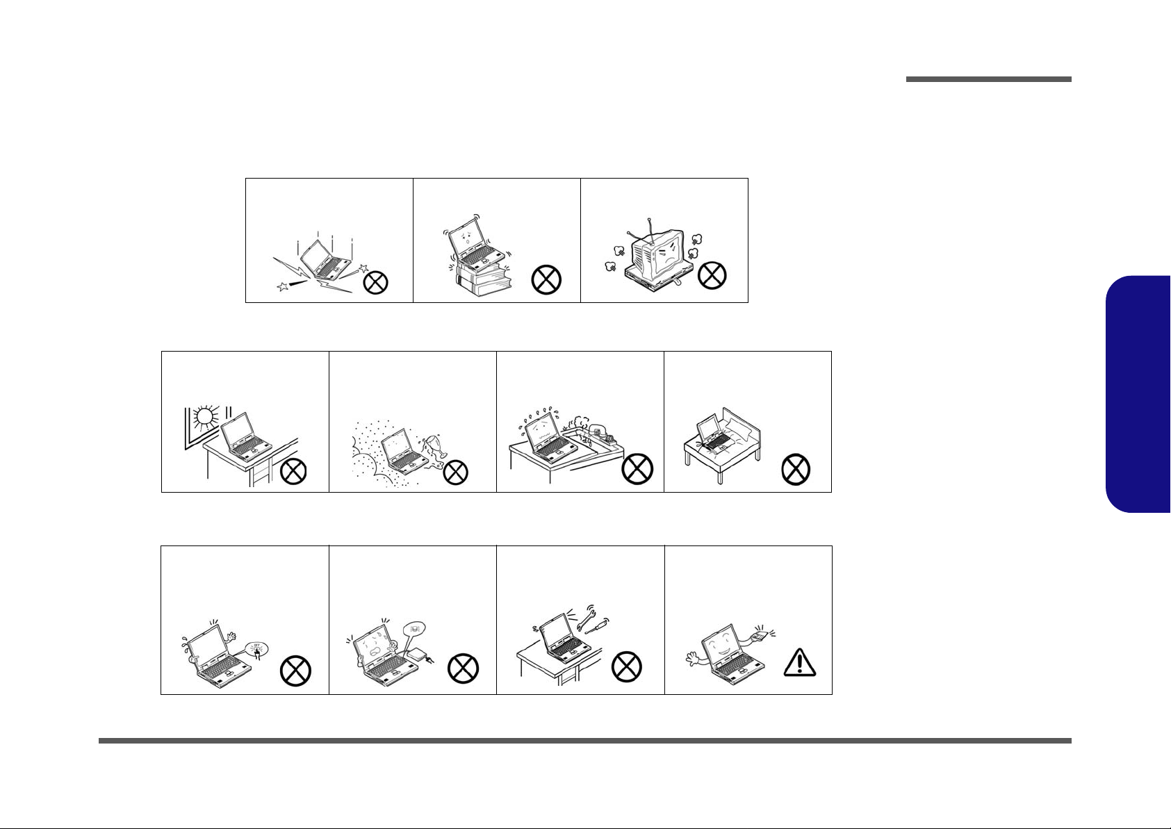
The notebook computer is quite rugged, but it can be damaged. To prevent this, follow these suggestions:
1. Don’t drop it, or expose it to shock. If the computer falls, the case and the components could be damaged.
Preface
Do not expose the computer
to any shock or vibration.
Do not place it on an unstable
surface.
Do not place anything heavy
on the computer.
2. Keep it dry, and don’t overheat it. Keep the computer and power supply away from any kind of heating element. This
is an electrical appliance. If water or any other liquid gets into it, the co mputer could be badly damaged.
Do not expose it to excessive
heat or direct sunlight.
Do not leave it in a place
where foreign matter or moisture may affect the system.
Don’t use or store the computer in a humid environment.
Do not place the computer on
any surface which will block
the vents.
3. Follow the proper working procedures for the computer. Shut the computer down properly and don’t forget to save
your work. Remember to periodically save your data as data may be lost if the battery is depleted.
Do not turn off the power
until you properly shut down
all programs.
Do not turn off any peripheral
devices when the computer is
on.
Do not disassemble the computer by yourself.
Perform routine maintenance
on your computer.
Preface
V
Page 8
Preface
Power Safety
Warning
Before you undertake
any upgrade procedures, make sure that
you have turned off the
power, and disconnected all peripherals
and cables (including
telephone lines). It is
advisable to also remove your battery in
order to prevent accidentally turning the
machine on.
4. Avoid interference. Keep the computer away from high capacity transformers, electric motors, and oth er strong mag-
netic fields. These can hinder proper performance and damage your data.
5. Take care when using peripheral devices.
Preface
VI
Use only approved brands of
peripherals.
Unplug the power cord befor e
attaching peripheral devices.
Power Safety
The computer has specific power requirements:
• Only use a power adapter approved for use with this computer.
• Your AC adapter may be designed for international travel but it still requires a stea dy, uninterrupted po wer supply. If you ar e
unsure of your local power specifications, consult your service representative or local power company.
• The power adapter may have either a 2-prong or a 3-prong grounded plug. The third prong is an important safety feature; do
not defeat its purpose. If you do not have access to a compatible outlet, have a qualified electrician install one.
• When you want to unplug the power cord, be sure to disconnect it by the plug head, not by its wire.
• Make sure the socket and any extension cord(s) you use can support the total current load of all the connected devices.
• Before cleaning the computer, make sure it is disconnected from any external power supplies (i.e. AC/DC adapter or car
adapter).
Do not plug in the power
cord if you are wet.
Do not use the power cord if
it is broken.
Do not place heavy objects
on the power cord.
Page 9

Battery Precautions
Battery Disposal
The product that you have purchased contains a rechargeable battery. The battery is recyclable. At the end of its useful life, under various state and local laws, it may be illegal to dispose of this battery into the municipal waste stream. Check with your local solid waste
officials for details in your area for recycling options or proper disposal.
Caution
Danger of explosion if battery is incorrectly replaced. Replace only with the same or equivalent type recommended by the manufacturer.
Discard used battery according to the manufacturer’s instructions.
Battery Level
Click the battery icon in the taskbar to see the current battery level and charge status. A battery that drops below a level of 10%
will not allow the computer to boot up. Make sure that any battery that drops below 10% is recharged within one week.
• Only use batteries designed for this computer. The wrong battery type may explode, leak or damage the computer.
• Do not continue to use a battery that has been dropped, or that appears damaged (e.g. bent or twisted) in any way. Even if the
computer continues to work with a damaged battery in place, it may cause circuit damage, which may possibly result in fire.
• Recharge the batteries using the notebook’s system. Incorrect recharging may make the battery explode.
• Do not try to repair a battery pack. Refer any battery pack repair or replacement to your service representative or qualified service
personnel.
• Keep children away from, and promptly dispose of a damaged battery. Always dispose of batteries carefully. Batteries may explode
or leak if exposed to fire, or improperly handled or discarded.
• Keep the battery away from metal appliances.
• Affix tape to the battery contacts before disposing of the battery.
• Do not touch the battery contacts with your hands or metal objects.
Battery Guidelines
The following can also apply to any backup batteries you may have.
• If you do not use the battery for an extended period, then remove the battery from the computer for storage.
• Before removing the battery for storage charge it to 60% - 70%.
• Check stored batteries at least every 3 months and charge them to 60% - 70%.
Preface
Preface
VII
Page 10

Preface
Preface
Related Documents
You may also need to consult the following manual for additional information:
User’s Manual on CD
This describes the notebook PC’s features and the procedures for operating the computer and its ROM-based setup program. It also describes the installation and operation of the utility programs provided with the notebook PC.
VIII
Page 11

Contents
Preface
Introduction ..............................................1-1
Overview .........................................................................................1-1
System Specifications .....................................................................1-2
External Locator - Top View with LCD Panel Open ......................1-4
External Locator - Front and Rear View .........................................1-5
External Locator - Left & Right Side View ...................................1-6
External Locator - Bottom View .....................................................1-7
Mainboard Overview - Top (Key Parts) .........................................1-8
Mainboard Overview - Bottom (Key Parts) ....................................1-9
Mainboard Overview - Top (Connectors) .....................................1-10
Mainboard Overview - Bottom (Connectors) ...............................1-11
Disassembly ...............................................2-1
Overview .........................................................................................2-1
Maintenance Tools ..........................................................................2-2
Connections .....................................................................................2-2
Maintenance Precautions .................................................................2-3
Disassembly Steps ...........................................................................2-4
Removing the Battery ......................................................................2-5
Removing the Hard Disk Drive .......................................................2-6
Removing the Optical (CD/DVD) Device ......................................2-8
Removing the System Memory (RAM) ..........................................2-9
Removing and Installing a Processor ............................................2-10
Removing the 3G Module .............................................................2-13
Removing the Wireless LAN Module ...........................................2-14
Removing the Bluetooth Module ..................................................2-15
Removing the LCD Front Cover ...................................................2-16
Removing the Inverter Board ........................................................2-17
Removing the Keyboard ................................................................2-18
Part Lists ..................................................A-1
Part List Illustration Location ........................................................ A-2
Top (C4500/C4501) ....................................................................... A-3
Top (C4505) ................................................................................... A-4
Bottom ........................................................................................... A-5
LCD ............................................................................................... A-6
DVD-ROM Drive .......................................................................... A-7
HDD ............................................................................................... A-8
Schematic Diagrams.................................B-1
SYSTEM BLOCK DIAGRAM ......................................................B-2
Clock Generator ..............................................................................B-3
CPU 1/4 ..........................................................................................B-4
CPU 2/4 ..........................................................................................B-5
CPU 3/4 ..........................................................................................B-6
CPU 4/4 ..........................................................................................B-7
DDR2 SO-DIMM 0 ........................................................................B-8
DDR2 SO-DIMM 1 ........................................................................B-9
RS780M-1 .....................................................................................B-10
RS780M-2 .....................................................................................B-11
RS780M-3 .....................................................................................B-12
LVDS, Inverter .............................................................................B-13
HDMI, CRT ..................................................................................B-14
SB700-1 ........................................................................................B-15
SB700-2 ........................................................................................B-16
SB700-3 ........................................................................................B-17
SB700-4 ........................................................................................B-18
New Card, Mini PCIE ...................................................................B-19
CCD, 3G, SATA ODD .................................................................B-20
USB, Fan, TP, Multi Con .............................................................B-21
Card Reader / LAN JMB261 ........................................................B-22
SATA HDD, LED, MDC, BT ......................................................B-23
Preface
XI
Page 12

Preface
Audio Codec ALC272 .................................................................. B-24
KBC ITE IT8502E .......................................................................B-25
System PWR, 2.5V .......................................................................B-26
PWRGD, RST .............................................................................. B-27
VCore ........................................................................................... B-28
0.9V, 1.8V, 1.8VS, 1.5VS ............................................................ B-29
1.1VS, 1.2V, 1.2VS, 1.2V ............................................................ B-30
VDD3, VDD5 ...............................................................................B-31
Charger, DC In ............................................................................. B-32
Click Board ..................................................................................B-33
Audio Board ................................................................................. B-34
Power Switch Board .....................................................................B-35
Preface
XII
Page 13

1: Introduction
Overview
This manual covers the information you need to service or upgrade the C4500/C4501/C4505 series notebook computer.
Information about operating the computer (e.g. getting started, and the Setup utility) is in the User’s Manual. Information
about drivers (e.g. VGA & audio) is also found in User’s Manual. That manual is shipped with the computer.
Operating systems (e.g. Windows XP, etc.) have their own manuals as do application software (e.g. word processing and
database programs). If you have questions about those programs, you should consult those manuals.
Introduction
The C4500/C4501/C4505 series notebook is designed to be upgradeable. See Disassembly on page 2 - 1 for a detail ed
description of the upgrade procedures for each specific component. Please note the warning and safety information indicated by the “” symbol.
The balance of this chapter reviews the computer’s technical specifications and features.
1.Introduction
Overview 1 - 1
Page 14
Introduction
System Specifications
1.Introduction
Processor
AMD® Athlon™ x2 Dual Core Processor:
QL62 (2.0GHz)
65nm (65 Nanometer) Process Technology,
1MB L2 Cache & 667MHz FSB -
(638-pin) Micro--PGA Package - Socket-S1G2
AMD® Athlon™ Single Core Processor:
QI46 (2.1GHz)
65nm (65 Nanometer) Process Technology,
512KB L2 Cache & 667MHz FSB -
(638-pin) Micro--PGA Package - Socket-S1G2
TDP 35W -
TDP 25W -
Core Logic
ATI® RS780MN + SB700
Display
14.0” 16:9 HD (1366 * 768) TFT LCD
Memory
64-bit Wide DDRII (DDR2) Data Channel
Two 200 Pin SO-DIMM sockets supporting
DDR2 667/800 MHz
Memory Expandable up to 4GB (using 1GB/
2GB SO-DIMM Modules)
Video
ATI® Radeon HD3200 On Board Video:
High Preference 3D/2D Graphic Accelerator
Shared Memory Architecture of up to 512MB
Supports Microsoft DirectX10 Compatible
BIOS
Storage
One Changeable 12.7mm(h) Super Multi
Optical Device Drive
Interface
One Changeable 2.5" 9.5 mm (h) HDD with
SATA (Serial) Interface
(CD/DVD) with SATA
Audio
High Definition Audio
Direct Sound 3D™ Compatible
Built-In Microphone
2 * Built-In Speakers
Keyboard & Pointing Device
Isolated WinKey Keyboard
Built-in TouchPad with Multi-Gesture
Functionality
Interface
Three USB 2.0 Ports
One External Monitor Port
One HDMI Out Port
One Headphone-Out Jack
One Microphone-In Jack
One RJ-45 LAN Jack
One DC-In Jack
Card Reader
Embedded 7-in-1 Card Reader (MS/ MS Pro/
SD/ Mini SD/ MMC/ RS MMC/ MS Duo) Note:
MS Duo/ Mini SD/ RS MMC Cards require a
PC adapter
Slots
One ExpressCard 34 Slot Supporting USB &
PCIe Interfaces
Two Mini-Card Slot s with PCIe (Slot 1) & USB
(Slot 2) interface:
Slot 1 for Half Mini-Card WLAN Module
(Option)
Slot 2 for 3.75G Module (
Factory Option
)
Communication
Built-In 10M/100Mb Base-T Ethernet LAN
3rd Party WLAN 802.11b/g/n
Module with PCIe Interface(Option)
Bluetooth 2.1 + EDR (Enhanced Data Rate)
Module (Factory Option)
1.3M Pixel PC Camera Module with USB
interface (Factory Option)
3.75G Module:
UMTS/HSPDA-based 3.75G Module with USB
Mini-Card Interface (
Quad-band GSM/GPRS (850 MHz, 900 MHz,
1800 MHz, 1900 MHz)
UMTS WCDMA FDD (2100 MHz)
Note that UMTS modes CAN NOT be used
in North America
Factory Option
Half Mini-Card
)
Power Management
Supports Wake on LAN
Supports Wake on USB
One 8Mb SPI Flash ROM
Phoenix™ BIOS
1 - 2 System Specifications
Page 15
Power
Full Range AC/DC Adapter
AC input 100 - 240V, 50 - 60Hz,
DC Output 19V, 3.42A or 18.5V, 3.5A (65
Watts)
Removable 6 Cell Smart Lithium Ion Battery
Pack 48.84WH
Security
Security (Kensington® Type) Lock Slot
BIOS Password
Operating System
Introduction
Windows® Vista (with Service Pack 2)
Windows® 7
Environmental Spec
Temperature
Operating: 5
Non-Operating: -20°C - 60°C
Relative Humidity
Operating: 20% - 80%
Non-Operating: 10% - 90%
Dimensions & Weight
340mm (w) * 238mm (d) * 13.9 - 31.8mm (h)
2.2 kg with 6 Cell Battery & ODD
°C - 35°C
1.Introduction
System Specifications 1 - 3
Page 16
Introduction
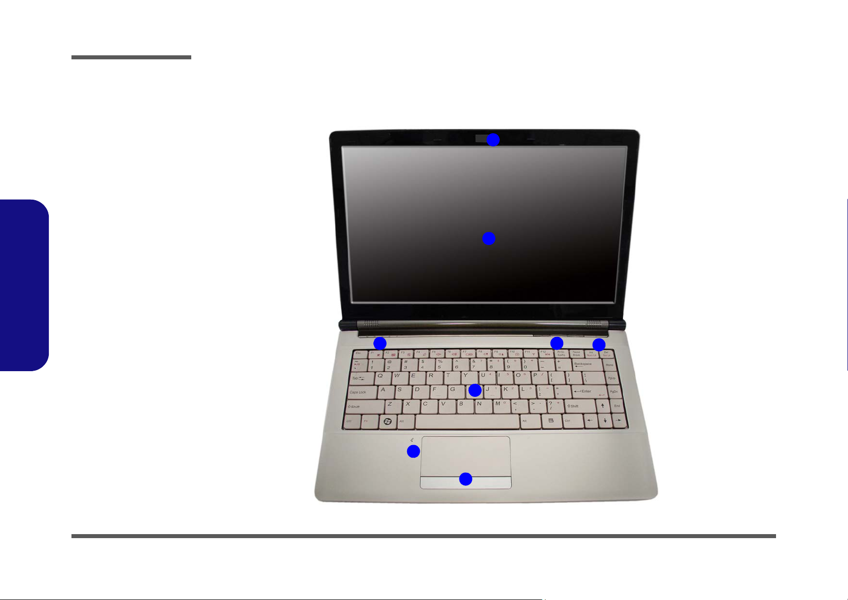
Figure 1
Top View
1. Optional Built-In PC
Camera
2. LCD
3. Power Button
4. Hot Key Buttons
5. LED Status
Indicators
6. Keyboard
7. Built-In Microphone
8. TouchPad and
Buttons
2
4
1
6
7
3
5
8
1.Introduction
External Locator - Top View with LCD Panel Open
1 - 4 External Locator - Top View with LCD Panel Open
Page 17
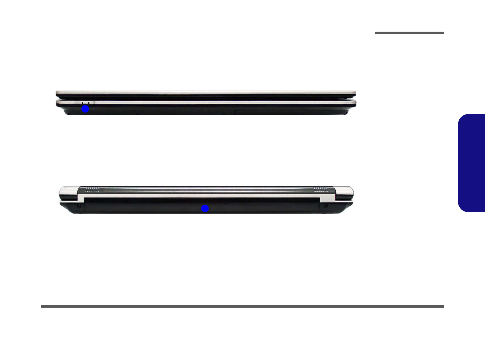
External Locator - Front and Rear View
1
Figure 2
Front View
1. LED Power
Indicators
Figure 3
Rear View
1. Battery
1
Introduction
1.Introduction
External Locator - Front and Rear View 1 - 5
Page 18

Introduction
1
6
3
5
2
8
5
7
4
Figure 4
Left Side View
1. DC-In Jack
2. External Monitor
Port
3. RJ-45 LAN Jack
4. HDMI-Out Port
5. 2 * USB 2.0 Ports
6. Vent/Fan Intake/
Outlet
7. Express Card Slot
8. 7-in-1 Card
Reader
Figure 5
Right Side View
1. Microphone-In
Jack
2. Headphone-Out
Jack
3. USB 2.0 Ports
4. Optional Device
Drive Bay
5. Security Lock Slot
142
3
5
1.Introduction
External Locator - Left & Right Side View
1 - 6 External Locator - Left & Right Side View
Page 19
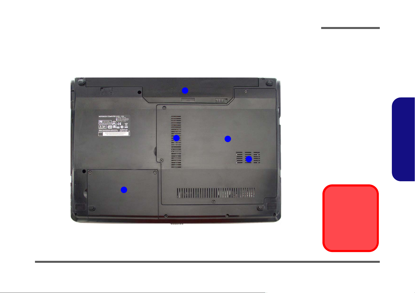
External Locator - Bottom View
Figure 6
Bottom View
1. Battery
2. Component Bay
Cover
3. Vent/Fan Intake/
Outlet
4. H ard Disk Bay
Cover
Overheating
To prevent your computer from overheating
make sure nothing
blocks the vent/fan intakes while the computer is in use.
1
2
4
3
3
Introduction
1.Introduction
External Locator - Bottom View 1 - 7
Page 20
Introduction
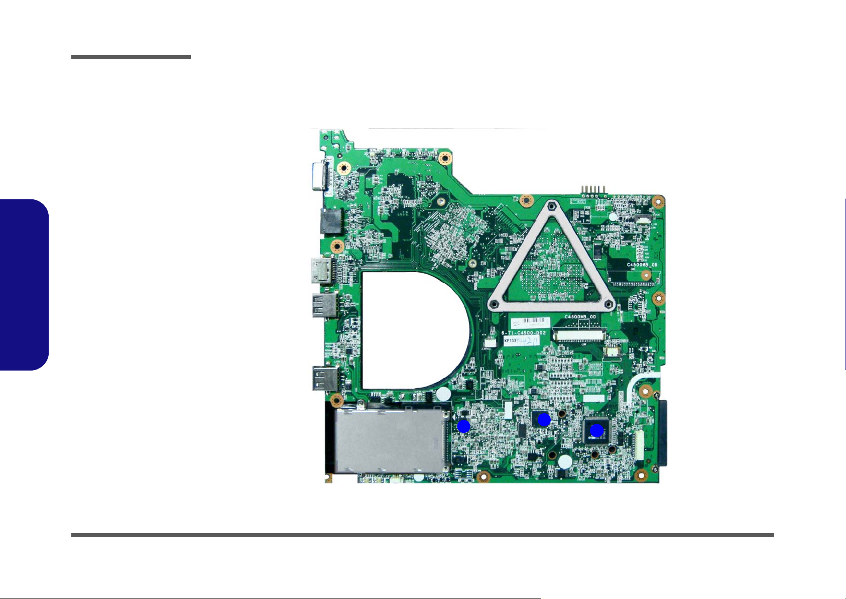
Figure 7
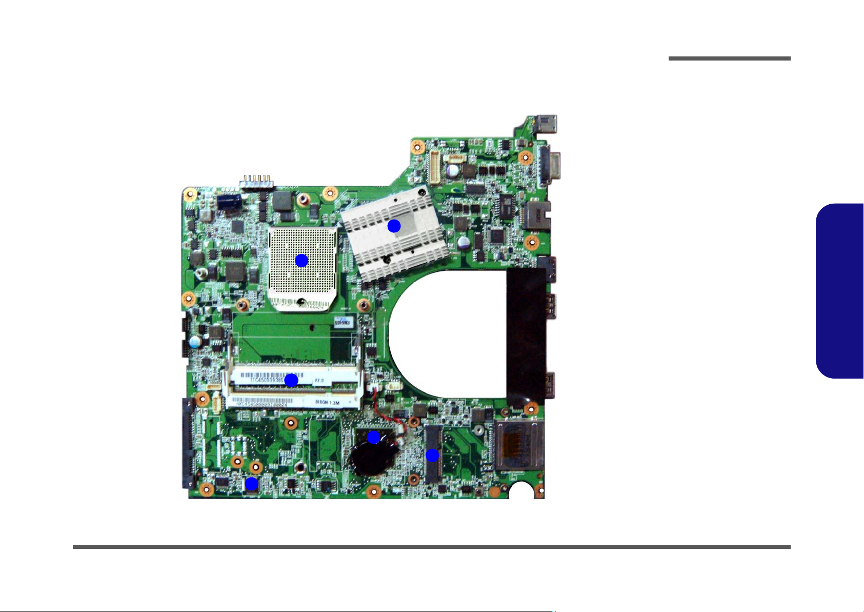
Mainboard Top
Key Parts
1. JMB385
2. ICS9LPRS480
3. ITE IT8502E
2
1
3
1.Introduction
Mainboard Overview - Top (Key Parts)
1 - 8 Mainboard Overview - Top (Key Parts)
Page 21
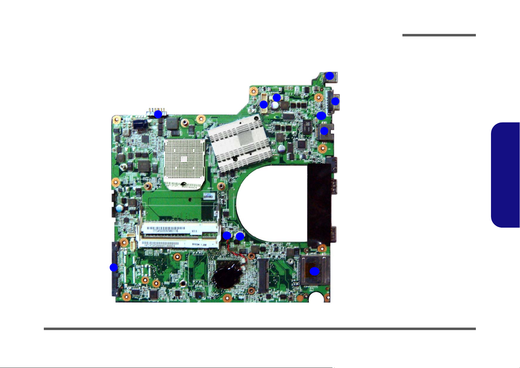
Mainboard Overview - Bottom (Key Parts)
Figure 8
Mainboard Bottom
Key Parts
1. CPU Socket (no
CPU installed)
2. NorthBridge
3. Memory Slots
DDR2 So-DIMM
4. SouthBridge
5. Realtek ALC272
6. Mini-PCIe Socket
(Wireless Lan
Module)
1
5
2
4
3
6
Introduction
1.Introduction
Mainboard Overview - Bottom (Key Parts) 1 - 9
Page 22
Introduction
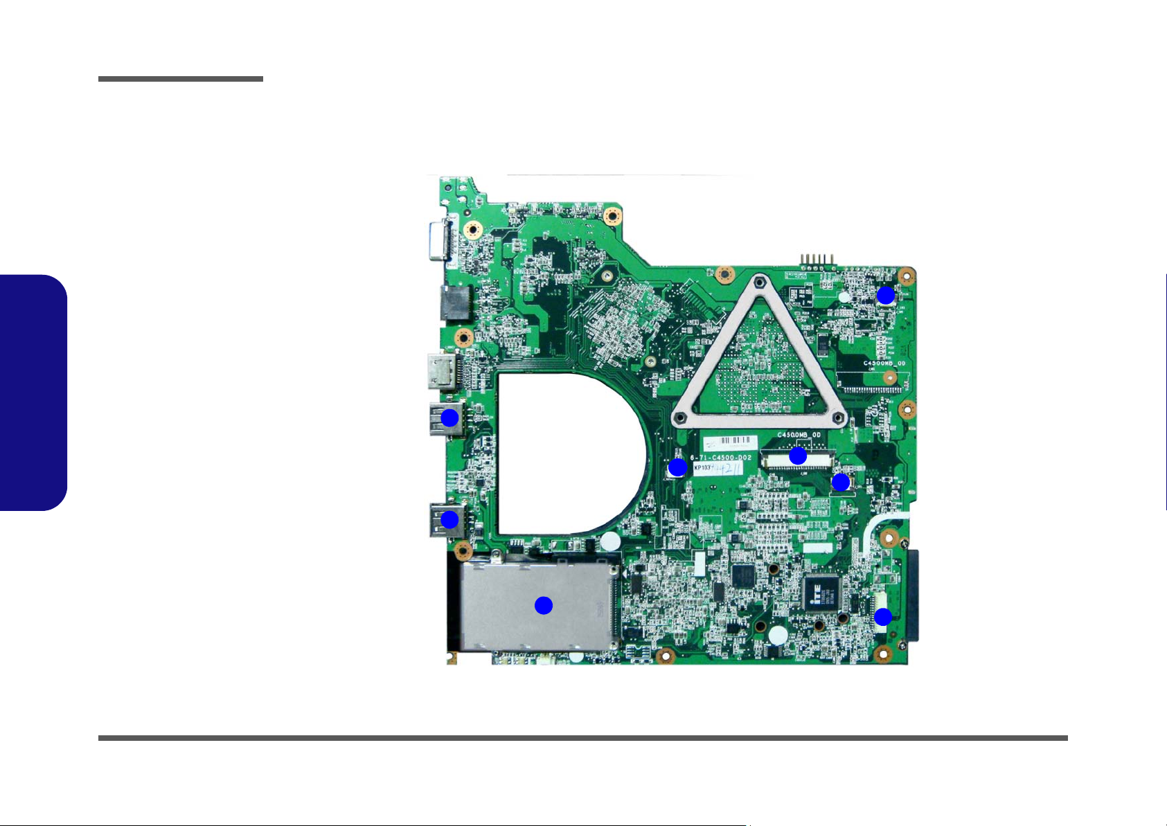
Figure 9
Mainboard Top
Connectors
1. USB Port
2. ExpressCard/34
Slot
3. Internal
Microphone Cable
Connector
4. Keyboard Cable
Connector
5. TouchPad Cable
Connector
6. Audio Board Cable
Connector
7. Power Switch
Board Cable
Connector
1
6
7
5
2
3
4
1
1.Introduction
Mainboard Overview - Top (Connectors)
1 - 10 Mainboard Overview - Top (Connectors)
Page 23
Mainboard Overview - Bottom (Connectors)
Figure 10
Mainboard Bottom
Connectors
1. RJ-45 Jack
2. CRT Port
3. DC-In Jack
4. CCD Cable
Connector
5. LCD Cable
Connector
6. Battery Connector
7. HDD Connector
8. CMOS Battery
Connector
9. Fan Cable
Connector
10.7-in-1 Card Reader
1
6
7
8
5
2
4
3
9
10
17
Introduction
1.Introduction
Mainboard Overview - Bottom (Connectors) 1 - 11
Page 24

Introduction
1.Introduction
1-12
Page 25

2: Disassembly
Information
Warning
Overview
This chapter provides step-by-step instructions for disassembling the C4500/C4501/C4505 series notebook’s parts and
subsystems. When it comes to reassembly, reverse the procedures (unless otherwise indicated).
We suggest you completely review any procedure before you take the computer apart.
Disassembly
Procedures such as upgrading/replacing the RAM, optical device and hard disk are included in the User’s Manual but are
repeated here for your convenience.
To make the disassembly process easier each section may have a box in the page margin. Information contained under
the figure # will give a synopsis of the sequence of procedures involved in the disassembly procedure. A box with a
lists the relevant parts you will have after the disassembly process is complete. Note: The parts listed will be for the disassembly procedure listed ONLY, and not any previous disassembly step(s) required. Refer to the part list for the previous disassembly procedure. The amount of screws you should be left with will be listed here also.
A box with a will also provide any possible helpful information. A box with a contains warnings.
An example of these types of boxes are shown in the sidebar.
2.Disassembly
Overview 2 - 1
Page 26

Disassembly
2.Disassembly
NOTE: All disassembly procedures assume that the system is turned OFF, and disconnected from any power supply (the
battery is removed too).
Maintenance Tools
The following tools are recommended when working on the notebook PC:
• M3 Philips-head screwdriver
• M2.5 Philips-head screwdriver (magnetized)
• M2 Philips-head screwdriver
• Small flat-head screwdriver
• Pair of needle-nose pliers
• Anti-static wrist-strap
Connections
Connections within the computer are one of four types:
Locking collar sockets for ribbon connectors To release these connectors, use a small flat-head screwdriver to
gently pry the locking collar away from its base. When replacing the connection, make sure the connector is oriented in the
same way. The pin1 side is usually not indicated.
2 - 2 Overview
Pressure sockets for multi-wire connectors To release this connector type, grasp it at its head and gently
rock it from side to side as you pull it out. Do not pull on the
wires themselves. When replacing the connection, do not try to
force it. The socket only fits one way.
Pressure sockets for ribbon connectors To release these connectors, use a small pair of needle-nose pli-
ers to gently lift the connector away from its socket. When replacing the connection, make sure the connector is oriented in
the same way. The pin1 side is usually not indicated.
Board-to-board or multi-pin sockets To separate the boards, gently rock them from side to side as
you pull them apart. If the connection is very tight, use a small
flat-head screwdriver - use just enough force to start.
Page 27

Maintenance Precautions
Power Safety
Warning
Before you undertake
any upgrade procedures, make sure that
you have turned off the
power, and disconnected all peripherals
and cables (including
telephone lines). It is
advisable to also remove your battery in
order to prevent accidentally turning the
machine on.
The following precautions are a reminder. To avoid personal injury or damage to the computer while performing a removal and/or replacement job, take the following precautions:
1. Don't drop it. Perform your repairs and/or upgrades on a stable surface. If the computer falls, the case and other
components could be damaged.
2. Don't overheat it. Note the proximity of any heating elements. Keep the computer out of direct sunlight.
3. Avoid interference. Note the proximity of any high capacity transformers, electric motors, and other strong mag-
netic fields. These can hinder proper performance and damage component s and/or data. You should also monitor
the position of magnetized tools (i.e. screwdrivers).
4. Keep it dry. This is an electrical appliance. If water or any other liquid gets into it, the computer could be badly
damaged.
5. Be careful with power. Avoid accidental shocks, discharges or explosions.
•Before removing or servicing any part from the computer, turn the computer off and detach any power supplies.
•When you want to unplug the power cord or any cable/wire, be sure to disconnect it by the plug head. Do no t pull on th e wir e.
6. Peripherals – Turn off and detach any peripherals.
7. Beware of static discharge. ICs, such as the CPU and main support chips, are vulnerable to static electricity.
Before handling any part in the computer, discharge any static electricity inside the computer. When handling a
printed circuit board, do not use gloves or other materials which allow static electricity buildup. We suggest that
you use an anti-static wrist strap instead.
8. Beware of corrosion. As you perform your job, avoid touching any connector leads. Even the cleanest hands produce oils which can attract corrosive elements.
9. Keep your work environment clean. Tobacco smoke, dust or other air-born particulate matter is often attracted
to charged surfaces, reducing performance.
10. Keep track of the components. When removing or replacing any part, be careful not to leave small part s, such as
screws, loose inside the computer.
Cleaning
Do not apply cleaner directly to the computer, use a soft clean cloth.
Do not use volatile (petroleum distillates) or abrasive cleaners on any part of the computer.
Disassembly
2.Disassembly
Overview 2 - 3
Page 28

Disassembly
Disassembly Steps
The following table lists the disassembly steps, and on which page to find the related information. PLEASE PERFORM
THE DISASSEMBLY STEPS IN THE ORDER INDICATED.
2.Disassembly
To remove the Battery:
1. Remove the battery page 2 - 5
To remove the HDD:
1. Remove the battery page 2 - 5
2. Remove the HDD page 2 - 6
To remove the Optical Device:
1. Remove the battery page 2 - 5
2. Remove the Optical device page 2 - 8
To remove the System Memory:
1. Remove the battery page 2 - 5
2. Remove the system memory page 2 - 9
To remove and install a Processor:
1. Remove the battery page 2 - 5
2. Remove the processor page 2 - 10
3. Install the processor page 2 - 12
To remove the 3G Module:
1. Remove the battery page 2 - 5
2. Remove the 3G module page 2 - 13
To remove the Bluetooth Module:
1. Remove the battery page 2 - 5
2. Remove the Bluetooth Module page 2 - 15
To remove the LCD Front Cover:
1. Remove the battery page 2 - 5
2. Remove the LCD Front Cover page 2 - 16
To remove the Inverter Board:
1. Remove the battery page 2 - 5
2. Remove the inverter board page 2 - 17
To remove the Keyboard:
1. Remove the battery page 2 - 5
2. Remove the keyboard page 2 - 18
To remove the Wireless LAN Module:
1. Remove the battery page 2 - 5
2. Remove the WLAN module page 2 - 14
2 - 4 Disassembly Steps
Page 29

Removing the Battery
3. Battery
1
234
Figure 1
Battery Removal
a. Slide latch towards the
unlock symbol and hold it
in place.
b. Slide the battery out.
1
2
4
a.
b.
3
1. Turn the computer off, and turn it over.
2. Slide the latch in the direction of the arrow.
3. Slide the latch in the direction of the arrow, and hold it in place.
4. Slide the battery out in the direction of the arrow .
Disassembly
2.Disassembly
Removing the Battery 2 - 5
Page 30

Disassembly
Figure 2
HDD Assembly
Removal
a. Remove the screws.
b. Remove the cover and lo-
cate the hdd.
8. Hard Disk Bay Cover
•2 Screws
1
2
3
a. b.
3
2
1
Removing the Hard Disk Drive
The hard disk drive is mounted in a removable case and can be taken out to accommodate other 2.5" serial (SATA) hard
disk drives with a height of 9.5mm (h). Follow your operating system’s installation instructions, and install all necessary
drivers and utilities (as outlined in Chapter 4 of the User’s Manual) when setting up a new hard disk.
2.Disassembly
Hard Disk Upgrade Process
1. Turn off the computer, and turn it over and remove the battery (page 2 - 5).
2. Locate the hard disk bay cover and loosen screws & .
3. Carefully remove the HDD bay cover .
2 - 6 Removing the Hard Disk Drive
Page 31

456
9
10
11
4
6
7
8
9
c.
d.
10
e.
5
11
Figure 3
HDD Assembly
Removal (cont’d)
c. Grip the tab and slide the
HDD assembly in the direction of the arrow
d. Lift the HDD assembly
out.
e. Remove the screws and
adhesive cover from the
HDD.
10 HDD Adhesive Cover
11.HDD
•4 Screws
Disassembly
4. Grip the tab and slide the hard disk in the direction of arrow .
5. Lift the hard disk assembly out of the bay.
6. Remove the screw(s) - and the adhesive cover from the HDD .
7. Reverse the process to install a new hard disk drive (do not forget to replace al the screws and covers).
2.Disassembly
Removing the Hard Disk Drive 2 - 7
Page 32

Disassembly
Figure 4
Optical Device
Removal
a. Remove the screws.
b. Remove the cover.
c. Remove the screw.
b. Push the optical device
out of the computer at
point 8.
Fan Cable
Make sure you reconnect the fan cable
(see page 2 - 6) before
screwing down the bay
cover.
514
5
6
798
a.
c.
6
1
3
2
4
5
5
b.
8
7
9
d.
6. Component Bay
Cover
9. Optical Device
•5 Screws
2.Disassembly
Removing the Optical (CD/DVD) Device
1. Turn off the computer, turn it over and remove the battery (page 2 - 5).
2. Locate the component bay cover and remove screws - .
3. Carefully (a fan and cable are attached to the under side of the cover) lift up the bay cover.
4. Carefully disconnect the fan cable , and remove the cover .
5. Remove the screw at point , and use a screwdriver to carefully push out the optical device at point out of
the computer.
6. Insert the new device and carefully slide it into the computer (the device only fits one way. DO NOT FORCE IT; The
screw holes should line up).
7. Restart the computer to allow it to automatically detect the new device.
2 - 8 Removing the Optical (CD/DVD) Device
Page 33

Removing the System Memory (RAM)
Figure 5
RAM Module
Removal
a. Locate the memory
socket.
b. Pull the release
latch(es).
c. Remove the mod-
ule(s).
Contact Warning
Be careful not to touch
the metal pins on the
module’s connecting
edge. Even the cleanest
hands have oils which
can attract particles, and
degrade the module’s
performance.
4. RAM Module
123
a.
b.
c.
1
3
2
4
4
The computer has two memory sockets for 200 pin Small Outline Dual In-line Memory Modules (SO-DIMM) supporting
DDRII (DDR2) 667MHz/800 MHz. The main memory can be expanded up to 4GB. The SO-DIMM modules supported
are 1024MB and 2048MB DDRII Modules. The total memory size is automatically detected by the POST routine once
you turn on your computer.
Memory Upgrade Process
1. Turn off the computer, turn it over and remove the battery (page 2 - 5) and the component bay cover (page 2 - 6).
2. The RAM module(s) will be visible at point on the mainboard.
3. Gently pull the two release latches ( & ) on the sides of the memory socket in the direction indicated by the
Disassembly
arrows (Figure 5b).
2.Disassembly
4. The RAM module(s) will pop-up
5. Pull the latches to release the second module if necessary.
6. Insert a new module holding it at about a 30° angle and fit the connectors firmly into the memory slot.
7. The module will only fit one way as defined by its pin alignment. Make sure the module is seated as far into the slot
8. Press the module in and down towards the mainboard until the slot levers click into place to secure the module.
9. Replace the component bay cover and the screws (make sure you reconnect the fan cable before screwing
10. Restart the computer to allow the BIOS to register the new memory configuration as it starts up.
(Figure 5c), and you can then remove it.
as it will go. DO NOT FORCE IT; it should fit without much pressure.
down the bay cover).
Removing the System Memory (RAM) 2 - 9
Page 34

Disassembly
1
245
6
7
8
2
3
4
1
a.
c.
b.
5
6
7
8
Figure 6
Processor Removal
a. Locate the heat sink.
b. Remove the screws from
the CPU heatsink and
bracket.
c. Remove the CPU heat
sink and bracket .
7. CPU Heat Sink
8. Bracket
•5 Screws
Removing and Installing a Processor
Processor Removal Procedure
1. Turn off the computer, turn it over, and remove the battery (page 2 - 5) and the component bay cover (page 2 - 6).
2. The heat sink will be visible at point on the mainboard
3. Remove the screws - from the heat sink in the order indicated (Figure 6b).
4. Remove the screws & from the bracket on the Northbridge heat sink (Figure 6b).
5. Carefully lift the CPU heat sink and metal bracket
(Figure 6c) up off the computer.
2.Disassembly
2 - 10 Removing and Installing a Processor
Page 35

9
10
Figure 7
Processor Removal
(cont’d)
d. Turn the release latch to
unlock the CPU.
e. Lift the CPU out of the
socket.
d.
e.
Caution
The heat sink, and CPU area in
general, contains parts which are
subject to high temperatures. Allow
the area time to cool before removing these parts.
Unlock Lock
10
9
9
10.CPU
Disassembly
6. Turn the release latch towards the unlock symbol to release the CPU.
7. Carefully (it may be hot) lift the CPU up and out of the socket (Figure 7e).
8. Reverse the process to install a new CPU.
9. When re-inserting the CPU, pay careful attention to the pin alignment, it will fit only one way (DO NOT FORCE IT!).
2.Disassembly
Removing and Installing a Processor 2 - 11
Page 36

Disassembly
ABC
DEF
G
1
3
4
5
d.
b. e.
B
a.
D
G
1
3
2
4
Note:
Tighten the screws in the order
as indicated on the label.
C
5
A
F
c.
E
Figure 8
Processor
Installation
a. Insert the CPU.
b. Turn the r elease latch to-
wards the lock symbol.
c. Remove the screws and
lift the bracket off the
Northbridge heat sink.
d. Remove the sticker from
the heat sink and insert
the heat sink.
e. Tighten the screws.
A. CPU
E. Bracket
G. Heat Sink
Processor Installation Procedure
1. Insert the CPU , pay careful attention to the pin alignment, it will fit only one way (DO NOT FORCE IT!), and turn
the release latch towards the lock symbol (Figure 8b).
2. Remove the screws - and lift the metal bracket
3. Remove the sticker (Figure 8c) from the heat sink.
4. Insert the heat sink
5. Tighten the CPU heat sink screws in the order
bracket screws
as indicated in Figure 8c.
to (the order as indicated on the label in Figure 8d) and
& .
6. Replace the component bay cover and tighten the screws (see page 2 - 6).
off the Northbridge heat sink (Figure 6b).
2.Disassembly
2 - 12 Removing and Installing a Processor
Page 37

Removing the 3G Module
Figure 9
3G Module Removal
a. Locate the 3G module.
b. Disconnect the cable
and remove the screw.
c. Remove the 3G module.
Note: Make sure you
reconnect the antenna
cable to socket (Fig-
ure 9b).
1
2
3
4
b.
c.
a.
3
1
2
4
4. 3G Module
•1 Screw
1. Turn off the computer, turn it over, and remove the battery (page 2 - 5) and the component bay cover (page 2 - 6).
2. The 3G module will be visible at point on the mainboard.
3. Carefully disconnect the cable , and then remove the screw
4. The 3G module (Figure 10c) will pop-up, and you can remove it off the computer.
.
Disassembly
2.Disassembly
Removing the 3G Module 2 - 13
Page 38

Disassembly
Figure 10
Wireless LAN
Module Removal
a. Locate the WLAN.
b. Disconnect the cable
and remove the screw.
c. The WLAN module will
pop up.
d. Remove the Wireless
LAN module.
Note: Make sure you
reconnect the antenna
cable to the “1 + 2”
socket (Figure 10b).
1
234
5
b.
c.
a.
4
3
2
5
5
d.
1
5. Wireless LAN
Module
•1 Screw
Removing the Wireless LAN Module
1. Turn off the computer, turn it over, and remove the battery (page 2 - 5) and the component bay cover (page 2 - 6).
2. The wireless LAN module will be visible at point on the mainboard.
3. Carefully disconnect the cables - , and then remove the screw
4. The wireless LAN module (Figure 10c) will pop-up, and you can remove it off the computer.
.
2.Disassembly
2 - 14 Removing the Wireless LAN Module
Page 39

Removing the Bluetooth Module
Figure 11
Bluetooth Module
Removal
a. Locate the Bluetooth
module.
b. Remove the screw.
c. Disconnect the cable
and the connector from
the bluetooth module.
d. Lift the Bluetooth module
out.
1
234
5
c.
a.
4
1
5
2
3
b.
d.
5. Bluetooth Module
•1 Screw
1. Turn off the computer, turn it over, and remove the battery (page 2 - 5) and the component bay cover (page 2 - 6).
2. The Bluetooth module will be visible at point on the mainboard.
3. Remove the screw and turn the module over.
4. Carefully disconnect the cable and separate the connector (Figure 11b) from the Bluetooth Module.
5. Lift the Bluetooth Module (Figure 11c) up and off the computer.
Disassembly
2.Disassembly
Removing the Bluetooth Module 2 - 15
Page 40

Disassembly
Figure 12
LCD Front Cover
Removal
a. Remove the screws and
unsnap the LCD front
cover from the LCD pan-
el.
b. Slide the LCD panel cov-
er in the direction of the
arrow.
145
6
7
5. LCD Front Cover
•4 Screws
a. b.
1
2
3
4
7
5
6
7
5
Rubber Screw Covers
After removing the rubber screw covers, place them on a
clean dry surface (or attach them to the front cover itself) in
order to prevent loss of adhesive.
Removing the LCD Front Cover
1. Turn off the computer, and remove the battery (page 2 - 5).
2. Remove any rubber covers and screws - (Figure 12a), then run your finger around the middle of the frame
to carefully unsnap the LCD front cover from the LCD panel.
3. After unsnapping all four sides of the LCD front cover, carefully slide the LCD front cover downwards in the direction of the arrow (be careful of the LCD hinges at point ).
4. You can now remove the LCD front cover.
2.Disassembly
2 - 16 Removing the LCD Front Cover
Page 41

Removing the Inverter Board
Figure 13
Inverter Board
Removal
a. Remove the screw from
the inverter board and lift
the board up slightly.
b. Disconnect the cables
from the inverter.
c. Remove the inverter.
Note: C4500 LCD
does not have Inverter
board.
123
4
4. Inverter Board
•1 Screw
a.
b.
Inverter Power Warning
In order to prevent a short circuit
when removing the inverter it is
necessary to discharge any remaining system power. To do
so, press the computer’s power
button for a few seconds before
disconnecting the inverter cable.
1
2
3
c.
4
1. Turn off the computer, remove the battery (page 2 - 5) and remove LCD front cover (page 2 - 16).
2. Discharge the remaining system power (see Inverter Power Warning below).
3. Remove screw (Figure 13b) from the inverter, and carefully lift the inverter board up slightly.
4. Disconnect cables & (Figure 13c) from the inverter , then remove the inverter (Figure 13d) from the top
case assembly.
Disassembly
2.Disassembly
Removing the Inverter Board 2 - 17
Page 42

Disassembly
Figure 14
Keyboard Removal
a. Press the four latches to
release the keyboard.
b. Lift the keyboard up and
disconnect the cable
from the locking collar.
c. Remove the keyboard.
145
5
6
7
Re-Inserting the
Keyboard
When re-inserting the
keyboard firstly align the
four keyboard tabs at the
bottom (Figure 14d) at
the bottom of the keyboard with the slots in the
case.
a.
b.
Keyboard Tabs
1
3
2
4
6
7
5
c.
7. Keyboard
Removing the Keyboard
1. Turn off the computer, and remove the battery (page 2 - 5).
2. Press the four keyboard latches - at the top of the keyboard to elevate the keyboard from its normal position
(you may need to use a small screwdriver to do this).
3. Carefully lift the keyboard up, being careful not to bend the keyboard ribbon cable (Figure 14b).
4. Disconnect the keyboard ribbon cable from the locking collar socket .
5. Carefully lift up the keyboard (Figure 14c) off the computer.
2.Disassembly
2 - 18 Removing the Keyboard
Page 43

Appendix A:Part Lists
This appendix breaks down the C4500/C4501/C4505 series notebook’s construction into a series of illustrations. The
component part numbers are indicated in the tables opposite the drawings.
Note: This section indicates the manufacturer’s part numbers. Your organization may use a different system, so be sure
to cross-check any relevant documentation.
Note: Some assemblies may have parts in common (especially screws). However, the part lists DO NOT indicate the
total number of duplicated parts used.
Part Lists
Note: Be sure to check any update notices. The parts shown in these illustrations are appropriate for the system at the
time of publication. Over the product life, some parts may be improved or re-configured, resulting in new part numbers.
A.Part Lists
A-1
Page 44

Part Lists
Table A - 1
Part List Illustration
Location
Part List Illustration Location
The following table indicates where to find the appropriate part list illustration.
Part C4500/C4501 C4505
Top
page A - 3
A.Part Lists
Top
Bottom
LCD
DVD-ROM Drive
HDD
page A - 4
page A - 5
page A - 6
page A - 7
page A - 8
A - 2 Part List Illustration Location
Page 45

Top (C4500/C4501)
Figure A - 1
Top (C4500/C4501)
Part Lists
A.Part Lists
Top (C4500/C4501) A - 3
Page 46

Part Lists
Figure A - 1
Top (C4505)
A.Part Lists
Top (C4505)
A - 4 Top (C4505)
Page 47

Bottom
Figure A - 2
Bottom
Part Lists
A.Part Lists
Bottom A - 5
Page 48

Part Lists
Figure A - 3
LCD
A.Part Lists
A - 6 LCD
LCD
Page 49

DVD-ROM Drive
Figure A - 4
DVD-ROM Drive
Part Lists
A.Part Lists
DVD-ROM Drive A - 7
Page 50

Part Lists
Figure A - 5
HDD
A.Part Lists
HDD
A - 8 HDD
Page 51

Appendix B:Schematic Diagrams
Table B - 1
Schematic
Diagrams
Version Note
The schematic diagrams in this chapter
are based upon version 6-7P-C4504-012.
If your mainboard (or
other boards) are a later version, please
check with the Service
Center for updated diagrams (if required).
This appendix has circuit diagrams of the C4500/C4501/C4505 notebook’s PCB’s. The following table indicates where
to find the appropriate schematic diagram.
Diagram - Page Diagram - Page Diagram - Page
SYSTEM BLOCK DIAGRAM - Page B - 2 HDMI, CRT - Page B - 14 System PWR, 2.5V - Page B - 26
Clock Generator - Page B - 3 SB700-1 - Page B - 15 PWRGD, RST - Page B - 27
CPU 1/4 - Page B - 4 SB700-2 - Page B - 16 VCore - Page B - 28
CPU 2/4 - Page B - 5 SB700-3 - Page B - 17 0.9V, 1.8V, 1.8VS, 1.5VS - Page B - 29
CPU 3/4 - Page B - 6 SB700-4 - Page B - 18 1.1VS, 1.2V, 1.2VS, 1.2V - Page B - 30
CPU 4/4 - Page B - 7 New Card, Mini PCIE - Page B - 19 VDD3, VDD5 - Page B - 31
DDR2 SO-DIMM 0 - Page B - 8 CCD, 3G, SATA ODD - Page B - 20 Charger, DC In - Page B - 32
DDR2 SO-DIMM 1 - Page B - 9 USB, Fan, TP, Multi Con - Page B - 21 Click Board - Page B - 33
Schematic Diagrams
B.Schematic Diagrams
RS780M-1 - Page B - 10 Card Reader / LAN JMB261 - Page B - 22 Audio Board - Page B - 34
RS780M-2 - Page B - 11 SATA HDD, LED, MDC, BT - Page B - 23 Power Switch Board - Page B - 35
RS780M-3 - Page B - 12 Audio Codec ALC272 - Page B - 24
LVDS, Inverter - Page B - 13 KBC ITE IT8502E - Page B - 25
B-1
Page 52

Schematic Diagrams
Sheet 1 of 34
SYSTEM BLOCK
DIAGRAM
AUD IO BOA RD
VCO RE _VD D_ NB
BATTER Y CH AGER
Port 1
SPI ROM
POWE R SW ITCH B OARD
AM D S 1 G 2 CP U
AT A 66 / 1 00 /1 33
128pins LQFP
PCIE0
VCO RE _VD D_ CORE
CPU_V DD0 ,C PU_VD D D1
USB#0
CR T CON
CCD
DE BU G PO RT
KBC IT8502E
480 Mbps
Bluetooth
Port 2
IN
14 * 14 * 1. 6m m
1 X8 P C IE I/ F
USB8
AC9 7 2. 3
33 MHz
UNB UFFE RE D D DR2
SODIMM 0
OUT
USB#2
PS 2
TO UC H P AD
PWRGD,RST
Channel A
SB700
PCIE3
CLEVO C4500
Car d Re ad e r \ Lan
X4
SPI I/F
0.9V,1.8V ,
1.8VS,1.5VS
PCIE2
USB#1
32.768 KHz
1 X4 P C IE I/ F W IT H S B
CLI CK B OA RD
638-Pin uFCPGA 638
LVDS /CR T
4 X1 P C IE I/ F
SATA II (4PORTS)
EXTERNAL CLOCK GENERATOR
64 PIN
ICS9LPRS480
HyperTransport LINK0 CPU I/F
GPP PCIE INTERFACE
AZALIA HD AUDIO
Channel B
SYSTEM PW R ,2.5V
1.8VS,3.3VS,5VS,3.3V,1.2VS
IN T
KEY B OA RD
Port 0
USB9 o r US B6
Power switch + Hotkey X 3
100 MHz
A UD IO BO ARD
RS78 0M(C)
USB2 .0 ( 10)
NEW C ARD
CPU
Temperature sen sor
DDR II
1.1VS,1.2V,1.2VS,1.2V_ HT
INT RT C
CPU FAN
JM C261
PCIE
VD D3 , VDD5
MINIPCIE-WLMINIPCIE-3G
INTEGRATE D GRAP HICS
USB 4
RJ11+USB X 2
6-7P-C4504-012
PCB 4-in-1:
6-71-C4500-D01A
6-71-C4502-D01
6-71-C4508-D01A
6-71-C450S-D01A
6-71-C4502-D01
USB 2.0
USB7
LP C I/F
ACPI 1 .1
6-71-C4508-D01A
LPC
HDMI CON
UNB UFFE RE D D DR2
SODIMM 1
USB5
6-71-C450S-D01A
CHARGER,DC IN
32.768 KHz
LVDS CON
HDT
HyperTransport (HT)
Headphone Jack
ALC 2 72 COD EC/
TPA60 17 AM P
HD AUDIO I/F
Int Speaker x1
MIC In Jack
MD C
24 MHz
54 9P I N F CB G A
SATA I/F
HDD x1
SATA#1
SA TA ODD
SA TA#4
AUDIO BOARD
R
L
INT MIC
465 PIN FCB GA
Int Speaker x1
SYSTEM BLOCK DIAGRAM
B.Schematic Diagrams
B - 2 SYSTEM BLOCK DIAGRAM
Page 53

Clock Generator
PCIE _E XP CAR D_C LKR EQ #
Z0206
Plac e n ext to VDD 48
2008/03/18
WLAN _CLKR EQ#
Z0204
PCIE_EXPCARD _CLKREQ#
WLAN_CLKREQ#
Z0202
100 M Hz non-spreading dif ferential SATA clock
10 0 M Hz s p readi n g diff erentia l SRC c lock
SE L_27 MH z
10 0 M Hz s p readi n g diff erentia l SRC c lock
SE L_SATA
0*
SE L_H TT66
27 MHz singled clock
1
100 M Hz diff e re ntial HT T c lo c k
0 *
1 *
* default
66 M Hz 3.3V single ended H TT clock
0
1
Pl a c e ve r y
clo s e to U 1
Place wi thin 0.5" o f
CLKGEN
SEL_27MHz
S EL_ H T 66
C270
.1U _16V_ 0 4
R142
*8 . 2 K _ 04
R135
*8.2K_04
R N31 *0_4P2R_04_4mil_sh or t1
2 3
4
C29 3
.1U _16V_ 0 4
L25 H CB1608KF-121T25-06
R N34 *0_4P2R_04_4mil_sh or t1
2 3
4
R134
*8 .2 K _ 04
R151
90.9_1%_ 06
C258
.1U_ 1 6 V _ 0 4
U4
IC S 9 LPR S 4 8 0
VD DA_2 7
4
GN D A _27
7
VD DR EF
56
GN D R EF
60
VD DSAT A
40
GN D S A T A
43
VD D48
63
GN D 4 8
1
VD DC PU
48
GN D C PU
46
VD DH TT
55
GN D H T T
52
VD DATIG
26
VD DSR C_IO 1
11
VD DSR C
16
VD DSB_ SR C
35
GN D A TIG 1
24
GN DS RC 1
10
GN DS RC 2
18
GN D S B _ SR C
33
X1
61
X2
62
CLKR EQ 2#
44
SM BCLK
2
SM BDAT
3
PD #
51
REF 0/S EL_H T T66
59
REF1/SEL_SATA
58
RE F 2/ SEL _27
57
CPUKG0T_LPRS
50
CPUKG0C_LPRS
49
ATI G0T_LPR S
30
ATIG0C _LPR S
29
ATI G1T_LPR S
28
ATIG1C _LPR S
27
SB_SR C0T _LPR S
37
SB_SR C0C _LPR S
36
SB_SR C1T _LPR S
32
SB_SR C1C _LPR S
31
SR C0T_LPR S
22
SR C0 C _LPR S
21
SR C1T_LPR S
20
SR C1 C _LPR S
19
SR C2T_LPR S
15
SR C2 C _LPR S
14
SR C3T_LPR S
13
SR C3 C _LPR S
12
SR C4T_LPR S
9
SR C4 C _LPR S
8
SRC7T_LPRS/27MHz_SS
6
SRC 7C_ L PRS / 27M Hz _N S
5
SRC6C /SATAC_LPRS
41
SRC 6T/SATAT_LPR S
42
HTT0T/ 66M _LPR S
54
HTT0C/66M_LPRS
53
48MHz_0
64
CLKR EQ 0#
23
CLKR EQ 1#
45
VD DATIG _IO
25
VD DC PU_IO
47
VD DSB_ SR C_IO
34
VD DSR C_IO 2
17
CLKR EQ 3#
39
CLKR EQ 4#
38
Therma l_GN D1
GND1
Therma l_GN D2
GND2
Therma l_GN D3
GND3
Therma l_GN D4
GND4
Ther mal_GN D5
GND5
Ther mal_GN D6
GND6
Ther mal_GN D7
GND7
Ther mal_GN D8
GND8
Ther mal_GN D9
GND9
R N36 *0_4P2R_04_4mil_sh or t1
2 3
4
C291
.1U_ 1 6V _04
C527
10U_6.3V_08
R176 33_1%_04
C24 0
.1U_ 1 6 V _ 04
R158 158_1% _06
R N37 *0_4P2R_04_4mil_sh or t1
2 3
4
R159
*8 .2 K _ 04
R 1 33 8. 2K_ 0 4
C28 1
27P_50V_04
C25 9
.1U_ 1 6 V _ 04
L54 H CB1608K F-121T25-06
R150
8.2K_04
L32 H CB1608K F-121T25-06
C32 1
10U _6.3V_08
R152
*8.2K_04
C237
.1U_ 1 6V _04
C29 2
.1U _16V_ 0 4
L31 H CB1608KF-121T25-06
C260
.1U_ 1 6 V _04
R N32 *0_4P2R_04_4mil_sh or t1
2 3
4
C23 9
.1U_ 1 6 V _ 04
R N30 *0_4P2R_04_4mil_sh or t1
2 3
4
R N35 *0_4P2R_04_4mil_sh or t1
2 3
4
R179
*0_0402_5mil_s hort
C29 0
.1U_ 1 6 V _ 04
R143
8.2K_04
C24 9
*1 U _ 16 V _ 0 6
C23 8
.1U _ 1 6V _04
R17 5
*1M_04
C32 0
27P_50V_04
C24 1
.1U _ 16V_ 0 4
C289
.1U_ 1 6 V _ 04
X2
14.318M Hz
12
R160
*8 .2 K _ 04
R N33 *0_4P2R_04_4mil_sh or t1
2 3
4
C306
1U _16V_06
CLK_VD D
CLK_ VD D
1.2VS
CLK_VDD
CLK_VDD
3.3VS
CLK_VDD
CLK_VD D
CLK_VDDIO
CLK_VDDIO
CPU_CLKP 5
CLK_VD D
Z0203
NBG F X_CLKN 10
NBG F X_CLKP10
CPU_CLKN 5
Z0201
SBLINK_CLKP 10
SBSRC_CLKP 14
SBSRC_CLKN 14
SBLINK_CLKN 10
PC IE_ PE2 _C L KP_ R
PCIE_ EX PCARD_CLKN 18
PCIE_ EX PCARD_CLKP 18
PC IE_PE1_CL KN_R
PC IE_PE3_CL KN_R
PC IE_ PE3 _C L KP_ R
PC IE_PE2_CL KN_R
PC IE_ PE1 _C L KP_ R
PCIE_ WL AN_ CL KP 18
PCIE_ CR_CLKP 21
PCIE_ CR_CLKN 21
PC IE_ EXPC ARD _ CLKP_ R
PC IE_ EXPC ARD _ CLKN _R
NBHT_CLKN 10
NBHT_CLKP 10
PCIE_ WL AN_ CL KN 1 8
SEL_SATA
SC L K07,8,15
SD ATA07,8,15
CLK_48M_U SB 15
Z0208
WLAN_CLKREQ#18
PCIE_EXPCARD _CLKREQ#15, 18
NB_ O SC10
Z0205
SEL_HT66
SEL_2 7MHz
NB GPP _C LK P_ R
NB GPP _C LK N_ R
Z0207
NB GFX_ CLKP_ R
NB GF X_ CL KN _R
CP U_ CL KP _R
CP U_ CL KN _ R
GF X_C LK N_R
GF X_C LK P_ R
RS780 1.1V
SEL_SATA
Layout note:
PLACE CRYSTAL WITHIN 500
MILS OF ICS9LPRS480
SBSR C_C LK P_R
SBSR C_C LK N_R
NB S L INK_ C LK P_R
NB S L INK_ C LK N_ R
NB HT RE F_C L KN_ R
NB HT RE F_C L KP_ RZ0209
Z0210
Z0211
Clo ck ch ip has in ternal serial termin atio ns
for d iffer en cial pa irs , exte rnal resi sto rs are
r e served f or debug purpose.
Sheet 2 of 34
Clock Generator
Schematic Diagrams
B.Schematic Diagrams
Clock Generator B - 3
Page 54

Schematic Diagrams
Sheet 3 of 34
CPU 1/4
* If VLD T is con ne cted only o n o ne sid e ,
one 4.7uF cap sh ould be add e d to
the is land sid e
1.5A
60MIL
1.5A
60MIL
Place close to socket
C440
4.7U _6 .3V_06
C447
4.7 U_6 .3V_06
C452
.22 U_1 0V_04
C451
.22U _10V_04
HT LINK
U15A
SOCKET_638_P IN
VLDT_A3
D4
VLDT_A2
D3
VLDT_A1
D2
VLDT_A0
D1
VLDT_B3
AE5
VLDT_B2
AE4
VLDT_B1
AE3
VLDT_B0
AE2
L0_CADIN_H15
N5
L0_C ADI N_L15
P5
L0_CADIN_H14
M3
L0_C ADI N_L14
M4
L0_CADIN_H13
L5
L0_C ADI N_L13
M5
L0_CADIN_H12
K3
L0_C ADI N_L12
K4
L0_CADIN_H11
H3
L0_C ADI N_L11
H4
L0_CADIN_H10
G5
L0_C ADI N_L10
H5
L0_CADIN_H9
F3
L0_CADIN_L9
F4
L0_CADIN_H8
E5
L0_CADIN_L8
F5
L0_CADIN_H7
N3
L0_CADIN_L7
N2
L0_CADIN_H6
L1
L0_CADIN_L6
M1
L0_CADIN_H5
L3
L0_CADIN_L5
L2
L0_CADIN_H4
J1
L0_CADIN_L4
K1
L0_CADIN_H3
G1
L0_CADIN_L3
H1
L0_CADIN_H2
G3
L0_CADIN_L2
G2
L0_CADIN_H1
E1
L0_CADIN_L1
F1
L0_CADIN_H0
E3
L0_CADIN_L0
E2
L0_CADOU T_H15
T4
L0_CADOUT_L15
T3
L0_CADOU T_H14
V5
L0_CADOUT_L14
U5
L0_CADOU T_H13
V4
L0_CADOUT_L13
V3
L0_CADOU T_H12
Y5
L0_CADOUT_L12
W5
L0_CADOU T_H11
AB5
L0_CADOUT_L11
AA5
L0_CADOU T_H10
AB4
L0_CADOUT_L10
AB3
L0_CAD OUT_H 9
AD5
L0_CADOUT_L9
AC5
L0_CAD OUT_H 8
AD4
L0_CADOUT_L8
AD3
L0_CAD OUT_H 7
T1
L0_CADOUT_L7
R1
L0_CAD OUT_H 6
U2
L0_CADOUT_L6
U3
L0_CAD OUT_H 5
V1
L0_CADOUT_L5
U1
L0_CAD OUT_H 4
W2
L0_CADOUT_L4
W3
L0_CAD OUT_H 3
AA2
L0_CADOUT_L3
AA3
L0_CAD OUT_H 2
AB1
L0_CADOUT_L2
AA1
L0_CAD OUT_H 1
AC2
L0_CADOUT_L1
AC3
L0_CAD OUT_H 0
AD1
L0_CADOUT_L0
AC1
L0_CLKIN_H1
J5
L0_CLKIN_L1
K5
L0_CLKIN_H0
J3
L0_CLKIN_L0
J2
L0_CTLIN_H1
P3
L0_CTLIN_L1
P4
L0_CTLIN_H0
N1
L0_CTLIN_L0
P1
L0_CLKOUT_H1
Y4
L0_CLKOUT_L1
Y3
L0_CLKOUT_H0
Y1
L0_CLKOUT_L0
W1
L0_ CTLOUT_H 1
T5
L 0_CTLO UT_ L1
R5
L0_ CTLOUT_H 0
R2
L 0_CTLO UT_ L0
R3
C441
180P_NPO_50V_04
C442
180P_NPO_50V_0 4
C443
4.7U _6. 3 V_06
1.2VS
1.2 VS
HT_NB_CPU_CAD_L09
HT_CPU_NB_CAD_H 0 9
1.2VS
HT_NB_CPU_CAD_H29
HT_NB_CPU_CAD_L19
HT_NB_CPU_CAD_H19
HT_NB_CPU_CAD_H49
HT_NB_CPU_CAD_L39
HT_NB_CPU_CAD_H39
HT_NB_CPU_CAD_L29
HT_NB_CPU_CAD_L59
HT_NB_CPU_CAD_H59
HT_NB_CPU_CAD_L49
HT_NB_CPU_CAD_H79
HT_NB_CPU_CAD_L69
HT_NB_CPU_CAD_H69
HT_NB_CPU_CAD_L89
HT_NB_CPU_CAD_H89
HT_NB_CPU_CAD_L79
HT_NB_CPU_CAD_H109
HT_NB_CPU_CAD_L99
HT_NB_CPU_CAD_H99
HT_NB_CPU_CAD_H129
HT_NB_CPU_CAD_L119
HT_NB_CPU_CAD_H119
HT_NB_CPU_CAD_L109
HT_NB_CPU_CAD_L139
HT_NB_CPU_CAD_H139
HT_NB_CPU_CAD_L129
HT_NB_CPU_CAD_H159
HT_NB_CPU_CAD_L149
HT_NB_CPU_CAD_H149
HT_NB_CPU_CLK_L09
HT_NB_CPU_CLK_H09
HT_NB_CPU_CAD_L159
HT_NB_CPU_CTL_H09
HT_NB_CPU_CLK_L19
HT_NB_CPU_CLK_H19
HT_CPU_NB_CAD_L0 9
HT_NB_CPU_CTL_L19
HT_NB_CPU_CTL_H19
HT_NB_CPU_CTL_L09
HT_CPU_NB_CAD_H 2 9
HT_CPU_NB_CAD_L1 9
HT_CPU_NB_CAD_H 1 9
HT_CPU_NB_CAD_L3 9
HT_CPU_NB_CAD_H 3 9
HT_CPU_NB_CAD_L2 9
HT_CPU_NB_CAD_H 5 9
HT_CPU_NB_CAD_L4 9
HT_CPU_NB_CAD_H 4 9
HT_CPU_NB_CAD_L6 9
HT_CPU_NB_CAD_H 6 9
HT_CPU_NB_CAD_L5 9
HT_CPU_NB_CAD_L8 9
HT_CPU_NB_CAD_H 8 9
HT_CPU_NB_CAD_L7 9
HT_CPU_NB_CAD_H 7 9
HT_CPU_NB_CAD_H 10 9
HT_CPU_NB_CAD_L9 9
HT_CPU_NB_CAD_H 9 9
HT_CPU_NB_CAD_L11 9
HT_CPU_NB_CAD_H 11 9
HT_CPU_NB_CAD_L10 9
HT_CPU_NB_CAD_H 13 9
HT_CPU_NB_CAD_L12 9
HT_CPU_NB_CAD_H 12 9
HT_CPU_NB_CAD_L14 9
HT_CPU_NB_CAD_H 14 9
HT_CPU_NB_CAD_L13 9
HT_CPU_NB_CLK_L0 9
HT_CPU_NB_CLK_H0 9
HT_CPU_NB_CAD_L15 9
HT_CPU_NB_CAD_H 15 9
HT_CPU_NB_CTL_H0 9
HT_CPU_NB_CLK_L1 9
HT_CPU_NB_CLK_H1 9
HT_CPU_NB_CTL_L1 9
HT_CPU_NB_CTL_H1 9
HT_CPU_NB_CTL_L0 9
HT_NB_CPU_CAD_H09
CPU 1/4
B.Schematic Diagrams
B - 4 CPU 1/4
Page 55

CPU 2/4
C499
4.7U_6.3V_06
C492
*.22U_10V _04
CPU _M_ VRE F _SU S
C483
1000P _X7R_50V_04
C49 1
*4 . 7 U_ 6 .3V _06
R301 39.2_1%_04
C86
180P_NPO_50V_04
C493
4.7U_6.3V_06
C115
.1U_X7R_10V_04
C48 5
.22U _10V_04
MEM:CMD /CTRL/ CLK
U15 B
SOCKET_638_PIN
VTT1
D10
VTT2
C10
VTT3
B10
VTT4
AD10
VTT5
W10
VTT6
AC 1 0
VTT7
AB10
VTT8
AA10
VTT9
A10
MA1_ODT1
V19
MA1_ODT0
U21
MA0_ODT1
V22
MA0_ODT0
T1 9
MB1_ODT0
Y26
MB0_ODT1
W23
MB0_ODT0
W26
RSV D_ M2
B18
MB 1_C S _L0
U22
MB 0_C S _L1
W25
MB 0_C S _L0
V26
MA0_CS_L1
U19
MA1_CS_L1
V20
MA1_CS_L0
U20
MA0_CS_L0
T2 0
MA_ADD15
K19
MA_ADD14
K24
MA_ADD13
V24
MA_ADD12
K20
MA_ADD11
L2 2
MA_ADD10
R21
MA_ADD9
K22
MA_ADD8
L1 9
MA_ADD7
L2 1
MA_ADD6
M2 4
MA_ADD5
L2 0
MA_ADD4
M2 2
MA_ADD3
M1 9
MA_ADD2
N22
MA_ADD1
M2 0
MA_ADD0
N21
M A_B ANK2
J2 1
M A_B ANK1
R23
M A_B ANK0
R20
MA_RAS_L
R19
MA_CAS_L
T2 2
MA_W E_L
T2 4
MEMZP
AF10
MEMZN
AE10
VTT_SEN SE
Y10
MEMVREF
W17
MA_C LK_H4
P19
MA_C LK_L4
P20
MA_C LK_H7
Y16
MA_C LK_L7
AA16
MA_C LK_H1
E16
MA_C LK_L1
F16
MA_C LK_H5
N19
MA_C LK_L5
N20
MB_CLK_H4
R26
MB _C L K _L4
R25
MB_CLK_H7
AF18
MB _C L K _L7
AF17
MB_CLK_H1
A17
MB _C L K _L1
A18
MB_CLK_H5
P22
MB _C L K _L5
R22
MA_CKE0
J2 2
MA_CKE1
J2 0
MB_CKE0
J25
MB_CKE1
H26
MB_A DD15
J24
MB_A DD14
J23
MB_A DD13
W24
MB_A DD12
L25
MB_A DD11
L26
MB_A DD10
T26
MB_ A D D 9
K26
MB_ A D D 8
M26
MB_ A D D 7
L24
MB_ A D D 6
N25
MB_ A D D 5
L23
MB_ A D D 4
N26
MB_ A D D 3
N23
MB_ A D D 2
P26
MB_ A D D 1
N24
MB_ A D D 0
P24
M B_B ANK2
J26
M B_B ANK1
U26
M B_B ANK0
R24
MB_RAS_L
U25
MB_CAS_L
U24
MB_ W E_ L
U23
RSVD_M1
H16
C105
1000P_X7R_50V_04
C85
*1000P_X7R_50V_04
C490
*180P _N PO_50V_04
C495
10 00P_ X7 R_5 0V_04
C50 0
4.7U _6.3V_06
C48 8
180P_N PO _50V_04
R96
1K_04_1%
C477
*.22U _10V_04
C47 8
*1000P_X7R_50V_04
C489
.22U_10V_04
PL A CE T HE M C LOS E TO
CP U WITHIN 1"
R293 39.2_1%_04
C484
18 0 P _ N P O _5 0 V _ 0 4
MEM:DATA
U15 C
SOCKET _638 _PI N
MB_DATA63
AD 11
MB_DATA62
AF 11
MB_DATA61
AF 14
MB_DATA60
AE 14
MB_DATA59
Y11
MB_DATA58
AB 11
MB_DATA57
AC 12
MB_DATA56
AF 13
MB_DATA55
AF 15
MB_DATA54
AF 16
MB_DATA53
AC 18
MB_DATA52
AF 19
MB_DATA51
AD 14
MB_DATA50
AC 14
MB_DATA49
AE 18
MB_DATA48
AD 18
MB_DATA47
AD 20
MB_DATA46
AC 20
MB_DATA45
AF 23
MB_DATA44
AF 24
MB_DATA43
AF 20
MB_DATA42
AE 20
MB_DATA41
AD 22
MB_DATA40
AC 22
MB_DATA39
AE 25
MB_DATA38
AD 26
MB_DATA37
AA 25
MB_DATA36
AA 26
MB_DATA35
AE 24
MB_DATA34
AD 24
MB_DATA33
AA 23
MB_DATA32
AA 24
MB_DATA31
G24
MB_DATA30
G23
MB_DATA29
D26
MB_DATA28
C26
MB_DATA27
G26
MB_DATA26
G25
MB_DATA25
E24
MB_DATA24
E23
MB_DATA23
C24
MB_DATA22
B24
MB_DATA21
C20
MB_DATA20
B20
MB_DATA19
C25
MB_DATA18
D24
MB_DATA17
A21
MB_DATA16
D20
MB_DATA15
D18
MB_DATA14
C18
MB_DATA13
D14
MB_DATA12
C14
MB_DATA11
A20
MB_DATA10
A19
MB_DATA9
A16
MB_DATA8
A15
MB_DATA7
A13
MB_DATA6
D12
MB_DATA5
E11
MB_DATA4
G11
MB_DATA3
B14
MB_DATA2
A14
MB_DATA1
A11
MB_DATA0
C11
MA_ D A TA 63
AA 12
MA_ D A TA 62
AB 12
MA_ D A TA 61
AA 14
MA_ D A TA 60
AB 14
MA_ D A TA 59
W11
MA_ D A TA 58
Y12
MA_ D A TA 57
AD 1 3
MA_ D A TA 56
AB 13
MA_ D A TA 55
AD 1 5
MA_ D A TA 54
AB 15
MA_ D A TA 53
AB 17
MA_ D A TA 52
Y17
MA_ D A TA 51
Y14
MA_ D A TA 50
W14
MA_ D A TA 49
W16
MA_ D A TA 48
AD 1 7
MA_ D A TA 47
Y18
MA_ D A TA 46
AD 1 9
MA_ D A TA 45
AD 2 1
MA_ D A TA 44
AB 21
MA_ D A TA 43
AB 18
MA_ D A TA 42
AA 18
MA_ D A TA 41
AA 20
MA_ D A TA 40
Y20
MA_ D A TA 39
AA 22
MA_ D A TA 38
Y22
MA_ D A TA 37
W21
MA_ D A TA 36
W22
MA_ D A TA 35
AA 21
MA_ D A TA 34
AB 22
MA_ D A TA 33
AB 24
MA_ D A TA 32
Y24
MA_ D A TA 31
H22
MA_ D A TA 30
H20
MA_ D A TA 29
E22
MA_ D A TA 28
E21
MA_ D A TA 27
J19
MA_ D A TA 26
H24
MA_ D A TA 25
F22
MA_ D A TA 24
F20
MA_ D A TA 23
C23
MA_ D A TA 22
B22
MA_ D A TA 21
F18
MA_ D A TA 20
E18
MA_ D A TA 19
E20
MA_ D A TA 18
D22
MA_ D A TA 17
C19
MA_ D A TA 16
G18
MA_ D A TA 15
G17
MA_ D A TA 14
C17
MA_ D A TA 13
F14
MA_ D A TA 12
E14
MA_ D A TA 11
H17
MA_ D A TA 10
E17
MA_DATA9
E15
MA_DATA8
H15
MA_DATA7
E13
MA_DATA6
C13
MA_DATA5
H12
MA_DATA4
H11
MA_DATA3
G14
MA_DATA2
H14
MA_DATA1
F12
MA_DATA0
G12
MB_DM7
AD 12
MB_DM6
AC 16
MB_DM5
AE 22
MB_DM4
AB 26
MB_DM3
E25
MB_DM2
A22
MB_DM1
B16
MB_DM0
A12
MB_DQ S_H7
AF 12
MB_DQ S_L7
AE 12
MB_DQ S_H6
AE 16
MB_DQ S_L6
AD 16
MB_DQ S_H5
AF 21
MB_DQ S_L5
AF 22
MB_DQ S_H4
AC 25
MB_DQ S_L4
AC 26
MB_DQ S_H3
F26
MB_DQ S_L3
E26
MB_DQ S_H2
A24
MB_DQ S_L2
A23
MB_DQ S_H1
D16
MB_DQ S_L1
C16
MB_DQ S_H0
C12
MB_DQ S_L0
B12
MA_DM7
Y13
MA_DM6
AB 16
MA_DM5
Y19
MA_DM4
AC 2 4
MA_DM3
F24
MA_DM2
E19
MA_DM1
C15
MA_DM0
E12
MA_ D QS _ H 7
W12
MA_DQS_L7
W13
MA_ D QS _ H 6
Y15
MA_DQS_L6
W15
MA_ D QS _ H 5
AB 19
MA_DQS_L5
AB 20
MA_ D QS _ H 4
AD 2 3
MA_DQS_L4
AC 2 3
MA_ D QS _ H 3
G22
MA_DQS_L3
G21
MA_ D QS _ H 2
C22
MA_DQS_L2
C21
MA_ D QS _ H 1
G16
MA_DQS_L1
G15
MA_ D QS _ H 0
G13
MA_DQS_L0
H13
R97
1K_04_1%
0. 9V
0. 9 V
1.8V
0.9V
CPU _M _ VREF _S U S
MEM_MA_A DD[ 0..15]7
1.8V
MEM_MA_B ANK17
MEM_MA_B ANK07
MEM_MB_DATA[0..63]8
MEM_MA_W E#7
MEM_MA_C AS#7
MEM_MA_R AS#7
MEM_MA_B ANK27
MEM _ MA0 _ CS# 07
MEM _ MA0 _ OD T17
MEM _ MA0 _ OD T07
MEM _ MA_ C KE 17
MEM _ MA_ C KE 07
MEM _ MA0 _ CS# 17
MEM_MA_C LK7_P7
MEM_MA_C LK1_N7
MEM_MA_C LK1_P7
MEM _ MB0 _ O D T1 8
MEM _ MB0 _ O D T0 8
MEM_MA_C LK7_N7
MEM _ MB_ C KE 1 8
MEM _ MB_ C KE 0 8
MEM _ MB0 _ C S # 1 8
MEM _ MB0 _ C S # 0 8
MEM _ MB_ C L K 7 _ P 8
MEM _ MB_ C L K 1 _ N 8
MEM _ MB_ C L K 1 _ P 8
MEM _ MB_ B A N K 0 8
MEM _ MB_ A D D [ 0 ..1 5] 8
MEM _ MB_ C L K 7 _ N 8
MEM _ MB_ R AS # 8
MEM _ MB_ B A N K 2 8
MEM _ MB_ B A N K 1 8
MEM _ MB_ D M [0 .. 7 ]8
MEM _ MB_ W E# 8
MEM _ MB_ C AS # 8
MEM_MB_DQS1_N8
MEM_MB_DQS1_P8
MEM_MB_DQS0_N8
MEM_MB_DQS0_P8
MEM_MB_DQS3_P8
MEM_MB_DQS2_N8
MEM_MB_DQS2_P8
MEM_MB_DQS4_N8
MEM_MB_DQS4_P8
MEM_MB_DQS3_N8
MEM_MB_DQS6_P8
MEM_MB_DQS5_N8
MEM_MB_DQS5_P8
MEM_MB_DQS7_N8
MEM_MB_DQS7_P8
MEM_MB_DQS6_N8
MEM_MA_DQS0_N 7
MEM_MA_DQS0_P 7
ME M_ MA _ D M [ 0 . . 7 ] 7
ME M_ MA _ D A TA [0.. 6 3 ] 7
MEM_MA_DQS2_P 7
MEM_MA_DQS1_N 7
MEM_MA_DQS1_P 7
MEM_MA_DQS3_N 7
MEM_MA_DQS3_P 7
MEM_MA_DQS2_N 7
MEM_MA_DQS5_P 7
MEM_MA_DQS4_N 7
MEM_MA_DQS4_P 7
MEM_MA_DQS6_N 7
MEM_MA_DQS6_P 7
MEM_MA_DQS5_N 7
MEM_MA_DQS7_N 7
MEM_MA_DQS7_P 7
Place close to socket
To SO-DIMM 0
socket
To SO-DIMM 1
socket
DEL
Width 20 mil ,length <6 inch
C138
10U _10V_08
VTT
75 0m A
VTT
750mA
Z0401
Z0402
Z0403
Z0404
Z0405
Z0406
Z0410
Z0409
Z0408
Z0411
Z0412
M_ Z N
M_ ZP
MEM_MB_DATA6
MEM_MB_DATA1
MEM_MB_DATA11
MEM_MB_DATA16
MEM_MB_DATA20
MEM_MB_DATA14
MEM_MB_DATA12
MEM_MB_DATA13
MEM_MB_DATA7
MEM_MB_DATA4
MEM_MB_DATA15
MEM_MB_DATA21
MEM_MB_DATA19
MEM_MB_DATA0
MEM_MB_DATA10
MEM_MB_DATA9
MEM_MB_DATA2
MEM_MB_DATA18
MEM_MB_DATA5
MEM_MB_DATA3
MEM_MB_DATA17
MEM_MB_DATA8
MEM _M A _ D A T A 5 4
MEM _M A _ D A T A 0
MEM _M A _ D A T A 1
MEM _M A _ D A T A 2
MEM _M A _ D A T A 5 5
MEM _M A _ D A T A 3
MEM _M A _ D A T A 5 6
MEM _M A _ D A T A 5
MEM _M A _ D A T A 7
MEM _M A _ D A T A 4
MEM _M A _ D A T A 8
MEM_MA_D ATA12
MEM_MA_D ATA10
MEM _M A _ D A T A 6
MEM _M A _ D A T A 5 7
MEM _M A _ D A T A 9
MEM _M A _ D A T A 1 5
MEM_MA_D ATA11
MEM _M A _ D A T A 1 3
MEM _M A _ D A T A 1 6
MEM _M A _ D A T A 1 9
MEM _M A _ D A T A 5 8
MEM _M A _ D A T A 1 7
MEM _M A _ D A T A 1 4
MEM _M A _ D A T A 1 8
MEM _M A _ D A T A 5 9
MEM _M A _ D A T A 2 0
MEM _M A _ D A T A 2 2
MEM _M A _ D A T A 2 1
MEM _M A _ D A T A 2 6
MEM _M A _ D A T A 2 3
MEM _M A _ D A T A 2 5
MEM _M A _ D A T A 2 4
MEM _M A _ D A T A 2 9
MEM _M A _ D A T A 2 8
MEM _M A _ D A T A 3 1
MEM _M A _ D A T A 3 2
MEM _M A _ D A T A 2 7
MEM _M A _ D A T A 3 0
MEM _M A _ D A T A 3 6
MEM _M A _ D A T A 4 0
MEM _M A _ D A T A 3 4
MEM _M A _ D A T A 3 3
MEM _M A _ D A T A 3 5
MEM _M A _ D A T A 6 0
MEM _M A _ D A T A 3 9
MEM _M A _ D A T A 4 1
MEM _M A _ D A T A 3 8
MEM _M A _ D A T A 3 7
MEM _M A _ D A T A 4 5
MEM _M A _ D A T A 4 3
MEM _M A _ D A T A 4 6
MEM _M A _ D A T A 4 4
MEM _M A _ D A T A 6 1
MEM _M A _ D A T A 4 2
MEM _M A _ D A T A 5 3
MEM _M A _ D A T A 4 7
MEM _M A _ D A T A 5 1
MEM _M A _ D A T A 4 8
MEM _M A _ D A T A 5 0
MEM _M A _ D A T A 4 9
MEM _M B_ A DD 14
MEM _M B_ A DD 3
MEM _M B_ A DD 12
MEM _M A _ D A T A 6 2
MEM _M A _ D A T A 5 2
MEM _M B_ A DD 6
MEM _M B_ A DD 1
MEM _M B_ A DD 7
MEM _M B_ A DD 10
MEM _M B_ A DD 13
MEM _M B_ A DD 11
MEM _M B_ A DD 8
MEM _M B_ A DD 4
MEM _M B_ A DD 2
MEM _M B_ A DD 5
MEM _M B_ A DD 9
MEM _M B_ A DD 0
MEM _M B_ A DD 15
MEM _M A _ D A T A 6 3
Z0407
M E M _ M A _A DD 14
M E M _ M A _A DD 13
MEM_MA_A DD3
M E M _ M A _A DD 12
M E M _ M A _A DD 10
M E M _ M A _A DD 11
MEM_MA_A DD2
MEM_MA_A DD1
MEM_MA_A DD8
MEM_MA_A DD9
MEM_MA_A DD5
MEM_MA_A DD6
MEM_MA_A DD7
MEM_MA_A DD4
MEM_MA_A DD0
M E M _ M A _A DD 15
M E M_ MA _D M5
MEM_MA_RESET#
M E M_ MA _D M6
M E M_ MA _D M2
M E M_ MA _D M4
M E M_ MA _D M1
M E M_ MA _D M0
M E M_ MA _D M3
M E M_ MA _D M7
ME M_ MB1 _ O D T 0
MEM_MA1_ODT0
MEM_MA1_ODT1
MEM_MB_DM5
MEM_MB_DM6
MEM_MB_DM4
MEM_MB_DM3
MEM_MB_DM7
MEM_MB_DM2
MEM_MB_DM1
MEM_MB_DM0
ME M_ MB_ R ESE T #
MEM_MB_DATA40
MEM_MB_DATA26
MEM_MB_DATA37
MEM_MB_DATA23
MEM_MB_DATA31
MEM_MB_DATA41
MEM_MB_DATA28
MEM_MB_DATA38
MEM_MB_DATA43
MEM_MB_DATA42
MEM_MB_DATA32
MEM_MB_DATA39
MEM_MB_DATA34
MEM_MB_DATA24
MEM_MB_DATA22
MEM_MB_DATA29
MEM_MB_DATA35
MEM_MB_DATA33
MEM_MB_DATA30
MEM_MB_DATA62
MEM_MB_DATA25
MEM_MB_DATA27
MEM_MB_DATA36
MEM_MB_DATA52
MEM_MB_DATA55
MEM_MB_DATA56
MEM_MB_DATA54
MEM_MB_DATA53
MEM_MB_DATA50
MEM_MB_DATA51
MEM_MB_DATA46
MEM_MB_DATA48
MEM_MB_DATA44
MEM_MB_DATA49
MEM_MB_DATA45
MEM_MB_DATA60
MEM_MB_DATA59
MEM_MB_DATA63
MEM_MB_DATA47
MEM_MB_DATA57
MEM_MB_DATA61
MEM_MB_DATA58
Proces sor M em ory In terfa ce
Sheet 4 of 34
CPU 2/4
Schematic Diagrams
B.Schematic Diagrams
CPU 2/4 B - 5
Page 56

Schematic Diagrams
20 08/ 03/1 8
20 08/ 03/1 8
EXIT BALL FIELD) A ND 500 mils LONG .
50 mils WIDE (USE 2x25 mil TRACES TO
CPU_SVD_R
Keep tra ce from resisor to C P U within 0.6"
ke ep t rac e f r o m ca ps t o C P U w i thin 1.2"
CPU_MEMHOT#_1.8V
LA YOUT: ROUTE VDDA T RAC E APPRO X.
CPU_VDDA_ RUN
CP U_HTREF0
R285 *0_0402_10mil_short
C47
.1U_X7R_10V_04
C83
10 U _10 V _08
P R 36 2. 2_ 1%_ 06
R43
*0_0402_5mil_s hort
R320
30 0_ 04
R85
30 0_ 04
R319
*0_0402_5mil_short
R45
*220_ 04
R191
30 0_ 04
Q39
2N3904
B
E C
U13
ADM1032ARM
SCLK
8
SDATA
7
ALERT#
6
GND5TH E R M#
4
D-
3
D+
2
VDD
1
R316
* 0_0 40 2_ 5m i l_ s h or t
Q38
*2N390 4
B
EC
R308
100K_04
R274
*0 _0 4
R300
4. 7K _ 04
R317
39 0_ 04
PR109 2.2_1%_06
R36
1K_04
R89
*2.2K_ 04
Q11
2N7002W
G
DS
R63 44.2_1%_04
R94
*2 20_0 4
C475
1U_16V_06
R56 44.2_1%_04
R44
*0_ 04 02_ 5m il _s hor t
R324
1K _0 4
R314
300 _0 4
R64
30 0_0 4
P R 37 2. 2 _ 1 % _0 6
R88 *0_04
PR108 2.2_1%_06
U15D
SOCKET_638_PIN
VDDA1
F8
VDDA2
F9
RESET_L
B7
PWROK
A7
LD T S TOP _L
F10
SIC
AF 4
SID
AF 5
HT_REF1
P6
HT_REF0
R6
VDD0_ FB_H
F6
VDD0_ FB_L
E6
VDDIO_FB_H
W9
VDDIO_ F B_L
Y9
THERMTRIP_L
AF 6
PROCHOT_L
AC 7
RSVD2
A5
LD T R E Q _L
C6
SV C
A6
SV D
A4
RSVD6
C5
RSVD4
B5
RSVD1
A3
CLKIN_H
A9
CLKIN_L
A8
DBRDY
G10
TMS
AA 9
TC K
AC9
TR S T _L
AD9
TD I
AF 9
DBREQ_L
E1 0
TD O
AE 9
TEST25_H
E9
TEST25_L
E8
TEST1 9
G9
TEST1 8
H10
RSVD8
AA 7
TEST9
C2
TE S T1 7
D7
TE S T1 6
E7
TE S T1 5
F7
TE S T1 4
C7
TEST1 2
AC8
TEST7
C3
TEST6
AA 6
TH E R M D C
W7
THERMDA
W8
VDD1_ FB_H
Y6
VDD1_ FB_L
AB 6
TE ST 29 _ H
C9
TEST29_L
C8
TEST2 4
AE 7
TEST2 3
AD7
TEST2 2
AE 8
TEST2 1
AB 8
TEST2 0
AF 7
TE ST 28 _ H
J7
TEST28_L
H8
TEST2 7
AF 8
ALERT_ L
AE 6
TE S T1 0
K8
TEST8
C4
RSVD3
B3
RSVD5
C1
VDDNB_FB_H
H6
VDDNB_FB_L
G6
RSVD7
D5
KEY2
W1 8
MEMH O T_ L
AA 8
RSVD10
H18
RSVD9
H19
KEY1
M11
Q12
2N7002W
G
DS
R325
*10K_04
PR116 2.2_1% _06
R35
1K _0 4
PW R G D
R76
*0_ 04 02_ 5m il _s hor t
C48
.1U_X7 R_10V_0 4
R48
*220_04
R318
300_04
R321
390_04
PR113 2.2_1%_06
R292 10K_04
C75
39 00 P_ X7 R _50 V _04
CPU_THERMTRIP#_1.8V
R278
30 0_0 4
R80
*0_0402_5mil_s hort
C459
.1U_X7R_10V_04
R 91 3 4. 8K _ 04
R75 300_04
C463
4.7U_6.3V_06
R84
30 0_ 04
R95
10 K_ 04
C474
1000P_X7R_50V_04
R90 2 0K_04
R83
4. 7K _0 4
R312
0_04
R189
30 0_ 04
R322
*1 0K _0 4
R299
4. 7K _0 4
C464
. 2 2U _1 6V _0 6
LDT_RST#
C84
3900P_X7R_50V_04
R47
*0_0402_5mil_s hort
L48 FCM1608KT-300T07
R323
10 K _04
R62
169 _1 % _0 4
R315
*0_0402_5mil_short
R46
*0_0402_5mil_s hort
R279 *0_0402_10mil_short
C76
39 00 P_ X7 R _50 V _04
1.8V
1. 8V
LD T_ R S T#
1. 8V S
2.5V_CPU
1. 8V
1.8V
VDD3
TH M _ VD D
1. 8V S
1. 8V S
place them to C PU within 1.5"
TH M _ VD D
3. 3V
LDT_RST#_HDT
3. 3 V
3. 3V S
3.3VS
CPU_VDD1
CPU_VDD0
CPU_VDDNB
3.3VS
1. 2 VS
1.8V
1.8V
1. 8V
CPU_SVC 27,30
CP U _MEMHOT# 7,8
CPU_THERMTRIP# 15
CPU_CLKP2
CPU_CLKN2
CPU_SVD 27,30
SC L K 315
SDAT A315
CPU_LDT_STOP#10 , 14
CPU_LDT_RST#14
SMC_CPU_THERM 24
CPU_LDT_REQ#10
CPU_PWRGD14
THERM_ALERT# 15,24
SMD_CPU_THERM 24
CPU_V DD1_RUN_FB_H27
CPU_V DD0_RUN_FB_L27
CPU_V DD1_RUN_FB_L27
CPU_VDDNB_RUN_FB_H 3 0
CPU_VDDNB_RUN_FB_L 30
CPU_V DD0_RUN_FB_H27
CPU_PWRGD_SVID_REG 27,30
CPU_PROCHOT# 14
CPU_SVC_R
Z0502
Z0503
Z0 50 5
CPU_PWRGD_SVID_REG
CPU_ALERT
N ear to
A DM10 32
10 MI LE
La yout No te:
Ro ute H_T HERM DA a nd
H_ THER MDC on same la yer.
10 mil tr ace on 1 0 m il
sp acin g.
10 MI LE
PWRGD
20 mi l
Thermal IC
CP U_ TD I
CP U_ TM S
CP U_ DB RE Q #
CP U_ TD O
CP U_ DB RD Y
CP U_ TC K
LDT_RST#_HDT
CP U_ TR ST #
KEY
J1
* ASP-68200-07
1
19
21
23
2
4
6
8
10
12
3
14
16
18
20
22
24
26
5
7
9
11
13
15
17
CPU_DBREQ#
PWRGD
2008/03/24
Z0 5 0 1
CPU_LDT_REQ#
CPU_CLKIN_SC_P
CPU_CLKIN_SC_N
LD T_ R S T#
CPU_TDO
CPU_DBREQ#
CPU_TEST25_L_BYPASSCLK_L
H_THERMDA
CLOSE TO SOC KET
C L OSE TO SOCKET
H_THERMDC
CPU_PROCHOT#_R
CPU_TEST28 _L_PLLCHRZ_N
CPU_TEST17 _BP3
CPU_TEST8_ DIG_T
CPU_TEST28 _H_PLLCHRZ_P
CPU_TEST16 _BP2
CPU_TEST10 _ANALOGOUT
CPU_TEST29 _L_FBCLKOUT_N
CPU_TEST15 _BP1
CPU_TEST7_ A NALOG_T
CPU_TEST14 _BP0
CPU_TEST29 _H_FBCLKOUT_P
VDDA
250mA
CPU_SID
CP U_HTREF1
CPU_SIC
CPU_TEST25_H_BYPASSCLK_H
LD T_ S TOP #
CPU_SVC_R
H_THERMDA
H_THERMDC
PWRGD
CPU_SVC
CPU_SVD_R
CPU_TEST12 _SCANSHIFTENB
CPU_TEST9_ANALOGIN
CPU_TDI
CPU_TEST20 _SCANCLK2
CPU_TEST27 _SINGLECHAIN
CPU_TRST#
CPU_TEST 23_TST UPD
CPU_SVD
CPU_TEST21 _SCANEN
CPU_DBRDY
CPU_TMS
CPU_TCK
CPU_TEST6_ DIECRACKMON
CPU_TEST22 _SCANSHIFTEN
CPU_TEST24 _SCANCLK1
C P U _ TEST 18 _P LL TE S T1
C P U _ TEST 19 _P LL TE S T0
PWRGD1
CPU_LDT_REQ#
CPU_THERMDC
CPU_THERMDA
CPU_SID
CPU_SIC
VID Over rid e Cir cu it
LD T_ S TOP #
AMD CHECK
tolerance 10% 1113
PWRGD
HDT Connector
1. 8 V
Known low temper ature PG issue,
Rep lace w ith another part
PW R G D
Sheet 5 of 34
CPU 3/4
CPU 3/4
B.Schematic Diagrams
B - 6 CPU 3/4
Page 57

CPU 4/4
VDDIO
2A
C79
22U _10V_12
C12 9
4. 7 U _6 . 3 V _ 0 6
C11 4
.01 U_ 1 6V_0 4
C99
22U__Y 5V_6.3V_08
C121
.01U _16V_04
C12 5
4.7U_6.3V_06
C117
.22U _10V_04
C91
.22 U_ 1 0 V _04
C11 6
.22U _10V_04
U15F
S O C KE T _6 3 8 _P IN
VS S1
AA4
VS S2
AA11
VS S3
AA13
VS S4
AA15
VS S5
AA17
VS S6
AA19
VS S7
AB2
VS S8
AB7
VS S9
AB9
VS S10
AB23
VS S11
AB25
VS S12
AC 11
VS S13
AC 13
VS S14
AC 15
VS S15
AC 17
VS S16
AC 19
VS S17
AC 21
VS S18
AD6
VS S19
AD8
VS S20
AD 25
VS S21
AE11
VS S22
AE13
VS S23
AE15
VS S24
AE17
VS S25
AE19
VS S26
AE21
VS S27
AE23
VS S28
B4
VS S29
B6
VS S30
B8
VS S31
B9
VS S32
B11
VS S33
B13
VS S34
B15
VS S35
B17
VS S36
B19
VS S37
B21
VS S38
B23
VS S39
B25
VS S40
D6
VS S41
D8
VS S42
D9
VS S43
D11
VS S44
D13
VS S45
D15
VS S46
D17
VS S47
D19
VS S48
D21
VS S49
D23
VS S50
D25
VS S51
E4
VS S52
F2
VS S53
F11
VS S54
F13
VS S55
F15
VS S56
F17
VS S57
F19
VS S58
F21
VS S59
F23
VS S60
F25
VS S61
H7
VS S62
H9
VS S63
H21
VS S64
H23
VS S65
J4
VSS 66
J6
VSS 67
J8
VSS 68
J10
VSS 69
J12
VSS 70
J14
VSS 71
J16
VSS 72
J18
VSS 73
K2
VSS 74
K7
VSS 75
K9
VSS 76
K11
VSS 77
K13
VSS 78
K15
VSS 79
K17
VSS 80
L6
VSS 81
L8
VSS 82
L10
VSS 83
L12
VSS 84
L14
VSS 85
L16
VSS 86
L18
VSS 87
M7
VSS 88
M9
VSS 89
AC 6
VSS 90
M17
VSS 91
N4
VSS 92
N8
VSS 93
N10
VSS 94
N16
VSS 95
N18
VSS 96
P2
VSS 97
P7
VSS 98
P9
VSS 99
P11
VSS100
P17
VSS101
R8
VSS102
R10
VSS103
R16
VSS104
R18
VSS105
T7
VSS106
T9
VSS107
T11
VSS108
T13
VSS109
T15
VSS110
T17
VSS111
U4
VSS112
U6
VSS113
U8
VSS114
U10
VSS115
U12
VSS116
U14
VSS117
U16
VSS118
U18
VSS119
V2
VSS120
V7
VSS121
V9
VSS122
V11
VSS123
V13
VSS124
V15
VSS125
V17
VSS126
W6
VSS127
Y21
VSS128
Y23
VSS129
N6
C92
22U _10V_12
C13 3
22 U _1 0 V _ 1 2
C65
180P_N PO_50V_04
C78
.01U _16V_04
C120
*4 . 7 U _ 6 . 3 V _06
C10 2
22U _10V_12
C93
22 U _ 1 0 V _ 12
C94
.22 U_ 1 0 V _04
C124
*.22U_10V_04
C10 3
22U _10V_12
C13 2
22U_10V_12
C112
1 8 0P _ X 7 R _ 5 0V _0 4
C35
22U __Y 5V_6.3V_08
C118
.22U _10V_04
C12 8
4.7U _6.3V_06
C97
22U__Y5V_6.3V_08
C111
*.22U_10V_04
C11 0
4
C11 3
180P_X7R_50V_04
U15E
SOC KET_638 _P IN
VD D1_ 25
AC 4
VD D1_ 26
AD 2
VDD0_1
G4
VDD0_2
H2
VDD0_3
J9
VDD0_4
J11
VDD0_5
J13
VDD0_7
K6
VDD0_8
K10
VDD0_9
K12
VDD0_10
K14
VDD0_11
L4
VDD0_12
L7
VDD0_13
L9
VDD0_14
L11
VDD0_15
L13
VDD0_17
M2
VDD0_18
M6
VDD0_19
M8
VDD0_20
M10
VDD0_21
N7
VDD0_22
N9
VDD0_23
N11
VDD 1 _1
P8
VDD 1 _2
P10
VDD 1 _3
R4
VDD 1 _4
R7
VDD 1 _5
R9
VDD 1 _6
R11
VDD 1 _7
T2
VDD 1 _8
T6
VDD 1 _9
T8
VD D1_ 10
T10
VD D1_ 11
T12
VD D1_ 12
T14
VD D1_ 13
U7
VD D1_ 14
U9
VD D1_ 15
U11
VD D1_ 16
U13
VD D1_ 18
V6
VD D1_ 19
V8
VD D1_ 20
V10
VD D1_ 21
V12
VD D1_ 22
V14
VD D1_ 23
W4
VD D1_ 24
Y2
VDD0_6
J15
VD DN B_ 1
K16
VDD0_16
L15
VD DN B_ 2
M16
VD DN B_ 3
P16
VD DN B_ 4
T16
VD D1_ 17
U15
VD DN B_ 5
V16
VD DIO 1
H25
VD DIO 2
J17
VD DIO 3
K18
VD DIO 4
K21
VD DIO 5
K23
VD DIO 6
K25
VD DIO 7
L17
VD DIO 8
M18
VD DIO 9
M21
VD DIO 10
M23
VD DIO 11
M25
VD DIO 12
N17
VD DIO 13
P18
VD DIO 14
P21
VD DIO 15
P23
VD DIO 16
P25
VD DIO 17
R17
VD DIO 18
T18
VD DIO 19
T21
VD DIO 20
T23
VD DIO 21
T25
VD DIO 22
U17
VD DIO 23
V18
VD DIO 24
V21
VD DIO 25
V23
VD DIO 26
V25
VD DIO 27
Y25
C34
10U _6.3V_08
C98
.01U _16V_04
C10 4
.22U_10V_04
C77
180P_N PO_50V_04
C100
22U_10V_12
CPU_VDD0
C PU_ V D D1
1. 8 V
CPU_VDDNB
C P U_ VD D1
C PU_ V D DN B 1.8V
1.8V
1.8V
C PU_ V D D0
BOTTOM SIDE DEC OUPLING
PLACE CLOSE T O PR OCESSOR A S POSSIB LE
DECO U PLING BETWEEN PRO C ESSOR AND DIMMs
VDDIO
2A
CP U_VDDNB
3A
VDD1 CORE
1.37 5- 1. 50 0V
18A
VDD0 CORE
0. 375-1 .5 00 V
18 A
Sheet 6 of 34
CPU 4/4
Schematic Diagrams
B.Schematic Diagrams
180P_NP O_50V_0
CPU 4/4 B - 7
Page 58

Schematic Diagrams
MEM_MA _B A N K2
SO-DIMM 0
MEM_MA _A D D 9
CLO SE TO SO- DIM M_0
MEM_MA _A D D 12
W idth 20 mil ,length <6 in ch
MVR E F _DIM
Z0704
Z0702
MEM_MA _A D D 8
Z0703
MEM_MA _B A N K2
MEM_MA _B A N K0
MEM_MA _A D D 1
MEM_MA _A D D 5
MEM_MA _A D D 3
MEM_MA _A D D 10
MEM_MA _B A N K0
MEM_ MA_DA TA20
MEM_ MA_DA TA55
MEM_ MA_DA TA30
MEM_MA _DQ S0 _N
MEM_ MA_DA TA63
MEM_ MA_DA TA52
MEM_ MA_DA TA3
MEM_ MA_DA TA40
MEM_ MA_DA TA31
MEM_MA _CL K7_ N
MEM_MA _DM 3
MEM_ MA_DA TA1
MEM_ MA_DA TA38
MEM_ MA_DA TA57
MEM_MA _DQ S0 _P
MEM_ MA_DA TA25
MEM_ MA_DA TA47
MEM_ MA_DA TA6
MEM_ MA_DA TA5
MEM_MA _DQ S6 _N
MEM_ MA_DA TA61
MEM_ MA_DA TA8
MEM_MA _DQ S5 _P
MEM_MA _DQ S1 _N
MEM_MA _DM 1
MEM_ MA_DA TA48
MEM_ MA_DA TA56
MEM_ MA_DA TA49
MEM_ MA_DA TA62
MEM_MA 0_ C S #1
MEM_ MA_DA TA41
MEM_ MA_DA TA13
MEM_ MA_DA TA19
MEM_MA _DQ S4 _N
MEM_MA _DM 5
MEM_ MA_DA TA14
MEM_ MA_DA TA58
MEM_MA _CL K7_ P
SA1_DIM0_1
MEM_MA _DM 7
MEM_MA _CL K1_ N
MEM_MA _CL K1_ P
MEM_MA _DM 4
MEM_MA _DQ S7 _N
MEM_MA 0_ OD T1
MEM_ MA_DA TA32
MEM_ MA_DA TA26
MEM_ MA_DA TA23
MEM_ MA_DA TA11
MEM_MA _DQ S2 _P
SDAT A0
MEM_MA _DM 0
MEM_ MA_DA TA18
MEM_ MA_DA TA15
MEM_ MA_DA TA7
MEM_ MA_DA TA51
MEM_ MA_DA TA0
MEM_ MA_DA TA60MEM_MA _DQ S3 _N
MEM_MA _CK E 0
MEM_MA _W E #
MEM_MA _DM 6
MEM_ MA_DA TA29
MEM_ MA_DA TA45
MEM_MA _RA S #
MEM_MA _DQ S7 _P
MEM_ MA_DA TA4
MEM_ MA_DA TA9
MEM_ MA_DA TA42
SCLK0
MEM_MA _DQ S6 _P
MEM_ MA_DA TA33
MEM_ MA_DA TA37
MEM_ MA_DA TA39
MEM_ MA_DA TA21
MEM_ MA_DA TA2
SA0_DIM0_1
MEM_MA 0_ OD T0
MEM_MA _DQ S2 _N
MEM_ MA_DA TA34
MEM_ MA_DA TA24
MEM_ MA_DA TA46
MEM_ MA_DA TA12
MEM_MA _CA S #
MEM_MA _DQ S4 _P
MEM_ MA_DA TA22
MEM_ MA_DA TA16
MEM_ MA_DA TA44
MEM_ MA_DA TA10
MEM_MA _CK E 1
MEM_MA _DM 2
MEM_MA _DQ S5 _N
MEM_ MA_DA TA17
MEM_ MA_DA TA35
MEM_ MA_DA TA54
MEM_ MA_DA TA43
MEM_ MA_DA TA28
MEM_ MA_DA TA36
MEM_ MA_DA TA50
MEM_ MA_DA TA27
MEM_ MA_DA TA59
MEM_MA _DQ S1 _P
MEM_MA _DQ S3 _P
MEM_MA 0_ C S #0
MEM_ MA_DA TA53
MEM_MA _A D D 15
MEM_MA _A D D5
MEM_MA _A D D1 1
MEM_MA _A D D1
MEM_MA _A D D9
MEM_MA _A D D1 3
MEM_MA _A D D7
MEM_MA _A D D2
MEM_MA _A D D0
MEM_MA _A D D3
MEM_MA _A D D8
MEM_MA _A D D4
MEM_MA _A D D1 0
MEM_MA _A D D6
MEM_MA _A D D1 2
MEM_MA _A D D 14
MEM_MA _A D D 7
R109
1K _ 1% _ 04
C191
*1 0U _ 10V _ 08
RN14
4 P 2R X 47_ 04
1 4
2 3
C179
1 0U _ 10 V_ 08
R113
*10K_04
C177
.1U_X7R_1 0V_04
C123
*. 1 U _X 7R _ 10V _ 04
C150
1U _ 6.3 V _ 04
MEM_MA _A D D1 5
C147
.22U_X7R_06
RN6
4 P 2R X 47_ 04
14
23
C 174
.1U_X7 R_10V_04
C 185 *. 1 U _X 7R _1 0V _ 04
C168 .1U_X7R_10V_04
C158
.1U_X7R _10V_04
C 163 *. 1 U _X 7R _1 0V _ 04
C 187 *. 1 U _X 7R _1 0V _ 04
MEM_MA _A D D 11
RN2
4 P 2R X 47_ 04
14
23
R110 * 0_04
C122
.1U_X7R_10V_04
C109
.1U_X7R_ 10V_04
C184 .1U_X7R_10V_04
C106
1.5P_X7R_50V_04
RN4
4 P 2R X 47_ 04
14
23
J_DIMM_1B
1 - 734 07 4- 1
VD D 1
11 2
VD D 2
11 1
VD D 3
11 7
VD D 4
96
VD D 5
95
VD D 6
11 8
VD D 7
81
VD D 8
82
VD D 9
87
VD D 10
10 3
VD D 11
88
VD D 12
10 4
VD D SP D
19 9
NC1
83
NC2
12 0
NC3
50
NC4
69
NCTEST
16 3
VR E F
1
GND0
20 1
GND1
20 2
VS S 1
47
VS S 2
13 3
VS S 3
18 3
VS S 4
77
VS S 5
12
VS S 6
48
VS S 7
18 4
VS S 8
78
VS S 9
71
VS S 10
72
VS S 11
12 1
VS S 12
12 2
VS S 13
19 6
VS S 14
19 3
VS S 15
8
VSS16
18
VSS17
24
VSS18
41
VSS19
53
VSS20
42
VSS21
54
VSS22
59
VSS23
65
VSS24
60
VSS25
66
VSS26
127
VSS27
139
VSS28
128
VSS29
145
VSS30
165
VSS31
171
VSS32
172
VSS33
177
VSS34
187
VSS35
178
VSS36
190
VSS37
9
VSS38
21
VSS39
33
VSS40
155
VSS41
34
VSS42
132
VSS43
144
VSS44
156
VSS45
168
VSS46
2
VSS47
3
VSS48
15
VSS49
27
VSS50
39
VSS51
149
VSS52
161
VSS53
28
VSS54
40
VSS55
138
VSS56
150
VSS57
162
C152
4
C172 .1U_X7R_10V_04
R112
1K _1 %_ 04
R123
10K _ 04
MEM_MA _A D D1 4
RN15
4 P 2R X 47_ 04
1 4
2 3
C149
*.22U_X7R_06
C 176 *. 1 U _X 7R _1 0V _ 04
RN7
4 P 2R X 47_ 04
14
23
C146
10U_10V_08
RN12
4 P 2R X 47_ 04
1 4
2 3
C101
1. 5 P_ X7 R_5 0V _0 4
C178 .1U_X7R_10V_04
R125
*0_0402_5mil_short
C134
*. 1U F _1 6V _ 04
C154
.1U_X7R_10V_04
C162
1U _6. 3 V_ 04
MEM_MA _A D D 6
C190
.1U_X7R_10V_04
R126
10 K _0 4
C 183 *. 1 U _X 7R _1 0V _ 04
C169 .1U_X7R_10V_04
C170
*4.7U_6.3V_06
R111 0_04
C161
. 1U _ X7 R _10 V _0 4
C160
100 0P _ X7R _50 V _04
C151
.0 1U _ 16 V_ 04
C126
*. 1U _ X7 R _1 0V _0 4
C 173 *. 1 U _X 7R _1 0V _ 04
RN10
4 P 2R X 47_ 04
1 4
2 3
C182
*1U_6.3V_04
C165
1 0U _ 10 V_ 08
C175 .1U_X7R_10V_04
+
-
U3B
*LM358
5
6
7
84
RN8
4 P 2R X 47_ 04
14
23
R108 *0_04
RN13
4 P 2R X 47_ 04
1 4
2 3
J_DIMM_1A
1 - 734 07 4- 1
A0
10 2
A1
10 1
A2
10 0
A3
99
A4
98
A5
97
A6
94
A7
92
A8
93
A9
91
A1 0/ A P
10 5
A1 1
90
A1 2
89
A1 3
11 6
A1 4
86
A1 5
84
A1 6_ B A2
85
DQ0
5
DQ1
7
DQ2
17
DQ3
19
DQ4
4
DQ5
6
DQ6
14
DQ7
16
DQ8
23
DQ9
25
DQ10
35
DQ11
37
DQ12
20
DQ13
22
DQ14
36
DQ15
38
DQ16
43
DQ17
45
DQ18
55
DQ19
57
DQ20
44
DQ21
46
DQ22
56
DQ23
58
DQ24
61
DQ25
63
DQ26
73
DQ27
75
DQ28
62
DQ29
64
DQ30
74
DQ31
76
DQ32
123
DQ33
125
DQ34
135
DQ35
137
DQ36
124
DQ37
126
DQ38
134
DQ39
136
DQ40
141
DQ41
143
DQ42
151
DQ43
153
DQ44
140
DQ45
142
DQ46
152
DQ47
154
DQ48
157
DQ49
159
DQ50
173
DQ51
175
DQ52
158
DQ53
160
DQ54
174
DQ55
176
DQ56
179
DQ57
181
DQ58
189
DQ59
191
DQ60
180
DQ61
182
DQ62
192
DQ63
194
BA 0
10 7
BA 1
10 6
RAS#
10 8
WE #
10 9
CAS#
11 3
S0 #
11 0
S1 #
11 5
CKE0
79
CKE1
80
CK0
30
CK0#
32
CK1
16 4
CK1#
16 6
SD A
19 5
SC L
19 7
SA 1
20 0
SA 0
19 8
DM0
10
DM1
26
DM2
52
DM3
67
DM4
13 0
DM5
14 7
DM6
17 0
DM7
18 5
DQS0
13
DQS1
31
DQS2
51
DQS3
70
DQS4
13 1
DQS5
14 8
DQS6
16 9
DQS7
18 8
DQS0#
11
DQS1#
29
DQS2#
49
DQS3#
68
DQS4#
12 9
DQS5#
14 6
DQS6#
16 7
DQS7#
18 6
ODT0
11 4
ODT1
11 9
MEM_MA _A D D 4
C156
*.1U_X7R_10V_04
C153
4.7U_6.3V_06
C188 .1U_X7R_10V_04
C130
.1U_X7R_10V_04
C140
10 00 PF _5 0V _ 04
R104
*10_04_1%
RN3
4 P 2R X 47_ 04
14
23
C148
1 0U _ 10 V_ 08
C171
.1U_X7R_10V_04
RN11
4 P 2R X 47_ 04
1 4
2 3
C155
.1U_X7R_10V_ 04
C 181 *. 1 U _X 7R _1 0V _ 04
C127
.01U_16V_04
C159
2. 2U _ 6. 3 V_ 06
+
C167
1 00U _6.3 V_ B 2
RN9
4 P 2R X 47_ 04
1 4
2 3
RN5
4 P 2R X 47_ 04
14
23
C 186 .01 U _1 6V _0 4
C189
2. 2 U _6 .3V_06
C157
*. 1U _ X7R _ 10 V _04
C 164 *. 1 U _X 7R _1 0V _ 04
0. 9V
1. 8 V
1. 8V
3.3VS
1. 8V
1. 8V
1.8V
1.8V
0. 9 V
1.8V
1.8V
1.8V
1.8V
1.8V
1. 8V
1.8V
1.8V
MEM_MA _A D D 2
3. 3V
MVREF _ DIM
MEM _MA_DQS 7_ P4
MEM_MA0 _ODT 04
MEM_MA0 _ODT 14
MVREF_ DIM
MEM_ MA0_CS#04
MEM _MA_DQS 1_ P4
MEM _MA_DQS 3_ P4
MEM _MA_DQS 6_ P4
MEM _MA_DQS 4_ P4
MEM _MA_DQS 5_ P4
MEM _MA_DQS 2_ P4
MEM _MA_DQS 0_ P4
MEM_MA_ CKE04
MEM_ MA_CLK7_ N4
MEM_MA_ CKE14
MEM_ MA0_CS#14
MEM _MA_DQS 0_ N4
MEM _MA_DQS 4_ N4
MEM _MA_DQS 7_ N4
MEM_MA _DM[0 ..7]4
MEM _MA_DQS 3_ N4
MEM _MA_DQS 5_ N4
MEM _MA_DQS 6_ N4
MEM_M A_ ADD [0..15]4
MEM _MA_DQS 2_ N4
MEM _MA_DQS 1_ N4
MEM_ MA_CLK1_ P4
MEM_ MA_CLK1_ N4
MEM_ MA_CLK7_ P4
ME M _M A_ C LK 1_ N4
CP U _MEMH O T#5,8
MEM_MA _ BAN K [0.. 2]4
MEM_MA _WE #4
ME M _M A_ C LK 7_ P4
ME M _M A_ C LK 7_ N4
ME M _M A_ C LK 1_ P4
SCLK02, 8, 1 5
MEM_ MA _CAS #4
MEM_ MA _RAS #4
MEM_MA _CKE 04
MEM_MA 0_C S#14
SDAT A02, 8, 1 5
MEM_MA 0_O DT14
MEM_MA _WE #4
MEM_MA _CKE 14
MEM_MA 0_C S#04
MEM_MA 0_O DT04
MEM_MA _ DATA [0..63] 4
MEM_MA _CAS #4
MEM_MA _RAS #4
MEM_MA _A D D 0
MEM_MA _B A N K1
MEM_MA _A D D 13
PLAC E C L OSE TO PROC ESSO R
W ITHIN 1.5 INCH
PLACE CLO SE T O SOCKET( PER EM I/EMC)
Z0701
MEM_MA _B A N K1
tol eran ce 10% 11 13
tol eran ce 10% 11 13
MVR EF_ DIM
DIMM0_GND1
DIMM0_GND0
Sheet 7 of 34
DDR2 SO-DIMM 0
DDR2 SO-DIMM 0
B.Schematic Diagrams
B - 8 DDR2 SO-DIMM 0
.1U_X7R_10V_0
Page 59

DDR2 SO-DIMM 1
MEM_ MB _BA N K 2
MEM_ MB _ADD 1 2
MEM_ MB _ADD 9
MEM _MB_AD D 2
MEM _MB_AD D 1 4
MEM _MB_R AS#
MEM _MB_BA NK 2
MEM _MB_C LK1_P
MEM _MB_AD D 3
MEM _MB_C KE0
MEM _MB_C LK7_N
MEM_ MB _ADD 8
MEM _MB_C AS#
MEM _MB_AD D 9
MEM _MB_BA NK 0
MEM _MB_C LK1_N
MEM _MB_AD D 6
MEM _MB_AD D 1 3
MEM _MB_C KE1
MEM _MB_AD D 7
MEM _MB_W E #
MEM _MB_AD D 0
MEM _MB_AD D 4
MEM _MB0_ C S #0
MEM _MB0_ C S #1
MEM _MB_AD D 1 2
MEM _MB_BA NK 1
MEM _MB_AD D 8
MEM _MB_AD D 5
MEM _MB_AD D 1 5
MEM _MB_AD D 1 0
MEM _MB_AD D 1 1
MEM _MB_AD D 1
MEM _MB_C LK7_P
MEM_ MB _ADD 5
PLAC E CLOS E TO PROC ES SOR
W IT HIN 1 .5 INC H
PLAC E CLOS E TO SOC KET ( PER EM I/EM C)
MEM_ MB _ADD 3
MEM_ MB _ADD 1
MEM_ MB _ADD 1 0
MEM_ MB _BA N K 0
MEM_ MB _ADD 1 4
MEM_ MB _ADD 1 5
MEM_ MB _ADD 7
MEM_ MB _ADD 1 1
MEM_ MB _ADD 6
MEM_ MB _ADD 1 3
SDATA 0
Z0 80 1
SCLK 0
SA 0 _ D I M 1 _ 1
MEM _MB_D ATA 13
MEM _MB_D ATA 28
MEM _MB_D ATA 56
MEM _MB_D ATA 46
MEM _MB_D ATA 24
MEM _MB_D ATA 11
MEM _MB_D ATA 31
MEM _MB_D ATA 61
MEM _MB_D ATA 22
MEM _MB_D ATA 19
MEM _MB_D ATA 40
MEM _MB_D ATA 58
MEM _MB_D ATA 50
MEM _MB_D ATA 2
MEM _MB_D ATA 54
MEM _MB_D ATA 63
MEM _MB_D ATA 1
MEM _MB_D ATA 57
MEM _MB_D ATA 60
MEM _MB_D ATA 41
MEM _MB_D ATA 37
MEM _MB_D ATA 44
MEM _MB_D ATA 30
MEM _MB_D ATA 9
MEM _MB_D ATA 34
MEM _MB_D ATA 17
MEM _MB_D ATA 25
MEM _MB_D ATA 5
MEM _MB_D ATA 38
MEM _MB_D ATA 7
MEM _MB_D ATA 3
MEM _MB_D ATA 27
MEM _MB_D ATA 36
MEM _MB_D ATA 59
MEM _MB_D ATA 43
MEM _MB_D ATA 47
MEM _MB_D ATA 8
MEM _MB_D ATA 35
MEM _MB_D ATA 33
MEM _MB_D ATA 62
MEM _MB_D ATA 4
MEM _MB_D ATA 15
MEM _MB_D ATA 26
MEM _MB_D ATA 42
MEM _MB_D ATA 48
MEM _MB_D ATA 29
MEM _MB_D ATA 45
MEM _MB_D ATA 55
MEM _MB_D ATA 16
MEM _MB_D ATA 53
MEM _MB_D ATA 10
MEM _MB_D ATA 52
MEM _MB_D ATA 18
MEM _MB_D ATA 12
MEM _MB_D ATA 0
MEM _MB_D ATA 6
SA 1 _ D I M 1 _ 1
MEM _MB_D ATA 20
MEM _MB_D ATA 39
MEM _MB_D ATA 49
MEM _MB_D ATA 21
MEM _MB_D ATA 51
MEM _MB_D ATA 23
MEM _MB_D ATA 32
MEM _MB_D ATA 14
DIMM1_ G N D0
DIMM1_ G N D1
MVR EF _ D IM
RN20
4P 2 R X4 7_ 04
14
23
RN16
4P 2 R X4 7_ 04
14
23
C23 1
.22U_X7R_06
C244
1U _6 .3V_04
C228 .1U_X7R_10V_04
C 22 1 * . 1U _X7R _ 10 V_ 04
C519
.1U_X7R_10V_04
R132
0_ 04
RN28
4P 2 R X4 7_ 04
1 4
2 3 C218 .1U_X7R_10V_04
+
C515
*2 20 U_4 V_D
C 22 5 * . 1U _X7R _ 10 V_ 04
R131
*0 _0 40 2_ 5m il _s ho r t
RN25
4P 2 R X4 7_ 04
1 4
2 3
RN17
4P 2 R X4 7_ 04
14
23
C215
.1U_X7R_10V_04
C 20 5 * . 1U _X7R _ 10 V_ 04
C23 4
*4 .7U_6.3V_06
C224 .1U_X7R_10V_04
C199
4. 7 U _6 . 3V _ 06
C210
*. 1U _X 7R _ 10 V_ 04
C211 .1U_X7R_10V_04
RN22
4P 2 R X4 7_ 04
14
23
C243
1U _6 .3V_04
C 21 2 * . 1U _X7R _ 10 V_ 04
RN24
4P 2 R X4 7_ 04
1 4
2 3
C206
*. 1U _X 7R _ 10 V_ 04
C229
10 U _ 10 V_ 08
C217
.1U_X7R_10V_04
C242
*10U_10V_08
C 22 7 * . 1U _X7R _ 10 V_ 04
C197
.1U_X7R_ 10V_04
C207 .1U_X7R_10V_04
C517
.1U_X7R_10V_04
RN18
4P 2 R X4 7_ 04
14
23
RN23
4P 2 R X4 7_ 04
1 4
2 3
C108
1.5P_X7R_50V_04
RN27
4P 2 R X4 7_ 04
1 4
2 3
J_ D I M M_ 2A
2-1734072-2
A0
102
A1
101
A2
100
A3
99
A4
98
A5
97
A6
94
A7
92
A8
93
A9
91
A10/AP
105
A11
90
A12
89
A13
116
A14
86
A15
84
A16_BA2
85
DQ0
5
DQ1
7
DQ2
17
DQ3
19
DQ4
4
DQ5
6
DQ6
14
DQ7
16
DQ8
23
DQ9
25
DQ10
35
DQ11
37
DQ12
20
DQ13
22
DQ14
36
DQ15
38
DQ16
43
DQ17
45
DQ18
55
DQ19
57
DQ20
44
DQ21
46
DQ22
56
DQ23
58
DQ24
61
DQ25
63
DQ26
73
DQ27
75
DQ28
62
DQ29
64
DQ30
74
DQ31
76
DQ32
123
DQ33
125
DQ34
135
DQ35
137
DQ36
124
DQ37
126
DQ38
134
DQ39
136
DQ40
141
DQ41
143
DQ42
151
DQ43
153
DQ44
140
DQ45
142
DQ46
152
DQ47
154
DQ48
157
DQ49
159
DQ50
173
DQ51
175
DQ52
158
DQ53
160
DQ54
174
DQ55
176
DQ56
179
DQ57
181
DQ58
189
DQ59
191
DQ60
180
DQ61
182
DQ62
192
DQ63
194
BA0
107
BA1
106
RAS#
108
WE#
109
CAS#
113
S0#
110
S1#
115
CKE0
79
CKE1
80
CK0
30
CK0#
32
CK1
164
CK1#
166
SDA
195
SCL
197
SA1
200
SA0
198
DM0
10
DM1
26
DM2
52
DM3
67
DM4
130
DM5
147
DM6
170
DM7
185
DQS0
13
DQS1
31
DQS2
51
DQS3
70
DQS4
131
DQS5
148
DQS6
169
DQS7
188
DQS0#
11
DQS1#
29
DQS2#
49
DQS3#
68
DQS4#
129
DQS5#
146
DQS6#
167
DQS7#
186
ODT0
114
ODT1
119
C107
1.5P_X7R_50V_04
C245
10 U _1 0V _ 08
C518
.1U_X7 R _1 0V _ 04
C230
. 22 U _X 7R _ 06
C198
2. 2 U _6 . 3V _ 06
C521
4
J_ D I M M_ 2B
2-1734072-2
VDD1
112
VDD2
111
VDD3
117
VDD4
96
VDD5
95
VDD6
118
VDD7
81
VDD8
82
VDD9
87
VDD10
103
VDD11
88
VDD12
104
VDDSPD
199
NC1
83
NC2
120
NC3
50
NC4
69
NCTEST
163
VREF
1
G ND0
201
G ND1
202
VSS1
47
VSS2
133
VSS3
183
VSS4
77
VSS5
12
VSS6
48
VSS7
184
VSS8
78
VSS9
71
VSS10
72
VSS11
121
VSS12
122
VSS13
196
VSS14
193
VSS15
8
VSS1 6
18
VSS1 7
24
VSS1 8
41
VSS1 9
53
VSS2 0
42
VSS2 1
54
VSS2 2
59
VSS2 3
65
VSS2 4
60
VSS2 5
66
VSS2 6
127
VSS2 7
139
VSS2 8
128
VSS2 9
145
VSS3 0
165
VSS3 1
171
VSS3 2
172
VSS3 3
177
VSS3 4
187
VSS3 5
178
VSS3 6
190
VSS3 7
9
VSS3 8
21
VSS3 9
33
VSS4 0
155
VSS4 1
34
VSS4 2
132
VSS4 3
144
VSS4 4
156
VSS4 5
168
VSS4 6
2
VSS4 7
3
VSS4 8
15
VSS4 9
27
VSS5 0
39
VSS5 1
149
VSS5 2
161
VSS5 3
28
VSS5 4
40
VSS5 5
138
VSS5 6
150
VSS5 7
162
C200
2. 2 U _6 . 3V _ 06
C 22 3 * . 1U _X7R _ 10 V_ 04
RN21
4P 2 R X4 7_ 04
14
23
C226 .1U_X7R_10V_04
C201
.1U_X7R_ 10V_04
C214 .1U_X7R_10V_04
C203
1U _6 .3V_04
C213
.1U_X7R_10V_04
RN26
4P 2 R X4 7_ 04
1 4
2 3
C193
10 U _1 0V _ 08
C520
.1U_X7 R _1 0V _ 04
R130
4. 7 K _0 4
C 20 9 * . 1U _X7R _ 10 V_ 04
C19 2
10 U _1 0V _ 08
RN19
4P 2 R X4 7_ 04
14
23
C219
.1U_X7R_10V_04
C208
.1U_X7R_10V_04
C516
. 01 U _1 6V _ 04
C222 .01U_16V_04
RN29
4P 2 R X4 7_ 04
1 4
2 3
+
C220
10 0U _6 .3V_B2
C204
.1U_X7R_10V_04
C 21 6 * . 1U _X7R _ 10 V_ 04
3.3VS
0. 9 V
1.8V
0. 9 V
3. 3 V S
1. 8 V
1.8V
1. 8 V
1. 8 V
1. 8 V
1. 8 V
1. 8 V
MEM _MB0_ O D T 1
MEM _MB_D M6
1. 8 V
1. 8 V
1. 8 V
1. 8 V
MEM _MB_D M5
MEM _MB_D M4
MEM _M B _C LK1_ P4
MEM _MB_C KE04
MVREF_DIM
MEM_MB0_CS#04
MEM _M B _C LK7_ N4
MEM _M B _C LK1_ N4
MEM_MB0_CS#14
MEM _MB_D M3
MEM_ MB _ADD [ 0 ..15]4
MEM _MB_C KE14
MEM _M B _C LK7_ P4
MEM _MB_D M0
MEM_ MB _DM[0 . .7]4
MEM_ MB _W E #4
MEM_MB_BANK[0..2]4
MEM _MB0_ O D T 0
MEM_M B_D Q S 3_P4
MEM _MB0_ ODT 04
MEM _MB0_ ODT 14
MEM _MB_D M7
MEM _MB_D M2
MEM_M B_D Q S 7_N4
MEM_M B_D Q S 3_N4
MEM_M B_D Q S 6_P4
MEM _MB_D M1
MEM_M B_D Q S 0_N4
MEM_M B_D Q S 1_P4
MEM_M B_D Q S 2_P4
MEM_M B_D Q S 4_P4
MEM_M B_D Q S 7_P4
MEM_M B_D Q S 5_N4
MEM_M B_D Q S 4_N4
MEM_M B_D Q S 1_N4
MEM_M B_D Q S 2_N4
MEM_M B_D Q S 6_N4
CPU _MEMHOT#5,7
MEM_M B_D Q S 5_P4
MEM_M B_D Q S 0_P4
MEM _M B _C LK7_ N4
MEM _M B _C LK1_ P4
MEM _M B _C LK7_ P4
SCLK02, 7 , 15
MEM_M B_ C A S #4
MEM_M B_ R A S #4
MEM _M B _C LK1_ N4
MEM _MB_W E#4
MEM _MB_D AT A [63 :0] 4
SDATA02, 7 , 15
MEM _MB0_O DT 04
MEM _MB_C KE04
MEM _M B 0_ C S #14
MEM _MB0_O DT 14
MEM _MB_C KE14
MEM _M B 0_ C S #04
MEM _MB_C AS#4
MEM _MB_R AS#4
MEM _MB_D QS4_P
MEM _MB_D QS3_N
MEM _MB_D QS6_N
MEM _MB_D QS0_P
MEM _MB_D QS1_N
MEM _MB_D QS7_N
MEM _MB_D QS5_P
MEM _MB_D QS2_N
MEM _MB_D QS4_N
MEM _MB_D QS3_P
MEM _MB_D QS0_N
MEM _MB_D QS5_N
MEM _MB_D QS2_P
MEM _MB_D QS7_P
MEM _MB_D QS6_P
MEM _MB_D QS1_P
SO-DIMM 1
MEM_ MB _ADD 2
MEM_ MB _ADD 4
to le ran ce 10 % 111 3
to le ran ce 10 % 111 3
MEM_ MB _BA N K 1
MEM_ MB _ADD 0
Sheet 8 of 34
DDR2 SO-DIMM 1
Schematic Diagrams
B.Schematic Diagrams
.1U_X7R_10V_0
DDR2 SO-DIMM 1 B - 9
Page 60

HDMI_CLKP
HDMI_CLKN
C466 0.1u_10V_X7R_04
HDMI_DATA1P
HDMI_DATA1N
C467 0.1u_10V_X7R_04
C461 0.1u_10V_X7R_04
C460 0.1u_10V_X7R_04
C453 0.1u_10V_X7R_04
C454 0.1u_10V_X7R_04
C449 0.1u_10V_X7R_04
C448 0.1u_10V_X7R_04
HT_RXCALN
HT_RXCALP
GFX _ TX0 P
GFX _ TX0 N
GFX _ TX1 P
GFX _ TX1 N
GFX _ TX2 P
GFX _ TX2 N
GFX _ TX3 P
GFX _ TX3 N
HDMI_DATA0P 13
HDMI_DATA1P 13
HDMI_DATA0N 13
HDMI_DATA1N 13
HDMI_DATA2P 13
HDMI_DATA2N 13
HDMI_CLKP 13
HDMI_CLKN 13
HT_TXCALN
HT_TXCALP
C431 .1U_X7R_16V_04
C439 .1U_X7R_16V_04
R303 301_1%_04
PART 2 OF 6
PCIE I/F GFX
PCIE I/F GPP
PCIE I/F SB
U10B
RS780(RX780)
SB_TX3P
AD5
SB_TX3N
AE5
GP P _TX 2P
AA2
GPP_TX2N
AA1
GP P _TX 3P
Y1
GPP_TX3N
Y2
SB_RX3P
W5
SB_RX3N
Y5
GPP _R X2 P
AD1
GPP _R X2 N
AD2
GPP _R X3 P
V5
GPP _R X3 N
W6
SB_TX0P
AD7
SB_TX0N
AE7
SB_TX1P
AE6
SB_TX1N
AD6
SB_RX0P
AA8
SB_RX0N
Y8
SB_RX1P
AA7
SB_RX1N
Y7
PCE_CAL RP(PC E_B CALR P)
AC8
PCE_CALRN(P CE_BCALRN)
AB8
SB_TX2N
AC6
SB_RX2P
AA5
SB_RX2N
AA6
SB_TX2P
AB6
GPP _R X0 P
AE3
GPP _R X0 N
AD4
GPP _R X1 P
AE2
GPP _R X1 N
AD3
GP P _TX 0P
AC1
GPP_TX0N
AC2
GP P _TX 1P
AB4
GPP_TX1N
AB3
GFX _ R X0 P
D4
GFX _ R X0 N
C4
GFX _ R X1 P
A3
GFX _ R X1 N
B3
GFX _ R X2 P
C2
GFX _ R X2 N
C1
GFX _ R X3 P
E5
GFX _ R X3 N
F5
GFX _ R X4 P
G5
GFX _ R X4 N
G6
GFX _ R X5 P
H5
GFX _ R X5 N
H6
GFX _ R X6 P
J6
GFX _ R X6 N
J5
GFX _ R X7 P
J7
GFX _ R X7 N
J8
GFX _ R X8 P
L5
GFX _ R X8 N
L6
GFX _ R X9 P
M8
GFX _ R X9 N
L8
GFX _ R X1 0P
P7
GFX _ R X1 0N
M7
GFX _ R X1 1P
P5
GFX _ R X1 1N
M5
GFX _ R X1 2P
R8
GFX _ R X1 2N
P8
GFX _ R X1 3P
R6
GFX _ R X1 3N
R5
GFX _ R X1 4P
P4
GFX _ R X1 4N
P3
GFX _ R X1 5P
T4
GFX _ R X1 5N
T3
GFX_TX0P
A5
GF X_ TX0 N
B5
GFX_TX1P
A4
GF X_ TX1 N
B4
GFX_TX2P
C3
GF X_ TX2 N
B2
GFX_TX3P
D1
GF X_ TX3 N
D2
GFX_TX4P
E2
GF X_ TX4 N
E1
GFX_TX5P
F4
GF X_ TX5 N
F3
GFX_TX6P
F1
GF X_ TX6 N
F2
GFX_TX7P
H4
GF X_ TX7 N
H3
GFX_TX8P
H1
GF X_ TX8 N
H2
GFX_TX9P
J2
GF X_ TX9 N
J1
GF X_ TX1 0P
K4
GFX_TX10N
K3
GF X_ TX1 1P
K1
GFX_TX11N
K2
GF X_ TX1 2P
M4
GFX_TX12N
M3
GF X_ TX1 3P
M1
GFX_TX13N
M2
GF X_ TX1 4P
N2
GFX_TX14N
N1
GF X_ TX1 5P
P1
GFX_TX15N
P2
GP P _TX 4P
Y4
GPP_TX4N
Y3
GP P _TX 5P
V1
GPP_TX5N
V2
GPP _R X4 P
U5
GPP _R X4 N
U6
GPP _R X5 P
U8
GPP _R X5 N
U7
R 2 69 1 . 27K_ 1% _ 0 4
C11 .1U_X7R _16V_04
C425 .1U_X7R_16V_04
C9 .1U_X7R_16V_04
PART 1 OF 6
HYPER TRANSPORT CPU I/F
U10A
RS780(RX780)
HT_RXCAD15P
U19
HT_RXCAD15N
U18
HT_RXCAD14P
U20
HT_RXCAD14N
U21
HT_RXCAD13P
V21
HT_RXCAD13N
V20
HT_RXCAD12P
W21
HT_RXCAD12N
W20
HT_RXCAD11P
Y22
HT_RXCAD11N
Y23
HT_RXCAD10P
AA24
HT_RXCAD10N
AA25
HT_RXCAD9P
AB25
HT_RXCAD9N
AB24
HT_RXCAD8P
AC2 4
HT_RXCAD8N
AC2 5
HT_RXCAD7P
N24
HT_RXCAD7N
N25
HT_RXCAD6P
P25
HT_RXCAD6N
P24
HT_RXCAD5P
P22
HT_RXCAD5N
P23
HT_RXCAD4P
T2 5
HT_RXCAD4N
T2 4
HT_RXCAD3P
U24
HT_RXCAD3N
U25
HT_RXCAD2P
V25
HT_RXCAD2N
V24
HT_RXCAD1P
V22
HT_RXCAD1N
V23
HT_RXCAD0P
Y25
HT_RXCAD0N
Y24
HT_RXCLK1P
AB23
HT_RXCLK1N
AA22
HT_RXCLK0P
T2 2
HT_RXCLK0N
T2 3
HT_ RXCTL 0P
M22
HT_ RXCTL 0N
M23
HT_ RXCTL 1P
R21
HT_ RXCTL 1N
R20
HT_ RXCA LP
C23
HT_ RXCA LN
A24
HT_TXCAD15P
P18
HT_TXCAD15N
M1 8
HT_TXCAD14P
M2 1
HT_TXCAD14N
P21
HT_TXCAD13P
M1 9
HT_TXCAD13N
L18
HT_TXCAD12P
L19
HT_TXCAD12N
J19
HT_TXCAD11P
J18
HT_TXCAD11N
K17
HT_TXCAD10P
J20
HT_TXCAD10N
J21
HT_TXC AD9P
G2 0
HT_TXCAD9N
H21
HT_TXC AD8P
F21
HT_TXCAD8N
G2 1
HT_TXC AD7P
K23
HT_TXCAD7N
K22
HT_TXC AD6P
K24
HT_TXCAD6N
K25
HT_TXC AD5P
J25
HT_TXCAD5N
J24
HT_TXC AD4P
H23
HT_TXCAD4N
H22
HT_TXC AD3P
F23
HT_TXCAD3N
F22
HT_TXC AD2P
F24
HT_TXCAD2N
F25
HT_TXC AD1P
E24
HT_TXCAD1N
E25
HT_TXC AD0P
D24
HT_TXCAD0N
D25
HT_TXCLK1P
L21
HT_TXCLK1N
L20
HT_TXCLK0P
H24
HT_TXCLK0N
H25
HT _TXCT L 0P
M2 4
HT_TXC TL0N
M2 5
HT _TXCT L 1P
P19
HT_TXC TL1N
R18
HT_ TXCA LP
B24
HT_TXC ALN
B25
C444 .1U_X7R_16V_04
R23 2K_1%_04
C10 .1U_X7R _16V_04
C434 .1U_X7R_16V_04
C12 .1U_X7R _16V_04
C438 .1U_X7R_16V_04
R 3 02 30 1_ 1 % _0 4
C435 .1U_X7R_16V_04
C16 .1U_X7R _16V_04
C8 .1U_X7R_16V_04
C436 .1U_X7R_16V_04
HT _C P U _N B _ C AD_ H 03
VDD_PCIE
HT _C P U _N B _ C AD_ L 13
HT _C P U _N B _ C AD_ H 13
HT _C P U _N B _ C AD_ L 03
HT _C P U _N B _ C AD_ H 23
HT _C P U _N B _ C AD_ H 33
HT _C P U _N B _ C AD_ L 23
HT _C P U _N B _ C AD_ H 73
HT _C P U _N B _ C AD_ L 53
HT _C P U _N B _ C AD_ H 43
HT _C P U _N B _ C AD_ L 63
HT _C P U _N B _ C AD_ H 63
HT _C P U _N B _ C AD_ L 43
HT _C P U _N B _ C AD_ H 53
HT _C P U _N B _ C AD_ H 83
HT _C P U _N B _ C AD_ L 73
HT _C P U _N B _ C AD_ L 33
HT _C P U _N B _ C AD_ L 93
HT _C P U _N B _ C AD_ H 93
HT _C P U _N B _ C AD_ L 83
HT _C P U _N B _ C AD_ H 113
HT _C P U _N B _ C AD_ L 103
HT _C P U _N B _ C AD_ H 103
HT _C P U _N B _ C AD_ H 143
HT _C P U _N B _ C AD_ H 123
HT _C P U _N B _ C AD_ L 113
HT _C P U _N B _ C AD_ L 123
HT _C P U _N B _ C AD_ L 153
HT _C P U _N B _ C AD_ H 133
HT _C P U _N B _ C AD_ L 143
HT _C P U _N B _ C LK_ H 03
HT _C P U _N B _ C AD_ L 133
HT _C P U _N B _ C AD_ H 153
HT _C P U _N B _ C LK_ H 13
HT _C P U _N B _ C LK_ L 13
HT _C P U _N B _ C LK_ L 03
HT _C P U _N B _ C TL_H 03
HT _C P U _N B _ C TL_L 03
HT _C P U _N B _ C TL_H 13
HT_NB_CPU_CAD_L0 3
HT_NB_CPU_CAD_H0 3
HT _C P U _N B _ C TL_L 13
HT_NB_CPU_CAD_L2 3
HT_NB_CPU_CAD_H2 3
HT_NB_CPU_CAD_L1 3
HT_NB_CPU_CAD_H1 3
HT_NB_CPU_CAD_H4 3
HT_NB_CPU_CAD_L3 3
HT_NB_CPU_CAD_H3 3
HT_NB_CPU_CAD_L5 3
HT_NB_CPU_CAD_H5 3
HT_NB_CPU_CAD_L4 3
HT_NB_CPU_CAD_L7 3
HT_NB_CPU_CAD_L6 3
HT_NB_CPU_CAD_H6 3
HT_NB_CPU_CAD_L11 3
HT_NB_CPU_CAD_L14 3
HT_NB_CPU_CAD_H7 3
HT_NB_CPU_CAD_L15 3
HT_NB_CPU_CAD_L13 3
HT_NB_CPU_CAD_L9 3
HT_NB_CPU_CAD_L12 3
HT_NB_CPU_CAD_H10 3
HT_NB_CPU_CAD_H12 3
HT_NB_CPU_CAD_H8 3
HT_NB_CPU_CAD_L8 3
HT_NB_CPU_CAD_H9 3
HT_NB_CPU_CAD_L10 3
HT_NB_CPU_CAD_H15 3
HT_NB_CPU_CAD_H11 3
HT_NB_CPU_CAD_H13 3
HT_NB_CPU_CLK_L0 3
HT_NB_CPU_CLK_H0 3
HT_NB_CPU_CAD_H14 3
HDMI_DATA2P
HT_NB_CPU_CTL_H0 3
HT_NB_CPU_CTL_L1 3
HT_NB_CPU_CLK_L1 3
HT_NB_CPU_CLK_H1 3
HDMI_DATA2N
HT_NB_CPU_CTL_L0 3
HT_NB_CPU_CTL_H1 3
HDMI_DATA0P
HDMI_DATA0N
PCIE_SB_NB_RX3N14
PCIE_SB_NB_RX0N14
PCIE_SB_NB_RX2N14
PCIE_SB_NB_RX1P14
PCIE_SB_NB_RX1N14
PCIE_SB_NB_RX3P14
PCIE_SB_NB_RX0P14
PCIE_SB_NB_RX2P14
PCIE_ NB_C ARDR EAD ER_RXN21
PCIE_ NB_C ARDR EAD ER_RXP21
PCIE _NB_ MINIC AR D_RXP18
PCIE _NB_ MINIC AR D_RXN18
PCIE _NB_ EXPCARD _RXN18
PCIE _NB_ EXPCARD _RXP18
PC IE _N B_ MI NI C ARD _ TXN 18
GPP_TX0N_C
GPP_TX0P _C
PCIE _NB_ EXPCARD _TXN 18
PCIE _NB_ EXPCARD _TXP 18
PCIE _NB_ SB_TX0N 14
PCIE _NB_ SB_TX3N 14
GPP_TX2N_C
GPP_TX3N_C
GPP_TX2P _C
GPP_TX3P _C
PC IE _N B_ MI NI C ARD _ TXP 18
PCIE _NB_ SB_TX1N 14
PCIE _NB_ SB_TX3P 14
PCIE _NB_ SB_TX2P 14
PCIE _NB_ CARD REA DER_TXP 2 1
PCIE _NB_ CARD REA DER_TXN 21
PCIE _NB_ SB_TX0P 14
PCIE _NB_ SB_TX2N 14
PCIE _NB_ SB_TX1P 14
A_TX0N_CA_TX0N_C
A_TX0P_CA_TX0P_C
Z0902
A_TX1N_CA_TX1N_C
A_TX1P_CA_TX1P_C
Z0901
A_TX3P_C
A_TX3N_C
A_TX2N_C
A_TX2P_C
Sheet 9 of 34
RS780M-1
B.Schematic Diagrams
Schematic Diagrams
B - 10 RS780M-1
RS780M-1
Page 61

RS780M-2
C487
4. 7U _6.3 V _0 6
C71
10 U _6 . 3V _0 6
L9 H C B 1 60 8K F -121T25
R 295 3K_04
NB_LDT_STOP#
R67
*0_0402_5mil_short
R70
*0 _0 40 2_ 20 m il _ s ho r t
L52 HCB1608KF-121T25
R34
*1.2 7K_0 4
R55
*0 _0 40 2_ 5 mi l _s hor t
R294
1 . 8K _1 %_ 04
C72
2.2U_6.3V_06
R29
*0_0402_5mil_short
R60 150_1% _04
C 6 2 2 2P _5 0V _0 4
R54
1.27K_04
L5 0 HC B 16 08K F -12 1T 25
R42 140_1% _04
R61 150_1% _04
R58 *0_0402_5mil_short
C58
2.2U_6.3V_06
R73
10 K_ 04
C 6 3 2 2P _5 0V _0 4
R72
*0_0402_5mil_short
R25 4.7K _ 04
C61
2. 2 U _6 . 3V _0 6
L15 HCB1608KF-121T25
R 280 *3 K _04
R281 4.7K_04
C481
2. 2 U _6 .3V_06
C95
10U_6.3V_08
R287 10K_04
R28 *0_04
R33
*0_0402_5mil_s hort
R304 *0_0402_5mil_short
R26 4.7K_04
PA RT 3 O F 6
PM
CLOCKs PLL PWR
MIS.
CRT/TV OUT
LVTM
U10C
R S 78 0( R X 780 )
VDDA18HTP L L
H17
SYSRESETb
D8
POW ER GOOD
A10
LDTSTOPb
C10
A L L O W _L D TS TO P
C12
REFCLK_P/OSCIN(OSCIN)
E11
PLLVDD(NC)
A12
HPD (NC )
D10
DDC _DATA 0 /AUX0N(NC)
B8
DDC _CLK0/AUX0P(NC)
A8
TH E R MA LD I O D E _ P
AE8
T H E R M A LD I O D E _N
AD8
I2C_CLK
B9
STRP_ DATA
B10
GFX _REFC LKP
T2
GFX _REFC LKN
T1
GPP_REF CL KP
U1
GPP_REF CL KN
U2
P L LV D D 18 (N C )
D14
PLLVSS(NC)
B12
TX O U T_ L0 P (NC )
A22
TX O U T_ L0N (NC )
B22
TX O U T_ L1 P (NC )
A21
TX O U T_ L1N (NC )
B21
TX O U T_ L2 P (NC )
B20
TXOUT_L2N(DBG_GPIO0)
A20
TX O U T_ L3 P (NC )
A19
TXOUT_U0P(NC )
B18
TXOUT_L3N(DBG_GPIO2)
B19
TX O U T_ U 0N ( NC )
A18
TXOUT_ U1P(PCIE_RESET_GPIO3)
A17
TXOUT_U1N(PCIE_RESET_GPIO2 )
B17
TXOUT_U2P(NC )
D20
TX O U T_ U 2N ( NC )
D21
TXOUT_ U3P(PCIE_RESET_GPIO5)
D18
TX O U T_ U 3N ( NC )
D19
T XC L K_ LP (D B G _G P I O1 )
B16
TX C LK _ LN ( D B G _G P I O 3 )
A16
TXCLK_UP(PCIE_RESET_GPIO4)
D16
TXCLK_UN(PCIE_RESET _GPIO1)
D17
VDDLTP18(NC )
A13
VS S LT P 18 (NC )
B13
C_Pr(DFT_GPIO5)
E17
Y(DFT_GPIO2)
F17
COM P_Pb(DFT_ GPIO4)
F15
RED(DFT_GPIO0)
G18
TM D S _ H PD ( NC )
D9
I2C_DATA
A9
TE S TM O D E
D13
HT_REFCLKN
C24
HT_REFCLKP
C25
SU S _ ST A T# ( PWM_GPIO5)
D12
GREEN(DFT_GPIO1)
E18
BLUE(DFT_GPIO3)
E19
DAC_VSYNC(PWM_GPIO6)
B11
DAC_HSY NC(PWM_GPIO4)
A11
DAC_RSET(PW M_GPIO1)
G14
AVDD1(NC)
F12
AVDD2(NC)
E12
REDb(NC)
G17
GREEN b (NC )
F18
AVDDDI(NC)
F14
AVSSDI(NC)
G15
AVDDQ(NC)
H15
AVSSQ(NC)
H14
VDDLT18_2(NC )
B15
VDDLT33_1(NC )
A14
VDDLT33_2(NC )
B14
VS S L T 1( V S S )
C14
VS S L T 2( V S S )
D15
VDDLT18_1(NC )
A15
VS S L T 3( V S S )
C16
VS S L T 4( V S S )
C18
VS S L T 5( V S S )
C20
LVDS_DIGON(PCE_TCALRP)
E9
LVDS_BLON(PCE_RCALRP)
F7
LV D S _E N A _B L (PWM_GPIO2)
G12
VS S L T 6( V S S )
E20
VDDA18 PCIEPLL1
D7
VDDA18 PCIEPLL2
E7
BLUEb(NC)
F19
AUX_CAL(NC)
C8
GPPSB_REFCLKP(SB_REFCLKP)
V4
GPPSB_REF CLKN(SB_REFCLKN)
V3
DDC _DATA 1 /AUX1N(NC)
A7
DDC _CLK1/AUX1P(NC)
B7
DAC_SCL(PCE_ RCALRN)
F8
DAC_SDA(PCE_TCALRN)
E8
REFCLK_N(PWM_GPIO3)
F11
VS S L T 7( V S S )
C22
RSVD
G11
C476
2.2U_6.3V_06
R41 *0_0402_5mil_short
L12 HCB1608KF-121T25
R69
715_1%_04
R32
1.27K_04
C90
2. 2 U _6 .3V_06
R 305
* 0_ 04 02_ 5m il _s ho r t
L14 HCB1608KF-121T25
R74 * 0_0 4
R40 *0_0402_5mil_short
C57
2.2U_6.3V_06
L11 HCB1608KF-121T25
R289 4.7K_04
R273 0_04
C480
. 1U _16 V _0 4
C 6 4 2 2P _5 0V _0 4
R296
30 0_ 04
C73
2.2U_6.3V_06
SBD_MEM/DVO_I/F
PA R 4 OF 6
U10D
R S 780 ( R X7 80 )
MEM_ A0 (N C)
AB12
MEM_ A1 (N C)
AE16
MEM_ A2 (N C)
V11
MEM_ A3 (N C)
AE15
MEM_ A4 (N C)
AA12
MEM_ A5 (N C)
AB16
MEM_ A6 (N C)
AB14
MEM_ A7 (N C)
AD14
MEM_ A8 (N C)
AD13
MEM_ A9 (N C)
AD15
MEM_ A1 0(NC )
AC16
MEM_ A1 1(NC )
AE13
MEM_ A1 2(NC )
AC14
MEM_ A1 3(NC )
Y14
MEM_ BA0 (NC )
AD16
MEM_ BA1 (NC )
AE17
MEM_ BA2 (NC )
AD17
MEM_ RASb (NC)
W12
MEM_ CASb (NC)
Y12
MEM_WEb(NC)
AD18
MEM_CSb (NC)
AB13
MEM_CKE (NC)
AB18
MEM_ODT(NC)
V14
MEM_CKP (NC)
V15
MEM_CKN(NC)
W14
MEM_DM0 (NC )
W17
MEM_DM1/DVO_D8(NC)
AE19
MEM_DQS 0P/ DV O_IDC K P ( N C)
Y17
MEM_D QS0N/DVO_IDCKN(NC)
W18
M EM_DQS1P(NC)
AD20
MEM_DQS1 N(NC)
AE21
MEM_DQ 0/DVO_VSYNC(NC)
AA18
MEM_DQ1 /DVO_HSYNC(NC)
AA20
MEM_DQ2 /DVO_DE(NC)
AA19
MEM_DQ3/DVO_D0 (NC)
Y19
MEM_DQ 4 (NC )
V17
MEM_DQ5/DVO_D1 (NC)
AA17
MEM_DQ6/DVO_D2 (NC)
AA15
MEM_DQ7/DVO_D4 (NC)
Y15
MEM_DQ8/DVO_D3 (NC)
AC20
MEM_DQ9/DVO_D5 (NC)
AD19
MEM_DQ10/DVO_D6(NC)
AE22
MEM_DQ11/DVO_D7(NC)
AC18
MEM_ D Q12( N C)
AB20
MEM_DQ13/DVO_D9(NC)
AD22
ME M_ D Q 14 / D VO _ D 10 ( N C )
AC22
ME M_ D Q 15 / D VO _ D 11 ( N C )
AD21
MEM_ COMPP( N C)
AE12
MEM_ COMPN (NC )
AD12
MEM_ VREF (N C )
AE18
IOPLLVDD18(NC)
AE23
IOPLLVSS(NC)
AD23
IOPLLVDD(NC)
AE24
3.3VS
1. 1 VS
1. 8 VS
1. 1 VS
1.8VS
3. 3V S
1. 1V S
1. 8V S
1. 8V S
1.8VS
1.8VS
3. 3 V S
1.8VS
3.3VS
3.3VS
NBGFX_CLKP
NB_C RT_DDC_CLK13
NB_OSC2
N B _P W R G D _I N26
NB_VGA_ G13
NB_VGA_ R13
NB_C RT_DDC_DATA13
NB_LVDS_TX_L0N 12
NB_LVDS_TX_L0P 12
NB_VGA_ B13
NB_LVDS_TX_L2P 12
NB_LVDS_TX_L1N 12
NB_LVDS_TX_L1P 12
NB_LVDS_TX_U0N 12
NB_LVDS_TX_U0P 12
NB_LVDS_TX_U2N 12
NB_LVDS_TX_L2N 12
NB_LVDS_TX_U1P 12
NB_LVDS_TX_U1N 12
NB_LVDS_TX_U2P 12
NB_LVDS_TX_CLKLP 12
NB_LVDS_TX_CLKUN 12
NB_LVDS_TX_CLKLN 12
SUS_ST AT# 1 5
TMDS_ HPD0 13
NB_LVDS_TX_CLKUP 12
NBGFX_C LKP2
NBHT_CLKN2
NBHT_CLKP2
NB_HDMI_DDC_DATA13
SBLINK_CLKN2
SBLINK_CLKP2
NBGFX_C LKN2
N B _L C D _D D C _C L K12
A_RST#14, 1 6, 2 6
NB_HDMI_DDC_CLK13
A LL O W _L D TS TO P14
CPU_LDT_REQ#5
N B _L C D _D D C _D A TA12
NB_LCD_BKL_EN 1 2
N B _L C D _P W R _E N 12
CPU_LDT_STOP#5, 1 4
VSYNC#13
HSYNC#13
NBHT_CLKP
NB_HDMI_DDC_CLK
NB_HDMI_DDC_DATA
HSYNC#
Z1014
Z1015
Z1074
NB_ALLOW_ LDTST OP
OC/1.8V IN
*
VSYNC#
TEST_EN
Z1022
Z1021
600mA
RS740/RS780: En ables Side port mem ory
RS740: RS740_DFT_GPIO0
RS780: HSYNC#
Select s if Memory SIDE P ORT is available o r not
1 = Me mory Side port Not available
0 = Me mory Side port ava ilable
Regist er Readback of str ap:
N
OC
Z1018
OC
Z1 00 5
LDT_STOP#
IN(default)/IN
Z1 06 0
Z1 05 5
Z1 05 9
Z1 06 1
Z1 05 7
Z1 05 0
Z1 05 1
Z1 05 2
Z1 06 2
Z1 05 3
Z1 05 8
Z1 05 4
Z1 05 6
Z1 06 9
Z1 07 2
Z1 06 5
Z1 06 4
Z1 06 7
Z1 06 6
Z1 07 0
Z1 06 3
Z1 07 1
Z1 06 8
Z1016
A LL O W _L D TS TO P
OUT(default)/IN
2008/03/18
1.8V IN
VSYNC#
NB_REFCL K_N
3. 3V I N
Z1079
1. 8V I N
Z1020
*, CLMC mode: NB send LDT_STOP#, A L LO W _L D TS TO P w il l bec om e i np ut
Z1 02 4
Z1 02 5
Z1 02 6
Z1 02 3
Z1 03 0
Z1 02 7
Z1 03 9
Z1 03 1
Z1 02 8
Z1 04 0
Z1 03 2
Z1 02 9
Z1 04 1
Z1 04 2
Z1 03 6
Z1 03 3
Z1 03 7
Z1 03 4
Z1 03 8
Z1 03 5
Z1 04 6
Z1 04 8
Z1 04 7
Z1 04 3
Z1 04 4
Z1 04 9
Z1 04 5
NB_REFCL K_P
RX740/RS740/RS780 difference table
3.3V IN/OC
*
NB_LC D_DDC_DATA
HSYNC#
NB_PW RGD
IN
NB_LC D_DDC_CLK
STRA P_ DEBU G_BUS_ GPIO_ENABL Eb
Enable s the Test Debug B us using GPIO.
RX780: NB_TV_C; RS740:RS7 40_DFT_GPIO5; RS78 0:VSYNC#
RS740 /RS780 RX780
1 Disa ble Enable
0 Enab le Disable
Z1004
Z1073
AVDDDI
RS780
CK_AVDD
1.8V IN
Z1008
Z1009
Z1011
Z1012
Z1006
Z1007
150R t ermination < 1 inch t race
PLLVDD18
PLLVDD
RX780
Z1003
VDDA18 PCIEPLL
VDDA18 HTPLL
RS740
3. 3V I N
Z1001
Z1002
NBHT_CLKN
NBGFX_CLKN
SBLINK_CLKP
SBLINK_CLKN
NB_LDT_STOP#
A_RST#
NB_ALLOW_LDTSTOP
Z1078
Z1077
Z1076
Z1013
STRP_DATA29
L16 HCB1608KF-121T25
R282 4.7K_04
R68 3K_04
R288 4.7K_04
R 286 *3 K _04
Sheet 10 of 34
RS780M-2
Schematic Diagrams
B CLK CFG:CLK TOP SPARE D[1]
B.Schematic Diagrams
RS780M-2 B - 11
Page 62

Schematic Diagrams
+1.8V
+1.1V
VDD_MEM
NC
RS 740
NC
+1 . 2 V
+3.3V
NC
AVDD
+1.8V
+1.8V
+1.8V
IO PL L VD D1 8
VDDHTTX
VDDLTP18
+1.8V
+1.8V
+1.8V
RS740
NC VDDLT33
+1.2V
+1.8V
A V DD DI
+1.8V
+3 . 3 V
+1.1V
IO PL L V D D +1.2 V
+1 . 8 V
VDDC
VDDHT
+1.8V
+1.8V
+3.3V
+1.8V/1.5V
NC
NC
+1 . 2 V
NC
RX780
PLLVDD
+1. 8V
+1.1V
VDDLT18
VDDG18
+1.1V
+1.8V
+1 . 2 V
+1.8V
RS780
NCVDDG33
+1.2V
NC
+1.1V
PIN NAME
+1.8V /1.5V
VDDA18HTPLL
NC
+1.8V
+1.8V
NC
VDDPCIE
+1 . 8 V
+1.8V
VDDHTRX
+1.1V
RS7 40/ RX7 80/R S780 P OWER DI F FER ENCE T ABL E
VDDA18PCIE
+3.3V
+1.1V
NC+1.2V
+1.1V
+1.8V
NC
AVDDQ
+3.3V
PLLVDD18
+1. 8V
NC
NC
+1.1V
V DD A18 PCI EPLL
NC
RS780
+1.8V
+1.2V+1.1V
PIN NAME
RX 780
+1.8V NC
NC
VDD18_MEM
VDDA18PCIE
C20
.1U_16V_04
C23
.1U _16 V_ 0 4
C30
.1U_ 1 6 V _ 0 4
C465
1U _10V_06
C24
.1U _ 1 6 V _ 04
C39
1U _10V_06
L51 HCB1608KF-121T25
C31
4.7U_6.3V _06
C21
10U _6.3V_06
C430*1U_10V_06
C32
.1U_16V_04
C479
.1U _ 16V _04
L8
H CB1608KF-121T25
C25
.1U_ 16 V_ 0 4
C19
.1U_ 16 V_ 0 4
C17
.1U _16 V_ 0 4
C44
.1U_16V_04
C45
.1U _ 16V _04
C264. 7U _6.3V_06
C40
4. 7U_6.3V_06
C54
.1U_16V_04
C48 64.7U_6.3V _06
R272 * 0_0603_32mil_short
L6 HCB 1608KF-121T25
C13
.1U_16V_04
L7 H CB 1608KF-121T25
C82
.1U _1 6V _04
C46
4.7U_6.3V_06
C14
.1U _ 1 6V _04
L10 HCB1608KF-121T25
C22
.1U _ 16V _04
P ART 6/6
GROUND
U10F
R S780(RX780)
VSSA HT1
A25
VSSA HT2
D23
VSSA HT3
E22
VSSA HT4
G22
VSSA HT5
G24
VSSA HT6
G25
VSSA HT7
H19
VSSA HT8
J22
VSSA HT9
L17
VSSA HT1 0
L22
VSSA HT1 1
L24
VSSA HT1 2
L25
VSSA HT1 3
M20
VSSA HT1 4
N22
VSSA HT1 5
P20
VSSA HT1 6
R19
VSSA HT1 7
R22
VSSA HT1 8
R24
VSSA HT1 9
R25
VSSA HT2 1
U22
VSSA HT2 2
V19
VSSA HT2 3
W22
VSSA HT2 4
W24
VSSA HT2 5
W25
VSSA HT2 6
Y21
VSSA HT2 7
AD 2 5
VS S2
D11
VS S3
G8
VS S4
E14
VS S5
E15
VS S7
J12
VS S8
K14
VS S9
M11
VS S1 0
L15
VSS11
L12
VSS12
M14
VSS13
N13
VSS14
P12
VSS15
P15
VSS16
R11
VSS17
R14
VSS18
T12
VSS19
U14
VSS20
U11
VSS21
U15
VSS22
V12
VSS23
W11
VSS24
W15
VSS25
AC 1 2
VSS26
AA 1 4
VSS27
Y18
VSS28
AB 1 1
VSS29
AB 1 5
VSS30
AB 1 7
VSS31
AB 1 9
VSS32
AE 2 0
VS SAPC IE1
A2
VS SAPC IE2
B1
VS SAPC IE3
D3
VS SAPC IE4
D5
VS SAPC IE5
E4
VS SAPC IE6
G1
VS SAPC IE7
G2
VS SAPC IE8
G4
VS SAPC IE9
H7
VS SAPC IE1 0
J4
VS SAPC IE1 1
R7
VS SAPC IE1 2
L1
VS SAPC IE1 3
L2
VS SAPC IE1 4
L4
VS SAPC IE1 5
L7
VSS34
K11
VS SAPC IE1 6
M6
VS SAPC IE1 7
N4
VS SAPC IE1 8
P6
VS SAPC IE1 9
R1
VS SAPC IE2 0
R2
VS SAPC IE2 1
R4
VS SAPC IE2 2
V7
VS SAPC IE2 3
U4
VS SAPC IE2 4
V8
VS SAPC IE2 5
V6
VS SAPC IE2 6
W1
VS SAPC IE2 7
W2
VS SAPC IE2 8
W4
VS SAPC IE2 9
W7
VS SAPC IE3 0
W8
VS SAPC IE3 1
Y6
VS SAPC IE3 2
AA4
VS SAPC IE3 3
AB5
VS SAPC IE3 4
AB1
VS SAPC IE3 5
AB7
VS SAPC IE3 6
AC 3
VS SAPC IE3 7
AC 4
VS SAPC IE3 8
AE1
VS SAPC IE3 9
AE4
VS SAPC IE4 0
AB2
VS S1
AE14
VSSA HT2 0
H20
VSS33
AB 2 1
VS S6
J15
C60
.1U _1 6V _04
C43
.1U_ 1 6 V _ 0 4
C551U_10V_06
C18
4.7U_6.3V _06
P ART 5/ 6
POWER
U10E
R S780(RX780)
VD DH T _1
J17
VD DH T _2
K16
VD DH T _3
L16
VD DH T _4
M16
VD DH T _5
P16
VD DH T _6
R16
VD DH T _7
T16
VD DH T TX_1
AE25
VD DH T TX_2
AD 2 4
VD DH T TX_3
AC 2 3
VD DH T TX_4
AB22
VD DH T TX_5
AA21
VD DH T TX_6
Y20
VD DH T TX_7
W19
VD DH T TX_8
V18
VD DH T RX_1
H18
VD DH T RX_2
G19
VD DH T RX_3
F20
VD DH T RX_4
E21
VD DH T RX_5
D22
VD D18 _1
F9
VD D18 _2
G9
VD D 1 8 _ ME M1 (N C )
AE11
VD D 1 8 _ ME M2 (N C )
AD 1 1
VD DA 18PC IE_1
J10
VD DA 18PC IE_2
P10
VD DA 18PC IE_3
K10
VD DA 18PC IE_1 0
Y9
VD DA 18PC IE_1 1
AA9
VD DA 18PC IE_1 2
AB9
VD DA 18PC IE_1 3
AD 9
VD DA 18PC IE_1 4
AE9
VD DA 18PC IE_6
W9
VD DA 18PC IE_7
H9
VD D PCIE _1
A6
VD D PCIE _2
B6
VD D PCIE _3
C6
VD D PCIE _4
D6
VD D PCIE _5
E6
VD D PCIE _6
F6
VD D PCIE _7
G7
VD D PCIE _8
H8
VD D PCIE _9
J9
VD DA 18PC IE_4
M10
VD DA 18PC IE_5
L10
VD DC _ 1
K12
VD DC _ 2
J14
VD DC _ 3
U16
VDDPCIE_11
M9
VD DC _ 4
J11
VD DC _ 5
K15
VDDPCIE_10
K9
VD DC _ 6
M1 2
VD DC _ 7
L14
VD DC _ 8
L11
VD DC _ 9
M1 3
VD DC _1 0
M1 5
VD DC _1 1
N12
VD DC _1 2
N14
VD DC _1 3
P11
VD DC _1 4
P13
VD DC _1 5
P14
VD DC _1 6
R12
VD DC _1 7
R15
VD DC _1 8
T11
VD DC _1 9
T15
VD DC _2 0
U12
VD DC _2 1
T14
VDD 33_1(NC)
H11
VDD 33_2(NC)
H12
VDD _ ME M1(N C)
AE10
VDD _ ME M2(N C)
AA11
VDD _ ME M3(N C)
Y11
VDD _ ME M4(N C)
AD 10
VDD _ ME M6(N C)
AC 10
VDD _ ME M5(N C)
AB10
VD DA 18PC IE_8
T10
VD DC _2 2
J16
VDDPCIE_12
L9
VD DA 18PC IE_9
R10
VDDPCIE_13
P9
VDDPCIE_14
R9
VDDPCIE_15
T9
VDDPCIE_16
V9
VDDPCIE_17
U9
VD DA 18PC IE_1 5
U10
VD DH T RX_6
B23
VD DH T RX_7
A23
VD DH T TX_9
U17
VD DH T TX_10
T17
VD DH T TX_11
R17
VD DH T TX_12
P17
VD DH T TX_13
M17
C41
.1U_16V_04
C42
.1U _ 1 6 V _ 04
R59
*0_0603_32m il_s hort
C27
.1U _16 V_ 0 4
C33
.1U _ 16V_ 0 4
C74
.1U_16V_04
C15
1 0 U _ 6. 3V _0 6
C56
.1U_ 1 6 V _ 0 4
C59
.1U_16V_04
1.8VS
1.2VS
1.1VS
1.1VS
3.3VS
1.8VS
1.8VS
1. 1 V S
VD D_ PC IE
VD D_ P CIE
VDDHTTX
VDDHTRX
Z1101
Z1103
1.2V(RS740) 1.1V(RX780;RS780) 1.2V(RS740) 1.1V(RX780;RS780)
Z1102
Sheet 11 of 34
RS780M-3
RS780M-3
B.Schematic Diagrams
B - 12 RS780M-3
Page 63

LVDS, Inverter
3.3V
C36 7
*.1U_10V_X7R_04
N B_LCD_BKL_EN
Q29
P2 7 0 3 B A G
3
2 4
1
5
6
NB_LVDS_TX_CLKLN
NB_LVDS_TX_L 0P
C41 1
4.7u_25V_X5R_08
NB_LVDS_TX_L 1P
C40 9
0.1u_16V_Y5V_04
NB_LVDS_ TX_U2P
NB_L C D_ DDC _D A TA
NB_LVDS_TX_U1N
C412
0.1u_16V_Y5V_04
INV_BLO N
3. 3 V S
NB_LVD S_TX_L2N
NB_LVDS_TX_U1P
NB_LVDS_TX_L 1N
NB_LVDS_ TX_U0N
NB_LVDS_TX_CLKUN
NB_LVDS_ TX_U2N
NB_LVDS_ TX_U0P
NB_L C D_ DDC _C LK
NB_LVDS_TX_L 0N
NB_LVDS_TX_CLKLP
PLVDD
NB_LVD S_TX_L2P
BR IGHT NES S
NB_LVDS_TX_CLKUP
J_ LC D1
87126-3006
112
2
334
4
556
6
778
8
9910
10
111112
12
131314
14
151516
16
171718
18
191920
20
212122
22
232324
24
252526
26
272728
28
292930
30
BLON
C423
0.1u_50V_Y5V_06
80mi l s
VIN
C422
0.1u_50V_Y5V_06
C4
0.1u_50V_Y5V_06
COSTDOWN
L3
H C B 1 60 8 K F - 12 1 T2 5
INV_BLON
INVERTER CONNECTOR
PANEL CONNECTOR
AMD CH ECK
2A
BRIGHTNESS 24
BR IGHTNESS
????
C402
0.1u_16V_Y5V_04
C410
0.1u_16V_Y5V_04
C413
10 u_ 6 . 3V _ X 5R _ 0 6
+
C421
*100u_6.3V_B_C
C5
0.1u_16V_Y5V_04
CLOSE TO J_LCD1
Q5
MTN7002Z HS 3
G
DS
R247
1M_04
U8B
74LVC 08PW
4
5
6
147
R260
100K_04
C378
*0 . 1u_1 6 V _Y 5V_ 04
R 197 0_04
R261
200_1% _04
U8D
74LVC 08PW
12
13
11
147
Q7
MTN7002ZHS3
G
DS
CLOSE TO LVDS CONN.
PIN
R246 100K_04
R12
1M_04
Q6
M TN7002ZHS 3
G
DS
U8A
74 L V C0 8P W
1
2
3
147
R262
200_1% _04
R13 *2.7K_04
C392
0.47u_10V_Y 5V_04
C419
0.1u_16V_Y5V_04
U8C
74LVC08PW
9
10
8
147
R245
10 0K _ 0 4
R244 1 0 K_04
R198
*2.7K_04
R14
1M _0 4
3.3V
3. 3 V
3. 3 V 3. 3 V
3. 3 V SSYS15V
PLVDD
SYS15V
NB_LCD _BKL_ EN10
SB_PW RGD15 , 2 6
SB_BLON16
LID_SW#15,20,24
NB_LCD_PWR_EN10
BK L _ E N24
N B _L C D _D D C _ D A T A 10
NB_L VDS _ TX_U 2N 10
N B _L C D _D D C _ C L K 10
NB_L VDS _ TX_U 0N 10
NB_L VDS _ TX_U 2P 10
N B _L V DS _ T X_ L 2N 1 0
NB_L VDS _ TX_U 0P 10
N B _L V DS _ T X_ L 2P 1 0
NB_LVDS_TX_ CLKUP10
PANEL POWER
NB_LVDS_TX_ CLKUN10
NB_LVDS_TX_ U1N10
NB_LVDS_TX_ U1P10
NB_LVDS_TX_ CLKL N10
NB_LVDS_TX_ CLKL P10
NB_LVDS_TX_ L1P10
NB_LVDS_TX_ L1N10
NB_LVDS_TX_ L0N10
NB_LVDS_TX_ L0P10
3. 3 V S
D20
* BAV99
A
C
AC
R19 6
4.7K_04
Sheet 12 of 34
LVDS, inverter
Schematic Diagrams
B.Schematic Diagrams
LVDS, Inverter B - 13
Page 64

Schematic Diagrams
HD MI_DAT A2 P
HD MI_DAT A2 N
HDM I_DAT A0N
H DM I_DATA1P
H DM I_DATA1N
HDM I_DAT A0P
HDM I_CLKP
HDM I_CLKN
VGA_B
VGA_G FGRN_R
HDM I_HPD
FBLUE_R
Q9
2N 39 0 4
B
E C
DDC LK
VGA_R
D8
RB 751 V
A C
L13
HC B 1005KF -12T20
FRED_R
COSTDOWN
L46 FC M1005KF-121T03
L1 FCM1005KF-121T03
L4 FCM1005KF-121T03
L5 FCM1005KF-121T03
VSYNC
DDC DAT A
HSYN C
Q10
MTN 70 0 2ZH S 3
G
D S
3.3V S
COSTDOWN
C RT _D DC_ C LK
NB_V GA_ B
LC1
E F 0 8 05 V 0 54 0 0
1
2
3
4 8
7
6
5
109
D36
* BA V99 RE CTIFIE R
A
C
AC
D34
* BAV99 R ECT IFIER
A
C
AC
NB_V GA_ G
NB_V GA_ R
D35
*BAV99 RECTIF IER
A
C
AC
U2
SN 7 4AH C1 G1 25DC K R
125
4
3
3. 3 V S
5V S
HDMI
COSTDOWN
DD CD ATA
HS YNC
C RT _D DC_ D ATA
Please close to HDMI connector
R29 0
1K_04
D40
*B AV99
A
C
AC
5VS
Q33
2N7002W
G
DS
R310
2.2K_04
R297
2.2K_04
R306
2.2K_04
5VS
3. 3 V S
3. 3 V S
H DMI_DDC_CLK
3.3VS
Q32
2N7002W
G
DS
3.3VS
5VS
R298
2.2K_04
5VS
D39
*B AV99
A
C
AC
HDMI_DDC_DATA
P IN G ND1~ 4 = GN D
HDMI CONNECTOR
U1
SN74AHC1G125D CKR
125
4
3
NB_HDM I_DDC _D ATA10
NB_HDM I_DDC _C LK10
PLEASE CLOSE TO CONNECTOR
CRT
HSY NC#
VSYNC #
R77 200K_04
R307
200K_04
VSY NC
3.3VS
D6
*BAV99 R E CTIF IE R
A
C
AC
R82
750_1% _04
C42 0
*22p_50V_NPO_04
L4 5 F C M 1 6 08 K - 1 21 T 06
C41 6
*22p_50V_NPO_04
L4 4 F C M 1 6 08 K - 1 21 T 06
R264
150_1% _04
R86
75 0 _ 1% _ 04
D7
*BAV99 RE CTIF IE R
A
C
AC
L17
*WC M2012F2S-161T03-short
1
4
2
3
D37
* BAV 99 RE CTIFIE R
A
C
AC
R79
750_1% _04
J_ H D M I1
C12817-119A 5-L
SHIELD2
2
TMDS D ATA1+
4
TMDS D ATA1-
6
SHIELD0
8
TMDS C LOCK+
10
TMDS C LOCK-
12
RESER VED
14
SDA
16
+5V
18
TMDS DATA2+
1
TM DS DA TA2-
3
SHIELD1
5
TMDS DATA0+
7
TM DS DA TA0-
9
CLK SHIELD
11
CEC
13
SCL
15
DD C/CE C GN D
17
HO T PLUG DETE CT
19
R93
750_1%_04
J_CRT1
C10533-91505-L
8
7
6
5
4
3
2
1
9
10
11
12
13
14
15
GND 2
GND1
R26 7 *4 .7 K_04
C415
*22p_50V_NPO_04
C3
1000p_50V_X7R_04
R92
750_1%_04
C414
*22p_50V_NPO_04
L19
*WC M2012F2S-161T03-short
1
4
2
3
L20
*WCM2012F2S-161T03-short
1
4
2
3
C418
*22p_50V_NPO_04
R11 * 4.7K _ 0 4
Q31
*MTN 7 0 02Z H S 3
G
DS
L18
*WCM2012F2S-161T03-short
1
4
2
3
R268 0_ 04
C42 4
R263
150_1%_04
C6
1000p_50V_X7R_04
C417
*22p_50V_NPO_04
C88
22u_6.3V_X5R _08
L2 F C M 1 6 08 K -1 21 T 06
HDM I_D A TA1P
R9 0_ 04
R10
6.8K_1%_04
R266
6.8K_1%_04
R87
750_1% _04
TMDS_HPD010
R78
750_1%_04
HDM I_C LKN
HD MI_DATA0P
C87
*22u_6.3V_Y5V_08
C2
1000p_50V_X7R_04
Q4
*MTN 7002ZHS3
G
DS
D9
*BA V 99 REC TIFIER
A
C
AC
HD MI_DATA2P
R81
750_1% _04
R265
150_1%_04
CL OSE TO HDMI CONN.
HDM I_C LKP
5VS5V S
HD MI_DATA0N
5VS
5VS
5V S
3. 3 V S
3. 3 V S
5VS
HD MI_DATA2N
5VS
HDM I_D A TA1N
HDMI_DDC_CLK
HDM I_D DC_ DA TA
H SYNC #10
NB_V GA_ G10
NB_V GA_ B10
VSY NC#10
NB_V GA_ R10
HDMI_HPD
NB _C RT _D DC_ DA TA10
NB _C RT _D DC_ CL K10
HD MI_D AT A1 N 9
HDMI_CLKP 9
HDMI_CLKN 9
HD MI_D AT A1 P 9
HD MI_D AT A0 P 9
HD MI_D AT A0 N 9
HD MI_D AT A2 N 9
HD MI_D AT A2 P 9
DD CL K
Sheet 13 of 34
HDMI, CRT
HDMI, CRT
B.Schematic Diagrams
B - 14 HDMI, CRT
1 00 0 p_ 5 0 V _X 7 R _ 04
Page 65

SB700-1
Z18 16
Z18 05
Z18 09
Z18 13
Z18 20
Z18 10
Z18 07
Z18 14
Z18 11
Z18 17
Z18 08
Z18 06
Z18 15
Z18 18
Z18 12
Z18 19
Z18 21
Z18 22
Z182 3
Z182 4
PCI C L K5
1
0
X0
X
IGP only mode
Power Expr ess m ode
PE_GPIO2
DISPLA Y SUPPORT TABLE
IGP + M XM
M XM( L VDS , VG A,HDM I ,TV )
1 *MXM( V GA,HDMI, TV ,DP) ; M XM /I GP(L VDS )
I GP( LV DS,VG A,HDM I,TV )0
X
0
I GP( LV DS,VG A,HDM I,TV )
0/1
PX_EN
MXM only mode
X
INT_VGA_TV_EN#
0
DISPLAY OUTPUT
VB AT_ I N A_VBAT
PX _ENZ183 0
PX_EN
SBSRC_CLKP
PE_GPIO0
SBSRC_CLKN
PLACE THESE PCIE AC COUPLING
CAPS CLO SE TO SB700
GPIO65
CPU_PROCHOT # PU 3. 3v BECAUSE FOR FAN CONTROL.
OTHERWISE, P U TO VDDIO.
PCI _ R EQ #3
PCI _ C L K2
PLACE THESE CO MPONE NTS CLOSE TO U600, AND
USE GROUND GUARD FOR 32K_ X1 AND 32K_X2
LDRQ#1
LDRQ#0
C608 AND C6 09 CLOSE
TO S B7 00
PCI _ C L K3
RTC CLEAR
PCIRST#
C560
18P_NPO_0 4
JOP EN1
*OP EN_ 10 mil -1 MM
12
R3 39 100 K_04
R351 *10K_04
C538 . 1U_X7R_ 10V_ 04
R337 0_04
J_RTC1
8 5205-02R
1
2
R370
*1K_04
C563
1U_10V_06
R393 20M_0 6
C539 . 1U_X7R_ 10V_ 04
R195 * 8.2K _04
R345 * 8.2K _04
R379 *1M_04
R1 38 *2.2K _04
D41
RB751V
AC
C287 . 1U_X7R_ 10V_ 04
R354 33_04
R157 * 8.2K _04
PCI_CLK2
PCI_CLK3
R156 * 8.2K _04
PCI EXPRESS INTERFACE
Part 1 of 5
SB700
PC I IN T ER FACE
LP C
RTC
CP U
RTC XTA L
PCI C LKS
CLOCK GE NERATO R
U18A
SB700
A_RST #
N2
PCIE_RX2P
R20
PCIE_RX2N
R21
PCIE_RX3P
R18
PCIE_TX3N
T22
PCIE_TX3P
T23
PCIE_TX2N
U24
PCIE_TX2P
U25
PCIE_RX1P
U19
PCIE_RX1N
V19
PCIE_RX0P
U22
PCIE_RX0N
U21
PCIE_TX1N
V25
PCIE_TX1P
V24
PCIE_TX0N
V22
PCIE_TX0P
V23
PCIE_RCLKP/NB_LNK_CLKP
N25
PCIE_RCLKN/NB_LNK_ CLKN
N24
PCIE_CALRP
T25
PCIE_CALRN
T24
PCIE_PVDD
P24
GPP_CL K1N
L19
X1
A3
X2
B3
VB AT
B2
GPP_CL K0N
J18
GPP_CL K2P
M19
ALLOW_LDTSTP
F23
CPU_HT_CL KN
M18
GPP_CL K2N
M20
SLT_GFX_CLKP
M23
CPU_HT_CL KP
P17
LDT_ RST#
G24
PCI C LK0
P4
PCI C LK1
P3
PCI C LK2
P1
PCI C LK3
P2
PCI R ST#
N1
CBE0#
W2
CBE1#
U7
CBE2#
AA 7
CBE3#
Y1
FRA ME#
AA 6
DEVSE L #
W5
IRDY#
AA 5
TRDY#
Y5
PAR
U6
STOP#
W6
PERR#
W4
REQ 0#
AC3
REQ 1#
AD4
REQ 2#
AB 7
REQ3#/GP IO70
AE 6
GNT0#
AD2
GNT1#
AE 4
GNT2#
AD5
GNT3#/GPIO72
AC6
SERR#
V7
CLK RUN#
AD6
LAD0
H24
LAD1
H23
LAD2
J25
LAD3
J24
LFRAME#
H25
LDRQ0#
H22
SERIRQ
V15
PCI C LK4
T4
LPCCLK 0
G22
LPCCLK 1
E22
AD0
U2
AD1
P7
AD2
V4
AD3
T1
AD4
V3
AD5
U1
AD6
V1
AD7
V2
AD8
T2
AD9
W1
AD1 0
T9
AD1 2
R7
AD1 3
R5
AD1 4
U8
AD1 5
U5
AD1 6
Y7
AD1 7
W8
AD1 8
V9
AD1 9
Y8
AD2 0
AA 8
AD2 1
Y4
AD2 2
Y3
AD2 3
Y2
AD2 4
AA 2
AD2 5
AB 4
AD2 6
AA 1
AD2 7
AB 3
AD2 8
AB 2
AD2 9
AC1
AD3 0
AC2
AD3 1
AD1
AD1 1
R6
REQ4#/GP IO71
AB 6
GNT4#/GPIO73
AE 5
LDRQ1# /GNT5#/GP IO68
AB 8
GPP_CL K1P
L20
RTCCLK
C3
PCIE_RX3N
R17
INTE#/GPIO33
AD3
INTF#/GPIO34
AC4
INTG#/G PIO3 5
AE 2
INTH#/GPIO3 6
AE 3
LOCK#
V5
PCIE_PVSS
P25
PCICLK5/GP IO41
T3
BMREQ#/REQ5#/GP IO65
AD7
NB_HT_CL KP
M24
LDT_ PG
F22
LDT_ STP#
G25
GPP_CL K3N
P22
INTRUDER_ALERT#
C2
NB_DISP_CLKP
K23
25 M _48M_66M_OSC
L18
GPP_CL K0P
J19
NB_HT_CL KN
M25
SLT_GFX_CLKN
M22
GPP_CL K3P
N22
25 M _X1
J21
25 M _X2
J20
NB_DISP_CLKN
K22
PROCHOT#
F24
R3 43 *2.2K _04
R183 * 22_04
GPIO65
R206 10K_04
R190 10K_04
R394
*10K_ 04
R355 10K_04
R1 94 22_04
R332 *1K _04
C544 . 1U_X7R_ 10V_ 04
R188 *0_04
PCI _ G N T#3
X4 32.7 68KHz
14
3 2
PCI _ R EQ #1
PCI _ R EQ #2
C543 . 1U_X7R_ 10V_ 04
C304 . 1U_X7R_ 10V_ 04
C288 . 1U_X7R_ 10V_ 04
R340 * 8.2K _04
R342 * 8.2K _04
R3 31 0_04
C280 . 1U_X7R_ 10V_ 04
C561
18P_NPO_04
L56 BK1608HS601
R352 562_1% _04
R344
R333
4 70_04
R395
10K_04
C548
1 U_10V_06
R384 510_04
R341 * 8.2K _04
C562
.1U_16 V_04
LPC_CLK1
R155 * 8.2K _04
LPC_CLK0
R403
*20M_ 06
C553
10U_10V _08
D42
RB7 51V
AC
R174 2. 05K_1%_06
R353 10K_04
PCIE_VDDR
1. 2VS
3. 3V
1.8VS
3. 3VS
VDD3
LPC_CLK1 24
PCI E _S B_ N B _R X2N9
3.3 VS
PCI E _S B_ N B _R X1P9
PCI E _S B_ N B _R X1N9
PCI E _S B_ N B _R X0P9
PCI E _S B_ N B _R X2P9
A_ R ST#10 ,16, 26
PCI E _S B_ N B _R X3N9
PCI E _S B_ N B _R X3P9
PCI E _S B_ N B _R X0N9
ALL OW_ LDTS TOP10
SBSRC_CLKN2
SBSRC_CLKP2
PCI E_ NB _SB _ TX0 P9
PCI E_ NB _SB _ TX1 N9
LAD0 24
PCI E_ NB _SB _ TX2 N9
LAD3 24
CPU_ L DT_STOP#5, 10
PCI E_ NB _SB _ TX2 P9
PCI E_ NB _SB _ TX0 N9
CPU_PWRG D5
LAD2 24
CPU_LDT_ RST#5
PCI E_ NB _SB _ TX3 N9
CPU_PRO CHO T #5
LFRAME# 24
PCI E_ NB _SB _ TX3 P9
PCI E_ NB _SB _ TX1 P9
LAD1 24
SERIRQ 24
CR_WAKE# 2 1
Z182 8
Z182 7
Z182 9
? ? ? st rap s pa ge
A MD CHEC K
PE _G P I O0
Z1837
PCI _ AD 0
PCI _ F RA M E#
PCI_DEVSEL#
PCI_TRDY#
PCI_IRDY#
PCI _ SE R R #
PCI _ PA R
PCI _ ST OP #
PCI _ PE R R #
PCI _ R EQ #0
LPC_CLK1
LP C_ CLK0
LP C_ CLK1 _R
INTRUDER_ALERT#
PCI _ CBE # 1
A_R X3N _ C
PCI_REQ#3
A_R X3P _ C
PCI _ CBE # 3
A_R X2N _ C
A_R X2P _ C
PCI_REQ#2
A_R X0N _ C
A_R X1P _ C
A_R X1N _ C
PCI_REQ#4
A_R X0P _ C
PCI _ AD 1 9
PCI_REQ#1
PCI_REQ#0
Z1803
PCI _ AD 2 1
PCI _ AD 2 4
PCI _ AD 2 3
PCI _ AD 2 0
Z1802
PCI _ AD 2 2
PCI _ AD 2 5
PCI _ AD 2 6
Z1804
PCI _ AD 2 7
25M_X1
PCI _ AD 2 8
PCI _ AD 2 9
PCI _ AD 3 0
PCI _ AD 3 1
PCI _ R EQ #4
PCI _ AD 3
PCI _ AD 1
PCI _ AD 2
RTC_CL K
PCI _ AD 4
PCI _ AD 5
32 K_X2
32 K_X1
PCI _ AD 6
PCI _ AD 9
PCI _ AD 7
PCI_CLKR UN#
PCI _ AD 8
PCI _ AD 1 1
PCI _ AD 1 3
PCI _ AD 1 0
PCI _ AD 1 2
PCI _ AD 1 4
PCI _ AD 1 6
PCI _ AD 1 5
PCI _ AD 1 8
PCI _ AD 1 7
PCI _ CBE # 2
PCI _ CBE # 0
Z1833
PCI _ G N T#4
PCI _ G N T#0
Z1834
GPIO65
Z1801
PCI _ I N TB #
PCI _ I N TA #
LDRQ#0
LDRQ#1
PCIRST# 26
32K_X2
32K_X1
Z183 2 LPC_CLK1
RTC_CLK
Sheet 14 of 34
SB700-1
Schematic Diagrams
B.Schematic Diagrams
SB700-1 B - 15
Page 66

Z1907
Z1902
SB GPIO5
R407 10K_04
CR_C PPE#21
Z1906
SBGPIO4
Z1911
AZ_RST#
Z1905
Z1904
Z1903
SDATA 1
Z1932
AZ_SDIN2
SB_TEST2
RSMRST #_R
Z1931
SB GPIO8
Z1917
Z1915
Z1918
Z1912
Z1972
GP16
GP17
Z1971
AZ_SDIN3
Z1935
Z1936
Z1910
SBGPIO6
Z1925
SCL K0
SCL K1
SDATA 0
GP17
GP16
AZ_RST#
Z1973
PWR _ BTN #
SB_TEST1
SB_TEST0
RSM RST# _R
SBGPIO6
Z1914
SB GPIO66
SB_CR_ CPPE #
SB GPIO10
0801
R366 * 0_0402_5mil_short
R215 *2.2K_04
R398 *10K_04
R184 * 0_04
R378 10K_04
USB 2.0
Pa r t 4 o f 5
SB700
ACPI / WA KE U P EV ENTS
GPIO
HD AUDI O
US B OC
USB 1.1
USB MIS C
INTEGRATED uC
IN TEGRATED u C
U18D
SB700
USBCLK/14M_25M_48M_OS C
C8
USB_ RCO MP
G8
USB_OC6#/IR _TX1/GEVENT 6#
B9
USB_HSD5P
C12
USB_HSD5N
D12
USB_HSD4P
B12
USB_HSD4N
A12
USB_HSD3P
G12
USB_HSD3N
G14
USB_HSD2P
H14
USB_HSD2N
H15
USB_HSD1P
A13
USB_HSD1N
B13
USB_HSD0P
B14
USB_HSD0N
A14
USB_OC4#/IR _RX0/GPM4#
A8
USB_OC3#/IR _RX1/GPM3#
A9
USB_OC1#/GPM1#
F8
USB_OC2#/GPM2#
E5
USB_HSD7P
G11
USB_HSD7N
H12
USB_HSD6P
E12
USB_HSD6N
E14
USB_OC0#/GPM0#
E4
DD R 3_ R ST#/ G E VENT7#
G5
SATA_IS0#/GPIO10
AE18
AZ_SDIN3/GPIO46
M3
PCI _ PME#/ GEVENT4#
E1
RI #/E XTEVN T0#
E2
SLP_S3#
F5
SLP_S5#
G1
PWR_BTN#
H2
PWR_GOOD
H1
SUS_STAT#
K3
TEST1
H4
TEST0
H3
GA20IN/GEVENT0#
Y15
KBRST#/GEVENT1#
W15
SMB AL ERT # /THRMTRI P#/ G E VENT 2#
J6
LPC_PME#/GEVENT3 #
K4
LPC_SMI#/E XTEVNT1#
K24
S3 _STATE/ GEVENT5#
F1
SYS_RESET#/GPM7#
J2
WAKE#/GEVEN T8#
H6
RSMRST#
D3
CLK_REQ3#/SATA_IS1#/GP IO6
AD1 8
NB_ PWRGD
W14
SMA R TVOLT/S ATA _IS2# / GPIO4
AA19
SHUTDOWN#/GPIO5
Y19
S PKR/ GPIO2
W21
SCL0/ GPOC0#
AA18
SDA0/GP OC1#
W18
DDC1_SCL/GPIO9
AA20
DDC1_SDA /GPIO 8
Y18
AZ_BITCLK
M1
AZ_SDOUT
M2
AZ_SYNC
L6
AZ_RST#
M4
USB_HSD9P
A11
USB_HSD9N
B11
USB_HSD8P
C10
USB_HSD8N
D10
LLB#/GPIO66
C1
AZ_DOCK_RST#/GPM8#
L5
SLP_S2/GPM9#
H7
USB_OC5#/IR _TX0/GPM 5#
B8
BLINK/GPM6#
F2
SCL1/ GPOC2#
K1
SDA1/GP OC3#
K2
TEST2
H5
CLK_REQ0#/SATA_IS3#/GP IO0
W17
AZ_SDIN2/GPIO44
L8
AZ_SDIN1/GPIO43
J8
AZ_SDIN0/GPIO42
J7
CLK_REQ1#/SATA_IS4#/F ANOUT3/GPIO39
V17
CLK _ REQ2 # /SATA_IS5# /FA NIN3 /G PIO4 0
W20
USB_FSD13P
E6
USB_FS D1 3 N
E7
USB_FSD12P
F7
USB_FS D1 2 N
E8
USB_HS D11P
H11
USB_HSD11 N
J10
USB_HS D10P
E11
USB_HSD10 N
F11
IMC_G PIO9
B18
IMC_ PW M0/ I MC _G PI O1 0
F21
SCL2/IMC_GPIO11
D21
SDA 2 / IM C_GPI O 12
F19
SCL3_LV/IMC_GPIO13
E20
SDA3_LV/IMC_GPIO14
E21
IMC_ PW M1/ I MC _G PI O1 5
E19
IMC_PWM2/ IMC _GPO16
D19
IMC_PWM3/ IMC _GPO17
E18
IMC_G PIO1 8
G20
IMC_G PIO1 9
G21
IMC_G PIO2 0
D25
IMC_G PIO2 1
D24
IMC_G PIO2 2
C25
IMC_G PIO2 3
C24
IMC_G PIO2 4
B25
IMC_G PIO2 5
C23
IMC_G PIO0
H19
IMC_G PIO1
H20
SPI_CS2# /IMC_GPIO2
H21
IDE_RST#/F_RS T#/IM C_ G PO3
F25
IMC_G PIO4
D22
IMC_G PIO5
E24
IMC_G PIO6
E25
IMC_G PIO7
D23
IMC_G PIO8
A18
IMC_G PIO2 6
B24
IMC_G PIO2 7
B23
IMC_G PIO2 8
A23
IMC_G PIO2 9
C22
IMC_G PIO3 0
A22
IMC_G PIO3 1
B22
IMC_G PIO3 2
B21
IMC_G PIO3 3
A21
IMC_G PIO3 4
D20
IMC_G PIO3 5
C20
IMC_G PIO3 6
A20
IMC_G PIO3 7
B20
IMC_G PIO3 8
B19
IMC_G PIO3 9
A19
IMC_G PIO4 0
D18
IMC_G PIO4 1
C18
R200 * 0_04
R180 1K_04
R193 * 0_0402_5mil_short
R187 *10K_04
R374 0_04
C346
*2. 2U_6.3V_06
R338 20K_04
Z1923
Z1924
R165 10K _04
SB GPIO9
R400 * 0_0402_5mil_short
Z1927
Z1928
R205 *2.2K_04
R172 20K_04
Z1930
Z1929
R365 *0_04
R359 2.2K_04
R186 0_04
Z1945
Z1944
Z1942
Z1937
Z1938
Z1933
Z1934
SBGPIO0
R357 10K_04
Z1943
Z1941
Z1946
Z1967
Z1949
Z1970
Z1955
Z1957
Z1948
Z1963
Z1960
Z1950
Z1968
Z1956
R367 *0_04
Z1951
Z1964
Z1953
Z1969
Z1961
Z1952
Z1966
Z1962
Z1965
Z1947
Z1958
Z1959
Z1954
R204 2.2K_04
R164 2.2K_04
R185 10K_04
R199 *0_0402_5mil_s hort
R223 10K_04
R372 0_04
R219 11.8K_1%_06
C554
22P_50V_04
R218
2. 2K_04
R217
2. 2K_04
R148 * 0_0402_5mil_short
R173 2.2K_04
R216 2.2K_04
R213 *10K_04
R399 *0_04
R368 2.2K_04
R373
*22K_04
R358 33_04
R371
*10K_04
R364 * 0_0402_5mil_short
R201 * 0_04
R224 *0_04
R375 *0_04
R392 0_04
R203 *10K_04
R149 * 0_0402_5mil_short
R166
*0_0402_5mil_short
C549
*68P_5 0V_04
3.3VS
3.3V
3.3VS
3.3V
3.3V
3.3V
3.3V
ICH_S PKR23
3.3V
SUSB#18,24, 25,26
USB_OCP0_1#20
USBN9 19
SCL K 2 1 8
CLK_48M_USB 2
TH ERM _AL E RT #5, 24
AZ _SY N C22,23
AZ_SDIN122
USBP 9 19
SCI#24
GA2024
KB C_ R ST#24
USBP 4 19
USBP 2 20
USBN2 20
S DAT A02,7, 8
S DAT A118
WD_PWRGD26
SCLK02,7, 8
SMI#24
SYS_RST#26
AZ _R ST#22,23
USBP 8 22
USBN8 22
SCLK118
USBP 6 19
SUS_ STAT#10
USBN7 18
AZ_SDIN023
USBP 0 20
USBN0 20
SCL K 3 5
SDATA2 1 8
USBP 1 20
AZ _SD O UT22,23
USBN1 20
USBN4 19
SDATA3 5
SCLK2,SDATA2=>PCI Express Card(NEW CARD)
USBP 7 18
USBN6 19
PCI E _ WAKE #18,21
PWR _ BTN #24
LI D_SW#12, 20,24
RSMRST#24
SWI #24
SUSC#24
SB _PW R GD12,26
USBN5 18
USBP 5 18
SWI #24
CR _CPPE#21
PCI E_ EXPCA R D_CLK REQ#2,18
CPU_ THE RMTRIP#5
PME#24
SBGPIO0
AZ _BI TC L K22,23
PCI E_ EXPCA R D_PW REN#18
PCI E_ EXPCA R D_PW REN#18
SCLK3,SDATA3=>CPU
Z1974
Z1921
SCLK1,SDATA1=>PCI-E Mini Card(WLAN,LAN)
3 5mil
Z1901
NEW CARD
M/ B USB PORT 0,1
Wh en External Cl ock G en, u sed as 4 8 M Clock input
When I nternal Clock Gen, us ed as 4 8M C lock
output
SCLK0,SDATA0=>Clock Gen,DDR 2,VGA
CPU_ THE RMTRIP#SB
Z1916
*SCLK3,SDATA3=>CPU
CPU? PULL HIGH
Z1920
Z1926
PWR_BTN#
SUS_ S TAT#
USB13 N.C
USB12 N.C
USB11 N.C
USB 10 N.C
USB9 C C D
USB8 Bu le t o oth
USB7 Ne w C ard
USB6 C CD? ? DEBUG
USB5 WLAN (PCI E Mini Card)
USB4 3 G( PC IE M ini Ca r d )
USB3 N.C
USB2 US B Po r t 2 (Au d io/B)
USB1 US B Po r t 1 (M /B)
USB0 US B Po r t 0 (M /B)
STRAP pin to define
use LPC or SPI ROM
R391
*0_0402_5mil _short
2008/03/18
USB_ OC P 6 _7 #18
to CPU Thermal IC
2008/03/18
Sheet 15 of 34
SB700-2
B.Schematic Diagrams
Schematic Diagrams
B - 16 SB700-2
SB700-2
Page 67

PLAC E SATA AC COUPLING
CAPS CLOSE TO SB7 00
BD_ I D1
CLO SE TO THE
BA L L O F S B 7 0 0
VIN _ 5
SATA_TX2+
SATA_TX2-
SATA_RX2SATA_RX2+
SATA_TX4-_C
SATA_TX4+_C
HWM_ AGND T RACE AT LEAST
10MIL WIDE
Z2031
SATA_RX4-_C
SATA_RX4+_C
VIN _ 6
NOTE:
NOTE: ROUTE T EMP_C OMM
A S A 1 0MIL TRAC E
TEMPI N3
Z2021
PLACE S ATA_ CA L
RES VERY CLOSE TO
BALL OF SB700
BD_ I D0
Z2032
IDE_PDA1
VIN _ 7
SPI_CLK
SPI_DATAOUT
Z2020
IDE_PDD4
IDE_PDCS1#
IDE_PDA0
IDE_PDD8
IDE_PDA2
IDE_PDD2
IDE_PDD5
IDE_PDCS3#
IDE_PDD7
IDE_PDD9
SB_DPS_LAN
IDE_PDD11
IDE_PDD14
IDE_PDIOR#
IDE_PDD12
IDE_PDD15
IDE_PDD0
IDE_PDDAC K#
IDE_PDD13
IDE_PDD10
IDE_PDD1
IDE_PDIOW#
IDE_PDD6
IDE_PDD3
IDE_PDDRE Q
IDE_IRQSATA_TX0-
SATA_TX0+
SATA_TX4SATA_RX4-
SATA_RX4+
Z2003
Z2001
Z2006
Z2008
Z2013
Z2016
Z2015
Z2014
SATA_X2
SATA_TX4+
Z2004
Z2002
Z2005
Z2007
SATA_X1
SATA_CAL
SATA_TX0-_C
SATA_TX0+_C
SATA_RX0SATA_RX0+
SATA_X2
SATA_X1
IDE_PDIORDY
SPI_DATAIN
Z2017
Z2023
LAN_RS T#
SPI_CS#
Z2018
SPI_HOLD#
SP I_ FL A SH
BD_ I D1
BD_ I D0
BD _ I D 1
L
M740K
BD_ID0
H
L
M740J
H
0731
Z2028
Z2027
SAT A_R X0 -_ C
SAT A_R X0 +_ C
SPI_HOLD#
SPI_DATAOUT
SPI_CLK
SP I_ C S#_ S EL
3.3V_SPI
SST SPI ROM
SPI_DAT AIN
8Mbit
SPI_HOLD#_R
9
J_SPI1
1
SPI _ H OLD#_ R SPI_DAT AIN
J_SPI? PIN ? ? LV220 JSPIDBG
SPI _ D ATA OUT
10
SP I_C LK
2
SPI_CS #_SEL
SPI_FLASH
SPI ROM =>base on AMD, change net name
Z2019
R401
*10K_04
R426
10K_04
R349
*1K_04
C253
2.2U_6.3V _06
R139
*0_0402_5mi l_short
R414 *0_04
C522 .01U_16V_ 04
C246 .01U_16V _04
NC2 NC_04
C337
.1U_16V_04
J_S PI1
*SPUFZ-10S 3-VB-0-B_N
12
34
56
78
910
D29 RB751V
AC
R140
*0_0402_5mi l_short
C247 .01U_16V _04
L23 HC B1608KF-121T25-06
C523 .01U_16V_ 04
C275 15P_NP O_04
R416
1K_04
R381 * 0_0402_5m il_shor t
R383
10K_04
C328
2.2U_6.3V _06
C235 .01U_16V _04
C266
*1U_10V_06
C513 .01U_16V _04
R382
10K_04
R409 * 0_0402_5m il_shor t
R415
*0_04
AT A 66/10 0/1 33
Part 2 of 5
SB700
SAT A PW R SERI AL ATA
SPI ROM
HW MONI TO R
U18B
SB700
IDE_ IO RDY
AA 24
IDE_ IRQ
AA 25
IDE_A0
Y22
IDE_A1
AB 23
IDE_A2
Y23
IDE_ DACK#
AB 24
IDE_ DRQ
AD2 5
IDE_IOR#
AC2 5
IDE_ IO W#
AC2 4
IDE_CS1 #
Y25
IDE_CS3 #
Y24
IDE_ D0 /G PIO15
AD2 4
IDE_ D1 /G PIO16
AD2 3
IDE_ D2 /G PIO17
AE 22
IDE_ D3 /G PIO18
AC2 2
IDE_ D4 /G PIO19
AD2 1
IDE_ D5 /G PIO20
AE 20
IDE_ D6 /G PIO21
AB 20
IDE_ D7 /G PIO22
AD1 9
IDE_ D8 /G PIO23
AE 19
IDE_ D9 /G PIO24
AC2 0
IDE_D10/ GPIO25
AD2 0
IDE_D11/ GPIO26
AE 21
IDE_D12/ GPIO27
AB 22
IDE_D13/ GPIO28
AD2 2
IDE_D14/ GPIO29
AE 23
IDE_D15/ GPIO30
AC2 3
XTLV D D _SA TA
W12
PLLVDD_S ATA
AA11
SATA_TX2P
AB12
SATA_TX2N
AC1 2
SATA_RX2P
AD1 2
SATA_RX2N
AE12
SATA_TX3P
AD1 3
SATA_TX3N
AE13
SATA_RX3P
AC1 4
SATA_RX3N
AB14
SATA_TX0P
AD9
SATA_TX0N
AE9
SATA_RX0N
AB10
SATA_RX0P
AC1 0
SATA_TX1P
AE10
SATA_TX1N
AD1 0
SATA_RX1N
AD1 1
SATA_RX1P
AE11
SATA_CAL
V12
SATA_X1
Y12
SATA_X2
AA12
SATA_ACT#/GPIO67
W11
SPI_DI/GPIO12
G6
SPI_DO/GPIO11
D2
SP I_ C LK/ GPIO47
D1
SPI_HOLD#/ GPI O31
F4
SP I_ C S#/ GPIO32
F3
FAN OUT 1 /G PIO48
M5
FAN OUT 2 /G PIO49
M7
FANIN0/GPI O50
P5
FANIN1/GPI O51
P8
FANIN2/GPI O52
R8
LAN_RS T#/GPIO13
U15
ROM_ RST# /G PIO1 4
J1
VIN 0 / GPIO53
A4
VIN 1 / GPIO54
B4
VIN 2 / GPIO55
C4
VIN 3 / GPIO56
D4
VIN 4 / GPIO57
D5
VIN 5 / GPIO58
D6
VIN 6 / GPIO59
A7
VIN 7 / GPIO60
B7
TEMPI N0/ GPIO61
B6
TEMPI N1/ GPIO62
A6
TEMPI N2/ GPIO63
A5
TEMPIN3/TALERT#/ GPI O64
B5
FAN OUT 0 /G PIO3
M8
AVDD
F6
AVSS
G7
TEMP_COMM
C6
SATA_TX4P
AE14
SATA_TX4N
AD1 4
SATA_RX4N
AD1 5
SATA_RX4P
AE15
SATA_TX5P
AB16
SATA_TX5N
AC1 6
SATA_RX5N
AE16
SATA_RX5P
AD1 6
U7
*SST25VF080B
CE#
1
SO
2
WP#
3
GND
4
VDD
8
HOLD#
7
SCK
6
SI
5
C512 .01U_16V _04
C284 15P_NP O_04
R402
*10K_04
R212 * 0_0402_5m il_shor t
Z2024
R141 1.0K_1 %_04
C236 .01U_16V _04
R163
10M_04
X1
25MHz
12
C265
1U_10V_06
R413
10K_04
R408
20K_04
R348
20K_04
Z2025
R380
*0_0402_5mi l_short
C276
1U_10V_06
R214 *0_0 4
C389
*. 1U_16V_04
L26 HC B1608KF-121T25-06
D43 RB751V
AC
PLLVDD_ATA
LAN_RS T#
Z2026
1.2VS
PLLVDD_ATA
XTLV D D_ATA
3.3V
3.3VS
XTLV D D_ATA
3.3V_SPI
3.3V
3. 3V
3.3VS
SATA_RX0+_C22
3. 3V3.3V
PCIE_RST#26
SATA_RX0-_C22
SATA_LED#22
TEMPI N3
SA TA_T X0- _C22
SA TA_T X0+_C22
A_RST#10,14,26
SB_MUTE# 23
SB_BLON 12
SATA_RX4-_C19
SA TA_T X4- _C19
SA TA_T X4+_C19
SATA_RX4+_C19
0801
SB700_ROM_RST#
0417
ALL HWM C IRCUITS ARE ONLY FOR SB600
R 650 IS 1K 1% FOR 25MHz
XT AL, 4.99K 1% F OR 100MHz
IN TER NAL C LOCK
SATA PORTS DISTRIBUT ION:
0 - 2.5" HDD
1 - e SATA CONN.
2, 3,4 , 5 - NO T USED
SP I_ C S#_ S EL
ALL HWM VALUES ARE TBD
IF T HERE IS NO ID E, T EST
PO INTS FOR D EBUG BUS
IS MAN DATO RY
CLO SE TO THE BAL L
OF SB7 00
Z2022
NOTE:
NOTE:
Sheet 16 of 34
SB700-3
SB700-3
SPI CONN.=>base on LV220
Schematic Diagrams
B.Schematic Diagrams
SB700-3 B - 17
Page 68

Schematic Diagrams
2.5A
SB700 (A11) 1.2V
SB700 (A12) 1.2VS
1.8V=>F LASH MEMORY MODE(DEFAUL T)
3.3V=>IDE MODE
2A
2A
2A
? ? ? ? M 540SE ? ? ? ?
PLACE ALL THE DECOUPLING CA PS ON
THIS SH EET CL O S E TO SB AS
POSSIBLE.
200mA
200mA
200mA
V5 _ VRE FAVDD _ USB
Z21 02
Z21 01
AVDD _ SA TA
2A
C277
1U_10V_06
L24
HCB1608KF- 121T25_06
C302
. 1U_16V_04
C254
1U_ 10V_06
C301
1U_1 0V_06
C256
*1U_10V_06
C308
.1U_16V_04
C568
.1U_16V_04
C278
.1U_16 V_ 0 4
C286
1U_10V _06
C348
*.1U_16V_04
C330
.1U_16V_04
C329
1U_10V_ 06
C332
*1U_10V_06
C248
22U_6.3 V_08
D16
FM5822
AC
C340
. 1U_16V_04
SB700
GROUND
Pa r t 5 o f 5
SB 70 0
U18E
VSS _4
D7
VSS _2
A25
VS S_ 2 1
M13
VS S_ 1 0
K16
VS S_ 1 1
L4
VSS _1
A2
VS S_ 1 7
L16
VSS _8
K9
VSS _9
K11
VS S_ 4 6
AB1
VS S_ 1 3
L10
VS S_ 1 4
L11
VS S_ 1 5
L12
VS S_ 1 6
L14
VS S_ 1 8
M6
VS S_ 1 9
M10
VS S_ 2 0
M11
VS S_ 2 2
M15
VS S_ 2 3
N4
VS S_ 2 6
P6
VS S_ 2 7
P9
VS S_ 2 8
P10
VS S_ 2 9
P11
VS S_ 3 2
R1
VS S_ 3 3
R2
VS S_ 3 4
R4
VS S_ 3 6
R10
VS S_ 3 7
R12
VSS _3
B1
VS S_ 3 5
R9
VS S_ 3 0
P13
AVSS_SA TA_ 15
AB 13
AVSS_SA TA_ 18
AC8
AVSS_SA TA_ 5
V1 1
AVSS_SA TA_ 11
Y1 7
AVSS_SA TA_ 19
AD8
VS S_ 3 1
P15
VS S_ 2 4
N12
AVSS_SA TA_ 14
AB 11
AVSS_SA TA_ 2
U10
AVSS_SA TA_ 3
U11
AVSS_SA TA_ 1
T1 0
AVSS_SA TA_ 17
AB 17
AVSS_SA TA_ 4
U12
AVSS_SA TA_ 12
AA9
AVSS_SA TA_ 6
V1 4
AVSS_SA TA_ 10
Y1 4
AVSS_SA TA_ 7
W9
AVSS_SA TA_ 8
Y9
AVSS_SA TA_ 16
AB 15
AVSS_SA TA_ 20
AE8
AVSS_SA TA_ 13
AB9
AVSS_U SB _5
D9
AVSS_U SB _8
D14
AVSS_U SB _4
D8
AVSS_U SB _3
C14
AVSS_U SB _6
D11
AVSS_U SB _7
D13
AVSS_U SB _2
B1 5
AVSS_U SB _2 1
K1 0
AVSS_U SB _1 0
E1 5
AVSS_U SB _2 0
J15
AVSS_U SB _2 2
K1 2
AVSS_U SB _1 1
F1 2
AVSS_U SB _1 2
F1 4
AVSS_U SB _2 3
K1 4
AVSS_U SB _1 6
J9
AVSS_U SB _1 5
H17
AVSS_U SB _1 9
J14
AVSS_U SB _1 4
H9
AVSS_U SB _1
A1 5
AVSS_U SB _2 4
K1 5
VS S_ 1 2
L7
AVSS_U SB _1 7
J11
AVSS_U SB _1 8
J12
VSS _7
H8
VS S_ 2 5
N14
VSS _6
G19
AVSS_U SB _1 3
G9
AVSS_U SB _9
D15
AV SSCK
L17
PCI E _ C K_ VS S_3
J22
PCI E_ C K _VS S_ 1 4
U20
PCI E_ C K _VS S_ 1 3
U18
PCI E_ C K _VS S_ 1 2
T17
PCI E_ C K _VS S_ 1 8
W19
PCI E _ C K_ VS S_6
M17
PCI E_ C K _VS S_ 1 1
R19
PCI E _ C K_ VS S_8
P1 6
PCI E _ C K_ VS S_7
M21
PCI E_ C K _VS S_ 1 7
V21
PCI E_ C K _VS S_ 1 6
V20
PCI E_ C K _VS S_ 1 5
V18
VS S_ 5 0
AE24
PCI E_ C K _VS S_ 2 1
W25
PCI E_ C K _VS S_ 1 9
W22
PCI E_ C K _VS S_ 2 0
W24
AVSSC
F9
PCI E _ C K_ VS S_2
J17
PCI E _ C K_ VS S_1
H18
PCI E _ C K_ VS S_4
K2 5
VSS _5
F20
PCI E _ C K_ VS S_5
M16
PCIE_CK_VSS_9
P23
PCI E_ C K _VS S_ 1 0
R16
VS S_ 4 9
AE1
VS S_ 4 4
V6
VS S_ 4 5
Y21
VS S_ 4 2
U4
VS S_ 4 8
AB25
VS S_ 4 7
AB19
VS S_ 4 1
T14
VS S_ 4 3
U14
VS S_ 3 8
R14
VS S_ 3 9
T11
VS S_ 4 0
T12
AVSS_SA TA_ 9
Y1 1
R147
1K_04
C331
.1U_16 V_ 0 4
C326
.1U_16V_04
C359
10U_1 0V_08
C268
.1U_16V _ 0 4
C313
.1U_16 V_ 0 4
C333
10U_10V_08
C300
1U_1 0V_06
C264
22U_6.3V _08
C342
2.2U_6 .3V_ 06
C343
. 1U_16V_04
C314
.1U_16V_04
C559
. 1U_16V_04
C285
.1U_16V_04
C312
.1U_16V_04
C349
1U_10V_06
C315
1U_1 0V_06
C252
1U_1 0V_06
C358
10U_10V_08
L55
HCB1608KF -121T25_06
C325
22U_6. 3V_08
C267
.1U_16V_04
C255
22U_6.3V_08
C299
1U_10V_06
C269
.1U_16 V_04
C338
.1U_16V_04
C279
. 1U_16V_04
C310
1U_10 V_06
C535
22U_6 .3V_08
L27
HCB1608KF -121T25_06
C257
*1U_10V_ 06
C318
1U_10 V_06
C344
.1U_16V_04
R397 * 0_060 3_32mi l_s hor t
C305
2. 2U_6.3V _06
C335
1U_10V _06
C327
.1U_16V_04
C339
2.2U_6. 3V_06
L36
HCB 1608KF-121 T25_06
R346
*0_08 05_50mil _shor t
C317
1U_10V_06
C567
22U_6.3V_08
C319
22U_6. 3V_08
HCB1005 KF-121T20_0 4
L35
C354
1U_10V_06
HCB1005K F-1 21T20_04
L29
C303
.1U_16V_04
Pa r t 3 of 5
SB700
POWER
PCI/GPIO I /O
CORE S0
3. 3V_S 5 I/OCORE S5
A-L INK I/O
SA TA I/O
US B I/ O
PLL CLKGEN I/ O
IDE /FLS H I /O
U18C
SB700
VDD Q_2
M9
VDD Q_6
U17
VDD Q_3
T15
VDD Q_1 1
AB 5
VDD Q_1
L9
VDD Q_4
U9
VDD Q_5
U16
VDD Q_1 2
AB 21
VDD Q_1 0
AA 4
VDD Q_7
V8
VDD Q_8
W7
VDD Q_9
Y6
S5_ 3.3V_1
A17
S5_ 3.3V_2
A24
S5_ 3.3V_3
B17
S5_ 3.3V_4
J4
S5_ 3.3V_5
J5
S5_ 1.2V_2
G4
S5_ 1.2V_1
G2
US B_ PHY _ 1. 2 V _1
A10
US B_ PHY _ 1. 2 V _2
B10
V5 _ VRE F
AE7
AVDDCK _ 3.3V
J16
AVDDCK _ 1.2V
K17
AV DDC
E9
AVDDTX_0
A16
AVDDTX_1
B16
AVDDTX_2
C16
AVDDTX_3
D16
AVDDTX_5
E17
AVDDTX_4
D17
AVDDRX_2
F18
AVDDRX_0
F15
AVDDRX_5
G18
AVDDRX_4
G17
PCIE_VDDR_4
P21
PCIE_VDDR_3
P20
PCIE_VDDR_7
R25
PCIE_VDDR_2
P19
PCIE_VDDR_5
R22
PCIE_VDDR_1
P18
PCIE_VDDR_6
R24
AVDD_SATA_1
AA 14
AVDD_SATA_4
AB 18
AVDD_SATA_2
AA 15
AVDD_SATA_3
AA 17
AVDD_SATA_5
AC1 8
AVDD_SATA_6
AD1 7
AVDD_SATA_7
AE 17
VDD _ 1
L15
VDD _ 2
M12
VDD _ 3
M14
VDD _ 4
N13
VDD _ 5
P12
VDD _ 6
P14
VDD _ 7
R11
VDD _ 9
T16
VDD _ 8
R15
AVDDRX_1
F17
AVDDRX_3
G15
VDD 33_ 18_ 2
AA 21
VDD 33_ 18_ 4
AE 25
VDD 33_ 18_ 3
AA 22
VDD 33_ 18_ 1
Y20
CKVDD_ 1 .2 V_ 2
L22
CKVDD_ 1 .2 V_ 1
L21
CKVDD_ 1 .2 V_ 4
L25
CKVDD_ 1 .2 V_ 3
L24
S5_ 3.3V_7
L2
S5_ 3.3V_6
L1
C274
1U_10V_06
C316
1U_10V_06
L34
HCB1608KF -121T25_06
C341
*1U_10V_06
C309
.1U_16V _ 0 4
C355
.1U_16V_04
C311
1U_1 0V_06
C336
1U_10V_06
HCB1005K F-121T20_04
L30
C347
.1U_16V _ 0 4
1.2V_USB_PHY_R
1.2V
3.3V
1.2V_ USB_PHY_R
AVDDCK_1.2V
1. 2V_CKVDD
1.2V
1.2V_CKVD D
3. 3VS
5VS
3.3VS
AVDDCK _ 1.2V
1.2VS
AVDDCK_3.3V
AVDDCK _ 3.3V
3.3V_AVDDC
3.3VS
3.3V_ AVDDC 3.3V
3. 3VS
PCIE_VDDR
3.3V
1.2VS
1.2VS
1.2 VS
Sheet 17 of 34
SB700-4
SB700-4
B.Schematic Diagrams
B - 18 SB700-4
Page 69

New Card, Mini PCIE
Sheet 18 of 34
New Card, Mini
PCIE
MINI CARD (WLAN,Port 5)
BU F_PLT_R ST#
NC_3.3VA UX
NC_P ERS T#
48mils
NC_CPPE#
NC_CPUSB#
NC_3.3V
NC_RST#
NC_1.5V
36mils
ENE P223 1NF E2 pin1, 8,9,10,20 has
int er n a ll y p u lle d high ( 1 10 ~ 3 30 K
Ohm )
48mils
R377 * 10mi l_s hort_04
R376 * 10mi l_s hort_04
NEW CARD(Port 8)
UIM_PWR_1
PCI E _ WAKE #
UIM_DAT A_1
UIM_CL K_1
R369
10K_04
UIM_RST _ 1
UIM_VPP _ 1
3.3VS
La yout Show " WLAN(Wimax , 802.11 N)" Note
20mi ls
20mils
R418 10K_04
3.3VS
C579
*0.1u_16V_Y5V_04
C583
0. 1u_16V_Y5V_04
C529
10u_6. 3V_X 5R_06
R361 * 0_04
R410 *15m il_short _06
C545
0.1u_16V_Y5V_04
U22
MC74VHC1G08DFT1G
1
2
5
4
3
R422 10K_04
C593
0.1u_16V_Y5V_04
R360 * 0_04
C580
0.1u_16V_Y 5V_04
C551
0. 1u_16V_Y5V_04
C530
0.1u_16V_Y 5V_04
L41
*WCM2012F2 S-161T03-s hort
1
4
2
3
C581
* 10 u_ 6. 3 V_X5 R_ 06
R427 *10K_04
C550
0.1u_16V_Y 5V_04
L57
*HCB1608K F-12 1T25
C584
10u_6.3V_X5R_06
R424
*100K_04
C582
0. 1u_16V_Y5V_04
R347 10K_04
R423
*100K_04
C588 0.1 u_16V_Y5V_04
J_N EW1
13580151-5
CPPE#
17
GND
1
GND
23
GND
20
GND
26
REFC LK+
19
REFC LK-
18
PETp 0
22
PETn 0
21
PERp 0
25
PERn 0
24
+3.3V
14
+3.3V
15
+3.3VAU X
12
+1.5V
10
PERS T#
13
WAKE#
11
SMB_D A TA
8
SMB_C LK
7
CLKREQ#
16
RESE RVE D
5
RESE RVE D
6
USB_D+
3
USB_D-
2
CPUSB#
4
+1.5V
9
C531
0.1u_16V_Y5V_04
R421
*10K_04
U23
W83L351YG
SYS RST#
6
SHD N #
20
STB Y #
1
3.3VOUT
3
PERST#
8
NC4GND
7
CPUSB#
9
CPPE #
10
1.5VOUT
11
1.5VIN
12
AUXOUT
15
AUXI N
17
RCLK EN
18
OC#
19
NC
5
NC
13
NC
14
NC
16
3.3VIN
2
EGND
21
1.5 VS
3.3V
3. 3V1.5VS 3.3VS
3.3V
3.3V
3.3V
1.5VS
1.5VS
3.3V3.3VS
3. 3V
3.3V3.3V
3.3V
3.3V
3I N124
VDD 3
PCIE_NB_MINICARD_TXP9
PCIE_NB_MINICARD_TXN9
PCIE_N B_EXPCARD_TXP9
SUSB#15,24, 25, 26
PCI E _ EXPCAR D _CLK P2
PCI E _ EXPCAR D _CLK N2
PCIE_N B_EXPCARD_TXN9
PCI E_ NB_M INICARD_RXP9
WLA N_DE T#24
BUF _PLT_R ST#21,24, 26
PCI E_ NB_M INICARD_RXN9
PCI E_EXPCARD_CLKREQ#2, 15
PCI E _ WAKE#15,21
PCI E _ NB_ E XPC ARD _ RXP9
USB_O CP6_ 7#15
PCI E _ NB_ E XPC ARD _ RXN9
SCL K215
SDATA 215
PCIE_EXPCARD_P WREN#15
WLAN_EN 22,24
PCIE_WLAN_CLKN2
USBN715
USBP715
WLA N_CLKREQ#2
SCLK1 15
PCIE_WLAN_CLKP2
USBP5 15
USBN515
S DATA1 15
80CLK24
WDT_EN 24
NC _CPU SB #
NC _CPP E#
KEY
J_MINI1
88908-5204M-01
COEX1
3
COEX2
5
CLKREQ#
7
GND0
9
REFCLK-
11
REFCLK+
13
WAKE #
1
GND1
15
PETn0
23
PETp0
25
GND2
21
GND3
27
PERn 0
31
PERp 0
33
GND4
29
Reser ved0
17
Reser ved1
19
W_DISABLE#
20
GND12
37
3.3VAUX_3
39
3.3VAUX_4
41
GND13
43
Reser ved2
45
Reser ved3
47
Reser ved4
49
Reser ved5
51
LED_WLAN#
44
LED_WWA N#
42
GND6
18
UIM_VPP
16
UIM_RESET
14
3.3VAUX_0
2
UIM_CL K
12
UIM_DATA
10
UIM_PWR
8
1. 5V_0
6
GND5
4
PERS ET#
22
3.3VAUX_1
24
GND7
26
1. 5V_1
28
SMB_CLK
30
SMB_D A T A
32
GND8
34
USB_D-
36
USB_D+
38
GND9
40
LED_WPAN#
46
1. 5V_2
48
GND10
50
3.3VAUX_2
52
GND11
35
80DET#24
CL_CLK1
CL_DA T A1
CL_RS T # 1
R363 * 10mil_sho rt
R362 * 10mil_sho rt
BUF_PLT_RST#
MIN I_ SC LK1
Schematic Diagrams
B.Schematic Diagrams
New Card, Mini PCIE B - 19
Page 70

Schematic Diagrams
KE Y
J_3G1
88910-5204M-01
COEX1
3
COEX2
5
CLKREQ#
7
GND0
9
REFCLK-
11
REFCLK+
13
WAKE#
1
GND1
15
PETn0
23
PETp0
25
GND2
21
GND3
27
PERn 0
31
PERp 0
33
GND4
29
Reser ved0
17
Reser ved1
19
W_ D ISA BLE #
20
GND12
37
3.3VAUX_3
39
3.3VAUX_4
41
GND13
43
Reser ved2
45
Reser ved3
47
Reser ved4
49
Reser ved5
51
LED_W LAN#
44
LED_WWAN#
42
GND6
18
UIM_VPP
16
UIM_RESET
14
3.3VAUX_0
2
UIM_CLK
12
UIM_DATA
10
UIM_PWR
8
1.5V_0
6
GND5
4
PERSET#
22
3.3VAUX_1
24
GND7
26
1.5V_1
28
SMB_C L K
30
SMB_DATA
32
GND8
34
USB_D-
36
USB_D+
38
GND9
40
LED_WPAN#
46
1.5V_2
48
GND10
50
3.3VAUX_2
52
GND11
35
USBN915
US BP915
60mils
UIM_PWR
UIM_RST UI M_ VPP
J_CCD2
*85205- 05001_R
1
2
3
4
5
Layout Show "3.5G(HSDPA)" Not e
????
US BP615
USBN615
USBP 6
USBN 6
CC D_ DET #
SA TA ODD
? ? debug ccd
SIM CONN
PIN G N D1~2=GND
BCN C980511
BCN C980511
UIM_DATA
MINI CARD 3G(Port 6)
UIM_VPP
UIM_PWR
UIM_RST
+
C501
100u_6. 3V_B_A
UIM_CL K
UIM_DATA
Layo ut?
1. SIM?????? ??(10mil)
2. ??????? ?GND
3. S IM ho ld ? ? ? ? ? GND ? ?
4. S IM CO NN ? ? MIN I CAR D
CONN
C526
22p_50V_NPO_04
C503
*0.1u_16V_Y5V_04
J_ODD1
C18553-101
S1
S2
S3
S4
S5
S6
S7
P1
P2
P3
P4
P5
P6
Q22
AO3415
G
DS
R226 4.7K_04
R137 * 0_08
C263
0.1u_16V_Y5V_04
C506
0.1u_16V_Y5V_04
C361
22p_50V_NPO_04
C507
0.1u_16V_Y5V_04
+
C251
220u_4V_V_B
R146
20K_1%_04
R390
*10mil_short_04
C250
0. 1u_16V_Y5V_04
C505
*0.1u_16V_Y 5V_04
C365
*0. 1u_16V_Y5V_04
R182
*15mi l_short _06
Q23
MT N7 0 0 2 ZHS3
G
DS
C262
0. 1u_16V_Y5V_04
R136 100K_04
C566
22p_50V_NPO_04
C504
1u_6. 3V_Y5V_04
L33
*WCM2012F 2S-161T03-short
1
4
2
3
C558
0.1u_16V_Y5V_04
C556
10u_6.3V_X5R_06
+
C283
220u_4V_V_B
C502
10u_6. 3V_X5R_06
C528
22p_50V_NPO_04
R154
100K_04
R336
*10mi l_short _04
C233 1u_6.3V_Y 5V_04
(TOP VIEW)
LOCK
OPEN
J_SIM1
C1770661-1
UIM_DATA
C7
UIM_V PP
C6
UIM_GND
C5
UIM_PWR
C1
UIM_RST
C2
UIM_CL K
C3
C232
10u_10V_Y5V_08
3G_3.3V
5VS
3G_3.3V
3G _3.3V
3G_3.3V
3G_3.3V
SA TA_TX 4+_C 16
3.3V
C408
1u_6.3V_Y5V_04
SA TA_RX4-_C 16
SA TA_RX4+_C 16
SA TA_TX 4-_C 16
Q28
MTP 3403N3
G
DS
3G _PWR24
USBP4 15
3G _DET#24
R4
100K_04
3G_EN 24
USBN415
L43 HCB1005KF-121T20
Fr om H8 defa ult H I
48 mil
5V
USBN 9
J_CCD1
85205-05001_R
1
2
3
4
5
USBP 9
C405
1u_6.3V_Y 5V_04
C1 0.1u_10V_X7R_04
CC D_ DET #
R6 330K_04
MJ_CCD1
R259
100K_04
5
CCD _EN
C406
0.1u_10V_X7R_04
Q3
MTN7002ZHS3
G
DS
CCD
5V_CCD
1
C407
1u_6.3V_Y5V_04
M/B NO
CONNECTION
CC D_ EN24
3G POWER
Fro m SB GPIO Pin defa ult HI
Po wer Plane: Suspend
S 3 : D e fi n e d
3A 120m ils 3A 120mils
UIM_CL K
SIMLOCK
60mils
Sheet 19 of 34
CCD, 3G,
SATA ODD
CCD, 3G, SATA ODD
B.Schematic Diagrams
B - 20 CCD, 3G, SATA ODD
Page 71

USB, Fan, TP, Multi Con
Sheet 20 of 34
USB, CCD, TP,
Multi Con
HEADPHONE-R
SPK_H P#
MIC1-L
HEADPHONE-L
MIC _SENSE
VIN
MIC 1-R
HP_ S EN SE
US B_ OC P0 _1 #
??? ?
R100 *0_04
R99 *0_04
PC4 1
0.01u_50V_ X7R_04
R129 *0_04
R128 *0_04
USBN2_R
USBP2_R
USBN2_R
USBP2_R
LID_S W#
AP_O N#
SPKOUTR+
SPKO UTR-
6 0mils
6- 02 -0 97 15 -9 20
PC4 0
0.01u_50V_X7R_04
AP_K EY #
SPK OU TR-23
SPK OU TR+23
+
C482
100u_6.3V_B_A
Q13
2N7002W
G
DS
80 mil
USBVCC01
Q14
2N7002W
G
DS
C980428
C980428
3. 3V3.3V S
PWR_ BTN#
FON#
FON#
WEB_ EMAI L#
WEB_WWW#
WEB_WWW# 24
WEB_EMAIL#24
LID_SW# 12,15, 24
R30
*47K_04
J_SW1
50500-01041- 001L
1
2
3
4
5
6
7
8
9
10
FOR AUDI O BOA RD
AP _O N
FOR CLICK BOARD
R178 0_06
CLOSE T O J_SW1
USB PORT*2(Port 0,Port1)
A
C508
0.1u_16V_Y 5V_04
R31 100K_04
FAN CONTROL
J_U SB2
C10770- 104A3
V+
1
GND1
GND1
DATA_L
2
DATA_H
3
GND
4
GND2
GND2
GND4
GND4
GND3
GND3
J_FAN1
85205-03701
1
2
3
L22
WCM2012F2S-161 T03
1
4
2
3
R71
*10K_04
C81
1u_6.3V_Y5V_04
C298 0.01u_50V_X7R_04
R117
10K_04
C142
47p_50V_NPO_04
R118 * 15mil_sho rt_06
U17
G990P11U
VOUT
3
GND
5
VIN
2
FON
1
VSET
4
GND
6
GND
7
GND
8
Port 0
C511
10u_ 6.3V_X5R_06
U14
RT9715BGS
VOU T1
6
VOU T38VI N2
3
VI N12VOU T2
7
GND1EN#
4
FLG#
5
R211 *10mil_short _04
C80
0.1u_16V_Y5V_04
C119
0. 1u_16V_Y5V_04
R66
15K_1%_04
+
C195
100u_6.3V_B_A
R65
10K_04
R210 *10mil_short _04
Port 1
D15 CH355PT
AC
C144
1u_6.3V_Y5V_04
C89
10u_6. 3V_X5R_06
C143
*10u_6. 3V_X5R_06
J_USB1
C10770- 104A3
V+
1
GND1
GND1
DATA_L
2
DATA_H
3
GND
4
GND2
GND2
GND4
GND4
GND3
GND3
R116
10K_04
C131
22u_6.3V_X5R_08
R326
*0_04
C145
47p_50V_NPO_04
R124 4. 7K_04
J_AUDIO1
87213- 14R
1
2
3
4
5
6
7
8
10
11
12
13
14
9
L21
WCM2012F2S-161 T03
1
4
2
3
C180
0.1u_1 6V_Y5V_04
R119 * 0_06
5VS _FAN 5VS
5VS
80 mil
USBVCC01
3.3V
3.3VS
5VS_FAN
USBVCC 01
5V
5V
5VS_TP
5VS
CPU_FAN24
5V
DD_ON#25,26,2 8,29
USB_OCP0_1#15
CPU_ FA NSEN24
US BP115
USBP 215
USBN 215
USBN115
USBP015
USBN015
CLICK CONN
M_B TN# 25
MIC_SENSE23
TP_CLK 24
TP_DATA 24
HEADPHONE-L23
MIC1-L23
HEADPHONE-R23
HP_SENSE23
MIC1-R23
POWER SWITCH CONN.
FOR POWER SWITCH BOA RD
1. 1A 6 0mils
J_SW2
88296-08L
1
2
3
4
5
6
7
8
VDD3
PC5 2
0.01u_50V_X7R_04
R328
*0_04
20mil
3
LED_PWR# 2 2,24
LED_BAT_C HG# 22, 24
LED_BAT_FULL# 22, 24
LED_ACIN# 22,24
JFAN
5VS
1
AP_KEY# 24
S ECOND ID CONN.
AP_ON# 25
J_TP1
85201-04051
1
2
3
4
20mil
60mi ls
Schematic Diagrams
B.Schematic Diagrams
udio/B CONN.(Port 2)
USB, Fan, TP, Multi Con B - 21
Page 72

Schematic Diagrams
MLMX1+
MLMX0-
DC_NP
MLMX0+
DD_NP
LAN_MDIP1
TX_CT
MLMX1+_R
MLMX1-
RD_CT RX_ CT
LAN_MDIN1
LAN_MDIP0 MLMX0+_R
TD_CT
MLMX1-_R
MLMX0-_RLAN_MDIN0
MLMX0+ _R
MLMX1- _R
MLMX1+ _R
MLMX0- _R
SD_ D2
SD_ D1
SD_ D0
MDIO13
D11
*BAV99 RE CTI FI ER
A
C
AC
SD_CD#
MS_ IN S#
SD_CLK
LAN_LED0
LAN_LED1
LAN_MDIN2
LAN_MDIN0
LAN_MDIN1
LAN_MDIP1
LAN_MDIP0
D12
*BAV99 RECTIFIER
A
C
AC
LAN_MDIP3
LAN_MDIN3
LAN_MDIP2
XRS T N
SD_BS
D14
*BA V99 RECTIFIER
A
C
AC
D13
*BA V99 RE CTIFIER
A
C
AC
Fo r JM C 25 1/2 61
only
SD_ D3
MDIO11
MDIO8
SD_WP
MDI O7
SD_ B S
MDI O12
MDIO10
MDIO9
LAN_SDA
LAN_SCL
WAKEN
MDI O13
MDI O14
MDIO Single
En d = 50 Ohm
PCIe Differential
Pairs = 100 Ohm
5VS
REG L X
DVDD
LANXO UT
LANXIN
LAN_SCL
LAN_SDA
SD_D1
SD_CD#
Card Reader/Lan (JMC261)
SD_ BS
MS_INS#
SD_ W P
SD_ CD#
Ne ar Cardreader CONN
MPD
4 I N 1 SO CK ET S D/ MMC/M S/ MS P ro
(>20mil)
(>20mil)
Ca rd R e a d e r Po w e r
SD_BS
CR_CP PE#
SD_CLK
Nea r JMC261 Power Pin
CR1_PCTL N
CR1_PC TLN
????
SD_CLK
C980504
SD_D3
LANXOUT
LANXIN
SD_CLK
Fo r JM C 25 1/2 61
only
MS_I NS#
BF 10X10 -> 7X7
C980428
SD_ CD#
C28
*10p_50V _NPO_04
C555
0.1u_16V_Y5V_04
R49 4.7K_04
C552
0.1u_16V_Y5V_04
C470
22p_50V_NPO_04
R277 0_04
LP2
*WCM2012F 2S-161T03
1
4
2
3
R51 4. 7K_0 4
C473
22u _6.3V_X5R_08
R22
75_1%_04
J_CA RD-REV1
MDR01 9 -C0 - 1 0 42
DAT2_SD
P2
VS S_MS
P21
CD/DAT 3 _ SD
P3
CMD_SD
P4
VS S_SD
P5
VDD_SD
P6
CLK _SD
P7
VS S_SD
P8
DAT0_SD
P9
DAT1_SD
P10
WP_ SD
P11
VS S_MS
P12
VCC_MS
P13
SCLK_MS
P14
DAT3_M S
P15
INS_MS
P16
DAT2_M S
P17
SDIO/DAT0_MS
P18
DAT1_M S
P19
BS _MS
P20
CD_S D
P1
GND
P23
GND
P22
C471 0.1u_10V_X7R_04
C432
0.01u_50V _X7R_04
R52 4. 7K_0 4
C446
10u_6.3V_X5R_06
R21
75_1 %_04
C29
*10u_6. 3V_X5R_06
C437
0. 01u_50V_X7R_04
C445
0.1u_16V _Y5V_04
X5 X8A025000FG1H_25MHz12
C67
0.1u_16V _Y5V_04
WAKEN
C51
0.1u_16V _Y5V_04
R50 4.7K_04
C53
0.1u_16V _Y5V_04
R271
75_1%_04
C37
10u_6.3V_X5R_06
C50
0.1u _16V_Y5V_04
R38
*15mi l_s hort_ 06
C458
22u_6. 3V_X5R_08
SD_D2
(LQFP 64)
JMC261
U11
JMC261
REXT1VDDX332XIN3XOU T4GND5LX6FB127VDDREG8CLK N9CLK P10AVDDH11RXP12GND14TXN15TXP
16
AV DDX
17
RSTN
18
WAKEN
19
MPD
20
CREQ N
21
SMB _SCL/LED2
22
CR_CD1N
23
CR_CD0N
24
RXN
13
MDIO 837VDDIO38MDIO 739MDIO 6
40
GND
41
MDIO 542MDIO 443MDIO 344VDDIO45MDIO246MDIO147MDIO0
48
MDI O9
36
MDIO1035MDIO1134MDIO12
33
GND
32
MDIO13
31
MDIO14
30
SMB_ SDA/CR_LEDN
29
TESTN
28
VDDIO
27
VDD
26
VCC3O
25
LED0
49
LED1
50
VDD
51
GND
52
VIP _ 1
53
VIN _ 1
54
AV DD12
55
VIP _ 2
56
VIN _ 2
57
GND
58
AV DD33
59
VIP _ 3 (N C )
60
VIN _ 3( N C)
61
AV DD12(NC)
62
VIP _ 4 (N C )
63
VIN _ 4( N C)
64
C68
0 .1u_16V_Y5V _04
L49
SWF2520 CF-4R7 M - M
C38
0.1u_16V _Y5V_04
C52
0.1u_16V_Y5V _04
C456
0 .1u_16V_Y5V _04
R37 * 0_04
C557
*0. 1u_16V_Y5V_04
R39
75_1%_04
RN1
10K_8P4R_04
1
2
3456
7
8
C70
0.1u_16V_ Y5V_04
R24
75_1%_04
R283 1M_04
R275 0_04
C468
22p_50V_NPO_04
C469
*10u_6. 3V_X5R_06
C540
10u_6.3V_X5R_06
R27 22_04
C429
1000 p_2KV_X7R_12_H125
C66
0.1u_16V _Y5V_04
LP1
*WCM2012F 2S-161T03
1
4
2
3
SD_WP
L47
LF-H 80P-1
RD+
1
RD-
2
RX+
16
RX-
15
RD_CT3RX_ CT
14
NC4NC
12
NC
5
TD_C T
6
TD+
7
NC
13
TX-
9
TD-
8
TX_CT
11
TX+
10
C462
0.1u_16V_Y5V_04
U12
*HT24LC0218PB
SCL
6
A0
1
A1
2
A2
3
WP
7
SDA
5
VCC
8
GND
4
R276 0_04
C450
0.1u_16V _Y5V_04
C69
0 .1u_16V_Y5V _04
D38 * RB75 1V
A C
C49
0.1u_16V_Y5V _04
C457 0.1u_16V_Y 5V_04
PJS-08SL3B
J_RJ1
DD-
8
DD+
7
DB-
6
DC-
5
DC+
4
DB+
3
DA-
2
DA+1shield
GND1
shield
GND2
R57
12K_1%_04
R53 * 100K_04
C472 0.1u_10V_X7R_04
DVDD
DVDD
DVDD
DVDD
LAN MPD
C980511
VCC_CARD
DVDD
DVDD
DVDD
3. 3V
VCC_ CARD
VCC_CARD
VCC_CARD
3.3V3.3V
3. 3V
3. 3V
SD_D0
3.3V
3.3V
3.3V
3.3V
3.3V
3.3VS
3.3V
3.3V
DVDD
PCIE_NB_CARDRE ADER_TX N 9
PCIE_NB_CARDRE ADER_TX P 9
BUF_PLT_RST# 18, 24,26
VCC_ CARD
PCI E _CR_CLKP 2
PCIE_ CR_ CLKN 2
PCIE_ NB_CARDRE AD ER _ RXP 9
PCIE_ NB_CARDRE AD ER _ RXN 9
PCI E _ WAKE# 15,18
CR_WAKE# 14
CR_CPPE# 15
0.1 u
R133 R132
0
(> 20 m il )(>2 0m il)
Switching Regulator
SD_D0
En ab le D 3 E ( 1 )
1 00K
R129
Disabl e D3E0
1. Fo r JMC251/JMC261 o nl y.
2. MPD co nne ct to Main Po w er or R STN fo r
D3E ap pl ica i on, to A UX po w er o the rw is e.
En ab le D 3 E ( 2 )
C295NCFunc tion
NCNC NC
NCNC
NCNC
MLMX1+
MLMX1-
MLMX0MLMX0+
FOR 810L
C980428
SD_D1
C980428
SD_D2
Place all capacitors cl osed to chip.
The subscri pt in each CAP incicates the
pin number of JMC251/JMC261 that
should be closed to.
REG LX
SD_D3
Sheet 21 of 34
Card Reader /
LAN JMB261
Card Reader / LAN JMB261
B.Schematic Diagrams
B - 22 Card Reader / LAN JMB261
Page 73

C542
22p_50V_NPO_04
R389 33_04
R386 33_04
C547
.1U_10V_X7R _04
J_MDC1
88018-120G
GND
1
Azalia_SDO
3
GND
5
Azalia_SYN C
7
Azalia_SDI
9
Azalia_R ST#11Azalia_BCLK
12
GND
10
GND
8
3.3V Main/aux
6
RESE R VED
4
RESE R VED
2
R388 22_04
R387 33_04
Fr om EC defa ult H I
Bluetooth(Port8)
3.3V
50mil
AZ_SDIN115
HDD_NC1
HDD_NC2
HDD_NC3
L53
HCB1005KF-12T20
COSTDOWN
BT_DET#24
SATA_TX0+_C
SATA_TX0-_C
SATA_RX0- _ C
SATA_RX0+_ C
HDD_NC0
3.3V
R356
*0_0402_10mil_short
BT_E N#
1
CAPS
LOCK
LED
LED
SATA HDD
NUM
LOCK
LED
2
POWER ON
LED
HDD/
CD-RO M
LED
PIN GND1~2=GND
MAZ_SDIN1_R
S CROLL
L OCK
LED
MAZ_SYNC_R
MAZ_ SDOU T_R
MAZ_RST#_R
BAT L ED
Layout Show "Bluetooth
For M740K/KU" Note
MAZ_ BITC LK_R
3
24
1
WLAN
LED
BT
LED
12
MJ_MDC1
1
11
10mil
2
C541
0.01u_50V_X7R_04
SG
Y
D31
RY-SP155HYYG4
1
3
2
4
C546
10u_6.3V_X5R_06
Q2
DTC114EUA
CE
B
D3
RY-SP172YG34
AC
R2
220_04
D4
RY-SP172YG34
AC
D2
RY-SP172YG34
AC
Q1
DTC114EUA
CE
B
R254
220_04
C533
0.1u_16V_Y5V_04
J_HDD1
ACES-91907-0220A-H01
S1
S2
S3
S4
S5
S6
S7
P1
P2
P3
P4
P5
P6
P7
P8
P9
P10
P11
P12
P13
P14
P15
R327 10K_04
R350 0_04
R251
220_04
AZ _BITC LK
C510
0.1u_16V_Y 5V_04
R8
220_04
J_B T1
87212-06L
1
2
3
4
5
6
SG
Y
D1
RY-S P155HYYG4
1
3
2
4
C509
10u_6.3V_X5R_06
R5
220 _04
R3
220_04
+
C524
*100u_6.3V_B_A
R1
120_04
C537
22u_6.3V_X5R_08
SG
Y
D30
RY-SP155HYYG4
1
3
2
4
C534
0.1u_16V_Y5V_04
R252
220_04
Q40
MTN7002ZHS3
G
DS
C532
1u_6.3V_Y5V_04
D5
RY-SP172YG34
AC
C536
0.1u_16V_Y5V_04
R253
220_04
R7
220_04
3.3VS
VDD3VD D3
3.3VS
5VS
3.3VS
3.3VS
VDD3VDD3
3.3VS
3.3V
3.3V
3.3VS 3.3VS
3V_BT1
LED_BAT_FULL# 20,24
LE D_ BAT_ CHG# 20,24
LED_PWR# 20,24
LED_ACIN# 20,24
SATA_RX0- _ C 16
BT_EN 24
WLAN_EN 18,24
SATA_RX0+_ C 16
USBP815
USBN815
SATA_TX0+_C16
SATA_LED#16 LED_CAP# 24 LED_SCROLL# 24
SATA_TX0-_C 16
LED_NUM# 24
BT_EN24
AZ_BITCLK 15,23
AZ_SDOUT15,23
AZ_RST#15, 23
AZ_S YN C15, 23
Sheet 22 of 34
SATA HDD, LED,
MDC, BT
SATA HDD, LED, MDC, BT
Schematic Diagrams
B.Schematic Diagrams
SATA HDD, LED, MDC, BT B - 23
Page 74

Schematic Diagrams
CODEC ( ALC272-GR )
Very close to Audio Codec
AMP (TPA6017)
J_IN TMIC1
C364
*0.1u_10V_X 7R_04
Layout Note:
C353
1u_ 6.3V_Y5V _04
L37 HCB1005KF-1 21T20
AUD G
JDREF
Layout Note:
5VS_AU D
5VS
6-20-63120-1 02
C587
0.1u_10V_X7R_04
C404
0.1u_10V_X7R_04
C565
0.1u_10V_X7R_04
AUD G
Very close to Audio Codec
Layout Note :
C372 *0. 1u_16V_Y5 V_04
PIN 13 ,PIN34 JD_SENSE
????????
AUD G
SPKOUTR-20
SPKOUTR+20
T O AU DI O BO A RD
CONN.
MIC2-V REFO
A MP_B Y PA SS
R221 *100K_04
R222 100K_04
R232 *100K_04
C375 1u_6.3V_X5R_04
5V
C398 1u_6.3V_X5R_04
C374 1u_6.3V_X5R_04
R231 100K_04
FRONT- L
FRONT- R
L38 HCB1005KF-1 21T20
C369 *0. 1u_16V_Y5 V_04
GAIN0
C370 *0. 1u_16V_Y5 V_04
C371 *0. 1u_16V_Y5 V_04
AUDG
GAIN1
AUD G
MIC2_L
MIC2_R
MIC1_L
MIC1_R
AUD G
AUDG
AUDG
SP KOU TL+_ R
MIC 1-L20
MIC 1-R20
FRONT-L
FRONT-R
C380
*680p_50V _X7R_04
C573 *0. 1u_10V_X 7R_04
D28
CH355PT
A C
LINLIN+
R248 *0_04
RINRIN+
SP KOU TL- _R
MIC 1-V R EF O
R239
*10m il_shor t
AUDG AUDG
C575 2. 2u_6.3V_X5R_04
C592
10u_10V_Y5V_08
DIGITAL
ANALOG
U21
ALC272
DVDD
1
GPIO0/DMIC-DATA1/2
2
GPIO1/DMIC-DATA3/4
3
DVSS1
4
SDATA-OUT
5
BIT-CLK
6
DVSS2
7
SDATA-IN
8
DVDD-IO
9
SYNC
10
RESET#
11
PCBE EP - I N
12
Sense A (JD1)
13
LINE2-L
14
LINE2-R
15
MI C2-L
16
MI C2-R
17
LINE1-VREFO
18
MI C2-VREFO
19
LINE2-VREFO
20
MI C1-L
21
MI C1-R
22
LINE1-L
23
LINE 1-R
24
AVSS1
26
VREF
27
MIC1-V REFO
28
CBP
29
CBN
30
CPVEE
31
HPOUT- R
32
HPO UT-L
33
Sense B (JD2)
34
LOUT1-L
35
LOUT1-R
36
MONO-OUT
37
LOUT2-L
39
JDREF
40
LOUT2-R
41
AVSS2
42
NC
43
DMIC-CLK3/4
44
SP DIFO2
45
DMIC-CLK1/2
46
EA PD
47
SP DIFO1
48
AV DD238AV D D1
25
MIC1-V REF O - L
MIC1-V REF O - R
C381
*680p_50V _X7R_04
R405 22_04
R229 75_1%_04
C394 4.7 u_6.3V_X5R_06
R228 75_1%_04
R250
4.7K_04
R230
4.7 K_04
R257 20K_1%_04
R235 10K_04
C385
1000p_50V_X7R_04
HEADPHONE-L
R258
1 00K_04
L42
HCB1005KF-1 21T20
R249 1K_04 C395 4.7u_6. 3V_X5R_06
C572 1u_6.3V_Y 5V_04
C571 10u_10V_Y5V_08
C379
*0.1u_10V_X7R_04
R396 1K_1%_04
C576 2. 2u_6.3V_X5R_04
L39
FCM1005KF-121T03
1 2
C577
0. 1u_10V_X7R_04
U9
MC74VHC1G08DFT1G
1
2
5
4
3
C376
0.47u_10V_Y 5V_04
C403
0.1u_10V_X7R_04
C382 1u_6.3V_X5R_04
C357 0.1u_50V_Y5V_0 6
R115
2. 2K_04
C141
330p_50V_X 7R_04
L40 FCM1005KF-121T031 2
C574 0.1u_10 V_X7R_04
5VS_REAR
3. 3VS
3.3VS_AUD
AUD G
3.3VS_AUD3. 3VS
AUDG
AUD G
AUDG
D25 *SCS551V-30
AC
C586
*22p_50V _NPO_04
C356 0.1u_50V_Y5V_0 6
5VS
AZ_S DIN0_R
MIC 2-V REFO
Gain Settings
GAIN0 GAIN1 AV(inv) INPUT IMPEDAN CE
0 0 6 dB 90 k
0 1 10 dB 70 k
1 0 15.6 dB 45 k
1 1 21.6 dB 25 k
2
J_S PK1
C397
*1u_6.3V_X5R_06
Lo w mu te!
AUDG
C980504
C980504
BCN C980428
C591
*1u_6.3V_X5R_06
1
AUDG
C383
*1u_6. 3V_X 5R_06
Th erm al Pad
U19
TPA6017A2PWPR
SD#
19
RIN-
17
LIN-
5
BYPASS
10
GND
11
GAIN0
2
ROUT-
14
LOUT-
8
PVDD
6
LOUT+
4
GND
20
GAIN1
3
ROUT+
18
PVDD
15
EXP O SED PA D
21
LIN+
9
GND
1
GND
13
NC
12
VDD
16
RIN+
7
C366 * 1u_6. 3V_X5R_06
SPKOUTL -
SPKOUTL +
MIC 1-RMIC 1-L
HEADPHONE-R
INT_M IC
SPKOUTL+
SPKOU TL -
C564
10u_10V_Y5V_08
ALC _V R EF
C396
10u_10V_Y5V_08
???
SP K_E N
INT_MIC
ALC _G P I O1
ALC _G P I O0
D27
CH355PT
A C
SP KOU TL-
SP KOU TL +
SPKOU TR -
SPKOUTR+
MIC1_L
MIC1_R
AUD G
SP DIFO
BEEP
AUDG
D44 * SCS355V
AC
R236
100K_04
EA PD_MODE
C393 *0.1u_16V_Y 5V_04
C363 4.7 u_6.3V_X5R_06
MIC2_L
MIC2_R
C386
1 80p_50V_NPO_04
C387
180p_50V_NPO_04
C373 4.7 u_6.3V_X5R_06
J_S PKL1
85204-02001
R
1
2
PCB FOOTPRINT 2L
J _INTMIC1
8 8266-02001
PCB Footpr int = 88266-2L
1
2
NEAR CO DEC
Codec pin 1 ~ pin 11 and pin 44 ~ pin 48
are Digital signals.
The others are Analog signals.
C362 1u_6.3V_Y 5V_04
C368 1u_6.3V_Y 5V_04
5VS
C570
10u_10V_Y5V_08
C400
*10u_6.3V _X5R_06
R412 5. 1K_1%_04
R227 20K_1%_04
C569
*10u_10V_Y5V _08
1
AUDG
L58
HCB1005KF- 121T20
C399
0.1 u_16V_Y5V_04
BEEP
PC BEEP
3.3VS
2
AZ _RST #15 ,22
KB C _BE EP24
ICH_SPKR15
AZ_ BI TC L K15,22
AZ _SY N C15,22
AZ_SDOUT15, 22
SB_MUTE#16
KB C _MU T E#24
MIC_SE NSE20
HP_ SENSE20
AZ_SDIN015
HEADP HO NE-R 20
HEADP HO NE-L 20
EAPD_ MODE
PIN25,PIN38 ? 1? 10uF/.1uF
Sheet 23 of 34
Audio Codec
ALC272
Audio Codec ALC272
B.Schematic Diagrams
B - 24 Audio Codec ALC272
PCB Footp ri nt = 85 204-02
Page 75

KBC ITE IT8502E
Sheet 24 of 34
KBC ITE IT8502E
MODEL_ID
HI/LOW
*
HI
THE RM_ RST#
C4500
LOW
MODEL
LED_CTRL
TP_CLK20
TP_DATA20
SYS_FAN
R171
*10mil_short_04
KB_BD_ID
R406 4 7_04
R161 * 100_04
R181 * 10_04
D23
BA V99 RECTIFIER
A
C
AC
C391 0.1u_16V_Y5V_04
R208 4. 7K_04
R192 *10M_04
S MC _VG A_ THERM
S MD _VG A_ THERM
C271 * 1u_6.3V_Y 5V_04
R209 0_04
C401 * 33p_50V_NPO_04
D18
*BAV99 RECTI FI E R
A
C
AC
C272 * 1u_6.3V_Y 5V_04
C296
0.1u_16V_Y 5V_04
R144 10K _04
C351
0.1u_16 V_Y5V_04
SYS_FANSEN
C273 * 0.1u_16 V_Y5V_ 04
R207 4. 7K_04
3G_DET#
K/B MAT RIX
FLAS H
LP C
SM BUS
PS /2
PW M
UA RT
DA C
C LOCK
IT8502E-J
CIR
AD C
WA KE U P
PWM/ COU NTER
LPC/ WAK E UP
EXT GPI O
GP INT ERR UPT
WAKE UP
GPIO
U5
IT8502E-J
WR ST#
14
LPCCLK
13
LAD0
10
LAD1
9
LAD2
8
LAD3
7
LFRAME#
6
( PD )LPCPD#/WUI 6/GP E6
17
SE RI R Q
5
ECSM I# /G PD4( PU )
15
ECSCI#/G PD3( PU )
23
GA20/GPB5
126
KB RST #/ GPB6( P U )
4
KSI0/STB#
58
KSI1/AF D#
59
KSI2/INIT#
60
KSI3/SLIN#
61
KSI4
62
KSI5
63
KSI6
64
KSI7
65
KSO0/ PD0
36
KSO1/ PD1
37
KSO2/ PD2
38
KSO3/ PD3
39
KSO4/ PD4
40
KSO5/ PD5
41
KSO6/ PD6
42
KSO7/ PD7
43
KSO8/ACK#
44
KSO9/BUSY
45
KSO10/PE
46
KS O11/ERR#
51
KSO12/ SLCT
52
KSO13
53
KSO14
54
KSO15
55
VCC
11
VS TBY26VST BY50VS TB Y92VS TB Y
114
VS TB Y
127
VS TB Y
12 1
VBAT
3
AV CC
74
PS2CLK0/GPF0( PU )
85
PS2DAT0/GPF1( PU )
86
PS2CLK1/GPF2( PU )
87
( PD )TMRI0/ W UI2/ GPC4
120
( PD )TMRI1/ W UI3/ GPC6
124
LPCRST#/WUI 4/GPD2( PU )
22
( PD )WUI5/GP E5
35
PWR SW / GP E4 ( PU )
125
RI1#/WUI0/G PD 0( PU )
18
RI2#/WUI1/G PD 1( PU )
21
( PD )RING# /PWRFAI L#/LP CRST# /GPB 7
112
TXD / GP B1 ( PU )
109
RXD/G PB0( PU )
108
( PD )CTX/GPB2
123
PS2DAT1/GPF3( PU )
88
PS2CLK2/GPF4( PU )
89
PS2DAT2/GPF5( PU )
90
( PD )TACH0/GPD6
47
( PD )TACH1/GPD7
48
PWM 0/ G P A0 ( PU )
24
PWM 1/ G P A1 ( PU )
25
PWM 2/ G P A2 ( PU )
28
PWM 3/ G P A3 ( PU )
29
PWM 4/ G P A4 ( PU )
30
PWM 5/ G P A5 ( PU )
31
PWM 6/ G P A6 ( PU )
32
PWM 7/ G P A7 ( PU )
34
ADC 0 /G P I 0
66
ADC 1 /G P I 1
67
ADC 2 /G P I 2
68
ADC 3 /G P I 3
69
ADC 4 /G P I 4
70
ADC 5 /G P I 5
71
ADC 6 /G P I 6
72
ADC 7 /G P I 7
73
VSS1VSS12VS S27VS S49VSS
122
VS S
113
AVSS
75
CK32KE
2
CK32K
128
DAC3 /G PJ3
79
DAC2 /G PJ2
78
DAC1 /G PJ1
77
DAC0 /G PJ0
76
( PD )E GCS#/GPE2
83
( PD )E GCL K/GPE3
84
( PD )E GAD/GPE1
82
GINT/GPD5( PU )
33
L80LLAT/GPE7( PU )
20
VS S
91
DAC5 /G PJ5
81
DAC4 /G PJ4
80
PWU R EQ# / GPC7 ( PU )
16
( PD ) CRX/ GPC 0
119
( PD )KSO16/ GPC3
56
( PD )KSO17/ GPC5
57
( PD )I D0/GPH0
93
( PD )I D1/GPH1
94
( PD )I D2/GPH2
95
( PD )I D3/GPH3
96
( PD )I D4/GPH4
97
( PD )I D5/GPH5
98
( PD )I D6/GPH6
99
( PD )I D7/GPG1
107
SMCLK 0 /G PB 3
110
SMDA T0/ G PB 4
111
SMCLK 1 /G PC 1
115
SMDA T1/ G PC2
116
SMCLK 2 /G PF 6 ( P U )
117
SMDA T2/ G PF 7( P U )
118
FLF R AME# / GPG 2
100
FLAD0/SCE#
101
FLAD1/SI
102
F LAD 2 / SO
103
FLAD3/GPG6
104
FL CLK/S CK
105
( PD )F LRST#/WUI7/ TM/GPG0
106
( PD )L80HLA T/GPE0
19
C322
10 u_6.3V_X5R_06
R234 4 7_04
C261 1u_6. 3V_Y5V _04
R256 1 5_1%_04
C295
0.1u_16V_Y 5V_04
C297
1u_6. 3V_Y5V_04
C282 0.1u_1 6V_Y5V _04
U20
SST25VF080B
CE#
1
SO
2
WP#
3
VS S
4
SI
5
SCK
6
HOLD#
7
VDD
8
SYS _PW R GD _R
J_KB2
85201-24051
24
23
22
14
12
11
21
8
20
19
6
5
18
4
17
10
9
7
3
2
1
16
15
13
C307
4
R243 4. 7K_04
D24
BA V99 RECTIFIER
A
C
AC
D21
*BAV99 RECTI FI E R
A
C
AC
C350
0. 1u_16V_Y5V_04
C323
0 .1u_16V_Y5 V_04
C352
0.1u _16V_Y5V_04
X3 CM200S327681220 _32.768KHz
14
3 2
C377 * 33p_50V_NPO_04
SMC_CPU_T HERM
D19
BA V99 RECTIFIER
A
C
AC
C294
*0.1u_16V_Y5V_04
NC3
NC_04
2 1
C578 * 33p_50V_NPO_04
C334
18p_ 50V_NPO_04
R153 100_04
D17
BA V99 RECTIFIER
A
C
AC
J_ KB1
*85201-2 4051
24
23
22
14
12
11
21
8
20
19
6
5
18
4
17
10
9
7
3
2
1
16
15
13
C324
0. 1u_16V_Y5V_04
R242 1 5_1%_04
C345
18p_50V_NPO_04
R162 * 100_04
24
R177
100K_04
R233 1K_04
C390 * 33p_50V_NPO_04
KBC_AGND
KBC_AGND
VDD3
VDD 3
KBC_AVDD VDD3
VDD 3
VDD 3
3. 3VS
3G_DET#19
PME #15
BA T_VO LT32
AC_ I N#32
CUR _SENSE32
PWR_SW#25
BUF_PLT_RST#18, 21 ,26
BAT _DET32
LPC_CLK114
LED_SCROL L#22
LE D_BA T_FU LL#20, 22
BT_E N22
CPU_ FA N20
LED_CA P#22
LED_ ACIN#20,22
GA2015
J _KB1
LED_B AT _ CHG#20, 22
LED_PWR#20,22
KB C_MU T E#23
LED_NUM#22
WLA N_ EN18,22
KBC_BEEP23
3G_PWR19
BRIGHTNESS12
BKL_EN12
SMC_BAT32
LAD314
LAD114
SMC_CPU_T HERM5
LAD014
SMD_BAT32
SERIRQ14
LAD214
LFR AME#14
WEB_ WWW#20
SMD_CPU_T HERM5
TOTA L_C UR32
WEB_EM AIL #20
SUSB# 15,18,25, 26
CPU_ FANSEN 20
AP_KEY#
SUS C#15
LID_SW#12 , 15,20
THE RM_AL ERT#5, 15
WLAN_DET# 18
SY S _PW R GD 26DD _ON25
AP _KE Y #20
PWR _ BTN # 1 5
3G_EN 19
KB C_ RST# 15
RSMRS T# 15
SWI # 15
VCORE_ON 27
CC D_ EN 19
SMI # 1 5
SCI # 15
CH G_EN 32
1
HOLD#
KBC_SPI_ SCLK_R
KBC_SPI_ SO_R
LPC_CLK2
SPI_VDD
BT_D E T# 22
KB-SO8
KB- SO15
KB-SI0
KB-SO4
KB-SO1
KB-SO7
KB-SO6
KB- SO10
KB- SO14
KB-SO0
KB-SI3
KB-SI6
KB-SI7
KB-SI1
KB- SO11
KB-SI2
KB-SI5
KB- SO12
KB-SO5
KB-SI4
KB-SO3
KB- SO13
KB-SO2
KB-SO9
BAT_VOLT_R
SYS_PWRGD_R
CUR_S ENSE_R
BA T_VOLT_RBAT_VOLT
CUR_S ENSE
TOTAL_C UR
W E B0 -- ->A P KE Y
WEB1--->EMAILKEY
WEB2--->WWW KEY
LPC_CLK2
R168 1 0K_04
BT_DET#
MODEL_ID
VDD 3
R170 *10K _04
L28
HCB1005KF- 12T20
JSPI1
*ACA-SP I-004-T03
CE#
1
SO
2
WP#
3
VSS4SI
5
SCK
6
HOLD#
7
VDD
8
KBC_SPI_ CE#_R
KBC_SPI_ SO_R
COSTDOWN
WP#
SP I_ V DD
KB C_ SP I _SC L K_R
HOLD#
KB C_ SP I _SI _R
VDD 3
PCLK_KBC_R
TOTAL_CUR_R
R167
*10K_04
R169
*10K_04
KBC_WRESET#
80CLK
VDD3
80DET#
KB_BD_I D
J_80DEBUG1
85205-05001
1
2
3
4
5
3IN1
KBC_SPI_ S I_R
KBC_SPI_ CE#_R
CU R _S EN SE _ R
KB -S I 2
KB-SO11
KB -S I 3
KB -S O 5
KB -S O 2
KB -S I 4
KB -S I 7
KB -S O 1
KB-SO15
KBC_WRESET#
KB -S O 9
KB-SO14
KB-SO13
KB-SO10
KB -S I 0
KB -S O 3
KB -S O 4
KB -S O 0
KB-SO12
KB -S O 7
KB -S I 5
KB -S O 6
KB -S I 1
KB -S O 8
KB -S I 6
KBC_SPI_ CE#
WDT_ EN 18
???
K BC_ SPI_ *_R = 0.1" ~0. 5"
WP#
LCD_BRIGHTNESS
LCD_BRIGHTNESS
CTX0
TOTAL_CUR_R
DEL
KB C_SPI_C E#
KB C_SPI_SO
KB C_SPI_SCLK
KB C_SPI_SI
KBC_SPI_ SI
KBC_SPI_ SO
CK32K
CK32K E
KB C_ SP I _SC LK
3I N118
80 CLK18
80DET#18
NC1 NC_04
2 1
KBC_BEEP
FOR C4500
MCH_TS ATN_E C
MODEL _ ID
SMD_BAT
SMC_BAT
VGA_ALERT#
SMD_CPU_T HERM
KB C_ SP I _S I
CLKRUN #
LAN_DSP_EC#
TP_DATA
TP_CLK
BAT_DET
CCD_DE T#
KB C_ SP I _S O
KBC_SPI_CE#
KB C_ SP I _S CLK
SMC_BAT
TOTA L_CUR
BAT_DET
CUR_SENSE
SMD_BAT
BAT_VOLT
THE RM_ RST#26
Schematic Diagrams
CO-LAYOUT WITH SPI ROM
B.Schematic Diagrams
*10p_50V _NPO_0
KBC ITE IT8502E B - 25
Page 76

Schematic Diagrams
Sheet 25 of 34
System PWR, 2.5V
PWR _SW #24
M_BTN#20
DD_ON# 20,26 ,28,29
DD_ON24
SUS BL 26 , 28 , 2 9
SUSB #15,18, 24,26
PR171 * 100K_04
3.3VS
2.5V_PG
5V_EN
AP _O N#PWR_SW#
Po w e r P la n e
NM OS
SUS B#
5A 2A
3A5A
3. 3V_EN
DD _ON#
AP_ON# 20
M7XJ
TIMMING
5A
NMOS
5A
Q35
MTN7002ZHS3
G
DS
C496
10u_6.3V_X5R_06
C494
2200p_50V_06
Fro m H8
C497
0.1u_16V_Y 5V_04
NM OS
Power Plane
NM O S NM OS
Q37
AO4 46 8
4
6 2
5
7 3
1
8
R311
200K_1%_04
1. 8V
1.8VSSYS15V
SUSBL 26,28,2 9
SUS BL
3.3VS -> 5VS
C980428
DD_ON
M_B TN#
8A
NMOS
M7XJ
TIMMING
M7XJ
TIMMING
PR172 100K _04
PQ4 1
MTN7002ZHS3
G
DS
5V
SUSB L26, 28,29
PC206
.022U_50V_X7R_04
SUSBL 26,28,29
3. 3VS_EN
SUSBL
5VS_EN
SUSBL
C428
2200p_50V_06
M7XJ
TIMMING
Rb
1A
Vout = 0.8V ( 1 + Ra / Rb )
Ra
C426
10U_6.3 V_06
Q30
AO4456
4
6 2
5
7 3
1
8
R270
1M_04
C427
.1U_ 10V_04
Q8
2N7 002W
G
DS
1.1 V 1.1V S
SY S15V
PU6
OZ8033
GND
1
VCNT L
6
VOU T
3
VI N
5
VOU T
4
VFB
2
POK
7
EN
8
VI N
9
R411
100K_1%_04
C196
10 u_10V_Y5V_08
PC1 38
0.01u_5 0V_X7R_04
PC1 50
10u_6.3V_X5R_06
PC205
0.1u_16 V_Y5V_04
C589
0.1u_16V_Y 5V_04
Q43
MT N7 0 02 ZHS 3
G
DS
PC203
0.1u_5 0V_Y5V_06
PC198 0. 01u_50V_X7R_04
PC180 *0.01u_50 V_X 7R_04
PR42 10K_04
R120
1M_04
C202
0.1u_16 V_Y5V_04
PQ4 0
MTN7002ZHS3
G
DS
Q47
AO4468
4
6 2
5
7 3
1
8
PQ3 7
MTN7002ZHS3
G
DS
PC42 0. 01u_50V_X7R_04
PC145
10u_6.3 V_X5R_06
PJ1 2
OPEN-1mm
12
R335
10K_04
C194
22 00p_50V_X7R_04
PR121
10K_1%_04
C585
2200p _50V_X7R_04
R145
100K_04
PR67
200 K_04
C384
0.1u_50V_X7R_04
R334
1M_04
C514
22 00p_50V_X7R_04
PQ3 9
MT N70 0 2 ZHS3
G
DS
Q19
MTN7002ZHS3
G
DS
SW1
TJG- 533-S-T/R
3
1
4
2
5
6
PC87 0. 01u_50V_X7R_04
PR66
100K_04
C590
10u_10V_Y5V_08
PR1 70 1 0K_ 04
PQ5
2SB1198KR/ T146 L/PNP
B
E C
PR169 10K _04
Q24
MT N7 0 02 ZHS 3
G
DS
PJ3
OPEN-1mm
12
PD6 FM0540-N
A C
PC1 46
10u_6. 3V_X5R_06
PC200 *0.01u_50 V_X 7R_04
Q46
MTN7002ZHS3
G
DS
PC148
1u_10V_06
DD_ON#
DD _ON#
Q21
MTN7002ZHS3
G
DS
DD_ON
PR43
1 00K_04
R255
1 00K_04
PR123
4.7K_1%_04
PD5 FM0540-N
A C
C166
2200p _50V_X7R_04
PC147
0.1u_16V_Y 5V_04
R237
10K_04
PC202 0. 01u_50V_X7R_04
PQ1 0
DTA114EUA
CE
B
R127
68 0K_1%_04
Q20
AO4468
4
6 2
5
7 3
1
8
Q44
AO4468
4
6 2
5
7 3
1
8
Q42
AO4468
4
6 2
5
7 3
1
8
Q16
MTN7002ZHS3
G
DS
C525
30p_50V_NPO_04
PC176 0. 01u_50V_X7R_04
VDD3 3.3V
5VS
5VSYS15V
VDD 5
VDD 5
3.3V
VI N 1
VI N
VA
SYS15V
M7XJ
TIMMING
VDD 3
3.3VS
SYS15V
VIN
DEBUG USE
VDD 3
SYS 5V
5VS
SYS15V
5A5A
M7XJ
TIMMING
2. 5V_C PU
5VS3.3VS
5A
5A
SYS5V
System PWR, 2.5V
B.Schematic Diagrams
B - 26 System PWR, 2.5V
Page 77

Schematic Diagrams
Q45
MTN7002Z HS3
G
DS
R404
100_1%_06
M14
M-MARK1
H24
C67D67
D33 RB751V
AC
M10
M-MARK1
H26
C158D158
R17 *10K_04
Q34
MTN7002ZHS3
G
DS
H13
C276D146_1
H1
C276D186
H16
C276D186
M1
M-MARK1
Q15
MTN7002ZHS3
G
DS
M6
M-MARK1
R240
10K_04
D26 *RB751V
AC
M3
M-MA RK1
1
H7
MTH315D111_N4567
2
3 8
9
H21
C276D146_1
R15 22_04
Q17
MTN7002Z HS3
G
DS
1
H17
MTH315D111_N34678
2
5
9
Q27
MT N7 0 0 2 ZHS 3
G
DS
H2
C237D1 1 1
M12
M-MARK1
H20
C276D146_1
M7
M-MARK1
R385 * 0_04
R18 10K_04
1
H9
MTH315D111
2
3
4
5 6
7
8
9
1
H6
MTH315D111
2
3
4
5 6
7
8
9
1
H12
MTH315D111
2
3
4
5 6
7
8
9M2
M-MARK1
M13
M-MARK1
M4
M-MARK1
R20 0_04
1
H18
MTH315D 111
2
3
4
5 6
7
8
9
R114
100_1%_06
D10 *RB751V
AC
H4
C158D158
D32 RB751V
AC
H8
C67D67
H19
C276D146_1
1
H23
MTH315D 111
2
3
4
5 6
7
8
9
Q25
MTN7002ZHS 3
G
DS
R420 10K_04
M5
M-MARK1
Q48
MTN7002ZHS3
G
DS
R417
10K_04
R241 10K_04
R425
100_1%_06
M8
M-MA RK1
R225 22_04
R122
100_1%_06
M11
M-MARK1
M9
M-MA RK1
Q26
MTN7002Z HS3
G
DS
H15
C276D186
C388
*4.7u_6.3V_X5R_06
1
H22
MTH315D 111
2
3
4
5 6
7
8
9
R16 22_04
C7
*2.2u_6. 3V_Y5V_06
1
H25
MTH315D 111
2
3
4
5 6
7
8
9
1
H14
MTH315D 111
2
3
4
5 6
7
8
9
H3
C158D158
1
H5
MTH315D 111
2
3
4
5 6
7
8
9
U6
MC74VHC1G 08DFT1G
1
2
5
4
3
H10
C276D146_1
H27
C158D158
R121
100_1%_06
R238
100_1%_06
H11
C276D186
R309
100_1%_06
Q18
MT N7 0 0 2 ZHS3
G
DS
3.3VS
5V 3.3V
3.3VV DD5
5VS
CPU _ VCORE & VDD_NB
1. 5VS3.3VS5VS 1. 8VS
3. 3VS
3.3V
2. 5V_CPU
PCI R ST#14
3. 3V
BUF_PLT_RST# 18, 21,24
DD_ON#20,25, 28,29
NB_ PWRGD_ IN 10
1.1V_NB_PG29
1.2V_PG29 S B_PWRGD 12,15
1.8V_PG28
SYS_PWRGD24
1.2V_SB_PG29
A_R ST#10,14,16
SUSB L25,28,29
SYS_R ST#15
PWRGD_VCORE27,30
R19
300_04
1.8VS
DD_ON#
C980428
PWRGD
B CN C980428
D22
*CH751H-40PT
AC
S USBL
H28
C276D146_1
R419 *0_04
PCI E _ RST#16
THE RM_RST#24
M7XJ TIMMING
R428
100K_04
2.5V_C PU
R220
20K_04
U16
74AHC1G08GW
2
1
4
3
5
C360
.1U_50V_06
3.3V
3.3VS
SY S _RST# 15
SUSB#15,18, 24,25
CPU_ VDD_EN 27
WD_PWRGD15
SY S _RST#
Sheet 26 of 34
PWRGD, RST
PWRGD, RST
B.Schematic Diagrams
PWRGD, RST B - 27
Page 78

Sheet 27 of 34
VCore
PR202 16.2K_1%_04
PR216
255_1% _04
PC 236
1u_10V_06
PR198 6.81K_1%_04
PR112
10 0 K _0 4
PC 136
4.7u_25V_08
PC210 1200P_50V_04
PR181
1_06
PR174 22K_1% _04
+
PC13 2 3 30UF_2 .5V_D3
12
PC209 33P_50V_04
PR 175
10_06
PC 230
0.1u_50V_X7R_06
PR 208
10_06
PC 2 14
4.7u_25V_08
PR182 *0_06
PR 200
*15mil_short
PQ29
2N 70 0 2 W
G
DS
PR180 0_06
PC 208
10u_6.3V_X5R_06
PC 103
4.7u_25V_08
PR 1 90 * 15m il_short
PR 188
*15mil_short
PC 220
4700P_50V_06
PR 199
1_06
PQ31B
SP8K10SFD5TB
4
3
5
6
PC231
0.1u_50V_X7R_06
PR204 0_06
P L 10 0 . 3 6U H _ 1 0* 10 *4 . 1
PR 173
10_06
+
PC134
22 0 u_ 4 V _ D
12
PQ 27
AP9412GM
4
6257318
PR201
*1 5m i l_ s ho r t
PR178 *15m il_short
PC227 10u_6.3V_X5R_06
+
PC112 3 30UF_2.5V_D 3
12
PL7 0.36UH_1 0*10*4.1PR185 *15mil_short
C 4 3 3 . 1 U_ 50 V _ 04
PR 205 * 15m il_short
PC207 1000P_50V_04
PC58
4.7u_25V_08
PC 102
4.7u_25V_08
PC228 0.22u_10V_Y5V_04
PQ 17
IR F7413ZPBF
4
6257318
+
PC117 3 30UF_2.5V_D3
12
PR 117 0_04
PC131
0 . 1u _ 5 0V _ 0 6
PC 213
4.7u_25V_08
PR195
255_1%_04
PR207 *15m il_sho rt
PR194
10 0 K _1 % _0 4
PC233
4700P_50V_06
+
PC23
*15u_25V_1.9_C
PC 211
0.1u_50V_06
P C 45 * . 01 U _ 5 0 V _0 4
C36 .01U _50V_04
PHASE_NB
+
PC56 330UF_2.5V_D3
12
PR 206 * 15m il_s hort
PR 218
10_06
PR38
*15mil_short
PR 118 *0_04
PR213 *1K_06
PC 219
2.2u_16V_X7R_06
PU1
ISL6265_QFN_48 6x6
PG ND_ 1
28
PGND_N B
40
PHASE_NB
38
UG ATE_N B
37
PG ND_ 0
32
RTN_1
17
PHASE_0
33
PHASE_1
27
UG ATE_0
34
VSEN _1
18
RBIAS
7
ISN_0
14
CO MP_0
11
VDIFF_0
9
VW_0
12
OC SE T
8
ISP_013VSEN_0
15
ENABLE
6
RTN _ 0
16
SVC
5
PGOOD
2
SVD
4
UG ATE_1
26
FB_0
10
LG ATE_1
29
OFS/VFIXEN
1
PVCC
30
LG ATE_0
31
BO OT_NB
36
BOOT_0
35
GND
49
PWRO K
3
VD IFF_119FB_120COMP _1
21
LG ATE_ NB
39
VW_122ISP_123ISN_1
24
BOOT_1
25
OCSET _ NB
41
RTN_NB
42
VSEN _N B43FSET_NB
44
CO MP _N B
45
FB_NB
46
VCC
47
VIN
48
PR 193
107K_1%_04
PR 1 87 * 15m il_short
PQ 28
IR F7413ZPBF
4
6257318
PC 57
4.7 u _2 5 V _0 8
PR 176
11.3K_1%_04
PR 177
44.2K _04
PR210 6.81K_1%_04
PQ 16
AP94 12GM
4
6257318
PC 221
4.7 u _2 5 V _ 08
PL11
4.7UH_7*7*3.5
1 2
PC217 0.22u_10 V_Y5V_04
SVI
PR 186
1_06
PR196
1K _ 1 %_ 0 4
Z3301
PR115 10K_04
PC 223
1200P_50V_04
PQ31A
SP8K10SFD5TB
7
8
1
2
O
O
X
PR197
54 . 9 K _ 1% _ 04
PQ 23
AP9412GM
4
6257318
PC 54
4.7 u _2 5 V _0 8
PR 219
10_06
PQ 26
AP94 12GM
4
6257318
PR215 1K_1%_04
PC218 0.01u_50V_X7R _04
PR 212
10_06
P C 46 * . 01 U _ 5 0 V _0 4
PR209
4 . 02 K _ 1% _ 04
C96 .1 U_50V_ 04
PR192 0_06
PC 215
0.1u_50V_X7R_06
PR 220
10_06
PQ30
2N 70 0 2W
G
DS
0. 9
PR211
16.2K_1%_04
PC232 1000P_50V_04
0
SVC
1
1. 0
1
PJ6
OPEN-1mm
12
PC212
0 . 1u _ 5 0V _ X 7R _0 6
1. 1
SVD
0
PR189
*1 5m i l_ s ho r t
PC 234
1 2 00 P _ 50 V _ 0 4
Output
0
PR179 *15m il_short
PR 203
4.02K_1%_04
0
PR 1 91 * 15m il_short
PC235 180P_50V_04
+
PC125
*15u_25V_1.9_C
PR 183
10K_04
PC216 10u_6.3V_X5R_06
PC224
180P_50V_04
PR 214
10_06
PR184 *10K_06
PR 217
54.9K_1%_04
P C 22 9 0 . 0 1u _ 50 V _ X 7R _ 04
PC226 1000P_50V_04
PC225
0.1u_50V_X7R_06
0. 811
PC 2 22
4.7u_25V_08
18A
18A
CPU _ VD D1
CPU _VD D0
5V
CPU_VDD0
Metal VID Codes
1.8V
CPU _VD DNB
CPU _VD D1
SGND5
SG ND5
SG ND5
EN_VCORE
EN _VC OR E
SGND5
SGND5
SGN D5
SGND5
SGND5
SGND5
0
SVC
VFIX EN VID Codes
CPU_ VDD NB
KBCVR ON
1. 4
1. 0
Output
0. 8
CPU_VDD1
3.3VS
5VS
VIN
VIN
1. 2
1
5VS
VIN
1
3.3VS
CPU_VDD0
VIN
1
5VS
0
SVD
0
0
1
CPU _VD D1_RUN _FB_H5
CPU_SVD5
CPU_SVC5
CPU_VDD1_RUN_FB_L5
PWRGD _VC ORE26
CPU_PWRGD_SVID_REG5
CPU_VDDNB_RU N_F B_H 5
CPU_VDDNB_RU N_F B_L 5
CPU_VDD0_RUN_FB_L5
CPU _VDD0 _RUN _FB_H5
O
+5 V
Pin 49 is GND Pin
CPU_V DD _E N26
VC OR E_ON24
LGATE_1
LG ATE_N B
X
ISP _0
ISP_1
ISN _ 0
RTN_ 1
ISN _1
OF S/VFIXEN
ISP_ 0
GN D
PH ASE_1
O ffset &
D roop
Parallel
X
PHASE_0
O
RTN _1
Close to
CPU
socket
LGATE_0
Close to
CPU
socket
X
U GATE_1
+ 3.3V
VFIX
U GATE_0
ISN_ 0
X
3A
EMI
EMI
UGATE_NB
B.Schematic Diagrams
Schematic Diagrams
B - 28 VCore
VCore
Page 79

0.9V, 1.8V, 1.8VS, 1.5VS
DEL C839
PQ6
2N700 2W
G
DS
PR6 2
*0_04
PC71
. 1U_16V_X7R_06
PQ7
2N700 2W
G
DS
PC72
. 1U_16V_X7R_06
PR60 47K_04
PR59
47K_04
PR6 1
0_04
5V
5V
DD_ON#20,2 5,26, 29
DD_ON#20,25, 26,29
SUS BL25, 26, 29
1.5V S_PWRGD
PC1 61
0.1u_ 50V_Y5V_06
PQ3 3
AP9412GM
4
6257318
PR5 8
10_06
PU8
SC486
VT TEN
11
TON
2
VDD QS
3
VSSA
4
VCC A
5
FB
6
PGD
7
REF
8
COMP
9
VT TS
10
EN/ PS V
1
VDD P 2
12
VDD P 2
13
VT T
14
VT T
15
PGND1
16
PGND2
17
PGND1
18
DL
19
VDD P 1
20
ILIM
21
LX
22
DH
23
BS T
24
GND
25
PC171
*4.7u_6.3V_X5R_06
PR152
2K_1%_04
PC1 68
1u_10V_06
PQ3 2
AP9408GM
4
6257318
+
PC1 5 8
220u_4V_V_A
PC165
4.7u_6 .3V_X5R_06
+
PC156
*220u_4V _V_A
PR1 46
0_06
PC170
1u_10V_06
PJ2
OPEN- 6mm
1 2
Ra
PL 1 2
2.5UH_6.8 *7.3*3. 5
PC163
1u_10V_06
Rb
PC1 59
0.01u_5 0V_X 7R_04
PR1 47
7.15K_1%_04
PD1 7
FM5822
A C
PC67
1u_10V_06
PC1 73
*0. 1u_16V_Y5V_04
PC174
*0.068u_50V_06
PC1 7 2
1u_10V_06
+
PC160
15u_25V_6.3*4. 4_C
PR1 5 3
10_06
PD8
FM0540-N
AC
PR148 10_06
PR1 49
20K_1%_04
PC167
1u_10V_06
PR151
10K_1%_04
PR1 5 4
10_06
PC1 64
1000p_50V_X7R_04
PC162
0.1u_50V_Y 5V_06
PC166
10u_6. 3V_X5R_06
PR1 5 0
*15mil_short _06
PR1 45
1M_04
PJ10
OPEN-3mm
12
PR1 55
10_06
PC1 6 9
100p_50V_NPO_04
PC157
0.1u_16V_Y 5V_04
VIN
5V
VDDQ
5V
VI N
VDD Q
1.8V
VDD Q
0.9V
1.8V_PG 26
PR168
10K_1%_04
PC193
1u_10V_06
PC1 95
0.1u_1 6V_Y5V_04
PR166 *10K _04
PR165 1 00K_04 PR167
8. 87K_1%_04
PC194
10u_6. 3V_X5R_06
PC201
2200p_50V_X 7R_04
PQ38
MTN7002ZHS3
G
DS
PC196
10u_6.3V_X5R_06
PC1 9 7
4
PC204
68p_50V_NPO_04
PC1 99
10u_6.3 V_X5 R_06
PU1 0
OZ8033
GND
1
VCNTL
6
VOUT
3
VIN
5
VOUT
4
VFB
2
POK
7
EN
8
VIN
9
5V
5V
5V1.8V
1.5VS
SUS BL25, 26, 29
DD_ON#
PR119? ? 1.8V
OCP? 11A
OCP = 11.75A
OCP = 10u A*4.7K / 4mohm
10uA * 4.7K = OCP * 4mo hm(IRF7832)
O.C .P Fun ction De sign
10uA * R(Ilim ) = O CP * R ds(on)
?? ???
C980504
1.8VEN
VTT EN
VSSA
VS SA
M7XJ TIMMING
6A
1.5A
Vout = 1.5V ( 1 + Ra / Rb )
Rb
Vout = 0.8V ( 1 + Ra / Rb )
M7XJ TIMMING
2.5A
Ra
Sheet 28 of 34
0.9V, 1.8V, 1.8VS,
1.5VS
Schematic Diagrams
B.Schematic Diagrams
0.1u_ 16V_Y5V_0
0.9V, 1.8V, 1.8VS, 1.5VS B - 29
Page 80

Schematic Diagrams
STRP_DATA
1.1V
Vo lt a g e
1
1.0V0
EMI
PR87 0_04
PQ14
2N7002 W
G
DS
PR77
10K_04
PC98
.1U_50 V_06
PC95
.1U_50V _06
PR7 6
*0_04
PQ15
2N70 02W
G
DS
PR7 8
47K_04
5V
Rb
5V
SUSB L25, 26, 28
DD_ON#20,25, 26,28
1A
Vout = 0.8V ( 1 + Ra / Rb )
Ra
+
PC1 1 4
*15u_25V _1.9_C
PQ12
AP9408GM
4
6257318
PC3 1
0.1u_50V_Y 5V_06
PC8
0.1u_16 V_Y5V_04
PR64
20K_1%_04
PC93
*1000p_50V _X7R_04
PC8 2
10u_6.3 V_X 5R_06
PC13 0. 1u_16V_Y5 V_04
PQ24
*MTN7002ZHS3
G
DS
5VS
SC 413
PU4
PGN D 1
1
DL1
2
VDD P1
3
ILIM1
4
LX1
5
DH1
6
BS T1
7
EN/ P SV 2
8
TON2
9
VOU T2
10
VCCA2
11
FBK2
12
PGOOD2
13
AGND214PGND2
15
DL2
16
VDD P2
17
ILIM2
18
LX2
19
DH2
20
BS T2
21
EN/ P SV 1
22
TON1
23
VOU T1
24
VCCA1
25
FBK1
26
PGOOD 1
27
AGND1
28
PC85
1u_10V_06
PD1 1
FM5822
A C
PR8 5 1M_ 04
+
PC124
*220u_4 V_V_A
PR90
10 K_04
PC86
*0.1u _16V_Y5V_04
PC83
0. 1u_16V_Y5 V_04
ST RP_DATA 10
PQ18
*MTN7002Z HS3
G
DS
PC12 1 000p_50V_X7R_04
+
PC127
220u_6.3V_6.3* 6_B
PC3
0.1u_50V_Y 5V_06
PC9
20p_50V_NPO_04
PC1 2 2
1000p_50V_X7R_04
PR92 0_04
PC14 1u_10V _06
PJ8
m
1 2
PR6
10K_1%_04
PR5
12K_1%_04
PC8 1
10u_6.3 V_X5 R_06
PR7 4
*10_08
+
PC94
2 20u_6.3V_6.3* 6_B
PR9 8
10_08
PQ20
AP9412GM
4
6257318
PC27
4. 7u_25V_X5R_08
PC26
4.7u _25V_X5 R_08
PC7 1u_10V _06
PR65 10K_04
PU3
OZ8033
GND
1
VCNTL
6
VOUT
3
VI N
5
VOUT
4
VFB
2
POK
7
EN
8
VI N
9
PR8 5. 36 K_1% _06
PC11 1 000p_50V_X7R_04
PQ13
AP9412GM
4
6257318
PD1
FM0540-N
AC
PQ21
AP9408GM
4
6257318
PC7 9
68p_50V_NPO_04
PC84
1 0u_6.3V_X5R_06
PR79 750K_04
PQ9
MTN7002ZHS3
G
DS
PR1 10_04
PC80 0.01u_50V_X7R_04
PR2
14K_1%_04
PJ5
OPEN-5 mm
1 2
PD9
FM5822
A C
PC6
4. 7u_25V_X5R_08
PC7 8
0.1u_16V_Y 5V_04
PC5
4 .7u_25V_X5R_08
PR3
10K_1%_04
PC77 *0.01u_50V _X7R_04
PD2
FM0540-N
AC
PR7 5
6.8K_1%_06
PC96 1u_10V_06
PL6
2.5UH_6.8*7.3*3.5
PC107 1u_10V_06
PR86
*15mil_short_0 6
PL9
2.5UH_6.8* 7.3*3.5
PR7 10_04
PR63
10K_1%_04
PR4
*15mil_short_06
PC1 0
100p_50V_NPO_04
SGND1 SGND2
SGND1 SGND2
SGND2
SGND1
SGND1
SGND1
SGN D 2
SGND2
VI N
1.1V 1.1V _NB
1.2VS1.2V _SB
5V
3.3V
1.2V
1.2 V
3. 3V
3. 3V
1. 2V_SB_PG261.1V_NB_PG26
1.2V_PG26
DD_ON#20, 25,26, 28
SUSBL
(
??PWM??
)
CLOSE TO MOSFE T
2A
2A
Rb
Ra
Power Pla ne
Power Plane
6A
5A
Rb
Ra
Vou t = 0.5V ( 1 + Ra / Rb )
Vout = 0.5V ( 1 + Ra / Rb )
M7XJ
TIMMING
SUSB L25, 26, 28
M7XJ
TIMMING
PR89
60. 4K_1%_04
SGN D 1
SGND2
Sheet 29 of 34
1.1VS, 1.2V, 1.2VS,
1.2V
1.1VS, 1.2V, 1.2VS, 1.2V
B.Schematic Diagrams
B - 30 1.1VS, 1.2V, 1.2VS, 1.2V
OPEN-6m
Page 81

VDD3, VDD5
PC1 90
*33p_ 50V_NPO_04
PC181
0 .1u_25V_X7R_0 6
PD22 FM0 540-N
AC
PR157 20K _1%_06
PR5 1
10K_04
PR47
10K_1%_06
PC7 0
1u_25V_08
PR1 56
15mil_sh ort
PR162
10K_1%_04
PR159
*1 0K_04
PC184
4.7 u_25V_X5R_08
PC1 9 1
4
PQ36
AO4468
4
6257318
PC74
0. 1u_16V_Y 5V_04
PC65
1000p_50V_ X7R_04
PQ8
AO4468
4
6257318
PC62
220p_50V_NP O_04
PR161
0_06
PR52 422K_1%_06
PC7 6
4.7u_2 5V_X 5R_08
PR5 6
10_06
PR57 15K_1%_04
PC69
1u_ 10V_06
PR4 9
*1 0K_04
PC6 1
1000p_50V_X7R_04
PR4 4
20K_1%_04
PR48
137K_1%_04
PNC1 15mil_short
PC64
2 . 2u _6 . 3V_ Y 5 V_ 06
PD20 FM0 540-N
AC
PC177
4. 7u_25V_X5R_08
PD18
FM0540-N
AC
PC1 89
100p_50V_NP O_04
PR53
75K_06
PR4 5
10K_1%_04
PC63
*30p_50V _NPO_04
PR160
*0_06
PC175
0.1u_16V_Y 5V_04
PC1 8 2
0.1u_ 50V_Y5 V_06
PQ35
AO4468
4
6257318
PC60
*0. 1u_ 25V_X7R_06
PU2
SC418
FB
1
FBL
2
VDD A3VOUT
4
NC
5
VIN
6
VLD O
7
BST
8
DH
9
LX
10
PGN D11DL12VDD P13RPSV14PGOOD
15
ILIM
16
EN/PSV
17
AGND
18
RTON
19
ENL
20
PAD
21
PR54 *1 00K_04
PU9
SC412A
LX
1
BS T
2
VCC
3
DL
4
GND5RTN6N. C7N.C
8
FB
9
VOUT
10
PGD
11
EN
12
ILIM
13
N. C14N.C
15
DH
16
PA D
17
PD21 FM0 540-N
A C
PR158
10K_04
PR50 113 K_1%_04
+
PC7 5
*15u_25V _1.9_C
PD7
*FM0540 -N
AC
+
PC185
15 0u_6.3V_V _A
PC179
0.01u_5 0V_X 7R_04
+
PC73
150u_6.3V_V_ A
PR1 6 4
*10mi l_shor t
PC178
0.01u_5 0V_X 7R_04
PL4
4.7UH_ 6. 8* 7.3* 3.5
1 2
PR163
2.94K_1%_04
PC1 8 6
1u_10V_06
PC1 9 2
4
PJ1 1
5mm
1 2
PL 1 3
4.7UH_ 6.8* 7. 3* 3. 5
1 2
PR46
91K_1%_06
PC1 8 8
0.01u _50V_X7R_04
PR55 10_06
PQ34
AO4468
4
6257318
PJ4
5mm
1 2
PC6 6
1u_10V_06
PC1 83
4.7u_2 5V_X 5R_08
PC5 9
0.02 2u_25V_X7R_ 06
PD19 FM0 540-N
A C
PC187
0.01u _50V_X7R_04
PC68
1 u_25V_08
VDD5
INTVCC2
SGND4
SYS10V
SY S 5V
SYS5V
INTVCC2
VIN
SGN D 4
SGND4
SGND4
SGND4
SGN D4
VIN
SYS15V
INTVCC2
SGN D4
VDD 3
VI N 1
SGND4
SY S 5V
SGND4
SYS 3V
SGND4
SGND3 DEL
C980503
BCN C980428
BCN C980428
SC418
5A
4A
Rb
Ra
C980505
ADD PC245
C980505
C980505
? ??7343
C980504
SGND3 DEL
C980503
SGND3 DEL
C980503
C980503
LGATE1
LGATE1
Sheet 30 of 34
VDD3, VDD5
Schematic Diagrams
2200p_50V_X7R _0
2200p_50V_X7R _0
B.Schematic Diagrams
VDD3, VDD5 B - 31
Page 82

Schematic Diagrams
CTL1
CHARGER
0.5V/1A
0.5V/1A
# C h ar g e V ol t ag e 1 2.6 V
# Total Power 60W
# C h ar g e C u r r e n t 3.0 A
?? H=7.3
? ? :6 -20- B3 400-0 03
PIN 25th
FO R 2 S C O NN E C T T O G ND
FO R 3 S C O NN E C T N . C .
FO R 4 S C O NN E C T T O V RE F P I N
PIN 17th CONNECT
TO B AT C O NN.
CHARGE
CURRENT
ADJ
JACK1
2DC-G026-B22
GND2
GND1
2
1
PD4
UDZ16B
AC
PC1 5
0.1u_50V_Y5V_06
PC29 0. 1u_50V_Y5V_06
PC55
0. 1u_50V_Y5V_06
PR88
10K_1%_04
PR70 0_04
PC1 7
30P_50V_04
PR84 0_06
PR1 1
60.4K_1%_04
PC4
0. 1u_50V_Y5V_06
PR16
300K_1%_04
PL3 HCB1005KF-121T20
PC99 4. 7u_25V_X5R _08
PQ25A
SP8K10SFD5TB
7
8
1
2
PR69 0_04
PC2 8
0.1u_50V_Y 5V_06
PR9 1
0_04
PR80
0. 02_1%_32
PC97 4.7u_25V _X5R_08
PC116
1u_25V_08
PR83
10K_1%_04
PR25 *0_04
PQ11
AM4835P
4
6 2
5
7 3
1
8
PC88 0.1u_50V _Y5V_06
PR24
130K_1%_04
PJ 1
OPEN-1mm
12
PC106 0.1u_50V _Y5V_06
PR82
22K_1%_04
PC105 4.7u_25V _X5R_08
PR1 5
49.9K_1%_04
JB ATTA2
BTD-05TI1G
1
2
3
4
5
PC21
0.1u_50V_Y 5V_06
PR1 3
22K_1% _04
PC111 0. 1u_50V_Y5 V_06
PR1 4
1K_1% _04
PC115
*0. 1u_50V_Y5V_06
PR2 2
100K_04
PR1 8
20K_1%_04
PC104 4.7u_25V _X5R_08
PR27
0_04
PL1
HCB1005KF-121T20
PD3
FM0540- N
AC
PQ2
MTN7002Z HS3
G
DS
PR26
100K_04
PR7 1
200K_04
PR2 0 * 0_ 04
PR6 8
0.02_1%_32
PC1 01
1000p_50V_X 7R_04
PR28
10K_04
PC20
0 .1u_50V_Y5V_06
JB ATTA1
*BTD-05TI1G
1
2
3
4
5
PQ22
DTC114EUA
CE
B
PR21 39.2K _1%_04
PC108 4.7u_ 25V_X 5R_08
PC2 2
0.1u_50V_Y 5V_06
PQ19
AM4835P
4
62
5731
8
PC2
0.1u_50 V_Y5V_06
PC1 9
30P_50V_04
PC9 2
0.1u_50V_Y5V_06
PC32 0. 1u_50V_Y5V _06
PQ3
AO3409
G
DS
PC1
0.1u_50V_Y5V_06
TOTAL
POWER
ADJ
PC90 4.7u_25V_ X5R_08
PR72 100K_04
PC89 0. 1u_50V_Y5V_06
PR81
1K_1%_04
PC24 *22p_50V_NPO _04
PR17
10K_1%_04
PQ4
MTN7002ZHS3
G
DS
PC110 0.1u_50V _Y5V_06
PC91 4. 7u_25V_X5R _08
PC109 4.7u_25V_X5R_08
PL2
HCB1005KF-121T20
PR1 0
0_04
PR7 3
10K_08
PC3 0
0.1u_50V_Y5 V_06
PC2 5
100p_50V_NPO_04
PQ25B
SP 8K10SFD5TB
4
3
5
6
PR19 0_04
PQ1
MTN7002ZHS3
G
DS
PR1 2
10K_1%_04
PC18
30P_50V_04
PL8
10UH_6.8*7. 3*3.5
PC16
0.01u_ 50V_X7R_04
TRER MAL PAD
PU5
MB39A132
VCC
1
-INC1
2
+I NC1
3
ACIN
4
ACOK
5
-INE3
6
ADJ 1
7
-INE19OUTC110OUTC 211+INC212-I NC213ADJ 214COMP 2
15
BATT
17
ADJ 3
18
CS
19
RT
20
VRE F
21
GND
22
CTL1
23
CELLS25PGND26OUT-2
27
VB28LX
29
OUT-1
30
CB
31
COMP1
8
COMP3
16
VIN
24
CTL2
32
SGND
33
PL5
HCB4532KF-800T60
PC1 00
1000p_50V_X 7R_04
PR9
200K_04
SGND6
SGND6
SGN D 6
SGND6
VA
SGN D 6
SG ND6
SGN D 6
SGN D 6
VIN
VA
VDD3
VA
VIN
VA
VA
V_B AT
SGN D 6
SYS5V
V_BAT
SYS5V
CH G_EN24
V_BA T
SY S5V
SMD_BA T24
AC_IN# 24
TOTAL_CUR24
CUR_SENSE24
BAT_DET24
SMC_BA T24
BA T_VO LT 24
FOR W740K
V_B AT
CTL1
Sheet 31 of 34
Charger, DC In
Charger, DC In
B.Schematic Diagrams
B - 32 Charger, DC In
Page 83

Click Board
CGND
CTPBUTTON_L CTPBUTTON_R
CJ_TP1
85201-04051
1
2
3
4
RIGHT
KEY
CLICK BOARD
321
CSW1~2
LIFT
KEY
4
CTP_CLK
CTP_DATA
CTPBUTTON_L
CTPBUTTON_R
CC2
0.1u_10V_X7R_04
CSW2
TJG-533-S-T/R
3
1
4
2
5
6
CSW1
TJG-533-S -T/R
3
1
4
2
5
6
CGND
CGND
CGND
CGND
C5V
CGND CGNDCGND
1
CH1
MTH237D91
2
3
4
5 6
7
8
9
CGNDCGND
1
CH4
MTH237D91
2
3
4
5 6
7
8
9
CGNDCGND
1
CH2
MTH237D91
2
3
4
5 6
7
8
9
1
CH3
MTH 237D91
2
3
4
5 6
7
8
9
CGND
CTP_DATA
CTP_CLK
CJ_TP2
85201-06051
1
2
3
4
5
6
CGND
CC1
0.1u_10V_X7R_04
C5V
Sheet 32 of 34
Click Board
Schematic Diagrams
B.Schematic Diagrams
Click Board B - 33
Page 84

1
J_SPK1
2
ASPKOU TR +
ASPKOU TR -
AH3
C59D59
A_A U DG
AUSB_PN2 AU S B_P N2_R
AUSB _ PP2
AUDIO JACK
AMIC_ SE N SE
BLACK
BLACK
C980428
AL3 FCM1005KF-121T03
+
AC1
100u_6.3V_B_A
AL6 FCM1005KF-121T03
AU1
RT9715BGS
VOUT1
6
VOUT3
8
VIN2
3
VIN12VOUT2
7
GND
1
EN#
4
FLG#
5
AR3 470_1%_04
AC7
0.1u_ 16V_Y5V_04
AC13 0.1u_16V_Y 5V_04
R
L
AJ_ MI C 1
2SJ-S351-S30
2
6
5
3
1
4
AH1
C59D59
AC2
100p_50V_NPO_04
1
AH2
MT H2 76D111
2
3
4
5 6
7
8
9
AJ_AUDIO1
87212-14R
1
2
3
4
5
6
7
8
9
10
11
12
13
14
AL5
HC B1608KF-121T25
AR5 470_1%_04
AC14 0.1u_16V_Y 5V_04
AC9
10u_10V_Y5V_08
AC6
0.1u_16V_Y 5V_04
AL4 FCM1005KF-121T03
AL2 FCM1005KF-121T03
AC3
100p_50V_NPO_04
AC15 0.1u_16V_Y 5V_04
AJ_ U SB 1
C10770-104A3
V+
1
GND1
GND1
DATA_L
2
DATA_H
3
GND
4
GND2
GND2
GND4
GND4
GND3
GND3
1
AH4
MTH276D111
2
3
4
5 6
7
8
9
AC10
100p_50V_NPO_04
AC4
100p_50V_NPO_04
AC16 0.1u_16V_Y 5V_04
R
L
AJ_ H P1
2SJ-S351-S30
2
6
5
3
1
4
AC5
0.1u_16V_Y5V_04
A_AUDG
A_AU D G
A_A U DG
A_5V
A_USBVCC2A _U SBV C C
A_AU D G
A_5V
A_ USBV CCA_USBVCC
50 m i ls
AUSB_PP2_R
6 -0 2- 09 715 - 920
AR9
*1K_04
AGND AGN DAG NDAGN D
AGND
AGND
AGN D
AGND AGN D AGND
AGND
AGND
AR8
*1K_04
50mils
60 mil
USB PORT
PI N SWA P
HEADPHONE
AL7 F CM1005KF-121T031 2ASPKO UT R+
AJ_ S PKR 1
85204-02001
PCB Footprint = 85204-02R
1
2
AR1
*10mil_short
AMIC1 -R
ASPKOU TR- ASPKOUTR-_R
AC11
1000p_50V_X7R_04
AC8
180p_50V_NPO_04
AMIC1 -L
C455
180p_50V_NP O_04
AL8
FCM1005KF-121T03
1 2
AHEA DPHONE-R
AHEA DPHONE-L
ASPKOUTR+_R
ASPK_H P #
?????R130T
AHP_ S EN SE
AUSB _ PN 2
AUSB _ PP 2
TO M/B
AL1
WC M 2012F2S-161T03
1
4
2
3
MIC IN
AHEA DPHONE - L
AHEA DPHONE - R
AMI C _SE N SE
AHP_ S EN SE
AMIC1-R
AMIC1-L
ASPK_HP#
AGN D
????
Sheet 33 of 34
Audio Board
Schematic Diagrams
Audio Board
B.Schematic Diagrams
B - 34 Audio Board
Page 85

Power Switch Board
SMGN D
SMGNDSMGN D
SMGND
SD1
RY-SP150DNB84-5/1X
AC
SD2
* BAV 99
C
AC
A
S_3.3V
SJ_SW1
50500-01041- 001L
1
2
3
4
5
6
7
8
9
10
SA P_O N
SL I D _SW #
S_3.3VS
SM_B T N#
SMGND
SWE B_ W WW#
SWE B_ EMA I L#
S_3.3V
1
SMH 1
MTH237D87
2
3
4
5 6
7
8
9
SMGND SMGNDSMGND
SU1
MH-248
VCC1OUT
2
GND
3
SC2
0.1u_16V_Y5V_04
S_3.3V
SR1 100K_04
SC1
100p_50V_NPO_04
SMGND
Z43 01
S_3.3VS
SR2
220_04
SMGND
SM_B TN#
1
SMH4
MTH237D118
2
3
4
5 6
7
8
9
SPWR_SW1
TJG-533-S-T/R
3
1
4
2
5
6
SMGND
SMGND
SR5
47K_04
SMGN D
SC3
0.1u_16V_Y5V_04
SWEB _ WWW# SW EB_E MAIL #
SWWW_SW1
TJG-533-S-T/R
3
1
4
2
5
6
SMA IL_SW1
TJG-533-S-T/ R
3
1
4
2
5
6
SC4
0.1u_16V_Y 5V_04
SC5
0. 1u_16V_Y5V_04
SAP_ON
S AP_S W1
TJG-533-S-T/R
3
1
4
2
5
6
SMGN D SMGN D SMGND
2
HOT KEY
SMGN D
LID SWITCH IC
W EB_W WW#
SMGND
J20090728
SR4
*47K_04
SMGN D
PSW1~8
4
3
20mil
J20090724
PO WER B UTTO N
J20090729
AP_K EY#
J20090724
3
1
P OWER
S WITCH
LED
POWER SW & LED & HOT KEY
2
Change to 10 pin connector
WE B_EMA IL#
1
SU1, SU2
20mil
1
SMH 3
MTH237D87
2
3
4
5 6
7
8
9
SMGN D
S_VIN
SMGN D
SC6
*.1U_04
S_ VI N
SR3
100K_04
SLID_SW#
Sheet 34 of 34
Power Switch
Board
Schematic Diagrams
B.Schematic Diagrams
Power Switch Board B - 35
Page 86

Schematic Diagrams
B.Schematic Diagrams
B - 36
 Loading...