

Page 1

hexainf@hotmail.com
Page 2

Page 3

Notebook Computer
hexainf@hotmail.com
C4100/C4105
Service Manual
Preface
Preface
I
Page 4

Preface
Preface
Notice
The company reserves the right to revise this publication or to change its contents without notice. Information contained
herein is for reference only and does not constitute a commitment on the part of the manufacturer or any subsequent vendor. They assume no responsibility or liability for any errors or inaccuracies that may appear in this publication nor are
they in anyway responsible for any loss or damage resulting from the use (or misuse) of this publication.
This publication and any accompanying software may not, in whole or in part, be reproduced, translated, transmitted or
reduced to any machine readable form without prior consent from the vendor, manufacturer or creators of this publication, except for copies kept by the user for backup purposes.
Brand and product names mentioned in this publication may or may not be copyrights and/or registered trademarks of
their respective companies. They are mentioned for identification purposes only and are not intended as an endorsement
of that product or its manufacturer.
Version 1.0
January 2010
Trademarks
Intel, and Intel Core are trademarks/registered trademarks of Intel Corporation.
Other brand and product names are trademarks and./or registered trademarks of their respective companies.
II
Page 5

About this Manual
hexainf@hotmail.com
This manual is intended for service personnel who have completed sufficient training to undertake the maintenance and
inspection of personal computers.
It is organized to allow you to look up basic information for servicing and/or upgrading components of the C4100/C4105
series notebook PC.
The following information is included:
Chapter 1, Introduction, provides general information about the location of system elements and their specifications.
Chapter 2, Disassembly, provides step-by-step instructions for disassembling parts and subsystems and how to upgrade
elements of the system.
Preface
Appendix A, Part Lists
Appendix B, Schematic Diagrams
Preface
III
Page 6

Preface
IMPORTANT SAFETY INSTRUCTIONS
Follow basic safety precautions, including those listed below, to reduce the risk of fire, electric shock and injury to persons when using any electrical equipment:
1. Do not use this product near water, for example near a bath tub, wash bowl, kitchen sink or laundry tub, in a wet
basement or near a swimming pool.
2. Avoid using a telephone (other than a cordless type) during an electrical storm. There may be a remote risk of electrical shock from lightning.
3. Do not use the telephone to report a gas leak in the vicinity of the leak.
4. Use only the power cord and batteries indicated in this manual. Do not dispose of batteries in a fire. They may
explode. Check with local codes for possible special disposal instructions.
5. This product is intended to be supplied by a Listed Power Unit (Full Range AC/DC Adapter - AC Input 100 - 240V,
50 - 60Hz/ DC Output 19V, 3.42A or 18.5V, 3.5A (65W) minimum).
Preface
IV
CAUTION
Always disconnect all telephone lines from the wall outlet before servicing or disassembling this equipment.
TO REDUCE THE RISK OF FIRE, USE ONLY NO. 26 AWG OR LARGER,
TELECOMMUNICATION LINE CORD
This Computer’s Optical Device is a Laser Class I Product
Page 7
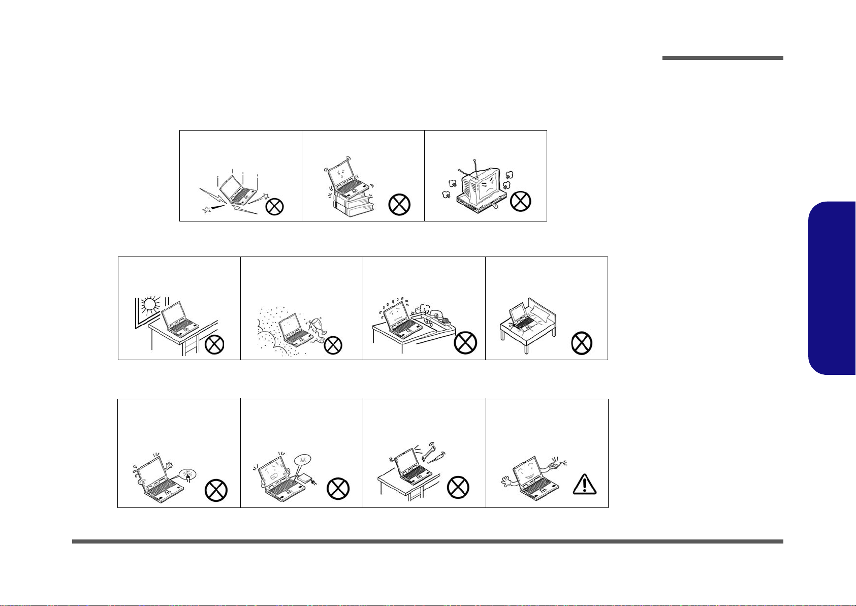
Instructions for Care and Operation
hexainf@hotmail.com
The notebook computer is quite rugged, but it can be damaged. To prevent this, follow these suggestions:
1. Don’t drop it, or expose it to shock. If the computer falls, the case and the components could be damaged.
Preface
Do not expose the computer
to any shock or vibration.
Do not place it on an unstable
surface.
Do not place anything heavy
on the computer.
2. Keep it dry, and don’t overheat it. Keep the computer and power supply away from any kind of heating element. This
is an electrical appliance. If water or any other liquid gets into it, the co mputer could be badly damaged.
Do not expose it to excessive
heat or direct sunlight.
Do not leave it in a place
where foreign matter or moisture may affect the system.
Don’t use or store the computer in a humid environment.
Do not place the computer on
any surface which will block
the vents.
3. Follow the proper working procedures for the computer. Shut the computer down properly and don’t forget to save
your work. Remember to periodically save your data as data may be lost if the battery is depleted.
Do not turn off the power
until you properly shut down
all programs.
Do not turn off any peripheral
devices when the computer is
on.
Do not disassemble the computer by yourself.
Perform routine maintenance
on your computer.
Preface
V
Page 8
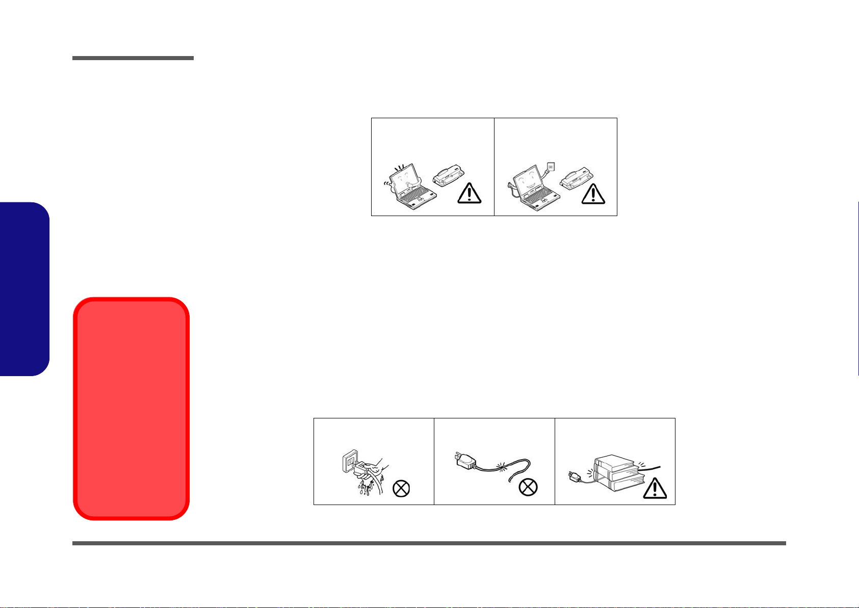
Preface
Power Safety
Warning
Before you undertake
any upgrade procedures, make sure that
you have turned off the
power, and disconnected all peripherals
and cables (including
telephone lines). It is
advisable to also remove your battery in
order to prevent accidentally turning the
machine on.
4. Avoid interference. Keep the computer away from high capacity transformers, electric motors, and oth er strong mag-
netic fields. These can hinder proper performance and damage your data.
5. Take care when using peripheral devices.
Preface
VI
Use only approved brands of
peripherals.
Unplug the power cord befor e
attaching peripheral devices.
Power Safety
The computer has specific power requirements:
• Only use a power adapter approved for use with this computer.
• Your AC adapter may be designed for international travel but it still requires a stea dy, uninterrupted po wer supply. If you ar e
unsure of your local power specifications, consult your service representative or local power company.
• The power adapter may have either a 2-prong or a 3-prong grounded plug. The third prong is an important safety feature; do
not defeat its purpose. If you do not have access to a compatible outlet, have a qualified electrician install one.
• When you want to unplug the power cord, be sure to disconnect it by the plug head, not by its wire.
• Make sure the socket and any extension cord(s) you use can support the total current load of all the connected devices.
• Before cleaning the computer, make sure it is disconnected from any external power supplies (i.e. AC/DC adapter or car
adapter).
Do not plug in the power
cord if you are wet.
Do not use the power cord if
it is broken.
Do not place heavy objects
on the power cord.
Page 9

Battery Precautions
Battery Disposal
The product that you have purchased contains a rechargeable battery. The battery is recyclable. At the end of its useful life, under various state and local laws, it may be illegal to dispose of this battery into the municipal waste stream. Check with your local solid waste
officials for details in your area for recycling options or proper disposal.
Caution
Danger of explosion if battery is incorrectly replaced. Replace only with the same or equivalent type recommended by the manufacturer.
Discard used battery according to the manufacturer’s instructions.
Battery Level
Click the battery icon in the taskbar to see the current battery level and charge status. A battery that drops below a level of 10%
will not allow the computer to boot up. Make sure that any battery that drops below 10% is recharged within one week.
hexainf@hotmail.com
• Only use batteries designed for this computer. The wrong battery type may explode, leak or damage the computer.
• Do not continue to use a battery that has been dropped, or that appears damaged (e.g. bent or twisted) in any way. Even if the
computer continues to work with a damaged battery in place, it may cause circuit damage, which may possibly result in fire.
• Recharge the batteries using the notebook’s system. Incorrect recharging may make the battery explode.
• Do not try to repair a battery pack. Refer any battery pack repair or replacement to your service representative or qualified service
personnel.
• Keep children away from, and promptly dispose of a damaged battery. Always dispose of batteries carefully. Batteries may explode
or leak if exposed to fire, or improperly handled or discarded.
• Keep the battery away from metal appliances.
• Affix tape to the battery contacts before disposing of the battery.
• Do not touch the battery contacts with your hands or metal objects.
Battery Guidelines
The following can also apply to any backup batteries you may have.
• If you do not use the battery for an extended period, then remove the battery from the computer for storage.
• Before removing the battery for storage charge it to 60% - 70%.
• Check stored batteries at least every 3 months and charge them to 60% - 70%.
Preface
Preface
VII
Page 10

Preface
Preface
VIII
Page 11

Contents
hexainf@hotmail.com
Preface
Introduction ..............................................1-1
Overview .........................................................................................1-1
Specifications ..................................................................................1-2
External Locator - Front View with LCD Panel Open ....................1-4
External Locator - Front and Rear View .........................................1-5
External Locator - Left & Right Side View ...................................1-6
External Locator - Bottom View .....................................................1-7
Mainboard Overview - Top (Key Parts) .........................................1-8
Mainboard Overview - Bottom (Key Parts) ....................................1-9
Mainboard Overview - Top (Connectors) .....................................1-10
Mainboard Overview - Bottom (Connectors) ...............................1-11
Disassembly ...............................................2-1
Overview .........................................................................................2-1
Maintenance Tools ..........................................................................2-2
Connections .....................................................................................2-2
Maintenance Precautions .................................................................2-3
Disassembly Steps ...........................................................................2-4
Removing the Battery ......................................................................2-5
Removing the Hard Disk Drive .......................................................2-6
Removing the Optical (CD/DVD) Device ......................................2-8
Removing the System Memory (RAM) ..........................................2-9
Removing and Installing a Processor ............................................2-10
Removing the 3G Module .............................................................2-13
Removing the Wireless LAN Module ...........................................2-14
Removing the Bluetooth Module ..................................................2-15
Removing the Modem ...................................................................2-16
Removing the LCD Back Cover for MOFA (C4801M) ...............2-17
Removing the LCD Front Cover ...................................................2-19
Removing the Keyboard ................................................................2-20
Part Lists ..................................................A-1
Part List Illustration Location ........................................................ A-2
Top (C4100) ................................................................................... A-3
Top (C4105) ................................................................................... A-4
Bottom (C4100) ............................................................................. A-5
LCD (C4100) ................................................................................. A-6
LCD (C4105) ................................................................................. A-7
HDD ............................................................................................... A-8
SATA-DVD-SUPER MULTI ....................................................... A-9
Schematic Diagrams.................................B-1
SYSTEM BLOCK DIAGRAM ......................................................B-2
CLOCK GENERATOR ..................................................................B-3
Penryn (Socket-P)1/2 ......................................................................B-4
Penryn (Socket-P)2/2 ......................................................................B-5
CANTIGA 1/7, HOST ....................................................................B-6
CANTIGA 2/7, Graphics ................................................................B-7
CANTIGA 3/7 ................................................................................B-8
CANTIGA 4/7 ................................................................................B-9
CANTIGA 5/7 ..............................................................................B-10
CANTIGA 6/7 ..............................................................................B-11
CANTIGA 7/7 ..............................................................................B-12
DDRIII SO-DIMM A ...................................................................B-13
DDRIII SO-DIMM B ...................................................................B-14
PANEL, CRT ................................................................................B-15
INVERTER, BLUETOOTH, FAN ...............................................B-16
ICH9M 1/4, SATA .......................................................................B-17
ICH9M 2/4, PCI, USB ..................................................................B-18
ICH9M 3/4 ....................................................................................B-19
ICH9M 4/4 ....................................................................................B-20
Preface
IX
Page 12

Preface
HDMI ........................................................................................... B-21
KBC-ITE IT8502E ....................................................................... B-22
JMC21 CARD READER/LAN .................................................... B-23
AUDIO CODEC ALC272 ...........................................................B-24
AUDIO AMP TPA6017 ...............................................................B-25
HDD, ODD, MDC, TP, Conn, 3G ...............................................B-26
NEW CARD, USB, MINI PCIE .................................................. B-27
LED, CCD, AUDIO Conn ........................................................... B-28
SYSTEM POWER, PWR SW .....................................................B-29
AC_IN, CHARGER .....................................................................B-30
VCORE ........................................................................................ B-31
VDD3, VDD5 ...............................................................................B-32
1.8V/1.05VS .................................................................................B-33
1.5V,0.75VS .................................................................................B-34
CLICK BOARD ........................................................................... B-35
AUDIO/ USB/ RJ11 BOARD ......................................................B-36
Preface
POWER SWITCH & LID BOARD .............................................B-37
X
Page 13

1: Introduction
hexainf@hotmail.com
Overview
This manual covers the information you need to service or upgrade the C4100/C4105 series notebook computer. Information about operating the computer (e.g. getting started, and the Setup utility) is in the User’s Manual. Information
about drivers (e.g. VGA & audio) is also found in User’s Manual. That manual is shipped with the computer.
Operating systems (e.g. Windows Vista/ Window 7, etc.) have their own manuals as do application software (e.g. word
processing and database programs). If you have questions about those programs, you should consult those manuals.
Introduction
The C4100/C4105 series notebook is designed to be upgradeable. See Disassembly on page 2 - 1 for a detailed description of the upgrade procedures for each specific component. Please note the warning and safety information indicated by
the “” symbol.
The balance of this chapter reviews the computer’s technical specifications and features.
1.Introduction
Overview 1 - 1
Page 14
Introduction
Latest Specification Information
The specifications listed in this here are correct
at the time of going to press. Certain items (particularly processor types/speeds) may be
changed, delayed or updated due to the manufacturer's release schedule. Check with your
service center for details.
CPU
The CPU is not a user serviceable part. Accessing the CPU in any way may violate your
warranty.
Specifications
1.Introduction
Processor Options
Intel® Core™2 Duo Processor
T6600 (2.2GHz), T6500 (2.1GHz), T6400 (2.0GHz)
2MB On-die L2 Cache & 800MHz FSB
Intel® Pentium® Processor
T4300 (2.12GHz), T4200 (2.0GHz)
1MB On-die L2 Cache & 800MHz FSB
Intel® Celeron Processor
900 (2.2GHz), T3100 (1.9GHz), T3000 (1.8GHz)
1MB On-die L2 Cache & 800MHz FSB
T1700 (1.83GHz), T1600 (1.66GHz)
1MB On-die L2 Cache & 667MHz FSB
LCD
14" HD TFT LCD
Core Logic
Intel ® GL40 + ICH9M
Memory
Two 204 Pin SO-DIMM Sockets Supporting DDR3 1066/
1333MHz Memory
Memory Expandable up to 4GB
Video Adapter
Intel ® GL40 Integrated Video
Shared Memory Architecture of up to 1GB
MS DirectX® 10 compatible
BIOS
One 16Mb SPI Flash ROM
Phoenix™ BIOS
Storage
(Factory Option) One Changeable 12.7mm(h) Optical
Device Type Drive
(Super Multi Drive Module
One Changeable 2.5" 9.5 mm (h) SATA (Serial) HDD
Audio
High Definition Audio Compliant Interface
2 * Built-In Speakers
Built-In Microphone
Keyboard
“WinKey” keyboard (with embedded numeric keypad)
Pointing Device
Built-in Touchpad
Security
Security (Kensington® Type) Lock Slot
BIOS Password
Interface
Three USB 2.0 Ports
One HDMI Out Port
One Headphone-Out Jack
One Microphone-In Jack
One RJ-45 LAN Jack
One RJ-11 Modem Jack
One DC-in Jack
One External Monitor Port
One ExpressCard/34 Slot
)
1 - 2 Specifications
Page 15

Communication
hexainf@hotmail.com
Introduction
10Mb/100Mb
(Factory Option) 802.11b/g/n Wireless LAN Half Mini-Card
Module
(Factory Option) 1.3M Pixel USB PC Camera Module
(Factory Option) Bluetooth 2.1 + EDR Module
(Factory Option) 3.75G/HSPA Mini-Card Module
Card Reader
Embedded 7-in-1 Card Reader (MS/ MS Pro/ SD/ Mini SD/
MMC/ RS MMC/ MS Duo)
Note: MS Duo/ Mini SD/ RS MMC Cards require a PC
adapter
Power
6 Cell Smart Lithium-Ion Battery Pack, 48.84WH
(Factory Option)
Full Range AC/DC Adapter
AC Input: 100 - 240V, 50 - 60Hz
DC Output: 19V, 3.42A or 18.5V, 3.5A (65 Watts)
Energy Star 5.0 Compliant
Environmental Spec
Temperature
Operating: 5
Non-Operating: -20°C - 60°C
Relative Humidity
Operating: 20% - 80%
Non-Operating: 10% - 90%
Ethernet LAN
6 Cell Battery Pack, 62.16WH
C - 35°C
°
1.Introduction
Dimensions & Weight
340mm (w) * 238mm (d) * 13.9 - 31.8mm (h)
2.2 kg With 6 Cell Battery and ODD
Specifications 1 - 3
Page 16
Introduction
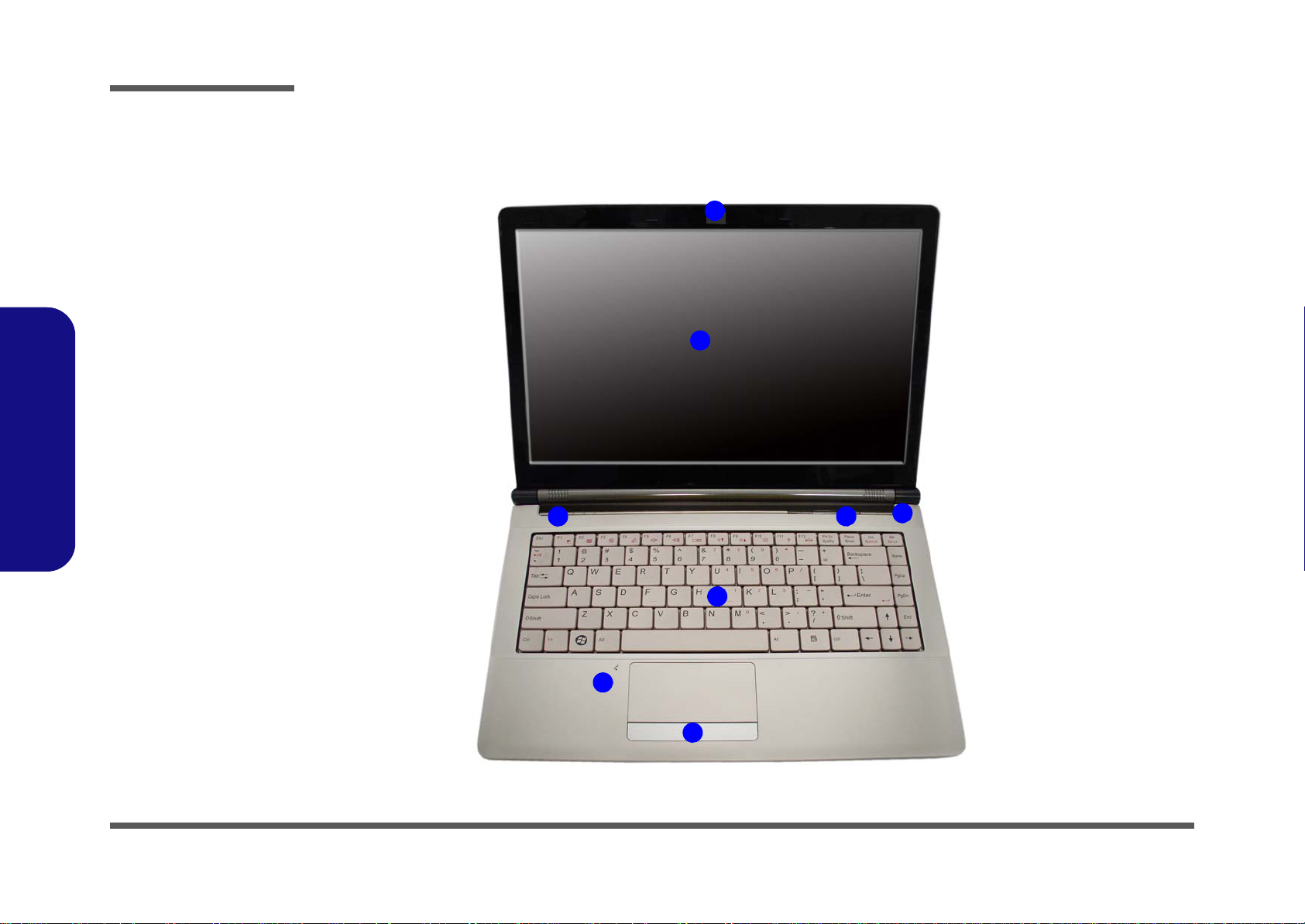
Figure 1
Front View with LCD Pan-
el Open
1. Built-In PC Camera
(Optional)
2. LCD
3. Power Button
4. Hot-Key Buttons
5. LED Status
Indicators
6. Keyboard
7. Built-In Microphone
8. Touchpad &
Buttons
1
4
6
7
3
5
8
2
1.Introduction
External Locator - Front View with LCD Panel Open
1 - 4 External Locator - Front View with LCD Panel Open
Page 17
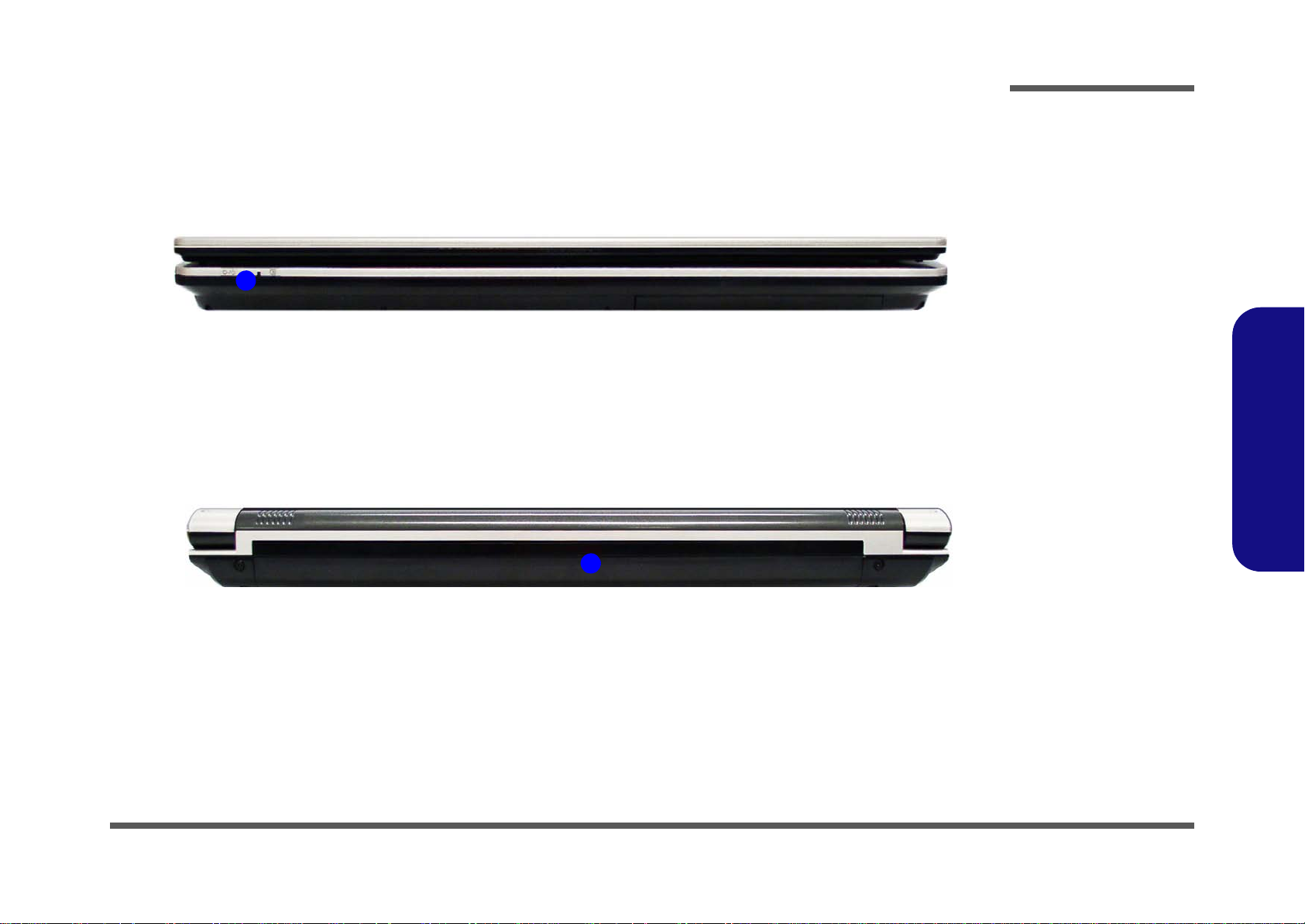
External Locator - Front and Rear View
1
Figure 2
Front View
1. LED Power
Indicators
Figure 3
Rear View
1. Battery
1
hexainf@hotmail.com
Introduction
1.Introduction
External Locator - Front and Rear View 1 - 5
Page 18
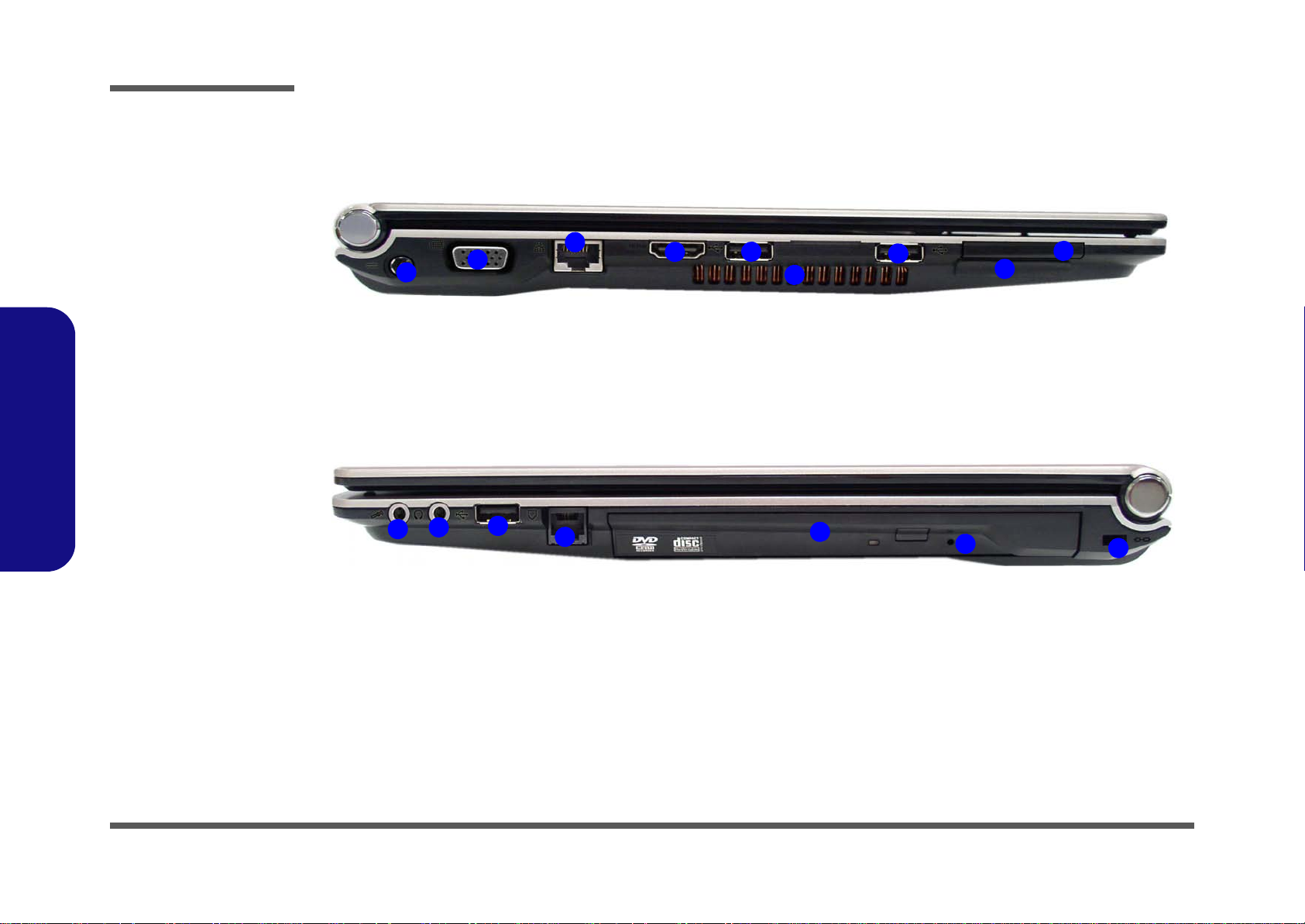
Introduction
1
2
4
6
3
5
7
8
5
Figure 4
Left Side View
1. DC-In Jack
2. External Monitor
Port
3. RJ-45 LAN Jack
4. HDMI Port
5. 2 * USB 2.0 Ports
6. Vent
7. ExpressCard/34
Slot
8. 7-in-1 Card
Reader
Figure 5
Right Side View
1. Microphone-In
Jack
2. Headphone-Out
Jack
3. USB 2.0 Port
4. RJ-11 Modem
Jack
5. Optical Device
Drive Bay
6. Emergency Eject
Hole
7. Security Lock Slot
1
2
3
5
6
4
7
1.Introduction
External Locator - Left & Right Side View
1 - 6 External Locator - Left & Right Side View
Page 19
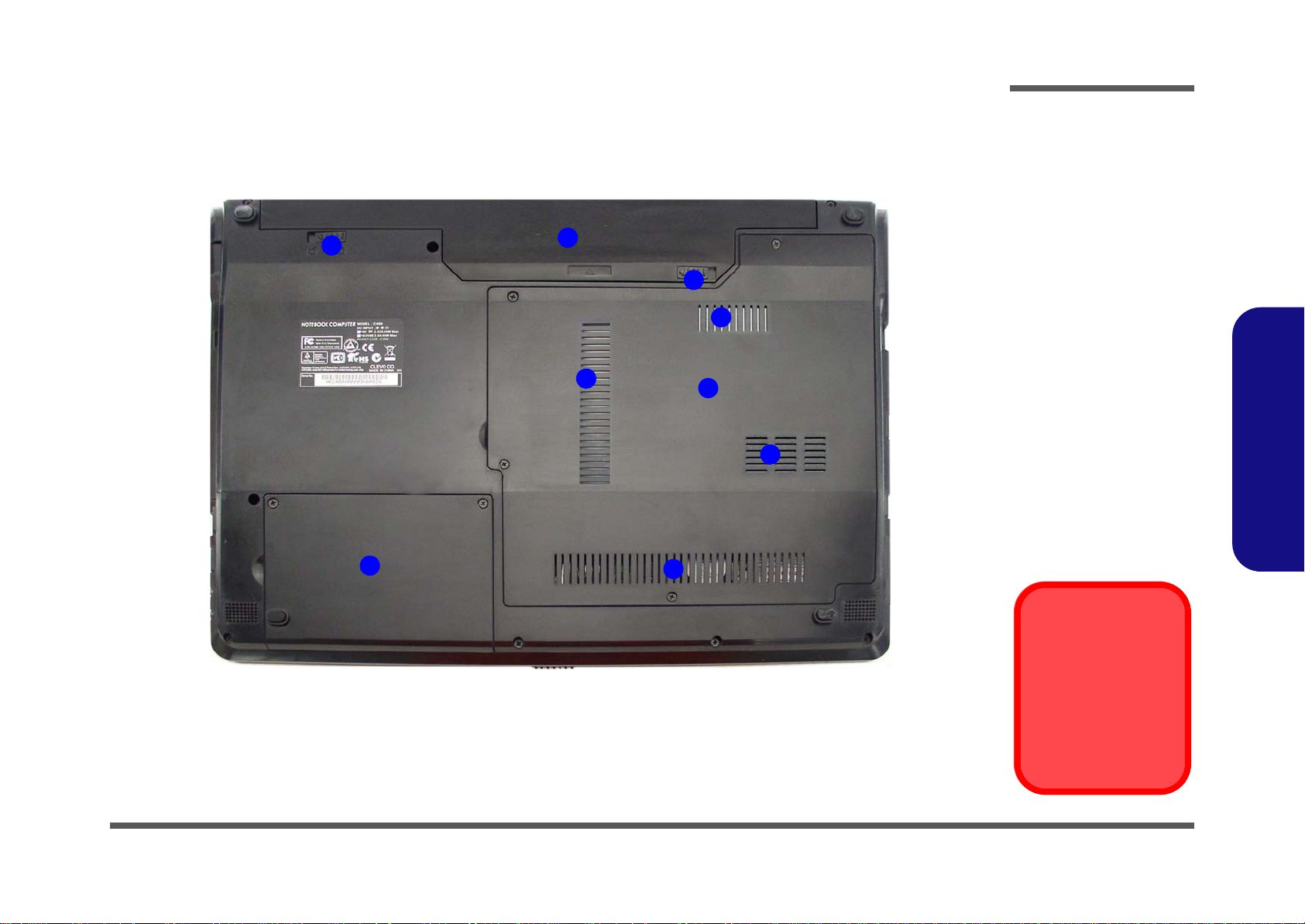
External Locator - Bottom View
Figure 6
Bottom View
1. Vent
2. Component Bay
Cover
3. Hard Disk Bay
Cover
4. Battery Release
Latch
5. Battery
Overheating
To prevent your computer from overheating
make sure nothing
blocks the vent/fan intakes while the computer is in use.
2
4
1
1
3
1
1
4
5
hexainf@hotmail.com
Introduction
1.Introduction
External Locator - Bottom View 1 - 7
Page 20
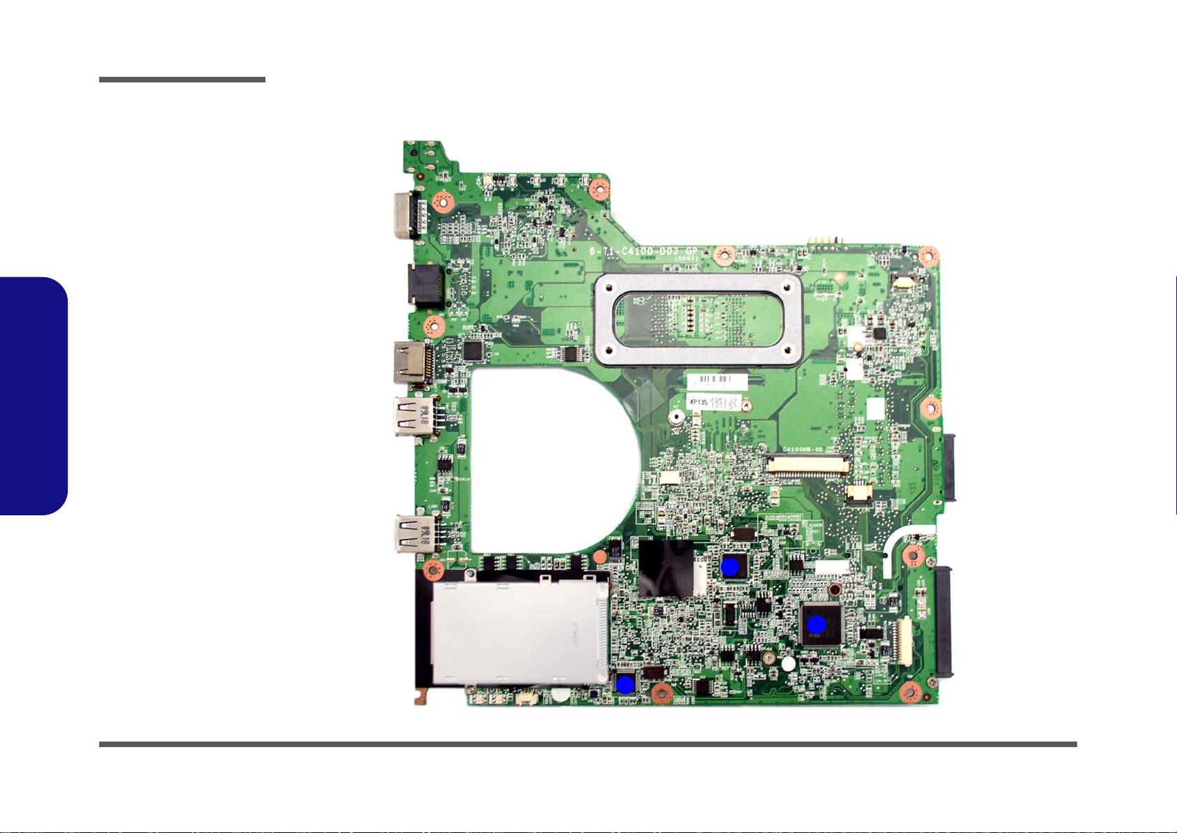
Introduction
Figure 7
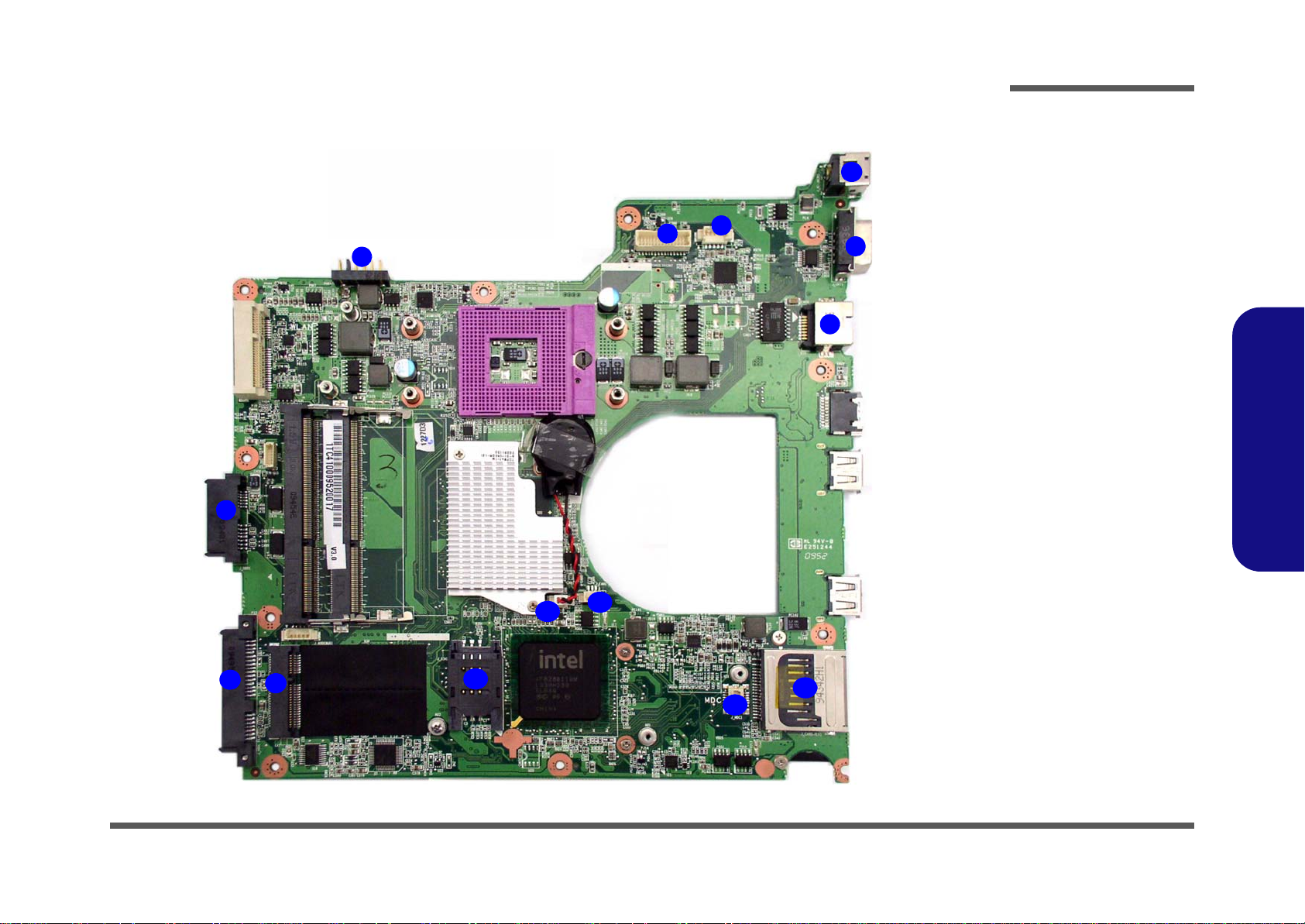
Mainboard Top
Key Parts
1. JMB261
2. CLOCK GEN.
3. ITE 8502E
2
1
3
1.Introduction
Mainboard Overview - Top (Key Parts)
1 - 8 Mainboard Overview - Top (Key Parts)
Page 21
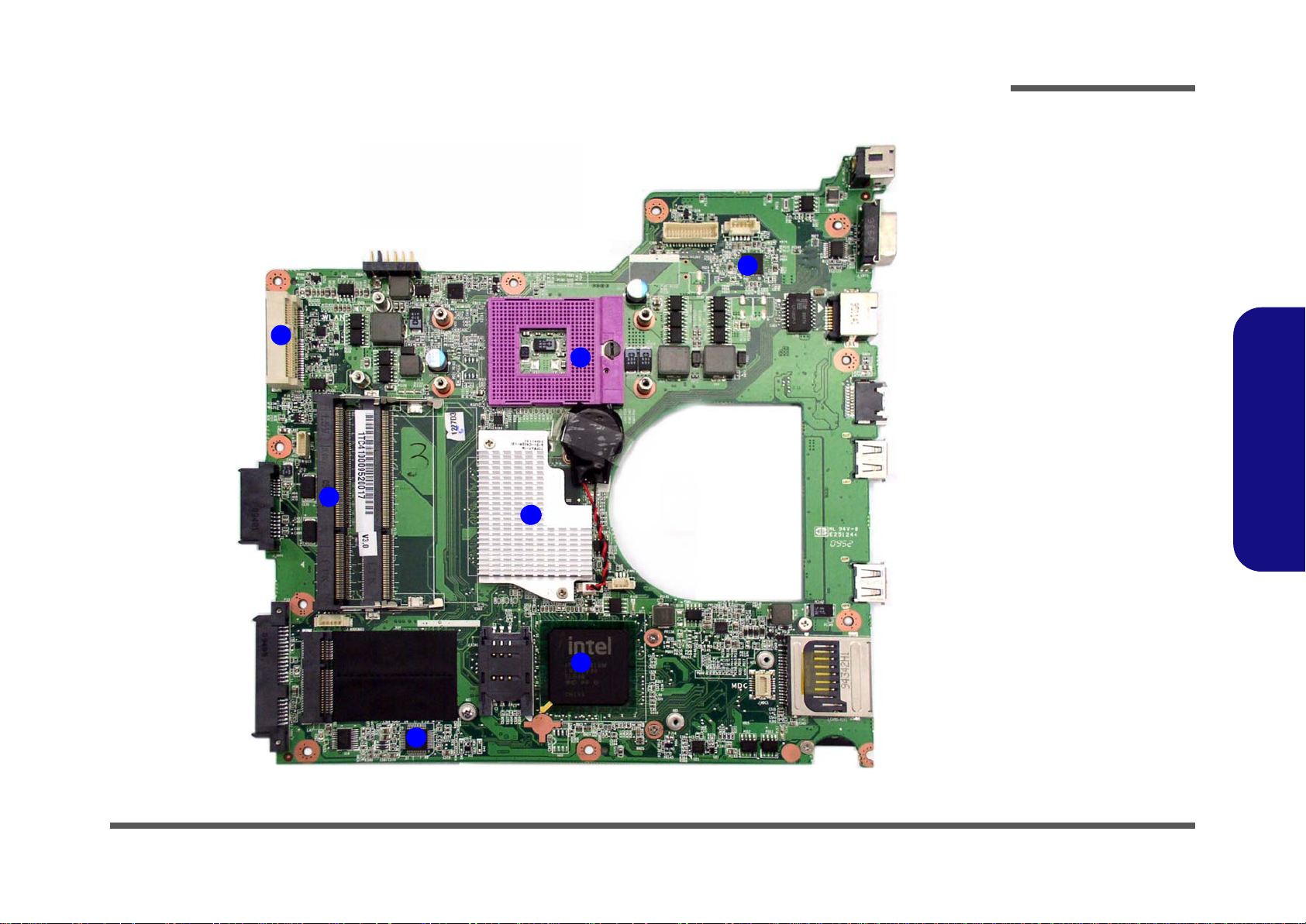
Mainboard Overview - Bottom (Key Parts)
Figure 8
Mainboard Bottom
Key Parts
1. SC452
2. CPU Socket (no
CPU installed)
3. NorthBridge
INTEL GL40
4. SorthBridge
ICH9M
5. REALTEK
ALC272
6. Memory Slots
DDR3 So-DIMM
7. Mini-PCIe Socket
(Wireless Lan
Module)
1
5
2
4
3
6
7
hexainf@hotmail.com
Introduction
1.Introduction
Mainboard Overview - Bottom (Key Parts) 1 - 9
Page 22
Introduction
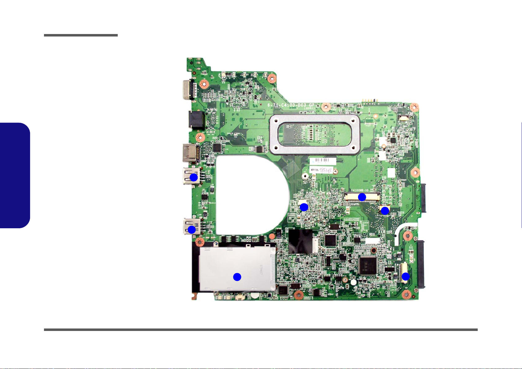
Figure 9
Mainboard Top
Connectors
1. USB Ports
2. ExpressCard/34
Slot
3. Microphone Cable
Connector
4. Keyboard Cable
Connector
5. TouchPad Cable
Connector
6. Audio Cable
Connector
1
6
5
2
4
3
1
1.Introduction
Mainboard Overview - Top (Connectors)
1 - 10 Mainboard Overview - Top (Connectors)
Page 23
Mainboard Overview - Bottom (Connectors)
Figure 10
Mainboard Bottom
Connectors
1. RJ-45 Jack
2. D-Sub-Out Port
3. DC-In Jack
4. CCD Cable
Connector
5. LCD Cable
Connector
6. Battery Connector
7. ODD Connector
8. HDD Connector
9. 3G Module
Connector
10.SIMLOCK
11. CMOS Cable
Connector
12.Fan Cable
Connector
13.MDC Cable
Connector
14.7-in-1 Card Reader
1
6
7
8
5
2
4
3
9
11
10
12
14
13
hexainf@hotmail.com
Introduction
1.Introduction
Mainboard Overview - Bottom (Connectors) 1 - 11
Page 24

Introduction
1.Introduction
1-12
Page 25

2: Disassembly
Information
Warning
hexainf@hotmail.com
Overview
This chapter provides step-by-step instructions for disassembling the C4100/C4105 series notebook’s parts and subsystems. When it comes to reassembly, reverse the procedures (unless otherwise indicated).
We suggest you completely review any procedure before you take the computer apart.
Disassembly
Procedures such as upgrading/replacing the RAM, CD device and hard disk are included in the User’s Manual but are
repeated here for your convenience.
To make the disassembly process easier each section may have a box in the page margin. Information contained under
the figure # will give a synopsis of the sequence of procedures involved in the disassembly procedure. A box with a
lists the relevant parts you will have after the disassembly process is complete. Note: The parts listed will be for the disassembly procedure listed ONLY, and not any previous disassembly step(s) required. Refer to the part list for the previous disassembly procedure. The amount of screws you should be left with will be listed here also.
A box with a will also provide any possible helpful information. A box with a contains warnings.
An example of these types of boxes are shown in the sidebar.
2.Disassembly
Overview 2 - 1
Page 26

Disassembly
2.Disassembly
NOTE: All disassembly procedures assume that the system is turned OFF, and disconnected from any power supply (the
battery is removed too).
Maintenance Tools
The following tools are recommended when working on the notebook PC:
• M3 Philips-head screwdriver
• M2.5 Philips-head screwdriver (magnetized)
• M2 Philips-head screwdriver
• Small flat-head screwdriver
• Pair of needle-nose pliers
• Anti-static wrist-strap
Connections
Connections within the computer are one of four types:
Locking collar sockets for ribbon connectors To release these connectors, use a small flat-head screwdriver to
gently pry the locking collar away from its base. When replacing the connection, make sure the connector is oriented in the
same way. The pin1 side is usually not indicated.
2 - 2 Overview
Pressure sockets for multi-wire connectors To release this connector type, grasp it at its head and gently
rock it from side to side as you pull it out. Do not pull on the
wires themselves. When replacing the connection, do not try to
force it. The socket only fits one way.
Pressure sockets for ribbon connectors To release these connectors, use a small pair of needle-nose pli-
ers to gently lift the connector away from its socket. When replacing the connection, make sure the connector is oriented in
the same way. The pin1 side is usually not indicated.
Board-to-board or multi-pin sockets To separate the boards, gently rock them from side to side as
you pull them apart. If the connection is very tight, use a small
flat-head screwdriver - use just enough force to start.
Page 27

Maintenance Precautions
Power Safety
Warning
Before you undertake
any upgrade procedures, make sure that
you have turned off the
power, and disconnected all peripherals
and cables (including
telephone lines). It is
advisable to also remove your battery in
order to prevent accidentally turning the
machine on.
hexainf@hotmail.com
The following precautions are a reminder. To avoid personal injury or damage to the computer while performing a removal and/or replacement job, take the following precautions:
1. Don't drop it. Perform your repairs and/or upgrades on a stable surface. If the computer falls, the case and other
components could be damaged.
2. Don't overheat it. Note the proximity of any heating elements. Keep the computer out of direct sunlight.
3. Avoid interference. Note the proximity of any high capacity transformers, electric motors, and other strong mag-
netic fields. These can hinder proper performance and damage component s and/or data. You should also monitor
the position of magnetized tools (i.e. screwdrivers).
4. Keep it dry. This is an electrical appliance. If water or any other liquid gets into it, the computer could be badly
damaged.
5. Be careful with power. Avoid accidental shocks, discharges or explosions.
•Before removing or servicing any part from the computer, turn the computer off and detach any power supplies.
•When you want to unplug the power cord or any cable/wire, be sure to disconnect it by the plug head. Do no t pull on th e wir e.
6. Peripherals – Turn off and detach any peripherals.
7. Beware of static discharge. ICs, such as the CPU and main support chips, are vulnerable to static electricity.
Before handling any part in the computer, discharge any static electricity inside the computer. When handling a
printed circuit board, do not use gloves or other materials which allow static electricity buildup. We suggest that
you use an anti-static wrist strap instead.
8. Beware of corrosion. As you perform your job, avoid touching any connector leads. Even the cleanest hands produce oils which can attract corrosive elements.
9. Keep your work environment clean. Tobacco smoke, dust or other air-born particulate matter is often attracted
to charged surfaces, reducing performance.
10. Keep track of the components. When removing or replacing any part, be careful not to leave small part s, such as
screws, loose inside the computer.
Cleaning
Do not apply cleaner directly to the computer, use a soft clean cloth.
Do not use volatile (petroleum distillates) or abrasive cleaners on any part of the computer.
Disassembly
2.Disassembly
Overview 2 - 3
Page 28

Disassembly
Disassembly Steps
The following table lists the disassembly steps, and on which page to find the related information. PLEASE PERFORM
THE DISASSEMBLY STEPS IN THE ORDER INDICATED.
2.Disassembly
To remove the Battery:
1. Remove the battery page 2 - 5
To remove the HDD:
1. Remove the battery page 2 - 5
2. Remove the HDD page 2 - 6
To remove the Optical Device:
1. Remove the battery page 2 - 5
2. Remove the Optical device page 2 - 8
To remove the System Memory:
1. Remove the battery page 2 - 5
2. Remove the system memory page 2 - 9
To remove and install a Processor:
1. Remove the battery page 2 - 5
2. Remove the processor page 2 - 10
3. Install the processor page 2 - 12
To remove the 3G Module:
1. Remove the battery page 2 - 5
2. Remove the 3G module page 2 - 13
To remove the Bluetooth Module:
1. Remove the battery page 2 - 5
2. Remove the Bluetooth Module page 2 - 15
To remove the Modem:
1. Remove the battery page 2 - 5
2. Remove the Modem page 2 - 16
To remove the LCD Back Cover:
1. Remove the battery page 2 - 5
2. Remove the LCD Back Cover page 2 - 17
To remove the LCD Front Cover:
1. Remove the battery page 2 - 5
2. Remove the LCD Front Cover page 2 - 19
To remove the Keyboard:
1. Remove the battery page 2 - 5
2. Remove the keyboard page 2 - 20
To remove the Wireless LAN Module:
1. Remove the battery page 2 - 5
2. Remove the WLAN module page 2 - 14
2 - 4 Disassembly Steps
Page 29

Removing the Battery
2. Battery
1
2
634
Figure 1
Battery Removal
a. Slide latch at point 1 to-
wards the unlock symbol
and hold it in place.
b. Slide the battery in the di-
rection of the arrow.
1
a.
b.
3
2
4
hexainf@hotmail.com
1. Turn the computer off, and turn it over.
2. Slide the latch in the direction of the arrow.
3. Slide the latch in the direction of the arrow, and hold it in place.
4. Slide the battery in the direction of the arrow .
Disassembly
2.Disassembly
Removing the Battery 2 - 5
Page 30

Disassembly
Figure 2
HDD Assembly
Removal
a. Locate the HDD bay
cover and remove th
screw(s).
•2 Screws
1
2
2
1
a.
HDD System Warning
New HDD’s are blank. Before you
begin make sure:
You have backed up any data
you want to keep from your old
HDD.
You have all the CD-ROMs and
FDDs required to install your operating system and programs.
If you have access to the internet,
download the latest application
and hardware driver updates for
the operating system you plan to
install. Copy these to a removable medium.
Removing the Hard Disk Drive
The hard disk drive can be taken out to accommodate other 2.5" serial (SATA) hard disk drives with a height of 9.5mm
(h). Follow your operating system’s installation instructions, and install all necessary drivers and utilities (as outlined in
Chapter 4 of the User’s Manual) when setting up a new hard disk.
Hard Disk Upgrade Process
1. Turn off the computer, and remove the battery (page 2 - 5).
2. Locate the hard disk bay cover and remove screw & .
2.Disassembly
2 - 6 Removing the Hard Disk Drive
Page 31

Disassembly
634
5
6
9
10
11
4
b.
c.
e.
5
9
d.
3
e.
10
8
7
6
11
3. HDD Bay Cover
10.Adhesive Cover
11.HDD
•4 Screws
Figure 3
HDD Assembly
Removal (cont’d.)
b. Remove the HDD bay
cover.
c. Grip the tab and slide the
HDD in the direction of
the arrow.
d. Lift the HDD assembly
out of the bay.
e. Remove the screws and
adhesive cover.
hexainf@hotmail.com
3. Remove the hard disk bay cover
4. Grip the tab and slide the hard disk in the direction of arrow
.
.
5. Lift the hard disk out of the bay .
6. Remove the screw - and the adhesive cover from the hard disk .
7. Reverse the process to install a new hard disk (do not forget to replace all the screws and covers).
2.Disassembly
Removing the Hard Disk Drive 2 - 7
Page 32

Disassembly
Figure 4
Optical Device
Removal
a. Remove the screws.
b. Remove the cover.
c. Remove the screw.
d. Slide the optical device
out of the computer at
point 9.
Fan Cable
Make sure you reconnect the fan cable
before screwing down
the bay cover.
61256
1
789
1. Component Bay
Cover
8. Optical Device
•5 Screws
2
4
3
b.
1
5
1
5
6
a.
d.
c.
8
7
9
1
Removing the Optical (CD/DVD) Device
1. Turn off the computer, remove the battery (page 2 - 5).
2. Locate the component bay cover , and remove screws - .
3. Carefully (a fan and cable are attached to the under side of the cover) lift up the bay cover.
4. Carefully disconnect the fan cable , and remove the cover
5. Remove the screw at point , and use a screwdriver to carefully push out the optical device at point .
6. Insert the new device and carefully slide it into the computer (the device only fits one way. DO NOT FORCE IT; The
screw holes should line up).
7. Restart the computer to allow it to automatically detect the new device.
.
2.Disassembly
2 - 8 Removing the Optical (CD/DVD) Device
Page 33

Removing the System Memory (RAM)
Figure 5
RAM Module
Removal
a. Locate the memory
socket.
b. Pull the release
latch(es).
c. Remove the mod-
ule(s).
Contact Warning
Be careful not to touch
the metal pins on the
module’s connecting
edge. Even the cleanest
hands have oils which
can attract particles, and
degrade the module’s
performance.
4. RAM Module
123
a.
b.
c.
1
3
2
4
4
hexainf@hotmail.com
The computer has two memory sockets for 200 pin Small Outline Dual In-line Memory Modules (SO-DIMM) supporting
DDRIII (DDR3) Up to 1066/1333 MHz. The main memory can be expanded up to 4GB. The SO-DIMM modules supported are 1024MB and 2048MB DDRIII Modules. The total memory size is automatically detected by the POST routine once you turn on your computer.
Memory Upgrade Process
1. Turn off the computer, turn it over and remove the battery (page 2 - 5) and the component bay cover (page 2 - 8).
2. The RAM module(s) will be visible at point on the mainboard.
3. Gently pull the two release latches ( & ) on the sides of the memory socket in the direction indicated by the
Disassembly
arrows (Figure 5b).
2.Disassembly
4. The RAM module(s) will pop-up
5. Pull the latches to release the second module if necessary.
6. Insert a new module holding it at about a 30° angle and fit the connectors firmly into the memory slot.
7. The module will only fit one way as defined by its pin alignment. Make sure the module is seated as far into the slot
8. Press the module in and down towards the mainboard until the slot levers click into place to secure the module.
9. Replace the component bay cover and the screws
10. Restart the computer to allow the BIOS to register the new memory configuration as it starts up.
as it will go. DO NOT FORCE IT; it should fit without much pressure.
(
Figure 5c), and you can then remove it
(see
page 2 - 8).
.
Removing the System Memory (RAM) 2 - 9
Page 34

Disassembly
4
321
5
Figure 6
Processor Removal
a. Locate the heat sink.
b. Remove the screws from
the CPU heatsink.
c. Remove the CPU heat
sink.
5. Heat Sink
•4 Screws
2
3
4
a.
c.
b.
5
A
1
Removing and Installing a Processor
Processor Removal Procedure
1. Turn off the computer, turn it over, and remove the battery (page 2 - 5) and the component bay cover (page 2 - 8).
2. Locate the heat sink.
3. Loosen the CPU heat sink screws in the order ,
4. Carefully lift up the heat sink (Figure 6c) off the computer.
, & (the reverse order as indicated on the label).
2.Disassembly
2 - 10 Removing and Installing a Processor
Page 35

6
7
Figure 7
Processor Removal
(cont’d)
d. Turn the release latch to
unlock the CPU.
e. Lift the CPU out of the
socket.
d.
e.
Caution
The heat sink, and CPU area in
general, contains parts which are
subject to high temperatures. Allow
the area time to cool before removing these parts.
Unlock Lock
6
7
6
7. CPU
hexainf@hotmail.com
Disassembly
5. Turn the release latch towards the unlock symbol to release the CPU.
6. Carefully (it may be hot) lift the CPU up and out of the socket (Figure 7e).
7. Reverse the process to install a new CPU.
8. When re-inserting the CPU, pay careful attention to the pin alignment, it will fit only one way (DO NOT FORCE IT!).
2.Disassembly
Removing and Installing a Processor 2 - 11
Page 36

Disassembly
ABC
D
123
4
b.
B
a.
D
1
3
2
4
Note:
Tighten the screws
in the order as indicated on the label.
C
A
c.
d.
Figure 8
Processor
Installation
a. Insert the CPU.
b. Turn the release latch to-
wards the lock symbol.
c. Remove the sticker from
the heat sink and insert
the heat sink.
d. Tighten the screws.
A. CPU
D. Heat Sink
•3 Screws
Processor Installation Procedure
1. Insert the CPU , pay careful attention to the pin alignment, it will fit only one way (DO NOT FORCE IT!), and turn
the release latch towards the lock symbol (Figure 8b).
2. Remove the sticker (Figure 8c) from the heat sink.
3. Insert the heat sink
4. Tighten the CPU heat sink screws in the order
8d).
5. Replace the component bay cover (don’t forget to replace the fan cable) and tighten the screws (page 2 - 8).
as indicated in Figure 8d.
, , & (the order as indicated on the label and Figure
2.Disassembly
2 - 12 Removing and Installing a Processor
Page 37

Removing the 3G Module
Figure 9
3G Module Removal
a. Locate the 3G module.
b. Disconnect the cable
and remove the screw.
c. Remove the 3G module.
Note: Make sure you
reconnect the antenna
cable to socket (Fig-
ure 9b).
1
2
3
4
b.
c.
a.
3
1
2
4
4. 3G Module
•1 Screw
hexainf@hotmail.com
1. Turn off the computer, turn it over, and remove the battery (page 2 - 5) and the component bay cover (page 2 - 8).
2. The 3G module will be visible at point on the mainboard.
3. Carefully disconnect the cable , and then remove the screw
4. The 3G module (Figure 10c) will pop-up, and you can remove it from the computer.
.
Disassembly
2.Disassembly
Removing the 3G Module 2 - 13
Page 38

Disassembly
Figure 10
Wireless LAN
Module Removal
a. Locate the WLAN.
b. Disconnect the cable
and remove the screw.
c. The WLAN module will
pop up.
d. Remove the Wireless
LAN module.
Note: Make sure you
reconnect the antenna
cable to the “1 + 2”
socket (Figure 10b).
1
234
5
b.
c.
a.
4
3
2
d.
5
5
1
5.Wireless LAN Module
•1 Screw
Removing the Wireless LAN Module
1. Turn off the computer, turn it over, and remove the battery (page 2 - 5) and the component bay cover (page 2 - 8).
2. The Wireless LAN module will be visible at point on the mainboard.
3. Carefully disconnect the cables & , and then remove the screw
4. The Wireless LAN module (Figure 10c) will pop-up, and you can remove it from the computer.
.
2.Disassembly
2 - 14 Removing the Wireless LAN Module
Page 39

Removing the Bluetooth Module
Figure 11
Bluetooth Module
Removal
a. Locate the Bluetooth
module.
b. Remove the screw.
c. Disconnect the cable
and the connector from
the Bluetooth module.
d. Lift the Bluetooth module
out.
1
2
3
4
5
c.
a.
4
1
5
2
3
b.
d.
5. Bluetooth Module
•1 Screw
hexainf@hotmail.com
1. Turn off the computer, turn it over, and remove the battery (page 2 - 5) and the component bay cover (page 2 - 8).
2. The Bluetooth module will be visible at point on the mainboard.
3. Remove the screw and turn the module over.
4. Carefully disconnect the cable and separate the connector (Figure 11b) from the Bluetooth Module.
5. Lift the Bluetooth Module (Figure 11c) up and off the computer.
Disassembly
2.Disassembly
Removing the Bluetooth Module 2 - 15
Page 40

Disassembly
Figure 12
Modem Removal
a. Locate the modem.
b. Remove the screws.
c. Lift the modem up and
off the sockets.
1
2
354
5. Modem
•2 Screws
c.
a.
4
1
5
2
3
b.
Removing the Modem
1. Turn off the computer, turn it over, and remove the battery (page 2 - 5) and the component bay cover (page 2 - 8).
2. The modem will be visible at point on the mainboard.
3. Remove the screws
4. Carefully lift the modem up and off the socket .
- ,
2.Disassembly
2 - 16 Removing the Modem
Page 41

Removing the LCD Back Cover for MOFA
1
2
3
4
5
6
7
a.
1
3
2
4
5 6
b.
7
c.
Rubber Screw Covers
After removing the rubber screw covers, place them on a
clean dry surface (or attach them to the front cover itself) in
order to prevent loss of adhesive.
Figure 13
LCD Back Cover
Removal
a. Remove the rubber cov-
ers and screws.
b. Slide the cover forward.
c. Remove the LCD back
cover.
7. LCD Back Cover
•2 Screws
hexainf@hotmail.com
1. Turn off the computer, and turn the computer over to remove the battery (page 2 - 5).
2. Open the LCD and carefully remove the rubber screw covers & (2 corne r rubber screw covers only) a nd set
them aside.
3. Remove screws & from the front cover.
4. Carefully slide the cover forward in the direction of the arrows & as illustrated below.
5. Remove the LCD back cover .
Disassembly
2.Disassembly
Removing the LCD Back Cover for MOFA 2 - 17
Page 42

Disassembly
8
8
9
9
10 10
10
d.
Figure 14
LCD Back Cover
Removal (cont’d)
d. Align the replacement
cover and slide forward to
click firmly into place.
9
10
2.Disassembly
6. Align the replacement cover with the dotted line as illustrated below (and as marked on the cover).
7. Slide the back cover forward until it clicks firmly into place .
8. Run your hands around the sides and front of the cover to make sure it is firmly aligned in place (carefully press
down to make sure the fit is secure).
9. Replace the screws and rubber covers.
2 - 18 Removing the LCD Back Cover for MOFA
Page 43

Removing the LCD Front Cover
Figure 15
LCD Front Cover
Removal
a. Remove the screws and
unsnap the LCD front
cover from the LCD panel.
b. Slide the LCD panel cov-
er in the direction of the
arrow.
1
4
5
6
7
5. LCD Front Cover
•4 Screws
a. b.
1
2
3
4
7
5
6
7
5
Rubber Screw Covers
After removing the rubber screw covers, place them on a
clean dry surface (or attach them to the front cover itself) in
order to prevent loss of adhesive.
hexainf@hotmail.com
1. Turn off the computer, and remove the battery (page 2 - 5), and remove the LCD back cover (page 2 - 17).
2. Remove the rubber covers and screws - (Figure 15a), then run your finger around the middle of the frame to
carefully unsnap the LCD front cover from the LCD panel.
3. After unsnapping all four sides of the LCD front cover, carefully slide the LCD front cover downwards in the direction of the arrow (be careful of the LCD hinges at point ).
4. You can now remove the LCD front cover.
Disassembly
2.Disassembly
Removing the LCD Front Cover 2 - 19
Page 44

Disassembly
Figure 16
Keyboard Removal
a. Press the four latches to
release the keyboard.
b. Lift the keyboard up and
disconnect the cable
from the locking collar.
c. Remove the keyboard.
5
5
6
7
Re-Inserting the
Keyboard
When re-inserting the
keyboard firstly align the
four keyboard tabs at the
bottom (
Figure 16c) at
the bottom of the keyboard with the slots in the
case.
a.
b.
Keyboard Tabs
1
3
2
4
6
7
5
c.
7. Keyboard
Removing the Keyboard
1. Turn off the computer, and remove the battery (page 2 - 5).
2. Press the four keyboard latches at the top of the keyboard to elevate the keyboard from its normal position (you
may need to use a small screwdriver to do this).
3. Carefully lift the keyboard up, being careful not to bend the keyboard ribbon cable (Figure 16b).
4. Disconnect the keyboard ribbon cable from the locking collar socket .
5. Carefully lift up the keyboard (Figure 16c) off the computer.
2.Disassembly
2 - 20 Removing the Keyboard
Page 45

Appendix A:Part Lists
hexainf@hotmail.com
This appendix breaks down the C4100/C4105 series notebook’s construction into a series of illustrations. The component
part numbers are indicated in the tables opposite the drawings.
Note: This section indicates the manufacturer’s part numbers. Your organization may use a different system, so be sure
to cross-check any relevant documentation.
Note: Some assemblies may have parts in common (especially screws). However, the part lists DO NOT indicate the
total number of duplicated parts used.
Part Lists
Note: Be sure to check any update notices. The parts shown in these illustrations are appropriate for the system at the
time of publication. Over the product life, some parts may be improved or re-configured, resulting in new part numbers.
A.Part Lists
A-1
Page 46

Part Lists
Table A - 1
Part List Illustration
Location
Part List Illustration Location
The following table indicates where to find the appropriate part list illustration.
Part C4100/C4105
Top (C4100)
page A - 3
A.Part Lists
Top (C4105)
Bottom (C4100)
LCD (C4100)
LCD (C4105)
HDD
SATA-DVD-SUPER-MULTI
page A - 4
page A - 5
page A - 6
page A - 7
page A - 8
page A - 9
A - 2 Part List Illustration Location
Page 47

Top (C4100)
Figure A - 1
Top (C4100)
無鉛
無鉛
無鉛
(灰色) 無鉛
無鉛
無鉛
無鉛
無鉛
無鉛
(非耐落) 無鉛
無鉛
無鉛
香檳銀色 無鉛
無鉛
無鉛
非耐落 無鉛
無鉛
無鉛
無鉛
hexainf@hotmail.com
Part Lists
A.Part Lists
Top (C4100) A - 3
Page 48

Part Lists
Figure A - 1
Top (C4105)
無鉛
無鉛
(灰色) 無鉛
無鉛
無鉛
無鉛
無鉛
(非耐落) 無鉛
無鉛
非耐落 無鉛
無鉛
無鉛
無鉛
黑色 無鉛
無鉛
無鉛
無鉛
無鉛
無鉛
A.Part Lists
Top (C4105)
A - 4 Top (C4105)
Page 49

Bottom (C4100)
Figure A - 2
Bottom (C4100)
hexainf@hotmail.com
Part Lists
A.Part Lists
Bottom (C4100) A - 5
Page 50

Part Lists
Figure A - 3
LCD (C4100)
無鉛
無鉛
(華力)無鉛
無鉛
非耐落 無鉛
今皓 / 泰林 無鉛
無鉛
無鉛
中性 電鑄薄膜鍍亮鉻(字體連結) 無鉛
無鉛
無鉛
無鉛
無鉛
無鉛
銘板 無鉛
無鉛
華力 無鉛
無鉛
無鉛
無鉛
無鉛
無鉛
精乘 (銅箔接地)無鉛
精乘 無鉛
精乘 無鉛
無鉛
無鉛
無鉛
無鉛
A.Part Lists
LCD (C4100)
A - 6 LCD (C4100)
Page 51

LCD (C4105)
無鉛
無鉛
(華力)無鉛
無鉛
非耐落 無鉛
今皓 / 泰林 無鉛
無鉛
無鉛
無鉛
無鉛
中性 電鑄薄膜鍍亮鉻(字體連結) 無鉛
無鉛
無鉛
無鉛
無鉛
無鉛
銘板 無鉛
無鉛
無鉛
無鉛
無鉛
無鉛
無鉛
無鉛
無鉛
精乘 (銅箔接地) 無鉛
精乘 無鉛
精乘 無鉛
無鉛
無鉛
Figure A - 4
LCD (C4105)
hexainf@hotmail.com
Part Lists
A.Part Lists
LCD (C4105) A - 7
Page 52

Part Lists
無鉛
(無鉛)
Figure A - 5
HDD
A.Part Lists
HDD
A - 8 HDD
Page 53

SATA-DVD-SUPER MULTI
*(非耐落) 無鉛
無鉛
無鉛
無鉛
內縮 無鉛
內縮 無鉛
已內縮 無鉛
已內縮 無鉛
Figure A - 6
SATA-DVD-SUPER
MULTI
hexainf@hotmail.com
Part Lists
A.Part Lists
SATA-DVD-SUPER MULTI A - 9
Page 54

Part Lists
A.Part Lists
A - 10
Page 55

Appendix B:Schematic Diagrams
Table B - 1
Schematic
Diagrams
Version Note
The schematic diagrams in this chapter
are based upon version 6-7P-C4104-003.
If your mainboard (or
other boards) are a later version, please
check with the Service
Center for updated diagrams (if required).
hexainf@hotmail.com
This appendix has circuit diagrams of the C4100/C4105 notebook’s PCB’s. The following table indicates where to find
the appropriate schematic diagram.
Diagram - Page Diagram - Page Diagram - Page
SYSTEM BLOCK DIAGRAM - Page B - 2 DDRIII SO-DIMM B - Page B - 14 HDD, ODD, MDC, TP, Conn, 3G - Page B - 26
CLOCK GENERATOR - Page B - 3 PANEL, CRT - Page B - 15 NEW CARD, USB, MINI PCIE - Page B - 27
Penryn (Socket-P)1/2 - Page B - 4 INVERTER, BLUETOOTH, FAN - Page B - 16 LED, CCD, AUDIO Conn - Page B - 28
Penryn (Socket-P)2/2 - Page B - 5 ICH9M 1/4, SATA - Page B - 17 SYSTEM POWER, PWR SW - Page B - 29
CANTIGA 1/7, HOST - Page B - 6 ICH9M 2/4, PCI, USB - Page B - 18 AC_IN, CHARGER - Page B - 30
CANTIGA 2/7, Graphics - Page B - 7 ICH9M 3/4 - Page B - 19 VCORE - Page B - 31
CANTIGA 3/7 - Page B - 8 ICH9M 4/4 - Page B - 20 VDD3, VDD5 - Page B - 32
CANTIGA 4/7 - Page B - 9 HDMI - Page B - 21 1.8V/1.05VS - Page B - 33
Schematic Diagrams
B.Schematic Diagrams
CANTIGA 5/7 - Page B - 10 KBC-ITE IT8502E - Page B - 22 1.5V,0.75VS - Page B - 34
CANTIGA 6/7 - Page B - 11 JMC21 CARD READER/LAN - Page B - 23 CLICK BOARD - Page B - 35
CANTIGA 7/7 - Page B - 12 AUDIO CODEC ALC272 - Page B - 24 AUDIO/ USB/ RJ11 BOARD - Page B - 36
DDRIII SO-DIMM A - Page B - 13 AUDIO AMP TPA6017 - Page B - 25 POWER SWITCH & LID BOARD - Page B - 37
B-1
Page 56

Schematic Diagrams
Sheet 1 of 35
SYSTEM BLOCK
DIAGRAM
<=8"
0.5"~5.5"
SO-DIMM1
USB2
CLEVO C4 100 DDR3 S ystem Block Diagram
USB2.0
(JUS B 1)
24 MHz
Memory Termination
667/800 MHz
MIC IN,HEADPHONE
Synaptic
32.768 KHz
AZALIA LINK
SYSTEM POWER
Aud io Boar d
CLICK BOARD
AC-IN,CHARGER
48pins LQFP
USB 5
ITE 85 02E
PCIE
+VCORE
PATA-133
RJ-45
AUDIO AMP
128pins LQFP INT SPK
100 MHz
INT. K/B
VDD3,VDD5,3.3V,5V
SATA I/II 3.0Gb/s
EC SMBUS
LPC
Bluetooth
Realtek
ALC272
MDC C ON
480 Mbps
LCD CO NNE CTO R,
INVERTER
24pins TSSOP
SMART
FAN
MIC
IN
1.8V,1.05VS
14*14*1.6mm
TOUCH PAD
USB & Phone
Jack B'd
32.768KHz
3G CARD
F75383M
810602-1703
667/800MHz
1.5V,0.75VS
FSB
9.8*6.4*1.2mm
AZALIA
MDC
MODULE
THERMAL
SENSOR
EC
SPI
TPA6017
9*9*1.6mm
33 MHz
SMART
BATTERY
INT MIC
SO-DIMM2
USB3
RJ-11
Azal ia Co dec
HP
OUT
CRT
DDRIII
DDRIII
CCD
Intel Penryn
Intel GL40
PROCESSOR
NORTH BRIDGE
1329 Ball FCBGA
DMI
478pins uFCBGA
SOUTH BRIDG E
676 mBGA
ICH9M
14.318 MHz
SLG8SP513V
CLOCK GEN.
SYSTEM SMBU S
0.1"~13
HDMI
Ne w Ca rd
SO CK ET
(U SB 8) (U SB4)
SOCKET
Mini PCI E
JMB261
CARD READER
LAN
SOCKET
4IN1
USB
USB11
USB
(JUSB0)
SATA HDD ,
LID
SATA ODD
SYSTEM BLOCK DIAGRAM
B.Schematic Diagrams
B - 2 SYSTEM BLOCK DIAGRAM
Page 57

CLOCK GENERATOR
1.05V S
3.3VS
1.05VS
3.3VS
3.3V S_G
1.05VS
1.05VS_G
3. 3 V S
3.3VS_G
3.3V S
3.3VS_G
1.05VS_G
PM _STPC PU# 18
C PU _BSEL 23
CPU _BSEL 03
ICH _SM BDA T012,13,18
CLK_SATA# 16
CLK_CPU_BCLK# 3
CLK_ IC H4 818
PC L K_KBC21
CLK_CPU_BCLK 3
C LK _D R EFSS# 7
C PU _BSEL 13
MCH_ BS EL 0 7
CLK_SATA 16
CLK_D REF #7
CLK_D REF7
PCLK_ICH17
ICH _SM BCLK012,13,18
CLK_DREFSS 7
PM _STPPC I# 18
CLK_MCH_BCLK 5
CLK_MCH_BCLK# 5
C LK _P CIE_N EW _C ARD # 26
C LK _P CIE_N EW _C ARD 2 6
CLK_PCIE_ICH# 17
CLK_PCIE_ICH 17
CLK_ IC H1 418
CLK_PW RG D18
MCH_CLKREQ# 7
N EW C ARD _CLKR EQ # 2 6
WLAN_CLKREQ # 26
PWR SAVE #18
LAN_CLKREQ# 22
CLK_PCIE_MINI# 26
CLK_PCIE_MINI 26
CLK_PCIE_3GPLL 7
CLK_PCIE_3GPLL# 7
C LK _P CIE_CR# 22
CLK_PCIE_CR 22
MC H_ B S E L 17 MC H_ BSE L2 7
C L K_SEL
PC LK TP M
C L K_BSEL 2
CLK_CPU_BCLK
PC L K_KBC
C L K_BSEL 1
C L K_SATA#
C L K_DR EF SS #
C L K_BSEL 0
C L K_DR EF SS
FSLA
CLK_CPU_BCLK #
C L K_SATA
C LK _B SEL 0
PC LK KBC
VTT_PWR _GD
XTAL_ IN
XTAL_ OU T
VTT_PWR_GD
C L K_MC H_BC LK
C L K_MC H_BC LK#
XTA L_IN
XTA L_OUT
C L K_DR EF
C L K_DR EF #
C L K_PCI E_ NEW _ CAR D#
C L K_PCI E_ NEW _ CAR D
C L K_PCI E_ ICH
C L K_PCI E_ ICH #
FSLB
CLK_ICH14
FSLC
CLK_SE L
C L K_PCI E_ MIN I#
C L K_PCI E_ 3GPLL #
C L K_PCI E_ MIN I
C L K_PCI E_ 3GPLL
C L K_PCI E_ CR
C L K_PCI E_ CR #
PC LK ICH
CLK_BS EL2
CLK_BS EL1
RN26
1K_8P4R_04
123
45
678
R152 *10mil_short
R129 10K_04
R161 0_04
U6
SLG8SP 513V
8
9
10
11
12
13
14
15
16
17
18
19
20
21
22
23
24
25
26
27
28
29
30
31
32
33
34
35
36 37
38
39
7
6
5
4
3
2
1
64
63
62
61
60
59
58
57
56
55
54
53
52
51
50
49
48
47
46
45
44
43
42
41
40
65
66
67
68
69
70
PCI_0/C L KRE Q_A#
VDD _PC I
PCI_1/C L KRE Q_B#
PCI_2
PCI_3
^PCI _4/LCDCLK_SEL
PCIF _5/I TP _E N
VSS_PC I
VDD _4 8
USB _48 M Hz /FS_ A
VSS_48
VD D_I/O
SRC _0 /DO T_96
SRC _0 #/ DO T_96#
VSS_I/O
VDD _PL L3
LCDCLK /27M
LCDCLK#/27M_S S
VSS_PLL 3
V DD_PLL3_I/O
SR C_2
SR C_2 #
VSS_SR C_ 1
SRC _3 /CLKR EQ _C #
SRC_3#/CLKREQ_D#
VD D_SR C _I /O_1
SR C_4
SR C_4 #
VSS_SR C_ 2 SR C_9
SR C_9 #
SR C_1 1# /CLKR EQ _G #
SCL
SDA
REF /FS_C/ TE ST_S EL
VDD _RE F
XT A L _ I N
XT A L _ O U T
VSS_R EF
FS_B/TEST_MOD E
C KPW R G D/PD #
VDD _CP U
CP U_ 0
CPU_0#
VSS_C PU
CPU_1_MCH
CPU_1_MCH#
VD D_ CP U_ I/O
NC
SRC_8/CPU_ITP
SRC_8#/CPU_ITP#
VD D_SR C _I /O_3
SR C_7 /C LK REQ _F #
SR C_ 7 # /C LK RE Q _ E #
VSS_SR C_ 3
SR C_6
SR C_6 #
VDD _SR C
PCI_STO P#
CPU_STOP#
VD D_SR C _I /O_2
SR C _10#
SR C_1 0
SRC_11/CLKREQ_H#
TH R M_PAD_1
TH R M_PAD_2
TH R M_PAD_3
TH R M_PAD_4
TH R M_PAD_5
TH R M_PAD_6
R 172 475_1%_04
C22 1
0.1u_16V_Y5V_04
C50 7
0.1u_16V_Y5V_04
C225
0.1u_16V_Y5V_04
C505
0.1u_16V_Y 5V_04
C504
1u_ 6.3 V_Y5V_ 0 4
R 179 *20mil_shor t_04
R132 *10K_04
C24 7
0. 1u_16V_Y5V_04
C248
1u_ 6.3V_ Y5 V_04
R144 2.2K_04
C250
0.1u_16V_Y5V_04
C210
33p_50V _NPO_04
C218
0.1u_16V_Y 5V _04
R 180 33_04
R159 100K_04
C503
0.1u_16V _Y5V_04
C 246
0.1u_16V _Y5V_04
C21 6
0.1u_16V_Y 5V _04
R 351 *20mil_short_04
R151 33_04
C222
0.1u_16V_Y 5V_04
C249
1u_6.3V_Y5V_04
C24 5
10u_6.3V_X5R_06
C502
10u_6.3V_X5R_06
C20 6
0.1u_16V_Y 5V _04
X1
FSX8L_14. 31818MH z
1 2
R 170 475_1%_04
C20 9
33p_50V_NPO_04
R137
*56_04
R133 *0_04
R150 *0_04
R 143 1K_04
C501
1u_6. 3V _Y5V_04
R128 2.2K_04
R 126 *10K_04
R138
1K_04
R 178 475_1%_04
R127 33_04
R130 33_04
C217
0.1u_16V_Y 5V_04
C215
*.1U_10V_X7R _04
C582
22p_50V_N PO_04
R136 33_04
R 131 10K_04
EMI
CLOCK GENERATOR
1
FSC
0
FSA
13 3 MH z
0
667 MHz
0
20 0 MH z
10 66 MH z
800 MHz
1
FS B
0
Hos t Cloc k
0
10
533 MHz
1
0
CK505
BSEL0
26 6 MH z
16 6 MH z
0
BSEL2 BSEL1
Frequency
0.1u F near t he every p ower p in .
LAYOUT NOTE:
??Pin???,?? ??? ???? 0.1u?CAP
10mil
PLACE CRYSTAL
WITHIN 500 MILS
OF CK410M
D02
D02
D02
Sheet 2 of 36
CLOCK
GENERATOR
hexainf@hotmail.com
Schematic Diagrams
B.Schematic Diagrams
CLOCK GENERATOR B - 3
Page 58

Schematic Diagrams
Sheet 3 of 36
Penryn (Socket-
P)1/2
3.3VS
1.05VS
1.05VS
3.3V
H_TRDY# 5
H_IGNNE#16
THER M_AL ER T # 21
H_BPRI# 5
H_INTR16
H _D#[63:0]5
H_D INV#2 5
CPU_BSEL22
H _D STBP#3 5
H_D STBN#3 5
H_BNR# 5
PSI # 30
H_LOCK# 5
H_DSTBP #05
H_F ER R #16
H_DINV#15
H_D#[ 63:0]5
PM_TH RM # 1 8
CPU_BSEL02
CLK_CPU_BCLK 2 H_D PRSTP# 7,16,30
H_CPURST# 5
H_C PUSLP# 5
H_NMI16
H_STPCLK#16
H_RS#2 5
H_DRDY# 5
H _D PSLP# 1 6
H_DSTBP #15
H_D PWR# 5
H_DSTBN #15
H _D BSY # 5
H_HIT# 5
H_ADS# 5
H_D#[6 3 :0 ] 5
H _ ADSTB#15
H_DSTBN #05
H_INIT# 16
H _ RE Q# [4 :0 ]5
H_D#[6 3 :0 ] 5
H_HITM# 5
SM D_ C PU_ T H ERM 21
H_DINV#05H _A#[35:3]5
H_DEFER# 5
H_D STBN#2 5
PM_ TH R MTRI P# 7,16,31
H _ AD ST B#05
CLK_CPU_BCLK# 2
H_P WRGD 16
H_D INV#3 5
H_BR0# 5
CPU_BSEL12
H _D STBP#2 5
H_SMI#16
H_RS#1 5
H _A #[35:3]5
H_A20M#16
SM C_ C PU_ T H ERM 21
H_RS#0 5
H _D#38
H_D #13
H_B PM1#
H _D#52
H_THER M DC
H_A# 3 0
H_D #24
H_R EQ# 2
H_D #19
CPU _T ES T1
H_IERR#
H_TCK
H_A# 1 8
H _D#60
H_D #18
H_D #30
H_P REQ#
H_D #2
COMP0
CPURSVD04
H_A# 8
H_TMS
H_D #23
H_A# 2 1
H_A# 3 4
H _D#48
H_P ROCHOT#
CO MP2
H_A# 1 4
H_A# 1 6
H_A# 2 9
H _D#33
H _D#62
H_A# 6
H _D#49
H_TDI
H_A# 1 9
H _D#37
H _D#61
H _D#35
H_D #27
H _D#42
H_A# 2 5
H_D #29
H_D #17
H_B PM3#
H_A# 3 2
H_P RDY#
H_THER M DA
H _D#45H_R EQ# 0
H_A# 1 5
H_D #0
H_A# 1 0
H _D#63
H_D #25
H _D#34
CPU _T ES T2 COMP2
H_D #16
H_D #6
H_A# 7
CPURSVD06
H_IERR#
CPU _T ES T6
H_D #9
ITP_ D BRST #
H_D #26
H_D #3
H_D #10
H_THERMDA
H_D #14
COMP1
H _D#59
CPU _T ES T4
H_A# 1 3
H_D #12
H_D #20
CPURSVD02
H_D #11
H _D#54
H _D#39H_D #7
H _D#41
H_THERMDC
H_A# 2 0
CPU _T ES T3
H_D #21
H _D#36
H _D#57
H_A# 2 7
H_P ROCHOT#
H _D#46
H_D #15
H_A# 2 3
CPURSVD09
H_TDO
H_D #5
CPU _T ES T7
H _D#51
ITP_ D BRST #
H
_D#58
H_A# 9
H_A# 1 2
H_R EQ# 4
H_D #1
COMP3
CO MP0
H_D #22
H_B PM2#
CPURSVD01
H _D#53
CPURSVD03
CP U_ GTL R EF
H_D #28
H_B PM0#
H_A# 1 1
H_D #4
H_R EQ# 1
H_D #8
H _D#50
H_A# 2 2
H _D#40
H_A# 2 8
CPURSVD05
CO MP1
H_A# 2 6
H_A# 5
CPU _T ES T5
H_P REQ#
H_A# 3 5
H_TCK
CPURSVD08
H_TRST#
H_A# 3 1
H_A# 4
H_TMS
H_A# 3 3
CPURSVD07
H_A# 3
CO MP3
H_R EQ# 3
H _D#55
H _D#32
H _D#43
H_A# 2 4
H_A# 1 7
H_TRST#
H _D#44
H _D#47
H_TDI
H_D #31
H _D#56
R26 54.9_1%_04
R330
10K_04
R 324 *1K_04
C43 3
1000p_50V_X7R_04
R 331 *0_04
R328 56_04
C 413 *.1U_10V_X7R _04
DATA GRP 0 DATA GRP 1
DATA GRP 2DATA GRP 3
MIS C
JS K T 1B
Penry n
R26
U26
AA1
Y1
E22
F24
J2 4
J2 3
H22
F26
K22
H23
N22
K25
P26
R23
E26
L2 3
M2 4
L2 2
M2 3
P25
P23
P22
T2 4
R24
L2 5
G22
T2 5
N25
Y22
AB24
V24
V26
V23
T22
U25
U23
F23
Y25
W22
Y23
W24
W25
AA23
AA24
AB25
AE24
AD 2 4
G25
AA21
AB22
AB21
AC 2 6
AD 2 0
AE22
AF23
AC 2 5
AE21
AD 2 1
E25
AC 2 2
AD 2 3
AF22
AC 2 3
E23
K24
G24
AF1
H25
N24
U22
AC 2 0
E5
B5
D24
J2 6
L2 6
Y26
AE25
H26
M2 6
AA26
AF24
AD26
AE6
D6
D7
C24
B22
B23
C21
D25
AF26
A26
C23
C3
CO M P[0 ]
CO M P[1 ]
CO M P[2 ]
CO M P[3 ]
D[0]#
D[1]#
D [10]#
D [11]#
D [12]#
D [13]#
D [14]#
D [15]#
D [16]#
D [17]#
D [18]#
D [19]#
D[2]#
D [20]#
D [21]#
D [22]#
D [23]#
D [24]#
D [25]#
D [26]#
D [27]#
D [28]#
D [29]#
D[3]#
D [30]#
D [31]#
D[32]#
D[33]#
D[34]#
D[35]#
D[36]#
D[37]#
D[38]#
D[39]#
D[4]#
D[40]#
D[41]#
D[42]#
D[43]#
D[44]#
D[45]#
D[46]#
D[47]#
D[48]#
D[49]#
D[5]#
D[50]#
D[51]#
D[52]#
D[53]#
D[54]#
D[55]#
D[56]#
D[57]#
D[58]#
D[59]#
D[6]#
D[60]#
D[61]#
D[62]#
D[63]#
D[7]#
D[8]#
D[9]#
TES T5
DINV[0]#
DINV[1]#
DIN V[2 ]#
DIN V[3 ]#
DPRSTP#
D PSL P#
DPWR#
DSTBN[0]#
DSTBN[1]#
DSTB N [2]#
DSTB N [3]#
DSTBP[0]#
DSTBP[1]#
D ST BP[2]#
D ST BP[3]#
GTLREF
PSI#
PWRGOOD
SLP#
TES T3
B SEL [0]
B SEL [1]
B SEL [2]
TES T2
TES T4
TES T6
TES T1
TES T7
R27 54.9_1%_04
R29
27.4_1%_ 04
R25 54.9_1%_04 R31
54.9_1%_04
ADDR
GROUP_0
ADDR
GROUP _1
CONTROLX D P/ I TP S I G NALS
H CLK
THERMAL
RESERVED
IC H
JSKT1A
Pen ryn
N3
P5
P2
L2
P4
P1
R1
Y2
U5
R3
W6
U4
Y5
U1
R4
T5
T3
W2
W5
Y4
J4
U2
V4
M4
N5
T2
V3
B2
D2
D22
L5
L4
K5
M3
N2
J1
A6
H1
M1
V1
D3
A22
A21
E2
AD4
AD3
AD1
AC4
G5
F1
C20
E1
H5
F21
A5
G6
E4
D20
C4
B3
C6
B4
H4
AC2
AC1
D21
K3
H2
K2
J3
L1
C1
F3
F4
G3
A3
D5
AC5
AA6
AB3
C7
A24
B25
AB5
G2
AB6
W3
AA4
AB2
AA3
F6
A[10]#
A[11]#
A[12]#
A[13]#
A[14]#
A[15]#
A[16]#
A[17]#
A[18]#
A[19]#
A[20]#
A[21]#
A[22]#
A[23]#
A[24]#
A[25]#
A[26]#
A[27]#
A[28]#
A[29]#
A[3]#
A[30]#
A[31]#
RSVD[01]
RSVD[02]
RSVD[03]
RSVD[04]
RSVD[05]
RSVD[06]
RSVD[07]
A[4]#
A[5]#
A[6]#
A[7]#
A[8]#
A[9]#
A20 M#
ADS #
AD ST B[0]#
AD ST B[1]#
RSVD[08]
BCLK[0]
BCLK[1]
BN R #
BPM[0]#
BPM[1]#
BPM[2]#
BPM[3]#
BPRI #
BR 0 #
DBR#
D BSY #
DE FER #
DRDY#
FER R#
HIT#
HITM #
IER R #
IG NN E#
IN IT #
LINT0
LINT1
LOCK #
PRD Y #
PR EQ #
PR OC HO T #
REQ[0]#
REQ[1]#
REQ[2]#
REQ[3]#
REQ[4]#
RES E T#
RS [0] #
RS [1] #
RS [2] #
SM I#
STPC L K#
TCK
TDI
TD O
TH ERMTRIP #
THE RMDA
TH E R M D C
TMS
TRDY #
TR ST#
A[32]#
A[33]#
A[34]#
A[35]#
RSVD[09]
R319
2K _1 % _ 0 4
U14
W83L771AWG
1
2
3
4
5
6
7
8
VDD
D+
D-
TH ERM
GND
ALERT
SD AT A
SC LK
R32 2
27.4_1%_0 4
R320 54.9_1% _04
R28 54.9_1%_04
R 321
54.9_1%_04
D35 RB751V
AC
R32 7 * 1 K_ 04
C44 2
*1U_6.3V_04
R318 1K_1%_04
R 329
*1 0 m i l _s h o rt
R 326 *1K_04
R325 56_04
10mils
THERMAL SENSER
<1 2i nc h es
no decoupling should be
placed on the
GTLREF pin
DESIGN GUID E P.65
H_CPURST# 1"<L<5"
Zo= 55O ? 5%
Within 2.0"
of the CPU
H_NMI
H_INTR
H_A20M#
H_DPSLP#
H_IGNNE#
H_INIT#
H_SMI#
H_STPCLK#
0.5" < L< 12"
CPU TO ICH with same
ground plane
Layout Note:
Layout note:
Layout Note:
Zo = 55 O? 5%
COMP0, COMP2: 0.5" Max, Zo=27.4 Ohms
COMP1, COMP3: 0.5" Max, Zo=55 Ohms
Best estimate is 18 mils wide trace for outer
layers and 14 mils wide trace if on internal
layers.
Layout note:
Zo=55 ohm, 0.5"max for
GTLREF
H_TDI
C i rc ul t: 5 4 .9 o hm c he c k 15 0 oh m
If PRO CHO T# is rou te d be tw een CPU , IMV P an d MC H,
p ul l- up re si st or ha s to be 6 8 oh m ? 5 %. If no t
us e, pull -u p re sis to r ha s to be 56 ohm ? 5%
Route H_THERMDA and
H_THERMDC on same layer.
10 mil trace on 10 mil
spacing.
Zo = 55 O? 5%
Layout Note:
Near to Thermal
IC
COMP[3:0]
traces should be at least 25 mils (> 50 mils
preferred) away from any other toggling
signal.
TO POWER PAGE
D12
D12
Penryn (Socket-P)1/2
B.Schematic Diagrams
B - 4 Penryn (Socket-P)1/2
Page 59

Penryn (Socket-P)2/2
Sheet 4 of 36
Penryn (Socket-
P)2/2
1. 05 V S
VCO R E
VCORE
VC OR E
VCORE
VC OR E
1.05V S
1.5VS
VCORE
VC OR E
1.05V S
VC OR E
VC CS ENS E 30
H_VID 6 30
H_VID 1 30
H_VID 5 30
H_VID 4 30
H_VID 0 30
H_VID 2 30
VSS S EN SE 3 0
H_VID 3 30
VCCSENSE
VSSS ENS E
C42 9
1u_6.3V_Y5V _04
C405
0.1u_10V_X7R _04
C27
*10u_6.3V _X 5R _06
C41 7
10u_6.3V_X5R_06
C440
1u_6.3V_Y5V_04
C29
*.1U_10V_X7R_04
C423
10u_6.3V_X5R_06
C38
*10u_6.3V_X5R_06
R316
100_1% _06
C416
2 2 u _ 6. 3 V _X 5 R _0 8
C34
22u_6.3V_X5R _08
C43 9
0.1u_10V_X7R_04
C19
0.1u_10V_X7R_04
C435
1u_6.3V _Y5V_04
C43 6
1u_6.3V_Y5V_04
C40
*.1U_10V_X7R_04
R317
100_1%_06
C406
0.01u_16V_X7R_04
C412
0.1u_10V_X7R _0 4
C44 1
1u_6.3V_Y5V_04
C17
10u_6.3V_X5R_06
C24
0. 1u_10V_X7R _04
C424
22u_6.3V_X5R _08
C43 7
0.01u_16V_X7R_04
C42 5
22u_6.3V_X5R _08
C31
*10u_6.3V_X5R _06
C25
22u_6.3V_X5R_08
C28
0.1u_10V_X7R_04
C428
1u_6.3V _Y5V_04
C43 2
0.01u_16V_X7R_04
C41 9
10 u_6.3V_X5R_06
C30
22u_6.3V_X5R_08
C22
22u_6.3V_X5R_08
C42 1
1u_6.3V_Y 5V_04
C35
* 10u_6.3V_X5 R _ 06
JSKT1C
Penryn
.
A7
A9
A10
A12
A13
A15
A17
A18
A20
B7
B9
B10
B12
B14
B15
B17
B18
B20
C9
C10
C12
C13
C15
C17
C18
D9
D10
D12
D14
D15
D17
D18
E7
E9
E10
E12
E13
E15
E17
E18
E20
F7
F9
F10
F12
F14
F15
F17
F18
F20
AA 7
AA 9
AA10
AA12
AA13
AA15
AA17
AA18
AA20
AB 9
AC 10
AB10
AB12
AB14
AB15
AB17
AB18
AB 20
AB 7
AC 7
AC 9
AC 1 2
AC 1 3
AC 1 5
AC 1 7
AC 1 8
AD 7
AD 9
AD 1 0
AD 1 2
AD 1 4
AD 1 5
AD 1 7
AD 1 8
AE 9
AE 10
AE 12
AE 13
AE 15
AE 17
AE 18
AE 20
AF 9
AF 10
AF 12
AF 14
AF 15
AF 17
AF 18
AF 20
B26
J6
K6
M6
J21
K21
M21
N21
N6
R21
R6
T21
T6
V21
W21
AF 7
AD 6
AF 5
AE 5
AF 4
AE 3
AF 3
AE 2
AE 7
C26
G21
V6
VCC[001]
VCC[002]
VCC[003]
VCC[004]
VCC[005]
VCC[006]
VCC[007]
VCC[008]
VCC[009]
VCC[010]
VCC[011]
VCC[012]
VCC[013]
VCC[014]
VCC[015]
VCC[016]
VCC[017]
VCC[018]
VCC[019]
VCC[020]
VCC[021]
VCC[022]
VCC[023]
VCC[024]
VCC[025]
VCC[026]
VCC[027]
VCC[028]
VCC[029]
VCC[030]
VCC[031]
VCC[032]
VCC[033]
VCC[034]
VCC[035]
VCC[036]
VCC[037]
VCC[038]
VCC[039]
VCC[040]
VCC[041]
VCC[042]
VCC[043]
VCC[044]
VCC[045]
VCC[046]
VCC[047]
VCC[048]
VCC[049]
VCC[050]
VCC[051]
VCC[052]
VCC[053]
VCC[054]
VCC[055]
VCC[056]
VCC[057]
VCC[058]
VCC[059]
VCC[060]
VCC[061]
VCC[062]
VCC[063]
VCC[064]
VCC[065]
VCC[066]
VCC[067]
VCC [068]
VCC [069]
VCC [070]
VCC [071]
VCC [072]
VCC [073]
VCC [074]
VCC [075]
VCC [076]
VCC [077]
VCC [078]
VCC [079]
VCC [080]
VCC [081]
VCC [082]
VCC [083]
VCC [084]
VCC [085]
VCC [086]
VCC [087]
VCC [088]
VCC [089]
VCC [090]
VCC [091]
VCC [092]
VCC [093]
VCC [094]
VCC [095]
VCC [096]
VCC [097]
VCC [098]
VCC [099]
VCC [100]
VC C A[01 ]
VC C P[03 ]
VC C P[04 ]
VC C P[05 ]
VC C P[06 ]
VC C P[07 ]
VC C P[08 ]
VC C P[09 ]
VC C P[10 ]
VC C P[11 ]
VC C P[12 ]
VC C P[13 ]
VC C P[14 ]
VC C P[15 ]
VC C P[16 ]
VC CSE NS E
VID [0]
VID [1]
VID [2]
VID [3]
VID [4]
VID [5]
VID [6]
VSSSE NS E
VC C A[02 ]
VC C P[01 ]
VC C P[02 ]
C430
1u_6.3V_Y5V_04
C418
10u_6.3V _X 5R_06
C36
0.1u_10V_X7R _04
C43 1
10u_1 0V_ Y5V_0 8
C434
1u_6.3V _Y5V_04
C23
10u_6.3V_X5R_06
+
C422
150u_4V _B 2
C20
*.1U_10V_X7R_04
C41 0
1u_6.3V_Y5V _04
C32
0.1u_10V_X7R_04
JSKT1D
Pen ryn
.
P6
AE11
A8
A11
A14
A16
A19
A23
AF2
B6
B8
B11
B13
B16
B19
B21
B24
C5
C8
C11
C14
C16
C19
C2
C22
C25
D1
D4
D8
D11
D13
D16
D19
D23
D26
E3
E6
E8
E11
E14
E16
E19
E21
E24
F5
F8
F11
F13
F16
F19
F2
F22
F25
G4
G1
G23
G26
H3
H6
H21
H24
J2
J5
J22
J25
K1
K4
K23
K26
L3
L6
L21
L24
M2
M5
M22
M25
N1
N4
N23
N26
P3 A25
AF21
AF19
AF16
AF13
AF11
AF8
AF6
A2
AE26
AE23
AE19
P21
P24
R2
R5
R22
R25
T1
T4
T23
T26
U3
U6
U21
U24
V2
V5
V22
V25
W1
W4
W23
W26
Y3
Y21
Y24
AA2
AA5
AA8
AA11
AA14
AA16
AA19
AA22
AA25
AB1
AB4
AB8
AB11
AB13
AB16
AB19
AB23
AB26
AC3
AC6
AC8
AC11
AC14
AC16
AC19
AC21
AC24
AD2
AD5
AD8
AD11
AD13
AD16
AD19
AD22
AD25
AE1
AE4
Y6
A4
AE14
AE16
AE8
AF25
VSS[08 2]
VSS[14 8]
VSS[ 002]
VSS[ 003]
VSS[ 004]
VSS[ 005]
VSS[ 006]
VSS[ 007]
VSS[ 008]
VSS[ 009]
VSS[ 010]
VSS[ 011]
VSS[ 012]
VSS[ 013]
VSS[ 014]
VSS[ 015]
VSS[ 016]
VSS[ 017]
VSS[ 018]
VSS[ 019]
VSS[ 020]
VSS[ 021]
VSS[ 022]
VSS[ 023]
VSS[ 024]
VSS[ 025]
VSS[ 026]
VSS[ 027]
VSS[ 028]
VSS[ 029]
VSS[ 030]
VSS[ 031]
VSS[ 032]
VSS[ 033]
VSS[ 034]
VSS[ 035]
VSS[ 036]
VSS[ 037]
VSS[ 038]
VSS[ 039]
VSS[ 040]
VSS[ 041]
VSS[ 042]
VSS[ 043]
VSS[ 044]
VSS[ 045]
VSS[ 046]
VSS[ 047]
VSS[ 048]
VSS[ 049]
VSS[ 050]
VSS[ 051]
VSS[ 052]
VSS[ 053]
VSS[ 054]
VSS[ 055]
VSS[ 056]
VSS[ 057]
VSS[ 058]
VSS[ 059]
VSS[ 060]
VSS[ 061]
VSS[ 062]
VSS[ 063]
VSS[ 064]
VSS[ 065]
VSS[ 066]
VSS[ 067]
VSS[ 068]
VSS[ 069]
VSS[ 070]
VSS[ 071]
VSS[ 072]
VSS[ 073]
VSS[ 074]
VSS[ 075]
VSS[ 076]
VSS[ 077]
VSS[ 078]
VSS[ 079]
VSS[ 080]
VSS[ 08 1] VSS[162]
VSS[16 1]
VSS[16 0]
VSS[15 9]
VSS[15 8]
VSS[15 7]
VSS[15 6]
VSS[15 5]
VSS[15 4]
VSS[15 3]
VSS[15 2]
VSS[15 1]
VSS[08 3]
VSS[08 4]
VSS[08 5]
VSS[08 6]
VSS[08 7]
VSS[08 8]
VSS[08 9]
VSS[09 0]
VSS[09 1]
VSS[09 2]
VSS[09 3]
VSS[09 4]
VSS[09 5]
VSS[09 6]
VSS[09 7]
VSS[09 8]
VSS[09 9]
VSS[10 0]
VSS[10 1]
VSS[10 2]
VSS[10 3]
VSS[10 4]
VSS[10 5]
VSS[10 7]
VSS[10 8]
VSS[10 9]
VSS[11 0]
VSS[11 1]
VSS[11 2]
VSS[11 3]
VSS[11 4]
VSS[11 5]
VSS[11 6]
VSS[11 7]
VSS[11 8]
VSS[11 9]
VSS[12 0]
VSS[12 1]
VSS[12 2]
VSS[12 3]
VSS[12 4]
VSS[12 5]
VSS[12 6]
VS
S[127 ]
VSS[12 8]
VSS[12 9]
VSS[13 0]
VSS[13 1]
VSS[13 2]
VSS[13 3]
VSS[13 4]
VSS[13 5]
VSS[13 6]
VSS[13 7]
VSS[13 8]
VSS[13 9]
VSS[14 0]
VSS[14 1]
VSS[14 2]
VSS[14 3]
VSS[14 4]
VSS[14 5]
VSS[14 6]
VSS[10 6]
VSS[ 001]
VSS[14 9]
VSS[15 0]
VSS[14 7]
VSS[16 3]
C16
2 2 u _ 6. 3 V _X 5 R _0 8
C37
22u_6.3V_X5R _08
C438
1u_6.3V _Y5V_04
C26
*.1U_10V_X7R_04
C408
0.1u_10V_X7R_04
C42
*.1U_10V_X7R_04
C40 7
1u_6.3V_Y 5V_04
C33
0.1u_10V_X7R_04
Layout note:
0.1UF*6 INSIDE CPU CENTER CAVITY IN 2 ROWS
+VCCP = 1.05V (0.997V~1.10 2V)
NEAR CPU PIN
PLA CE NEAR CPU
TO POWER PAGE
PLACE AS CLOSE
AS PO SSI BL E TO
THE CPU VCCA PIN
R ou te VCCS ENS E and
VSSSENSE traces at 27.4Ohm
with 50 mil spacing.
Place PU and PD within 1
in ch of CPU .
80mils
Layout note:
EMI
20mils
hexainf@hotmail.com
Schematic Diagrams
B.Schematic Diagrams
Penryn (Socket-P)2/2 B - 5
Page 60

Schematic Diagrams
Sheet 5 of 36
CANTIGA 1/7,
HOST
1.05VS
1.05VS
CLK_MCH_BCLK# 2
H_D#[63:0]3
H_DSTBN#0 3
H_DSTBP#3 3
H_TRDY# 3
H_CPURST#3
H_A#[35:3] 3
H_HITM# 3
H_AD S# 3
H_RS#2 3
H_RS#0 3
H_RS#1 3
H_DSTBP#1 3
H_CPUSLP#3
H_DSTBP#0 3
H_HIT# 3
H_DBSY# 3
H_AD STB#0 3
H_DSTBN#2 3
H_DINV#1 3
H_REQ#[4:0] 3
H_AD STB#1 3
H_DINV#3 3
H_BNR# 3
H_DSTBN#3 3
H_DINV#0 3
CLK_MCH_BCLK 2
H_DEFER# 3
H_DINV#2 3
H_DRDY# 3
H_BPR I # 3
H_LOCK# 3
H_DSTBN#1 3
H_BR0# 3
H_DSTBP#2 3
H_DPWR# 3
H_A#7
H_D#49
H_D#33
H_D#44
H_A#27
H_A#31
H_A#16
H_D#36
H_A#14
H_A#32
H_A#5
H_D#42
H_D#25
H_D#50
H_A#21H_D#17
H_A#19
H_D#3
H_A#33
H_A#26
H_D#46
H_D#9
H_D#23
H_A#29
H_D#2
H_A#35
H_D#26
H_D#37
H_D#43
H_D#11
H_D#60
H_D#31
H_D#47
H_A#25
H_D#52
H_D#45
H_A#28
H_A#18
H_A#10
H_A#20
H_D#0
H_D#6
H_REQ#4
H_D#18
H_A#17
H_D#55
H_D#38
H_REQ#0
H_D#27
H_D#15
H_D#16
H_A#9
H_D#58
H_D#30
H_D#41
H_D#57
H_D#59
H_D#32
H_D#20
H_D#53
H_REQ#2
H_A#23
H_D#29
H_REQ#1
MCH_HSWING
H_D#40
H_D#56
H_D#8
H_D#61
H_D#22
H_A#30
H_D#14
H_A#3
H_D#7
H_D#48
H_A#34
H_D#62
H_A#12
H_D#13
H_REQ#3
H_D#12
H_D#5
H_A#15
H_A#13
H_D#28
H_D#19
H_A#11
H_D#51
MCH_HRCOMP
H_A#22
H_D#34
H_A#24
H_A#8H_D#4
H_D#21
H_A#4
H_D#54
H_D#63
H_D#10
H_D#24
H_D#35
H_
A#6
H_D#39
H_D#1
C459
0.1u_10V _X7R_04
R338
100_1%_04
R339
221_1%_04
R65
24.9_1%_04
HOST
U15A
CA NTIGA
P16
R16
N17
M13
E17
P17
F17
G20
B19
J16
E20
H16
J20
L17
A17
B17
L16
C21
J17
H20
A14
B18
K17
C15
F16
H13
C18
M16
J13
H12
B16
G17
A9
F11
G12
AH6
C12
AH7
F2
F13
B13
G8
M9
L6
N10
AA8
AA2
AE11
D4
H3
B10
M1 1
J1
J2
N12
J6
P2
L2
R2
N9
F8
M5
J3
N2
R1
N5
N6
P13
N8
L7
E6
M3
Y3
AD14
Y6
Y10
Y12
Y14
Y7
W2
G2
Y9
AA13
AA9
AA11
AD11
AD10
AD13
AE12
AE9
H6
AD8
AA3
AD3
AD7
AE14
AF3
AC1
AE3
AC3
H2
AE8
AG2
AD6
F6
E9
J8
L3
Y13
Y1
J11
F9
L10
M7
AA 5
AE 6
L9
M8
AA 6
AE 5
A11
B11
C9
H9
E12
H11
B15
K13
B14
B20
F21
K21
L20
C5
E11
E3
B6
F12
C8
H_A#_10
H_A#_11
H_A#_12
H_A#_13
H_A#_14
H_A#_15
H_A#_16
H_A#_17
H_A#_18
H_A#_19
H_A#_20
H_A#_21
H_A#_22
H_A#_23
H_A#_24
H_A#_25
H_A#_26
H_A#_27
H_A#_28
H_A#_29
H_A#_3
H_A#_30
H_A#_31
H_A#_4
H_A#_5
H_A#_6
H_A#_7
H_A#_8
H_A#_9
H_ADS#
H_ADSTB#_0
H_ADSTB#_1
H_BNR#
H_BP RI #
H_ BR EQ#
HPLL_CLK#
H _ CP UR ST #
HPLL_CLK
H_D#_0
H_REQ#_2
H_REQ#_3
H_D#_1
H_D#_10
H_D#_20
H_D#_30
H_D#_40
H_D#_50
H_D#_60
H_D#_8
H_D#_9
H_DBSY#
H_D#_11
H_D#_12
H_D#_13
H_D#_14
H_D#_15
H_D#_16
H_D#_17
H_D#_18
H_D#_19
H_D#_2
H_D#_21
H_D#_22
H_D#_23
H_D#_24
H_D#_25
H_D#_26
H_D#_27
H_D#_28
H_D#_29
H_D#_3
H_D#_31
H_D#_32
H_D#_33
H_D#_34
H_D#_35
H_D#_36
H_D#_37
H_D#_38
H_D#_39
H_D#_4
H_D#_41
H_D#_42
H_D#_43
H_D#_44
H_D#_45
H_D#_46
H_D#_47
H_D#_48
H_D#_49
H_D#_5
H_D#_51
H_D#_52
H_D#_53
H_D#_54
H_D#_55
H_D#_56
H_D#_57
H_D#_58
H_D#_59
H_D#_6
H_D#_61
H_D#_62
H_D#_63
H_D#_7
H_DEFER#
H_DINV#_0
H_DINV#_1
H_DINV#_2
H_DINV#_3
H_DPWR#
H_DRDY#
H_
DSTB N#_0
H_DSTB N#_1
H_DSTB N#_2
H_DSTB N#_3
H_DSTBP #_0
H_DSTBP #_1
H_DSTBP #_2
H_DSTBP #_3
H_AVR EF
H _ DV RE F
H_TRDY#
H_HIT#
H_H ITM#
H_LOCK#
H_REQ#_0
H_REQ#_1
H_REQ#_4
H_A#_32
H_A#_33
H_A#_34
H_A#_35
H_SWING
H _ CP US LP #
H_RCOMP
H_RS#_0
H_RS#_1
H_RS#_2
R340
2K_1%_04
C463
0.1u_10V_X7R_04
R341
1K_1%_04
C462
0.1u_10V_X7R _04
MCH_HRCO MP a 1 0 mils tra ces
and 20 m ils sp acing
Layout Not ice :
Layo ut Not ice :
10mils
10mils
0.1 uF shou ld be pla ced
100mils or le ss from GMCH
pin.
FOR QUAD C ORE
16.9_1%_04
10mils
SH ORT BOTH PIN
BE LOW GMCH
PACKAGE
CLO SE TO PIN
CANTIGA 1/7, HOST
B.Schematic Diagrams
B - 6 CANTIGA 1/7, HOST
Page 61

CANTIGA 2/7, Graphics
Sheet 6 of 36
CANTIGA 2/7,
Graphics
1.05VM_PEG
3.3 VS
LVDS -LC LK N14
P_DDC_CLK14
LVDS-L1P14
BLON15
DAC_ DDCADATA14
DAC_RED14
LVDS-L2N14
LVDS-L0N14
LVDS-L0P14
DAC_D DCACLK14
LVDS-L2P14
P_DDC_DATA14
DAC_GREEN14
NB_ENAVDD14
LVDS-L1N14
LVDS -LC LK P14
PORTB_HPD# 20
DAC_HSYNC14
DAC_VSYNC14
DAC_BLU E14
HDMI B _D1BP 2 0
HDMIB_CLKBP 20
HDMI B _D0BN 20
HDMIB_CLKBN 20
HDMI B _D2BN 20
HDMI B _D2BP 2 0
HDMI B _D0BP 2 0
HDMI B _D1BN 20
DAC_ RED
PEG_TX#_1
CR T_VS
PEG_TX_0
DAC_ GREEN
PEG_TX_5
PEG_COMP
LVDSB_DAT A3
LVDS-U2P
LVDSA_DAT A#3
PEG_RX5
LVDS-U0N
LVDS- UCLKN
PEG_TX_1
PEG_TX#_3
PEG_RX8LVDS-U1N
LVDS- UCLKP
LVDS_IBG
LVDS-U0P
PEG_TX#_0
TVB_DAC
TVC_DAC
CR T_HS
PEG_TX#_2
PEG_TX_2
PEG_TX_3
LVDS-U2N
PEG_RX10
LVDSA_DAT A3
CR T_TV O
PEG_RX14
PEG_RX4
L_BKLT_CTRL
LVDS-U1P
LVDSB_DAT A#3
LVDS_VBG
PEG_RX9
TVA_DAC
PEG_TX#_6
PEG_TX#_4
PEG_TX#_5
PEG_TX#_7
PEG_TX#_8
PEG_TX#_9
PEG_TX#_10
PEG_TX#_11
PEG_TX#_12
PEG_TX#_13
PEG_TX#_14
PEG_TX#_15
PEG_TX_4
PEG_TX_6
PEG_TX_7
PEG_TX_8
PEG_TX_9
PEG_TX_10
PEG_TX_11
PEG_TX_12
PEG_TX_13
PEG_TX_14
PEG_TX_15
PEG_RX#6
PEG_RX#9
PEG_RX#4
PEG_RX#11
PEG_RX#12
PEG_RX1
PEG_RX#5
PEG_RX#2
PEG_RX0
PEG_RX#0
PEG_RX#3
PEG_RX#14
PEG_RX3
PEG_RX#1
PEG_RX#7
PEG_RX#8
PEG_RX#10
PEG_RX#13
PEG_RX#15
PEG_RX2
PEG_RX6
PEG_RX7
PEG_RX11
PEG_RX12
PEG_RX13
PEG_RX15
DAC_ BLUE
C 494 0. 1u_ 10V _X7R _04
C 495 0. 1u_ 10V _X7R _04
R1 21 0_04
C 182 0. 1u_ 10V _X7R _04
C 493 0. 1u_ 10V _X7R _04
C 492 0. 1u_ 10V _X7R _04
C 201 0. 1u_ 10V _X7R _04
C 200 0. 1u_ 10V _X7R _04
R 84 75 _1%_04
R 76 75 _1%_04
R 82 75 _1%_04
L1 2
*2 0m il_ s hor t_ 04
LVDS
PCI-EXPRESS GRAPHICS
TV VGA
U15C
CANTIGA
T37
T36
H44
J46
L44
L40
N41
P4 8
N44
T43
U43
Y43
Y48
Y36
AA 4 3
AD 3 7
AC 4 7
AD 3 9
H43
J44
L43
L41
N40
P4 7
N43
T42
U42
Y42
W47
Y37
AA 4 2
AD 3 6
AC 4 8
AD 4 0
J41
Y40
M40
M42
R48
N38
T40
U37
U40
M46
AA 4 6
AA 3 7
AA 4 0
AD 4 3
AC 4 6
M47
J42
L46
M48
M39
M43
R47
N37
T39
U36
U39
Y39
Y46
AA 3 6
AA 3 9
AD 4 2
AD 4 6
M32
M33
K33
J33
M29
C44
B43
E37
E38
C41
C40
H47
E46
G40
D45
F40
B37
A37
A41
H38
G37
G38
F37
G32
F25
H25
K25
H24
E28
H32
J32
G28
J29
E29
J28
G29
L29
H48
B42
L32
C31
E32
A40
B40
J37
K37
PEG _ C O MP I
PEG_COMPO
PEG_RX#_0
PEG_RX#_1
PEG_RX#_2
PEG_RX#_3
PEG_RX#_4
PEG_RX#_5
PEG_RX#_6
PEG_RX#_7
PEG_RX#_8
PEG_RX#_9
PEG_ RX#_10
PEG_ RX#_11
PEG_ RX#_12
PEG_ RX#_13
PEG_ RX#_14
PEG_ RX#_15
PEG_RX_0
PEG_RX_1
PEG_RX_2
PEG_RX_3
PEG_RX_4
PEG_RX_5
PEG_RX_6
PEG_RX_7
PEG_RX_8
PEG_RX_9
PEG_RX_10
PEG_RX_11
PEG_RX_12
PEG_RX_13
PEG_RX_14
PEG_RX_15
PEG_TX#_0
PEG_ TX#_10
PEG_TX#_3
PEG_TX#_4
PEG_TX#_5
PEG_TX#_6
PEG_TX#_7
PEG_TX#_8
PEG_TX#_9
PEG_TX#_1
PEG_ TX#_11
PEG_ TX#_12
PEG_ TX#_13
PEG_ TX#_14
PEG_ TX#_15
PEG_TX#_2
PEG_TX_0
PEG_TX_1
PEG_TX_2
PEG_TX_3
PEG_TX_4
PEG_TX_5
PEG_TX_6
PEG_TX_7
PEG_TX_8
PEG_TX_9
PEG_TX_10
PEG_TX_11
PEG_TX_12
PEG_TX_13
PEG_TX_14
PEG_TX_15
L_CTRL_CLK
L_CTRL_DATA
L_DDC_ CLK
L_DDC_ DATA
L_ VDD _EN
LVDS _I BG
LVDS_VBG
LVDS_VREF H
LVDS_VREF L
LVDSA_CLK#
LVDSA_CLK
LVDSA_DATA#_0
LVDSA_DATA#_1
LVDSA_DATA#_2
LVDSA_DATA_1
LVDSA_DATA_2
LVDSB_CLK#
LVDSB_CLK
LVDSB_DATA#_0
LVDSB_DATA#_1
LVDSB_DATA#_2
LVDSB_DATA_1
LVDSB_DATA_2
L_ BKLT_E N
TVA_DAC
TVB_DAC
TVC_DAC
TV_ R TN
CR T_BLUE
CR T_DDC_CLK
CR T_DDC_DATA
CR T_G REEN
CR T_HSYNC
CR T_T VO_IREF
CR T_RED
C
R T_I R TN
CRT_VSYNC
LVDSA_DATA_0
LVDSB_DATA_0
L_ BKLT_C T RL
TV_DCONSEL_0
TV_DCONSEL_1
LVDSA_DATA#_3
LVDSA_DATA_3
LVDSB_DATA#_3
LVDSB_DATA_3
C 183 0. 1u_ 10V _X7R _04
R114
10K_04
R1 09 * 10mi l_s hort
R1 08 * 10mi l_s hort
R113
2.2K_04
R337 30.1_1%_04
R112
2. 2K_04
R 99 1 . 02K_ 1%_04
R335 30.1_1%_04
R120
49. 9_1 %_04
R334
15 0_1%_0 4
R332
1 50_1 %_04
R333
15 0_1 %_04
R115
10K_0 4
R1 23 2. 37K _1 %_04
Zo= 55O? 5 %
Min imize REFS ET
rou ting lengt h and
shi eld w ith V SS
MA X=0.5 "
Zo= 50O? 5%
FOR IN TE L HD MI CO NN
PEG _CO M PI and the PE G_CO M PO pin s sh oul d be
sho rte d at th e pa cka ge a nd t hen rou ted to one
end of a 4 9.9 O ? % pull -up res isto r t o
VCC _PE G . P lac e th e r esis tor wit hin 500 mil s
(1. 27 cm) of the (G)MCH
Zdiff=
100O? 0%
Z s.e=37.5O
Z s.e=50O
CRT_TVO_IREF(R99)? ? ? ? ? LAYOUT? ?
1.? ? 12? , ? 1K _ 1%
2.12~15.3? ,? 976_1%
D02
D12
hexainf@hotmail.com
Schematic Diagrams
B.Schematic Diagrams
CANTIGA 2/7, Graphics B - 7
Page 62

Schematic Diagrams
Sheet 7 of 36 CANTIGA 3/7
1. 5V
3.3VS
1.05V S
1.5V
3.3VS
3. 3 V S
1.5V
1.05VS
CLK_DREF 2
MCH_HDA_SYNC 16
CLK_DREFSS# 2
DMI_RXN2 17
H_D PRST P#3,16,30
M_B_CS0# 13
M_CLK_B_DDR0# 13
M_CLK_A_DDR0# 12
M_A_ODT1 12
DMI_RXP2 17
H DMI_CTRLCLK 20
DMI_RXP3 17
CL_DATA0 18
M_A_ODT0 12
M_CLK_B_DDR1 13
MCH_HDA_BCLK 16
MPWROK 15,18,21
DMI_RXN0 17
PM_D PRS LP VR18,30
PLT_RST#17
DMI_TXN2 17
C L_R ST#0 18
DMI_RXP1 17
DMI_TXN1 17
M_B_CKE0 13
DMI_TXP1 17
M_CLK_A_DDR1 12
M_A_CS1# 12
D EL AY_PW RG D18 , 3 0
M_A_CKE0 12
DMI_TXN0 17
C LK_PCIE_3G PLL# 2
M_B_CKE1 13
M_CLK_A_DDR1# 12
M_CLK_B_DDR0 13
M_A_CS0# 12
DMI_TXP0 17
MCH_CLKREQ# 2
M CH _BSEL 02
DMI_TXN3 17
M_B_ODT1 13
PM_THRMTRIP#3,16,31
MCH_HDA_RST# 16
CL_CLK0 18
M_CLK_B_DDR1# 13
H DMI_CTRLDATA 20
M_B_CS1# 13
DMI_RXN3 17
DMI_TXP3 17
M CH _BSEL 12
MCH_HDA_S DI 16
M_A_CKE1 12
PM_BMBUSY#18
CLK_DREF# 2
CLK_DREFSS 2
M CH _ICH _SYN C# 18
M_CLK_A_DDR0 12
MCH_HDA_SDO 16
DMI_RXP0 17
M_B_ODT0 13
DMI_RXN1 17
M CH _BSEL 22
C LK_PCIE_3G PLL 2
DMI_TXP2 17
PM_ EXTTS_DDR #12,13
D DR3_DRAMRST# 12,13
SM _P W RO K 33
MC H_ C F G_ 9
MCH_CFG_12
MCH_CFG_6
MCH_CLKREQ#
DD PC _C TRL D AT A
MCH_RSVD11
MCH_CFG_8
MCH_CFG_10
DDPC_CTRLDATA
MCH_RSVD23
MCH_CFG_5
MCH_RSVD4
MCH_CL_VREF
MCH_CFG_14
MCH_NC_19
MCH_NC_16
MCH_RSVD7
MC H_CFG_12
D D P C _C T R L C LK
MCH_CFG_13
MCH_CFG_18
SM_RCOMP_VOH
MCH_RSTIN#
MCH_NC_3
PM_EXTTS_D DR#
MCH_NC_14
MC H_ C F G_ 1 9
MC H_ C F G_ 6
HD M I_C T RL C LK
MCH_NC_4
MCH_NC_18
MC H_ C F G_ 7
MCH_NC_17
CLK_D REF
MCH_RSVD14
MCH_NC_5
MCH_RSVD5
MCH_RSVD8
SM _R CO M P_ VOH
MCH_NC_7
PM_EXTTS_DDR#
MCH_CFG_17
MC H_CFG_10
MCH_NC_13
CLK_D REF #
MCH_NC_6
MCH_RSVD10
MCH_RSVD6
MCH_NC_2
MCH_CFG_3
PM_EXTTS0#
MC H_CFG_13
DF GT_V ID _2
MCH_RSVD17
DDR3_DRAMRST#
MCH_CFG_4
MCH_RSVD22
MC H_CFG_16
MCH_NC_8
MCH_NC_22
MCH_RSVD16
HD M I_C T RL D ATA
MCH_CLKREQ#
DF GT_V ID _4
CLK_D REF SS#
MCH_RSVD13
MCH_RSVD24
MCH_RSVD20
CLK_D REF SS
MCH_CFG_7
SM_RCOMP_VOL
MCH_RSVD3
MCH_TSATN#
MCH_CFG_11
MCH_DPRSLPVR
MCH_NC_10
MCH_NC_23
MCH_NC_26
MCH_RSVD15
MCH_RSVD2
DF GT_V ID _0
DF GT_V R_ EN
M_ V R E F _ M C H
MCH_CFG_16
MCH_RSVD1
MCH_RSVD25
MCH_NC_15
MCH_NC_25
MCH_RSVD9
SM _R CO M P
SM _R EXT
HDMI_CTRLCLK
MCH_NC_9
DF GT_V ID _3
MC H_ C F G_ 5
MCH_NC_20
PM_EXTTS0#
MCH_NC_24
MCH_CFG_9
MCH_NC_11
MCH_NC_21
SM
_R CO M P#
MCH_NC_12
SM _R CO M P_ VOL
DF GT_V ID _1
MCH_CFG_20
MCH_CFG_15
MCH_RSVD12
MCH_CFG_19
HDMI_CTRLDATA
MCH_NC_1
MC H_ C F G_ 2 0
DDPC_CTRLCLK
R74 * 2.21K_1%_04
R75 * 2.21K_1%_04
R88 *4.02K_1%_06
R 87 *20_1%_04
R 1 07 10 K _ 0 4
R 1 00 10 K _ 0 4
R 1 04 10 K _ 0 4
R344 *2.21K_1%_04
C155
0.01u_16V_X7R_04
R 79 *20_1%_04
R95
1K_1%_04
C156
2.2u_6.3V _Y 5V_06
C147
2.2u_6.3V _Y 5V_06
C148
0.01u_16V_X7R_04
R96
1K _ 1 % _ 0 4
R92
3.01K_1%_04
R11 7
10K_1%_04
R 67 54.9_1%_04
R73 * 2.21K_1%_04
R68
499_1% _04
R 3 90 2. 2 K _ 0 4
R102 * 10mil_short
R70 *10mil_short
C184
0.01u_16V_X7R_04
C168
0.1u_10V_X7R_04
R10 1
1K _ 1 % _ 0 4
R10 3
511_1%_04
R343 *2.21K_1%_04
R11 6
10K_1%_04
R66 100_04
R83 * 2.21K_1%_04
R 345 33_04
R94 *4.02K_1%_06
PM
MISC
NC
DDR CLK/ CONTROL/COMPENSATIONCLK
DMI
CFG
RSVD
GRAPHICS VIDMEHDA
U15B
CANTIGA
AP24
AT21
AV24
AR24
AR21
AU24
BC28
AY28
AY36
BB36
BA17
AY16
AV16
AR13
BC36
BD17
AY17
BF15
AY13
BG22
BH21
P29
R28
P25
T25
R25
T28
P20
P24
C25
N24
M2 4
E21
C23
C24
N21
P21
T21
R20
M2 0
L21
H21
R29
N33
P32
AT40
AT11
B38
A38
E41
F41
AE41
AE37
AE47
AH39
AE40
AE38
AE48
AH40
AE35
AE43
AE46
AH42
AD35
AE44
AF46
AH43
AL34
AN35
AK34
AM35
BG23
BF23
BH18
BF18
B7
AU20
AV20
AY21
AH 9
AH10
AH12
AH13
M3 6
N36
R33
T33
B33
B32
G33
F33
C34
BF28
BH28
T20
R32
K12
AH37
AH36
AN36
AJ35
AH34
A47
BG48
BF48
BD48
BC48
BH47
BG47
BE47
BH46
BF46
BG45
BH44
BH43
BH 6
BH 5
BG 4
G36
E36
K36
T24
H36
B12
E43
F43
BH 3
E33
B31
N28
BF3
BH 2
BG 2
BE2
BG 1
BF1
BD 1
BC 1
F1
AV42
AR36
BF17
M1
B28
B30
B29
C29
A28
M28
B2
SA_CK_0
SA_CK_1
SB_CK_0
SA_CK#_0
SA_CK#_1
SB_CK#_0
S A_ CKE_0
S A_ CKE_1
S B_ CKE_0
S B_ CKE_1
SA_CS#_0
SA_CS#_1
SB_CS#_0
SB_CS#_1
SM_D RAM RST #
S A_ODT_0
S A_ODT_1
S B_ODT_0
S B_ODT_1
SM _RC OM P
SM_RCOMP#
C FG_18
C FG_19
CFG_2
CFG_0
CFG_1
C FG_20
CFG_3
CFG_4
CFG_5
CFG_6
CFG_7
CFG_8
CFG_9
C FG_10
C FG_11
C FG_12
C FG_13
C FG_14
C FG_15
C FG_16
C FG_17
PM _S YN C#
PM _E XT_TS #_ 0
PM _E XT_TS #_ 1
PWR OK
RSTIN#
DPLL_REF_CLK
D PLL_R EF_CLK#
D PL L _ REF _ SS CL K
DPLL_REF _SSCLK#
DM I_ RXN_ 0
DM I_ RXN_ 1
DM I_ RXN_ 2
DM I_ RXN_ 3
D MI_RXP_0
D MI_RXP_1
D MI_RXP_2
D MI_RXP_3
DMI_TXN_0
DMI_TXN_1
DMI_TXN_2
DMI_TXN_3
DMI_ TXP_0
DMI_ TXP_1
DMI_ TXP_2
DMI_ TXP_3
RSVD10
RSVD12
RSVD11
RSVD13
RSVD22
RSVD23
RSVD24
RSVD25
PM _DPR STP #
SB_CK_1
SB_CK#_1
RSVD20
RSVD5
RSVD6
RSVD7
RSVD8
RSVD1
RSVD2
RSVD3
RSVD4
GFX_VID_0
GFX_VID_1
GFX_VID_2
GFX_VID_3
GFX_VR _E N
SM_RCOMP_VOH
SM_RCOMP_VOL
THERM TRIP#
DPRSLPVR
RSVD9
C L_CLK
CL_DATA
CL_PWROK
CL_ RST #
CL_ VR EF
NC_26
NC_1
NC_2
NC_3
NC_4
NC
_5
NC_6
NC_7
NC_8
NC_9
NC_10
NC_11
NC_12
NC_13
NC_14
NC_15
SDV O_CTRLCLK
SDVO _CTR LD ATA
CLKR EQ#
RSVD14
ICH _SYN C#
TSATN#
PEG _CLK#
PEG _CLK
NC_16
GFX_VID_4
RSVD15
D DP C_CTRLCLK
NC_17
NC_18
NC_19
NC_20
NC_21
NC_22
NC_23
NC_24
NC_25
SM_VR EF
SM _P W RO K
SM _REXT
RSVD17
HDA_BCLK
HD A_ RS T#
HDA_SDI
HD A _ S D O
HDA_SYNC
DDPC_CTRLDATA
RSVD16
R 1 05 2. 2 K _ 0 4
R 1 06 2. 2 K _ 0 4
R78 * 2.21K_1%_04
R77 * 2.21K_1%_04
R 91 2.2K_04
R 72 80.6_1%_04
R 86 80.6_1%_04
F SB Dy na mi c OD T
Zdif f=
75O? 0%
DMI X2 select Low= DMI x 2
High=DMI x 4 (default)
SDVO/DP/iHDMI
Concurrent
with PCIe
ME TLS
Confidentiality
Z o= 1 00O? 5%
Hi gh : iH DM I/D P en ab le
High: SDVO/iHDMI/DP enable
MCH_CFG_12
MCH_CFG_13
clock
un-gating
P CI ex pr es s gr ap hi cs la ne
reverse option for layout
convenience
MCH_CFG_10
PCIE
Loopback
enable
iTPM HOST INTERFACE
Lo w= enab le
High=disable
(default)
Add 0.1uF capacitor on this
rail close to (G)MCH.
DM I la ne re ve rs al
This "Daisy Chain" CMOS topology
should be routed from ICH9M to Intel
MVP, then to (G)MCH and CPU (in this
order exactly). CPU must be end agent
on the DPRSTP topology to avoid
signal integrity degradation.
Zo=
40O? 5%
D12
D12
D12
D12
D12
D12
D12
CANTIGA 3/7
B.Schematic Diagrams
B - 8 CANTIGA 3/7
Page 63

CANTIGA 4/7
Sheet 8 of 36 CANTIGA 4/7
M_B _DQS4 13
M_A_BS0# 12
M_A _DQS5 12
M_A_BS1# 12
M_B _BS0# 13
M_B _DM6 13
M_B _DQS6 13
M_A _RAS# 12
M_A _DQS6# 12
M_ A _D Q [ 6 3: 0]12
M_A _DQS1 12
M_A _WE# 12
M_A _DM5 12
M_B _WE# 13
M_A _DQS7 12
M_B _DM7 13
M_B _BS1# 13
M_A _DQS0 12
M_A _DM7 12
M_B _DM2 13
M_B _DQS6# 13
M_B _DM3 13
M_B _DM1 13
M_B _DQS7 13
M_A _DM4 12
M_B _DQS3# 13
M_B _DQS1 13
M_B _DQS2# 13
M_A _DQS3 12
M_A _DM0 12
M_A_BS2# 12
M_A _DQS0# 12
M_A _DM2 12
M_B _DQS0# 13
M_B_DQ[63:0]13
M_B _DQS5 13
M_B _DQS0 13
M_B _DQS2 13
M_A _DQS3# 12
M_B_CAS# 13
M_A _DM6 12
M_A _DQS5# 12
M_A _DM1 12
M_A _DQS7# 12
M_A _DQS6 12
M_A _DQS2 12
M_A _CAS# 12
M_B _DM5 13
M_B _BS2# 13
M_B _DQS4# 13
M_B _DQS7# 13
M_B _DQS1# 13
M_B _DM4 13
M_A _DQS4 12
M_A _DQS1# 12
M_A _DQS2# 12
M_A _DM3 12
M_B_RAS# 13
M_B _DM0 13
M_A _DQS4# 12
M_B _DQS3 13
M_B _DQS5# 13
M_A _A[14:0] 12 M_B _A[14:0] 13
M_A _ D Q4
M_B_DQ8
M_B_DQ0
M_B_DQ63
M_A _ D Q3 9
M_B_DQ42
M_A _ D Q1
M_A _ D Q1 6 M_B_DQ17
M_A_A6
M_B_DQ57
M_A _ D Q4 2
M_A _ D Q9
M_A _ D Q0
M_A_A7
M_A _ D Q3 3
M_B_DQ21
M_B_DQ31
M_A _ D Q3 8
M_B_DQ9
M_ B_ A0
M_A _ D Q1 8
M_B_DQ47
M_A _ D Q3
M_B_DQ14
M_ B_ A12
M_A _ D Q5 8
M_B_DQ25
M_A _ D Q4 9
M_B_DQ28
M_B_DQ58
M_B_DQ41
M_A_A9
M_B_DQ37
M_A _ D Q4 8
M_A _ D Q2
M_B_DQ34
M_ B_ A2
M_B_DQ62
M_B_DQ48
M_B_DQ35
M_A_A0
M_B_DQ27
M_A _ D Q6
M_B_DQ12
M_A _ D Q4 5
M_A _ D Q2 4
M_ B_ A7
M_B_DQ44
M_B_DQ6
M_B_DQ55
M_B_DQ51
M_A_A10
M_B_DQ29
M_B_DQ4
M_B_DQ56
M_ B_ A6
M_A _ D Q6 1
M_ B_ A11
M_ B_ A8
M_A _ D Q6 2
M_A_A2
M_B_DQ52M_ A_A14
M_B_DQ22
M_B_DQ45
M_A _ D Q8
M_A _ D Q2 8
M_B_DQ2
M_A _ D Q3 0
M_ B_ A4
M_A _ D Q1 7
M_A _ D Q2 9
M_A _ D Q2 5
M_B_DQ43
M_A_A13
M_B_DQ10
M_B_DQ46
M_A _ D Q4 4
M_A _ D Q4 3
M_ B_ A9
M_A _ D Q5 1
M_A _ D Q5 0
M_A _ D Q6 3
M_B_DQ20
M_ B_ A10
M_B_DQ61
M_B_DQ40
M_A _ D Q3 6
M_B_DQ50
M_A_A1
M_A _ D Q5 5
M_A_A4
M_A _ D Q2 6
M_A _ D Q4 7
M_A _ D Q4 1
M_B_DQ26
M_B_DQ18
M_B_DQ23
M_A_A12
M_B_DQ53
M_
B_DQ15
M_A _ D Q2 1
M_B_DQ3
M_B_DQ7
M_B_DQ38
M_A_A3
M_A _ D Q1 4
M_ B_ A13
M_A _ D Q3 4
M_A _ D Q1 1
M_A _ D Q5 3
M_B_DQ32
M_A _ D Q5 7
M_A _ D Q7
M_A _ D Q2 7
M_ B_ A5
M_B_DQ13
M_A _ D Q2 3 M_B_DQ24
M_A _ D Q1 3
M_A _ D Q3 2
M_B_DQ5
M_B_DQ49
M_ B_ A14
M_B_DQ30
M_B_DQ54
M_A _ D Q1 2
M_ B_ A1
M_A _ D Q3 7
M_B_DQ36
M_A _ D Q1 5
M_A _ D Q3 5
M_B_DQ1
M_A_A8
M_A _ D Q5 6
M_B_DQ16
M_A _ D Q1 0
M_A _ D Q2 0
M_A _ D Q5 4
M_A _ D Q5
M_ B_ A3
M_B_DQ11
M_B_DQ19
M_A _ D Q4 0
M_A_A11
M_A _ D Q2 2
M_A _ D Q4 6
M_A _ D Q5 2
M_B_DQ39
M_A _ D Q3 1
M_A _ D Q6 0
M_A _ D Q1 9
M_B_DQ60M_A _ D Q5 9
M_B_DQ59
M_A_A5
M_B_DQ33
DDR SYSTEM MEMORY A
U15D
CA NT IG A
AJ38
AJ41
AU 40
AT38
AN 41
AN 39
AU 44
AU 42
AV 39
AY 44
BA 40
BD 43
AN 38
AV 41
AY 43
BB 41
BC 40
AY 37
BD 38
AV 37
AT36
AY 38
BB 38
AM38
AV 36
AW 36
BD 13
AU 11
BC 11
BA 12
AU 13
AV 13
BD 12
BC 12
AJ36
BB9
BA9
AU 10
AV9
BA 11
BD9
AY8
BA6
AV5
AV7
AJ40
AT9
AN8
AU5
AU6
AT5
AN 10
AM11
AM5
AJ9
AJ8
AM44
AN 12
AM13
AJ11
AJ12
AM42
AN 43
AN 44
BD 2 1
BG 18
AT25
BD 2 0
AM3 7
AT41
AY 4 1
AU 3 9
BB12
AY 6
AT7
AJ44
AT44
BA43
BC 3 7
AW12
BC 8
AU 8
AM7
AJ5
AJ43
AT43
BA44
BD 3 7
AY 1 2
BD 8
AU 9
AM8
BA21
BC 2 4
BC 2 1
BG 26
BH 2 6
BH 1 7
BG 24
BH 2 4
BG 25
BA24
BD 2 4
BG 27
BF25
AW24
BB20
AY 2 0
AY 2 5
SA_D Q_0
SA_D Q_1
SA_D Q_1 0
SA_D Q_1 1
SA_D Q_1 2
SA_D Q_1 3
SA_D Q_1 4
SA_D Q_1 5
SA_D Q_1 6
SA_D Q_1 7
SA_D Q_1 8
SA_D Q_1 9
SA_D Q_2
SA_D Q_2 0
SA_D Q_2 1
SA_D Q_2 2
SA_D Q_2 3
SA_D Q_2 4
SA_D Q_2 5
SA_D Q_2 6
SA_D Q_2 7
SA_D Q_2 8
SA_D Q_2 9
SA_D Q_3
SA_D Q_3 0
SA_D Q_3 1
SA_D Q_3 2
SA_D Q_3 3
SA_D Q_3 4
SA_D Q_3 5
SA_D Q_3 6
SA_D Q_3 7
SA_D Q_3 8
SA_D Q_3 9
SA_D Q_4
SA_D Q_4 0
SA_D Q_4 1
SA_D Q_4 2
SA_D Q_4 3
SA_D Q_4 4
SA_D Q_4 5
SA_D Q_4 6
SA_D Q_4 7
SA_D Q_4 8
SA_D Q_4 9
SA_D Q_5
SA_D Q_5 0
SA_D Q_5 1
SA_D Q_5 2
SA_D Q_5 3
SA_D Q_5 4
SA_D Q_5 5
SA_D Q_5 6
SA_D Q_5 7
SA_D Q_5 8
SA_D Q_5 9
SA_D Q_6
SA_D Q_6 0
SA_D Q_6 1
SA_D Q_6 2
SA_D Q_6 3
SA_D Q_7
SA_D Q_8
SA_D Q_9
SA_BS _0
SA_BS _1
SA_BS _2
SA _CAS#
SA _DM _0
SA _DM _1
SA _DM _2
SA _DM _3
SA _DM _4
SA _DM _5
SA _DM _6
SA_D QS _0
SA_D QS _1
SA_D QS _2
SA_D QS _3
SA_D QS _4
SA_D QS _5
SA_D QS _6
SA_D QS _7
SA _DM _7
SA_D Q S# _0
SA_D Q S# _1
SA_D Q S# _2
SA_D Q S# _3
SA_D Q S# _4
SA_D Q S# _5
SA_D Q S# _6
SA_D Q S# _7
SA_MA_0
SA_MA_1
SA_M A_ 10
SA_M A_ 11
SA_M A_ 12
SA_M A_ 13
SA_MA_2
SA_MA_3
SA_MA_4
SA_MA_5
SA_MA_6
SA_MA_7
SA_MA_8
SA_MA_9
SA _RAS#
SA_WE #
SA_M A_ 14
DDR SYSTEM MEMOR Y B
U15E
CANTIGA
AK 47
AH 46
BA 48
AY 48
AT47
AR 47
BA 47
BC 47
BC 46
BC 44
BG43
BF 43
AP 47
BE 45
BC 41
BF 40
BF 41
BG38
BF 38
BH 35
BG35
BH 40
BG39
AP 46
BG34
BH 34
BH 14
BG12
BH 11
BG8
BH 12
BF 11
BF8
BG7
AJ46
BC5
BC6
AY3
AY1
BF6
BF5
BA1
BD3
AV2
AU3
AJ48
AR3
AN2
AY2
AV1
AP3
AR1
AL1
AL2
AJ1
AH1
AM48
AM2
AM3
AH3
AJ3
AP 48
AU 47
AU 46
BC 1 6
BB17
BB33
BG 16
AM4 7
AY 4 7
BD 4 0
BF35
BG 11
BA3
AP1
AK2
AL47
AV48
BG 41
BG 37
BH 9
BB2
AU 1
AN 6
AL46
AV47
BH 4 1
BH 3 7
BG 9
BC 2
AT2
AN 5
AV17
BA25
BB16
AW 33
AY 3 3
BH 1 5
BC 2 5
AU 2 5
AW 25
BB28
AU 2 8
AW 28
AT33
BD 3 3
AU 3 3
AU 1 7
BF14
SB_D Q_0
SB_D Q_1
SB_D Q_1 0
SB_D Q_1 1
SB_D Q_1 2
SB_D Q_1 3
SB_D Q_1 4
SB_D Q_1 5
SB_D Q_1 6
SB_D Q_1 7
SB_D Q_1 8
SB_D Q_1 9
SB_D Q_2
SB_D Q_2 0
SB_D Q_2 1
SB_D Q_2 2
SB_D Q_2 3
SB_D Q_2 4
SB_D Q_2 5
SB_D Q_2 6
SB_D Q_2 7
SB_D Q_2 8
SB_D Q_2 9
SB_D Q_3
SB_D Q_3 0
SB_D Q_3 1
SB_D Q_3 2
SB_D Q_3 3
SB_D Q_3 4
SB_D Q_3 5
SB_D Q_3 6
SB_D Q_3 7
SB_D Q_3 8
SB_D Q_3 9
SB_D Q_4
SB_D Q_4 0
SB_D Q_4 1
SB_D Q_4 2
SB_D Q_4 3
SB_D Q_4 4
SB_D Q_4 5
SB_D Q_4 6
SB_D Q_4 7
SB_D Q_4 8
SB_D Q_4 9
SB_D Q_5
SB_D Q_5 0
SB_D Q_5 1
SB_D Q_5 2
SB_D Q_5 3
SB_D Q_5 4
SB_D Q_5 5
SB_D Q_5 6
SB_D Q_5 7
SB_D Q_5 8
SB_D Q_5 9
SB_D Q_6
SB_D Q_6 0
SB_D Q_6 1
SB_D Q_6 2
SB_D Q_6 3
SB_D Q_7
SB_D Q_8
SB_D Q_9
SB_BS _ 0
SB_BS _ 1
SB_BS _ 2
SB _CAS #
SB _DM _ 0
SB _DM _ 1
SB _DM _ 2
SB _DM _ 3
SB _DM _ 4
SB _DM _ 5
SB _DM _ 6
SB _DM _ 7
SB_DQS_0
SB_DQS_1
SB_DQS_2
SB_DQS_3
SB_DQS_4
SB_DQS_5
SB_DQS_6
SB_DQS_7
SB_DQ S#_0
SB_DQ S#_1
SB_DQ S#_2
SB_DQ S#_3
SB_DQ S#_4
SB_DQ S#_5
SB_DQ S#_6
SB_DQ S#_7
SB_MA _ 0
SB_MA _ 1
SB_M A_ 10
SB_M A_ 11
SB_M A_ 12
SB_M A_ 13
SB_MA _ 2
SB_MA _ 3
SB_MA _ 4
SB_MA _ 5
SB_MA _ 6
SB_MA _ 7
SB_MA _ 8
SB_MA _ 9
SB_M A_ 14
SB _RAS #
SB_WE #
Zo = 5 5O? 5%
Zo= 55 O? 5%
Z o= 55 O? 5%
Zo = 4 5O? 5 %
Z o= 45 O? 5%
Zo= 55 O? 5%
Zo= 45 O? 5%
Zo = 45O ? 5 %
hexainf@hotmail.com
Schematic Diagrams
B.Schematic Diagrams
CANTIGA 4/7 B - 9
Page 64

Schematic Diagrams
Sheet 9 of 36 CANTIGA 5/7
1.05VS
1.05VS
1.05VS
1.05VS
1.05VS
1.5V
1.05VS
VCCSM_LF2
VCCSM_LF7
VCCSM_37
VCCSM_LF1
VCCSM_42
GPU VCC SENSE
VCCSM_40
VCCSM_LF6
VCCSM_LF4
VCCSM_38
VCCSM_36
GPU VSSSE NSE
VCCSM_LF5
VCCSM_LF3
C133
*.1U_16V_04
C171
*.1U _16V_04
C105
*.1U _16V_04
C106
*.1U _16V_04
C93
*.1U _16V_04
C1 58 0.1u_10V_X7R_04
C1 79 0.47u_6.3V_X5R_04
C112 0. 1u_10V_X7R_04
C154 0.1u_10V_X7R_04
C126 0.1u_10V_X7R_04
C185 1u_6.3V_Y5V_0 4
C101 1u_6.3V_ Y5V_04
+
C446 10U _2.5V_ B
C120 0. 22u_16V_06 C110 22u_6.3V_X5R_08
C177 1u_6.3V_Y5V_04
C132 0. 1 u_10V _X7R _04
C1 34 22u_6.3V_X5R_08
C86 0.1u_16V_Y 5V_0 4
POWER
VCC NCTF
VCC CORE
U15F
CANT I G A
AM32
AC3 0
AJ2 9
AK25
AA32
Y32
W32
U32
AM30
AL30
AK30
AG30
AF 30
AE30
AL32
W30
V30
AK32
AH2 9
AG29
AE29
AL28
AK28
AL26
AK26
AJ3 2
AK24
AH3 2
AG32
AE32
AC3 2
AC2 9
AA29
Y29
W29
V29
U30
AL29
AK29
AH3 0
AB30
AA30
Y30
AG34
AC3 4
AB34
AA34
Y34
V34
U34
AM33
AK33
AJ3 3
AG33
AF33
AE33
AC3 3
AA33
Y33
W33
V33
U33
AH2 8
AF28
AC2 8
AA28
AJ2 6
AG26
AE26
AC2 6
AH2 5
AG25
AF25
AG24
AJ2 3
AH2 3
AF23
T32
AK23
VCC _NCTF_ 1
VCC _N CTF_20
VCC _N CTF_29
VCC _N CTF_42
VCC _NCTF_ 9
VCC _N CTF_10
VCC _N CTF_11
VCC _N CTF_12
VCC _N CTF_13
VCC _N CTF_14
VCC _N CTF_15
VCC _N CTF_17
VCC _N CTF_18
VCC _N CTF_19
VCC _NCTF_ 2
VCC _N CTF_24
VCC _N CTF_25
VCC _NCTF_ 3
VCC _N CTF_30
VCC _N CTF_31
VCC _N CTF_32
VCC _N CTF_38
VCC _N CTF_39
VCC _N CTF_40
VCC _N CTF_41
VCC _NCTF_ 4
VCC _N CTF_43
VCC _NCTF_ 5
VCC _NCTF_ 6
VCC _NCTF_ 7
VCC _NCTF_ 8
VCC _N CTF_33
VCC _N CTF_34
VCC _N CTF_35
VCC _N CTF_36
VCC _N CTF_37
VCC _N CTF_26
VCC _N CTF_27
VCC _N CTF_28
VCC _N CTF_16
VCC _N CTF_21
VCC _N CTF_22
VCC _N CTF_23
VCC_1
VCC_2
VCC_3
VCC_4
VCC_5
VCC_6
VC
C_7
VCC_
8
VCC_9
VCC_10
VCC_11
VCC_12
VCC_13
VCC_14
VCC_15
VCC_16
VCC_17
VCC_18
VCC_19
VCC_20
VCC_21
VCC_22
VCC_23
VCC_24
VCC_25
VCC_26
VCC_27
VCC_28
VCC_29
VCC_30
VCC_31
VCC_32
VCC_33
VCC_34
VCC_35
VCC _N CTF_44
+
C444 *220U_4V_D2
C1 13 0.1u_10V_X7R_04
C121 0. 22u_16V_06
C153 22u_ 6.3V_X5R_08
C94 0.1u_16V _Y5V_04
+
C169 * 150U_4V_B2
C151 0. 22u_16V_06
POWER
VCC SM VCC GFX
VCC GFX NCTF
VCC SM LF
U15G
CANTIGA
AY3 2
BF31
AW29
BD3 2
BC3 2
BB32
BA32
AW32
AV32
AU3 2
AT32
AR3 2
AP32
AN3 2
BH3 1
BG31
AN3 3
BG30
BH2 9
BG29
BF29
BD2 9
BC2 9
BB29
BA29
AY2 9
BH3 2
AV29
AU2 9
AT29
AR2 9
V23
AM21
AL21
AK21
W21
V21
U21
AM20
AK20
W20
V28
U20
AM19
AL19
AK19
AJ1 9
AH1 9
AG19
AF 19
AE19
AB19
W26
AA19
Y19
W19
V19
U19
AM17
AK17
AH1 7
AG17
AF 17
V26
AE17
AC1 7
AB17
Y17
W17
V17
AM16
AL16
AK16
AJ1 6
W25
AH1 6
AG16
AF 16
AE16
AC1 6
AB16
AA16
V25
W24
V24
W23
AP29
BG32
BF32
W28AP33
Y26
AE25
AB25
AA25
AE24
AC2 4
AA24
Y24
AE23
AC2 3
AB23
AA23
AJ2 1
AG21
AE21
AC2 1
AA21
Y21
AH2 0
AF20
AE20
AC2 0
AB20
AA20
T17
AM15
AL15
AJ1 5
AH1 5
AF15
AB15
AV44
BA37
AM40
AV21
AY5
AM10
BB13
T16
AG15
AA15
Y15
V15
U15
AN1 4
AM14
U14
T14
AJ1 4
AH1 4
Y16
W16
V16
U16
BA36
BB24
BD1 6
BB21
AW16
AW13
AT13
AE15
VCC_SM_10
VCC_SM_20
VCC_SM_30
VCC_SM_6
VCC_SM_7
VCC_SM_8
VCC_SM_9
VCC_SM_11
VCC_SM_12
VCC_SM_13
VCC_SM_14
VCC_SM_15
VCC_SM_16
VCC_SM_17
VCC_SM_18
VCC_SM_19
VCC_SM_2
VCC_SM_21
VCC_SM_22
VCC_SM_23
VCC_SM_24
VCC_SM_25
VCC_SM_26
VCC_SM_27
VCC_SM_28
VCC_SM_29
VCC_SM_3
VCC_SM_31
VCC_SM_32
VCC_SM_33
VCC_SM_34
VCC_ AXG_N CTF_10
VCC_ AXG_N CTF_11
VC
C_ AXG_N CT
F_12
VCC_ AXG_N CTF_13
VCC_ AXG_N CTF_14
VCC_ AXG_N CTF_15
VCC_ AXG_N CTF_16
VCC_ AXG_N CTF_17
VCC_ AXG_N CTF_18
VCC_ AXG_N CTF_19
VCC_ AXG_NC TF_2
VCC_ AXG_N CTF_20
VCC_ AXG_N CTF_21
VCC_ AXG_N CTF_22
VCC_ AXG_N CTF_23
VCC_ AXG_N CTF_24
VCC_ AXG_N CTF_25
VCC_ AXG_N CTF_26
VCC_ AXG_N CTF_27
VCC_ AXG_N CTF_28
VCC_ AXG_N CTF_29
VCC_ AXG_NC TF_3
VCC_ AXG_N CTF_30
VCC_ AXG_N CTF_31
VCC_ AXG_N CTF_32
VCC_ AXG_N CTF_33
VCC_ AXG_N CTF_34
VCC_ AXG_N CTF_35
VCC_ AXG_N CTF_36
VCC_ AXG_N CTF_37
VCC_ AXG_N CTF_38
VCC_ AXG_N CTF_39
VCC_ AXG_NC TF_4
VCC_ AXG_N CTF_40
VCC_ AXG_N CTF_41
VCC_ AXG_N CTF_42
VCC
_AXG_ NCTF_43
VCC_ AXG_N CTF_44
VCC_ AXG_N CTF_45
VCC_ AXG_N CTF_46
VCC_ AXG_N CTF_47
VCC_ AXG_N CTF_48
VCC_ AXG_N CTF_49
VCC_ AXG_NC TF_5
VCC_ AXG_N CTF_50
VCC_ AXG_N CTF_51
VCC_ AXG_N CTF_52
VCC_ AXG_N CTF_53
VCC_ AXG_N CTF_54
VCC_ AXG_N CTF_55
VCC_ AXG_N CTF_56
VCC_ AXG_NC TF_6
VCC_ AXG_NC TF_7
VCC_ AXG_NC TF_8
VCC_ AXG_NC TF_9
VCC_SM_35
VCC_SM_4
VCC_SM_5
VCC_ AXG_NC TF_1VCC_SM_1
VCC_AXG_1
VCC_AXG_2
VCC_AXG_3
VCC_AXG_4
VCC_AXG_5
VCC_AXG_6
VCC_AXG_7
VCC_AXG_8
VCC_AXG_9
VCC_AXG_10
VC
C_AXG _11
VCC_AXG_12
VCC_AXG_13
VCC_AXG_14
VCC_AXG_15
VCC_AXG_16
VCC_AXG_17
VCC_AXG_18
VCC_AXG_19
VCC_AXG_20
VCC_AXG_21
VCC_AXG_22
VCC_AXG_23
VCC_AXG_24
VCC_AXG_25
VCC_AXG_27
VCC_AXG_28
VCC_AXG_30
VCC_AXG_31
VCC_AXG_33
VCC_AXG_34
VCC_SM_LF1
VCC_SM_LF2
VCC_SM_LF3
VCC_SM_LF4
VCC_SM_LF5
VCC_SM_LF6
VCC_SM_LF7
VCC_AXG_26
VCC_AXG_32
VCC_AXG_35
VCC_AXG_36
VCC_AXG_37
VCC_AXG_38
VCC_AXG_39
VCC_AXG_40
VC
C_AXG _41
VCC_AXG_42
VCC_AXG_SEN SE
VSS_ AXG_S ENSE
VCC_ AXG_N CTF_57
VCC_ AXG_N CTF_58
VCC_ AXG_N CTF_59
VCC_ AXG_N CTF_60
VCC_SM_36/NC
VCC_SM_37/NC
VCC_SM_38/NC
VCC_SM_39/NC
VCC_SM_40/NC
VCC_SM_41/NC
VCC_SM_42/NC
VCC_AXG_29
C167 0. 22u_16V_06
C70 0.22u_16V_06
C60 0.22u_16V_06
C1 64 0.1u_10V_X7R_04
C163 0.1u_10V_X7R _04
C129 10u_6.3V_X5R_06
? BGA
PLACE CLOSE
TO THE GMCH
3A
3A
8.7A
3A
D12
D12
CANTIGA 5/7
B.Schematic Diagrams
B - 10 CANTIGA 5/7
Page 65

CANTIGA 6/7
1.05VS
3.3VS
3.3VS
1.05V S
1.05VS
1.8V_TXLV DS
1.05VS
1.5VS
1.05VM_PEGPLL
1.05VM_DMI
1.05VS
1.5VS
1.05VS
3.3VS
1.05VS
1.5VS
1.05VM_P E G
3.3VS_T V _CR T_BG
1.8V
1.05VS
1.8V
1.05V S
3.3VS_TV_CRT_BG
1.8V_TX LV D S
1.05VS
1.05VM_P E GP LL
1.5V
VCCA_MPLL
VTTLF _C AP2
MCH_VCC_S MCK
VCCA_HPLL
VCCA_DPLLA
MCH_VCC _ HDA
VCCD_TVDAC
VTTLF _C AP1
MCH_VCC_A XF
VTTLF _C AP3
MCH_VCC D_ L VDS
VCCA_HPLL
VCCA_MPLL
VCCA_DPLLB
C180
0.1u_10V_X7R_04
C484
4.7u_6.3V_X5R _06
C175
1u_6.3V_Y5V_04
C162
2.2u_6.3V_Y5V_06
R346
*0_04
C477
0.1u_10V_X7R_04
C181
1u_6 .3V_Y5V_04
C4 72
1u_6 .3V_Y5V_04
R342 0_06
C469
*10U_ 10V _08
C96
10u_ 6.3V_X 5R_08
C1 03
0.1u_10V_X7R_04
R69 0_06
R111
*20mi l_short_04
C195
0.1u_10V_X7R_ 04
C202
10u_10V _Y5V_ 08
R90
*20mi l_ short_04
.
L38
HCB1005KF-1 21T20
R3 47
*20mil_short_04
.
L16
HCB1005KF-121T20
C49 9
10u_6.3V_X5R_08
C192
10u_1 0V_ Y5V_08
+
C500
*220U_6.3V_B2
C205
1000p_50 V_X7R_04
C108
*10U_10V_08
C97
*0.1U_16V_04
C125
*0.1U_16V_04
C114
0.47u_6.3V_ X 5R_04
C1 90
0.1u_10V_X7R_04
C191
0.1u_10V_X 7 R_04
+
C56
*100U_6.3V_B 2
C449
10u_1 0V _Y5V_08
C488
0.1u_10V_X7R_04
C166
0.01u_16 V_X7 R_04
C480
0.01u_16V_X7R_04
C157
0.1u_10V_X7R _0 4
C478
0.1u_10V_X7R_04
C460
0.47u_6.3V_X5R _04
C59
0.47u_6.3V _X 5R_04
C476
0.01u_16V_X7R _04
C193
0.1u_10V_X 7 R_04
.
L40
HCB1608KF-121T25
C473
0.1u_10V_X7R_04
C452
0.1u_10V _X 7R_04
C188
0.1u_10V _X 7R_04
D1 7
SCS3 55V
AC
C4 53
0.47u_6.3V_X5R_04
R122 10_ 06
C172
0.1u_16V_ Y5V_04
.
L14
HCB1608KF -121T25
.
L13
HCB1608KF -121T25
C198
1000p_50 V_X7R_04
C64
4.7u_6.3V_X5R _06
+
C194
*220U_6.3V_B2
C159
10u_10V_Y5V_08
C150
1u_6.3V_Y5V_04
C79
4.7u_6.3V_X5R_ 06
.
L11
HCB1005KF-1 21T20
C196
10u_10V _Y5V_ 08
C160
0.1u_10V_X7R_ 04
C450
4.7u_6.3V_X5R_06
C131
0.01u_16V_X7R_04
C140
0.1u_10V_X7R_04
C498
4.7u_6.3 V_X5 R_ 06
C496
0.1u_10V_X7R_04
C497
0.1u_10V _X 7R_04
C451
0.1u _1 0V_X7 R_04
C2 04
22u_ 6.3V_X 5R_08
.
L41
HCB1005KF-121T20
C83
0.1u_10V_X7R_ 04
C170
10u_10V_Y 5V_0 8
.
L37
HCB1005 KF-121T20
C1 43
4.7u_6.3 V_X5R_06
C100
*2.2u_6. 3V_06
C187
0.1u_10V _X 7R_0 4
POWER
CRT
PLL
A PEG
A SM TV
D TV/ CR T
LVDS
VTTL F
PEG
SM CK
AXF
VTT
DMI
HV
A CK
A LVDS
HDA
U1 5H
CANTIGA
V3
U3
V2
U2
AD48
AA48
B27
A26
F47
L48
AD1
J4 8
AE1
B24
A24
AA47
U6
T6
U5
T5
T8
U7
T7
AF1
U13
T13
T12
U11
T11
U10
T10
U9
T9
U8
U12
AP28
AN28
A25
M25
A8
L1
AB2
AH48
AF48
BF21
BH20
BG20
BF20
M38
L28
B22
B21
A21
AR20
AP20
AN20
AR17
AP17
AT16
AR16
AP16
K47
J4 7 C35
B35
V48
L37
U48
V47
U47
U46
AN17
AP25
AN25
AN24
AM28
AM26
AM25
AL25
AM24
AL24
AM23
T2
V1
U1
A35
AH47
AG47
B25
AL23
A32
VTT_19
VTT_20
VTT_21
VTT_22
VCCA_PEG_BG
VCCA_PEG_PLL
VCCA_CRT_DAC_ 1
VCCA_CRT_DAC_ 2
VCCA_DP LLA
VCCA_DP LLB
VCCA_HPLL
VCCA_LVD S
VCCA_MP LL
VCCA_TV_DAC_1
VCCA_TV_DAC_2
VCCD _PEG_ PLL
VTT_15
VTT_16
VTT_17
VTT_18
VTT_12
VTT_13
VTT_14
VCCD_HPLL
VTT_1
VTT_2
VTT_4
VTT_5
VTT_6
VTT_7
VTT_8
VTT_9
VTT_10
VTT_11
VTT_3
VCCA_SM_CK_1
VCCA_SM_CK_2
VCCA_DAC_BG
VCCD_TVDAC
VTTLF1
V
TTLF2
VTTLF3
VCC_DMI_1
VCC_DMI_2
VCC_SM_CK_1
VCC_SM_CK_2
VCC_SM_CK_3
VCC_SM_CK_4
VCCD_LVDS_1
VCCD_QDAC
VCC_ AXF_1
VCC_ AXF_2
VCC_ AXF_3
VCCA_SM_1
VCCA_SM_2
VCCA_SM_3
VCCA_SM_4
VCCA_SM_5
VCCA_SM_7
VCCA_SM_8
VCCA_SM_9
VCC_TX_LVDS
VSSA_ LVD S VCC_HV_1
VCC_HV_2
VCC_PEG_1
VCCD_LVDS_2
VCC_PEG_2
VCC_PEG_3
VCC_PEG_4
VCC_PEG_5
VCCA_SM_6
VCCA_SM_CK_3
VCCA_SM_CK_4
VCCA_SM_CK_5
VCCA_SM_C
K_NCTF _1
VCCA_SM_CK_NCTF_2
VCCA_SM_CK_NCTF_3
VCCA_SM_CK_NCTF_4
VCCA_SM_CK_NCTF_5
VCCA_SM_CK_NCTF_6
VCCA_SM_CK_NCTF_7
VTT_23
VTT_24
VTT_25
VCC_HV_3
VCC_DMI_3
VCC_DMI_4
VSSA_ DAC _BG
VCCA_SM_CK_NCTF_8
VCC_HDA
.
L42
HCB1005 KF-121T20
10mil s
20 mils
20 mils
10 mils
20mils
10 mils
10mil s
10mil s
25mils
80mils
10mils
D12
D12
D02
D02
D02
10 mils
10mil s
10mil s
10mil s
10 mils
10mil s
10mil s
10mils
10 mils
10 mils
10mil s
10mils
10mils
10 mils
Sheet 10 of 36
CANTIGA 6/7
hexainf@hotmail.com
Schematic Diagrams
B.Schematic Diagrams
CANTIGA 6/7 B - 11
Page 66

Schematic Diagrams
R 80 * 10mi l_short
R 85 * 10mi l_short
R 98 * 10mi l_short
R 81 * 10mi l_short
VSS
U15I
CANTIGA
AU48
A23
AR48
AL48
BB4 7
AW 4 7
AN47
AJ47
AF 47
AD47
AB4 7
Y47
T47
N47
L47
G47
BD46
BA4 6
AV4 6
AR46
AM46
V46
R46
P46
H46
F46
BF 44
AH44
AD44
AA4 4
Y44
U44
T44
M44
F44
BC43
AV4 3
AU43
AM43
J43
C43
BG42
AY42
AT42
AN42
AJ42
AE4 2
N42
L42
BD41
AU41
AM41
AH41
AD41
AA4 1
Y41
U41
T41
M41
G41
B41
BG40
BB4 0
AV4 0
AN40
H40
E40
AT39
AM39
AJ39
AE3 9
N39
L39
B39
BH38
BC38
BA3 8
AU38
AH38
AD38
AA3 8
Y38
U38
T38
J38
F38
C38
BD36
AM36
AE3 6
P36
L36
J36
F36
B36
AH3 5
AA3 5
Y35
U35
T35
BF 34
AM34
AJ3 4
AF 34
AE3 4
W34
B34
A34
BG33
BC3 3
BA3 3
AV3 3
AR3 3
AL33
AH3 3
AB3 3
P33
L33
H33
N32
K32
F32
C32
A31
AN2 9
T29
N29
K29
H29
F29
A29
BG28
BD2 8
BA2 8
AV2 8
AT28
AR2 8
AJ2 8
AG28
AE2 8
AB2 8
Y28
P28
K28
H28
F28
C28
BF 26
AH2 6
AF 26
AB2 6
AA2 6
C26
B26
BH2 5
BD2 5
BB2 5
AV2 5
AR2 5
AJ2 5
AC2 5
Y25
N25
L25
J25
G25
E25
BF 24
BF 37
BB3 7
AW 3 7
AT37
AN37
AJ37
H37
C37
BG36
AU36
AT24
AH2 4
AB2 4
L24
AY46
G24
E24
AG23
B23
AY2 4
AJ2 4
AF 24
R24
K24
J24
F24
BH2 3
Y23
AK1 5
AD1 2
AJ6
VSS_1
VSS_198
VSS_2
VSS_3
VSS_4
VSS_5
VSS_6
VSS_7
VSS_8
VSS_9
VSS_10
VSS_11
VSS_12
VSS_13
VSS_14
VSS_15
VSS_16
VSS_17
VSS_19
VSS_20
VSS_21
VSS_22
VSS_23
VSS_24
VSS_25
VSS_26
VSS_27
VSS_28
VSS_29
VSS_30
VSS_31
VSS_32
VSS_33
VSS_34
VSS_35
VSS_36
VSS_37
VSS_38
VSS_39
VSS_40
VSS_41
VSS_42
VSS_43
VSS_44
VSS_45
VSS_46
VSS_47
VSS_48
VSS_49
VSS_50
VSS_51
VSS_52
VSS_53
VSS_54
VSS_55
VSS_56
VSS_57
VSS_58
VSS_59
VSS_60
VSS_61
VSS_62
VSS_63
VSS_64
VSS_65
VSS_66
VSS_67
VSS_68
VSS_69
VSS_70
VSS_71
VSS_72
VSS_73
VSS_74
VSS_75
VSS_76
VSS_77
VSS_78
VSS_79
VSS_80
VSS_81
VSS_82
VSS_83
VSS_84
VSS_85
VSS_86
VSS_87
VSS_97
VSS_100
VSS_101
VSS_102
VSS_103
VSS_104
VSS_105
VSS_106
VSS_107
VSS_108
VSS_109
VSS_110
VSS_111
VSS_112
VSS_113
VSS_114
VSS_115
VSS_116
VSS_117
VSS_118
VSS_119
VSS_120
VSS_121
VSS_122
VSS_123
VSS_124
VSS_125
VSS_126
VSS_127
VSS_128
VSS_129
VSS_130
VSS_131
VSS_132
VSS_133
VSS_134
VSS_135
VSS_136
VSS_137
VSS_138
VSS_139
VSS_140
VSS_141
VSS_142
VSS_143
VSS_144
V
SS _145
VSS_146
VSS_147
VSS_148
VSS_149
VSS_150
VSS_151
VSS_152
VSS_153
VSS_154
VSS_155
VSS_156
VSS_157
VSS_158
VSS_159
VSS_160
VSS_161
VSS_162
VSS_163
VSS_164
VSS_165
VSS_166
VSS_167
VSS_168
VSS_169
VSS_170
VSS_171
VSS_172
VSS_173
VSS_174
VSS_175
VSS_176
VSS_177
VSS_178
VSS_179
VSS_88
VSS_89
VSS_90
VSS_91
VSS_92
VSS_93
VSS_94
VSS_95
VSS_96
VSS_99
VSS_182
VSS_184
VSS_186
VSS_188
VSS_18
VSS_191
VSS_193
VSS_195
VSS_197
VSS_181
VSS_183
VSS_185
VSS_187
VSS_189
VSS_190
VSS_192
VSS_194
VSS_196
VSS_98
VSS_180
VSS_199
VSS
VSS NCTF
VSS SCB
NC
U15J
CANTIGA
BG 21
AW 2 1
AU 2 1
AP21
AN 2 1
AH 2 1
AF21
AB21
R21
M21
J21
G21
BC 2 0
BA20
AW 2 0
AT20
AJ20
AG 20
Y20
N20
K20
F20
C20
A20
BG 19
A18
BG 17
BC 1 7
AW 1 7
AT17
R17
M17
H17
C17
BA16
AU 1 6
AN 1 6
N16
K16
G16
E16
BG 15
W15
A15
BG 14
AA14
C14
BG 13
BC 1 3
BA13
AN 1 3
AJ13
AE13
N13
L13
G13
E13
BF12
AV12
AT12
AM 12
AA12
J12
A12
BD 1 1
BB11
AY 1 1
AN 1 1
AH 1 1
Y11
N11
G11
C11
BG 10
AV10
AT10
AJ10
AE10
AA10
BH 8
B9
G9
AD 9
AM 9
AN 9
BC 9
M10
BF9
AH8
Y8
L8
E8
B8
AY7
AU7
AN7
AJ7
AE7
AA7
N7
J7
BG6
BD6
AV6
AT6
AC 1 5
AM6
M6
C6
BA5
AH5
AD5
Y5
L5
J5
H5
F5
BE4
BC3
AV3
AL3
AF 32
AB3 2
V32
AJ3 0
AM29
AF 29
AB2 9
U26
U23
AL20
V20
AC1 9
AL17
AJ1 7
AA1 7
U17
BH4 8
BH1
A48
C1
A3
E1
D2
C3
B4
A5
A6
A43
A44
B45
C46
D47
B47
A46
F48
E48
C48
B48
R3
P3
BA2
AR2
AU2
AP2
F3
AW 2
AE2
AF 2
AH2
AJ2
AD2
AC2
Y2
M2
K2
AM1
AA1
P1
H1
BB8
AV8
AT8
U24
U28
U25
U29
L12
VSS_199
VSS_201
VSS_202
VSS_203
VSS_204
VSS_205
VSS_206
VSS_207
VSS_208
VSS_209
VSS_210
VSS_211
VSS_212
VSS_213
VSS_214
VSS_215
VSS_216
VSS_217
VSS_218
VSS_219
VSS_220
VSS_221
VSS_222
VSS_223
VSS_224
VSS_225
VSS_226
VSS_227
VSS_228
VSS_229
VSS_230
VSS_231
VSS_232
VSS_233
VSS_235
VSS_237
VSS_238
VSS_239
VSS_240
VSS_241
VSS_242
VSS_243
VSS_245
VSS_246
VSS_247
VSS_248
VSS_249
VSS_250
VSS_251
VSS_252
VSS_255
VSS_256
VSS_257
VSS_258
VSS_259
VSS_260
VSS_261
VSS_262
VSS_263
VSS_264
VSS_265
VSS_266
VSS_267
VSS_268
VSS_269
VSS_270
VSS_271
VSS_272
VSS_273
VSS_275
VSS_276
VSS_277
VSS_278
VSS_279
VSS_280
VSS_281
VSS_282
VSS_283
VSS_284
VSS_293
VSS_292
VSS_291
VSS_290
VSS_289
VSS_288
VSS_287
VSS_285
VSS_286
VSS_297
VSS_298
VSS_299
VSS_300
VSS_301
VSS_302
VSS_303
VSS_304
VSS_305
VSS_306
VSS_307
VSS_308
VSS_309
VSS_310
VSS_311
VSS_312
VSS_313
VSS_244
VSS_314
VSS_315
VSS_316
VSS_317
VSS_318
VSS_319
VSS_320
VSS_321
VSS_322
VSS_323
VSS_324
VSS_325
VSS_327
VSS_328
VSS_329
VSS_NCTF_1
VSS_NCTF_2
VSS_NCTF_3
VSS_NCTF_4
VSS_NCTF_5
VSS_NCTF_6
VSS_NCTF_7
VSS_NCTF_8
V
SS_NCTF_9
VSS_NCTF_10
VSS_NCTF_11
VSS_NCTF_12
VSS_NCTF_13
VSS_NCTF_14
VSS_NCTF_15
VSS_NCTF_16
VSS_SCB_1
VSS_SCB_2
VSS_SCB_3
VSS_SCB_4
VSS_SCB_5
NC _26
NC _27
NC _28
NC _29
NC _30
NC _31
NC _32
NC _33
NC _34
NC _35
NC _36
NC _37
NC _38
NC _39
NC _40
NC _41
NC _42
VSS_330
VSS_331
VSS_333
VSS_336
VSS_335
VSS_337
VSS_332
VSS_334
VSS_341
VSS_340
VSS_339
VSS_338
VSS_342
VSS_343
VSS_344
VSS_345
VSS_346
VSS_347
VSS_348
VSS_349
VSS_350
VSS_294
VSS_295
VSS_296
VSS_351
VSS_352
VSS_353
VSS_354
VSS_200
Sheet 11 of 36
CANTIGA 7/7
CANTIGA 7/7
B.Schematic Diagrams
B - 12 CANTIGA 7/7
Page 67

DDRIII SO-DIMM A
Sheet 12 of 36
DDRIII SO-DIMM A
1.5V
1.5V
1.5V
VTT_MEM
VTT_MEM
3.3VS
M_CLK_A_DDR0#7
M_ A _C S 0 #7
M_CLK_A_DDR07
M_A_RAS#8
M_A_CAS#8
ICH _SM BCLK02,13,18
M_ A _B S1 #8
M_ A _O D T 07
ICH _SM BDA T02,13,18
M_A_DQ[63:0] 8
M_ A _B S2 #8
PM _E XTTS_D DR #7,13
M_ A _C K E 07
M_ A _B S0 #8
DD R3 _ D RAM RS T#7,13
M_CLK_A_DDR17
M_ A _C S 1 #7
M_ A _O D T 17
M_ A _C K E 17
M_A_A[14:0]8
M_ A _ W E #8
M_CLK_A_DDR1#7
M_A_DM[7:0]8
M_A _D Q S[7:0]8
M_A_DQS0#8
M_A_DQS1#8
M_A_DQS2#8
M_A_DQS3#8
M_A_DQS5#8
M_A_DQS6#8
M_A_DQS7#8
M_A_DQS4#8
M_ A _ A 2
M_ A _ A 3
M_ A _ A 4
M_ A _ A 5
M_ A _ A 6
M_ A _ A 7
M_ A _ A 8
M_ A _ A 9
M_ A _ A 10
M_ A _ A 11
M_ A _ A 12
M_ A _ A 13
M_ A _ A 14
M_A_BS0#
M_A_BS1#
M_A_BS2#
M_ C S0 #
M_ C S1 #
M_A_C KE0
M_A_C KE1
M_A_DQ29
M_A_C AS#
M_A_DQ21
M_A_DQ23
M_A_DQ15
M_A_DQ25
M_A_DQ27
M_A_DQ22
M_A_DQ19
M_A_DQ24
M_A_DQ28
M_A_DQ17
M_A_DQ26
M_A_DQ16
M_A_DQ18
M_A_DQ20
M_A_R AS#
M_ A _ W E #
M_A_DQ37
SA0_A_DIM0
M_A_DQ33
M_A_DQ38
M_A_DQ43
M_A_DQ30
M_A_DQ40
M_A_DQ44
M_A_DQ31
M_A_DQ41
M_A_DQ42
M_A_DQ34
M_A_DQ32
M_A_DQ39
M_A_DQ35
M_A_DQ36
SA1_A_DIM0
M_A_DQ55
M_A_DQ53
M_A_DQ52
M_A_DQ58
M_A_DQ57
M_A_DQ59
M_A_DQ54
M_A_DQ48
M_A_DQ45
M_A_DQ46
M_A_DQ56
M_A_DQ49
M_A_DQ47
M_A_DQ50
M_A_DQ51
M_ A _ O D T 0
M_A_DQ62
M_ A _ O D T 1
M_A_DQ60
M_A_DQ61
M_A_DQ63
M_A_DQ0
M_A_DQ1
M_A_DQ2
M_A_DQ3
M_A_DQ4
M_A_DQ5
M_A_DQ7
M_A_DQ6
M_A_DQ8
M_A_DQ12
M_A_DQ9
M_A_DQ14
M_A_DQ13
M_A_DQ11
M_A_DQ10
M_ A _ D Q S 7#
M_ A _ D Q S 1#
M_ A _ D M3
M_ A _ D Q S 0
M_ A _ D M1
M_ A _ D Q S 5
M_ A _ D M5
M_ A _ D M7
M_ A _ D M4
M_
A_ D QS 2
M_ A _ D M0
M_ A _ D M6
M_ A _ D Q S 7
M_ A _ D Q S 6
M_ A _ D Q S 4
M_ A _ D M2
M_ A _ D Q S 1
M_ A _ D Q S 3
M_ A _ D Q S 0#
M_ A _ D Q S 6#
M_ A _ D Q S 5#
M_ A _ D Q S 3#
M_ A _ D Q S 4#
M_ A _ D Q S 2#
M_ C LK _A _D D R0
M_ C LK _A _D D R0 #
MVREF_A_DIM0
M_ C LK _A _D D R1
M_ C LK _A _D D R1 #
M_ A _ A 0
M_ A _ A 1
R392
1K_1%_04
R395
1K_1%_04
C 596
*10u_6.3V_X5R _06
R393
10K_04
+
C638
2 2 0 U _4 V _ D 2 _D
C 604
0.01u_16V_X7R_04
R394
10K_04
C632
2.2u_6.3V_Y5V_06
C594
10u_6. 3V _X5R _06
C597
*10u_6.3V_X5R _06
C595
10u_6.3V_X5R_06
C631
*0.1u_10V_X5R_04
C635
1u_6. 3V _X5R _04
C600
0.1u_10V_X7R_04
C63 7
0.1u_10V_X7R _04
J_DIMM1B
DDR RK-20401- TR4B
75
76
81
82
87
88
93
94
99
100
105
106
199
77
122
125
1
2
3
8
9
13
14
19
20
25
26
31
32
37
38
43
44
48
49
54
55
60
61
65
66
71
72
12 7
12 8
13 3
13 4
13 8
13 9
14 4
14 5
15 0
15 1
15 5
15 6
16 1
16 2
16 7
16 8
17 2
17 3
17 8
17 9
18 4
18 5
18 9
19 0
19 5
19 6
GN D2
GN D1
20 4
20 3
126
30
198
111
112
118
117
123
124
VDD 1
VDD 2
VDD 3
VDD 4
VDD 5
VDD 6
VDD 7
VDD 8
VDD 9
VDD 10
VDD 11
VDD 12
VDD SPD
NC 1
NC 2
NC T EST
VRE F_ DQ
VSS1
VSS2
VSS3
VSS4
VSS5
VSS6
VSS7
VSS8
VSS9
VSS10
VSS11
VSS12
VSS13
VSS14
VSS15
VSS 16
VSS 17
VSS 18
VSS 19
VSS 20
VSS 21
VSS 22
VSS 23
VSS 24
VSS 25
VSS 26
VSS 27
VSS 28
VSS 29
VSS 30
VSS 31
VSS 32
VSS 33
VSS 34
VSS 35
VSS 36
VSS 37
VSS 38
VSS 39
VSS 40
VSS 41
VSS 42
VSS 43
VSS 44
VSS 45
VSS 46
VSS 47
VSS 48
VSS 49
VSS 50
VSS 51
VSS 52
G2
G1
VTT2
VTT1
VRE F_ CA
RES ET#
EVEN T#
VDD 13
VDD 14
VDD 16
VDD 15
VDD 17
VDD 18
C636
1u_6.3V_X5R_04
C628
2.2u_6.3V_Y 5V_06
J_D IMM1A
DDRRK-20401-TR 4B
98
97
96
95
92
91
90
86
89
85
107
84
83
119
80
78
5
7
15
17
4
6
16
18
21
23
33
35
22
24
34
36
39
41
51
53
40
42
50
52
57
59
67
69
56
58
68
70
129
131
141
143
130
132
140
142
147
149
157
159
146
148
158
160
163
165
175
177
164
166
174
176
181
183
191
193
180
182
192
194
109
108
110
113
115
114
121
73
74
101
103
102
104
200
202
201
197
11
28
46
63
136
153
170
187
12
29
47
64
137
154
171
188
10
27
45
62
135
152
169
186
116
120
79
A0
A1
A2
A3
A4
A5
A6
A7
A8
A9
A10/A P
A11
A12/B C#
A13
A14
A15
DQ0
DQ1
DQ2
DQ3
DQ4
DQ5
DQ6
DQ7
DQ8
DQ9
DQ10
DQ11
DQ12
DQ13
DQ14
DQ15
DQ16
DQ17
DQ18
DQ19
DQ20
DQ21
DQ22
DQ23
DQ24
DQ25
DQ26
DQ27
DQ28
DQ29
DQ30
DQ31
DQ32
DQ33
DQ34
DQ35
DQ36
DQ37
DQ38
DQ39
DQ40
DQ41
DQ42
DQ43
DQ44
DQ45
DQ46
DQ47
DQ48
DQ49
DQ50
DQ51
DQ52
DQ53
DQ54
DQ55
DQ56
DQ57
DQ58
DQ59
DQ60
DQ61
DQ62
DQ63
BA0
BA1
RAS#
WE#
CAS#
S0#
S1#
CKE0
CKE1
CK0
CK0 #
CK1
CK1 #
SDA
SCL
SA1
SA0
DM 0
DM 1
DM 2
DM 3
DM 4
DM 5
DM 6
DM 7
DQ S 0
DQ S 1
DQ
S2
DQ S 3
DQ S 4
DQ S 5
DQ S 6
DQ S 7
DQ S 0 #
DQ S 1 #
DQ S 2 #
DQ S 3 #
DQ S 4 #
DQ S 5 #
DQ S 6 #
DQ S 7 #
OD T0
OD T1
BA2
C601
*0.1u_10V_X5R_04
C603
1u_6.3V_X5R_04
C 630
1u_6.3V_X5R_04
C639
10u_6.3V_X5R_06
C602
*0.1u_10V_X5R_04
C633
*0.1u_10V_X5R_04
C629
0. 1u_10V_X7R _04
C634
1u_6.3V_X5R _04
C598
*10u_6.3V_X5R _06
C59 9
0.1u_10V _X7R_04
(REV)4.0mm
SN:6-86-24204-012
6-86-24204-011
6-86-24204-007
20mils
D12
D12
hexainf@hotmail.com
Schematic Diagrams
B.Schematic Diagrams
DDRIII SO-DIMM A B - 13
Page 68

Schematic Diagrams
Sheet 13 of 36
DDRIII SO-DIMM B
1.5V
1.5V
1.5V
VTT_MEM
VTT_ MEM
3.3VS
3.3VS
M_CLK_B_DDR0#7
M_ B _ C S 0 #7
M_CLK_B_DDR07
M_B_R AS#8
M_B_C AS#8
I CH _SMBC L K02,12,18
M_ B _ B S 1 #8
M_ B _ O DT 07
I CH _SMBD AT 02,12,18
M_B _DQ [63:0] 8
M_ B _ B S 2 #8
PM _E XTTS_D DR #7,12
M_B_C KE07
M_ B _ B S 0 #8
DD R3 _ D RA M RS T#7,12
M_CLK_B_DDR17
M_ B _ C S 1 #7
M_ B _ O DT 17
M_B_C KE17
M_ B _ A [ 1 4 : 0 ]8
M_B_WE#8
M_CLK_B_DDR1#7
M_ B _D M[ 7:0 ]8
M_B_D QS[ 7:0]8
M_ B _ D QS 0#8
M_ B _ D QS 1#8
M_ B _ D QS 2#8
M_ B _ D QS 3#8
M_ B _ D QS 4#8
M_ B _ D QS 5#8
M_ B _ D QS 6#8
M_ B _ D QS 7#8
M _B_ BS0 #
M _B_ BS1 #
M _B_ BS2 #
M_B_CS0#
M_B_CS1#
M_B_CKE0
M_B_CKE1
M_B_CAS#
M_B_RAS#
M_B_WE#
SA 0_B_D IM 0
SA 1_B_D IM 0
M_B_ODT0
M_B_ODT1
M_B_D QS7#
M_B_D QS1#
M_ B _ D M3
M_B_D QS0
M_ B _ D M1
M_B_D QS5
M_ B _ D M5
M_ B _ D M7
M_ B _ D M4
M_B_D QS2
M_ B _ D M0
M_ B _ D M6
M_B_D QS7
M_B_D QS6
M_B_D QS4
M_ B _ D M2
M_B_D QS1
M_B_D QS3
M_B_D QS0#
M_B_D QS6#
M_B_D QS5#
M_B_D QS3#
M_B_D QS4#
M_B_D QS2#
M _CL K_B_ D DR 0
M _CL K_B_ D DR 0 #
MVR EF _ B_ D IM0
M _CL K_B_ D DR 1
M _CL K_B_ D DR 1 #
M_ B _ D Q2 7
M_ B _ D Q6 1
M_ B _ D Q1 2
M_ B _ D Q2 9
M_ B _ D Q4 3
M_ B _ D Q4 4
M_ B _ D Q1 7
M_ B _ D Q3 1
M_ B _ D Q1 5
M_ B _ D Q1 0
M_ B _ D Q4 6
M_ B _ D Q3
M_ B _ D Q4 9
M_ B _ D Q1 4
M_ B _ D Q3 5
M_ B _ D Q3 0
M_ B _ D Q8
M_ B _ D Q3 4
M_ B _ D Q4 2
M_ B _ D Q3 2
M_ B _ D Q1 6
M_ B _ D Q2 0
M_ B _ D Q5 5
M_ B _ D Q9
M_ B _ D Q4 5
M_ B _ D Q5 2
M_ B _ D Q4 1
M_ B _ D Q1 3
M_ B _ D Q3 3
M_ B _ D Q5 0
M_ B _ D Q2
M_ B _ D Q7
M_ B _ D Q1
M_ B _ D Q2 5
M_ B _ D Q2 3
M_ B _ D Q0
M_ B _ D Q2 4
M_ B _ D Q1 1
M_ B _ D Q5
M_ B _ D Q5 1
M_ B _ D Q3 8
M_ B _ D Q5 9
M_ B _ D Q6 3
M_ B _ D Q2 8
M_ B _ D Q6 0
M_ B _ D Q2 2
M_ B _ D Q5 3
M_ B _ D Q6 2
M_ B _ D Q5 7
M_ B _ D Q2 1
M_ B _ D Q3 9
M_ B _ D Q1 8
M_ B _ D Q3 6
M_ B _ D Q1 9
M_ B _ D Q6
M_ B _ D Q3 7
M_ B _ D Q4 8
M_ B _ D Q5 8
M_
B_ D Q5 6
M_ B _ D Q4 0
M_ B _ D Q4 7
M_ B _ D Q2 6
M_ B _ D Q5 4
M_ B _ D Q4
M_B_A12
M_B_A6
M_B_A13
M_B_A0
M_B_A2
M_B_A8
M_B_A4
M_B_A9
M_B_A7
M_B_A11
M_B_A5
M_B_A1
M_B_A3
M_B_A10
M_B_A14
C609
2.2u_6.3V_Y5V_06
C617
1 0 u _ 6. 3V _X 5 R _0 6
C620
*10u_6.3V_X5R _06
C60 8
*0.1u_10V_X5R_04
C618
10u_6.3V_X5R_06
C612
1u_6.3V _X5R_04
C623
0.1u_10V_X7R_04
C61 4
0.1u_10V_X7R _04
J_DIMM2B
DDR RK-20401- TP 8D
75
76
81
82
87
88
93
94
99
100
105
106
199
77
122
125
1
2
3
8
9
13
14
19
20
25
26
31
32
37
38
43
44
48
49
54
55
60
61
65
66
71
72
12 7
12 8
13 3
13 4
13 8
13 9
14 4
14 5
15 0
15 1
15 5
15 6
16 1
16 2
16 7
16 8
17 2
17 3
17 8
17 9
18 4
18 5
18 9
19 0
19 5
19 6
GN D2
GN D1
20 4
20 3
126
30
198
111
112
118
117
123
124
VDD 1
VDD 2
VDD 3
VDD 4
VDD 5
VDD 6
VDD 7
VDD 8
VDD 9
VDD 1 0
VDD 1 1
VDD 1 2
VDD SPD
NC 1
NC 2
NC T E ST
VRE F _DQ
VSS1
VSS2
VSS3
VSS4
VSS5
VSS6
VSS7
VSS8
VSS9
VSS10
VSS11
VSS12
VSS13
VSS14
VSS15
VSS 16
VSS 17
VSS 18
VSS 19
VSS 20
VSS 21
VSS 22
VSS 23
VSS 24
VSS 25
VSS 26
VSS 27
VSS 28
VSS 29
VSS 30
VSS 31
VSS 32
VSS 33
VSS 34
VSS 35
VSS 36
VSS 37
VSS 38
VSS 39
VSS 40
VSS 41
VSS 42
VSS 43
VSS 44
VSS 45
VSS 46
VSS 47
VSS 48
VSS 49
VSS 50
VSS 51
VSS 52
G2
G1
VTT2
VTT1
VRE F _CA
RES ET #
EVEN T #
VDD 1 3
VDD 1 4
VDD 1 6
VDD 1 5
VDD 1 7
VDD 1 8
C60 5
2.2u_ 6.3V_Y 5V_ 06
C613
1u_6.3V_X5R_04
C62 6
1u _ 6 . 3 V _ X 5R _ 0 4
J_DIMM2A
D DR RK-20401-TP8D
98
97
96
95
92
91
90
86
89
85
107
84
83
119
80
78
5
7
15
17
4
6
16
18
21
23
33
35
22
24
34
36
39
41
51
53
40
42
50
52
57
59
67
69
56
58
68
70
129
131
141
143
130
132
140
142
147
149
157
159
146
148
158
160
163
165
175
177
164
166
174
176
181
183
191
193
180
182
192
194
109
108
110
113
115
114
121
73
74
101
103
102
104
200
202
201
197
11
28
46
63
136
153
170
187
12
29
47
64
137
154
171
188
10
27
45
62
135
152
169
186
116
120
79
A0
A1
A2
A3
A4
A5
A6
A7
A8
A9
A10/AP
A11
A12/BC #
A13
A14
A15
DQ 0
DQ 1
DQ 2
DQ 3
DQ 4
DQ 5
DQ 6
DQ 7
DQ 8
DQ 9
DQ 1 0
DQ 1 1
DQ 1 2
DQ 1 3
DQ 1 4
DQ 1 5
DQ 1 6
DQ 1 7
DQ 1 8
DQ 1 9
DQ 2 0
DQ 2 1
DQ 2 2
DQ 2 3
DQ 2 4
DQ 2 5
DQ 2 6
DQ 2 7
DQ 2 8
DQ 2 9
DQ 3 0
DQ 3 1
DQ 3 2
DQ 3 3
DQ 3 4
DQ 3 5
DQ 3 6
DQ 3 7
DQ 3 8
DQ 3 9
DQ 4 0
DQ 4 1
DQ 4 2
DQ 4 3
DQ 4 4
DQ 4 5
DQ 4 6
DQ 4 7
DQ 4 8
DQ 4 9
DQ 5 0
DQ 5 1
DQ 5 2
DQ 5 3
DQ 5 4
DQ 5 5
DQ 5 6
DQ 5 7
DQ 5 8
DQ 5 9
DQ 6 0
DQ 6 1
DQ 6 2
DQ 6 3
BA 0
BA 1
R AS#
WE #
C AS#
S0#
S1#
C KE0
C KE1
CK0
CK0#
CK1
CK1#
SD A
SC L
SA 1
SA 0
DM0
DM1
DM2
DM3
DM4
DM5
DM6
DM7
DQS0
DQS1
DQS2
DQS3
DQS4
DQS5
DQS6
DQS7
DQS0#
DQS1#
DQ
S2#
DQS3#
DQS4#
DQS5#
DQS6#
DQS7#
ODT0
ODT1
BA 2
C616
10u_6.3V_X5R_06
C624
*0.1u_10V_X5R_04
C610
*0.1u_10V_X5R_04
C607
1u _6.3V_X5R_04
C62 5
* 0.1 u_1 0V_ X5 R_0 4
C611
1u_6.3V_X5R _04
C60 6
0. 1u_10V_X7R _04
C62 2
0 . 1 u _ 1 0V _X 7 R _0 4
C621
*10u_6.3V_X5R_06
R 399
1K_1%_04
R39 7
10K _04
R 400
1K_1%_04
C619
*10u_6.3V_X5R_06
R398
10K_04
+
C61 5
220U_4V_D2_D
C627
0.01u_16V_X7R_04
(REV)8.0mm
SN:6-86-24204-XXX
20mils
20mils
D12
D12
DDRIII SO-DIMM B
B.Schematic Diagrams
B - 14 DDRIII SO-DIMM B
Page 69

PANEL, CRT
Sheet 14 of 36
PANEL, CRT
3.3VS
VIN
PLVDD
VI N_INV
3.3VS
5V S
3.3V S
3.3V S
3. 3V S
PLVD D
5VS3.3VS
LVDS -LC LKN6
LV D S - L 1 N6
LV D S - L 0 N6
LV D S - L 0 P6
DAC_RED 6
D AC_ GR EEN 6
DAC_BLUE 6
LVDS-L2N 6
LV D S - L 1 P6
BRI GH TNESS 21
P_DDC_DATA 6
INV _BLO N 15
LVDS -LC LKP6 LVDS-L2P 6
P_DDC_CLK6
NB_EN AVD D6
DAC _HSY NC6
D A C_ VSY NC6
DAC _ D D CAC LK6
DAC_DDCADATA6
CR T _D DC ADA T
CR T _H SY NC
GR EEN
BLUE
CR T_V SYN C
DA C_ GR EEN
DA C_BL UE
DA C_RED
LVDS-LC LKP
IN V_BL ON
BR IGH T NESS
LVDS-L0N
LVDS-L2NLVDS-LC LKN
LVDS-L0P
LVDS-L1N
LVDS-L2P
LVDS-L1P
G REEN
REDDAC_RED
DAC_GREEN
DAC_B LUE
CRT_DDCACLK
BLU E
RED
CRT_HSYNCHS
V S C RT_ VSYN C
C RT _ DD CAD AT
C RT _ DD CAC L K
R N27 2.2K_04_8P4R
81
72
653
4
C6
*10U_6.3V_08
C398
10p_50V _N PO_04
J_LCD 1
87216-3006
1 2
3 4
5 6
7 8
9 10
11 12
13 14
15 16
17 18
19 20
21 22
23 24
25 26
27 28
29 30
12
34
56
78
910
11 12
13 14
15 16
17 18
19 20
21 22
23 24
25 26
27 28
29 30
U1
G5243A
4
5
3
1
2
VIN
VIN
EN
VOUT
GN D
L49 FCM1005MF -470T04
C592
22p_50V_NPO_04
C591
22p_50V_NPO_04
L50 FCM1005MF -470T04
L32 FCM1005MF -470T04
C59 0
22p_50V_NPO_04
C 395
0.1u_50V_Y5V_06
C11
0.1u_10V_X7R_04
L48 FCM1005MF -470T04
U13
IP4772CZ16
1
2
3
4
5
6
7
8
910
11 12
13 14
15 16
VC C_SY NC
VC C_VID EO
VID EO_1
VID EO_2
VID EO_3
GND
VC C_D DC
BY P
DDC_OUT1DDC_IN1
D DC _I N2 D DC _O UT 2
SY NC _ IN1 SY NC _O UT1
SY NC _ IN2 SY NC _O UT2
R312
150_1%_04
R18 * 100K_04
R310
150_1%_04
C401
0.22u_10V_Y5V_04
C402
0.1u_50V_Y5V_06
C10
30p_50V_NPO_04
L34 FCM1005MF -470T04
C400
0.22u_10V_Y5V_04
C396
10p_50V_NPO_04
R 306 *2.2K_04
C391
0.1u_50V_Y5V_06
C392
0.22u_10V_Y5V_04
J_C RT1
108AH15FST04N 1C3
8
7
6
5
4
3
2
1
9
10
11
12
13
14
15
GND2
GN D 1
L33 HCB1608KF-121T25
C9
1000p_50V_X7R_04
C403
10p_50V_NPO_04
C399
10p_50V_NPO_04
L31 FCM1005MF -470T04
C3
4.7u_6.3V_X5R _06
C12 * .01U _16V_X7R_04
C39 3
10p_50V_N PO _04
C390
0.1u_16V_Y5V_04
R314
150_ 1%_04
C404
1000p_50V_X7R_04
R 307 *2.2K_04
C394
10p_50V_NPO_04
C 397 *.1U _50V_06
C13
30p_50V_NPO_04
R 12 33_04
R 13 33_04
R16
*1 M _04
R8
*10K_04
PANEL
2A
CRT
80 mil
CM2009-02QR PN:6-02-20090-B60
IP4772CZ16 PN:6-02-47721-B60
co-lay? TSSOP-16 IC(IP4772CZ16)
C980903
2A
2A
Z s.e=50O Z s.e=55O
L31,L31,L34? ? 47O? BEAD
L48~L50? ? 47O? BEAD
D02
D12
D12
D02
D02
D02
D12
hexainf@hotmail.com
Schematic Diagrams
B.Schematic Diagrams
PANEL, CRT B - 15
Page 70

Schematic Diagrams
3.3V
3VS_BT
3. 3VS
3.3V
5VS
3.3V
3.3V
3.3V
3.3V
5VS5VS_FAN
5VS 5V S_FAN
BT_DET#21,26
BT_EN21,26, 27
CPU_ FA N21
CPU_F ANSE N21
USB_PN317
USB_PP317
SB_BLON18
LID_SW#21,28
BLO N6
MPWRO K7, 18,21
BKL_EN21
INV_ BLON14
BT_E N#
INV_BLON
CPU_FON#
CPU_ FON#
Q15
2N7002W_A
G
DS
U3C
74LVC08PW
9
10
8
147
R336 10K_04
U16
AX 995S A
3
5
2
1
4
6
7
8
VOU T
GND
VIN
FON
VSE T
GND
GND
GND
R48 *100K_04
C490
10 u_10V_Y5V_08
J_FAN1
85205- 03701
1
2
3
R350 4.7K_04
J_B T1
87212-06G0
1
2
3
4
5
6
C445
0.1u_16V_Y5V_04
R47 *100K_04
R46 *100K_04
R49
4. 7K_04
R348
*10K_04
R50
*1M_04
U3A
74LVC08PW
1
2
3
147
C44
*.1U_16V_04
.
L39
HCB1608KF-121T25
C46
0. 1u_16V_Y5V_04
U3D
74LVC08PW
12
13
11
147
C443
10u_10V_Y5V_08
C491
0.1u_10V_X7R_04
U3B
74LVC08PW
4
5
6
147
IN VE RT ER CO NNE CT OR
50mil
6-20-41A10-106
Bluetooth
F AN CO NTR OL
1
40MIL
3
J_FAN1
4 0MIL
61
J_BT1
D02
D02
D02
12/18
Sheet 15 of 36
INVERTER,
BLUETOOTH, FAN
INVERTER, BLUETOOTH, FAN
B.Schematic Diagrams
B - 16 INVERTER, BLUETOOTH, FAN
Page 71

ICH9M 1/4, SATA
Sheet 16 of 36
ICH9M 1/4, SATA
R T CV CC
1.05VS
3.3VS
1.5VS
3.3VS
3. 3V
3.3VS
RTCVCC
3.3VS
3.3VS
1.05V S
VD D3
H_IGNNE# 3
H_PWRGD 3
H_A20M# 3
LPC_AD2 21
H_NMI 3
GA20 21
LP C _ A D 0 2 1
SATATXN125
LPC_FRA ME# 21
LP C _ A D 3 2 1
PM_THRMTRIP# 3,7,31
LPC_AD1 21
M CH _ HD A_ SD I7
SATATXP125
AZ_SD IN125
S AT ARXP125
AZ_SD IN023
AZ_SD OU T23,25
MCH_ H DA_ SD O7
CLK_ S A T A# 2
MC H_ H DA _R S T #7
MCH_HDA_SYNC7
AZ_BITCLK23,25
SA TA RXN 125
C L K_SAT A 2
SATA_L ED # 27
H_DPSLP# 3
AZ_R ST#23,25
H_INIT# 3
AZ_SY NC23,25
H_DPRSTP# 3,7,30
MCH_HDA_BCLK7
H_INTR 3
H _ STPCLK# 3
H_S MI# 3
KB C_ R ST # 21
H_F ERR# 3
SATATXP025
SA TA RXP025
SA TA RXN 025
SATATXN025
SATA_LED#
GLAN_CLK
SATA_L ED #
LPC_D RQ0#
SATATXP0
IN TR U DER #
LDRQ1#
ICH _ DP RS TP #
SATA4R XP
SATA4TXP
SATAR XP1
SR TCR ST#
SATA_R XN 5
SATA_TXN5
RTC _ X2
RTC _ VBAT_ 1
ICH _DP SLP#
SATA4R XN
SATAR XN1
SATAR XN0
SATA_R XP 5
HDA_DOCK_EN#_R
RTC _ X1
RTC _ VBAT1
SATAR XP0
IC H_ G LA N_ C OM P
LAN_RXD2
SATATXN 0
LAN_TXD2
HD A_ D OC K _RS T#
LAN_RXD0
RTC RS T#
SATATXN 1
LAN_TXD1
ICH_FERR#
ICH _ T P1 2
SATATXP1
IC H_ G PIO56
SATA_TXP5
SB_THR M TR IP#
LAN_RXD1
IC H_ IN TV RM EN
LAN_TXD0
LAN_RSTSYNC
SATA4TXN
HD A_ SD IN 3
R174
20K_1%_04
R164 54.9_1%_04
R241 10K_04
C220
*.1U_16V_04
D18
RB 751 V
A C
C273 15p_50V_NPO_04
R 192
1M_04
R 239 *10K_04
R263 10K_04
R169 56_04
C223
1u_6.3V _Y 5V_04
JO PEN 1
*OP EN_10mil-1MM
12
C281
1u_6.3V _Y 5V_04
D19
RB 751 V
A C
R251
24.9_1%_04
R234
*10K_04
R236 10K_04
R171 *56_04
C318
0.1u_16V_Y5V_04
R 173 *10mil_short
R 163 *10mil_short
R175 * 10m il_short
R235 33_04
R406
*20mil_s hort_04
R259 33_04
.
L22 0_04
C 312 *22P_50V _04
J_RTC1
85205-02701
1
2
R244 33_04
R 250 33_04
X2
1TJ S125DJ4A420P_32. 768KH z
14
3
2
R 176
332K_1%_06
R162 *56_04
R167 56_04
R 352 24.9_1% _04
R 248 *1K_04
R166 56_04
R 160
1K_04
RTCLAN / GLANIHDASATA
LPCCPU
U 17A
IC H9 M
C23
C24
B22
C22
E25
C13
F14
G13
D14
D13
D12
E13
AF6
AH4
AE7
AF4
AG4
AH3
AG5
AG8
AJ16
AH 16
AF 17
AG 17
AH 13
AJ13
AG 14
AF 14
AH18
AJ1 8
AJ7
AH7
K5
K4
L6
K2
J3
J1
K3
N7
AJ2 7
AJ2 5
AE23
AJ2 6
AD22
AF25
AE22
AG25
L3
AF24
AF23
AH27
AG26
A25
B10
B27
B28
AE5
AG12
AH11
AF12
AJ1 1
AG27
AG7
AE8
A22
AH9
AJ9
AE10
AF10
F20
RTC X1
RTC X2
INTVR M EN
INTR UD E R #
GLAN _CLK
LAN_R STSY NC
LAN_ R XD0
LAN_ R XD1
LAN_ R XD2
LAN_ T XD0
LAN_ T XD1
LAN_ T XD2
HD A_ BIT_CLK
HD A_ SY NC
HD A _ RS T#
HD A_ SD IN0
HD A_ SD IN1
HD A_ SD IN2
HD A_ SD OU T
SATALED #
SATA0R XN
SATA0R XP
SATA0T XN
SATA0T XP
SATA1R XN
SATA1R XP
SATA1T XN
SATA1T XP
SATA_C LKN
SATA _CLKP
SATAR BIAS#
SATAR BIAS
FWH 0/LAD0
FWH 1/LAD1
FWH 2/LAD2
FWH 3/LAD3
LD RQ0#
LDRQ1#/G PIO23
FWH 4 /LFR AME#
A20GATE
A20M#
DP RSTP#
D PSL P#
FER R#
CP UP W RG D
IGNNE#
IN IT#
IN T R
RC IN#
SMI#
NMI
STPCLK#
TH RMTRIP#
RTC RST#
GPI O5 6
GLA N _ C O MP O
GLA N _ C O MP I
HD A_ SD IN3
SATA4TXN
SATA 4R XN
SA TA 4TXP
SATA4RXP
TP 12
HD A _ DO C K_ EN# /G PIO 33
HD A _ DO C K_ RST # /G PIO 34
LAN100_SLP
SATA 5R XN
SATA5RXP
SATA5TXN
SA TA 5TXP
SRTC RS T#
C 228
1u_6.3V_Y5V_04
C274 15p_50V_NPO_04
R191
20K_1%_04
R186
10M_04
SATA HDD & ODD LED
E-SATA
54 .9 _ 1% n ee ds to p la c ed
w it hin 2" of ICH8 , 56 Oh m
mu st be p la ce d w it hi n 2 " of
2 4. 9_1 % w/ o stu b.
R TC CL EA R
Zo= 50O? 5%
HDD
Within 500mil
20mils
20mils
<0.2inches< 2 in ch es
ODD
Z dif f= 1 00O ? 0 %
Zd iff = 10 0O? 0%
Layout note:
10mils
hexainf@hotmail.com
Schematic Diagrams
B.Schematic Diagrams
ICH9M 1/4, SATA B - 17
Page 72

3.3VS
1.5VS
3.3V
3.3VS
3.3V
3.3VS
3.3V
3. 3V S
3.3V
DMI_RXN1 7
USB_PP0 26
DMI_TXP1 7
PLT_ RST# 7
USB_PN0 26
CLK_PCIE_ICH 2
DMI_TXP3 7
DMI_TXP0 7
PCIE_RXN2_NEW_CARD26
DMI_TXN1 7
USB _OC# 0 126
SPI_W P# 18
PCI E_TXP5_C ARD22
DMI_RXP0 7
PC IE_ TXP2_ N EW _ CA RD26
DMI_RXP1 7
DMI_TXN3 7
PCIE _R XN1_ WL AN26
PCIE _R XP1_ W LAN26
DMI_RXN0 7
DMI_RXN2 7
DMI_RXN3 7
USB_PP1 26
PC IE_ RXP2_ N EW_ CA RD26
DMI_TXN2 7
DMI_TXN0 7
PC IE_ RXN 5 _C AR D22
PC IE_ TXP1 _W L AN26
PCIE_TXN2_NEW_CARD26
PM E# 21
PC IE_ RXP5_ C ARD22
PC IE_ TXN1_ W L AN26
PC L K_ ICH 2
DMI_RXP3 7
USB_PN1 26
DMI_TXP2 7
DMI_RXP2 7
CLK_PCIE_ICH# 2
PCIE_TXN5_CARD22
USB_PN2 25
USB_PN4 26
USB_PP2 25
USB_PN5 27
USB_PN3 15
USB_PP5 27
USB_PP4 26
USB_PP3 15
USB_PN8 26
USB_PN11 27
USB_PP8 26
U SB_PP11 27
LP C _ R S T # 26
PCI_R ST# 26
BUF _P LT_R ST# 21,22
USB _OC# 826
PCIE _TXP5_C
PC I_RE Q#3
SP I_S I
PC I_ AD 8
PC I_ AD 28
SPI_C S0#
SPI_W P#
PC I_FRAM E#
OC 11 #
PCIE _R XP6_ C
PCIE _TXN 6_C
PC I_ INT # H
PC I_ INT # G
PC I_TR DY #
PC I_LOCK #
PC I_ AD 5
PC I_ AD 29
OC 7#
PC I_ AD 9 PC I_C/BE #0
USB_PN10
PC I_ AD 31
ICH_USBRBIAS
SP I_S CL K
SPI_SO _R
PC I_GN T#2
PC I_ INT # A
USB_PN9
PC I_ AD 24
PC I_ AD 30
PC I_ AD 14
PCIE _TXN 2_C
OC 5#
SP I_H O LD #
SPI_SC LK
SPI_SC LK
PC I_ AD 22
PCIE _R XN6_ C
DM I_ CO M P
PCIE _TXP1_C
PCIE _TXP2_C
PC I_ INT # D
SPI_SI
PC I_SERR #
PC I_ AD 11
SPI_CS 0#
PC I_RST#
PC I_ INT # E
U SB_ PP9
U SB_ PP1 0
PC I_ AD 12
PLT_RST#
SPIC S0 #
PC I_ AD 4
PC I_C/BE #1
PC I_ AD 23
PC I_ AD 25
SPI_SO
OC 10 #
PC I_ AD 17
USB_PN6
PC LK_I CH
PC I_REQ #0
SPI_SO
PC I_C/BE #2
PC I_ AD 7
PC I_ AD 2
PC I_GN T# 0
PC I_ AD 6
PC I_ AD 16
PC I_PAR
PC I_PERR #
SPI_WP#
SPIC LK
SPI_SI
PCIE _TXN 1_C
SPIM OSI
PC I_ AD 1
PC I_ AD 21
PC I_ AD 19
OC 9#
OC 6#
U SB_ PP6
PC I_ INT # C
PCIE _TXP6_C
PC I_DEVS EL #
PC I_ AD 27
PC I_ AD 0
PC I_ AD 3
SPI_C S0#
PC I_ INT # B
OC 4#
USB_PN7
SPI_H OLD#
PC I_REQ #1
dGPU_SELEC T#
PC I_ AD 13
SPI_C S1#
PC I_ AD 26
PC I_ AD 20
PC
I_GN T#3
PCIE _TXN 5_C
PC I_GN T#1
PC I_ IRD Y#
PC I_ INT # F
U SB_ PP7
PC I_ AD 10
PC I_STOP#
SPI_SO
PC I_C/BE #3
PC I_ AD 18
PC I_ AD 15
OC 2#
OC 3#
OC 10#
OC 6#
OC 9#
OC 7#
OC 5#
OC 4#
OC 11#
PCI_IR DY #
PCI_IN T#A
PCI_PE RR #
PCI_D EVSE L#
PCI_STO P#
PCI_SE RR #
PCI_R EQ #0
PCI_R EQ #3
PCI_IN T#G
PCI_R EQ #1
PCI_IN T#F
PCI_IN T#B
PCI_FR AM E#
PCI_IN T#D
dGP U_SELEC T#
PCI_IN T#C
PCI_IN T#E
PCI_LO CK#
PCI_TR DY #
PCI_IN T#H
OC 3#
PLT_R ST#
C 513 0.1u_10V_X7R _04
R156 15_1%_04
J_S PI1
*SPUFZ-10S3-VB-0-B
12
34
56
78
910
RN 2 0
8.2K_8P 4R_04
8 1
7 2
653
4
RN 2 4
10K_8P4R _04
81
72
653
4
R15 8 *1K_ 0 4
RN 1 9
8.2K_8P 4R_04
81
72
653
4
C 511 0.1u_10V_X7R _04
C 510 0.1u_10V_X7R _04
PCI-Express
Direct Media Interface
USB
SPI
U17 D
ICH 9 M
N29
N28
P27
P26
L2 9
L2 8
M2 7
M2 6
J2 9
J2 8
K27
K26
G29
G28
H27
H26
E29
E28
F27
F26
C29
C28
D27
D26
V27
V26
U29
U28
Y27
Y26
W29
W28
AB27
AB26
AA29
AA28
AD 27
AD 26
AC 29
AC 28
T26
T25
AF29
AF28
N4
N5
N6
P6
M1
N2
M4
M3
AC 5
AC 4
AD 3
AD 2
AC 1
AC 2
AA5
AA4
AB2
AB3
AA1
AA2
W5
W4
Y3
Y2
AG1
AG2
D23
D24
F23
D25
E23
N3
N1
W2
W1
V2
V3
U5
U1
U4
U2
P5
P3
PERN1
PERP1
PETN1
PETP1
PERN2
PERP2
PETN2
PETP2
PERN3
PERP3
PETN3
PETP3
PERN4
PERP4
PETN4
PETP4
PERN5
PERP5
PETN5
PETP5
P ERN6/GLAN_RXN
P ERP 6/G L AN_R XP
PETN6/GLAN_TXN
PETP6/GLAN_TXP
DM I0 RXN
DMI0RXP
DMI0TXN
DM I0 TXP
DM I1 RXN
DMI1RXP
DMI1TXN
DM I1 TXP
DM I2 RXN
DMI2RXP
DMI2TXN
DM I2 TXP
DM I3 RXN
DMI3RXP
DMI3TXN
DM I3 TXP
DMI_CLKN
DM I_ CL K P
DM I_ Z CO MP
DMI_IRCOMP
OC0#/GPIO59
OC1#/GPIO40
OC2#/GPIO41
OC3#/GPIO42
OC4#/GPIO43
OC5#/GPIO29
OC6#/GPIO30
OC7#/GPIO31
U SBP0 N
USBP 0P
U SBP1 N
USBP 1P
U SBP2 N
USBP 2P
U SBP3 N
USBP 3P
U SBP4 N
USBP 4P
U SBP5 N
USBP 5P
U SBP6 N
USBP 6P
U SBP7 N
USBP 7P
U SBR BIAS #
U SBR BIAS
SPI_CLK
SPI_CS0#
S P I_ CS1 # /G PIO5 8 /C LGPIO 6
SPI_MOSI
SPI_MISO
OC8#/GPIO44
OC9#/GPIO45
USBP 8P
U SBP8 N
U SBP9 N
USBP 9P
USBP10N
USBP11N
USB P10P
USB P11P
OC 10#/GPIO46
OC 11#/GPIO47
RN 2 2
8.2K_8P 4R_04
81
72
653
4
U8
74AHC1G08GW
1
2
5
4
3
C593
0.01u_16V_X7R_04
RN 2 1
8.2K_8P 4R_04
81
72
653
4
R182 15_1%_04
R252 10K_04
R242 * 1K _04
NC 1
SH OR T
R 181 15_1%_04
R267 24_1%_06
C298 0.1u_16V_Y5V_04
R 227 * 10m il_short
R 213 * 10m il_short
R 219 * 10m il_short
R22 4
3. 3K _1 % _ 0 4
R14 8 * 3.3K_ 0 4
RN 1 8
8.2K_8P 4R_04
8 1
7 2
653
4
U7
25VF016B-75
1
2
3
4
5
6
7
8
CE#
SO
WP#
VS S
SI
SC K
HOLD#
VD D
C 514 0.1u_10V_X7R _04
R15 7 * 3.3K_ 0 4
R155 15_1%_04
R189 * 10K_04
R147 * 10K_04
C 515 0.1u_10V_X7R _04
R22 3
3. 3K _1 % _ 0 4
C 305 0. 1u_16V_Y5V_04
R168 24.9_1% _04
R215
*100K_04
C 516 0.1u_10V_X7R _04
R264 1K_04
RN 2 3
10K_8P4R _04
81
72
653
4
PCI
Interrupt I/F
U17 B
IC H9 M
D11
C8
D9
E12
E9
C9
E10
B7
C7
C5
G11
F8
F11
E7
A3
D2
F10
D5
D10
B3
F7
C3
F3
F4
C1
G7
H7
D1
G5
H6
G1
H3
F1
G4
B6
A7
F13
F12
E6
F6
D8
B4
D6
A5
D3
E3
R1
C6
E4
C2
J4
A4
F5
D7
C14
D4
R2
J5
E1
J6
C4 G2
F2
K6
H4
AD0
AD1
AD2
AD3
AD4
AD5
AD6
AD7
AD8
AD9
AD10
AD11
AD12
AD13
AD14
AD15
AD16
AD17
AD18
AD19
AD20
AD21
AD22
AD23
AD24
AD25
AD26
AD27
AD28
AD29
AD30
AD31
REQ 0 #
GNT0#
REQ1#/GPIO50
GNT1#/GPIO51
REQ2#/GPIO52
GNT2#/GPIO53
REQ3#/GPIO54
GNT3#/GPIO55
C/BE0#
C/BE1#
C/BE2#
C/BE3#
IR DY #
PAR
PCIRST#
DEV SEL #
PERR#
PLOC K #
SERR#
STO P#
TR DY #
FR AME#
PLTRST#
PC IC LK
PM E#
PIR QA#
PIR QB#
PIRQC#
PIRQD# PIRQH#/GPIO5
PIRQG #/GPIO 4
PIR QF #/G PIO 3
PIR QE #/G PIO 2
PCI_GNT#0
N/B,IDE,FWH
NEW CARD,MINI CARD
Unst aff
Stuff
Place within 500
mils of ICH
SPI
Boot BIOS selec t
Zdi ff=
90O ? 5%
Z o= 55O? 5%
BUF_PLT_RST#:
USB0: PORT0
USB1: PORT1
USB2: 3G
USB3: Bluetooth
USB4: Mini Card
USB5: CCD
USB6: NC
USB7: NC
USB8: New card
USB9: NC
USB10: NC
USB11: PORT2
SPI_CS#1
J_SPI2 PIN ? ? M720SR JSPIDBG
Stuff
PLT_RST#:
Strap
SPI_*_R = 0.1"~0.5"
PC I U nstaff
iTPM Enable
R254? ?
10K_04
Zo= 60O? 5%
Place within 500
mils of ICH
Stuff
11
10
01
16Mbit
LAN,Cardbus,KBC
StuffFWH(default)
PCIRST#:
Zo= 55O ? 5%
D02
D02
Sheet 17 of 36
ICH9M 2/4, PCI,
USB
B.Schematic Diagrams
Schematic Diagrams
ICH9M 2/4, PCI, USB
B - 18 ICH9M 2/4, PCI, USB
Page 73

ICH9M 3/4
Sheet 18 of 36
ICH9M 3/4
3.3V
3.3VS
3.3V
3.3VS
3.3V
3.3V
3.3V
3. 3V
3.3V
3.3V
3.3VS
3.3VS
3.3V
ODD_DETECT#25
LPC_SIRQ21
PW RS AVE#2
IC H_ S MBC LK 02,12,13
MC H_ I C H _ S Y N C#7
MPW RO K 7 , 1 5 , 2 1
PM_TH RM #3
SU SB# 21, 24,26,28,32 ,33
IC H_ S MBD AT 126
SB _B L ON15
CLK_ PW RG D 2
PM_ DPR SLPV R 7 ,30
PM _BM BU SY#7
SMI#21
CLK _I CH 4 8 2
AC _PRE SEN T 21
PWR _BT N # 21
CLK EN #30
IC H_ S MBC LK 126
PM_ STPC PU#2
RSMRST# 21
CL_RST#0 7
IC H_ S MBD AT 02,12,13
1. 5V _P W R G D33
SW I#21
I CH _SPKR23
CL_CLK0 7
PM_STPPCI#2
SCI#21
SP I_ W P#17
PC IE_ W A KE#22 ,26
DELAY _PWRGD7,30
CLK _I CH 1 4 2
CL_DATA0 7
SB _MU TE#24
SU S_PW R _ AC K 21
SU SC # 21 ,32,33
1.5V_PWR G D33
1.05VS_PWR GD32
CL_CLK1 26
CL_DATA1 26
CL_RST#1 26
C R _W AKE#22
PM _SY SR ST#21
SM I#
ICH _ SM BD AT0
PM_S YS RST#
SC I#
PM _ST PPC I#
ICH _ G PIO8
RSMRST#
DPRSLPVR
IC H_ R SM RST#
PC IE_ W A KE#
SLP_S5 #
IC H_ G PIO 24
CL_ VR EF0
PM_CLKRUN#
SC I#
ICH _ G PIO5 7
ICH _ T P9
GP O22
PM _ST PC PU#
IC H_ SU SC #
LP C_ S IRQ
IC H_ G PIO 38
SB_M UTE#
LAN_RST#
S4_STATE#
SB_PWROK
PW RSA VE#_ R
CL_RST#1
PM _T HR M#
ICH _ T P1 1
SB_G PIO 21
ICH _ G PIO6 0
LPC_SIRQ
SB_SU SSTAT#
ICH _ T P1 0
SWI#
S4_ STATE#
SB_G PIO 19
ICH _ G PIO4 9
IC H_ G PIO 17
ICH _ SM BC LK 1
dGP U_PR SNT#
PW R_BTN #
ICH _ G PIO1 1
PM _S T PCP U#
IC H_SM BC L K1
ICH _ G PIO2 8
SYS_PW ROK
IC H_SM BD AT1
IC H_ S US B #
dGP U_RUNPWR OK
PWR SAV E#_ R
PM _ST PPC I#
SB_PW RO K
SU SPW R_AC K
IC H_SM BD AT0
O D D _DE TE CT #
SB_BLO N
PC IE_ W AK E#
ICH _ T P3
CLK _ICH48
ICH _ SM BC LK 0
SB _B LON
SU SC LK
AC PR ESEN T
SY S_ PW RO K
IC H_ G PIO 57
MPWROK
SB _MU TE #
ICH _ G PIO4 8
ICH _ G PIO3 9
SLP_M #
IC H_ G PIO 9
IC H_SM BC L K0
ICH _ G PIO3 8
SU SPW R_AC K
CL_VREF1
MPW RO K
IC H_ SU SB#
PM_CLKRUN#
PM_TH R M#
ICH _ G PIO1 7
CLK _ICH14
ICH _ T P8
SB_SUSSTAT#
SMI#
ICH _ SM BD AT1
AC PR ESEN T
SB_BA T LO W#
IC H_SU SB#
ODD_DETECT#
IC H_ SU SC #
IC H_ G PIO 60
SW I#
IC H_ G PIO 11
PM _SY SRS T#
CR_WAKE#
IC H_ G PIO 8
CL_RST#1
SB_G PIO 21
dG
P U_RUNPWR OK
SB_G PIO 19
dGP U_PR SNT#
SB_SU SSTA T#
R 190 10K_04
Q1 1
2N7002W _A
G
DS
R183 *8.2K_04
R 1 7 7 1 0 0K _0 4
C272
0.033u_10V_X7R _04
R225 *10K_04
R199 *10K_04
C54 7
0.1u_16V_Y 5V_04
R22 6 1 0 K _ 04
R229 2.2K_04
SATA
SMBSYS GPIO
GPIO
GPIO
Clocks
Power MGTController Link
MISC
U17C
IC H9 M
AH 23
AF19
AE21
AD 20
G16
A13
E17
C17
B18
R4
G19
M6
AG 1 9
AH 2 1
AG 2 1
A21
C12
A17
AE 1 8
K1
AJ22
L1
A14
E19
AE 1 9
AG 2 2
L4
AF 21
E20
M5
AJ23
D21
H1
AF3
P1
C16
E16
G1 7
G2 0
M2
B13
R3
D20
D22
F19
C10
A9
D19
A20
R5
R6
B16
AF 8
F24
B19
F22
C19
C25
A19
F21
C18
C20
C11
A16
M7
B21
D18AH 2 4
C21
A8
AJ21
AH 2 0
AJ24
AJ20
SATA0G P/G PIO 21
SATA1G P/G PIO 19
SATA4G P/G PIO 36
SATA5G P/G PIO 37
SM BCLK
SM BDA TA
LINK ALER T#/G PIO 60 /CLG PIO 4
SM LINK0
SM LINK1
SU S_ STAT #/L PC P D#
SY S_ RE SET#
PM SYN C # /GPI O0
GP IO1
GP IO6
GP IO7
GP IO8
GP IO1 2
SM BALER T#/ GPI O11
GP IO1 7
GP IO1 8
SC L OC K/G PIO 22
SATAC L KR EQ#/G PIO 35
STP_PC I#
STP_C PU#
SLOAD/GPIO38
SD AT AO UT0 /G PIO 39
CLK RU N#
SD AT AO UT1 /G PIO 48
WAKE#
SER IR Q
THRM#
VR MPW RG D
CLK 14
CLK 48
SUS CL K
SLP_ S 3#
SLP_ S 4#
SLP_ S 5#
PWROK
D PR SLPVR /G PIO 16
BATLOW#
PWR BTN#
LAN_RST#
RSMRST#
RI #
S4_STATE#/G PIO26
GP IO2 7
GP IO2 8
TP11
CK_PWRGD
CLP W RO K
SLP_M#
GP IO2 0
CL_CLK0
CL_CLK1
C L _ DATA0
C L _ DATA1
CL_VREF0
CL_VREF1
CL_ RS T0#
G P IO1 0 /S US_ PW R_ AC K
W OL_EN/GPIO9
G P IO 14 /A C_ P RES ENT
MEM_LED/GPIO24
SPK R
TP3
CL_ RS T1#GP IO4 9
GP IO1 3
GP IO5 7 /C L GPI O5
TP10
TP8
MC H _S Y N C#
TP9
R25 3 1 0 K _ 04
R195 *0_04
RN 1 6
10K_8P4R_04
81
72
653
4
R20 1 1 0 K _ 04
R249 *10K_04
R208 2.2K_04
RN 1 7
10K_8P4R_04
81
72
653
4
R19 7 1 0 K _ 04
R 2 0 4 1 0 0K _0 4
C366
*.1U_16V_04
R27 5 1 0 K _ 04
R 292
10K_04
R30 2
*1 0 0 K _ 0 4
R 1 9 8 1 0 0K _0 4
R36 5 1 0 K _ 04
U12B
74LVC08PW
4
5
6
147
U12 C
74LV C08PW
9
10
8
147
R20 3 1 0 K _ 04
R243 *10K_04
C589
*1u_6.3V_X5R_04
R 2 3 0 1 0 0K _0 4
RN15 10K_8P4R_04
1
2
3
4 5
6
7
8
R 2 0 6 1 0 0K _0 4
U12D
74LVC08PW
12
13
11
147
U12A
74LVC08PW
1
2
3
147
R273 *10mil_shor t
R254 100K_04
R304
*100K_04
R200 *10mil_short
R232 *10mil_short
R 20 9 * 10mil_short
R 23 3 * 0_04
R15 4
3.24K_1% _06
R214 10K_04
R221 8.2K_04
R276 *0_04
R202
453_1%_06
R366 *10K_04
R193 100K_04
R217 *10K_04
C27 9
0. 1u_10V_X7R_04
R29 4
10 K _0 4
R210
3.24K_1%_06
R 274 *100K_04
R15 3
453_1%_06
C264 100p_50V_N PO_04
R18 7 1 0 0_0 4
R184 10K _04
R21 2 1 0 K _ 04
R19 4 1 0 K _ 04
R185
1M_04
R261 8.2K_04
R188
10K_04
C21 9
0.1u_10V_X7R_04
R20 7 1 0 K _ 04
Zo= 55O? 5%
DDR3, CLK GEN
NEW CARD, MINI CARD
ICH_GPIO57:
Can be used as TPM Physical
Presence for iTPM. Refer to
the CRB Schematics fo r a
sample implementation.
0919
8.2-k Pull-up
to Vcc3_3 if
TEMP SENSOR
not used
CL_ VRE T0/ 1=0 .40 5V
12mils
12mils
Zo= 55O? 5%
It"s for internal te sting
pu rpose s on ly
Layout note:
D02
D02
D02
hexainf@hotmail.com
Schematic Diagrams
B.Schematic Diagrams
ICH9M 3/4 B - 19
Page 74

Schematic Diagrams
Sheet 19 of 36
ICH9M 4/4
3.3VS
5V
3.3V
1.05VS
1.5VS
1.5VS
RTC VCC
1.05VS
1.5 VS_P CIE_ICH
1.5V
1.5VS
3.3V
1.5VS
3.3V
5VS 1.5VS_PCIE_ICH
3.3VS
3.3VS
1.5VS
1.5VS
1.05VS
1.5VS
1.5VS
3.3VS
3.3VS
3.3V
3.3VS
VCCGLANPLL
VCCSATAPLL
VCCLA N3 _ 3
TP_VCCSUS15_ICH1
VCC3.3_4
VCC 5REF
VCCDMIPLL
VCCGLANPLL
V5R EF_SU S
VCCGLAN3_3
VCC5REF
V5REF_SUS
TP_VCCLAN105_ICH
TP_VCCSUS105_ICH1
TP_VCCCL_105
VCCSUSHDA
VCCGLAN3_3
TP_VCCSUS105_ICH2
VCCLA N3 _ 3
TP_VCCSUS15_ICH2
VCCHDA
TP_VCCCL_15
VCC _DMI
VCCSUS3.3
C226
0.1u_16V_Y5V _04
C331
0.1u_10V_ X7R_04
R258
10_04
U17E
ICH9 M
AA26
AA27
AA3
AA6
AB1
AA23
AB28
AB29
AB4
AB5
AC17
AC26
AC27
AC3
AD1
AD10
AD12
AD13
AD14
AD17
AD18
AD21
AD28
AD29
AD4
AD5
AD6
AD7
AD9
AE12
AE13
AE14
AE16
AE17
AE2
AE20
AE24
AE3
AE4
AE6
AE9
AF13
AF16
AF18
AF22
AH26
AF26
AF27
AF5
AF7
AF9
AG13
AG16
AG18
AG20
AG23
AG3
AG6
AG9
AH12
AH14
AH17
AH19
AH2
AH22
AH25
AH28
AH5
AH8
AJ12
AJ14
AJ17
AJ8
B11
B14
B17
B2
B20
B23
B5
B8
C26
C27
E11
E14
E18
E2
E21
E24
E5
E8
F16
F28
F29
G12
G14
G18
G24
G26
G27
G8
H2
H23
H28
H29
H5
J23
J26
J27
AC2 2
K28
K29
L13
L15
L2
L26
L27
L5
L7
M12
M13
M14
M15
M16
M17
M23
M28
M29
N11
N12
N13
N14
N15
N16
N17
N18
N26
N27
P12
P13
P14
P15
P16
P17
P2
P23
P28
P29
P4
P7
R11
R12
R13
R14
R15
R16
R17
R18
R28
T12
T13
T14
T15
T16
T17
T23
U12
U13
U14
U15
U16
U17
AD2 3
U26
U27
U3
A1
A2
A28
A29
AH1
AH2 9
AJ1
AJ2
AJ2 8
AJ2 9
B1
B29
V1
V13
V15
V23
V28
G21
V29
V4
V5
W26
W27
W3
Y1
Y28
Y29
Y4
Y5
AG28
AH6
AF2
B26
B25
VSS[1]
VSS[2]
VSS[3]
VSS[4]
VSS[5]
VSS[6]
VSS[7]
VSS[8]
VSS[9]
VSS[10 ]
VSS[11 ]
VSS[12 ]
VSS[13 ]
VSS[14 ]
VSS[15 ]
VSS[16 ]
VSS[17 ]
VSS[18 ]
VSS[19 ]
VSS[20 ]
VSS[21 ]
VSS[22 ]
VSS[23 ]
VSS[24 ]
VSS[25 ]
VSS[26 ]
VSS[27 ]
VSS[28 ]
VSS[29 ]
VSS[30 ]
VSS[31 ]
VSS[32 ]
VSS[33 ]
VSS[34 ]
VSS[35 ]
VSS[36 ]
VSS[37 ]
VSS[38 ]
VSS[39 ]
VSS[40 ]
VSS[41 ]
VSS[42 ]
VSS[43 ]
VSS[44 ]
VSS[45 ]
VSS[46 ]
VSS[47 ]
VSS[48 ]
VSS[49 ]
VSS[50 ]
VSS[51 ]
VSS[52 ]
VSS[53 ]
VSS[54 ]
VSS[55 ]
VSS[56 ]
VSS[57 ]
VSS[58 ]
VSS[59 ]
VSS[60 ]
VSS[61 ]
VSS[62 ]
VSS[63 ]
VSS[64 ]
VSS[65 ]
VSS[66 ]
VSS[67 ]
VSS[68 ]
VSS[69 ]
VSS[70 ]
VSS[71 ]
VSS[72 ]
VSS[73 ]
VSS[74 ]
VSS[75 ]
VSS[76 ]
VSS[77 ]
VSS[78 ]
VSS[79 ]
VSS[80 ]
VSS[81 ]
VSS[82 ]
VSS[83 ]
VSS[84 ]
VSS[85 ]
VSS[86 ]
VSS[87 ]
VSS[88 ]
VSS[89 ]
VSS[90 ]
VSS[91 ]
VSS[92 ]
VSS[93 ]
VSS[94 ]
VSS[95 ]
VSS[96 ]
VSS[97 ]
VSS[99 ]
VSS [100]
VSS [101]
VSS [102]
VSS [103]
VSS [104]
VSS [105]
VSS [106]
VSS[ 107]
VSS[ 1
08]
VS
S[ 109]
VSS[ 110]
VSS[ 111]
VSS[ 112]
VSS[ 113]
VSS[ 114]
VSS[ 115]
VSS[ 116]
VSS[ 117]
VSS[ 118]
VSS[ 119]
VSS[ 120]
VSS[ 121]
VSS[ 122]
VSS[ 123]
VSS[ 124]
VSS[ 125]
VSS[ 126]
VSS[ 127]
VSS[ 128]
VSS[ 129]
VSS[ 130]
VSS[ 131]
VSS[ 132]
VSS[ 133]
VSS[ 134]
VSS[ 135]
VSS[ 136]
VSS[ 137]
VSS[ 138]
VSS[ 139]
VSS[ 140]
VSS[ 141]
VSS[ 142]
VSS[ 143]
VSS[ 144]
VSS[ 145]
VSS[ 146]
VSS[ 147]
VSS[ 148]
VSS[ 149]
VSS[ 150]
VSS[ 151]
VSS[ 152]
VSS[ 153]
VSS[ 154]
VSS[ 155]
VSS[ 156]
VSS[ 157]
VSS[ 158]
VSS[ 159]
VS
S[ 160]
VSS[ 161]
VSS[ 162]
VSS[ 163]
VSS[ 164]
VSS[ 165]
VSS[ 166]
VSS[ 167]
VSS[ 169]
VSS[ 170]
VSS[ 171]
VSS[ 172]
VSS[ 173]
VSS[ 174]
VSS[ 175]
VSS[ 176]
VSS[ 177]
VSS[ 178]
VSS_ NCTF[ 1]
VSS_ NCTF[ 2]
VSS_ NCTF[ 3]
VSS_ NCTF[ 4]
VSS_ NCTF[ 5]
VSS_ NCTF[ 6]
VSS_ NCTF[ 7]
VSS_ NCTF[ 8]
VSS_ NCTF[ 9]
VSS_NCT F[10]
VSS_NCT F[11]
VSS_NCT F[12]
VSS[ 179]
VSS[ 180]
VSS[ 181]
VSS[ 182]
VSS[ 183]
VSS[98 ]
VSS[ 184]
VSS[ 185]
VSS[ 186]
VSS[ 187]
VSS[ 188]
VSS[ 189]
VSS[ 190]
VSS[ 191]
VSS[ 192]
VSS[ 193]
VSS[ 194]
VSS[ 195]
VSS[ 196]
VSS[ 197]
VSS[ 168]
VS
S[ 198]
C302
0.1u_16V_Y5V_ 04
C276 0.1u_16V_Y5V_04
+
C26 8
*220U_2.5V_B
C323
0.1u_10V_ X7R_04
C304
0.1u_10V_X7R_04
C335
0.1u_10V_X7R_04
C224
0.1u_16V _Y5V_04
C313 0.1u_16V_ Y5V_0 4
C2 51
*1U_6.3V_04
C267
22u_6.3V_X5R _0 8
.
L20
HCB1005KF-121T 20
C306
0.1u_16V_Y5V_04
C284
1u_6.3V_Y5V _04
C508
0.1u_16V_Y5V _04
C330
1u_10V_06
C517
0.1u_16V _Y5V_04
C340
1u_10V_06
.
L45 HCB1005KF-121T2 0
C309
0.1u_16V _Y5V_04
C233
2.2u_6.3V_Y5V_06
C287
1u_6.3V_Y5V _04
C321
0.1u_16V _Y5V_04
R271
10_04
.
L18
HCB1608KF-121T2 5
R353
10_04
.
L24 *BKP 1 005HS121_04
+
C288
100u_6.3V _B_ B
C296
0.1u_16V _Y5V_04
R237
10_04
C230
0.1u_10V_X7R_04
.
L25 *BKP 1 005HS121_04
R165
10_04
C290
10u_10V_ Y5V_08
C292
1u_6.3V_Y5V _04
C265
*.1U_10V_X7R _04
C512
10u_10V _Y5V_08
C277 0.1u_16V_ Y5V_0 4
C531 0.1u_16V_Y5V_04
C316
0.1u_16V_Y5V_ 04
D22
RB751V
AC
C311
0.1u_10V_X7R_04
C533 0.1u_16V_Y5V_04
C320
0.022u_16V_X7R_04
C271 4. 7u_6.3V_X5R _06
C232
*10U_10V_08
.
L43
HCB1005KF-121T2 0
C319
0.022u_16V _X 7R _04
C282
0.1u_16V _Y5V_04
.
L17
HCB1005KF-121T 20
C286
4.7u_6.3V_X5R_0 6
.
L19
HCB1005KF-121T 20
.
L44 HCB1005KF-121T2 0
C324 0.1u_16V_ Y5V_0 4
C227
0.1u_10V_X7R_04
C266
22u_6.3V_X5R_08
C293
0.1u_10V_ X7R_04
C322
0.1u_16V_Y5V_ 04
C506
0.01u_16V _X 7R_ 04
C329
0.1u_16V _Y5V_04
C303
0.1u_16V_Y5V_ 04
C326
0.1u_10V_X7R_04
C294
0.1u_10V_X7R_04
CORE
VCCA3GP ATXARX USB CORE
PCI
GLAN POWER
VCCP_CORE
VCCPSUSVCCPUSB
U17F
ICH9M
A6
AE1
AA24
AA25
AB24
AB25
AC2 4
AC2 5
AD2 4
AD2 5
AE25
AE26
AE27
AE28
AE29
F25
G25
H24
H25
J24
J25
K24
K25
L23
L24
L25
M24
M25
N23
N24
N25
P24
P25
R24
R25
R26
R27
T24
T27
T28
T29
U24
AG29
R29
AC1 6
AD1 5
AD1 6
AE15
AF15
AJ1 9
AJ6
AC1 1
AD1 1
AJ5
A10
A11
A15
B15
C15
D15
E15
F15
L11
L12
L14
L16
L17
L18
M11
M18
P11
P18
T11
T18
U11
U18
A12
B12
AJ4
AJ3
AB2 3
AC23
F9
G3
G6
J2
J7
K7
A23
A18
D16
D17
E22
T1
T2
T3
T4
T5
T6
U6
U7
V6
V7
W6
W7
AG10
AC8
F17
G9
AC1 2
AC1 3
AC1 4
AA7
AF1
B9
AB6
V12
V17
V14
V11
V18
V16
E27
D29
E26
D28
A26
A27
AD19
Y6
AD8
F18
Y23
W2 3
G22
B24
A24
G23
W24
V25
U25
W25
U23
V24
K23
Y24
Y25
AG15
AH1 5
AJ1 5
AE11
AF11
Y7
AF2 0
AG24
AC20
AC10
AC2 1
G10
AC1 9
AC1 8
AC9
AJ1 0
AH1 0
AG11
AB7
AC6
AC7
T7
V5R EF
V5R EF_S US
VCC1_5_B[ 1]
VCC1_5_B[ 2]
VCC1_5_B[ 3]
VCC1_5_B[ 4]
VCC1_5_B[ 5]
VCC1_5_B[ 6]
VCC1_5_B[ 7]
VCC1_5_B[ 8]
VCC1_5_B[ 9]
VCC1_5_B[ 10]
VCC1_5_B[ 11]
VCC1_5_B[ 12]
VCC1_5_B[ 13]
VCC1_5_B[ 14]
VCC1_5_B[ 15]
VCC1_5_B[ 16]
VCC1_5_B[ 17]
VCC1_5_B[ 18]
VCC1_5_B[ 19]
VCC1_5_B[ 20]
VCC1_5_B[ 21]
VCC1_5_B[ 22]
VCC1_5_B[ 23]
VCC1_5_B[ 24]
VCC1_5_B[ 25]
VCC1_5_B[ 26]
VCC1_5_B[ 27]
VCC1_5_B[ 28]
VCC1_5_B[ 29]
VCC1_5_B[ 30]
VCC1_5_B[ 31]
VCC1_5_B[ 32]
VCC1_
5_B[33]
V
CC1_5_B[34]
VCC1_5_B[ 35]
VCC1_5_B[ 36]
VCC1_5_B[ 37]
VCC1_5_B[ 38]
VCC1_5_B[ 39]
VCC1_5_B[ 40]
VCC3_3[1]
VCCDMIPLL
VCC1_5_A[ 1]
VCC1_5_A[ 2]
VCC1_5_A[ 3]
VCC1_5_A[ 4]
VCC1_5_A[ 5]
VCC SATAP LL
VCC3_3[2]
VCC1_5_A[ 9]
VCC1_5_A[ 10]
VCCUSBPLL
VCCLAN 1_05[1]
VCCLAN 1_05[2]
VCC1_05[1]
VCC1_05[2]
VCC1_05[3]
VCC1_05[4]
VCC1_05[5]
VCC1_05[6]
VCC1_05[7]
VCC1_05[8]
VCC1_05[9]
VCC1_05[10]
VCC1_05[11]
VCC1_05[12]
VCC1_05[13]
VCC1_05[14]
VCC1_05[15]
VCC1_05[16]
VCC1_05[17]
VCC1_05[18]
VCC1_05[19]
VCC1_05[20]
VCCLAN 3_3[1]
VCCLAN 3_3[2]
VC
CHDA
VCCSUSHD A
V_CPU_IO [1 ]
V_CPU_IO [2 ]
VCC3_3[9]
VCC3_3[10]
VCC3_3[11]
VCC3_3[12]
VCC3_3[13]
VCC3_3[14]
VCCRTC
VCCSUS3_3[1]
VCCSUS3_3[2]
VCCSUS3_3[3]
VCCSUS3_3[4]
VCCSUS3_3[6]
VCCSUS3_3[7]
VCCSUS3_3[8]
VCCSUS3_3[9]
VCCS US 3_3[10]
VCCS US 3_3[11]
VCCS US 3_3[12]
VCCS US 3_3[13]
VCCS US 3_3[14]
VCCS US 3_3[15]
VCCS US 3_3[16]
VCCS US 3_3[17]
VCC1_5_A[ 13]
VCCS US 1_05[1]
VCCS US 1_05[2]
VCC1_5_A[ 22]
VCC1_5_A[ 23]
VCC1_5_A[ 24]
VCC1_5_A[ 25]
VCC1_5_A[ 26]
VCCSUS3_3[5]
VCC3_3[8]
VCC1_5_A[ 27]
VCC1_05[22]
VCC1_05[25]
VCC1_05[23]
VCC1_05[21]
VCC1_05[26]
VCC1_05[24]
VCCGLAN1_5[4]
VCCGLAN1_5[2]
V
CCG LA N1_5[3]
VCCGLAN1_5[1]
VCCGLAN3_3
VCCGLANP LL
VCC3_3[3]
VCCS US 3_3[18]
VCCSUS1_5[1]
VCCSUS1_5[2]
VCC_DMI[2]
VCC_DMI[1]
VCC CL1_05
VCCCL3_3[2]
VCCCL3_3[1]
VCC CL1_5
VCC1_5_B[ 45]
VCC1_5_B[ 43]
VCC1_5_B[ 41]
VCC1_5_B[ 46]
VCC1_5_B[ 44]
VCC1_5_B[ 42]
VCC1_5_B[ 47]
VCC1_5_B[ 48]
VCC1_5_B[ 49]
VCC1_5_A[ 6]
VCC1_5_A[ 7]
VCC1_5_A[ 8]
VCC1_5_A[ 11]
VCC1_5_A[ 12]
VCCS US 3_3[19]
VCC3_3[4]
VCC3_3[5]
VCC3_3[6]
VCC3_3[7]
VCC1_5_A[ 20]
VCC1_5_A[ 21]
VCC1_5_A[ 19]
VCC1_5_A[ 18]
VCC1_5_A[ 17]
VCC1_5_A[ 16]
VCC1_5_A
[ 15]
VCC1_5_A[ 14]
VCC1_5_A[ 28]
VCC1_5_A[ 29]
VCC1_5_A[ 30]
VCCS US 3_3[20]
C301
0.1u_16V _Y5V_04
D23
RB751V
AC
C509
0.1u_10V_X7R_04
C231
0.1u_16V_Y5V _04
C229
0.1u_10V_X7R _0 4
Layout note:
Layout note:
10 mils
P la c e ab o ve Ca ps wi t hi n 1 00 mils of IC H o n t he bo tt o m
s ide or 1 40 mi ls on th e t op ne ar D2 8 , T2 8 , A D2 8
Pl ace with in 10 0mi ls of
IC H on the bott om sid e or
1 40 mi ls on th e t op ne ar
pin AE7
20mils
Place within 100mils of ICH on the
bottom side or 140 mils on the top
Layout note:
10m ils
1.5V/VS: FOR MONTEVINA PLATFORM
GMCH HD_AUDIO USED
CLOSE TO pin AD25
Place within 100 mils
of pin G4 of ICH9M on
th e bo tt om si d e of
140mils on the top
Place at MCH edge
20m ils
20m ils
20m ils
Pl ace w i th in 10 0 mi ls
of IC H o n th e bo tt om
si de or 14 0 m il s on
th e t op
10mils
10mils
Layout note:
Layout note:
P l ace within 100mils of ICH
on th e bot t om si de or 14 0 m il s
o n the to p near pin F1
Place within 100 mils
of pin A16 and T7 of
IC H 9M on th e b ot to m
s ide or 140 mil s on
th e t o p si d e
Layout note:
10mils
Layout note:
10mils
Layout note:
20mils
1A
1.7A
1.7A
1.7A
1.7A
10mils
10mils
30mils
40mils
1.7A
ICH9M 4/4
B.Schematic Diagrams
B - 20 ICH9M 4/4
Page 75

3.3VS
3.3VS
5VS
3.3VS
5VS
3.3VS 3.3VS
5VS
HDMI_CTRLDATA7
POR TB_ H P D#6
HD M I_CTRLCLK7
HDMIB_D0BP6
HDMIB_D2BN6
HDMIB_D0BN6
HDMIB_D1BP6
HDMIB_CLKBN6
HDMIB_D1BN6
HDMIB_CLKBP6
HDMIB_D2BP6
DCC_E N#
PC0
PC1
HDMI_DATA1N
HDMI_DDC_DA TA
HDMI_DATA1P
HDMI_CL KN
HDMI_DATA2N
HDMI_DATA2P
HDMI_CTRLDATA
HDMI_CL KP
HDMI_CTRLCLK
PC0
HDMI_DATA0P
HDMI_DATA0N
DCC_E N#
PC1
HDMI_DDC_CLK
HDMI_HPD
HDMI_DATA0P
HDMI_DATA1N
HDMI_DDC_CLK
HDMI_HPD
HDMI_DATA2N
HDMI_DATA1P
HDMI_DDC_DAT A
HDMI_CL KP
HDMI_DATA2P
HDMI_DATA0N
HDMI_CL KN
L5
*WC M2012F2S-161T03-short
1
4
2
3
J_HDMI1
C12817-119A 5-L
2
4
6
8
10
12
14
16
18
1
3
5
7
9
11
13
15
17
19
SHIELD2
TM DS DATA1+
TM DS DATA1-
SHIELD0
TM DS CLO CK+
TM DS CLO CK-
RESERV ED
SDA
+5V
TM DS DATA2+
TMDS DATA2-
SHI E LD1
TM DS DATA0+
TMDS DATA0-
CLK SHIELD
CEC
SCL
DDC/CEC G ND
HOT PLUG DETECT
R323 1_04R401 1_04
L7
*WC M2012F2S-161T03-short
1
4
2
3
L8
*WCM2012F2S-161T03-short
1
4
2
3
R55 * 4.7K _04
R41
7.5K_1%_04
L6
*WCM2012F2S-161T03-short
1
4
2
3
R53
1. 5K_04
R40
20K_1%_04
R36 1K_04
C426
22u_6.3V_X5R_08
R54
20K_1%_04
R52 *0_04
R61 4.7K_04
R59 * 4.7K _04
C48
0. 1u_16V_Y5V_04
R37 499_1%_04
C427
*22u_6.3V_Y5V_08
R42
20K_1%_04
Q8
2N7002W_A
G
DS
R38 *4.7K_04
D16
BA V99 R ECTIFIER
A
C
AC
R39 4.7K_04
C41
0. 1u_16V_Y5V_04
D15
BA V99 R ECTIFIER
A
C
AC
C45
0. 1u_16V_Y5V_04
R62 * 4.7K _04
U2
PS8101
39
38
42
41
45
44
48
47
9
8
7
25
32
10
3
4
6
27
35
34
22
23
19
20
16
17
13
14
28
29
30
2
11
15
21
26
33
40
46
1
5
12
18
24
31
36
37
43
IN_D1+
IN_D1-
IN_D2+
IN_D2-
IN_D3+
IN_D3-
IN_D4+
IN_D4-
SCL
SDA
HPD
OE#
DCC_E N#
RT_EN#
PC0
PC1
REXT
GND[6]
QE_2
OE_1
OUT_D1+
OUT_D1-
OUT_D2+
OUT_D2-
OUT_D3+
OUT_D3-
OUT_D4+
OUT_D4-
SCL_SINK
SDA _SI N K
HPD_SINK
VCC[1 ]
VCC[2 ]
VCC[3 ]
VCC[4 ]
VCC[5 ]
VCC[6 ]
VCC[7 ]
VCC[8 ]
GND[1]
GND[2]
GND[3]
GND[4]
GND[5]
GND[7]
GND[8]
GND[9]
GND[10]
C43
0. 1u_16V_Y5V_04
C47
0. 1u_16V_Y5V_04
D14
BAV99 RECT IFIER
A
C
AC
R60
1. 5K_04
HDMI
C LOS E TO HD MI CONN.
???
???
???
For ESD
PIN 4 9=GND
HDMI CONNECTOR
PIN GND1~4=GND
Safty Require
D12
Sheet 20 of 36
HDMI
hexainf@hotmail.com
HDMI
Schematic Diagrams
B.Schematic Diagrams
HDMI B - 21
Page 76

Schematic Diagrams
Sheet 21 of 36
KBC-ITE IT8502E
VDD 3
VD D 3
VD D3
VDD 3
KBC _AG ND
KB C_ AG ND
VDD3
VD D3
KBC _ AVDD
3.3VS
VD D 3
VD D3
3.3V
LPC_AD216
CPU _ F AN SEN 1 5
BR IGH T NESS14
BK L_EN15
3G_D ET#25
SMI# 18
PM E#17
SMD_CPU_THERM3
THERM_ALERT#3
LP C _ F R A M E #16
3G_EN 25
CC D_ EN 27
PWR _SW #28
LE D_ PW R#27
SMC_ BAT29
LPC_AD116
LPC_SIRQ18
LID_SW #15,28
RSM R ST# 18
WEB_W WW#28
BT_EN15,26, 27
VCOR E_ON 30
WLAN_E N26,27
TP_DATA25
SWI# 18
LED_ACIN#27
LED_NUM#27
SMD_ BAT29
SMC_CPU_THERM3
WEB_EMAIL#28
BT_DET# 15,26
WL AN _D ET # 26
AC_PR ESE NT 18
LED_BAT_FULL#27
LPC_AD016
SCI # 18
BU F_PLT_RST#17,22
PWR _BTN# 18
TP_CLK25
KBC _ MU TE #24
AC_IN #29
LPC_AD316
KBC _BEEP23
KBC_RST# 16
LED_BAT_CHG#27
BAT_D ET29
CH G_ EN 2 9
BAT_VOLT29
CPU_FAN15
SUS B# 18,24,26,28,32,33
LE D _ S C R O L L#27
WE B_ AP#28
GA2016
PCLK_KBC2
SUS_PWR_ACK 18
MPW RO K 7,15,18
CCD_DET#27
LED_CAP#27
SUS C# 18,32,33
DD_ON 28,31
80 C L K26
80 P O R T_ D E T #26
3I N 126
PM _SY SR S T#18
3G_ PWR25
VCH G -SEL 2 9
SM C_BAT
KB-S O12
KB-S O10
3G_D ET#
KBC _SPI_SI
KBC_SPI_SCLK_R
KB-S O15
MODEL_ID
KB-S O12
KB-S O6
KB-S O9
MO D E L_ I D
80P ORT_D ET#
KBC _ SPI_ SI
PCLK_KBC
KB-S O11
3G_PWR
KB-S I1
CC D_ D ET#
KBC _ SPI_ SO
KB-S O9
KB-S O14
THERM_RST#
KB-S O13
BAT_VO LT_R
KB-S O4
KB-S I0
KB-S I5
BAT_DE T
KB-S O7
CU R_ SE NS E _R
CK 32K
KB-S O2
KB-S O2
SM D_BAT
BA T_D ET
KB-S O7
SM C_VG A_THE R M
KB-S O10
KBC _ SPI_ C E#
LCD_BRIGHTNESS
KB-S I2
MCH_TSATN_EC
KB-S I7
3IN1
KBC_SPI_CE#_R
KB-S O14
KBC_SPI_SI_R
SM D_VG A_THE R M
KBC _SPI_SC LK
KBC _W RE SET#
KB-S O3
SM C_BAT
KB-S I6
KBC _SPI_CE #
KB-S O0
KB-S O5
KB-S I4
KB-S O11
CTX0
KB-S I5
KB-S I2
KB-S O5
SM D_BAT
BA T_VOL T
KB-S I3
KB-S I1
3G_DET#
CR X0
PCLK_KB C_R
KB-S O8
KB-S I0
KB-S O6
P C LK _K B C
KBC _ SPI_ SC L K
KBC_SPI_SO_R
KB-S O15
KBC_WRESET#
KB-S O1
KBC _ HO L D#
KB-S O0
KB-S I7
LCD_BRIGHTNESS
LEDTHROTTLE #SM D_ CP U_ T HE RM
KB-S I3
KB-S O13
KB-S O8
KB-S I6
CC D_ D ET#
KB-S I4
KBC BEEP
KB-S O4
80C LK
KBC _SPI_SO
KBC _ FL ASH
KB-S O1
SM C_ CP U_ T HE RM
KB-S O3
CK 32KE
80CLK
3I
N 1
80PORT_DET#
BAT_VOL T_ RBAT_VOLT
LCD_BRIGHTNESS
VC HG -SEL
SMD_ CP U_T HE RM
SMC_ CP U_T HE RM
THER M_AL ER T#
D25
BAV99 RECTIFIER
A
C
AC
NC3 SHORT
R283 15_1%_04
R 24 5 4.7K_04
R262
100K_04
C337
*.1U_16V_04
R216 10K_04
U10
EN25P05-50GCP
1
2
3
4
5
6
7
8
CE#SOWP#
VSS
SI
SCK
HOLD#
VDD
D21
BAV99 RECTIFIER
A
C
AC
R211 10K_04
R240 *10M_04
R222 *10K_04
D20
BAV99 RECTIFIER
A
C
AC
C283 1u_10V_06
X3 1TJS125D J4A 420P_32.768KHz
14
3 2
C 255 *.1U_16V_04
C30 8
15p_50V_NPO_04
R247 47_04
C31 7
*.1U_16V_04
D 2 6 *SCS3 3 5
A C
R 205 100_04
R282 15_1%_04
C 310 0.1u_16V_Y5V_04
C297 *10P_50V_04
C338
0.1u_16V_Y5V_04
C357 *33P_50V_04
R270 4.7K_04
R269 4.7K_04
C32 8
15p_50V_NP O_04
D24
BAV99 RECTIFIER
A
C
AC
R22 8 * 1 0 K_ 04
C358 *33P_50V_04
R 268 4.7K_04
R246 47_04
C327
0.1u_16V_Y5V_04
R 231 * 10_ 04
R218 10K_04
C291 1u_10V_06
C315 *33P_50V_04
R255 1K_04
R 265 4.7K_04
C29 9
0.1u_16V_Y5V_04
C300
0.1u_16V _Y 5V_04
C314 *33P_50V_04
C336
10u_10V_Y 5V _08
C325 0.1u_16V_Y5V_04
C295 *.1U_16V_04
C 240 *.1U_16V_04
C 254 *.1U_16V_04
C 239 *.1U_16V_04
J_ K B 1
85201-24051
24
23
22
14
12
11
21
8
20
19
6
5
18
4
17
10
9
7
3
2
1
16
15
13
C 252 *.1U_16V_04
C389
0.1u_16V_Y5V_04
C333
1u_10V_06
C 253 *.1U_16V_04
C 238 *.1U_16V_04
C339
*.1U_16V_04
K/B MATRIX
FLASH
LPC
SMBUS
PS/2
PW M
UART
DA C
CLOCK
IT8512E
CIR
AD C
WAKE UP
PWM/COUNTER
LPC/WAKE UP
EXT GPIO
GP INTERRUPT
WAKE UP
GPIO
U9
IT8 502E -J
14
13
10
9
8
7
6
17
5
15
23
126
4
58
59
60
61
62
63
64
65
36
37
38
39
40
41
42
43
44
45
46
51
52
53
54
55
1126509211 4
127
121374
85
86
87
120
124
22
35
125
18
21
112
109
108
123
88
89
90
47
48
24
25
28
29
30
31
32
34
66
67
68
69
70
71
72
73
112274912 2
113
75
2
128
79
78
77
76
83
84
82
33
20
91
81
80
16
119
56
57
93
94
95
96
97
98
99
107
110
111
115
116
117
118
100
101
102
103
104
105
106
19
WRST#
LPCC LK
LAD0
LAD1
LAD2
LAD3
LFRAME#
( PD )LPCPD # /WU I6/GPE 6
SER IRQ
ECS MI#/GPD4( PU )
ECS CI#/G PD3( PU )
GA2 0 /G PB 5
KBR ST#/GPB6( PU )
KSI 0/S TB#
K S I1 /AF D #
KSI2 /IN IT#
KSI3/SLIN #
KS I4
KS I5
KS I6
KS I7
KSO 0 /PD 0
KSO 1 /PD 1
KSO 2 /PD 2
KSO 3 /PD 3
KSO 4 /PD 4
KSO 5 /PD 5
KSO 6 /PD 6
KSO 7 /PD 7
KSO 8/ACK #
KS O9/BU SY
KSO10/PE
KSO 11/E RR #
KSO12/SLCT
KSO 13
KSO 14
KSO 15
VCC
VSTB Y
VSTBY
VS TBY
VSTB Y
VST BY
VSTBY
VBA T
AVCC
PS2CLK0/GPF0( PU )
PS2DAT0/GPF1( PU )
PS2CLK1/GPF2( PU )
( PD )TMRI0/WUI2/GPC4
( PD )TMRI1/WUI3/GPC6
LPC R ST# /W U I4 /GPD 2 ( PU )
( PD )W U I5 / GPE 5
PWR SW/G PE4( PU )
RI1#/WU I0/GPD0( PU )
RI2#/WU I1/GPD1( PU )
( PD )RIN G #/PW RF AIL # /L PCR ST# /GPB 7
TXD /G PB1 ( PU )
RXD /GPB 0( P U )
( PD )C TX/GPB 2
PS2DAT1/GPF3( PU )
PS2CLK2/GPF4( PU )
PS2DAT2/GPF5( PU )
( P D )T AC H0 / G PD 6
( P D )T AC H1 / G PD 7
PWM 0/GPA 0( PU )
PWM 1/GPA 1( PU )
PWM 2/GPA 2( PU )
PWM 3/GPA 3( PU )
PWM 4/GPA 4( PU )
PWM 5/GPA 5( PU )
PWM 6/GPA 6( PU )
PWM 7/GPA 7( PU )
ADC 0/GP I0
ADC 1/GP I1
ADC 2/GP I2
ADC 3/GP I3
ADC 4/GP I4
ADC 5/GP I5
ADC 6/GP I6
ADC 7/GP I7
VSS
VSS
VS S
VSS
VSS
VSS
AVS S
CK3 2 KE
CK 32K
DAC 3 /GP J3
DAC 2 /GP J2
DAC 1 /GP J1
DAC 0 /GP J0
( P D )E GC S# / GPE 2
( P D )E GC LK / GPE 3
( PD )E G AD /GP E 1
GIN T/GP D5( PU )
L80LLAT/GPE7( PU )
VSS
DAC 5 /GP J5
DAC 4 /GP J4
PWU REQ # /GP C7 ( PU )
( P D )C RX/ G PC 0
( PD )KSO 16/G PC 3
( PD )KSO 17/G PC 5
( PD )ID 0 /G P H 0
( PD )ID 1 /G P H 1
( PD )ID 2 /G P H 2
( PD )ID 3 /G P H 3
( PD )ID 4 /G P H 4
( PD )ID 5 /G P H 5
( PD )ID 6 /G P H 6
( PD )ID 7 /G P G 1
SMCL K0/GP B3
SMDAT0 /GP B4
SMCL K1/GP C1
SMDAT1 /GP C2
SMC L K2/GP F6( PU )
SMD AT 2 /GP F 7 ( PU )
FLFR AME#/GPG 2
FLAD 0/SCE #
FLAD1/SI
FLAD 2/SO
FLAD3/GPG 6
FLCLK/SCK
( PD )FLRST#/WUI7/TM/GPG0
( PD )L 80H L A T /GP E 0
C 263 *.1U_16V_04
C 275 *.1U_16V_04
C 237 *.1U_16V_04
C 235 *.1U_16V_04
C 236 *.1U_16V_04
C 262 *.1U_16V_04
C307
*.1U_16V_04
R 196 10K_04
C28 9
0. 1u_16V_Y5V_04
C 258 *.1U_16V_04
C5840.1u_16V_Y5V_04
C 259 *.1U_16V_04
C5830.1u_16V_Y5V_04
C58 50.1u_16V_Y5V_04
C 242 *.1U_16V_04
C58 60.1u_16V_Y5V_04
C 244 *.1U_16V_04
NC2
SH OR T
C 241 *.1U_16V_04
C 256 *.1U_16V_04
C 257 *.1U_16V_04
C 243 *.1U_16V_04
D29
BA V9 9 RE C T IFIER
A
C
AC
.
L23
H CB1005KF-121T20
R 2 20 * 1 0 m il _ s ho r t
C 234 *.1U_16V_04
C 260 *.1U_16V_04
C 261 *.1U_16V_04
R238 *0_04
J_80DEBUG 1
85205-05001
1
2
3
4
5
.
L21
H C B 1 0 0 5K F - 1 2 1T 2 0
KBC_SPI_*_R = 0.1"~0.5"
RX
???
MO DE L_ ID
512Kbit
0_ 04 F OR IT 85 12 CX / EX
0 .1 U_ 04 FOR IT E8 5 12-J (I TE 85 02- J W/0 CIR)
E C Co st Down
RY
0_04 for M760T/TU
BKP1005HS121_04 for M740T/TU
E MI So lu ti on
24
C4100-DDR2
1
X
J_KB1
VOLTAGE
3.3V
LOW ACTIVE
D12
D02
D02
D12
RY
C4100-DDR3
RX
X0V
D02 For EMI
KBC-ITE IT8502E
B.Schematic Diagrams
B - 22 KBC-ITE IT8502E
Page 77

JMC21 CARD READER/LAN
DVD D
3.3V
3.3VS
DVD D
3.3V
3.3V
VC C_ C ARD
3.3V
DVDD
3.3V
VC C_C ARD
3.3V
3.3V
DVD D
3. 3 V
VCC _ CAR D
DVD D
3.3V
3.3V
3. 3 V
VC C_C ARD
5VS
DVD D
DVD D
DVDD
VCC_CARD
3. 3V
P CIE_W AK E# 18,26
CR _ W AKE# 18
LAN_C LKREQ # 2
C L K_ PCIE_C R 2
CLK _ PC IE_ CR # 2
P C I E _T X N 5_ C A R D 1 7
PCIE _TXP5_CAR D 17
PCIE_RXN 5_CAR D 17
BU F _PL T_R ST# 17,21
PC IE_ RXP5_ C ARD 1 7
DC _N P
MLMX0-
MDIO13
MDIO13
M LM X 0- _R
ML MX 1 +
SD_CD#
LAN_MDIN0
LAN_LED1
SD_BS
SD_D3
LAN_MDIN 1
TD _ C T
MD IO 12
RD _C T
MLMX1+
LAN_MDIP2
SD_CLK
MDIO14
LAN_S DA
MS_INS#
SD_CLK
SD_BS
SD_D3
MDIO10
ML M X1-_ R
SD_CD#
LAN_MDIN1
REGLX
LAN_MDIP1
XR ST N
REG L X
SD _W P
SD _CL K
SD_D2
LAN_SDA
MLMX0+
DD _N P
WA KEN
SD _D3
LAN_MDIN 2
SD_D0
M LM X 1- _R
ML M X1+ _ R
LAN_S CL
DV DD
LAN_MDIP0
LAN_MDIP3
SD_D 0
CR 1 _P C TL N
SD_D1
LAN_MDIP0
LANXOUT
LAN_MDIP1
MDIO9
MLMX0+_R
ML MX 1 -
ML MX 0 +
SD_WP
LANXOUT
LAN_SCL
SD_CLK
SD _ CD #
MPD
SD _CD #
CR1_PCTLN
SD_D2
MLMX1+_R
ML MX 0 -
TX_C T
LAN_MDIN 3
MDIO11
SD_WP
SD _D2
ML M X0-_ R
ML M X0+ _ R
WAKEN
SD_D1
MLMX1-
LANXIN
MS_INS#
LAN_LED0
SD_BS
LAN_MDIN 0
MS_INS#
LA N X I N
SD _BS
MDIO8
SD_D1
LAN_C L KREQ #
MDIO7
SD_D0
RX_CT
C54 2
*10p_50V_N PO_04
C36 9
0.1u_16V_Y5V_04
R368 4.7K_04
C54 1
0.1u_16V_Y5V_04
C36 0
22p_50V_NPO_04
LP2
*W CM201 2F2S-161T03
1
4
2
3
R 2 80 * 10 m i l _s h o r t
R278 4.7K_04
C38 1
22u_6.3V_X5R _08
R23
75_1%_04
J_ CA RD -REV1
MDR 019-C 0-1042
P2
P21
P3
P4
P5
P6
P7
P8
P9
P10
P11
P12
P13
P14
P15
P16
P17
P18
P19
P20
P1
P23
P22
DAT2_SD
VSS _MS
CD/DAT3_SD
CMD_SD
VSS _SD
VD D_SD
CLK _SD
VSS _SD
DAT0_SD
DAT1_SD
WP_SD
VSS _MS
VC C_M S
SC LK_MS
DAT3_MS
IN S _MS
DAT2_MS
SD IO/DAT 0_MS
DAT1_MS
BS_M S
CD_SD
GND
GND
C 550 0.1u_10V_X7R_04
C414
0.01u_16V_X7R_04
R364 4.7K_04
C567
10u_6.3V_X5R_06
R24
75_1% _04
C382
* 1 0u _ 6 . 3 V _ X5 R _ 06
C41 5
0.01u_16V _X7R_04
C56 0
0.1u_16V_Y5V_04
X4 X8 A02 5 000 FG 1H _25M Hz12
C34 4
0.1u_16V_Y5V_04
C371
0.1u_16V_Y5V_04
R374 4.7K_04
C343
0.1u_16V_Y 5V _04
R21
75_1%_04
C558
10u_6.3V_X5R_06
C370
0.1u_16V_Y5V_04
C575
22u_6.3V_X5R_08
(LQFP 64)
JMC261
U11
JMC 261-LGCZ0A 7*7
123456789101112141516
17
18
19
20
21
22
23
24
13
3738394041424344454647
48
363534
33
32
31
30
29
28
27
26
25
49
50
51
52
53
54
55
56
57
58
59
60
61
62
63
64
REXT
VD DX33
XIN
XO UT
GN DLXFB12
VDD REG
CLKN
CLKP
AVDDH
RX P
GND
TXN
TX P
AVD DX
RSTN
WAKEN
MPD
CREQN
SM B_SCL /LED2
CR_CD1N
CR_CD0N
RXN
MDIO8
VDD IO
MDIO7
MDIO6
GND
MDIO5
MDIO4
MDIO3
VDD IO
MDIO2
MD IO 1
MDIO0
MDIO9
MD IO 10
MDIO11
MDIO12
GN D
MDIO13
MDIO14
SM B_SDA/ CR _LED N
TESTN
VDD IO
VD D
VCC 3 O
LED0
LED1
VD D
GND
VI P_1
VI N_ 1
AV DD 12
VI P_2
VI N_ 2
GND
AV DD 33
VI P_3(N C)
VI N_ 3(NC )
AV DD 12(N C)
VI P_4(N C)
VI N_ 4(NC )
D10
*B AV99 REC TIFIER
A
C
AC
C566
0.1u_16V_Y5V_04
L29
S WF2520C F-4R7M-M
C347
0.1u_16V_Y 5V _04
C345
0.1u_16V_Y5V_04
C384
0.1u_16V_Y5V_04
R36 3 * 0_04
R295
75_1%_04
D11
*BAV99 R ECT IF IER
A
C
AC
RN25
10K_8P4R_04
1
2
3456
7
8
C37 3
0. 1u _ 1 6V _Y 5 V _ 04
R22
75_1% _04
R288 1M_04
R 361 0_04
C36 1
22p_50V_N PO_04
C38 3
*10u_6.3V_ X5R _ 06
C54 5
10u_6.3V _X5R_06
R 29 1 22_04
D13
*BAV99 R EC TIF IE R
A
C
AC
C409
1000p_2KV_X7R _12_H125
D12
*B AV99 RECTIFIER
A
C
AC
C386
0.1u_16V_Y 5V _04
LP1
*W CM201 2F2S-161T03
1
4
2
3
L36
LF-H80P-1
1
2
16
15
3 14
4 12
5
6
7
13
98
11
10
RD +
RD -
RX+
RX-
RD _C T R X_C T
NC NC
NC
TD _ C T
TD +
NC
TX-TD -
TX_CT
TX+
C38 8
0.1u_16V_Y5V_04
U20
*H T24LC0218P B
6
1
2
3
7
5
8
4
SCL
A0
A1
A2
WP
SDA
VCC
GND
C387
0.1u_16V_Y 5V _04
C368
0.1u_16V_Y5V_04
D37 * RB751V
A C
C385
0.1u_16V_Y5V_04
C 346 * 0. 1u_16V _Y 5V_04
R30 5
12K_1%_04
R290 *28mil_short_06
R362 *100K_04
C 549 0.1u_10V_X7R_04
R 279 *10mil_short
PJS-08SL3B
J_RJ1
8
7
6
5
4
3
2
1 GN D 1
GN D 2
DD-
DD+
DB-
DC-
DC+
DB+
DA-
DA+ shield
shield
NC
NC
Func ti on
Ca rd Re a der P ow e r
0.1u
MDIO S ingle
End = 50
Ohm
NC
(>20 m il)
For JMC251 /261
only
NC
R363
Near Ca r dr eade r CO NN
NC Enab l e D 3 E( 1)
R362
NC
100K
0
NC
R361
Disable D3E
Near JMC 261 Power Pin
0NC
(>20mil)
1. For JMC251/JMC261 onl y.
2. M PD co nnect t o M ain Power or RSTN for
D3E applicai on, to A UX pow er ot herw i se.
Ena bl e D 3 E( 2)
For JMC25 1/261
only
(>20mil)
Switchin g Regulat or
4 IN 1 SOCKET SD/MMC/MS/MS Pro
Pla ce al l c apacito rs cl os ed to c hip.
The subscr ipt in each CAP inc icate s the
pin n um b er o f JM C2 51 /J MC 26 1 th at
sh ou ld be c los ed t o.
C346
Card Reader/Lan (JMC261)
P CI e Di ff er en ti al
Pa ir s = 10 0 Oh m
(>20mil)
D02
D02
Sheet 22 of 36
JMC21 CARD
READER/LAN
hexainf@hotmail.com
Schematic Diagrams
B.Schematic Diagrams
JMC21 CARD READER/LAN B - 23
Page 78

Schematic Diagrams
Sheet 23 of 36
AUDIO CODEC
ALC272
AUDG
AUDG
AUDG
AUD G
AUDG
5V
3.3VS
AUDG
3.3VS_AU D
AUDG
AUD G
5VS
AUDG
AUD G
5V S_ AU D
1.5VS3.3V S
MIC 1-R27
AZ_S DIN016
AZ _SDOUT16, 25
AZ_SYNC16,25
JD _ SE N SE_MI C27
MIC1-L27
HEADPHONE-L 27
AZ _RST#16, 25
JD_SENSE27
HEADPHONE-R 27
AZ _BITC LK16, 25
FRONT- L 24
FRONT- R 24
E APD_MODE24
ICH _S PKR18
KB C_B EEP21
BEE P
INT_ MIC
MIC 1-L
HEADP HONE-L
MIC 1_R
MIC1-R
MIC 2_L
ALC _V REF
MIC1_L
MIC1-VREFO-R
MIC 2_R
MIC 1-V REFO
MIC1_R
MIC 1_L
ALC _GPI O 0
AZ_SDIN0_R
MIC2_L
INT_MIC
MIC1-VREFO-L
HEADP HONE-R
MIC 2-VREF O
MIC2_R
ALC _GPI O 1
FRONT-R
JDREFMIC 2-VREF O
FRONT-L
SP DIFO
B EEP
R389 *28 mil_short _06
R284 1K_04
C546
*0. 1u_10V_X7R_04
C365
0.1u_16V_Y5V_04
C354 4.7u_6.3V _X5R_ 06
C552 * 0.1u_10V_X7R_04
C574
0. 1u_16V_Y5V_04
C581 0.1u_50V_Y5V_06
C363 *0.1u_16V_Y5V_04
C349 4.7u_6.3V _X5R_ 06
C556
0.1u_16V_Y5V_04
R71
2.2K_04
C351 4.7u_6.3V _X5R_ 06
C356 *0.1u_16V_Y5V_04
C579
10u_10V_Y5V_08
R369 1K _1%_04
R385 5.1K_1% _04
R377 22_04
C348 *0.1u_16V_Y5V_04
R286 75_1% _04
C380
1u_6. 3V_Y5V_04
C548 1u_6.3V_Y5V_04
C578
10u_10V_Y5V_08
R285 20K_1%_04
D38 *SCS551V-30
AC
C553
*680p_50V_X7R _04
C375
0.1u_16V_Y5V_04
C554
*680p_50V_X 7R_04
R296 20K_1%_04
C118
330p_50V_X 7R_04
J_INTMIC1
88266-02001
88266-2L
2
1
C573 2.2u_6.3V _X5R _04
C362 *0.1u_16V_Y5V_04
C379
0.1u_16V_Y5V_04
L28
*20mil_short_04
L30 * 28mil_short _0 6
R281 75_1% _04
C555 0.1u_16V _Y5V_04
R367 10K _04
D41
CH 355PT
A C
R376
4.7K_04
R289
*0_04
C350 4.7u_6.3V _X5R_ 06
C580 0.1u_50V_Y5V_06
D39
CH 355PT
A C
C564 4.7u_25V_X5R_08
C572 * 22p_50V_NPO_04
R375
4.7K_04
C569 2.2u_6.3V _X5R _04
C557
10u_10V_Y5V_08
DIGITAL
ANAL OG
U19
ALC272
1
2
3
4
5
6
7
8
9
10
11
12
13
14
15
16
17
18
19
20
21
22
23
24
26
27
28
29
30
31
32
33
34
35
36
37
39
40
41
42
43
44
45
46
47
48
38
25
DVD D
GPIO0/DM IC-DAT A1/2
GPIO1/DM IC-DAT A3/4
DVSS1
S DATA- OUT
BIT-CLK
DVSS2
S DATA- IN
DVDD- IO
SYNC
RESET #
PCBEEP-IN
Sense A( JD1)
LI NE2-L
LI NE2-R
MIC 2-L
MIC 2-R
LI NE1-VREFO
MIC2 -VREF O
LI NE2-VREFO
MIC 1-L
MIC 1-R
LINE1-L
LINE 1-R
A VSS 1
VREF
MIC1 - VREFO
CBP
CBN
CPVEE
HPOUT- R
HPOUT-L
Sense B( JD2)
LOUT1-L
LOUT1-R
MONO-OUT
LOUT2-L
JDREF
LOUT2-R
A VSS 2
NC
DMIC-CLK3/4
SPDIFO2
DMIC-CLK1/2
EAPD
SPDIFO1
AVDD2
AVDD1
C355
1u_10V_06
C352
1u_10V_06
R287
*28mil_short _06
NEAR CODEC
Codec pin 1 ~ pin 11 and pin 44 ~ pin 48
are Digital signals.
The others are Analog signals.
PIN25,PIN38 ? 1? 10uF/ .1uF
CO DE C ( AL C2 72 -G R )
V ery clos e to Audi o Co dec
Layout Note:
Layout Note:
Ve ry cl ose to Au dio Code c
Layout Note:
PIN 13 ,PIN34 JD_SENSE
P C BE EP
D12
B.Schematic Diagrams
B - 24 AUDIO CODEC ALC272
AUDIO CODEC ALC272
Page 79

AUDIO AMP TPA6017
Sheet 24 of 36
AUDIO AMP
TPA6017
AUDG
AUD G
AUD G
5VS_REAR
5VS
3. 3VS
AUDG
AUDG
AUD G
5VS
3. 3VS
AUD G
3.3VS_AUD
SPKOUTR- 27
SPKOUTR+ 27
FRONT-R23
KB C_M U TE #21
FRONT-L23
SB_MUTE#18
EAPD_MODE23
SUSB#18,2 1,2 6,2 8,32 ,33
LIN-
SPKOUTL+
SPKOUTR+
SPK_EN
GAIN1
FRONT-L
SPKOUTL-_R
SPKOUTL+_R
SPK_EN
FRONT-R
LIN+
SPKOUTR-
RIN+
RIN-
SPKOUTL-
GAIN0
AMP_BYPASS
C57 6 1u_6 .3V_X5R_0 4
C565
*0.1 u_10 V_X7R_ 04
R383 100K_04
C57 7 1u_6 .3V_X5R_0 4
R293 100K_04
Th erm al Pa d
U18
N701 0
19
17
5
10
11
2
14
8
6
4
20
3
18
15
21
9
1
13
12
16
7
SD#
RIN-
LIN -
BYPASS
GND
GAIN0
ROUT-
LOUT -
PVDD
LOU T+
GND
GAIN1
ROUT+
PVDD
E XP O SE D PA D
LIN +
GND
GND
NC
VDD
RIN+
C559
*10u_ 6.3 V_X5R_ 06
C35 9 1u_6 .3V_X5R_0 4
C353
4.7 u_6. 3V _X5R _06
D40 *SCS355V
AC
C563
*10 u_10 V_Y 5V_08
C571
0.1u _16 V_ Y5V _04
C37 2 *1 000p _50V _X7R_0 4
L27 F CM10 05KF -121 T031 2
C551
10u_10V_Y 5 V_08
C374
180 p_50 V_NPO_04
R303 *10m i l_s h ort
R379 *10 0K _04
J_SPKL1
85204-0 2001
PCB Fo otp ri nt = 85204 -02 R
1
2
C367
180 p_5 0V_NPO_04
L26 F CM10 05KF -121 T031 2
C57 0 *0.1 u_16 V_Y 5V_04
C36 4 1u_6 .3V_X5R_0 4
R301 *10 0K _04
R387
*100K_04
U22
MC 74VHC1 G08DF T1 G
1
2
5
4
3
R 386 *0_0 4
R382
10 0K_04
L47 R0805_sh ort
D42 *SCS355V
AC
AMP (TPA6017)
1
J _SPK 1
2
Gain Set ting s
GAIN 0 GA IN1 AV( inv) INPU T IM PED ANCE
0 0 6 d B 90 k
0 1 10 dB 70 k
1 0 15. 6 dB 45 k
1 1 21. 6 dB 25 k
Low mu te !
D02
D0 2
hexainf@hotmail.com
Schematic Diagrams
B.Schematic Diagrams
AUDIO AMP TPA6017 B - 25
Page 80

Schematic Diagrams
Sheet 25 of 36
HDD, ODD, MDC,
TP, Conn, 3G
5VS
3G_3.3V
3.3V
3G_3.3V
3G_3.3V
3G _ 3 . 3 V
3G_3.3V
3.3V
5VS
5VS_T P
5VS
3.3VS
1.5V3.3V
3G_DET#21
3G _ E N 2 1
SATATXN 1 16
SATATXP1 16
SATAR XP1 1 6
SATAR XN1 1 6
3G _ P W R21
AZ_SD IN116
AZ_SY NC16,23
AZ_RS T#16,23
AZ_SDOUT16,23
A Z_BITCLK 16,23
TP_D ATA 21
TP_CLK 21
USB _P N2 1 7
USB _P P2 1 7
ODD_DETECT# 18
SATATXN0 16
SATATXP0 16
SATAR XP 0 16
SATAR XN0 1 6
U SB_ PN 2
MUIM_DATA
MUIM_VPP
MUIM_PWR
MUIM_RST
MUIM_CLK
U SB_ PP2
MUIM_DATA
MUIM_RST MUIM_VPPMUIM_VPP
MUIM_PWR
MUIM_CLK
SATAR XP1 _R
SATATXP1 _R
SATATXN1_ R
SATAR XN1 _R
AZ_SY NC
AZ_SDOUT MAZ_SDOUT
AZ_RS T#
AZ_SD IN1
MAZ_RST#
MA Z _ S D I N1
MA Z _ S Y N C
MAZ _ B I TC L K
SATATXN0_R
SATATXP0_R
SATARXP 0_R
SATARXN 0_R
C 470
0.1u_16V_Y5V_04
C33 4
1u_6.3V_Y5V_04
C465
*10U_10V_08
C537
*22P_50V_04
C466
1u_10V_06
C538
*22P_50V_04
C54 0
*22P_50V _04
C536
*22P_50V_04
C 529
10u_10V_Y5V_08
R25 7
10K_1% _04
C278
0.1u_10V_X7R_04
R 370 0_04
C535
0.1u_10V_X7R_04
R 373 0_04
R277 *0_08
C342
0.1u_16V_Y 5V_04
J_MDC1
88018-120G
1
3
5
7
9
11 12
10
8
6
4
2
GND
Azalia_SDO
GND
Aza lia_SYN C
Azalia_SDI
Azalia_RST# Azalia_BCLK
GND
GND
3.3V Main/aux
R ESER VED
R ESER VED
R 256
100K_04
C 483 0.01u_16V_X7R_04
C 485 0.01u_16V_X7R_04
C521
0.1u_10V_X7R _04
C525
* . 01 U _ 16 V _ X 7 R _ 0 4
C 489 0.01u_16V_X7R_04
C534 0.01u_16V_X7R _04
R119
*20mil_short_04
C 487 0.01u_16V_X7R_04
C543 0.01u_16V_X7R _04
C 519
*1U_10V_06
C270
10u_10V_Y5V_08
J_TP1
85201-04051
1
2
3
4
C539 0.01u_16V_X7R _04
+
C 285
*100U _6.3V _B 2
J_H D D1
ALLTOP -C166N5-12205-L
S1
S2
S3
S4
S5
S6
S7
P1
P2
P3
P4
P5
P6
P7
P8
P9
P10
P11
P12
P13
P14
P15
R35 5
*0 _ 06
C532 0.01u_16V_X7R _04
C522
*.1U_10V _X7R_04
C524
*10U_10V_08
+
C332
220U_4V_B2_B
J_O DD1
C 18553-11305-L
S1
S2
S3
S4
S5
S6
S7
P1
P2
P3
P4
P5
P6
R356
*28mil_shor t_06
+
C280
220U_4V _B2_B
R 354 *10mil_short-NMNP R358 *10mil_short-N MN P
C 186
1u_10V_06
C17 8
47p_50V_NP O_04
C174
47p_50V_NPO_04
R110
10K_04
R11 8
10K_04
C269
10u_10V_Y5V_08
R260
100K_04
Q13 AO 3415
G
DS
R 360 0_04
R 371 0_04
C 341
10u_10V_Y5V_08
L46
H CB1005KF-121T20
R 359 *4.7K_04
C530
0.1u_16V_Y5V_04
(T OP VI EW)
LOCK
OP EN
J_SIM1
C 1770661-1
C7
C6
C5C1
C2
C3
UIM _ DAT A
UI M_VPP
UIM _ GN DUIM_PW R
UIM_RST
UIM_CLK
R 372 22_04
KEY
J_3G 1
BELLWETH ER 80003-1021
3
5
7
9
11
13
1
15
23
25
21
27
31
33
29
17
19
20
37
39
41
43
45
47
49
51
44
42
18
16
14
2
12
10
8
6
4
22
24
26
28
30
32
34
36
38
40
46
48
50
52
35
BT_DATA
BT_CH CLK
CLKR EQ #
GN D 0
REF CL KREF CL K+
WAKE #
GN D 1
PETn0
PETp0
GN D 2
GN D 3
PER n0
PER p0
GN D 4
NC 3
NC 4
W_ D ISABL E#
NC 6
NC 7
NC 8
NC 9
NC 1 0
NC 1 1
NC 1 2
NC 1 3
LED_W LAN#
NC(LED_WWAN#)
GN D 6
UIM_ VPP
U IM_R ESET
3.3V_0
UIM _ CL K
UIM_DATA
UIM_PWR
1.5V_0
GN D 5
PE RSET#
3. 3V A U X
GN D 7
1.5V_1
NC(SMB _CLK)
N C( SMB_D ATA)
GN D 8
NC(USB_D-)
NC (US B_ D+ )
GN D 9
NC(LED_WPAN#)
1.5V_2
GN D 1 0
3.3V_1
GN D 1 1
C468
*.1U_10V_X7R _04
Q12
MTN7002ZHS3
G
DS
+
C458
100u_6.3V_B_B
C518
*22P_50V_04
3G
Layout?
1. SIM????????(10mil)
2. ????????GND
3. SIM hold ?????GND??
4. S IM CO NN ? ? MI NI CA RD C O N N
ODD
20 mil
MDC CONN
PIN G N D1 ~ 4 = G ND
Close to
connector
120mil 120mil
3G POWER
W740S
21
J_MDC
10mil
12
11
20mil
SIM card
TP CONN
PIN GND 1~2= GND
Close to
connector
SATA HDD
HDD, ODD, MDC, TP, Conn, 3G
B.Schematic Diagrams
B - 26 HDD, ODD, MDC, TP, Conn, 3G
Page 81

NEW CARD, USB, MINI PCIE
Sheet 26 of 36
NEW CARD, USB,
MINI PCIE
USBV CC 35 U SB_VC C35 _2
3.3V
1.5VS
3.3VS
NC_3.3VS
NC_3.3V
3.3V
3.3VS
1.5VS
NC_1.5VS
U SB_ VC C35 _2
3.3V
3. 3 V S
3.3V
1.5VS
1.5VS
3.3V S
3.3V
3.3V
3.3V
3.3V
3.3V
VD D3
U SBVC C35
3. 3V
5V
U SB_ OC # 0117
PC IE_RXN 2_N E W _CA RD17
PCIE_TXN 2_N EW_CARD17
PCIE_RXP2_NE W_CAR D17
LPC_R ST#17
PC IE_ TXP2_N EW _ CAR D17
USB_PP817
PC IE_ W AKE#18,22
CLK_PC IE_NEW _C AR D#2
USB_PN 817
SUSB #18,21,24,28,32,33
USB_O C# 817
WLAN _DET#21
WLAN_EN 2 1,27
PCI _R ST# 17
USB_PP4 17
USB_PN4 17
NEWCARD_CLKREQ#2
CLK_PCIE_NEW_CARD2
PCIE_TXP1_WLAN17
PC IE_TXN 1_WL AN17
PC IE_ RXN1_W L AN17
PCIE_RXP1_WLAN17
PCIE_W A K E#18,22
CLK_ P C IE_MIN I#2
CLK_PC IE_MIN I2
WLAN_CLKREQ#2
80CLK 21
80PO RT_DET#21
3IN121
DD_ON#28,31,33
U SB_ PP117
USB_PN117
ICH _S MBC LK 118
ICH _S MBD AT118
USB_PN017
U SB_ PP017
CL_RST#118
CL_CLK 118
CL_DATA118
BT_E N15,21,27
BT_DE T# 15,21
NC _PE RST #
LPC_RST#
PCIE _TXP0_NEW _C ARD _ R
LPC_RST#
USB_PN 8
USB_PP8
PCIE _TXN0_NE W_ CAR D_ R
PCIE_WA KE#
UIM_PWR
UIM_DATA
UIM_CLK
UIM_RST
UIM_VPP
WLAN_EN
U SB_ PP4
U SB_ PN 4
NC_RST#
NC _C P PE #
NC _C P US B #
M INI_C ARD _ CLKR EQ#
USB _O C#01
USB_ PN 1 _R
USB_PP1_ R
USB_ PN 0 _R
USB_PP0_ R
R272 *1 0m il_short
R266 *1 0m il_short
R 391 *10mil_short
C92
1u_6 .3V_Y5V_04
L10 H CB 160 8KF-121T25
C376 *.1U_10V_X7R _04
C15
0.1u_16V_Y 5V_04
C42 0
0.1u_16V_Y5V_04
J_ N E W 1
13 0 8 01 - 0 2
17
1
10
26
20
23
4
19
18
22
21
25
24
14
15
12
9
13
11
8
7
16
5
6
3
2
27
28
CPPE#
GN D
+1.5V
GN D
GN D
GN D
CPUSB#
REFCLK+
REFCLK-
PE Rp0
PE Rn0
PE Tp0
PE Tn0
+3.3V
+3.3V
+3.3VAUX
+1.5V
PE RST#
W AKE#
SM B_DATA
SM B_CL K
C L KREQ #
RESERVED
RESERVED
USB_D+
USB_D-
NC
NC
R89
*560K_04
C55
*.1U_10 V_X7R _04
C562 0.1u_16V_Y 5V _04
R378 *100K _04
C377 0.1u_16V_Y 5V _04
R 125 *10mil_s hort
C 526 0.1u_16V_Y5V_04
R 124 *10mil_s hort
C 528 0.1u_16V_Y5V_04
L15
*WCM2012F2S-161T03
1
4
2
3
C568 0.1u_16V_Y 5V _04
+
C176
100u _6.3V_B2
R357 10 K_04
C144
*.1U _10V_X7R_04
J_U SB1
31 7 D E 04 P S A 3A 2C
1
GND 1
2
3
4
GN D2
GN D4
GND 3
V+
GND1
DATA_ L
DATA_ H
GN D
GN D2
GND4
GND3
C378 *.1U_10V_X7 R_04
R381 *100K _04
R 384 *10K_04
C 520 0.1u_16V_Y5V_04
C 523 * .1U_10V _X7R_04
C18
0.1u_16V_Y5V_04
R20 22_04
R 63 *10mil_short
KEY
J_ M I N I 1
88908- 5204
3
5
7
9
11
13
1
15
23
25
21
27
31
33
29
17
19
20
37
39
41
43
45
47
49
51
44
42
18
16
14
2
12
10
8
6
4
22
24
26
28
30
32
34
36
38
40
46
48
50
52
35
BT_D ATA
BT_C HC LK
CLKREQ#
GND0
REFCLKREFCLK+
W AKE#
GND1
PE Tn0
PE Tp0
GND2
GND3
PE Rn0
PE Rp0
GND4
NC3
NC4
W_ D ISABLE#
NC6
NC7
NC8
NC9
NC10
NC11
NC12
NC13
LED_W LAN #
NC (LE D_W W A N # )
GND6
UIM_VPP
UIM_RESET
3.3V_0
UIM_CLK
UIM_DATA
UIM_PWR
1.5V_0
GND5
PER SET #
3.3VAU X
GND7
1.5V_1
NC(SMB_C LK)
NC(SMB_DATA)
GND8
NC(USB_D-)
NC (USB _D + )
GND9
NC (LE D_W PA N # )
1.5V_2
GN D1 0
3.3V_1
GND11
L9
*WCM2012F2S-161T03
1
4
2
3
C19 9
0. 1u_16V _Y 5V_04
R 64 *10mil_short
U23
74AHC 1G08GW
1
2
5
4
3
U4
R T9715B GS
6
83
2 7
14
5
VOUT1
VOUT3VIN 2
VIN1 VOUT2
GN DEN#
FLG#
R 45 * 10m il_short
C41 1
*10U_10V_08
R93
*10K_04
R380 *10K_04
R38 8 10K_ 0 4
C165
10u_10V_Y 5V_08
R 19 10K_04
U21
P2231NF E2
6
20
1
2
3
8
4
7
9
10
1112
15
17
18
19
5
13
14
16 21
SY SRS T#
SH DN #
STBY #
3.3VIN
3.3V OUT
PER ST#
NC
GN D
CPUSB#
CPPE #
1.5V OUT1.5VIN
AU XOU T
AU XIN
RC LKE N
OC#
NC
NC
NC
NC GND
C 527 * .1U_10V _X7R_04
R97 10K_04
C39
10u_1 0V_Y 5 V_08
C561 *.1U_10V_X7R _04
+
C89
100u _6.3V_B2
J_U SB2
31 7 D E 04 P S A 3A 2C
1
GND1
2
3
4
GN D2
GN D4
GND3
V+
GND1
DATA_ L
DATA_ H
GN D
GN D2
GND4
GND3
R 44 * 10m il_short
R 43 * 10m il_short
R 32 * 10m il_short
R 33 * 10m il_short
C588
0.1u_16V_Y 5V _04
C587
0.1u_16V_Y5V_04
NEW CARD
USB PORT
60 mil
M INI CARD
40 mil
40 mil
20 mil
GN D1 ~4=G ND
6-01-74108-Q61
20 mil
20 mil
20 mil
20 mil
40 mil
60 mil
EN E P2 23 1N F E2 pi n1 ,8 ,9 ,1 0, 20 h as
in te rn al ly p ul le d hi gh ( 11 0~ 33 0K
oh m)
6- 02-09 715-9 20
100 mil
60 mil
?????
Combo card (W LAN & BT)
D12
D02
D02
12/17
hexainf@hotmail.com
Schematic Diagrams
B.Schematic Diagrams
NEW CARD, USB, MINI PCIE B - 27
Page 82

Schematic Diagrams
VD D3 VD D3
VD D3VD D3 5VS5VS
3. 3 V S
3.3VS 3. 3V S3. 3V S
5V_CCD5V
5V_CCD5V
AUDG
5V
LE D_BAT_FULL# 21LE D_BAT_ CH G#21
LE D _ P W R # 21LED_ACIN#21 WLAN_EN 21,26BT_E N15,21,26
LED_SCROLL# 21
LED_NUM# 21 SATA_LED# 16LED _CAP# 21
USB_PN517
USB_PP517
CC D_ EN21
CCD_DET#21
JD_S ENSE_MIC23
H E AD PHO NE-L23
SPKO UTR -24
USB_PN1117
SPKO UTR +24
MIC 1 -R23
USB_PP1117
MIC 1 -L23
JD_S ENSE23
H E AD PHO NE-R23
LE D _ S C R O LL #
LE D _ N U M # SATA_LED#LED_CA P#
CCD_EN
USB_PN5
CCD_DET#
USB_PP5
S PKOU TR+
MIC1-L
H EAD PHO NE- R
S PK_ HP#
H EAD PHO NE- L
U SB_ PP11
MIC1-R
J D _S E N S E _M I C
S PKOU TR-
JD_S ENSE
U SB_ PN 11
C5
1u_6.3V_Y5V_ 04
Q3
AO3409
G
DS
C 1 0.1u_10V_X7R_04
MR 1
100K_04
R14
*100K_04
C4
1u_6 .3V_Y 5 V_04
C2
1u_6.3V_Y5V_04
C7
1u_6.3V_Y5V_04
R7 330K_04
C8
0.1u_16V_Y 5V_04
L1 HC B1005KF- 121T20
J_CCD1
85205-05001
1
2
3
4
5
Q4
2N7002W _A
G
DS
J_AUDIO1
87213-1400G
1
2
3
4
5
6
7
8
10
11
12
13
14
9
R2
220_04
D4
KP- 2012SGC
AC
R4
22 0 _ 04
R30 0
220_04
Q2
DTC1 14 E UA
C
E
B
SG
Y
D28
KPB-3025YSGC
1
3
2
4
Q1
DTC114EUA
C
E
B
SG
Y
D27
KPB-3025YSGC
1
3
2
4
R1
22 0 _ 0 4
SG
Y
D1
KPB-3025Y SGC
1
3
2
4
D2
KP- 201 2SGC
AC
R29 7
220_04
D5
KP-2012SGC
AC
R298
220_04
R299
220_04
R5
470_04
R3
22 0 _ 0 4
D3
KP-2012SG C
AC
R6
470_04
BAT CHARGE/ FULL L ED
LED
AC IN/POWER ON LED WLAN/BT LED
SCROLL
LOCK
LED
NUM LOCK
LE D
HDD/CD-ROM
LED
CAPS LOCK
LED
5
1
40 mil
From EC default HI
CCD
J_CCD1
A udio/ USB CONN
Sheet 27 of 36
LED, CCD, AUDIO
Conn
LED, CCD, AUDIO Conn
B.Schematic Diagrams
B - 28 LED, CCD, AUDIO Conn
Page 83

SYSTEM POWER, PWR SW
Sheet 28 of 36
SYSTEM POWER,
PWR SW
5VSVDD 5SYS15V
3. 3V
VIN
3.3V3. 3V S
VA VIN1
VIN
VIN
VD D3
VIN1VA
VIN
3.3V S
SY S15V 5VVDD 5 3.3V
VD D3
1.5VS
VD D3
VD D3
SY S1 5 V
SY S1 5V 1.5V
3.3VS
SY S1 5V
W EB_EM AIL# 21
LID_S W# 15,21
WEB_WWW# 21
PWR _S W#21
W EB_AP# 21
D D_ON 21,31
D D_ON# 26,31,33 DD_ON # 26,31,33
SU SB #18, 21,24,26,32,33
SU SB 32,33
SUSB
WEB_EMAIL#
LID_SW #
WEB_W WW#
MBTN
AP_KE Y
W EB_ AP#
W EB_ EM AIL #
WEB_WWW#
LID_SW#
M_BTN#
DD_ON
PWR _S W#
I NSTAN T _O N
M_B TN#
M_ B T N #MBTN
AP_KE Y
M_BTN#
DD_ON#
SU SB
SU SB SU SB
DD_ON#
SU SB
INSTANT_ON
PJ5
1mm
12
PQ19
2N 7002W_AG
DS
R403 *10mil_short
PC54
0.1u_16V_Y 5V_04
PQ 41
IR F 8 707
4
6 2
5
7 3
1
8
SW1
TJG -533-S-T/R
3
1
4
2
5
6
C14 0.01u_ 16V_X7R _04
PC127
2200p_50V_X7R_04
PR71
*1 0 0 K _ 04
PC52
1000p_50V_X7R_04
PQ 17
IR F 8 707
4
6 2
5
7 3
1
8
PR 6 7
*100K_04
R 149 100K_04
PR68
10K_04
PR69
1M_04
PR 11 7
*100K_04
PQ 3 9
2N7002W_AG
DS
PQ52
IRF8707
4
6 2
5
7 3
1
8
PC53
10u_10V_Y5V_08
PQ 18
2N7002W_AG
DS
PC161
0.1u_16V_Y5V_04
PD 7 * SCS 140 P
A C
PQ20
2N 700 2W_A
G
DS
J_SW 1
*50500-01041-001L
1
2
3
4
5
6
7
8
9
10
PQ 5 0
*2N 7002WG
DS
PR 1 44
*100_1%_04
PR63 *20K_1%_04
R30
*47K_04
PQ 4 4
IR F 8 7 0 7
4
6 2
5
7 3
1
8
PD 8 * SCS 140 P
A C
PQ 14
*2N 7002W_A
G
DS
PQ 21
2N7002W _A
G
DS
Q1 0
*2 N 7 00 2
G
DS
PC51
*0.1u_50V_Y5V_06
PR60 *10K_04
PR64 * 100K _04
PR62 * 100K_04
PQ13
*AO 3 4 09
G
DS
PR 1 22
*100K_04
PQ15
*2N7002W _A
G
DS
PC57
*2200p_50V _X7R_04
Q9
*2 N 7 0 0 2
G
DS
PR72
1M_04
PC 5 0
* 0.1 u_50V_ Y5V_ 0 6
PQ16
*2N7002W_A
G
DS
PC 143
2200p_50V _X7R _04
PQ53
IRF 8707
4
6 2
5
7 3
1
8
PR61
*1 0 0 K _0 4
PQ12
*D TA 11 4 E U A
CE
B
PQ43
2N 7002W_A
G
DS
PR 65
10K_04
PR70
*100K _04
U5
P2808A1
1
2
3
4 5
6
7
8
VA
VIN
M_BTN#
IN STAN T -ON GN D
PW R_SW #
DD_ON _LATC H
VIN1
PR 126
1M_04
PC 56
470p_50V_X7R _04
PC 58
0.1u_16V_Y5V_04
PC128
0.1u_16V_Y 5V_04
C21 0.01u_ 16V_X7R _04
PR 1 16
1M_04
PC 1 6 3
10u_10V_Y5V _08
J_ S W 2
88296-08L
1
2
3
4
5
6
7
8
PC131
10u_10V_Y5V_08
PR146
*1 0 0 K _0 4
PR 66
1M_04
5V,3.3V,5VS,3.3VS,1.5VS
4A4A
POWER SWITCH CONNECTE R
20mil
20mil
DEBUG USE
4A4A
Power Plane
3A
3A
3A
Power Plane
3A 3A
3A
(7)
(8)(1)(2)
(6)
(3)
(4)
D02
D02
D02
D02
(5)
12 /16
12 /1 6
hexainf@hotmail.com
Schematic Diagrams
B.Schematic Diagrams
SYSTEM POWER, PWR SW B - 29
Page 84

Schematic Diagrams
BAT
VA
VA
VD D3
SG ND 5
SG ND 5
SG ND 5
VDD 3
SGN D5
SG ND 5
VA
SG ND 5
SGND5
VA
BAT
VIN
VDD 3
VR EG5
VIN
VD D3
AC_IN # 21
SMD_ BA T21
CHG_E N21
BAT_VOLT 21
SMC_ BA T21
BAT_DE T21
BA T_D ET21
VCHG- SE L21
CTL
CTL
BAT
BAT
VCHG-SEL-HW
VO LT-S EL
VC HG -SEL-H W
VO LT-S EL
PL2 HC B1 0 05KF -12 1T 20
PR76
10 K _ 1 % _ 04
PR96 *10mil_short
TRERMAL PAD
PU4
MB3 9 A 1 3 2
1
2
3
4
5
6
7
9101112131415
17
18
19
20
21
22
23
25262728293031
8
16
24
32
33
VCC
-INC1
+INC1
ACIN
ACOK
-INE3
ADJ 1
-INE 1
OUTC 1
OU TC 2
+INC2
-IN C2
ADJ 2
COMP 2
BATT
ADJ3
CS
RT
VRE F
GND
CTL 1
CEL LS
PG ND
OU T-2
VB
LX
OU T-1
CB
COMP1
CO M P 3
VIN
CTL 2
SG ND
PC93
0.1u_50V_Y 5V_06
PR100
60 . 4 K _ 1 % _ 04
PL5
4.7U H_6.8*7.3*3.5
PC82
1000p_50V_X7R_04
PR30 *10m il_short
P C 78 * 2 2 P _ 5 0V _0 4
PC74 0.1u_16V_Y 5 V_04
PC 104
0.1u_50V_Y5V_06
PR 16 8 5 .1_06
PR 104
1 0 0K _1 % _ 0 4
PQ27
FDS4435BZ P-CH
4
62
5731
8
PR105
10K _1%_04
PR77
130K_1%_0 4
PC 15
4.7u_25V_X5R _08
PC 20
0.01u_50V_X7R _04
PQ28A
SP8K1 0S FD 5TB
781
2
PL1
HCB1005KF-121T20
PQ 22
SI4835BDY
4
6 2
5
7 3
1
8
PC 1 6 6
* . 1U _ 1 6V _0 4
PC 964.7u_25V_X5R_08
PC77 0.1u_50V_Y5V_06
P C14 0.1u_50V_Y 5V_06
PR158
*100K_04
J_A C-JACK1
50932-00301-001
GND2
GND1
2
1
PR159 *0_04
PR101 0. 02_1%_32
PC164
*.1U_16V_04
PJ6
1mm
12
PD 21
*RB0540S2
A C
PC89
4.7u_25V_X5R _08
PR 103 100K _04
PR 2 1 *0_04
PC75
1000p_50V_X7R_04
PC90
4. 7 u _ 2 5V _X 5 R _0 8
+
-
U24A
G M358S8R
3
2
1
84
PR 27
200K_1% _04
PC21 0. 1u _25V_X7R _06
PR160
*0_04
PL4
H CB4532KF-800T60
PC18
30 p _ 5 0V _N P O _ 0 4
PR163 *0_04
PC 103
0.1u_50V_Y5V_06
PR162
*100K_04
PC17
30 p _ 5 0V _ N P O _ 0 4
PR157
*1 0 K_ 0 4
PR 1
10K_08
PC 88
0.1u_50V_Y 5V_06
PC 72
100p_50V_NPO_04
PR 156
*137K_04
PR155 *470K_04
PC 9 2
0.1u_50V_Y 5V_06
PC 86
1u_25V_08
PQ56
*MTN7002ZH S3
G
DS
PR 28
1K_1%_04
PR 161
*100K_04
PR98 22K_1%_04
PR29 *10m il_short
PC 16
4.7u_25V_X5R _08
PC59
0.1u_5 0V_Y5 V_0 6
PC165
*.1U_16V_04
PQ 28 B
SP 8K 10SFD 5 TB
4
3
5
6
PC 106
0.1u_50V_Y5V_06
PC73 0.1u_50V_Y5V_06
PR154
*0_04
PR 91
1K_1%_04
PQ 8
2N7002W _A
G
DS
PR87 *15mil_short
PL3
HCB1005KF-121T20
PR57
200K_04
PR95
100K_04
PR 2 0 *0_04
PC19
30 p _ 5 0V _N P O _ 0 4
PR 9 0 39.2K_ 1 % _ 04
PQ 2 5
AO 3 409
G
DS
P R73 0.02_1%_32
PC 1
0.1u_50V_Y5V_06
PR 7 4
100K_04
PC1004.7u_25V_X5R _08
PC79
0.1u_10V_X7R_04
PR59 1M_04
PR 7 5
2 0 0K _1 % _ 0 4
PQ26
2N7002W _A
G
DS
PR 58
10K_04
PR22
0_04
PC954. 7 u _ 2 5V _X 5R _ 0 8
PR107
*1 0 m il_ s hor t
PR 31
100K _1%_04
PC 91
0.1u_50V_Y 5V_06
PC87
0.1u_50V_Y5V_06
PC1014.7u_25V_X5R_08
PR 8 9
3 0 0K _1 % _ 0 4
PC2
0. 1 u _ 5 0V _Y 5 V _ 06
PMBAT1
BA05Q16BCC0I8
1
2
3
4
5
PR23
200K_04
PQ24
2N7002W _A
G
DS
PC 1 05
0.1u_50V_Y5V_06
PC169
0.1u_50V_Y5V_06
PR148
*0_04
PR149
2M_1%_04
PQ 5 5
2N7002W
GDSPR150 0_04
P R151 *0_04
PR 1 5 2
102K_1%_04
PR 153
76 . 8 K _ 1 % _0 4
PC170
0. 1 u _ 5 0V _Y 5 V _ 06
PD3 R B0540S2
AC
PC 171
0.1u_50V_Y5V_06
PC 172
0.1u_50V_Y5V_06
PC175
0.1u_50V _Y5V_06
PC174
0.1u_50V_Y 5V_06
PC 168
2200p_50V_X7R_06
PC 1 73
0.1u_50V_Y 5V_06
PQ 3
MTN7002ZHS 3
G
DS
PR 102
2 0 0K _1 % _ 0 4
Total Power 60W
PR35 = 16.2K for
M760SU (Total Power
Limit: 83W)
B tte ry Vol tag e:
9V~12.6V
3.2A
BAT DET( BATT ERY I NTER NAL) : 2 S / 5 K / NT19 12
2S / 10K / NT1908
3S / 2K
4S / 390
2800m AH / 51K
VH=4.2V
VL=4.3V
D02
D02
D02
12/16
12 /1 7
12/17
12 /1 7
VIN
VA
Charge Voltage 12.6V
charge Current 3.2A
Sheet 29 of 36
AC_IN, CHARGER
B.Schematic Diagrams
B - 30 AC_IN, CHARGER
AC_IN, CHARGER
Page 85

VCORE
Sheet 30 of 36
VCORE
5V
5V
SGND3
SGND3
VIN
5V
SGND3
SGN D3
5V
VIN
SGND3SG ND3
VCO RE
3.3VS
VIN
VI N
SGND3
SGND3
SGND3
SGND3
3.3VS
3.3VS
VI N
VCORE_O N21
H_VID34
VCCSENSE4
PM_DP RSLPVR7,18
H_VID64
H_VID54
CLKEN#18
H_ DPRSTP #3, 7,16
VSSS ENSE4
H_VID24
H_VID44
H_VID14
DELAY_PWRGD7,18
PSI #3
H_VID04
VCORE_HYS
VC_SS
DAC
VCCA
CS2 N
DRPDRP+
BG1BG1BG1BG1BG1
V-R C1
VCORE_ VREF
H_VID6
H_VID4
H_VID5
E-RC
H_VID2
H_VID3
H_VID1
H_VID0
EN_VCORE
VCORE_CL SET
DRP+
FB+
DRP-
DRP_L1
CS2N
CS1N
DCR_DR2
DRN1
DRP_L2
DCR_DR1
TG1
TG2
DRN2
BG2
VC_ SS
VPN2
BST2
CLKEN#
DPRSL
CS1 N
VCORE_VREF
DRN2
V-R C2
DPRSL_STP
CS2N
CS2P
CS1N
BST1
FB-
ISH
EN_VCORE
DPRS L _ STP
VPN1
DPRS L
CLKEN#
DRN1
DRN1
PR7 0_04
PQ29
IR F7413ZPBF
4
62738
5
1
+
PC122
*330u
PR37
17.4K_1%_04
PC110
*4.7U _25V_08
PR10 *0 _04
PR15 100_ 1% _04
PR5
47K_04
PC1 09
0.1u_50V_Y 5V_ 06
TRERMAL P AD
PU2
SC452
1
2
3
4
5
6
7
8
9
10
11
15161718192021
22
23
24
25
26
27
28
29
30
31
32
33
3435363738394041424344
141312
45
CLKEN#
VREF
HYS
CLSET
VID 6
VID 5
VID 4
VID 3
VID 2
VID 1
VID 0
BST 2
TG2
DRN2
BG2
V5_2
PSI#
FB+
FB-
DRP-
DRP+
SS
DAC
AGND
VCCA
ERR OUT
CS2 +
CS2-
CS1-
CS1 +
ISH
DPRSTP#
EN
V5_1
BG1
DRN 1
TG1
BST 1
VIN 1
VPN1
DPRSL
VIN 2
VPN2
PWRGD
GND
PR1 1
*680_04
PD1
FM0540-N
AC
PD11
SK34SA
A C
PR81 10_ 04
PC64
0.1u_25V_X 7R _06
PR99 220 K_1%_04
PC4 100p_50V_NPO_04
PRT1
100K_N T C_06_ A
12
PR3 6
28K_1% _04
PC8 * 100P_50V_04
+
PC94
560u_2.5V_6.6*6. 6*5.9
PR78*15mil_short
PC71
1u_25V _08
PQ32
IRF7832ZTRPBF
4
62738
5
1
+
PC123
330u_2.5V_V_ A
PC13
1000p_50V_X7R _04
PR1 14
10_06
PC62 0.01u_16V_X7R_0 4
PR84 10_ 04
PC85 100 p_50V_N PO_0 4
PQ34
IR F7832 ZTRPBF
4
62738
5
1
PR9 4
680_04
PR88 *0_04
PQ23
*2N70 02W
G
DS
PC6 5 * 100P_50V_04
PC7 0
1u_ 25V _08
PC11
1u_10V_06
PR1 06 *1 0mil_short
PR4 6
28K_1% _04
PR3
1K_1% _04
PR42
17.4K_1%_04
PR92 *10mil_short
PR25
130K_1%_04
PR26 33K_1%_04
+
PC1 24
330u_2.5V_V_ A
PR113
10_06
PR8 0
*10K_04
PQ31
IR F7832 ZTRPBF
4
62738
5
1
PQ1
2N7002W_A
G
DS
PRT2
100K_NT C_06_A
12
PC12
1000p_50V_X7R _04
PR24
130K_1%_04
PJ1
1mm
12
PC60 15000p_50V_X7R_0 6
PC6 0.033u_16V_X7R _04
PR17
100_1%_04
PR14 *0_04
PC115
1000p_50V_X7R _06
PU3
*74AHCT1G 02GW
4
53
1
2
PR447K_04
PQ35
IR F7832ZTRPBF
4
62738
5
1
PC111
4.7u_25V_X5 R_ 0 8
PC9 8
4.7u_25V_ X5R_0 8
PL7
0.5UH_10*10*4.1
PR247K_04
PR93
1K_04
PC61 1u_10V_06
PR86 *10mil _sho r t
PR8 3 *0_04
PL8
0.5UH_10*10*4.1
PR38 *15mil_short
PC67 *100P_50V _04
PR44 *15mil_short
PC31500p_50V_04
PC66
680p_50V_X7R _04
PC5 0.033u_16V_X7R _04
PC6 8
*. 022U_16 V_X7R_04
PC7 6 * 100P_50V_04
+
PC8 0
*15u_25V_6.3*4 .4_C
PC83 100 0p_50V_X7R _04
+
PC1 19
330u_2.5V_V_A
PC1 16
1000p_5 0V_ X7R_06
PR1 6
7.5K_1%_ 04
PC1 02
0.1u_50V_Y5V_06
PR7 9
10_06
+
PC8 1
*15u_25V_6 .3*4.4_C
PC63
1500 0p _5 0V_ X7R_06
PC6 9
*.1U_16V_04
PR13 *10mil_short
PR8
47K_04
+
PC1 25
*330u_2.5V_V_A
PQ2
2N7002W_A
G
DS
PC7 1000 p_50V _X 7R_04
PR97
*15mi l_ short
PR6
9.1K_1%_06
PR18 7.5K_1%_04
PR19 *499_1%_04
PQ30
IR F7413ZPBF
4
62738
5
1
PR82 10K_04
PR85 *10mil _sho r t
+
PC99
*15u_2 5V_6 .3*4.4_C
PC1 0
1u_10V_06
PC84 100 p_50V_N PO_0 4
PR12 * 10mil_short
PR9
100K_04
PC97
*4.7U_25V_08
PD2
RB05 40S 2
AC
PC9
*0.1U_16V_04
PD12
SK34SA
A C
VCORE FOR PENRYN CPU
40A20A
20A
close to IMVP6
? C4 ? PR19 Del
D02
D12
D02
D02
D02
D02
hexainf@hotmail.com
Schematic Diagrams
B.Schematic Diagrams
VCORE B - 31
Page 86

VD D3 SYS 3V
VR EG 5
VR EG3
VRE G5
VIN
VR EG 5
VIN
VRE G5
VD D5
VIN
SY S5V
VR E F
VRE F
VR EG 5
SY S5 V
VREG5
SYS 5V
5V
VIN 1
SYS 15V
SYS 10V
SYS 5V
DD_ON# 26,28,33
DD_ON21,28
DD_ON21,28
PM_THRMTR IP# 3,7,16
E N _A LL
EN_3V
EN_5V
DD _ON #
EN _3V
EN_3V EN_5V
EN _5V
PC 1 55
*.1U_10V_04
PR135
*100K_04
PQ 4 9
*2N 7002W
G
DS
PQ 54
2N7002W_A
G
DS
PD19
*SK34SA
A C
PC 1 52
10u_6.3V_X5R _06
PR139 *0_04
PR123
120K_04
PU7
uP6182
312
4
17
19
20
5
10
18
9
6
7
8
11
12
131415
16
21
22
23
24
25
VREF
EN1
VFB1
T ON SEL
LD O5
LG AT E1
P HAS E1
VFB2
UG ATE2
VCLK
BO OT2
EN2
VO 2
LDO3
PH ASE2
LGATE2
EN0
S KIPSEL
GND
VIN
U G ATE1
BOOT 1
PO K
VO 1
GN D P AD
PD 18
*SK 34 S A
A C
PC154
0.1u_25V _X7R_06
PC 1 47
1000p_50V_X7R _04
PR133 *10K_04
PQ 9
MDS 2658
4
62573
1
8
PR125 *0_04
P R137 2.2_06
PC 1 53
1u_25V_08
PR138
*680K _1% _04
PC 1 50
2200p_50V_X7R_04
PC 1 51
2200p_50V_X7R_04
PC 1 57
0.01u_50V_X7R _04
PC 1 56
0.01u_50V_X7R _04
PQ 45
MDS 2658
4
62573
1
8
PD6
*R B0540S2
A C
PR129
120K_04
PQ11
MDS2658
4
62573
1
8
PQ10
MD S2658
4
62573
1
8
PR140 0_04
PR124
20K _1%_04
PC145
100p_50V _N PO _04
PR127
13 K _ 0 4
PJ10
5mm
12
PJ1 2
1mm
12
PC46
4.7u_25V_X5R_08
+
PC 44
150u_6.3V_V_A
PC 141
0.1u_16V_Y5V_04
PL11
4.7U H_6.8*7.3*3.5
12
PC47
4.7u_25V_X5R_08
PD16 RB 0540S2
A C
PD17 RB 0540S2
AC
PD15 RB 0540S2
AC
PC158
4.7u_25V_X5R_08
PD14 RB 0540S2
A C
PR164 0_04
PC144
1u_10V_06
PC159
10u_6.3V_X5R_06
PR128 0_04
PD 5
*RB 0540S2
AC
PR141
10 K _ 0 4
PC 4 8
0.1u_50V_Y5V_06
P C146
100p_50V_N PO_04
+
PC 142
150u_6.3V_V_A
PR132 *0_04
PR 131
31. 6K _1% _06
PR134 0_04
PQ48
2N 7002W_A
G
DS
PR165 * 0_04
PC 4 3
4.7u_25V_X5R_08
PQ47
2N7002W_A
G
DS
PC 4 9
4.7u_25V_X5R _08
PC 1 49
0.1u_16V_Y 5V_04
PR142 100K _04
PC1600.1u_10V _X 7R _04
PL10
4.7UH_6.8*7.3*3. 5
1 2
PJ1 3
5m m
1 2
+
PC45
*15u_25V_6.3*4.4_C
PR 130
20K _1%_06
PD 1 3
R B0540S2
AC
PC148
1000p_50V_X7R_04
PC 1 62
*. 1U _16V_04
PR 1 47
10K_04
PQ46
*2N7002W
G
DS
PJ1 1
40mil
12
PR 1 45
100K _04
PR 136
*10K_04
PJ14
1mm
12
PQ51
*2N7002W
G
DS
PR 143
*10K_04
5A
4A
Rb
Ra
D02
D02
D02
D02
Sheet 31 of 36
VDD3, VDD5
B.Schematic Diagrams
Schematic Diagrams
VDD3, VDD5
B - 32 VDD3, VDD5
Page 87

Schematic Diagrams
V1.8 1. 8V
3.3V
3.3V
V1.05
5V
1.05VS
VIN
5V
3.3V
SUSC #18, 21 ,33
SUSB #18,21, 24,26,28, 33
SUSB28,33
1. 05VS_ PWR GD18
SUSB#
PJ7
1mm
12
PQ4
*2N7002W
G
DS
R405 *0_04
PC5 5
*.1U_10V_X7R_04
PU6
AX 6607-18B A
1
2
3
5
4
VIN
GND
SHD N#
VOUT
BYP
R404 *0_04
PQ36
IRF7413ZPBF
4
62573
1
8
PC1 67
0.01u_50V_X7R _04
PR3 2
*10mil_short
PC134
*82p_50V_NPO_04
R34 *10mil_short
PC1 40
4.7u_6.3V_X5R_ 06
PL6
0.5UH_10*10*4.1
+
PC108
330u_2.5V_V_A
PC136
10u_6.3V_X5R_06
PD20
*SK34SA
A C
PJ2
8mm
1 2
PR1 21
*4.3K_1%_04
PR3 4
220K_1% _04
PJ9
1mm
1 2
PR119
*10K_04
PC1 35
0.01u_50V_X7R_04
PU5
SC412A
1
2
3
4
567
8
9
10
11
12
131415
16
17
LX
BST
VCC
DL
GND
RT N
N.C
N.C
FB
VOU T
PGD
EN
ILIM
N.C
N. C
DH
PAD
PR1 10
10K_1% _04
PR109
*15mil _short
PC2 4
4.7u_25V_X5R_08
PQ42
*2N7002W_A
G
DS
PR115
*100K_04
PC112
1u_10V_06
PC23
0.1u_50V_Y5V_06
PR118 100K_04
PC118
0.1u_25V_X7R_06
PC138
0.1u_16V_Y5V_0 4
PQ38
2N7002W_A
G
DS
PR1 11
100K_04
PR1 08
4.02K_1%_04
PC114
0.01u_50V_X7R_04
PC2 7
4.7u_25V_X5R_08
PC1 07
100p_5 0V_NPO_04
PC2 2
0.1u_16V_Y5V_04
PD9
RB0540S2
AC
PR112 6. 8K_1%_04
PC117
0.1u_16V_Y5V_04
PQ33
IR F7862ZTR PBF
4
62573
1
8
Vout=1. 25V(1+Ra/R b)
NCT370 5U-18 ? ? :6 -02-37051- 3C0
AX6607 -18BA ? ? :6 -02-66071- 3C0
1A 600mA
D12
Rb
Ra
16A
Vout=0.75 V(1+Ra/Rb)
12/17
12/18
Sheet 32 of 36
1.8V/1.05VS
hexainf@hotmail.com
1.8V/1.05VS
B.Schematic Diagrams
1.8V/1.05VS B - 33
Page 88

Schematic Diagrams
V1.5
5V
V1.5
3.3V5V
V1.5
5V
VIN
5V
VIN
3.3V
1.5V
VTT_M EM
0.75VS
SM_PW RO K 7
SU SC #18, 21,32
DD_ON#26,28,31
1.5V_PWRGD 18
SU SB#18,21,24,26,28,32
SU SB28,32
1.5V_PWR G D
1. 5 V E N
VTTE N
VSSA
VS SA
PC130
0.1u_50V _Y 5V_06
PC 3 4
*.1U_10V_04
PR40 100K_04
PR51
*10K_1%_04
PR 45
10_0 6
PU 1
SC486
11
2
3
4
5
6
7
8
9
10
1
12
13
14
15
16
17
18
19
20
21
22
23
24
25
VTTEN
TO N
VDDQS
VSSA
VCCA
FB
PG D
REF
COMP
VTTS
EN/PSV
VDDP2
VDDP2
VTT
VTT
PG ND 1
PG ND 2
PG ND 1
DL
VDDP1
ILIM
LX
DH
BST
PG ND 2
1
H11
MTH 315D111
3
4
5 6
7
8
9
PR 4 3
6.8K_1%_04
PC38
1u_10V_06
1
H29
MTH 315D111
3
4
5 6
7
8
9
P R56 10_06
PR 3 5
*100K_04
PQ 7
2N 7002W_A
G
DS
PC33
0.1u_16V_Y5V_04
PC 40
1 0 00 p _ 5 0 V _ X7 R _ 04
PC132
0.01u_50V_X7R_04
PR166
10K_1%_04
1
H7
MTH 315D 111
3
4
5 6
7
8
9
PR 1 67
12K_1%_04
PU8
74 A H C 1 G 0 8G W
1
2
4
5
3
M5
M-MA RK1
H27
C67D67
1
H3
MTH 315D 111
3
4
5 6
7
8
9
H24
C 158D 158
PC17 6 *2200p_50V _X7R _06
H18
H 4_7B 6_0D 3_7
H9
C276D186
H10
C27 6 D1 8 6
PQ 6
*2N7002W
G
DS
PJ3
1mm
12
R 35 *10m il_short
H8
H 4_0B 6_0D 2_8
H21
H4_7B6_0D3_7
H17
H3_5B5_0D2_2
1
H5
MTH315D111
3
4
5 6
7
8
9
1
H26
MTH315D111
3
4
5 6
7
8
9
H6
C67 D 67
H25
C158D158
PL 9 2 .5 UH _ 6. 8* 7 .3 *3 .5
1
H20
MTH315D111
3
4
5 6
7
8
9
H23
H4_ 7 B6 _0D 3 _ 7
1
H16
M T H3 1 5 D1 1 1
3
4
5 6
7
8
9
H15
H4_ 7 B6 _0D 3 _ 7
H13
C276D186
H2
C158D158
H1
C158D158
M4
M-MARK1
H22
H4_ 7 B6 _0D 3 _7
H14
C276D186
M3
M-M AR K 1
M6
M-M AR K 1
1
H28
MTH315D111
3
4
5 6
7
8
9
PD 4
RB0540S2
AC
1
H19
MTH315D111
3
4
5 6
7
8
9
M2
M-MARK1
H12
H3_ 5 B5 _0D 2 _2
M7
M-MA RK1
PR169
*5 . 1 _ 06
M8
M-M A R K 1M1M-MARK1
PD10
*SK34SA
A C
+
PC 126
560U_2.5V _6X6
PJ8
8mm
1 2
PC28
4. 7u_25V_X5R _08
PR33
20K_1%_04
PR50 47K_04
PQ40
IRF 7413ZPBF
4
62738
5
1
PC 1 29
4.7u_25V_X5R_08
PC37
1u_10V_06
PQ5
2N 7002W_A
G
DS
PC25
10u_10V _Y5V_08
PC 13 3
0.1u_16V_Y 5V_04
PC35
0.068u_10V_X7R_04
PC 36
0.1u_25V_X7R_06
PR39 *15mil_short
1
H4
MTH315D111
3
4
5 6
7
8
9
PR49
*15mil_short
PC 26
1u_10V_06
PR 41
*15mil_short
PC42
100p_50V_NPO _04
PR47
*15mil_short
PR48
10_06
PR54
0_ 0 4
PC 120
4.7u_25V_X5R_08
PR55
10_0 6
PC 3 2
1u_10V _06
PC121
4.7u_25V _X5R_08
PR52
100K_04
PJ4
3mm
12
H30
H4_7B6_0 D3_7
PC39
0.1u_16V_Y5V_04
PC29
10u_10V_Y 5V_08
PQ37
IR F 7 8 6 2Z T RPBF
4
62738
5
1
PC41
1u_1 0V_06
PC30
1u_1 0V_06
PR 53
1M_04
1.5A
11A
Ra
Rb
D12
D12
D12
D12
D12
D12
D12
12/17
Sheet 33 of 36
1.5V,0.75VS
1.5V,0.75VS
B.Schematic Diagrams
B - 34 1.5V,0.75VS
Page 89

CLICK BOARD
C5VS
CGND
CGND
CGND
CGND
C5VS
CGND
CGND
CGND
CGNDCGND
CGND
CGND CGNDCGND CGND
CTP_DATA
CTPBUTTON_L
CTP_CLK CTP_DATA
CTPBUTTON_R
CTPBUTTON_L
CTPBUTTON_R
CTP_CLK
1
CH1
MTH237D 91
2
3
4
5 6
7
8
9
1
CH4
MTH237D91
2
3
4
5 6
7
8
9
1
CH2
MTH 237D91
2
3
4
5 6
7
8
9
CJ_TP1
85201-04 051
1
2
3
4
1
CH3
MTH 237 D91
2
3
4
5 6
7
8
9
CJ_TP2
85201-06051
1
2
3
4
5
6
CC2
0.1u_10V_X7R_04
CSW2
TJG-533 -S-T/ R
3
1
4
2
5
6
CSW1
TJG-533-S-T/R
3
1
4
2
5
6
CC1
0.1u_10V_X7R_04
RIGHT
KEY
3
4
LIFT
KEY
2
1
CSW1~2
Sheet 34 of 36
CLICK BOARD
hexainf@hotmail.com
Schematic Diagrams
B.Schematic Diagrams
CLICK BOARD B - 35
Page 90

Schematic Diagrams
Sheet 35 of 36
AUDIO/ USB/ RJ11
BOARD
AUDIO/ USB/ RJ11 BOARD
B.Schematic Diagrams
B - 36 AUDIO/ USB/ RJ11 BOARD
Page 91

POWER SWITCH & LID BOARD
SMGN D SMGN D
SMGN D
SMGND
SMGND
SMGN D
SMGND
S_3.3VS
SMGND
SMGND
SMGND
SMGND
SMGND
SMGN D
SMGN D
SMGND
S_3.3V
SMGND
SMGN D
S_3.3V
S_3.3VS
SMGND
SMGND
S_3 . 3VS
S_3.3V
S_VIN
SMGND
SMGND
S_VIN
SMGND
S_3 . 3V
SWEB _EM AI L#
SLI D_SW#
SWEB_EMAIL#
SWEB_WWW#
SM_BTN#
SA P_O N
SM_B TN#
SA P_O N
SLI D_SW#
SLID_SW#
SM_BTN #
SWEB _WWW#
SWEB_WWW#
SWEB _EM A I L#
SAP_ON
SU1
MH-248
1 2
3
VCC O U T
GND
SC2
0.1u_16V_Y5V_04
SD2
*BAV99
C
AC
A
SR1 100K_04
SC1
100p_50V_NPO_04
SR3
*100K_04
SJ_ S W2
88296-08R
1
2
3
4
5
6
7
8
SC3
0.1u_16V _Y5V_04
SR2
220_04
SWWW_SW1
TJG-533-S-T/R
3
1
4
2
5
6
SMA IL_SW1
TJG-533-S-T/R
3
1
4
2
5
6
SC4
0. 1u_16V_Y5V_04
SJ_SW1
*50500-01041-001L
1
2
3
4
5
6
7
8
9
10
SC5
0.1u_16V_Y5V _04
SAP_SW1
TJG- 533-S-T/ R
3
1
4
2
5
6
1
SMH3
MT H2 3 7D8 7
2
3
4
5 6
7
8
9
SC6
*. 1 U_ 04
1
SMH4
MTH237D 118
2
3
4
5 6
7
8
9
SPWR_SW1
TJG-533-S-T/R
3
1
4
2
5
6
SR5
*47K_04
1
SMH1
MT H2 3 7D8 7
2
3
4
5 6
7
8
9
SD1
LTS T-C150T B KT
AC
SR4
0_04
COPY C48
C980914
AP_ KEY#
3
WEB_ WWW#
3
POW ER
SWI TCH
LED
PSW1~8
POWER SW & LED & HOT KEY
20mil
1
HOT KEY
SU1, SU2
20mil
LID SWITCH IC
2
1
2
W EB_E MAIL#
20mil
P OWER BUTT ON
4
Sheet 36 of 36
POWER SWITCH &
LID BOARD
hexainf@hotmail.com
Schematic Diagrams
B.Schematic Diagrams
POWER SWITCH & LID BOARD B - 37
Page 92

Schematic Diagrams
B.Schematic Diagrams
B - 38 POWER SWITCH & LID BOARD
 Loading...