

Page 1

A9100
SERVICE
MANUAL
Page 2

Page 3

LCD Computer
A9100
Service Manual
Preface
Preface
I
Page 4

Preface
Preface
Notice
The company reserves the right to revise this publication or to change its contents without notice. Information contained herein
is for reference only and does not constitute a commitment on the part of the manufacturer or any subsequent vendor. They
assume no responsibility or liability for any errors or inaccuracies that may appear in this publication nor are they in anyway
responsible for any loss or damage resulting from the use (or misuse) of this publication.
This publication and any accompanying software may not, in whole or in part, be reproduced, translated, transmitted or reduced to any machine readable form without prior consent from the vendor, manufacturer or creators of this publication, except for copies kept by the user for backup purposes.
Brand and product names mentioned in this publication may or may not be copyrights and/or registered trademarks of their
respective companies. They are mentioned for identification purposes only and are not intended as an endorsement of that
product or its manufacturer.
Version 1.0
©December 2010
Trademarks
Intel, Intel Core, Intel Pentium and Intel Celeron are trademarks/registered trademarks of Intel Corporation.
Windows® is a registered trademark of Microsoft Corporation.
Other brand and product names are trademarks and/or registered trademarks of their respective companies.
II
Page 5

About this Manual
This manual is intended for service personnel who have completed sufficient training to undertake the maintenance and
inspection of personal computers.
It is organized to allow you to look up basic information for servicing and/or upgrading components of the A9100 series
LCD PC.
The following information is included:
Chapter 1, Introduction, provides general information about the location of system elements and their specifications.
Chapter 2, Disassembly, provides step-by-step instructions for disassembling parts and subsystems and how to upgrade
elements of the system.
Preface
Appendix A, Part Lists
Appendix B, Schematic Diagrams
Appendix C, Wall Moutning Information
Appendix D, Updating the FLASH ROM BIOS
Preface
III
Page 6

Preface
FCC Statement
(Federal Communications Commission)
You are cautioned that changes or modifications not expressly approved by the party responsible for compliance could void
the user's authority to operate the equipment.
This equipment has been tested and found to comply with the limits for a Class B digital device, pursuant to Part 15 of the
FCC Rules. These limits are designed to provide reasonable protection against harmful interference in a residential installation. This equipment generates, uses and can radiate radio frequency energy and, if not installed and used in accordance with
the instructions, may cause harmful interference to radio communications. However, there is no guarantee that interference
will not occur in a particular installation. If this equipment does cause harmful interference to radio or television reception,
which can be determined by turning the equipment off and on, the user is encouraged to try to correct the interference by one
or more of the following measures:
• Re orient or relocate the receiving antenna.
• Increase the separation between the equipment and receiver.
• Connect the equipment into an outlet on a circuit different from that to which the receiver is connected.
• Consult the service representative or an experienced radio/TV technician for help.
Preface
IV
Operation is subject to the following two conditions:
1. This device may not cause interference.
And
2. This device must accept any interference, including interference that may cause undesired operation of the device.
Page 7

FCC RF Radiation Exposure Statement:
Warning
Use only shielded cables to connect I/O devices to this equipment. You are cautioned that changes or modifications not expressly approved by the manufacturer for compliance with the above standard s could void your authority to operate the
equipment.
1. This Transmitter must not be co-loca ted or operating in conjunction with any other antenna or transmitter.
2. This equipment complies with FCC RF radiation exposure limits set forth for an uncon trolle d en vir on m en t. This equ ipm e nt
should be installed and operated with a minimum distance of 20 centimeters between the radiator and your body.
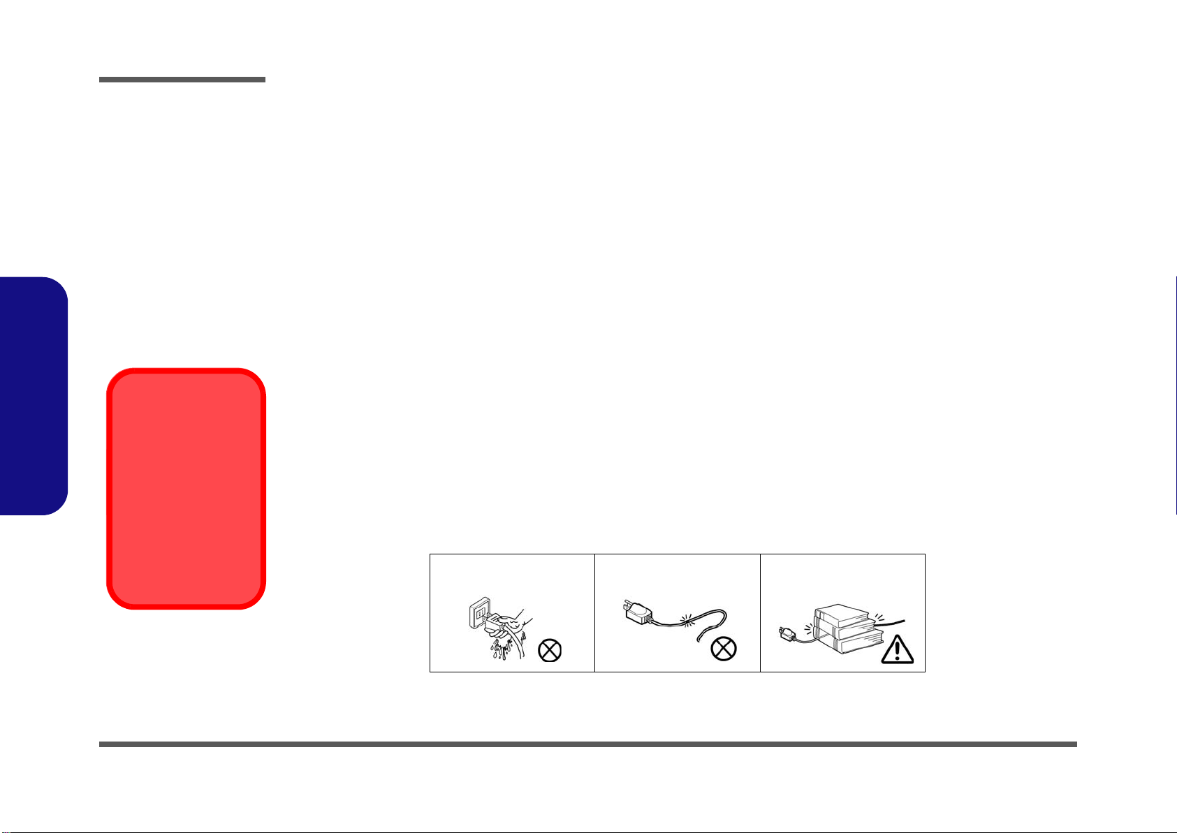
IMPORTANT SAFETY INSTRUCTIONS
Follow basic safety precautions, including those listed below, to reduce the risk of fire, electric shock, and injury to persons
when using any electrical equipment:
1. Do not use this product near water, for example near a bath tub, wash b owl, kitchen sink or laun dr y tub, in a wet ba sement or
near a swimming pool.
2. Avoid using this equipment with a telephone line (other than a cordless type) during an electrical storm. There may be a
remote risk of electrical shock from lightning.
3. Do not use the telephone to report a gas leak in the vicinity of the leak.
4. Use only the power cord and batteri es indicated in this manual. Do not dispose of batteries in a fir e. They may explode. Check
with local codes for possible special disposal instructions.
This product is intended to be supplied by a Listed Power Unit with an AC Input of 100 - 240V, 50 - 60Hz, DC Output
5.
19V, 4.74A (90W).
Preface
Preface
CAUTION
This Computer’s Optical Device is a Laser Class 1 Product
V
Page 8
Preface
Instructions for Care and Operation
The notebook computer is quite rugged, but it can be damaged. To prevent this, follow these suggestions:
1. Don’t drop it, or expose it to shock. If the computer falls, the case and the components could be damaged.
2. Keep it dry, and don’t overheat it. Keep the computer and power supply away from any kind of heating element. This
is an electrical appliance. If water or any other liquid gets into it, the computer could be badly damaged.
3. Follow the proper working procedures for the computer. Shut the computer down properly and don’t forget to save
your work. Remember to periodically save your data as data may be lost if the battery is depleted.
4. Avoid interference. Keep the computer away from high capacity transformers, electric motors, and other strong magnetic fields. These can hinder proper performance and damage your data.
5. Take care when using peripheral devices.
Power Safety
The computer has specific power requirements:
Preface
VI
Power Safety
Warning
Before you undertake
any upgrade procedures, make sure that
you have turned off the
power, and disconnected all peripherals
and cables (including
telephone lines).
• Only use a power adapter approved for use with this computer.
• Your AC adapter may be designed for international travel but it still requires a steady, uninterrupted power supply. If you are
unsure of your local power specifications, consult your service representative or local power company.
• The power adapter may have either a 2-prong or a 3-prong grounded plug. The third prong is an important safety feature; do
not defeat its purpose. If you do not have access to a compatible outlet, have a qualified electrician install one.
• When you want to unplug the power cord, be sure to disconnect it by the plug head, not by its wire.
• Make sure the socket and any extension cord(s) you use can support the total current load of all the connected devices.
• Before cleaning the computer, make sure it is disconnected from any external power supplies.
Do not plug in the power
cord if you are wet.
Do not use the power cord if
it is broken.
Do not place heavy objects
on the power cord.
Page 9

Cleaning
Removal Warning
When removing any cover(s) and screw(s) for the purposes of device upg rade, remember to replace the cover(s) and
screw(s) before turning the computer on.
Do not apply cleaner directly to the computer, use a soft clean cloth.
Do not use volatile (petroleum distillates) or abrasive cleaners on any part of the computer.
Servicing
Do not attempt to service the computer yourself. Doing so may violate your warranty and expose you and the computer to
electric shock. Refer all servicing to authorized service personnel. Unplug the computer from the power supply. Then refer
servicing to qualified service personnel under any of the following conditions:
• When the power cord is damaged or frayed.
• If the computer has been exposed to any liquids.
• If the computer does not work normally when you follow the operating instructions.
• If the computer has been dropped or damaged (do not touch the poisonous liquid if the LCD panel breaks).
• If there is an unusual odor, heat or smoke coming from your computer.
Preface
Preface
VII
Page 10
Preface
Power Button (located under the LCD)
Preface
Related Documents
You may also need to consult the following manual for additional information:
User’s Manual on CD
This describes the computer’s features and the procedures for operating the computer and its ROM-based setup program.
It also describes the installation and operation of the utility programs provided with the computer.
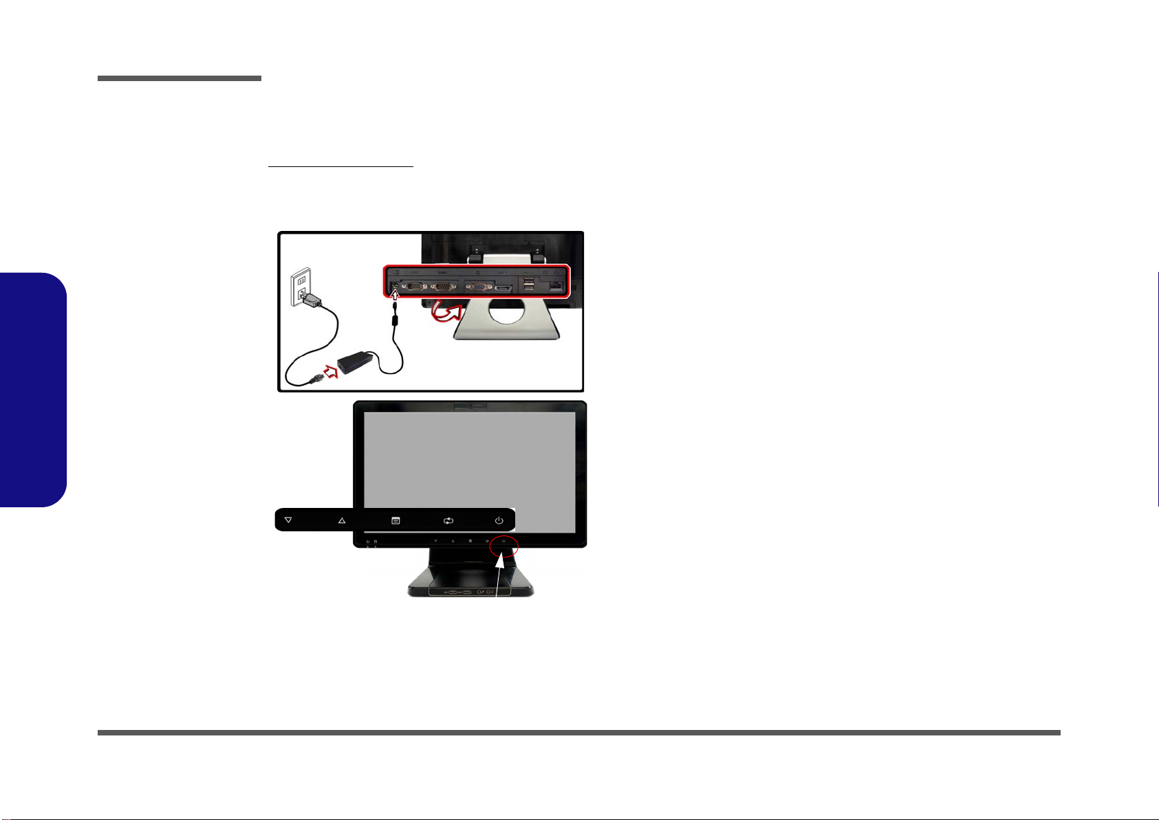
System Startup
1.Remove all packing materials.
2.Place the computer on a stable surface.
3.Securely attach any peripherals you want to use with the computer (e.g.
keyboard and mouse) to their ports.
4.Attach the AC/DC adapter to the DC-In jack located under the LCD,
then plug the AC power cord into an outlet, and connect the AC power
cord to the AC/DC adapter.
5.Push the power button at the front of the computer (under the LCD) to
turn the computer “on”.
VIII
Figure 1 - Computer with AC/DC Adapter Plugged-In/Power Button
Page 11

Contents
Preface
Introduction ..............................................1-1
Overview .........................................................................................1-1
Specifications ..................................................................................1-2
Tilting the LCD Screen ...................................................................1-4
External Locator - Front View ........................................................1-5
External Locator - Left & Right Side Views ...................................1-6
External Locator - Rear View .........................................................1-7
Mainboard Overview - Top (Key Parts) .........................................1-8
Mainboard Overview - Bottom (Key Parts) ....................................1-9
Mainboard Overview - Top (Connector) ......................................1-10
Mainboard Overview - Bottom (Connectors) ...............................1-11
Disassembly ...............................................2-1
Overview .........................................................................................2-1
Maintenance Tools ..........................................................................2-2
Connections .....................................................................................2-2
Maintenance Precautions .................................................................2-3
Disassembly Steps ...........................................................................2-4
Removing the Rear Top Cover ........................................................2-5
Removing the Hard Disk Drive .......................................................2-6
Upgrading the System Memory (RAM) ..........................................2-7
Removing the Stand ........................................................................2-9
Removing the Rear Bottom Cover ................................................2-10
Removing the Fan Module ............................................................2-11
Removing the Optical (CD/DVD) Device ....................................2-12
Removing the Wireless LAN Module ...........................................2-13
Removing the CPU ........................................................................2-14
Removing the TV Tuner Module ..................................................2-17
Part Lists ..................................................A-1
Part List Illustration Location ........................................................ A-2
LCD .............................................................................................. A-3
Stand ............................................................................................. A-4
Back .............................................................................................. A-5
DVD .............................................................................................. A-6
Combo ........................................................................................... A-7
Schematic Diagrams.................................B-1
System Block Diagram ...................................................................B-2
Clock Generator ..............................................................................B-3
CPU 1/7 (DMI, PEG, FDI) .............................................................B-4
CPU 2/7 (CLK, MISC, JTAG) .......................................................B-5
CPU 3/7 (DDR3) ............................................................................B-6
CPU 4/7 (Power) .............................................................................B-7
CPU 5/7 (Graphics Power) .............................................................B-8
CPU 6/7 (GND) ..............................................................................B-9
CPU 7/7 (RESERVED) ................................................................B-10
DDR3 SO-DIMM_0 .....................................................................B-11
DDR3 SO-DIMM_1 .....................................................................B-12
LVDS, Inverter .............................................................................B-13
LVDS & Audio Switch .................................................................B-14
HDMI, CRT ..................................................................................B-15
SCALAR .......................................................................................B-16
IBEXPEAK-M_HDA/SATA .......................................................B-17
IBEXPEAK-M_PCIE/CLK/SM ...................................................B-18
IBEXPEAK-M_DMI/FDI/GPIO ..................................................B-19
IBEXPEAK-M_LVDS/DDI .........................................................B-20
Preface
XI
Page 12

Preface
IBEXPEAK-M_PCI/USB/NVRAM ............................................ B-21
IBEXPEAK-M_GPIO/MISC ....................................................... B-22
IBEXPEAK-M_Power ................................................................. B-23
IBEXPEAK-M_Power ................................................................. B-24
IBEXPEAK-M_GND ...................................................................B-25
New Card, Mini PCIE .................................................................. B-26
JMC 251 Card Reader ..................................................................B-27
LAN,SATA HDD, ODD, BT, CCD .............................................B-28
USB 3.0 ........................................................................................ B-29
USB, Fan ...................................................................................... B-30
Audio Codec VIA1812 (ALC272) ............................................... B-31
Audio Jack ....................................................................................B-32
KBC-ITE IT8518E ....................................................................... B-33
COM Port ..................................................................................... B-34
5VS, 3VS, 1.5VS ..........................................................................B-35
Power 3.3V/5V .............................................................................B-36
Preface
Power 1.5V/0.75V, 1.8VS ............................................................ B-37
Power 1.1VS_VTT .......................................................................B-38
Power VGFX_Core ......................................................................B-39
V-Core ..........................................................................................B-40
AC In ............................................................................................B-41
Power, SW Board ......................................................................... B-42
LED Board ................................................................................... B-43
USB, Audio Board ....................................................................... B-44
Sequence .......................................................................................B-45
Download the BIOS ................................ D-1
Unzip the downloaded files to a bootable CD/DVD/ or USB Flash
drive ............................................................................................... D-1
Set the computer to boot from the external drive .......................... D-1
Use the flash tools to update the BIOS .......................................... D-2
Restart the computer (booting from the HDD) .............................. D-2
Wall Mounting Guide............................. C-1
Removing the Stand .......................................................................C-2
Mounting Systems ..........................................................................C-3
General Guidelines for Wall Mounting .......................................... C-4
Mounted System Example .............................................................C-5
XII
Page 13

Chapter 1: Introduction
Overview
This manual covers the information you need to service or upgrade the A9100 series LCD computer. Information about
operating the computer (e.g. getting started, and the Setup utility) is in the User’s Manual. Information about drivers (e.g.
VGA & audio) is also found in User’s Manual. That manual is shipped with the computer.
Operating systems (e.g. Windows XP, Windows Vista, etc.) have their own manuals as do application software (e.g. word
processing and database programs). If you have questions about those programs, you should consult those manuals.
Introduction
The A9100 series computer is designed to be upgradeable. See Disassembly 2 on page 2 - 1 for a detailed description of
the upgrade procedures for each specific component. Please note the warning and safety information indicated by the
“” symbol.
The balance of this chapter reviews the computer’s technical specifications and features.
1.Introduction
Overview 1 - 1
Page 14

Introduction
Latest Specification Information
The specifications listed here are correct at the
time of sending them to the press. Certain items
(particularly processor types/speeds) may be
changed, delayed or updated due to the manufacturer's release schedule. Check with your
service center for more details.
CPU
The CPU is not a user serviceable part. Accessing the CPU in any way may violate your
warranty.
Specifications
1.Introduction
Processor Options
Intel® Core™ i7 Processor
i7-640M (2.80GHz), i7-620M (2.66GHz)
4MB L3 Cache & 1066MHz FSB
Intel® Core™ i5 Processor
i5-540M (2.53GHz), i5-520M (2.4GHz), i5-450M (2.4GHz)
3MB L3 Cache & 1066MHz FSB
Intel® Core™ i3 Processor
i3-350M (2.26GHz), i3-330M (2.13GHz), i3-370M (2.4GHz)
3MB L3 Cache & 1066MHz FSB
Intel® Pentium® Processor
P6000 (1.86GHz)
3MB L3 Cache & 1066MHz FSB
Intel® Celeron® Processor
P4500 (1.86GHz)
2MB L3 Cache & 1066MHz FSB
Core Logic
Intel® HM55 Chipset
BIOS
One 16Mb SPI Flash ROM
Phoenix™ BIOS
Memory
Two 204 Pin SO-DIMM Sockets Supporting DDR3 1066/
1333MHz Memory
Memory Expandable up to 8GB
Video Adapter
Intel® GMA HD
Shared Memory Architecture up to 1.7GB Supports
DirectX10.0
Security
BIOS Password
Security (Kensington® Type) Lock Slot
LCD Options
19" (42.8cm) WXGA+ (1440 * 900) TFT LCD
(Factory Option) Hard Glass
(Factory Option) Multi-Touch Panel
Audio
High Definition Audio Compliant Interface
2 * Built-In Speakers
Storage
(Factory Option) One Changeable 12.7mm(h) Optical
Device Type Drive (Super Multi Drive Module or
Blu-Ray Combo Drive Module)
Two Changeable 2.5" 9.5mm (h) SATA (Serial) HDD
Keyboard
RF Keyboard with mouse/Receiver (Factory Option)
(Factory Option) RF Remote Controller with Receiver
Card Reader
Embedded Multi-in-1 Card Reader
MMC (MultiMedia Card) / RS MMC
SD (Secure Digital) / Mini SD / SDHC/ SDXC
Compatible
MS (Memory Stick) / MS Pro / MS Duo
1 - 2 Specifications
Page 15

Introduction
Mini Card Slots
(Factory Option) One Mini-Card Slot for WLAN Module or
Combo Card
(Factory Option) One Mini-Card Slot for TV Tuner Module
Communication
Built-In Gigabit Ethernet LAN
(Factory Option) Combo WLAN (802.11b/g/n) and Blue-
tooth 3.0 Module
(Factory Option) 802.11b/g/n Wireless LAN Half Mini-
Card Module
(Factory Option) 2.0M Pixel USB PC Camera Module
(Factory Option) TV Tuner Module
(Factory Option) RF for TV Tuner Remote Controller
Interface
Four USB 2.0 Ports
One USB 3.0 Port
One eSATA Port
Two Serial (COM) Ports
One External Monitor Port
One Headphone-Out Jack
One Microphone-In Jack
One S/PDIF Output Jack
One Line-In Jack
One RJ-45 LAN Jack
One DC-in Jack
One ExpressCard/34(54) Slot
One HDMI-In Port
Resolutions Supported:
1440 * 900
1280 * 800
1280 * 720
1024 * 768
800 * 600
Power
Full Range AC/DC Adapter
AC Input: 100 - 240V, 50 - 60Hz
DC Output: 19V, 4.74A (90W)
Energy Star 5.0 Compliant
Envionmental Spec
Temperature
Operating: 5
Non-Operating: -20°C - 60°C
Relative Humidity
Operating: 20% - 80%
Non-Operating: 10% - 90%
°C - 35°C
Dimensions & Weight
450mm (w) * 312mm (d) * 66.5mm (h))
Around 11 kg
1.Introduction
1-3
Page 16
Introduction
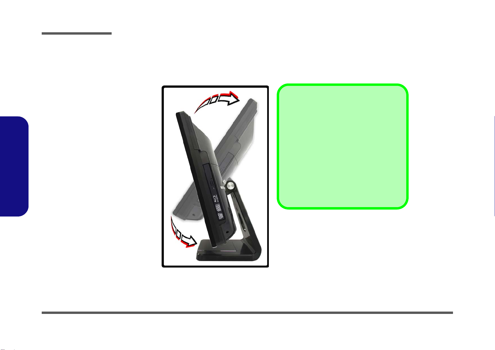
Figure 1
Tilting the LCD
Screen
Moving the Computer
We strongly recommend using both hands to
move the computer. You can use one hand to
grip the computer by the stand, and the other to
hold the top of the LCD screen.
It is recommended that you carry the computer
with the LCD facing your body to avoid scratching
the surface against other objects. However take
care not to scratch the LCD with any personal
items, belt fittings or jewelry etc.(one hand gripping the stand and the other gripping the top of
the computer to avoid accidentally dropping it).
45°
-5°
Tilting the LCD Screen
It is possible to tilt the LCD screen in order to get the best possible viewing angle of the screen without glare etc. Apply
pressure with one hand at the base of the computer, while carefully pushing the LCD screen to tilt it to the appropriate
viewing angle.
1.Introduction
1 - 4 Tilting the LCD Screen
Page 17
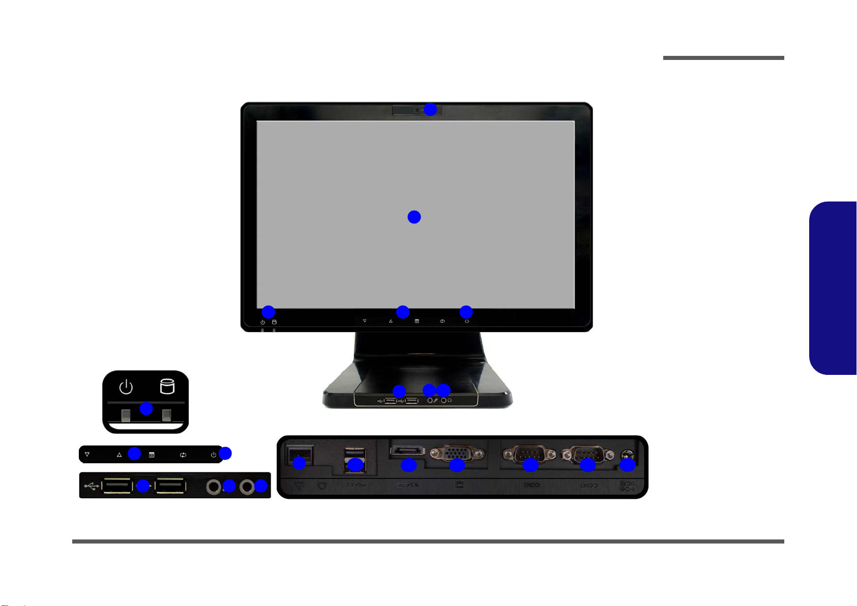
External Locator - Front View
Figure 2
Front View
1. PC Camera
(Optional)
2. LCD (With
Optional Touch
Panel)
3. Power & System
Activity LED
Indicators
4. Function Buttons*
5. Power Button*
6. USB 2.0 Ports
7. Microphone-In
Jack
8. Headphone/
Speaker-Out Jack
Under the LCD
9. RJ-45 LAN Jack
10.2 * USB Ports
11. eSATA Port
12.External Monitor
Port
13.2 * COM Ports
14.DC-In Jack
43
1
8
9
6
5
2
8
4
6
5
3
13
10
11
13
14
7
12
7
Under the LCD
Introduction
1.Introduction
External Locator - Front View 1 - 5
Page 18
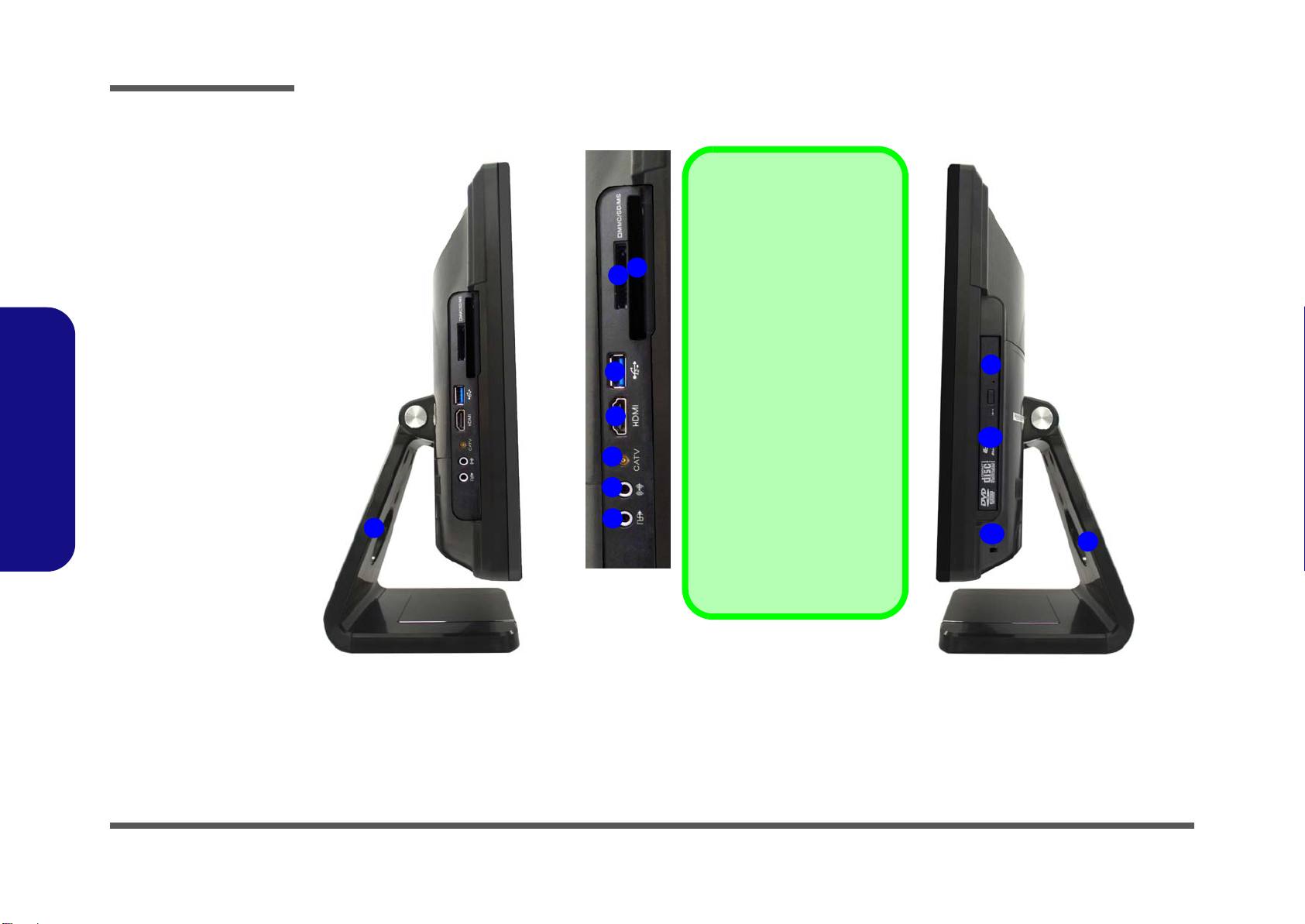
Introduction
Figure 3
Left & Right Side
Views
1. Stand
2. Multi-in-1 Card
Reader
3. ExpressCard Slot
/54(34)
4. 1 * USB 3.0 Port
5. HDMI-In Port
6. CATV
7. Line-In Jack
8. S/PDIF-Out Jack
9. Emergency Eject
Hole
10.Optical Device
Drive Bay
11. Security Lock Slot
2
3
4
5
6
7
8
1
ExpressCard Slot
The ExpressCard Slot accepts
either ExpressCard/34 or Ex-
pressCard/54 formats.
7-in-1 Card Reader
The card reader allows you to
use the most popular digital
storage card formats:
MMC (MultiMedia Card) / SD (Se-
cure Digital) / MS (Memory Stick) /
MS Pro (Memory Stick Pro) / MS
Duo (requires PC adapter) /
Mini SD (requires PC adapter) / RS
MMC (requires PC adapter)
Mini-IEEE 1394 Port
The Mini-IEEE 1394 port only
supports SELF POWERED
IEEE 1394 devices.
1
9
10
11
1.Introduction
External Locator - Left & Right Side Views
1 - 6 External Locator - Left & Right Side Views
Page 19

External Locator - Rear View
Figure 4
Rear View
1. Stand
2. Rear Component
Cover
3. Vent/Fan Intake
4. Security Lock Slot
5. Carrying Handle
Area
Overheating
To prevent your computer from overheating
make sure nothing
blocks the vent/fan intakes while the computer is in use.
1
3
2
3 3
4
5
Carrying the Computer
We strongly recommend using both hands to move the computer (one hand gripping the handle area and the other gripping the
computer) to avoid accidentally dropping it. Be care ful that objects such as belt bu ckles etc. do not scratch th e screen while it
is being carried.
Introduction
1.Introduction
External Locator - Rear View 1 - 7
Page 20
Introduction
Figure 5
Mainboard Top
Key Parts
1. ExpressCard/34/
54 Slot
1
1.Introduction
Mainboard Overview - Top (Key Parts)
1 - 8 Mainboard Overview - Top (Key Parts)
Page 21
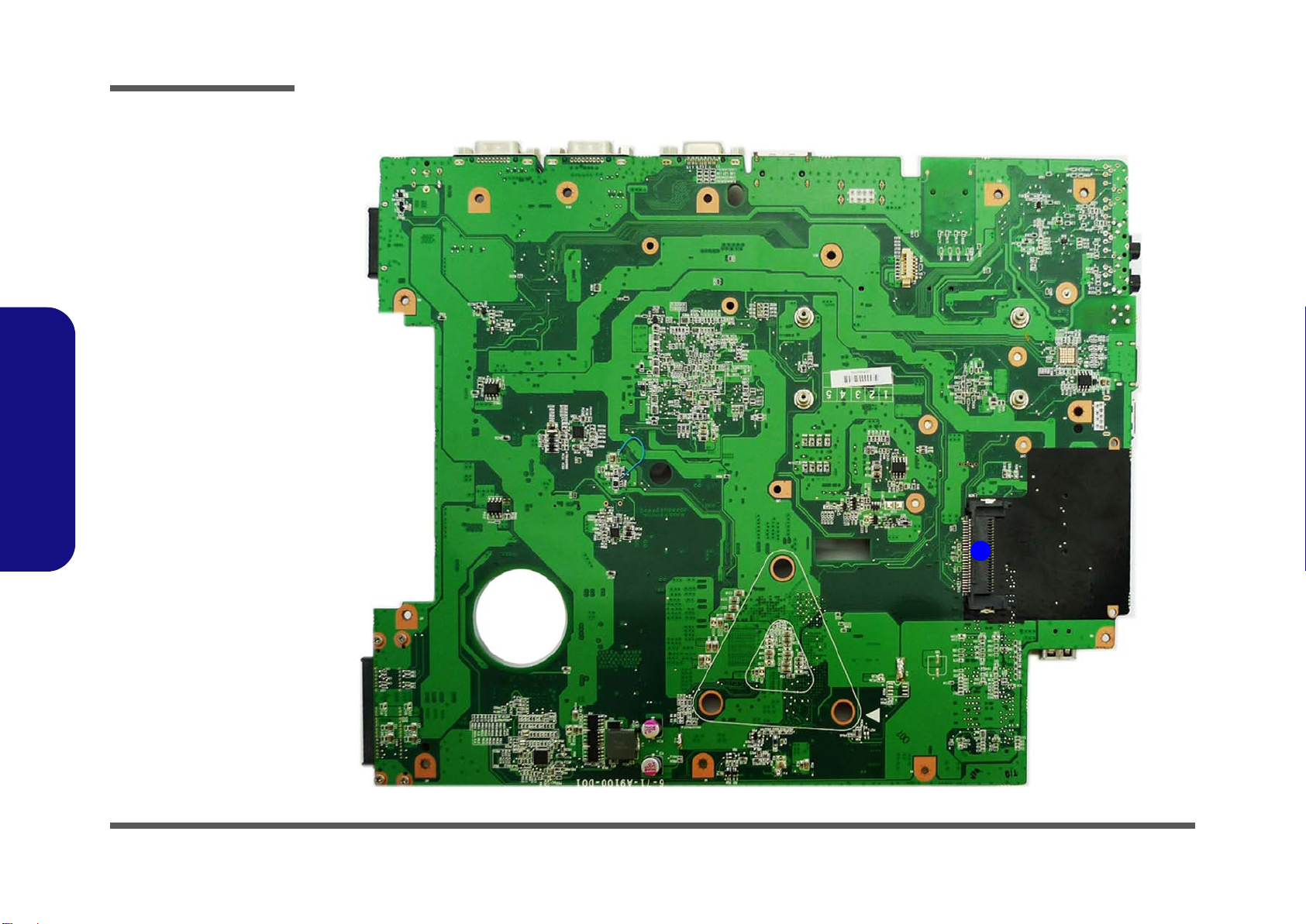
Mainboard Overview - Bottom (Key Parts)
1
2
4
5
6
7
3
8
9
10
Figure 6
Mainboard Bottom
Key Parts
1. Audio Codec
2. Mini-Card
Connector (WLAN
Module)
3. Mini-Card
Connector (TV
Card)
4. Clock Generator
5. Platform Controller
Hub
6. JMC 251C
7. Memory Slots
DDR3 SO-DIMM
8. CPU Socket (CPU
uninstalled)
9. VCORE
10.KBC-ITE IT8513E
Introduction
1.Introduction
Mainboard Overview - Bottom (Key Parts) 1 - 9
Page 22
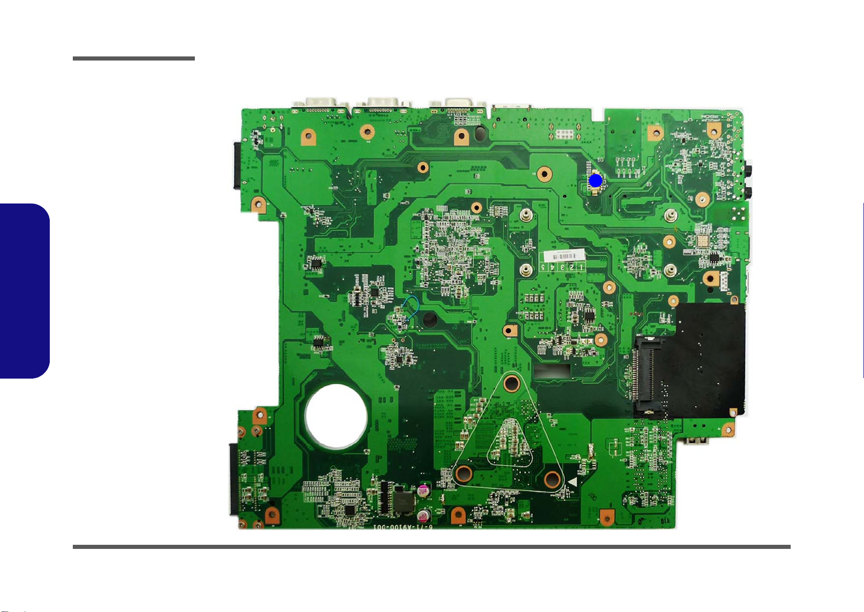
Introduction
Figure 7
Mainboard Top
Connector
1. Touch Panel
Connector
1
1.Introduction
Mainboard Overview - Top (Connector)
1 - 10 Mainboard Overview - Top (Connector)
Page 23
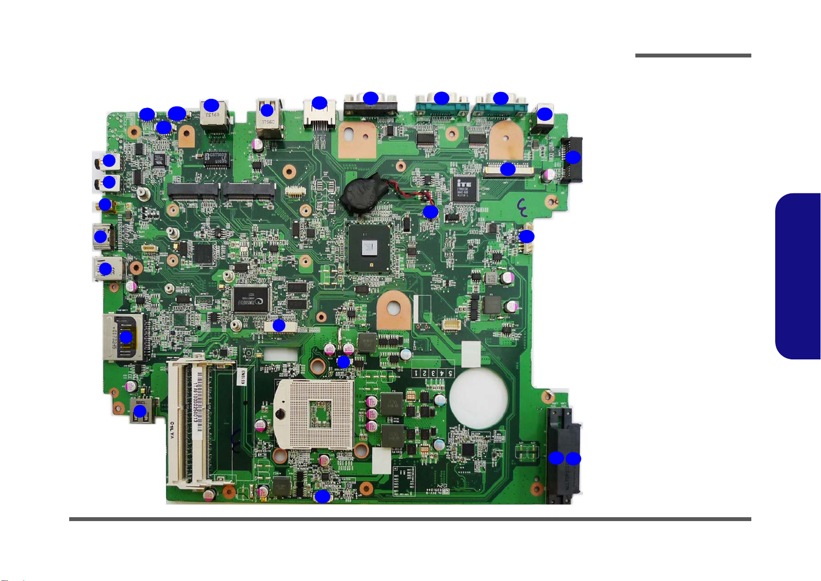
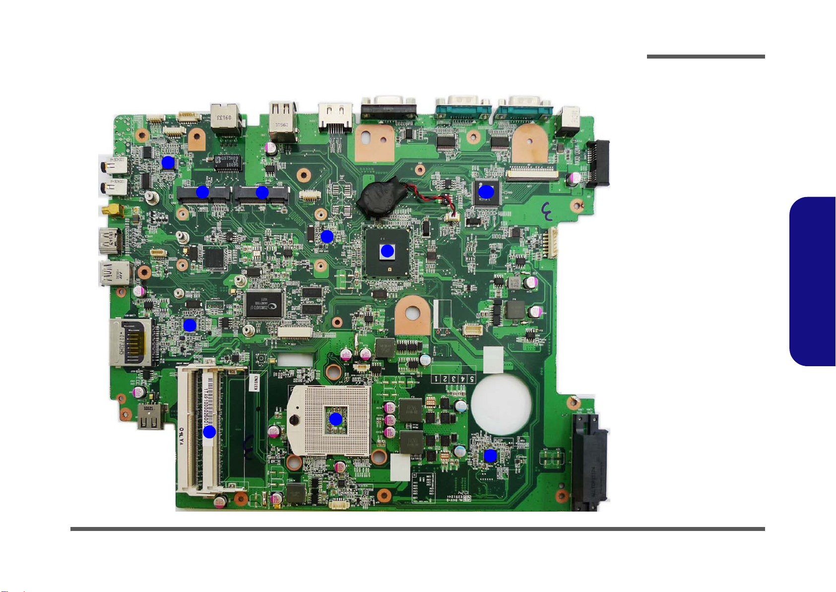
Mainboard Overview - Bottom (Connectors)
Figure 8
Mainboard Bottom
Connectors
1. S/PDIF-Out Jack
2. Line-In Jack
3. CATV
4. HDMI-In Port
5. USB 3.0 Port
6. Multi-in-1 Card
Reader
7. USB 2.0 Ports
8. LCD Cable
Connector
9. CPU Fan Cable
Connector
10. CCD Cable
Connector
11. HDD Connectors
12. Inverter Connector
13. CMOS Battery
Connector
14. Keyboard Cable
Connector
15. ODD Connector
16. DC-In Jack
17. COM Ports
18. External Monitor Port
19. eSAT A Port
20. RJ-45 Lan Jack
21. Power Switch Cable
Connector
22. Speaker Cable
Connector
23. LED Cable Connector
Connector
9
1
5
2
3
4
6
7
11
11
12
13
14
16
17
15
8
10
1718
19
20
21
22
23
7
Introduction
Mainboard Overview - Bottom (Connectors) 1 - 11
1.Introduction
Page 24

Introduction
1.Introduction
1-12
Page 25

Chapter 2: Disassembly
Warning
Information
Overview
This chapter provides step-by-step instructions for disassembling the A9100 series LCD computer’s parts and subsystems. When it comes to reassembly, reverse the procedures (unless otherwise indicated).
We suggest you completely review any procedure before you take the computer apart.
Disassembly
Procedures such as upgrading/replacing the RAM, optical device and hard disk are included in the User’s Manual but are
repeated here for your convenience.
To make the disassembly process easier each section may have a box in the page margin. Information contained under
the figure # will give a synopsis of the sequence of procedures involved in the disassembly procedure. A box with a
lists the relevant parts you will have after the disassembly process is complete. Note: The parts listed will be for the disassembly procedure listed ONLY, and not any previous disassembly step(s) required. Refer to the part list for the previous disassembly procedure. The amount of screws you should be left with will be listed here also.
A box with a will also provide any possible helpful information. A box with a contains warnings.
An example of these types of boxes are shown in the sidebar.
2.Disassembly
Overview 2 - 1
Page 26

Disassembly
2.Disassembly
NOTE: All disassembly procedures assume that the system is turned OFF, and disconnected from any power supply.
Maintenance Tools
The following tools are recommended when working on the notebook PC:
• M3 Philips-head screwdriver
• M2.5 Philips-head screwdriver (magnetized)
• M2 Philips-head screwdriver
• Small flat-head screwdriver
• Pair of needle-nose pliers
• Anti-static wrist-strap
Connections
Connections within the computer are one of four types:
Locking collar sockets for ribbon connectors To release these connectors, use a small flat-head screwdriver to gently pry
the locking collar away from its base. When replacing the connection, make
sure the connector is oriented in the same way. The pin1 side is usually not
indicated.
2 - 2 Overview
Pressure sockets for multi-wire connectors To release this connector type, grasp it at its head and gently rock it from side
to side as you pull it out. Do not pull on the wires themselves. When replacing
the connection, do not try to force it. The socket only fits one way.
Pressure sockets for ribbon connectors To release these connectors, use a small pair of needle-nose pliers to gently
lift the connector away from its socket. When replacing the connection, make
sure the connector is oriented in the same way. The pin1 side is usually not
indicated.
Board-to-board or multi-pin sockets To separate the boards, gently rock them from side to side as you pull them
apart. If the connection is very tight, use a small flat-head screwdriver - use
just enough force to start.
Page 27

Maintenance Precautions
Power Safety
Warning
Before you undertake
any upgrade procedures, make sure that
you have turned off the
power, and disconnected all peripherals and
cables (including telephone lines).
Removal Warning
When removing any
cover(s) and screw(s)
for the purposes of device upgrade, remember
to replace the cover(s)
and screw(s) before
turning the computer on.
The following precautions are a reminder. To avoid personal injury or damage to the computer while performing a removal and/or replacement job, take the following precautions:
1. Don't drop it. Perform your repairs and/or upgrades on a stable surface. If the computer falls, the case and other
components could be damaged.
2. Don't overheat it. Note the proximity of any heating elements. Keep the computer out of direct sunlight.
3. Avoid interference. Note the proximity of any high capacity transformers, electric motors, and other strong mag-
netic fields. These can hinder proper performance and damage component s and/or data. You should also monitor
the position of magnetized tools (i.e. screwdrivers).
4. Keep it dry. This is an electrical appliance. If water or any other liquid gets into it, the computer could be badly
damaged.
5. Be careful with power. Avoid accidental shocks, discharges or explosions.
•Before removing or servicing any part from the computer, turn the computer off and detach any power supplies.
•When you want to unplug the power cord or any cable/wire, be sure to disconnect it by the plug head. Do no t pull on th e wir e.
6. Peripherals – Turn off and detach any peripherals.
7. Beware of static discharge. ICs, such as the CPU and main support chips, are vulnerable to static electricity.
Before handling any part in the computer, discharge any static electricity inside the computer. When handling a
printed circuit board, do not use gloves or other materials which allow static electricity buildup. We suggest that
you use an anti-static wrist strap instead.
8. Beware of corrosion. As you perform your job, avoid touching any connector leads. Even the cleanest hands produce oils which can attract corrosive elements.
9. Keep your work environment clean. Tobacco smoke, dust or other air-born particulate matter is often attracted
to charged surfaces, reducing performance.
10. Keep track of the components. When removing or replacing any p art, be careful not to leave small p arts, such as
screws, loose inside the computer.
Cleaning
Do not apply cleaner directly to the computer, use a soft clean cloth.
Do not use volatile (petroleum distillates) or abrasive cleaners on any part of the computer.
Disassembly
2.Disassembly
Overview 2 - 3
Page 28

Disassembly
Disassembly Steps
The following table lists the disassembly steps, and on which page to find the related information. PLEASE PERFORM
THE DISASSEMBLY STEPS IN THE ORDER INDICATED.
2.Disassembly
To remove the Rear Top Cover:
1. Remove the rear top cover page 2 - 4
To remove the Hard Disk Drive:
1. Remove the rear top cover page 2 - 4
2. Remove the HDD page 2 - 6
To remove and install the System Memory:
1. Remove the rear top cover page 2 - 4
2. Remove the system memory page 2 - 7
To remove the Stand:
1. Remove the rear top cover page 2 - 4
2. Remove the stand page 2 - 9
To remove the Rear Bottom Cover:
1. Remove the rear top cover page 2 - 4
2. Remove the stand page 2 - 9
3. Remove the rear bottom cover page 2 - 10
To remove the Optical Device:
1. Remove the rear top cover page 2 - 4
2. Remove the stand page 2 - 9
3. Remove the rear bottom cover page 2 - 10
4. Remove the optical device page 2 - 12
To remove the WLAN Module:
1. Remove the rear top cover page 2 - 4
2. Remove the WLAN module page 2 - 13
To remove the CPU:
1. Remove the rear top cover page 2 - 4
2. Remove the CPU page 2 - 14
3. Install the CPU page 2 - 16
To remove the Fan Module:
1. Remove the rear top cover page 2 - 4
2. Remove the stand page 2 - 9
3. Remove the rear bottom cover page 2 - 10
4. Remove the fan module page 2 - 11
2 - 4 Disassembly Steps
Page 29
Removing the Rear Top Cover
Figure 1
Rear Top Cover
Removal
a. Remove the screws.
b. Slide the top cover to
unlock.
c. Remove the rear top
cover.
F. Rear Top Cover
•4 Screws
A
DE6
F
B
A
C D
E
a.
b.
c.
F
Before undertaking any upgrade procedure it is necessary to remove the rear top cover to access the components.
1. Turn off the computer and disconnect all cables and peripherals.
2. Carefully place the computer flat with the LCD facing down (make sure you cover the LCD to avoid scratches) so
that you may access the rear cover.
3. Remove screws -
4. Slide the rear top cover until the arrow is aligned with the unlock icon
5. When the arrow is aligned with the unlock icon you can remove the rear top cover
Disassembly
(Figure 1a).
(Figure 1b).
(Figure 1c).
2.Disassembly
Removing the Rear Top Cover 2 - 5
Page 30
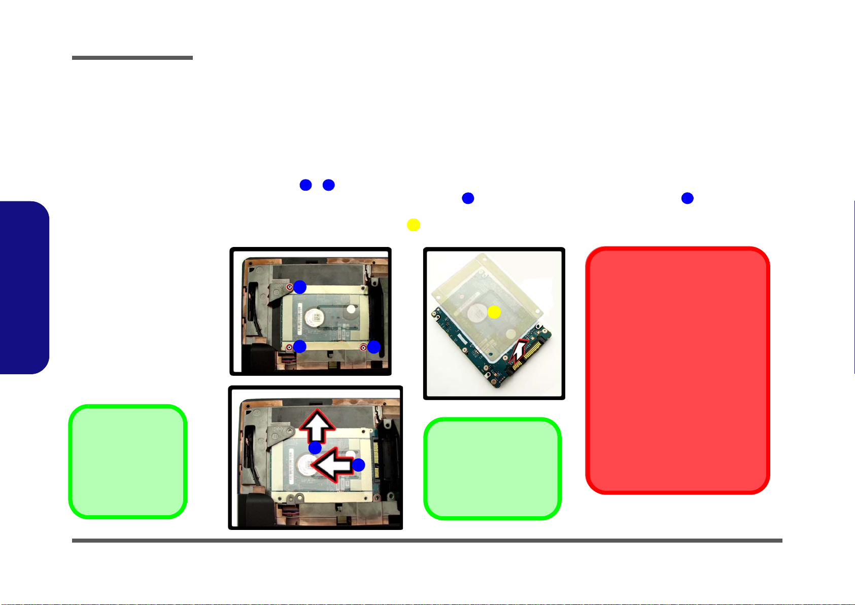
Disassembly
Figure 2
Hard Disk Drive
Removal
a. Remove the screws.
b. Slide the hard disk in
the direction of the arrows.
c. Remove the adhesive
hard disk cover top
cover.
F. Adhesive Hard Disk
Cover
•3 Screws
ACDE6
F
B
A
C
Hard Disk Slot
Make sure you install the
hard disk into the lower slot
on the mainboard.
a.
b.
c.
D
E
F
HDD System Warning
New HDD’s are blank. Before you begin
make sure:
You have backed up any data you want
to keep from your old HDD.
You have all the CD-ROMs and FDDs
required to install your operating system and programs.
If you have access to the internet,
download the latest application and
hardware driver updates for the operating system you plan to install. Copy
these to a removable medium.
Removing the Hard Disk Drive
The hard disk drive can be taken out to accommodate other 2.5" serial (SATA) hard disk drives with a height of 9.5mm
(h). Follow your operating system’s installation instructions, and install all necessary drivers and utilities (as outlined in
Chapter 4 of the User’s Manual) when setting up a new hard disk.
2.Disassembly
Hard Disk Upgrade Process
1. Remove the rear top cover (page 2 - 5).
2. Remove screws -
(Figure 2a).
3. Firstly slide the hard disk in the direction of arrow , and then slide it in the direction of arrow to remove it
(Figure 2b).
4. Remove the adhesive hard disk cover
5. Reverse the process to install a new hard disk.
(Figure 2c).
2 - 6 Removing the Hard Disk Drive
Page 31

Upgrading the System Memory (RAM)
Figure 3
RAM Module
Removal
a. Locate the RAM.
b. Pull the latches to re-
lease the RAM module.
c. Remove the RAM
module.
Single Memory
Module Installation
If your computer has a
single memory module,
then insert the module
into the Channel 0
(JDIMM_1) socket. In
this case this is the upper memory socket (the
socket furthest from the
mainboard) as shown in
Figure 3
b.
D. RAM Module
ABC
A
B
C
a. c.
Contact Warning
Be careful not to touch the metal pins on the module’s connecting edge. Even
the cleanest hands have oils which can attract particles, and degrade the module’s performance.
b.
D
6
D
The computer has two memory sockets for 204 pin Small Outline Dual In-line (SO-DIMM) DDRIII (DDR3) type memory modules (see Memory page 1 - 2 for details of supported module types).
The total memory size is automatically detected by the POST routine once you turn on your computer.
1. Remove the rear top cover (page 2 - 5).
2. The RAM is located at point
(Figure 3a).
3. Gently pull the two release latches on the sides of the memory socket in the direction indicated by the arrows (
& ) in Figure 3b.
4. The RAM module will pop-up
(Figure 3c), and you can remove it (see over).
Disassembly
2.Disassembly
Upgrading the System Memory (RAM) 2 - 7
Page 32

Disassembly
2.Disassembly
5. Pull the latches to release the second module if necessary.
6. Insert a new module holding it at about a 30° angle and fit the connectors firmly into the memory slot.
7. The module’s pin alignment will allow it to only fit one way. Make sure the module is seated as far into the slot as it
will go. DO NOT FORCE the module; it should fit without much pressure.
8. Press the module in and down towards the mainboard until the slot levers click into place to secure the module.
9. Replace the module bay cover and screws.
10. Restart the computer to allow the BIOS to register the new memory configuration as it starts up.
2 - 8 Upgrading the System Memory (RAM)
Page 33

Removing the Stand
Figure 4
Stand Removal
a. Remove the screws
and stand cover.
b. Disconnect the cable
and remove the
screws.
c. Remove the stand.
C. Stand Cover
I. Stand
•6 Screws
AB6
C
DEH
6
I
A
B
D
C
a.
b.
E
F
G
H
c.
I
1. Turn off the computer and disconnect all cables and peripherals.
2. Carefully place the computer flat with the LCD facing down (make sure you cover the LCD to avoid scratches) so
that you may access the rear cover.
3. Remove screws & from the stand cover, and then remove the stand cover
4. Carefully release cable , and remove screws -
5. Remove the stand
Disassembly
(Figure 4a).
(Figure 4b).
(Figure 4c).
2.Disassembly
Removing the Stand 2 - 9
Page 34

Disassembly
Figure 5
Rear Bottom
Cover Removal
a. Remove the screws.
b. Carefully remove the
rear bottom cover and
disconnect the fan cable as you lift up the
cover.
D. Rear Bottom Cover
•3 Screws
AC6DE
A
B
a. b.
D
E
E
C
Removing the Rear Bottom Cover
1. Remove the rear top cover (page 2 - 5) and stand (page 2 - 9).
2. Remove screws -
3. Carefully remove the rear bottom cover (a fan cable/connector is attached at points and this will need to be
disconnected) Figure 5b.
(Figure 5a).
2.Disassembly
2 - 10 Removing the Rear Bottom Cover
Page 35

Removing the Fan Module
Figure 6
Fan Module
Removal
a. Remove the screws.
b. Remove the Fan unit.
c. Remove the bracket if
required.
C. Fan Module
H. Fan Bracket
•6 Screws
AB6CDG6
H
A
B
a. b.
C
c.
H
G
D
E
F
1. Remove the rear top cover (page 2 - 5), stand (page 2 - 9) and rear bottom cover (page 2 - 10).
2. Turn over the rear bottom cover and remove screws &
3. Carefully remove the fan module and screws -
4. Remove the fan bracket (if required) Figure 6c.
(Figure 6a).
(Figure 6b).
Disassembly
2.Disassembly
Removing the Fan Module 2 - 11
Page 36

Disassembly
Figure 7
Optical Device
Module Removal
a. Remove the screw.
b. Push out the optical
device module.
B. Optical Device Mod-
ule
•1 Screw
A
6BC
A
a.
B
b.
C
Removing the Optical (CD/DVD) Device
1. Remove the rear top cover (page 2 - 5), stand (page 2 - 9) and rear bottom cover (page 2 - 10).
2. Remove screw from the optical device
3. Push the optical device out in the direction of arrow
(Figure 7a).
(Figure 7b).
2.Disassembly
2 - 12 Removing the Optical (CD/DVD) Device
Page 37

Removing the Wireless LAN Module
Figure 8
WLAN Module
Module Removal
a. Locate the WLAN
module.
b. Remove the screw
and disconnect the
antenna cables.
c. The module will pop
up.
d. You can then remove
the module.
E. WLAN Module
•1 Screw
ABCD6
E
A
a. b.
D C B
E
c. d.
E
1. Remove the rear top cover (page 2 - 5).
2. The WLAN module is located at point
3. Remove screw , and disconnect antenna cables &
4. When the screw and cables have been removed/disconnected the WLAN module will pop up
can be removed
(Figure 8d).
(Figure 8a).
Disassembly
(Figure 8b).
(Figure 8c) and
2.Disassembly
Removing the Wireless LAN Module 2 - 13
Page 38

Disassembly
Figure 9
CPU Removal
a. Locate the heat sink.
b. Loosen the screws in
the order indicated.
c. Remove the heat sink
unit.
B. Heat Sink Unit
A3216
B
1
a. b.
2
3
c.
A
B
Caution
The heat sink, and CPU area in general, contains parts which ar e subject to
high temperatures. Allow the area time to cool before removing these parts.
To remove the heat sink unit loosen the screws in
the order , , (there are numbers on the
heat sink unit itself).
321
Removing the CPU
1. Remove the rear top cover (page 2 - 5).
2. The CPU heat sink unit is located at point
3. Loosen the heat sink unit screws in the order , ,
4. You can then remove the heat sink unit
(Figure 9a).
(Figure 9b).
(Figure 9c).
2.Disassembly
2 - 14 Removing the CPU
Page 39

5. Turn the release latch towards the unlock symbol , to release the CPU (Figure 10d).
Figure 10
CPU Removal
(cont’d)
d. Unlock the cpu.
e. Remove the cpu.
D. CPU
C
6
D
d. e.
C
D
6. Carefully (it may be hot) lift the CPU up out of the socket
7. See page 2 - 16 for information on inserting a new CPU.
8. When inserting a CPU, pay careful attention to the pin alignment, it will fit only one way (DO NOT FORCE IT!).
Disassembly
(Figure 10e).
2.Disassembly
Removing the CPU 2 - 15
Page 40

Disassembly
Figure 11
Processor
Installation
a. Lock the cpu.
b. Insert the heat sink
(remember to remove
any sticker on a new
heat sink unit).
c. Tighten the screws in
the order indicated.
C. Heat Sink Unit
AB6
C
123
a.
b.
c.
A
B
C
1
2
3
To remove the heat sink unit
loosen the screws in the order
, , (there are numbers
on the heat sink unit itself).
123
Processor Installation Procedure
1. Insert the CPU paying careful attention to the pin alignment, it will fit only one way (DO NOT FORCE IT!).
2. Turn the release latch towards the lock symbol
3. Remove the sticker from the heat sink
4. Insert the heat sink as indicated
5. Tighten screws in the order , ,
(Figure 11b).
(Figure 11b).
(Figure 11c).
(Figure 11a).
2.Disassembly
2 - 16 Removing the CPU
Page 41

Removing the TV Tuner Module
Figure 12
TV Tuner Module
Removal
a. The TV Tuner module will
be visible at point .
b. Carefully disconnect the
cable and remove the
screw from the TV Tuner
module.
c. The TV Tuner module will
pop up.
d. Lift the TV Tuner module
up and off the computer.
1
1
2
3
4
4
a.
b.
1
4
2
3
4
c.
d.
4. TV Tuner Module
•1 Screw
1. Remove the rear top cover (page 2 - 5).
2. The TV Tuner module will be visible at point
3. Carefully disconnect the cable
4. The TV Tuner module will pop up
and remove the screw from the TV Tuner module (Figure 12b).
(Figure 12c).
5. Lift the TV Tuner module up and off the computer (Figure 12d).
(Figure 12a).
Disassembly
2.Disassembly
Removing the TV Tuner Module 2 - 17
Page 42

Disassembly
2.Disassembly
2-18
Page 43

Appendix A: Part Lists
This appendix breaks down the A9100 series LCD computer’s construction into a series of illustrations. The component
part numbers are indicated in the tables opposite the drawings.
Note: This section indicates the manufacturer’s part numbers. Your organization may use a different system, so be sure
to cross-check any relevant documentation.
Note: Some assemblies may have parts in common (especially screws). However, the part lists DO NOT indicate the
total number of duplicated parts used.
Part Lists
Note: Be sure to check any update notices. The parts shown in these illustrations are appropriate for the system at the
time of publication. Over the product life, some parts may be improved or re-configured, resulting in new part numbers.
A.Part Lists
A-1
Page 44

Part Lists
Table A- 1
Part List Illustration
A.Part Lists
Part List Illustration Location
The following table indicates where to find the appropriate part list illustration.
Parts A9100
Location
LCD page A - 3
Stand page A - 4
Back page A - 5
DVD page A - 6
COMBO page A - 7
A - 2 Part List Illustration Location
Page 45

LCD
無鉛
銘板 無 鉛
導電布 無鉛
銘板 膠 黑色亮面
(華鶴) 外包
(設變)
(宇辰) 外包
Figure A - 1
LCD
Part Lists
A.Part Lists
LCD A - 3
Page 46

Part Lists
(設變)
(設變)
(偉鎮)
防鬆處理 化學膠
(越得)
(志精)
醋酸膠帶 (久威)
Figure A - 2
Stand
A.Part Lists
Stand
A - 4 Stand
Page 47

Back
Figure A - 3
Back
Part Lists
A.Part Lists
Back A - 5
Page 48

Part Lists
(擴孔)
Figure A - 4
DVD
A.Part Lists
DVD
A - 6 DVD
Page 49

Combo
(擴孔)
Figure A - 5
Combo
Part Lists
A.Part Lists
Combo A - 7
Page 50

Part Lists
A.Part Lists
A - 8
Page 51

Appendix B: Schematic Diagrams
Table B - 1
Schematic
Diagrams
Version Note
The schematic diagrams in this chapter
are based upon version 6-7P-A9104-003.
If your mainboard (or
other boards) are a later version, please
check with the Service
Center for updated diagrams (if required).
This appendix has circuit diagrams of the A9100 series LCD computer’s PCBs. The following table indicates where to
find the appropriate schematic diagram.
Diagram - Page Diagram - Page Diagram - Page
System Block Diagram - Page B - 2 IBEXPEAK-M_PCIE/CLK/SM - Page B - 18 COM Port - Page B - 34
Clock Generator - Page B - 3 IBEXPEAK-M_DMI/FDI/GPIO - Page B - 19 5VS, 3VS, 1.5VS - Page B - 35
CPU 1/7 (DMI, PEG, FDI) - Page B - 4 IBEXPEAK-M_LVDS/DDI - Page B - 20 Power 3.3V/5V - Page B - 36
Schematic Diagrams
B.Schematic Diagrams
CPU 2/7 (CLK, MISC, JTAG) - Page B - 5
CPU 3/7 (DDR3) - Page B - 6 I BEXPEAK-M_GPIO/MISC - Page B - 22 Power 1.1VS_VTT - Page B - 38
CPU 4/7 (Power) - Page B - 7 IBEXP EAK-M_Power - Page B - 23 Power VGFX_Core - Page B - 39
CPU 5/7 (Graphics Power) - Page B - 8 IBEXPEAK-M_Power - Page B - 24 V-Core - Page B - 40
CPU 6/7 (GND) - Page B - 9 IBEXPEAK-M_GND - Page B - 25 AC In - Page B - 41
CPU 7/7 (RESERVED) - Page B - 10 New Card, Mini PCIE - Page B - 26 Power, SW Board - Page B - 42
DDR3 SO-DIMM_0 - Page B - 11 JMC 251 Card Reader - Page B - 27 LED Board - Page B - 43
DDR3 SO-DIMM_1 - Page B - 12
LVDS, Inverter - Page B - 13 USB 3.0 - Page B - 29 Sequence - Page B - 45
LVDS & Audio Switch - Page B - 14 USB, Fan - Page B - 30
HDMI, CRT - Page B - 15 Audio Codec VIA1812 (ALC272) - Page B - 31
SCALAR - Page B - 16 Audio Jack - Page B - 32
IBEXPEAK-M_HDA/SATA - Page B - 17 KBC-ITE IT8518E - Page B - 33
IBEXPEAK-M_PCI/USB/NVRAM - Page B 21
LAN,SATA HDD, ODD, BT, CCD - Page B 28
Power 1.5V/0.75V, 1.8VS - Page B - 37
USB, Audio Board - Page B - 44
B-1
Page 52

Schematic Diagrams
Sheet 1 of 44
System Block
Diagram
SPDIF
Ca l pe l la S yste m B l oc k Diagr am
POWE R SW IT CH +H OT KEY X 3
LINE IN
(USB2)
New Ca rd
Cloc k G en er at or
SATA HDD x 2 S AT A OD D
<8"
LVDS
CRT CO NNEC TO R
LPC
P OWE R GP U
SO-DIMM1
SOCKET
<=8"
PCIE
Memory Termination
27x27mm
1071 Ball FCBGA
480 Mbps
DDRIII
Min i PC IE
14.318 MHz
SLG8 S P5 85 V
SPI
1"~16"
STAND MIC
DDRIII
Clarksfield/
Auburndale
24 M Hz
<12"
FDI
H DM I IN (S CALA R)
INT SPK L
128pins LQFP
SO-DIMM0
32.768KHz
EC SMBU S
AZA LI A LI NK
SOCK ET
0.1" ~1 3
SYSTEM SMBUS
BIOS
SPI
IT E 85 18 E
<12"
Ibex Peak-M
Platform
Controller
H ub (P CH)
LED BOA RD
INT. K/B
EC Azalia Codec
0.5"~11"
<15"
5V,3V,5VS,3VS,1.5VS,
USB2. 0
LV DS SW IT CH
DMI*4
VDD3,VDD5
W83L 77 1A WG
rPGA989/988
32.768 KHz
(USB3)
SATA
6-71 -C 45 0S -D 02
800/1067 /1333 MHz
DD R3 / 1 . 5V
1.8VS
VI A VT 18 12
PROCESSOR
14*14*1.6mm
100 MHz
THERMAL
SENSOR
33 M Hz
POWER SWITCH BOARD
SMAR T
FAN
SOCKET
Mini PCI E
(USB6)
(USB 7)
USB 3. 0
25
MHz
CARD READ ER
7IN1
SOCK ET
RJ-45
JMC251
LAN
Fo r WL AN
For TV t uner
AUDIO B OARD
PJ11 +U SB +E AR PH ONE+ EXT. MIC
AUDIO
BOARD
COM
X 2
6-71 -C 45 02 -D 02
6-71 -C 41 0A -D 01
N7101
AMP
INTERNAL
GRAPHICS
INTERNAL
GRAPHICS
LCD pa nn el
MUX X 2
Fo r De bu g
AUDIO
BOARD
CCD
(USB11)
AUDI O
BOAR D
USB8
USB 9 (USB 5)
Blue toot h
USB0
USB1
USB4
Fo r RF K B/ MS
SCALAR
STAND HP
INT SPK R
VCORE
1.5V,0.75VS(VTT_MEM)
1.1VS_VTT
MUX
System Block Diagram
B.Schematic Diagrams
B - 2 System Block Diagram
Page 53

Clock Generator
CL OC K GE NE RA TO R
100MH z100MHz1(0.7V-1.5V)
0(default)
PIN_ 30 CPU_1CPU_0
R508 2.2K_04
R509 2.2K_04
133MH z133MHz
CPU _SEL_Duri ng CK_PE WGD Latc h Pinl
CLK_SDATA
CLK_SCL K
3.3VS 10,11,12,14,16,18,19,20,21,22,23,25,26,27,29,30,32,33,34,38,39
U31
SLG 8SP 585
V DD_ DO T
1
V DD_ 2 7
5
V DD_ SR C
17
V DD_ CP U
24
V DD_ RE F
29
V SS_D OT
2
XTAL_OUT
27
XTAL_IN
28
REF_0/CPU_SEL
30
SDA
31
SCL
32
V SS_2 7
8
V SS_SAT A
9
V SS_SR C
12
V SS_C PU
21
V SS_R EF
26
VDD_ SR C_ I/O
15
VDD_ C PU_ I/O
18
DOT_ 96
3
DO T_96#
4
27M
6
27 M _ S S
7
SRC _ 1/SATA
10
SRC_1# /SATA#
11
SRC _2
13
SR C_ 2#
14
CPU _STOP#
16
CPU _1
20
CPU_1#
19
CPU _0
23
CPU_0#
22
C KPW RG D/PD#
25
GND
33
R 3 64 2.2 1 K _ 1% _ 04
R92 *4.7K_04
Q1 7
MTN7002ZHS3
G
DS
R374
10K_04
C 461 *10p_50V _N PO_06
L45 *15mil_short_06
C474
0.1 u_ 16 V_Y5 V_04
C485
1u _6.3V_ X5R _04
C46 0
0.1u_16V_Y5V_04
L49 *15mil_short_0 6
R88 33_04
C48 6
1u_6.3V_X5R_04
C466
0.1u_16V_Y 5V _04
S
D
G
Q1 6 B
MT D N 70 0 2 Z H S 6 R
5
3
4
C484
10u_6.3V_X5R_06
SMBu s
C LK_SD ATA
CLK_SCLK
R365
1M_04
R91 1 0K_0 4
X5 FSX8L_14.31818MHz
12
S
D
G
Q1 6 A
MT D N 70 0 2 Z H S 6 R
2
6
1
C47 9
33p_50V_NPO_04
C476
33p_50V_NPO_04
CLK _ VCC 1
CLK_VCC1
3.3VS
CLK_VCC 2
1.1VS_V TT
C L K_VC C2
3.3VS
3.3V S
3.3VS
3.3VS
C475
10u_6.3V_X5R _06
C LK_BU F_R EF1417
C L K_BU F_ DOT96_P 17
5VS
C L K_BU F_ BCLK_N 1 7
C L K_BU F_ BCLK_P 17
C L K_BU F_ DOT96_N 17
C L K_PC IE_ICH# 1 7
C L K_PC IE_ICH 17
CLKEN #39
1.1VS_VTT 4,6,7,16,17,18,21,22,23,37,38,39
SMB_CLK17
C L K_SATA# 1 7
C L K_SATA 17
5VS 14,19,22,23,27,29,30,34,38,39
CLK_SDATA 1 0,11
CLK_SCLK 10,11
SMB_DATA17
XO UT
REF_ 0 /CP U _SEL
REF_0/CPU_SEL
0.1u F near the every power pin
CLKGE N POWER
0.1uF near the every power pin
V D D_ I / O c a n b e
r a ng i n g f r om
1.05 V to 3.3V
CLK_PW RG D
EMI Capactior
EMI
XI N
ICS 9LRS3197
Realtek RTM875N632-VB
X12
*H SX321S_14.318MH Z
1 2
34
CPU _STO P#
R EF _0/C PU_SEL
XO U T
XI N
Sheet 2 of 44
Clock Generator
Schematic Diagrams
B.Schematic Diagrams
Clock Generator B - 3
Page 54

Schematic Diagrams
Sheet 3 of 44
CPU 1/7
(DMI, PEG, FDI)
PLACE NEAR U2
3
2
1
PEG_IRCOMP _R
EXP_RBIAS
C314
0.1u_10V_X 7R_04
C276
*0.1u_10V_X 5R_04
R217 *10mil_short
U11
*W83L771AWG
VDD
1
D+
2
D-
3
THERM
4
GND
5
ALERT
6
SDA TA
7
SCLK
8
D12 * RB751V
AC
Q8
*2N3904
B
E C
Q9
G711ST 9U
OUT1VCC
2
GND
3
C316
0.1u_10V_X 7R_04
PCI EXPRESS -- GR APHI CS
DMI Intel(R ) FDI
U12A
PZ98927-3641-01F
DMI_RX#[0]
A24
DMI_RX#[1]
C23
DMI_RX#[2]
B22
DMI_RX#[3]
A21
DMI_RX[0]
B24
DMI_RX[1]
D23
DMI_RX[2]
B23
DMI_RX[3]
A22
DMI_TX#[0]
D24
DMI_TX#[1]
G24
DMI_TX#[2]
F23
DMI_TX#[3]
H23
DMI_ TX[0]
D25
DMI_ TX[1]
F24
DMI_ TX[3]
G23
DMI_ TX[2]
E23
FDI_TX#[0]
E22
FDI_TX#[1]
D21
FDI_TX#[2]
D19
FDI_TX#[3]
D18
FDI_TX#[4]
G21
FDI_TX#[5]
E19
FDI_TX#[6]
F21
FDI_TX#[7]
G18
FDI_TX[0]
D22
FDI_TX[1]
C21
FDI_TX[2]
D20
FDI_TX[3]
C18
FDI_TX[4]
G22
FDI_TX[5]
E20
FDI_TX[6]
F20
FDI_TX[7]
G19
FDI_FSYNC[0]
F17
FDI_FSYNC[1]
E17
FDI_INT
C17
FDI_LSYNC[0]
F18
FDI_LSYNC[1]
D17
PE G_ I COMPI
B26
PEG_ I COMPO
A26
PE G_RBIAS
A25
PE G_RCOM PO
B27
PE G_RX#[0]
K35
PE G_RX#[1]
J34
PE G_RX#[2]
J33
PE G_RX#[3]
G35
PE G_RX#[4]
G32
PE G_RX#[5]
F34
PE G_RX#[6]
F31
PE G_RX#[7]
D35
PE G_RX#[8]
E33
PE G_RX#[9]
C33
PE G_ RX#[10]
D32
PE G_ RX#[11]
B32
PE G_ RX#[12]
C31
PE G_ RX#[13]
B28
PE G_ RX#[14]
B30
PE G_ RX#[15]
A31
PE G_RX[0]
J35
PE G_RX[1]
H34
PE G_RX[2]
H33
PE G_RX[3]
F35
PE G_RX[4]
G33
PE G_RX[5]
E34
PE G_RX[6]
F32
PE G_RX[7]
D34
PE G_RX[8]
F33
PE G_RX[9]
B33
PE G_RX[10]
D31
PE G_RX[11]
A32
PE G_RX[12]
C30
PE G_RX[13]
A28
PE G_RX[14]
B29
PE G_RX[15]
A30
PE G_TX #[0]
L33
PE G_TX #[1]
M35
PE G_TX #[2]
M33
PE G_TX #[3]
M30
PE G_TX #[4]
L31
PE G_TX #[5]
K32
PE G_TX #[6]
M29
PE G_TX #[7]
J31
PE G_TX #[8]
K29
PE G_TX #[9]
H30
PE G_TX #[10]
H29
PE G_TX #[11]
F29
PE G_TX #[12]
E28
PE G_TX #[13]
D29
PE G_TX #[14]
D27
PE G_TX #[15]
C26
PE G_TX [0]
L34
PE G_TX [1]
M34
PE G_TX [2]
M32
PE G_TX [3]
L30
PE G_TX [4]
M31
PE G_TX [5]
K31
PE G_TX [6]
M28
PE G_TX [7]
H31
PE G_TX [8]
K28
PE G_TX [9]
G30
PE G_TX [10]
G29
PE G_TX [11]
F28
PE G_TX [12]
E27
PE G_TX [13]
D28
PE G_TX [14]
C27
PE G_TX [15]
C25
R221 49.9_1%_04
R222 750_1%_04
DMI _TXP018
DMI_TXN018
DMI _TXP318
DMI _TXP218
DMI _TXP118
DMI_RXN018
DMI_TXN318
DMI_TXN218
DMI_TXN118
DMI_R XP018
DMI_RXN318
DMI_RXN218
DMI_RXN118
FDI _F SY NC018
DMI_R XP318
DMI_R XP218
DMI_R XP118
FDI_L SY NC118
FDI_L SY NC018
FDI_ IN T18
FDI _F SY NC118
FDI _TXN318
FDI _TXN218
FDI _TXN118
FDI _TXN018
FDI _TXN718
FDI _TXN618
FDI _TXN518
FDI _TXN418
FDI _TXP318
FDI _TXP218
FDI _TXP118
FDI _TXP018
FDI _TXP718
FDI _TXP618
FDI _TXP518
FDI _TXP418
TH ERM_ALE RT# 32
SMD_CPU_THERM 17,32
SMC_CPU_THERM 17,32
CRIT_TEMP_REP# 21
THE RM_V OLT 32
PM_EXTTS #_E C 4
3.3V
Analog Thermal Sens or
3. 3V4,12,16,17, 18,20,21,22,23,25, 26,27,28, 29,33,34, 36,37,38
20 mil
1:2 (4mils:8mils)
On Board DDR3 Thermal Sensor
PROCESSOR 1/7 ( DMI,PEG,FDI )
3. 3V
It applies to Auburndale and Clarksfield discrete graphic designs.
If discrete graphic chip is used for Auburndale, VAXG (GFX core) rail can be connected
to GND if motherboard only supports discrete graphics and also in a common
motherboard design if GFX VR is not stuffed. On the other hand, if the VR is stuffed,
VAXG can be left floating in a common motherboard design (Gfx VR keeps VAXG from
floating).
In addition, FDI_RXN_[7:0] and FDI_RXP_[7:0] can be left floating on the PCH.
FDI_TX[7:0] and FDI_TX#[7:0] can be left floating on the Auburndale.
The GFX_IMON, FDI_FSYNC[0], FDI_FSYNC[1], FDI_LSYNC[0], FDI_LSYNC[1], and
FDI_INT signals should be tied to GND (through 1K ? % resistors) in the common
motherboard design case. Please not that if these signals are left floating, there are no
functional impacts but a small amount of power (~15 mW) maybe wasted. VAXG_SENSE
and VSSAXG_SENSE on Auburndale can be left as no connect.
DPLL_REF_SSCLK and DPLL_REF_SSCLK# can be connected to GND on Auburndale
directly if motherboard only supports discrete graphics. In a common motherboard
design, these pins are driven via PCH (even if Graphics is disabled by BIOS) thus no
external termination is required.
2009/11/5
CPU 1/7 (DMI, PEG, FDI)
B.Schematic Diagrams
B - 4 CPU 1/7 (DMI, PEG, FDI)
Page 55

CPU 2/7 (CLK, MISC, JTAG)
SM_DRAMRST#
IN 3 .3V
?? IBEX CONTROL
H_CPU RS T#
R230 0_04
R215 *10mil_short
R205 49.9_1%_04
R4 *51_04
R206 20_1% _04
R200 *1.5K_1%_04
U10
*MC74VHC1G08DFT1G
1
2
5
4
3
R212 1.5K_1%_04
R19 7 10K_0 4
R20 3 *1 0 m il_short
R23 5
*1 0 0K _04
C31 8
*47n_50V_04
R19 4 *0_04
R22 49.9_1%_04
R20 1
3K_1%_ 04
R21 0 *0_04
R207 20_1% _04
D DR 3 Co mp en s at io n Si gn a ls
R219 24.9_1%_04
R202 *51_04
R21 4
1 . 1K _1 % _ 04
R218 130_1% _04
R5 68_04
R196 49.9_1%_04
R213
750_ 1%_04
R236
*1K_04
R2 1 1 * 1 2. 4K _ 1 % _ 04
R188 51_0 4
R216 *8.2K_04
R189 *51_04
R10 0_04
R19 8 * 0 _04
R199 *10mil_short
R19 5 10K_0 4
R204 51_0 4
Q12
*RJU003N03T106
G
DS
R191 *51_04
CLOCKS
MISC THERMAL PWR MANAGEM ENT
DDR3
MISC
JTAG & BPM
U12B
PZ98927-3641- 01F
SM_RCOMP[1]
AM1
SM_RCOMP[2]
AN 1
SM_D RAM RST#
F6
SM_RCOMP[0]
AL1
BCLK#
B16
BC LK
A16
BCLK_ITP#
AT30
BCLK_ITP
AR 30
PEG _CL K#
D16
PEG _CL K
E16
DP LL_RE F _SS CL K #
A17
DPLL_REF_SSCLK
A18
CA TER R#
AK14
CO MP 3
AT23
PEC I
AT15
PR OC HO T#
AN26
THER MTR IP#
AK15
RE SET_OBS#
AP26
VC CPW R GO OD _1
AN14
VC CPW R GO OD _0
AN27
SM_DRAM PW R OK
AK13
VTTPWRGOO D
AM15
RS TIN #
AL14
P M_EXT_TS#[0]
AN 15
P M_EXT_TS#[1]
AP15
P RDY #
AT28
PREQ#
AP27
TC K
AN 28
TMS
AP28
TRST#
AT27
TD I
AT29
TDO
AR 27
TDI_M
AR 29
TDO_M
AP29
DBR #
AN 25
BP M#[0]
AJ2 2
BP M#[1]
AK22
BP M#[2]
AK24
BP M#[3]
AJ2 4
BP M#[4]
AJ2 5
BP M#[5]
AH 22
BP M#[6]
AK23
BP M#[7]
AH 23
CO MP 2
AT24
PM_SYNC
AL15
TAPPWR GOOD
AM26
CO MP 1
G16
CO MP 0
AT26
SKTOCC#
AH24
R220 100_1% _04
R190 *51_04
R192 *68_04
1.1VS_VTT
1.1VS_VTT
1.1VS_VTT
1.5VS_ CPU
1.5 V
CLK_ DP _ N 1 7
H_CPUPWRGD21
3.3 V
H _VTTPWR GD18
BCLK_CPU_N 21
BCLK_CPU_P 21
CLK_ DP _ P 1 7
CLK_EXP_ N 17
CLK_EXP_ P 17
BU F_ PL T_RST#20,25,26,28,32
PM_D RAM _P WRG D18
1.1V S_V TT 2 ,6 ,7,16,1 7,1 8, 21,22 ,2 3,37,3 8,39
PM_EXTTS#_E C 3
TS#_D IMM0_1 10,11
H_THRMTRIP#21
1.5V 9,10,11,23,25,28,30,34,36,39
DE LAY _ PW R GD18 ,3 9
H_PM _SYNC18
H_PEC I21
1.1VS_VTT_P WRGD 18,36,37
3.3V 3,12,16,17,18,20,21,22,23,25,26,27,28,29,33,34,36,37,38
DRAMRST_CTRL 9,17,21
DD R3 _ DR AM RS T# 10,11
H_PROCHOT#39
1.5V S_CPU 7,34
H_PR OC HO T#_D
Processor Pullups
XDP_TDI_M
XD P _ T R S T #
If PROCHOT# is not u sed, then it must be terminated
with a 50-O pull-up resistor to VTT_1.1 rail.
XD P_TD O_R
H_CO MP2
H_CO MP3
H_CO MP1
H_CO MP0
TRACE W IDTH 10MIL, LENGTH <500MILS
XD P _ T MS
Intel change
4.75K -->1.1K
12K -->3K
DRAMPWRGD_CPU
P M_EXTTS#[0]
H_PRO CH OT#_D
XD P _ T D O _R
XD P_TD O_M
H_C PUR ST#
P ro ce ss or Co mp en sa ti o n
Signals
H_PWRGD_XDP
PLT_R ST#_R
XD P_P REQ #
XD P_TC LK
XD P_TR ST#
XD P_TMS
Connect to the Processor (VTTPWRGOOD) V TT_1.1 VR power
good signal to processor. Signal voltage level is 1.1 V.
H_C OM P 3
SY S_A GEN T_PWR OK
H_C OM P 2
P M_EXTTS#[1]
H_C OM P 1
Signal from PCH to Pr ocessor
Connect to PCH (PLT_R ST#)
(needs to be level tr anslated
from 3.3 V to 1.1 V).
SM_DRAMRST#
S M_RC OMP_0
XD P _ T D O _M
XD P _ T D I _ R
S M_RC OMP_1
PROCESSOR 2/7 ( CLK,MISC,JTAG )
VD DPW R GO OD _R
S M_RC OMP_2
H_C AT ERR #
XD P _ P R E Q #
XD P _ T C L K
XD P_TD I_R
H_C OM P 0
XD P_TD I_M
BSS138 ( VGS 1.5V )
XD P _ T D O _M
SM_R CO MP_2
SM_R CO MP_1
SM_R CO MP_0
VDD PW R GO OD _R
H_CATER R#
Sheet 4 of 44
CPU 2/7
(CLK, MISC, JTAG)
Schematic Diagrams
B.Schematic Diagrams
CPU 2/7 (CLK, MISC, JTAG) B - 5
Page 56

Schematic Diagrams
DDR S YSTEM ME MORY - B
U12D
PZ98927-3641-01F
SB_B S[ 0]
AB1
SB_B S[ 1]
W5
SB_B S[ 2]
R7
SB_C AS #
AC5
SB_R AS #
Y7
SB_W E#
AC6
SB_C K[ 0]
W8
SB_C K[ 1]
V7
SB_C K#[ 0]
W9
SB_C K#[ 1]
V6
SB_CKE[0]
M3
SB_CKE[1]
M2
SB_C S#[ 0]
AB8
SB_C S#[ 1]
AD6
SB_ODT[ 0]
AC7
SB_ODT[ 1]
AD1
SB_DM[0]
D4
SB_DM[1]
E1
SB_DM[2]
H3
SB_DM[3]
K1
SB_DM[4]
AH1
SB_DM[5]
AL2
SB_DM[6]
AR4
SB_DM[7]
AT8
SB _DQS[ 4]
AG2
SB _DQS#[ 4 ]
AH2
SB _DQS[ 5]
AL5
SB _DQS#[ 5 ]
AL4
SB _DQS[ 6]
AP5
SB _DQS#[ 6 ]
AR5
SB _DQS[ 7]
AR7
SB _DQS#[ 7 ]
AR8
SB _DQS[ 0]
C5
SB _DQS#[ 0 ]
D5
SB _DQS[ 1]
E3
SB _DQS#[ 1 ]
F4
SB _DQS[ 2]
H4
SB _DQS#[ 2 ]
J4
SB _DQS[ 3]
M5
SB _DQS#[ 3 ]
L4
SB_MA[ 0]
U5
SB_MA[ 1]
V2
SB_MA[ 2]
T5
SB_MA[ 3]
V3
SB_MA[ 4]
R1
SB_MA[ 5]
T8
SB_MA[ 6]
R2
SB_MA[ 7]
R6
SB_MA[ 8]
R4
SB_MA[ 9]
R5
SB_MA[ 1 0]
AB5
SB_MA[ 1 1]
P3
SB_MA[ 1 2]
R3
SB_MA[ 1 3]
AF7
SB_MA[ 1 4]
P5
SB_MA[ 1 5]
N1
SB_D Q[ 0 ]
B5
SB_D Q[ 1 ]
A5
SB_D Q[ 2 ]
C3
SB_D Q[ 3 ]
B3
SB_D Q[ 4 ]
E4
SB_D Q[ 5 ]
A6
SB_D Q[ 6 ]
A4
SB_D Q[ 7 ]
C4
SB_D Q[ 8 ]
D1
SB_D Q[ 9 ]
D2
SB_D Q[ 1 0]
F2
SB_D Q[ 1 1]
F1
SB_D Q[ 1 2]
C2
SB_D Q[ 1 3]
F5
SB_D Q[ 1 4]
F3
SB_D Q[ 1 5]
G4
SB_D Q[ 1 6]
H6
SB_D Q[ 1 7]
G2
SB_D Q[ 1 8]
J6
SB_D Q[ 1 9]
J3
SB_D Q[ 2 0]
G1
SB_D Q[ 2 1]
G5
SB_D Q[ 2 2]
J2
SB_D Q[ 2 3]
J1
SB_D Q[ 2 4]
J5
SB_D Q[ 2 5]
K2
SB_D Q[ 2 6]
L3
SB_D Q[ 2 7]
M1
SB_D Q[ 2 8]
K5
SB_D Q[ 2 9]
K4
SB_D Q[ 3 0]
M4
SB_D Q[ 3 1]
N5
SB_D Q[ 3 2]
AF3
SB_D Q[ 3 3]
AG1
SB_D Q[ 3 4]
AJ3
SB_D Q[ 3 5]
AK1
SB_D Q[ 3 6]
AG4
SB_D Q[ 3 7]
AG3
SB_D Q[ 3 8]
AJ4
SB_D Q[ 3 9]
AH4
SB_D Q[ 4 0]
AK3
SB_D Q[ 4 1]
AK4
SB_D Q[ 4 2]
AM6
SB_D Q[ 4 3]
AN2
SB_D Q[ 4 4]
AK5
SB_D Q[ 4 5]
AK2
SB_D Q[ 4 6]
AM4
SB_D Q[ 4 7]
AM3
SB_D Q[ 4 8]
AP3
SB_D Q[ 4 9]
AN5
SB_D Q[ 5 0]
AT4
SB_D Q[ 5 1]
AN6
SB_D Q[ 5 2]
AN4
SB_D Q[ 5 3]
AN3
SB_D Q[ 5 4]
AT5
SB_D Q[ 5 5]
AT6
SB_D Q[ 5 6]
AN7
SB_D Q[ 5 7]
AP6
SB_D Q[ 5 8]
AP8
SB_D Q[ 5 9]
AT9
SB_D Q[ 6 0]
AT7
SB_D Q[ 6 1]
AP9
SB_D Q[ 6 2]
AR10
SB_D Q[ 6 3]
AT10
DDR S YSTEM ME MORY A
U12C
PZ 98 927-3641-01F
SA _BS[ 0]
AC3
SA _BS[ 1]
AB2
SA _BS[ 2]
U7
SA_ CAS#
AE1
SA_ RAS#
AB3
SA_ WE#
AE9
SA _CK[0]
AA6
SA _CK[1]
Y6
SA _CK#[0]
AA7
SA _CK#[1]
Y5
SA_C KE [ 0]
P7
SA_C KE [ 1]
P6
SA _CS#[0]
AE2
SA _CS#[1]
AE8
SA_O DT [0 ]
AD8
SA_O DT [1 ]
AF9
SA_D M[ 0]
B9
SA_D M[ 1]
D7
SA_D M[ 2]
H7
SA_D M[ 3]
M7
SA_D M[ 4]
AG6
SA_D M[ 5]
AM7
SA_D M[ 6]
AN10
SA_D M[ 7]
AN13
SA_DQS[0]
C8
SA_DQS#[0]
C9
SA_DQS[1]
F9
SA_DQS#[1]
F8
SA_DQS[2]
H9
SA_DQS#[2]
J9
SA_DQS[3]
M9
SA_DQS#[3]
N9
SA_DQS[4]
AH8
SA_DQS#[4]
AH7
SA_DQS[5]
AK10
SA_DQS#[5]
AK9
SA_DQS[6]
AN11
SA_DQS#[6]
AP11
SA_DQS[7]
AR13
SA_DQS#[7]
AT13
SA _MA[0 ]
Y3
SA _MA[1 ]
W1
SA _MA[2 ]
AA8
SA _MA[3 ]
AA3
SA _MA[4 ]
V1
SA _MA[5 ]
AA9
SA _MA[6 ]
V8
SA _MA[7 ]
T1
SA _MA[8 ]
Y9
SA _MA[9 ]
U6
SA _MA[1 0]
AD4
SA _MA[1 1]
T2
SA _MA[1 2]
U3
SA _MA[1 3]
AG8
SA _MA[1 4]
T3
SA _MA[1 5]
V9
SA_ DQ[0]
A10
SA_ DQ[1]
C10
SA_ DQ[2]
C7
SA_ DQ[3]
A7
SA_ DQ[4]
B10
SA_ DQ[5]
D10
SA_ DQ[6]
E10
SA_ DQ[7]
A8
SA_ DQ[8]
D8
SA_ DQ[9]
F10
SA_ DQ[10]
E6
SA_ DQ[11]
F7
SA_ DQ[12]
E9
SA_ DQ[13]
B7
SA_ DQ[14]
E7
SA_ DQ[15]
C6
SA_ DQ[16]
H10
SA_ DQ[17]
G8
SA_ DQ[18]
K7
SA_ DQ[19]
J8
SA_ DQ[20]
G7
SA_ DQ[21]
G1 0
SA_ DQ[22]
J7
SA_ DQ[23]
J10
SA_ DQ[24]
L7
SA_ DQ[25]
M6
SA_ DQ[26]
M8
SA_ DQ[27]
L9
SA_ DQ[28]
L6
SA_ DQ[29]
K8
SA_ DQ[30]
N8
SA_ DQ[31]
P9
SA_ DQ[32]
AH5
SA_ DQ[33]
AF5
SA_ DQ[34]
AK6
SA_ DQ[35]
AK7
SA_ DQ[36]
AF6
SA_ DQ[37]
AG5
SA_ DQ[38]
AJ7
SA_ DQ[39]
AJ6
SA_ DQ[40]
AJ10
SA_ DQ[41]
AJ9
SA_ DQ[42]
AL10
SA_ DQ[43]
AK 12
SA_ DQ[44]
AK8
SA_ DQ[45]
AL7
SA_ DQ[46]
AK 11
SA_ DQ[47]
AL8
SA_ DQ[48]
AN8
SA_ DQ[49]
AM10
SA_ DQ[50]
AR11
SA_ DQ[51]
AL11
SA_ DQ[52]
AM9
SA_ DQ[53]
AN9
SA_ DQ[54]
AT11
SA_ DQ[55]
AP 12
SA_ DQ[56]
AM12
SA_ DQ[57]
AN12
SA_ DQ[58]
AM13
SA_ DQ[59]
AT14
SA_ DQ[60]
AT12
SA_ DQ[61]
AL13
SA_ DQ[62]
AR14
SA_ DQ[63]
AP 14
M_CLK_D DR1 10
M_C KE1 1 0
M_A_BS110
M_C KE0 1 0
M_CS#1 10
M_CS#0 10
M_A_BS210
M_CLK_D DR#1 10
M_A_DM[7:0]10
M_A_CAS#10
M_ODT010
M_ODT110
M_CLK_D DR0 10
M_A_WE#10
M_A_A [15:0] 10
M_A_RAS#10
M_B_B S011
M_CLK_D DR#0 10
M_A_BS010
M_A_DQ[63:0]10
M_B_B S211
M_B_WE#11
M_B_RAS #11
M_B_B S111
M_CKE3 11
M_CKE2 11
M_B_CAS #11
M_B_DQ[63:0]11
M_CS#3 1 1
M_CS#2 1 1
M_CLK_DDR#3 11
M_CLK_DDR3 11
M_CLK_DDR#2 11
M_CLK_DDR2 11
M_ODT2 11
M_ODT3 11
M_B _DQS [7: 0]11
M_B _DQS #[7:0] 11
M_B_A[15:0] 1 1
M_B_DM[7: 0] 11
M_A_DQS[7:0] 10
M_A_DQS#[7:0] 10
M_A_DQ1
M_A_DQ2
M_A_DQ3
M_A_A6
M_A_A5
M_A_A7
M_A_A8
M_A_A9
M_A_DQ29
M_A_DQ4
M_A_A4
M_A_DQ32
M_A_DQ31
M_A_DQ30
M_A_DQ37
M_A_DQ36
M_A_DQ35
M_A_DQ34
M_A_DQ33
M_A_DQ42
M_A_DQ41
M_A_DQ40
M_A_DQ39
M_A_DQ47
M_A_DQ46
M_A_DQ45
M_A_DQ44
M_A_DQ43
M_A_DQ51
M_A_DQ28
M_A_DQ50
M_A_DQ49
M_A_DQ38
M_A_DQ48
M_A_DQ55
M_A_DQ54
M_A_DQ53
M_A_DQ52
M_A_A3
M_A_DQ5
M_A_A0
M_A_DQS7
M_A_A1
M_A_A2
M_A_A15
M_A_DQS6
M_A_DQ58
M_A_DQ57
M_A_DQ56
M_A_DQ6
M_A_DQ59
M_A_DQ63
M_A_DQ62
M_A_DQ61
M_A_DQ60
M_A_DQS4
M_A_DQS5
M_A_DQS0
M_A_DQS2
M_A_DQS1
M_A_DQS3
M_A_DQ7
M_A_A14
M_A_A13
M_A_DQ8
M_A_DQ9
M_A_DQ13
M_A_DQ12
M_A_DQ11
M_A_A11
M_A_DQ19
M_A_DQ18
M_A_DQ17
M_A_DQ16
M_A_DQ15
M_A_DQ14
M_A_DQS#5
M_A_DQS#6
M_A_DQS#7
M_A_DQ10
M_A_DQS#2
M_A_DQS#1
M_A_DQS#3
M_A_DQS#4
M_A_DQS#0
M_A_DQ22
M_A_DQ21
M_A_DQ26
M_A_DQ25
M_A_DQ24
M_A_DQ23
M_A_DQ0
M_A_A12
M_A_DQ20
M_A_DQ27
M_A_DM4
M_A_DM5
M_A_DM6
M_A_DM7
M_A_DM0
M_A_DM2
M_A_DM1
M_A_DM3
M_A_A10
PROCESSOR 3/7 ( DDR3 )
M_B_DQ48
M_B_DQ47
M_B_DQ54
M_B_DQ53
M_B_DQ52
M_B_DQ51
M_B_DQ50
M_B_DQ49
M_B _DQS5
M_B_DQ58
M_B_DQ57
M_B_DQ56
M_B_DQ55 M_B _DQS7
M_B _DQS0
M_B _DQS1
M_B _DQS2
M_B _DQS3
M_B _DQS4
M_B _DQS6
M_B_DQ61
M_B_DQ60
M_B_DQ59
M_B _DQS# 4
M_B _DQS# 6
M_B _DQS# 5
M_B_DQ11
M_B_DQ63
M_B_DQ62
M_B _DM6
M_B _DM5
M_B_DQ12
M_B _DQS# 7
M_B _DQS# 0
M_B _DQS# 1
M_B _DQS# 2
M_B _DQS# 3
M_B _DM7
M_B _DM0
M_B _DM1
M_B _DM2
M_B _DM3
M_B _DM4
M_B_DQ3
M_B_DQ2
M_B_DQ1
M_B_DQ4
M_B_DQ6
M_B_DQ5
M_B_DQ9
M_B_DQ8
M_B_DQ7
M_B_DQ0
M_B_DQ10
M_B_DQ13
M_B _A2
M_B _A3
M_B _A4
M_B _A6
M_B _A5
M_B _A0
M_B _A1
M_B _A8
M_B _A9
M_B _A10
M_B _A11
M_B _A13
M_B _A12
M_B_DQ14
M_B_DQ18
M_B_DQ17
M_B_DQ16
M_B _A14
M_B _A15
M_B_DQ15
M_B _A7
M_B_DQ23
M_B_DQ22
M_B_DQ21
M_B_DQ20
M_B_DQ19
M_B_DQ28
M_B_DQ27
M_B_DQ26
M_B_DQ25
M_B_DQ24
M_B_DQ34
M_B_DQ33
M_B_DQ32
M_B_DQ31
M_B_DQ30
M_B_DQ29
M_B_DQ39
M_B_DQ38
M_B_DQ37
M_B_DQ36
M_B_DQ35
M_B_DQ44
M_B_DQ43
M_B_DQ42
M_B_DQ41
M_B_DQ40
M_B_DQ46
M_B_DQ45
Sheet 5 of 44
CPU 3/7
(DDR3)
CPU 3/7 (DDR3)
B.Schematic Diagrams
B - 6 CPU 3/7 (DDR3)
Page 57

CPU 4/7 (Power)
1K PU to VTT and 1K PD to GND
for POC
1.1VS_VTT
I CCMA X_V TT Max Cur ren t
for VTT Rail
SV 18
VCORE
Ple ase note that the
VTT Rail Values are
Aub urndale VTT=1 .05V
PROCESSOR 4/7 ( POWER )
C109
*10u_6.3V_X5R_06
C54
10u_6.3V_X5R _06
C278
22u_6.3V_X5R_ 08
C98
22u_6.3V_X5R_ 08
C55
*22u_6.3V_X5R_08
C94
*10u_6.3V_X5R_0 6
R3
1K_04
C97
22u_6. 3V_X5R_08
C78
22u_6.3V_X5R_08
C53
* 10u _6 .3 V_X5 R_06
C74
22u_6.3V_X5R_08
C76
10u_6.3V_X5R_06
C292
*10u_6.3V_X5R_06
C95
10u_6.3V_X5R_06
C290
10u_6. 3V_X5R_06
R2
*1K_04
C112
10u_6.3V_X5R_ 06
C106
*10u_6.3V_X5R_06
C71
10u_6.3V_X5R_06
C67
22u_6.3V_X5R_08
C295
0.01u_16V_X7R_04
R6
1K_04
C89
22u_6.3V_X5R_08
C56
10u_6.3V_X5R_ 06
C107
*22u_6.3V_X5R_08
C114
*22u_6.3V_X5R_08
C96
*10u_6.3V_X5R_06
C57
0.1u_16V_Y5V_04
R8
*1K_04
C72
10u_6.3V_X5R_06
C288
10u_6.3V_X5R_06
C75
*22u_6.3V_X5R_08
POWER
CPU CORE SUPPLY
1.1V RAIL POWER
SENSE LINES
C PU VIDS
U12F
PZ98927-3641-01F
ISENSE
AN35
VTT_SEN SE
B15
PSI #
AN33
VID[0]
AK35
VID[1]
AK33
VID[2]
AK34
VID[3]
AL35
VID[4]
AL33
VID[5]
AM33
VID[6]
AM35
PRO C_DPRSL PVR
AM34
VTT_SELEC T
G15
VCC_SENSE
AJ34
VSS_ SEN SE_ VTT
A15
VCC1
AG35
VCC2
AG34
VCC3
AG33
VCC4
AG32
VCC5
AG31
VCC6
AG30
VCC7
AG29
VCC8
AG28
VCC9
AG27
VCC10
AG26
VCC11
AF35
VCC12
AF34
VCC13
AF33
VCC14
AF32
VCC15
AF31
VCC16
AF30
VCC17
AF29
VCC18
AF28
VCC19
AF27
VCC20
AF26
VCC21
AD35
VCC22
AD34
VCC23
AD33
VCC24
AD32
VCC25
AD31
VCC26
AD30
VCC27
AD29
VCC28
AD28
VCC29
AD27
VCC30
AD26
VCC31
AC35
VCC32
AC34
VCC33
AC33
VCC34
AC32
VCC35
AC31
VCC36
AC30
VCC37
AC29
VCC38
AC28
VCC39
AC27
VCC40
AC26
VCC41
AA35
VCC42
AA34
VCC43
AA33
VCC44
AA32
VCC45
AA31
VCC46
AA30
VCC47
AA29
VCC48
AA28
VCC49
AA27
VCC50
AA26
VCC51
Y35
VCC52
Y34
VCC53
Y33
VCC54
Y32
VCC55
Y31
VCC56
Y30
VCC57
Y29
VCC58
Y28
VCC59
Y27
VCC60
Y26
VCC61
V35
VCC62
V34
VCC63
V33
VCC64
V32
VCC65
V31
VCC66
V30
VCC67
V29
VCC68
V28
VCC69
V27
VCC70
V26
VCC71
U35
VCC72
U34
VCC73
U33
VCC74
U32
VCC75
U31
VCC76
U30
VCC77
U29
VCC78
U28
VCC79
U27
VCC80
U26
VCC81
R35
VCC82
R34
VCC83
R33
VCC84
R32
VCC85
R31
VCC86
R30
VCC87
R29
VCC88
R28
VCC89
R27
VCC90
R26
VCC91
P35
VCC92
P34
VCC93
P33
VCC94
P32
VCC95
P31
VCC96
P30
VCC97
P29
VCC98
P28
VCC99
P27
VCC100
P26
VTT0_33
AF10
VTT0_34
AE10
VTT0_35
AC10
VTT0_36
AB10
VTT0_37
Y10
VTT0_38
W10
VTT0_39
U10
VTT0_40
T10
VTT0_41
J12
VTT0_42
J11
VTT0_ 1
AH14
VTT0_ 2
AH12
VTT0_ 3
AH11
VTT0_ 4
AH10
VTT0_ 5
J14
VTT0_ 6
J13
VTT0_ 7
H14
VTT0_ 8
H12
VTT0_ 9
G14
VTT0_10
G13
VTT0_11
G12
VTT0_12
G11
VTT0_13
F14
VTT0_14
F13
VTT0_15
F12
VTT0_16
F11
VTT0_17
E14
VTT0_18
E12
VTT0_19
D14
VTT0_20
D13
VTT0_21
D12
VTT0_22
D11
VTT0_23
C14
VTT0_24
C13
VTT0_25
C12
VTT0_26
C11
VTT0_27
B14
VTT0_28
B12
VTT0_29
A14
VTT0_30
A13
VTT0_31
A12
VTT0_32
A11
VSS_ SEN SE
AJ35
VTT0_43
J16
VTT0_44
J15
C88
22u_6.3V_X5R_ 08
C113
22u_6.3V_X5R_08
C296
*10u_6.3V_X5R_06
C110
22u_6.3V_X5R _08
R19 *10m il_short_04
C77
*22u_6.3V_X5R_08
C73
10u_6.3V_X5R_06
C105
22u_6.3V_X5R_ 08
R20 *10m il_short_04
C6 6
*10u _6 .3 V_X5R _0 6
C291
10u_6.3V_X5R_ 06
C277
22u_6. 3V_X5R _08
1.1VS_VTTVCORE
1.1VS_VTT
1.1VS_VTT
VCORE
1.1VS_VT T
VCORE
PM_D PRSLPVR 39
IMON 39
VSS_ SENSE 39
VCC_SENSE 39
H_VID539
H_VID439
1.1VS_VTT 2,4, 7,16,17,18,21,22,23,37,38,39
VCORE 39
H_VID639
H_VID339
H_VID139
H_VID239
PSI # 39
VTT_SENSE 37
H_VID039
PSI #
+VTT_44
TO VCORE POWER CONTROL
P ROCESSOR UNCO RE PO WERPROC ESSO R CO RE PO WER
H_VTTVID1
+VTT_43
ICCMAX Maximum Processor SV 48
The decoupli ng capacitors , filter
recommendati ons and sense resistors on the
CPU/PCH Rail s are specifi c to the CRB
Implementati on. Customers need to foll ow the
recommendati ons in the Ca lpella Platfo rm
Design Guide
VT T TO TAL 2 1A
48A
Sheet 6 of 44
CPU 4/7
(Power)
Schematic Diagrams
B.Schematic Diagrams
CPU 4/7 (Power) B - 7
Page 58

Schematic Diagrams
Please note that the
VTT Rail Values are
Auburndale VTT=1.0 5V
Clarksfield VTT=1.1V
VCCPLL 0.6A
VDDQ 6A
PROCESSOR 5/7 ( GRAPHICS POWER )
+
C273
220u_ 6.3V_6.3(D)*4.2(H)
+
C282
220u_6.3V_6 .3(D)*5.9(H)
GFXV R_D PRSLP VR
C111
1u_6.3V_X5R_04
C301
1u_6.3V _X 5R_0 4
C279
10u_6.3V_X5R_06
C289
22u_6. 3V_X5R_08
C87
1u_6.3V _X 5R_0 4
C117
22u_6.3V_X5R_08
C287
10u_6.3V_X5R _06
C297
2.2u_16V_X5R _06
C293
0.01u_16V_X7R_04
C302
10u_6.3V_X5R _06
C306
10u_6.3V_X5R _06
C299
10u_6.3V _X 5R_06
POWER
GRAPHICS VIDs
GRAPH ICS
DDR 3 - 1.5V RAILS
FDI PEG & DMI
SENSE
LINES
1.1V1.8 V
U1 2G
PZ98927-3641-01F
GFX_V ID[0]
AM22
GFX_V ID[1]
AP22
GFX_V ID[2]
AN2 2
GFX_V ID[3]
AP23
GFX_V ID[4]
AM23
GFX_V ID[5]
AP24
GFX_V ID[6]
AN2 4
GFX_ VR _EN
AR2 5
GFX_DPRSLP VR
AT25
GFX_IMON
AM24
VAXG_ SENSE
AR2 2
V SSAXG_ SENSE
AT22
VAXG1
AT21
VAXG2
AT19
VAXG3
AT18
VAXG4
AT16
VAXG5
AR21
VAXG6
AR19
VAXG7
AR18
VAXG8
AR16
VAXG9
AP 21
VAXG1 0
AP 19
VAXG1 1
AP 18
VAXG1 2
AP 16
VAXG1 3
AN21
VAXG1 4
AN19
VAXG1 5
AN18
VAXG1 6
AN16
VAXG1 7
AM21
VAXG1 8
AM19
VAXG1 9
AM18
VAXG2 0
AM16
VAXG2 1
AL21
VAXG2 2
AL19
VAXG2 3
AL18
VAXG2 4
AL16
VAXG2 5
AK 21
VAXG2 6
AK 19
VAXG2 7
AK 18
VAXG2 8
AK 16
VAXG2 9
AJ21
VAXG3 0
AJ19
VAXG3 1
AJ18
VAXG3 2
AJ16
VAXG3 3
AH21
VAXG3 4
AH19
VAXG3 5
AH18
VAXG3 6
AH16
VTT1_45
J24
VTT1_46
J23
VTT1_47
H25
VTT1_48
K26
VTT1_49
J27
VTT1_50
J26
VTT1_51
J25
VTT1_52
H27
VTT1_53
G2 8
VTT1_54
G2 7
VTT1_55
G2 6
VTT1_56
F26
VTT1_57
E26
VTT1_58
E25
VDDQ1
AJ1
VDDQ2
AF1
VDDQ3
AE7
VDDQ4
AE4
VDDQ5
AC1
VDDQ6
AB7
VDDQ7
AB4
VDDQ8
Y1
VDDQ9
W7
VDDQ10
W4
VDDQ11
U1
VDDQ12
T7
VDDQ13
T4
VDDQ14
P1
VDDQ15
N7
VDDQ16
N4
VDDQ17
L1
VDDQ18
H1
VTT0_59
P10
VTT0_60
N1 0
VTT0_61
L10
VTT0_62
K10
VCCPLL1
L26
VCCPLL2
L27
VCCPLL3
M26
VTT1_63
J22
VTT1_64
J20
VTT1_65
J18
VTT1_66
H2 1
VTT1_67
H2 0
VTT1_68
H1 9
C303
10u_6.3V_X5R _06
C298
10u_6.3V _X 5R_ 06
C284
22u_6. 3V_X5R_08
C285
22u_6.3V_ X5R_ 08
C119
22u_6. 3V_X5R_08
C294
0. 01u_16V _X 7R _04
C118
22u_6.3V_X5R_08
C108
1u_6.3V _X 5R_0 4
C280
1u_6.3V_X5R _04
C300
22u_6.3V_X5R _08
C305
22u_6.3V _X 5R_ 08
C286
22u_6.3V_X5R_08
C304
22u_6.3V_X5R _08
C283
10u_6. 3V_X5R_06
C308
4.7u_6.3V_X5R_0 6
C307
1u_6.3V_X5R _04
R193 * 1K_04
R9 100_1%_ 04
C115
1u_6.3V_X5R _04
C281
22u_6.3V_X5R _08
C116
22u_6. 3V_X5R_08
VGFX_C ORE
1.5VS_CPU
1.1VS_V TT
1.1VS_ VTT
1.1VS_VTT
1.1VS_VTT
1.1VS_VTT
1.8VS
DFGT_VID _0 3 8
DFGT_VR_EN 38
1.1VS_VTT
DFGT_VID _4 3 8
DFGT_VID _3 3 8
DFGT_VID _2 3 8
DFGT_VID _1 3 8
1.8VS 22,36
1.5V 4,9,10,11,23,25, 28,30,34,36 ,39
1.1VS_ VTT2,4,6,16,17,18,21 ,22,23,37, 38,39
VGFX_ CORE 38
DFGT_VID _6 3 8
DFGT_VID _5 3 8
GPUVSSSEN SE 38
GPUVCC SENSE 38
GFX_IMON 38
1.5VS_ CPU 4,34
TP_GFX_IMON
Sheet 7 of 44
CPU 5/7
(Graphics Power)
CPU 5/7 (Graphics Power)
B.Schematic Diagrams
B - 8 CPU 5/7 (Graphics Power)
Page 59

CPU 6/7 (GND)
PROCESSOR 6/7 ( GND )
VSS
NCTF
U12I
PZ9 892 7- 364 1- 01F
VSS16 1
K2 7
VSS16 2
K9
VSS16 3
K6
VSS16 4
K3
VSS16 5
J32
VSS16 6
J30
VSS16 7
J21
VSS16 8
J19
VSS16 9
H35
VSS17 0
H32
VSS17 1
H28
VSS17 2
H26
VSS17 3
H24
VSS17 4
H22
VSS17 5
H18
VSS17 6
H15
VSS17 7
H13
VSS17 8
H11
VSS17 9
H8
VSS18 0
H5
VSS18 1
H2
VSS18 2
G34
VSS18 3
G31
VSS18 4
G20
VSS18 5
G9
VSS18 6
G6
VSS18 7
G3
VSS18 8
F3 0
VSS18 9
F2 7
VSS19 0
F2 5
VSS19 1
F2 2
VSS19 2
F1 9
VSS19 3
F1 6
VSS19 4
E3 5
VSS19 5
E3 2
VSS19 6
E2 9
VSS19 7
E2 4
VSS19 8
E2 1
VSS19 9
E1 8
VSS20 0
E1 3
VSS20 1
E1 1
VSS20 2
E8
VSS20 3
E5
VSS20 4
E2
VSS20 5
D33
VSS20 6
D30
VSS20 7
D26
VSS20 8
D9
VSS20 9
D6
VSS21 0
D3
VSS21 1
C34
VSS21 2
C32
VSS21 3
C29
VSS21 4
C28
VSS21 5
C24
VSS21 6
C22
VSS21 7
C20
VSS21 8
C19
VSS21 9
C16
VSS22 0
B3 1
VSS22 1
B2 5
VSS22 2
B2 1
VSS22 3
B1 8
VSS22 4
B1 7
VSS22 5
B1 3
VSS22 6
B1 1
VSS22 7
B8
VSS22 8
B6
VSS22 9
B4
VSS23 0
A2 9
VSS_NC TF1
AT35
VSS_NC TF2
AT1
VSS_NC TF3
AR34
VSS_NC TF4
B34
VSS_NC TF5
B2
VSS_NC TF6
B1
VSS_NC TF7
A35
VSS23 1
A2 7
VSS23 2
A2 3
VSS23 3
A9
VSS
U12H
PZ 98 927 -3 641 -0 1F
VSS1
AT20
VSS2
AT17
VSS3
AR31
VSS4
AR28
VSS5
AR26
VSS6
AR24
VSS7
AR23
VSS8
AR20
VSS9
AR17
VSS10
AR15
VSS11
AR12
VSS12
AR9
VSS13
AR6
VSS14
AR3
VSS15
AP20
VSS16
AP17
VSS17
AP13
VSS18
AP10
VSS19
AP7
VSS20
AP4
VSS21
AP2
VSS22
AN34
VSS23
AN31
VSS24
AN23
VSS25
AN20
VSS26
AN17
VSS27
AM29
VSS28
AM27
VSS29
AM25
VSS30
AM20
VSS31
AM17
VSS32
AM14
VSS33
AM11
VSS34
AM8
VSS35
AM5
VSS36
AM2
VSS37
AL34
VSS38
AL31
VSS39
AL23
VSS40
AL20
VSS41
AL17
VSS42
AL12
VSS43
AL9
VSS44
AL6
VSS45
AL3
VSS46
AK29
VSS47
AK27
VSS48
AK25
VSS49
AK20
VSS50
AK17
VSS51
AJ31
VSS52
AJ23
VSS53
AJ20
VSS54
AJ17
VSS55
AJ14
VSS56
AJ11
VSS57
AJ8
VSS58
AJ5
VSS59
AJ2
VSS60
AH35
VSS61
AH34
VSS62
AH33
VSS63
AH32
VSS64
AH31
VSS65
AH30
VSS66
AH29
VSS67
AH28
VSS68
AH27
VSS69
AH26
VSS70
AH20
VSS71
AH17
VSS72
AH13
VSS73
AH9
VSS74
AH6
VSS75
AH3
VSS76
AG10
VSS77
AF8
VSS78
AF4
VSS79
AF2
VSS80
AE35
VSS81
AE 3 4
VSS82
AE 3 3
VSS83
AE 3 2
VSS84
AE 3 1
VSS85
AE 3 0
VSS86
AE 2 9
VSS87
AE 2 8
VSS88
AE 2 7
VSS89
AE 2 6
VSS90
AE 6
VSS91
AD 1 0
VSS92
AC 8
VSS93
AC 4
VSS94
AC 2
VSS95
AB 3 5
VSS96
AB 3 4
VSS97
AB 3 3
VSS98
AB 3 2
VSS99
AB 3 1
VS S100
AB 3 0
VS S101
AB 2 9
VS S102
AB 2 8
VS S103
AB 2 7
VS S104
AB 2 6
VS S105
AB 6
VS S106
AA 1 0
VS S107
Y8
VS S108
Y4
VS S109
Y2
VS S110
W35
VS S111
W34
VS S112
W33
VS S113
W32
VS S114
W31
VS S115
W30
VS S116
W29
VS S117
W28
VS S118
W27
VS S119
W26
VS S120
W6
VS S121
V1 0
VS S122
U8
VS S123
U4
VS S124
U2
VS S125
T35
VS S126
T34
VS S127
T33
VS S128
T32
VS S129
T31
VS S130
T30
VS S131
T29
VS S132
T28
VS S133
T27
VS S134
T26
VS S135
T6
VS S136
R10
VS S137
P8
VS S138
P4
VS S139
P2
VS S140
N35
VS S141
N34
VS S142
N33
VS S143
N32
VS S144
N31
VS S145
N30
VS S146
N29
VS S147
N28
VS S148
N27
VS S149
N26
VS S150
N6
VS S151
M10
VS S152
L35
VS S153
L32
VS S154
L29
VS S155
L8
VS S156
L5
VS S157
L2
VS S158
K3 4
VS S159
K3 3
VS S160
K3 0
Sheet 8 of 44
CPU 6/7 (GND)
Schematic Diagrams
B.Schematic Diagrams
CPU 6/7 (GND) B - 9
Page 60

Schematic Diagrams
TP_RS VD86
VR EF _C H_A_ D IMM
? ? IBEX CONTROL
MV R E F _ D Q _ D IM0
CFG7
VREF_CH_A_DIMM
VREF_CH_B_DIMM
AP2302GN
AP2302GN
CFG3
CFG4
VSS (AP34) can be left NC is
CRB imple mentation ; EDS/DG
recommendation to GND
CFG4
CFG3
CFG0
2009/11/17
2009/ 11/ 17
CFG7
Clar ksfi eld (on ly f or e arly sam ple s
pre- ES1) - C onn ect to G ND w ith 3.0 1K O hm/5 %
resistor
PROCESSOR 7/7 ( RESE RVED )
H _RSV D17_R
H _RSV D18_R
RSVD 86
Conn ect to GND
R SVD64_R
R SVD65_R
R23 2
*100K_04
R 7 * 3 . 0 1K _0 4
Q11
*AO3402L
G
DS
R23 4
*1 K _ 0 4
R22 8
*1 K _ 0 4
R21 *0_04
R23 3
*1 K _ 0 4
R 227 *0_04
Q10
*AO3402L
G
DS
CFG7
R 11 *3.01K _04
R22 9
*1 K _ 0 4
R209 * 10mil_sho rt_04
R 231 *0_04
R22 6
*100K_04
R 223 *10m il_short_04
R 12 *3.01K _04
R208 * 10mil_sho rt_04
RESERVED
U12 E
PZ98927-3641-01F
CFG [0]
AM 30
CFG [1]
AM 28
CFG [2]
AP 31
CFG [3]
AL32
CFG [4]
AL30
CFG [5]
AM 31
CFG [6]
AN 29
CFG [7]
AM 32
CFG [8]
AK 32
CFG [9]
AK 31
CFG[10]
AK 28
CFG[11]
AJ28
CFG[12]
AN 30
CFG[13]
AN 32
CFG[14]
AJ32
CFG[15]
AJ29
CFG[16]
AJ30
CFG[17]
AK 30
RSVD34
AH25
RSVD35
AK26
RSVD38
AJ2 6
RSV D_NC TF_42
AT3
RSVD39
AJ2 7
RSV D_NC TF_40
AP1
RSV D_NC TF_41
AT2
RSV D_NC TF_43
AR1
RSV D_T P_ 86
H16
RSVD45
AL28
RSVD46
AL29
RSVD47
AP30
RSVD48
AP32
RSVD49
AL27
RSVD50
AT31
RSVD51
AT32
RSVD52
AP33
RSVD53
AR33
RSV D_NC TF_54
AT33
RSV D_NC TF_55
AT34
RSV D_NC TF_56
AP35
RSV D_NC TF_57
AR35
RSVD58
AR32
RSV D_NC TF_30
C35
RSV D_NC TF_31
B35
RSV D_NC TF_28
A34
RSV D_NC TF_29
A33
RSV D27
J28
RSV D26
J29
RSV D16
A19
RSV D15
B19
RSV D17
A20
RSV D18
B20
RSV D20
T9
RSV D19
U9
RSV D22
AB9
RSV D21
AC9
RSV D_NC TF_23
C1
RSV D_NC TF_24
A3
RSV D_TP_66
AA5
RSV D_TP_67
AA4
RSV D_TP_68
R8
RSV D_TP_71
AA2
RSV D_TP_72
AA1
RSV D_TP_73
R9
RSV D_TP_69
AD3
RSV D_TP_74
AG7
RSV D_TP_70
AD2
RSV D_TP_75
AE3
RSV D_TP_76
V4
RSV D_TP_77
V5
RSV D_TP_78
N2
RSV D_TP_81
W3
RSV D_TP_82
W2
RSV D_TP_83
N3
RSV D_TP_79
AD5
RSV D_TP_84
AE5
RSV D_TP_80
AD7
RSV D_TP_85
AD9
RSVD36
AL26
RSV D_NC TF_37
AR2
RSV D1
AP 25
RSV D2
AL25
RSV D3
AL24
RSV D4
AL22
RSV D5
AJ33
RSV D6
AG9
RSV D7
M27
RSV D8
L28
RSV D9
J17
RSV D10
H17
RSV D11
G25
RSV D12
G17
RSV D13
E31
RSV D14
E30
RSVD32
AJ1 3
RSVD33
AJ1 2
RSV D_TP_59
E15
RSV D_TP_60
F15
KEY
A2
RSVD62
D15
RSVD63
C15
RSVD64
AJ1 5
RSVD65
AH15
VSS
AP34
R 224 *10m il_short_04
R 1 87 * 3 . 0 1K _0 4
1.5V
1.5V
D RAM RS T_C T RL 4,1 7 ,2 1
D RAM RS T_C T RL 4,1 7 ,2 1
MV R E F _ D Q _ D IM111
MV R E F _ D Q _ D IM010
1.5V 4,10,11,23,25,28,30,34 ,36,39
R SVD 8 6
CFG0
? ? IBEX CONTROL
VR EF _C H_B_ D IMM MV RE F _ D Q_ D IM1
1 : Single PEG
0 : Bifurcat ion enable
CFG0
CFG3
PCI-Expr ess Configuration Select
CFG4
CFG3 - PCI-Express Static Lane Reversal
1 : Normal Oper ation
0 : Lane Numbers Re versed
15 -> 0, 14 -> 1, ...
CFG4 - D isplay Port Presence
1 : Disablled; No physical Display Port
attached to Embedded Display Port
0 : Enabled; An external Display Port
d evic e is co nn ecte d t o th e Embe dded
is pl ay P or t
Sheet 9 of 44
CPU 7/7
(RESERVED)
CPU 7/7 (RESERVED)
B.Schematic Diagrams
B - 10 CPU 7/7 (RESERVED)
Page 61

DDR3 SO-DIMM_0
SO- DIM M A
M_A _DQ3
M_A _DQ2
M_A _DQ1
M_A _DQ32
M_A _DQ31
M_A _DQ30
M_A _DQ29
M_A _DQ4
M_A _DQ39
M_A _DQ37
M_A _DQ36
M_A _DQ35
M_A _DQ34
M_A _DQ33
M_A _DQ44
M_A _DQ43
M_A _DQ42
M_A _DQ41
M_A _DQ40
M_A _DQ49
M_A _DQ38
M_A _DQ47
M_A _DQ46
M_A _DQ45
M_A _DQ54
M_A _DQ53
M_A _DQ52
M_A _DQ51
M_A _DQ28
M_A _DQ50
M_A _DQ56
M_A _DQ6
M_A _DQ5
M_A _DQ48
M_A _DQ55
M_A _DQ62
M_A _DQ61
M_A _DQ60
M_A _DQ58
M_A _DQ57
M_A _DQ11
M_A _DQ9
M_A _DQ8
M_A _DQ7
M_A _DQ59
M_A _DQ63
M_A _DQ16
M_A _DQ15
M_A _DQ14
M_A _DQ13
M_A _DQ12
M_A _DQ21
M_A _DQ10
M_A _DQ19
M_A _DQ18
M_A _DQ17
M_A _DQ26
M_A _DQ25
M_A _DQ24
M_A _DQ23
M_A _DQ0
M_A _DQ22
M_A _DQ20
M_A _DQ27
CHANGE TO STANDARD
SA1_DIM 0
CLOSE TO SO-D IMM_0
SA0_DIM 1
SA1_DIM 1
SA0_DIM 0
MVREF_DIM0
20m ils
si gna l /sp a ce / sig na l:
Layout Note:
8 / 4 / 8
20m ils
MVREF_DIM0
SA0_DIM 0
SA1_DIM 0
M_A_DM5
M_A_DM6
M_A_DM7
M_A_DM0
M_A_DM2
M_A_DM1
M_A_DM3
M_A_DM4
M_A_A6
M_A_A5
M_A_A7
M_A_A8
M_A_A9
M_A_A0
M_A_A1
M_A_A2
M_A_A3
M_A_A4
M_A_A12
M_A_A11
M_A_A13
M_A_A14
M_A_A15
M_A_A10
M_A_DQS0
+
C65
*220u_6.3V_6.3(D)*5.9(H )
M_A_DQS1
M_A_DQS2
M_A_DQS3
M_A_DQS4
M_A_DQS5
M_A_DQS6
M_A_DQS7
M_A_DQS#0
M_A_DQS#1
R15
1K_04
C8
1u_6.3V_X5R_04
C 323 1u_6.3V _X5R_04
C14
10u_6.3V_X5R _06
R 1 10K_04
C3
1u_6.3V _X5R_04
R18 1K _04
C83
0.1u_16V_Y 5V _04
JDIMM1B
AS0A621-U 2SN-7F
VDD 1
75
VDD 2
76
VDD 3
81
VDD 4
82
VDD 5
87
VDD 6
88
VDD 7
93
VDD 8
94
VDD 9
99
VDD 10
100
VDD 11
105
VDD 12
106
VDD SPD
199
NC 1
77
NC 2
122
NC TE S T
125
VREF _D Q
1
VSS1
2
VSS2
3
VSS3
8
VSS4
9
VSS5
13
VSS6
14
VSS7
19
VSS8
20
VSS9
25
VSS10
26
VSS11
31
VSS12
32
VSS13
37
VSS14
38
VSS15
43
VS S1 6
44
VS S1 7
48
VS S1 8
49
VS S1 9
54
VS S2 0
55
VS S2 1
60
VS S2 2
61
VS S2 3
65
VS S2 4
66
VS S2 5
71
VS S2 6
72
VS S2 7
12 7
VS S2 8
12 8
VS S2 9
13 3
VS S3 0
13 4
VS S3 1
13 8
VS S3 2
13 9
VS S3 3
14 4
VS S3 4
14 5
VS S3 5
15 0
VS S3 6
15 1
VS S3 7
15 5
VS S3 8
15 6
VS S3 9
16 1
VS S4 0
16 2
VS S4 1
16 7
VS S4 2
16 8
VS S4 3
17 2
VS S4 4
17 3
VS S4 5
17 8
VS S4 6
17 9
VS S4 7
18 4
VS S4 8
18 5
VS S4 9
18 9
VS S5 0
19 0
VS S5 1
19 5
VS S5 2
19 6
G2
GN D2
G1
GN D1
VTT2
20 4
VTT1
20 3
VREF _C A
126
RESE T#
30
EVEN T#
198
VDD 13
111
VDD 14
112
VDD 16
118
VDD 15
117
VDD 17
123
VDD 18
124
C64
*0.1u_10V_X7R _04
C9
*1u_6.3V_X5R_04
C69
*1u_6.3V_X5R _04
C51
*0.1u_10V_X7R_04
C41
*0.1u_10V _X7R_04
+
C26 8
560U _2.5V_6X6
C40
10u_6.3V _X5R_06
JDIMM1A
AS0A621-U2SN-7F
A0
98
A1
97
A2
96
A3
95
A4
92
A5
91
A6
90
A7
86
A8
89
A9
85
A10/AP
107
A11
84
A12/BC#
83
A13
119
A14
80
A15
78
DQ 0
5
DQ 1
7
DQ 2
15
DQ 3
17
DQ 4
4
DQ 5
6
DQ 6
16
DQ 7
18
DQ 8
21
DQ 9
23
DQ10
33
DQ11
35
DQ12
22
DQ13
24
DQ14
34
DQ15
36
DQ16
39
DQ17
41
DQ18
51
DQ19
53
DQ20
40
DQ21
42
DQ22
50
DQ23
52
DQ24
57
DQ25
59
DQ26
67
DQ27
69
DQ28
56
DQ29
58
DQ30
68
DQ31
70
DQ32
129
DQ33
131
DQ34
141
DQ35
143
DQ36
130
DQ37
132
DQ38
140
DQ39
142
DQ40
147
DQ41
149
DQ42
157
DQ43
159
DQ44
146
DQ45
148
DQ46
158
DQ47
160
DQ48
163
DQ49
165
DQ50
175
DQ51
177
DQ52
164
DQ53
166
DQ54
174
DQ55
176
DQ56
181
DQ57
183
DQ58
191
DQ59
193
DQ60
180
DQ61
182
DQ62
192
DQ63
194
BA0
109
BA1
108
RA S#
110
WE#
113
CA S#
115
S0#
114
S1#
121
CK E0
73
CK E1
74
CK 0
101
CK 0#
103
CK 1
102
CK 1#
104
SD A
200
SC L
202
SA1
201
SA0
197
DM 0
11
DM 1
28
DM 2
46
DM 3
63
DM 4
136
DM 5
153
DM 6
170
DM 7
187
DQ S 0
12
DQ S 1
29
DQ S 2
47
DQ S 3
64
DQ S 4
137
DQ S 5
154
DQ S 6
171
DQ S 7
188
DQ S 0 #
10
DQ S 1 #
27
DQ S 2 #
45
DQ S 3 #
62
DQ S 4 #
135
DQ S 5 #
152
DQ S 6 #
169
DQ S 7 #
186
OD T0
116
OD T1
120
BA2
79
C101
0.1u_16V_Y 5V_04
C 102
10u_6.3V_X5R_06
R239 *0_04
C10
*1u_6.3V _X5R_04
C52
*1u_6.3V_X5R _04
C43
*0.1u_10V_X7R _04
C103
1u_6.3V_X5R _04
+
C267
*560u_2.5V_6. 6*6.6*5.9
C50
*0.1u_10V_X7R_04
C34 0.1u_16V_Y5V_04
C 326 0.1u_16V_Y 5V _04
M_A_DQS#2
C104
*1 0 u _6.3 V_ X 5 R _ 0 6
C13
1u_6.3V _X5R_04
C42 1u_6.3V_X5R _04
C86
1u_6.3V_X5R_04
C35
0.1u_16V_Y5V_04
C7
0.1u_16V _Y 5V_04
R 238 0_04
C93
0.1u_16V_Y5V_04
RN1
10K_8P4R _04
1
2
3
4 5
6
7
8
C85
0.1u_16V_Y5V_04
C70
*1u_6.3V _X5R_04
C84
0.1u_16V_Y 5V_04
3.3VS
3.3VS
VTT_ M EM
1. 5 V
1.5V
1.5V
3.3VS
VTT_M EM
1. 5 V
M_A_DQS#3
M_ O DT 15
M_A _R AS#5
M_A_BS15
M _ CL K_ DD R15
M_A _W E#5
M_A _C AS#5
M _ CL K_ DD R# 15
DDR3_DRAMRST#4, 1 1
M _ CL K_ DD R05
VTT_MEM11,36
M_ O DT 05
M_A_BS05
M_ A _ D Q [ 6 3 : 0] 5
M_ C K E 15
M_A_BS25
M_ C K E 05
M_ C S # 05
3.3VS2,11,12,14,16,18,19,20,21,22,23,25,26,27, 29,30,32,33,34,38,39
M _ CL K_ DD R# 05
M_ C S # 15
M_A_D M[7:0 ]5
M_ A _ D QS # [7 : 0 ]5
M_ A_ D QS [7 :0 ]5
TS#_DIMM0_14, 1 1
C L K_SCLK2,11
1.5V4,9,11,23,25,28,30,34,36,39
MVREF_DQ_D IM09
M_A_A[15:0 ]5
SA0_D IM1 11
SA1_D IM1 11
CLK_SDATA2,1 1
M_A_DQS#4
M_A_DQS#5
M_A_DQS#6
M_A_DQS#7
Sheet 10 of 44
DDR3 SO-DIMM_0
Schematic Diagrams
B.Schematic Diagrams
DDR3 SO-DIMM_0 B - 11
Page 62

Schematic Diagrams
MVR E F _ DI M 1
SO -DI MM B
CHANGE TO STANDARD
Lay out Note:
M_ B _ DQ 3 1
M_ B _ DQ 4 6
M_ B _ DQ 1 3
M_ B _ DQ 2 4
M_ B _ DQ 5 6
M_ B _ DQ 2 8
M_ B _ DQ 1 1
M_ B _ DQ 2 3
M_ B _ DQ 6 1
M_ B _ DQ 6 2
M_ B _ DQ 5 8
M_ B _ DQ 5 0
M_ B _ DQ 1
M_ B _ DQ 1 6
M_ B _ DQ 6 0
M_ B _ DQ 2
M_ B _ DQ 4 0
M_ B _ DQ 5 4
M_ B _ DQ 4 1
M_ B _ DQ 5 7
M_ B _ DQ 3 7
M_ B _ DQ 2 5
M_ B _ DQ 3 0
M_ B _ DQ 2 7
M_ B _ DQ 4 4
M_ B _ DQ 3
M_ B _ DQ 7
M_ B _ DQ 9
M_ B _ DQ 3 4
M_ B _ DQ 5
M_ B _ DQ 4 7
M_ B _ DQ 4 3
M_ B _ DQ 3 8
M_ B _ DQ 1 7
M_ B _ DQ 4 2
M_ B _ DQ 8
M_ B _ DQ 5 9
M_ B _ DQ 3 5
M_ B _ DQ 3 6
8 / 4 / 8
M_ B _ DQ 4
M_ B _ DQ 2 6
M_ B _ DQ 6 3
M_ B _ DQ 3 3
M_ B _ DQ 4 5
M_ B _ DQ 4 8
M_ B _ DQ 5 5
M_ B _ DQ 2 9
M_ B _ DQ 1 5
M_ B _ DQ 1 0
M_ B _ DQ 5 2
M_ B _ DQ 5 3
M_ B _ DQ 6
M_ B _ DQ 1 9
M_ B _ DQ 1 8
M_ B _ DQ 0
M_ B _ DQ 1 2
M_ B _ DQ 2 0
M_ B _ DQ 3 9
M_ B _ DQ 4 9
M_ B _ DQ 5 1
M_ B _ DQ 2 1
M_ B _ DQ 3 2
M_ B _ DQ 1 4
M_ B _ DQ 2 2
M_B _A3
M_B _A4
M_B _A6
M_B _A5
M_B _A9
M_B _A10
M_B _A11
M_B _A13
M_B _A12
M_B _A0
M_B _A1
M_B _A2
M_B _A14
M_B _A7
M_B _A8
20 m ils
SA1_D IM1
si gnal/space/signal:
CLO SE T O SO -D IM M _1
M_B _A15
M_B _DM5
M_B _DM6
M_B _DM7
M_B _DM0
M_B _DM2
M_B _DM1
M_B _DM3
M_B _DM4
M_B_DQS0
M_B_DQS6
M_B_DQS5
M_B_DQS4
M_B_DQS3
M_B_DQS2
M_B_DQS1
M_B_DQS#3
M_B_DQS#2
M_B_DQS#1
M_B_DQS#0
M_B_DQS7
M_B_DQS#7
M_B_DQS#6
M_B_DQS#5
M_B_DQS#4
R13 *0_04
C5
0.1u_16V_Y 5V_04
C99
0.1u_16V_Y 5V _04
C81
0.1u_16V_Y5V_04
C2
1u _6 .3V_ X5R _ 04
C320 1u_6.3V_X5R _04
C1
*1u_6.3V_X5R_04
C79
0.1u_16V_Y5V_04
JDIMM2B
AS0A6 21 -UAS N-7F
VD D1
75
VD D2
76
VD D3
81
VD D4
82
VD D5
87
VD D6
88
VD D7
93
VD D8
94
VD D9
99
VD D1 0
100
VD D1 1
105
VD D1 2
106
VD DSPD
199
NC 1
77
NC 2
122
NC TEST
125
VR EF _DQ
1
VSS1
2
VSS2
3
VSS3
8
VSS4
9
VSS5
13
VSS6
14
VSS7
19
VSS8
20
VSS9
25
VSS10
26
VSS11
31
VSS12
32
VSS13
37
VSS14
38
VSS15
43
VSS16
44
VSS17
48
VSS18
49
VSS19
54
VSS20
55
VSS21
60
VSS22
61
VSS23
65
VSS24
66
VSS25
71
VSS26
72
VSS27
127
VSS28
128
VSS29
133
VSS30
134
VSS31
138
VSS32
139
VSS33
144
VSS34
145
VSS35
150
VSS36
151
VSS37
155
VSS38
156
VSS39
161
VSS40
162
VSS41
167
VSS42
168
VSS43
172
VSS44
173
VSS45
178
VSS46
179
VSS47
184
VSS48
185
VSS49
189
VSS50
190
VSS51
195
VSS52
196
G2
GN D2
G1
GN D1
VTT2
204
VTT1
203
VR EF _CA
126
RE SET #
30
EVEN T #
198
VD D1 3
111
VD D1 4
112
VD D1 6
118
VD D1 5
117
VD D1 7
123
VD D1 8
124
C4
*1u_6.3V _X5R_04
C48
*1u_6.3V_X5R _04
C92
0.1u _16V_Y 5V_ 04
C11
1u_6.3V_X5R _04
C6
1u_6.3V_X5 R_04
C39
1u_6.3V_X5R_04
C31
10u_6.3V_X5R _06
C33 0.1u_16 V_Y 5 V_04
C82
0.1u _1 6V_ Y5V_ 04
C100
*10u_6.3V_X5R_06
C62
1u_6.3V_X5R_04
C90
0.1u_16V_Y5V_04
C32
0.1u_16V_Y5V_04
C12
10u_6.3V_X5R _06
R17 1K _04
C63
*1u_6.3V_X5R_04
C68
0.1u_16V_Y5V_04
JDIMM2A
AS0A6 21 -UASN -7F
A0
98
A1
97
A2
96
A3
95
A4
92
A5
91
A6
90
A7
86
A8
89
A9
85
A10/AP
107
A11
84
A12/BC#
83
A13
119
A14
80
A15
78
DQ 0
5
DQ 1
7
DQ 2
15
DQ 3
17
DQ 4
4
DQ 5
6
DQ 6
16
DQ 7
18
DQ 8
21
DQ 9
23
DQ 1 0
33
DQ 1 1
35
DQ 1 2
22
DQ 1 3
24
DQ 1 4
34
DQ 1 5
36
DQ 1 6
39
DQ 1 7
41
DQ 1 8
51
DQ 1 9
53
DQ 2 0
40
DQ 2 1
42
DQ 2 2
50
DQ 2 3
52
DQ 2 4
57
DQ 2 5
59
DQ 2 6
67
DQ 2 7
69
DQ 2 8
56
DQ 2 9
58
DQ 3 0
68
DQ 3 1
70
DQ 3 2
129
DQ 3 3
131
DQ 3 4
141
DQ 3 5
143
DQ 3 6
130
DQ 3 7
132
DQ 3 8
140
DQ 3 9
142
DQ 4 0
147
DQ 4 1
149
DQ 4 2
157
DQ 4 3
159
DQ 4 4
146
DQ 4 5
148
DQ 4 6
158
DQ 4 7
160
DQ 4 8
163
DQ 4 9
165
DQ 5 0
175
DQ 5 1
177
DQ 5 2
164
DQ 5 3
166
DQ 5 4
174
DQ 5 5
176
DQ 5 6
181
DQ 5 7
183
DQ 5 8
191
DQ 5 9
193
DQ 6 0
180
DQ 6 1
182
DQ 6 2
192
DQ 6 3
194
BA0
109
BA1
108
RA S#
110
WE#
113
CA S#
115
S0#
114
S1#
121
CK E0
73
CK E1
74
CK 0
101
CK 0#
103
CK 1
102
CK 1#
104
SD A
200
SC L
202
SA1
201
SA0
197
DM 0
11
DM 1
28
DM 2
46
DM 3
63
DM 4
136
DM 5
153
DM 6
170
DM 7
187
DQ S 0
12
DQ S 1
29
DQ S 2
47
DQ S 3
64
DQ S 4
137
DQ S 5
154
DQ S 6
171
DQ S 7
188
DQ S 0 #
10
DQ S 1 #
27
DQ S 2 #
45
DQ S 3 #
62
DQ S 4 #
135
DQ S 5 #
152
DQ S 6 #
169
DQ S 7 #
186
OD T 0
116
OD T 1
120
BA2
79
C47
0.1u_16V_Y5V_04
C38 1u_6.3V_X5R _04
C46
1u_ 6.3V_X5 R_04
C49
0.1u_16V_Y5V_04
R16
1K_04
C80
10u_6.3V_X5R _06
C91
0.1u_16V_Y5V_04
C319 0.1u_16V_Y 5V_04
R14 0_04
1. 5 V
1.5V
VTT_ M EM
3. 3 V S
1.5V
1.5V
DDR 3_ DR A MR S T#4,10
3.3VS2,10,12, 14,16,18,19,20,21,22,23,25,26,27,29,30,32,33,34,38,39
VTT_MEM
M_B_A[15 :0]5 M_B_DQ[63:0] 5
TS # _ D I MM 0 _ 14,10
VTT_M EM10 , 3 6
M_CLK_DDR#35
M_ B _ RA S #5
M _B_ BS15
M_CLK_DDR35
M_CLK_DDR25
M _B_ BS05
M_ B _ W E #5
M_ B _ CA S #5
M_CS#35
M _CKE35
M _B_ BS25
M _CKE25
M_OD T25
M_OD T35
M_CS#25
M_CLK_DDR#25
MVREF _D Q_DIM19
M _B_ DQ S#[7:0]5
M_B _D QS [7:0]5
M _B _D M[7 :0 ]5
SA0_DIM 110
CLK_SC LK2, 1 0
CLK_SDA TA2,10
1.5V4,9,10,23,25,28,30,34,36,39
SA1_DIM 110
Layout N ote:
SO-DI MM _1 is pla ced farther from the G M CH t h an SO-DIMM_0
MV R E F _ D I M1
SA0_D IM1
Sheet 11 of 44
DDR3 SO-DIMM_1
DDR3 SO-DIMM_1
B.Schematic Diagrams
B - 12 DDR3 SO-DIMM_1
Page 63

LVDS, Inverter
Sheet 12 of 44
LVDS, Inverter
D2 * S CS7 5 1V-40
A C
+
C133
*1 00 U_ 6 .3 V _B2
LCDID _2
LCDID _1
LCDID _0
PLVDD_EN
CO S T DO W N
BR IGHTN ESS
CL OSE TO LVDS CONN.
PIN
PA NE L CON NE CT OR
2A 2A
PANEL POWER
Z1407
C135
0.1u_16V_Y5V_04
R31
*200_1%_06
R33
10K_04
U3
SI3456BDV-T1-E3
G
3
D
2
D
1
S
4
D
5
D
6
R34
10 K _ 04
C13 2
0.1u_16V_Y 5V_04
C13 4
0.1u_16V_Y5V_04
R495
100K_04
R30
10 0 K _0 4
VD D3 VDD5
PLVD D
VDD 3
VDD 313,15,16,25,26,30,32,34,35,40
U33 C
74LVC08PW
9
10
8
147
C368* 10P_50V_04
R416 1K_ 0 4
R29 *0_06
C470
*0.1u_10V_X5R_04
R37 0
100K_04
C126*10P_50V_04
RN24
8P4R X10K_0 4
8 1
7 265
3
4
C127* 10P_50V_04
R265
0_06
U2
G5243A
VIN
4
VIN
5
EN
3
VOUT
1
GN D
2
C364*10P_50V_04
C123
0.1u_16V_Y5V_04
R36 0
100K_04
R338
1M _0 4
C370*10P_50V_04
C463
0.1u_16V_Y 5V_04
C372 *10P_50V_04
C124
0.1u_16V_Y5V_04
C369* 10P_50V_04
C12 5
*10u_10V_Y5V_08
R26
100K_04
R371 10K_04
D16
*B A V99 REC TIF IE R
A
C
AC
C371* 10P_50V_04
U33B
74LVC 08PW
4
5
6
147
R415 1K_ 0 4
C3 65 * 1 0P _ 5 0 V _0 4
C130* 10P_50V_04
C480
*0.1u_10V_X5R_04
R359 100K_04
R337 0_06
R414 1K_ 0 4
C1 28 * 1 0P _ 5 0V _0 4
J_INV1
88290-060G
1
2
3
4
5
6
U33D
74LVC 08PW
12
13
11
147
C131*10P_50V_04
C366*10P_50V_04
U33 A
74LVC 08PW
1
2
3
147
C129 *10P_50V_04
L41
HCB 1608KF-121T25_06
1 2
R27 0_04
C367*10P_50V_04
12
ON
43
SW _LCD ID1
NH DS -0 4-T
3
4
1
2
5
6
7
8
JLC D1
88107-30001
RXO0-
1
RXO0+
3
RXO1-
5
RXO1+
7
RXO2-
9
RXO2+
11
GND
13
RXOC -
15
RXOC +
17
RXO3-
21
RXO3+
23
RXE0-
25
RXE0+
27
GND
19
RXE1-
2
RXE1+
4
GND
10
RXE2-
6
RXE2+
8
RXEC-
12
RXEC+
14
RXE3-
18
RXE3+
20
GND
16
NC/TEST
29
NC /DE OU T
22
NC/ S ELLVDS
24
VCC
26
VCC
28
VCC
30
C442
0.1U_5 0V_Y5V_ 06
PANEL ID SELECTOR
R28 *0_06
C459
0.1U_50V_Y5V_06
C 3 63 * 1 0P _ 5 0V _ 0 4
C481
0.47u_10 V_Y 5V _04
3.3V
3.3V3.3V
3.3V
PLVD D
3.3 V
VDD 5
PLVDD
VIN VIN _IN V
3. 3 V S
VIN34,35,36,37,38,39,40
3.3V3,4,16,17,18,20,21,22,23,25,26,27,28,29,33,34,36,37,38
3.3V S2,10,11,14,16,18,19,20,21,22,23,25,26,27,29,30,32,33,34,38,39
SB_BL O N21
BLON19
ALL_ SYS_PW RG D18 , 3 2
SYS 15V34,35
LV D S LP 113
LV D S LP 013
BKL_EN32
LVDSLN113
LVDSLN013
LVDSLN213
LV D S LP 213
LVDSUP1 13
LVDSUN1 13
LVDSUP 013
LV D S U N 013
LVDSUCLKN 13
LVDSUCLKP 13
LVDSUP2 13
LVDSUN2 13
LV D S LP 313
LVDSLN313
LVDSLCLKN13
LVDSLCLKP13
LVDSUP3 13
LVDSUN3 13
LCDID1 17
LCDID0 17
LC DID1 17
LC DID0 17
LC DID2 17
BRIGHTNESS32
adj_BAC KLIGHT15
D 1 SCS355V
A C
NB_ENA VD D19
VD D3
Q3
MTN7002ZH S3
G
DS
on_PANEL15
PLVD D_ EN
VDD 514 , 1 5, 3 0 , 3 2, 3 4 , 35
R496 100K_04
U45
74 A H C 1G 32 G W
4
53
1
2
on_BA CKLIGHT15
VDD 3
R339 0_0 6
D20 SCS355V
A C
PANEL
LV D S LN 0
LV D S LP 1
LV D S LN 1
LV D S LN 2
LV D S U N 3
LV D S LP 0
LV D S LN 3
LV D S LP 3
LV D S LP 2
032 8 D03 0328 D03
LCDID0
LVDSUC LKN
LCDID1
LVDSU P2
LVDSU N1
Z1406
LV D S U P 1
LV D S LC L K P
LVDSUC LKP
Z1405
LV D S LC L K N
LVDSU N2
LVDSUP 3
LVDSUN 3
LV D S U P 3
LV D S U P 0
LV D S U N 0
U1
74AH C1G32G W
4
53
1
2
BLON
INV _BLON
BKL_ EN_R
IN VE RT ER CO NN EC TOR
Q1
MTN70 02ZHS3
G
DS
0324 D03
R32 *0_04
Q2
MTN7002Z HS3
G
DS
Schematic Diagrams
B.Schematic Diagrams
LVDS, Inverter B - 13
Page 64

Schematic Diagrams
Sheet 13 of 44
LVDS & Audio
Switch
R530 * 0_04
LV D S L C LK N
LV D S L P 1
LV D S L P 0
LV D S L P 2
LV D S L N 1
LV D S L N 0
LV D S L N 2
LV D S L C LK P
LVDSU P3
R479 *0_04
LVDSU N3
Total: 28 Component
.
R410 *0_04
R471 *0_04
VD D 312,15,16, 25,26,30,32,34,35,40
R 532 0_04
R 279 0_04
M OD E_ SEL
R 286 0_04
R480 *0_04
R481 *0_04
3.3V3,4,12,16, 17,18,20, 21,22,23, 25,26,27, 28,29,33,34,36,37,38
R472 *0_04
R473 *0_04
IN T_ H EADP HO NE -R 3 0
SC AL AR_H P_L 15
IN T_ H EADP HO NE -L 3 0
SC AL AR_H P_R 15
3.3VS2,10,11, 12,14,16, 18,19,20, 21,22,23, 25,26,27, 29,30,32,33,34,38,39
R482 *0_04
R 525 *0_04
R483 *0_04
HEA DPH ON E-L29,31
HEA DPH ON E-R29,31
R 526 *0_04
IN T _S PDIF O30
R503 0_04
R 527 *0_04
IN T_ S P D IF O SPD IFO
SPD IFO 3 1
L : A-->B1 (EXTER NA L LVDS)
H : A -- > B2 ( I NT ERN A L L V DS )
L : Y -- >0 (E XTERN AL AUDIO)
H : Y-->1 (INT ERNAL AUDIO)
R474 *0_04
R 528 *0_04
R475 *0_04
R419 0_04
AU DG
MO D E _S E L
C506
1u_10V_06
C521
0.1u_16V_Y5V_04
U38
PI3V512Q E
VDD 0
1
YA
2
GN D0
3
VDD1
4
YB
5
YC
6
GN D1
7
YD
8
VD D2
9
GN D2
10
YE
11
SEL
12
E1
13
E0
14
D1
15
C1
16
D0
17
C0
18
VDD 3
19
GN D3
20
B1
21
B0
22
A1
23
A0
24
VDD 3
C507
0.1u_16V_Y 5V _04
S CALAR _S PK_ L 15
IN T_FRONT-L 30
IN T_FRONT-R 30
S CALAR _S PK_ R 1 5
FRONT-L30
FRONT-R30
AUDG
M OD E_ SEL_ R
C375 * 0.1u_10V _X 7R _04
C138 * 0.1u_10V_X7R _04
C398 *0.1u _1 0V_X7 R_0 4
U24
TS3DV5 20 ERH U RG 4_+H
VCC 1
4
VCC 2
10
VCC 3
18
VCC 4
27
VCC 5
38
VCC 6
50
VCC 7
56
GN D5
16
A8
19
A9
20
8B1
22
9B1
23
8B2
25
0B1
48
1B1
47
2B1
43
3B1
42
0B2
46
1B2
45
2B2
41
4B1
37
3B2
40
5B1
36
6B1
32
7B1
31
4B2
35
9B2
26
GN D6
21
GN D7
24
GN D9
33
A0
2
A1
3
5B2
34
6B2
30
7B2
29
SEL1
17
A7
15
A6
14
A5
12
A4
11
A3
8
A2
7
GN D8
28
SEL2
54
GN D1
1
GN D2
6
GN D3
9
GN D4
13
GN D1 0
39
GN D1 1
44
GN D1 2
49
GN D1 3
53
GN D1 4
55
NC 1
51
NC 2
52
DNC
5
GN D1 5
57
C410 * 0.1u_10V_X7R _04
C397 * 0.1u_10V_X7R_04
C393 *0.1u _1 0V_X7 R_0 4
U20
TS3D V5 20 ER HU RG 4_ +H
VC C1
4
VC C2
10
VC C3
18
VC C4
27
VC C5
38
VC C6
50
VC C7
56
GND5
16
A8
19
A9
20
8B1
22
9B1
23
8B2
25
0B1
48
1B1
47
2B1
43
3B1
42
0B2
46
1B2
45
2B2
41
4B1
37
3B2
40
5B1
36
6B1
32
7B1
31
4B2
35
9B2
26
GND6
21
GND7
24
GND9
33
A0
2
A1
3
5B2
34
6B2
30
7B2
29
SE L1
17
A7
15
A6
14
A5
12
A4
11
A3
8
A2
7
GND8
28
SE L2
54
GND1
1
GND2
6
GND3
9
GND4
13
GND10
39
GND11
44
GND12
49
GND13
53
GND14
55
NC1
51
NC2
52
DN C
5
GND15
57
C405 * 0.1u_10V _X 7R _04
C404 *0.1u_10V_X7R _04
C374 *0.1u_ 10V_ X7R_04
C388 *0.1u_10V_X7R _04
VDD 3
L V D S -L 3P 19
VDD 3
SC AL_LVD S-U3P 15
S CAL_ LVDS-L3N 15
S CAL_ LVDS-L3P 15
LVDS -L3N 19
M OD E_ SEL 15 ,32
LVDS-UC LKN 19
LVDS-U1P 19
LV D S - U 3 P 1 9
LVDS-U1N 19
LVDS-U0N 19
LVDS-UC LKP 19
LVDS-U0P 19
SC AL _LV DS-U CLKN 1 5
SC AL _LV DS-U 2P 15
LVDS-U2P 19
LVDS-U2N 19
R 531 0_04
SC AL _LV DS-U 2N 15
SC AL _LV DS-U 1P 15
SC AL _LV DS-U CLKP 15
SC AL _LV DS-U 1N 15
LVDS-L2N 19
LVDS-L1P 19
SC AL _LV DS-U 0P 15
SC AL _LV DS-U 0N 15
S CAL_ LVDS-L2N 15
LVDS-L2P 19
S CAL_ LVDS-L2P 15
LVDS-L1N 19
S CAL_ LVDS-L0N 15
S CAL_ LVDS-L0P 15
S CAL_ LVDS-L1P 15
S CAL_ LVDS-L1N 15
LVDS-L0N 19
LVDS-L0P 19
S CAL_ LVDS-LC LKN 15
S CAL_ LVDS-LC LKP 15
LVDS-U3N 19
SC AL_LVD S-U3N 15
LVDS-LCLKP 19
LVDS-LCLKN 19
LVDS UP112
LVDS UN 112
LVDS UP012
LVDS UN 012
LVDS UC LK P12
LVDS UC LK N12
LVDS UP212
LVDS UN 212
LV D S L C LK P12
LV D S L C LK N12
LVDS UP312
LVDS UN 312
LV D S L P 212
LV D S L N 212
LV D S L P 112
LV D S L N 112
LV D S L P 312
LV D S L N 312
LV D S L P 012
LV D S L N 012
R484 *0_04
R485 *0_04
AU DG
C62 4
1u_10V_06
VDD3
C62 5
0.1u_16V_Y5V_04
U46
PI3V512Q E
VDD 0
1
YA
2
GND0
3
VD D1
4
YB
5
YC
6
GND1
7
YD
8
VDD 2
9
GND2
10
YE
11
SE L
12
E1
13
E0
14
D1
15
C1
16
D0
17
C0
18
VDD3
19
GND3
20
B1
21
B0
22
A1
23
A0
24
C626
0.1u_16V_Y5V_04
HE ADPH ON E-L29 , 3 1
HE ADPH ON E-R29 , 3 1
AU DG
MODE_SEL_R
R476 *0_04
R477 *0_04
SCALAR_HP_R 15
INT_HE ADPH ON E-R 3 0
SCALAR_HP_L 15
INT_HE ADPH ON E-L 3 0
R534 0_04
R533 0_04
R536 0_04
R535 0_04
LVDS -L2N
LVDS -U1P
LVDS -UC LK NLV D S L N 3
LV D S L P 3 LVDS -UC LK P
LVDS -L0P
LVDS -U0P
LVDS -U2P
LVDS -L0N
LVDS -LC LKP
LVDS -L2P
LVDS -L1N
LVDS -LC LKN
LVDS -L1P
LVDS -U2N
LVDS -U0N
LVDS -U1N
LVDSU P0
LVDSU CLKP
LVDSU P2
LVDSU N1
LVDSU N0
LVDSU N2
LVDSU P1
LVDSU CLKN
L : A -- > B1 ( EX TER NA L LV D S)
H : A- ->B2 (INT ERNAL LVDS)
FOR SG
Main:TS3DV520ERHURG4--PN:6-05-35204-060Ma in :TS3 D V5 20 ERHURG4- -PN:6- 05 -3 52 04 -0 60
PLACE NEAR PI2PCIE412-D UNDER SIDE
LVDSUN1
LVDSUP0
LVDSUN0
LVDSUN2
LVDSUP1
LVDSUCLKN
LVDSUP2
LVDSUCLKP
LVDSLP1
LVDSLP0
FOR SG
LVDSLCLKN
LVDSLCLKP
LVDSLN2
LVDSLP2
LVDSLN0
LVDSLN1
L VD S Port Switch T S3D V520ERHURG4
R529 * 0_04
R478 *0_04
FOR INTEGRAPHIC
LVDS & Audio Switch
B.Schematic Diagrams
B - 14 LVDS & Audio Switch
Page 65

HDMI, CRT
L9
*LEC M20 12H -90 0QT
142
3 HDMI B _D AT A2 N
HDMI_DATA1P
HDMI_DATA1N HDMI_IND2N
RED
HDMI_IND0N
F OR EMI
DDCL K
FOR E MI
DDCDATA
HDMI _IND1P
24 mil
VSYNC
HSYNC
HDMI_IND0P
GRN
BLUE
HDMI_ DDCD_SCL
HDMI_CEC
HDMI_DDCD_SDA
HDMI_ IN_HP D
HDMI _DDCD_SCL
HDMI _IND1N
H DMI IN PO R T
HDMI _IND0P
HDMI _IND0N
CM2 009-02QR PN:6 -02-20090-B6 0
IP4 772CZ16 PN:6- 02-47721-B60
CRT PORT
HDMI_IN_HPD
DDCLK
Fo r ESD
HDMI _DDCD_SDA
CRT_HSYNC
DDCDAT A
HDMI _IND2P
RED
BLUE
GRN
HSYNC
VSYNCCRT_VSYNC
HDMI _INCLKP
HDMI _IND2N
HDMI _INCLKN
6-19-31001-264
HDMI_IN_HPD
HDMI B _D AT A2 P
PORTC_HPD
HDMIB_EXT1_SCL
HDMIB_DATA1N
HDMIB_DATA1P
HDMIB_DATA0P
HDMIB_DATA0N
PIN 49=GND
HDMIB_EXT1_HPD
PORTC_HPD
PS8101 (6- 03-08101-032) PIN TO PIN
HDMIB_EXT1_SDA
HDMIB_CLOCKP
HDMIB_DATA2P
M_PORTB_HPD#_R
M_PORTB_HPD#_R
HDMIB_DATA2N
HDMIB_CLOCKN
HDMI_CT R LC LK
HDMI_CTRLDATA
PC 1
PC1
M_PORTB _HPD#_R
DCC_EN#
6-03-03360-030
PC0
PC 0
DCC_EN#
R510 2.2K_04
HDMI_DATA2P
HDMI_DATA2N
R511 2.2K_04
HDMI_DATA0P
L47
*LEC M20 12H -90 0QT
142
3
HDMI_IND1P
HDMI_DATA0N
HDMI_DDCD_SCL
HDMI_CLOCKP
HDMI_CLOCKNHDMI_INCLKN
L7 9
1_ 06
HDMI B _D AT A0 N
HDMI_DDCD_SDA
HDMI_DDCD_SCL
R512 * 0_04
HDMIB_CLOCKP
HDMIB_DATA1N
HDMIB_CLOCKN
HDMIB_DATA1P
R497
2.2K _04
R513 * 0_04
VDD51 2,1 5,30 , 32, 34 ,35
R333 0_04
C 26 4 6p _50 V_NP O _04
C585
0.2 2u_ 50V _06
.
L28 F CM1005KF-3 0 0T 03_ 04
Q18
2N39 04
B
E C
R336
*LV AR 0 402- 2 40E 0R 05P - LF
.
L26 F CM1005KF-3 0 0T 03_ 04
R90 *0_04
R97 *0_0 4
R180
150 _1%_0 4
C580
0.22u _50 V_0 6
R334 0_04
C 25 8 6p _50 V_ NPO _04
R358
*LV AR 0 402- 2 40E 0R 05P - LF
J_HDMI1
C12807-1 19A 5-L
SHIELD2
2
TMDS DATA1+
4
TMDS DATA1-
6
SHIELD0
8
TMDS CLOCK+
10
TMDS CLOCK-
12
RESERVED
14
SDA
16
+5V
18
TMD S D A TA2 +
1
TMDS DATA2-
3
SH I E L D 1
5
TMD S D A TA0 +
7
TMDS DATA0-
9
CLK SHIELD
11
CEC
13
SCL
15
DDC/CEC GND
17
HOT PLUG DETECT
19
GND1
GND1
GND2
GND2
GND3
GND3
GND4
GND4
C 609 100 0p_ 50V _X 7R _04
RD2
BAV99 RECTIFIER
A
C
AC
J_CRT1
108A H 15F S TB6 A1 CC
8
7
6
5
4
3
2
1
9
10
11
12
13
14
15
GND2
GND1
C186
1 0u_ 6. 3V_ X5R _ 06
R349
*LVAR0402-2 40E 0R 05P -LF
Q4
*MTN7002ZHS3
G
DS
C469
0.1u _16 V_ Y5V_ 04
C260 6p_5 0V _N PO_0 4
R376
1K_04
R72
*20K _1% _04
C477
*0. 1u_ 10V _X7 R_04
R3 66 0_0 4
HDMI_DDCD_S DA
R74
*20K _1% _04
C 606 10 00p _50V _X 7R _0 4
U6
AT24 C02N - 10S C
A0
1
A1
2
A2
3
GND4SD A
5
SC L
6
WP
7
VC C
8
C175
*0. 1u_ 10V _X7 R_0 4
R375
20K_1% _ 04
R10 8 * 4. 7K _04
R82 *4.7K_04
R98 *0_04
R109 *0_0 4
L6 1_06
RD3
BAV99 RECTIFIER
A
C
AC
R369
*LV A R0 402 -240E 0R 05P - LF
R3 48 0_0 4
U7
*P TN 336 0B BS
IN _D 1+
39
IN _D 1-
38
IN _D 2+
42
IN _D 2-
41
IN _D 3+
45
IN _D 3-
44
IN _D 4+
48
IN _D 4-
47
SCL
9
SDA
8
HPD
7
OE#
25
DCC_EN#
32
RT_EN#
10
PC0
3
PC1
4
REXT
6
GND[6]
27
QE_2
35
OE_1
34
OUT_D1+
22
OUT_D1-
23
OUT_D2+
19
OUT_D2-
20
OUT_D3+
16
OUT_D3-
17
OUT_D4+
13
OUT_D4-
14
SC L _ SI N K
28
SD A _ SI N K
29
HPD_SINK
30
VCC[1]
2
VCC[2]
11
VCC[3]
15
VCC[4]
21
VCC[5]
26
VCC[6]
33
VCC[7]
40
VCC[8]
46
GND[1]
1
GND[2]
5
GND[3]
12
GND[4]
18
GND[5]
24
GND[7]
31
GND[8]
36
GND[9]
37
GND[10]
43
GND
49
R106 *0_0 4
R461 33_04
R110 * 0_04
L11
*LECM2012H -900QT
142
3
C 263 6p _50V _N P O_04
R335
*LV AR 0 402- 24 0E 0R 05P - LF
.
L27 F CM1005KF-3 0 0T 03_ 04
C579
0.22 u_5 0V _06
R86 *0_04
R89 *0_0 4
C 262 6p_ 50V _N PO_ 04
R182
15 0_1% _04
L8
*LECM2012H -900QT
142
3
R181
150_1%_04
C 60 8 2 20p_ 50V _N P O_04
R81 499_1%_04
C200
0.1 u_1 6V_ Y 5V_ 04
C 607 220 p_50 V_ NPO _04
R357
*LV AR 0 402- 24 0E 0R 05P - LF
HDMI OUT PORT
C224
0.1u _16V _Y 5V _0 4
R3 67 0_0 4
C487
0.1 u_1 6V_ Y5 V_ 04
U44
IP4 772CZ 16
VCC_SYNC
1
VCC_VIDEO
2
VIDEO_1
3
VIDEO_2
4
VIDEO_3
5
GND
6
VCC_DDC
7
BYP
8
DDC_OUT1
9
DDC_IN1
10
DDC_IN211DDC_OUT2
12
SYNC_ IN113SYNC_OUT1
14
SYNC_ IN215SYNC_OUT2
16
R350
*LVAR0402-2 40E 0R 05P -LF
C187
22u _6.3V _X5 R _08
C218
0 . 1u_1 6V _Y 5V _04
C 25 9 6 p_5 0V_ N PO_0 4
HDMI_IND1N
R1 11 4. 7 K_0 4
R73
*7.5K_1%_04
R113 *4.7K_04
L48
*LECM2012H -900QT
142
3
R83 4.7K_04
PR 17 1 4 .7K_04
R356 0_04
R368
*LV A R0 402 -240E 0R 05P - LF
R101 *0 _04
R80
* 10m i l_ shor t
R112 *4.7K_04
D6
BAT54H
AC
R3 47 0_0 4
RD1
BAV99 RECTIFIER
A
C
AC
R355 0_04
L46
*LECM2012H -900QT
142
3
R107 *0_0 4
R460 33_04
3.3V S
3.3V S
5V S3.3V S
VDD5
5V S
HDMI_IND2P
VD D 5
VDD5
VDD5
VDD5
3.3V S
3.3V S
3.3VS
3.3VS
DAC_DDCACLK19
DAC_DDCADA TA19
3.3VS
3.3VS2,10 ,1 1, 12, 1 6, 18, 19 ,2 0, 21, 22 , 23, 25, 2 6,27 ,29 ,3 0, 32, 33 , 34, 38 ,39
5VS2, 1 9, 22, 23 ,2 7, 29, 30 , 34, 38 ,39
DAC_VSYNC19
DAC_HSYNC19
5V23, 27 ,2 8, 29, 30 , 34, 36 ,37
DAC_BLUE19
DAC_GREEN19
DAC_RED19
HDMI_IND1P15
HDMI_IND1N15
HDMI_INCLKN15
HDMI_INCLKP15
HDMI_DDCD_S DA15
HDMI_IND0P15
HDMI_IND0N15
HDMI_IND2N15
HDMIB_D2BN19
HPD_CTRL15
HDMI_IND2P15
HDMI_DDCD_S CL15
HDMIB_D2BP19
HDMIB_CLKBN19
HDMIB_D0BN19
HDMIB_D1BN19
PORTC_HPD19
HDMIB_CLKBP19
HDMIB_D0BP19
HDMIB_D1BP19
HDMI_CTRLDATA19
HDMI_CT RLC LK19
HDMI_INCLKP
L7
*LEC M20 12H -90 0QT
142
3
R498
2.2K _04
L43
*LEC M20 12H -90 0QT
142
3
HDMI B _D AT A0 P
R499
2.2K _ 0 4
R500
2.2K _0 4
Sheet 14 of 44
HDMI, CRT
Schematic Diagrams
B.Schematic Diagrams
HDMI, CRT B - 15
Page 66

Sheet 15 of 44
Scalar
VD D 3
+
C633 220u_6.3V_6.3(D)*4.2(H)
R462 *0_0 6
S C AL AR _ SP K _ L _ C
C628 22 00p _5 0V _X7 R _06
KE Y 1
R463 *0_0 6
R545
*100K_04
R284 0 _04
BRIGHT _DOWN# 3 2
R305
10K _ 04
AU C O M
AU V AG
AU V R M
Close to I C
wit h wid th
t race
C6 31 220 0p _50 V_ X7R_ 04
Gro uped to in put j ack
R142 *10K_04
Gr ouped
WP
AU V R M
AU C O M
AU V AG
J_SCALAR
852 04 -04001
1
2
3
4
S C AL AR _ SP K _ R _C
S C AL AR _ SP K_ L13
S C AL AR _ SP K_ R13
D21
RB 75 1V
A C
C622
0.1 u_1 6V_Y 5V _0 4
S C AL AR _ SP K _ R _C
R521 *0_04
R493 100_04
KEY4
KEY2
R537 *0_04
VD D 3
R494 *0 _04
Fo r upd ate S cal ar FW
VDD3
S C AL AR _ SP K _ L_ C
SC A L_S D A 3 2
MODE _SEL
R520 *0 _04
X1 1
*H SX 321 S _14 .318MHZ
1 2
34
SC A L_S C L 32
KE Y 3
VDD5 12,14,30,32,34,35
VDD3 12,13,16,25,2 6,30,32,34 ,35,40
VDD3
C629 22 00p _5 0V _X7 R _06
KE Y 4
R301
10 K_ 04
VOLUME_DOWN#32
VDD3
R492 100_04
C416
0.1u _1 6V_Y 5V _0 4
R269 100_04
C425
1 0u_ 6. 3V _X 5R _0 6
C379
0.1 u_1 6V _Y 5V _ 04
R276
3.3K _1 %_0 4
C143
0.22u_50V_06
R275 1 00 _04
PU8
AX6610
GND
1
VC N T L
6
VOUT
3
VI N
5
VOUT
4
VFB
2
POK
7
EN
8
VI N
9
.
L3 5
HCB1608KF-121T25_06
C357
0.1u _1 6V_Y 5V _0 4
R296 100_04
R49
*100 K_04
2 009 /1 2/2 2
R257
3.3K _1 % _04
C411
0.1 u_1 6V _Y 5V _ 04
P C149 10 u_ 6. 3V _X 5R _ 06
PC 1 5 1
82p _50 V _N PO _ 04
P C164
1u _2 5V _08
PR96
2 00K _1 % _0 4
R295 100_04
PC146
4 . 7u_ 25V _X 5R _0 8
R37
*1 0K _04
PC 1 6 5
1u_ 25V _0 8
R36
3.3K _1 %_0 4
R303
3.9 k_1 % _0 6
R299 0_06
R47 0_0 6
C354
0.1 u_1 6V _Y 5V _ 04
C380
1 0u_ 6. 3V _X 5R _0 6
PR161
1K_1%_04
PR 1 6 7 1 0K _04
R297 0_06
PC 1 3 3
0.1u _50 V _Y 5V _0 6
KE Y 1
C355
0.1 u_1 6V _Y 5V _ 04
PR 1 6 8 1 0K _04
C413
0.1u _1 6V_Y 5V _0 4
R51 100_04
C390
1 0u_ 6. 3V _X 5R _0 6
PC46
1 u_ 25V _0 8
C415
0.1u _16 V_ Y 5V _04
C421 33p_50V_NPO_04
TSUMU58 ADT3
U23
RIN0P
63
GIN0P
60
SOG I N 0
61
BI N 0P
58
RIN0N
62
GIN0N
59
BI N 0N
57
HSYNC0
66
VS Y N C 0
67
REXT
44
REFP
65
REFM
64
SD O
76
SC K
78
CSZ
77
SD I
79
GPIO_P24/PWM2/SPDIFO
86
LVACKM
11 0
XI N
26
XOU T
25
LVA 2P
11 1
LVA2 M
11 2
LVA 1P
11 3
LVA1 M
11 4
LVA 0P
11 5
LVA0 M
11 6
LVB 3P
11 9
LVB3 M
12 0
LV BCK P
12 1
LVBCKM
12 2
LVB 2P
12 3
LVB2 M
12 4
LVB 1P
12 5
LVB1 M
12 6
LVB 0P
12 7
LVB0 M
12 8
LV ACK P
10 9
LVA3 M
10 8
LVA 3P
10 7
GND6GND
12
RXA2P
48
RXA2N
49
RXA1P
51
RXA1N
52
AVDD_33
27
RXA0P
54
RXA0N
55
RXACKP
46
RXACKN
47
GND32GND38GND
50
SS P KL
99
MODE
68
VCTRL
4
VDDP
117
DDCA_SDA/R S 23 2_ TX
69
DDCA_SCL/RS232_RX
70
DDCDA_SDA
42
DDCDA_SCL
43
AVDD_33
35
GP I O_P 04/ P WM3
10 3
GP I O_P 23/ P WM1
71
GPIO_P00/SAR0
14
GPIO_P01/SAR1
15
GPIO_P02/SAR2
16
GPIO_P06
19
GPIO_P07
20
I2C_MDA/GPIO_P11
72
I2C_MCL/GPIO_P10
73
RST
8
GPIO_P15
40
GPIO_P16
41
VDDC24VDDC
75
VDDP13VDDP
74
GND
87
SS P KR
100
GND
11 8
BYPASS
3
GP I O_P 25/ P WM3
9
GPIO_P05
10 4
AV D D _ 3 3
45
GPIO_P03/SAR3
17
AVDD_18
56
AU S C K
82
AU O U TL R
81
AUSD
83
SPDIFO/CEC_BUS/GPIO_P42
85
AUMUTE/GPIO_P43
84
MCKO
80
GP I O_P 13/ P WM2
23
VD D P
7
VDDC
88
LIN EI N _L 0
89
LIN EI N _R0
90
VC O M
91
AVDD_AUSDM
92
GP I O_P 26/ P WM0
10
GP I O_P 27/ P WM1
11
VR M
94
GND
95
LIN EO UT _L
96
LIN EO UT _R
97
AVDD_EAR
98
RXB2P
30
RXB2N
31
RXB1P
33
RXB1N
34
RXB0P
36
RXB0N
37
RXBCKP
28
RXBCKN
29
DDCDB_SDA
21
DDCDB_SCJ
22
VA G
93
GPIO_06
10 2
GPIO_P17
18
VD D C
5
AVDD_33
53
VDDC
106
VDDP
105
GND
101
GP I O_P 14/ P WM0
39
GPIO_11
1
GPIO_12
2
P C15 0 1 0u_ 6. 3V _X 5R _ 06
PC 1 31
0.1u _50 V_ Y 5V _0 6
R48 0_06
R43
0_ 06
.
L3 4
HCB1608KF-121T25_06
C378
0 . 1u_ 16V _Y 5 V_ 04
R277 1 00 _04
D15
RB751V
A C
R274
3.3K_1%_04
X3
F SX8L_ 14. 3 181 8M H z
12
+
C632 220u_6.3V_6.3(D)*4.2(H)
C348
1 0u_ 6. 3V _X 5R _0 6
R256 100_06
C356
0.1u _16 V_ Y 5V _04
R290
*1 0K _0 4
R35
1 0K _04
R53
10K_04
R44 390_1%_06
U19 HT24 LC16
A0
1
A1
2
A2
3
GND4SDA
5
SCL
6
WP
7
VCC
8
C141
1 000 p_ 50V _X 7R_0 4
C349
1 0u_ 6. 3V _X 5R _0 6
C414
0.1 u_1 6V _Y 5 V_ 04
PC 1 4 3
0.1u _50 V_Y 5V _06
Burst_CTL
PC123
0 . 1u_ 50 V_ Y5 V_ 06
.
L3 3
HCB1608KF-121T25_06
PC 1 5 9
10u _6. 3 V_ X5R _ 06
R52
10K _0 4
PWR_SW#
C142
10u _6 .3V_X5R_06
C412
0.1 u_1 6V _Y 5V _ 04
R266 100_06
R304
3.9k _1% _06
R298 0_06
R46
100 K_ 04
D14
RB 75 1V
A C
C358
0 . 1u_ 16V _Y 5 V_ 04
PC 1 5 8
0.1u _5 0V _Y 5V _0 6
PC 1 5 2 0. 1u _1 6 V_ Y5 V_ 0 4
.
L3 6
HCB1608KF-121T25_06
U5 SS T2 5V F0 1 0 A
CE#
1
SDO
2
WP#
3
VSS4SDI
5
SCK
6
HOLD#
7
VDD
8
C426
0.1 u_1 6V_Y 5V _0 4
PC 4 7
4.7u_25V_X5R_08
C399
0.1 u_1 6V _Y 5V _ 04
SCALAR_HP_R13
SCALAR_HP_L13
PR 1 6 0
1.27 K_ 1%_ 04
C427
0.1u _16 V_ Y 5V _0 4
C376
0.1u _16 V_ Y 5V _04
.
L3 9
HCB1608KF-121T25_06
C389
0 . 1u_ 16V _Y 5 V_ 04
R50
*10K_04
C394
0.1 u_1 6V _Y 5 V_ 04
3A
2A
R28 5 10 0_0 4
PC 4 5
0.1u _50 V_ Y 5V _06
PJ20
OPEN_3A
1 2
C4 22 33p _5 0V _N P O_04
GS71 13
6-02 -0711 3-320
AX66 10
6-02 -0661 0-320
1.8V
KE Y 2
.
L4 0
HCB1608KF-121T25_06
AD C 3 3 AD C 1 .8 VDDP VD D 3
AVDD_ AU
AVDD_EAR
VDDC ADC33
VD D 3
VD D 3
AVDD_EAR
1.8
SC_1.8V
AVDD_AU
VD D 3
VDD5
VDD3
VD D 5
SC_1.8V
SC _ 1 . 8V
VD D C
ADC1.8
VD D PVDD3
R45 1 0K _04
VDD5
VDD3
AD C 3 3
D22
RB751V
A C
VDD3
C623
0.1u _16 V_ Y 5V _0 4
VDD5
VDD3 VD D 3
VDD3
SCAL _LVDS-UCL KN 13
SCAL _LVDS-UCL KP 13
SCAL _LVDS-U3 N 13
SCAL _LVDS-U3 P 13
SCAL _LVDS-U1 N 13
SCAL _LVDS-U1 P 13
SCAL _LVDS-U2 N 13
SCAL _LVDS-U2 P 13
SCAL _LVDS-L3N 13
SCAL _LVDS-L3P 13
SCAL _LVDS-U0 P 13
SCAL _LVDS-U0 N 13
SCAL _LVDS-L2N 13
SCAL _LVDS-L2P 13
SCAL _LVDS-LCLKN13
SCAL _LVDS-LCLKP13
SCAL _LVDS-L0P 13
SCAL _LVDS-L0N 13
SCAL _LVDS-L1N 13
SCAL _LVDS-L1P 13
R38 0 _04
HDMI_IND2N14
HDMI_IND2P14
HDMI_IND0N14
HDMI_IND0P14
WP
HDMI_INCLKN14
HDMI_INCLKP14
HDMI_IND1N14
HDMI_IND1P14
PW R _S W# 3 2, 34
HDMI_DDCD_SCL14
HDMI_DDCD_SDA14
HP _S EN S E 29 , 30, 3 1
HPD_CTRL14
SCAL_SPK_EN 3 0
C6 30 220 0p _50 V_ X7R_ 04
MODE_SEL 13,32
KE Y 3
VOLUME_UP# 32
adj_BACKLIGHT 12
o n_B A C KL I GHT 1 2
o n_P A N EL 1 2
BRIGHT _UP# 32
S C AL AR _ H P_ L
R77 22K _0 4
S C AL AR _ H P_ R
R522 22K_04
R523 * 10K _0 4
R51 8 1K _06
R524 * 10K _0 4
R51 9 1K _06
B.Schematic Diagrams
Schematic Diagrams
B - 16 SCALAR
SCALAR
Page 67

IBEXPEAK-M_HDA/SATA
C473
15p_50V_NPO_04
R152 33_04
D5 R B7 5 1V
AC
U34
MX25L3205DM2I-12G
CE #
1
SO
2
WP#
3
VSS
4
SI
5
SCK
6
HO L D#
7
VD D
8
C478
2.2u_16V_X5R_06
R79 1K_ 04
R396
*200_06
C575 0.01u_16V_X7R_04
NC 2
SH OR T
R397
*200_06
C490
0.1u_16V_Y 5V_04
C576 0.01u_16V_X7R_04
R341
10M_04
JOP EN3
*OPEN_10mil-1MM
12
R382
*100_1%_04
LP4
*W CM3216F2S-161T03_S HORT
1
4
2
3
R95 330K_04
R372
1M_04
X6
1TJS 125 D J4A42 0P_ 32.76 8KHz
14
3 2
JOPEN 1
*OPEN _10m il-1M M
12
R119 10K_04
C573 0.01u_16V_X7R_04
R378
*10K_04
R381
*10 0_1%_04
C482 2. 2u_16V_X5R_06
C574 0.01u_16V_X7R_04
R 132 10K_04
RTCIHDA
SATA
LPC
SPI JTAG
U29A
IbexPeak-M_R ev 0_9
RTCX1
B13
RTCX2
D13
INTVRMEN
A14
INTRUDER#
A16
HDA_BCLK
A30
HDA_SYNC
D29
HDA_RST#
C30
HDA_SDIN0
G30
HDA_SDIN1
F30
HDA_SDIN2
E32
HDA_SDO
B29
SATALED#
T3
FWH 0 / LA D0
D33
FWH 1 / LA D1
B33
FWH 2 / LA D2
C32
FWH 3 / LA D3
A32
LDRQ1# / GPIO23
F34
FWH 4 / LFRAME#
C34
LDRQ0#
A34
RTCRST#
C14
HDA_SDIN3
F32
HDA_DOCK_EN# / GPIO33
H32
HDA_DOCK_RST# / GPIO13
J30
S RTCR ST#
D17
SATA0R XN
AK 7
SATA0RXP
AK 6
SATA0T XN
AK 11
SATA0T XP
AK 9
SATA1R XN
AH 6
SATA1RXP
AH 5
SATA1T XN
AH 9
SATA1T XP
AH 8
SATA2R XN
AF 11
SATA2RXP
AF 9
SATA2T XN
AF 7
SATA2T XP
AF 6
SATA3R XN
AH 3
SATA3RXP
AH 1
SATA3T XN
AF 3
SATA3T XP
AF 1
SATA4R XN
AD 9
SATA4RXP
AD 8
SATA4T XN
AD 6
SATA4T XP
AD 5
SATA5R XN
AD 3
SATA5RXP
AD 1
SATA5T XN
AB 3
SATA5T XP
AB 1
SATAIC OM PI
AF 15
SPI_CLK
BA2
SPI_CS0#
AV3
SPI_CS1#
AY3
SPI_MOSI
AY1
SPI_MISO
AV1
SATA0G P / G PIO21
Y9
SATA1G P / G PIO19
V1
JTAG _TC K
M3
JTAG _TM S
K3
JTAG _TD I
K1
JTAG _TD O
J2
JT AG _ RST#
J4
SER IRQ
AB 9
S PKR
P1
SATAICOMPO
AF 16
R384 *1K_04
LP3
*W CM3216F2S-161T03_S HORT
1
4
2
3
R 385 * 10K_04
C483
2.2u_16V_X5R_06
U36
*M X25L3205DM2I-12G
CE#
1
SO
2
WP#
3
VSS
4
SI
5
SC K
6
HOLD#
7
VDD
8
R380
*100_1%_04
JOPEN 2
*OPEN _10m il-1M M
12
R423 *1K_04
R 94 37.4_1% _04
R395
*200_06
C464
15p_50V_NPO_04
R 402 10K_04
VD D3
1.1VS_VTT
RTCV CC
RTCVCC
3.3VS
3. 3V S
3. 3V S
3.3V
3.3VS
3.3VS
HD A_ SDI N030
HD A_ BITCLK30
HD A_ SPKR30
HD A_ SDO UT30
HD A_ RST #30
HD A_ SYN C30
LPC_AD3 32
LPC_AD2 32
LPC_AD1 32
LPC_AD0 32
ODD_DETECT# 27
SATA_LED # 32
SERIRQ 32
LPC_FRA ME# 32
SATATXN 0 27
SATARXP0 2 7
SATARXN 0 27
ME_WE#32
SATATXP 1 27
SATATXN 1 27
SATARXN 1 27
SATATXP 0 27
1.1V S_ VTT2,4,6, 7,17,18,21,22,23,37,38,39
3.3VS2,10,11,12,14,18,19,20,21,22,23,25,26,27,29,30,32,33,34, 38,39
VDD312,13,15,25,26,30,32,34,35,40
SATARXP1 2 7
SATATXN 3 27
SATARXN 3 27
3.3V3,4,12,17,18,20,21,22,23,25,26,27,28,29,33,34,36,37,38
RTCVCC23
SATARXP3 2 7
SATATXP 3 27
SPI_C S1#
SPI_SI
iTPM ENABLE/DISABLE
HD A_ SPKR
TPM FUNCTION:SPI_SI High Enable
NO REBOOT STRAP: HDA_SPKR High Enable
SERI RQ
SATA HDD 0
SATA HDD 1
SPI _SI _R
R144 *0_04
R147 0_04
SATATXP 2
SATATXN 2
JSPI 2
*ACA -SPI-004- T03
CE#
1
SO
2
WP #
3
VSS4SI
5
SCK
6
HO LD #
7
VDD
8
JSPI 1
*ACA -SPI-004- T03
CE#
1
SO
2
WP #
3
VSS4SI
5
SCK
6
HO LD #
7
VDD
8
J _ RTC1
BH800.9G
1
2
SPI_SO
SPI_SO
Zo= 50O ? 5 %
Flash Descriptor
Security Overide
SATAR XN 0
SATAIC OM P
SATA_DET# 1
SATAR XP0
PC H_ JT AG_TMS
PC H_ JT AG_R ST#
PC H_ JT AG_TDO
PCH_J TA G_TCK_BUF
R148 0_04
PC H_ JT AG_TDI
X13
*32.768KHz
14
3 2
PCH_JTAG_TMS
H SPI_ CE#32
RTC_R ST#
SPI_C S0#
SATATXN0
BIOS ROM
PCH_JTAG_TDI
ODD_DETECT#
SATA_TXP2
IBEXP EAK - M (HDA,JTAG ,SATA)
SPI_SI
SPI_HOLD#
R149 *0_04
SATATXP0
R153 *0_04
RTC_X2
SPI _SC LK_ R
PCH_JTAG_TDO
SPI_HOLD#
SPI_SI
SPI_SO
SPI_SCLK
SPI_CS1# SPI_VDD
SPI_WP#
HDA_SPKR
SATA ODD
SATATXN3
SATAR XP3
SATAR XN 3
SATATXP3
P CH _JT AG _RST #
SRTC_RTC#
R TC _ VBAT1
20mils
RT C CL EA R
20mils
J_RTC1
2
TP M CL EA R
10mils
1
SPI_SI
S ATA_R XP2
SPI_WP#
SPI_VDD
SATA_LED#
H SPI_ SC LK32
SPI_SI
32Mbit
SPI_W P#
SPI_SCLK
SPI_H OLD#
SPI_CS1#
SPI_SO
H SPI_ MSI32
SPI _SO_ R
H SPI_ MS O32
SPI_SI
SPI_W P#
32Mb i t
SPI_VD D
SPI_C S0#
SPI_HO L D#
SPI_SC LK
SPI_* = 1. 5"~6.5"
SPI_SO
SATARXN 2
SATARXP2
SATATXP1
SATATXN1
SATAR XP1
SATAR XN 1
R143 0_04
SPI_SC LK
SATA_RXN2
SATA_TXN2
SPI_CS0#
RTC_ VB A T_1
SER IRQ
ESATA
R150 *0_04
S M_INT R UD ER#
PCH_INTVRMEN
PCH_JTAG_TCK_BUF
SPI_VD D
SPI _C S0# _R
HDA_DOCK_EN#
ESATA
R417
3. 3K_1%_04
RTC_X1
JO PEN 4
*OP EN_10mil-1MM
1 2
SATAR XP2
SATATXP2
SATATXN2
SATAR XN 2
A
A
C
D18
BAT54C S3
1
2
3
R 377
1K_04
R361
20K_1%_04
R394
*20K_1% _04
SPI_SCLK
R398 *4.7K_04
R418
3. 3K_1%_04
R373
20K_1%_04
J_E SATA1
PS ABT6-07M LB S1NN 4N 0
1
1
2
2
3
3
4
4
5
5
6
6
7
7
GND1
GND2
GND3
GND4
Sheet 16 of 44
IBEXPEAK-M_HDA/
SATA
Schematic Diagrams
B.Schematic Diagrams
IBEXPEAK-M_HDA/SATA B - 17
Page 68

Schematic Diagrams
PC H _U PEK _INIT#
C407 18p_50V_NPO _04
C 444 0.1u _16V_Y5V_04
R379 10K _04
R57 0 _ 0 6
R118 10K_04 R58 0 _ 0 6
R 71 9 0. 9_ 1 % _ 0 4
C 450 0.1u _16V_Y5V_04
RN 20
10K_8P4R _04
1
2
3
4 5
6
7
8
C 443 0.1u _16V_Y5V_04
C 451 0.1u _16V_Y5V_04
C 434 0.1u _16V_Y5V_04
C 453 0.1u _16V_Y5V_04
C 449 0.1u _16V_Y5V_04
C406 18p_50V_NPO _04
R56 0 _ 0 6
C 433 0.1u _16V_Y5V_04
R388 *10mil_short
R294
1M_04
R 399 0_04
R389 *10mil_short
R125 10K_04
C 435 0.1u _16V_Y5V_04
PCI-E*
SMB us
Controller
From CLK BU FFER PEGClo ck Flex
Lin k
U29 B
IbexP eak-M_Rev0_9
PER N1
BG 30
PER P1
BJ30
PER N2
AW 30
PER P2
BA 30
PER N3
AU 30
PER P3
AT30
PER N4
BA 32
PER P4
BB 32
PER N5
BF 33
PER P5
BH 33
PER N6
BA 34
PER P6
AW 34
PER N7
AT34
PER P7
AU 34
PER N8
BG 34
PER P8
BJ34
PETN1
BF 29
PETP1
BH 29
PETN2
BC 30
PETP2
BD 30
PETN3
AU 32
PETP3
AV 32
PETN4
BD 32
PETP4
BE 32
PETN5
BG 32
PETP5
BJ32
PETN6
BC 34
PETP6
BD 34
PETN7
AU 36
PETP7
AV 36
PETN8
BG 36
PETP8
BJ36
SM BAL ER T# / G PIO11
B9
SMB CLK
H14
SMBDATA
C8
SM L 0CL K
C6
SM L0D AT A
G8
CLKO UT _ PC IE0 N
AK 48
CLKO UT _ PC IE0 P
AK 47
CLKO UT _ PC IE1 N
AM 43
CLKO UT _ PC IE1 P
AM 45
CLKO UT _ PC IE2 N
AM 47
CLKO UT _ PC IE2 P
AM 48
CLKO UT _ PC IE3 N
AH 42
CLKO UT _ PC IE3 P
AH 41
CLKO UT _ PC IE4 N
AM 51
CLKO UT _ PC IE4 P
AM 53
CLKO UT _ PC IE5 N
AJ50
CLKO UT _ PC IE5 P
AJ52
SM L0AL ER T# / G PIO60
J1 4
C L_CLK1
T1 3
CL_DATA1
T1 1
CL_RS T1#
T9
CLKIN _ BC L K_N
AP3
C LK IN_B C L K_ P
AP1
CLKIN_DMI_N
AW2 4
CLK IN _ DM I_ P
BA24
C LK IN_ D OT_ 9 6 N
F18
CLKIN_DOT_96P
E18
CLKIN_SATA_N / CKSSCD_N
AH13
CLKI N_S ATA _P / CK SSC D_P
AH12
XTAL 25 _I N
AH51
XTAL25_O UT
AH53
REFCLK14IN
P41
CLKIN _ PC IL OO PBAC K
J4 2
CLKOUT_PEG_A_N
AD43
CLK O UT_ PEG _ A_ P
AD45
PE G_A_ C L KRQ # / G PIO47
H1
PCI ECL KR Q0 # / G PIO 73
P9
PCI ECL KR Q1 # / G PIO 18
U4
PCI ECL KR Q2 # / G PIO 20
N4
PCI ECL KR Q3 # / G PIO 25
A8
PCI ECL KR Q4 # / G PIO 26
M9
PCI ECL KR Q5 # / G PIO 44
H6
CLKOUTFLEX0 / GPIO64
T4 5
CLKOUTFLEX1 / GPIO65
P43
CLKOUTFLEX2 / GPIO66
T4 2
CLKOUTFLEX3 / GPIO67
N50
CLKOUT_DMI_N
AN4
C LKOUT_DMI_P
AN2
PEG _B _C L KR Q# / G PIO 5 6
P13
CLKO UT_ PEG _B_ P
AK 51
CLKO UT_ PEG _B_ N
AK 53
SM L1AL ER T# / G PIO74
M1 4
SML1 C LK / G PIO5 8
E10
S ML1DA TA / G PIO75
G1 2
XCLK_RCOMP
AF38
CLKOUT_DP_P / CLKOUT_BCLK1_P
AT3
CLK O UT_ D P_ N / CL KO UT _ BC L K1 _ N
AT1
RN 2 3
10K_8P4R _04
1
2
3
4 5
6
7
8
X2
X8A 025000FG1H_25M Hz
12
C 448 0.1u _16V_Y5V_04
3. 3V
1.1VS_VTT
3.3V
CLK_DP_N 4
SMB_DATA 2
SMB_CLK 2
SM D_ C P U_ TH E RM 3 ,3 2
CLK_DP_P 4
CLK_BUF_BCLK_N 2
C L K_EXP_ N 4
C L K_EXP_ P 4
CLK_SATA# 2
C LK_BU F_DO T96_P 2
C LK_BU F_DO T96_N 2
CLK_BUF_BCLK_P 2
C LK _ PC IE_ ICH 2
CLK_PCI_FB 20
CLK_BUF_REF14 2
CLK_SATA 2
PCIE _TXN 4 _G LAN26
P C I E _T X P 4 _ G LA N26
PCIE _TXP2_ N EW _C ARD25
C LK _ PC IE_ ICH # 2
PC IE_RXP4 _G LA N26
PC IE_RXP2_ N EW_ C ARD25
PC IE_RXN 4_GL AN26
PCIE _TXN 2 _N EW _C AR D25
CLK_PC IE_NE W _CA RD #25
CLK_PCIE_GLAN26
CLK_PCIE_GLAN#26
PCIE_RXN 2_N EW_C ARD25
SM C_ C P U_ TH E RM 3 ,3 2
PCH _BT _EN # 25,27
NEWCARD_CLKREQ#25
C L K_PC IE_NE W _CAR D25
PC IE_T XN3_W L AN25
PC IE_T XP3_ WL AN25
SML0_D ATA 2 5
SML0_C LK 2 5
PC IE_T XP5_C
CLK_ P CIE_ M INI25
WLAN_CLKREQ #25
P CIE_R XP3_W LAN25
P CIE_RXN3_WLAN25
PCIE_TXN5_ C
3.3VS 2,10,11,12,14,16,18, 19,20,21,22,23,25,26,27,29, 30,32,33,34,38,39
3.3V 3,4,12,16,18,20,21,22, 23,25,26,27,28,29,33,34,36,37,38
1.1VS _V TT 2,4,6,7,16,18,21, 22,23,37,38,39
C LK _P CIE _MIN I#25
P CIE_ R XP1 _ TV25
P CIE_RXN1_TV25
PC IE_T XN1_T V25
PC IE_T XP1_ TV25
PCIE _TXN 5 _U S B28
PCIE _TXP5_ U S B28
C LK _ PCIE _TV#25
CLK _P CIE_ TV25
C LK _P CIE _U SB28
C L K_PCI E_USB #28
PC IE_RXP5 _U SB28
PC IE_RXN 5_U SB28
LC DI D1 1 2
LC DI D0 1 2
LC DI D2 1 2
PCIE_TXN1_ C
R263 2.2K_04
R264 2.2K_04
LP D_S P I_ INT R # 21
SML0_CLK
PC IE_T XP1_C
X1 4
*H SX321S_24MH Z H SX32
1 2
34
R486 2.2K_04
R487 2.2K_04
PC IEC L KRQ 0#
SMB_DATA
IBEXPEAK - M (PCI-E,SMBUS,CLK)
100-MHz Gen2 differential clock to PCIe Graphics
device.
90.9-O ? % pullup
to +VccIO
(1.05V, S0 rail)
XTAL25_OUT
XTAL25_IN
S ML0_CLK
P CH _ UPE K _ INIT#
S ML0_DATA
10K pull-down to
GND
100-MHz differential clock from PCH to Processor.
Connect to PEG_CLK#/PEG_CLK pins of the
processo
SMC_CPU_THERM
LPD _S PI_ IN TR#
CLK_SLOT2_OE#
PCIE_TXN2_ C
PC IE_T XP4_C
PC IE_T XP2_C
PCIE_TXN4_ C
Lane 1 TV
Lane 2 NEW CARD
Lane 3 WLAN
Lane 4 GLAN / C ARD READER
Lane 5 USB 3.0
Lane 6 X
Lane 7 X
Lane 8 X
UsagePCI-E x1
PCI ECLKR Q0#
P CH_CLK_D P_N_R
SMD_CPU_THERM
PEG _B _ CLKR Q#
PC IEC L KRQ 1#
XC L K_RC OMP
P CH_CLK_D P_P_R
PEG _ CL KR EQ #
LAN_CLK REQ#
PCH_BT_EN#
SM B_D ATA
SM B_C L K
SMC_CPU_THERM
PEG_B_CLKR Q#
PC IECL KR Q 5#
SMD_CPU_THERM
PEG_CLKREQ#
SMB_CLK
PC IE_T XP3_C
PCIE_TXN3_ C
PCI ECLKR Q1#
LA N_C L KREQ #
PCI ECLKR Q5#
R489 2.2K_04
R488 2.2K_04
PCH_MUTE#21, 30
PC H _M U TE #
PC H _B T_E N#
2009/11/12
DRAMRST_CTRL4 , 9, 21
DRAMRST_CTRL
SM L0 _DATA
Sheet 17 of 44
IBEXPEAK-
M_PCIE/CLK/SM
IBEXPEAK-M_PCIE/CLK/SM
B.Schematic Diagrams
B - 18 IBEXPEAK-M_PCIE/CLK/SM
Page 69

IBEXPEAK-M_DMI/FDI/GPIO
Sheet 18 of 44
IBEXPEAK-M_DMI/
FDI/GPIO
C432
1u_6.3V_X5R_04
SWI#
PM_S LP _LA N#
PCI E_ WAK E#
PWR _BT N#
PM_B ATL OW #
AC_P RES EN T
SUS _ PWR _ AC K
ALL_SY S_PWR GD
PM _CLKR U N#
PM_MPWROK
SY S_ RE SET#
SU S_ PW R_ AC K
AU XPPW R O K_R
PC IE_W A KE#
PM _MPW RO K
RSMRST#
AC _ PR ESEN T
DM I_ C OM P _R
PM _BATL O W #
SWI #
PW R_B TN #
SB_PW RO K
SY S_ PW R O K
SUS B#
PM_S LP _LA N#
ALL_SYS_PWRGD
U28C
74LV C08PW
9
10
8
147
3.3V
R123 *10K_04
R329
10K _04
R328 * 10mil_shor t
R383 10K_04
IBEXPEAK - M (DMI,FDI,GPIO)
R141 *10K_04
R128 1K_04
EXT-LAN
R363 8.2K_04
R 362 10K _04
R393 8.2K_04
R308 10K_04
R 309 2K _04
R 340 10K _04
R15 1 *10mil_short
R 140 10K_04
R310
1K_04
R330 * 10mil_shor t
R96 10K_04
R 325 49. 9_1%_04
R126 10K_04
DMI
FDI
Sys tem Power Manage ment
U 29C
IbexPeak-M_Rev0_9
DMI0RXN
BC 2 4
DMI1RXN
BJ2 2
DMI2RXN
AW20
DMI3RXN
BJ2 0
DMI0RXP
BD 2 4
DMI1RXP
BG 22
DMI2RXP
BA20
DMI3RXP
BG 20
DMI0TXN
BE22
DMI1TXN
BF21
DMI2TXN
BD 2 0
DMI3TXN
BE18
DMI0TXP
BD 2 2
DMI1TXP
BH 2 1
DMI2TXP
BC 2 0
DMI3TXP
BD 1 8
DMI_ZCOMP
BH 2 5
DMI_IRCOMP
BF25
FDI_RXN0
BA18
FDI_RXN1
BH 1 7
FDI_RXN2
BD 1 6
FDI_RXN3
BJ1 6
FDI_RXN4
BA16
FDI_RXN5
BE14
FDI_RXN6
BA14
FDI_RXN7
BC 1 2
FD I_RXP0
BB18
FD I_RXP1
BF17
FD I_RXP2
BC 1 6
FD I_RXP3
BG 16
FD I_RXP4
AW1 6
FD I_RXP5
BD 1 4
FD I_RXP6
BB14
FD I_RXP7
BD 1 2
FD I_FS YN C0
BF13
FD I_FS YN C1
BH 1 3
FDI _LS YN C0
BJ1 2
FDI _LS YN C1
BG 14
FD I_INT
BJ1 4
PM SYN C H
BJ1 0
TP 23
N2
SLP_M#
K8
SLP_ S 3#
P12
SLP_ S 4#
H7
S LP _ S 5 # / G PIO 63
E4
SY S_ R ESE T#
T6
SY S_ PW RO K
M6
PW RB TN#
P5
RI#
F14
WAKE#
J12
SUS_STAT# / GPIO61
P8
SU SCLK / G PIO 62
F3
AC PR ESE NT / GPI O31
P7
LAN_RS T#
A10
M EPW RO K
K5
BATLO W # / GP IO72
A6
PW RO K
B17
C L K RU N # / G PIO 32
Y1
SU S_ PW R_A CK / GP IO30
M1
RSMRST#
C16
DRAMPWROK
D9
S LP_LAN#
F6
3.3VS
3.3V
3.3VS
1. 1V S _ V T T
1.1VS_VTT 2,4,6,7,16,17, 21,22,23,37,38,39
3.3VS 2,10,11,12,14,16,19, 20,21,22,23,25,26,27,29, 30,32,33,34,38,39
3.3V 3,4,12,16,17,20,21,22, 23,25,26,27,28,29,33,34, 36,37,38
FDI _TXP6 3
FDI _TXP7 3
FDI _TXP2 3
FDI _TXP3 3
FDI _TXP4 3
FDI _TXP5 3
FDI _TXN 0 3
FDI _TXN 5 3
FDI _TXP0 3
FDI _TXP1 3
FDI _TXN 2 3
FDI _TXN 7 3
FDI _TXN 1 3
FDI _TXN 6 3
FD I_FSY N C0 3
FD I_IN T 3
FDI _TXN 4 3
FDI _TXN 3 3
DMI_RXN03
FD I_LSY NC 1 3
FD I_LSY NC 0 3
FD I_FSY N C1 3
D M I_RXP03
DMI_RXN33
DMI_RXN23
DMI_RXN13
DMI_TXN03
D M I_RXP33
D M I_RXP23
D M I_RXP13
D MI _TXP03
DMI_TXN33
DMI_TXN23
DMI_TXN13
RSMRST#32
D MI _TXP33
D MI _TXP23
D MI _TXP13
PM_DRAM_PWRGD4
SWI #32
AC _ PRE SEN T20,32
SU S_ PWR _ AC K32 SUSB# 25,28,32,34
PWR _BT N #32
PC IE_W AKE# 2 5,26 ,28
H _ PM_S YN C 4
SUSC # 32,36
DELAY_PWRGD4,39
VC OR E_ O N32,39
ALL_SY S_PWR G D 12,32
PM_CLKR UN#
H _VTTPWR G D 4
U28B
74LV C08PW
4
5
6
147
1.8VS_PW RGD36
3.3V
D D R1.5V_ PW RG D36
1.1VS _VTT_P WR GD4,36,37
U28A
74LVC08PW
1
2
3
147
ON
3.3V
1.1V S_ VTT_ EN37
1. 1V S_ VTT_ EN
SB_PW RO K
SYS _ PW R OK
U28D
74LVC08PW
12
13
11
147
3.3V
SUS B#
Schematic Diagrams
B.Schematic Diagrams
IBEXPEAK-M_DMI/FDI/GPIO B - 19
Page 70

Schematic Diagrams
LVDS_IBG
L_CTR L_DAT A
L_CTR L_CLK
DAC_RED_R
DAC_BLUE_R
NEAR PCH
EMI
DAC_GR EEN_R
DAC_B LUE_R
DAC_GREEN_R
DAC_RED_R
DAC _ IR EF_ R
Connect to GND
External Graphics (PCH Integrated Graphics Disable)
External Graphics (PCH Integrated Graphics Disable)
HDMIB_D0BN_C
HDMIB_D1BP_C
HDMIB_D1BN_C
HDMIB_D2BP_C
HDMIB_D2BN_C
HDMIB_D0BP_C
No Connect
PCH _DDPC_HPD
HDMIB_CLKBN_C
HDMIB_CLKBP_C
2009 /11/12
PCH_DDP C _ HPD
PCH_DDP C _ HPD
POR TC_HPD
C403
*33p_50V_NPO_04
LVDS
Digital Display Interface
CRT
U2 9D
IbexPeak-M_Rev0_9
L_BK LT C TL
Y48
L_BK LT E N
T48
L_CTRL_ CLK
AB 46
L_CTRL_ DA T A
V48
L_DDC_CLK
AB 48
L_DDC_DATA
Y45
L_VD D_ EN
T47
LVDSA _ CL K#
AV 53
LVDSA _ CL K
AV 51
LVDSA _ DAT A #0
BB 47
LVDSA _ DAT A #1
BA 52
LVDSA _ DAT A #2
AY 48
LVDSA _ DAT A #3
AV 47
LVDSA _ DAT A 0
BB 48
LVDSA _ DAT A 1
BA 50
LVDSA _ DAT A 2
AY 49
LVDSA _ DAT A 3
AV 48
LVDSB _ CL K#
AP 48
LVDSB _ CL K
AP 47
LVDSB _ DAT A #0
AY 53
LVDSB _ DAT A #1
AT49
LVDSB _ DAT A #2
AU52
LVDSB _ DAT A #3
AT53
LVDSB _ DAT A 0
AY 51
DD PB_0N
BD42
DD PB_1N
BJ4 2
LVD_ VREFH
AT43
LVD_ VREFL
AT42
DDPD_ 2N
BF37
DDPD_ 3N
BE36
DD PB_2N
BB40
DD PB_3N
AW38
DDPC_ 0N
BE40
DDPC_ 1N
BF41
DDPC_ 2N
BD38
DDPC_ 3N
BB36
DDPD_ 0N
BJ4 0
DDPD_ 1N
BJ3 8
DDPB_0P
BC42
DDPB_1P
BG42
DD PD_2P
BH37
DD PD_3P
BD36
DDPB_2P
BA40
DDPB_3P
BA38
LVDSB _ DAT A 1
AT48
LVDSB _ DAT A 2
AU50
LVDSB _ DAT A 3
AT51
LVD_ IBG
AP 39
LVD_ VBG
AP 41
DD PC_1P
BH41
DD PC_0P
BD40
DD PC_2P
BC38
DD PC_3P
BA36
DD PD_0P
BG40
DD PD_1P
BG38
CRT_ BLUE
AA 52
CRT_ DDC_CLK
V51
CRT_ DDC_DATA
V53
CRT_ GREEN
AB 53
CRT_ HSYNC
Y53
CRT_ IRTN
AB 51
CRT_ RED
AD53
CRT_ VSYNC
Y51
DAC_IR EF
AD48
SDVO_CTRLCLK
T51
SDVO_CTR LDA TA
T53
DDPC_CTRLCLK
Y49
DD PC_CTRLDAT A
AB49
DDPD_CTRLCLK
U50
DD PD_CTRLDAT A
U52
DD PB_AUXN
BG44
DDPC_AUXN
BE44
DDPD_AUXN
BC46
DDPB_AUX P
BJ4 4
DD PC_AUXP
BD44
DD PD_AUXP
BD46
DD PB_HPD
AU38
DDP C_HPD
AV40
DDP D_HPD
AT38
SDVO_TVCLKINP
BG46
SDVO _TVC LKINN
BJ4 6
SDVO_S TA LLP
BG48
SDVO_STALLN
BJ4 8
SDVO_IN TP
BH45
SDVO _I N TN
BF45
R62 *10K_04
C179 0.1u_16V_Y5V_04
C167 0.1u_16V_Y5V_04
R70 2. 37K_1% _04
R63 *10K_04
R288 *15mil_short
R312 *0_04
C181 0.1u_16V_Y5V_04
R313
100K_04
C154 0.1u_16V_Y5V_04
R289
*15mil_short
C180 0.1u_16V_Y5V_04
R293 150_1%_04
Q15
MTN7002ZHS 3
G
DS
C155 0.1u_16V_Y5V_04
R287 *15mil_short
C401
*33p_50V_NPO_04
C168 0.1u_16V_Y5V_04
R292 150_1%_04
C156 0.1u_16V_Y5V_04
R61 1K_04
R291 150_1%_04
C402
*33p_50V_NPO_04
3.3VS
3.3VS
3.3VS
3.3VS2,10,11,12,14,16,18,20,21,22,23, 25,26,27,29,30,32 ,33,34,38,39
5VS2,14,2 2,23,27, 29,30,34,38, 39
5VS
LVDS-LCLKN13
DAC_RED14
DAC_GR EEN14
DAC_ BLUE14
LVDS-L2N13
LVDS-L1N13
LVDS-L0N13
LVDS-LCLKP13
DAC_DDCADATA14
DAC_DDCACL K14
DAC_VSYNC14
DAC_HSYNC14
BLON12
LVDS-L2P13
LVDS-L1P13
LVDS-L0P13
LVDS-U2 N13
LVDS-U1 N13
LVDS-U0 N13
NB_ENAVDD12
LVDS-U3 N13
LVDS-U2 P13
LVDS-U0 P13
LVDS-U1 P13
LVDS-UCLK N13
LVDS-L3 N13
LVDS-L3 P13
LVDS-U3 P13
HDMIB_CLK BP 14
HDMIB_CLK BN 14
PORT C_HPD 14
LV DS-UCLKP13
HDMIB_D1B P 14
HDMIB_D1B N 14
HDMIB_D0B P 14
HDMIB_D0B N 14
HDMI_CTRLD ATA14
HDMI_CTRLC LK 14
HDMIB_D2B P 14
HDMIB_D2B N 14
IBEXPEAK - M (LVDS,DDI)
Display Port D Display Port C Display Port B
SDVO
2009/12/16
R504 2.2K_04
R505 2.2K_04
R507 2. 2K_04
R506 2. 2K_04
Sheet 19 of 44
IBEXPEAK-
M_LVDS/DDI
IBEXPEAK-M_LVDS/DDI
B.Schematic Diagrams
B - 20 IBEXPEAK-M_LVDS/DDI
Page 71

IBEXPEAK-M_PCI/USB/NVRAM
R5 01 10K _04
IN T_PIRQD#
USB_OC#45
PCI_DEVSEL#
USB_OC#1011
INT_PIRQA#
IN T_PIRQH#
USB_OC#89
PCI_REQ#3
RN27
8 .2K_8P4R_ 04
81
72
6
5
3
4
R1 17 10K _04
R3 00 * 1K_04
PCI
NVRAM
USB
U29E
Ibex Pea k-M_ Rev 0_9
AD 0
H40
AD 1
N34
AD 2
C44
AD 20
C42
AD 21
K46
AD 22
M51
AD 23
J52
AD 24
K51
AD 25
L34
AD 26
F42
AD 27
J40
AD 28
G46
AD 29
F44
AD 3
A38
AD 30
M47
AD 31
H36
AD 4
C36
AD 5
J34
AD 6
A40
AD 7
D45
AD 8
E36
AD 9
H48
C/BE0#
J50
C/BE1#
G42
C/BE2#
H47
C/BE3#
G34
PC IR S T#
K6
PERR#
E50
PI R Q A #
G38
PI R Q B #
H51
PIRQC#
B37
PIRQD#
A44
PL O C K #
D49
PL TR S T #
D5
PM E#
M7
REQ0#
F51
REQ1# / GPIO5 0
A46
REQ2# / GPIO5 2
B45
REQ3# / GPIO5 4
M53
SERR#
E44
ST OP#
D41
TRDY#
C48
NV_ALE
BD3
NV_CE#0
AY9
NV_CE#1
BD1
NV_CE#2
AP15
NV_CE#3
BD8
NV_CLE
AY6
NV_DQS0
AV9
NV_DQS1
BG8
NV_D Q0 / NV_I O0
AP7
NV_D Q1 / NV_I O1
AP6
NV_D Q 10 / NV _IO1 0
BD6
NV_D Q 11 / NV _IO1 1
BB7
NV_D Q 12 / NV _IO1 2
BC8
NV_D Q 13 / NV _IO1 3
BJ8
NV_D Q 14 / NV _IO1 4
BJ6
NV_D Q 15 / NV _IO1 5
BG6
NV_D Q2 / NV_I O2
AT6
NV_D Q3 / NV_I O3
AT9
NV_D Q4 / NV_I O4
BB1
NV_D Q5 / NV_I O5
AV6
NV_D Q6 / NV_I O6
BB3
NV_D Q7 / NV_I O7
BA4
NV_D Q8 / NV_I O8
BE4
NV_D Q9 / NV_I O9
BB6
NV_RB#
AV7
NV_RCOMP
AU2
NV_WR#0_RE#
AY8
NV_WR#1_RE#
AY5
NV_WE#_CK0
AV11
NV_WE#_CK1
BF5
USBP0N
H18
USBP0P
J18
USBP1 0N
A22
USBP10P
C22
USBP1 1N
G2 4
USBP11P
H24
USBP1 2N
L2 4
USBP12P
M2 4
USBP1 3N
A24
USBP13P
C24
USBP1N
A18
USBP1P
C18
USBP2N
N20
USBP2P
P20
USBP3N
J20
USBP3P
L2 0
USBP4N
F20
USBP4P
G2 0
USBP5N
A20
USBP5P
C20
USBP6N
M2 2
USBP7N
B21
USBP7P
D21
USBP8N
H22
USBP8P
J22
USBP9N
E22
USBP9P
F22
USBRBIAS#
B25
US BR BI AS
D25
USBP6P
N22
AD 10
E40
AD 11
C40
AD 12
M48
AD 13
M45
AD 14
F53
AD 15
M40
AD 16
M43
AD 17
J36
AD 18
K48
AD 19
F40
DEVSEL#
F46
FR AME #
C46
GNT0#
F48
GNT1# / GPI O51
K45
GNT2# / GPI O53
F36
GNT3# / GPI O55
H53
PIRQE# / GPIO2
B41
PIRQF# / GPIO3
K53
PIR QG# / GPIO 4
A36
PIRQH# / GPIO 5
A48
IRDY#
A42
PA R
H44
OC0# / GPIO5 9
N16
OC1# / GPIO4 0
J16
OC2# / GPIO4 1
F16
OC3# / GPIO4 2
L1 6
OC4# / GPIO4 3
E14
OC5# / GPIO9
G1 6
OC6# / GPIO1 0
F12
OC7# / GPIO1 4
T1 5
CLKOUT_ PCI0
N52
CLKOUT_ PCI1
P53
CLKOUT_ PCI2
P46
CLKOUT_ PCI3
P51
CLKOUT_ PCI4
P48
U8
MC 74VHC1G0 8DF T1G
1
2
5
4
3
R145
100K_04
RN16
10K_8P 4R_ 04
8 1
7 2
6
5
3
4
RN25
8 .2K_8P4R_ 04
81
72
6
5
3
4
R311 22 _04
RN28
8 .2K_8P4R_ 04
81
72
6
5
3
4
R67 *1K_04
R68 *1K_04
RN12
8 .2K_8P4R_ 04
81
72
6
5
3
4
RN26
8 .2K_8P4R_ 04
81
72
6
5
3
4
R321 2 2.6_ 1%_06
R390 3 2.4_ 1%_04
R116 *0_04
R64 22 _04
C23 0 * 0.1u _10V _X7R _04
3. 3V
3.3VS
TV
3.3 V
3. 3VS
CLK_PCI_FB17
PME #32
3.3V3, 4,12 , 16, 17,1 8,21 ,22, 23,2 5,26 ,27, 28, 29,3 3, 34 ,36, 37,3 8
3.3VS2, 10, 11, 1 2,14 , 16, 18,1 9,21 ,22, 23,2 5,26 ,27, 29, 30,3 2,33 ,34, 38, 3 9
USB_PN11 27
USB_PN5 2 7
USB_PN1 2 9
USB_PN0 2 9
USB_PP11 27
USB_PP5 27
USB_PP1 29
USB_PP0 29
AC_PRESENT 18,32
PCLK _KBC32
BUF _PLT_RS T# 4, 25,2 6,28 , 32
USB_OC#01 2 9
USB_PP3 25
USB_PN3 2 5
USB_PP2 25
USB_PN2 2 5
USB_PN4 2 9
USB_OC#23 2 5
USB_OC#89 2 9
USB_PP6 25
USB_PN6 2 5
USB_PN9 2 9
USB_PP4 29
DP1PP_3 2 8
USB_PN8 2 9
USB_PP8 29
USB_PP9 29
DMIPN_3 2 8
USB_TP_P 29
USB _TP_N 29
INT_PIRQE#
R2 83 10K _04
USB_OC#1213
PCI_TRDY#
PCI_PERR#
PCI_IRDY#
STP_PCI#
PCI_SERR#
INT_PIRQB#
PCI_STOP#
PCI_REQ#1
2009/ 11/1 8
DGPU_PW M_SELEC T#
INT_PIRQH#
INT_ PI RQG#
INT_PIRQF#
INT_PIRQE#
IN T_PIRQF#
PCI_LOCK#
PC I_ I R DY #
USB_OC#67
USB_OC#45
PC I_ F R A ME#
PC I_ D E V SE L #
NEW CAR D
PL T_RST#
CLK_PCI_FB_R
USB_BIAS
PCI_GNT#0
CLK_PCI_KBC_R
PCI _LOC K#
PC I_ TR D Y #
PC I_ S TO P #
PCI _ GN T #3
USB_OC#89
Understa n d th e RE D FON T defin e
PC I_ S ER R #
PLT_RS T#
INT_PIRQA#
PIN PLT_RST# to Buffer
B ACKL IGHT CONT ROL F ROM I GPU/ DGPU
INT_PIRQB#
PC I_ P ER R #
PCI_G NT#0 PCI _GNT#1 B oot BIOS Location
0 0 LPC
0 1 Reserved (NAND)
1 0 PCI
1 1 SPI
IN T_PI RQG#
PCI_FRAME#
PCI_REQ#0
IN T_PIRQC#
INT_PIRQD#
INT_PIRQC#
Boot BIOS Strap
NV_RCOMP
USB_OC#23
GPIO14
PCI_GNT#1
PC I_ R E Q# 3
PC I_ R E Q# 1
PC I_ R E Q# 0
WLAN
US B PORT1
USB POR T0
BT
CCD
IBEXPEAK - M (PCI,USB,NVRAM)
DGPU_PW M_SELECT#
PC I_ GN T #1
PC I_ GN T #0
USB _OC#10 11
USB _OC#12 13
PC I_ GN T #3
USB POR T2
ST P_ PCI #21
3. 3V
USB_OC#67
Sheet 20 of 44
IBEXPEAK-M_PCI/
USB/NVRAM
Schematic Diagrams
B.Schematic Diagrams
IBEXPEAK-M_PCI/USB/NVRAM B - 21
Page 72

Schematic Diagrams
CRIT_TEMP_REP#_R
HO S T _ AL E R T #1
DGPU_HPD_INTR#
LOW: DGPU PRESENT
DGPU_PRSNT#
BIO S_ RE C
DG P U _ P RS NT #
STP_PC I#
SPI_C S#2
DR AM RS T_C T RL
CRB_SV_DET
CRIT_TEMP _R EP#_R
2009/12/16
CR B_SV_D ET
MF G _ M OD E
SV_SET _U P
GPIO35
HOST_ALER T#1
LP D_SPI_INTR # 17
R121
*0_04
R 387 10K_04
RN13
10K_8P4R _04
1
2
3
4 5
6
7
8
R133 *1K_04
R99 56_04
GPIO
MISC
NCTF
RSVD
CPU
U29F
I bexPeak-M_Rev0_9
GPIO27
AB12
GPIO28
V13
M EM _L ED / GP IO24
H10
GPIO57
F8
LAN_PHY_PWR_CTRL / GPIO12
K9
VSS_NCTF_1
A4
VSS_NCTF_2
A49
VSS_NCTF_3
A5
VSS_NCTF_4
A50
VSS_NCTF_5
A52
VSS_NCTF_6
A53
VSS_NCTF_7
B2
VSS_NCTF_8
B4
VSS_NCTF_9
B52
VSS_NCTF_10
B53
VSS_NCTF_11
BE1
VSS_NCTF_12
BE53
VSS_NCTF_13
BF1
VSS_NCTF_14
BF53
VSS_NCTF_15
BH 1
VSS_NCTF_16
BH 2
VSS_NCTF_17
BH 5 2
VSS_NCTF_18
BH 5 3
VSS_NCTF_19
BJ1
VSS_NCTF_20
BJ2
VSS_NCTF_21
BJ4
VSS_NCTF_22
BJ4 9
VSS_NCTF_23
BJ5
VSS_NCTF_24
BJ5 0
VSS_NCTF_25
BJ5 2
VSS_NCTF_26
BJ5 3
VSS_NCTF_27
D1
VSS_NCTF_28
D2
VSS_NCTF_29
D53
VSS_NCTF_30
E1
VSS_NCTF_31
E53
TAC H 2 / G PIO 6
D37
TAC H 0 / G PIO 17
F38
TAC H 3 / G PIO 7
J32
TP9
M1 8
TP 1 0
N18
TP 1 1
AJ2 4
TP 1 2
AK41
SATA3GP / GPIO37
AB13
SATA5GP / GPIO49
AA4
S CLO CK / G PIO 22
Y7
SLOAD / GPIO38
V3
SDATAOUT0 / GPIO39
P3
SDATAOUT1 / GPIO48
AB6
A20GATE
U2
PR OC PW RG D
BE10
RC IN#
T1
PE CI
BG 1 0
THR M TRIP#
BD 1 0
GPIO8
F10
CLKOUT_PCIE6N
AH 4 5
CLKOUT_PCIE6P
AH 4 6
PCIECLKRQ6# / GPIO45
H3
CLKOUT_PCIE7N
AF48
CLKOUT_PCIE7P
AF47
PCIECLKRQ7# / GPIO46
F1
TP5
AY 46
TP4
AY 45
TP6
AV43
TP7
AV45
B MBU SY # / G P IO 0
Y3
TP 1 6
M3 0
TP 1 7
N30
NC_1
AB45
NC_2
AB38
NC_3
AB42
NC_4
AB41
GPIO15
T7
TAC H 1 / G PIO 1
C38
TP 1 3
AK42
TP3
BB22
TP1
BA22
TP2
AW2 2
TP 1 4
M3 2
TP 1 5
N32
SATA2GP / GPIO36
AB7
NC_5
T39
IN IT3 _3V#
P6
STP_PCI# / GPIO34
M11
SATACLKREQ# / GPIO35
V6
SATA4GP / GPIO16
AA2
TP 2 4
C10
TP8
AF13
CLKOUT_BCLK0_N / CLKOUT_PCIE8N
AM 3
CLKOUT_BCLK0_P / CLKOUT_PCIE8P
AM 1
TP 1 9
AA23
TP 1 8
H12
R135 10K_04
R134 10K_04
R93 56_04
RN21
10K_8P4R _04
1
2
3
4 5
6
7
8
R122
*0_04
R139 *10K_04
R400
100K_04
R13 8 *0_ 04
R136 1K_04
R 137 *10K_04
R120
*0_04
R 69 * 10K_04
R 386 10K_04
R105 10K_04
R124 1K_04
R127 * 10K _04
R401 *10K_04
R 100 *10K_04
R102 0_04
3.3VS
1. 1V S _ V T T
3.3V
3.3VS
3.3VS
3.3VS
3.3VS
3.3VS
1.1VS _VTT
3. 3V S
3.3VS
3.3VS
3. 3V GA20 32
SC I#32
SM I#32
3.3VS
H_P E CI 4
KB C_ R ST# 32
BC LK _ CPU _ P 4
BC LK _ CPU _ N 4
3.3V3,4,12,16,17,18,20,22, 23,25,26,27,28,29,33,34, 36,37,38
3.3VS2,10,11, 12,14,16,18,19,20,22, 23,25,26,27,29,30,32,33, 34,38,39
H_CPUPW RGD 4
H_THRMTRIP# 4
C RI T_TEM P_R EP#3
PCH_MUTE#17,30
SB _B LON12
1.1VS _V TT2,4,6,7,16,17,18,22,23, 37,38,39
DRAMRST_CTRL4,9,17
PCH _ G P IO57
SC I#
STP_P CI#20
BI OS RECOV ERY
DISABLE----NO STUFF (DEFAULT)
ENABLE-----STUFF
BIO S_ R EC
MFG_MO DE
Connected to PCH (THRMTRIP#)
Routing gu idel ines available in
Calpella D esig n Guide.
NOTE: CRB uses a 54.9 O ? %
series resistor and 56-O pull-up.
0213 S_GPIO CHANGE TO EDP_CARD_DET#
LP D_SP I_INT R #
SB_BL O N
3.3V
GPI O3 5
DGPU_PRSNT#
SPI_C S#2
SV _S E T_UP
SMI #
R490 10K_04
R491 10K_04
DGPU HDP (NV CONTROL BYSELF)
SM I#
DG P U _ HP D _ IN TR #
IBEXPEAK - M (GPIO,VSS_NCTF,RSVD)
CR B/SV DET ECT
NO STUFF [DETECT]
PCH _ M UTE#
SCI #
H_P E CI_ R
EDP _CARD_DET#
ED P _C ARD _D ET#
Sheet 21 of 44
IBEXPEAK-
M_GPIO/MISC
IBEXPEAK-M_GPIO/MISC
B.Schematic Diagrams
B - 22 IBEXPEAK-M_GPIO/MISC
Page 73

IBEXPEAK-M_Power
IBEXPEAK - M (POWER)
2009/11/12
C158
0.01u_16V_X7R_04
C213
1u_6.3V_X5R _04
C172
0. 1u_16V_Y 5V _04
U4
*SC 1563ISK -3.0TR T
IN
5
SHDN
1
GN D2AD J
3
OU T
4
R 1 31 * 0 _0 4
C225
0.1u_16V_Y 5V_04
R114 * 15m il_short_06
C195
10u_6.3V_X5R _06
C139
0.1u_16V_Y5V _04
C150
10u_6.3V_X5R_06
.
L4
HCB1608KF-121T25_06
.
L42
*BKP1005HS 121_04
C211
1u_6.3V_X5R_04
POWER
VCC CORE
DMI
PCI E*
CRTLVDS
FDI
NAND / SPI HVCMOS
U 29G
IbexPeak-M_Rev0_9
VC C CO R E[1]
AB24
VC C CO R E[2]
AB26
VC C CO R E[3]
AB28
VC C CO R E[4]
AD 2 6
VC C CO R E[5]
AD 2 8
VC C CO R E[6]
AF26
VC C CO R E[7]
AF28
VC C CO R E[8]
AF30
VC C CO R E[9]
AF31
VC C CO R E[10 ]
AH 2 6
VC C CO R E[11 ]
AH 2 8
VC C CO R E[12 ]
AH 3 0
VC C CO R E[13 ]
AH 3 1
VC C CO R E[14 ]
AJ3 0
VC C CO R E[15 ]
AJ3 1
VC C PN AND [4]
AK19
VC C PN AND [3]
AK20
VC C IO[ 27]
AN 2 3
VC C IO[ 28]
AN 2 4
VC C IO[ 29]
AN 2 6
VC C IO[ 30]
AN 2 8
VC C IO[ 54]
AN 3 0
VC C IO[ 55]
AN 3 1
VC C IO[ 33]
AT26
VC C IO[ 34]
AT28
VC C IO[ 35]
AU 2 6
VC C IO[ 36]
AU 2 8
VC C IO[ 37]
AV26
VC C IO[ 38]
AV28
VC C IO[ 39]
AW26
VC C IO[ 40]
AW28
VC C IO[ 41]
BA26
VC C IO[ 42]
BA28
VC C IO[ 43]
BB26
VC C IO[ 44]
BB28
VC C IO[ 45]
BC 2 6
VC C IO[ 46]
BC 2 8
VC C IO[ 47]
BD 2 6
VC C IO[ 48]
BD 2 8
VC C IO[ 49]
BE26
VC C IO[ 50]
BE28
VC C IO[ 51]
BG 2 6
VC C IO[ 52]
BG 2 8
VC C IO[ 53]
BH 2 7
VC C IO[ 31]
BJ2 6
VC C IO[ 32]
BJ2 8
VC CA DAC [1 ]
AE50
VC CA DAC [2 ]
AE52
VC CTX_ LVD S[1]
AP43
VC CTX_ LVD S[2]
AP45
VCCALVDS
AH38
VC C VRM [2]
AT24
VC C VR M[1]
AT22
VC C APLL EXP
BJ2 4
VC C FD IPLL
BJ1 8
VC C PN AND [6]
AK13
VC C PN AND [5]
AK15
VC C PN AND [7]
AM12
VC C PN AND [8]
AM13
VC C IO[ 24]
AK24
VC CTX_ LVD S[4]
AT45
VC CTX_ LVD S[3]
AT46
VSSA _ DAC [1]
AF53
V SSA_ L VD S
AH39
VSSA _ DAC [2]
AF51
VC C IO[ 1]
AM 23
VCC3_3[2]
AB34
VCC3_3[3]
AB35
VCC3_3[4]
AD35
VC C 3_3[1]
AN 3 5
VCC ME3_3[1]
AM8
VCC ME3_3[2]
AM9
VCC ME3_3[3]
AP11
VCC ME3_3[4]
AP9
VC C PN AND [2]
AK16
VC C PN AND [9]
AM15
VC C PN AND [1]
AM16
VC C DM I[1]
AT16
VC C DM I[2]
AU16
VC C IO[ 25]
AN 2 0
VC C IO[ 26]
AN 2 2
.
L1
H CB1608KF-121T25_06
R 130 *15mil_short_06
R42
17.4K_1%_04
C46 5
*10u_6. 3V _X5R _06
C140
22u_6.3V_X5R _08
R41
10K_1% _06
R 55 *15m il_s hort_06
C 214
1u_6.3V_X5R_04
C197
10u_6.3V_X5R _06
C 183
1u_6.3V_X5R_04
C157
0. 01u_16V_X7R_04
C 147
0.1u_16V_Y5V_04
C219
0. 1u_16V_Y 5V _04
L44
*HC B1005KF-121T20
C169
10u_6.3V_X5R _06
C144
22u_6.3V_X5R _08
C454
10u_6.3V_X5R _06
C 146
10u_6.3V_X5R _06
R 104 * 0_04
R54 0_06
C14 9
10u_6.3V_X5R_06
C145
0.01u_16V _X7R_04
R84 *15mil_short_06
C137
1u_6. 3V _X5R_04
R103 *0_04
C205
1u_6.3V_X5R _04
C196
1u_6.3V_X5R _04
R 115 * 15mil_short_06
3.3VS
VCC A_D AC _3. 3V S
1.1VS _VTT
3.3VS_VCCA_LVD
3.3VS
V_NVRAM_VCCQ
3.3VS
1.5VS _1. 8V S
1.8VS _V CCTX_LV D 1.8VS
1.1VS_ VTT
1.1VS_VTT
1. 1V S_ VC CAP L L_F DI
1.1VS_VTT
1. 1V S_VC CAP L L_E XP
1.8VS 1.5VS _1.8V S
3.3VS
3.3VS1.8VS
1.5VS
1.1VS_ VTT
1.1VS_VC CD PLL_FDI1.1VS_ VTT
1.5VS_1.8VS
5VS
VC CM E3 .3V
3. 3V S 3.3V
1.5VS_1.8VS23
1.8VS7,36
3.3VS2,10, 11,12,14,16,18,19,20, 21,23,25,26,27,29,30, 32,33,34,38,39
1.1VS_ VTT2,4,6,7,16,17,18, 21,23,37,38,39
3.3V3,4,12,16,17,18,20, 21,23,25,26,27,28,29, 33,34,36,37,38
1.5VS25,34,39
5VS2,14,19,23,27, 29,30,34,38,39
0828
Sheet 22 of 44
IBEXPEAK-
M_Power
Schematic Diagrams
B.Schematic Diagrams
IBEXPEAK-M_Power B - 23
Page 74

Schematic Diagrams
V CCIO 3062m A
D4 RB7 5 1S -40C2
AC
20.4mA
357mA
<1mA
D7 RB751S-40C2
AC
2m A
+
C409
*220u_6.3V_6.3( D)*5.9 (H)
IBEXPEAK - M (POWER)
+
C424
*220u_6.3V_6.3( D)*5.9 (H)
142.6mA
VCC RTCEXT
VCC SST
1.1V_INT_VC CSU S
TP_PCH _VCC DSW
C215
0.1u_16V_Y5V_04
C428
1u_6.3V_X5 R_04
C418
*0.1u_10V_X5R_04
C17 3
22u_6.3V_X5R_08
C 202 1u_6.3V _X5R_04
C206
0.1u_16V_Y 5V_04
C174
0.1u_16V_Y 5V_04
C148
1u_6.3V_X5R _04
C222
0.1u_16V_Y5V_04
L3
HCB1005KF-121T20_04
C217
0.1u_16V_Y5V_04
C419
1u_6.3V_X5 R_04
C15 9
22u_6.3V_X5R_08
R75 * 0_04
L3 8
*H CB1005KF-121T20
C226 0.1u_16V_Y5V_04
C198
1u_6.3V_X5R_04
POWER
SATA
US B
Cl ock and M is cell aneo us
HD A
CP U
PC I/G PI O/ LP C
RT C PC I/ GP IO/ LP C
U29 J
IbexPeak-M_Rev0_9
DCP SUS BY P
Y20
VCC ME[1]
AD38
VCC ME[2]
AD39
VCC ME[3]
AD41
VCC ME[5]
AF41
VCC ME[6]
AF42
VC CSU S HDA
L3 0
VCCSUS3_3[28]
U23
VCC IO[56]
V23
VCC IO[13]
AD19
VCC IO[14]
AF20
VCC IO[15]
AF19
VCC ME[7]
V39
VCC ME[8]
V41
VCC ME[9]
V42
VCC ME[10]
Y39
VCC ME[11]
Y41
VCC ME[12]
Y42
V5REF
K49
VCC 3_3[8]
J3 8
VCC 3_3[9]
L3 8
VCC 3 _3 [10 ]
M3 6
VCC 3 _3 [11 ]
N36
VCC 3 _3 [12 ]
P36
VCC 3 _3 [13 ]
U35
VCC RTC
A12
VCCSUS3_3[27]
A26
VCCSUS3_3[26]
A28
VCCSUS3_3[25]
B27
VCCSUS3_3[24]
C26
VCCSUS3_3[23]
C28
VCCSUS3_3[22]
E26
VCCSUS3_3[21]
E28
VCCSUS3_3[20]
F26
VCCSUS3_3[19]
F28
VCCSUS3_3[18]
G26
VCCSUS3_3[17]
G28
VCCSUS3_3[16]
H26
VCCSUS3_3[15]
H28
VCCSUS3_3[14]
J2 6
VCCSUS3_3[13]
J2 8
VCCSUS3_3[12]
L2 6
VCCSUS3_3[11]
L2 8
VCCSUS3_3[10]
M2 6
VCC SUS 3_3 [9]
M2 8
VCC SUS 3_3 [8]
N26
VCC SUS 3_3 [7]
N28
VCC SUS 3_3 [6]
P26
VCC SUS 3_3 [5]
P28
VCC SUS 3_3 [4]
U24
VCC SUS 3_3 [3]
U26
VCC SUS 3_3 [2]
U28
VCC SUS 3_3 [1]
V28
VCC IO[11]
AD20
VCC IO[20]
AD22
VCC IO[10]
AH19
VCC ADPL LA[2 ]
BB53
VCC ADPL LB[1 ]
BD51
VCC IO[22]
AJ3 5
V5REF_SUS
F24
VCC IO[16]
AH20
VCC IO[17]
AB19
VCC IO[18]
AB20
VCC IO[19]
AB22
VCC IO[12]
AF22
VCC 3 _3 [14 ]
AD13
VC CIO [9]
AH22
VCC VRM [4 ]
AT20
DCP SUS
Y22
VCC IO[2]
AF34
VCC IO[3]
AH34
VCC LAN [1]
AF23
VCC LAN [2]
AF24
VCC ADPL LA[1 ]
BB51
VCC ADPL LB[2 ]
BD53
VCC VRM [3]
AU24
VCC ACL K[1]
AP51
VCC ACL K[2]
AP53
DCP RT C
V9
VCC IO[4]
AF32
VCC ME[4]
AF43
VCC IO[23]
AH35
VCC IO[21]
AH23
DCP SS T
V12
VC CSAT APLL [2]
AK1
VC CSAT APLL [1]
AK3
VCCM E [1 3 ]
AA34
VCCM E [1 4 ]
Y34
VCCM E [1 5 ]
Y35
VCCM E [1 6 ]
AA35
VCC 3_3[5]
V15
VCC 3_3[6]
V16
VCC 3_3[7]
Y16
VCC SUS3_3[29]
P18
VCC SUS3_3[30]
U19
VCC SUS3_3[31]
U20
VCC SUS3_3[32]
U22
VC CIO [5]
V24
VC CIO [6]
V26
VC CIO [7]
Y24
VC CIO [8]
Y26
V_C PU_ IO [1]
AT18
V_C PU_ IO [2]
AU18
C160
1u _6 .3V_ X5R_ 04
C 170 1u_6.3V _X5R_04
C227 0.1u_16V_Y5V_04
C429
22u_6.3V_X5R _08
R76 *15mil_short_06
C210
0.1u_16V_Y5V_04
C216 0.1u_16V_Y5V_04
C22 8
*10u_6.3V_X5R_06
C40 8
10u_6.3V_X5R_06
C19 4
0.1u_16V_Y 5V_04
R60
*0_04
C420
22u_6.3V_X5R _08
R78 *15mil_short_06
L2
HCB1005KF-121T20_04
R85
100_1% _04
C18 4
1u_6.3V_X5R _04
C20 3
1u_6.3V_X5R_04
C 182 1u_6.3V _X5R_04
C220
0.1u_16V_Y 5V_04
L1 0
*HC B1005KF-121T20
C20 7
1u_6.3V_X5R_04
C22 3
0.1u_16V_Y 5V_04
C171
1u _6 .3V_ X5R_ 04
C199
0.1u_16V_Y 5V_04
C212
1u_6.3V_X5R_04
C204
1u_6.3V_X5R_04
R59 100_1% _04
C229
*1 u_6.3V_X5R _04
C221
0.1u_16V_Y5V_04
1.1VS_VCCA _C LK
1.1VS_VC CA_B_DPL
1.1VS _VTT
1.1VS_ VTT
1.5VS_1.8VS
RTCVC C
1.1VS _VTT
1.1 VS_VTT
3.3V_VCC PUSB
3.3V
5V
3.3VS
5V S
3. 3V S
5V_PC H_VC C5REFSUS
3. 3 V
1.1VS_VTT
3. 3V S
1.1 VS_VTT
1.1VS_VCC APLL
3.3VS
3.3V
1.5 V_VCC SUSH DA
1.1VS_VTT
1.5VS_1.8VS
1.1 VS_VTT
1.1V S_VTT
1.1 VS_VT T
1.1VS_ VTT
VCC 5 REF
1.1VS_VC CA_A_DPL
3.3V1.5V
5V27,28,29,30,34,36,37
3.3V3,4,12,16, 17,18,20,21,22,25,26,27,28,29,33,34,36,37,38
3.3VS2,10,11,12,14,16, 18,19,20,21,22,25,26,27,29,30,32,33,34,38,39
1.1VS_ VTT2,4,6,7,16,17,18,21,22,37,38,39
RTC V CC16
1.5VS_1.8VS22
5VS2,14,19,22,27,29,30,34,38,39
1.5V4,9,10,11,25,28,30,34,36,39
320mA
52mA
1849mA
Vo lt age R ai l Vol ta ge S0 I ccm ax C urr en t (A )
V_ CP U_I O 1. 1/ 1. 05 < 1 (mA )
V5 RE F 5 < 1 (mA )
V5 RE F_S us 5 < 1 (mA )
Vc c3 _3 3. 3 0. 35 7
Vc cA Clk 1. 05 0. 05 2
Vc cA DAC 3. 3 0. 06 9
Vc cA DPL LA 1. 05 0. 06 8
Vc cA DPL LB 1. 05 0. 06 9
Vc ca pll EX P 1. 05 0. 04 0
Vc cC ore 1. 05 1. 43 2
Vc cD MI 1. 05 0. 05 8
Vc cD MI 1. 1 0. 06 1
Vc cF DIP LL 1. 05 0. 03 7
Vc cI O 1. 05 3. 06 2
Vc cL AN 1. 05 0. 32 0
Vc cM E 1. 05 1. 84 9
Vc cM E3_ 3 3. 3 0. 08 5
Vc cp NAN D 1. 8 0. 15 6
Vc cR TC 3. 3 2 (m A)
Vc cS ATA PL L 1. 05 0. 03 1
Vc cS us3 _3 3. 3 0. 16 3
Vc cS usH DA 3. 3 0. 00 6
Vc cV RM 1. 8/ 1. 5 0. 19 6
Vc cV RM 1. 05 < 1 (mA )
Vc cA LVD S 3. 3 < 1 (mA )
Vc cT X_L VD S 1. 8 0. 05 9
68mA
69mA
Sheet 23 of 44
IBEXPEAK-
M_Power
IBEXPEAK-M_Power
B.Schematic Diagrams
B - 24 IBEXPEAK-M_Power
Page 75

IBEXPEAK-M_GND
H26
HU20X22 B8X9D3_3
1
H13
MTHU8X9B13X10RD2 _8N
2
3
4
5 6
7
8
9
LH5
C354D27 6
1
H4
MTHU8_0X9_0B8_ 0D2_8N
2
3
4
5 6
7
8
9
LH13
H7_0D2 _ 9
LH4
C354D27 6
LH7
H6_0D2_ 7
LH14
H7_0D2 _ 9
LH8
C276D15 4
H17
HU20x22B8_0D8_ 0N
LH6
U6_0X8_0B6_0D2_8
MH6
M_MARK
1
H10
MTH8_0D 2_3
2
3
4
5
AUD G
MH8
M_MARK
1
H5
MTHU8_0X9_0B8_ 0D2_8N
2
3
4
5 6
7
8
9
LH15
H6_0D2_ 7
1
H12
MTHU8_0X9_0B8_ 0D2_8N
2
3
4
5 6
7
8
9
MH7
M_MARK
1
H14
MTH8_0D 2_8
2
3
4
5 6
7
8
9
U29H
IbexP eak-M_ Rev0_9
VSS[ 1]
AA19
VSS[ 2]
AA20
VSS[ 3]
AA22
VSS[ 5]
AA24
VSS[ 6]
AA26
VSS[ 7]
AA28
VSS[ 8]
AA30
VSS[ 9]
AA31
VSS[ 10]
AA32
VSS[ 11]
AB11
VSS[ 12]
AB15
VSS[ 13]
AB23
VSS[ 14]
AB30
VSS[ 15]
AB31
VSS[ 16]
AB32
VSS[ 17]
AB39
VSS[ 18]
AB43
VSS[ 19]
AB47
VSS[ 20]
AB5
VSS[ 21]
AB8
VSS[ 22]
AC2
VSS[ 23]
AC5 2
VSS[ 24]
AD1 1
VSS[ 25]
AD1 2
VSS[ 26]
AD1 6
VSS[ 27]
AD2 3
VSS[ 28]
AD3 0
VSS[ 29]
AD3 1
VSS[ 30]
AD3 2
VSS[ 31]
AD3 4
VSS[ 33]
AD4 2
VSS[ 34]
AD4 6
VSS[ 35]
AD4 9
VSS[ 36]
AD7
VSS[ 37]
AE2
VSS[ 38]
AE4
VSS[ 39]
AF12
VSS[ 43]
AF35
VSS[ 44]
AP13
VSS[ 46]
AF45
VSS[ 47]
AF46
VSS[ 48]
AF49
VSS[ 49]
AF5
VSS[ 50]
AF8
VSS[ 51]
AG2
VSS[ 52]
AG5 2
VSS[ 53]
AH1 1
VSS[ 54]
AH1 5
VSS[ 55]
AH1 6
VSS[ 56]
AH2 4
VSS[ 57]
AH3 2
VSS[ 59]
AH4 3
VSS[ 60]
AH4 7
VSS[ 61]
AH7
VSS[ 62]
AJ1 9
VSS[ 63]
AJ 2
VSS[ 64]
AJ2 0
VSS[ 65]
AJ2 2
VSS[ 66]
AJ2 3
VSS[ 67]
AJ2 6
VSS[ 68]
AJ2 8
VSS[ 69]
AJ3 2
VSS[ 70]
AJ3 4
VSS[ 71]
AT 5
VSS[ 72]
AJ 4
VSS[ 73]
AK12
VSS[ 76]
AK26
VSS[ 77]
AK22
VSS[ 78]
AK23
VSS[ 79]
AK28
VSS[ 80]
AK30
VSS[ 81]
AK31
VSS[ 82]
AK32
VSS[ 83]
AK34
VSS[ 84]
AK35
VSS[ 85]
AK38
VSS[ 86]
AK43
VSS[ 87]
AK46
VSS[ 88]
AK49
VSS[ 89]
AK5
VSS[ 90]
AK8
VSS[ 91]
AL2
VSS[ 92]
AL52
VSS[ 93]
AM11
VSS[ 96]
AM20
VSS[ 97]
AM22
VSS[ 98]
AM24
VSS[ 99]
AM26
VSS[100]
AM28
VSS[102]
AM30
VSS[103]
AM31
VSS[104]
AM32
VSS[105]
AM34
VSS[106]
AM35
VSS[107]
AM38
VSS[108]
AM39
VSS[109]
AM42
VSS[110]
AU20
VSS[111]
AM46
VSS[112]
AV22
VSS[113]
AM49
VSS[114]
AM7
VSS[116]
BB10
VSS[117]
AN32
VSS[118]
AN50
VSS[119]
AN52
VSS[120]
AP12
VSS[121]
AP42
VSS[122]
AP46
VSS[123]
AP49
VSS[124]
AP5
VSS[125]
AP8
VSS[126]
AR2
VSS[127]
AR52
VSS[128]
AT11
VSS[131]
AT32
VSS[132]
AT36
VSS[133]
AT41
VSS[134]
AT47
VSS[135]
AT7
VSS[136]
AV12
VSS[137]
AV16
VSS[138]
AV20
VSS[139]
AV24
VSS[140]
AV30
VSS[141]
AV34
VSS[142]
AV38
VSS[143]
AV42
VSS[144]
AV46
VSS[145]
AV49
VSS[146]
AV5
VSS[147]
AV8
VSS[148]
AW14
VSS[149]
AW18
VSS[150]
AW2
VSS[151]
BF9
VSS[152]
AW32
VSS[153]
AW36
VSS[154]
AW40
VSS[155]
AW52
VSS[156]
AY11
VSS[157]
AY43
VSS[158]
AY47
VSS[ 40]
Y13
VSS[ 42]
AU4
VSS[ 45]
AN3 4
VSS[115]
AA50
VSS[ 0]
AB16
VSS[ 58]
AV18
VSS[ 32]
AU2 2
VSS[ 4]
AM1 9
VSS[ 74]
AM4 1
VSS[ 75]
AN1 9
VSS[ 41]
AH4 9
VSS[129]
BA12
VSS[130]
AH48
VSS[101]
BA42
VSS[ 95]
AD24
VSS[ 94]
BB44
U29I
Ibex Peak- M_Rev0 _9
VSS[159]
AY7
VSS[160]
B11
VSS[161]
B15
VSS[162]
B19
VSS[163]
B23
VSS[164]
B31
VSS[165]
B35
VSS[166]
B39
VSS[167]
B43
VSS[168]
B47
VSS[169]
B7
VSS[170]
BG12
VSS[171]
BB 12
VSS[172]
BB 16
VSS[173]
BB 20
VSS[174]
BB 24
VSS[175]
BB 30
VSS[176]
BB 34
VSS[177]
BB 38
VSS[178]
BB 42
VSS[179]
BB 49
VSS[180]
BB 5
VSS[181]
BC10
VSS[182]
BC14
VSS[183]
BC18
VSS[184]
BC2
VSS[185]
BC22
VSS[186]
BC32
VSS[187]
BC36
VSS[188]
BC40
VSS[189]
BC44
VSS[190]
BC52
VSS[191]
BH9
VSS[192]
BD48
VSS[193]
BD49
VSS[194]
BD5
VSS[195]
BE 12
VSS[196]
BE 16
VSS[197]
BE 20
VSS[198]
BE 24
VSS[199]
BE 30
VSS[200]
BE 34
VSS[201]
BE 38
VSS[202]
BE 42
VSS[203]
BE 46
VSS[204]
BE 48
VSS[205]
BE 50
VSS[206]
BE 6
VSS[207]
BE 8
VSS[208]
BF 3
VSS[209]
BF 49
VSS[210]
BF 51
VSS[211]
BG18
VSS[212]
BG24
VSS[213]
BG4
VSS[214]
BG50
VSS[215]
BH11
VSS[216]
BH15
VSS[217]
BH19
VSS[218]
BH23
VSS[219]
BH31
VSS[220]
BH35
VSS[221]
BH39
VSS[222]
BH43
VSS[223]
BH47
VSS[224]
BH7
VSS[225]
C12
VSS[226]
C50
VSS[227]
D51
VSS[228]
E12
VSS[229]
E16
VSS[230]
E20
VSS[231]
E24
VSS[232]
E30
VSS[233]
E34
VSS[234]
E38
VSS[235]
E42
VSS[236]
E46
VSS[237]
E48
VS S[264]
K47
VS S[265]
K7
VS S[266]
L14
VS S[267]
L18
VS S[268]
L2
VS S[269]
L22
VS S[270]
L32
VS S[271]
L36
VS S[272]
L40
VS S[273]
L52
VS S[274]
M12
VS S[275]
M16
VS S[276]
M20
VS S[277]
N38
VS S[278]
M34
VS S[279]
M38
VS S[280]
M42
VS S[281]
M46
VS S[282]
M49
VS S[283]
M5
VS S[284]
M8
VS S[285]
N24
VS S[286]
P11
VS S[288]
P22
VS S[289]
P30
VS S[290]
P32
VS S[291]
P34
VS S[292]
P42
VS S[293]
P45
VS S[294]
P47
VS S[295]
R2
VS S[296]
R52
VS S[297]
T12
VS S[298]
T41
VS S[299]
T46
VS S[300]
T49
VS S[301]
T5
VS S[302]
T8
VS S[303]
U30
VS S[304]
U31
VS S[305]
U32
VS S[306]
U34
VS S[307]
P38
VS S[308]
V11
VS S[309]
P16
VS S[310]
V19
VS S[311]
V20
VS S[312]
V22
VS S[313]
V30
VS S[314]
V31
VS S[315]
V32
VS S[316]
V34
VSS[238]
E6
VSS[239]
E8
VSS[240]
F49
VSS[241]
F5
VSS[242]
G10
VSS[243]
G14
VSS[244]
G18
VSS[245]
G2
VSS[246]
G22
VSS[247]
G32
VSS[248]
G36
VSS[249]
G40
VSS[250]
G44
VSS[251]
G52
VS S[317]
V35
VS S[318]
V38
VS S[319]
V43
VS S[320]
V45
VS S[321]
V46
VS S[322]
V47
VS S[323]
V49
VS S[324]
V5
VS S[325]
V7
VS S[326]
V8
VS S[327]
W2
VS S[328]
W52
VS S[329]
Y11
VS S[330]
Y12
VS S[331]
Y15
VS S[332]
Y19
VS S[333]
Y23
VS S[334]
Y28
VS S[335]
Y30
VS S[336]
Y31
VS S[337]
Y32
VS S[338]
Y38
VS S[339]
Y43
VS S[340]
Y46
VS S[342]
Y5
VS S[343]
Y6
VS S[344]
Y8
VS S[341]
P49
VS S[345]
P24
VS S[287]
AD1 5
VSS[252]
AF 39
VSS[253]
H16
VSS[254]
H20
VSS[255]
H30
VSS[256]
H34
VSS[257]
H38
VSS[258]
H42
VS S[346]
T43
VS S[347]
AD5 1
VS S[348]
AT8
VS S[349]
AD4 7
VS S[350]
Y47
VS S[351]
AT12
VS S[352]
AM6
VS S[353]
AT13
VS S[354]
AM5
VS S[355]
AK 45
VS S[356]
AK 39
VS S[366]
AV 14
VS S[262]
K11
VS S[263]
K43
VS S[259]
H49
VS S[260]
H5
VS S[261]
J24
LH10
C276D15 4
1
H7
MTHU8_0X9_0B8_ 0D2_8N
2
3
4
5 6
7
8
9
LH16
H6_0D2_ 7
H1
C158D1 5 8N
MH5
M_MARK
H2
C158D1 5 8N
LH11
C276D15 4
1
H8
MTHU8_0X9_0B8_ 0D2_8N
2
3
4
5 6
7
8
9
LH3
C354D27 6
MH1
M_MARK
1
H6
MTH8_0D 2_8
2
3
4
5 6
7
8
9
AUD G
H18
HU22X20D3 _3D5_5X8N- L390T
LH9
C276D15 4
1
H11
MTH8_0D 2_8
2
3
4
5 6
7
8
9
1
H3
MTHU8_0 X9_0B8_0D2_3N
2
3
4
5 6
7
8
9
H15
C158D1 5 8N
LH12
H7_0D2 _ 9
MH4
M_MARK
MH2
M_MARK
MH3
M_MARK
1
H9
MTHU8_0X9_0B8_ 0D2_8N
2
3
4
5 6
7
8
9
H16
C158D1 5 8N
Sheet 24 of 44
IBEXPEAK-M_GND
Schematic Diagrams
B.Schematic Diagrams
IBEXPEAK-M_GND B - 25
Page 76

Schematic Diagrams
R467 0_06
KEY
J_MINI1
88911-5204
BT_DATA
3
BT_CHC L K
5
CLKR EQ#
7
GN D0
9
RE FCL K-
11
RE FCL K+
13
WAKE#
1
GN D1
15
PETn0
23
PETp0
25
GN D2
21
GN D3
27
PER n0
31
PER p0
33
GN D4
29
NC 3
17
NC 4
19
W_ DISA BLE#
20
NC 6
37
NC 7
39
NC 8
41
NC 9
43
NC 1 0
45
NC 1 1
47
NC 1 2
49
NC 1 3
51
LED_WLAN#
44
NC (LED _ W W A N# )
42
GND6
18
U IM_VPP
16
U IM_RESET
14
3.3V_0
2
UIM_CLK
12
UIM_DATA
10
UIM _ P W R
8
1.5V_0
6
GND5
4
PER SET#
22
3.3VAUX
24
GND7
26
1.5V_1
28
NC( SMB_CLK)
30
NC(S MB_DATA)
32
GND8
34
N C(U SB_ D-)
36
NC (USB_D+)
38
GND9
40
NC (LED _ WPAN# )
46
1.5V_2
48
GND10
50
3.3V_1
52
GN D1 1
35
R425 *0_04
MINI CARD (WLAN)
BUF_PLT_R ST#
48mils
NC_RST#
48mils
36mils
NE W CAR D( Por t 8)
NC _CPPE#
NC _CPUSB#
EN E P 22 31 pi n3 ,4 ,15 ,2 2
ha s i nt er nal ly
pu lle d hi gh (1 70 Koh m)
N C_RC LKEN
NC_SHDN#
NC_3.3VAUX
PC IE_ WAKE#
NC_1.5V
NC_PER ST #
Port 3
NC_3.3V
3.3V
R464 *0_06
6-02-83351-9Q0
USB
Port 2
R470 0_04
80C LK 32
BU F_PLT_RST#
R465 0_06
VD D3
TV - G N D
PCH _BT_EN#
PC IE_ WAKE#
40 m il
20 mil
20 mil
20 mil
20 mil
R427 0_06
BUF _PL T_RST #
3.3V AUX_ 1
WLAN_LED# 32
20 mil
80D ET# 32
J_TV2
MCX-015D -F-90
GND
1
GND
2
GND
3
GND
4
C ABLE
5
R466 0_06
BT_ EN
Layout S ho w "WLAN(Wimax, 802.11N)" Note
TV-GNDTV-G ND
TV - G N D
CA BLE_TV
L74 H CB4532KF-800T60
J_TC 1
ANTENN A ST R/M
1
2
3
C500 0.1u_16V_Y5V_04
BT_EN27,32
BT_EN
R 408 * 15mil_short_06
C 325 *0.1u_10V _X7R_04
C327
0.1u_16V_Y5V_04
R 242 10K_04
C322
0.1u_16V_Y5V_04
R241 *10K_04
R431 *0_04
C120
0.1u_16V_Y5V_04
R243 *10K_04
R412 *10K_04
C121
0.1u_16V_Y 5V_04
R413 *15mil_short_06
J_TV1
*MC X-015D-Ni-110-4
GN D
1
GN D
2
GN D
3
GN D
4
C497
0.1u_16V_Y5V_04
U15
W83L351Y G
SY SRST#
6
SHDN#
20
STBY #
1
3.3VIN23.3VOU T
3
PERST#
8
NC
4
GND
7
CPU SB#
9
C PPE#
10
1.5VOU T
11
1.5VIN
12
AUXOUT
15
AU XIN
17
R CL KEN
18
OC#
19
NC
5
NC
13
NC
14
NC16GND
21
C498
0.1u_16V_Y5V_04
U16
MC74VHC 1G08DFT1G
1
2
5
4
3
C499
0.1u_16V_Y 5V_04
C496
10u_10V _Y 5V _08
R23
*100K_04
R424 *10K_04
C324
0.1u_16V_Y5V_04
R25
10K_04
J_NEW 1
130801-1
C PPE#
17
GND
1
+1.5V
10
GND
26
GND
20
GND
23
C PUSB#
4
REFCLK+
19
REFCLK-
18
PER p0
22
PER n0
21
PETp0
25
PETn0
24
+3.3V
14
+3.3V
15
+3.3VA UX
12
+1.5V
9
PER ST #
13
WAKE #
11
SM B_D ATA
8
SM B_C L K
7
C LKR EQ#
16
RESER VED
5
RESER VED
6
U SB_D +
3
U SB_D -
2
GND
GND 1
GND
GND 2
GND
GND 3
GND
GND 4
R24
*100K_04
R 409 10K _04
KEY
J_MINI2
88910-5204M-01
CO EX1
3
CO EX2
5
CLKR EQ#
7
GN D0
9
RE FCL K-
11
RE FCL K+
13
WAKE#
1
GN D1
15
PETn0
23
PETp0
25
GN D2
21
GN D3
27
PER n0
31
PER p0
33
GN D4
29
Res e rv e d0
17
Res e rv e d1
19
W_ DISA BLE#
20
GN D1 2
37
3.3VAUX_3
39
3.3VAUX_4
41
GN D1 3
43
Res e rv e d2
45
Res e rv e d3
47
Res e rv e d4
49
Res e rv e d5
51
LED_WLAN#
44
LE D _ W W A N #
42
G ND6
18
U IM_VPP
16
U IM_RESET
14
3.3VA UX_0
2
UIM_CLK
12
UIM_DATA
10
UIM _ P W R
8
1.5V_0
6
G ND5
4
PER SET#
22
3.3VA UX_1
24
G ND7
26
1.5V_1
28
SMB_CLK
30
SMB_DATA
32
G ND8
34
U SB_ D-
36
USB_D+
38
G ND9
40
LE D_W PAN#
46
1.5V_2
48
GND10
50
3.3VA UX_2
52
GN D1 1
35
C122
0.1u_16V _Y 5V_04
R411 0_04
3.3V
3.3V
3.3V
3.3V1. 5 V S
3.3V
3.3VS
1. 5 V S
3.3VS
3.3V
R426 *10K_04
3. 3 V
3.3V S
3.3V
3.3V
3.3V
1. 5 V
3.3VS
1. 5 V S
3.3VS
3. 3 V S
3. 3 V S
3. 3 V S
1.5VS
3.3VS
3.3V S
1.5V4,9,10, 11,23,28,30,34,36,39
USB_OC # 2320
SU SB#18,28,32,34
BU F_PLT_RST#4,20,26,28,32
VDD312,13,15,16,26,30,32,34,35,40
1.5VS22,34,39
3. 3 V S2,10,11,12,14,16,18,19,20,21,22,23,26,27,29,30,32,33,34,38,39
3. 3 V3,4,12,16,17,18,20,21,22,23,26,27,28,29,33,34,36,37,38
SML0_C LK17
SML0_D ATA17
US B_PP 320
US B_PN 320
PC IE_ TXP2 _NEW _C ARD17
PC IE_ TXN 2_N EW_ CARD17
PC IE_R XP2_N EW _CARD17
PC IE_R XN2 _NEW _CAR D17
PC IE_ WAKE#18 , 2 6 , 28
NE W CAR D_ CL KRE Q#17
C L K_PC IE_NEW _C ARD#17
C LK_P CIE_NEW_C ARD17
WLA N_DET#32
CLK_PCIE_M INI17
CLK_PCIE_MIN I#17
WLAN_CLKREQ#17
PCIE_RXP3_WLAN17
PCIE _RXN 3 _WLAN17
PCIE_TXP3_WLAN17
PCIE_TXN 3_WLAN17
USB _PP2 20
USB _PN 2 20
PCIE_TXN1_TV17
BT_DET# 27,32
WLAN_EN 32
CLK_PCIE_TV17
PC IE_ RXP1_TV17
P CIE_RXN1_TV17
PCIE_TXP1_TV17
U SB_ PP6 20
U SB_ PN6 20
C LK_PC IE_TV#17
3IN1 32
PCH _BT_EN#17 , 2 7
R 468 0_06
20 mil
TV - G N D TV-GND
MINI CARD (TV)
Sheet 25 of 44
New Card, Mini PCIE
New Card, Mini PCIE
B.Schematic Diagrams
B - 26 New Card, Mini PCIE
Page 77

JMC 251 Card Reader
Sheet 26 of 44
JMC 251 Card
Reader
Change for L390T
SD _ D0
MDIO10
LAN_SDA
3 . 3V _L A N
LAN_LED1
MPD
SD XC _ POWER
SD _ D2
SD_C D#
REG LX
MDIO11
MDIO9
LAN_MDIN3
SD XC_ PO W ER
MDIO12
SD_D 3
DVD D
Card Reade r Pul l High/Lo w
Resistors
LAN_LED0
SD_W P
S 5 WA KE ON LAN
Pin#13
Pin#7
Pin#52
Pl ace all cap acitors clos ed to c hip.
The subscript in ea ch CAP incicates the pin
nu mber of J MC251/JMC261 t hat sho uld be
closed to.
Pin#7Pin#55
Pin#43
Reserv ed
Pin#43
Pin#59 Pin#2
Pin#62
Reserved
Pin#21Pin#59
DVD D
Pin#33
REG LX
( >20 mi l)
F or JM C2 51 /2 61
only
S wi tch in g Re gul at o r
close to PIN6
Pin#33
(> 20m il )
SD_C LK
Near Cardreader CONN
ISON
( >20 mi l)
Pin#31
( >20 mi l)
Pin#32Pin#32
Pin#31
MPD
2010 0326 D02A
LAN_SDA
LAN_SCL
LANXOUT
PIN#2PIN#2
LANXIN
7 in 1 SOCKET
SD_CLK
Car d Re ader
Power
2010 0319 D02A
SD_D 1DVD D
ISON
AVD D12_52
LANXIN
S D_CLK
AVD D1 2_ 13
LAN_MDIN2
AVD D12_55
MD IO 1 4
MDIO8
AVD D12_62
LAN_MDIP3
LAN_MDIP2
PC Ie Di ff er en tia l
Pa ir s = 1 00 O hm
DVD D
SD _ BS
(> 20m il )
JM C2 51 C
LAN_SCL
LAN _PC IE_W AKE#
MDIO13
AVD D1 2_ 7
PCIE _WA KE#
LANXOUT
MDIO7
MS_IN S#
(> 20m il )
3.3V
P CIE_RXP4_ C_GLAN
PCIE_RXN4_C_GLAN
SD_W P
SD _C D#
MS _IN S#
R 253 10K_04
(L QF P 6 4)
JMC251 C
U18
JMC251_C
REXT1AVD D3 32XI N3XOU T4GN D
10
LX
33
AV DD1 2
7
CPPEN
23
CLKN5CLK P
6
AV DD1 213RXP
8
GND
22
TX N11TXP
12
PWR CR
30
RSTN
24
WAKEN
27
MPD
28
ISO N
45
LAN_LED2
26
CR _C D 1N
16
CR _C D0 N
17
RXN
9
MDI O 8
51
LAN_LED 0
47
MDIO7
15
MDIO6
20
GN D
44
MDIO541MDIO440MDIO339VD DIO43MDIO238MDIO137MDIO0
36
MDI O 9
50
MDI O 1 0
49
MDIO11
48
MDI O1 2
19
VDDREG
32
MDIO13
14
MDI O1 4
18
CR_L E D
25
TEST
29
VD DIO
21
GN D
34
VCC 3V
31
FB 12
35
LA N_ L ED1
46
VDD O
42
VDD
52
VIP_1
53
VIN_1
54
AVDD 12
55
VIP_2
56
VIN_2
57
GND
58
AVDD 33
59
VIP_3
60
VIN_3
61
AVDD 12
62
VIP_4
63
VIN_4
64
DVDD
G9141
APL5603-12B(no R201,R198)
C328
1u _ 6 . 3V _X 5 R _0 4
R261
75_1%_04
C359
10u_6.3V_X5R_06
R248 100K_04
R267 *15mil_short_06
C382
0. 1u_16V_Y 5V_04
C345
0.1u_16V_Y5V_04
C335
0.1u _16 V_Y5 V_04
C346
10u_6.3V_X5R _06
C332
0.1u_16V_Y5V_04
C373
0.1u_16V_Y 5V _04
C340
0 . 1u _ 1 6V _ Y 5V _0 4
C343
10u_6.3V_X5R_06
.
L32
SWF 2520CF-4R7M-M
R 2 62 * 4 . 7 K _ 04
C387
0.1u_16V_Y 5V _04
X1
X8A025000FG1H_25MHz
12
R247
*15mil_short_06
R258 *15mil_short_06
C341
0.1u_16V_Y5V_04
R 240 10K_04
R 272 *4.7K_04
R39
*15mil_short_06
C384
0 . 1u _ 1 6V _ Y 5V _0 4
C331
2.2u_16V_X5R _06
C392
22p_50V_NPO_04
C 351 0.1u_16V_Y5V_04
D13
SCS751V -40
A C
R245
*0_06
C360
0 . 1u _ 1 6V _ Y 5V _ 0 4
R 259 100K_04
R280 1M_04
J_CARD-REV1
MDR019-C0-1042
DAT2_SD
P2
VSS_MS
P21
CD/DAT3_SD
P3
CM D_ S D
P4
VSS_SD
P5
VDD _ SD
P6
CLK _ SD
P7
VSS_SD
P8
DAT0_SD
P9
DAT1_SD
P10
WP_SD
P11
VSS_MS
P12
VCC _ MS
P13
SCLK_MS
P14
DAT3_MS
P15
INS_M S
P16
DAT2_MS
P17
SDIO/DAT0_MS
P18
DAT1_MS
P19
BS_MS
P20
CD _S D
P1
GND
P23
GND
P22
C347
*10p_50V_NPO _06
C353
0.1u_16V_Y5V_04
C339
0.1u_16V_Y 5V _04
C38 1
10u_6. 3V_X5R_06
C336
0.1u_16V_Y5V_04
R244
*10K_1% _04
C350
0 . 1u _ 1 6V _ Y 5V _0 4
R24 9 *100K_ 0 4
C362
0.1u_16V_Y5V_04
C383
0 . 1u _ 1 6V _ Y 5V _ 0 4
C352
0.1u_16V_Y 5V_04
R260 10K_04
C329
*10p_50V_N PO_06
R254 *15mil_short_06
R246
*2K_1% _04
R252
*15mil_short_06
C136
10u_6.3V_X5R _06
C337
0.1u_16V_Y 5V_04
C333
10 u_ 6.3V_X5 R_06
C361
0.1u_16V_Y 5V _04
C386 0.1u_10V_X7R _04
R271 *0_04
C34 2
0.1u_16V_Y5V_04
R27 0
12K_1%_04
U17
APL5603
IN
1
SET4GN D
2
SH DN #
3
OU T
5
R251
*0_06
C391
22p_50V_N PO_04
C334
4. 7u_6. 3V_X5R_06
R255 *4.7K_04
R 250 22_1%_04
R 273 *4.7K_04
R268 *0_04
U21
*A T24C02BN
SCL
6
A0
1
A1
2
A2
3
WP
7
SDA
5
VCC
8
GN D
4
C385 0.1u_10V_X7R _04
R40
*15mil_short_06
A VDD 12_7
3.3V_LAN
3.3V_LAN
VCC_CARD
A VDD 12_52
DVD D
VCC _CARD
V DD3
3.3V_LAN
3.3V_LAN
3. 3V S
DVDD
DVDD
DVDD
3. 3V_LAN
VC C_CA RD
3.3VS
VCC_CARD
3. 3V _ L A N
VD D3
VD D3
VC C_ CAR D
3.3V_LAN
3.3V_LAN 3. 3 V
3. 3 V S
3. 3 V S
A VDD 12_62
3. 3 V
VDD 3
A VDD 12_13
AVDD12_7AVDD12_55
3.3V
VC C_ CAR D
VC C_ CAR D
3. 3 V S2,10,11,12,14,16,18,19,20,21,22,23,25,27,29,30,32,33,34,38,39
VD D3
PC IE_ W AKE#18 , 2 5 , 28 LA N_ PCIE_W AK E# 3 2
DV DD27
3. 3 V3,4,12,16,17,18,20,21,22,23,25,27,28,29,33,34,36,37,38
LA N _ M D I P 327
LA N _ M D I N 227
LA N _ M D I P 227
VD D312,13,15,16,25,30,32,34,35,40
LA N _ M D I N 027
LA N _ M D I P 027
B UF_PLT_ RST# 4,20,25,28,32
LA N _ M D I N 327
PCIE _TXP4_G LAN 1 7
C LK _PC IE_GLAN 17
LA N _ M D I N 127
LA N _ M D I P 127
PCIE _RXP4_G LAN 1 7
PCIE_RXN4_GLAN 17
CLK_PCI E_G L AN# 17
PC IE_ TXN 4_G LAN 17
ISO N32
LA N_PCIE_WAK E# 32
X9
*H SX321S_24MHZ HS X321S
1 2
34
SD_D 1
SD_BS
SD_C LK
SD_D 3
SD_C LK
SD_BS
MS_ IN S#
SD_D 0
SD_W P
SD_D 2
SD_D 3
SD_D 2
SD_C D#
SD_D 1
SD_D 0
Schematic Diagrams
B.Schematic Diagrams
JMC 251 Card Reader B - 27
Page 78

Schematic Diagrams
Sheet 27 of 44
LAN, SATA HDD,
ODD, BT, CCD
C513
1 0 u _6 . 3 V _ X 5 R _ 06
R171 75_1% _04
C24 22u_6.3V_X5R_08
C 60 0.01u_16V_X7R_04
C441
10u_6. 3V_X5R_06
C28
0.01u_16V _X7R_04
R18 6
100K_04
C430
10u_6.3V_X5R_06
C24 0
0.01u_16V_X7R_04
C27
*1 0 u _6 .3 V_ X5 R _06
C 548 0.01u_16V_X7R _04
J_CCD1
85205- 05001
1
2
3
4
5
C 36 0.01u_16V_X7R _04
C24 1
0.01u_16V_X7 R_04
Q1 4
MT N 70 0 2 Z HS 3
G
DS
C 2 0 1 u_ 6 . 3 V _X 5R _0 4
C 540 0.01u_16V_X7R _04
C17 0.1u_ 16V_Y 5V_0 4
R30 2
*1 5m i l _s h o r t _0 6
R30 6
10K _04
C23 9
0.01u_16V_X7R _04
C 561 0.01u_16V_X7R _04
C 22 0.1u_1 6V_Y 5V_0 4
C 44 0.01u_16V_X7R _04
C272
0.1u_16V_Y 5V_04
L52
G ST5009 LF
TCT1
1
2
TD1+
3
TD1-
TCT2
4
5
TD2+
6
TD2-
TCT3
7
TD3-
8
TD3+
9
TCT4
10
11
TD4+
12
TD4-13MX4-
14
MX4+
MCT 4
15
16
MX3 -
17
MX3+
MCT 3
18
19
MX2-
20
MX2 +
MCT 2
21
22
MX1 -
23
MX1 +
MCT 1
24
C 26 0.1u_16V_Y5V_04
C440
*180p _50V_NPO _04
C30
0.01u_16V_X7R_04
C29
*10u_6.3V_ X5R _06
C15 22u_6.3V_X5R_08
C269
1u_6.3V_X5R _04
C 560 0.01u_16V_X7R _04
U26
*G5243A
VIN
4
VIN
5
EN
3
VOU T
1
GND
2
C 59 0.01u_16V_X7R _04
C43 9
*180p_50V _N PO_04
R16 2
*0_04
C266
0.1u_10V_X5R_04
J_HD D1
C166J5-12204
S1
S2
S3
S4
S5
S6
S7
P1
P2
P3
P4
P5
P6
P7
P8
P9
P10
P11
P12
P13
P14
P15
C25 0.1u_16V _Y5V_04
R316
47K_04
C522
*0.1u_10V _X5R _04
C 37 0.01u_16V_X7R_04
C 58 0.01u_16V_X7R _04
C23 1u_6.3V_Y5V_04
C523
0.1u_16V_Y 5V_04
C18 22u_6.3V_X5R_08
Q6
MT N 70 0 2 Z HS 3
G
DS
C 45 0.01u_16V_X7R_04
Q7
MT P 3 4 0 3N 3
G
DS
C19 0.1u_16V_Y5V_04
R315 *0_04
C 16 0.1u_1 6V_Y5V_0 4
C51 2
0. 1u _16V_Y5V_04
C270
1u _6.3V_ X5R_ 04
C54 4
1000p_2KV_X7R _12
R185 330K_04
J_BT1
*87212-06G 0
1
2
3
4
5
6
R169 75_1% _04
C511
*0. 1u_10V_X5R_04
J_ O D D 1
91922-0137P
S1
S2
S3
S4
S5
S6
S7
P1
P2
P3
P4
P5
P6
R172 75_1% _04
C52 4
1u_6.3V_X5R _04
C21 22u_6.3V_X5R_08
C27 1
1u_6 .3V_X5R_ 04
J _ HD D2
C16687-12204
S1
S2
S3
S4
S5
S6
S7
P1
P2
P3
P4
P5
P6
P7
P8
P9
P10
P11
P12
P13
P14
P15
R18 4
100K_04
L29 *15mil_short_06
R170 75_1% _04
C 61 0.01u_16V_X7R_04
C238
0.01u_16V_X7R_04
3.3V S
5V S
5VS
3.3VS
5V S
DVD D
GN D
3V_BT
3V_BT
3. 3 V
3.3V
3.3V
5V_C CD
5V
3.3VS 2,10,11,12,14,16,18,19,20,21,22,23,25,26,29,30,32,33,34, 38,39
3.3V 3,4,12,16,17,18,20,21,22, 23,25,26,28,29,33,34,36,37,38
SATA TX P0 1 6
5V S 2 , 1 4 , 19 , 2 2 , 23 , 2 9 , 30 , 3 4 , 38 , 3 9
DVD D 2 6
1.5V 4,9,10,11,23,25,28,30,34, 36,39
SATARXP3 16
SATA RXN0 16
SATA RXP0 16
SATA TX N0 1 6
SATA_TXP0
SATA_TXN0
SATARXN3 1 6
SATATXN 3 1 6
SATATXP3 1 6
ODD_DETECT#16
SATARXN1 1 6
SATARXP1 16
SATATXN 1 16
SATATXP1 1 6
LAN_MD IN126
LAN_MD IP126
LAN_MD IN026
LAN_MD IP026
BT_EN #
LAN_MD IN326
LAN_MD IP326
LAN_MD IN226
LAN_MD IP226
USB_PN1120
BT_DET #25,32
PC H_ BT_EN #17,25
BT_EN #
U SB _PP520
USB_PN 520
BT_E N25,32
U SB _PP1120
CCD_EN32
CCD _ DET #32
BT_E N
PN :G524 3A-- 6- 02 -05 24 3- 9C 0
50 mil 50 mi l
SATA HDD 0
PIN GND1~2=GND
BT_E N#
COST DOWN
From EC default HI
Port 1 1
Bluetooth
BT_DET#
L76
WC M2012F2S-161T03
1
4
2
3
+
C514
*2 2 0 u_ 6 . 3 V _6 . 3 ( D ) * 5 . 9( H )
5V 2 3,2 8,29,30,34,36,37
+
C275
*220u_6.3V_6.3(D)* 4.2(H )
+
C27 4
*220u_6.3V _6 .3(D)* 4.2(H )
C10091-108A4
J_ R J1
DD-
8
DD+
7
DB-
6
DC-
5
DC+
4
DB+
3
DA-
2
DA+1shield
GND 1
shield
GND 2
L75
WC M2012F2S-161T03
1
4
2
3
SATA _TXP1
SATA _TXN1
SATA_RXN0 SATA_RXP1
SATA _RXN 1
SATA_RXP0
SATA HDD 1
LAN_MD IP2
LMX4+
LMX3-
LMX3+
LAN_MD IN0
LAN_MD IP0
LAN_MD IP3
LAN_MD IN3
LAN_MD IN2
DLM X2 +
LMX4- DLM X4 -
LAN_MD IP1
LAN_MD IN1
PN:6-19-41001-239
DLM X1 -
DLM X3 +
DLM X4 +
LMX1-
LMX1+
DLM X2 -
DLM X3 -
LMX2-
LMX2+
GIGA LAN (JMC251C)
NMCT_1
NMCT_2
NMCT_4
NMCT_3
40 mi l
NMCT_R
From H8 default HI
48 mil
CCD_DET#
SATA ODD
CCD_EN
5
MJ_CCD1
1
CCD
L78
WC M2012F2S-161T03
1
4
2
3
DLM X1 +
L77
WC M2012F2S-161T03
1
4
2
3
SATA_R XP3
SATA_TXN3
SATA_R XN3
SATA_TXP3
P IN GND 1 ~2=G ND
LAN,SATA HDD, ODD, BT, CCD
B.Schematic Diagrams
B - 28 LAN,SATA HDD, ODD, BT, CCD
Page 79

USB3_OC#1
PP O N 1
AUXDET_ R
USB_SPI_CE#
USB_SPI_SCLK
USB_SPI_SI
USB_SPI_SO
X4 2 4 M H z_ 1 6 PF
12
C165
0. 1 u_1 6V _Y 5 V _04
C166
0.0 1u _16V_X7R_04
C208 0.01u_16V_X7R_04
C 467 0. 1 u_1 6V _Y 5 V _04
R 352 47 _0 4
R318 *0 _04
R 6 5 1 0K _0 4
R320
10K_04
C445
0.1u_16V_Y5V_04
C377
10u_10V_Y5V_08
C447 0.1u_10V_X7R_04
C176
0. 1 u_1 6V _Y 5 V _04
R317 *0 _04
C178
0. 01 u_ 16V _ X7 R _0 4
.
L5
HCB1 608KF-121T25_06
CLOSE TO CONNECTOR
C 4 62 0. 01 5u _1 0V _X 7R _0 4
.
L37 HCB1608KF-121T25_06
C446
10 u_ 10 V_ Y 5V _0 8
C188
0.0 1u _16V_X7R_04
R 353 47 _0 4
C 1 64 5p _5 0V _N P O _0 4
R66 0_06
C 162
0 . 01 u_1 6V _X 7 R _04
C437
1u_10V_06
R 32 2 *0 _04
R323 0_04
R324
10 0 _0 4
C 152
0 . 01 u_1 6V _X 7 R _04
C395
*0 . 1u_10 V_ X7R _0 4
R 344 15 _1 %_0 4
R 354
392K_04_1%
R 351 1K _0 4
Q1 3
*2N7002W
G
DS
C161
0. 1u _1 6V _Y 5 V_ 04
uPD720200
U27
XT 2
M14
XT 1
N14
PONRSTB
P5
PERSTB
H2
PEW AKEB
K1
PECRE QB
K2
AUXDET
J2
U2AVDD33
P1 3
U3AVDD33
D7
PECLKP
B2
PECLKN
B1
PETXP
D2
PETXN
D1
PERXP
F2
PERXN
F1
U3AVSS
D6
U2AVSS
N12
U2PVSS
N11
CSEL
P6
SPISCK
M2
SPICSB
N2
GND
P4
GND
J13
GND
K14
GND
K13
VDD33N5VDD33N4VDD33
L1 4
VDD33
L13
VD D 3 3
L10
VDD33L9VDD33G4VDD33G3VD D 3 3
F14
VDD33
F1 3
VDD33F3VDD33
D10
GND
B13
GND
B11
VD D 1 0E4VD D 1 0E3VDD10D9VDD10D8VD D 1 0D5VDD10C9VDD10C8VDD10C7VDD10C6VDD10C5VDD10C4VD D 3 3P3VD D 3 3
N6
GND
C14
GNDF8GNDF7GNDF6GNDF4GND
E14
GND
E13
GNDE2GNDE1GND
D12
GND
D11
GNDD4GNDD3GND
C13
GND
C11
GND
C10
GND
C3
GND
C2
GND
C1
GNDF9GND
F11
GND
F12
GNDG1GNDG2GNDG6GNDG7GNDG8GNDG9GND
G11
GND
G12
GND
G13
GNDH6GNDH7GNDH8GNDH9GND
H12
GNDJ3GNDJ4GND
J6
PSEL
J1
GNDJ7GNDJ8GNDJ9GND
J11
GND
J1 2
GNDK3GNDK4GNDL2GNDL3GND
L4
GND
L6
GND
L7
GND
L1 1
GND
L1 2
GND
M3
GND
M4
GND
M5
GND
M6
GND
M7
GND
M8
GND
A14
GND
B3
GND
B7
GND
B9
GND
B4
GND
B5
GND
A4
GND
A5
GND
A7
GND
A9
GND
A11
GND
A13
GND
A1
GND
A2
GND
A3
GND
P14
GND
P11
GND
P9
GND
P7
GND
P2
GND
P1
GND
N13
GND
N9
GND
N7
GND
N3
GND
M13
GND
M12
GND
M11
GND
M10
GND
M9
SPISI
N1
SPISO
M1
VDD10
E11
VDD10
E12
VDD10H3VD D 1 0H4VDD10
H11
VDD10
K11
VDD10
K1 2
VD D 1 0L5VDD10
L8
GND
L1
SMIB
H1
RREF
P12
U3TXDP2
B6
U3TXDN2
A6
U3RXDP2
B8
U3RXDN2
A8
U2DP1
P10
U2DM1
N10
U3TXDP1
B10
U3TXDN1
A10
U3RXDP1
B12
U3RXDN1
A12
U2DP2
P8
U2DM2
N8
OCI2 B
G14
OCI1 B
H13
PP O N 2
H14
PP O N 1
J1 4
GND
B14
GND
C12
GND
D13
GND
D14
C190
0 . 1u _16 V _Y 5V _ 04
R278
*15mil_s hort
R314
1K _0 4
R326 10K_04
C396
0. 1u _1 6V _Y 5 V_ 04
C151
0.1u_16V_Y5V_04
C209 0.01u_16V_X7R_04
NC1
*NC _04
C177
0. 01 u_ 16V _ X7 R _0 4
U30
AX6610
GND
1
VCNTL
6
VOUT
3
VI N
5
VOUT
4
VFB
2
PO K
7
EN
8
VI N
9
C193
0.1u_16V_Y5V_04
C43 6
*0. 1 u_1 0V _X 7R _ 04
C456
1 0u_ 10 V_ Y 5V _0 8
R 343 15 _1 %_0 4
C 192
0 . 01 u_1 6V _X 7 R _04
C201
0.01u_16V_X7R_04
C452
12 p _5 0V _N P O _ 04
D17
RB7 51V
A C
R346 *15mil_short
U22
RT9715BGS
VOUT1
6
VOUT38VIN2
3
VIN12VOUT2
7
GND1EN#
4
FLG#
5
C458
1 2 p_ 50 V_ N P O _04
R 345 4. 7K _0 4
R 33 2 7 50_ 1% _04
C191
0.01u_16V_X7R_04
C423 0.1u_10V_X7R_04
R331
2.4K_1%_04
C468
1u_25V_08
R319 10K_04
C431
10u_10V_Y5V_08
R342
47 K_ 04
C455
*10 u_1 0V _Y 5 V _08
U32
AT25F512 AN
CE#
1
SO
2
WP#
3
VSS
4
SI
5
SCK
6
HOLD#
7
VDD
8
C 1 89 0. 1u _1 6V _Y 5 V_ 04
U25
*G5 243A
VIN
4
VIN
5
EN
3
VOUT
1
GND
2
C417 0.1u_10V_X7R_04
R281
* 10K _ 04
C438 0.1u_10V_X7R_04
C163
0. 01 u_ 16V _ X7 R _0 4
R87 1.6K_1 %_0 4
C45 7
0. 1u _1 6V _Y 5 V_ 04
C153
0. 0 1u_ 16 V_ X 7R _0 4
3.3V3. 3 V
3.3V_USB
5V
1.5V
1. 0 5V
5V
USBV CC_ USB303. 3 V
3. 3V _U S B
3.3V_USB
PC I E _ R X P5 _C _ U SB
PCI E _R X N 5_ C _U S B
3. 3 V
USBGND
3VA
3VA
3V A
PEWAKE
3.3V
3.3V_USB
USBGND
1. 0 5V
3. 3V
1. 5 V4, 9 ,1 0, 1 1, 23 , 25, 3 0, 34 , 36 ,39
USBVCC_ USB30
3. 3 VS2,10,11,12,14,16,18,1 9, 2 0, 21 , 22, 2 3, 25 , 26 ,2 7, 2 9, 30 , 32, 3 3, 34 , 38 ,39
5V2 3, 2 7, 29 , 30, 3 4, 36 , 37
SYS5V34 , 35
3. 3 V3 , 4, 12 , 16 ,1 7, 1 8, 20 , 21, 2 2, 23 , 25 ,2 6, 2 7, 29 , 33, 3 4, 36 , 37 ,38
USB3 _OC#2
CLK_PCIE_USB#17
SUSB#18, 2 5, 32 , 34
PCIE_WAKE#1 8, 2 5, 26
DD_ON# 29,34,36
PCIE_RXN5_USB17
BUF_PLT_RST#4,20,25,26,32
PC I E _ T XP 5_ U SB17
CLK_PCIE_USB17
U3TX1#
DP1PP_320
DMIPN_320
PCIE_TXN5_USB17
PCIE_RXP5_USB17
U3T X1_C
U3TX1#_C
U3RX1
U3RX1#
DMIPN3
DP1PP3
U3TX1
S5
SMD80X8 0
1
1
3A
(15nF~48nF)
2A
AUXDET_R
S3
SMD80X8 0
1
1
DMIPN_3
S1
SMD80X8 0
1
1
S4
SMD80X8 0
1
1
DP1PP_3
PPON1
DD_ON#
1 00 MIL
USB PORT(Port 0)
Standard-A
J_US B 3_ 1
TA R 01
VBUS
1
D-
2
D+
3
GND_ D
7
SSRX-
5
SSRX+
6
GND
4
SSTX-
8
SSTX+
9
SHIELD
GND1
SHIELD
GND2
R282
10K_04
3. 3V
R546 *0_04
+
C400 220u_6.3V_6.3(D)*4.2(H)
USB_ SPI_SCL K
USB_SP I_SI
USB_SPI_CE#_R
USB_SPI_SO_R
USB_ S PI_VDD_1
USB_HOLD#
USB_ SPI_CE#
USB_SPI_SCLK_R
USB_SP I_SO
USB_SPI_SI_R
USB_FLASH
KBC_ SPI _*_R = 0.1" ~0. 5"
512Kbit
X8
*HSX321S_24MHZ HSX321S
1 2
34
USB3 _OC#1
Sheet 28 of 44
USB 3.0
USB 3.0
Schematic Diagrams
B.Schematic Diagrams
USB 3.0 B - 29
Page 80

Schematic Diagrams
1
16152
B_CN1
0314 D03
change to D01 Connector
Port 4
+
C562
220u_6. 3V_6.3(D)* 4.2(H)
USB_ T P_ P
Po rt 0, 1
FON#
FAN CONTROL
3
JFAN
1
60 mil
DD_O N# 28,34,36
USB_L_ PP1
USB_L_ PN1
60 mil
USB_ T P_ N
J_TP1
85 2 0 4- 0 6 0 01
1
2
3
4
5
6
U SB_P N020
R160 0_04
C510
10u_6.3V_X5R _06
C54 3
0.1u_16V_Y5V_04
J_ U S B 2
C 10786
V+
1
shield
GND1
DATA_L
2
DATA_H
3
GND
4
sh i e ld
GN D2
R438
*10K_04
C542
*10u_6.3V_X5R _06
R237 * 10K_04
C315
0.1u_16V_Y5V_04
R440
10K_04
R44 1
*0_04
C31 3
0.1u_16V_Y 5V _04
U13
R T9715BGS
VOU T1
6
VOU T3
8
VIN 2
3
VIN 12VOU T2
7
GN D
1
EN #
4
FLG#
5
C57 7
0.1u _1 6V_Y5V_ 04
L30
WCM2012F2S -121T03
1
4
2
3
J_ F A N 1
85205-03701
1
2
3
J_ USB1
C 10783-108A3-L
VCC
1
1DATA-
2
1DATA+
3
GN D
4
VCC
5
2DATA-
6
2DATA+
7
GN D
8 GN D3
GN D3
GN D4
GN D4
GN D1
GN D1
GN D2
GN D2
C31 7
10u_6.3V_X5R_06
.
L3 1
HCB1608KF-1 21T25_06
U14
G 990P11U
VO UT
3
GND
5
VIN
2 FO N
1
VSET
4 GND
6
GND
7GND
8
R154 0_04
C32 1
10u_6.3V_X5R_ 06
C312
0.1u_16V_Y5V_04
R225 4.7K_04
C541
0.1 u_ 16V_Y5 V_0 4
B_CN 1
87216-1606
1 2
3 4
5 6
7 8
9 10
11 12
13 14
15 16
.
L5 3
HCB1608KF-121T25_06
C578
0.1u_16V_Y5V_04
R159 0_04
C311
*10u_6.3V_X5R_06
R156 0_04
C309
0.1u_16V_Y 5V_04
U39
R T9715BGS
VO UT1
6
VO UT3
8
VIN2
3
VIN12VO UT2
7
GND
1
EN#
4
FLG#
5
R157 0_04
US BVCC 01
3. 3V3.3V
U SBVCC 01
5V
USB_VC C01_0
5V S
3. 3 V S
5VS_ FAN
5VS_ FAN 5VS
5V U SBVCC 4
USBVCC_4U SBVCC 4
5V
3.3V
5V
3.3V3, 4,12,16,17,18,20,21,22,23,25,26,27,28,33,34,36,37, 38
5VS2,14,19,22,23,27,30,34,38, 39
5V23,27,28,30,34,36, 37
DD_ON#28 , 3 4 , 36
3.3VS2,10,11,12,14,16,18,19,20,21,22,23,25,26,27,30,32,33,34,38, 39
USB_OC#0120
VIN12,34,35,36,37,38,39, 40
U SB_P P120
USB_PN 120
U SB_P P020
U SB_ PN420
DD_O N#28,34,36
CPU_FANSEN32
CPU_FAN32
R163 0_04
USB_OC #8920
U SB_ PN820
USB_PP820
USB_PP420
USB_TP_ N20
USB_TP_ P20
U SB_ PP920
US B_PN 920
M IC_SENS E 30 ,31
HEAD PHON E-R 13,31
H EADPH ON E-L 13,31
H P_S ENSE 15 ,30,31
MIC 1 -L 3 0 ,3 1
MIC1-R 30,31
USB_L_ PN0
USB_L_ PP0
L56
WCM2012F2S-121T03
1
4
2
3
USB_L_P N4
USB_L_P P4
USB_FL G#
10 0 M IL
L5 5
WCM2012F2S-121T03
1
4
2
3
USB PORT*2(Port 0,Port1)
USB _FLG #
+
C310
220u_6.3V_6.3(D )*4.2( H)
Touch pannel port
60 MIL
AU DG
Sheet 29 of 44
USB, Fan
B.Schematic Diagrams
USB, Fan
B - 30 USB, Fan
Page 81

Audio Codec VIA1812 (ALC272)
BEEP
P C BE EP
AUD G
EAPD_MO DE
AZ_BITC LK_R
AZ_SD OU T_ R
AZ_SY NC _R
INT_FRON T-R
INT_FRON T-L
AZ_SD IN0 _R
AZ_R ST #_R
FOR EMI
Codec pin 1 ~ pin 11 and pin 44 ~ pin 48
are Digital signals.
The others are Analog signals.
AMP (N7010)
L ay out N ote :
AUDG
Very close to Audio Codec
MIC 1_ L
MIC 1_ R
Layout Note:
ALC_GPIO 0
NEAR C OD EC
Gain Settings
GAIN0 GAIN1 AV(inv) INPUT IMPEDANCE
0 0 6 dB 90 k
0 1 10 dB 70 k
1 0 15.6 dB 45 k
1 1 21.6 dB 25 k
SPKOUTL+
SPKOUTL-
R317
La yo ut Note :
Ve ry cl os e t o A ud io Co dec
PCBEEP_C PC BEEP _RBE EP
10 /16 change
fo otprinter
LIN-
RIN-
GAIN0
LIN+
RIN+
GAIN1
SPK_EN
AM P_BY PASS
Low mute!
SPKO UTL-_R
FO R E MI
SPKOUTR-
SPKOUTR+
SPK_EN
MIC1_L_C
2009/12/14
MIC1_L
MIC1_RMIC1_R_CMI C 1-R
JD2
M IC1 -VREFO -R
R161 5.1K_1%_04
CO DE C (VI A1 81 2 /A LC 272)
ALC_GPIO 1
EAPD _ MOD E
R3 11 V IA1 81 2 5.1 K_ 1% _04
A LC2 72 20K _1 %_ 04
EAPD _MODE_R
AUD G
La you t No te:
2009/12/17
D24 R B 751V
AC
Ve ry cl os e t o A ud io Co dec
AUD G
R538 *0_ 06
SPKO UTR-_R
U47
74AHC1G 32GW
4
53
1
2
VDD3
R542 *0_06
.
L20 FC M1005KF-121T03_04
C265 *0.1u_10V_X7R_04
L7 3
*10mil_short
C234 *0.1u_10V_X7R_04
R454 22 _ 04
.
L54 HCB1608K F-121T25_06
C568 1u _6.3V_Y5 V_04
C243
10u_6.3V_X5R_06
C563 *22p_50V_N PO_04
C245
680p_50V_X7R _04
R179
10 0 K _0 4
Thermal Pad
U41
TPA6017
SD #
19
RIN-
17
LIN-
5
BYPASS
10
GND
11
GAIN0
2
ROU T-
14
LOUT-
8
PVDD
6
LO U T +
4
GND
20
GAIN1
3
RO UT +
18
PVDD
15
EXPOSE D PAD
21
LIN+
9
GND
1
GND
13
NC
12
VDD
16
RIN+
7
R167 5.1K_1%_04
A
A
C
D10
BAT54 AS3
1
2
3
C235 0.1u_16V_Y5V_04
C 533 10u_6.3V_X5R _0 6
D9 *R B 551V 3 0
AC
.
L19 FC M1005KF-121T03_04
R453 22 _ 04
R439 75_1%_04
C25 2
10u_6.3V_ X5R _06
C25 7
*0.1u_10 V_X5R_04
R 456 10K_04
D 11 *SCS355 V
AC
C 531 10u_6.3V_X5R _0 6
C 5 6 6 22 p _ 50 V _ N P O _0 4
R158 10K _04
C58 8
180p_50V_N PO_04
.
L21 FC M1005KF-121T03_04
R455 22 _ 04
R166 75_1%_04
C 517 2.2u_16V_X5R_06
C559
*10u_ 6.3V_X5R_06
C52 0
0.1u_16V_Y 5V_04
C 570 1u_6.3V_X5R_04
C532 *0.1u_10V_X5 R_04
C 534 4.7u_6.3V_X5R_06
R457 0_04
C545 *100p_50V_N PO_04
R183 20K _1% _04
C248 0.1u_16V_Y5V_04
R 450 *100K_04
C558
*1u_6.3V_X5R _04
R175 *15mil_short_06
C55 7
0.1u_16V_Y5V_04
U9
MC7 4 VH C 1G 0 8D F T1G
1
2
5
4
3
R174 *0_04
C 538 4.7u_6.3V_X5R_06
C236 *0.1u_10V_X7R_04
C 572 1u_6.3V_X5R_04
C 5 6 4 22 p _ 50 V _ N P O _0 4
C565 *22p_50V_N PO_04
R 459 *100K_04
R 458 100K_04
R 442 4.7K_04
C253 0.1u_16V_Y5V_04
C519 10u_6.3V_X5R_06
C515 *100p_50V_N PO_04
C539
4.7u_6.3V_X5R_06
C55 5
10 u _ 6. 3 V _ X 5R _0 6
C537 *0.1u_10V_X5 R_04
C587
180p_50V_NPO_04
A
A
C
D19
BAT54CS3
1
2
3
R 448 100K_04
C249 0.1u_16V_Y5V_04
.
L15 HCB1608K F-121T25_06
C 546 1u_6.3V_X5R_04
R165 4.7K_04
C256 0.1u_16V_Y5V_04
R449 0_04
C 547 1u_6.3V_X5R_04
C246
0 . 1 u_ 1 6 V _Y 5V _0 4
C536
0.1u_16V_Y 5V_04
R178 *0_04
C24 2
*0.1u_10V_X5R_04
C556
0.1u_16V_Y5V_04
C250 *100p_50V_N PO_04
C571
0 . 1 u_ 1 6V _Y 5V _ 0 4
D IGI TA L
ANALOG
U40
VT18 12
DVD D
1
G PIO0 /D M IC-D ATA1/2
2
G PIO1 /D M IC-D ATA3/4
3
DVSS1
4
SD ATA -OUT
5
BIT-CLK
6
DVSS2
7
SD ATA -IN
8
DVDD-IO
9
SY NC
10
RESET#
11
PC BEEP -IN
12
Sense A(JD1)
13
LINE2-L
14
LINE2-R
15
MIC2-L
16
MIC2-R
17
LINE1-VREFO
18
MIC2-VREFO
19
LINE2-VREFO
20
MIC1-L
21
MIC1-R
22
LINE1-L
23
LI N E 1- R
24
AVSS1
26
VR EF
27
M IC1 -V REF O
28
CBP
29
CB N
30
CPVEE
31
HPOU T- R
32
HPOUT-L
33
Sense B(JD2)
34
LOUT1-L
35
LO U T 1- R
36
MONO-O UT
37
LOUT2-L
39
JDREF
40
LO U T 2- R
41
AVSS2
42
NC
43
DMIC-CLK3/4
44
SPD IFO2
45
DMIC-CLK1/2
46
EAPD
47
SPD IFO1
48
AVDD 238AV DD1
25
C 516 2.2u_16V_X5R_06
C58 9
180p_50V_NPO_04
C53 0
10u_6.3V_X5R _06
C535
680p_50V_X7R _04
C 569 100p_50V_NPO_04
L22
HCB1005KF-121T20_04
C 5 6 7 22 p _ 50 V _ N P O _0 4
.
L18 FC M1005KF-121T03_04
L16 *15mil_s hort_06
R 5 39 0_ 0 6
R544 *0_06
C518 *0.1u_10V_X7R_04
R452 22 _ 04
R451 22 _ 04
C247
* 1u _ 6 . 3V _ X 5R _ 04
C586
180p_50V_NPO_04
R 447 5.1K_1%_04
JSPK_1
85204-04001
1
2
3
4
AUD G
5VS
5V
AUD G
AUD G
AUD G
AU DG
AU DG
AUD G
5VS_AUD
AUDG
AU DG
AUDG
AU DG
AUDG
5V S _ R E A R
AUD G
AUD G
AUD G
3.3VS
AUD G
3.3VS_AUD
1.5V
AUD G AUD G
3.3VS
MIC1-L29 , 3 1
H DA_SYN C16
H DA_ SDO UT16
PCH _MUTE#17 , 2 1
H DA_ SPKR16
HDA _R ST#16
MIC1-R29 , 3 1
5V 23,27,28,29,34,36,37
HDA_SD IN016
H DA_ BITCLK16
KBC _MUTE#32
KB C_ BEEP32
3.3V 3,4,12,16,17,18,20,21,22 ,23,25,26,27,28,29,33,34,36,37,38
5 V S 2 , 1 4 , 19 ,2 2 , 23 , 2 7, 2 9 , 3 4, 3 8 , 3 9
3.3V S 2,10,11,12,14,16,18,19,20,21,22,23,25,26,27,29,32,33,34,38,39
LINE-R 31
INT_HEAD PHON E -L 13
INT_HEAD PHON E -R 1 3
1.5V 4,9,10,11,23,25,28,34,36 ,39
LINE_SENSE31
HP_SENSE15,29,31MIC _SE NS E29,31
LINE-L 31
INT_S PDIF O13
FRONT-R13
FRONT-L13
INT_F RO NT-R 1 3
INT_F RO NT-L 13
C610 0.1u_16V_Y5V_04
MIC1-R
C611 0.1u_16V_Y5V_04
C612 0.1u_16V_Y5V_04
C614 0.1u_16V_Y5V_04
C613 0.1u_16V_Y5V_04
C615 0.1u_16V_Y5V_04
6-02-07010-AL0
2009/12/14
C617 0.1u_16V_Y5V_04
C616 0.1u_16V_Y5V_04
SPKO UTL+_R
C618 0.1u_16V_Y5V_04
C619 0.1u_16V_Y5V_04
C621 0.1u_16V_Y5V_04
C620 0.1u_16V_Y5V_04
VDD 3
R 540 0_06
AUDG
JD1
SPK_EN
JD1
R54 1 * 0_06
JD2
ALC _VREF
1 .5 V VIA18 12 10K
3 .3 V VIA 18 12 5. 1K
AL C2 72 10 K
MIC1 -V R E F O
D23 *SC S 3 55V
AC
3.3VS
MIC 1-L
VDD 5
SCAL_SPK_EN15
VD D512,14,15,32,34,35
VDD5
JD R E F
R543 *0_06
VD D312 , 1 3, 1 5 , 1 6, 2 5 , 2 6, 3 2 , 34 , 3 5 , 40
SPKO UTR+_R
2010/07/20
MIC1-LM IC1 -VREFO -L
N ea r M IC co nn ect
Layout Note:
Sheet 30 of 44
Audio Codec
VIA1812 (ALC272)
Schematic Diagrams
Audio Codec VIA1812 (ALC272) B - 31
B.Schematic Diagrams
Page 82

Schematic Diagrams
AUDG
R514 *0_ 06
R515 *0_ 06
HEADPHON E-R13,29
HEADPHON E-L13, 29
A
Z2 313
BLACK
SPDIF OUT
SP D I F O Z2 322
Z2 311
Z2 310
Z2 312
.
L17 F CM10 05KF-121T 03_04
.
L23 F CM10 05KF-121T 03_04
C254
680P_50V _X7R_ 04
C251
680P_50V _X7R _04
R 177 33_06
Z2 320
LINE _S EN SE
R 168 33_06
HEADPHONE
Z 231 7
Z 231 8
Z 231 9
Z 232 1
LINE-L
LINE-R
PIN GND 1 ~2 = GND
LINE IN
SOLDER SIDE VIEW
Z23 23
HP_SEN SE
JHP1
*2SJ-S 351-S 30
2
6
5
3
1
4
GND1
GND2Z23 24
R173
1K_04
BLACK
R176
1K_04
HP_SENSE15,29,30
BLACK
AUDG
C2 33
680P_50 V_X7 R_04
JSPD IF1
2SJ -S351 -S 30
2
6
5
3
1
4
GND1
GND2
C232
6 80P_ 50V _X7R_0 4
.
L14 F CM 1005K F -1 02T02_04
JLINEIN1
2SJ -S351 -S 30
2
6
5
3
1
4
GND1
GND2
C244
0.01U _16V _X7R_ 04
R164
220_04
C237
68 0P_ 50V_ X7R_04
.
L13 F CM 1005K F -1 21T03_04
.
L12 F CM 1005K F -1 21T03_04
SP D IF O13
LINE -R30
LINE _S EN S E30
LINE -L30
AU DG
AUDG
.
L24 FC M1005 KF -121T0 3_04
C261
680P_50V _X7R_ 04
C255
680P_50V _X7R _04
.
L25 FC M1005 KF -121T0 3_04
MIC IN
MIC_SENSE
Z 2314
Z 2316
Z 2315
JMIC1
*2SJ-S 351-S 30
2
6
5
3
1
4
GND 1
GND 2
BLACK
MIC_SENSE29,30
MIC1-R29, 30
MIC1-L29,30
AUDG
R516 *0_ 06
R517 *0_ 06
031 4 D03
cha nge to D 01 Connec tor
AUDG
AUDG
AUDG
Sheet 31 of 44
Audio Jack
Audio Jack
UD IO JACK
B.Schematic Diagrams
B - 32 Audio Jack
Page 83

KBC-ITE IT8518E
PCLK_KBC
CCD_DET#
BAT_DET
CTS1 #
DTR1#
DSR 1#
RI1#
RTS1 #
DC D1 #
A C_PRE SENT
V OLUM E_DOW N#
V OLUM E_UP#
CCD_DET#
B RIG HT_ DO W N#
BRIGHT_UP#
POWER SWITCH CONN
RX
H S P I _M S O 16
RSMRST#
HO LD #
KBC_SPI_SCLK_R
KBC_SPI_SO_R
SP I1_ VD D
WLAN _LED#
KB-S O1
KB-S O8
KB-S O15
KB-S O4
KB-S I0
ME_WE#
KB-S O7
KB-S O10
KB-S O6
BRIGHT_DOWN#
KB-S O14
KB-S O0
KB-S I3
KB-S I6
V OLUM E_UP#
KB-S I1
KB-S I7
KB-S O11
KB-S I2
KB-S I5
KB-S O12
KB-S O5
KB-S O9
KB-S I4
KB-S O2
KB-S O3
BT_EN
B RIG HT_ DO W N#
RXD1
TX D 1
P CLK_KBC
KB-S O15
R43 4 * 10K _ 0 4TH ERM_VOLT
WLAN_LED#25
M OD E_ SEL
80DET#
SCAL_SDA
SCAL_SCL
K BC_W R E SET#
KBC _ SPI_CE#
KB-S O13
R46 9 1 0 K _ 04
LED_PW R#
KBC _ FLA SH
PM E#
WL AN _D ET#
DTR0#
LCD_BRIGHTNESS
RI0#
RTS0 #
CTS0 #
RXD0
DC D0 #
DSR 0#
TX D 0
LC D _ B R I G H T N E S S
C489
*10p_50V_NPO_04
R40 4 1 0 K _ 04
C488 * .1U _16V_04
C502
0.1u_16V_Y5V_04
NC 3 NC _04
R405 * 10_04
NC 4 NC_0 4
C508 * 33P _50V_04
C52 8
0.1u_16V_Y 5V_04
C529
10u_6. 3V_X5R_06
C526
0.1u_16V_Y 5V _04
R403 30K_04
J_LED1
85204-06001
1
2
3
4
5
6
R43 5 * 10K _ 0 4
J_PW1
85205-07001
1
2
3
4
5
6
7
C504 * 33P _50V_04
R 428 1K_04
C494
15p_50V_NPO _04
J_ 80D EBUG 1
85204-05001
1
2
3
4
5
R40 6 * 1 0M_ 04
C49 5
15p_50V_NPO_04
K/B MATRIX
FLASH
LP C
GPIO
SM BUS
PS/2
PWM
WAKE UP
UART port
DAC
CLOCK
IT8513
CIR
ADC
WAKE UP
PWM/COUNTER
LPC/WAKE UP
EXT GPIO
U35
IT8 5 13
WRST#
14
LP C C L K
13
LA D 0
10
LA D 1
9
LA D 2
8
LA D 3
7
LF R A M E #
6
(PD)LPC P D# /W U I6 /GPE 6
17
SERIR Q
5
ECSM I#/GPD 4 (PU)
15
ECSC I#/GPD 3(PU)
23
GA2 0 /G P B 5
126
KBRST#/G PB6(UP)
4
(PD )SSCE 1#/G PG0/TM
10 6
FSCK
10 5
DSR0#/GPG6
10 4
FM ISO
10 3
FM OSI
10 2
FSCE #
10 1
SSC E0 #/G PG 2
10 0
KSI0/STB#
58
KSI1/AFD #
59
KSI2/IN IT#
60
KSI3/SLIN #
61
KS I4
62
KS I5
63
KS I6
64
KS I7
65
KSO0/PD0
36
KSO1/PD1
37
KSO2/PD2
38
KSO3/PD3
39
KSO4/PD4
40
KSO5/PD5
41
KSO6/PD6
42
KSO7/PD7
43
KS O8/ACK #
44
KSO9/BU SY
45
KSO10/PE
46
KSO 1 1/E RR #
51
KSO 12/SLC T
52
KSO 1 3
53
KSO 1 4
54
KSO 1 5
55
VC C
11
VS TBY26VSTBY50VSTBY92VSTB Y
114
VSTB Y
127
VSTBY
12 1
VB AT
3
AVCC
74
SMC LK 0/GPB3
110
SMC LK 1/GPC 1
115
SMD AT0/G PB4
111
SMD AT1/G PC 2
116
PS2CLK0 /GPF 0(P U)
85
PS2DAT0 /GPF 1(P U)
86
PS2C LK 1/D TR0# /GPF 2
87
TMR0/WUI2/GPC4(PD)
120
TMR1/WUI3/GPC6(PD)
124
LPC RS T#/ W U I4 /GPD 2 (UP)
22
WU I5 /RT S1 # /GPE 5
35
PWRSW /GPE 4(PU )
125
RI1#/WUI0/GPD0(PU )
18
RI2#/WUI1/GPD1(PU )
21
RIN G#/PWR FAIL#/LP CRST#/GPB7(PD )
112
TXD/S O UT0 /GPB 1
10 9
R XD/SI N0/GPB 0
10 8
CTX0/G PB2(PD )
123
PS2DAT1 /RTS0# /GPF 3
88
PS2CLK2 /GPF 4(P U)
89
PS2DAT2 /GPF 5(P U)
90
SMC LK 2/GPF 6(PU )
117
SMD AT2/G PF7 (PU )
118
TA C H 0 / G P D 6 ( P D )
47
TA C H 1 / G P D 7 ( P D )
48
PWM0/G PA0 (PU)
24
PWM1/G PA1 (PU)
25
PWM2/G PA2 (PU)
28
PWM3/G PA3 (PU)
29
PWM4/G PA4 (PU)
30
PWM5/G PA5 (PU)
31
PWM6/SSC K/G PA6 (PU)
32
PW M7/R IG1# /GPA 7
34
ADC 0/G PI0
66
ADC 1/G PI1
67
ADC 2/G PI2
68
ADC 3/G PI3
69
ADC 4/G PI4
70
ADC5/DCD1#/GP I5
71
AD C6/D SR1# /GP I6
72
ADC7/CTS1#/GP I7
73
VSS1VSS12VSS27VSS49VSS
122
VSS
113
AV SS
75
CK 32KE
2
CK32K
12 8
DAC 3/GP J 3
79
DAC 2/GP J 2
78
DAC 1/GP J 1
77
DAC 0/GP J 0
76
(PD )E GC S # /GP E 2
83
(PD )EGC LK/GPE 3
84
(PD)EGAD /GPE 1
82
GIN T/C TS0 #/G PD 5
33
L80LLA T/W UI7/GP E7(PU)
20
L80HLAT/GPE0(PD)
19
(P D)G P H5 /ID 5
98
(P D)G P H6 /ID 6
99
(P D)G P H3 /ID 3
96
(P D)G P H4 /ID 4
97
CR X1/ SIN1 /G PH1 /ID 1
94
C TX1/SO UT1 /G PH2 /ID 2
95
(PD)C L K RU N# /G PH0 /ID 0
93
VSS
91
DAC 5/ RIG 0#/G P J 5
81
D AC4 /D CD 0#/G P J 4
80
PWUR EQ#/G PC7 (PU )
16
CR X0 /G PC0 (PD )
119
GPG 1 /D T R1 # /ID 7
10 7
(PD )KSO17/SSI/G PC 5
57
(PD)K S O1 6 /S S O/G PC 3
56
R391
100K_04
C49 3
0.1u_16V_Y5V_04
C527
*0.1u_10V_X7R_04
R430 47_04
R421 15_1%_04
C501
0.1u_16V_Y5V_04
R43 7 1 0 K _ 04
R43 3 1 0 K _ 04
R436 *15mil_short_06
R 422 4.7K_04
X7 3 2.7 68 KHz
14
3 2
C491
1u_6.3V_X5R _04
R429 47_04
C505 0.1u_16V_Y 5V _04
.
L50
H CB1005K F-121T20_04
J_ KB1
85202-24051
24
23
22
14
12
11
21
8
20
19
6
5
18
4
17
10
9
7
3
2
1
16
15
13
U37
SST25VF512A
CE#
1
SO
2
WP#
3
VSS
4
SI
5
SCK
6
HO L D#
7
VD D
8
C52 5
*0.1u_10V _X7R_04
R43 2 1 0 K _ 04
C503 * 33P _50V_04
.
L51
H CB1005 KF-121T20_04
R420 15_1%_04
C509 * 33P _50V_04
C492
*0.1u_10V_X7R _04
VDD 3
VDD 3
VD D3
KBC _ AVDD
VDD 3
K BC_ AG ND
KB C_AGN D
VDD 3
3. 3 V S
GND
VDD3
VDD 3
3. 3V S
VD D5
GND
CCD_EN 27
VC OR E_ON18,39
SWI#18
KBC _RST# 2 1
3.3VS 2,10,11, 12,14,16,18,19,20,21,22,23,25,26,27,29, 30,33,34,38,39
CPU_FANSEN29
V DD3 12,13,15,16,25, 26 ,30,34,35,40
THER M_AL ER T#3
LPC_AD 016
SUSB# 18,25,28,34
SUSC# 18,36
LPC _F RAM E#16
LPC_AD 116
LPC_AD 216
SE RIR Q16
B UF_PLT_R ST#4,20, 25,26,28
KBC_BEEP30
BR IGH TN ESS12
LPC_AD 316
AC_IN#40
GA2 021
PWR _SW #15,34
PC LK_KB C20
CTS0 # 33
DSR 0# 33
DC D0 # 33
ALL _S YS_ PW R GD12 , 1 8
KBC _ SPI_SI
TX D 0 33
DTR0# 33
RI0# 33
RTS0 # 33
CTS1 # 33
DSR 1# 33
DC D1 # 33
RXD0 33
TX D 1 33
DTR1# 33
RI1# 33
RTS1 # 33
3IN1
AC_IN#
80CLK25
SATA_L ED#16
M_BTN#34
RXD1 33
BR IGH T_D OW N#15
BR IGH T_U P#15
VOLUME_DOWN#15
VOLUME_UP#15
80 C L K
KBC_M UTE#30
WLAN_EN25
SM I#21
SC I#21
3I N 1
80 D E T #
LED_ACIN#
BT_DE T#25,27
SM C_ C P U_ THE R M3,17
SM D_ C P U_ THE R M3,17
CPU_FAN29
RSMRST# 18
PME #20
SU S_PW R_AC K18
PWR _BTN# 1 8
AC _ PRESE NT18,20
DD_ON 34
BKL_EN12
ME_ W E #16
BT_EN 25,27
80 D E T #25
CC D_ D ET #27
HSP I_S CL K 16
H SPI_ C E# 16
HSP I_M SI 1 6
3I N 1 25
KBC _ SPI_SO
R 407 *0_04
DD_ON
PWR _ BTN#
KBC _ SPI_SCL K
V DD5 12,14,15,30,34, 35
THE RM_VO LT3
TH ERM _VOLT
MODE_ SEL13,15
KBC_MUTE#
SMC_CPU_THERM
X10 * 32.768KHz MC -146
14
3 2
SMD_CPU_THERM
LA N_ PCIE _W AKE#26
W LA N_LED#
PC IE_W AKE#
1
BR IGH T_U P#
V1 .0
J_KB1
3. 3V
CP U_ FA N SE N
BKL_EN
MO DE L_I D
SC AL_SC L15
SC AL_SD A15
HI GH
S US_PW R _ACK
KBC_SPI_*_R = 0.1"~0.5"
V OLUM E_DOW N#
ISO N
24
R155 * 10m il_short
VOLTAGE
KBC _SPI_SI
KBC_SPI_CE#_R
KBC_SPI_SI_R
ISON26
80CLK
BAT_DET
MO DE L_ ID
H SPI_ MSI
LE D _ A C I N #
H SPI_ CE#
H SPI_ MSO
H SPI_ SCLK
LE D _ P W R #
16 Mbit
R392 0_04
KBC _SPI_SO
VE R.
KBC _SPI_SCLK
KBC _SPI_CE#
K BC_W R ESET#
LED CONN
MODEL_ID
1015
WLAN _D ET# 25
Sheet 32 of 44
KBC-ITE IT8518E
Schematic Diagrams
B.Schematic Diagrams
KBC-ITE IT8518E B - 33
Page 84

Schematic Diagrams
DSR1#
RI1#
RTS1#
CTS1#
DTR1#
TXD1
RXD1
DCD1#
FO RC EOFF
FO RC EON
INVAL ID
NDSR1#
NTXD1
NDTR1#
NRTS1#
NRXD1
NRI1#
NCTS1#
NDCD1#
NDSR0#
NDTR0#
NRTS0#
NRI0#
NRXD0
NTXD0
NDCD0#_R
N DTR0#_R
N RTS0#_R
NTXD0_R
N RXD0_R
NDSR0#_R
N RI0#_R
NCTS0# N CTS0#_R
NDCD0#
NDSR1#
NRXD1
NDTR1# N DTR1#_R
NRTS1 # _R
NTXD1_R
NR XD1 _R
NDSR1#_R
NDC D1# _R
N RI1#_RNRI1#
NCTS1#_R
NTXD1
NRTS1#
NDCD1#
NCTS1#
TXD0
RXD0
CTS0#
DTR0#
DSR0#
RI0#
RTS0#
DCD0#
NRI0#
NDSR0#
NDTR0#
NRTS0#
NRXD0
NCTS0#
NDCD0#
NTXD0
S erial Port 1
C553
0.1U _ 50V_ Y5V_06
C 605 180P_50V_NPO_04
R444 * 100K_04
C 603 180P_50V_NPO_04
.
L72 F CM1005KF- 121T03_04
C 590 180P_50V_N PO_04
.
L63 F CM1005KF- 121T03_04
.
L60 F CM1005KF- 121T03_04
R443 100K_04
.
L68 F CM1005KF- 121T03_04
C582
0.1U _ 50V_ Y5V_06
U43
MAX3243
C1+
28
C1-
24
C2+
1
C2-
2
T1IN
14
T2IN
13
T3IN
12
R2OUTB
20
R1OUT
19
R2OUT
18
R3OUT
17
R4OUT
16
R5OUT
15
FORCEON
23
/ F ORC EOF F
22
/ INVALID
21
V+
27
V-
3
T1O UT
9
T2O UT
10
T3O UT
11
R1IN
4
R2IN
5
R3IN
6
R4IN
7
R5IN
8
GN D
25
VC C
26
.
L71 F CM1005KF- 121T03_04
C 600 180P_50V_N PO_04
R446 * 100K_04
.
L69 F CM1005KF- 121T03_04
C602 180P_50V_N PO_ 04
C 595 180P_50V_NPO_04
R445 100K_04
CO M2
D Z10191-N T208-AF
5
9
4
8
3
7
2
6
1
GN D1
GN D2
C551
0.1u_16V_Y5V_04
CO M1
D Z10191-N T208-AF
5
9
4
8
3
7
2
6
1
GN D1
GN D2
.
L59 F CM1005KF- 121T03_04
.
L62 F CM1005KF- 121T03_04
C554
0.1U_ 50V_ Y5V_06
C 6 01 18 0 P _ 50 V _ N P O _0 4
C 597 180P _50V_NPO_04
.
L64 F CM1005KF- 121T03_04
C584
0.1U _ 50V_ Y5V_06
.
L58 F CM1005KF- 121T03_04
C583
0.1U _ 50V_ Y5V_06
C552
0.1u_16V_Y5V_04
.
L66 F CM1005KF- 121T03_04
C 5 91 18 0 P _ 50 V _ N P O _0 4
U42
MAX3243
C1+
28
C1-
24
C2+
1
C2-
2
T1IN
14
T2IN
13
T3IN
12
R2OUTB
20
R1OUT
19
R2OUT
18
R3OUT
17
R4OUT
16
R5OUT
15
FORCEON
23
/ F ORC EOF F
22
/ INVALID
21
V+
27
V-
3
T1O UT
9
T2O UT
10
T3O UT
11
R1IN
4
R2IN
5
R3IN
6
R4IN
7
R5IN
8
GN D
25
VC C
26
C 5 93 1 8 0 P _5 0 V _ N P O _0 4
C594 180P_50V_N PO_0 4
C581
0.1U_ 50V_ Y 5V_06
C 598 180P_50V_N PO_04
.
L57 F CM1005KF- 121T03_04
C550
0.1U_ 50V_ Y5V_06
C596 180P_50V_NP O_04
C604 180P_50V_N PO_ 04
.
L67 F CM1005KF- 121T03_04
C549
0.1U_ 50V_ Y 5V_06
.
L61 F CM1005KF- 121T03_04
.
L65 F CM1005KF- 121T03_04
C592 180P_50V _N PO_04
.
L70 F CM1005KF- 121T03_04
C599 180P_50V_NPO_04
3. 3 V
3. 3 V
3.3V
3.3VS
3.3V
3.3VS
DC D0#32
3.3VS 2,10,11,12,14,16,18,19,20,21,22,23,25,26,27,29,30,32,34,38,39
5 V 23 , 2 7 , 28 , 2 9 , 30 , 3 4 , 36 , 3 7
3.3V 3,4,12,16,17,18,20,21,22,23,25,26,27,28,29,34,36,37,38
TXD 032
RTS0 #32
CTS0 #32
DSR0#32
CTS1 #32
DTR0 #32
RI0#32
RXD032
RI1#32
RXD132
TXD 132
RTS1 #32
DSR1#32
DC D1#32
DTR1 #32
S erial Port 2
Sheet 33 of 44
COM Port
COM Port
B.Schematic Diagrams
B - 34 COM Port
Page 85

5VS, 3VS, 1.5VS
ON
DD_ON "L" TO
"H" FRO M EC
SU SB
ON
ON
R327
*100K_04
5VS
DD_ON
Z 2811
ON
Z 2812
PWR -SW A
R12 9
10K_04
P R112 10K_04
Q5
MTN7002ZHS3
G
DS
D8
*SCS551V-30
A C
PR111 100K _04
PQ 1 4
D TA 114EU A
CE
B
R146
100K _04
C 231
0.1u_16V_Y 5V _04
PC 64
0.1U_50V_Y5V_06
M_B TN#32
VDD3
VI N
PWR _ SW #15,32
PQ43
MTN7002Z HS3
G
DS
5A
1.045A
5A
1.642A
1.045A
1.642A
3A
Z3506 Z 3507
PJ3 MUST SHORT
Z3516
1. 5 V S _C P U E N
NMO S
ON
SUSB
1.5VS_CPU
Z3509
0.196A
6A
6A
SUSB
0.196A
DD_ON#
R 307 *0_06
1.5VS_ EN
NM OS
ON
1.5VS
3A
Power Plane
5VS
3.3V
5V
Power Plane
3.3VS
Z 3515
ON
ON
NMOS
NMOS
5V
Z3510
Z3508
DD_ON#
PJ7
*OPEN _8A
1 2
SUSB
DD_ON#
ON
ON
PR 80
*1 M _04
C471
0.01u_16V_X7R _04
PC 3 5
*0.1u_10V_X7R_04
PQ39A
MT N N 2 0N 0 3Q 8
1
3
7
28
PC 163
0.1u_50V_Y5V_06
PC 121
470p_50V_X7R _04
P_SW 1
* T JG -5 33 -S - T/R
3
1
4
2
5
6
PQ 1 2B
MTNN 20N03Q8
6
5
4
PC 153
0.1u_16V_Y5V_04
PQ33B
MTNN20N03Q8
6
5
4
PQ39B
MTNN 20N 03Q8
6
5
4
PR164
100K_04
PQ7
*MTN7002ZHS 3
G
DS
PC 33
*2200p_50V_X7R _04
PQ13A
MTNN 20N03Q8
1
3
7
28
PR 166
10K_04
PR 1 69
100_1%_04
PR 1 10
1M_04
PR39
*220_0 4
S
D
G
PQ 4 1B
MTDN 7002ZHS 6R
5
3
4
C472
0.01u_16V_X7R_04
PC 1 61
2200p_50V _X7R_04
PC 1 60
10u_6.3V_X5R _06
PQ 40B
MTN N20N03Q8
6
5
4
PR 1 51
1M_04
PJ11
40mil
12
PQ40A
MTNN 20N03Q8
1
3
7
28
P Q10A
*MTNN20N03Q8
1
3
7
28
PC 156
10u_6.3V_X5R _06
PU 7
*P2808A1
VA
1
VIN
2
M_BTN#
3
IN STANT -O N4GN D
5
PWR_ SW #
6
DD_ON_LATCH
7
VIN 1
8
PC 1 66
0.1u_16V_Y5V_04
C344
0. 01u_16V_X7R_04
PQ33A
MTNN 20N03Q8
1
3
7
28
P C155
*0.1u_10V_X5R _04
PJ1 6
40mil
12
P R163
10K_04
PC 4 2
0.1u_16V_Y5V_04
PR 1 58
100_1%_06
PR92
1M _04
PC 6 2
2200p_50V_X7R_04
C338
0.01u_16V_X7R _04
PC44
470p_50V_X7R_04
PR162
1M _ 04
PQ 4 2
MTN7002ZHS3
G
DS
PQ10B
*MTNN20N03Q8
6
5
4
PC 157
*0.1u_10V_X5R_04
PC34
*10u_6.3V_X5R _06
PR 1 70
1M_04
PC154
2200p_50V_X7R _04
PC 1 62
0.1u_50V_Y5V_06
C330
0.01u_16V_X7R _04
C185
0.01u_16V _X7R_04
PC 148
0.1u_50V_Y5V_06
PQ 3 8
MTN 7002ZH S3
G
DS
PR159
*10K_04
S
D
G
PQ41A
MTD N7002ZHS6R
2
6
1
PQ13B
MTNN20N03Q8
6
5
4
PQ 1 2A
MTNN 20N03Q8
1
3
7
28
PR 165
100K_04
SYS 5V
P R173
100_1%_06
VIN 1
VIN
VA
VA
VDD 3
VIN 1VIN
SYS5V
3.3VS
5V
3. 3V
SYS 15 V VDD 5
3.3VS
VDD 3
SY S15V
SYS15 V
5VS
SY S15V VD D3
VD D5
5V
3.3V
SY S15V
1.5V
1.5VS
SY S1 5V
1. 5 V
DD_ON# 28 ,29,36
DD _ON32
1.5VS_CPU
M_ B T N#32
VDD5 12,14,15,30,32,35
VDD3 12,13,15,16,25,26,30,32, 35,40
3.3V 3,4,12,16,17,18,20,21,22,23,25,26, 27,28,29,33,36,37,38
VIN 12,35,36,37,38,39,40
PWR _S W # 1 5,3 2
1.5VS 22,25,39
5V 23,27,28,29,30,36,37
SY S5 V 35
SY S15V 35
VA 40
1.5VS_ C PU 4,7
1.5V 4,9,10,11,23,25,28,30,36,39
SU SB 3 6
SU SB#18,25,28,32
5VS 2,14,19, 22,23,27,29,30,38,39
3.3VS 2,10,11, 12,14,16,18,19,20,21,22,23,25,26,27,29,30, 32,33,38,39
2009/11/16
Sheet 34 of 44
5VS, 3VS, 1.5VS
Schematic Diagrams
B.Schematic Diagrams
5VS, 3VS, 1.5VS B - 35
Page 86

PC 48
1000p_50V_X7R _04
P R101
19.1K_06
PJ1 8
*5 m m
1 2
PL7
4.7UH_6.8*7.3*3.5
12
PC127
0.1u_50V_Y5V_06
PR108
*680K_1%_04
PD14
SK34 SA
A C
PJ19
*5mm
12
PC 53
1u_10V_06
PR156 * 0_04
PC 52
2200p_50V_X7R_04
PD 16
R B0540S2
A C
PC 142
1000p_50V_X7R _04
PC 140
4.7u_25V_X5R_08
PC 57
4.7u_25V_X5R _08
PC141
4.7u_25V_X5R_08
+
PC 13 4
220u_6.3V_6.3(D)*5.9(H)
PR 10 9
100K_04
PC58
1000p_50V_X7R_04
PC 49
1u_25V_08
PC59
1u_10V_06
PC 54
2200p_50V_X7R_04
PR102
680K_1%_06
P R157
13K_1%_06
PC 50
0.01u_50V_X7R _04
PR98 *10K_04
PC60
0.1u_50V_Y 5V _06
PR107 *0_04
PR 99
0_04
PD 6
RB0540S2
AC
SY S5 V
SY S1 5V
VD D 3
VR EF
S YS3 V
SY S1 0V
VD D5
VIN
VRE G3
VREG 5
VR EG 5
SY S5V
VREF
VIN
VIN 12, 34,36,37,38,39,40
VREG5 VREG5
S YS5V
VDD3 12, 13,15,16,25,26,30 ,32,34,40
VDD 5 12, 14,15,30,32,34
SYS15 V 3 4
SY S5V 34
Z2411
Z 2403
Z2410
Z2413
EN_ALL
Z2406
Z2405
Z2401
Z2414
Z2417
Z2412
Z2416
Z2415
Z2404
EN _3V
Z2407
EN _5V
Z2421
Z2420
5A
Ra
Rb
7A
VIN
PQ 3 7B
AP6901GSM
4
3
5
6
PL6
4.7UH _10*10*4.1
PQ 3 7A
AP6901GSM
7
8
1
2
PC 136
4.7u_25V_X5R _08
PR97
100K_04
PC 51
0.01u_50V_X7R _04
P R100
*0_04
PR105
2.2_06
PQ34
P 1203BV
4
6257318
PU 3
uP6182
VR EF
3
EN 1
1
VFB 1
2
T ON SEL
4
LDO5
17
LG ATE1
19
PH AS E1
20
VFB2
5
UG ATE2
10
VC LK
18
BOO T2
9
EN2
6
VO2
7
LD O 3
8
PHAS E2
11
LG ATE2
12
EN013SKIPSEL14GND15VIN
16
UG ATE1
21
BO OT1
22
PO K
23
VO1
24
GN D P AD
25
P C126
0.1u_16V _Y 5V_04
P R155
30K_1%_06
+
PC144
220u_6.3V_6.3(D )*5.9(H)
PC135
4.7u_25V_X5R_08
PC147
0.1u_16V_Y5V_04
PD 5
R B0540S2
A C
PR103 0_04
PQ 3 6
P1203 BV
4
6257318
PC56
1u_10V_06
PR104 0_04
PD 15
R B0540S2
AC
PD 4
R B0540S2
AC
PC 145
100p_50V_NPO _04
PR106
20K_1%_04
PD 7
RB0540S2
A C
Sheet 35 of 44
Power 3.3V/5V
B.Schematic Diagrams
Schematic Diagrams
Power 3.3V/5V
B - 36
Page 87

Power 1.5V/0.75V, 1.8VS
PR21
0_06
PC 72
*10 00p_X7R_06
PC660.1U _50V_Y5V_06
PR17 100K_04
PR20 0_06
PJ1
*OP EN_2A
12
PR120 0_06
PC20 0.1u_16V_Y5V_04
PR43 2.2_06
PR 4 5
100K_04
PC70
10u_10V_Y 5V _08
PR114 *10_04
PR14 *0_04
PC129 10 u_6.3V_X5R_06
PJ1 7
O PEN_3A
1 2
PQ1
MTN7002ZHS3
G
DS
PQ5
MTN 7002ZHS3
G
DS
PR154 62K_1% _04
PJ1 2
*OPEN _8A
1 2
PC73 0.1u_16V_Y 5V _04
PR16 47K_04
PC 79
1u_10V_06
PJ2
*6 m il
1 2
PC 132
1u_10V_06
PC 2
PR 1 16
0_06
PC77
0.1u_16V_Y5V_04
PC71
8
P C 12 8 0 . 1 u_ 1 6 V _ Y 5 V _0 4
PC 81
*1000p_X7R_06
PC 1 30
0.1u_50V_Y5V_06
PD 1
R B0540S2
A C
PR42 100K_04
S
D
G
PQ 8 A
*2N 7002KD W
2
6
1
PC30.1U _50V_Y5V_06
PQ2
MTN 7002ZHS3
G
DS
PR94
10K _04
PC670 .01 U _16V_ X7R_0 4
PR117 10K_1%_06
PL2
BCIHP1040-1R 0M
1 2
PR152
1K _1 % _ 04
PR153
1. 27 K _ 1 % _0 4
PD 1 0
SK34SA
A C
PR40 *22_04
PC9
*10u_10V_Y5V_08
PQ35
MTN 7002ZHS 3
G
DS
PU4
uP6163
VTTGN D
1
VLD OIN
23
VTT
24
VTTSNS
2
GND
3
MODE
4
VTTREF5VC C5
14
PG OO D
13
S5
11
S3
10
VD DQ SET
9
VD DQ SNS
8
COMP
6
CS
16
PGND
18
DRVL
19
LL
20
DRVH
21
VBST
22
PVC C5
15
CS_GND
17
NC7NC12GN D
25
PR41 * 100K_04
PQ3
*M TN 7002ZHS 3
G
DS
PC780. 1u _ 1 6V _ Y 5 V _ 0 4
PC 7 6
0.1u_16V_Y5V_04
PC 74
10u_10V_Y5V_08
PC4
10u_10V _Y 5V_08
PR25
*10K_04
PC 138
10u_6.3V_X5R_06
PC69
*100 0p_X7R _06
PR115 *0_04
PR118
0_06
PU6
AX6610
GND
1
VCN TL
6
VOUT
3
VIN
5
VOUT
4
VFB
2
POK
7
EN
8
VIN
9
PR95 10K _04
PC 124 1 0u _6.3 V_X 5R _ 06
PR29
10K_1%_06
PC 8 0
1u_10V_06
PR15 0_06
PC125
82p_50V_N PO_04
PR119
0_06
P C137
0.1u_50V_Y5V_06
PR 12 1
*5 . 1 _ 06
P R44 6.19K _1% _06
5V
VD DQ
VDD Q
5V
5V
VIN
5V
VTT_MEM
5V
VDD Q
1.5V
5V
5V
3.3V
3.3 V
1. 8V S
3.3V
5V
VS 1.8
5V
VTT_ ME M 3. 3 V3,4, 12,16,17,18,20,21,22,23,25,26,27,28,29,33,34,37,38
5V23,27,28,29,30,34,37
1. 5 V4,9,10,11,23,25,28,30,34,39
VTT_ ME M10, 11
DD _ON#28,29,34
SUSC#18,32
1. 8 V S7,22
VIN12,34,35,37,38,39,40
SUSB34
SUS B34
1.1VS_ VTT _P W RG D4,18,37
DD R1. 5 V_P W RG D 1 8
+
PC82 *330U_2.5V_6X6
1.5VEN
Z2615
11/5
Z2618
Z 2603
Z261 4
Z 2605
11/5
SU SB
Z2609
VTTE N
Z2613Z2601
Z2611
Z2620
8A
1.5V
Z2608
Z2621Z2602
Z 2604
DDR1.5V_PWRGD
Z 2606
Z2607
Z2610
11/5
PC139
1u_10V_06
Z2612
+
PC75 *330U _2.5V_6X6
DDR3 VDDQ --> 1.5V ( V POWER)
VTT-->0.75V ( VS POWER)
2009/12/22
EN1.8VS
1.8VS
2A
3A
GS7113
6-02-0711 3-320
AX6610
6-02-0661 0-320
PQ17
QM3002S
4
6257318
1.8V S_P WRGD
PQ18
QM3006S
4
6257318
1.8VS_PWR GD18
VTT_MEM
+
P C68 330U_2.5V_6X6
SU SB
Sheet 36 of 44
Power 1.5V/0.75V,
1.8VS
Schematic Diagrams
4.7u_25V_X5R _08
4.7u_25V_X5R_0
B.Schematic Diagrams
Power 1.5V/0.75V, 1.8VS B - 37
Page 88

Schematic Diagrams
PC 40
1u_25V_08
PQ32
MD S 2 65 5
4
62738
5
1
PR84 10K_04
PR 8 9
*10K_04
PR88
*100K _04
PR85
0_04
PR 150
8.2K_1% _04
PJ9
40mil
12
PC43
*0.1u_10V_X5R_04
PJ1 0
40mil
1 2
PR91 10K_04
PJ15
*OPEN- 12 m m
1 2
PD 1 3
SK 34 SA
A C
PQ29
*M DS2659
4
62738
5
1
S
D
G
PQ11B
*2N7002KDW
5
3
4
PL5
0.56UH_10*10*4.1
PC39
0.1u_16V_Y 5V_04
PC38
0.1u_50V_Y5V_06
PR87
10K_1%_06
+
PC 1 17
15u_25V_6.3*4.5_ELNA
PC 118
0.1u_16V_Y5V_04
PJ8
40mil
12
PU 2
SC 4 12 A
LX
1
BST
2
VC C
3
DL
4
GND5RTN6D17D0
8
FB
9
VOU T
10
PGD
11
EN
12
IL IM
13
G014G1
15
DH
16
PAD
17
PQ 3 1
MDS2655
4
62738
5
1
S
D
G
PQ11A
*2N7 0 0 2 KDW
2
6
1
PC41
*20p_50V_N PO_04
PR86
24.9K_1% _04
PQ 3 0
MDS2659
4
62738
5
1
PR90 *90.9K _1%_04
PD 3
RB0540S2
AC
5V
VIN
3. 3V
VTT1. 1VS
5V
5V
5V23,27,28,29,30,34,36
1.1VS_VTT
3. 3V3,4, 12,16,17,18,20,21,22, 23,25,26,27 ,28,29,33,34,36,38
1.1VS_ VTT_ PW R GD4,18,36
VIN12,34,35,36,38,39,40
1.1VS_ VTT2,4,6, 7,16,17,18, 21,22,23,38,39
1.1VS_ VTT_ EN18
VTT_ SENS E 6
D3
CDBU 00340
AC
PR 9 3
100K_1% _04
+
PC 120 330U_2.5V_6X6
+
PC119 330U _2.5V_6X6
1.1VS_VTT_EN_R
FB
1.1VS_VTT_E N_R
1.1VS_VTT=0.75 X (1+PR65 / PR 67)
ON
OCP
25A(15A)
1.1VS_VTT
2009/12/22
Sheet 37 of 44
Power 1.1VS_VTT
Power 1.1VS_VTT
B.Schematic Diagrams
B - 38 Power 1.1VS_VTT
Page 89

Power VGFX_Core
+
P C 24 *33 0 U _ 2. 5 V _6 X 6
15A(7A )
PC14
47p_50V_N PO_04
PC6
1500p_50V_06
PR47 *1K_0 4
PR3
3 3 2K _ 1% _ 06
PC21
1u_6.3V_X5R_04
PC 7
220p_50V_N PO _04
P R 32 1K _ 04
PR24 100_1%_04
PR5
180K_1%_04
PR51 1K_04
PR 54 10 K _0 4
PC27 0.1u_50V_Y5V_06
P R 53 1K_ 04
PR31 *1K_04
PR22
4. 7 K _1 %_ 0 4
P R 10 20 K _1 % _0 4
PR48 1K_ 04
PR 19
1K _ 1% _ 04
PR30 1K_04
PJ5 40mil
12
PR 8
80 . 6K _ 1 %_ 04
PC 12
2 2 00 p_ 5 0V _ X 7R _0 4
PQ6
MDS 2 65 5
4
6257318
PQ9
MDS 2 65 9
4
6257318
PC 25 *0.1u_10V_X5R _04
PC11 *0.01u_50V_X7R_04
PR 18
2.2_06
PR52 1K_04
PR 26
0_06
PR35 *1K_04
PC15
470p_50V_X7R_04
PC 8
1000p_50V_X7R_04
PL1
1.0UH _10* 10*4.5
1 2
PC 16 220p_50V_N PO_04
PR 2
4 2 2K _ 1% _ 06
PC17
0. 2 2 u_ 50 V _ 06
PC28 4.7u_25V_X5R_08
PR5 5 1K_1%_04
PR37
4.7K_04
PR12
0_04
PJ4 40m il
12
PC 19
0.1u_50V_Y5V_06
PR34 *1K_04
PR23
*10K_04
PC 18
1000p_50V_X7R_04
PR 11
*0_04
PR6
140K_1%_04
PC26 *0.01u_50V_X7R _04
PR36 *1K_0 4
PR49 *1K_0 4
PR1
110K_1%_06
PQ 4
*MDS 2 655
4
6257318
PR7
2 0 0K _ 1% _ 04
PU1
ADP321 1
GPU
7
PWR GD
1
IMON
2
CLK EN #
3
FBR TN
4
FB
5
COMP
6
ILIM
8
IRE F9RPM10RT11RAM P12LLINE13CSREF14CSFB15CSCOM P
16
VCC
24
BST
23
DRVH
22
SW
21
PVCC
20
DR VL
19
PGND
18
AGND
17
EN
32
VID031VID 130VID229VID 328VID427VID526VID6
25
AGND
33
PR28
10K_04
PJ3
OPEN_8A
1 2
PR9
5.1K_1%_04
PR46
10_06
PR4
0_ 04
PC22 4.7u_25V_X5R_08
PC 13
2.2u_16V_X5R_06
PR3 8 10K_04
P R 50 * 1K _ 04
P C 2 3 *4 . 7 u_ 25 V _ X 5R _ 0 8
PR13 100_1%_04
PR 33 1K_04
RT1
100K_NTC_06_B
12
PC 1
1000p_50V_X7R_04
PR 27
*10K_04
PD2
SK34SA
A C
GPUVSSSENSE 7
D F G T _V I D _17
D F G T _V I D _27
D F G T _V I D _07
GPUVCC SEN SE 7
D F G T _V I D _57
D F G T _V I D _67
D F G T _V I D _37
D F G T _V I D _47
1.1 V S_ V TT
3. 3 V S
GFX _IMO N7
VIN
GPU
5VS
3.3VS
5VS
5VS
VGFX_CO RE
GPU
3. 3 V
GND_3211GND _3 211
VIN
GN D_3211
G ND_321 1
GND_3211
GND _3211
3. 3V S
GN D_3211
G ND_321 1
GN D_3211
VIN12,34,35,36,37,39,40
5V S2,14,19,22,23,27,29,30,34,39
1.1VS_ VTT
3. 3 V3,4,12,16,17,18,20,21,22,23,25,26,27,28,29,33,34,36,37
1. 5 V4,9,10,11,23,25,28,30,34,36,39
3. 3 V S2,10,11,12,14,16,18,19,20,21,22,23,25,26,27,29,30,32,33,34,39
VG FX_COR E7
1.1VS_VTT2,4,6,7,16,17,18,21,22,23,37,39
DFGT_VR _E N7
distrib ute evenly betw een N side and S side ,
pref erably on secondary side.
3211_D RVL
CPU
GPU1
GPU
0
2009/11/19
App. P l ac e RT H 1 cl os e to
i n du ct or on t he sa me l a ye r
3211_D RVH
3211_C SCOM P
DFGT_VR_E N
VGFX_CORE
3211_CSCOMP
3211_SW
3211_CSC OMP
(0. 7V ~1 .77V)
2009/12/22
DFGT_VID_3
DFGT_VID_4
DFGT_VID_5
DFGT_VID_0
DFGT_VID_1
DFGT_VID_2
DFGT_VID_6
2009/11/12
2009/11/12
+
PC5 330U_2.5V_6X6
3211_CLKEN#
Sheet 38 of 44
Power VGFX_Core
Schematic Diagrams
B.Schematic Diagrams
Power VGFX_Core B - 39
Page 90

Schematic Diagrams
+
PC1 03 330U_2.5V_6X6
2009/11/12
+
PC1 06 330U_2.5V_6X6
2009/11/12
PC8 5 4.7u_25V_X5R_08
2009/12/22
P C 10 8 4 . 7 u_ 2 5V _ X 5 R _0 8
PJ1 4
OPEN_3A
1 2
5VS
CS_PH 1
TTSN S
VR _ON
HDR1
CSSU M
CS_ PH2
CSREF
TRDET #
TRDET #
CSCOM P
TTSN S
VR_ON
PR7 1 1K_04
PC 98
1500p_50V_06
PQ 27
IRFH7923
G
DS
PC55 0.1 u_50 V_Y5V_06
PR 123
100_1%_04
CSCO MP
PQ 22
MTN 7002ZHS3
G
DS
PR128
6.2K_1%_04
PC30
0.1u_50V_Y5V_06
PC110
* 4.7u_ 25V_ X5R_08
PR 72 * 1K_0 4
PC 91
150p_50V_06
RT2
10 0 K _N TC _0 6_ B
12
PR75
2_06
CSR EF
PC8 8 0.1u_50V_Y5V_06
PC99 1000p_50V_X7R _04
PR 60 1 K_04
PR66 *649_1%_04
VCORE
RSP
PR78
3K_1% _04
PR 131
5.1K_1%_04
PC29
0.22u_50V_06
+
PC1 05 330U_2.5V_6X6
RT1 close to PL6
RT3
100K_NTC_06_B
12
P R 13 5 1 50 K _1 % _0 4
PQ23
IRFH7932
G
DS
24A
PR125
10_06
PC 36 0.1u_ 50V_ Y5V_0 6
PC 31
150p_50V_06
PC61 0.1 u_50V_Y5 V_06
PR74 *1K_0 4
PL3
0.36UH_12.9*14*3.8
PR145
*47K_04
PR81 150K_1%_04
PQ21
IRFH7923
G
DS
PR62 *1K_0 4
24A
BST2
PR73 *1K_04
S
D
G
PQ19A
MTDN7002ZHS6R
2
6
1
PR 69 * 1K_0 4
PC87 0.1u _50V_ Y5V_0 6
CS_PH2
PC37 0.1u_50V_Y5V_06
+
PC95 15u_25V_6.3*4.5_ELN A
PR64 1K_04
PC10 0.1 u_50V_Y5 V_06
PR56
0_04
PQ 20
* IRF H7 923
G
DS
PD 12
SK34SA
A C
PR79
0_04
PL4
0.36U H_12.9*14*3.8
PR57 0_04
PR139 680K_1%_04
PR 133
7.32K_1%_04
PR13 0
39.2K_1%_04
PC94
0.22u_50V_06
PC11 6 0.1u_50V_Y5V_06
PC 11 1
0.1u_50V_Y5V_06
PD 11
SK34SA
A C
PC97
1u_25V_08
PR 126
100K_04
PR 146 1 62 K_1%_06
PR61 *1K_04
PJ13
40mil
1 2
PR148
5.1_06
PR140
2.21K_1%_04
PR65 1K_04
PC100
*1n_50V_04
PC86 *4.7u_25V_X5R _08
PQ 28
* IRF H7 9 23
G
DS
PU5
ADP 321 2
EN
1
PWRGD
2
IMON
3
FBRTN
5
FB
6
RT
15
BST2
25
TT S N S
11
CSREF
18
AGND
12
SW2
27
SW1
34
SWF B1
33
LL I N E
17
TR D E T #
8
VCC37PH1
38
VRTT
10
PH 0
39
PVC C
32
DRVH2
26
RAM P
16
BST1
36
VARFR
9
PGN D
30
COM P
7
DPRSL P
40
CLKEN#
4
DRVH1
35
DR VL1
31
SWF B2
28
DR VL2
29
AGND
49
CSC OMP
20
CSSUM
19
IREF13RPM
14
ILIM
21
OD3#
22
PW M 3
23
SW FB3
24
PSI#41VID 642VID543VID444VID345VID 246VID147VID0
48
PR129
100_06
PR134
100_06
PC 32
*1000p_50V_X7R_04
PR137 47.5K_1% _04
PR76 649_1% _04
PC101
470p_50V_X7R _04
PR 132
*R_04
PR124
3K_1%_04
PR58 0_04
BST1
PC109
* 4.7u_ 25V_ X5R_08
PR 138 162K_1%_0 6
PR 83
1.6K_1%_04
PC84
1u_25V_08
PR67
*R_04
PR127 100_1% _04
PR136 80.6K_1%_04
PR68 1K_04
S
D
G
PQ 19B
MTD N7002ZHS6R
5
3
4
PC 11 2 0.1u_ 50V_ Y5V_0 6
PC 89 0.1u_ 50V_ Y5V_0 6
+
PC122 * 330u _CAR3 1 5L
PR82
0_04
PC 93
4.7u_25V_X5R _08
PR144
10_06
PR149
5.1_06
PR 63 1 K_04
PJ6
40mil
1 2
PQ 26
IRFH7932
G
DS
PR59 *1K_0 4
PR70 1K_0 4
PC 83
*0.1u_10V_X5R _04
PR 142 1 K_04
PC102
220p_50V_NPO _04
+
PC 10 7
15u_25V_6.3*4.5_ELNA
PC104
220p_50V_NPO _04
PC90
1000p_50V_X7R_04
PR141
2_06
PR122
*1 0K_ 04
PC63 0.1u_50V_Y5V_06
PQ24
IRFH 7932
G
DS
PQ25
IRFH7932
G
DS
PR 147
73.2K_1%_04
PR77 10K_04
PC 92
12p_50V_NPO_04
PR143
10_06
PC 96
0.01u_16V_X7R_04
VIN
SGN D2
SGN D2
5VS
5V S
SGND2
VIN
3.3VS
5VS
5V S
3. 3 V S
SGN D2
1.5V
3.3VS
SGND 2
SGND 2
SGN D2 VCO RE
5VS
VIN
SGN D2
1.1VS_ VTT
VIN12,34,35,36,37,38,40
5VS2,14,19,22,23,27,29,30,34,38
3.3VS2,10,11,12,14,16,18,19,20,21,22,23,25,26,27,29,30,32,33,34,38
1.5VS
DELAY_PW RG D4,18
VCOR E_ ON18,32 1.1VS_VTT2,4,6,7,16,17,18,21,22,23,37,38
VC ORE6
H_VID26
H_VID06
H_VID16
PSI#6
H_VID46
H_VID56
IMON6
H_VID36
VCC_ SENS E 6
VSS_SEN SE 6
CLKEN#2
H_VID66
1.5V4,9,10,11,23,25,28,30,34,36
1.5VS22,25,34
H_P RO CHO T#4
PM _D PR SLPVR6
RSP
RSN
5VS
RSN
CS_ PH2
HD R2
CS_ PH1
+
PC115 330U_2.5V_6X6+P C 11 4 * 33 0 U _ 2. 5 V _ 6X 6
+
PC 113 330U _2.5V_6X6
CS_ PH1
FOR EMI
Sheet 39 of 44
V-Core
V-Core
B.Schematic Diagrams
B - 40 V-Core
Page 91

Z3201
Z3231
Z 3202
.
PL8
HCB4532KF-800T60
PD9
UDZ16B
AC
PR172
10K_08
PC173
0.1U_50V_Y5V_06
PC16 9
0. 1U_50V_Y5V_06
J_D C-JA CK1
2DC-G213-B200
GND2
GND1
2
1
GND4
GND3
PQ 15
DTD114EK
CE
B
PC167
0.1U_50V_Y5V_06
PC17 0
0. 1U_50V_Y5V_06
PC65
* 0.1u_10V_X7R _04
PR 113
10K_04
PC168
0.1U_50V_Y5V_06
PC 171
0. 1U_50V_Y5V_06
PC172
0.1U _50V_Y 5V _06
VDD3
VA
VA VIN
VI N 12, 34,35,36,37,38,39
SYS5V 34,35
VD D3 12, 13,15,16,25,26,30,32,34,35
VA 34
AC_IN# 32
Sheet 40 of 44
AC In
AC In
Schematic Diagrams
B.Schematic Diagrams
AC In B - 41
Page 92

Schematic Diagrams
POW ER SW
SVOLUME_UP
VOLU ME_UP
SM_BTN#
SV OLUME _DOWN
SV OLUME _UP
SB RI G HT_D OWN
SB RI G HT_U P
SH4
C67D67N
SS W3
TA-32W-T/R
314
2
GND1
GND2
SJ_PW1
87212-06G0
1
2
3
4
5
6
SH2
H6_0D2 _3
SH3
H6_0D3_2
SH5
H6_0D2_3
SH1
C67D67N
SS W5
TA-32W-T/R
314
2
GND1
GND2
SC1
0.1u_25V_X7R_06
SS W2
TA-32 W-T/R
314
2
GND1
GND 2
SS W1
TA-32 W-T/R
314
2
GND1
GND2
SSW4
TA -3 2 W -T /R
314
2
GND1
GND2
SGND
SGN D SGND
SGN D SGND
SGN D SGN D
SGN D SGN D
SGN D
SVOLUME_D OWN
VOLUME_ DOWN
SBRIGHT_DOWN
BRIGHT_ DOWN
SBRIGHT_UP
61
SJ_PW1
POWER BOARD
SM_BTN#
BRIGHT _UP
Sheet 41 of 44
Power, SW Board
Power, SW Board
B.Schematic Diagrams
B - 42 Power, SW Board
Page 93

L_HD_LED#
L_HD_LED#
L_LED_PWR#
L_LED_ACIN#
PQ1 6
DTA114EUA
C E
B
JL_LED 1
85204-06001
1
2
3
4
5
6
LH1
C67D67N
SR1
330_06
SR 2
330_06
LH2
H6_0D2_3
SG
Y
LD2
KPB -3025YSGC
1
3
2
4
LD1
KP -2012SG C
AC
SR3
150_1%_04
LVDD5
LVDD5 LVDD5
GND_ L
GND_L
L3VS
L3VS
GND_L
LED
3
4
2
1
L_LED_ACIN#
ACIN/PW-ON
LED
HDD/CD-ROM
LED
L_LED_PWR#
Sheet 42 of 44
LED Board
LED Board
Schematic Diagrams
B.Schematic Diagrams
LED Board B - 43
Page 94

Schematic Diagrams
PINK
MIC IN 2
B_MI C_SEN SE
Z3701
Z3703B_MI C2-L
B_MI C2-R
Z3702
GND_B
B_USB_PP9
B_USB_PN9
1012
B_HEAD PH ON E-R
B_HEAD PH ON E-L
B _U SB_ PN 9
06/15
For ESD
USB PORT 1,2
B _U SB_ PP8
R502 *0_04
HEADPHONE
GREEN
B_H EAD PHO NE -L
Z3704
Z3705
B_H P_ SEN SE
B_H EAD PHO NE -R Z3706
B_SP K_ HP#
Z3707
B_MIC 2-L
B_MIC _SENS E
B_MIC 2-R
B R3 330_06
B R4 330_06
B_USB_PN8
B_USB_PP8
B_USB _O C#8 9
B_HP_SEN SE
B _U SB_ PN 8
B _U SB_ PP9
6-24-30003-05
B_DD_ON#
100 MIL
6-24-30003-05
BR7 0 _0 4
.
BL1 F CM1005KF-121T03_04
JB_HP 1
2SJ-S351-017
2
6
5
3
1
4
GND1
GND2
BC8
680P_50V_X7R _04
BR5 *0_04
BH1
C67D67N
BC10 0.1u_16V _Y 5V_04
PJAU DG
JB _U SB1
U SB-04 RM X
V+
1
sh i e ld
GN D1
DATA_L
2
DATA_H
3
GND
4
shield
GND2
B_C N2
88107-16001
1 2
3 4
5 6
7 8
9 10
11
13
15
12
14
16
BC 3
* . 1U _ 1 6V _0 4
BR6 *0_04
.
BL4 F CM1005KF-121T03_04
BL6
LECM2012H -900Q T
1
4
2
3
BC18
0.1u_16V _Y 5V_04
BL7
*LE CM2012H-900QT
1
4
2
3
BR1
*560K_04
BC5
0.1u_16V _Y 5V_04
.
BL2 F CM1005KF-121T03_04
.
BL3 F CM1005KF-121T03_04
BR8 0 _0 4
BC7 *MLV S0402K 1420A
BR2
*470K_04
BH 3
H6_ 0 D 2 _ 8
B_U SB_ OC #8 9
BC6
0.1u_16V _Y 5V_04
BU 1
R T9715BGS
VOU T1
6
VOU T3
8
VIN 2
3
VIN 12VOU T2
7
GN D
1
EN #
4
FLG#
5
BC9
680P_50V _X7R _04
BC11 *M LV S0402K 1420A
BC 2
*.1U _16V_04
BH 2
H6_0D2_8
JB_MI C1
2SJ-S351-018
2
6
5
3
1
4
GND1
GND2
BC13
680P_50V _X7R _04
BC 15
10u_6.3V_X5R _06
BC 4
0.1u_16V_Y5V_04
.
BL5
H CB1608K F-121T25_06
BC12
680P_50V_X7R _04
BC14 0.1u_16V _Y 5V_04
BC16
*10u_6.3V_X5R _06
BC1 0.1u_16V _Y 5V_04
JB _U SB2
U SB-04 RM X
V+
1
sh i e ld
GN D 1
DATA_L
2
DATA_H
3
GND
4
shield
GND2
U SBVC C_ 2BUSB V CC 0 1_B
5V_B
GN D_ B
USB V CC _ 2B
GND_B GN D_ B
PJAU DG
PJAU DG
PJA UD G
GND_B
GND_B
GND_B
GND_B
GND_B
B_U SB_ OC #89
GN D_ B
5V_B
GND_B
GN D_ B
USB V CC 0 1_B
GND_B
PJAUD G
GN D_ B
5V_B
6-21-B4910-104
6-21-B4910-104
0118
0118
0321 D03
PJAU DG
B_US B_L_PP9
B_US B_L_PN 9
60 mil
AUDIO JACK
+
BC19
*100U_6.3V_B2
+
BC 17
220u_6.3V_6.3(D )*5.9(H )
0327 D03
B_DD _O N #
B_US B_L_PP8
B_US B_L_PN 8
60 mil
Sheet 43 of 44
USB, Audio Board
USB, Audio Board
B.Schematic Diagrams
B - 44 USB, Audio Board
Page 95

Sequence
3.3V
RTCRST#
VCCRTC
SUSB#
SUSC#
5VS
DD_ON#
1.8VS
3.3VS
1.5V (VDDQ)
VCORE_ON
AL L_SY S_PW RGD
1.1VS_VTT
SM _DRA MPWR OK
SYS_PWRGD/SB_PWROK
CLKIN_BCLK
VCORE
SPEC MIN 9mS
H_CPUPWRGD
DD R1.5 V_PW RGD
SUS_STATE#
SPEC MIN 99mS
SPEC 0.0001mS ~ 500mS
1.34ms (DD_ON# to 3 .3V)
825us (DD_ON# to 5V)
38.8ms VCCRTC t o RTCRST#
E5120Q D02 POWER SEQUENCE
PLT_RST#
20ms (PWRBTN# to RSMRST#)
150ms83.4ms
1.8ms (SUSC# to 1.5V (V DDQ))
98ms (RSMRST# to SUS C#)
1us (RSMRST# to SUS_PWR_ACK)
2ms (1.5V (VDDQ) to DDR1.5V_PWRGD )
10 0us (SUSC# to SUSB#))
2.95ms (SUSB# to VTT_MEM(0.75V))
VTT_MEM(0.75V)
1.46ms(SUSB# to 3.3VS)
0ms(1.1 VS_VTT_EN to 1.1VS_VTT)
1.6m s(1.8VS to 1.8VS_PWGD)
12 .25ms(SUSB# to 1.8VS)
200us(1.1VS_VTT to 1.1VS_PWRGD)
1.1VS_PWRGD
13.5ms(SUSB# to 1.1VS_VTT)
2.32ms(ALL_SYS_PWRGD to H_VTTPWRGD)
265us(1.1VS_VTT to ALL_SYS_PWRGD)
H_VTTPWRGD
14.8ms(SUSB# to VGFX_CORE)
0 ms(VGFX _VCORE_EN to VGFX_VID)
13.5ms(SU SB# to VGFX_VCORE_EN)
1.5 5ms(VCORE__ON to VCORE)
280ms(ALL_SYS_PWRGD to VCORE_ON)
476ms(ALL_SYS_PWRGD to PM_MPWROK)
7.7ms(VGFX_VCORE to VGFX_VORE_PG )
120us(VCORE to CLKEN#)
300ms
(SUSB# to SYS_PWRGD/SB_PWROK)
8.45ms(VCORE to DELAY_PWRGD)
0.84ms(CLKEN# to CLKIN_BCLK)
SPEC 0.03mS ~ 2mS
1. 64ms
8.6ms
(VCORE to H_CPUPWRGD)
35ms(VCORE to SM_DRAMPWROK)
SPEC MIN 60us
(SUS_STATE# to PLT_RST#)
230u s
(H_CPUPWRGD to SUS_STATE#)
PWRBTN#
SUS_PWR_ACK
VGFX_VCORE_EN (DFGT_VR_EN)
VGFX_CORE
820us (SUSB# to 5VS)
1.8VS_PWRGD
VG FX_V ORE_ PG
VGFX_VID
MEPWROK
1. 1VS_ VTT_ EN
VCORE PG (DELAY_PWRGD)
RSMRST#
SPEC MAX 3mS
CLKEN#
5V
SPEC 0.05mS ~ 650mS
P_SW 1.1
R34 0. 1
R38 3. 2
PQ 11.6
PJ17
P C 11 8. 2
Q17.G
PJ14.2
PQ 19.4
R30 9. 1
R32 9. 1
U31.22
PJ3
PJ5
PR 37 .2
R15 1
PR 28 .1
P R 12 4. 1
D18 .3
R21 5
R30 9. 2
PR 84 .2
U8.1
R19 9
C48 3. 1
PQ 2.G
PC 42 .2
PQ 41.5
PR 45 .1
PC 78 .1
P C 15 6. 1
PJ1
PR 94 .1
P C 14 7. 1
P C 12 6. 1
PQ 33.5
Sheet 44 of 44
Sequence
Schematic Diagrams
B.Schematic Diagrams
Sequence B - 45
Page 96

Schematic Diagrams
B.Schematic Diagrams
B - 46
Page 97

Appendix C: Wall Mounting Guide
The computer may be mounted on a wall for display, however in order to avoid personal injury or damage to the computer
make note of the standards, warnings and precautions listed in this chapter:
The system meets VESA (FDMI) Standard (100mm * 100mm), however before attaching any display bracket it is necessary to remove the stand.
Wall Mounting Info
C. Wall Mounting Info
C-1
Page 98

Wall Mounting Info
Figure 1
Stand Removal
a. Remove the screws
and stand cover.
b. Disconnect the cable
and remove the
screws.
c. Remove the stand.
d. Remove the rubber
covers.
C. Stand Cover
I. Stand
•6 Screws & 4
Rubber Covers
AB6CDEH
6
I
J
M
A
B
D
C
a.
b.
E
F
G
H
c.
I
J
K
L
M
d.
Stand & Screws
Make sure you keep the stand
and removed screws in a safe
place in case you need to re-attach the stand at a later date.
Removing the Stand
1. Turn off the computer and disconnect all cables and peripherals.
2. Carefully place the computer flat with the LCD facing down (make sure you cover the LCD to avoid scratches) so
that you may access the rear cover.
3. Remove screws & from the stand cover, and then remove the stand cover .
4. Carefully release cable , and remove screws - .
5. Remove the stand .
6. Remove the rubber covers -
.
C. Wall Mounting Info
C - 2 Removing the Stand
Page 99

Mounting Systems
Warning
If non-qualified installers are used to install any mounting system the system may fall and cause a serious injury if:
The wall bracket does not support the weight of the system.
The wall bracket is not securely (or is unevenly) fastened to the wall.
The wall itself is not sturdy enough to support the system.
An earthquake occurs.
This computer complies to the VESA FDMI (Flat Display Mounting Interface) 100mm * 100mm standard. Make sure
that any mounting system you want to use meets the same standard.
It is imperative that you consult appropriate professional installers (i.e. qualified engineering, construction or architectural personnel) to install, move or service any mounting system. This is especially so as vertical surfaces vary widely
and thus the actual mounting of any screen is beyond the scope of what can be outlined in written manual form. Some
surfaces require significant reinforcement before any mount and display can function safely. Professional installers can
determine if any vertical surface can bear the weight of the whole system.
Wall Mounting Info
C. Wall Mounting Info
Mounting Systems C - 3
Page 100

Wall Mounting Info
General Guidelines for Wall Mounting
• Only use professional installers to install, move or service any mounting system.
• The system must only be mounted on a wall which can support the whole system’s weight (including the weight of any
arm or bracket).
• Make sure any wall is perpendicular and flat.
• Any mounting system used must support a minimum of 30kg weight and be VESA compliant.
• Only use the screws and fittings supplied with the mounting system.
• Only use M4 screws of a length of 12mm to attach any bracket to the computer.
• Drill any holes to a depth of 30mm (minimum), and only use the screws supplied with any bracket to attach it to the wall.
• Bear in mind that sufficient space must be left between the rear of the computer and the wall in order to allow:
access to the ports & jacks
the screen to be tilted (if the mounting system supports this)
ventilation space
• It usually requires two people to mount the display on the wall (i.e. when joining the display bracket to the wall bracket).
C. Wall Mounting Info
C - 4 Mounting Systems
• Make sure that any cables are firmly secured and do not cause an obstruction.
• Do not make any alterations or adjustments to any wall bracket yourself.
• Do not hang anything from (or add any other items to) the system.
• Do not expose the system to moisture or liquid.
• Do not mount the system in a location where it may excessively protrude or cause an obstruction.
• Do not mount the system too close to an air conditioning unit.
• Take care, and do not lean your weight on the system when cleaning it.
• Keep flammable objects and/or open flames away from the mounted system.
• Do not spill or spray liquid on the system.
 Loading...