

Page 1
Page 2

Contents
Part 1: Introduction and Specifications .................... 1-1
Specifications ..........................................................................1-2
Part 2: Chipsets and Mainboard..................................2-1
Mainboard................................................................................2-2
Microprocessor.....................................................................2-2
82C694X Host Bridge System Controller .......................... 2-3
Southbridge Chip - VIA 82C686A....................................... 2-3
VGA Controller – ATI 3D RAGE Mobility-128 ................. 2-4
PC Card (Card Bus) Interface Controller - TI-4450 ......... 2-4
ZV Port Custom Interface ................................................... 2-5
Super I/O Floppy Disk Controller – FDC37N869.............2-5
Serial Port ............................................................................. 2-6
High Performance PCI Audio Chip - ES1988 .................... 2-6
Audio CODEC ES1921 ......................................................... 2-6
Video-In Decoder 7114A ...................................................... 2-6
Keyboard Controller - M38867M8...................................... 2-7
IEEE 1394 – TI PHY TSB41LV02.......................................2-7
LAN 100/10 Mbps – RTL8139C ...........................................2-7
D/D Board ................................................................................ 2-9
Top View ...............................................................................2-9
Bottom View .........................................................................2-9
Mainboard Top View ............................................................ 2-10
Mainboard Bottom View ...................................................... 2-11
Connector and pin information ........................................... 2-12
HDD.....................................................................................2-12
CD-ROM..............................................................................2-13
FDD .....................................................................................2-13
RS-232 Serial Interface .....................................................2-14
Parallel Interface ...............................................................2-14
External Keyboard/PS2 Interface .................................... 2-14
External Monitor Interface ............................................... 2-15
External S-video out Interface ........................................ 2-15
Touchpad Interface ........................................................... 2-15
External 1394 (IEEE) Interface........................................2-15
External USB Interface-port A ......................................... 2-15
External USB Interface-port B ......................................... 2-15
PCMCIA Cardbus Interface Socket A ..............................2-16
PCMCIA Cardbus Interface Socket B ..............................2-17
Part 3: Installing a processor....................................... 3-1
A: Remove the heat sink ........................................................3-2
B: Remove the existing processor ......................................... 3-2
C: Install a new processor ......................................................3-4
D: Install the heat sink...........................................................3-6
Part 4: BIOS ...................................................................... 4- 1
Updating the Flash ROM BIOS .............................................4-2
A: Download the BIOS update from the web site. ...........4-2
B: Create a bootable Floppy Disk. .....................................4-2
C: Copy your BIOS files on to the bootable Floppy Disk. 4-3
D: Reboot your computer from the FDD ..........................4-3
E: Reboot your computer from the HDD .......................... 4-3
Phoenix BIOS Post Error Messages .....................................4-4
Fatal Errors .......................................................................... 4-4
Nonfatal errors .....................................................................4-5
Flash ROM Error codes ....................................................... 4-7
Notes: .......................................................................................4-8
Part 5: Diagrams and part numbers ........................... 5-1
CD-ROM Assembly .................................................................5-2
FDD Assembly ......................................................................... 5-3
HDD Assembly ........................................................................ 5-4
LG Display Panel ..................................................................5-5
(Panasonic, Sanyo, Hyundai, Hitachi) Display Panel..........5-6
Bottom View ............................................................................5-7
Top View ..................................................................................5-8
Part 6: Schematics ......................................................... 6-1
Page 3

Part 1: Introduction and Specifications
Part 1: Introduction and Specifications
The model 8500V notebook computer supports up to an 800MHz Intel Pentium!!! processor. The 8500V features a 15.0” TFT LCD
panel and one bay for a removable FDD module, which is interchangeable with a Zip 250MB Drive or secondary IDE HDD. This product also features one bay for a removable CD-ROM, which is interchangeable with a DVD-ROM or CD-RW Drive.
1 – 1
Page 4

Service Manual
Specifications
Structure
- Full PC 99 Compliant
- ACPI 1.0B Compliant
Security
- Kensington® Lock
Processor
- Intel Pentium III 500/533/550/600/650/667/700/733/750/800/850/866/933 MHz ( FC-PGA 370 Package)
Memory
- Provides 64 bit data bus system memory
- Expandable memory up to 512 MB, depend on 32/64/128/256 MB SODIMM Module
- Two PC-100 or PC-133 compliant 144-pin SODIMM sockets, support Sync DRAM SODIMM (3.3V)
BIOS
- One 256KB Flash ROM
- Phoenix BIOS with Smart Battery, Plug and Play ( 1.0a ), ACPI 1.0B
LCD
- 15.0” XGA(1024 x 768) /SXGA+(1400 x 1050) TFT LCD panel (18bit)
Display
- AGP 2X
- 128-bit Hardware 2D Accelerator Graphics Engine
- Hardware 3D Accelerator Graphics Engine
1 – 2
Page 5

Part 1: Introduction and Specifications
- Motion Compensation and IDCT for DVD playback Acceleration
- High quality TV-out with MacroVision® V7.01 anti-copy technology
- 8 or 16MB Video memory
- CRT resolution up to 1600x1200 x16M non-interlaced
- TV resolution 1024x768 x 32bpp
- DuoView display capability under Windows 98
- Supports external Video Input
Storage
- Removable 3.5" 3-mode FDD, interchangeable with a 15 mm (h) Zip 250MB Drive (IO MEGA), or 2.5” 12.7mm(h) / 12.5mm(h) secondary IDE HDD
- Removable 24X speed CD-ROM, interchangeable with DVD-ROM or CD-RW
- Removable 2.5" 9.5mm/ 12.7 mm/ 17.0 mm (h) HDD
- Support DMA mode 2/ PIO mode 4/ ATA-33 /ATA-66 IDE HDD
Audio
- AC 97 Compliant
- Compatible with Sound Blaster Pro™
- HRTF 3D Positional Audio, DirectSound and DirectSound 3D Acceleration
- AC-3 Virtualization
- S/PDIF output for DVD content
- IIS interface for external ZV port or MPEG audio
- Built in microphone
- 2 built in 2 watt speakers
1 – 3
Page 6

Service Manual
Keyboard
- 101/102 Key Win 95 keyboard includes numeric keypad
PCMCIA
- Two (PCI) PCMCIA 3.3V/5V sockets, type II x2 or type III x1
- Supports Zoomed Video Port / CardBus (PC Card95)
Interface
- Built in Touchpad (PS/2)
- IEEE 1394 port
- Dual USB port
- One serial port (COM1)
- One parallel port (LPT1) , support ECP / EPP 1.7and 1.9
- Fast Infrared (FIR) file transfer, IrDA 1.1 or ASKIR (SHARP standard)
- One External CRT monitor port.
- One S-Video jack for TV output
- One RCA jack for Video input
- One PS/2 port for External keyboard or Mouse (PS/2 type)
- One jack for line-in /speaker out
- One speaker-out jack
- One jack for microphone / S/PDIF output
- One RJ-11 jack for 56K MDC Modem
- One RJ-45 jack for 100M/10M LAN
- One (120 pins) connector for Port Replicator
- DC-in jack
1 – 4
Page 7

Communication
- Wireless Infrared transfer IrDA 1.1, 1cm~1M operating distance, 4Mbps FIR
- 56K MDC Modem with V.90 compliant
- 100M/10M LAN
PMU
- Supports ACPI v1.0B
- Supports APM v1.2 Soft Off
- Device Power Management
- CPU over temperature protection
- Supports suspend to disk
- Battery low suspend
- Resume from alarm time/ modem ring ( COM port Only)
- Smart Fan Control
Power
- Full Range 65 watts AC adapter – AC in 100~240V,47~63Hz.
- One Smart Lithium-Ion Battery
Part 1: Introduction and Specifications
Indicator
- LED with AC-IN / HDD Accessing / Battery Charge / Suspend indicator
Certificate
- FCC Class B , CE, VCCI, CTICK, UL, CUL, TUV, CB
- Windows Logo, Macrovision, CTR21, Part 68
- Environmental
1 – 5
Page 8

Service Manual
Spec.
- Temperature Operating: 5
0
C~ 350C; Non-Operating : -200C ~ 600C
- Relative Humidity Operating : 20% ~ 80%; Non-operation: 10% ~ 90%
Physical
- 358(w) x 280(d) x 50(h) mm
3
Weight
- 4.2 kg with Lithium-Ion battery
Optional
- 3002 Lithium-Ion smart battery pack
- 8006A Port Replicator
- 8007 IO Mega 100 MB ZIP Drive
- 800D DVD-ROM Driver Module 12.7mm (h)
- 800E CD-RW Driver Module 12.7mm (h)
- 800F Software DVD Player
- 800J 56K Modem Module (MDC) with V.90 compliant
- 800I IO Mega 250MB Zip Drive
- 800H 9000mAh Lithium-Ion Battery Pack
1 – 6
Page 9
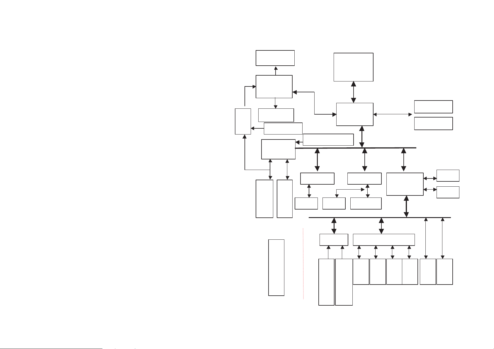
Part 2: Chipsets and Mainboard
M3
AGP BUS
4450
PCI BUS 3.3V
USB
IDE
FDC37N869
M38867
ISA BUS
EXT K/B MOUSE
COM1 LPT1 FIR FDD
Socket 370
FC-PGA
VIA
82C694X
SODIMM1
82686A
ESS1988
SOCKET B
MOUSE
SOCKET A
7114A
ZV PORT
PHY TSB41LV02
BIOS RTC
PCI I/F
SODIMM0
ESS1921
PORT REPLICATOR
INT K/B MOUSE
TV OUT
VIDEO IN
S
Interface
MDC
RTL8139C
RJ-45
Part 2: Chipsets and Mainboard
LVD
ATI
Intel
GTL+ HOST BUS
MM BUS
TI
VIA
MOUSE
2 – 1
Page 10

Service Manual
Mainboard
The mainboard is designed with Intel 370 Socket processor base and includes the following CHIPSET functions:
- 82C694X North bridge chipset solution from VIA
- 82C686A South bridge chipset solution from VIA
- ATI 3D RAGE Mobility-128 Multimedia Flat Panel Controller
- TI 4450 PC CARD Controller
- FDC37N869 super I/O Floppy Disk Controller
- ES1988 PCI Audio Chip and ES1921 AC97’ CODEC
- 7114A Video-in decoder
- M38867(Version 1.44) Keyboard Controller
- TSB41LV02 PHY for IEEE1394
- Realtek RTL8139c Controller for 10/100 Mbps LAN
Microprocessor
Intel Pentium!!! processor product line. Features include:
- P6 core (FC-PGA package)
- Separated 16K instruction and 16K data level one caches
- Integrated 256K second level cache
- 4GB of system memory which can be cached
- High performance Floating Point Unit
- Enhanced 64 bit data bus
- Dynamic Execution micro-architecture
- MMX media technology instruction
- Power management features
- Low power GTL+ Host bus specification
2 – 2
Page 11

Part 2: Chipsets and Mainboard
82C694X Host Bridge System Controller
VIA’s 82C694X Host Bridge system controller is a highly integrated device that combines the processor bus controller, the DRAM
controller, and the PCI bus controller into one component. The 82C694X Host Bridge has multiple power management features:
- Host Interface
- Memory Interface
- PCI Interface
- AGP Interface
Southbridge Chip - VIA 82C686A
Contains the following features:
- Supported Kits for both PentiumII and Pentium!!! microprocessors
- Multifunction PCI to ISA Bridge
+ Supports PCI at 33 MHz
+ Supports PCI Rev 2.1 Specification
+ Supports Full ISA or Extended I/O BUS
- Ultra-low power for Mobile Environment Support
- Full Support for ACPI (Advanced Configuration and Power Interface) Revision 1.2
- Integrated IDE Controller Support Ultra DMA/33/66
+ Supports two 82C37 Enhanced DMA Controller
+ Supports two 82C59 Interrupt Controller
+ Supports 82C54 Timer Based
+ Supports UHCI V1.1 USB Ports
+ Supports SMBus
2 – 3
Page 12

Service Manual
VGA Controller –
ATI 3D RAGE Mobility-128
The ATI 3D RAGE MOBILITY-128 Multimedia Flat Panel Controller is a DRAM based fully integrated LCD, CRT & TV 64 bits controller for AGP systems. It contains the following functions:
- Supports displays for 8 MB or 16 MB
- 64 bit high performance 2D/3D Graphic Engine
- Supports bus master AGP and SGRAM memory
- Supports 24 bit TFT panels up to 1280x1024 resolution
- Supports non-interlaced 1600x1200x64k, 1280x1024x64k, 1024x768x16M, 800x600x16M and 640x480x16M color on CRT
- Simultaneous display in 24 bit color on flat panel and CRT
- Internal buffer provides flicker reduction
- ATI 3D RAGE MOBILITY-128 DAC can directly interface with a standard off-the-shelf NTSC/PAL encoder. Composite synchronization signals support for standard home TV connection up to 1280x1024x16M and 16:9 Wide mode
- Graphic functions optimized by a 64 bit internal data bus and VGA, SVGA and XGA flat panel
- Provide flexible and extensive power management capabilities and support four states of VESA Display Power Management Signaling Standard
- IDCT for DVD playback acceleration
- Fully compliant ZV-port interface with device driver supports for VPM
- Motion compensation
PC Card (Card Bus) Interface Controller - TI-4450
TI Card Bus Interface Controller 4450 implements the PCMCIA 2.0/JEIDA 4.1 standard. It contains the following functions:
- Supports 2 PCMCIA 2.1& JEIDA 4.2 R2 cards or 2 CardBus cards
- Yenta Registers-compatible
- Supports Zoom Video Mode
- PCMCIA dual-socket interface
- Supports Ultra Zoomed Video Ports
2 – 4
Page 13

Part 2: Chipsets and Mainboard
- Bus Master Transfer capability
- Supports both 5V and 3.3V PC cards
- Supports PCMCIA_ATA Specification
- Supports Advanced Submicron Low Power CMOS Technology
- ACPI 1.0 Compliant
- 256 pin Micro-Star BGA package
- OHCI Link Function is IEEE 1394-1995 Compliant and compatible with Proposal 1394
ZV Port Custom Interface
The ZV (Zoomed Video) Port is a single source, point-to-point unidirectional video bus between a PC Card socket and a VGA controller. The ZV Port complies with CCIR601 timing to allow NTSC decoders to deliver real-time digital video straight into the VGA frame
buffer from a PC Card. The ZV Port also allows an industry standard mechanism for transferring digital audio PCM data to a low cost
DAC for conversion to an analog signal.
Super I/O Floppy Disk Controller – FDC37N869
The SMC FDC37N869 super I/O is optimized for mainboard applications. It provides:
- Intelligent Auto Power Management
- 16 Bit Address Qualification
- 1.44MB Super I/O Floppy Disk Controller
+ Support Vertical Recording Format
+ 16 Byte Data FIFO
+ Enhanced Digital Data Separator (Data rate up to 1Mb/s)
- Multi-Mode Parallel Port with ChiProtect Circuitry
+ Standard Mode
IBM PC/AT and PS/2 compatible bidirectional parallel port
+ Enhanced Mode
Enhanced Parallel Port (EPP) Compatible
2 – 5
Page 14

Service Manual
+ High Speed Mode
Microsoft and Hewlett Packard Extended Capabilities Port (ECP) Compatible
Serial Port
- Two high speed NS16C550 compatible UARTs with Send/Receive 16 Byte FIFOs
- Programmable Baud Rate Generator
- Modem Control Circuitry
- Infrared-IrDA, HPSIR, ASKIR, Fast IR(4Mbps IrDA), Consumer IR Support
High Performance PCI Audio Chip - ES1988
- 500-MIPS-equivalent, dual-engine PCI audio accelerator
- HRTF 3-D positional audio acceleration
- 64 Channel wavetable synthesis
- Advanced platform for interactive 3-D gaming, DVD movie playback and internet communications
- Full plug and play
- Multi-Stream DirectSound and DirectSound3D acceleration
- Full DOS Game compatibility
- I2S Zoomed Video interface
Audio CODEC ES1921
- Single, high-performance, mixed-signal, 16 bit stereo VLSI chip
- Meet Audio Codec ‘97 analog performance specification
- Full-duplex operation for simultaneous record and playback
Video-In Decoder
The SAA7114 is a video capture device located at the image port of the VGA controller. It has the following features:
- Automatic detection of 50/60Hz field frequency and automatic switching between PAL and NTSC standards
2 – 6
7114A
Page 15

Part 2: Chipsets and Mainboard
- Luminance and chrominance signal processing for PAL BGDHIN, Combination-PAL N, PALM, NTSC M, NTSC-Japan, NTSC 4.43
and SECAM
- Two-wire, Inter-Integrated Circuit(I2C)
- User programmable sharpness control
Keyboard Controller - M38867M8
- Memory size: 1024 bytes (RAM)
- Timers: 8 bit prescaler X 4 + 8 bit timer X 3
- Comparator: 4 bit X 8 channels
- Bus interface: 2 bytes
- Key on wake-up: 8 channels
- Interrupts: 8 external, 7 internal and 1 software
- A-D converter: 8 channels
- D-A converter: 2 channels
- PWM: 2 channels
- System bus interface: 8042 type
IEEE 1394 – TI PHY TSB41LV02
- 400Mb/S max data rate
- Available with one or three ports
- Fully compliant with OpenHCI requirements
- Advanced Power Management
- Supports IEEE 1394-1995 Isolation Barrier Feature at LINK-PHY interface
LAN 100/10 Mbps – RTL8139C
- Supports Wake-On-Lan and ACPI features
- Single-chip fast Ethernet controller
2 – 7
Page 16

Service Manual
- Fully compliant with IEEE 802.3u 100Base-T SPEC and IEEE802.3x full duplex flow control
- Supports Analog Auto-Power-Down
2 – 8
Page 17
Part 2: Chipsets and Mainboard
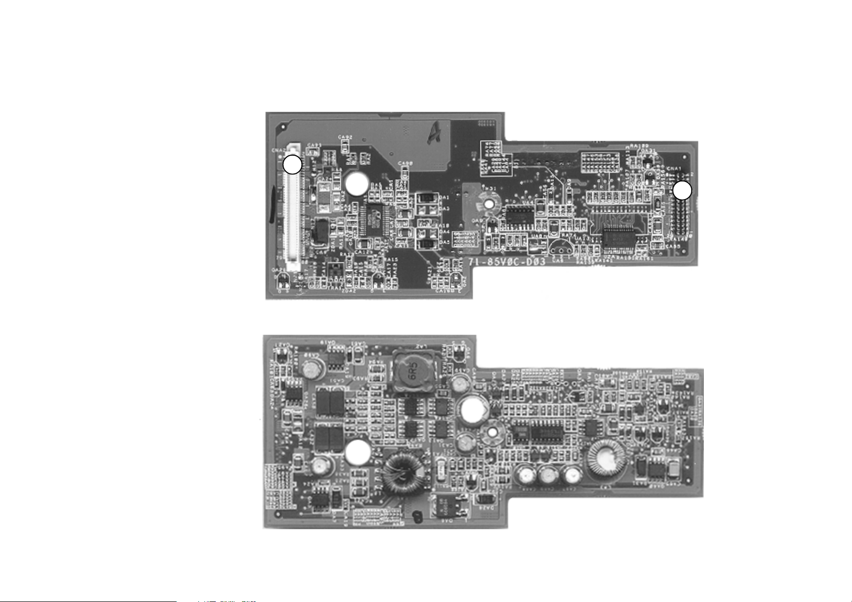
D/D Board
Top View
1) D/D Board Connectors
1
1
Bottom View
2 – 9
Page 18
Service Manual
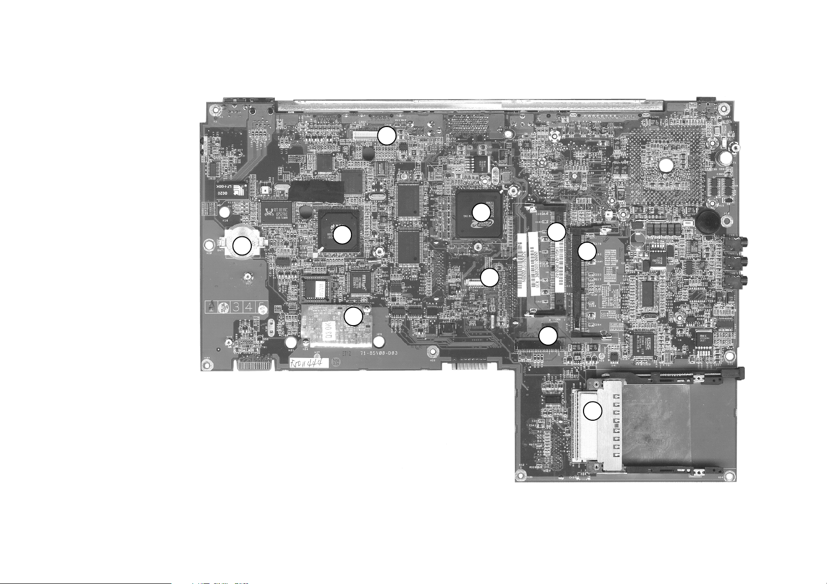
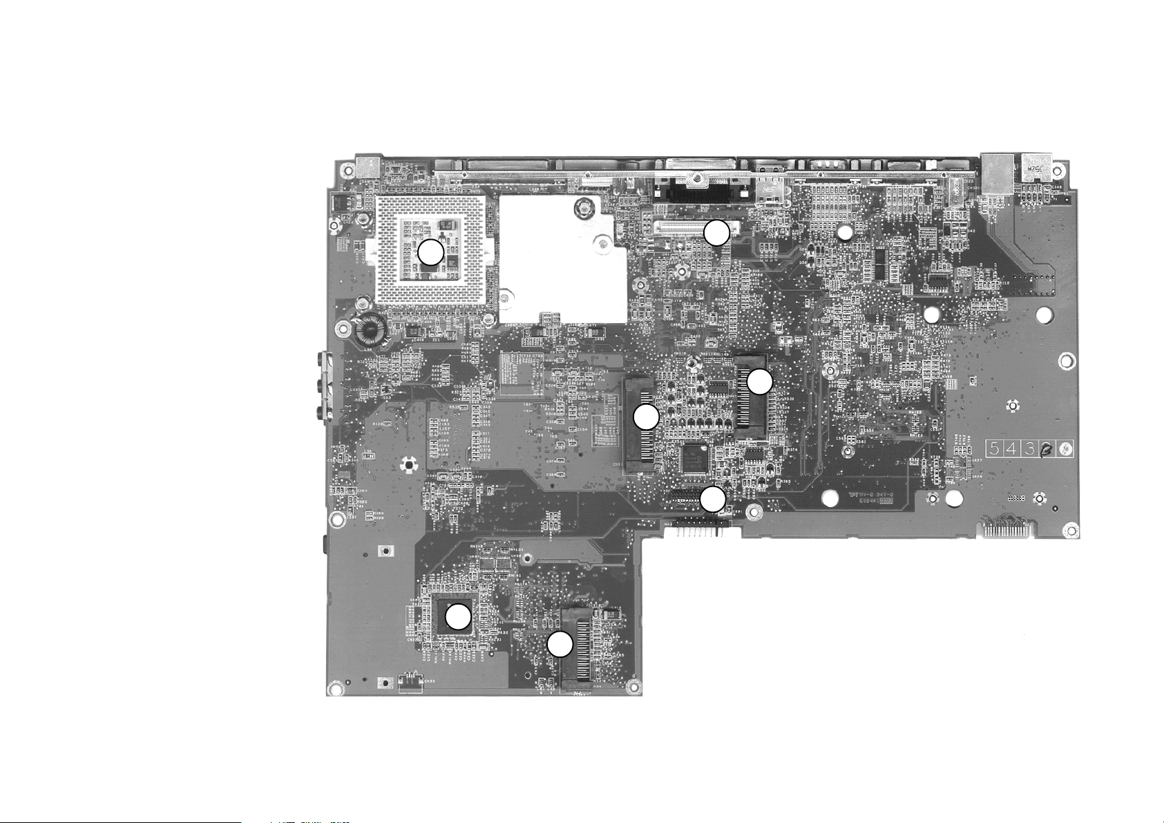
Mainboard Top View
1
4
2
1) LCD Connector
2) CMOS Battery
3) Southbridge Chip- VIA 82C686A
4) Video Chip - ATI 3D RAGE Mobility-128
5) MDC Card
3
5
6) Switch Connector
7) RAM Socket
8) Keyboard Connector
9) PCMCIA Connector
7
7
6
8
9
2 – 10
Page 19
Mainboard Bottom View
1) CPU Socket
2) D/D board connectors
3) FDD connector
4) CD-ROM connector
5) PCMCIA chipset
6) HDD connector
Part 2: Chipsets and Mainboard
2
1
4
3
2
5
6
2 – 11
Page 20

Service Manual
niP noitpircseD niP noitpircseD niP noitpircseD niP noitpircseD
1DNG61YDROIP1301PDD64#P3SC
2DNG71#KCADP2311PDD74DNG
3#TSRDH8141QRI3321PDD84CCV_DDH
47PDD911ADP4331PDD94CN
56PDD020ADP5341PDD05CN
65PDD12#P1SC6351PDD
74PDD22#DEL_DHP73CN
83PDD32CCV_DDH83DNG
92PDD42DNG93DNG
011PDD52CN04DNG
110PDD62DNG14LESC
21DNG72DNG24DNG
31QERDP82DNG34CN
41#WOIDP928PDD44CN
51#ROIDP039PDD542ADP
Connector and pin information
HDD
2 – 12
Page 21
Part 2: Chipsets and Mainboard
niP noitpircseD niP noitpircseD niP noitpircseD niP noitpircseD
1SCCV611SDD13SCCV6441SDD
2#0RTM710SDD23#0VRD7451SDD
3#EDOM381DNG33#XEDNI84CN
4#0KRT91QERDS43#GHCKSD94DNG
5#LESDH02#WOIDS53#RID05DNG
6#ATADR12#ROIDS63#PETS15DNG
7#DF_PW22YDROIS73#TADW25LESC
8#ETAGW32#KCADS83CN35DNG
9#TSRDC42QRI_DC93DNG45CN
017SDD521ADS048SDD55GAIDP
116SDD620ADS149SDD652ADS
215SDD72#S1SC2401SDD75#S3SC
314SDD82#DEL_DHS3411SDD85DNG
413SDD92CCV_DC4421SDD95CCV_DC
512SDD03DNG5431SDD06CN
CD-ROM
niP noitpircseD niP noitpircseD niP noitpircseD niP noitpircseD
1L_DC611ADSS1311PDDS64CCV_DC
2DNGA710ADSS2321PDDS74DNG
3#TSRDC81#S1SCS3331PDDS84DNG
47PDDS91#DEL_DHS4341PDDS94DNG
56PDDS02CCV_DC5351PDDS05CN
65PDDS12CCV_DC63QERDSS
74PDDS22DNG73#ROIDSS
83PDDS32DNG83DNG
92PDDS42LESC93#KCADS
011PDDS52CN04CN
110PDDS62R_DC14GAIDP
21DNG72DNGA242ADSS
31#WOIDSS828PDDS34#S3SCS
41YDROIS929PDDS44CCV_DC
51QRIDC0301PDDS54CCV_DC
FDD
2 – 13
Page 22
Service Manual
niP noitpircseD
1ADKE
2ADME
3DNG
4CCV
5KLCKE
6KLCME
RS-232 Serial Interface
niP noitpircseD
1)tceteDreirraCATAD(DCD
2)ataDdevieceR(DXR
3)ataDdettimsnarT(DXT
4)ydaeRlanimreTataD(RTD
5)dnuorGlangiS(DNG
6)ydaeRteSataD(RSD
7)dneSoTtseuqeR(STR
8)dneSoTraelC(STC
9)rotacidnIgniR(IR
Parallel Interface
niP noitpircseD niP noitpircseD
1#ebortS2
31ataD4 2ataD
53ataD64ataD
75ataD86ataD
97ataD01#KCA
11ysuB21ytpmErepaP
31tceleS41otuA
51#rorrE61#ezilaitinI
71nItceleS81dnuorG
91dnuorG02dnuorG
12dnuorG22dnuorG
D
External Keyboard/PS2 Interface
0ata
#deefeniL
2 – 14
32dnuorG42dnuorG
52dnuorG
Page 23
Part 2: Chipsets and Mainboard
niP noitpircseD
1PPV
2DNGV
3-BPT
4+BPT
5-APT
6+APT
niP noitpircseD
1ACCV_BSU
2-0PBSU
3+0PBSU
4DNG
niP noitpircseD
1BCCV_BSU
2-1PBSU
3+1PBSU
4DNG
External Monitor Interface
niP noitpircseD
1DERB
2NEERGB
3EULBB
4C.N
5DNG
6DNG
7DNG
8DNG
9C.N
01DNG
11C.N
21ADCDD
External S-video out Inter-
face
niP noitpircseD
1DNG
2PMOC
3AMULX
4AMRCX
Touchpad Interface
niP noitpircseD niP noitpircseD
91dnuorG02dnuorG
12dnuorG22dnuorG
32dnuorG42dnuorG
External 1394 (IEEE) Inter-
face
External USB Interface-port A
External USB Interface-port B
31CNYSHD
41CNYSVD
51KLCDD
52dnuorG
2 – 15
Page 24

Service Manual
niP noitpircseD niP noitpircseD niP noitpircseD niP noitpircseD
1DNG62DNG15DNG67DNG
23DC-A72PPV-A25#1DC-A77PPV-A
34DC-A8261AC-A3511DC-A8722AC-A
4DNG92DNG45DNG97DNG
55DC-A0351AC-A5521DC-A0832AC-A
66DC-A1321AC-A6531DC-A1842AC-A
7DNG23DNG75DNG28DNG
87DC-A337AC-A8541DC-A3852AC-A
9#1EC-A436AC-A9551DC-A482SV-A
01DNG53DNG06DNG58DNG
1101AC-A635AC-A16#2EC-A68TESER-A
21#EO-A734AC-A261SV-A78#TIAW-A
31DNG83DNG36DNG88DNG
4111AC-A933AC-A46#DROI-A98KCAPNI-A
519AC-A042AC-A56#RWOI-A09#GER-A
61DNG14DNG66DNG19DNG
718AC-A241AC-A7671AC-A29#2DVB-A
8131AC-A340AC-A8681AC-A39#1DVB-A
91DNG44DNG96DNG49DNG
0241AC-A540DC-A0791AC-A598DC-A
12#EW-A641DC-A1702AC-A699DC-A
22DNG74DNG27DNG79DNG
32#YBYDR-A842DC-A3712AC-A8901DC-A
42C-CCV-A94#PW-A47C-CCV-A99#2DC-A
52DNG05DNG57DNG001DNG
PCMCIA Cardbus Interface Socket A
2 – 16
Page 25

PCMCIA Cardbus Interface Socket B
niP noitpircseD niP noitpircseD niP noitpircseD niP noitpircseD
1DNG62DNG15DNG67DNG
23DC-B72PPV-B25#1DC-B77PPV-B
34DC-B8261AC-B3511DC-B8722AC-B
4DNG92DNG45DNG97DNG
55DC-B0351AC-B5521DC-B0832AC-B
66DC-B1321AC-B6531DC-B1842AC-B
7DNG23DNG75DNG28DNG
87DC-B337AC-B8541DC-B3852AC-B
9#1EC-B436AC-B9551DC-B482SV-B
01DNG53DNG06DNG58DNG
1101AC-B635AC-B16#2EC-B68TESER-B
21#EO-B734AC-B261SV-B78#TIAW-B
31DNG83DNG36DNG88DNG
4111AC-B933AC-B46#DROI-B98KCAPNI-B
519AC-B042AC-B56#RWOI-B09#GER-B
61DNG14DNG66DNG19DNG
718AC-B241AC-B7671AC-B29#2DVB-B
8131AC-B340AC-B8681AC-B39#1DVB-B
91DNG44DNG96DNG49DNG
0241AC-B540DC-B0791AC-B598DC-B
12#EW-B641DC-B1702AC-B699DC-B
22DNG74DNG27DNG79DNG
32#YBYDR-B842DC-B3712AC-B8801DC-B
42C-CCV-B94#PW-B47C-CCV-B99#2DC-B
52DNG05DNG57DNG001DNG
Part 2: Chipsets and Mainboard
2 – 17
Page 26

Service Manual
Notes:
2 – 18
Page 27

Part 3: Installing a processor
The notebook computer supports an Intel Pentium !!! processor.
Note:
Part 3: Installing a processor
Remember to wear an antistatic wrist strap when adding or replacing the processor.
If you remove the heat sink, which is necessary to add or replace the processor, you will need to have a replacement heat sink pad
available. Before proceeding, please contact your dealer to get a replacement pad which you will need when you reinstall the
heat sink.
The 4 basic steps to Installing/Upgrading a processor are:
A: Remove the heat sink
B: Remove the existing processor
C: Install a new processor
D: Install the heat sink
3 - 1
Page 28

Service Manual
2
A: Remove the heat sink
1) Unscrew and remove the CPU cover.
2) Remove the four screws which hold the heat sink in place.
3) Lift the heat sink out of the computer.
B: Remove the existing processor
By this step you should have successfully removed the heat sink and are
now looking at the CPU socket with processor.
ZIF plug
CPU cover
heat sink
3 - 2
1
The CPU socket with the ZIF plug (lock) in place.
Remove the ZIF plug from the CLOSE side of the CPU
socket.
Page 29

4
6
3
Part 3: Installing a processor
Place the CPU tool on top of the CPU.Align the CPU tool over the CPU.
5
Place the screwdriver into the open slot on the CPU case,
then hold the CPU tool (jig) in place and move the screwdriver in towards the CPU. (this will unlock the CPU from
its socket).
Remove the screwdriver and the CPU tool and gently lift
the CPU out of the socket.
3 - 3
Page 30

Service Manual
2
C: Install a new processor
Now you should be looking at an empty CPU socket. To install a new processor simply follow these steps:
1
The empty CPU socket without a processor module.
Gently place the processor into the opened CPU
socket and press it into place.
3 - 4
3
Align the CPU tool with the CPU socket.
4
Place the CPU tool on top of the CPU.
Page 31

5
6
8
Part 3: Installing a processor
Place the screwdriver into the close slot on the CPU then
move the screwdriver in towards the CPU. (this will lock
the CPU securely in place).
7
Place the ZIF plug (lock) on the CLOSE side of the CPU
socket.
Remove the screwdriver and the CPU tool.
The processor is now securely locked into the CPU socket.
3 - 5
Page 32

Service Manual
D: Install the heat sink
Note: Before installing the heat sink, make sure you place a new heat sink pad on the heat sink.
1) Peel off the old heat sink pad and stick on a new one.
2) Place the heat sink on top of the Hex studs.
3) Tighten the two heat sink screws on the CLOSE side of the CPU socket first. (this will prevent the socket from unlocking
accidentally).
4) Tighten the two heat sink screws on the OPEN side of the CPU socket.
5) Make sure the Heat sink fan plug is properly installed.
6) Replace and screw in the CPU cover.
Proper installation of the heat sink.
Improper installation of the heat sink.
Heat sink pad
3 - 6
Page 33

Part 4: BIOS
Part 4: BIOS
4 - 1
Page 34

Service Manual
Updating the Flash ROM BIOS
To update the FLASH ROM BIOS you must do five things:
A: Download the BIOS update from the web site.
B: Create a bootable Floppy Disk.
C: Copy you BIOS files onto the bootable Floppy Disk.
D: Reboot your computer from the FDD.
E: Reboot from the HDD.
A: Download the BIOS update from the web site.
1) Using your web browser go to www.clevo.com.tw
2) Choose Download from the menu bar at the top of the page.
3) In the Download Drivers section select the model of your computer (8500V series) and the BIOS driver.
4) Select GO to download the zip file to your computer.
5) Unzip the file into a suitable directory.
B: Create a bootable Floppy Disk.
Through Windows 98
1) Insert a Floppy Disk into your FDD. (This disk will be overwritten and all information erased, so make sure it has no important data on it!)
2) Go to My Computer or Windows Explorer.
3) Highlight the Floppy Drive icon and click the left mouse button, a menu will appear.
4) Select Format.
5) In the “Format 3 ½ Floppy Drive” window select:
Format type = Quick
Other options = Copy system files.
6) Press “Start”. (This will create a disk which you will use to boot your system and update your BIOS).
4 - 2
Page 35

Through DOS
1) Insert a Floppy Disk into your FDD. (This disk will be overwritten and all information erased, so make sure it has no
important data on it!)
2) At the DOS prompt type: Format A:/s
C: Copy your BIOS files on to the bootable Floppy Disk.
Take the Unzipped BIOS files and copy them to the disk you just formatted.
D: Reboot your computer from the FDD
1) Insert the newly formatted disk with the BIOS files into your Floppy Drive.
2) Restart your computer.
Note: When your system boots from the floppy disk it will automatically update the BIOS.
E: Reboot your computer from the HDD
Part 4: BIOS
After the computer has been started using the floppy disk:
1) Turn off the computer.
2) Remove the floppy disk from the drive.
3) Restart the computer.
It is now running normally with the updated BIOS.
4 - 3
Page 36

Service Manual
Phoenix BIOS Post Error Messages
Errors which occur during the POST procedure can be grouped into two categories, fatal and nonfatal. All fatal errors will not allow
the system to continue the boot process.
Fatal Errors
rorrE
edoC
613-2-2-1
021-1-3-1hserferMARDtseT
223-1-3-1rellortnocdraobyeK2478tseT
C21-4-3-1xxxxenilsserddanoeruliafMAR
E23-4-3-1
031-1-4-1
643-2-1-2ecitonthgirypocMORkcehC
851-3-2-2stpurretnidetcepxenuroftseT
peeB
ecneuqeS
noitpircseD
muskcehcMARSOIB
yromemetybwolfoxxxxstibATADnoeruliafmaR
sub
yromemepythgihfoxxxxstibATADnoeruliafmaR
sub
4 - 4
Page 37

Part 4: BIOS
rorrE
edoC
noitinifeD
20edomlaeryfireV
40epytUPCteG
60erawdrahmetsysezilaitinI
80
sretsigertespihcezilaitinI
seulavTSOPlaitinihtiw
90galfTSOPniteS
A0sretsigerUPCezilaitinI
B0ehcacUPCelbanE
C0
laitiniotsechacezilaitinI
seulavTSOP
E0O/IezilaitinI
F0EDIsublacilehtezilitinI
01
rewoPezilaitinI
tnemeganaM
11
draobyekevitanretladaoL
rellortnoc
21
drowlortnocUPCerotseR
toobermrawgnirud
41
draobyekezilaitinI
rellortnoc
61
peeb(muskcehcMORSOIB
)3-2-2edoc
81noitazilaitiniremit4528
rorrE
edoC
noitinifeD
A1
rellortnocAMD7328
noitazilaitini
C1
elbammargorpteseR
rellortnoctpurretni
02
-3edochserferMARDtseT
1-1
22
draobyek7428tseT
)3-1-3edocpeb(rellortnoc
42
otretsigertnemgesSEteS
BG4
82MARDezisotuA
A2MARDesabK215raelC
C2
enilsserddanoeruliafMAR
)1-4-3edocpeeb(’xxxx
E2
stibatadnoeruliafMAR
foetybwolfo’xxxx
-4-3edocpeeb(subyromem
)3
23
kcolcsubUPCtseT
ycneuqerf
43MARSOMCtseT
53
tespihcevitanretlaezilaitinI
sretsiger
63nwodtuhstratsmraW
83MORSOIBmetsyswodahS
A3ehcacezisotuA
Nonfatal errors
Most nonfatal errors will allow the system to boot. Should the system halt due
to a nonfatal error, a physical change
must be made to the system.
4 - 5
Page 38

Service Manual
rorrE
edoC
noitinifeD
67srorredraobyekrofkcehC
C7
tpurretnierawdrahroftseT
srotcev
E7tneserpfirossecorpoctseT
08stropO/IdraobnoelbasiD
28
lanretxellatsnidnatceteD
strop232SR
48
lanretxellatsnidnatceteD
stroplellarap
58
elbitapmoc-CPezilaitinI
secivedASIPnP
68
O/Idraobnoezilaitni-eR
strop
88aeraataDSOIBezilaitinI
A8
SOIBdednetxEezilaitinI
aeraataD
C8rellortnocyppolfezilaitinI
09
ksiddrahezilaitinI
rellortnoc
19
ksiddrahsub-lacolezilaitinI
rellortnoc
292hctaPresUotpmuJ
39
-itlumrofELBATPMdliuB
sdraobrossecorp
49enilsserdda02AelbasiD
rorrE
edoC
C3
D3
24srotcevtpurretniezilaitinI
44stpurretniSOIBezilaitinI
64
74
84
94
A4
B4neercstooBteiuQyalpsiD
C4MORSOIBoedivwodahS
E4ecitonthgirypocyalpsiD
05deepsdnaepytUPCyalpsiD
15draobASIEezilaitnI
25draobyektseT
noitinifeD
tespihcdecnavdaerugifnoC
sretsiger
rorrE
edoC
45delbanefikcilcyekteS
65draobyekelbanE
sretsigeretanretladaoL
seulavSOMChtiw
thgirypocMORkcehC
)3-2-1-2edocpeeb(eciton
ICProfreganamezilaitinI
85
A5
C5
06yromemdednetxetseT
SMORnoitpo
noitarugifnocoedivkcehC
SOMCtsniaga
26
461hctaPresUotpmuJ
dnasubICPezilaitinI
secived
66
sretpadaoedivllaezilaitinI
metsysni
86
A6ezisehcaclanretxeyalpsiD
C6egassemwodahsyalpsiD
E6
07segassemrorreyalpsiD
27
47kcolcemitlaertseT
noitinifeD
detcepxenuroftseT
stpurretni
)1-3-2-2edocpeeb(
ot2FsserP"tpmorpyalpsiD
"puteSretne
dna215neewtebMARtseT
K046
yromemdednetxetseT
senilsserdda
ehcacdecnavdaerugifnoC
sretsiger
UPCdnalanretxeelbanE
sehcac
elbasopsid-nonyalpsiD
stnemges
noitarugifnocrofkcehC
srorre
4 - 6
Page 39

rorrE
edoC
noitinifeD
2EtespihcehtezilaitinI
3EretnuochserferezilaitinI
4EhsalFdecroFrofkcehC
5EMORrofsutatsWHkcehC
6EKOsiMORSOIB
7EtsetMARetelpmocaoD
8EnoitazilaitniMEOoD
9ErellortnoctpurretniezilaitinI
AEedocpartstoobehtnidaeR
BEsrotcevllaezilaitinI
CEmargorphsalFehttooB
DEecivedtoobehtezilaitinI
EEKOdaersawedoctooB
Flash ROM Error codes
Part 4: BIOS
rorrE
edoC
59toobrofMOR-DCllatsnI
69
89sMORnoitporofhcraeS
A9sMORnoitpowodahS
C9tnemeganaMrewoPputeS
E9stpurretnierawdrahelbanE
0AyadrofemitteS
2AkcolyeKkcehC
4AetarcitamepytezilaitinI
8Atpmorp2FesarE
AAtpmorp2FrofnacS
CAekortsyek2FrofnacS
noitinifeD
tnemgesSEeguhraelC
retsiger
rorrE
edoC
5BunemtooBitluMyalpsiD
6B)lanoitpo(drowssapkcehC
8BelbatrotpircsedlabolgraelC
CBsrekcehcytirapraelC
EB)lanoitpo(neercsraelC
FB
0C91TNIhtiwtoobyrT
0DrorrereldnahtpurretnI
2DrorretpurretninwonknU
4DrorretpurretnignidneP
6DrorreMORnoitpoezilaitinI
8DrorrenwodtuhS
ADevomkcolbdednetxE
CDrorre01nwodtuhS
noitinifeD
pukcabdnasurivkcehC
srednimer
EAgalfTSOP-noraelC
0BsrorrerofkcehC
2B
4BpeebenO
5BunemtooBitluMyalpsiD
tooboteraperp-enodTSOP
metsysgnitarepo
4 - 7
Page 40

Service Manual
Notes:
4 - 8
Page 41

Part 5: Diagrams and part numbers
Part 5: Diagrams and part numbers
5 - 1
Page 42

Service Manual
CD-ROM Assembly
5 – 2
Page 43

Part 5: Diagrams and part numbers
FDD Assembly
5 - 3
Page 44

Service Manual
HDD Assembly
5 – 4
Page 45

Part 5: Diagrams and part numbers
3
20
22
23
21
11
19
18
16
17
15
14
12
13
7
9
10
8
5
6
4
2
1
ITEM
PART NAME
REMARK
PART NO
LG Display Panel
5 - 5
Page 46

Service Manual
(Panasonic, Sanyo, Hyundai, Hitachi) Display Panel
5 – 6
Page 47

Part 5: Diagrams and part numbers
GASKET(9*40*3.5t)
SCREW
MODEM MODULE 4.0
SCREW
SCREW
SCREW
HEX STUD
SCREW
AL PLATE FOR CHIP
GASKET(W7*L50* H2)
GASKET(30*5*4t)
57
58
54
56
55
53
52
49
50
51
48
BOTTOM CASE
REAR COVER ASS'Y
CD-ROM ASS'Y 8500
BATTERY LOCK KNOB
LOCK KNOB SPRING
HDD ASS'Y 8500
FCC LABEL 8500
MYLAR FOR BATTERY
GASKET (W10*33L*5 .5t)
LABEL FOR BATTERY
MYLAR FOR DIMM
GASKET (10*17* 6.5)
GASKET (14*10* 5.5)
GASKET FOR PS2 (14* 5*5.5)
BOTTOM CASE RUBBER PAD
47-00190-1 S0
47-00190-4 01
35-41120-3RA
34-85V0S-040
35-22120-5R0
33-85V0S-010
47-00190-0 71
35-41125-120-1
76-85V00-001
35-06130-6RA
35-41125-4R0
45
46
47
44
43
BATTERY
33
38
FOOT SPRING
K/B BRACKET
SCREW
40
42
41
39
SCREW
37
36
34
35
MYLAR (A)
29
BATTERY
HDD LOCK
33
32
31
30
FOOT(L)
27
28
26
25
47-85M23-010
40-8505S-011
47-00190-1 04
47-00190-1 E0
47-85093-0 30
(99-85005-070)
(99-8500 5-060)
Reference Ass'y Dwg
Reference Ass'y Dwg
87-85V8S-42H
45-3500M-010
35-B1120-3RA
45-85V03-030
79-8502I-010-A
35-29120-3R5
38-85026-0 10
33-85V07-011
47-00190-1 03
40-8505M-010
39-85013- 01G
79-8502Z-06 0
42-85063-0 20
42-85P7Q-001
87-85V8S-42A
42-85083-0 11
38-62026-0 10
42-6208M-010
40-85053-010-A
PART NAME
REAR BRACKET
SDRAM CARD 32M
SDRAM CARD 32M
SDRAM CARD 128M
SDRAM CARD 64M
SDRAM CARD 64M
HEAT SINK MODULE
FDD ASS'Y 8500
LOCK BRACKET
BOTTOM CASE RUBBER PAD
MYLAR FOR CARD BUS
SDRAM CARD 32M
15
SCREW
20 SCREW
FOOT RUBBER
CPU COVER
22
24
23
21
MYLAR(B)
FOOT(R)
19
18
16
17
HEX STUD
DC/DC
HEX STUD
13
14
12
11
10
10
10
10
10
ITEM
5
NUT M2.5,SN
HEX STUD
MAIN BOARD
HEX STUD
HEX STUD
8
9
10
7
6
HEX STUD
SCREW
SCREW
3
4
2
1
(99-85005-050)
Reference Ass'y Dwg
35-41120- 14A
40-85053-0 30
79-8502J-0 10-A
40-85053-0 21
47-35023-010-A
35-41025-4RA
33-85003-0 20
47-85013-010-A
42-85063-010-A
42-85M73-010
76-0017U-A2 0
76-0017U-8 20
76-0017U-8 10
76-0017U-A1 0
34-8500S-02 A
31-85V00-010
34-85V0S-010
77-85V0C-D03
76-0018U-B10
REMARK
PART NO
34-07009-011-A
33-85P0Q-011
35-26130-6R0
35-06125- 6R0-A
34-85V0P-010
77-85V00-D0X
34-85V0N-010
36-05111-2 50
34-85V0S-010
76-9827U-8 40
Bottom View
5 - 7
Page 48

Service Manual
COPPER SHEET(W20*L340)
SPRING FOR K/B LOCK KNOB
SPONGE FOR GLIDE PAD BRACKET
CABLE
PAPER WASHER
GASKET(5*340*1.5)
GASKET(5*110*1.5)
33
34
35
32
31
21
K/B LOCK KNOB
K/B LOCK BRACKET
K/B SPRING PLATE
CONNECTOR COVER
SCREW
LED BOARD
SCREW
GASKET(W10*L25*H8.5)
SPONGE FOR 85 LENS
26
28
30
29
27
25
24
22
23
IR LENS
FFC CABLE
TOUCHPAD ALPS-KGDDER943A
SCREW
SWITCH BOARD
GLIDE PAD HOLDER
SCREW
SCREW
20
19
18
17
14
15
16
13
12
43-85V04-011
37-02A00-800
47-00190-340
47-85V07-010
47-00190-B11
42-85082-030
33-66002-020
38-35020-010
42-85072-010
35-06125-6RA
77-85V04-D02
35-26130-6RA
47-85092-060
47-00190-101
47-85092-070
42-850I2-010
49-00102-010
35-41120-3RA
77-8500S-D02A
33-85002-011
27-9350C-F50
35-41025-4RA
38-00R26-010
35-06120-6RA
TOP CASE+G/P+LE NS+POWER KNOB
EMI SPONGE(A) REAR BRL TOP B/C
2 SPEAKER COVER (R)+NET
SPEAKER + CON.
COVER KNOB POM
SPRING FOR COVER KNOB
CARD BUS COVER
FFC CABLE
SPEAKER COVER (L)+NET
EMI SPONGE(2) FOR K/B
7
9
11
10
8
6
5
3
4
KEYBOARD FOR 8500
1
ITEM
PART NAME
REMARK
33-8500T-A10
23-5A020-900
42-62082-010
38-62020-020
42-8507P-010
39-85V01-010
27-9350C-850
33-8500T-A21
47-85093-051
47-35097-020
PART NO
80-85038-7G
*
Top View
5 – 8
35
33
1
34
34
35
30
3
25
29
28
31
26
26
19
27
13
18
28
26
10
21
22
9
27
23
2
32
13
32
27
4
17
9
5
6
20
13
21
22
7
8
13
4
32
17
20
10
15
14
24
24
16
13
12
11
13
13
19
Page 49

Part 6: Schematics
Part 6: Schematics
6 – 1
Page 50

Service Manual
2.0A
KAPOK
³Í³Õ¹q¸£
Custom137
Frida y, O ctobe r 2 0, 20 00
SOC KET 370
Size
Document Number
Rev
Date:
SheetofV_CPU
V2.5
VTT
VTT
VTT
V_CPU
V_CPU
V_CPU
VTT
V_CPU
V_CPU
VCC3
HA#[3..31]3HR E Q#[0 ..4]3HD#[0..63]3ADS#3STPCLK#7SLP#7NMI11INTR11HTRDY#3A20M#11HIT#3HITM#3BREQ0#3BPRI#3BNR#3HLOCK#3DBSY#3RS#03RS#13RS#23DEFER#3IGNN E#11PWROK
3,7,12
GCL_VGATE
12,29
APICLK10DRDY#3HCLKCPU10BSE L011CPUINIT#7SMI#7-FEER#7CPURST#3APICLK
HA#9
HA#12
HA#28
HA#13
HA#15
HA#8
HA#14
HA#11
HA#4
DEFER#
HREQ#4
HREQ#2
HREQ#3
HA#17
HA#23
HA#10
HA#19
HA#21
HA#25
HA#24
HA#20
HA#30
HA#27
HA#18
HA#29
BPR I#
HREQ#1
HA#7
BNR #
HD#28
HD#34
HD#43
HD#22
HD#39
HD#37
HD#45
HD#36
HD#51
HD#27
HD#44
HD#42
HD#41
HD#47
HD#40
HD#49
HD#54
HD#57
HD#55
HD#50
HD#58
HD#60
HD#53
HD#56
TPRD Y#
HD#61
HD#62
HD#38
HD#26
HD#19
HD#33
HD#25
HD#29
HD#31
HD#32
HD#35
HD#8
HD#1
HD#17
HD#5
HD#15
HD#0
HD#6
HD#4
HD#13
HD#11
HD#2
HD#14
HD#18
HD#9
HD#10
HD#12
HD#21
HD#23
HD#16
HD#24
HD#20
HD#7
HA#5
HA#6
HA#16
HA#3
HA#22
HA#31
CPURST#
HA#26
HD#3
HD#30
HD#46
PWROK
GCL_VGATE
FE R R #
STPCLK#
SMI#
CPUINIT#
PICD0
PICD1
SLP#
TPREQ#
PWGOOD
TMS
TD O
TC K
CPURST#
TP R D Y #
HCLKCPU
TRST#
TDI
RS#1
HITM#
HLOCK#
HREQ#0
HD#63
HD#48
HD#59
HD#52
AD S #
BREQ 0#
RS#2
RS#0
HIT#
DRDY#
DBSY#
HTRDY#
FLUS H#
NMI
INTR
A20M#
IGNN E#
-FEER#
HA#3
HA#30
HREQ#3
TRST#
STPCLK#
HD#10
HD#52
HA#13
HA#15
HA#16
HREQ#0
HREQ#2
HD#34
HD#37
HD#60
HD#8
HD#11
HD#28
HD#46
FLUS H#
HD#3
HD#4
HD#39
HD#48
HD#50
HA#5
HA#10
HA#19
TC K
TDI
HD#27
HD#59
HD#62
H RE Q#[0..4 ]
FE R R #
HA#21
HA#27
IGNN E#
PWGOOD
HD#0
HD#16
HD#36
HD#45
PICD1
PICD0
HA #[ 3. . 31 ]
HA#4
HA#20
ADS#
BPRI#
A20M#
HD#9
HD#19
CPUINIT#
HA#23
HREQ#4
HIT#
INTR
HD#24
HD#47
HD#53
HA#18
HREQ#1
HTRDY#
RS#1
TMS
HD#15
HD#32
DBSY#
8MHz
CPURST#
HA#11
HA#14
HA#31
DEFER#
HD#2
HD#12
HD#14
HD#18
HD#29
HD#40
HCLKCPU
HA#17
HA#29
BREQ0#
TD O
SLP#
HD#6
HD#35
HD#42
HD#44
HD#56
HD#58
HD#17
HD#38
HA#9
HA#12
HA#28
TP R D Y #
HD#1
HD#13
HD#22
HD#43
HD#51
DRDY#
H D # [0 ..6 3 ]
HA#7
HA#24
BNR#
SMI#
NMI
HD#5
HD#20
HD#26
HD#33
HD#54
HD#55
HD#63
100/66#(BSEL0#)
HA#6
HA#8
FE R R #
HD#7
HD#41
HD#49
HD#57
NMI
HA#22
HA#25
HLOCK#
HITM#
RS#2
TPREQ#
HD#23
HD#25
HD#30
HD#31
HA#26
RS#0
HD#21
HD#61
C445
0.1U
R367
330(R)
RN68
8P4R -5612348765
RN83
8P4R -5612348765
RN80
8P4R -5612348765
C683
0.1U
RN88
8P4R -5612348765
R32356R407
470
RN84
8P4R -5612348765
R414
470
RN72
8P4R -5612348765
RN98
8P4R -5612348765
RN73
8P4R -5612348765
C346
0.1U
RN74
8P4R -5612348765
RN108
8P4R -5612348765
C483
0.1U
C469
0.1U
C116
0.1U
RN93
8P4R -5612348765
C356
0.1U
C424
0.1U
TP 1 0
TP7
TP 1 1
C487
0.1U
C484
0.1U
C347
0.1U
C67
0.1U
TP4
R431
240
TP3R41K
TP6
TP2
TP 1 2
TP5
C355
0.1U
TP9
TP8
TP1TC486
0.1UTTTRN81
8P4R -5612348765
R41822RN109
8P4R -5612348765R820K
RN111
8P4R -5612348765
U45A
CELERON-A
AK8
AH12
AH8
AN9
AL15
AH10
AL9
AH6
AK10
AN5
AL7
AK14
AL5
AN7
AE1Z6AG3
AC3
AJ1
AE3
AB6
AB4
AF6Y3AA1
AK6Z4AA3
AD4
AK18
AH16
AH18
AL19
AL17
AN31
AE35
AN29
AN17
AH14
AK20
AL25
AL23
AN19
G33
E37
C35
E35
AN25
AH26
AH22
AK28
AE33
AC35
AG37
AK26
AJ35
AL33
AN37
AN35
AK32
AN33
J37
A35
M36
L37
AG35
AH30W1T4N1M6U1S3T6J1S1P6Q3M4Q1L1N3U3H4R4P4H6L3G1F8G3K6E3E1F12A5A3J3C5F6C1C7B2C9A9D8D10
C15
D14
D12A7A11
C11
A21
A15
A17
C13
C25
A13
D16
A23
C21
C19
C27
A19
C23
C17
A25
A27
E25
F16
AL27
AN27
J33
L35
J35
AG33
AE37X4W37
AJ33
AH4
A#3
A#4
A#5
A#6
A#7
A#8
A#9
A#10
A#11
A#12
A#13
A#14
A#15
A#16
A#17
A#18
A#19
A#20
A#21
A#22
A#23
A#24
A#25
A#26
A#27
A#28
A#29
A#30
A#31
REQ #0
REQ #1
REQ #2
REQ #3
REQ #4
ADS#
IER R#
BR0#
BPRI#
BNR#
LOC K #
HIT#
HITM#
DEFER#
BP#2
BP#3
BPM#0
BPM#1
TRDY#
RS#0
RS#1
RS#2
A20M#
FE R R #
IGNN E#
PWGOOD
SMI#
TC K
TD O
TDI
TMS
TR S T#
PREQ#
PRDY#
LINT0#/INTR
LIN T1# /N M I
STPCLK#
SLP#
D#0
D#1
D#2
D#3
D#4
D#5
D#6
D#7
D#8
D#9
D#10
D#11
D#12
D#13
D#14
D#15
D#16
D#17
D#18
D#19
D#20
D#21
D#22
D#23
D#24
D#25
D#26
D#27
D#28
D#29
D#30
D#31
D#32
D#33
D#34
D#35
D#36
D#37
D#38
D#39
D#40
D#41
D#42
D#43
D#44
D#45
D#46
D#47
D#48
D#49
D#50
D#51
D#52
D#53
D#54
D#55
D#56
D#57
D#58
D#59
D#60
D#61
D#62
D#63
DBSY#
DRDY#
PICCLK
PICD1
PICD0
INIT#
FLUS H#
RESET#
BCLK
BSE L#
NC/RESET#
R15
150
R13
330
R101KR111KR411
330
RN89
8P4R -5612348765
RN76
8P4R -5612348765
RN69
8P4R -5612348765
R422
27K
Q31
MMBT3904BECRN94
8P4R -5612348765
R48
330(R)
R12
330
R369
330
RN71
8P4R -5612348765
RN75
8P4R -5612348765
RN105
8P4R -5612348765
C485
0.1U
R370
330
R14
330
RN102
8P4R -5612348765
R421
27KR9330
C458
1U(0805)
RN103
8P4R -5612348765
R416
330
R415
330R70(R)
R417
330
R574
27K
R43056RN106
8P4R -5612348765
RN107
8P4R -5612348765
R404
330
RN110
8P4R -5612348765
R54
680D1F01 J 2EAC
RN104
8P4R -5612348765
RN70
8P4R -5612348765
SOCKET 3 70
71-85V00-D03
Debug port
For future CPU voltage translation
6 – 2
Page 51

2.0A
KAPOK
³Í³Õ¹q¸£
Custom237
Friday, Oc tober 20, 2000
SOCKET 370
Size
Document Number
Rev
Date:
SheetofVTT
VCC_CORE
VCC_CORE
VCC_CORE
VTT
V2.5
VCC_CORE
V_CPU
V2.5
VTT
VCC_CORE
VCC_CORE
VCC_CORE
VTT
VCC_CORE
VCC_CORE
V2.5
VCC3
VCC3
VCC3
VTT
VCC3
VCC_CORE
VCC_CORE
VID029VID129VID229VID329VID429BSEL111OS#12SMBDA
11,13
SMBCL
11,13
VID1
VID2
VID3
ERMTRIP#
THE RMDP
PLL1-1
VID0
RTTCTRL
SLEWCTRL
PLL1-2
THE RMDNTHE RMDN
VID4
CPUVREF
EDGCTRL
CLK REF
-BSEL1
-BSEL1
BS EL1#
THE RMDN
Z637
THE RMDP
BSEL1
C711
10U ( 1206 )12C733
220U/6V(E)12C732
220U/6V(E)12C715
0.1U
C710
10U ( 1206 )12C716
0.1U
C80
0.1U
C29
0.1UU1MAX1617(TC1066)
15121461015913162341178STBY#
SMBDATA
SMBCLK
ADD1
ADD0NCNCNCNCNCVCC
DXP
DXN
ALERT#
GND
GNDR34.7K
C49
1000P
C74
4.7U(1206)12C32
0.1U
C141
0.1U
C464
4.7U(1206)12C407
4.7U(1206)12C345
4.7U(1206)12C495
4.7U(1206)12R21KC447
22U (D )12
C125
0.1U
T
T
C87
1000PC12200PR11K
C77
4.7U(1206)12C148
0.1U
C35
0.1UTC123
4.7U(1206)
12
TTTTT
T
T
T
C81
10U ( 1206 )
12
TTT
T
T
T
T
R321
10K (R )TR5
10K (R )C80.1U
T
T
T
T
L43
0(08 05)
C121
1000PC60.1U
C36
1U(0805)
T
T
TTTTT
TTT
R108
110(1%)
R76
110(1%)
TTT
T
R26
51(1 % )TC86
4.7U(1206)12C34
0.1U
C85
0.1U
C147
0.1U
C117
0.1U
C97
220U/6V(E)12U45B
CELERON -A
AL35
AM36
AL37
AJ37
AA37
AA5
AB2
AB34
AD32
AE5
AF2
AF34
AH24
AH32
AH36
AJ13
AJ17
AJ21
AJ25
AJ29
AJ5
AJ9
AK2
AK34
AM12
AM16
AM20
AM24
AM28
AM32
AM4
AM8
B10
B14
B18
B22
B26
B30
B34B6C3
D20
D24
D28
D32
D36D6E13
E17E5E9
F14F2F22
F26
F30
F34F4H32
H36J5K2
K32
K34
M32N5P2
P34
R32
R36S5T2
T34
V32
V36W5X34
Y35
Z32
AD36
Z36
AB36
E33
F18K4R6V6AD6
AK12
AK22
A37
AB32
AC33
AC5
AD2
AD34
AF32
AF36
AG5
AH2
AH34
AJ11
AJ15
AJ19
AJ23
AJ27
AJ3
AJ7
AK36
AK4
AL1
AL3
AM10
AM14
AM18
AM2
AM22
AM26
AM30
AM34
AM6
AN3
B12
B16
B20
B24
B28
B32B4B8
D18D2D22
D26
D30
D34D4E11
E15
E19E7F20
F24
F28
F32
F36G5H2
H34
K36L5M2
M34
P32
P36Q5R34
T32
T36U5V2
V34
X32
X36
Y37Y5Z2
Z34
AJ31
Y33
AG1
C37
AH28
AL31
AL29
W33
U33
AH20
A29
A31
A33
AA33
AA35
AC1
AC37
AF4
AK16
AK24
AK30
AL11
AL13
AL21
AN11
AN13
AN15
AN21
AN23
B36
C29
C31
C33
E23
E29
E31
F10
G35
G37
L33
N33
N35
N37
Q33
Q35
Q37
S33
S37
U35
U37V4W3
W35X6Y1
E21
E27R2S35
X2
VID0
VID1
VID2
VID3
VCC-CORE
VCC-CORE
VCC-CORE
VCC-CORE
VCC-CORE
VCC-CORE
VCC-CORE
VCC-CORE
VCC-CORE
VCC-CORE
VCC-CORE
VCC-CORE
VCC-CORE
VCC-CORE
VCC-CORE
VCC-CORE
VCC-CORE
VCC-CORE
VCC-CORE
VCC-CORE
VCC-CORE
VCC-CORE
VCC-CORE
VCC-CORE
VCC-CORE
VCC-CORE
VCC-CORE
VCC-CORE
VCC-CORE
VCC-CORE
VCC-CORE
VCC-CORE
VCC-CORE
VCC-CORE
VCC-CORE
VCC-CORE
VCC-CORE
VCC-CORE
VCC-CORE
VCC-CORE
VCC-CORE
VCC-CORE
VCC-CORE
VCC-CORE
VCC-CORE
VCC-CORE
VCC-CORE
VCC-CORE
VCC-CORE
VCC-CORE
VCC-CORE
VCC-CORE
VCC-CORE
VCC-CORE
VCC-CORE
VCC-CORE
VCC-CORE
VCC-CORE
VCC-CORE
VCC-CORE
VCC-CORE
VCC-CORE
VCC-CORE
VCC-CORE
VCC-CORE
VCC-CORE
VCC-CORE
VCC-CORE
VCC-CORE
VCC-CORE
VCC-CORE
VCC-CORE
VCC-CORE
VCC-CORE
VCC-CORE
VCC_1.5V
VCC_2.5V
VCC_CMOS
VREF0
VREF1
VREF2
VREF3
VREF4
VREF5
VREF6
VREF7
GND
GND
GND
GND
GND
GND
GND
GND
GND
GND
GND
GND
GND
GND
GND
GND
GND
GND
GND
GND
GND
GND
GND
GND
GND
GND/NC
GND
GND
GND
GND
GND
GND
GND
GND
GND
GND
GND
GND
GND
GND
GND
GND
GND
GND
GND
GND
GND
GND
GND
GND
GND
GND
GND
GND
GND
GND
GND
GND
GND
GND
GND
GND
GND
GND
GND
GND
GND
GND
GND
GND
GND
GND
GND
GND
GND
GND
GND
GND
GND/BSEL1
GND/CLK REF
EDGCTRL
CPUPRES#
THER MTRIP #
THE RMDP
THE RMDN
PLL1
PLL2
NC/VTT
NCNCNCNCNCNCNC
NC
NC/VTT
NCNCNC
NC/VTT
NC/VTT
NC/VTTNCNC/VTT
NCNCNCNCNCNCNC
NCNCNC
NC/VTT
NCNCNCNCNCNCNCNCNCNCNCNCNCNCNCNCNCNCNCNCNC
NC
T
C76
0.1U
R49
75(1 % )
R56
150(1%)
T
C73
0.1U
C68
4.7U(1206)
R47
150
R35
150
R55
10K (R )
C84
1U(0805)
C54
1U(0805)
C47
4.7U(1206)12C37
1U(0805)R64.7K(R)
R322
4.7K
C124
4.7U(1206)12C4
1U(0805)
C45
4.7U(1206)12C28
0.1U
C122
1U(0805)
C72
0.1U
L89
22uH(1210)21
R77
2.7K
C18
0.1UTC7
220U/6V(E)12C127
0.1U
JCK 1(R)213C53
0.1U
C438
4.7U(1206)12C437
4.7U(1206)12C33
0.1U
R7240R723
0(R)
C126
4.7U(1206)12C491
4.7U(1206)12C149
220U/6V(E)12C46
10U ( 1206 )
C146
0.1U
C145
220U/6V(E)12R725
10KC20.1U
C687
220U/6V(E)12C686
220U/6V(E)
12
For Future Compati bility Upgrate
For Joshua
For Joshua
Intel
Cyrix
2-3
1-2
Part 6: Schematics
6 – 3
Page 52

Service Manual
2. 0A
KAPOK
³Í³Õ¹q¸£
Custom337
Friday, October 20, 2000
NORTH BRIDGE VT82C694A/X-A
Size
Doc um e nt N um ber
Rev
Date:
SheetofVCC3
VDD3
VCC3
VCC3
VTT
VTT
VTT
ADS#1BNR#1DBS Y #1DEF ER #1DRDY #1HTRDY #1RS#01BREQ0#1TRDY#
5, 7, 16, 1 8, 21
PCIGNT#7PCIREQ#7PAR
7, 16, 18 , 21
SERR#
7, 16, 18
PCIRST#
7, 16, 18 , 23
GNT#018REQ#018REQ#1
REQ#321REQ#4
HD#[0. .63]1HA#[3. . 31]1HREQ#[0..4]1
BPRI#1RS#11RS#21CPUR S T #1REQ#216GNT#1
GNT#216GNT#321C-BE#[0..3]
5, 7, 16, 1 8, 21
AD[ 0. . 31]
5, 7, 16, 1 8, 21
FRAME#
5, 7, 16, 1 8, 21
DEVSEL#
7, 16, 18 , 21
STOP#
7, 16, 18 , 21
IRDY#
5, 7, 16, 1 8, 21
PLOCK #
FRAME#
5, 7, 16, 1 8, 21
IRDY#
5, 7, 16, 1 8, 21
TRDY#
5, 7, 16, 1 8, 21
STO P#
7, 16, 18 , 21
HIT #1GNT#4
NPCLK10CRES E T #11HLO CK #1HIT M#1SUSST#
7, 22
PWRO K
1, 7, 12
HCLK10SERR#
7, 16, 18
PLOCK #
DEVSEL#
7, 16, 18 , 21
PCIREQ#7GNT#216GNT#4
GNT#321GNT#1
REQ#4
REQ#321GNT#018PERR#
16,18
PCIGNT#7REQ#216REQ#1
REQ#0
18
HA#22
HD#7
HREQ#1
AD24
AD25
TRDY#
REQ#0
GNT#3
HA#10
HA#19
HA#26
HA#29
HA#31
HD#10
HD#44
RS#1
HIT M#
CPUR S T #
AD8
AD10
PCIRST#
PCIREQ#
HA#21
HA#28
HD#14
HD#26
HD#53
BREQ0#
AD12
AD31
C-BE#1
GNT#4
HA#7
HA#13
HA#16
HD#16
HREQ#2
DEVSEL#
SUSST#
HA#15
HD#15
HD#28
HD#42
HD#51
HD#62
AD4
AD16
AD18
AD22
HA#3
HA#6
HA#12
HA#23
HD#3
HD#12
HD#19
HD#20
HD#21
HD#32
HD#33
HD#35
HD#52
HD#57
BPRI#
BNR#
RS#0
DEF ER #
AD15
NPCLK
HCLK
HA#17
HD#63
HREQ#3
HLO CK #
AD17
AD19
AD29
PCIGNT#
HA#14
HA#25
HD#0
HD#6
HD#13
HD#18
HD#22
HD#27
HD#38
AD28
HD#[0..6 3]
HD#34
HD#36
HD#54
HD#55
AD20
AD26
AD27
C-BE#2
HD#25
ADS#
AD9
GT LVREFA
HD#1
AD0
AD1
HD#8
HD#29
HD#30
AD2
AD11
AD13
IRDY#
HD#11
HD#17
HD#23
HD#24
HD#43
HD#45
HD#47
HD#48
HD#49
HD#50
RS#2
HIT #
AD14
AD21
AD30
REQ#2
SERR#
REQ#1
GNT#1
CRES E T #
GT LVREFA
PWRO K
HA#[3. . 31]
HA#5
HA#20
DBS Y #
AD5
AD7
FRAME#
REQ#3
PAR
HA#4
HA#9
HA#27
HD#46
REQ#4
HA#8
HD#31
HD#40
HD#41
HREQ#0
AD3
C-BE#0
C-BE#3
PLOCK #
GNT#2
HA#11
HA#18
HA#24
HA#30
HD#2
HD#4
HD#5
HD#9
HD#37
HD#39
HD#56
HD#58
HD#59
HD#60
HD#61
HREQ#4
HTRDY #
DRDY #
AD6
AD23
STO P#
GNT#0
GT LVREFB
GT LVREFB
U46
VT82C694X
G25
H22
G23
H23
G24
F26
G26
G22
F22
F23
F24
F25
E23
E26
E25
D25
D26
B25
C26
A25
C25
A24
D24
C23
B24
C24
A23
E22
D23
B22
D22
E21
A22
D21
C21
A21
C20
B21
E20
A20
E19
B20
E18
D20
D19
D18
C19
B19
A18
A19
B18
C17
E17
D17
B17
C16
A17
C15
B16
D16
A16
B15
A15
D14
D15
B13
C14
E14
D13
A13
D12
B12
B14
C13
E13
D11
A12
B11
A11B7C12C8B10
A10A9A7
E11D9C11
C10B8A8B9J22
J23
K24
K25
J25
K26
L26
L25
K21
B26
H26
H24
L24
L22
J26
H25
L23
K23
B23
K22K6K2K4K3K5J1J2H2H1J5H3H5H4G1G2G4D1D3D2C1A2C3B3D4E5A4D5B4B5A5E6C6J4G3E4C4E2F3E1F5F4M25F1A6C7F10D8D10G5F2A3B2D6B6
N23E7D7
E10E8E9
M26
M23
E16
M24
F17
A1J3C5F6H6
F8C9M11
E12
L12
N12
M13
N13
A14
M14
N14
E15
L15
N15
M16
C18
F19
F21
H21
C22
J24
E24
A26
B1G6J6F7F9
L11
N11
M12
L13
L14
M15
L16
N16
F18
F20
G21
J21E3C2
K1
M21
M22
N21
N22
P22
U6
N24
V6
W21
Y21
AF3
AA11
AA12
AE3
A3A4A5A6A7A8A9
A10
A11
A12
A13
A14
A15
A16
A17
A18
A19
A20
A21
A22
A23
A24
A25
A26
A27
A28
A29
A30
A31
D0D1D2D3D4D5D6D7D8D9D10
D11
D12
D13
D14
D15
D16
D17
D18
D19
D20
D21
D22
D23
D24
D25
D26
D27
D28
D29
D30
D31
D32
D33
D34
D35
D36
D37
D38
D39
D40
D41
D42
D43
D44
D45
D46
D47
D48
D49
D50
D51
D52
D53
D54
D55
D56
D57
D58
D59
D60
D61
D62
D63
HRE Q 0
HRE Q 1
HRE Q 2
HRE Q 3
HRE Q 4
RS0
RS1
RS2
ADS
BREQ 0
BPRI
BNR
HIT
HIT M
DEF ER
HTRDY
HDBSY
HDRDY
CPU RS T
HLO CK
AD0
AD1
AD2
AD3
AD4
AD5
AD6
AD7
AD8
AD9
AD10
AD11
AD12
AD13
AD14
AD15
AD16
AD17
AD18
AD19
AD20
AD21
AD22
AD23
AD24
AD25
AD26
AD27
AD28
AD29
AD30
AD31
C_BE 0
C_BE 1
C_BE 2
C_BE 3
IRDY
DEV SE L
FRAME
TRDY
ST OP
TESTIN
SERR
PCIRST
PREQ1
PREQ2
PREQ3
PREQ4
PAR
PLO CK
PREQ0
PCLKIN
PHLDA
PHOLD
HCLKIN
PGNT0
PGNT1
PGNT2
PGNT3
PGNT4
CRE SE T
GT LVRE FA
GT LVRE FB
VT T A
VT T B
GND
GND
GND
GND
GND
GND
GND
GND
GND
GND
GND
GND
GND
GND
GND
GND
GND
GND
GND
GND
GND
GND
GND
GND
GND
GND
GND
GND
VCC3
VCC3
VCC3
VCC3
VCC3
VCC3
VCC3
VCC3
VCC3
VCC3
VCC3
VCC3
VCC3
VCC3
VCC3
VCC3
VCC3
GND
VCC3
GND
VSSA
VSSA
VCCA
VCCA
GND
VSSA
GND
VCCA
VSSA
VCCA
PWRO K
*VSUS
*S U ST A T
WSC
C94
0. 1U
R83
150( 1%)
R82
75 1%
R81
75 1%
R80
150( 1%)
C93
0. 1UTR360
8. 2K
RN14
8P4R-10K12348765
RN15
8P4R-10K12348765
RN112
8P4R-8.2K12348765
RN18
8P4R-8.2K12348765
RN22
8P4R-4.7K12348765
Ne ar to VT 82C6 94X
6 – 4
Page 53

Part 6: Schematics
2.0A
KAPOK
³Í³Õ¹q¸£
Cus t om437
Friday , O ctober 20, 2000
NORTH BRIDGE VT82C6 94A/X-B
Size
Docum ent Number
Rev
Date:
SheetofVDDQ
VDDQ
VCC3
VDDQ
VDDQ
VCC3
VCC3
VDDQ
MD[0..63]6GBE#023GBE#123GBE#223GBE#323GFRAME#23GDEVSEL#23GIRDY#23GTRDY #23GSTOP#23GPAR23GREQ#23GGNT #23ST 023ST 123ST 223PIPE#23RB F #23SB_ST B
23,24
AD_ST B023AD_ST B123SBA0
23,24
SBA1
23,24
GCLKO23SCASA#5SWEA#5AD_ST B#0
AD_ST B#1
SB_ST B#
WBF#
CK E05CK E15CK E25CK E35MA[0..14]5CSA#[0..3]5DQMA[0..7]5DCL KW R10SBA7
23,24
SBA4
23,24
SBA6
23,24
SBA3
23,24
SBA5
23,24
SBA2
23,24
MD[0..63]6MAB811MAB1 211GAD[0..31]23DCLKO10SRASA#5GFRAME#
GIRDY#
GTRDY #
GSTOP#
GDEVSEL#
AD_ST B0
AD_ST B1
SB_ST B
PIPE#
RB F #
GREQ#
GGNT #
WBF#
AD_ST B#0
AD_ST B#1
SB_ST B#
MAB5
MAB1 1
MAB1 0
GAD14
GAD16
GBE#2
GGNT #
SBA6
MD2
MD11
MD18
MD63
MA8
DQ M A6
GAD13
GAD20
GAD30
SBA4
MD10
MD21
GAD25
MD17
MD19
MD44
MAB5
MAB1 2
GAD9
GAD18
GAD22
ST 2
MD0
MD3
MD12
MD51
DQ M A4
CSA # 0
AD_ST B#0
GAD11
GTRDY #
SBA3
ST 0
ST 1
MD23
MD25
MD31
MD33
MD37
MD42
MD47
MD52
MD60
MA5
MA10
CK E3
MD[32 .. 63]
GAD19
GAD26
GIRDY#
MD16
MD39
MA4
DQ M A3
AGPVREF
MD29
MD34
MD48
MD53
MD58
MA1
MA7
DQ M A0
DQ M A7
GAD12
MD6
MD62
MA9
MA11
GAD7
GREQ#
MD20
MD24
MD28
MD38
MD50
MD55
MAB1 1
MA14
SWEA#
GAD3
GAD23
GAD27
GAD31
GBE#1
GSTOP#
PIPE#
SB_ST B
SBA1
SBA2
MD13
MD30
SB_ST B#
GAD4
GAD10
GPAR
MD8
DQ M A1
RB F #
MD[0..31]
GAD8
GAD15
SBA0
MD5
MD7
MD15
MD35
MD45
MD54
MA3
MAB8
CSA # 2
GAD2
GAD5
GFRAME#
GDEVSEL#
MD1
MD26
MD32
MD36
MD41
MD61
MA2
MA12
MAB1 0
CK E1
DQ M A5
AD_ST B#1
GAD21
GAD24
GAD29
GBE#0
SBA5
MD9
MD14
MD22
MD27
MD46
MD56
CSA # 3
GAD1
GAD17
GAD28
GBE#3
MD57
CSA # 1
DQ M A2
AD_ST B0
GAD0
MD43
MD59
MA13
CK E2
GAD6
AD_ST B1
SBA7
MD4
MD40
MD49
MA0
MA6
CK E0
SCASA#
WBF#
DCLKO
GCLK
GCLKIN
GCLKO
AGPVREF
U820
VT 82C694X
AB5
AE1
AD3
AD2
AC2
AC3
AC1
AB4
AB1
AA5
AB2
AA4
AA2
AA1
AD1W4V2V1U4U3T4W1U1T2R5U2T1R4V3R2P6R1AB3Y4V5T3W2W5W3Y2V4Y1L5L3M3M4Y5T6N3M2M1N2P4P5P2P1N1L4L2
L1
AC5
AE5
AB6
AC6
AF6
AD7
AE7
AC8
AD8
AF8
AE8
AF9
AD10
AE10
AB11
AC11
Y23
Y26
W22
V22
V23
V25
U22
U25
U26
T24
T25
U21
R23
R26
P24
P25
AF4
AE4
AF5
AD6
AE6
AB7
AC7
AF7
AB8
AB9
AC9
AE9
AB10
AC10
AF10
AD11
Y24
Y25
W23
W24
W26
W25
V26
U24
U23
T22
T23
T26
R24
R25
P23
N25
AF11
AD12
AA25
Y22
AE11
AA10
AA23
AA26
AF17
AB16
AE17
AC17
AF18
AE19
AF19
AC18
AC19
AE20
AD20
AF21
AC21
AF25
AD16
AC16
AD17
AB17
AE18
AD19
AB18
AB19
AF20
AC20
AB20
AE21
AD21
AF22
AC22
AF23
AE24
AD23
AC23
AF24
AB14
AF15
AE15
AC15
AD15
AE16
AE25
AD24
AD26
AC24
AC26
AB23
AB21
AB22
AD25
AE14
AC14
AA22
AA24
AD13
AC13
AC25
AB26
AD14
AE13N5N4
AF12
AB13
AF16
AA17
AE12
AC12
AF1
AA6
AA8
AD9
R11
P12
T12
AB12
P13
R13
AF13
P14
R14
P15
T15
R16
AD18
AA19
R22
AD22
V24
AB24
AB25
P26
AF26
AA9
P11
T11
R12
T13
T14
AF14
R15
P16
AB15
T16
AA18
AA20
V21
N26
AE26
L6R3R6
AA3
AA7
M6
N6
N7P3P7W6Y3
AA21
AE2
AE22
AE23
AF2
U5T5M5
Y6
Y7
Y8
L7
R7
AD4
AC4
AD5
K7
U7
GAD0
GAD1
GAD2
GAD3
GAD4
GAD5
GAD6
GAD7
GAD8
GAD9
GAD10
GAD11
GAD12
GAD13
GAD14
GAD15
GAD16
GAD17
GAD18
GAD19
GAD20
GAD21
GAD22
GAD23
GAD24
GAD25
GAD26
GAD27
GAD28
GAD29
GAD30
GAD31
GC_BE0
GC_BE1
GC_BE2
GC_BE3
GFRAME
GDEVSEL
GIRDY
GTRDY
GSTOP
GPAR
GREQ
GGNT
PIPE
ST 2
AD_ST B0
AD_ST B1
SB_ST B
SBA1
SBA2
SBA3
SBA4
SBA5
SBA6
SBA7
AGPRE F
ST 0
SBA0
ST 1
MD0
MD1
MD2
MD3
MD4
MD5
MD6
MD7
MD8
MD9
MD10
MD11
MD12
MD13
MD14
MD15
MD16
MD17
MD18
MD19
MD20
MD21
MD22
MD23
MD24
MD25
MD26
MD27
MD28
MD29
MD30
MD31
MD32
MD33
MD34
MD35
MD36
MD37
MD38
MD39
MD40
MD41
MD42
MD43
MD44
MD45
MD46
MD47
MD48
MD49
MD50
MD51
MD52
MD53
MD54
MD55
MD56
MD57
MD58
MD59
MD60
MD61
MD62
MD63
MECC0
MECC1
MECC2
MECC3
MECC4
MECC5
MECC6
MECC7
MAA0
MAA1
MAA2
MAA3
MAA4
MAA5
MAA6
MAA7
MAA8
MAA9
MAA1 0
MAA1 1
MAA1 2
MAA1 3
MAB0
MAB1
MAB2
MAB3
MAB4
MAB5
MAB6
MAB7
MAB8
MAB9
MAB1 0
MAB1 1
MAB1 2
MAB1 3
CK E0
CK E1
CKE2/CSA6
CKE3/CSA7
CKE4/CSB6
CKE5/CSB7
CSA 0
CSA 1
CSA 2
CSA 3
CSA 4
CSA 5
CS B0
CS B1
CS B2
CS B3
CS B4
CS B5
DCLKO
MAA1 4
DCL KW R
DQ M A0
DQ M A1
DQ M A2
DQ M A3
DQ M A4
DQ M A5
DQ M A6
DQ M A7
DQ M B1
DQ M B5
GCLKIN
GCLKOUT
SCASA
SCASB
SRASA
SRASB
WEA
WEB
GND
GND
GND
GND
GND
GND
GND
GND
GND
GND
GND
GND
GND
GND
GND
GND
GND
GND
GND
GND
GND
GND
GND
GND
GND
VCC3
VCC3
VCC3
VCC3
VCC3
VCC3
VCC3
VCC3
VCC3
GND
VCC3
VCC3
VCC3
VCC3
VCC3
VCC3
VCCQ
VCCQ
VCCQ
VCCQ
VCCQ
WBF
RB F
GND
GND
GND
*VCCQ
GND
GND
NCO M P
MAB1 4
GND
PCOMP
AD_ST B0
AD_ST B1
SB_ST B
*GND
GND
GND
*VCCQ
*VCCQ
*VCCQQ
*GND
*VSSQQ
*GND
*GND
C92
0.1U
C91
1U(0805)
R7822R88
10K ( R)
R444
60(1%)
R93
0(1206)
C128
0.1U
C129
1U(0805)
C118
1U(0805)
C130
0.1U
R29
10K ( R)
C712
10P(R)TC106
4.7U(1206)12TTTTTTC131
4.7U(1206)12TTTTTTTTTTTTTTTTTTTTTTTTTTC56
10P(R)
C490
0.1U
R443
60(1%)
R759
150(1%)
R760
100(1%)
R14022R91
10K
C150
10P(R)
R442
8.2K
R440
8.2K
R441
8.2K
R14522R134
8.2K
R151
8.2K
R437
8.2K
R450
8.2K
R133
8.2K
R454
8.2K
R144
8.2K
R138
8.2K
R435
8.2K
R434
8.2K
R447
8.2K
R146
8.2K
R139
8.2K
SRASA#
Near the
82C694 X
PCI1 66/ 33 MHz support.
Install for IOQ = 1
Install for CPU quic k start.
* FOR TES T
Near to VT83C694X
6 – 5
Page 54

Service Manual
2.0A
KAPOK
³Í³Õ¹q¸£
Custom537
Friday , October 20 , 2000
DAMPING
Size
Document Number
Rev
Date:
SheetofVCC
VCC
MA14IMA16MA24IMA26MA34IMA06MA04IMA36IMA66MA74MA44IMA46IMA56MA54MA64IMA76SCASA#4SRAS#6SRASA#4IMA96MA94MA84IMA86SCAS#6IMA146MA134MA124IMA126IMA136MA104MA114MA144IMA106IMA116CKE14ICKE16CKE34CKE24ICKE26CKE04ICKE06ICKE36CSA#14IRAS#26IRAS#16CSA#04CSA#34IRAS#36CSA#24IRAS#06SWEA#4IWEA#6DQMA64DQMA24IDQMA3
6
IDQMA6
6
DQMA74IDQMA7
6
DQMA34IDQMA2
6
AD[0..31]
3,7,16,18,21
1UH10PCIRST_2#
8,23
FRAME#
3,7, 16,18, 21
IRDY#
3,7, 16,18, 21
TRD Y#
3,7, 16,18, 21
C-BE#1
3,7,16,18,21
C-BE#0
3,7,16,18,21
C-BE#2
3,7,16,18,21
C-BE#3
3,7,16,18,21
DQMA04DQMA54DQMA14DQMA44IDQMA4
6
IDQMA0
6
IDQMA5
6
IDQMA1
6
MA0
MA1
MA3
MA2
IMA0
IMA1
IMA3
IMA2
IMA5
MA7
MA6
MA4
MA5
IMA7
IMA4
IMA6
SRASA#
MA8
SCAS#
IMA9
SRAS#
IMA8
MA9
SCASA#
MA12
IMA11
IMA13
IMA12
MA10
IMA14
IMA10
MA14
MA13
MA11
ICKE3
ICKE1
ICKE2
CKE3
CKE2
CKE1
ICKE0
CKE0
CSA#0
IRAS#3
IRAS#0
IRAS#1
CSA#2
CSA#3
IRAS#2
CSA#1
IWEA#
SWEA#
DQMA 2
DQMA 7
DQMA 6
IDQMA 2
IDQMA 7
IDQMA 3
IDQMA 6
DQMA 3
AD[0..31]
AD4
AD5
AD6
AD7
AD8
AD9
AD10
AD11
AD12
AD13
AD14
AD15
AD1
AD3
AD0
AD2
DQMA 0
DQMA 5
DQMA 1
DQMA 4
IDQMA 4
IDQMA 0
IDQMA 5
IDQMA 1
R10510RN85
8P4R-10
12348765RN86
8P4R-10
12348765RN87
8P4R-10
12348765R9010K1
GOLD-FIGEN
1357911131517192123252729312468101214161820222426283032LLLLLLLLLLLLLLLLUUUUUUUUUUUUUUUUR4610R8910R36210R5010RN90
8P4R-10
12348765RN82
8P4R-10
12348765RN91
8P4R-10
12348765RN12
8P4R-10
1234876
5
6 – 6
Page 55

Part 6: Schematics
2.0A
KAPOK
³Í³Õ¹q¸£
Custom637
Friday, Oc tober 20, 2000
SO- DIM M
Size
Document Number
Rev
Date:
SheetofVCC3
VCC3
VCC3
VCC3
VCC3
VCC3
VCC3
VCC3
VCC3
VCC3
MEMCLK110MEMCLK210MEMCLK310MEMCLK410SDA_RA11SCL_RB11SDA_RB11IMA145IMA145MD [ 0. . 63 ]4SRAS#5IWEA#5SRAS#5SCL_RA11IRAS#05IRAS#15IRAS#25IRAS#35ICK E05ICK E15ICK E35ICK E25IDQMA 45IDQMA 55IDQMA 65IDQMA 75IDQMA 05IDQMA 25IDQMA 35IDQMA 45IDQMA 55IDQMA 65IDQMA 75IDQMA 15IDQMA 25IDQMA 35IWEA#5SCAS#5SCAS#5IMA[0..13]5IDQMA 05IDQMA 15IDQMA 4
IDQMA 0
IDQMA 4
IDQMA 5
IDQMA 1
IDQMA 5
IMA0
IMA3
IMA0
IMA3
IMA1
IMA4
IMA1
IMA4
IMA2
IMA5
IMA2
IMA5
MEMCLK1
MEMCLK3
ICK E2
SRAS#
SCAS#
SRAS#
SCAS#
IWEA#
ICK E1
IWEA#
ICK E3
IMA14
IRAS#2
IMA14
IRAS#3
MEMCLK2
MEMCLK4
IMA6
IMA7
IMA6
IMA7
IMA8
IMA11
IMA8
IMA11
IMA9
IMA12
IMA9
IMA12
IMA10
IMA13
IMA10
IMA13
IDQMA 2
IDQMA 6
IDQMA 2
IDQMA 6
IDQMA 3
IDQMA 7
IDQMA 3
IDQMA 7
SDA_RA
SCL_RA
SDA_RB
SCL_RB
IDQMA 1
IMA[0..13]
IMA[0..13]
MAA [0..13]
IRAS#0
IRAS#1
ICK E0
IDQMA 0
GND
GND
GND
GND
GND
GND
GND
GND
GND
GND
GND
GND
GND
GND
GND
GND
GND
GND
GND
GND
GND
GND
GND
GND
GND
GND
GND
GND
GND
GND
GND
GND
GND
GND
GND
GND
MD28
MD28
MD22
MD0
MD0
MD32
MD32
MD7
MD7
MD19
MD60
MD17
MD53
MD53
MD26
MD36
MD57
MD58
MD [ 0. . 63 ]
MD45
MD45
MD48
MD49
MD6
MD37
MD42
MD24
MD3
MD62
MD12
MD6
MD [ 0. . 63 ]
MD [ 0. . 63 ]
MD1
MD14
MD4
MD17
MD52
MD34
MD1
MD50
MD44
MD43
MD25
MD35
MD11
MD48
MD44
MD27
MD30
MD46
MD2
MD43
MD8
MD11
MD50
MD24
MD3
MD9
MD39
MD56
MD52
MD47
MD51
MD23
MD54
MD42
MD10
MD40
MD22
MD46
MD33
MD14
MD60
MD38
MD49
MD54
MD21
MD59
MD63
MD34
MD33
MD19
MD15
MD25
MD18
MD18
MD13
MD55
MD9
MD16
MD29
MD2
MD41
MD27
MD38
MD13
MD12
MD35
MD20
MD56
MD40
MD61
MD47
MD31
MD58
MD15
MD62
MD36
MD20
MD10
MD61
MD29
MD59
MD57
MD23
MD55
MD21
MD16
MD63
MD39
MD26
MD31
MD4
MD51
MD41
MD5
MD5
MD30
MD8
MD37
R496
1K(R)
R217
1K(R)
C166
0.1U
C151
0.1U
R1991KCN6
SOCKE T-DIMM144
13579111315171921232527293133353739414345474951535557596163656769717375777981838587899193959799101
103
105
107
109
111
113
115
117
119
121
123
125
127
129
131
133
135
137
139
141
1432468101214161820222426283032343638404244464850525456586062646668707274767880828486889092949698100
102
104
106
108
110
112
114
116
118
120
122
124
126
128
130
132
134
136
138
140
142
144
VSS
DQ0
DQ1
DQ2
DQ3
VCC
DQ4
DQ5
DQ6
DQ7
VSS
CE0#
CE1#
VCCA0A1A2VSS
DQ8
DQ9
DQ10
DQ11
VCC
DQ12
DQ13
DQ14
DQ15
VSS
RESVD/DQ64
RESVD/DQ65
RFU
VCC
RFU
WE#
RE0#
RE1#
QE#
VSS
RESVD/DQ66
RESVD/DQ67
VCC
DQ16
DQ17
DQ18
DQ19
VSS
DQ20
DQ21
DQ22
DQ23
VCCA6A8
VSSA9A10
VCC
CE2#/RESV D
CE3#/RESV D
VSS
DQ24
DQ25
DQ26
DQ27
VCC
DQ28
DQ29
DQ30
DQ31
VSS
SDA
VCC
VSS
DQ32
DQ33
DQ34
DQ35
VCC
DQ36
DQ37
DQ38
DQ39
VSS
CE4#
CE5#
VCCA3A4A5VSS
DQ40
DQ41
DQ42
DQ43
VCC
DQ44
DQ45
DQ46
DQ47
VSS
RESVD/DQ68
RESVD/DQ69
RFU
VCC
RFU
RFU
RFU
RFU
RFU
VSS
RESVD/DQ70
RESVD/DQ71
VCC
DQ48
DQ49
DQ50
DQ51
VSS
DQ52
DQ53
DQ54
DQ55
VCCA7A11
VSS
A12
A13
VCC
CE6#/RESV D
CE7#/RESV D
VSS
DQ56
DQ57
DQ58
DQ59
VCC
DQ60
DQ61
DQ62
DQ63
VSS
SCL
VCC
C154
0.1U
C210
0.1U
C191
0.1U
C172
10U ( 1206 )
C314
100U(D)
C494
0.1U
C247
0.1U
C239
10U ( 1206 )
C230
0.1U
C515
0.1U
C535
0.1U
C524
10U ( 1206 )
C504
0.1U
C313
100U(D)
C479
10U ( 1206 )
C566
0.1U
C554
0.1U
C546
0.1U
C193
0.1U
C178
0.1U
C171
0.1U
C235
0.1U
C207
10U ( 1206 )
C284
0.1U
C223
0.1U
C534
0.1U
C525
10U ( 1206 )
C519
0.1U
C511
0.1U
C567
0.1U
C588
0.1U
C578
0.1U
C542
0.1U
CN10
SOC KET-DIMM1 44-R
13579111315171921232527293133353739414345474951535557596163656769717375777981838587899193959799101
103
105
107
109
111
113
115
117
119
121
123
125
127
129
131
133
135
137
139
141
1432468101214161820222426283032343638404244464850525456586062646668707274767880828486889092949698100
102
104
106
108
110
112
114
116
118
120
122
124
126
128
130
132
134
136
138
140
142
144
VSS
DQ0
DQ1
DQ2
DQ3
VCC
DQ4
DQ5
DQ6
DQ7
VSS
CE0#
CE1#
VCCA0A1A2VSS
DQ8
DQ9
DQ10
DQ11
VCC
DQ12
DQ13
DQ14
DQ15
VSS
RESVD/DQ64
RESVD/DQ65
RFU
VCC
RFU
WE#
RE0#
RE1#
QE#
VSS
RESVD/DQ66
RESVD/DQ67
VCC
DQ16
DQ17
DQ18
DQ19
VSS
DQ20
DQ21
DQ22
DQ23
VCCA6A8
VSSA9A10
VCC
CE2#/RESV D
CE3#/RESV D
VSS
DQ24
DQ25
DQ26
DQ27
VCC
DQ28
DQ29
DQ30
DQ31
VSS
SDA
VCC
VSS
DQ32
DQ33
DQ34
DQ35
VCC
DQ36
DQ37
DQ38
DQ39
VSS
CE4#
CE5#
VCCA3A4A5VSS
DQ40
DQ41
DQ42
DQ43
VCC
DQ44
DQ45
DQ46
DQ47
VSS
RESVD/DQ68
RESVD/DQ69
RFU
VCC
RFU
RFU
RFU
RFU
RFU
VSS
RESVD/DQ70
RESVD/DQ71
VCC
DQ48
DQ49
DQ50
DQ51
VSS
DQ52
DQ53
DQ54
DQ55
VCCA7A11
VSS
A12
A13
VCC
CE6#/RESV D
CE7#/RESV D
VSS
DQ56
DQ57
DQ58
DQ59
VCC
DQ60
DQ61
DQ62
DQ63
VSS
SCL
VCC
C269
10U ( 1206 )
C248
0.1U
C550
0.1UTTTTTTTTTTTT
C497
100U(D)TTTT
R5481KC496
100U(D)
BANK0
BANK0
BANK0
BANK0
BANK0
BANK1
BANK1
BANK1
BANK1
BANK1
BANK0
BANK1
6 – 7
Page 56

Service Manual
2.0A
KAPOK
³Í³Õ¹q¸£
Custom737
Friday, October 20, 2000
SOUT H BRIDGE VT 82C686A-A
Size
Do cument N umber
Rev
Date:
SheetofVCC3
VDD3
VDD3
VDD3
VCCP
+12V
HM_GND
VCC2_5
VCC
VCC3
HM_GND
VCC3
VCC3
VDD3
VCC3
VDD3
VDD3
VCC3
VCC
VCC3
VCC3
VCC3
VCC3
VCC3
VCC3
VCC3
VDD3
VDD3
AD[0..31]
3,5,16,18,21
INTR A#
16,18,21
INTR B#
18,21
INTR C#
16,18
INTR D#
18,23
IRDY#
3,5,16,18,21
DEVSEL#
3,16,18,21
STOP#
3,16,18,21
SERR#
3,16,18
PAR
3,16,18,21
C-BE#[0..3]
3,5,16,18,21
PCIGNT#3PDD[0..15]9SD_A19-S D CS _19-S D CS _39-DDACK_B9DDREQ_B9-DIOR_B9-DI OW _B9HDRDY_B9PWROK
1,3,12
SPCLK10SDIN22SYNC22SDOUT22SDIN222WAKE13FRA ME#
3,5,16,18,21
TRDY#
3,5,16,18,21
PCIREQ#3LID25AD18
3,16,18,21
PD_A09PD_A19PD_A29-P D CS _19-P D CS _39-DDACK_A9DDREQ_A9-DIOR_A9-DI OW _A9HDRDY_A9SMBDATA11ACIN#
11,13
ACRST#22SD_A29A20M#-11INTR -11SMBCLK11DVD_DRV21FLA SH #12SUSST#
3,22
DIS BL15BITCLK22SPEAK15SPEAK15EXTSMI13SELEC TA11SELEC TB11SD_A09IGNNE#-11-FEER#1SCI13FAULT#
12,15
NMI-11PWR_ON
12,13,28,29,31
PWRSW #12SLP#1STPCLK#1CPUINIT#1SMI#1PCIRST#
3,16,18,23
INTR A#
16,18,21
INTR B#
18,21
INTR C#
16,18
INTR D#
18,23
CLK RUN#
14,16,18,21,23
AMP_DOWN#
22
SUS_ST2#
18,22,27
SUSB#26BATFULL
25,27,31
CPU _FAN
12,13
SHUTDOWN
12,31
BA KCTL#27SD_80P
8,9
PD_80P9BITCLK
SDIN
SDIN2
SYNC
SDOUT
ACRST#
AD18
A20M#-
AD21
IRDY#
SD_A2
-P D CS _3
PCIREQ#
HDRDY_B
ACIN#
INTR A#
AD4
AD6
AD8
AD14
AD22
AD10
AD13
AD15
-S D CS _3
DDREQ_A
AD17
AD19
PDD9
PDD2
SERR#
PDD13
-DIOR_A
AD16
AD28
PD_A1
PWRBTN#
AD0
AD2
AD20
C-BE#2
PD_A2
PDD1
-DDACK_B
-S D CS _1
PDD6
PAR
PDD15
-DI OW _A
HDRDY_A
PDD7
PDD10
SUSB#
AD9
AD11
AD24
AD31
TRDY#
SMBDATA
PD_A0
PCIRST#
INTR B#
AD7
AD12
SD_A0
PDD4
-DIOR_B
SPCLK
AD18
C-BE#0
WAKE
PDD0
PDD14
-DDACK_A
AD1
AD3
AD25
C-BE#1
FRA ME#
SMI_S#
STPCLK_S#
AD23
C-BE#3
INTR D#
-P D CS _1
PDD3
PDD8
PDD12
DDREQ_B
AD27
AD30
DEVSEL#
RSMR ST#
PCIGNT#
PDD11
-DI OW _B
SLP_S#
AD26
AD29
EXTSMI#
PDD5
PWR_ON
INTR C#
AD5
SD_A1
PWROK
PD_80P
STOP#
SUS _CLK
SPEAK
INTR -
SMBCLK
V_BAT
LID
SUSST#
SPEAK_
SCI
IGNNE#-
CINIT_S#
A20M#-
IGNNE#-
INTR -
PCIGNT#
PCIREQ#
SMI_S#
SLP_S#
STPCLK_S#
CINIT_S#
SUSST#
SUS _CLK
PD_80P
-FEER#
FAULT#
NMI-
PWRBTN#
SMI_S#
CINIT_S#
STPCLK_S#
SLP_S#
NMI-
SD_80P
SMBCLK
SMBDATA
INTR A#
INTR B#
INTR D#
INTR C#
SUS_ST2#
SUSB#
SUS_ST2#
EXTSMI#
RSMR ST#
BA KCTL#
R761
0(R)
C168
4.7U (1 206 )12C513
0.1U
C512
0.1U
C195
4.7U (1 206 )12R155
10K
R206
10K
R464
10K
U15
VT82C686AU7T7U6Y7V8V7Y8W7
A16
D17
C17U8E16
L17
L16
K20
K19
K18
K17
K16
J20
J18
J17
J16
H20
H19
H18
H17
H16
F16
E20
E19
E18
E17
D20
D19
D18
B20
A20
A19
B19
A18
B18
C18
A17
J19
G20
F17
C19
F18
F19
F20
G16
G17
W12W5T19
T17
U19
V18
U20
U17
U18
W18
V17
Y17
V16
Y16
U15
W15
U14
Y15
V15
T15
W16
U16
W17
Y18
Y19
V12Y9T9
V10
T10
B17
Y12
Y10U9Y11
V11V6W10
M17
M19
M18
L20
M16
P16
P18
P20
R19
T16
T18T6C20
G19
B16
L18
L19
G18W8R17
T20W6V5
R10
R20
R18
R16
P19
P17
N20
V14
Y14
F15
G15
N17
N18
N19
M20
N16
W19
W20
Y20
V19
V20
W14
R12
R13
U13
V13
W13
Y13
T12
U12
T13
T14V9W9
U10
W11
T11T8K15
H15
L15
M15
N15
P15R9R11Y5R14
R15R7J15Y6U11R8NMI
SLP/GPO7
SMI
A20M
CPURST
FE R R
IGNNE
STPCLK
PINTA
PINTB
PINTC
GPIOD
PCICLK
AD0
AD1
AD2
AD3
AD4
AD5
AD6
AD7
AD8
AD9
AD10
AD11
AD12
AD13
AD14
AD15
AD16
AD17
AD18
AD19
AD20
AD21
AD22
AD23
AD24
AD25
AD26
AD27
AD28
AD29
AD30
AD31
C_BE0
C_BE1
C_BE2
C_BE3
FRAME
IRDY
TRDY
DEVSEL
STOP
CLKRUN
RTCX2
PDD8
PDD9
SDA0
SDA1
SDA2
SDCS1
SDCS3
SDD 0/B ITCLK
*S DD1/SDIN
*SDD2/SDIN2
SDD3/SYNC
SDD4/SDOUT
SDD5/-ACRST
SDD6/JBY
SDD7/JBX
SDD8/JAY
SDD9/JAX
SDD10/JAB2
SDD11/JAB1
SDD12/JBB2
SDD13/JBB1
SDD14/MSO
SDD15/MSI
PC ISTP /GP O5
*SUSC
*SMBDATA
*SUSST1/GPO6
*SUSCLK
PINTD
CPUSTP/GPO4
*EXTSMI
*SMBCLK
*PWRBTN
*R ING/GP I7
*RSMRST
*SMBALT/GPI6
PDA0
PDA1
PDA2
PDCS1
PDCS3
PDD0
PDD1
PDD2
PDD4
PDD5
PDD6
INIT
IDS EL
PAR
PCIRST
REQ
GNT
SERR
INTR
PDD3
PDD7
*PWRGD
SPK R
VCCSUS
PDD10
PDD11
PDD12
PDD13
PDD14
PDD15
CH AS /GP IOC /GPIO 10
IN12
GND
GND
PDIOR
PDIOW
PDDREQ
PDDACK
PDRDY
SDIOR
SDIOW
SDDREQ
SDDACK
SDRDY
IN5
VCCHWM
GNDHWM
IN2A
IN2B
TSEN1
TSEN2
FAN1
FAN2/GPIOB/GPIO9
VREF
GP I OA / GP I O8
*SUSA/APICACK/GPO1
*SUSB/APICCS/GPO2
*LID/APICREQ/GPI3
*GPI1/IRQ8
*PME/GPI5/THRM
*GPO0
VCC
VCC
GND
VCC
VCC
GND
VCCSUS
VCC
RTCX1
VCC
GND
VCC
VCC
VBAT
*BATLOW/GPI2
VCC
R465
4.7K
R142
10K (1 % )
R137
10K (1 % )
R445
16K (1 % )
R452
53K (1 % )
C482
0.1U
R647
22K
C6351UR1230R697
10K
R696
10K
C493
1U(0 805 )
C153
1U(0 805 )
C480
0.1U
R659
10K (R )
R699
10K
U33D
740798
U33B
740734
R158
10K
U33A
74071214U33F
74071312
R661
10K
R660
10K
U33C
740756
R279
4.7K
R280
4.7K
R281
4.7K
R249
4.7K
C503
10u(1206)
L960C502
0.1u
U33E
74071110
R124
100
R433
10K
R466
10K
R6480R698
0(R)
R129
4.7K
R160
4.7K
R1180R42822R12822R12622R1190R211
4.7K
R213
4.7K
R212
4.7K
R210
4.7K
R4831KR460
10K
C175
0.1U
R132
0(R)
R471
10K
R120
10K
L930BAT1
C527
10p
C526
10p
R121
10KX132.7 68K H z12C174
10U(1206)
D13
F01J2EACTC521
0.1U
R462
10K
R459
10K
R156
10K
R4741KR475
4.7K(R)
RN138
8P 4R- 4. 7K12348765
R644
10K
R643
10K
R149
10K
D14
F01J2E
A C
Q11
2N7002
G
S D
TTR467
100KTTTR432
10K
R159
10K
R727
10K
R726
10K
R740
100K
Q59
2N7002
G
S D
*:VS US
For SDD[15..0]
For Audio/Game
For Intel new CPU
6 – 8
Page 57

2.0A
KAPOK
³Í³Õ¹q¸£
Custom837
Friday , Oc tober 20, 20 00
SOU TH BRID GE VT 82C68 6A-B
Size
Doc ument N umber
Rev
Date:
SheetofVCC3
VCC3
VCC3
VCC3
VCC3
VCC3
VCC
USB_VCCB
USB_VCC A
VCC
VDD3
VDD3
BLUE_VCC3
BLUE_VCC3
VCC3TC14
DREQ_B14-KBR S T13DACK_B#14SA [0.. 19]
9,12,13 ,14
S IO_OS C10IRQ113USBCLK10AEN14DREQ_A14BIOSCS#12DACK_A#14SD[ 0.. 15]
12,13, 14
IOW#
13,14
SIRQ
14,18
MCC S #13DREQ_C14SIO_RES9IRQ1213IRQ149BT_BEEP#
15,27
IOR#
13,14
IOCHRDY14MEMW #
12,14
SMEMW#14MEMR#
12,14
SMEMR#14SBHE#14IRQ314IRQ714IRQ914IRQ1014IRQ1114REFRES H#14IOCS16#14ME MC S1 6#14IRQ414IRQ159DETACH
IRQ514SD_8 0P
7,9
ISOB16DACK_C#14DACK_D#14USB_DT2+
USB_DT2-
KBCS#13USBP 1+26USBP 1-26USBP 0+26USBP 0-26SD1
12,13, 14
SD2
12,13, 14
SD0
12,13, 14
SD3
12,13, 14
WAKE_UPON-A20GA TE13ON
WAKE_UP
WAKE_UP#17DREQ_D14DETACH
PCIRST_2#
5,23
SA3
SA18
SMEMR#TCMEMW #
DACK_B#
IRQ11
USB_DT2-
BT_BEEP#
IOCHRDY
MEMR#
SA7
DACK_A#
IOW#
SIRQ
IRQ7
DREQ_C
IRQ3
IRQ5
AEN
SA1
-A20GA TE
-KBR S T
USB_GND
SA5
SA11
SA0
IRQ10
USB_DT2+
S IO_OS C
DREQ_B
SA4
SA13
USB_VCC
IRQ14
SA8
SA9
SA10
SA14
SA16
USB_DT0+
USB_DT1+
USB_DT1-
USB_DT0-
USBCLK
DREQ_A
SA6
DACK_C#
SA19
SA2
SD_8 0P
IRQ9
IRQ1
MCC S #
SA12
SA15
SA17
DACK_D#
IOR#
SMEMW#
SBHE#
SD15
SD2
SD7
SD10
SD14
SD13
SD1
SD6
SD12
SD11
SD3
SD0
SD4
SD9
SD5
SD8
REFRES H#
ME MC S1 6#
IOCS16#
IRQ4
IRQ15
DETACH
ISOB
DREQ_D
USBP 0-
USBP 1+
USBP 1-
USBP 0+
USB_DT1+
USB_DT1-
USB_DT0+
USB_DT0-
OVER_C0
USBP 1+
USBP 0+
USBP 0-
USBP 1-
OVER_C1
OVER_C0
OVER_C1
REFRES H#
WAKE_UP
DETACHONON#
WAKE_UP#
USB_DT2+
USB_DT2-
PCIRST_2#
ON#
R703
10K
R704
10K
R705
10K
R203
4.7K
C20
47P
C408
47P
C19
47P
R490
10KJ5CON12B123456789101112
R487
15K
R665
100K
R664
4.7K
Q56
2N7002
G
S D
C50
1000P
R31
560K
R30
470K
C70
0.1U
L32
0(1206)
C700
10U(1206)
C699
0.1U
R650
10KTTTTTTTTTTTTTTTTTTTT
R736
0(1206)TTTTTC426
1000P
R366
560K
R363
470K
C425
10U(1206)TTTTTC27
10U(1206)TTTTTTTTTTTTTTTTTTTTTR513
10K
R48027R479
15KF2POLYFUS E
SMDC110
R6510C702
10U(1206)
C701
0.1UF4POLYFUS E
SMDC110TR473
10K
R173
10K
L83
0(1206)
L82
FCM2012V-3 01
C185
47P
U810
VT82C 686AG4G3G2G1F5H4K3K4L1K5A3C3H1A4C4D4B4B3T5E4N2M3M5M1D3H3E2L3B2H2D1F4A2F3J5J4J3J2F1U4V4E3J1W1V2V1U3U2U1T4T3T2T1R5R4R3R2R1P5P4P3K2F2Y1Y2W2Y3W3V3Y4W4L5M2M4N1N3N5P1P2A1B1L2E1G5D2C1D5E6K1C2L4N4H5N6E5B5A5F11C5D7A8B8D8E8A7E7B6C6C7D12
E12
C11
C12
A12
E11C9A9
C10
A10
E10B9B11
D11B7A6E9C8D9D6
E15
C15
C16
D16
C13
D13
A11
B12
D10
B10
B13
F14F6H6
B15
D15
A14
B14
C14
D14
E14
A13
E13
A15J6K6F9L6M6F10F8F12U5F13F7R6G6P6J9J10
J11
J12K9K10
K11
K12L9L10
L11
L12M9M10
M11
M12
IRQ3
IRQ4
IRQ5
IRQ6/SLPBTN
IRQ7
IRQ9
IRQ10
IRQ11
IRQ14
IRQ15
USBP 0+
USBCLKTCUSBP 2+
USBP 1+
USBP 1-
USBP 2-
USBP 0-
XDIR/PCS0/GPO12
OSC
DACK7
DACK6
DRQ6
DRQ5
DRQ3
DRQ2/ OC1/S ER IR Q/GPIO E
DRQ1
DRQ0
AEN
BALE
IOR
IOCHK/GPI0
IOCHRDY
IOCS16
LA 20
LA 21
LA 22
LA 23
MEMCS16
MEMR
MEMW
REFRESH
RSTDRV
SA0
SA1
SA2
SA3
SA4
SA5
SA6
SA7
SA8
SA9
SA10
SA11
SA12
SA13
SA14
SA15
SA16
SA17
SA18
SBHE
SD0
SD1
SD2
SD3
SD4
SD5
SD6
SD7
SD8
SD9
SD10
SD11
SD12
SD13
SD14
SD15
SMEMR
SMEMW
DACK0
DACK1
DAC K 2/OC 0/ GP IO F
DACK3
ROMCS
MS C K /I R Q1
USBP 3-
SA19
IOW
DACK5
DRQ7
BCLK
VCC
KBCK
USBP 3+
KBDT/KBRC
GND
MSDT/IRQ12
INDEX
DS1
DS0
DIR
STEP
WDATA
TRA K 00
RDATA
DSKCHG
HDSEL
IRRX/GPO15
IRTX/GPO14
CTS1
DSR1
DCD1
RI1
RI2
CTS2
DSR2
DCD2
RTS2
DTR2
RTS1
DTR1
WGATE
WRTPRT
MTR0
MTR1
DRVDEN0
DRVDEN1
SLCTIN
PINIT
AUTOFD
STROBE
BUSYPETX D 1
RXD1
TX D 2
RXD2
ACK
VCC
GND
VCC
PRD0
PRD1
PRD2
PRD3
PRD4
PRD5
PRD6
PRD7
SLCT
ERROR
VCC
VCC
VCCUS B
GND
VCC
VCC
GNDUSB
VCC
XOE/GPO13
VCC
VCC
GND
GND
GND
GND
GND
GND
GND
GND
GND
GND
GND
GND
GND
GND
GND
GND
GND
GND
GND
L81
FCM2012V-3 01
L30
FCM2012V-3 01
L31
FCM2012V-3 01
R690
4.7K
Q58
2N7002
G
S D
R691
100K
C180
47P
C510
0.1u
C509
10u(1206)
C409
47P
CN26
USB-PLUG56781234
91011
12
V+_OUT1
DATA_L1
DATA_H1
GND
V+_OUT2
DATA_L2
DATA_H2
GND
GND
GND
GND
GND
R49927R49527R494
15K
C194
47P
C190
47P
R498
15K
C16
0.1U
C406
0.1UTTTR48827T
U32
AHC244246811131517119181614129753A0A1A2A3A4A5A6A7
OE0
OE1Y0Y1Y2Y3Y4Y5Y6Y7
T
*Set IN IT low activ e.
Part 6: Schematics
6 – 9
Page 58

Service Manual
2.0A
KAPOK
³Í³Õ¹q¸£
Custom937
Friday, October 20, 2000
IDE INTER FACE
Size
Document Number
Rev
Date:
SheetofHDD_VCC
HDD_VCC
VCC
SVCC
VCC
CD_VCC
HDD_VCC
SVCC
VCC
VCC
CD_VCC
CD_VCC
CD_VCC
IRQ158CD_L21CD_R21-DIO W_B7-DIOR_B7HDRDY_B7DDREQ_B7-DD AC K _B7-SD CS _ 17-SD CS _ 37SA[0..15]
8,12 ,13 ,14
-DD AC K _A7DDREQ_A7-DIOR_A7HDRDY_A7-DIO W_A7-PD CS _ 17-PD CS _ 37PDD[0..15]7PD_A07PD_A17PD_A27SD_A07SD_A17SD_A27SIO_RES8RES_DRV14DIR#14WP#14HDSEL#14RDATA#14DRV0#14WDATA#14SD_80P
7,8
DSKCHG#14TRK0#14STEP#143MODE#14MTR0#14WP#143MODE#14PD_80P7HD_LED27IRQ148WGATE#14INDEX#14INDEX#14DSKCHG#14TRK0#14RDATA#14SD_80P
7,8
CD_GND
CS1S#
DDS15
IDE RST#
SHD_LED#
SDA1
DDS3
DDS7
DDS1
SDACK#
DDS10
SDA0
SDIOW#
DDS6
DDS11
SDREQ
DDS9
DDS5
CS3S#
DDS12
SDA2
DDS2
DDS4
DDS13
DDS14
SDRDY
DDS8
SA3
DDS3
SA2
DDS2
SA1
DDS1
SA0
DDS0
SA7
SA7
DDS7
SA6
DDS6
SA5
DDS5
SA4
DDS4
SA11
DDS11
SA10
DDS10
SA9
SA8
SA15
DDS15
SA14
DDS14
SA13
DDS13
SA12
DDS12
SDACK#
SDIOW#
SDIOR#
SDRDY
SDREQ
-SD CS _ 1
CS1S#
-SD CS _ 3
CS3S#
DDS9
DDS8
DDP4
DDP5
DDP6
DDP7
DDP8
DDP9
DDP10
DDP11
DDP12
DDP13
DDP14
DDP15
PDIOW#
PDIOR#
PDACK#
PIORDY
PDREQ
CS1P#
CS3P#
PD_A2
PDA2
PD_A1
PDA1
PD_A0
PDA0
SD_A2
SDA2
SD_A1
SDA1
SD_A0
SDA0
SIO_RES
IDE RST#
CS1S#
DDS2
DDS5
DDS7
DDS0
SDIOR#
DDS4
DDS13
DDS12
SDA0
SDA2
SDACK#
SDIOW#
DDS1
DDS3
DDS14
SDREQ
DDS15
DDS6
SDA1
SDRDY
CS3S#
WP#
3MODE#
HD_LED
SHD_LED#
PHD_LED#
CD_R
SDIOR#
CD_L
DDS0
DDP8
DDP9
DDP10
DDP11
DDP12
DDP13
DDP14
DDP15
PDA2
CS3P#
DDP1
IDE RST#
DDP7
DDP6
DDP5
DDP4
DDP3
DDP2
DDP0
CS1P#
PDACK#
PDA0
PDIOW#
PDIOR#
PHD_LED#
PIORDY
PDA1
PDREQ
SD_80P
DRV0#
WDATA#
3MODE#
DSKCHG#
DIR#
STEP#
MTR0#
CD_IRQ
IDE RST#
WP#
RDATA#
WGATE#
SHD_LED#
TRK0#
HDSEL#
CD_IRQ
PDD0
PDD2
PDD3
PDD12
PDD15
DDP0
PDD7
PDD4
PDD7
PDD10
PDD1
PDD8
DDP3
PDD9
DDP1
PDD5
PDD11
PDD6
PDD13
DDP2
PDD14
DDS10
DDS8
DDS9
DDS11
INDEX#
INDEX#
DSKCHG#
TRK0#
RDATA#
SD_80P
R316
10K
R31533R63433R63833R63933C619
0.1U
C614
0.1U+C612
100U (D )
12
+
C610
10U (1206 )12R64033R5380R553
10K
R5330D29
1N4 148AC
C217
0.1U+C226
10U (1206 )12CN31
IDE_HDD_60123456789101112131415161718192021222324252627282930313233343536373839404142434445464748495051525354555657585960123456789101112131415161718192021222324252627282930313233343536373839404142434445464748495051525354555657585960
RN137
8P4R-3312348765
D28
1N4 148AC
RN67
8P4R-3312348765
R311
10K
Q42
2N3 906BCERN46
8P4 R- 012348765
RN66
8P4R-3312348765
R551
0(R)
RN48
8P4 R- 012348765
Q39
2N3 906BCERN51
8P4 R- 012348765
RN54
8P4 R- 012348765
C216
0.1U+C238
100U (D )12R63533RN57
8P4 R- 012348765
R318
470(R)
RN60
8P4 R- 012348765
R505
10K
R53433R53733R53033CN34
IDE_HDD_5012345678910111213141516171819202122232425262728293031323334353637383940414243444546474849501234567891011121314151617181920212223242526272829303132333435363738394041424344454647484950
R51533R12233C685
47P(R)
R531
330
R22733C684
47P(R)
R555
4.7K
R21633R22433R521
5.6K
R53233U47C
F0456
U47A
F0412
U47B
F0434
R22233R233
33+C341
10U1206)12C340
0.1U
L64
0(1206)
R552
10K(R)
R529
4.7K
R52733RN62
8P4R-1K12348765
R319
5.6k
R5791KR5701KR320
10K
R55633RN36
8P4R-3312348765
RN39
8P4R-3312348765
R63333R63133L53
0(1206)
U47D
F0498
R31233R31333R31433C228
0.1U+C214
10U (1206 )12C577
0.1U
L61
0(1206)+C279
10U (1206 )12C278
0.1U+C581
10U (1206 )12R236
470
R3171KRN43
8P4R-3312348765
U47E
F041110
U47F
F041312
R554
10K
RN136
8P4R-3312348765
CN30
IDE_CDROM_50
12345678910111213141516171819202122232425262728293031323334353637383940414243444546474849501234567891011121314151617181920212223242526272829303132333435363738394041424344454647484950R5471KRN47
8P4R-3312348765
CN33:5 1-52 PIN-> GND
CN28:5 1-52 PIN-> GND
CN29:6 1-62 PIN-> GND
6 – 10
Page 59

2.0A
KAPOK
³Í³Õ¹q¸£
Custom1037
Friday, October 20, 2000
CLOCK
Size
Document Number
Rev
Date:
SheetofCLKVCC
VCC3
VCC3
VCC3
VCC3
VCC3
VCC3
VCC3
VCC3
VCC3
VCC3
VCC3
VCC3
VCC3
VCC3
V2.5
VCC3
SCL_ATF11SDA_ATF11DCLKWR4HCLK3HCLKCP U1DCLKO4NPCLK3SPCLK7MEMCLK 16MEMCLK 26MEMCLK 46MEMCLK 36USB CLK8APICLK1SIO_OSC8869_CLK14FS 311FS 211AUDIO_CLK21LAN_CLK16PCLKP CM18869_P C L K141UH5MEMCLK 36MEMCLK 46MEMCLK 26USB CLK8HCLKCP U1MEMCLK 16HCLK3NPCLK3SPCLK7869_P C L K14AUDIO_CLK21LAN_CLK16PCLKP CM18SIO_OSC8
FS 111FS 011CLKVCC
14XIN-1
14XIN-2
SCL_ATF
MEMCLK 4
MEMCLK 1
MEMCLK 2
USB CLK
HCLKCP U
MEMCLK 3
HCLK
NPCLK
SPCLK
869_P C L K
AUDIO_CLK
LAN_CLK
PCLKP CM
SIO_OSC
U29
ICW ORK S- W144
474310111213782021282931323435233716402464225161438223319484526394124273045181744153936IOAPIC
CPU1
PCI2
PCI3
PCI4
PCI5
PC I0/MO DE
PCI1/FS3
SDRAM9
SDRAM8
SDRAM7
SDRAM6
SDRAM5
SDRAM4
SDRAM3
SDRAM2
SDATA
SDRAM1
GND
SDRAM12
REF0/(CPU_STOP#)
REF1/FS2
VDDQ2
24MHz/FS1
VDDQ3
VDDQ3
VDDQ3
SDRAM0
GND
GND
VDDQ3
VDDQ2X1X2
48MHz/FS0
GND
GND
SDRAM#13
SCLK
VDDQ3
VDDQ3
GND
SDRAM10
SDRAM11
CPU_F
SDRAMIN
GND
VDDQ3
R522
270(R)
R528
300(R)
C539
5P( R )
C528
5P( R )
R506
270(R)
R507
300(R)
C477
5P( R )
R453
270(R)
R448
300(R)
R390
270(R)
C454
5P( R )
R391
300(R)
R22310C531
5P( R )
R512
300(R)
R511
270(R)
R253
4.7
R25222R25522R256
4.7
R26222R26322R23522R24022C570
5P( R )
R27122R21822R21422R228
300(R)
R234
270(R)
C237
5P( R )
R536
300(R)
C544
5P( R )
R546
270(R)
R23910R24410C568
5P( R )
R22510R22910C558
5P( R )
C231
0.1U
C240
1000P
C232
0.1U
C252
1000P
C234
1000P
C262
0.1U
C555
5P( R )
L54
0(0805)
R451
300(R)
R438
270(R)
C489
5P( R )
C264
0.1U
C553
5P( R )
C258
470P
C565
5P( R )
C221
0.01 U
C246
0.01 U
C569
5P( R )
C545
1000P
R484
300(R)
R485
270(R)
C549
5P( R )
C522
5P( R )
R24522T
C267
5P( R )
C88
10P(R)
C227
470P
R628
300(R)
C621
5P( R )
R629
270(R)
C574
5P( R )
C547
5P( R )
C156
5P( R )
R152
300(R)
C274
10U(1206)
R261
1M(R )Y714.318MHz12C260
20P
R147
270(R)
C270
0.01 U
C275
470P
L59
0(0805)
C261
20P
C576
5P( R )
R287
300(R)
R286
270(R)
C590
5P( R )
C543
5P( R )
R250
270(R)
C563
5P( R )
R251
300(R)
R575
0(R)
R580
10K
C561
5P( R )
C229
10U(1206)
C557
5P( R )
C548
5P( R )
C5641UR52
300(R)
C55
5P( R )
R51
270(R)
C552
5P( R )
R22622R232
22
©Ò¦³¹s¥ó¾aªñCLOCK
GENERATOR IC
¾aSOCKET-DIM144
¾aSOCKET-DIM144
¾aSOCKET-DIM144
¾aSOCKET-DIM144
¾aCPU
¾a82C694A
¾a82C694A
¾aFDC37N869
¾a82C686A
¾a82C686A
¾aESS1988
¾aPCI4450
¾a82C686A
Part 6: Schematics
6 – 11
Page 60

Service Manual
0
KAPO K
³Í³Õ¹q¸£
Custom1137
Friday, October 20, 2000
FREQ/RATI O
Size
Document Number
Rev
Date:
SheetofVCC3
VCC
VCC3
VCC3
VCC3
VCC3
VCC
VCC3
VCC
VCC3
A++
KBV3
INTR-7NMI-7CRESET #3A20M#-7IGNNE#-7IGNNE#1INTR1A20M#1NMI1FS110FS010BSEL01MAB124FS210FS310BSEL12MAB84SDA_RB6SDA_RA6SELE CT A7SELE CT B7SMB DA T A7SMBCLK7SCL_ATF10SCL_RA6SCL_RB6SDA_ AT F10SMBDA
2,1 3
SMBCL
2,1 3
BAT_CLK27BAT_DATA27ACIN#
7,1 3
RAT IO 0
RAT IO 1
RAT IO 2
RAT IO 3
RAT IO 2
RAT IO 3
RAT IO 1
RAT IO 0
FS0
FS2
MAB12
BSEL0
BSEL1
MAB8
FS3
FS1
SMBDATA
SMBCLK
SELE CT B
SELE CT A
SDA_RB
SDA_ATF
SCL_ATF
SCL_RA
SCL_RB
SDA_RA
BAT_DATA
SMBDA
SMBCL
BAT_CLK
ACIN#
Z43
R568
220
R559
220
R567
10K
R558
10K
R557
10K
R6700R6690R6671KR6681KR246
10K
R2482KU27
LV244A24681113151711918161412975320A0A1A2A3A4A5A6A7OE0
OE1Y0Y1Y2Y3Y4Y5Y6Y7VR2471KQ20
2N390 4BECR549
10K
Q43
2N700 2GSDQ44
2N700 2GSDR540
10K
R541
10K
C529
0.1U
U34D
740798
U34F
74071312
RN21
8P4R-10K
123
4
876
5
S2
SW SMD-PAD-16P8SW
12345678161514131211109R2421KRN56
8P4R - 1K12348765
U14
QS325316114279158654310111213
VCC
EA#S0S1YAYB
EB#
GND
10A
11A
12A
13A
10B
11B
12B
13B
RN29
8P4R - 1K
123
4
876
5
R243
10K
RN55
8P4R-10K
123
4
876
5
R270
100K
U34A
74071214C660
68P
C659
68P
U30
TC7SO4F12345N.C.INGND
OUT
VCC
R535
10K
R539
10K
U34C
740756
U34B
740734
U34E
74071110
11100
(A20M# )
1-16
1
0
2/9
(IGNNE# )
11110
0
1/7
1/4
11000
1/2
0
Reserved
1/6
2/7
RATIO0
4-131100
1
(INTR)
110
0
1/5
111110000
0
RATIO3
(NMI)
1
0
1/3
2-15
3-1411
0
2/11
111001100011000
1/8
RATIO2
1
1
1/2
2/15
2/13
0
0
2/3
2/5
RATIO1
0
0
0
66 MHz10
S2(8-9)
133 MHz
1*Bus Frequency
*:For Cyrix CPU,the BSEL0 and BSEL1 are input pins.
*
0
S2(7-10)
100 MHz
1
6 – 12
Page 61

Part 6: Schematics
0
KAPOK
³Í³Õ¹q¸£
Custom1237
Frida y, Oc tob er 20, 2 000
BIOS&FAN
Size
Document Number
Rev
Date:
SheetofVCC3
VCC3
VCC3
VCC
VCC
VCC
VCC3
VCC
VCC
VCC3
VCC
VCC3
VDD3
VDD3
VDD3
VDD3
VDD3
VCC3
VDD3B+VDD3
VDD3
VDD3
VDD3
PWROK
1,3,7
GCL_VGATE
1,29
FAU LT#
7,15
FAN _P W M13SUSPEND27CPU_FAN
7,13
SA18
8,14
MEM W#
8,14
SA17
8,14
S A[0..16]
8,9,13,14
SD [0 .. 7]
8,13,14
ME MR#
8,14
BIOS CS #8FLA SH #7SHUTDOWN
7,31
KB_ON#13Q13PWR_ON
7,13,28,29,31
PWRSW#7OS#2PWRSW31TUR N_O N #27PWRSW#7GCL_VGATE
PWROK
Z630
Z372
CPU_FAN
FAN _ VO
FAN _S E N
FAN _P W M
SUSPEND
FAU LT#
S A[0..16]
SD4
SA18
SA13
SA5
SA10
SD0
SA15
SA8
SA7
SA1
SD7
ME MR#
SA4
SA11
SD3
SA2
FLA SH #
SD5
SD1
SD2
SA6
MEM W#
SA16
WBIOS#
SA0
SA12
SA17
SD6
SA3
SA14
BIOS CS #
SA9
PWR_ON
SHUTDOWN
KB_ON#
Q
PWRSW#
PWRSW
PWRSW#
C585
0.1 U (R )
C584
0.1U
C595
0.1U
C571
0.1 U (R )
D31
1SS 355AC
U48A
MC14013
4 6
37512
14
RS
CLK
GNDDQQVDD
Q53
2N7002GSDC594
1U(0805)12R596
10K
R5871MR589
10K
R595
10K
D37
1SS 355AC
U28
29F0201211109876527262325428293222241311314151718192021321630A0A1A2A3A4A5A6A7A8A9
A10
A11
A12
A13
A14
A15
A16CEOE
VPP
PGMO0O1O2O3O4O5O6O7
VCC
GND
A17
R231
0(R)
R588
560K
R259
4.7K
Q21
2N7002GSDR290
10K(R)
R282
10K(R)
D18
F01J2EAC
Q23
2N7002GSDR6071MR308
100K
Q24
2N7002GSDR230
10K
U25
TC7 S 32 F124C241
0.1U
R241
10K
C6611UR309
240K
R606RR612
100K
U42
MAX708S12345678
MR#
VCC
GND
PF1
PF0
N.C.
RESE T
RESE T
C603
0.1U
C604
0.01U
Q22
2N7002GSDR307
2.2M
R73RQ28
2N7002GSDU3
TC 64 2
(S O 8)132675
4 8
VIN
VMINCFFAU LTVOSENSE
GND VDD
R358
820
C412
1U(0805)
R57
100K
R28
10K
R721KD6
1SS 355ACR43
34. 8K (1% )
D23
1SS 355
A C
C25
0.01U(K% )
C66
0.01U
R22
6.8K
CN29
FAN _C O N123123
C65
0.01U
C23
0.22U(0805)(K%)
R74RR75RR580L84
0(1206)
R270Q25
2SC 4672BECQ27
2N3906BCER44
15K_1%
R590R357RR685
10K
U48B
MC14013
10 8
11913
12
RS
CLKDQQU823E
74HC14111014D38
1SS 355AC
Q57
2N3906BCER672
10K
D36
1SS 355AC
R671
10K
U823F
74HC14131214U823C
74HC145614U823B
74HC143414U823A
74HC141214U823D
74HC149814R673
10K
R675
100
R674
470K
C662
0.1U
Q1 PIN C 1 ->
FAN _ V O
40MIL
40MIL
6 – 13
Page 62

Service Manual
0
KAPOK
³Í³Õ¹q¸£
Custom1337
Frida y, O ctobe r 2 0, 20 00
KEYBOATD CONTROL
Size
Document Number
Rev
Date:
SheetofVCC
KBV3
VCC
KBV3
KBV3
VCC
KBV3
KBV3
KBV3
VCC
VCC
+12V
V2.5
VCC
VDD3
KBV3
KBV3
KBV3
VCC3
KBV3
IOW#
8,14
IRQ128MCC S#8EXTSMI7KB_ON#12SD0
8,12 ,14
SD1
8,12 ,14
SD2
8,12 ,14
SD3
8,12 ,14
SD4
8,12 ,14
SD5
8,12 ,14
SD6
8,12 ,14
SD7
8,12 ,14Q12
WAKE7EMCLK26EMDA26EKDA26EKCLK26IOR#
8,14
ACIN#
7,11
BATLOW#
27,31
VOLUP#21BID027BRIGADJ25FA N _ P W M12SMBDA
2,11
SMBCL
2,11
KBCS#8SA2
8,9,12,14
IRQ18PME#17RING#15CPU_FAN
7,12
A20GATE
KBRST
-KBRST8-A 20G A TE8BEEP_EN#27SCI7VOLDN#21PWR_ON
7,12,28,29,31
LID25COL8
COL7
COL6
COL5
COL4
COL3
COL2
COL1
ROW1
ROW2
ROW6
ROW7
ROW5
ROW9
ROW10
ROW11
ROW8
KB_ON#
ROW12
ROW3
ROW16
ROW13
ROW14
ROW15
COL1
COL2
COL3
COL4
COL5
COL6
COL7
COL8
MCC S#
EKCLK
EMDA
EMCLK
IMCLK
EKDA
IMDA TA
KBVCC
SD2
ROW3
ROW6
SD5
SD6
COL8
XIN
EKD A
XOUT
IO W #
SD0
IO R #
COL1
COL4
COL5
ROW12
SD3
COL6
ROW2
MC C S # -1
ROW9
ROW16
EX T SM I
EMC L K
ROW7
COL3
ROW4
ROW5
ROW13
WAKE
COL2
ROW15
EKCL K
SA2
ROW8
ROW10
ROW11
SD4
ROW1
ROW14
SD1
SD7
COL7
EMD A
EMC L K
EMD A
EKD A
EKCL K
ROW4
IM C L K
IMD ATA
VOLUP#QBID0
A20 GATE
FA N _ P W M
SMBDA
SMBCL
KBCS#
KBDCS#-1
A20GATE
KBRST
CNVSS
CNVSS
KBRST
CPU_FAN
SCI
BEEP_EN#
BRIGADJ
KBV3
IR Q 1 2
KBV REF
VOLDN#
IR Q 1
PWR_ON
D19
1SS355AC
D20
1SS355AC
D21
1SS355AC
Q46
2N70 02GSDQ45
2N70 02GSDCN14
HEADER 2612345678910111213141516171819202122232425261234567891011121314151617181920212223242526
Q50
NDS352AP(R)
GSD
L71
0(12 06)21
L67
FC M201 2V -3 01
21C349
0.1U
C353
47P
C352
47P
C351
47P
C350
47P
C579
4.7U(1206)12C257
22P
C256
22P
C573
0.1U
C559
0.1U (R )
C575
0.1U
Q48
DTD114E K(R)
EBC
Q47
ND S 06 10 (R )GSDC560
0.1U ( R )
L68
FC M201 2V -3 01
21L69
FC M201 2V -3 01
21L70
FC M201 2V -3 01
21RN64
8P4R -10K12348765
U49
M38867M8(1.44)
7139404142434445464748495051525354555657585960616231323334636465666768697014151617232218747576777879801721011192120353637381213252430733258476927262829VCC
P17
P16
P15
P14
P13
P12
P11
P10
PO7
PO6
PO5
PO4
PO3
PO2
PO1
PO0
P37
P36
P35
P34
P33
P32
P31
P30
P27
P26
P25
P24
DQ7
DQ6
DQ5
DQ4
DQ3
DQ2
DQ1
DQ0
P53/WR#
P52/RD#
P51/CS#
P50/A0
P42/IRQ1
P43/IRQ12
P47/CS(ACPI)
P67
P66
P65
P64
P63
P62
P61
P60
VREF
P57
P56
P46
P44
P45
P23
P22
P21
P20
P55
P54
RESET#
CNVSS
VSS
AVSS
P76/SDA
P77/SCL
P74/EMCLK
P71/EMDA
P75/EKCLK
P72/EKDA
P73/IMCLK
P70/IMDA
P40
P41
XIN
XOUT
RN124
8P4R -10K12348765
CN18
MINI-DIN-MUS
462175398
CN12
MOUSE_PAD
1234C273
0.1U
C268
4.7U(1206)
C272
30P
C271
30PY98MHZ12RN63
8P4R -10K12348765
RN61
8P4R -10K12348765
R590
0(1206)
R274
100K
Q49
2N70 02GSDR571
100K
R544
100K
R542
100K
R577
510( 0805 )
R573
4.7K
R560
100K
R565
1K(R)
R5690R563
4.7K (R )
R564
22K (R )
R562
47K (R )
R576
1K (080 5) (R )
D16
1SS355AC
C249
10U( 12 06)12R258
100K
D30
AS2431
3 2
1
CN35
MODE M_41234
L62
0(08 03)21
L63
0(08 03)21
CN36
FAN_ CON123123
R709
100K
C691
0.1U
R6860R6870R561
10K
R653
10K
R652
10K
R706
100K
R707
100K
D39
1SS355AC
D40
1SS355AC
VOLT AGE: 2.5V
6 – 14
Page 63

Part 6: Schematics
0
KAPOK
³Í³Õ¹q¸£
Custom1437
Friday, O ctober 20, 2 000
SUPER I /O
Size
Document Number
Rev
Date:
S hee tofVCC3
VCC3
VCC
VCC3
VCC3
VCC3
VCC3
VCC3
VCC3
VCC
VCC
VCC3
SA10
8, 9,1 2
SA15
8, 9,1 2
SA8
8, 9,1 2
SA11
8, 9,1 2
SA13
8, 9,1 2
SA9
8, 9,1 2
SA12
8, 9,1 2
SA14
8, 9,1 2
PSLIN#
15,26
PSTB#
15,26
PATFD#
15,26
PINIT#
15,26
PD2
15,26
PD7
15,26
PD6
15,26
PD3
15,26
PD5
15,26
PD4
15,26
PD0
15,26
PD1
15,26
SA3
8, 9,1 2
SA4
8, 9,1 2
SA0
8, 9,1 2
SA6
8, 9,1 2
SA2
8,9 ,1 2,1 3
SA5
8, 9,1 2
SA7
8, 9,1 2
SA1
8, 9,1 2
RTS1#15SA[0..15]
8,9 ,1 2,1 3
3MOD E #9HDS EL#9WGATE#9IRRX15IOW#
8,1 3
DRV0#9WDATA#9PPE
15,26
DSK CHG#9PSLCT
15,26
DIR#9PBUSY
15,26
S D[0..7]
8,12,13
IOR #
8,1 3
CTS1#15DTR1#15SIN115TRK 0#9PACK#
15,26
INDE X #9PPERR#
15,26
STEP#9RI1#15WP#9FIR / S IR #15RDATA#9SOUT115MTR0#9RI2#26SIRQ
8,1 8
WDATA#9WGATE#9IRTX15AEN8RES _DRV9IOCH RDY8DREQ_A8DACK_A#8DACK_B#8DACK_C#8DACK_D#8DCD1#15DCD2#26DSR1#15DSR2#26RTS2#26CTS2#26SIN226SOUT226CLKRUN#
7,16,18,21,23
869_ P C LK10DREQ_C8DREQ_B8DREQ_D8SD88SD98SD108SD118SD128SD138SD148REFRESH#8IOCS 16#8ME MC S 1 6 #8SA16
8,1 2
SA17
8,1 2
SA18
8,1 2
SA198ME M W #
8,1 2
MEMR#
8,1 2
IRQ 98IRQ1 18IRQ1 08IRQ 38IRQ 58IRQ 48IRQ 78SBHE#8SMEMW#8SMEMR#8SD158TC8869_C LK10DTR2#26IRQ 9
SD5
SD6
SD7
DACK_D#
SD0
SA19
DACK_A#
SD1
SA17
SA16
SD3
SA18
SD4
SD2
DRV0#
PIN IT#
PD-6
PD-3
PINI T#- 1
PATFD#
PSLIN#
PD-4
CTS2#
PATFD #-1
PG#
PSLIN# -1
PD-1
PD-0
PST B#- 1
PD-2
PD-5
PD-7
PST B#
ME M W #
MEMR#
IOW#
IOR #
PD1
PD3
PD6
PD0
PD7
PD4
PD5
PD2
SA8
SA7
PD-2
HDS EL#
RES _DRV
PINIT#-1
SA3
SA9
PD-1
WP#
SOUT1
PSTB#-1
SA14
SA11
SA13
SD5
PD-4
DCD1#
DACK_A#
PSLCT
869_C LK
SIRQ
MTR0#
PPE
RTS1#
DTR1#
DSK CHG#
SA0
PACK#
DSR1#
DRV0#
DREQ_C
SA12
SA6
SA4
CTS1#
TRK 0#
PG#
3MOD E #
DIR#
SA5
DREQ_B
DREQ_D
RI1#
SA15
SA10
STEP#
DCD2#
RDATA#TCDREQ_A
PPERR#
SD7
SD4
CTS2#
RXD 2
INDE X #
DACK_B#
SD1
PATFD#-1
SA1
IRTX
FIR / S IR #
SA2
SD2
SD0
PSLIN#-1
PD-6
PD-5
PBUSY
RI2#
IOR #
PD-7
PD-0
IRRX
DACK_D#
IOW#
IOCH RDY
DACK_C#
WGATE#
SD6
SD3
PD-3
SIN1
WDATA#
DSR2#
SD8
SD9
SD10
SD11
SD12
SD13
SD14
IOCS 16#
REFRESH#
IOCH RDY
IRQ1 0
IRQ1 1
IRQ 9TCME MC S 1 6 #
IRQ 3
IRQ 4
IRQ 5
DTR2#
RTS2#
SOUT2
CLKRUN#
869_ P C LK
DACK_B#
DACK_C#
DREQ_D
FIR / S IR #
DREQ_C
DREQ_B
DREQ_A
IRQ1 1
IRQ 7
IRQ1 0
IRQ 3
IRQ 5
IRQ 4
IRQ 7
SBHE#
SMEMW#
SMEMR#
RI2#
RXD 2
DCD2#
DSR2#
SD15
AEN
C532
68p
C200
68p
C203
68p
RN44
8P4R-10K12348765
C202
68p
C204
68p
C205
68p
U24
FDC37N869(TQFP)
68
6737646663
100
696162
3817552442627282930313239404146474849515253543334137079807882868789919088147856111015125758596071727374754524239893658395456924342509161881848599229697947776192021353613
25
PD1 /TRK0#
PD2 /WRTPRT#
SIRQ
PD4 /DSKCHG#
PD3 /RDATA#
PD5
MTR0#
PD 0 /INDE X#
PD7
PD6 /MTR0#
CLK33
DRQ_D
RES ET_DRV
DS0#
AENA0A1A2A3A4A5A6A7A8A9D0D1D2D3D4D5D6D7TCDACK_B#
VCC
VCC
RTS1#
CTS1#
DSR1#
RI1#
RX D2/IRRX
TX D 2 /I R TX
RTS2#
DTR2#
CTS2#
DSR2#
RDATA#
WDATA#
WGATE#
DIR#
STEP#
TRK 0#
INDE X #
DSK CHG#
WRTPRT#
SLCT /WGATE#
PE /WRDATA#
BUSY /MTR1#
ACK# /DS1#
S LCTIN# /S TE P#
INIT# /D IR #
ERROR# /HDSEL#
AUTOFD# /DENSEL#
STROBE# /DS0#
VSS
IRTX 2
IRRX2
IOCH RDY
VSS
VSS
DCD1#
A10
VSS
PWRGD/GAMECS#
ADRX # /C LKRUN #
IOW#
IOR #
DRQ_B
HDS EL#
DRVDEN1
CLK14
DTR1#
RI2#
DCD2#
DRVDEN0
DACK_D#
IRQIN
DRQ_C
DACK_C#
TX D 1
RXD 1
DRQ_A
DACK_A#
IRMODE/IRR3
A11
A12
A13
A14
A15
RN40
8P 4R -4 .7K12348765
C225
0.1U21T
C556
68p
RN118
8P 4R -4 .7K12348765
C201
68p
RN59
8P 4R -4 .7K12348765
RN123
8P 4R -4 .7K12348765
RN49
8P 4R -3 312348765
RN52
8P 4R -3 312348765
RN120
8P 4R -4 .7K12348765
RN38
8P 4R -4 .7K12348765
RN37
8P 4R -4 .7K12348765
RN119
8P 4R -4 .7K12348765
R205
4.7K
R2152KR2092KR283
4.7K
R204
4.7K
RN42
8P4R-10K12348765
RN117
8P 4R -4 .7K12348765
RN58
8P 4R -4 .7K12348765
RN122
8P 4R -4 .7K12348765
C636CR654RRN121
8P4R-10K12348765
RN45
8P 4R -3 312348765
C233
0.1U21C42
4. 7U (120 6)21R207
4.7K
R679
820
R678
1K (R )
RN41
8P 4R -4 .7K12348765
C562
5P (R )
RN50
8P 4R -4 .7K12348765
RN53
8P 4R -4 .7K12348765
T
6 – 15
Page 64

Service Manual
1.2
KAPOK
³Í³Õ¹q¸£
Custom1537
Friday, October 20, 2000
I/O CONNECT
Size
Document Number
Rev
Date:
SheetofVCC
VCC
KBV3
VCC
VCC3
KBV3
VCC
VCC3
VCC3
VCC
VCC
VCC
VCC
VCC
VCC
VCC
VCC
SOUT114SIN114DCD1#14DSR1#14RTS1#14CTS1#14DTR1#14RI1#14PD4
14,26
PD5
14,26
PD6
14,26
PD7
14,26
PACK#
14,26
PBUSY
14,26
PPE
14,26
PSLCT
14,26
PPERR#
14,26
PC-RING#18RING#13FI R / S IR #14IRTX14IRRX14PACK#
14,26
PBUSY
14,26
PPE
14,26
PSLCT
14,26
PSTB#
14,26
PINIT#
14,26
PSLIN#
14,26
PATFD#
14,26
PPERR#
14,26
PD4
14,26
PD0
14,26
PD5
14,26
PD7
14,26
PD6
14,26
PD1
14,26
PD2
14,26
PD3
14,26
BT_BEEP#
8,27
SPEAK7DISBL7DISBL7FAU LT#
7,12
PCMSPK18PC_BE EP21COM2RI26DTRA26RTSA26SOUTA26DCDA26SINA26CTSA26RIA26DSRA26BAT_BEEP
25,27
PINIT#
14,26
PD2
14,26
PSLIN#
14,26
PD3
14,26
PSTB#
14,26
PATFD#
14,26
PD0
14,26
PD1
14,26
C1+V+C1-
C2+V-C2-
SOUT1
COMP3
RTS1#
COMP7
DTR1#
COMP4
COM1RI
DSR1#
COMP6
RI1#
COMP9
CTS1#
COMP8
SIN1
COMP2
DCD1#
COMP1
Z461
PPERR#
PD7
PD6
PD5
PD4
PACK#
PBUSY
PPE
PSLCT
RING#
PC-RING#
FI R / S IR #
PPERR#
PSLCT
PSTB#
PBUSY
PINIT#
PPE
PACK#
PATFD#
PD0
PD4
PD5
PD3
PD1
PD6
PD7
PD2
BT_BEEP#
DISBL
PC_BE EP
COM
BAT_BEEP
PCMSPK
DISBL
SPEAK
FAULT#
COM2RI
COM1RI
SO UTA
CTSA
RIA
SINA
DCDA
DTRA
RTSA
DSRA
COMP9
DTRA
SINA
COMP3
DSRA
COMP1
DCDA
RTSA
COMP6
COMP2
COMP8
CTSA
COMP7
RIA
COMP4
SO UTA
PINIT#
PD2
PSLIN#
PD3
PSTB#
PATFD#
PD0
PD1
PSLIN#
Q30
2N7002GSDR383
10K
R380
0(0805)
R381
0(0805)(R)
RN1
8P4R-2212348765
RN2
8P4R-2212348765
D26
F01 J 2 EAC
R201KR79
100K
D25
F01 J 2 EAC
C100
0.1U(K% )
C98
0.1U(K% )U7MAX 324328241214131220191817161523222127391011456782526
C1+
C1-
C2+
C2-
T1IN
T2IN
T3IN
R2OUTB
R1OUT
R2OUT
R3OUT
R4OUT
R5OUT
FORCE ON
FORCE OFF
INV ALIDV+V-
T1OUT
T2OUT
T3OUT
R1IN
R2IN
R3IN
R4IN
R5IN
GND
VCC
C102
0.1U(K% )
C90
0.1U(K% )D21SS355AC
C363
180P
C364
180P
C362
180P
C360
180P
C361
180P
C359
180P
C358
180P
C380
180P
C357
180P
CN22
CONNECTOR DB25
132512241123102292182071961851741631521412829
C444
0.1U
CN20
CONNECTOR DB9
5948372611213
RN145
8P4 R -012348765
RN146
8P4 R -012348765
RN148
8P4 R -012348765
RN147
8P4 R -012348765
Q18
2N3906BCEQ14
DTD114EKBECC198
0.1U
Q13
2N3904BECR178
10K
R190
0(R)
R1931KR221
2.2K
R219
10K
U20E
74HC14111014R180
10K
R220
10K
C170
0.47 U
C211
0.01U
Q19
2N3906BCEQ17
2N3904BECR179
100
U20C
74HC145614R200
100K
R1971KL114
0(0803)
U20F
74HC14131214Q16
2N7002GSDR1921MR191
4.7K
U20B
74HC143414D12
1SS355AC
U20A
74HC141214R201
4.7K
U20D
74HC149814RN6
8P4 R -2K12348765
RN3
8P4 R -2K12348765
RN5
8P4 R -2K12348765
RN4
8P4 R -2K12348765
RC1
8P4R-180P
123
4
876
5
R45
4.7K
C21
10U(1206)
R53
2.2 (1206)
C17
0.47 U
R36
47KU2HSDL-360010983
672
1
4
5
LEDA
TXD
RXD
FI R _ S E L
NC
GND
AGND
VCC
MD0
MD1
R382
10K
RC2
8P4R-180P
123
4
876
5
Q29
2N7002
G
S D
RC3
8P4R-180P
123
4
876
5
RC4
8P4R-180P
123
4
876
5
R377
10K
6 – 16
Page 65

Part 6: Schematics
0
KAPOK
³Í³Õ¹q¸£
Custom1637
Friday, O ctober 20, 2 000
LAN- RTL8193C
Size
Document Number
Rev
Date:
S hee tofLANVDD3
VCC3
VDD3
LANVDD3
VDD3
LANVDD3
LANVDD3
LANVDD3
VCC3
LANVDD3
VDD3
LANVDD3
LANVDD3
LANVDD3
LAN_CLK10PCIRST#
3,7 ,1 8,2 3
REQ#23GNT#23RXIN -17RXIN+17INTRA #
7,18,21
TXD -17TX D +17AD[0..31]
3,5,7,18,21
C-BE#0
3,5,7,18,21
C-BE#2
3,5,7,18,21
C-BE#3
3,5,7,18,21
STOP#
3,7 ,1 8,2 1
DEVSEL#
3,7 ,1 8,2 1
FR A M E #
3,5,7,18,21
AD22
3,7 ,1 8,2 1
INTRC #
7,1 8
CLKRUN#
7,14,18,21,23
PME_LAN#17SERR#
3, 7,1 8
PERR#
3,1 8
TRDY #
3,5,7,18,21
IRDY#
3,5,7,18,21
PAR
3,7 ,1 8,2 1
C-BE#1
3,5,7,18,21
IS OB8LAN_CLK
INTRA #
INTRC #
STOP#
EEDI
CLKRUN#
LE D 2
TXD -
AD18
AD11
RXIN -
FR A M E #
IDSEL
AD22
AD14
IS OB
AD28
AD26
AD25
C-BE#3
EECS
PME_LAN#
LW A K E
LE D 1
LE D 0
C-BE#1
AD12
AD7
AD2
AD[0..31]
PCIRST#
AD17
SERR#
AD9
AD29
PERR#
XTALF
C-BE#2
AD15
AD13
AD8
CLKOU T
CLKOU T
TX D +
DEVSEL#
XTALF
AD23
AD21
AD20
AD19
AD16
AD10
AD6
AD5
AD3
AD1
AD0
EEDO
EESK
RXIN+
AD31
AD30
AD27
AD24
C-BE#0
AD4
GNT#2
REQ#2
IRDY#
PAR
TRDY #
R656
0(1206)
R680
100
R655
15K
L920L900L910U9
93C 4 612348765CSSKDIDO
VCCNCNC
GND
R125
5.6K
C132
0.1U
C134
0.1U
R1480R113
1.7KTC463
27PY625MHz
CRYSTAL
C462
27P
C137
0.1U(R)
C136
0.1U
U12
RTL8139C
12345768910111213141516171819202122232425262728293031323334353637
38
39414042434445464748495051525354555657585960616263
64
6566676869707172737475767778798081828384858687888990919293949596979899
100
101
102
103
104
105
106
107
108
109
110
111
112
113
114
115
116
117
118
120
121
122
123
124
125
126
127
128
119
VDD
CBE3B
IDSEL
AD23
AD22
GND
AD21
AD20
AD19
AD18
AD17
VDD
AD16
CBE2B
FRA MEB
IRD YB
TRDYB
GND
DEVSELB
STOPB
PERRB
SERRB
PAR
CBE1B
VDD
AD15
AD14
AD13
AD12
GND
AD11
AD10
AD9
AD8
VDD
CBE0B
AD7
AD6
AD5
AD4
GND
AD3
AD2
AD1
AD0
VDD
MA0
MA1
MA2
EECS
MA3
MA4
MA5NCGND
GND
MA 6/ 935 6S E L
VDD
VDD
MA7
MA8
GND
MA9
MA10
MA11
MA12
MA13
MA14
MA15
MA16
NCNCNC
GND
CLKRUNB
PMEB
VDD
X2
X1
GND
RTT3
RTT2
LW A K E
RTSET
GND
RXIN -
RXIN+
OEB
WEB
VDD
TXD -
TX D +
GND
NC
ISOL ATEB
VDD
LE D 2
LE D 1
LE D 0
MD7
MD6
MD5
MD4
MD3
MD2
VDD
MD1
MD0
VDD
ROMCSB
GND
GND
GND
INTAB
RSTB
CLK
GNTB
REQB
AD31
AD30
AD29
AD28
GND
AD27
AD26
AD25
AD24
VDD
C461
33P
R11250R41250R135
510
R127
510
R130
510
R1111KC164
22U(1210)
C165
0.1U
C142
0.1U
R141
0(R )
R163
100
C143
0.1U
L46
0(0805)
C135
33P
C436
0.1U
C133
10U(1206)12C158
4. 7U (120 6)12C259
0.1U
R1360LE D 3
LED(R)
LE D 2
LED(R)
LE D 1
LED(R)
C337
10U(1206)12C533
4. 7U (120 6)12C587
0.1U
C206
0.1U
RTL8139 C
Digital GND
Analog GND
6 – 17
Page 66

Service Manual
0
KAPO K
³Í³Õ¹q¸£
Cust om1737
Friday, October 20, 2000
RJ-45
Size
Document Number
Rev
Date:
SheetofVDD3
KBV3
RXI N+16TXD +16RXI N-16TXD -16PME_CB#18PME_LAN#16PME#13WAKE_UP#8RXI N-
TXD -
TXD +
RXI N+
PME_LAN#
PME_CB#
PME#
WAKE_UP#
C704
C(R)
C703
C(R)
R738
R(R)
R737
R(R)
C692
0.1U
L101
choke
L102
choke
L103
FCM2012C-121
L104
FCM2012C-121
D35
1SS355AC
D34
1SS355AC
D43
1SS355AC
R3450U4
PE68515123151416756111210
RD+
RD-CTTD-CTTD+
RX+CTRX-
TX-
CMT
TX+
R33575R3275R33675C30
0.1U
C96
0.1U
CN19
RJ-4512345678910
TX+
TX-
RX+
N/C
N/C
RX-
N/C
N/C
GND
GND
R182
10K
C31
0.1U
R8475R3350C101
0.01U/3KV
L44
FCM2012C-121
L33
0(0803)
L45
FCM2012C-121
L42
0(0803)
6 – 18
Page 67

Part 6: Schematics
1.2
KAPOK
³Í³Õ¹q¸£
Custom1837
F riday, O ctober 20, 2000
Cardbus PCI4450
Size
Docum ent Num ber
Rev
Date:
SheetofVCCP
VCCCA
VCCCB
VCC3
VCCCB
VCC3
CB_VCORE
VCCCB
VCC
VCC3
VPPCA
+12V
VCCCB
VCCCA
VCC3
VCC3
VCC3
VCCCA
VCC3
VCCP
CB_VCORE
VCC3
VCCCB
VCCCA
VCCCA
CB_VCORE
VCCP
VPPCB
VCC3
C-BE #[0..3]
3,5,7,16,21
BCCD1#19ACPAR19BCPERR#
19
PHY_SCLK
19
PAR
3,7,16,21
BCCBE#[0..3]
19
ZV_VSYNC
23
BCSTO P#
19
ARSVD/D2
19
ACINT#19BCTRDY#
19
TPSLATCH
ACAD[0..31]
19
BCINT#19BCDEVSEL#
19
ACDEVSEL#
19
BCRST#19PHY_LREQ
19
ACBLOCK#
19
ACCLK19BCCLKRUN#
19
ACCLKRUN#
19
ACAUDIO
19
BCAD[0..31]
19
BCFRAME#
19
ACREQ#19BCIRDY#
19
PHY_LPS
19
SDATA21ACSERR#
19
ACPERR#
19
PC-RING#
15
BCREQ#19BCGNT#19CLKRUN#
7,14,16,21,23
ZV_HREF
23
REQ #03GNT#03PHY_CTL1
19
ACIRDY#
19
PHY_LINKON
19
PHY_D[0..7]
19
ARST#19ACTRDY#
19
BCSERR#
19
ACSTO P#
19
BCCD2#19LRCL K21ACSTSCHG
19
ACCBE#[0..3]
19
BCAUDIO
19
TPSCLOCK
PCIRST_1#
21,23
BCPAR19SIRQ
8,14
ACGNT#19PHY_CTL0
19
BCVS119ARSVD/D14
19
ZV_PIXCLK
20,23
ARSVD/A18
19
BCSTSCHG
19
STO P#
3,7,16,21
BCBLOCK#
19
SERR#
3,7,16
ACFRAME#
19
PME_CB#
17
TPSCLOCK
TPSDATA
TPSLATCH
BCCLK19AD [0..31]
3,5,7,16,21
PCIRST#
3,7,16,23
SUS_ST2#
7,22,27
AD23
3,7,16,21
ZVPPORT[15..0]
20
PERR#
3,16
ASCLK21ACVS219ACCD2#19BRSVD/D2
19
BRSVD/D14
19
CBSD A19ACVS119ACCD1#19BRSVD/A18
19
CBSC L19BCVS219TPSDATA
PCMSP K15TRDY#
3,5,7,16,21
IR DY #
3,5,7,16,21
FRAME#
3,5,7,16,21
PCLKPCM
10
DEVSEL#
3,7,16,21
INT RA#
7,16,21
INT RC#
7,16
INT RB#
7,21
INT RD#
7,23
VI_PIXCLK
20
ZVSTAT20PCLKPCM
BCPERR#
BCRST#
BCSTO P#
BCTRDY#
BCDEVSEL#
BCBLOCK#
BCCLKRUN#
BCSTSCHG
BCIRDY#
BCAUDIO
BCSERR#
BCREQ#
BCINT#
ACIRDY#
ACDEVSEL#
ACSERR#
ACINT#
ACPERR#
ACTRDY#
ACSTSCHG
ACCLKRUN#
ACREQ#
ACAUDIO
ACSTO P#
ACBLOCK#
ARST#
PCLKPCM
SUS_ST2#
SUSPEND1#
SUSPEND1#
MFUNC1
MFUNC5
BCVS1
ACVS1
ACVS2
PERR#
BRSVD/A18
AD29
AD19
AD13
AD6
PHY_D4
PHY_SCLK-R
ZVPPORT10
BCAUDIO
BCPEER#
BCBLOCK#
BCAD4
ACAD13
MFUNC1
PHY_LPS
ZVPPORT12
ACINT#
ACAD24
ACCBE#2
BCAD29
BCAD24
BCAD20
BCAD8
C-BE#2
PHY_LREQ
BCAD19
BCCD2#
BCCBE#[0..3]
FRAME#
ARSVD/D14
AD17
AD16
AD15
AD14
AD11
TPSLATCH
PHY_CTL1
ZVPPORT4
ZVPPORT3
ACAD25
ACCLK-R
ACDEVSEL#
ACAD16
ACAD12
BCGNT#
BCCBE#1
ACAD14
C-BE#1
PHY_CTL0
ZVPPORT0
ACAD18
ACFRAME#
ACAD15
ACCD2#
ACCD1#
BCAD23
BCREQ#
LRCL K
GNT#0
CBSD A
ACVS2#
BCAD21
BCAD18
BCSEER#
C-BE #[0..3]
AD9
PCMSP K
PHY_D5
ACAD10
BCAD16
BCAD12
BCAD11
AD [0..31]
SDATA
BRSVD/D14
ASCLK
ACAD31
ACAD30
ACCBE#1
BCCLKRUN#
BCAD17
PHY_D[0..7]
ACCD2#
CBSC L
PHY_D0
ACAD21
ACAD20
ACCBE#3
ACREQ#
ACPAR
ACAD11
ACAD6
ACAD4
ACAD3
BCDEVSEL#
BCCBE#0
BCAD7
BCAD[0..31]
REQ #0
PAR
AD23
PHY_D7
PHY_D3
ZVPPORT15
ZVPPORT9
ACCLKRUN#
ACTRDY#
ACIRDY#
ACAD7
BCAD31
BCAD30
BCAD26
BCVS2#
BCCLK-R
BCRST#
BCAD13
BCAD1
ACAD[0..31]
CLKRUN#
AD24
C-BE#3
AD20
PHY_D2
ACAD22
BCVS1#
BCAD25
BCPAR
BCAD15
SIRQ
PHY_D6
PHY_D1
PHY_LINKON
ACAD19
ACBLOCK#
BCAD27
BCAD22
BCFRAME#
BCAD9
BCAD3
BCAD2
ZVPPORT[15..0]
ACCD1#
PCLKPCM
AD26
TPSDATA
MFUNC5
ZVPPORT2
ACSTSCHG
ACPERR#
BCINT#
BCTRDY#
BCSTO P#
BCAD5
ZVPPORT8
ACCBE#[0..3]
DEVSEL#
C-BE#0
ACGNT#
ACAD1
BCIRDY#
PCIRST_1#
SERR#
AD31
AD30
AD28
AD27
AD25
AD22
AD21
AD18
AD12
AD10
AD7
AD5
AD4
AD3
AD2
AD1
AD0
ZVPPORT13
ZVPPORT7
ZVPPORT6
ZVPPORT1
ACAD29
ACAD28
ACVS1#
ACAD27
ACAD26
ACAD23
ACAD8
ACAD5
ACAD2
ACAD0
BRSVD/D2
AD8
ZVPPORT14
ZVPPORT11
ARST#
ACAD17
ACAD9
BCSTSCHG
BCCBE#3
BCCBE#2
BCAD6
BCCD1#
STO P#
ARSVD/A18
TPSCLOCK
ZVPPORT5
ARSVD/D2
ACAUDIO
ACSERR#
ACSTO P#
ACCBE#0
BCAD28
BCAD14
BCAD10
BCAD0
BCCD1#
IR DY #
TRDY#
BCVS2
BCCD2#
MFUNC2
VI_PIXCLK
MFUNC3
MFUNC4
MFUNC6
MFUNC6
C628
0.1U
C624
0.1U
R625
0(R)12
C335
0.1U
C333
0.1U
C618
0.1U
C334
0.1U
R6150C615
0.1U
R6580R616
0(R)
R620
43k
C616
0.1U
C630
0.1U
RN126
8P4R-10K
12348765C625
0.1U
R657
0(R)
C631
0.1U
C613
0.1U
C339
10U(1206)12
C342
10U(1206)12
R6220D33
F01J2 E(R)
ACC607
0.1U
R614
10K
RN134
8P4R-47K
12348765RN131
8P4R-47K
12348765C627
1U(0805)
C622
15PF12
R6307512R641
10K
R617
10K12
R618
43K12
C608
0.1U
R626
10012
R62312
R6324712C606
10U(1206)12
R6374712T501R619012R613
0(0805)12
C629
10U(1206)12
C336
1U(0805)12
C332
1U(0805)12
C338
10U(1206)12
U43
T PS2216D B
15816917101112203021722242318126143452627282919133VAVPP
3V.
AVCC
3V,
.AV CC5V,AV CC
5V.
BVCC
5V,
.BV CC
12V
,BV CC
12V.
BVPPOCGND
RESE T
RESE T
DATA
CLOC K
LAT CHNCNCNCNCNCNC
C623
1U(0805)
C330
10U(1206)12
C605
1U(0805)
R624
47K12
R636
47K12
ZOOMED VID EO
SOCKET A
SOCKET B
PCI
LINK
WOLF
U50
PC I4450_GJG
D9M5D18B2H15
K15
E7
K18
K19
K14
L14
L15
L18
L19
L16
M15
M16
M18
M19
M14
N19
W13
N15
N14
P18
P19
P16
R18
R19
R15
R16
T18
T19
U18
U19
V19
V18
W18
V17
T16
W17
V16
W16
T15
V15
W15
P14
R14
T14
W14
P13
R13
T13
N18
N13
R12
T12
V12
P12
R11
T11
V11
W11
P11
R10
T10
W10
P10P9R9V9W9T9R8T8V8W8P8W7V7R7V6W6T6R6P7V5W5
R5
V13
V10T5P15P1J14
E19E6E1
D14
A11
A3
A16C1D8
F12G1G19M2N16T4T7
V14
W12
V4W4V3
W3W2V2
V1U2U1T2T1R4R1P6P5P4P2N6N5
N4
N2
N1
N7M4M1M6L5L4L2L1L6B6K4K2K1K6J6J5J2J1J4H5H4H2H1H6G4G2G5G6F2K5F4F5E2E5E4D2D1C2B1A2B3D4B4A4B5A5F6
D6F1A6F7D7B7A7G7E8B8A8F8E9B9A9F9E10
D10
B10
A10
F10
F11
E11
B11
D11
E12
D12
F18
A12
D13
A13
B13
E13
F13
B14
A14
E14
B15
A15
E15
D15
B16
B17
A17
A18
B18
B19
C18
D16
C19
D19
E16
E18
F14
F15
F16
B12
F19
G14
G15
G16
G18
G13
H16
H18
H19
H14
J15
J16
J18
J19
D5R2B_RSVD/D2
A_RSVD/D2
B_RSVD/A18
A_RSVD/A18
B_RSVD/D14
PCLK
A_RSVD/D14
CLKRUN#
PRST#
GNT#
REQ#
AD31
AD30
AD29
AD28
AD27
AD26
AD25
AD24
C/BE3#
IDSE L/M FUN C7
VCCP
AD23
AD22
AD21
AD20
AD19
AD18
AD17
AD16
C/BE2#
FRAME#
IR DY #
TRDY#
DEVSEL#
STO P#
PERR#
SERR#
PAR
C/BE1#
AD15
AD14
AD13
AD12
AD11
AD10
AD9
AD8
C/BE0#
AD7
AD6
AD5
AD4
VCCP
AD3
AD2
AD1
AD0
IR Q SE R
PME#/RI_OUT#
CLOC K
DATA
LAT CH
G_RST#
SUSPEND#
SPKROUT#
MFUNC0
MFUNC1
MFUNC2
MFUNC3
SCL
SDA
MFUNC4
PHY_DATA7
PHY_DATA6
PHY_DATA5
PHY_DATA4
PHY_DATA3
PHY_DATA2
PHY_DATA1
PHY_DATA0
PHY_CTL1
PHY_CTL0
PHY_CLK
PHY_LREQ
LINK ON
LPS
MFUNC5
MFUNC6
VCC3.3
VCC3.3
VCC3.3
VCC3.3
VCC3.3
VCC3.3
VCC3.3
VCC3.3
VCC3.3
VCC3.3
VCC3.3
GND
GND
GND
GND
GND
GND
GND
GND
GND
GND
GND
GND
GND
ZV_PCLK
ZV_SDATA
Z V_LRCL K
ZV_MCLK
ZV_UV7
ZV_SCLK
ZV_UV5
ZV_UV6
ZV_UV3
ZV_UV4
ZV_UV1
ZV_UV2
ZV_Y7
ZV_Y6
ZV_Y5
ZV_Y4
ZV_Y3
ZV_Y2
ZV_Y1
ZV_Y0
ZV_VSYNC
ZV_HREF
A_CAD31
A_CAD30
A_CAD29
A_CAD28
A_CAD27
A_CCD2#
A_CLKRUN#
A_CSTSCHG
A_CAUDIO
VCCA
A_CSERR#
A_CINT #
A_CVS1
A_CAD26
A_CAD25
A_CAD24
A_CC/BE3#
A_CAD23
A_CREQ#
A_CAD22
A_CAD21
A_CRST#
A_CAD20
A_CVS2
A_CAD19
A_CAD18
A_CAD17
A_CC/BE2#
A_CF RAME#
VCCA
A_CIRDY#
A_CTRDY#
A_CCLK
A_CDEVSEL#
A_CG NT#
A_CSTOP #
A_CPERR#
A_CBLO CK#
A_CPAR
A_CC/BE1#
A_CAD16
A_CAD14
A_CAD15
A_CAD12
A_CAD11
A_CAD10
A_CAD9
A_CC/BE0#
VCCA
A_CAD8
A_CAD7
A_CAD5
A_CAD6
A_CAD3
A_CAD4
A_CAD1
A_CAD2
A_CAD0
A_CCD1#
B_CAD31
B_CAD30
B_CAD29
B_CAD28
B_CAD27
B_CCD2#
B_CLKRUN#
B_CSTSCHG
B_CAUDIO
B_CSERR#
B_CINT #
B_CVS1
B_CAD26
B_CAD25
B_CAD24
VCCB
B_CC/BE3#
B_CAD23
B_CREQ#
B_CAD22
B_CAD21
B_CRST#
B_CAD20
B_CVS2
B_CAD19
B_CAD18
B_CAD17
B_CC/BE2#
B_CF RAME#
B_CIRDY#
B_CTRDY#
B_CCLK
B_CDEVSEL#
B_CG NT#
B_STOP#
B_CPERR#
B_CBLO CK#
B_CPAR
B_CC/BE1#
B_CAD16
B_CAD14
B_CAD15
B_CAD12
B_CAD13
VCCB
B_CAD11
B_CAD10
B_CAD9
B_CC/BE0#
B_CAD8
B_CAD7
B_CAD5
B_CAD6
B_CAD3
B_CAD4
B_CAD1
B_CAD2
B_CAD0
B_CCD1#
A_CAD13
ZV_UV0
C609
15P(R )12
R627
75(R)12
C611
0.1U
R621
10K
RN133
8P4R-47K
12348765RN127
8P4R-47K
12348765RN130
8P4R-47K
12348765C617
0.1U
C620
1U(0805)
RN128
8P4R-47K
12348765RN132
8P4R-47K
12348765C626
0.1U
RN135
8P4R-47K
1234876
5
For PCI4450
For TPS2216
6 – 19
Page 68

Service Manual
1.2
KAPO K
³Í³Õ¹q¸£
Custom1937
Frida y, O ctob er 20, 200 0
Ti139 4&P CMCI A SOCKET A/B
Size
Document Number
Rev
Date:
SheetofVCC3
VCC3
VCC3
VCC3
VPPC A
VCCCA
+12V
1394_3V
VCC
1394_3V
VCC3
1394_3V
1394_3V
1394_3V
VCCCB
VPPC B
1394GND
CBS CL18CBS DA18ACCLK18ACFRAME#18ACIRDY#18ACTRDY#18ACDEVSEL#
18
ACSTOP#18ACPAR18ACPERR#18ACSERR#18ACGNT#18ACINT#18ACBLOCK#18ACCLKRUN#
18
ARST#18ARSVD/D218ARSVD/D1418ARSVD/A1818ACVS118ACVS218ACCD1 #18ACCD2 #18ACAUDIO18ACSTSCHG18ACREQ#18ACCB E #[0..3]
18
ACAD[0..31]18PHY_LINKON
18
PHY_CTL118PHY_SCLK18PHY_LREQ18PHY_CTL018PHY_D[0..7]18
PHY_LPS18BCVS218BCBLOCK#18BCPAR18BCSERR#18BCGNT#18BRSVD/A1818BCDEVSEL#
18
BCINT#18BRSVD/D1418BCVS118BCSTOP#18BCRST#18BCIRDY#18BCFRAME#18BCCD1 #18BRSVD/D218BCTRDY#18BCCLK18BCSTSCHG18BCPERR#18BCCLKRUN#
18
BCAD[0..31]18BCAUDIO18BCCD2 #18BCCB E #[0..3]
18
BCREQ#18ACAD[0..31]
ACCB E #[0..3]
ACAD26
ACINT#
ACBLOCK#
ARSVD/D14
ACAD20
ACCBE#0
ACAD30
ACAD9
VPPC A
ACTRDY#
ACCLKRUN#
ACAD25
ACAD15
ACAD10
ACAD3
ACPAR
ACVS2
ACCBE#3
ACAD21
ACAD12
ACAD4
ACCLK
ACAD29
ACAD27
ACAD14
ACAD11
ACVS1
ACCD2 #
ACAD22
ACAD8
ACAD2
ACSERR#
ACAD6
ACIRDY#
ARSVD/D2
ACAD31
ACAD13
ACAD5
ACAD28
ACAD18
ACAD17
ACAD7
ACCBE#1
ACAD19
ACAD16
ACAD1
ACFRAME#
ACSTOP#
ARST#
ACAD23
ACDEVSEL#
ACAD24
ACPERR#
ACGNT#
CSTSCHG
VPPC A
CAUDI O
ARSVD/A18
ACCD1 #
ACCBE#2
ACAD0
ACREQ#
VCCCA
VCCCAXIPHY_D7
PHY_D5
PHY_CTL1
TPA 0
PHY_D6
PHY_D3
PHY_D2XOTPBIAS0
TPA0#
PHY_CTL0
PHY_D0
TPB0#
TPB 0
PHY_D1
PHY_D4
BCCB E #[0..3]
BCAD[0..31]
BCVS1
VPPC B
BCDEVSEL#
BCCD1 #
BCVS2
BRSVD/D14
BCFRAME#
BCPERR#
BCBLOCK#
BCSERR#
BCGNT#
BRSVD/A18
BCTRDY#
BCCLK
BCSTOP#
BCCLKRUN#
BRSVD/D2
BCRST#
BCIRDY#
BCSTSCHG
BCPAR
BCAUDIO
BCCD2 #
BCCBE#0
BCCBE#3
BCCBE#2
BCCBE#1
VCCCB
VCCCB
VPPC B
BCAD18
BCAD5
BCAD25
BCAD24
BCAD22
BCAD8
BCAD31
BCAD30
BCAD16
BCAD10
BCAD1
BCAD26
BCAD23
BCAD21
BCAD13
BCAD11
BCINT#
BCAD9
BCAD4
BCAD15
BCAD28
BCAD6
BCAD14
BCAD12
BCAD29
BCAD3
BCAD7
BCAD2
BCAD17
BCAD27
BCAD20
BCAD19
BCREQ#
BCAD0
TPBIAS0
TPA 0
TPB0#
TPB 0
TPA0#
L105
choke
L106
BK 1 608HS 22 0
R87
0(1206)Y324.576 0MHz12
CN15
PCMCIA-A
A74
A24
A77
A27
A28
A80
A30
A78
A73
A71
A18
A20
A87
A89
A21
A23
A70
A49
A86
A48
A58
A68
A62
A84
A52
A99
A92
A93
A90
A31
A17A9A98
A96
A46
A95
A45
A43
A42
A40
A39
A37
A36
A34
A83
A33
A81
A67
A65
A15
A64
A14
A12
A61
A11
A59A8A56A6A55A5A53A3A2
A1A4A7
A10
A13
A16
A19
A22
A25
A26
A29
A32
A35
A38
A41
A44
A47
A50
A51
A54
A57
A60
A63
A66
A69
A72
A75
A76
A79
A82
A85
A88
A91
A94
A97
A100
VCC
VCC
VPP
VPP
CCLK (A16)
CFRAME# (A 23)
CIRDY# (A15)
CTRDY# (A22)
CDEV SE L# (A21)
CSTOP# (A20)
CPAR (A13)
CPE RR# (A1 4)
CSE RR# (WA IT*)
CREQ# (INPACK*)
CGNT# (WE* )
CINT# (IRQ* )
CBLOCK# (A19)
CCLK RUN# (IO16* )
CRES E T# (RESE T)
RFU (R 2_D2)
RFU (R2_D14)
RFU (R2_A18)
CVS1
CVS2
CCD1# (CD1*)
CCD2# (CD2*)
CAUDI O (BV D2/SP KR * )
CSTS CHG (BV D1/RI* )
CC /BE 3# (R EG * )
CC/BE2# (A12)
CC/BE1# (A8)
CC /BE 0# (C E1 * )
(D1 0) CA D3 1
(D9 ) C AD3 0
(D1 ) C AD2 9
(D8 ) C AD2 8
(D0 ) C AD2 7
(A 0) C AD 26
(A 1) C AD 25
(A 2) C AD 24
(A 3) C AD 23
(A 4) C AD 22
(A 5) C AD 21
(A 6) C AD 20
(A2 5) C AD 19
(A 7) C AD 18
(A2 4) C AD 17
(A1 7) C AD 16
(IOW R* ) C AD 15
(A 9) C AD 14
(IORD*) CAD13
(A1 1) C AD 12
(OE * ) C AD1 1
(CE2*) CAD10
(A10) CAD9
(D15) CAD8
(D7) C AD7
(D13) CAD6
(D6) C AD5
(D12) CAD4
(D5) C AD3
(D11) CAD2
(D4) C AD1
(D3) C AD0
GND
GND
GND
GND
GND
GND
GND
GND
GND
GND
GND
GND
GND
GND
GND
GND
GND
GND
GND
GND
GND
GND
GND
GND
GND
GND
GND
GND
GND
GND
GND
GND
GND
GND
GND
GND
C41
0.1U
C104
0.1U
C115
12P
C114
12P
R421KC120
4.7U(120 6)12C38
1U(080 5)
R381KR611KCN16
PCMCIA-B
B74
B24
B77
B27
B28
B80
B30
B78
B73
B71
B18
B20
B87
B89
B21
B23
B70
B49
B86
B48
B58
B68
B62
B84
B52
B99
B92
B93
B90
B31
B17B9B98
B96
B46
B95
B45
B43
B42
B40
B39
B37
B36
B34
B83
B33
B81
B67
B65
B15
B64
B14
B12
B61
B11
B59B8B56B6B55B5B53B3B2
B1B4B7
B10
B13
B16
B19
B22
B25
B26
B29
B32
B35
B38
B41
B44
B47
B50
B51
B54
B57
B60
B63
B66
B69
B72
B75
B76
B79
B82
B85
B88
B91
B94
B97
B100
VCC
VCC
VPP
VPP
CCLK (A16)
CFRAME# (A 23)
CIRDY# (A15)
CTRDY# (A22)
CDEV SE L# (A21)
CSTOP# (A20)
CPAR (A13)
CPE RR# (A1 4)
CSE RR# (WA IT*)
CREQ# (INPACK*)
CGNT# (WE* )
CINT# (IRQ* )
CBLOCK# (A19)
CCLK RUN# (IO16* )
CRES E T# (RESE T)
RFU (R 2_D2)
RFU (R2_D14)
RFU (R2_A18)
CVS1
CVS2
CCD1# (CD1*)
CCD2# (CD2*)
CAUDI O (BV D2/SP KR * )
CSTS CHG (BV D1/RI* )
CC /BE 3# (R EG * )
CC/BE2# (A12)
CC/BE1# (A8)
CC /BE 0# (C E1 * )
(D1 0) CA D3 1
(D9 ) C AD3 0
(D1 ) C AD2 9
(D8 ) C AD2 8
(D0 ) C AD2 7
(A 0) C AD 26
(A 1) C AD 25
(A 2) C AD 24
(A 3) C AD 23
(A 4) C AD 22
(A 5) C AD 21
(A 6) C AD 20
(A2 5) C AD 19
(A 7) C AD 18
(A2 4) C AD 17
(A1 7) C AD 16
(IOW R* ) C AD 15
(A 9) C AD 14
(IORD*) CAD13
(A1 1) C AD 12
(OE * ) C AD1 1
(CE2*) CAD10
(A10) CAD9
(D15) CAD8
(D7) C AD7
(D13) CAD6
(D6) C AD5
(D12) CAD4
(D5) C AD3
(D11) CAD2
(D4) C AD1
(D3) C AD0
GND
GND
GND
GND
GND
GND
GND
GND
GND
GND
GND
GND
GND
GND
GND
GND
GND
GND
GND
GND
GND
GND
GND
GND
GND
GND
GND
GND
GND
GND
GND
GND
GND
GND
GND
GND
C40
0.1U
C107
1U(080 5)
C113
1U(080 5)
R39
10K
R351
5.11K (1% )
C365
1U(080 5)
C674
10U(120 6)12C411
220P
C673
0.1U
C89
0.1U
C109
4.7U(120 6)12C39
0.1U
C111
0.1UU5TSB41LV0116562526616223244746454443383435363754552829575831718636430314251522740416059191512456789101112132021225314323339484950NCPLLVDD
DVDD 1
DVDD 2
DVDD 3
DVDD 4
ISO
CPSNCNCNCNCNCTPB TA S 0
TPB0-
TPB0+
TPA0-
TPA0+
FIL TE R 0
FIL TE R 1SESM
PLLGND1
PLLGND2
CNA
GND
DGND
DGND4
DGND5
AVDD1
AVDD2
AVDD3
AVDD4
AVDD5
TE S TMR0R1X0X1
C/KLON
LPS
LREQ
SYSCLK
CTL0
CTL1D0D1D2D3D4D5D6D7
PC0
PC1
PC2
RES ETPDAGND1
AGND2
AGND3
AGND4
AGND5
AGND6
R371KC110
0.1U
CN25
1394_CON123456789VPP
VGND
TPB #
TP B
TPA #
TP A
C_GND1
C_GND2
C_GND3
L107
choke
L108
BK 1 608HS 22 0
C693
0.1U
L110
BK 1 608HS 22 0
L109
choke
L112
BK 1 608HS 22 0
L111
choke
R64210R692
4.7K (R )12R693
4.7K12R762
BK 1 608HS 12 1
D42
F1A J 3 (R )AC
D41
F1A J 3 (R )AC
C675
0.1U
C676
10U(120 6)12R747
BK 1 608HS 12 1
R353
56.2(1% )
C112
0.1U
R63
6.34K (1% )
R331
56.2(1% )
R341
56.2(1% )
R304
4.7K12R303
4.7K12D7
F1AJ3AC
R354
56.2(1% )
R601KR62
1M(1% )
U41
NM24C02UFLEMT8
13824765A0A2VCCA1VSSNCSCL
SDA
R40
10K
R41
10K
6 – 20
Page 69

0
KAPO K
³Í³Õ¹q¸£
Custom2037
Friday, Oct ober 20 , 2000
VIDEO IN(SA7114)
Size
Do cu men t N umb er
Rev
Date:
SheetofVCC3
Video_GND
VCC3
VCC3
Video_GND
VCC
Video_GND
VCC
Video_GND
VCC3
VCC3
VCC3
VCC3
VCC3
VI_PIXCLK18M2GPIO123M2GPIO023VIDEO_IN26LTGIOV 023ZVP ORT[ 15.. 0]
23
ZV S TA T18ZV _P I XC L K
18,23
ZVP P ORT [15.. 0]
18
ZVP ORT[ 15.. 0]
23
ZVS TAT #
ZVP P ORT [15.. 0]
18
ZVP ORT[ 15.. 0]
23
ZVS TAT #
LTGIOV 0
M2GPIO1
M2GPIO0
VI_PIXCLK
ZVP ORT0
ZVP ORT1
ZVP ORT2
ZVP ORT3
ZVP ORT4
ZVP ORT5
ZVP ORT6
ZVP ORT7
ZV P P OR T 0
ZV P P OR T 1
ZV P P OR T 2
ZV P P OR T 3
ZV P P OR T 4
ZV P P OR T 5
ZV P P OR T 6
ZV P P OR T 7
ZVP ORT8
ZVP ORT9
ZVPORT10
ZVPORT11
ZVPORT12
ZVPORT13
ZVPORT14
ZVPORT15
ZV P P OR T 8
ZV P P OR T 9
ZV P P O R T1 0
ZV P P O R T1 1
ZV P P O R T1 2
ZV P P O R T1 3
ZV P P O R T1 4
ZV P P O R T1 5
ZVP ORT3
ZVPORT15
ZVPORT14
ZVP ORT0
ZVP ORT7
ZVPORT12
ZVP ORT5
ZVP ORT6
ZVP ORT2
ZVPORT11
ZVPORT13
ZVP ORT8
ZVP ORT[ 15.. 0]
ZVP ORT1
ZVP ORT4
ZVP ORT9
ZVPORT10
ZV P P OR T 8
ZV P P OR T 5
ZV P P O R T1 5
ZV P P OR T 4
ZV P P OR T 7
ZV P P OR T 1
ZV P P OR T 2
ZV P P OR T 6
ZV P P O R T1 0
ZV P P O R T1 4
ZVS TAT #
ZV P P OR T 9
ZV P P O R T1 2
ZV P P O R T1 3
ZV P P OR T 0
ZV P P OR T 3
ZV P P O R T1 1
ZVP ORT0
ZVP ORT3
ZVP ORT1
ZVP ORT2
ZVP ORT4
ZVP ORT5
ZVP ORT6
ZVP ORT7
VIDEO_INTC448
47n
R402
33
T
T
R990R3385612R640R384
33TR337
FCM1608K22 1
12T
C449
47nTT
R38833R40333R6733TTC400
47n12
R39433T
R376
0(R)
R6833R71
0(R)
R700R38533TTT
R39333L72
FCM1608K -601
R38933T
R3750T
R1170R1091M12Y5
24.576 0MHz12TT
MHz
Y4
24.5760MH z- OS C
4321TTC119
10P12
C460
10P12
C459
0.01UTTTTTTTCN24
RCA JACK21
TTTTTTT
U8
SAA71142731414247963262616059575655
54
2124159265076
1003863
88
484952
53
809798
99
2317114312551753358688393929495191391
463739403435362458222829302018101214167364473747778799089878685848281727170696766656445CESCL
AMXCLK
ITRDY
ITRI
XRDY
SDA
LPD 0
LPD 1
LPD 2
LPD 3
LPD 4
LPD 5
LPD 6
LPD 7
AGND
VSSA0
VSSA1
VSSA2
VSSE
VSSE
VSSE
VSSE
VSSI
VSSE
VSSE
IGP0
IGP1
IGPV
IGPH
XTRI
TRSTN
TCK
TMS
VDDA0
VDDA1
VDDA2
VDDCI
VDDE
VDDE
VDDE
VDDE
VDDI
VDDI
VDDI
VDDI
VDDI
XRH
XCLK
XDQ
AI1D
AI2D
XRV
IDQ
AMCLK
ASCLK
ALRCLK
RTS0
RTS1
RTCO
TDO
XTOUT
VXSS
VXDD
AOUT
LLC
LLC2
RES ON
AI11
AI12
AI24
AI23
AI22
AI21
XTALI
TDI
XTAL
TEST0
TEST1
TEST2
TEST3
TEST4
TEST5
XPD0
XPD1
XPD2
XPD3
XPD4
XPD5
XPD6
XPD7
HPD0
HPD1
HPD2
HPD3
HPD4
HPD5
HPD6
HPD7
ICLK
C678
0.01U
RN141
8P4R-012348765
RN139
8P4R-012348765
R694
0(R)
R744
10K(R)
C666
0.1U
C665
10U(120 6)12U822
AHC244246811131517119181614129753A0A1A2A3A4A5A6A7
OE 0
OE 1Y0Y1Y2Y3Y4Y5Y6Y7
U824
TC7SO4F12345N.C.INGND
OUT
VCC
C664
0.1U
C663
10U(120 6)12C632CU829
AH C 244(R )246811131517119181614129753A0A1A2A3A4A5A6A7
OE 0
OE 1Y0Y1Y2Y3Y4Y5Y6Y7
U830
AH C 244(R )246811131517119181614129753A0A1A2A3A4A5A6A7
OE 0
OE 1Y0Y1Y2Y3Y4Y5Y6Y7
U825
74ALVC125(R)
12345
OE #INGND
OUT
VCC
RN142
8P4R-012348765
RN140
8P4R-012348765
R689
10K
U821
AHC244246811131517119181614129753A0A1A2A3A4A5A6A7
OE 0
OE 1Y0Y1Y2Y3Y4Y5Y6Y7
R40833R65
3.3K
R374
2.2K
R69
2.2K
R66
3.3K
C677
0.01U
12 mile s trace ¥] Grou nd plane
Part 6: Schematics
6 – 21
Page 70

Service Manual
0
KAPOK
³Í³Õ¹q¸£
Custom2137
Friday, October 20, 2000
ES1988
Size
Document Number
Rev
Date:
SheetofVCC3
AVDD
AGND
AVDD
VCC
AVDD
AGND
AGND
AGND
+12V
AGND
AGND
AGND
VCC3
AVDD
VCC3
AGND
VCC
VCC3
VCC3
VCC3
AD [0..3 1]
3,5,7,16,18
GNT#33PCIRST_1#
18,23
INTRA#
7,16,18
AUDIO_CLK10C-BE#0
3,5,7,16,18
C-BE#1
3,5,7,16,18
C-BE#2
3,5,7,16,18
C-BE#3
3,5,7,16,18
STOP#
3,7,16,18
DEVSEL#
3,7,16,18
TRD Y #
3,5,7,16,18
IRDY #
3,5,7,16,18
FRA ME #
3,5,7,16,18
LINEIN_L22LINEIN_R22AOUTR22AOUTL22DVD_DRV7INTMIC25PHONE22PC_BE EP15CD_R9CD_L9CD_GND9REQ#33INTRB#
7,18
PAR
3,7,16,18
MIC1
SPDIF
CLKRUN#
7,14 ,1 6,1 8, 23
VOLDN#13GD[0..7]26VOLUP#13TXD26RXD26ASCLK18SDATA18LRC L K18CD_GND9CD_GND9PAR
AD29
AD28
AD26
AD25
AOUTR
IRDY #
AD5
AD4
AD3
AD2
AD1
C-BE#3
SPDIF
PCIRST_1#
AD30
FRA ME #
C-BE#1
C-BE#0
GNT#3
STOP#
AUDIO_CLK
REQ#3
AD20
AD19
AD18
AD16
AD15
LINEIN_L
Z005
REF
DEVSEL#
AD27
AD12
AD10
AD9
LINEIN_R
Z004
AOUTL
AD11
AD8
AD7
AD6
AD22
AD21
C-BE#2
AD23
AD24
AD17
TRD Y #
AD14
AD13
AD0
AD31
MIC1
DVD_DRV
SPDIFON
SPDIF
PHONE
PC_BE EP
Z001
CD_GND
CD_GND
INTMIC
SPDIFOUT
CLKRUN#
VOLDN#
AD [0..3 1]
Z001
Z005
GD[0..7]
GD6
GD4
GD5
GD7
GD3
GD1
GD0
GD2
VOLUP#
SDATA
ASCLK
LRC L K
MIC_IN
MIC1
Z004
C304
1U(0805)
C287
0.1U
C288
0.1U
C329
0.1U
C301
0.1U
C293
0.1U
C219
0.1U
C312
1U(0805)
U23
74H C T04
147
1359111324681012R208
300
C208
0.1U
C179
0.22 U
C188
680P
CN5
PHONEJACK
12354
C265
0.1U
U21
PI5A319A(SO8)
12348765COMNCGND
VCCNONICINNIC
U35
78L05(SO8)
1
236
7
8
OUT
GND
GND
GND
GND
IN
L58
0(1206)
C537
0.022U
R525
7.5K+C222
10U(1206)
R305
0(R)
R202
7.5K
L510C599
1U(0805)
C308
1U(0805)
C315
1U(0805)
C600
1U(0805)+C282
10U(1206)
C285
0.1U
L60
0(1206)
U38
ES198812
3
45678910
11
1213141516171855192021
22232425262728
29
30
41
31323334353637
38
40
543989
63
44
57
5950515253
56
90807173707968
606162
826465
83
42
435845
46
474849
816967
66
85
84
787586877288779192
76
93949596979899
100
74
C/BE3#
PCRE Q#/SPD IFO/R0#/IDSEL
GND
AD23
AD22
AD21
AD20
AD19
AD18
AD17
AD16
VCC
C/BE2#
FRA ME #
IRDY #
TRD Y #
DEVSEL#
STOP#
VAUX
PAR
C/BE1#
GND
AD15
AD14
AD13
AD12
AD11
AD10
AD9
AD8
C/BE0#
VCC
AD7
AD6
AD5
AD4
AD3
AD2
AD1
AD0
GND
PCGNT#/PME#/SP DIFO/VOLDN#
CLKRUN# / ECS
GND
GPI O12 / PCGN T# / GTO# / GS0
GD2 / EDIN / V OLUP#
OSCI
GPIO3 / SRESET2
NC
GPIO 5 / GS 0 / GT0#
GPIO 6 / R 0#
GPIO7 / MC97_DI / PCREQ# / VOLUP#
GPIO 8 / S DI2
VCC
LINE_OUT_R
LINE_IN_R
AVSS1
LIN E _I N _L
LINE _ OU T _L
CD_R
GPIO 9 / S DFS2
GPI O10 / S CLK2
GPIO 11 / SDO2 / V auxD
AVSS2
PC_BE EP
PHONE
AVDD2
GD0
GD1 / EDOUT
OSCO
GD3 / ECLK / VOLDN#
GD4
GPIO 13 / GD5
GPIO 14 / GD6
GPIO 15 / GD7
MONO_OUT
MIC
CD_GND
CD_L
GPI O2 / TX D
GPIO1 / RX D
VREFADC
AFILT1
RST#
INT#
AVDD1
PCICLK
VCM
GNT#
REQ#
AFILT2
AD31
AD30
AD29
AD28
AD27
AD26
AD25
AD24
VREF
R5940R288
0(R)
C310
1U(0805)
R3010R610
10K
L49
FCM2012V-301
L48
0(0803)
R30633C323
0.01 U
MHz
Y8
49.152MHZ4321
L98
0(1206)
R310
R(10K)
TTTTT
C591
10U(1206)
C289
0.1U
C286
0.1U+C305
10U(1206)+C318
10U(1206)+C294
10U(1206)
C291
1000P
C290
1000P
C592
10U(1206)
C688
0.022U
C713
0.022U
RN143
8P4R-10K
123
4
876
5
C717
47P
C718
47P
C714
0.022U
C719
47P
C720
47P
RN144
8P4 R -2 .2 K12348765
C723
0.01 U
C722
0.01 U
C721
0.01 U
C724
0.01 U
R609
10K
R681
3.3K
R728
3.3K
R753
10K(R)
R75447C726
1000P
C725
1000P
R75547R763
67K(1%)
R765
67K(1%)
C737
0.022UF
C738
0.022UF
R764
3.3K ( 1% )
R766
3.3K ( 1% )
ES1988
MIC IN /
SPDIF OUT
Near ESS1988
6 – 22
Page 71

Part 6: Schematics
2.0A
KAPOK
³Í³Õ¹q¸£
Cust om2237
Friday, Oct ober 20, 2000
AMP&MDC
Size
Document Number
Rev
Dat e:
SheetofAGND
AGND
AGND
AGND
AGND
AGND
VCC
AMPVDD
AGND
AGND
AGND
VCC
AMPVDD
VCC3
AGND
AGND
VCC3
VCC3
AGND
AMPVDD
AGND
AGND
VCC3
VCC
MSPKR
MSPKL
MSPKRG
MSPKLG
AOUTL21AOUTR21AMP_DOWN#7MSPKLG
MSPKRG
MSPKL
MSPKR
LINEIN_L21LINEIN_R21SDOUT7SDIN27SDIN7ACRST#7SYNC7BITCLK7PHONE21SUSST#
3,7
SUS_ST2#
7,18,27
MSPKL
MSPKLG
MSPKR
MSPKRG
AOUTL
AOUTR
HP_SENSE
HP_SENSE
MSPKRG
MSPKR
MSPKL
MSPKLG
AMP_DOWN#
LINEIN_R
LINEIN_L
BITCLK
SYNC
SDIN2
SDIN
SDIN
PHONE
SDOUT
SDIN2
ACRST#
SUSST#
SUS_ST2#
CN11
MDC30135791113151719212325272930282624222018161412108642
MONO_OUT
GND
AUXR
AUXL
CDGND
CD_R
CD_L
GND
3.3V
GND
3.3V
SDATA_O
RESET#
GND
MCLK
BCLK
GND
SDATA_INA
SDATA_INB
SYNC
GND
VCC
P_DN
R_D
R_D
VCC
GND
R_D
MONO_PHONE
AUDIO_PD
L50
FCM2012V-301
R5820C245
0.22U
L52
FCM2012V-301
C209
330P
C244
0.22U
C212
330P
CN7
PHONEJACK12354R752
0(R)
L57
0(0805)
R695
4.7K
R2371KC253
0.068U
C255
0.068U
C277
0.1U
C302
0.1U
CN3
SP_R12
CN2
SP_L12+C242
47U(D)
R296
10K
R6031KC325
0.1U
C309
0.33U
R298
15K(1%)
C303
0.33U
R300
15K(1%)
C326
0.1U
R297
0(R)
R605
6.34K(1%)
R600
6.8K
R599
2.2K
C598
0.1U
R602
10K
R291
0(R)
R269
20K(1%)
R268
20K(1%)
C328
4.7U(1206)
C324
0.01U
C322
4.7U(1206)
R299
(R)
R294
(R)
R292
10K
C327
0.1U
C317
4.7U(1206)
C319
4.7U(1206)
R608
18K(1%)
R264
20K(1%)
C593
4.7U(1206)
R265
20K(1%)
L55
FCM2012V-301
R2381KC224
120P
CN9
PHONEJACK1235
4+C243
47U(D)
C583
0.1U(0805)
R293
20K(1%)
R729
1.2K
R730
1.2K
U40
MI C29152BU45123OUT
ADJ
ENABLE
IN
GND
R572
100K
C597
1U(0805)
C266
0.01U
R581
100K
L56
FCM2012V-301
C236
120P
U37
LM4835MTE
18142023
222145313121110921918171528262524
61627
7
GND
GND
GND
GND
GND
BYPASS
HP SENSE
MODE
MUTE
GAIN SELECT
LEFT DOCK
LEFT IN
BEEP
RIGHT IN
RIGHT DOCK
SHUTDN
LEFT GAIN1
LEFT GAIN2
LEFT OUT-
LEFT OUT+
RIGHT OUT+
RIGHT OUT-
RIGHT GAIN2
RIGHT GAIN1
VDD
VDD
VDD
DC VOL
R266
20K(1%)
R295
20K(1%)
C254
1U(K%)(0805)
R267
20K(1%)
R682
0(1206) ( R)
C669
4.7U(1206)
C667
0.1U
C668
0.01U
U828
74LV041351311924612108147A0A1A2A3A4A5Y0Y1Y2Y3Y4Y5
VCC
GND
C709
0.1U
C739
0.1U
C740
0.1U
U827A
74LVC7443721614512101311
PRE#
CLK
GNDD1CLR#QVDDQD2
PRE#2
CLR#2
CLK2
C706
18P12
Y10
24. 5760MHz12
C707
18P12
R7411M12R7420C727C12R7200R748
0(R)
C708
0.1U
R749
0
4.7V
SPEAKER OUT
LINE IN
PIN2 9~ 42: AGND
12 m ile s tr ace ¥] Ground plane
6 – 23
Page 72

Service Manual
2.0A
KAPOK
³Í³Õ¹q¸£
Custom
2337Friday, October 20, 2000
VGA MOBILITY M3
Size
Document Number
Rev
Date:
Sheet
of
VDDC
AVD
VDDR
TXVD DR
VPP
VPP
VCC3
PVDD
VDDC
VDDR
PVDD
TXVD DR
VCC3
VDDR
PVDD
VCC3
VCC
PVDD
VDDQ
VDDQ
VDDQ
GBE#[3..0]4GAD[31..0]4MEM_DQ M#[7..0]
24
MEM_MD[63..0]
24
MEM_MA[11..0]
24
P[0..19]25ZV P O R T[1 5. .0 ]
20
GSTOP#4STP_AGP#24MEM_CK E24RED
25,26
COMP25GFRAME#4EX T_MEM_CLKIN
24
M2GP IO120HSYNC25MEM_WE#24STANDBY#24RBF#4GDEVSEL#4GPAR4AD_STB04MEM_RA S#24GRE EN
25,26
CRMA
25,26
ST[2..0]4GIRD Y #4EXT_MEM_CLKOUT
24
M2GP IO020BLUE
25,26
BLON#25XTALOUT24ENAVDD25SUSPEND#24MEM_DS F24M2GP IO425GGN T#4MEM_CS 0#24SBA[6..0]
4,24
LTGIO225GREQ#4LUMA
25,26
GCLKO4GTRD Y#4SB_STB
4,24
AD_STB14INT_MEMCLKOUT
24
XTALIN24INTRD#
7,18
INT_ ME MC L K IN
24
M2GP IO325MEM_CA S#24CLKRUN#
7,14,16,18 ,21
LTGIO125AGP_BUSY#
24
PIPE#4SBA7
4,24
VSYNC
24,25
PCIRST_2#
5,8
PCIRST_1#
18,21
PCIRST#
3,7,16,18
ZV _H R E F18MEM_CS 1#24ZV_ P I X C LK
18,20
ZV_VSYNC18LTGIO025LTGIO125LTGIO225LTGIO025LTGIOV 020GCLKO
PCIRST#
SBA[6..0]
GAD[31..0]
GIRD Y #
STANDBY#
SBA7/IDSEL
MEM_DQM#5
MEM_DQM#3
MEM_MD38
MEM_MD24
MEM_MD14
SBA1
ZV P O R T9
GBE #2
GAD 12
CLKRUN#
MEM_MD57
MEM_MD48
MEM_MD46
MEM_MD40
MEM_MD11
ZV P O R T7P0ENAVDD
GBE #3
GAD 23
ST[2..0]
MOND ET
GSTOP
MEM_DQM#4
MEM_DQM#1
MEM_MA6
MEM_MD45
MEM_MD34
MEM_MD31
SBA5
ZV P O R T2
P13
P12
GBE #0
GAD 29
GAD 26
GAD 11
MEM_MA[11..0]
MEM_MD59
MEM_MD52
MEM_MD26
MEM_MD19
MEM_MD16
ST0
ZV P O R T13P6P15
BLON#
GAD 0
GRS T#
M2GP IO1
MEM_MA7
MEM_MA1
MEM_MD63
SBA2
GAD 31
MEM_DQ M#[7..0]
GBE#[3..0]
GGN T#
M2GP IO4
MEM_MD43
MEM_MD21
MEM_MD6
P18
GAD 21
GPAR
MEM_MA2
MEM_MA0
MEM_MD61
MEM_MD44
MEM_MD28
MEM_MD17
MEM_MD12
MEM_MD8
MEM_MD3
VSYNC
GAD 8
GTRD Y#
CS#1
MEM_DQM#7
MEM_MA4
MEM_MA3
MEM_MD55
MEM_MD41
MEM_MD10
ZV_VSYNC
ZV P O R T14
P11
GAD 28
GAD 24
GAD 17
GAD 14
GAD 10
MEM_MD[63..0]
M2GP IO0
MEM_DQM#6
MEM_MA5
MEM_MD62
MEM_MD54
MEM_MD33
MEM_MD13
ZV P O R T8
ZV P O R T10
RED
P19
P14
SUSPEND#
MEM_MA8
MEM_MD56
MEM_MD37
MEM_MD15
ZV P O R T4
ZV _H R E F
ZV P O R T12
ZV P O R T11
P10
GAD 2
GAD 18
GCLKO
M2GP IO3
MEM_DQM#0
MEM_MA11
MEM_MA10
MEM_MA9
MEM_MD60
MEM_MD35
MEM_MD30
MEM_MD29
SBA4
ZV P O R T5
ZV P O R T1P9P5
P17
GAD 30
P[0..19]
GFRAME#
MEM_DQM#2
MEM_MD47
MEM_MD42
ST2
SBA0
SBA3
ZV_ P I X C LK
GRE EN
GAD 6
ZV P O R T[1 5. .0 ]
GDEVSEL#
SBA7/IDSEL
MEM_MD53
MEM_MD51
MEM_MD32
MEM_MD27
MEM_MD5
ST1
ZV P O R T3
ZV P O R T0P4P3
GBE #1
BLUE
GREQ#
XTALIN
MEM_MD58
MEM_MD49
MEM_MD36
MEM_MD18
LUMA
P16
GAD 9
GAD 1
INTRD#
XTALOUT
MEM_MD50
MEM_MD39
MEM_MD25
MEM_MD20
MEM_MD9
MEM_MD0
CRMA
ZV P O R T6
P7
GAD 7
GAD 4
GAD 22
GAD 20
GAD 15
GRS T#
MEM_MD23
MEM_MD22
MEM_MD4
MEM_MD1
COMP
SBA6
ZV P O R T15P8P2
HSYNC
GAD 5
GAD 3
GAD 25
GAD 19
GAD 16
MEM_MD7
MEM_MD2
P1
GAD 27
GAD 13
GIOCLAMP
E19_VDDM
R276
510(R)
R277
1K(R)
C492
0.01U
C481
0.1U
R732
510(R)
U31A
SN74ACT86123R7500R7510U31B
SN74ACT86456R735
1K(R)
R734
510(R)
C105
10U(12 06)
C43
0.1U
C471
0.01U
C476
0.1U
C478
0.1U
C505
10U(12 06)
U31C
SN74ACT861098R733
1K(R)TTTTTTTTTTTT
R731
10KTTTC468
22U(12 10)
C472
0.1U
R425
0(1206)
C24
0.1U
U31D
SN74ACT86121311R758
10K (R)
C470
0.01U
C466
0.1U
C507
0.01U
C467
0.1U
R396
357
R143
0(R)
R1500R395
100K
R463
33(R)
C506
22P (R)TR399
365
FLA T PA NEL INTERFACE
PCI/A GP BUS INTERFA CE
MEMORY INTERFACE
DAC2
CORE I/O & MEMORY POW ER ZV PORT
GPIOLV DS
TMDS
DAC1
CRT/TV OUT
PCI/ AGP
AGP2X
CLKS
U13
RAGE MOBILITY M3
B11
A11
C14
D14
A14
A18
D15
B14
D18
C19
E17
E18
C11
D20
B20
F18
F19
G18
G19
F20
D17
J20
G16
D12
G20
F16
C12
A12
B12
D13
A13
E14
D2E4D4B1Y1
B13
E15
E20
C18
H19
J19
D16V3D19
C2
J18
A2B2C5B6A1A3B3A4B4C4A5B5E3
R14
K16
A20
G4F3J3J2J1K4K3K2K1L1L2L3F2P3P4R3R4E1T3T4U1F1G3G2G1H1H2H3G5
A16C3J17
G17
D3
Y2
B17Y3B19
T10
J16
L16
G15
E10K5R7
T15
J10
J11
J12J9K10
K11
K12K9L10
L11
L12L9M10
M11
M12M9F15F7L5F4D11
D10C8B8A8E7D7C7B7A7E6C10
B10
A10D9C9B9A9
D8
A15
C16
B16
E16
C17
A17
B18
A19
H20
H17
H16
C20
F17
C13
H18
B15
C15
K18
K17G6F14
E13
H4J4M4M5P1N1N2N3N4P2E12E9J5T5U8
U13
U11
H6
P5
R6
T11
R15
P16
D5C6D6J8J15L8K8
H15
N15M8R11R2N5P6T7T9R9R8R13
R12
T12
T14
P15H5E8F6L15
R10
K15
Y11
U12
V12
W12
Y12
V13
W13
Y13
U14
V14
W14
Y14
U15
V15
W15
Y15
U16
V16
W16
Y16
V17
W17
Y17
W18
Y18
W19
Y19
Y20
W20
V19
V18
V20
U20
U19
U18
U17
T20
T19
T18
T17
R16
R20
R19
R18
R17
P20
P19
P18
P17
N16
N20
N19
N18
N17
M20
M19
M18
M17
L20
L19
L18
L17
K20
K19T6Y7W7V7U7Y8W8V8Y9W9W6U2V9U9
Y10
W10
V10
U10
V11
W11U5Y6W4W3Y4Y5W5V5U6V6V4U4
E19
M15
M16
T13
T16T8R5E2D1F5C1W2A6E5L4M1M2M3R1T1T2U3V1V2W1
E11
AD0
AD1
AD10
AD11
AD12
AD13
AD14
AD15
AD16
AD17
AD18
AD19
AD2
AD20
AD21
AD22
AD23
AD24
AD25
AD26
AD27
AD28
AD29
AD3
AD30
AD31
AD4
AD5
AD6
AD7
AD8
AD9
AVDD
AVSSQ
AVSSNBBLON#
C/BE#0
C/BE#1
C/BE#2
C/BE#3
CLKRUN/SBSTB#
CPUCLK
DEVSEL#
DIGON
FR AM E #
G
GNT#
TX 2N
TX 2P
TXVSSR
TP V S S
TXVSSR
TX 1N
TX 1P
TX 0N
TX 0P
TXVD DR
TX CN
TX CP
HSYNC
VDDM
INTR #
IRDY#
TXO U T_ L0N
TXO U T_ L0P
TX O UT_ U 0N
TX O UT_ U 0P
TX O UT_ U 1N
TX O UT_ U 1P
TX O UT_ U 2N
TX O UT_ U 2P
TX C LK _ U N
TX C LK _ U P
TX O UT_ U 3N
TX O UT_ U 3P
TXO U T_ L1N
VSS
MOND ET
VSS
VSS
TXO U T_ L1P
LTGIO0
LTGIO1
LTGIO2
TXO U T_ L2N
TXO U T_ L2P
TXCLK _LN
TXCLK _LP
TXO U T_ L3N
TXO U T_ L3P
LV DDR
LV SS R
PAR
R
REQ#
RESET#
RSET
STANDBY#
STOP#
SUSPEND#
TRD Y #
VDDC
VPP
VDDC
VPP
VDDC
VDDC
VSS
VSS
VSS
VSS
VSS
VSS
VSS
VSS
VSS
VSS
VSS
VSS
VSS
VSS
VSS
VSS
VSS
VSS
VSS
VSS
LV SS R
VSYNC
ZV P O R T0
ZV P O R T1
ZV P O R T10
ZV P O R T11
ZV P O R T12
ZV P O R T13
ZV P O R T14
ZV P O R T15
ZV P O R T16
ZV P O R T17
ZV P O R T18
ZV P O R T2
ZV P O R T3
ZV P O R T4
ZV P O R T5
ZV P O R T6
ZV P O R T7
ZV P O R T8
ZV P O R T9
SBA7
SBA6
SBA5
SBA4
SBA3
SBA2
SBA1
SBA0
ST2
ST1
ST0
SB_STB
AD_STB1
AD_STB0
RBF#
AGP_BUSY#
STP_AGP#
PAVSS
PAVDD
VSS
VPP
VPP
LP VD D
LP VS S
A2VSSQ
A2VSSN
A2VDDYC
COMP
R2SET
SYNC
VSS
VSS
VSS
VSS
VSS
VSS
VDDC
VDDC
VDDM
VDDM
VSS
VDDM
VDDM
TXVD DR
TP V D D
TXVSSR
VSS
VSS
VSS
VSS
VSS
VSS
VSS
VSS
GIOCLAMP
VDDR1
VDDR1
VDDR1
VDDR1
VDDR1
VDDR1
VDDR2
VDDR2
VDDR2
VDDR2
VDDR2
VDDR3
VDDR3
VDDR3
VDDC
VDDC
VDDC
MD0
MD1
MD2
MD3
MD4
MD5
MD6
MD7
MD8
MD9
MD10
MD11
MD12
MD13
MD14
MD15
MD16
MD17
MD18
MD19
MD20
MD21
MD22
MD23
MD24
MD25
MD26
MD27
MD28
MD29
MD30
MD31
MD32
MD33
MD34
MD35
MD36
MD37
MD38
MD39
MD40
MD41
MD42
MD43
MD44
MD45
MD46
MD47
MD48
MD49
MD50
MD51
MD52
MD53
MD54
MD55
MD56
MD57
MD58
MD59
MD60
MD61
MD62
MD63
MA0
MA1
MA2
MA3
MA4
MA5
MA6
MA7
MA8
MA9
MA10
MA11
DQM#0
DQM#1
DQM#2
DQM#3
DQM#4
DQM#5
DQM#6
DQM#7
RAS#
CAS#
WE#
CS#0
CS#1
CKE
ROMCS#
DSF
MCK I N 0
MCK 0
MCK I N 1
MCK 1
VDDM
VDDM
VDDQ
VDDQ
VDDQ
VDDQ
VDDQ
XTALIN
XTALOUT
PVSS
PVDD
TE S TE N
M2GP IO0
M2GP IO1
M2GP IO2
M2GP IO3
M2GP IO4
M2GP IO5
M2GP IO6
M2GP IO7
M2GP IO8
M2GP IO9
M2GPIO 10
M2GPIO 11
M2GPIO 12
VPP
R439
0(0805)
C475
10U(1206)
C473
0.1U
C488
0.1U
C474
10U(12 06)
R2750C551
0.1U
R329
10K
R359
10K
R342
10K
C26
10U(1206)
R756
10K (R)
R757
10K (R)
RAGE MOBL I TY M 3
Near to the RAGE MO BILITY M3
6 – 24
Page 73

Part 6: Schematics
2.0A
KAPOK
³Í³Õ¹q¸£
Custom2437
Friday, October 20, 2000
SGR AM
Size
Document Number
Rev
Date:
SheetofVCC
TXV DD R
PVDD
VDDC
AVD
VCC3
VCC3
VCC3
VCC3
VCC3
VCC3
VCC3
VCC3
VCC3
VCC3
VCC
PVDD
VCC3
VCC3
VDDC
PVDD
AVD
SG MD[63..0 ]
WE#
CAS#
SG MA[11..0 ]
ME M _ MD [ 63 . . 0 ]
23
SG MD[63..0 ]
WE#
RAS#
CAS#
CS0
MEM_ CKE23MEM_C S0#23MEM_C AS #23MEM_R AS #23CS0
RAS#
DQM#[7 ..0 ]
CKE
DSF
MEM_D SF23MA Y
MA X
MAZ
MAW
DQM#[7 ..0 ]
MEM_D QM# [7..0 ]
23
ME M _ MA [ 1 1 . . 0 ]
23
STANDBY#23SB_S TB
4,23
SBA7
4,23
SG MA[11..0 ]
SBA[6..0]
4,23
STP_AGP#23AGP_BUSY#
23
SUSPEND#23ME M _ MA [ 1 1 . . 0 ]
23
MC K
EXT_MEM_CLKIN
23
EXT_MEM_CLKOUT
23
INT_ME MCLK IN
23
INT_ME MCLK OUT
23
VSYNC
23,25
MC H
XTALOUT23XTALIN23CKE
MEM_C S1#23CS1#
MEM_ WE#23MA X
MA X
MA Y
MC H
MC H
MAZ
CKE
CS0
CS0
RAS#
RAS#
CAS#
CAS#
WE#
WE#
MAW
MAW
MAZ
MC K
DSF
Z17 9
PVDD
MAZ
MA Y
MAW
MA X
DQM#2
DQM#3
DQM#7
DQM#7
DQM#6
DQM#3
DQM#5
DQM#[7 ..0 ]
DQM#5
DQM#4
DQM#1
DQM#0
DQM#[7 ..0 ]
MEM_D QM#1
MEM_D QM# [7..0 ]
MEM_D QM#0
MA Y
SBA[6..0]
SBA2
SBA5
SBA0
SBA6
SBA3
SBA4
SBA1
MEM_MD 32
MEM_MD 20
MEM_MD 7
MEM_MD 15
MEM_MD 5
MEM_MD 9
ME M _ MD [ 63 . . 0 ]
MEM_MD 49
MEM_MD 53
MEM_MD 1
MEM_MD 51
MEM_MD 60
MEM_MD 8
MEM_MD 63
MEM_MD 33
MEM_MD 14
MEM_MD 13
MEM_MD 2
MEM_MD 35
MEM_MD 48
MEM_MD 34
MEM_MD 47
MEM_MD 11
MEM_MD 45
MEM_MD 23
MEM_MD 44
MEM_MD 57
MEM_MD 0
MEM_MD 3
MEM_MD 4
MEM_MD 6
MEM_MD 10
MEM_MD 12
MEM_MD 16
MEM_MD 17
MEM_MD 18
MEM_MD 19
MEM_MD 21
MEM_MD 46
MEM_MD 50
MEM_MD 52
MEM_MD 54
MEM_MD 55
MEM_MD 56
MEM_MD 58
MEM_MD 59
MEM_MD 61
MEM_MD 62
MEM_MD 22
DQM#0
DQM#1
DQM#2
DQM#4
DQM#6
MEM_D QM#2
MEM_D QM#3
MEM_D QM#4
MEM_D QM#5
MEM_D QM#6
MEM_D QM#7
MC K
DSF
MEM_MA 5
MEM_MA 1
MEM_MA 2
MEM_MA 10
MEM_MA 7
MEM_MA 8
MEM_MA 6
MEM_MA 11
MEM_MA 3
MEM_MA 9
MEM_MA 5
MEM_MA 4
MEM_MA 3
MEM_MA 6
MEM_MA 0
ME M _ MA [ 1 1 . . 0 ]
MEM_MA 8
MEM_MA 2
MEM_MA 4
MEM_MA 0
MEM_MA 10
MEM_MA 1
MEM_MA 9
ME M _ MA [ 1 1 . . 0 ]
MEM_MA 11
MC H
CKE
CS1#
CS1#
SGMD57
SGMD44
SGMD44
SGMD23
SGMD35
SGMD34
SGMD0
SGMD21
SGMD27
SGMD28
SGMD59
SGMD8
SGMD61
SGMD38
SGMD4
SGMA6
SGMD60
SGMD47
SGMD43
SGMD49
SGMD1
SGMD46
SGMD59
SGMD15
SGMA7
SGMD62
SGMD56
SGMD52
SGMD1
SGMD9
SGMD16
SGMD19
SGMD63
SGMD47
SGMD6
SGMA6
SGMD40
SGMD33
SGMD53
SGMD4
SGMA11
SGMD33
SGMD56
SGMD12
SGMD15
SG MD[63..0 ]
SGMD5
SGMA5
SGMD34
SGMD54
SGMD8
SG MA[11..0 ]
SGMD46
SGMA4
SGMD41
SGMD51
SGMD39
SGMA1
SGMA1
SGMA8
SGMD7
SGMA3
SGMD55
SGMD37
SGMA0
SGMA0
SGMD35
SGMD45
SGMD61
SGMA7
SGMD32
SGMD2
SGMD14
SG MD[63..0 ]
SGMA4
SGMD53
SGMD12
SGMD45
SGMD55
SGMD50
SGMD52
SGMD29
SGMD31
SGMD51
SGMD3
SGMD32
SGMD13
SGMD20
SGMD25
SGMD26
SGMD57
SGMD14
SGMA6
SGMD62
SGMD17
SGMD48
SGMA9
SGMD6
SGMD10
SGMD16
SGMD19
SGMD10
SGMA2
SGMD9
SGMA10
SGMA9
SGMD5
SGMD23
SG MA[11..0 ]
SGMA4
SGMD18
SGMD63
SGMA5
SGMD20
SGMA11
SGMD42
SGMD2
SGMD11
SGMD3
SGMD18
SGMD22
SGMD0
SGMA3
SGMA1
SGMA0
SGMA2
SGMD60
SGMA8
SGMD49
SGMA7
SGMD21
SGMA10
SGMD58
SGMD54
SGMD11
SGMD17
SGMD58
SGMA5
SGMD22
SGMA3
SGMD48
SGMD36
SGMD7
SGMD50
SGMD13
SGMD24
SGMD30
SGMA2
MEM_MD 31
MEM_MD 29
MEM_MD 30
MEM_MD 28
SGMD31
SGMD29
SGMD30
SGMD28
SGMD27
MEM_MD 27
SGMD25
MEM_MD 25
MEM_MD 26
MEM_MD 24
SGMD26
SGMD24
SGMD36
MEM_MD 36
SGMD37
MEM_MD 37
MEM_MD 38
SGMD38
MEM_MD 39
SGMD39
MEM_MD 42
MEM_MD 40
MEM_MD 43
MEM_MD 41
SGMD41
SGMD42
SGMD43
SGMD40
C741
0.1U(R)
C155
0.1U
C139
0.01U
C144
0.01U
U11
1MX 3229515049484734333231555624252627285436373839404142434445868788899091929394955258308483818078777574212018171312109727169686463616076431
1009897281422596773791535659651119627076829916466685535723A9/A10
A8/A9A7A6A5A4A3A2A1A0
CLK
DQM1
DQM2WECAS
RASCSCKENCNCNCNCNCNCNCNCNCNCNCNCNCNCNCNCNCNCNCNCNCNC
NC/MA8
DQ31
DQ30
DQ29
DQ28
DQ27
DQ26
DQ25
DQ24
DQ23
DQ22
DQ21
DQ20
DQ19
DQ18
DQ17
DQ16
DQ15
DQ14
DQ13
DQ12
DQ11
DQ10
DQ9
DQ8
DQ7
DQ6
DQ5
DQ4
DQ3
DQ2
DQ1
DQ0
VCCQ
VCCQ
VCCQ
VCCQ
VCCQ
VCCQ
VCCQ
VCCQ
VCC
VCC
VCC
VCC
VSSQ
VSSQ
VSSQ
VSSQ
VSSQ
VSSQ
VSSQ
VSSQ
VSS
VSS
VSS
VSS
DSF
DQM3
DQM0
U17
1MX 3229515049484734333231555624252627285436373839404142434445868788899091929394955258308483818078777574212018171312109727169686463616076431
1009897281422596773791535659651119627076829916466685535723A9/A10
A8/A9A7A6A5A4A3A2A1A0
CLK
DQM1
DQM2WECAS
RASCSCKENCNCNCNCNCNCNCNCNCNCNCNCNCNCNCNCNCNCNCNCNCNC
NC/MA8
DQ31
DQ30
DQ29
DQ28
DQ27
DQ26
DQ25
DQ24
DQ23
DQ22
DQ21
DQ20
DQ19
DQ18
DQ17
DQ16
DQ15
DQ14
DQ13
DQ12
DQ11
DQ10
DQ9
DQ8
DQ7
DQ6
DQ5
DQ4
DQ3
DQ2
DQ1
DQ0
VCCQ
VCCQ
VCCQ
VCCQ
VCCQ
VCCQ
VCCQ
VCCQ
VCC
VCC
VCC
VCC
VSSQ
VSSQ
VSSQ
VSSQ
VSSQ
VSSQ
VSSQ
VSSQ
VSS
VSS
VSS
VSS
DSF
DQM3
DQM0
C184
0.01U
C182
0.1U
C199
0.1U
C138
0.1U
C140
0.01U
C446
22P (R )
C455
22P (R )
R386
1M(R)
C79
22U ( 1210 )
R85
51.0K
R86
51.0K
D24
AS2431(R)
3 2
1
C103
22U ( 1210 )
R379
33(1 206) (R )
R378
680(R)
R373
2K(R)
C82
0.01U
R11033R97
0(08 05)
R96
0(08 05)
R95
0(08 05)
C83
0.1U
C78
22U ( 1210 )
R1142KR98
0(08 05)
R1650R940R1670R1070R10433R43633R45533R46133Y1
27.0 00 0MH z (R )
12
R40633R405
33(R )
R392
150
R40133R40033R409
100
R427
10K (R )
R429
10K
R449
10K (R )
R423
10K (R )
R184
10K
R166
10K
R154
10K
R419
10K (R )
R458
10K
R157
20K
R168
10K
R101
20K
R413
10K (R )
R457
10K (R )
R424
10K (R )
R185
10K
R102
10K
R420
10K (R )
R426
10K (R )
R183
10K
R177
10K
R174
10K
R161
20K
R398
10K (R )
R10633R10033R11633R41033R10333C742
0.1U(R)U6MIC29152BU45123OUT
ADJ
ENABLE
IN
GND
C51
10U ( 1206 )12C500
0.1U
C501
0.1U
C218
4.7U(1206)12C456
0.01U
C746
0.1U
C745
10U ( 1206 )
C514
0.1U
RN28
8P4R -012348765
RN27
8P4R -012348765
RN26
8P4R -012348765
RN25
8P4R -012348765
RN24
8P4R -012348765
RN23
8P4R -012348765
RN34
8P4R -012348765
RN113
8P4R -012348765
RN30
8P4R -012348765
RN31
8P4R -012348765
RN35
8P4R -012348765
RN115
8P4R -012348765
RN114
8P4R -012348765
RN116
8P4R -012348765
RN32
8P4R -012348765
MHz
Y2
27 .00 00M H Z-OS C
4321C735
0.1U
C734
10U ( 1206 )
C731
0.1U
C730
10U ( 1206 )
C728
10U ( 1206 )
C729
0.1U
R115
33(R )
R397
10K (R )
RN33
8P4R -012348765
C744
0.1U
C743
10U ( 1206 )
RN19
8P 4R -3312348765
RN16
8P 4R -3312348765
RN17
8P 4R -3312348765
RN20
8P 4R -3312348765
MEMORY DATA
MEMORY ADDRESS
SGRAM
ADD DECOUPLING CAPS AS REQUIRED
ADD DECOUPLING CAPS AS REQUIRED
40MIL
+2.5V
REGULATOR
1.5A
AS REQUIRED
+ 2.5V R EGU LATOR
For external memory install R538,R539,R541,R536,R542
1.CHANGE ID
2.AGP 1X CLOCK FEEDBACK
PHASE ADJUSTMENT WRT REFCLK
3.AGP CLOCK PHASE ADJUSTMENT
BETWEEN X1 AND X2 CLOCK
8.VCO GAIN FOR AGP PLL
4.ID_DISABLE
5.BUS_TYPE
6.INTERRUPT
7.IDSEL ADDRESS SELECT
9.BUS CLOCL SELECT
Near to the RAGEMOBILITY M3
40MIL
ADD DECOUPLING CAPS
6 – 25
Page 74

Service Manual
2.0A
KAPOK
³Í³Õ¹q¸£
Custom2537
Friday, Oc tober 20, 20 00
TV&CRT&LVDS
Size
Document Number
Rev
Date:
SheetofB+
VCC3
VCC3
VCC
VCC
VCC
VCC3
VCC
VCC
VCC
VCC
VCC
VCC
VCC
LCD V D D
LCD V D D
LCD V D D
VCC
VDD3
TV A G N D
TV A G N D
COMP23LUMA
23,26
CRMA
23,26
P[0..19]23LTGIO023PP0
PP4
PP1
PP5
PP12
PP13
PP2
PP3
PP10
INTMIC21PP11
PP15
PP14
LTGIO123LTGIO223BLON#23ENAVEE27BLUE
23,26
DDCLK26DHSYNC26GREEN
23,26
DVSYNC26DDCDA26RED
23,26
HSYNC23VSYNC
23,24
DDCDA26DDCLK26M2GPIO423DVSYNC26DHSYNC26M2GPIO323ENAVDD23PP8
PP9
PP19
PP18
LID7ACIN27BATON27BAT_BEEP
15,27
BRIGADJ13BATFULL
7,27,31
ENABKKL27BATCHA
27,31
PP8
PP9
PP18
PP19
PP2
PP3
PP15
PP12
LCD V D D
PP5
PP6
PP7
PP10
PP19
PP3
PP1
PP8
PP14
PP4
PP13
PP11
PP12
PP15
PP14
PP11
PP1
PP0
LCD V D D
PP13
PP18
PP2
PP9
PP0
PP5
PP10
INTMIC
ENAVEE
BLON#
DDCLK
DDCDA
GREEN
DHSYNC
ENAVDD#
DDCDA
DHSYNC
PP4
P15
P[0..19]
P18
P16P9P5
P11P4P13P2P6
P19P3P0P1P10P8P12P7P17
P14
PP17
PP16
BLUE
DDCLK
DVSYNC
DVSYNC
ENAVDD
LCD V D D
TV A G N D
TV A G N D
MICGND
ACIN
LID
TV A G N D
BATON
BRIGADJ
BAT_BEEP
BATFULL
BATCHA
ENABKKL
LTGIO0
LTGIO1
LTGIO2
RED
L113
BK2125HS601
C694
0.1UL40(1206)
C705
0.1U
R739
10K
L27
FCM2012V -301
C386
82P
C401
82P
L28
FCM2012V -301
C387
82P
C402
82P
R24
75(1%)
CN23
SVI DE O_CON
42136785CRMA
GND
GND
LUMA
SLD
SLD
SLD
SLD
L41
BK1608HS220
L79
BK1608HS220
L80
BK1608HS220
C403
82P
C388
82P
L29
FCM2012V -301
R25
75(1%)
R23
75(1%)
L75
BK1608HS220
L36
BK1608HS220
L35
BK1608HS220
L39
BK1608HS220
L87
BK1608HS220
L88
BK1608HS220
L77
BK1608HS220
L40
BK1608HS220
C415
R(0603)
L74
BK1608HS220
L85
BK1608HS220
L86
BK1608HS220
L76
BK1608HS220
L73
BK1608HS220
L34
BK1608HS220
L37
BK1608HS220
C60
R(0603)
C420
R(0603)
C59
R(0603)
C63
R(0603)
C419
R(0603)
C453
R(0603)
C451
R(0603)
C62
R(0603)
C64
R(0603)
C450
R(0603)
C57
R(0603)
C414
R(0603)
C58
R(0603)
C418
R(0603)
C452
R(0603)
C417
R(0603)Q6DTD114EKBEC20P
C416
R(0603)
C421
R(0603)
CN1
CON5012345678910111213141516171819202627282930313233343536373839404142434445212223242546474849501234567891011121314151617181920262728293031323334353637383940414243444521222324254647484950
L20
FCM2012V -121
L24
FCM2012V -121
D3
DA221(R)
3 2
1
D4
DA221(R)
3 2
1
D5
DA221(R)
3 2
1
C366
33P
R92
47K
L26
FCM2012V -121
+
C69
10U (120 6)12Q5
9934
NDS9953A
(S O8 )12348765S1G1S2G2D1D1D2D2
C48
0.1U
C22
0.1U+C12
10U (120 6 )
12
+
C15
22U (12 10)( R )12L21
FCM2012V -121
L25
FCM2012V -121
Q3
2N7002GSDQ1
2N7002GSDR34633R3452KR3492KQ4
2N7002GSDQ26
DTD114EKBECR365
10K
C434
R(0603)
C395
R(0603)
C396
R(0603)
C61
R(0603)
L38
BK160HS 220
L78
BK1608HS229
R35033R34833C430
R(0603)
C431
R(0603)
C432
R(0603)
C441
R(0603)
C442
R(0603)
C393
R(0603)
C394
R(0603)
C433
R(0603)
C390
R(0603)
C439
R(0603)
C440
R(0603)
C427
R(0603)
C428
R(0603)
C391
R(0603)
C392
R(0603)
C429
R(0603)
C404
10P
R33475R33375R33275C367
33P
L22
FCM2012V -121
C389
R(0603)
C405
10PQ22N7002GSDR34733C397
33P
R325
100
R326
100
C399
33P
C398
10P
L23
FCM2012V -121
C586
0.1U
C44
10U (120 6)12C108
0.1U
C52
4.7U(1206)12CN21
CRT DB158157146135124113102911819C3695PC3685PC3705PC71
0.1U
C331
10U (120 6 )
12
EVEN
PIXELS
ODD PIXELS
TXOUTL0-
TXOUTL0+
TXOUTL1-
TXOUTL1+
TXOUTL2-
TXOUTL2+
TXOUTL3-
TXOUTL3+
TXCLKOUTL-
TXCLKOUTL+
TXOUTU0-
TXOUTU0+
TXOUTU1-
TXOUTU2-
TXOUTU3-
TXOUTU2+
TXOUTU3+
TXOUTU1+
TXCLKOUTU-
TXCLKOUTU+
6 – 26
Page 75

Part 6: Schematics
0
KAPOK
³Í³Õ¹q¸£
Cus t om2637
Fr iday, Oc tobe r 20, 2000
PORT R EPL ICATOR
Size
Docume nt Number
Rev
Date:
SheetofA+ +
FB0
VCC
VCC
A+ +
CCO
VID E O_I N20COM2RI15DDCDA25DDC L K25LUMA
23, 25
CRMA
23, 25
DVSY NC25DHSYNC25PD0
14, 15
PD1
14, 15
PD2
14, 15
PD3
14, 15
PD4
14, 15
PD5
14, 15
PD6
14, 15
PD7
14, 15
PPERR#
14, 15
PST B#
14, 15
PSLIN#
14, 15
PSLCT
14, 15
PINIT #
14, 15
PAT FD#
14, 15
PAC K#
14, 15
PBU SY
14, 15
PPE
14, 15
EMDA13EKC LK13EKDA13DCD2#14DSR2#14RI 2 #14CT S2 #14SIN214SO UT 214RT S2 #14DT R2 #14GD221GD421GD621GD721GD021USBP1+8USBP1-8USBP0+8USBP0-8SUS B#7RE D
23, 25
BLUE
23, 25
GREEN
23, 25
GD521GD121GD321EMCLK13RI A15DT RA15CT SA15SOUTA15RT SA15SINA15DSRA15DCDA15RXD21TXD21USBP1+
USBP1-
USBP0+
USBP0-
LUMA
CRMA
VID E O_I N
SO UT 2
RE D
RT S2 #
BLUE
DT R2 #
GREEN
COM2RI
DVSY NC
DSR2#
RI 2 #
DHSYNC
CT S2 #
SIN2
DDCDA
DCD2#
DDC L K
PD0
PD1
SUS B#
PD2
PD3
EKDA
PD4
EKC LK
PD5
PD6
PD7
EMDA
PST B#
EMCLK
PSLIN#
PSLCT
PINIT #
GD4
PAT FD#
GD5
PAC K#
GD6
PBU SY
GD7
PPE
PPERR#
GD0
GD1
GD2
GD3
TXD
RXD
DT RA
RT SA
CT SA
SOUTA
RIA
SINA
DS RA
DCDA
H46
HO LEC 315D1 10N- V 8
1
H35
HO LEC 315D1 10N- V 8
1
C671
1000P
C672
1000P
CN27
PORT_CON_120PIN
123456789101112131415161718192021222324252627282930313233343536373839404142434445464748495051525354555657585960616263646566676869707172737475767778798081828384858687888990919293949596979899
100
101
102
103
104
105
106
107
108
109
110
111
112
113
114
115
116
117
118
119
120123456789101112131415161718192021222324252627282930313233343536373839404142434445464748495051525354555657585960616263646566676869707172737475767778798081828384858687888990919293949596979899100
101
102
103
104
105
106
107
108
109
110
111
112
113
114
115
116
117
118
119
120H7HO LEC 315D1 10N- V 8
1
H14
HO LEC 315D1 10N- V 8
1
H21
HO LE C 3 15 D1 1 0N - V 8
1
H2
HO LEC 315D1 26N- V 8
1
H34
HO LEC 315D2 05N- V 8
1
H20
HO LEC 315D2 05N- V 8
1
H29
HO LEC 315D2 05N- V 8
1
H3
HOLEC59D59N
1
H24
HO LEC 236D1 10N- V 8
1
H1
HO LEC 315D1 26N- V 8
1
H22
HO LEC 236D1 10N- V 8
1
H13
PADC1181H28
PADC1571H4
HOLEC59D59N
1
H17
HO LEC 315D3 15N
1
H16
HO LEC 315D3 15N
1
H8
HO LEC 315D3 15N
1
H32
HOLEC59D59N
1
H11
PADC1571H12
PADC1181H10
HO LEC 394D3 94N
1
H27
PADC1571H25
HO LEC 315D3 15N
1
H23
HOLEC315D315N
1
H38
HO LE C 2 36 D1 1 0N - V 8
1
H37
HO LE C 2 36 D1 1 0N - V 8
1
H5
HO LE C 3 15 D1 1 0N - V 8
1
H6
HO LEC 315D1 10N- V 8
1
H18
HO LEC 315D1 10N- V 8
1
H15
HO LEC 315D1 10N- V 8
1
H9
HO LEC 236D1 10N- V 8
1
H44
HO LEC 236D1 10N- V 8
1
H26
HO LEC 315D1 26N- V 8
1
H33
HO LE C 3 15 D1 2 6N - V 8
1
H19
HO LEC 315D1 26N- V 8
1
H31
HO LE C 3 15 D1 1 0N - V 8
1
H30
HO LEC 315D1 26N- V 8
1
H36
HO LE C 3 15 D1 1 0N - V 8
1
A++ = > U se wid e trace
FB0 = > U se wid e trace
CCO = > U se wid e trace
A++ = > U se wid e trace
CN20:1 21-1 22 PIN->D OCK _GND
6 – 27
Page 76

Service Manual
2.0A
KAPOK
³Í³Õ¹q¸£
Custom2737
Friday, October 20, 2000
POWER CON NEC T
Size
Document Number
Rev
Date:
SheetofVCC
VCC3
BAT
BAT
KBV3
VCC3ADB+
A++
VDD3B+A++
VCC
A++
VCC
CCO
FB0ADVCC3
VCC3
VCC3
TURN_ON#12ACIN25BAT_BEEP
15,25
BATON25BATFULL
7,25 ,31
BATCHA
25,31
HD_LED9ENAVEE25ENABKKL25BT_BEEP#
8,15
TEMP31BAT_CLK11BAT_DATA11Z47 6
BID013BEEP_EN#13BATON25ACIN25SUS PEN D12SUS _ST2#
7,18 ,22
BAKCTL#7BATLOW#
13,31
TURN_ON#
SUS_LED
HD_LED
BATCHA
BATFULL
ACIN
BAT_BEEP
BATON
ENAVEE
ENABKKL
BEEP_EN#
BT_BEEP#
BAT_DATA
BAT_CLK
TEMP
BID0
SUS_LED
BATON
Z53 2
ACIN
SUS PEN D
SUS _ST2#
BAKCTL#
BATLOW#
CN8
CON1012345678910ABCDEFGHIJ
U10
74LV 081245910121336811141A2A1B2B1C2C1D2DAYBYCY
DY
VCC
C457
0.1U
C465
0.1U
CN33
CON812345678F55A
R598
47K
R597
100K
C601
1U(0805)
Q40
NDS 0610GSDR543
220
Q54
DTD114E KBECF35AR364
470 (080 5)(R)
R368
470(0805)(R))
R356
470 (080 5)(R)
R361
470 (080 5)(R)
Q38
2N39 04BECQ35
2N39 06BCER519
10K
R510
10K
R509
10K
R500
5.1K
R501
5.1K
R502
5.1K
R503
5.1K
R517
47K
R745
0(R)
R746
10K
R372
100K(R)
C443
4.7U (1 20 6)(R )
R520
470
C14
0.1U(0805)
Q37
2N39 04BECC435
0.1U (R )
U44
LT1121-3.3(R)
123
VI
GND
VO
D22
60QC04(TO-252)
A1A2C
C11
10U /50 V (18 12 )
CN17
CON2X23142
567
8
9
314
2
567
8
9
C3
0.1U (K % )
L65
J3216HS480NT
C348
0.1U (K % )
L66
0(12 06)
C344
0.1U (K % )L1J3216HS480NT
Q41
DTD114E KBECR545
10K
C13
100U F/ 25V ( DI P 6 .3 * 7 )
C422
0.1U(0805)C50.1U
C354
0.1U
C343
0.1U
U826
TC 7S O4 F12345N.C.INGND
OUT
VCC
R743
10K
6 – 28
Page 77

Part 6: Schematics
1.0A
8500V
Cust om2837
Friday, October 20, 2000
VT T
Size
Document Number
Rev
Dat e:
Shee t
of
VTT+
VCC3
VT T
VTT+
VT T
S3
S3
VCC3
VCCS3PWR_ON
7, 1 2, 13, 29 , 3 1
Z742
Z740
Z743
Z748
Z745
Z744
Z746
Z747
+
C213
47UF/ 6. 3V( D)N6R508RR493RN5
C530CC499
2. 2UF / 25 V( 1 2 06 )
R516RR523
10K(0603 J)
C508
103 (06 03 K)
R196
R( 1206)+C189
47UF/ 6. 3V( D)+C157
47UF/ 6. 3V( D)
R486
100 K
R497
402 K
C536
102(0603 K)
C538CR478
270 K / F
R518RD15
F1AJ3CAR469
237K/F
C540
220P(0603 K)
R468
RN3N1N2N4GSDU19
SI3443(T SOP-6)
5
3
4
2
6
1
C541CL47
4.7UH(SDS1005-4R7M)
R524
10K(0603 J)
Q36
2N3906BECJ3
SHO RT12
R188
0( 12 06 )
U22
LTC1622 (MSOP8)
12345678SENSEN-
ITH
VFB
RUN/SS
SYNC
GND
PDRV
VIN
R198
14m ( 12 06 )
C517
C(0603 K)
C215
104(0805 K)
U18
MIC29152BU(TO-263-5)
215
43VI
ON/OFF
ADJ
VO
GND
NOTE: VCCT/2.5A
SPARE
6 – 29
Page 78

Service Manual
1. 0 A
8500V
Cus t om2937
Friday, October 20, 2000
POWER CORE
Size
Docum ent Numb er
Rev
Dat e:
SheetofVCCS2VCC3
S2S2S2
P2
VCC_CORE+
VCC_CORE
INTVCC2
INTVCC2
P2
S2B+S2P2P2S2S2S2S2
S2
INTVCC2
VCC_CO RE
VI N
VI D02VI D12VI D32VI D42PWR_ON
7,12, 13,28,31
GCL_VGAT E
1,12
VCC_SENSE
VSS_SENSE
VI D22VI D42VCC_SENSE
Z763
Z694
Z691
Z710
Z697
Z701
Z692
Z699
Z702
Z703
Z709
Z690
Z689
J4
SHORT12
U16
LTC1736CG(SSOP24)
620232416221911872117213495151413121810PGOOD
INTVcc
BOOSTTGVI DVccSWBGB0SENSE+
SENSE-
RUN/ S S
Cos c
EXTVcc
VI N
IT H
FCB
VFB
SGNDB4B3B2B1
PGND
VOSENSE
R477RR4760R4920C173
47P /K
C192
2.2UF/25V(1206)
R195
10K
D11
F1J4AC
C516
102/K
R472
10K
Q33
2N 39 0 6BECC176
220P
R481
10K
C181CC518CQ7
SI4884(S0-8)34
8
2
5
6
7
1
Q8
SI4874 (S0-8)
3
4
8
2
5
6
7
1
Q10
SI4874 (S0-8)
3
4
8
2
5
6
7
1
C177
104/K
R164
10m (1206)
C152
2.2UF/ 25V(1206)
C167
104(0603 K)+C162
330UF/4V(D NEO)
+
C160
330UF/4V(D NEO)
ZD1
3.6V (LL-34)
CA
C163
330UF/4V(D NEO)
C187
102/K
C196
100P/X7 R
C197CR4910R170
0
R169
0
N10
R194
392K
N11N7N8N9F1
5A/F USE
C75
22UF/25V(DIP10x5 OSCON)
C95
104(0805 K)
R210R19RR18RR16RR340RR330RR324RR17RR327RJ2
SHORT12J1SHORT12D8F1AJ3
CA
+
C498
330UF/4V(D NEO)
+
C161
330UF/4V(D NEO)
Q9
SI4884(S0-8)34
8
2
5
6
7
1
C183
2.2U F/25 V(1206)
R131
0
R1721R4821R343
R
R371
R
R504RR153
10m (2512)
L94
CH1.5UH
Q34
2N 70 0 2GSDC520CC523CR683RR684RR700RC634CC633CR7210R722RC695
4.7UF(1206)
C696
0.1U(0805)+C736
330UF/4V(D NEO)
R767
200K
NOTE: CORE/17A PK/19A
6 – 30
Page 79

Part 6: Schematics
C0NN ECTOR
1.0A
8500VA33137Frida y , Octob er 20, 2000
Title
Size
Document Number
Rev
Date:
She et
of
VCC3+
VDD3+
B++
B++
+V2.5+
VCC +
+12V +
VCC +
VCC3+
VCC3
VDD 3B+B+
VCC
V2.5
+12V
VCC
VCC 3
VIN
BAT
A++
A++
PWRSW+
34,3 5
BAT+
33,35,36
BATL OW #+
36
DD_ON#+
33,34,35
PWR SW12BATLOW#
13,2 7
SHUTDOWN
7,12
BATFULL
7,25,27
BATC H A
25,2 7
TEM P27PWR_ON
7,12 ,13 ,28,2 9
TEMP+
35,3 6
VIN+34+A++
35,3 6
+A++
35,3 6
BATFULL
TEM P
BATC H A
BATLOW#
SHUT DO WN
CNA 2
CON-8013579111315171921232527293133353739414345474951535557592468101214161820222426283032343638404244464850525456586062646668707274767880616365676973757779711357911131517192123252729313335373941434547495153555759246810121416182022242628303234363840424446485052545658606264666870727476788061636567697375777971
CNA 1
CON-30123456789101112131415161718192022242628302123252729
CN2 8
CON8013579111315171921232527293133353739414345474951535557592468101214161820222426283032343638404244464850525456586062646668707274767880616365676973757779711357911131517192123252729313335373941434547495153555759246810121416182022242628303234363840424446485052545658606264666870727476788061636567697375777971
CN3 2
CON30123456789101112131415161718192022242628302123252729
BATCHA+
SHU TDO WN +
BATF U LL +
6 – 31
Page 80

Service Manual
LED_BOA RD
A
LED_BOARD
KAPO K COMPU TER C O.
CL EVO
Cus t o m3237
Fr iday , Oct ober 20, 2000
Title
Size
Docum ent Num ber
Rev
Da t e:
Sheetof_BAT FULL
_HD_LED
_BAT _B EE P
_BAT CHA
_SUS_LE D
_ACI N
_T URN_O N#
_BAT O N
_BAT CHA
_HD_LED
_BAT FULL
_ACI N
_SUS_LE D
_BAT _B EE P
_T URN_O N#
_BAT O N
_ACI N
_HD_LED
_SUS_LE D
_BAT CHA
_T URN_O N#
_BAT _B EE P
_BAT FULL
_BAT O N
H43
HOLE276D941H41
HOLE276D941H42
HOLE276D941D442143
D46
LED112
D47
LED112S3SW_BUTTON
1243D452143
CNC1
CON1012345678910ABCDEFGHIJ
SML_020_MLT
SML_020_MLT
SML_010_MLT
SML_010_MLT
6 – 32
Page 81

Part 6: Schematics
VCC3 & 2. 5V
1. 0A
8500C POWER
8500VB3337Friday, October 20, 2000
Title
Size
Docum ent Nu mber
Rev
Date:
Sheet
of
VCC3+
+12V+
VDD3+
B++
+V 2. 5+
VCC3+
+12V+
V2.5+
DD_ON#+
31, 34,35
BAT +
31, 35,36
QA26
SI480034
8
2
5
6
7
1
RA101
10K
CA63
0.1u
CA64
10U(1206)
RA100
10 0K
QA27
2N70 02
GDSQA28
2N70 02
GDSDA24
F0 1J 2E
A C
RA99
10 0K
123
DA6
EA60QC04( T O-252)
ZDA2
ZD
CA
DA19
F0 1J 2EAC+CA60
100UF/25V
RA17
750
RA131KRA18
90. 9K
TRA1
AS 24 31
3 2
1
N22
N21
CA14CQA19
SI4410(S08)
34825671CA93
C(0805)
CA90
0.1U( 0805)
CA91
0.1U( 0805)
CA92
0.1U( 0805)
6 – 33
Page 82

Service Manual
VDD & VCC3
1.0A
77-85V0C-D01A
8500VB34
37
Fri day, O ct ober 2 0, 2000
Title
Size
Docum ent Number
Rev
Date:
Sheet
of
INTVCCP1INTVCC
S1
S1
VCC3+S1+VCC+
VCC+
+12V +
+VD D3+
VDD3+
S1
S1
INTVCC
S1P1S1
S1
+12V+ +
VCC+
VDD3+
VIN1
VIN1
INTVCC
S1P1S1S1P1S1S1
VC
B++
B++
DD_ON #+
31,33, 35
VIN+31VIN+31DD_ON #+
31,33, 35
PWRSW+
31,3 5
Z662
Z663
Z659
Z681
Z666
Z671
Z685
Z684
Z682
Z535
Z736
Z677
Z687
Z680
Z672
Z674
DD_ON#+
Z673
Z678
Z679
Z668
Z667
Z669
Z536
Z665
Z537
Z686
DD_ ON +
Z538
CA94
0.1U(0805)
CA62
4.7U F(1206)
RA970RA950RA980RA960LA2
6.5UH( SDS1208-6R 5M)
QA13
SI4 416(SO -8)34
8
2
5
6
7
1
QA16
SI4 416(SO -8)34
8
2
5
6
7
1
N19
N16
N15
N14
N13
DA1
F1J4ACDA5
F1J4ACN20
N17
N18
CA7
104(0805 K)
DA3
DCADA4
D
CA
CA8
2.2UF/25V(1206 M)
CA3
104(0603 K)
CA11
104(0603 K)
FA1
7A/ FUS E
CA27
104(0805 K)
CA55
104(0805 K)
+
CA59
100UF/ 25V(DI P6.3x7 E/ C)
+
CA31
100UF/ 25V(DI P6.3x7 E/ C)
RA94
25m(1206 J)
RA93
14m (1206 J )
CA5
2.2UF /25V( 1206 M)
+
CA46
22U F/25V (DIP 10x5 OSC ON)
RA58
20K/F
CA35
330P
RA59
107K(0603 F)
RA86
20K(0603 F )
CA57
100P(K)
RA87
64.9K (0603 F)+CA51
47 UF/6.3 V(D S PCO N)
+
CA50
47UF/ 6. 3V(D S PCON)
RA11
R(1206)
CA61
2.2UF /25V( 1206 M)
ZDA1
ZD(LL-34)
CA
RA4
0
CA6
104
RA3
R
RA60RRA710RA38
25m (1206 J)
CA49
102(0603 K)
CA54CRA83
10K(0603 J )
CA53
102(0603 K)
RA7RCA43CRA72
20K(0603 F)
CA42
2200P(K)
RA73
0(0603 J)
RA25
14m(1206 J)
RA9
0(0603 J )+CA25
100UF/25V(6.3 x 7)
CA19
103(0603 K)
DA7
F1J4
A C
CA44
2200P(K)
CA13
102(0603 K)
RA22RRA21RN12
CA1
100p(0603 J)
RA6
287K(0603 F)
QA1
2N3904BECRA20
200K(0603)
CA17
102(0603 K)
RA19
10K(0603)
QA2QBEC
CA15
C
JA2
SHORT12
JA1
SHORT12
RA27
100K
RA26
10K(0603)
QA15
SI4 812(S 0-8)34
8
2
5
6
7
1
CA4
1000P(0603 J )
RA12RCA12
2.2UF /25V( 1206 M)
UA1
LT C1628( SSO P28)
1
89324
20
21
24
26252715111618231917141312567102228
RUN/S S 1
ITH1
SGND
SENSE1-
SENSE1+
VOSENSE1
PGND
INTVCC
VIN
SW1
BOOST 1
TG1
RUN/S S 2
ITH2
TG2
BOOST 2
BG1
BG2
SW2
SENSE2+
SENSE2-
VOSENSE2
FREQSET
ST BY MD
FCB
3.3V out
EXTVCC
FLTCPL
CA16
C
RA5RRA57
1M
+
CA9
C(D)+CA2
C(D)+CA32
47UF/ 6. 3V( D)
RA16
100K
RA24
4.7K (0603 F)
QA3A
SI9945(SO-8)
2
7
8
1
G
S
S
D
QA3B
SI9945(SO-8)
4
5
6
3
G
S
S
D
CA10
102(0603 K)
DA2
ZD(LL-34)CACA21
2.2UF/25V(1206)
+
CA33
47UF/ 6. 3V( D)
DA12
DCAQA12
SI4 812(SO -8)34
8
2
5
6
7
1
RA23
R(06 0 3)
RA15
0(0603 J )
RA14
0(0603 J )
LA1
10UH( 1.42)273458910
QA6
2N7002
G
S D
RA8
R(1206)
RA2
0(0603)
CA41CCA36CCA52CCA48CRA1
0(0603)
RA10
5R1(0805 J )
QA25
DT D11 4E KEBCQA24
DT B 114E KBCEDA23
1SS355
CADA22
1SS355
CADA25
1SS355
C
A
NOTE: 3.3V/6A (7.2A) 5V/5.2A (7.5A) 12V/0.5A
SPARE
6 – 34
Page 83

Part 6: Schematics
CHARGE148500VA33537T hurs day, D ecem ber 07, 2000
Title
Size
Document Number
Rev
Date:
SheetofVc
+A++VcVcVcVr36CHG_CT L_A36FB1
DD_O N # +
31,33, 34
Ichg36VA_BAT36FB1
TEMP+
31,36
BAT +
31,33, 36
TEMP+
31,36
BAT +
31,33, 36
PWRSW+
31,34
DD_O N # +
31,33, 34
+A++
31,36
+A++
31,36
+A++
31,36
+A++
31,36
RA107
36.5 K/F
CA65
10UF/ 25V( 1812)
UA11
T L494(S O-16)81112135643191016151427
Q1-C
Q2-C
VCC
MO D ECTRT
DEAD
CO M P
1IN+
Q1-E
Q2-E
2IN+
2IN-
VREF
1IN-
GND
QA40
SI 4431(S O-8)12345678
SOURCE S
SOURCE S
SOURCE S
GAT E
DRA I N
DRA I N
DRA I N
DRA I N
CA67
100UF/ 25V
RA109
4.7
RA1081KRA113
10K/ F
CA66
0.1UF( 0805)
QA32
2N7002
GDSQA29
2N7002
GDSLA3
100UH(55130X2P)
12RA105
2K/F
RA159
1.5M
RA104
2K/F
RA102
40m( 1206)
RA103
40m( 1206)
CA70
0.1UF( 0805)
CA69
100UF/ 25V
CA68
100UF/ 25V
RA125RCA73CCA75
0.1U F
RA130
5.1K
RA127
100K
RA126
10K
CA74
1000P
RA110
499K/ F
RA135
100K
RA134
12K
RA133
133K
RA132
232K/ F
RA128
10K
RA124RRA1220CA71
1UF/ 16V( 0805)
RA111
75K/ B
RA106
300K/ B
CA76
0.1U F
RA129
499K
+
-
UA10A
LM35832
184RA121
40.2K
RA123
15K
RA120
51K/ F
RA115
374K/ F
+
-
UA10B
LM35856
784RA114
100K
RA118
10K
RA119
27.4K
RA117
18K/ B
RA112
27.4 K/F
DA27
1SS 355
CACA77
2.2UF( 1206)
CA78
0.1UF( 0805)
UA12
MIC2951(S O -8)
853
142
6
7
VI
ON/O F F
ADJ
VO
GND
VO
6
7
CA80
1UF/ 16V( 0805)
CA72CRA138
14K/ F
RA116
10K
QA35
2N3904BECQA30
2N3904BECRA137
10K
CA79
2.2UF( 1206)
DA30
1SS 355
CADA29
1SS 355
CARA136
10K
DA28
1SS 355
CARA164RDA31
RB 05 L
A C
DA26
F1AJ3AC
QA31
2N3906BECQA37
DT D114EKBECQA33
DT D114EKBECQA34
DT B114E BBECQA36
2N3906BECCA89
0.1U F
CA88
104
CA95
0.1U F
ZDA3
ZD(LL -34)
CA
6 – 35
Page 84

Service Manual
CHA RG E2
1. 0A
8500VA33637F riday , October 20, 2000
Title
Size
Docum ent Number
Rev
Date:
SheetofVCC+
VCC+
VCC3+
VCC3+
VCC+VcVcVcVcVcVcVcVc
VCC+
BAT+
31,33, 35
BAT+
31,33, 35
BAT L O W#+31Vr35Vr35Ichg35VA_B AT35CHG_CT L_A35CHG_CT L_A35VA_B AT35TEMP+
31, 35
TEMP+
31, 35
Ichg35CHG_CT L_A35+A++
31, 35
+A++
31, 35
RA162
100K
RA163
100K
UA13
WIN719(SOIC-28)
65432223242526272114131211181920171610928715821PC4
PC5
PC6
PC7
PA0/ P WM0
PA1/ P WM1
PA2/ P WM2
PA3/ P WM3
PA4/ SCL0
PA5/ SDA0
PA6/ SCL1
PA7/ SDA1
PB7/ A N0
PB6/ A N1
PB5/ A N2
PB4/ A N3TMCS AVMCAP(ADC)
VSS
PB 3/ CS1 ( O SC2)
PB 2/ CS0 ( O SC1)
RE S ET
IRQ / Vpp
Vdd
PB1/ T CA P
ESV
U2A
WIN719(S SOP -28)
65432223242526272114131211181920171610928715821PC4
PC5
PC6
PC7
PA0/ P WM0
PA1/ P WM1
PA2/ P WM2
PA3/ P WM3
PA4/ SCL0
PA5/ SDA0
PA6/ SCL1
PA7/ SDA1
PB7/ A N0
PB6/ A N1
PB5/ A N2
PB4/ A N3TMCS AVMCAP(ADC)
VSS
PB 3/ CS1 ( O SC2)
PB 2/ CS0 ( O SC1)
RE S ET
IRQ / Vpp
Vdd
PB1/ T CA P
ESV
RA90
18K/ F
RA62
100K
CA45
0. 1U
CA56
2.2U/ 25V(1206)
CA29
2.2U/ 25V(1206)
RA44
47K
RA45
287K 1%
RA491MRA50
47K
RA61
47K
+
-
UA 4A
LM33954
2
312
+
-
UA 4B
LM33976
1
312
RA47
97.6K 1%
RA46
10M
RA48RUA8
AIC431( SO T -89)
2
13UA6
AIC 431(T O-92)
2
13RA76
47K
RA75
90.9K 1%
RA77
226K 1%
DA15
1SS355
A C
DA9
1SS355AC
DA10
1SS355AC
DA11
1SS355AC
RA74
18K/ F
QA9
2N3904BECRA145
20K
RA144
10K
CA84
0.1UF
CA83
10UF/ 25V(1206)
CA82
1UF/ 16V(0805)
CA81
C(1206)
RA141RRA1390RA143
10K
RA140
330(0805)
RA146
10K
RA147
10K
RA148
10K
RA153
10K
RA154
10K
RA155
10K
RA149
43. 2K/ F
RA150
10K
CA87
0.1UF
RA156RCA85
1UF/ 16V(0805)
RA151
100K/ F
RA157
330(0805)
RA158
10K
RA142RRA152RQA38
2N3906BECQA39
2N3904BECCA86
1UF/ 16V(A)12RA1600RA1610SHUT DO WN+
BAT F ULL+
BATCHA+
6 – 36
Page 85

Part 6: Schematics
2. 0A
KAPO K
³Í³Õ ¹q¸£
Cust om3737
Fr iday, Oct ober 20, 2000
RJ-11
Size
Docum ent Num ber
Rev
Dat e:
SheetofH45
HOLEC 315D11 0N- V8
1
CN39
MO DEM- E XT - RJ1 112
L99
0(08 03)21
L100
0(08 03)21
CN37
FAN_ CO N123123
C697CC698
C
6 – 37
Page 86

Service Manual
85MDD - 0 2. S CH
A
8500M SYST EM POWER REGULAT ORS
KAPOK COMPUTER CO.
71-85M0C-D02B13Friday, Sept ember 15, 2000
Title
Size
Document Number
Rev
Dat e:
SheetofVCC3
VCC
SS3GND
SS3GND
SS3GND
SS3GND
SS3GND
SS3GND
SS4GND
SS4GND
SS4GND
SS4GND
VCC3
VCC
PGND
PGND
PGND
PGND
PGND
SS3GNDB+12VA
VCC3
VCC
DD_ON#
DD_ON
DD_ON
DD_ON
C43
10UF/25V(2220)
R42
2.7
Q18
SI4410(SO- 8)34
8
2
5
6
7
1
R51
2.7
R45
200K
R17
10K
R84
33m(2010)+C16
220UF/4V(DIP8X5)
+
C39
68UF/6.3V(DI P6.8X5)
L2
2UH(55050)
D17
F05J4L23
C14
0.01UF
C48
2.2UF/25V(1206)
L3
1:1.8( EER14.5)
6194C12
C+C42
47UF/25V(DIP6. 3X7)
D22
1N4148AC
C36
C+C44
47UF/25V(DIP6. 3X7)
D16
RB050L-40
A C
C50
2.2UF/25V(1206)
R86
150(0805)(R)
R39
10K
C26
0.01UF
C29
1000PF
R41RC52
100PQ3SI4410(SO- 8)34
8
2
5
6
7
1
D20
1N4148ACC19
1000PF
R48
35.7K
C37CR47
2.7C12.2UF/25V(1206)
R49RR38
19.1K
R87
150(0805)(R)
C47
2.2UF/25V(1206)
R37
10KQ93906F1FUSE
C25
1000PF
Q17
SI4410(S0-8)34
8
2
5
6
7
1
D18
F1J4AC
D19
RB050L-40
A C
R821MC22
220PF
R76
2.7+C9
22UF/25V(DIP10X5)
C45
2.2UF/25V(1206)
C30
0.1UF
D14
1N4148AC
R50
10K
R40
3. 3 M
R31
10KQ2SI4410(SO- 8)34
8
2
5
6
7
1
R85
33m(2010)
R750R660L1
7UH(55050*2P)
+
C34
68UF / 6. 3V ( DI P6. 8 X5)
ZD2
5.6V(LL-34)
C46
2.2UF/25V(1206)
C20
0.1UF
D13
1N4148AC
R89
40m(2010)
R90
40m(2010)
R350R340ZD3
3.9V(LL-34)+C17
220UF/4V(DIP8X5)
C28
100PF
R81
47K
C35CC11CC27
1000PF
Q19
2SA1797(SOT - 89)
132+C40
22UF/25V(DIP10X5)
D21
1N4148ACR33
200KD1RB050L-40
A C
R83
90.9K
R46RQ7
3906U5LTC1538(SSOP)
26
128272534511121322201918678
15
16
9
17
102114223
24
VIN
BOOST 1
TGL1
SW1
BG1
SENSE+1
SENSE-1
VPROG1
VOSENSE2
SENSE-2
SENSE+2
BG2
SW2
TGL2
BOOST 2
ITH1
COSC
SGND
AUXDR
AUXFB
SFB1
AUXON
ITH2
EXTVCC
RUN/SS2
RUN/SS1
PGND
INTVCC
+
C41
47UF/25V(DIP6. 3X7)
C49
2.2UF/25V(1206)
C18
470PF
C23
1000PF
(5.49~5.73)
5V/4.6A/PK 6.4A ; 12V/0.3A/PK 0.5A;3.45V/4A/PK 6A
GND PLANE
GND OF C10 IS NEAR TO Q8
GND OF C13 IS NEAR TO Q5
|LINK
|PWR_CON2.SCH
|85MCHAR2.SCH
6 – 38
Page 87

Part 6: Schematics
85MCHAR2. SCH
A
8500M CHARGER
KAPOK COMPUTER CO.
71-85M0C-D02B23Friday, Septem ber 15, 2000
Title
Size
Document Number
Rev
Date:
SheetofVCVCVC
CCOVCBAT
BATVCBATVrVCVCA++
VCC3
VCC3
VCC
VCC3
VCC
VCC3VCSS5GND
SS5GND
SS5GND
SS5GND
SS5GND
SS5GND
SS5GND
SS5GND
BAT
CCO
CCOVrB+VCBAT
CV_A
CV_A
FB0
CT L_A
SHUTDOWN
BAT FULL
TEMP
BAT CHAABAT_LOW
BAT
CT L_A
CV_A
TEMP
CT L_A
BAT CHA
BAT FULL
FB0
SHUTDOWN
CV_A
BAT_LOWAQ6
DT B114E K
R16
10KQ52N3906R847KR947K
U7A
AIC431Q42N3904
R650R32
10K1%R741KR3
10K
D10
F01J2EACD7
1N4148ACD9F01J2EACR12
26K 0.1%(1206)
R10
10K
+
-
U2B
LM33976
1
312
D15
1N4148AC
RN2
8P4R-10K12345678C50.1UFU7AIC431
C21
0.1UF
D23
SK 24AC
+
-
U2A
LM33954
2
312
C15
2.2UF/ 25V(1206)
Q11
DT B114E KR2470R6100
R27
12K
R61
330(0805)C60.1UF/ NPOU4WIN716(SSOP-30)
123456789101112131415161718192021222324252627282930XOUT
XIN
RST
DSG
THSVCVA-MH
N.C
VB-MH
THRA
THRB
VA-LI
VB-LI
TMR-MH
GND
TMR-LI
LEDA
LEDA'
LEDB
LEDB'
CT L-A
CT L-B
N.C
CV-A
CV-B
SYS
BTSA
BTSB
MODE
VCCR110K
R18
47K
Q16
IRF7304(SO-8)
MI495312345678S1G1S2G2D2D2D1D1U1SI4435(SO- 8)
34825671RN1
8P4R-10K12345678
C51
10UF/50V(2220)Q8DT B114E KU3AIC431U6LT11 21CS8-5(SO8)
8
5321IN
SHDN
GND
(ADJ)
OUT
R78
0(1206)
R77
0(1206)
C38
2.2UF/ 25V(1206)
C24
2.2UF/ 25V(1206)
C10
0.1UF/ NPO
R44
10KD8SK 24ACQ12N3904D4KS823C04(TO-252)
A1A2C
R28RR20
47KC333PF/NPOD51N4148AC
R221MD6
1N4148AC
R23
287K1%R52
4.32K
R29RR21
100K 1%
R68
10K
R13
10K 0.1%(1206)
R62
10K
R69
10K
R26
750
R25
90.9K 1%
D11
1N4148AC
R67
10K
R19
47K
R24
226K 1%
R80
10K
R79
10K
R431KQ14
2N3904
Q10
DT B114E K
R71
18K0.1%C22.2UF/ 25V(1206)
C13
0.1UF/ NPO
U3A
AIC431
R73
4.53K0.1%
C33
0.1UF
Q15
2N3904
R64
330(0805)
R111KR63
1.8KC80.1UF/ NPO
R36
4.7K
R72
470K0.1%
R70RD2
1N4148AC
RACCBEAIC431
6 – 39
Page 88

Service Manual
PWR_CON02.SCH
A
POWER CONNECTOR
KAPOK COMPUTER CO.
71-85M0C-D02
B33
Friday, September 15, 2000
Ti tl e
Size
Document Number
Rev
Date:
SheetofG-
BAT-
BAT
VCC
VCC3
A++
FB0B+12VA
BAT-
BAT
VCC
VCC3
CCO
CCOB+VC C S
12VA
TEMPFA
SHUTDOWN
BATCHA
BATFULL
FAN
VC C S
FAN
DD_ON
BAT_LOW
DD_ON
VC C S
FAN
12VA
BATFULL
BATCHA
SHUTDOWN
BAT_LOW
AFTEMP
FAN
JP2
HEADER 2
12R88RR15
0(1206)
R14
R(1206)
CN2
HEADER 10X2
13579111315171924681012141618201357911131517192468101214161820JP1
HEADER 2
12CN1
POWER_CON_46
13579111315171921232527293133353739246810121416182022242628303234363840414345424446135791113151719212325272931333537392468101214161820222426283032343638404143454244
46
6 – 40
 Loading...