

Clevo 3220, 3420, 3620 Service Manual

1
2
3
4
5
6
7
8
i
Notebook Computer
Service Manual
3220/3420/3620

1
2
3
4
5
6
7
8
ii
Preface
copyrights
NOTICE
The company reserves the right to revise this publication or to change its contents without notice. Information
contained herein is for reference only and does not constitute a commitment on the part of the manufacturer or any
subsequent vendor. They assume no responsibility or liability for any errors or inaccuracies that may appear in this
publication nor are they in anyway responsible for any loss or damage resulting from the use (or misuse) of this
publication.
This publication and any accompanying software may not, in whole or in part, be reproduced, translated, transmitted or reduced to any machine readable form without prior consent from the vendor, manufacturer or creators of
this publication, except for copies kept by the user for backup purposes.
Brand and product names mentioned in this publication may or may not be copyrights and/or registered trademarks
of their respective companies. They are mentioned for identification purposes only and are not intended as an
endorsement of that product or its manufacturer.
First Edition ©May, 2000
Trademarks
Intel, Pentium
and Celeron are trademarks of Intel Corporation.
IBM and PS/2 are trademarks of IBM Corporation.
MS-DOS, Windows, Windows 95 and Windows NT are trademarks of Microsoft Corporation.
Other brand and product names are trademarks and/or registered trademarks of their respective companies.

1
2
3
4
5
6
7
8
iii
the manual
ABOUT THIS MANUAL
This manual is intended for service personnel who have completed sufficient training to undertake the maintenance and inspection of personal computers.
It is organized to allow you to look up basic information for servicing and/or upgrading components of the 3220/
3420/3620 notebook computer. The following information is included:
Chapter 1, Introduction, provides general information about the location of system elements and their specifications.
Chapter 2, Chipset, briefly describes the computer’s CPU, core logic and supporting chips.
Chapter 3, Disassembly, provides step-by-step instructions for disassembling parts and subsystems and how to
upgrade elements of the system.
Chapter 4, Troubleshooting, provides recommendations on how to solve possible system problems.
Appendix A, Parts Lists
Appendix B, Circuit Diagrams

1
2
3
4
5
6
7
8
iv
Preface
related documents
RELATED DOCUMENTS
You may also need to consult the following manuals for additional information:
User’s Manual on CD
This describes the notebook’s features and the procedures for operating the computer and its ROM-based setup
program. It also describes the installation and operation of the utility programs provided with the notebook.
Concise User’s Manual
This gives a quick guide to the notebook and a brief introduction to its features.

1
2
3
4
5
6
7
8
v
table of contents
TABLE OF CONTENTS
Preface
Cover....................................................................................................................................................................................................i
Notice.................................................................................................................................................................................................. ii
About This Manual ........................................................................................................................................................................... iii
Related Documents .................................................................................................................................................................... iv
Table of Contents ............................................................................................................................................................................... v
List of Figures .................................................................................................................................................................................. viii
List of Tables.......................................................................................................................................................................................x
Chapter 1: Introduction
System Specifications ....................................................................................................................................................................1-2
CPU .............................................................................................................................................................................................1-2
Core Logic ..................................................................................................................................................................................1-2
Memory ......................................................................................................................................................................................1-2
BIOS.............................................................................................................................................................................................1-2
Video...........................................................................................................................................................................................1-3
Drives ..........................................................................................................................................................................................1-3
Audio...........................................................................................................................................................................................1-3
I/O ...............................................................................................................................................................................................1-4
Interface .....................................................................................................................................................................................1-4
Power System............................................................................................................................................................................1-4
Other Features (optional) .........................................................................................................................................................1-5
Environment ....................................................................................................................................................................................1-5
Physical ............................................................................................................................................................................................1-5
External Locator..............................................................................................................................................................................1-6
Chapter 2: Chipset
CPU - Intel Mobile Pentium III/Celeron ......................................................................................................................................2-4
Core Logic Chipset - Intel 440ZX-M/BX AGPset ......................................................................................................................2-5
North Bridge, AGPset System Controller, 82443ZX-M/82443BX.....................................................................................2-5
South Bridge, PCI ISA IDE Xcelerator, 82371EB(PIIX4E)........................................................................................................2-6

1
2
3
4
5
6
7
8
vi
Preface
Supporting Chips ...........................................................................................................................................................................2-8
Ricoh 5C475 PCI-CardBus Bridge ..........................................................................................................................................2-8
SMSC FDC37N869 PC 99 ...................................................................................................................................................... 2-10
Compliant 5V and 3.3V Super I/O Controller with Infrared Support............................................................................... 2-10
ATI RAGE LT PRO Graphics Controller................................................................................................................................... 2-11
RealTek ALS300+ Integrated PCI Audio Accelerator.......................................................................................................... 2-12
Chapter 3: Disassembly
Connections...................................................................................................................................................................................3-2
Maintenance Precautions ...................................................................................................................................................... 3-3
Battery Precautions ..................................................................................................................................................................3-3
Cleaning ....................................................................................................................................................................................3-4
Maintenance Tools ..................................................................................................................................................................3-4
General Disassembly: Removing the Keyboard & Heat Plate ................................................................................................3-5
Removing the Heat Sink Module ........................................................................................................................................... 3-6
Changing the CPU ................................................................................................................................................................... 3-7
General Disassembly: Removing the LCD Module...................................................................................................................3-8
Replacing the LCD.................................................................................................................................................................. 3-10
12.1” Disassembly.............................................................................................................................................................. 3-10
13.3” Disassembly............................................................................................................................................................. 3-10
Removing the Inverter Board .......................................................................................................................................... 3-10
General Disassembly: Top Cover Assembly ............................................................................................................................ 3-12
Separating the Top Cover Assembly .................................................................................................................................... 3-12
General Disassembly: Top Cover Components ................................................................................................................. 3-14
TouchPad ........................................................................................................................................................................... 3-14
Microphone....................................................................................................................................................................... 3-14
General Disassembly: Bottom Cover Assembly...................................................................................................................... 3-16
HDD Bracket ........................................................................................................................................................................... 3-16
Mainboard .............................................................................................................................................................................. 3-16
Optional Fax/Modem Module, The Power Board, The IR Board, and the IO Bracket.................................................. 3-18
Fax/Modem Module (not shown)................................................................................................................................... 3-18
The Power Board .............................................................................................................................................................. 3-18
The IR Board ...................................................................................................................................................................... 3-18
The IO Bracket................................................................................................................................................................... 3-18
table of contents

1
2
3
4
5
6
7
8
vii
Module Disassembly: HDD Module .........................................................................................................................................3-20
Removing the HDD Module..................................................................................................................................................3-20
Replacing/Upgrading the HDD ............................................................................................................................................ 3-21
Taking it Apart .................................................................................................................................................................... 3-21
Assembling the HDD Module .........................................................................................................................................3-22
Setting Up a New HDD for the First Time ......................................................................................................................3-23
Connectors...................................................................................................................................................................................3-24
Chapter 4: Troubleshooting
Before You Begin...........................................................................................................................................................................4-2
Tools...........................................................................................................................................................................................4-2
System Troubleshooting Chart.....................................................................................................................................................4-3
Pre-POST Assistant........................................................................................................................................................................4-4
AC Power LED Fails ..................................................................................................................................................................4-5
AC/DC Adapter ...................................................................................................................................................................4-5
AC Power & Charge LEDs Fail................................................................................................................................................4-6
Checking the Power Board ...............................................................................................................................................4-6
Checking the Fuses............................................................................................................................................................ 4-6
Checking the Battery Pack and its Cabling.................................................................................................................. 4-10
Checking the Battery Pack ........................................................................................................................................ 4-10
Checking the Cabling ................................................................................................................................................. 4-11
Checking the System Board............................................................................................................................................ 4-11
LCD Screen Failure to Display............................................................................................................................................... 4-12
Checking the LCD to System Board Connection .......................................................................................................... 4-12
Checking the Inverter Board ........................................................................................................................................... 4-13
Checking the LCD Screen................................................................................................................................................ 4-14
POST — Testing the System....................................................................................................................................................... 4-15
No Errors Found During the POST........................................................................................................................................ 4-15
POST Error Beeps & Screen Messages .............................................................................................................................. 4-16
Post-POST Problems ...................................................................................................................................................................4-24
PC Card Socket Malfunction .................................................................................................................................................4-25
Sound Output Failure .............................................................................................................................................................4-26
Checking the Software Configuration ............................................................................................................................4-26
table of contents

1
2
3
4
5
6
7
8
viii
Preface
Checking the Volume.......................................................................................................................................................4-26
Checking the Speaker Cable ..........................................................................................................................................4-27
Suspend Function Failure......................................................................................................................................................4-28
Charge LED Failure.................................................................................................................................................................4-28
Appendix A: Parts Lists
Appendix B: Circuit Diagrams
LIST OF FIGURES
Fig. 1 – 1 Front View ............................................................................................................................................................1-6
Fig. 1 - 2 Bottom View ........................................................................................................................................................1-6
Fig. 1 – 3 Left View...............................................................................................................................................................1-7
Fig. 1 – 4 Right View............................................................................................................................................................1-7
Fig. 1 – 5 Rear View ............................................................................................................................................................. 1-7
Fig. 2 – 1 System Block Diagram .......................................................................................................................................2-1
Fig. 2 – 2 Chipset Site Diagrams................................................................................................................................... 2-2,3
Fig. 3 – 1 Releasing the Keyboard & Removing the Heat Plate...................................................................................3-5
Fig. 3 – 2 Removing the Heat Sink Module.....................................................................................................................3-6
Fig. 3 – 3 Changing the CPU ............................................................................................................................................. 3-7
Fig. 3 – 4 Removing the LCD Module...............................................................................................................................3-9
Fig. 3 – 5 Separat ing the LCD & Fr ame........................................................................................................................... 3-11
Fig. 3 – 6 Top Cover Disassembly (Bottom Screws)...................................................................................................... 3-12
Fig. 3 – 7 Top Cover Disassembly (Top Screws) ............................................................................................................ 3-13
Fig. 3 – 8 Top Cover Assembly........................................................................................................................................ 3-15
Fig. 3 – 9 Bottom Cover Assembly ..................................................................................................................................3-17
Fig. 3 – 10 Final Separation ............................................................................................................................................... 3-19
Fig. 3 – 11 Removing the HDD ......................................................................................................................................... 3-20
Fig. 3 – 12 HDD Module Disassembly.............................................................................................................................. 3-21
Fig. 3 – 13 HDD Module Assembly.................................................................................................................................. 3-22
Fig. 3 – 14 Ports & Connectors (top views) .................................................................................................................... 3-24
Fig. 3 – 15 Ports & Connectors (bottom views) .............................................................................................................. 3-25
list of figures

1
2
3
4
5
6
7
8
ix
Fig. 4 – 1 Troubleshooting Flowchart...............................................................................................................................4-3
Fig. 4 – 2 Adapter’s Check Points.....................................................................................................................................4-5
Fig. 4 – 3 Power Components.......................................................................................................................................... 4-7
Fig. 4 - 4 Battery Circuitry ................................................................................................................................................ 4-10
Fig. 4 - 5 LCD to Mainboard Connection ...................................................................................................................... 4-12
Fig. 4 - 6 Inverter Board Component Sites ................................................................................................................... 4-13
Fig. 4 – 7 Startup Screen: The POST ............................................................................................................................... 4-15
Fig. 4 – 8 Speaker Connector on Mainboard...............................................................................................................4-27
Fig. A – 1 3220 & 3620 Bottom Assembly ..................................................................................................................... A-2
Fig. A – 2 3220 & 3620 Bottom Assembly Parts List .................................................................................................... A-3
Fig. A – 3 3420 Bottom Assembly.................................................................................................................................... A-4
Fig. A – 4 3420 Bottom Assembly Parts List................................................................................................................... A-5
Fig. A – 5 3220 Top Case Assembly................................................................................................................................ A-6
Fig. A – 6 3220 Top Case Assembly Parts List................................................................................................................A-7
Fig. A – 7 3420 Top Case Assembly................................................................................................................................ A-8
Fig. A – 8 3420 Top Case Assembly Parts List............................................................................................................... A-9
Fig. A – 9 3620 Top Case Assembly............................................................................................................................... A-10
Fig. A – 10 3620 Top Case Assembly Parts List ...............................................................................................................A-11
Fig. A – 11 3220/3420/3620 12.1” LCD Assembly..........................................................................................................A-12
Fig. A – 12 3220/3420/3620 12.1” LCD Assembly Parts List......................................................................................... A-13
Fig. A – 13 3220/3420/3620 13.3” LCD Assembly ......................................................................................................... A-14
Fig. A – 14 3220/3420/3620 13.3” LCD Assembly Parts List ........................................................................................ A-15
Fig. A – 15 3220/3420/3620 CD-ROM Assembly ..........................................................................................................A-16
Fig. A – 16 3220/3420/3620 CD-ROM Assembly .......................................................................................................... A-17
Fig. A – 17 3220/3420/3620 FDD Assembly...................................................................................................................A-18
Fig. A – 18 3220/3420/3620 FDD Assembly Parts List.................................................................................................. A-19
Fig. A – 19 3220/3420/3620 HDD Assembly ................................................................................................................. A-20
Fig. A – 20 3220/3420/3620 HDD Assembly Parts List................................................................................................. A-21
Fig. B – 1 Mainboard CPU: Pentium III Rev. 2 (Diagram 1 of 2) ..................................................................................... B-2
Fig. B – 2 CPU: Pentium III Rev. 2 (Diagram 2 of 2) ........................................................................................................B-3
Fig. B – 3 GTL Pull-Up Resistors Rev. 2 ............................................................................................................................B-4
Fig. B – 4 CPU Power Rev. 2 ............................................................................................................................................. B-5
Fig. B – 5 CPU Power VCCT & 2.5V Rev. 2 ...................................................................................................................... B-6
Fig. B – 6 443BX_443ZX Rev. 2 (Diagram 1 of 2)............................................................................................................ B-7
list of figures

1
2
3
4
5
6
7
8
x
Preface
list of tables
Fig. B – 7 443BX_443ZX Rev. 2 (Diagram 2 of 2) ...........................................................................................................B-8
Fig. B – 8 VGA Mobility/LT Pro Rev. 2 ...............................................................................................................................B-9
Fig. B – 9 VGA Memory & TV-Out Rev. 2........................................................................................................................ B-10
Fig. B – 10 VGA STARP Option Rev. 2................................................................................................................................. B-11
Fig. B – 11 SODIMM Rev. 2 ................................................................................................................................................ B-12
Fig. B – 12 Clock Generator Rev. 2................................................................................................................................... B-13
Fig. B – 13 PIIX4 Rev. 2 (Diagram 1 of 2) .......................................................................................................................... B-14
Fig. B – 14 PIIX4 Rev. 2 (Diagram 2 of 2).......................................................................................................................... B-15
Fig. B – 15 USB/ROM/PCI/ISA Pull High Rev. 2 ............................................................................................................... B-16
Fig. B – 16 HDD & CDROM/FDD Connector Rev. 2..........................................................................................................B-17
Fig. B – 17 Super I/O SMC869 Rev. 2............................................................................................................................... B-18
Fig. B – 18 I/O Ports Rev. 2 ................................................................................................................................................ B-19
Fig. B – 19 KBC H8 Rev. 2 ................................................................................................................................................. B-20
Fig. B – 20 KBC PS/2 & FAN Rev. 2................................................................................................................................... B-21
Fig. B – 21 Power Button & LED 3V H8 & LED Rev. 2 .................................................................................................... B-22
Fig. B – 22 AC In Rev. 2 ..................................................................................................................................................... B-23
Fig. B – 23 PCMCIA RL5C475A Rev. 2 ............................................................................................................................. B-24
Fig. B – 24 RealTek Audio Controller ALS300+ & Conn. Rev. 2 ................................................................................... B-25
Fig. B – 25 AC 97 Rev. 2 .................................................................................................................................................... B-26
Fig. B – 26 MOdem Connector Rev. 2..............................................................................................................................B-27
LIST OF TABLES
Table 4 – 1 Pre-POST Problems ...........................................................................................................................................4-4
Table 4 – 2 Adapter Contacts...............................................................................................................................................4-5
Table 4 – 3 Inverter Board Check Areas........................................................................................................................... 4-13
Table 4 – 4 Fatal Error Messages ...................................................................................................................................... 4-16
Table 4 – 5 Non-Fatal Error Messages .................................................................................................................... 4-17,18,19
Table 4 – 6 Phoenix BIOS POST Default Test Points (displayed on debug card) ......................................... 4-20,21,22,23
Table 4 – 7 Post-POST Problems ....................................................................................................................................... 4-24
Table 4 – 8 Possible PC Card Problems & Solutions ..................................................................................................... 4-25

1
1 – 1
1 Introduction
This manual covers the information you need to service or upgrade the 3220/3420/3620 Notebook Computer.
Information about operating the computer (e.g. getting started, and the Setup utility) is in the User’s Manual. Information about drivers (e.g. VGA & audio) is also found in User’s Manual. That manual is shipped with the computer.
Operating systems (e.g. DOS, Windows 9x, Windows NT 4.0, Windows 2000, UNIX, etc.) have their own manuals as
do application software (e.g. word processing and database programs). If you have questions about those programs,
you should consult those manuals.
The notebook is designed to be upgradable. It supports Intel mobile Pentium
™
III and Celeron CPUs of different
speeds and different types of LCD screens: TFT color from a variety of manufacturers and in a variety of resolution/color configurations. See Chapter 3, “Disassembly,” for a detailed description of the upgrade procedures for
each specific component. In addition, system memory, hard disk, and BIOS are also upgradable.
Please note the warning and safety information indicated by the “M” symbol.
The balance of this chapter reviews the computer’s technical specifications and external features.

1
1 – 2
Introduction
SYSTEM SPECIFICATIONS
CPU
mm
mm
mPGA2 Package Intel Celeron: 450 ~ 650 MHz
Intel Pentium III: 450 ~ 650 MHz
(including CPUs with SpeedStep technology)
CORE LOGIC
chipset Intel 440ZX-M or 440BX (100MHz) AGPset
MEMORY
L1 cache (in CPU) 16KB code + 16KB data
L2 cache Celeron: 128KB on die SRAM
(integrated with CPU) Pentium III: 256KB on die SRAM
RAM base 0MB (onboard)
RAM expansion 2 small outline DIMM sockets (144 pin)
DIMM sizes: 32MB, 64MB, 128MB
standards: TSOP package, 3.3-volt
mode: SDRAM
speed: 100MHz or faster
use: singly or mixed or identical pairs
maximum expansion: 256MB
BIOS
512KB Flash ROM
support: Plug ‘n Play 1.0a, LBA, APM 1.2, ACPI
specifications

1
1 – 3
VIDEO
memory 8MB SGRAM
chipset ATI Rage LT AGP (with 3D, & AGP proprietary driver)
architecture 64-bit 2x AGP bus with Windows Acceleration
display TFT (active matrix)
12.1” SVGA, (800x600) at 24-bit color (TrueColor)
13.3”/XGA, (1024x768) at 32-bit color (TrueColor)
DRIVES
HDD Bay
HDD module removable 2½” (9.5mm) , PCI local bus IDE interface
Device Bay
CD-ROM module full size (5.25”) ATAPI interface tray-loading mechanism,
access time below 100ms
or DVD
†
module full size (5.25”) ATAPI interface tray-loading mechanism,
access time below 100ms
or CD-RW module full size (5.25”) ATAPI interface tray-loading mechanism,
access time below 100ms
or FDD module removable 3.5”, 1.44 MB with 3-Mode support
or LS-120 module removable 3½” (12.7mm height), 120MB PCI local bus IDE interface
† with Software MPEG support
AUDIO
chipset RealTek ALS 300+, proprietary driver
architecture 32-bit PCI bus
compatibility DirectSound, DirectSound3D Sound Blaster, Sound Blaster Pro, and Sound Blaster
16 emulation
sampling max. record & playback up to 48 KHz stereo (WAVE audio)
specifications

1
1 – 4
Introduction
3D QSound Q3D Positional /QEM EAX sound support
interface speakers (phones), microphone, line-in
speakers 2 built-in: 0.5W stereo amp.
I/O
USB compliant with UHCI 1.1, USB 1.0 & PCI 2.1
Serial 1 9-pin, 16C550 compatible
Serial 2 infrared, IrDA v 1.1, FIR, SIR compatible
Parallel 25-pin, ECP, EPP, output-only, bi-directional
CRT 15-pin VGA
TV-out S-Video
PS/2 6-pin, mini-din, mouse or keyboard
PC Card one Type I or Type II socket, PC Card 3.0 & CardBus compliant
INTERFACE
keyboard 87-key or 90-key (depending on the language)
Windows 95 compliant with embedded numeric keypad
pointing device PS/2 TouchPad (built-in), MS-Mouse compatible
POWER SYSTEM
adapters (external) universal, auto-sensing switching
input: 90-240VAC @47- 63Hz
output: 55W, 19V, 2.8A
battery pack(s) Li-Ion: smart battery with gauge circuit
Ni-MH: dumb battery without gauge circuit
battery charge time Fast (system off) approx. 3 hours per battery, 2000mA ±200mA
Slow (system on) approx. 6 hours per battery, 600mA ± 50mA
(based on a 4000mA smart battery)
specifications
¯
Advanced Users
Actual battery life per
charge may differ from this
figure. It will vary depending on the condition of the
battery, the environment,
setup, and working habits.

1
1 – 5
life per charge approx. 180 minutes per battery (based on an Intel Pentium III 500 MHz CPU,
running “ZD BatteryMark 2.0”” software in the Windows 98 operating system)
management BIOS control, APM ver 1.2
levels: full-on, standby, suspend-to-RAM/suspend-to-disk (0 volt)
OTHER FEATURES (OPTIONAL)
56K Fax/Data/Voice modem
ENVIRONMENT
operating temp. 0oC to 35oC (32oF to 95oF)
storage temp. -10
o
C to 65oC (14oF to 149oF)
operating humidity 40% to 80%, non-condensing
storage humidity 10% to 90%, non-condensing
altitude 8000 feet
shock (unpacked) 5G (11 + 1 microsecond pulse)
PHYSICAL
dimensions 306mm(w) x 232mm(d) x 29.8/32mm(h)
weight 2.28Kg (with Li-Ion battery, FDD, HDD & 12.1” LCD)
specifications
1
1 – 6
Introduction
external locator
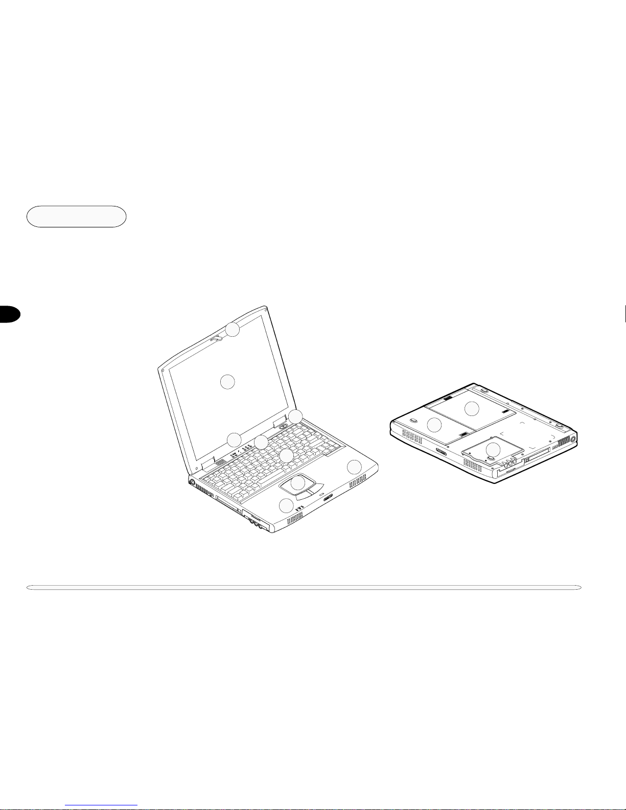
FRONT VIEW
FIG. 1 – 1
1. Cover latch
2. LCD
3. Speakers
4. Microphone
5. On/Off switch
6. LED status indicators
7. Keyboard
8. TouchPad & buttons
EXTERNAL LOCATOR
The following figures show the external locations of the computer’s main subsystems.
2
1
3
7
6
5
3
4
8
11
9
10
BOTTOM VIEW
FIG. 1 - 2
9. Device bay
10. Battery bay
11. RAM bay
1
1 – 7
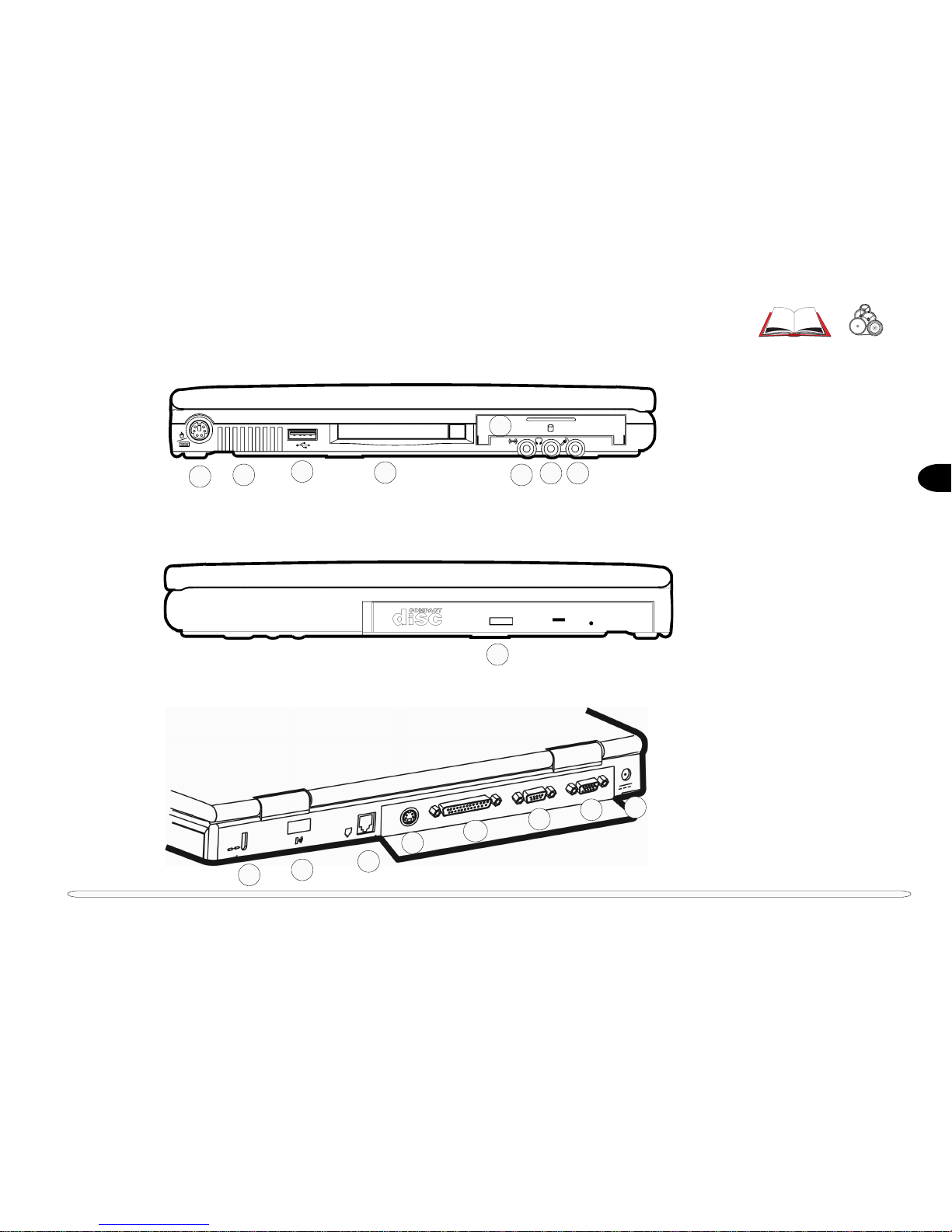
LEFT VIEW
FIG. 1 – 3
1. PS/2 port
2. Fan
3. USB port
4. PC Card slot
5. HDD module
6. Audio line-in jack
7. Phone jack
8. Mic jack
RIGHT VIEW
FIG. 1 – 4
9. CD-ROM module (option)
or DVD ROM module (option)
or FDD module (option)
or LS-120 module (option)
REAR VIEW
FIG. 1 – 5
10. Kensington lock port
11. IrDA (serial 2) port
12. Fax/Modem (option)
13. S-Video TV-out port
14. Parallel port
15. COM (serial 1) port
16. External monitor port
17. Adapter port
external locator
11
6
798
10
13
12
14
5
1
2
3
4
16
17
15

1
1 – 8
Introduction
notes
NOTES:
2
2 – 1
2 Chipset
The computer is completely AT-compatible. Its chipset supports a high-performance AGP bus video interface and
state-of-the-art power management features. This chapter mainly describes the following major system components:
• CPU • Core logic chipset • Supporting chips
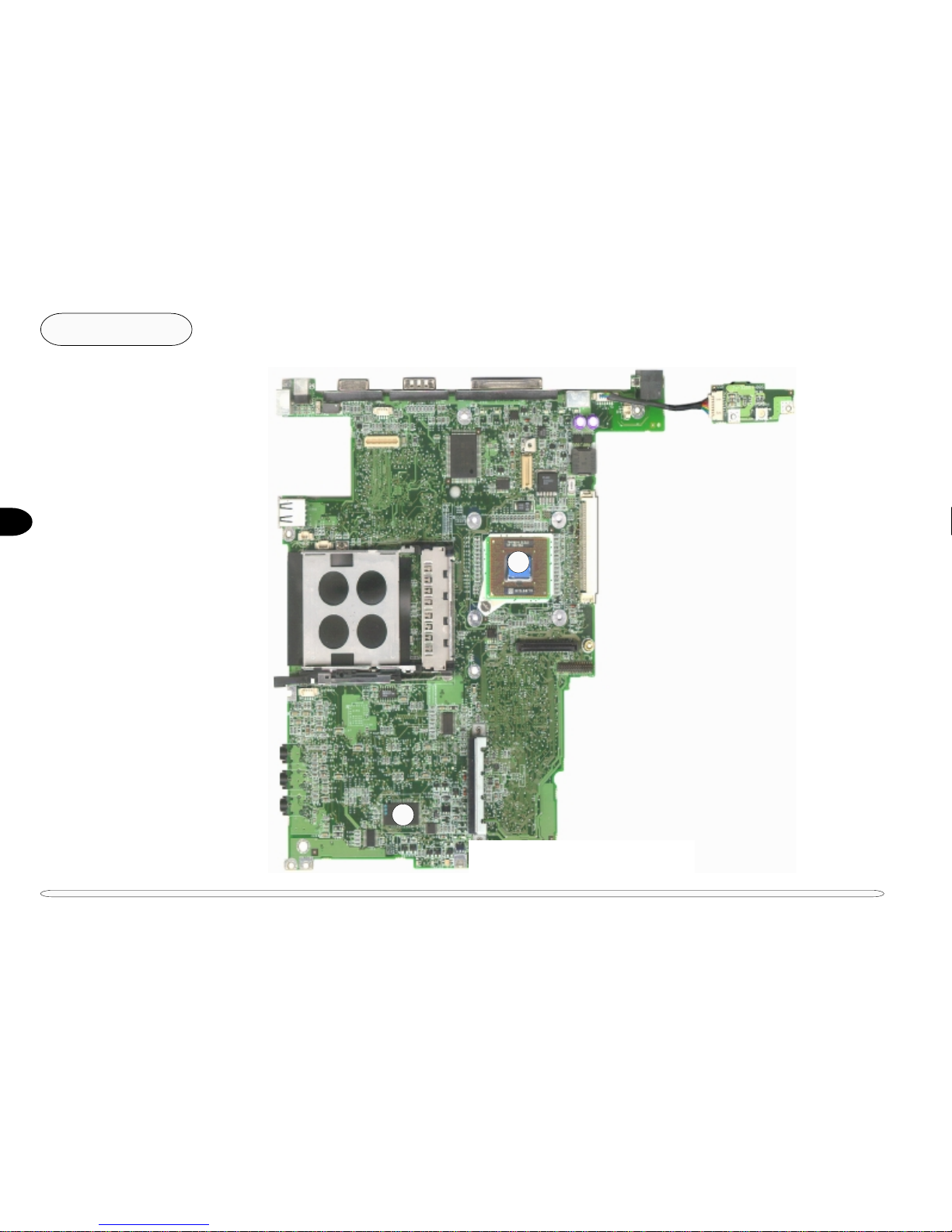
The following figures are the system block diagram and the component site diagram. These provide an overview of
the computer’s layout and a practical locator for chipset components.
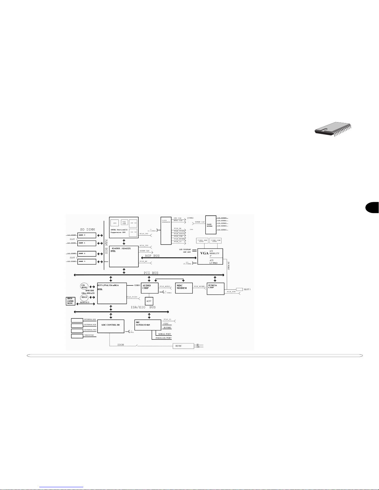
SYSTEM BLOCK DIAGRAM
FIG. 2 – 1
2
2 – 2
Chipset
CHIPSET SITE DIAGRAM
FIG. 2 – 2
1. Pentium III/Celeron CPU
2. BIOS chip
AMD AM29L V004BT
chipset diagram
1
2

2
2 – 3
CHIPSET SITE DIAGRAM
FIG. 2 – 2 (CONT.)
3. Super I/O controller
SMSC FDC37N869
4. Video controller
ATI RAGE LT PRO
5. PC Card controller
Ricoh R5C475
6. Audio controller
RealTek ALS300
+
7. Core Logic chip
82443ZX-M/B (North Bridge)
8. Core Logic chip
82371EB (South Bridge)
9. Keyboard controller
H8/3434
10. SDRAM DIMM socket
11. SDRAM DIMM socket
chipset diagram
6
7
9
11
10
3
4
5
8

2
2 – 4
Chipset
CPU - INTEL MOBILE PENTIUM III/CELERON
The Notebook uses the Intel Mobile Pentium III/Celeron processor in a microPGA2 package. The Intel Mobile
Pentium III/Celeron processor features an integrated L2 cache (256KB for Pentium III and 128KB for Celeron) and
a 64-bit high performance system bus.
The Mobile Pentium III/Celeron processor’s 64-bit wide Low Power Gunning Transceiver Logic system bus is
compatible with the 440BX AGPSet and provides a glue-less, point-to-point interface for an I/O bridge/memory
controller.
The Intel Mobile Pentium III and Celeron processors are fully compatible with all software written for the Pentium
processor with MMX technology, Pentium processor, Intel486 microprocessor, and Intel386 microprocessor. In
addition, they provide improved multimedia & communications performance. They feature:
• Performance improved over existing mobile processors
- Supports the Intel Architecture with Dynamic Execution
- Supports the Intel Architecture MMX technology
• Integrated primary (L1) instructions and data caches
- 4-way set associative, 32-byte line size, 1 line per sector
- 16-Kbyte instruction cache and 16-Kbyte writeback data cache
- Cacheable range programmable by processor programmable registers
• Integrated second level (L2) cache
- 4-way set associative, 32-byte line size, 1 line per sector
- Operated at full core speed
- 256-Kbyte, ECC protected cache data array
• Low Power GTL+ system bus interface
- 64-bit data bus, 66-MHz operation
- Uniprocessor, two loads only (processor and I/O bridge/memory controller)
- Short trace length and low capacitance allows for single ended termination
• Voltage reduction technology
• Pentium II processor clock control
- Quick Start for low power, low exit latency clock “throttling”
- Deep Sleep mode for extremely low power dissipation
• Thermal diode for measuring processor temperature
CPU

2
2 – 5
CORE LOGIC CHIPSET - INTEL 440ZX-M/440BX AGPSET
The Intel 440ZX-M/BX AGPset consists of the BX System Controller (443ZX-M/443BX) and the PCI ISA IDE
Xcelerator (PIIX4E). The AGPset forms a Host-to-PCI bridge and provides the second level cache control and a full
function 64-bit data path to main memory.
NORTH BRIDGE, AGPSET SYSTEM CONTROLLER, 82443ZX-M/82443BX
The BX System Controller (443ZX-M/BX) integrates the cache and main memory DRAM control functions and
provides bus control to transfer between the CPU, cache, main memory, AGP bus and the PCI Bus.
Features
• Supports the Pentium II processor family host bus at 100MHz and 66 MHz at 3.3V
• PCI 2.1 compliant
• Integrated Data Path
• Integrated DRAM controller
- 8Mbytes to 256Mbytes main memory
- 64Mbit DRAM/SDRAM technology support
- EDO and SDRAM DRAM support
- Integrated programmable-strength for DRAM interface
- CAS-Before-RAS refresh, extended CBR and self refresh for EDO
- CAS-Before-RAS and self refresh for SDRAM
• Fully synchronous, minimum latency 30/33 MHz PCI bus interface
- Five PCI bus masters (including PIIX4)
- 10 DWord PCI-to-DRAM read prefetch buffer
- 18 DWord PCI-DRAM post buffer
- Multi-Transaction timer to suppor t multiple short PCI transactions
• AGP Features
- AGP 1.0 compliant
- 66/133 MHz data transfer capability
- Supports concurrent CPU, AGP and PCI transactions
• Power Management Features
- Dynamic stop clock support
- Suspend to RAM (STR)
- Suspend to Disk (STD)
- Power On Suspend (POS)
- Internal clock control
- SDRAM and EDO self refresh during suspend
- ACPI support
- Compatible SMRAM (C_SMRAM) and Extended SMRAM (E_SMRAM)
- SMM write-back cacheable in E_SMRAM mode up to 1MB
• Supports the Universal Serial Bus (USB)
• 492 Pin BGA 440BX AGPset with integrated data paths
core logic chipset

2
2 – 6
Chipset
SOUTH BRIDGE, PCI ISA IDE XCELERATOR, 82371EB (PIIX4E)
The PCI ISA IDE Xcelerator (PIIX4E) is a multi-function PCI device implementing a PCI-to-ISA bridge function, a
PCI IDE function, a Universal Serial Bus host/hub function, and an Enhanced Power Management function. As a
PCI-to-ISA bridge, the PIIX4E integrates many common I/O functions found in ISA-based PC systems - a seven
channel DMA Controller, two 82C59 Interrupt Controllers, an 8254 Timer/Counter, and a Real Time Clock. In
addition to compatible transfers, each DMA channel supports Type F transfers. The PIIX4E also contains full
support for both PC/PCI and Distributed DMA protocols implementing PCI based DMA. The Interrupt Controller
has Edge or Level sensitive and programmable inputs and fully supports the use of an external I/O Advanced
Programmable Interrupt Controller (APIC) and Serial Interrupts. Chip select decoding is provided for BIOS, Real
Time Clock, Keyboard Controller, second external Microcontroller, as well as 2 Programmable Chip Selects. The
PIIX4 provides full Plug and Play compatibility. The PIIX4E can be configured as a Subtractive Decode bridge. This
allows the use of a subtractive decode PCI-to-PCI bridge such as the 82380 chipset which implements a PCI/ISA
docking station environment.
The PIIX4E supports two IDE connectors for up to four IDE devices providing an interface for IDE hard disks and
ROMs. Up to four IDE devices can be supported in Bus Master mode. The PIIX4E contains support for “Ultra
DMA” synchronous DMA compatible devices.
The PIIX4E contains a Universal Serial Bus (USB) Host Controller that is Universal Host Controller Interface
(UHCI) compatible. The Host Controller’s root hub has two programmable USB ports.
The PIIX4E supports Enhanced Power Management, including full Clock Control, Device Management for up to
14 devices, and Suspend and Resume logic with Power On Suspend, Suspend to RAM or Suspend to Disk. It fully
supports Operating System Directed Power Management via the Advanced Configuration and Power Interface
(ACPI) specification. The PIIX4E integrates both a System Management Bus (SMBus) Host and Slave interface for
serial communication with other devices.
core logic chipset
Features
• Supports Pentium and Pentium II Microprocessors
- 440BX ISA kit
• Power Management Logic
- Global and local device management
- Suspend/resume logic
- Supports thermal alarm
- Support for external microcontroller
- Full support for Advanced Configuration and Power Interface (ACPI) Specification and OS Directed Power Management

2
2 – 7
• Multifunction PCI to ISA Bridge
- Supports PCI at 30 MHz and 33 MHz
- Supports PCI Rev 2.1 specification
- Supports Full ISA or Extended I/O (EIO) Bus
- Supports full positive decode or subtractive decode of PCI
- Supports ISA/EIO at 1/4 of PCI frequency
• Supports both mobile and desktop deep green environments
- 3.3 V operation with 5 V tolerant buffers
- Ultra-low power for mobile environments
- Power-On Suspend and Soft-OFF for desktop environment
- All registers readable/restorable for proper resume from 0 V suspend
• Integrated IDE Controller
- Independent Timing of up to 4 drives
- PIO Mode 4 transfers up to 14 Mbytes/s
- Supports “Ultra 33” Synchronous DMA mode transfers up to 33 MBytes/sec
- Integrated 8 x 32-bit buffer for IDE PCI Burst
- Supports glue-less “Swap-Bay” option with full electrical isolation
• Enhanced DMA Controller
- T wo 8237 DMA controllers
- Supports PCI DMA with 3 PC/PCI channels and Distributed DMA protocols (simultaneously)
- Fast T ype-F DMA for reduced PCI bus usage
• Interrupt Controller based on two 82C59
- 15 interrupt support
- Independently programmable for Edge/Level sensitivity
- Supports optional external I/O APIC
- Serial interrupt input
• Timers based on 82C54
- System Timer , Refresh Request, Speaker Tone Output
• USB
- T wo USB 1.0 ports for serial transfers at 12 or 1.5 Mbit/sec
- Supports legacy keyboard and mouse software with USB-based keyboard and mouse
- Supports UHCI Design Guide Revision 1.1 Interface
• SMBus
- Host interface allows CPU to communicate via SMBus
- Slave interface allows external SMBus master to control resume events
• Real-Time Clock
- 256 Byte Battery-Pack CMOS SRAM
- Includes Date Alarm
- Two 8-byte Lockout Ranges
• Microsoft Win95/98 compliant
core logic chipset

2
2 – 8
Chipset
supporting chip - PC Card
SUPPORTING CHIPS
The following subsections describe major supporting chips:
• Ricoh 5C475 PCI-CardBus Bridge
• SMSC FDC37N869 PC 99 Compliant 5V and 3.3V Super I/O Controller with Infrared Support
• ATI RAGE LT PRO Graphics Controller
• RealTeck ALS300+ Audio Controller
RICOH 5C475 PCI-CARDBUS BRIDGE
The 5C475 is a PC card controller offering a single chip solution as a bridge between PCI bus and CardBus. The
5C475 includes a PC Card 95 compliant socket interface and a bridge function to the PCI bus of 33MHz. The 5C475
can support the 32-bit CardBus (Card-32) and the 16-bit PC card (Card-16) without external buffers.
Concerning the card control interface, the 5C475’s register is compatible with the Intel 82365SL and Ricoh’s
RF5C396/366 in order to maintain backward compatibility with the existing 16-bit PC Card compliant with PCMCIA2.
1/JEIDA4.2. All PC card interface signals are individually buffered to allow direct connection to CardBus and Hot
insertion/removal without external buffers. The 5C475 also allows direct connection to PCI bus.
The PCI interface and PC card socket interface have their own power supply terminals that can be powered at
either 3.3V or 5V for compatibility with 3.3V and 5V signaling environments. The core logic is powered at 3.3V.
The 5C475 allows the system to be equipped with the high performance multimedia PC cards like the Video capture
card. It features:
• PC98 compliant
- PC98 Design Guide compliant (Subsystem ID, Subsystem Vender ID)
- ACPI 1.0 and PCI Bus Power Management 1.0 compliant
• Low Power consumption
- Hardware Suspend
- CLKRUN#, CCLKRUN# support
• High-performance
• Single Chip PCI-CardBus Bridge
- PCMCIA PC-Card 95 socket support
- CardBus (Card-32) Card and 16-bit (PCMCIA2.1/JEIDA4.2) Card support

2
2 – 9supporting chip - PC Card
• PCI Bus Interface
- Compliant with PCI Local Bus Specification 2.1
- The maximum frequency 33MHz
- PCI Master/T arget protocol support
- Direct connection to PCI bus
• CardBus PC card Bridge
- Compliant with PCMCIA PC Card 95/CardBus Standard Specification
- Compliant with Yenta register set Rev2.2
- The maximum frequency 33MHz
- CardBus Master/T arget protocol support
- T ransfer transactions
- All memory read/write transaction (bi-direction)
- I/O read/write transaction (bi-direction)
- Configuration read/write transaction (PCI-Card)
- 2 programmable memory windows
- 2 programmable I/O windows
• PC Card-16 Bridge
• Compliant with PCMCIA PC Card 95 CardBus (PC Card-16) Standard Specification
- 5 programmable memory windows
- 2 programmable I/O windows
- Compliant with i82365SL compatible register set / ExCA TM
• System Interrupt
- INTA# support for PCI system inter rupt
- IRQn support for ISA system interrupt (Non shared IRQn pins)
- Serialized IRQ support
• 3.3V/5V Mixed Voltage Operation at 33Mhz
• GPIO support
• Posting Write and Prefetching Read support
• Plug and Play support
• 16-bit Legacy mode (3E0/3E2 I/O port) support
• PCIway Legacy DMA support

2
2 – 10
Chipset
SMSC FDC37N869 PC 99 COMPLIANT 5V AND 3.3V SUPER I/O CONTROLLER WITH INFRARED SUPPORT
The FDC37N869 features:
supporting chip - super I/O
• 5 volt and 3.3 volt operation
• Intelligent auto power management
• 16 bit address qualification
• 2.88MB Super I/O Floppy Disk Controller
- Licensed CMOS 765B Floppy Disk Controller
- Software and register compatible with SMSC proprietary
82077AA compatible core
- Supports one Floppy Drive directly
- Configurable Open Drain/Push-Pull Output Drivers
- Supports Vertical Recording Format
- 16 byte data FIFO
- 100% IBM compatibility
- Detects all overrun and underrun conditions
- Sophisticated Power Control Circuitry (PCC) including
multiple power-down modes for reduced power
consumption
- DMA enable logic
- Data rate and drive control registers
- Swap drives A and B
- Non-burst mode DMA option
- 48 Base I/O address, 15 IRQ and 4 DMA options
- Forceable write protect and disk change controls
• Floppy disk available on parallel port pins ACPI compliant
• Enhanced digital data separator
- 2Mbps, 1Mbps, 500 Kbps, 300 Kbps, 250 Kbps data rates
- Programmable precompensation modes
• Serial ports
- T wo high speed NS16C550 compatible UARTs with send/
receive 16 Byte FIFOs
- Supports 230k and 460k baud
- Programmable baud rate generator
- Modem control circuitry
• Infrared communications controller
- IrDA v1.2 (4Mbps), HPSIR, ASKIR, Consumer IR Support
- 2 IR Ports
- 96 base I/O address, 15 IRQ options and 4 DMA options
• Multi-mode parallel port with ChiProtect
- Standard Mode
- IBM PC/XT PC/AT and PS/2 compatible bi-dir ectional
parallel port
- Enhanced Parallel Port (EPP) compatible
- EPP 1.7 and EPP 1.9 (IEEE 1284 compliant)
- Enhanced Capabilities Port (ECP) compatible (IEEE 1284
compliant)
- Incorporates ChiProtect Circuitry for Protection Against
Damage Due to Printer Power-On
- 192 base I/O address, 16 IRQ and 4 DMA options
• Game port select logic
- 48 base I/O addresses
• General Purpose Address Decoder
- 16-byte block decode

2
2 – 11
supporting chip - video
ATI RAGE LT PRO GRAPHICS CONTROLLER
The RAGE LT Pro is a highly integrated graphics accelerator with superior support for 3D and motion video —
ideal for notebooks and LCD desktops. It incorporates comprehensive support for Intel’s Accelerated Graphics Port
(AGP), including 1X or 2X mode with sidebands.
Delivering superior 3D acceleration and comprehensive 3D support, the RAGE LT Pro includes a triangle set-up
engine, single-pass trilinear filtering, six perspectively correct texturing modes, video texturing, Gouraud and specular shading, and a host of 3D special effects.
The best choice for DVD notebooks and LCD desktops, the RAGE LT Pro’s DVD features include motion compensation, acceleration for soft DVD, integrated TV-out with Macrovision and support for third-party MPEG-2 decoders via the ATI Multimedia Channel (AMC).
Using Tri-View™ the RAGE LT Pro can output to LCD, CRT, and TV simultaneously. It also includes two output
controllers so that any two display devices can have different images and/or refresh rate.
It has the following main features:
• First mobile accelerator to use AGP 2X (133MHz) in AGP Texturing with sideband signals to realize all the benefits of AGP.
• First mobile accelerator to deliver full motion soft DVD using motion compensation circuitry.
• First mobile acccelerator with integrated LVDS transmitter .
• Innovative Dynamic Power Management with ACPI compliance.
• Superior 3D performance acheived through a hardware setup
engine and a 4KB on-chip texture cache.
• Superior 2D performance with support of 100MHz SGRAM.
• TFT and DSTN panel interface support for up to 1280x1024 resolutions.
• Integrated ImpacTV2-quality TV output provides optimal image
quality via programmable 6 tap flicker filter, resolution modes
scale down from 1024x768 and 16:9 wide mode support. Direct
YUV422 mode, Macrovision 7.01 and CGMS support.
• Support for 2, 4, or 8MB frame buffers, and integrated 230MHz
DAC.
• High quality ratiometric expansion that fits source images to any
panel resolution.
• Flexible graphics memory configurations: 4MB up to 8MB
SDRAM/SGRAM.
• Memory upgrade via industry standard SGRAM SO-DIMM,
for reduced board area and higher memory speeds.
• DDC1 and DDC2B+ for plug and play monitors.
• External Spread Spectrum chip support to reduce EMI on
digital interface.
• Power management with full VESA DPMS and EPA Energy
Star compliance.
• Integrated hardware diagnostic tests performed automatically upon initialization.
• High quality components through built-in SCAN, IDDQ, CRC
and chip diagnostics.
• Single chip solution in 0.25um, 2.5V CMOS technology.
• Comprehensive HDKs, SDKs and utilities augmented by full
engineering support.
• Fully compliant with relevant sections of PC 98 and PC 99.

2
2 – 12
Chipset
supporting chip - audio
REALTEK ALS300+ INTEGRATED PCI A UDIO ACCELERATOR
The ALS300+ Integrated PCI Audio Accelerator brings forth a new age of highly integrated, single chip sound
products. It provides cost-efficient audio solutions for motherboard and add-in card and notebook implementations.
The ALS300+ fully supports the PCI Plug and Play standard. Its main features are as follows:
• High performance VLSI sound ASIC
• Compatible with DirectSound, DirectSound3D Sound Blaster, Sound Blaster Pro, and Sound Blaster 16 emulation
• 64-Voice Wavetable Synthesis w/ DLS-1 support
• Built-in ALSFM Synthesizer
• Supports Dual AC-97 CODECs/4-channel speakers
• I2S & S/PDIF Digital In/Out
• Host Modem support
• Legacy/DOS compatibility
• QSound Q3D Positional/QEM EAX Sound Support
• Supports Sound Blaster ADPCM decompression
• MPU-401 MIDI controller with FIFO
• Enhanced normal & digital game port support
• 16-bit full-duplex for concurrent recording and playback
• ACPI/PCI Bus Power Management Interface Specification 1.1
• 5.0/3.3V dual power mode
• 128-Pin PQFP package
 Loading...