

Page 1

1500P Series
Service Manual
The circuit schematics herein provided for reference only are not necessarily
the latest version.
Mainboard 71-11P00-D02
Switch board 71-11A0S-D01
Charger board 71-11A0E-D01A
TFT & DSTN card 71-11PCL-D00
Flat Link card 71-11PFL-D00
Jack Board 71-11P0K-D00
Specifications are subject to change without notice. Jan. 1999
99-01. version
1
Page 2

Specifications
The Notebook Computer is a state-of-the-art, high performance, portable
system. It offers a host of features specially designed to enhance
performance and usability.
: Processor
− Mobile Pentium II processors (AGP) at 300/266/233 MHz
− Intel Mobile Module Connector2 Structure (MMC2)
− 66 MHz CPU Bus Clock
: Memory
− 3.3V power supply
− 64 bit data bus system memory
− Supports EDO/SDRAM
− 8MB expandable up to 256 MB
− Two 144-pin SODIMM package
: System BIOS
− 256KB flash ROM
− SystemSoft BIOS with Smart Battery
− Plug and Play 1.0a
− ACPI
: Display
− 14.1” TFT XGA (1024x768 pixels) LCD panel available
− 13.3” TFT XGA (1024x768 pixels) LCD panel available
− 12.1” DSTN/SVGA (800x600 pixels) LCD panel available
− AGP 2X
− 64 bits Hardware 2D/3D Graphics Engine
− Motion Video acceleration
− Motion Compensation
− Support Video Playback
− High quality TV-out
− High quality dedicated S-Video TV Out
− 4MB display memory SGRAM type
− Vertical Interpolate 720V x 480H pixel wide video source
− CRT resolution up to 1280x1024x16M non-interlaced
− Ratiometric LCD expansion
− 230 MHz DAC
− Tri-View for a triple display solution, TV, CRT and LCD
− Support external Video Input
− Support VPM 1.10
1
Page 3

: Mass Storage
− 3.5” floppy diskette drive
− 2.5” hard disk drive (12.7mm high or less)
− 5.25” CD-ROM.
− Support Master mode IDE.
− Support PIO mode 4/ATA-33 (Ultra DMA)
: Audio
− Sound Blaster Pro compatible
− Full duplex operation
− 3D stereo sound effects
− Built-in microphone
− Built-in speakers
− Wavetable Downloadable
− IIS interface for external ZV port MPEG audio
− High-quality FM music synthesizer 16 bits stereo sound system,
compliant to PC97 Rev. 1.0
: PC Card Sockets
− One Type III PC card or two Type II PC cards
− One socket ZV-capable
− CardBus support
: Input/Output
− Built-in trackpad (PS/2)
− USB port
− S-video jack for TV output
− RCA jack for video input
− Docking connector for Port Replicator
− External CRT monitor (CRT) port
− Parallel port (LPT1)
− Serial port (COM 1)
− PS/2 type port (External keyboard/Mouse)
− Microphone-in jack
− Headphone jack
− DC-in jack
− Phone jack for a 56K Modem Card (Optional)
: Infrared Wireless Communication
− IrDA
− FIR
− ASKIR
− 56K Modem Card (Optional)
2
Page 4

: Keyboard
− Windows 95
− Detachable for various language versions
: Power Management
− APM 1.2
− ACPI
− Global standby
− Suspend and resume
− CPU over temperature protection
− Secondary cache power control
− Device power management for all devices
− Battery low suspend
: Rechargeable Battery Pack
− Ni-MH battery available
− Li-Ion battery available
− Battery low warning
− Auto-switching with AC power adapter
: Size & Weight
− 302mm(w)x249mm(d)x46mm(h)
− 3kg
: Temperature Environment
− Operating 5°C∼35°C
− Storage -20°C∼60°C
: Humidity Environment
− Operating 20%∼80%, non-condensing
− Storage 10%∼90%, non-condensing
3
Page 5
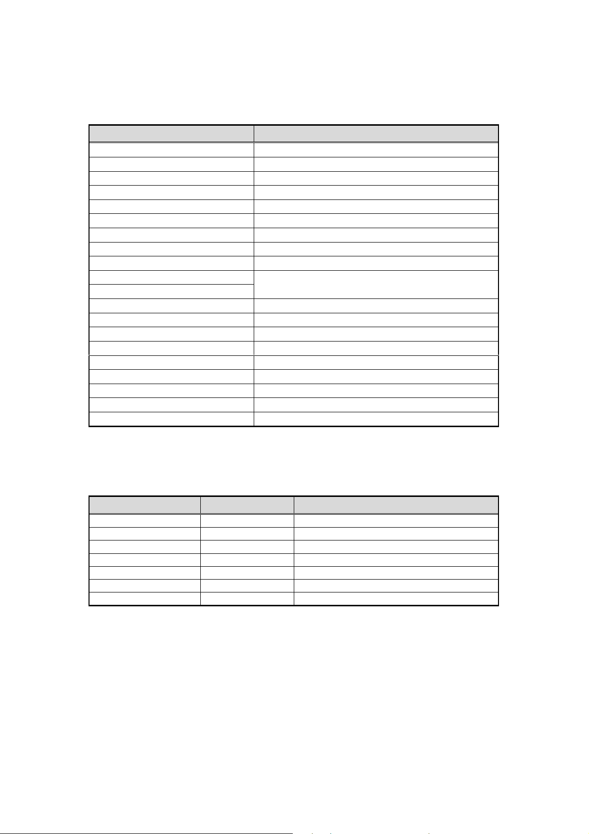
I/O Address Map
Hex Range Device
000 – 00F DMA controller-1
020 – 021 Interrupt controller-1
040 – 043 Timer 1
048 – 04B Timer 2
060 – 06E KB controller M38867 chip select
070 – 071 RTC and NMI mask
080 – 08F DMA page register
0A0 – 0A1 Interrupt controller-2
0C0 – 0DF DMA controller-2
1F0 – 1F7
3F6 , 3F7
2F8 – 2FF Serial port 2
378 – 37A Parallel port 1
3B4 , 3B5 CRT controller index (mono)
3D4 , 3D5 CRT controller index (color)
3BA Feature control
3C0 – 3DA
3F2 – 3F7 Floppy disk controller
3F0 , 3F1 Configuration port
3F8 – 3FF Serial port 1
Fixed disk select
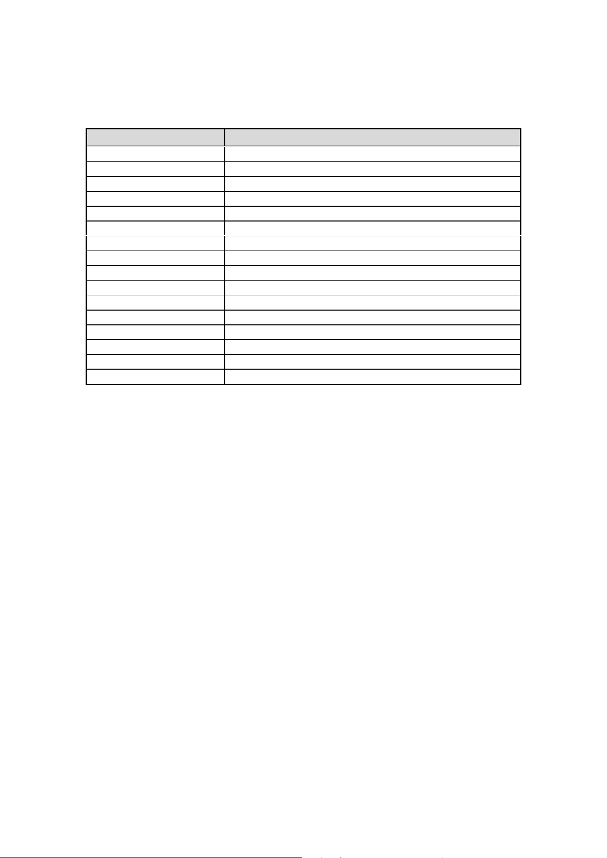
System Memory Map
Address Size Function
000000 – 09FFFF 640KB 640KB Base Memory
0A0000 – 0BFFFF 128KB Video RAM
0C0000 – 0CFFFF 64KB VGA BIOS
0D0000 – 0DFFFF 64KB Reserved
0E0000 – 0EFFFF 64KB System BIOS for SCU, PCI, PnP, PMU
0F0000 – 0FFFFF 64KB System BIOS for Kernal
100000 – Above 1MB Extended Memory
4
Page 6
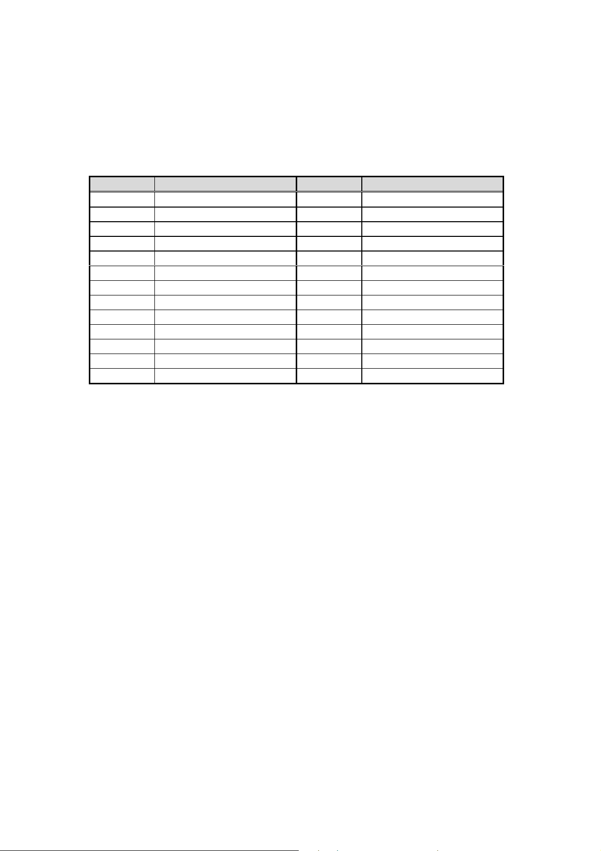
System Resource Allocation
IRQs Devices
IRQ0 Timer
IRQ 1 Keyboard
IRQ 2 Cascade
IRQ 3 COM2
IRQ 4 COM1
IRQ 5 Audio/MPU-401
IRQ 6 Floppy Disk
IRQ 7 Parallel Port
IRQ8 Real Time Clock
IRQ9 Available
IRQ10 USB/PCMCIA
IRQ11 Available
IRQ12 Trackpad (PS/2)
IRQ13 Floating Point Unit
IRQ14 Primary IDE Interface (HDD)
IRQ15 Secondary IDE Interface (CD-ROM)
5
Page 7

Motherboard
The motherboard is designed mainly based Intel MMC2 structure CPU and
82371EB(PIIX4E) Chipset ; it includes the following features:
ü 82371EB(PIIX4E) chipset solution from INTEL
ü ATI 3D RAGE LT PRO Multimedia Flat Panel Controller
ü FDC37N769 Super I/O with IR Support Controller
ü M38867 Keyboard Controller
ü Flash EPROM 256KB with SystemSoft system BIOS, VGA BIOS
ü DRAM Upgradable to 256MB
ü 7 DMA channels
ü 13 interrupt levels
ü Real time clock / calendar, battery back up
ü Buzzer for sound system
ü Built-in 3D stereo audio subsystem
ü Port connectors :
− 9 pin serial port (COM1)
− 25 pin parallel printer port (LPT1)
− 15 pin external monitor port
− 6 pin external keyboard port
− 4 pin USB port
− 120 pin Port Replicator connector
− Phone jack for a 56K Modem Card(Optional)
6
Page 8

Microprocessor
Intel Mobile Module Family
I. Mobile Module Connector 2 (MMC2) Mobile Module
The Intel Pentium II processor Mobile module (400 pin MMC) is a small,
highly integrated assembly containing an Intel Pentium II mobile processor
and its immediate system-level support. Specification, the processor module
contain a power supply for the processor’ s unique voltage requirement, a
system Level 2 cache memory and the core logic require to bridge the
processor to the standard system bus. The module interface electrically to its
host system via a 3.3 volts PCI bus, a 3.3 volts memory bus and some Intel
443BX Host Bridge control signals.
II. Intel 440BX AGPset
The 440BX AGPset is the fourth generation chipset based on the
Pentium Pro processor architecture. It has been designed to interface with
the Mobile Pentium II processor’ s system bus at 66 MHz. Along with its Hostto-PCI bridge interface, the 82443 BX host bridge controller has been
optimized with a 66 MHz SDRAM memory controller and data path. The
82443 BX component includes the following function and capabilities:
ü 64-bit Low Power GTL + based system data bus interface
ü 32-bit system address bus support
ü 64/72-bit main memory interface with optimized support for SDRAM
ü 32-bit PCI bus interface with integrated PCI arbiter
ü AGP interface with up to 133 MHz data transfer capability
ü Extensive data buffering between all interface for high throughput and
concurrent operations
Functionality:
ü 233/266/300 MHz Mobile Pentium II Processors
ü Intel Mobile Module Connector 2 Structure (MMC2)
ü Support Write-back L1 & L2 Cache
ü 66 MHz CPU bus clock
7
Page 9

Chips
Core Logic – Intel 82371EB (PIIX4E) Chipset
It contains the following features:
ü Support kits for both Pentium and Pentium II Microprocessor
ü Multifunction PCI to ISA Brige
ü Supports PCI at 30 and 33 Mhz
ü Supports PCI Rev 2.1 specification
ü Supports Full ISA or Extended I/O Bus
ü Supports Mobil Deep Green Environments
ü 3.3V Operation with 5V Tolerant Buffers
ü Ultra-low power for Mobil Environments Support
ü Full Support for ACPI (Advanced Configuration and Power Interface)
Revision 1.0
ü Integrated IDE Controller
ü Support Ultra DMA/33
ü Supports two 82C37 Enhanced DMA controller
ü Supports two 82C59 Interrupt controller
ü Supports UHCI USB Ports
ü Supports SM BUS
8
Page 10

VGA Controller – ATI 3D RAGE LG PRO
The ATI 3D RAGE LT PRO is highly integrated graphics accelerator superior
support for 3D and motion video, making it ideal for notebooks. DVD features
include motion compensation, acceleration for soft DVD, integrated TV-out
with Macrovision. It incorporates comprehensive support for Intel’ s
Accelerated Graphics Port (AGP) including 1X or 2X mode with sidebands.
The simultaneously. It contains the following functions:
ü Accelerator to use AGP 2X (133 MHz) in AGP Texturing with sideband
signals to realize all benefits of AGP
ü Accelerator with integrated LVDS transmitter
ü Accelerator to use Tri-View architecture for a triple display solution
allowing three simultaneous outputs to TV, CRT and LCD with up to two
different refresh rates
ü Supports displays with SGRAM 4 MB
ü Superior 3D performance achieved through a hardware setup engine and
a 4KB on-chip texture cache
ü Superior 2D performance with support of 100MHz SGRAM
ü Supports DRAM, EDO DRAM, SDRAM and SGRAM at up to 100 MHz
memory clock providing bandwidths up to 880MB/sec across a 64-bit
interface
ü Supports 16/24 bit color DSTN up to 1024x768x16M color, and TFT
panels up to 1280x1024x64K color
ü Supports non-interlaced 1280x1024x64K , 1024x768x16M ,
800x600x16M color on CRT
ü Simultaneous display in 24 bit color on flat panel and CRT
ü Internal buffer provides flicker reduction
ü RGB signals driven form the ATI LUT/DAC can directly interface with a
standard off-the-shelf NTSC/PAL encoder
ü Composite synchronization signals support for standard Home TV
connection
ü Graphic function optimized by a 64 bit internal data bus and VGA , SVGA,
XGA AND SXGA flat panel
ü Fully compliant ZV-Port interface with device driver support for VPM
ü Industry leading DualView Simultaneous display
9
Page 11

PC CARD95 (CARD BUS) Interface Controller TI1225
TI CardBus Interface Controller 1225 implements the PCMCIA 2.0/JEIDA 4.1
standard. It contains the following functions:
ü PCI interface Specification 2.1
ü Supports Zoom Video Mode
ü PCMCIA dual-socket interface
ü Yenta Registers-compatible
ü ACPI 1.0 Compliant
ü One-Slot plus MPEG three Zoomed Video Ports Support
ü Bus Master Transfer capability
ü Supports both 5V & 3.3V PC cards
ü Supports PCMCIA ATA Specification
ü Advanced Submicron, Low Power CMOS Technology
ZV Port Custom Interface
The ZV (Zoomed Video) Port is a single source, point-to-point uni-directional
video bus between a PC card socket and a VGA controller. The ZV Port
complies with CCIR601 timing to allow NTSC decoders to deliver real-time
digital video straight into the VGA frame buffer from a PC card. The ZV Port
also allows an industry standard mechanism for transferring digital audio PCM
data to a low cost DAC for conversion to an analog signal.
10
Page 12

Super I/O Controller – SMC FDC37N769
The SMC's FDC37N769 super I/O is optimized for motherboard applications.
It provides:
ü 3.3 Volt operation
ü Intelligent Auto Power Management
ü 16 Bit Address Qualification (Optional)
ü 2.88MB Super I/O Floppy Disk Controller
− Support Vertical Recording Format
− 16 Byte Data FIFO
− Enhanced Digital Data Separator. Data rate up to 1Mb/s.
ü Multi-Mode Parallel Port with ChipProtect Circuitry
− Standard Mode
IBM PC/AT and PS/2 compatible bi-directional Parallel port.
− Enhanced Mode
Enhanced Parallel Port (EPP) Compatible
− High Speed Mode
Microsoft and Hewlett Packard Extended Capabilities Port (ECP)
Compatible
ü Serial Port
− Two high speed NS16C550 compatible UARTs with Send/Receive
16 Byte FIFOs
− Programmable Baud Rate Generator
− Supports 230K and 460K Baud
− Modem Control Circuitry
− Infrared-IrDA, HPSIR, ASKIR ,Fast IR(4Mbps IrDA), Consumer IR
Support
11
Page 13

High Quality Audio Chip – ESS Maestro-2EM
ü 500-MIPS-equivalent dual-engine PCI audio accelerator
ü 64-Voice Wave processor for director sound and wavetable application
ü HRTF 3-D positional audio acceleration under DirectX 5.0
ü Multi-Stream Directsound and Direct Sound3D acceleration
ü Hardware acceleration for DirectMusic, ActiveMovie, and DirectInput API
ü Enhanced effects (reverb, chorus, flange, treble, bass, and 3D stereo
extender)
ü Advanced platform for interactive 3-Dgaming, DVD movie playback, and
internet communications
Real PCI to USB (UHCI) Chip
– Intel 82371EB (PIIX4E)
The PIIX4E USB controller provides enhanced support for the Universal
Host Controller Interface (UHCI). This includes support that allows legacy
software to use a USB-based keyboard and mouse.
Keyboard Controller - M38867M8
ü Memory size: 1024 bytes(RAM)/32K bytes(ROM)
ü Timers: 8 bit timer X 4 ,8 bit prescalers X 3
ü Comparator: 8 channels
ü The minimum instruction execution time: 0.5us (8MHZ)
ü Clock Generating Circuit: 2 clock generating circuits
ü Interrupts: 21 sources, 16 vectors
ü Multi-Master IIC-bus/SMBus (option): 1 channel
12
Page 14

Infrared Communications Controller
ü IrDA v1.1(4Mbps), HPSIR, ASKIR, Consumer IR Support
ü 2 IR Ports
ü 96 Base I/O Address and 7 IRQ Options
RGB to NTSC/PAL Encoder in ATI LT PRO
RGB signals driven from the ATI LUT/DAC can directly interface with a
standard off-the-shelf NTSC/PAL encoder
Composite synchronization signals support for standard Home TV connection
13
Page 15

DRAM Speed
The speed ratings of DRAM for various CPU external clock rates are listed
below (using 1Mx16, 2Mx8, 4Mx16 or 8Mx8 memory):
DRAM Speed 66MHz (clocks) 100MHz (clocks)
60ns read x-4-4-4 read x-4-4-4
60ns write x-3-3-3 write x-3-3-3
Refresh cycle (with CAS-BEFORE-RAS Refresh Cycle) = 2K
14
Page 16
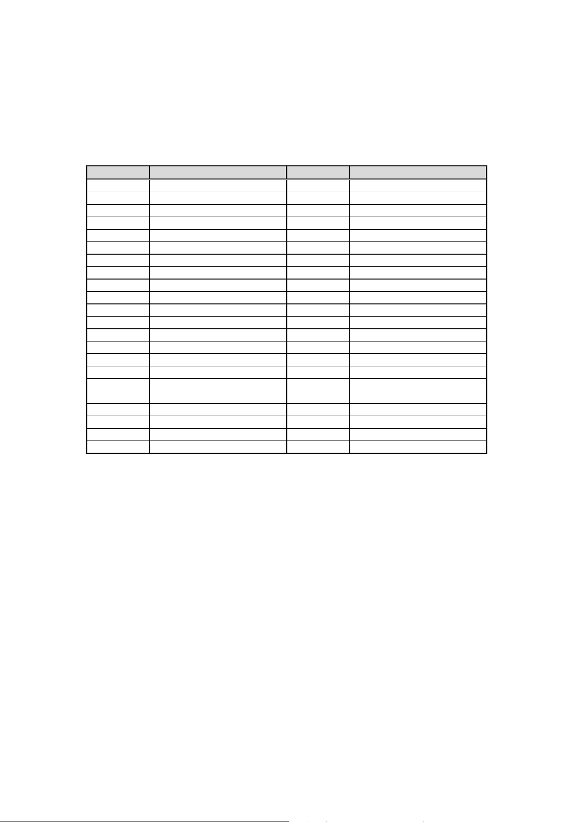
Pin Configurations
Floppy Disk Drive Interface
The Notebook PC uses one 26-pin FFC connector to interface with the built-in
1.44MB 3.5" disk drive. The pin configuration is:
Pin Description
1 VCC 2 INDEX#
3 VCC 4 DRV0#
5 VCC 6 DSKCHG#
7 N.C. 8 N.C.
9 3MODE# 10 MTR0#
11 N.C. 12 DIR#
13 N.C. 14 STEP#
15 GND 16 WDATA#
17 GND 18 WGATE#
19 GND 20 TRK0#
21 GND 22 WP-FD#
23 GND 24 RDATA#
25 GND 26 HDSEL#
Pin
Description
15
Page 17
Hard Disk Drive Interface
The Notebook PC has a standard PC/AT interface (IDE) which can directly
interface with any hard disk drive with an embedded controller supporting the
same PC/AT interface through the use of a 44-pin pin header connector. The
44-pin connector has the following pin configurations:
Pin Description Pin Description
1 HDRST# 2 GND
3 DDP7 4 DDP8
5 DDP6 6 DDP9
7 DDP5 8 DDP10
9 DDP4 10 DDP11
11 DDP3 12 DDP12
13 DDP2 14 DDP13
15 DDP1 16 DDP14
17 DDP0 18 DDP15
19 GND 20 N.C.
21 PDREQ 22 GND
23 PDIOW# 24 GND
25 PDIOR# 26 GND
27 PIORDY 28 GND
29 PDACK# 30 GND
31 IRQ14 32 N.C.
33 PDA1 34 N.C
35 PDA0 36 PDA2
37 CS1P# 38 CS3P#
39 HD-LED# 40 GND
41 VCC 42 VCC
43 GND 44 N.C.
16
Page 18

RS-232C Serial Interface
The Notebook PC has one RS-232C serial port which enables users to
connect a serial printer, a serial mouse, a plotter, a modem, etc. The key
features of the serial port are listed as follows:
ü IBM PC/AT compatible.
ü Compatible with NS16C550.
ü Individual modem control/signals for each channel.
ü Programmable serial interface characteristics:
− 5-, 6-, 7-, or 8-bit characters.
− Even, odd, or no parity bit generation and detection.
− 1, 1 1/2 or 2 stop bit generation.
− Tri-state TTL drives capabilities for bi-directional data bus and
control bus.
The RS-232C serial port uses a 9-pin D-sub male connector which has the
following pin configurations:
Pin Description
1 DCD (DATA Carrier Detect)
2 RXD (Received Data)
3 TXD (Transmitted Data)
4 DTR (Data Terminal Ready)
5 GND (Signal Ground)
6 DSR (Data Set Ready)
7 RTS (Request To Send)
8 CTS (Clear To Send)
9 RI (Ring Indicator)
17
Page 19

Parallel Interface
The parallel interface is implemented using a 25-pin D-sub female connector
which has the following pin configurations:
Pin Description Pin Description
1 Strobe# 2 Data 0
3 Data 1 4 Data 2
5 Data 3 6 Data 4
7 Data 5 8 Data 6
9 Data 7 10 ACK#
11 Busy 12 Paper Empty
13 Select 14 Auto Linefeed#
15 Error# 16 Initialize#
17 Select In 18 Ground
19 Ground 20 Ground
21 Ground 22 Ground
23 Ground 24 Ground
25 Ground
18
Page 20

Expansion Memory Socket
Socket 1:
Pin Description Pin Description Pin Description
1 GND 2 GND 3 MD0
4 MD32 5 MD1 6 MD33
7 MD2 8 MD34 9 MD3
10 MD35 11 MEM-VCC 12 MEM-VCC
13 MD4 14 MD36 15 MD5
16 MD37 17 MD6 18 MD38
19 MD7 20 MD39 21 GND
22 GND 23 ICAS#0 24 ICAS#4
25 ICAS#1 26 ICAS#5 27 MEM-VCC
28 MEM-VCC 29 IMA0 30 IMA3
31 IMA1 32 IMA4 33 IMA2
34 IMA5 35 GND 36 GND
37 MD8 38 MD40 39 MD9
40 MD41 41 MD10 42 MD42
43 MD11 44 MD43 45 MEM-VCC
46 MEM-VCC 47 MD12 48 MD44
49 MD13 50 MD45 51 MD14
52 MD46 53 MD15 54 MD47
55 GND 56 GND 57 N.C
58 N.C 59 N.C 60 N.C
61 MEMCLK1 62 CKE 63 MEM-VCC
64 MEM-VCC 65 SRAS# 66 SCAS#
67 IMWE# 68 CKE 69 IRAS#0
70 IMA12 71 IRAS#1 72 IMA13
73 GND 74 MEMCLK2 75 GND
76 GND 77 N.C 78 N.C
79 N.C 80 N.C 81 MEM-VCC
82 MEM-VCC 83 MD16 84 MD48
85 MD17 86 MD49 87 MD18
88 MD50 89 MD19 90 MD51
91 GND 92 GND 93 MD20
94 MD52 95 MD21 96 MD53
97 MD22 98 MD54 99 MD23
100 MD55 101 MEM-VCC 102 MEM-VCC
103 IMA6 104 IMA7 105 IMA8
106 IMA11 107 GND 108 GND
109 IMA9 110 IMA12 111 IMA10
112 N.C 113 MEM-VCC 114 MEM-VCC
115 ICAS#2 116 ICAS#6 117 ICAS#3
118 ICAS#7 119 GND 120 GND
121 MD24 122 MD56 123 MD25
124 MD57 125 MD26 126 MD58
127 MD27 128 MD59 129 MEM-VCC
130 MEM-VCC 131 MD28 132 MD60
133 MD29 134 MD61 135 MD30
136 MD62 137 MD31 138 MD63
139 GND 140 GND 141 SMBDA
142 SMBCL 143 MEM-VCC 144 MEM-VCC
19
Page 21

Socket 2:
Pin Description Pin Description Pin Description
1 GND 2 GND 3 MD0
4 MD32 5 MD1 6 MD33
7 MD2 8 MD34 9 MD3
10 MD35 11 MEM-VCC 12 MEM-VCC
13 MD4 14 MD36 15 MD5
16 MD37 17 MD6 18 MD38
19 MD7 20 MD39 21 GND
22 GND 23 ICAS#0 24 ICAS#4
25 ICAS#1 26 ICAS#5 27 MEM-VCC
28 MEM-VCC 29 IMA0 30 IMA3
31 IMA1 32 IMA4 33 IMA2
34 IMA5 35 GND 36 GND
37 MD8 38 MD40 39 MD9
40 MD41 41 MD10 42 MD42
43 MD11 44 MD43 45 MEM-VCC
46 MEM-VCC 47 MD12 48 MD44
49 MD13 50 MD45 51 MD14
52 MD46 53 MD15 54 MD47
55 GND 56 GND 57 N.C
58 N.C 59 N.C 60 N.C
61 MEMCLK3 62 CKE 63 MEM-VCC
64 MEM-VCC 65 SRAS# 66 SCAS#
67 IMWE# 68 CKE 69 IRAS#2
70 IMA12 71 IRAS#3 72 IMA13
73 GND 74 MEMCLK4 75 GND
76 GND 77 N.C 78 N.C
79 N.C 80 N.C 81 MEM-VCC
82 MEM-VCC 83 MD16 84 MD48
85 MD17 86 MD49 87 MD18
88 MD50 89 MD19 90 MD51
91 GND 92 GND 93 MD20
94 MD52 95 MD21 96 MD53
97 MD22 98 MD54 99 MD23
100 MD55 101 MEM-VCC 102 MEM-VCC
103 IMA6 104 IMA7 105 IMA8
106 IMA11 107 GND 108 GND
109 IMA9 110 IMA12 111 IMA10
112 N.C 113 MEM-VCC 114 MEM-VCC
115 ICAS#2 116 ICAS#6 117 ICAS#3
118 ICAS#7 119 GND 120 GND
121 MD24 122 MD56 123 MD25
124 MD57 125 MD26 126 MD58
127 MD27 128 MD59 129 MEM-VCC
130 MEM-VCC 131 MD28 132 MD60
133 MD29 134 MD61 135 MD30
136 MD62 137 MD31 138 MD63
139 GND 140 GND 141 SMBDA
142 SMBCL 143 MEM-VCC 144 MEM-VCC
20
Page 22

Internal Trackpad Interface
There is a connector used to interface with the internal trackpad. It should be
disabled when external serial mouse has been installed. The trackpad is
hardware-connected to PS/2 port, hardware-compatible to Microsoft PS/2
mouse and software-compatible to Microsoft mouse mode. The following is
the pin configurations for the connector:
Pin Description
1 VCC
2 PS/2 DATA
3 PS/2 CLK
4 GND
External Monitor Interface
Pin Description
1 RED
2 GREEN
3 BLUE
4 N.C
5 GND
6 GND
7 GND
8 GND
9 N.C
10 GND
11 N.C
12 DDCDATA
13 HSYNC
14 VSYNC
15 DDCCLK
RGB Out
Output Impedance : 75Ω
RGB peak voltage : 0.7Vpp
21
Page 23

External Keyboard/PS2 Mouse Interface
Pin Description
1 EKDA
2 EMDA
3 GND
4 VCC
5 EKCLK
6 EMCLK
External USB (Universal Serial Bus) Interface
Pin Description
1 VCC
2
3
4 GND
DATA−
DATA+
External S-Video TV-out Interface
Pin Description
1 GND
2 GND
3 XLUMA
4 XCRMA
Video-in Interface
Pin Description
1 Video-In
2 GND
22
Page 24

PCMCIA CardBus Interface
Socket A:
Pin Description Pin Description
A1 GND A2 N/A
A3
A5 A_CD4 A6 A_CD11
A7 A_CD5 A8 A_CD12
A9 GND A10 A_CD6
A11 A_CD13 A12 A_CD7
A13 A_CD14 A14 A_CE1#
A15 A_CD15 A16 GND
A17 A_CA10 A18 A_CE2#
A19 A_OE# A20 A_VS1
A21 A_CA11 A22 GND
A23 A_IORD# A24 A_CA9
A25 A_IOWR# A26 A_CA8
A27 A_CA17 A28 GND
A29 A_CA13 A30 A_CA18
A31 A_CA14 A32 A_CA19
A33 A_WE# A34 A_CA20
A35 A_RDYBY# A36 A_CA21
A37 A_VCC_C A38 A_VCC_C
A39 A_VPP A40 A_VPP
A41 GND A42 A_CA16
A43 GND A44 A_CA22
A45 A_CA15 A46 A_CA23
A47 A_CA12 A48 A_CA24
A49 A_CA7 A50 A_CA25
A51 GND A52 A_CA6
A53 A_VS2 A54 A_CA5
A55 A_RESET A56 A_CA4
A57 A_WAIT# A58 A_CA3
A59 GND A60 A_INPACK
A61 A_CA2 A62 A_REG#
A63 A_CA1 A64 A_BVD2#
A65 A_CA0 A66 A_BVD1#
A67 A_CD0 A68 GND
A69 A_CD8 A70 A_CD1
A71 A_CD9 A72 A_CD2
A73 A_CD10 A74 GND
A75 A_WP# A76 A_CD2#
A77 GND A78 GND
A_CD3
A4 A_CD1#
23
Page 25

Socket B:
Pin Description Pin Description
B1 GND B2 N/A
B3
B_CD3
B5 B_CD4 B6 B_CD11
B7 B_CD5 B8 B_CD12
B9 GND B10 B_CD6
B11 B_CD13 B12 B_CD7
B13 B_CD14 B14 B_CE1#
B15 B_CD15 B16 GND
B17 B_CA10 B18 B_CE2#
B19 B_OE# B20 B_VS1
B21 B_CA11 B22 GND
B23 B_IORD# B24 B_CA9
B25 B_IOWR# B26 B_CA8
B27 B_CA17 B28 GND
B29 B_CA13 B30 B_CA18
B31 B_CA14 B32 B_CA19
B33 B_WE# B34 B_CA20
B35 B_RDYBY# B36 B_CA21
B37 B_VCC_C B38 B_VCC_C
B39 B_VPP B40 B_VPP
B41 GND B42 B_CA16
B43 GND B44 B_CA22
B45 B_CA15 B46 B_CA23
B47 B_CA12 B48 B_CA24
B49 B_CA7 B50 B_CA25
B51 GND B52 B_CA6
B53 B_VS2 B54 B_CA5
B55 B_RESET B56 B_CA4
B57 B_WAIT# B58 B_CA3
B59 GND B60 B_INPACK
B61 B_CA2 B62 B_REG#
B63 B_CA1 B64 B_BVD2#
B65 B_CA0 B66 B_BVD1#
B67 B_CD0 B68 GND
B69 B_CD8 B70 B_CD1
B71 B_CD9 B72 B_CD2
B73 B_CD10 B74 GND
B75 B_WP# B76 B_CD2#
B77 GND B78 GND
B4 B_CD1#
24
Page 26

LCD Interface
Pin Description Pin Description
1 GND 2 GND
3 SHFCLK 4 LP
5 GND 6 GND
7 M 8 FLM
9 PP0 10 PP1
11 PP2 12 PP3
13 VCC 14 VCC
15 VCC 16 VCC
17 PP4 18 PP5
19 PP6 20 PP7
21 VCC3 22 VCC3
23 VCC3 24 VCC3
25 PP8 26 PP9
27 PP10 28 PP11
29 NC 30 NC
31 PP12 32 PP13
33 PP14 34 PP15
35 NC 36 NC
37 PP16 38 PP17
39 PP18 40 PP19
41 NC 42 NC
43 PP20 44 PP21
45 PP22 46 PP23
47 NC 48 NC
49 VD47 50 VD48
51 VD49 52 VD50
53 NC 54 NC
55 NC 56 NC
57 GND 58 GND
59 NC 60 NC
61 NC 62 NC
63 GND 64 GND
65 LCDVDD 66 LCD-ADJ
67 LCDVDD 68 LCDVDD
69 LCDVDD 70 LCDVDD
71 GND 72 GND
73 GND 74 GND
75 ACIN 76 BATON
77 NC 78 NC
79 NC 80 NC
81 NC 82 NC
83 CONTADJ 84 BRIGADJ
85 ENABKKL 86 ENAVEE
87 BATFULL 88 BATCHA
89 BAT-BEEP 90 HD-LED
91 SUS-LED 92 BIASON
93 GND 94 GND
95 NC 96 LID
97 GND 98 GND
99 B+ 100 B+
25
Page 27

SIGMA Design MPEG II Module
Pin Description Pin Description
1 3V3_SUS 2 PCICLK
3 GND 4 RST#
5 REQ# 6 AD31
7 AD29 8 AD27
9 AD25 10 CBE3#
11 AD23 12 AD21
13 AD19 14 AD17
15 CBE2# 16 3V3
17 IRDY# 18 GND
19 DEVSEL# 20 PERR#
21 SERR# 22 CBE1#
23 AD14 24 AD12
25 AD10 26 AD8
27 AD7 28 AD5
29 AD3 30 AD1
31 DVD ON# 32 DVD EN#
33 DRIVE BUS 34 Y0
35 Y2 36 Y4
37 Y6 38 GND
39 UV0 40 UV2
41 UV4 42 UV6
43 3V3 44 LUMA
45 CHROMA 46 GND
47 S/PDIF 48 SCLK
49 MCLK 50 3V3
51 3V3 52 INTA#
53 GND 54 GNT#
55 AD30 56 AD28
57 AD26 58 AD24
59 IDSEL 60 AD22
61 AD20 62 AD18
63 AD16 64 FRAME#
65 TRDY# 66 3V3
67 STOP# 68 GND
69 PAR 70 AD15
71 AD13 72 AD2
73 AD9 74 GND
75 CBE0# 76 AD6
77 AD4 78 AD2
79 AD0 80 GND
81 Reserved 82 PCLK
83 HREF 84 VSYNC
85 Y1 86 Y3
87 Y5 88 Y7
89 UV1 90 UV3
91 UV5 92 UV7
93 3V3 94 CVBS
95 GND 96 Reserved
97 Reserved 98 SDATA
99 LRCLK 100 3V3
26
Page 28

Port Replicator Connector
Pin Description Pin Description
1 A++ 2 AD
3 A++ 4 AD
5 A++ 6 AD
7 PWRGND 8 PWRGND
9 PWRGND 10 PWRGND
11 PWRGND 12 PWRGND
13 VCC 14 VCCS
15 VCC 16 VCCS
17 GND 18 GND
19 GND 20 GND
21 DCDA 22 DSRA
23 SINA 24 RTSA
25 SOUTA 26 CTSA
27 DTRA 28 RIA
29 DVDGND 30 DVDPORTOUT
31 CCO 32 CCO
33 CCO 34 CCO
35 CCO 36 CCO
37 VCC 38 VCCS
39 PD0 40 PACK#
41 PD1 42 PBUSY
43 PD2 44 PPE
45 PD3 46 PSLCT
47 PD4 48 PSTB#
49 PD5 50 PATFD
51 PD6 52 PPERR#
53 PD7 54 PINIT#
55 GND 56 PSLIN#
57 GND 58 GND
59 XCRMA 60 TVAGND
61 DDCDA 62 FBO
63 DDCLK 64 GND
65 GND 66 GND
67 GND 68 GND
69 USBP0- 70 USBP0+
71 DUSBP1- 72 DUSBP1+
73 OC1# 74 GND
75 GND 76 GND
77 GD0 78 GD1
79 GD2 80 GD3
81 GD4 82 GD5
83 GD6 84 GD7
85 RXD 86 TXD
87 GND 88 TVAGND
89 AVSS 90 XLUMA
91 RED 92 GREEN
93 BLUE 94 AVSS
95 AVSS 96 PORTHSYNC
97 PORTVSYNC 98 GND
99 GND 100 GND
27
Page 29

Port Replicator Connector (Continued)
101 GND 102 GND
103 SOUT2 104 RTS2#
105 DTR2# 106 COM2RI
107 DSR2# 108 CTS2#
109 RI2# 110 SIN2
111 DCD2# 112 COMSTBY#
113 EKDA 114 EMDA
115 EKCLK 116 EMCLK
117 GND 118 GND
119 AGND VI 120 PORTVDO_IN
28
Page 30

Flash ROM BIOS
The DIP Switch needed to be set in the On position when updating the
existing system BIOS. The DIP Switches should be reset to the Off position
after BIOS updating is complete.
Flash ROM BIOS S1 S2
Existing BIOS Off Off
Updating BIOS On On
Hot Keys
Hot Keys System Features Remark
Fn + F3 Expand LCD display
Fn + F4 Control display top/center position
Fn + F6 Toggle CRT/LCD/LCD+CRT/TV/CRT+TV
Fn + F9 Decrease LCD brightness
Fn + F10 Increase LCD brightness
Fn + F11
Fn + F12
Fn + Z Toggle audio mute on/off
Fn + Esc
Decrease audio volume
Increase audio volume
Put the system in a suspend state for power
management
29
Page 31

DC / DC Converter
Input Characteristics
Input Voltage from AC adapter 9.0 ~ 21V
from battery 12V
Efficiency
The total efficiency is 85% minimum at full load condition.
Output Characteristics
+5V and +3.45V power on simultaneously.
Voltage Regulation Ripple & Noise
+ 5 V - 4% ~ +2 % 150mVp-p 3.0 A 4.0 A
+3.45 V - 4% ~ +2 % 150mVp-p 3.3 A 4.0 A
+ 12 V - 5% ~ +5% 200mVp-p 0.22 A 0.4 A
Current
Typical
System Alarm
Type Battery Low Shut Down
Li-Ion 9.8 V ± 0.3V 8.8 V ± 0.3V
Ni-MH 11 V ± 0.3V 10 V ± 0.3V
Current
Peak
30
Page 32

CPU Power Connector
20 Pin Assignment CN1
Pin Assignment
1~10 B+
11~17 DD_ON
12~18 A
19 CCO
20 F
30 Pin Assignment CN2
Pin Assignment
1~6 VCC3
7~12 GND
13~18 VCC
19~24 GND
25 12V
26 Temp
27 Bat
28 Bat low
29 X
30 Shut Down
Charger B/D Connector CN1
Pin Assignment
1~6 B+
7~12 Bat
13~17,19 GND
26~29 GND
18 BATCHA
20 BAT FULL
21 F
22 Bat CLK
23 A
24 Bat Data
25 Temp
30~32 CCO
33 A++
34 FBO
31
Page 33

Charger B/D Connector CN2
Pin Assignment
1 2 A (Moli)
3 F (Panasonic)
4 X
5 Temp
6 CLK
7 Data
8 +
Battery Connector Assignment
Pin Assignment
1 2 A (Moli)
3 F (Panasonic)
4 X
5 Temp
6 CLK
7 Data
8 +
32
Page 34

Inverter
1. LED1, LED2
LED3~LED6
2. DIP 15-Pin Connector (Pin Assignment):
1. B+
2. B+
3. GND
4. GND
5. BRIGADJ
6. BKLO
7. BATFULL
8. BATCHA
9. BAT_BEEP
10. ACIN
11. BATON
12. HDD_LED
13. SUS_LED
14. X
15. X
3. Lamp Current
2.0 ± 0.2 mA ~ 5.0 ± 5.5 mA rms
è
è
SML-010 (GREEN)
SML-020 (GREEN/RED)
4. Lamp Voltage
700 Vrms
5. Starting Voltage
1400 Vrms @ 0°C
6. Freq : 30 ~ 80 KHZ
7. BRIGADJ ( Brightness ) : 0 ~ 2.5 V
8. B+ : 7 ~ 22 V
9. BKLO : 3.3 V (ON) ; 0V (OFF).
10. Temperature Rise:
Temperature Rise under 40°C
Max. operation temperature 75°C
33
Page 35

Removing Processor Module
Figure 1
Insertion Board
Processor Mobil
Processor Mobil
Inserting Processor Module
To insert the mobile processor module properly and correctly, the operator has to
follow the steps illustrated below. To insert the mobile module, use the insertion
board in the package. Insert the Guide-Pin on the Mounting holes of the module.
(Figure 1) Then hold the insertion tool and push the mobile module into the
mainboard. (Figure 2) When the module is fastened by the force of the insertion
board, remove the insertion board away; fasten the heat fan and cover. (Figure 3 & 4)
Insertion Board (Optional)
Guide Pin
Mounting Hole
Module
(Optional)
Module
Connector
Figure 2
34
Page 36

Figure 3
35
Figure 4
Page 37

Extracting Processor Module
Use the extraction tool to replace the processor module. Position the extraction tool
above the notebook and press the top. (Figure 4 & 5) Use the barb toward the mobile
module at the tip of the tool to move the module out. (Figure6 & 7)
Figure 4
Figure 5
The Barb
36
Page 38

Figure 6
Extraction Tool
Processor
The Top
(Optional)
Mobil Module
Figure 7
37
Page 39

System Block Diagram
38
Page 40

394041
Page 41

Page 42

Page 43

42
Page 44

43444546474849
Page 45

Page 46

Page 47

Page 48

Page 49

Page 50

CD-ROM ASS’ YDWG
Page 51

50
Page 52

DVD-ROM ASS’ YDWG
51
Page 53

52
Page 54

Battery ASS’ YDWG
53
Page 55

54
 Loading...