

Page 1
ZigBee OEM Module
ZBEE_BOOST
User Manual
Revision : 1.00
Document : UM_ZBEE_BOOST_20140402_001_01_00.doc
S.A. au capital de 167 200 €
R.C.S. Saint Brieuc TGI 450 570 767
Siège social : 8 rue Bourseul 22300 Lannion France
Tél. : +33 (0) 2 96 48 68 18 – Fax : +33 (0) 2 96 48 19 11
Page 2

ZigBee OEM Module – User manual
WARRANTY
The device supplied to the buyer and/or the recipient is guaranteed by CLEODE against any malfunctions
originating from a design and/or manufacturing flaw, for a period of twelve (12) months following delivery.
The buyer and/or recipient is (are) responsible for proving the existence of the said defects or flaws. This
warranty is applicable in accordance with articles 1641 to 1648 of the French Civil Code and in compliance
with the French statutory warranty. The warranty covers the replacement free of charge of devices and
parts affected by a design and/or manufacturing flaw excluding conspicuous defects in the device that are
covered by the buyer and/or the recipient.
In order to invoke the warranty, the buyer must immediately send written notice to CLEODE of the flaws
that it attributes to the device. It must enable CLEODE to have access to the device to observe these
defects and repair them. The warranty provided by CLEODE is strictly limited to the equipment provided
and shall only have for effect the replacement or repair, at CLEODE’s expense, on its own premises, of all
devices or parts that are not functioning as a result of defects or flaws. CLEODE reserves the right to
modify the devices in order to comply with the warranty.
The warranty does not apply to replacement or repairs that may result from normal wear and tear of
devices, systems or products, damage or accidents resulting from negligence, failure to supervise or
maintain, or incorrect use of the devices, systems and/or products.
The maintenance service is provided by CLEODE with all reasonable care possible and in compliance with
the current state of the arts.
The exchange of parts or repairs performed under the warranty cannot result in extending the length of
the warranty. In no event can the unavailability of the device due to servicing give rise to compensation
for any reason whatsoever. The seller is released from all obligations relating to the warranty if the product
or device has been modified without prior written consent, or if original parts have been replaced by parts
which it has not manufactured without prior consent. If unforeseen damage is caused by the device, it is
expressly agreed that the seller can only be liable for the reimbursement of monies received for the
purchase of the device if it has been destroyed. Under no circumstances can the seller be held liable for
indirect or contingent damage. The seller is released from any liability and the buyer waives any rights
against it if an accident or direct or indirect damage is caused to the buyer following a defect, incorrect
usage, incorrect maintenance or normal wear of the device sold.
ZBEE BOOST_UserMannaul CLEODE Page 2 sur 15
Page 3

ZigBee OEM Module – User manual
TABLE OF CONTENT
WARRANTY .................................................................................................................................. 2
REFERENCE DOCUMENTS .............................................................................................................. 6
I INTRODUCTION ...................................................................................................................... 7
I.1 ZBEE PRESENTATION ................................................................................................................. 7
I.2 COPYRIGHT ............................................................................................................................. 7
II HANDLING INSTRUCTIONS ..................................................................................................... 8
II.1 ELECTROSTATIC DISCHARGES ...................................................................................................... 8
III ZBEE BOOST USE .................................................................................................................. 9
III.1 INTERFACE DEFINTIONS ........................................................................................................... 9
III.1.1 PIN ASSIGNMENT ........................................................................................................................... 9
III.1.2 MAPPING ................................................................................................................................... 10
III.2 BOARD IMPLANTATION ......................................................................................................... 10
III.2.1 PCB LAYOUT ................................................................................................................................ 11
III.2.2 JTAG PINOUT .............................................................................................................................. 11
IV TECHNICAL CHARACTERISTICS ............................................................................................. 12
IV.1 OUTPUT POWER .................................................................................................................. 12
IV.2 SPECIFICATIONS ................................................................................................................... 12
REPAIR AND MAINTENANCE ....................................................................................................... 14
ZBEE BOOST_UserMannaul CLEODE Page 3 sur 15
Page 4

ZigBee OEM Module – User manual
LIST OF FIGURES
Figure 1: ESD Logo ........................................................................................................................................... 8
Figure 2: ZBee Boost Pin assignment .............................................................................................................. 9
Figure 3: PCB Layout for the standard version .............................................................................................. 11
Figure 4: Pinout assignment to CCDebugger connector ............................................................................... 11
ZBEE BOOST_UserMannaul CLEODE Page 4 sur 15
Page 5

ZigBee OEM Module – User manual
TABLE OF REVISIONS
Version Authors(s) Version description Date
0.1 CLEODE Initial version
1.0 CLEODE Validated document
02/04/2014
22/04/2014
ZBEE BOOST_UserMannaul CLEODE Page 5 sur 15
Page 6

ZigBee OEM Module – User manual
REFERENCE DOCUMENTS
N° Document Description
[1] CC2530 Data Sheet CC2530 User guide
ZBEE BOOST_UserMannaul CLEODE Page 6 sur 15
Page 7

ZigBee OEM Module – User manual
I INTRODUCTION
I.1 ZBEE PRESENTATION
The module ZBee Boost provides an easy hardware solution to quickly implement ZigBee devices with
amplified radio. The module is already pre-qualified you will not have you worried about the hardware RF
of your product.
On a small surface area, ZBee Boost provides all the access to the I/Os of the Texas Instrument CC2530
chipset.
I.2 COPYRIGHT
The CLEODE trademark and the CLEODE logo are properties of CLEODE SA, France. This document also
refers to trademarks and other product names that are registered trademarks of their respective owners.
Copyright © 2014 CLEODE SA. All rights reserved.
ZBEE BOOST_UserMannaul CLEODE Page 7 sur 15
Page 8

ZigBee OEM Module – User manual
II HANDLING INSTRUCTIONS
II.1 ELECTROSTATIC DISCHARGES
The ZBee Boost board is an ESD-sensitive device. To protect the components from ESD damage, it is
important to take the following precautions:
x When the ZBee Boost board is not mounted on its motherboard, always keep it in its anti-static
packaging. If the ZBee Boost board is delivered with a motherboard, the packaging bears the following
logo
Figure 1: ESD Logo
x As far as possible, handle the board on an ESD-safe workstation taking care to follow the instructions
relevant to that kind of workstation.
x When an ESD-safe workstation is not available:
¾ Discharge yourself and your tools by making a contact with the housing
¾ Hold the ZBee Boost board by the upper corners
ZBEE BOOST_UserMannaul CLEODE Page 8 sur 15
Page 9
ZigBee OEM Module – User manual
III ZBEE BOOST USE
III.1 INTERFACE DEFINTIONS
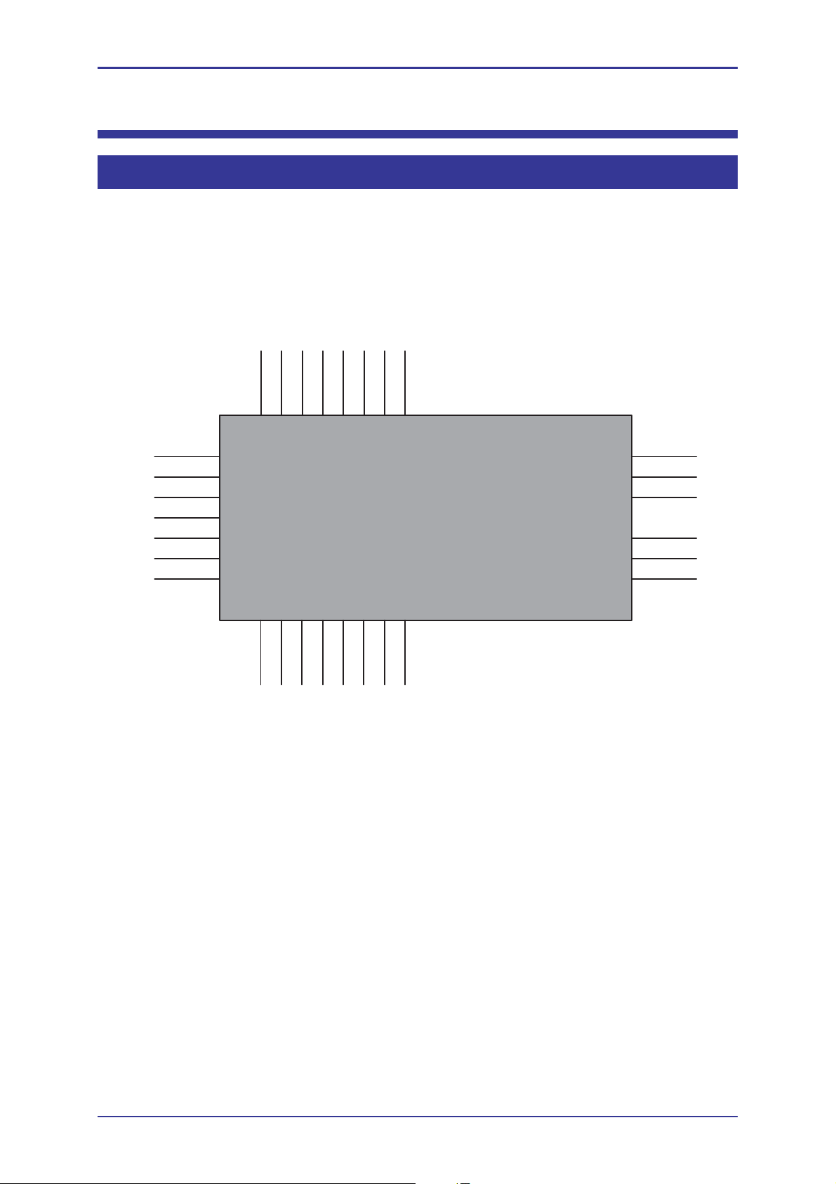
The physicals interfaces on ZBee Boost provide an access of all CC2530 I/Os. The function of each I/O is
defined below (see Figure 2). The Zbee Boost measures 12.7 x 25.4 x 3.55 mm.
III.1.1 PIN ASSIGNMENT
2324
2526272829
22
1
2
3
4
5
6
7
8
1510 11 12 13 149
21
20
19
18
17
16
Figure 2: ZBee Boost Pin assignment
ZBEE BOOST_UserMannaul CLEODE Page 9 sur 15
Page 10
ZigBee OEM Module – User manual
III.1.2 MAPPING
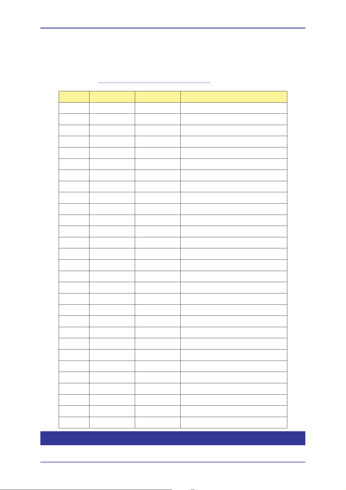
The following table lists the I/O pins description.
For a more precise description of each CC2530 I/O function see the CC2530 User Guide :
Document: Æ http://focus.ti.com/lit/ds/symlink/cc2530.pdf
Pin CC2530 Pin CC2591 Pin Description
1 GND GND Ground
2 P0_4 X I/O
3 P0_5 X I/O
4 P0_1 X I/O
5 P0_3 X I/O
6 P0_2 X I/O
7 GND GND Ground
8 P0_7 HGM I/O – LNA Gain Mode (CC2591)
9 P1_2 X I/O
10 P0_6 X I/O
11 P2_0 X I/O
12 P2_1 X I/O
13 P2_2 X I/O
14 P0_0 X I/O
15 P1_3 EN I/O – LNA Enable (CC2591)
16 GND GND Ground
17 X RF External antenna connexion
18 GND GND Ground
19 RESET_N X Reset
20 +3.3V +3.3V VDD
21 GND GND Ground
22 P2_4 X I/O – XTAL 32.768 kHz XOSC
23 P2_3 X I/O – XTAL 32.768 kHz XOSC
24 P1_7 X I/O
25 P1_6 X I/O
26 P1_5 X I/O
27 P1_4 X I/O
28 P1_1 PAEN I/O – PA Enable (CC2591)
29 P1_0 X I/O
III.2 BOARD IMPLANTATION
ZBEE BOOST_UserMannaul CLEODE Page 10 sur 15
Page 11
ZigBee OEM Module – User manual
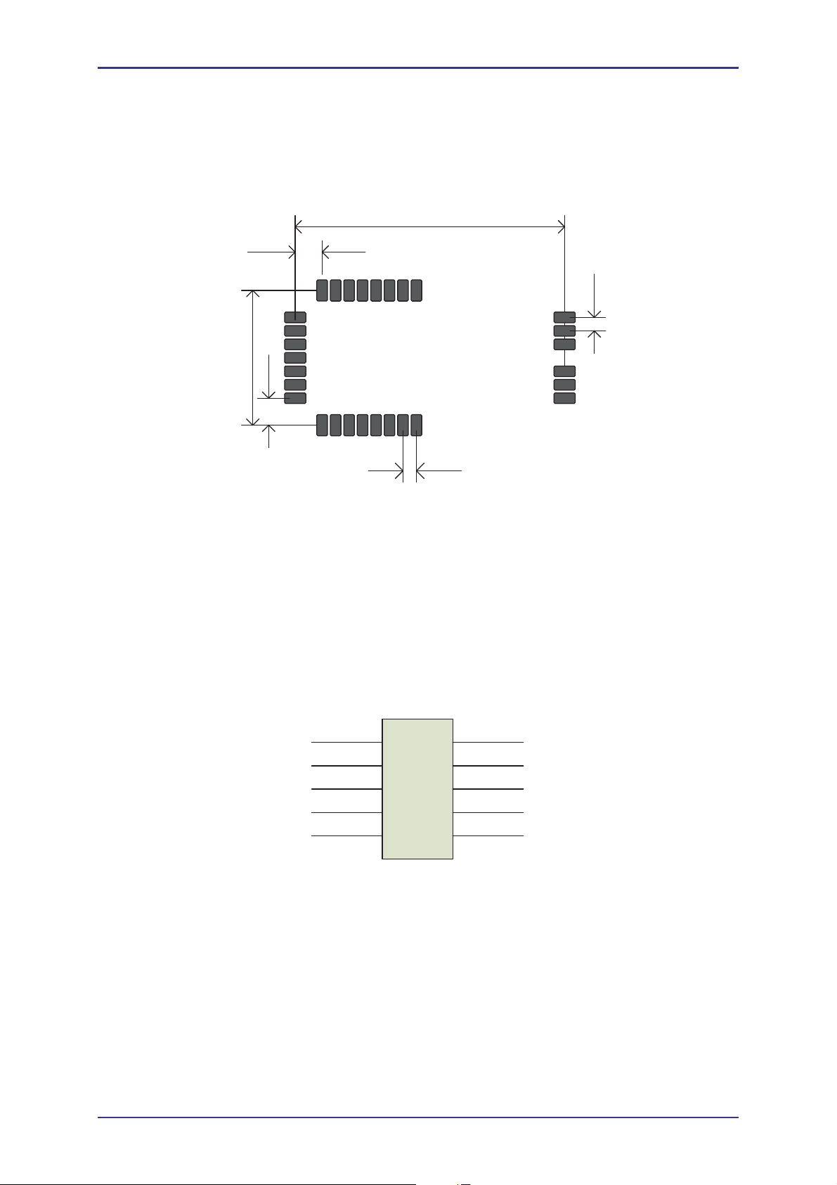
The ZBee Boost module has to be surface mounted on PCB.
III.2.1 PCB LAYOUT
Follow these following PCB layouts:
25,40
2,54
12,70
1
2,54
8
1,27
22
1,27
16
Figure 3: PCB Layout for the standard version
III.2.2 JTAG
PINOUT
The ZBee module must be connected to a debug connector to be programmed or debugged via JTAG.
This connector can be a 5x2 pins connector with a 1,27 mm pitch (example : Ref. 623310235321 from
Wurth Electronic) to use directly the CCDebugger from Texas Instrument.
The following pinout assignment shows how to connect the ZBee Boost to the CCDebugger connector:
GND
Zbee Boost (13)
NC
Zbee Boost (19)
VDD
NC : Not connected
1
3
5
7
9
CCDebugger Connector
2
4
6
8
10
VDD
Zbee Boost (12)
NC
NC
NC
Figure 4: Pinout assignment to CCDebugger connector
ZBEE BOOST_UserMannaul CLEODE Page 11 sur 15
Page 12
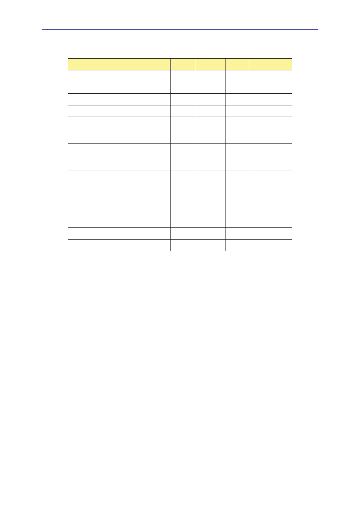
ZigBee OEM Module – User manual
Parameter Min Typ. Max Unit
Power supply 2.7 3.6 V
Frequency band MHz
24802405
Data rate 250 kbps
Current consumption
TX
Current consumption
151 mA
28 mA
RX
Sensitivity -99 dBm
Dimension
Length
Width
Height
25.4
12.7
3.5
mm
mm
mm
Storage temperature -40 85 °C
Operating temperature -20 70 °C
ZBEE BOOST_UserMannaul CLEODE Page 13 sur 15
Page 13

ZigBee OEM Module – User manual
REPAIR AND MAINTENANCE
Defective equipments shall be first reported to the CLEODE support team in order to be assigned an RMA
number. Be prepared to state your name, company and the serial number of the defective item to the
support personnel.
The item shall then be returned to CLEODE with the following documents:
The RMA number
A copy of the delivery slip
A detailed description of the default and the test context
The maintenance period is typically four (4) weeks starting from the date of reception of the equipment at
the CLEODE headquarters.
Remark
: A FAQ (Frequently Asked Questions) is available on the www.cleode.com web site.
ZBEE BOOST_UserMannaul CLEODE Page 14 sur 15
Page 14

ZigBee OEM Module – User manual
CLEODE S.A.
Technical Support Division
3, rue Thomas Edison
22300 Lannion
France
Phone: +33 (0) 2 96 48 68 18
Fax: +33 (0) 2 96 48 19 11
E-mail: [email protected]
Web: http://www.cleode.com
ZBEE BOOST_UserMannaul CLEODE Page 15 sur 15
Page 15

Compliance Information
FCC Compliance Statement:
This device complies with Part 15 of the FCC Rules. Operation is subject to the
following two conditions:
(1) This device may not cause harmful interference, and
(2) this device must accept any interference received, including interference that may
cause undesired operation.
Changes or modifications not expressly approved by the party responsible for
compliance could void the user's authority to operate the equipment.
This device must accept any interference received, including interference that may
cause undesired operation. Product that is a radio transmitter is labeled with FCC ID.
When the module is installed inside another device, the user manual of this device
must contain below warning statements;
A. This device complies with Part 15 of the FCC Rules. Operation is subject to the
following two conditions:
(1) This device may not cause harmful interference.
(2) This device must accept any interference received, including interference that may
cause undesired operation.
B. Changes or modifications not expressly approved by the party responsible for
compliance could void the user's authority to operate the equipment.
The devices must be installed and used in strict accordance with the manufacturer's
instructions as described in the user documentation that comes with the product.
FCC Caution:
(1) Exposure to Radio Frequency Radiation. This equipment must be installed and
operated in accordance with provided instructions and the antenna(s) used for this
transmitter must be installed to provide a separation distance of at least 20 cm from all
persons and must not be collocated or operating in conjunction with any other
antenna or transmitter. End-users and installers must be provided with antenna
installation instructions and transmitter operating conditions for satisfying RF
exposure compliance.
(2) Any changes or modifications not expressly approved by the grantee of this device
could void the user's authority to operate the equipment.
(3) This Transmitter must not be co-located or operating in conjunction with any other
antenna or transmitter.
(4) Changes or modifications to this unit not expressly approved by the party
responsible for compliance could void the user authority to operate the equipment.
RF exposure warning
This equipment complies with FCC radiation exposure limits set forth for an
uncontrolled environment
The equipment must not be co-located or operating in conjunction with any other
antenna or transmitter.
Page 16

Frequency Band(GHz)
Type
M/N
Gain (dBi)
2.405 ~ 2.480
Dipole
N/A
1.2
IMPORTANT NOTE: In the event that these conditions cannot be met (for example
certain laptop configurations or co-location with another transmitter), then the FCC
authorization is no longer considered valid and the FCC ID cannot be used on the
final product. In these circumstances, the OEM integrator will be responsible for
re-evaluating the end product (including the transmitter) and obtaining a separate
FCC authorization.
The antenna gain which being use as below:
(1) The modules FCC ID is not visible when installed in the host, or
(2) If the host is marketed so that end users do not have straight forward commonly
used methods for access to remove the module so that the FCC ID of the module
is visible
OEM integration instructions˖
˖
This device is intended only for OEM integrators under the following conditions˖
The transmitter module may not be co- located with any other transmit or antenna.
The antenna must be installed such that 20 cm is maintained between the antenna
The antenna must be installed such that 20 cm is maintained between the antenna
and usersˈand the transmitter module may not be co-located with any other transmit
usersˈand and
or anten The module shall be only used with the provided antenna(s) that has been
originally tested and certified with this module.
As long as 3 conditions above are metˈfurther transmitter test will not be required.
Howeverˈthe OEM integrator is still responsible for testing their end-product for any
additional compliance requirement with this module installed(for exampleˈdigital
device emissionˈPC peripheral requirementsˈetc.)
OEM integration instructions
˖
In the event that these conditions cannot be met (for example certain laptop
configuration or co-location with another transmitter), then the FCC authorization for
this module in combination with the host equipment is no longer considered valid and
the FCC ID of the module cannot be used on the final product. In these and
circumstanceˈthe OEM integrator will be responsible for re-evaluating. The end
product (including the transmitter) and obtaining a separate FCC authorization
End product labeling
This transmitter module is authorization only for use in device where the antenna may
This transmitter module is authorization only for use in device where the antenna may
be installed such that 20 cm may be maintained between the antenna and users. The
be installed such that 20 cm may be maintained between the antenna and users.
The final end product must be labeled in a visible area with the following ˖
final end product must be labeled in a visible area with the following˖
˖
“Contains Transmitter Module FCC ID: 2ACL6-ZBEEBOOST or Contains FCC ID:
2ACL6-ZBEEBOOST”
Information that must be placed in the end user manual
˖
Page 17

The OEM integrator has to be aware not to provide information to the end user
regarding how to install or remove this RF module in the user’s manual of the end
product which integrates this module. The end user manual shall include all required
regulatory information/warning as show in this manual.
 Loading...