


ZigBee Module Unit Part (ZMP)
CRC2602
OEM/Integrator
Installation Instructions
Version 1.2 (Dec. 2011)
- 1 -

Contents
1. General
specification
7.3 Packing box
dimension
3
1.1 Applications 3
1.2 Features 3
1.3 Block diagram 5
1.4 Pin assignment 7
1.5 I/O resources
2. 10
Zigbee Interface
2.1 The ZigBee protocol
2.2 Debug interface
2.3 Power management
2.4 RF frequency, output power levels and data rates
2.5 Antenna and range considerations
2.6 Antenna Specifications 13
3. Electrical specification 14
3.1 Absolute maximum ratings 14
3.2 Electrical specification 15
3.3 Environmental specification 16
4. Demensions(unit = mm) 17
5. Module label information(Option) 28
6. Recommended soldering reflow profile 19
7. Mechanical specification 20
7.1 Carrier dimension 20
9
10
10
11
11
12
7.2 Taping package/reel Dimension 21
22
- 2 -

1. General specification
The CRC2602 RF Transceiver Modem is a compact surfacemounted modules specially
designed for the ZigBee™ protocol stack for wireless star and mesh networks based on
IEEE 802.15.4 compliant PHY and MAC layers providing 16channels in the 2.45 GHz world-
wide license-free ISM band.
The complete shielded module is only 14.5mm x 17.0mm x 2.5 mm.
256 kB flash memory, 21 digital and analog I/Os, an 8 channel 12 bit ADC, timers, UART and
SPI interfaces make it possible to embed the complete application in this tiny modem. 32k,
64k, 128k flash memory options will be available.
1.1
Applications
▣ 2.4-GHz IEEE 802.15.4 Systems
▣ RF4CE Remote Control Systems
▣ ZigBee Systems
▣ Home/Building Automation
▣ Lighting Systems
▣ Industrial Control and Monitoring
▣ Low-Power Wireless Sensor Networks
▣ Consumer Electronics
▣ Health Care
1.2
Features
▣ 2.4-GHz IEEE 802.15.4 Compliant RFTransceiver
▣ Excellent Receiver Sensitivity and Robustness to Interference
▣ Programmable Output Power Up to 4.5 dBm
▣ Suitable for Systems Targeting Compliance With Worldwide Radio-Frequency
Regulations: ETSI EN 300 328 and EN 300 440 (Europe), FCC CFR47 Part 15 (US) and
ARIB STD-T-66 (Japan)
▣ 14.5 x 17.0 x 2.5 mm, compact shielded modem for SMD mounting
▣ High-Performance and Low-Power 8051 Microcontroller Core With Code Prefetch
▣ IR Generation Circuitry
▣ CSMA/CA Hardware Support
▣ Accurate Digital RSSI/LQI Support
▣ 256 kB flash memory, 8 kB SRAM
▣ 17 digital and analog I/Os, 8 channel 12 bit ADC
▣ High performance direct sequence spread spectrum (DSSS) RF transceiver
▣ 16 channels in the 2.45 GHz ISM band
▣ Industrial operating temperature range –30 to 85°C
- 3 -

▣ Two Powerful USARTs With Support for Several Serial Protocols
▣ Watchdog Timer
▣ Operating voltage 2.7 ~ 3.6V
▣ Compact size
- Size 14.5±0.3mm x 17.0±0.3mm
- Height 2.5±0.3mm
- Weight 1.2±0.5grams
▣ RoHS compliant
- 4 -
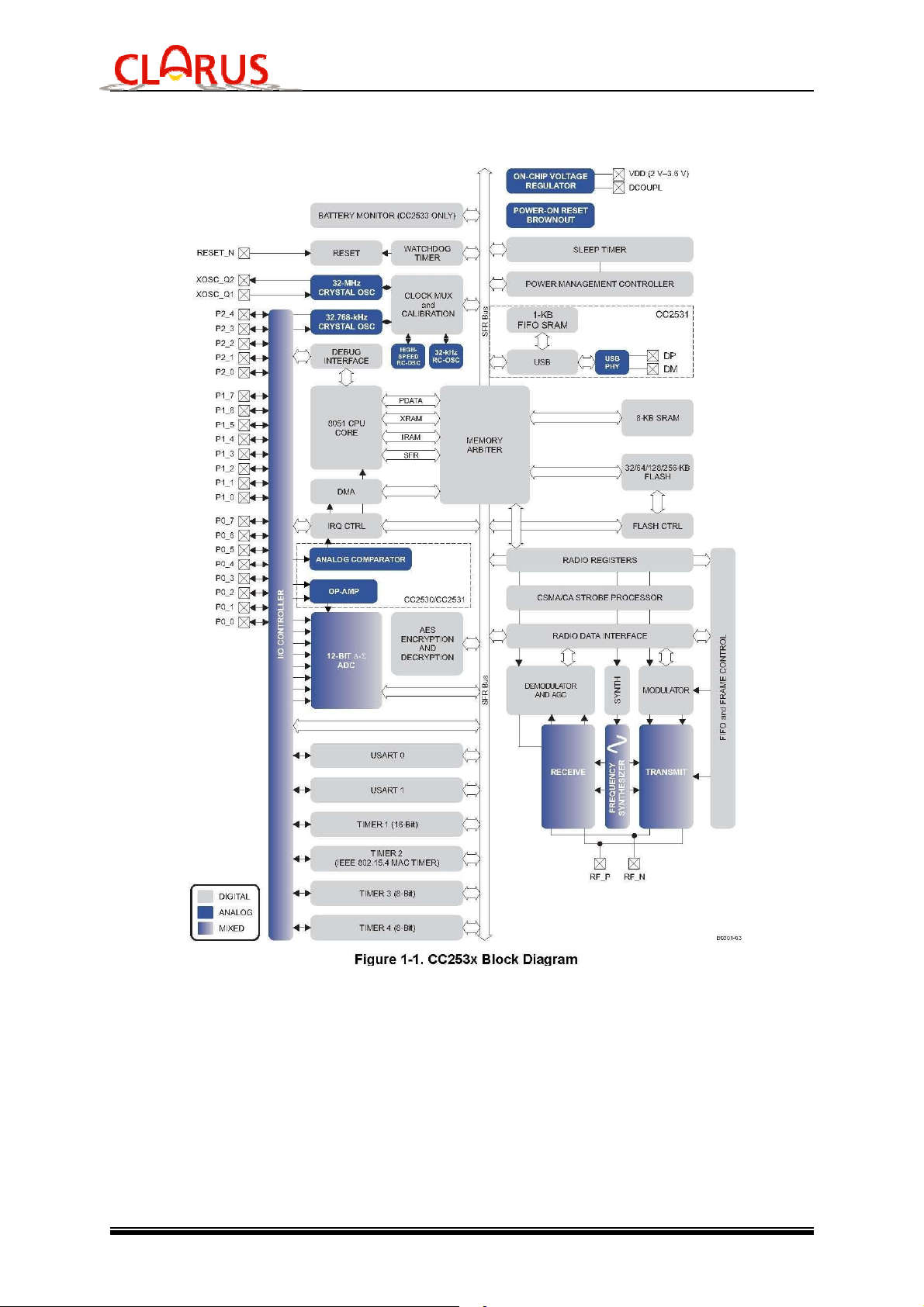
1.3
Block diagram
Circuit description
The modem contains an IEEE 802.15.4 compliant SoC RF transceiver, external Reset, high
speed oscillator and an RTC 32 kHz oscillator. The modem is intended for running the
ZigBee network protocol.
The application software together with the ZigBee protocol software stack can be
programmed in Flash memory through a proprietary serial debugging interface. The easiest
way to do this is by using an evaluation board from TI and an IAR Embedded workbench.
The module includes two USART that are configurable as either SPI or UART. Totally 21 I/O
- 5 -

pins are available to the user. 8 pins can be used for the internal 8-12 bit A/D converter. All of
the pins have interrupt features.
The MCU provides several low power modes with can be utilized to reduce the current
consumption in battery operated applications. An internal 32 kHz crystal oscillator can be
used for real-time clock and timer applications.
For further details on the SoC transceiver (TI, CC2530), please consult the respective data
sheet.
- 6 -
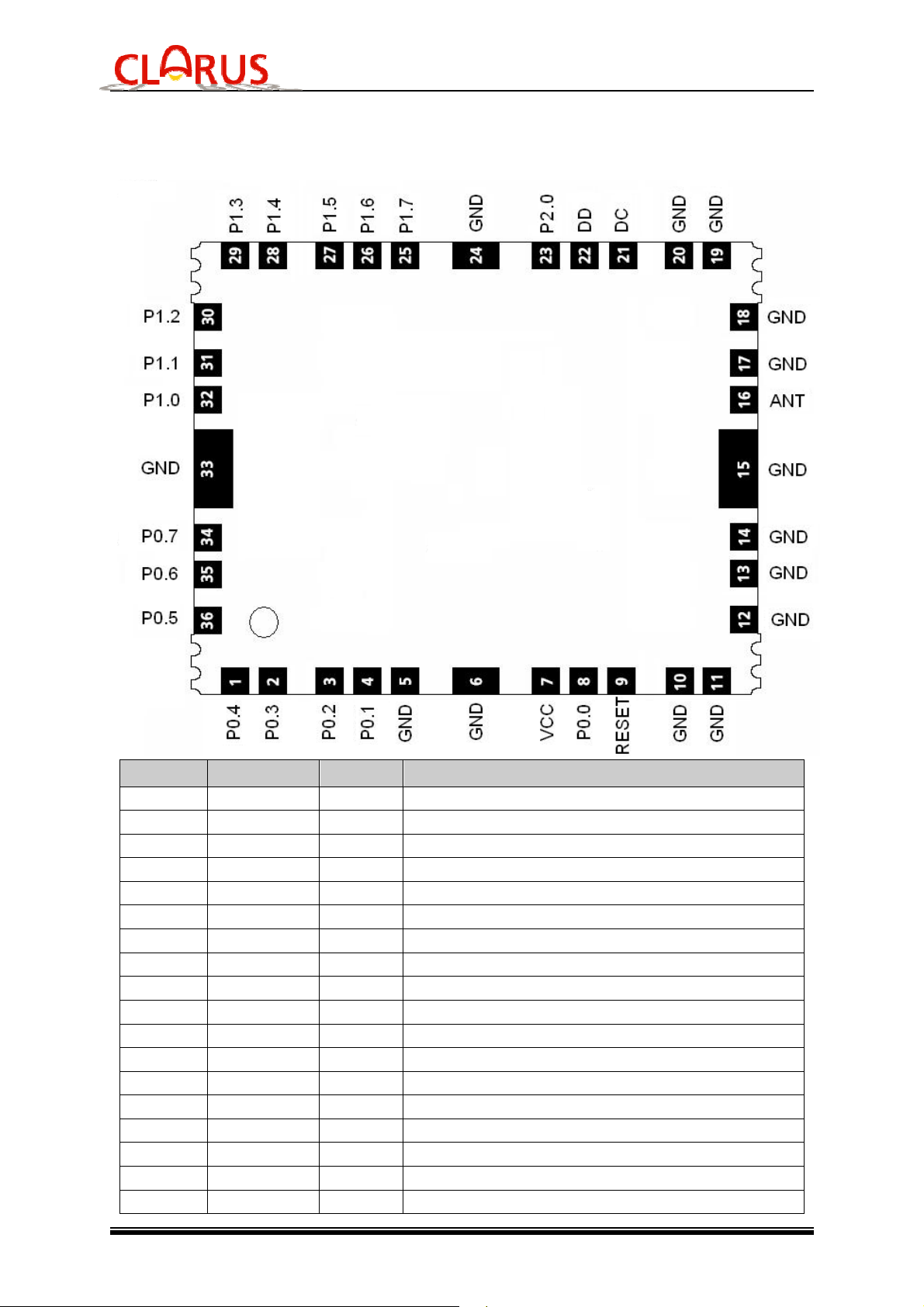
1.4
Pin assignment
Pin
Name
1
P0.4
2
P0.3
3
P0.2
4
P0.1
5
GND
6
GND
7
VCC
8
P0.0
9
RESET
10
GND
11 GND
12
GND System ground
13
GND
14
GND
15
GND
16
ANT
17
GND
18
GND
I/O
Description
I/O
Digital I/O, P0.4
I/O
Digital I/O, P0.3
I/O
Digital I/O, P0.2
I/O
Digital I/O, P0.1
-
System ground
-
System ground
-
Supply voltage input.(2.7 ~ 3.6V, typically 3.3V)
I/O
Digital I/O, P0.0
-
Reset output with internal pullup
-
System ground
-
System ground
-
System ground
-
System ground
-
System ground
I/O
RF I/O connection to antenna, 50 Ohm
-
System ground
-
System ground
- 7 -
19
20
21
22
23 P2.0
24
25
26 P1.6
27 P1.5
28 P1.4
29 P1.3
30 P1.2
GND
GND
DC
DD
GND
P1.7
-
System ground
-
System ground
I/O
Debug Clock, P2.2
I/O
Debug Data, P2.1
I/O
Digital I/O, P2.0
-
System ground
I/O
Digital I/O, P1.7
I/O
Digital I/O, P1.6
I/O
Digital I/O, P1.5
I/O
Digital I/O, P1.4
I/O
Digital I/O, P1.3
I/O
Digital I/O, P1.2
31 P1.1
32 P1.0
33
34 P0.7
35 P0.6
36 P0.5
GND
I/O
Digital I/O, P1.1, 20 mA sink/source capability
I/O
Digital I/O, P1.0, 20 mA sink/source capability
-
System ground
I/O
Digital I/O, P0.7
I/O
Digital I/O, P0.6
I/O
Digital I/O, P0.5
- 8 -

1.5
T
Operational
Analog
USART 0
SPI
MO MI C SS
USART
0
TX RX RT CT
USART 1
SPI
MI MO C SS MI MO C SS
USART
1
RX TX RT CT RX TX RT CT
TIMER
1
4 3 2 1 0
0 1 2
TIMER
3
1 0
1 0 TIMER
4
1 0 1 0
I/O resources
Periphery
/function
ADC A7 A6 A5 A4 A3 A2 A1 A0
Amplifier
Comparator
Alt. 2
UART
Alt. 2
Alt. 2
UART
Alt. 2
Alt. 2
Alt. 2
Alt. 2
32-kHz XOSC Q1 Q2
DEBUG DC DD
OBSSEL
7 6 5 4 3 2 1 0 7 6 5 4 3 2 1 0 4 3 2 1 0
3 4
P0 P1 P2
O – +
+ –
C SS MO MI
RT CT TX RX
5 4 3 2 1 0
- 9 -

2. ZigBee interface
2.1.
The ZigBee Alliance is an association of companies working together to enable reliable,
costeffective,
low-power, wirelessly networked, monitoring and control products based on an open global
standard. The ZigBee Alliance is a rapidly growing, non-profit industry consortium of leading
semiconductor manufacturers, technology providers, OEMs and end-users worldwide.
Membership is open to all. The ZigBee Alliance, in collaboration with the IEEE, is defining the
network, security, and application layers above the IEEE 802.15.4 PHY and MAC layers.
This cooperation has resulted in an easy-to-use, standards-based wireless network platform
optimized for wireless monitoring and control applications. For more information about the
ZigBee Alliance and the ZigBee standard, please consult www.zigbee.org
The module is intended for using the ZigBee protocol. However, other proprietary network
protocols can also be implemented using the module.
The ZigBee stack implementation from TI/Chipcon/Figure 8 Wireless is recommended as it
provides seamless integration with the module. However, third party stack implementations
can also be used provided they support the TI/Chipcon MAC firmware.
The ZigBee protocol
2.2.
The modem has a two-wire proprietary debug interface. This interface can also be used for
incircuit programming of the device.
For debugging the device programmer sends command <DEBUGGING_INSTR> to the
icrocontroller. The instructions succeeding the debugging commando are executed by the
CPU without updating the program counter.
For in circuit programming the same debugging command is used, only the instruction
preformed is flash programming with through the flash controller.
Supply and ground must also be connected during programming or debugging.
Pin 21 and 22 can be used as normal digital I/O pins when the module is not in debugging
mode.
Debugging interface
Pin Description
21
22
P2.2, Debug Clock
P2.1, Debug Data
- 10 -

2.3.
The ZigBee protocol allows End Devices to be powered down, while Routers must be
powered all the time in order to handle packet routing. Battery operated devices should be
End Devices in order to reduce the power consumption to a minimum.
The modem can be set in several sleep modes using the features of the MCU and turning off
the RF transceiver. Sleep modes enable the application to shut down unused segments in
the MCU, thereby saving power. The MCU provides various sleep modes allowing the user
to tailor the power consumption to the application’s requirements.
To enter any of the 3 sleep modes (power modes 1-3) available in the modem, the
appropriate registers in CC2530 must be set. See datasheet for CC2530 for details.
The different power modes available are:
Power mode 1 – Digital regulator on; 16-MHz RCOSC and 32-MHz crystal oscillator off;
32.768-kHz XOSC, POR, BOD and sleep timer active; RAM and register retention.
Power mode 2 – Digital regulator off; 16-MHz RCOSC and 32-MHz crystal oscillator off; 1 2
μA 32.768-kHz XOSC, POR, and sleep timer active; RAM and register retention.
Power mode 3 – Digital regulator off; no clocks; POR active; RAM and register retention.
Power management
2.4.
RF frequency, output power levels and data rates
The following table shows the RF channels as defined by the IEEE 802.15.4 standard.
RF channel Frequency
11 2405MHz
12 2410MHz
13 2415MHz
14 2420MHz
15 2425MHz
16 2430MHz
17 2435MHz
18 2440MHz
19 2445MHz
20 2450MHz
21 2455MHz
22 2460MHz
23 2465MHz
24 2470MHz
25 2475MHz
26 2480MHz
For proprietary solutions (non-IEEE 802.15.4), the RF transceiver can be programmed in
steps of 1 MHz.
The output power level can be configured from the firmware in the range about -22 to 4.5
dBm.
- 11 -

The RF transceiver uses direct sequence spread spectrum (DSSS) with 2 Mchip/s chip rate,
giving a raw data rate of 250Kbit/s. The modulation format is Offset – Quadrature Phase Shift
Keying (O-QPSK). The DSSS makes the communication link robust in noisy environments
when sharing the same frequency band with other applications.
The use of RF frequencies and maximum allowed RF power is limited by national regulations.
The modem is complying with the applicable regulations for the world wide 2.45 GHz ISM
band.
Specifically it complies with the European Union R&TTE directive meeting EN 300 328 and
EN300 440 class 2. It also meets the FCC CFR47 Part15 regulations for use in the US and
the ARIB T-66 for use in Japan.
2.5.
Antenna and range considerations
This modem is a very compact solution containing all the critical RF parts within the modem.
However, a somewhat better range can be achieved using an external antenna.
Range testing using the external antenna shows these typical distances:
- Compact size with a ceramic antenna working as a quarter-wave resonant antenna
- Good performance with ¼ wave monopole antenna on ground plane
- High performance with with 5/8 wave dipole antenna
Due to the dielectric ceramic material the antenna is shorter than a normal quarter wave
antenna (in air), still providing high radiation efficiency (typical 1 dBi). The antenna is
matched for use in the 2.45 GHz band. The radiating part of the antenna is the white ceramic
component located outside the shield can. The radiation pattern from the antenna is similar
to the donut-shaped radiation from a quarter wave antenna. That is, the maximum radiation
is in the plane normal to the length axis of the antenna. For best possible omni-directional
radiation the module should be oriented so that the antenna is vertical. To achieve the very
best range the transmitting and receiving antenna should be oriented the same way,
ensuring the same polarity at both devices. However, indoors reflections of the radio waves
in metallic structures tend to spread the polarisation, so even if same orientation is not
possible, communication will still take place, but the range is somewhat shorter, typically by
20%.
The antenna should be kept away (> 10mm) from metallic or other conductive and dielectric
materials, and should never be used inside a metallic enclosure.
Compared to lower frequencies, operation at 2.45 GHz is more limited to LOS. Reflections
from walls and other objects may give multi-path fading resulting in dead-zones. The ZigBee
mesh network topology is used to overcome this fading as it allows for alternative routing
paths. The mesh network is therefore highly recommended for increased reliability and
extended coverage throughout buildings.
In applications where the module must be placed in a metallic enclosure, an external
- 12 -

antenna must be used. The RF available at a module pin must be fed to external antenna.
The RF input/output is matched to 50 Ohm. If the antenna or antenna connector is placed
away from the module at the motherboard, the track between the RF pin and the connector
should be a 50 Ohm transmission line.
On a two layer board made of FR4 the width of a microstrip transmission line should be 1.8
times the thickness of the board, assuming a dielectric constant of 4.8. The line should be
run at the top of the board, and the bottom side should be a ground plane.
Example: For a 1.6 mm thick FR4 board, the width of the trace on the top side should be 1.8
x 1.6 mm = 2.88 mm.
The simplest antenna to use is the quarter wave whip antenna. A quarter wave whip antenna
above a ground plane yields 37 Ohm impedance and a matching circuit for 50 Ohm are
usually not required.
A PCB antenna can be made as a copper track where the ground plane is removed on the
back side. The rest of the PCB board should have a ground plane as large as possible,
preferably as large (in one dimension) as the antenna itself, to make it act as a counterweight
to the antenna. A quarter wavelength antenna on a PCB must be shorter than the wire
antenna due to the influence of the dielectric material of the PCB. The length reduction
depends on the PCB thickness and material, as well as how close to the edge of the board
the antenna is placed. Typical reduction is to 75-90 % but must be found empirically.
The length of a quarter-wave antenna is given in the table below.
Frequency{MHz}
2450
Length of whip antenna[cm] Length of PCB track[cm]
2.9 2.25 ~ 2.7
If, for space reasons, the track is made even shorter than the resonating quarter of a
wavelength, the antenna should be matched to 50 ohms using a series inductor and a shunt
capacitor.
2.6. Antenna Specifications
- Chip Antenna
- Gain: 3.5 dBi
- Model Number: ALA931C5
- Manufacture: AMOTECH
Peak Gain
(dBi)
Avg. Gain
(dBi)
Total Avg. Gain
(dBi)
Efficiency
(%)
Azimuth
Elevation 1
Elevation 2
2.8 1.0
3.5 -0.7
1.7 -1.6
-0.22 95
- 13 -

3. Electrical specification
3.1
Absolute maximum ratings
Parameter Min Max Units
Supply voltage, VCC - 0.3 3.9 V
Voltage on any digital pin - 0.3 VCC+0.3 V V
RF output Power 4.5 dBm
Storage temperature -40 125
Operating temperature - 40 125
Stresses beyond those listed under Absolute Maximum Ratings may cause permanent damage to the device.
These are stress ratings only, and functional operation of the device at these or any other conditions beyond
those indicated under Recommended Operating Conditions is not implied. Exposure to absolute-maximum-rated
conditions for extended periods may affect device reliability.
℃
℃
- 14 -

3.2
fc= 2480
MHz
Electrical Specifications
Parameter
Operating frequency
Number of channels
Channel spacing
Input/output impedance 50 Ohm
Data rate 250 kbit/s
DSSS chip rate
Frequency stability
Transmit power
Spurious emission, TX
Max recommended output
power setting
25 MHz–1000 MHz
(outside restricted bands)
25 MHz–2400 MHz
(within FCC restricted bands)
25 MHz–1000 MHz
(within ETSI restricted bands)
1800–1900 MHz
(ETSI restricted band)
5150–5300 MHz
(ETSI restricted band)
At 2 × fc and 3 × fc
(FCC restricted band)
At 2 × fc and 3 × fc
(ETSI EN 300-440 and EN 300-
328)
1 GHz–12.75 GHz
(outside restricted bands)
At 2483.5 MHz and above
Min Typ Max Units
2394
16
5 MHz
2 Mc/s
-40 40 ppm
-22 4.5 dBm
-60
-60
-60
-57
-55
-42
-31
-53
2507
MHz
dBm
Notes
Programmable in 1-MHz steps, 5 MHz between
channels for compliance with [1]
For IEEE 802.15.4 compliance
For IEEE 802.15.4 compliance
Programmable from firmware
Complies with EN 300 328, EN 300 440, FCC
CRF47 Part 15 and ARIB STD-T66
(FCC restricted band)
Error Vector Magnitude 2
Sensitivity -97
Adjacent channel rejection
+/- 5 MHz
Alternate channel selectivity
+/- 10 MHz
Blocking / Interferer rejection /
desensitization
+/- 5 MHz
+/- 10 MHz
+/- 20 MHz
+/- 50 MHz
-42
49/49
57/57
-33/-35
-33/-35
-32/-34
-31/-34
%
dBm
dB
dB
dBm
PER = 1%, as specified by [1]
[1] requires –85 dBm
Wanted signal –82 dBm, adjacent modulated channel
at 5 MHz, PER = 1 %, as specified by [1]. [1] requires
0 dB.
Wanted signal –82 dBm, adjacent modulated channel
at 10 MHz, PER = 1%, as specified by [1]. [1] requires
30 dB
Wanted signal 3 dB above the sensitivity level, CW
jammer, PER = 1%. Measured according to EN 300
440 class 2.
- 15 -

Parameter Min Typ Max Units
Saturation 10 dBm
Spurious emission, RX
30 – 1000 MHz
1-12.75 GHz
Supply voltage 2.7
32-MHz
XOSC
running, radio
Core current
consumption
Flash memory 32 kB
RAM memory 8 kB
MCU clock frequency 32 MHz
MCU low frequency crystal 32.768
in RX mode
32-MHz
XOSC
running, radio
in TX mode
Power mode
1.
Power mode
2.
Power mode
3.
3.3 3.6 V
3.4 mA
6.5 8.9 mA
20.5 mA –50-dBm input power, no peripherals active, CPU idle
24.3 29.6 mA
28.7 mA 1-dBm output power, no peripherals active, CPU idle
33.5 39.6 mA 4.5-dBm output power, no peripherals active, CPU idle
0.2 0.3 mA
1 2 μA
0.4 1 μA
-80
-57
dBm
kHz
Notes
Conducted measurement with a 50-Ω single-ended
load. Suitable for systems targeting compliance with
EN 300 328, EN 300 440, FCC CFR47 Part 15 and
ARIB STD-T-66.
Digital regulator on. 16-MHz RCOSC running. No
radio, crystals, or peripherals active.
Medium CPU activity: normal flash access(1), no RAM
access
32-MHz XOSC running. No radio or peripherals active.
Medium CPU activity: normal flash access(1), no RAM
access
-100-dBm input power (waiting for signal), no
peripherals active, CPU idle
Digital regulator on; 16-MHz RCOSC and 32-MHz
crystal oscillator off; 32.768-kHz XOSC, POR, BOD
and sleep timer active; RAM and register retention
Digital regulator off; 16-MHz RCOSC and 32-MHz
crystal oscillator off; 32.768-kHz XOSC, POR, and
sleep timer active; RAM and register retention
Digital regulator off; no clocks; POR active; RAM and
register retention
3.3
Environmental specification
Test Standard
Visual inspection -
Thermal shock KS C 0225 and IEC 68-2-14
Function at various temperature KS C 0220/0221 and IEC 68-2-1/2
Damp heat KS C 0225 and IEC 68-2-30
Vibration KS C 0240 and IEC 68-2-6
Metallographic investigations IPC-QE-650
- 16 -

4. Demensions (unit = mm)
- 17 -

5. Module label information (Option)
2
MODEL: CRC2602
3
1
4
FCC ID: 2AE73-CRC2602
IC: 20386-CRC2602
No. Index
1 Pin number index
2 Manufacturer’s model name
3 Manufactured year,serial number
4
FCC ID, IC Certification
- 18 -

6. Recommended soldering reflow profile
Consider for a long time in the soldering zone (with temperature higher than 180 °C)
has to
be kept as short as possible to prevent component and substrate damages. Peak
temperature
must not exceed 250 °C. (
according to IPC/JEDEC J-STD-020C)
- 19 -

7. Mechanical specification
7.1
Carrier dimension
- 20 -

7.2
Taping package/reel dimension
- 21 -

7.3
Packing box dimension
- 22 -

FCC Statement
FCC Part 15.19
This device complies with part 15 of the FCC Rules. Operation is subject to the following two
conditions: (1) This device may not cause harmful interference, and (2) this device must
accept any interference received, including interference that may cause undesired operation.
FCC Part 15.21
Any changes or modifications (including the antennas) to this device that are not expressly
approved by the manufacturer may void the user’s authority to operate the equipment.
FCC RF Radiation Exposure Statement
This equipment complies with FCC RF Radiation exposure limits set forth for an uncontrolled
environment. This device and its antenna must not be co-located or operating in conjunction
with any other antenna or transmitter.
This equipment should be installed and operated with a minimum distance of 20 centimeters
between the radiator and your body.
FCC Compliance Requirements with KDB996369
- 23 -

Information for OEM integrator
i. “Module is limited to OEM installation ONLY “
ii. “OEM integrators is responsible for ensuring that the end-user has no manual
instructions to remove or install module”
iii. “FCC RF Exposure requirements: Module is limited to installation in mobile or fixed
applications, according to Part 2.1091(b). Separate FCC approval is required for all other
operating configurations, including portable configurations with respect to Part 2.1093 and
different antenna configurations.”
iv. “If (1) the module’s FCC ID is not visible when installed in the host, or (2) if the host is
marketed so that end users do not have straightforward commonly used methods for access
to remove the module so that the FCC ID of the module is visible; then an additional
permanent label referring to the enclosed module: “Contains Transmitter Module FCC ID:
2AE73-CRC2602” or “Contains FCC ID: 2AE73-CRC2602” must be used. The host OEM user
manual must also contain clear instructions on how end users can find and/or access the
module and the FCC ID.”
v. “A host product is required to comply with all applicable FCC equipment authorizations
regulations, requirements and equipment functions not associated with the transmitter module
portion. For example, compliance must be demonstrated to regulations for other transmitter
components within the host product; to requirements for unintentional radiators (Part 15B),
such as digital devices, computer peripherals, radio receivers, etc.; and to additional
authorization requirements for the non-transmitter functions on the transmitter module (i.e.,
Verification, or Declaration of Conformity) (e.g., Bluetooth and WiFi transmitter modules may
also contain digital logic functions) as appropriate.
vi. To ensure compliance with all non-transmitter functions the host manufacturer is
responsible for ensuring compliance with the module(s) installed and is fully operational. For
example, if a host was previously authorized as an unintentional radiator under the
Declaration of Conformity procedure without a transmitter certified module and a module is
added, the host manufacturer is responsible for ensuring that after the module is installed and
operational the host continues to be compliant with the Part 15B unintentional radiator
requirements. Since this may depend on the details of how the module is integrated with the
host, the grantee (the party responsible for the module grant) shall provide guidance to the
host manufacturer for compliance with the Part 15B requirements.”
- 24 -

IC Statement
This device complies with Industry Canada’s licence-exempt RSSs. Operation is subject to
the following two conditions:
(1) This device may not cause interference; and
(2) This device must accept any interference, including interference that may cause
undesired operation of the device.
Le présent appareil est conforme aux CNR d'Industrie Canada applicables aux appareils
radio exempts de licence. L'exploitation est autorisée aux deux conditions suivantes : (1)
l'appareil ne doit pas produire de brouillage, et (2) l'utilisateur de l'appareil doit accepter tout
brouillage radioélectrique subi, même si le brouillage est susceptible d'en compromettre le
fonctionnement.
RSS-Gen section 8.3
This radio transmitter (identify the device by certification number or model number if
Category II) has been approved by Industry Canada to operate with the antenna types listed
below with the maximum permissible gain indicated. Antenna types not included in this list,
having a gain greater than the maximum gain indicated for that type, are strictly prohibited
for use with this device.
Le présent émetteur radio (identifier le dispositif par son numéro de certification ou son
numéro de modèle s'il fait partie du matériel de catégorie II) a été approuvé par Industrie
Canada pour fonctionner avec les types d'antenne énumérés ci dessous et ayant un gain
admissible maximal. Les types d'antenne non inclus dans cette liste, et dont le gain est
supérieur au gain maximal indiqué, sont strictement interdits pour l'exploitation de
l'émetteur.
- 24 -
 Loading...