

Page 1

- 1 -
PH-2416I
Published by Service Dept.
Printed in Japan
Clarion Co., Ltd.
5-35-2, Hakusan, Bunkyouku, Tokyo, 112-8608 Japan
Service Dept.- 50 kamitoda,Toda-shi,Saitama,335-8511 Japan Tel: 048-443-1111 FAX:048-433-6996
298-5935-00
Oct.2001 P
Service Manual
Model
HONDA Automobile Genuine
AM/FM Radio CD Stereo
PH-2416I
※ Prevent damage caused by static electricity when re-
pairing the pick-up.
The pattern of the pick-up is short-circuiting for prevention.
Remove the soldering with a solder iron whose insulation resistance is larger than 10M
Ω(DC500V) after com-
plete connection to the main PWB
For repair table shall use copper or conductive sheet
(with impedance is lower to 100M
Ω from 1MΩ)such as
a sheet.
Be sure to put on a wrist-strap for prevent electric
static's.(with impedance is to 100M
Ω from 1MΩ) The
strap works to drain away the static electricity build-up
on the human body.
And as static electricity build-up on clothes is not drained
away, be careful and not your clothes to touch the pickup.
Position of short soldering for pick-up protection position is different by model.
Some units have two short soldering points.
Always short LD circuit to open the short circuit and removes by soldering iron.
■COMPONENTS
PH-2416I-A
Main unit −−−−− 1
CATS CARD 287-1681-03 1
Label 290-7868-02 1
■SPECIFICATIONS
Radio setion
Receive range: FM 87.75 & 87.9 to 107.9MHz
(200kHz step)
AM 530 to 1,710Hz(10kHz step)
Intermediate frequency:
FM 10.7
±0.2MHz
AM 450
±3kHz
Quieting sensitivity: FM Less than 12dB
μ
(at 30dB S/N)
AM Less than 35dB
μ
(at 20dB S/N)
Auto tuning stop sensitivity:
FM 24
±6dBμ
AM 35±6dBμ
CD section
System: Compact disc audio system
Usable Discs: Compact disc
Signal to Noise Ratio: More then 60dB
Separation: More then 55dB
General
Load impedance: 4Ω
Output power: More then 30W×2
Power supply voltage: DC13.2V(10.8 to 15.6V)
Negative ground
Dimensions(mm): 187.5(W)
×60(H)×160(D)
Weight: 1.65kg
■NOTE
※ Specification and design are subject to change without
notice for further improvement.
※ We cannot supply PWB with component parts in prin-
ciple. When a circuit on PWB has failure, please repair
it by component parts base. Parts which are not mentioned in service manual are not supplied.
(Genuine No.39100-S6M-A000)
(ID No.4XJ0)
■ To engineers in charge of repair or
inspection of our products.
Before repair or inspection, make sure to follow
the instructions so that customers and Engineers
in charge of repair or inspection can avoid suffering any risk or injury.
2005.05.25
Page 2

- 2 -PH-2416I
■COMPUTER ANTI-THEFT SYSTEM
This unit has a built-in Computer Anti-Theft System(CATS)
which makes the radio inoperative if power to the unit is
interrupted for any reason whatsoever(including disconnection and reconnection of the car battery). The radio will remain inoperative unless you enter the correct CATS number.
RELEASE the CATS
1. Turn on the power switch, "COdE" appear on the display.
2. Enter the code number of five figures using the preset
buttons.
3. If the entered code number is correct, make a beep sound
(about 1 second) and radio operating.
4. If the entered code number is incorrect, "Err1" appear
on the display for 1 secound and make a beep sound. It
repeats three times.
5. To enter the code number again, "COdE" reappears after 1 second on the display. Enter the correct code number.
6. If you enter an incorrect code number ten times in succession, "ErrE" appear on the display.
7. The system will not accept another code input for one
hour. If at the end of that hour make a beep sound (about
1 second) and you enter an incorrect code number again,
you will have to wait another hour to try once more and
so on.
■ADJUSTMENT
Clock accuracy
Item Procedure
Measuring
instrument
1. Turn on the ACC switch.
2. Set a universal timer to TP101(T-BASE), adjust TC102 so that a reading of the
meter is 0 to 1.0 sec./day.
Chronometer
1. Use specified parts.
The system uses parts with special safety features against
fire and voltage. Use only parts with equivalent characteristics when replacing them.
The use of unspecified parts shall be regarded as remodeling for which we shall not be liable. The onus of
product liability (PL) shall not be our responsibility in cases
where an accident or failure is as a result of unspecified
parts being used.
2. Place the parts and wiring back in their original positions
after replacement or re-wiring.
For proper circuit construction, use of insulation tubes,
bonding, gaps to PWB, etc, is involved. The wiring connection and routing to the PWB are specially planned
using clamps to keep away from heated and high voltage
parts. Ensure that they are placed back in their original
positions after repair or inspection.
If extended damage is caused due to negligence during
repair, the legal responsibility shall be with the repairing
company.
3. Check for safety after repair.
Check that the screws, parts and wires are put back securely in their original position after repair. Ensure for
safety reasons there is no possibility of secondary
ploblems around the repaired spots.
If extended damage is caused due to negligence of repair, the legal responsibility shall be with the repairing
company.
4. Caution in removal and making wiring connection to the
parts for the automobile.
Disconnect the battery terminal after turning the ignition
key off. If wrong wiring connections are made with the
battery connected, a short circuit and/or fire may occur.
If extensive damage is caused due to negligence of repair, the legal responsibility shall be with the repairing
company.
5. Cautions regarding chips.
Do not reuse removed chips even when no abnormality
is observed in their appearance. Always replace them
with new ones. (The chip parts include resistors, capacitors, diodes, transistors, etc). The negative pole of tantalum capacitors is highly susceptible to heat, so use special care when replacing them and check the operation
afterwards.
6. Cautions in handling flexible PWB
Before working with a soldering iron, make sure that the
iron tip temperature is around 270
℃. Take care not to
apply the iron tip repeatedly(more than three times)to the
same patterns. Also take care not to apply the tip with
force.
7. Turn the unit OFF during disassembly and parts replacement. Recheck all work before you apply power to the
unit.
8. Cautions in checking that the optical pickup lights up.
The laser is focused on the disc reflection surface through
the lens of the optical pickup. When checking that the
laser optical diode lights up, keep your eyes more than
30cms away from the lens. Prolonged viewing of the laser within 30cms may damage your eyesight.
9. Cautions in handling the optical pickup
The laser diode of the optical pickup can be damaged by
electrostatic charge caused by your clothes and body.
Make sure to avoid electrostatic charges on your clothes
or body, or discharge static electricity before handling the
optical pickup.
9-1. Laser diode
The laser diode terminals are shorted for transportation in order to prevent electrostatic damage.
After replacement, open the shorted circuit. When
removing the pickup from the mechanism, short
the terminals by soldering them to prevent this
damage.
9-2. Actuator
The actuator has a powerful magnetic circuit. If a
magnetic material is put close to it. Its characteristics will change. Ensure that no foreign substances enter through the ventilation slots in the
cover.
9-3. Cleaning the lens
Dust on the optical lens affects performance. To
clean the lens, apply a small amount of isopropyl
alcohol to lens paper and wipe the lens gently.
Page 3

- 3 -
PH-2416I
■EXPLANATION OF IC
052-3154-11 M30622MA-F08GP Radio CD system controller
1.Terminal Description
pin 1: REM +5V : O : REM5V Power supply ON signal output.
pin 2: CD +8V : O : Power supply ON signal output for the
Loading motor and the Photo sensors.
pin 3: CD +5V : O : Power supply control signal output for the
CD DSP. "H"= ON.
pin 4: NU : - : Not in use.
pin 5: TIME BASE : IN : Time base signal input.
pin 6: BYTE : IN : Input "L" .
pin 7: CN VSS : IN : Input "L" .
pin 8: NU : - : Not in use.
pin 9: NU : - : Not in use.
pin 10: RESET_ : IN : Reset signal input. Negative logic.
pin 11: X OUT : O : Crystal connection.
pin 12: VSS : - : Negative supply voltage.
pin 13: X IN : IN : Crystal connection. Ceramic resonator con-
nection.
pin 14: VCC : - : Positive supply voltage.
pin 15: NU : - : Not in use.
pin 16: SBSY_ :IN : Sub Q data input from CD.
pin 17: ACC DET_ : IN: ACC detection terminal. "L"= ACC ON.
pin 18: B/U DET_ : IN : Backup voltage ON signal input. "L"= Back-
up ON.
pin 19: H bus In/Rx int : IN : H bus data input, and IE-bus start bit de-
tection signal input.
pin 20: NAVI INT L_ : O : Front Left Navi audio signal ON. Negative
logic.
pin 21: NAVI INT R_ : O : Front Right Navi audio signal ON. Negative
logic.
pin 22: MUTE F/L : O : Audio mute signal output to "Front Left".
pin 23: MUTE F/R : O : Audio mute signal output to "Front Right".
pin 24: MUTE REAR : O : Audio mute signal output to "Rear".
pin 25: MUTE AMP : O : Amplifier Mute signal output.
pin 26: BEEP : O : Beep out(3.0kHz).
pin 27: RX_ : IN : GA-NET RX terminal.
pin 28: HB O/GA TX : O : H bus data output, and GA-NET TX.
pin 29: F-ROM/T TXD : O : With testing box, TX terminal.
pin 30: F-ROM/T RXD : IN : With testing box, RX terminal.
pin 31: F-ROM K/T Req : IN
:
With testing box, REQ input.
pin 32: F-ROM BUSY : O : Fixed to the low level in the normal condi-
tion.
pin 33: E VOL DO : O : Serial data output to the volume IC.
pin 34: NAVI MUTE_ : IN : NAVI mute signal input. Negative logic.
pin 35: E VOL CLK : O : Clock pulse output to the E VOL IC.
pin 36: E VOL CE : O : Chip enable signal output to the E VOL IC.
pin 37: SYS ACC ON : O : System ACC ON signal output.
pin 38: Power IC Diag : IN : Power IC diagnosis signal input.
pin 39: F ROM EPM_ : O : Fixed to the low level in the normal condi-
tion.
pin 40 : TEST : IN: Test key signal input.
pin 41: EJECT :IN : Eject key input. Negative logic.
pin 42: POWER : IN : "L"= power ON.
pin 43: NU : - : Not in use.
pin 44: F ROM CE_ : O : Fixed to the low level in the normal condi-
tion.
pin 45: EEPROM DI : IN : Serial data input from the EEPROM.
pin 46: EEPROM DO : O : Serial data output to the EEPROM.
pin 47 : EEPROM CLK : O : Serial clock output to EEPROM.
pin 48: EEPROM CE : O : Chip enable signal output to the EEPROM.
pin 49: NU : - : Not in use.
pin 50: FM SD : IN : FM station detect signal input.
pin 51 : AM SD : IN : AM station detect signal input.
pin 52: FM STEREO_ : IN : FM STEREO ON signal input. Negative log-
ic.
pin 53: PLL DI : IN : PLL serial data input.
pin 54: PLL DO : O : PLL serial data output.
pin 55: PLL CLK : O : PLL clock pulse output
pin 56: PLL CE : O : Chip enable signal output to PLL.
pin 57: AREA 1 : IN : Destination setting input. Ref. Table 1.
pin 58: AREA 2 : IN: Destination setting input. Ref. Table 1.
pin 59: Clock ON_/OFF : IN : Clock ON_/OFF initial setting input.
pin 60: VCC : - : Positive supply voltage.
pin 61 : NU : - : Not in use.
pin 62: VSS : - : Negative supply voltage.
pin 63: 12_ / 24 : IN : "H"= 24 hour mode.
pin 64 : A MODE : IN : Sub volume initial setting.
pin 65: X MODE : IN : "L"= X MODE ON.
pin 66: SW+B_/Rd ON : IN : Radio on port control input. "H"= with Ra-
dio mode, "L"= with Power mode.
pin 67: CD_/AUX : O : The converter input select signal output.
pin 68 : RADIO ON : O : Radio ON signal output.
pin 69: CATS KEY_ : IN : Special signal input.
pin 70 : Disc ind : O : Disc indicator ON signal output.
pin 71 : CATS ind : O : CATS indicator ON signal output.
pin 72 : BUC 0 :I/O: CD IC Data input / output.
pin 73 : BUC 1 :I/O: CD IC Data input / output.
pin 74 : BUC 2 :I/O: CD IC Data input / output.
pin 75 : BUC 3 :I/O: CD IC Data input / output.
pin 76 : BUC CLOCK : O : CD IC clock pulse output.
pin 77 : CCE : O : Chip enable signal output to CD IC.
pin 78: CD RESET : O : Reset signal output to CD mechanism con-
troller. Negative logic.
pin 79: CHUCK : IN : Chucking switch signal input.
pin 80: TR A :IN: Photo sensor signal input from the CD
mechanism.
pin 81: TR B :IN: Photo sensor signal input from the CD
mechanism.
pin 82: TR C : IN : Photo sensor signal input from the CD
mechanism.
pin 83: CW : O : Loading motor control output.
Ref. Table 2.
pin 84: CCW : O : Loading motor control output.
Ref. Table 2.
pin 85 : Main Volume A : IN : Main volume control pulse input.
pin 86 : Main Volume B : IN : Main volume control pulse input.
pin 87 : Sub Volume A : IN: Sub volume control pulse input.
pin 88 : Sub Volume B : IN: Sub volume control pulse input.
pin 89 : LCD DI_ : IN : LCD driving data input.
pin 90 : LCD DO : O : Serial data output to the LCD driver.
pin 91 : LCD CLK : O : Serial data clock output to LCD driver.
pin 92: LCD CE : O : Chip enable signal output to the LCD driv-
er.
pin 93 : S METER :IN : Input terminal of Internal A/D converter to
detect the Voltage of FM S meter.
pin 94: A VSS : - : Analog ground.
pin 95: REMOCON : IN : Steering wheel remote control switch signal
input.
pin 96: Vref : IN : Reference voltage terminal for the bulit-in A/
D converter.
pin 97 : A VCC : - : Positive supply voltage for the internal an-
alog section.
pin 98 : Back light ON : O : Back light On signal output.
pin 99 : NU : - : Not in use.
pin100: AUDIO ON : O : "H"= Audio power supply ON.
Table 1. Destination setting input
Area1(pin57) Area2(pin58)
U.S.A. H-BUS L L
EXP H-BUS H L
Table 2. Loading motor control output
Loadin g Eject Brake Stop
CW ( pin 83 ) H L H L
CCW ( pin 84 ) L H H L
Page 4

- 4 -PH-2416I
■EXPLODED VIEW・PARTS LIST
Escutcheon section
NO. PART NO. DESCRIPTION Q'TYNO. PART NO. DESCRIPTION Q'TY
1 940-7949-02 ESCUTCHEON ASSY 1
1-1 716-0872-00 PAD SCREW(M1.7×5 SILVER) 2
2 331-3029-00 LCD COVER 1
3 379-1208-32 INDICATOR 1
4 335-6413-00 COLOR FILTER 1
5 335-6515-10 LCD ILLUMI 1
6 335-6441-00 ILLUMI HOLDER 1
7 039-1974-00 SWITCH PWB 1
(WITHOUT COMPONENT)
8 016-0014-05 VR W-SHAFT 2
9 017-0433-77 PILOT LAMP(14V40mA RED) 7
10 017-0429-13 PILOT LAMP(8V105mA RED) 2
11 013-6201-50 PUSH SWITCH 13
12 074-1151-20 OUTLET SOCKET (20P) 1
13 001-0518-96 LED(GREEN) 1
14 340-4323-00 SPACER 1
15 001-0412-17 DIODE 1
16 380-5522-00 KNOB 2
17 373-0963-02 DIAL COVER 1
18 335-6650-00 FILTER 1
19 346-0124-10 LEATHER SHEET 1
20 331-3030-00 SHIELD PLATE 1
21 335-6567-00 DISC GUIDE 1
22 335-6566-00 DISC INDICATOR 1
23 347-6410-00 DOUBLE FACE 1/100
24 345-8188-20 ES-RUBBER 1
25 716-0872-11 PAD SCREW(M1.7×6 BLACK) 4
26 716-1889-00 SCREW(M2.6×5) 2
Page 5
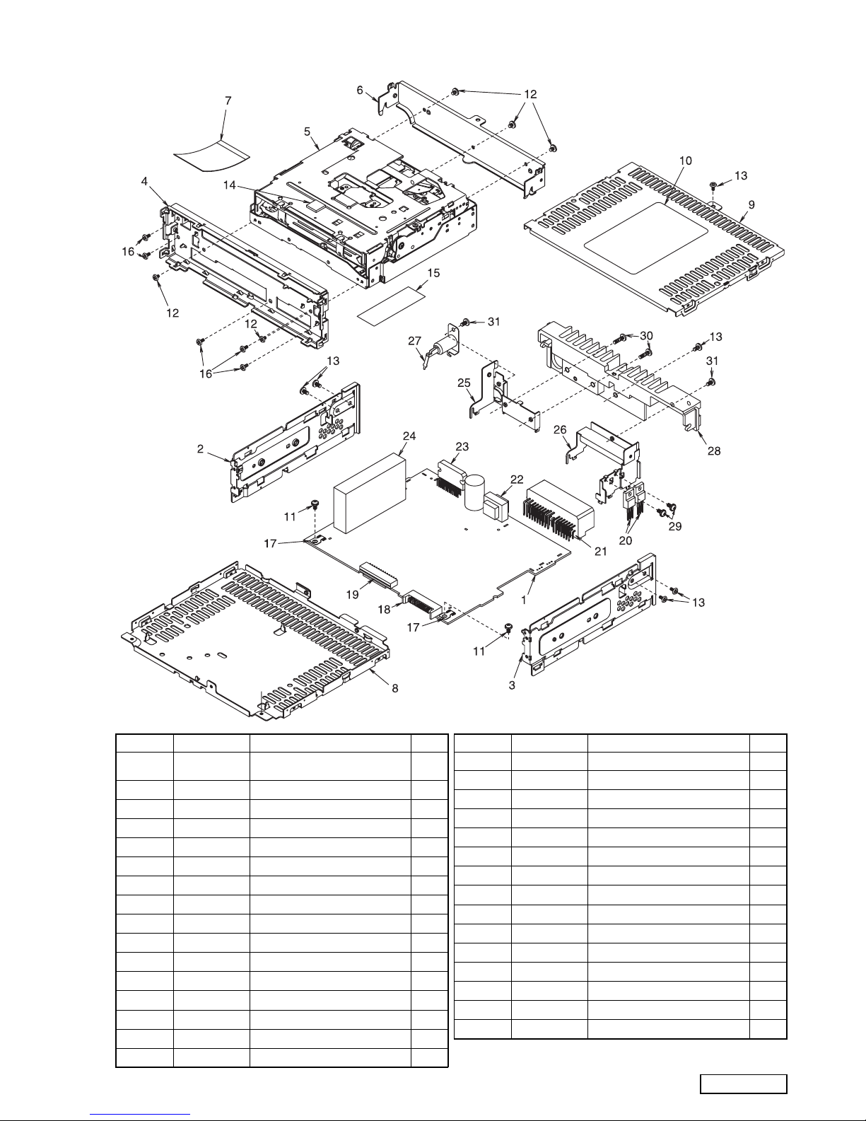
- 5 -
PH-2416I
Main section
NO. PART NO. DESCRIPTION Q'TYNO. PART NO. DESCRIPTION Q'TY
1 039-1797-02 MAIN PWB 1
(WITHOUT COMPONENT)
2 305-0293-10 SIDE PLATE LH 1
3 305-0294-10 SIDE PLATE RH 1
4 331-3034-00 ES PLATE 1
5 929-0091-80 CD MECHA MODULE 1
6 331-2874-00 MECHA BRACKET 1
7 816-2490-00 FLAT WIRE 1
8 311-1799-00 LOWER CASE 1
9 310-1703-00 UPPER CASE 1
10 286-9412-24 SETPLATE 1
11 716-0878-00 IT SCREW(M2.6×5) 2
12 714-2303-81 MACHINE SCREW (M2.3×3) 5
13 714-2606-81 MACHINE SCREW (M2.6×6) 6
14 345-4138-00 RUBBER PARTS 1
15 347-2022-02 PAPER PARTS 1
16 714-2606-11 MACHINE SCREW(M2.6×6) 5
17 073-0762-90 TERMINAL 2
18 076-0540-20 PLAG (20P) 1
19 074-1186-26 OUTLET SOCKET (26P) 1
20 103-2012-00 TRANSISTOR 2
21 074-1166-00 OUTLET SOCKET 1
22 009-0666-0L CHOKE 1
23 051-2023-01 IC(TA8260AH) 1
24 880-1914H TUNER PACK (AM/FM) 1
25 307-0658-00 REAR PLATE LH 1
26 307-0659-00 REAR PLATE RH 1
27 092-0702-00 ANT RECEPT 1
28 313-1824-00 HEAT SINK 1
29 716-1494-00 IT SCREW (M2.6×6) 2
30 714-2612-81 MACHINE SCREW (M2.6×12) 2
31 714-2606-81 MACHINE SCREW (M2.6×6) 2
Page 6

- 6 -PH-2416I
CD mechanism section
※ The parts list is on page 8.
L1
K
A11
L1
N
A5
D1
A10
P
D2
D5
D6
D7
D4
D3
L2
D4
D7
H2
H1
M
D5
D6
J
I2
H2
H1
C2
C1
I1
I2
I3
I1
P
N
A7
Page 7

- 7 -
PH-2416I
B
F2
F1
E3
M
A4
I3
D2
D3
A11
A7
K
A4
A6
F1
A5
A8
G
A9
A1
A10
D1
G
A9
E4
E4
A1
A3
B
E1
E2
E3
A2
A6
F2
A8
C2
E1
E2
A3
A2
C1
A7
Page 8

- 8 -PH-2416I
NO. PART NO. DESCRIPTION Q'TYNO. PART NO. DESCRIPTION Q'TY
1 HBS-463-100 DRIVE UNIT 1
1-1 966-0314-21 STOP LINK ASSY 1
1-2 966-0447-23 DR-PLATE ASSY 1
1-3 966-0448-21 SIDE PLATE ASSY 1
1-4 966-0449-23 CLAMP LINK ASSY 1
1-5 969-0050-04 PICK UP UNIT 1
969-0050-34 PICK UP UNIT
969-0050-52 PICK UP UNIT
1-6 013-7100-00 LIMIT SWITCH 1
1-7 620-0198-03 CLAMPER PLATE 1
1-8 620-0491-03 SPRING PLATE 1
1-9 620-0690-01 RATTLE PLATE 1
1-10 621-0205-02 CLAMPER LINK 1
1-11 621-0251-03 LOCK LINK 1
1-12 621-0252-03 DISC STOPPER 1
1-13 621-0253-02 MOTOR HOLDER 1
1-14 621-0255-02 SECOND GEAR 1
1-15 621-0375-00 SH-BASE 1
1-16 621-0357-03 PICK UP GUIDE 1
1-17 621-0358-02 LS-HOLDER F 1
1-18 621-0359-02 LS-HOLDER R 1
1-19 622-1073-02 CLAMPER ROLLER 1
1-20 714-2003-81 MACHINE SCREW(M2×3) 10
1-21 716-0675-00 SCREW(M2×2.5) 2
1-22 716-1468-00 SCREW(M2×2.5) 2
1-23 716-1555-00 WAVE SCREW 1
1-24 716-1733-00 SCREW(M2×2.5) 2
1-25 732-2004-11 SEMS SCREW 2
1-26 739-1735-17 PRECISION SCREW 2
1-27 746-0761-00 SCREW(M2×2.5) 2
1-28 750-3097-03 CLAMPER SPRING 1
1-29 750-3098-00 L-LINK SPRING 1
1-30 750-3099-00 ES-SPRING 1
1-31 816-2372-00 WIRE(BLU) 1
1-32 816-2373-00 WIRE(WHT) 1
1-33 966-0454-00 SH-RACK ASSY 1
1-34 HBS-432-100 LS-GEAR ASSY 1
1-35 SMA-146-100 SLED MOTOR ASSY 1
1-36 SMA-151-100 SPINDLE MOTOR ASSY 1
2 966-0308-11 CHASSIS ASSY 1
3 966-0309-20 L-DISC-G-ASSY 1
4 966-0310-21 SHIFT-P-CH-ASSY 1
5 966-0312-21 SHIFT-P-ASSY 1
6 966-0358-21 DRIVE-L-PL-ASSY 1
7 966-0359-21 SIDE-L-PL-ASSY 1
8 013-3879-01 CHUCKING SWITCH 1
9 039-0586-01 CHUCKING SWITCH PWB 1
(WITHOUT COMPONENT)
10 039-0588-01 SENSOR PWB 1
(WITHOUT COMPONENT)
11 060-0252-01 PHOTO TR (PT4850F) 3
12 345-7513-01 CLAMPER SHEET 1
13 345-7514-00 S-PWB SHEET 1
14 620-0485-04 FRONT PLATE 1
15 620-0488-01 S-L-LINK PLATE 1
16 620-0489-02 MOTOR PLATE 1
17 620-0492-01 MOTOR BRACKET 1
18 620-0773-01 MECH BRACKET 1
19 621-0402-02 U-DISC GUIDE F 1
20 621-0243-02 ROLLER SLAVE 2
21 621-0248-07 RACK GEAR 1
22 621-0249-02 ROLLER GEAR 1
23 621-0250-21 DAMPER HOLDER 4
24 621-0258-03 LOADING ROLLER 2
25 622-1072-05 ROLLER SHAFT 1
26 622-1219-01 SHIFT ROLLER 1
27 629-0058-00 DAMPER-VA 4
28 714-2003-81 MACHINE SCREW(M2X3) 9
29 714-2603-81 MACHINE SCREW(M2.6X3) 5
30 716-1468-00 SCREW(M2×2.5) 3
31 716-1507-00 SCREW(M2×3) 2
32 716-1670-00 SCREW(M2×4) 6
33 716-1677-00 SCREW(M2×5) 1
34 716-1704-00 SCREW(M2×7) 1
35 716-1742-00 SCREW(M2×5) 1
36 743-1500-10 E-RING 3
37 746-0712-03 WASHER 1
38 746-0762-00 WASHER 1
39 746-0877-02 WASHER 2
40 750-3090-02 RO-SPRING L 1
41 750-3091-03 RO-SPRING R 1
42 750-3092-03 SHIFT SPRING 1
43 750-3094-00 S-ARM SPRING 1
44 750-3096-01 DR-SPRING R 1
45 750-3098-00 L-LINK SPRING 1
46 750-3164-00 DR-SPRING-LR 1
47 750-3188-00 DR-SPRING-F-B 1
48 750-3189-00 SIDE-L-SPRING 1
49 750-3201-00 DR-SPRING-F-R 1
50 750-3348-00 CENTER SPRING 1
51 800-4904-60 WIRE(BLK) 1
52 800-4910-60 WIRE(BLK) 1
53 801-4910-60 WIRE(BRN) 1
54 802-4904-60 WIRE(RED) 1
55 802-4910-60 WIRE(RED) 1
56 804-4910-60 WIRE(YEL) 1
57 001-0563-00 DIODE 3
58 HBS-430-100 GEAR PLATE ASSY 1
59 039-1088-03 CD MECH PWB 1
(WITHOUT COMPONENT)
60 SMA-147-100 LOADING MOTOR ASSY 1
61 620-0804-00 CE-SP-PLATE F 1
62 620-0803-00 CE-SP-PLATE R 1
Page 9

- 9 -
PH-2416I
REF No. PART No. DESCRIPTION REF No. PART No. DESCRIPTION REF No. PART No. DESCRIPTION
Note) Several different parts of the same reference number are alternative parts.
One of those parts is used in the set.
■ELECTRICAL PARTS LIST
Main PWB section(B1)
ANT101 092-0702-00 ANT RECEPT
BL101 880-1914H AM/FM TUNER
C102 166-1801-50 18pF CH
C103 166-1007-50 10pF CH
C104 168-2232-55 0.022μF
C105 168-4735-56 0.047μF
C106 183-1073-27 10V100μF
C107 166-1801-50 18pF CH
C109 183-1073-27 10V100μF
C111 183-1073-27 10V100μF
C112 042-0458-50 50V 1μF LN
C113 168-1045-56 0.1μF
C114 166-1011-50 100pF CH
C115 166-1011-50 100pF CH
C116 168-2222-55 2200pF
C117 166-1011-50 100pF CH
C118 166-1011-50 100pF CH
C119 166-2201-50 22pF CH
C120 168-3322-55 3300pF
C121 183-1063-37 16V10μF
C124 168-1022-55 1000pF
C125 183-4763-37 16V47μF
C126 168-4735-56 0.047μF
C127 183-1543-67 50V0.15μF
C128 168-8222-55 8200pF
C129 168-2722-55 2700pF
C130 183-1543-67 50V0.15μF
C131 168-4735-56 0.047μF
C132 168-8222-55 8200pF
C133 168-2722-55 2700pF
C134 168-2232-55 0.022μF
C135 168-2232-55 0.022μF
C137 183-1056-67 50V1μF NP
C138 168-1232-55 0.012μF
C139 168-2232-55 0.022μF
C140 168-2232-55 0.022μF
C141 166-1007-50 10pF CH
C142 166-1007-50 10pF CH
C143 168-2232-55 0.022μF
C201 183-3343-67 50V0.33μF
C202 183-3343-67 50V0.33μF
C203 183-4763-37 16V47μF
C204 183-1053-67 50V1μF
C205 183-1053-67 50V1μF
C208 178-2242-78 0.22μF
C209 178-2242-78 0.22μF
C210 183-1063-37 16V10μF
C211 183-1063-37 16V10μF
C212 183-1063-37 16V10μF
C213 183-1063-37 16V10μF
C214 043-0309-90 10V 1μF
C215 043-0309-90 10V 1μF
C216 168-6835-56 0.068μF
C217 168-6835-56 0.068μF
C218 168-1032-55 0.01μF
C219 168-1032-55 0.01μF
C220 168-4712-55 470pF
C221 168-4712-55 470pF
C222 183-1063-37 16V10μF
C223 183-1063-37 16V10μF
C224 168-3335-56 0.033μF
C225 166-1011-50 100pF CH
C226 166-1011-50 100pF CH
C227 183-2253-67 50V2.2μF
C228 183-2253-67 50V2.2μF
C229 183-2263-37 16V22μF
C230 183-2263-37 16V22μF
C238 168-5612-55 560pF
C241 183-1063-37 16V10μF
C243 168-4735-56 0.047μF
C244 178-1242-78 0.12μF
C245 178-1242-78 0.12μF
C246 178-2242-78 0.22μF
C247 178-5642-78 0.56μF
C248 178-6832-78 0.068μF
C249 178-1542-78 0.15μF
C250 178-2242-78 0.22μF
C251 178-5642-78 0.56μF
C252 178-6832-78 0.068μF
C253 178-1542-78 0.15μF
C254 178-1832-78 0.018μF
C255 178-2732-78 0.027μF
C256 178-1032-78 0.01μF
C257 178-1032-78 0.01μF
C258 178-1832-78 0.018μF
C259 178-2732-78 0.027μF
C260 178-1032-78 0.01μF
C261 178-1032-78 0.01μF
C262 178-1532-78 0.015μF
C263 178-1032-78 0.01μF
C264 178-2232-78 0.022μF
C265 178-5622-78 5600pF
C266 178-1532-78 0.015μF
C267 178-1032-78 0.01μF
C268 178-2232-78 0.022μF
C269 178-5622-78 5600pF
C270 178-2242-78 0.22μF
C271 178-2242-78 0.22μF
C272 183-2256-57 35V2.2μF NP
C273 183-2256-57 35V2.2μF NP
C274 183-2256-57 35V2.2μF NP
C275 183-2256-57 35V2.2μF NP
C276 183-1073-27 10V100μF
C279 183-1073-27 10V100μF
C282 168-1022-55 1000pF
C283 168-1022-55 1000pF
C284 168-1022-55 1000pF
C285 168-1022-55 1000pF
C286 042-0466-00 16V4700μF
C287 183-2263-37 16V22μF
C288 166-1011-50 100pF CH
C290 166-1011-50 100pF CH
C292 168-1545-56 0.15μF
C293 168-1545-56 0.15μF
C294 168-1545-56 0.15μF
C295 168-1545-56 0.15μF
C296 172-1041-15 0.1μF
C298 183-2253-67 50V2.2μF
C299 183-2253-67 50V2.2μF
C301 183-4763-37 16V47μF
C302 168-2212-55 220pF
C303 168-2212-55 220pF
C304 183-2263-37 16V22μF
C305 183-2263-37 16V22μF
C308 183-1063-37 16V10μF
C309 183-1063-37 16V10μF
C312 168-8232-78 0.082μF
C313 168-8232-78 0.082μF
C314 168-1822-55 1800pF
C315 168-1822-55 1800pF
C316 168-2722-55 2700pF
C319 168-2722-55 2700pF
C320 183-2253-67 50V2.2μF
C321 183-2253-67 50V2.2μF
C330 168-2222-55 2200pF
C331 168-2222-55 2200pF
C332 183-2253-67 50V2.2μF
C333 183-2253-67 50V2.2μF
C334 183-2253-67 50V2.2μF
C335 183-2253-67 50V2.2μF
C336 183-2253-67 50V2.2μF
C337 183-2253-67 50V2.2μF
C338 183-2253-67 50V2.2μF
C339 183-2253-67 50V2.2μF
C340 183-1073-27 10V100μF
C341 183-3363-25 10V33μF
C342 183-3363-25 10V33μF
C343 183-1073-27 10V100μF
C344 183-2253-67 50V2.2μF
C345 183-2253-67 50V2.2μF
C346 183-2253-67 50V2.2μF
C347 183-2253-67 50V2.2μF
C348 183-2253-67 50V2.2μF
C349 183-2253-67 50V2.2μF
C350 178-2242-78 0.22μF
C351 178-2242-78 0.22μF
C352 166-1011-50 100pF CH
C353 166-1011-50 100pF CH
C354 183-1063-37 16V10μF
C355 183-1063-37 16V10μF
C358 166-1011-50 100pF CH
C359 166-1011-50 100pF CH
C401 168-1045-56 0.1μF
C403 166-1501-50 15pF CH
C404 166-1801-50 18pF CH
C405 168-1045-56 0.1μF
C406 168-1045-56 0.1μF
C407 168-4735-56 0.047μF
C408 168-1045-56 0.1μF
C412 168-3312-55 330pF
C414 119-0000-05 1/16W 0Ω JW
C416 183-6853-47 25V6.8μF
C501 183-2263-37 16V22μF
C502 183-2263-37 16V22μF
C503 168-1022-55 1000pF
C508 183-1063-37 16V10μF
C509 168-1022-55 1000pF
C510 183-1063-37 16V10μF
C512 168-1032-55 0.01μF
C513 168-1022-55 1000pF
C516 183-2253-67 50V2.2μF
C517 178-2242-78 0.22μF
C518 178-2242-78 0.22μF
C519 178-2242-78 0.22μF
C520 184-4773-12 6.3V470μF
C521 183-1063-37 16V10μF
C522 042-0452-81 10V220μF
C523 183-4763-37 16V47μF
C527 172-1041-15 0.1μF
C528 183-1063-37 16V10μF
C529 184-4773-12 6.3V470μF
C530 183-3353-61 50V3.3μF
C531 172-1041-15 0.1μF
C532 172-1041-15 0.1μF
C533 183-1063-37 16V10μF
D301 001-0516-90 MA111
D404 001-0516-90 MA111
D503 001-0529-55 MA8120-L
D505 001-0529-42 MA8075-H
D506 001-0529-33 MA8056-H
D507 001-0529-45 MA8082-H
D508 001-0529-43 MA8082-L
D509 001-0330-00 1SS119
D510 001-0516-90 MA111
D511 001-0516-90 MA111
D512 001-0516-90 MA111
D513 001-0535-90 MA729
D514 001-0529-47 MA8091-M
D515 001-0504-34 HZS6 C1L
D515 001-0503-34 HZS6 C1L
D516 001-0516-90 MA111
D517 001-0592-00 RM4Z
D518 001-0466-90 S5688B
Page 10

- 10 -PH-2416I
REF No. PART No. DESCRIPTION REF No. PART No. DESCRIPTION REF No. PART No. DESCRIPTION
D519 001-0466-90 S5688B
D521 001-0466-90 S5688B
D522 001-0535-90 MA729
D523 001-0503-42 HZS7C3L
D523 001-0504-42 HZS7C3L
D524 001-0516-90 MA111
IC102 051-6201-90 LC72146M
IC201 051-5012-10 LC75386NE-L
IC204 051-1080-91 NJM4560M
IC205 051-2023-01 TA8260AH
IC206 051-1979-90 M5243FP09
IC207 051-1979-90 M5243FP09
IC208 051-1080-91 NJM4560M
IC301 051-3013-90 M5203AFP
IC302 051-3013-90 M5203AFP
IC306 051-0722-90 SA571D
IC307 051-0722-90 SA571D
IC401 052-3154-11 M30622MA-F08GP
IC402 051-9400-18 AT93C46-10SI
IC501 051-1822-08 S-80732AN-DW-X
J301 074-1186-26 26P
J302 076-0540-20 20P
J901 074-1166-00 34P
L101 010-2003-04 COIL
L102 010-6009-88 220μH
L701 010-6009-64 2.2μH
Q101 190-1298-00 2SA1298
Q102 190-1298-00 2SA1298
Q103 125-2004-92 RN1402
Q210 192-2712-00 2SC2712
Q211 192-2712-00 2SC2712
Q301 192-2712-00 2SC2712
Q302 192-2712-00 2SC2712
Q304 125-2004-93 RN1403
Q305 192-2712-00 2SC2712
Q306 192-2712-00 2SC2712
Q402 190-1162-00 2SA1162
Q403 125-2004-92 RN1402
Q404 192-2712-00 2SC2712
Q406 125-2004-92 RN1402
Q501 125-0002-93 RN2403
Q502 193-1858-00 2SD1858
Q503 193-1858-00 2SD1858
Q504 193-1858-00 2SD1858
Q505 125-0002-92 RN2402
Q506 125-2004-92 RN1402
Q507 125-0013-96 RN2426
Q508 193-1858-00 2SD1858
Q509 103-2012-00 2SD2012
Q511 125-0002-92 RN2402
Q512 125-2004-92 RN1402
Q513 193-1858-00 2SD1858
Q514 193-1858-00 2SD1858
Q515 125-0002-92 RN2402
Q516 125-2004-92 RN1402
Q517 103-2012-00 2SD2012
Q518 125-0002-92 RN2402
Q519 125-2004-92 RN1402
Q520 192-2712-00 2SC2712
Q522 125-0013-97 RN2427
Q523 125-2004-92 RN1402
Q524 193-1858-00 2SD1858
Q525 125-2004-92 RN1402
Q526 193-1858-00 2SD1858
Q527 193-1858-00 2SD1858
Q528 125-0002-92 RN2402
Q529 125-2004-92 RN1402
Q530 190-1431-00 2SA1431
Q533 193-1858-00 2SD1858
Q537 192-2712-00 2SC2712
Q538 192-2712-00 2SC2712
Q539 193-1858-00 2SD1858
Q540 193-1858-00 2SD1858
Q541 192-2712-00 2SC2712
Q542 193-1858-00 2SD1858
R101 119-4721-15 1/16W 4.7kΩ
R102 119-2221-15 1/16W 2.2kΩ
R103 111-6891-94 1/4WS 6.8Ω
R104 119-2221-15 1/16W 2.2kΩ
R105 119-2221-15 1/16W 2.2kΩ
R106 119-3321-15 1/16W 3.3kΩ
R107 119-2221-15 1/16W 2.2kΩ
R108 119-2231-15 1/16W 22kΩ
R109 119-2221-15 1/16W 2.2kΩ
R110 119-1221-15 1/16W 1.2kΩ
R111 119-4731-15 1/16W 47kΩ
R112 119-1031-15 1/16W 10kΩ
R113 119-1031-15 1/16W 10kΩ
R114 119-1221-15 1/16W 1.2kΩ
R117 119-1021-15 1/16W 1kΩ
R118 119-1041-15 1/16W 100kΩ
R119 111-6891-94 1/4WS 6.8Ω
R120 119-0000-05 1/16W 0Ω JW
R121 119-1021-15 1/16W 1kΩ
R122 119-1831-15 1/16W 18kΩ
R123 111-1001-94 1/4WS 10Ω
R124 119-1021-15 1/16W 1kΩ
R125 119-2221-15 1/16W 2.2kΩ
R201 119-1031-15 1/16W 10kΩ
R202 119-3931-15 1/16W 39kΩ
R203 119-1041-15 1/16W 100kΩ
R204 119-1041-15 1/16W 100kΩ
R205 119-3931-15 1/16W 39kΩ
R206 119-1031-15 1/16W 10kΩ
R209 119-3321-15 1/16W 3.3kΩ
R210 119-3321-15 1/16W 3.3kΩ
R211 119-4741-15 1/16W 470kΩ
R212 119-2221-15 1/16W 2.2kΩ
R213 119-2221-15 1/16W 2.2kΩ
R214 119-2221-15 1/16W 2.2kΩ
R215 119-4731-15 1/16W 47kΩ
R216 119-1031-15 1/16W 10kΩ
R217 119-4721-15 1/16W 4.7kΩ
R218 119-4721-15 1/16W 4.7kΩ
R224 119-1031-15 1/16W 10kΩ
R225 119-1031-15 1/16W 10kΩ
R228 119-3331-15 1/16W 33kΩ
R229 119-3331-15 1/16W 33kΩ
R232 119-1031-15 1/16W 10kΩ
R233 119-1031-15 1/16W 10kΩ
R234 119-1521-15 1/16W 1.5kΩ
R235 119-1521-15 1/16W 1.5kΩ
R236 119-6821-15 1/16W 6.8kΩ
R237 119-6821-15 1/16W 6.8kΩ
R238 119-2221-15 1/16W 2.2kΩ
R239 119-2221-15 1/16W 2.2kΩ
R244 119-1031-15 1/16W 10kΩ
R245 119-1031-15 1/16W 10kΩ
R246 119-1031-15 1/16W 10kΩ
R247 119-1031-15 1/16W 10kΩ
R251 119-1031-15 1/16W 10kΩ
R256 119-1021-15 1/16W 1kΩ
R257 119-1531-15 1/16W 15kΩ
R258 117-4721-15 1/10W 4.7kΩ
R259 117-4721-15 1/10W 4.7kΩ
R261 117-4721-15 1/10W 4.7kΩ
R263 117-4721-15 1/10W 4.7kΩ
R264 117-1831-15 1/10W 18kΩ
R266 117-1831-15 1/10W 18kΩ
R268 117-8211-15 1/10W 820Ω
R269 117-2231-15 1/10W 22kΩ
R270 117-8211-15 1/10W 820Ω
R271 117-2231-15 1/10W 22kΩ
R280 117-6811-15 1/10W 680Ω
R281 117-3931-15 1/10W 39kΩ
R282 117-6811-15 1/10W 680Ω
R283 117-3931-15 1/10W 39kΩ
R284 117-4721-15 1/10W 4.7kΩ
R285 117-4721-15 1/10W 4.7kΩ
R286 117-4721-15 1/10W 4.7kΩ
R287 117-4721-15 1/10W 4.7kΩ
R288 117-4721-15 1/10W 4.7kΩ
R289 117-4721-15 1/10W 4.7kΩ
R290 119-1001-15 1/16W 10Ω
R291 119-1031-15 1/16W 10kΩ
R292 119-1001-15 1/16W 10Ω
R293 119-2721-15 1/16W 2.7kΩ
R294 119-2221-15 1/16W 2.2kΩ
R295 119-2721-15 1/16W 2.7kΩ
R296 119-2221-15 1/16W 2.2kΩ
R297 119-1821-15 1/16W 1.8kΩ
R298 119-1821-15 1/16W 1.8kΩ
R301 119-1031-15 1/16W 10kΩ
R302 119-1021-15 1/16W 1kΩ
R303 119-1021-15 1/16W 1kΩ
R306 119-4731-15 1/16W 47kΩ
R307 119-4731-15 1/16W 47kΩ
R308 119-6821-15 1/16W 6.8kΩ
R309 119-6821-15 1/16W 6.8kΩ
R310 119-1031-15 1/16W 10kΩ
R311 119-2221-15 1/16W 2.2kΩ
R312 119-1031-15 1/16W 10kΩ
R313 119-2221-15 1/16W 2.2kΩ
R314 119-1521-15 1/16W 1.5kΩ
R317 119-1031-15 1/16W 10kΩ
R318 119-1031-15 1/16W 10kΩ
R321 119-1521-15 1/16W 1.5kΩ
R322 119-1531-15 1/16W 15kΩ
R323 119-1531-15 1/16W 15kΩ
R326 119-2231-15 1/16W 22kΩ
R327 119-2231-15 1/16W 22kΩ
R328 119-2731-15 1/16W 27kΩ
R329 119-2731-15 1/16W 27kΩ
R334 119-6831-15 1/16W 68kΩ
R335 119-4731-15 1/16W 47kΩ
R336 119-4731-15 1/16W 47kΩ
R337 119-6831-15 1/16W 68kΩ
R338 119-2231-15 1/16W 22kΩ
R339 119-6821-15 1/16W 6.8kΩ
R340 119-1031-15 1/16W 10kΩ
R341 119-1031-15 1/16W 10kΩ
R342 119-6821-15 1/16W 6.8kΩ
R343 119-2231-15 1/16W 22kΩ
R344 119-1031-15 1/16W 10kΩ
R345 119-1031-15 1/16W 10kΩ
R346 119-1031-15 1/16W 10kΩ
R347 119-1031-15 1/16W 10kΩ
R348 119-1031-15 1/16W 10kΩ
R349 119-1031-15 1/16W 10kΩ
R350 119-2731-15 1/16W 27kΩ
R351 119-1031-15 1/16W 10kΩ
R352 119-2221-15 1/16W 2.2kΩ
R353 119-1021-15 1/16W 1kΩ
R354 119-1031-15 1/16W 10kΩ
R355 119-2731-15 1/16W 27kΩ
R356 119-1021-15 1/16W 1kΩ
R357 119-2221-15 1/16W 2.2kΩ
R360 119-1021-15 1/16W 1kΩ
R361 119-1021-15 1/16W 1kΩ
R362 119-1021-15 1/16W 1kΩ
R363 119-1021-15 1/16W 1kΩ
R364 119-1021-15 1/16W 1kΩ
R365 119-1021-15 1/16W 1kΩ
R366 119-1021-15 1/16W 1kΩ
R367 119-1021-15 1/16W 1kΩ
R368 119-1031-15 1/16W 10kΩ
R369 119-1031-15 1/16W 10kΩ
R370 119-2721-15 1/16W 2.7kΩ
R371 119-2721-15 1/16W 2.7kΩ
R401 119-4741-15 1/16W 470kΩ
R402 119-4721-15 1/16W 4.7kΩ
R403 119-4721-15 1/16W 4.7kΩ
Page 11

- 11 -
PH-2416I
REF No. PART No. DESCRIPTION REF No. PART No. DESCRIPTION REF No. PART No. DESCRIPTION
R404 119-4721-15 1/16W 4.7kΩ
R406 119-4731-15 1/16W 47kΩ
R409 119-2231-15 1/16W 22kΩ
R411 119-2231-15 1/16W 22kΩ
R413 119-2231-15 1/16W 22kΩ
R415 119-2231-15 1/16W 22kΩ
R417 119-2231-15 1/16W 22kΩ
R419 119-2231-15 1/16W 22kΩ
R421 119-2231-15 1/16W 22kΩ
R422 119-1021-15 1/16W 1kΩ
R423 119-2231-15 1/16W 22kΩ
R424 119-4721-15 1/16W 4.7kΩ
R425 119-4721-15 1/16W 4.7kΩ
R426 119-4721-15 1/16W 4.7kΩ
R427 119-4721-15 1/16W 4.7kΩ
R436 119-1021-15 1/16W 1kΩ
R437 119-1021-15 1/16W 1kΩ
R438 119-4721-15 1/16W 4.7kΩ
R439 119-4731-15 1/16W 47kΩ
R440 119-4731-15 1/16W 47kΩ
R441 119-4731-15 1/16W 47kΩ
R442 119-4731-15 1/16W 47kΩ
R443 119-2231-15 1/16W 22kΩ
R444 119-2231-15 1/16W 22kΩ
R445 119-2231-15 1/16W 22kΩ
R446 111-2211-94 1/4WS 220Ω
R447 119-4721-15 1/16W 4.7kΩ
R448 119-4731-15 1/16W 47kΩ
R450 119-4721-15 1/16W 4.7kΩ
R452 119-3921-15 1/16W 3.9kΩ
R453 119-4731-15 1/16W 47kΩ
R455 119-4731-15 1/16W 47kΩ
R456 119-1831-15 1/16W 18kΩ
R457 119-1031-15 1/16W 10kΩ
R458 119-4731-15 1/16W 47kΩ
R461 119-4731-15 1/16W 47kΩ
R462 119-4731-15 1/16W 47kΩ
R464 119-1021-15 1/16W 1kΩ
R465 119-4731-15 1/16W 47kΩ
R467 119-4731-15 1/16W 47kΩ
R468 119-1021-15 1/16W 1kΩ
R469 119-1021-15 1/16W 1kΩ
R470 119-1011-15 1/16W 100Ω
R471 119-1011-15 1/16W 100Ω
R472 119-1011-15 1/16W 100Ω
R501 119-4721-15 1/16W 4.7kΩ
R502 119-4721-15 1/16W 4.7kΩ
R503 119-4721-15 1/16W 4.7kΩ
R504 119-4721-15 1/16W 4.7kΩ
R505 111-2291-94 1/4WS 2.2Ω
R506 111-2291-94 1/4WS 2.2Ω
R507 111-6811-94 1/4WS 680Ω
R509 111-3311-94 1/4WS 330Ω
R510 111-2291-94 1/4WS 2.2Ω
R511 111-2291-94 1/4WS 2.2Ω
R525 111-2291-94 1/4WS 2.2Ω
R526 111-2291-94 1/4WS 2.2Ω
R527 119-5611-15 1/16W 560Ω
R528 111-4711-94 1/4WS 470Ω
R529 111-4711-94 1/4WS 470Ω
R530 119-4731-15 1/16W 47kΩ
R531 119-1031-15 1/16W 10kΩ
R532 119-2221-15 1/16W 2.2kΩ
R533 111-1011-94 1/4WS 100Ω
R534 111-2221-94 1/4WS 2.2kΩ
R536 119-1041-15 1/16W 100kΩ
R537 119-2241-15 1/16W 220kΩ
R538 119-2241-15 1/16W 220kΩ
R539 119-3331-15 1/16W 33kΩ
R541 119-1021-15 1/16W 1kΩ
R542 119-4711-15 1/16W 470Ω
R543 111-2291-94 1/4WS 2.2Ω
R544 111-2291-94 1/4WS 2.2Ω
R545 111-1521-94 1/4WS 1.5kΩ
R547 119-1531-15 1/16W 15kΩ
R548 111-3311-94 1/4WS 330Ω
R549 119-4731-15 1/16W 47kΩ
R554 111-2291-94 1/4WS 2.2Ω
R557 119-3311-15 1/16W 330Ω
R558 119-1031-15 1/16W 10kΩ
R559 119-1511-15 1/16W 150Ω
R560 119-1031-15 1/16W 10kΩ
R561 111-1221-94 1/4WS 1.2kΩ
R562 114-4791-11 1W 4.7Ω
R563 111-2291-94 1/4WS 2.2Ω
R565 119-8221-15 1/16W 8.2kΩ
R566 111-1031-94 1/4WS 10kΩ
R568 111-2291-94 1/4WS 2.2Ω
R569 111-6811-94 1/4WS 680Ω
R570 117-4721-15 1/10W 4.7kΩ
R571 119-2721-15 1/16W 2.7kΩ
R572 119-4721-15 1/16W 4.7kΩ
R601 119-2221-15 1/16W 2.2kΩ
R602 119-2221-15 1/16W 2.2kΩ
R603 119-1041-15 1/16W 100kΩ
R604 119-1041-15 1/16W 100kΩ
R605 119-1031-15 1/16W 10kΩ
R606 119-1031-15 1/16W 10kΩ
SUP101 060-0122-20 DSP-141N-S00B
T501 009-0666-0L 0.4mH
TC102 004-1580-60 30pF
TH501 002-0222-90 PTH61G30BD
TM101 073-0762-90 TERMINAL
TM102 073-0762-90 TERMINAL
X102 061-1066-00 7.2MHz
X401 061-3504-90 CX-5F 10MHz
Switch PWB section(B2)
REF No. PART No. DESCRIPTION REF No. PART No. DESCRIPTION REF No. PART No. DESCRIPTION
C701 178-1042-78 0.1μF
C702 042-0423-94 10V 4.7μF
C703 178-1042-78 0.1μF
C704 178-1042-78 0.1μF
C705 178-6812-78 680pF
D701 001-0412-17 GC-3HD8
D702 001-0518-96 BG1101W-240
IC701 051-6000-20 LC7583NW
P701 074-1151-20 20P
PL701 017-0429-13 8V105mA
PL702 017-0429-13 8V105mA
PL703 017-0433-77 14V40mA
PL704 017-0433-77 14V40mA
PL705 017-0433-77 14V40mA
PL706 017-0433-77 14V40mA
PL707 017-0433-77 14V40mA
PL708 017-0433-77 14V40mA
PL709 017-0433-77 14V40mA
R702 117-0000-05 1/10W 0Ω JW
R703 117-0000-05 1/10W 0Ω JW
R706 117-0000-05 1/10W 0Ω JW
R707 117-0000-05 1/10W 0Ω JW
R711 117-6831-15 1/10W 68kΩ
R721 117-0000-05 1/10W 0Ω JW
R722 117-0000-05 1/10W 0Ω JW
R723 117-0000-05 1/10W 0Ω JW
R724 117-0000-05 1/10W 0Ω JW
S701 013-6201-50 SKPMAA
S702 013-6201-50 SKPMAA
S703 013-6201-50 SKPMAA
S704 013-6201-50 SKPMAA
S705 013-6201-50 SKPMAA
S706 013-6201-50 SKPMAA
S707 013-6201-50 SKPMAA
S708 013-6201-50 SKPMAA
S709 013-6201-50 SKPMAA
S710 013-6201-50 SKPMAA
S711 013-6201-50 SKPMAA
S712 013-6201-50 SKPMAA
S713 013-6201-50 SKPMAA
VR701 016-0014-05 VR W-SHAFT
VR702 016-0014-05 VR W-SHAFT
Chucking switch PWB section(B3) : CD mechanism
REF No. PART No. DESCRIPTION
S2 013-3879-01 CHUCKING
CD mech PWB section(B4) : CD mechanism
REF No. PART No. DESCRIPTION REF No. PART No. DESCRIPTION REF No. PART No. DESCRIPTION
C1 183-1073-12 6.3V100μF
C2 183-4763-11 6.3V47μF
C3 178-1042-78 0.1μF
C4 176-2201-00 22pF CH
C5 176-1801-00 18pF CH
C6 176-1801-00 18pF CH
C7 176-8201-00 82pF CH
C8 178-1042-78 0.1μF
C9 178-2242-78 0.22μF
C10 178-2242-78 0.22μF
C11 176-4701-00 47pF CH
C12 178-1532-78 0.015μF
C13 178-1032-78 0.01μF
C14 178-2722-78 2700pF
C15 178-4722-78 4700pF
C16 176-1201-00 12pF CH
C17 178-4712-78 470pF
C18 178-4712-78 470pF
C19 178-4732-78 0.047μF
C20 178-4732-78 0.047μF
C21 178-4732-78 0.047μF
C22 178-4732-78 0.047μF
C23 178-1032-78 0.01μF
C25 042-0505-01 10V22μF
C26 178-1042-78 0.1μF
C27 178-1042-78 0.1μF
C29 178-1042-78 0.1μF
C30 178-1042-78 0.1μF
C31 178-1032-78 0.01μF
C32 178-1032-78 0.01μF
C33 178-1042-78 0.1μF
C34 176-1501-00 15pF CH
C35 176-1501-00 15pF CH
C38 178-1022-78 1000pF
C39 178-1042-78 0.1μF
C40 178-1042-78 0.1μF
C41 183-1073-12 6.3V100μF
C43 183-1073-12 6.3V100μF
C44 183-4763-11 6.3V47μF
Page 12

- 12 -PH-2416I
REF No. PART No. DESCRIPTION REF No. PART No. DESCRIPTION REF No. PART No. DESCRIPTION
C45 183-1073-12 6.3V100μF
C46 178-1032-78 0.01μF
C47 178-1042-78 0.1μF
C48 178-1032-78 0.01μF
C49 176-6801-00 68pF CH
C51 178-1032-78 0.01μF
C52 178-1032-78 0.01μF
C54 183-4763-11 6.3V47μF
C55 178-1042-78 0.1μF
C56 178-1042-78 0.1μF
C58 178-1042-78 0.1μF
C59 178-2222-78 2200pF
D1 001-0563-00 GL380
D2 001-0563-00 GL380
D3 001-0563-00 GL380
D4 001-0330-00 1SS119
IC1 051-5704-00 TA2096FN
IC2 051-6342-00 TC9462F
IC3 051-6026-08 TA2058F
IC4 051-6027-00 BA6283N
L1 010-2155-03 10μH
L3 010-2199-74 10μH J
Q1 101-1237-50 2SB1237QR
Q2 102-2712-00 2SC2712
R1 117-1011-10 1/10W 100Ω
R2 117-1841-10 1/10W 180kΩ
R3 117-1841-10 1/10W 180kΩ
R4 117-2201-10 1/10W 22Ω
R5 117-8231-10 1/10W 82kΩ
R6 117-1041-10 1/10W 100kΩ
R7 117-1041-10 1/10W 100kΩ
R8 117-1031-10 1/10W 10kΩ
R9 117-2221-10 1/10W 2.2kΩ
R10 117-1031-10 1/10W 10kΩ
R12 117-1031-10 1/10W 10kΩ
R13 117-4731-10 1/10W 47kΩ
R15 117-4741-10 1/10W 470kΩ
R17 117-3331-10 1/10W 33kΩ
R18 117-3311-10 1/10W 330Ω
R19 117-3321-10 1/10W 3.3kΩ
R20 117-1031-10 1/10W 10kΩ
R21 117-3321-10 1/10W 3.3kΩ
R22 117-3321-10 1/10W 3.3kΩ
R23 117-3321-10 1/10W 3.3kΩ
R24 117-3321-10 1/10W 3.3kΩ
R26 117-1041-10 1/10W 100kΩ
R27 117-4711-10 1/10W 470Ω
R28 117-2211-10 1/10W 220Ω
R29 117-2211-10 1/10W 220Ω
R30 117-4721-10 1/10W 4.7kΩ
R34 111-2711-91 1/4WS 270Ω
R40 117-3321-10 1/10W 3.3kΩ
X1 061-3051-00 16.92MHz
REF No. PART No. DESCRIPTION REF No. PART No. DESCRIPTION REF No. PART No. DESCRIPTION
Sensor PWB section(B5) : CD mechanism
Q101 060-0252-01 PT4850F Q102 060-0252-01 PT4850F Q103 060-0252-01 PT4850F
Limit switch PWB section(B6) : CD mechanism
REF No. PART No. DESCRIPTION
S1 013-7100-00 LIMIT
■BLOCK DIAGRAM
Page 13

■CIRCUIT DIAGRAM
Main PWB section(B1)
- 13 -
PH-2416I
Page 14

- 14 -
PH-2416I
Page 15

- 15 -
PH-2416I
Page 16

- 16 -
PH-2416I
 Loading...