

Page 1

Clarion Co., Ltd.
50 Kamitoda, Toda-shi, Saitama 335-8511 Japan
Service Dept.: 5-66 Azuma , Kitamoto-shi, Saitama 364-0007 Japan
Tel: +81-48-541-2335 / 2432 FAX: +81-48-541-2703
Service Manual
SUBARU Automobile Genuine
MW/FM 6-Disc CD Changer Deck
Published by Service Dept.
298-6005-00
Printed in Japan
Nov.2002 P
SPECIFICATIONS
Radio section
Tuning system: PLL Frequency synthesizer system
Receive range: MW 530 kHz to 1,710 kHz
FM 87.75 MHz to 107.9 MHz
WB 162.400 MHz to 162.550 MHz
Intermediate frequency:
MW 450 kHz
FM 10.7 MHz
Quieting sensitivity: MW Less than 35 dBu
(at 20 dB S/N)
FM Less than 15 dBu
(at 30 dB S/N)
WB Less than 10 dBu
(at 20 dB S/N)
Separation: FM More than 20 dB
Auto tuning stop sensitivity:
MW 32 +6/-6 dBu
FM 24 +6/-6 dBu
WB -1 +5/-5 dBu
Model
PF-2520I-A
(Genuine No.86201AE38A)
NOTE
We cannot supply PWB with component parts in principle.
When a circuit on PWB has failure , please repair it by component parts base. Parts which are not mentioned in service manual are not supplied.
Specifications and design arevsubject to change without
notice for further improvement.
COMPONENTS
PF-2520I-A
Main unit ----------- 1
CAUTIONS
Use of controls, adjustments, or performance of procedures
other than those specified herein, may result in hazardous
radiation exposure.
The COMPACT DISC player should not be adjusted or repaired by anyone except properly qualified service personnel.
CD section
Disc: Compact disc (8 cm / 12 cm)
Separation: More than 65 dB
S/N ratio: More than 80 dB
Distortion: Less than 0.1 % (at 20 kHz LPF)
General
Output level: More than 2.5 V x 4 (at CD 1 kHz 0dB)
Typ. 3.0 V x 4
Power supply voltage: DC13.2 V (10.8 V to 15.6 V)
Negative ground
Current consumption: Less than 3A
Dimensions(mm): 178 (W) x 100 (H) x 176.5 (D)
Weight: 2.4 kg
- 1 -
PF-2520I-A
Page 2

To engineers in charge of repair or
inspection of our products.
Before repair or inspection, make sure to follow the
instructions so that customers and Engineers in
charge of repair or inspection can avoid suffering
any risk or injury.
1. Use specified parts.
The system uses parts with special safety features against
fire and voltage. Use only parts with equivalent characteristics when replacing them.
The use of unspecified parts shall be regarded as remodeling for which we shall not be liable. The onus of product
liability (PL) shall not be our responsibility in cases where
an accident or failure is as a result of unspecified parts
being used.
2. Place the parts and wiring back in their original positions
after replacement or re-wiring.
For proper circuit construction, use of insulation tubes,
bonding, gaps to PWB, etc, is involved. The wiring connection and routing to the PWB are specially planned using clamps to keep away from heated and high voltage
parts. Ensure that they are placed back in their original
positions after repair or inspection.
If extended damage is caused due to negligence during
repair, the legal responsibility shall be with the repairing
company.
3. Check for safety after repair.
Check that the screws, parts and wires are put back securely in their original position after repair. Ensure for safety
reasons there is no possibility of secondary ploblems
around the repaired spots.
If extended damage is caused due to negligence of repair,
the legal responsibility shall be with the repairing company.
4. Caution in removal and making wiring connection to the
parts for the automobile.
Disconnect the battery terminal after turning the ignition
key off. If wrong wiring connections are made with the battery connected, a short circuit and/or fire may occur. If extensive damage is caused due to negligence of repair, the
legal responsibility shall be with the repairing company.
5. Cautions regarding chips.
Do not reuse removed chips even when no abnormality is
observed in their appearance. Always replace them with
new ones. (The chip parts include resistors, capacitors,
diodes, transistors, etc). The negative pole of tantalum
capacitors is highly susceptible to heat, so use special care
when replacing them and check the operation afterwards.
6. Cautions in handling flexible PWB
Before working with a soldering iron, make sure that the
iron tip temperature is around 270
ply the iron tip repeatedly(more than three times)to the
same patterns. Also take care not to apply the tip with force.
7. Turn the unit OFF during disassembly and parts replacement. Recheck all work before you apply power to the unit.
8. Cautions in checking that the optical pickup lights up.
The laser is focused on the disc reflection surface through
the lens of the optical pickup. When checking that the laser optical diode lights up, keep your eyes more than 30cms
away from the lens. Prolonged viewing of the laser within
30cms may damage your eyesight.
. Take care not to ap-
9. Cautions in handling the optical pickup
The laser diode of the optical pickup can be damaged by
electrostatic charge caused by your clothes and body. Make
sure to avoid electrostatic charges on your clothes or body,
or discharge static electricity before handling the optical
pickup.
9-1. Laser diode
The laser diode terminals are shorted for transportation in order to prevent electrostatic damage. After
replacement, open the shorted circuit. When removing the pickup from the mechanism, short the terminals by soldering them to prevent this damage.
9-2. Actuator
The actuator has a powerful magnetic circuit. If a
magnetic material is put close to it. Its characteristics will change. Ensure that no foreign substances
enter through the ventilation slots in the cover.
9-3. Cleaning the lens
Dust on the optical lens affects performance. To
clean the lens, apply a small amount of isopropyl
alcohol to lens paper and wipe the lens gently.
- 2 -PF-2520I-A
Page 3

EXPLANATION OF IC
052-3176-10 M30620MCA-F70GP System Controller
1.Terminal Description
pin 1: FUNCTION 2 :IN : Low = without MD.
pin 2: FUNCTION 3 :IN : Low = without Cassette tape.
pin 3: AREA 1 :IN: The destination setting input.
pin 4: AREA 2 :IN: The destination setting input.
pin 5: CLK SEL :IN : Low = without Clock.
pin 6: BYTE : IN : Connect to the ground.
pin 7: CN VSS :IN : Connect to VSS.
pin 8: WB SD :IN : WB station detect signal input.
pin 9: VFD ON : O : VFD ON signal output.
pin 10: RESET : IN : Reset signal input.
pin 11: X OUT : O : Crystal connection.
pin 12: GND : - : Ground.
pin 13: X IN : IN : Crystal connection.
pin 14: VDD : - : Positive supply voltage.
pin 15: NMI :IN : Pull up.
pin 16: BU DET : IN: Backup detection signal input.
pin 17: ACC DET :IN : ACC detection signal input.
pin 18: NU : - : Not in use.
pin 19: Ce-NET RX : IN : The serial data input from Ce-NET.
pin 20: ILL ON :IN : Illumination ON signal input.
pin 21: AUDIO OUT : O : Audio signal output command output for
pin 22: NAVI MUTE : O : Muting signal output to suppress the
pin 23: LINE MUTE : O : The line mute signal output.
pin 24: BEEP : O : Beep out.
pin 25: TIME BASE : IN : Time base pulse input.
pin 26: DX/LO : O : DX/Local select signal output.
pin 27: Ce-NET RX : IN : The serial data input from Ce-NET.
pin 28: Ce-NET TX : O : The serial data output to Ce-NET.
pin 29: IX-6 TX : O : Serial data output.
pin 30: IX-6 RX : IN : Serial data input.
pin 31: ST : IN : The stereo flag input.
pin 32: AMP ON : O : Audio power amplifier ON signal output.
pin 33: NU : - : Not in use.
pin 34: NU : - : Not in use.
pin 35: NU : - : Not in use.
pin 36: NU : - : Not in use.
pin 37: NU : - : Not in use.
pin 38: NU : - : Not in use.
pin 39: ANT ON : O : Antenna ON command output.
pin 40: SYS ACC : O : ACC detect signal output.
pin 41: SYS ON : O : System ON signal output.
pin 42: AMP MUTE : O : Muting signal output to the Audio Power
pin 43: TEL ON :IN : Telephone ON signal input.
pin 44: PLL DI : IN : Serial data input from the PLL IC.
pin 45: VFD BLANK : O : Blank pulse output to the VFD driver.
pin 46: EEP CEO : O : The chip enable signal output to EEP-
pin 47: EEP CLK : O : The clock pulse output to EEP-ROM.
pin 48: EEP DO : O : The serial data output to EEP-ROM.
pin 49: EEP DI :IN : The serial data input from EEP-ROM.
pin 50: MD 8V : O : Control signal output to the power supply
pin 51: MD LD : IN : Disc-in signal input from the MD mecha-
pin 52: MD SI : IN : Serial data input from the MD mechanism.
pin 53: MD X SRQ :IN : Request signal input from the MD mech-
pin 54: MD RESET : O : Reset pulse output to the MD mechanism.
pin 55: MD SO : O : Serial data output to the MD mechanism.
pin 56: MD X SCK : O : The clock pulse output to the MD mech-
pin 57: MD X CS : O : The chip selection signal output to the
pin 58: MD WP : O : Wake up signal output to the MD mech-
Ce-NET.
noise without Navigation sound interrupting.
Amplifier.
ROM.
circuit.
nism.
anism.
anism.
MD mechanism.
anism.
pin 59: CD 8V : O : Power supply control signal output for the
pin 60: VDD : - : Positive supply voltage.
pin 61: CD 5V : O : 5V power supply ON signal output for CD.
pin 62: GND : - : Ground.
pin 63: BUC 0 :I/O:CD IC Data input / output.
pin 64: BUC 1 :I/O:CD IC Data input / output.
pin 65: BUC 2 :I/O:CD IC Data input / output.
pin 66: BUC 3 :I/O:CD IC Data input / output.
pin 67: BUC CLOCK : O : CD IC clock pulse output.
pin 68: CD CE : O : CD chip enable pulse output.
pin 69: CD RESET : O : The reset pulse output to the CD IC.
pin 70: S STOP : IN : Inside limit signal input from the CD
pin 71: SUB Q SYNC :IN : Sub Q Sync signal input.
pin 72: CHU SW :IN: CD disc chucking signal input.
pin 73: NU : - : Not in use.
pin 74: TR B :IN: Photo sensor signal input from the CD
pin 75: TR A :IN: Photo sensor signal input from the CD
pin 76: LD CNT : O : Loading control signal output.
pin 77: LD MUTE : O : Muting signal output to the CD mecha-
pin 78: Serial DO : - : The serial data output.
pin 79: VFD DI : IN : Serial data input from the VFD driver.
pin 80: CKO : O : Clock pulse output.
pin 81: CEO : O : Chip enable output.
pin 82: VFD RESET : O : The reset pulse output to the VFD driv-
pin 83: E VOL 1L : IN : Pulse signal input from the rotary encod-
pin 84: E VOL 2L : IN : Pulse signal input from the rotary encod-
pin 85: NU : - : Not in use.
pin 86: NU : - : Not in use.
pin 87: POWER SW :IN : Power switch ON signal input.
pin 88: IX-6 LOAD : IN : IX-6 loading signal input.
pin 89: TP/MD EJ : IN : Tape/MD eject signal input.
pin 90: CD/IX-6 EJ : IN : CD/IX-6 eject signal input.
pin 91: IX-6 REQUE : IN : Reuest signal input from IX-6.
pin 92: VFD CS : O : CS signal output to VFD driver.
pin 93: VFD CP : O : CP signal output to VFD driver.
pin 94: A VSS : - : Analog ground.
pin 95: VFD DO : O : The serial data output to the VFD driver.
pin 96: Vref : - : Reference voltage.
pin 97: A VCC : - : Positive supply voltage for the internal
pin 98: DIM C SEL : IN : Low = Without dimmer canceller.
pin 99: ILL CONT : IN : The input terminal of internal ADC for
pin100: FUNCTION 1 :IN : Low = GS-1, High = IX-6.
motor / photo IC. "H"= ON.
mechanism.
mechanism.
mechanism.
nism.
er.
er.
er.
analog section.
adjusting brightness of the illumination.
- 3 -
PF-2520I-A
Page 4

BLOCK DIAGRAM
- 4 -PF-2520I-A
Page 5

EXPLODED VIEW : PARTS LIST
Escutcheon section
1 370-9618-00 ESCUTCHEON 1
2 372-3220-00 DIAL PLATE 1
3 380-5547-00 KNOB 2
4 382-4925-10 BUTTON(6) 1
5 382-4930-10 BUTTON(1) 1
6 382-4931-10 BUTTON(2) 1
7 382-4932-10 BUTTON(3) 1
8 382-4933-10 BUTTON(4) 1
9 382-4934-10 BUTTON(5) 1
10 382-6551-00 BUTTON(FM/AM) 1
11 382-6552-00 BUTTON(WB) 1
12 382-6553-00 BUTTON(DISC) 1
13 382-6554-00 BUTTON(LOAD) 1
14 382-6555-00 BUTTON(EJECT) 1
15 382-6556-00 BUTTON 2
16 383-0686-00 SIDE TRIM 1
- 5 -
NO. PART NO. DESCRIPTION Q'TYNO. PART NO. DESCRIPTION Q'TY
17 383-0686-10 SIDE TRIM 1
18 335-6873-00 VFD COVER 1
19 335-5612-00 ILLUMI C 3
20 335-6809-00 ILLUMI PLATE 1
21 335-6810-00 ILLUMI PLATE 1
22 947-0527-10 DOOR ASSY 1
23 039-2194-00 SW PWB 1
24 013-6005-50 SWITCH 15
25 013-7415-20 DETECTOR SW 1
26 016-0025-00 VR W/SHAFT 1
27 016-9900-86 VR W/SHAFT 1
28 017-0420-09 PILOTLAMP 9
29 379-4044-24 INDICATOR 1
30 716-0778-00 WAVE SCREW (M2 x 6) 14
(WITHOUT COMPONENT)
PF-2520I-A
Page 6

Main section
1 039-2193-00 MAIN PWB 1
2 941-0210-10 AM/FM TUNER 1
3 941-0212-00 WB TUNER 1
4 076-0540-12 PLUG (12P) 1
5 076-0540-16 PLUG (16P) 1
6 092-0702-00 ANT-RECEPT 1
7 074-1010-10 OUTLET SOCKET (14P) 1
8 074-1129-08 OUTLET SOCKET (8P) 1
9 074-1192-22 OUTLET SOCKET (22P) 1
10 074-1194-00 OUTLET SOCKET (Ce-NET) 1
11 307-0689-00 REAR PLATE 1
12 331-3491-00 TR-HOLDER 1
13 714-2605-81 MACHINE SCREW (M2.6 x 5) 2
(WITHOUT COMPONENT)
NO. PART NO. DESCRIPTION Q'TYNO. PART NO. DESCRIPTION Q'TY
14 716-0878-00 IT-SCREW (M2.6 x 5) 3
15 855-3473-00 MULTI-POLE CORD 1
16 309-0787-00 ES PLATE 1
17 311-1861-10 LOWER CASE 1
18 ----------- CD CHANGER MECHANISM 1
19 816-2603-00 FLAT WIRE 1
20 290-5010-79 LABEL 1
21 714-2003-89 MACHINE SCREW (M2 x 3) 1
22 714-2605-81 MACHINE SCREW (M2.6 x 5) 10
23 716-0878-00 IT-SCREW (M2.6 x 5) 6
24 093-0785-08 ANT-JUMPER 1
25 286-7201-40 SETPLATE 1
(281910)
- 6 -PF-2520I-A
Page 7

CD changer mechanism section : Main chassis
1 311-1864-81 LOWER CASE 1
2 331-3266-21 PWB-HOLDER 1
3 305-0315-86 SIDE CASE 1
4 310-1741-83 UPPER CASE 1
5 629-0083-00 DAMPER 4
6 620-1086-20 DAMPER-H-PLT 4
7 750-3491-00 FL-SPRING 1
8 039-2219-00 MAIN PWB 1
(WITHOUT COMPONENT)
- 7 -
NO. PART NO. DESCRIPTION Q'TYNO. PART NO. DESCRIPTION Q'TY
9 716-1716-00 SCREW (M2 x 3) 14
10 039-1957-01 FPC 1
11 716-3450-00 SCREW (M1.7 x 2) 4
12 ----------- CD CHANGER MODULE 1
13 347-6619-00 INSULATOR 1
14 345-8329-00 CUSHION RUBBER 2
(WITHOUT COMPONENT)
PF-2520I-A
Page 8

CD changer mechanism section : Main module 1/2
- 8 -PF-2520I-A
Page 9

CD changer mechanism section : Main module 2/2
- 9 -
PF-2520I-A
Page 10

1 HBS-511-100 LOADING UNIT 1
2 SMA-186-100 LOADING MOTOR ASSY 1
3 HBS-512-100 MOTOR PLATE SUB ASSY 1
4 HBS-513-100 DRIVE UNIT 1
5 039-1951-00 CD PWB 1
6 039-1953-00 DRIVER PWB 1
7 966-0597-02 CHASSIS ASSY 1
8 966-0600-01 LOCK-P-RE-ASSY 1
9 966-0601-00 M-GEAR-P-ASSY 1
10 966-0602-02 DR-LINK-ASSY 1
11 966-0603-00 MODE-P-ASSY 1
12 966-0604-02 LOCK-PF-ASSY 1
13 966-0605-00 SHIFT-P-ASSY 1
14 966-0606-02 HLC-PLATE-ASSY 1
15 966-0607-03 COV-OLATE-ASSY 1
16 966-0610-03 TOP-PLATE-ASSY 1
17 966-0611-84 DR-BASE-P-ASSY 1
18 966-0615-81 LOCK-L-RF-ASSY 1
19 966-0616-20 LOCK-L-LF-ASSY 1
20 966-0618-21 EJECT-B-ASSY 1
21 966-0624-03 DISC-HOL-ASSY 1
22 001-7042-00 DIODE (GL4800) 4
23 013-7414-50 DETECTOR SWITCH 1
24 039-1954-00 LED-L-PWB 1
25 039-1955-00 LED-R-PWB 1
26 039-1956-00 SENSOR PWB 1
27 039-2009-00 PIM FPC 1
28 039-2010-00 RIV-FOC 1
29 039-2011-00 LED-FPC 1
30 039-2012-00 SENSOR-FPC 1
31 039-2013-00 MOS-FPC 1
32 039-2014-00 L-MOTOR-FPC 1
33 051-5806-01 IC (GPIS93) 1
34 051-5806-02 IC (GPIS95) 1
35 060-0252-01 PHOTO-TR 4
36 347-6657-01 LO-COVER SHEET 1
37 620-1041-02 GEAR PLATE 1
38 620-1042-00 M-GEAR-H 1
39 620-1056-21 HLR-PLATE-L 1
40 620-1057-21 HLR-PLATE-R 1
41 620-1063-00 LO-MOTOR-PLT 1
(WITHOUT MOTOR)
(WITHOUT COMPONENT)
(WITHOUT COMPONENT)
(WITHOUT COMPONENT)
(WITHOUT COMPONENT)
(WITHOUT COMPONENT)
(WITHOUT COMPONENT)
NO. PART NO. DESCRIPTION Q'TYNO. PART NO. DESCRIPTION Q'TY
42 620-1066-20 LOCK LINK-LR 1
43 620-1067-81 SLIDE PLATE-L 1
44 620-1068-22 SLIDE PLATE-R 1
45 620-1071-20 EJECT ARM 1
46 620-1072-20 EJECT PLATE 1
47 620-1073-00 FRONT PLATE 1
48 620-1083-20 FPC-PLATE 1
49 620-1090-00 GAP PLATE 1
50 620-1568-00 RATTLE PLATE-F 2
51 621-0640-00 V-GEAR-G 1
52 621-0641-01 PI-HOLDER-M 1
53 621-0656-21 PI-HOLDER-V 1
54 622-1622-00 SL-G-ROLLER 2
55 622-1623-00 SL-G-ROLLER-R 2
56 622-1648-02 DU-STP-SLEEVE 1
57 622-1650-02 COV-PLATE PIN-B 2
58 622-1651-00 LOCK-RE-ROLLER 1
59 622-1652-00 LOCK-PF-ROLLER 1
60 716-1866-00 SCREW (M1.7 x 3) 4
61 716-1873-00 SCREW (M2 x 1.6) 1
62 716-3449-00 SCREW (M2 x 3) 15
63 716-3450-00 SCREW (M1.7 x 2) 4
64 716-3451-00 SCREW (M1.7 x 2.5) 4
65 716-3459-00 SCREW (M1.7 x 5) 1
66 716-3466-02 SCREW 1
67 738-1420-17 PRECISION SCREW 2
68 743-1200-20 E-RING 2
69 743-1500-10 E-RING 13
70 746-0624-00 WASHER 1
71 746-0712-03 WASHER 1
72 746-0761-00 WASHER 1
73 750-3478-01 TOP-P-SP-L 2
74 750-3479-01 TOP-P-SP-R 1
75 750-3480-01 DR-LOCK-SP 1
76 750-3483-00 EJECT-A-SPRING 1
77 750-3484-01 DR-BASE-SPRING 1
78 750-3485-01 TENSION-SP-L 1
79 750-3486-01 LO-TENSION-SP 1
80 750-3489-00 DRIVE-P-SPRING 1
81 750-3496-00 GAP-P-SPRING R 1
82 750-3497-00 GAP-P-SPRING L 1
83 750-6711-01 DU-STP-SPRING 1
84 750-6712-01 DR-LOCK-SP-B 1
- 10 -PF-2520I-A
Page 11

CD changer mechanism section : Drive unit
1 HBS-514-100 CLAMPER SUB ASSY 1
2 SMA-185-100 SPINDLE MOTOR ASSY 1
3 SMA-184-100 SLED MOTOR ASSY 1
4 HBS-515-100 LS-ASSY 1
5 966-0621-24 SH-SP-PLT-ASSY 1
6 966-0622-02 D-SHIFT-P-ASSY 1
7 969-0009-00 PICK UP-ASSY 1
8 013-7414-50 DETECT SWITCH 1
9 039-2015-00 P/U-FPC 1
10 039-2016-01 M/S-FPC 1
11 347-6632-00 PU-SHEET 1
12 620-1078-00 PUSH PLATE 1
13 620-1080-01 PU-GUIDE PLATE 1
14 620-1081-00 SCREW PUSH-PLT 1
15 620-1082-01 SPRING PLATE 1
16 620-1084-00 SCREW-HOL-PLT 1
- 11 -
NO. PART NO. DESCRIPTION Q'TYNO. PART NO. DESCRIPTION Q'TY
17 621-0670-20 LS-HOLDER-L 1
18 621-0673-00 D-GEAR A 1
19 621-0674-00 D-GEAR B 1
20 621-0675-00 D-GEAR C 1
21 621-0683-21 DU-STOPPER 1
22 716-3460-00 SCREW (M1.4 x 1.8) 2
23 716-3470-00 SCREW (M1.7 x 3) 5
24 738-1722-17 PRECISION SCREW 2
25 738-2025-17 PRECISION SCREW 2
26 716-3474-00 SCREW (M1.7 x 3) 2
27 743-1500-20 E-RING 1
28 750-3487-00 SHIFT-P-SPRING 1
29 750-3488-00 CLAMP-A-SPRING 1
30 966-0619-05 DRIVE PLT-ASSY 1
31 745-0807-00 WASHER 1
32 745-0808-00 WASHER 1
PF-2520I-A
Page 12

ELECTRICAL PARTS LIST
Main PWB(B1) section
REF No. PART No. DESCRIPTION REF No. PART No. DESCRIPTION REF No. PART No. DESCRIPTION
ANT101 092-0702-00 ANT RECEPT
BL101 941-0210-10 AM/FM TUNER
BL102 941-0212-00 WB TUNER
C101 183-3353-69 50V3.3uF
C102 168-2732-55 16V 0.027uF
C103 168-2732-55 16V 0.027uF
C104 168-2232-55 0.022uF
C105 166-5601-50 56pF CH
C106 168-1022-55 1000pF
C107 168-2232-55 0.022uF
C108 168-1032-55 0.01uF
C109 168-2232-55 0.022uF
C110 168-2232-55 0.022uF
C111 183-4763-39 16V47uF
C112 168-1042-78 16V 0.1uF
C113 183-1073-29 10V100uF
C114 168-1042-78 16V 0.1uF
C116 183-1073-29 10V100uF
C117 183-4763-39 16V47uF
C118 168-1022-55 1000pF
C119 168-4712-55 470pF
C120 168-4722-55 4700pF
C121 042-0458-90 50V1uF
C123 168-1022-55 1000pF
C125 178-1242-78 0.12uF
C126 168-5632-78 16V 0.056uF
C127 168-8232-78 0.082uF
C128 168-4712-55 470pF
C129 183-4753-59 35V4.7uF
C130 166-1011-50 100pF CH
C131 166-1011-50 100pF CH
C132 166-4701-50 47pF CH
C133 166-5601-50 56pF CH
C134 183-1063-39 16V10uF
C135 166-1011-50 100pF CH
C136 166-1011-50 100pF CH
C137 178-1542-78 0.15uF
C138 168-2232-55 0.022uF
C140 183-4763-39 16V47uF
C141 166-1801-50 18pF CH
C142 166-5601-50 56pF CH
C143 168-4732-78 0.047uF
C144 183-4753-59 35V4.7uF
C145 168-2232-55 0.022uF
C151 166-1801-50 18pF CH
C152 168-1032-55 0.01uF
C153 183-3363-29 10V33uF
C154 042-0398-53 16V3.3uF TAN
C155 168-2732-55 16V 0.027uF
C156 166-4701-50 47pF CH
C157 168-1032-55 0.01uF
C159 168-2232-55 0.022uF
C160 166-1011-50 100pF CH
C161 166-1011-50 100pF CH
C200 168-1042-78 16V 0.1uF
C201 183-4763-19 6.3V47uF
C202 168-1032-55 0.01uF
C203 168-1032-55 0.01uF
C204 168-1032-55 0.01uF
C250 168-1022-55 1000pF
C251 168-1042-78 16V 0.1uF
C252 183-1053-69 50V1uF
C253 168-1022-55 1000pF
C302 183-4763-19 6.3V47uF
C303 168-1042-78 16V 0.1uF
C308 168-1042-78 16V 0.1uF
C309 183-1063-39 16V10uF
C310 183-1073-29 10V100uF
C400 043-0328-90 0.1uF
C401 043-0328-90 0.1uF
C402 184-2273-39 16V220uF
C403 168-2232-55 0.022uF
C404 184-4773-39 16V470uF
C405 043-0328-90 0.1uF
C406 184-4773-39 16V470uF
C407 043-0328-90 0.1uF
C408 184-1073-59 35V100uF
C409 184-4773-62 50V470uF
C410 168-2232-55 0.022uF
C411 043-0328-90 0.1uF
C412 183-4763-39 16V47uF
C413 183-1063-69 50V10uF
C414 183-1063-39 16V10uF
C415 183-1063-39 16V10uF
C416 183-4763-39 16V47uF
C417 043-0328-90 0.1uF
C418 043-0328-90 0.1uF
C419 043-0328-90 0.1uF
C450 183-1073-29 10V100uF
C451 168-1042-78 16V 0.1uF
C452 042-0576-00 5.5V0.1F
C453 183-4763-39 16V47uF
C500 168-1032-55 0.01uF
C615 178-2255-79 2.2uF
C617 178-2255-79 2.2uF
C621 178-2255-79 2.2uF
C626 178-2255-79 2.2uF
C678 183-1073-29 10V100uF
C679 168-1042-78 16V 0.1uF
C680 183-4763-19 6.3V47uF
C682 183-4763-39 16V47uF
C683 168-1042-78 16V 0.1uF
C684 183-1063-39 16V10uF
C690 168-1042-78 16V 0.1uF
C691 183-4763-19 6.3V47uF
C692 183-4763-19 6.3V47uF
C694 166-2201-50 22pF CH
C695 183-1063-39 16V10uF
C696 166-2201-50 22pF CH
C709 183-4763-39 16V47uF
C710 183-1073-29 10V100uF
C711 172-1041-15 0.1uF
C712 183-1053-69 50V1uF
C713 042-0586-00 16V4700uF
C714 172-1041-15 0.1uF
C722 183-1053-69 50V1uF
C734 183-1063-39 16V10uF
C750 168-2222-55 2200pF
C751 168-2222-55 2200pF
C752 166-1811-50 180pF CH
C753 166-1811-50 180pF CH
C754 184-1073-39 16V100uF
C755 184-1073-39 16V100uF
C756 184-1073-39 16V100uF
C757 184-1073-39 16V100uF
C760 184-1073-39 16V100uF
C761 184-1073-39 16V100uF
C762 184-1073-39 16V100uF
C763 184-1073-39 16V100uF
C766 166-1811-50 180pF CH
C767 166-1811-50 180pF CH
C768 168-2222-55 2200pF
C769 168-2222-55 2200pF
C770 166-1811-50 180pF CH
C771 166-1811-50 180pF CH
C772 166-1811-50 180pF CH
C773 166-1811-50 180pF CH
C801 168-8232-78 0.082uF
C802 168-8232-78 0.082uF
C817 183-1063-39 16V10uF
C818 183-1063-39 16V10uF
C821 183-1063-39 16V10uF
Note) Several different parts of the same reference number are alternative parts.
One of those parts is used in the set.
C822 183-1063-39 16V10uF
C824 183-4763-39 16V47uF
C825 183-4763-19 6.3V47uF
C827 183-2253-69 50V2.2uF
C828 183-2253-69 50V2.2uF
C831 183-1053-69 50V1uF
C832 183-1053-69 50V1uF
C837 168-1042-78 16V 0.1uF
C838 168-1042-78 16V 0.1uF
C839 168-1042-78 16V 0.1uF
C840 168-1042-78 16V 0.1uF
C841 168-1022-55 1000pF
C842 168-1022-55 1000pF
C843 168-1022-55 1000pF
C844 168-1022-55 1000pF
C845 183-1066-38 16V10uF NP
C846 183-1066-38 16V10uF NP
C847 168-3332-78 0.033uF
C851 183-2253-69 50V2.2uF
C852 183-2253-69 50V2.2uF
C853 168-1032-55 0.01uF
C854 168-1032-55 0.01uF
C855 168-1032-55 0.01uF
C856 168-1032-55 0.01uF
C857 168-1032-55 0.01uF
C858 168-1032-55 0.01uF
C859 168-1022-55 1000pF
C860 168-1022-55 1000pF
C901 168-1042-78 16V 0.1uF
C902 183-1063-39 16V10uF
C903 168-4732-78 0.047uF
C904 168-4732-78 0.047uF
C905 168-1042-78 16V 0.1uF
C906 183-1063-39 16V10uF
C907 168-4732-78 0.047uF
C908 168-1042-78 16V 0.1uF
C909 183-1063-39 16V10uF
C910 183-1063-39 16V10uF
C911 183-1063-39 16V10uF
C912 183-1063-39 16V10uF
C913 168-1042-78 16V 0.1uF
C914 183-1063-39 16V10uF
C915 168-1042-78 16V 0.1uF
C916 183-1063-39 16V10uF
C917 178-2255-79 2.2uF
C918 178-2255-79 2.2uF
C919 168-1022-55 1000pF
C920 168-6812-55 680pF
C921 166-1511-50 150pF CH
C922 168-1022-55 1000pF
C923 168-6812-55 680pF
C924 166-1511-50 150pF CH
CCT200 050-0122-53 1/16W1k ohm x4 J
D101 001-0516-90 MA111
D102 001-0466-90 S5688B
D250 001-0454-91 MA700A
D251 001-0454-91 MA700A
D252 001-0529-25 MA8047-L
D302 001-0529-33 MA8056-H
D303 001-0347-48 MA4091H
D400 001-0466-90 S5688B
D401 001-0466-90 S5688B
D402 001-0516-90 MA111
D403 001-0466-90 S5688B
D404 001-0504-87 HZS33-3L-TJ
D405 001-0529-39 MA8068-H
D406 001-0529-48 MA8091-H
D407 001-0347-69 MA4180M
D450 001-0466-90 S5688B
D451 001-0516-90 MA111
D452 001-0516-90 MA111
- 12 -PF-2520I-A
Page 13

REF No. PART No. DESCRIPTION REF No. PART No. DESCRIPTION REF No. PART No. DESCRIPTION
D453 001-0504-36 HZS7 A1L
D500 001-0347-69 MA4180M
D501 001-0347-69 MA4180M
D502 001-0347-69 MA4180M
D601 001-0516-90 MA111
D602 001-0466-90 S5688B
D603 001-0347-48 MA4091H
D604 001-2015-00 RL253
D606 001-0466-90 S5688B
D608 001-0466-90 S5688B
D752 001-0424-31 MA4180
D753 001-0424-31 MA4180
D754 001-0424-31 MA4180
D755 001-0424-31 MA4180
D758 001-0424-31 MA4180
D759 001-0424-31 MA4180
D760 001-0424-31 MA4180
D761 001-0424-31 MA4180
D762 001-0466-90 S5688B
D763 001-0466-90 S5688B
IC102 051-4200-90 TA2051FN
IC103 051-6212-08 LC72191JM-TLM
IC200 052-3176-10 M30162
IC250 051-0869-58 NJM2103M
IC300 051-9400-28 BR93LC46F-WE2
IC400 051-0172-08 TC4011BF
IC501 051-6600-38 CA0008AM
IC607 051-3010-90 NJM4580E
IC608 051-3010-90 NJM4580E
IC750 051-3010-90 NJM4580E
IC751 051-3010-90 NJM4580E
IC752 051-3010-90 NJM4580E
IC753 051-3010-90 NJM4580E
IC801 051-5027-00 LC75412WH
IC901 051-6317-08 CS8412CS
IC902 051-6322-08 PCM1710U-T2
IC903 051-3010-90 NJM4580E
J301 074-1192-22 22P
J500 074-1194-00 13P CE-NET
J600 074-1129-08 8P
J601 074-1010-10 14P
L101 010-2003-04 COIL
L102 010-2199-54 0.22uH J
L104 010-6009-76 22uH
L106 010-2199-55 0.27uH J
L107 010-6004-40 2.2mH J
L109 010-6009-76 22uH
L250 010-6009-76 22uH
L300 010-6009-76 22uH
L500 010-6009-76 22uH
L901 010-2199-78 22uH J
P500 076-0540-12 12P
P501 076-0540-16 16P
Q101 125-2004-92 RN1402
Q102 125-2004-92 RN1402
Q103 192-2712-51 2SC2712G,L
Q104 192-2712-51 2SC2712G,L
Q105 191-1240-00 2SB1240
Q106 191-1240-00 2SB1240
Q107 191-1240-00 2SB1240
Q250 192-2712-00 2SC2712
Q251 192-2712-00 2SC2712
Q300 192-2712-00 2SC2712
Q301 125-0002-92 RN2402
Q302 192-2712-00 2SC2712
Q303 190-1428-00 2SA1428
Q304 192-2712-00 2SC2712
Q305 193-1858-00 2SD1858
Q306 103-2012-00 2SD2012
Q311 103-2012-00 2SD2012
Q313 125-0002-92 RN2402
Q317 125-2004-92 RN1402
Q351 125-0002-92 RN2402
Q352 125-2004-92 RN1402
Q400 103-1684-00 2SD1684Q,S,T
Q401 190-1048-00 2SA1048
Q402 190-1428-00 2SA1428
Q403 190-1428-00 2SA1428
Q404 193-2118-00 2SD2118
Q405 103-2012-00 2SD2012
Q406 193-1858-00 2SD1858
Q407 190-1428-00 2SA1428
Q408 192-3668-00 2SC3668
Q409 192-3668-00 2SC3668
Q410 192-3668-00 2SC3668
Q411 125-2004-92 RN1402
Q450 193-2118-50 2SD2118F5
Q451 191-1240-00 2SB1240
Q452 192-2712-00 2SC2712
Q500 192-2712-00 2SC2712
Q604 192-2712-00 2SC2712
Q606 193-2118-00 2SD2118
Q608 125-0002-92 RN2402
Q609 125-2004-92 RN1402
Q611 191-1240-00 2SB1240
Q613 190-1428-00 2SA1428
Q614 193-1858-00 2SD1858
Q615 192-2712-00 2SC2712
Q616 192-2712-00 2SC2712
Q617 192-2712-00 2SC2712
Q750 191-1240-00 2SB1240
Q751 192-2712-00 2SC2712
Q901 192-2712-00 2SC2712
R101 119-0000-05 1/16W 0 ohm JW
R102 111-1001-98 1/4W 10 ohm
R103 119-1001-15 1/16W 10 ohm
R104 119-2221-15 1/16W 2.2k ohm
R105 119-0000-05 1/16W 0 ohm JW
R106 119-4721-15 1/16W 4.7k ohm
R107 119-1041-15 1/16W 100k ohm
R108 119-6831-15 1/16W 68k ohm
R109 119-1021-15 1/16W 1k ohm
R110 119-1031-15 1/16W 10k ohm
R111 119-1031-15 1/16W 10k ohm
R112 119-5631-15 1/16W 56k ohm
R113 119-1031-15 1/16W 10k ohm
R114 119-1031-15 1/16W 10k ohm
R115 119-1041-15 1/16W 100k ohm
R116 119-2241-15 1/16W 220k ohm
R117 111-1001-98 1/4W 10 ohm
R119 119-4721-15 1/16W 4.7k ohm
R120 119-1031-15 1/16W 10k ohm
R121 119-1211-15 1/16W 120 ohm
R122 119-1231-15 1/16W 12k ohm
R123 119-5631-15 1/16W 56k ohm
R124 119-6821-15 1/16W 6.8k ohm
R125 119-1221-15 1/16W 1.2k ohm
R126 119-3321-15 1/16W 3.3k ohm
R127 119-1031-15 1/16W 10k ohm
R128 119-1031-15 1/16W 10k ohm
R129 119-1011-15 1/16W 100 ohm
R132 119-2221-15 1/16W 2.2k ohm
R133 119-2221-15 1/16W 2.2k ohm
R134 119-2221-15 1/16W 2.2k ohm
R135 119-1031-15 1/16W 10k ohm
R138 119-1031-15 1/16W 10k ohm
R140 119-2221-15 1/16W 2.2k ohm
R141 119-1011-15 1/16W 100 ohm
R146 119-3331-15 1/16W 33k ohm
R149 119-4731-15 1/16W 47k ohm
R150 119-1021-15 1/16W 1k ohm
R151 119-1021-15 1/16W 1k ohm
R152 119-1021-15 1/16W 1k ohm
R154 119-1001-15 1/16W 10 ohm
R200 119-4731-15 1/16W 47k ohm
R201 119-1021-15 1/16W 1k ohm
R202 119-1031-15 1/16W 10k ohm
R206 119-0000-05 1/16W 0 ohm JW
R209 119-0000-05 1/16W 0 ohm JW
R210 119-1021-15 1/16W 1k ohm
R211 119-0000-05 1/16W 0 ohm JW
R214 119-0000-05 1/16W 0 ohm JW
R216 119-0000-05 1/16W 0 ohm JW
R217 119-1021-15 1/16W 1k ohm
R218 119-1021-15 1/16W 1k ohm
R219 119-1021-15 1/16W 1k ohm
R220 119-0000-05 1/16W 0 ohm JW
R222 119-4731-15 1/16W 47k ohm
R223 119-4721-15 1/16W 4.7k ohm
R224 119-4721-15 1/16W 4.7k ohm
R225 119-4731-15 1/16W 47k ohm
R226 119-4731-15 1/16W 47k ohm
R227 119-4731-15 1/16W 47k ohm
R228 119-4731-15 1/16W 47k ohm
R229 119-0000-05 1/16W 0 ohm JW
R230 119-0000-05 1/16W 0 ohm JW
R231 119-1031-15 1/16W 10k ohm
R233 119-4721-15 1/16W 4.7k ohm
R234 119-1031-15 1/16W 10k ohm
R250 119-6831-15 1/16W 68k ohm
R251 119-4731-15 1/16W 47k ohm
R252 119-4731-15 1/16W 47k ohm
R253 119-4731-15 1/16W 47k ohm
R254 119-4731-15 1/16W 47k ohm
R255 119-4731-15 1/16W 47k ohm
R256 119-5621-15 1/16W 5.6k ohm
R257 119-2231-15 1/16W 22k ohm
R258 119-2231-15 1/16W 22k ohm
R259 119-1021-15 1/16W 1k ohm
R260 119-6831-15 1/16W 68k ohm
R261 119-3341-15 1/16W 330k ohm
R300 119-2231-15 1/16W 22k ohm
R301 119-2231-15 1/16W 22k ohm
R302 119-1031-15 1/16W 10k ohm
R303 119-4721-15 1/16W 4.7k ohm
R304 119-5631-15 1/16W 56k ohm
R305 119-4721-15 1/16W 4.7k ohm
R306 111-4711-98 1/4W 470 ohm
R307 111-4711-98 1/4W 470 ohm
R308 119-3321-15 1/16W 3.3k ohm
R309 119-2231-15 1/16W 22k ohm
R310 119-1021-15 1/16W 1k ohm
R311 111-2291-98 1/4W 2.2 ohm
R313 111-2291-98 1/4W 2.2 ohm
R318 119-3611-15 1/16W 360 ohm
R324 111-1511-81 1/2W 150 ohm
R400 119-1031-15 1/16W 10k ohm
R401 119-4731-15 1/16W 47k ohm
R402 111-1521-98 1/4W 1.5k ohm
R403 119-1231-15 1/16W 12k ohm
R404 119-2221-15 1/16W 2.2k ohm
R405 119-4711-15 1/16W 470 ohm
R406 111-2221-98 1/4W 2.2k ohm
R407 111-2721-81 1/2W 2.7k ohm
R408 111-5621-98 1/4W 5.6k ohm
R409 119-4731-15 1/16W 47k ohm
R410 111-1521-98 1/4W 1.5k ohm
R411 111-1521-98 1/4W 1.5k ohm
R412 119-1231-15 1/16W 12k ohm
R413 119-5631-15 1/16W 56k ohm
R414 111-1021-98 1/4W 1k ohm
R415 111-1211-98 1/4W 120 ohm
R417 119-4721-15 1/16W 4.7k ohm
R419 111-6801-98 1/4W 68 ohm
R420 119-2231-15 1/16W 22k ohm
R450 111-1001-98 1/4W 10 ohm
R451 119-6821-15 1/16W 6.8k ohm
R452 119-1031-15 1/16W 10k ohm
R453 119-1021-15 1/16W 1k ohm
R454 119-1021-15 1/16W 1k ohm
R455 119-1031-15 1/16W 10k ohm
R456 119-2221-15 1/16W 2.2k ohm
- 13 -
PF-2520I-A
Page 14

REF No. PART No. DESCRIPTION REF No. PART No. DESCRIPTION REF No. PART No. DESCRIPTION
R500 119-4721-15 1/16W 4.7k ohm
R501 119-4721-15 1/16W 4.7k ohm
R503 119-4721-15 1/16W 4.7k ohm
R506 119-2231-15 1/16W 22k ohm
R507 119-4721-15 1/16W 4.7k ohm
R508 119-4721-15 1/16W 4.7k ohm
R600 119-4731-15 1/16W 47k ohm
R687 119-4731-15 1/16W 47k ohm
R688 119-8211-15 1/16W 820 ohm
R691 119-2231-15 1/16W 22k ohm
R692 119-2231-15 1/16W 22k ohm
R693 117-4731-15 1/10W 47k ohm
R694 119-1031-15 1/16W 10k ohm
R695 119-1021-15 1/16W 1k ohm
R696 119-2731-15 1/16W 27k ohm
R697 119-2731-15 1/16W 27k ohm
R699 119-4731-15 1/16W 47k ohm
R703 119-1031-15 1/16W 10k ohm
R705 119-4731-15 1/16W 47k ohm
R708 119-4731-15 1/16W 47k ohm
R710 111-4711-98 1/4W 470 ohm
R711 111-5621-98 1/4W 5.6k ohm
R721 119-1031-15 1/16W 10k ohm
R723 119-1031-15 1/16W 10k ohm
R724 111-2221-98 1/4W 2.2k ohm
R725 119-4721-15 1/16W 4.7k ohm
R727 111-2221-98 1/4W 2.2k ohm
R728 111-2221-98 1/4W 2.2k ohm
R731 111-2221-98 1/4W 2.2k ohm
R732 111-2221-98 1/4W 2.2k ohm
R733 119-3321-15 1/16W 3.3k ohm
R734 119-1031-15 1/16W 10k ohm
R735 119-3321-15 1/16W 3.3k ohm
R736 111-2231-98 1/4W 22k ohm
R737 119-2221-15 1/16W 2.2k ohm
R741 119-2221-15 1/16W 2.2k ohm
R742 119-1031-15 1/16W 10k ohm
R743 119-1031-15 1/16W 10k ohm
R750 119-6821-15 1/16W 6.8k ohm
R751 119-6821-15 1/16W 6.8k ohm
R752 119-3321-15 1/16W 3.3k ohm
R753 119-3321-15 1/16W 3.3k ohm
R754 111-1001-98 1/4W 10 ohm
R755 111-1001-98 1/4W 10 ohm
R756 111-1001-98 1/4W 10 ohm
R757 111-1001-98 1/4W 10 ohm
R760 111-1001-98 1/4W 10 ohm
R761 119-1021-15 1/16W 1k ohm
R762 119-1021-15 1/16W 1k ohm
R763 111-1001-98 1/4W 10 ohm
R764 111-1001-98 1/4W 10 ohm
R765 111-1001-98 1/4W 10 ohm
R768 119-1021-15 1/16W 1k ohm
R769 119-1021-15 1/16W 1k ohm
R770 119-6821-15 1/16W 6.8k ohm
R771 119-6821-15 1/16W 6.8k ohm
R772 119-3321-15 1/16W 3.3k ohm
R773 119-3321-15 1/16W 3.3k ohm
R774 119-1021-15 1/16W 1k ohm
R775 119-1021-15 1/16W 1k ohm
R776 119-1021-15 1/16W 1k ohm
R777 119-1021-15 1/16W 1k ohm
R778 111-4711-81 1/2W 470 ohm
R779 119-1031-15 1/16W 10k ohm
R780 111-2221-98 1/4W 2.2k ohm
R783 119-3321-15 1/16W 3.3k ohm
R784 119-1031-15 1/16W 10k ohm
R785 119-4731-15 1/16W 47k ohm
R786 119-4731-15 1/16W 47k ohm
R787 119-4731-15 1/16W 47k ohm
R788 119-4731-15 1/16W 47k ohm
R791 119-1021-15 1/16W 1k ohm
R792 119-1021-15 1/16W 1k ohm
R793 119-1021-15 1/16W 1k ohm
R794 119-1021-15 1/16W 1k ohm
R801 119-1021-15 1/16W 1k ohm
R802 119-1021-15 1/16W 1k ohm
R809 119-5631-15 1/16W 56k ohm
R810 119-5631-15 1/16W 56k ohm
R817 119-5631-15 1/16W 56k ohm
R818 119-5631-15 1/16W 56k ohm
R819 119-1521-15 1/16W 1.5k ohm
R820 119-1521-15 1/16W 1.5k ohm
R823 119-1051-15 1/16W 1M ohm
R851 119-1021-15 1/16W 1k ohm
R852 119-1021-15 1/16W 1k ohm
R853 119-1021-15 1/16W 1k ohm
R854 119-1021-15 1/16W 1k ohm
R855 119-2221-15 1/16W 2.2k ohm
R856 119-2221-15 1/16W 2.2k ohm
R857 119-4721-15 1/16W 4.7k ohm
R858 119-4721-15 1/16W 4.7k ohm
R901 119-1021-15 1/16W 1k ohm
R902 119-1031-15 1/16W 10k ohm
R903 119-0000-05 1/16W 0 ohm JW
R904 119-1031-15 1/16W 10k ohm
R910 119-2221-15 1/16W 2.2k ohm
R911 119-2231-15 1/16W 22k ohm
R912 119-2231-15 1/16W 22k ohm
R913 119-1041-15 1/16W 100k ohm
R914 119-1041-15 1/16W 100k ohm
R915 119-2221-15 1/16W 2.2k ohm
R916 119-2231-15 1/16W 22k ohm
R917 119-2231-15 1/16W 22k ohm
RY101 014-0497-00 FBR22D09-P
SUP101 060-0122-91 DSP-141N-S00B
T600 009-0673-01 CHOKE
TH600 002-0222-90 PTH61G30BD
TM101 073-0762-90 TERMINAL
TM102 073-0762-90 TERMINAL
TM103 073-0762-90 TERMINAL
TM104 073-0762-90 TERMINAL
TM105 073-0768-90 TERMIMAL
X101 061-1066-80 7.2MHz
X200 060-1505-50 10MHz
Switch PWB(B2) section
REF No. PART No. DESCRIPTION REF No. PART No. DESCRIPTION REF No. PART No. DESCRIPTION
C1 166-3301-50 33pF CH
C2 168-1042-78 16V 0.1uF
C3 043-0328-90 0.1uF
C4 043-0328-90 0.1uF
C5 178-1052-78 1uF
C6 178-2242-78 0.22uF
D1 001-7043-91 CL-170UR-CD
D2 001-7043-91 CL-170UR-CD
D3 001-7043-91 CL-170UR-CD
D4 001-7043-91 CL-170UR-CD
D5 001-7043-91 CL-170UR-CD
D6 001-7043-91 CL-170UR-CD
D7 001-2403-90 M1F60
D8 001-2403-90 M1F60
D9 001-2403-90 M1F60
D10 001-2403-90 M1F60
FL1 379-4044-24 NDICATOR
IC1 051-6050-08 LC75742E
IC2 051-6059-00 MN9203-01GA
J1 074-1151-12 12P
J2 074-1151-16 16P
L1 010-2199-78 22uH J
L2 010-2199-78 22uH J
PL1 017-0420-09 14V40mA
PL2 017-0420-09 14V40mA
PL3 017-0420-09 14V40mA
PL4 017-0420-09 14V40mA
PL5 017-0420-09 14V40mA
PL6 017-0420-09 14V40mA
PL7 017-0420-09 14V40mA
PL8 017-0420-09 14V40mA
PL9 017-0420-09 14V40mA
Q1 125-2004-92 RN1402
Q2 192-2712-00 2SC2712
Q3 125-2004-92 RN1402
Q4 125-2004-92 RN1402
Q5 125-2004-92 RN1402
Q6 125-2004-92 RN1402
Q7 125-2004-92 RN1402
R5 119-1001-15 1/16W 10 ohm
R6 119-1231-15 1/16W 12k ohm
R7 119-1021-15 1/16W 1k ohm
R8 119-4731-15 1/16W 47k ohm
R20 117-1121-15 1/10W 1.1k ohm
R21 117-1121-15 1/10W 1.1k ohm
R22 117-1121-15 1/10W 1.1k ohm
R23 117-1121-15 1/10W 1.1k ohm
R24 117-1121-15 1/10W 1.1k ohm
R25 117-1121-15 1/10W 1.1k ohm
R26 117-1121-15 1/10W 1.1k ohm
R27 117-1121-15 1/10W 1.1k ohm
R28 117-1121-15 1/10W 1.1k ohm
R29 117-1121-15 1/10W 1.1k ohm
R30 117-1121-15 1/10W 1.1k ohm
R31 117-1121-15 1/10W 1.1k ohm
R32 117-1121-15 1/10W 1.1k ohm
R33 117-1121-15 1/10W 1.1k ohm
R34 117-1121-15 1/10W 1.1k ohm
R35 117-1121-15 1/10W 1.1k ohm
R36 117-1121-15 1/10W 1.1k ohm
R37 117-1121-15 1/10W 1.1k ohm
S1 013-6005-50 SKQNAC
S2 013-6005-50 SKQNAC
S3 013-7415-50 DETECTOR-SW
S4 013-6005-50 SKQNAC
S5 013-6005-50 SKQNAC
S6 013-6005-50 SKQNAC
S7 013-6005-50 SKQNAC
S8 013-6005-50 SKQNAC
S9 013-6005-50 SKQNAC
S10 013-6005-50 SKQNAC
S11 013-6005-50 SKQNAC
S12 013-6005-50 SKQNAC
S13 013-6005-50 SKQNAC
S14 013-6005-50 SKQNAC
S15 013-6005-50 SKQNAC
S16 013-6005-50 SKQNAC
VR1 016-0025-00 VR W/SHAFT
VR2 016-9900-86 VR W/SHAFT
X1 060-1506-50 CSTCC4.00MG0H6
- 14 -PF-2520I-A
Page 15

CD changer maechanism section
CD Main PWB section(B3)
REF No. PART No. DESCRIPTION REF No. PART No. DESCRIPTION REF No. PART No. DESCRIPTION
C101 168-1045-56 0.1uF
C102 046-1032-78 0.01uF
C104 163-1073-15 6.3V100uF
C106 163-1063-35 16V10uF
C107 163-1073-15 6.3V100uF
C108 168-1042-78 16V 0.1uF
C109 168-1042-78 16V 0.1uF
C110 168-1042-78 16V 0.1uF
C111 163-1073-35 16V100uF
C112 168-2722-55 2700pF
C113 163-2263-35 16V22uF
C114 163-2263-35 16V22uF
C115 046-3312-58 330pF
C116 046-3312-58 330pF
C117 045-1011-50 100pF
C118 045-1011-50 100pF
C119 168-2722-55 2700pF
C120 046-1022-58 1000pF
C121 163-2263-35 16V22uF
C122 046-1022-58 1000pF
C123 163-2263-35 16V22uF
C124 042-0403-55 16V33uF
C125 042-0403-55 16V33uF
C502 168-1045-56 0.1uF
C503 046-1032-78 0.01uF
C504 168-1045-56 0.1uF
C506 046-1032-78 0.01uF
C507 046-1032-78 0.01uF
D103 001-0504-07 HZS4BLL
D104 001-0516-90 MA111
D105 001-0529-31 MA8056-L
D106 001-2601-90 MA728-TX
D107 001-2601-90 MA728-TX
IC501 051-9400-28 BR93LC46F-WE2
IC502 052-5047-10 M30621MCM-F40
IC504 051-1407-90 NJM4556AM
J101 074-1189-95 45P
J102 074-1191-22 22P
L101 010-3071-65 18uH
L102 010-2199-80 33uH J
P101 076-0478-55 PLUG
Q101 125-2004-92 RN1402
Q102 131-1188-50 2SB1188PQR
Q103 193-1758-00 2SD1758TK-P,Q,R
Q104 193-1758-00 2SD1758TK-P,Q,R
Q105 125-0014-92 DTA114EK
Q106 125-2004-92 RN1402
Q505 125-2004-92 RN1402
Q506 125-0014-92 DTA114EK
Q507 125-0002-92 RN2402
Q508 192-2712-00 2SC2712
Q509 125-2004-92 RN1402
R101 119-4711-15 1/16W 470 ohm
R102 033-2231-15 1/16W 22k ohm
R103 119-1821-15 1/16W 1.8k ohm
R104 033-1831-15 1/16W 18k ohm
R105 116-1211-15 1/8W 120 ohm
R107 033-4731-15 1/16W 47k ohm
R108 119-1031-15 1/16W 10k ohm
R109 119-1031-15 1/16W 10k ohm
R110 033-4741-15 1/16W 470k ohm
R111 033-4741-15 1/16W 470k ohm
R112 033-2731-15 1/16W 27k ohm
R113 033-2731-15 1/16W 27k ohm
R114 033-2731-15 1/16W 27k ohm
R115 033-2731-15 1/16W 27k ohm
R116 033-5611-15 1/16W 560 ohm
R117 033-5611-15 1/16W 560 ohm
R118 033-4731-15 1/16W 47k ohm
R119 033-4731-15 1/16W 47k ohm
R122 033-2241-15 1/16W 220k ohm
R126 033-2221-15 1/16W 2.2k ohm
R127 033-2221-15 1/16W 2.2k ohm
R128 033-1021-15 1/16W 1k ohm
R129 033-1021-15 1/16W 1k ohm
R130 033-2221-15 1/16W 2.2k ohm
R502 033-4731-15 1/16W 47k ohm
R503 033-4731-15 1/16W 47k ohm
R505 119-4731-15 1/16W 47k ohm
R506 033-1041-15 1/16W 100k ohm
R507 033-0000-05 1/16W 0 ohm
R512 050-0145-54 1/16W 47k ohm x 4
R513 033-1041-15 1/16W 100k ohm
R514 033-2241-15 1/16W 220k ohm
R515 033-2241-15 1/16W 220k ohm
R516 033-2241-15 1/16W 220k ohm
R517 033-1041-15 1/16W 100k ohm
R518 033-2241-15 1/16W 220k ohm
R519 033-0000-05 1/16W 0 ohm
R522 033-1041-15 1/16W 100k ohm
R524 033-1041-15 1/16W 100k ohm
R526 033-4731-15 1/16W 47k ohm
R529 033-1021-15 1/16W 1k ohm
R531 033-1021-15 1/16W 1k ohm
R532 033-1021-15 1/16W 1k ohm
R533 033-1021-15 1/16W 1k ohm
R535 033-2231-15 1/16W 22k ohm
R536 033-2231-15 1/16W 22k ohm
R538 033-1031-15 1/16W 10k ohm
R539 033-5631-15 1/16W 56k ohm
R540 033-1041-15 1/16W 100k ohm
R541 033-1021-15 1/16W 1k ohm
R542 033-4721-15 1/16W 4.7k ohm
R546 033-1031-15 1/16W 10k ohm
X501 060-1505-50 10MHz
CD PWB section(B4)
REF No. PART No. DESCRIPTION REF No. PART No. DESCRIPTION REF No. PART No. DESCRIPTION
C1 045-1201-50 12pF
C2 046-1022-58 1000pF
C3 168-1042-78 16V0.1uF
C4 042-0636-54 4V220uF
C5 168-1042-78 16V0.1uF
C6 046-1032-78 0.01uF
C7 168-1042-78 16V0.1uF
C8 178-4742-78 0.47uF
C9 178-2242-78 0.22uF
C10 168-1042-78 16V0.1uF
C11 168-1042-78 16V0.1uF
C12 168-1042-78 16V0.1uF
C13 046-2232-78 0.022uF
C14 168-5612-55 560pF
C15 168-1042-78 16V0.1uF
C16 046-2212-58 220pF
C17 046-2212-58 220pF
C18 168-1222-55 1200pF
C19 046-3322-58 3300pF
C20 168-3932-78 0.039uF
C21 168-3932-78 0.039uF
C22 042-0416-52 10V10uF TAN
C23 045-1201-50 12pF
C25 178-1052-78 1uF
C26 042-0472-91 16V47uF
C27 178-3342-78 0.33uF
C29 168-2732-55 16V0.027uF
C30 042-0416-58 4V100uF
C31 042-0636-52 4V47uF
C32 046-1022-58 1000pF
C33 046-6822-58 6800pF
C34 168-2732-55 16V0.027uF
C35 178-2742-78 0.27uF
C36 178-1052-78 1uF
C37 168-1042-78 16V0.1uF
C38 042-0472-91 16V47uF
C39 042-0636-50 6.3V100uF
C40 045-1211-50 120pF
C41 045-5601-50 56pF
C42 168-1042-78 16V0.1uF
C43 042-0636-52 4V47uF
C50 168-1042-78 16V0.1uF
C51 168-1042-78 16V0.1uF
C60 168-5612-55 560pF
C61 045-1201-50 12pF
D1 001-0516-90 MA111
IC1 051-6365-00 MN662785TBUC
IC2 051-9318-00 MSM51V17400D
IC3 051-6060-08 BD7961FM-E2
IC4 051-5711-90 AN8882SB-E1
J1 074-1189-95 45P
J4 074-1138-56 6P
J5 074-1201-65 15P
J6 074-1059-76 26P
L2 010-2155-93 10uH
Q2 131-1188-00 2SB1188
Q3 131-1188-00 2SB1188
R2 033-1041-15 1/16W 100k ohm
R3 033-3311-15 1/16W 330 ohm
R4 033-6811-15 1/16W 680 ohm
R5 033-1041-15 1/16W 100k ohm
R6 033-3931-15 1/16W 39k ohm
R7 033-1041-15 1/16W 100k ohm
R8 033-5611-15 1/16W 560 ohm
R9 033-5611-15 1/16W 560 ohm
R10 033-1011-15 1/16W 100 ohm
R11 033-3911-15 1/16W 390 ohm
R12 033-2221-15 1/16W 2.2k ohm
R13 033-6831-15 1/16W 68k ohm
R14 033-5621-15 1/16W 5.6k ohm
R15 033-1021-15 1/16W 1k ohm
R16 033-5631-15 1/16W 56k ohm
R17 033-1031-15 1/16W 10k ohm
R18 033-1031-15 1/16W 10k ohm
R19 033-5621-15 1/16W 5.6k ohm
R20 033-6831-15 1/16W 68k ohm
R21 033-5621-15 1/16W 5.6k ohm
R22 033-1031-15 1/16W 10k ohm
R23 033-1031-15 1/16W 10k ohm
R24 033-4731-15 1/16W 47k ohm
R25 033-3931-15 1/16W 39k ohm
R26 033-6831-15 1/16W 68k ohm
R27 033-6831-15 1/16W 68k ohm
R28 033-1031-15 1/16W 10k ohm
R29 033-2201-15 1/16W 22 ohm
R31 033-8211-15 1/16W 820 ohm
R32 033-5631-15 1/16W 56k ohm
R33 033-6831-15 1/16W 68k ohm
R34 033-3331-15 1/16W 33k ohm
R35 033-6831-15 1/16W 68k ohm
R38 033-3931-15 1/16W 39k ohm
R39 033-1831-15 1/16W 18k ohm
R40 117-1001-15 1/10W 10 ohm
R41 033-6821-15 1/16W 6.8k ohm
R42 033-6821-15 1/16W 6.8k ohm
R43 033-1241-15 1/16W 120k ohm
- 15 -
PF-2520I-A
Page 16

REF No. PART No. DESCRIPTION REF No. PART No. DESCRIPTION REF No. PART No. DESCRIPTION
R44 033-6831-15 1/16W 68k ohm
R45 116-4711-15 1/8W 470 ohm
R46 117-1811-15 1/10W 180 ohm
R47 116-4711-15 1/8W 470 ohm
R48 033-1031-15 1/16W 10k ohm
R49 033-1011-15 1/16W 100 ohm
R60 033-1031-15 1/16W 10k ohm
TM1 073-0768-90 TERMIMAL
X2 061-3525-90 33.8688MHz
Sensor PWB section(B5)
REF No. PART No. DESCRIPTION REF No. PART No. DESCRIPTION REF No. PART No. DESCRIPTION
PT3 060-0252-01 PT4850F
PT4 060-0252-01 PT4850F
PT5 060-0252-01 PT4850F
PT6 060-0252-01 PT4850F
S1 013-7414-50 SPVG22
PIM-FPC section(B6)
IC5 051-5806-02 GPIS95
Driver PWB section(B7)
REF No. PART No. DESCRIPTION REF No. PART No. DESCRIPTION REF No. PART No. DESCRIPTION
C1 168-1045-56 0.1uF
C2 163-1073-35 16V100uF
D1 001-0529-32 MA8056-M
IC1 051-6044-18 BA6920FP-Y
PIV-FPC section(B8)
REF No. PART No. DESCRIPTION REF No. PART No. DESCRIPTION REF No. PART No. DESCRIPTION
IC6 051-5806-01 GPIS93
L-Motor-FPC section(B11)
REF No. PART No. DESCRIPTION REF No. PART No. DESCRIPTION
M1 SMA-186-100 LOADING
J1 074-1239-76 26P
J2 074-1100-59 9P
R1 033-1021-15 1/16W 1k ohm
R2 032-0104-59 1/4W 2.2 ohm
LED-L-PWB section(B9)
LED3 001-7042-00 GL4800
LED4 001-7042-00 GL4800
M/S-FPC section(B12) :
M2 SMA-185-100 SPINDLE
M3 SMA-184-100 SLED
S2 013-7414-50 SPVG22
R3 032-0104-59 1/4W 2.2 ohm
S1 013-7412-50 SPVG21
LED-R-PWB section(B10)
LED5 001-7042-00 GL4800
LED6 001-7042-00 GL4800
- 16 -PF-2520I-A
Page 17

Page 18
Page 19

Page 20

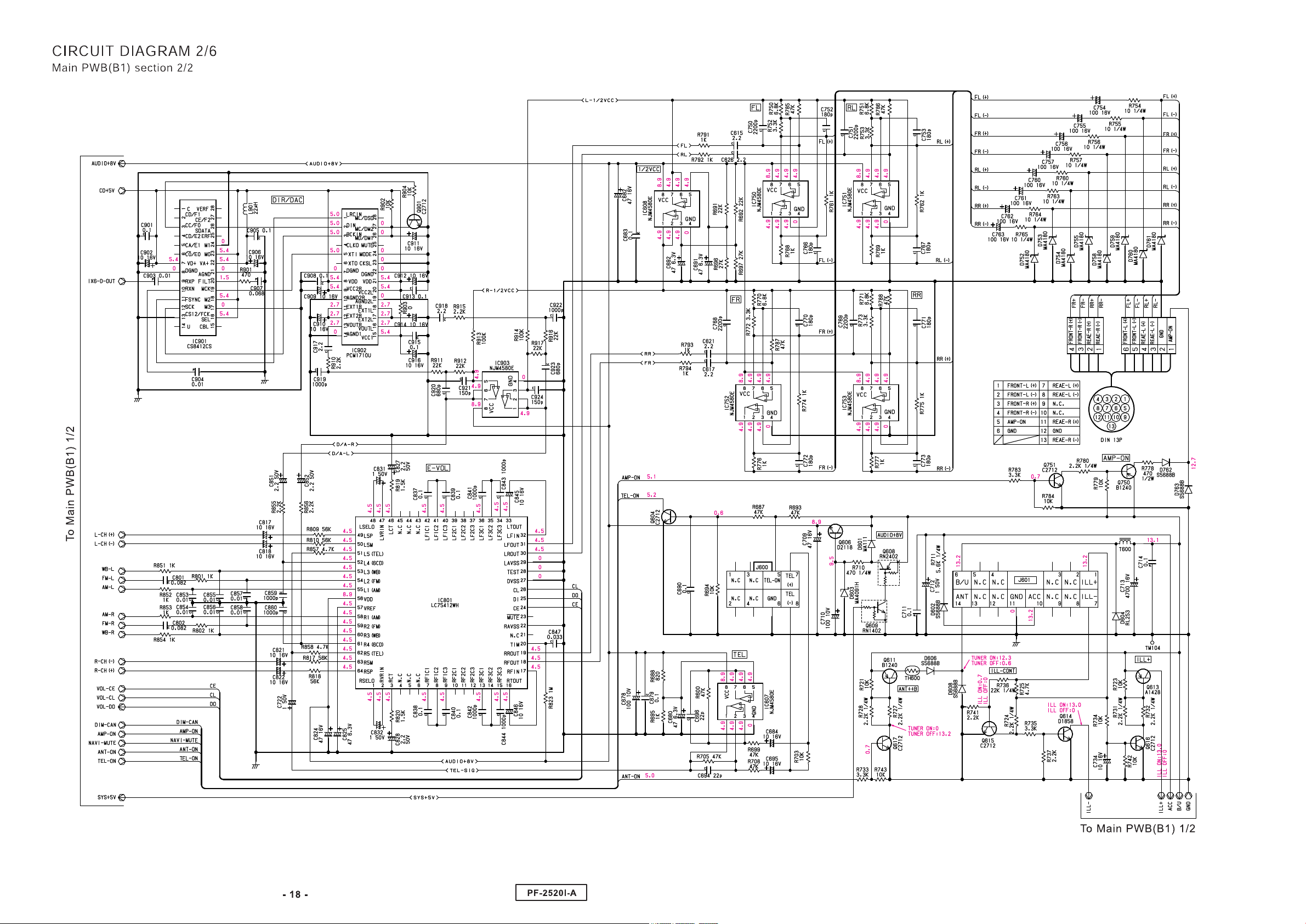
Page 21

Page 22

Page 23

Page 24

 Loading...