

Page 1

Xiamen Clarion Electrical Enterprise Co., Ltd
8/F., Xiamen Mail Processing Centre, No.275 Lujiang Road , Xiamen,China
Tel:+86-592-2389080 Fax:+86-592-2389089
Clarion Co., Ltd.
7-2, Shintoshin, Chuo-Ku, Saitama-Shi, Saitama 330-0081, Japan
Service Manual
CD/MP3/WMA Receiver
Published by Service Dept.
298-6524-00 JAN. 2008P
Printed in P.R.C.
(DB188RMP)
This product is a lead free model.
Lead free solder is used in PWB stamped LF mark.
Please keep the following conditions when you repair.
1. Use lead free solder.
* Koki's lead free solder S3X-55M 0.6mm
(CLARION Parts No.642-0231-01)
* Koki's lead free solder S3X-55M 1.0mm
(CLARION Parts No.642-0231-02)
2. Use a nitrogen solder system.
3. Do not use "General solder" and "Lead free solder"
together.
SPECIFICATIONS
Radio section
Tuning system: PLL synthesizer tuner
Receiving frequencies: FM : 87.5 MHz to 108 MHz
(0.05 MHz steps)
MW : 531 kHz to 1602 kHz
(9 kHz steps)
LW : 153 kHz to 279 kHz
(3 kHz steps)
CD player section
System: Compact disc digital audio system
Frequency response: 5Hz to 20kHz(+1/-1dB)
Dynamic range: 90dB(1kHz)
Harmonic distortion: 0.01%
MP3/WMA mode
MP3 Sampling rate: 8kHz to 48kHz
MP3 Bit rate: 8kbps to 320kbps / VBR
WMA Bit rate: 48kbps to 192kbps
Logical format: ISO9660 level1, 2
JOLIET or Romeo
General
Output power: 25 W x 4
(DIN45324, +B=14.4V)
Model
DB188RMP
(PE-3050E-A)
DB189RMP
(PE-3050E-B)
DB189RGMP
(PE-3050E-C)
Power supply voltage: 14.4V DC(10.8 to 15.6V allowable),
negative ground
Power consumption: Less than 15A
Speaker impedance: 4ohm(4ohm to 8ohm allowable)
Weight: 1.2kg
Dimensions(mm): 178(W)x50(H)x155(D)
COMPONENTS
PE-3050E-A/PE-3050E-B/PE-3050E-C
1. Source unit 1
2. Mounting bracket 300-7742-00 1
3. DCP case 335-6035-22
4. Escutcheon(OUT-ES)
5. Parts bag
5-1. Removal key 331-2497-00
5-2. Rubber part 345-3653-20
5-3. Stopper 335-4899-20 1
5-4. Screw(M5x10) 716-0726-51 1
5-5. A-lead 850-6681-50
370-6286-00
NOTE
We cannot supply PWB with component parts in principle. When
*
a circuit on PWB has failure, please repair it by component parts
base. Parts which are not mentioned in service manual are not
supplied.
Specifications and design are subject to change without notice for
*
further improvement.
Use only compact discs bearing the or mark.
*
Some CDs recorded in CD-R/CD-RW mode may not be usable.
* Windows Media , and the Windows logo are trademarks, or re-
gistered trademarks of Microsoft Corporation in the United States
and/or other countries.
* WMA is the abbreviation of Windows Media Audio, an audio file
format developed by Microsoft Corporation.
* This product includes technology owned by Microsoft Corporation
and cannot be used or distributed without a license from MSLGP.
1
1
1
2
1
1
-1-
DB188/189RMP/DB189RGMP
Page 2
To engineers in charge of repair or inspection of our products.
Before repair or inspection, make sure to follow the
instructions so that customers and Engineers in charge
of repair or inspection can avoid suffering any risk or
injury.
1. Use specified parts.
The system uses parts with special safety features against fire
and voltage. Use only parts with equivalent characteristics
when replacing them.
The use of unspecified parts shall be regarded as remodeling
for which we shall not be liable. The onus of product liability
(PL) shall not be our responsibility in cases where an accident
or failure is as a result of unspecified parts being used.
2. Place the parts and wiring back in their original positions after
replacement or re-wiring.
For proper circuit construction, use of insulation tubes, bond-
ing, gaps to PWB, etc, is involved. The wiring connection and
routing to the PWB are specially planned using clamps to keep
away from heated and high voltage parts. Ensure that they are
placed back in their original positions after repair or inspec-
tion.
If extended damage is caused due to negligence during repair, the legal responsibility shall be with the repairing company.
3. Check for safety after repair.
Check that the screws, parts and wires are put back securely
in their original position after repair. Ensure for safety reasons
there is no possibility of secondary ploblems around the repaired spots.
If extended damage is caused due to negligence of repair, the
legal responsibility shall be with the repairing company.
4. Caution in removal and making wiring connection to the parts
for the automobile.
Disconnect the battery terminal after turning the ignition key
off. If wrong wiring connections are made with the battery con-
nected, a short circuit and/or fire may occur. If extensive damage is caused due to negligence of repair, the legal responsibility shall be with the repairing company.
5. Cautions in soldering
Please do not spread liquid flux in soldering.
Please do not wash the soldering point after soldering.
6. Cautions in soldering for chip capacitors
Please solder the chip capacitors after pre-heating for replace-
ment because they are very weak to heat.
Please do not heat the chip capacitors with a soldering iron
directly.
7. Cautions in handling for chip parts.
Do not reuse removed chips even when no abnormality is ob-
served in their appearance. Always replace them with new
ones. (The chip parts include resistors, capacitors, diodes, transistors, etc).
Please make an operation test after replacement.
8. Cautions in handling flexible PWB.
Before working with a soldering iron, make sure that the iron
tip temperature is around 270 . Take care not to apply the
iron tip repeatedly (more than three times) to the same patterns.
Also take care not to apply the tip with force.
9. Turn the unit OFF during disassembly and parts replacement.
Recheck all work before you apply power to the unit.
10. Cautions in checking that the optical pickup lights up.
The laser is focused on the disc reflection surface through the
lens of the optical pickup. When checking that the laser optical diode lights up, keep your eyes more than 30cms away
from the lens. Prolonged viewing of the laser within 30cms
may damage your eyesight.
11. Cautions in handling the optical pickup.
The laser diode of the optical pickup can be damaged by electrostatic charge caused by your clothes and body. Make sure
to avoid electrostatic charges on your clothes or body, or discharge static electricity before handling the optical pickup.
11-1. Laser diode
The laser diode terminals are shorted for transportation in order to prevent electrostatic damage. After replacement, open
the shorted circuit. When removing the pickup from the mechanism, short the terminals by soldering them to prevent this
damage.
11-2. Actuator
The actuator has a powerful magnetic circuit. If a magnetic
material is put close to it. Its characteristics will change. Ensure that no foreign substances enter through the ventilation
slots in the cover.
11-3. Cleaning the lens
Dust on the optical lens affects performance.
To clean the lens, apply a small amount of isopropyl alcohol to
lens paper and wipe the lens gently.
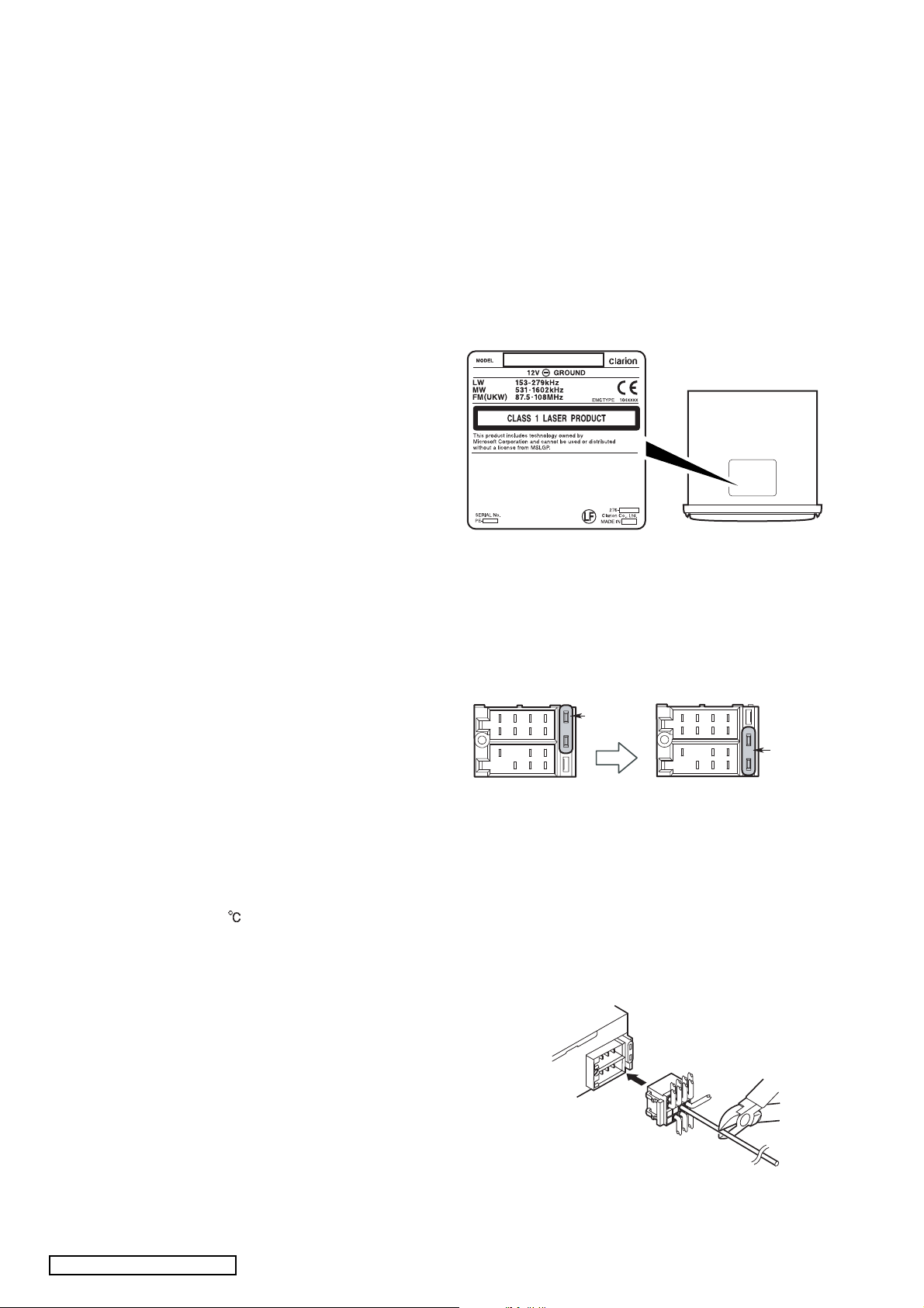
CAUTION
This appliance contains a laser system and is classified as a
"CLASS 1 LASER PRODUCT". In case of any trouble with this
player, please contact your nearest"authorized service station".
To prevent direct exposure to the laser beam, do not try to open
the enclosure.
Bottom view of
main unit
NOTES OF ISO CONNECTOR
1. For VW and Audi vehicles, change the position of fuse
installation as shown on the diagram.(Figure 1)
ISO CONNECTOR type
For other vehicles (initial position)
FUSE
(15A)
Main unit side ISO connector
Figure 1
2. When the car stereo is installed in 1998 and later Volkswagen
models, make sure to cut the car lead wire connected the A-5
terminal. (A breakdown could occur if the lead wire is not cut.)
After cutting the lead wire, isulate the front end of the lead wire
with insulation tape to prevent the risk of short-circuits.(Figure 2 )
Note: Before cutting the lead wire, disconnect the car battery --
(negative) cable.
3. When the main unit is also connected to an external amplifier,
connect REMOTE on the external amplifier to the previously
cut lead wire on the side of the connector.
For VW and Audi vehicles
FUSE
(15A)
Figure 2
DB188/189RMP/DB189RGMP
-2-
Page 3
TROUBLESHOOTING
Problem
Power does not turn on.
(No sound is produced.)
Fuse is blown.
Incorrect wiring.
Cause
Measure
Replace with a fuse of the same amperage as the old fuse.
Read the attached "Installation/Wire connection Guide" once again
and wire properly.
No sound output when
operating the unit with
amplifiers or power
antenna attached.
Nothing happens when
buttons are pressed.
GeneralCD/MP3/WMA
Display is not accurate.
No sound heard. The speaker protection circuit is
No sound heard. MP3/WMA files are absent in
Power antenna lead is shorted
to ground or excessive current
is required for remote-on the
amplifiers or power antenna.
The microprocessor has
malfunctioned due to noise,
etc.
DCP or main unit connectors
are dirty.
operating.
a disc.
Files are not recognized as an
MP3/WMA file.
File system is not correct. Use ISO9660 level 1,2 or JOLIET or Romeo file system.
1. Turn the unit off.
2. Remove all wires attached to the power antenna lead. Check
each wire for a possible short to ground using an ohm meter.
3.Turn the unit back on.
4. Reconnect each amplifier remote wire to the power antenna lead
one by one. If the amplifiers turn off before all wires are attached,
use an external relay to provide remote-on voltage
(excessive current required).
Turn off the power, then press the
[RELEASE] button and remove the DCP.
Press the reset button for about 2 seconds
with a thin rod.
Wipe the dirt off with a soft cloth moistened with cleaning alcohol.
Turn down sound volume. Function can also be restored by turning
the power off and on again.
(Speaker volume is reduced automatically when the speaker prote-
ction circuit operates).
Write MP3/WMA files onto the disc properly.
Use MP3/WMA files encoded properly.
Reset button
Sound skips or is noisy. Compact disc is dirty.
Compact disc is heavily scratch-
ed or warped.
Sound is cut or skipped.
Noise is generated or noise
is mixed with sound.
Sound is bad directly after
power is turned on.
Wrong filename File system is not correct. Use ISO9660 level 1, 2 or JOLIET or Romeo file system.
MP3/WMA files are not
encoded properly.
Water droplets may form on
the internal lens when the car
is parked in a humid place.
Clean the disc with a soft cloth.
Replace with a disc with no scratches.
Use MP3/WMA files encoded properly.
Let dry for about 1 hour with the power on.
ERROR DISPLAYS
If an error occurs, one of the following displays is displayed. Take the measures described below to eliminate the problem.
Error Display Cause Measure
CD/MP3/
WMA
ERROR 2
ERROR 3 A CD cannot be played due to scratches, etc. Replace with a non-scratched, non-warped disc.
ERROR 6
A CD is caught inside the CD deck and is not
ejected.
A CD is loaded upside-down inside the CD deck
and does not play.
This is a failure of CD deck's mechanism.
Eject the disc then reload it properly.
If an error display other than the ones described above appears, press the reset button.
-3-
DB188/189RMP/DB189RGMP
Page 4

EXPLANATION OF IC
:
:O:
:
:O:
:
:O:
:
:IN:
:
:
:IN:
:
:
:IN:
:
:IN:
:
:O:
:
:-:
:
:IN:
:
:O:
:
:-:
:
:O:
:
:O:
:
:IN:
:
:
:IN:
:
:IN:
:
:
:IN:
:
:IN:
:
:
:
:O:
:
:IN:
:
:-:
:
:O:
:
:
:O:
:
:O:
:
:
:
:
:
:
:O:
:
:-:
:
:-:
:
:
:
:O:
:
:O:
:
RDS NOISE_DCHG
:O:
:
:
:
:O:
:
:O:
:
:IN:
:
:-:
:
:O:
:
:
:
:-:
:
:-:
:
:IN:
:
:IN:
:
:IN:
:
:IN:
:
:IN:
:
:IN:
:
:IN:
:
:IN:
:
:IN:
:
:O:
:
:IN:
:
:
:O:
:
:IN:
:
:
:
:
:
:
:
:O:
:
:IN:
:
:IN:
:
:
:O:
:
:IN:
:
:O:
:
:
:
:
:
:
:
:
:
:
:
:
:
:
:
:
:
:
:
:
:IN:
:
:O:
:
:O:
:
:O:
:
:IN:
:
:IN:
:
:IN:
:
:IN:
:
:IN:
:
:O:
:
:O:
:
:O:
:
:IN:
:
:IN:
:
:IN:
:
:O:
:
:IN:
:
:O:
:
:IN:
:
:-:
:
:-:
:
:O:
:
:O:
:
:O:
:
:O:
:
:-:
:
:O:
:
:O:
:
:IN:
:
:-:
:
:O:
:
:
:
:O:
:
:O:
:
:O:
:
:-:
:
:-:
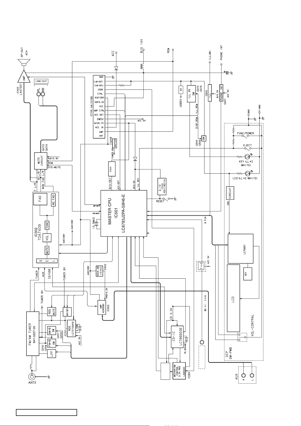
Main section
052-1955-00 LC8783J2PA-59H6-E Main System Controller
Terminal Description
DBGP0
pin 1
DBGP1
pin 2
DBGP2
pin 3
B/U_DET
pin 4
pin 5
ACC_DET:IN:ACC detection signal input.
pin 6
REMCON
RDS_CLK:IN:RDS clock pulse input.
pin 7
RES
pin 8
XT1
pin 9
XT2
pin 10
VSS
pin 11
pin 12
CF1
CF2
pin 13
VDD
pin 14
pin 15
N.C
N.C
pin 16
N.C
pin 17
S-METER:IN:RDS S-METER signal input.
pin 18
NOISE
pin 19
KEY_A/D
pin 20
pin 21
AMP_MUTE:O:Muting signal output to internal audio power
pin 22
N.C
N.C
pin 23
pin 24
MODEL_INT3:IN:The destination setting input.
TEXT PORT:O:For CD text pin, Hi=OK, Lo=NG.
pin 25
pin 26
CD_DI
pin 27
CD_DO
CD_CLK
pin 28
pin 29
CD_CE
pin 30
CD_MUTE:IN:Connect to LC786920 CD_MUTE pin.
pin 31
CD_RST
IF_REQ
pin 32
pin 33
SUB_RDY:IN:Connect to USB_READY pin.
pin 34
REG_RDY:IN:Connect to REG_READY pin.
CD_INSW1:IN:Connect to CD MECHA SW1.
pin 35
CD_INSW2:IN:Connect to CD MECHA SW2.
pin 36
pin 37
CD_DMUTE:O:Connect to CD driver IC MUTE pin.
CD_S/L
pin 38
VSS
pin 39
VDD
pin 40
pin 41
CD_ERROR:IN:Connect to CD_ERROR pin.
CD_LIMIT_SW:IN:Inside limit switch signal input.
pin 42
CD_EM
pin 43
pin 44
CD_LM
pin 45
pin 46
RDS_MUTE:O:RDS mute signal output.
pin 47
SYS_MUTE:O:System mute signal output.
N.C
pin 48
LCD_DI
pin 49
pin 50
LCD_DO
LCD_CLK
pin 51
LCD_CE
pin 52
EVOL_DATA:I/O:The serial data output to the volume IC.
pin 53
EVOL_CLK:O:Clock pulse output to the volume IC.
pin 54
VDD
pin 55
VSS
pin 56
INT_1
pin 57
pin 58
INT_2
VER_1
pin 59
pin 60
VER_2
pin 61
N.C
N.C
pin 62
pin 63
N.C
pin 64
N.C
N.C
pin 65
pin 66
N.C
pin 67
N.C
DISP_REM:O:The power supply control signal output for LCD
pin 68
pin 69
ILL_REM
pin 70
KEY_INT
INT_AMPREM:O:ON signal output to the internal amplifier.
pin 71
pin 72
AMP_REMOUT:O:The control signal output to internal audio power
Not in use.
Not in use.
Not in use.
Backup detection signal input.
Remote controller signal input terminal.
Reset signal input.
32.768kHz crystal input, sub clock
32.768kHz crystal output, sub clock
Connect to GND.
13.5MHz crystal input, main clock
13.5MHz crystal output, main clock
Positive supply voltage, connect to 5V
Not in use.
Not in use.
Not in use.
RDS noise signal input.
Input terminal of A/D converter for key judgement.
amplifier.
Connect to GND.
Connect to GND.
Connect to LC786920 DI pin.
Connect to LC786920 DO pin.
Connect to LC786920 CLK pin.
The chip enable signal output to LC786920.
Connect to LC786920 REST pin.
The tuner pack IF buffer control signal output.
Connect to CD driver IC VIN-SW pin.
Connect to GND.
Positive supply voltage, connect to 5V.
CD eject signal output for CD dirver IC.
CD_LM="L", CD_EM="H"
CD loading signal output for CD dirver IC.
CD_LM="H", CD_EM="L"
RDS noise discharge signal output.
Not in use.
Connect to LCD driver IC DI pin
Connect to LCD driver IC DO pin
The clock pulse output to the LCD dirver IC.
The chip enable signal output to the LCD dirver
IC.
Positive supply voltage, connect to 5V.
Connect to GND.
The destination setting input.
The destination setting input.
Pefrence vlotage input for A/D converter.
Pefrence vlotage input for A/D converter.
Connect to GND.
Connect to GND.
Connect to GND.
Connect to GND.
Not in use.
Not in use.
Not in use.
power and LCD backlight.
The power supply control signal output for
illumination.
Key interrupting signal input.
amplifier.
AUTO_ANT:O:Motor antenna control signal output.
pin 73
PHONE_INT:IN:The telephone interrupt signal input.
pin 74
RDS TEST 1:O:The power supply ON signal output for the
pin 75
RDS TEST 2:IN:For debug when RDS TEST.
pin 76
pin 77
N.C
pin 78
N.C
pin 79
JOG_CW
JOG_CCW:IN:JOG key signal input.
pin 80
pin 81
CD TEST
pin 82
ILL_DET
CTRL
pin 83
pin 84
OFFSET_DET:IN:The emergency signal input from the power IC.
RDS_TEST_DSR :IN
pin 85
RDS_TEST_DTR :O
pin 86
VERG : O:The reference voltage.
pin 87
VSS : -:Connect to GND.
pin 88
VDD : -:Positive voltage supply, connect to 5V.
pin 89
OSC_FM/AM : IN:FM/AM oscillation input.
pin 90
N.C : IN:Connect to GND.
pin 91
FM/AM_IFC : IN:FM/AM IF signal input.
pin 92
N.C : IN:Connect to GND.
pin 93
EO : O:PLL phase compare ERROR output.
pin 94
pin 95
SUBPD : O:For high speed lock up.
FM ON : O:The power supply control signal outpur for tuner
pin 96
pin 97
AM ON : O:The power supply control signal outpur for tuner
pin 98
MUTE_SPEED_UP: O : Station detection speed up command output
pin 99
FM-ST/SD : IN:At receiving the FM station, this port detects
RDS_DATA : IN:RDS serial data input.
pin100
051-6743-00 LC786920E
Terminal Description
pin 1
EFMIN
RFOUT
pin 2
pin 3
LPF
PHLPF
pin 4
pin 5
AIN
CIN
pin 6
pin 7
BIN
pin 8
DIN
SLCISET
pin 9
pin 10
RFMON
pin 11
VREF
JITTC
pin 12
pin 13
EIN
FIN
pin 14
PCNCNT
pin 15
TE OUT
pin 16
TE IN
pin 17
pin 18
LDD
LDS
pin 19
AVSS
pin 20
AVDD
pin 21
FDO
pin 22
TDO
pin 23
pin 24
SLDO
SPDO
pin 25
pin 26
VVSSI
pin 27
PDOUT1
PDOUT0
pin 28
PCKIST
pin 29
pin 30
VVDD1
pin 31
DMUTEB
PUIN
pin 32
pin 33
DEFECT
pin 34
FSEQ
pin 35
C2F
pin 36
DVDD
DVSS
pin 37
Not in use.
Not in use.
JOG key signal input.
For CD mecha test pin.
illumination ON signal input.
Power supply ON signal input.
The communication control signal input for RDS
PC test.
The communication control signal output for
RDS PC test.
FM+B.
AM+B.
for RDS.
the stereo signal. At seeking or scanning, this
port detects the station detection signal.
CMOS LSI for compact disc player
RF signal input terminal.
RF signal output terminal.
RF signal DC label detection LPF capacitor
connection terminal.
Wound detection LPF capacitor connection
terminal.
A signal input terminal.
C signal input terminal.
B signal input terminal.
D signal input terminal.
SLCO output Resistance connection terminal.
Inside LSI analog signal monitor terminal.
VREF voltage output terminal.
Getta detection capacitor connection terminal.
E signal input terminal.
F signal input terminal.
EFM PLL Charge Pump Control voltage input
terminal.
TE signal output terminal.
TES signal generation input terminal.
Laser power control signal output terminal.
Laser power control signal input terminal.
Connect to GND.
Analogue power supply terminal.
Focus signal output terminal. D/A output.
Tracking signal output terminal. D/A output.
Thread signal output terminal. D/A output.
Spindle signal output terminal. D/A output.
Connect to GND.
Built-in VCO control phase comparison output
terminal 1.
Built-in VCO control phase comparison output
terminal 0.
PDOUT0 output 1 Resistance connection terminal.
Connect to GND.
Not in use.
I/O:PUIN input output terminal.
Wound detection signal output terminal.
Synchronous signal output terminal, It becomes
"H" when Synchronous Idle detected from the
EFM signal is corresponding to Synchronous Idle
of internal generation.
C2 error signal output terminal.
Digital system power supply terminal.
Digitalsystem earth terminal, Must connect to 0V.
DB188/189RMP/DB189RGMP
-4-
Page 5

pin 38:DVDD15
:O:
:
:-:
:
:-:
:
:-:
:
:-:
:CE:IN:
:CL:IN:
:
:IN:
:DO:O:
:
:IN:
:
:
:
:
:
:
:
:IN:
:
:
:
:
:
:
:
:IN:
:
:O:
:
:O:
:
:O:
:
:-:
:
:IN:
:
:IN:
:
:
:-:
:
:O:
:
:-:
:
:-:
:
:O:
:
:O:
:
:-:
:
:O:
:
:IN:
:
:-:
:
:-:
:
:O:
:
:O:
:
:O:
:
:-:
:
:O:
:
:O:
:
:O:
:
:O:
:
:O:
:S5:O:
:S6:O:
:S7:O:
:S8:O:
:S9:O:
:
:O:
:
:O:
:
:O:
:
:O:
:
:O:
:
:O:
:
:O:
:
:O:
:
:O:
:
:O:
:
:O:
:
:O:
:O:
:
:O:
:
:O:
:
:O:
:
:O:
:
:O:
:
:O:
:
:O:
:
:O:
:
:O:
:
:O:
:
:O:
:
:O:
:
:O:
:
:O:
:
:O:
:
:O:
:
:
:
:O:
:
:O:
:
:O:
:
:O:
:
:O:
:
:O:
:
:O:
:
:O:
:
:IN:
:
:IN:
:
:IN:
:
:IN:
:
:IN:
:
:-:
:
:-:
:
:IN:
:
:IN:
:
:-:
:
:IN:
:
:
:DO:O:
:CE:IN:
:CL:IN:
:DI:IN:
VVDD3
pin 39
pin 40
VVSS3
pin 41
DVDD
DVSS
pin 42
pin 43
pin 44
DIN
pin 45
pin 46
RESB
pin 47
REG_READYO:O:Host IF:REG_READY output.
pin 48
pin 49
SUB_READYO:O:Host IF:SUB_READYSY output.
pin 50
CD_MUTEO:I/O:Output L fixation after reset is released.
pin 51
LOW_BAT1:I/O:Host IF:Standby control input.
CONT
pin 52
pin 53
MODE
STREQ
pin 54
STCK
pin 55
STDATA
pin 56
TEST
pin 57
DATA
pin 58
pin 59
DATACK
LRSY
pin 60
pin 61
VVDD2
pin 62
VPREF2
VCOC2
pin 63
VPDOUT2:O:Building VCO into control output terminal.
pin 64
VVSS2
pin 65
DVDD15
pin 66
DVSS
pin 67
DVDD
pin 68
DOUT
pin 69
AMUTEB
pin 70
pin 71
XVSS
XOUT
pin 72
XIN
pin 73
XVDD
pin 74
LRVDD
pin 75
pin 76
LCHO
LRREF
pin 77
RCHO
pin 78
pin 79
LRVSS
SLCO
pin 80
051-6095-00 LC75857W
Terminal Description
P1/S1
pin 1
P2/S2
pin 2
P3/S3
pin 3
P4/S4
pin 4
pin 5
pin 6
pin 7
pin 8
pin 9
S10
pin 10
pin 11
S11
Digital circuit power source capacitor earth terminal.
Building PLL into power supply terminal.
Connect to GND.
Digital system power supply terminal.
Digital system earth terminal, Must connect to 0V.
Host IF:Enable signal input terminal.
Host IF:Data transfer clock input terminal.
Host IF:Data input terminal.
Host IF:Data output terminal.
(Nch opening drain output)
The external of the Pull-Up resistance is necessary.
LIS reset input terminal.
Once you turn on the power supply , It turn to "L" .
(Nch opening drain output)
The external of the Pull-Up resistance is necessary.
(Nch opening drain output)
The external of the Pull-Up resistance is necessary.
Host IF:CD_MUTE request output.
(Nch opening drain output)
The external of the Pull-Up resistance is necessary.
I/O:Connect to GND.
Setting Input terminal, Must connect to DVDD.
I/O:Stream data demand signal output terminal.
I/O:Stream data bit clock input terminal.
I/O:Stream data input terminal.
Connect to GND.
Lch/Rch channel data output terminal.
Bit clock output terminal.
Lch/Rch clock output terminal.
Building VCO into Power supply terminal.
Building VCO into oscillation cooking stove setting
input terminal.
Building VCO into Control setting voltage terminal.
Building VCO into earth terminal, Must connect
to 0V.
Digital circuit power source capacitor earth terminal.
Digital system power supply terminal, Must
connect to 0V.
Digital system power supply terminal
Digital out output terminal, EIAJ format.
CD_MUTE0 signal output terminal.
Connect to GND.
16.9344MHz departure pendulum Connected
terminal.
16.9344MHz departure pendulum Connected
terminal.
Oscillation circuit Power supply terminal.
LR channel power supply terminal.
L channel output terminal.
LR channel Reference output terminal.
R channel output terminal.
Connect to GND.
Slice label control output terminal.
CMOS IC 1/3, 1/4 Duty LCD Display
Drivers with Key Input Function
Segment outputs for displaying the display data
transferred by serial data input.
Segment outputs for displaying the display data
transferred by serial data input.
Segment outputs for displaying the display data
transferred by serial data input.
Segment outputs for displaying the display data
transferred by serial data input.
Segment outputs for displaying the display data
transferred by serial data input.
Segment outputs for displaying the display data
transferred by serial data input.
Segment outputs for displaying the display data
transferred by serial data input.
Segment outputs for displaying the display data
transferred by serial data input.
Segment outputs for displaying the display data
transferred by serial data input.
Segment outputs for displaying the display data
transferred by serial data input.
Segment outputs for displaying the display data
transferred by serial data input.
pin 12
S12
pin 13
S13
S14
pin 14
S15
pin 15
S16
pin 16
S17
pin 17
pin 18
S18
S19
pin 19
S20
pin 20
S21
pin 21
:
pin 22 S22
S23
pin 23
S24
pin 24
S25
pin 25
S26
pin 26
S27
pin 27
S28
pin 28
S29
pin 29
S30
pin 30
S31
pin 31
S32
pin 32
S33
pin 33
S34
pin 34
S35
pin 35
S36
pin 36
S37
pin 37
S38
pin 38
COM4/S39:O:Common driver outputs.
pin 39
:
pin 40 COM3 : O
COM2
pin 41
pin 42
COM1
pin 43
KS1/S40
KS2/S41
pin 44
pin 45
KS3/S42
pin 46
KS4
KS5
pin 47
pin 48
KS6
pin 49
KI1
KI2
pin 50
pin 51
KI3
pin 52
KI4
pin 53
KI5
VDD
pin 54
pin 55
VLCD
pin 56
VLCD1
VLCD2
pin 57
VSS
pin 58
pin 59
TEST
pin 60
OSC
pin 61
pin 62
pin 63
pin 64
Segment outputs for displaying the display data
transferred by serial data input.
Segment outputs for displaying the display data
transferred by serial data input.
Segment outputs for displaying the display data
transferred by serial data input.
Segment outputs for displaying the display data
transferred by serial data input.
Segment outputs for displaying the display data
transferred by serial data input.
Segment outputs for displaying the display data
transferred by serial data input.
Segment outputs for displaying the display data
transferred by serial data input.
Segment outputs for displaying the display data
transferred by serial data input.
Segment outputs for displaying the display data
transferred by serial data input.
Segment outputs for displaying the display data
transferred by serial data input.
Segment outputs for displaying the display data
transferred by serial data input.
Segment outputs for displaying the display data
transferred by serial data input.
Segment outputs for displaying the display data
transferred by serial data input.
Segment outputs for displaying the display data
transferred by serial data input.
Segment outputs for displaying the display data
transferred by serial data input.
Segment outputs for displaying the display data
transferred by serial data input.
Segment outputs for displaying the display data
transferred by serial data input.
Segment outputs for displaying the display data
transferred by serial data input.
Segment outputs for displaying the display data
transferred by serial data input.
Segment outputs for displaying the display data
transferred by serial data input.
Segment outputs for displaying the display data
transferred by serial data input.
Segment outputs for displaying the display data
transferred by serial data input.
Segment outputs for displaying the display data
transferred by serial data input.
Segment outputs for displaying the display data
transferred by serial data input.
Segment outputs for displaying the display data
transferred by serial data input.
Segment outputs for displaying the display data
transferred by serial data input.
Segment outputs for displaying the display data
transferred by serial data input.
Common driver outputs.
Common driver outputs.
Common driver outputs.
Key scan outputs.
Key scan outputs.
Key scan outputs.
Key scan outputs.
Key scan outputs.
Key scan outputs.
Key scan inputs.
Key scan inputs.
Key scan inputs.
Key scan inputs.
Key scan inputs.
Logic block power supply connection.
LCD driver block power supply connection.
Used for applying the LCD drive 2/3 bias voltage
externally.
Used for applying the LCD drive 1/3 bias voltage
externally.
Power supply connection. Connect to ground.
This pin must be connected to ground.
I/O:The OSC pin can be used to form an oscillator
circuit with an external resistor and an external
capacitor.
Serial data interface connections to the controller.
Serial data interface connections to the controller.
Serial data interface connections to the controller.
Serial data interface connections to the controller.
-5-
DB188/189RMP/DB189RGMP
Page 6
BLOCK DIAGRAM
Main section
DET
S80850CNMC
DET
IC 701
DISPLAY
DRIVER
MATRIX
DIF
DB188/189RMP/DB189RGMP
-6-
MECH
IC801
WIRE REMOTE
IC802
Page 7

EXPLODED VIEW / PARTS LIST
(
)
(
)
)
(
)
(
)
)
(
)
)
(
)
)
(
)
(
)
(
)
)
(
)
(FW)(
)
(FW)(
)
(
)
T
(
(
)
(
)
(FF)(
)
(FF)(
)
(
)
(
)
(TA)(
)
(TA)(
)
(
)
(
)
(
)
(
)
(
)
(
)
(
)
DCP section
1-17
1-40
1-41
1-16
1-15
1-18
1-19
1-18
1-4
1-3
1-13
1-7
1-6
1-5
1-14
1-8
1-9
1-43
1-12
1-39
1-11
1-21
1-46
1-46
1-44
1-42 (PE3050EA)
1-23
1-39
1-38
1-45
1-22
1-24
1-20
1-33
1-36
1-35
1-33
1-34
1-34
1-33
1-34
1-32
1-34
1-31
1-10
1-37
1-30
1-29
1-2
1-1
: SANKOL application
Note) SANKOL uses CFD-409Z
NO. PART NO. DESCRIPTION Q'TY NO. PART NO. DESCRIPTION Q'TY
1 DCP-622-700 DCP ASSY
DCP-623-700 DCP ASSY
DCP-624-700 DCP ASSY
1-1 373-1162-00 DIAL-CVR
373-1162-07 DIAL-CVR
373-1162-08 DIAL-CVR
1-2 347-7999-00 DOUBLE FACE 1 1-23 382-8589-00 BUTTON
1-3 347-8265-00 DOUBLE FACE 2 1-24 382-8584-00 BUTTON
1-4 380-5717-01 KNOB 1 1-25 331-4527-00 LCD COVER 1
1-5 382-8583-00 BUTTON
382-8583-01 BUTTON
1-6 382-8586-00 BUTTON
382-8586-01 BUTTON
1-7 382-8579-00 BUTTON
382-8579-01 BUTTON
1-8 382-8580-00 BUTTON
382-8580-02 BUTTON
1-9 382-8585-00 BUTTON
382-8585-01 BUTTON
1-10 382-8581-00 BUTTON
382-8581-02 BUTTON
1-11 382-8582-00 BUTTON
382-8582-03 BUTTON
1-12 382-8578-00 BUTTON
382-8578-02 BUTTON
1-13 370-6321-00 ESCUTCHEON 1-42 347-8428-00 FILM
1-14 382-8587-00 BUTTON
1-15 750-6858-00 SPRING
1-16 335-8224-00 BAR ILLUMI
335-8224-01 BAR ILLUMI
PE-3050E-A
PE-3050E-B
PE-3050E-C
PE-3050E-A
PE-3050E-B
PE-3050E-C
SRC)(PE-3050E-A
SRC)(PE-3050E-B/C
PE-3050E-A
PE-3050E-B/C
EJECT)(PE-3050E-A
EJECT)(PE-3050E-B/C)1 1-31 335-8228-00 LCD HOLDER 1
DISP)(PE-3050E-A
DISP)(PE-3050E-B/C
PE-3050E-A
PE-3050E-B/C
BND)(PE-3050E-A
BND)(PE-3050E-B/C
PE-3050E-A
PE-3050E-B/C
ENT)(PE-3050E-A
ENT)(PE-3050E-B/C
RELEASE
RELEASE
PE-3050E-A
PE-3050E-B/C
1-26
1-25
1 1-17 335-8226-00 ILLUMI PLATE 1
1 1-18 716-0872-62 SCREW(M1.7X6
1 1-19 335-8225-00 REAR COVER 1
1 1-20 716-1764-50 PAD SCREW(M1.7X6
1 1-21 382-8588-00 BUTTON(1/3
1 1-22 382-8617-00 BUTTON(4/6
1
1-26 379-1401-41 INDICATOR(LCD
1 1-27 347-8410-00 BLACK FILM 1
1-28 347-8411-00 SHADE FILM 1
1
1 1-29 335-8227-00 LCD ILLUMI 1
1 1-30 345-6177-00 RUBBER PAR
1-32 ----------- SWITCH PWB 1
1
1 1-33 013-6312-50 TACT SWITCH 15
1-34 001-7114-90 DIODE 6
1
1-35 076-0615-50 PLUG 1
1
1-36 016-9901-02 VR W/SHAFT 1
1
1 1-37 347-8412-00 REFLECTOR 1
1
1-38 347-8413-00 FILM 1
1-39 347-8414-00 FILM 3
1
1-40 347-8421-00 SHADE 1
1
1 1-41 347-8426-00 FILM 1
1
1 1-43 347-8429-00 FILM 1
1 1-44 347-8431-00 FILM 1
1
1-45 347-8481-00 FILM 2
1-46 345-6224-00 CUSHION 2
1
1-27
1-28
Note)Several different parts of the same
reference number are alternative parts.
One of those parts is used in the set.
PE-3050E-A
1
2/5
SOUND
4
1
1
1
1
1
1
1
1
-7-
DB188/189RMP/DB189RGMP
Page 8

Main section
(
)
)
(
)
K
(
)
(
)
(
)
T
(
(
)
(P)
)
K
(
)
(
)
(P)
35
34
35
34
33
35
33
34
32
35
24
27
25
37
24
26
28
41
24
39
20
38
40
27
21
28
23
43
44
43
42
35
10
14
13
9
8
12
11
19
36
17
15
16
7
1
2
3
4
5
6
29
18
31
30
22
Note) CD MECHANISM 929-4002-00 is exchanged
correspondence, it is not being possible to repair.
NO. PART NO. DESCRIPTION Q'TY NO. PART NO. DESCRIPTION Q'TY
1 074-1217-50 OUTLET SOCKET
2 074-2246-67 OUTLET SOCKET
3 ----------- MAIN PWB 1 26 347-8456-00 FILM 1
4 013-6100-00 TACT SWITCH 1 27 345-6201-00 CUSHION 2
5 941-0227-30 TUNER PAC
6 092-4000-51 ANT-RECEPT 1 29 347-8427-00 FILM 1
7 075-0393-50 JACK 1 30 276-0372-00 SETPLATE
8 051-3349-00 IC 1 276-0396-00 SETPLATE
9 051-2060-00 IC 1 276-0397-00 SETPLATE
10 009-9006-60 CHOKE 1 31 311-1859-05 LOWER CASE 1
009-9006-70 CHOKE 1 32 345-3799-20 RUBBER PAR
11 331-4533-00 JACK HOLDER 1 33 714-2610-85 MACHINE SCREW
12 331-3935-02 IC HOLDER 1 34 714-3006-85 MACHINE SCREW
13 074-1285-00 OUTLET SOCKET
14 060-0057-57 AUTO FUSE(15A) 1 36 313-2006-02 HEAT SIN
15 855-5426-53 RCA PIN CORD
16 ----------- ISO PWB 1 38 929-4002-00 CD MECHANISM 1
17 331-3562-02 CONNECTOR-HOLD 1 39 341-1627-00 SHAFT 1
18 854-4619-50 AUX LEAD 1 40 750-3219-00 SPRING
19 347-8489-00 FILM 1 41 335-5915-01 HOOK 1
20 382-8567-00 BUTTON
21 750-6861-00 SPRING 1 43 076-0502-55 PLUG 1
22 346-0194-00 LEATHER SHEET 1 44 ----------- AUX PWB 1
23 075-9021-50 JACK 1
12P
12P
2CH
1 24 731-2606-8B TAPTIGHT(M2.6X6
1 25 347-8490-00 FILM 1
1 28 345-6195-00 CUSHION 2
PE-3050E-A
PE-3050E-B
PE-3050E-C
M2.6X10)3
M3X6
1 35 731-3008-89 TAPTIGHT(M3X8
1 37 310-1871-00 UPPER CASE 1
F-HOOK
1 42 370-6322-01 INNER-ES 1
3
1
1
1
2
3
5
1
1
DB188/189RMP/DB189RGMP
-8-
Page 9

REF No. PART No. DESCRIPTION REF No. PART No. DESCRIPTION REF No. PART No. DESCRIPTION
ANT2 092-4000-51 ANT-RECEPT C319 043-1735-90 100pF C820 043-1608-90 0.1uF
BL1 941-0227-30 TUNER PACK C320 043-1735-90 100pF C821 043-1804-90 0.1uF
C118 043-1608-90 0.1uF C321 187-1063-35 16V 10uF C822 043-1802-90 0.01uF
C119 043-1608-90 0.1uF C322 187-1063-35 16V 10uF C824 043-1804-90 0.1uF
C120 187-1073-15 6.3V 100uF C337 187-1063-35 16V 10uF C825 043-1824-90 0.22uF
C121 043-1608-90 0.1uF C338 187-1063-35 16V 10uF C826 043-1625-90 0.022uF
C122 187-1073-35 16V 100uF C339 187-1063-35 16V 10uF C827 043-1608-90 0.1uF
C123 043-1608-90 0.1uF C340 187-1063-35 16V 10uF C828 187-1073-15 6.3V 100uF
C124 187-1073-35 16V 100uF C346 043-1841-90 0.047uF C829 043-1608-90 0.1uF
C125 043-1608-90 0.1uF C401 042-1715-00 16V 3300uF C830 043-1804-90 0.1uF
C200 187-1063-35 16V 10uF C413 178-4742-78 0.47uF C831 187-1073-15 6.3V 100uF
C201 043-1804-90 0.1uF C414 178-4742-78 0.47uF C833 189-3373-11 6.3V 330uF
C202 043-1727-90 47pF C415 178-4742-78 0.47uF C834 189-4773-22 10V 470uF
C203 043-1817-90 0.018uF C416 178-4742-78 0.47uF C835 043-1804-90 0.1uF
C204 043-1817-90 0.018uF C421 043-1620-90 4700pF C836 163-4753-55 50V 4.7uF
C205 043-1623-90 560pF C428 187-1063-35 16V 10uF C837 163-4753-55 50V 4.7uF
C206 043-1804-90 0.1uF C435 178-4742-78 0.47uF C838 043-1800-90 1000pF
C207 189-2273-21 10V 220uF C442 187-1053-65 50V 1uF C839 043-1800-90 1000pF
C208 043-1617-90 6800pF C445 172-1041-15 0.1uF C840 043-1800-90 1000pF
C209 187-1073-25 10V 100uF C447 043-1751-90 470pF C841 043-1800-90 1000pF
C210 187-1073-25 10V 100uF C449 043-1751-90 470pF C842 043-1731-90 68pF
C211 043-1804-90 0.1uF C450 043-1751-90 470pF C843 043-1731-90 68pF
C212 043-1804-90 0.1uF C451 043-1751-90 470pF C844 043-1608-90 0.1uF
C213 187-1073-25 10V 100uF C452 043-1751-90 470pF C845 043-1608-90 0.1uF
C214 043-1804-90 0.1uF C453 043-1751-90 470pF C846 043-1608-90 0.1uF
C215 172-6831-15 0.068uF C454 043-1751-90 470pF C847 187-1053-65 50V 1uF
C216 043-1607-90 0.01uF C455 043-1751-90 470pF C848 187-1073-15 6.3V 100uF
C217 043-1607-90 0.01uF C500 187-3363-45 10V 33uF C849 043-1804-90 0.1uF
C218 043-1601-90 100pF C501 168-1052-78 50V 1uF C850 043-1804-90 0.1uF
C219 043-1713-90 12pF C502 043-1608-90 0.1uF C853 189-4773-22 10V 470uF
C220 043-1713-90 12pF C503 043-1608-90 0.1uF C854 043-1841-90 0.047uF
C221 043-1622-90 330pF C504 168-1052-78 50V 1uF C855 043-1608-90 0.1uF
C222 043-1719-90 22pF C505 043-1804-90 0.1uF C856 043-1804-90 0.1uF
C223 043-1804-90 0.1uF C506 043-0540-00 16V 10uF C857 187-1073-15 6.3V 100uF
C224 187-1073-25 10V 100uF C507 163-1063-35 16V 10uF C858 043-1804-90 0.1uF
C226 187-1053-65 50V 1uF C508 043-1710-90 9pF C859 187-1073-15 6.3V 100uF
C227 043-1804-90 0.1uF C509 043-1710-90 9pF C860 187-1073-15 6.3V 100uF
C230 043-1607-90 0.01uF C510 043-1719-90 22pF C861 043-1608-90 0.1uF
C231 187-4763-15 6.3V 47uF C511 043-1719-90 22pF C870 187-1073-35 16V 100uF
C232 043-1802-90 0.01uF C512 043-1607-90 0.01uF D100 001-0592-61 1N5404
C233 187-4753-65 50V 4.7uF C513 043-1601-90 100pF D109 001-0466-61 1A4
C234 043-1735-90 100pF C514 042-1577-00 6.3V 100uF D201 001-1323-90 L1SS355T1G
C235 043-1735-90 100pF C515 043-1607-90 0.01uF D202 001-1323-90 L1SS355T1G
C236 043-1618-90 0.018uF C516 189-1083-12 6.3V 1000uF D302 001-4316-17 LM3Z4V3T1G
C237 043-1625-90 0.022uF C800 187-1073-15 6.3V 100uF D401 001-4316-24 LM3Z8V2T1G
C238 043-1626-90 820pF C801 043-1620-90 4700pF D402 001-1323-90 L1SS355T1G
C239 043-1624-90 680pF C802 043-1802-90 0.01uF D403 001-1323-90 L1SS355T1G
C240 043-1600-90 10pF C803 043-1804-90 0.1uF D500 001-1323-90 L1SS355T1G
C244 043-1625-90 0.022uF C804 043-1804-90 0.1uF D502 001-4301-26 HZU4.7B2
C245 043-1607-90 0.01uF C805 187-3363-25 6.3V 33uF D503 001-1323-90 L1SS355T1G
C250 187-4763-35 16V 47uF C806 043-1804-90 0.1uF D504 001-1323-90 L1SS355T1G
C307 187-1053-65 50V 1uF C807 187-1073-15 6.3V 100uF D505 001-1323-90 L1SS355T1G
C308 187-1053-65 50V 1uF C809 043-1804-90 0.1uF D506 001-1323-90 L1SS355T1G
C309 187-1053-65 50V 1uF C810 043-1804-90 0.1uF D507 001-1323-90 L1SS355T1G
C310 187-1053-65 50V 1uF C811 043-1802-90 0.01uF D509 001-4301-41 HZU7.5B2
C311 187-1053-65 50V 1uF C812 043-1606-90 1000pF D510 001-4301-41 HZU7.5B2
C312 187-1053-65 50V 1uF C813 043-1804-90 0.1uF D511 001-4301-41 HZU7.5B2
C313 187-4763-15 6.3V 47uF C814 043-1607-90 0.01uF D512 001-4301-41 HZU7.5B2
C314 187-1063-35 16V 10uF C815 187-1073-15 6.3V 100uF D521 001-1323-90 L1SS355T1G
C315 043-1735-90 100pF C816 168-1052-78 50V 1uF D801 001-1323-90 L1SS355T1G
C316 043-1735-90 100pF C817 043-1606-90 1000pF D802 001-0644-90 MA113
C317 043-1804-90 0.1uF C818 043-1608-90 0.1uF IC105 051-3349-00 HA13166
C318 187-4763-35 16V 47uF C819 187-1073-15 6.3V 100uF IC201 051-4620-90 LC72725KM
ELECTRICAL PARTS LIST
Main PWB(B1) section
Note)1. Several different parts of the same reference number are alternative parts.
One of those parts is used in the set.
2. Some parts depend on each model. The model name is specified in the description.
-9-
DB188/189RMP/DB189RGMP
Page 10

REF No. PART No. DESCRIPTION REF No. PART No. DESCRIPTION REF No. PART No. DESCRIPTION
IC202 051-0350-93 NJM4558 Q516 125-0021-91 DTA114EUA R454 119-2231-15 1/10W 22k ohm
IC302 051-5028-90 TDA7409 Q516 125-0034-92 RT1P141M R456 119-3311-15 1/10W 330 ohm
IC305 051-3060-90 AZ4558C Q801 190-2060-00 2SA2060 R457 119-2231-15 1/10W 22k ohm
IC402 051-2060-00 LA47201 Q802 101-0941-00 2SB941 R459 033-1021-15 1/16W 1k ohm
IC501 052-1955-00 LC8783J2PA- R154 116-1521-15 1/4WS 1.5k ohm R500 116-4721-15 1/4WS 4.7k ohm
59H6-E R156 119-1241-15 1/10W 120k ohm R501 119-4731-15 1/10W 47k ohm
IC502 051-5443-38 S80850CNMC R200 119-1031-15 1/10W 10k ohm R502 033-4721-15 1/16W 4.7k ohm
IC503 051-5437-58 R3111N211A R201 119-5631-15 1/10W 56k ohm R503 033-4731-15 1/16W 47k ohm
IC801 051-6743-00 LC786920E R202 033-1001-15 1/16W 10 ohm R504 033-4721-15 1/16W 4.7k ohm
IC802 051-6096-90 LA6242H R203 116-3311-15 1/4WS 330 ohm R505 033-1031-15 1/16W 10k ohm
J501 074-1217-50 12P R204 033-1011-15 1/16W 100 ohm R506 033-1041-15 1/16W 100k ohm
J502 075-0393-50 JACK R205 119-5121-15 1/10W 5.1k ohm R507 033-6831-15 1/16W 68k ohm
J801 074-2246-67 17P R206 119-5111-15 1/10W 510 ohm R509 119-1031-15 1/10W 10k ohm
L201 010-2003-04 30uH(Variable) R207 119-0000-05 1/10W 0 ohm J W R512 119-0000-05 1/10W 0 ohm JW
L202 010-3105-67 1k ohm/100MHz R208 119-0000-05 1/10W 0 ohm JW R513 033-4731-15 1/16W 47k ohm
L203 010-3105-67 1k ohm/100MHz R209 119-2711-15 1/10W 270 ohm R514 033-4731-15 1/16W 47k ohm
L205 010-2275-53 220uH R212 119-0000-05 1/10W 0 ohm JW R515 119-1841-15 1/10W 180k ohm
L206 010-6009-57 0.56uH R213 119-1021-15 1/10W 1k ohm R516 033-4731-15 1/16W 47k ohm
L301 010-6009-84 100uH R214 119-5621-15 1/10W 5.6k ohm R518 033-1031-15 1/16W 10k ohm
L302 010-3105-67 1k ohm/100MHz R222 119-4721-15 1/10W 4.7k ohm R521 033-5641-15 1/16W 560k ohm
L303 010-3105-67 1k ohm/100MHz R223 119-4721-15 1/10W 4.7k ohm R526 033-1031-15 1/16W 10k ohm
L501 010-3112-90 1k ohm/100MHz R224 119-2231-15 1/10W 22k ohm R527 033-1031-15 1/16W 10k ohm
L502 010-3123-90 2.2uH R226 033-3311-15 1/16W 330 ohm R528 033-5621-15 1/16W 5.6k ohm
L503 010-3123-90 2.2uH R227 033-1021-15 1/16W 1k ohm R529 119-4721-15 1/10W 4.7k ohm
L504 010-3123-90 2.2uH R228 033-1231-15 1/16W 12k ohm R530 033-1031-15 1/16W 10k ohm
L801 010-6009-76 22uH R229 033-1031-15 1/16W 10k ohm R531 033-4721-15 1/16W 4.7k ohm
L802 010-6009-76 22uH R231 033-3321-15 1/16W 3.3k ohm R532 119-4721-15 1/10W 4.7k ohm
Q200 198-0669-00 2SK669 R232 033-3331-15 1/16W 33k ohm R533 033-1041-15 1/16W 100k ohm
Q201 125-0025-93 RN2303 R233 119-4741-15 1/10W 470k ohm R534 033-1031-15 1/16W 10k ohm
Q201 125-0034-93 RT1P241M R234 033-1041-15 1/16W 100k ohm R535 033-4731-15 1/16W 47k ohm
Q202 125-0025-93 RN2303 R235 033-2211-15 1/16W 220 ohm R536 033-2231-15 1/16W 22k ohm
Q202 125-0034-93 RT1P241M R236 119-3311-15 1/10W 330 ohm R537 033-1041-15 1/16W 100k ohm
Q203 125-2027-92 DTC124EUA R237 119-5631-15 1/10W 56k ohm R538 119-4711-15 1/10W 470 ohm
Q203 125-2041-93 RT1N241M R313 033-2711-15 1/16W 270 ohm R539 119-4711-15 1/10W 470 ohm
Q204 125-4024-90 3DG3875 R314 033-2711-15 1/16W 270 ohm R540 119-0000-05 1/10W 0 ohm JW
Q205 125-0025-93 RN2303 R315 033-2711-15 1/16W 270 ohm R541 119-1021-15 1/10W 1k ohm
Q205 125-0034-93 RT1P241M R316 033-2711-15 1/16W 270 ohm R542 119-1021-15 1/10W 1k ohm
Q206 125-2027-92 DTC124EUA R317 119-3311-15 1/10W 330 ohm R543 033-4721-15 1/16W 4.7k ohm
Q206 125-2041-93 RT1N241M R319 119-0000-05 1/10W 0 ohm JW R558 119-0000-05 1/10W 0 ohm JW
Q207 125-2027-91 DTC114EUA R321 119-0000-05 1/10W 0 ohm J W R560 033-0000-05 0.5A 0 ohm
Q207 125-2041-92 RT1N141M R325 032-0140-89
1/10W 47k ohm(F)
R561 033-3311-15 1/16W 330 ohm
Q208 125-4011-90 KTD863YAT R326 032-0140-89
1/10W 47k ohm(F)
R562 033-1521-15 1/16W 1.5k ohm
Q209 125-2027-92 DTC124EUA R328 032-0140-89
1/10W 47k ohm(F)
R563 119-0000-05 1/10W 0 ohm JW
Q209 125-2041-93 RT1N241M R329 032-0140-89
1/10W 47k ohm(F)
R801 033-3311-15 1/16W 330 ohm
Q403 125-4024-90 3DG3875 R332 032-0140-89
1/10W 47k ohm(F)
R802 119-1031-15 1/10W 10k ohm
Q404 125-2027-95 DTC143ZUA R333 032-0140-89
1/10W 47k ohm(F)
R804 033-4711-15 1/16W 470 ohm
Q404 125-2041-96 RT1N141M R334 032-0140-89
1/10W 47k ohm(F)
R805 033-4721-15 1/16W 4.7k ohm
Q405 125-2198-90 KRC110S R335 032-0140-89
1/10W 47k ohm(F)
R806 033-4721-15 1/16W 4.7k ohm
Q409 125-0021-95 DTA143ZUA R344 119-1021-15 1/10W 1k ohm R807 116-3391-15 1/4W 3.3 ohm
Q409 125-0034-96 RT1P436M R346 119-1041-15 1/10W 100k ohm R808 119-0000-05 1/10W 0 ohm JW
Q413 125-4012-90 KTD1304 R347 119-1041-15 1/10W 100k ohm R809 119-0000-05 1/10W 0 ohm JW
Q414 125-4012-90 KTD1304 R408 033-8221-15 1/16W 8.2k ohm R810 119-2231-15 1/10W 22k ohm
Q500 125-4024-90 3DG3875 R409 119-1021-15 1/10W 1k ohm R811 119-1531-15 1/10W 15k ohm
Q501 125-3014-90 ISA1602AM1 R410 033-1021-15 1/16W 1k ohm R812 119-2231-15 1/10W 22k ohm
Q501 190-1576-00 2SA1576A R411 033-4711-15 1/16W 470 ohm R813 119-2231-15 1/10W 22k ohm
Q502 125-3014-90 ISA1602AM1 R412 033-2231-15 1/16W 22k ohm R815 033-6811-15 1/16W 680 ohm
Q502 190-1576-90 2SA1576A R413 033-4721-15 1/16W 4.7k ohm R817 033-6811-15 1/16W 680 ohm
Q503 125-2027-91 DTC114EUA R424 033-1231-15 1/16W 12k ohm R818 033-6831-15 1/16W 68k ohm
Q503 125-2041-92 RT1N141M R425 119-0000-05 1/10W 0 ohm JW R820 119-1011-15 1/10W 100 ohm
Q504 125-2027-92 DTC124EUA R427 033-1021-15 1/16W 1k ohm R821 119-1011-15 1/10W 100 ohm
Q504 125-2041-93 RT1N241M R428 033-1021-15 1/16W 1k ohm R825 119-3921-15 1/10W 3.9k ohm
Q505 125-0021-91 DTA114EUA R429 033-1021-15 1/16W 1k ohm R826 119-3921-15 1/10W 3.9k ohm
Q505 125-0034-92 RT1P141M R430 033-1021-15 1/16W 1k ohm R827 119-3921-15 1/10W 3.9k ohm
Q515 125-2027-92 DTC124EUA R446 033-1031-15 1/16W 10k ohm R828 033-2731-15 1/16W 27k ohm
Q515 125-2041-93 RT1N241M R453 119-3311-15 1/10W 330 ohm R829 033-1021-15 1/16W 1k ohm
DB188/189RMP/DB189RGMP
-10-
Page 11

Switch PWB(B2) section
REF No. PART No. DESCRIPTION REF No. PART No. DESCRIPTION REF No. PART No. DESCRIPTION
C701 043-1841-90 0.047uF Q713 125-2027-92
TRANSISTOR
S703 013-6312-50 SWITCH
C702 043-1841-90 0.047uF Q713 125-2041-93
RT1N241M
S704 013-6312-50 SWITCH
C703 043-1841-90 0.047uF Q714 125-2027-92 TRANSISTOR S705 013-6312-50 SWITCH
C704 043-1800-90 1000pF Q714 125-2041-93 RT1N241M S706 013-6312-50 SWITCH
C705 042-0423-97 16V 10uF TAN R701 119-3311-15 1/10W 330 ohm S707 013-6312-50 SWITCH
C707 043-1841-90 0.047uF
R702 119-3931-15 1/10W 39k ohm
S709 013-6312-50 SWITCH
D702 001-4907-90 PG05GBUSU
R703 119-1041-15 1/10W 100k ohm
S710 013-6312-50 SWITCH
D705 001-4301-29 HZU5.1B2 R704 119-3921-15 1/10W 3.9k ohm S711 013-6312-50 SWITCH
D706 001-4301-29 HZU5.1B2 R709 119-4721-15 1/10W 4.7k ohm S713 013-6312-50 SWITCH
D707 001-4907-90 PG05GBUSU R715 119-1021-15 1/10W 1k ohm S714 013-6312-50 SWITCH
D708 001-4907-90 PG05GBUSU R716 119-1021-15 1/10W 1k ohm S715 013-6312-50 SWITCH
D717 001-4301-29 HZU5.1B2 R717 119-1021-15 1/10W 1k ohm S716 013-6312-50 SWITCH
D718 001-4301-41 HZU7.5B2 R718 119-1021-15 1/10W 1k ohm S717 013-6312-50 SWITCH
D720 001-4301-51 HZU10B3 R723 119-0000-05 1/10W 0 ohm JW S718 016-9901-02 VR W/SHAFT
IC701 051-6095-00 LC75857 S701 013-6312-50 SWITCH PWB 039-3208-01 PWB(WITHOUT
J701 076-0615-50 12P S702 013-6312-50 SWITCH COMPONENT)
LCD701
379-1401-41
INDICATOR(LCD)
REF No. PART No. DESCRIPTION REF No. PART No. DESCRIPTION REF No. PART No. DESCRIPTION
D711 001-7114-90 LWL38G-Q1R2 D716 001-7114-90 LWL38G-Q1R2 R719 119-4711-15 1/10W 470 ohm
D712 001-7114-90 LWL38G-Q1R2 R705 119-1221-15 1/10W 1.2k ohm R720 119-4711-15 1/10W 470 ohm
D713 001-7114-90 LWL38G-Q1R2 R706 119-4711-15 1/10W 470 ohm R724 119-1221-15 1/10W 1.2k ohm
D714 001-7114-90 LWL38G-Q1R2 R713 119-4711-15 1/10W 470 ohm R725 119-4711-15 1/10W 470 ohm
D715 001-7114-90 LWL38G-Q1R2 R714 119-4711-15 1/10W 470 ohm
REF No. PART No. DESCRIPTION REF No. PART No. DESCRIPTION REF No. PART No. DESCRIPTION
D711 001-7115-90
VFA1111C-4B93B
R700 119-5611-15 1/10W 560 ohm R719 119-1011-15 1/10W 100 ohm
D712 001-7115-90
VFA1111C-4B93B
R705 119-5611-15 1/10W 560 ohm R720 119-1011-15 1/10W 100 ohm
D713 001-7115-90
VFA1111C-4B93B
R706 119-5611-15 1/10W 560 ohm R724 119-5611-15 1/10W 560 ohm
D714 001-7115-90
VFA1111C-4B93B
R713 119-1011-15 1/10W 100 ohm R725 119-5611-15 1/10W 560 ohm
D715 001-7115-90
VFA1111C-4B93B
R714 119-1011-15 1/10W 100 ohm R726 119-5611-15 1/10W 560 ohm
D716 001-7115-90
VFA1111C-4B93B
REF No. PART No. DESCRIPTION REF No. PART No. DESCRIPTION REF No. PART No. DESCRIPTION
D711 001-7115-91
VUG1111C-4BX3B
D716 001-7115-91
VUG1111C-4BX3B
R719 119-1511-15 1/10W 150 ohm
D712 001-7115-91
VUG1111C-4BX3B
R705 119-8211-15 1/10W 820 ohm R720 119-1511-15 1/10W 150 ohm
D713 001-7115-91
VUG1111C-4BX3B
R706 119-4711-15 1/10W 470 ohm R724 119-8211-15 1/10W 820 ohm
D714 001-7115-91
VUG1111C-4BX3B
R713 119-1511-15 1/10W 150 ohm R725 119-4711-15 1/10W 470 ohm
D715 001-7115-91
VUG1111C-4BX3B
R714 119-1511-15 1/10W 150 ohm
REF No. PART No. DESCRIPTION REF No. PART No. DESCRIPTION REF No. PART No. DESCRIPTION
R830 033-1011-15 1/16W 100 ohm R850 033-1031-15 1/16W 10k ohm R871 032-0140-50
1/10W 10k ohm(F)
R831 033-2221-15 1/16W 2.2k ohm R851 033-1031-15 1/16W 10k ohm R872 119-6221-15 1/10W 6.2k ohm
R832 033-2221-15 1/16W 2.2k ohm R853 119-2721-15 1/10W 2.7k ohm R873 119-1031-15 1/10W 10k ohm
R833 033-2221-15 1/16W 2.2k ohm R854 119-1021-15 1/10W 1k ohm R874 119-6221-15 1/10W 6.2k ohm
R834 119-2201-15 1/10W 22 ohm R855 119-1021-15 1/10W 1k ohm R875 119-6821-15 1/10W 6.8k ohm
R835 033-3321-15 1/16W 3.3k ohm R856 119-1021-15 1/10W 1k ohm R876 033-3331-15 1/16W 33k ohm
R836 033-1511-15 1/16W 150 ohm R857 119-1021-15 1/10W 1k ohm R877 033-3331-15 1/16W 33k ohm
R837 033-2231-15 1/16W 22k ohm R858 033-1031-15 1/16W 10k ohm S501 013-6100-00 SWITCH
R839 119-4701-15 1/10W 47 ohm R859 033-1031-15 1/16W 10k ohm
SUP202
060-0122-20 DSP-141N9S00B
R840 119-3301-15 1/10W 33 ohm R860 033-1031-15 1/16W 10k ohm T101 009-9006-60 0.23mH
R841 119-1511-15 1/10W 150 ohm R861 033-1031-15 1/16W 10k ohm T101 009-9006-70 CHOKE
R842 119-1511-15 1/10W 150 ohm R862 119-6831-15 1/10W 68k ohm X201 061-3013-00 4.33MHz
R845 033-0000-05 0.5A 0 ohm R863 119-2231-15 1/10W 22k ohm X501 061-1056-00 32.768kHz
R846 033-0000-05 0.5A 0 ohm R865 119-3351-15 1/10W 3.3m ohm X502 061-3562-90 13.5MHz
R847 033-0000-05 0.5A 0 ohm R866 033-1031-15 1/16W 10k ohm X801 060-1535-90 16.9344MHz
R848 033-0000-05 0.5A 0 ohm R867 119-1031-15 1/10W 10k ohm PWB 039-3207-00 PWB(WITHOUT
R849 033-1031-15 1/16W 10k ohm R870 032-0140-54
1/10W 22k ohm(F)
COMPONENT)
The same parts for PE-3050E-A/B/C
The parts for PE-3050E-A
The parts for PE-3050E-B
The parts for PE-3050E-C
-11-
DB188/189RMP/DB189RGMP
Page 12

REF No. PART No. DESCRIPTION REF No. PART No. DESCRIPTION REF No. PART No. DESCRIPTION
J401 074-1285-00 18P JW3 999-0150-06 JUMPER WIRE FUSE 060-0057-57 AUTO FUSE(15A)
JW1 999-0150-06 JUMPER WIRE JW4 999-0150-06 JUMPER WIRE PWB 039-3036-00 PWB(WITHOUT
JW2 999-0150-06 JUMPER WIRE JW5 999-0150-06 JUMPER WIRE COMPONENT)
AUX PWB(B3) section
REF No. PART No. DESCRIPTION REF No. PART No. DESCRIPTION REF No. PART No. DESCRIPTION
J1 075-9021-50 JACK L3 010-3105-67 1k ohm/100MHz PWB 039-3209-00 PWB(WITHOUT
L1 010-3105-67 1k ohm/100MHz P1 076-0502-55 5P COMPONENT)
L2 010-3105-67 1k ohm/100MHz
ISO PWB(B4) section
CIRCUIT DIAGRAM 1/6
AUX PWB(B3) section
To AUX Bluetooth BB
PRINTED WIRING BOARD 1/4
AUX PWB(B3) section
To AUX Bluetooth BB
COMPONENT SIDE
Caution:
COMPONENT SIDE: Parts on the component side seen from the component side are indicated.
SOLDER SIDE: Parts on the solder side seen from the solder side are indicated.
To Main PWB(B1)(page 17)
connect with AUX LEAD 854-4619-50
51
P1
To Main PWB(B1) (page 13)
connect with AUX LEAD 854-4619-50
SOLDER SIDE
DB188/189RMP/DB189RGMP
-12-
Page 13

PRINTED WIRING BOARD 2/4
Main PWB(B1) section 1/2
ISO PWB(B4) section
YEL
RED
ISO PWB(B4)
B7
B5
B8
B6
A7
A5
A8
BRN
ORG
B1
B3
B4
B2
J201
A1
1
5
A4A6
JW1
JW2
JW3
JW5
JW4
S-GND
R-R
R-L
RCA PIN CORD(2CH)
(855-5426-53)
BLACK
RED
REAR/RIGHT
WHITE
LINE OUT
REAR/LEFT
1
226
1
25
2
OEM STEERING WHEEL REMOTE
CONTROL INPUT JACK
IC Q
GND
15
14
IN
J201
1
B3
B
A
B1
B2
B4
A3
A1
A2
A4
A
A1
PHONE MUTE
---
A2
---
A3
BACK UP
A4
A5
REMOTE
ILLUMINA TION
A6
ACC
A7
A8
GROUND
B7
B5
B6
A7
A5
A8
A6
B
B1
REAR RIGHT +
B2
REAR RIGHT -
B3
FRONT RIGHT +
FRONT RIGHT -
B4
B5
FRONT LEFT +
FRONT LEFT -
B6
B7
REAR LEFT +
REAR LEFT -
B8
B8
1
15
1
21
61
41
11
1
81
1
51
31
5
10
15
20
26
COMPONENT SIDE
Caution:
COMPONENT SIDE: Parts on the component side seen
from the component side are indicated.
-13-
121
To J701 of Switch PWB(B2) (page 14)
DB188/189RMP/DB189RGMP
5
8
5
4
1
1
To P1 of AUX PWB(B3)(page 12)
connect with AUX LEAD 854-4619-50
Page 14

PRINTED WIRING BOARD 3/4
Main PWB(B1) section 2/2
GND
IN
15
14
PRINTED WIRING BOARD 4/4
To CD MECHANISM
Note) CD MECHANISM 929-4002-00 is exchanged
correspondence, it is not being possible to repair.
1
24
2
25
2
1
Swiche PWB(B2) section
[SRC]
[]
[ ] (EJECT]
Q
IC
[BND]
[TA]
[]
[DISP]
[]
12
[ROTARY]
1
(PE-3050E-B)
5
1
D
L
MD
LD-GND
R
V
-
10
T
F-
F+
T+
ND
E
A
PD_G
D
C
B
F
C
17
V
CC
V
[1]
15
[2]
To J501 of Main PWB(B1)
(page 13)
(PE-3050E-B)
1
20
26
SOLDER SIDE
Caution:
SOLDER SIDE: Parts on the solder side seen
from the solder side are indicated.
12 1
The parts of a dashed line express the parts on a component side.
[3]
[4]
[5]
[6]
[SOUND]
COMPONENT SIDE
16
17
32
33
SOLDER SIDE
1
64
49
48
Caution:
COMPONENT SIDE: Parts on the component side seen from the component side are indicated.
SOLDER SIDE: Parts on the solder side seen from the solder side are indicated.
-14-
DB188/189RMP/DB189RGMP
Page 15

CIRCUIT DIAGRAM 2/6
Main PWB(B1) section 1/4
To 2/4(page 16)To 3/4(page 17)
To 3/4(page 17)To 3/4(page 17) To 4/4(page 18)
To J701 of Switch PWB(B2) (page 16)
-15-
DB188/189RMP/DB189RGMP
Page 16

CIRCUIT DIAGRAM 3/6
Main PWB(B1) section 2/4
To 3/4(page 17)
To 1/4(page 15)
To 3/4(page 17)
CIRCUIT DIAGRAM 4/6
Switch PWB(B2) section
To J501 of Main PWB(B1) (page 15)
To 1/4(page 15)
MODEL
PE-3050E-A
PE-3050E-B
PE-3050E-C
R705,R724
1.2k ohm
560 ohm
820 ohm
R706,R725
470 ohm
560 ohm
470 ohm
R713,R714,
R719,R720
470 ohm
100 ohm
150 ohm
R700,R726
X
X
To 1/4(page 15)
5V
7.9V
7.3V
5V
5V
-16-
DB188/189RMP/DB189RGMP
Page 17

CIRCUIT DIAGRAM 5/6
Main PWB(B1) section 3/4
ISO PWB(B4) section
To 2/4(page 16)
To 1/4(page 15)
To 4/4(page 18)
To 1/4(page 15)
LINE OUT
To P1 of USB JACK PWB(B3)(page 12)
connect with AUX LEAD 854-4619-50
To 2/4(page 16)
To 4/4(page 18)
A1
PHONE MUTE
A2
A3
BACK UP
A4
A5
REMOTE
ILLUMINA TION
A6
ACC
A7
A8
GROUND
A
---
---
ISO PWB(B4)
B
B1
REAR RIGHT +
B2
REAR RIGHT -
B3
FRONT RIGHT +
FRONT RIGHT -
B4
B5
FRONTLEFT+
FRONT LEFT -
B6
B7
REAR LEFT +
REAR LEFT -
B8
To 1/4(page 15)
To 1/4(page 15)
To 2/4(page 16)
To 3/4(page 17)
-17-
DB188/189RMP/DB189RGMP
A
A2
A4
A6
A8
B
B2
A1
A3
A5
A7
B1
B4
B3
B6
B5
B7
B8
Page 18

CIRCUIT DIAGRAM 6/6
Main PWB(B1) section 4/4
RED
ORANGE
GREEN
GREEN
RED
BLACK
BLUE
WHITE
BROWN
To CD MECHANISM
To 1/4(page 15)
Note) CD MECHANISM 929-4002-00 is
exchanged correspondence, it is
not being possible to repair.
To 1/4(page 15)
To 3/4(page 17)
-18-
DB188/189RMP/DB189RGMP
 Loading...