

CLARE M-982-02T, M-982-02P, M-982-02S Datasheet
www.clare.com
DS-M982-02-R4
M-982-02
Precise Call Progress Tone Detector
1
Description
Features
• Precise detection of call progress tones
• Linear (analog) input
• Digital (CMOS compatible), tri-state outputs
• 22-pin DIP and 20-pin SOIC
• Single supply 3 to 5 volt (low power CMOS)
• Inexpensive 3.58 MHz crystal time base
• Wide dynamic range (30 dB)
• Lower power consumption (power-down mode)
• 425 Hz detection
Applications
• Automatic dialers
• Dialing modems
• Traffic
• Measurement equipment
• Test equipment
• Service evaluation
• Billing systems
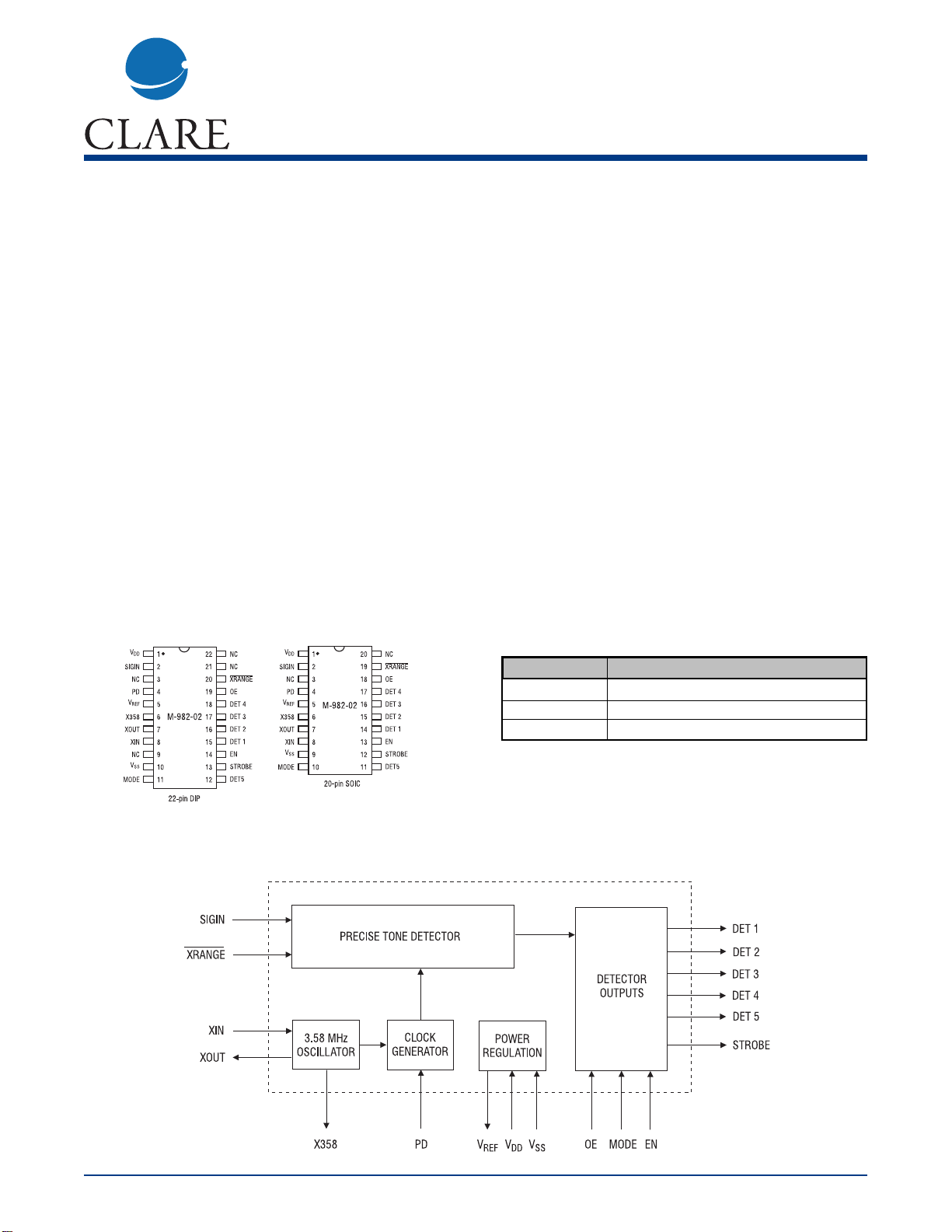
The M-982-02 is an integrated circuit precise tone
detector for special-purpose use in automatic following
of switched telephone calls. The circuit uses lowpower CMOS techniques to provide the complete filtering and control required for this function. The basic
timing of the M-982-02 is designed to permit operation
with almost any progress tone system.The use of integrated circuit techniques allows the M-982-02 to pack
the five filters for call progress following into a single
22-pin DIP or 20-pin SOIC. A 3.58 MHz crystal-controlled time base guarantees accuracy and repeatability.
The M-982-02 is an enhanced drop-in replacement for
the M-982-01. It has a wider operating voltage range
(down to 3V). It has lower power consumption under
normal operating conditions. In addition, a powerdown (PD) feature is provided to further reduce power
consumption when inactive. It includes a 425 Hz
detector to support common international call progress
requirement.
Block Diagram
Ordering Information
Part # Description
M-982-02P 22-pin plastic DIP
M-982-02S 20-pin plastic SOIC
M-982-02T 20-pin plastic SOIC,Tape and Reel
Pin Diagram
www.clare.com
2
M-982-02
Rev. 4
Absolute Maximum Ratings
Storage Temperature -40 to 150°C
Operating Ambient Temperature -40 to 85°C
V
DD
7V
Input Voltage on SIGIN VSS- 6.5 to VDD+ 0.3V
Input Voltages (except SIGIN) VSS- 0.3 to VDD+ 0.3 V
Lead Soldering Temperature 260° C for 5 seconds
Note: Exceeding these ratings may permanently damage the M-982-02.
Absolute Maximum Ratings are stress ratings. Stresses in
excess of these ratings can cause permanent damage to
the device. Functional operation of the device at these or
any other conditions beyond those indicated in the operational sections of this data sheet is not implied. Exposure of
the device to the absolute maximum ratings for an extended period may degrade the device and effect its reliability.
Specifications
Parameter Conditions Min Max Units Notes
Operating V
DD
- 2.7 5.5 V -
Conditions Power supply noise 0.1 - 5 kHz - 20 mV p-p
Power Current drain (I
DD
)V
REF
open - 15 mA -
V
REF
V
REF
- 48% of V
DD
52% of V
DD
V-
Impedance - 3.25 8.25 kW
Signal Frequency range in-band signal -1 +1 % of f
o
1
Detection Level: V
DD
= 5.0V XRANGE = open -30 0 dBm
(24.5 mV) (775 mV)
XRANGE = V
SS
-40 -10 dBm
(7.8 mV) (245 mV) -
Level: V
DD
= 3.0V XRANGE = open -33 (17.4 mV) -3 (549 mV) dBm
XRANGE = V
SS
-43 (5.5 mV) -13 (173.5 mV) dBm
Duration (t
DD
) - 200 - ms
Bridge time (t
BB
)--20ms
Level skew between adjacent
inband signals for detection of both - 6 dB
High level to low level signal for high = 0 dBm (775 mV) 1 - s detection of both (t
IL
) low = -30 dBm (24.5 mV)
Time to output (t
DO
) SIGIN ≈ -24 dBm - 200 ms
SIGIN < -24 dBm - 240 ms -
Time from DET n to STROBE (t
DS
)- -10ms
Signal Frequency range - -6 -6 % of f
o
1
Rejection Level: V
DD
= 5.0V XRANGE = open - -50(2.5 mV) dBm
XRANGE = V
SS
- -60 (0.8 mV) dBm
Level: V
DD
= 3.0V XRANGE= open - -53 (1.7 mV) dBm
XRANGE = V
SS
- -63 (.6 mV) dBm
Interval duration (t
ID
) - 160 - ms
Time to output (T
IO
) - - 200 ms
Outputs DET n, V
OL
I
SINK
= -1mA - 0.5 V
STROBE pins V
OH
I
SOURCE
=1mA VDD-0.5 - V -
DET n pins I
OZ
VO=VDD, V
SS
-1µA
Inputs EN, OE, XRANGE, VIL - - 0.5 V -
MODE, PD pins VIH VDD = 5V VDD - 2.0 - V
VDD = 2.7V VDD - 0.5 - V
Pull-up and Pull-down MODE = VSS VDD = 5V 12.5 50 µA
currents VDD = 2.7V 4 20 µA
/Xrange = VSS - 2 6 µA
PD =VDD - 4 10 µA
M-982-02
www.clare.com
3
Rev. 4
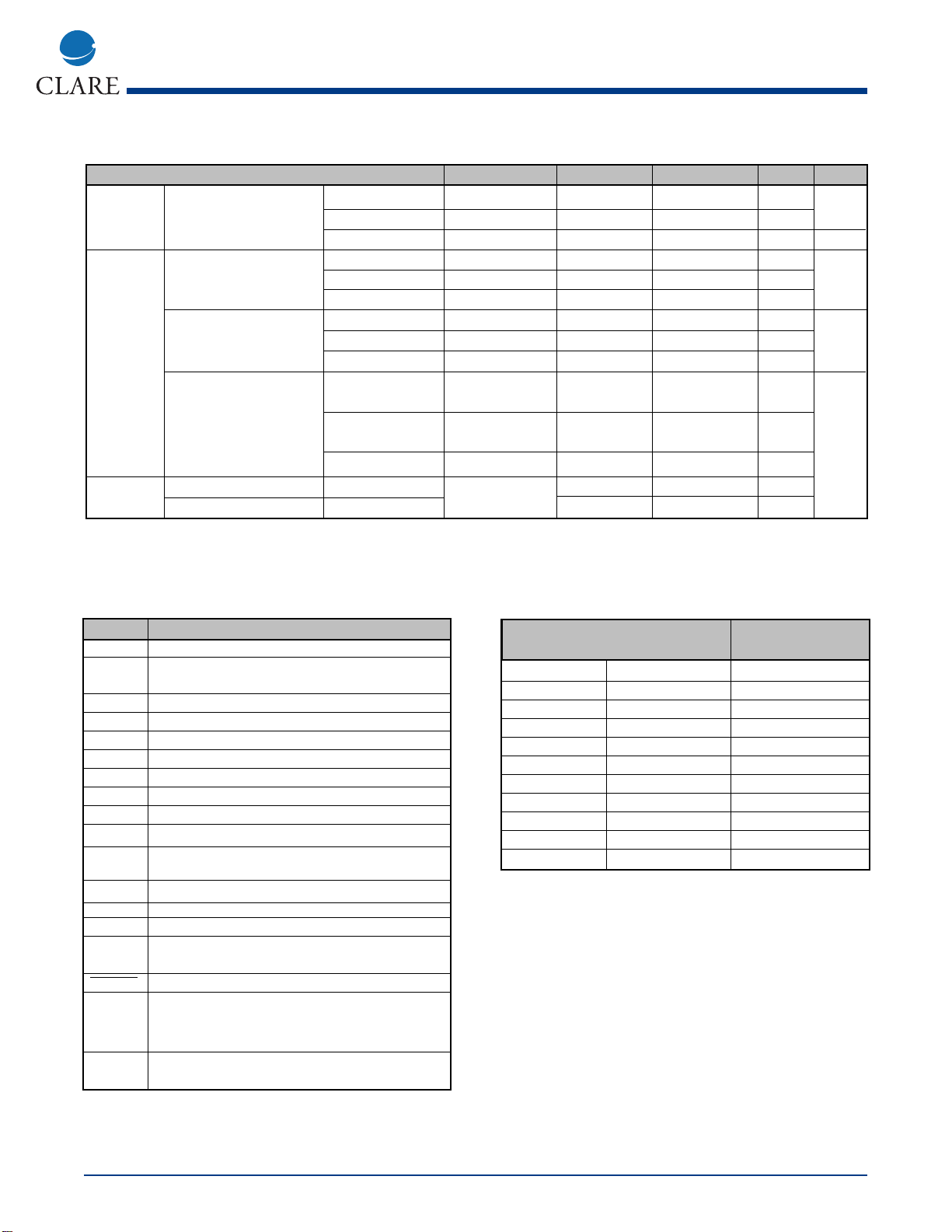
Call Progress Tones
Frequency (HZ) Use
12
350 440 Dial Tone
400 Off Special
440 Off Alert Tone
440 480 Audible Ring
440 620 Pre-empt
480 Off Bell High Tone
480 620 Reorder (Bell Low)
350 Off Special
620 Off Special
941 1209 DTMF “*”
425 Off European
Specifications (continued)
Parameter Conditions Min Max Units Notes
SIGIN pin Voltage range - -6.5 VDD V
Input impedance f=500 Hz 80 - kΩ
Input spectrum - - 28 kHz
Clock External clock VIL XOUT open - 0.2 V
connected to XIN pin VIH XOUT open VDD-0.2 - V
Duty cycle XOUT open 40 60 %
XIN, XOUT with crystal Capacitance - - 10 pF
osc. active Internal resistance - 20 - MW
Power up (TPU) PD hi to lo - 30 ms
X358 pin VOL CL = 20 pF, - 0.2 V
ISINK = -1mA
VOH CL = 20 pF,
ISOURCE =1mA VDD - 0.2 - V
Duty cycle CL = 20 pF 40 60 %
Tri-state tEN,(High Z to Low Z) CL = 50 pF, - 250 ns
Operation tDE,(Low Z to High )Z RL = 100 kW - 250 ns
Unless otherwise noted, VDD- VSS= 5V, Ta = 25°C, PD at logical low state, and XRANGE at a logical high state.
Power levels are in dBm referenced to 600 ohm. DC voltages are referenced to V
SS
.
Notes:
1. Per tone.
Pin Functions
Pin Funtion
DET 1 Active high tri-state output, detect for 350 Hz.
DET 2 Active high tir-state ooutput, detect for 400/620 Hz.
(See Note.)
DET 3 Active high tri-state output, detect for 440 Hz.
DET 4 Active high tri-state output, detect for 480 Hz.
DET 5 Active high tri-state output, detect for 425 Hz.
EN Active high enabled, when low drives STROBE low.
OE Active high input. When low tri-state DET n pins.
SIGIN Analog signal input (internally capacitive coupled).
STROBE Active high output, indicates valid DET n.
V
DD
Most positive power supply input pin.
V
REF
Internally generated mid-power supply voltage
(output).
V
SS
Most negative power supply input pin.
X358 Buffered oscillator output (3.58 MHz).
XIN Crystal oscillator or digital clock input.
XOUT Crystal oscillator output. Used only with a crystal.
Use X358 when clock output signal is required.
XRANGE Active low input. Adds 10 dB of gain to input stage.
MODE Compatibility selection. Connection to VSS selects
400 Hz detection. (M-981-02 emulation.) Connection
to VDDor no connection selects 620 Hz detection.
PD Power-down operation, logic high inhibits internal
clock. Internal pulldown resistor.
Note: This output indicates 400 Hz detect when MODE is connected to VSSand 620
Hz detect when open, or connected to VDD.
 Loading...