

CLARE M-8870-02T, M-8870-02SM, M-8870-01SMTR, M-8870-01SM, M-8870-01 Datasheet
...
Part # Description
M-8870-01 18-pin plastic DIP
M-8870-01SM 18-pin plastic SOIC
M-8870-01SMTR 18-pin plastic SOIC, tape and reel
M-8870-02 18-pin plastic DIP, power-down,
option
M-8870-02SM 18-pin plastic SOIC, power-down,
option
M-8870-02T 18-pin plastic SOIC, power-down
option, tape and reel
www.clare.com
DS-M8870-R3
M-8870
DTMF Receiver
1
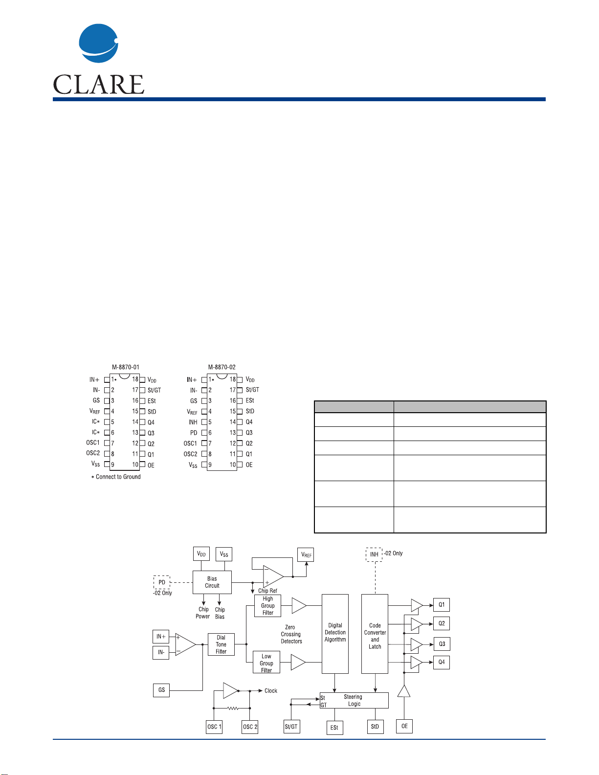
Block Diagram
Pin Configuration
Ordering Information
Features
• Low Power Consumption
• Adjustable Acquisition and Release Times
• Central Office Quality and Performance
• Power-down and Inhibit Modes (-02 only)
• Inexpensive 3.58 MHz Time Base
• Single 5 Volt Power Supply
• Dial Tone Suppression
Applications
• Telephone switch equipment
• Remote data entry
• Paging systems
• Personal computers
• Credit card systems
Description
The M-8870 is a full DTMF Receiver that integrates
both bandsplit filter and decoder functions into a single
18-pin DIP or SOIC package. Manufactured using
CMOS process technology, the M-8870 offers low
power consumption (35 mW max) and precise data
handling. Its filter section uses switched capacitor
technology for both the high and low group filters and
for dial tone rejection. Its decoder uses digital counting
techniques to detect and decode all 16 DTMF tone
pairs into a 4-bit code. External component count is
minimized by provision of an on-chip differential input
amplifier, clock generator, and latched tri-state interface bus. Minimal external components required
include a low-cost 3.579545 MHz color burst crystal, a
timing resistor, and a timing capacitor.
The M-8870-02 provides a “power-down” option
which, when enabled, drops consumption to less
than 0.5 mW. The M-8870-02 can also inhibit the
decoding of fourth column digits (see Tone Decoding
table on page 5).
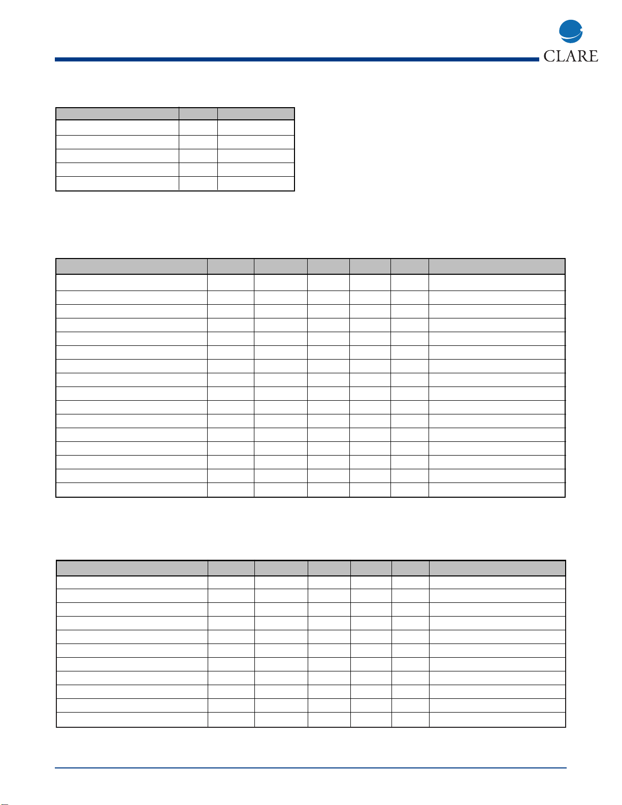
Operating Characteristics - Gain Setting Amplifier
Parameter Symbol Min Typ Max Units Test Conditions
Input leakage current I
N
- ± 100 - nA VSS< VIN< V
DD
Input resistance R
IN
4--MΩ -
Input offset voltage V
OS
-±25-mV Power supply rejection PSRR 50 - - dB 1 KHz
Common mode rejection CMRR 55 - - dB -3.0V < VIN< 3.0V
DC open loop voltage gain A
VOL
60 - - dB -
Open loop unity gain bandwidth f
C
1.2 1.5 - MHz -
Output voltage swing V
O
3.5 - - V
P-P
RL ≈ 100 KΩ to V
SS
Tolerable capacitive load (GS) C
L
- - 100 pF Tolerable resistive load (GS) R
L
--50kΩ -
Common mode range V
CM
2.5 - - V
P-P
No load
*Typical figures are at 25°C and are for design aid only; not guaranteed and not subject to production testing.
Notes:
1. All voltages referenced to VSSunless otherwise noted. For typical values, VDD= 5.0V, VSS= 0V, TA = 25°C.
DC Characteristics
Parameter Symbol Min Typ Max Units Test Conditions
Operating supply voltage V
DD
4.75 - 5.25 V -
Operating supply current I
DD
- 3.0 7.0 mA -
Standby supply current (see Note 3) IDDQ - - 100 µA PD=V
DD
Power consumption P
O
- 15 35 mW f = 3.579 MHz, VDD= 5.0 V
Low level input voltage V
IL
- - 1.5 V -
High level input voltage V
IH
3.5 - - V -
Input leakage current IIH/I
IL
- 0.1 - µA VIN= VSSor VDD(see Note 2)
Pullup (source) current on OE I
SO
- 6.5 15.0 µA OE = 0 V
Input impedance, signal inputs 1, 2 R
IN
810-mΩ @ 1 kHz
Steering threshold voltage V
TSt
2.2 - 2.5 V -
Low level output voltage V
OL
- - 0.03 V No load
High level output voltage V
OH
VDD- 0.03 - - V No load
Output low (sink) current I
OL
1.0 2.5 - mA V
OUT
= 0.4 V
Output high (source) current I
OH
0.4 0.8 - mA V
OUT
= VDD- 0.4 V
Output voltage V
REF
V
REF
2.4 - 2.7 V No load
Output resistance V
REF
R
OR
-10-kΩ -
*Typical figures are at 25°C and are for design aid only; not guaranteed and not subject to production testing.
Absolute Maximum Ratings
Parameter Symbol Value
Power supply voltage (VDD- VSS)V
DD
6.0 V max
Voltage on any pin V
DCVSS
-0.3, VDD +0.3
Current on any pin I
DD
10 mA max
Operating temperature T
A
-40°C to + 85°C
Storage temperature T
S
-65°C to + 150°C
Note:
Exceeding these ratings may cause permanent damage. Functional operation under
these conditions is not implied.
www.clare.com
2
M-8870
Rev. 3
Absolute Maximum Ratings are stress ratings. Stresses in
excess of these ratings can cause permanent damage to
the device. Functional operation of the device at these or
any other conditions beyond those indicated in the operational sections of this data sheet is not implied. Exposure of
the device to the absolute maximum ratings for an extended period may degrade the device and effect its reliability.
M-8870
www.clare.com
3
Rev. 3
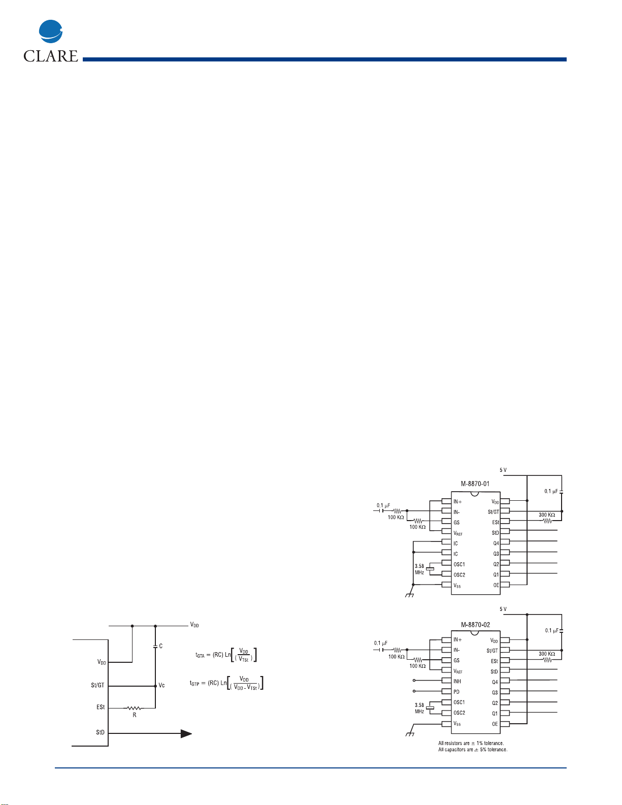
Basic Steering Circuit
Single-Ended Input Configuration
Functional Description
M-8870 operating functions (see block diagram on
page 1) include a bandsplit filter that separates the
high and low tones of the received pair, and a digital
decoder that verifies both the frequency and duration
of the received tones before passing the resulting 4-bit
code to the output bus.
Filter
The low and high group tones are separated by applying the dual-tone signal to the inputs of two 6th order
switched capacitor bandpass filters with bandwidths
that correspond to the bands enclosing the low and
high group tones. The filter also incorporates notches
at 350 and 440 Hz, providing excellent dial tone rejection. Each filter output is followed by a single-order
switched capacitor section that smooths the signals
prior to limiting. Signal limiting is performed by highgain comparators provided with hysteresis to prevent
detection of unwanted low-level signals and noise.
The comparator outputs provide full-rail logic swings
at the frequencies of the incoming tones.
Decoder
The M-8870 decoder uses a digital counting technique to determine the frequencies of the limited tones
and to verify that they correspond to standard DTMF
frequencies. A complex averaging algorithm is used to
protect against tone simulation by extraneous signals
(such as voice) while tolerating small frequency variations. The algorithm ensures an optimum combination
of immunity to talkoff and tolerance to interfering signals (third tones) and noise. When the detector recognizes the simultaneous presence of two valid tones
(known as signal condition), it raises the Early
Steering flag (ESt). Any subsequent loss of signal
condition will cause ESt to fall.
Steering Circuit
Before a decoded tone pair is registered, the receiver
checks for a valid signal duration (referred to as character-recognition-condition). This check is performed
by an external RC time constant driven by ESt. A logic
high on ESt causes VC (see block diagram on page 1)
to rise as the capacitor discharges. Provided that signal condition is maintained (ESt remains high) for the
validation period (t
GTF
), VCreaches the threshold (V
TSt
)
of the steering logic to register the tone pair, thus latching its corresponding 4-bit code (see DC
Characteristics on page 2) into the output latch. At this
point, the GT output is activated and drives VCto VDD.
GT continues to drive high as long as ESt remains
high. Finally, after a short delay to allow the output
latch to settle, the delayed steering output flag (StD)
goes high, signaling that a received tone pair has been
registered. The contents of the output latch are made
available on the 4-bit output bus by raising the threestate control input (OE) to a logic high. The steering
circuit works in reverse to validate the interdigit pause
between signals. Thus, as well as rejecting signals too
short to be considered valid, the receiver will tolerate
signal interruptions (dropouts) too short to be considered a valid pause. This capability, together with the
ability to select the steering time constants externally,
allows the designer to tailor performance to meet a
wide variety of system requirements.
 Loading...