

CLARE LOC211PTR, LOC211P Datasheet
1
www.clare.com
LOC211
DS-LOC211-R3
Linear Optocouplers
Applications
Features Description
Approvals
Ordering Information
Pin Configuration
LOC211 is a dual linear optocoupler for use in telecom,
medical and power supply isolation circuits. They are
available in a 16 Pin SOIC package.
• Modem Transformer Replacement With No
Insertion Loss
• Digital Telephone Isolation
• Power Supply Feedback Voltage/Current
• Medical Sensor Isolation
• Audio Signal Interfacing
• Isolation of Process Control Transducers
• UL Recognized: File Number E76270
• CSA Certified: File Number LR 43639-10
• BSI Certified:
• BS EN 60950:1992 (BS7002:1992)
Certificate #:7344
• BS EN 41003:1993
Certificate #:7344
• 16 Pin SOIC Package (PCMCIA Compatible)
• Couples Analog and Digital Signals
• Wide Bandwidth (>200kHz)
• High Gain Stability
• Low Input/Output Capacitance
• Low Power Consumption
• 0.01% Servo Linearity
• THD 87dB Typical
• Machine Insertable, Wave Solderable
• Surface Mount and Tape Reel Versions Available
• VDE Compatible
Part # Description
LOC211P 16 Pin Flatpack (50/Tube)
LOC211PTR 16 Pin Flatpack (1000/Reel)
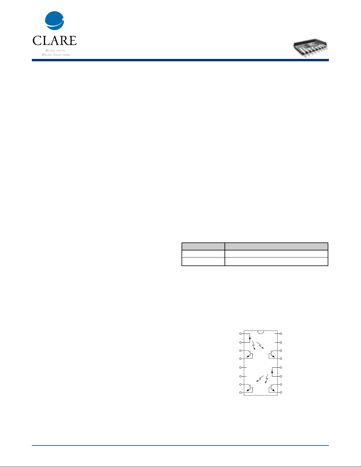
LOC210/LOC211 Pinout
– LED
+ LED
+ V
cc
I
1
NC
NC
+V
cc
I
2
+V
cc
I
1
NC
NC
+V
cc
I
2
1
2
3
4
16
15
14
13
5
6
7
8
12
11
10
9
– LED
+ LED
www.clare.com
LOC211
Rev. 3
Absolute Maximum Ratings are stress ratings. Functional
operation of the device at these or any other conditions
beyond those indicated in the operational sections of this
data sheet is not implied. Exposure of the device to the
absolute maximum ratings for an extended period may
degrade the device and effect its reliability.
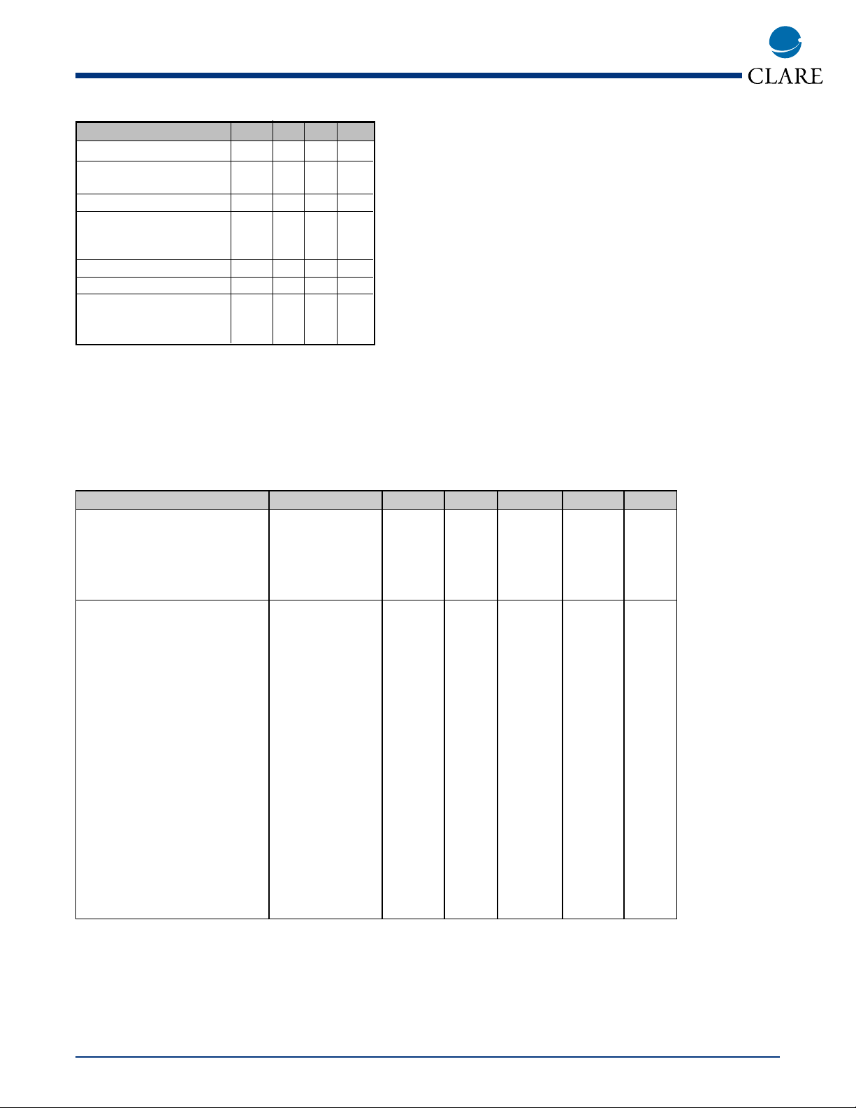
Absolute Maximum Ratings (@ 25
o
C)
2
Electrical Characteristics
PARAMETER CONDITIONS SYMBOL MIN TYP MAX UNITS
Input Characteristics @ 25°C1
LED Voltage Drop I
F
=2-10mA V
F
0.9 1.2 1.4 V
Reverse LED Current V
R
=5V I
R
- - 10 µA
Reverse LED Voltage - V
R
-- 5 V
Forward LED Current - I
F
- - 100 mA
Coupler/Detector
Characteristics @ 25°C1
Dark Current I
F
=0mA, VCC=15V I
D
-1 25nA
K1, Servo Gain (I
1/IF
)I
F
=2-10mA, VCC=15V K1 0.008 - 0.030 -
K2, Forward Gain (I
2/IF
)I
F
=2-10mA, VCC=15V K2 0.006 - 0.030 -
K3, Transfer Gain (K
2/K1
)I
F
=2-10mA, VCC=15V K3 0.733 - 1.072 -
∆K3, Transfer Gain Linearity I
F
=2-10mA ∆K3 - - 1.0 %
(non-servoed)
K3 Temperature Coefficient I
F
=2-10mA, V
det
=-5V ∆K3/∆T - 0.005 - %/°C
Common Mode Rejection Ratio V=20V
P-P
, RL=2KΩ, CMRR - 130 - dB
F=100Hz
Total Harmonic Distortion F
O
=350Hz, 0dBm THD -96 -87 -80 dB
Frequency Response Photoconductive
Operation BW (-3dB) - 200 - kHz
Photovoltaic
Operation BW (-3dB) - - 40 kHz
Input/Output Capacitance - C
I/O
-3 - pF
Input/Output Isolation
SOIC Package - VI/O 3750 - - VRMS
1 All parameters above are for each optocoupler.
Parameter Min Typ Max Units
Input Power Dissipation - - 1501mW
Input Control Current - - 100 mA
Peak (10ms) - - 1 A
Total Package Dissipation - - 8002mW
Isolation Voltage
Input to Output
SOIC Package 3750 - - V
RMS
Operational Temperature -40 +85°C
Storage Temperature -40 - +125°C
Soldering Temperature - - +220
°
C
(10 Seconds Max)
Flatpack Package - - +260
°
C
1
Derate Linearly 1.33 mW/°C
2
Derate Linearly 6.67 mW/°C
 Loading...