

1
www.clare.com
ITC135P
DS-ITC135P-Rxx
The Integrated Telecom Circuit combines a 1-Form-A solid
state relay, bridge rectifier, Darlington transistor, optocoupler and zener diodes into one 16 pin SOIC package, consolidating designs and reducing component count in
telecom applications. The ITC135P’s optocoupler provides
half wave ring detection.
• Data/Fax Modem
• Voice Mail Systems
• Telephone Sets
• Computer Telephony Integration
• Cable TV Modems
• UL Recognized: File Number E76270
• CSA Certified: File Number LR 43639-12
• BSI Certified:
• BS EN 60950:1992 (BS7002:1992)
Certificate #: 7969
• BS EN 41003:1993
Certificate #: 7969
• Small 16 Pin SOIC Package (PCMCIA Compatible)
• Board Space and Cost Savings
• 2mW Hookswitch Drive Power (Logic Compatible)
• No Moving Parts
• 3750V
RMS
Input/Output Isolation
• FCC Compatible Part 68
• Full-Wave Bridge Rectifier
• Darlington Transistor for Electronic Inductor “Dry”
Circuits
• Half Wave Current Detector for Ring Signal or Loop
Current Detect
• Current Limiting and Tape & Reel Versions Available
• JEDEC Standard Pin Out
• Includes Zener Diodes
Applications
Features
Description
Approvals
Integrated Telecom Circuits
Ordering Information
Part # Description
ITC135P 16 Pin SOIC (50/Tube)
ITC135P 16 Pin SOIC (1000/Reel)
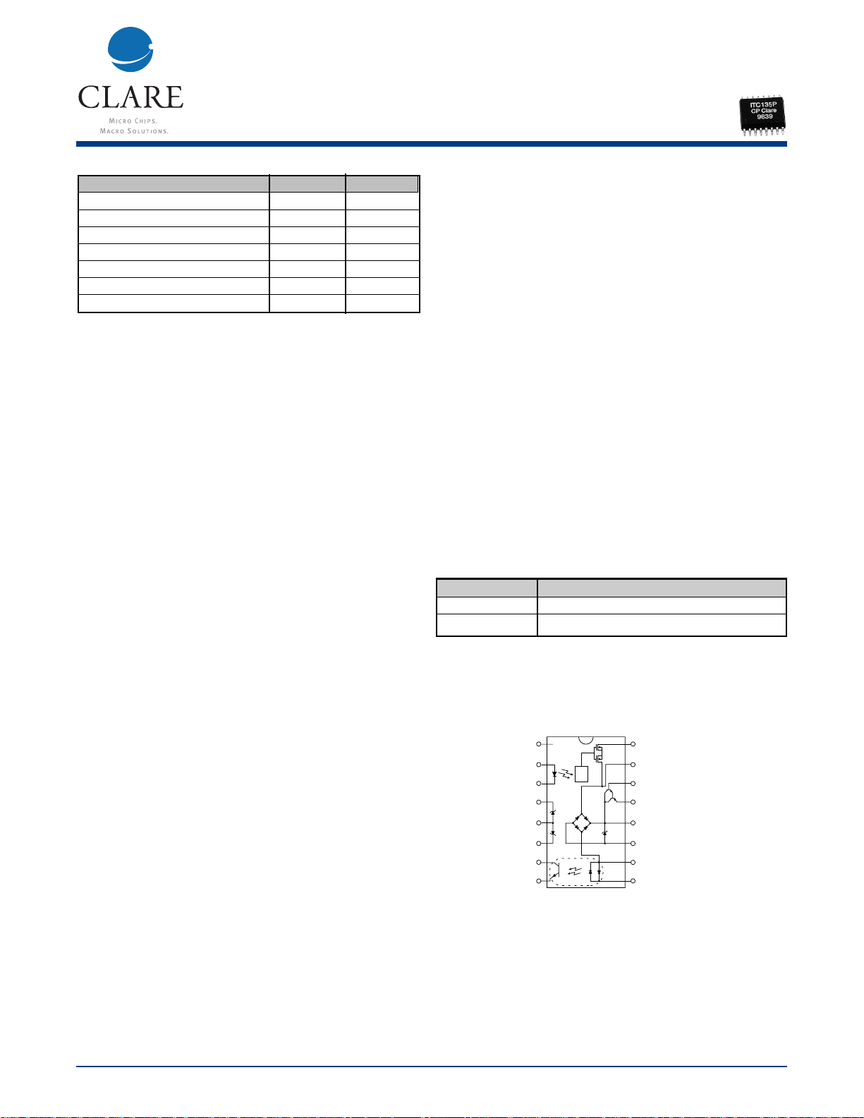
Pin Configuration
C
ITC135P Units
Relay Load Voltage 350 V
Relay Load Current 120 mA
Relay Max R
ON
15 Ω
Bridge Rectifier Reverse
Voltage 100 V
Darlington Collector Current 120 mA
Darlington Current Gain 10,000 -
1
(N/C)
– LED - Form A Relay
– LED - Form A Relay
+ Zener Diode (cathode)
– Zener Diode (anode)
+ Zener Diode (cathode)
ollector - Phototransistor
Emitter - Phototransistor
2
3
4
5
6
7
8
ITC135P
PV
Denotes half-wave detection
*
16
15
14
13
12
11
10
9
*
Output Form A
Output Form A/Bridge Input –/+
Darlington Base
Darlington Emitter
Bridge Output +/Darlington Collector/
+ Zener Diode (cathode)
Bridge Output –/– Zener Diode (anode)
LED - Phototransistor –/+
LED - Phototransistor +/–
www.clare.com
ITC135P
Rev. X
Absolute Maximum Ratings are stress ratings. Stresses
in excess of these ratings can cause permanent damage
to the device. Functional operation of the device at these
or any other conditions beyond those indicated in the
operational sections of this data sheet is not implied.
Exposure of the device to the absolute maximum ratings
for an extended period may degrade the device and effect
its reliability.
Absolute Maximum Ratings (@ 25˚ C)
2
Parameter Min Typ Max Units
Total Package Dissipation - - 1
1
W
Isolation Voltage
Input to Output 3750 - - V
RMS
Operational Temperature -40 - +85 °C
Storage Temperature -40 - +125 °C
Soldering Temperature - - +220 °C
(10 Seconds Max.)
1
Above 25˚ derate linerity 8.33mw/˚C
Total Power Dissipation (PD):
P
D=PHOOKSWITCH
+ P
BRIDGE
+ P
DARLINGTON
+ P
LED
PD=(RDS(on)) (I
2
L
) + 2(VF)(IL) + (VCE)(IL) + (V
LED
)(IF)
WHERE:
R
DS
(on) = Maximum realy on resistance
I
L
= Maximum loop current
V
F
= Maximum diode forward voltage
V
CE
= Maximum voltage collector to emitter
V
LED
= Maximum LED forward voltage
I
F
= Maximum LED current
Electrical Characteristics
Parameter Conditions Symbol Min Typ Max Units
Relay Portion (Pins 15,16)
Output Characteristics @ 25°C
Load Voltage, DC or Peak AC - V
L
- - 350 V
Load Current (Continuous) - I
L
- - 120 mA
On-Resistance I
L
=120mA R
ON
-- 15Ω
Off-State Leakage Current V
L
=350, TJ=25˚C I
LEAK
-- 1µA
Switching Speeds
Turn-On I
F
=5mA, VL=10V T
ON
-- 3ms
Turn-Off I
F
=5mA, VL=10V T
OFF
-- 3ms
Output Capacitance 50V, f=1MHz C
OUT
-25 - pF
Relay Portion (Pins 2,3)
Input Characteristics @ 25°C
Input Control Current I
L
=120mA I
F
5- 50mA
Input Voltage Drop I
F
=5mA V
F
0.9 1.2 1.4 V
Reverse Input Voltage - V
R
-- 5V
Reverse Input Current VR=5V I
R
- - 10 µA
Detector Portion (Pins 7,8)
Output Characteristics @ 25°C
Phototransistor Blocking
Voltage I
C
=10µA BV
CEO
20 50 - V
Phototransistor Dark Current V
CE
=5V, IF=0mA I
CEO
- 50 500 A
Saturation Voltage I
C
=2mA, IF=16mA V
SAT
- 0.3 0.5 V
Current Transfer Ratio IF=6mA, VCE=0.5V CTR 33 400 - %
Detector Portion (Pins 9,10)
Input Characteristics @ 25°C
Input Control Current I
C
=2mA, VCE=0.5V I
F
6 2 100 mA
Input Voltage Drop I
F
=5mA V
F
0.9 1.2 1.4 V
Input Current I
C
=1µA, VCE=5V I
F
525 - µA
(Detector must be off)
ITC135P
www.clare.com
3
Rev. X
Electrical Characteristics
Parameter Conditions Symbol Min Typ Max Units
Bridge Rectifier Electrical
Ratings @ 25°C
Reverse Voltage - V
RD
- - 100 V
Forward Drop Voltage I
FD
=120mA V
FD
- - 1.5 V
Reverse Leakage Current T
J
=25˚C, VR=100V I
RD
- - 10 µA
T
J
=85˚C - - 50 µA
Forward Current (Continuous) I
FD
- - 140 mA
Forward Current (Peak) t=10mS I
FD
- - 0.5 A
Darlington Electrical
Ratings @ 25°C
Collector-Emitter Voltage I
c
=10mA DC, IB=0 V
CEO
40 - - V
Collector-Current Continuous V
C
=3.5V I
C
- - 120 mA
Power Dissipation @ 25˚C - P
d
- - 500 mW
Off-State Collector Emitter
Leakage Current V
CE
=10V; IB=0mA I
CEX
-- 1µA
DC Current Gain I
C
=120mA, h
FE
10,000 - -
V
CE
=10VDC
Saturation Voltage I
C
=120mA V
CE(SAT)
- - 1.5 V
Total Harmonic Distortion fo=300Hz @ -10dBm - - - -80 dB
IC=40mA
Zener Characteristics @ 25°C
Zener Voltage I
ZT
=20mA V
z
- 4.3 - V
(Between pins 4+5 and 6+5)
Zener Voltage I
ZT
=20mA V
z
-15 - V
(Between pins 12+11)
Input to Output Capacitance - C
I/O
-3 -pF
Input to Output Isolation - V
I/O
3750 - - V
RMS
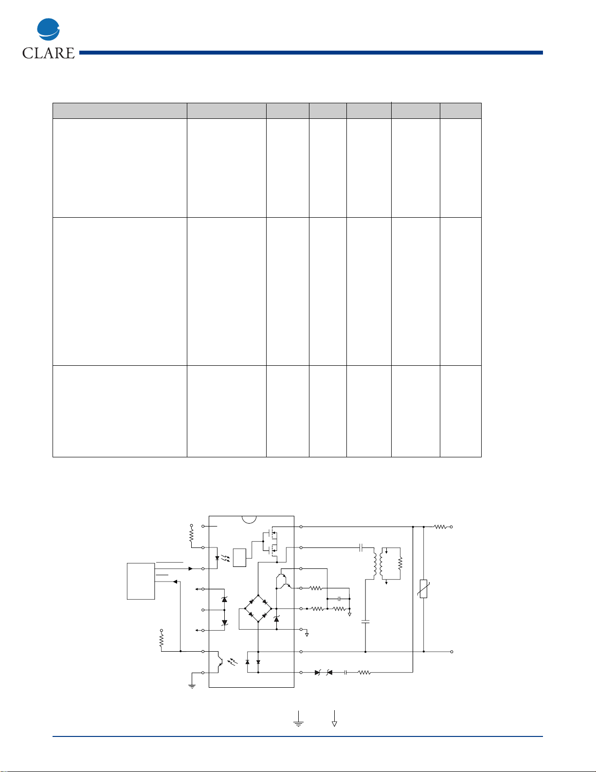
EXAMPLE CIRCUIT
MOSFET
DRIVER
CIRCUIT
4
1
3
2
7
8
6
5
16
15
14
13
12
11
10
9
DIGITAL
GROUND
ISOLATED
GROUND
CPU
RING
OFF-HOOK
680
V
CC
15V
4.7µF
+
4.7µF
+
51k
15Ω
10µF
25k
COUPLING
TRANSFORMER
R
L
10
300V SURGE
PROTECTION
TELEPHONE
LINE
RING
18Vx 2 0.47µF
250V
8.2k
V
CC
TIP
A
B
A
B

www.clare.com
4
ITC135P
Rev. X
PERFORMANCE DATA*
The Performance data shown in the graphs above is typical of device performance. For guaranteed parameters not indicated in the written specifications, please contact
our application department.
ITC135P
Typical LED Forward Voltage Drop
(N=50 Ambient Temperature = 25°C)
IF = 5mADC
35
30
25
20
15
10
5
0
1.17 1.19 1.21 1.23 1.25
LED Forward Voltage Drop (V)
Device Count (N)
ITC135P
Typical On-Resistance Distribution
(N=50 Ambient Temperature = 25°C)
(Load Current = 120mADC)
35
30
25
20
15
10
5
0
9.25 10.258.75 9.75 10.75
On-Resistance (Ω)
Device Count (N)
ITC135P
Typical Blocking Voltage Distribution
(N=50 Ambient Temperature = 25°C)
35
30
25
20
15
10
5
0
365 385 405 425375 395 415
Blocking Voltage (V)
Device Count (N)
ITC135P
Typical IF for Switch Operation
(N=50 Ambient Temperature = 25°C)
(Load Current = 120mADC)
0.42 0.66 0.900.30 0.54 0.78 1.02
LED Current (mA)
Device Count (N)
25
20
15
10
5
0
ITC135P
Typical IF for Switch Dropout
(N=50 Ambient Temperature = 25°C)
(Load Current = 120mADC
25
20
15
10
5
0
0.30 0.54 0.780.18 0.42 0.66 0.90
LED Current (mA)
Device Count (N)
)
ITC135P
Typical Turn-On Time
(N=50 Ambient Temperature = 25°C)
(Load Current = 120mADC; IF = 2mADC)
0.88 1.58 2.28 2.981.23 1.93 2.63
Turn-On (ms)
Device Count (N)
25
20
15
10
5
0
ITC135P
Typical Turn-Off Time
(N=50 Ambient Temperature = 25°C)
(Load Current = 120mADC; IF = 2mADC)
0.06 0.14 0.22 0.300.260.180.10
Turn-Off (ms)
Device Count (N)
25
20
15
10
5
0
ITC135P
Load Current vs. Ambient Temperature
Ambient Temperature (°C)
Percent of Maximum
Load Rating (Typical) (%)
-40
100
75
50
25
0
025
50 85
IF = 5mA
ITC135P
Typical Leakage vs. Temperature
(Measured across Pins 15 & 16)
Temperature (°C)
Leakage (µA)
-40
0.10
0.09
0.08
0.07
0.06
0.05
0.04
0.03
0.02
0.01
0
-20 0 20 40 60 80 100
ITC135P
Typical Blocking Voltage
vs. Temperature
Temperature (°C)
Blocking Voltage (V
RMS
)
-40
415
410
405
400
395
390
385
380
-20 0 20 40 60 80 100
ITC135P
Typical Turn-On vs. Temperature
(Load Current = 120mADC)
Temperature (°C)
Turn-On (ms)
-40
3.0
2.5
2.0
1.5
1.0
0.5
0
-20 0 20 40 60 80 100
5mA
10mA
20mA
ITC135P
Typical Turn-Off vs. Temperature
(Load Current = 120mA)
Temperature (°C)
Turn-Off (ms)
-40
0.30
0.25
0.20
0.15
0.10
0.05
0
-20 0 20 40 60 80 100
5mA

ITC135P
www.clare.com
5
Rev. X
PERFORMANCE DATA*
*The Performance data shown in the graphs above is typical of device performance. For guaranteed parameters not indicated in the written specifications, please contact
our application department.
ITC135P
Typical LED Forward Voltage Drop
vs. Temperature
Temperature (°C)
LED Forward Voltage Drop (V)
1.8
1.6
1.4
1.2
1.0
0.8
-40 -20 0 20 40 60 80 120100
50mA
30mA
20mA
10mA
5mA
ITC135P
Typical Turn-On vs.
LED Forward Current
(Load Current = 120mADC)
LED Forward Current (mA)
Turn-On (ms)
0
5 1015202530354045
2.0
1.8
1.6
1.4
1.2
1.0
0.8
0.6
0.4
0.2
0
50
ITC135P
Typical Turn-Off vs. LED Forward Current
(Load Current = 120mADC)
LED Forward Current (mA)
Turn-Off (ms)
0
5 1015202530354045
0.18
0.16
0.14
0.12
0.10
0.08
0.06
0.04
50
ITC135P
Typical On-Resistance vs. Temperature
(Load Current = 120mADC; IF = 5mADC)
Temperature (°C)
On-Resistance (Ω)
-40
60
50
40
30
20
10
0
-20 0 20 40 60 80 100
ITC135P
Package Power Derating
Temperature (°C)
Power Dissipation (Watts)
25
1.00
0.95
0.90
0.85
0.80
0.75
0.70
0.65
0.60
0.55
0.50
303540
45 50 55
60 657075
80 85
Operating Area
ITC135P
Typical Load Current vs. Load Voltage
(Ambient Temperature = 25°C)
IF = 5mADC
Load Voltage (V)
Load Current (mA)
200
150
100
50
0
-50
-100
-150
-200
-2.0 -1.5 -1.0 -0.5 0 0.5 1.0 2.01.5
ITC135P
Energy Rating Curve
Time
Load Current (A)
10µs
1.2
1.0
0.8
0.6
0.4
0.2
0
1ms100µs 100ms
1s
10ms 10s 100s
ITC135P
Single Transistor
Typical Normalized CTR vs. Temperature
(VCE = 0.5V)
Temperature (°C)
Normalized CTR (%)
8
7
6
5
4
3
2
1
0
-40 -20 0 20 40 60 80 120100
1mA
2mA
5mA
10mA
15mA
20mA
ITC135P
V-I Characteristics for Test Circuit
I
OUT
(mA)
V
IN
(Volts)
20
10
9
8
7
6
5
4
40 60 80
100
120
ITC135P
Typical IF for Switch Dropout
vs. Temperature
(Load Current = 120mADC)
Temperature (°C)
LED Current (mA)
-40
1.8
1.6
1.4
1.2
1.0
0.8
0.6
0.4
0.2
0
-20 0 20 40 60 80 100
ITC135P
Typical IF for Switch Operation
vs. Temperature
(Load Current = 120mADC)
Temperature (°C)
LED Current (mA)
-40
1.8
1.6
1.4
1.2
1.0
0.8
0.6
0.4
0.2
0
-20 0 20 40 60 80 100
ITC135P
Single Transistor
Typical Normalized CTR vs. Forward Current
(VCE = 0.5V)
IF (mA)
Normalized CTR (%)
0
2 4 6 8 10 12 14 16 18
4.5
4.0
3.5
3.0
2.5
2.0
1.5
1.0
0.5
0
20

www.clare.com
6
ITC135P
Rev. X
ITC135P
Single Transistor
Typical Collector Current vs. Forward Current
(VCE = 0.5V)
IF (mA)
I
C
(mA)
0
2468 1210 14 16 18 20
12
10
8
6
4
2
0
ITC135P
Darlington Transistor
Typical Collector Current vs. Forward Current
(V
CE
= 0.5V)
IF (mA)
I
C
(mA)
0
2468 1210 14 16 18 20
16
14
12
10
8
6
4
2
0
ITC135P
Darlington Transistor
Typical Normalized CTR vs. Forward Current
(VCE = 0.8V)
IF (mA)
Normalized CTR (%)
0
2 4 6 8 10 12 14 16 18
2.5
2.0
1.5
1.0
0.5
0
20
ITC135P
Darlington Transistor
Typical Normalized CTR vs. Temperature
(VCE = 0.8V)
Temperature (°C)
Normalized CTR (%)
-40
3.0
2.5
2.0
1.5
1.0
0.5
0
-20 0 20 40 60 80 100
1mA
2mA
5mA
10mA
15mA
20mA
0
0
8
4
16
12
24
20
28
123456
78
910
1mA
10mA
5mA
2mA
ITC135P
Typical Transfer Characteristics of
Single Transistor Detector
Collector Emitter Voltage
Collector Current (mA)
ITC135P
Typical Transfer Characteristics of
Darlington Transistor
Collector Emitter Voltage
Collector Current (mA)
0246 810
20
40
60
80
100
120
I
b
= 2µA
I
b
= 4µA
I
b
= 6µA
I
b
= 8µA
I
b
= 10µA
PERFORMANCE DATA*
*The Performance data shown in the graphs above is typical of device performance. For guaranteed parameters not indicated in the written specifications, please contact
our application department.

ITC135P
www.clare.com
7
Rev. X
Dimensions
mm
(inches)
Mechanical Dimensions
PC Board Pattern
(Top View)
1.193
(.047)
9.728 ± .051
(.383 ± .002)
.787
(.031)
1.270
(.050)
7.493 ± .051
(.295 ± .002)
7.493 ± .127
(.295 ± .005)
.254
(.010)
1.270 TYP.
(.050)
2.108 MAX.
(.083)
1.981 TYP.
(.078)
1.016
(.040)
10.363 ± .127
(.408 ± .005)
8.890 TYP.
(.350)
.406 TYP.
(.016)
10.160 ± .051
(.400 ± .002)
16 Pin SOIC (“P” Suffix)
Tape and Reel Packaging for 16 Pin SOIC Package
7.493 ± .102
(.295 ± .004)
12.090
(.476)
1.753 ± .102
(.069 ± .004)
3.987 ± .102
(.157 ± .004)
1.498 ± .102
(.059 ± .004)
6.731 MAX.
(.265)
.406 MAX.
(.016)
3.175
(.125)
Top Cover
Tape
2.007 ± .102
(.079 ± .004)
11.989 ± .102
(.472 ± .004)
User Direction of Feed
.050R TYP.
16.002 ± .305
(.630 ± .012)
10.693 ± .025
(.421 ± .001)
Embossment
Embossed Carrier
Top Cover
Tape Thickness
.102 MAX.
(.004)
10.897 ± .025
(.429 ± .001)
1.549 ± .102
(.061 ± .004)
330.2 DIA.
(13.00)
116

CLARE LOCATIONS
Clare Headquarters
78 Cherry Hill Drive
Beverly, MA 01915
Tel: 1-978-524-6700
Fax: 1-978-524-4900
Toll Free: 1-800-27-CLARE
Clare Micronix Division
145 Columbia
Aliso Viejo, CA 92656-1490
Tel: 1-949-831-4622
Fax: 1-949-831-4628
SALES OFFICES
AMERICAS
Americas Headquarters
Clare
78 Cherry Hill Drive
Beverly, MA 01915
Tel: 1-978-524-6700
Fax: 1-978-524-4900
Toll Free: 1-800-27-CLARE
Eastern Region
Clare
P.O. Box 856
Mahwah, NJ 07430
Tel: 1-201-236-0101
Fax: 1-201-236-8685
Toll Free: 1-800-27-CLARE
Central Region
Clare Canada Ltd.
3425 Harvester Road, Suite 202
Burlington, Ontario L7N 3N1
Tel: 1-905-333-9066
Fax: 1-905-333-1824
Western Region
Clare
1852 West 11th Street, #348
Tracy, CA 95376
Tel: 1-209-832-4367
Fax: 1-209-832-4732
Toll Free: 1-800-27-CLARE
Canada
Clare Canada Ltd.
3425 Harvester Road, Suite 202
Burlington, Ontario L7N 3N1
Tel: 1-905-333-9066
Fax: 1-905-333-1824
EUROPE
European Headquarters
CP Clare nv
Bampslaan 17
B-3500 Hasselt (Belgium)
Tel: 32-11-300868
Fax: 32-11-300890
France
Clare France Sales
Lead Rep
99 route de Versailles
91160 Champlan
France
Tel: 33 1 69 79 93 50
Fax: 33 1 69 79 93 59
Germany
Clare Germany Sales
ActiveComp Electronic GmbH
Mitterstrasse 12
85077 Manching
Germany
Tel: 49 8459 3214 10
Fax: 49 8459 3214 29
Italy
C.L.A.R.E.s.a.s.
Via C. Colombo 10/A
I-20066 Melzo (Milano)
Tel: 39-02-95737160
Fax: 39-02-95738829
Sweden
Clare Sales
Comptronic AB
Box 167
S-16329 Spånga
Tel: 46-862-10370
Fax: 46-862-10371
United Kingdom
Clare UK Sales
Marco Polo House
Cook Way
Bindon Road
Taunton
UK-Somerset TA2 6BG
Tel: 44-1-823 352541
Fax: 44-1-823 352797
ASIA/PACIFIC
Asian Headquarters
Clare
Room N1016, Chia-Hsin, Bldg II,
10F, No. 96, Sec. 2
Chung Shan North Road
Taipei, Taiwan R.O.C.
Tel: 886-2-2523-6368
Fax: 886-2-2523-6369
http://www.clare.com
Worldwide Sales Offices
Specification: DS-ITC135-Rxx
©Copyright 2000, Clare, Inc.
All rights reserved. Printed in USA.
3/22/01
Clare cannot assume responsibility for use of any circuitry other
than circuitry entirely embodied in this Clare product. No circuit
patent licenses nor indemnity are expressed or implied. Clare
reserves the right to change the specification and circuitry, without notice at any time. The products described in this document
are not intended for use in medical implantation or other direct life
support applications where malfunction may result in direct physical harm, injury or death to a person.
 Loading...