

CJB WEX-QM871 User Manual

WEX-QM871 Intel QM87
User Manual Rev.01, Aug. 2015

2
Contents
Chapter 1 Product Information ............................................................................... 4
1.1 Block Diagram ............................................................................................. 4
1.2 Features ....................................................................................................... 5
1.3 PCB Layout .................................................................................................. 7
1.4 Dimensions .................................................................................................. 9
1.5 Jumper Setting .......................................................................................... 10
1.6 Connector Function List ........................................................................... 13
1.7 Connector Definitions ............................................................................... 15
1.8 I/O Ports Power Output (max.) ................................................................. 30
Chapter 2 BIOS Setup ............................................................................................ 32
2.1 Main Menu.................................................................................................. 32
2.2 Advanced Menu ......................................................................................... 33
2.3 CPU Configuration (1/2) ............................................................................ 35
2.3 CPU Configuration (2/2) ............................................................................ 36
2.4 PCH-IO Configuration ............................................................................... 39
2.5 PCI Express Configuration ....................................................................... 40
2.6 Intel® Rapid Start Technology .................................................................. 41
2.7 SATA Configuration................................................................................... 42
2.8 Serial ATA Port Configuration – SATA 1 .................................................. 44
2.9 Serial ATA Port Configuration – SATA 2 .................................................. 45
2.10 Serial ATA Port Configuration – SATA 3 ................................................ 46
2.11 System Agent Configuration .................................................................. 47
2.12 Graphics Configuration .......................................................................... 48
2.13 DMI Configuration ................................................................................... 50
2.14 Memory Configuration ............................................................................ 51
2.15 USB Configuration .................................................................................. 52
2.16 Super I/O Configuration .......................................................................... 54
2.17 Serial Port 1 Configuration ..................................................................... 55
2.18 Serial Port 2 Configuration ..................................................................... 56
2.19 Hardware Monitor .................................................................................... 57
2.20 CPU Fan Configuration ........................................................................... 58
2.21 System Fan Configuration ...................................................................... 59
2.22 Platform Misc Configuration .................................................................. 60
2.23 Power Management ................................................................................ 61
2.24 Boot Menu ................................................................................................ 62
2.25 CSM Parameters ...................................................................................... 64

3
2.25 Security Menu .......................................................................................... 66
2.26 Security Boot Menu ................................................................................ 67
2.27 Exit Menu ................................................................................................. 68
Chapter 3 Drivers Installation ................................................................................ 70
3.1 Intel Chipset Device Software .................................................................. 70
3.2 Intel Graphic Media Accelerator Driver ................................................... 73
3.3 LAN Driver ................................................................................................. 76
3.4 Audio Driver ............................................................................................... 79
3.5 USB Driver ................................................................................................. 80
3.6 iAMT Driver ................................................................ ................................ 83
Appendix A: Watchdog Timer ............................................................................... 85
Appendix B: GPIO .................................................................................................. 88

4
Chapter 1 Product Information
This chapter introduces the product features, jumper and connector information.
1.1 Block Diagram
Intel®
Haswell

5
1.2 Features
System Processor/
Chipsets
Processor
Intel® 4th Generation Core™ i7/i5/i3/Celeron®
Processor on board; FCBGA1364
Chipset
Intel® 8 Series Chipset Family Mobile
Platform Controller Hub (PCH)
BIOS
AMI
Memory
Technology
DDR3/DDR3L 1333/1600 MHz SDRAM
Max.
Capacity
Up to 8GB DDR3/DDR3L DRAM
Socket
1 x 204-pin DDR3/DDR3L SO-DIMM
Display
Chipset
Intel® QM87
VRAM
Intel® Core™ integrated HD Graphics 4000
Shared system memory up to 2GB
LVDS
Dual channel 18/24-bit
Resolution
VGA: Up to 1920 x 1200 @ 60Hz
HDMI: Up to 1080P @ 60Hz
LVDS: Up to 1920x1200 @ 60Hz
Dual Display
VGA + LVDS, VGA + HDMI, HDMI + LVDS
Triple Display
HDMI + LVDS + VGA
Ethernet
Interface
10/100/1000 Mbps
Controller
Intel® I210 GbE Controller
Intel® I217-LM GbE PHY
Audio
Interface
High Definition Audio
Controller
Realtek ALC662 HD CODEC
SATA
Max. Data
Transfer
Rates
SATA III 600MB/s
Port
2 x SATA III
Expansion Slot
Mini-PCIe
1 (Full-size w/ mSATA)
Onboard
Pin-Header
USB 2.0
4
SATA III
2
LVDS
1
6
COM
1 x RS-232/422/485
Audio
1 (Line-in, Line-out, Mic-in)
Front Panel
1
DIO
8-bit programmable digital input/output
Rear I/O
VGA
1
COM
1 x RS-232
LAN
2 x RJ45
HDMI
1
USB 3.0
2
Power
DC 12V Input
1x2*2-pin ATX power connector for DC +12V input
Watchdog Timer
Interval
Programmable 1~255 sec/min
Output
System reset
Environment
Operating
Temp.
0°C~60°C
Storage
Temp.
-20°C~80°C
Relative
Humidity
0%~ 95% (non-condensing)
Form Factor
Dimension
(L x W)
146mm x 102mm (5.75” x 4.01”)
7
1.3 PCB Layout
Top View
8
Bottom View
MINI-PCIe
Rear I/O View
COM1
VGA
HDMI
USB1
LAN1
LAN2
9
1.4 Dimensions
10
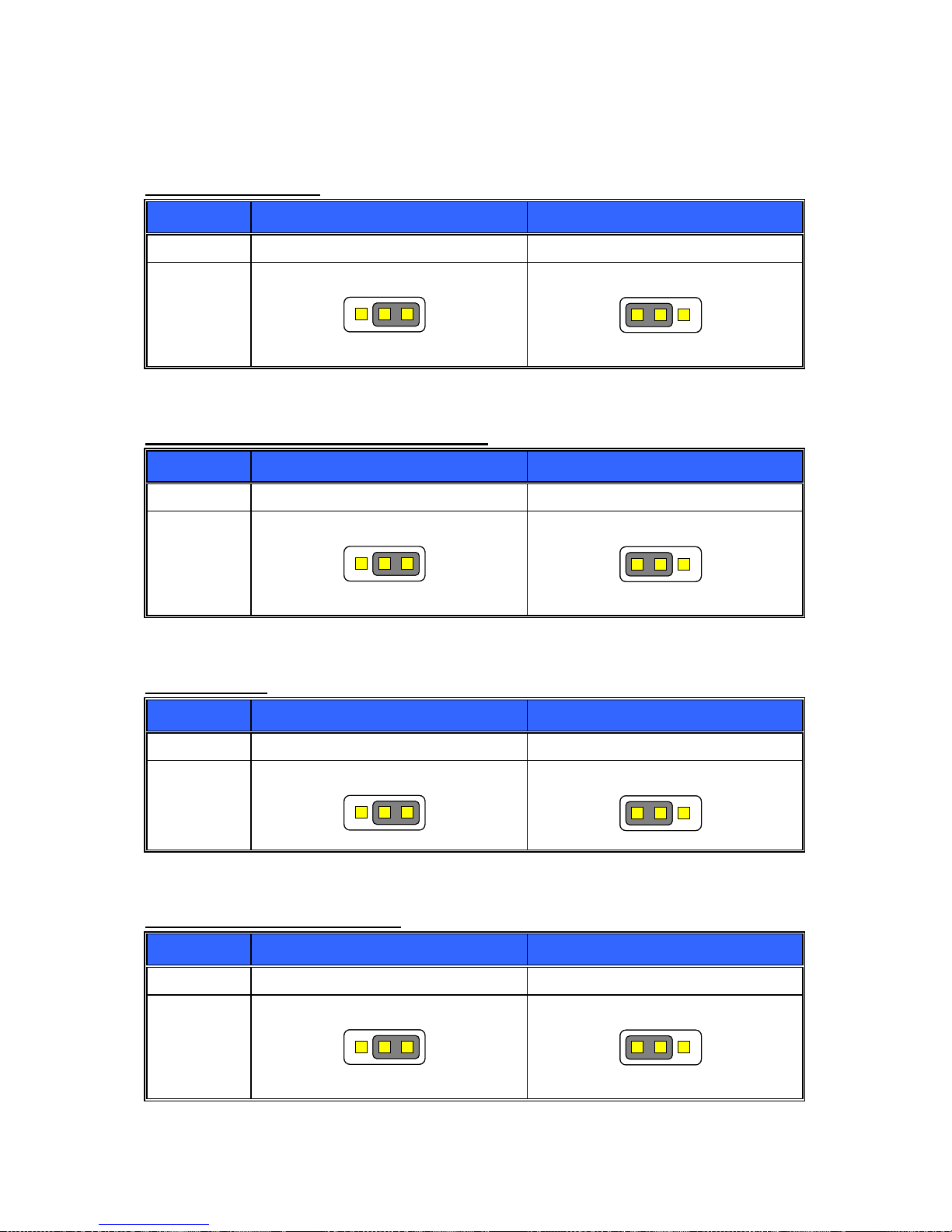
1.5 Jumper Setting
JCMOS: CMOS Clear
Pin No.
1-2
2-3
Function
Normal Operation (Default)
Clear CMOS Contents
Jumper
Setting
3 2 13 2 1
3 2 13 2 1
JLVDS: LCD Power (+3.3V/+5V) Selection
Pin No.
1-2
2-3
Function
LCD Power +3.3V (Default)
LCD Power +5V
Jumper
Setting
3 2 13 2 1
3 2 13 2 1
JME: ME Clear
Pin No.
1-2
2-3
Function
Normal Operation (Default)
Clear ME Contents
Jumper
Setting
3 2 13 2 1
3 2 13 2 1
JPWR: AT/ATX Mode Selection
Pin No.
1-2
2-3
Function
AT Mode
ATX Mode (Default)
Jumper
Setting
3 2 13 2 1
3 2 13 2 1
11
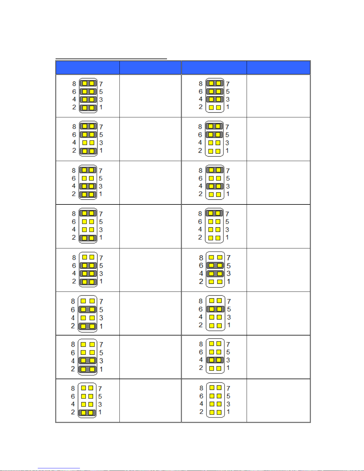
JLVDS1: LCD Panel Type Selection
Jumper Setting
LCD Panel Type
Jumper Setting
LCD Panel Type
800 x 600
18bit
(Default)
1024 x 768
18bit
1024 x 768
24bit
1280 x 768
18bit
1280 x 800
18bit
1280 x 960
18bit
1280 x 1024
24bit
1366 x 768
18bit
1366 x 768
24bit
1440 x 900
24bit
1440 x 1050
24bit
1600 x 900
24bit
1680 x 1050
24bit
1600 x 1200
24bit
1920 x 1080
24bit
1920 x 1200
24bit
12
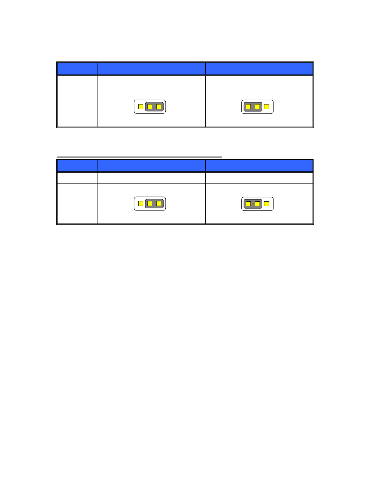
JMINI-PCIE: Mini-PCIE_or mSATA Function Selection
Pin No.
1-2
2-3
Function
Mini-PCIe (Default)
mSATA
Jumper
Setting
3 2 13 2 1
3 2 13 2 1
JCOM: SP339E RS232/422/485 Slew Rate Selection
Pin No.
1-2
2-3
Function
250Kbps (Default)
1Mbps
Jumper
Setting
3 2 13 2 1
3 2 13 2 1
13
1.6 Connector Function List
Rear I/O Port List
Connector
Function
Note
COM1
Serial port connector
LAN1, LAN2
RJ45 connector
USB1
USB3.0 connector
HDMI
HDMI port connector
VGA
VGA connector
OnBoard Expansion Slot List
Connector
Function
Note
CHA-DIMM1
DDR3/DDR3L SO-DIMM connector
MINI-PCIE
Mini-PCI Express connector/mSATA (share)
OnBoard I/O Connector List (1/2)
Connector
Function
Note
AUDIO
Line-in/MIC-in/Line-out with box-header
SATA1, SATA2
SATA III connector
SATA_PWR
SATA Power with box-header
COM2
Serial port connector with box-header
CPUFAN
CPUFAN 4-pin connector
DIO
Digital I/O with pin-header
SYSFAN
System FAN connector
INV
LCD inverter with box-header
JFRONT
Front Panel with pin-header
LPC
Reserved for debug
SMB
SMBUS with pin-header
JCOM
SP339E RS232/422/485 Slew Rate select
LVDS
LVDS connector
PWR1
ATX 2x2 connector
14
OnBoard I/O Connector List (2/2)
Connector
Function
Note
USB2,USB3
USB2.0 with box-header
BAT
CMOS BAT (CR2032) with box-header
SPI1
Reserved for debug
15
1.7 Connector Definitions
The following sections provide pin definitions and detailed description of all on-board
connectors. The connector definitions follow the following notation:
Column
Name
Description
Pin
Shows the pin-numbers in the connector. The graphical layout of the
connector definition tables is made similar to the physical connectors.
Type
Al
Analog Input.
AO
Analog Output.
I
Input, TTL compatible if nothing else stated.
IO
Input / Output TTL compatible if nothing else stated.
IOT
Bi-directional tri-state IO pin.
IS
Schmitt-trigger input, TTL compatible.
IOC
Input/open-collector Output, TTL compatible.
IOD
Input / Output, CMOS level Schmitt-triggered (open drain output).
NC
Pin not connected.
O
Output, TTL compatible.
OC
Output, open-collector or open-drain, TTL compatible.
OT
Output with tri-state capability, TTL compatible.
DIFF
Differential Signal.
PWR
Power supply or ground reference pins.
IOH
Typical current in mA flowing out of an output pin through a
grounded load, while the output voltage is > 2.4 V DC (if nothing
else stated).
IOL
Typical current in mA flowing into an output pin from a VCC
connected load, while the output voltage is < 0.4 V DC (if nothing
else stated).
Signal
The mnemonic name of the signal at the current pin. The notation “XX#”
states that the signal “XX” is active low.
Note
Special remarks concerning the signal.
※ The abbreviation TBD is used for specifications which are not available yet or which are
not sufficiently specified by the component vendors.

16
Rear I/O Port Pin Define
COM1: RS-232 Serial Port (DB9) Connector
COM1
Pin
Type
Signal
Note
RS-232
1 I Data Carrier Detect (DCD)
COM1
RS-232
2 I Received Data (RXD)
3 O Transmitted Data (TXD)
4 O Data Terminal Ready (DTR)
5
PWR
Ground
6 I Data Set Ready (DSR)
7 O Request To Send (RTS)
8 I Clear To Send (CTS)
9 I Ring Indicator (RI#)
HDMI: HDMI Connector
HDMI
Pin
Type
Signal
Note
1
DIFF
HDMI TMDS2+
2
PWR
Ground
3
DIFF
HDMI TMDS2-
4
DIFF
HDMI TMDS1+
5
PWR
Ground
6
DIFF
HDMI TMDS1-
7
DIFF
HDMI TMDS0+
8
PWR
Ground
9
DIFF
HDMI TMDS0-
10
DIFF
HDMI TMDS_CLK+
11
PWR
Ground
12
DIFF
HDMI TMDS_CLK-
13
NC
Not connected
14
NC
Not connected
15
IO
HDMI DDC clock
1
16
IO
HDMI DDC data
1
17
PWR
Ground
18
PWR
HDMI power +5V
19 I HDMI Hot plug detect
Note 1: HDMI port pin.15 (DDC Clock) and pin.16 (DDC Data) Pull Up +5V/2.2KΩ.
COM1
VGA
HDMI
USB1
LAN1
LAN2

17
LAN1, LAN2: RJ45 (LAN) Connectors
LAN1, LAN2
Pin
Type
Signal
Note
P1
DIFF
MDI0+ / TXD+
RJ45
P2
DIFF
MDI0- / TXD-
P3
DIFF
MDI1+ / RXD+
P4
DIFF
MDI2+
P5
DIFF
MDI2-
P6
DIFF
MDI1- / RXD-
P7
DIFF
MDI3+
P8
DIFF
MDI3-
USB1: USB3.0 Connectors
USB1
Pin
Type
Signal
Note
10
PWR
USB3.0 P2 power +5V
(Note 1)
USB 3.0
(UP)
(Blue)
11
DIFF
USB2.0 P1_D-
12
DIFF
USB2.0 P1_D+
13
PWR
Ground
14
DIFF
USB3.0 P2_RX-
15
DIFF
USB3.0 P2_RX+
16
PWR
Ground
17
DIFF
USB3.0 P2_TX-
18
DIFF
USB3.0 P2_TX+
1
PWR
USB3.0 P1 power +5V
(Note 1)
USB 3.0
(DOWN)
(Blue)
2
DIFF
USB2.0 P0_D-
3
DIFF
USB2.0 P0_D+
4
PWR
Ground
5
DIFF
USB3.0 P1_RX-
6
DIFF
USB3.0 P1_RX+
7
PWR
Ground
8
DIFF
USB3.0 P1_TX-
9
DIFF
USB3.0 P1_TX+
Note 1: USB3.0 port power supply maximum +5V/0.9A
18
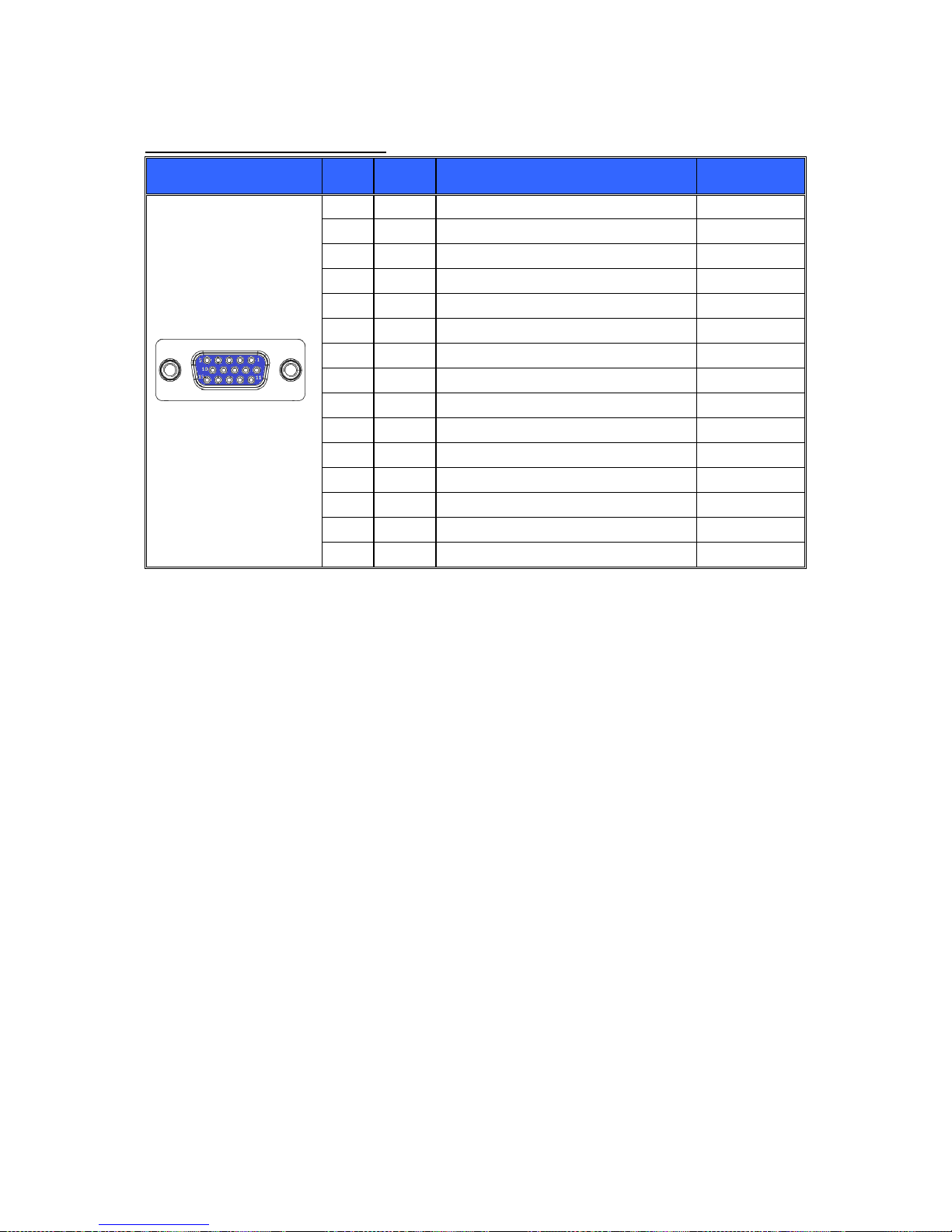
VGA: VGA (DB15) Connector
VGA
Pin
Type
Signal
Note
1
AO
VGA Red color values
2
AO
VGA Green color values
3
AO
VGA Blue color values
4
NC
Not connected
5
PWR
Ground
6
PWR
Ground
7
PWR
Ground
8
PWR
Ground
9
PWR
VGA power +5V
10
PWR
Ground
11
NC
Not connected
12
IO
VGA DDC data
1
13 O VGA Horizontal synchronization
14 O VGA Vertical synchronization
15
IO
VGA DDC clock
1
Note 1: VGA port pin.12 (DDC Data) and pin.15 (DDC Clock) Pull Up +5V/2.2KΩ.
19
OnBoard Expansion Slot Pin Define
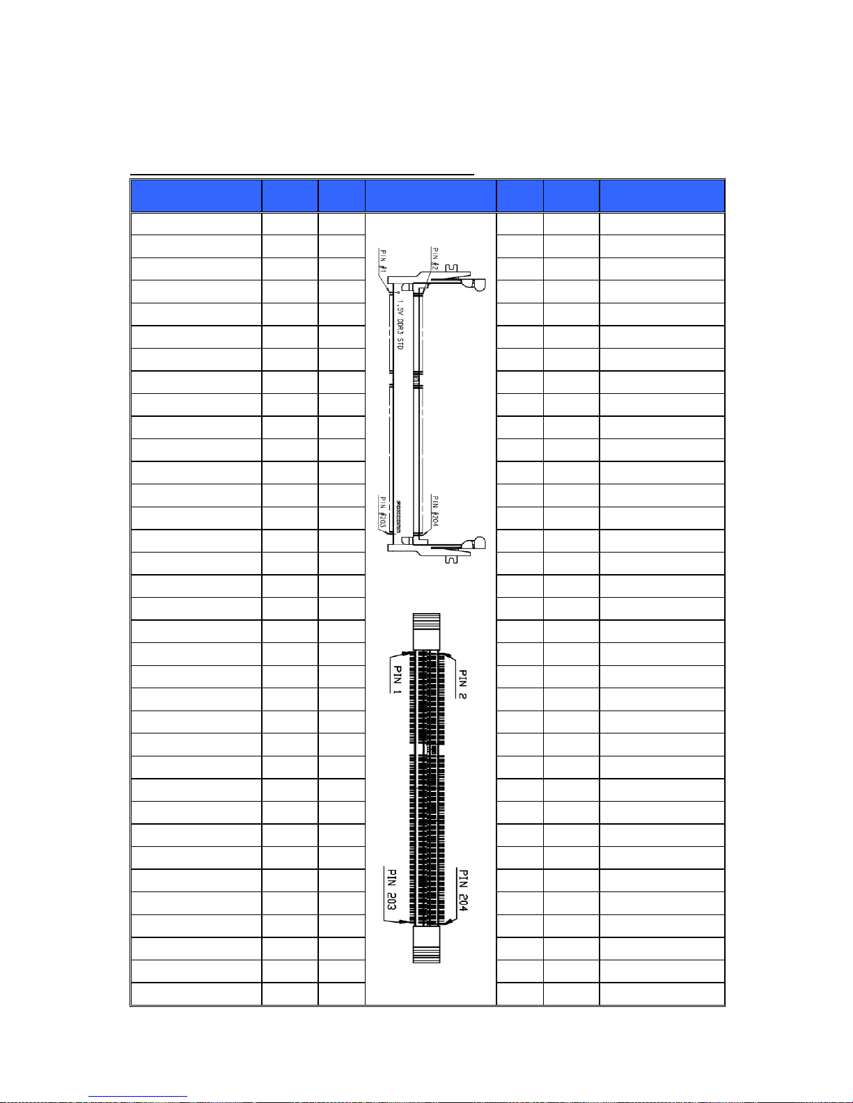
CHA-DIMM1: DDR3/DDR3L SO-DIMM Slot (1/3)
Signal
Type
Pin
CHA-DIMM1
Pin
Type
Signal
VREF_DQ
IO
1 2
PWR
Ground
Ground
PWR
3 4 IO
DQ4
DQ0
IO 5 6
IO
DQ5
DQ1
IO 7 8
PWR
Ground
Ground
PWR
9
10
DIFF
DQS0#
DM0 I 11
12
DIFF
DQS0
Ground
PWR
13
14
PWR
Ground
DQ2
IO
15
16
IO
DQ6
DQ3
IO
17
18
IO
DQ7
Ground
PWR
19
20
PWR
Ground
DQ8
IO
21
22
IO
DQ12
DQ9
IO
23
24
IO
DQ13
Ground
PWR
25
26
PWR
Ground
DQS1#
DIFF
27
28
I
DM1
DQS1
DIFF
29
30
I
Reset#
Ground
PWR
31
32
PWR
Ground
DQ10
IO
33
34
IO
DQ14
DQ11
IO
35
36
IO
DQ15
Ground
PWR
37
38
PWR
Ground
DQ16
IO
39
40
IO
DQ20
DQ17
IO
41
42
IO
DQ21
Ground
PWR
43
44
PWR
Ground
DQS2#
DIFF
45
46
I
DM2
DQS2
DIFF
47
48
PWR
Ground
Ground
PWR
49
50
IO
DQ22
DQ18
IO
51
52
IO
DQ23
DQ19
IO
53
54
PWR
Ground
Ground
PWR
55
56
IO
DQ28
DQ24
IO
57
58
IO
DQ29
DQ25
IO
59
60
PWR
Ground
Ground
PWR
61
62
DIFF
DQS3#
DM3 I 63
64
DIFF
DQS3
Ground
PWR
65
66
PWR
Ground
DQ26
IO
67
68
IO
DQ30
DQ27
IO
69
70
IO
DQ31
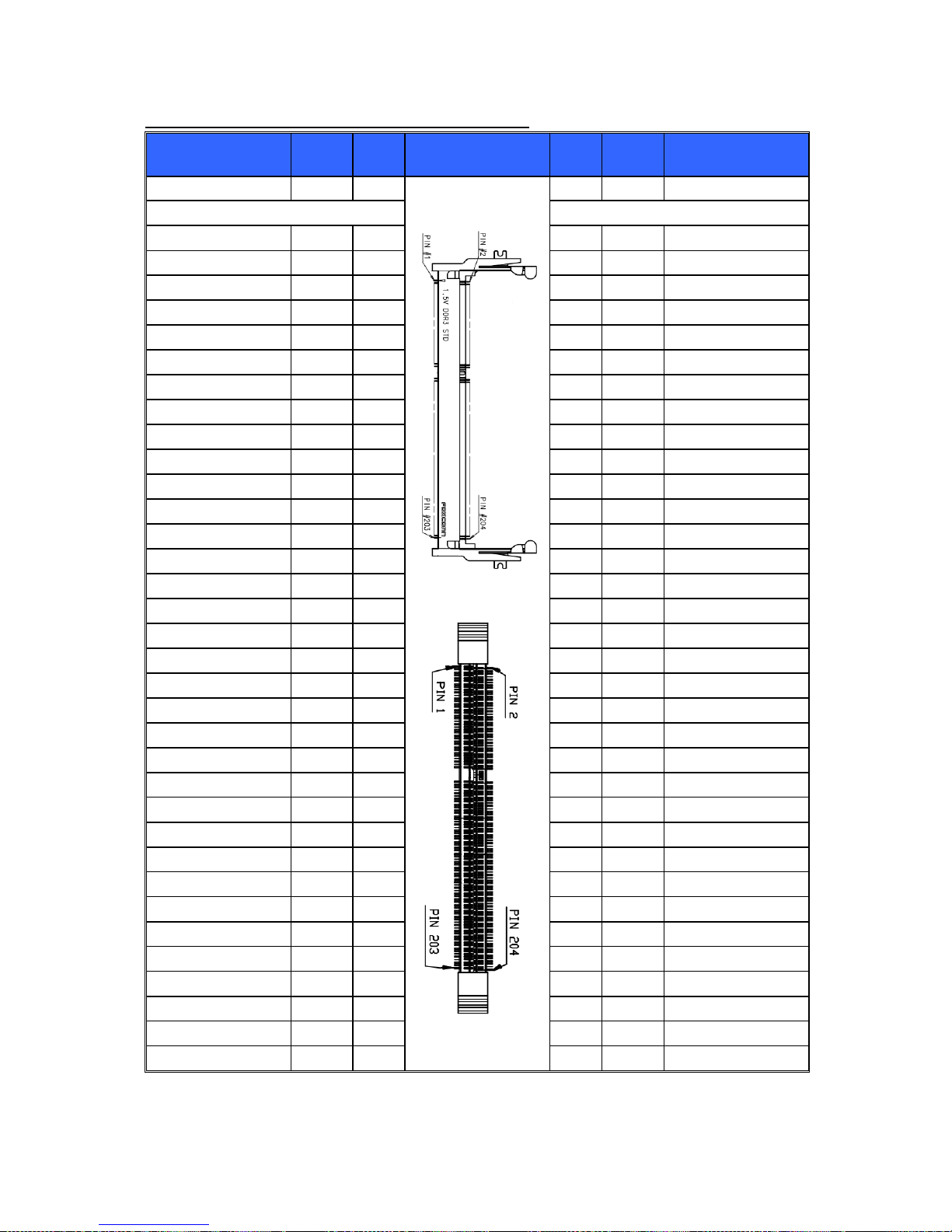
20
CHA-DIMM1: DDR3/DDR3L SO-DIMM Slot (2/3)
Signal
Type
Pin
CHA-DIMM1
Pin
Type
Signal
Ground
PWR
71 72
PWR
Ground
KEY
KEY
CKE0
I
73
74 I CKE1
VDDQ +1.35V
(Note1)
PWR
75
76
PWR
VDDQ +1.35V
(Note1)
Not connected
NC
77
78 I A15
BA2 I 79
80 I A14
VDDQ +1.35V
(Note1)
PWR
81
82
PWR
VDDQ +1.35V
(Note1)
A12 I 83
84 I A11
A9 I 85
86 I A7
VDDQ +1.35V
(Note1)
PWR
87
88
PWR
VDDQ +1.35V
(Note1)
A8 I 89
90 I A6
A5 I 91
92 I A4
VDDQ +1.35V
(Note1)
PWR
93
94
PWR
VDDQ +1.35V
(Note1)
A3 I 95
96 I A2
A1 I 97
98 I A0
VDDQ +1.35V
(Note1)
PWR
99
100
PWR
VDDQ +1.35V
(Note1)
CK0
DIFF
101
102
DIFF
CK1
CK0#
DIFF
103
104
DIFF
CK1#
VDDQ +1.35V
(Note1)
PWR
105
106
PWR
VDDQ +1.35V
(Note1)
A10 I 107
108
I
BA1
BA0 I 109
110
I
RAS#
VDDQ +1.35V
(Note1)
PWR
111
112
PWR
VDDQ +1.35V
(Note1)
WE#
I
113
114
I
CS0#
CAS#
I
115
116
I
ODT0
VDDQ +1.35V
(Note1)
PWR
117
118
PWR
VDDQ +1.35V
(Note1)
A13 I 119
120
I
ODT1
CS1#
I
121
122
NC
Not connected
VDDQ +1.35V
(Note1)
PWR
123
124
PWR
VDDQ +1.35V
(Note1)
Not connected
NC
125
126
IO
VREF_CA
Ground
PWR
127
128
PWR
Ground
DQ32
IO
129
130
IO
DQ36
DQ33
IO
131
132
IO
DQ37
Ground
PWR
133
134
PWR
Ground
DQS4#
DIFF
135
136
I
DM4
DQS4
DIFF
137
138
PWR
Ground
Ground
PWR
139
140
IO
DQ38
21
CHA-DIMM1: DDR3/DDR3L SO-DIMM Slot (3/3)
Signal
Type
Pin
CHA-DIMM1
Pin
Type
Signal
DQ34
IO
141
142
IO
DQ39
DQ35
IO
143
144
PWR
Ground
Ground
PWR
145
146
IO
DQ44
DQ40
IO
147
148
IO
DQ45
DQ41
IO
149
150
PWR
Ground
Ground
PWR
151
152
DIFF
DQS5#
DM5
I
153
154
DIFF
DQS5
Ground
PWR
155
156
PWR
Ground
DQ42
IO
157
158
IO
DQ46
DQ43
IO
159
160
IO
DQ47
Ground
PWR
161
162
PWR
Ground
DQ48
IO
163
164
IO
DQ52
DQ49
IO
165
166
IO
DQ53
Ground
PWR
167
168
PWR
Ground
DQS6#
DIFF
169
170
I
DM6
DQS6
DIFF
171
172
PWR
Ground
Ground
PWR
173
174
IO
DQ54
DQ50
IO
175
176
IO
DQ55
DQ51
IO
177
178
PWR
Ground
Ground
PWR
179
180
IO
DQ60
DQ56
IO
181
182
IO
DQ61
DQ57
IO
183
184
PWR
Ground
Ground
PWR
185
186
DIFF
DQS7#
DM7
I
187
188
DIFF
DQS7
Ground
PWR
189
190
PWR
Ground
DQ58
IO
191
192
IO
DQ62
DQ59
IO
193
194
IO
DQ63
Ground
PWR
195
196
PWR
Ground
SA0 I 197
198
NC
Not connected
VDDSPD +3.3V
PWR
199
200
IO
SMBus data
SA1 I 201
202
O
SMBus clock
VTT +0.675V
(Note 2)
PWR
203
204
PWR
VTT +0.675V
(Note 2)
Note 1: CHA-DIMM1 Slot power supply maximum +1.35V/2.0A
Note 2: CHA-DIMM1 Slot power supply maximum +0.675V/0.6A
22
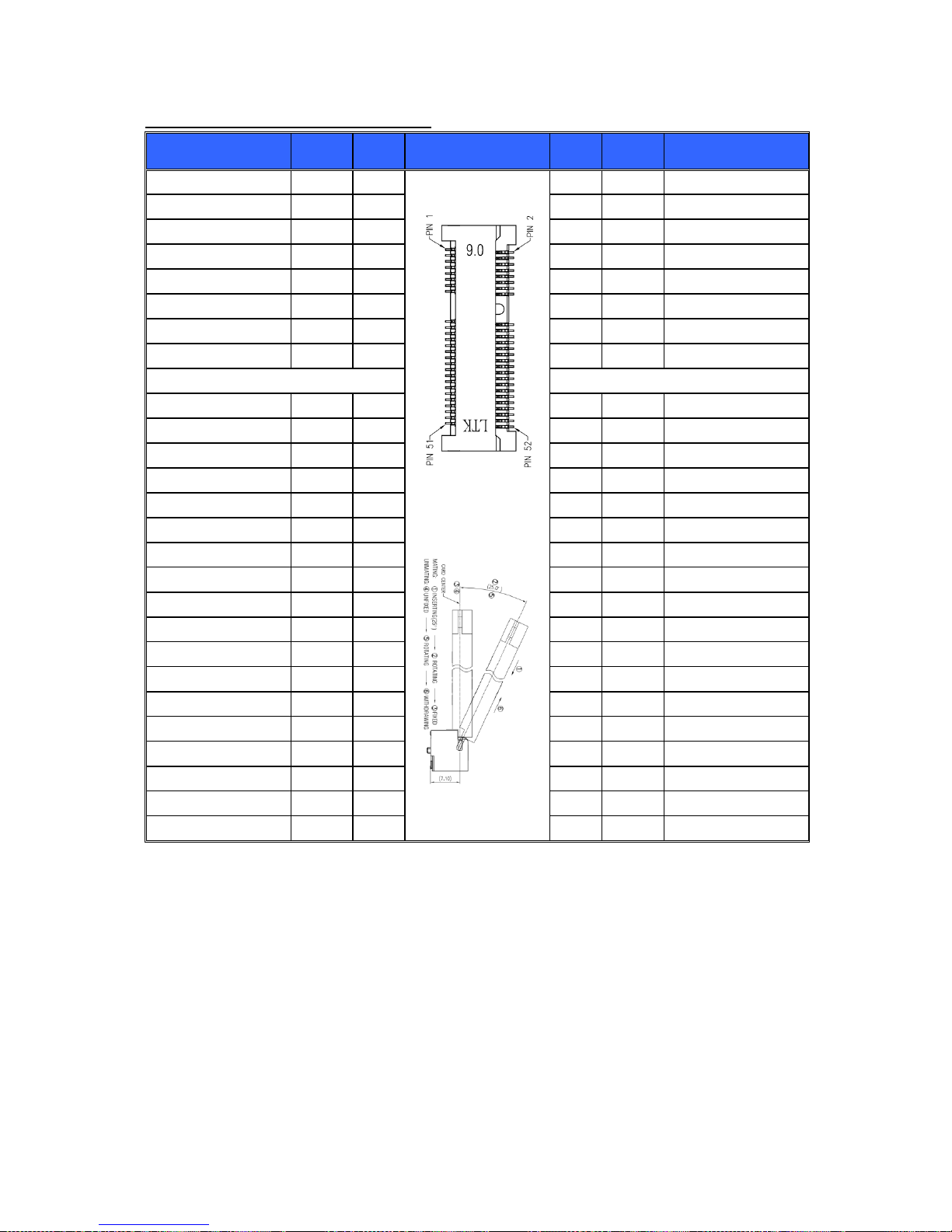
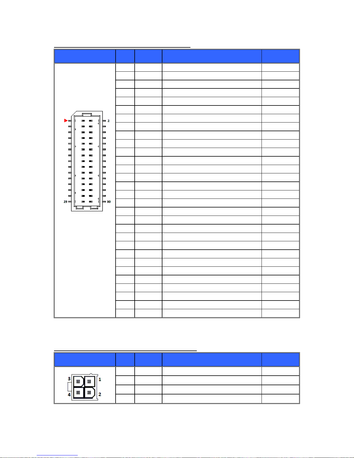
MINI-PCIE: Mini-PCIe Express Slot
Signal
Type
Pin
MINI-PCIE
Pin
Type
Signal
WAKE#
I
1 2
PWR
+3.3Vaux
(Note 1)
Not connected
NC 3 4
PWR
Ground
Not connected
NC 5 6
PWR
+1.5V (Note2)
CLKREQ#
I 7 8
NC
Not connected
Ground
PWR
9
10
NC
Not connected
PCIE_CLOCK-
DIFF
11
12
NC
Not connected
PCIE_CLOCK+
DIFF
13
14
NC
Not connected
Ground
PWR
15
16
NC
Not connected
KEY
KEY
Not connected
NC
17
18
PWR
Ground
Not connected
NC
19
20
NC
Not connected
Ground
PWR
21
22 O PERST#
PCIE_RXN
DIFF
23
24
PWR
+3.3Vaux
(Note 1)
PCIE_RXP
DIFF
25
26
PWR
Ground
Ground
PWR
27
28
PWR
+1.5V
(Note 2)
Ground
PWR
29
30 O SMBus clock
PCIE_TXN
DIFF
31
32
IO
SMBus data
PCIE_TXP
DIFF
33
34
PWR
Ground
Ground
PWR
35
36
DIFF
USB2.0 P10_D-
Ground
PWR
37
38
DIFF
USB2.0 P10_D+
+3.3Vaux
(Note 1)
PWR
39
40
PWR
Ground
+3.3Vaux
(Note 1)
PWR
41
42
NC
Not connected
mPCIE_SEL1
I
43
44
NC
Not connected
Not connected
NC
45
46
NC
Not connected
Not connected
NC
47
48
PWR
+1.5V
(Note 2)
Not connected
NC
49
50
PWR
Ground
Not connected
NC
51
52
PWR
+3.3Vaux
(Note 1)
Note 1: MINI-PCIE Slot power supply maximum +3.3Vaux/1.1A, peak 2.5A.
Note 2: MINI-PCIE Slot power supply maximum +1.5V/0.375A, peak 0.5A.
23
OnBoard I/O Connector Pin Define
AUDIO: Audio with Box-header
AUDIO
Pin
Type
Signal
Note
Box-header 2.0mm
1
AI
Line-in (Right)
2
AI
Line-in (Left)
3
AI
Line-in jack detect
4
AI
Mic-in jack detect
5
AI
Mic-in (Right)
6
AI
Mic-in (Left)
7
AI
Line-out jack detect
8
PWR
Audio Ground
9
AO
Line-out (Right)
10
AO
Line-out (Left)
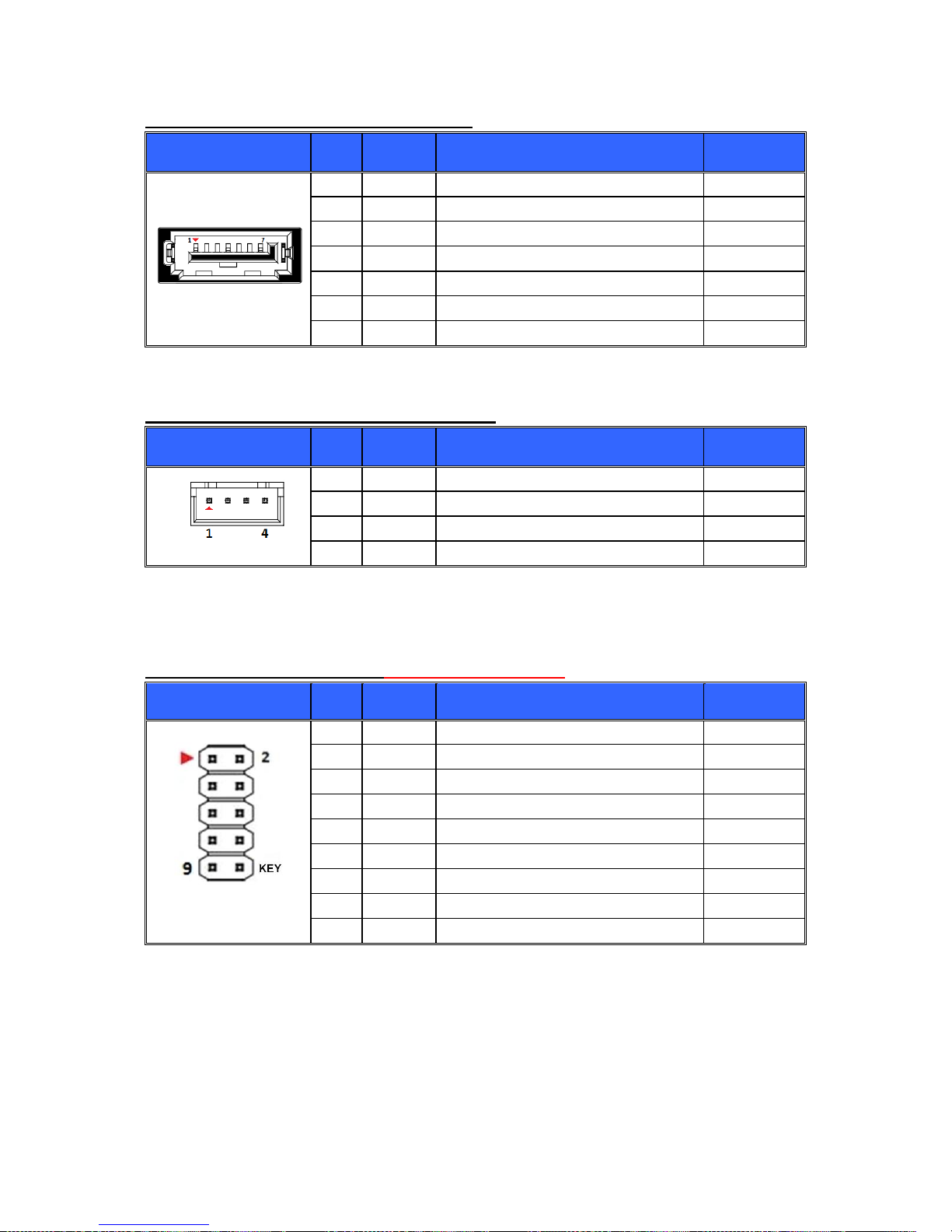
BAT: CMOS Battery with Box-header
BAT
Pin
Type
Signal
Note
Box-header 1.25mm
1
PWR
CR2032 Lithium Manganese
Battery +2.5V~+3.3V
2
PWR
Ground
COM2: RS-232/422/485 Serial Ports with Box-header
COM2
Pin
Type
Signal
Note
RS-232
RS-422/
485 Full
RS-485
Half
Box-header 2.0mm
1
I
Data Carrier Detect
TX D-
DATA-
COM2
RS-232
RS-422
RS-485
2
I
Data Set Ready
3
I
Received Data (RXD)
TX D+
DATA+
4
O
Request To Send
5
O
Transmitted Data
RX D+
6
I
Clear To Send (CTS)
7
O
Data Terminal Ready
RX D-
8
I
Ring Indicator (RI#)
9
PWR
Ground
10
NC
Not connected
24
CPUFAN: CPU FAN 4-Pin Connector
CPUFAN
Pin
Type
Signal
Note
1
PWR
Ground
2
PWR
CPU FAN power +12V
1 3 I
CPU FAN Sense
2 4 O
CPU FAN Control
Note 1: CPUFAN pin.2 power supply maximum +12V/0.75A
Note 2: CPUFAN pin.3 sensor pull up +12V/4.7KΩ
SYSFAN: System FAN 3-Pin Connector
SYSFAN
Pin
Type
Signal
Note
1
PWR
Ground
2 PWR
SYSFAN power +12V
1 3 I
SYSFAN sense
2
Note 1: SYSFAN pin.2 power supply maximum +12V/0.75A
Note 2: SYSFAN pin.3 sensor pull up +12V/4.7KΩ
DIO: Digital I/O with Pin-header
DIO
Pin
Type
Signal
Note
Pin-header 2.0mm
1 O Digital I/O-Output0 (bit4)
1
2 I Digital I/O-Input0 (bit0)
3 O
Digital I/O-Output1 (bit5)
1 4 I
Digital I/O-Input1 (bit1)
5 O
Digital I/O-Output2 (bit6)
6 I
Digital I/O-Input2 (bit2)
7 O
Digital I/O-Output3 (bit7)
8 I
Digital I/O-Input3 (bit3)
9 PWR
DIO power +12V
2
10
PWR
DIO power +5V
3
11
PWR
Ground
12
-
KEY
Note 1: DIO pin.1 Output0 (bit4) and pin.3 Output1 (bit5) power sink 8A
Note 2: DIO pin.9 power supply maximum +12V/0.5A
Note 3: DIO pin.10 power supply maximum +5V/0.5A
25
INV: LCD Inverter with Box-header
INV
Pin
Type
Signal
Note
Box-header 2.5mm
1
PWR
Inverter power +12V
1
2
PWR
Inverter power +12V
1
3
PWR
Ground
4 O LCD Panel backlight adjustment
5 O LCD Panel backlight enable
Note 1: INV pin.1~2 total power supply maximum +12V/1.5A
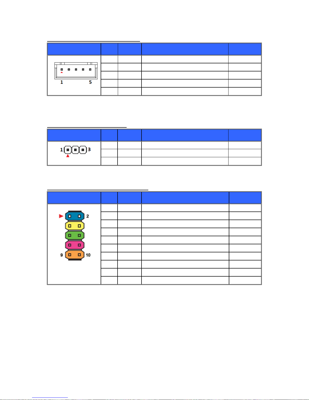
SMB: SMBus with Pin-header
SMB
Pin
Type
Signal
Note
Pin-header 2.54mm
1
OC
SMBus clock
(+3.3V Level)
2
IOC
SMBus data
(+3.3V Level)
3
PWR
Ground
JFRONT: Front Panel with Pin-header
JFRONT
Pin
Type
Signal
Note
Pin-header 2.54mm
1 O Power on LED
1
2
PWR
Ground
3 O HDD LED
1 4 O
HDD LED control
5 O Suspend LED
1
6 O Suspend LED control
7 I
System Reset#
8
PWR
Ground
9 I Power button#
10
PWR
Ground
Note 1: JFRONT pin.1 Power On & pin.3 HDD LED & pin.5 Suspend LED pull up +5V/470Ω/10mA
26
LVDS: LCD Panel LVDS 18/24bit Box-header
LVDS
Pin
Type
Signal
Note
Box-header 1.0mm
1
PWR
Ground
2
PWR
Ground
3
DIFF
LVDS_A3+
4
DIFF
LVDS_A3-
5
DIFF
LVDS_ACLK+
6
DIFF
LVDS_ACLK-
7
DIFF
LVDS_A2+
8
DIFF
LVDS_A2-
9
DIFF
LVDS_A1+
10
DIFF
LVDS_A1-
11
DIFF
LVDS_A0+
12
DIFF
LVDS_A0-
13
PWR
Ground
14
PWR
Ground
15
DIFF
LVDS_B3+
16
DIFF
LVDS_B3-
17
DIFF
LVDS_BCLK+
18
DIFF
LVDS_BCLK-
19
DIFF
LVDS_B2+
20
DIFF
LVDS_B2-
21
DIFF
LVDS_B1+
22
DIFF
LVDS_B1-
23
DIFF
LVDS_B0+
24
DIFF
LVDS_B0-
25
PWR
Ground
26
PWR
Ground
27
PWR
LVDS power +3.3V / +5V
1, 2
28
PWR
LVDS power +3.3V / +5V
1, 2
29
PWR
LVDS power +3.3V / +5V
1, 2
30
PWR
LVDS power +3.3V / +5V
1, 2
Note 1: LVDS pin.27~30 power voltage by jumper select +3.3V / +5V
Note 2: LVDS pin.27~30 power supply maximum +3.3V/1.0A or +5V/1.0A
PWR1: DC-IN +12V 2x2-pin (4-pole) Connector
PWR1
Pin
Type
Signal
Note
1
PWR
Ground
2
PWR
Ground
3
PWR
DC-IN +12V
4
PWR
DC-IN +12V
27
SATA1, SATA2: SATA III Port Connector
SATA1, SATA2
Pin
Type
Signal
Note
1
PWR
Ground
2
DIFF
SATA TX+
3 DIFF
SATA TX-
4
PWR
Ground
5
DIFF
SATA RX-
6 DIFF
SATA RX+
7
PWR
Ground
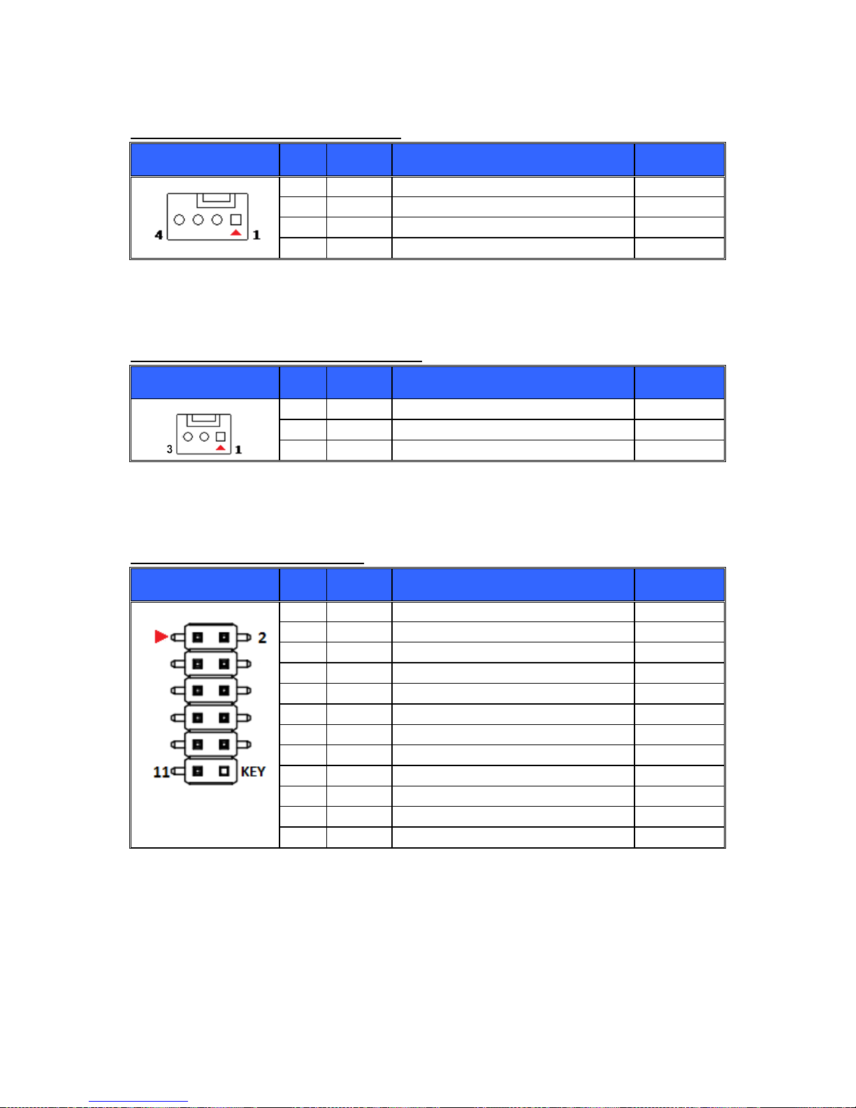
SATA_PWR: SATA Power with Box-header
SATA_PWR
Pin
Type
Signal
Note
Box-header 2.5mm
1
PWR
SATA power +5V
1
2
PWR
Ground
3
PWR
Ground
4
PWR
SATA power +12V
2
Note 1:
SATA_PWR pin.1 power supply maximum +5V/1.5A
Note 2:
SATA_PWR pin.4 power supply maximum +12V/1.5A
LPC: Low Pin Count Header - (reserved for debug)
LPC
Pin
Type
Signal
Note
Pin-header 2.0mm
1
IOC
LPC_AD0
2
OC
LPC_PLTRST#
1
3
IOC
LPC_AD1
4
OC
LPC_FRAME#
5
IOC
LPC_AD2
6
PWR
LPC Power +3.3V
7
IOC
LPC_AD3
8
PWR
GND
9
I
LPC33MHz
Note 1: LPC pin.2 LPC_PLTRST# pull up +3.3V/470Ω
 Loading...