

CJB WEX-E38451 User Manual

WEX-E38451
Intel Atom E3845
Rev.01, Oct. 2015
1

Revision
Date
Comment
Rev. 01
2015/10/26
Release
Document revision history
2

The information in this document is subject to change without prior notice in order to
improve reliability, design and function; moreover, the information does not represent
a commitment on the part of the manufacturer.
This document contains proprietary information protected by copyright. All rights are
reserved. No part of this material including the product and software are available in
this publication may be reproduced or transcribed in any form or by any means
without the prior written permission of the publisher.
All registered trademarks and product names mentioned herein are used for
identification purposes only and may be trademarks or registered trademarks of their
respective owners.
Trademarks
Copyright Notice
3
AMI is a registered trademark of AMI Software International Inc.
Intel is registered trademarks of Intel Corporation.
Microsoft Windows is a registered trademark of Microsoft Corporation.
FINTEK is a registered trademark of FINTEK Electronics Corporation.
REALTEK is a registered trademark of REALTEK Electronics Corporation.
All other product names or trademarks are properties of their respective owners.
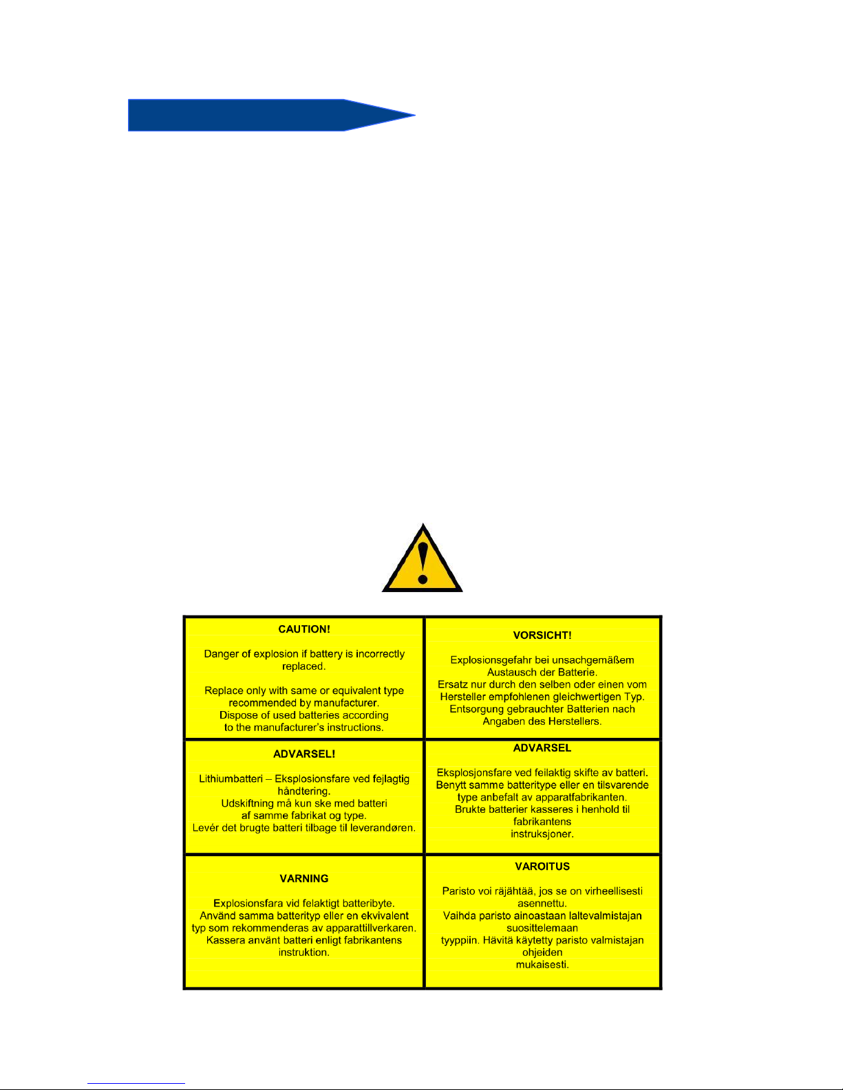
Lithium-Ion Battery Warning
CAUTION
Please replace with the same or equivalent type recommended by the manufacturer.
Do not crush, puncture, incinerate, or short circuit external contacts.
Do not dispose of in fire or expose to excess heat.
Acknowledgement
4

WEX-E38451
Driver CD (Include user manual)
1 x PS/2 Y Cable (Keyboard and Mouse)
1 x 2 Ports COM Cable with Bracket
1 x USB2.0 Cable with Bracket (for pin-header)
1 x USB2.0 Cable with Bracket (for box-header)
1 x SATA Cable
Optional Accessory
Packing List
5

Contents
Chapter 1 Product Information ......................................................................... 8
1.1 Block Diagram ............................................................................. 8
1.2 Features ........................................................................................ 9
1.3 PCB Layout ................................................................................. 12
1.4 Dimensions ................................................................................. 14
1.5 Jumper Setting ........................................................................... 15
1.6 Connector Function List ............................................................ 17
1.7 Connector Definitions ............................................................... 19
1.8 I/O Ports Power Output (max.) ................................................. 35
Chapter 2 BIOS Setup ...................................................................................... 37
2.1 Main Menu ................................................................................. 37
2.2 Advanced Menu ....................................................................... 38
2.3 ACPI Settings .............................................................................. 40
2.4 Super IO Configuration ............................................................. 41
2.5 Serial Port 1 Configuration ........................................................ 42
2.6 Serial Port 2 Configuration ........................................................ 43
2.7 Serial Port 3 Configuration ........................................................ 44
2.8 Hardware Monitor ..................................................................... 45
2.9 Smart Fan Mode Configuration ................................................ 46
2.10 CPU Configuration ................................................................... 47
2.11 IDE Configuration .................................................................... 48
2.12 Network Stack Configuration ................................................. 50
2.13 CSM Configuration .................................................................. 51
2.14 USB Configuration .................................................................... 53
2.15 Chipset ..................................................................................... 55
2.16 North Bridge ............................................................................. 56
2.17 Intel IGD Configuration ........................................................... 57
2.18 South Bridge ............................................................................. 60
2.19 USB Configuration .................................................................. 61
2.20 PCI Express Configuration ...................................................... 62
2.21 Password Configuration .......................................................... 63
2.22 Boot Configuration .................................................................. 64
2.23 Exit Manu .................................................................................. 65
Chapter 3 Drivers Installation .......................................................................... 66
3.1 Intel Chipset Device Software .................................................. 66
6

3.2 Intel Graphic Media Accelerator Driver ................................. 69
3.3 LAN Driver .................................................................................. 72
3.4 Audio Driver ............................................................................... 75
3.5 USB Driver ................................................................................... 76
Appendix A: Watch Dog Timer ....................................................................... 79
Appendix B: GPIO ............................................................................................ 82
7
Chapter 1 Product Information
This chapter introduces the product features, jumper and connector information.
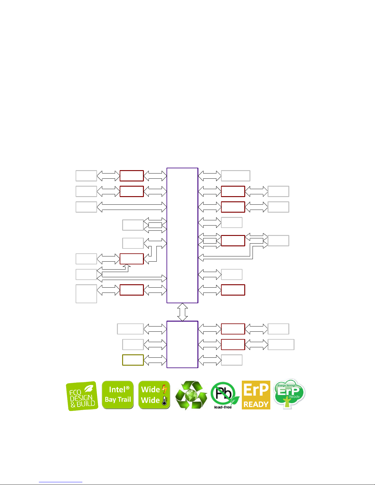
1.1 Block Diagram
SPI
VGA R.G.B
USB2.0
TMDS
Mini-PCIe
(Half-size)
HDMI
SATA 2.0
PCIe x1
SATA Port
x1
Intel BayTrail
Family
Processor
Atom E3845
Super I/O
F81866AD
USB2.0
PCIe x1
SATA 2.0
ASM1455
HS Bus
SPI Flash
HDA
ALC662
Analog
Mic-in
Line-out
SMBus
SMB
USB2.0
USB2.0
x5
USB2517
[MTT]
UART
SP339
COM
RS-232/422/485
(DB9)
ADM213
COM
VINx
HW Monitor
ErP/EuP 2013 < 0.5W
UART
Line-in
RS-232
x2
Mini-PCIe
(Full-size)
LPC
GPIO
Transceiver
LAN2
(RJ45)
GbE LAN I210
PCIe x1
Digital I/O 8-bit
4in/4out
Chan A
DDI1
CH7511B
LVDS
LVDS
2ch/24bits
Transceiver
DDR3L SO-DIMM
x1
VGA
(DB15)
PS/2
I/O
KB_MS
x1
CPU Fan
WECX-E38451 System Block Diagram
USB3.0
x1
GbE LAN I210
ASM1442
DDI0
USB2.0
x1
USB2.0
PCIe x1
USB3.0
USB2.0
LAN1
(RJ45)
8

1.2 Features
System Processor/
Chipsets
Processor
Intel® Atom™ Processor E3845 Product
1.91GHz Quad-Core SoC (10W)
Intel® Atom™ Processor E3825 Product
1.33GHz Dual-Core SoC (6W)
FCBGA1170 Package 25.0mm x 27.0mm
BIOS
AMI BIOS, 64Mbit SPI Low Power Flash ROM
Memory
Technology
Atom™ Processors DDR3L 1333 MT/s (E3845)
Atom™ Processors DDR3L 1066 MT/s (E3825)
DDR3L DRAM Device Technology (+1.35V)
- Standard 1Gb/2Gb/4Gb technologies and addressing.
- Read latency 5, 6, 7, 8, 9, 10, 11.
- Write latency 5, 6, 7, 8.
Max. Capacity
Up to 8GB DDR3L DRAM
Socket
1 (DDR3L SO-DIMM +1.35V)
Display
Chipset
Intel® 7th generation (Gen 7) graphics and media
encode/decode engine
VRAM
Shared system memory up to 512MB (max.)
LVDS
18/24bit, Dual Channel
Max. resolution up to 1920x1200 @ 60Hz
VGA
Analog Display:
Max. resolution up to 2560x1600 @ 60Hz
HDMI
Digital Display:
Max. resolution up to 1920x1200 @ 60Hz
Any 2
Displays
(1) LVDS + VGA
(2) LVDS + HDMI
(3) HDMI + VGA
Ethernet
Interface
PCIe x1 Gigabit LAN 10/100/1000 Mb/s
Controller
LAN1: Intel® Ethernet Controller I210
LAN2: Intel® Ethernet Controller I210
9
Audio
Interface
Intel® High Definition Audio
Controller
Realtek® ALC662-VD0 HD Audio Codec
SATA
Max. Data
Transfer Rate
SATA II:3.0Gb/s
Port
1 x SATA II,
1 x mSATA (Share MINI-PCIE slot)
Integrated AHCI controller
Expansion Slot
Mini-PCIE
1 x Full-size Mini-PCIe with mSATA supported
1 x Half-size Mini-PCIe
Rear I/O
VGA
1
COM
1 (RS-232/422/485)
1. COM1 RS-422/485 support Half and Full Duplex.
2. COM1 RS-232 Slew Rate 1Mbps (max.).
3. COM1 RS-422/485 Slew Rate 20Mbps (max.).
HDMI
1
LAN
2 (RJ45)
USB 2.0
1
USB 3.0
1
Onboard Conn.
and Pin-Header
COM
2 (RS-232)
DIO
4-in/4-out (sink 6A x2)
FRONT
1 (Power/HDD/Suspend-LED/PwrBTN/RstBTN)
HD Audio
1 (Line-in/MIC-in/Line-out)
PS/2
1 (Keyboard and Mouse)
SMBus
1
USB 2.0
4
10

Power
DC Input
+12Vdc ~ +24Vdc
Connector
ATX 4P
Watchdog Timer
Interval
Programmable 1~255 sec/min
Output
System reset
Energy
ErP/EuP
ErP/EuP 2013 Ready
Power off mode (G3) < 0.5W
Environment
Operating
Temp.
0°C ~ +60°C (standard)
-20°C ~ 70°C (optional)
-40°C ~ 70°C (optional)
Storage
Temp.
-40°C ~ 85°C (non-condensing)
Relative
Humidity
0% ~ 95% (non-condensing)
Form Factor
Dimension
(L x W)
3.5‖ SBC
102mm x 146mm (4.02‖ x 5.75‖)
*** WEX-E38451 base unit will be RoHS compliant from LP/MP phase.
*** The content is subjected to change without notice.
11
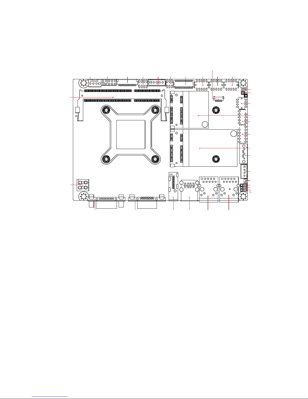
1.3 PCB Layout
Top View
CPUFAN FRONT LPC_SPI JLVDS
INV JPLVDS LVDS COM3 COM2 AUDIO
LAN2LAN1USB1HDMIVGACOM1
PWR1
CHA-DIMM
USB3
USB2
DIO
SATA
SATAPWR
MINI-PCIE2
MINI-PCIE1
SMB
BZ
BAT
JTRTC
JCMOS
JPWR
KB_MS
12
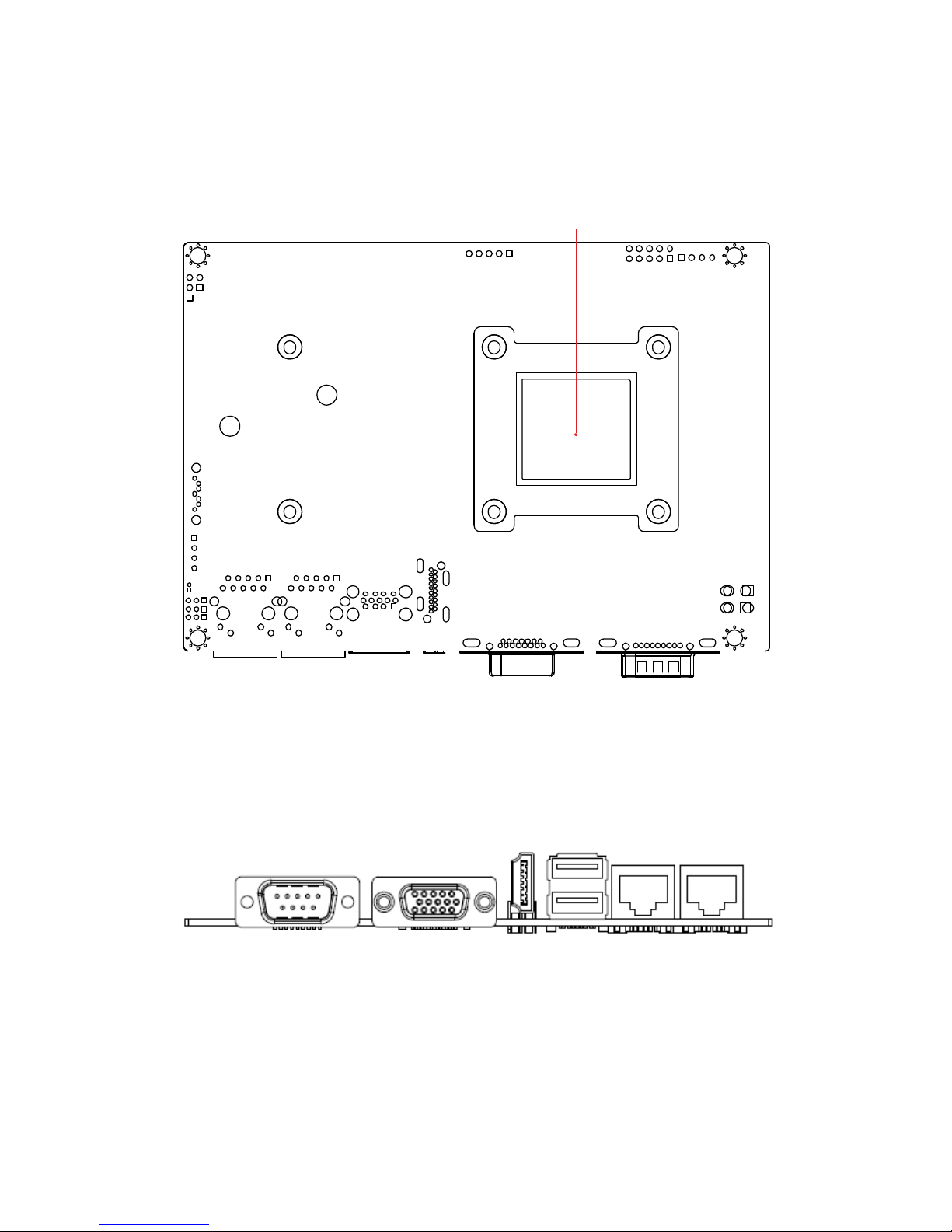
Bottom View
Rear I/O View
CPU
COM1
VGA
HDMI
USB1
LAN1
LAN2
13
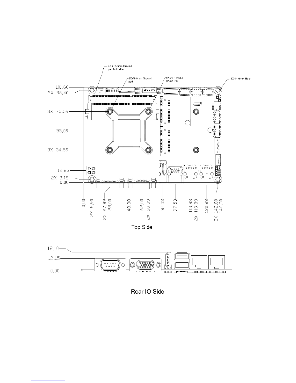
1.4 Dimensions
14
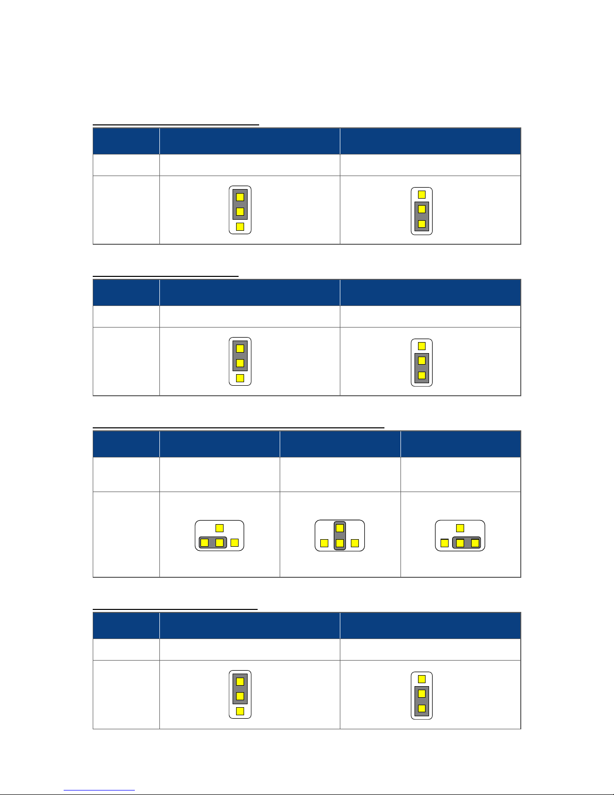
1.5 Jumper Setting
JCMOS: CMOS Clear Selection
Pin No.
1-2
2-3
Function
Normal Operation (Default)
Clear CMOS Contents
Jumper
Setting
JTRTC: RTC Test Selection
Pin No.
1-2
2-3
Function
Normal Operation (Default)
Clear RTC Register Contents
Jumper
Setting
JPLVDS: LCD Panel Power (+3.3V/+5V/+12V) Selection
Pin No.
1-3
3-4
3-5
Function
LCD Power +3.3V
(Default)
12V
LCD Power +5V
Jumper
Setting
JPWR: AT/ATX Mode Selection
Pin No.
1-2
2-3
Function
AT Mode
ATX Mode (Default)
Jumper
Setting
1
2
3
1
2
3
1
2
3
1
2
3
1 3 5
2 4
1 3
2 4
1 3 5
2 4
1
2
3
1
2
3
15
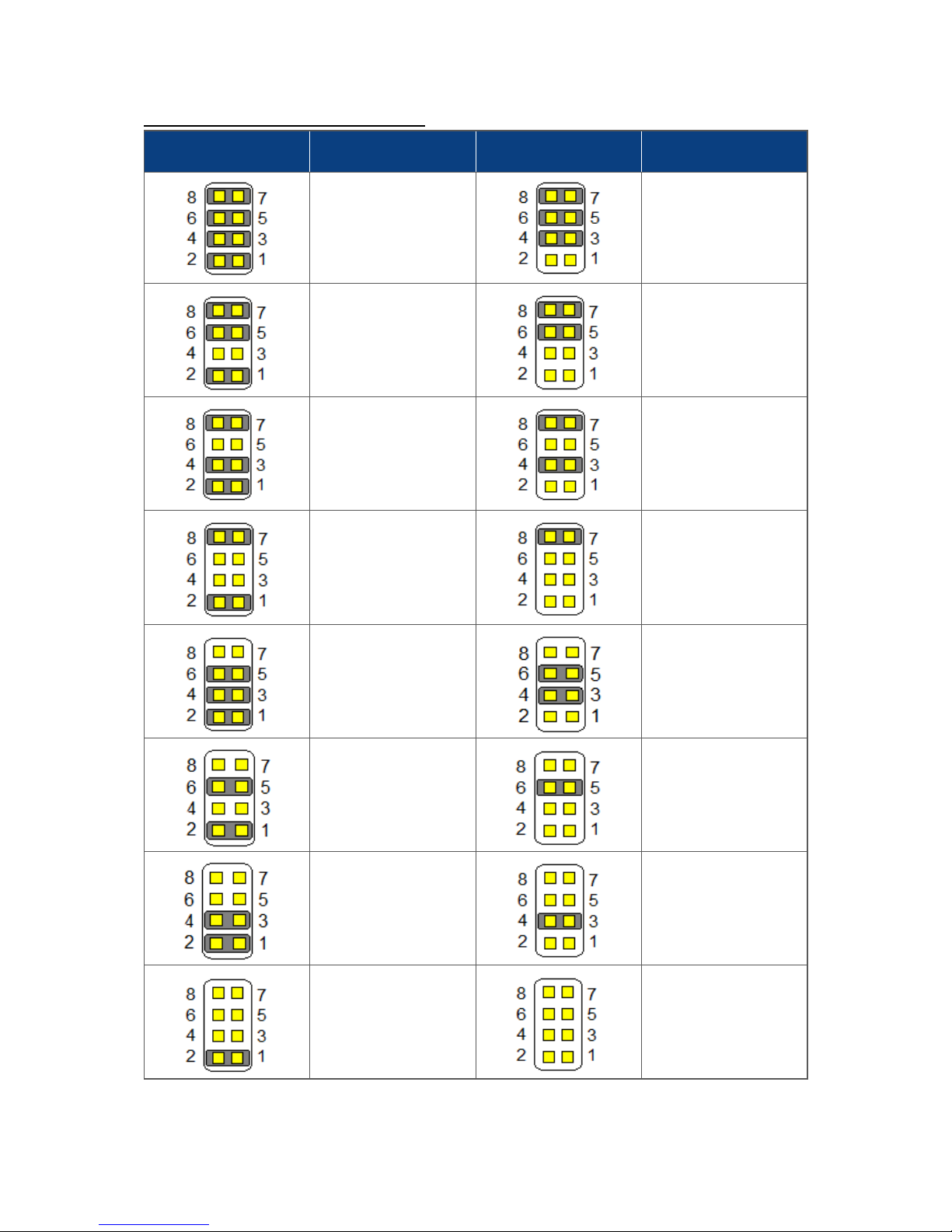
JLVDS: LCD Panel Type Selection
Jumper Setting
LCD Panel Type
Jumper Setting
LCD Panel Type
800 x 600
18bit
(Default)
1024 x 768
18bit
1024 x 768
24bit
1280 x 768
18bit
1280 x 800
18bit
1280 x 960
18bit
1280 x 1024
24bit
1366 x 768
18bit
1366 x 768
24bit
1440 x 900
24bit
1440 x 1050
24bit
1600 x 900
24bit
1680 x 1050
24bit
1600 x 1200
24bit
1920 x 1080
24bit
1920 x 1200
24bit
16
1.6 Connector Function List
Rear I/O Port List
Connector
Function
Note
COM1
COM1, RS-232/422/485 serial port (DB9) connector
HDMI
HDMI, HDMI connector
LAN1
LAN1, RJ45 (LAN) connenctor
LAN2
LAN2, RJ45 (LAN) connenctor
USB1
USB1, USB3.0 x1 / USB2.0 x1 connenctor
VGA
VGA, VGA (DB15) connector
OnBoard Expansion Slot List
Connector
Function
Note
CHA-DIMM
DDR3L SO-DIMM slot
MINI-PCIE1
Mini-PCIe Express (half-size)
MINI-PCIE2
Mini-PCIe Express (full-size) / mSATA slot (share)
OnBoard I/O Connector List (1/2)
Connector
Function
Note
AUDIO
Line-in / MIC-in / Line-out with box-header
BAT
CMOS BAT (CR2032) with box-header
BZ
Buzzer with pin-header
COM2, COM3
RS-232 serial ports with box-header
CPUFAN
CPU FAN 4-pin connector
DIO
Digital I/O with pin-header
FRONT
Front Panel with pin-header
INV
LCD inverter with box-header (+12V)
KB_MS
PS/2 keyboard and mouse with box-header
LVDS
LCD panel LVDS 18/24bit connector
PWR1
ATX +12VDC~+24VDC 2x2pin (4-pole) connector
SATA
SATA 2.0 port connector
17
OnBoard I/O Connector List (2/2)
Connector
Function
Note
SATAPWR
SATA power with box-header (+5V and +12V)
SMB
SMBus with pin-header
USB2
USB2.0 with pin-header
USB3
USB2.0 with box-header
LPC_SPI
Reserved for debug with box-header
18
1.7 Connector Definitions
The following sections provide pin definitions and detailed description of all on-board
connectors. The connector definitions follow the following notation:
Column
Name
Description
Pin
Shows the pin-numbers in the connector. The graphical layout of the
connector definition tables is made similar to the physical connectors.
Type
Al
Analog Input.
AO
Analog Output.
I
Input, TTL compatible if nothing else stated.
IO
Input / Output TTL compatible if nothing else stated.
IOT
Bi-directional tri-state IO pin.
IS
Schmitt-trigger input, TTL compatible.
IOC
Input / open-collector Output, TTL compatible.
IOD
Input / Output, CMOS level Schmitt-triggered (open drain output).
NC
Pin not connected.
O
Output, TTL compatible.
OC
Output, open-collector or open-drain, TTL compatible.
OT
Output with tri-state capability, TTL compatible.
DIFF
Differential Signal.
PWR
Power supply or ground reference pins.
Signal
The mnemonic name of the signal at the current pin. The notation ―XX#‖
states that the signal ―XX‖ is active low.
Note
Special remarks concerning the signal.
The abbreviation TBD is used for specifications which are not available yet or which are not
sufficiently specified by the component vendors.
19
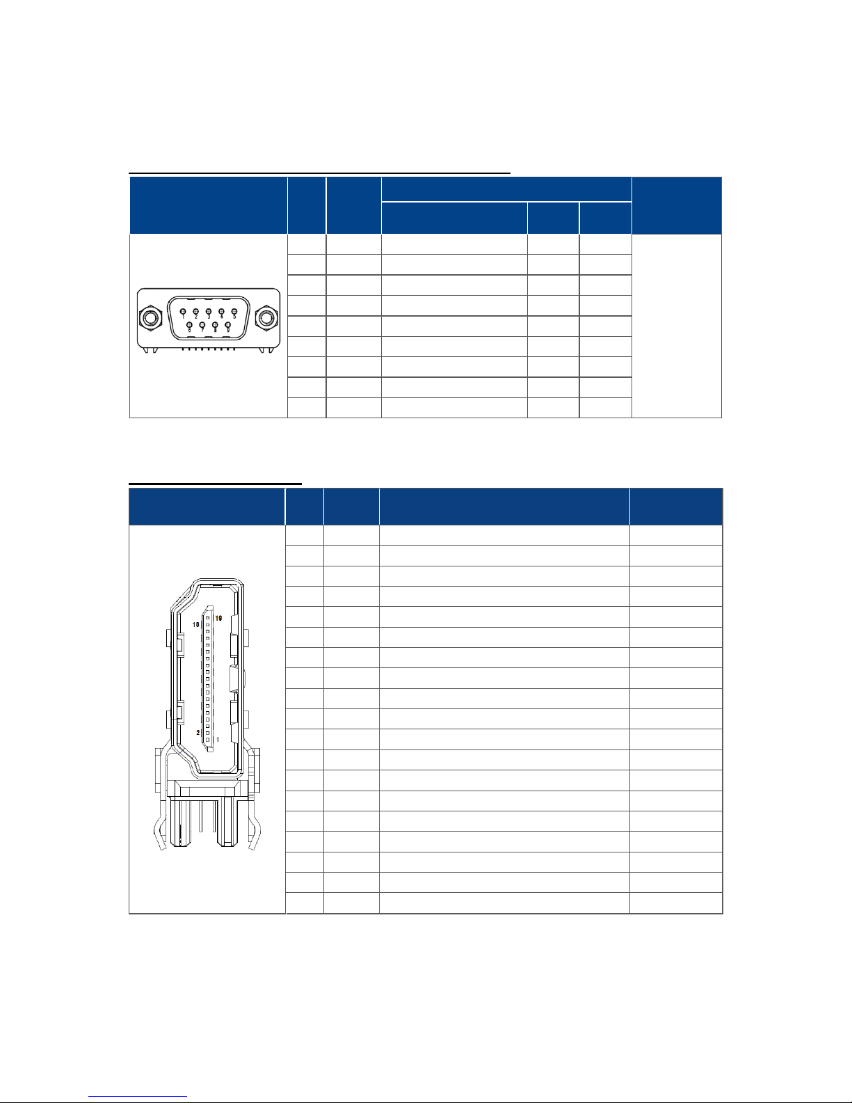
Rear I/O Port Pin Define
COM1: RS-232/422/485 Serial Port (DB9) Connector
COM1
Pin
Type
Signal
Note
RS-232
RS-422/
485 Full
RS-485
Half
1
I
Data Carrier Detect
TX D-
DATA-
COM1
RS-232
RS-422
RS-485
2
I
Received Data (RXD)
TX D+
DATA+
3
O
Transmitted Data (TXD)
RX D+
4
O
Data Terminal Ready
RX D-
5
PWR
Ground
6
I
Data Set Ready (DSR)
7
O
Request To Send (RTS)
8
I
Clear To Send (CTS)
9
I
Ring Indicator (RI#)
HDMI: HDMI Connector
HDMI
Pin
Type
Signal
Note
1
DIFF
HDMI TMDS2+
2
PWR
Ground
3
DIFF
HDMI TMDS2-
4
DIFF
HDMI TMDS1+
5
PWR
Ground
6
DIFF
HDMI TMDS1-
7
DIFF
HDMI TMDS0+
8
PWR
Ground
9
DIFF
HDMI TMDS0-
10
DIFF
HDMI TMDS_CLK+
11
PWR
Ground
12
DIFF
HDMI TMDS_CLK-
13
NC
Not connected
14
NC
Not connected
15
IO
HDMI DDC clock
1
16
IO
HDMI DDC data
1
17
PWR
Ground
18
PWR
HDMI power +5V
19 I HDMI Hot plug detect
Note 1: HDMI port pin.15 (DDC Clock) and pin.16 (DDC Data) pull-up +5V/2.2KΩ.
20
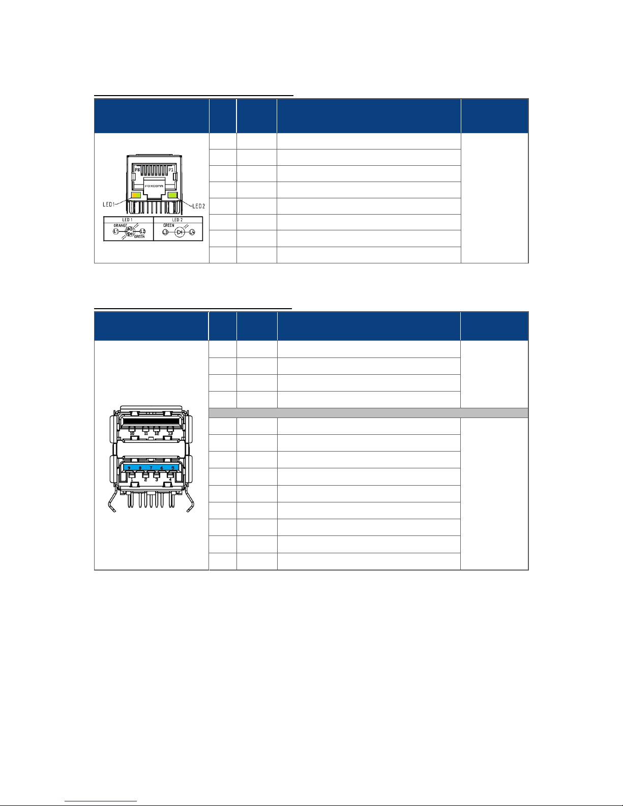
LAN1, LAN2: RJ45(LAN) Connectors
LAN1 / LAN2
Pin
Type
Signal
Note
P1
DIFF
MDI0+ / TXD+
RJ45
P2
DIFF
MDI0- / TXD-
P3
DIFF
MDI1+ / RXD+
P4
DIFF
MDI2+
P5
DIFF
MDI2-
P6
DIFF
MDI1- / RXD-
P7
DIFF
MDI3+
P8
DIFF
MDI3-
USB1: USB 2.0 / USB3.0 Connectors
USB1
Pin
Type
Signal
Note
10
PWR
USB2.0 P1 power +5V
#1
USB 2.0
(UP)
(Black)
11
DIFF
USB2.0 P1_D-
12
DIFF
USB2.0 P1_D+
13
PWR
Ground
1
PWR
USB3.0 P0 power +5V
#2
USB 3.0
(DOWN)
(Blue)
2
DIFF
USB2.0 P0_D-
3
DIFF
USB2.0 P0_D+
4
PWR
Ground
5
DIFF
USB3.0 P0_RX-
6
DIFF
USB3.0 P0_RX+
7
PWR
Ground
8
DIFF
USB3.0 P0_TX-
9
DIFF
USB3.0 P0_TX+
Note 1: USB1 — USB2.0 port power supply maximum +5V/0.5A
Note 2: USB1 — USB3.0 port power supply maximum +5V/0.9A
21
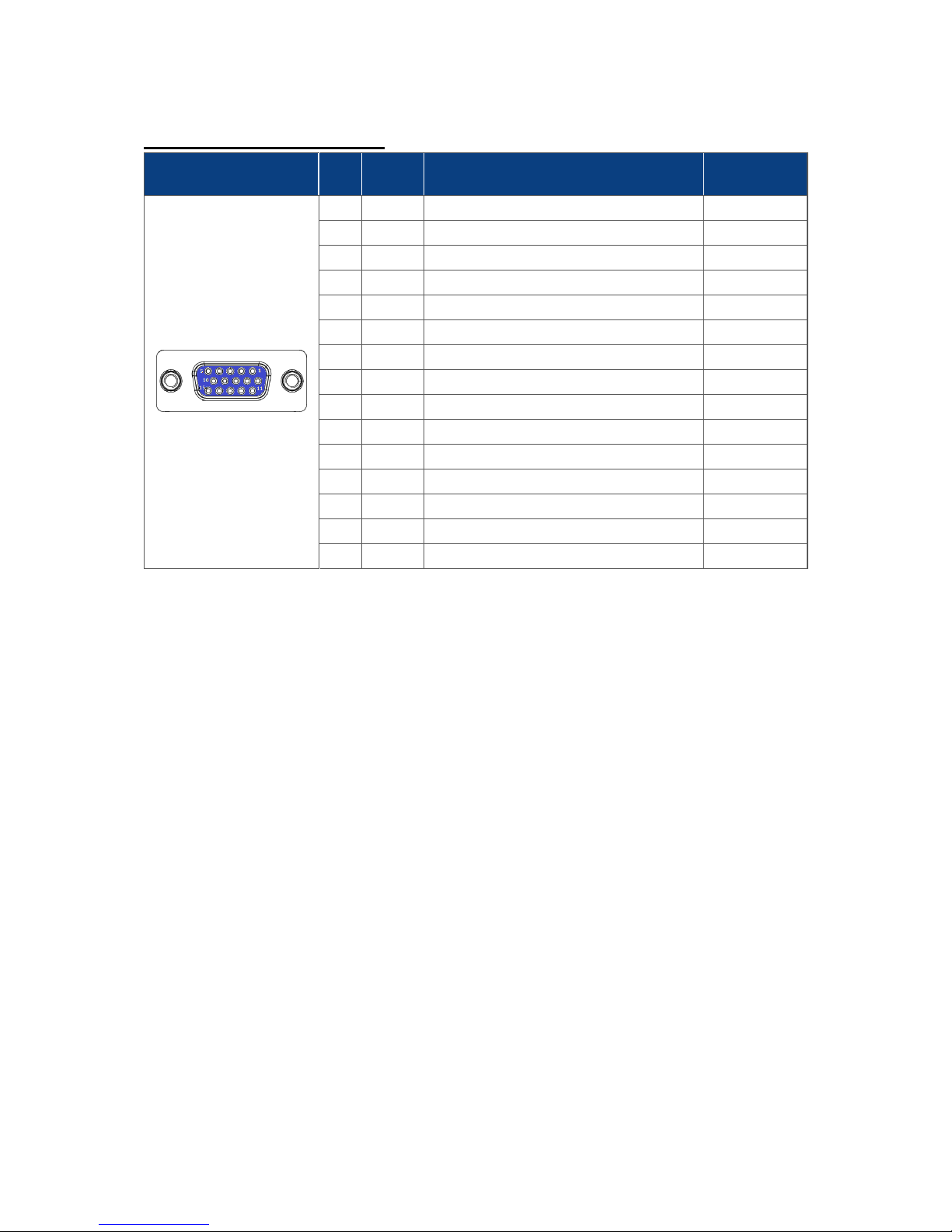
VGA: VGA (DB15) Connector
VGA
Pin
Type
Signal
Note
1
AO
VGA Red color values
2
AO
VGA Green color values
3
AO
VGA Blue color values
4
NC
Not connected
5
PWR
Ground
6
PWR
Ground
7
PWR
Ground
8
PWR
Ground
9
PWR
VGA power +5V
10
PWR
Ground
11
NC
Not connected
12
IO
VGA DDC data
1
13 O VGA Horizontal synchronization
14 O VGA Vertical synchronization
15
IO
VGA DDC clock
1
Note 1: VGA port pin.15 (DDC Clock) and pin.12 (DDC Data) pull-up +5V/2.2KΩ.
22
OnBoard Expansion Slot Pin Define
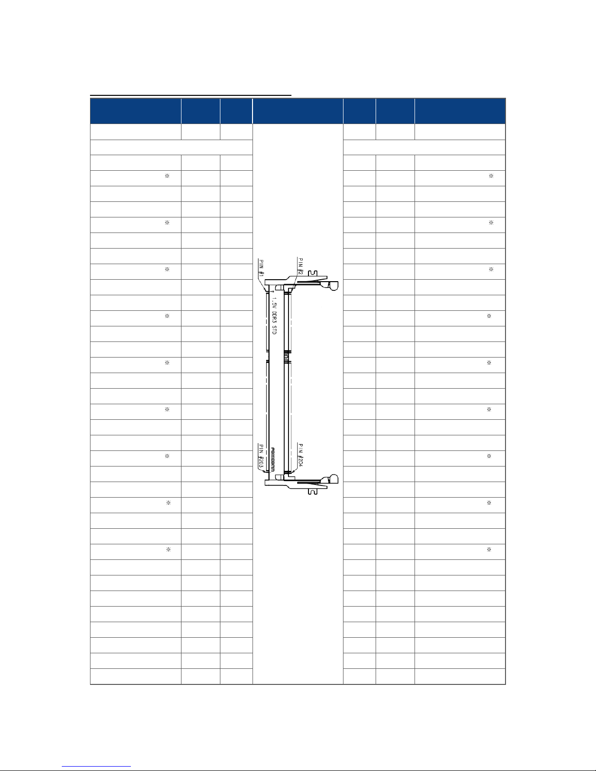
CHA-DIMM: DDR3L SO-DIMM Slot (1/3)
Signal
Type
Pin
CHA-DIMM
Pin
Type
Signal
VREF_DQ
IO 1 2
PWR
Ground
Ground
PWR
3 4 IO
DQ4
DQ0
IO 5 6
IO
DQ5
DQ1
IO 7 8
PWR
Ground
Ground
PWR
9
10
DIFF
DQS0#
DM0
I
11
12
DIFF
DQS0
Ground
PWR
13
14
PWR
Ground
DQ2
IO
15
16
IO
DQ6
DQ3
IO
17
18
IO
DQ7
Ground
PWR
19
20
PWR
Ground
DQ8
IO
21
22
IO
DQ12
DQ9
IO
23
24
IO
DQ13
Ground
PWR
25
26
PWR
Ground
DQS1#
DIFF
27
28
I
DM1
DQS1
DIFF
29
30
I
Reset#
Ground
PWR
31
32
PWR
Ground
DQ10
IO
33
34
IO
DQ14
DQ11
IO
35
36
IO
DQ15
Ground
PWR
37
38
PWR
Ground
DQ16
IO
39
40
IO
DQ20
DQ17
IO
41
42
IO
DQ21
Ground
PWR
43
44
PWR
Ground
DQS2#
DIFF
45
46
I
DM2
DQS2
DIFF
47
48
PWR
Ground
Ground
PWR
49
50
IO
DQ22
DQ18
IO
51
52
IO
DQ23
DQ19
IO
53
54
PWR
Ground
Ground
PWR
55
56
IO
DQ28
DQ24
IO
57
58
IO
DQ29
DQ25
IO
59
60
PWR
Ground
Ground
PWR
61
62
DIFF
DQS3#
DM3
I
63
64
DIFF
DQS3
Ground
PWR
65
66
PWR
Ground
DQ26
IO
67
68
IO
DQ30
DQ27
IO
69
70
IO
DQ31
23
CHA-DIMM: DDR3L SO-DIMM Slot (2/3)
Signal
Type
Pin
CHA-DIMM
Pin
Type
Signal
Ground
PWR
71
72
PWR
Ground
KEY
KEY
CKE0
I
73
74
I
CKE1
VDDQ +1.35V
1
PWR
75
76
PWR
VDDQ +1.35V
1
Not connected
NC
77
78
I
A15
BA2
I
79
80
I
A14
VDDQ +1.35V
1
PWR
81
82
PWR
VDDQ +1.35V
1
A12
I
83
84
I
A11
A9
I
85
86
I
A7
VDDQ +1.35V
1
PWR
87
88
PWR
VDDQ +1.35V
1
A8
I
89
90
I
A6
A5
I
91
92
I
A4
VDDQ +1.35V
1
PWR
93
94
PWR
VDDQ +1.35V
1
A3
I
95
96
I
A2
A1
I
97
98
I
A0
VDDQ +1.35V
1
PWR
99
100
PWR
VDDQ +1.35V
1
CK0
DIFF
101
102
DIFF
CK1
CK0#
DIFF
103
104
DIFF
CK1#
VDDQ +1.35V
1
PWR
105
106
PWR
VDDQ +1.35V
1
A10
I
107
108
I
BA1
BA0
I
109
110
I
RAS#
VDDQ +1.35V
1
PWR
111
112
PWR
VDDQ +1.35V
1
WE#
I
113
114
I
CS0#
CAS#
I
115
116
I
ODT0
VDDQ +1.35V
1
PWR
117
118
PWR
VDDQ +1.35V
1
A13
I
119
120
I
ODT1
CS1#
I
121
122
NC
Not connected
VDDQ +1.35V
1
PWR
123
124
PWR
VDDQ +1.35V
1
Not connected
NC
125
126
IO
VREF_CA
Ground
PWR
127
128
PWR
Ground
DQ32
IO
129
130
IO
DQ36
DQ33
IO
131
132
IO
DQ37
Ground
PWR
133
134
PWR
Ground
DQS4#
DIFF
135
136
I
DM4
DQS4
DIFF
137
138
PWR
Ground
Ground
PWR
139
140
IO
DQ38
24

CHA-DIMM: DDR3L SO-DIMM Slot (3/3)
Signal
Type
Pin
CHA-DIMM
Pin
Type
Signal
DQ34
IO
141
142
IO
DQ39
DQ35
IO
143
144
PWR
Ground
Ground
PWR
145
146
IO
DQ44
DQ40
IO
147
148
IO
DQ45
DQ41
IO
149
150
PWR
Ground
Ground
PWR
151
152
DIFF
DQS5#
DM5
I
153
154
DIFF
DQS5
Ground
PWR
155
156
PWR
Ground
DQ42
IO
157
158
IO
DQ46
DQ43
IO
159
160
IO
DQ47
Ground
PWR
161
162
PWR
Ground
DQ48
IO
163
164
IO
DQ52
DQ49
IO
165
166
IO
DQ53
Ground
PWR
167
168
PWR
Ground
DQS6#
DIFF
169
170
I
DM6
DQS6
DIFF
171
172
PWR
Ground
Ground
PWR
173
174
IO
DQ54
DQ50
IO
175
176
IO
DQ55
DQ51
IO
177
178
PWR
Ground
Ground
PWR
179
180
IO
DQ60
DQ56
IO
181
182
IO
DQ61
DQ57
IO
183
184
PWR
Ground
Ground
PWR
185
186
DIFF
DQS7#
DM7
I
187
188
DIFF
DQS7
Ground
PWR
189
190
PWR
Ground
DQ58
IO
191
192
IO
DQ62
DQ59
IO
193
194
IO
DQ63
Ground
PWR
195
196
PWR
Ground
SA0
I
197
198
NC
Not connected
VDDSPD +3.3V
PWR
199
200
IO
SMBus data
SA1
I
201
202
O
SMBus clock
VTT +0.675V
2
PWR
203
204
PWR
VTT +0.675V
2
Note 1: CHA-DIMM Slot power supply maximum +1.35V/2.0A
Note 2: CHA-DIMM Slot power supply maximum +0.675V/0.6A
25
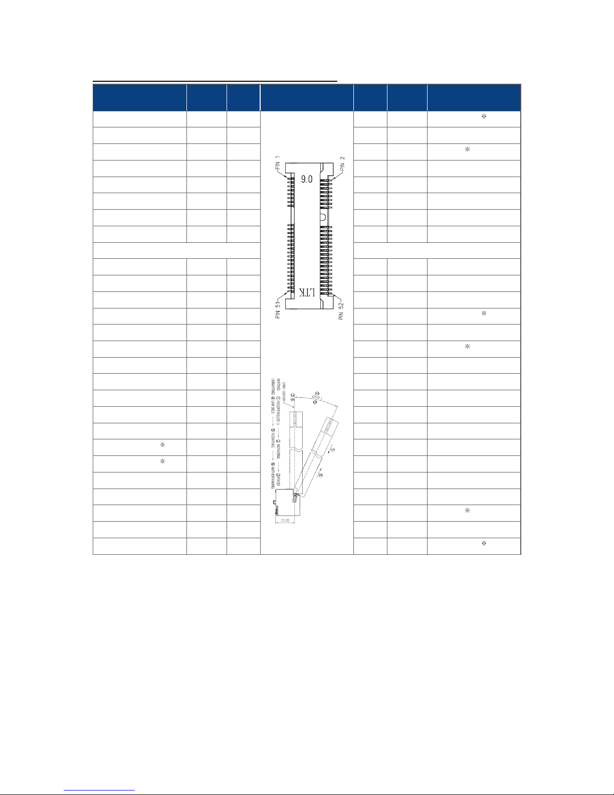
MINI-PCIE1: miniPCIe Express (Half-size) Slot
Signal
Type
Pin
MINI-PCIE1
Pin
Type
Signal
WAKE#
I 1 2
PWR
+3.3Vaux
1
Not connected
NC 3 4
PWR
Ground
Not connected
NC 5 6
PWR
+1.5V
2
CLKREQ#
I 7 8
NC
Not connected
Ground
PWR
9
10
NC
Not connected
PCIE_CLOCK-
DIFF
11
12
NC
Not connected
PCIE_CLOCK+
DIFF
13
14
NC
Not connected
Ground
PWR
15
16
NC
Not connected
KEY
KEY
Not connected
NC
17
18
PWR
Ground
Not connected
NC
19
20
O
W_DISABLE1#
Ground
PWR
21
22
O
PERST#
PCIE_RXN
DIFF
23
24
PWR
+3.3Vaux
1
PCIE_RXP
DIFF
25
26
PWR
Ground
Ground
PWR
27
28
PWR
+1.5V
2
Ground
PWR
29
30
O
SMBus clock
PCIE_TXN
DIFF
31
32
IO
SMBus data
PCIE_TXP
DIFF
33
34
PWR
Ground
Ground
PWR
35
36
DIFF
USB2.0 PH5_D-
Ground
PWR
37
38
DIFF
USB2.0 PH5_D+
+3.3Vaux
1
PWR
39
40
PWR
Ground
+3.3Vaux
1
PWR
41
42
NC
Not connected
Ground
PWR
43
44
NC
Not connected
Not connected
NC
45
46
NC
Not connected
Not connected
NC
47
48
PWR
+1.5V
2
Not connected
NC
49
50
PWR
Ground
Not connected
NC
51
52
PWR
+3.3Vaux
1
Note 1: MINI-PCIE1 Slot power supply maximum +3.3Vaux/1.1A, peak 2.5A.
Note 2: MINI-PCIE1 Slot power supply maximum +1.5V/0.375A, peak 0.5A.
26
 Loading...