

Page 1
FEATURES
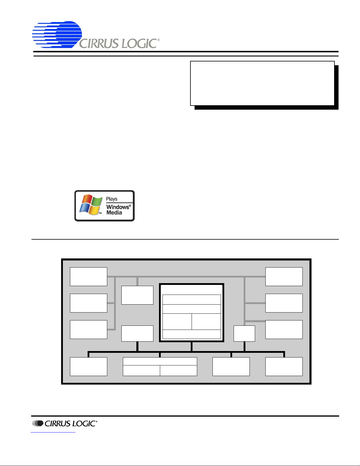
LCD
Controller
Boot
ROM
MaverickKey
TM
ARM7TDMI CPU Core
MMU
8 KB
Cache
Write
Buffe r
Intern a l D a ta B u s
EPB Bus
Memory Co ntro ller
SDRAM I/FSRA M I/F
On-chip SRAM
48 KB
ICE -J T A G
Clocks &
Timers
Keypad&
Touch
Screen I/F
Interrupts,
PWM & GPIO
Bus
Bridge
(2) UARTs
w/ IrDA
Power
Management
Serial
Interface
Digital
Audio
Interface
ARM720T
SERIAL PORTS
USER INTERFACE
FEATURES
ARM®720T Processor
— ARM7TDMI CPU Operating at Speeds of 74 and
90 MHz
— 8 kBytes of Four-way Set-associative Cache
— MMU with 64-entry TLB
— Thumb™ Code Support Enabled
Ultra low power
— 90 mW at 74 MHz Typical
— 108 mW at 90 MHz Typical
— <.03 mW in the Standby State
Advanced Audio Decoder/decompression Capability
— Supports bit streams with adaptive bit rates.
— Allows for support of multiple audio decompression
algorithms (MP3, WMA, AAC, Audible, etc.).
EP7312 Data Sheet
High-performance,
Low-power, System-on-chip
with SDRAM & Enhanced
Digital Audio Interface
OVERVIEW
OVERVIEW
The Cirrus Logic™ EP7312 is designed for ultra-low-power
portable and line-powered applications such as portable
consumer entertainment devices, home and car audio juke box
systems, and general purpose industrial control applications, or
any device that features the added capability of digital audio
compression & decompression. The core-logic functionality of
the device is built around an ARM720T processor with
8 kBytes of four-way set-associative unified cache and a write
buffer. Incorporated into the ARM720T is an enhanced
memory management unit (MMU) which allows for support of
sophisticated operating systems like Microsoft
CE and Linux®.
®
Windows
®
BLOCK DIAGRAM
http://www.cirrus.com
Copyright Cirrus Logic, Inc. 2011
(cont.)
MEMORY and STORAGE
(All Rights Reserved) MAR ‘11
(cont.)
DS508F2
Page 2

EP7312
High-Performance, Low-Power System on Chip
FEATURES (cont)
48 KBytes of On-chip SRAM
™
MaverickKey
IDs
— 32-bit unique ID can be used for DRM-compliant 128-
bit random ID.
Available in 74 and 90 MHz clock speeds.
LCD controller
— Interfaces directly to a single-scan panel monochrome
STN LCD.
— Interfaces to a single-scan panel color STN LCD with
minimal external glue logic.
Full JTAG Boundary Scan and Embedded ICE
Support
Integrated Peripheral Interfaces
— 32-bit SDRAM Interface, Up to 2 External Banks
— 8/32/16-bit SRAM/FLASH/ROM Interface
— Digital Audio Interface provides glueless interface to
low-power DACs, ADCs, and CODECs.
— Two Synchronous Serial Interfaces (SSI1, SSI2)
— CODEC Sound Interface
—88 Keypad Scanner
— 27 General-purpose Input/Output Pins
— Dedicated LED Flasher Pin from the RTC
Internal Peripherals
— T wo 16550-compatible UARTs
— IrDA Interface
— Two PWM Interfaces
— Real-time Clock
— Two General-purpose 16-bit Timers
— Interrupt Controller
— Boot ROM
Package
—208-Pin LQFP
—256-Ball PBGA
The fully static EP7312 is optimized for low power
dissipation and is fabricated using a 0.25 micron CMOS
process.
OVERVIEW (cont.)
The EP7312 is designed for ultra-low-power operation. Its core
operates at only 2.5 V, while its I/O has an operation range of
2.5 V–3.3 V. The device has three basic power states:
operating, idle and standby.
MaverickKey unique hardware programmed IDs are a solution
to the growing concern over secure web content and
commerce. With Internet security playing an important role in
the delivery of digital media such as books or music,
traditional software methods are quickly becoming unreliable.
The MaverickKey unique IDs provide OEMs with a method of
utilizing specific hardware IDs such as those assigned for
SDMI (Secure Digital Music Initiative) or any other
authentication mechanism.
The EP7312 integrates an interface to enable a direct
connection to many low cost, low power, high quality audio
converters. In particular, high quality ADCs, DACs, or
CODECs such as the Cirrus Logic CS53L32A, CS43L42, and
CS42L50 are easily added to an EP73xx design via the DAI.
Some of these devices feature digital bass and treble boost,
digital volume control and compressor-limiter functions.
Simply by adding desired memory and peripherals to the
highly integrated EP7312 completes a low-power system
solution. All necessary interface logic is integrated on-chip.
2 Copyright Cirrus Logic, Inc. 2011
(All Rights Reserved) DS508F2
Page 3

EP7312
High-Performance, Low-Power System on Chip
Table of Contents
FEATURES ................................................................................................................................. ..........1
OVERVIEW ..................................................................................... ................ ................. .....................1
FEATURES (cont) .......................................................................................................................................................2
OVERVIEW (cont.) ......................................................................................................................................................2
Description of the EP7312’s Component s, Functionality, and Interfaces ....................................6
Processor Core - ARM720T ..................................................................................................................................6
Power Management ..............................................................................................................................................6
MaverickKey™ Unique ID .....................................................................................................................................6
Memory Interfaces .............................. ... .... ... ... ... ... .... ... .........................................................................................6
Digital Audio Capability ...................................... ... .... ... ... ... .... ... ... .........................................................................7
Universal Asynchronous Receiver/Transmitters (UARTs) .....................................................................................7
Digital Audio Interface (DAI) .. ... .... ... ... ... .............................................................. ... ... ... .... ... ..................................7
CODEC Interface ............................................ ... ... .... ... ... ... .... ... ... ... ......................................................................8
SSI2 Interface ........................................................................................................................................................8
Synchronous Serial Interface ................................................................................................................................8
LCD Controller .......................................................................................................................................................8
64-Key Keypad Interface .......................................................................................................................................8
Interrupt Controller ................................................................................................................................................9
Real-Time Clock ....................................................................................................................................................9
PLL and Clocking ..................................................................................................................................................9
DC-to-DC Converter Interface (PWM) ............................. ................ ................ ................. ...................................10
Timers .................................................................................................................................................................10
General Purpose Input/Output (GPIO) ................................................................................................................10
Hardware Debug Interface ..................................................................................................................................10
LED Flasher ........................................................................................................................................................10
Internal Boot ROM ........................... ... ... .... ... .......................................................... ... ... .... ...................................10
Packaging ..................................... ...... ....... ...... ...... ....... ...... ....... ...... ....... ...... ... ....... .............................................10
Pin Multiplexing ...................................................................................................................................................11
System Design ....................................................................................................................................................12
ELECTRICAL SPECIFICATIONS .................................................... ................................. ................ .13
Absolute Maximum Ratings .................................................................................................................................13
Recommended Operating Conditions .................................................................................................................13
DC Characteristics ....................................... ... ... ... ........................................................... ...................................13
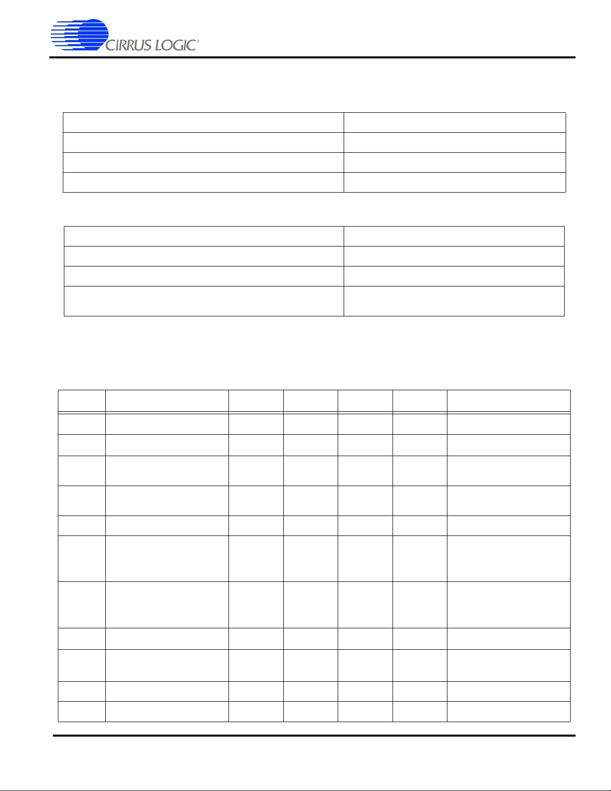
Timings ........................................................................................... .............. ............................ ..........15
Timing Diagram Conventions ....................................................................................................................15
Timing Conditions ........................................ .... ... ... ... .................................................................................15
SDRAM Interface ............................................ .......................................................... ... .... ...................................16
SDRAM Load Mode Register Cycle ..........................................................................................................17
SDRAM Burst Read Cycle ........... .... ... ... ... ... .... ... ... ... .... ... ... .......................................................................18
SDRAM Burst Write Cycle ........................... .... .......................................................... ... .............................19
SDRAM Refresh Cycle ....... ... ... ... .... ... ... ... ... ........................................................... ... ... ... ... .......................20
Static Memory ......................................................................................................................................................21
Static Memory Single Read Cycle .............................................................................................................22
Static Memory Single Write Cycle ..............................................................................................................23
Static Memory Burst Read Cycle ...............................................................................................................24
Static Memory Burst Write Cycle ...............................................................................................................25
SSI1 Interface ......................................................................................................................................................26
DS508F2 Copyright Cirrus Logic, Inc. 2011
(All Rights Reserved) 3
Page 4

EP7312
High-Performance, Low-Power System on Chip
SSI2 Interface ..................................................................................................................................................... 27
LCD Interface ...................................................................................................................................................... 28
JTAG Interface .......................... ... ... .... ... ... ... .......................................................... .... ... ...................................... 29
Packages ...........................................................................................................................................30
208-Pin LQFP Package Characteristics ............................................................................................................. 30
208-Pin LQFP Pin Diagram ......................... .... ... ... ... ... .... ... ... ... .... ... ... ... .... ... ... ... ................................................ 31
208-Pin LQFP Numeric Pin Listing ..................................................................................................................... 32
256-Ball PBGA Package Characteristics ............................................................................................................ 38
256-Ball PBGA Pinout (Top View) ....................................................................................................................... 39
256-Ball PBGA Ball Listing ................................................................................................................................. 40
JTAG Boundary Scan Signal Ordering ..... ... .... ... ... ... ... .... ... ... ... .... ...................................................................... 45
CONVENTIONS .................................................................................................................................50
Acronyms and Abbreviations .............. ... ... ... .... ............................................................. ... ... ................................ 50
Units of Measurement ......................................................................................................................................... 50
General Conventions ............. ... .......................................................... ... .... ... ... ... ... .... ... ... ... ................................ 51
Pin Description Conventions ............................................................................................................................... 51
Ordering Information .......................................................................................................................52
Environmental, Manufacturing, & Handling Information .............................................................52
Revision History ..............................................................................................................................53
4 Copyright Cirrus Logic, Inc. 2011
(All Rights Reserved) DS508F2
Page 5

EP7312
High-Performance, Low-Power System on Chip
List of Figures
Figure 1. A Fully-Configured EP7312-Based System ...................... ... ... ... .... ... ... ..........................................................12
Figure 2. Legend for Timing Diagrams .........................................................................................................................15
Figure 3. SDRAM Load Mode Register Cycle Timing Measurement ..................... ................................ .......................17
Figure 4. SDRAM Burst Read Cycle Timing Measurement ..........................................................................................18
Figure 5. SDRAM Burst Write Cycle Timing Measurement ..........................................................................................19
Figure 6. SDRAM Refresh Cycle Timing Measurement ......................................... ... .... ... .............................................20
Figure 7. Static Memory Single Read Cycle Timing Measurement ...............................................................................22
Figure 8. Static Memory Single Write Cycle Timing Measurement .................. ................................... ..........................23
Figure 9. Static Memory Burst Read Cycle Timing Measurement ................................................................................24
Figure 10. Static Memory Burst Write Cycle Timing Measurement ..............................................................................25
Figure 11. SSI1 Interface Timing Measurement ...........................................................................................................26
Figure 12. SSI2 Interface Timing Measurement ...........................................................................................................27
Figure 13. LCD Controller Timing Measurement ..........................................................................................................28
Figure 14. JTAG Timing Measurement ........................ .............................................................. ...................................29
Figure 15. 208-Pin LQFP Package Outline Drawing ....................................................................................................30
Figure 16. 208-Pin LQFP (Low Profile Quad Flat Pack) Pin Diagram ..........................................................................31
Figure 17. 256-Ball PBGA Package ..............................................................................................................................38
List of Tables
Table 1. Power Management Pin Assignments ..............................................................................................................6
Table 2. Static Memory Interface Pin Assignments ........................................................................................................6
Table 3. SDRAM Interface Pin Assignments ..................................................................................................................7
Table 4. Universal Asynchronous Receiver/Transmitters Pin Assignments ....................... ... .... ... ... ... ... .... ... ... ... .. ..........7
Table 5. DAI Interface Pin Assignments .........................................................................................................................7
Table 6. CODEC Interface Pin Assignments ..................................................................................................................8
Table 7. SSI2 Interface Pin Assignments .......................................................................................................................8
Table 8. Serial Interface Pin Assignments ......................................................................................................................8
Table 9. LCD Interface Pin Assignments ........................................................................................................................8
Table 10. Keypad Interface Pin Assignments ..... ... ... ... ... .... ... ... ... .... ... ... ... .... ... ... ... ... .... ... ...............................................9
Table 11. Interrupt Controller Pin Assignments ..... .........................................................................................................9
Table 12. Real-Time Clock Pin Assignments ............ ... ... .... ... ... ... .... ... ... ... .... ... ... ... ... .... ... ... ... .... ... ... ...............................9
Table 13. PLL and Clocking Pin Assignments ................................................................................................................9
Table 14. DC-to-DC Converter Interface Pin Assignments .................... ................................ .......................................10
Table 15. General Purpose Input/Output Pin Assignments ..........................................................................................10
Table 16. Hardware Debug Interface Pin Assignments ................................................................................................10
Table 17. LED Flasher Pin Assignments ............ ... ... ... .......................................................... .... ... ................................10
Table 18. DAI/SSI2/CODEC Pin Multiplexing ........................................ ... .... ... ... ... ... .... ... ... ... .... ... ... ... ..........................11
Table 19. Pin Multiplexing .............................................................................................................................................11
Table 20. 208-Pin LQFP Numeric Pin Listing ...............................................................................................................32
Table 21. 256-Ball PBGA Ball Listing ...........................................................................................................................40
Table 22. JTAG Boundary Scan Signal Ordering ..................... ... .... ... ... ... .... ... ... ... ... .... ... ... ... .... ... ... ... ..........................45
Table 23. Acronyms and Abbreviations .............. ... ... ... ... .... ... ... ... .... ... ... ... .... ... ... ... ... .... ... ... ..........................................50
Table 24. Unit of Measurement .......... .... ... ... .......................................................... ... .... ... ... ... .......................................50
Table 25. Pin Description Conventions .................................. ... ... .... ... ... ... .... ................................................................51
DS508F2 Copyright Cirrus Logic, Inc. 2011
(All Rights Reserved) 5
Page 6
EP7312
High-Performance, Low-Power System on Chip
Description of the EP7312’s Components, Functionality, and Interfaces
The following sections describe the EP7312 in more detail.
Processor Core - ARM720T
The EP7312 incorporates an ARM 32-bit RISC micro
controller that controls a wide range of on-chip peripherals.
The processor utilizes a three-stage pipeline consisting of
fetch, decode and execute stages. Key features include:
• ARM (32-bit) and Thumb (16-bit compressed) instruction
sets
• Enhanced MMU for Microsoft Windows CE and other
operating systems
• 8 KB of 4-way set-associative cache.
• Translation Look Aside Buffers with 64 Translated Entries
Power Management
The EP7312 is designed for ultra-low-power operation. Its core
operates at only 2.5 V, while its I/O has an operation range of
2.5 V–3.3 V. The device has three basic power states:
• Operating — This state is the full performance state.
All the clocks and peripheral logic are enabled.
• Idle — This state is the same as the Operating State,
except the CPU clock is halted while waiting for an
event such as a key press.
• Standby — This state is equivalent to the computer
being switched off (no display), and the main
oscillator shut down. An event such as a key press
can wake-up the processor.
Table 1 shows the power management pin assignments.
Table 1. Power Management Pin Assignments
Pin Mnemonic I/O Pin Description
BATOK I Battery ok input
nEXTPWR I
nPWRFL I Power fail sense input
nBATCHG I Battery changed sense input
External power supply sense
input
Both a specific 32-bit ID as well as a 128-bit random ID is
programmed into the EP7312 through the use of laser probing
technology. These IDs can then be used to match secure
copyrighted content with the ID of the target device the
EP7312 is powering, and then deliver the copyrighted
information over a secure connection. In addition, secure
transactions can benefit by also matching device IDs to server
IDs. MaverickKey IDs provide a level of hardware security
required for today’s Internet appliances.
Memory Interfaces
There are two main external memory interfaces. The first one
is the ROM/SRAM/FLASH-style interface that has
programmable wait-state timings and includes burst-mode
capability, with six chip selects decoding six 256 MB sections
of addressable space. For maximum flexibility, each bank can
be specified to be 8-, 16-, or 32-bits wide. This allows the use
of 8-bit-wide boot ROM options to minimize overall system
cost. The on-chip boot ROM can be used in product
manufacturing to serially download system code into system
FLASH memory. To further minimize system memory
requirements and cost, the ARM Thumb instruction set is
supported, providing for the use of high-speed 32-bit
operations in 16-bit op-codes and yielding industry-leading
code density. shows the Static Memory Interface pin
assignments.
Table 2. Static Memory Interface Pin Assignments
Pin Mnemonic I/O Pin Description
nCS[5:0] O Chip select out
A[27:0] O Address output
D[31:0] I/O Data I/O
nMOE/nSDCAS (Note) O ROM expansion OP enable
nMWE/nSDWE (Note) O ROM expansion write enable
HALFWORD O
WORD O Word access select output
WRITE/nSDRAS (Note) O Transfer direction
Halfword access select
output
MaverickKey™ Unique ID
MaverickKey unique hardware programmed IDs are a solution
Note: Pins are multiplexed. See Table 19 on page 11 for
more information.
to the growing concern over secure web content and
commerce. With Internet security playing an important role in
the delivery of digital media such as books or music,
traditional software methods are quickly becoming unreliable.
The MaverickKey unique IDs provide OEMs with a method of
utilizing specific hardware IDs such as those assigned for
SDMI (Secure Digital Music Initiative) or any other
authentication mechanism.
6 Copyright Cirrus Logic, Inc. 2011
(All Rights Reserved) DS508F2
Page 7
EP7312
High-Performance, Low-Power System on Chip
The second is the programmable 16- or 32-bit-wide SDRAM
interface that allows direct connection of up to two banks of
SDRAM, totaling 512 Mb. To assure the lowest possible power
consumption, the EP7312 supports self-refresh SDRAMs,
which are placed in a low-power state by the device when it
enters the low-power Standby State. Table 3 shows the
SDRAM Interface pin assignments.
Table 3. SDRAM Interface Pin Assignments
Pin Mnemonic I/O Pin Description
SDCLK O SDRAM clock output
SDCKE O SDRAM clock enable output
nSDCS[1:0] O SDRAM chip select out
WRITE/nSDRAS (Note 2) O SDRAM RAS signal output
nMOE/nSDCAS (Note 2) O SDRAM CAS control signal
nMWE/nSDWE (Note 2) O
A[27:15]/DRA[0:12] (Note 1) O SDRAM address
A[14:13]/DRA[12:14] O SDRAM internal bank select
PD[7:6]/SDQM[1:0] (Note 2) I/O SDRAM byte lane mask
SDQM[3:2] O SDRAM byte lane mask
D[31:0] I/O Data I/O
Note: 1. Pins A[27:13] map to DRA[0:14] respectively.
(i.e. A[27}/DRA[0}, A[26}/DRA[1], etc.) This is to
balance the load for large memory systems.
2. Pins are multiplexed. See Table 19 on page 11 for
more information.
SDRAM write enable control
signal
Digital Audio Capability
The EP7312 uses its powerful 32-bit RISC processing engine
to implement audio decompression algorithms in software. The
nature of the on-board RISC processor, and the availability of
efficient C-compilers and other software development tools,
ensures that a wide range of audio decompression algorithms
can easily be ported to and run on the EP7312
Universal Asynchronous Receiver/T ransmitters (UARTs)
The EP7312 includes two 16550-type UARTs for RS-232
serial communications, both of which have two 16-byte FIFOs
for receiving and transmitting data. The UARTs support bit
rates up to 115.2 kbps. An IrDA SIR proto col encoder/decoder
can be optionally switched into the RX/TX signals to/from
UART 1 to enable these signals to drive an infrared
communication interface directly. Table 4 shows the UART pin
assignments.
Table 4. Universal Asynchronous Receiver/Transmitters Pin
Pin Mnemonic I/O Pin Description
TXD[1] O UART 1 transmit
RXD[1] I UART 1 receive
CTS I UART 1 clear to send
DCD I UART 1 data carrier detect
DSR I UART 1 data set ready
TXD[2] O UART 2 transmit
RXD[2] I UART 2 receive
LEDDRV O Infrared LED drive output
PHDIN I Photo diode input
Assignments
Digital Audio Interface (DAI)
The EP7312 integrates an interface to enable a direct
connection to many low cost, low power, high quality audio
converters. In particular, the DAI can directly interface with
the Crystal
Crystal
feature digital bass and treble boost, digital volume control and
compressor-limiter functions. Table 5 shows the DAI Interface
pin assignments.
SCLK O Serial bit clock
SDOUT O Serial data out
SDIN I Serial data in
LRCK O Sample clock
MCLKIN I Master clock input
MCLKOUT O Master clock output
Note: See Table 18 on page 11 for information on pin
‚
CS43L41/42/43 low-power audio DACs and the
‚
CS53L32 low-power ADC. Some of these devices
Table 5. DAI Interface Pin Assignments
Pin Mnemonic I/O Pin Description
multiplexes.
DS508F2 Copyright Cirrus Logic, Inc. 2011
(All Rights Reserved) 7
Page 8
EP7312
High-Performance, Low-Power System on Chip
CODEC Interface
The EP7312 includes an interface to telephony-type CODECs
for easy integration into voice-over-IP and other voice
communications systems. The CODEC interface is
multiplexed to the same pins as the DAI and SSI2. Tabl e 6
shows the CODEC Interface Pin Assignments.
Table 6. CODEC Interface Pin Assignments
Pin Mnemonic I/O Pin Description
PCMCLK O Serial bit clock
PCMOUT O Serial data out
PCMIN I Serial data in
PCMSYNC O Frame sync
Note: See Table 18 on page 11 for information on pin
multiplexes.
SSI2 Interface
An additional SPI/Microwire1-compatible interface is
available for both master and slave mode communications. The
SSI2 unit shares the same pins as the DAI and CODEC
interfaces through a multiplexer. The SSI2 Interface has these
features:
• Synchronous clock speeds of up to 512 kHz
• Separate 16 entry TX and RX half-word wide FIFOs
• Half empty/full interrupts for FIFOs
• Separate RX and TX frame sync signals for asymmetric
traffic
Table 7 shows the SSI2 Interface pin assignments.
Table 7. SSI2 Interface Pin Assignments
Pin Mnemonic I/O Pin Description
SSICLK I/O Serial bit clock
SSITXDA O Serial data out
SSIRXDA I Serial data in
SSITXFR I/O Transmit frame sync
SSIRXFR I/O Receive frame sync
Note: See Table 18 on page 11 for information on pin
multiplexes.
Synchronous Serial Interface
The EP7312 Synchronous Serial Interface has these features:
• ADC (SSI) Interface: Master mode only; SPI and
Microwire1-compatible (128 kbps operation)
• Selectable serial clock polarity
Table 8 shows the Synchronous Serial Interface pin
assignments.
Table 8. Serial Interface Pin Assignments
Pin Mnemonic I/O Pin Description
ADCLK O SSI1 ADC serial clock
ADCIN I SSI1 ADC serial input
ADCOUT O SSI1 ADC serial output
nADCCS O SSI1 ADC chip select
SMPCLK O SSI1 ADC sample clock
LCD Controller
A DMA address generator is provided that fetches video
display data for the LCD controller from memory. The display
frame buffer start address is programmable, allowing the LCD
frame buffer to be in SDRAM, internal SRAM or external
SRAM. The LCD controller has these features:
• Interfaces directly to a single-scan panel monochrome STN
LCD
• Interfaces to a single-scan panel color STN LCD with
minimal external glue logic
• Panel width size is programmable from 32 to 1024 pixels in
16-pixel increments
• Video frame buffer size programmable up to
128 KB
• Bits per pixel of 1, 2, or 4 bits
T able 9 shows the LCD Interface pin assignments.
Table 9. LCD Interface Pin Assignments
Pin Mnemonic I/O Pin Description
CL1 O LCD line clock
CL2 O LCD pixel clock out
DD[3:0] O LCD serial display data bus
FRM O LCD frame synchronization pulse
M O LCD AC bias drive
64-Key Keypad Interface
Matrix keyboards and keypads can be easily read by the
EP7312. A dedicated 8-bit column driver output generates
8 Copyright Cirrus Logic, Inc. 2011
(All Rights Reserved) DS508F2
Page 9
EP7312
High-Performance, Low-Power System on Chip
strobes for each keyboard column signal. The pins of Port A,
when configured as inputs, can be selectively OR'ed together
to provide a keyboard interrupt that is capable of waking the
system from a STANDBY or IDLE state. The Keypad
Interface has these features:
• Column outputs can be individually set high with the
remaining bits left at high-impedance
• Column outputs can be driven all-low, all-high, or all-highimpedance
• Keyboard interrupt driven by OR'ing together all Port A
bits
• Keyboard interrupt can be used to wake up the system
•88 keyboard matrix usable with no external logic, extra
keys can be added with minimal glue logic
Table 10 shows the Keypad Interface Pin Assignments.
Table 10. Keypad Interface Pin Assignments
Pin Mnemonic I/O Pin Description
COL[7:0] O
Keyboard scanner column
drive
Interrupt Controller
When unexpected events arise during the execution of a
program (i.e., interrupt or memory fault) an exception is
usually generated. When these exceptions occur at the same
time, a fixed priority system determines the order in which
they are handled. The EP7312 interrupt controller has two
interrupt types: interrupt request (IRQ) and fast interrupt
request (FIQ). The interrupt controller has the ability to control
interrupts from 22 different FIQ and IRQ sources. The
Interrupt controller has these features:
• Supports 22 interrupts from a variety of sources (such as
UARTs, SSI1, and key matrix.)
• Routes interrupt sources to the ARM720T’s IRQ or FIQ
(Fast IRQ) inputs
• Five dedicated off-chip interrupt lines operate as level
sensitive interrupts
Table 11 shows the interrupt controller pin assignments.
Real-Time Clock
The EP7312 contains a 32-bit Real Time Clock (RTC) that can
be written to and read from in the same manner as the timer
counters. It also contains a 32-bit output match register which
can be programmed to generate an interrupt.
• Driven by an external 32.768 kHz crystal oscillator
Table 12 shows the Real-Time Clock pin assignments.
Table 12. Real-Time Clock Pin Assignments
Pin Mnemonic Pin Description
RTCIN Real-Time Clock Oscillator Input
RTCOUT Real-Time Clock Oscillator Output
VDDRTC Real-Time Clock Oscillator Power
VSSRTC Real-Time Clock Oscillator Ground
PLL and Clocking
The EP7312 processor and peripheral clocks have these
features:
• Processor and peripheral clocks operate from a single
3.6864 MHz crystal or external 13 MHz clock
• Programmable clock speeds allow the peripheral bus to run
at 18 MHz when the processor is set to 18 MHz and at
36 MHz when the processor is set to 36, 49 or 74 MHz, and
at 45 MHz when the processor is set to 90 MHz.
Table 13 shows the PLL and clocking pin assignments.
Table 13. PLL and Clocking Pin Assignments
Pin Mnemonic Pin Description
MOSCIN Main Oscillator Input
MOSCOUT Main Oscillator Output
VDDOSC Main Oscillator Power
VSSOSC Main Oscillator Ground
.
nEINT[2:1] I External interrupt
EINT[3] I External interrupt
nEXTFIQ I External Fast Interrupt input
nMEDCHG/nBROM (Note) I Media change interrupt input
DS508F2 Copyright Cirrus Logic, Inc. 2011
Table 11. Interrupt Controller Pin Assignments
Pin Mnemonic I/O Pin Description
Note: Pins are multiplexed. See Table 19 on page 11 for
more information.
(All Rights Reserved) 9
Page 10
EP7312
High-Performance, Low-Power System on Chip
DC-to-DC Converter Interface (PWM)
• Provides two 96 kHz clock outputs with programmable
duty ratio (from 1-in-16 to 15-in-16) that can be used to
drive a positive or negative DC to DC converter
Table 14 shows the DC-to-DC Converter Interface pin
assignments.
Table 14. DC-to-DC Converter Interface Pin Assignments
Pin Mnemonic I/O Pin Description
DRIVE[1:0] I/O PWM drive output
FB[1:0] I PWM feedback input
Timers
• Internal (RTC) timer
• Two internal 16-bit programmable hardware count-down
timers
General Purpose Input/Output (GPIO)
• Three 8-bit and one 3-bit GPIO ports
• Supports scanning keyboard matrix
Table 15 shows the GPIO pin assignments.
Table 16. Hardware Debug Interface Pin Assignments
Pin Mnemonic I/O Pin Description
TCLK I JTAG clock
TDI I JTAG data input
TDO O JTAG data output
nTRST I JTAG async reset input
TMS I JTAG mode select
LED Flasher
A dedicated LED flasher module can be used to generate a low
frequency signal on Port D pin 0 for the purpose of blinking an
LED without CPU intervention. The LED flasher feature is
ideal as a visual annunciator in battery powered applications,
such as a voice mail indicator on a portable phone or an
appointment reminder on a PDA. Table 17 shows the LED
Flasher pin assignments.
• Software adjustable flash period and duty cycle
• Operates from 32 kHz RTC clock
• Will continue to flash in IDLE and STANDBY states
• 4 mA drive current
Table 15. General Purpose Input/Output Pin Assignments
Pin Mnemonic I/O Pin Description
PA[7:0] I/O GPIO port A
PB[7:0] I/O GPIO port B
PD[0]/LEDFLSH (Note) I/O GPIO port D
PD[5:1] I/O GPIO port D
PD[7:6]/SDQM[1:0] (Note) I/O GPIO port D
PE[1:0]/BOOTSEL[1:0] (Note) I/O GPIO port E
PE[2]/CLKSEL (Note) I/O GPIO port E
Note: Pins are multiplexed. See Table 19 on page 11 for
more information.
Hardware Debug Interface
• Full JTAG boundary scan and Embedded ICE support
Table 16 shows the Hardware Debug Interface pin
assignments.
Table 17. LED Flasher Pin Assignments
Pin Mnemonic I/O Pin Description
PD[0]/LEDFLSH (Note) O LED flasher driver
Note: Pins are multiplexed. See Table 19 on page 11 for
more information.
Internal Boot ROM
The internal 128-byte Boot ROM facilitates download of saved
code to the on-board SRAM/FLASH.
Packaging
The EP7312 is available in a 208-pin LQFP package, 256-ball
PBGA package, or a 204-ball TFBGA package.
10 Copyright Cirrus Logic, Inc. 2011
(All Rights Reserved) DS508F2
Page 11
EP7312
High-Performance, Low-Power System on Chip
Pin Multiplexing
Table 18 shows the pin multiplexing of the DAI, SSI2 and the
CODEC. The selection between SSI2 and the CODEC is
controlled by the state of the SERSEL bit in SYSCON2. The
choice between the SSI2, CODEC, and the DAI is controlled
by the DAISEL bit in SYSCON3 (see the EP7312 User’s
Manual for more information).
Table 18. DAI/SSI2/CODEC Pin Multiplexing
Pin
Mnemonic
SSICLK I/O SCLK SSICLK PCMCLK
SSITXDA O SDOUT SSITXDA PCMOUT
SSIRXDA I SDIN SSIRXDA PCMIN
SSITXFR I/O LRCK SSITXFR PCMSYNC
SSIRXFR I MCLKIN SSIRXFR p/u
BUZ O MCLKOUT
I/O DAI SSI2 CODEC
Table 19 shows the pins that have been multiplexed in the
EP7312.
Table 19. Pin Multiplexing
Signal Block Signal Block
nMOE Static Memory nSDCAS SDRAM
nMWE Static Memory nSDWE SDRAM
WRITE Static Memory nSDRAS SDRAM
A[27:15] Static Memory DRA[0:12] SDRAM
A[14:13] Static Memory DRA[13:14] SDRAM
PD[7:6] GPIO SDQM[1:0] SDRAM
RUN
nMEDCHG
PD[0] GPIO LEDFLSH LED Flasher
PE[1:0] GPIO BOOTSEL[1:0]
PE[2] GPIO CLKSEL
System
Configuration
Interrupt
Controller
CLKEN
nBROM
System
Configuration
Boot ROM
select
System
Configuration
System
Configuration
DS508F2 Copyright Cirrus Logic, Inc. 2011
(All Rights Reserved) 11
Page 12
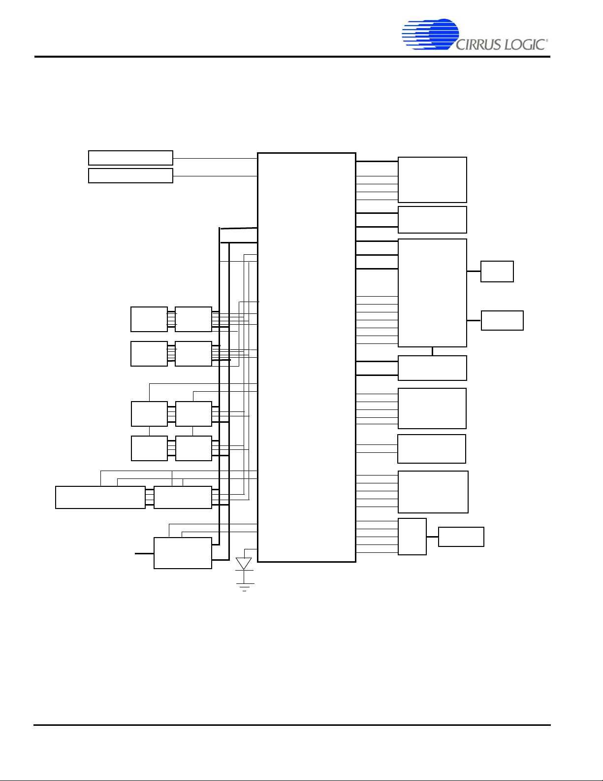
EP7312
LCD
KEYBOARD
BATTER Y
DC-TO-DC
CONVERTERS
ADC
DIGITIZER
IR LED AND
PHOTODIODE
2RS-232
TRANSCEIVERS
ADDITIONAL I/O
DD[0-3]
CL1
CL2
FRM
M
D[0-31]
A[0-27]
COL[0-7]
PA[0-7]
DC
INPUT
nMOE
WRITE
PB[0-7]
PD[0-7]
PE[0-2]
nPOR
nPWRFL
BATOK
nEXTPWR
nBATCHG
RUN
WAKEUP
nCS[0]
nCS[1]
DRIVE[0-1]
FB[0-1]
EP7312
ADCCLK
nADCCS
ADCOUT
ADCIN
SMPCLK
LEDDRV
PHDIN
RXD[[1/2]
TXD[1/2]
DSR
CTS
DCD
CS[n]
WORD
nCS[2]
nCS[3]
16
FLASH
16
FLASH
6
FLASH
EXTERNAL MEMORY MAPPED EXPANSION
BUFFERS
BUFFERS
AND
LATCHES
16
FLASH
POWER
SUPPLY UNIT
AND
COMPARATORS
CRYSTAL
CODEC/SSI2/
DAI
SSICLK
SSITXFR
SSITXDA
SSIRXDA
SSIRXFR
RTCIN
LEDFLSH
CRYSTAL
MOSCIN
16
SDRAM
16
SDRAM
6
SDRAM
16
SDRAM
SDCS[1]
SDQM[0-3]
SDCS[0]
SDQM[0-3]
SDRAS/
SDCAS
High-Performance, Low-Power System on Chip
System Design
As shown in system block diagram, simply adding desired
memory and peripherals to the highly integrated EP7312
completes a low-power system solution. All necessary
interface logic is integrated on-chip.
Note: A system can only use one of the following peripheral interfaces at any given time: SSI2,CODEC or DAI.
12 Copyright Cirrus Logic, Inc. 2011
Figure 1. A Fully-Configured EP7312-Based System
(All Rights Reserved) DS508F2
Page 13
High-Performance, Low-Power System on Chip
ELECTRICAL SPECIFICATIONS
Absolute Maximum Ratings
DC Core, PLL, and RTC Supply Voltage 2.9 V
DC I/O Supply Voltage (Pad Ring) 3.6 V
DC Pad Input Current 10 mA/pin; 100 mA cumulative
Storage Temperature, No Power –40C to +125C
Recommended Operating Conditions
DC core, PLL, and RTC Supply Voltage 2.5 V 0.2 V
DC I/O Supply Voltage (Pad Ring) 2.3 V - 3.5 V
DC Input / Output Voltage O–I/O supply voltage
EP7312
Operating Temperature
Extended -20C to +70C; Commercial 0C to +70C;
Industrial -40C to +85C
DC Characteristics
All characteristics are specified at V
DDCORE
for all frequencies of operation. The current consumption figures have test conditions specified per parameter.”
Symbol Parameter Min Typ Max Unit Conditions
VIH CMOS input high voltage
VIL CMOS input low voltage
VT+
VT-
Vhst Schmitt trigger hysteresis 0.1 - 0.4 V VIL to VIH
VOH
Schmitt trigger positive going
threshold
Schmitt trigger negative going
threshold
CMOS output high voltage
Output drive 1
Output drive 2
a
a
a
= 2.5 V, V
0.65 V
DDIO
0.3
V
SS
--2.1V
0.8 - - V
VDD – 0.2
2.5
2.5
= 3.3 V and VSS = 0 V over an operating temperature of 0°C to +70°C
DDIO
+ 0.3
-
-
-
-
-
V
DDIO
0.25 V
-
-
-
DDIO
V
V
V
V
V
V
= 2.5 V
DDIO
= 2.5 V
V
DDIO
IOH = 0.1 mA
IOH = 4 mA
IOH = 12 mA
CMOS output low voltage
VOL
IIN Input leakage current - - 1.0 µA
IOZ
CIN Input capacitance 8 - 10.0 pF
COUT Output capacitance 8 - 10.0 pF
Output drive 1
Output drive 2
Bidirectional 3-state leakage
current
a
a
b c
a
-
-
-
25 - 100 µA
-
-
-
0.3
0.5
0.5
DS508F2 Copyright Cirrus Logic, Inc. 2011
(All Rights Reserved) 13
V
V
V
IOL = –0.1 mA
IOL = –4 mA
IOL = –12 mA
VIN = V
VOUT = V
or GND
DD
DD
or GND
Page 14

EP7312
High-Performance, Low-Power System on Chip
Symbol Parameter Min Typ Max Unit Conditions
CI/O Transceiver capacitance 8 - 10.0 pF
IDD
STANDBY
@ 25 C
IDD
STANDBY
@ 70 C
IDD
STANDBY
@ 85 C
IDD
idle
at 74 MHz
IDD
IDLE
at 90 MHz
VDD
STANDBY
Standby current consumption
Core, Osc, RTC @2.5 V
I/O @ 3.3 V
Standby current consumption
Core, Osc, RTC @2.5 V
I/O @ 3.3 V
Standby current consumption
Core, Osc, RTC @2.5 V
I/O @ 3.3 V
Idle current consumption
Core, Osc, RTC @2.5 V
I/O @ 3.3 V
Idle current consumption
Core, Osc, RTC @2.5 V
I/O @ 3.3 V
1
-
-
1
-
-
1
-
-
1
-
-
1
-
-
77
41
10
11
-
µA
-
-
-
-
-
6
570
111
1693
163
-
µA
µA
mA
-
7
-
mA
-
Standby supply voltage 2.0 - - V
Only nPOR, nPWRFAIL,
nURESET, PE0, PE1, and RTS
are driven, while all other float,
VIH = V
± 0.1 V,
DD
VIL = GND ± 0.1 V
Only nPOR, nPWRFAIL,
nURESET, PE0, PE1, and RTS
are driven, while all other float,
VIH = V
± 0.1 V,
DD
VIL = GND ± 0.1 V
Only nPOR, nPWRFAIL,
nURESET, PE0, PE1, and RTS
are driven, while all other float,
VIH = V
± 0.1 V,
DD
VIL = GND ± 0.1 V
Both oscillators running, CPU
static, Cache enabled, LCD
disabled, VIH = V
± 0.1 V, VIL
DD
= GND ± 0.1 V
Both oscillators running, CPU
static, Cache enabled, LCD
disabled, VIH = V
± 0.1 V, VIL
DD
= GND ± 0.1 V
Minimum standby voltage for
state retention, internal SRAM
cache, and RTC operation only
a. Refer to the strength column in the pin assignment tables for all package types.
b. Assumes buffer has no pull-up or pull-down resistors.
c. The leakage value given assumes that t he pin is configured as an input pin but is not currently being driven.
Note: 1) Total power consumption = IDD
2) A typical design will provide 3.3 V to the I/O supply (i.e., V
CORE x
2.5 V + IDD
IO x
3.3 V
), and 2.5 V to the remaining logic. This is to allow the I/O to be
DDIO
compatible with 3.3 V powered external logic (i.e., 3.3 V SDRAMs).
2) Pull-up current = 50 µA typical at V
= 3.3 V.
DD
14 Copyright Cirrus Logic, Inc. 2011
(All Rights Reserved) DS508F2
Page 15
EP7312
Clock
High to Low
High/Low to H igh
Bus Change
Bus Valid
Undefined/Invalid
V a lid B u s to T ris ta te
Bus/Signal O m ission
Figure 2. Legend for Timing Diagrams
High-Performance, Low-Power System on Chip
Timings
Timing Diagram Conventions
This data sheet contains timing diagrams. The following key explains the components used in these diagrams. Any variations are
clearly labelled when they occur. Therefore, no additional meaning should be attached unless specifically stated.
Timing Conditions
Unless specified otherwise, the following conditions are true for all timing measurements. All characteristics are specified at
V
= 3.1 - 3.5 V and VSS = 0 V over an operating temperature of -40C to +85C. Pin loadings is 50 pF. The timing values are
DDIO
referenced to 1/2 V
DS508F2 Copyright Cirrus Logic, Inc. 2011
.
DD
(All Rights Reserved) 15
Page 16
EP7312
High-Performance, Low-Power System on Chip
SDRAM Interface
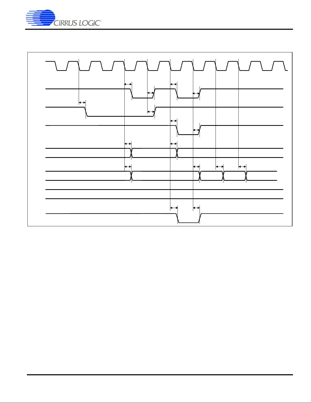
Figure 3 through Figure 6 define the timings associated with all phases of the SDRAM. The following table contains the values for
the timings of each of the SDRAM modes.
Parameter Symbol Min Typ Max Unit
SDCLK falling edge to SDCS assert delay time
SDCLK falling edge to SDCS deassert delay time
SDCLK falling edge to SDRAS assert delay time
SDCLK falling edge to SDRAS deassert delay time
SDCLK falling edge to SDRAS invalid delay time
SDCLK falling edge to SDCAS assert delay time
SDCLK falling edge to SDCAS deassert delay time
SDCLK falling edge to ADDR transition time
SDCLK falling edge to ADDR invalid delay time
SDCLK falling edge to SDMWE assert delay time
SDCLK falling edge to SDMWE deassert delay time
DATA transition to SDCLK falling edge time
SDCLK falling edge to DATA transition hold time
SDCLK falling edge to DATA transition delay time
t
CSa
t
CSd
t
RAa
t
RAd
t
RAnv
t
CAa
t
CAd
t
ADv
t
ADx
t
MWa
t
MWd
t
DAs
t
DAh
t
DAd
024ns
3 2 10 ns
137ns
3 1 10 ns
247ns
22 5ns
50 3ns
31 5ns
22 5ns
31 5ns
40 4ns
2--ns
1--ns
0 - 15 ns
16 Copyright Cirrus Logic, Inc. 2011
(All Rights Reserved) DS508F2
Page 17
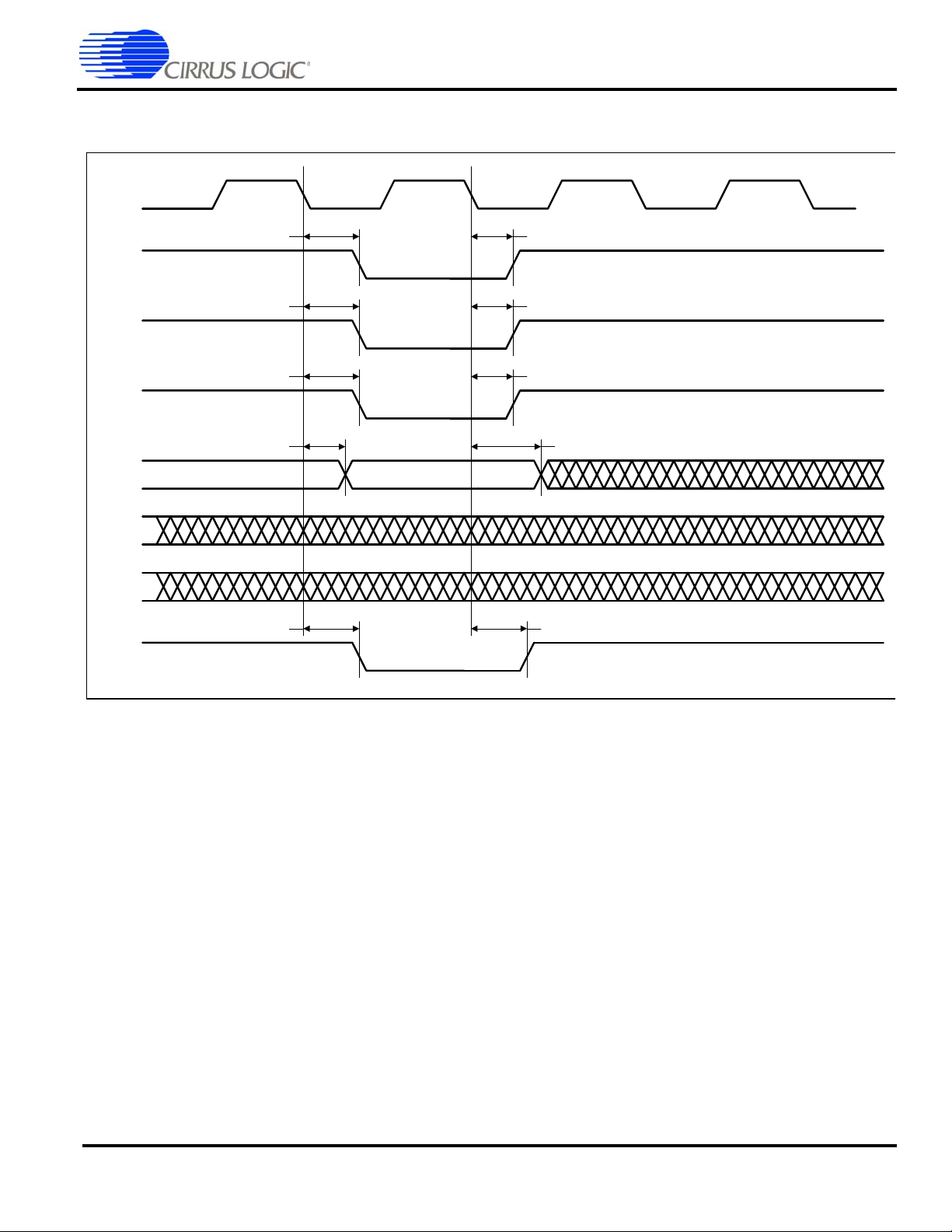
SDRAM Load Mode Register Cycle
SDCLK
SDCS
SDRAS
SDCAS
ADDR
DATA
SDQM
SDMWE
t
CSa
t
RAa
t
CAa
t
MWa
t
ADv
t
ADx
t
RAd
t
CSd
t
CAd
t
MWd
Figure 3. SDRAM Load Mode Register Cycle Timing Measurement
EP7312
High-Performance, Low-Power System on Chip
Note: 1. Timings are shown with CAS latency = 2
2. The SDCLK signal may be phase shifted relative to the rest of the SDRAM control and data signals due to uneven loading.
Designers should take care to ensure that delays between SDRAM control and data signals are approximately equal
DS508F2 Copyright Cirrus Logic, Inc. 2011
(All Rights Reserved) 17
Page 18

EP7312
ADRAS ADCAS
SDCLK
SDCS
SDRAS
SDCAS
SDQM
[0:3]
ADDR
DATA
SDMWE
D1 D4D3D2
t
ADv
t
ADv
t
CSd
t
CSa
t
CSa
t
CAa
t
RAd
t
CSd
t
CAd
t
RAa
t
DAh
t
DAs
t
DAh
t
DAs
t
DAh
t
DAs
t
DAh
t
DAs
t
RAnv
Figure 4. SDRAM Burst Read Cycle Timing Measurement
High-Performance, Low-Power System on Chip
SDRAM Burst Read Cycle
Note: 1. Timings are shown with CAS latency = 2
2. The SDCLK signal may be phase shifted relative to the rest of the SDRAM control and data signals due to uneven loading.
Designers should take care to ensure that delays between SDRAM control and data signals are approximately equal.
18 Copyright Cirrus Logic, Inc. 2011
(All Rights Reserved) DS508F2
Page 19
SDRAM Burst Write Cycle
SDCLK
SDCS
SDRAS
SDCAS
SDQM
ADDR
DATA
SDMWE
0
D1
ADRAS
ADCAS
D4D3D2
t
CSa
t
RAa
t
CAa
t
CSa
t
CSd
t
RAd
t
CSd
t
CAd
t
ADv
t
DAd
t
ADv
t
DAd
t
DAd
t
DAd
t
MWa
t
MWd
Figure 5. SDRAM Burst Write Cycle Timing Measurement
EP7312
High-Performance, Low-Power System on Chip
Note: 1. Timings are shown with CAS latency = 2
2. The SDCLK signal may be phase shifted relative to the rest of the SDRAM control and data signals due to uneven loading.
Designers should take care to ensure that delays between SDRAM control and data signals are approximately equal
DS508F2 Copyright Cirrus Logic, Inc. 2011
(All Rights Reserved) 19
Page 20
EP7312
SDCLK
SDCS
SDRAS
SDCAS
SDQM
[3:0]
SDMWE
SDATA
ADDR
t
CSa
t
RAa
t
CSd
t
RAd
t
CAa
t
CAd
Figure 6. SDRAM Refresh Cycle Timing Measurement
High-Performance, Low-Power System on Chip
SDRAM Refresh Cycle
Note: 1. Timings are shown with CAS latency = 2
2. The SDCLK signal may be phase shifted relative to the rest of the SDRAM control and data signals due to uneven loading.
Designers should take care to ensure that delays between SDRAM control and data signals are approximately equal
20 Copyright Cirrus Logic, Inc. 2011
(All Rights Reserved) DS508F2
Page 21
EP7312
High-Performance, Low-Power System on Chip
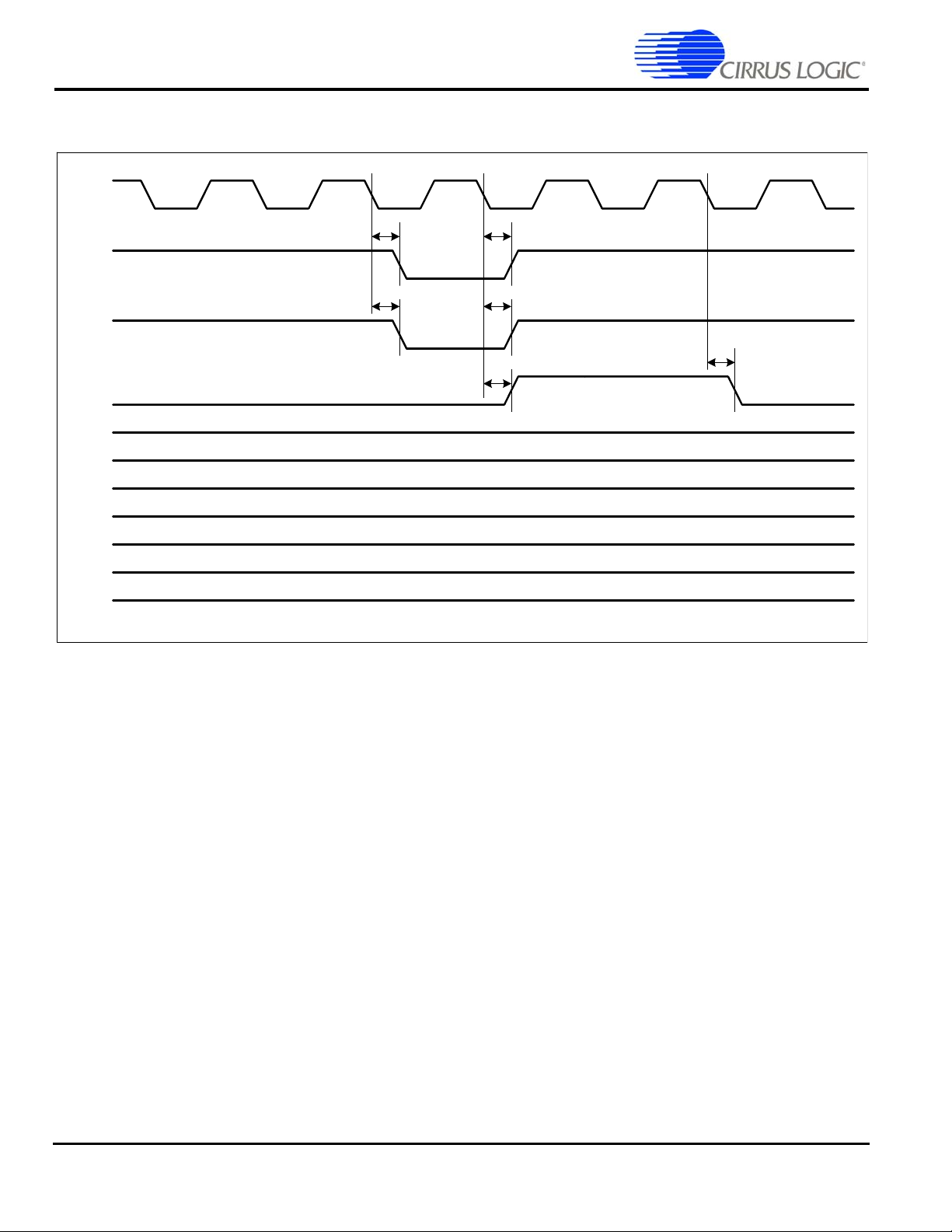
Static Memory
Figure 7 through Figure 10 define the timings associated with all phases of the Static Memory. The following table contains the
values for the timings of each of the Static Memory modes.
Parameter Symbol Min Typ Max Unit
EXPCLK rising edge to nCS assert delay time
EXPCLK falling edge to nCS deassert hold time
EXPCLK rising edge to A assert delay time
EXPCLK falling edge to A deassert hold time
EXPCLK rising edge to nMWE assert delay time
EXPCLK rising edge to nMWE deassert hold time
EXPCLK falling edge to nMOE assert delay time
EXPCLK falling edge to nMOE deassert hold time
EXPCLK falling edge to HALFWORD deassert delay time
EXPCLK falling edge to WORD assert delay time
EXPCLK rising edge to data valid delay time
EXPCLK falling edge to data invalid delay time
Data setup to EXPCLK falling edge time
EXPCLK falling edge to data hold time
t
CSd
t
CSh
t
Ad
t
Ah
t
MWd
t
MWh
t
MOEd
t
MOEh
t
HWd
t
WDd
t
Dv
t
Dnv
t
Ds
t
Dh
2 8 20 ns
2 7 20 ns
4 9 16 ns
31019ns
3 6 10 ns
3 6 10 ns
3 7 10 ns
2 7 10 ns
2 8 20 ns
2 8 16 ns
81321ns
61530ns
--1ns
--3ns
EXPCLK rising edge to WRITE assert delay time
EXPREADY setup to EXPCLK falling edge time
EXPCLK falling edge to EXPREADY hold time
t
WRd
t
EXs
t
EXh
DS508F2 Copyright Cirrus Logic, Inc. 2011
(All Rights Reserved) 21
51123ns
--0ns
--0ns
Page 22
EP7312
EXPCLK
nCS
A
nMWE
HALF-
WORD
WORD
D
WRITE
nMOE
t
CSd
t
Ad
t
CSh
t
MOEh
t
Dh
t
Ds
t
HWd
t
WDd
t
WRd
t
MOEd
EXPRDY
t
EXh
t
EXs
Figure 7. Static Memory Single Read Cycle Timing Measurement
High-Performance, Low-Power System on Chip
Static Memory Single Read Cycle
Note: 1. The cycle time can be extended by integer multiples of the clock period (22 ns at 45 MHz, 27 ns at 36 MHz, 54 ns at
18.432 MHz, and 77 ns at 13 MHz), by either driving EXPRDY low and/or by programming a number of wait states. EXPRDY is
sampled on the falling edge of EXPCLK before the data transfer. If low at this point, the transfer is delayed by one clock period
where EXPRDY is sampled again. EXPCLK need not be referenced when driving EXPRDY, but is shown for clarity.
2. Address, Halfword, Word, and Write hold state until next cycle.
22 Copyright Cirrus Logic, Inc. 2011
(All Rights Reserved) DS508F2
Page 23
Static Memory Single Write Cycle
EXPCLK
nCS
A
nMWE
HALF-
WORD
WORD
D
WRITE
t
HWd
t
WDd
t
CSd
t
Ad
t
MWd
t
Dv
t
MWh
t
CSh
nMOE
EXPRDY
t
EXh
t
EXs
Figure 8. Static Memory Single Write Cycle Timing Measurement
EP7312
High-Performance, Low-Power System on Chip
Note: 1. The cycle time can be extended by integer multiples of the clock period (22 ns at 45 MHz, 27 ns at 36 MHz, 54 ns at
18.432 MHz, and 77 ns at 13 MHz), by either driving EXPRDY low and/or by programming a number of wait states. EXPRDY is
sampled on the falling edge of EXPCLK before the data transfer. If low at this point, the transfer is delayed by one clock period
where EXPRDY is sampled again. EXPCLK need not be referenced when driving EXPRDY, but is shown for clarity.
2. Zero wait states for sequential writes is not permitted for memory devices which use nMWE pin, as this cannot be driven with
valid timing under zero wait state conditions.
3. Address, Data, Halfword, Word, and Write hold state until next cycle.
DS508F2 Copyright Cirrus Logic, Inc. 2011
(All Rights Reserved) 23
Page 24
EP7312
EXPCLK
nCS
A
nMOE
HALF
WORD
WORD
D
nMWE
EXPRDY
WRITE
t
CSd
t
Ad
t
Ah
t
Ah
t
Ah
t
CSh
t
MOEh
t
MOEd
t
EXs
t
EXh
tDst
Dh
t
Ds
t
Ds
t
Ds
t
Dh
t
Dh
t
Dh
t
WRd
t
HWd
t
WDd
Figure 9. Static Memory Burst Read Cycle Timing Measurement
High-Performance, Low-Power System on Chip
Static Memory Burst Read Cycle
Note: 1. Four cycles are shown in the above diagram (minimum wait states, 1-0-0-0). This is the maximum number of consecutive
cycles that can be driven. The number of consecutive cycles can be programmed from 2 to 4, inclusively.
2. The cycle time can be extended by integer multiples of the clock period (22 ns at 45 MHz, 27 ns at 36 MHz, 54 ns at
18.432 MHz, and 77 ns at 13 MHz), by either driving EXPRDY low and/or by programming a number of wait states. EXPRDY is
sampled on the falling edge of EXPCLK before the data transfer. If low at this point, the transfer is delayed by one clock period
where EXPRDY is sampled again. EXPCLK need not be referenced when driving EXPRDY, but is shown for clarity.
3. Consecutive reads with sequential access enabled are identical except that the sequential access wait state field is used to
determine the number of wait states, and no idle cycles are inserted between successive non-sequential ROM/expansion
cycles. This improves performance so the SQAEN bit should always be set where possible.
4. Address, Halfword, Word, and Write hold state until next cycle.
24 Copyright Cirrus Logic, Inc. 2011
(All Rights Reserved) DS508F2
Page 25
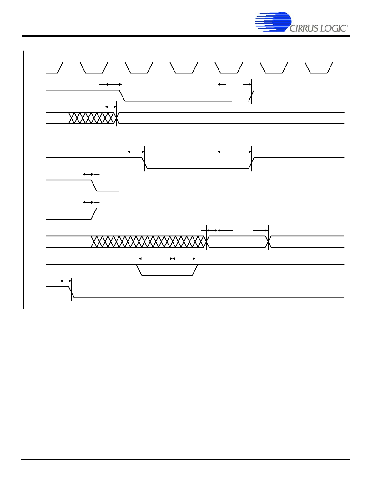
Static Memory Burst Write Cycle
EXPCLK
nCS
A
nMOE
HALF
WORD
WORD
D
nMWE
EXPRDY
WRITE
t
CSd
t
Ad
t
MWd
t
MWh
t
MWd
t
MWd
t
MWd
t
MWh
t
MWh
t
MWh
t
Ah
t
Ah
t
Ah
t
EXs
t
EXh
t
CSh
t
Dv
t
Dv
t
Dv
t
Dnv
t
Dnv
t
Dnv
t
Dv
t
HWd
t
WDd
Figure 10. Static Memory Burst Write Cycle Timing Measurement
EP7312
High-Performance, Low-Power System on Chip
Note: 1. Four cycles are shown in the above diagram (minimum wait states, 1-1-1-1). This is the maximum number of consecutive
cycles that can be driven. The number of consecutive cycles can be programmed from 2 to 4, inclusively.
2. The cycle time can be extended by integer multiples of the clock period (22 ns at 45 MHz, 27 ns at 36 MHz, 54 ns at
18.432 MHz, and 77 ns at 13 MHz), by either driving EXPRDY low and/or by programming a number of wait states. EXPRDY is
sampled on the falling edge of EXPCLK before the data transfer. If low at this point, the transfer is delayed by one clock period
where EXPRDY is sampled again. EXPCLK need not be referenced when driving EXPRDY, but is shown for clarity.
3. Zero wait states for sequential writes is not permitted for memory devices which use nMWE pin, as this cannot be driven with
valid timing under zero wait state conditions.
4. Address, Data, Halfword, Word, and Write hold state until next cycle.
DS508F2 Copyright Cirrus Logic, Inc. 2011
(All Rights Reserved) 25
Page 26

EP7312
ADC
CLK
nADC
CSS
ADCIN
ADC
OUT
t
INs
t
INh
t
Cd
t
Od
t
Ovd
Figure 11. SSI1 Interface Timing Measurement
High-Performance, Low-Power System on Chip
SSI1 Interface
Parameter Symbol Min Max Unit
ADCCLK falling edge to nADCCSS deassert delay time
ADCIN data setup to ADCCLK rising edge time
ADCIN data hold from ADCCLK rising edge time
ADCCLK falling edge to data valid delay time
ADCCLK falling edge to data invalid delay time
t
t
t
t
Cd
INs
INh
Ovd
t
Od
910ms
-15ns
-14ns
713ns
23ns
26 Copyright Cirrus Logic, Inc. 2011
(All Rights Reserved) DS508F2
Page 27

SSI2 Interface
SSI
CLK
SSIRXFR/
SSITXFR
SSI
TXDA
SSI
RXDA
D1D7
D7
D2
D2 D1
D0
D0
t
clk_per
t
clk_high
t
clk_low
t
FRd
t
FR_per
t
RXs
t
TXd
t
FRa
t
RXh
t
clkrf
t
TXv
Figure 12. SSI2 Interface Timing Measurement
EP7312
High-Performance, Low-Power System on Chip
Parameter Symbol Min Max Unit
SSICLK period (slave mode)
SSICLK high time
SSICLK low time
SSICLK rise/fall time
SSICLK rising edge to RX and/or TX frame sync high time
SSICLK rising edge to RX and/or TX frame sync low time
SSIRXFR and/or SSITXFR period
SSIRXDA setup to SSICLK falling edge time
SSIRXDA hold from SSICLK falling edge time
SSICLK rising edge to SSITXDA data valid delay time
SSITXDA valid time
t
clk_per
t
clk_high
t
clk_low
t
clkrf
t
FRd
t
FRa
t
FR_per
t
RXs
t
RXh
t
TXd
t
TXv
185 2050 ns
925 1025 ns
925 1025 ns
318ns
-3ns
-8ns
960 990 ns
37ns
37ns
-2ns
960 990 ns
DS508F2 Copyright Cirrus Logic, Inc. 2011
(All Rights Reserved) 27
Page 28

EP7312
CL[2]
CL[1]
FRM
M
DD [3:0]
t
CL1d
t
FRMd
t
Md
t
DDd
t
CL2d
Figure 13. LCD Controller Timing Measurement
High-Performance, Low-Power System on Chip
LCD Interface
Parameter Symbol Min Max Unit
CL[2] falling to CL[1] rising delay time
CL[1] falling to CL[2] rising delay time
CL[1] falling to FRM transition time
CL[1] falling to M transition time
CL[2] rising to DD (display data) transition time
t
CL1d
t
CL2d
t
FRMd
t
t
DDd
Md
10 25 ns
80 3,475 ns
300 10,425 ns
10 20 ns
10 20 ns
28 Copyright Cirrus Logic, Inc. 2011
(All Rights Reserved) DS508F2
Page 29

JTAG Interface
TDO
TCK
TDI
TMS
t
JPh
t
clk_high
t
clk_low
t
JPzx
t
JPco
t
JPxz
t
clk_per
t
JPs
Figure 14. JTAG Timing Measurement
EP7312
High-Performance, Low-Power System on Chip
Parameter Symbol Min Max Units
TCK clock period
TCK clock high time
TCK clock low time
JTAG port setup time
JTAG port hold time
JTAG port clock to output
JTAG port high impedance to valid output
JTAG port valid output to high impedance
t
clk_per
t
clk_high
t
clk_low
t
JPs
t
JPh
t
JPco
t
JPzx
t
JPxz
2-ns
1-ns
1-ns
-0ns
-3ns
-10ns
-12ns
-19ns
DS508F2 Copyright Cirrus Logic, Inc. 2011
(All Rights Reserved) 29
Page 30

EP7312
Figure 15. 208-Pin LQFP Package Outline Drawing
Pin 1 Indicator
29.60 (1.165)
30.40 (1.197)
0.17 (0.007)
0.27 (0.011)
27.80 (1.094)
28.20 (1.110)
0.50
(0.0197)
BSC
29.60 (1.165)
30.40 (1.197)
27.80 (1.094)
28.20 (1.110)
1.35 (0.053)
1.45 (0.057)
0
MIN
7
MAX
0.09 (0.004)
0.20 (0.008)
1.40 (0.055)
0.45 (0.018)
0.75 (0.030)
0.05 (0.002)
1.00 (0.039) BSC
Pin 1
Pin 208
1.60 (0.063)
0.15 (0.006)
EP7312
208-Pin LQFP
High-Performance, Low-Power System on Chip
Packages
208-Pin LQFP Package Characteristics
Note: 1) Dimensions are in millimeters (inches), and controlling dimension is millimeter.
2) Drawing above does not reflect exact package pin count.
3) Before beginning any new design with this device, please contact Cirrus Logic for the latest package information.
4) For pin locations, please see Figure 16. For pin descriptions see the EP7312 User’s Manual.
30 Copyright Cirrus Logic, Inc. 2011
(All Rights Reserved) DS508F2
Page 31

208-Pin LQFP Pin Diagram
160
159
158
157
53
54
55
56
57
58
59
60
61
62
63
76
77
78
79
80
81
82
83
84
85
86
87
88
89
90
91
92
93
94
95
96
97
106
107
108
109
110
112
113
114
115
116
117
118
119
120
121
64
65
67
68
69
70
71
72
73
74
75
66
98
99
100
101
102
103
104
122
124
125
126
127
128
129
130
105
131
132
133
134
156
155
154
153
152
151
150
149
148
147
146
145
144
143
140
139
138
137
136
141
142
135
161
162
163
164
165
166
167
168
169
170
171
172
173
174
180
181
182
183
184
185
186
187
188
189
190
191
192
193
194
195
196
197
198
199
201
202
203
204
205
206
207
208
200
175
176
177
178
179
123
111
EP7312
208-Pin LQFP
(Top View)
2345678910111213141516171819202122232425262728293031323334353637383940414243444546474849515052
1
nEXTPWR
BATOK
nPOR
VSSOSC
VDDOSC
MOSCIN
MOSCOUT
nURESET
WAKEUP
A[6]
D[6]
A[5]
D[5]
VDDIO
VSSIO
A[4]
D[4]
A[3]
D[3]
nPWRFL
A[2]
D[2]
A[1]
A[0]
D[0]
VDDCORE
VSSIO
VDDIO
CL[2]
CL[1]
FRM
M
DD[2]
DD[1]
DD[0]
nSDCS[1]
SDQM[3]
SDQM[2]
VDDIO
VSSIO
SDCLK
nMWE/nSDWE
nMOE/nSDCAS
nCS[0]
nCS[1]
nCS[2]
nCS[3]
D[7]
A[7]
D[8]
A[8]
D[9]
D[10]
A[10]
VSSIO
VDDIO
A[11]
D[12]
A[12]
D[13]
A[13]\DRA[14]
D[14]
DD[3]
D[17]
D[15]
A[17]
/DRA[10]
nTRST
VSSIO
VDDIO
D[18]
A[18
/DRA[9]
D[19]
A[19]
/DRA[8]
D[20]
VSSIO
A[21]
/DRA[6]
D[22]
D[23]
A[23]
/DRA[4]
D[24]
VSSIO
VDDIO
A[24]
/DRA[3]
HALFWORD
A[14]/DRA[13]
nBATCHG
A[25]/DRA[2]
D[25]
D[27]
A[27]/DRA[0]
VSSIO
D[28]
D[29]
D[30]
D[31]
BUZ
COL[0]
COL[1]
TCLK
VDDIO
COL[2]
COL[3]
COL[4]
COL[5]
COL[6]
COL[7]
FB[0]
VSSIO
FB[1]
ADCOUT
ADCCLK
DRIVE[0]
VDDIO
PD[2]
VSSIO
VSSCORE
nADCCS
ADCIN
SSIRXDA
SSIRXFR
SSITXDA
SSITXFR
VSSIO
SSICLK
PD[0]/LEDFLSH
PD[1]
PD[3]
A[22]
/DRA[5]
PD[4]
VDDIO
PD[5]
PD[6]/SDQM[0]
DRIVE[1]
PD[7]/SDQM[1]
D[26]
A[15]
/DRA[12]
D[16]
A[16]
/DRA[11]
nCS[4]
VDDCORE
A[26]/DRA[1]
D[21]
TMS
A[20]
/DRA[7]
SMPCLK
D[11]
A[9]
D[1]
VSSCORE
nSDCS[0]
SDCKE
VSSIO
VSSIO
VSSIO
VSSIO
EXPCLK
WORD
WRITE/nSDRAS
RUN/CLKEN
EXPRDY
PB[7]
PB[6]
PB[5]
PB[4]
PB[3]
PB[2]
PB[1]
VSSIO
TDI
VDDIO
TDO
PE[2]/CLKSEL
nEXTFIQ
PA[6]
PA[5]
PA[4]
PA[3]
PA[2]
PA[1]
PA[0]
LEDDRV
TXD[2]
PHDIN
CTS
RXD[2]
DCD
DSR
RTCOUT
RTCIN
VSSIO
PA[7]
VDDIO
VSSIO
nCS[5]
PB[0]
TXD[1]
RXD[1]
nTEST[1]
nTEST[0]
EINT[3]
nEINT[2]
nEINT[1]
PE[1]BOOTSEL[1]
PE[0]BOOTSEL[0]
N/C
VSSRTC
VDDRTC
Figure 16. 208-Pin LQFP (Low Profile Quad Flat Pack) Pin Diagram
nMEDCHG/nBROM
EP7312
High-Performance, Low-Power System on Chip
Note: 1. N/C should not be grounded but left as no connects.
DS508F2 Copyright Cirrus Logic, Inc. 2011
(All Rights Reserved) 31
Page 32
EP7312
High-Performance, Low-Power System on Chip
208-Pin LQFP Numeric Pin Listing
Table 20. 208-Pin LQFP Numeric Pin Listing
Pin
No.
1 nCS[5] 1 Low O Chip select 5
2 VDDIO Pad Pwr Digital I/O power, 3.3 V
3 VSSIO Pad Gnd I/O ground
4 EXPCLK 1 I Expansion clock input
5 WORD 1 Low O Word access select output
6 WRITE/nSDRAS 1 Low O
7 RUN/CLKEN 1 Low O
8 EXPRDY 1 I Expansion port ready input
9 TXD[2] 1 High O UART 2 transmit data output
10 RXD[2] I UART 2 receive data input
11 TDI with p/u* I JTAG data input
12 VSSIO Pad Gnd I/O ground
13 PB[7] 1
14 PB[6] 1
15 PB[5] 1
16 PB[4] 1
17 PB[3] 1
18 PB[2] 1
19 PB[1] 1
20 PB[0] 1
21 VDDIO Pad Pwr Digital I/O power, 3.3 V
22 TDO 1
23 PA[7] 1
24 PA[6] 1
25 PA[5] 1
26 PA[4] 1
27 PA[3] 1
28 PA[2] 1
29 PA[1] 1
30 PA[0] 1
31 LEDDRV 1 Low O IR LED drive
32 TXD[1] 1 High O UA RT 1 transmit data out
33 VSSIO 1 High Pad Gnd I/O ground
34 PHDIN I Photodiode input
35 CTS I UART 1 clear to send input
36 RXD[1] I UART 1 receive data input
37 DCD I UART 1 data carrier detect
Signal
Strength
†
Reset
State
Input
Input
Input
Input
Input
Input
Input
Input
Input
Input
Input
Input
Input
Input
Input
Input
Input
Type Description
Transfer direction / SDRAM
RAS signal output
Run output / clock enable
output
‡
‡
‡
‡
‡
‡
‡
‡
‡
‡
‡
‡
‡
‡
‡
‡
‡
I/O GPIO port B
I/O GPIO port B
I/O GPIO port B
I/O GPIO port B
I/O GPIO port B
I/O GPIO port B
I/O GPIO port B
I/O GPIO port B
O JTAG data out
I/O GPIO port A
I/O GPIO port A
I/O GPIO port A
I/O GPIO port A
I/O GPIO port A
I/O GPIO port A
I/O GPIO port A
I/O GPIO port A
32 Copyright Cirrus Logic, Inc. 2011
(All Rights Reserved) DS508F2
Page 33
High-Performance, Low-Power System on Chip
Table 20. 208-Pin LQFP Numeric Pin Listing (Continued)
EP7312
Pin
No.
38 DSR I UART 1 data set ready input
39 nTEST[1] With p/u* I Test mode select input
40 nTEST[0] With p/u* I Test mode select input
41 EINT[3] I External in terrupt
42 nEINT[2] I External interrupt input
43 nEINT[1] I External interrupt input
44 nEXTFIQ I External fast interrupt input
45 PE[2]/CLKSEL 1
46 PE[1]/BOOTSEL[1] 1
47 PE[0]/BOOTSEL[0] 1
48 VSSRTC RTC Gnd Real time clock ground
49 RTCOUT O
50 RTCIN I
51 VDDRTC RTC power Real time clock power, 2.5 V
52 N/C
53 PD[7]/SDQM[1] 1 Low I/O
54 PD[6]/SDQM[0] 1 Low I/O
55 PD[5] 1 Low I/O GPIO port D
56 PD[4] 1 Low I/O GPIO port D
57 VDDIO Pad Pwr Digital I/O power, 3.3 V
58 TMS with p/u* I JTAG mode select
59 PD[3] 1 Low I/O GPIO port D
60 PD[2] 1 Low I/O GPIO port D
61 PD[1] 1 Low I/O GPIO port D
62 PD[0]/LEDFLSH 1 Low I/O
63 SSICLK 1
64 VSSIO Pad Gnd I/O ground
65 SSITXFR 1 Low I/O DAI/CODEC/SSI2 serial clock
66 SSITXDA 1 Low O
67 SSIRXDA I
68 SSIRXFR
69 ADCIN I SSI1 ADC serial input
70 nADCCS 1 High O SSI1 ADC chip select
71 VSSCORE Core ground Core ground
72 VDDCORE Core Pwr Core power, 2.5 V
73 VSSIO Pad Gnd I/O ground
74 VDDIO Pad Pwr Digital I/O power, 3.3 V
75 DRIVE[1] 2
76 DRIVE[0] 2
77 ADCCLK 1 Low O SSI1 ADC serial clock
78 ADCOUT 1 Low O SSI1 ADC serial data output
Signal
Strength
†
Reset
State
Input
Input
Input
Input
Input
High /
Low
High /
Low
Type Description
‡
‡
‡
‡
‡
I/O
I/O
I/O
I/O DAI/CODEC/SSI2 serial clock
I/O DAI/CODEC/SSI2 frame sync
I/O PWM drive output
I/O PWM drive output
GPIO port E / clock input
mode select
GPIO port E / boot mode
select
GPIO port E / Boot mode
select
Real time clock oscillator
output
Real time clock oscillator
input
GPIO port D / SDRAM byte
lane mask
GPIO port D / SDRAM byte
lane mask
GPIO port D / LED blinker
output
DAI/CODEC/SSI2 serial data
DAI/CODEC/SSI2 serial data
output
input
DS508F2 Copyright Cirrus Logic, Inc. 2011
(All Rights Reserved) 33
Page 34
EP7312
High-Performance, Low-Power System on Chip
Table 20. 208-Pin LQFP Numeric Pin Listing (Continued)
Pin
No.
79 SMPCLK 1 Low O SSI1 ADC sample clock
80 FB[1] I P W M feedback input
81 VSSIO Pad Gnd I/O ground
82 FB[0] I P W M feedback input
83 COL[7] 1 High O
84 COL[6] 1 High O
85 COL[5] 1 High O
86 COL[4] 1 High O
87 COL[3] 1 High O
88 COL[2] 1 High O
89 VDDIO Pad Pwr Digital I/O power, 3.3 V
90 TCLK I JTAG clock
91 COL[1] 1 High O
92 COL[0] 1 High O
93 BUZ 1 Low O Buzzer drive output
94 D[31] 1 Low I/O Data I/O
95 D[30] 1 Low I/O Data I/O
96 D[29] 1 Low I/O Data I/O
97 D[28] 1 Low I/O Data I/O
98 VSSIO Pad Gnd I/O ground
99 A[27]/DRA[0] 2 Low O
100 D[27] 1 Low I/O Data I/O
101 A[26]/DRA[1] 2 Low O
102 D[26] 1 Low I/O Data I/O
103 A[25]/DRA[2] 2 Low O
104 D[25] 1 Low I/O Data I/O
105 HALFWORD 1 Low O Halfword access select output
106 A[24]/DRA[3] 1 Low O
107 VDDIO — Pad Pwr Digital I/O power, 3.3 V
108 VSSIO — Pad Gnd I/O ground
109 D[24] 1 Low I/O Data I/O
110 A[23]/DRA[4] 1 Low O
111 D[23] 1 Low I/O Data I/O
112 A[22]/DRA[5] 1 Low O
113 D[22] 1 Low I/O Data I/O
114 A[21]/DRA[6] 1 Low O
115 D[21] 1 Low I/O Data I/O
116 VSSIO Pad Gnd I/O ground
117 A[20]/DRA[7] 1 Low O
Signal
Strength
†
Reset
State
Type Description
Keyboard scanner column
drive
Keyboard scanner column
drive
Keyboard scanner column
drive
Keyboard scanner column
drive
Keyboard scanner column
drive
Keyboard scanner column
drive
Keyboard scanner column
drive
Keyboard scanner column
drive
System byte address /
SDRAM address
System byte address /
SDRAM address
System byte address /
SDRAM address
System byte address /
SDRAM address
System byte address /
SDRAM address
System byte address /
SDRAM address
System byte address /
SDRAM address
System byte address /
SDRAM address
34 Copyright Cirrus Logic, Inc. 2011
(All Rights Reserved) DS508F2
Page 35
High-Performance, Low-Power System on Chip
Table 20. 208-Pin LQFP Numeric Pin Listing (Continued)
EP7312
Pin
No.
118 D[20] 1 Low I/O Data I/O
119 A[19]/DRA[8] 1 Low O
120 D[19] 1 Low I/O Data I/O
121 A[18]/DRA[9] 1 Low O
122 D[18] 1 Low I/O Data I/O
123 VDDIO Pad Pwr Digital I/O power, 3.3 V
124 VSSIO Pad Gnd I/O ground
125 nTRST I JTAG async reset input
126 A[17]/DRA[10] 1 Low O
127 D[17] 1 Low I/O Data I/O
128 A[16]/DRA[11] 1 Low O
129 D[16] 1 Low I/O Data I/O
130 A[15]/DRA[12] 1 Low O
131 D[15] 1 Low I/O Data I/O
132 A[14]/DRA[13] 1 Low O
133 D[14] 1 Low I/O Data I/O
134 A[13]/DRA[14] 1 Low O
135 D[13] 1 Low I/O Data I/O
136 A[12] 1 Low O System byte address
137 D[12] 1 Low I/O Data I/O
138 A[11] 1 Low O System byte address
139 VDDIO Pad Pwr Digital I/O power, 3.3 V
140 VSSIO Pad Gnd I/O ground
141 D[11] 1 Low I/O Data I/O
142 A[10] 1 Low O System byte address
143 D[10] 1 Low I/O Data I/O
144 A[9] 1 Low O System byte address
145 D[9] 1 Low I/O Data I/O
146 A[8] 1 Low O System byte address
147 D[8] 1 Low I/O Data I/O
148 A[7] 1 Low O System byte address
149 VSSIO Pad Gnd I/O ground
150 D[7] 1 Low I/O Data I/O
151 nBATCHG I Battery changed sense input
152 nEXTPWR I
153 BATOK I Battery OK input
154 nPOR Schmitt I Power-on reset input
155 nMEDCHG/nBROM I
156 nURESET Schmitt I User reset input
157 VDDOSC Oscillator Power Oscillator power in, 2.5 V
158 MOSCIN I Main oscillator input
159 MOSCOUT O Main oscillator output
160 VSSOSC Oscillator Ground Oscillator Ground
Signal
Strength
†
Reset
State
Type Description
System byte address /
SDRAM address
System byte address /
SDRAM address
System byte address /
SDRAM address
System byte address /
SDRAM address
System byte address /
SDRAM address
System byte address /
SDRAM address
System byte address /
SDRAM address
External power supply sense
Media change interrupt input /
input
internal ROM boot enable
DS508F2 Copyright Cirrus Logic, Inc. 2011
(All Rights Reserved) 35
Page 36
EP7312
High-Performance, Low-Power System on Chip
Table 20. 208-Pin LQFP Numeric Pin Listing (Continued)
Pin
No.
161 WAKEUP Schmitt I System wake up input
162 nPWRF L I Power fail sen s e input
163 A[6] 1 Low O System byte address
164 D[6] 1 Low I/O Data I/O
165 A[5] 1 Low Out System byte address
166 D[5] 1 Low I/O Data I/O
167 VDDIO Pad Pwr Digital I/O power, 3.3 V
168 VSSIO Pad Gnd I/O ground
169 A[4] 1 Low O System byte address
170 D[4] 1 Low I/O Data I/O
171 A[3] 2 Low O System byte address
172 D[3] 1 Low I/O Data I/O
173 A[2] 2 Low O System byte address
174 VSSIO Pad Gnd I/O ground
175 D[2] 1 Low I/O Data I/O
176 A[1] 2 Low O System byte address
177 D[1] 1 Low I/O Data I/O
178 A[0] 2 Low O System byte address
179 D[0] 1 Low I/O Data I/O
180 VSSCORE Core ground Core ground
181 VDDCORE Core Pwr Core power, 2.5 V
182 VSSIO Pad ground I/O ground
183 VDDIO Pad Power Digital I/O power, 3.3 V
184 CL[2] 1 Low O LCD pixel clock out
185 CL[1] 1 Low O LCD line clock
186 FRM 1 Low O
187 M 1 Low O LCD AC bias drive
188 DD[3] 1 Low I/O LCD serial display data
189 DD[2] 1 Low I/O LCD serial display data
190 VSSIO Pad Gnd I/O ground
191 DD[1] 1 Low I/O LCD serial display data
192 DD[0] 1 Low I/O LCD serial display data
193 nSDCS[1] 1 High O SDRAM chip select 1
194 nSDCS[0] 1 High O SDRAM chip select 0
195 SDQM[3] 2 Low I/O SDRAM byte lane mask
196 SDQM[2] 2 Low I/O SDRAM byte lane mask
197 VDDIO Pad Pwr Digital I/O power, 3.3 V
198 VSSIO Pad Gnd I/O ground
199 SDCKE 2 Low I/O SDRAM clock enable output
200 SDCLK 2 Low I/O SDRAM clock out
201 nMWE/nSDWE 1 High O
202 nMOE/nSDCAS 1 High O
203 VSSIO Pad Gnd I/O ground
204 nCS[0] 1 High O Chip select 0
205 nCS[1] 1 High O Chip select 1
Signal
Strength
†
Reset
State
Type Description
LCD frame synchronization
pulse
ROM, expansion write
enable/ SDRAM write enable
control signal
ROM, expansion OP
enable/SDRAM CAS control
signal
36 Copyright Cirrus Logic, Inc. 2011
(All Rights Reserved) DS508F2
Page 37
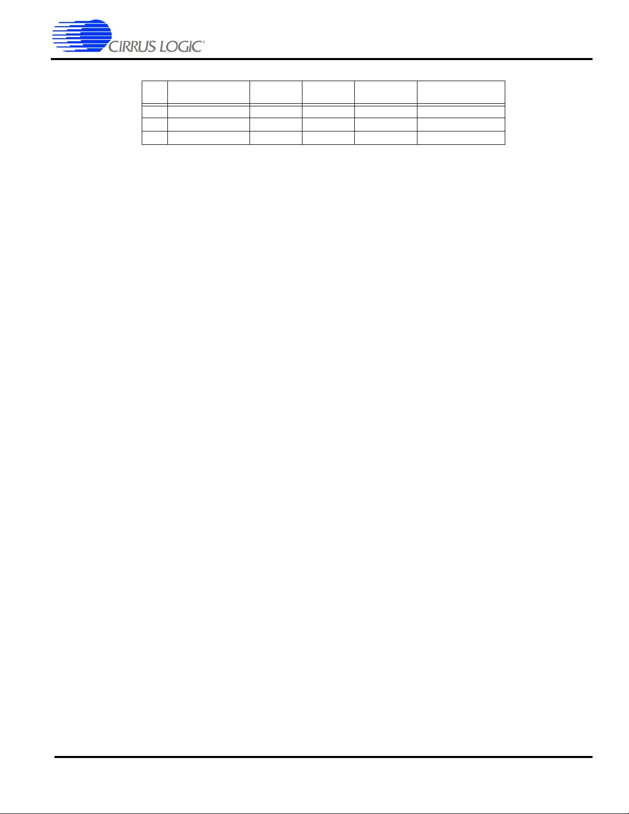
High-Performance, Low-Power System on Chip
Table 20. 208-Pin LQFP Numeric Pin Listing (Continued)
EP7312
Pin
No.
206 nCS[2] 1 High O Chip select 2
207 nCS[3] 1 High O Chip select 3
208 nCS[4] 1 High O Chip select 4
*
“With p/u” means with internal pull-up of 100 KOhms on the pin.
†
Strength 1 = 4 ma
Signal
Strength
†
Reset
State
Strength 2 = 12 ma
‡
Input. Port A,B,D,E GPIOs default to input at nPOR and URESET conditions.
Type Description
DS508F2 Copyright Cirrus Logic, Inc. 2011
(All Rights Reserved) 37
Page 38
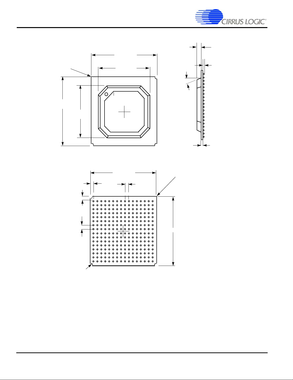
EP7312
TOP VIEW
17.00 (0.669)
15.00
(0.590)
SIDE VIEW
BOTTOM VIEW
A
B
C
D
E
F
G
H
J
K
L
M
N
P
R
T
1.00 (0.040)
Pin 1 Indicator
Pin 1 Corner
Pin 1 Corner
16 15 14 13 12 11 10 9 8 7 6 5 4 3 2 1
15.00
(0.590)
2 Layer
17.00 (0.669)
17.00 (0.669)
1.00 (0.040)
1.00 (0.040)
1.00 (0.040)
30° TYP
REF
REF
0.50
3 Places
0.85 (0.034)
±0.05 (.002)
0.40 (0.016)
±0.05 (.002)
0.36 (0.014)
17.00 (0.669)
R
D1
E1
D
E
±0.20 (.008)
±0.20 (.008)
±0.20 (.008)
±0.20 (.008)
±0.09 (0.004)
JEDEC #: MO-151
Ball Diameter: 0.50 mm ± 0.10 mm
17 ¥ 17 ¥ 1.61 mm body
High-Performance, Low-Power System on Chip
256-Ball PBGA Package Characteristics
Figure 17. 256-Ball PBGA Package
Note: 1) For pin locations see Table 21.
2) Dimensions are in millimeters (inches), and controlling dimension is millimeter
3) Before beginning any new EP7312 design, contact Cirrus Logic for the latest package information.
38 Copyright Cirrus Logic, Inc. 2011
(All Rights Reserved) DS508F2
Page 39

EP7312
High-Performance, Low-Power System on Chip
256-Ball PBGA Pinout (Top View)
1 234 5678910111213141516
A VDDIO nCS[4] nCS[1] SDCLK SDQM[3] DD[1] M VDDIO D[0] D[2] A[3] VDDIO A[6] MOSCOUT VDDOSC VSSIO A
B nCS[5] VDDIO nCS[3]
C VDDIO EXPCLK VSSIO VDDIO VSSIO VSSIO VSSIO VDDIO VSSIO VSSIO VSSIO VDDIO VSSIO VSSIO nPOR nEXTPWR C
WRITE/
D
nSDRAS
E RXD[2] PB[7] TDI WORD VSSIO nCS[0] SDQM[2] FRM A[0] D[5] VSSOSC VSSIO
F P B[5] PB[3] VSSIO TXD[2]
G PB[1] VDDIO TDO PB[4] PB[6] VSSCore VSSRTC DD[0] D[3] VSSRTC A[7] A[8] A[9] VSSIO D[12] D[13] G
H PA[7] PA[5] VSSIO PA[4] PA[6] PB[0] PB[2] VSSRTC VSSRTC A[10] A[11] A[12]
J PA[3] PA[1] VSSIO PA[2] PA[0] TXD[1] CTS VSSRTC VSSRTC
K LEDDRV PHDIN VSSIO DCD nTEST[1] EINT[3] VSSRTC ADCIN COL[4] TCLK D[20] D[19] D[18] VSSIO VDDIO VDDIO K
L RXD[1] DSR VDDIO nEINT[1]
M nTEST[0] nEINT[2] VDDIO
N nEXTFIQ
EXPRDY VSSIO VDDIO nCS[2]
PE[1]/
BOOTSEL[1]
VSSIO VDDIO PD[5] PD[2] SSIRXDA ADCCLK SMPCLK COL[2] D[29] D[26] HALFWORD VSSIO D[22] D[23] N
nMOE/
nSDCAS
PE[0]/
BOOTSEL[0]
VDDIO nSDCS[1] DD[2] CL[1] VDDCORE D[1] A[2] A[4] A[5] WAKEUP VDDIO nURESET B
nMWE/
nSDCS[0] CL[2] VSSRTC D[4] nPWRFL MOSCIN VDDIO VSSIO D[7] D[8] D
nSDWE
RUN/
CLKEN
PE[2]/
CLKSEL
VSSIO SDCKE DD[3] A[1] D[6] VSSRTC BATOK nBATCHG VSSIO D[11] VDDIO F
A[17]/
DRA[10]
VSSRTC
TMS VDDIO SSITXFR DRIVE[1] FB[0] COL[0] D[27] VSSIO
PD[0]/
LEDFLSH
VSSRTC COL[6] D[31] VSSRTC
A[16]/
DRA[11]
DRA[12]
DRA[5]
A[15]/
A[22]/
nMEDCHG/
nBROM
A[13]/
DRA[14]
A[14]/
DRA[13]
A[21]/
DRA[6]
A[23]/
DRA[4]
VDDIO D[9] D[10] E
VSSIO D[14] D[15] H
nTRST D[16] D[17] J
A[18]/
A[20]/
A[19]/
DRA[8]
D[21] M
VSSIO
VDDIO
DRA[9]
DRA[7]
L
P VSSRTC RTCOUT VSSIO VSSIO VDDIO VSSIO VSSIO VDDIO VSSIO VDDIO VSSIO VSSIO VDDIO VSSIO D[24] VDDIO P
R RTCIN VDDIO PD[4] PD[1] SSITXDA nADCCS VDDIO ADCOUT COL[7] COL[3] COL[1] D[30]
T VDDRTC
PD[7]/
SDQM[1]
PD[6]/
SDQM[0]
PD[3] SSICLK SSIRXFR VDDCORE DRIVE[0] FB[1] COL[5] VDDIO BUZ D[28]
A[27]/
DRA[0]
A[25]/
DRA[2]
A[26]/
DRA[1]
VDDIO
A[24]\
DRA[3]
D[25] VSSIO T
R
DS508F2 Copyright Cirrus Logic, Inc. 2011
(All Rights Reserved) 39
Page 40
EP7312
High-Performance, Low-Power System on Chip
256-Ball PBGA Ball Listing
The list is ordered by ball location.
Table 21. 256-Ball PBGA Ball Listing
Reset
Ball Location Name
A1 VDDIO Pad power Digital I/O power, 3.3 V
A2 nCS[4] 1 High O Chip select 4
A3 nCS[1] 1 High O Chip select 1
A4 SDCLK 2 Low O SDRAM clock out
A5 SDQM[3] 2 Low O SDRAM byte lane mask
A6 DD[1] 1 Low O LCD serial display data
A7 M 1 Low O LCD A C bias drive
A8 VDDIO Pad power Digital I/O power, 3.3 V
A9 D[0] 1 Low I/O Data I/O
A10 D[2] 1 Low I/O Data I/O
A11 A[3] 2 Low O System byte address
A12 VDDIO Pad power Digital I/O power, 3.3V
A13 A[6] 1 Low O System byte address
A14 MOSCOUT O Main oscillator out
A15 VDDOSC Oscillator power Oscillator power in, 2.5 V
A16 VSSIO Pad ground I/O ground
B1 nCS[5] 1 Low O Chip select 5
B2 VDDIO Pad power Digital I/O power, 3.3 V
B3 nCS[3] 1 High O Chip select 3
B4 nMOE/nSDCAS 1 High O ROM, expansion OP enable/SDRAM CAS control signal
B5 VDDIO Pad power Digital I/O power, 3.3 V
B6 nSDCS[1] 1 High O SDRAM chip select 1
B7 DD[2] 1 Low O LCD serial display data
B8 CL[1] 1 Low O LCD line clock
B9 VDDCORE Core power Digital core power, 2.5V
B10 D[1] 1 Low I/O Data I/O
B11 A[2] 2 Low O System byte address
B12 A[4] 1 Low O System byte address
B13 A[5] 1 Low O System byte address
B14 WAKEUP Schmitt I System wake up input
B15 VDDIO Pad power Digital I/O power, 3.3 V
B16 nURESET Schmitt I User reset input
C1 VDDIO Pad power Digital I/O power, 3.3V
C2 EXPCLK 1 I Expansion clock input
C3 VSSIO Pad ground I/O ground
C4 VDDIO Pad power Digital I/O power, 3.3 V
C5 VSSIO Pad ground I/O ground
C6 VSSIO Pad ground I/O ground
C7 VSSIO Pad ground I/O ground
C8 VDDIO Pad power Digital I/O power, 3.3 V
C9 VSSIO Pad ground I/O ground
C10 VSSIO Pad ground I/O ground
C11 VSSIO Pad ground I/O ground
C12 VDDIO Pad power Digital I/O power, 3.3 V
C13 VSSIO Pad ground I/O ground
Strength
†
State
Type Description
40 Copyright Cirrus Logic, Inc. 2011
(All Rights Reserved) DS508F2
Page 41

High-Performance, Low-Power System on Chip
Table 21. 256-Ball PBGA Ball Listing (Continued)
Reset
Ball Location Name
C14 VSSIO Pad ground I/O ground
C15 nPOR Schmitt I Power-on reset input
C16 nEXTPWR I External power supply sense input
D1 WRITE/nSDRAS 1 Low O Transfer direction / SDRAM RAS signal output
D2 EXPRDY 1 I Expansion port ready input
D3 VSSIO Pad ground I/O ground
D4 VDDIO Pad power Digital I/O power, 3.3V
D5 nCS[2] 1 High O Chip select 2
D6 nMWE/nSDWE 1 High O ROM, expansion write enable/ SDRAM write enable control signal
D7 nSDCS[0] 1 High O SDRAM chip select 2
D8 CL[2] 1 Low O LCD pixel clock out
D9 VSSRTC Core ground Real time clock ground
D10 D[4] 1 Low I/O Data I/O
D11 nPWRFL I Power fail sense input
D12 MOSCIN I Main oscillator input
D13 VDDIO Pad power Digital I/O power, 3.3V
D14 VSSIO Pad ground I/O ground
D15 D[7] 1 Low I/O Data I/O
D16 D[8] 1 Low I/O Data I/O
E1 RXD[2] I UART 2 receive data input
E2 PB[7] 1
E3 TDI with p/u* I J TAG data input
E4 WORD 1 Low O Word access select output
E5 VSSIO Pad ground I/O ground
E6 nCS[0] 1 High O Chip select 0
E7 SDQM[2] 2 Low O SDRAM byte lane mask
E8 FRM 1 Low O LCD frame synchronization pulse
E9 A[0] 2 Low O System byte address
E10 D[5] 1 Low I/O Data I/O
E11 VSSOSC Oscillator ground PL L ground
E12 VSSIO Pad ground I/O ground
E13 nMEDCHG/nBROM I Media change interrupt input / internal ROM boot enable
E14 VDDIO Pad power Digital I/O power, 3.3V
E15 D[9] 1 Low I/O Data I/O
E16 D[10] 1 Low I/O Data I/O
F1 PB[5] 1
F2 PB[3] 1
F3 VSSIO Pad ground I/O ground
F4 TXD[2] 1 High O UART 2 transmit data output
F5 RUN/CLKEN 1 Low O Run output / clock enable output
F6 VSSIO Pad ground I/O ground
F7 SDCKE 2 Low O SDRAM clock enable output
F8 DD[3] 1 Low O LCD serial display data
F9 A[1] 2 Low O System byte address
F10 D[6] 1 Low I/O Data I/O
F11 VSSRTC RTC ground Real time clock ground
F12 BATOK I Battery OK input
Strength
†
State
‡
Input
‡
Input
‡
Input
Type Description
IGPIO port B
IGPIO port B
IGPIO port B
EP7312
DS508F2 Copyright Cirrus Logic, Inc. 2011
(All Rights Reserved) 41
Page 42

EP7312
High-Performance, Low-Power System on Chip
Table 21. 256-Ball PBGA Ball Listing (Continued)
Reset
Ball Location Name
F13 nBATCHG I Battery changed sense input
F14 VSSIO Pad ground I/O ground
F15 D[11] 1 Low I/O Data I/O
F16 VDDIO Pad power Digital I/O power, 3.3V
G1 PB[1] 1
G2 VDDIO Pad power Digital I/O power, 3.3V
G3 TDO 1
G4 PB[4] 1
G5 PB[6] 1
G6 VSSCore Core ground Core ground
G7 VSSRTC RTC ground Real time clock ground
G8 DD[0] 1 Low O LCD serial display data
G9 D[3] 1 Low I/O Data I/O
G10 VSSRTC RTC ground Real time clock ground
G11 A[7] 1 Low O System byte address
G12 A[8] 1 Low O System byte address
G13 A[9] 1 Low O System byte address
G14 VSSIO Pad ground I/O ground
G15 D[12] 1 Low I/O Data I/O
G16 D[13] 1 Low I/O Data I/O
H1 PA[7] 1
H2 PA[5] 1
H3 VSSIO Pad ground I/O ground
H4 PA[4] 1
H5 PA[6] 1
H6 PB[0] 1
H7 PB[2] 1
H8 VSSRTC RTC ground Real time clock ground
H9 VSSRTC RTC ground Real time clock ground
H10 A[10] 1 Low O System byte address
H11 A[11] 1 Low O System byte address
H12 A[12] 1 Low O System byte address
H13 A[13]/DRA[14] 1 Low O System byte address / SDRAM address
H14 VSSIO Pad ground I/O ground
H15 D[14] 1 Low I/O Data I/O
H16 D[15] 1 Low I/O Data I/O
J1 PA[3] 1
J2 PA[1] 1
J3 VSSIO Pad ground I/O ground
J4 PA[2] 1
J5 PA[0] 1
J6 TXD[1] 1 High O UART 1 transmit data out
Strength
†
State
‡
Input
‡
Input
‡
Input
‡
Input
‡
Input
‡
Input
‡
Input
‡
Input
‡
Input
‡
Input
‡
Input
‡
Input
‡
Input
‡
Input
Type Description
IGPIO port B
O JTAG data out
IGPIO port B
IGPIO port B
I/O GPIO port A
I/O GPIO port A
I/O GPIO port A
I/O GPIO port A
I/O GPIO port B
I/O GPIO port B
I/O GPIO port A
I/O GPIO port A
I/O GPIO port A
I/O GPIO port A
42 Copyright Cirrus Logic, Inc. 2011
(All Rights Reserved) DS508F2
Page 43

High-Performance, Low-Power System on Chip
Table 21. 256-Ball PBGA Ball Listing (Continued)
Reset
Ball Location Name
J7 CTS I UART 1 clear to send input
J8 VSSRTC RTC ground Real time clock ground
J9 VSSRTC RTC ground Real time clock ground
J10 A[17]/DRA[10] 1 Low O System byte address / SDRAM address
J11 A[16]/DRA[11] 1 Low O System byte address / SDRAM address
J12 A[15]/DRA[12] 1 Low O System byte address / SDRAM address
J13 A[14]/DRA[13] 1 Low O System byte address / SDRAM address
J14 nTRST I JTAG async reset input
J15 D[16] 1 Low I/O Data I/O
J16 D[17] 1 Low I/O Data I/O
K1 LEDDRV 1 Low O IR LED drive
K2 PHDIN I Photodiode input
K3 VSSIO Pad ground I/O ground
K4 DCD I UART 1 data carrier detect
K5 nTEST[1] With p/u* I Test mode select input
K6 EINT[3] I External interrupt
K7 VSSRTC RTC ground Real time clock ground
K8 ADCIN I SSI1 ADC serial input
K9 COL[4] 1 High O Keyboard scanner column drive
K10 TCLK I JTAG clock
K11 D[20] 1 Low I/O Data I/O
K12 D[19] 1 Low I/O Data I/O
K13 D[18] 1 Low I/O Data I/O
K14 VSSIO Pad ground I/O ground
K15 VDDIO Pad power Digital I/O power, 3.3V
K16 VDDIO Pad power Digital I/O power, 3.3V
L1 RXD[1] I UART 1 receive data input
L2 DSR I UART 1 data set ready input
L3 VDDIO Pad power Digital I/O power, 3.3V
L4 nEINT[1] I External interrupt input
L5 PE[2]/CLKSEL 1
L6 VSSRTC RTC ground Real time clock ground
L7 PD[0]/LEDFLSH 1 Low I/O GPIO port D / LED blinker output
L8 VSSRTC Core gr ound Real time clock ground
L9 COL[6] 1 High O Keyboard scanner column drive
L10 D[31] 1 Low I/O Data I/O
L11 VSSRTC RTC ground Real time clock ground
L12 A[22]/DRA[5] 1 Low O System byte address / SDRAM address
L13 A[21]/DRA[6] 1 Low O System byte address / SDRAM address
L14 VSSIO Pad ground I/O ground
L15 A[18]/DRA[9] 1 Low O System byte address / SDRAM address
L16 A[19]/DRA[8] 1 Low O System byte address / SDRAM address
M1 nTEST[0] With p/u* I Test mode select input
M2 nEINT[2] I External interrupt input
M3 VDDIO Pad power Digital I/O power, 3.3V
M4 PE[0]/BOOTSEL[0] 1
M5 TMS with p/u* I JTAG mode select
Strength
†
State
‡
Input
‡
Input
Type Description
I/O GPIO port E / clock input mode select
I GPIO port E / Boot mode select
EP7312
DS508F2 Copyright Cirrus Logic, Inc. 2011
(All Rights Reserved) 43
Page 44

EP7312
High-Performance, Low-Power System on Chip
Table 21. 256-Ball PBGA Ball Listing (Continued)
Reset
Ball Location Name
M6 VDDIO Pad power Digital I/O power, 3.3V
M7 SSITXFR 1 Low I/O DAI/CODEC/SSI2 frame sync
M8 DRIVE[1] 2
M9 FB[0] I PWM feedback input
M10 COL[0] 1 High O Keyboard scanner column drive
M11 D[27] 1 Low I/O Data I/O
M12 VSSIO Pad ground I/O ground
M13 A[23]/DRA[4] 1 Low O System byte address / SDRAM address
M14 VDDIO Pad power Digital I/O power, 3.3V
M15 A[20]/DRA[7] 1 Low O System byte address / SDRAM address
M16 D[21] 1 Low I/O Data I/O
N1 nEXTFIQ I External fast interrupt input
N2 PE[1]/BOOTSEL[1] 1
N3 VSSIO Pad ground I/O ground
N4 VDDIO Pad power Digital I/O power, 3.3V
N5 PD[5] 1 Low I/O GPIO port D
N6 PD[2] 1 Low I/O GPIO port D
N7 SSIRXDA I/O DAI/CODEC/SSI2 serial data input
N8 ADCCLK 1 Low O SSI1 ADC serial clock
N9 SMPCLK 1 Low O SSI1 ADC sample clock
N10 COL[2] 1 High O Keyboard scanner column drive
N11 D[29] 1 Low I/O Data I/O
N12 D[26] 1 Low I/O Data I/O
N13 HALFWORD 1 Low O Halfword access select output
N14 VSSIO Pad ground I/O ground
N15 D[22] 1 Low I/O Data I/O
N16 D[23] 1 Low I/O Data I/O
P1 VSSRTC RTC ground Real time clock ground
P2 RTCOUT O Real time clock oscillator output
P3 VSSIO Pad ground I/O ground
P4 VSSIO Pad ground I/O ground
P5 VDDIO Pad power Digital I/O power, 3.3V
P6 VSSIO Pad ground I/O ground
P7 VSSIO Pad ground I/O ground
P8 VDDIO Pad power Digital I/O power, 3.3V
P9 VSSIO Pad ground I/O ground
P10 VDDIO Pad power Digital I/O power, 3.3V
P11 VSSIO Pad ground I/O ground
P12 VSSIO Pad ground I/O ground
P13 VDDIO Pad power Digital I/O power
P14 VSSIO Pad ground I/O ground
P15 D[24] 1 Low I/O Data I/O
P16 VDDIO Pad power Digital I/O power, 3.3V
R1 RTCIN I/O Real time clock oscillator input
R2 VDDIO Pad power Digital I/O power, 3.3V
R3 PD[4] 1 Low I/O GPIO port D
R4 PD[1] 1 Low I/O GPIO port D
Strength
†
State
High /
Low
‡
Input
Type Description
I/O PWM drive output
I/O GPIO port E / boot mode select
44 Copyright Cirrus Logic, Inc. 2011
(All Rights Reserved) DS508F2
Page 45

High-Performance, Low-Power System on Chip
Table 21. 256-Ball PBGA Ball Listing (Continued)
Reset
Ball Location Name
R5 SSITXDA 1 Low O DAI/CODEC/SSI2 serial data ou tpu t
R6 nADCCS 1 High O SSI1 ADC chip select
R7 VDDIO Pad power Digital I/O power, 3.3V
R8 ADCOUT 1 Low O SSI1 ADC serial data output
R9 COL[7] 1 High O Keyboard scanner column drive
R10 COL[3] 1 High O Keyboard scanner column drive
R11 COL[1] 1 High O Keyboard scanner column drive
R12 D[30] 1 Low I/O Data I/O
R13 A[27]/DRA[0] 2 Low O System byte address / SDRAM address
R14 A[25]/DRA[2] 2 Low O System byte address / SDRAM address
R15 VDDIO Pad power Digital I/O power, 3.3V
R16 A[24]/DRA[3] 1 Low O System byte address / SDRAM address
T1 VDDRTC RTC power Real time clock power, 2.5V
T2 PD[7]/SDQM[1] 1 Low I/O GPIO port D / SDRAM byte lane mask
T3 PD[6]/SDQM[0] 1 Low I/O GPIO port D / SDRAM byte lane mask
T4 PD[3] 1 Low I/O GPIO port D
T5 SSICLK 1
T6 SSIRXFR 1
T7 VDDCORE Core power Core power, 2.5V
T8 DRIVE[0] 2
T9 FB[1] I PWM feedback input
T10 COL[5] 1 High O Keyboard scanner column drive
T11 VDDIO Pad power Digital I/O power, 3.3V
T12 BUZ 1 Low O Buzzer drive output
T13 D[28] 1 Low I/O Data I/O
T14 A[26]/DRA[1] 2 Low O System byte address / SDRAM address
T15 D[25] 1 Low I/O Data I/O
T16 VSSIO Pad ground I/O ground
Strength
†
State
‡
Input
‡
Input
High /
Low
Type Description
I/O DAI/CODEC/SSI2 serial clock
I/O DAI/CODEC/SSI2 frame sync
I/O PWM drive output
EP7312
*
“With p/u” means with internal pull-up of 100 KOhms on the pin.
†
Strength 1 = 4 ma
Strength 2 = 12 ma
‡
Input. Port A,B,D,E GPIOs default to input at nPOR and URESET conditions.
JTAG Boundary Scan Signal Ordering
Table 22. JTAG Boundary Scan Signal Ordering
LQFP
Pin No.
1B1 nCS[5] O 1
4 C2 EXPCLK I/O 3
5E4 WORD O 6
6 D1 WRITE/nSDRAS O 8
7 F5 RUN/CLKEN O 10
8 D2 EXPRDY I 13
DS508F2 Copyright Cirrus Logic, Inc. 2011
PBGA
Ball
Signal Type Position
(All Rights Reserved) 45
Page 46

EP7312
High-Performance, Low-Power System on Chip
Table 22. JTAG Boundary Scan Signal Ordering (Continued)
LQFP
Pin No.
9F4 TXD2 O 14
10 E1 RXD2 I 16
13 E2 PB[7] I/O 17
14 G5 PB[6] I/O 20
15 F1 PB[5] I/O 23
16 G4 PB[4] I/O 26
17 F2 PB[3] I/O 29
18 H7 PB[2] I/O 32
19 G1 PB[1] I/O 35
20 H6 PB[0] I/O 38
23 H1 PA[7] I/O 41
24 H5 PA[6] I/O 44
25 H2 PA[5] I/O 47
26 H4 PA[4] I/O 50
27 J1 PA[3] I/O 53
28 J4 PA[2] I/O 56
29 J2 PA[1] I/O 59
30 J5 PA[0] I/O 62
31 K1 LEDDRV O 65
32 J6 TXD1 O 67
34 K2 PHDIN I 69
35 J7 CTS I 70
36 L1 RXD1 I 71
37 K4 DCD I 72
38 L2 DSR I 73
39 K5 nTEST1 I 74
40 M1 nTEST0 I 75
41 K6 EINT3 I 76
42 M2 nEINT2 I 77
43 L4 nEINT1 I 78
44 N1 nEXTFIQ I 79
45 L5 PE[2]/CLKSEL I/O 80
46 N2
47 M4 PE[0]/BOOTSEL0 I/O 86
53 T2 PD[7]/SDQM[1] I/O 89
54 T3 PD[6/SDQM[0]] I/O 92
55 N5 PD[5] I/O 95
56 R3 PD[4] I/O 98
59 T4 PD[3] I/O 101
60 N6 PD[2] I/O 104
PBGA
Ball
Signal Type Position
PE[1]/
BOOTSEL[1]
I/O 83
46 Copyright Cirrus Logic, Inc. 2011
(All Rights Reserved) DS508F2
Page 47

High-Performance, Low-Power System on Chip
Table 22. JTAG Boundary Scan Signal Ordering (Continued)
EP7312
LQFP
Pin No.
61 R4 PD[1] I/O 107
62 L7 PD[0]/LEDFLSH O 110
68 T6 SSIRXFR I/O 122
69 K8 ADCIN I 125
70 R6 nADCCS O 126
75 M8 DRIVE1 I/O 128
76 T8 DRIVE0 I/O 131
77 N8 ADCCLK O 134
78 R8 ADCOUT O 136
79 N9 SMPCLK O 138
80 T9 FB1 I 140
82 M9 FB0 I 141
83 R9 COL7 O 142
84 L9 COL6 O 144
85 T10 COL5 O 146
86 K9 COL4 O 148
87 R10 COL3 O 150
88 N10 COL2 O 152
91 R11 COL1 O 154
92 M10 COL0 O 156
93 T12 BUZ O 158
94 L10 D[31] I/O 160
95 R12 D[30] I/O 163
96 N11 D[29] I/O 166
97 T13 D[28] I/O 169
99 R13 A[27]/DRA[0] Out 172
100 M11 D[27] I/O 174
101 T14 A[26]/DRA[1] O 177
102 N12 D[26] I/O 179
103 R14 A[25]/DRA[2] O 182
104 T15 D[25] I/O 184
105 N13 HALFWORD O 187
106 R16 A[24]/DRA[3] O 189
109 P15 D[24] I/O 191
110 M13 A[23]/DRA[4] O 194
111 N16 D[23] I/O 196
112 L12 A[22]/DRA[5] O 199
113 N15 D[22] I/O 201
114 L13 A[21]/DRA[6] O 204
115 M16 D[21] I/O 206
117 M15 A[20]/DRA[7] O 209
PBGA
Ball
Signal Type Position
DS508F2 Copyright Cirrus Logic, Inc. 2011
(All Rights Reserved) 47
Page 48

EP7312
High-Performance, Low-Power System on Chip
Table 22. JTAG Boundary Scan Signal Ordering (Continued)
LQFP
Pin No.
118 K11 D[20] I/O 211
119 L16 A[19]/DRA[8] O 214
120 K12 D[19] I/O 216
121 L15 A[18]/DRA[9] O 219
122 K13 D[18] I/O 221
126 J10 A[17]/DRA[10] O 224
127 J16 D[17] I/O 226
128 J11 A[16]/DRA[11] O 229
129 J15 D[16] I/O 231
130 J12 A[15]/DRA[12] O 234
131 H16 D[15] I/O 236
132 J13 A[14]/DRA[13] O 239
133 H15 D[14] I/O 241
134 H13 A[13]/DRA[14] O 244
135 G16 D[13] I/O 246
136 H12 A[12] O 249
137 G15 D[12] I/O 251
138 H11 A[11] O 254
141 F15 D[11] I/O 256
142 H10 A[10] O 259
143 E16 D[10] I/O 261
144 G13 A[9] O 264
145 E15 D[9] I/O 266
146 G12 A[8] O 269
147 D16 D[8] I/O 271
148 G11 A[7] O 274
150 D15 D[7] I/O 276
151 F13 nBATCHG I 279
152 C16 nEXTPWR I 280
153 F12 BATOK I 281
154 C15 nPOR I 282
155 E13 nMEDCHG/nBROM I 283
156 B16 nURESET I 284
161 B14 WAKEUP I 285
162 D11 nPWRFL I 286
163 A13 A[6] O 287
164 F10 D[6] I/O 289
165 B13 A[5] O 292
166 E10 D[5] I/O 294
169 B12 A[4] O 297
170 D10 D[4] I/O 299
PBGA
Ball
Signal Type Position
48 Copyright Cirrus Logic, Inc. 2011
(All Rights Reserved) DS508F2
Page 49
High-Performance, Low-Power System on Chip
Table 22. JTAG Boundary Scan Signal Ordering (Continued)
EP7312
LQFP
Pin No.
171 A11 A[3] O 302
172 G9 D[3] I/O 304
173 B11 A[2] O 307
175 A10 D[2] I/O 309
176 F9 A[1] O 312
177 B10 D[1] I/O 314
178 E9 A[0] O 317
179 A9 D[0] I/O 319
184 D8 CL2 O 322
185 B8 CL1 O 324
186 E8 FRM O 326
187 A7 M O 328
188 F8 DD[3] O 330
189 B7 DD[2] O 333
191 A6 DD[1] O 336
192 G8 DD[0] O 339
193 B6 nSDCS[1] O 342
194 D7 nSDCS[0] O 344
195 A5 SDQM[3] I/O 346
196 E7 SDQM[2] I/O 349
199 F7 SDCKE I/O 352
200 A4 SDCLK I/O 355
201 D6 nMWE/nSDWE O 358
202 B4 nMOE/nSDCAS O 360
204 E6 nCS[0] O 362
205 A3 nCS[1] O 364
206 D5 nCS[2] O 366
207 B3 nCS[3] O 368
208 A2 nCS[4] O 370
PBGA
Ball
Signal Type Position
1) See EP7312 Users’ Manual for pin naming / functionality.
2) For each pad, the JTAG connection ordering is input, output, then enable as applicable.
DS508F2 Copyright Cirrus Logic, Inc. 2011
(All Rights Reserved) 49
Page 50
EP7312
High-Performance, Low-Power System on Chip
CONVENTIONS
This section presents acronyms, abbreviations, units of
measurement, and conventions used in this data sheet.
Acronyms and Abbreviations
Table 23 lists abbreviations and acronyms used in this data
sheet.
Table 23. Acronyms and Abbreviations
Acronym/
Abbreviation
A/D analog-to-digital
ADC analog-to-digital converter
CODEC coder / decoder
D/A digital-to-analog
DMA direct-memory access
EPB embedded peripheral bus
FCS frame check sequence
FIFO first in / first out
FIQ fast interrupt request
GPIO general purpose I/O
ICT in circuit test
IR infrared
IRQ standard interrupt request
IrDA Infrared Data Association
JTAG Joint Test Action Group
LCD liquid crystal display
LED light-emitting diode
LQFP low profile quad flat pack
LSB least significant bit
MIPS millions of instructions per second
MMU memory management unit
MSB most significant bit
PBGA plastic ball grid array
PCB printed circuit board
PDA personal digital assistant
PLL phase locked loop
p/u pull-up resistor
RISC reduced instruction set computer
RTC Real-Time Clock
SIR slow (9600–115.2 kbps) infrared
SRAM static random access memory
SSI synchronous serial interface
Definition
Table 23. Acronyms and Abbreviations (Continued)
Acronym/
Abbreviation
TAP test access port
TLB translation lookaside buffer
UART universal asynchronous receiver
Definition
Units of Measurement
Table 24. Unit of Measurement
Symbol Unit of Measure
C
fs sample frequency
Hz hertz (cycle per second)
kbps kilobits per second
KB kilobyte (1,024 bytes)
kHz kilohertz
k
kilo Ohm
Mbps megabits (1,048,576 bits) per second
MB megabyte (1,048,576 bytes)
MBps megabytes per second
MHz megahertz (1,000 kilohertz)
A microampere
Fmicrofarad
Wmicrowatt
s microsecond (1,000 nanoseconds)
mA milliampere
mW milliwatt
ms millisecond (1,000 microseconds)
ns nanosecond
Vvolt
Wwatt
degree Celsius
50 Copyright Cirrus Logic, Inc. 2011
(All Rights Reserved) DS508F2
Page 51
General Conventions
Hexadecimal numbers are presented with all letters in
uppercase and a lowercase “h” appended or with a 0x at the
beginning. For example, 0x14 and 03CAh are hexadecimal
numbers. Binary numbers are enclosed in single quotation
marks when in text (for example, ‘11’ designates a binary
number). Numbers not indicated by an “h”, 0x or quotation
marks are decimal.
Registers are referred to by acronym, with bits listed in
brackets separated by a colon (:) (for example, CODR[7:0]),
and are described in the EP7312 User’s Manual. The use of
“TBD” indicates values that are “to be determined,” “n/a”
designates “not available,” and “n/c” indicates a pin that is a
“no connect.”
Pin Description Conventions
Abbreviations used for signal directions are listed in Table 25.
Table 25. Pin Description Conventions
Abbreviation Direction
EP7312
High-Performance, Low-Power System on Chip
I Input
O Output
I/O Input or Output
DS508F2 Copyright Cirrus Logic, Inc. 2011
(All Rights Reserved) 51
Page 52
EP7312
High-Performance, Low-Power System on Chip
Ordering Information
Model T emperature Package
EP7312-CBZ 0 to +70 °C
EP7312-IBZ -40 to +85 °C.
EP7312-CVZ
0 to +70 °C
EP7312-CV-90Z (90 MHz)
E
P7312-IVZ -40 to +85 °C.
Environmental, Manufacturing, & Handling Information
Model Number Peak Reflow Temp MSL Rating* Max Floor Life
EP7312-CBZ
EP7312-CVZ
EP7312-CV-90Z (90 MHz)
EP7312-IBZ
EP7312-IVZ
260 °C 3 7 Days
256-pin PBGA, 17mm X 17mm
208-pin LQFP.
* MSL (Moisture Sensitivity Level) as specified by IPC/JEDEC J-STD-020.
All devices are now lead (Pb) free.
52 Copyright Cirrus Logic, Inc. 2011
(All Rights Reserved) DS508F2
Page 53
High-Performance, Low-Power System on Chip
Revision History
Revision Date Changes
PP5 JAN 2004 Preliminary release. Updated SDRAM timing.
F1 AUG 2005 Updated ordering information. Added MSL data.
F2 MAR 2011 Removed all lead-containing device ordering information. Removed 204-pin
TFBGA package option.
EP7312
DS508F2 Copyright Cirrus Logic, Inc. 2011
(All Rights Reserved) 53
Page 54

EP7312
Contacting Cirrus Logic Support
For all product questions and inquiries contact a Cirrus Logic Sales Representative.
To find the one nearest to you go to www.cirrus.com
IMPORTANT NOTICE
Cirrus Logic, Inc. and it s su bsi d iari e s (“Ci r ru s”) be li eve t hat the inf or mati o n con tai n ed in th i s docu ment i s acc urate and reliable. However, t he in f o rmat io n i s su bj e ct
to change without noti ce and is provi ded “AS I S” with out warran ty of any kind ( express or implied ). Cust omers are a dvised to obtain the latest version of relevant
information to verify, before placing orders, tha t inform atio n bei ng relied on is curr ent and com plete. Al l prod ucts are sold s ubject to the ter ms and co nditio ns of sale
supplied at the time of order acknowledgment, including those pertaining to warranty, indemnification, and limitation of liability. No responsibility is assumed by Cirrus
for the use of this information, including use of this information as the basis for manufacture or sale of any items, or for infringement of pate nts or other righ ts of thir d
parties. This document is the property of Ci rrus and by furnishing this information, Cirrus gr an ts no li cense, express or implied under any patents, mask work rights,
copyrights, trademarks, trade secrets or other intellectual property rights. Cirrus owns the copyrights associated with the information contained herein and gives consent for copies to be made of the information only for use within your organization with respect to Cirrus integrated circuits or other products of Cirrus. This consent
does not extend to other copying such as copying for ge neral distribution, advertising or promotional purpose s, or for crea ting any work for resale.
CERTAIN APPLICATIONS USING SEMICONDUCTOR PRODUCTS MAY INVOLVE POTENTIAL RISKS OF DEATH, PERSONAL INJURY, OR SEVERE PROPERTY OR ENVIRONMENTAL DAMAGE (“CRITICAL APPLICATIONS”). CIRRUS PRODUCTS ARE NOT DESIGNED, AUTHORIZED OR WARRANTED FOR USE
IN PRODUCTS SURGICALLY IMPLANTED INTO THE BODY, AUTOMOTIVE SAFETY OR SECURITY DEVICES, LIFE SUPPORT PRODUCTS OR OTHER CRITICAL APPLICATIONS. INCLUSION OF CIRRUS PRODUCTS IN SUCH APPLICATIONS IS UNDERSTOOD TO BE FULLY AT THE CUSTOMER'S RISK AND CIRRUS DISCLAIMS AND MAKES NO WARRANTY, EXPRESS, STATUTORY OR IMPLIED, INCLUDING THE IMPLIED WARRANTIES OF MERCHANTABILITY AND
FITNESS FOR PARTICULAR PURPOSE, WITH REGARD TO ANY CIRRUS PRODUCT THAT IS USED IN SUCH A MANNER. IF THE CUSTOMER OR CUSTOMER'S CUSTOMER USES OR PERMITS THE USE OF CIRRUS PRODUCTS IN CRITICAL APPLICATIONS, CUSTOMER AGREES, BY SUCH USE, TO FULLY
INDEMNIFY CIRRUS, ITS OFFICERS, DI RECTORS, EMPL OYEES, DI STRIBUTO RS AND OTHER AGENTS FROM ANY AND ALL LIABILITY, INCLUDING ATTORNEYS' FEES AND COSTS, THAT MAY RESU LT FROM OR ARISE IN CONNECTION WITH THESE USES.
Cirrus Logic, Cirrus, and the Cirrus Logic logo designs are trademarks of Cirrus Logic, Inc. All other brand and product names in this document may be trademarks
or service marks of their respective owners.
SPI is a trademark of Motorola, Inc.
Microwire is a trademark of National Semiconductor Corporation.
LINUX is a registered trademark of Linus Torvalds.
Microsoft Windows and Microsoft are registered trademarks of Microsoft Corporation.
High-Performance, Low-Power System on Chip
54 Copyright Cirrus Logic, Inc. 2011
(All Rights Reserved) DS508F2
 Loading...