

CS98100
DVD Processor for Low Cost DVD Players
Features
l 32-Bit RISC Processor, supported by RTOS, C/C++
compilers
l 32-bit DSP capable of AC-3, MPEG, DTS, MP3, and WMA
l Progressive Scan (480p) with 3:2 pull down support or
Interlaced (PAL/NTSC) video encoding, both modes with
Macrovision encoding, via three 10-bit Video DACs
l Serial DVD data interface for direct connection to low cost
(track buffer-less) DVD loader
l Flexible interface connects ATAPI, local bus or
microcontroller-less DVD loaders without external logic
l MPEG decoder supports VCD, VCD 3.0, SVCD, DVD video
standards
l Advanced subpicture unit handles DVD and SVCD, and
PAL<->NTSC scaling
l High quality video scaling for zoom and NTSC/PAL
conversion
l 4-bit multi-region OSD and special video effects
l Simultaneous 8 channels PCM audio output and IEC-958.
l 2-Channel PCM audio input for high-end karaoke
applications
l Three serial control/status ports
l Low-power, ~0.5 W power dissipation
Description
Building on innovative, market-leading technology, Cirrus
Logic presents the most complete DVD processor solution available: CS98100. The CS98100 provides the highperformance typical of Cirrus Logic integrated circuits,
and on-chip integration that allows for seamless integration of functions. Among the integrated functions in this
system-on-chip architecture is
encoder with a triple 10-bit video DAC, allowing for a significant decrease in system cost.
Not only is the CS98100 equipped with an intuitive onscreen display and user interface, but the CS98100 also
offers progressive output, DTS decoding, HDCD support, and MP3 plus WMA decoding. Other advanced
features include karaoke down-mix. The low cost extended feature set makes the CS98100 ideal for both
low-end and high-end system manufacturers.
ORDERING INFORMATION
CS98100-CM 0° to 70° C 208-pin MQFP
a high quality NTSC/PAL
Preliminary Product Information
P.O. Box 17847, Austin, Texas 78760
(512) 445 7222 FAX: (512) 445 7581
http://www.cirrus.com
This document contains information for a new product.
Cirrus Logic reserves the right to modify this product without notice.
Copyright Cirrus Logic, Inc. 2002
(All Rights Reserved)
DS552PP4
JUL ‘02
1
TABLE OF CONTENTS
nformation being relied on is current and
bject to the PRC Foreign Trade Law
n this document may be trademarks
1. CHARACTERISTICS AND SPECIFICATIONS ........................................................................5
1.1 AC and DC Parametric Specifications ...............................................................................5
1.1.1 Absolute Maximum Rating .................................................................................... 5
1.1.2 Recommended Operating Conditions ...................................................................5
1.1.3 Electrical Characteristics .......................................................................................5
1.2 AC Characteristics .............................................................................................................7
1.2.1 ATAPI Interface .....................................................................................................7
1.2.2 SDRAM Interface .................................................................................................. 8
1.2.3 DVD Serial Interface Timing ................................................................................11
1.2.4 Digital Video Interface Timing .............................................................................12
1.2.5 Digital Audio Interface Timing .............................................................................13
1.2.6 ROM/NVRAM Interface ....................................................................................... 15
1.2.7 Miscellaneous Timings ........................................................................................17
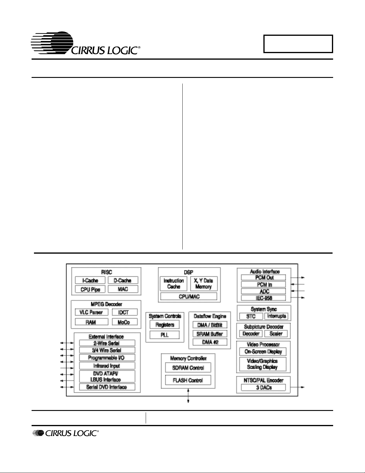
2. TYPICAL APPLICATION ........................................................................................................18
2.1 CS98100 Device Summary .............................................................................................18
3. FUNCTIONAL DESCRIPTION ...............................................................................................20
3.1 RISC Processor ...............................................................................................................20
3.2 DSP Processor ................................................................................................................20
3.3 Memory Control ...............................................................................................................20
3.4 Dataflow Control (DMA) ................................................................................................... 20
3.5 System Control Functions ................................................................................................ 20
3.6 DVD/ATAPI Interface .......................................................................................................21
3.7 Serial DVD Interface ........................................................................................................21
3.8 MPEG Video Decoding .................................................................................................... 21
3.9 Audio Processing .............................................................................................................21
3.10 Video Processing ........................................................................................................... 22
3.11 Video Encoder ...............................................................................................................22
4. MEMORY MAP AND REGISTERS .........................................................................................23
4.1 Processor Memory Map ................................................................................................... 23
CS98100
Contacting Cirrus Logic Support
For a complete listing of Direct Sales, Distributor, and Sales Representative contacts, visit the Cirrus Logic web site at:
http://www.cirrus.com/corporate/contacts
IMPORTANT NOTICE
“Preliminary” product information describes products that are in production, but for which full characterization data is not yet available. “Advance” product information
describes products that are in development and subject to development changes. Cirrus Logic, Inc. and its subsidiaries (“Cirrus”) believe that the information contained
in this document is accurate and reliable. However, the information is subject to change without notice and is provided “AS IS” without warranty of any kind (express
or implied). Customers are advised to obtain the latest version of relevant information to verify, before placing orders, that i
complete. All products are sold subject to the terms and conditions of sale supplied at the time of order acknowledgment, including those pertaining to warranty, patent
infringement, and limitation of liability. No responsibility is assumed by Cirrus for the use of this information, including use of this information as the basis for manufacture or sale of any items, or for infringement of patents or other rights of third parties. This document is the property of Cirrus and by furnishing this information,
Cirrus grants no license, express or implied under any patents, mask work rights, copyrights, trademarks, trade secrets or other intellectual property rights. Cirrus
owns the copyrights of the information contained herein and gives consent for copies to be made of the information only for use within your organization with respect
to Cirrus integrated circuits or other parts of Cirrus. This consent does not extend to other copying such as copying for general distribution, advertising or promotional
purposes, or for creating any work for resale.
An export permit needs to be obtained from the competent authorities of the Japanese Government if any of the products or technologies described in this material
and controlled under the “Foreign Exchange and Foreign Trade Law” is to be exported or taken out of Japan. An export license and/or quota needs to be obtained
from the competent authorities of the Chinese Government if any of the products or technologies described in this material is su
and is to be exported or taken out of the PRC.
CERTAIN APPLICATIONS USING SEMICONDUCTOR PRODUCTS MAY INVOLVE POTENTIAL RISKS OF DEATH, PERSONAL INJURY, OR SEVERE PROPERTY OR ENVIRONMENTAL DAMAGE (“CRITICAL APPLICATIONS”). CIRRUS PRODUCTS ARE NOT DESIGNED, AUTHORIZED, OR WARRANTED TO BE
SUITABLE FOR USE IN LIFE-SUPPORT DEVICES OR SYSTEMS OR OTHER CRITICAL APPLICATIONS. INCLUSION OF CIRRUS PRODUCTS IN SUCH APPLICATIONS IS UNDERSTOOD TO BE FULLY AT THE CUSTOMER'S RISK.
Cirrus Logic, Cirrus, and the Cirrus Logic logo designs are trademarks of Cirrus Logic, Inc. All other brand and product names i
or service marks of their respective owners.
Purchase of I2C components of Cirrus Logic, Inc., or one of its sublicensed Associated Companies conveys a license under the Phillips I
components in a standard I2C system.
2
2
C Patent Rights to use those

4.2 Host Port Memory Map .................................................................................................... 23
4.3 Internal IO Space Map ..................................................................................................... 24
4.4 CS98100 Register Space ................................................................................................ 24
5. PIN DESCRIPTIONS .............................................................................................................. 37
6. PIN ASSIGNMENTS ............................................................................................................... 38
6.1 Miscellaneous Pins .......................................................................................................... 46
6.2 Serial Interface ................................................................................................................ 47
6.3 SDRAM Interface ............................................................................................................. 48
6.4 ROM/NVRAM Interface ................................................................................................... 49
6.5 Digital Video Output Interface .......................................................................................... 50
6.6 Audio Output/Input Interface ............................................................................................ 51
6.7 Host Master/ATAPI Interface ........................................................................................... 52
6.8 DVD I/O Channel Interface .............................................................................................. 53
6.9 DVD Serial Data Interface ............................................................................................... 54
6.10 Video Encoder Interface ................................................................................................ 55
6.11 General Purpose Input/Output (GPIO) .......................................................................... 56
6.12 Power and Ground ........................................................................................................ 57
7. 208 PIN MQFP PACKAGE SPECIFICATIONS ...................................................................... 58
LIST OF FIGURES
CS98100
Figure 1. ATAPI Interface Timing Diagram..................................................................................... 7
Figure 2. SDRAM Refresh Transaction........................................................................................... 8
Figure 3. SDRAM Burst Read Transaction..................................................................................... 9
Figure 4. SDRAM Burst Write Transaction ..................................................................................... 9
Figure 5. CS98100 SDRAM Read and Write................................................................................ 10
Figure 6. CS98100 DVD Serial Interface Timing Diagram............................................................ 11
Figure 7. CS98100 Digital Video Interface Timing Diagram ......................................................... 12
Figure 8. Digital Audio In Timing Diagram .................................................................................... 13
Figure 9. Digital Audio Out Timing Diagram.................................................................................. 14
Figure 10. ROM/NVRAM Reading Timing .................................................................................... 15
Figure 11. ROM/NVRAM Write Timing ......................................................................................... 16
Figure 12. Miscellaneous Timings................................................................................................. 17
Figure 13. CS98100 Application ................................................................................................... 18
Figure 14. CS98100 Pin Layout.................................................................................................... 37
Figure 15. CS98100 208-Pin MQFP Package Drawing................................................................ 58
LIST OF TABLES
Table 1. ATAPI Interface Characteristics........................................................................................ 7
Table 2. SDRAM Interface Characteristics ..................................................................................... 8
Table 3. CS98100 DVD Interface Characteristics......................................................................... 11
Table 4. CS98100 Digital Video Interface Characteristics............................................................ 12
Table 5. Digital Audio In Characteristics....................................................................................... 13
Table 6. Digital Audio Out Characteristics .................................................................................... 14
Table 7. RAM/NVROM Characteristics......................................................................................... 15
Table 8. Miscellaneous Timing Characteristics............................................................................. 17
Table 9. Memory Map - RISC Processor...................................................................................... 23
Table 10. Host Port Memory Map................................................................................................. 23
Table 11. Internal IO Space Map.................................................................................................. 24
Table 12. CS98100 Register Map and Blocks.............................................................................. 24
Table 13. CS98100 Registers....................................................................................................... 25
3

CS98100
Table 14. Pin Type and Direction Legend.....................................................................................37
Table 15. Pin Assignments............................................................................................................38
Table 16. Miscellaneous Interface Pins.........................................................................................46
Table 17. Serial Interface Pin Assignments ..................................................................................47
Table 18. SDRAM Interface Pin Assignments...............................................................................48
Table 19. ROM/NVRAM Interface Pin Assignments ..................................................................... 49
Table 20. Video Output Interface Pin Assignments.......................................................................50
Table 21. Audio Output Interface Pin Assignments.......................................................................51
Table 22. Host Master Interface Pin Assignments........................................................................ 52
Table 23. DVD I/O Channel Interface Pin Assignments................................................................53
Table 24. DVD Serial Data Interface Pin Assignments................................................................. 54
Table 25. Video Encoder Interface Pin Assignments....................................................................55
Table 26. General Purpose I/O Interface Pin Assignments...........................................................56
Table 27. Power and Ground........................................................................................................57
4
1. CHARACTERISTICS AND SPECIFICATIONS
1.1 AC AND DC PARAMETRIC SPECIFICATIONS
(AGND, DGND=0V, all voltages with respect to 0V)
1.1.1 ABSOLUTE MAXIMUM RATING
Symbol Description Min Max Unit
CS98100
VDD
VDD
V
I
I
I
I
O
T
SOL
T
VSOL
T
STOR
T
AMB
P
total
IO
CORE
Power Supply Voltage on I/O ring -0.5 4.6 Volts
Power Supply Voltage on core logic and PLL -0.5 2.5 Volts
Digital Input Applied Voltage (power applied) -0.5 5.5 Volts
Digital Input Forced Current -10 10 mA
Digital Output Forced Current -50 50 mA
Lead Soldering Temperature 260
Vapor Phase Soldering Temperature 235
Storage Temperature (no power applied) -40 125
Ambient Temperature (power applied) 0 70
o
C
o
C
o
C
o
C
Total Power consumption 2 W
CAUTION: Operating beyond these Minimum and Maximum limits can result in permanent damage to
the device. Cirrus Logic recommends that CS98000 devices operate at the settings described in the next
table.
1.1.2 RECOMMENDED OPERATING CONDITIONS
Parameter Symbol Min Typ Max Units
Supply Voltage, IO V
Supply Voltage, core and PLL V
Ambient Temperature (power applied) T
1.1.3 ELECTRICAL CHARACTERISTICS
Parameter Symbol Conditions Min Typ Max Units
Power Supply
Supply Voltage, IO V
Supply Voltage, core and PLL V
Supply Current, IO I
Supply Current, core and PLL I
Digital Pins
Input Voltage, High V
Input Voltage, Low V
DD
DD
DD
DD
Normal Operating 45 mA
Normal Operating 210 mA
IH
IL
DD
DD
AMB
3.0 3.3 3.6 Volts
1.62 1.8 1.98 Volts
0 25 70
o
C
3.0 3.3 3.6 Volts
1.62 1.8 1.98 Volts
2.2 Volts
0.8 Volts
5
CS98100
Parameter Symbol Conditions Min Typ Max Units
Input Current I
Input Pull up/down resistor R
Output Voltage, High V
Output Voltage, Low V
High-Z-state Leakage I
IN
I
OH
OL
OZ
Analog Video Pins
Full Scale Current I
Output Voltage Range V
DAC to DAC matching
1
Output Voltage Range V
FS
IO
MAT 2 %
out
Differential Gain DG 1 %
Differential Phase DP 0.5 deg
Signal to Noise SNR 74 dB
Chrominance AM Noise AM 80 dB
Chrominance PM Noise PM 75 dB
1.
Only applies each set of three.
V
= V
IN
DD
or V
SS
-1 +1 µA
75 KΩ
@ buffer rating 2.4 Volts
@ buffer rating 0.4 Volts
V
= VSS or V
OUT
DD
-1 +1 µA
RL = 37.5 Ω 34 mA
RL = 37.5 Ω 1.28 Volts
RL= 37.5Ω 1.28 Volts
6
CS98100
1.2 AC CHARACTERISTICS
(TA= 25°C; VDD_PLL=VDD_CORE=1.8 V±10%, VDD_IO=3.3 V±10%)
1.2.1 ATAPI Interface
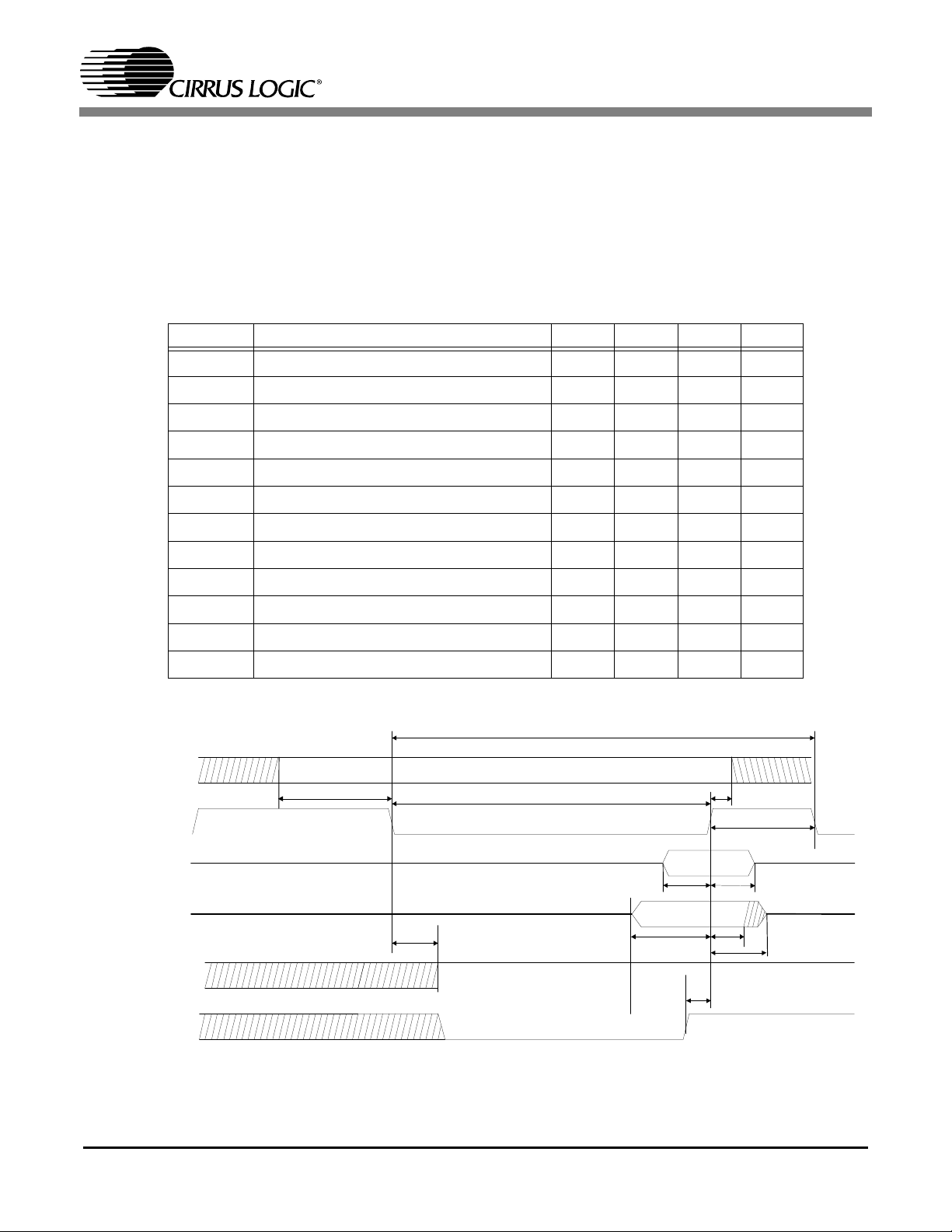
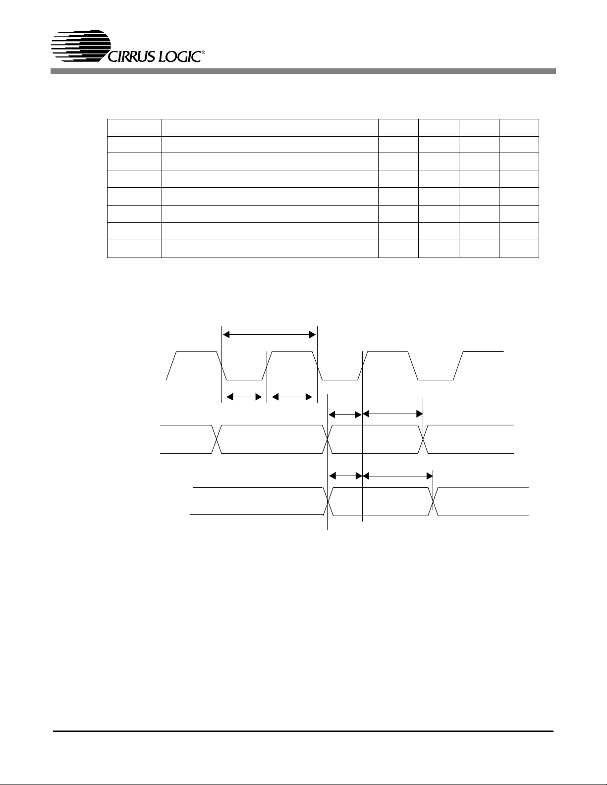
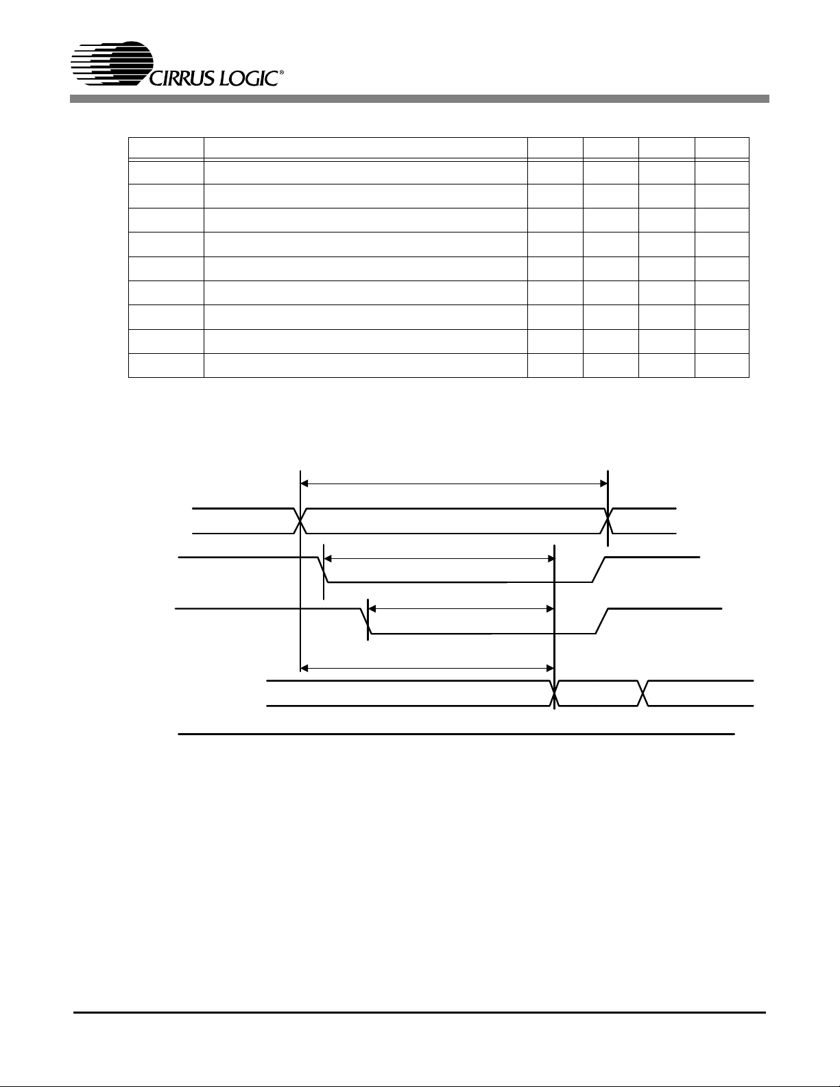
The CS98100 can interface with ATAPI-type slave loader gluelessly. Figure1 illustrates a read ATAPI
transaction and a write ATAPI transaction. PIO mode 4 is implemented for sufficient data transfer rate between ATAPI device and the CS98100.
See Table1 for the ATAPI symbols and characterization data.
Symbol Description Min Typ Max Unit
t
acyc
t
aavr
t
ah
t
arww
t
arec
t
awsu
t
awh
t
ardsu
t
arddh
t
ardts
t
arsu
t
arh
1
1
Cycle Time 87 ns
Address Valid to HMRD-/HMWR- Setup 7 ns
Address Hold from HMRD-/HMWR Setup 8 ns
H_RD/H_WR Pulse Width 58 ns
H_RD/H_WR Recovery Time 19 ns
H_WR Data Setup 20 ns
H_WR Data Hold 4 ns
H_RD Data Setup 20 ns
H_RD Data hold 0 ns
H_RD Data three-state 7 ns
H_RDY Setup Time 14 ns
H_RDY Hold Time 0 ns
H_A[2:0] ,
H_CS[3:0]
H_RD/H_WR
H_D[15:0](WRITE)
H_D[15:0](READ)
H_RDY(deasserted
before tarsu)
H_RDY(asserted
before tarsu)
Table 1. ATAPI Interface Characteristics
1.
Values are guaranteed by design only
t aavr
Figure 1. ATAPI Interface Timing Diagram
tarsu
tarww
tacyc
tardsu
tarh
tarddh
t ah
tarec
tawhtawsu
tardts
7
CS98100
1.2.2 SDRAM Interface
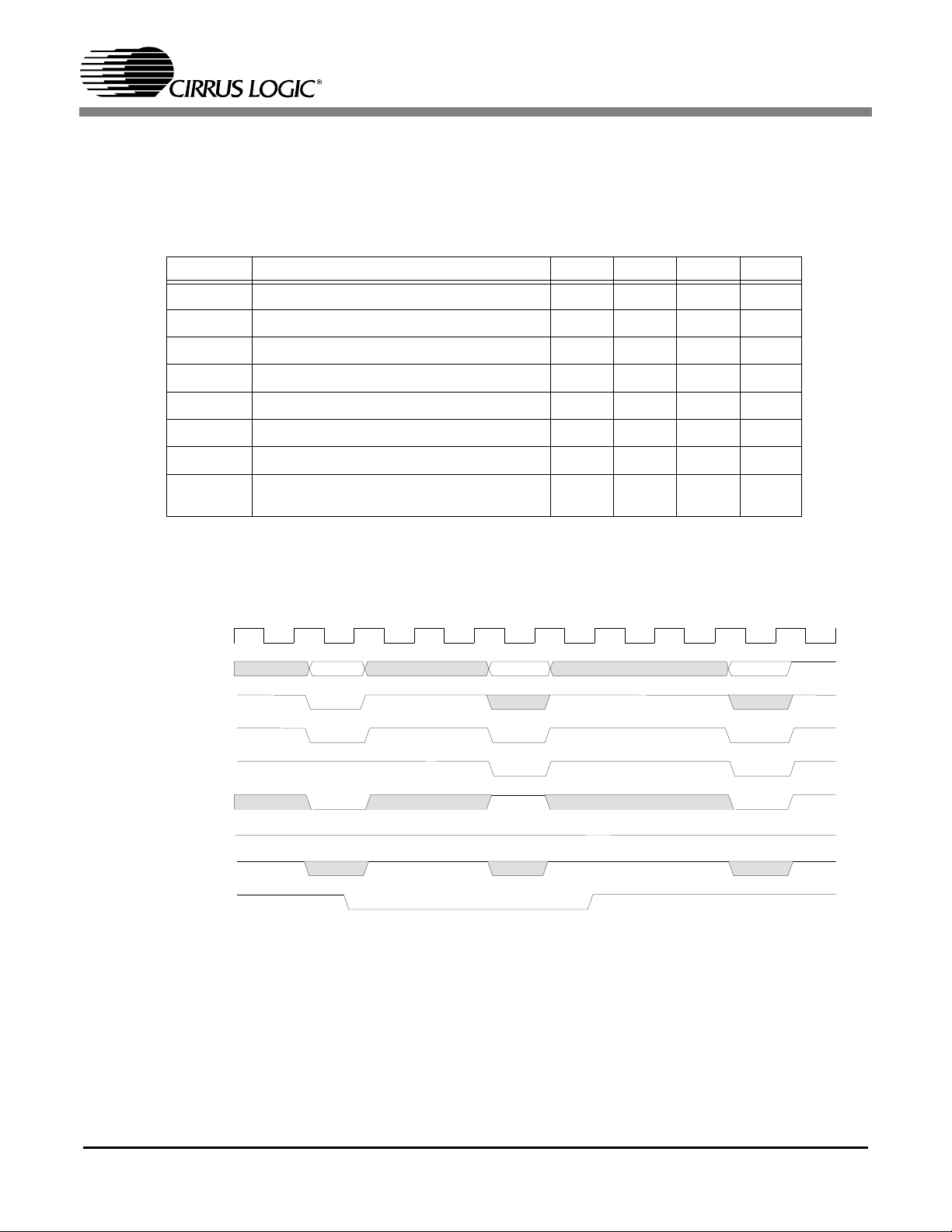
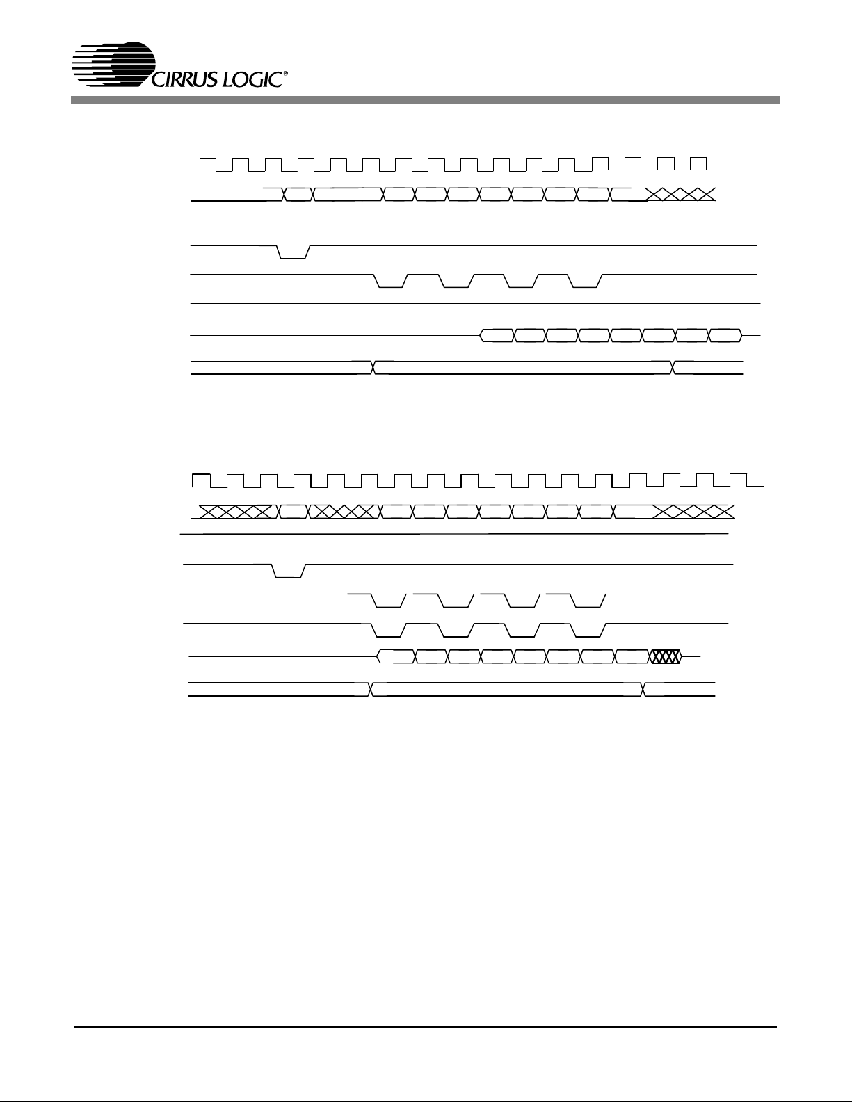
The CS98100 interfaces with either SDRAM or SGRAM, for high data bandwidth transfer. Figure5 and
Table2 show the interface pin timing. Figure2 shows the refresh cycle performed by the CS98100.
Figure3 shows a burst read (length = 8) transaction, while Figure4 shows a burst write (length=8) trans-
action. In both Figure3 and Figure4, CAS latency is programmed to 3.
Symbol Description Min Typ Max Unit
t
mco
t
mper
t
mdow
t
mhw
t
msur
t
msurd
t
mhr
t
mhrd
1
1
1
Output Delay from DR_CKO active edge 9 ns
DR_CKO Period 11 12.2 ns
DR_D[31:0] delay from DR_CKO 9.1 ns
DR_D[31:0] valid time after DR_CKO 1.5 ns
DR_D[31:0] setup to DR_CKO 3.9 ns
1
DR_D[31:0] setup to DR_CKO with delay 4.3 ns
DR_D[31:0] hold time after DR_CKO 1.85 ns
DR_D[31:0] hold time after DR_CKO with
1.3 ns
delay
1.
Delay is programmable by selecting the DRAM_Input_Speed bit of the Command Register(0x000)
DR_CKO
DR_A[11:0]
DR_BS_N
DR_RAS_N
DR_CAS_N
DR_WE_N
DR_D[31:0]
DR_DQM_[3:0]
DR_AP
Table 2. SDRAM Interface Characteristics
Figure 2. SDRAM Refresh Transaction
8
DR_CKO
CS98100
DR_A_[11:0]
DR_CKE
DR_RAS_N
DR_CAS_N
DR_WE_N
DR_D[31:0]
DR_DQM[3:0]
DR_CKO
DR_A_[11:0]
DR_CKE
DR_RAS_N
R0
C0
C1
C2
C3 C4 C5 C6 C7
D0 D1 D2
0F
Figure 3. SDRAM Burst Read Transaction
R0
C0
C1
C2
C3 C4 C5 C6 C7
D3
D4 D5 D6 D7
F
DR_CAS_N
DR_WE_N
DR_D[31:0]
DR_DQM[3:0]
D0
D1 D2
D3
D4 D5 D6 D7
0F
Figure 4. SDRAM Burst Write Transaction
F
9
DR_CKO
DR_RAS_N,DR_CAS_N
DR_WE_N,DR_AP,DR_DQM[3:0],
DR_CKE,DR_A[11:0]
DR_D[31:0](WRITE)
DR_D[31:0](READ)
tmpertmco
tmdow
CS98100
tmhw
tmsur
tmhr
Figure 5. CS98100 SDRAM Read and Write
10
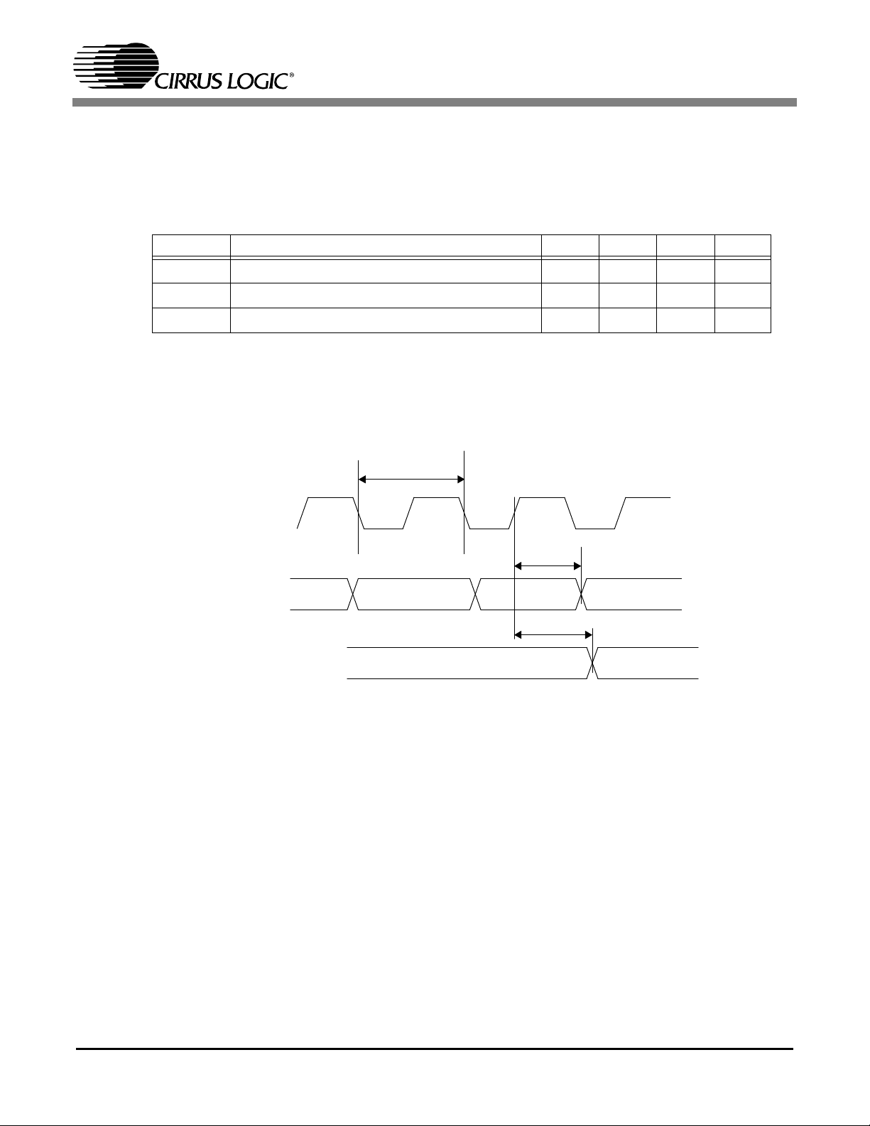
1.2.3 DVD Serial Interface Timing
Figure6 and Table3 illustrate the signal timing for the DVD serial interface input pins.
Symbol Description Min Typ Max Unit
t
dsckper
t
dsckl
t
dsckh
t
dsdsu
t
dsdhd
t
dscdsu
t
dscdhd
1
DVDS_CLK Period 33 ns
1
DVDS_CLK Low Time 40 50 %
1
DVDS_CLK High Time 40 50 %
DVDS_DATA Setup to DVDS_CLK active edge 4 ns
DVDS_DATA Hold after DVDS_CLK active edge 0 ns
DVDS_VLD,DVDS_SOS Setup to DVDS_CLK 3 ns
DVDS_VLD,DVDS_SOS Hold after DVDS_CLK 0 ns
Table 3. CS98100 DVD Interface Characteristics
1.
Values are guaranteed by design only
t
dsckper
CS98100
DVDS_CLK
(Input)
DVDS_DATA
(Input)
DVDS_VLD, DVDS_SOS
(Input)
t
dsckl dsckh
t
t
dsdsu
t
dscdsu
t
dsdhd
t
dscdhd
Figure 6. CS98100 DVD Serial Interface Timing Diagram
11
CS98100
1.2.4 Digital Video Interface Timing
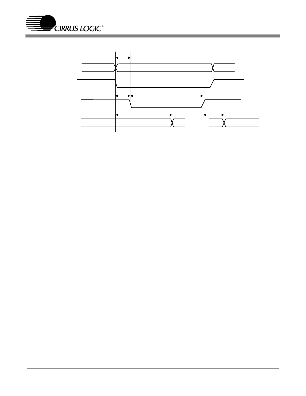
Figure7 illustrates the signal timing for the digital video interface pins. The clock is without a polarity to
show the clock may be inverted by register programming. This also illustrates that data is clocked out on
both clock edges in progressive mode. The data order is Cr,Y0,Cb,Y1, and the sync outputs may be programmed as active high or active low.
Symbol Description Min Typ Max Unit
t
t
t
1
vocper
covo1
covo2
CLK27_O period 37.037 ns
2
VDAT[7:0] delay from CLK27_O -10 10 ns
2
Vsync/Hsync delay from CLK27_O -10 10 ns
Table 4. CS98100 Digital Video Interface Characteristics
1.
Values are guaranteed by design only
2.
It is recommanded that the output data should be taken at the opposite edge of the CLK27_O.
Tvocper
CLK27_O
(Output)
VDAT[7:0]
(Output)
VSYNC/HSYNC (Output)
Figure 7. CS98100 Digital Video Interface Timing Diagram
Tcovo1
Tcovo2
12
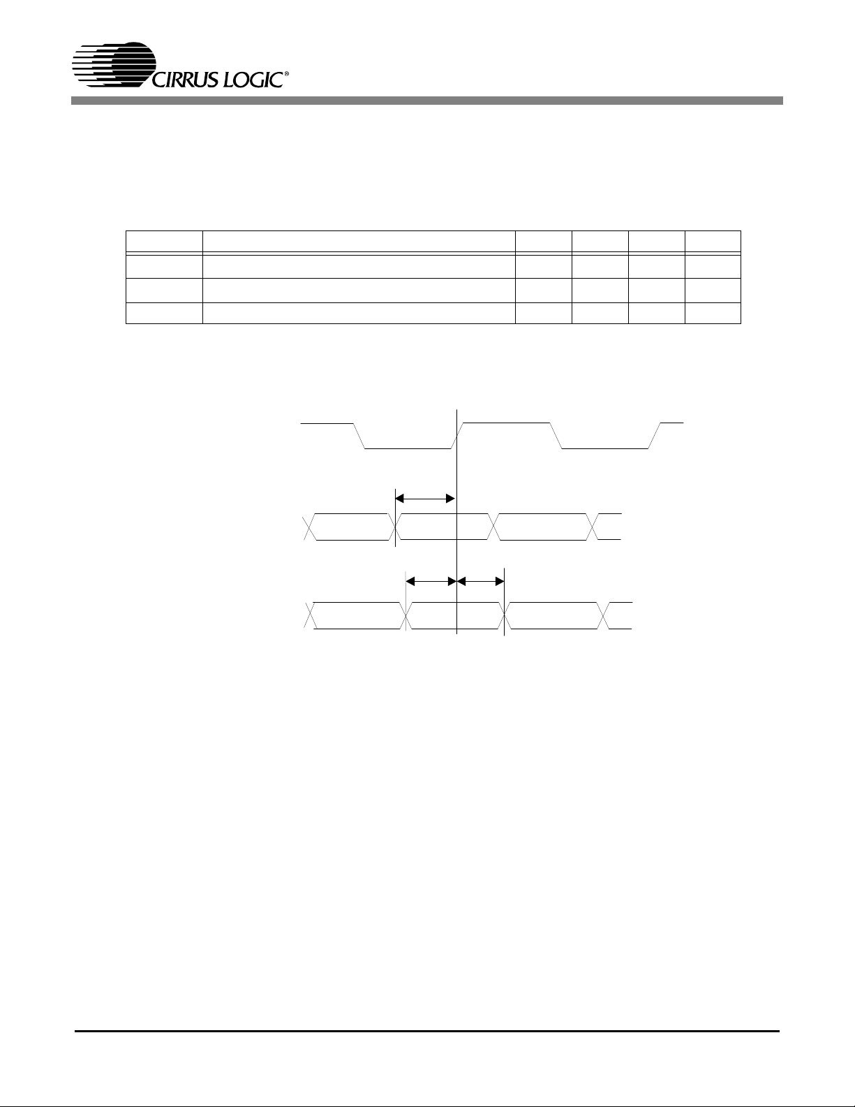
CS98100
* Active clock edge is programmable. Timing is referenced from active edge.
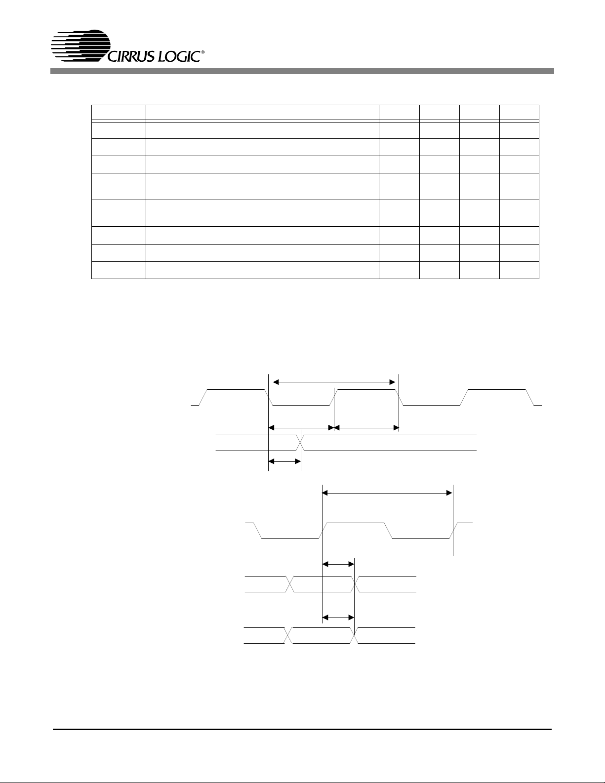
1.2.5 Digital Audio Interface Timing
Figure8 and Figure9 illustrate the signal timing for the digital audio pins. The bi-directional AUD_XCK
pin clocks at 8x the frequency of the AUD_BCK pin. The AUD_BCK pin outputs at 32x or 48x of the
sample frequency, and transitions on the falling edge of the AUD_XCK pin. AUD_BCK is shown without
polarity to indicate the polarity is programmable.
Symbol Description Min Typ Max Unit
t
slri
t
sdi
thsdi AIN_DATA hold time after AUD_BCK active edge 1 - ns
*AUD_BCK (Output)
AIN_LRCK setup to AUD_BCK active edge 25 - ns
AIN_DATA setup to AUD_BCK active edge 25 - ns
Table 5. Digital Audio In Characteristics
AIN_LRCK (Input)
AIN_DATA (Input)
t
lrts
t
sdsus
Figure 8. Digital Audio In Timing Diagram
t
sdhs
13
CS98100
Symbol Description Min Typ Max Unit
t
1
axch
1
taxcl
t
axper
t
odbck
t
odbck
t
aoper
t
2
odlr
t
2
odsd
1.
Values are guaranteed by design only
2.
It is recommanded that the output data should be taken at the opposite edge of the AUD_BCK.
AUD_XCLK High Time (AUD_XCLK is Input/Output) 40 50 %
AUD_XCLK Low Time (AUD_XCLK is Input/Output) 40 50 %
AUD_XCLK period (Input/Output) 27 ns
AUD_BCK delay from AUD_XCLK(output) active
10 ns
edge
AUD_BCK delay from AUD_XCLK(input) active
21 ns
edge
AUD_BCK period 216 ns
AUD_LRCK delay from AUD_BCK active edge -10 10 ns
AUD_D[3:0] delay from AUD_BCK active edge -10 10 ns
Table 6. Digital Audio Out Characteristics
AUD_XCLK(Input/Output)
AUD_BCK(Output)
* AUD_BCK(Output)
AUD_LRCK(Output)
AUD_DO[3:0] (Output)
t
axper
t
odsd
t
axch
t
odlr
t
aoper
t
axcl
t
odbck
14
* Active clock edge is programmable. Timing is referenced from active edge.
Figure 9. Digital Audio Out Timing Diagram
1.2.6 ROM/NVRAM Interface
Symbol Description Min Typ Max Unit
t
rc
t
cds
t
ods
t
ads
t
aws
t
cws
t
wp
t
wdo
t
dh
Read Cycle Time 98 ns
CE to Data Setup 80 ns
OE to Data Setup 70 ns
Address to Data Setup 90 ns
Address to WE setup (Write) 20 ns
CE to WE setup (Write) 5 ns
WE Pulse Width (Write) 160 ns
CE to Data Output (Write) -5 ns
WE to Data Hold (Write) 10 ns
Table 7. RAM/NVROM Characteristics
Note:Read timing based on 10.5 ns memory clock and 4 programmed wait states.
CS98100
Address
M_A[11:0],
M_D[27:16]
NVM_CE_N
NVM_OE_N
(M_AP)
M_D[7:0]
NVM_WE_N
t
rc
t
cds
t
ods
t
ads
Figure 10. ROM/NVRAM Reading Timing
15
Address
M_A[11:0],
M_D[27:16]
NVM_CE_N
t
CS98100
aws
NVM_WE_N
M_D[7:0]
NVM_OE_N
(M_AP)
t
cws
t
wdo
t
wp
Figure 11. ROM/NVRAM Write Timing
t
wdh
16
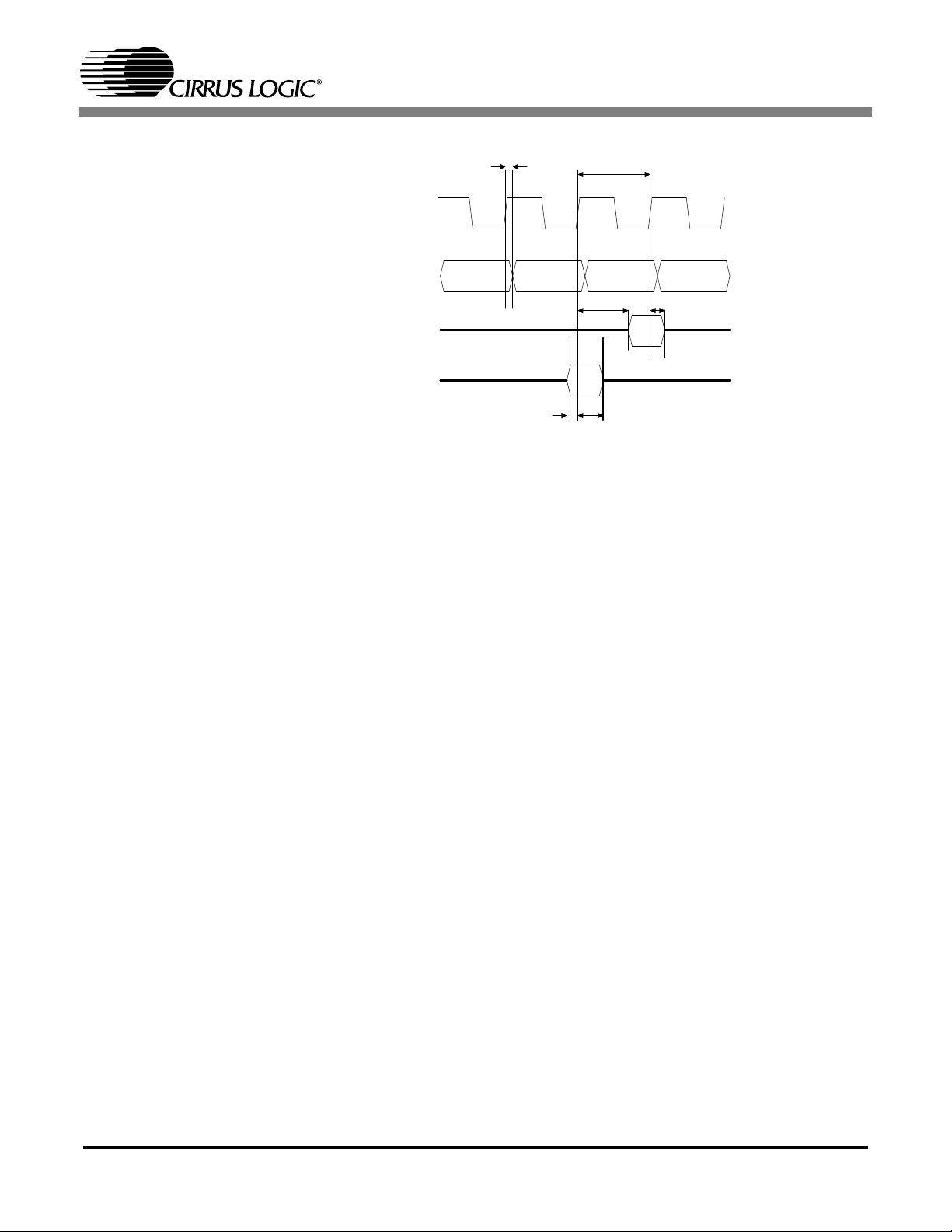
1.2.7 Miscellaneous Timings
Symbol Description Min Typ Max Unit
1
txclper
trstl RST_N Low Pulse Width 1000 ns
tgph GPIO PW High 50 ns
tgpl GPIO PW Low 50 ns
1.
XTLCLK must meet the requirement of external the video encoder for correct chroma (27 MHz ± 1 KHz).
XTLCLK period 37.037 ns
Table 8. Miscellaneous Timing Characteristics
XTLCLOCK
RESET-N
xccper
t
trstl
CS98100
GPIO
tgph
Figure 12. Miscellaneous Timings
tgpl
17
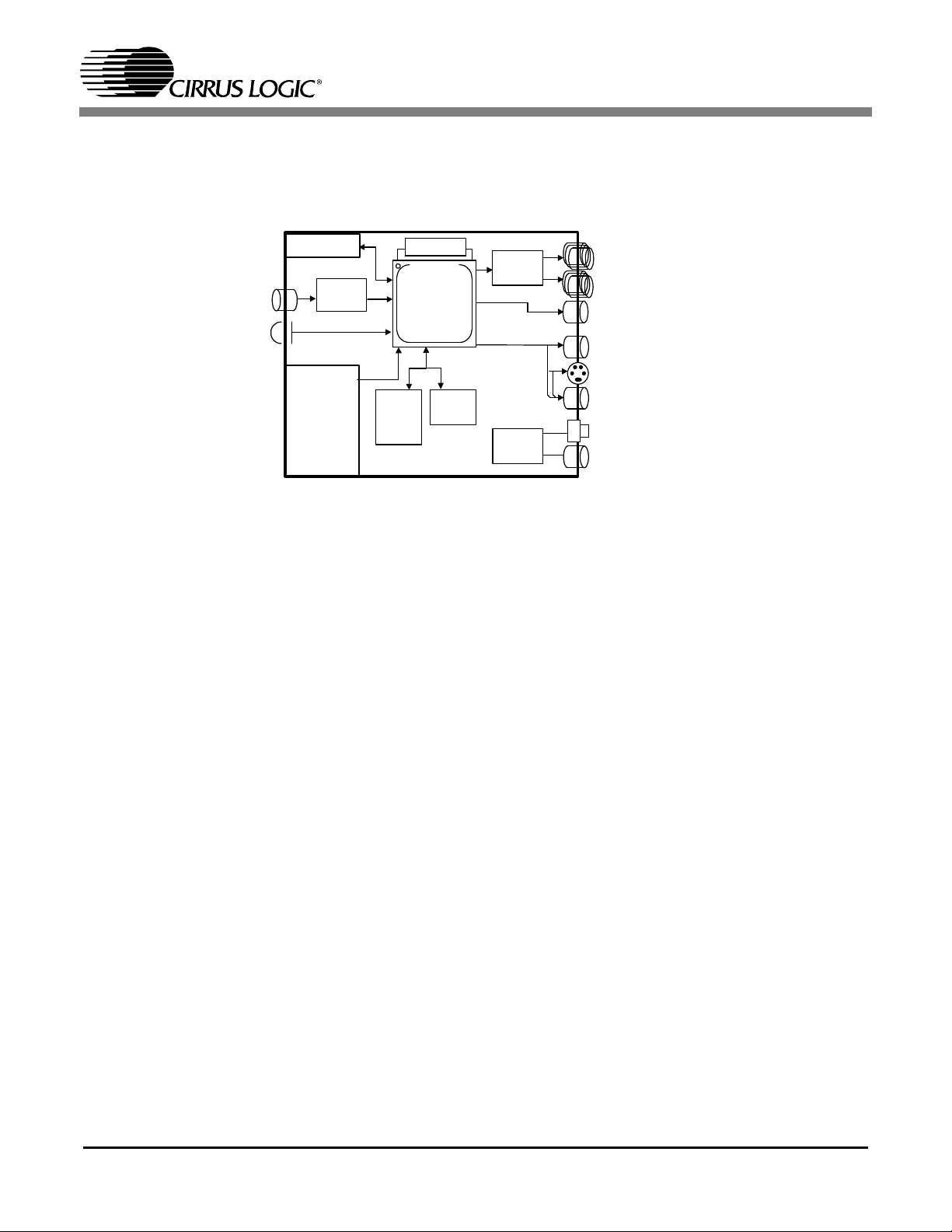
2. TYPICAL APPLICATION
Figure13 shows an example of a complete high-end DVD solution using the CS98100.
CS98100
Audio
Front Panel
Audio
ADC
IR
DVD Loader
(IO Channel,
ATPAI or
Serial)
Figure 13. CS98100 Application
ROM/
FLASH
1/
-1MB
2
27M XTAL
CS98100
SDRAM
4-8MB
2.1 CS98100 Device Summary
RISC-32
• Powerful 32-bit RISC processor
• Optimizing C compiler and source level debugger
• Big or little endian data formats supported
• MAC multiply/accumulate in two cycles with
C support.
(4)Audio
DACs
Power
Reg.
Audio-
Up to 8 Channels
S/PDIF
Composite Video
S-Video
Component Video
Switch
Power
communication
• 32-bit timers for I/O and other uses, with programmable interval rates
• Both hardware and software interrupts on data
or debug
• Performance monitors which measures DRAM
bandwidth, usage, and RSK performance
• 4 Kbyte instruction cache, 2 Kbyte data cache.
• Single cycle instructions run at 90 MHz.
DSP-32
• Powerful 24/32-bit DSP processor
• 24-bit fixed point logic, with 54-bit accumulator.
• Single-cycle throughput, 2-cycle latency multiply accumulate, 32-bit simple integer logic.
• 8 Kbyte instruction cache, 12 Kbyte program
visible local memory
• Single cycle instructions run at 90 MHz.
SYSTEM CONTROLS
• Include several hardware lockable semaphore
registers
• General-purpose registers for inter-processor
18
• Built in PLLs generate all required clocks from
27 MHz input clock.
• Memory Controller
• Supports SDRAM, and SGRAM, from 2
MBytes to 32 MBytes.
• Supports multiple banks of FLASH and ROM
up to 32 MBytes.
• 32-bit data bus for DRAM, 8 or 16-bit data bus
for ROM.
DATA FLOW ENGINE
• Two DMA controllers – local memory based
and direct memory-to-memory
• 2432 bytes of internal memory, DMA to/from
main RAM into local SRAM.
• Supports endian conversion and byte, short,

CS98100
long data formats on DMA.
• Supports block transfers for graphics bit blits.
MPEG VIDEO DECODER
• Supports VCD1.0, 1.1, 2.0 and 3.0, SVCD, and
DVD video standards.
• Supports trick features, including smooth 2x
forward play.
• Special anti-tearing logic controls picture decode and presentation.
• Advanced error concealment hardware.
SYSTEM SYNCHRONIZATION
• System time clock (STC) for audio/video synchronization
• Flexible interrupt structure for controlling decode and presentation times
• Hardware scheduling of sub-picture and highlight events
AUDIO INTERFACE
• Supports 8 channels PCM, I2S at up to 24 bits
and 96 kHz output rate.
• Simultaneous IEC-958 output with programmable channel status and user data
• Also supports S/PDIF receiver for high performance applications
EXTERNAL INTERFACE
• 2-wire serial master and slave port, second 2wire master port for controlling DVD device.
• 3- or 4-wire serial master/slave port.
• Large number of programmable bi-directional
I/O pins.
• All pins not used for other function can be reassigned as general purpose I/O pins
• 8 pins can be used as edge or level detection interrupt pins.
• Hardware-assisted support for infrared remote
devices, such as remote control, infrared keyboard, mouse, printer, and more.
• Programmable parallel host master interface
supports formats including ATAPI, ISA, and
more.
• IO channel interface supports standard DVD
loader protocols
• Separate serial DVD interface to support lowcost (track buffer-less) loaders
VIDEO PROCESSOR
• On screen display module supports 2-bit or 4bit, pixel modes. It supports 3 separate regions
and 16 transparency overlay levels
• High quality scaling using 16 tap polyphase
programmable vertical and horizontal filters, to
support any size image up to 768x576.
• Multiple video plain overlays (main video /
subpicture / picture-in-picture / on-screen display).
• Gamma Correction.
• Progressive scan video output
VIDEO ENCODER
• Three 10-bit video DACs, drive 37.5Ω load directly without external buffering
• Supports PAL (B,D,G,H,I,N) and NTSC
• Component (RBG or YUV) or composite + SVideo output
• Progressive or interlaced mode output
• Macrovision 7.1 support (interlaced) and Macrovision 1.03 support (progressive)
• Wide-screen signaling support (interlaced and
progressive) and CGMS support
• Closed captioning support
SUB-PICTURE PROCESSOR
• Run-length decode DVD sub-pictures and
SVCD OGT formats
• Hardware vertical scaling supports NTSC-PAL
format conversion
• 16 level alpha blending
System Functions
• 208-pin MQFP package.
• All I/O pins are 3V with 5V tolerance.
• Advanced 0.18 micron CMOS technology.
• Chip runs at 90 MHz
• Supports Low power modes and clock shutoff.
19

3. FUNCTIONAL DESCRIPTION
CS98100
3.1 RISC Processor
The CS98100 includes a powerful, proprietary 32bit RISC processor with optimizing C compiler
support. The RISC has a MAC engine which performs multiply/accumulate in 2 cycles in a pipelined fashion with C support, effectively achieving
single cycle throughout. The CS98100 fully supports many Real Time Operating Systems (RTOS).
The RISC processor co-ordinates on-chip multithreaded tasks, as well as supervises system activities such as remote control and VFD front panel
control.
3.2 DSP Processor
The CS98100 contains a proprietary digital signal
processor (DSP) which is optimized for audio applications. The DSP performs 32-bit simple integer
operations, and has a 24-bit fixed point logic unit,
with a 54-bit accumulator. There are 32 generalpurpose registers, and eight independent address
generation registers, featuring: post-increment
ALU, linear and circular buffer operations, bit reverse ALU operations, and dual operand read from
memory. The multiply-accumulator has single-cycle throughput, with two cycle latency. The DSP is
optimized for bit packing and unpacking operations. The interface to main memory is designed for
bursting flexible block sizes and skip counts.
3.3 Memory Control
The DRAM Interface performs the SDRAM control and arbitration functions for all the other modules in the CS98100. The DRAM interface services
and arbitrates a number of clients and stores their
code and/or data within the local memory. This arbitration and scheduling guarantees the allocation
of sufficient bandwidth to the various clients. The
DRAM Interface supports up to 32 MByte. For a
typical DVD player application, CS98100 requires
8 MByte of SDRAM and 1 MByte of FLASH.
Sharing the same interface, the CS98100 also supports flash ROM, OTP, or masked ROM interface.
Code is stored in ROM. After the system is booted,
the code is shadowed inside DRAM for execution.
FLASH ROM interface is provided so that the code
can be upgraded in field once the communication
channel is established via, for example, CD-R or
serial port. Utility software will be provided to debug and upgrade code for the system manufacturer.
3.4 Dataflow Control (DMA)
The DMA controller moves data between the external memory and an internal memory. The external
memory address can be specified using a register,
or in FIFO mode, using start and end address registers. Separate start/end address registers are used
for DMA read and write operations. The DMA interface also has a block transfer function, which allows for the transfer of one block of data from one
external memory location to another external memory location. In effect, combining a DMA read and
write into one operation. In addition, the DMA
write operation allows for byte, short, word, and
other types of masking. A second dedicated DMA
controller provides for fast memory-to-memory
transfers.
3.5 System Control Functions
The system control functions are used to coordinate
the activities of the multiple processors, and to provide the supporting system operations. Four 32-bit
communication registers are available inter-processor communication, and eight semaphore registers are used for resource locking. Timers are
available for general-purpose functions, as well as
more specialized functions such as watchdog timers and performance monitoring. The large number
of general purpose I/Os offers flexibility in system
configurations.
Three separate serial interfaces, conforming to industry-standard protocols, are available for a vari-
20

CS98100
ety of system interface functions. Interrupts can be
generated on specific or generic events. Infrared inputs can be filtered of glitches or stored unfiltered
into memory. Power-down control of the internal
clocks is also possible. Internal PLLs are used to
generate the internal system and memory clocks,
and audio clocks of any widely used frequency.
3.6 DVD/ATAPI Interface
The CS98100 has a programmable interface port,
which can be configured to connect to industry
standard CD/DVD loaders without external glue
logic. The CD/DVD interface fully supports a wide
range of popular CD/DVD loaders. The interface
consists of DVD control and data ports, and an optional CD control/data port. The CS98100 hardware manages the DVD interface and moving data
to an arbitrary size input FIFO in DRAM.
The same interface pins can be optionally configured as a generic 16-bit host master port. In this
mode, the CS98100 can control up to four devices
(using 4 chip select outputs), each of which may
use different protocol and timing. The interface can
be set up in ATAPI mode, to connect directly to any
ATAPI DVD loader (using two chip selects). Simultaneously, the other two chip selects can be
configured to connect to other devices, such as a
super I/O chip or hard disk.
A third option is to configure the interface for micro-less DVD loader operation, which may also be
configured to connect without external glue logic.
3.7 Serial DVD Interface
The CS98100 has a 4-pin serial port which interfaces to the data port of popular low-cost DVD loaders. This type of loader provides for low system
cost by eliminating the track buffer, interface
FIFO, and flow control logic. The CS98100 contains a large internal SRAM to handle high burst
data rates, without requiring reverse flow control.
The track buffer resides in the CS98100 SDRAM,
which reduces system complexity and simplifies
the software architecture. The CS98100 performs
error detection, sector number tracking, and interrupt generation.
3.8 MPEG Video Decoding
Compressed MPEG data is read from the DVD disk
into an input FIFO in DRAM. The data flow
(DMA) controller moves Video packets from the
input FIFO into the MPEG decoder’s input FIFO
(also in DRAM). The DMA controller can also perform advanced functions such as start code search,
relieving the RISC processor. The System Sync
function is used to control the timing of MPEG picture decoding. The MPEG Video decoder processes I, B and P frames, and writes to video frame
buffers in DRAM, for output to the display. Special
anti-tearing logic ensures currently displayed
frame buffers are not overwritten.
3.9 Audio Processing
Compressed Audio data is read from the DVD disk
into an input FIFO in DRAM. The data is decompressed, then written to a PCM output FIFO, also in
DRAM. Presentation time stamps (PTS) are extracted from the stream to update the STC, in order
to maintain audio/video synchronization. The
DMA and decompression stages of audio processing can be done with a combination of the DMA
unit, DSP and RISC processors. The DSP is optimized for audio processing, so most common formats can be handled by the DSP alone, including
AC-3, MPEG2 audio, and others. The DSP has
enough reserve bandwidth to handle the Karaoke
echo-mix and pitch shift, and AC-3 down-mix
functions.
The audio output data is written into a DRAM
FIFO in 16, 18, 20 or 24-bit PCM format. A flexible audio output stage can simultaneously output 8
channels of PCM data to audio DACs, plus an IEC958 encoded output, at up to 96 kHz. The IEC-958
output has fully programmable channel status
(commercial), and provides a flexible solution to
support all IEC-958 modes for User Data.
21

CS98100
The audio interface also includes a flexible PCM
input interface, which can input a wide range of
protocols from IEC-958 receiver. Another, lowcost approach for audio input is the internal sigmadelta demodulator. This module inputs a digital
PWM version of the audio input, which can be created on the board using an inexpensive ramp generator and comparator. The sigma-delta demodulator
uses a set of programmable filters to reconstruct 9bit (mono) audio data at up to 12 kHz sampling frequency.
3.10 Video Processing
The CS98100 Video processor is a powerful, fully
programmable video post processing engine that
displays video on an interlaced TV or a progressive
HDTV. A 16-tap polyphase vertical filter is fully
programmable on a line-by-line basis, to provide
high quality vertical scaling and interlaced field
conversion. Horizontal filtering is done with a programmable 16-tap polyphase filter. This advanced
filter processing is used for de-interlacing, zoom,
and frame size conversion.
Source mode of interlaced or progressive is determined from the disk type automatically. For progressive source detection, 3:2 pulldown is detected
from status flags in the video stream to ensure optimized playback. Interlaced video source is filtered up to progressive size output using the
bilinear vertical filter. This is visibly superior to
simple line doubling. Each 240 line field being filtered and output at 480p. Progressive video source
is output at the full progressive resolution. Each
480 line frame output at 480p. Source mode of interlaced or progressive is determined from the disk
type. For progressive source detection, 3:2 pulldown is simply detected from status flags in the
video stream.
Zoom is fully programmable, from 1X to 500X
zoom, with any value in between. Frame type conversion, from NTSC to PAL, or PAL to NTSC, is
done with a the bilinear vertical filter, reducing
flicker and jaggies.
There is a programmable gamma-correction look-
up table for the final output. Cirrus Logic provides
some easy to use utilities in order to get the best advantage of the powerful video filtering capabilities
of the CS98100. The video encoder sends progressive or interlaced digital video data to the internal
video encoder, and can output parallel digital data
to an external video encoder.
The video processor also allows multiple video
plain overlay (main video / sub-picture / on-screen
display). The sub-picture unit is a hardware-only
solution which performs high-quality vertical scaling for PAL/NTSC conversion, and full support for
DVD (sub-picture) and SVCD (OGT) modes. The
on-screen display unit features 2-bit and 4-bit pixels, 16 transparency levels, and three independent
regions of up to full-screen size. The picture-in-picture unit can place a 1/2 or 1/4 screen sized window
anywhere on the screen. This feature can be used
for special effects, such as snapshot freeze and
zoom assist.
3.11 Video Encoder
The video encoder uses three 10-bit DACS to convert digital data to component (RGB or YPRPB) or
composite (composite plus S-Video) analog video.
The output can be interlaced (PAL/NTSC) or high
resolution progressive. In progressive mode, the
video encoder will typically drive YPRPB to a 525line television at 59.94 Hz, although other output
modes are possible, such as 625 lines and RGB.
The encoder performs the Macrovision copy protection function for all modes (revision 7.1 for interlaced, revision 1.03 for progressive). Other
features include built-in voltage reference, color
bar generator, individual power-down control for
each DAC, programmable baseband filters, color/contrast/tint controls, Closed Captioning (interlaced modes), wide screen signalling (PAL mode),
and Copy Generation Management System (NTSC
and progressive modes).
22

CS98100
4. MEMORY MAP AND REGISTERS
4.1 Processor Memory Map
The CS98100 externally supports up to 32 Mbytes DRAM and 16 Mbytes ROM/NVRAM. Table9 lists
the memory map as viewed by the RISC processor, and identifies whether each segment is mapped or
cacheable.
Processor byte address Description Cacheable
0000_0000 – 07FF_FFFF DRAM (mapped) Y
8000_0000 - 81FF_FFFF DRAM (32 Mbytes) Y
9400_0000 – 9CFF_FFFF 16 bit NVRAM write (16 Mbytes) N
9C00_0000 – 9CFF_FFFF 16 bit NVRAM/ROM (16 Mbytes) Y
9D00_0000 – 9DFF_FFFF 8 bit NVRAM/ROM (16 Mbytes) Y
A000_0000 – A1FF_FFFF DRAM (32 Mbytes) N
B000_0000 – B003_FFFF Internal I/O (256 Kbytes) N
B400_0000 – BCFF_FFFF 16 bit NVRAM write (16 Mbytes) N
BC00_0000 – BCFF_FFFF 16 bit NVRAM/ROM (16 Mbytes) N
BD00_0000 – BDFF_FFFF 8 bit NVRAM/ROM (16 Mbytes) N
C000_0000 – FFFF_FFFF DRAM (mapped) Y
Table 9. Memory Map - RISC Processor
4.2 Host Port Memory Map
Table10 lists the memory map as viewed by host slave port.
Host byte address Description
0000 0000 – 003F FFFF Internal I/O Space
1000 0000 – 13FF FFFF DRAM space (16 Mbytes)
1400 0000 – 17FF FFFF NVRAM space (16 Mbytes)
Table 10. Host Port Memory Map
23

CS98100
4.3 Internal IO Space Map
Table11 shows how the Internal IO space is mapped between general registers, internal SRAM ports, and
the RISC processor debug port.
Byte address offset Description
0_0000 – 0_2FFF General registers
0_3000 – 1_FFFF General Internal SRAM
2_0000 – 2_FFFF RISC Internal SRAM/Registers
Table 11. Internal IO Space Map
4.4 CS98100 Register Space
Table12 lists the register groups, and how they are split among the main CS98100 functional blocks.
CS98100 Register Block
000xx, 010xx General
001xx Host
002xx DRAM Controller (DRC)
003xx DMA
004xx CD/DVD Interface
005xx Serial DVD (DVDS)
006xx DSP
007xx Sync Control
008xx MPEG Video Decoder
00Axx Picture-in-picture
00Bxx Video Processor
00Cxx Subpicture Display
00Dxx On-screen Display
00Exx PCM In/Out
02xxxx RISC Processor
Table 12. CS98100 Register Map and Blocks
Table13 lists all the registers for the CS98100 and their addresses, and indicates whether the registers are
read/write (R/W), read only (RO) or write only (WO).
24

Address Type Function Register Name
0 R/W General Command
10 R/W General InterProc_Comm_Register_0
14 R/W General InterProc_Comm_Register_1
18 R/W General InterProc_Comm_Register_2
10C R/W General InterProc_Comm_Register_3
20 R/W General Semaphore_Register_0
24 R/W General Semaphore_Register_1
28 R/W General Semaphore_Register_2
02C R/W General Semaphore_Register_3
30 R/W General Semaphore_Register_4
CS98100
34 R/W General Semaphore_Register_5
38 R/W General Semaphore_Register_6
03C R/W General Semaphore_Register_7
40 RO General (Genio) GenIO_Read_Data
44 R/W General (Genio) GenIO_Write_Data
48 R/W General (Genio) GenIO_Three_State_Enable
04C R/W General (Genio) GenIO_Positive_Edge
50 R/W General (Genio) GenIO_Negative_Edge
54 R/W General (Genio) GenIO_Interrupt_Status
58 R/W General (Genio) GenIO_Positive_Edge_Mask
05C R/W General (Genio) GenIO_Negative_Edge_Mask
60 R/W General (Genio) GenIO_Level_Mask
1040 RO General (Genio) GenIO2_Read_Data
1044 R/W General (Genio) GenIO2_Write_Data
1048 R/W General (Genio) GenIO2_Three_State_Enable
1064 R/W General (Genio) GenIO2_Mode
1068 RO General (Genio) GenIODVD_Read_Data
106C R/W General (Genio) GenIODVD_Write_Data
Table 13. CS98100 Registers
25

CS98100
Address Type Function Register Name
1070 R/W General (Genio) GenIODVD_Three_State_Enable
1074 R/W General (Genio) GenIODVD_Mode
68 R/W General (Serial IF1) Ser1_Mstr_Byte_Read_Subaddress_Write
06C R/W General (Serial IF1) Ser1_Mstr_Write_1Byte
70 R/W General (Serial IF1) Ser1_Mstr_Write_2Bytes
74 R/W General (Serial IF1) Ser1_Mstr_Control
78 RO General (Serial IF1) Ser1_Mstr_Status
07C RO General (Serial IF1) Ser1_Mstr_Read_Data
80 R/W General (Interrupt) RSK_Interrupt_Mask
84 WO General (Interrupt) RSK_Interrupt_Set
88 R/W General (Interrupt) RSK_Interrupt_Status
08C RO General (Interrupt) RSK_Interrupt_Cause
90 R/W General (Interrupt) DSP_Interrupt_Mask
94 WO General (Interrupt) DSP_Interrupt_Set
98 R/W General (Interrupt) DSP_Interrupt_Status
09C RO General (Interrupt) DSP_Interrupt_Cause
0A0 R/W General (Interrupt) RSK_Interrupt_Mask2
0A4 WO General (Interrupt) RSK_Interrupt_Set2
0A8 R/W General (Interrupt) RSK_Interrupt2_Status
0AC RO General (Interrupt) RSK_Interrupt_Cause2
0B0 R/W General (Interrupt) DSP_Interrupt_Mask2
0B4 WO General (Interrupt) DSP_Interrupt_Set2
0B8 R/W General (Interrupt) DSP_Interrupt2_Status
0BC RO General (Interrupt) DSP_Interrupt_Cause2
0C0 R/W General (Timer) Timer_0
0C4 R/W General (Timer) Timer_1
0C8 R/W General (Timer) Timer_2
0CC R/W General (Timer) Timer_3
0D0 R/W General (Timer) Timer_Control
0D4 RO General (Timer) Performance_Monitor_Count
Table 13. CS98100 Registers (Continued)
26

Address Type Function Register Name
0D8 R/W General (Timer) Timer_M_Over_N
0DC R/W General (IR) IR_Glitch_Max
0E0 R/W General (IR) IR_Control
0E4 R/W General (IR) IR_Dram_Start_Address
0E8 R/W General (IR) IR_Dram_End_Address
0EC RO General (IR) IR_Dram_Write_Address
0F0 R/W General (PLL) PLL_Control_Register1
10F0 R/W General (PLL) Low_Power_Clock_Control
0F4 R/W General (PLL) PLL_Control_Register2
0F8 R/W General (PLL) PLL_Turn_Off
10F8 R/W General (PLL) PLL_Monitor
0FC R/W General (PLL) PLL_Clock_Divider
CS98100
1000 R/W General (DMA) DMA2_Source_Addr
1004 R/W General (DMA) DMA2_Dest_Addr
1008 R/W General (DMA) DMA2_Size
10B0 R/W General (Serial IF2) Ser2_Mstr_Write_Data_0
10B4 R/W General (Serial IF2) Ser2_Mstr_Write_Data_1
10B8 R/W General (Serial IF2) Ser2_Mstr_Write_Data_2
10BC R/W General (Serial IF2) Ser2_Mstr_Write_Data_3
10C0 RO General (Serial IF2) Ser2_Mstr_Read_Data_0
10C4 RO General (Serial IF2) Ser2_Mstr_Read_Data_1
10C8 RO General (Serial IF2) Ser2_Mstr_Read_Data_2
10CC RO General (Serial IF2) Ser2_Mstr_Read_Data_3
10D0 R/W General (Serial IF2) Ser2_Mstr_Setup
10D4 R/W General (Serial IF2) Ser2_Mstr_Command_Status
10E0 R/W General (Serial IF2) Ser3_Control
10E4 R/W General (Serial IF3) Ser3_Write_Data
10E8 RO General (Serial IF3) Ser3_Read_Data
100 R/W Host Device_1_Control
104 R/W Host Device_2_Control
Table 13. CS98100 Registers (Continued)
27

Address Type Function Register Name
108 R/W Host Device_3_Control
10C R/W Host Device_4_Control
110 R/W Host Write_Data_Port
114 RO Host Read_Data_Port
120 R/W Host Host_Start_Address
124 R/W Host Dram Start Address
128 R/W Host Stream_Transfer_Size
12C R/W Host DRAM_Burst_Threshold
134 R/W General Ser1_Slave_Address
13C R/W Host Host_Master_Control
200 R/W Dram controller DRAM_Controller_Priority0
204 R/W Dram controller DRAM_Controller_Priority1
CS98100
208 R/W Dram controller DRAM_Controller_Priority2
20C R/W Dram controller DRAM_Controller_Priority3
210 R/W Dram controller DRAM_Controller_Priority4
214 R/W Dram controller DRAM_Controller_Setup
218 R/W Dram controller DRAM_Command
21C R/W Dram controller DRAM_Controller_Mb_Width
220-224 R/W Dram controller DRAM_Controller_Debug
300 WO DMA DMA_Enable
304 R/W DMA DMA_Control
308 RO DMA DMA_Status
30C R/W DMA Xfer_Byte_Cnt
310 R/W DMA Dram_Byte_Start_Addr
314 R/W DMA Sram_Byte_Start_Addr
318 R/W DMA Fifo_Start_Rd_Addr
31C R/W DMA Fifo_Start_Wr_Addr
328 R/W DMA Search_Control
32C RO DMA Search_Status
330 R/W DMA Fifo_End_Rd_Addr
Table 13. CS98100 Registers (Continued)
28

Address Type Function Register Name
334 R/W DMA Fifo_End_Wr_Addr
338 R/W DMA Lines_and_Skip
33C R/W DMA Mask_Pattern_Match
400 R/W CD/DVD DVD_Control
404 R/W CD/DVD DVD_Fifo_Base_Address
408 R/W CD/DVD DVD_Fifo_Size
40C R/W CD/DVD DVD_Sector
410 RO CD/DVD DVD_Start_of_Sector
414 RO CD/DVD DVD_Current_Dram_Address
418 R/W CD/DVD CD_Control
41C R/W CD/DVD CD_Error_Status
438 RO CD/DVD DVD_Status
CS98100
440 R/W CD/DVD DCI_Control_Reg
444 RO CD/DVD DCI_Status
448 R/W CD/DVD DCI_Dram_Rd_Start_Addr
44C R/W CD/DVD DCI_Dram_Wr_Start_Addr
450 R/W CD/DVD DCI_Mbytes_Sent
454 R/W CD/DVD DCI_Mbytes_Switch
458 RO CD/DVD DCI_Diagnostic
45C R/W CD/DVD DCI_Active
500 R/W DVDS DVDS_Control
504 R/W DVDS DVDS_DataSwap _Mode
508 R/W DVDS DVDS_Flow_Control_Ref
510 R/W DVDS Track_Buffer_Base
514 R/W DVDS Track_Buffer_End
518 RO DVDS Track_Buffer_Current_Address
534 RO DVDS DVDS_Sector_ID
53C RO DVDS DVDS_Bad_Sector_ID
544 R/W DVDS Interrupt_Status
548 R/W DVDS Interrupt_Enable
Table 13. CS98100 Registers (Continued)
29

Address Type Function Register Name
54C R/W DVDS DRAM_Underflow_Status
550 R/W DVDS Input_Data_Counter
600 WO DSP DSP_Boot_Code_Start_Address
604 WO DSP DSP_Run_Enable
6XX RO DSP DSP_Program_CntRun_Status
700 R/W Sync Control Audio_Sync_Control
704 R/W Sync Control Video_Sync_Control
708 RO Sync Control Video_Sync_Status
70C R/W Sync Control Wait_Line
710 R/W Sync Control Frame_Period
714 R/W Sync Control STC_Interval
718 R/W Sync Control System_Time_Clock
CS98100
71C R/W Sync Control Top_Bits
720 R/W Sync Control Video_PTS_FIFO_Start_Address
724 R/W Sync Control Video_PTS_FIFO_End_Address
728 R/W Sync Control Video_PTS_FIFO_Write_Address
72C RO Sync Control Video_PTS_FIFO_Read_Address
730 R/W Sync Control Subpicture_PTS_FIFO_Start_Address
734 R/W Sync Control Subpicture_PTS_FIFO_End_Address
738 R/W Sync Control Subpicture_PTS_FIFO_Write_Address
73C RO Sync Control Subpicture_PTS_FIFO_Read_Address
740 R/W Sync Control Highlight_Start_PTS
744 R/W Sync Control Highlight_End_PTS
748 R/W Sync Control Button_End_PTS
74C RW Sync Control Highlight_Control_Information_Address
750 R/W Sync Control Video_PTS
754 R/W Sync Control Audio_PTS
758 RO Sync Control Subpicture_PTS
75C RO Sync Control Audio_Time
760 RO Sync Control Video_Sync_Debug
Table 13. CS98100 Registers (Continued)
30

CS98100
Address Type Function Register Name
764 R/W Sync Control SP_DRC_VPTS_Debug
768 R/W Sync Control Frame_Count_Interrupt
76C R/W Sync Control Video_DTS
770 RO Sync Control Sync_Interrupt_Status
774 R/W Sync Control Sync_Interrupt_Control
778 WO Sync Control Sync_Interrupt_Set
77C WO Sync Control Sync_Interrupt_Clear
800 R/W MPEG Vid. Decoder MPEG_Video_Control
804 R/W MPEG Vid. Decoder MPEG_Video_Setup
808 R/W MPEG Vid. Decoder MPEG_Video_FIFO_Start_Address
80C R/W MPEG Vid. Decoder MPEG_Video_FIFO_End_Address
810 RO MPEG Vid. Decoder MPEG_Video_FIFO_Current_Address
814 RO MPEG Vid. Decoder MPEG_Video_Horiz_Pan_Vector
818 WO MPEG Vid. Decoder MPEG_Video_FIFO_Add_Bytes
81C RO MPEG Vid. Decoder MPEG_Video_FIFO_Curr_Bytes
820 R/W MPEG Vid. Decoder MPEG_Video_FIFO_Interrupt_Bytes
824 RO MPEG Vid. Decoder MPEG_Video_FIFO_Total_Bytes
828 RO MPEG Vid. Decoder MPEG_Video_Status
82C R/W MPEG Vid. Decoder Macroblock Width_Height
830 RO MPEG Vid. Decoder MPEG_Video_Debug
834 R/W MPEG Vid. Decoder MPEG_U_Offset
83C R/W MPEG Vid Decoder MPEG_I_Base_Register
840 R/W MPEG Vid Decoder MPEG_P_Base_Register
844 R/W MPEG Vid Decoder MPEG_Dest_Control
848 RO MPEG Vid Decoder MPEG_Software_Flags
84C R/W MPEG Vid Decoder MPEG_V_Offset
854 R/W MPEG Vid Decoder MPEG_AntiTearWindow
858 R/W MPEG Vid Decoder MPEG_Error_Pos
A00 R/W PIP PIP_Control
A04 R/W PIP PIP_VidBrdStartX
Table 13. CS98100 Registers (Continued)
31

Address Type Function Register Name
A08 R/W PIP PIP_VidBrdEndX
A0C R/W PIP PIP_VidBrdStartY
A10 R/W PIP PIP_VidBrdEndY
A14 R/W PIP PIP_BorderClr
A18 R/W PIP PIP_Vscale
A1C R/W PIP PIP_Line_Offnum_Bot
A20 R/W PIP PIP_FrBaseY
A24 R/W PIP PIP_FrBaseU
A28 R/W PIP PIP_FrBaseV
A2C R/W PIP PIP_Line_Width
A30 R/W PIP PIP_ Line_Offnum_Top
A34 R/W PIP PIP_Frame_Size
CS98100
B00 R/W Video Processor Video_Processor_Control
B04 R/W Video Processor Video_DRAM_Line_Length
B08 R/W Video Processor Display_ActiveX
B0C R/W Video Processor Display_ActiveY
B10 R/W Video Processor Blank_Color
B14 R/W Video Processor Internal_Hsync_Count
B18 R/W Video Processor Internal_Vsync_Count
B1C R/W Video Processor Horizontal_Y_Offset
B20 R/W Video Processor Horizontal_UV_Offset
B24 R/W Video Processor Vertical_Offset
B28 R/W Video Processor Video_Line_Size
B2C R/W Video Processor Frame_Buffer_Base
B30 R/W Video Processor Video_Line_Mode_Buffer
B34 R/W Video Processor Horizontal_Vertical_Filter
B38 R/W Video Processor Source_X_Offset
B3C R/W Video Processor Horizontal_Video_Scaling
B40 R/W Video Processor Frame_V_Buffer_Compressed_Offset
B44 WO Video Processor Mb_Width
Table 13. CS98100 Registers (Continued)
32

Address Type Function Register Name
B48 WO Video Processor Anti-Flicker
B4C WO Video Processor Anti-Flicker
B50 WO Video Processor Anti-Flicker
B54 WO Video Processor Anti-Flicker
B58 WO Video Processor Anti-Flicker
B5c WO Video Processor Gamma Control
B60 WO Video Processor Gamma Control
B64 WO Video Processor Gamma Control
B68 WO Video Processor Gamma Control
B6C WO Video Processor Gamma Control
B70 WO Video Processor Gamma Control
B74 WO Video Processor Gamma Control
CS98100
B78 WO Video Processor Gamma Control
B7C R/W Video Processor ENC_Field_at_EAV
C00 R/W Subpicture Subpicture_Color0
C04 R/W Subpicture Subpicture_Color1
C08 R/W Subpicture Subpicture_Color2
C0C R/W Subpicture Subpicture_Color3
C10 R/W Subpicture Subpicture_Color4
C14 R/W Subpicture Subpicture_Color5
C18 R/W Subpicture Subpicture_Color6
C1C R/W Subpicture Subpicture_Color7
C20 R/W Subpicture Subpicture_Color8
C24 R/W Subpicture Subpicture_Color9
C28 R/W Subpicture Subpicture_Color10
C2C R/W Subpicture Subpicture_Color11
C30 R/W Subpicture Subpicture_Color12
C34 R/W Subpicture Subpicture_Color13
C38 R/W Subpicture Subpicture_Color14
C3C R/W Subpicture Subpicture_Color15
Table 13. CS98100 Registers (Continued)
33

Address Type Function Register Name
C40 R/W Subpicture Subpicture_DCI_Address
C44 R/W Subpicture Subpicture_HLI_Address
C50 R/W Subpicture Subpicture_Control
C54 R/W Subpicture Subpicture_Display_Offset
C58 R/W Subpicture Subpicture_Display_Scale
D00 RO On Screen Display OSD_Status
D04 R/W On Screen Display OSD_Control
D08 R/W On Screen Display OSD_Color_Number
D0C R/W On Screen Display OSD_Color_Data
D10 R/W On Screen Display OSD_Region1_Control
D14 R/W On Screen Display OSD_Region1_Hlimits
D18 R/W On Screen Display OSD_Region1_Vlimits
CS98100
D1C R/W On Screen Display OSD_Region1_DramBase
D20 R/W On Screen Display OSD_Region2_Control
D24 R/W On Screen Display OSD_Region2_Hlimits
D28 R/W On Screen Display OSD_Region2_Vlimits
D2C R/W On Screen Display OSD_Region2_DramBase
D30 R/W On Screen Display OSD_Region3_Control
D34 R/W On Screen Display OSD_Region3_Hlimits
D38 R/W On Screen Display OSD_Region3_Vlimits
D3C R/W On Screen Display OSD_Region3_DramBase
D40 R/W On Screen Display OSD_Blend
D44 R/W On Screen Display OSD_Debug1
D48 R/W On Screen Display OSD_Debug2
E00 R/W PCM PCM_Run_Clear
E04 R/W PCM PCM_Output_Control
E08 R/W PCM PCM_Out_FIFO_Start_Address
E0C R/W PCM PCM_Out_FIFO_End_Address
E10 R/W PCM PCM_Out_FIFO_Interrupt_Address
E14 RO PCM PCM_Out_FIFO_Current_Address
Table 13. CS98100 Registers (Continued)
34

CS98100
Address Type Function Register Name
E18 R/W PCM IEC958_Channel_Status
E20 R/W PCM PCM_Input_Control
E24 R/W PCM PCM_In_FIFO_Start_Address
E28 R/W PCM PCM_In_FIFO_End_Address
E2C R/W PCM PCM_In_FIFO_Interrupt_Address
E30 R/W PCM PCM_Out_FIFO_Interrupt_Address2
E34 R/W PCM PCM_Out_FIFO_Interrupt_Address3
E38 RO PCM PCM_In_FIFO_Current_Address
E3C R/W PCM IEC958_Output_Control
E40 R/W PCM IEC958_Output_FIFO_Start_Address
E44 R/W PCM IEC958_Output_FIFO_End_Address
E48 RO PCM IEC958_Output_FIFO_Current_Address
E4C R/W PCM IEC958_Output_FIFO_Interrupt_Address
E50 R/W PCM IEC958_Output_FIFO_Add_Blocks
E58 R/W PCM Reserved
E5C R/W PCM Reserved
E60 R/W PCM User_Data_Start_Frame
E64 R/W PCM User_Data_DRAM_Address
E68 R/W PCM User_Data_Interrupt_Frame
E6C RO PCM User_Data_Current_Address
F00 R/W Video Encoder VidEnc_PowerDown
F04 RO Video Encoder VidEnc_Status
F40 R/W Video Encoder Video_Mode
F44 R/W Video Encoder Video_Sync
F48 R/W Video Encoder Video_Setup
F4C R/W Video Encoder Contrast
F50 R/W Video Encoder Brigthness
F54 R/W Video Encoder Chroma_Saturation
F58 R/W Video Encoder Tint
F5C R/W Video Encoder VideoDAC_Select
Table 13. CS98100 Registers (Continued)
35

Address Type Function Register Name
F60 R/W Video Encoder Test
F64 R/W Video Encoder Test
F68 R/W Video Encoder Test
F6C R/W Video Encoder Burst_Gain
F70 R/W Video Encoder Component_Mode
F74 R/W Video Encoder Sync_Attenuation
F78 R/W Video Encoder Sync_Offset
F7C R/W Video Encoder Test
F80 R/W Video Encoder Closed_Caption_Control
F84 R/W Video Encoder Closed_Caption_Data0
F88 R/W Video Encoder Closed_Caption_Data1
F8C R/W Video Encoder Closed_Caption_Data2
CS98100
F90 R/W Video Encoder Closed_Caption_Data3
F94 R/W Video Encoder WideScreen_Data0
F98 R/W Video Encoder WideScreen_Data1
F9C R/W Video Encoder WideScreen_Data2
FA0-FFC R/W Video Encoder Reserved
2xxxx R/W RISC RISC Processor Registers
Table 13. CS98100 Registers (Continued)
36

5. PIN DESCRIPTIONS
.
CS98100
DVD IF /
ATAPI IF
(27 pins)
Serial DVD
(4 pins)
Misc.
(13 pins)
Serial I/O
(8 pins)
H_D[15:0]
H_CS[3:0]
H_A[2:0]
H_ALE
H_RD
H_WR
H_RDY
DVDS_CLK
DVDS_DAT
DVDS_VLD
DVDS_SOS
XTLCLK_I
XTLCLK_O
RST_N
IR_IN
MFG_TST
GPIO[7:0]
SER_CLK
SER_CS
SER_DO
SER_DI
MS_SCL1
MS_SDA1
M_SCL2
M_SDA2
CS98100
M_A[11:0]
DR_BS_N
M_D[31:0]
DR_DQM[3:0]
DR_RAS_N
DR_CAS_N
DR_WE_N
DR_AP
DR_CKE
DR_CKO
NVM_CE_N
NVM_OE_N
NVM_WR_N
HSYNC
VSYNC
CLK27_O
VDAT[7:0]
Y_G_Y
U_B_C
V_R_YC
RSET
COMP
VREF
AUD_XCK
AUD_BCK
AUD_LRCK
AUD_DO[3:0]
IEC958_O
AIN_DATA
AIN_LRCK
Memory IF
(58 pins)
Video out
(17 pins)
Audio Out
(8 pins)
Audio In
(2 pins)
Figure 14. CS98100 Pin Layout
Table14 lists the conventions used to identify the pin type and direction.
Symbol Description
I Input
S Schmitt trigger on input
D pull down resistor
U pull up resistor
O Output
O4 Output – 4mA drive
O8 Output – 8mA drive
B Bi-direction
B4 Bi-direction – 4mA drive
B8 Bi-direction – 8mA drive
Pwr +2.5V or +3.3V power supply voltage
Gnd Power supply ground
Name N Low active
Name L Low active
Table 14. Pin Type and Direction Legend
37

6. PIN ASSIGNMENTS
CS98100
Table15 lists the pin number, pin name and pin
type for the 208-pin CS98100 package. For signal
pins, the pin direction after reset is shown. The pri-
Pin Name Type Reset Function #1 Dir Function #2 Dir Function #3 Dir Note
1 PLL_1V8 Pwr PLL Power
2 M_A11 O8 O DR_Addr[11] O NVM_Addr[11] O
3 M_A10 O8 O DR_Addr[10] O NVM_Addr[10] O
4 M_A9 O8 O DR_Addr[9] O NVM_Addr[9] O
5 M_D8 B8U I DR_Data[8] B NVM_Data[8] B
6 M_D7 B8U I DR_Data[7] B NVM_Data[7] B
7 M_D6 B8U I DR_Data[6] B NVM_Data[6] B
8 IO_GND Gnd I/O Ground
9 M_D5 B8U I DR_Data[5] B NVM_Data[5] B
10 IO_3V3 Pwr I/O Power
mary function and pin direction is shown for all
signal pins. For some signal pins, a second or third
function and direction are also shown.
11 M_D4 B8U I DR_Data[4] B NVM_Data[4] B
12 M_D3 B8U I DR_Data[3] B NVM_Data[3] B
13 M_D2 B8U I DR_Data[2] B NVM_Data[2] B
14 M_D1 B8U I DR_Data[1] B NVM_Data[1] B
15 DIG_1V8 Pwr Core Power
16 M_D0 B8U I DR_Data[0] B NVM_Data[0] B
17 DR_CKE B8 O DR_CKE O
18 DIG_GND Gnd Core Ground
19 IO_GND Gnd I/O Ground
20 DR_CKO O8 O DR_CKO O
21 IO_3V3 Pwr I/O Power
22 GPIO1 B4U I GPIO[1] B 1
23 GPIO2 B4U I GPIO[2] B 1
24 GPIO3 B4U I GPIO[3] B 1
38
Table 15. Pin Assignments

CS98100
Pin Name Type Reset Function #1 Dir Function #2 Dir Function #3 Dir Note
25 GPIO4 B4U I GPIO[4] B 1
26 GPIO5 B4U I GPIO[5] B 1
27 Not used 2
28 Not used 2
29 Not used 2
30 Not used 2
31 Not used 2
32 Not used 2
33 Not used 2
34 Not used 2
35 M_BS_N O8 O DR_BS_N O
36 DIG_1V8 Pwr Core Power
37 DR_AP O8 O DR_AP O
38 DIG_GND Gnd Core Ground
39 IO_GND Gnd I/O Ground
40 DR_RAS_N O8 O DR_RAS_N O
41 IO_3V3 Pwr I/O Power
42 DR_CAS_N O8 O DR_CAS_N O
43 M_D31 B8U I DR_Data[31] B 3
44 M_D30 B8U I DR_Data[30] B 3
45 M_D29 B8U I DR_Data[29] B 3
46 M_D28 B8U I DR_Data[28] B 3
47 M_D27 B8U I DR_Data[27] B NVM_Addr[23] O 3
48 IO_GND Gnd I/O Ground
49 M_D26 B8U I DR_Data[26] B NVM_Addr[22] O 3
50 IO_3V3 Pwr I/O Power
51 M_D25 B8U I DR_Data[23] B NVM_Addr[21] O 3
Table 15. Pin Assignments (Continued)
39

CS98100
Pin Name Type Reset Function #1 Dir Function #2 Dir Function #3 Dir Note
52 M_D24 B8U I DR_Data[24] B NVM_Addr[20] O 3
53 M_D23 B8U I DR_Data[23] B NVM_Addr[19] O 3
54 M_D22 B8U I DR_Data[22] B NVM_Addr[18] O 3
55 M_D21 B8U I DR_Data[21] B NVM_Addr[17] O 3
56 GPIO6 B4U I GPIO[6] B 1
57 GPIO7 B4U I GPIO[7] B 1
58 IO_GND Gnd I/O Ground
59 NVM_CE_N O4 O NVM_CE_N O
60 NVM_OE_N O4 O NVM_OE_N O
61 NVM_WE_N O4 O NVM_WE_N O
62 IO_3V3 Pwr I/O Power
63 M_D20 B8U I DR_Data[20] B NVM_Addr[16] O 3
64 M_D19 B8U I DR_Data[19] B NVM_Addr[15] O 3
65 M_D18 B8U I DR_Data[18] B NVM_Addr[14] O 3
66 H_A2 B4 I Hst_Addr[2] O GPIO_D[25] B
67 H_A1 B4 I Hst_Addr[1] O GPIO_D{[24] B
68 H_A0 B4 I Hst_Addr[0] O GPIO_D[23] B
69 H_ALE B4U I Hst_ALE O GPIO_D[26] B
70 M_D17 B8U I DR_Data[17] B NVM_Addr[13] O 3
71 IO_GND Gnd I/O Ground
72 M_D16 B8U I DR_Data[16] B NVM_Addr[12] O 3
73 M_D15 B8U I DR_Data[15] B NVM_Data[15] B
74 M_D14 B8U I DR_Data[14] B NVM_Data[14] B
75 IO_3V3 Pwr I/O Power
76 M_D13 B8U I DR_Data[13] B NVM_Data[13] B
77 M_D12 B8U I DR_Data[12] B NVM_Data[12] B
78 M_D11 B8U I DR_Data[11] B NVM_Data[11] B
Table 15. Pin Assignments (Continued)
40

CS98100
Pin Name Type Reset Function #1 Dir Function #2 Dir Function #3 Dir Note
79 DIG_1V8 Pwr Core Power
80 M_D10 B8U I DR_Data[10] B NVM_Data[10] B
81 DIG_GND Gnd Core Ground
82 IO_GND Gnd I/O Ground
83 M_D9 B8U I DR_Data[9] B NVM_Data[9] B
84 M_A8 O8 O DR_Addr[8] O NVM_Addr[8] O
85 M_A7 O8 O DR_Addr[7] O NVM_Addr[7] O
86 IO_3V3 Pwr I/O Power
87 H_D3 B4 I Hst_Data[3] B GPIO_D[3] B DVD_Data[3] I
88 H_D2 B4 I Hst_Data[2] B GPIO_D[2] B DVD_Data[2] I
89 H_D1 B4 I Hst_Data[1] B GPIO_D[1] B DVD_Data[1] I
90 H_D0 B4 I Hst_Data[0] B GPIO_D[0] B DVD_Data[0] I
91 H_CS3 B4 I Hst_CS[3] O GPIO_D[21] B
92 H_CS2 B4 I Hst_CS[2] O GPIO_D[20] B
93 H_CS1 B4 I Hst_CS[1] O GPIO_D[19] B DVD_Error I
94 H_CS0 B4 I Hst_CS[0] O GPIO_D[18] B DVD_SOS I
95 IO_GND Gnd I/O Ground
96 M_A6 O8 O DR_Addr[6] O NVM_Addr[6] O
97 M_A5 O8 O DR_Addr[5] O NVM_Addr[5] O
98 M_A4 O8 O DR_Addr[4] O NVM_Addr[4] O
99 IO_3V3 Pwr I/O Power
100 M_A3 O8 O DR_Addr[3] O NVM_Addr[3] O
101 M_A2 O8 O DR_Addr[2] O NVM_Addr[2] O
102 M_A1 O8 O DR_Addr[1] O NVM_Addr[1] O
103 M_A0 O8 O DR_Addr[0] O NVM_Addr[0] O
104 IO_GND Gnd I/O Ground
105 VDAT0 B4 O Vid_Data[0] O GPIO_2[0] B
Table 15. Pin Assignments (Continued)
41

CS98100
Pin Name Type Reset Function #1 Dir Function #2 Dir Function #3 Dir Note
106 VDAT1 B4 O Vid_Data[1] O GPIO_2[1] B
107 VDAT2 B4 O Vid_Data[2] O GPIO_2[2] B
108 VDAT3 B4 O Vid_Data[3] O GPIO_2[3] B
109 VDAT4 B4 O Vid_Data[4] O GPIO_2[4] B
110 VDAT5 B4 O Vid_Data[5] O GPIO_2[5] B
111 VDAT6 B4 O Vid_Data[6] O GPIO_2[6] B
112 VDAT7 B4 O Vid_Data[7] O GPIO_2[7] B
113 HSYNC O8 O Vid_Hsync O
114 VSYNC O8 O Vid_Vsync O
115 SER_RDY B4U I SER_CS B GPIO_2[8] B
116 IO_3V3 Pwr I/O Power
117 SER_DO B4U I SER_Dout B GPIO_2[9] B
118 SER_DI B4U I SER_Din B GPIO_2[10] B
119 SER_CLK B4U I SER_Clock B GPIO_2[11] B
120 AUD_XCK B4U I AUD_XCK B
121 AUD_BCK B4U O AUD_BCK O GPIO_2[12]
122 AUD_LRCK O4 O AUD_LRCK O
123 H_WR B4 I Hst_Write O GPIO_D[17] B DVD_ENA I
124 H_RD B4 I Hst_Read O GPIO_D[16] B DVD_RDY O
125 MFG_TEST I I (Tie to ground) I
126 IO_GND Gnd I/O Ground
127 DIG_GND Gnd Core Ground
128 AUD_DO0 B4 O AUD_Dout[0] O
129 DIG_1V8 Pwr Core Power
130 AUD_DO1 B4U O AUD_Dout[1] O GPIO_2[13] B
131 AUD_DO2 B4U O AUD_Dout[2] O GPIO_2[14] B
132 AUD_DO3 B4U O AUD_Dout[3] O GPIO_2[15] B
Table 15. Pin Assignments (Continued)
42

CS98100
Pin Name Type Reset Function #1 Dir Function #2 Dir Function #3 Dir Note
133 Not used 2
134 AIN_DATA B4U I AIN_DATA I GPIO_2[16] B I
135 Not used 2
136 AIN_LRCK B4U I AIN_LRCK I GPIO_2[17] B
137 IEC958_O O4 O AUD_IEC958 O
138 GPIO0 B4U I GPIO[0] B 1
139 MS_SCL1 B4SU I M_SCL2 B GPIO_2[18] B
140 MS_SDA1 B4SU I M_SDA2 B GPIO_2[19] B
141 IO_3V3 Pwr I/O Power
142 M_SCL2 B4SU I M_CLK2 B GPIO_2[20] B
143 M_SDA2 B4SU I M_DAT2 B GPIO_2[21] B
144 DVDS_CLK IU I DVDS_CLK I
145 DVDS_DAT B4U I DVDS_DAT I GPIO_2[23] B
146 DVDS_VLD B4U I DVDS_VLD B GPIO_2[25] B
147 DVDS_SOS B4U I DVDS_SOS B GPIO_2[24] B
148 CLK27_O B4U O Vid_Clock O GPIO_2[22] B
149 Not used 2
150 Not used 2
151 Not used 2
152 IR_IN IS I Infrared I
153 IO_GND Gnd I/O Ground
154 RST_N IS I Reset_L I
155 Not used 2
156 PLL_1V8 Pwr PLL Power
157 PLL_GND Gnd PLL Ground
158 H_RDY B4S I Hst_Ready O GPIO_D[22] B DVD_STB I
159 DIG_GND Gnd Core Ground
Table 15. Pin Assignments (Continued)
43

CS98100
Pin Name Type Reset Function #1 Dir Function #2 Dir Function #3 Dir Note
160 H_D15 B4 I Hst_Data[15] B GPIO_D[15] B CD_DATA I
161 DIG_1V8 Pwr Core Power
162 H_D14 B4 I Hst_Data[14] B GPIO_D[14] B CD_LRCK I
163 H_D13 B4S I Hst_Data[13] B GPIO_D[13] B CD_BCLK I
164 H_D12 B4 I Hst_Data[12] B GPIO_D[12] B CD_C2P0 I
165 H_D11 B4 I Hst_Data[11] B GPIO_D[11] B DVDL_DI I
166 H_D10 B4 I Hst_Data[10] B GPIO_D[10] B DVDL_DO O
167 H_D9 B4 I Hst_Data[9] B GPIO_D[9] B DVDL_RDY I
168 H_D8 B4 I Hst_Data[8] B GPIO_D[8] B DVDL_CK O
169 IO_3V3 Pwr I/O Power
170 H_D7 B4 I Hst_Data[7] B GPIO_D[8] B DVD_Data[7] I
171 H_D6 B4 I Hst_Data[6] B GPIO_D[8] B DVD_Data[6] I
172 H_D5 B4 I Hst_Data[5] B GPIO_D[8] B DVD_Data[5] I
173 H_D4 B4 I Hst_Data[4] B GPIO_D[8] B DVD_Data[4] I
174 Not used 2
175 Not used 2
176 Not used 2
177 Not used 2
178 DAC_GND Gnd Analog Ground
179 DAC_1V8 Pwr Digital Power
180 DAC_DGND Gnd Digital Ground
181 U_B_C Analog Video Out O
182 DAC_3V3 Pwr Analog Power
183 DAC_GND Gnd Analog Ground
184 Y_G_Y Analog Video Out O
185 DAC_3V3 Pwr Analog Power
186 DAC_GND Gnd Analog Ground
Table 15. Pin Assignments (Continued)
44

CS98100
Pin Name Type Reset Function #1 Dir Function #2 Dir Function #3 Dir Note
187 V_R_YC Analog Video O
188 DAC_3V3 Pwr Analog Power
189 DAC_GND Gnd Analog Ground
190 COMP Analog Compensation O
191 RSET Analog Current Set B
192 VREF Analog Voltage Ref B
193 DAC_3V3 Pwr Analog Power
194 DAC_GND Gnd Analog Ground
195 DAC_GND Gnd Analog Ground
196 DAC_3V3 Pwr Analog Power
197 DAC_3V3 Pwr. Analog Power
198 IO_GND Gnd I/O Ground
199 DR_WE_N O8 O DR_WE_N O
200 DR_DQM0 O8 O DR_DQM[0] O
201 DR_DQM1 O8 O DR_DQM[1] O
202 DR_DQM2 O8 O DR_DQM[2] O
203 DR_DQM3 O8 O DR_DQM[3] O
204 IO_3V3 Pwr I/O Power
205 XTLCLK_I I I 27 MHz Osc. I
206 XTLCLK_O O O 27 MHz Osc. O
207 IO_GND Gnd I/O Ground
208 PLL_GND Gnd PLL Ground
Table 15. Pin Assignments (Continued)
Note 1: Pin may be used for micro-less DVD loader interface
Note 2: Pin should be left unconnected
Note 3 M_D[31:16] are driving when CS98100 is reading ROM/NVRAM on M_D[15:0], which occurs
immediately after reset.
45

CS98100
6.1 Miscellaneous Pins
These pins are used for used for basic functions, such as clocking, reset, and infrared receiver interface.
Pin Signal Name Type Description
152 IR_IN I De-modulated infrared Input, from IR receiver.
205 XTLCLK_I I 27 MHz crystal input, or 27 MHz oscillator input
206 XTLCLK_O O 27 MHz crystal output
154 RST_N I Reset Input, active low.
125 MFG_TEST I Manufacturing test pin, should always connect to ground.
Table 16. Miscellaneous Interface Pins
46

6.2 Serial Interface
There are two 2-wire serial controllers, which support industry standard protocols. One controller is
a combination master/slave, and is typically used
for debug (slave), or to control a small non-volatile
memory (master). The slave chip select address is
programmable and defaults to a 7-bit value of
0x1A. The second 2-wire controller is a dedicated
master and can be used for controlling certain DVD
Pin Signal Name Type Description
139 MS_SCL1 B Clock for 2-wire serial port #1 (master/slave port)
140 MS_SDA1 B Data for 2-wire serial port #1 (master/slave port)
142 M_SCL2 B Clock for 2-wire serial port #2 (master)
143 M_SDA2 B Data for 2-wire serial port #2 (master)
119 SER_CLK B Clock for 4-wire serial port (output for master mode, input
CS98100
devices. A third serial controller in the device supports industry standard 3-wire and 4-wire protocols. In master mode, this interface can control a
front panel or a small non-volatile memory. In
slave mode, it can operate under control of an external processor, for example, in a combination
unit.
for slave mode)
117 SER_DO B Output data for 4-wire serial port – may function as bi-
directional data in 3-wire mode.
118 SER_DI B Input data for 4-wire serial port
115 SER_CS B Chip select for 4-wire serial port (output for master mode,
input for slave mode). Can also be used as bi-directional
ready line.
Table 17. Serial Interface Pin Assignments
47

6.3 SDRAM Interface
These pins are used to interface the CS98100 with
external SDRAM of various sizes. Typical configurations are two 1 Mbyte x16-bit, or one 2 Mbyte
Pin Signal Name Type Description
CS98100
x32-bit. Table18 gives instructions on how to interface any particular configuration of SDRAM.
43, 44, 45, 46,
47, 49, 51, 52,
53, 54, 55, 63,
64, 65, 70, 72,
73, 74, 76, 77,
78, 80, 83, 5,
6, 7, 9, 11, 12, 13,
14, 16
2, 3, 4, 84, 85, 96,
97, 98,
100,101,102, 103
20 DR_CKO O Memory Clock
17 DR_CKE O Memory Clock Enable
35 DR_BS_N O Bank Selection. Always connect to RAM BS or BS0 pin.
37 DR_AP O Memory Auto Pre-charge. Always connect to RAM AP pin.
40 DR_RAS_N O Memory Row Address Strobe
42 DR_CAS_N O Memory Column Address Strobe
199 DR_WE_N O Memory Write Enable
203,202,201,200 DR_DQM[3..0] O IO Mask of Data Bus DR_DQM[3] -> DR_Data[31:24]
M_D[31:0] B Memory Data Bus. CS98100 can use all 32 bits or can use
only M_D[15:0], in which case M_D[31:16] can be left
unconnected.note: 32 bits wide is recommended
M_A[11.0] O Memory Address Bus. Connect in order starting with M_A[0]
to all RAM address pins not already connected to DR_BS_N
or DR_AP.
48
Table 18. SDRAM Interface Pin Assignments

6.4 ROM/NVRAM Interface
This interface connects to the non-volatile memory
that contains the firmware. The memory could be
ROM, NVRAM (FLASH), EEPROM, or any combination of these. This interface can also connect to
SRAM that can emulate a ROM on a development
system. The bus width is 8 or 16 bits. Most of these
Pin Signal Name Type Description
CS98100
pins are shared with the DRAM interface, which
operates simultaneously with the ROM/NVRAM
interface.
73, 74, 76, 77,
78, 80, 83, 5,
6, 7, 9, 11, 12,
13, 14. 16
28 M_A[11:0] O NVM_Addr[11:0], Memory Address Bus[11:0] (shared with
47, 49, 51, 52,
53, 54, 55, 63,
64, 65, 70, 72
59 NVM_CE_N O ROM/NVRAM Chip Enable.
60 NVM_OE_N O ROM/NVRAM Output Enable.
43 M_D[31] O Copy of ROM/NVRAM Output Enable.
61 NVM_WE_N O NVRAM Write Enable.
M_D[15:0] B NVM_Data[15:0], Memory Data Bus (shared with bits
[15:0] of DRAM data bus). Use M_D[7:0] for 8-bit interface.
DRAM address bus)
M_D[27:16] O NVM_Addr[23:12], Memory Address Bus[23:12] (shared
with bits [27:16] of DRAM data bus)
Table 19. ROM/NVRAM Interface Pin Assignments
49

CS98100
6.5 Digital Video Output Interface
This interface can be used to drive CCIR601/CCIR-656 digital data to an external video encoder (such as an CS4955), for example if a fourth
DAC is required. The CS98100 is sync master of
Pin Signal Name Type Description
113 HSYNC O Horizontal Sync output
114 VSYNC O Vertical or combined vertical/horizontal Sync output
148 CLK27_O O 27 MHz Clock Output.
this interface. For progressive mode, the data pins
output on both edges of the clock.
Optionally, this interface can be used only to generate separate or combined horizontal/ vertical
sync, for example to drive syncs to a VGA monitor.
112, 111, 110, 109,
108, 107, 106, 105
VDAT[7:0] O Video Data Output[7:0] in YCrCb format.
Table 20. Video Output Interface Pin Assignments
50

6.6 Audio Output/Input Interface
This is the audio PCM interface that connects to an
audio CODEC. The sample rate and the size of the
Pin Signal Name Type Description
120 AUD_XCK B Audio 256x/384x Clock input or output to Serial DAC. When
output, it’s generated from CS98100 internal PLL.
121 AUD_BCK O Audio Bit Clock output to serial DAC. Polarity is programma-
ble.
122 AUD_LRCK O Audio Out Left/Right Clock to serial DAC.
128 AUD_DO0 O Audio Serial PCM Data Out[0] (Front)
130 AUD_DO1 O Audio Serial PCM Data Out[1] (Surround)
131 AUD_DO2 O Audio Serial PCM Data Out[2] (Center + LFE)
132 AUD_DO3 O Audio Serial PCM Data Out[3] (2-channel downmix)
CS98100
samples are programmable for both input and output direction.
137 IEC958_O O IEC-958 Output
134 AIN_DATA I This input can come from from an external comparator.
136 AIN_LRCK I Left/Right Clock. Input from external audio ADC. The
CS98100 can be programmed to use the Audio Output func-
tion’s internally generated LR clock, in which case this pin is
not required.
Table 21. Audio Output Interface Pin Assignments
51

CS98100
6.7 Host Master/ATAPI Interface
This 16-bit parallel host interface allows the
CS98100 to be a host master, controlling other devices that would be used on the same system. The
interface supports a programmable protocols and
speeds, including multiplexed and non-multiplexed
addressing. Slaves with different protocols can be
connected at the same time, controlled by different
Pin Signal Name Type Description
91, 92, 93, 94 H_CS[3:0] O Host Chip Select[3:0]. The host master can be programmed
69 H_ALE O Host address latch enable. Used for modes which multiplex
124 H_RD O Host Read Request.
123 H_WR O Host Write Request.
chip selects. For example, two chip selects can be
used to control an ATAPI DVD device, while the
other two chip selects can control another ATAPI
or non-ATAPI slave device.
to use a different protocol for each of the 4 chip selects
upper address information onto the data lines
158 H_RDY I Host Ready. Connect to pull-up or pull-down if host is not
used.
66, 67, 68 H_A[2:0] O Host Address[2:0].
160, 162, 163, 164,
165, 166, 167, 168,
170, 171, 172, 173,
87, 88, 89, 90
H_D[15:0] B Host Data Bus[15:0]. These pins can also output Host
Address during the address phase for multiplexed
address/data mode. Tie together to pull-up or pull-down if
host is not used.
Table 22. Host Master Interface Pin Assignments
52

6.8 DVD I/O Channel Interface
This interface connects to standard DVD loaders,
and consists of three parts: Control, DVD Data and
CD Data. This interface shares CS98100 pins with
the Host Master/ATAPI interface. The pin defini-
CS98100
tion is set via register programming, and the two
modes are mutually exclusive.
Pin Signal
Name
94 DVD_SOS I DVD data start sector signal from loader
93 DVD_Error I DVD data error signal from loader
124 H_RD O DVD_RDY, DVD data ready signal to loader
123 H_WR I DVD_ENA, DVD data enable signal from loader
158 H_RDY I DVD_STB, DVD data clock from loader
170, 171, 172, 173,
87, 88, 89, 90
164 CD_C2P0 I CD error signal from loader
163 CD_BCLK I CD clock from loader
162 CD_LRCK I CD left/right clock from loader
160 CD_DATA I CD serial data from loader
168 DVDL_CK O Control port clock to loader
167 DVDL_RD
H_D[7:0] I DVD_Data[7:0], DVD data port parallel data input from
Y
Type Description
loader
I Control port ready signal from loader
166 DVDL_DO O Control port serial command to loader
165 DVDL_DI I Control port serial status from loader
Table 23. DVD I/O Channel Interface Pin Assignments
53

6.9 DVD Serial Data Interface
This interface connects to the data port of low cost
DVD loaders using a 4-wire serial interface. In this
case, control for the loader will typically be done
using the 2-wire serial interface master. The ATAPI/IO channel pins are then free to be used for a
Pin Signal Name Type Description
144 DVDS_CLK I DVD clock input – rising edge is the active edge
145 DVDS_DAT I DVD serial data input (data can be input MSB or LSB first)
146 DVDS_VLD I DVD valid – a bit of data is clocked in when this pin is high
147 DVDS_SOS I DVD start of sector input – active high
Table 24. DVD Serial Data Interface Pin Assignments
CS98100
second DVD loader, a general purpose ATAPI, or
as GPIOs.
54

6.10 Video Encoder Interface
The video encoder interface has three DAC outputs, and operates in one of three modes: component YUV, component RGB, and S-Video plus
composite. The component modes may operate ei-
Pin Signal Name Type Description
181 U_B_C O Analog video output – U(YUV), B(RGB), C(Y/C/YC)
184 Y_G_Y O Analog video output – Y(YUV), G(RGB), Y(Y/C/YC)
187 V_R_YC O Analog video output – V(YUV), R(RGB), YC(Y/C/YC)
190 COMP O Compensation pin, should be connect through 0.1µF capaci-
tor to analog 3.3V supply
191 RSET B Current adjust pin, connect through 174Ω,1% resistor to
analog ground
192 VREF B Voltage reference pin, connect through 0.1µF capacitor to
analog ground
CS98100
ther normal interlaced resolution, or progressive
(high resolution).
Table 25. Video Encoder Interface Pin Assignments
55

6.11 General Purpose Input/Output (GPIO)
The CS98100 provides a number of GPIO pins,
each with individual output three-state controls.
There are eight dedicated GPIO pins, which can
also be used to generate internal interrupts based on
edge or level events on the pins. Two groups of ad-
Pin Signal
Name Type Description
57, 56, 26, 25,
24, 23, 22, 138
146, 147, 145,
148, 143, 142, 140,
139, 136, 134, 132,
131, 130, 121, 119,
118, 117, 115, 112,
111, 110, 109, 108,
107, 106, 105
69, 66, 67,
68, 158, 91, 92, 93,
94, 123, 124, 160,
162, 163, 164, 165,
166, 167, 168, 170,
171, 172, 173, 87,
88, 89, 90
GPIO[7:0] B 8 General purpose I/O on dedicated pins
GPIO_2[2
5:24]
GPIO_2[2
3:20]
GPIO_2[1
9:16]
GPIO_2[1
5:12]
GPIO_2[1
1:8]
GPIO_2[7:
4]
GPIO_2[3:
0]
GPIO_D[2
6:24]
GPIO_D[2
3:20]
GPIO_D[1
9:16]
GPIO_D[1
5:12]
GPIO_D[1
1:8]
GPIO_D[7:
4]
GPIO_D[3:
0]
B 28 General purpose I/Os, redefined from following pins:
DVDS_VLD, DVDS_SOS, DVDS_DAT, CLK27_O, SDA2, SCL2,
SDA1, SCL1, AIN_LRCK, AIN_DATA,
AUD_DO_3, AUD_DO_2, AUD_DO_1, AUD_BCK, SER_CLK,
SER_DI, SER_DO, SER_RDY, VDAT_7, VDAT_6, VDAT_5,
VDAT_4, VDAT_3, VDAT_2, VDAT_1, VDAT_0
B 27 General purpose I/Os, redefined from following pins:
H_ALE, H_A_2, H_A_1, H_A_0, H_RDY, H_CS_3, H_CS_2,
H_CS_1, H_CS_0, H_WR, H_RD, H_D_15, H_D_14, H_D_13,
H_D_12, H_D_11, H_D_10, H_D_9, H_D_8, H_D_7, H_D_6,
H_D_5, H_D_4, H_D_3, H_D_2, H_D_1, H_D_0
CS98100
ditional pins may also be re-defined as GPIOs if not
required for other functions. Each of these additional pins has its own control register bit to select
either GPIO or normal function for the pin.
56
Table 26. General Purpose I/O Interface Pin Assignments

6.12 Power and Ground
The CS98100 requires five different types of power
supplies for the Plus, internal logic, IO pins, video
DAC-digital and video DAC analog. The PLLs, internal logic and video DAC digital use 1.8 V supply
voltage. The IO pins and video DAC analog use 3.3
V supply voltage. It is recommended to use good
CS98100
layout techniques to provide isolation between the
supply types on the board. Contact Cirrus Logic applications engineering for layout guidelines.
Pin Signal
Name
1, 156 PLL_1V8 1.8V for internal PLLs
157, 208 PLL_GND Ground for internal PLLs
15, 36, 79, 129, 161 DIG_1V8 1.8V for internal core logic
18, 38, 81, 127, 159 DIG_GND Ground for internal core logic
10, 21, 41, 50, 62,
75, 86, 99, 116, 141,
169, 204
8, 19, 39, 48, 58, 71,
82, 95, 104, 126, 153,
198, 207
179 DAC_1V8 Digital 1.8V for video DAC
180 DAC_DGND Digital ground for video DAC
182, 185, 188, 193,
196, 197
178, 183, 186, 189,
194, 195
IO_3V3 3.3V for Digital I/Os
IO_GND Ground for Digital I/Os
DAC_3V3 Analog 3.3V for video DAC
DAC_GND Analog ground for video DAC
Type Description
Table 27. Power and Ground
57

7. 208 PIN MQFP PACKAGE SPECIFICATIONS
0.50±0.10
30.60±0.30
28.00±0.13
±0.08
1.30±0.20
±0.05
0.50±0.20
°
–0.05
0.15
CS98100
3.68(MAX)
3.23
0.10(MIN)
208
1
52
53 104
157
156
105
30.60±0.30
28.00±0.13
Detail A
58
+0.10
0~10
WITH PLATING
BASE METAL
0.20
DETAIL A
Notes: Measurement Unit = mm
Figure 15. CS98100 208-Pin MQFP Package Drawing
 Loading...