

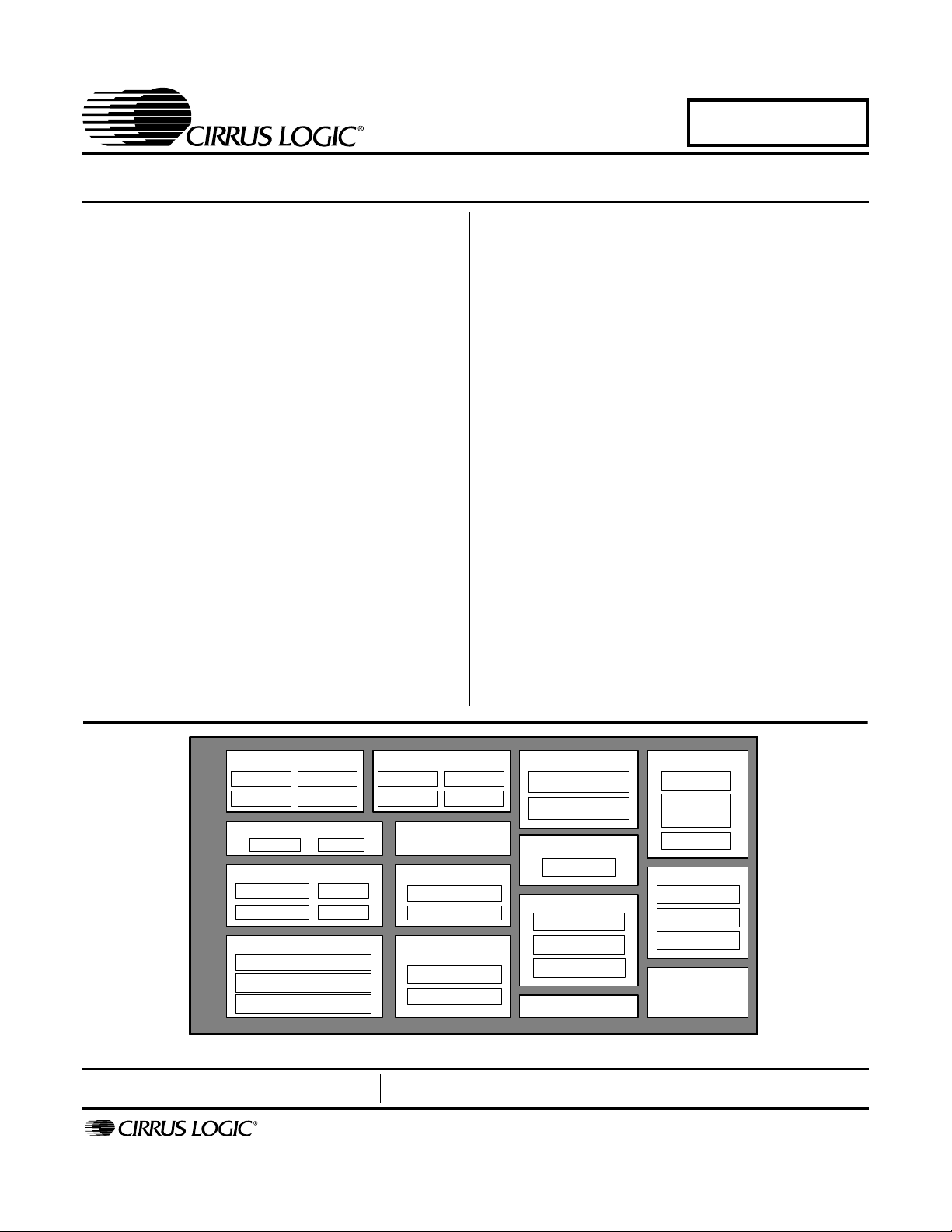
DVD On-a-Chip Solution
CS98000
Features
l Powerful Dual 32-bit RISCs >160 MIPS
l Software based on popular RTOS, C/C++
l MPEG video decoder supports DVD, VCD,
VCD 3.0, and SVCD standards
l Video input with Picture-in-Picture and zoom
l 8-bit multi-region OSD w/vertical flicker filter
l Universal subpicture unit for DVD and SVCD
l PAL<->NTSC Scaling and Transcoding
l Supports SDRAM and FLASH memories
l Powerful 32-bit Audio DSP >80 MIPS
l Decodes: AC-3, DTS, MPEG Stereo
l Plays MP3 CDs
l Karaoke echo mix and pitch shift
l Optional 3-D Virtual, bass & treble control
l Up to 8-channel PCM output
l IEC-60958/61937 Out: AC-3, DTS, MPEG
l Multi-Mode Serial Audio I/O: I2S & AC-Link
l AV Bus or ATAPI interface or DVD/CD/HD
l GPIO support for all common sub-circuits
Description
Overall the CS98000 Crystal DVD Processor is targeted as a market specific consumer entertainment
processor that empowers new product classes with
the inclusion of a DVD player as a fundamental feature. You can use this integrated circuit with all the
other Crystal mixed signal data converters, DSPs,
and the CS98000’s high quality factory firmware to
rapidly conceptualize, design, and market cuttingedge Internet age products such as:
• DVD A/V Mini-Systems
• DVD Players
• DVD Receivers
• Car/SUV Entertainment Units
ORDERING INFORMATION
CS98000-CM 0° to 70° C 208-pin
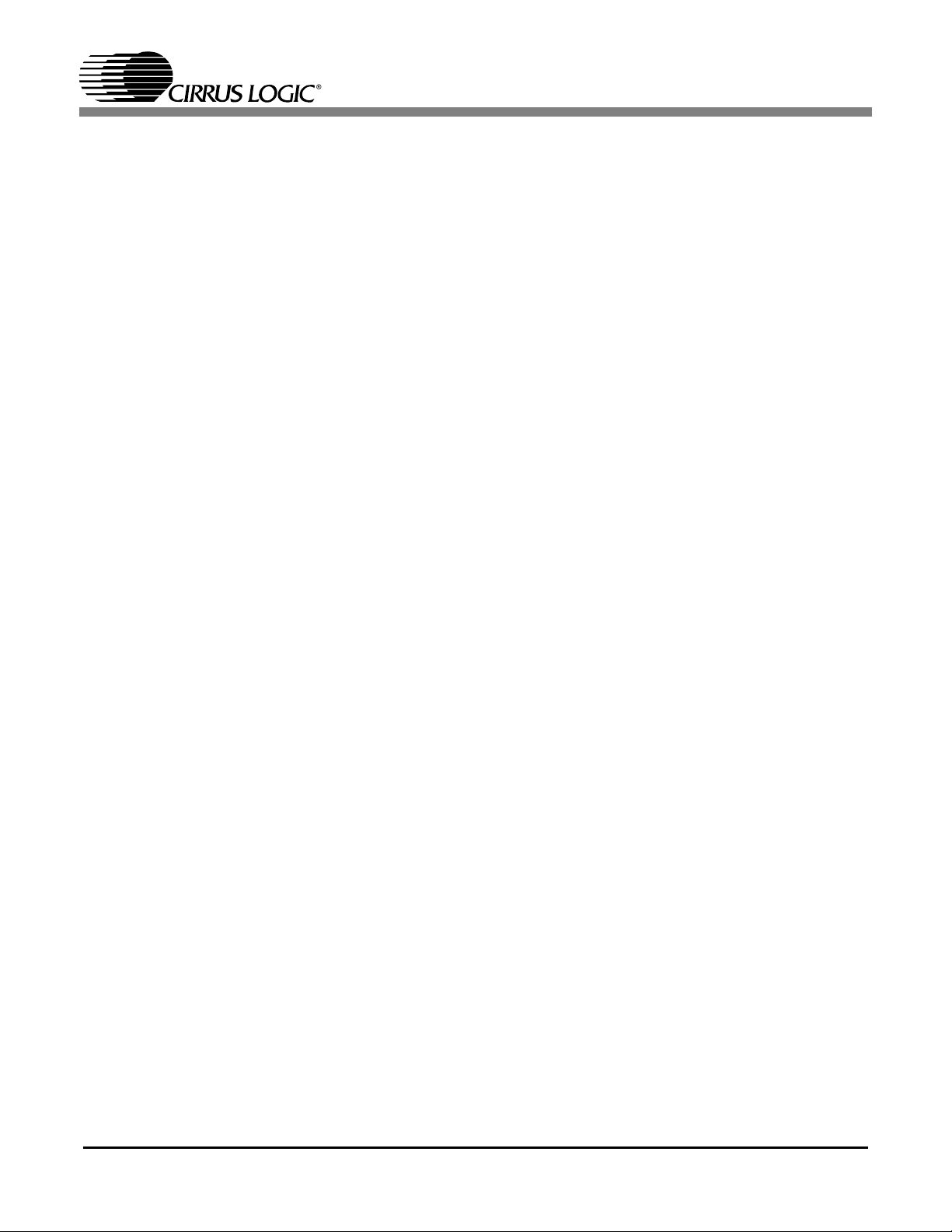
RISC-1
I-Cache D-Cache
MMU
Filter
MPEG Decoder
VLC Parser
RAM MoCo
Video Processor
On-Screen Display
Picture-in-Picture
Video/Graphics Display
MAC
Video Input
Scaler
IDCT
Preliminary Product Information
P.O. Box 17847, Austin, Texas 78760
(512) 445 7222 FAX: (512) 445 7581
http://www.cirrus.com
RISC-2
I-Cache D-Cache
MMU
Clock Manager
Dataflow Engine
This document contains information for a new product.
Cirrus Logic reserves the right to modify this product without notice.
MAC
DMA / BitBlit
SRAM Buffer
External I/Os
Remote Input
GPIOs
Copyright Cirrus Logic, Inc. 2000
Memory Controller
SDRAM Control
FLASH Control
Subpicture Decode
Scaler
System Controls
STC
Interrupts
Registers
SDRAM
(All Rights Reserved)
32- Bit DSP
I-Cache
X,Y Data
Memory
CPU / MAC
Audio I/O
PCM Out
PCM In
XMT958
A/V Bus
ATAPI-IDE
Local Bus
NOV ‘01
DS525PP2
1
TABLE OF CONTENTS
1. CHARACTERISTICS AND SPECIFICATIONS ........................................................................5
1.1 AC AND DC PARAMETRIC SPECIFCATIONS .................................................................5
1.1.1 ABSOLUTE MAXIMUM RATING ..........................................................................5
1.1.2 RECOMMENDED OPERATING CONDITIONS ...................................................6
1.1.3 ELECTRICAL CHARACTERISTICS ....................................................................6
1.2 DC CHARACTERISTICS ................................................................................................... 7
1.2.1 ATAPI Interface .....................................................................................................7
1.2.2 SDRAM Interface .................................................................................................. 8
1.2.3 ROM/NVRAM Interface ......................................................................................10
1.2.4 Video Output Interface ........................................................................................11
1.2.5 Video Input Interface ...........................................................................................12
1.2.6 Audio Input Interface ...........................................................................................13
1.2.7 Audio Output Interface ........................................................................................14
1.2.8 AC97/CODEC Interface ......................................................................................15
1.2.9 Miscellaneous Interface Timing ...........................................................................16
2. TYPICAL APPLICATION ........................................................................................................17
3. FUNCTIONAL DESCRIPTION ...............................................................................................18
3.1 Block Diagram ..................................................................................................................18
3.2 CS98000 Device Details ..................................................................................................18
3.2.1 RISC-32 Processors ...........................................................................................18
3.2.2 Powerful 24/32-Bit DSP ......................................................................................18
3.2.3 System Controls ..................................................................................................18
3.2.4 Memory Controller ...............................................................................................19
3.2.5 Data Flow Engine ................................................................................................ 19
3.2.6 MPEG Video Decoder .........................................................................................19
3.2.7 System Synchronization ......................................................................................19
3.2.8 Audio Interface .................................................................................................... 19
3.2.9 Video Input ..........................................................................................................19
3.2.10 External Interface .............................................................................................. 19
3.2.11 Video Processor ................................................................................................19
3.2.12 Sub-Picture Processor ......................................................................................19
3.2.13 System Functions ..............................................................................................20
3.3 RISC Processor ...............................................................................................................20
3.4 DSP Processor ................................................................................................................20
3.5 Memory Control ...............................................................................................................20
CS98000
Contacting Cirrus Logic Support
For a complete listing of Direct Sales, Distributor, and Sales Representative contacts, visit the Cirrus Logic web site at:
http://www.cirrus.com/corporate/contacts/
Preliminary product information describes products which are in production, but for which full characterization data is not yet available. Advance product information describes products which are in development and subject to development changes. Cirrus Logic, Inc. has made best efforts to ensure that the information contained in this
document is accurate and reliable. However, the information is subject to change without notice and is provided “AS IS” without warranty of any kind (express or implied).
Customers are advised to obtain the latest version of relevant information to verify, before placing orders, that information being relied on is current and complete. All products are sold subject to the terms and conditions of sale supplied at the time of order acknowledgment, including those pertaining to warranty, patent infringement, and
limitation of liability. No responsibility is assumed by Cirrus Logic, Inc. for the use of this information, including use of this information as the basis for manufacture or sale
of any items, nor for infringements of patents or other rights of third parties. This document is the property of Cirrus Logic, Inc. and by furnishing this information, Cirrus
Logic, Inc. grants no license, express or implied under any patents, mask work rights, copyrights, trademarks, trade secrets or other intellectual property rights of Cirrus
Logic, Inc. Cirrus Logic, Inc., copyright owner of the information contained herein, gives consent for copies to be made of the information only for use within your organization
with respect to Cirrus Logic integrated circuits or other parts of Cirrus Logic, Inc. The same consent is given for similar information contained on any Cirrus Logic web site
or disk. This consent does not extend to other copying such as copying for general distribution, advertising or promotional purposes, or for creating any work for resale. The
names of products of Cirrus Logic, Inc. or other vendors and suppliers appearing in this document may be trademarks or service marks of their respective owners which
may be registered in some jurisdictions. A list of Cirrus Logic, Inc. trademarks and service marks can be found
Purchase of I2C components of Cirrus Logic, Inc., or one of its sublicensed Associated Companies conveys a license under the Phillips I2C Patent Rights to use those
components in a standard I2C system.
2
at http://www.cirrus.com
.
CS98000
3.6 Dataflow Control (DMA) ................................................................................................... 20
3.7 System Control Functions ............................................................................................... 21
3.8 DVD/ATAPI Interface ....................................................................................................... 21
3.9 MPEG Video Decoding .................................................................................................... 21
3.10 Audio Processing ........................................................................................................... 21
3.11 Soft Modem ................................................................................................................... 22
3.12 Video ............................................................................................................................. 22
4. MEMORY MAP ....................................................................................................................... 22
4.1 Processor Memory Map .................................................................................................. 22
4.2 Host Port Memory Map .................................................................................................... 22
4.3 Internal I/O Space Map .................................................................................................... 22
5. REGISTER DESCRIPTION .................................................................................................... 24
5.1 CS98000 Register Space ................................................................................................ 24
6. PIN DESCRIPTION ................................................................................................................. 33
6.1 Pin Assignments .............................................................................................................. 34
6.2 Miscellaneous Interface Pins ........................................................................................... 40
6.3 SDRAM Interface ............................................................................................................. 40
6.4 ROM/NVRAM Interface ................................................................................................... 41
6.5 Video Output Interface ..................................................................................................... 41
6.6 Video Input Interface ....................................................................................................... 42
6.7 Audio Output/Input Interface ............................................................................................ 42
6.8 AC97/CODEC Interface ................................................................................................... 43
6.9 Host Master/ATAPI Interface ........................................................................................... 43
6.10 DVD I/O Channel Interface ............................................................................................ 44
6.11 General Purpose Input/Output (GPIO) .......................................................................... 44
6.12 Power and Ground ........................................................................................................ 45
7. PACKAGE SPECIFICATIONS ............................................................................................... 46
LIST OF FIGURES
Figure 1. ATAPI Transactions - Read and Write............................................................................. 7
Figure 2. SDRAM Refresh Transaction........................................................................................... 8
Figure 3. SDRAM Burst Write Transaction ..................................................................................... 8
Figure 4. SDRAM Burst Read Transaction..................................................................................... 9
Figure 5. SDRAM Timing................................................................................................................ 9
Figure 6. ROM/RVRAM Timing..................................................................................................... 10
Figure 7. Video Output Timing..................................................................................................... 11
Figure 8. Video Input Timing......................................................................................................... 12
Figure 9. Audio Input Timings....................................................................................................... 13
Figure 10. Audio Output Timing.................................................................................................... 14
Figure 11. CODEC Timing............................................................................................................ 15
Figure 12. Miscellaneous Timing .................................................................................................. 16
Figure 13. CS98000 Typical Application....................................................................................... 17
Figure 14. CS98000 Block Diagram.............................................................................................. 18
Figure 15. CS98000 Pinouts......................................................................................................... 33
Figure 16. 208-Pin Package Drawing ........................................................................................... 46
LIST OF TABLES
Table 1. ATAPI Interface Symbols / Characterization Data............................................................ 7
Table 2. SDRAM Interface Symbols and Characterization Data..................................................... 8
Table 3. ROM/NVRAM Interface Symbols and Characterization Data......................................... 10
Table 4. Video Output Interface Symbols and Characterization Data........................................... 11
3

CS98000
Table 5. Video Input Interface Symbols and Characterization Data..............................................12
Table 6. Audio Input Interface Symbols and Characterization Data..............................................13
Table 7. Audio Output Interface Symbols and Characterization Data...........................................14
Table 8. AC97/CODEC Interface Symbols and Characterization Data.........................................15
Table 9. Miscellaneous Interface Symbols and Characterization Data......................................... 16
Table 10. Memory Map-RISC0 Processor ....................................................................................23
Table 11. Host Port Memory Map .................................................................................................23
Table 12. Internal IO Space Map ..................................................................................................23
Table 13. CS98000 Register Map and Blocks ..............................................................................24
Table 14. CS98000 Registers.......................................................................................................24
Table 15. Pin Type Legend...........................................................................................................33
Table 16. 208-Pin Package Assignments .....................................................................................34
Table 17. Miscellaneous Interface Pins.........................................................................................40
Table 18. SDRAM Interface ..........................................................................................................40
Table 19. ROM/NVRAM Interface................................................................................................. 41
Table 20. Video Output Interface ..................................................................................................41
Table 21. Video Input Interface.....................................................................................................42
Table 22. Audio Input/Output Interface .........................................................................................42
Table 23. AC97/CODEC Interface ................................................................................................43
Table 24. Host Master/ATAPI Interface.........................................................................................43
Table 25. DVD I/O Channel Interface............................................................................................44
Table 26. General Purpose I/O Interface ......................................................................................44
Table 27. Power and Ground.......................................................................................................45
4
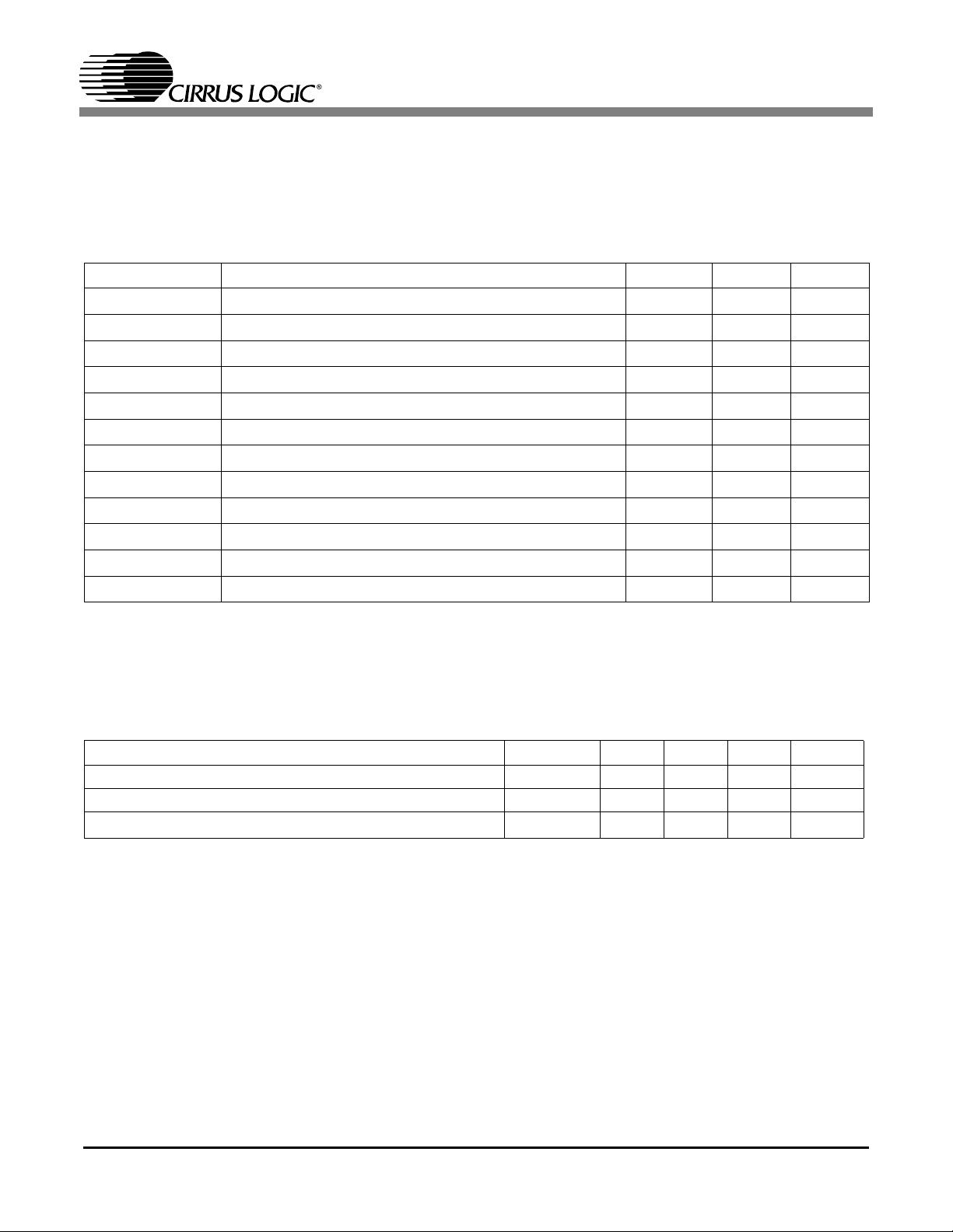
1. CHARACTERISTICS AND SPECIFICATIONS
1.1 AC AND DC PARAMETRIC SPECIFICATIONS
(AGND, DGND=0V, all voltages with respect to 0V)
1.1.1 ABSOLUTE MAXIMUM RATING
Symbol Description Min Max Unit
VDD
VDD
V
I
I
I
I
O
T
SOL
T
VSOL
T
STOR
T
AMB
P
IO
P
CORE
P
PLL
IO
CORE
Power Supply Voltage on I/O ring -0,5 4.6 Volts
Power Supply Voltage on core logic and PLL -0.5 3.6 Volts
Digital Input Applied Voltage (power applied) -0.5 5.5 Volts
Digital Input Forced Current -10 10 mA
Digital Output Forced Current -50 50 mA
Lead Soldering Temperature - 260
Vapor Phase Soldering Temperature - 220
Storage Temperature (no power applied) -40 125
Ambient Temperature (power applied) 0 70
Power consumption on I/O ring (CL = 35 pF) - 57 mA
Power consumption on the core logic - 620 mA
Power consumption on the PLL logic - 15 mA
CS98000
o
C
o
C
o
C
o
C
CAUTION: Operating beyond these Minimum and Maximum limits can result in permanent damage to
the device. Cirrus Logic recommends that CS98000 devices operate at the settings described in the next
table.
1.1.2 RECOMMENDED OPERATING CONDITIONS
Parameter Symbol Min Typ Max Units
Supply Voltage, IO V
Supply Voltage, core and PLL V
Ambient Temperature(power applied) T
DD
DD
AMB
3.0 3.3 3.6 Volts
2.25 2.5 2.75 Volts
0 25 70
o
C
5
1.1.3 ELECTRICAL CHARACTERISTICS
Parameter Symbol Conditions Min Typ Max Units
Supply Current, IO I
Supply Current, core and PLL I
Input Voltage, High V
Input Voltage, Low V
Input Current I
Input Pull up/down resistor R
Output Voltage, High V
Output Voltage, Low V
Three-state Leakage I
Input Capacitance C
Output Capacitance C
Bidirect Capacitance C
DD
DD
IH
IL
IN
I
OH
OL
OZ
IN
OUT
BID
CS98000
Normal Operating - 45 - mA
Normal Operating - 550 - mA
2.0 - 5.0 Volts
- - 0.8 Volts
V
= V
DD
or V
SS
IN
@ buffer rating 2.4 - - Volts
@ buffer rating - - 0.4 Volts
V
= VSS or V
OUT
DD
-1 - +1 µA
- 75 - KΩ
-10 - +10 µA
- 3 - pF
3 6 pF
3 6 pF
6
CS98000
1.2 DC CHARACTERISTICS
(TA= 25°C; VDD_PLL=VDD_CORE=2.5V±10%, VDD_IO=3.3V±10%)
1.2.1 ATAPI Interface
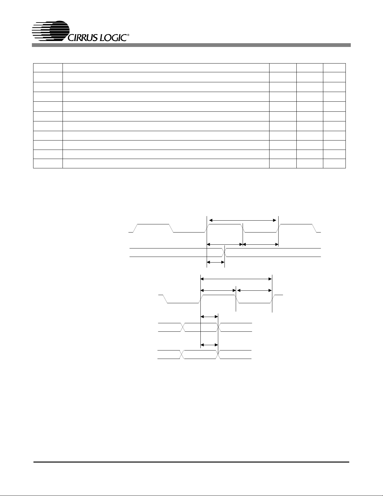
CS98000 can interface with a ATAPI-type slave loader gluelessly. Figure1 illustrates a read ATAPI trans-
action and a write ATAPI transaction. PIO mode 4 is implemented to enable a sufficient data transfer rate
between ATAPI device and CS98000.
Note: ATAPI interface is a standard administered by the T13 committee that is responsible for all interface standards
relating to the AT Attachment (ATA) storage interface. T13 is a technical committee for the National
Committee on Information Technology Standards (NCITS).See http://www.t13.org/.
Symbol Description Min Typ Max Unit
t
acyc Cycle Time
t
aavr
t
arww
t
arec
t
awsu
t
awh
t
ardsu
t
arddh
t
ardr
t
arsu
t
aipw
t
arls
Address Valid to HMRD-/HMWR- Setup 20 ns
H_RD-/H_WR- Pulse Width 70 ns
H_RD-/H_WR- Recovery Time 25 ns
H_WR- Data Setup 20 ns
H_WR- Data Hold 10 ns
H_RD- Data Setup 20 ns
H_RD- Data hold 5 ns
Read Data Valid to H_RDY Active 0 ns
H_RDY Setup Time 35 ns
H_RDY Pulse Width 1250 ns
H_RDY Assertion to Release 5 ns
1
70 ns
Table 1. ATAPI Interface Symbols / Characterization Data
1.
Values are guaranteed by design only.
H_A[4:0]
H_RD-/H_WR-
H_D[15:0](WRITE)
H_D[15:0](READ)
H_RDY(deasserted
before tarsu)
H_RDY(asserted
before tarsu)
tacyc
taavr
tarsu
tarar
tarww
taipw
Figure 1. ATAPI Transactions - Read and Write
tardr
tardsu
tarec
Dout
tawhtawsu
Din
tarddh
tarls
7
CS98000
1.2.2 SDRAM Interface
CS98000 interfaces with either SDRAM or SGRAM for high data bandwidth transfer. Figure2 shows the
refresh cycle performed by CS98000. Figure3 shows a burst write (length = 8) transaction. Figure4 on
page9 shows a burst read (length = 8) transaction, while Figure5 on page9 shows detailed SDRAM in-
terface timing. In both Figure3 and Figure4, CAS latency is programmed to 3.
Symbol Description Min Typ Max Unit
t
msur
t
mhr
t
mco
tcch M_CKO high time 4.5 ns
tccl M_CKO low time 4.5 ns
t
mper
t
mhw
t
mdow
tmsuw M_D[31:0] valid time prior to M_CKO 4 ns
1.
Values are guaranteed by design only.
M_D[31:0] setup to M_CKO 3 ns
M_D[31:0] hold time after M_CKO 1 ns
M_CKO active edge to Output transition 7 ns
M_CKO Period1
10 12.5 ns
M_D[31:0] valid time after M_CKO 5 ns
M_D[31:0] delay from M_CKO rising edge 5 ns
Table 2. SDRAM Interface Symbols and Characterization Data
M_CKE
M_A_[11:0]
M_BS_N
M_RAS_N
M_CAS_N
M_WE_N
MD[31:0]
M_DQM_[3:0]
M_CKO
M_A_[11:0]
M_BS_N
M_RAS_N
M_CAS_N
M_WE_N
M_D_[31:0]
M_DQM_[3:0]
M_AP
M_AP
Figure 2. SDRAM Refresh Transaction
C1 C2 C3 C4 C5 C6 C7C0R0
D0 D1 D2 D3 D4 D5 D6 D7
Figure 3. SDRAM Burst Write Transaction
8
M_CKO
M_A_[11:0]
M_BS_N
M_RAS_N
M_CAS_N
M_WE_N
M_D_[31:0]
M_DQM_[3:0]
M_AP
CS98000
C1 C2 C3 C4 C5 C6 C7C0R0
D0 D1 D2 D3 D4 D5 D6 D7
Figure 4. SDRAM Burst Read Transaction
tccltcchtmpertmco
M_CKO
M_WE_N,M_AP,M_DQM[3:0],
M_RAS_N,M_CAS_N
M_CKE,M_A[11:0]
M_D[31:0](WRITE)
M_D[31:0](READ)
tmsur
tmhr
Figure 5. SDRAM Timing
tmdow
tmhw
tmsuw
9
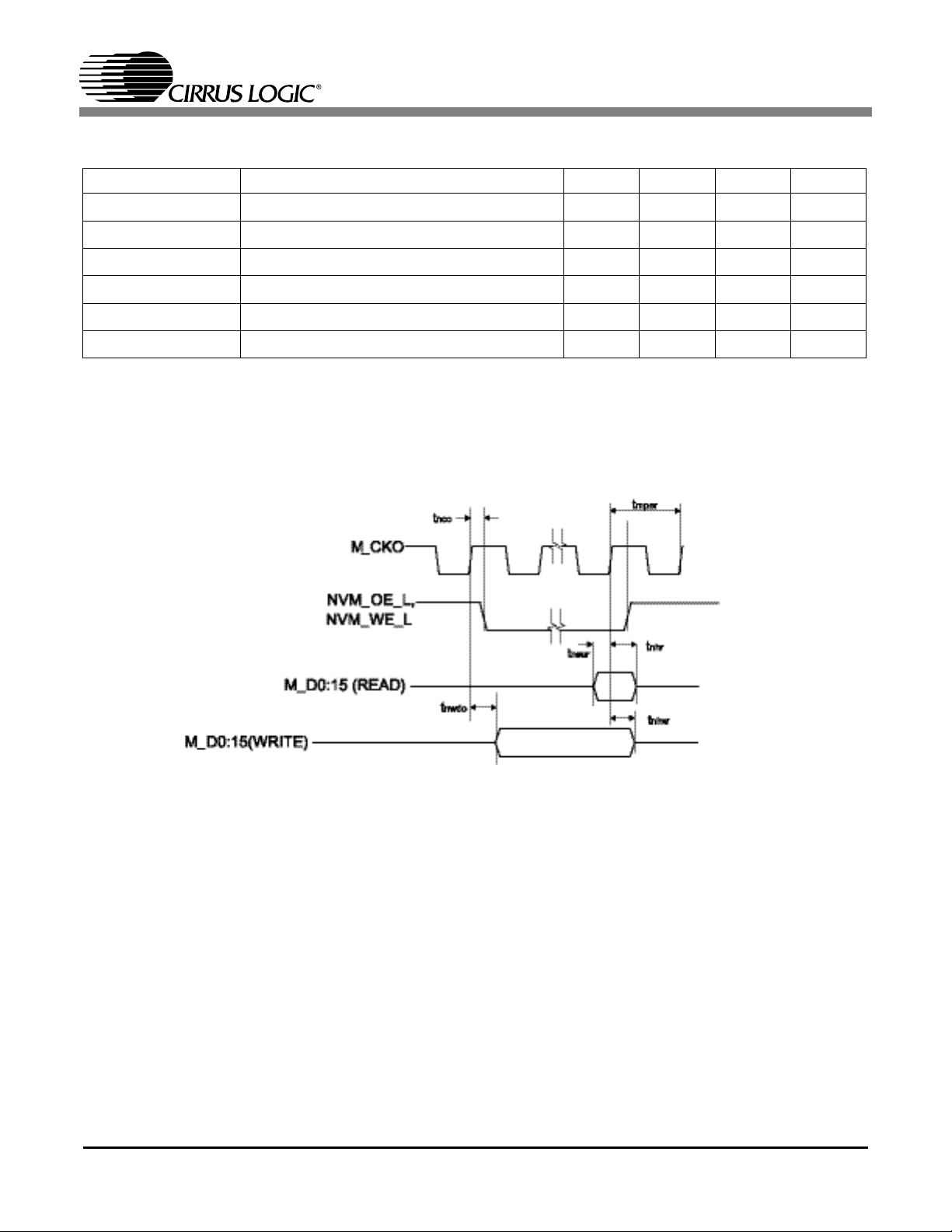
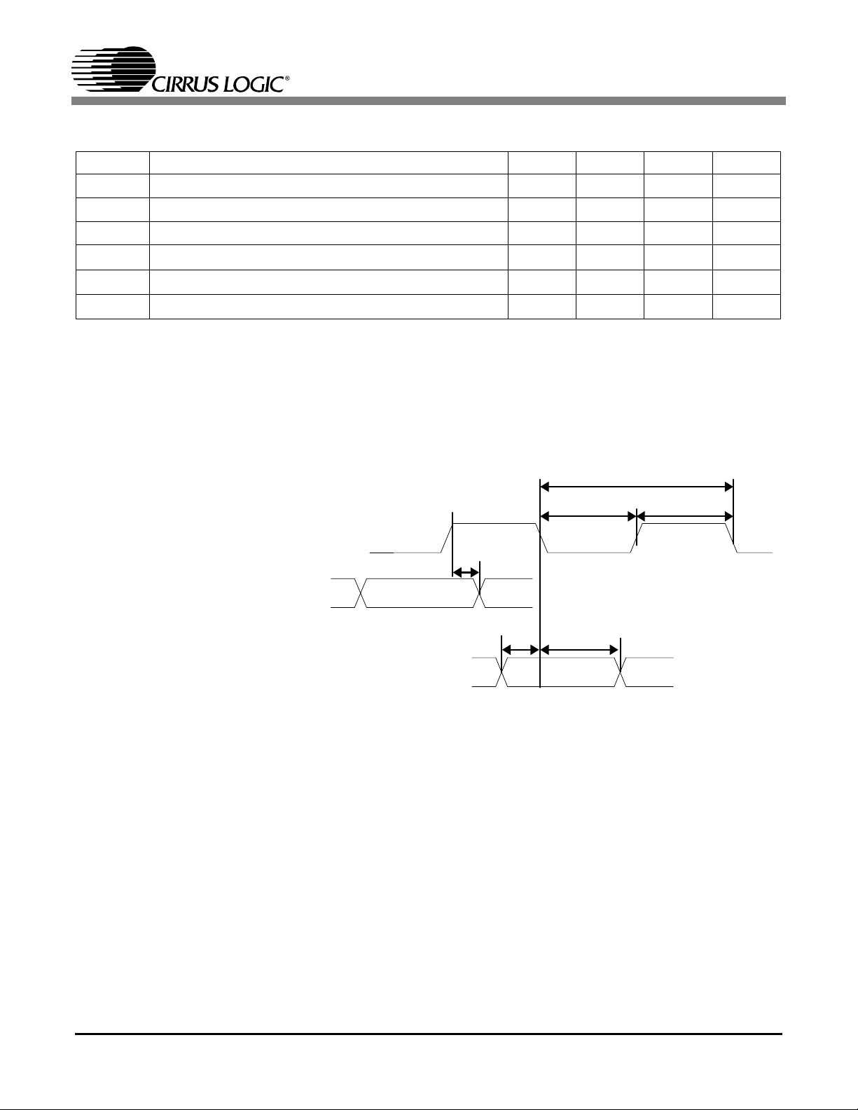
1.2.3 ROM/NVRAM Interface
Symbol Description Min Typ Max Unit
t
mper M_CKO period
t
nco
t
nwdo
t
nsur
t
nhw
t
nhr
M_CKO to WE or OE out 15 ns
M_CKO to write data out 10 ns
Data setup to M_CKO 5 ns
Data hold from WE inactive 5 ns
Data hold from OE inactive 1 ns
Table 3. ROM/NVRAM Interface Symbols and Characterization Data
1.
Values are guaranteed by design only.
CS98000
1
10 12.5 ns
10
Figure 6. ROM/RVRAM Timing
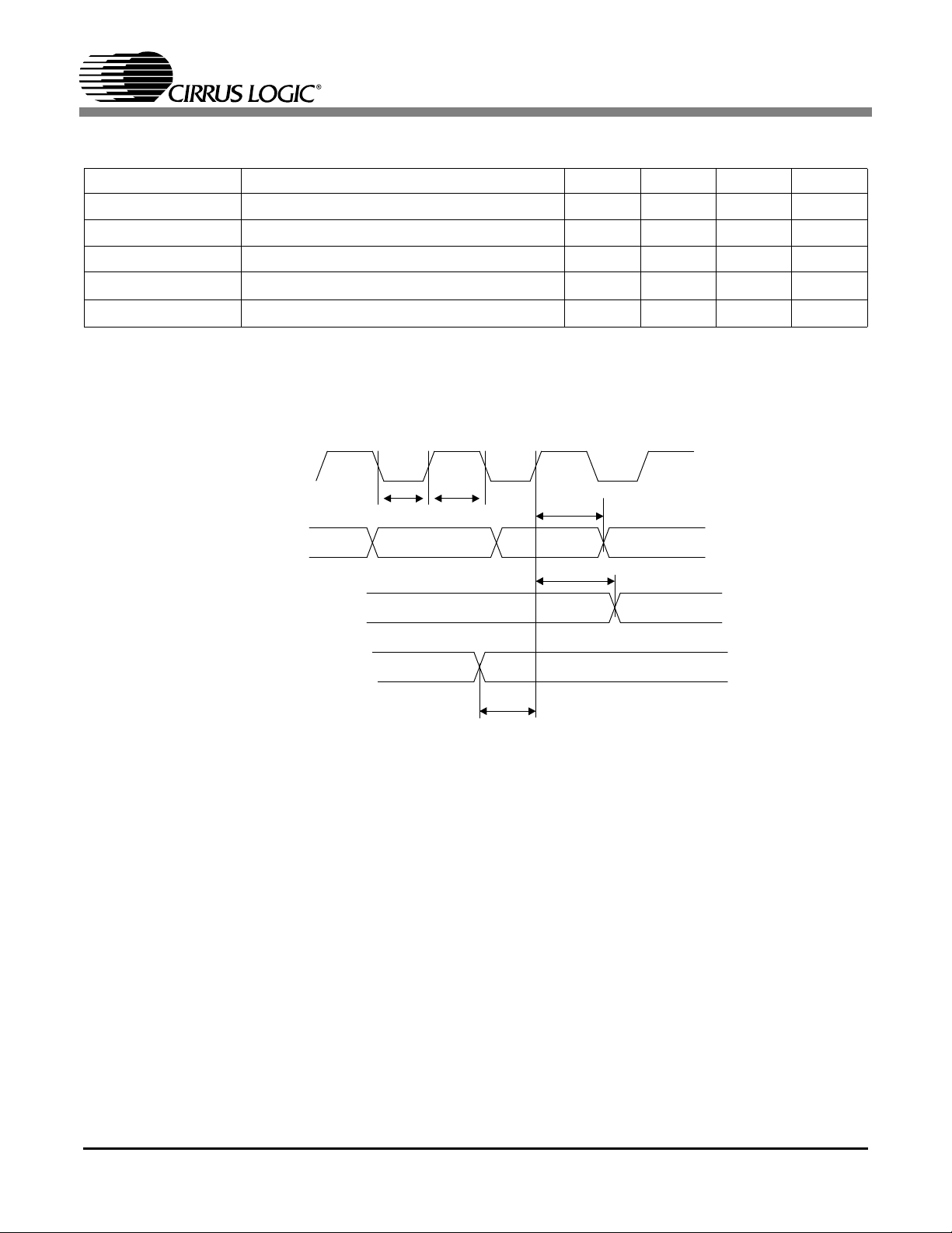
1.2.4 Video Output Interface
Symbol Description Min Typ Max Unit
t
suvo
t
covo1
t
covo2
t
voch
t
vocl
Vsync/Hsync input setup to CLK27_O 5 ns
VDAT[7:0] delay from CLK27_O transition 10 ns
Vsync/Hsync delay from CLK27_O transition 10 ns
CLK27_O High Time
CLK27_O Low Time
Table 4. Video Output Interface Symbols and Characterization Data
1.
Values are guaranteed by design only
CLK27_O
(Output)
VDAT[7:0]
(Output)
1
1
Tvocl Tvoch
CS98000
14.8 18.5 22.2 ns
14.8 18.5 22.2 ns
Tcovo1
Tcovo2
VSYNC/HSYNC (Output)
VSYNC/HSYNC (Input)
Tsuvo
Figure 7. Video Output Timing
11
CS98000
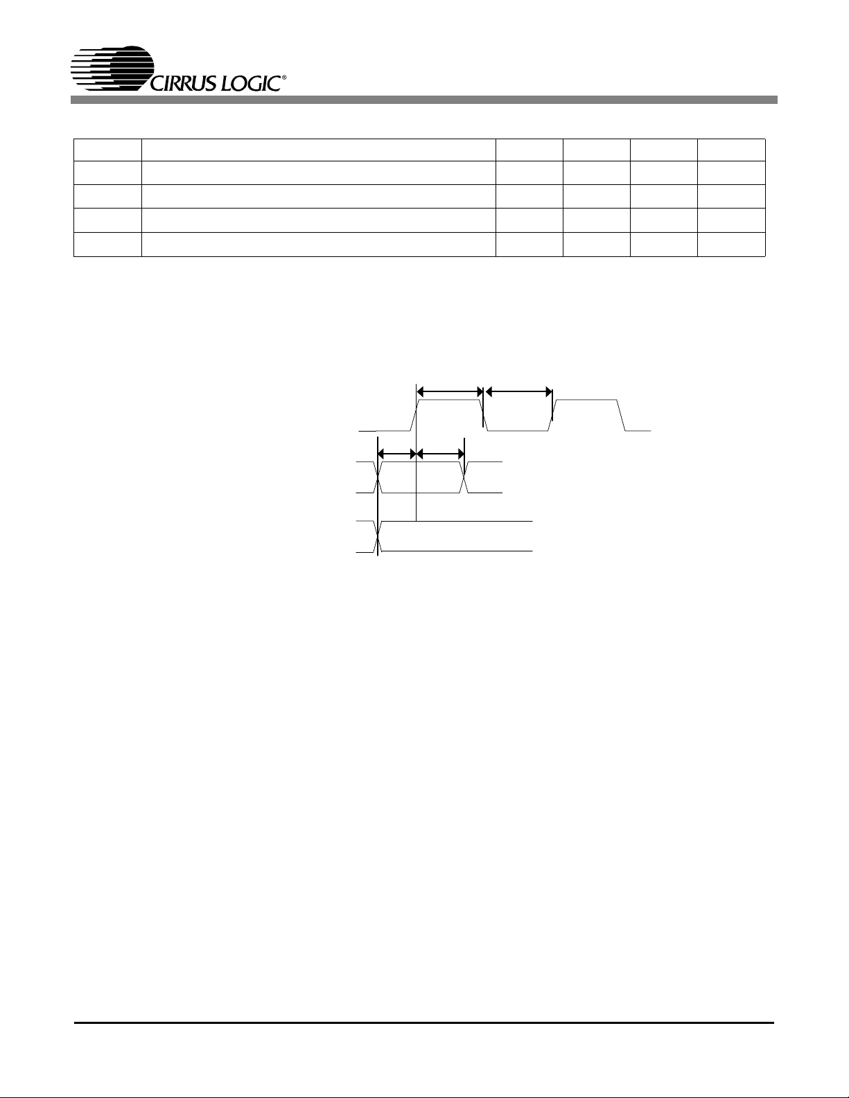
1.2.5 Video Input Interface
Symbol Description Min Typ Max Unit
.
t
suvi
t
hvi
t
vich
t
vicl
1.
VIN_D[7:0] set up to VIN_CLK 5 ns
VIN_D[7:0] hold time after VIN_CLK rising edge 2 ns
VIN_CLK High Time
VIN_CLK Low Time
1
1
14.8 18.5 22.2 ns
14.8 18.5 22.2 ns
Table 5. Video Input Interface Symbols and Characterization Data
Active clock edge is programmable. Timing is referenced from active edge
VIN_CLK
VIN_D[7-0]
VIN_HSNC,VIN_VSNC,
VIN_FLD
tvicl
tvich
tsuvi thvi
Figure 8. Video Input Timing
12
1.2.6 Audio Input Interface
CS98000
Symbol
t
aicl
t
aich
t
aiper
t
stlr
t
lrts
t
sdsus
t
sdhs
AIN_BCK Low Time1,
AIN_BCK High Time
AIN_BCK period
1, 2
Time form AIN_LRCK transition to AUD_BCK active edge 5 - ns
Time form AIN_LRCK transition to AIN_BCK active edge 2 - ns
AIN_DATA setup to AIN_BCK transition 5 - ns
AIN_DATA hold time after AIN_BCK transition 2 - ns
Description Min Typ Max Units
2
1, 2
Table 6. Audio Input Interface Symbols and Characterization Data
1.
Values are guaranteed by design only
2.
Active clock edge is programmable. Timing is referenced from active edge
AIN_BCK (Input)
14 ns
14 ns
162.7 ns
t
aiper
t
aich
t
lrts
t
stlr
t
aicl
AIN_LRCK (Input)
AIN_DATA (Input)
t
sdsus
t
sdhs
Figure 9. Audio Input Timings
13
CS98000
1.2.7 Audio Output Interface
Symbol Description Min Max Units
1, 2
2
4.5 - ns
4.5 - ns
13 ns
14 - ns
14 ns
162.7 ns
- 2
- 2
- 2
- 2
t
axper
t
axch
t
axcl
t
axper
t
aoch
t
aocl
t
aoper
t
sdm
t
sdm
t
lrds
t
adsm
AUD_XCLK High Time (AUD_XCLK is Input/Output)1,
AUD_XCLK Low Time (AUD_XCLK is Input/Output)
AUD_XCLK period (Input/Output)
AUD_BCK High Time for Master mode
AUD_BCK Low Time for Master mode
AUD_BCK period (Output)
1, 2
1, 2
1, 2
1, 2
AUD_BCK delay from AUD_XCLK transition
AUD_BCK delay from AUD_XCLK transition
AUD_LRCK delay from AUD_BCK transition
AUD_D[3:0] delay from AUD_BCK transition
Table 7. Audio Output Interface Symbols and Characterization Data
1.
Values are guaranteed by design only
2.
Active clock edge is programmable. Timing is referenced from active edge
ns
ns
ns
ns
AUD_XCLK(Input/Output)
AUD_BCK(Output)
AUD_BCK(Output)
AUD_LRCK(Output)
AUD_DO[3:0] (Output)
t
axch
t
sdm
t
aoperl
t
aoch
t
lrds
t
adsm
Figure 10. Audio Output Timing
t
axcl
t
aocl
14
CS98000
1.2.8 AC97/CODEC Interface
Symbol Description Min Typ Max Units
t
suc
t
hc
t
coc
t
cch
t
ccl
t
ccper
1.
2.
Data set up to CDC_CK 5 ns
Data hold time after CDC_CK 1 ns
Time from active edge of CDC_CK to Data transition 10 ns
CDC_CK High Time1,
CDC_CK Low Time
CDC_CK period
1, 2
1, 2
2
14 ns
14 ns
162.7 ns
Table 8. AC97/CODEC Interface Symbols and Characterization Data
Values are guaranteed by design only
Active clock edge is programmable. Timing is referenced from active edge
tccper
CDC_CK
(Intput)
CDC_DO,
CDC_SY, CDC_Rst
(Output)
CDC_DI, CDC_SY
(Input)
tcoc
Figure 11. CODEC Timing
tsuc
thc
tccl
tcch
15

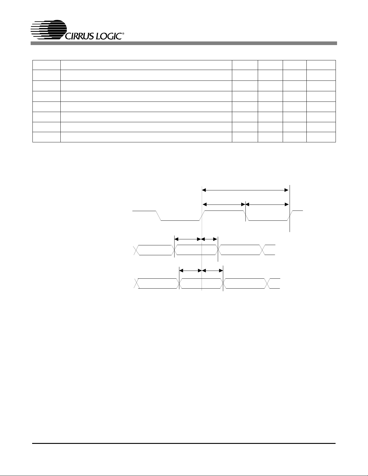
1.2.9 Miscellaneous Interface Timing
Symbol Description Min Typ Max Units
t
xccl
t
xcch
t
xccper
t
rstl
t
gpl
t
gpl
1.
XTLCLOCK must meet the requirement of external the video encoder for correct chroma.
XTLCLOCK Rise Time 4.5 ns
XTLCLOCK Fall Time 4.5 ns
XTLCLOCK period
RESET_N Pulse Width 1000 ns
GPIO PW Low 50 ns
GPIO PW High 50 ns
XTLCLOCK/RESET_N Rising Time 5 ns
XTLCLOCK/RESET_N Falling Time 5 ns
Table 9. Miscellaneous Interface Symbols and Characterization Data
1
CS98000
14.8 18.5 22.2 ns
XTLCLOCK
RESET-N
GPIO
txccl
tgph
Figure 12. Miscellaneous Timing
tgpl
xccper
t
trstl
txcch
16

CS98000
2. TYPICAL APPLICATION
The Figure13 shows a typical example of a complete Internet-DVD solution using the CS98000.
Remote
Keyboard/
Control
Audio-L
Audio-R
Video
DAA
IR
CODEC
Front Panel
Audio
ADC
Video
Decoder
DVD Loader
(I/O Chan)
or
ATAPI
Loader
+ Hard Drive*
* Hard drive useable with ATAPI loader
Figure 13. CS98000 Typical Application
CS98000
FLASH
.5-2MB
FLASH
2MB
SDRAM
SDRAM
4-8MB
8MB
(3)Audio
DACs
Driver
Video
Encoder
Power
Reg.
Phone
Line
Parallel Port
Audio-L(3)
Audio-R(3)
S/PDIF
S-Video
Composite Video
Switch
Power
17

CS98000
3. FUNCTIONAL DESCRIPTION
3.1 Block Diagram
The CS98000 block diagram is shown in Figure14.
3.2 CS98000 Device Details
3.2.1 RISC-32 Processors
• Two Powerful 32-bit RISC processors (RISC0 and
RISC1)
• Virtual memory support
• Optimizing C compiler
• Big or little endian data formats support
• MAC multiply/accumulate in 2 cycles with C support
• 4Kbyte instruction cache, 2Kbyte data cache
• Single cycle instructions, runs at 81Mhz
3.2.2 Powerful 24/32-Bit DSP
• Powerful 24/32 bit DSP processor, programmable
through CS98000 API, See CS98000 Software API,
(DS525UM1)
• 24-bit fixed point logic, with 54-bit accumulator
• Single-cycle throughput, 2-cycle latency multiply
accumulate, 32-bit simple integer logic. 8-Kbyte instruction cache, 8-Kbyte program visible local memory
• Single cycle instructions, runs at 81Mhz
3.2.3 System Controls
• Includes several hardware lockable semaphore
registers
• General-purpose register for inter-processor communication
• 32-bit timers for I/O and other uses, with programmable interval rates
18
Figure 14. CS98000 Block Diagram

CS98000
• Both hardware and software interrupts on data or
debug
• Built in PLLs generate all required clocks from
27Mhz input clock
3.2.4 Memory Controller
• Supports SDRAM, and SGRAM, from 2Mbytes to
32Mbytes
• Supports multiple banks of FLASH and ROM up to
16Mbytes
• 32-bit data bus for DRAM, 8 or 16-bit data bus for
ROM
3.2.5 Data Flow Engine
• 2432 bytes of internal memory
• DMA to/from main RAM into local SRAM
• Supports endian conversion and byte, short, long
data formats on DMA
• Supports block transfers for graphics bit blits
3.2.6 MPEG Video Decoder
• Supports VCD, VCD 3.0, SVCD, DVD video standards
• Supports trick features, including smooth 2x play
and reverse play
• Special anti-tearing logic controls picture decode
and presentation
• Advanced error concealment hardware
3.2.7 System Synchronization
• System time clock (STC) for audio/video synchronization
• Flexible interrupt structure for controlling decode
and presentation times
• Hardware scheduling of subpicture and highlight
events
3.2.8 Audio Interface
• Supports PCM, I2S and IEC-958 outputs at up to
96KHz output rate
• 8 output channels, 2 input channels
3.2.9 Video Input
• NTSC/PAL video decoder input interface
• Built in variable down scaling, handles CCIR 601 to
QCIF input formats
• Video input image can be displayed in small window, or as main picture
3.2.10 External Interface
• Serial I2C
®
master and slave port
• 29 independent fully programmable bi-directional
I/O pins
• 8 edge or level detection interrupt pins
• Hardware assisted support for infrared remote devices, such as remote control, infrared keyboard,
mouse, printer, and more
• Programmable parallel host master and slave interface supports many formats including ATAPI, ISA,
and more
• IO channel interface supports standard DVD loader
protocols
• Serial interface supports AC-97 and other standard
MODEM CODEC protocols
3.2.11 Video Processor
• Supports 24-bit 4:2:0 and 4:2:2 video modes and
16-bit true color graphics modes.
• On screen display module supports 2-bit, 4-bit, or 8bit pixel modes, while supporting 3 separate regions
and 16 transparency overlay levels
• Picture-in-picture module includes horizontal and
vertical downscaling with programmable output sizes, positions, and borders
• Overlay mixer with RGB to YUV conversion and
output formatting
• Supports 4:2:0, 4:2:2, YUV655, RGB565 and
RGB555 frame buffer inputs
• Outputs 4:2:2 video in CCIR-601 or CCIR-656 format
• High quality scaling using a vertical and a horizontal
16 taps polyphase programmable filter and supports any size image up to 768x576
• Programmable sharpening and de-blocking filters
• 5 taps programmable adaptative anti-flicker filtering
for graphics source
• Master or Slave video sync configuration
• Multiple video plains overlay (main video / video input / picture_in_picture / picture/on_screen / display/cursor)
• Gamma correction
3.2.12 Sub-Picture Processor
• Run-length decode DVD sub-pictures and SVCD
OGT formats
• Hardware vertical scaling supports NTSC-PAL format conversion
• 16-level alpha blending
• Provides hardware cursor mode for non-DVD applications
19

CS98000
3.2.13 System Functions
• 208-pin PQFP packages
• All I/O pins are 3V with 5V tolerance
• Advanced 0.25 micron CMOS technology
• Internal processors run at 81MHz
• Supports Low Power modes and clock shutoff
3.3 RISC Processor
The CS98000 includes two powerful, proprietary
32-bit RISC processors, RISC0 and RISC1, with
optimizing C compiler support and source level debugger. The RISC processors fully support many
Real Time Operation Systems (RTOS). The DVD
application user interface resides on RISC1 and is
customer programmable. The real time control of
low level DVD functions is performed by RISC0.
RISC1 gains access to system resources controlled
by RISC0 via calls through an Applications Programming Interface, (see the CS98000 Software
API). All RISC0 firmware, API and sample application code are supplied with the CS98000.
The RISC processors also have a MAC engine,
which performs multiply/accumulate in 2 cycles in
a pipelined fashion with C support, effectively
achieving single cycle throughout. The RISC0 processor coordinates on-chip multi-threaded tasks, as
well as system activities such as remote control and
front panel control. The DVD application end-user
interface resides on RISC1, and any modifications
to that interface occur through the CS98000 API.
3.4 DSP Processor
The CS98000 contains a proprietary digital signal
processor (DSP), which is optimized for audio applications. The DSP performs 32-bit simple integer
operations, and has a 24-bit fixed point logic unit,
with a 54-bit accumulator. There are 32 generalpurpose registers, and eight independent address
generation registers, featuring: linear and circular
buffer operations, and dual operand read from
memory. The multiply-accumulator has single-cycle throughput, with two cycle latency. The DSP is
optimized for bit packing and unpacking opera-
tions. The interface to main memory is designed for
handling flexible block sizes and skip counts.
3.5 Memory Control
The DRAM Interface performs the SDRAM control and arbitration functions for all the other modules in the CS98000. The DRAM interface services
and arbitrates a number of clients and stores their
code and/or data within the local memory. This arbitration and scheduling guarantees the allocation
of sufficient bandwidth to the various clients. The
DRAM Interface supports up to 32Mbytes. For a
typical DVD player application, CS98000 requires
8Mbytes memory space.
Sharing the same interface, CS98000 also supports
FLASH ROM, OTP, or mask ROM interface. Code
is stored in ROM. After the system is booted, the
code is shadowed inside SDRAM for execution.
The FLASH ROM interface is provided so that the
code can be upgraded in the field once the communications channel is established (via modem port,
CD-R, or serial port). Utility software will be provided to debug and upgrade code for the system
manufacturer.
3.6 Dataflow Control (DMA)
The DMA controller moves data between the external memory and internal memory. The external
memory address can be specified using a register,
or in FIFO mode, using start and end address registers. Separate start/end address registers are used
for DMA read and write operations. The DMA interface also has a block transfer function, which allows for the transfer of one block of data from one
external memory location to another external memory location. In effect, this feature combines a
DMA read and write into one operation. In addition, the DMA write operation allows for byte,
short, word, and other types of masking.
3.7 System Control Functions
The system control functions are used to coordinate
the activities of the multiple processors, and to pro-
20

CS98000
vide the supporting system operations. Four 32-bit
communication registers are available for interprocessor communication, and eight semaphore
registers are used for resource locking. Timers are
available for general-purpose functions, as well as
more specialized functions such as watchdog timers and performance monitoring.
The large number of general purpose I/Os offers
flexibility in system configurations. An I2C master
allows for control of other I2C devices, such as a
video encoder. An I2C slave port shares the same
pins, and can be used for debug functions. Interrupts can be generated on specific or generic
events. Infrared inputs can be filtered to make them
free of glitches or stored unfiltered into memory.
Control of all the internal clocks is also possible.
Internal PLLs are used to generate the internal system and memory clocks and audio clocks of any
widely used frequency.
3.8 DVD/ATAPI Interface
The CS98000 has a programmable interface port
which can be configured to connect to industry
standard CD/DVD loaders without external glue
logic. The CD/DVD interface fully supports many
popular CD/DVD loaders. The interface consists of
DVD control and data ports and an optional CD
control/data port.
The CS98000 hardware manages the DVD interface and moving data to an arbitrary size input
FIFO in DRAM. The same interface pins can be
optionally configured as a generic 16-bit host master port. In this mode, the CS98000 can control up
to four devices (using 4 chip select outputs), each
of which may use different protocol and timing.
The interface can be set up in ATAPI mode, to connect directly to any
ATAPI DVD loader (using two chip selects). Simultaneously, the other two chip selects can be
configured to connect to other devices, such as a
super I/O chip or hard disk.
A third option is to configure the interface for micro-less DVD loader operation, which may also be
configured to connect without external glue logic.
3.9 MPEG Video Decoding
Compressed MPEG data is read from the DVD disk
into an input FIFO in DRAM. The data flow
(DMA) controller moves Video packets from the
input FIFO into the MPEG decoder’s input FIFO
(also in DRAM). The DMA controller can also perform advanced functions such as start code search,
relieving the RISC processors. The System Synchronization function is used to control the timing
of MPEG picture decoding. The MPEG Video decoder processes I, B, and P frames, and writes to
video frame buffers in DRAM for output to the display. Special anti-tearing logic ensures that currently displayed frame buffers are not overwritten.
3.10 Audio Processing
Compressed Audio data is read from the DVD disk
into an input FIFO in DRAM. The data is decompressed, then written to a PCM output FIFO, also in
DRAM. Presentation time stamps (PTS) are extracted from the stream to update the STC, in order
to maintain audio/video synchronization.
The DMA and decompression stages of audio processing can be done with a combination of the
DMA unit, DSP, and RISC processors. The DSP is
optimized for audio processing, so most common
formats can be handled by the DSP alone, including AC-3, DTS, MPEG2 audio, and MP3. The DSP
has enough reserve bandwidth to handle the
Karaoke echo-mix and pitch shift, and AC-3 downmix functions.
The audio output data is written into a DRAM
FIFO in 16-, 18-, 20- or 24-bit PCM format. A flexible audio output stage can simultaneously output 8
channels of PCM data to audio DACs, or 6 channels of audio data plus an IEC-958 encoded output,
at up to 96 KHz. The audio interface also includes
a flexible PCM input interface, which can input a
21

CS98000
wide range of protocols from an audio ADC or an
IEC-958 receiver.
3.11 Soft Modem
The soft modem processing is handled by one of
the RISC processors, which is typically dedicated
for that function. Data rates up to 56Kbits (V.90
protocol) are supported. The CS98000 interfaces to
a simple external CODEC/DAA circuit using a
flexible serial interface. The serial interface is a fully programmable, bi-directional interface and can
be used either as a PCM interface or as an AC97 interface. In PCM mode, the sample size could be adjusted to 20, 18 or 16 bits to match common DAC
and ADC formats, or any other specific size. In
AC97 mode, any slot can be used to interface either
a modem CODEC or an audio CODEC.
3.12 Video
The Digital Video Interface provides flexible and
powerful means of outputting digital video data to
external devices in CCIR601/3 and CCIR656 formats. The interface directly supports NTSC/PAL
video encoding, in both master and slave synchronization configurations. The internal frame buffer
format could be 4:2:0, 4:2:2, YUV655, RGB565
and RGB555. Cirrus Logic provides some easy-touse utilities in order to get the best advantage of the
powerful video filtering capabilities of the
CS98000. The CS98000 also features an
NTSC/PAL video decoder input interface. The interface accepts CCIR601, CIF, and QCIF formats,
out of many TV decoders on the market. The video
processor also allows overlay of multiple video
planes (main video / video input /
picture_in_picture / on_screen display / cursor).
CS98000 has been proven to work with many TV
encoders on the market with brands such as: Crystal, Brooktree, ADI, and AVS.
The Video Input Scaler (VIS) module inputs 8-bit
digital video data from a camera or PAL/NTSC decoder, optionally down-scales to SIF or QSIF, and
stores the data in one to three DRAM frame buffers. The scaled image, with a border, can be overlaid anywhere on the screen into a ½ or ¼-screen
sized window by the Picture in Picture (PIP) module.
An alternate method of using the Video Input function is to input a full sized picture and present it on
the screen full size (bypass mode). In this mode, the
PIP module can place full motion DVD images in
the small window. An internal glitch-free mux can
switch the video processor clock source from the
internal clock to the Video Input clock, allowing
the PIP mode to switch back and forth on the fly,
with no dropout.
4. MEMORY MAP
4.1 Processor Memory Map
The CS98000 externally supports up to 32Mbytes
DRAM and 16 Mbytes ROM/NVRAM. Table10,
Table11 and Table12 on the next page list the
memory map as viewed by the RISC processors,
and identifies whether each segment is mapped or
cacheable.
For detailed information on programming
CS98000 memory, see CS98000 Memory Interface
User’s Manual (DS525UMD1).
4.2 Host Port Memory Map
Table11 on page23 lists the memory map as
viewed by host slave port.
4.3 Internal I/O Space Map
Table10, Table11, and Table12 show how the In-
ternal I/O space is mapped between general registers, internal SRAM ports, and the RISC
processors’ debug port.
22
Processor Byte Address Description Cacheable
Table 10. Memory Map-RISC0 Processor

CS98000
0000_0000 – 07FF_FFFF DRAM (mapped) Y
8000_0000 - 81FF_FFFF DRAM (32 Mbytes) Y
9400_0000 – 9CFF_FFFF 16-bit NVRAM write (16 Mbytes) N
9C00_0000 – 9CFF_FFFF 16-bit NVRAM/ROM (16 Mbytes) Y
9D00_0000 – 9DFF_FFFF 8-bit NVRAM/ROM (16 Mbytes) Y
A000_0000 – A1FF_FFFF DRAM (32 Mbytes) N
B000_0000 – B003_FFFF Internal I/O (256 Kbytes) N
B400_0000 – BCFF_FFFF 16-bit NVRAM write (16 Mbytes) N
BC00_0000 – BCFF_FFFF 16-bit NVRAM/ROM (16 Mbytes) N
BD00_0000 – BDFF_FFFF 8-bit NVRAM/ROM (16 Mbytes) N
C000_0000 – FFFF_FFFF DRAM (mapped) Y
Table 10. Memory Map-RISC0 Processor
Host Byte Address Description
0000 0000 – 003F FFFF Internal I/O Space
1000 0000 – 13FF FFFF DRAM space (16 Mbytes)
1400 0000 – 17FF FFFF NVRAM space (16 Mbytes)
Table 11. Host Port Memory Map
Byte Address Offset Description
0_0000 – 0_2FFF General registers
0_3000 – 1_FFFF General Internal SRAM
2_0000 – 2_FFFF RISC_0 Internal SRAM/Registers
3_0000 – 3_FFFF RISC_1 Internal SRAM/Registers
Table 12. Internal I/O Space Map
23

5. REGISTER DESCRIPTION
5.1 CS98000 Register Space
CS98000
Table13 lists the register groups, and how they are
split among the main CS98000 functional blocks.
Table14 lists all the registers for the CS98000 and
CS98000 Register Block
000xx, 010xx General
001xx Host
002xx DRC
003xx DMA
004xx DVD Interface
005xx Serial Interface
006xx DSP
007xx Synchronization Control
008xx MPEG Video Decoder
009xx Video Input Scaler
00Axx Picture-in-picture
00Bxx Video Processor
00Cxx Subpicture Display
00Dxx On-screen Display
00Exx PCM In/Out
02xxxx RISC_0
03xxxx RISC_1
Table 13. CS98000 Register Map and Blocks
their addresses, and indicates whether the registers
are read/write (R/W), read only (RO), or write only
(WO).
Address Type Function Register Name
000 R/W General Command
010 R/W General InterProc_Comm_Register_0
014 R/W General InterProc_Comm_Register_1
018 R/W General InterProc_Comm_Register_2
10C R/W General InterProc_Comm_Register_3
020 R/W General Semaphore_Register_0
024 R/W General Semaphore_Register_1
028 R/W General Semaphore_Register_2
02C R/W General Semaphore_Register_3
030 R/W General Semaphore_Register_4
034 R/W General Semaphore_Register_5
Table 14. CS98000 Registers
24

038 R/W General Semaphore_Register_6
03C R/W General Semiphore_Register_7
040 RO General GenIO_Read_Data
044 R/W General GenIO_Write_Data
048 R/W General GenIO_Three_State_Enable
04C R/W General GenIO_Positive_Edge
050 R/W General GenIO_Negative_Edge
054 R/W General GenIO_Interrupt_Status
058 R/W General GenIO_Positive_Edge_Mask
05C R/W General GenIO_Negative_Edge_Mask
060 R/W General GenIO_Level_Mask
064 R/W General GenIO_Mode Register
1040 RO General GenIOMIS_Read_Data
1044 R/W General GenIOMIS_Write_Data
1048 R/W General GenIOMIS_Three_State_Enable
104C R/W General GenIOMIS_Positive_Edge
1050 R/W General GenIOMIS_Negative_Edge
1054 R/W General GenIOMIS_Interrupt_Status
1058 R/W General GenIOMIS_Positive_Edge_Mask
105C R/W General GenIOMIS_Negative_Edge_Mask
1060 R/W General GenIOMIS_Level_Mask
1064 R/W General GenIOMIS_Mode Register
1068 RO General GenIODVD_Read_Data
106C R/W General GenIODVD_Write_Data
1070 R/W General GenIODVD_Three_State_Enable
1074 RO General GenIOHST_Read_Data
1078 R/W General GenIOHST_Write_Data
107C R/W General GenIOHST_Three_State_Enable
068 R/W General
06C R/W General
070 R/W General
074 R/W General
078 RO General
07C RO General
080 R/W General RSK0_Interrupt_Mask
084 WO General RSK0_Interrupt_Set
088 R/W General RSK0_Interrupt_Status
08C RO General RSK0_Interrupt_Cause
090 R/W General DSP_Interrupt_Mask
094 WO General DSP_Interrupt_Set
I2C_Mstr_Read_Comand
I2C_Mstr_Write_1Byte
I2C_Mstr_Write_2Bytes
I2C_Mstr_Control
I2C_Mstr_Status
I2C_Mstr_Read_Data
CS98000
Table 14. CS98000 Registers (Continued)
25

098 R/W General DSP_Interrupt_Status
09C RO General DSP_Interrupt_Cause
0A0 R/W General RSK0_Interrupt_Mask2
0A4 WO General RSK0_Interrupt_Set2
0A8 R/W General RSK0_Interrupt2_Status
0AC RO General RSK0_Interrupt_Cause2
1080 R/W General RSK1_Interrupt_Mask
1084 WO General RSK1_Interrupt_Set
1088 R/W General RSK1_Interrupt_Status
108C RO General RSK1_Interrupt_Cause
10A0 R/W General RSK1_Interrupt_Mask2
10A4 WO General RSK1_Interrupt_Set2
10A8 R/W General RSK1_Interrupt2_Status
10AC RO General RSK1_Interrupt_Cause2
0B0 R/W General DSP_Interrupt_Mask2
0B4 WO General DSP_Interrupt_Set2
0B8 R/W General DSP_Interrupt2_Status
0BC RO General DSP_Interrupt_Cause2
0C0 R/W General Timer_0
0C4 R/W General Timer_1
0C8 R/W General Timer_2
0CC R/W General Timer_3
0D0 R/W General Timer_Control
0D4 RO General Performance_Monitor_Count
0D8 R/W General Timer_M_Over_N
0E0 R/W General IR_Control
0E4 R/W General IR_Dram_Start_Address
0E8 R/W General IR_Dram_End_Address
0EC RO General IR_Dram_Write_Address
0F0 R/W General PLL_Control_Register1
10F0 R/W General Low_Power_Clock_Control
0F4 R/W General PLL_Control_Register2
10F4 R/W General PLL_Control_Register3
0F8 R/W General PLL_Turn_Off
0FC R/W General PLL_Clock_Divider
100 R/W Host Device_1_Control
104 R/W Host Device_2_Control
108 R/W Host Device_3_Control
10C R/W Host Device_4_Control
110 R/W Host Write_Data_Port
114 RO Host Read_Data_Port
CS98000
26
Table 14. CS98000 Registers (Continued)

120 R/W Host Host_Start_Address
124 R/W Host DRAM Start Address
128 R/W Host Stream_Transfer_Size
12C R/W Host DRAM_Burst_Threshold
13C R/W Host Host_Master_Control
200 R/W DRAM controller DRAM_Controller_Priority0
204 R/W DRAM controller DRAM_Controller_Priority1
208 R/W DRAM controller DRAM_Controller_Priority2
20C R/W DRAM controller DRAM_Controller_Priority3
210 R/W DRAM controller DRAM_Controller_Priority4
214 R/W DRAM controller DRAM_Controller_Setup
218 R/W DRAM controller DRAM_Command
21C R/W DRAM controller DRAM_Controller_Mb_Width
220 R/W DRAM controller DRAM_Controller_Debug_Control
224 RO DRAM controller DRAM_Debug_Status
300 WO DMA DMA_Enable
304 R/W DMA DMA_Control
308 RO DMA DMA_Status
30C R/W DMA Xfer_Byte_Cnt
310 R/W DMA Dram_Byte_Start_Addr
314 R/W DMA Sram_Byte_Start_Addr
318 R/W DMA Fifo_Start_Rd_Addr
31C R/W DMA Fifo_Start_Wr_Addr
328 R/W DMA Search_Control
32C RO DMA Search_Status
330 R/W DMA Fifo_End_Rd_Addr
334 R/W DMA Fifo_End_Wr_Addr
338 R/W DMA Lines_and_Skip
33C R/W DMA Byte_Mask_Pattern
400 R/W CD/DVD DVD1 _Control
404 R/W CD/DVD DVD1 _Fifo_Base_Address
408 R/W CD/DVD DVD1_Fifo_Size
40C R/W CD/DVD DVD1_Sector
410 RO CD/DVD DVD1_Start_of_Sector
414 RO CD/DVD DVD1_Current_Dram_Address
418 R/W CD/DVD CD_Control
41C R/W CD/DVD CD_Error_Status
438 RO CD/DVD DVD1_Status
440 R/W SER/DCI DCI_Control_Reg
444 RO SER/DCI DCI_Status
448 R/W SER/DCI DCI_Dram_Rd_Start_Addr
CS98000
Table 14. CS98000 Registers (Continued)
27

CS98000
44C R/W SER/DCI DCI_Dram_Wr_Start_Addr
450 R/W SER/DCI DCI_Nbytes_Sent
454 R/W SER/DCI DCI_Mbytes_Switch
458 RO SER/DCI DCI_Diagnostic
45C R/W SER/DCI DCI_Active
540 R/W SER/DCI Serial_Frame_Sync_Control
544 R/W SER/DCI Serial_Output_Input_Control
548 R/W SER/DCI AC97_Codec_Control
54C R/W SER/DCI AC97_Codec_Command
550 R/W SER/DCI Serial_Output_Fifo_Start_Address
554 R/W SER/DCI Serial_Output_Fifo_End_Address
558 R/W SER/DCI Serial_Input_Fifo_Start_Address
55C R/W SER/DCI Serial_Input_Fifo_End_Address
560 RO SER/DCI Serial_Output_Fifo_Read_Address
564 RO SER/DCI Serial_Input_Fifo_Write_Address
568 R/W SER/DCI Serial_Clock_Synthesis_Parameters
56C RO SER/DCI Codec_Register_Status
570 R/W SER/DCI Slot5_Register_Data
574 R/W SER/DCI Slot10_Register_Data
578 R/W SER/DCI Slot11_Register_Data
57C R/W SER/DCI Slot12_Register_Data
580 R/W SER/DCI Out_fifo_int
584 R/W SER/DCI In_fifo_int
588 R/W SER/DCI Rate_Control
600 WO DSP DSP_Boot_Code_Start_Address
604 WO DSP DSP_Run_Enable
6XX RO DSP DSP_Program_CntRun_Status
700 R/W Synchronization Control Audio_Sync_Control
704 R/W Synchronization Control Video_Sync_Control
708 RO Synchronization Control Video_Sync_Status
70C R/W Synchronization Control Wait_Line
710 R/W Synchronization Control Frame_Period
714 R/W Synchronization Control STC_Interval
718 R/W Synchronization Control System_Time_Clock
71C R/W Synchronization Control Top_Bits
720 R/W Synchronization Control Video_PTS_FIFO_Start_Address
724 R/W Synchronization Control Video_PTS_FIFO_End_Address
728 R/W Synchronization Control Video_PTS_FIFO_Write_Address
72C RO Synchronization Control Video_PTS_FIFO_Read_Address
730 R/W Synchronization Control Subpicture_PTS_FIFO_Start_Address
734 R/W Synchronization Control Subpicture_PTS_FIFO_End_Address
28
Table 14. CS98000 Registers (Continued)

CS98000
738 R/W Synchronization Control Subpicture_PTS_FIFO_Write_Address
73C RO Synchronization Control Subpicture_PTS_FIFO_Read_Address
740 R/W Synchronization Control Highlight_Start_PTS
744 R/W Synchronization Control Highlight_End_PTS
748 R/W Synchronization Control Button_End_PTS
74C RW Synchronization Control Highlight_Control_Information_Address
750 R/W Synchronization Control Video_PTS
754 R/W Synchronization Control Audio_PTS
758 RO Synchronization Control Subpicture_PTS
75C RO Synchronization Control Audio_Time
760 RO Synchronization Control Video_Sync_Debug
764 R/W Synchronization Control SP_DRC_VPTS_Debug
768 R/W Synchronization Control Frame_Count_Interrupt
76C R/W Synchronization Control Video_DTS
770 RO Synchronization Control Sync_Interrupt_Status
774 R/W Synchronization Control Sync_Interrupt_Control
778 WO Synchronization Control Sync_Interrupt_Set
77C WO Synchronization Control Sync_Interrupt_Clear
800 R/W MPEG Video Decoder MPEG_Video_Control
804 R/W MPEG Video Decoder MPEG_Video_Setup
808 R/W MPEG Video Decoder MPEG_Video_FIFO_Start_Address
80C R/W MPEG Video Decoder MPEG_Video_FIFO_End_Address
810 RO MPEG Video Decoder MPEG_Video_FIFO_Current_Address
814 RO MPEG Video Decoder MPEG_Video_Horiz_Pan_Vector
818 WO MPEG Video Decoder MPEG_Video_FIFO_Add_Bytes
81C RO MPEG Video Decoder MPEG_Video_FIFO_Curr_Bytes
820 R/W MPEG Video Decoder MPEG_Video_FIFO_Interrupt_Bytes
824 RO MPEG Video Decoder MPEG_Video_FIFO_Total_Bytes
828 RO MPEG Video Decoder MPEG_Video_Status
82C R/W MPEG Video Decoder Macroblock Width_Height
830 RO MPEG Video Decoder MPEG_Video_Debug
834 R/W MPEG Video Decoder MPEG_U_Offset
83C R/W MPEG Video Decoder MPEG_I_Base_Register
840 R/W MPEG Video Decoder MPEG_P_Base_Register
844 R/W MPEG Video Decoder MPEG_Dest_Control
848 RO MPEG Video Decoder MPEG_Software_Flags
84C R/W MPEG Video Decoder MPEG_V_Offset
854 R/W MPEG Video Decoder MPEG_AntiTearWindow
858 R/W MPEG Video Decoder MPEG_Error_Pos
900 R/W Video Input Scaler VIS_Control
904 R/W Video Input Scaler VIS_StartX
Table 14. CS98000 Registers (Continued)
29

908 R/W Video Input Scaler VIS_EndX
90C R/W Video Input Scaler VIS_StartY
910 R/W Video Input Scaler VIS_EndY
914 R/W Video Input Scaler VIS_Frame_Base
918 R/W Video Input Scaler VIS_U_Offset
91C R/W Video Input Scaler VIS_V_Offset
920 R/W Video Input Scaler VIS_Frame_Size
A00 R/W Picture-in-Picture PIP_Control
A04 R/W Picture-in-Picture PIP_VidBrdStartX
A08 R/W Picture-in-Picture PIP_VidBrdEndX
A0C R/W Picture-in-Picture PIP_VidBrdStartY
A10 R/W Picture-in-Picture PIP_VidBrdEndY
A14 R/W Picture-in-Picture PIP_BorderClr
A18 R/W Picture-in-Picture PIP_Vscale
A1C R/W Picture-in-Picture PIP_Line_Offnum_Bot
A20 R/W Picture-in-Picture PIP_FrBaseY
A24 R/W Picture-in-Picture PIP_FrBaseU
A28 R/W Picture-in-Picture PIP_FrBaseV
A2C R/W Picture-in-Picture PIP_Line_Width
A30 R/W Picture-in-Picture PIP_ Line_Offnum_Top
A34 R/W Picture-in-Picture PIP_Frame_Size
B00 R/W Video Processor Video_Processor_Control
B04 R/W Video Processor Video_DRAM_Line_Length
B08 R/W Video Processor Display_ActiveX
B0C R/W Video Processor Display_ActiveY
B10 R/W Video Processor Blank_Color
B14 R/W Video Processor Internal_Hsync_Count
B18 R/W Video Processor Internal_Vsync_Count
B1C R/W Video Processor Horizontal_Y_Offset
B20 R/W Video Processor Horizontal_UV_Offset
B24 R/W Video Processor Vertical_Offset
B28 R/W Video Processor Video_Line_Size
B2C R/W Video Processor Frame_Buffer_Base
B30 R/W Video Processor Video_Line_Mode_Buffer
B34 R/W Video Processor Horizontal_Vertical_Filter
B38 R/W Video Processor Source_X_Offset
B3C R/W Video Processor Horizontal_Video_Scaling
B40 R/W Video Processor Frame_V_Buffer_Compressed_Offset
B44 WO Video Processor Mb_Width
B48 WO Video Processor Anti-Flicker
B4C WO Video Processor Anti-Flicker
CS98000
30
Table 14. CS98000 Registers (Continued)

B50 WO Video Processor Anti-Flicker
B54 WO Video Processor Anti-Flicker
B58 WO Video Processor Anti-Flicker
B5c WO Video Processor Gamma Control
B60 WO Video Processor Gamma Control
B64 WO Video Processor Gamma Control
B68 WO Video Processor Gamma Control
B6C WO Video Processor Gamma Control
B70 WO Video Processor Gamma Control
B74 WO Video Processor Gamma Control
B78 WO Video Processor Gamma Control
B7C R/W Video Processor Vid_Sync Adjust
C00 R/W Subpicture Subpicture_Color0
C04 R/W Subpicture Subpicture_Color1
C08 R/W Subpicture Subpicture_Color2
C0C R/W Subpicture Subpicture_Color3
C10 R/W Subpicture Subpicture_Color4
C14 R/W Subpicture Subpicture_Color5
C18 R/W Subpicture Subpicture_Color6
C1C R/W Subpicture Subpicture_Color7
C20 R/W Subpicture Subpicture_Color8
C24 R/W Subpicture Subpicture_Color9
C28 R/W Subpicture Subpicture_Color10
C2C R/W Subpicture Subpicture_Color11
C30 R/W Subpicture Subpicture_Color12
C34 R/W Subpicture Subpicture_Color13
C38 R/W Subpicture Subpicture_Color14
C3C R/W Subpicture Subpicture_Color15
C40 R/W Subpicture Subpicture_DCI_Address
C44 R/W Subpicture Subpicture_HLI_Address
C50 R/W Subpicture Subpicture_Control
C54 R/W Subpicture Subpicture_Display_Offset
C58 R/W Subpicture Subpicture_Display_Scale
D00 RO On Screen Display OSD_Status
D04 R/W On Screen Display OSD_Control
D08 R/W On Screen Display OSD_Color_Number
D0C R/W On Screen Display OSD_Color_Data
D10 R/W On Screen Display OSD_Region1_Control
D14 R/W On Screen Display OSD_Region1_Hlimits
D18 R/W On Screen Display OSD_Region1_Vlimits
D1C R/W On Screen Display OSD_Region1_DramBase
CS98000
Table 14. CS98000 Registers (Continued)
31

CS98000
D20 R/W On Screen Display OSD_Region2_Control
D24 R/W On Screen Display OSD_Region2_Hlimits
D28 R/W On Screen Display OSD_Region2_Vlimits
D2C R/W On Screen Display OSD_Region2_DramBase
D30 R/W On Screen Display OSD_Region3_Control
D34 R/W On Screen Display OSD_Region3_Hlimits
D38 R/W On Screen Display OSD_Region3_Vlimits
D3C R/W On Screen Display OSD_Region3_DramBase
D40 R/W On Screen Display OSD_Blend
D44 R/W On Screen Display OSD_Debug1
D48 R/W On Screen Display OSD_Debug2
E00 R/W PCM PCM_Run_Clear
E04 R/W PCM PCM_Output_Control
E08 R/W PCM PCM_Out_FIFO_Start_Address
E0C R/W PCM PCM_Out_FIFO_End_Address
E10 R/W PCM PCM_Out_FIFO_Interrupt_Address
E14 RO PCM PCM_Out_FIFO_Current_Address
E18 R/W PCM SPDIF_Channel_Status
E20 R/W PCM PCM_Input_Control
E24 R/W PCM PCM_In_FIFO_Start_Address
E28 R/W PCM PCM_In_FIFO_End_Address
E2C R/W PCM PCM_In_FIFO_Interrupt_Address
E30 R/W PCM PCM_Out_FIFO_Interrupt_Address2
E34 R/W PCM PCM_Out_FIFO_Interrupt_Address3
E38 RO PCM PCM_In_FIFO_Current_Address
E3C RW PCM SPDIF_Output_Control
E40 RW PCM SPDIF_Output_FIFO_Start_Address
E44 RW PCM SPDIF_Output _FIFO_End_Address
E48 RO PCM SPDIF_Output _FIFO_Current_Address
E4C RW PCM SPDIF_Output _FIFO_Interrupt_Address
E50 RW PCM SPDIF_Output_Add_Block
2XXXX R/W RISC0 RISC 0 Processor registers
3XXXX R/W RISC1 RISC 1 Processor registers
32
Table 14. CS98000 Registers (Continued)

6. PIN DESCRIPTION
CS98000
Host/Loader
(30)
Video In
(12)
CODEC IF
(5)
MISC.
(41)
GPIO_[15-10, 8-7, 4-2, 0]
H_D_[15:0]
H_CS_[3:0]
H_A_[4:0]
VIN_ D[7:0]
VIN_HSNC
VIN_VSNC
VIN_CLK
VIN_FLD
CDC_DO
CDC_RST
CDC_CK
XTLCLOCK
MFG_TST
GPIO
_
GPIO
GPIO_V10
_
H_ALE
H_RD
H_WR
H_CKO
H_RDY
CDC_DI
CDC_SY
RST_N
IR_IN
D[20-0]
H[16-14]
CS98000
Figure 15. CS98000 Pinouts
M_A_[11:0]
M_BS_N
M_D_[31:0]
M_DQM_[3:0]
M_RAS_N
M_CAS_N
M_WE_N
M_AP
M_CKE
M_CKO
NVR_OE_N
NVR_WR_N
HSYNC
VSYNC
CLK27_O
VDAT_[7:0]
AUD_BCK
AUD_LRCK
AUD_DO_[3:0]
SPDIF_O
AIN_BCK
AIN_LRCK
AIN_DATA
Memory IF
(57)
Video out
(11)
DAC Out
(7)
ADC In
(3)
Table15 lists the conventions used to identify the pin type and direction.
Pin Type Direction
I Input
IS Input, with schmitt trigger
ID Input, with pull down resistor
IU Input, with pull up resistor
O Output
O4 Output – 4 mA drive
O8 Output – 8 mA drive
T4 Three-Stateable Output – 4mA drive
B Bi-direction
B4 Bi-direction – 4 mA drive
B4U Bi-direction – 4 mA drive, with pull-up
B8U Bi-direction – 8 mA drive, with pull-up
B4S Bi-direction – 4 mA drive, with schmitt trigger
B4SU Bi-direction – 4 mA drive, with pull-up and Schmitt trigger
Pwr +2.5 V or +3.3 V power supply voltage
Gnd Power supply ground
Name_N Low active
Table 15. Pin Type Legend
33

CS98000
6.1 Pin Assignments
Table16 lists the pin number, pin name, and pin
type for the 208 pin CS98000 package. The primary function and pin direction is shown for all signal
pins. For some signal pins, a secondary function
Pin Name Type Primary Function Dir Secondary Function Dir Note
1 VDD_PLL Pwr PLL Power 2.5V I
2 M_A_11 O8 SDRAM Address[11] O ROM/NVRAM Address[11] O
3 M_A_10 O8 SDRAM Address[10] O ROM/NVRAM Address[10] O
4 GPIO_D18 B4U GenioDVD[18] B System Clock PLL Bypass I
5 M_A_9 O8 SDRAM Address[9] O ROM/NVRAM Address[9] O
6 M_A_8 O8 SDRAM Address[8] O ROM/NVRAM Address8] O
7 M_A_7 O8 SDRAM Address[7] O ROM/NVRAM Address[7] O
8 GPIO_D16 B4SU GenioDVD[16] B
9 M_A_6 O8 SDRAM Address[6] O ROM/NVRAM Address[6] O
10 M_A_5 O8 SDRAM Address[5] O ROM/NVRAM Address[5] O
11 M_A_4 O8 SDRAM Address[4] O ROM/NVRAM Address[4] O
12 GPIO_D17 B4U GenioDVD[17] B
13 M_A_3 O8 SDRAM Address[3] O ROM/NVRAM Address[3] O
14 M_A_2 O8 SDRAM Address[2] O ROM/NVRAM Address[2] O
15 M_A_1 O8 SDRAM Address[1] O ROM/NVRAM Address[1] O
16 M_A_0 O8 SDRAM Address[0] O ROM/NVRAM Address[0] O
17 GPIO_D19 B4U GenioDVD[19] B Memory Clock PLL Bypass I
18 VSS_IO Gnd I/O Ground I
19 M_CKO O8 SDRAM Clock O
20 VDD_IO Pwr I/O Power 3.3V I
21 M_BS_N O8 SDRAM Bank Select O
22 M_CKE B8 SDRAM Clock Enable O GenioMis(7) B
23 M_AP O8 SDRAM Auto Pre-charge O
24 M_RAS_N O8 SDRAM Row Strobe O
25 M_CAS_N O8 SDRAM Column Strobe O
26 GPIO_D20 B4U GenioDVD[20] B
27 M_WE_N O8 SDRAM Write Enable O
28 M_DQM_0 O8 SDRAM DQM[0] O
29 M_DQM_1 O8 SDRAM DQM[1] O
30 GPIO_D0 B4U GenioDVD[0] B
31 M_DQM_2 O8 SDRAM DQM[2] O
32 M_DQM_3 O8 SDRAM DQM[3] O
33 M_D_8 B8U SDRAM Data[8] B ROM/NVRAM Data[8] B
34 GPIO_D1 B4U GenioDVD[1] B
and direction are also shown. For pins having more
than one function, the primary function is chosen
when the chip is reset.
34
Table 16. 208-Pin Package Assignments

CS98000
Pin Name Type Primary Function Dir Secondary Function Dir Note
35 VSS_IO Gnd I/O Ground I
36 VSS_CORE Gnd Core Ground I
37 M_D_7 B8U SDRAM Data[7] B ROM/NVRAM Data[7] B
38 VDD_IO Pwr I/O Power 3.3V I
39 GPIO_D2 B4U GenioDVD[2] B
40 M_D_9 B8U SDRAM Data[9] B ROM/NVRAM Data[9] B
41 VDD_CORE Pwr Core Power 2.5V I
42 M_D_6 B8U SDRAM Data[6] B ROM/NVRAM Data[6] B
43 GPIO_D3 B4U GenioDVD[3] B
44 M_D_10 B8U SDRAM Data[10] B ROM/NVRAM Data[10] B
45 M_D_5 B8U SDRAM Data[5] B ROM/NVRAM Data[5] B
46 M_D_11 B8U SDRAM Data[11] B ROM/NVRAM Data[11] B
47 GPIO_D4 B4U GenioDVD[4] B
48 M_D_4 B8U SDRAM Data[4] B ROM/NVRAM Data[4] B
49 M_D_12 B8U SDRAM Data[12] B ROM/NVRAM Data[12] B
50 GPIO_D5 B4U GenioDVD[5] B
51 M_D_3 B8U SDRAM Data[3] B ROM/NVRAM Data[3] B
52 UNUSED may leave unconnected
53 UNUSED may leave unconnected
54 M_D_13 B8U SDRAM Data[13] B ROM/NVRAM Data[13] B
55 M_D_2 B8U SDRAM Data[2] B ROM/NVRAM Data[2] B
56 M_D_14 B8U SDRAM Data[14] B ROM/NVRAM Data[14] B
57 GPIO_D6 B4U GenioDVD[6] B
58 VSS_IO Gnd I/O Ground I
59 M_D_1 B8U SDRAM Data[1] B ROM/NVRAM Data[1] B
60 M_D_15 B8U SDRAM Data[15] B ROM/NVRAM Data[15] B
61 GPIO_D7 B4U GenioDVD[7] I B
62 M_D_0 B8U SDRAM Data[0] B ROM/NVRAM Data[0] B
63 VSS_CORE Gnd Core Ground I
64 M_D_24 B8U SDRAM Data[24] B ROM/NVRAM Address[20] O
65 GPIO_D11 B4U GenioDVD[11] B
66 VDD_CORE Pwr Core Power 2.5V I
67 M_D_23 B8U SDRAM Data[23] B ROM/NVRAM Address[19] O
68 M_D_25 B8U SDRAM Data[23] B ROM/NVRAM Address[21] O
69 GPIO_D10 B4U GenioDVD[10] B
70 M_D_22 B8U SDRAM Data[22] B ROM/NVRAM Address[18] O
71 M_D_26 B8U SDRAM Data[26] B ROM/NVRAM Address[22] O
72 M_D_21 B8U SDRAM Data[21] B ROM/NVRAM Address[17] O
73 GPIO_D9 B4U GenioDVD[9] B
74 M_D_27 B8U SDRAM Data[27] B ROM/NVRAM Address[23] O
Table 16. 208-Pin Package Assignments (Continued)
35

CS98000
Pin Name Type Primary Function Dir Secondary Function Dir Note
75 M_D_20 B8U SDRAM Data[20] B ROM/NVRAM Address[16] O
76 M_D_28 B8U SDRAM Data[28] B
77 GPIO_D8 B4U GenioDVD[8] B
78 M_D_19 B8U SDRAM Data[19] B ROM/NVRAM Address[15] O
79 M_D_29 B8U SDRAM Data[29] B
80 M_D_18 B8U SDRAM Data[18] B ROM/NVRAM Address[14] O
81 NV_WE_N B4U NVRAM Write Enable O GenioMis[8] B
82 VSS_CORE Gnd Core Ground I
83 M_D_30 B8U SDRAM Data[30] B ROM/NVRAM Decode Low O
84 VDD_CORE Pwr Core Power 2.5V I
85 H_ALE B4U Host Address Latch O GenioHst[13] B
86 M_D_17 B8U SDRAM Data[18] B ROM/NVRAM Address[13] O
87 M_D_31 B8U SDRAM Data[31] B ROM/NVRAM Decode High O
88 M_D_16 B8U SDRAM Data[16] B ROM/NVRAM Address[12] O
89 GPIO_H14 B4U GenioHst[14] B
90 NV_OE_N O4 ROM/NVRAM Output
Enable
91 VDD_IO Pwr I/O Power 3.3V I
92 H_RD B4S Host Read Strobe O DVD Data Strobe I 1
93 H_WR B4 Host Write Strobe O DVD Data Enable I 1
94 GPIO_H15 B4U GenioHst[15] B
95 H_RDY B4 Host Ready I DVD Data Ready O 1
96 VSS_IO Gnd I/O Ground I
97 H_A_2 B4 Host Address[2] O GenioHst[10] B 1
98 GPIO_H16 B4U GenioHst[16] B
99 H_A_1 B4 Host Address[1] O GenioHst[9] B 1
100 H_A_0 B4 Host Address[0] O GenioHst[8] B 1
101 H_CS_1 B4 Host Chip Select [1] O DVD Error I 1
102 H_A_4 B4 Host Address[4] O GenioHst[12] B 1
103 VSS_CORE Gnd Core Ground I
104 VSS_PLL Gnd PLL Ground I
105 VDD_PLL Pwr PLL Power 2.5V I
106 H_CS_0 B4 Host Chip Select[0] O DVD Start Sector I 1
107 H_A_3 B4 Host Address[3] O GenioHst[11] B 1
108 VDD_CORE Pwr Core Power 2.5V I
109 H_D_15 B4 Host Data[15] B CD Data I 1, 2
110 H_D_14 B4 Host Data[14] B CD Left Right Clock I 1, 2
111 H_CS_3 B4 Host Chip Select[3] O GenioHst[18] B 1
112 H_D_13 B4S Host Data[13] B CD Clock I 1, 2
113 H_D_12 B4 Host Data[12] B CD Error I 1, 2
O
36
Table 16. 208-Pin Package Assignments (Continued)

CS98000
Pin Name Type Primary Function Dir Secondary Function Dir Note
114 H_D_11 B4 Host Data[11] B DVD Control Data In I 1, 2
115 H_CS_2 B4 Host Chip Select[2] O GenioHst[17] B 1
116 H_D_10 B4 Host Data[10] B DVD Control Data Out O 1, 2
117 H_D_9 B4 Host Data[9] B DVD Control Ready I 1, 2
118 H_D_8 B4 Host Data[8] B DVD Control Clock O 1, 2
119 VSS_IO Gnd I/O Ground I
120 H_CKO B4 Host Clock O GenioHst[19] B 1
121 H_D_7 B4 Host Data[7] B DVD Data[7] I 1
122 H_D_6 B4 Host Data[6] B DVD Data[6] I 1
123 H_D_5 B4 Host Data[5] B DVD Data[5] I 1
124 AUD_BCK B4 Audio Out Bit Clock O GenioMis[3] B
125 H_D_4 B4 Host Data[4] B DVD Data[4] I 1
126 VSS_CORE Gnd Core Ground I
127 H_D_3 B4 Host Data[3] B DVD Data[3] I 1
128 AUD_LRCK O4 Audio Out LR Clock O
129 VDD_CORE Pwr Core Power 2.5V I
130 H_D_2 B4 Host Data[2] B DVD Data[2] I 1
131 VDD_IO Pwr I/O Power 3.3V I
132 H_D_1 B4 Host Data[1] B DVD Data[1] I 1
133 AUD_DO_2 B4 Audio Out Data[2] O GenioMis[2] B
134 H_D_0 B4 Host Data[0] B DVD Data[0] I 1
135 AUD_DO_0 O4 Audio Out Data[0] O
136 AUD_DO_1 B4 Audio Out Data[1] O GenioMis[1] B
137 AIN_BCK IU Audio In Bit Clock I
138 VSS_CORE Gnd Core Ground I
139 AIN_LRCK IU Audio In LR Clock I
140 AIN_DATA B4U Audio In Data I GenioMis[0] B
141 VDD_CORE Pwr Core Power 2.5V I
142 CDC_DI IU Serial CODEC Data In I
143 VSS_IO Gnd I/O Ground I
144 CDC_DO T4 Serial CODEC Data Out O
145 VIN_CLK IU Video Input Clock I
146 CDC_RST T4 Serial CODEC Reset O
147 CDC_CK IU Serial CODEC Bit Clock I
148 CDC_SY B4U Serial CODEC Sync B
149 GPIO_V10 B4U GenioMis[26] B
150 GPIO_D15 B4U GenioDvd[15] B
151 GPIO_D14 B4U GenioDvd[14] B
152 GPIO_D13 B4SU GenioDvd[13] B
153 VIN_VSNC B4U Video Input Vsync I GenioMis[25] B
Table 16. 208-Pin Package Assignments (Continued)
37

CS98000
Pin Name Type Primary Function Dir Secondary Function Dir Note
154 CLK27_O B4U Video Output Clock O GenioMis[6] B
155 GPIO_D12 B4U GenioDvd[12] B
156 VDD_PLL Pwr PLL Power 2.5V I
157 VSS_PLL Gnd PLL Ground I
158 VSS_CORE Gnd Core Ground I
159 HSYNC B4U Video Output Hsync O GenioMis[4] B
160 VIN_HSYNC B4U Video Input Hsync I GenioMis[24] B
161 VDD_CORE Pwr Core Power 2.5V I
162 VSYNC B4U Video Output Vsync O GenioMis[5] B
163 VDAT_0 O4 Video Output Data[0] O
164 VIN_D0 B4U Video Input Data[0] I GenioMis[16] B
165 VDAT_1 O4 Video Output Data[1] O
166 VDAT_2 O4 Video Output Data[2] O
167 VDAT_3 O4 Video Output Data[3] O
168 VIN_D1 B4U Video Input Data[1] I GenioMis[17] B
169 VDAT_4 O4 Video Output Data[4] O
170 VDAT_5 O4 Video Output Data[5] O
171 UNUSED may leave unconnected
172 VDAT_6 O4 Video Output Data[6] O
173 VDAT_7 O4 Video Output Data[7] O
174 GPIO_0 B4U General Purpose IO[0] B Audio PLL Input Bypass I
175 VIN_D2 B4U Video Input Data[2] I GenioMis[18] B
176 VSS_CORE Gnd Core Ground I
177 AUD_DO_3 B4U Audio Out Data[3] O General Purpose IO[1] B
178 VDD_CORE Pwr Core Power 2.5V I
179 VIN_D3 B4U Video Input Data[3] I GenioMis[19] B
180 VDD_IO Pwr I/O Power 3.3V I
181 GPIO_2 B4U General Purpose IO[2] B
182 VSS_IO Gnd I/O Ground I
183 GPIO_3 B4U General Purpose IO[3] B
184 VIN_D4 B4U Video Input Data[4] I GenioMis[20] B
185 GPIO_4 B4U General Purpose IO[4] B
186 SCL B4U I2C Clock B General Purpose IO[5] B
187 SDA B4U I2C Data B General Purpose IO[6] B
188 GPIO_7 B4U General Purpose IO[7] B
189 VIN_D5 B4U Video Input Data[5] I GenioMis[21] B
190 GPIO_8 B4U General Purpose IO[8] B
191 AUD_XCLK B4U Audio 256x/384x Clock B General Purpose IO[9] B
192 GPIO_10 B4U General Purpose IO[10] B
193 VIN_D6 B4U Video Input Data[6] I GenioMis[22] B
38
Table 16. 208-Pin Package Assignments (Continued)

CS98000
Pin Name Type Primary Function Dir Secondary Function Dir Note
194 GPIO_11 B4U General Purpose IO[11] B
195 GPIO_12 B4U General Purpose IO[12] B
196 GPIO_13 B4U General Purpose IO[13] B
197 GPIO_14 B4U General Purpose IO[14] B
198 VIN_D7 B4U Video Input Data[7] I GenioMis[23] B
199 GPIO_15 B4U General Purpose IO[15] B
200 VSS_CORE Gnd Core Ground I
201 IR_IN IS Infrared input I
202 XTLCLOCK I 27 MHz Clock In I
203 VDD_CORE Pwr Core Power 2.5V I
204 SPDIF_O O4 S/PDIF Out O
205 RESET_N IS Reset In I
206 MFG_TEST I (Tie to ground) I
207 VIN_FLD ID Video Input Field I
208 VSS_PLL Gnd PLL Ground I
Table 16. 208-Pin Package Assignments (Continued)
Notes: 1. Pin may be used for micro-less DVD loader interface
2. H_D(15:8) pins may be reassigned as GenIOHst(7:0)
39

CS98000
6.2 Miscellaneous Interface Pins
These pins are used for used for basic functions
such as clock and reset input. See Table17. The
I2C pins are used for both master and slave mode
(8-bit slave address is 0x30 for write, and 0x31 for
read).
6.3 SDRAM Interface
These pins are used to interface the CS98000 with
some external SDRAM. The CS98000 can interface with SDRAM of various sizes. Both 16 and
32-bit data width is supported, but best performance is achieved with 32 bits. Follow the instructions in Table18 on how to interface with any
particular configuration of SDRAM.
Pin Signal Name Type Description
186 SCL B
187 SDA B
201 IR_IN I Infrared Input, from IR receiver.
202 XTLCLOCK I 27 MHz Clock Input.
205 RESET_N I Reset Input, active low.
206 MFG_TEST I Manufacturing test pin, should always connect to ground.
Table 17. Miscellaneous Interface Pins
I2C Clock
I2C Data
Pin Signal Name Type Description
87, 83, 79, 76,
74, 71, 68, 64,
67, 70, 72, 75,
78, 80, 86, 88,
60, 56, 54, 49,
46, 44, 40, 33,
37, 42, 45, 48,
51, 55, 59. 62
2, 3, 5, 6, 7, 9,
10, 11, 13, 14,
15, 16
19 M_CKO O Memory Clock
22 M_CKE O Memory Clock Enable
21 M_BS_N O Bank Selection. Always connect to RAM BS or BS0 pin.
23 M_AP O Memory Auto Pre-charge. Always connect to RAM AP pin.
24 M_RAS_N O Memory Row Address Strobe
25 M_CAS_N O Memory Column Address Strobe
27 M_WE_N O Memory Write Enable
32, 31, 29, 28 M_DQM[3..0] O IO Mask of Data Bus M_DQM[3] -> M_D[31:24]
M_D[31..0] B Memory Data Bus. CS98000 can use all 32 bits or can use
only M_D[15..0], in which case M_D[31..16] can be left un-connected.
M_A[11..0] O Memory Address Bus. Connect in order starting with M_A[0] to
all RAM address pins not already connected to M_BS_L or
M_AP. Unused upper M_A pins unconnected.
40
Table 18. SDRAM Interface

CS98000
6.4 ROM/NVRAM Interface
This is the interface to the non-volatile memory
that contains the firmware. See Table19. It could
be either ROM, NVRAM – FLASH, or EEPROM,
or any combination of these types of memory. This
interface can also connect to SRAM that would emulate a ROM on a development system. The bus
width is 8 or 16 bits. Except for the NVM_WE_N
and NVM_OE_N pins, all these pins are shared
6.5 Video Output Interface
This is the interface to a video encoder chip that
will send the CS98000 video signals to a TV. See
Figure20. The output format is either CCIR-601 or
CCIR-656. The CS98000 supports both master and
slave configuration. For CCIR-656 mode, the
CS98000 must be the sync master. In this case, the
HSYNC and VSYNC pins can be redefined as
GPIOs
with the DRAM interface, which operates simultaneously with the ROM/NVRAM interface.
Pin Signal Name Type Description
60, 56, 54, 49,
46, 44, 40, 33,
37, 42, 45, 48,
51, 55, 59. 62
2, 3, 5, 6, 7, 9,
10, 11, 13, 14,
15, 16
74, 71, 68, 64,
67, 70, 72, 75,
78, 80, 86, 88
83 M_D[30] O Address decode low. Copy of address MSB.
87 M_D[31] O Address decode high. Compliment of address MSB.
60 NVM_WE_N O NVRAM Write Enable.
62 NVM_OE_N O ROM/NVRAM Output Enable.
M_D[15..0] B Memory Data Bus. Use M_D[7:0] for 8-bit interface
M_A[11..0] O Memory Address Bus[11..0]
M_D[27..16] O Memory Address Bus[23..12] For
16-bit data mode, M_D[26:16] is upper word address.
For 8-bit data mode, M_D[27:16] is upper byte address.
Table 19. ROM/NVRAM Interface
.
Pin Signal Name Type Description
154 CLK27_O O 27 Mhz Clock Output.
159 HSYNC B Horizontal Sync. Output when the CS98000 is the video
master, input when the video encoder is master.
162 VSYNC B Vertical Sync. Output when the CS98000 is the video mas-
ter, input when the video encoder is master.
173, 172, 170,
169, 167, 166,
165, 163
VDAT[7..0] O Video Data Output[7..0] in Cb,Y,Cr,Y format.
Table 20. Video Output Interface
41

CS98000
6.6 Video Input Interface
The CS98000 supports CCIR-601, CIF, and QCIF
video input format thought this interface. See
Table21.
6.7 Audio Output/Input Interface
This is the audio PCM interface that connects to an
audio CODEC. See Table22. The sample rate and
the size of the samples are programmable for both
input and output direction.
Pin Signal Name Type Description
145 VIN_CLK I Video Input Clock.
153 VIN_VSNC I Video Input Vertical Sync.
160 VIN_HSNC I Video Input Horizontal Sync.
207 VIN_FLD I Video Input Field.
198, 193, 189,
184, 179, 175,
168, 164
VIN_D [7..0] I Video Data Input[7..0] in Cb,Y,Cr,Y format.
Table 21. Video Input Interface
Pin Signal Name Type Description
191 AUD_XCLK B Audio 256x/384x Clock input or output to Serial DAC. When
output, is generated from CS98000 internal PLL.
124 AUD_BCK O Audio Bit Clock output to serial DAC.
128 AUD_LRCK O Audio Out Left/Right Clock to serial DAC.
135 AUD_DO_0 O Audio Serial Data Out[0].
136 AUD_DO_1 O Audio Serial Data Out[1].
133 AUD_DO_2 O Audio Serial Data Out[2].
177 AUD_DO_3 O Audio Serial Data Out[3].
204 SPDIF_O O S/PDIF Output
137 AIN_BCK I Audio Input Bit Clock. The CS98000 can be programmed to
use the Audio Output function’s internally generated bit
clock, in which case this pin is not required.
139 AIN_LRCK I Audio Input Left/Right Clock. The CS98000 can be pro-
grammed to use the Audio Output function’s internally gen-
erated LR clock, in which case this pin is not required.
140 AIN_DATA I Audio Input Data from Serial ADC.
Table 22. Audio Input/Output Interface
42

CS98000
6.8 AC97/CODEC Interface
This serial interface could be used either as a second PCM CODEC interface or as an AC97 serial
link to an AC97 compliant CODEC. This interface
could control a modem, or a second set of audio
channels. Table23 describes the pin to signal assignments for the AC97/CODEC Interface.
6.9 Host Master/ATAPI Interface
This 16-bit parallel host interface allows the
CS98000 to be a host master, controlling other devices that would be used on the same system. See
Table24. The interface supports programmable
protocols and speeds, including multiplexed and
non-multiplexed addressing. Slaves with different
protocols can be connected at the same time, controlled by different chip selects.
Pin Signal Name Type Description
142 CDC_DI I Serial Data Input from Modem CODEC
144 CDC_DO O Serial Data Output to Modem CODEC
146 CDC_RST O Reset Output to Modem CODEC
147 CDC_CK I Serial Bit Clock input from Modem CODEC
148 CDC_SY B Frame Sync, output when CS98000 is master, input when
CODEC is master.
Table 23. AC97/CODEC Interface
Pin Signal Name Type Description
111, 115, 101,
106
85 H_ALE O Host address latch enable. Used for modes which multiplex
92 H_RD O Host Read Request.
93 H_WR O Host Write Request.
95 H_RDY I Host Ready. Connect to pull-up or pull-down if host is not
120 H_CKO O Host clock out, required for some synchronous slaves
102, 107, 97, 99,
100
109, 110, 112,
113, 114, 116,
117, 118, 121,
122, 123, 125,
127, 130, 132,
134
H_CS[3..0] O Host Chip Select[3..0]. The host master can be pro-
grammed to use a different protocol for each of the 4 chip
selects
upper address information onto the data lines
used.
H_A[4..0] O Host Address[4..0].
H_D[15..0] B Host Data Bus[15..0]. These pins can also output Host
Address during the address phase for multiplexed
address/data mode. Tie together to pull-up or pull-down if
host is not used.
Table 24. Host Master/ATAPI Interface
43

CS98000
6.10 DVD I/O Channel Interface
This interface connects to standard DVD loaders,
and consists of three parts: Control, DVD Data and
CD Data. (See Table25.) This interface shares
CS98000 pins with the Host Master/ATAPI interface. (See Table24 on page43.) The definition of
the pins is set via register programming, and the
two modes are mutually exclusive.
Pin Signal Name Type Description
121, 122, 123,
125, 127, 130,
132, 134
118 H_D[8] O Control port clock to loader
117 H_D[9] I Control port ready signal from loader
116 H_D[10] O Control port serial command to loader
114 H_D[11] I Control port serial status from loader
113 H_D[12] I CD error signal from loader
112 H_D[13] I CD clock from loader
110 H_D[14] I CD left/right clock from loader
109 H_D[15] I CD serial data from loader
106 H_CS_0 I DVD data start sector signal from loader
101 H_CS_1 I DVD data error signal from loader
95 H_RDY O DVD data ready signal to loader
93 H_WR I DVD data enable signal from loader
92 H_RD I DVD data clock from loader
H_D[7:0] I DVD_Data[7:0] – DVD data port parallel data input from
6.11 General Purpose Input/Output
(GPIO)
The CS98000 provides 37 GPIO pins, each with individual output three-state controls. Three-state
means that the output driver is turned off or placed
in the high-impedance state. Table26 describes the
General Purpose I/O Interface. Additional pins
may also be re-defined as GPIO’s.
loader
Table 25. DVD I/O Channel Interface
Pin Signal Name Type Description
26, 17, 4, 12, 8,
150, 151, 152,
155, 65, 69, 73,
77, 61, 57, 50,
47, 43, 39, 34,
30
98, 94, 89 GPIO_H[16:14] B 3 General purpose I/O’s
149 GPIO_V10 B General purpose I/O
199, 197, 196,
195, 194, 192
190, 188 GPIO_[8:7] B 2 General purpose I/O’s
195, 183, 181 GPIO_[4:2] B 3 General purpose I/O’s
174 GPIO_0 B General purpose I/O
44
GPIO_D[20:0] B 21 General purpose I/O’s
GPIO_[15:10] B 6 General purpose I/O’s
Table 26. General Purpose I/O Interface

CS98000
6.12 Power and Ground
The CS98000 requires 3 different types of power
supplies – PLLs, internal logic and IO pins -. The
Pin Signal Name Type Description
1, 105, 158 VDD_PLL I 2.5 V for internal PLLs
41, 66, 84, 108,
129, 141, 161,
178, 203
20, 38, 91, 131,
180
104, 157, 208 VSS_PLL I Ground for internal PLLs
36, 63, 82, 103,
126, 138, 158,
176, 200
18, 35, 58, 96,
119, 143, 182
VDD_CORE I 2.5 V for internal core logic
VDD_IO I 3.3 V for I/O’s
VSS_CORE I Ground for internal core logic
VSS_IO I Ground for I/Os
Table 27. Power and Ground
PLLs and internal logic use 2.5V power supply,
The IO pins use 3.3V power supply, and are 5V
input tolerant. (See Table27.)
45

7. PACKAGE SPECIFICATIONS
0.50
±0.05
30.6
±0.2
28.00
±0.05
0°(MIN)
R0.20
1.3±0.1
R0.15
10
°
15
°
0.20
BASE METAL
WITH PLATING
0.50±0.15°
±0.1
±0.05
208
1
157
156
28.00±0.05
CS98000
3.80(MAX)
3.35
0.35
30.6±0.2
52
53 104
±0.05
0.22
0.15 TYP.
0.15 TYP.
Figure 16. 208-Pin Package Drawing
105
Detail A
0.2
(MIN)
DETAIL A
46
 Loading...