CS8952
CrystalLAN™ 100BASE-X and 10BASE-T Transceiver
Features
! Single-Chip IEEE802.3Physical Interface IC
for 100BASE-TX, 100BASE-FX and
10BASE-T
! Adaptive Equalizer provides Extended
Length Operation (>160 m) with Superior
Noise Immunity and NEXT Margin
! Extremely Low Transmit Jitter (<400 ps)
! Low Common Mode Noise on TX Driver for
Reduced EMI Problems
! Integrated RX and TX Filters for 10BASE-T
! Compensation for Back-to-Back “Killer
Packets”
! Digital Interfaces Supported
– Media Independent Interface (MII) for
100BASE-X and 10BASE-T
– Repeater 5-bit code-group interface
(100BASE-X)
– 10BASE-T Serial Interface
! Register Set Compatible with DP83840A
! IEEE802.3Auto-Negotiationwith Next Page
Support
! Six LED drivers (LNK, COL, FDX, TX, RX,
and SPD)
! Low power (135 mA Typ) CMOS design
operates on a single 5 V supply
Description
The CS8952 uses CMOS technology to deliver a highperformance, low-cost 100BASE-X/10BASE-T Physical
Layer (PHY) line interface. It makes use of an adaptive
equalizer optimized for noise and near end crosstalk
(NEXT) immunity to extend receiver operation to cable
lengths exceeding 160 m. In addition, the transmit circuitry has been designed to provide extremely low
transmit jitter (<400 ps) for improved link partner performance. Transmit driver common mode noise has been
minimized to reduce EMI for simplified FCC certification.
The CS8952 incorporates a standard Media Independent Interface (MII) for easy connection to a variety of 10
and 100 Mb/s Media Access Controllers (MACs). The
CS8952 also includes a pseudo-ECL interface for use
with 100Base-FX fiber interconnect modules.
ORDERING INFORMATION
CS8952-CQ 0 to 70 °C 100-pin TQFP
CDB8952 Evaluation Board
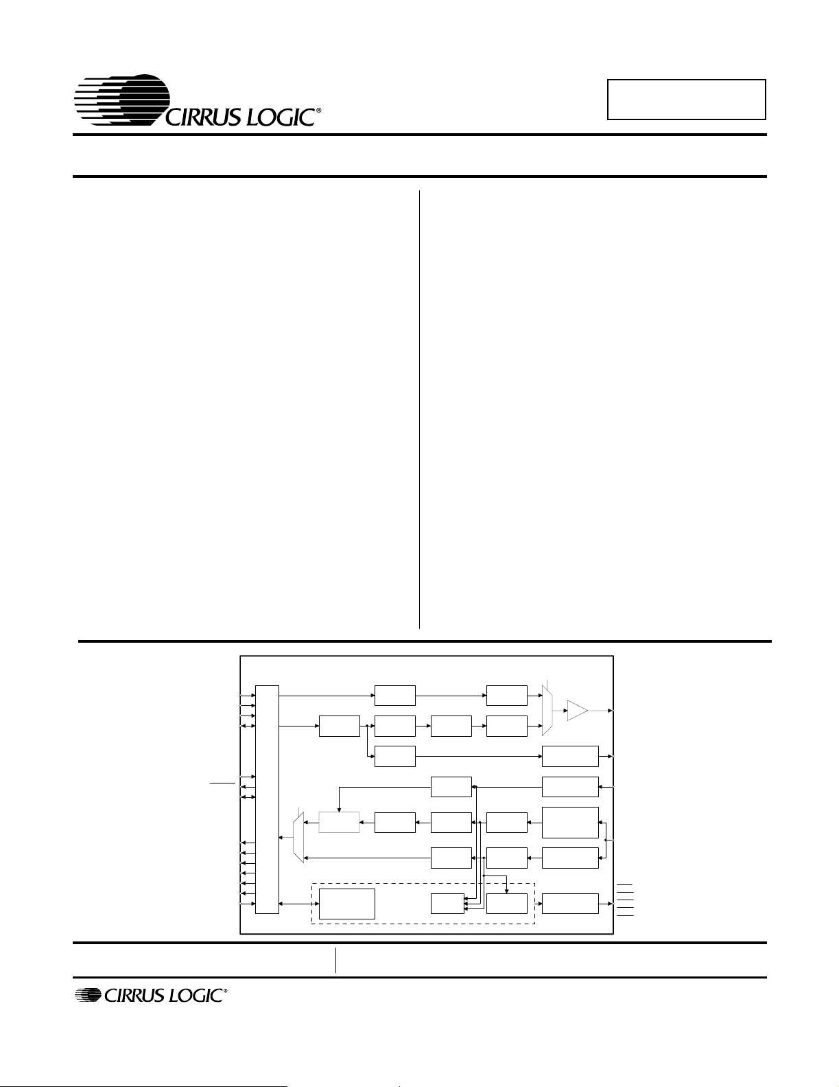
CS8952 10BaseT/100Base-X
Transceiver
TX_EN
TX_ER/TXD4
TXD[3:0]
TX_CLK
MDC
MII_IRQ
MDIO
CRS
COL
RX_ER/RXD4
RX_DV
RXD[3:0]
RX_CLK
RX_EN
10/100
(MII)
M
U
Media Independent Interface
X
Preliminary Product Information
P.O. Box 17847, Austin, Texas 78760
(512) 445 7222 FAX: (512) 445 7581
http://www.cirrus.com
10/100
10BaseT
Filter
Slew Rate
Control
100BaseT
Slicer
10BaseT
Slicer
Auto
Negotiation
M
U
X
ECL Driver
ECL Receiver
Adaptive Eq. &
Baseline Wander
Compensation
10BaseT
Filter
LED
Drivers
TX+,
TX-
TX_NRZ+,
TX_NRZ-
RX_NRZ+,
RX_NRZ-
RX+,
RX-
LED1
LED2
LED3
LED4
LED5
4B/5B
Encoder
4B/5B
Decoder
MII
Control/Status
Registers
Manchester
Encoder
Scrambler
Fiber NRZI
Interface
Descrambler
Link
Management
MLT-3
Encoder
Fiber NRZI
Interface
MLT-3
Decoder
Manchester
Decoder
Timing
Recovery
This document contains information for a new product.
Cirrus Logic reserves the right to modify this product without notice.
Copyright Cirrus Logic, Inc. 2001
(All Rights Reserved)
DS206PP3
1
OCT ‘01

TABLE OF CONTENTS
SPECIFICATIONS AND CHARACTERISTICS............................................................. 4
ABSOLUTE MAXIMUM RATINGS .......................................................................4
RECOMMENDED OPERATING CONDITIONS ...................................................4
QUARTZ CRYSTAL REQUIREMENTS ...............................................................4
DC CHARACTERISTICS ..................................................................................... 5
10BASE-T CHARACTERISTICS .........................................................................7
100BASE-X CHARACTERISTICS ....................................................................... 8
100BASE-TX MII RECEIVE TIMING - 4B/5B ALIGNED MODES ........................ 9
100BASE-TX MII RECEIVE TIMING - 5B BYPASS ALIGN MODE ................... 10
100BASE-TX MII TRANSMIT TIMING - 4B/5B ALIGN MODES ........................ 11
100BASE-TX MII TRANSMIT TIMING - 5B BYPASS ALIGN MODE ................ 12
10BASE-T MII RECEIVE TIMING ...................................................................... 13
10BASE-T MII TRANSMIT TIMING ...................................................................14
10BASE-T SERIAL RECEIVE TIMING ..............................................................15
10BASE-T SERIAL TRANSMIT TIMING ............................................................16
AUTO NEGOTIATION / FAST LINK PULSE TIMING ........................................ 17
SERIAL MANAGEMENT INTERFACE TIMING ................................................. 18
INTRODUCTION ..........................................................................................................19
High Performance Analog ...................................................................................19
Low Power Consumption ....................................................................................19
Application Flexibility...........................................................................................19
Typical Connection Diagram ...............................................................................19
FUNCTIONAL DESCRIPTION ....................................................................................21
Major Operating Modes.......................................................................................21
100BASE-X MII Application (TX and FX) ..................................................... 21
Symbol Encoding and Decoding ...........................................................22
100 Mb/s Loopback ............................................................................... 23
100BASE-X Repeater Application ............................................................... 23
10BASE-T MII Application ...........................................................................24
Full and Half Duplex operation .............................................................. 24
Collision Detection ................................................................................. 24
Jabber ................................................................................................... 24
Link Pulses ............................................................................................ 24
Receiver Squelch .................................................................................. 25
10BASE-T Loopback ............................................................................. 25
Carrier Detection ................................................................................... 25
CS8952
Contacting Cirrus Logic Support
For a complete listing of Direct Sales, Distributor, and Sales Representative contacts, visit the Cirrus Logic web site at:
http://www.cirrus.com/corporate/contacts/sales.cfm
Preliminary product information describes products which are in production, but for which full characterization data is not yet available. Advance product information describes products whichare in development and subject to development changes. Cirrus Logic, Inc. has made best effortsto ensure that the information
contained in this document is accurate and reliable. However, the information is subject to change without notice and is provided “AS IS” without warranty of
any kind (express or implied). Customers are advised to obtain the latest version of relevant information to verify, before placing orders, that information being
relied on is current and complete. All products are sold subject to the terms and conditions of sale supplied at the time of order acknowledgment, including those
pertainingto warranty, patent infringement,and limitation of liability. No responsibility is assumed by Cirrus Logic, Inc. for the use of this information, including
use of this information as the basis for manufacture or sale of any items, nor for infringements of patents or other rights of third parties. This document is the
property of Cirrus Logic, Inc. and by furnishing this information, Cirrus Logic, Inc. grants no license, express or implied under any patents, mask work rights,
copyrights, trademarks, trade secrets or other intellectual property rights of Cirrus Logic, Inc. Cirrus Logic, Inc., copyright owner of the information contained
herein, gives consent for copies to be made of the information only for use within your organization with respect to Cirrus Logic integrated circuits or other parts
of Cirrus Logic, Inc. The same consent is given for similar information contained on any Cirrus Logic website or disk. This consent does not extend to other
copying such as copying for general distribution, advertising or promotional purposes, or for creating any work for resale. The names of products of Cirrus Logic,
Inc. or other vendors and suppliers appearing in this document may be trademarks or service marks of their respective owners which may be registered in some
jurisdictions. Alist of Cirrus Logic, Inc. trademarks and service marks can be found at http://www.cirrus.com
2 CrystalLAN™ 100BASE-X and 10BASE-T Transceiver
.

10BASE-T Serial Application ....................................................................... 25
Auto-Negotiation ................................................................................................. 25
Reset Operation.................................................................................................. 26
LED Indicators..................................................................................................... 26
MEDIA INDEPENDENT INTERFACE (MII) ................................................................. 27
MII Frame Structure ............................................................................................ 27
MII Receive Data................................................................................................. 28
MII Transmit Data................................................................................................ 28
MII Management Interface .................................................................................. 29
MII Management Frame Structure...................................................................... 29
CONFIGURATION ...................................................................................................... 30
Configuration At Power-up/Reset Time............................................................... 30
Configuration Via Control Pins............................................................................ 30
Configuration via the MII ..................................................................................... 30
CS8952 REGISTERS .................................................................................................. 31
Basic Mode Control Register - Address 00h ..................................................... 32
Basic Mode Status Register - Address 01h ...................................................... 34
PHY Identifier, Part 1 - Address 02h ................................................................. 36
PHY Identifier, Part 2 - Address 03h ................................................................. 37
Auto-Negotiation Advertisement Register - Address 04h .................................. 38
Auto-Negotiation Link Partner Ability Register - Address 05h ........................... 39
Auto-Negotiation Expansion Register - Address 06h ........................................ 40
Auto-Negotiation Next-Page Transmit Register - Address 07h ......................... 41
Interrupt Mask Register - Address 10h ............................................................. 42
Interrupt Status Register - Address 11h ............................................................ 45
Disconnect Count Register - Address 12h ........................................................ 48
False Carrier Count Register - Address 13h ..................................................... 49
Scrambler Key Initialization Register - Address 14h ......................................... 50
Receive Error Count Register - Address 15h .................................................... 51
Descrambler Key Initialization Register - Address 16h ..................................... 52
PCS Sub-Layer Configuration Register - Address 17h ..................................... 53
Loopback, Bypass, and Receiver Error Mask Register - Address 18h ............. 56
Self Status Register - Address 19h ................................................................... 59
10BASE-T Status Register - Address 1Bh ........................................................ 61
10BASE-T Configuration Register - Address 1Ch ............................................ 62
DESIGN CONSIDERATIONS ...................................................................................... 64
Twisted Pair Interface ......................................................................................... 64
100BASE-FX Interface........................................................................................ 64
Internal Voltage Reference ................................................................................. 64
Clocking Schemes .............................................................................................. 65
Recommended Magnetics .................................................................................. 66
Power Supply and Decoupling............................................................................ 66
General Layout Recommendations..................................................................... 66
PIN DESCRIPTIONS ................................................................................................... 69
PACKAGE DIMENSIONS ........................................................................................... 81
CS8952
CrystalLAN™ 100BASE-X and 10BASE-T Transceiver 3
CS8952
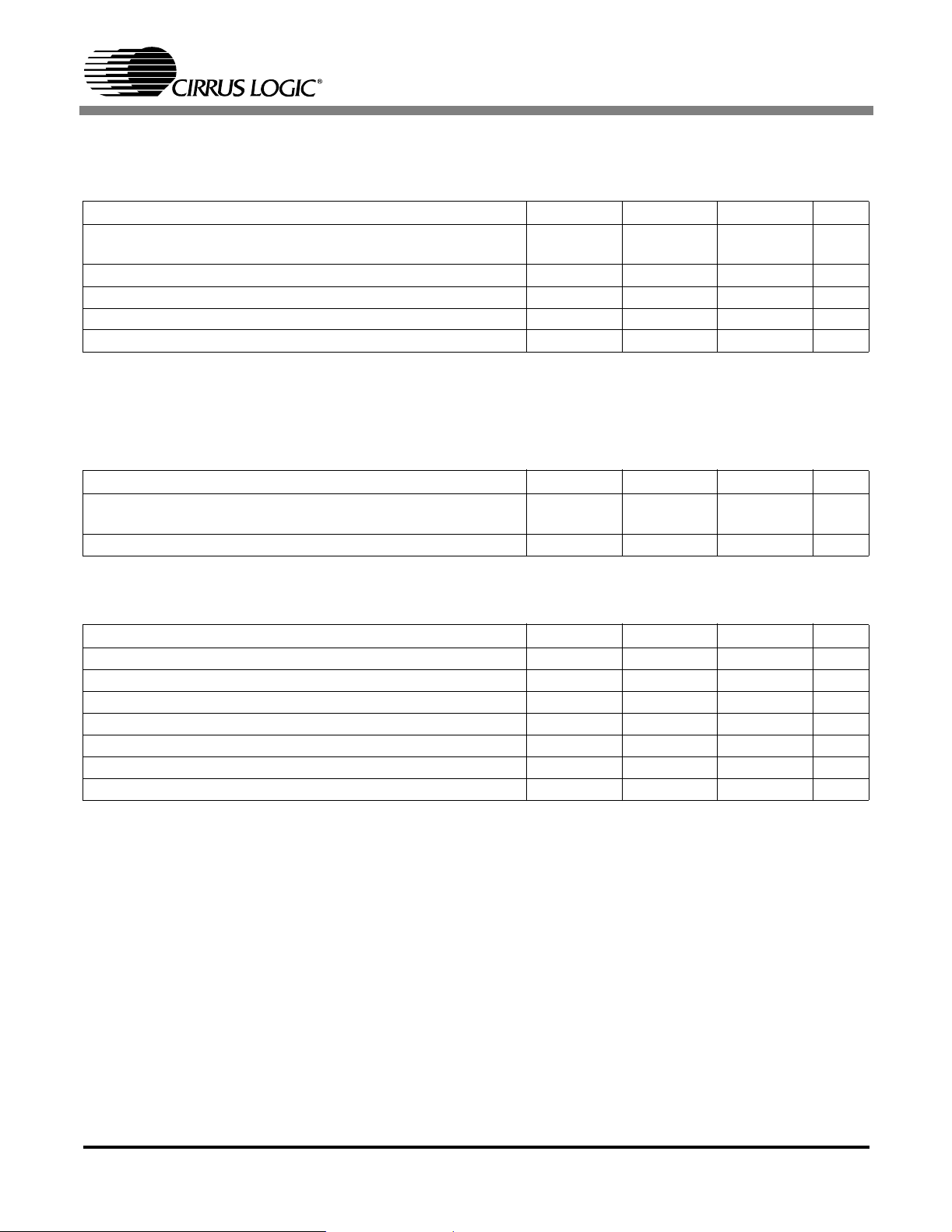
1. SPECIFICATIONS AND CHARACTERISTICS
ABSOLUTE MAXIMUM RATINGS (AVSS,DVSS = 0 V, all voltages with respect to 0 V.)
Parameter Symbol Min Max Unit
Power Supply V
Input Current Except Supply Pins - +/-10.0 mA
Input Voltage -0.3 V
Ambient Temperature Power Applied -55 +125 °C
Storage Temperature -65 +150 °C
WARNING: Operation at or beyond these limits may result in permanent damage to the device.
Normal operation is not guaranteed at these extremes.
V
DD_MII
DD
RECOMMENDED OPERATING CONDITIONS (AVSS, DVSS = 0 V, all voltages with respect
to 0 V.)
Parameter Symbol Min Max Unit
Power Supply Core
MII
Operating Ambient Temperature T
V
V
DD_MII
DD
A
-0.3
-0.3
4.75
3.0
070°C
6.0
6.0
+0.3 V
DD
5.25
5.25
V
V
V
QUARTZ CRYSTAL REQUIREMENT S (If a 25 MHz quartz crystal is used, it must meet the fol-
lowing specifications.)
Parameter Min Typ Max Unit
Parallel Resonant Frequency - 25.0 - MHz
Resonant Frequency Error (CL = 15 pF) -50 - +50 ppm
Resonant Frequency Change Over Operating Temperature -40 - +40 ppm
Crystal Load Capacitance - 15 - pF
Motional Crystal Capacitance - 0.021 - pF
Series Resistance - - 18 Ω
Shunt Capacitance - - 7 pF
4 CrystalLAN™ 100BASE-X and 10BASE-T Transceiver

DC CHARACTERISTICS (Over recommended operating conditions)
Parameter Symbol Min Typ Max Unit
External Oscillator
XTAL_I Input Low Voltage V
XTAL_I Input High Voltage V
XTAL_I Input Low Current I
XTAL_I Input High Current I
XTAL_I Input Capacitance C
XTAL_I Input Cycle Time t
XTAL_I Input Low Time t
XTAL_I Input High Time t
Power Supply
Power Supply Current 100BASE-TX (Note 1)
I
100BASE-FX (Note 1)
10BASE-T (Note 1)
Hardware Power-Down (Note 1)I
Software Power-Down (Note 1)I
Low Power Power-Up (Note1)I
DDHPDN
DDSPDN
DDSLPUP
Digital I/O
Output Low Voltage
CLK25, MII_IRQ
, SPD10, SPD100 IOL=4.0mA
V
IXH
IXH
IXL
IXH
L
IXC
IXL
XH
DD
OL
-0.3 - 0.5 V
3.5 - VDD+0.5 V
-40 - - µA
--40µA
39.996 - 40.004 ns
18 - 22 ns
18 - 22 ns
-
-
-
-900-µA
-20-mA
-900-µA
-
CS8952
-35pF
135
90
80
-
145
-
-
0.4
mA
V
LED[4:0] I
Output Low Voltage (MII_DRV = 1)
COL, CRS, MDIO, RXD[3:0],
RX_CLK, RX_DV, RX_ER,
TX_CLK I
VDD_MII = 5V; I
VDD_MII = 3.3V, I
Output Low Voltage (MII_DRV = 0)
COL, CRS, MDIO, RXD[3:0],
RX_CLK, RX_DV, RX_ER,
TX_CLK I
Output High Voltage
CLK25, SPD10, SPD100 I
Output High Voltage (MII_DRV = 1)
COL, CRS, MDIO, RXD[3:0],
RX_CLK, RX_DV, RX_ER,
TX_CLK I
VDD_MII=5V;I
VDD_MII=3.3V,I
OH
OH
=10.0mA
OL
=4.0mA
OL
=43.0mA
OL
=26.0mA
OL
=4.0mA
OL
=-4.0mA
OH
=-4.0mA
OH
=-20.0mA
=-20.0mA
-
V
OL
-
-
-
V
OL
-
0.4
V
-
-
-
0.4
3.05
2.1
V
--0.4
V
OH
V
2.4 - -
V
OH
2.4
1.1
1.1
-
-
-
-
-
-
V
CrystalLAN™ 100BASE-X and 10BASE-T Transceiver 5

DC CHARACTERISTICS (CONTINUED) (Over recommended operating conditions)
Parameter Symbol Min Typ Max Unit
Output High Voltage (MII_DRV = 0)
COL, CRS, MDIO, RXD[3:0],
RX_CLK, RX_DV, RX_ER,
TX_CLK I
=-4.0mA
OH
V
OH
2.4 - -
CS8952
V
Input Low Voltage
All Inputs Except AN[1:0], TCM, TXSLEW[1:0]
Input High Voltage
All Inputs Except AN[1:0], TCM, TXSLEW[1:0]
Tri-Level Input Voltages
AN[1:0], TCM, TXSLEW[1:0]
Input Low Current
MDC, TXD[3:0], TX_CL K, TX_EN,
TX_ER V
MDIO V
=0.0V
I
=0.0V
I
Input High Current
MDC, TXD[3:0], TX_CL K, TX_EN,
TX_ER V
MDIO V
=5.0V
I
=5.0V
I
V
IL
V
IH
V
IL
--0.8V
2.0 - - V
-
-
1/3 V
DD_MII
V
-20%
V
IM
1/3 V
DD_MII
-
+20%
V
IH
2/3 V
DD_MII
-
2/3 V
-20%
DD_MII
-
+20%
I
IL
-20
-3800
I
IH
-
-
-
-
-
-
-
-
200
20
µA
µA
Input Leakage Current
All Other Inputs 0<=V<=V
DD
I
LEAK
µA
-10 - +10
Notes: 1. With digital outputs connected to CMOS loads.
6 CrystalLAN™ 100BASE-X and 10BASE-T Transceiver
CS8952
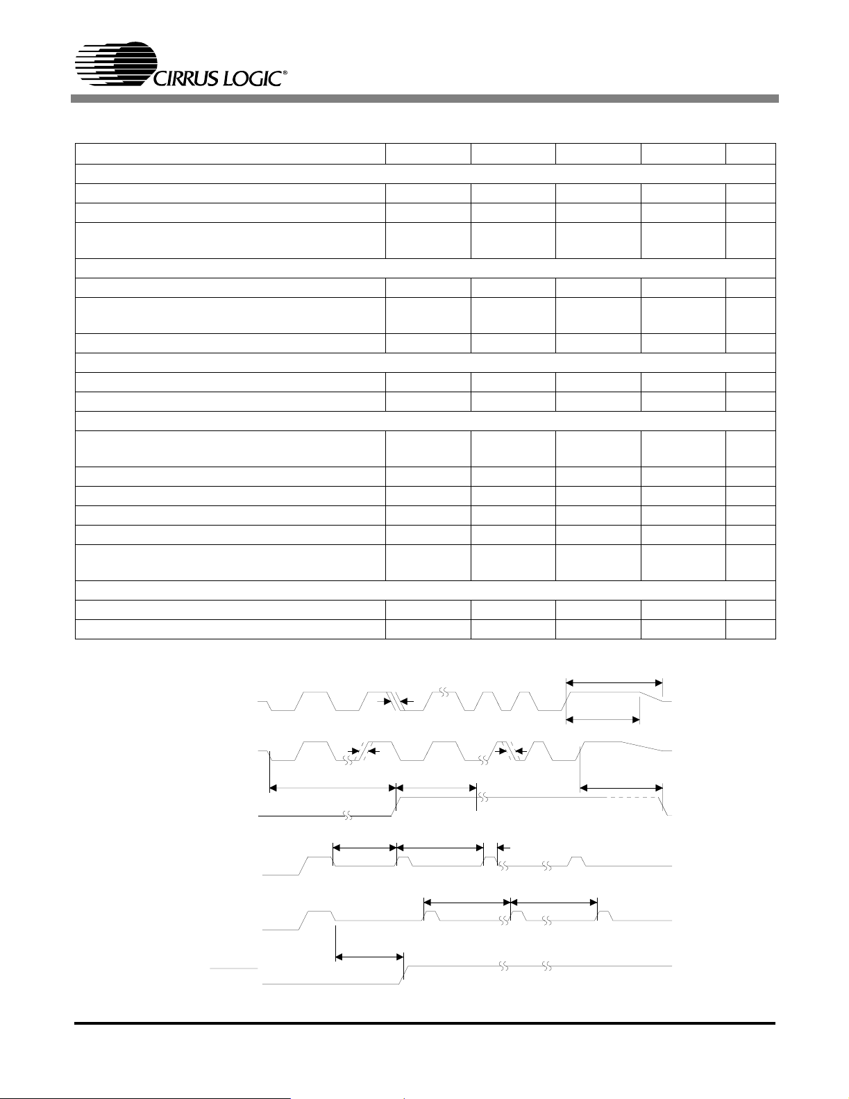
10BASE-T CHARACTERISTICS
Parameter Symbol Min Typ Max Unit
10BASE-T Interface
Transmitter Differential Output Voltage (Peak) V
Receiver Normal Squelch Level (Peak) V
Receiver Low Squelch Level (LoRxSquelch bit
V
OD
ISQ
SQL
set)
10BASE-T Transmitter
TXD Pair Jitter into 100 ΩLoad t
TXD Pair Return to ≤50 mV after Last Positive
TTX1
t
TTX2
Transition
TXD Pair Positive Hold Time at End of Packet t
TTX3
10BASE-T Receiver
Allowable Received Jitter at Bit Cell Center t
Allowable Received Jitter at Bit Cell Boundary t
TRX1
TRX2
10BASE-T Link Integrity
First Transmitted Link Pulse after Last Transmit-
t
LN1
ted Packet
Time Between Transmitted Link Pulses t
Width of Transmitted Link Pulses t
Minimum Received Link Pulses Separation t
Maximum Received Link Pulse Separation t
Last Receive Activity to Link Fail (Link Loss
LN2
LN3
LN4
LN5
t
LN6
Timer)
10Base-T Jabber/Unjabber Timing
Maximum Transmit Time - 105 - ms
Unjabber Time - 406 - ms
2.2 - 2.8 V
300 - 525 mV
125 - 290 mV
--8ns
--4.5µs
250 - - ns
- - +/-13.5 ns
- - +/-13.5 ns
15 16 17 ms
15 16 17 ms
60 - 200 ns
257ms
25 52 150 ms
50 52 150 ms
t
TTX2
TXD±
t
RXD±
Carrier Sense
(Internal)
TXD±
RXD±
LINKLED
t
RTX3
t
RTX1
t
LN1
t
LN6
TTX1
RTX4
t
t
RTX2
t
LN2
t
LN4
t
LN3
t
LN5
t
TTX3
CrystalLAN™ 100BASE-X and 10BASE-T Transceiver 7
CS8952
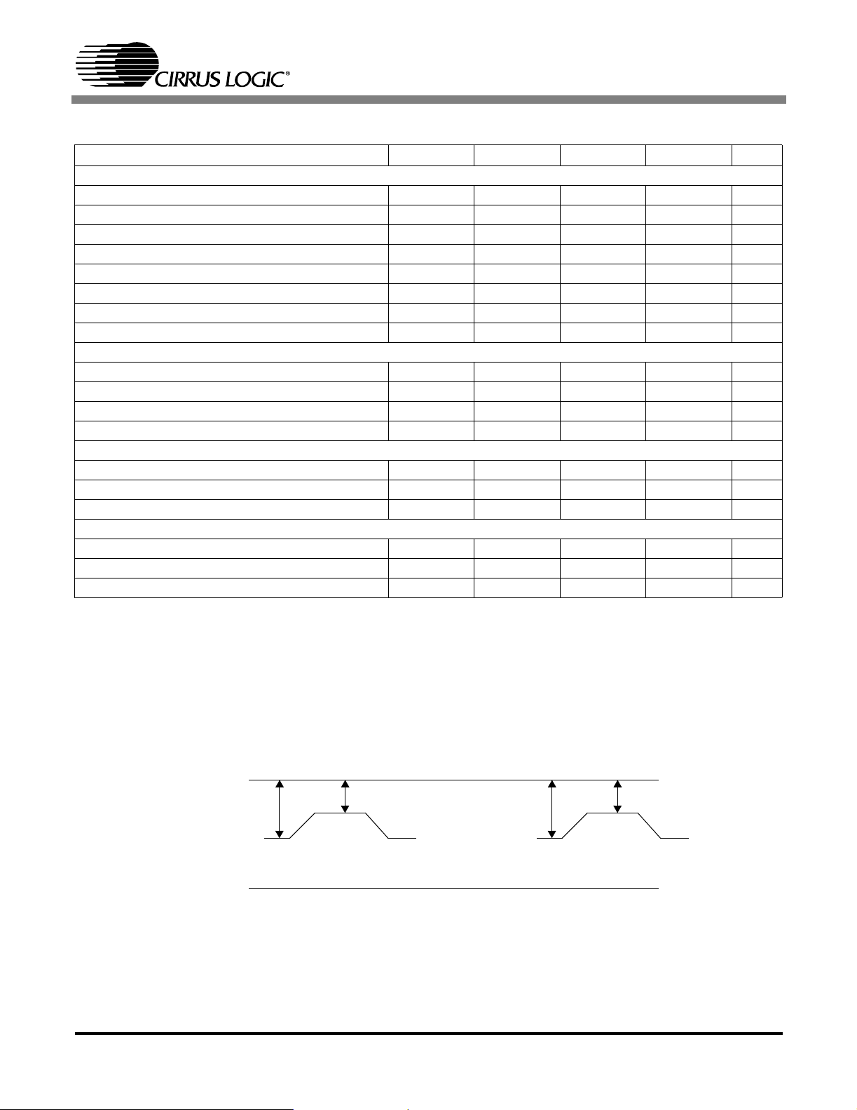
100BASE-X CHARACTERISTICS
Parameter Symbol Min Typ Max Unit
100BASE-TX Transmitter
TX Differential Output Voltage (Peak) V
Signal Amplitude Symmetry V
Signal Rise/Fall Time t
Rise/Fall Symmetry t
Duty Cycle Distortion t
Overshoot/Undershoot t
Transmit Jitter t
TX Differential Output Impedance Z
OP
SYM
RF
RFS
DCD
OS
JT
OUT
100BASE-TX Receiver
Receive Signal Detect Assert Threshold - - 1.0 V
Receive Signal Detect De-assert Threshold 0.2 - - V
Receive Signal Detect Assert Time - - 1000 µs
Receive Signal Detect De-assert Time - - 350 µs
100BASE-FX Transmitter
TX_NRZ+/- Output Voltage - Low V
TX_NRZ+/- Output Voltage - High V
Signal Rise/Fall Time T
1
2
RF
100Base-FX Receiver
RX_NRZ+/- Input Voltage - Low V
RX_NRZ+/- Input Voltage - High V
Common Mode Input Range V
3
4
CMIP
0.95 - 1.05 V
98 - 102 %
3.0 - 5.0 ns
--0.5ns
--+/-0.5ns
--5%
- 400 1400 ps
-100-ohms
-1.830 - -1.605 V
-1.035 - -0.880 V
--1.6ns
-1.830 - -1.605 V
-1.035 - -0.880 V
-3.56-V
p-p
p-p
RX/TX Signaling for 100Base-FX
V
DD
TX_NRZ+/-
V
V
1
2
V
3
RX_NRZ+/-
V
4
0
8 CrystalLAN™ 100BASE-X and 10BASE-T Transceiver
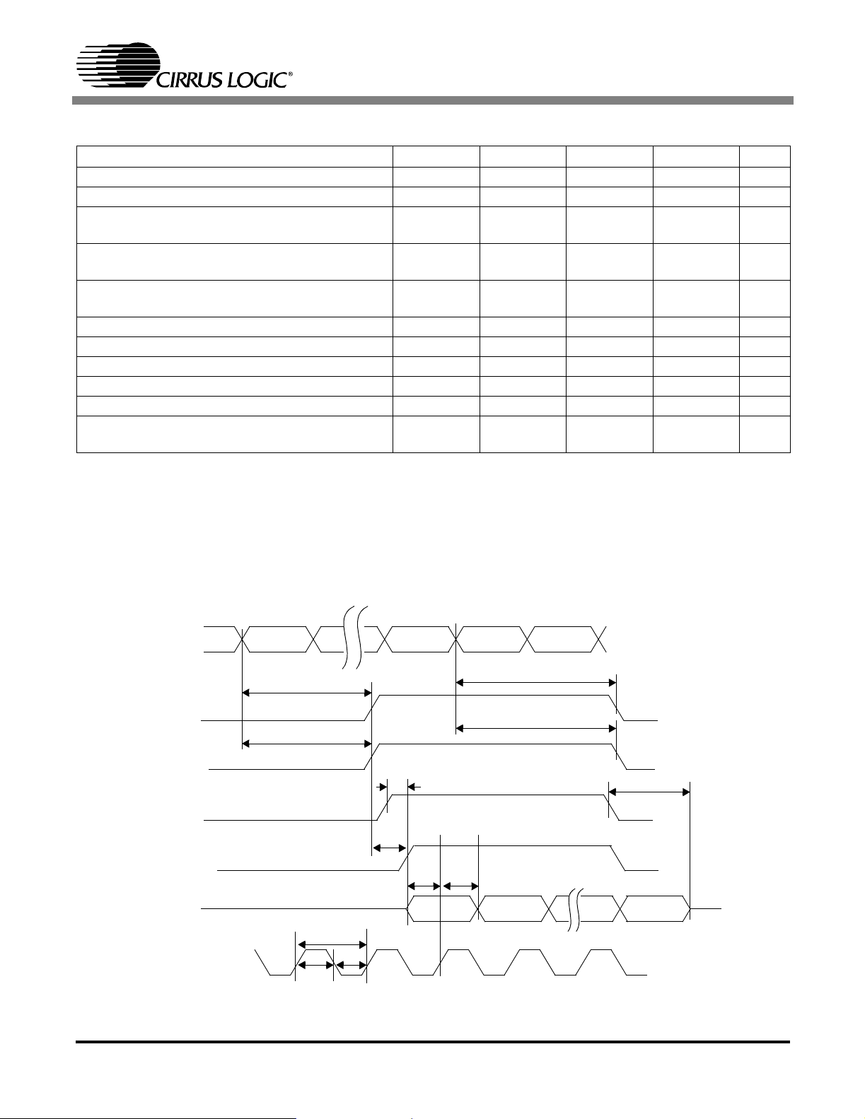
100BASE-TX MII RECEIVE TIMING - 4B/5B ALIGNED MODES
Parameter Symbol Min Typ Max Unit
RX_CLK Period t
RX_CLK Pulse Width t
WL,tWH
RXD[3:0],RX_ER/RXD4,RX_DV setup to rising
edge of RX_CLK
RXD[3:0],RX_ER/RXD4,RX_DV hold from rising
edge of RX_CLK
CRStoRXDlatency 4BAligned
t
5B Aligned
“Start of Stream” to CRS asserted t
“End of Stream” to CRS de-asserted t
“Start of Stream” to COL asserted t
“End of Stream” to COL de-asserted t
CRS1
CRS2
COL1
COL2
RX_EN asserted to RX_DV, RXD[3:0] valid t
RX_EN de-asserted to RX_DV, RXD[3:0].
RX_ER/RXD4 in high impedance state
P
t
SU
t
HD
DLAT
EN
t
DIS
-40-ns
-20-ns
10 - - ns
10 - - ns
2
2
3-6
3-6
-1011BT
--21BT
--11BT
--21BT
-TBD-ns
-TBD-ns
CS8952
8
8
BT
RX+/-
CRS
COL
RX_EN
RX_DV
RXD[3:0],
RX_ER/RXD4
RX_CLK
Start of
Stream
t
CRS1
t
COL1
t
WL
t
RLAT
t
P
t
WH
End of
Stream
t
CRS2
t
COL2
t
EN
t
DIS
t
t
HD
SU
IN
OUT
OUT
IN
OUT
OUT
OUT
CrystalLAN™ 100BASE-X and 10BASE-T Transceiver 9
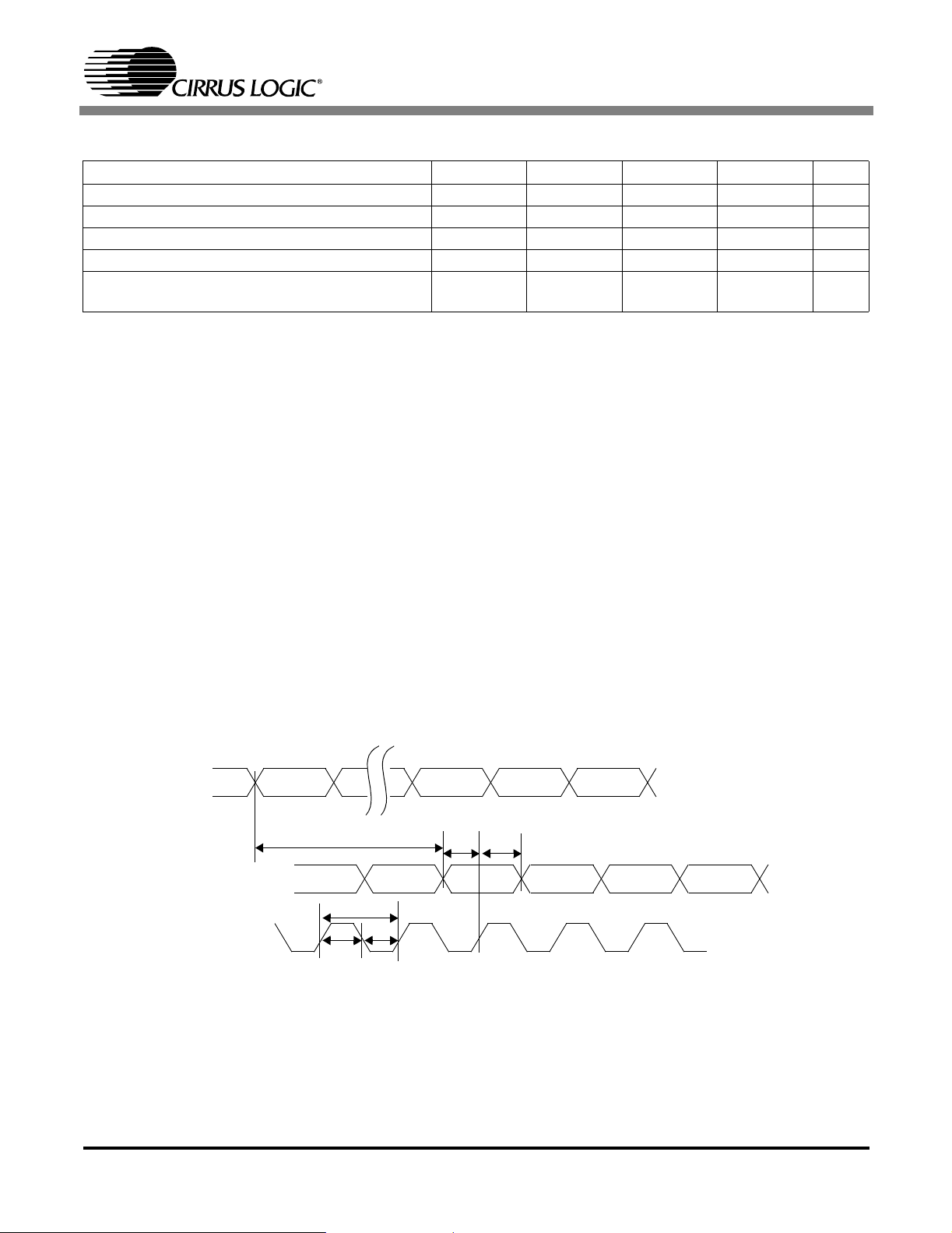
100BASE-TX MII RECEIVE TIMING - 5B BYPASS ALIGN MODE
Parameter Symbol Min Typ Max Unit
RX_CLK Period t
RX_CLK Pulse Width t
WL,tWH
RXD[4:0]setuptorisingedgeofRX_CLK t
RXD[4:0] hold after rising edge of RX_CLK t
Start of 5B symbol to symbol output on RX[4:0]
t
5B Mode
P
SU
HD
RLAT
-40-ns
-20-ns
10 - - ns
10 - - ns
5-9BT
CS8952
RX+/-
RXD[4:0],
RX Symbol
0
t
RLAT
RX Symbol
N-1
t
SU
t
P
t
HD
RX Data
0
RX Symbol
N
RX Data
1
IN
OUT
RX_CLK
OUT
t
t
WL
WH
10 CrystalLAN™ 100BASE-X and 10BASE-T Transceiver
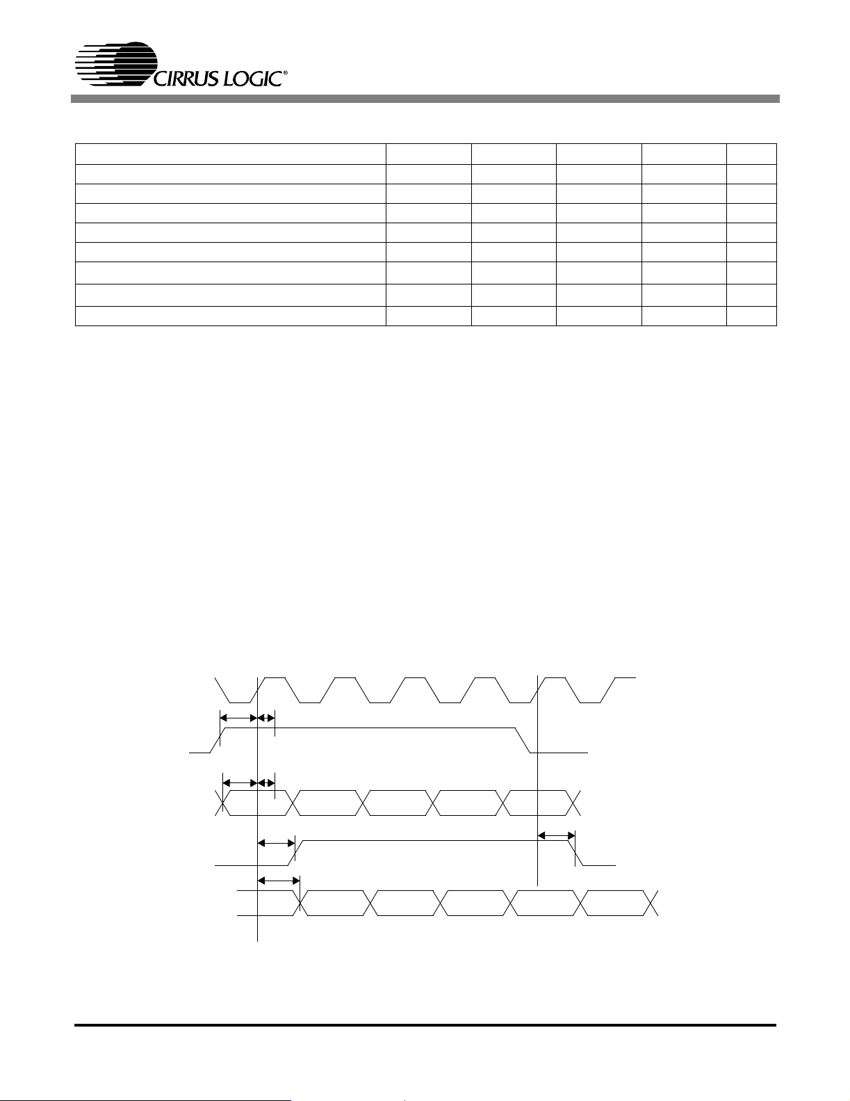
100BASE-TX MII TRANSMIT TIMING - 4B/5B ALIGN MODES
Parameter Symbol Min Typ Max Unit
TXD[3:0] Setup to TX_CLK High t
TX_EN Setup to TX_CLK High t
TXD[3:0] Hold after TX_CLK High t
TX_ER Hold after TX_CLK High t
TX_EN Hold after TX_CLK High t
TX_EN “high” to CRS asserted latency t
TX_EN “low” to CRS de-asserted latency t
TX_EN “high” to TX+/- output (TX Latency) t
SU1
SU2
HD1
HD2
HD3
CRS1
CRS2
LAT
10 - - ns
10 - - ns
0--ns
0--ns
0--ns
-8BT
-8BT
678BT
CS8952
TX_CLK
TX_EN
TXD[3:0],
TX_ER/TXD4
CRS
TX+/-
t
SU2
t
SU1
Data
IN
t
CRS1
t
HD2
t
HD1
t
LAT
Symbol
Out
t
CRS2
Input/Output
Input
Input
Output
Output
CrystalLAN™ 100BASE-X and 10BASE-T Transceiver 11
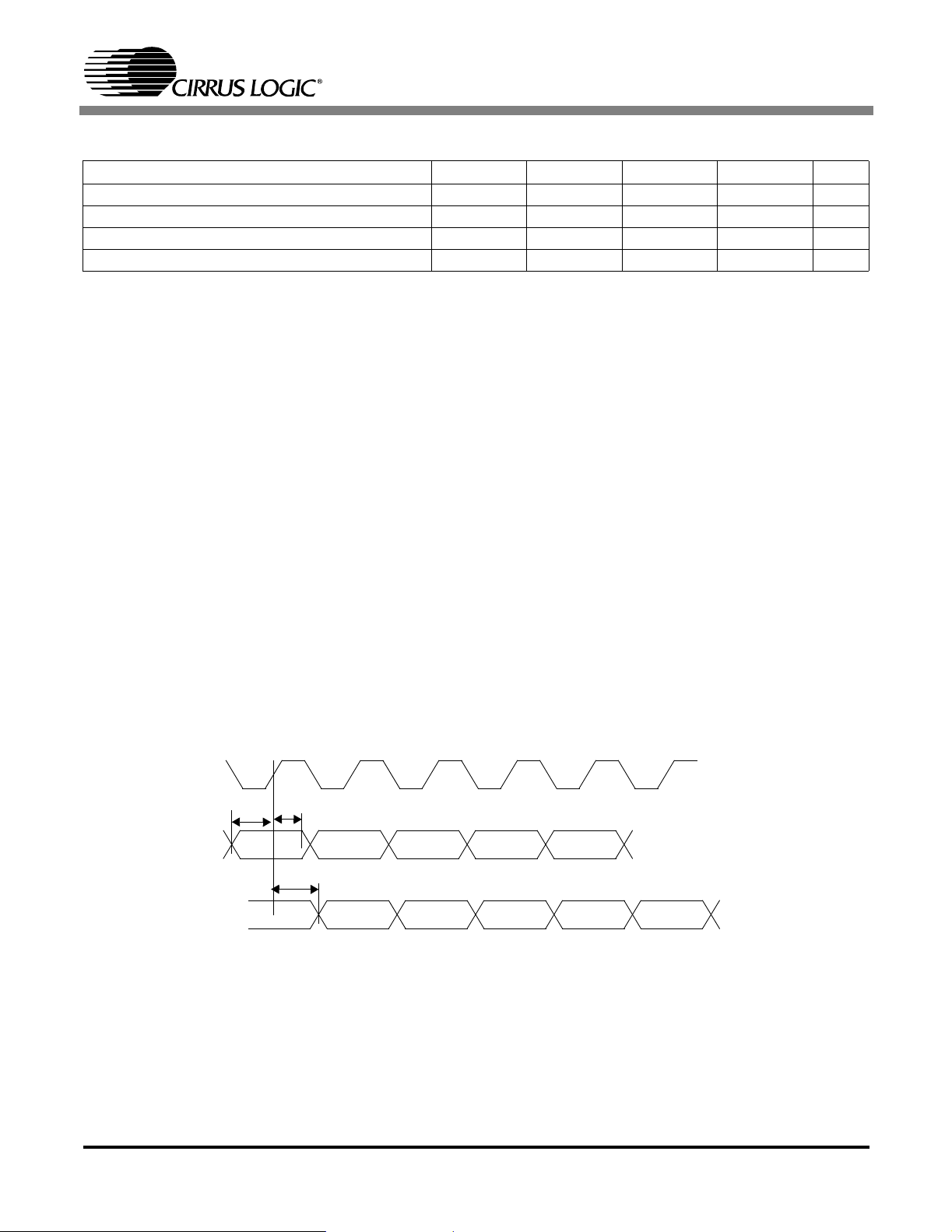
100BASE-TX MII TRANSMIT TIMING - 5B BYPASS ALIGN MODE
Parameter Symbol Min Typ Max Unit
TXD[4:0] Setup to TX_CLK High t
TXD[4:0] Hold after TX_CLK High t
TX_ER Hold after TX_CLK High t
TXD[4:0] Sampled to TX+/- output (TX Latency) t
SU1
HD1
HD2
LAT
10 - - ns
0--ns
0--ns
-67ns
CS8952
TX_CLK
TXD[4:0]
TX+/-
t
SU1
Data
IN
t
LAT
t
HD1
Symbol
OUT
Input/Output
Input
Output
12 CrystalLAN™ 100BASE-X and 10BASE-T Transceiver
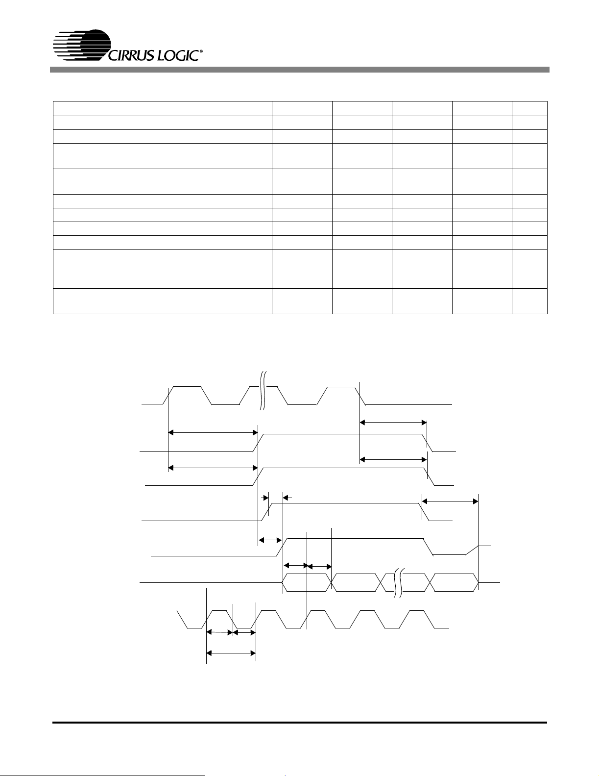
10BASE-T MII RECEIVE TIMING
Parameter Symbol Min Typ Max Unit
RX_CLK Period t
RX_CLK Pulse Width t
RXD[3:0],RX_ER,RX_DVsetuptorisingedgeof
RX_CLK
RXD[3:0], RX_ER, RX_DV hold from rising edge
of RX_CLK
RX data valid from CRS t
RX+/- preamble to CRS asserted t
RX+/- end of packet to CRS de-asserted t
RX+/- preamble to COL asserted t
RX+/- end of packet to COL de-asserted t
RX_EN asserted to RX_DV, RXD[3:0], RX_ER
valid
RX_ENde-assertedto RX_DV, RXD[3:0]. RX_ER
in high impedance state
WL,tWH
P
t
SU
t
HD
RLAT
CRS1
CRS2
COL1
COL2
t
EN
t
DIS
CS8952
-400-ns
-200-ns
30 - - ns
30 - - ns
-810BT
-57BT
2.5 3 BT
0-7BT
--3BT
- - 60 ns
- - 60 ns
RX+/-
CRS
COL
RX_EN
RX_DV
RXD[3:0],
RX_ER
RX_CLK
t
CRS1
t
COL1
t
WL
t
RLAT
t
t
P
WH
IN
t
CRS2
t
COL2
t
EN
t
DIS
t
t
HD
SU
OUT
OUT
IN
OUT
OUT
OUT
CrystalLAN™ 100BASE-X and 10BASE-T Transceiver 13
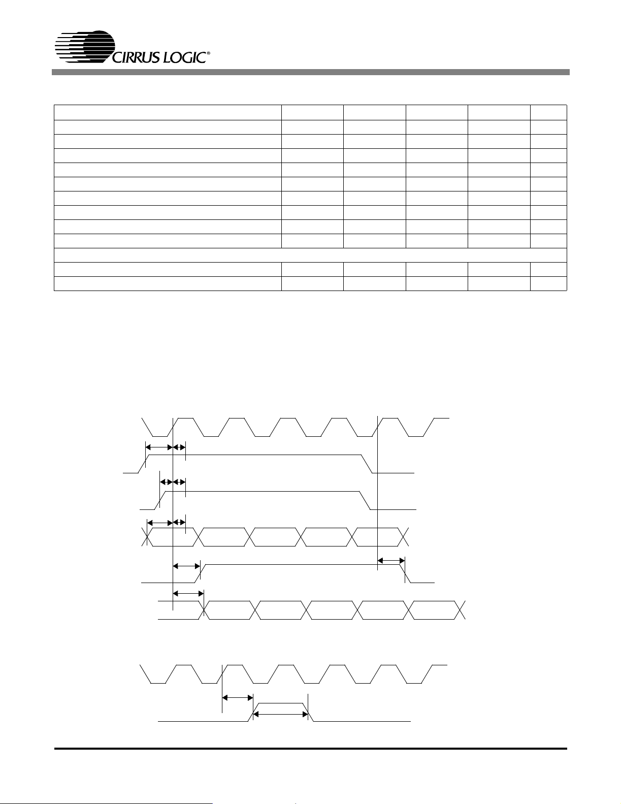
10BASE-T MII TRANSMIT TIMING
Parameter Symbol Min Typ Max Unit
TXD[3:0] Setup to TX_CLK High t
TX_ER Setup to TX_CLK High t
TX_EN Setup to TX_CLK High t
TXD[3:0] Hold after TX_CLK High t
TX_ER Hold after TX_CLK High t
TX_EN Hold after TX_CLK High t
TX_EN “high” to CRS asserted latency t
TX_EN “low” to CRS de-asserted latency t
TX_EN “high” to TX+/- output (TX Latency) t
SQE Timing
COL (SQE) Delay after CRS de-asserted t
COL (SQE) Pulse Duration t
SU1
SU2
SU3
HD1
HD2
HD3
CRS1
CRS2
LAT
COL
COLP
CS8952
10 - - ns
10 - - ns
10 - - ns
0--ns
0--ns
0--ns
0-4BT
0-16BT
6-14BT
0.65 0.9 1.6 µs
0.65 1.0 1.6 µs
TX_CLK
TX_EN
TX_ER
TXD[3:0]
CRS
TX+/-
TX_CLK
t
t
SU3
SU1
t
SU2
t
CRS1
t
t
HD2
t
HD3
HD1
10BASE-T Transmit Timing
t
LAT
Valid
Data
SQE Timing
t
CRS2
Input/Output
Input
Input
Input
Output
Output
Input/Output
t
COL
SQE
t
SQEP
Output
14 CrystalLAN™ 100BASE-X and 10BASE-T Transceiver
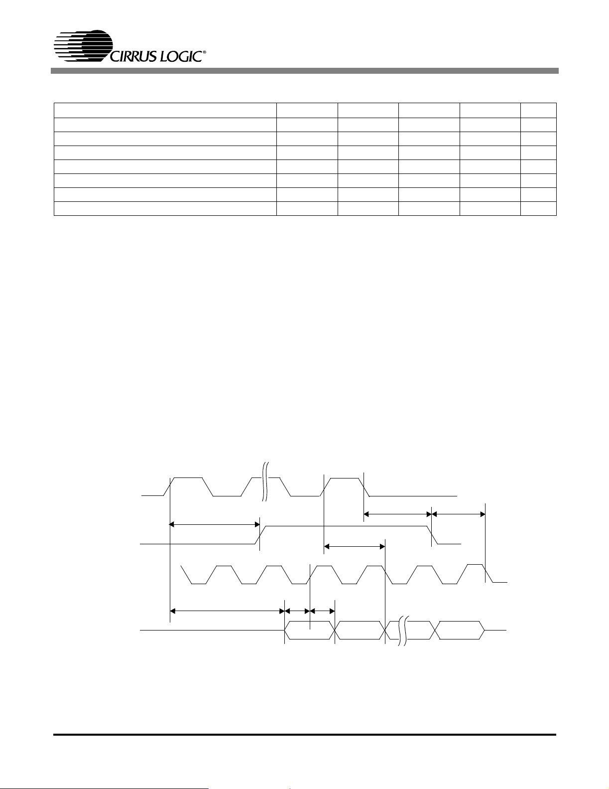
10BASE-T SERIAL RECEIVE TIMING
Parameter Symbol Min Typ Max Unit
RX+/- active to RXD[0] active t
RX+/- active to CRS active t
RXD[0] setup from RX_CLK t
RXD[0] hold from RX_CLK t
RX_CLK hold after CRS off t
RXD[0] throughput delay t
CRS turn off delay t
DATA
CRS
RDS
RDH
RCH
RD
CRSOFF
CS8952
- - 1200 ns
--600ns
35 - - ns
50 - - ns
5--ns
--250ns
--400ns
RX+/-
CRS
t
CRS
t
RD
t
CRSOFF
t
RCH
IN
OUT
RX_CLK
OUT
t
t
HD
SU
OUT
RXD[0]
t
DATA
CrystalLAN™ 100BASE-X and 10BASE-T Transceiver 15
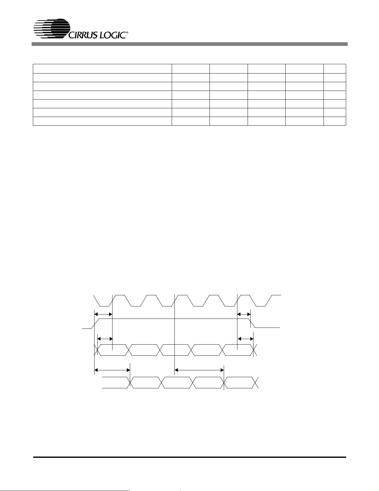
10BASE-T SERIAL TRANSMIT TIMING
Parameter Symbol Min Typ Max Unit
TX_EN Setup from TX_CLK t
TX_EN Hold after TX_CLK t
TXD[0] Setup from TX_CLK t
TXD[0] Hold after TX_CLK t
Transmit start-up delay t
Transmit throughput delay t
EHCH
CHEL
DSCH
CHDU
STUD
TPD
CS8952
10 - - ns
10 - - ns
10 - - ns
10 - - ns
--500ns
--500ns
TX_CLK
TX_EN
TXD[3:0]
TX+/-
t
EHCH
t
STUD
t
DSCH
Valid
Data
t
CHEL
t
CHDU
t
PD
Input/Output
Input
Input
Output
16 CrystalLAN™ 100BASE-X and 10BASE-T Transceiver

AUTO NEGOTIATION / FAST LINK PULSE TIMING
Parameter Symbol Min Typ Max Unit
FLP burst to FLP burst t
FLP burst width t
Clock/Data pulses per burst
Clock/Data pulse width t
Clock pulse to Data pulse t
Clock pulse to clock pulse t
BTB
FLPW
-
PW
CTD
CTC
15 16 17 ms
-2-ms
17 - 33 ea.
-100-ns
55.5 64 69.5 µs
111 128 139 µs
CS8952
TX+/-
t
FLPW
t
BTB
Clock
Pulse
Data
Pulse
Clock
Pulse
TX+/-
t
t
t
PW
CTD
CTC
t
PW
CrystalLAN™ 100BASE-X and 10BASE-T Transceiver 17
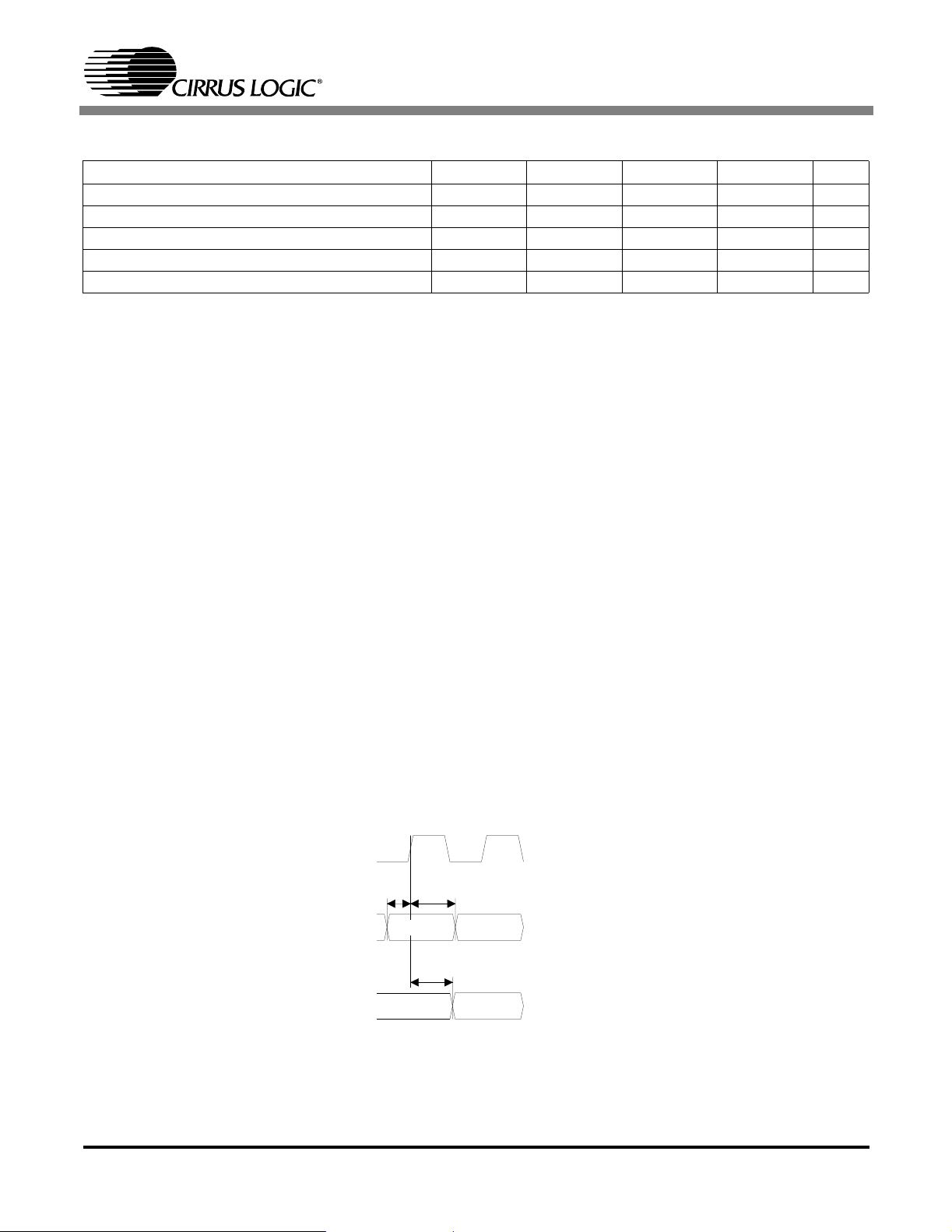
SERIAL MANAGEMENT INTERFACE TIMING
Parameter Symbol Min Typ Max Unit
MDC Period t
MDC Pulse Width t
MDIO Setup to MDC (MDIO as input) t
MDIO Hold after MDC (MDIO as input) t
MDC to MDIO valid (MDIO as output) t
p
WL,tWH
MD1
MD2
MD3
CS8952
60 - - ns
40 - 60 %
10 - - ns
10 - - ns
0 - 40 ns
DIRECTION:
IN or OUT of chip
MDC
MDIO
MDIO
t
MD1tMD2
Valid Data
t
MD3
Valid Data
Valid Data
IN
IN
OUT
18 CrystalLAN™ 100BASE-X and 10BASE-T Transceiver

CS8952
2. INTRODUCTION
The CS8952 is a complete physical-layer transceiver for 100BASE-TX and 10BASE-T applications.
Additionally, the CS8952 can be used with an external optical module for 100BASE-FX.
2.1 High Performance Analog
The highly integrated mixed-signal design of the
CS8952 eliminates the need for external analog circuitry such as external transmit or receive filters.
The CS8952 builds upon Cirrus Logic’s experience
in pioneering the high-volume manufacturing of
10BASE-T integrated circuits with “true” internal
filters. The CS8952, CS8920, CS8904, and
CS8900 include fifth-order, continuous-time Butterworth 10BASE-T transmit and receive filters, allowing those products to meet 10BASE-T wave
shape, emission, and frequency content requirements without external filters.
2.2 Low Power Consumption
The CS8952 is implemented in low power CMOS,
consuming only 135 mA typically. Three low-power modes are provided to make the CS8952 ideal
for power sensitive applications such as CardBus.
2.3 Application Flexibility
The CS8952’s digital interface and operating
modes can be tailored to efficiently support a wide
variety of applications. For example, the Media Independent Interface (MII) supports 100BASE-TX,
100BASE-FX and 10BASE-T NIC cards, switch
ports and router ports. Additionally, the low-latency “repeater” interface mode minimizes data delay
through the CS8952, facilitating system compliance with overall network delay budgets. To support 10BASE-T applications, the CS8952 provides
a 10BASE-T serial port (Seven-wire ENDEC interface).
2.4 Typical Connection Diagram
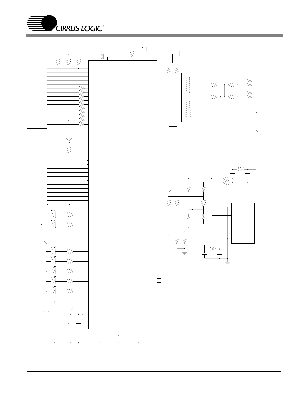
Figure 1 illustrates a typical MII to CS8952 appli-
cation with twisted-pair and fiber interfaces. Refer
to the Analog Design Considerations section for
detailed information on power supply requirements
and decoupling, crystal and magnetics requirements, and twisted-pair and fiber transceiver connections.
3. FUNCTIONAL DESCRIPTION
The CS8952is a complete physical-layer transceiver for 100BASE-TX and 10BASE-T applications.
It provides a Physical Coding Sub-layer for communication with an external MAC (Media Access
Controller). The CS8952 also includes a complete
Physical Medium Attachment layer and a
100BASE-TX and 10BASE-T Physical Medium
Dependent layer. Additionally, the CS8952 provides a PECL interface to an external optical module for 100BASE-FX applications.
The primary digital interface to the CS8952 is an
enhanced IEEE 802.3 Media Independent Interface
(MII). The MII supports parallel data transfer, access to the CS8952 Control and Status registers,
and several status and control pins. The CS8952's
operating modes can be tailored to support a wide
variety of applications, including low-latency
100BASE-TX repeaters, switches and MII-based
network interface cards.
For 100BASE-TX applications, the digital data interface can be either 4-bit parallel (nibbles) or 5-bit
parallel (code-groups). For 10BASE-T applications, the digital data format can be either 4-bit parallel (nibbles) or one-bit serial.
The CS8952 is controlled primarily by configuration registers via the MII Management Interface.
Additionally, a number of the most fundamental
register bits can be set at power-up and reset time
by connecting pull-up or pull-down resistors to external pins.
The CS8952's MII interface is enhanced beyond
IEEE requirements by register extensions and the
addition of pins for MII_IRQ
DEF signals. The MII_IRQ
,RX_EN,andISO-
pin provides an inter-
CrystalLAN™ 100BASE-X and 10BASE-T Transceiver 19
CS8952
MII
I/F
CONTROL
I/F
10 µF 0.1µF
VDD_MII
VDD_MII
4.7 k
1.5 k
4.7 k
Ω
Ω
4
Ω
33
33
Ω
33
Ω
33
Ω
33
Ω
33
Ω
Ω
33
Ω
33
Ω
33
33
Ω
VDD_MII
4.7 k
Ω
680
Ω
680
680
Ω
680
Ω
Ω
680
680
Ω
Ω
680
+5 V
10 µF 0.1 µF
25 MHz
Ω
XTAL_I XTAL_O
MDIO
MDC
TXD
TX_ER/TXD[4]
TX_EN
TX_CLK
RX_CLK
RXD[0]
RXD[1]/PHYAD[1]
RXD[2]
RXD[3]/PHYAD[3]
RX_ER/RXD[4]/PHYAD[4]
RX_DV/MII_DRV
COL/PHYAD0
CRS/PHYAD[2]
LPSTRT
RX_EN
PWRDN
REPEATER
BPSCR
BP4B5B
BPALIGN
LPBK
ISODEF
10BT_SER
RESET
MII_IRQ
SPEED10
SPEED100
LED1
LED2
LED3
LED4
LED5
3
VDD_MII
11
VDD
RSVD VSS TEST0 TEST1
7 21
VSS18 RES VSS17
CS8952
4.99 k
Ω
49.9
RX+
RX-
TX+
TX-
0.1 µF 0.1 µF
SIGNAL+
SIGNAL-
82
TX_NRZTX_NRZ+
RX_NRZ-
RX_NRZ+
TXSLEW0
TXSLEW1NCNC
AN0
AN1NCNC
TCM
Ω
+5 V
Ω
130
0.1 µF
49.9
82
82
49.9Ω49.9
Ω
Ω
Ω
0.1 µF
Ω
130
68
Ω
Ω
63.4
Ω
+5 V
Ω
0.1 µF 0.1 µF
51
Ω
0.01 µF
2KV
0.1 µF
Ω
Ω
Ω
51
51
Ω
+5 V
TRANSCEIVER
VEE
SD+
TDTD+
VCC
VCC
RDRD+
VEE
51
51
51
0.1 µF
FIBER
Ω
Ω
Ω
Ω
75
75
Ω
130
191
SHLD
8
7
6
5
4
3
2
1
SHLD
RJ45
Figure 1. Typical Connection Diagram
20 CrystalLAN™ 100BASE-X and 10BASE-T Transceiver
CS8952
rupt signal to the controller when a change of state
has occurred in the CS8952, eliminating the need
for the system to poll the CS8952 for state changes.
The RX_EN signal allows the receiver outputs to
be electrically isolated. The ISODEF pin controls
the value of register bit ISOLATE in the Basic
Mode Control Register (address 00h) which in turn
electrically isolates the CS8952's MII data path.
3.1 Major Operating Modes
The following sections describe the four major operating modes of the CS8952:
- 100BASE-X MII Modes (TX and FX)
- 100BASE-X Repeater Modes
- 10BASE-T MII Mode
- 10BASE-T Serial Mode
The choice of operating speed (10 Mb/s versus
100 Mb/s) is made using the auto-negotiation input
pins (AN0, AN1) and/or the auto-negotiation MII
registers. The auto-negotiation capability also is
used to select a duplex mode (full or half duplex).
Both speed and duplex modes can either be forced
or negotiated with the far-end link partner.
The digital interface mode (MII, repeater, or
10BASE-T serial) is selected by input pins
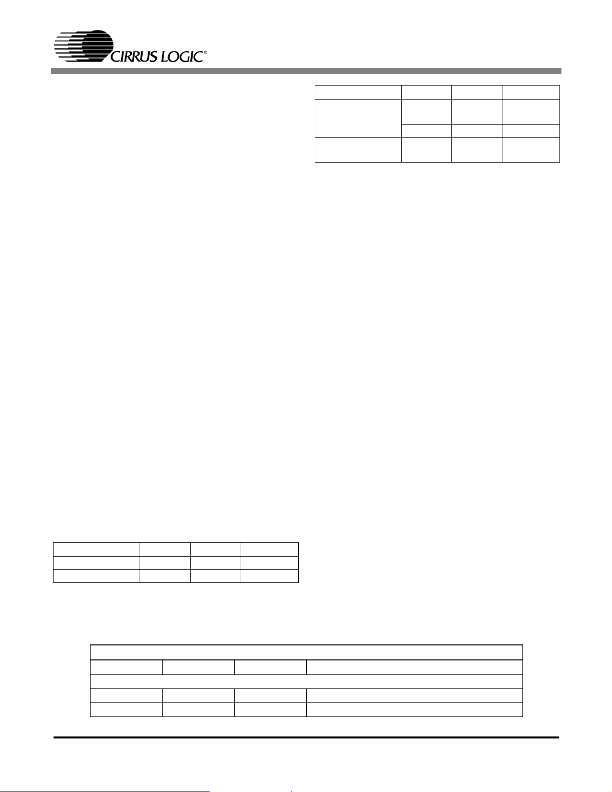
BPALIGN, BP4B5B and 10BT_SER as shown in
Table 1. Speed and duplex selection are made
through the AN[1:0] pins as shown in Table 5.
Operating Mode BPALIGN BP4B5B 10BT_SER
100BASE-X MII 0 0 0
10BASE-T MII 0 0 0
Table 1.
Operating Mode BPALIGN BP4B5B 10BT_SER
100BASE-X
Repeater
10BASE-T Serial Don’t
1Don’t
Care
01 0
Don’t
Care
Table 1.
Care
0
1
3.1.1 100BASE-X MII Application (TX and FX)
The CS8952 provides an IEEE 802.3-compliant
MII interface. Data is transferred across the MII in
four-bit parallel (nibble) mode. TX_CLK and
RX_CLK are nominally 25 MHz for 100BASE-X.
The 100BASE-X mode includes both the TX and
FX modes, as determined by pin BPSCR (bypass
scrambler), or the BPSCR bit (bit 13) in the Loopback, Bypass, and Receiver Error Mask Register
(address 18h). In FX mode, an external optical
module is connected to the CS8952 via pins
TX_NRZ+, TX_NRZ-, RX_NRZ+, RX_NRZ-,
SIGNAL+, and SIGNAL-. In FX mode, the MLT3/NRZI conversion blocks and the scrambler/descrambler are bypassed.
3.1.1.1 Symbol Encoding and Decoding
In 100BASE-X modes, 4-bit nibble transmit data is
encoded into 5-bit symbols for transmission onto
the media as shown in Tables 2 and 3. The encoding is necessary to allow data and control symbols
to be sent consecutively along the same media
transparent to the MAC layer. This encoding causes the symbol rate transmitted across the wire (125
symbols/second) to be greater than the actual data
rate of the system (100 symbols/second).
DATA and CONTROL Codes (RX_ER = 0 or TX_ER = 0)
Name 5-bit Symbol 4-bit Nibble Comments
DATA (Note 1)
0 11110 0000
1 01001 0001
CrystalLAN™ 100BASE-X and 10BASE-T Transceiver 21
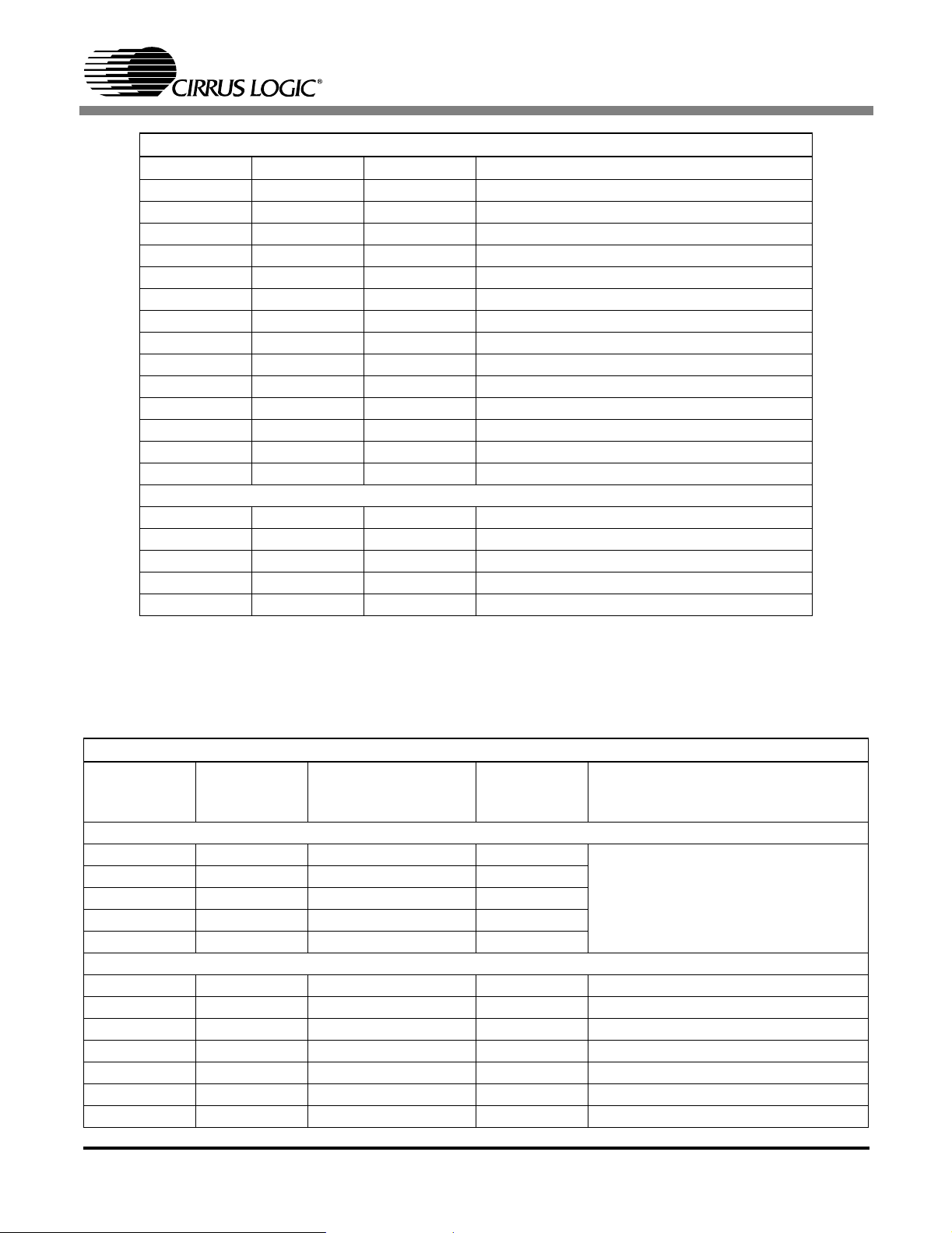
DATA and CONTROL Codes (RX_ER = 0 or TX_ER = 0)
Name 5-bit Symbol 4-bit Nibble Comments
2 10100 0010
3 10101 001 1
4 01010 0100
5 01011 0101
6 01110 0110
7 01111 0111
8 10010 1000
9 10011 1001
A 10110 1010
B 10111 1011
C 11010 1100
D 11011 1101
E 11100 1110
F 11101 1111
CONTROL (Note 2)
I 11111 0101 IDLE (Note 3)
J 11000 0101 First Start of Stream Symbol
K 10001 0101 Second Start of Stream Symbol
T 01101 0000 First End of Stream Symbol
R 00111 0000 Second End of Stream Symbol
1. DATA code groups are indicated by RX_DV = 1
2. CONTROL code groups areinserted automatically during transmission in response to
TX_EN. They are not generated through any combination of TXD[3:0] or TX_ER.
3. IDLE is indicated by RX_DV = 0.
Table 2. 4B5B Symbol Encoding/Decoding
CS8952
Code Violations (RX_ER = 1 or TX_ER = 1)
Error Report
Normal Mode 4-bit
Name 5-bit Symbol
CONTROL (Note 1)
I 11111 0000 0000 This portion of the table relates received
J 11000 0000 0000
K 10001 0000 0000
T 01101 0000 0000
R 00111 0000 0000
CODE VIOLATIONS
H 00100 0000 0000
V0 00000 0110 or 0101 (Note 2) 0001
V1 00001 0110 or 0101 (Note 2) 0111
V2 00010 0110 or 0101 (Note 2) 1000
V3 00011 0110 or 0101 (Note 2) 1001
V4 00101 0110 or 0101 (Note 2) 1010
V5 00110 0110 or 0101 (Note 2)1011
22 CrystalLAN™ 100BASE-X and 10BASE-T Transceiver
Nibble
Mode 4-bit
Nibble Comments
5-bit symbols to received 4-bit nibbles
only . The control code groups may not
be transmitted in the data portion of the
frame.
Code Violations (RX_ER = 1 or TX_ER = 1)
Error Report
Normal Mode 4-bit
Name 5-bit Symbol
V6 01000 0110 or 0101 (Note 2)1100
V7 01100 0110 or 0101 (Note 2)1101
V8 10000 0110 or 0101 (Note 2)1110
V9 11001 0110 or 0101 (Note 2) 1111
1. CONTROL code groups become violations when found in the data portion of the frame.
2. Invalid code groups are mapped to 5h unless the Code Error Report select bit in the Loopback,
Bypass,and Receiver Error Mask Register(address 18h) is set, in which case invalid code groupsare
mapped to 6h.
Nibble
Table3. 4B5BCodeViolationDecoding
Mode 4-bit
Nibble Comments
CS8952
3.1.1.2 100 Mb/s Loopback
One of two internal 100BASE-TX loopback modes
can be selected. Local loopback redirects the
TXD[3:0] input data to RXD[3:0] data outputs
through the 4B5B coders and scramblers. Local
loopback is selected by asserting pin LPBK, by setting the LPBK bit (bit 14) in the Basic Mode Control Register (address 00h) or by setting bits 8 and
11 in the Loopback, Bypass, and Receiver Error
Mask Register (address 18h) as shown in Table 4.
Remote loopback redirects the analog line interface
inputs to the analog line driver outputs. Remote
loopback is selected by setting bit 9 in the Loopback, Bypass, and Receiver Error Mask Register
(address 18h) as shown in Table 4.
Remote
Loopback
(bit 9)
0 0 No Loopback
0 1 Local Loopback (toward MII)
1 0 Remote Loopback (toward line)
1 1 Operation is undefined
When changing between local and non-loopback
modes, the data on RXD[3:0] will be undefined for
approximately 330 µs.
PMD
Loopback
(bit 8)
Function
Table 4.
3.1.2 100BASE-X Repeater Application
The CS8952 provides two low latency modes for
repeater applications. These are selected by asserting either pin BPALIGN or BP4B5B. Both pins
have the effect of bypassing the 4B5B encoder and
decoder. Bypassing the coders decreases latency,
and uses a 5-bit wide parallel code group interface
on pins RXD[4:0] and TXD[4:0] instead of the 4bit wide MII nibble interface on pins RXD[3:0] and
TXD[3:0]. In repeater mode, pin RX_ER is redefined as the fifth receive data bit (RXD4), and pin
TX_ER is redefined as the fifth transmit data bit
(TXD4).
BPALIGN can also be selected by setting bit 12 in
Loopback, Bypass, and Receiver Error Mask Register (address 18h). BP4B5B can be selected by setting bit 14 of the same register.
Pin BPALIGN causes more of the CS8952 to be
bypassed than the BP4B5B pin. BPALIGN also bypasses the scrambler/descrambler, and the NRZI to
NRZ converters (see Figure 1). Also, for repeater
applications, pin REPEATER should be asserted to
redefine the function of the CRS (carrier sense) pin.
The REPEATER function may also be invoked by
setting bit 12 in the PCS Sublayer Configuration
Register (address 17h).
For repeater applications, the RX_EN pin can be
used to gate the receive data pins (RXD[4:0],
CrystalLAN™ 100BASE-X and 10BASE-T Transceiver 23

CS8952
RX_CLK, RX_DV, COL, and CRS) onto a shared,
external repeater system bus.
3.1.3 10BASE-T MII Application
The digital interface used in this mode is the same
as that used in the 100BASE-X MII mode except
that TX_CLK and RX_CLK are nominally
2.5 MHz.
The CS8952 includes a full-featured 10BASE-T in-
terface, as described in the following sections.
3.1.3.1 Full and Half Duplex operation
The 10BASE-T function supports full and half duplex operation as determined by pins AN[1:0]
and/or the corresponding MII register bits. (See Table 5).
3.1.3.2 Collision Detection
If half duplex operation is selected, the CS8952 detects a 10BASE-T collision whenever the receiver
and transmitter are active simultaneously. When a
collision is present, the collision is reported on pin
COL. Collision detection is undefined for full-duplex operation.
3.1.3.3 Jabber
The jabber timer monitors the transmitter and disables the transmissionif the transmitter is active for
greaterthan approximately 105 ms. The transmitter
stays disabled until approximately 406 ms after the
internal transmit request is no longer enabled.
3.1.3.4 Link Pulses
To prevent disruption of network operation due to a
faulty link segment, the CS8952 continually monitors the 10BASE-T receive pair (RXD+ and RXD-)
for packets and link pulses. After each packet or link
pulse is received, an internal Link-Loss timer is
started. As long as a packet or link pulse is received
before the Link-Loss timer finishes (between 50 and
100 ms), the CS8952 maintains normal operation. If
no receive activity is detected, the CS8952 disables
packet transmission to prevent “blind” transmissions onto the network (link pulses are still sent
while packet transmission is disabled). To reactivate
transmission, the receiver must detect a single packet (the packet itself is ignored), or two normal link
pulses separated by more than 6 ms and no more
than 50 ms.
The CS8952 automatically checks the polarity of
the receive half of the twisted pair cable. To detect
a reversed pair, the receiver examines received link
pulses and the End-of-Frame (EOF) sequence of
incoming packets. If it detects at least one reversed
link pulse and at least four frames in a row with
negative polarity after the EOF, the receive pair is
considered reversed. If the polarity is reversed and
bit 1 of the 10BASE-T Configuration Register (address 1Ch), is set, the CS8952 automatically corrects a reversal.
In the absence of transmit packets, the transmitter
generates link pulses in accordance with
Section 14.2.1.1 of the Ethernet standard. Transmitted link pulses are positive pulses, one bit time
wide, typically generated at a rate of one every
16 ms. The 16 ms timer also starts whenever the
transmitter completes an End-of-Frame (EOF) sequence. Thus, a link pulse will be generated 16 ms
after an EOF unless there is another transmitted
packet.
3.1.3.5 Receiver Squelch
The 10BASE-T squelch circuit determines when
valid data is present on the RXD+/RXD- pair. Incoming signals passing through the receive filter
are tested by the squelch circuit. Any signal with
amplitude less than the squelch threshold (either
positive or negative, depending on polarity) is rejected.
3.1.3.6 10BASE-T Loopback
When Loopback is selected, the TXD[3:0] pins are
looped back into the RXD[3:0] pins through the
24 CrystalLAN™ 100BASE-X and 10BASE-T Transceiver

CS8952
Manchester Encoder and Decoder. Selection is
made via:
- setting bit 14 in the Basic Mode Control
Register (address 00h) or
- setting bits 8 and 11 in the Loopback, Bypass, and Receiver Error Mask Register
(address 18h) or
- asserting the LPBK pin.
3.1.3.7 Carrier Detection
The carrier detect circuit informs the MAC that valid receive data is present by asserting the Carrier
Sense signal (CRS) as soon it detects a valid bit pattern (1010b or 0101b for 10BASE-T). During normal packet reception, CRS remains asserted while
the frame is being received, and is de-asserted
within 2.3 bit times after the last low-to-high transition of the End-of-Frame (EOF) sequence. Whenever the receiver is idle (no receive activity), CRS
is de-asserted.
3.1.4 10BASE-T Serial Application
This mode is selected when pin 10BT_SERis asserted during power-up or reset, and operates similar to the 10BASE_T MII mode except that data is
transferred serially on pins RXD0 and TXD0 using
a10MHzRX_CLKandTX_CLK.Receivedatais
framed by CRS rather than RX_DV.
3.2 Auto-Negotiation
The CS8952 supports auto-negotiation, which is
the mechanism that allows the two devices on either end of an Ethernet link segment to share information and automatically configure both devices
for maximum performance. When configured for
auto-negotiation, the CS8952 will detect and automatically operate full-duplex at 100 Mb/s if the device on the other end of the link segment also
supports full-duplex, 100 Mb/s operation, and
auto-negotiation. The CS8952 auto-negotiation capability is fully compliant with the relevant portions of section 28 of the IEEE 802.3u standard.
The CS8952 can auto-negotiate both operating
speed (10 versus 100 Mb/s), duplex mode (half duplex versus full duplex), and flow control (pause
frames), or alternatively can be set not to negotiate.
At power-up and reset times, the auto-negotiation
mode is selected via the auto-negotiation input pins
(AN[1:0]). This selection can later be changed using the Auto-Negotiation Advertisement Register
(address 04h).
Pins AN[1:0] are three level inputs, and have the
function shown in Table 5.
CrystalLAN™ 100BASE-X and 10BASE-T Transceiver 25
 Loading...