

CS8920A
Advanced Product Databook
FEATURES
■ Single-Chip IEEE 802.3 Ethernet Controller with
Direct ISA-Bus Inte rface
■ Implements Industry-Standard Plug and Play
■ Full Duplex Operation
■ Auto-Negotiation of Full and Half duplex Modes
■ Recognizes Received Magic Packet™ Frames and
Requests the Processor to Power Up
■ Supported by Complete Family of Device Drivers
■ Efficient PacketPage™ Architecture Operates in
I/O and Memory Space, and as DMA Slave
■ On-Chip RAM Buffers Transmit & Receive Frames
■ 10BASE-T Port with Internal Analog Filters
■ AUI Port for 10BASE2, 10BASE5 and 10BASE-F
■ Programmable Receive Features:
— StreamTransfer™ for Reduced CPU Overhead
— Auto-Switch Between DMA and On-Chip Memory
— Early Interrupts for Frame Pre-Processing
■ Four LED Drivers for Link Status, Full Duplex, and
LAN Activity
■ Small 144-pin TQFP package, and minimal exter-
nal components (transformer, crystal and
optional EEPROM)
ORDERING INFORMATION
Contact Cirrus to check on the availability of CS8920A
for use in ISA for m-fact or adapte r- card app lic ation s.
CS8920A-CQ
CDK8920A Developer's Kit
0 to 70É C 144-pin TQFP
&U\VWDO/$1
TM
ISA
Plug-and-Play Ethernet
Controller
DESCRIPTION
The CS8920A is a low-cost Ethernet LAN Controller optimized for Industry Standard Architecture
(ISA) Personal Computers. Its highly-integrated
design eliminates the need for costly external com ponents required by other Ethernet controllers.
In addition to high integration, the CS8920A offers
a broad range of performance features and configuration options. Its unique PacketPage
architecture automatically adapts to changing network traffic patterns and available system
resources. The result is increased system efficiency and minimized CPU overhead.
The CS8920A is available in a thin 144-pin TQFP
package ideally suited for small form-factor, costsensitive Ethernet applications, such as desktop
and portable motherboards. With the CS8920A,
system engineers can design a complete Plugand-Play Ethernet circuit that occupies less than
2.0 square inches (14 sq. cm) of board space.
Crystal LAN is a trademark of Cirrus Logic, Inc.
Magic Packet is a trademark of Advanced Micro Devices, Inc.
EEPROM
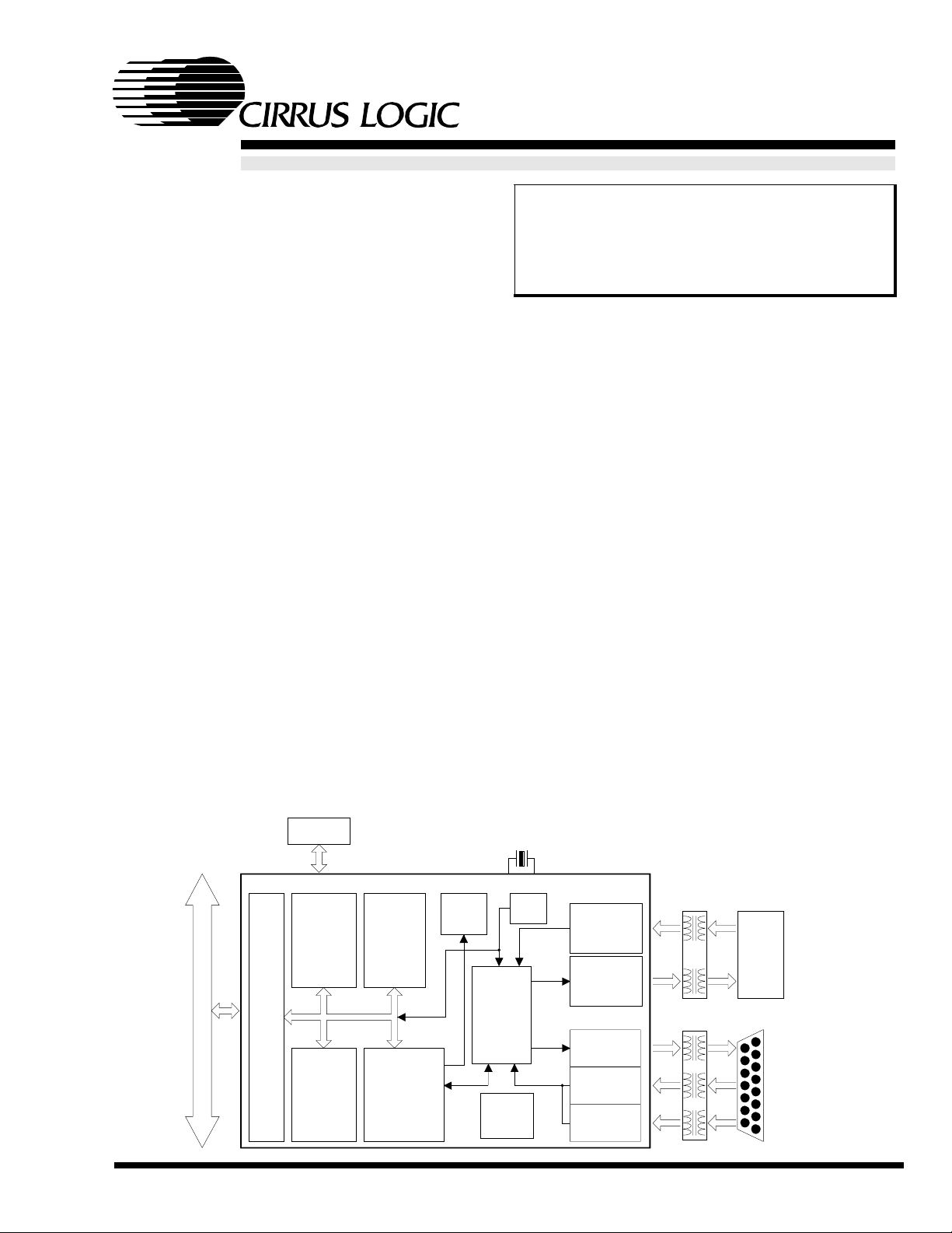
CS8920 ISA Ethernet Controller
LED
EEPROM
Control
ISA
Bus
I
S
A
Logic
&
Plug
and
Play
Memory
Manager
RAM
802.3
MAC
Engine
and Auto
Negotiation
SEP ‘97 DS238PP2
Control
Copyright Cirrus Logic, I nc. 1997
(All Rights Reserv ed)
20 MHz
XTAL
Clock
Encoder/
Decoder
&
PLL
Power
Manager
10BASE-T
RX Filters &
Receiver
10BASE-T
TX Filters &
Transmitter
AUI
Transmitter
AUI
Collision
AUI
Receiver
RJ-45 10BASE-T
Attachment
Unit
Interface
(AUI)

CS8920A
CONTENTS
1.0 INTRODUCTION
1.1 General Description . . . . 4
1.2 System Applications . . . . 5
1.3 Key Features and Benefits . . . 5
1.4 Enhancements Made in CS8920A . 8
2.0 PIN DESCRIP TION
2.1 Pin Diagram . . . . . . 9
2.2 Pin Description . . . . . . 10
3.0 FUNCTIONAL DESCRIPTION
3.1 Overview . . . . . . . 14
3.2 ISA Bus Interface . . . . . 15
3.3 Reset and Initialization . . . . 16
3.4 Plug and Play . . . . . . 18
3.5 Configuration with EEPROM . . 19
3.6 Programming the EEPROM . . 23
3.7 Boot PROM Operation . . . . 24
3.8 Low-Power Modes . . . . . 25
3.9 LED Outputs . . . . . . 26
3.10 Media Access Control (MAC) . . 27
3.11 Encoder/Decoder (ENDEC) . . 33
3.12 10BASE-T Transceiver . . . . 34
3.13 Attachment Unit Interface (AUI) . 37
3.14 External Clock Oscillator . . . 38
4.0 PACKETPAGE ARCHITECTURE
4.1 PacketPage Overview . . . . 39
4.2 PacketPage Memory Map . . . 40
4.3 Bus Interface Registers
Product Identification Code . . 42
DMA Start of Frame . . . . 43
DMA Frame Count . . . . 43
RxDMA Byte Count . . . . 43
EEPROM Command . . . . 44
EEPROM Data . . . . . 44
Receive Frame Byte Counter . . 44
4.4 Status and Control Registers . . 45
4.4.1 Status/Control Bit Definitions 46
4.4.2 Status/Control Register Summary 47
4.5 Status/Control Register Details
(0) Interrupt Status Queue . . 50
(3) Receiver Configuration (RxCFG) 51
(4) Receiver Event (RxEvent) . 52
(5) Receiver Control (RxCTL) . 53
(7) Transmit Configuratio n (TxCFG) 5 4
(8) Transmit Event (TxE vent) . 55
(9) Transmit Command (TxCM D) 56
(B) Buffer Configuration (BufCFG) 57
(C) Buffer Event (BufEvent) . . 59
(D) Advance In ter ru pt C on tro l
and Status (ADVintCTL/ST) . 60
(10) Rece ive Miss Coun ter ( RxM ISS) 61
(12) Trans. Collision Count (TxCOL) 61
(13) Line Control (LineCTL) . . 62
(14) Line Status (LineST) . . . 63
(15) Self Control (SelfCTL) . . 64
(16) Self Status (SelfST) . . . 65
(17) Bus Control (BusCTL) . . 66
(18) Bus Status (BusST) . . . 67
(19) Test Control (TestCTL) . . 68
(1C) AUI Time Domain Reflectometer 6 9
(1D) Auto Negotiation Control
(AutonegCTL) . . 70
(1E) Auto Negotiation Status
(AutonegST) . . 71
4.6 Initiate Transmit Register
Transmit Command (TxCMD) . 72
Transmit Length (TxLength) . . 73
4.7 Address Filter Regi sters
Logical Address Table (hash table) 74
Individual Address (IEEE address) 74
4.8 Plug n Play Resource Registers . 75
4.9 Receive and Transmit Frame Locatio ns 80
4.10 8 and 16-bit Transfers . . . . 80
4.11 Memory Mode Operation . . . 81
4.12 I/O Space Operation . . . . 83
5.0 OPERATION
5.1 Servicing the Interrupt Status Queue 86
5.2 Basic Receive Operation . . . 88
5.3 Receive Frame Address Filtering . 95
5.4 Rx Missed and Collision Counters . 98
5.5 Receive DMA . . . . . . 98
5.6 Auto-Switch DMA . . . . . 103
5.7 StreamTransfer . . . . . . 106
5.8 Transmit Operation . . . . . 108
5.9 Full Duplex Considerations . . . 115
5.10 System Wakeup with Wakeup Frames 115
6.0 TEST MODES
6.1 Boundary Scan Test . . . . . 121
7.0 ABSOLUTE MAXIMUM RATINGS . 125
Recommended Operating Conditions . 125
8.0 OPERATING CONDITIONS . . . 125
2 DS238PP2

9.0 DC CHARACTERISTICS
Crystal . . . . . . . . 125
Power Supply . . . . . . 125
Digital Inputs/Outputs . . . . 126
10BASE-T Interface . . . . 127
AUI Interface . . . . . . 127
9.1 CAPACITANCE . . . . . 127
10.0 SWITCHING CHARACTERISTICS
ISA Bus Timing . . . . . 128
10BASE-T Timing . . . . . 132
AUI Timing . . . . . . . 133
Boot PROM Timing . . . . 135
EEPROM Timing . . . . . 135
11.0 10BASE-T WIRING DIAGRAM . . 136
12.0 AUI WIRING DIAGRAM . . . . 137
CS8920A
13.0 CRYSTAL OSCILLATOR . . . . 137
14.0 PHYSICAL DIMENSIONS . . . . 138
15.0 GLOSSARY . . . . . . . . 139
DS238PP2 3

CS8920A
1.0 INTRODUCTION
1.1 General Description
The CS8920A is a single-chip, ISA Plug-andPlay, full-duplex, Ethernet solution,
incorporating all of the analog and digital circuitry needed for a complete Ethernet
circuit. Major functional blocks include: industry-standard plug-and-play protocol engine, a
direct ISA-bus interface, an 802.3 MAC engine
with auto-negotiation and wake-up frame recognition capability, integrated buffer memory; a
serial EEPR OM interface, and a complete an alog
front end with both 10BASE-T and AUI.
Plug and Play
The CS8920A implements Plug and Play in accordance with the Intel/Microsoft Plug and Play
ISA Specification Version 1.0a, allowing interrupts, DMA channels, IO base address, memory
base address, and optional BootPROM address
to be selected dynamically, by either a system
BIOS, an operat ing syste m or an appl ication program such as the Configuration Manager. The
CS8920A supports 11 interrupts and 3 DMA
channels.
frames on chip, eliminating the need for complex, inefficient memory management schemes.
The on-chip bu ffer manager supports full-duplex
operation.
802.3 Ethernet MAC Engine
The CS8920A’s Ethernet Media Access Control
(MAC) engine is fully compliant with the IEEE
802.3 Ethernet stand ard (ISO/IEC 8802-3, 1993),
and supports full-duplex operation. The full-duplex mode may be entered by a command from
the host, or vi a auto-negotiation using link-p ulse
signaling.
Magic Packet Frames
The MAC machine recognizes Magic Packet
frames, and can send a wakeup signal to a system power management chip via a dedicated
control line or vi a an interrup t pin.
EEPROM Interface
The CS8920A provides a simple serial
EEPROM interface that allows configuration information to be stored in EEPROM, and then
loaded auto matically at power-up.
Direct ISA-Bus Interface
The CS8920A has a direct ISA-bus interface
with full 24 mA driv e capability. The CS8920A
operates in either 24-bit memory space, 16-bit
I/O space, or with external DMA controllers
(three 16-bit channels), providing maximum design flexibilit y.
Complete Analo g Front End
The CS8920A’s analog front end incorporates a
Manchester encoder/decoder, clock recovery circuit, 10BASE-T transceiver, and complete
Attachment Unit Interface (AUI). It provides
manual and automatic selection of either
10BASE-T or AUI, and offers three on-chip
LED drivers for link status, bus status, an d Eth-
Integrated Memory
The CS8920A incorporates a 4-Kbyte page of
on-chip memory, eliminating the cost and board
area associate d with external memor y chips. Unlike most other Ethernet controllers, the
CS8920A buffers entire transmit and receive
4 DS238PP1
ernet line ac tivity.
The 10BASE-T transceiver includes drivers, receivers, and analog filters, allowing direct
connection to low-cost isolation transformers. It
supports 100, 120, and 150 Ω shielded and unshielded cabl es, extende d cable len gths.
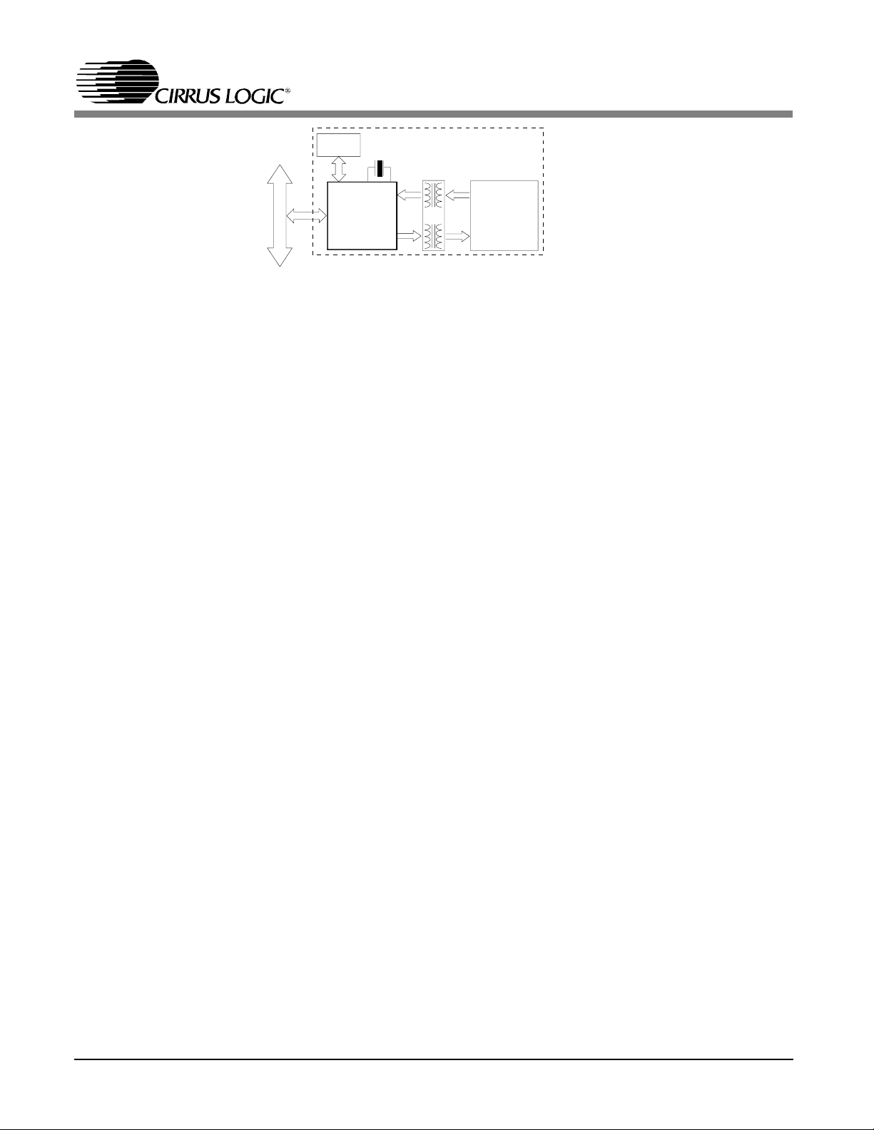
CS8920A
EEPROM
I
S
A
20 MHz
XTAL
CS 8920A
Figure 1.1. Complete Ethernet Motherboard Sol ution
The AUI port provides a direct interface to
10BASE-2, 10BASE-5 and 10BASE-FL networks, and is capable of driving a full 50-meter
AUI cable.
1.2 System Applications
The CS8920A is designe d to work well in either
motherboard o r adapter app lications.
Motherboard LANs
The CS8920A requires the minimum number of
external components needed for an Ethernet
node, allowing a complete Ethernet circuit that
occupies as little as 2.0 square inches of PCB
area (Figure 1.1). In addition, the CS8920A’s
power-saving features make it a perfect fit for
power-sensitive p ortable and desktop PCs. Motherboard design op tions includ e:
(2.0 sq. in.)
RJ-45 10B ASE - T
use of the CS8920A without an attached
EEPROM.
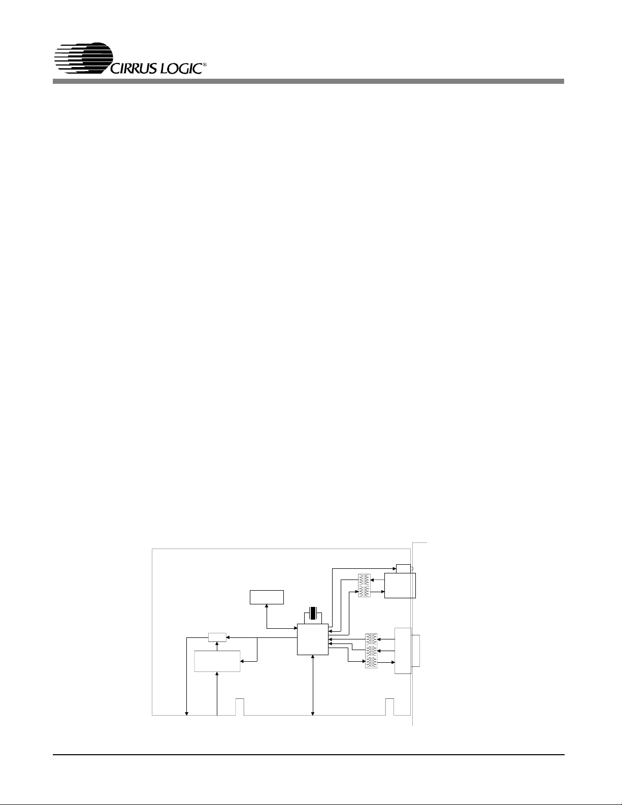
Plug-and-Play Ethernet Adapter Cards
The CS8920A’s highly efficient StreamTrans-
TM
fer
and Auto-Switch DMA options, make it
an excellent choice for high-performance, lowcost, ISA adapter cards (Fig. 1.2). The
CS8920A’s wide rang e of configuration options,
listed belo w, allow engineers to desig n Ethernet
solutions that meets their particular system requirements.
• A Boot PROM can b e added to support disk-
less appli cations.
• The 10BASE-T transmitter and receiver im-
pedance can be adjusted to sup port 100, 120,
or 150 Ω twisted pair cables.
• The EEPROM, used to store node-specific
information, such as the Ethernet Individual
• On-chip LED ports can be used for either
optional LEDs, o r as programmable outputs.
Address, can be eliminated by storing information in the syst em CMOS.
• The 20 MHz crystal oscillator may be re-
1.3 Key Features and Benefits
Very Low Cost
placed by a 20 MHz clo ck signal.
The CS8920A is designed to provi de the lowest-
Note: while operation of the CS8920A is possible without the use of an attached EEPROM,
special design considerations are required. Fur-
cost Ethernet solutions avai lable for ISA desktop
motherboards, portable motherboards, and
adapter car ds. Cost-s aving feat ures inclu de:
thermore, some of the CS8920A functions, such
as Plug and Play capabilities and wakeup frame
recognition are not possible without an attached
• Integrated RAM eliminates the need for ex-
pensive external memory chips.
EEPROM. Please contact Crystal’s CS8920A
technical support for more information on the
DS238PP1 5
CS8920A
• On-chip 10BASE-T filters allow desig ners to
use simple isolation transformers instead of
more costly filter/tra nsformer packages .
• The serial EEPROM port, used for configu-
ration and initialization, eliminates the need
for expensive s witches and j umpers.
• The CS8920A is designed to be used on a
2-layer circuit board instead of a more expensive multi-layer boa rd.
• The CS8920A-based solution offers the
smallest footprint available, saving valuable
printed circuit board area.
• A set of certifie d software dri vers is av ailable
at no charge, eliminating the need for costly
software development.
High Performance
The CS8920A is a ful l 16-bit Ethernet controller
designed to provide optimal system performance
by minimizing time on the ISA bus and CPU
overhead per frame. It offers equal or superior
performance for less money when compared to
other Ethernet control lers. The CS8920A’s PacketPage architecture allows software to select
whichever access method is best suited to each
particular CPU/ISA-bus configuration. When
compared to olde r I/O-sp ace design s, P acketPage
is faster, simpler and more efficient.
To boost performance further, the CS8920A include several key features that increase
throughput and l ower CPU overhead, including:
• StreamTransfer cuts up to 87% of interrupts
to the host CPU duri ng large block trans fers.
• Auto-Switch DMA allows the CS8920A to
maximize throughput while minimizing
missed frames.
• Early interrupts allow the host to preprocess
incoming frames.
• On-chip buffering of full frames cuts the
amount of host bandwidth need ed to manage
Ethernet traffic.
Low Power and Lo w Noise
For low power needs, the CS8920A offers three
power-down options: Hardware Standby, Hardware Suspend, and Software Suspend. In
Standby mode, the chip is powered down with
the exception of the 10BASE-T receiver, which
is enabled to listen for link activity. In either
Hardware or Software Suspend mode, the re-
LED
RJ-45
Attachment
Unit
Interface
(AUI)
’245
Boot PROM
EEPROM
20 MHz
XTAL
CS8920A
Figure 1.2. Full-Featured ISA Adapter Solution
6 DS238PP1
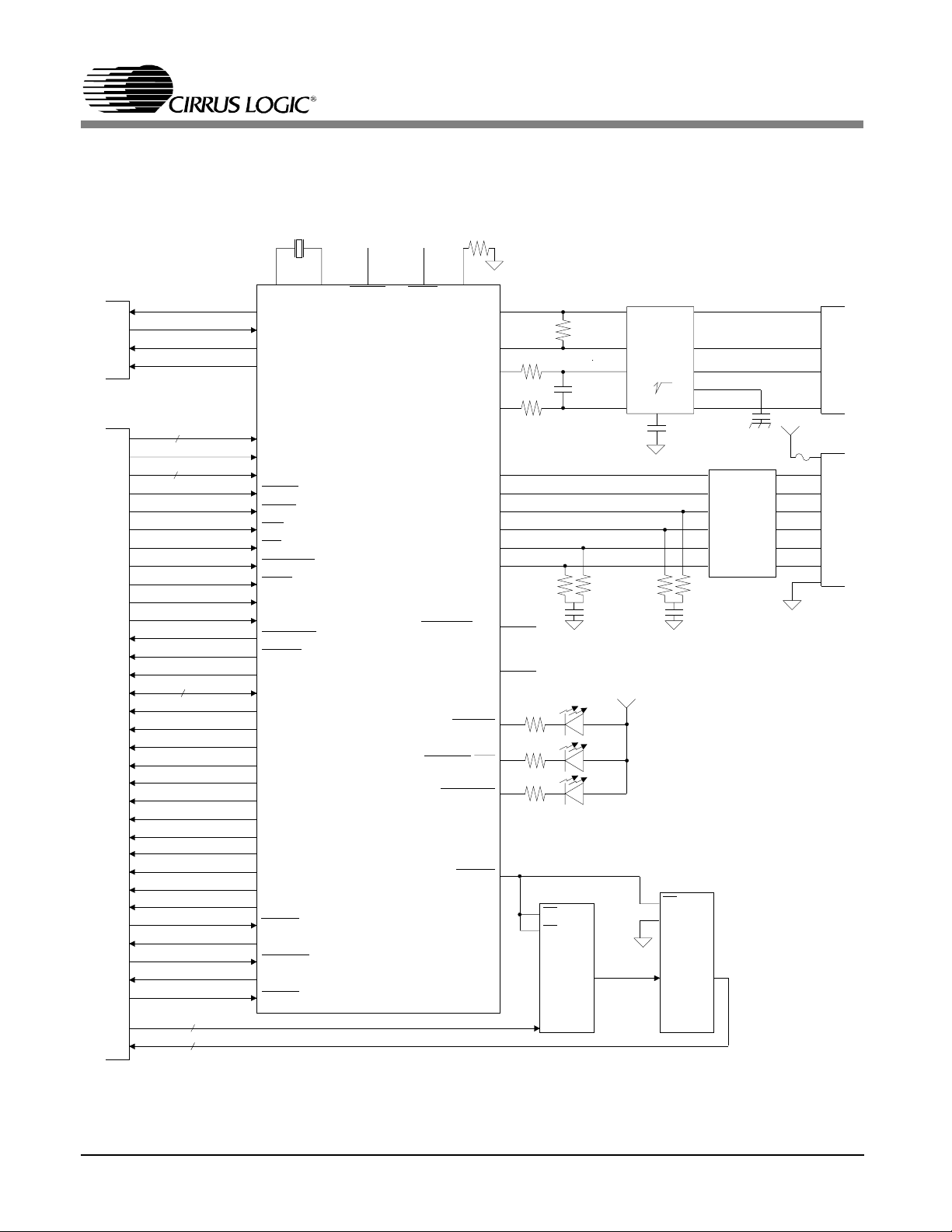
CS8920A
EEPROM
93C56
CS
DO
CLK
ISA
BUS
SA[0:14]
SD[0:7]
20 MHz
4.7 k
135 136
XTAL1 XTAL2 SLEEP TEST RES
16
15
8
141
7
6
142
57
28
29
90
89
83
52
91
114
44
43
92
75
76
77
78
79
106
34
33
32
30
31
16
17
14
15
9
10
EECS
EEDATAIN
EEDATAOUT
EESK
LA[17:23]
BALE
SA[0:16]
MEMW
MEMR
IOW
IOR
REFRESH
SBHE
AEN
RESET
MEMCS16
IOCS16
IOCHRDY
SD[0:15]
IRQ3
IRQ4
IRQ5
IRQ6
IRQ7
IRQ9
IRQ10
IRQ11
IRQ12
IRQ14
IRQ15
DRQ5
DACK5
DRQ6
DACK6
DRQ7
DACK7
1
4
3
DI
2
7
17
Ω
116
115
CS8920A
BSTATUS/HCI
LINKLED/HC0
Ω
4.99 k
131
RXD-
RXD+
TXD-
TXD+
DO-
DO+
CI-
CI+
DI-
DI+
EWAKE
LANLED
LOCALLED
CSOUT
, 1%
130
129
126
125
122
121
120
119
118
117
39.2
113
3
140
139
5
8
24.3
Ω, 1%
24.3
Ω, 1%
Ω
, 1%
680
Ω
680
Ω
680
Ω
Boot-PROM
27C256
20
CE
22
OE
100
68 pF
PD[0:7]
Ω, 1%
39.2 Ω, 1%
39.2
0.1
µ
F
10 BASE T
Isolation
Transforme r
1
1:1
3
6
1:
8
2
Ω
, 1%
5 V
19
1
2
.1 µF
39.2 Ω, 1%
0.1 µF
74LS245
OE
DIR
16
14
11
10
9
.1 µF
AUI Isola tion
Transformer
1
1:1
2
4
1:1
5
7
1:1
8
12 V
16
15 3
13
12
10
9
6
3
2
1
10
9
2
12
5
6
RJ45
15 pin D
Figure 1.3. Typica l Connection Diagram
DS238PP1 7

CS8920A
ceiver is disabled and power consumption drops
to the micro-Amp range.
In addition, the CS8920A has been designed for
very low noise emission, thus shortening the
time required for E MI testing and qual ification.
Complete Support
The CS8920A comes with a suite of software
drivers for immediate use with most industry
standard network operating systems. In addition,
complete evaluation kits and manufacturing
packages are available, significan tly reducing the
cost and time required to produce new Ethernet
products.
1.4 Enhancements Made in CS8920A
The functional enhancements made to the
CS8920A includ e the following:
To support software compatibility with existing
device drivers, the CS8920A’s Product Identification Code register has the same Product ID
Number as the CS8920. The CS8920A’s revision numb er has been incremented.
The CS8920A has added the EWAKE pin to the
boundary scan.
The FDX_LED pin of the CS8920 has been re dfined as the local-LAN-activity LED on the
CS8920A. The LOCALLED will light when
one of two event s occurs:
• the CS8920A tran smits onto the network, or
• the CS8920A receives a frame from the net-
work and that frame is addressed to this
station (i.e., the frame’s address passes the
CS8920A’s address filt er).
The Plug and Play standard provide s for an Auxillary Key which is normally used for testing
purposes or to program the EEPROM. The
CS8920A will respond to the Auxillary Key at
any time. The CS8920 responded to the Auxillary Key only if Plug and Pl ay was enabled , or if
the CS8920 had det ected that the EEPROM co ntained a bad CRC value. This meant that the
CS8920 would ignore the Auxillary Key in no nPlug and Play mode as long as the CRC was
valid.
8 DS238PP1
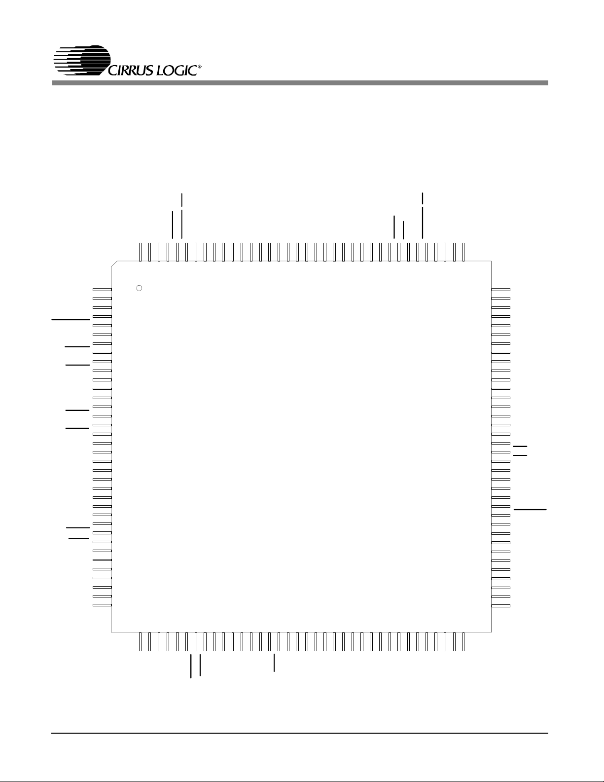
2.0 PIN DE SCRIPTION
2.1 Pin Diagram
EESK
EECS
144
143
142
141
1
2
EWAKE
ASUB1
LOCALLED
EEDO
EEDI
CSOUT
DRQ7
DACK7
DVSS1
DVDD1
DSUB1
DRQ6
DACK6
DRQ5
DACK5
SD15
SD14
SD13
SD12
DVDD2
DVSS2
SD11
SD10
SD9
SD8
MEMW
MEMR
IRQ14
IRQ15
IRQ12
IRQ1 1
IRQ10
3
4
5
6
7
8
9
10
11
12
13
14
15
16
17
18
19
20
21
22
23
24
25
26
27
28
29
30
31
32
33
34
35
36
LANLED
140
CS8920A
ASUB2
ASUB3
LINKLED/HC0
139
138
ASUB4
XTAL2
XTAL1
AVDD1
134
137
136
135
133
RXD+
AVSS1
RES
RXD-
129
132
131
130
CS8920A
144-Pin
TQFP
AVSS2
AVDD2
127
128
(Q)
CI-
DI-
TXD-
TXD+
AVSS3
AVDD3
DO-
DO+
120
126
122
125
124
123
121
CI+
119
118
DI+
117
SLEEP
TEST
RESET
BSTATUS/HC1
116
115
114
113
112
111
110
109
108
107
106
105
104
103
102
101
100
99
98
97
96
95
94
93
92
91
90
89
88
87
86
85
84
83
82
81
80
79
78
77
76
75
74
73
IRQ2 /I R Q 9
SD7
SD6
SD5
SD4
DVDD5
DVSS5
SD3
SD2
SD1
SD0
DSUB3
DVDD4
DVSS4
IOCHR DY
AEN
IOW
IOR
SA16
SA15
SA14
SA13
SA12
REFRESH
SA11
SA10
SA9
IRQ7
IRQ6
IRQ5
IRQ4
IRQ3
37
38
39
40
41
42
43
444546
MCS16
IOCS16
47
484950
LA17
LA18
LA19
LA20
525354
51
LA21
LA22
LA23
SBHE
DSUB2
555657
BAL E
DVSS3
DVDD3
58
SA0
61
59
60
SA1
SA2
SA3
626364
SA4
SA5
SA6
65
SA7
66
SA8
67
6869707172
DS238PP2 9

CS8920A
2.2 Pin Description
ISA Bus Interface
Symbol Pin Number Type Description
SA0-SA8
SA9-SA11
SA12-SA16
LA17-LA23 45-51 I Latchable Address Bus: Address decoding for the buffered version of the
BALE 57 I Buffered Address Latch Enable: Rising edge signals the CS8920A to
SD0-SD3
SD4-SD7
SD8-SD11
SD12-SD15
RESET 114 I Reset: Active-high asynchronous input used to reset the CS8920A. Must
AEN 91 I Address Enable: When TEST is high, the active-high AEN input indicates
MEMR 29 I Memory Read: Active-low input indicates that the host is executing a
MEMW 28 I Memory Write: Active-low input indicates that the host is executing a
MCS16 44 OD24 Memory Chip Select 16: Open-drain, active-low output generated by the
REFRESH 83 I Refresh: Active-low input indicates to the CS8920A that a DRAM refresh
IOR 89 I I/O Read: When IOR is low and a valid address is detected, the CS8920A
IOW 90 I I/O Write: When IOW is low and a valid address is detected, the
58-66
80-82
84-88
96-99
102-105
27-24
21-18
I System Address Bus: Address decoding for the ISA addresses including
Boot PROM and memory addres ses. SA0-SA15 a re used for I/O read/wr ite
operations. SA0-SA16 are used in for Memory read and write operations.
upper ISA address bits. Used for early address decode. Latched on the
trailing edge of the BALE signal.
decode the LA17:LA23. The trailing edge of BALE is used to latc h the
address and hold it for the duration of the current bus cycle.
B24 System Data Bus: Bi-directional 16-bit System Data Bus used to transfer
data between the CS8920A and the host.
be stable for at least 400 ns before the CS8920A recognizes the signal as
a valid reset.
to the CS8920A that the system DMA controller has control of the ISA bus.
When AEN is high, the CS8920A will not respond t o an IO or Memory
space access.
Memory Read operation.
Memory Write operat ion.
CS8920A when it recognizes an address on the ISA bus that corresponds
to its assigned Memo ry space (CS8920A must be in Memory Mode with
the MemoryE bit (Registe r 17, BusCTL, Bit A) set f or MCS16 to go active).
Tri-stated when not active.
cycle is in progress. W hen REFRESH is low, MEMR, MEMW, IOR, IOW,
DMACK0, DMACK1, and DMACK2 are ignored.
outputs the contents of the selected 16-bit I/O register onto the System
Data Bus. IOR is ignored if REFRESH is low.
CS8920A writes the data on the System Data Bus into the selected 16-bit
I/O register. IOW is ignored if REFRESH is low.
Pin Types:
dI = Dif ferential Input Pair I = Inp ut G = Ground
dO = Differe ntial Output Pa ir O = Output ts = Tri-State
B = Bi-Directional with Tri-State Output P = Power w = Internal Weak Pullup
OD = Open Drain Output
Digital outputs are followed by drive in mA (Example: OD24 = Open Drain Output with 24 mA drive).
10 DS238PP2

CS8920A
ISA Bus Interface (continued)
Symbol Pin Number Type Description
IOCS16 43 OD24 I/O Chip Select 16-bit: Open-drain, active-low output generated by the
CS8920A when it recognizes an address on the ISA bus that
corresponds to its assigned I/O space. Tri-stated when not active.
IOCHRDY 92 OD24 I/O Channel Ready: When driven low, this open-drain, active-h igh
output extends I/O Read and Memory Read cycles to the CS8920A. This
output is functional when th e IOCHRDYE bit in the Bus Control r egister
(Register 17) is clear. This pin is always tri-stated when the IOCHRDYE
bit is set.
SBHE 52 I System Bus High Enable: Active-low input indicates a data transfer on
the high byte of the System Data Bus (SD8-SD15). After a hardware or
software reset, provide a HIGH to LOW and then a LOW to HIGH
transition on SBHE signal before any IO or memory access isdone to the
CS8920A. *
IRQ2/IRQ9
IRQ3-IRQ7
IRQ10-IRQ12
IRQ14-IRQ15
DRQ5
DRQ6
DRQ7
DACK5
DACK6
DACK7
106
75-79
34-32
30-31
16
14
9
17
15
10
O24ts Interrupt Request: Active-high output indicates the presence of an
interrupt event. The pin goes low after the host reads a non-zero value
from the Interrupt Status Queue (ISQ).
O24ts DMA Request: Active-high, tri-stateable output used by the CS8920A to
request a DMA transfer. Only one DMA Request output is used (one is
selected during configuration). All non-selected DMA Request outputs
are pla ced in a hig h-i mped anc e st ate.
I DMA Acknowledge: Active-low input indicates acknowledgment by the
host of the corresponding DMA Request output.
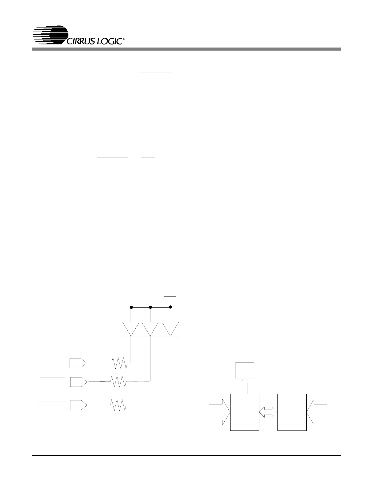
EEPROM and Boot PROM Interface
Symbol Pi n Number Type Description
EESK 142 O4 EEPROM Serial Clock: Serial clock used to clock data into or out of the
EEPROM.
EECS 1 41 O4 EEPROM Chip Select: Active-high output used to select the EEPROM.
EEDI 7 Iw EEPROM Data In: Serial input used to receive data from the EEPROM.
Connects to the DO pin on the EEPROM. EEDI is also used to sense the
presence of the EEPROM.
EEDO 6 O4 EEPROM Data Out: Serial output used to send data to the EEPROM.
Connects to the DI pin on the EEPROM. When TEST is low, this pin
becomes the output for the Boundary Scan Test.
CSOUT 8 O4 Chip Select for External Boot PROM: Active-low output used to select
an external Boot PROM when the CS8920A decodes a valid Boot PROM
memory address.
Pin Types:
dI = Dif ferential Input Pair I = Inp ut G = Ground
dO = Differe ntial Output Pa ir O = Output ts = Tri-State
B = Bi-Directional with Tri-State Output P = Power w = Internal Weak Pullup
OD = Open Drain Output
Digital outputs are followed by drive in mA (Example: OD24 = Open Drain Output with 24 mA drive).
* For operation of the CS8920A in 16 bit mode, a transition on the
software reset .
SBHE line is required after a hardware or
DS238PP2 11

10BASE-T Interface
Symbol Pin Number Type Description
TXD+
TXD-
RXD+
RXD-
125
126
129
130
dO 10BASE-T Transmit: Differential output pair drives 10 Mb/s
Manchester-encoded data to the 10BASE-T transmit pair.
dI 10BASE-T Receive: Differential input pair re ceives 10 Mb/s
Manchester-encoded data from the 10BASE-T receive pair.
Attachment Unit Interface (AUI)
Symbol Pin Number Type Description
DO+
DO-
DI+
DI-
CI+
CI-
121
122
117
118
119
120
dO AUI Data Out: Differential output pair drives 10 Mb/s
Manchester-encoded data to the AUI transmit pair.
dI AUI Data In: Differential input pair receives 10 Mb/s Manchester-encoded
data from the AUI receive pair.
dI AUI Collision In: Differe ntial input pair c onnects to the AUI collision pai r.
A collision is indicated by the presence of a 10 MHz +/ -15% signal with
duty cycle no worse than 60/40.
CS8920A
Pin Types:
dI = Dif ferential Input Pair I = Inp ut G = Ground
dO = Differe ntial Output Pa ir O = Output ts = Tri-State
B = Bi-Directional with Tri-State Output P = Power w = Internal Weak Pullup
OD = Open Drain Output
Digital outputs are followed by drive in mA (Example: OD24 = Open Drain Output with 24 mA drive).
12 DS238PP2

CS8920A
General Pins
Symbol Pin Number Type D escr ipti on
XTAL1
XTAL2
SLEEP 116 I W H ardware Sleep: Active-low input used to enable the two hardware sleep
EWAKE 3 O4w Wakeup Signal: The CS8920A asserts EWAKE high when a wakeup
LINKLED
or
HC0
BSTATUS
or
HC1
LANLED 140 OD10 LAN Activity LED: During normal operation, this active-low output goes
LOCALLED 5 OD10 Local Activity LED: During normal operation, this active-low output goes
TEST 115 IW T est En able : Active-low input used to put the CS8920A in Boundary Scan
RES 131 I
DVDD1 DVDD5
DVSS1 DVSS5
DSUB1 DSUB3
AVDD1 AVDD3
AVSS1 AVSS7
AVSS1 AVSS4
Pin Types:
dI = Dif ferential Input Pair I = Inp ut G = Ground
dO = Differe ntial Output Pa ir O = Output ts = Tri-State
B = Bi-Directional with Tri-State Output P = Power w = Internal Weak Pullup
OD = Open Drain Output
Digital outputs are followed by drive in mA (Example: OD24 = Open Drain Output with 24 mA drive).
135
136
139 OD10 Link Good LED or Host Controlled Output 0: When the HCE0 bit of the
113 OD10 Bus Status or Host Controlled Output 1: When the HCE1 bit of the Self
12, 22,
55, 94, 101
11, 23, 56 ,
93, 100
13, 54,
95
133, 128,
123
4, 124, 127,
132, 134,
137, 138
4, 134,
137, 138
I/O Crystal: A 20 MHz crystal should be connected across these pins. If a
crystal is not used, a 20 MHz signal should be connected to XTAL1 and
XTAL2 should be left open. (See section 9.0 and 13.0.)
modes: Hardware Suspend and Hardware Standby. (See section 3.8.)
frame is detected on the Ethernet receiver.
Self Control register (Register 15) is clear, this active-low output is low
when the CS8920A detects the presence of valid link pulses. When the
HCE0 bit is set, the host may drive this pin low by setting the HCBO in the
Self Control register.
Control register (Register 15) is clear, this active-low output is low when
receive activity causes an ISA bus access. When the HCE1 bit is set, the
host may drive this pin low by setting the HCB1 in the Self Control register.
low f or 6 ms w hene ver th ere is a rece ive pac ket, a tran smi t pa cke t, or a
collision. During Hardware Standby mode, th is output is driv en low when
the receiver detects network activity.
low for 6 ms whenever there is either a receive packet addressed to this
node, or a transmit packet.
Test mode. For normal operation, this pin should be high or left open.
Reference Resistor: This input should be connected to a 4.99 KΩ +/-1%
resistor needed for biasing of internal analog circuits.
P Digital Power: Provides 5 V +/- 5% power to the digital circuits of the
CS8920A.
G Digital Ground: Provides ground reference (0V) to the digital circuits of the
CS8920A.
Provide additional ground references (0V) to digital circuits of the CS8920A.
P Analog Power: Provides 5 V +/- 5% power to the analog circuits of the
CS8920A.
G Analog Ground: Provide ground reference (0V) to the analog circuits of the
CS8920A.
Provided additional ground references (0V) to analog circuits of the
CS8920A.
DS238PP2 13

CS8920A
3.0 F UNCTIONAL DESCRIPTION
3.1
Overview
During normal operati on, the CS8920A perfo rms
two basic functions: Ethernet packet transmission and reception. Before transmission or
reception is poss ible, the CS8920A must be co nfigured.
Configuration
The CS8920A must be configured for packet
transmission and reception at power-up or reset.
Various parameters must be writt en into its internal Configuration and Control registers such as
Memory Base Address; Ethernet Physical Address; what frame types to receive; and which
media interface to use. Configuration data can
either be written to the CS8920A by the host
(across the ISA bus), or loaded automatically
from an external EEPROM. Operation can begin
after configurati on is comple te.
memory, either as a Memory o r I/O space operation.
In the second phase of packet transmission, the
CS8920A converts the frame into an Ethernet
packet, then transmits it onto the network. The
second phase begins wit h the CS8920A transmitting the preamble and Start-of-Frame delimiter
as soon as the pro per number of bytes have been
transferred into its transmit buffer (5, 381, 1021
bytes or full frame, depen ding on configuration).
The preamble and Start-of-Frame are followed
by the Destination Address, Source Address,
Length field and LLC data (all supplied by the
host). If the frame is less than 64 bytes, including CRC, the CS8920A adds pad bits if
configured to do so. Finally, the CS8920A appends the prope r 32-bit CRC value.
Section 5.8 provides a detailed description of
packet transm ission.
Packet Reception
Sections 3.1 and 3.3 describe the configuration
process in de tail. Section 4.4 provides a detailed
description of the bits in the Configuration and
Control Registers.
Packet Trans mission
Packet transmission occurs in two phases. In the
first phase, the host moves the Ethernet frame
into the CS8920A’s buffer memory. The first
phase begins with the host issuing a Transmit
Command. This informs the CS8920A that a
frame is to be transmitted and tells the chip
when (i.e. after 5, 381, or 1021 bytes have been
transferred or after the full fra me has been transferred to the CS8920A) and how the frame
should be sent (i.e. with o r without C RC, with or
without pad bits, etc.). The host follows the
Transmit Command with the Transmit Length,
indicating how much buffer space is required.
When buffer space is available, the host writes
the Ethernet frame into the CS8920A’s internal
Like packet transmission, packet reception occurs in two phases. In the first phase, the
CS8920A receives an Ethernet packet and stores
it in on-chip memory. The first phase begins
with the receive frame passing through the analog front end and Manchester decoder where
Manchester dat a is converted to NRZ data. Next,
the preamble and Start-of-Frame delimiter are
stripped off and the receive frame is sent t hrough
the address filter. If the frame’s Destination Address matches the criteria programmed into the
address filter, the packet is stored in the
CS8920A’s internal memory. The CS8920A then
checks the CRC, and depending on the configuration, informs the processor that a frame has
been rece ived.
In the second phase, the host transfers the receive frame across the ISA bus and into host
memory. Receive frames can be transferred as
Memory space operations, I/O space operations,
or as DMA ope rations using h ost DMA. In addi-
14 DS238PP2

CS8920A
tion, the CS8920A provides the capability to
switch between Memory or I/O operation and
DMA operation by usi ng Auto-Switch DMA and
StreamTransfe r.
Sections 5.2 through 5.7 provide a detailed description of packet reception.
Reset/Boot/Sle ep
Nine resets can be activated on the CS8920A.
Three are activated by the V
power supply
CC
line; one is activated when the EEPROM fails
checksum; one is activated on a Plug and Play
instruction; one is activated when RESET is set;
and three ar e activated with sleep modes.
A sleep mode disabl es the CS8920A (completel y
or partially) to reduce power consumption. "Suspend" describes the CS8920A in the completely
disabled mode. "Standby" describes the
CS8920A in the partially disabled mode when
most of its circuits except the receiver are disabled. The CS8920A can be "Awakened" when
the receiver detects an d receives line activity.
After reset, p acket transmis sion and rece ption are
disabled. Either an external EEPROM must be
used to start the CS8920A, or the host must directly set up registers using Plug and Play
protocols.
The CS8920A is o ptimized for 16-bit data transfers, operating in either Memory space, I/O
space, or as a DMA slave.
Note that ISA-bus operation below 8 MHz
should use the CS8920A’s Receive DMA mode
to minimize missed frames. See Sectio n 5.5 for a
descriptio n of Receive DMA operation .
Memory Mode Operation
When configured for Memory Mode operation,
the CS8920A’s internal RAM is mapped into a
contiguous 4-Kbyte block of host memory, providing the host with direct access to the
CS8920A’s internal registers and frame buffers.
The host initiates Read operations by driving the
MEMR pin low and Write operations by driving
the
MEMW pin low.
For additional in formation about Memory Mode,
see Section 4. 11.
I/O Mode Operation
When configured for I/O Mode operation, the
CS8920A is accessed through eight, 16-bit I/O
ports that are mapped into sixteen contiguous
I/O locatio ns in the host sys tem’s I/O space. I/O
Mode is the default configuration for the
CS8920A and is always enabled.
Contact Crystal’s CS8920A technical support for
more information regarding the use of the
CS8920A without an external EEPROM.
For an I/O Read or Write opera tion, the AEN pin
must be low, and the 16-bit I/O address on the
ISA System Address bus (SA0 - SA15) must
match the address space of the CS8920A. For a
3.2
ISA Bus Interface
Read,
IOR must be low, and for a Write, IOW
must be low.
The CS8920A provides a direct interface to I SA
buses running at clock rates from 8 to 11 MHz.
Its on-chip bus drivers are capable of delivering
For additional information about I/O Mode, see
Section 4.12.
24 mA of drive current, allowing the CS8920A
to drive the ISA bus directly, without added ex-
Interrupt Req uest Signals
ternal "glue lo gic".
The CS8920A has eleven interrupt request out-
put pins that can be connected directly to any
DS238PP2 15
CS8920A
eleven of the ISA bus Interrupt Request signals.
Only one interrupt output is used at a time. The
interrupt output is selected during initialization
by writing the interrupt number (0 to 10) into
PacketPage Memory base + 0370h; or, the interrupt output can be accessed through t he Plug an d
Play resource register 0070h. Unused interrupt
request pins are placed in a high-impedance
state. The selected interrupt request pin goes
high when an enabled interrupt is triggered. The
pin goes low after the Interrupt Status Queue
(ISQ) is read as all 0’s (see Section 5.1 for a
description of the ISQ).
CS8920A Interrupt
Request Pin
IRQ3(Pin 75) IRQ3 0003h
IRQ4 (Pin 76) IRQ4 0004h
IRQ5 (Pin 77) IRQ5 0005h
IRQ6(Pin 78) IRQ6 0006h
IRQ7(Pin 79) IRQ7 0007h
IRQ9(Pin 106) IRQ9 0009h
IRQ10(Pin 34) IRQ10 000Ah
IRQ11(Pin 33) IRQ11 000Bh
IRQ12(Pin 32) IRQ12 000Ch
IRQ14(Pin 30) IRQ14 000Eh
IRQ15 (Pin 31) IRQ15 000Fh
ISA Bus
Interrupt
Packe t Pa ge
base + 0370h*
during initi alization by writi ng the number of the
desired channel (0, 1 or 2) into PacketPage
Memory base + 0374h. Unused DMA pins are
placed in a high-impedance state. The selected
DMA request p in goes high when th e CS8920A
has received frame s to transfer to the hos t mem-
ory via DMA. If the DMABurst bit (register 17,
BusCTL, Bit B) is se t, the pin goes low after the
DMA operation is complete. If the DMABurst
bit is clear, the pin goes low 32 µs after the st art
of a DMA transfer.
The DMA pin pairs are arranged on the
CS8920A to facilitate board layout. Crystal rec-
ommends the configuration in Table 3.2 when
connecting these pins to th e ISA bus.
For a description of DMA mode, see Section
CS8920A DMA
Signal (Pin #)
DRQ5 (16) DRQ5 0000h
DAC K 5 ( 17 ) DAC K 5
DRQ6 (14) DRQ6 0001h
DAC K 6 ( 15 ) DAC K 6
DRQ7 (9) DRQ7 0002h
DAC K 7 ( 10 ) DAC K 7
ISA DMA
Signal
PacketPage
base + 0374h
Table 3.1. Interrupt Assignments
Table 3.1 presents one possible way of connecting the interru pt request pins to the ISA bus that
utilizes common ly available interrupts and facilitates board layo ut.
*When in PnP mode, the in terrupt request ou tput
is accessed throu gh the resource register 0370h.
DMA Signals
The CS8920A interfaces directly to the host
DMA controller to provide DMA transfers of receive frames from CS8920A memory to host
memory. The CS8920A has three pa irs of DMA
pins that can be connected directly to the three
16-bit DMA channels of the ISA bus. Only one
DMA channel is used at a time. It is selected
Tab le 3.2. DMA Assignments
5.5.
3.3
Reset and Initialization
3.3.1 Reset
Nine different conditions cause the CS8920A to
reset its i nternal registers and circuit s.
External Reset, or ISA Reset: There is a chip-
wide reset whenever the RESET pin is high for
at least 40 ns . During a chip-wide reset, al l cir-
cuitry and registers in the CS8920A a re reset.
Power-Up Reset: When power is applied, the
CS8920A mainta ins reset until the voltage at t he
supply pins reaches approximately 2.5 V. The
CS8920A come s out of reset on ce Vcc is greater
16 DS238PP2

CS8920A
than approximately 2.5 V and the crystal oscill ator has stabili zed.
Power-Down Reset: If the supply voltage drops
below approximately 2.5 V, there is a chip-wide
reset. The CS8920A comes out of reset once the
power supply returns to a level greater than approximately 2.5 V and the crystal oscillator has
stabilized.
EEreset: There is a chip-wide reset if the
CS8920A detects an EEPROM checksum error.
(see Section 3 .1).
Software Initiated Reset: There is a chip-wide
reset whenever the RESET bit (Register 15,
SelfCTL, Bit 6) is set. The Plug and Play card
select number, Plug and Play Rd Data port,
PnP_disable bit, IO base address register, memory base address register, interrupt register, and
DMA register are preserved. The digital logic is
reset, but the an alog cir cuits are no t.
Magic Packet Frame Genera ted Reset: In power
down mode, with WakeupEn=1, the CS8920A
won’t reset completely unless the reset signal it
detects is followed by 6
MEMR cycles. The
Magic Packet frame generated reset ensures the
CS8920A resets only when it receives a true
power up reset signal.
3.3.2 Allowing Time for Reset Operat ion
After a reset, the CS8920A goes through a self
configuration. This includes calibrating on-chip
analog circuit ry, and reading EEPROM for validity and configuration. Time required for the reset
calibration is typically 10 ms. Software drivers
should not access registers internal to the
CS8920A during this time. When calibration is
done, bit INITD in the Self St atus Register (register 16) is set indicating that initialization is
complete, and the SIBUSY bit in the same register is cleared indicating the EEPROM is no
longer being read or programmed.
Hardware (HW) Standby or Suspend: The
CS8920A goes though a chip-wide reset whenever it enters or exits either HW Standby mode
or HW Suspend mode (see Sectio n 3.8 for more
information about HW Stan dby and Suspen d).
Software (SW) Suspend: Whenever the
CS8920A en ters SW Suspend mode, all registers
and circuits are reset except for th e ISA I/O Base
Address register (located at PacketPage base +
0360h) and the SelfCTL register (Register 15).
Upon exit, there is a chip-wide reset (see Sec tion
3.8 for more informati on about SW Suspend).
PnP Initiated Reset: Writing a one (setting
bit[0]) to the Plu g and Play Config Control register (address 0x02 ) causes all digital registers to
be reset, including the CS8920A’s Card select
Number and Plug and Play Read Data Port address. At the e nd of the reset, t he CS8920A will
attempt to read configuration information from
EEPROM. The analog circuits are not reset.
3.3.3 Bus Reset Considerations
The CS8920A reads 3000h from IObase+0Ah
after the reset, until the software writes a nonzero value at IObase+0Ah. The 3000h address
can be used as part of the CS8920A signature
when the system scans for the CS8920A. See
Section 4.1 2, I/O Space Op eration.
After a reset, the ISA bus outputs IRQx and
DRQx are tri-stated, thus avoiding any interrupt
or DMA channel conflicts on the ISA bus at
power-up time.
Initializati on
After each reset (except EEPROM Reset), the
CS8920A checks the sense of the EEDI pin to
see if an external EEPROM is present. If EEDI
is high, an EEPROM is present and the
CS8920A automatically loads the configuration
data stored in the EEPROM into its internal registers (see next section). If EEDI is low, an
DS238PP2 17

CS8920A
EEPROM is not present and the CS8920A
comes out of reset with th e default configuration
shown in Table 3.3.
A low-cost serial EEPROM can be used to store
configuration information that is automatically
loaded into t he CS8920A aft er each reset ( except
EEPROM reset). The u se of an EEPROM is op-
PacketPage
Address
0360h 0000h I/O Base Address*
0370h XXXX XXX X
0374h XXXX XXX X
0026h 0000h DMA Start-of-Frame Offset
0028h X000h DMA Frame Count
002Ah 0000h DMA Byte Count
0348h XXX0 0000h Memory Base Address
0340h XXX0 0000h Boot PROM Base
0343h XXX0 0000h Boot PROM Address Mask
0102h 0003h Register 3 - RxCFG
0104h 0005h Register 5 - RxCTL
0106h 0007h Register 7 - TxCFG
0108h 0009h Register 9 - TxCMD
010Ah 000Bh Register B - BufCFG
010Ch 000Dh Register D - Advint CTL/ST
010Eh Undefined Reserved
0110h Undefined Reserved
0112h 0013h Register 13 - LineCTL
0114h 0015h Register 15 - SelfCTL
0116h 0017h Register 17 - BusCTL
0118h 0019h Register 19 - TestCTL
011Ch 001Dh Register ID - AutoNeg CTL
* I/O base address is unaffected by SW Suspend mode.
Register
Contents
0000 0000
XXXX XX11
Register
Description
Interrupt Number
DMA Channel
Address
Table 3.3. Defa ult Configuration
EEPROM Type Size (16-bi t words)
’C46 (non-sequential) 64
’CS46 (sequential) 64
’C56 (non-sequential) 128
’CS56 (sequential) 128
’C66 (non-sequential) 256
’CS66 (sequential) 256
Table 3.4. Supp orted EEPROM Typ es
tional and is not required for all applications
(e.g. motherboard designs). However, while operation of the CS8920A is possible without the
use of an att ached EEPROM, special d esign considerations are required. Furthermore, some of
the CS8920A functions, such as Plug and Play
capabilities and wakeup frame recognition are
not possibl e without an atta ched EEPROM. Con-
tact Crystal’s CS8920A technical support for
more information on the use of the CS8920A
without an at tached EEPROM.
The CS8920A operates with any of six standard
EEPROM’s shown in Table 3.4. To work in a
PNP system, the CS8920A requires at least a
128 word EPROM.
3.4
Plug & Play
Plug and Play is a standard mechanism, developed by Intel and Microsoft, that provides an
automatic config uration capability for ISA cards.
System resources such as interrupts, memory addresses, and IO ports are assigned to Plug and
Play compatible devices by the Plug and Play
configuration mecha nism.
The CS8920A fully supports Plug and Play and
allows the complete configuration of the ISA interface by the Plug and Play compatible
operating system software or BIOS. Refer to the
Plug and Play ISA Specification for detailed information about the innerworkings of Plug and
Play.
Plug and Play Configuration Process
The Plug and Play configuration process determines the resource requirements of the Plug and
Play devices in a system and assigns non-conflicting resources to these cards. The
configuration process goes through several
phases:
18 DS238PP2

CS8920A
• A reset signal on the system bus places all
Plug and Play cards into a mode in which
they are all waiting for configuration to begin.
• A special key is writte n to all all of the PNP
cards to initi alize them for select ion.
• A special series of reads is performed that
allows a single card to be selected. The selected card is given a system identifier, called
the card select number (CSN). The configuration software then determines the resource
requirements of the card. Fi nally, the selected
card is placed into a slee p mode. The rem aining cards are individually selected and
assigned a CS N and their resource need s determined.
• The configuration software then selects an
individual card using the CSN, assigns nonconflicting resources to the card, and then
enables the card for normal oper ation. This is
repeated for each of the Plug and Play cards
until all of the cards have been configured
and enabled.
Plug and Play Auxi liary Key
The CS8920A wil l respond to a special auxilia ry
key at any time. The auxiliary initiation key is
normally used for testing/debug purposes. Two
bytes of 00 should pro ceed the initiation or auxiliary key. This auxiliary initiation key is listed
below in hexadecimal:
6A, B5, DA, 6D, B6, 5B, 2D, 16
0B, 05, 02, 01, 80, C0, 60, 30
18, 0C, 06, 83, 41, 20, 90, 48
24, 12, 89, C4, E2, F1, F8, FC
Plug and Play Device IDs
The Plug and Play device ID is a unique identifier that is used by the operating system to
associate the Plug and Play card with its device
CS8920A Pin
(Pin #)
EECS
(Pin 141)
EESK
(Pin 142)
EEDO
(Pin 6)
EEDI
(Pin 7)
Table 3.5. EEPROM Interface
CS8920A Func tion EEPROM
Pin
EEPROM Chip
Select
1 MHz EEPROM Seri al
Clock output
EEPROM Data Out
(data to EEPROM)
EEPROM Data In (data
from EEPROM)
Chip Select
Clock
Data In
Data Out
driver. Microsoft administers the assignment of
these device IDs. Contact Microsoft to receive a
unique device ID.
3.5
Configuration with EEPROM
EEPROM Interface
The interface to the EEPROM consists of the
four signals shown in Table 3.5
EEPROM Memory Organization
EEPROM is used to store initial configuration
information for the CS8920 A. The EEPROM is
organized in one or more blo cks of 16-bit words.
The first block in EEPROM, referred to as the
Configuration Block, is used to configure the
CS8920A after reset. An example of a typical
Configuration Block is shown in Table 3.6 . Additional user data may also be stored in the
EEPROM if space is available. The additional
data are stored as 16-bit words and can occupy
any EEPROM address space beginning immediately after the end of the Reset Configuration
Block up to address 7Fh, depending on
EEPROM size. This additional data can only be
accessed through software control (refer to Section 3.6 for more information on accessing the
EEPROM). Address space 80h to AFh is reserved
DS238PP2 19

CS8920A
Reset Configuration B lock
The first block in EEPROM, referred to as the
Reset Configuration Block, is used to automatically program the CS8920A with an initial
configuration after a reset. It is a block of contiguous 16-bit words starting at EEPROM
address 00h. The Reset Configuration Block ca n
be divided into three logical sections: a header,
one or more grou ps of configuration data words,
and a checksum value. All of the words in the
Reset Configuration Block are read sequentially
by the CS8920A after each reset, starting with
the header and ending with the checksum. Each
group of configuration da ta is used to program a
PacketPage register (or set of PacketPage registers in some cases) with an initial non-default
value.
Reset Configuration Block Header: The header
(first word of the block located at EEPROM address 00h) specifies the type of EEPROM used,
whether or not a Reset Configuration block is
present, if t he CS8920A’s Plug and Play support
is enabled or disabled, and how many bytes of
data are stor ed in the Re set Configurati on Block.
Determining the EEPROM Type: The LSB of
the high byte of the header i ndicates the type of
EEPROM attached: sequential or no n-sequential.
An LSB of 0 (XXXX-XXX0) indicates a sequential EEPROM. An LSB of 1 (XXXXXXX1) indicates a non-sequential EEPROM.
The CS8920A works equally well with either
type of EEPROM. The CS8920A will automatically generate sequential addresses while
reading the Reset Configuration Block if a nonsequential E EPROM is used.
Checking EEP ROM for presence of Reset Configuration Block: The readout of either a binary
101X-XXX0 or 101X-XXX1 (X = do not care)
from the high byte of the header indicates the
presence of configuration data. Any other read-
Word Address Value Description
FIRST WORD in DATA BLOCK
00h B112h Configuration Block Header.
The high byte, B1h, indicates a ’C56 EEPROM (non-sequential) is attached
and Plug and Play is disabled. The Link Byte, 12h, indica tes the nu mbe r of
bytes of configuration data in this block.
FIRST GROUP of WORDS
01h 2158h Group Header for first group of words.
Three words to be loaded, beginning at 0158h in PacketPage memory.
02h 0100h Individual address, bits[39-32], bits[47-40]
03h 0302h Individual address, bits[23-16], bits[31-24]
04h 0504h Individual address, bits[7-0], bits[15-8]
SECOND GROUP of WORDS
05h 0360h Group Header for second group of words.
One word to be loaded at 360h in PacketPage memory.
06h 0003h IO Base address = 300h
THIRD GROUP of WORDS
07h 0330h Group Header for third group of words.
One word to be loaded at 330h in PacketPage memory.
08h 0001 Set adapter’s activate bit (make active on reset w/o PnP).
CHECKSUM Value
09h 1B00h The high byte, 1Bh, is the checksum value. The checksum includes word
addresses 00h through 08h. The hexadecimal sum of the bytes is E5h,
resulting in a 2’s complement of 1Bh. The low byte, 00h, provides a pad to
the word boundary.
Tabl e 3.6. EEPROM Configuration Block Example
20 DS238PP2

CS8920A
out value terminates initialization from the
EEPROM. If an EEPROM is attached but not
used for configuration, Crystal recommends that
the high byte of the first word be programmed
with 00h in order to ensure that the CS8920A
will not attempt to read configuration data from
the EEPROM.
Setting Plug And Play Support Enabled/disabled: Setting bit four of the high byte of the
header disables the CS8920A’s Plug and Play
support. Clearing this bit leaves Plug and Play
support enabled (default). For example, a value
of 1011-XXXX (X = do not care) for the high
byte disables Plug and Play support while a
value of 1010-XXXX leaves Plug and Play enabled.
Determining Number of Bytes in the Reset
Configuration Block: The low byte of th e Reset
Configuration Blo ck header is known as the link
byte. The value of the Link Byte represents the
number of bytes o f configuration data in the Reset Configuration Block. The two bytes used for
the header are excluded when calculating the
Link Byte value.
For example, a Reset Configuration Block
header of A112h indicates a non-sequential
EEPROM programmed with eighteen (12h)
bytes of configuration data. The CS8920A’s
Plug and Play support is enabled. The Reset
Configuration Block occupies twenty bytes (10
words) of EEPROM space (2 bytes for the
header and 18 b ytes of configuratio n data).
Groups of Configuratio n Data
remaining words in the group are stored in successive PacketPage registers.
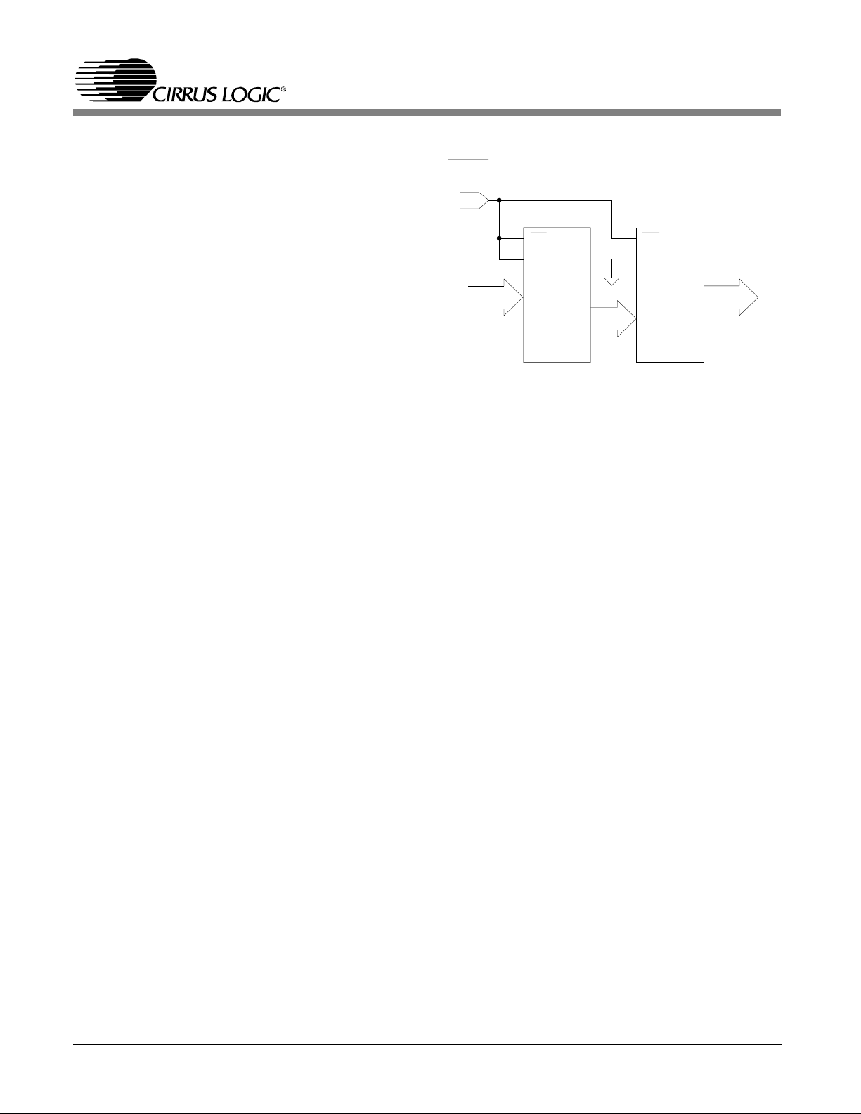
Group Header: Bits F through C of the Group
Header specify the number of words in each
group that are to be transferred to PacketPage
registers (see Figure 3.1). This value is two less
than the total number of wo rds in the group, including t he Group Head er. For example, if bits F
through C c ontain 0001, there are three words in
the group (a Group Header and two words of
configuration dat a).
First Word of a Group of Words
103
25
FE
Number of Words
in Group
Figure 3.1. Group Header
C
00
9
B
AD
8
10-bit PacketPage Address
476
Bits 9 through 0 of the Group Header specify a
10-bit PacketPage Address. This address defines
the PacketPage register that will be loaded with
the first word of configuration data from the
group. Bits B and A of the Group Header are
forced to 0, restricting the destination address
range to the first 10 24 bytes of PacketPage me mory.
Configuration data are arranged as groups of
words. Each group contains one or more words
Figure 3.1 shows the format of the Group
header.
of data that are to be loaded into PacketPage registers. The first word of each group is referred to
Reset Configuratio n Block Check sum
as the Group Header. The Group Header indicates the number of words in the group and the
address of the PacketPage register into which th e
first data word in the group is to be lo aded. Any
DS238PP2 21
A checksum is stored in the high byte position
of the word immediately foll owing the last group
of data in the Reset Configuration Block. (The
CS8920A
EEPROM address of the ch ecksum value can be
determined by dividing the value stored in the
Link Byte by two). The checksum value is the
2’s complement of the 8-bit sum (any carry out
of eighth bit is ignored) of all the bytes in the
Reset Configuration B lock, excluding the checksum byte. This sum includes the Reset
Configuration Block header at address 00h.
Since the c hecksum value is calculated as the 2’s
complement of the sum of all the preceding
bytes in the in the Reset Configuration Block, a
total of 0 sho uld result when the checksum value
is added to the sum of the previous bytes.
EEPROM Examp le
Tabl e 3.6 shows an example of a Reset Configuration Block stored in a ’C56 (non-sequential)
EEPROM. The B112h value in the header disables Plug and Play support and specifies
eighteen bytes of configuration data follow.
Note that litt le-endian word ord ering is used, i.e.,
the least significan t word of a multi-word datum
is located at th e lowest address.
EEPROM Readout
If the EEDI pin is asserted high at the end of
reset, the CS8920A reads the first word of
EEPROM data by:
1. Asserting EECS
2. Clocking out a Read-Register-00h command
on EEDO (E ESK provides a 1 MHz se rial clock
signal)
3. Clocking th e data in on EEDI.
If the EEDI pin is low at the end of the reset
signal, the CS8920A does not perform an
EEPROM readout (uses its default configura-
tion).
Determining EEPROM Size: The CS8920A de-
termines the size of the EEPROM by checking
the sense of EEDI on the tenth rising edge of
EESK. If EEDI is low, the EEPROM is a ’C46
or ’CS46. If EEDI is high, the EEPROM is a
’C56, ’CS56, ’C66 , or ’CS66.
Loading Configuration Data: The CS8920A
reads in the first word from the EEPROM to de-
termine if c onfiguration data are contai ned in the
AD7 - AD0 used with ’C56,
’CS56, ’C66 and ’CS66
F
EXDXCXB
X
Bit Name Description
[F:B] Reserved
[A] ELSEL External Logic Sel ect: When clear, the EECS pin is used to select the EEPROM. When set,
the ELCS pin is used to select the external LA decode circuit.
[9:8] OB1, OB0 Opcode: Indicates what command is being executed (see next section).
[7:0] A D7 to AD0 EE PROM Address: Address of EEPROM word being accessed.
A
9
8
X ELSEL OB1 OB0
AD7 AD6
Figure 3.2. EEPROM Command Register Format
22 DS238PP2
5476
AD5 AD 4
AD5 - AD 0 used with
’C 46 and ’ C S4 6
1
032
AD1 AD 0AD3 AD 2

CS8920A
EEPROM. If configuration data are not stored in
the EEPROM, the CS8920A terminates initialization from EEPROM and operates using its
default configuration (See Table 3.3). Note: the
default configuration leaves the CS8920A in a
PnP inactive state; it can then only be accessed
through the PnP configuration and data ports. If
configuration data are stored in EEPROM, the
CS8920A automatically loads all configuration
data stored i n the Reset Configurati on Block into
its inter nal PacketPage regist ers.
EEPROM Readout Completion
Once all the con figuration dat a are transferred to
the appropriate PacketPage registers, the
CS8920A adds the sum of the data by tes it read
to the 2’s complement checksum at the end of
the configuration data to verify the Reset Configuration Block’s data are valid. If the resulting
total is 0, the readout is c onsidered valid. Otherwise, the CS8920A initiates a partial reset to
restore the de fault configuration .
If the readout is valid, the EEPROMOK bit
(Register 16, SelfST, bit A) is set. EEPROMOK
is cleared if a checksum error is detected . In this
case, the CS8920A performs a partial reset and
is restored to its default. Once initialization is
complete (configuration loaded from EEPROM
or reset to d efault configuration) the INITD bit is
set (Register 16, SelfST, bit 7).
3.6
Programming the EEPROM
After initialization, the host can access the
EEPROM through the CS8920A by writing one
of seven commands to the EEPROM Command
register (PacketPage base + 0040h). Figure 3.2
shows the format of the EEPROM Command
register.
EEPROM Commands
The seven commands used to access the
EEPROM are: Read, Write, Erase, Erase/Write
Enable, Erase/Write Disable, Erase-All, and
Write-All. They a re descri bed i n Table 3.7.
EEPROM Command Exe cution
During the execution of a command, the two Opcode bits, followed by six bits of address (for a
’C46 or ’CS46) or eighth bits of address (for a
’C56, ’CS56, ’C66 or ’CS66), are shifted out of
the CS8920A, into the EEPROM. If the command is a Write, the data in the EEPROM Data
register (PacketPage base + 0042h) follows. If
Command Opcode
(bits 9, 8)
Read Register 1,0 word address yes all
Write Register 0,1 word address yes all 10 ms
Erase Register 1,1 word address no all 10 ms
Erase/Write Enable 0,0 XX11-XXXX no ’CS46, ’C46
Erase/Write Disable 0,0
0,0
Erase-All Registers 0,0
0,0
Write-All Registers 0,0
0,0
Table 3.7. EEPROM Comman ds
DS238PP2 23
EEPROM Address
(bits 7 to 0)
11XX-XXXX no ’CS56, ’C56, ’CS66, ’C66
XX00-XXXX no ’CS46, ’C46
00XX-XXXX no ’CS56, ’C56, ’CS66, ’C66
XX10-XXXX no ’CS46, ’C46 10 ms
10XX-XXXX no ’CS56, ’C56, ’CS66, ’C66 10 ms
XX01-XXXX yes ’CS46, ’C46 10 ms
01XX-XXXX yes ’CS56, ’C56, ’CS66, ’C66 10 ms
Data EEPROM T yp e Executi on Time
25 µs
9 µs
9 µs
9 µs
9 µs
CS8920A
the command is a Read, the d ata in the specified
EEPROM location is written into the EEPROM
Data register. If the command is an Erase or
Erase-All, no data is transferred to or from the
EEPROM Data register. Before issuing any command, the host must wait for the SIBUSY bit
(Register 16, SelfST, bit 8) to clear. After each
command has been issued, the host must wait
again for SI-BUSY to clear.
Enabling Ac cess to th e EEPROM
The Erase/Write Enable command provides protection from accidental writes to the EEPROM.
The host mus t write an Erase/W rite Enable command before it attempts to write to or erase any
EEPROM memory location. Once the host has
finished altering the co ntents of the EEPROM, it
must write an Erase/Write Disable command to
prevent unwanted modification of the E EPROM.
Writing and Erasing t he EEPROM
To write data to the EEPROM, the host must
execute the following s eries of com mands:
1. Iss ue an Eras e/Write Enab le command.
CS8920A
CSOUT
(Pin 17)
SA(0:14)
20
22
27C256
CE
OE
19
74LS245
OE
DIR
B1
.
.
.
B8
A1
.
.
.
A8
SD(0:7)
ISA
BUS
Figure 3.3. Boot PROM Connection Diagram
network server. This is typically done for a diskless workstation.
Accessing the Boot PR OM
The CS8920A provides address decoding circuitry to generate a chip select for a Boot
PROM. When the address on the ISA bus match
the address loaded into the Boot PROM base address register and qualified by Boot PROM
address mask register. The CS8920A generates a
chipselect signal for the Boot PROM.
2. Loa d the data i nto the EEPROM Data register.
Configuring the CS89 20A for Boot PROM
Operation
3. Iss ue a Writ e comma nd.
Figure 3.3 show how the CS8920A should be
4. Iss ue an Erase/Wr ite Disable c ommand.
connected to the Boot PROM and ’245 driver.
To co nfigure the CS8920A’s internal registers for
During the Eras e command, the CS8 920A writes
FFh to the spec ified EEPROM location. During
the Erase-All command, the CS8920A writes
FFh to all locat ions.
Boot PROM operation, the Boot PROM Base
Address must be loaded into the Boot PROM
Base Address register (PacketPage bas e + 0340h)
and the Boot PROM Address Mask must be
loaded into th e BootPROM Address Mask register (PacketPage base + 0343h). T he Boot PROM
Base Address provides the starting location in
3.7
Boot PROM Operation
host memory where the Boot PROM is mapped.
The Boot PROM Address Mask indicates the
The CS8920A supports an optio nal Boot PROM
used to store code for remote booting from a
size of the attached Boot PROM and is limited
to 4-Kbyte increments. The lower 12 bits of the
Address Mask are ign ored and shoul d be 000h.
24 DS238PP2

CS8920A
As an example, to configur e the CS8920A to use
a 16-Kbyte (128-Kbit) PROM mapped into host
memory at a starting address of D0000h, write
0D00h to the BootPROM Base Address register
and write 0FC0h into the BootPROM Address
Mask register. (The mask value for a 16-Kbyte
PROM is 0FC00h. See Section 4.8 for more information on determin g the BootPROM Address
and Mask register values.)
3.8
Low-Power Modes
For power-sensitive applications, the CS8920A
supports three low-power modes: Hardware
Standby, Hardware Suspend, and Software Suspend. All three low-power modes are controlled
through the SelfCT L register (Register 15).
An internal reset occurs when the CS8920A
comes out of any s uspend or standby mode. After a reset (internal or external), the CS8920A
goes though a self configuration. This includes
calibrating on-chip analog circuitry, and reading
EEPROM for validity and configuration. When
the calibration is done, bit InitD in Register 16
(Self Stat us regist er) is s et indicat ing th at init ialization is complete, and the SIBusy bit in the
same register is cleared (indicating that the
EEPROM is no longer being read or programmed. Time required fo r the reset calibration
is typically 10 ms. Software drivers should not
access registers internal to CS8920A during this
time.
Hardware Standby
Hardware (HW) Standby is designed for use in
systems, such as portable PC’s, that may be temporarily disconn ected from the 10BASE-T cable.
It allows the sys tem to conserve power while the
LAN is not in use, and then automatically restore Ethernet operation once the cable is
reconnected.
In HW Standby mod e, all analog and digita l circuitry in the CS8920A is turned off, except for
the 10BASE-T receiver which remains active to
listen for l ink activity. If link activity is detected,
the
LANLED pin is driven low, providing an indication to the host that the network connection
is active. The host can then activate the
CS8920A by de-asserting the
SLEEP pin. Dur-
ing this mode , all ISA bus a ccesses are ignored.
CS8920A Configuration CS8920A Operation
SLEEP
(Pin 116)
Low Set Set Clear Not Present HW Standby mode:
Low Set Set Clear Receiver
Low Clear Set Clear N/A HW Suspend mode
Low to High N/A Set Clear N/A CS8920A resets and goes
High N/A N/A Clear N/A Not in any sleep mode
Low N/A Clear Set N/A SW Suspend mode
Low N/A Clear Clear N/A Not in any sleep mode
NOTE: Both HW Standby and HW Suspend take precedence over SW Suspend.
Table 3 .8. Low-Power Mode Operation
DS238PP2 25
HWstandbyE
(SelfCTL, Bit
A)
HWSleepE
(SelfC TL, B it 9)
SWSuspend
(SelfCTL, Bit 8)
Link Pulses
Activity
10BASE-T receiver listens for
link activity
HW Standby mode:
LANLED low
through Initialization

CS8920A
To enter HW Standby mode, the SLEEP pin
must be low and the HWSleepE bit (R egister 15,
SelfCTL, Bit 9) and the HWstandbyE bit (Register 15, SelfCTL, Bit A) must be set. When the
CS8920A enters HW Standby, all registers and
circuits are reset except for the SelfCTL register.
Upon exit from HW Standby, the CS8920A performs a complete reset, and then goes through
normal initiali zation.
Hardware Suspend
During Hardware Suspend mode, the CS8920A
uses the least amou nt of current of the three lowpower modes. All internal circuits are turned off
and the CS892 0A’s core is electronically isol ated
from the rest of the system. Accesses from the
ISA bus and Ethernet activity are bo th ignored .
HW Suspend mode is entered by driving the
SLEEP pin low and setting the HWSleepE bit
(Register 15, SelfCTL, bit 9) while the
HWstandbyE bit (Registe r 15, SelfCTL, bit A) is
clear. To exit from this mode, the
SLEEP pin
must be driven high. Upon exit, the CS8920A
performs a comp lete reset, an d then goes through
a normal init ializatio n procedure.
Software Suspend
Software (SW) Suspend mode can be used to
conserve power in certain applications, such as
adapter cards that do not have power management circuitry available. During software
suspend mode there is a partial reset. All registers and c ircuits are re set except for the Plug an d
Play state, CSN, read data port, ISA I/O Base
Address Regist er, and the SelfCTL r egister.
To enter SW Suspend mode, the host must set
the SWSuspend bit (Register 15, SelfCTL, bi t 8).
To exit SW Suspend, the host must write to the
CS8920A’s assigned I/O space (the write is only
used to wake the CS8920A, the write itself is
ignored). Upon exit, the CS8920A performs a
complete reset, then goes through a normal initialization p rocedure.
Any hardware reset takes the chip out of any
sleep mode.
Table 3.8 summarizes the operation of the three
low-power modes.
HC0E
(Bit C)
0 N/A Pin configured as LINKLED: Output
1 0 Pin co nfigur ed as HC0:
1 1 Pin co nfigur ed as HC0:
Table 3.9. LINKLED/HC0 Pin Operation
3.9
HCB0
(Bit E)
Pin Function
is low when valid 10BASE-T link
pulses are detected. Output is high if
valid link pulses are not detected.
Output is high
Output is low
LED Outputs
The CS8920A provid es four output pins th at can
be used to cont rol LEDs or external lo gic.
LANLED:
LANLED goes low whenever the
CS8920A tran smits or receives a frame, or when
it detects a collision.
LANLED remains low until
there has been no activity for 6 ms (i.e. each
transmission, reception, or collision produces a
pulse lasting a minimum of 6 ms).
HC1E
(Bit D)
0 N/A Pin configured as BSTATUS: Output
1 0 Pin co nfigur ed as HC1:
1 1 Pin co nfigur ed as HC1:
Table 3.10. BSTATUS/HC1 Pin O peration
HCB1
(Bit F)
Pin Function
is low when a receive frame begins
transfer acro ss th e ISA bus. Output is
high otherwise.
Output is high
Output is low
26 DS238PP2
CS8920A
LINKLED or HC0: LINKLED or HC0 can be
controlled by either the CS8920A or the host.
When controlle d by the CS8920A,
LINKLED is
low whenever the CS8920A receives valid
10BASE-T link pulses. To configure this p in for
CS8920A control, the HC0E bit (Register 15,
SelfCTL, Bit C) must be clear. When controlled
by the host,
LINKLED is low whenever the
HCB0 bit (Register 15, SelfCTL, Bit E) is set.
To configure it for host control, the HC0E bit
must be set. Table 3.9 summari zes this ope ration.
BSTATUS or HC1:
BSTATUS or HC1 can be
controlled by either the CS8920A or the host.
When controlled by the CS8920A,
BSTATUS is
low whenever the host reads the RxEvent register (PacketPage base + 0124h), signaling the
transfer of a receive frame across the ISA bus.
To configure this pin for CS8920A control, the
HC1E bit (Register 15, SelfCTL, Bit D) must be
clear. When controlle d by the host,
BSTATUS is
low whenever the HCB1 bit (Register 15,
SelfCTL, Bit F) is set. To configure it for host
control, HC1E must be set. Table 3.10 summarizes this operatio n.
+5V
LOCALLED:
LOCALLED goes low whenever
local LAN activity is occurring. Local LAN activity is defined as either the the receipt of
Ethernet frames that pass the address filter of
the CS8920A, or the transmission of fra mes onto
the Ethernet. This LED is intended to be used
on the front panel of a PC in a manner analogous to a Hard Drive Activity LED. See Section
5.3 for discussi on of the receive address filter.
LED Connection
Each LED output is capab le of sinking 10 mA to
drive an LED directly through a series resistor.
The outp ut voltage of e ach pin is les s than 0.4 V
when the pin is low. Figure 3.4 shows a typical
LED circuit.
3.10
Media Access Control
Overview
The CS8920A’s Ethernet Media Access Control
(MAC) engine is fully compliant with the IEEE
802.3 Ethernet stand ard (ISO/IEC 8802-3, 1993).
It handles all asp ects of Et hernet frame transmission and recept ion, includi ng: collisio n detection,
preamble generation and detection, and CRC
generation and test. Programmable MAC features include automatic retransmission on
collision, a nd padding of tra nsmitted frames.
Figure 3.5 shows how the MAC engine interfaces to other CS8920A functions. On the host
side, it interfaces to the CS8920A’s internal
LOCALLED
LANLED
LINKLED
Figure 3.4. LED Connection Diagram
DS238PP2 27
CS8920A
Internal Bus
Figure 3.5. MAC Interface
LED
Logic
802.3
MAC
Engine
Enco der/
Decoder
&
PLL
10BASE-T
& AUI
CS8920A
data/address/control bus. On the network side, it
interfaces t o the internal Manchester encod er/decoder (ENDEC). The primary functions of the
MAC are: frame encapsulation and decapsulation; error detection and handling; and, media
access manag ement.
Frame Encapsulation and Decapsulation
The CS8920A’s MAC engine automatically assembles transmit packets and disassembles
receive packets. It also determines if transmit
and receive frames are of legal minimum size.
Transmission: Once the proper number of bytes
have been transferred to t he CS8920A’s memory
(either 5, 381, 1021 bytes, or full frame), and
providing that access to the network is permitt ed,
the MAC automatically transmi ts the 7-byte preamble (1010101b...), followed by the
Start-of-Frame Delimiter (SFD, 10101011b), and
then the serialized frame data. It then transmits
the Frame Check Seq uence (FCS). The data after
the SFD and before the FCS (Destination Address, So urce Address, Len gth, and data field) is
supplied by the host. FCS generation by the
CS8920A may be disabled by setting the InhibitCRC bit (Regis ter 9, TxCMD, bit C).
Figure 3.6 shows the Ethernet frame format.
Reception: The MAC receives the incoming
packet as a serial stream of NRZ data from the
Manchester enc oder/decoder. It begins by che cking for the SFD. Once the SFD is detected, the
MAC assumes all subseque nt bits ar e frame data.
It reads the DA and compares it to the criteria
programmed into the address filter (see Section
5.3 for a description of Address Filtering ). If the
DA passes the address filter, the frame is lo aded
into the CS8920A’s memory. If the BufferCRC
bit (Register 3, RxCFG, bit B) is set, the received FCS is also loaded into memory. Once
the entire packet has been received, the MAC
validates the FCS. If an error is detected, the
CRCerror bit (Registe r 4, RxEvent, Bit C) i s set.
Enforcing Minimum Frame Size: The MAC
provides minimum frame size enforcement of
both transmit and receive packets. When the
TxPadDis bit (Register 9, TxCMD, Bit D) is
clear, transmit frames will be padded with additional bits to ensure that the receiving station
receives a legal frame (64 bytes, including
CRC). When TxPadDis is set, the CS892 0A will
not add pad bits and will transmit frames less
that 64 bytes. If a frame is received that is less
than 64 bytes (including CRC), the Runt bit
(Register 4, RxEvent, Bit D) will be set indicating the arrival of an ill egal frame.
1 byteup to 7 bytes 6 bytes 6 bytes
alternating 1s / 0s
preamble
Direction of Transmission
SFD = Start of Frame Delimiter
DA = Destination Address
SA = Source Address
LLC = Logical Link Control
FCS = Frame Check Sequence (also
called Cyclic Redundancy Check, or CRC)
SFD DA SA
Packet
The optional field, which is two bytes long, is
either a TYPE field for Etherne t applica tions or
a LENGTH field for IEEE 802.3 applications.
The Pad field will be used only to get the frame
to the minimum size. When the CS8920 adds pad
bytes, the pad is the last byte of the LLC data
field rep eat e d M ti mes .
Frame
2 bytes N bytes M bytes
Optional Field
frame length
min 64 bytes
max 1518 bytes
LLC data Pad
4 bytes
FCS
Figure 3.6. Ethernet Frame Format
28 DS238PP2

CS8920A
Transmit Error Detectio n and Handling
The MAC engine monitors Ethernet activity and
reports and recovers from a number of error conditions. For transmission, the MAC reports the
following errors in the TxEvent register (Register
8) and BufEvent register (Register C):
Loss of Carrier: Whenever the CS8920A is
transmitting on the AUI port, it expects to see its
own transmission "loope d back" to its rece iver. If
it is unable to monitor its transmission after the
end of the pr eamble, the MAC reports a loss-ofcarrier error by setting the Loss-of-CRS bit
(Register 8, TxEvent, Bit 6). If the Loss-ofCRSiE bit (Register 7, T xCFG, Bit 6) is set, the
host will be inte rrupted.
SQE Error: After the end of transmission on the
AUI port, the MAC expects to see a collision
within 64 bit times. If no collision is detected,
the SQEerror bit (Register 8, TxEvent, Bit 7) is
set. If the SQEerroriE bit is set (Register 7,
TxCFG, Bit 7), the host is interrupted. An SQE
error may indicate a fault o n the AUI cable or a
faulty transc eiver (it is assumed th at the attached
transceiver supports this function).
Out-of-Window (Late) Collision: If a coll ision is
detected after the first 512 bits have been transmitted, the MAC reports a late collision by
setting the Out-of-window bit (Register 8,
TxEvent, Bit 9). The MAC then forces a bad
CRC and termin ates the transmiss ion. If the Outof-windowiE bit (Register 7, TxCFG, Bit 9) is
set, the host is interrupted. A late collision may
indicate an illegal n etwork configuration .
Jabber Error: If a transmission continue s longer
than about 26 ms, the MAC disables the transmitter and sets the Jabber bit (Register 8,
TxEvent, Bit A). The output of the transmitter
returns to idle and remains there until the host
issues a new Transmit Command. If the JabberiE
bit (Register 7, Tx CFG, Bit A) is set, the host is
interrupted. A Jabber condition indicates that
there may be something wrong with the
CS8920A transmit function. To prevent possible
network faults, t he host should clea r the transmit
buffer. Possible op tions includ e:
Reset the chip with either software or hardware
reset (see Se ction 3.3 ).
Issue a Force Transmit Command by setting the
Force bit (Register 9, Tx CMD, bit 8).
Issue a Transmit Command with the TxLength
field set to zero.
Transmit Collision: The MAC counts the number of times an individual packet must be
re-transmitted due to network collisi ons. The collision count is stored in bits B through E of the
TxEvent register (Register 8). If the packet collides 16 times, transmission of that packet is
terminated and the 16coll bit (Register 8,
TxEvent, Bit F) is set. If the 16co lliE bit (Register 7, TxCFG, Bit F) is set, the host will be
interrupted on the 16th collision. A running
count of transmit collisions is recorded in the
TxCOL register.
Transmit Underrun: If the CS8920A starts
transmission o f a packet but runs out of data before reaching the end of frame, the TxUnderrun
bit (Register C, BufEvent, Bit 9) is set. The
MAC then forces a bad CRC and term inates the
transmission. If the TxUnderruniE bit (Register
B, BufCFG, Bit 9) i s set, the hos t is interrupte d.
Receive Error Detec tion and Handling
The following receive errors are reported in the
RxEvent register (Register 4):
CRC Error: If a frame is received with a bad
CRC, the CRC error bit (Register 4, Rx Event, Bit
C) is set. If the CRCerrorA bit (Register 5,
RxCTL, Bit C) is set, the frame will be buffered
by the CS8920A. If the CRCerroriE bit (Register
3, RxCFG. Bit C) i s set, the hos t is interrupte d.
DS238PP2 29
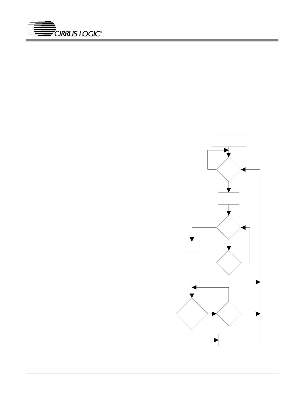
CS8920A
Runt Frame: If a frame is received that is
shorter than 64 bytes, the Runt bit (Register 4,
RxEvent, Bit D) is set. If the Runt A bit (Register
5, RxCTL, Bit D) is set, the frame will still be
buffered by CS8920A. If the RuntiE bit (Register 3, RxCFG. Bit D) is set, the host is
interrupted.
Extra Data: If a fr ame is received that is longer
than 1518 bytes, the Extradata bit (Register 4,
RxEvent, Bit E) is set. If the ExtradataA bit
(Register 5, RxCTL, Bit E) is set, the first 1518
bytes of the frame will still be buffered by
CS8920A. If the ExtradataiE bit (Register 3,
RxCFG. Bit E) is set, the host is interrupted.
Dribble Bits and Alignment Error: Under normal operating conditions, the MAC may detect
up to 7 add itional bits a fter the last ful l byte of a
receive packet. These bits, known as dribble bits,
are ignored. If dribb le bits are de tected, t he Dribblebit bit (Register 4, RxEvent, Bit 7) is set. If
both the Dribb lebit bit and CRCerror bit (Register 4, RxEvent, Bit C) are set at the same time,
an alignment er ror has occur red.
Media Access Managem ent
Collision Avoidance: The MAC continually
monitors network traffic by checking for the
presence of carrier activity (carrier activity is indicated by the assertion of the internal Carrier
Sense signal generated by the ENDEC). If carrier activity is detected, the network is assumed
busy and the MAC must wait until the current
packet is finished before attempting transmission. The CS8920A supports two schemes for
determining when to initiate transmission: TwoPart Deferral, and Simple Deferral. Selection of
the deferral scheme is determined by the 2-part-
Start Monitoring
Network Activity
Yes
Network
Active?
No
Start IPG
Timer
Yes
IPG
Timer =
s?
6.4
µ
The Ethernet networ k topology is a single s hared
medium with several attached stations. The Ethernet protocol is designed to allow each station
equal access to the network at any given time.
Wait
3.2
µ
s
No
Network
Active?
No
Any node can attempt to gain access to the network by first completing a deferral process
Yes
(described below) after the last network activity,
and then transmitting a packet that will be received by all other stations. If two nodes
transmit simultaneously, a collision occurs and
the colliding packets are corrupted. Two primary
Tx
Frame
and
Ready
in Backoff?
Not
No
No
Network
Active?
Yes
tasks of the MAC are to avoid network collisions, and then recover from them when they
occur. In addition, when the CS8920A is using
the AUI, the MAC must support the SQE Test
function described in section 7.2.4.6 of the Eth-
Figure 3 .7. Two-Part Deferral
Yes
Transmit
Frame
ernet standard.
30 DS238PP2

CS8920A
DefDis bit (Register 13, LineCTL, Bit D). If the
2-partDefDis bit is clear, the MAC uses a twopart deferral process defined in section 4.2.3.2.1
of the Ethernet standard (ISO/IEC 8802-3,
1993). If the 2-partDefDis bit is set, the MAC
uses a simplified deferral scheme. Both schemes
are described bel ow:
Two-Part Deferral: In the two-part deferral process, the 9.6 µs Inter Packet Gap (IPG) timer is
started whenever the internal Carrier Sense signal is de-asserted. If activity is detected during
the first 6.4 µs of the IPG timer, the timer is reset and then restarted once the activity has
stopped. If th ere is no ac tivity during the first 6. 4
µs of the IPG timer, the IPG timer is allowed to
time out (even if network activity is detected
during the final 3.2 µs). The MAC then begins
transmission if a transmit packet is ready and if
it is not in Backoff (Backoff is described later in
this section). If no transmit packet is pending,
the MAC continues to monitor the network. If
Start Monitoring
Network Activity
Yes
Network
Active?
activity is detected before a transmit frame is
ready, the MAC defers to the transmitting stati on
and resumes monitoring the network.
The two-part deferral scheme was developed to
prevent the possibility of the IPG being shortened due to a temporary loss of carrier. Figure
3.7 diagrams the two-part deferral proce ss.
Simple Deferral: In the simple deferral scheme,
the IPG timer is started whenever Carrier Sense
is de-asserted. Once the IPG timer is finished
(after 9.6 µs), if a transmit frame is pending and
if the MAC is not in Backoff, transmission begins (even if network activity is detected during
the 9.6 µs IPG). If no tra nsmit packet is pending ,
the MAC continues to monitor the network. If
activity is detected before a transmit frame is
ready, the MAC defers to the transmitting stati on
and resumes monitoring the network. Figure 3.8
diagrams the simple deferral process.
Collision Resolution: If a collision is detected
while the CS8920A is transmit ting, the MAC responds in one of three ways depending on
whether it is a normal collision (within the first
512 bits of transmis sion) or a late collision (after
the first 512 bits of t ransmission):
No
Normal Colli sions: If a collisio n is detected before the en d of the preambl e and SFD, the MAC
Wait
9.6
µ
s
finishes the preamble and SFD, tr ansmits the jam
sequence (32-bit pattern of all 0’s), and then initiates Backoff. If a collision is det ected after the
transmission of the preambl e and SFD but be fore
512 bit times, the MAC immediately terminates
transmission, transmits the jam sequence, and
then initiates Backoff. In either case, if the
Onecoll bi t (Register 9, TxCMD, Bi t 9) is clear,
Frame
Read
y
i
n Backoff?
No
T
x
nd
No
No
t
a
Network
Active?
Yes
the MAC will attempt t o transmit a packet a total
Yes
Transmit
Frame
Figure 3.8. Simple Deferral
DS238PP2 31
of 16 times (the initial attempt plus 15 retransmissions) due to normal collisions. On the 16th
collision, it sets the 16coll bit (Register 8,
TxEvent, Bit F) and discards the packet. If the

Onecoll bit is set, the MAC discards the packet
without attempt ing any re-transmissio n.
Late Collisions: If a collision is detected after
the first 512 bits have been transmitted, the
MAC immediately terminates transmission,
transmits the jam sequence, discards the packet,
and sets the Out-of-window bit (Register 8,
TxEvent, Bit 9). The CS8920A does not initiat e
backoff or attempt to re-transmit the frame. For
additional in formation about Late Collisions, see
Out-of-Window Error in this section.
Backoff: After the MAC has completed transmitting the jam sequence, it must wait, or "Back
off", before attempting to transmit again. The
amount of time it must wait is determined by
one of two Backoff algorithms: the Standard
Backoff algorithm (ISO/IEC 4.2.3.2.5) or the
Modified Backoff algorithm. The host selects
which algorithm through the ModBackoffE bit
(Register 13, Line CTL, Bit B).
CS8920A
where r (a random integer) is the number of slot
times the MAC must wait (1 slot time = 512 bit
times), and k is the smaller of n or 10, where n
is the number of re-transmission attempt s.
Modified Backoff: The Modified Backoff is described by the e quation:
0 ≤ r ≤ 2
k
where r (a random integer) is the number of slot
times the MAC must wait, and k is 3 for n <3
and k is the smaller of n or 10 for n
>3, where n
is the number of re-transmission attempt s.
The advantage of the Modified Backoff algorithm over the Stand ard Backoff algorithm is that
it reduces the possibility of multiple collisions
on the first three re-tries. The disadvantage is
that it extends th e maximum time needed to gain
access to the network for th e first three re-tries.
Standard Backoff: The Standard Backoff algorithm, also called the "Truncated Binary
Exponential Backoff", is described by the equation:
0 ≤ r ≤ 2
Carrier Sense
k
RX CLK
RX NRZ
Carrier
Detector
Decoder
& PLL
MAC
TXCLK
TX NRZ
TEN
Port Select
Collision
Encoder
The host may choose to disable the Backoff algorithm altoge ther by setting the DisableBackoff
bit (Register 19, TestCTL, Bit B). When dis-
abled, the CS8920A only waits the 9.6 µs IPG
time before starting transmission.
ENDEC
RXSQL
10BASE-T
RX
MUX
TX
MUX
RX
TX
AUISQL
AUIRX
AUITX
AUICol
Transceiver
AUI
Clock
Figure 3.9. ENDEC
32 DS238PP2

CS8920A
SQE Test: If the CS8920A is transmitting on the
AUI, the external transceiver should generate an
SQE Test signal on the CI+/CI- pair following
each transmission. The SQE Test is a 10 MHz
signal lasting 5 to 15 bit times and starting
within 0.6 to 1.6 µs after the end of transmission. During this period, the CS8920A ignores
receive carrier activity (see SQE Error in this
section for more information).
3.11
Encoder/Decoder (ENDEC)
The CS8920A’s integrated encoder/dec oder (ENDEC) circuit is compliant with the relevant
portions of section 7 of the Ethernet standard
(ISO/IEC 8802-3, 1993). Its primary functions
include:
Manchester encod ing of transmit da ta;
informing the MAC when valid receive data is
present (Carrier Detection); and, recovering the
clock and NR Z data from incoming Manches terencoded data .
Figure 3.9 provides a block diagram of the ENDEC and how it interf aces to the MAC, AUI and
10BASE-T transceiver.
Encoder
Carrier Detection
The internal Carrier De tection circuit informs the
MAC that valid receive data is present by asserting the internal Carrier Sense signal as soon it
detects a valid bit pattern (1010b or 0101b for
10BASE-T, and 1b or 0b for AUI). During normal packet reception, Carrier Sense remains
asserted while the frame is being received, and is
de-asserted 1.3 t o 2.3 bit times afte r the last lowto-high transition of the End-of-Frame (EOF)
sequence. Whenever the receiver is idle (no receive activity), Carrier Sense is de-asserted. The
CRS bit (Register 14, L ineST, Bit E) reports the
state of the Carrier Sense signal.
Clock and Data Rec overy
When the receiver is idle, the phase-lock loop
(PLL) is locked to the internal clock signal. The
assertion of the Carrier Sense signal interrupts
the PLL. When it restarts, it locks on the i ncoming data. The receive clock is then compared to
the incoming data at the bit cell center and any
phase difference is corrected. The PLL remains
locked as long as the receiver input signal is
valid. Once the PLL has locked on the incoming
data, the ENDEC converts the Manchester data
to NRZ and passes the decoded data and the recovered clock to the MAC for further processing.
The encoder converts NRZ data from the MAC
Interface Selec tion
and a 20 MHz Transmit Clock signal into a serial stream of Manchester data. The Transmit
Clock is produced by an on-chip oscillator circuit that is driven by either an external 20 MHz
quartz crystal or a TTL -level CMOS clock input.
Physical interface selection is determined by the
AUIonly bit (Bit 8) and the AutoAUI/10BT bit
(Bit 9) in the LineCTL register (Register 13).
Table 3.11 describes the possible configurations.
If a CMOS input is used, the clock should be 20
MHz ±0.01% with a duty cycle between 40%
and 60%. The specifications for the crystal are
described in section 13.0 (Quartz Crystal Requirements). The encoded signal is routed to
AUIonly
(Bit 8)
0010BASE-T Only
1 N/A AUI Only
01Auto-Select
Aut oAUI/10BT
(Bit 9)
Physical
Interface
either the 10BASE-T transceiver or AUI, depending on co nfiguration.
Table 3.11. Interface Selection
DS238PP2 33

CS8920A
10BASE-T Only: When configured for 10BASET-only operation, the 10BASE-T transceiver and
its interface to the ENDEC are active, and the
AUI is powered down.
AUI O n ly : When configured for AUI-only operation, the AUI and its in terface to the ENDE C are
active, and the 10BASE-T transceiver is powered
down.
Auto-Select: In Au to-Select mode, the CS8920A
automatically selects the 10BASE-T interface
and powers down the AUI if valid packets or lin k
pulses are dete cted by the 10BASE-T receiver. If
valid packets and link pulses are not detected,
the CS8920A selects the AUI. Whenever the AUI
is selected, the 10BASE-T receiver remains active to listen for link pulses or packets. If
10BASE-T activity is detected, the CS8920A
switches back to 10 BASE-T.
3.12
The CS8920 A includes an integrated 1 0BASE-T
transceiver that is compliant with the relevant
portions of section 14 of the Ethernet standard
(ISO/IEC 8802-3, 1993). It includes all analog
and digital circuitry needed to interface the
CS8920A directly to a simple isolation transformer (see section 11.0 for a connection
diagram). Figure 3. 10 provides a bloc k diagram
of the 10BASE-T transceiver.
10BASE-T Fil ters
The CS8920A’s 10BASE-T transceiver includes
integrated low-pass transmit and receive filters,
eliminating the need for external filters or a filter/transformer hybrid. On-chip filters are gm/c
implementations of fifth-order Butterworth lowpass filters. Internal tuning circuits keep the
gm/c ratio tightly controlled, even when large
temperature, supply, and IC process variations
10BASE-T Transceiver
LinkOK
(to MA C )
RXSQL
RX
ENDEC
TX
Figure 3.10. 10BASE-T Transceiver
Link Pulse
Detect or
TX Pre-
Distortion
10BASE-T Transceiver
RX Squelch
RX
Comparator
TX Filters
Filter Tuning
RX Filters
RXDRXD+
TXD-
TX Drivers
TXD+
34 DS238PP2

CS8920A
occur. The nominal 3 dB cutoff frequ ency of the
filters is 16 MHz, and the nominal atte nuation at
30 MHz (3rd harmonic) is -27 dB.
Transmitter
When configured for 1 0BASE-T operation, Manchester encoded data from the ENDEC is fed
into the transmitter’s pre-distortion circuit where
initial wave shaping and pre-equalization is performed. The output of the pre-disto rtion circui t is
fed into the transmit filter where final wave
shaping occurs and unwanted noise is removed.
The signal then passes to the differential driver
where it is amplified and driven out of the
TXD+/TXD- pins.
In the absence of transmit packets, the transmitter generates link pulses in accordance with
section 14.2.1.1 of the Ethernet standard. Transmitted link pulses are positive pulses, one bit
time wide, typically generated at a rate of one
every 16 ms. The 16 ms timer starts whenever
the transmitter completes an End-of-Frame
(EOF) sequence. Thus, there is a link pulse 16
ms after an EOF unless there is anot her transmitted packet. Figure 3.1 1 diagram s the operat ion of
the Link Pulse Ge nerator.
If no link pulses are being received on the receiver, the 10BASE-T transmitter is internally
forced to an inactive state unless bit DisableLT
in register 19 (Test Control register) is set to one.
Receiver
The 10BASE-T receive section consists of the
receive filter, squelch circuit, polarity detection
and correction circuit, and l ink pulse det ector.
Squelch Circuit: The 10BASE-T squelch circuit
determines when valid data is present on the
RXD+/RXD- pair. Incoming signals passing
through the receive filter are tested by the
squelch circuit. Any signal with amplitude less
than the squelch threshold (either positive or
negative, depending on pola rity) is rejecte d.
Extended Range: The CS8 920A supports an Extended Ran ge feature that reduc es the 10BASE-T
receive squelch threshold by approximately 6
dB. This allows the CS8920A to operate with
10BASE-T cables that are longer than 100 meters (100 meters is the maximum length specified
by the Ethernet standard). The exact additional
distance dep ends on the quality o f the cable and
the amount of electro-magnetic noise in the surrounding environment. To activate this feature,
the host must set the LoRxSquelch bit (Register
13, Li neCTL, Bit E).
Auto-Negotiation
The CS8920A supports Auto-Negotiation, the
mechanism th at allows the two devices on either
end of a 10Base-T link segment to share information and au tomatically configure both d ev ices
for maximum performance. When configured for
Auto-Negotiation, the CS8920A will detect and
automatically operate full-duplex, if the device
on the other end of the link segment also supports full-duplex and Auto-Negotiation. The
CS8920A Auto-Negotiation capability is fully
compliant with the relevant portions of section
28 of the IEEE 802. 3u standard.
Auto-Negotiation encapsulates information
within a burst of closely spaced link integrity
test pulses, referred to as a Fast Link Pulse
(FLP) Burst. The FLP Burst consists of a series
of link integrity pulses which form an al ternating
clock / data sequence . Extraction of the data bits
from the FLP Burst yields a Link Code Word
which identifies the capabilit y of the remote device. To remain interoperable with existing
10Base-T devices, the CS8920A also supports
the reception of 10Base-T compliant link integrity test pulses, refered to as Normal Link Pulses
(NLP). Devices that respond to the CS8920A
with a Normal Link Pulse, cause the CS8920A
to operat e as a 10Base -T half-d uplex device.
DS238PP2 35

CS8920A
Prior to enabling Auto-Negotiation, the AllowFDX bit (Register 1D, AutoNegCTL, Bit 7)
should be set if full -duplex operation is to be allowed and reset otherwise. If this bit is reset,
only half-dupl ex operation will be negotiated.
To enable Auto-Negotiation the host should set
the AutoNegEnable bit (Register 1D,
AutoNegCTL, Bit 8) and reset the NLPEnable
bit (Register 1D, AutoNegCTL, Bit 9) and the
ForceFDX bit (Register 1D, AutoNegCTL, Bit
F).
Re-negotiation can be forced to occur by setting
the ReNOW bit (Register 1D, AutoNegCTL, bit
6). Typically, this is done after a change in the
settings of the Auto-Negotiation bits, in ord er to
cause the new setting s to be acted u pon.
The NLPEnable b it (Register 1D, AutoNegCTL,
bit 9) overrides the Auto-Negotiation settings
and causes Norm al Link Pulses to be tra nsmitted
by the CS8920A. Auto-Negotiation is disabled.
The following section describes the operation of
the CS8920A in NLP mode .
packet or link pulse is received before the LinkLoss timer finishes (between 25 and 150 ms),
the CS8920A maintains normal operation. If no
receive activity is detected, the CS8920A disables packet transmission to prevent "blind"
transmissions onto the network (link pulses are
still sent while packet transmission is disabled).
To reactivate transmission, the receiver must detect a sing le packet (the packet itse lf is ignored),
or two link pu lses separated by more th an 2 to 7
ms and no more than 25 to 150 ms (see section
10.0 for 10BASE-T timing).
The state of the link segment is reported in the
LinkOK bit (Register 14, LineST, Bit 7). If the
HC0E bit (Regis ter 15, SelfCTL, Bi t C) is clear,
it is also indicated by the output of the
LINKLED pin. If the link is "good", the LinkOK
bit is set and the
LINKLED pin is driven low. If
the link i s "bad" the LinkOK bi t is clear and the
LINKLED pin is high. To disable this feature,
the host must set the DisableLT bit (Register 19,
TestCTL, Bit 7). If DisableLT is set, the
CS8920A will tra nsmit and receive packets independent of th e link segment.
Link Pulse Detectio n
To prevent disruption of network operation due
to a faulty link segment, the CS8920A continually monitors the 10BASE-T receive pair
(RXD+/ RXD-) for packets and link pulses. After each packet or link pulse is received, an
internal Link-Loss timer is started. As long as a
Time
Packet
less than
16 ms
Figure 3.11. Link Pulse Transmission
36 DS238PP2
Packet
Receive Po larity Detect ion and Correc tion
The CS8920A automatically checks the polarity
of the receive half of the twisted pair cable. If
the polarity is corre ct, the PolarityOK bit (Register 14, LineST, bit C) is set. If the polarity is
reversed, the PolarityOK bit is clear. If the PolarityDis bit (Registe r 13, LineCTL, Bi t C) is clear,
Link
Pulse
16 ms 16 ms
Link
Pulse

CS8920A
the CS8920A auto matically corrects a reversal. If
the PolarityDi s bit is set , the CS8920A does not
correct a reversal. The PolarityOK bit and the
PolarityDis bit are ind ependent.
To detect a reversed pair, the receiver examines
received link pulses and the End-of-Frame
(EOF) sequence of incoming packets. If it detects at leas t one reversed link p ulse and at least
four frames in a row with negative polarity aft er
the EOF, the receive pair is considered reversed.
Any data received before the correction of the
reversal is ignored.
Collision Detect ion
If half-duplex operation is selected (Register 1D,
Bit E, ForceFDX), the CS8920A detects a
10BASE-T collision whenever the receiver and
transmitter are active simultaneously. When a
collision is present, the Collision Detection circuit informs the MAC by asserting the internal
Collision signal (see section 3.11 for collision
handling).
3.13
Attachment Unit Interface (AUI)
AUI Transmitter
The AUI transmitter is a differential driver designed to drive a 78 ohm cable. It accepts data
from the ENDEC an d transmits it direct ly on the
DO+/DO- pins. After transmission has started,
the CS8920A expects to see the packet "loopedback" (or echoed) to the receiver, causing the
Carrier Sense signal to be asserted. This Carrier
Sense presence indicates that the transmit signal
is getting through to the transceiver. If the Carrier Sense signal remains de-asserted throughout
the tran smission, or i f the Carrier Sen se signal is
de-asserted before the end of the transmission,
there is a Loss-of-Carrier error and the Loss-ofCRS bit (Register 8, TxEvent, Bit 6) is set .
AUI Receiver
The AUI receiver is a differential pai r circuit that
connects directly to the DI+/DI- pins. It is designed to distinguish between transient noise
pulses and incoming Ethernet packets. Incoming
packets with proper amplitude and pulse width
are passed on to the ENDEC section, while unwanted noise i s rejected.
The CS8920A Attachment Unit Interface (AUI)
provides a dire ct interface to external 10BASE2,
10BASE5, and 10BASE-FL Ethernet transceivers. It is fully compliant with Section 7 of the
Ethernet standard (ISO/IEC 8802-3), and as
such, is capable of driving a full 50-meter AUI
cable.
The AUI consists of three pairs of signals: Data
CI+
CI-
DI+
DI-
DO+
DO-
-
AUI
Collision
+
-
+
Detect
AUICol (to MA C)
AUIRX
AUISQL
AUITX
ENDEC
Out (DO+/DO-), Data In (DI+/DI-), and Collision In (CI+/CI-). To select the AUI, the host
Figure 3.12. AUI
should set the AUI bit (Register 13, LineCTL,
Bit 8). The AUI can also be selected automat-
Collision Detec tion
ically as described in the previous section.
Figure 3.12 provides a block diagram of the
AUI. (For a connection diagram, see section
12.0).
The AUI collision circuit is a d ifferential pair receiver that detects the presence of collision
signals on the CI+/CI- pins. The collision signal
is generated by an external Ethernet transceiver
whenever a collision is detected on the Ethernet
DS238PP2 37

segment. (Section 7.3.1.2 of ISO/IEC 8802-3,
1993, defines the collision signal as a 10 MHz
+/- 15% signal with a duty cycle no worse than
60/40). Wh en a collisio n is present, th e AUI Collision circuit informs the MAC by asserting the
internal Coll ision signal.
CS8920A
3.14
External Clock Oscillator
A 20 MHz quartz crystal or CMOS clock input
is required by the CS8920A. If a CMOS clock
input is used, it should be connected the to
XTAL1 pin, with the XTAL2 pin left open. The
clock signal should be 20 MHz ±0.01% with a
duty cycle between 40% and 60%. The specifications for the crystal are described in section
13.0 (Quart z Crystal Requ irements).
38 DS238PP2

CS8920A
4.0 PACKETPAGE ARCHITECTURE
4.1 PacketPage Overview
The CS8920A architecture is based on a u nique,
highly-efficient method of a ccessing internal registers and buffer memory known as PacketPage.
PacketPage provides a unified way of controlling
the CS8920A i n Memory or I/O space that minimizes CPU overhead and simplifies software. It
provides a flexible set of performance features
and configuration options, allowing designers to
develop Ethernet circuits that meet their particular syst em requiremen ts.
Integrated Memory
Central to the CS89 20A architecture is a 4-Kbyt e
page of integrated RAM known as PacketPage
memory. PacketPage memory is used for temporary storage of transmit and receive frames, and
for internal registers. Access to this memory is
done directly, through Memory space operations
(Section 4.11), or indirectly, though I/O space
operations (Section 4.12). In most cases, Memory Mode will provide the best overall
performance, because ISA Memory operations
require fewer cycles than I/O operations. I/O
Mode is the CS8 920A’s default configuration an d
is used when memory space is not available or
when special operations are required (e.g. waking the CS8920A from the Software Sleep state
requires the host to write to the CS8920A’s assigned I/O sp ace).
The user-accessible portion of PacketPage memory is organized into th e following sections :
Bus Interface Registers
The Bus Inter face registers are us ed to configure
the CS8920A’s ISA-bus interface and to map the
CS8920A into the host system’s I/O and Memory space. Most of these registers are written
only during initialization, remaining unchanged
while the CS892 0A is in normal operatin g mode.
The exceptions to this are the DMA registers
which are modified continually whenever the
CS8920A is using DMA. These registers are described in more deta il in Section 4. 3.
Status and Control Registers
The Status and Control registers are the primary
means of controlling and getting status of the
CS8920A. They are described in more detail in
Section 4.4.
Initiate Trans mit Register s
The TxCMD/T xLength registers ar e used to init iate Ethernet frame transmission. These registers
are described in more detail in Section 4.6. (See
Section 5.8 for a description of frame transmission.)
Address Filt er Regis ters
The Filter registers store the Individual Address
filter and Logical Addre ss filter used by the Destination Address (DA) filter. These registers are
described in more de tail in Section 4.7. For a description of t he DA filter, see Section 5 .3.
Plug and Play Registers
Packe tPage
Address
0000h - 0048h
0100h - 013Fh
0120h
0140h - 015Dh
0330h - 03FFh
0400h - 09FFh
0A00h - 0FFFh
DS238PP2 39
Product/Bus Specific Registers
Status and Normal Control Registers
Interrupt Status Queue
Ethernet, or Line, Related Registers
Plug and Play Registers
Current Receive Frame Virtual Map
Current Transmit Frame Virtual Map
Contents
Plug and Play registers hold resources assigned
by a plug a nd play configuration manag er. These
resources include IO and memory base address,
interrupt number and DMA channel. See section
4.8.

CS8920A
Receive and T ransmit Frame Locatio ns
The Receive and Transmit Fram e PacketPage locations are used to transfer Ethernet frames to
and from the host. The host simply write s to and
reads from these locations, and internal buffer
memory is dynamically allocated between transmit and receive as needed. This provides more
efficient use of buffer memory and bet ter overall
network performance. As a resu lt of this dynamic
allocation, only one receive frame (starting at
PacketPage base + 0400h) and one transmit
Base
+
0000h 4 Read-only
0004h 34
0026h 2 Read-only
0028h 2 Read-only
002Ah 2 Read-only
002Ch 20
0040h 2 Read/Write
0042h 2 Read/Write
0044h 4
0048h 2 Read
004Ah 6 Read/Write
0050h 2 Read-only
0052h 174
0100h 32
0120h 32
0140h 2 Read-only
0142h 2
# of
Bytes
Type Description Cross
Bus Interface Registers
32-bit Product Identification Code Section 4.3
Reserved Note 2
ISA RxDMA Start of Frame 16-bit Offset to Status Sections 4.3, 4.12
ISA RxDMA 12-bit Frame Count Sections 4.3
ISA RxDMA Byte Count 16 bit Sections 4.3
Reserved. Do Not Write to This Space. Note 2
EEPROM Command Register Sections 3.6, 4.3
EEPROM Data Word Sections 3.6, 4.3
Reserved. Do Not Write to This Space. Note 2
Link Partner Ability in Auto Negotiation Note 2
Reserved. Do Not Wr ite to This Space. Sections 3.6, 4.3
Receive Frame byte counter Sections 4.3, 5.2.9
Reserved Note 2
Status a nd Cont rol Reg isters
CS8920A Config/Control Registers (two bytes per coded
value)
CS8920A Status/Event Registers, ISQ is 0120h Section 4.4, 4.5
Reserved. Do Not Use. Note 2
Reserved. Do Not Write to This Space. Note 2
frame (starting a t PacketPage base + 0A00h) are
directly acce ssible. See Section 4.9.
4.2 PacketPage Memory Map
Tabl e 4.1 shows the CS8920A PacketPage memory address map:
Tabl e 4.1 is cont inued on the next p age.
Reference
Section 4.4, 4.5
NOTES: 1) All registers are accessed as words only.
2) Read operation from the reserved location provides undefined data. Writing to a reserved location or
undefined bits may result in unpredictable operation of the CS8920A.
Table 4 .1 . PacketPag e Mem ory Add ress Map
40 DS238PP2

CS8920A
Base
+
# of
Bytes
Type Description Cross
0144h 2 Read/Write
0146h 2 Read/Write
0148h 8
0150h 8 Read/Write
0158h 6 Read/Write
015E 674
0330h 1 Read/Write
0331h 1 Read/Write
0340h 1 Read/Write
0341h 1 Read/Write
0343h 1 Read/Write
0344h 1 Read/Write
0348h 1 Read/Write
0349h 1 Read/Write
0360h 1 Read/Write
0361h 1 Read/Write
0370h 1 Read/Write
0371h 1 Read Only
0374h 1 Read/Write
0400h 2 Read Only
0402h 2 Read Only
0404h
0A00h
Reference
Initiate Transmit Registers
TxCMD. Command Request. The Value Written Here is Shown
in registert 9.
TxLength. Command Length Request in Bytes. Sections 4.6, 5.8
Reserved Note 2
Sections 4.6, 5.8
Address Filter Registers
Logical Address Filter (hash table) Sections 4.7, 5.3
Individual Address, IA Sections 4.7, 5.3
Reserved. Do Not Write in This Space. Note 2
Frame Location
PNP Activation Register Sections 4.8
PNP IO Range Check Register Sections 4.8
Boot PROM Base Address, high byte Sections 4.8
Boot PROM Base Address, low byte Sections 4.8
Boot PROM Address Mask, high byte A(23:16) Sections 4.8
Boot PROM Address Mask, low byte A(15:8) Sections 4.8
Memory Base Address, high byte Sections 4.8
Memory Base Address, low byte Sections 4.8
IO Base Address, high byte Sections 4.8
IO Base Address, low byte Sections 4.8
Interrupt Request Channel Select 0 Sections 4.8
Interrupt Request Type Select 0 Sections 4.8
DMA Channel Select Sections 4.8
Receive Status Sections 4.9, 5.8
Receive Length Sections 4.9, 5.8
Aliased RxFrame Sections 4.9, 5.8
Aliased TxFrame Sections 4.9, 5 .8
NOTES: 1. All registers are accessed as words only.
2. Read operation from the reserved location provides undefined data. Writing to a reserved location or
undefined bits may result in unpredictable operation of the CS8920A.
Table 4.1. PacketPage Memory Address Map, continued
DS238PP2 41

CS8920A
4.3 Bus Interface Registers
Bus Interface Register:
Product Identification Code (Read only) Address: PacketPage base + 0000h
Address 0000h Address 0001h Address 0002h Address 0003h
First byte of EISA registration
number for
Crystal Semiconductor
Second byte of EISA
registration number for
Crystal Semiconductor
First 8 bits of
Product ID Number
The Product Identification Code Register is located in the first four bytes of the PacketPage (0000h to 0003h).
The register contains a unique 32-bit product ID code that identifies the chip as belonging to the
CS8920/CS8920A family. The host can use this number to determine which software driver to load and to check
which fe atur es a re avai lable.
Last 3 bits of the Product ID
number (5 "X" bits are the
revision number)
This register’s initial state after reset is: 0000 1110
The X XXXX codes revision numbers are:
CS8920 revision B has code 0 0001.
CS8920 revision C has code 0 0010.
CS8920 revision D has code 0 0011.
CS8920A revisions A&B have code 0 0100.
CS8920A revision C has code 0 0101.
0110 0011 0000 0000 011X XXXX
42 DS238PP2

CS8920A
Bus Interface Register:
DMA St ar t-o f-Fr am e (R ead o nly) Addres s: PacketPage base + 0 026 h
Address 0027h Address 0026h
Most-significant byte of offset value Least-significant byte of offset value
The DMA Start-of-Frame Register contains a 16-bit value which defines the offset from the DMA base address to
the start of the most recently transferred received frame. See Section 5.5.
This register’s initial state after reset is: 0000 0000
0000 0000
Bus Interface Register:
DMA Frame Count (Read only) Address: PacketPage base + 0028h
Address 0029h Address 0028h
Most-significant byte of frame count
(most-significant nibble always 0h)
Least-significant byte of frame count
The lower 12 bits of the DMA Frame Count register define the number of valid frames transferred via DMA since
the last readout of this register. The upper 4 bits are reserved. See Section 5.5.
This register’s initial state after reset is: XXXX 0000
0000 0000
Bus Interface Register:
RxDMA Byte Count (Read only) Address: PacketPage base + 002Ah
Address 002Bh Address 002Ah
Most-significant byte of byte count. Least-significant byte of byte count.
The RxDMA Byte Count register describes the valid number of bytes DMAed since the last readout. See Section
5.5.
This register’s initial state after reset is: 0000 0000
0000 0000
DS238PP2 43

CS8920A
Bus Interface Register:
EEPROM Command (Read/Write) Address: PacketPage base + 0040h
F-A 9 8 7-0
Reserved OB1 OB0 ADD7 to ADD0
This register is used to control the reading, writing, and erasing of the EEPROM. See Section 3.6.
BIT NAME DESCRIPTION
7-0 ADD7-
Address of the EEPROM word being accessed.
ADD0
9-8 OB1,OB0 Indicates the Opcode of the command being executed. See Table 3.7.
F-A Reserved Reser ved and must be w ri tte n as 0.
This register’s initial state after reset is: XXXX XXXX XXXX XXXX
Bus Interface Register:
EEPROM Data (Read/Write) Address: PacketPage base + 0042h
Address 0043h Address 0042h
Most-significant byte of EEPROM data. Least-significant byte of the EEPROM data.
This register contains the word being written to, or read from, the EEPROM. See Section 3.6.
This register’s initial state after reset is: XXXX XXXX XXXX XXXX
Bus Interface Register:
Receive Frame Byte Counter (Read only) Address: PacketPage base + 0050h
Address 0051h Address 0050h
Most-significant byte of byte count. Least-significant byte of the byte count.
This register contains the count of the total number of bytes received in the the current received frame. This
count c ontinu ousl y incre ments as more byt es in th is frame ar e rece ived. See Secti on 5.2. 9.
This register’s initial state after reset is: XXXX XXXX XXXX XXXX
44 DS238PP2
CS8920A
4.4 Status and Control Registers
The Status and Control registers are the primary
registers used to control and check the status of
the CS8920A. They are organized into two
groups: Configuration/Control Registers and
Status/Event Registers. All Status and Control
Registers are 16-bit words as shown in Figure
4.1. Bit 0 indicates whether it is a Configuration/Control Register (Bit 0 = 1) or a
Status/Event Register (Bit 0 = 0). Bits 0 through
5 provide an internal address code that descri bes
the exact function of the register. Bits 6 through
F are the actual Configuration/Control and
Status/Event bits.
Configuration and Control R egisters
Configuration and Control registers are used to
set up the following :
• how frames will be tran smitted and received;
These regist ers are read/write and are designated
by odd numbers (e.g. Register 1, Register 3,
etc.).
The Transmit Command Register (TxCMD) is a
special type of register. It appears in two separat e
locations in the PacketPage memory map. The
first location, PacketPage bas e + 0108h, is within
the Configuration/Control Register block and is
read-only. The second location, PacketPage base
+ 0144h, is where the actual tran smit commands
are issued and is write-only. See Section 4.4
(Register 9) and Section 5.8 for a more detailed
description of the TxCMD register.
Status and Even t Register s
Status and Event registers report the status of
transmitted a nd received frames, as well as information about the configuration of the CS8920A.
They are read-only and are designated by even
numbers (e. g. Register 2 , Register 4, etc.).
• which frames will be tra nsmitted and re-
ceived;
• which events will cause interru pts to the
host processor; and ,
• how the Ethernet physic al interface will be
configured.
16-bit Register Word
Bit Number
F
E
DC
B
A
98
The Interrupt Status Queue (ISQ) is a special
type of Status/Event register. It is located at
PacketPage base + 0120h and is the first register
the host reads when responding to an Interrupt.
A more detailed description of the ISQ can be
found in Section 5. 1.
25476
10
Internal Address
(bits 0 - 5)
1 = Control/Configuration
0 = Status/Event
3
10 Register Bits
Figure 4.1. Status and Control Register Format
DS238PP2 45

CS8920A
Three 10-bit counters are included with the
Status and Event registers. RxMISS counts
missed receive frames, TxCOL counts transmit
collisions , and TDR is a time dom ain reflect ometer useful in locating cable faults. The following
sections contain more information about these
counters.
Table 4.2 provides a summary of PacketPage
Register types.
4.4.1 Status and Control Bit Defini tions
This section provides a descrip tion of the special
bit types used in the Statu s and Control regis ters.
Section 4.4 provid es a detailed des cription of the
bits in each register.
Act-Once Bits
There are four bits that cause the CS8920A to
take a certain action only once when set. These
Act-Once bits are: Skip_1 (Register 3, RxCFG,
Bit 6), RESET (Register 15, SelfCTL, Bit 6),
ResetRxDMA (Register 1 7, BusCTL, Bit 6), and
SWint-X (Register B, BufCFG, Bit 6). To cause
the action again, the host must set the bit again.
Act-Once bits ar e always read as cle ar.
Temporal Bits
Temporal bits are bits tha t are set and cleared by
the CS8920A without intervention by the host
processor. This includ es all status bits in the four
status registers (Register 14, Lin eST; Register 16,
SelfST; Register 18, BusST; and Register 1E,
AutoNegSt), the RxDest bit (Register C,
BufEvent, Bit F), and th e Rx128 bit (Register C,
BufEvent, Bit B). Like all Event bits, RxDest
and Rx128 are c leared when re ad by the ho st.
Interrupt Enabl e Bits and Event s
Interrupt Enable bits end with the suffix iE and
are located in three Configuration registers:
RxCFG (Register 3), TxCFG (Register 7), and
BufCFG (Register B). Each Interrupt Enable bit
corresponds to a specific event. If an Interrupt
Enable bit is set and its correspondi ng event occurs, the CS8920A generates an interrupt to the
host processor.
The bits that report when various events occur
are located in three Event registers and two
Suffix Type Description Comments
CMD Read/Write
CFG Read/Write
CTL Read/Write
Event Read-only
ST Read-only
Read-only
Command: Written once per frame to initiate transmit.
Configuration: Written at setup and used to determine what
frames will be transmitted and received and what events will cause
interrupts.
Control: Written at setup and used to deter mine what frames will
be transmitted and rec eived and how the physical interface will be
configured.
Event: Reports the status of transmitted and received frames.
Status: Reports information about the configuration of the
CS8920A.
Counters: Counts missed receive frames and collisions. Provides
time domain reflectometer for locating coax cable faults.
cleared when
read
cleared when
read
Table 4.2. Pac ketPage Registe r Types
46 DS238PP2

CS8920A
counters. The Event registers are RxEvent (Register 4), TxEvent (Register 8), and BufEvent
(Register C). The counter s are RxMISS (Register
10) and TxCOL (Register 12). Each Interrupt
Enable bi t and its asso ciated Event are iden tified
in Table 4.3.
An Event bit is set whenever the specified event
happens, whether or not the associated Interrupt
Enable bit is set. All Event registers are cleared
upon readout b y the host.
Accept Bits
There are ni ne Accept bits locat ed in the RxCTL
register (Register 5), each of which is followed
by the suffix A. Accept b its indicate which ty pes
Interrupt Enable Bit
(regist er na me)
ExtradataiE (RxCFG) Extradata (RxEvent)
RuntiE (RxCFG) Runt (RxEvent)
CRCerroriE (RxCFG) CRCerror (RxEvent)
RxOKiE (RxCFG) RxOK (RxEvent)
16colliE (TxCFG) 16coll (TxEvent)
AnycolliE (TxCFG) "Number-of-Tx-collisions"
JabberiE (TxCFG) Jabber (TxEvent)
Out-of-windowiE (TxCFG) Out-of-window (TxEvent)
TxOKiE (TxCFG) TxOK (TxEvent)
SQEerroriE (TxCFG) SQEerror (TxEvent)
Loss-of-CRSiE (TxCFG) Loss-of-CRS (TxEvent)
MissOvfloiE (BufCFG) RxMISS counter overflows
TxColOvfloiE (BufCFG) TxCOL counter overflows
RxDestiE (BufCFG) RxDest (BufEvent)
Rx128iE (BufCFG) Rx128 (BufEvent)
RxMissiE (BufCFG) RxMISS (BufEvent)
TxUnderruniE (BufCFG) TxUnderrun (BufEvent)
Rdy4TxiE (BufCFG) Rdy4Tx (BufEvent)
RxDMAiE (BufCFG) RxDMAFrame (BufEvent)
Event Bit or Counter
(registe r name)
counter is incremented
(TxEvent)
past 1FFh
past 1FFh
of frames will be accepted by the CS8920A. (A
frame is said to be "accepted" by the CS8920A
when the fra me data are placed in either on-chip
memory, or in host memory by DMA.) Four of
these bits have corresponding Interrupt Enable
(iE) bits. An Accept bit and an Interrupt Enable
bit are independent operations. It is possible to
set either, neither, or both bits. The four corresponding pairs of bits are:
iE Bit in RxCFG A Bit in RxCTL
ExtradataiE ExtradataA
RuntiE RuntA
CRCerroriE CRCerrorA
RxOKiE RxOKA
If one of the above Interrupt Enable bits is set
and the corresponding Accept bit is clear, the
CS8920A generate s an inte rrupt when the associated receive event occurs, but then does not
accept the receive frame (the length of the receive frame is set to zero).
The other five Accept bits in RxCTL are used f or
destination address filtering (see Section 5.3).
The Accept me chanism is explained in more d etail in Section 5. 2.
4.4.2 Status and Control Regis ter Summary
The figure on the following page (Figure 4.2)
provides a summary of the Status and Control
registers. Section 4.4.2 gives a detailed description of each Sta tus and Contro l register.
Table 4.3. Interrupt Enable Bits and Events
DS238PP2 47

CS8920A
Control and Configuration Bits Register
FEDCBA9 87 6Number
Reserved (register contents undefined) 1
Extra
dataiE
Extra
dataA
16colliE AnycolliE JabberiE Out-of-
RxDestiE Miss
Timer
Enable
WakeEn LoRx
HCB1 HCB0 HC1E HC0E HW
Enable
IRQ
Forc e
FDX
Mode Rx48/64iE Rx64 Rx48/64irq Timer irq D
Squelch
RuntiE CRC
RuntA CRC
TxPadDis Inhibit
OvfloiE
2-part
DefDis
RxDMA
size
erroriE
errorA
CRC
TxCol
OvfloiE
Pol ar ity
Dis
IOCH
RDYE
Buffer
CRC
Broad
castA
Rx128iE RxmissiE TxUnder
Not Applicable and Reserved F
Not Applicable and Reserved 11
Mod
BackoffE
DMA
Burst
Disable
Backoff
Not Applicable and Reserved 1B
Not Applicable and Reserved 1F
Auto Rx
DMAE
Individ
ualA
Route
Wakeup
StandbyEHWSleepESWSuspend
MemoryE UseSA Reset
AUIloop ENDEC
RxDMA
only
Multi
castA
windowiE
Onecoll Force TxStart 9
runiE
Auto
AUI/10BT
loop
NLP
Enable
RxOKiE StreamE S kip_1 3
RxOKA Promis
TxOKiE SQEerroriELoss-of-
Rdy4TxiE RxDMAiE SW int-X B
AUIonly SerTxON SerRx ON 13
Auto
Neg.
Enable
cuousA
Disable
LT
Allow
FDX
IAHashA 5
CRSiE7(0106h)
RESET 15
RxDMA17(0116)
reNow 1D
(Offset)
(0102h)
(0104h)
(0108h)
(010Ah)
(010Ch)
(0112h)
(0114h)
19
(0118)
(011Ch)
Name
RxCFG
RxCTL
TxCFG
TxCMD
BufCFG
Advint
CTL/ST
LineCTL
SelfCTL
BusCTL
TestCTL
Auto Ne g
Ctl
Figure 4.2. Status and Control Register Summary
48 DS238PP2

CS8920A
Status and Event Bits Register
FEDCBA9 87 6Number
Reserved (register contents undefined) 2
Event Register for the event that caused an interrupt 0120h IS Q
EWAKE
event
Extra
data
Runt CRC
error
Broad
cast
Individual
Adr
Hashed RxOK Dribble
bits
IAHash 4
(Offset)
(0124h)
Name
RxEvent
(alternate RxEvent meaning if Hashed = 1 and RxOK =1)
16coll Number of Tx collisions Jabber Out-of-
RxDest Rx128 RxMiss TxUnder
CRS Polarity
FDX
Active
HDX
Active
Hash Table Index
Reserved (register contents undefined) 6
Reserved (register contents undefined) A
Reserved (register contents undefined) E
10-bit Receive Miss (RxMISS) counter, cleared when read 10
10-bit Transmit Collision (TxCOL) c ounter, cleared when read 12
OK
EEsize EEPROMOKEEPROM
Reserved (register contents undefined) 1A
10-bit AUI Time Domain Reflectometer (TDR) counter, cleared when read 1C
Link Fault Flp Link
Good
Hashed RxOK Dribble
window
run
10BT AUI LinkOK 14
present
Figure 4.2. Status and Control Register Summary
bits
TxOK SQ E
Rdy4Tx RxDMA
SIBUSY INITD PnP
Rdy4Tx
NOW
Flp Link Auto
error
Frame
TxBid
Err
Neg Busy
IAHash 4
Loss-of-
CRS8(0128h)
SWintx C
Disable16(0136h)
(0124h)
(012Ch)
(0130h)
(0132h)
(0134h)
18
(0138h)
(013Ch)
1E
(013Eh)
RxEvent
alternate
TxEvent
BufEvent
RxMISS
TxCOL
LineST
SelfST
BusST
TDR
Auto Neg
ST
DS238PP2 49

CS8920A
4.5 Status and Control Register Detailed
Description
Register 0: Interrupt Status Queue (ISQ, Read-only) Address: PacketPage base + 0120h
F-6 5-0
RegContent RegNum
The Interrupt Status Queue Register is used in both Memory Mode and I/O Mode to provide the host with
interrupt information. Whenever an event occurs that triggers an enabled interrupt, the CS8920A sets the appropriat e bit( s) in o ne of fi ve regis ters, ma ps the conten ts of that re gister to the ISQ re gister, and drives a n IRQ pin
high. Three of the registers mapped to ISQ are event registers: RxEvent (Register 4), TxEvent (Register 8), and
BusEvent (Register C). The other two registers are counter-overflow reports: RxMISS (Register 10) and TxCOL
(Register 12). In Memory Mode, ISQ is located at PacketPage base + 120h. In I/O Mode, ISQ is located at I/O
Base + 0008h. See Section 5.1. A read of ISQ 0000 indicates that there are no pending interrupts.
BIT NAME DESCRIPTION
5-0 RegNum The lower six bits describe which register (4, 8, C, 10 or 12) is contained in the ISQ.
6 RegContent The upper ten bits contain the register data contents.
This register’s initial state after reset is: 0000 0000 0000 0000
50 DS238PP2

CS8920A
Register 3: Receiver Configuration (RxCFG, Read/Write) Address: PacketPage base + 0102h
FEDCBA98765-0
Extra
dataiE
RuntiE CRC
erroriE
Buffer
CRC
Auto R x
DMAE
RxDMA
only
RxOKiE StreamE Skip_1 000011
RxCFG determines how frames will be transferred to the h ost and what frame types will cause in terrupts.
BIT NAME DESCRIPTION
5-0 000011 These bits provide an internal address used by the CS8920A to identify this as the
Receiver Configuration Register.
6 Skip_1 When set, this bit causes the last committed received frame to be deleted from the
receive buffer. To skip another frame, the host must rewrite a 1 to this bit. This bit is
not to be used if RxDMAonly (Bit 9) is set. Skip_1 is an Act-Once bit. See Section 5.2.5
7 StreamE When set, StreamTransfer mode is used to transfer receive frames that are back-to-
and
back
that pass the Destination Address filter (see Section 5.3). When StreamE is
clear, StreamTransfer mode is not used. This bit must not be set unless either bit
AutoRXDMA or bit RXDMA-only is set. When StreamTransfer mode is used Rx128iE
(bit B) & RxDestiE (bit F) in the buffer configuration register (Register B) must be clear.
8 RxOKiE W hen set, there is an RxOK Interrupt if a frame is received without errors.
9 RxDMAonly W hen set, the Receive-DMA mode is used for all receive frames.
A AutoRxDMAE When set, the CS8920A will automa tically switch to Receive-DMA mode if t he
conditions specified in Section 5.6 are met. RxDMAonly (Bit 9) has precedence over
AutoRxDMAE.
B BufferCRC When set, the received CRC is included with the data stored in the receive-frame
buffer, and the four CRC bytes are included in t he receive-frame length (PacketPage
base + 0402h). When clear, neither the receive buffer nor the receive length include
the CRC.
C CRCerroriE When set , there is a CRCerr or Interr upt if a frame is received with a bad CRC.
D RuntiE When set, there is a Runt Interrupt if a frame is received that is shorter than 64 bytes.
The CS8920A always discards any frame that is shorter than 8 bytes.
E ExtradataiE When set, there is an Extradata Interrupt if a frame is received that is longer than
1518 bytes. The operation of this bit is independent of the received packet integrity
(good or bad CRC).
After reset, if no EEPROM is found by the CS8920A, the register has the following initial state. If an EEPROM is
found, the register’s initial value may be set by the EEPROM. See Section 3.3.
0000 0000 0000 0011
DS238PP2 51

CS8920A
Register 4: Receiver Event (RxEvent, Read-only) Address: PacketPage base + 0124h
FEDCBA98765-0
EWAKE
event
Extradata Runt CRCerror Broad
cast
Individual
Adr
Hashed RxOK Dribblebits IAHash 000100
Alternate meaning if bits 8 and 9 are both set (see Section 5.3 for exception regarding Broadcast frames).
FEDCBA98765-0
Hash Table Index (see Section 5.3) Hashed
= 1
RxOK = 1 Dribblebits IAHash 000100
RxEvent reports the status of the current received frame. All RxEvent bits are cleared upon readout. The host is
responsible for processing all event bits. RxStatus register (PacketPage base + 0400h) is the same as the
RxEvent register except RxStatus is not cleared when RxEvent is read. See Section 5.2. Value in RxEvent
register is undefined when RxDMAOnly bit (Bit 9, Register 3, RxCFG) is s et.
BIT NAME DESCRIPTION
5-0 000100 These bits identify this as the Receiver Event Register. When reading this register,
these bits will be 000100, where the LSB corresponds to Bit 0.
6IAHash When the received frame’s Destination Address is accepted by the hash filter, this bit is
set if, and only if, RxOK (Bit 8) is set, IAHashA (Registe r 5, RxCTL, Bit 6) is set, and
Hashed (Bit 9) is set. See Section 5.3.
7 Dribblebits When set, the received frame has from one to seven bits after the last received full
byte. An "Alignment Error" occurs when Dribblebits and CRCerror (Bit C) a re both set.
8 RxOK When set, the received frame has a good CRC and valid length (i.e., there is n ot a
CRC error, Runt error, or Extradata error). When RxOK is set, the length of the
received frame is contained at PacketPage base + 0402h. If RxOKiE (Register 3,
RxCFG, Bit 8) is set, t here is an inte rrupt.
9 Hashed When set, the received frame has a Destination Address that was accepted by the
and
hash filter. If Hashed
RxOK (Bit 8) are set, Bits F-A of RxEvent become the Hash
Table Index for this frame. (See Section 5.3 for an exception regarding broadcast
both
frames.) If Hashed and RxOK are not
set, Bits F-A are individual event bits.
A IndividualAdr When the received frame has a Destination Address that matched the Individual
Address found at PacketPage base + 0158h, this bit is set if, and only if, RxOK (Bit 8)
and
is set
IndividualA (Register 5, RxCTL, Bit A) is set.
B Broadcast When the received frame has a Broadcast Address (FFFF FFFF FFFFh) as the
and
Destination Address, this bit is set if, and only if, RxOK is s et
BroadcastA (Register
5, RxCTL, Bit B) is set.
C CRCerror When set, the received frame has a bad CRC. If CRCerroriE (Register 3, RxCFG, Bit
C) is set, there is an interrupt.
D Runt When set, the received frame is shorter than 64 bytes. If RuntiE (Register 3, RxCFG,
Bit D) is set, th ere is an interr upt.
E Extradata When set, the received frame is longer than 1518 bytes. All bytes beyond 1518 are
discarded. If ExtradataiE (Register 3, RxCFG, Bit E) is set, there is an interrupt.
F EWAKEevent Set once when the CS8920A recognizes a received frame as a Magic Packet frame.
Cleared when read. Set again only when another Magic Packet frame is recognized.
This register’s initial state after reset is: 0000 0000 0000 0100
52 DS238PP2

CS8920A
Register 5: Receiver Control (RxCTL, Read/Write) Address: PacketPage base + 0104h
FEDCBA98765-0
ExtradataA RuntA CRCer rorA Broad
castA
IndividualA MulticastA RxOKA Promis
cuousA
IAHashA 000101
RxCTL has two functions: Bits 8, C, D, and E define what types of frames to accept; Bits 6, 7, 9, A, and B
configure the Destination Address filter. See Section 5.3.
BIT NAME DESCRIPTION
5-0 000101 These bits provide an internal address used by the CS8920A to identify this as the
Receiver Control Register.
For a received frame to be accepted, the Destination Address of that frame must pass
the filter criteria found in Bits 6, 7, 9, A, and B (see Section 5.3).
6 IAHashA When set, receive frames are accepted when the Destination Address is an Individual
Address that passes the hash filter.
7 PromiscuousA Frames with any address are accepted when this bit is set.
8 RxOKA When set, the CS8920A acce pts frames with correct CRC and valid length 64 bytes <=
length <= 1518 bytes).
9 MulticastA When set, receive frames are accepted if the Destination Address is a Multicast
Address that passes the hash filter.
A IndividualA When set, receive frames are accepted if the Destination Address matches the
Individual Address found at PacketPage base + 0158h to PacketPage base + 015Dh.
B BroadcastA When set, receive frames are accepted if the Destination Address is FFFF FFFF
FFFFh.
C CRCerrorA When set, receive frames that pass the Destination Address filter, but have a bad CRC,
are accepted. When clear, frames with bad CRC are discarded. See Note 1.
D RuntA When set, receive frames that are smaller than 64 bytes, and that pass the Destination
Address filter are accepted. When clear, received frames less that 64 bytes in length
are discarded. The CS8920A discards any frame that is less than 8 bytes. See Note 1.
E ExtradataA When set, receive frames longer than 1518 bytes and that pass the Destination
Address filter are accepted. The CS8920A accepts only the first 1518 bytes and
ignores the rest. When clear, frames longer than 1518 bytes are discarded. See Note 1.
After reset, if no EEPROM is found by the CS8920A, the register has the following initial state. If an EEPROM is
found, the register’s initial value may be set by the EEPROM. See Section 3.3.
0000 0000 0000 0101
NOTE:
1. Typically, when bits CRCerrorA, RuntA, and Ext radataA are cleared (meaning bad frames are being discarded), then the corre sponding bits CRCe rroriE, RuntiE, and Extradat aiE should be set in register 3 (Re ceiver
Configuration register) to allow the device driver to keep track of discarded frames.
DS238PP2 53

CS8920A
Register 7: Transmit Configuration (TxCFG, Read/Write) Address: PacketPage base + 0106h
FEDCBA98765-0
16colliE AnycolliE JabberiE Out-of-
windowiE
TxOKiE SQE
erroriE
Loss-of-
CRSiE
000111
Each bit in TxCFG is an interrupt enable. When set, the interrupt is enabled as described below. When clear,
there is no interrupt.
BIT NAME DESCRIPTION
5-0 000111 These bits provide an internal address used by the CS8920A to identify this as the
Transmit Configuration Register.
6 Loss-of-CRSiE If the CS8920A starts transmitting on the AUI and does not see the Carrier Sense
signal at the end of the preamble; an interrupt is generated if this bit is set. Carrier
Sense activity is reported by the CRS bit (Register 14, LineST, Bit E).
7SQEerroriE
(AUI Only)
At the end of a transmission, the CS8920A expects an assertion of the SQE_test
signal on the AUI por t within 64 bit times. If this does not happen, an SQE error occurs.
8 TxOKiE When set, an interrupt is generated if a packet is completely transmitted.
9Out-of-
windowiE
When set, an interrupt is generated if a late collision occurs (a late collision is a
collision which occurs a fter the first 512 bit times). When this occurs, the CS8920A
forces a bad CRC and terminates the transmission.
A JabberiE When set, an interrupt is generated if a transmission is longer than approximately
26 ms.
B AnycolliE When set, if one or mo re collisions occur durin g the transmiss ion of a packet, an
interrupt occurs at the end of the transmission.
F 16colliE When the CS8920A encounters 16 normal collisions while attempting to transmit a
particular packet, the CS8920A stops attempting to transmit that packet. When this bit
is set, there is an in terrupt u pon detecting the 16th collision.
After reset, if no EEPROM is found by the CS8920A, the register has the following initial state. If an EEPROM is
found, the register’s initial value may be set by the EEPROM. See Section 3.3.
0000 0000 0000 0111
NOTE: Bit 8 (TxOKiE) and Bit B (AnycolliE) are int errupts for norma l transmit operation . Bits 6, 7, 9, A, and F
are interrupts for abnormal transmit operation.
54 DS238PP2

CS8920A
Register 8: Transmitter Event (TxEvent, Read-only) Address: PacketPage base + 0128h
FEDCBA98765-0
16coll Number-of-Tx-collisions Jabber Out-of-
window
TxOK SQEer ror Loss-of-
CRS
001000
TxEvent gi ves the event st atus of the las t packet t ransmi tted .
BIT NAME DESCRIPTION
5-0 001000 These bits provide an internal address used by the CS8920A to identify this as the
Transmitter Event Register. When reading this register, these bits will be 001000, where
the LSB corresponds to Bit 0.
6 Loss-of-CRS If the CS8920A is transmitting on the AUI and doesn’t see Carrier Sense (CRS) at the
end of the preamble, there is a Loss-of-Carrier error and this bit is set. If Loss-of-
CRSiE (Register 7, TxCFG, Bit 6) is set, there is an interru pt.
7 SQEerror At the end of a t ransmission on the AUI, the CS8920A expects to see a collision within
64 bit times. If this does not happen, there is an SQE error and this bit is set. If
SQEerroriE (Register 7, T xCFG, Bit 7) is set, there is an interrup t.
8 TxOK This bit is set if t he last packet was completely transmitted (Jabber (Bit A), out-of-
window-collision (Bit 9), and 16Coll (Bit F) must all be clear). If TxOKiE (Register 7,
TxCFG, Bit 8) is set, there is an interrupt.
9Out-of-
window
This bit is set if a co llision occurs more than 512 bit t imes after th e first bit o f the
preamble. When this occurs, the CS8920A forces a bad CRC and ter minates the
transmission. If Out-of-windowiE (Register 7, TxCFG, Bit 9) is set, there is an interru pt.
A Jabber If the last transmission is longer than 26 ms, the packet output is terminated by the
jabber logic and this bit is s et. If JabberiE (Register 7, TxCFG, Bit A) is set, t here is an
interrupt.
E-B Number-of-
Tx-collisions
These bits give the number of transmit collisions that occurred on the last transmitted
packet. Bit B is th e LSB. If AnycolliE (Register 7, TxCFG, Bit B) is set, there is an
interrupt when any collision occurs.
F 16coll This bit is set when the CS8920A encounters 1 6 norma l collisions while atte mpting to
transmit a particular packet. When this happens, the CS8920A stops further attempts to
send that packet. If 16colliE (Register 7, TxCFG, Bit F) is set, there is an inte rrupt.
This register’s initial state after reset is: 0000 0000 0000 1000
NOTES:
1. In any event register, like TxEvent, all bits are cleared upon readout. The host is responsible for
processing all event bi ts.
2. TxOK (Bit 8) and the Number-of-Tx-Collisions (Bits E-B) are used in normal packet transmission.
All other bits (6, 7, 9, A, and F) give t he status of abnormal transmit operation.
DS238PP2 55

CS8920A
Register 9: Transmit Command Status (TxCMD, Read-only) Address: PacketPage base + 0108h
FEDCBA98765-0
TxPadDis InhibitCRC Onecoll Force TxStar t 001001
This register contains the latest transmit command which tells the CS8920A how the next packet should be sent.
The command must be written to PacketPage base + 0144h in order to initiate a transmission. The host can read
the command from register 9 (PacketPage base + 0108h). See Section 5.8.
BIT NAME DESCRIPTION
5-0 001001 These bits provide an internal address used by the CS8920A to identify this as the
Transmit Command Register. When reading this register, these bits will be 001001,
where th e LSB co rresp onds t o Bit 0.
7, 6 TxStart This pair of bits determines how many bytes are transferred to the CS8920A before the
MAC starts the packet transmit process.
Bit 7 Bit 6
0 0 Star t transmission after 5 bytes are in the CS8920A
0 1 Star t transmission after 381 bytes are in the CS8920A
1 0 Star t transmission after 1021 bytes are in the CS8920A
1 1 St art transmission after the entire frame is in the CS8920A
8 Force When set in conjunction with a new transmit command, any transmit frames waiting in
the transmit buffer are deleted. If a previous packet has started transmission, that
packet is terminated within 64 bit times with a bad CRC.
9 Onecoll When this bit is set, any transmission will be te rminated aft er only one collision. When
clear, the CS8920A allows up to 16 normal co llisions before terminating the
transmission.
C InhibitCRC When set, the CRC is n ot appended to t he transmission.
D TxPadDis When TxPadDis is clear, and the host gives a transmit length less than 60 bytes and
InhibitCRC is set, the CS89 20A pads to 60 bytes. If the host gives a transmit le ngth
less than 60 bytes and InhibitCRC is clear, the CS8920A pads to 60 bytes and
appends the CRC.
When TxPadDis is set, the CS8920A allows transmission of runt frames (a frame less
than 64 bytes). If InhibitCRC is clear, the CS8920A appends the CRC. If InhibitCRC is
set, the CS8920A does not append the CRC.
After reset, if no EEPROM is found by the CS8920A, the register has the following initial state. If an EEPROM is
found, the register’s initial value may be set by the EEPROM. See Section 3.3.
0000 0000 0000 1001
NOTE:
The CS8920A does not transmit a frame if TxLength < 3.
56 DS238PP2

CS8920A
Regist er B: Buffe r Con fig urat ion (Buf CFG , Read/W rit e) Address : PacketPage b ase + 01 0Ah
FEDCBA98765-0
RxDestiE Miss
OvfloiE
TxCol
OvfloiE
Rx128iE RxMissiE TxUnder
runiE
Rdy4TxiE RxDMAiE SWint-X 001011
Each bit in BufCFG is an interrupt enable. When set, the interrupt described below is enabled. When clear, there
is no interrupt.
BIT NAME DESCRIPTION
5-0 001011 These bits provide an internal address used by the CS8920A to identify this as the
Buffer Configuration Register.
6 SWint-X When set, there is an interrupt requested by the host software. The CS8920A provides
the interrupt, and sets the SWint (Register C, BufEvent, Bit 6) bit. The CS8920A acts
upon this command at once. SWint-X is an Act-Once bit. To generate another interrupt,
rewrite a 1 to this bit.
and
7 RxDMAiE When set, there is an interrupt when a frame has been received
DMA is complete.
With this interrupt, the RxDMAFrame bit (Register C, BufEvent, Bit 7) is s et.
8 Rdy4TxiE When set, there is an interrupt when the CS8920A is ready to accept a frame from the
host for transmission. (See Section 5.8 for a description of the transmit bid process.)
9 TxUnderruniE When set, there is an interrupt if the CS8920A runs out of data before it reaches the
end of the frame (called a transmit underrun). When this happens, event bit
TXUnderrun (Register C, BufEvent, Bit 9) is set and the CS8920A makes no further
attempts to transmit t hat frame. If the host still wants to transmit that par ti cular frame,
the host must go through the transmit request process again.
A RxMissiE When set, there is an interrupt if one or more received frames are lost due to slow
movement of receive data out of the receive buffer (called a receive miss). When this
happens, the RxMiss bit (Regis ter C, BufEvent, Bit A) is set.
B Rx128iE When set, there is an interrupt after the first 128 bytes of a frame have been received.
This allows a host processor to examine the Destination Address, Source Address,
Length, Sequence Number, and other information before the entire frame is received.
This interrupt should not be used with DMA. If either AutoRxDMA (Register 3 , RxCFG,
Bit A) or RxDMAonly (Register 3, RxCFG, Bit 9) is set, the Rx128iE bit must be clear.
Do not set this bit when StreamTransfer mode is enabled.
C TxColOvfiE When set, there is an interrupt when the TxCOL counter increments from 1FFh to
200h. (The TxCOL counter (Register 12) is incremented whenever the CS8920A sees
that the RXD+/RXD- pins (10BASE-T) or the CI+/CI- pins (AUI) go active while a
packet is being transmitted.)
Continued on the next page.
DS238PP2 57

Register B: Buffer Configuration (BufCFG) continued
CS8920A
BITDNAME
MissOvfloiE
F RxDestiE When set, there is an interrupt when a receive frame passes the Destination Address
After reset, if no EEPROM is found by the CS8920A, the register has the following initial state after reset. If an
EEPROM is found, the register’s initial value may be set by the EEPROM. See Section 3.3.
DESCRIPTION
If MissOvfloiE is set, there is an inte rrupt whe n the RxMISS coun ter increments f rom
1FFh to 200h. (A receive miss is said to have occurred if packets are lost due to slow
movement of receive data out of the receive buffers. When this happens, the RxMiss bit
(Register C, BufEvent, Bit A) is set, and the RxMISS counter (Register 10) is
incremented.)
filter criter ia defined in the RxCTL register (Register 5 ). This bit provides an early
indication of an incoming frame. It is earlier than Rx128 (Register C, BufEvent, Bit B).
Do not set this bit when StreamTransfer mode is enabled.
If RxDestiE is set, the BufEvent could be RxDest or Rx128. After 128 bytes are
received , t he B ufE vent c han ges fr om RxD es t to Rx1 28.
0000 0000 0000 1011
58 DS238PP2

CS8920A
Register C: Buffer Event (BufEvent, Read-only) Address: PacketPage base + 012Ch
FEDCBA98765-0
RxDest Rx128 RxMiss TxUnder
run
Rdy4Tx RxDMA
Frame
SWint 001100
BufEvent gives the status of the transmit and receive buffers.
BIT NAME DESCRIPTION
5-0 001100 These bits provide an internal address used by the CS8920A to identify this as the
Buffer Event Register. When reading this registe r, these bits will be 001100, where the
LSB corresponds to Bit 0.
6 SWint When set, there has been a software initiated interrupt. This bit is used in conjunction
with the SWint-X bit (Re gister B, BufCFG, Bit 6 ).
7 RxDMAFrame When set, one or more received frames have been transferred by slave DMA. When
RxDMAiE (Register B, BufCFG, Bit 7) is set, there is an interrupt.
8 Rdy4Tx When set, the CS8920A is ready to accept a frame for transmission from the host.
When Rdy4TxiE (Register B, BufCFG, Bit 8) is se t, there is an interrupt. (See Section
5.8 for a description of the transmit bid process.)
9 TxUnderrun This bit is set if CS8920A runs out of data before it reaches the end of the frame
(called a transmit underrun). If TxUnderruniE (Register B, BufCFG, Bit 9) is set, there is
an interrupt.
A RxMiss When set, one or more receive frames have been lost due to slow movement of data
out of the receive buffers. If RxMissiE (Register B, BufCFG, Bit A) is set, there is an
interrupt.
B Rx128 This bit is set after the first 128 bytes of an incoming frame have been received. This
bit will allow the host the option of pre-processing frame data before the entire frame is
received . If Rx12 8iE (Re gist er B, B ufC FG, B it B) is se t, ther e i s an inte rr up t.
F RxDest When set, this bit shows that a receive frame has passed the Destination Address
Filter criteria as defined in the RxCTL register (Register 5). This bit is useful as an early
indication of an incoming frame. It will be earlier than Rx128 (Register C, BufEvent, Bit
B). If RxDestiE (Register B, BufCFG, Bit F) is set , there is an in terrupt.
This register’s initial state after reset is: 0000 0000 0000 1100
NOTE:
With any event register, like BufEvent, all bits are cleared upon readout. The host is responsible for
proces si ng al l event bit s.
DS238PP2 59

CS8920A
Register D: Advance Interrupt Control and Status
(ADVintCTL/ST, Read/Write) Address: PacketPage base + 010Ch
FEDCBA98765-0
Timer
Enable
Mode Rx48/64iE Rx64 Rx48/64
irq
Timer irq 001101
This register contains control bits for various interrupt sources and the status bits of those sources.
BIT NAME DESCRIPTION
5-0 001101 These bits provide an internal address used by the CS8920A to identify this as the
Buffer Configuration Register.
6 Timer irq When set, a timer-based interrupt has occurred (when IDT exceeds the PDV). This can
happen only when bit F (Timer Enable) is set.
7 Rx48/64 irq When set, an interrupt based on 48/64 bytes of received data has occurred. The status
bit is read only; it is reset when the bit is read.
A Rx64 This is a 64-byte interrupt. It is only applicable when Rx48/64iE is set.
B Rx48/64iE Interrupt enabled. If set to one, a 48- or 64-byte interru pt will be generated. The type of
interrupt depends on bit A, the Rx64 control bit. If cleared to 0, no interrupt will be
generated.
E Mode Used only for the IDT/PDV timer mechanism. This determines how often an interrupt
will automatically get generated. If the Timer-generated interrupt is t o be used, (Timer
Enable bit is set) then the Mode bit takes on this meaning:
Mode = 0 The Programmable Delay Value (PDV) register is reset to FFFFh following
the interrupt generat ion and must be reprogrammed by the host. This will prevent
generation of a second interrupt. The Interrupt Delay Timer (IDT) is restarted only on a
read of the Byte Counte r. If the Byte Counter is n ever read, a second interrupt will not
be generated.
or
Mode = 1 The IDT will be resta r ted on a read of the Byte Counter
when an interrupt
event is seen. This mode allows a periodic interrupt because the exiting of an interrupt
sequence/routine is accomplished by reading the ISQ. This will start the timer again.
The PDV remains at its programmed value.
F Timer Enable Must be set to 1 to allow a timer-driven interrupt to occur. This enables the interrupt
being generated from the PDV and IDT.
This register’s initial state after reset is: 0000 0000 0000 1101
60 DS238PP2

CS8920A
Register 10: Receiver Miss Counter (RxMISS, Read-only) Address: PacketPage base + 0130h
F-6 5-0
MissCount 010000
The RxMISS counter (Bits 6 through F) records the number of receive frames that are lost (missed) due to the
lack of available buffer space. When the MissOvflo iE bit (Register B, BufCFG, Bit D) is set, there is an interrupt
when RxMISS increments from 1FFh to 200h. This interrupt provides the host with an early warning that the
RxMISS counter should be read before it reaches 3FFh and starts over (by interrupting at 200h, the host has an
additional 512 counts before RxMISS actually overflows). The RxMISS counter is cleared when read.
BIT NAME DESCRIPTION
5-0 010000 These bits provide an internal address used by the CS8920A to identify this as the
Bus Status Register. When reading this register, these bits will be 010000, where the
LSB corresponds to Bit 0.
F-6 MissCount The upper ten bits contain the number of missed frames.
This register’s initial state after reset is: 0000 0000 0001 0000
Regist er 12: Transmi t Col lis ion Count er (T xCOL , Read-o nly) Addre ss: Packet Page b ase + 0 132h
F-6 5-0
ColCount 010010
The TxCOL counter (Bits 6 through F) is incremented whenever the 10BASE-T Receive Pair (RXD+ / RXD-) or
AUI Collision Pair (CI+ / CI-) becomes active while a packet is being transmitted. When the TxColOvfiE bit
(Register B, BufCFG, Bit C) is set, there is an interrupt when TxCOL increments from 1FFh to 200h. This
interrupt provides the host with an early warning that the TxCOL counter should be read before it reaches 3FFh
and starts over (by interrupting at 200h, the host has an additional 512 counts before TxCOL actually overflows).
The TxCOL counter is cleared when read.
BIT NAME DESCRIPTION
5-0 010010 These bits provide an internal address used by the CS8920A to identify this as the
Bus Status Register. When reading this register, these bits will be 010010, where the
LSB corresponds to Bit 0.
F-6 ColCount The upper ten bits contain the number of co llisions.
This register’s initial state after reset is: 0000 0000 0001 0010
DS238PP2 61

CS8920A
Register 13: Line Control (LineCTL, Read/Write) Address: PacketPage base + 0112h
FEDCBA98765-0
WakeupEn LoRx
Squelch
2-part
DefDis
PolarityDis Mod
BackoffE
Route
Wakeup
Auto
AUI/10BT
AUIonly SerTxON SerRxON 010011
LineCTL determines the configuration of the MAC engine and physical interface.
BIT NAME DESCRIPTION
5-0 010011 These bits provide an internal address used by the CS8920A to identify this as the
Line Control Register.
6 SerRxON When set, the receiver is enabled. When clear, no incoming packets pass through the
receiver. If SerRxON is cleared while a packet is being received, reception is completed
and no subsequent receive packets are allowed until SerRxON is set again.
7 SerTxON When set, the transmitter is enabled. When clear, no transmissions are allowed. If
SerTxON is cleared while a packet is being transmitted, transmission is completed and
no subsequent packets are transmitted until SerTxON is set again.
8 AUIonly Bits 8 and 9 are used to select either the AUI or the 10BASE-T interface according to
the following: (Note that the 10BASE-T transmitter will be inactive even when selected
unless link pulses are detected or bit DisableLT (register 19, bit 7) is set.)
AUIonly (Bit 8) AutoAUI/10BT (Bit 9) Physical Interface
1N/AAUI
0 0 10BASE-T
01Auto-Select
9 AutoAUI/10BT See AUIonly (Bit 8) description above.
A RouteWakeup Determines action to be taken when a wakeup frame is seen and bit F is set
(WakeupEn=1). When RouteWakeup=1, the EWAKE pin and a programmable interrupt
will be asserted. If RouteWakeup=0, only the EWAKE pin will be asserted. This is the
default case.
B ModBackoffE When clear, the ISO/IEC standard backoff algorithm is used (see Section 3.10). When
set, the Modified Backoff algorithm is used. ( The Modified Backoff algorithm extends
the backoff delay after each of the first three Tx collisions.)
CPolarityD
(10Bas e- T,
only)
The 10BASE-T receiver automatically determines the polarity of the received signal at
the RXD+/RXD- input (see Section 3.12). When this bit is clear, the polarity is
corrected, if necessary. When set, no effort is made to correct the polarity. This bit is
independent of the PolarityOK bit (Register 14, LineST, Bit C), which reports whether
the polarity is normal or reversed.
D 2-partDefDis Before a transmission can begin, the CS8920A follows a deferral procedure. With the 2-
partDefDis bit clear, the CS8920A uses the standard two-part deferral as defined in
ISO/IEC 8802-3 paragraph 4.2.3.2.1. With the 2-partDefDis bit set, the two-part deferral
is disa bled.
Continued on the next page.
62 DS238PP2
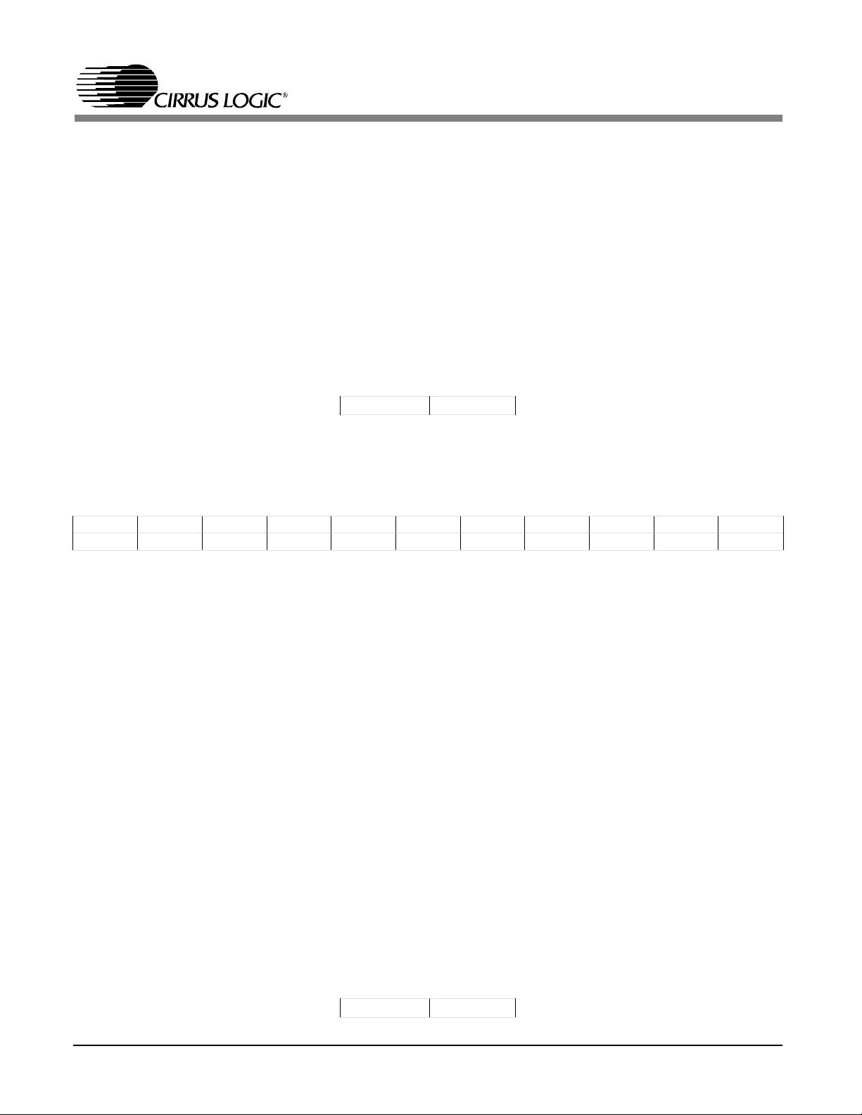
CS8920A
Register 13: Line Control (LineCTL, Read/Write) continued Address: PacketPage base + 0112h
BIT NAME DESCRIPTION
E LoRxSquelch
(10Bas e- T,
only)
When clear, the 10BASE-T receiver squelch thresholds are set to levels defined by the
ISO/IEC 8802-3 specification. When set, the thresholds are reduced by approximately 6
dB. This is useful for operating with "quiet" cables that are longer than 100 meters.
F WakeUpEn When set, the wakeup enable bit forces the MAC to look at a special Magic Packet
frame and ignore all other incoming data. WakeUpEn also enables some special logic
to determine when the ISA bus drivers are to be on/off and what is done when the
Magic Packet fram e is se en.
After reset, if no EEPROM is found by the CS8920A, the register has the following initial state. If an EEPROM is
found, the register’s initial value may be set by the EEPROM. See Section 3.3.
0000 0000 0001 0011
Note: For Rev. B of the CS8920A, if autonegotiation is selected and two CS8920As are connected back to back
the auto AUI/10BT function does not work.
Register 14: Line Status (LineST, Read-only) Address: PacketPage base + 0134h
FEDCBA98765-0
CRS PolarityOK 10BT AUI LinkOK 010100
LineST reports the status of the Ethernet physical interface.
BIT NAME DESCRIPTION
5-0 010100 These bits provide an internal address used by the CS8920A to identify this as the
Line Status Register. When reading this r egister, these bits will be 010100, where the
LSB corresponds to Bit 0.
7 LinkOK When set, the 10BASE-T link has not failed. When clear, the link has failed either
because the CS8920A has just come out of reset, or because the receiver has not
detected any activity (link pulses or received packets) for at least 50 ms.
8 AUI When set, the CS8920A is using the AUI.
9 10BT When set, the CS8920A is using the 10BASE-T interface.
C PolarityOK When set, the polarity of the 10BASE-T receive signal (at the RXD+ / RXD- inputs) is
correct. If clear, the polarity is reversed. If PolarityDis (Register 1 3, LineCTL, Bit C) is
clear, then the polarity is automatically corrected, if needed. The PolarityOK status bit
shows the true state of the incoming polarity independent of the PolarityDis control bit.
When PolarityDis is clear and PolarityOK is clear, the receive polarity is inverted, and
corrected.
E CRS This bit tells the host the status of an incoming frame. If CRS is set, a frame is
currently being received. CRS remains asserted until the end of frame (EOF). At EOF,
CRS goes inactive in about 1.3 to 2.3 bit times after the last low-to-high transition of
the recovered data.
This register’s initial state after reset is: 0X0X 00XX X001 0100
DS238PP2 63

CS8920A
Regist er 15: Sel f Co ntro l ( Sel fCTL, Re ad/ Wri te) Address: Packet Page b ase + 0 114 h
FEDCBA98765-0
HCB1 HCB0 HC1E HC0E HW
StandbyE
HWSleepE SW
Suspend
RESET 010101
SelfCTL controls the operation of the LED outputs and the low-power modes.
BIT NAME DESCRIPTION
5-0 010101 These bits provide an internal address used by the CS8920A to identify this as the
Chip Self Control Register.
6 RESET When set, a chip-wide reset is initiated immediately. RESET is an Act-Once bit. This bit
is cleared as a result of the reset.
8 SWSuspend When set, the CS8920A enters the software initiated Suspend mode. Upon entering
this mode, there is a partial reset. All registers and circuits are reset except for the ISA
I/O Base Address Register and the SelfCTL Register. There is no transmit nor receive
activity in this mode. To come out of software Suspend, the host issues an I/O Write
within the CS8920A’s assigned I/O space (see Sect ion 3.8 for a complete de scription
of the CS8920A’s low-power modes).
9 HWSleepE When set, the
SLEEP input pin is enabled. When SLEEP is high, the CS8920A is
"awake", or operative (unless in SWSuspend mode, as shown above). When
low, the CS8920A enters either the Hardware Standby or Hardware Suspend mode.
When clear, the CS8920A ignores the
SLEEP input pin (see Section 3.8 for a complete
description of the CS8920A’s low-power modes).
and
A HWStandbyE When HWSleepE is set
the SLEEP input pin is low, then when HWStandbyE is
set, the CS8920A enters the Hardware Standby mode. When clear, the CS8920A
enters the Hardware Suspend mode (see Section 3.8 for a complete description of the
CS8920A’s low-power modes).
C HC0E The
LINKLED or HC0 output pin is selected with this control bit . When HC0E is clear,
the output pin is
LINKLED. When HC0E is set, the output pin is HC0 and the HCB0 bit
(Bit E) controls the pin.
D HC1E The
BSTATUS or HC1 output pin is selecte d with this control b it. When HC1E is clear,
the output pin is
the output pin is
BSTATUS and indicate s receiver ISA Bus activity. When HC1E is set,
HC1 an d th e H CB1 bit ( Bit F) c ont ro ls t he pi n.
E HCB0 When HC0E (Bit C) is set, this bit controls the
HCB0 is clear,
HC0 is high. HC0 may drive an LED or a logic gate. When HC0E (Bit C)
is clear, this control bit is ignored.
F HCB1 When HC1E (Bit D) is set, this bit controls the
HCB1 is clear,
HC1 is high. HC1 may drive an LED or a logic gate. When HC1E (Bit D)
is clear, this control bit is ignored.
SLEEP is
HC0 pin. If HCB0 is set, HC0 is low. If
HC1 pin. If HCB1 is set, HC1 is low. If
After reset, if no EEPROM is found by the CS8920A, the register has the following initial state. If an EEPROM is
found, the register’s initial value may be set by the EEPROM. See Section 3.3.
0000 0000 0001 0101
64 DS238PP2

CS8920A
Register 16: Self Status (SelfST, Read-only) Address: PacketPage base + 0136h
FEDCBA98765-0
EEsize EEPRO MOKEEPROM
present
SIBUSY INITD PnP
Disable
010110
SelfST reports the status of the EEPROM interface and the initialization process.
BIT NAME DESCRIPTION
5-0 010110 These bits provide an internal address used by the CS8920A to identify this as the
Chip Self Status Register. When reading this register, these bits will be 010110, where
the LSB corresponds to Bit 0.
6 PnP Disable Indicates that t he PnP section has been disabled by a bit in the EEPROM. This
disabling feature may be needed if the CS8920A is to look like a legacy device.
7 INITD When set, the CS8920A initialization, including read-in of the EEPROM, is complete.
8 SIBUSY When set, the EECS output pin is high indicating that the EEPROM is currently being
read or programmed. The host must not write to PacketPage base + 0040h nor 0042h
until SIBUSY is clear.
9 EEPROM
present
When the EEDI pin is low after reset, there is no EEPROM present, and the
EEPROMpresent bit is clear. If the EEDI pin is high after reset, the CS8920A
"assumes" that an EEPROM is present, and this bit is set.
A EEPROMOK When set, the checksum of the EEPROM readout was OK.
C EEsize This bit shows the size of the attached EEPROM and is valid only if the
and
EEPROMpresent bit (Bit 9)
EEPROMOK bit (Bit A) are both set. If clear, the
EEPROM size is either 128 words (’C56 or ’CS56) or 256 words (C66 or ’CS66). If set,
the EEPROM size is 64 words (’C46 or ’CS46).
This register’s initial state after reset is: (X = Depends on Configuration.) 000X XXXX XX01 0110
DS238PP2 65

CS8920A
Register 17: Bus Control (BusCTL, Read/Write) Address: PacketPage base + 0116h
FEDCBA98765-0
EnableIRQ RxDMA
size
IOCH
RDYE
DMABurst MemoryE UseSA Reset
RxDMA
010111
BusCTL controls the operation of the ISA-bus interface.
BIT NAME DESCRIPTION
5-0 010111 These bits provide an internal address used by the CS8920A to identify this as the Bus
Control Register.
6 ResetRxDMA When set, the RxDMA offset pointer at PacketPage base + 0026h is reset to zero.
When the host sets this bit, the CS8920A does the following:
1. Terminates the current receive DMA activity, if any.
2. Clears all internal receive buffers.
3. Zeroes the RxDMA offset pointer.
The CS8920A acts upon this command only once when this bit is set. ResetRxDMA is
an Act-Once bit. To cause the pointer to reset again, the host must rewrite a 1.
9 UseSA When set, the
LA[17:23] match the CS8920A’s assigned Memory base address. When clear,
MCS16 pin goes low whenever the address on the SA bus [13..16] and
MCS16
is driven low whenever LA[17:23] match the CS8920A’s assigned memory base
address.
MCS16 is driven by the CS8920A in Memory Mode with th e Memory E bit
(Register 17, BusCTL, Bit A) set.
A MemoryE When set, the CS8920A may operate in Memory Mode. When clear, Memory Mode is
disabled. I/O Mode is always enabled.
B DMABurst When clear, the CS8920A performs continuous DMA until the receive frame is
completely transferred from the CS8920A to host memory. When set, each DMA
access is limited to 28 µs, after which time the CS8920A gives up the bus for 1.3 µs
before making a new DMA request.
C IOCHRDYE When set, the CS8920A does not use the I OCHRDY output pin, and the pin is always
in the high-impedance state. This allows external pull-up to force the output high. When
clear, the CS8920A drives IOCHRDY low to request additio nal time durin g I/O Read
and Memory Read cycl es. IOCHRDY does not affect I/O Wr ite, Memor y Write, nor DMA
Read.
D RxDMAsi ze This bi t de ter mi nes t he si ze of the r ece ive DMA buffer (l ocat ed i n ho st me mor y).
When set, the DMA buffer size is 64 Kbytes. When clear, it is 16 Kbytes.
F EnableIRQ When set, the CS8 920A will generate an interrupt in response to an interrupt event
(Section 5.1). When cleared, the CS8920A will not generate any interrupt s.
After reset, if no EEPROM is found by the CS8920A, the register has the following initial state. If an EEPROM is
found, the register’s initial value may be set by the EEPROM. See Section 3.3.
0000 0000 0001 0111
66 DS238PP2

CS8920A
Register 18: Bus Status (BusST, Read-only) Address: PacketPage base + 0138h
FEDCBA98765-0
Rdy4Tx
NOW
TxBidErr 011000
BusST describes the status of the current transmit operation.
BIT NAME DESCRIPTION
5-0 011000 These bits provide an internal address used by the CS8920A to identify this as the Bus
Status Register. When reading this register, these bits will be 011000, where th e LSB
corresponds to Bit 0.
7 TxBidErr If set, the host has commanded the CS8920A to transmit a frame that the CS8920A
will not send. Frames that the CS8920A will not send are:
1) Any frame greater than 1514 bytes, provided that InhibitCRC
(Register 9, TxCMD, Bit C) is clear.
2) Any frame greater than 1518 bytes.
Note that this bit is not set when transmit frames are too short.
8 Rdy4TxNOW Rdy4TxNOW signals the host that the CS8920A is ready to accept a frame from the
host for transmission. This bit is similar to Rdy4Tx (Register C, BufEvent, Bit 8) except
that there is no interrupt associated with Rdy4TxNOW. The host can poll the CS8920A
and check Rdy4TxNOW to determine if the CS8920A is ready for transmit. (See
Section 5.8 for a description of the transmit bid process.)
This register’s initial state after reset is: 0000 0000 XX01 1000
DS238PP2 67

CS8920A
Register 19: Test Control (TestCTL, Read/Write) Address: PacketPage base + 0118h
FEDCBA98765-0
Disable
Backoff
AUIloop ENDEC
loop
DisableLT 011001
TestCTL controls the diagnostic test modes of the CS8920A.
BIT NAME DESCRIPTION
5-0 011001 These bits provide an internal address used by the CS8920A to identify this as the Test
Control Register.
7 DisableLT When set, the 10BASE-T interface allows packet transmission and reception regardless
of the link status. DisableLT is used in conjunction with the LinkOK (Register 14,
LineST, Bit 7) as follows:
LinkOK DisableLT
0 0 No packet transmission or reception
allowed. Transmitter sends link pulses.
X 1 DisableLT overrides LinkOK to allow
packet transmission and reception.
1 N/A DisableLT has no meaning if LinkOK = 1.
Note that if the receiver is receiving no link pulses, then the 10BASE-T transmitter can
be active on ly if bit Disabl eLT is set.
9 ENDECloop When set, the CS8920A enters internal loopback mode where the internal Manchester
encoder output is connected to the decoder input. The 10BASE-T and AUI transmitters
and receivers are disabled. When clear, the CS8920A is configured for normal
operation.
A AUIloop When set, the CS8920A allows reception while transmitting. This facilitates loopback
tests for the AUI. When clear, the CS8920A is configured for normal AUI operation.
B Disable
Backoff
When set, the backoff algorithm is disabled. The CS8920A transmitter looks only for
completion of the inter-packet gap before star ting transmission. When clear, the backoff
algorithm is used.
At reset, if no EEPROM is found by the CS8920A, the register has the following initial state. If an EEPROM is
found, the register’s initial value may be set by the EEPROM. See Section 3.3.
0000 0000 0001 1001
68 DS238PP2

CS8920A
Regist er 1 C: AUI Time D o mai n R e fl ec to me te r ( Rea d -onl y) Addre ss: Packet Page bas e + 013C h
F-6 5-0
AUI_Delay 011100
The TDR counter (Bits 6 through F) is a time domain reflectometer useful in locating cable faults in 10BASE-2
and 10BASE-5 coax networks. It counts at a 10-MHz rate from the beginning of transmission on the AUI t o when
a collision or Loss-of-Carrier error occurs. The TDR counter is cleared when read.
BIT NAME DESCRIPTION
5-0 011100 These bits provide an internal address used by the CS8920A to identify this as the
Bus Status Register. When reading this register, these bits will be 011100, where the
LSB corresponds to Bit 0.
F-6 AUI-Delay The upper ten bits contain the number of 10-MHz clock periods between the beginning
of transmission on the AUI to when a collision or Loss-of-Carrier erro r occurs.
This register’s initial state after reset is: 0000 0000 0001 1100
DS238PP2 69

CS8920A
Regist er 1D: Auto N egot iat io n Con trol (AutoN eg CTL, Read /W rit e) Add ress : PacketPage b ase + 01 1Ch
FEDCBA98765-0
ForceFDX NLP
Enable
Auto Ne g
Enable
AllowFDX ReNOW 011101
BIT NAME DESCRIPTION
5-0 011101 These bits provide an internal address used by the CS8920A to identify this as the Test
Control Register.
6 ReNOW When set, and when NLPEnable and ForceFDX are not set, a re-negotiation is forced.
ReNOW clears itself after re-negotiation begins. Reset value is 0.
7 AllowFDX When set, the FDX mode is advertised. AllowFDX is sampled only when entering the
Ability Detect state dur ing arbitratio n. Changes to this bit are ignored after arbitration
begins. To re-sample this bit, a re-negotiation must be forced.
8 AutoNegEnable When set, and when NLPEnable and ForceFDX are not set, auto negotiation may
occur, including using fast link pulses. When AutoNegEnable is clear, negotiations are
aborted, including the negotiation in progress. Reset value is 0. When AutoNegEnable
bit is cleared, set bit ReNOW.
9 NLPEnable When set, the nor mal link pulses will be transmitted and auto negotia tion will be
disabled. Reset value is 0.
FForceFDX
(10BASE-T,
only)
This bit is used to force full duplex operation. The
that full duplex operation is being used. FDXactive is also set and auto negotiation
capability will be disabled. When ForceFDX is clear, the full duplex operation is not
FDXLED output is asserted to show
forced, but the CS8920A may be in full duplex due to auto negotiation.
NOTE:
One of the bits, either F, 9, or 8, must be set to allow a link to be established. If none of the bits are set,
no link pulses of any kind will be sent, and th e transmitter will be disabled.
This register’s initial state after reset is: 0000 0000 0001 1101
70 DS238PP2

CS8920A
Register 1E: Auto-Negotiation Status (AutoNegST, Read-only) Address: PacketPage base + 013Eh
FEDCBA98765-0
FDXActive HDXActive LinkFault F LPLink
Good
FLPLink AutoNeg
Busy
011110
Each bit in this register, when set, describes a particular activity on the ISA bus.
BIT NAME DESCRIPTION
5-0 011110 These bits provide an internal address used by the CS8920A to identify this as the Test
Control Register. To write to this register, these bits must be 011110, where the LSB
corresponds to Bit 0.
7 AutoNegBusy Auto Negotiation is busy. This is not a real register. AutoNegBusy is set while auto
negotiation is in progress. This implies AutoNegEnable is set, ForceFDX is not set,
NLPEnable is not set, and a good link has not yet been established.
8 FlpLink Set when the CS8920A has seen at least one FLP burst from the link partner. FLPLink
is cleared when a new auto negotiation begins.
B FLPLinkGood Set when auto negotiation has successfully completed. FLPLinkGood is cleared when
re-negotiation is restarted.
C LinkFault Set when an apparently good link goes down during auto negotiation. Reset value is 0.
E HDXActive Half Duplex Active. Set when ForceFDX is clear and NLPEnable is set, or when auto
negotiation finds a half-duplex-only capable link partner. HDXActive is cleared when re-
negotiation is requested.
F FDXActive Full Duplex Active. Set whenForceFDX is set, or when auto negotiation reveals a full-
duplex capable link partner. FDXActive is cleared when re-negotiation is requested.
This register’s initial state after reset is: 0000 0000 0001 1110
DS238PP2 71

CS8920A
4.6 Initiate Transmit Register
Initiate Transmit Register
Transmit Command Request - TxCMD (Write-only) Address: PacketPage base + 0144h
FEDCBA98765-0
TxPadDis InhibitCRC Onecoll Force TxStar t 001001
The word written to PacketPage base + 0144h tells the CS8920A how the next packet should be transmitted.
This PacketPage location is write-only, and the written word can be read from Register 9, at PacketPage base +
0108h. The CS8920A does not transmit a frame if TxLength (at PacketPage location base + 0146h) is less than
3. See Section 5. 8.
BIT NAME DESCRIPTION
5-0 001001 These bits provide an internal address used by the CS8920A to identify this as the
Transmit Command Register. When reading this register, these bits will be 001001,
where th e LSB co rresp onds t o Bit 0.
7, 6 TxStart This pair of bits determines how many bytes are transferred to the CS8920A before the
MAC starts the packet transmit process.
Bit 7 Bit 6
0 0 Star t transmission after 5 bytes are in the CS8920A
0 1 Star t transmission after 381 bytes are in the CS8920A
1 0 Star t transmission after 1021 bytes are in the CS8920A
1 1 St art transmission after the entire frame is in the CS8920A
8 Force When set in conjunction with a new transmit command, any transmit frames waiting in
the transmit buffer are deleted. If a previous packet has started transmission, that
packet is terminated within 64 bit times with a bad CRC.
9 Onecoll Wh en this bit is set, any transmiss ion will be termina ted after only one collision. When
clear, the CS8920A allows up to 16 normal co llisions before terminating the
transmission.
C InhibitCRC When set, the CRC is n ot appended to t he transmission.
D TxPadDis When TxPadDis is clear, if the host gives a transmit length less than 60 bytes and
InhibitCRC is set, the CS89 20A pads to 60 bytes. If the host gives a transmit le ngth
less than 60 bytes and InhibitCRC is clear, then the CS8920A pads to 6 0 bytes and
appends the CRC.
When TxPadDis is set, the CS8920A allows the transmission of runt frames (a frame
less than 64 bytes). When InhibitCRC is clear, th e CS8920A appends the CRC. When
InhibitCRC is set, the CS8920A does no t append the CRC.
Because this register is writ e-only, it’s initial state after reset is u ndefined.
72 DS238PP2

CS8920A
Initiate Transmit Register:
Transmit Length (Write-only) Address: PacketPage base + 0146h
Address 0147h Address 0146h
Most-significant byte of Transmit Frame Length. Least-significant byte of Transmit Frame Length.
This register is used in conjunction with register 9, TxCMD. When a transmission is initiated via a command in
TxCMD, the length of the transmitted frame is written into this register. The length of the transmitted frame may
be modified by the configuration of the TxPadDis and InhibitCRC bits in the TxCMD re gister. See Table 5.17, and
Section 5.8. TxLength must be >3 and < 1519.
Because this register is writ e-only, it’s initial state after reset is u ndefined.
DS238PP2 73

CS8920A
4.7 Address Filter Registers
Address Filter Register:
Logical Address Filter (hash table) (Read//Write) Address: PacketPage base + 0150h
Address 0157h Address 0156h Address 0155h Addr ess 0154h Address 0153h Addr ess 0152h Address 0151h Addr ess 0150h
Most-
significant
byte of hash
filter.
The CS8920A hashing decoder circuitry compares its output with one bit of the Logical Address Filter Register. If
the decoder output and the Logical Address Filter bit match, the frame passes the hash filter and the Hashed bit
(Register 4, RxEvent, Bit 9) is set. See Section 5.3.
This register’s initial state after reset is:
0000 0000 0000 0000 0000 0000 0000 0000 0000 0000 0000 0000 0000 0000 0000 0000
Least-
significant
byte of hash
filter.
Address Filter Register:
Individual Address (IEEE address) (Read//Write) Address: PacketPage base + 0158h
Address 0015Dh Address 0015Ch Address 0015Bh Address 0015Ah Address 0159h Addr ess 00158h
Octet 5 of IA Octet 0 of IA.
The unique, IEEE 48-bit Individual Address (IA) begins at 0158h. The first bit of the IA (Bit IA[00]) must be 0.
See Section 5.3.
The value of this register must be loaded from external storage, for example, from the EEPROM. See Section
3.3. If the CS8920A is not able to load the IA from the EEPROM, after a reset this register is undefined, and the
driver must write an address to this register.
74 DS238PP2

CS8920A
4.8 Plug n Play Resource Registers
Plug n Play Activation Register
Address: PacketPage base + 0330h
76543210
0000000Active
BIT NAME DESCRIPTION
0 Active Until this bit is set th e CS8920A will not re spond to memor y, IO (except PNP accesses)
and DMA accesses. When set the CS8920A will respond to modes that are enabled.
All other bits in this register are read as 0 after reset
0000
Plug n Play IO Rang e Ch eck Re gist er
Address: PacketPage base + 0331h
76543210
0 0 0 0 0 0 Check_Enable IO_Check
BIT NAME DESCRIPTION
0 IO_Check If the bit 1 (check enable) is set then when two IO_Check bit is clear the PNP read
port is read on 55 when IO_Check bit is set the PNP read port is read AA.
1 Check_Enable This bit is set to enable the IO range check.
DS238PP2 75

CS8920A
Boot PROM Base Address (Read/Write) Address: PacketPage base + 0340h
Address 0340h Address 0341h
Boot PROM base address, high byte. Boot PROM base address, low byte.
After reset, if no EEPROM is found by the CS8920A, the register has the following initial state. If an EEPROM is
found, the register’s initial value may be set by the EEPROM. See Section 3.3.
0000 0000 0000 0000
Boot PROM Address Mask (Read/Write) Address: PacketPage base + 0343h
Address 0343h Address 0344h
Boot PROM mask address, high byte. Boot PROM mask address, low byte.
The Boot PROM address mask register indicates the size of the attached Boot PROM. The bits in this register
select which address lines are used for address matching. If a bit is set, the corresponding address line is used
in address matching for the Boot PROM address. The high byte (PacketPage base + 0343h) corresponds to
address lines A[23:16] and the low byte corresponds to address line A[15:8]
For example:
Size of Boot PROM Register value
4k bits XXXX XXXX XXXX 1111 1111 0000 0000 0000
8k bits XXXX XXXX XXXX 1111 1110 0000 0000 0000
16k bits XXXX XXXX XXXX 1111 1100 0000 0000 0000
After reset, if no EEPROM is found by the CS8920A, the register has the following initial state. If an EEPROM is
found, the register’s initial value may be set by the EEPROM. See Section 3.3.
0000 0000 0000 0000
76 DS238PP2

CS8920A
Memory Base Address (Read/Write) Address: PacketPage base + 0348h
Address 0348h Address 0349h
Memory base address, high byte. Memory base address, low byte.
After reset, if no EEPROM is found by the CS8920A, the register has the following initial state. If an EEPROM is
found, the register’s initial value may be set by the EEPROM. The memory mode is disabled when the memory
base register is 0000 0000.
0000 0000 0000 0000
I/O Base Address (Read/Write) Address: PacketPage base + 0360h
Address 0360h Address 0361h
Most significant byte of I/O Base Address Least significant byte of I/O Base Address
The I/O Base Address Register describes the base address for the sixteen contiguous locations in the host
system’s I/O space, which are used to access the PacketPage registers. See Section 4.12. The CS8920A IO
mode is disabled if IO base register is 0000
After reset, if no EEPROM is found by the CS8920A, the register has the following initial state. If an EEPROM is
found, the register’s initial value may be set by the EEPROM. See Section 3.3.
0000 0000 0000 0000
DS238PP2 77

CS8920A
Interrupt Number (Read/Write) Address: PacketPage base + 0370h
Address 0370h
Interrupt number assignment:
0000 0011b= pin IRQ3
0000 0100b= pin IRQ4
0000 0101b= pin IRQ5
0000 0110b= pin IRQ6
0000 0111b= pin IRQ7
0000 1001b= pin IRQ9
0000 1010b= pin IRQ10
0000 1011b= pin IRQ11
0000 1100b= pin IRQ12
0000 1110b= pin IRQ14
0000 1111b= pin IRQ15
The Interrupt Number Register defines the interrupt pin selected by the CS8920A. In a typical application the
following bus signals are tied to the following pins:
Bus signal Typical pin connection
IRQ3 IRQ3
IRQ4 IRQ4
IRQ5 IRQ5
IRQ6 IRQ6
IRQ7 IRQ7
IRQ9 IRQ9
IRQ10 IRQ10
IRQ11 IRQ11
IRQ12 IRQ12
IRQ14 IRQ14
IRQ15 IRQ15
After reset, if no EEPROM is found by the CS8920A, the register has the following initial state, which corresponds to placing all the IRQ pins in a high-impedance state. If an EEPROM is found, the regist er’s initial value
may be set by the EEPROM. All interrupts are disabled when interrupt number register is 0000.
XXXX XXXX XXXX 0000
78 DS238PP2

CS8920A
DMA Channel Number (Read/Write) Address: PacketPage base + 0374h
Address 0374h
DMA channel assignment:
05 = pins DRQ5 and
06 = pins DRQ6 and
07 = pins DRQ7 and
08 = All DRQ pins high-impedance
DACK5
DACK6
DACK7
The DMA Channel register defines the DMA pins selected by the CS8920A. In the typical application, the following bus signals are tied to the following pins:
Bus signal Typical pin connection
DRQ5
DACK5
DRQ6
DACK6
DRQ7
DACK7
DRQ5
DACK5
DRQ6
DACK6
DRQ7
DACK7
After reset, if no EEPROM is found by the CS8920A, the register has 0000 effectively disabling DMA interface. If
an EEPROM is found, the register’s initial value may be set by the EEPROM.
XXXX XXXX XXXX 0000
DS238PP2 79

CS8920A
4.9 Receive and Transmit Frame
Locations
The Receive and Transmit Fram e PacketPage locations are used to transfer Ethernet frames to
and from the host. The host sequentially writes
to and reads from these locations, and internal
buffer memory is dynamically allocated between
transmit and receive as needed. One receive
frame and on e transmit frame are acces sible at a
time.
Receive Pac ketPage L ocations
In I/O mode, the receive status/length/frame locations are read through repetitive reads from
one I/O port a t the I/O base ad dress. See Section
4.12.
In memory mode, th e receive status/length/ frame
locations are read using memory reads of a block
of memory starting at memory base address +
0400h. Typically the memory locations are read
sequentially using repetitive Move instructions
(REP MOVS). See Table 4.4 and Section 4.11.
The first 118 bytes of the receive frame can be
accessed randomly if word reads on even word
boundaries are used. Beyond 118 bytes, the
memory reads must be sequenti al. Byte reads, or
reads on odd-word bo undaries, can be performed
only in sequent ial read mode. See Section 4. 10.
BufferCRC). If CRC has not been selected, then
the length does not include the CRC, and the
CRC is not prese nt in the rec eive buffer.
After the RxLength has been read, the receive
frame can be read. Once some portion of the
frame is read, the entire frame should be read
before reading the RxEvent register either directly or through the ISQ register. Reading the
RxEvent register s ignals to the CS8920A tha t the
host is finis hed with the cur rent frame and wants
to start processing the next frame. In this case,
the current frame will no longer be acc essible to
the host. The current frame will a lso become inaccessible if a Skip command is issued, or if th e
entire frame ha s been r ead. See Sec tion 5.2.
Transmit Locations
The host can write frames into the CS8920A
buffer using Memory writes using REP MOVS
to the TxFrame loc ation. See Sectio n 5.8.
Descripti on Mnemon ic R ead/ Write Location :
PacketPage base +
Receive
Status
Receive
Length
Receive
Frame
Transmit
Frame
RxStatus Read-only 0400h-0401h
RxLength Read-only 0402h-0403h
RxFrame Read-only starts at 0404h
TxFrame Write-only star ts at 0A00h
The RxStatus word reports the status of the current received frame. RxEvent register 4
Table 4.4. Receiv e/Transmit Memor y
Locations
(PacketPage base + 01 24h) has th e same contents
as the RxStatus register, except RxEvent is
4.10 Eight and Sixteen Bit Transfers
cleared when Rx Event is read . See Sectio n 5.2.
A data transfer to or from the CS8920A can be
The RxLength (receive length) word is the
length, in bytes, of the data to be transferred to
the host across the ISA bus. The register describes the length from the start of Source
Address to the end of CRC, assuming that CRC
done in eit her I/O or Memory space , and can be
either 16 bits wide (word transfers) or 8 bits
wide (byte trans fers). Because the CS892 0A’s internal architecture is based on a 16-bit d ata bus,
word transfers are the mos t efficient.
has been selected (via Register 3 RxCFG, bit
80 DS238PP2

CS8920A
The CS8920A d oes not support c onnection to 8bit buses.
To transfer transmit frames to the CS8920A and
receive frames from the CS8920A, the host may
mix word and byte transfers, p rovided it follows
three rules:
1.The primary method used to access CS8920A
memory is word access.
2.Word accesses to the CS8920A’s internal memory are kept on even-byte bounda ries.
3.When switching from byte accesses to word
accesses, a by te access to an even byte address
must be followed by a byte access to an oddbyte address before the host may execute a
word access (this will re-align the word transfers to even-byte boundaries). On the other
hand, a byte access to an odd-byte address
may be followed b y a word access .
Failure to observe these three rules may cause
data corruption.
Transferring Odd-Byte-Ali gned Data
Some applications gather transmit data from
more than one section of host memory. The
boundary between the various memory locations
may be either even- or odd-byte aligned. When
such a boundary is odd-byte aligned, the host
should transfer the last byte of the first block to
an even address, followed by the first byte of th e
second block to the following odd address . It can
then resume word transfers. An example of this
is shown in Figure 4.3.
Random Access to CS 8920A Memory
The first 118 byte s of a receive frame held in the
CS8920A’s on-chip memory may be randomly
accessed in Memory mode. After the first 118
bytes, only sequential access of received data is
allowed. Either by te or word access is permitted,
Word Trans fe r
First Block of Data
Word Trans fe r
Word Trans fe r
Byte Transfer
Byte Transfer
Word Trans fe r
Word Trans fe r
Word Trans fe r
Second Block of Data
Figure 4.3. Odd-Byte Aligned Data
as long as all word accesses are executed to
even-byte boundaries.
4.11 Memory Mode Operation
To configure the CS8920A for Memory Mode,
the PacketPage memory must be mapped into a
contiguous 4-Kbyte block of host memory. The
block must start a t an X000h boundary, with the
PacketPage base address mapped to X000h.
When the CS8920A comes out of reset, its default configuration is I/O Mode. When Memory
Mode is selected, all of the CS8920A’s registers
can be accesse d directly.
In Memory Mode, th e CS8920A supports Standard or Ready Bus cycles without introducing
additional wait states (i.e., IOCHRDY is not
deasserted).
Memory moves can use MOVD (double-word
transfers) as long as the CS8920A’s memory
base address is on a double word boundary. Because 286 processors don’t support the MOVD
instruction, word and byte tra nsfers must be used
with a 286.
DS238PP2 81

CS8920A
4.11.1 Accesses in Me mory Mode
The CS8920A allows Read/Write access to the
internal PacketPage me mory, and Read access of
the optional Boot PROM. (See Section 3.7 for a
description of th e optional Boo t PROM.)
A memory access occurs when all of the fo llowing are true:
• The address on the ISA System Address bus
SA[0:16] and LA[17:23] is within the Memory space range of the CS8920A or Boot
PROM.
• Either the
MEMR pin or the MEMW pin is
low.
4.11.2 Configuring the CS8920A for Memory
Mode
The CS8920A’s internal memory can be mapped
anywhere within the host system’s 24-bit memory space. The CS8920A occupie s 4K bytes of
space in the system memory map. Configuring
the CS8920A to respond in a memory mode requires the following:
• The Memory Base Address Registers
(PackatePage base + 0348h and 0349h) should
have the high and low bytes of the 24 bit memory base addres s. The value written in regist er at
0348h must be n on-zero for memory mode t o be
active. For example, if the memory base address
for the CS8920A is to be 0C8000h, write 0C at
PackatPage base + 0 348h and 80h at PacketPage
base + 0349h.
• The MemoryE bit (Bit A) in the Bus Control
register (Register 17, PacketPage base + 116h)
must be set.
The CS8920A latch es address on pi ns LA[17:23]
when the BALE signal remains LOW. When
either
MEMR (memory read) or MEMW (mem-
ory write) pin goes active (LOW), the CS8920A
will respond to memory access if
• Address latched from the LA[17:23] and address on pins SA[12:1 6] match the address in the
Memory Base Address Reg ister, and
• The memory enable bit MemoryE bit in the
Bus Control register is set, and
•
REFRESH, and AEN signals are inac tive.
4.11.3 Basic Memory Mode Transm it
Memory Mode transmit operations occur in the
following order (using interrupts):
1.The host bids for storage of the frame by writing the Transmit Command to the TxCMD
register (memory base + 0144h) and the transmit frame length to the TxLength register
(memory base + 0146 h). If the transmit lengt h
is erroneous, the command is discarded and
the TxBidErr bi t (Register 18, BusST, Bit 7) is
set.
2.The host reads the BusST register (Regis ter 18,
memory base + 0138h). When the
Rdy4TxNOW bit (Bit 8) is set, the frame can
be written. Whe n clear, the ho st must wait for
CS8920A buffer memory to become available.
When Rdy4TxiE (Register B, BufCFG, Bit 8)
is set, the host will be interrupted when
Rdy4Tx (Register C, BufEvent, Bit 8) becomes set .
3.Once the CS8920A is ready to accept the
frame, the host executes repetitive memory-tomemory move instructions (REP MOVS) to
memory base + 0A00h to transfer the entire
frame from host memory to CS8920A memory.
For a more detailed description of transmit, see
Section 5.8.
82 DS238PP2

4.11.4 Basic Memory Mode Receive
Memory Mode receive operations occur in the
following order (interrupts used to signal the
presence of a valid re ceive frame):
1.A frame is received by the CS8920A, triggering an enabled in terrupt.
CS8920A
abled. On power up, t he default value of the I/O
base address is set at 300h. (Note that 300h is
typically assigned to LAN peripherals). The I/O
base address may be changed to any available
XXX0h locatio n, either by loading con figuration
data from the EE PROM, or during system setup.
Table 4.5 shows the CS8920A I/O Mode mapping:
Receive/Tran smit Data Por ts 0 and 1
2.The host reads the Interrupt Status Queue
(memory base + 0120 h) and is informed of the
receive frame.
3.The host reads RxStatus (memory base +
0400h) to lear n the st atus of the receive frame.
4.The host reads RxLength (memory base +
0402h) to learn the frame’s length.
5.The host rea ds the frame data by executing repetitive memory-to-memory move instructions
(REP MOVS) from memory base + 0404h to
transfer the entire frame from CS8920A memory to host memory.
For a more detailed description of receive, see
Section 5.2.
4.11.5 Polling the CS892 0A in Memory Mode
If interrupts are not used, the host can poll the
CS8920A to check if receive frames are present
and if memory space is available for transmit.
However, this is beyond the scope of this data
sheet.
4.12 I/O Space Operation
In I/O Mode, PacketPage memory is accessed
through eight 16-bit I/O ports that are mapped
into 16 contiguous I/O locations in the host system’s I/O space. I/O Mode is the default
configuration for the CS89 20A and is always en-
These two ports ar e used when t ransferring t ransmit data to the CS8920A and receive data from
the CS8920A. Port 0 is used for 16-bit operations and Ports 0 and 1 are used for 32-bit
operations (lower-order word in Port 0).
TxCMD Port
The host writes the Transmit Command
(TxCMD) to this port at the start of each transmit operation. The Transmit Command tells the
CS8920A that the host has a frame to be transmitted as well as how that frame should be
transmitted. T his port is map ped into PacketPage
base + 0144h. See Register 9 in Section 4.4 for
more information.
TxLength Port
The length of the frame to be t ransmitted is written here immediately after the Transmit
Offset Type Description
0000h Read/Write Receive/Transmit Data (Port 0)
0002h Read/Write Receive/Transmit Data (Port 1)
0004h Write-only TxCMD (Transmit Command)
0006h Write-only TxLength (Transmit Length)
0008h Read-only Interrupt Status Queue
000Ah Read/Write PacketPage Pointe r
000Ch Read/Write PacketPage Data (Port 0)
000Eh Read/Write PacketPage Data (Port 1)
Table 4.5. I/O Mode Mapping
DS238PP2 83

CS8920A
I/O base + 000Bh I/O base + 000Ah
F
98
E
0
BADC
11
PacketPage Register Address
Bit F: 0 = Pointer remains fixed
1 = Auto-Increments to next word location
10325476
Figure 4.4. PackagePage Pointer
Command is written. This port is mapped into
PacketPage base + 0146h.
Interrupt Status Queue Port
This port contains the current value of the Interrupt Status Queue (ISQ). The ISQ is located at
PacketPage base + 0120h. For a more detailed
description of th e ISQ, see Section 5. 1.
PacketPage Pointer Port
The PacketPage Point er Port is written whenever
the host wishes to access any of the CS8920A’s
internal registers. The first 12 bits (bits 0 through
B) provide the i nternal address of the target register to be access ed during the current operation.
The next three bits (C, D, and E) must be 0. The
last bit (Bit F) indicates whether or not the PacketPage Pointer should be auto-incremented t o the
next word location. Figure 4.4 shows the structure of the PacketPage Po inter.
PacketPage Data Ports 0 and 1
I/O Mode Operation
For an I/O Read or Write oper ation, the AE N pin
must be low, and the 16-bit I/O address on the
ISA System Address bus (SA0 - SA15) must
match the address space of the CS8920A. For a
Read, the
the
IOW pin must be low.
IOR pin must be low, and for a Write,
Note that the ISA Latcha ble Address Bus (LA17
- LA23) is not needed for applications that use
only I/O Mode and Receive DMA operation.
Basic I/O Mode Transmit
I/O Mode transmit operations occur in the following order (using interrupts):
1.The host bids for storage of the frame by writing the Transmit Command to the TxCMD
Port (I/O base + 000 4h) and th e transmit frame
length to the TxLength Port (I/O base +
0006h).
2.The host reads the BusST register (Register 18)
to see if the Rdy4TxNOW bit (Bit 8) is set. To
read th e BusST regist er, the host must fi rst set
the PacketPage Pointer at the correct location
by writing 0138h to the PacketPage Pointer
Port (I/O base + 000Ah). It can then read the
BusST register from the PacketPage Data Port
(I/O base + 000Ch). When Rdy4TxNOW is
set, the frame can be written. When clear, the
host must wait for CS8920A buffer memory to
become available. When Rdy4TxiE (Register
B, BufCFG, Bit 8) is set, the host will be interrupted when Rdy4Tx (Register C, BufEvent,
Bit 8) becomes set. When the TxBidErr bit
(Register 18, BusST, Bit 7) is set, the transmit
length is not valid.
The PacketPage Data Ports are used to transfer
data to and from any of the CS8920A’s internal
registers. Port 0 is used for 16-bit operati ons and
Ports 0 and 1 are used for 32-bit operations
3.When the CS8920A is ready to accept the
frame, the host executes repetitive write instructions (REP OUT) to the Receive/Transmit
Data Port (I/O base + 0000h) to transfer the
(lower-order word in Port 0).
84 DS238PP2

CS8920A
entire frame from host memory to CS8920A
memory.
For a more detailed description of transmit, see
Section 5.8.
Basic I/O Mod e Receive
I/O Mode receive operat ions occur in the fo llowing order (In this example, interrupt s are enabled
to signal the pre sence of a valid receive frame):
1.A frame is received by the CS8920A, triggering an enabled in terrupt.
2.The host reads the Interrupt Status Queue Port
(I/O base + 0008h) and is informed of the receive frame.
3.The host rea ds the frame data by executing repetitive read instructions (REP IN) from the
Receive/Transmit Data Port (I/O base + 0000h)
to transfer the frame from CS8920A memory
to host memory. Preceding the frame data are
the contents of the RxStatus register (PacketPage base + 0400h) and the RxLength register
(PacketPage base + 0402h).
need to set up the PacketPage Pointer between
successive accesse s (see F igure 4.4) .
Polling the CS8 920A in I/O Mode
If interrupts are not used, the host can poll the
CS8920A to check if receive frames are present
and if memory space is available for transmit.
For a more detailed description of receive, see
Section 5.2.
Accessing Internal Registers
To acc ess any of the CS8920A’s internal registers
in I/O Mode, the hos t must first set up the PacketPage Pointer. It does this by writing the
PacketPage address of the target register to the
PacketPage Pointer Port (I/O base + 000Ah).
The conten t of the target register is then mapped
into the PacketPage Data Port (I/O base +
000Ch).
When the h ost needs to acc ess a sequenti al block
of registers, the MSB of the PacketPage address
of the first word to be accessed shou ld be set to
1. The PacketPage Pointer wi ll then move to the
next word location automati cally, eli minating the
DS238PP2 85

CS8920A
5.0 OPERATION
5.1 Managing Interrupts and Servicing
the Interrupt Status Queue
The Interrupt Status Queue (ISQ) is used by the
CS8920A to communicate Event reports to the
host processor. Whenever an event occurs that
triggers an enabled interrupt, the CS8920A sets
the appropriate bit(s) in one of five registers,
maps the con tents of that registe r to the ISQ, an d
drives the selected interrupt request pin high (if
an earlier interrupt is waiting in the queue, the
interrupt requ est pin will already be high). When
the host services the interrupt, it must first read
the ISQ to le arn the nature of the interru pt. It can
then process the interrupt (the first read to the
ISQ causes the interrup t request pin t o go low.
Three of the registers mapped to the ISQ are
event registers: RxEvent (Register 4), TxEvent
(Register 8), and BufEvent (Register C). The
other two registers are counter-overflow reports:
RxMISS (Register 10) and TxCOL (Register 12).
There may be more than one RxEvent report
and/or more than one TxEvent rep ort in the ISQ
at a time. However, there may be only one
BufEvent report, one RxMISS report and one
TxCOL report in the ISQ at a time.
Event reports stored in the ISQ are read out in
the order of priority, with RxEvent first, followed
by TxEvent, BufEvent, RxMiss, and then
TxCOL. The host only needs to read from one
location to g et the interrupt curre ntly at the front
of the queue. In Memory Mode, the ISQ is located at PacketPage bas e + 0120h. In I/O Mode,
it is located at I/O base + 0008h. Each time the
host reads t he ISQ, the bits in the co rresponding
register are cleared and the next report in the
queue moves to the front.
A readout of a null word (0000h) indicates that
all interrupts have been re ad.
The ISQ is re ad as a 16-bit word. The l owe r six
bits (0 through 5) con tain the register number (4,
8, C, 10 , or 1 2). The uppe r ten bits (6 through F)
contain the register contents. The host must always read the entire 16-bit word, because the
CS8920A does no t support 8-bit acces s to its internal registers. Figure 5.1 shows the operation
of the ISQ.
The active interrupt pin (INTRQx) is selected via
the Interrupt Number register (PacketPage base +
0370h). As an additional option, all of the interrupt pins can be placed in the high-impedance
state using th e same register. See Section 4. 3.
An event triggers an interrupt only whe n the EnableIRQ bit o f the Bus Control register (bit F of
register 17) is set.
After the CS8920A has generated an interrupt,
the first read of the ISQ makes the INTRQ output pin go low (inactive). INTRQ remains low
until the null word (0000h) is read from the ISQ,
or for 1.6 µs, whichever is longer.
Typi cally, when interrupts have been enab led for
various error conditions (runt, CRC error, frame
> 1518 bytes) via register 3, the software will
also select t hat those frames be discarde d (register 5).
When the host starts reading the ISQ, it must
read and process all Event reports in the queue.
86 DS238PP2

An enabled interru pt occurs.
The selected interrupt
request pin is driven high
(active) if not already high.
The host reads the ISQ.
The selected inter r upt
request pin is driven low.
CS8920A
EXIT.
Interrupts
re-enabled.
Yes
ISQ = 0000h?
No
Which
Event
report
type?
RxEvent
TxEvent
BufEvent
RxMISS
TxCOL
Proces s applicable
RxEvent bi ts: Extradata,
Runt, CRCerror, RxOK.
Proce s s applicabl e
TxEvent bits: 16coll, Jabber,
Out-of-window, TxOK.
Process applicab le BufEvent
bits: RxDest, Rx128, RxMiss,
TxUnderrun, Rdy4Tx,
RxDMAFrame, SWint.
Process RxMISS counter.
Process TxCOL counter.
None of the above
Service
Default
Figure 5.1. Interrupt Status Queue
DS238PP2 87

CS8920A
5.2 Basic Receive Operation
Overview
When an incoming packet has passed through
the analog front end and Manchester decoder, it
goes through the following three-step receive
process:
1. Pre-Processing
2. Temporary Buffering
3. Transfer to Host
Figure 5.2 shows the steps in frame reception.
As shown in the figure, all receive frames go
through the same pre-processing and temporary
buffering phases, regardless of transfer method.
Packet Received
Preamble and
Start-of-F rame
Delimiter Re mov ed
Frame Pre-
Processed
Frame
Temporarily
Buffered
When a frame has been pre-processed and buffered, it can be accessed by the host in either
Memory or I/O space. In add ition, the CS8920A
can transfer receive frames to host memory via
host DMA. This section describes receive frame
pre-processing and Memory and I/O space receive operation. Sections 5.5 through 5.6
describe DMA operation.
5.2.1 Terminology: Packet , Frame, and
Transfer
The terms Packet, Frame, and Transfer are used
extensively in the following sections. They are
defined below for clarity.
Packet: The term "packet" refers to the entire serial string of bits transmitted over an Ethernet
network. This includes the preamble, Start-ofFrame Delimiter (SFD), Destination Address
(DA), Source Address (SA), Length field, Data
field, pad bits (if necessary), and Frame Check
Sequence (FCS, also called CRC). Figure 3.6
shows the format of a packet.
Frame: The term "frame" refers to the portion of
a packet from the DA to the FCS. This includes
the Destination Address (DA), Source Address
(SA), Length field, Data field, pad b its (if necessary), and Frame Check Sequence (FCS, also
called CRC). Figure 3.6 shows the format of a
frame. The term "frame data" refers to all the
data from the DA to the FCS that is to be transmitted, or th at has been re ceived.
Use
DMA?
YesNo
Transfer : The term "transfer" refers to moving
data across the ISA bus, to and from the
CS8920A. During receive operations, only frame
Frame Held
On Chip
Frame DMAed
to Host Memory
data are transferred from the CS8920A to the
host (the preamble and SFD are stripped off by
the CS8920A’s MAC engine). The FCS may or
Host Reads
Frame from
CS8920A Memory
Host Reads
Frame from
Host Memory
may not be transferred, depending on the configuration. All transfers to and from the
CS8920A are counted in bytes, but may be pa d-
Figure 5.2. Frame Rec eption
88 DS238PP2
ded for word alignment.

CS8920A
5.2.2 Receive Config uration
After each reset, the CS8920A must be configured for receive operation. This can be done
automatically using an at tached EEPROM, or by
writing configuration commands to the
CS8920A’s internal registers (see Section 3.3).
The items that m ust be configure d include:
• which physical in terface to use;
• which types of frames to accept;
• which receive events cause interrupt s; and,
• how received frames are transferre d.
Configuring the Phys ical Interface: C onfiguring
the physical interface consists of determining
which Ethernet interface should be active and
enabling the receive logic for serial reception.
This is done via the LineCTL register (Register
13) and is described in Table 5.1.
Choosing Which Frame Types to Accept: The
RxCTL register (Register 5) is u sed to determine
which frame types will be accepted by the
CS8920A (a receive frame is said to be "accepted" when the frame is buffered, either on
chip or in host memory via DMA). Table 5.2 describes the configuration bits in this register.
Refer to Section 5.3 for a det ailed description of
Destination Addre ss filterin g.
Register 13 , LineCTL
Bit Bit Name Operation
6 SerRxON When set, reception enabled.
8 AUIonly When set, AUI selected (takes
precedence over AutoAUI/10BT).
9 AutoAUI/
10BT
ELoRx
Squelch
When set, automatic interface selection
enabled. When both bits 8 and 9 are
clear, 10BASE-T selected.
When set, receiver squelch level
reduced by approximately 6 dB.
Tab le 5.1. P hysical I nterface Configu ration
Selecting Which Events Cause Interrupts: The
RxCFG register (Register 3) and the BufCFG
register (Register B) are used to d etermine which
receive events will cause interrupts to the host
processor. Table 5.3 describes the interrupt enable (iE) bits in these registers.
Register 5, RxCTL
Bit Bit Name Operation
6 IAHashA When set, Individual Address frames
that pass the hash filter are accepted*.
7Promis
cuousA
8 RxOKA When set, frames with valid length and
9 MulticastA When set, Multicast frames that pass
A IndividualA When set, frames with DA that matches
B BroadcastA When set, all broadcast frames are
C CRCerrorA When set, frames with bad CRC that
D RuntA when set, frames shorter than 64 bytes
E ExtradataA When set, frames longer than 1518
* Must also meet the criteria programmed into
bits 8, C, D, and E.
When set, all frames are accepted*.
CRC and that pass the DA filter are
accepted.
the ha sh f il ter acc ept ed*.
the IA at PacketPage base + 0158h are
accepted*.
accepted*.
pass the DA filter are accepted.
that pass the DA filter are accepted.
bytes that pass the DA filter are
accepted (only the first 1518 bytes are
buffered) .
Tab le 5. 2. Fra me Accepta nce Crit eria
Register 3, RxCFG
Bit Bit Name Operation
8 RxOKiE When set, there is an interrupt if a
frame is received with valid length and
CRC*.
C CRCerroriE When set, there is an interrupt if a
frame is received with bad CRC*.
D RuntiE When set, there is an interrupt if a
frame is received that is shorter than
64 bytes*.
E ExtradataiE When set, there is an interrupt if a
frame is received that is longer than
1518 bytes*.
* M ust al so pass the DA filte r before th ere is an
interrupt.
DS238PP2 89

Choosing How to Transfer Frames: The RxCF G
register (Register 3) and the BusCTL register
(Register 17) are used to determine how frames
will be transferred to host memory, as described
in Table 5.4.
5.2.3 Receive Frame Pre-Proce ssing
The CS8920A pre-processes all receive frames
using a four step process:
1. Destina tio n Add ress filteri ng;
Register B, BufCFG
Bit Bit Name Operation
7 RxDMAiE When set, there is an interrupt if one or
more frames are transferred via DMA.
A RxMissiE When set, there is an interrupt if a
frame is missed due to insufficient
receive buffer s pac e.
B Rx128iE When set, there is an interrupt after the
first 128 bytes of receive data have
been buffered.
D MissOvfloiE When set, there is an interrupt if the
RxMI SS cou nte r over fl ows.
F RxDestiE When set, there is an interrupt after the
DA of an incoming frame has been
buffered.
Tabl e 5.3. Register s 3 & B
Interrupt Configurat ion
Register 3, RxCFG
Bit Bit Name Operation
7 StreamE When set, StreamTransfer enabled.
9 RxDMAonly When set, DMA slave operation used
for all receive frames.
AAutoRx
DMAE
Bit Bit Name Operation
B DMABurst When set, DMA operations hold the
F RxDMAsize When set, DMA buffer size is 64
When set, Auto-Switch DMA enabled.
Register 17, BusCTL
bus for up to approximately 28 µs.
When clear, DMA operations are
continuous.
Kbytes. When clear, DMA buffer size is
16 Kbytes.
Tabl e 5.4. Frame Transfer Method
CS8920A
2. Early Int errupt Generation;
3. Accep tance filteri ng; and,
4. Normal Int errupt Generation.
Figure 5.3 provides a diagram of frame preprocessing.
Destination Address Filtering: All incoming
frames are passed through the Destination Ad-
dress filter (DA filter). If the frame’s DA passes
the DA filter, the frame is passed on for further
pre-processing. If it fails the DA filter, the frame
is discarded. See Secti on 5.3 for a more detailed
description of DA filtering.
Early Interrupt Generation: The CS8920A supports the following two early interrupts that can
be used to in form the host that a frame is being
received:
• RxDest: The RxDest bit (Register C,
BufEvent, Bit F) is set as soon as the Destination Address (DA) of the incoming frame
passes the DA filter. When the RxDestiE bit
(Register B, BufCFG, bit F) is set, the
CS8920A generates a corresponding interrupt. When RxDest is set, the host is
allowed to read the incoming frame’s DA
(the first 6 bytes of the frame).
• Rx128: The Rx128 bit (Register C,
BufEvent, Bit B) is set as soon as the first
128 bytes of the incoming frame have been
received. When the Rx128iE bit (Register B,
BufCFG, bit B) is set, the CS8920A generates a corresponding interrupt. When the
Rx128 bit is set, the RxDest bit is cleared
and the host is allowed to read the first 128
bytes of the incoming frame. The Rx128 bit
is cleared by the host reading the BufEvent
register (either directly or through the Interrupt Status Queue) or by the CS8920A
90 DS238PP2

CS8920A
detecting the inco ming frame’s End-of-Frame
(EOF) sequen ce.
Like all Event bits , RxDest and Rx1 28 are set by
the CS8920A whenever the appropri ate event occurs. Unlike other Event b its, RxDest and Rx12 8
may be cleared by the CS8920A wi thout host i ntervention. All other event bits are cleared only
by the ho st readi ng the appr opriate event register,
either directly or through the Interrupt Status
Queue (ISQ). (RxDest and Rx128 can also be
cleared by the host reading th e BufE vent register,
either directly or through the Interrupt Status
Queue). Figure 5.4 provides a diagram of the
Early Interrupt proces s.
Acceptance Filteri ng: The thir d step of pre-processing is to determine whether or not to accept
the frame by co mparing the frame with the criteria programmed into the RxCTL register
(Register 5). When the receive frame passes the
Acceptance filter, the frame is buffered, either on
chip or in host memory via DMA. If the frame
fails the Accep tance filter, it is discarded. The results of the Acceptance filter are reported in the
RxEvent register (Register 4).
Normal Interrupt Generation: The final step of
pre-processing is to generate any enabled interrupts that are triggered by the incoming frame.
Interrupt generation occurs when the entire frame
has been buffered (up to the first 1518 bytes).
For more information about interrupt generation,
see Section 5 .1.
Status of receive
frame reported in
RxEvent register,
frame accepted
into on-c hip RAM
Receive Fr ame
Destination
Address Filter
Check:
- Promisc uousA?
- IAHashA?
- MulticastA?
- Individual A?
- BroadcastA?
Pass
DA Filter?
Generate Early
Interrupts if Enabled
(see figure 5.3)
Acceptance Filter
Check:
- RxOKA?
- ExtradataA?
- RuntA?
- CRCerrorA?
Yes No
Pass
Accept.
Filter?
No
Yes
Discard Frame
Status of receive
frame reported in
RxEvent register,
frame discarded.
5.2.4 Held vs. DMAed Rece ive Frames
All accepted frames are either held in on-chip
RAM until processed by the host, or stored in
host memory via DMA. A receive frame that is
Generate Interrupts
Check:
- RxOKiE?
- ExtradataiE?
- CRCerroriE?
- RuntiE?
- RxDMAiE?
held in on-chip RAM i s referred to as a held receive frame. A frame that is stored in host
memory via DMA is a DMAed receive frame.
Pre-Processing
Complete
This section describes buffering and transferring
held receive frames. Sections 5.5 t hrough 5.7 de-
Figure 5.3. Rece ive Frame Pre-Proc essing
scribe DMAed receive frames.
DS238PP2 91

Receive Frame
CS8920A
RxDest set.
Host may read the DA
(first 6 received bytes).
Yes
Yes
Yes
DA Filter
Passed?
64 bytes
Received?
No
EOF
Received?
Yes
128 by tes
Received?
No
No
Discard Frame
RxDest cleared
and Runt set.
If RuntA is set,
frame accepted and
Host may read frame.
No
Rx128 set and
RxDest cleared.
Host may read first
128 received bytes.
EOF
Received?
Yes
EOF
Received?
Yes
No
RxDest cleared and
RxOK or CRCerror
set, as appropriate.
If RxOKA or CRCerrorA
is set, frame accepted and
Host may read frame.
No
Rx128 cleared and
RxOK, CRCerror or
Extradata set, as
appropriate. If ExtradataA,
RxOKA or CRCerrorA is
set, frame is accepted and
Host may read frame.
Figure 5.4. Early Interrupt Generation
92 DS238PP2

CS8920A
5.2.5 Buffering Held Receive Frames
If space is available, an incoming frame will be
temporarily stored in on-chip RAM, where it
awaits processing by the host. Although this receive frame now occupies on-chip memory, the
CS8920A does no t commit the memory space t o
it until one of the following two conditions is
true:
1. The entire frame has been received and the
host has learned about the frame by reading
the RxEvent register (Register 4), either directly or throug h the ISQ.
Or:
2. The frame has been partially received, causing
either the RxDest bit (Register C, BufEvent,
Bit F) or the Rx128 bit (Register C,
BufEvent, Bit B) to become set, and the host
has learned about the receive frame by reading the BufEvent register (Register C), either
directly or thro ugh the ISQ.
When the CS8920A commits buffer space to a
particular held receive frame (termed a committed received frame), no data from subsequent
frames can be written to that buffer space until
the frame is freed from commitment. (The committed received frame may or may not have been
received error free.)
A received frame is freed from commitment by
either of the fol lowing condition s:
1. The host reads th e entire frame sequentially in
the order that it was received (first byte in,
first byte out).
Or:
2. The host reads part or none of the frame, and
then issues a Skip command by setting the
Skip_1 bit (Register 3, R xCFG, bit 6).
Both early int errupts are disa bled whenever there
is a committed receive frame waiting to be processed by the ho st.
5.2.6 Transferring Held Receive Frames
The host can read out held receive frames in
Memory or I/O space. To transfer frames in
Memory space , the host executes repetitive Move
instructions (REP MOVS) from PacketPage base
+ 0404h. To transfer frames in I/O space, the
host executes repetitive In instructions (REP IN)
from I/O base + 0000h, with status and length
preceding the fram e.
There are three possible ways that the host can
learn the sta tus of a part icular fra me. It can :
1. Read the In terrupt St atus Queue;
2. Read th e RxEvent registe r directly (Register 4);
or
3. Read the RxStatus register (PacketPage base +
0400h).
5.2.7 Receive Frame Visib ility
Only one rece ive frame is visible to t he host at a
time. The receive frame’s status can be read from
the RxStatus register (PacketPage base + 0400h)
and its length can be read from the RxLength
register (PacketPage base + 0 402h). For more information about Memory space operation, see
Section 4.11. For more information about I/O
space operat ion, see Sect ion 4.12.
5.2.8 Example of Memory Mode Rece ive
Operation
A common length for short frames is 64 bytes,
including the 4-byte CRC. Suppose that such a
frame has been received with the CS8920A co nfigured as follows:
DS238PP2 93

CS8920A
• The BufferCRC bit (Register 3, RxCFG, Bit
B) is set causing the 4-byte CRC to be buffered with the res t of the receive data.
• The RxOKA bit (Register 5, RxCTL, Bit 8)
is set, causing the CS8920A to accept good
frames (a good frame is one with legal len gth
and valid CRC).
• The RxOKiE b it (Register 3, RxCFG, Bit 8)
is set, causing an interrupt to be generated
whenever a good frame is rec eived.
Then the transfer to the host would proceed as
follows:
1. The CS8920A generates an RxOK interrupt to
the host to sig nal the arrival of a good frame.
2. The host reads the ISQ (PacketPage base +
0120h) to assess the status of the receive
frame and sees the contents of the RxEvent
register (Register 4) with the RxOK bit (Bit 8)
set.
3. The hos t reads the receive frame’s length from
the RxLength register (PacketPage base +
0402h).
4. The host rea ds the frame data by executing 32
consecutive MOV instructions from PacketPage base + 0404h.
The memory map of the 64-byte frame is given
in Table 5.5.
5.2.9 Receive Frame Byte Counter
The receive frame byte counter describes the
number of bytes received for the current frame.
The counter is incremented in real time as bytes
are received from the Ethe rnet. The byte counter
can be used by th e driver to determine how many
bytes are available for reading out of the
CS8920A. Maximum Ethern et throughput can be
achieved by using I/O or memory modes, and by
dedicating the CPU to reading this counter, and
using the count to read the frame out of the
CS8920A at the same time it is being received
by the CS8920A from the Ethernet (parallel
frame-reception and frame-read-out tasks).
The byte count register resides at PacketPage
base + 50h.
Following an RxDest or Rx128 interrupt, the
register contains the number of bytes which are
available to be read by the CPU. When the end
of frame is reached, the count contains the final
count value for the frame, including the allowance for the BufferCRC option. When this final
count is read by the CPU, the count register is
set to zero. Therefore, to read a complete frame
using the byte count register, the register can be
read and th e data moved until a count of zero is
detected. The RxEvent register can then be read
to determine the final frame status.
The sequen ce is as follows:
1. At the start of a frame, the byte counter
matches the in coming ch aracter coun ter.
2. At the end of the frame, the final count including the allowance for the CRC (if the
Memory Spa ce
Word Offset
0400h
0402h
0404h to 0409h
040Ah to 040Fh
0410h to 011h
0412h to 043Fh
0440h
0442h
Descript ion of Data Sto red i n On -
chip RAM
RxStat us R eg ister (t he h ost may
skip reading 0400h since
RxEvent was read from the ISQ.)
RxLength Register (In this
example, the length is 40h bytes.
The frame starts at 0404h, and
runs through 0443h.)
6-byte Destination Address.
6-byte Source Address.
2-byte Length or Type Field.
46 bytes of dat a.
CRC, bytes 1 and 2
CRC, bytes 3 and 4
Table 5.5. Example Memory Map
94 DS238PP2

CS8920A
BufferCRC option is enabled), is held until
the byte coun ter is read.
3. When a read of the byte counter returns a
count of z ero, the previous co unt was the final
count.
4. RxEvent s hould be read to obtain a final status
of the frame, fo llowed by a Skip command to
complete th e operation .
Note that all RxEvent’s should be processed before using the byte counter. The byte counter
should be used following a BufEvent when
RxDest or Rx128 in terrupts are ena bled.
5.3 Receive Frame Address Filtering
The CS8920A is equipped with a Destination
Address (DA) filter used to determine which receive frames will be accepted. (A receive frame
is said to be "accepted" by the CS8920A when
the frame data a re placed in either on-chip memory, or in host memory by DMA). Th e DA filter
can be configured to accept the following frame
types:
Individual Address Frames: For all Individual
Address frames, the first bit of the DA is a 0
(DA[0] = 0), indicating that the address is a
Physical Addres s. The addres s filter accepts Ind ividual Address frames whose DA matches the
Individual Address (IA) stored at PacketPage
base + 0158h, or whose hash-filtered DA
matches one of the bits programmed into the
Logical Address Filter (the hash filter is described later in this section).
Multicast Frames: For Multicast Frames, the
first bit of the DA is a 1 (DA[0] = 1), indicating
that the frame is a Logical Address. The address
filter accepts Multicast frames whose hash-filtered DA matches one of the bits programmed
into the Logi cal Address Filter (the hash filter is
described later is this secti on). As shown in Table
5.7, Broadcast Frames can be accepted as Multi-
cast frames under a very specific set of conditions.
Broadcast Frames : Broadcast frames hav e a
DA equal to FFFF FFFF FFFFh.
In addition, the CS8920A can be co nfigured for
Promiscuous Mod e, in which case it will ac cept
all receive frames, irrespective of DA.
Configuring the Destinat ion Address Fil ter
The DA filter is configured by programmin g five
DA filter bits in the RxCTL register (Register 5):
IAHashA, PromiscuousA, MulticastA, IndividualA, and BroadcastA. Four of these bits are
associated with four status bits in the RxEvent
register (Register 4): IAHash, Hashed, IndividualAdr, and Broadcast. The RxEvent register
reports the results of the DA filter for a given
receive frame. The bit s associated with DA filtering are summar ized bel ow:
Bit # RxCTL
Register 5
6IAHashA
(used only if IAHashA = 1)
7 PromiscuousA
9 M ulticastA
A IndividualA
(used only if IndividualA = 1)
B BroadcastA
(used on ly if B roadc astA = 1)
RxEvent
Register 4
IAHash
Hashed
IndividualAdr
Broadcast
The IAHashA, MulticastA, IndividualA, and
BroadcastA bits are used independent ly. As a result, many DA filter combinations are possible.
For example, if MulticastA and IndividualA are
set, then all frames that are either Multicast or
Individual Address frames are accepted. The
PromiscuousA bit, when set, overrides the other
four DA bits and allows all valid frames to be
accepted. Table 5.6 summarizes the configuratio n
options available for DA filtering.
DS238PP2 95

IAHashA PromiscuousA MulticastA IndividualA BroadcastA Frames Accepted
0 0 010
1 0 000
0 0 100
0 0 001
X 1 XXX
Individual Address frames
with DA matching the IA at
PacketPage base + 0158h
Individual Address frames
with DA that pass the hash
filter (DA[0] must be 0)
Multicast frames with DA that
pass th e hash fi lter (DA[0 ]
must be 1)
Broadcast frames
All frames
Table 5.6. Configuration Option s for DA filtering
It may become necessary for the host to change
the Destination Add ress (DA) filter criteria without resetting the CS8920A. This can be done as
follows:
asserting one of the decoder’s outputs. The asserted output is compared with a corresponding
bit in the 64-b it Logical Addre ss Filter, located at
PacketPage base + 0150h. If the decoder output
and the Logical Address Filter bit match, the
1. Clear SerRxON (Register 13, LineCTL, Bit 6)
to prevent any additional r eceive frames while
the filter is being cha nged.
frame passes the hash filter and the Hashed bit
(Register 4, RxEvent, Bi t 9) is set. If the two do
not match, the frame fails the filter and the
Hashed bit is cl ear.
2. Modify the DA filter bits (B, A, 9, 7, and 6) in
the RxCTL register. Modify the Logical Address Filter at PacketPage base + 0150h, if
necessary. Modify the Individual Address at
PacketPage base + 0158h, i f necessary.
Whenever the hash filter is passed by a "good"
frame, the RxOK bit (Register 4, RxE vent, Bit 8)
is set and the bits in the HR are mapped to the
Hash Table Index bits (Register 4, Rx Event, Bits
A through F).
3. Set SerRxON to re-enable the receiver.
Broadcast Frame Has hing Exception
Because the receiver has been disabled, the
CS8920A will ignore frames while the host is
changing the DA filter.
Table 5.7 describes in detail the content of the
RxEvent register fo r each output of the h ash and
address filters and describ es an exception to nor-
Hash Filter
mal processing. That exception can occur when
the hash-filter Broadca st address matches a bit in
The hash filter is used to help determine which
Multicast frames and which Individual Address
frames should be accep ted by the C S8920A.
the Logical Address Filter. To properly account
for this exception, the software driver should use
the following test to determine if the RxEvent
register conta ins a normal R xEvent (mea ning bits
Hash Filter Operation: See Figure 5.5. The DA
of the incoming frame is passed through the
CRC logic, generating a 32-bit CRC value. The
six most-significant bits of the CRC are latched
E-A are used for Extradata, Runt, CRC Error,
Broadcast and IndividualAdr) or a hash-table
RxEvent (meaning bits F-A contain the Hash Table Index).
into the 6-bit hash register (HR). The co ntents of
the HR are passed through a 6-to-64-bit deco der,
CS8920A
96 DS238PP2

CS8920A
to
Hashed
bit
Destination Address (DA)
from incoming frame
1
64-input
OR gate
CS8920A
(MSB)
CRC
Logic
6-to-64 decoder
64-bit Logical Address Filter (LAF)
Written into PacketPage base + 150h
32-bit CRC value
6-bit Hash Register (HR)
[Hash Table Index]
(LSB)
64
Figure 5.5. Hash Filter Operation
Address
Ty p e o f
Received
Frame
Individual
Address
Erred
Frame?
no yes Has h Table Index 1 1 1
no no
Passes
Hash
Filter?
Bits F-A Bit 9
Contents of RxEvent
ExtraRuntCRCBroa dcastIndividua l
Bit 8
Hashed
010
RxOK
Bit 6
IAHash
DataErrorAdr
yes don’t care
ExtraRuntCRCBroa dcastIndividua l
000
DataErrorAdr
Multicast
Address
no yes Has h t able in dex 1 1 0
no no
ExtraRuntCRCBroa dcastIndividual
010
DataErrorAdr
yes d on ’t c are
ExtraRuntCRCBroa dcastIndividual
000
DataErrorAdr
Broadcast
Address
no yes (No te 1)
ExtraRuntCRCBroa dcastIndividual
DataErrorAdr
110
(actual value X00010)
no no
ExtraRuntCRCBroa dcastIndividual
010
DataErrorAdr
yes d on’ t c are
ExtraRuntCRCBroa dcastIndividual
000
DataErrorAdr
NOTES:
1. Broadcast frames are accepted as Multicast frames if and only if all the following conditions are
met simultaneously:
a) the Logical Address Filter is programmed as: (MSB) 0000 8000 0000 0000h (LSB). Note that
this LAF value corresponds to a Multicast Addresses of both all 1s and 03-00-00-00-00-01.
b) The Rx Control Register (register 5) is programmed to accept IndividualA, MulticastA, RxOK-only,
and the following address filters were enabled: IAHashA and BroadcastA.
2. NOT (Note 1) .
3. This frame is accepted if the promiscuous accept bit is set.
4. This frame is accepted if either promiscuous accept or broadcast accept bit are set.
Table 5.7. Contents of Rx Event Upon Various Conditions
DS238PP2 97

CS8920A
If
bit Hashed =0, or
bit RxOK=0, or
(bits F-A = 02h and th e destinatio n
address is all ones)
then RxEvent co ntains a n ormal RxE vent
else RxEvent cont ained a hash R xEvent.
5.4 Rx Missed and Tx Collision Counters
5.4.1 RxMiss counter
The RxMiss counte r is (Register 10) incremente d
when receive data are lost (missed) due to slow
movement of the data out of the receive buffer.
RxMiss is a ten-bit counter (bit 6 to bit F) with
bit 6 as the LSB. RxMiss is clea red when read.
When MissOvfloiE is (R egister B, Buf CFG, bit
D) set, there is an interrupt when RxMiss increments from 1FFh to 200h. The actua l overflow is
at 3FFh. Interrupting at 200h provides an additional 512 (decimal) counts before RxMiss
actually overflows back to 0 00h.
5.4.2 TxCOL counter
The TxCol counter (Register 12) is incremented
when there is a transmit collision. TxCOL is a
ten-bit counter (bit 6 to bit F) with bit 6 as the
LSB. TxCOL is cleared when read.
The DMA option applies only to receive frames,
not to transmit operation. The CS8920A offers
three possib le Receive DMA modes:
1. Receive-DMA-only mode: All receive frames
are transfe rred via DMA.
2. Auto-Switch DMA mode: DMA is used only
when needed to hel p prevent missed frames.
3. StreamTransfer mode: DMA is used to minimize the number of interru pts to the host.
This section provides a description of ReceiveDMA-only mode. Section 5.6 describes
Auto-Switch DMA and Section 5.7 describes
StreamTransfer.
5.5.2 Configuring the CS8920A fo r DMA
Operation
The CS8920A interfaces to the host DMA controller through one pair of the DMA
request/acknowledge pins (see Section 3.2 for a
description of th e CS8920A’s DMA interface).
Four registers are used for DMA operation.
These are de scribed in Table 5 .8.
Receive-DMA-only mode is enabled by setting
the RxDMAonly bi t (Register 3, RxCF G, Bit 9).
When TxColOvfiE (Regist er B, Buf CFG, bit C)
is set, there is an interrupt when RxMiss increments from 1FFh to 200h. The actua l overflow is
at 3FFh. Interrupting at 200h provides an additional 512 (decimal) counts before TxCOL
Note that if the RxDMAonly bit and the
AutoRxDMAE bit (Register 3, RxCFG, Bit A)
are both set, th en RxDMAonly takes prece dence,
and the CS8920A is in DMA mode for all receive frames.
actually overflows back to 0 00h.
5.5.3 DMA Receive Buffer Size
5.5 Receive DMA
In receive DMA mode, the CS8920A stores re-
5.5.1 Overview
The CS8920A supports a direct interface to the
host DMA controller allowing it to transfer receive frames to host memory via slave DMA.
98 DS238PP2
ceived frames (along with t heir status an d length)
in a circular buffer located in host memory
space. The size of the circular buffer is determined by the RxDMAsize bit (Register 17,
BusCTL, Bit D). When RxDMAsize is clear, the

CS8920A
Packe tPage
Address
0374h DMA Channel Number: DMA channel
number (0, 1, or 2) that defines the
DMARQ/DMACK pin pair used.
0026h DMA Start-of-Frame: 16-bit value that
defines the offset from the DMA base
address to the start of the most recently
transferred received frame.
0028h DMA Frame Count: The lower 12 bits
define the number of valid frames
transferr ed via D MA sinc e the las t read- out
of this register. The upper 4 bits are
reserved and not applicable.
002Ah DMA Byte Count: Defines the number of
bytes that have been transferred via DMA
since t he last re ad- out of this re gis te r.
Register Description
Tabl e 5.8. Receive DMA Registers
buffer size is 16 Kbytes. When RxDMAsize is
set, the buffer is 64 Kbytes. It is the host’s task
to locate and keep track of the DMA receive
buffer’s base address. The DMA Start-of-Frame
register is the o nly circuit affected by this bit.
APPLICATION NOTE: As a result of the PC architecture, DMA cannot occur across a 128K
boundary in memory. Thus, the DMA buffer reserved for the CS8920A must not cross a 128K
boundary in host memory if DMA operation is
desired. Requesting a 64K, rather than a 16K
buffer, increases the probability of crossing a
128K alignment boundary. After the driver requests a DMA buffer, the driver must check for a
boundary crossing. If the boundary is crossed,
then the driver must disable DMA func tionality.
5.5.4 Receive-DMA-Only Op eration
RxStatus registe r (PacketPage base + 0400h ) and
the RxLeng th register (PacketPage base + 0402 h)
to host memory, followed by the frame data. If
the DMABurst bit (Registe r 17, BusCTL, Bit B)
is clear, the DMA Re quest pin remai ns high until
the entire frame is transferred. If the DMABurst
bit is set, the DMA Request pin (DMARQ) re-
mains high for approximately 28 µs then goes
low for approximately 1.3 µs to give the CPU
and other per ipherals access to th e bus.
The CS8920A’s DMA request pin remains active
(HIGH), until all but one word is transferred.
The DMA request pin goes inactive just before
transfer of the last word. For an ISA bus, the
DMA request signal is latched during a DMA
cycle. Therefore, a DMA controller will generate one more cycle after the CS8920A’s DMA
request pin goes in active. The CS8920A expects
this additio nal DMA cycle after its DMA requ est
pin goes inactive.
When the transfer is complete, the CS8920A
does the following:
• updates the DMA Start-of-Frame register
(PacketPage base + 0026h);
• updates the DMA Frame Co unt register
(PacketPage base + 0028h);
• updates DMA Byte Co unt register (Packet-
Page base + 002Ah);
• sets the RxDMAFrame bi t (Register C,
BufEvent, Bit 7); and ,
If space is available, an incoming frame is temporarily stored in on-chip RAM. When th e entire
• de-allocates th e buffer space used by the
transferred frame.
frame has been received, pre-processed, and accepted, the CS89 20A signals the DMA cont roller
that a frame is to be transferred to host memory
by driving the selected DMA Request pin high.
In addition, if the RxDMAiE bit (Register B,
BufCFG, Bit 7) is set, a corresponding interrupt
occurs.
The DMA controller acknowledges the request
by driving the DMA Acknowledge pin low. The
CS8920A then transfers the contents of the
DS238PP2 99

CS8920A
When the host pro cesses DMA ed frames, it must
read the DMA Frame C ount register.
Whenever a receive fram e is missed (lo st) due to
insufficient receive buffer space, the RxMISS
counter (Register 10) is incremented. A missed
receive frame causes the counter to increment in
either DMA or non-DMA modes.
Note that when i n DMA mode, reading the co ntents of the RxEvent register will return 0000h.
Status information should be obtained from the
DMA buffer.
5.5.5 Committing Buffer Space to a DMA ed
Frame
Although a receive frame may occupy space in
the host memory’s circular DMA buffer, the
CS8920A’s Memory Manager does not commit
the buffer space to the receive frame u ntil the entire frame has been transferred and the host
learns of the frame’s existence by reading the
Frame Count register (PacketPage base + 0 028h).
When the CS8 920A commits DMA buffer space
to a particular DMAed receive frame (termed a
committed received frame), no data from subsequent frames can be written to that buffer
space until the committed received frame i s freed
from commitment. (The committed received
frame may or may not have been received error
free.)
A committed DMAed receive frame is freed
from commitment by any one of the following
conditions:
1. The host re-reads the DMA Fra me Count register (PacketPage base + 0028h).
2. New frames have been transferred via DMA,
and the host reads the BufEvent register
(either directly or from the ISQ) and sees tha t
the RxDMAFrame bit is set (Register C, bit
7) (this condition is termed an "implied
Skip").
3. The host issues a Reset-DMA command by
setting the ResetRxDMA bit (Register 17,
BusCTL, Bit 6).
5.5.6 DMA Buffer Organization
When DMA is used to transfer receive frames,
the DMA Start-of-Frame register (PacketPage
Base + 0026h) defines the offset from the DMA
base to the start of the most recently transferred
received frame. Frames stored in the DMA buffer are transferred as words and maintain
double-word (32-bit) alignment. Unfilled memory space between successive frames stored in
the DMA buffer may result from double-word
Non-StreamTransfer Mode StreamTr ansfer Mode (see Section 5.7)
To Set RxDMAFrame The RxDMAFrame bit is set whenever the DMA
Frame Count register (PacketPage base +
0028h) transitions to non-zero.
To Clear RxDMAFrame The DMA Frame Count is zero. The DMA Frame Count is zero.
The RxDMAFrame bit is set at the end of a
StreamTransfer cycle.
Table 5.9. RxDMAFrame Bit
100 DS238PP2
 Loading...