Cirrus Logic CS8900A-IQ3, CS8900A-IQ, CS8900A-CQ3, CS8900A-CQ Datasheet
CS8900A
Product Data Sheet
FEATURES
■ Single-Chip IEEE 802.3 Ethernet Controller with
Direct ISA-Bus Interface
■
Maximum Current Consumption = 55 mA (5V Supply
■ 3 V Operation
■ Industrial Temperature Range
■
Comprehensive Suite of Software Drivers Available
■ Efficient PacketPage™ Architecture Operates in
I/O and Memory Space, and as DMA Slave
■ Full Duplex Operation
■ On-Chip RAM Buffers Transmit and Receive Frames
■ 10BASE-T Port with Analog Filters, Provides:
— Automatic Polarity Detection and Correction
■ AUI Port for 10BASE2, 10BASE5 and 10BASE-F
■ Programmable Transmit Features:
— Automatic Re-transmission on Collision
— Automatic Padding and CRC Generation
■ Programmable Receive Features:
— Stream Transfer™ for Reduced CPU Overhead
— Auto-Switch Between DMA and On-Chip Memory
— Early Interrupts for Frame Pre-Processing
— Automatic Rejection of Erroneous Packets
■ EEPROM Support for Jumperless Configuration
■ Boot PROM Support for Diskless Systems
■ Boundary Scan and Loopback Test
■ LED Drivers for Link Status and LAN Activity
■ Standby and Suspend Sleep Modes
&U\VWDO/$1™ ISA Ethernet
Controller
)
DESCRIPTION
The CS8900A is a low-cost Ethernet LAN Controller optimized for Industry Standard Architecture (ISA)
Personal Computers. Its highly-integrated design eliminates the need for costly external components required
by other Ethernet controllers. The CS8900A includes
on-chip RAM, 10BASE-T transmit and receive filters,
and a direct ISA-Bus interface with 24 mA Drivers.
In addition to high integration, the CS8900A offers a
broad range of performance features and configurationoptions. Its unique PacketPage architecture
automatically adapts to changing network traffic patterns and available system resources. The result is
increased system efficiency.
The CS8900A is available in a 100-pin TQFP package
ideally suited for small form-factor, cost-sensitive Ethernet applications. With the CS8900A, system engineers
can design a complete Ethernet circuit that occupies
less than 1.5 square inches (10 sq. cm) of board space.
ORDERING INFORMATION
CS8900A-CQ 0° to 70° C 5V TQFP-100
CS8900A-IQ -40° to 85° C 5V TQFP-100
CS8900A-CQ3 0° to 70° C 3.3V TQFP-100
CS8900A-IQ3 -40° to 85° C 3.3V TQFP-100
CRD8900A-1 Evaluation Kit
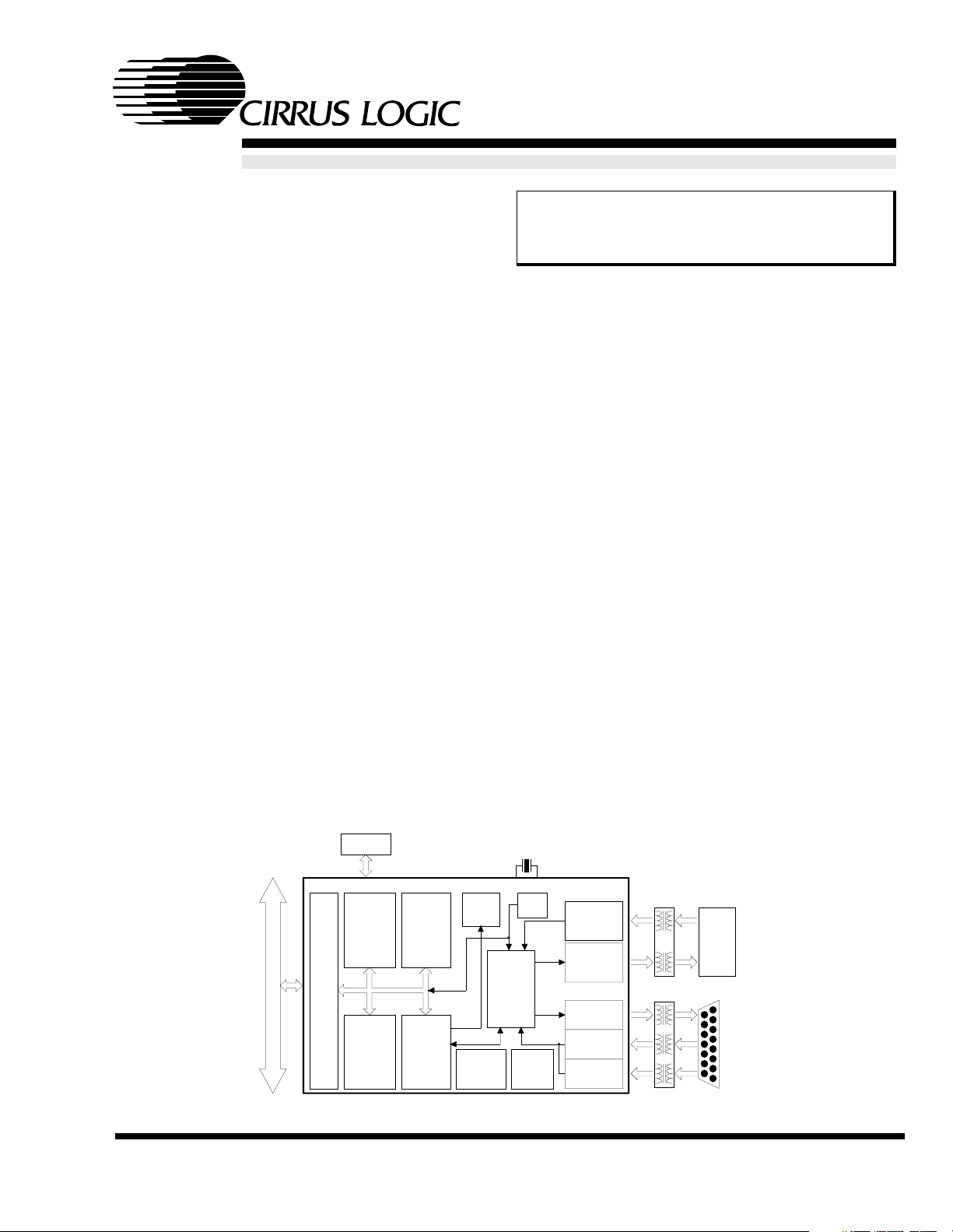
LED
Control
Scan
20 MHz
XTAL
Encoder/
Decoder
&
PLL
Mana ger
Clock
Power
10BASE-T
RX Filt ers &
Receiver
10BASE-T
TX Filt ers &
Tran smitt er
AUI
Tran smitt er
AUI
Collision
AUI
Receiver
RJ-45 10BASE-T
Attachment
Unit
Interface
(AUI)
EEPROM
CS8900A ISA Ethernet Controller
EEPROM
Contr ol
I
S
A
ISA
Bus
Logic
Memor y
Manager
RAM
802.3
MAC
Engine
Boundary
Test Logic
CIRRUS LOGIC PRODUCT DATASHEET
DS271PP4 APR ‘01
Copyright Cirrus Logic, Inc. 2001
(All Rights Reserved)

TABLE OF CONTENTS
1.0 INTRODUCTION ......................................................................................................................7
1.1 General Description ............................................................................................................7
1.1.1 TDirect ISA-Bus Interface ......................................................................................7
1.1.2 TIntegrated Memory ..............................................................................................7
1.1.3 T802.3 Ethernet MAC Engine ................................................................................7
1.1.4 TEEPROM Interface ..............................................................................................7
1.1.5 TComplete Analog Front End ................................................................................7
1.2 System Applications ...........................................................................................................7
1.2.1 TMotherboard LANs ..............................................................................................7
1.2.2 TEthernet Adapter Cards .......................................................................................8
1.3 Key Features and Benefits .................................................................................................9
1.3.1 TVery Low Cost .....................................................................................................9
1.3.2 THigh Performance ................................................................................................9
1.3.3 TLow Power and Low Noise ..................................................................................9
1.3.4 TComplete Support ...............................................................................................9
2.0 PIN DESCRIPTION .............................................................................................................11
3.0 FUNCTIONAL DESCRIPTION ...............................................................................................16
3.1 Overview ..........................................................................................................................16
3.1.1 TConfiguration .....................................................................................................16
3.1.2 TPacket Transmission .........................................................................................16
3.1.3 TPacket Reception ..............................................................................................16
3.2 ISA Bus Interface .............................................................................................................17
3.2.1 TMemory Mode Operation ...................................................................................17
3.2.2 TI/O Mode Operation ...........................................................................................17
3.2.3 TInterrupt Request Signals ..................................................................................17
3.2.4 TDMA Signals ......................................................................................................17
3.3 Reset and Initialization .....................................................................................................18
3.3.1 TReset .................................................................................................................18
3.3.1.1 External Reset, or ISA Reset ...............................................................18
3.3.1.2 Power-Up Reset ..................................................................................18
3.3.1.3 Power-Down Reset ..............................................................................18
3.3.1.4 EEPROM Reset ...................................................................................18
3.3.1.5 Software Initiated Reset .......................................................................18
3.3.1.6 Hardware (HW) Standby or Suspend ..................................................18
3.3.1.7 Sof tware (SW) Suspend .....................................................................18
3.3.2 TAllowing Time for Reset Operation ....................................................................18
3.3.3 TBus Reset Considerations .................................................................................18
3.3.4 TInitialization ........................................................................................................19
3.4 Configurations with EEPROM ..........................................................................................20
3.4.1 TEEPROM Interface ............................................................................................20
3.4.2 TEEPROM Memory Organization ........................................................................20
3.4.3 TReset Configuration Block .................................................................................20
3.4.3.1 Reset Configuration Block Structure ....................................................20
3.4.3.2 Reset Configuration Block Header ......................................................20
3.4.3.3 Determining the EEPROM Type ..........................................................20
3.4.3.4 Checking EEPROM for presence of Reset Configuration Block ..........20
3.4.3.5 Determining Number of Bytes in the Reset Configuration Block .........21
3.4.4 TGroups of Configuration Data ............................................................................21
3.4.4.1 Group Header ......................................................................................22
3.4.5 TReset Configuration Block Checksum ...............................................................22
3.4.6 TEEPROM Example ............................................................................................22
3.4.7 TEEPROM Read-out ...........................................................................................22
CS8900A
Crystal LAN™ ISA Ethernet Controller
CIRRUS LOGIC PRODUCT DATASHEET
2 DS271PP4

CS8900A
Crystal LAN™ ISA Ethernet Controller
3.4.7.1 Determining EEPROM Size .................................................................22
3.4.7.2 Loading Configuration Data ................................................................. 23
3.4.8 TEEPROM Read-out Completion ........................................................................ 23
3.5 Programming the EEPROM .............................................................................................23
3.5.1 TEEPROM Commands .......................................................................................23
3.5.2 TEEPROM Command Execution ........................................................................23
3.5.3 TEnabling Access to the EEPROM .....................................................................24
3.5.4 TWriting and Erasing the EEPROM .................................................................... 24
3.6 Boot PROM Operation ..................................................................................................... 24
3.6.1 TAccessing the Boot PROM ................................................................................ 24
3.6.2 TConfiguring the CS8900A for Boot PROM Operation .......................................24
3.7 Low-Power Modes ..........................................................................................................25
3.7.1 THardware Standby ............................................................................................25
3.7.2 THardware Suspend ...........................................................................................25
3.7.3 TSoftware Suspend .............................................................................................26
3.8 LED Outputs ..................................................................................................................... 27
3.8.0.1 LANLED .............................................................................................. 27
3.8.0.2 LINKLED or HC0 .................................................................................27
3.8.0.3 BSTATUS or HC1 ............................................................................... 27
3.8.1 TLED Connection ................................................................................................ 27
3.9 Media Access Control ...................................................................................................... 27
3.9.1 TOverview ...........................................................................................................27
3.9.2 TFrame Encapsulation and Decapsulation .........................................................28
3.9.2.1 Transmission ....................................................................................... 28
3.9.2.2 Reception ............................................................................................28
3.9.2.3 Enforcing Minimum Frame Size .......................................................... 28
3.9.3 TTransmit Error Detection and Handling .............................................................29
3.9.3.1 Loss of Carrier .....................................................................................29
3.9.3.2 SQE Error ............................................................................................29
3.9.3.3 Out-of-Window (Late) Collision ............................................................ 29
3.9.3.4 Jabber Error ........................................................................................ 29
3.9.3.5 Transmit Collision ................................................................................29
3.9.3.6 Transmit Underrun .............................................................................. 29
3.9.4 TReceive Error Detection and Handling ..............................................................30
3.9.4.1 CRC Error ............................................................................................ 30
3.9.4.2 Runt Frame .........................................................................................30
3.9.4.3 Extra Data ...........................................................................................30
3.9.4.4 Dribble Bits and Alignment Error ......................................................... 30
3.9.5 TMedia Access Management .............................................................................. 30
3.9.5.1 Collision Avoidance ............................................................................. 30
3.9.5.2 Two-Part Deferral ................................................................................ 30
3.9.5.3 Simple Deferral .................................................................................... 31
3.9.5.4 Collision Resolution ............................................................................. 31
3.9.5.5 Normal Collisions ................................................................................31
3.9.5.6 Late Collisions ..................................................................................... 32
3.9.5.7 Backoff ................................................................................................32
3.9.5.8 Standard Backoff ................................................................................. 32
3.9.5.9 Modified Backoff ..................................................................................32
3.9.5.10 SQE Test ........................................................................................... 32
3.10 Encoder/Decoder (ENDEC) ........................................................................................... 33
3.10.1 TEncoder ...........................................................................................................33
3.10.2 TCarrier Detection ............................................................................................. 33
3.10.3 TClock and Data Recovery ...............................................................................33
CIRRUS LOGIC PRODUCT DATASHEET
DS271PP4 3

CS8900A
Crystal LAN™ ISA Ethernet Controller
3.10.4 TInterface Selection ...........................................................................................34
3.10.4.1 10BASE-T Only .................................................................................34
3.10.4.2 AUI Only ............................................................................................34
3.10.4.3 Auto-Select ........................................................................................34
3.11 10BASE-T Transceiver ...................................................................................................34
3.11.1 T10BASE-T Filters .............................................................................................34
3.11.2 TTransmitter ......................................................................................................35
3.11.3 TReceiver ..........................................................................................................35
3.11.3.1 Squelch Circuit ...................................................................................35
3.11.3.2 Extended Range ................................................................................35
3.11.4 TLink Pulse Detection ........................................................................................35
3.11.5 TReceive Polarity Detection and Correction ......................................................36
3.11.6 TCollision Detection ...........................................................................................36
3.12 Attachment Unit Interface (AUI) .....................................................................................36
3.12.1 TAUI Transmitter ...............................................................................................36
3.12.2 TAUI Receiver ...................................................................................................37
3.12.3 TCollision Detection ...........................................................................................37
3.13 External Clock Oscillator ................................................................................................37
4.0 PACKETPAGE ARCHITECTURE ..........................................................................................38
4.1 PacketPage Overview ......................................................................................................38
4.1.1 TIntegrated Memory ............................................................................................38
4.1.2 TBus Interface Registers .....................................................................................38
4.1.3 TStatus and Control Registers .............................................................................38
4.1.4 TInitiate Transmit Registers .................................................................................38
4.1.5 TAddress Filter Registers ....................................................................................38
4.1.6 TReceive and Transmit Frame Locations ............................................................38
4.2 PacketPage Memory Map ................................................................................................39
4.3 Bus Interface Registers ....................................................................................................41
4.4 Status and Control Registers ...........................................................................................46
4.4.1 TConfiguration and Control Registers .................................................................46
4.4.2 TStatus and Event Registers ...............................................................................46
4.4.3 TStatus and Control Bit Definitions ......................................................................46
4.4.3.1 Act-Once Bits .......................................................................................47
4.4.3.2 Temporal Bits .......................................................................................47
4.4.3.3 Interrupt Enable Bits and Events .........................................................47
4.4.3.4 Accept Bits ...........................................................................................47
4.4.4 TStatus and Control Register Summary ..............................................................48
4.5 Initiate Transmit Registers ................................................................................................70
4.6 Address Filter Registers ...................................................................................................71
4.7 Receive and Transmit Frame Locations ...........................................................................72
4.7.1 TReceive PacketPage Locations .........................................................................72
4.7.2 TTransmit Locations ............................................................................................72
4.8 Eight and Sixteen Bit Transfers ........................................................................................72
4.8.1 TTransferring Odd-Byte-Aligned Data .................................................................73
4.8.2 TRandom Access to CS8900A Memory ..............................................................73
4.9 Memory Mode Operation ..................................................................................................73
4.9.1 TAccesses in Memory Mode ...............................................................................73
4.9.2 TConfiguring the CS8900A for Memory Mode .....................................................73
4.9.3 TBasic Memory Mode Transmit ...........................................................................74
4.9.4 TBasic Memory Mode Receive ............................................................................74
4.9.5 TPolling the CS8900A in Memory Mode ..............................................................75
4.10 I/O Space Operation ......................................................................................................75
4.10.1 TReceive/Transmit Data Ports 0 and 1 ..............................................................75
CIRRUS LOGIC PRODUCT DATASHEET
4 DS271PP4

CS8900A
Crystal LAN™ ISA Ethernet Controller
4.10.2 TTxCMD Port ....................................................................................................75
4.10.3 TTxLength Port ..................................................................................................75
4.10.4 TInterrupt Status Queue Port ............................................................................75
4.10.5 TPacketPage Pointer Port .................................................................................75
4.10.6 TPacketPage Data Ports 0 and 1 ...................................................................... 76
4.10.7 TI/O Mode Operation .........................................................................................76
4.10.8 TBasic I/O Mode Transmit ................................................................................. 76
4.10.9 TBasic I/O Mode Receive ..................................................................................76
4.10.10 TAccessing Internal Registers ......................................................................... 77
4.10.11 TPolling the CS8900A in I/O Mode .................................................................77
5.0 OPERATION .......................................................................................................................... 78
5.1 Managing Interrupts and Servicing the Interrupt Status Queue .......................................78
5.2 Basic Receive Operation ..................................................................................................78
5.2.0.1 Overview ............................................................................................. 78
5.2.1 TTerminology: Packet, Frame, and Transfer ....................................................... 80
5.2.1.1 Packet .................................................................................................80
5.2.1.2 Frame .................................................................................................. 80
5.2.1.3 Transfer ............................................................................................... 80
5.2.2 TReceive Configuration ....................................................................................... 80
5.2.2.1 Configuring the Physical Interface ....................................................... 80
5.2.2.2 Choosing which Frame Types to Accept ............................................. 80
5.2.2.3 Selecting which Events Cause Interrupts ............................................ 81
5.2.2.4 Choosing How to Transfer Frames ...................................................... 81
5.2.3 TReceive Frame Pre-Processing ........................................................................81
5.2.3.1 Destination Address Filtering ..............................................................82
5.2.3.2 Early Interrupt Generation ................................................................... 83
5.2.3.3 Acceptance Filtering ............................................................................ 83
5.2.3.4 Normal Interrupt Generation ................................................................ 83
5.2.4 THeld vs. DMAed Receive Frames ..................................................................... 83
5.2.5 TBuffering Held Receive Frames ........................................................................83
5.2.6 TTransferring Held Receive Frames ...................................................................85
5.2.7 TReceive Frame Visibility .................................................................................... 85
5.2.8 TExample of Memory Mode Receive Operation .................................................85
5.2.9 TReceive Frame Byte Counter ............................................................................ 86
5.3 Receive Frame Address Filtering ..................................................................................... 86
5.3.0.1 Individual Address Frames .................................................................. 87
5.3.0.2 Multicast Frames ................................................................................. 87
5.3.0.3 Broadcast Frames ............................................................................... 87
5.3.1 TConfiguring the Destination Address Filter ........................................................ 87
5.3.2 THash Filter ......................................................................................................... 88
5.3.2.1 Hash Filter Operation ..........................................................................88
5.3.3 TBroadcast Frame Hashing Exception ................................................................ 88
5.4 Receive DMA ...................................................................................................................89
5.4.1 TOverview ...........................................................................................................89
5.4.2 TConfiguring the CS8900A for DMA Operation ..................................................89
5.4.3 TDMA Receive Buffer Size ..................................................................................89
5.4.4 TReceive-DMA-Only Operation ........................................................................... 90
5.4.5 TCommitting Buffer Space to a DMAed Frame ...................................................91
5.4.6 TDMA Buffer Organization ..................................................................................91
5.4.7 TRxDMAFrame Bit ..............................................................................................91
5.4.8 TReceive DMA Example Without Wrap-Around .................................................. 91
5.4.9 TReceive DMA Operation for RxDMA-Only Mode ..............................................91
5.5 Auto-Switch DMA .............................................................................................................92
CIRRUS LOGIC PRODUCT DATASHEET
DS271PP4 5

CS8900A
Crystal LAN™ ISA Ethernet Controller
5.5.1 TOverview ...........................................................................................................92
5.5.2 TConfiguring the CS8900A for Auto-Switch DMA ...............................................93
5.5.3 TAuto-Switch DMA Operation ..............................................................................93
5.5.4 TDMA Channel Speed vs. Missed Frames ..........................................................94
5.5.5 TExit From DMA ..................................................................................................94
5.5.6 TAuto-Switch DMA Example ...............................................................................95
5.6 StreamTransfer ................................................................................................................95
5.6.1 TOverview ...........................................................................................................95
5.6.2 TConfiguring the CS8900A for StreamTransfer ...................................................95
5.6.3 TStreamTransfer Operation .................................................................................95
5.6.4 TKeeping StreamTransfer Mode Active ...............................................................95
5.6.5 TExample of StreamTransfer ...............................................................................97
5.6.6 TReceive DMA Summary ....................................................................................97
5.7 Transmit Operation ...........................................................................................................98
5.7.1 TOverview ...........................................................................................................98
5.7.2 TTransmit Configuration ......................................................................................98
5.7.2.1 Configuring the Physical Interface .......................................................98
5.7.2.2 Selecting which Events Cause Interrupts ............................................98
5.7.3 TChanging the Configuration ...............................................................................98
5.7.4 TEnabling CRC Generation and Padding ............................................................99
5.7.5 TIndividual Packet Transmission .........................................................................99
5.7.6 TTransmit in Poll Mode ......................................................................................100
5.7.7 TTransmit in Interrupt Mode ..............................................................................100
5.7.8 TCompleting Transmission ................................................................................101
5.7.9 TRdy4TxNOW vs. Rdy4Tx ................................................................................101
5.7.10 TCommitting Buffer Space to a Transmit Frame .............................................101
5.7.11 TTransmit Frame Length .................................................................................104
5.8 Full duplex Considerations .............................................................................................104
5.9 Auto-Negotiation Considerations ....................................................................................104
6.0 TEST MODES ......................................................................................................................105
6.0.1 TLoopback & Collision Diagnostic Tests ...........................................................105
6.0.2 TInternal Tests ...................................................................................................105
6.0.3 TExternal Tests .................................................................................................105
6.0.4 TLoopback Tests ...............................................................................................105
6.0.5 T10BASE-T Loopback and Collision Tests ........................................................105
6.0.6 TAUI Loopback and Collision Tests ...................................................................105
6.1 Boundary Scan ...............................................................................................................106
6.1.1 TOutput Cycle ....................................................................................................106
6.1.2 TInput Cycle ......................................................................................................106
6.1.3 TContinuity Cycle ...............................................................................................107
7.0 T CHARACTERISTICS/SPECIFICATIONS - COMMERCIAL .............................................110
8.0 T CHARACTERISTICS/SPECIFICATIONS - INDUSTRIAL ................................................121
9.0 PHYSICAL DIMENSIONS ....................................................................................................132
10.0 GLOSSARY OF TERMS ....................................................................................................133
10.1 Acronyms .....................................................................................................................133
10.2 Definitions .....................................................................................................................134
10.3 Acronyms Specific to the CS8900A .............................................................................135
10.4 Terms Specific to the CS8900A ...................................................................................135
10.5 Suffixes Specific to the CS8900A. ................................................................................136
11.0 REVISION HISTORY ..........................................................................................................137
CIRRUS LOGIC PRODUCT DATASHEET
6 DS271PP4

CS8900A
Crystal LAN™ ISA Ethernet Controller
1.0 INTRODUCTION
1.1 General Description
The CS8900A is a true single-chip, full-duplex,
Ethernet solution, incorporating all of the analog
and digital circuitry needed for a complete Ethernet
circuit. Major functional blocks include: a direct
ISA-bus interface; an 802.3 MAC engine; integrated buffer memory; a serial EEPROM interface; and
a complete analog front end with both 10BASE-T
and AUI.
1.1.1 Direct ISA-Bus Interface
Included in the CS8900A is a direct ISA-bus interface with full 24 mA drive capability. Its configuration options include a choice of four interrupts
and three DMA channels (one of each selected during initialization). In Memory Mode, it supports
Standard or Ready Bus cycles without introducing
additional wait states.
1.1.2 Integrated Memory
The CS8900A incorporates a 4-Kbyte page of onchip memory, eliminating the cost and board area
associated with external memory chips. Unlike
most other Ethernet controllers, the CS8900A buffers entire transmit and receive frames on chip,
eliminating the need for complex, inefficient memory management schemes. In addition, the
CS8900A operates in either Memory space, I/O
space, or with external DMA controllers, providing
maximum design flexibility.
1.1.3 802.3 Ethernet MAC Engine
The CS8900A’s Ethernet Media Access Control
(MAC) engine is fully compliant with the IEEE
802.3 Ethernet standard (ISO/IEC 8802-3, 1993),
and supports full-duplex operation. It handles all
aspects of Ethernet frame transmission and reception, including: collision detection, preamble generation and detection, and CRC generation and test.
Programmable MAC features include automatic re-
transmission on collision, and automatic padding
of transmitted frames.
1.1.4 EEPROM Interface
The CS8900A provides a simple and efficient serial EEPROM interface that allows configuration information to be stored in an optional EEPROM,
and then loaded automatically at power-up. This
eliminates the need for costly and cumbersome
switches and jumpers.
1.1.5 Complete Analog Front End
The CS8900A’s analog front end incorporates a
Manchester encoder/decoder, clock recovery circuit, 10BASE-T transceiver, and complete Attachment Unit Interface (AUI). It provides manual and
automatic selection of either 10BASE-T or AUI,
and offers three on-chip LED drivers for link status, bus status, and Ethernet line activity.
The 10BASE-T transceiver includes drivers, receivers, and analog filters, allowing direct connection to low-cost isolation transformers. It supports
100, 120, and 150 Ω shielded and unshielded cables, extended cable lengths, and automatic receive
polarity reversal detection and correction.
The AUI port provides a direct interface to
10BASE-2, 10BASE-5 and 10BASE-FL networks,
and is capable of driving a full 50-meter AUI cable.
1.2 System Applications
The CS8900A is designed to work well in either
motherboard or adapter applications.
1.2.1 Motherboard LANs
The CS8900A requires the minimum number of
external components needed for a full Ethernet
node. Its small-footprint package and high level of
integration allow System Engineers to design a
complete Ethernet circuit that occupies as little as
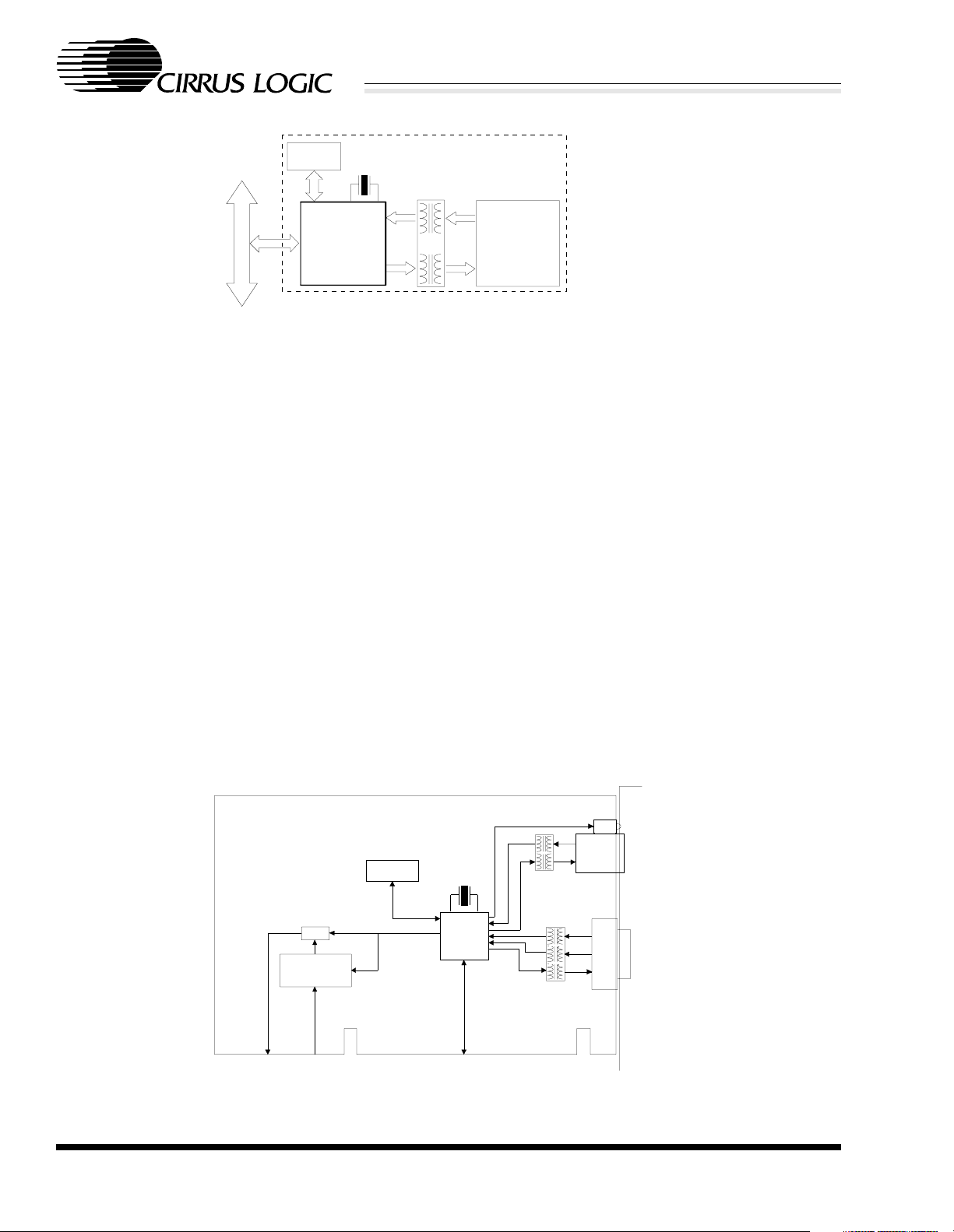
1.5 square inches of PCB area (Figure 1). In addition, the CS8900A’s power-saving features and
CMOS design make it a perfect fit for power-sensi-
CIRRUS LOGIC PRODUCT DATASHEET
DS271PP4 7
CS8900A
Crystal LAN™ ISA Ethernet Controller
EEPROM
I
S
A
Figure 1. Complete Ethernet Motherboard Solution
20 MHz
XTAL
CS8900A
tive portable and desktop PCs. Motherboard design
options include:
• An EEPROM can be used to store node-specif-
ic information, such as the Ethernet Individual
Address and node configuration.
• The 20 MHz crystal oscillator may be replaced
by a 20 MHz clock signal.
1.2.2 Ethernet Adapter Cards
The CS8900A’s highly efficient PacketPage architecture, with StreamTransfer™ and Auto-Switch
DMA options, make it an excellent choice for highperformance, low-cost ISA adapter cards
(Figure 2). The CS8900A’s wide range of configuration options and performance features allow en-
(2.0 sq. in.)
RJ-45
10BASE-T
gineers to design Ethernet solutions that meet their
particular system requirements. Adapter card design options include:
• A Boot PROM can be added to support diskless
applications.
• The 10BASE-T transmitter and receiver impedance can be adjusted to support 100, 120, or
150 Ohm twisted pair cables.
• An external Latchable-Address-bus decode circuit can be added to operate the CS8900A in
Upper-Memory space.
• On-chip LED ports can be used for either optional LEDs, or as programmable outputs.
LED
EEPROM
’245
Boot PROM
Figure 2. Full-Featured ISA Adapter Solution
CIRRUS LOGIC PRODUCT DATASHEET
8 DS271PP4
20 MHz
XTAL
CS89 00A
RJ-45
Attachment
Unit
Interface
(AUI )

CS8900A
Crystal LAN™ ISA Ethernet Controller
1.3 Key Features and Benefits
1.3.1 Very Low Cost
The CS8900A is designed to provide the lowestcost Ethernet solution available for embedded applications, portable motherboards, non-ISA bus
systems and adapter cards. Cost-saving features include:
• Integrated RAM eliminates the need for expensive external memory chips.
• On-chip 10BASE-T filters allow designers to
use simple isolation transformers instead of
more costly filter/transformer packages.
• The serial EEPROM port, used for configuration and initialization, eliminates the need for
expensive switches and jumpers.
• The CS8900A is designed to be used on a 2layer circuit board instead of a more expensive
multilayer board.
• The 8900A-based solution offers the smallest
footprint available, saving valuable printed circuit board area.
• A set of certified software drivers is available at
no charge, eliminating the need for costly software development.
older I/O-space designs, PacketPage is faster, simpler and more efficient.
To boost performance further, the CS8900A includes several key features that increase throughput
and lower CPU overhead, including:
• StreamTransfer cuts up to 87% of interrupts to
the host CPU during large block transfers.
• Auto-Switch DMA allows the CS8900A to
maximize throughput while minimizing missed
frames.
• Early interrupts allow the host to preprocess incoming frames.
• On-chip buffering of full frames cuts the
amount of host bandwidth needed to manage
Ethernet traffic.
1.3.3 Low Power and Low Noise
For low power needs, the CS8900A offers three
power-down options: Hardware Standby, Hardware Suspend, and Software Suspend. In Standby
mode, the chip is powered down with the exception
of the 10BASE-T receiver, which is enabled to listen for link activity. In either Hardware or Software
Suspend mode, the receiver is disabled and power
consumption drops to the micro-ampere range.
1.3.2 High Performance
In addition, the CS8900A has been designed for
very low noise emission, thus shortening the time
The CS8900A is a full 16-bit Ethernet controller
required for EMI testing and qualification.
designed to provide optimal system performance
by minimizing time on the ISA bus and CPU overhead per frame. It offers equal or superior performance for less money when compared to other
Ethernet controllers. The CS8900A’s PacketPage
architecture allows software to select whichever
access method is best suited to each particular
CPU/ISA-bus configuration. When compared to
CIRRUS LOGIC PRODUCT DATASHEET
DS271PP4 9
1.3.4 Complete Support
The CS8900A comes with a suite of software drivers for immediate use with most industry standard
network operating systems. In addition, complete
evaluation kits and manufacturing packages are
available, significantly reducing the cost and time
required to produce new Ethernet products.
CS8900A
Crystal LAN™ ISA Ethernet Controller
EEPROM
93C46
CS
DO
CLK
ISA
BUS
LA[20:23]
BALE
SA[0:19]
IRQ10
IRQ11
IRQ12
IRQ5
DRQ5
DACK5
DRQ6
DACK6
DRQ7
DACK7
SA[0:14]
SD[0:7]
20 MHz
97 98 93
XTAL1 XTAL2 SLEEP TEST RES
1
4
3
DI
2
Address
Decoder
4
PAL
3
EECS
6
EEDATAIN
5
EEDATAOUT
4
EESK
7
CHIPSEL
ELCS
20
SA[0:19]
28
MEMW
29
MEMR
62
IOW
61
IOR
49
REFRESH
36
SBHE
63
AEN
75
RESET
34
MEMCS16
33
IOCS16
64
32
31
30
35
15
16
13
14
11
12
IOCHRDY
SD[0:15]
INTRQ0
INTRQ1
INTRQ2
INTRQ3
DMARQ0
DMACK0
DMARQ1
DMACK1
DMARQ2
DMACK2
16
15
8
5 V
Ω
4.7 k
CS8900A
77 76
4.99 kΩ, 1%
RXD-
RXD+
TXD-
TXD+
DO-
DO+
CI-
CI+
DI-
DI+
BSTATUS/HCI
LANLED
LINKLED
CSOUT
92
91
Ω, 1%
24.3
88
87
Ω, 1%
24.3
84
83
82
81
80
79
39.2 Ω, 1%
78
680
100
680
99
17
Boot-PROM
20
CE
22
OE
100
68 pF
Ω
Ω
27C256
PD[0:7]
1
Ω, 1%
3
6
7
8
0.1 µF
39.2 Ω, 1%
39.2 Ω, 1%
0.1 µF
5 V
10 BASE T
Isolation
Transformer
1:1
1:
2
74LS245
19
OE
1
DIR
16
14
11
9
AUI Isolation
Transformer
1
2
4
5
7
8
39.2
0.1 µF
Ω
1:1
1:1
1:1
, 1%
12 V
16
15 3
13
12
10
9
4, 6
6
3
2
1
13
10
9
2
12
5
RJ45
15 pin D
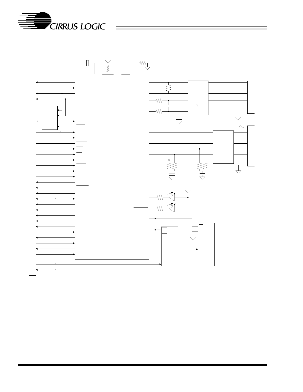
Figure 3. Typical Connection Diagram
CIRRUS LOGIC PRODUCT DATASHEET
10 DS271PP4
CS8900A
Y
Crystal LAN™ ISA Ethernet Controller
2.0 PIN DESCRIPTION
AVSS0
ELCS
EECS
EESK
EEDataOut
EEDataIn
CHIPSEL
DVSS1
DVDD1
DVSS1A
DMARQ2
DMACK2
DMARQ1
DMACK1
DMARQ0
DMACK0
CSOUT
SD15
SD14
SD13
SD12
DVDD2
DVSS2
SD11
SD10
10
11
12
13
14
15
16
17
18
19
20
21
22
23
24
25
XTAL1
XTAL2
LINKLED or HC0
LANLED
99
100
1
2
3
4
5
6
7
8
9
98
AVDD3
AVSS4
95
96
97
CS8900A
AVSS3
94
RES
93
92
91
RXD +
90
89
88
87
AVSS2
86
AVDD2
85
DO-
84
DO+
83
CI-
82
TXD +
TXD -
AVSS1
AVDD1
RXD -
100-pin
TQFP
(Q)
Top View
CI+
81
80
BSTATUS or HC1
TEST
SLEEP
DI-
DI+
79
76
77
78
75
74
73
72
71
70
69
68
67
66
65
64
63
62
61
60
59
58
57
56
55
54
53
52
51
RESET
SD7
SD6
SD5
SD4
DVSS4
DVDD4
SD3
SD2
SD1
SD0
IOCHRD
AEN
IOW
IOR
SA19
SA18
SA17
DVSS3A
DVDD3
DVSS3
SA16
SA15
SA14
SA13
2627282930313332343537
SD08
SD09
MEMR
MEMW
INTRQ2
INTRQ1
INTRQ0
36
SBHE
IOCS16
INTRQ3
MEMCS16
SA0
38
SA1
39
SA2
40
SA3
41
SA4
42
SA5
43
SA6
44
SA7
4647484950
45
SA9
SA8
SA11
SA10
SA12
REFRESH
CIRRUS LOGIC PRODUCT DATASHEET
DS271PP4 11

CS8900A
Crystal LAN™ ISA Ethernet Controller
ISA Bus Interface
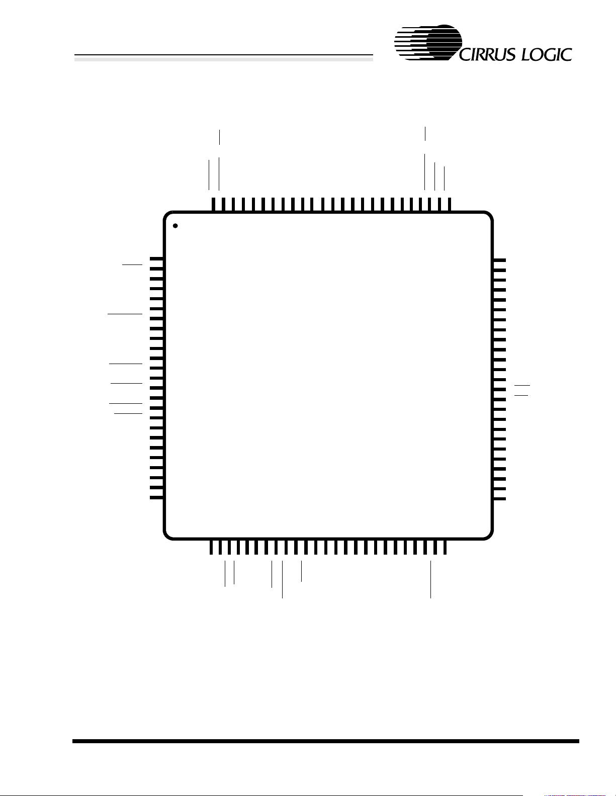
SA[0:19] - System Address Bus, Input PINS 37-48, 50-54, 58-60.
Lower 20 bits of the 24-bit System Address Bus used to decode accesses to CS8900A I/O and
Memory space, and attached Boot PROM. SA0-SA15 are used for I/O Read and Write
operations. SA0-SA19 are used in conjunction with external decode logic for Memory Read
and Write operations.
SD[0:15] - System Data Bus, Bi-Directional with 3-State Output PINS 65-68, 71-74, 27-24, 21-18.
Bi-directional 16-bit System Data Bus used to transfer data between the CS8900A and the host.
RESET - Reset, Input PIN 75.
Active-high asynchronous input used to reset the CS8900A. Must be stable for at least 400 ns
before the CS8900A recognizes the signal as a valid reset.
AEN - Address Enable, Input PIN 63.
When TEST
is high, this active-high input indicates to the CS8900A that the system DMA
controller has control of the ISA bus. When AEN is high, the CS8900A will not perform slave
I/O space operations. When TEST
Boundary Scan Test. AEN should be inactive when performing an IO or memory access and it
should be active during a DMA cycle.
MEMR
- Memory Read, Input PIN 29.
Active-low input indicates that the host is executing a Memory Read operation.
MEMW - Memory Write, Input PIN 28.
Active-low input indicates that the host is executing a Memory Write operation.
MEMCS16
- Memory Chip Select 16-bit, Open Drain Output PIN 34.
Open-drain, active-low output generated by the CS8900A when it recognizes an address on the
ISA bus that corresponds to its assigned Memory space (CS8900A must be in Memory Mode
with the MemoryE bit (Register 17, BusCTL, Bit A) set for MEMCS16
when not active.
REFRESH - Refresh, Input PIN 49.
Active-low input indicates to the CS8900A that a DRAM refresh cycle is in progress. When
REFRESH is low, MEMR, MEMW, IOR, IOW, DMACK0, DMACK1, and DMACK2 are
ignored.
is low, this pin becomes the shift clock input for the
to go active). 3-Stated
IOR - I/O Read, Input PIN 61.
When IOR is low and a valid address is detected, the CS8900A outputs the contents of the
selected 16-bit I/O register onto the System Data Bus. IOR is ignored if REFRESH is low.
IOW - I/O Write, Input PIN 62.
When IOW is low and a valid address is detected, the CS8900A writes the data on the System
Data Bus into the selected 16-bit I/O register. IOW is ignored if REFRESH is low.
CIRRUS LOGIC PRODUCT DATASHEET
12 DS271PP4

CS8900A
Crystal LAN™ ISA Ethernet Controller
IOCS16 - I/O Chip Select 16-bit, Open Drain Output PIN 33.
Open-drain, active-low output generated by the CS8900A when it recognizes an address on the
ISA bus that corresponds to its assigned I/O space. 3-Stated when not active.
IOCHRDY - I/O Channel Ready, Open Drain Output PIN 64.
When driven low, this open-drain, active-high output extends I/O Read and Memory Read
cycles to the CS8900A. This output is functional when the IOCHRDYE bit in the Bus Control
register (Register 17) is clear. This pin is always 3-Stated when the IOCHRDYE bit is set.
SBHE
- System Bus High Enable, Input PIN 36.
Active-low input indicates a data transfer on the high byte of the System Data Bus (SD8SD15). After a hardware or a software reset, provide a HIGH to LOW and then LOW to HIGH
transition on SBHE
signal before any IO or memory access is done to the CS8900A.
INTRQ[0:3] - Interrupt Request, 3-State PINS 30-32, 35.
Active-high output indicates the presence of an interrupt event. Interrupt Request goes low once
the Interrupt Status Queue (ISQ) is read as all 0’s. Only one Interrupt Request output is used
(one is selected during configuration). All non-selected Interrupt Request outputs are placed in
a high-impedance state. (Section 3.2 on page 17 and Section 5.1 on page 78.)
DMARQ[0:2] - DMA Request, 3-State PINS 11, 13, and 15.
Active-high, 3-Stateable output used by the CS8900A to request a DMA transfer. Only one
DMA Request output is used (one is selected during configuration). All non-selected DMA
Request outputs are placed in a high-impedance state.
DMACK
[0:2] - DMA Acknowledge, Input PINS 12, 14, and 16.
Active-low input indicates acknowledgment by the host of the corresponding DMA Request
output.
CHIPSEL - Chip Select, Input PIN 7.
Active-low input generated by external Latchable Address bus decode logic when a valid
memory address is present on the ISA bus. If Memory Mode operation is not needed,
CHIPSEL should be tied low. The CHIPSEL is ignored for IO and DMA mode of the
CS8900A.
EEPROM and Boot PROM Interface
EESK - EEPROM Serial Clock, PIN 4.
Serial clock used to clock data into or out of the EEPROM.
EECS - EEPROM Chip Select, PIN 3.
Active-high output used to select the EEPROM.
CIRRUS LOGIC PRODUCT DATASHEET
DS271PP4 13

Crystal LAN™ ISA Ethernet Controller
EEDataIn - EEPROM Data In, Input Internal Weak Pullup PIN 6.
Serial input used to receive data from the EEPROM. Connects to the DO pin on the EEPROM.
EEDataIn is also used to sense the presence of the EEPROM.
CS8900A
ELCS
- External Logic Chip Select, Internal Weak Pullup PIN 2.
Bi-directional signal used to configure external Latchable Address (LA) decode logic. If
external LA decode logic is not needed, ELCS should be tied low.
EEDataOut - EEPROM Data Out,PIN 5.
Serial output used to send data to the EEPROM. Connects to the DI pin on the EEPROM.
CSOUT
When TEST
- Chip Select for External Boot PROM, PIN 17.
is low, this pin becomes the output for the Boundary Scan Test.
Active-low output used to select an external Boot PROM when the CS8900A decodes a valid
Boot PROM memory address.
10BASE-T Interface
TXD+/TXD- - 10BASE-T Transmit, Differential Output Pair PINS 87 and 88.
Differential output pair drives 10 Mb/s Manchester-encoded data to the 10BASE-T transmit
pair.
RXD+/RXD- - 10BASE-T Receive, Differential Input Pair PINS 91 and 92.
Differential input pair receives 10 Mb/s Manchester-encoded data from the 10BASE-T receive
pair.
Attachment Unit Interface (AUI)
DO+/DO- - AUI Data Out, Differential Output Pair PINS 83 and 84.
Differential output pair drives 10 Mb/s Manchester-encoded data to the AUI transmit pair.
DI+/DI- - AUI Data In, Differential Input Pair PINS 79 and 80.
Differential input pair receives 10 Mb/s Manchester-encoded data from the AUI receive pair.
CI+/CI- - AUI Collision In, Differential Input Pair PINS 81 and 82.
Differential input pair connects to the AUI collision pair. A collision is indicated by the
presence of a 10 MHz ± 15% signal with duty cycle no worse than 60/40.
General Pins
XTAL[1:2] - Crystal, Input/Output PINS 97 and 98.
A 20 MHz crystal should be connected across these pins. If a crystal is not used, a 20 MHz
signal should be connected to XTAL1 and XTAL2 should be left open. (See Section 7.3 on
page 110 and Section 7.7 on page 120.)
CIRRUS LOGIC PRODUCT DATASHEET
14 DS271PP4

CS8900A
Crystal LAN™ ISA Ethernet Controller
SLEEP - Hardware Sleep, Input Internal Weak Pullup PIN 77.
Active-low input used to enable the two hardware sleep modes: Hardware Suspend and
Hardware Standby. (See Section 3.7 on page 25.)
LINKLED
or HC0 - Link Good LED or Host Controlled Output 0, Open Drain Output PIN 99.
When the HCE0 bit of the Self Control register (Register 15) is clear, this active-low output is
low when the CS8900A detects the presence of valid link pulses. When the HC0E bit is set, the
host may drive this pin low by setting the HCBO in the Self Control register.
BSTATUS or HC1 - Bus Status or Host Controlled Output 1, Open Drain Output PIN 78.
When the HC1E bit of the Self Control register (Register 15) is clear, this active-low output is
low when receive activity causes an ISA bus access. When the HC1E bit is set, the host may
drive this pin low by setting the HCB1 in the Self Control register.
LANLED - LAN Activity LED, Open Drain Output PIN 100.
During normal operation, this active-low output goes low for 6 ms whenever there is a receive
packet, a transmit packet, or a collision. During Hardware Standby mode, this output is driven
low when the receiver detects network activity.
TEST - Test Enable, Input Internal Weak Pullup PIN 76.
Active-low input used to put the CS8900A in Boundary Scan Test mode. For normal operation,
this pin should be high.
RES - Reference Resistor, Input PIN 93.
This input should be connected to a 4.99KΩ ± 1% resistor needed for biasing of internal analog
circuits.
DVDD[1:4] - Digital Power, Power PINS 9, 22, 56, and 69.
Provides 5 V ± 5% power to the digital circuits of the CS8900A.
DVSS[1:4} and DVSS1A, DVSS3A - Digital Ground, Ground PINS 8, 10, 23, 55, 57, and 70.
Provides ground reference (0 V) to the digital circuits of the CS8900A.
AVDD[1:3] - Analog Power, Power PINS 90, 85, and 95.
Provides 5 V ± 5% power to the analog circuits of the CS8900A.
AVSS[0:4] - Analog Ground, Ground PINS 1, 89, 86, 94, 96.
Provide ground reference (0 V) to the analog circuits of the CS8900A.
CIRRUS LOGIC PRODUCT DATASHEET
DS271PP4 15

CS8900A
Crystal LAN™ ISA Ethernet Controller
3.0 FUNCTIONAL DESCRIPTION
3.1 Overview
During normal operation, the CS8900A performs
two basic functions: Ethernet packet transmission
and reception. Before transmission or reception is
possible, the CS8900A must be configured.
3.1.1 Configuration
The CS8900A must be configured for packet transmission and reception at power-up or reset. Various
parameters must be written into its internal Configuration and Control registers such as Memory Base
Address; Ethernet Physical Address; what frame
types to receive; and which media interface to use.
Configuration data can either be written to the
CS8900A by the host (across the ISA bus), or loaded automatically from an external EEPROM. Operation can begin after configuration is complete.
Section 3.3 on page 18 and Section 3.4 on page 20
describe the configuration process in detail.
Section 4.4 on page 46 provides a detailed description of the bits in the Configuration and Control
Registers.
3.1.2 Packet Transmission
Packet transmission occurs in two phases. In the
first phase, the host moves the Ethernet frame into
the CS8900A’s buffer memory. The first phase begins with the host issuing a Transmit Command.
This informs the CS8900A that a frame is to be
transmitted and tells the chip when to start transmission (i.e. after 5, 381, 1021 or all bytes have
been transferred) and how the frame should be sent
(i.e. with or without CRC, with or without pad bits,
etc.). The Host follows the Transmit Command
with the Transmit Length, indicating how much
buffer space is required. When buffer space is
available, the host writes the Ethernet frame into
the CS8900A’s internal memory, either as a Memory or I/O space operation.
In the second phase of transmission, the CS8900A
converts the frame into an Ethernet packet then
transmits it onto the network. The second phase begins with the CS8900A transmitting the preamble
and Start-of-Frame delimiter as soon as the proper
number of bytes has been transferred into its transmit buffer (5, 381, 1021 bytes or full frame, depending on configuration). The preamble and Startof-Frame delimiter are followed by the Destination
Address, Source Address, Length field and LLC
data (all supplied by the host). If the frame is less
than 64 bytes, including CRC, the CS8900A adds
pad bits if configured to do so. Finally, the
CS8900A appends the proper 32-bit CRC value.
The Section 5.7 on page 98 provides a detailed description of packet transmission.
3.1.3 Packet Reception
Like packet transmission, packet reception occurs
in two phases. In the first phase, the CS8900A receives an Ethernet packet and stores it in on-chip
memory. The first phase of packet reception begins
with the receive frame passing through the analog
front end and Manchester decoder where Manchester data is converted to NRZ data. Next, the preamble and Start-of-Frame delimiter are stripped off
and the receive frame is sent through the address
filter. If the frame’s Destination Address matches
the criteria programmed into the address filter, the
packet is stored in the CS8900A’s internal memory. The CS8900A then checks the CRC, and depending on the configuration, informs the
processor that a frame has been received.
In the second phase, the host transfers the receive
frame across the ISA bus and into host memory.
Receive frames can be transferred as Memory
space operations, I/O space operations, or as DMA
operations using host DMA. Also, the CS8900A
provides the capability to switch between Memory
or I/O operation and DMA operation by using
Auto-Switch DMA and StreamTransfer.
The Section 5.2 on page 78 through Section 5.6 on
page 95 provide a detailed description of packet reception.
CIRRUS LOGIC PRODUCT DATASHEET
16 DS271PP4

CS8900A
Crystal LAN™ ISA Ethernet Controller
3.2 ISA Bus Interface
The CS8900A provides a direct interface to ISA
buses running at clock rates from 8 to 11 MHz. Its
on-chip bus drivers are capable of delivering
24 mA of drive current, allowing the CS8900A to
drive the ISA bus directly, without added external
"glue logic".
The CS8900A is optimized for 16-bit data transfers, operating in either Memory space, I/O space,
or as a DMA slave.
Note that ISA-bus operation below 8 MHz should
use the CS8900A’s Receive DMA mode to minimize missed frames. See Section 5.4 on page 89 for
a description of Receive DMA operation.
3.2.1 Memory Mode Operation
When configured for Memory Mode operation, the
CS8900A’s internal registers and frame buffers are
mapped into a contiguous 4-Kbyte block of host
memory, providing the host with direct access to
the CS8900A’s internal registers and frame buffers. The host initiates Read operations by driving
the MEMR
pin low and Write operations by driv-
ing the MEMW pin low.
For additional information about Memory Mode,
see Section 4.9 on page 73.
3.2.2 I/O Mode Operation
When configured for I/O Mode operation, the
CS8900A is accessed through eight, 16-bit I/O
ports that are mapped into sixteen contiguous I/O
locations in the host system’s I/O space. I/O Mode
is the default configuration for the CS8900A and is
always enabled.
For an I/O Read or Write operation, the AEN pin
must be low, and the 16-bit I/O address on the ISA
System Address bus (SA0 - SA15) must match the
address space of the CS8900A. For a Read, IOR
must be low, and for a Write, IOW must be low.
For additional information about I/O Mode, see
Section 4.10 on page 75.
3.2.3 Interrupt Request Signals
The CS8900A has four interrupt request output
pins that can be connected directly to any four of
the ISA bus Interrupt Request signals. Only one interrupt output is used at a time. It is selected during
initialization by writing the interrupt number (0 to
3) into PacketPage Memory base + 0022h. Unused
interrupt request pins are placed in a high-impedance state. The selected interrupt request pin goes
high when an enabled interrupt is triggered. The
pin goes low after the Interrupt Status Queue (ISQ)
is read as all 0’s (see Section 5.1 on page 78 for a
description of the ISQ).
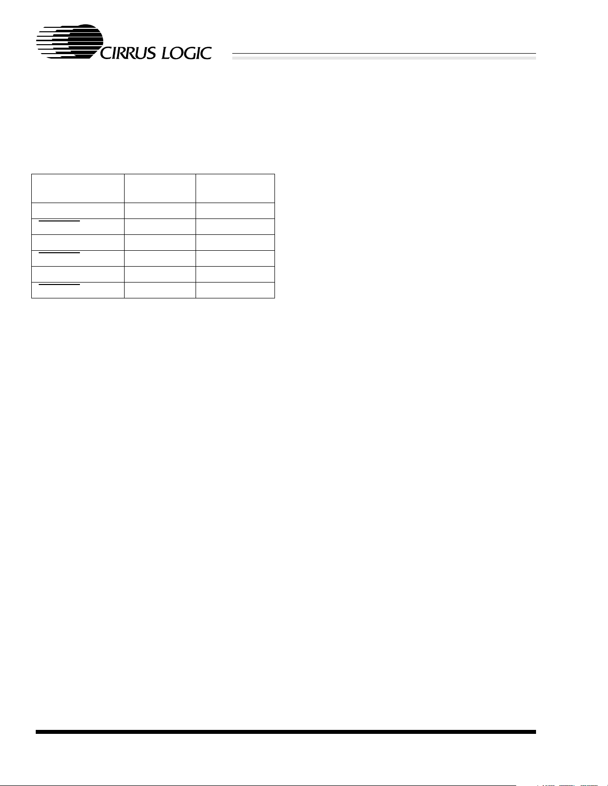
Table 1 presents one possible way of connecting
the interrupt request pins to the ISA bus that utilizes commonly available interrupts and facilitates
board layout.
CS8900A Interrupt
Request Pin
INTRQ3 (Pin 35)
INTRQ0 (Pin 32)
INTRQ1 (Pin 31)
INTRQ2 (Pin 30)
Table 1. Interrupt Assignments
ISA Bus
Interrupt
IRQ5 0003h
IRQ10 0000h
IRQ11 0001h
IRQ12 0002h
PacketPage
base + 0022h
3.2.4 DMA Signals
The CS8900A interfaces directly to the host DMA
controller to provide DMA transfers of receive
frames from CS8900A memory to host memory.
The CS8900A has three pairs of DMA pins that can
be connected directly to the three 16-bit DMA
channels of the ISA bus. Only one DMA channel is
used at a time. It is selected during initialization by
writing the number of the desired channel (0, 1 or
2) into PacketPage Memory base + 0024h. Unused
DMA pins are placed in a high-impedance state.
The selected DMA request pin goes high when the
CS8900A has received frames to transfer to the
host memory via DMA. If the DMABurst bit (register 17, BusCTL, Bit B) is clear, the pin goes low
after the DMA operation is complete. If the
CIRRUS LOGIC PRODUCT DATASHEET
DS271PP4 17
CS8900A
Crystal LAN™ ISA Ethernet Controller
DMABurst bit is set, the pin goes low 32 µs after
the start of a DMA transfer.
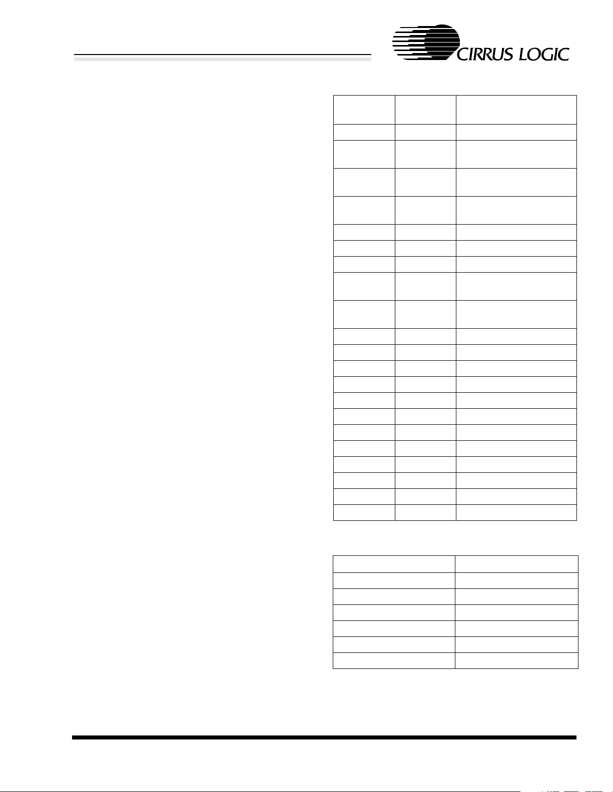
The DMA pin pairs are arranged on the CS8900A
to facilitate board layout. Crystal recommends the
configuration in Table 2 when connecting these
pins to the ISA bus.
CS8900A DMA
Signal (Pin #)
DMARQ0 (Pin 15) DRQ5 0000h
DMACK0
DMARQ1 (Pin 13) DRQ6 0001h
DMACK1
DMARQ2 (Pin 11) DRQ7 0002h
DMACK2
(Pin 16) DACK5
(Pin 14) DACK6
(Pin 12) DACK7
Table 2. DMA Assignments
ISA DMA
Signal
PacketPage
base + 0024h
For a description of DMA mode, see Section 5.4 on
page 89.
3.3 Reset and Initialization
3.3.1 Reset
Seven different conditions cause the CS8900A to
reset its internal registers and circuits.
3.3.1.4 EEPROM Reset
There is a chip-wide reset if an EEPROM checksum error is detected (see Section 3.4 on page 20).
3.3.1.5 Software Initiated Reset
There is a chip-wide reset whenever the RESET bit
(Register 15, SelfCTL, Bit 6) is set.
3.3.1.6 Hardware (HW) Standby or Suspend
The CS8900A goes though a chip-wide reset whenever it enters or exits either HW Standby mode or
HW Suspend mode (see Section 3.7 on page 25 for
more information about HW Standby and Suspend).
3.3.1.7 Software (SW) Suspend
Whenever the CS8900A enters SW Suspend mode,
all registers and circuits are reset except for the ISA
I/O Base Address register (located at PacketPage
base + 0020h) and the SelfCTL register (Register
15). Upon exit, there is a chip-wide reset (see
Section 3.7 on page 25 for more information about
SW Suspend).
3.3.2 Allowing Time for Reset Operation
3.3.1.1 External Reset, or ISA Reset
There is a chip-wide reset whenever the RESET pin
is high for at least 400 ns. During a chip-wide reset,
all circuitry and registers in the CS8900A are reset.
3.3.1.2 Power-Up Reset
When power is applied, the CS8900A maintains reset until the voltage at the supply pins reaches approximately 2.5 V. The CS8900A comes out of
reset once Vcc is greater than approximately 2.5 V
and the crystal oscillator has stabilized.
3.3.1.3 Power-Down Reset
If the supply voltage drops below approximately
2.5 V, there is a chip-wide reset. The CS8900A
comes out of reset once the power supply returns to
a level greater than approximately 2.5 V and the
crystal oscillator has stabilized.
CIRRUS LOGIC PRODUCT DATASHEET
After a reset, the CS8900A goes through a self configuration. This includes calibrating on-chip analog
circuitry, and reading EEPROM for validity and
configuration. Time required for the reset calibration is typically 10 ms. Software drivers should not
access registers internal to the CS8900A during
this time. When calibration is done, bit INITD in
the Self Status Register (register 16) is set indicating that initialization is complete, and the SIBUSY
bit in the same register is cleared indicating the EEPROM is no longer being read or programmed.
3.3.3 Bus Reset Considerations
The CS8900A reads 3000h from IObase+0Ah after
the reset, until the software writes a non-zero value
at IObase+0Ah. The 3000h value can be used as
part of the CS8900A signature when the system
scans for the CS8900A. See Section 4.10 on
page 75.
18 DS271PP4
CS8900A
Crystal LAN™ ISA Ethernet Controller
After a reset, the ISA bus outputs INTRx and
DMARQx are 3-Stated, thus avoiding any interrupt
or DMA channel conflicts on the ISA bus at powerup time.
3.3.4 Initialization
After each reset (except EEPROM Reset), the
CS8900A checks the sense of the EEDataIn pin to
see if an external EEPROM is present. If EEDI is
high, an EEPROM is present and the CS8900A automatically loads the configuration data stored in
the EEPROM into its internal registers (see next
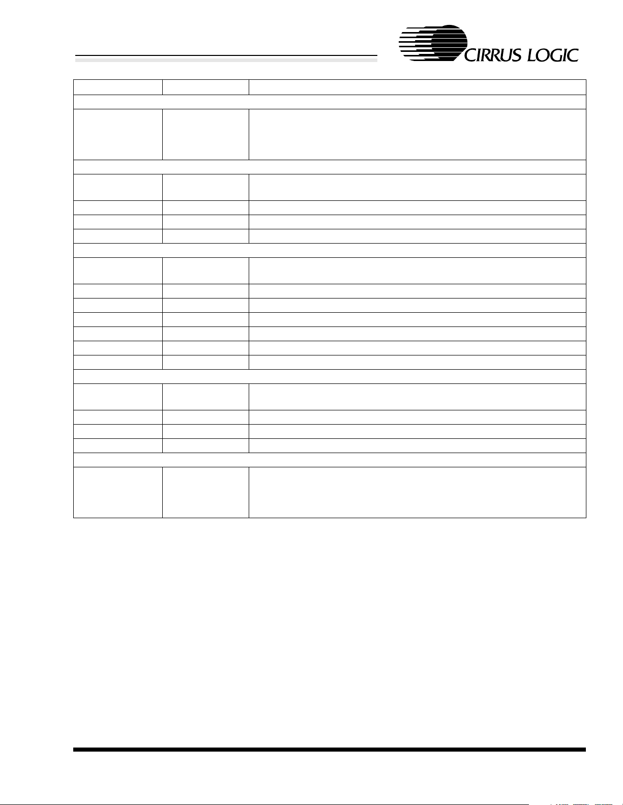
section). If EEDI is low, an EEPROM is not
present and the CS8900A comes out of reset with
the default configuration shown in Table 3.
A low-cost serial EEPROM can be used to store
configuration information that is automatically
loaded into the CS8900A after each reset (except
EEPROM reset). The use of an EEPROM is optional.
The CS8900A operates with any of six standard
EEPROM’s shown in Table 4.
PacketPage
Address
0020h 0300h I/O Base Address*
0022h XXXX XXXX
0024h XXXX XXXX
0026h 0000h DMA Start of Frame
0028h X000h DMA Frame Count
002Ah 0000h DMA Byte Count
002Ch XXX0 0000h Memory Base Address
0030h XXX0 0000h Boot PROM Base
0034h XXX0 0000h Boot PROM Address
0102h 0003h Register 3 - RxCFG
0104h 0005h Register 5 - RxCTL
0106h 0007h Register 7 - TxCFG
0108h 0009h Register 9 - TxCMD
010Ah 000Bh Register B - BufCFG
010Ch Undefined Reserved
010Eh Undefined Reserved
0110h Undefined Reserved
0112h 00013h Register 13 - LineCTL
0114h 0015h Register 15 - SelfCTL
0116h 0017h Register 17 - BusCTL
0118h
* I/O base address is unaffected by Software Suspend mode.
Register
Contents
XXXX X100
XXXX XX11
0019h
Tabl e 3 . Default Configuration
Register Descriptions
Interrupt Number
DMA Channel
Offset
Address
Mask
Register 19 - TestCTL
EEPROM Type Size (16-bit words)
‘C46 (non-sequential) 64
‘CS46 (sequential) 64
‘C56 (non-sequential) 128
‘CS56 (sequential) 128
‘C66 (non-sequential) 256
‘CS66 (sequential) 256
Table 4. Supported EEPROM Types
CIRRUS LOGIC PRODUCT DATASHEET
DS271PP4 19

CS8900A
Crystal LAN™ ISA Ethernet Controller
3.4 Configurations with EEPROM
3.4.1 EEPROM Interface
The interface to the EEPROM consists of the four
signals shown in Table 5.
CS8900A Pin
(Pin #) CS8900A Function
EECS (Pin 3) EEPROM Chip Select Chip Select
EESK (PIN 4) 1 MHz EEPROM
Serial Clock output
EEDO (Pin 5) EEPROM Data Out
(data to EEPROM)
EEDI (Pin 6) EEPROM Data in
(data from EEPROM)
Table 5. EEPROM Interface
EEPROM
Pin
Clock
Data In
Data Out
3.4.2 EEPROM Memory Organization
If an EEPROM is used to store initial configuration
information for the CS8900A, the EEPROM is organized in one or more blocks of 16-bit words. The
first block in EEPROM, referred to as the Configuration Block, is used to configure the CS8900A after reset. An example of a typical Configuration
Block is shown in Table 6. Additional blocks containing user data may be stored in the EEPROM.
However, the Configuration Block must always
start at address 00h and be stored in contiguous
memory locations.
3.4.3 Reset Configuration Block
The first block in EEPROM, referred to as the Reset Configuration Block, is used to automatically
program the CS8900A with an initial configuration
after a reset. Additional user data may also be
stored in the EEPROM if space is available. The
additional data are stored as 16-bit words and can
occupy any EEPROM address space beginning immediately after the end of the Reset Configuration
Block up to address 7Fh, depending on EEPROM
size. This additional data can only be accessed
through software control (refer to Section 3.5 on
page 23 for more information on accessing the EEPROM). Address space 80h to AFh is reserved.
3.4.3.1 Reset Configuration Block Structure
The Reset Configuration Block is a block of contiguous 16-bit words starting at EEPROM address
00h. It can be divided into three logical sections: a
header, one or more groups of configuration data
words, and a checksum value. All of the words in
the Reset Configuration Block are read sequentially by the CS8900A after each reset, starting with
the header and ending with the checksum. Each
group of configuration data is used to program a
PacketPage register (or set of PacketPage registers
in some cases) with an initial non-default value.
3.4.3.2 Reset Configuration Block Header
The header (first word of the block located at EEPROM address 00h) specifies the type of EEPROM used, whether or not a Reset Configuration
block is present, and if so, how many bytes of configuration data are stored in the Reset Configuration Block.
3.4.3.3 Determining the EEPROM Type
The LSB of the high byte of the header indicates
the type of EEPROM attached: sequential or nonsequential. An LSB of 0 (XXXX-XXX0) indicates
a sequential EEPROM. An LSB of 1 (XXXXXXX1) indicates a non-sequential EEPROM. The
CS8900A works equally well with either type of
EEPROM. The CS8900A will automatically generate sequential addresses while reading the Reset
Configuration Block if a non-sequential EEPROM
is used.
3.4.3.4 Checking EEPROM for presence of Reset Configuration Block
The read-out of either a binary 101X-XXX0 or
101X-XXX1 (X = do not care) from the high byte
of the header indicates the presence of configuration data. Any other readout value terminates initialization from the EEPROM. If an EEPROM is
attached but not used for configuration, Crystal recommends that the high byte of the first word be
programmed with 00h in order to ensure that the
CIRRUS LOGIC PRODUCT DATASHEET
20 DS271PP4
CS8900A
Crystal LAN™ ISA Ethernet Controller
Word Address Value Description
FIRST WORD in DATA BLOCK
00h A120h Configuration Block Header.
The high byte, A1h, indicates a ‘C46 EEPROM is attached. The Link Byte,
20h, indicates the number of bytes to be used in this block of configuration
data.
FIRST GROUP of WORDS
01h 2020h Group Header for first group of words.
Three words to be loaded, beginning at 0020h in PacketPage memory.
02h 0300h I/O Base Address
03h 0003h Interrupt Number
04h 0001h DMA Channel Number
SECOND GROUP of WORDS
05h 502Ch Group Header for second group of words.
Six words to be loaded, beginning at 002Ch in PacketPage memory.
06h E000h Memory Base Address - low word
07 000Fh Memory Base Address - high word
08h 0000h Boot PROM Base Address - low word
09h 000Dh Boot PROM Base Address - high word
0Ah C000h Boot PROM Address Mask - low word
0Bh 000Fh Boot PROM Address Mask - high word
THIRD GROUP of WORDS
0Ch 2158h Group Header for third group of words.
Three words to be loaded, beginning at 0158 in PacketPage memory.
0Dh 0010h Individual Address - Octet 0 and 1
0Eh 0000h Individual Address - Octet 2 and 3
0Fh 0000h Individual Address - Octet 4 and 5
CHECKSUM Value
10h 2800h The high byte, 28h, is the Checksum Value. In this example, the check-
sum includes word addresses 00h through 0Fh. The hexadecimal sum of
the bytes is D8h, resulting in a 2’s complement of 28h. The low byte, 00h,
provides a pad to the word boundary.
* FFFFh is a special code indicating that there are no more words in the EEPROM.
Table 6. EEPROM Configuration Block Example
CS8900A will not attempt to read configuration
data from the EEPROM.
3.4.3.5 Determining Number of Bytes in the Reset Configuration Block
The low byte of the Reset Configuration Block
header is known as the link byte. The value of the
Link Byte represents the number of bytes of configuration data in the Reset Configuration Block. The
two bytes used for the header are excluded when
calculating the Link Byte value.
For example, a Reset Configuration Block header
of A104h indicates a non-sequential EEPROM programmed with a Reset Configuration Block containing 4 bytes of configuration data. This Reset
Configuration Block occupies 6 bytes (3 words) of
EEPROM space (2 bytes for the header and 4 bytes
of configuration data).
3.4.4 Groups of Configuration Data
Configuration data are arranged as groups of
words. Each group contains one or more words of
data that are to be loaded into PacketPage registers.
CIRRUS LOGIC PRODUCT DATASHEET
DS271PP4 21
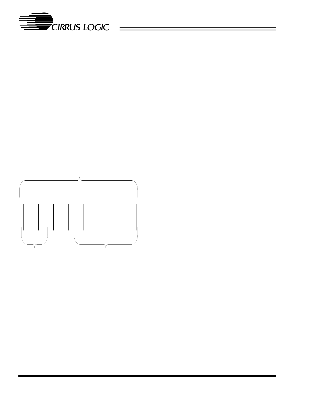
CS8900A
10
3
25
4
76
First Word of a Group of Words
98
BADC
F
E
Number of Words
in Group
0
0
9-bit PacketPage Address
0
Figure 4. Group Header
Crystal LAN™ ISA Ethernet Controller
The first word of each group is referred to as the
Group Header. The Group Header indicates the
number of words in the group and the address of the
PacketPage register into which the first data word
in the group is to be loaded. Any remaining words
in the group are stored in successive PacketPage
registers.
3.4.4.1 Group Header
Bits F through C of the Group Header specify the
number of words in each group that are to be transferred to PacketPage registers (see Figure 4). This
value is two less than the total number of words in
the group, including the Group Header. For example, if bits F through C contain 0001, there are three
words in the group (a Group Header and two words
of configuration data).
3.4.5 Reset Configuration Block Checksum
A checksum is stored in the high byte position of
the word immediately following the last group of
data in the Reset Configuration Block. (The EEPROM address of the checksum value can be determined by dividing the value stored in the Link Byte
by two). The checksum value is the 2’s complement of the 8-bit sum (any carry out of eighth bit is
ignored) of all the bytes in the Reset Configuration
Block, excluding the checksum byte. This sum includes the Reset Configuration Block header at address 00h. Since the checksum is calculated as the
2’s complement of the sum of all preceding bytes in
the Reset Configuration Block, a total of 0 should
result when the checksum value is added to the sum
of the previous bytes.
3.4.6 EEPROM Example
Table 6 shows an example of a Reset Configuration
Block stored in a C46 EEPROM. Note that littleendian word ordering is used, i.e., the least significant word of a multiword datum is located at the
lowest address.
Bits 8 through 0 of the Group Header specify a 9bit PacketPage Address. This address defines the
PacketPage register that will be loaded with the
first word of configuration data from the group.
Bits B though 9 of the Group Header are forced to
0, restricting the destination address range to the
first 512 bytes of PacketPage memory. Figure 4
shows the format of the Group header.
3.4.7 EEPROM Read-out
If the EEDI pin is asserted high at the end of reset,
the CS8900A reads the first word of EEPROM data
by:
1) Asserting EECS
2) Clocking out a Read-Register-00h command
on EEDO (EESK provides a 1MHz serial clock
signal)
3) Clocking the data in on EEDI.
If the EEDI pin is low at the end of the reset signal,
the CS8900A does not perform an EEPROM readout (uses its default configuration).
3.4.7.1 Determining EEPROM Size
The CS8900A determines the size of the EEPROM
by checking the sense of EEDI on the tenth rising
edge of EESK. If EEDI is low, the EEPROM is a
22 DS271PP4
CIRRUS LOGIC PRODUCT DATASHEET
CS8900A
Crystal LAN™ ISA Ethernet Controller
’C46 or ’CS46. If EEDI is high, the EEPROM is a
’C56, ’CS56, ’C66, or ’CS66.
3.4.7.2 Loading Configuration Data
The CS8900A reads in the first word from the EEPROM to determine if configuration data is contained in the EEPROM. If configuration data is not
stored in the EEPROM, the CS8900A terminates
initialization from EEPROM and operates using its
default configuration (See Table 3). If configuration data is stored in EEPROM, the CS8900A automatically loads all configuration data stored in the
Reset Configuration Block into its internal PacketPage registers.
3.4.8 EEPROM Read-out Completion
Once all the configuration data are transferred to
the appropriate PacketPage registers, the CS8900A
performs a checksum calculation to verify the Reset Configuration Blocks data are valid. If the resulting total is 0, the read-out is considered valid.
Otherwise, the CS8900A initiates a partial reset to
restore the default configuration.
If the read-out is valid, the EEPROMOK bit (Register 16, SelfST, bit A) is set. EEPROMOK is
cleared if a checksum error is detected. In this case,
the CS8900A performs a partial reset and is re-
stored to its default. Once initialization is complete
(configuration loaded from EEPROM or reset to
default configuration) the INITD bit is set (Register
16, SelfST, bit 7).
3.5 Programming the EEPROM
After initialization, the host can access the EEPROM through the CS8900A by writing one of
seven commands to the EEPROM Command register (PacketPage base + 0040h). Figure 5 shows the
format of the EEPROM Command register.
3.5.1 EEPROM Commands
The seven commands used to access the EEPROM
are: Read, Write, Erase, Erase/Write Enable,
Erase/Write Disable, Erase-All, and Write-All.
They are described in Table 7.
3.5.2 EEPROM Command Execution
During the execution of a command, the two Opcode bits, followed by the six bits of address (for a
’C46 or ’CS46) or eight bits of address (for a ’C56,
’CS56, ’C66 or ’CS66), are shifted out of the
CS8900A, into the EEPROM. If the command is a
Write, the data in the EEPROM Data register
(PacketPage base + 0042h) follows. If the command is a Read, the data in the specified EEPROM
AD7 - AD0 used with ’C56,
’CS56, ’C66 and ’CS66
FXEXDXCXB
Bit Name Description
[F:B] Reserved
[A] ELSEL External Logic Select: When clear, the EECS pin is used to select the EEPROM.
When set, the ELCS pin is used to select the external LA decode circuit.
[9:8] OP1, OP0 Opcode: Indicates what command is being executed (see next section).
[7:0] AD7 to AD0 EEPROM Address: Address of EEPROM word being accessed.
CIRRUS LOGIC PRODUCT DATASHEET
DS271PP4 23
A98
X ELSEL OP1 OP0
Figure 5. EEPROM Command Register Format
AD7 AD6
5476
AD5 AD4
AD5 - AD0 used with
’C46 and ’CS46
1032
AD1 AD0AD3 AD2
CS8900A
Crystal LAN™ ISA Ethernet Controller
Command Opcode
(bits 9,8)
Read Register 1,0 word address yes all 25 µs
Write Register 0,1 word address yes all 10 ms
Erase Register 1.1 word address no all 10 ms
Erase/Write Enable 0,0 XX11-XXXX no ‘CS46, ‘C46 9 µs
Erase/Write Disable 0,0
0,0
Erase-All Registers 0,0
0,0
Write-All Register 0,0
0,0
location is written into the EEPROM Data register.
If the command is an Erase or Erase-All, no data is
transferred to or from the EEPROM Data register.
Before issuing any command, the host must wait
for the SIBUSY bit (Register 16, SelfST, bit 8) to
EEPROM Address
(bits 7 to 0)
11XX-XXXX no ‘CS56, ‘C56, ‘CS66, ‘C66 9 µs
XX00-XXXX no ‘CS46, ‘C46 9 µs
00XX-XXXX no ‘CS56, ‘C56, ‘CS66, ‘C66 9 µs
XX10-XXXX no ‘CS46, ‘C46 10 ms
10XX-XXXX no ‘CS56, ‘C56, ‘CS66, ‘C66 9 µs
XX01-XXXX yes ‘CS46, ‘C46 10 ms
01XX-XXXX yes ‘CS56, ‘C56, ‘CS66, ‘C66 10 ms
Table 7. EEPROM Commands
Data EEPROM Type Execution
During the Erase command, the CS8900A writes
FFh to the specified EEPROM location. During the
Erase-All command, the CS8900A writes FFh to
all locations.
3.6 Boot PROM Operation
clear. After each command has been issued, the
host must wait again for SIBUSY to clear.
The CS8900A supports an optional Boot PROM
used to store code for remote booting from a net-
3.5.3 Enabling Access to the EEPROM
The Erase/Write Enable command provides protec-
work server.
3.6.1 Accessing the Boot PROM
tion from accidental writes to the EEPROM. The
host must write an Erase/Write Enable command
before it attempts to write to or erase any EEPROM
memory location. Once the host has finished altering the contents of the EEPROM, it must write an
Erase/Write Disable command to prevent unwanted modification of the EEPROM.
To retrieve the data stored in the Boot PROM, the
host issues a Read command to the Boot PROM as
a Memory space access. The CS8900A decodes the
command and drives the CSOUT
pin low, causing
the data stored in the Boot PROM to be shifted into
the bus transceiver. The bus transceiver then drives
the data out onto the ISA bus.
3.5.4 Writing and Erasing the EEPROM
3.6.2 Configuring the CS8900A for Boot PROM
To write data to the EEPROM, the host must exe-
Operation
cute the following series of commands:
Figure 6 shows how the CS8900A should be con-
1) Issue an Erase/Write Enable command.
2) Load the data into the EEPROM Data register.
3) Issue a Write command.
nected to the Boot PROM and ’245 driver. To configure the CS8900A’s internal registers for Boot
PROM operation, the Boot PROM Base Address
must be loaded into the Boot PROM Base Address
4) Issue an Erase/Write Disable command.
register (PacketPage base + 0030h) and the Boot
PROM Address Mask must be loaded into the
Time
CIRRUS LOGIC PRODUCT DATASHEET
24 DS271PP4
CS8900A
Crystal LAN™ ISA Ethernet Controller
BootPROM Address Mask register (PacketPage
base + 0034h). The Boot PROM Base Address provides the starting location in host memory where
the Boot PROM is mapped. The Boot PROM Address Mask indicates the size of the attached Boot
PROM and is limited to 4-Kbyte increments. The
lower 12 bits of the Address Mask are ignored and
should be 000h.
CS8900A
CSOUT
(Pin 17)
27C256
20
CE
22
OE
SA(0:14)
Figure 6. Boot PROM Connection Diagram
19
74LS245
OE
DIR
B1
.
.
.
B8
A1
.
.
.
A8
SD(0:7)
ISA
BUS
In the EEPROM example shown in Table 6, the
Boot PROM starting address is D0000h and the
Address Mask is FC000h. This configuration describes a 16-Kbyte (128 Kbit) PROM mapped into
host memory from D0000h to D3FFFh.
3.7 Low-Power Modes
For power-sensitive applications, the CS8900A
supports three low-power modes: Hardware Standby, Hardware Suspend, and Software Suspend. All
three low-power modes are controlled through the
SelfCTL register (Register 15). See also
Section 4.4.4 on page 48.
An internal reset occurs when the CS8900A comes
out of any suspend or standby mode. After a reset
(internal or external), the CS8900A goes through a
self configuration. This includes calibrating onchip analog circuitry, and reading EEPROM for validity and configuration. When the calibration is
done, bit InitD in Register 16 (Self Status register)
is set indicating that initialization is complete, and
the SIBUSY bit in the same register is cleared (in-
dicating that the EEPROM is no longer being read
or programmed. Time required for the reset calibration is typically 10 ms. Software drivers should not
access registers internal to CS8900A during this
time.
3.7.1 Hardware Standby
Hardware (HW) Standby is designed for use in systems, such as portable PC’s, that may be temporarily disconnected from the 10BASE-T cable. It
allows the system to conserve power while the
LAN is not in use, and then automatically restore
Ethernet operation once the cable is reconnected.
In HW Standby mode, all analog and digital circuitry in the CS8900A is turned off, except for the
10BASE-T receiver which remains active to listen
for link activity. If link activity is detected, the
LANLED
pin is driven low, providing an indication to the host that the network connection is active. The host can then activate the CS8900A by
deasserting the SLEEP pin. During this mode, all
ISA bus accesses are ignored.
To enter HW Standby mode, the SLEEP pin must
be low and the HWSleepE bit (Register 15, SelfCTL, Bit 9) and the HWStandbyE bit (Register 15,
SelfCTL, Bit A) must be set. When the CS8900A
enters HW Standby, all registers and circuits are reset except for the SelfCTL register. Upon exit from
HW Standby, the CS8900A performs a complete
reset, and then goes through normal initialization.
3.7.2 Hardware Suspend
During Hardware Suspend mode, the CS8900A
uses the least amount of current of the three lowpower modes. All internal circuits are turned off
and the CS8900A’s core is electronically isolated
from the rest of the system. Accesses from the ISA
bus and Ethernet activity are both ignored.
HW Suspend mode is entered by driving the
SLEEP pin low and setting the HWSleepE bit
(Register 15, SelfCTL, bit 9) while the HWStandbyE bit (Register 15, SelfCTL, bit A) is clear. To
CIRRUS LOGIC PRODUCT DATASHEET
DS271PP4 25
CS8900A
Crystal LAN™ ISA Ethernet Controller
exit from this mode, the SLEEP pin must be driven
high. Upon exit, the CS8900A performs a complete
reset, and then goes through a normal initialization
procedure.
3.7.3 Software Suspend
To enter SW Suspend mode, the host must set the
SWSuspend bit (Register 15, SelfCTL, bit 8). To
exit SW Suspend, the host must write to the
CS8900A’s assigned I/O space (the Write is only
used to wake the CS8900A, the Write itself is ignored). Upon exit, the CS8900A performs a com-
Software (SW) Suspend mode can be used to conserve power in applications, like adapter cards, that
plete reset, and then goes through a normal
initialization procedure.
do not have power management circuitry available.
During this mode, all internal circuits are shut off
except the I/O Base Address register (PacketPage
base + 0020h) and the SelfCTL register (Register
15).
CS8900A Configuration CS8900A Operation
SLEEP
(Pin 77)
Low to
HWStandbyE
(SelfCTL, Bit A)
Low 1 1 N/A Not Present HW Standby mode: 10BASE-T
Low 1 1 N/A Present HW Standby mode: LANLED
Low 0 1 N/A N/A HW Suspend mode
N/A 1 0 N/A CS8900A resets and goes through
High
High N/A N/A 0 N/A Not in low-power mode
High N/A N/A N/A SW Suspend mode
Low N/A 0 1 N/A SW Suspend mode
Low N/A 0 0 N/A Not in low-power mode
HWSleepE
(SelfCTL, Bit 9)
SWSuspend
(SelfCTL, Bit 8) Link Activity
Any hardware reset takes the chip out of any sleep
mode.
Table 8 summarizes the operation of the three lowpower modes.
receiver listens for link activity
initialization
low
Notes: 1. Both HW and HW Suspend take precedence over SW Suspend.
Table 8. Low-Power Mode Operation
CIRRUS LOGIC PRODUCT DATASHEET
26 DS271PP4
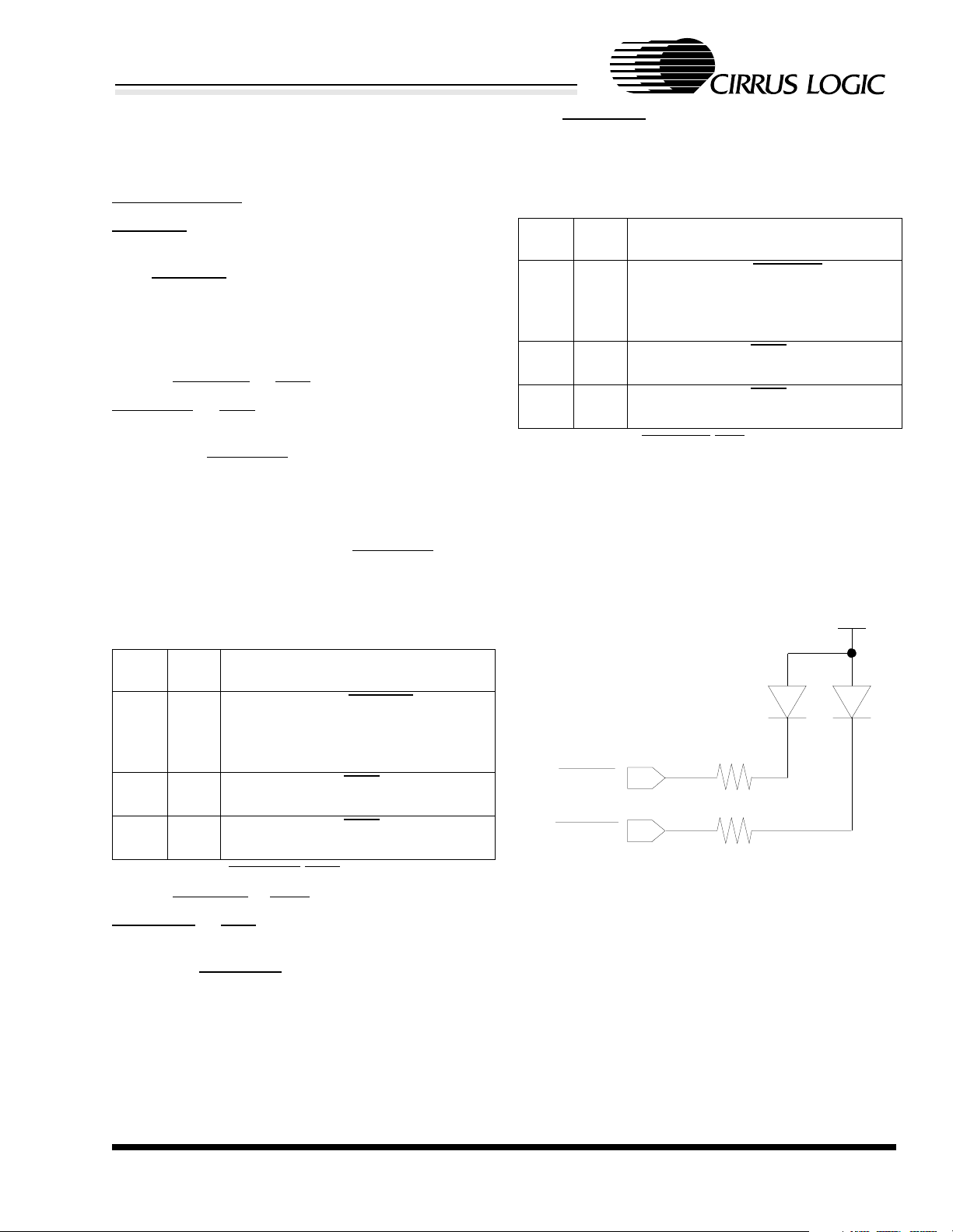
CS8900A
Crystal LAN™ ISA Ethernet Controller
3.8 LED Outputs
The CS8900A provides three output pins that can
be used to control LEDs or external logic.
3.8.0.1 LANLED
LANLED goes low whenever the CS8900A transmits or receives a frame, or when it detects a collision. LANLED remains low until there has been no
activity for 6 ms (i.e. each transmission, reception,
or collision produces a pulse lasting a minimum of
6 ms).
3.8.0.2 LINKLED
or HC0
LINKLED or HC0 can be controlled by either the
CS8900A or the host. When controlled by the
CS8900A, LINKLED is low whenever the
CS8900A receives valid 10BASE-T link pulses. To
configure this pin for CS8900A control, the HC0E
bit (Register 15, SelfCTL, Bit C) must be clear.
When controlled by the host, LINKLED is low
whenever the HCB0 bit (Register 15, SelfCTL, Bit
E) is set. To configure it for host control, the HC0E
bit must be set. Table 9 summarizes this operation.
host, BSTATUS
is low whenever the HCB1 bit
(Register 15, SelfCTL, Bit F) is set. To configure it
for host control, HC1E must be set. Table 10 summarizes this operation.
HC1E
(Bit D)
HCB1
(Bit F)
0N/A
10
11
Table 10. BSTATUS/HCI Pin Operation
Pin configured as BSTATUS
low when a receive frame begins transfer across the ISA bus. Output is high
otherwise
Pin configured as HC1
Output is high
Pin configured as HC1
Output is low
Pin Function
: Output is
:
:
3.8.1 LED Connection
Each LED output is capable of sinking 10 mA to
drive an LED directly through a series resistor. The
output voltage of each pin is less than 0.4 V when
the pin is low. Figure 7 shows a typical LED circuit.
+5V
HC0E
(Bit C)
HCB0
(Bit E)
0N/A
10
11
Table 9. LINKLED/HC0 Pin Operation
Pin configured as LINKLED
low when valid 10BASE-T link pulses
are detected. Output is high if valid link
pulses are not detected
Pin configured as HC0
Output is high
Pin configured as HC0
Output is low
Pin Function
: Output is
:
:
3.8.0.3 BSTATUS or HC1
BSTATUS or HC1 can be controlled by either the
CS8900A or the host. When controlled by the
CS8900A, BSTATUS is low whenever the host
reads the RxEvent register (PacketPage base +
0124h), signaling the transfer of a receive frame
across the ISA bus. To configure this pin for
CS8900A control, the HC1E bit (Register 15, SelfCTL, Bit D) must be clear. When controlled by the
LANLED
LINKLED
Figure 7. LED Connection Diagram
3.9 Media Access Control
3.9.1 Overview
The CS8900A’s Ethernet Media Access Control
(MAC) engine is fully compliant with the IEEE
802.3 Ethernet standard (ISO/IEC 8802-3, 1993). It
handles all aspects of Ethernet frame transmission
and reception, including: collision detection, preamble generation and detection, and CRC genera-
CIRRUS LOGIC PRODUCT DATASHEET
DS271PP4 27
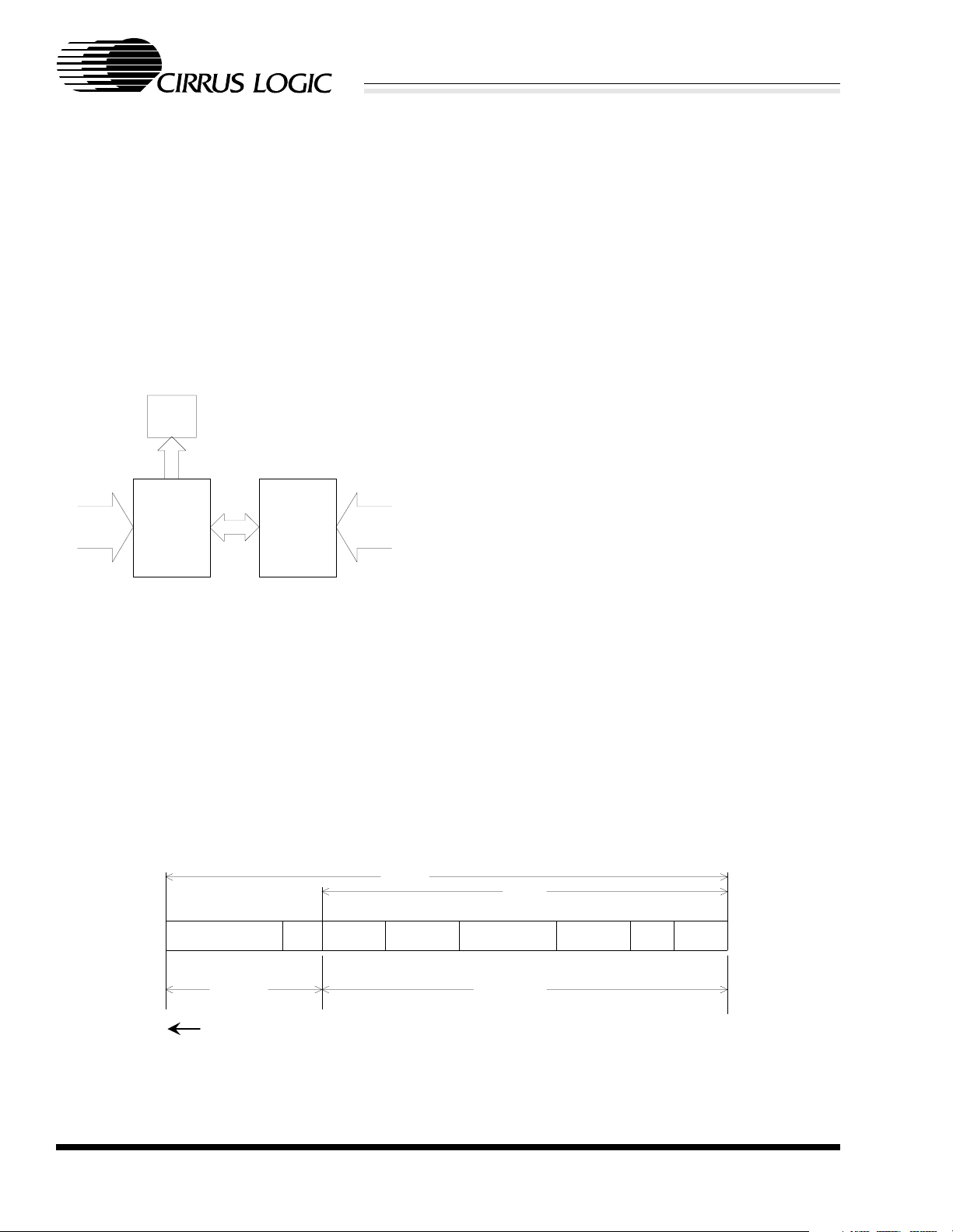
CS8900A
802.3
MAC
Engine
Encoder/
Decoder
&
PLL
LED
Logic
CS8900A
Internal Bus
10BASE-T
& AUI
Figure 8. MAC Interface
Crystal LAN™ ISA Ethernet Controller
tion and test. Programmable MAC features include
automatic retransmission on collision, and padding
of transmitted frames.
Figure 8 shows how the MAC engine interfaces to
other CS8900A functions. On the host side, it interfaces to the CS8900A’s internal data/address/control bus. On the network side, it interfaces to the
internal Manchester encoder/decoder (ENDEC).
The primary functions of the MAC are: frame encapsulation and decapsulation; error detection and
handling; and, media access management.
3.9.2 Frame Encapsulation and Decapsulation
The CS8900A’s MAC engine automatically assembles transmit packets and disassembles receive
packets. It also determines if transmit and receive
frames are of legal minimum size.
3.9.2.1 Transmission
Once the proper number of bytes have been transferred to the CS8900A’s memory (either 5, 381,
Packet
1 byteup to 7 bytes 6 bytes 6 bytes 2 bytes
1021 bytes, or full frame), and providing that access to the network is permitted, the MAC automatically transmits the 7-byte preamble (1010101b...),
followed by the Start-of-Frame Delimiter (SFD,
10101011b), and then the serialized frame data. It
then transmits the Frame Check Sequence (FCS).
The data after the SFD and before the FCS (Destination Address, Source Address, Length, and data
field) is supplied by the host. FCS generation by the
CS8900A may be disabled by setting the InhibitCRC bit (Register 9, TxCMD, bit C).
Figure 9 shows the Ethernet frame format.
3.9.2.2 Reception
The MAC receives the incoming packet as a serial
stream of NRZ data from the Manchester encoder/decoder. It begins by checking for the SFD.
Once the SFD is detected, the MAC assumes all
subsequent bits are frame data. It reads the DA and
compares it to the criteria programmed into the address filter (see Section 5.3 on page 86 for a description of Address Filtering). If the DA passes the
address filter, the frame is loaded into the
CS8900A’s memory. If the BufferCRC bit (Register 3, RxCFG, bit B) is set, the received FCS is also
loaded into memory. Once the entire packet has
been received, the MAC validates the FCS. If an error is detected, the CRCerror bit (Register 4, RxEvent, Bit C) is set.
3.9.2.3 Enforcing Minimum Frame Size
The MAC provides minimum frame size enforce-
Frame
4 bytes
alternating 1s / 0s
preamble
Direction of Transmission
28 DS271PP4
SFD = Start of Frame Delimiter
DA = Destination Address
SA = Source Address
SFD
CIRRUS LOGIC PRODUCT DATASHEET
DA
Figure 9. Ethernet Frame Format
SA
Length Field
frame length
min 64 bytes
max 1518 bytes
LLC = Logical Link Control
FCS = Frame Check Sequence (also
called Cyclic Redundancy Check, or CRC)
LLC data Pad
FCS

CS8900A
Crystal LAN™ ISA Ethernet Controller
ment of both transmit and receive packets. When
the TxPadDis bit (Register 9, TxCMD, Bit D) is
clear, transmit frames will be padded with additional bits to ensure that the receiving station receives a
legal frame (64 bytes, including CRC). When TxPadDis is set, the CS8900A will not add pad bits
and will transmit frames less that 64 bytes. If a
frame is received that is less than 64 bytes (including CRC), the Runt bit (Register 4, RxEvent, Bit D)
will be set indicating the arrival of an illegal frame.
3.9.3 Transmit Error Detection and Handling
The MAC engine monitors Ethernet activity and
reports and recovers from a number of error conditions. For transmission, the MAC reports the following errors in the TxEvent register (Register 8)
and BufEvent register (Register C):
3.9.3.1 Loss of Carrier
Whenever the CS8900A is transmitting on the AUI
port, it expects to see its own transmission "looped
back" to its receiver. If it is unable to monitor its
transmission after the end of the preamble, the
MAC reports a loss-of-carrier error by setting the
Loss-of-CRS bit (Register 8, TxEvent, Bit 6). If the
Loss-of-CRSiE bit (Register 7, TxCFG, Bit 6) is
set, the host will be interrupted.
3.9.3.2 SQE Error
After the end of transmission on the AUI port, the
MAC expects to see a collision within 64 bit times.
If no collision is detected, the SQEerror bit (Register 8, TxEvent, Bit 7) is set. If the SQEerroriE bit is
set (Register 7, TxCFG, Bit 7), the host is interrupted. An SQE error may indicate a fault on the AUI
cable or a faulty transceiver (it is assumed that the
attached transceiver supports this function).
3.9.3.3 Out-of-Window (Late) Collision
If a collision is detected after the first 512 bits have
been transmitted, the MAC reports a late collision
by setting the Out-of-window bit (Register 8, TxEvent, Bit 9). The MAC then forces a bad CRC and
terminates the transmission. If the Out-of-window-
iE bit (Register 7, TxCFG, Bit 9) is set, the host is
interrupted. A late collision may indicate an illegal
network configuration.
3.9.3.4 Jabber Error
If a transmission continues longer than about
26 ms, the MAC disables the transmitter and sets
the Jabber bit (Register 8, TxEvent, Bit A). The
output of the transmitter returns to idle and remains
there until the host issues a new Transmit Command. If the JabberiE bit (Register 7, TxCFG, Bit
A) is set, the host is interrupted. A Jabber condition
indicates that there may be something wrong with
the CS8900A transmit function. To prevent possible network faults, the host should clear the transmit buffer. Possible options include:
Reset the chip with either software or hardware reset (see Section 3.3 on page 18).
Issue a Force Transmit Command by setting the
Force bit (Register 9, TxCMD, bit 8).
Issue a Transmit Command with the TxLength
field set to zero.
3.9.3.5 Transmit Collision
The MAC counts the number of times an individual
packet must be retransmitted due to network collisions. The collision count is stored in bits B
through E of the TxEvent register (Register 8). If
the packet collides 16 times, transmission of that
packet is terminated and the 16coll bit (Register 8,
TxEvent, Bit F) is set. If the 16colliE bit (Register
7, TxCFG, Bit F) is set, the host will be interrupted
on the 16th collision. A running count of transmit
collisions is recorded in the TxCOL register.
3.9.3.6 Transmit Underrun
If the CS8900A starts transmission of a packet but
runs out of data before reaching the end of frame,
the TxUnderrun bit (Register C, BufEvent, Bit 9) is
set. The MAC then forces a bad CRC and terminates the transmission. If the TxUnderruniE bit
CIRRUS LOGIC PRODUCT DATASHEET
DS271PP4 29

CS8900A
Crystal LAN™ ISA Ethernet Controller
(Register B, BufCFG, Bit 9) is set, the host is interrupted.
3.9.4 Receive Error Detection and Handling
The following receive errors are reported in the RxEvent register (Register 4):
3.9.4.1 CRC Error
If a frame is received with a bad CRC, the CRCerror bit (Register 4, RxEvent, Bit C) is set. If the
CRCerrorA bit (Register 5, RxCTL, Bit C) is set,
the frame will be buffered by CS8900A. If the
CRCerroriE bit (Register 3, RxCFG. Bit C) is set,
the host is interrupted.
3.9.4.2 Runt Frame
If a frame is received that is shorter than 64 bytes,
the Runt bit (Register 4, RxEvent, Bit D) is set. If
the RuntA bit (Register 5, RxCTL, Bit D) is set, the
frame will still be buffered by CS8900A. If the
RuntiE bit (Register 3, RxCFG. Bit D) is set, the
host is interrupted.
3.9.4.3 Extra Data
If a frame is received that is longer than 1518 bytes,
the Extradata bit (Register 4, RxEvent, Bit E) is set.
If the ExtradataA bit (Register 5, RxCTL, Bit E) is
set, the first 1518 bytes of the frame will still be
buffered by CS8900A. If the ExtradataiE bit (Register 3, RxCFG. Bit E) is set, the host is interrupted.
3.9.4.4 Dribble Bits and Alignment Error
Under normal operating conditions, the MAC may
detect up to 7 additional bits after the last full byte
of a receive packet. These bits, known as dribble
bits, are ignored. If dribble bits are detected, the
Dribblebit bit (Register 4, RxEvent, Bit 7) is set. If
both the Dribblebits bit and CRCerror bit
(Register 4, RxEvent, Bit C) are set at the same
time, an alignment error has occurred.
3.9.5 Media Access Management
The Ethernet network topology is a single shared
medium with several attached stations. The Ether-
net protocol is designed to allow each station equal
access to the network at any given time. Any node
can attempt to gain access to the network by first
completing a deferral process (described below) after the last network activity, and then transmitting a
packet that will be received by all other stations. If
two nodes transmit simultaneously, a collision occurs and the colliding packets are corrupted. Two
primary tasks of the MAC are to avoid network collisions, and then recover from them when they occur. In addition, when the CS8900A is using the
AUI, the MAC must support the SQE Test function
described in section 7.2.4.6 of the Ethernet standard.
3.9.5.1 Collision Avoidance
The MAC continually monitors network traffic by
checking for the presence of carrier activity (carrier
activity is indicated by the assertion of the internal
Carrier Sense signal generated by the ENDEC). If
carrier activity is detected, the network is assumed
busy and the MAC must wait until the current
packet is finished before attempting transmission.
The CS8900A supports two schemes for determining when to initiate transmission: Two-Part Deferral, and Simple Deferral. Selection of the deferral
scheme is determined by the 2-partDefDis bit
(Register 13, LineCTL, Bit D). If the 2-partDefDis
bit is clear, the MAC uses a two-part deferral process defined in section 4.2.3.2.1 of the Ethernet
standard (ISO/IEC 8802-3, 1993). If the 2-partDefDis bit is set, the MAC uses a simplified deferral
scheme. Both schemes are described below:
3.9.5.2 Two-Part Deferral
In the two-part deferral process, the 9.6 µs Inter
Packet Gap (IPG) timer is started whenever the internal Carrier Sense signal is deasserted. If activity
is detected during the first 6.4 µs of the IPG timer,
the timer is reset and then restarted once the activity has stopped. If there is no activity during the first
6.4 µs of the IPG timer, the IPG timer is allowed to
time out (even if network activity is detected during
CIRRUS LOGIC PRODUCT DATASHEET
30 DS271PP4
 Loading...