

Page 1
CS8900A
EEPROM
RJ-45 10BASE-T
Attachment
Unit
Interface
(AUI)
20 MHz
XTAL
RAM
Bus
Logic
Memory
Manager
802.3
MAC
Engine
EEPROM
Control
Encoder/
Decoder
&
PLL
10BASE-T
RX Filters &
Receiver
10BASE-T
TX Filters &
Transmitter
AUI
Transmitter
AUI
Collision
AUI
Receiver
Clock
Power
Manager
Boundary
Scan
Test Logic
LED
Control
CS8900A ISA Ethernet Controller
Host
Host Bus
Product Data Sheet
FEATURES
Single-Chip IEEE 802.3 Ethernet Controller with
Direct ISA-Bus Interface
Maximum Current Consumption = 55 mA (5V
Supply
3V or 5V Operation
Industrial Temperature Range
Comprehensive Suite of Software Drivers
Available
Efficient PacketPage™ Architecture Operates in
I/O and Memory Space, and as DMA Slave
Full Duplex Operation
On-Chip RAM Buffers Transmit and Receive
Frames
10BASE-T Port with Analog Filters, Provides:
- Automatic Polarity Detection and Correction
AUI Port for 10BASE2, 10BASE5 and 10BASE-F
Programma bl e Tran smi t Featu res :
- Automatic Re-transmission on Collision
- Automatic Padding and CRC Generation
Programmable Receive Features:
- Stream Transfer™ for Reduced CPU Overhead
- Auto-Switch Between DMA and On-Chip Memory
- Early Interrupts for Frame Pre-Processing
- Automatic Rejection of Erroneous Packets
EEPROM Support for Jumperless Configuration
Boot PROM Support for Diskless Systems
Boundary Scan and Loopback Test
LED Drivers for Link Status and LAN Activity
Standby and Suspend Sleep Modes
)
Crystal LAN™ Ethernet
Controller
DESCRIPTION
The CS8900A is a low-cost Ethernet LAN Controller optimized for the Industry Standard Architecture (ISA) bus
and general purpose microcontroller busses. Its highlyintegrated design eliminates the need for costly external
components required by other Ethernet controllers. The
CS8900A includes on-chip RAM, 10BASE-T transmit
and receive filters, and a direct ISA-Bus interface with
24 mA Drivers.
In addition to high integration, the CS8900A offers a
broad range of performance features and configurationoptions. Its unique PacketPage architecture
automatically adapts to changing network traffic patterns and available system resources. The result is
increased system efficiency.
The CS8900A is available in a 100-pin LQFP package
ideally suited for small form-factor, cost-sensitive Ethernet applications. With the CS8900A, system engineers
can design a complete Ethernet circuit that occupies
less than 1.5 square inches (10 sq. cm) of board space.
ORDERING INFORMATION
CS8900A-CQZ 0° to 70° C 5V LQFP-100 Lead free
CS8900A-IQZ -40° to 85° C 5V LQFP-100 Lead fre e
CS8900A-CQ3Z 0° to 70° C 3.3V LQFP-100 Lead free
CS8900A-IQ3Z -40° to 85° C 3.3V LQFP-100 Lead free
CRD8900A-1 Evaluation Kit
Copyright Cirrus Logic, Inc. 2010
(All Rights Reserved)
DS271F5 SEP ‘10
Page 2

TABLE OF CONTENTS
1.0 INTRODUCTION ........... ... ... ... .... ... ... ... .... ...................................... .... ... ....................................8
1.1 General Description ...........................................................................................................8
1.1.1 Direct ISA-Bus Interface .......................................................................................8
1.1.2 Integrated Memory ...............................................................................................8
1.1.3 802.3 Ethernet MAC Engine .................................................................................8
1.1.4 EEPROM Interface ...............................................................................................8
1.1.5 Complete Analog Front End .................................................................................8
1.2 System Applications .................................. ... ....................................... ... .... ... ... ... .... ... .......8
1.2.1 Motherboard LANs .......................... .... ... ... ... .... ...................................... .... ... ... ....8
1.2.2 Ethernet Adapter Cards ........................................................................................9
1.3 Key Features and Benefits ..............................................................................................10
1.3.1 Very Low Cost ........................ ... ... ... .... ... ... ... ....................................... ... .... ........10
1.3.2 High Performance ...................................... ... .... ... ... ....................................... ... ..10
1.3.3 Low Power and Low Noise .................................................................................10
1.3.4 Complete Support ...............................................................................................10
2.0 PIN DESCRIPTION .............................................................................................................12
3.0 FUNCTIONAL DESCRIPTION...............................................................................................17
3.1 Overview ................................................ ... ... .... ... ....................................... ... ... ... ............17
3.1.1 Configuration ............................. ... ... .... ... ....................................... ... ... ... .... ... ... ..17
3.1.2 Packet Transmission ..........................................................................................17
3.1.3 Packet Reception ...............................................................................................17
3.2 ISA Bus Interface ............................................................................................................18
3.2.1 Memory Mode Operation ........... ... ... .... ... ... ... .... ... ... ....................................... ... ..18
3.2.2 I/O Mode Operation ............................................................................................18
3.2.3 Interrupt Request Signals ....................... ... ... .... ... ....................................... ... ... ..18
3.2.4 DMA Signals .......................................................................................................18
3.3 Reset and Initialization .................................................................................................... 19
3.3.1 Reset ................................................................... ... ... ....................................... ..19
3.3.1.1 External Reset, or ISA Reset ...............................................................19
3.3.1.2 Power-Up Reset ............................................. ... ... ...............................19
3.3.1.3 Power-Down Reset ............................ ... ... ... .... ... ... ... ... .... .....................19
3.3.1.4 EEPROM Reset ...................................................................................19
3.3.1.5 Software Initiated Reset .......................................................................19
3.3.1.6 Hardware (HW) Standby or Suspend ......... .... ... ... ... ... .... ... ... ... .... ... ... ..19
3.3.1.7 Software (SW) Suspend ......................................................................19
3.3.2 Allowing Time for Reset Operation .....................................................................20
3.3.3 Bus Reset Considerations ..................................................................................20
3.3.4 Initialization ............. ... ... ... .... ...................................... .... ... ... ... ............................ 20
3.4 Configurations with EEPROM .........................................................................................21
3.4.1 EEPROM Interface .............................................................................................21
3.4.2 EEPROM Memory Organization .........................................................................21
3.4.3 Reset Configuration Block ..................................................................................21
3.4.3.1 Reset Configuration Block Structure ........... .......... ...... .......... .......... .....22
3.4.3.2 Reset Configuration Block Header ......................................................22
3.4.3.3 Determining the EEPROM Type ................. .........................................23
3.4.3.4 Checking EEPROM for presence of Reset Configuration Block ..........23
3.4.3.5 Determining Number of Bytes in the Reset Co nf igu ra tio n Bloc k .........23
3.4.4 Groups of Configuration Data ....... ... .... ... ... ... .... ... ... ....................................... ... ..23
3.4.4.1 Group Header .......................................... ... ....................................... ..23
3.4.5 Reset Configuration Block Checksum ................................................................24
3.4.6 EEPROM Example ........................................................... ..................................24
3.4.7 EEPROM Read-out ............................................................................................24
CS8900A
Crystal LAN™ Ethernet Controller
CIRRUS LOGIC PRODUCT DATASHEET
2 DS271F5
Page 3

CS8900A
Crystal LAN™ Ethernet Controller
3.4.7.1 Determining EEPROM Size .................................................................24
3.4.7.2 Loading Configuration Data ................................. ................................24
3.4.8 EEPROM Read-out Completion .........................................................................24
3.5 Programming the EEPROM ............................................................................................25
3.5.1 EEPROM Commands ........................................................................................25
3.5.2 EEPROM Command Execution .........................................................................25
3.5.3 Enabling Access to the EEPROM ......................................................................26
3.5.4 Writing and Erasing the EEPROM .....................................................................26
3.6 Boot PROM Operation ....................................................................................................26
3.6.1 Accessing the Boot PROM .................................................................................26
3.6.2 Configuring the CS8900A for Boot PROM Operation ........................................26
3.7 Low-Power Modes ..........................................................................................................27
3.7.1 Hardware Standby ..............................................................................................27
3.7.2 Hardware Suspend ...................... ....................... ...................... ....................... ...27
3.7.3 Software Suspend ........................................................... ... ... ... .... ......................27
3.8 LED Outputs ....................................................................................................................29
3.8.1 LANLED ......... ....................................... ... ... .... ... ...................................... .... ... ...29
3.8.2 LINKLED or HC0 ............................ .... ... ... ... .... ... ... ... ....................................... ...29
3.8.3 BSTATUS or HC1 ....... ... ....................................... ... ... .... ... ... ... .... ......................29
3.8.4 LED Connection .................................................................................................29
3.9 Media Access Control .....................................................................................................29
3.9.1 Overview .. ... ... ... .... ... ... ... ....................................... ... ... .......................................29
3.9.2 Frame Encapsulation and Decapsulation ...........................................................30
3.9.2.1 Transmission ............. ... ... .... ... ... ... ....................................... ... ... .... ... ...30
3.9.2.2 Reception ........................ .... ... ....................................... ... ... ... ... .... ......30
3.9.2.3 Enforcing Minimum Frame Size ..........................................................31
3.9.3 Transmit Error Detection and Handling .... ... .... ... ... ... ... .... ... ... .............................31
3.9.3.1 Loss of Carrier ........ ... ... ... .... ...................................... .... ... ... ... .............31
3.9.3.2 SQE Error ........ ... .... ... ... ....................................... ... ... .... ... ...................31
3.9.3.3 Out-of-Window (Late) Collision .................. ... .... ... ... ... .... ... ... ... .............31
3.9.3.4 Jabber Error ........................................................................................31
3.9.3.5 Transmit Collision ...... ... ... .... ... ... ....................................... ... ... ... .... ... ...31
3.9.3.6 Transmit Underrun ..............................................................................32
3.9.4 Receive Error Detection and Handling ...............................................................32
3.9.4.1 CRC Error .. ....................................... ... ... ... ....................................... ...32
3.9.4.2 Runt Frame ............................... ... .... ... ... ... ... .......................................32
3.9.4.3 Extra Data ................................. ... .... ... ...................................... .... ... ...32
3.9.4.4 Dribble Bits and Alignment Error ...................... ...................................32
3.9.5 Media Access Management ...............................................................................32
3.9.5.1 Collision Avoidance ................ ... ... ....................................... ... ... .... ... ...32
3.9.5.2 Two-Part Deferral ......... ... .... ... ... ... .... ...................................... ... .... ......33
3.9.5.3 Simple Deferral .......................... ................................ ..........................33
3.9.5.4 Collision Resolution ... ... ... .... ... ....................................... ... ... ... ... .... ... ...34
3.9.5.5 Normal Collisions ......................... .... ... ... ... ... .... ...................................34
3.9.5.6 Late Collisions ........................................................ ... .... ... ... ................34
3.9.5.7 Backoff ............................ ....................................... .............................34
3.9.5.8 Standard Backoff .......... ... .... ... ... ... .... ...................................... ... .... ... ...34
3.9.5.9 Modified Backoff ..................................... ... ... .......................................35
3.9.5.10 SQE Test ...........................................................................................35
3.10 Encoder/Decoder (ENDEC) ..........................................................................................35
3.10.1 Encoder ............................................................................................................35
3.10.2 Carrier Detection ..............................................................................................36
3.10.3 Clock and Data Recovery .......... ... .... ... ... ....................................... ... ... ... .... ... ...36
CIRRUS LOGIC PRODUCT DATASHEET
DS271F5 3
Page 4

CS8900A
Crystal LAN™ Ethernet Controller
3.10.4 Interface Selection ............................................................................................36
3.10.4.1 10BASE-T Only .................................................................................36
3.10.4.2 AUI Only ............................................................................................36
3.10.4.3 Auto-Select ........................................................................................36
3.11 10BASE-T Transceiver ..................................................................................................36
3.11.1 10BASE-T Filters ..............................................................................................37
3.11.2 Transmitter .......................................................................................................37
3.11.3 Receiver ...........................................................................................................37
3.11.3.1 Squelch Circuit ...................................................................................37
3.11.3.2 Extended Range ................................................................................38
3.11.4 Link Pulse Detection .........................................................................................38
3.11.5 Receive Polarity Detection and Correction .......................................................38
3.11.6 Collision Detection ............................................................................................39
3.12 Attachment Unit Interface (AUI) ....................................................................................39
3.12.1 AUI Transmitter .................................................................................................39
3.12.2 AUI Receiver ................................. .... ... ... ... .... ... ....................................... ... ... ..39
3.12.3 Collision Detection ............................................................................................39
3.13 External Clock Oscillator ...............................................................................................40
4.0 PACKETPAGE ARCHITECTURE..........................................................................................41
4.1 PacketPage Overview .....................................................................................................41
4.1.1 Integrated Memory .............................................................................................41
4.1.2 Bus Interface Registers ......................................................................................41
4.1.3 Status and Control Registers ..............................................................................41
4.1.4 Initiate Transmit Registers ..................................................................................41
4.1.5 Address Filter Registers .....................................................................................41
4.1.6 Receive and Transmit Frame Locations .............................................................41
4.2 PacketPage Memory Map ...............................................................................................42
4.3 Bus Interface Registers ...................................................................................................44
4.4 Status and Control Registers ........... ... ............................................................................49
4.4.1 Configuration and Control Registers ...................................................................49
4.4.2 Status and Event Registers ................................................................................49
4.4.3 Status and Control Bit Definitions .......................................................................50
4.4.3.1 Act-Once Bits .............................. ... .... ... ... ....................................... ... ..50
4.4.3.2 Temporal Bits ........................ ... ....................................... ... ... ... .... ........50
4.4.3.3 Interrupt Enable Bits and Events .........................................................50
4.4.3.4 Accept Bits ............................ ... ....................................... ... ... ...............51
4.4.4 Status and Control Register Summary ...............................................................51
4.5 Initiate Transmit Registers ...............................................................................................69
4.6 Address Filter Registers ..................................................................................................71
4.7 Receive and Transmit Frame Locations ..........................................................................72
4.7.1 Receive PacketPage Locations ..........................................................................72
4.7.2 Transmit Locations .............................................................................................72
4.8 Eight and Sixteen Bit Transfers .......................................................................................72
4.8.1 Transferring Odd-Byte-Aligned Data ..................................................................73
4.8.2 Random Access to CS8900A Memory ...............................................................73
4.9 Memory Mode Operation .................................................................................................73
4.9.1 Accesses in Memory Mode .................................................................................73
4.9.2 Configuring the CS8900A for Memory Mode ......................................................74
4.9.3 Basic Memory Mode Transmit ................... ......................................................... 74
4.9.4 Basic Memory Mode Receive .............................................................................75
4.9.5 Polling the CS8900A in Memory Mode ...............................................................75
4.10 I/O Space Operation ......................................................................................................75
4.10.1 Receive/Transmit Data Ports 0 and 1 ...............................................................75
CIRRUS LOGIC PRODUCT DATASHEET
4 DS271F5
Page 5

CS8900A
Crystal LAN™ Ethernet Controller
4.10.2 TxCMD Port ......................................................................................................75
4.10.3 TxLength Port ......................... .................................................... ...................... 76
4.10.4 Interrupt Status Queue Port .............................................................................76
4.10.5 PacketPage Pointer Port .................................................................................. 76
4.10.6 PacketPage Data Ports 0 and 1 .......................................................................76
4.10.7 I/O Mode Operation ..........................................................................................76
4.10.8 Basic I/O Mode Transmit .................. ... ... ... .... ... ... ....................................... ... ...76
4.10.9 Basic I/O Mode Receive ............... .... ...................................... .... ... ... ... ... .... ......77
4.10.10 Accessing Internal Registers ..........................................................................77
4.10.11 Polling the CS8900A in I/O Mode ...................................................................77
5.0 OPERATION ................................................................... .... ... ... ... ..........................................78
5.1 Managing Interrupts and Servicing the Interrupt Status Queue ......................................78
5.2 Basic Receive Operation ....................... ... ... .... ... ....................................... ... ... ... ... .... ... ...78
5.2.0.1 Overview ............................. ... ... ....................................... ... ... .............78
5.2.1 Terminology: Packet, Frame, and Transfer ..................... ... ... ... .... ... ... ... ... .... ... ...80
5.2.1.1 Packet ............................. ....................................... .............................80
5.2.1.2 Frame ................. .... ... ... ... .... ... ... ... ....................................... ... ... .... ......80
5.2.1.3 Transfer .............. .... ... ... ... .... ... ... ... ....................................... ... ... .... ......80
5.2.2 Receive Configuration ........................................................................................80
5.2.2.1 Configuring the Physical Interface ................ ............................. .......... 81
5.2.2.2 Choosing which Frame Types to Accept ...... .... ... ... ... .... ... ... ... ... .... ... ...81
5.2.2.3 Selecting which Events Cause Interrupts ............................................81
5.2.2.4 Choosing How to Transfer Frames ................................ ... ... ... ... .... ... ...81
5.2.3 Receive Frame Pre-Processing .........................................................................82
5.2.3.1 Destination Address Filtering ..............................................................82
5.2.3.2 Early Interrupt Generation ...................................................................82
5.2.3.3 Acceptance Filtering ............ ... ... ... .... ... ... ... ... .... ...................................83
5.2.3.4 Normal Interrupt Generation ................................... ... .... ... ... ... .............83
5.2.4 Held vs. DMAed Receive Frames ............................ ....................................... ...83
5.2.5 Buffering Held Receive Frames .........................................................................85
5.2.6 Transferring Held Receive Frames ....................................................................85
5.2.7 Receive Frame Visibility .....................................................................................85
5.2.8 Example of Memory Mode Receive Operation ................ ......................... ..........86
5.2.9 Receive Frame Byte Counter .............................................................................86
5.2.10 Receive Frame Address Filtering .....................................................................87
5.2.10.1 Individual Address Frames ................................................................87
5.2.10.2 Multicast Frames ...............................................................................87
5.2.10.3 Broadcast Frames .............................................................................87
5.2.11 Configuring the Destination Address Filter .......................................................87
5.2.12 Hash Filter .............................................................. ... .... ...................................88
5.2.12.1 Hash Filter Operation ........................................................................88
5.2.13 Broadcast Frame Hashing Exception ...............................................................88
5.3 Receive DMA ..................................................................................................................90
5.3.1 Overview .. ... ... ... .... ... ... ... ....................................... ... ... .......................................90
5.3.2 Configuring the CS8900A for DMA Operation ....................................................90
5.3.3 DMA Receive Buffer Size ...................................................................................91
5.3.4 Receive-DMA-Only Operation ........ .... ... ... ... .... ... ... ... ....................................... ...91
5.3.5 Committing Buffer Space to a DMAed Frame ....... ... ... .... ... ... ... ..........................92
5.3.6 DMA Buffer Organization ...................................................................................92
5.3.7 RxDMAFrame Bit ...............................................................................................92
5.3.8 Receive DMA Example Without Wrap-Around ............ ....................................... 92
5.3.9 Receive DMA Operation for RxDMA-Only Mode ...............................................92
5.4 Auto-Switch DMA ............................................................................................................94
CIRRUS LOGIC PRODUCT DATASHEET
DS271F5 5
Page 6

CS8900A
Crystal LAN™ Ethernet Controller
5.4.1 Overview ....................................... ... ....................................... ... .... .....................94
5.4.2 Configuring the CS8900A for Auto-Switch DMA .................................................94
5.4.3 Auto-Switch DMA Operation ...............................................................................94
5.4.4 DMA Channel Speed vs. Missed Frames ...........................................................95
5.4.5 Exit From DMA ...................................................................................................96
5.4.6 Auto-Switch DMA Example .................. ... ... ... ....................................... ...............96
5.5 StreamTransfer ............ ....................................... ... ... .... ... ... ... .... ... ..................................96
5.5.1 Overview ....................................... ... ....................................... ... .... .....................96
5.5.2 Configuring the CS8900A for StreamTransfer ............... ................................ .....96
5.5.3 StreamTransfer Operation ..................................................................................96
5.5.4 Keeping StreamTransfer Mode Active . ... ... ... .... ... ... ... .... .....................................98
5.5.5 Example of StreamTransfer ................................................................................98
5.5.6 Receive DMA Summary .....................................................................................99
5.6 Transmit Operation ..........................................................................................................99
5.6.1 Overview ....................................... ... ....................................... ... .... .....................99
5.6.2 Transmit Configuration .......................................................................................99
5.6.2.1 Configuring the Physical Interface ........... ............................................99
5.6.2.2 Selecting which Events Cause Interrupts ..........................................100
5.6.3 Changing the Configuration ..............................................................................100
5.6.4 Enabling CRC Generation and Padding ...........................................................101
5.6.5 Individual Packet Transmission ........................................................................101
5.6.6 Transmit in Poll Mode .......................................................................................101
5.6.7 Transmit in Interrupt Mode ............... .... ... ... ... .... ...................................... .... ... ...102
5.6.8 Completing Transmission .................................................................................103
5.6.9 Rdy4TxNOW vs. Rdy4Tx ..................................................................................104
5.6.10 Committing Buffer Space to a Transmit Frame ........... ...................................105
5.6.11 Transmit Frame Length ..................................................................................105
5.7 Full duplex Considerations .................................. ... ... .... ... ... ....................................... ...105
5.8 Auto-Negotiation Considerations ...................................................................................105
6.0 TEST....... ... .... ... ....................................... ... ... ... ... ....................................... ... .... ... ................107
6.1 TEST MODES ...............................................................................................................107
6.1.1 Loopback & Collision Diagnostic Tests ................................... ... .... ... ... ... .... ... ...107
6.1.2 Internal Tests .......... ... ... ... .... ...................................... .... ... ... ... .......................... 107
6.1.3 External Tests ...................................................................................................107
6.1.4 Loopback Tests ............................ ... .... ... ... ....................................... ... ... .... ... ...107
6.1.5 10BASE-T Loopback and Collision Tests .........................................................107
6.1.6 AUI Loopback and Collision Tests ....... ... ... ... .... ... ... ... .... ... ... ... ..........................107
6.2 Boundary Scan ..............................................................................................................108
6.2.1 Output Cycle .....................................................................................................108
6.2.2 Input Cycle . ... ... ... .... ... ....................................... ... ... ....................................... ...108
6.2.3 Continuity Cycle ................................................................................................109
7.0 CHARACTERISTICS/SPECIFICATIONS - COMMERCIAL ............................ ...................112
8.0 CHARACTERISTICS/SPECIFICATIONS - INDUSTRIAL ..................................................123
9.0 PHYSICAL DIMENSIONS.......................................... ... ... .... ... ... ... .......................................134
10.0 GLOSSARY OF TERMS....................................................................................................135
10.1 Acronyms ....................................................................................................................135
10.2 Definitions ....................................................................................................................136
10.3 Acronyms Specific to the CS8900A ............................................................................137
10.4 Definitions Specific to the CS8900A ............................................................................137
10.5 Suffixes Specific to the CS8900A. ...............................................................................138
CIRRUS LOGIC PRODUCT DATASHEET
6 DS271F5
Page 7
CS8900A
Contacting Cirrus Logic Support
For all product questions and inquiries contact a Cirrus Logic Sales Representative.
To find one nearest you go to www.cirrus.com
IIMPORTANT NOTICE
Cirrus Logic, Inc. and its subsidiaries ("Cirrus") believe that the information contained in this document is accurate and reliable. However, the informat ion is sub -
ject to change without notice an d is prov ided "AS IS " withou t warra nty of any k ind (exp ress or i mplied ). Customer s are advi sed to obtain the latest version of
relevant information to verify, before plac ing orde rs, that inform ation be ing relie d on is curren t and com plete. All p rodu cts are sold subject to the terms and conditions of sale supplied at the time of order acknowledgment, including those pertaining to warranty, indemnification, and limitation of liability. No responsibility
is assumed by Cirrus for t he use of t his inf ormatio n, inclu ding use of this i nformati on as the b asis for man ufactu re or sale of any i tems, or for inf ringe ment of
patents or other rights of third parties. This document is the property of Cirrus and by f urnishi ng thi s informat ion, Ci rrus gr ants no license, express or implied
under any patents, mask wo r k ri gh t s, cop y ri ght s, t r adema rk s, t r ade s e cre t s or ot h er in tel l ec t ua l pr o per ty r ig ht s . Ci r r us owns t he copyrights associated with the
information containe d her ei n an d gi ve s c ons ent f or c opi es to b e made o f th e i n for mat i on on l y for u se wi t hi n yo ur or gan iz at i on w it h r esp ect t o Ci rrus i nt egra t ed
circuits or other products of Cirrus. T his consen t does not extend to oth er copyin g such a s copying for ge neral d istribution, a dver tising or promo tional p urpos es,
or for creating any work for resale.
CERTAIN APPLICATIONS USING SEMICONDUCTOR PRODUCTS MAY INVOLVE POTENTIAL RISKS OF DEATH, PERSONAL INJURY, OR SEVERE
PROPERTY OR ENVIRONMENTAL DAMAGE ("CRITICAL APPLICATIONS"). CIRRUS PRODUCTS ARE NOT DESIGNED, AUTHORIZED OR WARRANTED
FOR USE IN PRODUCTS SURGICALLY IMPLANTED INTO THE BODY, AUTOMOTIVE SAFETY OR SECURITY DEVICES, LIFE SUPPORT PRODUCTS
OR OTHER CRITICAL APPLICATIONS. INCLUSION OF CIRRUS PRODUCTS IN SUCH APPLICATIONS IS UNDERSTOOD TO BE FULLY AT THE CUSTOMER'S RISK AND CIRRUS DISCLAIMS AND MAKES NO WARRANTY, EXPRESS, STATUTORY OR IMPLIED, INCLUDING THE IMPLIED WARRANTIES
OF MERCHANTABILITY AND FITNESS FOR PARTICULAR PURPOSE, WITH REGARD TO ANY CIRRUS PRODUCT THAT IS USED IN SUCH A MANNER.
IF THE CUSTOMER OR CUSTOMER'S CUSTOMER USES OR PERMITS THE USE OF CIRRUS PRODUCTS IN CRITICAL APPLICATIONS, CUSTOMER
AGREES, BY SUCH USE, TO FULLY INDEMNIFY CIRRUS, ITS OFFICERS, DIRECTORS, EMPLOYEES, DISTRIBUTORS AND OTHER AGENTS FROM
ANY AND ALL LIABILITY, INCLUDING ATTORNEYS' FEES AND COSTS, THAT MAY RESULT FROM OR ARISE IN CONNECTION WITH THESE USES.
Cirrus Logic, Cirrus, the Cirrus Logic logo designs and Crystal LAN are trademarks of Cirrus Logic, Inc. All other brand and product names in this document may
be trademarks or service marks of their respective owners.
I
2
C is a registered trademark of Philips Semiconductor.
Crystal LAN™ Ethernet Controller
Table 1. Revision History
Release Date Changes
PP1 NOV 1997 Preliminary Release, revision 1
PP2 DEC 1998 Preliminary Release, revision 2
PP3 MAR 1999 Preliminary Release, revision 3
PP4 APR 2001 Preliminary Release, revision 4
Page 13: INTRQ[0:2] changed to INTRQ[0..3]
Page 41: Added bit definitions for Revisions C and D
Page 56: PacketPage base + 0218h changed to PacketPage base + 0128h
Page 81: Table 19: Register 5, LRxCTL changed to Register 5, RxCTL
Page 86: Table 23: 0410h to 011h changed to 0410h to 0411h
F1 JAN 2004 Final Release, revision 1
Page 1: Changed package option from TQFP to LQFP.
Page 134: Changed package drawing and from TQFP to LQFP, and updated
dimensions.
F2 JUL 2004 Added ordering information for the -CQ3Z lead free part
F3 SEP2004 Added ordering information for the -CQZ lead free part
F4 AUG 2007 Added industrial temperature range Pb-free devices.
F5 SEP 2010 Page 1: Removed lead-containg device ordering information.Page 112: Updated
Hardware Standby Mode current.
Page 113, 124: Updated Power Supply current & AUI Interface DC characteristics.
Page 119, 130: Updated AUI Interface switching characteristics.
DS271F5 7
CIRRUS LOGIC PRODUCT DATASHEET
Page 8

CS8900A
Crystal LAN™ Ethernet Controller
1.0 INTRODUCTION
1.1 General Description
The CS8900A is a true single-chip, full-duplex,
Ethernet solution, incorporating all of the analog and digital circuitry needed for a complete
Ethernet circuit. Major functional blocks include: a direct ISA-bus interface; an 802.3
MAC engine; integrated buffer memory; a serial EEPROM interface; and a complete analog
front end with both 10BASE-T and AUI.
1.1.1 General Purpose and ISA-Bus Interface
Included in the CS8900A is a direct ISA-bus interface with full 24 mA drive capability. Its configuration options include a choice of four
interrupts and three DMA channels (one of
each selected during initialization). In Memory
Mode, it supports Standard or Ready Bus cycles without introducing additional wait states.
The bus can be configured to support many
microcontroller and microcomputer busses.
tection, preamble generation and detection,
and CRC generation and test. Programmable
MAC features include automatic retransmission on collision, and automatic padding of
transmitted frames.
1.1.4 EEPROM Interface
The CS8900A provides a simple and efficient
serial EEPROM interface that allows configuration information to be stored in an optional
EEPROM, and then loaded automatically at
power-up. This eliminates the need for costly
and cumbersome switches and jumpers.
1.1.5 Complete Analog Front End
The CS8900A’s analog front end incorporates
a Manchester encoder/decoder, clock recovery circuit, 10BASE-T transceiver, and complete Attachment Unit Interface (AUI). It
provides manual and automatic selection of either 10BASE-T or AUI, and offers three onchip LED drivers for link status, bus status, and
Ethernet line activity.
1.1.2 Integrated Memory
The CS8900A incorporates a 4-Kbyte page of
on-chip memory, eliminating the cost and
board area associated with external memory
chips. Unlike most other Ethernet controllers,
the CS8900A buffers entire transmit and receive frames on chip, eliminating the need for
complex, inefficient memory management
schemes. In addition, the CS8900A operates
in either Memory space, I/O space, or with external DMA controllers, providing maximum
design flexibility.
1.1.3 802.3 Ethernet MAC Engine
The CS8900A’s Ethernet Media Access Control (MAC) engine is fully compliant with the
IEEE 802.3 Ethernet standard (ISO/IEC 88023, 1993), and supports full-duplex operation. It
handles all aspects of Ethernet frame transmission and reception, including: collision de-
The 10BASE-T transceiver includes drivers,
receivers, and analog filters, allowing direct
connection to low-cost isolation transformers.
It supports 100, 120, and 150 Ω shielded and
unshielded cables, extended cable lengths,
and automatic receive polarity reversal detection and correction.
The AUI port provides a direct interface to
10BASE-2, 10BASE-5, and 10BASE-FL networks, and is capable of driving a full 50-meter
AUI cable.
1.2 System Applications
The CS8900A is designed to work well in either motherboard or adapter applications.
1.2.1 Motherboard LANs
The CS8900A requires the minimum number
of external components needed for a full
Ethernet node. Its small-footprint package and
CIRRUS LOGIC PRODUCT DATASHEET
8 DS271F5
Page 9
CS8900A
RJ-45
10BASE-T
CS8900A
I
S
A
EEPROM
20 MHz
XTAL
(2.0 sq. in.)
Figure 1. Complete Ethernet Motherboard Solution
CS8900A
EEPROM
Boot PROM
'245
20 MHz
XTAL
RJ-45
LED
Attachment
Unit
Interface
(AUI)
Figure 2. Full-Featured ISA Adapter Solution
Crystal LAN™ Ethernet Controller
high level of integration allow System Engineers to design a complete Ethernet circuit
that occupies as little as 1.5 square inches of
PCB area (Figure 1). In addition, the
CS8900A’s power-saving features and CMOS
design make it a perfect fit for power-sensitive
portable and desktop PCs. Motherboard design options include:
• An EEPROM can be used to store nodespecific information, such as the Ethernet
Individual Address and node configuration.
• The 20 MHz crystal oscillator may be replaced by a 20 MHz clock signal.
1.2.2 Ethernet Adapter Cards
The CS8900A’s highly efficient PacketPage
architecture, with StreamTransfer™ and Auto-
Switch DMA options, make it an excellent
choice for high-performance, low-cost ISA
adapter cards (Figure 2). The CS8900A’s wide
range of configuration options and performance features allow engineers to design
Ethernet solutions that meet their particular
system requirements. Adapter card design options include:
• A Boot PROM can be added to support
diskless applications.
• The 10BASE-T transmitter and receiver
impedance can be adjusted to support 100,
120, or 150 Ohm twisted pair cables.
• An external Latchable-Address-bus decode circuit can be added to operate the
CS8900A in Upper-Memory space.
DS271F5 9
CIRRUS LOGIC PRODUCT DATASHEET
Page 10

CS8900A
Crystal LAN™ Ethernet Controller
• On-chip LED ports can be used for either
optional LEDs, or as programmable outputs.
1.3 Key Features and Benefits
1.3.1 Very Low Cost
The CS8900A is designed to provide the lowest-cost Ethernet solution available for embedded applications, portable motherboards, nonISA bus systems and adapter cards. Cost-saving features include:
• Integrated RAM eliminates the need for expensive external memory chips.
• On-chip 10BASE-T filters allow designers
to use simple isolation transformers instead of more costly filter/transformer
packages.
• The serial EEPROM port, used for configuration and initialization, eliminates the need
for expensive switches and jumpers.
• The CS8900A is designed to be used on a
2-layer circuit board instead of a more expensive multilayer board.
• The 8900A-based solution offers the smallest footprint available, saving valuable
printed circuit board area.
• A set of certified software drivers is available at no charge, eliminating the need for
costly software development.
1.3.2 High Performance
The CS8900A is a full 16-bit Ethernet controller designed to provide optimal system performance by minimizing time on the ISA bus and
CPU overhead per frame. It offers equal or superior performance for less money when compared to other Ethernet controllers. The
CS8900A’s PacketPage architecture allows
software to select whichever access method is
best suited to each particular CPU/ISA-bus
configuration. When compared to older I/O-
space designs, PacketPage is faster, simpler
and more efficient.
To boost performance further, the CS8900A
includes several key features that increase
throughput and lower CPU overhead, including:
• StreamTransfer cuts up to 87% of interrupts to the host CPU during large block
transfers.
• Auto-Switch DMA allows the CS8900A to
maximize throughput while minimizing
missed frames.
• Early interrupts allow the host to preprocess incoming frames.
• On-chip buffering of full frames cuts the
amount of host bandwidth needed to manage Ethernet traffic.
1.3.3 Low Power and Low Noise
For low power needs, the CS8900A offers
three power-down options: Hardware Standby, Hardware Suspend, and Software Suspend. In Standby mode, the chip is powered
down with the exception of the 10BASE-T receiver, which is enabled to listen for link activity. In either Hardware or Software Suspend
mode, the receiver is disabled and power consumption drops to the micro-ampere range.
In addition, the CS8900A has been designed
for very low noise emission, thus shortening
the time required for EMI testing and qualification.
1.3.4 Complete Support
The CS8900A comes with a suite of software
drivers for immediate use with most industry
standard network operating systems. In addition, complete evaluation kits and manufacturing packages are available, significantly
reducing the cost and time required to produce
new Ethernet products.
CIRRUS LOGIC PRODUCT DATASHEET
10 DS271F5
Page 11
CS8900A
EECS
EEDATAOUT
EESK
SA[0:19]
MEMW
MEMR
IOW
IOR
REFRESH
SBHE
SD[0:15]
INTRQ0
INTRQ1
RXD-
RXD+
TXD-
TXD+
DO-
DO+
CI-
CI+
DI-
DI+
LANLED
LINKLED
CSOUT
EEDATAIN
AEN
RESET
INTRQ2
INTRQ3
DMARQ0
DMACK0
DMARQ1
DMACK1
DMARQ2
DMACK2
MEMCS16
IOCHRDY
T
c
1
3
6
8
1%
T
r1
1%
92
91
88
87
100
Ω, 1%
RJ45
16
14
11
9
6
3
2
1
1:1
1
4
5
8
84
82
81
79
16
13
12
9
10
10
9
2
5
83
80
2
7
15 3
12
1:1
1:1
0.1 μF
680
Ω
680
Ω
CE
OE
OE
DIR
20
22
19
1
74LS245
XTAL1XTAL
2
SLEEP TEST RES
CS
DO
DI
CLK
1
3
2
4
3
5
4
6
93C46
28
62
61
29
7
IRQ10
IRQ11
IRQ12
IRQ5
DRQ5
DACK5
DRQ6
DACK6
DRQ7
DACK7
16
20
SA[0:19]
LA[20:23]
BALE
4
97 98 93
4.99 kΩ,1%
12 V
4, 6
20 MHz
0.1 μF
39.2Ω,1%
5V
4.7 k
Ω
CS8900A
CHIPSEL
IOCS16
49
63
75
36
34
64
33
32
30
35
31
15
13
14
16
11
12
99
100
17
39.2Ω,1%
39.2Ω,1%
39.2Ω,1%
EEPROM
Address
Decoder
PAL
27C256
ELCS
ISA
BUS
10 BASE T
Isolation
Transformer
1:1
15 p in D
AUI Isolation
Transformer
BSTATUS/HCI
Boot-PROM
PD[0:7]
SA[0:14]
SD[0:7]
15
8
5V
13
77 76
78
0.1 μF
7
T
r2
TTR
Figure 3. Typical ISA Bus Connection Diagram
5 Volt 3 Volt
TTR 1 : 1.414 1 : 2.5
T
r1
and T
r2
24.3 Ω 8.0 Ω
T
c
69 pF 560 pF
Crystal LAN™ Ethernet Controller
DS271F5 11
CIRRUS LOGIC PRODUCT DATASHEET
Page 12
2.0 PIN DESCRIPTION
36
40
41
4647484950
2627282930
31
333234
35
37
38
39
42
43
44
45
81
82
83
84
85
86
87
88
89
90
91
92
93
94
95
96
97
98
99
100
76
77
78
79
80
2
1
3
16
5
4
6
8
7
9
10
11
12
13
14
15
17
18
20
19
21
22
23
24
53
54
55
56
57
58
59
60
61
62
63
64
51
52
65
66
68
67
69
70
71
72
73
74
75
25
EEDataOut
EESK
EECS
EEDataIn
CHIPSEL
DMACK2
DMACK1
DMACK0
DMARQ2
DMARQ1
DMARQ0
SD15
SD14
SD13
SD12
DVDD2
DVSS2
SD11
CSOUT
SD10
SD08
SA3
SA4
SA15
SA14
AVSS4
BSTATUS or HC1
TXD +
TXD -
AVSS1
AVDD1
RXD -
RXD +
AVSS2
AVDD2
TEST
SLEEP
XTAL1
XTAL2
RES
AVSS3
SA0
INTRQ2
INTRQ1
IOCS16
INTRQ0
MEMCS16
SBHE
SA1
SA2
INTRQ3
SA9
SA10
SA8
SA11
SA5
SA6
SA7
REFRESH
SA19
SA18
SA17
DVDD3
DVSS3
SA16
SD0
AEN
IOW
IOR
IOCHRDY
SD1
SD5
SD4
SD3
SD2
DVSS4
DVDD4
SD6
SD7
LINKLED or HC0
RESET
SA13
MEMW
MEMR
DVSS1
DVDD1
ELCS
AVSS0
DVSS1A
SD09
SA12
DVSS3A
AVDD3
LANLED
DO-
DO+
DI-
DI+
CI-
CI+
CS8900A
100-pin
TQFP
(Q)
Top View
CS8900A
Crystal LAN™ Ethernet Controller
CIRRUS LOGIC PRODUCT DATASHEET
12 DS271F5
Page 13

CS8900A
Crystal LAN™ Ethernet Controller
ISA Bus Interface
SA[0:19] - System Address Bus, Input PINS 37-48, 50-54, 58-60.
Lower 20 bits of the 24-bit System Address Bus used to decode accesses to CS8900A
I/O and Memory space, and attached Boot PROM. SA0-SA15 are used for I/O Read
and Write operations. SA0-SA19 are used in conjunction with external decode logic for
Memory Read and Write operations.
SD[0:15] - System Data Bus, Bi-Directional with 3-State Output PINS 65-68, 71-74, 2724, 21-18.
Bi-directional 16-bit System Data Bus used to transfer data between the CS8900A and
the host.
RESET - Reset, Input PIN 75.
Active-high asynchronous input used to reset the CS8900A. Must be stable for at least
400 ns before the CS8900A recognizes the signal as a valid reset.
AEN - Address Enable, Input PIN 63.
When TEST is high, this active-high input indicates to the CS8900A that the system
DMA controller has control of the ISA bus. When AEN is high, the CS8900A will not
perform slave I/O space operations. When TEST is low, this pin becomes the shift
clock input for the Boundary Scan Test. AEN should be inactive when performing an
IO or memory access and it should be active during a DMA cycle.
MEMR - Memory Read, Input PIN 29.
Active-low input indicates that the host is executing a Memory Read operation.
MEMW - Memory Write, Input PIN 28.
Active-low input indicates that the host is executing a Memory Write operation.
MEMCS16 - Memory Chip Select 16-bit, Open Drain Output PIN 34.
Open-drain, active-low output generated by the CS8900A when it recognizes an
address on the ISA bus that corresponds to its assigned Memory space (CS8900A
must be in Memory Mode with the MemoryE bit (Register 17, BusCTL, Bit A) set for
MEMCS16 to go active). 3-Stated when not active.
REFRESH - Refresh, Input PIN 49.
Active-low input indicates to the CS8900A that a DRAM refresh cycle is in progress.
When REFRESH is low, MEMR, MEMW, IOR, IOW, DMACK0, DMACK1, and
DMACK2 are ignored.
IOR - I/O Read, Input PIN 61.
When IOR is low and a valid address is detected, the CS8900A outputs the contents
of the selected 16-bit I/O register onto the System Data Bus. IOR is ignored if
REFRESH is low.
CIRRUS LOGIC PRODUCT DATASHEET
DS271F5 13
Page 14

Crystal LAN™ Ethernet Controller
IOW - I/O Write, Input PIN 62.
When IOW is low and a valid address is detected, the CS8900A writes the data on the
System Data Bus into the selected 16-bit I/O register. IOW is ignored if REFRESH is
low.
IOCS16 - I/O Chip Select 16-bit, Open Drain Output PIN 33.
Open-drain, active-low output generated by the CS8900A when it recognizes an
address on the ISA bus that corresponds to its assigned I/O space. 3-Stated when not
active.
IOCHRDY - I/O Channel Ready, Open Drain Output PIN 64.
When driven low, this open-drain, active-high output extends I/O Read and Memory
Read cycles to the CS8900A. This output is functional when the IOCHRDYE bit in the
Bus Control register (Register 17) is clear. This pin is always 3-Stated when the
IOCHRDYE bit is set.
SBHE - System Bus High Enable, Input PIN 36.
Active-low input indicates a data transfer on the high byte of the System Data Bus
(SD8-SD15). After a hardware or a software reset, the CS8900A will be in 8-bit mode.
Provide a HIGH to LOW and then LOW to HIGH transition on the SBHE signal before
any 16-bit IO or memory access is done to the CS8900A.
CS8900A
INTRQ[0:3] - Interrupt Request, 3-State PINS 30-32, 35.
Active-high output indicates the presence of an interrupt event. Interrupt Request goes
low once the Interrupt Status Queue (ISQ) is read as all 0's. Only one Interrupt
Request output is used (one is selected during configuration). All non-selected
Interrupt Request outputs are placed in a high-impedance state. (Section 3.2 on
page 18 and Section 5.1 on page 78.)
DMARQ[0:2] - DMA Request, 3-State PINS 11, 13, and 15.
Active-high, 3-Stateable output used by the CS8900A to request a DMA transfer. Only
one DMA Request output is used (one is selected during configuration). All nonselected DMA Request outputs are placed in a high-impedance state.
DMACK
[0:2] - DMA Acknowledge, Input PINS 12, 14, and 16.
Active-low input indicates acknowledgment by the host of the corresponding DMA
Request output.
CHIPSEL - Chip Select, Input PIN 7.
Active-low input generated by external Latchable Address bus decode logic when a
valid memory address is present on the ISA bus. If Memory Mode operation is not
needed, CHIPSEL
should be tied low. The CHIPSEL is ignored for IO and DMA mode
of the CS8900A.
EEPROM and Boot PROM Interface
EESK - EEPROM Serial Clock, PIN 4.
Serial clock used to clock data into or out of the EEPROM.
CIRRUS LOGIC PRODUCT DATASHEET
14 DS271F5
Page 15

CS8900A
Crystal LAN™ Ethernet Controller
EECS - EEPROM Chip Select, PIN 3.
Active-high output used to select the EEPROM.
EEDataIn - EEPROM Data In, Input Internal Weak Pullup PIN 6.
Serial input used to receive data from the EEPROM. Connects to the DO pin on the
EEPROM. EEDataIn is also used to sense the presence of the EEPROM.
ELCS - External Logic Chip Select, Internal Weak Pullup PIN 2.
Bi-directional signal used to configure external Latchable Address (LA) decode logic. If
external LA decode logic is not needed, ELCS should be tied low.
EEDataOut - EEPROM Data Out, PIN 5.
Serial output used to send data to the EEPROM. Connects to the DI pin on the
EEPROM. When TEST
Test.
is low, this pin becomes the output for the Boundary Scan
CSOUT
- Chip Select for External Boot PROM, PIN 17.
Active-low output used to select an external Boot PROM when the CS8900A decodes
a valid Boot PROM memory address.
10BASE-T Interface
TXD+/TXD- - 10BASE-T Transmit, Differential Output Pair PINS 87 and 88.
Differential output pair drives 10 Mb/s Manchester-encoded data to the 10BASE-T
transmit pair.
RXD+/RXD- - 10BASE-T Receive, Differential Input Pair PINS 91 and 92.
Differential input pair receives 10 Mb/s Manchester-encoded data from the 10BASE-T
receive pair.
Attachment Unit Interface (AUI)
DO+/DO- - AUI Data Out, Differential Output Pair PINS 83 and 84.
Differential output pair drives 10 Mb/s Manchester-encoded data to the AUI transmit
pair.
DI+/DI- - AUI Data In, Differential Input Pair PINS 79 and 80.
Differential input pair receives 10 Mb/s Manchester-encoded data from the AUI receive
pair.
CI+/CI- - AUI Collision In, Differential Input Pair PINS 81 and 82.
Differential input pair connects to the AUI collision pair. A collision is indicated by the
presence of a 10 MHz ± 15% signal with duty cycle no worse than 60/40.
CIRRUS LOGIC PRODUCT DATASHEET
DS271F5 15
Page 16

CS8900A
Crystal LAN™ Ethernet Controller
General Pins
XTAL[1:2] - Crystal, Input/Output PINS 97 and 98.
A 20 MHz crystal should be connected across these pins. If a crystal is not used, a 20
MHz signal should be connected to XTAL1 and XTAL2 should be left open. (See
Section 7.3 on page 112 and Section 7.7 on page 122.)
SLEEP - Hardware Sleep, Input Internal Weak Pullup PIN 77.
Active-low input used to enable the two hardware sleep modes: Hardware Suspend
and Hardware Standby. (See Section 3.7 on page 27.)
LINKLED or HC0 - Link Good LED or Host Controlled Output 0, Open Drain Output PIN
99.
When the HCE0 bit of the Self Control register (Register 15) is clear, this active-low
output is low when the CS8900A detects the presence of valid link pulses. When the
HC0E bit is set, the host may drive this pin low by setting the HCBO in the Self
Control register.
BSTATUS or HC1 - Bus Status or Host Controlled Output 1, Open Drain Output PIN 78.
When the HC1E bit of the Self Control register (Register 15) is clear, this active-low
output is low when receive activity causes an ISA bus access. When the HC1E bit is
set, the host may drive this pin low by setting the HCB1 in the Self Control register.
LANLED - LAN Activity LED, Open Drain Output PIN 100.
During normal operation, this active-low output goes low for 6 ms whenever there is a
receive packet, a transmit packet, or a collision. During Hardware Standby mode, this
output is driven low when the receiver detects network activity.
TEST - Test Enable, Input Internal Weak Pullup PIN 76.
Active-low input used to put the CS8900A in Boundary Scan Test mode. For normal
operation, this pin should be high.
RES - Reference Resistor, Input PIN 93.
This input should be connected to a 4.99KΩ ± 1% resistor needed for biasing of
internal analog circuits.
DVDD[1:4] - Digital Power, Power PINS 9, 22, 56, and 69.
Provides 5 V ± 5% power to the digital circuits of the CS8900A.
DVSS[1:4} and DVSS1A, DVSS3A - Digital Ground, Ground PINS 8, 10, 23, 55, 57, and
70.
Provides ground reference (0 V) to the digital circuits of the CS8900A.
AVDD[1:3] - Analog Power, Power PINS 90, 85, and 95.
Provides 5 V ± 5% power to the analog circuits of the CS8900A.
AVSS[0:4] - Analog Ground, Ground PINS 1, 89, 86, 94, 96.
Provide ground reference (0 V) to the analog circuits of the CS8900A.
CIRRUS LOGIC PRODUCT DATASHEET
16 DS271F5
Page 17

CS8900A
Crystal LAN™ Ethernet Controller
3.0 FUNCTIONAL DESCRIPTION
3.1 Overview
During normal operation, the CS8900A performs two basic functions: Ethernet packet
transmission and reception. Before transmission or reception is possible, the CS8900A
must be configured.
3.1.1 Configuration
The CS8900A must be configured for packet
transmission and reception at power-up or reset. Various parameters must be written into
its internal Configuration and Control registers
such as Memory Base Address; Ethernet
Physical Address; what frame types to receive; and which media interface to use. Configuration data can either be written to the
CS8900A by the host (across the ISA bus), or
loaded automatically from an external EEPROM. Operation can begin after configuration is complete.
Section 3.3 on page 19 and Section 3.4 on
page 21 describe the configuration process in
detail. Section 4.4 on page 49 provides a detailed description of the bits in the Configuration and Control Registers.
3.1.2 Packet Transmission
Packet transmission occurs in two phases. In
the first phase, the host moves the Ethernet
frame into the CS8900A’s buffer memory. The
first phase begins with the host issuing a
Transmit Command. This informs the
CS8900A that a frame is to be transmitted and
tells the chip when to start transmission (i.e. after 5, 381, 1021 or all bytes have been transferred) and how the frame should be sent (i.e.
with or without CRC, with or without pad bits,
etc.). The Host follows the Transmit Command
with the Transmit Length, indicating how much
buffer space is required. When buffer space is
available, the host writes the Ethernet frame
into the CS8900A’s internal memory, either as
a Memory or I/O space operation.
In the second phase of transmission, the
CS8900A converts the frame into an Ethernet
packet then transmits it onto the network. The
second phase begins with the CS8900A transmitting the preamble and Start-of-Frame delimiter as soon as the proper number of bytes
has been transferred into its transmit buffer (5,
381, 1021 bytes or full frame, depending on
configuration). The preamble and Start-ofFrame delimiter are followed by the Destination Address, Source Address, Length field
and LLC data (all supplied by the host). If the
frame is less than 64 bytes, including CRC, the
CS8900A adds pad bits if configured to do so.
Finally, the CS8900A appends the proper 32bit CRC value.
The Section 5.6 on page 99 provides a detailed description of packet transmission.
3.1.3 Packet Reception
Like packet transmission, packet reception occurs in two phases. In the first phase, the
CS8900A receives an Ethernet packet and
stores it in on-chip memory. The first phase of
packet reception begins with the receive frame
passing through the analog front end and
Manchester decoder where Manchester data
is converted to NRZ data. Next, the preamble
and Start-of-Frame delimiter are stripped off
and the receive frame is sent through the address filter. If the frame’s Destination Address
matches the criteria programmed into the address filter, the packet is stored in the
CS8900A’s internal memory. The CS8900A
then checks the CRC, and depending on the
configuration, informs the processor that a
frame has been received.
In the second phase, the host transfers the receive frame across the ISA bus and into host
memory. Receive frames can be transferred
CIRRUS LOGIC PRODUCT DATASHEET
DS271F5 17
Page 18
CS8900A
Crystal LAN™ Ethernet Controller
as Memory space operations, I/O space operations, or as DMA operations using host DMA.
Also, the CS8900A provides the capability to
switch between Memory or I/O operation and
DMA operation by using Auto-Switch DMA
and StreamTransfer.
The Section 5.2 on page 78 through
Section 5.5 on page 96 provide a detailed description of packet reception.
3.2 ISA Bus Interface
The CS8900A provides a direct interface to
ISA buses running at clock rates from 8 to 11
MHz. Its on-chip bus drivers are capable of delivering 24 mA of drive current, allowing the
CS8900A to drive the ISA bus directly, without
added external “glue logic”.
The CS8900A is optimized for 16-bit data
transfers, operating in either Memory space,
I/O space, or as a DMA slave.
Note that ISA-bus operation below 8 MHz
should use the CS8900A’s Receive DMA
mode to minimize missed frames. See
Section 5.3 on page 90 for a description of Receive DMA operation.
3.2.1 Memory Mode Operation
When configured for Memory Mode operation,
the CS8900A’s internal registers and frame
buffers are mapped into a contiguous 4-Kbyte
block of host memory, providing the host with
direct access to the CS8900A’s internal registers and frame buffers. The host initiates Read
operations by driving the MEMR pin low and
Write operations by driving the MEMW pin low.
For additional information about Memory
Mode, see Section 4.9 on page 73.
3.2.2 I/O Mode Operation
When configured for I/O Mode operation, the
CS8900A is accessed through eight, 16-bit I/O
ports that are mapped into sixteen contiguous
I/O locations in the host system’s I/O space.
I/O Mode is the default configuration for the
CS8900A and is always enabled.
For an I/O Read or Write operation, the AEN
pin must be low, and the 16-bit I/O address on
the ISA System Address bus (SA0 - SA15)
must match the address space of the
CS8900A. For a Read, IOR must be low, and
for a Write, IOW must be low.
For additional information about I/O Mode, see
Section 4.10 on page 75.
3.2.3 Interrupt Request Signals
The CS8900A has four interrupt request output pins that can be connected directly to any
four of the ISA bus Interrupt Request signals.
Only one interrupt output is used at a time. It is
selected during initialization by writing the interrupt number (0 to 3) into PacketPage Memory base + 0022h. Unused interrupt request
pins are placed in a high-impedance state.
The selected interrupt request pin goes high
when an enabled interrupt is triggered. The pin
goes low after the Interrupt Status Queue
(ISQ) is read as all 0’s (see Section 5.1 on
page 78 for a description of the ISQ).
Table 2 presents one possible way of connecting the interrupt request pins to the ISA bus
that utilizes commonly available interrupts and
facilitates board layout.
CS8900A Interrupt
Request Pin
INTRQ3 (Pin 35) IRQ5 0003h
INTRQ0 (Pin 32) IRQ10 0000h
INTRQ1 (Pin 31) IRQ11 0001h
INTRQ2 (Pin 30) IRQ12 0002h
Table 2. Interrupt Assignments
ISA Bus
Interrupt
PacketPage
base + 0022h
3.2.4 DMA Signals
The CS8900A interfaces directly to the host
DMA controller to provide DMA transfers of receive frames from CS8900A memory to host
CIRRUS LOGIC PRODUCT DATASHEET
18 DS271F5
Page 19

CS8900A
Crystal LAN™ Ethernet Controller
memory. The CS8900A has three pairs of
DMA pins that can be connected directly to the
three 16-bit DMA channels of the ISA bus.
Only one DMA channel is used at a time. It is
selected during initialization by writing the
number of the desired channel (0, 1 or 2) into
PacketPage Memory base + 0024h. Unused
DMA pins are placed in a high-impedance
state. The selected DMA request pin goes
high when the CS8900A has received frames
to transfer to the host memory via DMA. If the
DMABurst bit (register 17, BusCTL, Bit B) is
clear, the pin goes low after the DMA operation
is complete. If the DMABurst bit is set, the pin
goes low 32 µs after the start of a DMA transfer.
The DMA pin pairs are arranged on the
CS8900A to facilitate board layout. Crystal
recommends the configuration in Table 3
when connecting these pins to the ISA bus.
CS8900A DMA
Signal (Pin #)
DMARQ0 (Pin 15) DRQ5 0000h
DMACK0
DMARQ1 (Pin 13) DRQ6 0001h
DMACK1
DMARQ2 (Pin 11) DRQ7 0002h
DMACK2
(Pin 16) DACK5
(Pin 14) DACK6
(Pin 12) DACK7
Table 3. DMA Assignments
ISA DMA
Signal
PacketPage
base + 0024h
For a description of DMA mode, see
Section 5.3 on page 90.
chip-wide reset, all circuitry and registers in
the CS8900A are reset.
3.3.1.2 Power-Up Reset
When power is applied, the CS8900A maintains reset until the voltage at the supply pins
reaches approximately 2.5 V. The CS8900A
comes out of reset once Vcc is greater than
approximately 2.5 V and the crystal oscillator
has stabilized.
3.3.1.3 Power-Down Reset
If the supply voltage drops below approximately 2.5 V, there is a chip-wide reset. The
CS8900A comes out of reset once the power
supply returns to a level greater than approximately 2.5 V and the crystal oscillator has stabilized.
3.3.1.4 EEPROM Reset
There is a chip-wide reset if an EEPROM
checksum error is detected (see Section 3.4
on page 21).
3.3.1.5 Software Initiated Reset
There is a chip-wide reset whenever the RESET bit (Register 15, SelfCTL, Bit 6) is set.
3.3.1.6 Hardware (HW) Standby or Suspend
The CS8900A goes though a chip-wide reset
whenever it enters or exits either HW Standby
mode or HW Suspend mode (see Section 3.7
on page 27 for more information about HW
Standby and Suspend).
3.3 Reset and Initialization
3.3.1 Reset
Seven different conditions cause the
CS8900A to reset its internal registers and circuits.
3.3.1.7 Software (SW) Suspend
Whenever the CS8900A enters SW Suspend
mode, all registers and circuits are reset except for the ISA I/O Base Address register (l ocated at PacketPage base + 0020h) and the
SelfCTL register (Register 15). Upon exit,
3.3.1.1 External Reset, or ISA Reset
There is a chip-wide reset whenever the RESET pin is high for at least 400 ns. During a
CIRRUS LOGIC PRODUCT DATASHEET
DS271F5 19
there is a chip-wide reset (see Section 3.7 on
page 27 for more information about SW Suspend).
Page 20

CS8900A
Crystal LAN™ Ethernet Controller
3.3.2 Allowing Time for Reset Operation
After a reset, the CS8900A goes through a self
configuration. This includes calibrating on-chip
analog circuitry, and reading EEPROM for validity and configuration. Time required for the
reset calibration is typically 10 ms. Software
drivers should not access registers internal to
the CS8900A during this time. When calibration is done, bit INITD in the Self Status Register (register 16) is set indicating that
initialization is complete, and the SIBUSY bit in
the same register is cleared indicating the EEPROM is no longer being read or programmed.
3.3.3 Bus Reset Considerations
After reset, the CS8900A packet page pointer
register (IObase+0Ah) is set to 3000h. The
3000h value can be used as part of the
CS8900A signature when the system scans
for the CS8900A. See Section 4.10 on
page 75.
set (except EEPROM reset). The use of an
EEPROM is optional.
The CS8900A operates with any of six standard EEPROM’s shown in Table 5.
After a reset, the ISA bus outputs INTRx and
DMARQx are 3-Stated, thus avoiding any interrupt or DMA channel conflicts on the ISA
bus at power-up time.
3.3.4 Initialization
After each reset (except EEPROM Reset), the
CS8900A checks the sense of the EEDataIn
pin to see if an external EEPROM is present. If
EEDI is high, an EEPROM is present and the
CS8900A automatically loads the configuration data stored in the EEPROM into its internal registers (see next section). If EEDI is low,
an EEPROM is not present and the CS8900A
comes out of reset with the default configuration shown in Table 4.
A low-cost serial EEPROM can be used to
store configuration information that is automatically loaded into the CS8900A after each re-
CIRRUS LOGIC PRODUCT DATASHEET
20 DS271F5
Page 21
CS8900A
Crystal LAN™ Ethernet Controller
3.4 Configurations with EEPROM
PacketPage
Address
0020h 0300h I/O Base Address*
0022h XXXX XXXX
0024h XXXX XXXX
0026h 0000h DMA Start of Frame
0028h X000h DMA Frame Count
002Ah 0000h DMA Byte Count
002Ch XXX0 0000h Memory Base Address
0030h XXX0 0000h Boot PROM Base
0034h XXX0 0000h Boot PROM Address
0102h 0003h Register 3 - RxCFG
0104h 0005h Register 5 - RxCTL
0106h 0007h Register 7 - TxCFG
0108h 0009h Register 9 - TxCMD
010Ah 000Bh Register B - BufCFG
010Ch Undefined Reserved
010Eh Undefined Reserved
0110h Undefined Reserved
0112h 00013h Register 13 - LineCTL
0114h 0015h Register 15 - SelfCTL
0116h 0017h Register 17 - BusCTL
0118h 0019h Register 19 - TestCTL
* I/O base address is unaffected by Software Suspend mode.
EEPROM Type Size (16-bit words)
‘C46 (non-sequential) 64
‘CS46 (sequential) 64
‘C56 (non-sequential) 128
‘CS56 (sequential) 128
‘C66 (non-sequential) 256
‘CS66 (sequential) 256
Register
Contents
XXXX X100
XXXX XX11
Table 4. Default Configuration
Table 5. Supported EEPROM Types
Register Descriptions
Interrupt Number
DMA Channel
Offset
Address
Mask
3.4.1 EEPROM Interface
The interface to the EEPROM consists of the
four signals shown in Table 6.
CS8900A Pin
(Pin #) CS8900A Function
EECS (Pin 3) EEPROM Chip Select Chip Select
EESK (PIN 4) 1 MHz EEPROM
Serial Clock output
EEDO (Pin 5) EEPROM Data Out
(data to EEPROM)
EEDI (Pin 6) EEPROM Data in
(data from EEPROM)
Table 6. EEPROM Interface
EEPROM
Pin
Clock
Data In
Data Out
3.4.2 EEPROM Memory Organization
If an EEPROM is used to store initial configuration information for the CS8900A, the EEPROM is organized in one or more blocks of
16-bit words. The first block in EEPROM, referred to as the Configuration Block, is used to
configure the CS8900A after reset. An example of a typical Configuration Block is shown in
Table 7. Additional blocks containing user data
may be stored in the EEPROM. However, the
Configuration Block must always start at address 00h and be stored in contiguous memory locations.
3.4.3 Reset Configuration Block
The first block in EEPROM, referred to as the
Reset Configuration Block, is used to automatically program the CS8900A with an initial configuration after a reset. Additional user data
may also be stored in the EEPROM if space is
available. The additional data are stored as
16-bit words and can occupy any EEPROM
address space beginning immediately after
the end of the Reset Configuration Block up to
address 7Fh, depending on EEPROM size.
This additional data can only be accessed
through software control (refer to Section 3.5
on page 25 for more information on accessing
CIRRUS LOGIC PRODUCT DATASHEET
DS271F5 21
Page 22

Crystal LAN™ Ethernet Controller
Word Address Value Description
FIRST WORD in DATA BLOCK
00h A120h Configuration Block Header.
The high byte, A1h, indicates a ‘C46 EEPROM is attached. The Link Byte,
20h, indicates the number of bytes to be used in this block of configuration
data.
FIRST GROUP of WORDS
01h 2020h Group Header for first group of words.
Three words to be loaded, beginning at 0020h in PacketPage memory.
02h 0300h I/O Base Address
03h 0003h Interrupt Number
04h 0001h DMA Channel Number
SECOND GROUP of WORDS
05h 502Ch Group Header for second group of words.
Six words to be loaded, beginning at 002Ch in PacketPage memory.
06h E000h Memory Base Address - low word
07h 000Fh Memory Base Address - high word
08h 0000h Boot PROM Base Address - low word
09h 000Dh Boot PROM Base Address - high word
0Ah C000h Boot PROM Address Mask - low word
0Bh 000Fh Boot PROM Address Mask - high word
THIRD GROUP of WORDS
0Ch 2158h Group Header for third group of words.
Three words to be loaded, beginning at 0158 in PacketPage memory.
0Dh 0010h Individual Address - Octet 0 and 1
0Eh 0000h Individual Address - Octet 2 and 3
0Fh 0000h Individual Address - Octet 4 and 5
CHECKSUM Value
10h 2800h The high byte, 28h, is the Checksum Value. In this example, the checksum
includes word addresses 00h through 0Fh. The hexadecimal sum of the
bytes is D8h, resulting in a 2’s complement of 28h. The low b yte, 00h, pro-
vides a pad to the word boundary.
* FFFFh is a special code indicating that there are no more words in the EEPROM.
Table 7. EEPROM Configuration Block Example
the EEPROM). Address space 80h to AFh is
reserved.
3.4.3.1 Reset Configuration Block Structure
The Reset Configuration Block is a block of
ending with the checksum. Each group of configuration data is used to program a PacketPage register (or set of PacketPage registers
in some cases) with an initial non-default value.
contiguous 16-bit words starting at EEPROM
address 00h. It can be divided into three logical sections: a header, one or more groups of
configuration data words, and a checksum value. All of the words in the Reset Configuration
Block are read sequentially by the CS8900A
3.4.3.2 Reset Configuration Block Header
The header (first word of the block located at
EEPROM address 00h) specifies the type of
EEPROM used, whether or not a Reset Configuration block is present, and if so, how many
after each reset, starting with the header and
CS8900A
CIRRUS LOGIC PRODUCT DATASHEET
22 DS271F5
Page 23

CS8900A
10
3
25
4
76
First Word of a Group of Words
98
BADC
F
E
Number of Words
in Group
0
0
9-bit PacketPage Address
0
Figure 4. Group Header
Crystal LAN™ Ethernet Controller
bytes of configuration data are stored in the
Reset Configuration Block.
3.4.3.3 Determining the EEPROM Type
The LSB of the high byte of the header indicates the type of EEPROM attached: sequential or non-sequential. An LSB of 0 (XXXXXXX0) indicates a sequential EEPROM. An
LSB of 1 (XXXX-XXX1) indicates a non-sequential EEPROM. The CS8900A works
equally well with either type of EEPROM. The
CS8900A will automatically generate sequential addresses while reading the Reset Configuration Block if a non-sequential EEPROM is
used.
3.4.3.4 Checking EEPROM for presence of Reset Configuration Block
The read-out of either a binary 101X-XXX0 or
101X-XXX1 (X = do not care) from the high
byte of the header indicates the presence of
configuration data. Any other readout value
terminates initialization from the EEPROM. If
an EEPROM is attached but not used for configuration, Crystal recommends that the high
byte of the first word be programmed with 00h
in order to ensure that the CS8900A will not attempt to read configuration data from the EEPROM.
data. This Reset Configuration Block occupies
6 bytes (3 words) of EEPROM space (2 bytes
for the header and 4 bytes of configuration data).
3.4.4 Groups of Configuration Data
Configuration data are arranged as groups of
words. Each group contains one or more
words of data that are to be loaded into PacketPage registers. The first word of each group
is referred to as the Group Header. The Group
Header indicates the number of words in the
group and the address of the PacketPage register into which the first data word in the group
is to be loaded. Any remaining words in the
group are stored in successive PacketPage
registers.
3.4.4.1 Group Header
Bits F through C of the Group Header specify
the number of words in each group that are to
be transferred to PacketPage registers (see
Figure 4). This value is two less than the total
number of words in the group, including the
Group Header. For example, if bits F through
C contain 0001, there are three words in the
group (a Group Header and two words of configuration data).
3.4.3.5 Determining Number of Bytes in the Reset Configuration Block
The low byte of the Reset Configuration Block
header is known as the link byte. The value of
the Link Byte represents the number of bytes
of configuration data in the Reset Configuration Block. The two bytes used for the header
are excluded when calculating the Link Byte
value.
For example, a Reset Configuration Block
header of A104h indicates a non-sequential
EEPROM programmed with a Reset Configuration Block containing 4 bytes of configuration
DS271F5 23
CIRRUS LOGIC PRODUCT DATASHEET
Page 24

CS8900A
Crystal LAN™ Ethernet Controller
Bits 8 through 0 of the Group Header specify a
9-bit PacketPage Address. This address defines the PacketPage register that will be loaded with the first word of configuration data from
the group. Bits B though 9 of the Group Header are forced to 0, restricting the destination
address range to the first 512 bytes of PacketPage memory. Figure 4 shows the format of
the Group header.
3.4.5 Reset Configuration Block Checksum
A checksum is stored in the high byte position
of the word immediately following the last
group of data in the Reset Configuration Block.
(The EEPROM address of the checksum value can be determined by dividing the value
stored in the Link Byte by two). The checksum
value is the 2’s complement of the 8-bit sum
(any carry out of eighth bit is ignored) of all the
bytes in the Reset Configuration Block, excluding the checksum byte. This sum includes
the Reset Configuration Block header at address 00h. Since the checksum is calculated
as the 2’s complement of the sum of all preceding bytes in the Reset Configuration Block,
a total of 0 should result when the checksum
value is added to the sum of the previous
bytes.
3.4.6 EEPROM Example
Table 7 shows an example of a Reset Configuration Block stored in a C46 EEPROM. Note
that little-endian word ordering is used, i.e., the
least significant word of a multiword datum is
located at the lowest address.
3.4.7 EEPROM Read-out
mand on EEDO (EESK provides a 1MHz
serial clock signal)
3) Clocking the data in on EEDI.
If the EEDI pin is low at the end of the reset sig-
nal, the CS8900A does not perform an EEPROM read-out (uses its default
configuration).
3.4.7.1 Determining EEPROM Size
The CS8900A determines the size of the EEPROM by checking the sense of EEDI on the
tenth rising edge of EESK. If EEDI is low, the
EEPROM is a ’C46 or ’CS46. If EEDI is high,
the EEPROM is a ’C56, ’CS56, ’C66, or ’CS66.
3.4.7.2 Loading Configuration Data
The CS8900A reads in the first word from the
EEPROM to determine if configuration data is
contained in the EEPROM. If configuration
data is not stored in the EEPROM, the
CS8900A terminates initialization from EEPROM and operates using its default configuration (See Table 4). If configuration data is
stored in EEPROM, the CS8900A automatically loads all configuration data stored in the
Reset Configuration Block into its internal
PacketPage registers.
3.4.8 EEPROM Read-out Completion
Once all the configuration data are transferred
to the appropriate PacketPage registers, the
CS8900A performs a checksum calculation to
verify the Reset Configuration Blocks data are
valid. If the resulting total is 0, the read-out is
considered valid. Otherwise, the CS8900A initiates a partial reset to restore the default configuration.
If the EEDI pin is asserted high at the end of
reset, the CS8900A reads the first word of EEPROM data by:
1) Asserting EECS
If the read-out is valid, the EEPROMOK bit
(Register 16, SelfST, bit A) is set. EEPROMOK is cleared if a checksum error is detected. In this case, the CS8900A performs a
partial reset and is restored to its default. Once
2) Clocking out a Read-Register-00h com-
CIRRUS LOGIC PRODUCT DATASHEET
24 DS271F5
Page 25
CS8900A
FXEXDXCXB
XELSELOP1OP0
A98
AD5 AD4
5476
AD7 AD6
1032
AD1 AD0AD3 AD2
AD5 - AD0 used with
'C46 and 'CS46
AD7 - AD0 used with 'C56,
'CS56, 'C66 and 'CS66
Figure 5. EEPROM Command Register Format
Bit Name Description
[F:B] Reserved
[A] ELSEL External Logic Select: When clear, the EECS pin is used to select the EEPROM.
When set, the ELCS pin is used to select the external LA decode circuit.
[9:8] OP1, OP0 Opcode: Indicates what command is being executed (see next section).
[7:0] AD7 to AD0 EEPROM Address: Address of EEPROM word being accessed.
Crystal LAN™ Ethernet Controller
initialization is complete (configuration loaded
from EEPROM or reset to default configuration) the INITD bit is set (Register 16, SelfST,
bit 7).
3.5 Programming the EEPROM
After initialization, the host can access the EEPROM through the CS8900A by writing one of
seven commands to the EEPROM Command
Command Opcode
(bits 9,8)
Read Register 1,0 word address yes all 25 µs
Write Register 0,1 word address yes all 10 ms
Erase Register 1.1 word address no all 10 ms
Erase/Write Enable 0,0 XX11-XXXX no ‘CS46, ‘C46 9 µs
Erase/Write Disable 0,0
0,0
Erase-All Registers 0,0
0,0
Write-All Register 0,0
0,0
EEPROM Address
(bits 7 to 0)
11XX-XXXX no ‘CS56, ‘C56, ‘CS66, ‘C66 9 µs
XX00-XXXX no ‘CS46, ‘C46 9 µs
00XX-XXXX no ‘CS56, ‘C56, ‘CS66, ‘C66 9 µs
XX10-XXXX no ‘CS46, ‘C46 10 ms
10XX-XXXX no ‘CS56, ‘C56, ‘CS66, ‘C66 9 µs
XX01-XXXX yes ‘CS46, ‘C46 10 ms
01XX-XXXX yes ‘CS56, ‘C56, ‘CS66, ‘C66 10 ms
Table 8. EEPROM Commands
register (PacketPage base + 0040h). Figure 5
shows the format of the EEPROM Command
register.
3.5.1 EEPROM Commands
The seven commands used to access the EEPROM are: Read, Write, Erase, Erase/Write
Enable, Erase/Write Disable, Erase-All, and
Write-All. They are described in Table 8.
Data EEPROM Type Execution
Time
3.5.2 EEPROM Command Execution
During the execution of a command, the two
DS271F5 25
CIRRUS LOGIC PRODUCT DATASHEET
Opcode bits, followed by the six bits of address
(for a ’C46 or ’CS46) or eight bits of address
Page 26
CS8900A
OE
DIR
B1
.
.
.
B8
A1
.
.
.
A8
74LS245
SD(0:7)
ISA
BUS
SA(0:14)
27C256
CE
OE
20
22
19
CS8900A
CSOUT
(Pin 17)
Figure 6. Boot PROM Connection Diagram
Crystal LAN™ Ethernet Controller
(for a ’C56, ’CS56, ’C66 or ’CS66), are shifted
out of the CS8900A, into the EEPROM. If the
command is a Write, the data in the EEPROM
Data register (PacketPage base + 0042h) follows. If the command is a Read, the data in the
specified EEPROM location is written into the
EEPROM Data register. If the command is an
Erase or Erase-All, no data is transferred to or
from the EEPROM Data register. Before issuing any command, the host must wait for the
SIBUSY bit (Register 16, SelfST, bit 8) to
clear. After each command has been issued,
the host must wait again for SIBUSY to clear.
3.5.3 Enabling Access to the EEPROM
The Erase/Write Enable command provides
protection from accidental writes to the EEPROM. The host must write an Erase/Write
Enable command before it attempts to write to
or erase any EEPROM memory location.
Once the host has finished altering the contents of the EEPROM, it must write an
Erase/Write Disable command to prevent unwanted modification of the EEPROM.
3.5.4 Writing and Erasing the EEPROM
To write data to the EEPROM, the host must
execute the following series of commands:
1) Issue an Erase/Write Enable command.
3.6.1 Accessing the Boot PROM
To retrieve the data stored in the Boot PROM,
the host issues a Read command to the Boot
PROM as a Memory space access. The
CS8900A decodes the command and drives
the CSOUT pin low, causing the data stored in
the Boot PROM to be shifted into the bus
transceiver. The bus transceiver then drives
the data out onto the ISA bus.
3.6.2 Configuring the CS8900A for Boot PROM Operation
Figure 6 shows how the CS8900A should be
connected to the Boot PROM and ’245 driver.
To configure the CS8900A’s internal registers
for Boot PROM operation, the Boot PROM
Base Address must be loaded into the Boot
PROM Base Address register (PacketPage
base + 0030h) and the Boot PROM Address
Mask must be loaded into the BootPROM Address Mask register (PacketPage base +
0034h). The Boot PROM Base Address provides the starting location in host memory
where the Boot PROM is mapped. The Boot
PROM Address Mask indicates the size of the
attached Boot PROM and is limited to 4-Kbyte
increments. The lower 12 bits of the Address
Mask are ignored and should be 000h.
2) Load the data into the EEPROM Data register.
3) Issue a Write command.
4) Issue an Erase/Write Disable command.
During the Erase command, the CS8900A
writes FFh to the specified EEPROM location.
During the Erase-All command, the CS8900A
writes FFh to all locations.
3.6 Boot PROM Operation
The CS8900A supports an optional Boot
PROM used to store code for remote booting
from a network server.
26 DS271F5
In the EEPROM example shown in Table 7,
the Boot PROM starting address is D0000h
CIRRUS LOGIC PRODUCT DATASHEET
Page 27

CS8900A
Crystal LAN™ Ethernet Controller
and the Address Mask is FC000h. This configuration describes a 16-Kbyte (128 Kbit) PROM
mapped into host memory from D0000h to
D3FFFh.
3.7 Low-Power Modes
For power-sensitive applications, the
CS8900A supports three low-power modes:
Hardware Standby, Hardware Suspend, and
Software Suspend. All three low-power modes
are controlled through the SelfCTL register
(Register 15). See also Section 4.4.4 on
page 51.
An internal reset occurs when the CS8900A
comes out of any suspend or standby mode.
After a reset (internal or external), the
CS8900A goes through a self configuration.
This includes calibrating on-chip analog circuitry, and reading EEPROM for validity and
configuration. When the calibration is done, bit
InitD in Register 16 (Self Status register) is set
indicating that initialization is complete, and
the SIBUSY bit in the same register is cleared
(indicating that the EEPROM is no longer being read or programmed. Time required for the
reset calibration is typically 10 ms. Software
drivers should not access registers internal to
CS8900A during this time.
3.7.1 Hardware Standby
Hardware (HW) Standby is designed for use in
systems, such as portable PC’s, that may be
temporarily disconnected from the 10BASE-T
cable. It allows the system to conserve power
while the LAN is not in use, and then automatically restore Ethernet operation once the cable is reconnected.
In HW Standby mode, all analog and digital circuitry in the CS8900A is turned off, except for
the 10BASE-T receiver which remains active
to listen for link activity. If link activity is detected, the LANLED
pin is driven low, providing an
indication to the host that the network connection is active. The host can then activate the
CS8900A by deasserting the SLEEP
pin. During this mode, all ISA bus accesses are ignored.
To enter HW Standby mode, the SLEEP pin
must be low and the HWSleepE bit (Register
15, SelfCTL, Bit 9) and the HWStandbyE bit
(Register 15, SelfCTL, Bit A) must be set.
When the CS8900A enters HW Standby, all
registers and circuits are reset except for the
SelfCTL register. Upon exit from HW Standby,
the CS8900A performs a complete reset, and
then goes through normal initialization.
3.7.2 Hardware Suspend
During Hardware Suspend mode, the
CS8900A uses the least amount of current of
the three low-power modes. All internal circuits
are turned off and the CS8900A’s core is electronically isolated from the rest of the system.
Accesses from the ISA bus and Ethernet activity are both ignored.
HW Suspend mode is entered by driving the
SLEEP pin low and setting the HWSleepE bit
(Register 15, SelfCTL, bit 9) while the HWStandbyE bit (Register 15, SelfCTL, bit A) is
clear. To exit from this mode, the SLEEP
pin
must be driven high. Upon exit, the CS8900A
performs a complete reset, and then goes
through a normal initialization procedure.
3.7.3 Software Suspend
Software (SW) Suspend mode can be used to
conserve power in applications, like adapter
cards, that do not have power management
circuitry available. During this mode, all internal circuits are shut off except the I/O Base Address register (PacketPage base + 0020h) and
the SelfCTL register (Register 15).
To enter SW Suspend mode, the host must set
the SWSuspend bit (Register 15, SelfCTL, bit
CIRRUS LOGIC PRODUCT DATASHEET
DS271F5 27
Page 28
CS8900A
Crystal LAN™ Ethernet Controller
8). To exit SW Suspend, the host must write to
the CS8900A’s assigned I/O space (the Write
is only used to wake the CS8900A, the Write
itself is ignored). Upon exit, the CS8900A per-
Any hardware reset takes the chip out of any
sleep mode.
Table 9 summarizes the operation of the three
low-power modes.
forms a complete reset, and then goes through
a normal initialization procedure.
CS8900A Configuration CS8900A Operation
SLEEP
(Pin 77)
Low to
Notes: 1. Both HW and HW Suspend take precedence over SW Suspend.
HWStandbyE
(SelfCTL, Bit A)
Low 1 1 N/A Not Present HW Standby mode: 10BASE-T
Low 1 1 N/A Present HW Standby mode: LANLED
Low 0 1 N/A N/A HW Suspend mode
N/A 1 0 N/A CS8900A resets and goes through
High
High N/A N/A 0 N/A Not in low-power mode
High N/A N/A N/A SW Suspend mode
Low N/A 0 1 N/A SW Suspend mode
Low N/A 0 0 N/A Not in low-power mode
HWSleepE
(SelfCTL, Bit 9)
Table 9. Low-Power Mode Operation
SWSuspend
(SelfCTL, Bit 8) Link Activity
receiver listens for link activity
initialization
low
CIRRUS LOGIC PRODUCT DATASHEET
28 DS271F5
Page 29
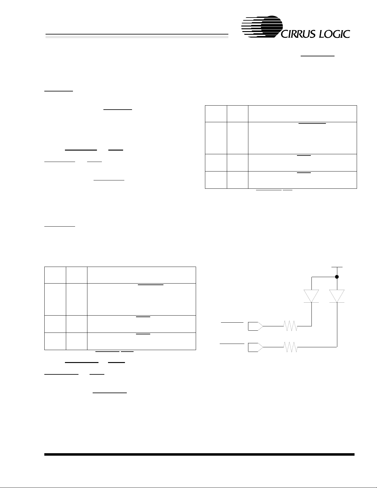
CS8900A
+5V
LANLED
LINKLED
Figure 7. LED Connection Diagram
Crystal LAN™ Ethernet Controller
3.8 LED Outputs
The CS8900A provides three output pins that
can be used to control LEDs or external logic.
3.8.1 LANLED
LANLED goes low whenever the CS8900A
transmits or receives a frame, or when it detects a collision. LANLED remains low until
there has been no activity for 6 ms (i.e. each
transmission, reception, or collision produces
a pulse lasting a minimum of 6 ms).
3.8.2 LINKLED or HC0
LINKLED or HC0 can be controlled by either
the CS8900A or the host. When controlled by
the CS8900A, LINKLED is low whenever the
CS8900A receives valid 10BASE-T link pulses. To configure this pin for CS8900A control,
the HC0E bit (Register 15, SelfCTL, Bit C)
must be clear. When controlled by the host,
LINKLED is low whenever the HCB0 bit (Register 15, SelfCTL, Bit E) is set. To configure it
for host control, the HC0E bit must be set. Table 10 summarizes this operation.
(Register 15, SelfCTL, Bit D) must be clear.
When controlled by the host, BSTATUS is low
whenever the HCB1 bit (Register 15, SelfCTL,
Bit F) is set. To configure it for host control,
HC1E must be set. Table 11 summarizes this
operation.
HC1E
(Bit D)
HCB1
(Bit F)
0N/A
10
11
Pin configured as BSTATUS
low when a receive frame begins transfer across the ISA bus. Output is high
otherwise
Pin configured as HC1
Output is high
Pin configured as HC1
Output is low
Table 11. BSTATUS/HCI Pin Operation
Pin Function
: Output is
:
:
3.8.4 LED Connection
Each LED output is capable of sinking 10 mA
to drive an LED directly through a series resistor. The output voltage of each pin is less than
0.4 V when the pin is low. Figure 7 shows a
typical LED circuit.
HC0E
(Bit C)
HCB0
(Bit E)
0N/A
10
11
Pin configured as LINKLED
low when valid 10BASE-T link pulses
are detected. Output is high if valid link
pulses are not detected
Pin configured as HC0
Output is high
Pin configured as HC0
Output is low
Table 10. LINKLED/HC0 Pin Operation
Pin Function
: Output is
:
:
3.8.3 BSTATUS or HC1
BSTATUS or HC1 can be controlled by either
the CS8900A or the host. When controlled by
the CS8900A, BSTATUS is low whenever the
host reads the RxEvent register (PacketPage
base + 0124h), signaling the transfer of a receive frame across the ISA bus. To configure
this pin for CS8900A control, the HC1E bit
CIRRUS LOGIC PRODUCT DATASHEET
3.9 Media Access Control
3.9.1 Overview
The CS8900A’s Ethernet Media Access Control (MAC) engine is fully compliant with the
IEEE 802.3 Ethernet standard (ISO/IEC 88023, 1993). It handles all aspects of Ethernet
frame transmission and reception, including:
DS271F5 29
Page 30
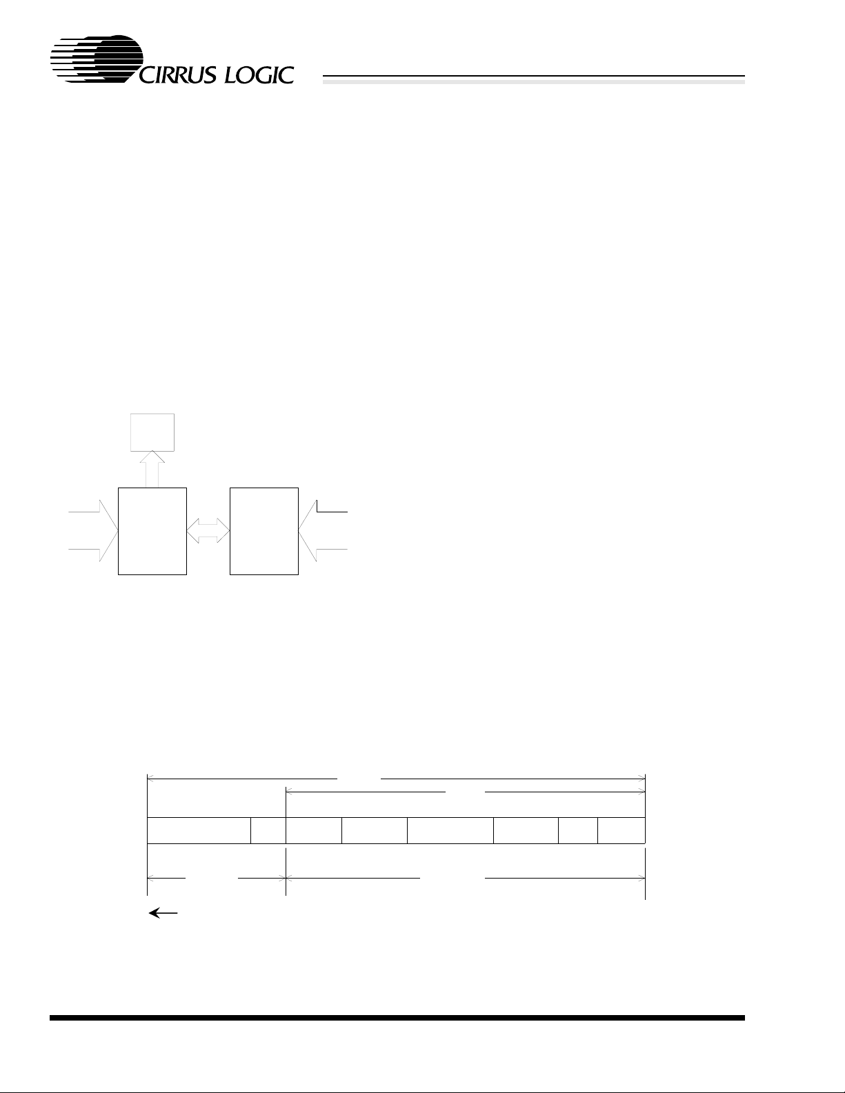
CS8900A
802.3
MAC
Engine
Encoder/
Decoder
&
PLL
LED
Logic
CS8900A
Internal Bus
10BAS E-T
& AUI
Figure 8. MAC Interface
1 byteup to 7 bytes 6 bytes 6 bytes 2 bytes
LLC data Pad
FCS
4 bytes
preamble
frame length
min 64 bytes
max 1518 bytes
alternating 1s / 0s
SFD
DA
SA
SFD = Start of Frame Delimiter
DA = Destination Address
SA = Source Address
Direction of Transmission
Frame
Packet
LLC = Logical Link Control
FCS = Frame Check Sequen ce (also
called Cyclic Redundancy Check, or CRC)
Length Field
Figure 9. Ethernet Frame Format
Crystal LAN™ Ethernet Controller
collision detection, preamble generation and
detection, and CRC generation and test. Programmable MAC features include automatic
retransmission on collision, and padding of
transmitted frames.
Figure 8 shows how the MAC engine interfaces to other CS8900A functions. On the host
side, it interfaces to the CS8900A’s internal
data/address/control bus. On the network
side, it interfaces to the internal Manchester
encoder/decoder (ENDEC). The primary functions of the MAC are: frame encapsulation and
decapsulation; error detection and handling;
and, media access management.
3.9.2 Frame Encapsulation and Decapsulation
The CS8900A’s MAC engine automatically assembles transmit packets and disassembles
receive packets. It also determines if transmit
and receive frames are of legal minimum size.
3.9.2.1 Transmission
Once the proper number of bytes have been
transferred to the CS8900A’s memory (either
5, 381, 1021 bytes, or full frame), and providing that access to the network is permitted, the
MAC automatically transmits the 7-byte preamble (1010101b...), followed by the Start-ofFrame Delimiter (SFD, 10101011b), and then
the serialized frame data. It then transmits the
Frame Check Sequence (FCS). The data after
the SFD and before the FCS (Destination Address, Source Address, Length, and data field)
is supplied by the host. FCS generation by the
CS8900A may be disabled by setting the InhibitCRC bit (Register 9, TxCMD, bit C).
Figure 9 shows the Ethernet frame format.
3.9.2.2 Reception
The MAC receives the incoming packet as a
serial stream of NRZ data from the Manchester encoder/decoder. It begins by checking for
the SFD. Once the SFD is detected, the MAC
assumes all subsequent bits are frame data. It
reads the DA and compares it to the criteria
programmed into the address filter (see
Section 5.2.10 on page 87 for a description of
Address Filtering). If the DA passes the address filter, the frame is loaded into the
CS8900A’s memory. If the BufferCRC bit
(Register 3, RxCFG, bit B) is set, the received
FCS is also loaded into memory. Once the en-
30 DS271F5
CIRRUS LOGIC PRODUCT DATASHEET
Page 31

CS8900A
Crystal LAN™ Ethernet Controller
tire packet has been received, the MAC validates the FCS. If an error is detected, the
CRCerror bit (Register 4, RxEvent, Bit C) is
set.
3.9.2.3 Enforcing Minimum Frame Size
The MAC provides minimum frame size enforcement of both transmit and receive packets. When the TxPadDis bit (Register 9,
TxCMD, Bit D) is
clear, transmit frames will be padded with additional bits to ensure that the receiving station
receives a legal frame (64 bytes, including
CRC). When TxPadDis is set, the CS8900A
will not add pad bits and will transmit frames
less that 64 bytes. If a frame is received that is
less than 64 bytes (including CRC), the Runt
bit (Register 4, RxEvent, Bit D) will be set indicating the arrival of an illegal frame.
times. If no collision is detected, the SQEerror
bit (Register 8, TxEvent, Bit 7) is set. If the
SQEerroriE bit is set (Register 7, TxCFG, Bit
7), the host is interrupted. An SQE error may
indicate a fault on the AUI cable or a faulty
transceiver (it is assumed that the attached
transceiver supports this function).
3.9.3.3 Out-of-Window (Late) Collision
If a collision is detected after the first 512 bits
have been transmitted, the MAC reports a late
collision by setting the Out-of-window bit (Register 8, TxEvent, Bit 9). The MAC then forces a
bad CRC and terminates the transmission. If
the Out-of-windowiE bit (Register 7, TxCFG,
Bit 9) is set, the host is interrupted. A late collision may indicate an illegal network configuration.
3.9.3.4 Jabber Error
3.9.3 Transmit Error Detection and Handling
The MAC engine monitors Ethernet activity
and reports and recovers from a number of error conditions. For transmission, the MAC reports the following errors in the TxEvent
register (Register 8) and BufEvent register
(Register C):
3.9.3.1 Loss of Carrier
Whenever the CS8900A is transmitting on the
AUI port, it expects to see its own transmission
“looped back” to its receiver. If it is unable to
monitor its transmission after the end of the
preamble, the MAC reports a loss-of-carrier
error by setting the Loss-of-CRS bit (Register
8, TxEvent, Bit 6). If the Loss-of-CRSiE bit
(Register 7, TxCFG, Bit 6) is set, the host will
be interrupted.
If a transmission continues longer than about
26 ms, the MAC disables the transmitter and
sets the Jabber bit (Register 8, TxEvent, Bit A).
The output of the transmitter returns to idle and
remains there until the host issues a new
Transmit Command. If the JabberiE bit (Register 7, TxCFG, Bit A) is set, the host is interrupted. A Jabber condition indicates that there
may be something wrong with the CS8900A
transmit function. To prevent possible network
faults, the host should clear the transmit buffer. Possible options include:
Reset the chip with either software or hardware reset (see Section 3.3 on page 19).
Issue a Force Transmit Command by setting
the Force bit (Register 9, TxCMD, bit 8).
Issue a Transmit Command with the TxLength
field set to zero.
3.9.3.2 SQE Error
After the end of transmission on the AUI port,
the MAC expects to see a collision within 64 bit
CIRRUS LOGIC PRODUCT DATASHEET
DS271F5 31
3.9.3.5 Transmit Collision
The MAC counts the number of times an individual packet must be retransmitted due to
Page 32

CS8900A
Crystal LAN™ Ethernet Controller
network collisions. The collision count is
stored in bits B through E of the TxEvent register (Register 8). If the packet collides 16
times, transmission of that packet is terminated and the 16coll bit (Register 8, TxEvent, Bit
F) is set. If the 16colliE bit (Register 7, TxCFG,
Bit F) is set, the host will be interrupted on the
16th collision. A running count of transmit collisions is recorded in the TxCOL register.
3.9.3.6 Transmit Underrun
If the CS8900A starts transmission of a packet
but runs out of data before reaching the end of
frame, the TxUnderrun bit (Register C, BufEvent, Bit 9) is set. The MAC then forces a bad
CRC and terminates the transmission. If the
TxUnderruniE bit (Register B, BufCFG, Bit 9)
is set, the host is interrupted.
3.9.4 Receive Error Detection and Handling
The following receive errors are reported in the
RxEvent register (Register 4):
3.9.4.1 CRC Error
If a frame is received with a bad CRC, the
CRCerror bit (Register 4, RxEvent, Bit C) is
set. If the CRCerrorA bit (Register 5, RxCTL,
Bit C) is set, the frame will be buffered by
CS8900A. If the CRCerroriE bit (Register 3,
RxCFG. Bit C) is set, the host is interrupted.
3.9.4.2 Runt Frame
If a frame is received that is shorter than 64
bytes, the Runt bit (Register 4, RxEvent, Bit D)
is set. If the RuntA bit (Register 5, RxCTL, Bit
D) is set, the frame will still be buffered by
CS8900A. If the RuntiE bit (Register 3, RxCFG. Bit D) is set, the host is interrupted.
3.9.4.3 Extra Data
If a frame is received that is longer than 1518
bytes, the Extradata bit (Register 4, RxEvent,
Bit E) is set. If the ExtradataA bit (Register 5,
RxCTL, Bit E) is set, the first 1518 bytes of the
frame will still be buffered by CS8900A. If the
ExtradataiE bit (Register 3, RxCFG. Bit E) is
set, the host is interrupted.
3.9.4.4 Dribble Bits and Alignment Error
Under normal operating conditions, the MAC
may detect up to 7 additional bits after the last
full byte of a receive packet. These bits, known
as dribble bits, are ignored. If dribble bits are
detected, the Dribblebit bit (Register 4, RxEvent, Bit 7) is set. If both the Dribblebits bit
and CRCerror bit (Register 4, RxEvent, Bit C)
are set at the same time, an alignment error
has occurred.
3.9.5 Media Access Management
The Ethernet network topology is a single
shared medium with several attached stations.
The Ethernet protocol is designed to allow
each station equal access to the network at
any given time. Any node can attempt to gain
access to the network by first completing a deferral process (described below) after the last
network activity, and then transmitting a packet that will be received by all other stations. If
two nodes transmit simultaneously, a collision
occurs and the colliding packets are corrupted.
Two primary tasks of the MAC are to avoid network collisions, and then recover from them
when they occur. In addition, when the
CS8900A is using the AUI, the MAC must support the SQE Test function described in section 7.2.4.6 of the Ethernet standard.
3.9.5.1 Collision Avoidance
The MAC continually monitors network traffic
by checking for the presence of carrier activity
(carrier activity is indicated by the assertion of
the internal Carrier Sense signal generated by
the ENDEC). If carrier activity is detected, the
network is assumed busy and the MAC must
wait until the current packet is finished before
CIRRUS LOGIC PRODUCT DATASHEET
32 DS271F5
Page 33

CS8900A
Transmit
Frame
Start Monitoring
Network Activity
IPG
Timer =
6.4
μ
s?
Network
Active?
Network
Active?
Start IPG
Timer
Network
Active?
Yes
No
Yes
Yes
Yes
No
No
No
No
Wait
3.2
μ
s
Yes
Tx
Frame
Ready
and
Not
in Backoff?
Figure 10. Two-Part Deferral
Crystal LAN™ Ethernet Controller
attempting transmission. The CS8900A supports two schemes for determining when to initiate transmission: Two-Part Deferral, and
Simple Deferral. Selection of the deferral
scheme is determined by the 2-partDefDis bit
(Register 13, LineCTL, Bit D). If the 2-partDefDis bit is clear, the MAC uses a two-part deferral process defined in section 4.2.3.2.1 of the
Ethernet standard (ISO/IEC 8802-3, 1993). If
the 2-partDefDis bit is set, the MAC uses a
simplified deferral scheme. Both schemes are
described below:
3.9.5.2 Two-Part Deferral
In the two-part deferral process, the 9.6 µs Inter Packet Gap (IPG) timer is started whenever the internal Carrier Sense signal is
deasserted. If activity is detected during the
first 6.4 µs of the IPG timer, the timer is reset
and then restarted once the activity has
stopped. If there is no activity during the first
6.4 µs of the IPG timer, the IPG timer is allowed to time out (even if network activity is
detected during the final 3.2 µs). The MAC
then begins transmission if a transmit packet is
ready and if it is not in Backoff (Backoff is described later in this section). If no transmit
packet is pending, the MAC continues to monitor the network. If activity is detected before a
transmit frame is ready, the MAC defers to the
transmitting station and resumes monitoring
the network.
not in Backoff, transmission begins the 9.6 µs
IPG). If no transmit packet is pending, the
MAC continues to monitor the network. If activity is detected before a transmit frame is ready,
the MAC defers to the transmitting station and
resumes monitoring the network. Figure 11 diagrams the simple deferral process.
The two-part deferral scheme was developed
to prevent the possibility of the IPG being
shortened due to a temporary loss of carrier.
Figure 10 diagrams the two-part deferral process.
3.9.5.3 Simple Deferral
In the simple deferral scheme, the IPG timer is
started whenever Carrier Sense is deasserted.
Once the IPG timer is finished (after 9.6 µs), if
a transmit frame is pending and if the MAC is
DS271F5 33
CIRRUS LOGIC PRODUCT DATASHEET
Page 34

CS8900A
T
x
Frame
Ready and Not
in Back
off?
Transmit
Frame
Start Monitoring
Network A c ti vi ty
Network
Active?
Network
Active?
Yes
No
Yes
No
No
Yes
Wait
9.6
μ
s
Figure 11. Simple Deferral
Crystal LAN™ Ethernet Controller
3.9.5.4 Collision Resolution
If a collision is detected while the CS8900A is
transmitting, the MAC responds in one of three
ways depending on whether it is a normal collision (within the first 512 bits of transmission)
or a late collision (after the first 512 bits of
transmission):
3.9.5.5 Normal Collisions
If a collision is detected before the end of the
preamble and SFD, the MAC finishes the preamble and SFD, transmits the jam sequence
(32-bit pattern of all 0’s), and then initiates
Backoff. If a collision is detected after the
transmission of the preamble and SFD but be-
fore 512 bit times, the MAC immediately terminates transmission, transmits the jam
sequence, and then initiates Backoff. In either
case, if the Onecoll bit (Register 9, TxCMD, Bit
9) is clear, the MAC will attempt to transmit a
packet a total of 16 times (the initial attempt
plus 15 retransmissions) due to normal collisions. On the 16th collision, it sets the 16coll
bit (Register 8, TxEvent, Bit F) and discards
the packet. If the Onecoll bit is set, the MAC
discards the packet without attempting any retransmission.
3.9.5.6 Late Collisions
If a collision is detected after the first 512 bits
have been transmitted, the MAC immediately
terminates transmission, transmits the jam sequence, discards the packet, and sets the Outof-window bit (Register 8, TxEvent, Bit 9). The
CS8900A does not initiate backoff or attempt
to retransmit the frame. For additional information about Late Collisions, see Out-of-Window
Error in this section.
3.9.5.7 Backoff
After the MAC has completed transmitting the
jam sequence, it must wait, or “Back off”, before attempting to transmit again. The amount
of time it must wait is determined by one of two
Backoff algorithms: the Standard Backoff algorithm (ISO/IEC 4.2.3.2.5) or the Modified
Backoff algorithm. The host selects which algorithm through the ModBackoffE bit (Register
13, LineCTL, Bit B).
3.9.5.8 Standard Backoff
The Standard Backoff algorithm, also called
the “Truncated Binary Exponential Backoff”, is
described by the equation:
where r (a random integer) is the number of
CIRRUS LOGIC PRODUCT DATASHEET
slot times the MAC must wait (1 slot time = 512
0 ≤ r ≤ 2
k
34 DS271F5
Page 35

CS8900A
Encoder
Carrier
Detector
Decoder
& PLL
RX
MUX
TX
MUX
RXSQL
AUISQL
RX
TX
AUIRX
AUITX
AUICol
Clock
Carrier Sens e
RX CLK
RX NRZ
TXCLK
TX NRZ
TEN
Port Select
Collision
MAC
ENDEC
10BASE-T
Transceiver
AUI
Figure 12. ENDEC
Crystal LAN™ Ethernet Controller
bit times), and k is the smaller of n or 10, where
n is the number of retransmission attempts.
3.9.5.9 Modified Backoff
The Modified Backoff is described by the
equation:
0 ≤ r ≤ 2
k
where r (a random integer) is the number of
slot times the MAC must wait, and k is 3 for n
< 3 and k is the smaller of n or 10 for n ≥ 3,
where n is the number of retransmission attempts.
The advantage of the Modified Backoff algorithm over the Standard Backoff algorithm is
that it reduces the possibility of multiple collisions on the first three retries. The disadvantage is that it extends the maximum time
needed to gain access to the network for the
first three retries.
The host may choose to disable the Backoff algorithm altogether by setting the DisableBackoff bit (Register 19, TestCTL, Bit B). When
disabled, the CS8900A only waits the 9.6 µs
IPG time before starting transmission.
3.9.5.10 SQE Test
If the CS8900A is transmitting on the AUI, the
external transceiver should generate an SQE
Test signal on the CI+/CI- pair following each
transmission. The SQE Test is a 10 MHz signal lasting 5 to 15 bit times and starting within
0.6 to 1.6 µs after the end of transmission.
During this period, the CS8900A ignores receive carrier activity (see SQE Error in this
section for more information).
3.10 Encoder/Decoder (ENDEC)
The CS8900A’s integrated encoder/decoder
(ENDEC) circuit is compliant with the relevant
portions of section 7 of the Ethernet standard
(ISO/IEC 8802-3, 1993). Its primary functions
include: Manchester encoding of transmit data; informing the MAC when valid receive data
is present (Carrier Detection); and, recovering
the clock and NRZ data from incoming Manchester-encoded data.
Figure 12 provides a block diagram of the ENDEC and how it interfaces to the MAC, AUI
and 10BASE-T transceiver.
3.10.1 Encoder
The encoder converts NRZ data from the MAC
and a 20 MHz Transmit Clock signal into a serial stream of Manchester data. The Transmit
Clock is produced by an on-chip oscillator circuit that is driven by either an external 20 MHz
quartz crystal or a TTL-level CMOS clock input. If a CMOS input is used, the clock should
be 20 MHz ±0.01% with a duty cycle between
DS271F5 35
CIRRUS LOGIC PRODUCT DATASHEET
Page 36

CS8900A
Crystal LAN™ Ethernet Controller
40% and 60%. The specifications for the crystal are described in Section 7.7 on page 122.
The encoded signal is routed to either the
10BASE-T transceiver or AUI, depending on
configuration.
3.10.2 Carrier Detection
The internal Carrier Detection circuit informs
the MAC that valid receive data is present by
asserting the internal Carrier Sense signal as
soon it detects a valid bit pattern (1010b or
0101b for 10BASE-T, and 1b or 0b for AUI).
During normal packet reception, Carrier Sense
remains asserted while the frame is being received, and is deasserted 1.3 to 2.3 bit times
after the last low-to-high transition of the Endof-Frame (EOF) sequence. Whenever the receiver is idle (no receive activity), Carrier
Sense is deasserted. The CRS bit (Register
14, LineST, Bit E) reports the state of the Carrier Sense signal.
9) in the LineCTL register (Register 13). Table
12 describes the possible configurations.
AUIonly
(Bit 8)
0 0 10BASE-T Only
1 N/A AUI Only
01Auto-Select
AutoAUI/10BT
(Bit 9)
Table 12. Interface Selection
Physical
Interface
3.10.4.1 10BASE-T Only
When configured for 10BASE-T only operation, the 10BASE-T transceiver and its interface to the ENDEC are active, and the AUI is
powered down.
3.10.4.2 AUI Only
When configured for AUI-only operation, the
AUI and its interface to the ENDEC are active,
and the 10BASE-T transceiver is powered
down.
3.10.4.3 Auto-Select
3.10.3 Clock and Data Recovery
When the receiver is idle, the phase-lock loop
(PLL) is locked to the internal clock signal. The
assertion of the Carrier Sense signal interrupts
the PLL. When it restarts, it locks on the incoming data. The receive clock is then compared to the incoming data at the bit cell center
and any phase difference is corrected. The
PLL remains locked as long as the receiver input signal is valid. Once the PLL has locked on
the incoming data, the ENDEC converts the
Manchester data to NRZ and passes the decoded data and the recovered clock to the
MAC for further processing.
3.10.4 Interface Selection
Physical interface selection is determined by
AUIonly bit (Bit 8) and the AutoAUI/10BT (Bit
In Auto-Select mode, the CS8900A automatically selects the 10BASE-T interface and powers down the AUI if valid packets or link pulses
are detected by the 10BASE-T receiver. If valid packets and link pulses are not detected, the
CS8900A selects the AUI. Whenever the AUI
is selected, the 10BASE-T receiver remains
active to listen for link pulses or packets. If
10BASE-T activity is detected, the CS8900A
switches back to 10BASE-T.
3.11 10BASE-T Transceiver
The CS8900A includes an integrated
10BASE-T transceiver that is compliant with
the relevant portions of section 14 of the Ethernet standard (ISO/IEC 8802-3, 1993). It includes all analog and digital circuitry needed to
interface the CS8900A directly to a simple isolation transformer (see Section 7.5 on
page 121 for a connection diagram). Figure 13
provides a block diagram of the 10BASE-T
transceiver.
CIRRUS LOGIC PRODUCT DATASHEET
36 DS271F5
Page 37

CS8900A
RXSQL
RX
TX
Link Pulse
Detector
TX Pre-
Distortion
RX Squelch
RX
Comparator
TX Filters
Filter Tuning
RX Filters
TX Drivers
RXDRXD+
TXDTXD+
ENDEC
LinkOK
(to MAC)
10BASE-T Transceiver
Figure 13. 10BASE-T Transceiver
Crystal LAN™ Ethernet Controller
3.11.1 10BASE-T Filters
The CS8900A’s 10BASE-T transceiver includes integrated low-pass transmit and receive filters, eliminating the need for external
filters or a filter/transformer hybrid. On-chip filters are gm/c implementations of fifth-order
Butterworth low-pass filters. Internal tuning circuits keep the gm/c ratio tightly controlled,
even when large temperature, supply, and IC
process variations occur. The nominal 3 dB
cutoff frequency of the filters is 16 MHz, and
the nominal attenuation at 30 MHz (3rd harmonic) is -27 dB.
3.11.2 Transmitter
When configured for 10BASE-T operation,
Manchester encoded data from the ENDEC is
fed into the transmitter’s predistortion circuit
where initial wave shaping and preequalization is performed. The output of the predistor-
with section 14.2.1.1. of the Ethernet standard.
Transmitted link pulses are positive pulses,
one bit time wide, typically generated at a rate
of one every 16 ms. The 16 ms timer starts
whenever the transmitter completes an Endof-Frame (EOF) sequence. Thus, there is a
link pulse 16 ms after an EOF unless there is
another transmitted packet. Figure 14 diagrams the operation of the Link Pulse Generator.
If no link pulses are being received on the receiver, the 10BASE-T transmitter is internally
forced to an inactive state unless bit DisableLT
in register 19 (Test Control register) is set to
one.
3.11.3 Receiver
The 10BASE-T receive section consists of the
receive filter, squelch circuit, polarity detection
and correction circuit, and link pulse detector.
tion circuit is fed into the transmit filter where
final wave shaping occurs and unwanted noise
is removed. The signal then passes to the differential driver where it is amplified and driven
out of the TXD+/TXD- pins.
In the absence of transmit packets, the trans-
3.11.3.1 Squelch Circuit
The 10BASE-T squelch circuit determines
when valid data is present on the RXD+/RXDpair. Incoming signals passing through the receive filter are tested by the squelch circuit.
Any signal with amplitude less than the
mitter generates link pulses in accordance
DS271F5 37
CIRRUS LOGIC PRODUCT DATASHEET
Page 38

CS8900A
Time Link
Pulse
Link
Pulse
16ms16ms
Less Than
16ms
Packet Packet
Figure 14. Link Pulse Transmission
Crystal LAN™ Ethernet Controller
squelch threshold (either positive or negative,
depending on polarity) is rejected.
3.11.3.2 Extended Range
The CS8900A supports an Extended Range
feature that reduces the 10BASE-T receive
squelch threshold by approximately 6 dB. This
allows the CS8900A to operate with 10BASET cables that are longer than 100 meters (100
meters is the maximum length specified by the
Ethernet standard). The exact additional distance depends on the quality of the cable and
the amount of electromagnetic noise in the
surrounding environment. To activate this feature, the host must set the LoRxSquelch bit
(Register 13, LineCTL, Bit E).
3.11.4 Link Pulse Detection
To prevent disruption of network operation due
to a faulty link segment, the CS8900A continually monitors the 10BASE-T receive pair
(RXD+/ RXD-) for packets and link pulses. After each packet or link pulse is received, an internal Link-Loss timer is started. As long as a
packet or link pulse is received before the LinkLoss timer finishes (between 25 and 150 ms),
the CS8900A maintains normal operation. If
no receive activity is detected, the CS8900A
disables packet transmission to prevent “blind”
transmissions onto the network (link pulses
are still sent while packet transmission is disabled). To reactivate transmission, the receiver must detect a single packet (the packet itself
is ignored), or two link pulses separated by
more than 2 to 7 ms and no more than 25 to
150 ms (see Section 7.4 on page 114 for
10BASE-T timing).
The state of the link segment is reported in the
LinkOK bit (Register 14, LineST, Bit 7). If the
HC0E bit (Register 15, SelfCTL, Bit D) is clear,
it is also indicated by the output of the LINKLED pin. If the link is “good”, the LinkOK bit is
set and the LINKLED pin is driven low. If the
link is “bad” the LinkOK bit is clear and the LINKLED pin is high. To disable this feature, the
host must set the DisableLT bit (Register 19,
TestCTL, Bit 7). If DisableLT is set, the
CS8900A will transmit and receive packets independent of the link segment.
3.11.5 Receive Polarity Detection and Correction
The CS8900A automatically checks the polarity of the receive half of the twisted pair cable.
If the polarity is correct, the PolarityOK bit
(Register 14, LineST, bit C) is set. If the polarity is reversed, the PolarityOK bit is clear. If the
PolarityDis bit (Register 13, LineCTL, Bit C) is
clear, the CS8900A automatically corrects a
reversal. If the PolarityDis bit is set, the
CS8900A does not correct a reversal. The PolarityOK bit and the PolarityDis bit are independent.
To detect a reversed pair, the receiver examines received link pulses and the End-ofFrame (EOF) sequence of incoming packets.
If it detects at least one reversed link pulse and
38 DS271F5
CIRRUS LOGIC PRODUCT DATASHEET
Page 39

DI+
DI-
DO+
DO-
ENDEC
CL+
CL-
Collision
Detect
AUICol (to M AC )
AUIRX
AUISQL
AUITX
AUI
-
+
-
+
Figure 15. AUI
CS8900A
Crystal LAN™ Ethernet Controller
at least four frames in a row with negative polarity after the EOF, the receive pair is considered reversed. Any data received before the
correction of the reversal is ignored.
3.11.6 Collision Detection
If half-duplex operation is selected (Register
19, Bit E, FDX), the CS8900A detects a
10BASE-T collision whenever the receiver and
transmitter are active simultaneously. When a
collision is present, the Collision Detection circuit informs the MAC by asserting the internal
Collision signal (see Section 3.9 on page 29
for collision handling).
3.12 Attachment Unit Interface (AUI)
The CS8900A Attachment Unit Interface (AUI)
provides a direct interface to external
10BASE2, 10BASE5, and 10BASE-FL Ethernet transceivers. It is fully compliant with Section 7 of the Ethernet standard (ISO/IEC 8802-
3), and as such, is capable of driving a full 50meter AUI cable.
The AUI consists of three pairs of signals: Data
Out (DO+/DO-), Data In (DI+/DI-), and Collision In (CI+/CI-). To select the AUI, the host
should set the AUI bit (Register 13, LineCTL,
Bit 8). The AUI can also be selected automatically as described in the previous section
(Section 3.10.4 on page 36). Figure 15 provides a block diagram of the AUI. (For a connection diagram, see Section 7.6 on
page 122).
3.12.1 AUI Transmitter
The AUI transmitter is a differential driver designed to drive a 78 Ω cable. It accepts data
from the ENDEC and transmits it directly on
the DO+/DO- pins. After transmission has
started, the CS8900A expects to see the packet “looped-back” (or echoed) to the receiver,
causing the Carrier Sense signal to be assert-
ed. This Carrier Sense presence indicates that
the transmit signal is getting through to the
transceiver. If the Carrier Sense signal remains deasserted throughout the transmission, or if the Carrier Sense signal is
deasserted before the end of the transmission,
there is a Loss-of-Carrier error and the Lossof-CRS bit (Register 8, TxEvent, Bit 6) is set.
3.12.2 AUI Receiver
The AUI receiver is a differential pair circuit
that connects directly to the DI+/DI- pins. It is
designed to distinguish between transient
noise pulses and incoming Ethernet packets.
Incoming packets with proper amplitude and
pulse width are passed on to the ENDEC section, while unwanted noise is rejected.
3.12.3 Collision Detection
The AUI collision circuit is a differential pair receiver that detects the presence of collision
signals on the CI+/CI- pins. The collision signal
is generated by an external Ethernet transceiver whenever a collision is detected on the
Ethernet segment. (Section 7.3.1.2 of ISO/IEC
8802-3, 1993, defines the collision signal as a
10 MHz ± 15% signal with a duty cycle no
worse than 60/40). When a collision is present,
the AUI Collision circuit informs the MAC by
asserting the internal Collision signal.
CIRRUS LOGIC PRODUCT DATASHEET
DS271F5 39
Page 40

CS8900A
Crystal LAN™ Ethernet Controller
3.13 External Clock Oscillator
A 20-MHz quartz crystal or CMOS clock input
is required by the CS8900A. If a CMOS clock
input is used, it should be connected the to
XTAL1 pin, with the XTAL2 pin left open. The
clock signal should be 20 MHz ±0.01% with a
duty cycle between 40% and 60%. The specifications for the crystal are described in
Section 7.7 on page 122.
CIRRUS LOGIC PRODUCT DATASHEET
40 DS271F5
Page 41

CS8900A
Crystal LAN™ Ethernet Controller
4.0 PACKETPAGE ARCHITECTURE
4.1 PacketPage Overview
The CS8900A architecture is based on a
unique, highly-efficient method of accessing
internal registers and buffer memory known as
PacketPage. PacketPage provides a unified
way of controlling the CS8900A in Memory or
I/O space that minimizes CPU overhead and
simplifies software. It provides a flexible set of
performance features and configuration options, allowing designers to develop Ethernet
circuits that meet their particular system requirements.
4.1.1 Integrated Memory
Central to the CS8900A architecture is a 4Kbyte page of integrated RAM known as PacketPage memory. PacketPage memory is used
for temporary storage of transmit and receive
frames, and for internal registers. Access to
this memory is done directly, through Memory
space operations (Section 4.9 on page 73), or
indirectly, through I/O space operations
(Section 4.10 on page 75). In most cases,
Memory Mode will provide the best overall performance, because ISA Memory operations
require fewer cycles than I/O operations. I/O
Mode is the CS8900A’s default configuration
and is used when memory space is not available or when special operations are required
(e.g. waking the CS8900A from the Software
Suspend State requires the host to write to the
CS8900A’s assigned I/O space).
The user-accessible portion of PacketPage
memory is organized into the following six sections:
PacketPage
Address
0000h - 0045h Bus Interface Registers
0100h - 013Fh Status and Control Registers
0140h - 014Fh Initiate Transmit Registers
0150h - 015Dh Address Filter Registers
Contents
PacketPage
Address
0400h Receive Frame Location
0A00h Transmit Frame Location
Contents
4.1.2 Bus Interface Registers
The Bus Interface registers are used to configure the CS8900A’s ISA-bus interface and to
map the CS8900A into the host system’s I/O
and Memory space. Most of these registers
are written only during initialization, remaining
unchanged while the CS8900A is in normal
operating mode. The exceptions to this are the
DMA registers which are modified continually
whenever the CS8900A is using DMA. These
registers are described in more detail in
Section 4.3 on page 44.
4.1.3 Status and Control Registers
The Status and Control registers are the primary means of controlling and getting status of
the CS8900A. They are described in more detail in Section 4.4 on page 49.
4.1.4 Initiate Transmit Registers
The TxCMD/TxLength registers are used to
initiate Ethernet frame transmission. These
registers are described in more detail in
Section 4.5 on page 69. (See Section 5.6 on
page 99 for a description of frame transmission.)
4.1.5 Address Filter Registers
The Filter registers store the Individual Address filter and Logical Address filter used by
the Destination Address (DA) filter. These registers are described in more detail in
Section 4.6 on page 71. For a description of
the DA filter, see Section 5.2.10 on page 87.
4.1.6 Receive and Transmit Frame Locations
The Receive and Transmit Frame PacketPage
locations are used to transfer Ethernet frames
CIRRUS LOGIC PRODUCT DATASHEET
DS271F5 41
Page 42

CS8900A
Crystal LAN™ Ethernet Controller
to and from the host. The host simply writes to
and reads from these locations and internal
buffer memory is dynamically allocated between transmit and receive as needed. This
provides more efficient use of buffer memory
and better overall network performance. As a
result of this dynamic allocation, only one re-
0400h) and one transmit frame (starting at
PacketPage base + 0A00h) are directly accessible. See Section 4.7 on page 72.
4.2 PacketPage Memory Map
Table 13 shows the CS8900A PacketPage
memory address map: s
ceive frame (starting at PacketPage base +
PacketPage
Address
Bus Interface Registers
0000h 4 Read-only Product Identification Code Section 4.3 on page 44
0004h 28 - Reserved Note 2
0020h 2 Read/Write I/O Base Address Section 4.3 on page 44,
0022h 2 Read/Write Interrupt Number (0,1,2,or 3) Section 3.2 on page 18,
0024h 2 Read/Write DMA Channel Number (0, 1, or 2) Section 3.2 on page 18,
0026h 2 Read-only DMA Start of Frame Section 4.3 on page 44,
0028h 2 Read-only DMA Frame Count (12 Bits) Sections Section 4.3 on page 44,
002Ah 2 Read-only RxDMA Byte Count Section 4.3 on page 44,
002Ch 4 Read/Write Memory Base Address Register
0030h 4 Read/Write Boot PROM Base Address Section 3.6 on page 26,
0034h 4 Read/Write Boot PROM Address Mask Section 3.6 on page 26,
0038h 8 - Reserved Note 2
0040h 2 Read/Write EEPROM Command Section 3.5 on page 25,
0042h 2 Read/Write EEPROM Data Section 3.5 on page 25,
0044h 12 - Reserved Note 2
0050h 2 Read only Received Frame Byte Counter Section 4.3 on page 44,
0052h 174 - Reserved Note 2
Status and Control Registers
Notes: 1. All registers are accessed as words only.
2. Read operation from the reserved location provides undefined data. Writing to a reserved location or
# of
Bytes
undefined bits may result in unpredictable operation of the CS890 0A.
Type Description Cross Reference
Section 4.7 on page 72
Section 4.3 on page 44
Section 4.3 on page 44
Section 5.3 on page 90
”Receive DMA”
Section 5.3 on page 90
Section 4.3 on page 44,
(20 Bit)
Table 13. PacketPage Memory Address Map
Section 4.9 on page 73
Section 4.3 on page 44
Section 4.3 on page 44
Section 4.3 on page 44
Section 4.3 on page 44
Section 5.2.9 on page 86
CIRRUS LOGIC PRODUCT DATASHEET
42 DS271F5
Page 43

CS8900A
Crystal LAN™ Ethernet Controller
PacketPage
Address
0100h 32 Read/Write Configuration & Control Registers
0120h 32 Read-only Status & Event Registers
0140h 4 - Reserved Note 2
Initiate Transmit Registers
0144h 2 Write-only TxCMD (transmit command) Section 4.5 on page 69,
0146h 2 Write-only TxLength (transmit length) Section 4.5 on page 69,
0148h 8 - Reserved Note 2
Address Filter Registers
0150h 8 Read/Write Logical Address Filter (hash table) Section 4.6 on page 71,
0158h 6 Read/Write Individual Address Section 4.6 on page 71,
015Eh 674 - Reserved Note 2
Frame Location
0400h 2 Read-only RXStatus (receive status) Section 4.7 on page 72,
0402h 2 Read-only RxLength (receive length, in bytes) Section 4.7 on page 72,
0404h - Read-only Receive Frame Location Section 4.7 on page 72,
0A00 - Write-only Transmit Frame Location Section 4.7 on page 72,
Notes: 1. All registers are accessed as words only.
2. Read operation from the reserved location provides undefined data. Writing to a reserved location or
# of
Bytes
undefined bits may result in unpredictable operation of the CS890 0A.
Type Description Cross Reference
Section 4.4 on page 49
(2 bytes per register)
Section 4.4 on page 49
(2 bytes per register)
Section 5.6 on page 99
Section 5.6 on page 99
Section 5.2.10 on page 87
Section 5.2.10 on page 87
Section 5.2 on page 78
Section 5.2 on page 78
Section 5.2 on page 78
Section 5.6 on page 99
T able 13. PacketPage Memory Address Map (continued)
CIRRUS LOGIC PRODUCT DATASHEET
DS271F5 43
Page 44

CS8900A
Crystal LAN™ Ethernet Controller
4.3 Bus Interface Registers
4.3.1 Product Identification Code
(Read only, Address: PacketPage base + 0000h)
Address 0000h Address 0001h Address 0002h Address 00003h
First byte of EISA registration
number for
Crystal Semiconductor
The Product Identification Code Register is located in the first four bytes of the PacketPage (0000h to 0003h). The
register contains a unique 32-bit product ID code that identifies the chip as a CS8900 A. The host can use this number to determine which software driver to load and to check which features are available.
Reset value is: 0000 1110 0110 0011 0000 0000 000X XXXX
The X XXXX codes for the CS8900A are:
Rev B: 0 0111
Rev C: 0 1000
Rev D: 0 1001
Rev F: 0 1010
Second byte of EISA
registration number for
Crystal Semiconductor
First 8 bits of
Product ID number
Last 3 bits of the Product ID
number (5 “X” bits are the
revision number)
4.3.2 I/O Base Address
(Read/Write, Address: PacketPage base + 0020h)
Address 0021h Address 0020h
Most significant byte of I/O Base Address Least significant byte of I/O Base Address
The I/O Base Address Register describes the base address for the sixteen contiguous locations in the host system's
I/O space, which are used to access the PacketPage registers. See Section 4.10 on page 75. The default location
is 0300h.
After reset, if no EEPROM is found by the CS8900A, then the register has the following initial state. If an EEPROM
is found, then the register's initial value may be set by the EEPROM. See Section 3.3 on page 19.
Reset value is: 0000 0011 0000 0000
4.3.3 Interrupt Number
(Read/Write, Address: PacketPage base + 0022h)
Address 0023h Address 0022h
Interrupt number assignment:
0000 0000b= pin INTRQ0
00h
0000 01XXb= All INTRQ pins high-impedance
0000 0001b= pin INTRQ1
0000 0010b= pin INTRQ2
0000 0011b= pin INTRQ3
The Interrupt Number Register defines the interrupt pin selected by the CS8900A. In a typical application the follow-
CIRRUS LOGIC PRODUCT DATASHEET
44 DS271F5
Page 45

CS8900A
Crystal LAN™ Ethernet Controller
ing bus signals are tied to the following pins:
Bus signal Typical pin connection
IRQ5 INTRQ3
IRQ10 INTRQ0
IRQ11 INTRQ1
IRQ12 INTRQ2
See Section 3.2 on page 18.
After reset, if no EEPROM is found by the CS8900A, then the register has the following initial state, which corre-
sponds to placing all the INTRQ pins in a high-impedance state. If an EEPROM is found, then the register's initial
value may be set by the EEPROM. See Section 3.3 on page 19.
Reset value is: XXXX XXXX XXXX X100
4.3.4 DMA Channel Number
(Read/Write, Address: PacketPage base + 0024h)
Address 0025h Address 0024h
DMA channel assignment:
0000 0000b= pin DMRQ0 and DMACK0
00h
0000 0001b= pin DMRQ1 and DMACK1
0000 0010b= pin DMRQ2 and DMACK2
0000 0011b= All DMRQ pins high-impedance
The DMA Channel register defines the DM A pins selected by the CS8900 A. In the typical applicat ion, the following
bus signals are tied to the following pins:
Bus signal Typical pin connection
DRQ5
DACK5
DRQ6
DACK6
DRQ7
DACK7
DMRQ0
DMACK0
DMRQ1
DMACK1
DMRQ2
DMACK2
See Section 3.2 on page 18 and Section 5.3 on page 90.
After reset, if no EEPROM is found by the CS8900A, then the register has the following initial state which corre-
sponds to setting all DMRQ pins to high-impedance. If a EEPROM is found, then the register's initial value may be
set by the EEPROM. See Section 3.3 on page 19.
Reset value is: XXXX XXXX XXXX XX11
4.3.5 DMA Start of Frame
(Read only, Address: PacketPage base + 0026h)
Address 0027h Address 0026h
Most significant byte of offset value Least significant byte of offset value
The DMA Start of Frame Register contains a 16-bit value which defines the offset from the DMA base address to
the start of the most recently transferred received frame. See Section 5.3 on page 90.
CIRRUS LOGIC PRODUCT DATASHEET
DS271F5 45
Page 46

CS8900A
Crystal LAN™ Ethernet Controller
Reset value is: 0000 0000 0000 0000
4.3.6 DMA Frame Count
(Read only, Address: PacketPage base + 0028h)
Address 0029h Address 0028h
Most significant byte of frame count
(most-significant nibble always 0h)
The lower 12 bits of the DMA Frame Count register define the number of valid frames transferred via DMA since the
last readout of this register. The upper 4 bits are reserved. See Section 5.3 on page 90.
Reset value is: XXXX 0000 0000 0000
4.3.7 RxDMA Byte Count
(Read only, Address: PacketPage base + 002Ah)
Address 002Bh Address 002Ah
Most significant byte of byte count Least significant byte of byte count
Least significant byte of frame count
The RxDMA Byte Count register describes the valid number of bytes DMAed since the last readout. See Section 5.3
on page 90.
Reset value is: 0000 0000 0000 0000
4.3.8 Memory Base Address
(Read/Write, Address: PacketPage base + 002Ch)
Address 002Fh Address 002Eh Address 002Dh Address 002Ch
Reserved
The most significant nibble of
memory base address. The
high-order nibble is reserved.
Contains portion of memory
base address.
The least significant byte of
the memory base address.
Memory Base Address: The lower three bytes (002Ch, 002Dh, and 002Eh) are used for the 20-bit memory base
address. The upper three nibbles are reserved.
After reset, if no EEPROM is found by the CS8900A, then the register has the following initial state. If an EEPROM
is found, then the register's initial value may be set by the EEPROM. See Section 3.3 on page 19.
Reset value is: XXXX XXXX XXXX 0000 0000 0000 0000 0000
4.3.9 Boot PROM Base Address
(Read/Write, Address: PacketPage base + 0030h)
Address 0033h Address 0032h Address 0031h Address 0030h
Reserved
The most significant nibble of
Boot PROM base address.
The high-order nibble is
reserved.
Contains portion of Boot PROM
base address.
The least significant byte of
the Boot PROM base
address.
CIRRUS LOGIC PRODUCT DATASHEET
46 DS271F5
Page 47

CS8900A
Crystal LAN™ Ethernet Controller
The lower three bytes (0030h, 0031h, and 00 32h) of the Bo ot PROM Base Add ress reg ister a re used for th e 20- bit
Boot PROM base address. The upper three nibbles are reserved. See Section 3.6 on page 26.
After reset, if no EEPROM is found by the CS8900A, then the register has the following initial state. If an EEPROM
is found, then the register's initial value may be set by the EEPROM. See Section 3.3 on page 19.
Reset value is: XXXX XXXX XXXX 0000 0000 0000 0000 0000
4.3.10 Boot PROM Address Mask
(Read/Write, Address: PacketPage base + 0034h)
Address 0037h Address 0036h Address 0035h Address 0034h
Reserved
The most significant nibble of
Boot PROM mask address.
The high-order nibble is
reserved.
Contains portion of Boot PRO M
mask address. The lower-order
nibble must be written as 0h.
The Boot PROM address mask register indicates the size of the attached Boot PROM and is limited to 4K bit increments. The lower 12 bits of the Address Mask are ignored, and should be 000 h. The next lowest-order bits describe
the size of the PROM. The upper three nibbles are reserved.
The least significant byte of
the Boot PROM mask
address. Must be written as
00h.
For example:
Size of Boot PROM Register value
4k bits XXXX XXXX XXXX 1111 1111 0000 0000 0000
8k bits XXXX XXXX XXXX 1111 1110 0000 0000 0000
16k bits XXXX XXXX XXXX 1111 1100 0000 0000 0000
See Section 3.6 on page 26.
After reset, if no EEPROM is found by the CS8900A, then the register has the following initial state. If an EEPROM
is found, then the register's initial value may be set by the EEPROM. See Section 3.3 on page 19.
Reset value is: XXXX XXXX XXXX 0000 0000 0000 0000 0000
4.3.11 EEPROM Command
(Read/Write, Address: PacketPage base + 0040h)
76543210
ADD7 to ADD0
FEDCBA9 8
Reserved ELSEL OB1 OB0
This register is used to control the reading, writing and erasing of the EEPROM. See Section 3.5.
ADD7-ADD0 Address of the EEPROM word being accessed.
OB1,OB0 Indicates the Opcode of the command being executed. See Table 8.
ELSEL External logic select: When clear, the EECS pin is used to select the EEPROM. When set, the
ELCS
pin is used to select the external LA decode circuit.
Reserved Reserved and must be written as 0.
CIRRUS LOGIC PRODUCT DATASHEET
DS271F5 47
Page 48

CS8900A
Crystal LAN™ Ethernet Controller
Reset value is: XXXX XXXX XXXX XXXX
4.3.12 EEPROM Data
(Read/Write, Address: PacketPage base + 0042h)
Address 0043h Address 0042h
Most significant byte of the EEPROM data. Least significant byte of the EEPROM data.
This register contains the word being written to, or read from, the EEPROM. See Section 3.5 on page 25.
Reset value is: XXXX XXXX XXXX XXXX
4.3.13 Receive Frame Byte Counter
(Read only, Address: PacketPage base + 0050h)
Address 0051h Address 0050h
Most significant byte of the byte count. Least significant byte of the byte count.
This register contains the count of the total number bytes received in the curr ent rece iv ed frame. This coun t continuously increments as more bytes in this frame are received. See Section 5.2.9 on page 86.
Reset value is: XXXX XXXX XXXX XXXX
CIRRUS LOGIC PRODUCT DATASHEET
48 DS271F5
Page 49

CS8900A
1
0325476
10 Register Bits
1 = Control/Configuration
0 = Status/Event
Internal Address
(bits 0 - 5)
16-bit Register Word
Bit Number
98
BADC
F
E
Figure 16. Status and Control Register Format
Crystal LAN™ Ethernet Controller
4.4 Status and Control Registers
The Status and Control registers are the primary registers used to control and check the
status of the CS8900A. They are organized
into two groups: Configuration/Control Registers and Status/Event Registers. All Status
and Control Registers are 16-bit words as
shown in Figure 16. Bit 0 indicates whether it
is a Configuration/Control Register (Bit 0 = 1)
or a Status/Event Register (Bit 0 = 0). Bits 0
through 5 provide an internal address code
that describes the exact function of the register. Bits 6 through F are the actual Configuration/Control and Status/Event bits.
4.4.1 Configuration and Control Registers
Configuration and Control registers are used
to setup the following:
• how frames will be transmitted and received;
• which frames will be transmitted and received;
• which events will cause interrupts to the
host processor; and,
The Transmit Command Register (TxCMD) is
a special type of register. It appears in two
separate locations in the PacketPage memory
map. The first location, PacketPage base +
0108h, is within the block of Configuration/Control Registers and is read-only. The
second location, PacketPage base + 0144h, is
where the actual transmit commands are issued and is write-only. See Section 4.4.4 on
page 51 (Register 9) and Section 5.6 on
page 99 for a more detailed description of the
TxCMD register.
4.4.2 Status and Event Registers
Status and Event registers report the status of
transmitted and received frames, as well as information about the configuration of the
CS8900A. They are read-only and are designated by even numbers (e.g. Register 2, Register 4, etc.).
The Interrupt Status Queue (ISQ) is a special
type of Status/Event register. It is located at
PacketPage base + 0120h and is the first register the host reads when responding to an Interrupt.
• how the Ethernet physical interface will be
configured.
These registers are read/write and are designated by odd numbers (e.g. Register 1, Register 3, etc.).
A more detailed description of the ISQ can be
found in Section 5.1 on page 78.
Three 10-bit counters are included with the
Status and Event registers. RxMISS counts
missed receive frames, TxCOL counts transmit collisions, and TDR is a time domain reflec-
DS271F5 49
CIRRUS LOGIC PRODUCT DATASHEET
Page 50

CS8900A
Crystal LAN™ Ethernet Controller
tometer useful in locating cable faults. The
following sections contain more information
Table 14 provides a summary of PacketPage
Register types.
about these counters.
Suffix Type Description Comments
CMD Read/Write Command: Written once per frame to initiate transmit.
CFG Read/Write Configuration: Written at setup and used to determine
what frames will be transmitted and received and what
events will cause interrupts.
CTL Read/Write Control: Written at setup and used to determine what
frames will be transmitted and received and how the physical interface will be configured.
Event Read-only Event: Reports the status of transmitted and received
frames.
ST Read-only Status: Reports information about the configuration of the
CS8900A.
Read-only Counters: Counts missed receive frames and collisions.
Provides time domain for locating coax cable faults.
Table 14. PacketPage Register Types
4.4.3 Status and Control Bit Definitions
This section provides a description of the special bit types used in the Status and Control
registers. Section 4.4.4 on page 51 provides a
detailed description of the bits in each register.
4.4.3.1 Act-Once Bits
There are four bits that cause the CS8900A to
take a certain action only once when set.
These “Act-Once” bits are: Skip_1 (Register 3,
RxCFG, Bit 6), RESET (Register 15, SelfCTL,
Bit 6), ResetRxDMA (Register 17, BusCTL, Bit
6), and SWint-X (Register B, BufCFG, Bit 6).
To cause the action again, the host must set
the bit again. Act-Once bits are always read as
clear.
4.4.3.2 Temporal Bits
vent, Bit B). Like all Event bits, RxDest and
Rx128 are cleared when read by the host.
4.4.3.3 Interrupt Enable Bits and Events
Interrupt Enable bits end with the suffix iE and
are located in three Configuration registers:
RxCFG (Register 3), TxCFG (Register 7), and
BufCFG (Register B). Each Interrupt Enable
bit corresponds to a specific event. If an Interrupt Enable bit is set and its corresponding
event occurs, the CS8900A generates an interrupt to the host processor.
The bits that report when various events occur
are located in three Event registers and two
counters. The Event registers are RxEvent
(Register 4), TxEvent (Register 8), and BufEvent (Register C). The counters are RxMISS
cleared when read
cleared when read
(Register 10) and TxCOL (Register 12). Each
Temporal bits are bits that are set and cleared
by the CS8900A without intervention of the
Interrupt Enable bit and its associated Event
are identified in Table 15.
host processor. This includes all status bits in
the three status registers (Register 14, LineST; Register 16, SelfST; and, Register 18,
BusST), the RxDest bit (Register C, BufEvent,
Bit F), and the Rx128 bit (Register C, BufE-
An Event bit will be set whenever the specified
event happens, whether or not the associated
Interrupt Enable bit is set. All Event registers
are cleared upon read-out by the host.
CIRRUS LOGIC PRODUCT DATASHEET
50 DS271F5
Page 51

CS8900A
Crystal LAN™ Ethernet Controller
Interrupt Enable Bit
(register name)
ExtradataiE (RxCFG) Extradata (RxEvent)
RuntiE (RxCFG) Runt (RxEvent)
CRCerroriE (RxCFG) CRCerror (RxEvent)
RxOKiE (RxCFG) RxOK (RxEvent)
16colliE (TxCFG) 16coll (TxEvent)
AnycolliE (TxCFG) “Number-of Tx-collisions”
JabberiE (TxCFG) Jabber (TxEvent)
Out-of-windowiE (TxCFG) Out-of-window (TxEvent)
TxOKiE (TxCFG) TxOK (TXEvent)
SQEerroriE (TxCFG) SQEerror (TxEvent)
Loss-of-CRSiE (TxCFG) Loss-of-CRS (TxEvent)
MissOvfloiE (BufCFG) RxMISS counter over-
TxColOvfloiE (BufCFG) TxCOL counter overflows
RxDestiE (BufCFG) RxDest (BufEvent)
Rx128iE (BufCFG) Rx128 (BufEvent)
RxMissiE (BufCFG) RxMISS (BufEvent)
TxUnderruniE (BufCFG) TxUnderrun (BufEvent)
Rdy4TxiE (BufCFG) Rdy4Tx (BufEvent)
RxDMAiE (BufCFG) RxDMAFrame (BufEvent)
Table 15. Interrupt Enable Bits and Events
Event Bit or Counter
(register name)
counter is incremented
(TxEvent)
flows past 1FFh
past 1FFh
4.4.3.4 Accept Bits
There are nine Accept bits located in the RxCTL register (Register 5), each of which is followed by the suffix A. Accept bits indicate
which types of frames will be accepted by the
CS8900A. (A frame is said to be “accepted” by
the CS8900A when the frame data are placed
in either on-chip memory, or in host memory
by DMA.) Four of these bits have corresponding Interrupt Enable (iE) bits. An Accept bit and
an Interrupt Enable bit are independent operations. It is possible to set either, neither, or
both bits. The four corresponding pairs of bits
are:
IE Bit in RxCFG A Bit in RxCTL
ExtradataiE ExtradataA
RuntiE RuntA
CRCerroriE CRCerrorA
RxOKiE RxOKA
If one of the above Interrupt Enable bits is set
and the corresponding Accept bit is clear, the
CS8900A generates an interrupt when the associated receive event occurs, but then does
not accept the receive frame (the length of the
receive frame is set to zero).
The other five Accept bits in RxCTL are used
for destination address filtering (see
Section 5.2.10 on page 87). The Accept
mechanism is explained in more detail in
Section 5.2 on page 78.
4.4.4 Status and Control Register Summary
The table on the following page (Table 16) provides a summary of the Status and Control
registers. Section 4.4.4 on page 51 gives a detailed description of each Status and Control
register.
CIRRUS LOGIC PRODUCT DATASHEET
DS271F5 51
Page 52

CS8900A
Crystal LAN™ Ethernet Controller
Control and Configuration Bits Register
FEDCBA9 876Number
(Offset)
Reserved (register contents undefined ) 1
Extra
dataiE
Extra
dataA
16colli
E
RxDe
stiE
LoRx
Squelch
HCB1 HCB0 HC1E HC0E HWStan
Enabl
e IRQ
FDX Disable
RuntiE CRC
erroriE
RuntA CRC
errorA
TxPad-
Dis
Miss
OvfloiE
2-part
DefDis
RxDMA
size
Inhibit-
CRC
TxCol
OvfloiE
Reserved (register contents undefined ) D-11
Polarity
Dis
IOCH
RDYE
Reserved (register contents undefined) 1B -1F
Table 16. Stat us and Control Register Descriptions
Buffer
CRC
Broad
castA
AnycolliE Jab
Rx128iE Rxmis-
Mod
BackoffE
DMA
Burst
Backoff
AutoRx
DMAE
Individ
ualA
beriE
siE
dbyE
Memo-
ryE
AUIloop ENDEC
RxDMA
only
Multi
castA
Out-of-
windowiE
Onecoll Force TxStart 9
TxUnder-
runiE
Auto-
AUI/10B
T
HW
SleepE
UseSA DMAex-
loop
RxOKiE StreamE Skip_1 3
(0102h)
RxOKA Promis
cuousA
TxOKiE SQErro-
riE
Rdy4TxiERxD-
MAiE
AUIonly Ser
TxON
SW Sus-
pend
tend
Disable
LT
IAHa-
shA5 (0104h)
Loss-of-
CRSiE7 (0106h)
(0108h)
SWint-X B
(010Ah)
Ser
RxON
RESET 15
Reset
RxDMA
(0112h)
(0114h)
(0116)
(0118)
13
17
19
BufCFG
SelfCTL
BusCTL
TestCTL
Name
RxCFG
RxCTL
TxCFG
TxCMD
Line
CTL
CIRRUS LOGIC PRODUCT DATASHEET
52 DS271F5
Page 53

CS8900A
Crystal LAN™ Ethernet Controller
Status and Event Bits Register
FEDCBA9 876Number
(Offset)
Interrupt Status Queue 0
(0120h)
Reserved (register contents undefined) 2
Extra
data
Hash Table Index (alternate RxEvent meaning if
16coll Number-of-Tx-collisions Jabber Out-of-
Rx
Dest
CRS Polarity
10-bit AUI Time Domain Reflectometer (TDR) counter, cleared when read 1C
Runt CRC
error
Hashed = 1 and RxOK = 1)
Reserved (register contents undefined) 6
Reserved (register contents undefined) A
Reserved (register contents undefined) E
10-bit Receive Miss (RxMISS) counter, cleared when read 10
10-bit Transmit Collision (TxCOL) counter, cleared when read 12
OK
EESize EL pr es -
Reserved (register contents undefined) 1A
Reserved (register contents undefined) 1E
Broad-
cast
Rx128 RxMiss TxUnder-
ent
Individual Adr
EEPRO
M OK
Hashed RxOK Dribble
Hashed RxOK Dribble
Window
run
10BT AUI LinkOK 14
EEPRO
Mpresent
IAHash 4
bits
IAHash 4
bits
TxOK SQE
error
Rdy4Tx RxDMA
Frame
SIBUSY INITD 3.3 V
Rdy4Tx
NOW
TxBid
Err
Loss-of-
CRS8 (0128h)
SWint C
Active
(0124h)
(0124h)RxEventalt
(012Ch)
(0130h)
(0132h)
(0134h)
16
(0136h)
18
(0138h)
(013Ch)
Name
TxEvent
RxMISS
TxCOL
LineST
SelfST
BusST
ISQ
Rx
Event
Buf
Event
TDR
Table 16. Status and Control Register Descriptions (continued)
4.4.5 Register 0: Interrupt Status Queue
(ISQ, Read-only, Address: PacketPage base + 0120h)
76543210
RegContent RegNum
FEDCBA9 8
RegContent
The Interrupt Status Queue Register is used in both Memory Mode and I/O Mode to provide the host with interrupt
information. Whenever an event occurs that triggers an enabled interrupt, the CS8900A sets the appropriate bit(s)
in one of five registers, maps the contents of that register to the ISQ register, and drives an IRQ pin high. Three of
the registers mapped to ISQ are event registers: RxEvent (Register 4), TxEvent (Register 8), and BufEvent (Register
C). The other two registers are counter-overflow reports: RxMISS (Register 10) and TxCOL (Register 12). In Memory Mode, ISQ is located at PacketPage base + 120h. In I/O Mode, ISQ is located at I/O Base + 0008h. See
Section 5.1 on page 78.
CIRRUS LOGIC PRODUCT DATASHEET
DS271F5 53
Page 54

CS8900A
Crystal LAN™ Ethernet Controller
RegNum The lower six bits describe which register (4, 8, C, 10 or 12) is contained in the ISQ.
RegContent The upper ten bits contain the register data contents.
Reset value is: 0000 0000 0000 0000
4.4.6 Register 3: Receiver Configuration
(RxCFG, Read/Write, Address: PacketPage base + 0102h)
76543210
StreamE Skip_1 000011
FEDCBA9 8
ExtradataiE RuntiE CRCerroriE BufferCRC AutoRx DMAE RxDMA only RxOKiE
RxCFG determines how frames will be transferred to the host and what frame types will cause interrupts.
000011 These bits provide an internal address used by the CS8900A to identify this as the Receiver
Configuration Register.
Skip_1 When set, this bit causes the last committed received frame to be deleted from the receive buf-
fer. To skip another frame, the host must rewrite a “1” to this bit. This bit is not to be used if
RxDMAonly (Bit 9) is set. Skip_1 is an Act-Once bit. See Section 5.2.5 on page 85.
StreamE When set, StreamTransfer mode is used to transfer receive frames that are back-to-back and
that pass the Destination Address filter (see Section 5.2.10 on page 87). When StreamE is
clear, StreamTransfer mode is not used. This bit must not be set unless either bit AutoRxDMA
or bit RXDMAonly is set.
RxOKiE When set, there is an RxOK Interrupt if a frame is received without errors. RxOK interrupt is
not generated when DMA mode is used for frame reception.
RxDMAonly The Receive-DMA mode is used for all receive frames when this bit is set.
AutoRxDMAE When set, the CS8900A will automatically switch to Receive-DMA mode if the conditions spec-
ified in Section 5.4 on page 94 are met. RxDMAonly (Bit 9) has precedence over AutoRxD-
MAE.
BufferCRC When set, the received CRC is included with the data stored in the receive-frame buffer, and
the four CRC bytes are included in the receive-frame length (PacketPa ge base + 0402h). When
clear, neither the receive buffer nor the receive length include the CRC.
CRCerroriE When set, there is a CRCerror Interrupt if a frame is received with a bad CRC.
RuntiE When set, there is a Runt Interrupt if a frame is received that is shorter than 64 bytes. The
CS8900A always discards any frame that is shorter than 8 bytes.
ExtradataiE When set, there is an Extradata Interrupt if a frame is received that is long er than 1 518 b ytes.
The operation of this bit is independent of the received packet integrity (good or bad CRC).
After reset, if no EEPROM is found by the CS8900A, then the register has the following initial state. If an EEPROM
is found, then the register’s initial value may be set by the EEPROM. See Section 3.3 on page 19.
Reset value is: 0000 0000 0000 0011
CIRRUS LOGIC PRODUCT DATASHEET
54 DS271F5
Page 55

CS8900A
Crystal LAN™ Ethernet Controller
4.4.7 Register 4: Receiver Event
(RxEvent, Read-only, Address: PacketPage base + 0124h)
76543210
Dribblebits IAHash 000100
FEDCBA9 8
Extradata Runt CRCerror Broadcast Individual Adr Hashed RxOK
Alternate meaning if bits 8 and 9 are both set (see Section 5.2.10 on page 87 for exception regarding Broadcast
frames).
76543210
Dribblebits IAHash 000100
FEDCBA9 8
Hash Table Index (see Section 5.2.10 on page 87) Hashed = 1 RxOK = 1
RxEvent reports the status of the current received frame.
000100 These bits identify this as the Receiver Event Register. When reading this register, these bits
will be 000100, where the LSB corresponds to Bit 0.
IAHash If the received frame's Destination Address is accepted by the hash filter, then this bit is set if,
and only if IAHashA (Register 5, RxCTL, Bit 6) is set, and Hashed (Bit 9) is set. See
Section 5.2.10 on page 87.
Dribblebits If set, the received frame had from o ne to seven bits after the last received full byte. An "Align-
ment Error" occurs when Dribblebits and CRCerror (Bit C) are both set.
RxOK If set, the received frame had a good CRC and valid length (i.e., there is not a CRC error, Runt
error, or Extradata error). When RxOK is set, then the length of the received frame is contained
at PacketPage base + 0402h. If RxOKiE (Register 3, RxCFG, Bit 8) is set, there is an inte rrupt.
Hashed If set, the received frame had a Destination Address that was accepted by the hash filter. If
Hashed and RxOK (Bit 8) are set, Bits F through A of RxEvent become the Hash Table Index
for this frame [See Section 5.2.10 on page 87 for an exception regarding broadcast frames!].If
Hashed and RxOK are not both set, then Bits F through A are individual event bits as defined
below.
IndividualAdr If the received frame ha d a De stin at ion Add ress which matched the Individual Address found
at PacketPage base + 0158h, then this bit is set if, and only if, RxOK (Bit 8) is set and IndividualA (Register 5, RxCTL, Bit A) is set.
Broadcast If the received frame had a Broadcast Address (FFFF FFFF FFFFh) as the Destination Ad-
dress, then this bit is set if, and only if, RxOK is set and BroadcastA (Register 5, RxCTL, Bit B)
is set.
CRCerror If set, the received frame had a bad CRC. If CRCerroriE (Register 3, RxCFG, Bit C) is set, there
is an interrupt
Runt If set, the received frame was shorter than 64 bytes. If RuntiE (Register 3, RxCFG, Bit D) is set,
there is an interrupt.
Extradata If set, the received frame was longer than 1518 bytes. All bytes beyond 1518 are discarded. If
ExtradataiE (Register 3, RxCFG, Bit E) is set, there is an interrupt.
Reset value is: 0000 0000 0000 0100
Notes: 3. All RxEvent bits are cleared upon readout. The host is responsible for processing all event bits.
4. RxStatus register (PacketPage base + 0400h) is th e sam e as the RxEve nt register except RxSta tus is
not cleared when RxEvent is read. See Section 5.2 on page 78. The value in the RxEvent register is
undefined when RxDMAOnly bit (Bit 9, Register 3, RxCFG) is set.
CIRRUS LOGIC PRODUCT DATASHEET
DS271F5 55
Page 56

CS8900A
Crystal LAN™ Ethernet Controller
4.4.8 Register 5: Receiver Control
(RxCTL, Read/Write, Address: PacketPage base +0104h)
76543210
PromiscuousA IAHashA 000101
FEDCBA9 8
ExtradataA RuntA CRCerrorA BroadcastA IndividualA MulticastA RxOKA
RxCTL has two functions: Bits 8, C, D, and E define what types of frames to accept. Bits 6, 7, 9, A, and B configure
the Destination Address filter. See Section 5.2.10 on page 8 7.
000101 These bits provide an internal address used by the CS8900A to identify this as the Receiver
Control Register. For a received frame to be accepted, the Destination Address of that frame
must pass the filter criteria found in Bits 6, 7, 9, A, and B (see Section 5 .2 .1 0 on pa ge 8 7) .
IAHashA When set, receive frames are accepted when the Destination Address is an Individual Address
that passes the hash filter.
PromiscuousA Frames with any address are accepted when this bit is set.
RxOKA When set, the CS8900A accepts frames with correct CRC and valid length (valid length is: 64
bytes <= length <= 1518 bytes).
MulticastA When set, receive frames are accepted if the Destination Address is an Multicast Address that
passes the hash filter.
IndividualA When set, receive frames are accepted if the Destination Address matches the Individual Ad-
dress found at PacketPage base + 0158h to PacketPage base + 015Dh.
BroadcastA When set, receive frames are accepted if the Destination Address is FFFF FFFF FFFFh.
CRCerrorA When set, receive frames that pass the Destination Address filter, but have a bad CRC, are ac-
cepted. When clear, frames with bad CRC are discarded. See Note 5.
RuntA When set, receive frames that are smaller than 64 bytes, and that pass the Destination Address
filter are accepted. When clear, received frames less that 64 bytes in length are disca rded. The
CS8900A discards any frame that is less than 8 bytes. See Note 5.
ExtradataA When set, receive frames longer than 1518 bytes and that pass the Destination Address filter
are accepted. The CS8900A accepts only the first 1518 bytes and ignores the rest. When clear,
frames longer than 1518 bytes are discarded. See Note 5.
After reset, if no EEPROM is found by the CS8900A, then the register has the following initial state. If an EEPROM
is found, then the register's initial value may be set by the EEPROM. See Section 5.2.10 on page 87.
Reset value is: 0000 0000 0000 0101
Notes: 5. Typically, when bits CRCerrorA, RuntA and ExtradataA are cleared (meaning bad frames are being
discarded), then the corresponding bits CRCerroriE, RuntiE and Extr adataiE should be set in register 3
(Receiver Configuration register) to allow the device driver to keep track of discarded frames.
CIRRUS LOGIC PRODUCT DATASHEET
56 DS271F5
Page 57

CS8900A
Crystal LAN™ Ethernet Controller
4.4.9 Register 7: Transmit Configuration
(TxCFG, Read/Write, Address: PacketPage base + 0106h)
76543210
SQE erroriE Loss-of-CRSiE 000111
FEDCBA9 8
16colliE AnycolliE JabberiE Out-of-window TxOKiE
Each bit in TxCFG is an interrupt enable. When set, the interrupt is enabled as described below. When clear, there
is no interrupt.
000111 These bits provide an internal address used by the CS8900A to identify this as the Transmit
Configuration Register.
Loss-of-CRSiE If the CS8900A starts transmitting on the AUI and do es not see the Carrier Sense signal at the
end of the preamble, an interrupt is g enerated if this bit is set. Carrier Se nse activity is reported
by the CRS bit (Register 14, LineST, Bit E).
SQErroriE When set, an interrupt is generated if there is an SQE error. (At the end of a transmission on
the AUI, the CS8900A expects to see a collision within 64 bit times. If this does not happen,
there is an SQE error.)
TxOKiE When set, an interrupt is generated if a packet is completely transmitted.
Out-of-windowiE When set, an interrupt is generated if a late collision occurs (a late collision is a collision which
occurs after the first 512 bit times). When this occurs, the CS8900A forces a bad CRC and ter-
minates the transmission.
JabberiE When set, an interrupt is generated if a transmission is longer than approximately 26 ms.
AnycolliE When set, if one or more collisions occur during the transmission of a packet, an interrupt oc-
curs at the end of the transmission
16colliE If the CS8900A encounters 16 normal collisions while attempting to transmit a particular packet,
the CS8900A stops attempting to transmit that p acket. When this bit is set, there is an interrupt
upon detecting the 16th collision.
After reset, if no EEPROM is found by the CS8900A, then the register has the following initial state. If an EEPROM
is found, then the register's initial value may be set by the EEPROM. See Section 3.3 on page 19.
Reset value is: 0000 0000 0000 0111
Notes: Bit 8 (TxOKiE) and Bit B (AnycolliE) are interrupts for normal transmit operation. Bits 6, 7, 9, A, and F
Notes:are interrupts for abnormal transmit operation.
4.4.10 Register 8: Transmitter Event
(TxEvent, Read-only, Address: PacketPage base + 0128h)
76543210
SQEerror Loss-of-CRS 001000
FEDCBA9 8
16coll Number-of-Tx-collisions Jabber Out-of-window TxOK
TxEvent gives the event status of the last packet transmitted.
CIRRUS LOGIC PRODUCT DATASHEET
DS271F5 57
Page 58

CS8900A
Crystal LAN™ Ethernet Controller
001000 These bits provide an internal address used by the CS8900A to identify this as the Transmitter
Event Register.
Loss-of-CRS If the CS8900A is transmitting on the AUI and doesn't see Carrier Sense (CRS) at the end of
the preamble, there is a Loss-of-Carrier error and this bit is set. If Loss-of-CRSiE (Register 7,
TxCFG, Bit 6) is set, there is an interrupt.
SQEerror At the end of a transmission on the AUI, the CS8900A expects to see a collision within 64 bit
times. If this does not happen, there is an SQE error and this bit is set. If SQEerroriE ( Register
7, TxCFG, Bit 7) is set, there is an interrupt.
TxOK This bit is set if the last packet was completely transmitted (Jabber (Bit A), out-of-window-colli-
sion (Bit 9), and 16Coll (Bit F) must all be clear). If TxOKiE (Register 7, TxCFG, Bit 8) is set,
there is an interrupt.
Out-of-Window This bit is set if a collision occurs more than 512 bit times after the first bit of the preamble. When
this occurs, the CS8900A forces a bad CRC and terminates the transmission. If Out-of-windowiE (Register 7, TxCFG, Bit 9) is set, there is an interrupt
Jabber If the last transmission is longer than 26 msec, then the packet output is terminated by the jab-
ber logic and this bit is set. If JabberiE (Register 7, TxCFG, Bit A) is set, there is an interrupt.
#-of-TX-collisions These bits give the number of transmit collisions that occurred on the last transmitted packet.
Bit B is the LSB. If AnycolliE (Register 7, TxCFG, Bit B) is set, there is an interrupt when any
collision occurs.
16coll This bit is set if the CS8900A encounters 16 normal collisions while attempting to transmit a
particular packet. When this happens, the CS8900A stops further attempts to send that packet.
If 16colliE (Register 7, TxCFG, Bit F) is set, there is an interrupt.
Reset value is:
Notes: 1.In any event register, like TxEvent, all bits are cleared upon readout. The host is responsible for
0000 0000 0000 1000
processing all event bits.
2.TxOK (Bit 8) and the Number-of-Tx-Collisions (Bits E-B) are used in normal packet transmission.All
other bits (6, 7, 9, A, and F) give the status of abnormal transmit operation.
4.4.11 Register 9: Transmit Command Status
(TxCMD, Read-only, Address: PacketPage base + 0108h)
76543210
TxStart 001001
FEDCBA9 8
TxPadDis InhibitCRC Onecoll Force
This register contains the latest transmit command which tells the CS8900A how the next packet should be sent.
The command must be written to PacketPage base + 0144h in order to initiate a transmission. The host can read
the command from register 9 (PacketPage base + 0108h). See Section 5.6 on page 99.
001001 These bits provide an internal address used by the CS8900A to identify this as the Transmit
Command Register. When reading this register, these bits will be 001001, where the LSB cor-
responds to Bit 0.
TxStart This pair of bits determ ines ho w ma n y byte s ar e tra n sfe rr ed to th e CS8 900A be fo re the MAC
starts the packet transmit process.
CIRRUS LOGIC PRODUCT DATASHEET
58 DS271F5
Page 59
CS8900A
Crystal LAN™ Ethernet Controller
Bit 7 Bit 6
0 0 Start transmission after 5 bytes are in the CS8900A
0 1 Start transmission after 381 bytes are in the CS8900A
1 0 Start transmission after 1021 bytes are in the CS8900A
1 1 Start transmission after the entire frame is in the CS8900A
Force When set in conjunction with a new transmit command, any transmit frames waiting in the trans-
mit buffer are deleted. If a previous packet has started transmission, that packet is terminated
within 64 bit times with a bad CRC.
Onecoll When this bit is set, any transmission will be terminated after only one collision. When clear, the
CS8900A allows up to 16 normal collisions before terminating the transmission.
InhibitCRC When set, the CRC is not appended to the transmission.
TxPadDis When TxPadDis is clear, if the host gives a transmit length less than 60 bytes and InhibitCRC
is set, then the CS8900A pads to 60 bytes. If the host gives a transmit length less than 60 bytes
and InhibitCRC is clear, then the CS8900A pads to 60 bytes and appends the CRC.
When TxPadDis is set, the CS8900A allows the transmission of runt frames (a frame less than
64 bytes). If InhibitCRC is clear, the CS8900A appends the CRC. If InhibitCRC is set, the
CS8900A does not append the CRC
After reset, if no EEPROM is found by the CS8900A, then the register has the following initial state. If an EEPROM
is found, then the register's initial value may be set by the EEPROM. See Section 3.3 on page 19.
Register value is: 0000 0000 0000 1001
Notes: The CS8900A does not transmit a frame if TxLength < 3
4.4.12 Register B: Buffer Configuration
(BufCFG, Read/Write, Address: PacketPage base + 010Ah)
76543210
RxDMAiE SWint-X 001011
FEDCBA9 8
RxDestiE Miss OvfloiE TxCol OvfloiE Rx128iE RxMissiE TxUnder runtiE Rdy4TxiE
Each bit in BufCFG is an interrupt enable. When set, the interrupt described below is enabled . When cle ar, there is
no interrupt.
001011 These bits provide an internal address used by the CS8900A to identify this as the Buffer Con-
figuration Register.
SWint-X When set, there is an interrupt requested by the host software. The CS8900A provides the in-
terrupt, and sets the SWint (Register C, BufEvent, Bit 6) bit. The CS8900A acts upon this command at once. SWint-X is an Act-Once bit. To generate another interrupt, rewrite a "1" to this bit.
RxDMAiE When set, there is an interrupt when a frame has b een received and DMA is complete. With
this interrupt, the RxDMAFrame bit (Register C, BufEvent, Bit 7) is set.
Rdy4TxiE When set, there is an interrupt when the CS8900A is ready to accept a frame from the host for
transmission. (See Section 5.6 on page 99 for a description of the transmit bid process.)
TxUnderruniE When set, there is an interrupt if the CS8900A runs out of data before it reaches the end of the
frame (called a transmit underrun). When this happens, event bit TXUnderrun (Register C,
BufEvent, Bit 9) is set and the CS8900A makes no further attempts to transmi t that frame. If the
CIRRUS LOGIC PRODUCT DATASHEET
DS271F5 59
Page 60

CS8900A
Crystal LAN™ Ethernet Controller
host still wants to transmit that particular frame, the host must go through the transmit request
process again.
RxMissiE When set, there is an interrupt if one or more received frames is lost due to slow movement of
receive data out of the receive buffer (called a receive miss). When this happens, the RxMiss
bit (Register C, BufEvent, Bit A) is set.
Rx128iE When set, there is an interrupt after the first 128 bytes of a frame have been received. This al-
lows a host processor to examine the Destination Address, Source Address, Length, Sequence
Number, and other information before the entire frame is received. This interru pt should not be
used with DMA. Thus, if either AutoRxDMA (Register 3, RxCFG, Bit A) or RxDMAonly (Register
3, RxCFG, Bit 9) is set, the Rx128iE bit must be clear.
TxColOvfiE If set, there is an interrupt when the TxCOL counter increments from 1FFh to 200h. (The TxCOL
counter (Register 18) is incremented whenever the CS8900A sees that the RXD+/RXD- pins
(10BASE-T) or the CI+/CI- pins (AUI) go active while a packet is being transmitted.)
MissOvfloiE If MissOvfloiE is set, there is an interrupt when the RxMISS counter increments from 1FFh to
200h. (A receive miss is said to have occurred if packets are lost due to slow movement of receive data out of the receive buffers. When this happens, the RxMiss bit (Register C, BufEvent,
Bit A) is set, and the RxMISS counter (Register 10) is incremented.)
RxDestiE When set, there is an interrupt when a receive frame passes the Destination Address filter cri-
teria defined in the RxCTL register (Register 5). This bit provides an early indication of an incoming frame. It is earlier than Rx128 (Register C, BufEvent, Bit B). If RxDestiE is set, the
BufEvent could be RxDest or Rx128. After 128 bytes are received, the BufEvent change s from
RxDest to Rx128.
After reset, if no EEPROM is found by the CS8900A, then the register has the following initial state after reset. If an
EEPROM is found, then the register's initial value may be set by the EEPROM. See Section 3.3 on page 19.
Reset value is: 0000 0000 0000 1011
4.4.13 Register C: Buffer Event
(BufEvent, Read-only, Address: PacketPage base + 012Ch)
76543210
RxDMA frame SWint 001100
FEDCBA9 8
RxDest Rx128 RxMiss TxUnder run Rdy4Tx
BufEvent gives the status of the transmit and receive buffers.
001100 These bits provide an internal address used by the CS8900A to identify this as the Buffe r Event
Register. When reading this register, these bits will be 001100, where the LSB corresponds to
Bit 0.
SWint If set, there has been a software initiated interrupt. This bit is used in conjunction with the SWint-
X bit (Register B, BufCFG, Bit 6).
RxDMAFrame If set, one or more received frames have been transferred by slave DMA. If RxDMAiE (Register
B, BufCFG, Bit 7) is set, there is an interrupt.
Rdy4Tx If set, the CS89 00A is ready to accept a fra me from the host for transmission. If Rdy4TxiE (Reg-
ister B, BufCFG, Bit 8) is set, there is an interrupt. (See Section 5.6 on page 99 for a description
of the transmit bid process.)
CIRRUS LOGIC PRODUCT DATASHEET
60 DS271F5
Page 61

CS8900A
Crystal LAN™ Ethernet Controller
TxUnderrun This bit is set if CS8900A runs out of data befor e it reaches the end of the frame (called a trans-
mit underrun). If TxUnderruniE (Register B, BufCFG, Bit 9) is set, there is an interrupt.
RxMiss If set, one or more receive frames have been lost due to slow movement of data out of the re-
ceive buffers. If RxMissiE (Register B, BufCFG, Bit A) is set, there is an interrupt.
Rx128 This bit is set after the first 128 bytes of an incoming frame have been received. This bit will
allow the host the option of preprocessing frame data before the entire frame is received. If
Rx128iE (Register B, BufCFG, Bit B) is set, there is an interrupt.
RxDest When set, this bit shows that a receive frame has passed the Destination Add ress Filter criteria
as defined in the RxCTL register (Register 5). Th is bit is useful as an early indication of an incoming frame. It will be earlier than Rx128 (Register C, BufEvent, Bit B). If RxDestiE (Register
B, BufCFG, Bit F) is set, there is an interrupt.
Reset value is:
Notes: With any event register, like BufEvent, all bits are cleared upon readout. The host is responsible for
0000 0000 0000 1100
processing all event bits.
4.4.14 Register 10: Receiver Miss Counter
(RxMISS, Read-only, Address: PacketPage base + 0130h)
76543210
MissCount 010000
FEDCBA9 8
MissCount
The RxMISS counter (Bits 6 through F) records the number of receive frames that are lost (missed) due to the lack
of available buffer space. If the MissOvfloiE bit (Register B, BufCFG, Bit D) is set, there is an interrupt when RxMISS
increments from 1FFh to 200h. This interrup t provides the host with an early warning that the RxMISS counter should
be read before it reaches 3FFh and starts over ( by interrupting at 200h, the host has an addition al 512 counts before
RxMISS actually overflows). The RxMISS counter is cleared when read.
010000 These bits provide an internal address used by the CS8900A to identify this as the Receiver
Miss Counter. When reading this register, these bits will be 010000, where the LSB corresponds to Bit 0.
MissCount The upper ten bits contain the number of missed frames.
Register’s value is: 0000 0000 0001 0000
4.4.15 Register 12: Transmit Collision Counter
(TxCOL, Read-only, Address: PacketPage base + 0132h)
76543210
ColCount 010010
FEDCBA9 8
ColCount
The TxCOL counter (Bits 6 through F) is incremented whenever the 10BASE-T Receive Pair (RXD+ / RXD-) or AUI
Collision Pair (CI+ / CI-) becomes active while a packet is being transmitted. If the TxColOvfiE bit (Register B, Buf-
CIRRUS LOGIC PRODUCT DATASHEET
DS271F5 61
Page 62

CS8900A
Crystal LAN™ Ethernet Controller
CFG, Bit C) is set, there is an interrupt when TxCOL increments from 1FFh to 200h. This interrupt provides the host
with an early warning that the TxCOL coun ter should be read before it reaches 3FFh a nd starts over (by interrupting
at 200h, the host has an additional 512 counts befo re TxCOL actually overflows). The TxCOL counter is cleared
when read.
010010 These bits provide an internal address used by the CS8900A to identify this as the Transmit
Collision Counter. When reading this register, these bits will be 010010, where the LSB corre-
sponds to Bit 0.
ColCount The upper ten bits contain the number of collisions.
Reset value is: 0000 0000 0001 0010
4.4.16 Register 13: Line Control
(LineCTL, Read/Write, Address: PacketPage base + 0112h)
76543210
SerTxOn SerRxON 010011
FEDCBA9 8
LoRx Squelch 2-part DefDis PolarityDis Mod BackoffE Auto AUI/10BT AUIonly
LineCTL determines the configura tio n of the M AC eng in e an d ph ys ical int er fa c e.
010011 These bits provide an internal address used by the CS8900A to identify this as the Line Control
Register.
SerRxON When set, the receiver is enabled. When clear, no incoming packets pass through the receiver.
If SerRxON is cleared while a packet is being received, reception is completed and no subse-
quent receive packets are allowed until SerRxON is set again.
SerTxON When set, the transmitter is enabled. When clear, no transmissions are allowed. If SerTxON is
cleared while a packet is being transmitted, transmission is completed and no subsequent
packets are transmitted until SerTxON is set again.
AUIonly Bits 8 and 9 are used to select either the AUI or the 10BASE-T interface according to the fol-
lowing: [Note: 10BASE-T transmitter will be inactive even when selected unless link pulses are
detected or bit DisableLT (register 19) is set.
AUIonly (Bit 8) AutoAUI/10BT (Bit 9) Physical Interface
1N/A AUI
0> 0 0BASE-T
0 1 Auto-Select
AutoAUI/10BT See AUIonly (Bit 8) description above.
ModBackoffE When clear, the ISO/IEC standard backoff algorithm is used (see Section 3.9 on page 29).
When set, the Modified Backoff algorithm is used. (The Modified Backoff algorithm extends the
backoff delay after each of the first three Tx collisions.)
PolarityDis The 10BASE-T receiver automatically determines the polarity of the received signal at the
RXD+/RXD- input (see Section 3.11 on page 36). When this bit is clear, the polarity is corrected, if necessary. When set, no effort is made to correct the polarity. This bit is independent of
the PolarityOK bit (Register 14, LineST, Bit C), which reports whether the polarity is normal or
reversed.
CIRRUS LOGIC PRODUCT DATASHEET
62 DS271F5
Page 63
CS8900A
Crystal LAN™ Ethernet Controller
2-partDefDis Before a transmission can begin, the CS8900A follows a deferral procedure. With the 2-part-
DefDis bit clear, the CS8900A uses the standard two-part deferr al as defined in ISO/IEC 88023 paragraph 4.2.3.2.1. With the 2-partDefDis bit set, the two-part deferral is disabled.
LoRxSquelch When clear, the 10BASE-T receiver squelch thresholds are set to levels defined by the ISO/IEC
8802-3 specification. When set, the thresholds are r educed by ap proximately 6d B. This is useful for operating with "quiet" cables that are longer than 100 meters.
After reset, if no EEPROM is found by the CS8900A, then the register has the following initial state. If an EEPROM
is found, then the register's initial value may be set by the EEPROM. See Section 3.3 on page 19.
Reset value is: 0000 0000 0001 0011
4.4.17 Register 14: Line Status
(LineST, Read-only, Address: PacketPage base + 0134h)
76543210
LinkOK 010100
FEDCBA9 8
CRS PolarityOK 10BT AUI
LineST reports the status of the Ethernet physical interface.
010100 These bits provide an internal address used by the CS8900A to identify this as the Line Status
Register. When reading this register, these bits will be 010100, where the LSB corresponds to
Bit 0.
LinkOK If set, the 10BASE-T link has not failed. When clear, the link has failed, either because the
CS8900A has just come out of reset, or because the receiver has not detected any activity (link
pulses or received packets) for at least 50 ms.
AUI If set, the CS8900A is using the AUI.
10BT If set, the CS8900A is using the 10BASE-T interface.
PolarityOK If set, the polarity of the 10BASE-T receive signal (at the RXD+ / RXD- inputs) is correct. If clear,
the polarity is reversed. If PolarityDis (Register 13, LineCTL, Bit C) is clear, the polarity is auto-
matically corrected, if needed. The PolarityOK status bit shows the true state of the incoming
polarity independent of the PolarityDis control bit. Thus, if PolarityDis is clear and PolarityOK is
clear, then the receive polarity is inverted, and corrected.
CRS This bit tells the host the status of an incoming frame. If CRS is set, a frame is currently being
received. CRS remains asserted until the end of frame (EOF). At EOF, CRS goes inactive in
about 1.3 to 2.3 bit times after the last low-to-high transition of the recovered data.
Reset value is: 0000 0000 0001 0100
CIRRUS LOGIC PRODUCT DATASHEET
DS271F5 63
Page 64

CS8900A
Crystal LAN™ Ethernet Controller
4.4.18 Register 15: Self Control
(SelfCTL, Read/Write, Address: PacketPage base + 0114h)
76543210
RESET 010101
FEDCBA9 8
HCB1 HCB0 HC1E HC0E HW Standby HWSleepE SW Suspend
SelfCTL controls the operation of the LED outputs and the lower-power modes.
010101 These bits provide an internal address used by the CS8900A to identify this as the Chip Self
Control Register.
RESET When set, a chip-wide reset is initiated immediately. RESET is an Act-Once bit. This bit is
cleared as a result of the reset.
SWSuspend When set, the CS8900A enters the software initiated Suspend mode. Upon entering this mode,
there is a partial reset. All registers and circuits are reset except for the ISA I/O Base Ad dres s
Register and the SelfCTL Register. There is no transmit nor receive activity in this mode. To
come out of software Suspend, the host issues an I/O Write within the CS8900A's assigned I/O
space (see Section 3.7 on page 27 for a complete description of the CS8900A's low-power
modes).
HWSleepE When set, the SLEEP
ative (unless in SWSuspend mode, as shown above). If SLEEP
ther the Hardware Standby or Hardware Suspend mode. When clear, the CS8900A ignor es the
SLEEP
power modes).
HWStandbyE If HWSleepE is set and the SLEEP
CS8900A enters the Hardware Standby mode. When clear, the CS8900A enters the Hardware
Suspend mode (see Section 3.7 on page 27 for a complete description of the CS8900A's lowpower modes).
HC0E The LINKLED
pin is LINKLED
pin.
HC1E The BSTATUS
put pin is BSTATUS
is HC1
HCB0 When HC0E (Bit C) is set, this bit controls the HC0
clear, HC0
trol bit is ignored.
HCB1 When HC1E (Bit D) is set, this bit controls the HC1
clear, HC1
trol bit is ignored.
input pin (see Section 3.7 on page 27 for a complete description of the CS8900A's low-
or HC0 output pin is selected with this control bit. When HC0E is clear, the output
and the HCB1 bit (Bit F) controls the pin.
is high. HC0 may drive an LED or a logic gate. When HC0E (Bit C) is clear, this con-
is high. HC1 may drive an LED or a logic gate. When HC1E (Bit D) is clear, this con-
input pin is enabled. If SLEEP is high, the CS8900A is "awake", or oper-
input pin is low, then when HWStandbyE is set, the
. When HC0E is set, the output pin is HC0 and the HCB0 bit (Bit E) controls the
or HC1 output pin is selected with this control bit. When HC1E is clear, the out-
and indicates receiver ISA Bus activity. When HC1E is set, the output pin
is low, the CS8900A enters ei-
pin. If HCB0 is set, HC0 is low. If HCB0 is
pin. If HCB1 is set, HC1 is low. If HCB1 is
After reset, if no EEPROM is found by the CS8900A, then the register has the following initial state. If an EEPROM
is found, then the register's initial value may be set by the EEPROM. See Section 3.3 on page 19.
Reset value is: 0000 0000 0001 0101
CIRRUS LOGIC PRODUCT DATASHEET
64 DS271F5
Page 65

CS8900A
Crystal LAN™ Ethernet Controller
4.4.19 Register 16: Self Status
(SelfST, Read-only, Address: PacketPage base + 0136h)
76543210
INITD 3.3V Active 010110
FEDCBA9 8
EEsize ELPresent EEPROM OK
SelfST reports the status of the EEPROM interface and the initialization process.
010110 These bits provide an internal address used by the CS8900A to identify this as the Chip Self
Status Register. When reading this register, these bits will be 010110, where the LSB corre-
sponds to Bit 0.
3,3VActive If the CS8900A is operating on a 3.3V supply, this bit is set. If the CS8900A is operating on a
5V supply, this bit is clear.
INITD If set, the CS8900A initialization, including read-in of the EEPROM, is complete.
SIBUSY If set, the EECS output pin is high indicating that the EEPROM is currently being read or pro-
grammed. The host must not write to PacketPage base + 0040h nor 0042h until SIBUSY is
clear.
EEPROM
present
SIBUSY
EEPROMpresent If the EEDataIn pin is low after reset, there is no EEPROM present, and the EEPROMpresent
bit is clear. If the EEDataIn pin is high after reset, the CS8900A "assumes" that an EEPROM
is present, and this bit is set.
EEPROMOK If set, the checksum of the EEPROM readout was OK.
ELpresent If set, external logic for Latchable Address bus decode is present.
EEsize This bit shows the size of the attached EEPROM and is valid only if the EEPROMpresent bit
(Bit 9) and EEPROMOK bit (Bit A) are both set. If clear, the EEPROM size is either 128 words
('C56 or 'CS56) or 256 words (C66 or 'CS66). If set, the EEPROM size is 64 words ('C46 or
'CS46).
Reset value is: 0000 0000 0001 0110
4.4.20 Register 17: Bus Control
(BusCTL, Read/Write, Address: PacketPage base + 0116h)
76543210
Reset RxDMA 010111
FEDCBA9 8
EnableIRQ RxDMA size IOCH RDYE DMABurst MemoryE UseSA DMAextend
BusCTL controls the operation of the ISA-bus interface.
010111 These bits provide an internal address used by the CS8900A to identify this as the Bus Control
Register.
CIRRUS LOGIC PRODUCT DATASHEET
DS271F5 65
Page 66

CS8900A
Crystal LAN™ Ethernet Controller
ResetRxDMA When set, the RxDMA offset pointer at PacketPage base + 0026h is reset to zero. When the
host sets this bit, the CS8900A does the following:
1.Terminates the current receive DMA activity, if any.
2.Clears all internal receive buffers.
3.Zeroes the RxDMA offset pointer.
DMAextend When set, DMARQx goes inactive on the falling edge of IOR
IOR
. See Switching Characteristics, DMA Read, t
N-1
DMAR5
instead of the rising edge of
N
. Setting this bit also enables single
transfer mode DMA. Normal operation is demand mode DMA in wh ich DM ACKx cannot dea ssert until after DMARQx deasserts, i.e. until a full ethernet frame is transferred. Single tr ansfer
mode allows DMACKx to deassert between each DMA read.
UseSA When set, the MEMCS16
CS8900A's assigned Memory base address and the CHIPSEL
pin goes low whenever the address on SA bus [12..19] match the
pin is low (internal address decode).
When clear, MEMCS16
is driven low whenever CHIPSEL goes low. (external address decode).
see Section 4.9 on page 73.
For MEMCS16
pin to be enabled, the CS8900A must be in Memory Mode with the MemoryE
bit (Register 17, BusCTL, Bit A) set.
MemoryE When set, the CS8900A may operate in Memory Mode. When clear, Memory Mode is disabled.
I/O Mode is always enabled.
DMABurst When clear, the CS8900A performs continuous DMA until the receive frame is completely
transferred from the CS8900A to host memory. When set, each DMA access is limited to 28us,
after which time the CS8900A gives up the bus for 1.3us before making a new DMA request.
IOCHRDYE When set, the CS8900A does not use the IOCHRDY output pin, and the pin is always high-im-
pedance. This allows external pull-up to force the output high . When clear, the CS8900A drives
IOCHRDY low to request additional time during I/O Read and Memory Read cycles. IOCHRDY
does not affect I/O Write, Memory Write, nor DMA Read.
RxDMAsize This bit dete rmines the size of the receive DMA buffer ( located in host memory). When set, the
DMA buffer size is 64 Kbytes. When clear, it is 16 Kbytes.
EnableRQ When set, the CS8900A will generate an interrupt in response to an interrupt event
(Section 5.1). When cleared, the CS8900A will not generate any interrupts.
After reset, if no EEPROM is found by the CS8900A, then the register has the following initial state. If an EEPROM
is found, then the register's initial value may be set by the EEPROM. See Section 3.3 on page 19.
Reset value is: 0000 0000 0001 0111
4.4.21 Register 18: Bus Status
(BusST, Read-only, Address: PacketPage base + 0138h)
76543210
TxBidErr 011000
FEDCBA9 8
Rdy4Tx NOW
BusST describes the status of the current transmit operation.
011000 These bits provide an internal address used by the CS8900A to identify this as the Bus Status
CIRRUS LOGIC PRODUCT DATASHEET
66 DS271F5
Page 67

CS8900A
Crystal LAN™ Ethernet Controller
Register. When reading this register, these bits will be 011000, where the LSB corresponds to
Bit 0.
TxBidErr If set, the host has commanded the CS8900A to transmit a frame that the CS8900A will not
send. Frames that the CS8900A will not send are:
1) Any frame greater than 1514 bytes, provided that InhibitCRC
(Register 9, TxCMD, Bit C) is clear.
2) Any frame greater than 1518 bytes.
Note that this bit is not set when transmit frames are too short.
Rdy4TxNOW Rdy4TxNOW signals the host that the CS8900A is ready to accept a frame from the host for
transmission. This bit is similar to Rdy4Tx (Register C, BufEvent, Bit 8) except that there is no
interrupt associated with Rdy4TxNOW. The host can poll the CS8900A and check
Rdy4TxNOW to determine if the CS8900A is ready for transmit. (See Section 5.6 on page 99
for a description of the transmit bid process.)
Reset value is: 0000 0000 0001 1000
4.4.22 Register 19: Test Control
(TestCTL, Read/Write, Address: PacketPage base + 0118h)
76543210
DisableLT 011001
FEDCBA9 8
FDX
TestCTL controls the diagnostic test modes of the CS8900A.
011001 These bits provide an internal address used by the CS8900A to identify this as the Test Control
Register.
DisableLT When set, the 10BASE-T interface allows packet transmission and reception regardless of the
link status. DisableLT is used in conjunction with the LinkOK (Register 14, LineST, Bit 7) as follows:
LinkOK DisableLT
0 0 No packet transmission or reception allowed.
Transmitter sends link pulses.
0 1 DisableLT overrides LinkOK to allow packet transmission and
reception.
Disable Back-
off
AUIloop ENDEC loop
1 X Disable has no meaning if LinkOK = 1.
ENDECloop When set, the CS8900A enters internal loopback mode where the internal Manchester encoder
output is connected to the decoder input. The 10BASE-T and AUI transmitters and receivers
are disabled. When clear, the CS8900A is configured for normal operation.
AUIloop When set, the CS8900A allows reception while transmitting. This facilitates loopback tests for
the AUI. When clear, the CS8900A is configured for normal AUI operation.
CIRRUS LOGIC PRODUCT DATASHEET
DS271F5 67
Page 68

CS8900A
Crystal LAN™ Ethernet Controller
Disable Backoff When set, the backoff algorithm is disabled. The CS8900A transmitter looks only for completion
of the inter packet gap before starting transmission. When clear, the ba ckoff algor ith m is used.
FDX When set, 10BASE-T full duplex mode is enabled and CRS (Register 14, LineST, Bit E) is ig-
nored. This bit must be set when performing loopback tests on the 10BASE-T port. When clear,
the CS8900A is configured for standard half-duplex 10BASE-T operation.
At reset, if no EEPROM is found by the CS8900A, then the register has the following initial state. If an EEPROM is
found, then the register’s initial value may be set by the EEPROM. See Section 3.3 on page 19.
Reset value is: 0000 0000 0001 1001
4.4.23 Register 1C: AUI Time Domain Reflectometer
(Read-only, Address: PacketPage base + 013Ch)
76543210
AUI Delay 011100
FEDCBA9 8
AUI Delay
The TDR counter (Bits 6 through F) is a time domain reflectometer useful in locating cable faults in 10BASE-2 and
10BASE-5 coax networks. It counts at a 10 MHz rate from the beginning of transmission on the AUI to when a collision or Loss-of-Carrier error occurs. The TDR counter is cleared when read.
011100 These bits provide an internal address used by the CS8900A to identify this as the Bus Status
Register. When reading this register, these bits will be 011100, where the LSB corresponds to
Bit 0.
AUI-Delay The upper ten bits contains the number of 10 MHz clock periods between the beginning of
transmission on the AUI to when a collision or Loss-of-Carrier error occurs.
Reset value is: 0000 0000 0001 1100
CIRRUS LOGIC PRODUCT DATASHEET
68 DS271F5
Page 69

CS8900A
Crystal LAN™ Ethernet Controller
4.5 Initiate Transmit Registers
4.5.1 Transmit Command Request - TxCMD
(Write-only, Address: PacketPage base + 0144h)
76543210
TxStart 001001
FEDCBA9 8
TxPadDis InhibitCRC Onecoll Force
The word written to PacketPage base + 0144h tells the CS8900A how the next packet should be transmitted. This
PacketPage location is write-only, and the written word can be read from Re gister 9, at Packe tPage base + 0108h.
The CS8900A does not transmit a frame if TxLength (at PacketPage location base + 0146h) is less than 3. See
Section 5.6 on page 99.
001001 These bits provide an internal address used by the CS8900A to identify this as the Transmit
Command Register. When reading this register, these bits will be 001001, where the LSB corresponds to Bit 0.
TxStart This pair of bits determines how many bytes are transferred to the CS8900A before the MAC
starts the packet transmit process.
Bit 7 Bit 6
0 0 Start transmission after 5 bytes are in the CS8900A
0 1 Start transmission after 381 bytes are in the CS8900A
1 0 Start transmission after 1021 bytes are in the CS8900A
1 1 Start transmission after the entire frame is in the CS8900A
Force When set in conjunction with a new transmit command, any transmit frames waiting in the trans-
mit buffer are deleted. If a previous packet has started transmission, that packet is terminated
within 64 bit times with a bad CRC.
Onecoll When this bit is set, any transmission will be terminated after only one collision. When clear, the
CS8900A allows up to 16 normal collisions before terminating the transmission.
InhibitCRC When set, the CRC is not appended to the transmission.
TxPadDis When TxPadDis is clear, if the host gives a transmit length less than 60 bytes and InhibitCRC
is set, then the CS8900A pads to 60 bytes. If the host gives a transmit length less than 60 bytes
and InhibitCRC is clear, then the CS8900A pads to 60 bytes and appends the CRC.
When TxPadDis is set, the CS8900A allows the transmission of runt frames (a frame less than
64 bytes). If InhibitCRC is clear, the CS8900A appends the CRC. If InhibitCRC is set, the
CS8900A does not append the CRC.
Since this register is write-only, it’s initial state after reset is undefined.
4.5.2 Transmit Length
(Write-only, Address: PacketPage base + 0146h)
Address 0147h Address 0146h
Most-significant byte of Transmit Frame Length Least-significant byte of Transmit Frame Length
This register is used in conjunction with register 9, TxCMD. When a transmission is initiated via a command in Tx-
CIRRUS LOGIC PRODUCT DATASHEET
DS271F5 69
Page 70

CS8900A
Crystal LAN™ Ethernet Controller
CMD, the length of the transmitted frame is written into this register. The length of the transmitted frame may be
modified by the configuration of the TxPadDis and InhibitCRC bits in the TxCMD register. See Table 36, and
Section 5.6 on page 99. TxLength must be >3 and < 1519.
Since this register is write-only, it’s initial state after reset is undefined.
CIRRUS LOGIC PRODUCT DATASHEET
70 DS271F5
Page 71

CS8900A
Crystal LAN™ Ethernet Controller
4.6 Address Filter Registers
4.6.1 Logical Address Filter (hash table)
(Read/Write, Address: PacketPage base + 0150h)
Address 0157h Address 0156h Address 015 5h Address 0154h Address 0153h Address 0152h Address 0151h Address 0150h
Most-signifi-
cant byte of
hash filter.
The CS8900A hashing decoder circuitry compares its output with one bit of the Logical Addr ess Filter Register. If
the decoder output and the Logical Address Filter bit match, the frame passes the hash filter and the Hashed bit
(Register 4, RxEvent, Bit 9) is set. See Section 5 .2.10 on page 87.
Reset value is: 0000 0000 0000 0000 0000 0000 0000 0000 0000 0000 0000 0000 0000 0000 0000 0000
4.6.2 Individual Address (IEEE address)
(Read/Write, Address: PacketPage base + 0158h)
Least-signifi-
cant byte of
hash filter.
Address 0015Dh Address 0015Ch Address 0015Bh Address 0015Ah Address 0159h Address 00158h
Octet 5 of IA Octet 0 of IA
The unique, IEEE 48-bit Individual Address (IA) begins at 0158h. The first bit of the IA (Bit IA[00]) must be "0". See
Section 5.2.10 on page 87.
The value of this register must be loaded from external storage, for example, from the EEPROM. See Section 3.3
on page 19. If the CS8900A is not able to load the IA from the EEPROM, then after a reset this register is undefined,
and the driver must write an address to this register.
CIRRUS LOGIC PRODUCT DATASHEET
DS271F5 71
Page 72

CS8900A
Crystal LAN™ Ethernet Controller
4.7 Receive and Transmit Frame Locations
The Receive and Transmit Frame PacketPage
locations are used to transfer Ethernet frames
to and from the host. The host sequentially
writes to and reads from these locations, and
internal buffer memory is dynamically allocated between transmit and receive as needed.
One receive frame and one transmit frame are
accessible at a time.
4.7.1 Receive PacketPage Locations
In IO mode, the receive status/length/frame locations are read through repetitive reads from
one IO port at the IO base address. See
Section 4.10 on page 75.
In memory mode, the receive status/length/frame locations are read using
memory reads of a block of memory starting at
memory base address + 0400h. Typically the
memory locations are read sequentially using
repetitive Move instructions (REP MOVS).
See Section 4.9 on page 73.
Random access is not needed. However, the
first 118 bytes of the receive frame can be accessed randomly if word reads, on even word
boundaries, are used. Beyond 118 bytes, the
memory reads must be sequential. Byte reads,
or reads on odd-word boundaries, can be performed only in sequential read mode. See
Section 4.8 on page 72.
CFG, bit BufferCRC). If CRC has not been selected, then the length does not include the
CRC, and the CRC is not present in the receive buffer.
After the RxLength has been read, the receive
frame can be read. When some portion of the
frame is read, the entire frame should be read
before reading the RxEvent register either directly or through the ISQ register. Reading the
RxEvent register signals to the CS8900A that
the host is finished with the current frame, and
wants to start processing the next frame. In
this case, the current frame will no longer be
accessible to the host. The current frame will
also become inaccessible if a Skip command
is issued, or if the entire frame has been read.
See Section 5.2 on page 78.
4.7.2 Transmit Locations
The host can write frames into the CS8900A
buffer using Memory writes using REP MOVS
to the TxFrame location. See Section 5.6 on
page 99.
4.8 Eight and Sixteen Bit Transfers
A data transfer to or from the CS8900A can be
done in either I/O or Memory space, and can
be either 16 bits wide (word transfers) or 8 bits
wide (byte transfers). Because the CS8900A’s
internal architecture is based on a 16-bit data
bus, word transfers are the most efficient.
The RxStatus word reports the status of the
current received frame. RxEvent register 4
(PacketPage base + 0124h) has the same
contents as the RxStatus register, except RxEvent is cleared when RxEvent is read.
The RxLength (receive length) word is the
length, in bytes, of the data to be transferred to
the host across the ISA bus. The register describes the length from the start of Destination
Address to the end of CRC, assuming that
CRC has been selected (via Register 3 Rx-
CIRRUS LOGIC PRODUCT DATASHEET
72 DS271F5
To transfer transmit frames to the CS8900A
and receive frames from the CS8900A, the
host may mix word and byte transfers, provided it follows three rules:
1) The primary method used to access
CS8900A memory is word access.
2) Word accesses to the CS8900A’s internal
memory are kept on even-byte boundaries.
3) When switching from byte accesses to
word accesses, a byte access to an even
Page 73

CS8900A
Word Transfer
Word Transfer
Byte Transfer
Word Transfer
Word Transfer
Byte Transfer
Word Transfer
Word Transfer
First Blo c k of Da ta
Second Block of Data
Figure 17. Odd-Byte Aligned Data
Crystal LAN™ Ethernet Controller
byte address must be followed by a byte
access to an odd-byte address before the
host may execute a word access (this will
realign the word transfers to even-byte
boundaries). On the other hand, a byte access to an odd-byte address may be followed by a word access.
Failure to observe these three rules may
cause data corruption.
4.8.1 Transferring Odd-Byte-Aligned Data
Some applications gather transmit data from
more than one section of host memory. The
boundary between the various memory locations may be either even- or odd-byte aligned.
When such a boundary is odd-byte aligned,
the host should transfer the last byte of the first
block to an even address, followed by the first
byte of the second block to the following odd
address. It can then resume word transfers.
An example of this is shown in Figure 17.
4.9 Memory Mode Operation
To configure the CS8900A for Memory Mode,
the PacketPage memory must be mapped into
a contiguous 4-kbyte block of host memory.
The block must start at an X000h boundary,
with the PacketPage base address mapped to
X000h. When the CS8900A comes out of reset, its default configuration is I/O Mode. Once
Memory Mode is selected (by setting the
Memory E bit (BusCTL Register)), all of the
CS8900A’s registers can be accessed directly.
In Memory Mode, the CS8900A supports
Standard or Ready Bus cycles without introducing additional wait states.
Memory moves can use MOVD (double-word
transfers) as long as the CS8900A’s memory
base address is on a double word boundary.
Since 286 processors don’t support the MOVD
instruction, word and byte transfers must be
used with a 286.
Description Mnemonic Read/Write Location:
PocketPage
base +
Receive
Status
Receive
Length
Receive
Frame
Transmit
Frame
T able 17. Receive/Transmit Memory Locations
RxStatus Read-only 0400h-0401h
RxLength Read-only 0402h-0403h
RxFrame Read-only starts at 0404h
TxFrame Write-only starts at 0A00h
4.9.1 Accesses in Memory Mode
4.8.2 Random Access to CS8900A Memory
The first 118 bytes of a receive frame held in
the CS8900A’s on-chip memory may be randomly accessed in Memory mode. After the
first 118 bytes, only sequential access of received data is allowed. Either byte or word access is permitted, as long as all word accesses
The CS8900A allows Read/Write access to
the internal PacketPage memory, and Read
access of the optional Boot PROM. (See
Section 3.7 on page 27 for a description of the
optional Boot PROM.)
A memory access occurs when all of the following are true:
are executed to even-byte boundaries.
CIRRUS LOGIC PRODUCT DATASHEET
DS271F5 73
Page 74

CS8900A
Crystal LAN™ Ethernet Controller
• The address on the ISA System Address
bus (SA0 - SA19) is within the Memory
space range of the CS8900A or Boot
PROM.
• The CHIPSEL input pin is low.
• Either the MEMR pin or the MEMW pin is
low.
4.9.2 Configuring the CS8900A for Mem-
ory Mode
There are two different methods of configuring
the CS8900A for Memory Mode operation.
One method allows the CS8900A's internal
memory to be mapped anywhere within the
host system's 24-bit memory space. The other
method limits memory mapping to the first 1
Mbyte of host memory space.
General Memory Mode Operation: Configuring
the CS8900A so that its internal memory can
be mapped anywhere within host Memory
space requires the following:
• a simple circuit must be added to decode
the Latchable Address bus (LA20 - LA23)
and the BALE signal.
• the host must configure the external logic
with the correct address range as follows:
• the host must write the memory base address into the Memory Base Address register (PacketPage base + 002Ch);
• the host must set the MemoryE bit (Register 17, BusCTL, Bit A); and
• the host must set the UseSA bit (Register
17, BusCTL, Bit 9).
Limiting Memory Mode to the First 1 Mbyte of
Host Memory Space: Configuring the
CS8900A so that its internal memory can be
mapped only within the first 1 Mbyte of host
memory space requires the following:
• the CHIPSEL pin must be tied low;
• the ISA-bus SMEMR signal must be connected to the MEMR pin;
• the ISA-bus SMEMW signal must be connected to the MEMW pin;
• the host must write the memory base address into the Memory Base Address register (PacketPage base + 002Ch);
• the host must set the MemoryE bit (Register 17, BusCTL, Bit A); and
• the host must clear the UseSA bit (Register
17, BusCTL, Bit 9).
1) Check to see if the INITD bit (Register
16,SelfST, bit 7) is set, indicating that
initialization is complete.
2) Check to see if the ELpresent bit (Register 16, SelfST, bit B) is set. This bit indicates that external logic for the LA
bus decode is present.
3) Set the ELSEL bit of the EEPROM
Command Register to activate the
ELCS pin for use with the external decode circuit.
4) Configure the external logic serially.
4.9.3 Basic Memory Mode Transmit
Memory Mode transmit operations occur in the
following order (using interrupts):
1) The host bids for storage of the frame by
writing the Transmit Command to the TxCMD register (memory base + 0144h) and
the transmit frame length to the TxLength
register (memory base + 0146h). If the
transmit length is erroneous, the command
is discarded and the TxBidErr bit (Register
18, BusST, Bit 7) is set.
2) The host reads the BusST register (Register 18, memory base + 0138h). If the
Rdy4TxNOW bit (Bit 8) is set, the frame
CIRRUS LOGIC PRODUCT DATASHEET
74 DS271F5
Page 75

CS8900A
Crystal LAN™ Ethernet Controller
can be written. If clear, the host must wait
for CS8900A buffer memory to become
available. If Rdy4TxiE (Register B, BufCFG, Bit 8) is set, the host will be interrupted when Rdy4Tx (Register C, BufEvent, Bit
8) becomes set.
3) Once the CS8900A is ready to accept the
frame, the host executes repetitive memory-to-memory move instructions (REP
MOVS) to memory base + 0A00h to transfer the entire frame from host memory to
CS8900A memory.
For a more detailed description of transmit,
see Section 5.6 on page 99.
4.9.4 Basic Memory Mode Receive
Memory Mode receive operations occur in the
following order (interrupts used to signal the
presence of a valid receive frame):
1) A frame is received by the CS8900A, triggering an enabled interrupt.
4.9.5 Polling the CS8900A in Memory Mode
If interrupts are not used, the host can poll the
CS8900A to check if receive frames are present and if memory space is available for transmit. However, this is beyond the scope of this
data sheet.
4.10 I/O Space Operation
In I/O Mode, PacketPage memory is accessed
through eight 16-bit I/O ports that are mapped
into 16 contiguous I/O locations in the host
system's I/O space. I/O Mode is the default
configuration for the CS8900A and is always
enabled. On power up, the default value of the
I/O base address is set at 300h. (Note that
300h is typically assigned to LAN peripherals).
The I/O base address may be changed to any
available XXX0h location, either by loading
configuration data from the EEPROM, or during system setup. Table 18 shows the
CS8900A I/O Mode mapping.
2) The host reads the Interrupt Status Queue
(memory base + 0120h) and is informed of
the receive frame.
3) The host reads RxStatus (memory base +
0400h) to learn the status of the receive
frame.
4) The host reads RxLength (memory base +
0402h) to learn the frame's length.
5) The host reads the frame data by executing repetitive memory-to-memory move instructions (REP MOVS) from memory base
+ 0404h to transfer the entire frame from
CS8900A memory to host memory.
For a more detailed description of receive, see
Section 5.2 on page 78.
Offset Type Description
0000h Read/Write Receive/Transmit Data (Port 0)
0002h Read/Write Receive/Transmit Data (Port 1)
0004h Write-only TxCMD (Transmit Command)
0006h Write-only TxLength (Transmit Length)
0008h Read-only Interrupt Status Queue
000Ah Read/Write PacketPage Pointer
000Ch Read/Write PacketPage Data (Port 0)
000Eh Read/Write PacketPage Data (Port 1)
Table 18. I/O Mode Mapping
4.10.1 Receive/Transmit Data Ports 0 and 1
These two ports are used when transferring
transmit data to the CS8900A and receive
data from the CS8900A. Port 0 is used for 16bit operations and Ports 0 and 1 are used for
32-bit operations (lower-order word in Port 0).
4.10.2 TxCMD Port
The host writes the Transmit Command (TxCMD) to this port at the start of each transmit op-
CIRRUS LOGIC PRODUCT DATASHEET
DS271F5 75
Page 76

eration. The Transmit Command tells the
10325
4
76
PacketPag e Regi ste r Ad dre ss
98
BADC
F
E
I/O base + 000Bh I/O base + 000Ah
Bit F: 0 = Pointer remains fixed
1 = Auto-Increments to next word location
Figure 18. PacketPage Pointer
CS8900A that the host has a frame to be
transmitted, as well as how that frame should
be transmitted. This port is mapped into PacketPage base + 0144h. See Register 9 in
Section 4.4 on page 49 for more information.
4.10.3 TxLength Port
The length of the frame to be transmitted is
written here immediately after the Transmit
Command is written. This port is mapped into
PacketPage base + 0146h.
4.10.4 Interrupt Status Queue Port
This port contains the current value of the Interrupt Status Queue (ISQ). The ISQ is located
at PacketPage base + 0120h. For a more detailed description of the ISQ, see Section 5.1
on page 78.
4.10.5 PacketPage Pointer Port
The PacketPage Pointer Port is written whenever the host wishes to access any of the
CS8900A's internal registers. The first 12 bits
(bits 0 through B) provide the internal address
of the target register to be accessed during the
current operation. The next three bits (C, D,
and E) are read-only and will always read as
011b. Any convenient value may be written to
these bits when writing to the PacketPage
Pointer Port. The last bit (Bit F) indicates
whether or not the PacketPage Pointer should
be auto-incremented to the next word location.
Figure 18 shows the structure of the PacketPage Pointer.
CS8900A
Crystal LAN™ Ethernet Controller
4.10.7 I/O Mode Operation
For an I/O Read or Write operation, the AEN
pin must be low, and the 16-bit I/O address on
the ISA System Address bus (SA0 - SA15)
must match the address space of the
CS8900A. For a Read, the IOR pin must be
low, and for a Write, the IOW pin must be low.
Note: The ISA Latchable Address Bus (LA17 LA23) is not needed for applications that use
only I/O Mode and Receive DMA operation.
4.10.8 Basic I/O Mode Transmit
I/O Mode transmit operations occur in the following order (using interrupts):
1) The host bids for storage of the frame by
writing the Transmit Command to the TxCMD Port (I/O base + 0004h) and the transmit frame length to the TxLength Port (I/O
base + 0006h).
4.10.6 PacketPage Data Ports 0 and 1
The PacketPage Data Ports are used to transfer data to and from any of the CS8900A's internal registers. Port 0 is used for 16-bit
operations and Port 0 and 1 are used for 32-bit
operations (lower-order word in Port 0).
76 DS271F5
2) The host reads the BusST register (Register 18) to see if the Rdy4TxNOW bit (Bit 8)
is set. To read the BusST register, the host
must first set the PacketPage Pointer at the
correct location by writing 0138h to the
PacketPage Pointer Port (I/O base +
000Ah). It can then read the BusST register from the PacketPage Data Port (I/O
CIRRUS LOGIC PRODUCT DATASHEET
Page 77

CS8900A
Crystal LAN™ Ethernet Controller
base + 000Ch). If Rdy4TxNOW is set, the
frame can be written. If clear, the host must
wait for CS8900A buffer memory to become available. If Rdy4TxiE (Register B,
BufCFG, Bit 8) is set, the host will be interrupted when Rdy4Tx (Register C, BufEvent, Bit 8) becomes set. If the TxBidErr bit
(Register 18, BusST, Bit 7) is set, the transmit length is not valid.
3) Once the CS8900A is ready to accept the
frame, the host executes repetitive write instructions (REP OUT) to the Receive/Transmit Data Port (I/O base +
0000h) to transfer the entire frame from
host memory to CS8900A memory.
For a more detailed description of transmit,
see Section 5.6 on page 99.
4.10.9 Basic I/O Mode Receive
I/O Mode receive operations occur in the following order (In this example, interrupts are
enabled to signal the presence of a valid receive frame):
1) A frame is received by the CS8900A, triggering an enabled interrupt.
2) The host reads the Interrupt Status Queue
Port (I/O base + 0008h) and is informed of
the receive frame.
3) The host reads the frame data by executing repetitive read instructions (REP IN)
from the Receive/Transmit Data Port (I/O
base + 0000h) to transfer the frame from
CS8900A memory to host memory. Preceding the frame data are the contents of
the RxStatus register (PacketPage base +
0400h) and the RxLength register (PacketPage base + 0402h).
For a more detailed description of receive, see
Section 5.2 on page 78.
4.10.10 Accessing Internal Registers
To access any of the CS8900A's internal registers in I/O Mode, the host must first setup the
PacketPage Pointer. It does this by writing the
PacketPage address of the target register to
the PacketPage Pointer Port (I/O base +
000Ah). The contents of the target register is
then mapped into the PacketPage Data Port
(I/O base + 000Ch).
If the host needs to access a sequential block
of registers, the MSB of the PacketPage address of the first word to be accessed should
be set to "1". The PacketPage Pointer will then
move to the next word location automatically,
eliminating the need to setup the PacketPage
Pointer between successive accesses (see
Figure 18).
4.10.11 Polling the CS8900A in I/O Mode
If interrupts are not used, the host can poll the
CS8900A to check if receive frames are present and if memory space is available for transmit.
CIRRUS LOGIC PRODUCT DATASHEET
DS271F5 77
Page 78

CS8900A
Crystal LAN™ Ethernet Controller
5.0 OPERATION
5.1 Managing Interrupts and Servicing the Interrupt Status Queue
The Interrupt Status Queue (ISQ) is used by
the CS8900A to communicate Event reports to
the host processor. Whenever an event occurs
that triggers an enabled interrupt, the
CS8900A sets the appropriate bit(s) in one of
five registers, maps the contents of that register to the ISQ, and drives the selected interrupt
request pin high (if an earlier interrupt is waiting in the queue, the interrupt request pin will
already be high). When the host services the
interrupt, it must first read the ISQ to learn the
nature of the interrupt. It can then process the
interrupt (the first read to the ISQ causes the
interrupt request pin to go low.)
Three of the registers mapped to the ISQ are
event registers: RxEvent (Register 4), TxEvent
(Register 8), and BufEvent (Register C). The
other two registers are counter-overflow reports: RxMISS (Register 10) and TxCOL (Register 12). There may be more than one
RxEvent report and/or more than one TxEvent
report in the ISQ at a time. However, there
may be only one BufEvent report, one RxMISS
report and one TxCOL report in the ISQ at a
time.
Event reports stored in the ISQ are read out in
the order of priority, with RxEvent first, followed by TxEvent, BufEvent, RxMiss, and
then TxCOL. The host only needs to read from
one location to get the interrupt currently at the
front of the queue. In Memory Mode, the ISQ
is located at PacketPage base + 0120h. In I/O
Mode, it is located at I/O base + 0008h. Each
time the host reads the ISQ, the bits in the corresponding register are cleared and the next
report in the queue moves to the front.
When the host starts reading the ISQ, it must
read and process all Event reports in the
queue. A read-out of a null word (0000h) indicates that all interrupts have been read.
The ISQ is read as a 16-bit word. The lower six
bits (0 through 5) contain the register number
(4, 8, C, 10, or 12). The upper ten bits (6
through F) contain the register contents. The
host must always read the entire 16-bit word.
The active interrupt pin (INTRQx) is selected
via the Interrupt Number register (PacketPage
base + 22h). As an additional option, all of the
interrupt pins can be 3-Stated using the same
register. see Section 4.3 on page 44.
An event triggers an interrupt only when the
EnableIRQ bit of the Bus Control register (bit F
of register 17) is set. After the CS8900A has
generated an interrupt, the first read of the ISQ
makes the INTRQ output pin go low (inactive).
INTRQ remains low until the null word (0000h)
is read from the ISQ, or for 1.6us, whichever is
longer.
5.2 Basic Receive Operation
5.2.0.1 Overview
Once an incoming packet has passed through
the analog front end and Manchester decoder,
it goes through the following three-step receive process:
1) Pre-Processing
2) Temporary Buffering
3) Transfer to Host
Figure 20 shows the steps in frame reception.
As shown in the figure, all receive frames go
through the same pre-processing and temporary buffering phases, regardless of transfer
method
Once a frame has been pre-processed and
buffered, it can be accessed by the host in either Memory or I/O space. In addition, the
CS8900A can transfer receive frames to host
CIRRUS LOGIC PRODUCT DATASHEET
78 DS271F5
Page 79

CS8900A
An enabled inte rrup t occu rs.
The selected interrupt
request pin is driven high
(active) if not already high.
ISQ = 0000h?
Yes
The host reads the ISQ.
The selected interrupt
request pin is driven low.
No
Process applicable
RxEvent bits: Extradata,
Runt, CRCerror, RxOK.
Process applicable
TxEvent bits: 16coll, Jabber,
Out-of-window, TxOK.
Process applicable BufEvent
bits: RxDe st, Rx 128, RxMiss,
TxUnderrun, Rdy4T x,
RxDMAFrame, SWint.
Process RxMISS counter.
Process TxCOL counter.
Which
Event
report
type?
RxEvent
TxEvent
BufEvent
RxMISS
TxCOL
None of the above
Service
Default
EXIT.
Interrupts
re-enabled.
(Interrupts
will be
disabled
for at least
1.6 us.)
Figure 19. Interrupt Status Queue
Crystal LAN™ Ethernet Controller
CIRRUS LOGIC PRODUCT DATASHEET
DS271F5 79
Page 80

memory via host DMA. This section describes
YesNo
Use
DMA?
Frame Held
On Chip
Frame DMAed
to Host Memory
Host Reads
Frame from
Host Memory
Frame Pre-
Processed
Frame
Temporarily
Buffered
Packet Received
Preamble and
Start-of-Frame
Delimiter Removed
Host Reads
Frame from
CS8900A Memory
Figure 20. Frame Reception
receive frame pre-processing and Memory
and I/O space receive operation. Section 5.3
on page 90 through Section 5.4 on page 94
describe DMA operation.
5.2.1 Terminology: Packet, Frame, and Transfer
The terms Packet, Frame, and Transfer are
used extensively in the following sections.
They are defined below for clarity:
5.2.1.1 Packet
The term "packet" refers to the entire serial
string of bits transmitted over an Ethernet network. This includes the preamble, Start-ofFrame Delimiter (SFD), Destination Address
(DA), Source Address (SA), Length field, Data
CS8900A
Crystal LAN™ Ethernet Controller
field, pad bits (if necessary), and Frame Check
Sequence (FCS, also called CRC). Figure 9
shows the format of a packet.
5.2.1.2 Frame
The term "frame" refers to the portion of a
packet from the DA to the FCS. This includes
the Destination Address (DA), Source Address
(SA), Length field, Data field, pad bits (if necessary), and Frame Check Sequence (FCS,
also called CRC). Figure 9 shows the format of
a frame. The term "frame data" refers to all the
data from the DA to the FCS that is to be transmitted, or that has been received.
5.2.1.3 Transfer
The term "transfer" refers to moving data
across the ISA bus, to and from the CS8900A.
During receive operations, only frame data are
transferred from the CS8900A to the host (the
preamble and SFD are stripped off by the
CS8900A's MAC engine). The FCS may or
may not be transferred, depending on the configuration. All transfers to and from the
CS8900A are counted in bytes, but may be
padded for double word alignment.
5.2.2 Receive Configuration
After each reset, the CS8900A must be configured for receive operation. This can be done
automatically using an attached EEPROM or
by writing configuration commands to the
CS8900A's internal registers (see Section 3.4
on page 21). The items that must be configured include:
• which physical interface to use;
• which types of frames to accept;
• which receive events cause interrupts;
and,
• how received frames are transferred.
80 DS271F5
CIRRUS LOGIC PRODUCT DATASHEET
Page 81

CS8900A
Crystal LAN™ Ethernet Controller
5.2.2.1 Configuring the Physical Interface
Configuring the physical interface consists of
determining which Ethernet interface should
be active, and enabling the receive logic for
serial reception. This is done via the LineCTL
register (Register 13) and is described in
Table19.
Register 13, LineCTL
Bit Bit Name Operation
6 SerRxON When set, reception enabled.
8 AUIonly When set, AUI selected (takes
precedence over AutoAUI/10BT).
9 AutoAUI/10BT When set, automatic interface
selection enabled. When both bits
8 and 9 are clear, 10BASE-T
selected.
E LoRx Squelch When set, receiver squelch level
reduced by approximately 6 dB.
Table 19. Physical Interface Configuration
5.2.2.2 Choosing which Frame Types to Accept
The RxCTL register (Register 5) is used to determine which frame types will be accepted by
the CS8900A (a receive frame is said to be
"accepted" when the frame is buffered, either
on chip or in host memory via DMA). Table 20
describes the configuration bits in this register.
Refer to Section 5.2.10 on page 87 for a detailed description of Destination Address filtering.
Register 5, RxCTL
Bit Bit Name Operation
6 IAHashA When set, Individual Address frames
that pass the hash filter are
accepted*.
7Promis
cuousA
8 RxOKA When set, frames with valid length
9 MulticastA When set, Multicast frames that pass
* Must also meet the criteria programmed into bits 8, C, D, and E.
Table 20. Frame Acceptance Criteria
When set, all frames are accepted*.
and CRC and that pass the DA filter
are accepted.
the hash filter are accepted*.
Register 5, RxCTL
Bit Bit Name Operation
A IndividualA When set, frames with DA that
matches the IA at PacketPage base
+ 0158h are accepted*.
BBroad-
castA
C CRCerrorA When set, frames with bad CRC that
D RuntA When set, frames shorter than 64
E ExtradataA When set, frames longer than 151 8
* Must also meet the criteria programmed into bits 8, C, D, and E.
Table 20. Frame Acceptance Criteria
When set, all broadcast frames are
accepted*.
pass the DA filter are accepted.
bytes that pass the DA filter are
accepted.
bytes that pass the DA filter are
accepted (only the first 1518 bytes
are buffered).
5.2.2.3 Selecting which Events Cause Interrupts
The RxCFG register (Register 3) and the BufCFG register (Register B) are used to determine which receive events will cause
interrupts to the host processor. Table 22 describes the interrupt enable (iE) bits in these
registers.
Register 3, RxCFG
Bit Bit Name Operation
8 RxOKiE When set, there is an interrupt if a
frame is received with valid length
and CRC*.
C CRCerroriE When set, there is an interrupt if a
frame is received with bad CRC*.
D RuntiE When set, there is an interrupt if a
frame is received that is shorter than
64 bytes*.
E ExtradataiE When set, there is an interrupt if a
frame is received that is longer than
1518 bytes*.
* Must also pass the DA filter before there is an interrupt.
Table 21.
5.2.2.4 Choosing How to Transfer Frames
The RxCFG register (Register 3) and the BusCTL register (Register 17) are used to deter-
CIRRUS LOGIC PRODUCT DATASHEET
DS271F5 81
Page 82
CS8900A
Crystal LAN™ Ethernet Controller
Register B, BufCFG
Bit Bit Name Operation
7 RxDMAiE When set, there is an interrupt if
one or more frames are transferred via DMA.
A RxMissiE When set, there is an interrupt if a
frame is missed due to insufficient
receive buffer space.
B Rx128iE When set, there is an interrupt
after the first 128 bytes of receive
data have been buffered.
D MissOvfloiE When set, there is an interrupt if
the RxMISS counter overflows.
F RxDestiE When set, there is an interrupt
after the DA of an incoming frame
has been buffered.
Table 22. Registers 3 and B Interrupt Configuration
mine how frames will be transferred to host
memory, as described in Table 23.
Register 3, RxCFG
Bit Bit Name Operation
7 StreamE When set, Stream Transfer
enabled.
9 RxDMAonly When set, DMA slave opera-
tion used for all receive
frames.
A AutoRX DMAE When set, Auto-Switch DMA
enabled.
B BufferCRC When set, the received CRC
is buffered.
Register 17, BusCTL
Bit Bit Name Operation
B DMABurst When set, DMA operations
hold the bus for up to approximately 28 µs. When clear,
DMA operations are continuous.
D RxDMAsize When set, DMA buffer size is
64 Kbytes. When clear , DMA
buffer size is 16 Kbytes.
Table 23. Receive Frame Pre-Processing
5.2.3 Receive Frame Pre-Processing
The CS8900A pre-processes all receive
frames using a four step process:
1) Destination Address filtering;
2) Early Interrupt Generation;
3) Acceptance filtering; and,
4) Normal Interrupt Generation.
Figure 21 provides a diagram of frame preprocessing.
5.2.3.1 Destination Address Filtering
All incoming frames are passed through the
Destination Address filter (DA filter). If the
frame's DA passes the DA filter, the frame is
passed on for further pre-processing. If it fails
the DA filter, the frame is discarded. See
Section 5.2.10 on page 87 for a more detailed
description of DA filtering.
5.2.3.2 Early Interrupt Generation
The CS8900A support the following two early
interrupts that can be used to inform the host
that a frame is being received:
• RxDest: The RxDest bit (Register C, BufEvent, Bit F) is set as soon as the Destination Address (DA) of the incoming frame
passes the DA filter. If the RxDestiE bit
(Register B, BufCFG, bit F) is set, the
CS8900A generates a corresponding interrupt. Once RxDest is set, the host is allowed to read the incoming frame's DA (the
first 6 bytes of the frame).
• Rx128: The Rx128 bit (Register C, BufEvent, Bit B) is set as soon as the first 128
bytes of the incoming frame have been received. If the Rx128iE bit (Register B, BufCFG, bit B) is set, the CS8900A generates
a corresponding interrupt. Once the Rx128
bit is set, the RxDest bit is cleared and the
host is allowed to read the first 128 bytes of
the incoming frame. The Rx128 bit is
cleared by the host reading the BufEvent
register (either directly or through the Interrupt Status Queue) or by the CS8900A de-
CIRRUS LOGIC PRODUCT DATASHEET
82 DS271F5
Page 83

CS8900A
Pass
DA Filter?
Discard Fr a me
Destination
Address Filter
Check:
- PromiscuousA?
- IAHashA?
- MulticastA?
- IndividualA?
- BroadcastA ?
Receive Frame
Yes
No
Yes
No
Generate Interrupts
Check:
- RxOKiE?
- ExtradataiE?
- CRCerroriE?
- RuntiE?
- RxDMAiE?
Pre-Processing
Complete
Generate Early
Interrupts if Enabled
(see next figure)
Acceptance Filter
Check:
- RxOKA?
- ExtradataA?
- RuntA?
- CRCerrorA?
Status of receive
frame reported in
RxEvent register,
frame discarded.
Status of receive
frame reported in
RxEvent register,
frame accepted
into on -chi p RA M
Pass
Accept.
Filter?
Figure 21. Receive Frame Pre-Processing
Crystal LAN™ Ethernet Controller
DS271F5 83
tecting the incoming frame's End-of-Frame
(EOF) sequence.
Like all Event bits, RxDest and Rx128 are set
by the CS8900A whenever the appropriate
event occurs. Unlike other Event bits, RxDest
and Rx128 may be cleared by the CS8900A
without host intervention. All other event bits
are cleared only by the host reading the appropriate event register, either directly or through
the Interrupt Status Queue (ISQ). (RxDest and
Rx128 can also be cleared by the host reading
the BufEvent register, either directly or through
the Interrupt Status Queue). Figure 22 provides a diagram of the Early Interrupt process.
5.2.3.3 Acceptance Filtering
The third step of pre-processing is to determine whether or not to accept the frame by
comparing the frame with the criteria programmed into the RxCTL register (Register 5).
If the receive frame passes the Acceptance filter, the frame is buffered, either on chip or in
host memory via DMA. If the frame fails the
Acceptance filter, it is discarded. The results of
the Acceptance filter are reported in the RxEvent register (Register 4).
5.2.3.4 Normal Interrupt Generation
The final step of pre-processing is to generate
any enabled interrupts that are triggered by
the incoming frame. Interrupt generation occurs when the entire frame has been buffered
(up to the first 1518 bytes). For more information about interrupt generation, see
Section 5.1 on page 78.
5.2.4 Held vs. DMAed Receive Frames
All accepted frames are either held in on-chip
RAM until processed by the host, or stored in
host memory via DMA. A receive frame that is
held in on-chip RAM is referred to as a held receive frame. A frame that is stored in host
memory via DMA is a DMAed receive frame.
CIRRUS LOGIC PRODUCT DATASHEET
Page 84

EOF
Received?
128 bytes
Received?
EOF
Received?
64 bytes
Received?
EOF
Received?
Receive Frame
RxDest cl e ared
and Runt set.
If RuntA is s e t,
frame accepted and
Host may read frame.
RxDest clea r ed and
RxOK or CRCerror
set, as appropr iate.
If RxOKA or CRCerrorA
is set, frame accepted and
Host may read frame.
Rx128 cleared and
RxOK, CRCerror or
Extradata set, as
appropri ate. If ExtradataA,
RxOKA or CRCerrorA is
set, frame is accepted and
Host may read frame.
DA Filter
Passed?
Yes No
Yes
No
No
Yes
Yes
No
No
Yes
Rx128 set and
RxDest cleared.
Host may read first
128 received bytes.
Yes
No
Discard Frame
RxDest set .
Host may read the DA
(first 6 received bytes).
Figure 22. Early Interrupt Generation
CS8900A
Crystal LAN™ Ethernet Controller
84 DS271F5
CIRRUS LOGIC PRODUCT DATASHEET
Page 85

CS8900A
Crystal LAN™ Ethernet Controller
This section describes buffering and transferring held receive frames. Section 5.3 on
page 90 through Section 5.5 on page 96 describe DMAed receive frames.
5.2.5 Buffering Held Receive Frames
If space is available, an incoming frame will be
temporarily stored in on-chip RAM, where it
awaits processing by the host. Although this
receive frame now occupies on-chip memory,
the CS8900A does not commit the memory
space to it until one of the following two conditions is true:
1) The entire frame has been received and
the host has learned about the frame by
reading the RxEvent register (Register 4),
either directly or through the ISQ.
Or:
2) The frame has been partially received,
causing either the RxDest bit (Register C,
BufEvent, Bit F) or the Rx128 bit (Register
C, BufEvent, Bit B) to become set, and the
host has learned about the receive frame
by reading the BufEvent register (Register
C), either directly or through the ISQ.
When the CS8900A commits buffer space to a
particular held receive frame (termed a committed received frame), no data from subsequent frames can be written to that buffer
space until the frame is freed from commitment. (The committed received frame may or
may not have been received error free.)
A received frame is freed from commitment by
any one of the following conditions:
1) The host reads the entire frame sequentially in the order that it was received (first byte
in, first byte out).
Or:
2) The host reads part or none of the frame,
and then issues a Skip command by set-
ting the Skip_1 bit (Register 3, RxCFG, bit
6).
Or:
3) The host reads part of the frame and then
reads the RxEvent register (Register 5), either directly or through the ISQ, and learns
of another receive frame. This condition is
called an "implied Skip". Ensure that the
host does not do “implied skips.”
Both early interrupts are disabled whenever
there is a committed receive frame waiting to
be processed by the host.
5.2.6 Transferring Held Receive Frames
The host can read-out held receive frames in
Memory or I/O space. To transfer frames in
Memory space, the host executes repetitive
Move instructions (REP MOVS) from PacketPage base + 0404h. To transfer frames in I/O
space, the host executes repetitive In instructions (REP IN) from I/O base + 0000h, with
status and length preceding the frame.
There are three possible ways that the host
can learn the status of a particular frame. It
can:
1) Read the Interrupt Status Queue;
2) Read the RxEvent register directly
(Register4); or
3) Read the RxStatus register (PacketPage
base + 0400h).
5.2.7 Receive Frame Visibility
Only one receive frame is visible to the host at
a time. The receive frame's status can be read
from the RxStatus register (PacketPage base
+ 0400h), and its length can be read from the
RxLength register (PacketPage base +
0402h). For more information about Memory
space operation, see Section 4.9 on page 73.
For more information about I/O space operation, see Section 4.10 on page 75.
CIRRUS LOGIC PRODUCT DATASHEET
DS271F5 85
Page 86

CS8900A
Crystal LAN™ Ethernet Controller
5.2.8 Example of Memory Mode Receive Operation
A common length for short frames is 64 bytes,
including the 4-byte CRC. Suppose that such
a frame has been received with the CS8900A
configured as follows:
• The BufferCRC bit (Register 3, RxCFG, Bit
B) is set causing the 4-byte CRC to be buffered with the rest of the receive data.
• The RxOKA bit (Register 5, RxCTL, Bit 8)
is set, causing the CS8900A to accept
good frames (a good frame is one with legal length and valid CRC).
• The RxOKiE bit (Register 3, RxCFG, Bit 8)
is set, causing an interrupt to be generated
whenever a good frame is received.
Then the transfer to the host would proceed as
follows:
1) The CS8900A generates an RxOK interrupt to the host to signal the arrival of a
good frame.
2) The host reads the ISQ (PacketPage base
+ 0120h) to assess the status of the receive frame and sees the contents of the
RxEvent register (Register 4) with the
RxOK bit (Bit 8) set.
3) The host reads the receive frame's length
from the RxLength register (PacketPage
base + 0402h).
4) The host reads the frame data by executing 32 consecutive MOV instructions starting with PacketPage base + 0404h.
The memory map of the 64-byte frame is given
in Table 24.
Memory Space
Word O ffset
0400h RxStatus Register (the host ma y
Description of Data S tored in On-
chip RAM
skip reading 0400h since RxEvent
was read from the ISQ.)
Table 24. Example Memory Map
Memory Space
Word Offset
0402h RxLength Re gister (In this example,
0404h to 0409h 6-byte Source Address.
040Ah to 040Fh 6-byte Destination Address.
0410h to 0411h 2-byte Length or Type Field.
0412h to 043Fh 46 bytes of data.
0440h CRC, bytes 1 and 2
0442h CRC, bytes 3 and 4
Table 24. Example Memory Map
Description of Data Stored in On-
chip RAM
the length is 40h bytes. The frame
starts at 0404h, and runs through
0443h.)
5.2.9 Receive Frame Byte Counter
The receive frame byte counter describes the
number of bytes received for the current
frame. The counter is incremented in real time
as bytes are received from the Ethernet. The
byte counter can be used by the driver to determine how many bytes are available for
reading out of the CS8900A. Maximum Ethernet throughput can be achieved by using I/O or
memory modes, and by dedicating the CPU to
reading this counter, and using the count to
read the frame out of the CS8900A at the
same time it is being received by the CS8900A
from the Ethernet (parallel frame-reception
and frame-read-out tasks).
The byte count register resides at PacketPage
base + 50h.
Following an RxDest or Rx128 interrupt the
register contains the number of bytes which
are available to be read by the CPU. When the
end of frame is reached, the count contains the
final count value for the frame, including the allowance for the BufferCRC option. When this
final count is read by the CPU the count register is set to zero. Therefore to read a complete
frame using the byte count register, the register can be read and the data moved until a
count of zero is detected. Then the RxEvent
CIRRUS LOGIC PRODUCT DATASHEET
86 DS271F5
Page 87

CS8900A
Crystal LAN™ Ethernet Controller
register can be read to determine the final
frame status.
The sequence is as follows:
1) At the start of a frame, the byte counter
matches the incoming character counter.
The byte counter will have an even value
prior to the end of the frame.
2) At the end of the frame, the final count, including the allowance for the CRC (if the
BufferCRC option is enabled), is held until
the byte counter is read.
3) When a read of the byte counter returns a
count of zero, the previous count was the final count. The count may now have an odd
value.
4) RxEvent should be read to obtain a final
status of the frame, followed by a Skip
command to complete the operation.
Note that all RxEvent's should be processed
before using the byte counter. The byte counter should be used following a BufEvent when
RxDest or Rx128 interrupts are enabled.
5.2.10 Receive Frame Address Filtering
The CS8900A is equipped with a Destination
Address (DA) filter used to determine which
receive frames will be accepted. (A receive
frame is said to be "accepted" by the CS8900A
when the frame data are placed in either onchip memory, or in host memory by DMA). The
DA filter can be configured to accept the following frame types:
5.2.10.1 Individual Address Frames
For all Individual Address frames, the first bit of
the DA is a "0" (DA[0] = 0), indicating that the
address is a Physical Address. The address
filter accepts Individual Address frames whose
DA matches the Individual Address (IA) stored
at PacketPage base + 0158h, or whose hashfiltered DA matches one of the bits pro-
grammed into the Logical Address Filter (the
hash filter is described later in this section).
5.2.10.2 Multicast Frames
For Multicast Frames, the first bit of the DA is
a "1" (DA[0] = 1), indicating that the frame is a
Logical Address. The address filter accepts
Multicast frames whose hash-filtered DA
matches one of the bits programmed into the
Logical Address Filter (the hash filter is described later is this section). As shown in Table
26, Broadcast Frames can be accepted as
Multicast frames under a very specific set of
conditions.
5.2.10.3 Broadcast Frames
Frames with DA equal to FFFF FFFF FFFFh
are broadcast frames. In addition, the
CS8900A can be configured for Promiscuous
Mode, in which case it will accept all receive
frames, irrespective of DA.
5.2.11 Configuring the Destination Address Filter
The DA filter is configured by programming
five DA filter bits in the RxCTL register (Register 5): IAHashA, PromiscuousA, MulticastA,
IndividualA, and BroadcastA. Four of these
bits are associated with four status bits in the
RxEvent register (Register 4): IAHash,
Hashed, IndividualAdr, and Broadcast. The
RxEvent register reports the results of the DA
filter for a given receive frame. The bits associated with DA filtering are summarized below:
Bit # RxCTL
Register 5
6 IAHashA IAHash
(used only if IAHashA = 1)
7 PromiscuousA
9 MulticastA Hashed
A IndividualA IndividualAdr
(used only if IndividualA = 1)
B BroadcastA Broadcast
(used only if BroadcastA = 1)
RxEvent
Register 4
CIRRUS LOGIC PRODUCT DATASHEET
DS271F5 87
Page 88

CS8900A
Crystal LAN™ Ethernet Controller
The IAHashA, MulticastA, IndividualA, and
BroadcastA bits are used independently. As a
result, many DA filter combinations are possible. For example, if MulticastA and IndividualA
are set, then all frames that are either Multicast
IAHashA PromiscuousA MulticastA IndividualA BroadcastA Frames Accepted
0 0 0 1 0 Individual Address frames with
1 0 0 0 0 Individual Address frames with
0 0 1 0 0 Multicast frames with DA that
0 0 0 0 1 Broadcast frames
X 1 X X X All frames
Table 25. DA Filtering Options
It may become necessary for the host to
change the Destination Address (DA) filter criteria without resetting the CS8900A. This can
be done as follows:
1) Clear SerRxON (Register 13, LineCTL, Bit
6) to prevent any additional receive frames
while the filter is being changed.
2) Modify the DA filter bits (B, A, 9, 7, and 6)
in the RxCTL register. Modify the Logical
Address Filter at PacketPage base +
0150h, if necessary. Modify the Individual
Address at PacketPage base + 0158h, if
necessary.
or Individual Address frames are accepted.
The PromiscuousA bit, when set, overrides the
other four DA bits, and allows all valid frames
to be accepted. Table 25 summarizes the configuration options available for DA filtering.
DA matching the IA at PacketPage base + 0158h
DA that pass the hash filter
(DA[0] must be “0”)
pass the hash filter (DA[0] must
be “1”)
5.2.12.1 Hash Filter Operation
See Figure 23. The DA of the incoming frame
is passed through the CRC logic, generating a
32-bit CRC value. The six most-significant bits
of the CRC are latched into the 6-bit hash register (HR). The contents of the HR are passed
through a 6-to-64-bit decoder, asserting one of
the decoder's outputs. The asserted output is
compared with a corresponding bit in the 64bit Logical Address Filter, located at PacketPage base + 0150h. If the decoder output and
the Logical Address Filter bit match, the frame
passes the hash filter and the Hashed bit
(Register 4, RxEvent, Bit 9) is set. If the two do
3) Set SerRxON to re-enable the receiver.
Because the receiver has been disabled, the
CS8900A will ignore frames while the host is
changing the DA filter.
5.2.12 Hash Filter
The hash filter is used to help determine which
Multicast frames and which Individual Address
not match, the frame fails the filter and the
Hashed bit is clear.
Whenever the hash filter is passed by a "good"
frame, the RxOK bit (Register 4, RxEvent, Bit
8) is set and the bits in the HR are mapped to
the Hash Table Index bits (Register 4, RxEvent, Bits A through F).
frames should be accepted by the CS8900A.
CIRRUS LOGIC PRODUCT DATASHEET
88 DS271F5
Page 89

CS8900A
64-bit Logical Address Filter (LAF)
Written into P a cketPage base + 150h
6-to-64 decoder
1
64
CS8900A
CRC
Logic
Destination Address (D A)
from incoming frame
32-bit CRC value
(MSB)
(LSB)
6-bit Hash Register (HR)
[Hash Table Index]
64-input
OR gate
to
Hashed
bit
Figure 23. Hash Filter Operation
Crystal LAN™ Ethernet Controller
5.2.13 Broadcast Frame Hashing Exception
Table 26 describes in detail the content of the
RxEvent register for each output of the hash
and address filters, and describes an exception to normal processing. That exception can
occur when the hash-filter Broadcast address
matches a bit in the Logical Address Filter. To
properly account for this exception, the software driver should use the following test to de-
Address
Type of
Received
Frame
Individual
Address
Multicast
Address
Notes: 6. Broadcast frames are accepted as Multicast frames if and only if all the following conditions are met
Erred
Frame?
no yes Hash Table Index 1 1 1
no no ExtraData Runt CRC Error Broadcast Individual Adr 0 1 0
yes don’t care ExtraData Runt CRC Error Broadcast Individual Adr 0 0 0
no yes Hash table index 1 1 0
no no ExtraData Runt CRC Error Broadcast Individual Adr 0 1 0
yes don’t care ExtraData Runt CRC Error Broadcast Individual Adr 0 0 0
simultaneously:
a) the Logical Address Filter is programmed as: (MSB) 0000 8000 0000 0000h (LSB). Note that this
LAF value corresponds to a Multicast Addresses of both all 1s and 03-00-00-00-00-01.
b) the Rx Control Register (register 5) is programmed to accept IndividualA, MulticastA, RxOK-only,
and the following address filters were enabled: IAHashA and BroadcastA.
7. NOT (Note 1).
Passes
Hash
Filter?
Table 26. Contents of RxEvent Upon Various Conditions
termine if the RxEvent register contains a
normal RxEvent (meaning bits E-A are used
for Extra data, Runt, CRC Error, Broadcast
and IndividualAdr) or a hash-table RxEvent
(meaning bits F-A contain the Hash Table Index).
If bit Hashed =0, or bit RxOK=0, or (bits F-A =
02h and the destination address is all ones)
then RxEvent contains a normal RxEvent, else
RxEvent contained a hash RxEvent.
Contents of RxEvent
Bits F-A Bit 9
Hashed
Bit 8
RxOK
Bit 6
IAHash
DS271F5 89
CIRRUS LOGIC PRODUCT DATASHEET
Page 90
CS8900A
Crystal LAN™ Ethernet Controller
Address
Type of
Received
Frame
Broad-
cast
Address
Notes: 6. Broadcast frames are accepted as Multicast frames if and only if all the following conditions are met
Erred
Frame?
no yes
no yes
no no ExtraData Runt CRC Error Broadcast Individual Adr 0 1 0
yes don’t care ExtraData Runt CRC Error Broadcast Individual Adr 0 0 0
simultaneously:
a) the Logical Address Filter is programmed as: (MSB) 0000 8000 0000 0000h (LSB). Note that this
LAF value corresponds to a Multicast Addresses of both all 1s and 03-00-00-00-00-01.
b) the Rx Control Register (register 5) is programmed to accept IndividualA, MulticastA, RxOK-only,
and the following address filters were enabled: IAHashA and BroadcastA.
7. NOT (Note 1).
5.3 Receive DMA
5.3.1 Overview
The CS8900A supports a direct interface to
the host DMA controller allowing it to transfer
receive frames to host memory via slave DMA.
The DMA option applies only to receive
frames, and not transmit operation. The
CS8900A offers three possible Receive DMA
modes:
1) Receive-DMA-only mode: All receive
frames are transferred via DMA.
2) Auto-Switch DMA: DMA is used only when
needed to help prevent missed frames.
3) StreamTransfer: DMA is used to minimize
the number of interrupts to the host.
This section provides a description of ReceiveDMA-only mode. Section 5.4 on page 94 describes Auto-Switch DMA and Section 5.5 on
page 96 describes StreamTransfer.
5.3.2 Configuring the CS8900A for DMA
Passes
Hash
Filter?
(Note 6)
(Note 7)
Contents of RxEvent
Bits F-A Bit 9
Hashed
ExtraData Runt CRC Error Broadcast Individual Adr 1 1 0
(actual value X00010)
ExtraData Runt CRC Error Broadcast Individual Adr 0 1 0
Table 26. Contents of RxEvent Upon Various Conditions
Bit 8
RxOK
knowledge pins (see Section 3.2 on page 18
for a description of the CS8900A's DMA interface).
Four 16-bit registers are used for DMA operation. These are described in Table 27.
Receive-DMA-only mode is enabled by setting
the RxDMAonly bit (Register 3, RxCFG, Bit 9).
Note: If the RxDMAonly bit and the AutoRxDMAE bit (Register 3, RxCFG, Bit A) are both
set, then RxDMAonly takes precedence, and
the CS8900A is in DMA mode for all receive
frames.
PacketPage
Address
0024h DMA Channel Number: DMA chan-
nel number (0, 1, or 2) that defines the
DMARQ/DMACK pin pair used.
0026h DMA Start of Frame: 16- bit value that
defines the offset from the DMA base
address to the start of the most
recently transferred received frame.
T able 27. Receive DMA Registers
Register Description
Bit 6
IAHash
Operation
The CS8900A interfaces to the host DMA controller through one pair of the DMA request/ac-
CIRRUS LOGIC PRODUCT DATASHEET
90 DS271F5
Page 91

CS8900A
Crystal LAN™ Ethernet Controller
PacketPage
Address
0028h DMA Frame Count: The lower 12 bits
define the number of valid frames
transferred via DMA since the last
read-out of this register. The upper 4
bits are reserved and not applicable.
002Ah DMA Byte Count: Defines the num-
ber of bytes that have been transferred
via DMA since the last read-out of this
register.
Table 27. Receive DMA Registers
Register Description
5.3.3 DMA Receive Buffer Size
In receive DMA mode, the CS8900A stores received frames (along with their status and
length) in a circular buffer located in host memory space. The size of the circular buffer is determined by the RxDMAsize bit (Register 17,
BusCTL, Bit D). When RxDMAsize is clear, the
buffer size is 16 Kbytes. When RxDMAsize is
set, the buffer is 64 Kbytes. It is the host's task
to locate and keep track of the DMA receive
buffer's base address. The DMA Start-ofFrame register is the only circuit affected by
this bit.
APPLICATION NOTE: As a result of the PC
architecture, DMA cannot occur across a 128K
boundary in memory. Thus, the DMA buffer reserved for the CS8900A must not cross a
128K boundary in host memory if DMA operation is desired. Requesting a 64K, rather than
a 16K buffer, increases the probability of
crossing a 128K boundary. After the driver requests a DMA buffer, the driver must check for
a boundary crossing. If the boundary is
crossed, then the driver must disable DMA
functionality.
5.3.4 Receive-DMA-Only Operation
If space is available, an incoming frame is temporarily stored in on-chip RAM. When the entire frame has been received, pre-processed,
and accepted, the CS8900A signals the DMA
controller that a frame is to be transferred to
host memory by driving the selected DMA Request pin high. The DMA controller acknowledges the request by driving the DMA
Acknowledge pin low. The CS8900A then
transfers the contents of the RxStatus register
(PacketPage base + 0400h) and the RxLength
register (PacketPage base + 0402h) to host
memory, followed by the frame data. If the
DMABurst bit (Register 17, BusCTL, Bit B) is
clear, the DMA Request pin remains high until
the entire frame is transferred. If the DMABurst
bit is set, the DMA Request pin (DMARQ) remains high for approximately 28 μs then goes
low for approximately 1.3 μs to give the CPU
and other peripherals access to the bus.
When the transfer is complete, the CS8900A
does the following:
• updates the DMA Start-of-Frame register
(PacketPage base + 0026h);
• updates the DMA Frame Count register
(PacketPage base + 0028h);
• updates DMA Byte Count register (PacketPage base + 002Ah);
• sets the RxDMAFrame bit (Register C,
BufEvent, Bit 7); and,
• deallocates the buffer space used by the
transferred frame.
In addition, if the RxDMAiE bit (Register B,
BufCFG, Bit 7) is set, a corresponding interrupt occurs.
When the host processes DMAed frames, it
must read the DMA Frame Count register.
Whenever a receive frame is missed (lost) due
to insufficient receive buffer space, the RxMISS counter (Register 10) is incremented. A
missed receive frame causes the counter to increment in either DMA or non-DMA modes.
CIRRUS LOGIC PRODUCT DATASHEET
DS271F5 91
Page 92

CS8900A
Crystal LAN™ Ethernet Controller
Note that when in DMA mode, reading the contents of the RxEvent register will return 0000h.
Status information should be obtained from
the DMA buffer.
5.3.5 Committing Buffer Space to a DMAed Frame
Although a receive frame may occupy space in
the host memory's circular DMA buffer, the
CS8900A's Memory Manager does not commit the buffer space to the receive frame until
the entire frame has been transferred and the
host learns of the frame's existence by reading
the Frame Count register (PacketPage base +
0028h).
When the CS8900A commits DMA buffer
space to a particular DMAed receive frame
(termed a committed received frame), no data
from subsequent frames can be written to that
buffer space until the committed received
frame is freed from commitment. (The committed received frame may or may not have been
received error free.)
A committed DMAed receive frame is freed
from commitment by any one of the following
conditions:
1) The host rereads the DMA Frame Count
register (PacketPage base + 0028h).
2) New frames have been transferred via
DMA, and the host reads the BufEvent register (either directly or from the ISQ) and
sees that the RxDMAFrame bit is set (this
condition is termed an "implied Skip").
3) The host issues a Reset-DMA command
by setting the ResetRxDMA bit (Register
17, BusCTL, Bit 6).
5.3.6 DMA Buffer Organization
When DMA is used to transfer receive frames,
the DMA Start-of-Frame register (PacketPage
Base + 0026h) defines the offset from the
DMA base to the start of the most recently
transferred received frame. Frames stored in
the DMA buffer are transferred as words and
maintain double-word (32-bit) alignment. Unfilled memory space between successive
frames stored in the DMA buffer may result
from double-word alignment. These "holes"
may be 1, 2, or 3 bytes, depending on the
length of the frame preceding the hole.
5.3.7 RxDMAFrame Bit
The RxDMAFrame bit (Register C, BufEvent,
bit 7) is controlled by the CS8900A and is set
whenever the value in the DMA Frame Count
register is non-zero. The host cannot clear RxDMAFrame by reading the BufEvent register
(Register C). Table 28 summarizes the criteria
used to set and clear RxDMAFrame.
To set RxDMAFrame
To Clear
RxDMAFrame
Non-Stream
Transfer Mode
The RxDMAFrame
bit is set whenever
the DMA Frame
Count register
(PacketPage base +
0028h) transitions to
non-zero.
The DMA Frame
Count is zero.
Table 28. RxDMAFrame Bit
Stream Transfer
Mode (see
Section 5.5)
The RxDMAFrame
bit is set at the end
of a Stream T ransfer
cycle.
The DMA Frame
Count is zero.
5.3.8 Receive DMA Example Without Wrap-Around
Figure 24 shows three frames stored in host
memory by DMA without wrap-around.
5.3.9 Receive DMA Operation for RxDMAOnly Mode
In an RxDMAOnly mode, a system DMA
moves all the received frames from the onchip memory to an external 16- or 64-Kbyte
buffer memory. The received frame must have
passed the destination address filter, and must
CIRRUS LOGIC PRODUCT DATASHEET
92 DS271F5
Page 93

CS8900A
RxSt a tus - F rame 1
RxLength - Frame 1
RxSt atus - Frame 2
RxLength - Frame 2
Frame 2
RxSt a tus - F rame 3
RxLength - Frame 3
Frame 3
DMA Buffer
Base Addres s
Frame 1
DMA Byte Count
(PacketPage base + 012Ah)
DMA Star t of Frame
register (PacketPage
base + 0126H)
points here.
"Holes" due to
double-word
alignment
Figure 24. Example of Frames Stored in DMA
Crystal LAN™ Ethernet Controller
be completely received. Usually, the DMA receive frame interrupt (RxDMAiE, bit 7, Register B, BufCFG) is set so that the CS8900A
generates an interrupt when a frame is transferred by DMA. Figure 25 shows how a DMA
Receive Frame interrupt is processed.
In the interrupt service routine, the BufEvent
register (register C), bit RxDMA Frame (bit 7)
indicates that one or more receive frames
were transferred using DMA. The software
driver should maintain a pointer (e.g.
PDMA_START) that will point to the beginning
of a new frame. After the CS8900A is initialized and before any frame is received, pointer
PDMA_START points to the beginning of the
DMA buffer memory area. The first read of the
DMA Frame Count, CDMA, commits the memory covered by the CDMA count, and the DMA
cannot overwrite this committed space until
the space is freed. The driver then processes
the frames described by the CDMA count and
makes a second read of the DMA frame count.
This second read frees the buffer memory
space described by the CDMA counter.
During the frame processing, the software
should advance the PDMA_START pointer. At
the end of processing a frame, pointer
PDMA_START should be made to align with a
double-word boundary. The software remains
in the loop until the DMA frame count read is
zero.
CIRRUS LOGIC PRODUCT DATASHEET
DS271F5 93
Page 94

CS8900A
Proc ess the
C
DMA
Frames
Read the DMA frame Count (C
DMA
)
(PacketPage base + 0028h)
No
C
DMA
= 0 ?
Host Enters Interrupt Routine
Process other events
that caused interrupt
Yes
No
RxDMA
Frame
bit set?
Process other events
that caused interrupt
Yes
Figure 25. RxDMA Only Operation
Crystal LAN™ Ethernet Controller
5.4 Auto-Switch DMA
5.4.1 Overview
The CS8900A supports a unique feature,
Auto-Switch DMA, that allows it to switch between Memory or I/O mode and Receive DMA
automatically. Auto-Switch DMA allows the
CS8900A to realize the performance advantages of Memory or I/O mode while minimizing
the number of missed frames that could result
due to slow processing by the host.
5.4.2 Configuring the CS8900A for Auto-
Switch DMA
Auto-Switch DMA mode requires the same
configuration as Receive-DMA-only mode,
with one exception: the AutoRxDMAE bit
(Register 3, RxCFG, Bit A) must be set, and
CIRRUS LOGIC PRODUCT DATASHEET
94 DS271F5
the RxDMAonly bit (Register 3, RxCFG, Bit 9)
must be clear (see Section 5.3 on page 90,
Configuring the CS8900A for DMA Operation).
In Auto-Switch DMA mode, the CS8900A operates in non-DMA mode if possible, only
switching to slave DMA if necessary.
Note that if the AutoRxDMAE bit and the RxDMAonly bit (Register 3, RxCFG, bit 9) are both
set, the CS8900A uses DMA for all receive
frames.
5.4.3 Auto-Switch DMA Operation
Whenever a frame begins to be received in
Auto-Switch DMA mode, the CS8900A checks
to see if there is enough on-chip buffer space
to store a maximum length frame. If there is,
the incoming frame is pre-processed and buff-
Page 95
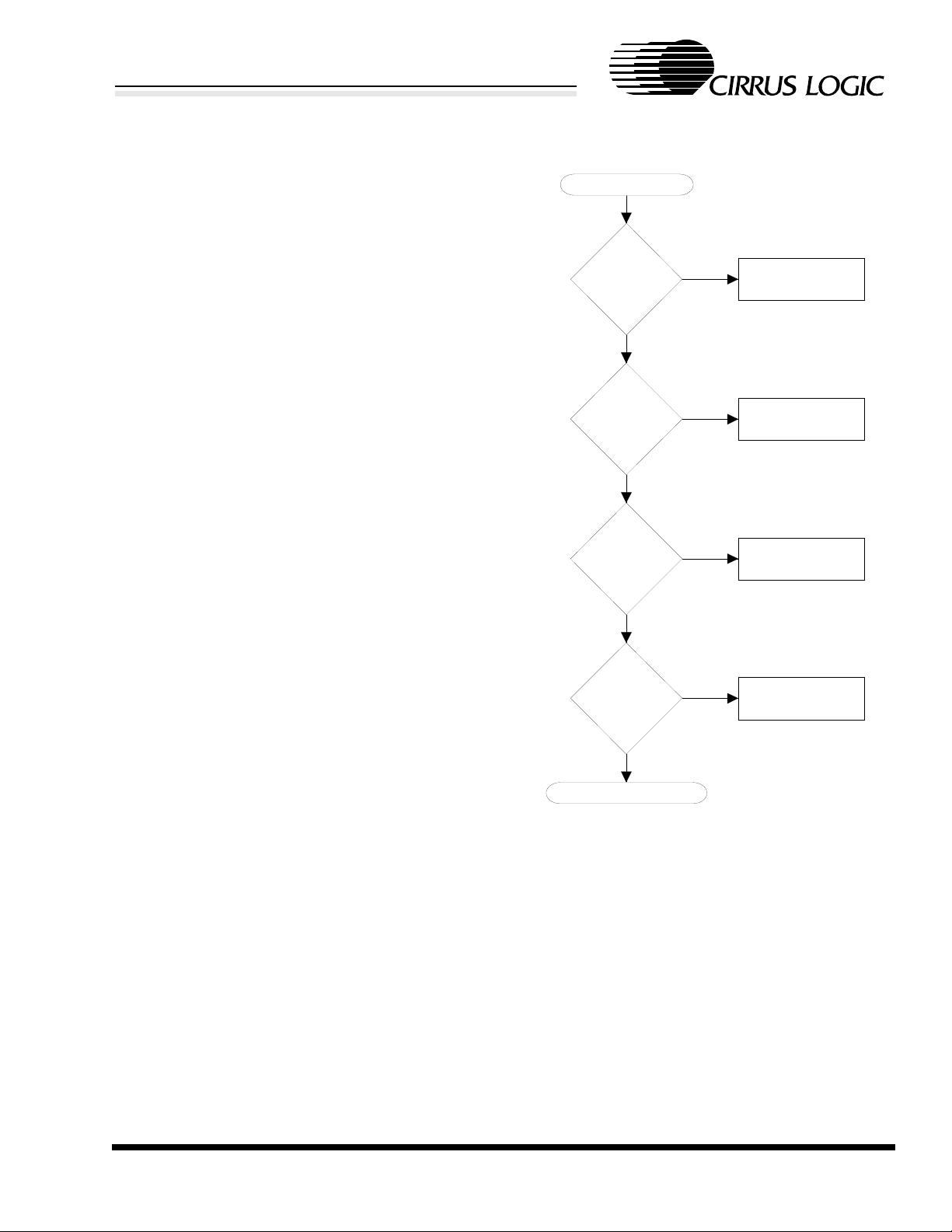
CS8900A
All Frames
use DMA
Yes
Yes
No
No
Yes
No
No
Yes
Frame
Discarded
Frame Buff ered
in On-chip RAM
Auto-Switch
DMA Disabled
Packet Received
Auto-Switch to DMA
Frame
Passed the
DA filter?
RxDMA only
Bit=1
More
Buffer Space
Available?
AutoRxDMA
Bit=1?
Figure 26. Conditions for Switching to DMA
Crystal LAN™ Ethernet Controller
ered as normal. If there isn't, the CS8900A's
MAC engine compares the frame's Destination Address (DA) to the criteria programmed
into the DA filter. If the incoming DA fails the
DA filter, the frame is discarded. If the DA
passes the DA filter, the CS8900A automatically switches to DMA mode and starts transferring the frame(s) currently being held in the
on-chip buffer into host memory. This frees up
buffer space for the incoming frame.
Figure 26 shows the steps the CS8900A goes
through in determining when to automatically
switch to DMA.
Whenever the CS8900A automatically enters
DMA, at least one complete frame is already
stored in the on-chip buffer. Because frames
are transferred to the host in the same order as
received (first in, first out), the beginning of the
received frame that triggered the switch to
DMA is not the first frame to be transferred. Instead, the oldest noncommitted frame in the
on-chip buffer is the first frame to use DMA.
When DMA begins, any pending RxEvent reports in the Interrupt Status Queue are discarded because the host cannot process
those events until the corresponding frames
have been completely DMAed.
Auto-Switch DMA works only on entire received frames. The CS8900A does not use
Auto-Switch DMA to transfer partial frames.
Also, when a frame has been committed (see
Section 5.2.5 on page 85), the CS8900A will
not switch to DMA mode until the committed
frame has been transferred completely or
skipped.
After a complete frame has been moved to
host memory, the CS8900A updates the DMA
Start-of-Frame register (PacketPage base +
0126h), the DMA Frame Count register (PacketPage base + 0128h), and the DMA Byte
Count register, then sets the RxDMAFrame bit
DS271F5 95
(Register C, BufEvent, bit 7). If RxDMAiE
(Register B, BufCFG, bit 7) is set, a corresponding interrupt occurs.
5.4.4 DMA Channel Speed vs. Missed Frames
When the CS8900A starts DMA, the entire oldest, noncommitted frame must be placed in
host memory before on-chip buffer space will
be freed for the next incoming frame. If the oldest frame is relatively large, and the next in-
CIRRUS LOGIC PRODUCT DATASHEET
Page 96

CS8900A
Crystal LAN™ Ethernet Controller
coming frame also large, the incoming frame
may be missed, depending on the speed of the
DMA channel. If this happens, the CS8900A
will increment the RxMiss counter (Register
10) and clear any event reports (RxEvent and
BufEvent) associated with the missed frame.
5.4.5 Exit From DMA
When the CS8900A has activated receive
DMA, it remains in DMA mode until all of the
following are true:
• The host processes all RxEvent and BufEvent reports pending in the ISQ.
• The host reads a zero value from the DMA
Frame Count register (PacketPage base +
0028h).
• The CS8900A is not in the process of
transferring a frame via DMA.
5.4.6 Auto-Switch DMA Example
Figure 27 shows how the CS8900A enters and
exits Auto-Switch DMA mode.
5.5 StreamTransfer
ceiver Configuration (register 3).
(StreamTransfer must not be selected unless
either one of AutoRxDMAE or RxDMA-only is
selected.)StreamTransfer only applies to
"good" frames (frames of legal length with valid CRC). Therefore, the RxOKA bit and the
RxOKiE bit must both be set. Finally, StreamTransfer works on whole packets and is not
compatible with early interrupts. This requires
that the RxDestiE bit and the Rx128iE bit both
be clear.
Table 29 summarizes how to configure the
CS8900A for StreamTransfer.
Register Name Bit Bit Name Value
Register 3, RxCFG 7 StreamE 1
8RxOKiE1
9
or
A
Register 5, RxCTL 8 RxOKA 1
Register B, BufCFG 7 RxDMAiE 1
FRxDestiE 0
B Rx128iE 0
Table 29. Stream Transfer Configuration
RxDMAonly
or
AutoRxDMA
1
or
1
5.5.1 Overview
The CS8900A supports an optional feature,
StreamTransfer, that can reduce the amount
of CPU overhead associated with frame reception. StreamTransfer works during periods
of high receive activity by grouping multiple receive events into a single interrupt, thereby reducing the number of receive interrupts to the
host processor. During periods of peak loading, StreamTransfer will eliminate 7 out of every 8 interrupts, cutting interrupt overhead by
up to 87%.
5.5.2 Configuring the CS8900A for Stream-
Transfer
StreamTransfer is enabled by setting the
StreamE bit along with either the AutoRxDMAE bit or the RxDMAonly bit in register Re-
CIRRUS LOGIC PRODUCT DATASHEET
5.5.3 StreamTransfer Operation
When StreamTransfer is enabled, the
CS8900A will initiate a StreamTransfer cycle
whenever two or more frames with the following characteristics are received:
1) pass the Destination Address filter;
2) are of legal length with valid CRC; and,
3) are spaced "back-to-back" (between 9.6
and 52 µs apart).
During a StreamTransfer cycle the CS8900A
does the following:
• delays the normal RxOK interrupt associated with the first receive frame;
• switches to receive DMA mode;
• transfers up to eight receive frames into
host memory via DMA;
96 DS271F5
Page 97

CS8900A
F
r
a
m
e
1
F
r
a
m
e
2
Frame 3 starts to be received and passes the DA filter.
This activates Auto-Switch DMA.
F
r
a
m
e
3
Frame 1 is placed in ho st memory via DMA freeing
space for the incoming F rame 3. The CS8900A updates
the DMA Frame Count, DMA Start of Frame and DMA
Byte Count registers. It then sets the RxDMA DMAFrame
bit and generates an interrupt.
Frame 2 is plac ed in host me m ory via DMA an d t he
CS8900A updates the DMA registers.
The host responds to the RxDMAFrame interrupt, and
read s t h e Frame Count r e gist e r, which is c lear ed w h e n
read. Since there are no receive in terrup ts pend ing, the
CS8900A exits DMA (assumes Frame 3 is still coming in).
Receive DMA used
during this time.
At this point, the CS8900A does not have sufficient buffer
space for another complete large frame (1518 bytes).
Frame 1 received and completely stored in on-chip RAM.
Frame 2 received and completely stored in on-chip RAM.
Enter Example Here
Exit Example
Time
Frame 3 is completely bu ffered in on-chip RA M, and
awaits processing by the host.
Entering this example, the receive buffer is empty and the
DMA Frame Count (P ac ketPage bas e + 0028h) is zero.
Figure 27. Example of Auto-Switch DMA
Crystal LAN™ Ethernet Controller
DS271F5 97
CIRRUS LOGIC PRODUCT DATASHEET
Page 98

CS8900A
4 Back-to-Back Frames 5 Back-to-Back Frames
Interrupt
Request
9 Interrupts for 9 "Good" Packets
Time
T > 52 us
Figure 28. Receive Example Without Stream Transfer
4 Back-to-Back Frames 5 Back-to-Back Frames
Interrupt
Request
2 Interrupts f or 9 "Go od" Pac k et s
Time
T > 52 us
Figure 29. Receive DMA Configuration Options
Crystal LAN™ Ethernet Controller
• updates the DMA Start-of-Frame register
(PacketPage base + 0026h);
• updates the DMA Frame Count register
(PacketPage base + 0028h);
• updates DMA Byte Count register (PacketPage base + 002Ah);
• sets the RxDMAFrame bit (Register C,
BufEvent, Bit 7); and,
• generates an RxDMAFrame interrupt.
5.5.4 Keeping StreamTransfer Mode
Active
When the CS8900A initiates a StreamTransfer
cycle, it will continue to execute cycles as long
as the following conditions hold true:
• all packets received are of legal length with
valid CRC;
• each packet follows its predecessor by less
than 52 ms; and,
• the DA of each packet passes the DA filter.
If any of these conditions are not met, the
CS8900A exits StreamTransfer by generating
RxOK and RxDMA interrupts. The CS8900A
then returns to either Memory, I/O, or DMA
mode, depending on configuration.
5.5.5 Example of StreamTransfer
Figure 28 shows how four back-to-back
frames, followed by five back-to-back frames,
would be received without StreamTransfer.
Figure 29 shows how the same sequence of
frames would be received with StreamTransfer.
98 DS271F5
CIRRUS LOGIC PRODUCT DATASHEET
Page 99

CS8900A
Crystal LAN™ Ethernet Controller
5.5.6 Receive DMA Summary
Table 30 summarize the Receive DMA configuration options supported by the CS8900A.
RxDMAonly
(Register 3,
RxCFG,Bit 9)
1 NA 0 NA Receive DMA used for all receive frames, without
1 NA 1 NA Receive DMA used for all receive frames, with
0 1 0 0 Auto-Switch DMA used if necessary, without inter-
0 1 1 1 Auto-Switch DMA used if necessary, with RxEvent
0 0 NA NA Memory or I/O Mode only.
5.6 Transmit Operation
5.6.1 Overview
AutoRxDMAiE
(Register 3,
RxCFG, Bit A)
RxDMAiE
(Register B,
BufCFG, Bit 7)
Table 30. Receive DMA Configuration Options
RxOKiE
(Register 3,
RxCFG, Bit 8)
CS8900A Configuration
interrupts.
BufEvent interrupts.
rupts.
and BufEvent interrupts possible.
381, 1021 bytes or full frame, depending on
configuration). The preamble and Start-ofFrame delimiter are followed by the data trans-
Packet transmission occurs in two phases. In
the first phase, the host moves the Ethernet
frame into the CS8900A's buffer memory. The
first phase begins with the host issuing a
Transmit Command.
This informs the CS8900A that a frame is to be
transmitted and tells the chip when (i.e. after 5,
ferred into the on-chip buffer by the host (Destination Address, Source Address, Length field
and LLC data). If the frame is less than 64
bytes, including CRC, the CS8900A adds pad
bits if configured to do so. Finally, the
CS8900A appends the proper 32-bit CRC value.
381, or 1021 bytes have been transferred or
after the full frame has been transferred to the
CS8900A) and how the frame should be sent
(i.e. with or without CRC, with or without pad
bits, etc.). The host follows the Transmit Command with the Transmit Length, indicating how
much buffer space is required. When buffer
space is available, the host writes the Ethernet
frame into the CS8900A's internal memory,
using either Memory or I/O space.
5.6.2 Transmit Configuration
After each reset, the CS8900A must be configured for transmit operation. This can be done
automatically using an attached EEPROM, or
by writing configuration commands to the
CS8900A's internal registers (see Section 3.4
on page 21). The items that must be configured include which physical interface to use
and which transmit events cause interrupts.
In the second phase of transmission, the
CS8900A converts the frame into an Ethernet
packet then transmits it onto the network. The
second phase begins with the CS8900A transmitting the preamble and Start-of-Frame delimiter as soon as the proper number of bytes
5.6.2.1 Configuring the Physical Interface
Configuring the physical interface consists of
determining which Ethernet interface should
be active (10BASE-T or AUI), and enabling the
transmit logic for serial transmission. Configuring the Physical Interface is accomplished via
has been transferred into its transmit buffer (5,
CIRRUS LOGIC PRODUCT DATASHEET
DS271F5 99
Page 100

CS8900A
Crystal LAN™ Ethernet Controller
the LineCTL register (Register 13) and is described in Table 31.
Register 13, LineCTL
Bit Bit Name Operation
7 SerTxON When set, transmission enabled.
8 AUIonly When set, AUI selected (takes
precedence over AutoAUI/10BT).
When clear, 10BASE-T selected.
9 AutoAUI/10BT When set, automatic interface
selection enabled.
BMod
BackoffE
D2-part
DefDis
Table 31. Physical Interface Configuration
When set, the modified backoff
algorithm is used. When clear,
the standard backoff algorithm is
used.
When set, two-part deferral is
disabled.
Note that the CS8900A transmits in 10BASET mode when no link pulses are being received only if bit DisableLT is set in register
Test Control (Register 19).
5.6.2.2 Selecting which Events Cause Interrupts
The TxCFG register (Register 7) and the BufCFG register (Register B) are used to determine which transmit events will cause
interrupts to the host processor. Tables 32 and
33 describe the interrupt enable (iE) bits in
these registers.
Register B, BufCFG
Bit Bit Name Operation
8 Rdy4TxiE When set, there is an interrupt
whenever buffer space becomes
available for a transmit frame
(used with a Transmit Request).
9 TxUnder
runiE
CTxCol
OvfloiE
Table 33. Transmit Interrupt Configuration
When set, there is an interrupt
whenever the CS8900A runs out
of data after transmit has started.
When set, there is an interrupt
whenever the TxCol counter
overflows.
Register 7, TxCFG
Bit Bit Name Operation
6 Loss-of-
CRSiE
7 SQErroriE When set, there is an interrupt
8 TxOKiE When set, ther e is an int er rupt
9Out-of-
windowiE
A Jabbe r i E When set, there is an interrupt
B AnycolliE When set, there is an interrupt
F 16colliE When set, there is an interrupt
Table 32. Transmitting Interrupt Configuration
When set, there is an interrupt
whenever the CS8900A fails to
detect Carrier Sense after transmitting the preamble (applies to
the AUI only).
whenever there is an SQE error.
whenever a frame is transmitted
successfully..
When set, there is an interrupt
whenever a late collision is
detected.
whenever there is a jabber condition.
whenever there is a collision.
whenever the CS8900A attempts
to transmit a single frame 16
times.
5.6.3 Changing the Configuration
When the host configures these registers it
does not need to change them for subsequent
packet transmissions. If the host does choose
to change the TxCFG or BufCFG registers, it
may do so at any time. The effects of the
change are noticed immediately. That is, any
changes in the Interrupt Enable (iE) bits may
affect the packet currently being transmitted.
If the host chooses to change bits in the
LineCTL register after initialization, the ModBackoffE bit and any receive related bit (LoRxSquelch, SerRxON) may be changed at any
time. However, the Auto AUI/10BT and AUIonly bits should not be changed while the SerTxON bit is set. If any of these three bits are to be
changed, the host should first clear the SerTxON bit (Register 13, LineCTL, Bit 7), and then
set it when the changes are complete.
CIRRUS LOGIC PRODUCT DATASHEET
100 DS271F5
 Loading...