

Page 1
Serial
Audio
Input
4:1
MUX
RX0/RXP0
RX1/RXN0
RX2/RXP1
RX3/RXN1
Receiver
Clock &
Data
Recovery
(PLL)
ILRCK
ISCLK
SDIN
Sample
Rate
Converter
C or U Data Buffer
(First 5 Bytes)
Control Port & Registers
2:1
MUX
Serial
Audio
Output
3:1
MUX
XTI
Clock
Generator
SDA/
CDOUT
SCL/
CCLK
AD1/
CDIN
AD0/
CS
RMCK
General
Purpose
Outputs
GPO0
Format
Detect
GPO1
GPO2
GPO3
OLRCK1
OSCLK1
SDOUT1
TDM_IN
Serial
Audio
Output
3:1
MUX
OLRCK2
OSCLK2
SDOUT2
VL
VA
AGND
XTO
Level Translators
Level Translators
DGND
V_REG
CS8422
24-bit, 192-kHz, Asynchronous Sample Rate Converter with
Integrated Digital Audio Interface Receiver
Sample Rate Converter Features
140 dB Dynamic Range
-120 dB THD+N
No External Master Clock Required
Supports Sample Rates up to 211 kHz
Input/Output Sample Rate Ratios from 6:1 to
1:6
Master Mode Master Clock/Sample Rate Ratio
Support: 64, 96, 128, 192, 256, 384, 512, 768,
1024
16, 18, 20, or 24-bit Data I/O
Dither Automatically Applied and Scaled to
Output Resolution
Multiple Device Outputs are Phase Matched
Digital Audio Interface Receiver
Features
Complete EIAJ CP1201, IEC-60958, AES3,
S/PDIF Compatible Receiver
28 kHz to 216 kHz Sample Rate Range
2:1 Differential AES3 or 4:1 S/PDIF Input Mux
De-emphasis Filtering for 32 kHz, 44.1 kHz,
and 48 kHz
Recovered Master Clock Output: 64 x Fs,
96 x Fs, 128 x Fs, 192 x Fs, 256 x Fs,
384 x Fs, 512 x Fs, 768 x Fs, 1024 x Fs
49.152 MHz Maximum Recovered Master
Clock Frequency
Ultralow-jitter Clock Recovery
High Input Jitter Tolerance
No External PLL Filter Components Required
Selectable and Automatic Clock Switching
AES3 Direct Output and AES3 TX Pass-
through
On-chip Channel Status Data Buffering
Automatic Detection of Compressed Audio
Streams
Decodes CD Q Sub-Code
http://www.cirrus.com
Copyright Cirrus Logic, Inc. 2012
(All Rights Reserved)
NOV '12
DS692F2
Page 2

CS8422
System Features
SPI™ or I²C™ Software Mode and Stand-Alone
Hardware Mode
Flexible 3-wire Digital Serial Audio Input Port
Dual Serial Audio Output Ports with
Independently Selectable Data Paths
Master or Slave Mode Operation for all Serial
Audio Ports
Time Division Multiplexing (TDM) Mode
Integrated Oscillator for use with External
Crystal
Four General-purpose Output Pins (GPO)
+3.3 V Analog Supply (VA)
+1.8 V to 5.0 V Digital Interface (VL)
Space-saving 32-pin QFN Package
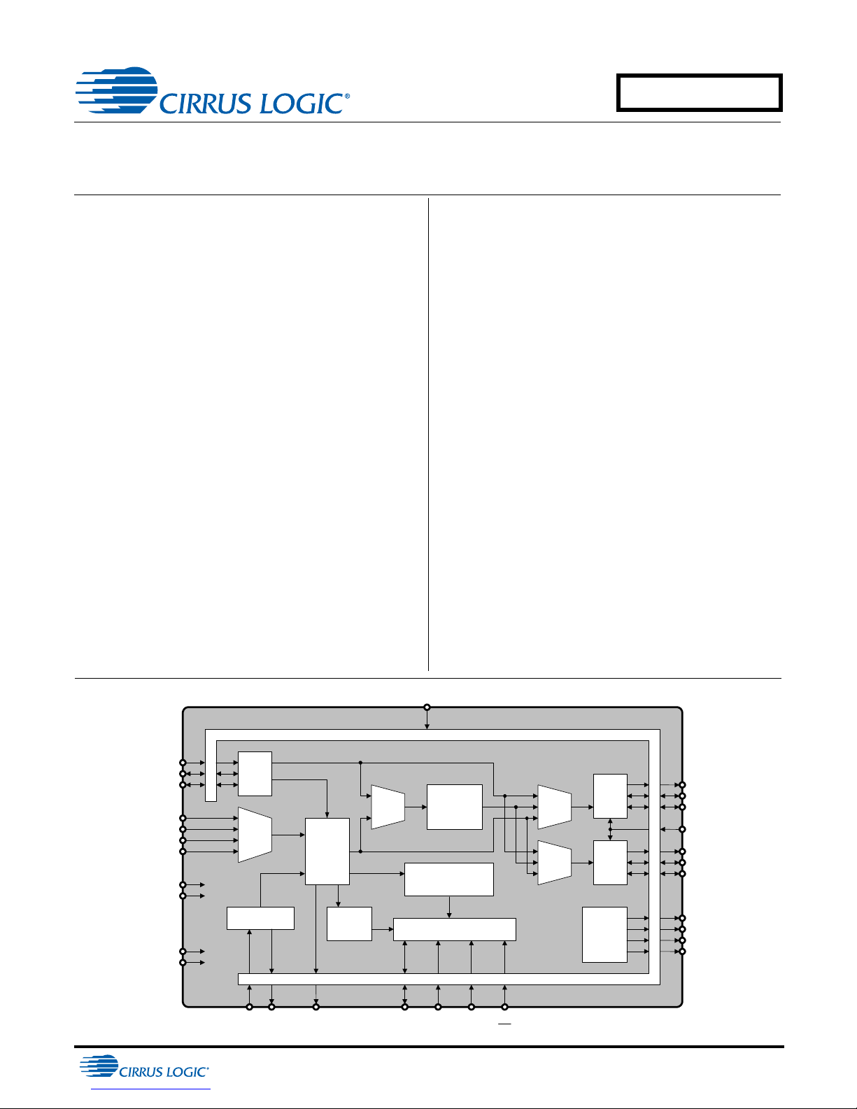
General Description
The CS8422 is a 24-bit, high-performance, monolithic
CMOS stereo asynchronous sample rate converter with
an integrated digital audio interface receiver that decodes audio data according to the EIAJ CP1201, IEC60958, AES3, and S/PDIF interface standards.
Audio data is input through the digital interface receiver
or a 3-wire serial audio input port. Audio is output
through one of two 3-wire seria l audio output ports. Serial audio data outputs can be set to 24, 20, 18, or 16-bit
word-lengths. Data into the digital interface receiver and
serial audio input port can be up to 24-bits long. Input
and output data can be completely asynchronous, synchronous to an external clock through XTI, or
synchronous to the recovered master clock.
The CS8422 can be controlled through the control port
in Software Mode or in a Stand-Alone Hardware Mode.
In Software Mode, the user can control the device
through an SPI or I²C control port.
Target applications include digital recording systems
(DVD-R/RW, CD-R/RW, PVR, DAT, MD, and VTR), digital mixing consoles, high-quality D/A, effects
processors, and computer audio systems.
The CS8422 is available in a space-saving QFN package in Commercial (-40° C to +85° C) grade. The
CDB4822 is also available for device evaluation and implementation suggestions. Please refer to “Ordering
Information” on page 81 for complete details.
2 DS692F2
Page 3

TABLE OF CONTENTS
1. PIN DESCRIPTION ................................................................................................................................. 9
1.1 Software Mode .................................. ... ... .... ... ... ... .......................................... .... ... ... ... ..................... 9
1.2 Hardware Mode ............................. ... ... ... .... ... ... ... .... ... .......................................... ... ... ................... 11
2. CHARACTERISTICS AND SPECIFICATIONS .................................................................................... 13
RECOMMENDED OPERATING CONDITIONS .................................................................................. 13
ABSOLUTE MAXIMUM RATINGS ...................................................................................................... 13
PERFORMANCE SPECIFICATIONS - SAMPLE RATE CONVERTER .............................................. 14
DIGITAL FILTER CHARACTERISTICS .............................................................................................. 14
DC ELECTRICAL CHARACTERISTICS . ... ... .... ... ... ... .... ... ... .......................................... ... ... .... ... ... ... ... 15
DIGITAL INTERFACE SPECIFICATIONS ........................................................................................... 16
SWITCHING SPECIFICATIONS ......................................................................................................... 17
SWITCHING CHARACTERISTICS - CONTROL PORT - SPI MODE ................................................. 20
SWITCHING CHARACTERISTICS - CONTROL PORT - I²C MODE ...................................... ............ 21
3. TYPICAL CONNECTION DIAGRAMS .................................................................................................22
3.1 Software Mode .............................................................................................................................. 22
3.2 Hardware Mode ............................... ... ... .... ... ... ... .... ... ... .......................................... ... ................... 23
4. OVERVIEW ........................................................................................................................................... 24
5. THREE-WIRE SERIAL INPUT/OUTPUT AUDIO PORT ...................................................................... 24
5.1 Serial Port Clock Operation .................... .... ... ... ... .... ... ... ... .... ......................................... ................ 25
5.1.1 Master Mode ......................................................................................................................... 25
5.1.2 Slave Mode ........................................................................................................................... 25
5.1.3 Hardware Mode Control ........................................................................................................25
5.1.4 Software Mode Control ................................ .... ... ... ... .... ... ... ... ... .... ... ... ................................... 25
5.1.5 Time Division Multiplexing (TDM) Mode ................................... .... ... ... ... .... ... ... ... ... .... ... ... ... ... 27
5.1.5.1 TDM Master Mode ..................................................................................................... 27
5.1.5.2 TDM Slave Mode ................................................................................. ...................... 27
5.1.5.3 Hardware Mode Control ................... .... ... .......................................... ... ... ................... 27
5.1.5.4 Software Mode Control .............................................................................................. 27
6. DIGITAL INTERFACE RECEIVER ....................................................................................................... 29
6.1 AES3 and S/PDIF Standards ......................................................................................................... 29
6.2 Receiver Input Multiplexer ............................................................................................................. 29
6.2.1 Hardware Mode Control ........................................................................................................29
6.2.2 Software Mode Control ................................ .... ... ... ... .... ... ... ... ... .... ... ... ................................... 29
6.2.2.1 Single-Ended Input Mode ....................................................... ... .... ... ... ... ................... 30
6.2.2.2 Differential Input Mode ............................................................................................... 30
6.3 Recovered Master Clock - RMCK .................................................................................................. 31
6.3.1 Hardware Mode Control ........................................................................................................31
6.3.2 Software Mode Control ................................ .... ... ... ... .... ... ... ... ... .... ... ... ................................... 31
6.4 XTI System Clock Mode ...................... ... .... ... ... ... .... ... .......................................... ... ... ... .... ............ 31
6.4.1 Hardware Mode Control ........................................................................................................32
6.4.2 Software Mode Control ................................ .... ... ... ... .... ... ... ... ... .... ... ... ................................... 32
6.5 AES11 Behavior ............................................................................................................................. 32
6.6 Error and Status Reporting ............................................................................................................ 32
6.6.1 Software Mode ...................................................................................................................... 32
6.6.2 Hardware Mode Control ........................................................................................................33
6.7 Non-Audio Detection ................................... ... ... ... .... ... ... ... .... ... ... ................................................... 33
6.7.1 Hardware Mode Control ........................................................................................................34
6.7.2 Software Mode Control ................................ .... ... ... ... .... ... ... ... ... .... ... ... ................................... 34
6.8 Format Detection (Software Mode Only) ....................................................................................... 34
6.9 Interrupts (Software Mode Only) .................................................................................................... 34
6.10 Channel Status and User Data Handling .....................................................................................34
6.10.1 Hardware Mode Control ...................................................................................................... 34
CS8422
DS692F2 3
Page 4

CS8422
6.10.2 Software Mode Control ........................................................................................................ 35
7. SAMPLE RATE CONVERTER (SRC) .................................................................................................. 37
7.1 SRC Data Resolution and Dither ................................................................................................... 37
7.1.1 Hardware Mode Control ........................................................................................................ 37
7.1.2 Software Mode Control .......................................................................................................... 37
7.2 SRC Locking .................................................................................................................................. 37
7.3 SRC Muting .................................................................................................................................... 38
7.4 SRC Master Clock ......................................................................................................................... 38
7.4.1 Hardware Mode Control ........................................................................................................ 39
7.4.2 Software Mode Control .......................................................................................................... 39
8. HARDWARE MODE CONTROL .......................................................................................................... 39
8.1 Hardware Mode Serial Audio Port Control ..................................................................................... 41
9. SOFTWARE MODE CONTROL ........................................................................................................... 43
9.1 Control Port Description ................................................................................................................ 43
9.1.1 SPI Mode .................................. ... ... .......................................... .... ... ...................................... 43
9.1.2 I²C Mode ................................ .......................................... ... ... ................................................ 44
9.1.3 Memory Address Pointer (MAP) ............................... .... ...... ...... ....... ...... ....... ...... ....... ...... ...... 44
10. REGISTER QUICK REFERENCE ...................................................................................................... 45
11. SOFTWARE REGISTER BIT DEFINITIONS ...................................................................................... 48
11.1 CS8422 I.D. and Version Register (01h) ..................................... ... .... ... ... ... .... ... ... ... ... .... ... ... ...... 48
11.2 Clock Control (02h) .. .... ... ... ... .......................................... .... ... ... ... ... ............................................. 48
11.3 Receiver Input Control (03h) ........................................................................................................ 49
11.4 Receiver Data Control (04h) ........................................................................................................ 49
11.5 GPO Control 1 (05h) .... ... ... ... .... ... .......................................... ... ... ... .... ... ...................................... 51
11.6 GPO Control 2 (06h) .... ... ... ... .... ... .......................................... ... ... ... .... ... ...................................... 51
11.7 Serial Audio Input Clock Control (07h) ........................................................................................ 51
11.8 SRC Output Serial Port Clock Control (08h) ...............................................................................52
11.9 Recovered Master Clock Ratio Control & Misc. (09h) ................................................................ 53
11.10 Data Routing Control(0Ah) ......................................................................................................... 54
11.11 Serial Audio Input Data Format (0Bh) ....................................................................................... 54
11.12 Serial Audio Output Data Format - SDOUT1 (0Ch) ................................................................... 55
11.13 Serial Audio Output Data Format - SDOUT2 (0Dh) .................................................................. 56
11.14 Receiver Error Unmasking (0Eh) .............................................................................................. 57
11.15 Interrupt Unmasking (0Fh) ......................................................................................................... 58
11.16 Interrupt Mode (10h) .................................................................................................................. 58
11.17 Receiver Channel Status (11h) ................................................................................................. 58
11.18 Format Detect Status (12h) ........................... .......... ............. ............. ............. ............ ................ 59
11.19 Receiver Error (13h) ................................................................................................................. 59
11.20 Interrupt Status (14h) ................................................................................................................ 60
11.21 PLL Status (15h) ....................................................................................................................... 61
11.22 Receiver Status (16h) ............................................................................................................... 62
11.23 Fs/XTI Ratio (17h - 18h) ........................................................................................................... 63
11.24 Q-Channel Subcode (19h - 22h) ................................................................................................ 63
11.25 Channel Status Registers (23h - 2Ch) ....................................................................................... 63
11.26 IEC61937 PC/PD Burst preamble (2Dh - 30h) .......................................................................... 64
12. APPLICATIONS ................................................................................................................................. 65
12.1 Reset, Power Down, and Start-Up ............................ .......................................... ......................... 65
12.2 Power Supply, Grounding, and PCB layout ................................................................................. 65
12.3 External Receiver Components ................... ... ... .... ... ... ... ............................................. .... ... ... ... ... 65
12.3.1 Attenuating Input signals ..................................................................................................... 66
12.3.2 Isolating Transformer Requirements ...................................... ............................................. 67
12.4 Channel Status Buffer Management ............................................................................................ 67
12.4.1 AES3 Channel Status (C) Bit Management ........................................................................ 67
12.4.2 Accessing the E buffer ........................................................................................................ 68
4 DS692F2
Page 5

12.4.3 Serial Copy Management System (SCMS) ......................................................................... 69
12.5 Jitter Attenuation .......................................................................................................................... 69
12.6 Jitter Tolerance ............................................................................................................................ 70
12.7 Group Delay ................................................................................................................................. 70
13. PERFORMANCE PLOTS ......................................... .... ... ... ... .... ... ... ... ... .... ... ... ................................... 71
14. PACKAGE DIMENSIONS ............................................................ ... ... ... .... ... ...................................... 80
15. THERMAL CHARACTERISTICS AND SPECIFICATIONS .............................................................. 80
16. ORDERING INFORMATION ................. ... ... .......................................... .... ... ... ... .... ... ... ... ... ................ 81
17. REFERENCES ....................... ... ... .... ... ... ... ... .... ... ... .......................................... ... .... ... ... ...................... 81
18. REVISION HISTORY ....................................... ... ... ... .... ... .......................................... ... ... ................... 82
LIST OF FIGURES
Figure 1.Non-TDM Slave Mode Timing ..................................................................................................... 19
Figure 2.TDM Slave Mode Timing ............................................................................................................ 19
Figure 3.Non-TDM Master Mode Timing ................................................................................................... 19
Figure 4.TDM Master Mode Timing .......................................................................................................... 19
Figure 5.SPI Mode Timing ........................................................................................................................ 20
Figure 6.I²C Mode Timing ......................................................................................................................... 21
Figure 7.Typical Connection Diagram, Software Mode .............................................................................22
Figure 8.Typical Connection Diagram, Hardware Mode ........................................................................... 23
Figure 9.Serial Audio Interface Format – I²S ............................................................................................. 26
Figure 10.Serial Audio Interface Format – Left-Justified ........................................................................... 26
Figure 11.Serial Audio Interface Format – Right-Justified (Master Mode only) ........................................ 26
Figure 12.Serial Audio Interface Format – AES3 Direct Output ................................................................ 26
Figure 13.TDM Master Mode Timing Diagram .......................................................................................... 28
Figure 14.TDM Slave Mode Timing Diagram ................................... ... ... ... ... .... ... ... ... .... ... ... ... ... .... ... ... ...... 28
Figure 15.TDM Mode Configuration (All CS8422 outputs are slave) ........................................................ 28
Figure 16.TDM Mode Configuration (First CS8422 output is master, all others are slave) ....................... 28
Figure 17.Single-Ended Receiver Input Structure, Receiver Mode 1 ....................................................... 30
Figure 18.Differential Receiver Input Structure ......................................................................................... 31
Figure 19.C/U Data Outputs ...................................................................................................................... 36
Figure 20.Typical Connection Diagram for Crystal Circuit ........................................................................ 38
Figure 21.Hardware Mode Clock Routing ................................................................................................. 40
Figure 22.Control Port Timing in SPI Mode ..................................... ... ... ... ... .... ... ... ... .... ... ......................... 43
Figure 23.Control Port Timing, I²C Slave Mode Write ............................................................................... 44
Figure 24.Control Port Timing, I²C Slave Mode Read ............................................................................... 44
Figure 25.De-Emphasis Filter Response .................................................................................................. 50
Figure 26.Professional Input Circuit – Differential Mode ........................................................................... 66
Figure 27.Transformerless Professional Input Circuit – Differential Mode ............. ................................... 66
Figure 28.S/PDIF MUX Input Circuit – Single-Ended ................................................................................ 66
Figure 29.Receiver Mode 1 Single-Ended Input Circuit – Differential Mode ................. ............................ 66
Figure 30.S/PDIF MUX Input Circuit – Digital Mode ................................................................................. 66
Figure 31.TTL/CMOS Input Circuit – Differential Mode ............................................................................ 66
Figure 32.Receiver Input Attenuation – Single-ended Input ..................................................................... 67
Figure 33.Receiver Input Attenuation – Differential Input ......................................................................... 67
Figure 34.Channel Status Data Buffer Structure ....................................................................................... 68
Figure 35.Flowchart for Reading the E Buffer ........................................................................................... 68
Figure 36.CS8422 PLL Jitter Attenuation Characteristics ......................................................................... 69
Figure 37.Jitter Tolerance Template ......................................................................................................... 70
Figure 38.Wideband FFT –
0 dBFS 1 kHz Tone, 48 kHz:48 kHz ......................................... .......................................... ... ... .... ... ......... 71
Figure 39.Wideband FFT –
0 dBFS 1 kHz Tone, 44.1 kHz:192 kHz .................................... ... .... ... ... ... ... .... ... ... ... ................................ 71
CS8422
DS692F2 5
Page 6

CS8422
Figure 40.Wideband FFT –
0 dBFS 1 kHz Tone, 44.1 kHz:48 kHz ...................................................................................................... 71
Figure 41.Wideband FFT –
0 dBFS 1 kHz Tone, 48 kHz:44.1 kHz ...................................................................................................... 71
Figure 42.Wideband FFT –
0 dBFS 1 kHz Tone, 48 kHz:96 kHz ......................................................................................................... 71
Figure 43.Wideband FFT –
0 dBFS 1 kHz Tone, 96 kHz:48 kHz ......................................................................................................... 71
Figure 44.Wideband FFT –
0 dBFS 1 kHz Tone, 192 kHz:48 kHz ....................................................................................................... 72
Figure 45.Wideband FFT –
-60 dBFS 1 kHz Tone, 48 kHz:96 kHz ...................................................................................................... 72
Figure 46.Wideband FFT –
-60 dBFS 1 kHz Tone, 48 kHz:48 kHz ...................................................................................................... 72
Figure 47.Wideband FFT –
-60 dBFS 1 kHz Tone, 44.1 kHz:192 kHz ................................................................................................. 72
Figure 48.Wideband FFT –
-60 dBFS 1 kHz Tone, 44.1 kHz:48 kHz ................................................................................................... 72
Figure 49.Wideband FFT –
-60 dBFS 1 kHz Tone, 48 kHz:44.1 kHz ................................................................................................... 72
Figure 50.Wideband FFT –
-60 dBFS 1 kHz Tone, 96 kHz:48 kHz ...................................................................................................... 73
Figure 51.IMD –
10 kHz and 11 kHz -7 dBFS, 96 kHz:48 kHz ............................................................................................73
Figure 52.Wideband FFT –
-60 dBFS 1 kHz Tone, 192 kHz:48 kHz ....................................................................................................73
Figure 53.IMD –
10 kHz and 11 kHz -7 dBFS, 48 kHz:44.1 kHz ......................................................................................... 73
Figure 54.IMD –
10 kHz and 11 kHz -7 dBFS, 44.1 kHz:48 kHz .........................................................................................73
Figure 55.Wideband FFT –
0 dBFS 20 kHz Tone, 44.1 kHz:48 kHz .................................................................................................... 73
Figure 56.Wideband FFT –
0 dBFS 80 kHz Tone, 192 kHz:192 kHz ................................................................................................... 74
Figure 57.Wideband FFT –
0 dBFS 20 kHz Tone, 48 kHz:96 kHz ....................................................................................................... 74
Figure 58.Wideband FFT –
0 dBFS 20 kHz Tone, 48 kHz:48 kHz ....................................................................................................... 74
Figure 59.Wideband FFT –
0 dBFS 20 kHz Tone, 96 kHz:48 kHz ....................................................................................................... 74
Figure 60.Wideband FFT –
0 dBFS 20 kHz Tone, 48 kHz:44.1 kHz .................................................................................................... 74
Figure 61.THD+N vs. Output Sample Rate –
0 dBFS 1 kHz Tone, Fsi = 192 kHz ........................................................................................................... 74
Figure 62.THD+N vs. Output Sample Rate –
0 dBFS 1 kHz Tone, Fsi = 48 kHz ............................................................................................................. 75
Figure 63.THD+N vs. Output Sample Rate –
0 dBFS 1 kHz Tone, Fsi = 96 kHz ............................................................................................................. 75
Figure 64.THD+N vs. Output Sample Rate –
0 dBFS 1 kHz Tone, Fsi = 44.1 kHz .......................................................................................................... 75
Figure 65.Dynamic Range vs. Output Sample Rate –
-60 dBFS 1 kHz Tone, Fsi = 192 kHz ....................................................................................................... 75
Figure 66.THD+N vs. Output Sample Rate –
0 dBFS 1 kHz Tone, Fsi = 32 kHz ............................................................................................................. 75
6 DS692F2
Page 7

CS8422
Figure 67.Dynamic Range vs. Output Sample Rate –
-60 dBFS 1 kHz Tone, Fsi = 32 kHz ...... ... ... ... ... .... ... ... ... .... .......................................... ... ... ... ... .... ... ......... 75
Figure 68.Dynamic Range vs. Output Sample Rate –
-60 dBFS 1 kHz Tone, Fsi = 96 kHz ...... ... ... ... ... .... ... ... ... .... .......................................... ... ... ... ... .... ... ......... 76
Figure 69.Dynamic Range vs. Output Sample Rate –
-60 dBFS 1 kHz Tone, Fsi = 44.1 kHz ... .......................................... ... ... ... ... .... ... ... ... .... ... ......................... 76
Figure 70.Frequency Response – 0 dBFS Input ....................................................................................... 76
Figure 71.Passband Ripple – 192 kHz:48 kHz ......................................................................................... 76
Figure 72.Dynamic Range vs. Output Sample Rate –
-60 dBFS 1 kHz Tone, Fsi = 48 kHz ...... ... ... ... ... .... ... ... ... .... .......................................... ... ... ... ... .... ... ......... 76
Figure 73.Linearity Error –
0 to -140 dBFS Input, 200 Hz Tone, 48 kHz:48 kHz ................................................................................. 76
Figure 74.Linearity Error –
0 to -140 dBFS Input, 200 Hz Tone, 48 kHz:44.1 kHz .............................................................................. 77
Figure 75.Linearity Error –
0 to -140 dBFS Input, 200 Hz Tone, 48 kHz:96 kHz ................................................................................. 77
Figure 76.Linearity Error –
0 to -140 dBFS Input, 200 Hz Tone, 96 kHz:48 kHz ................................................................................. 77
Figure 77.Linearity Error –
0 to -140 dBFS Input, 200 Hz Tone, 44.1 kHz:192 kHz ............................................................................ 77
Figure 78.Linearity Error –
0 to -140 dBFS Input, 200 Hz Tone, 44.1 kHz:48 kHz .............................................................................. 77
Figure 79.Linearity Error –
0 to -140 dBFS Input, 200 Hz Tone, 192 kHz:44.1 kHz ............................................................................ 77
Figure 80.THD+N vs. Input Amplitude –
1 kHz Tone, 48 kHz:44.1 kHz ................................................................................................................... 78
Figure 81.THD+N vs. Input Amplitude –
1 kHz Tone, 48 kHz:96 kHz ...................................................................................................................... 78
Figure 82.THD+N vs. Input Amplitude –
1 kHz Tone, 96 kHz:48 kHz ...................................................................................................................... 78
Figure 83.THD+N vs. Input Amplitude –
1 kHz Tone, 44.1 kHz:192 kHz ................................................................................................................. 78
Figure 84.THD+N vs. Input Amplitude –
1 kHz Tone, 44.1 kHz:48 kHz ................................................................................................................... 78
Figure 85.THD+N vs. Input Amplitude –
1 kHz Tone, 192 kHz:48 kHz .................................................................................................................... 78
Figure 86.THD+N vs. Input Frequency –
0 dBFS, 48 kHz:44.1 kHz .......................................................................................................................... 79
Figure 87.THD+N vs. Input Frequency –
0 dBFS, 48 kHz:96 kHz ............................................................................................................................. 79
Figure 88.THD+N vs. Input Frequency –
0 dBFS, 44.1 kHz:48 kHz .......................................................................................................................... 79
Figure 89.THD+N vs. Input Frequency –
0 dBFS, 96 kHz:48 kHz ............................................................................................................................. 79
Figure 90.Total Power Supply Current vs. Differential Mode Receiver Input Sample Frequency ............. 79
DS692F2 7
Page 8

LIST OF TABLES
Table 1. VLRCK Behavior ......................................................................................................................... 35
Table 2. PLL Clock Ratios ......................................................................................................................... 38
Table 3. Hardware Mode Control Settings ...... ... .... ... ... ... .... ... ... ... .... ... ... ... ................................................ 41
Table 4. Hardware Mode Serial Audio Format Control .............................................................................42
Table 5. Hardware Mode Serial Audio Port Clock Control ........... .... ... ... ... ... .... ... ... ... .... ... ... ... ... .... ... ... ... ... 42
Table 6. Summary of Software Register Bits ............................................................................................ 45
Table 7. GPO Pin Configurations .............................................................................................................. 51
Table 8. ISCLK/ILRCK Ratios and SISF Settings ..................................................................................... 54
Table 9. OSCLK1/OLRCK1 Ratios and SOSF1 Settings .......................................................................... 55
Table 10. OSCLK2/OLRCK2 Ratios and SOSF2 Settings ........... ............. ............. ............. ............. ......... 57
CS8422
8 DS692F2
Page 9
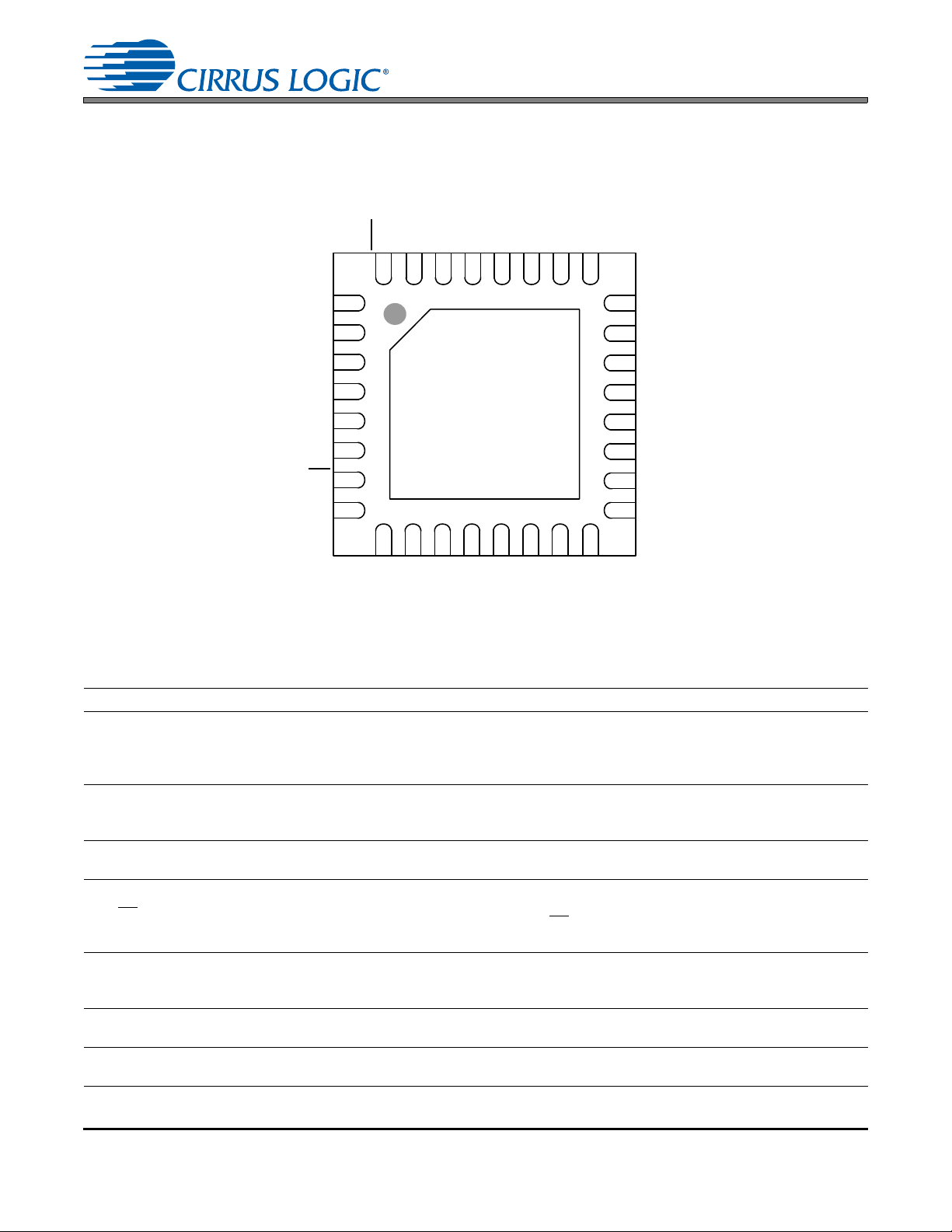
1. PIN DESCRIPTION
109
8
7
6
5
4
3
2
1
11
12
13 14 15 16
17
18
19
20
21
22
23
24
25
262728
29
303132
Top-Down View
32-Pin QFN Package
Thermal Pad
XTO
ILRCK
GPO3
OLRCK1
OSCLK1
SDOUT1
OSCLK2
VA
AGND
AD0/CS
RX0/RXP0
SDOUT2
VL
TDM_IN
OLRCK2
RX1/RXN0
RX2/RXP1
RX3/RXN1
RMCK
GPO2
VD_FILT
V_REG
XTI
AD1/CDIN
SDA/CDOUT
SCL/CCLK
ISCLK
GPO1
GPO0
SDIN
DGND
RST
1.1 Software Mode
CS8422
Pin Name Pin # Pin Description
1
AES3/SPDIF Input (Input) - Single-ended or differential receiver inputs carrying AES3 or S/PDIF
RX[3:0],
RXP/RXN[1:0]
2
encoded digital data. RX[3:0] comprise the single-ended input multiplexer. RXP[1:0] comprise the
5
non-inverting inputs of the differential input multiplexer and RXN[1:0] comprise the inverting inputs
6
of the differential input multiplexer. Unused inputs should be tied to AGND/DGND.
Analog Power (Input) - Analog power supply, nominally +3.3 V. Care should be taken to ensure
VA 3
that this supply is as noise-free as possible, as noise on this pin will directly affect the jitter perfor-
mance of the recovered clock.
AGND 4
AD0/CS
AD1/CDIN 8
SCL/CCLK 9
SDA/CDOUT 10
DS692F2 9
Analog Ground (Input) - Ground for the analog circuitry in the chip. AGND and DGND should be
connected to a common ground area under the chip.
Address Bit 0 (I²C) / Software Chip Select (SPI) (Input) - A falling edge on this pin puts the
CS8422 into SPI Control Port Mode. With no falling edge, the CS8422 defaults to I²C Mode. In I²C
7
Mode, AD0 is a chip address pin. In SPI Mode, CS
the CS8422. See “Control Port Description” on page 43.
Address Bit 1 (I²C) / Serial Control Data in (SPI) (Input) - In I²C Mode, AD1 is a chip address pin.
In SPI Mode, CDIN is the input data line to the control port interface. See “Control Port Description”
on page 43.
Software Clock (Input) - Serial control interface clock used to clock control data bits into and out of
the CS8422.
Serial Control Data I/O (I²C) / Data Out (SPI) (Input/Output) - In I²C Mode, SDA is the control I/O
data line. In SPI Mode, CDOUT is the output data from the control port interface on the CS8422.
is used to enable the control port interface on
Page 10
CS8422
Pin Name Pin # Pin Description
XTI 11
XTO 12
ILRCK 13
ISCLK 14 Serial Audio Input Bit Clock (Input/Output) - Serial bit clock for audio data on the SDIN pin.
SDIN 15 Serial Audio Input Data Port (Input) - Audio data serial input pin.
GPO[3:0]
V_REG 19 Voltage Regulator In (Input) - Regulator power supply input, nominally +3.3 V.
VD_FILT 20
DGND 21
VL 22 Logic Power (Input) - Input/Output power supply, typically +1.8 V, +2.5 V, +3.3 V, or +5.0 V.
SDOUT2 23 Serial Audio Output 2 Data Port (Output) - Audio data serial output 2 pin.
OSCLK2 24
OLRCK2 25
TDM_IN 26
SDOUT1 27
OSCLK1 28
OLRCK1 29
RMCK 31
RST
THERMAL PAD -
Crystal/Oscillator In (Input) - Crystal or digital clock input for Master clock. See “SRC Master
Clock” on page 38 for more details.
Crystal Out (Output) - Crystal output for Master clock. See “SRC Master Clock” on page 38 for
more details.
Serial Audio Input Left/Right Clock (Input/Output) - Word rate clock for the audio data on the
SDIN pin.
16
General Purpose Outputs (Output) - See page 51 for details. In I²C Mode, a 20 k pull-up resistor
17
to VL on GPO2 will set AD2 chip address bit to 1, otherwise AD2 will be 0.
18
30
Digital Voltage Regulator (Output) - Digital core voltage regulator output. Should be connected to
digital ground through a 10 µF capacitor. Typically +2.5 V. Cannot be used as an external voltage
source.
Digital & I/O Ground (Input) - Ground for the I/O and core logic. AGND and DGND should be con-
nected to a common ground area under the chip.
Serial Audio Output 2 Bit Clock (Input/Output) - Serial bit clock for audio data on the SDOUT2
pin.
Serial Audio Output 2 Left/ Righ t Clock (Input/Output) - Word rate clock for the audio data on the
SDOUT2 pin.
Serial Audio Output TDM Input (Input) - Time Division Multiplexing serial audio data input. Should
remain grounded when not used. See “Time Division Multiplexing (TDM) Mode” on page 27.
Serial Audio Output 1 Data Port (Output) - Audio data serial output 1 pin.
Serial Audio Output 1 Bit Clock (Input/Output) - Serial bit clock for audio data on the SDOUT 1
pin.
Serial Audio Output 1 Left/ Righ t Clock (Input/Output) - Word rate clock for the audio data on the
SDOUT 1 pin.
Recovered Master Clock (Output) - Recovered master clock from the PLL. Frequency is 128x,
192x, 256x, 384x, 512x, 768x, or 1024x Fs, where Fs is the sample rate of the incoming AES3-
compatible data, or ISCLK/64.
Reset (Input) - When RST is low the CS8422 enters a low power mode and all internal states are
32
reset. On initial power up RST must be held low until the power supply is stable and all input clocks
are stable in frequency and phase.
Thermal Pad - Thermal relief pad. Should be connected to the ground plane for optimized heat dis-
sipation.
10 DS692F2
Page 11
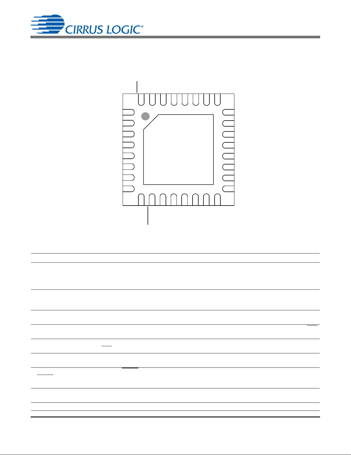
1.2 Hardware Mode
109
8
7
6
5
4
3
2
1
11
12
13 14 15 16
17
18
19
20
21
22
23
24
25
262728
29
303132
Top-Down View
32-Pin QFN Package
Thermal Pad
XTO
MCLK_OUT
SRC_UNLOCK
SDOUT1
OSCLK2
VA
AGND
SAOF
RXP0
SDOUT2
VL
TDM_IN
OLRCK2
RXN0
RXP1
RXN1
RMCK
TX/U
VD_FILT
V_REG
XTI
MS_SEL
V/AUDIO
NV/RERR
TX_SEL
C
RCBL
RX_SEL
DGND
RST
OSCLK1
OLRCK1
CS8422
Pin Name Pin # Pin Description
1
AES3/SPDIF Input (Input) - Differential receiver inputs carrying AES3 or S/PDIF encoded digital
RXP/RXN[1:0]
VA 3
AGND 4
SAOF 7
MS_SEL 8
NV/RERR 9
V/AUDIO
XTI 11
XTO 12 Crystal Out (Output) - Crystal output for Master clock. See “SRC Master Clock” on page 38.
DS692F2 11
2
5
6
10
data. RXP[1:0] comprise the non-inverting inputs of the differential input multiplexer; and RXN[1:0]
comprise the inverting inputs of the input multiplexer. Unused inputs should be tied to AGND.
Analog Power (Input) - Analog power supply, nominally +3.3 V. Care should be taken to ensure that
this supply is as noise-free as possible, as noise on this pin will directly affect the jitter performance of
the recovered clock.
Analog Ground (Input) - Ground for the analog circuitry in the chip. AGND and DGND should be
connected to a common ground area under the chip.
Serial Audio Output Format Select (Input) - Used to select the serial audio output format after RST
is released. See Table 4 on page 42 for format settings.
Master/Slave Select (Input) - Used to select Master or Slave settings for the output serial audio ports
after RST is released. See Table 5 on page 42 for format settings.
Non-Validity Receiver Error/Receiver Error (Output) - Receiver error indicator. NVERR is output by
default, RERR is selected by a 20 k resistor to VL.
Validity Data/AUDIO
data from the AES3 receiver, clocked by the rising and falling edges of OLRCK2 in master mode. If a
20 k pull-up is present, the pin will be low when valid linear PCM data is present at the AES3 input.
Crystal/Oscillator In (Input) - Crystal or digital clock input for Master clock. See “SRC Master Clock”
(Output) - If a 20 k pull-down is present on this pin, it will output serial Validity
on page 38.
Page 12
CS8422
Pin Name Pin # Pin Description
MCLK_OUT 13
TX_SEL 14
RX_SEL 15 Receiver MUX Selection (Input) - Used to select the active AES3-compatible receiver input.
RCBL 16
C17
TX/U 18
V_REG 19 Voltage Reg ul ato r In (Input) - Regulator power supply input, nominally +3.3 V.
VD_FILT 20
DGND 21
VL 22 Logic Power (Input) - Input/Output power supply, typically +1.8V, +2.5V, +3.3 V, or +5.0 V.
SDOUT2 23 Serial Audio Output 2 Data Port (Output) - Audio data serial output 2 pin.
OSCLK2 24 Serial Audio Output 2 Bit Clock (Input/Output) - Serial bit clock for audio data on the SDOUT2 pin.
OLRCK2 25
TDM_IN 26
SDOUT1 27
OSCLK1 28 Serial Audio Output 1 Bit Clock (Input/Output) - Serial bit clock for audio data on the SDOUT1 pin.
OLRCK1 29
SRC_UNLOCK 30
RMCK 31
RST
THERMAL PAD -
Buffered MCLK (Output) - Buffered out put of XTI cl ock. If a 20k pull-up resistor to VL is present on
this pin, the SRC MCLK source will be the PLL clock, otherwise it will be the ring oscillator.
TX Pin MUX Selection (Input) - Used to select the AES3-compatible receiver input for pass-through
to the TX pin.
Receiver Channel Status Block (Output) -Indicates the beginning of a received channel status
block. Will go high for one subframe during each Z preamble following the first detected Z preamble.
If no Z preamble is detected, output is indeterminate. See Figure 19 on page 36 for more detail.
Channel Status Data (Output) - Serial channel status data output from the AES3-compatible
receiver, clocked by the rising and falling edges of OLRCK2 in master mode. A 20 k pull-up resistor
to VL must be present on this pin to put the part in Hardware Mode.
Receiver MUX Pass-through/User Data (Output) - If no 20 k pull-up resistor is present on this pin
it will output a copy of the receiver mux input selected by the TX_SEL pin. If a 20 k pull-up resistor
to VL is present on this pin, it will output serial User data from the AES3 receiver, clocked by the rising
and falling edges of OLRCK2 in master mode.
Digital Voltag e Regu lator Out (Output) - Digital core voltage regulator output. Should be connected
to digital ground through a 10 µF capacitor. Cannot be used as an external voltage source.
Digital & I/O Ground (Input) - Ground for the I/O and core logic. AGND and DGND should be con-
nected to a common ground area under the chip.
Serial Audio Output 2 Left/Right Clock (Input/Output) - Word rate clock for the audio data on the
SDOUT2 pin.
Serial Audio Output 1 TDM Input (Input) - Time Division Multiplexing serial audio data input.
Grounded when not used. See “Time Division Multiplexing (TDM) Mode” on page 27
Serial Audio Output 1 Data Port (Output) - Audio data serial output 1 pin. A 20 k pull-up to VL
present on this pin will disable de-emphasis auto detect.
Serial Audio Output 1 Left/Right Clock (Input/Output) - Word rate clock for the audio data on the
SDOUT1 pin.
SRC Unlock Indicator (Output) - Indicates when the SRC is unlocked. See “SRC Locking” on
page 37 for more details.
Recovered Master Clock (Output) - Recovered master clock from the PLL. Frequency is 128 x,
256 x, or 512 x Fs, where Fs is the sample rate of the incoming AES3-compatible data or ISCLK/64.
If a 20 k pull-up to VL is present on this pin, the SDOUT1 MCLK source will be RMCK, otherwise it
will be the clock input through XTI-XTO.
Reset (Input) - When RST
32
reset. On initial power up RST
are stable in frequency and phase.
Thermal Pad - Thermal relief pad. Should be connected to the ground plane for optimized heat dissipation.
is low the CS8422 enters a low power mode and all internal states are
must be held low until the power supply is stable and all input clocks
for details.
12 DS692F2
Page 13
CS8422
2. CHARACTERISTICS AND SPECIFICATIONS
(All Min/Max characteristics and specifications are guar anteed over the S pecified Op erating Conditions. T ypical performance characteristics and specifications are derived from measurements taken at nominal supply voltages and
T
= 25° C.)
A
RECOMMENDED OPERATING CONDITIONS
GND = 0 V, all voltages with respect to 0 V.
Parameter Symbol Min Nominal Max Units
Power Supply Voltage
V_REG
Ambient Operating Temperature: Commercial Grade T
VL
VA
A
1.71
3.135
3.135
-40 - +85 °C
3.3
3.30
3.30
5.25
3.465
3.465
V
V
V
ABSOLUTE MAXIMUM RATINGS
DGND = AGND = 0 V; all voltages with respect to 0 V. Operation beyond thes e limit s may result in permanent
damage to the device. Normal operation is not guaranteed at these extremes.
Parameter Symbol Min Max Units
Power Supply Voltage
V_REG
Input Current, Any Pin Except Supplies (Note 1) I
Input Voltage, Any Pin Except RXP[1:0], RXN[1:0], or
RX[3:0]
Input Voltage, RXP[1:0], RXN[1:0], or RX[3:0] V
Ambient Operating Temperature (power applied) T
Storage Temperature T
VL
VA
V
stg
in
in
in
A
-0.3
-0.3
-0.3
-±10mA
-0.3 VL+0.4 V
-0.3 VA+0.4 V
-55 +125 °C
-65 +150 °C
6.0
4.3
4.3
V
V
V
Notes:
1. Transient currents of up to 100 mA will not cause SCR latch-up.
DS692F2 13
Page 14
CS8422
PERFORMANCE SPECIFICATIONS - SAMPLE RATE CONVERTER
XTI-XTO = 24.576 MHz; Input signal = 1.000 kHz, Measurement Bandwidth = 20 to Fso/2 Hz, and
Word Width = 24-Bits. (Note 2)
Parameter Min Typ Max Units
Resolution 16 - 24 bits
Sample Rate Slave
Master
Sample Rate Ratio - Upsampling - - 1:6 Fsi:Fso
Sample Rate Ratio - Downsampling - - 6:1 Fsi:Fso
Interchannel Gain Mismatch - 0.0 - dB
Interchannel Phase Deviation - 0.0 - Degrees
Gain Error -0.2 - 0 dB
Peak Idle Channel Noise Component - - -144 dBFS
Dynamic Range - Unweighted (20 Hz to Fso/2, -60 dBFS Input)
32 kHz:48 kHz - 140 - dB
44.1 kHz:48 kHz - 141 - dB
44.1 kHz:192 kHz - 138 - dB
48 kHz:44.1 kHz - 140 - dB
48 kHz:96 kHz - 141 - dB
96 kHz:48 kHz - 140 - dB
192kHz:32kHz - 141 - dB
Total Harmonic Distortion + Noise (20 Hz to Fso/2, 0 dBFS Input)
32 kHz:48 kHz - -134 - dB
44.1 kHz:48 kHz - -134 - dB
44.1 kHz:192 kHz - -133 - dB
48 kHz:44.1 kHz - -131 - dB
48 kHz:96 kHz - -135 - dB
96 kHz:48 kHz - -136 - dB
192kHz:32kHz - -137 - dB
XTI/2048
XTI/512
-
-
XTI/128
XTI/128
kHz
kHz
Notes:
2. Fsi indicates the input sample rate. Fso indicates the output sample rate. Numbers separated by a colon
indicate the ratio of Fsi to Fso.
DIGITAL FILTER CHARACTERISTICS
Parameter Min Typ Max Units
Passband (Upsampling or Downsampling)
Passband Ripple - - ± 0.05 dB
Stopband (Downsampling)
Stopba nd Attenuation 125 - - dB
Group Delay See “Group Delay” on page 70
14 DS692F2
--
0.5465*Fso
--Fs
0.4535*
min(Fsi,Fso)
Fs
Page 15
DC ELECTRICAL CHARACTERISTICS
AGND = DGND = 0 V; all voltages with respect to 0 V.
Parameter Min Typ Max Units
Power-Down Mode
Supply Current in power down VA
Normal Operation
Supply Current at 48 kHz Fsi and Fso VA
Supply Current at 192 kHz Fsi and Fso VA
(Note 3)
V_REG
VL = 1.8 V
VL = 2.5 V
VL = 3.3 V
VL = 5.0 V
(Note 4)
V_REG
VL = 1.8 V
VL = 2.5 V
VL = 3.3 V
VL = 5.0 V
V_REG
VL = 1.8 V
VL = 2.5 V
VL = 3.3 V
VL = 5.0 V
CS8422
-
-
-
-
-
-
-
-
-
-
-
-
-
-
-
-
-
-
4.7
1
0.3
7.1
16.9
102.6
18.8
15.2
2.7
3.8
5.2
5.3
18.9
32.4
6.2
8.8
12
18
-
-
-
-
-
-
-
-
-
-
-
-
-
-
-
-
-
-
µA
µA
µA
µA
µA
µA
mA
mA
mA
mA
mA
mA
mA
mA
mA
mA
mA
mA
Notes:
3. Power-Down Mode is defined as RST
attached across XTI - XTO.
4. Normal operation is defined as RST
interface receiver in differential mode, serial audio output port 1 in master mode sourced by the SRC,
and serial audio output port 2 in master mode sourced by the AES3 receiver output.
= LOW with all clocks and data lines held static and no crystal
= HIGH. The typical values shown were measured with the digital
DS692F2 15
Page 16
CS8422
DIGITAL INTERFACE SPECIFICATIONS
AGND = DGND = 0 V; all voltages with respect to 0 V.
Parameter Symbol Min Typ Max Units
Input Leakage Current (Note 5) I
Input Capacitance I
in
in
Digital Interface Receiver - RXP[1:0], RXN[1:0], RX[3:0 ]
Differential Input Sensitivity, RXP to RXN (Note 6) --200mVpp
Differential Input Impedance, RXP and RXN to GND - 11 - k
Single-Ended Input Sensitivity, RX pins, Receiver Input Mode 1
(Note 6)
Single-Ended Input Impedance, RX pins, Receiver Input Mode 1 - 11 - k
High-Level Input Voltage, RX pins in Digital mode V
Low-Level Input Voltage, RX pins in Digital mode V
IH
IL
Digital I/O
High-Level Output Voltage (I
Low-Level Output Voltage (I
High-Level Input Voltage V
Low-Level Input Voltage V
= -4 mA)
OH
= 4 mA)
OL
V
OH
V
OL
IH
IL
Input Hysteresis - 0.2 - V
--+32A
-8-pF
--200mVpp
0.55xVA
-0.3
.77xVL
-
0.65xVL
-
-
VA+0.3 V
-
-
-
-
-
0.3xVL V
0.8 V
-V
0.6 V
-V
Notes:
5. When a digital signal is sent to the AES RX pins, the pins will draw approximately 730 µA from the digital
signal’s supply from the time RST
is released until the RX_MODE, RX_SEL, and INPUT_TYPE bits in
register 03h are properly configured to allow a digital input signal on the driven pins, see Section 11.3
on page 49.
6. Maximum sensitivity in accordance with AES3-2003 section 8.3.3. Measured with eye diagram height
at the specified voltage and width of at least 50% of one-half the biphase symbol period.
16 DS692F2
Page 17
SWITCHING SPECIFICATIONS
Inputs: Logic 0 = 0 V, Logic 1 = VL; CL = 20 pF.
Parameter Symbol Min Typ Max Units
RST
pin Low Pulse Width (Note 7)
CS8422
1--ms
PLL Clock Recovery Sample Rate Range (Note 8)
RMCK Output Jitter (Note 9) Differential RX Mode
Single-Ended RX Mode
XTI Frequency Crystal
28 - 216 kHz
-
-
200
475
-
ps RMS
-
ps RMS
12 - 27.000 MHz
Digital Clock Source 1.024 - 49.152 MHz
XTI Pulse Width High/Low
9--ns
VL = 3.3V, 5V
RMCK/MCLK_OUT Output Frequency
RMCK/MCLK_OUT Output Duty Cycle
- - 49.152 MHz
45 50 55 %
Slave Mode
ISCLK Frequency
ISCLK High Time
ISCLK Low Time
OSCLK Frequency
OSCLK High Time
OSCLK Low Time
I/OLRCK Edge to I/OSCLK Rising Edge
I/OSCLK Rising Edge to I/OLRCK Edge
OSCLK Falling Edge/OLRCK Edge to SDOUT Output Valid
SDIN/TDM_IN Setup Time Before I/OSCLK Rising Edge
SDIN/TDM_IN Hold Time After I/OSCLK Rising Edge
TDM Mode OLRCK High Time (Note 10)
TDM Mode OLRCK Rising Edge to OSCLK Rising Edge
TDM Mode OSCLK Rising Edge to OLRCK Falling Edge
t
sckh
t
sckl
t
sckh
t
sckl
t
lcks
t
lckd
t
dpd
t
t
t
lrckh
t
fss
t
fsh
ds
dh
- - 49.152 MHz
9.2 - - ns
9.2 - - ns
- - 26.9 MHz
16.7 - - ns
16.7 - - ns
5.7 - - ns
4.2 - - ns
--15ns
3.6 - - ns
5.5 - - ns
20 - - ns
5.3 - - ns
4.2 - - ns
Master Mode (Note 11)
I/OSCLK Frequency (non-TDM Mode) 48*Fsi/o - 128*Fsi/o MHz
I/OLRCK Duty Cycle 49.5 - 50.5 %
I/OSCLK Duty Cycle 45 - 55 %
I/OSCLK Falling Edge to I/OLRCK Edge t
OSCLK Falling Edge to SDOUT Output Valid t
SDIN Setup Time Before I/OSCLK Rising Edge
SDIN Hold Time After I/OSCLK Rising Edge
lcks
dpd
t
ds
t
dh
--4.2ns
--4.6ns
2.7 - - ns
5.5 - - ns
TDM Mode OSCLK Frequency (Note 12) - - 49.152 MHz
DS692F2 17
Page 18
CS8422
Parameter Symbol Min Typ Max Units
TDM Mode OSCLK Falling Edge to OLRCK Edge t
fsm
VL = 1.8V, 2.5V
RMCK/MCLK_OUT Output Frequency (VL = 1.8 V)
RMCK/MCLK_OUT Output Frequency (VL = 2.5 V)
RMCK/MCLK_OUT Output Duty Cycle (VL = 1.8 V)
RMCK/MCLK_OUT Output Duty Cycle (VL = 2.5 V)
Slave Mode
ISCLK Frequency
ISCLK High Time
ISCLK Low Time
t
sckh
t
sckl
OSCLK Frequency
OSCLK High Time
OSCLK Low Time
I/OLRCK Edge to I/OSCLK Rising Edge
I/OSCLK Rising Edge to I/OLRCK Edge
OSCLK Falling Edge/OLRCK Edge to SDOUT Output Valid
SDIN/TDM_IN Setup Time Before I/OSCLK Rising Edge
SDIN/TDM_IN Hold Time After I/OSCLK Rising Edge
TDM Mode OLRCK High Time (Note 10)
TDM Mode OLRCK Rising Edge to OSCLK Rising Edge
TDM Mode OSCLK Rising Edge to OLRCK Falling Edge
t
sckh
t
sckl
t
lcks
t
lckd
t
dpd
t
t
t
lrckh
t
fss
t
fsh
ds
dh
Master Mode (Note 11)
I/OSCLK Frequency (non-TDM Mode) 48*Fsi/o - 128*Fsi/o MHz
I/OLRCK Duty Cycle 45 - 55 %
I/OSCLK Duty Cycle 45 - 55 %
I/OSCLK Falling Edge to I/OLRCK Edge t
OSCLK Falling Edge to SDOUT Output Valid (VL = 1.8 V) t
OSCLK Falling Edge to SDOUT Output Valid (VL = 2.5 V) t
SDIN Setup Time Before I/OSCLK Rising Edge
SDIN Hold Time After I/OSCLK Rising Edge
lcks
dpd
dpd
t
ds
t
dh
TDM Mode OSCLK Frequency (Note 12) --31MHz
TDM Mode OSCLK Falling Edge to OLRCK Edge (VL = 1.8V) t
TDM Mode OSCLK Falling Edge to OLRCK Edge (VL = 2.5V) t
fsm
fsm
Notes:
7. After powering up the CS8422, RST
should be held low until the power supplies and clocks are se ttled.
8. If ISCLK is selected as the clock source for the PLL, then the Sample Rate = ISCLK/64.
--4.2ns
--13.5MHz
--31MHz
37 50 63 %
45 50 55 %
- - 49.152 MHz
9.2 - - ns
9.2 - - ns
--15.7MHz
28.7 - - ns
28.7 - - ns
7.4 - - ns
6.2 - - ns
--29.5ns
4.7 - - ns
7.3 - - ns
20 - - ns
7.0 - - ns
6.2 - - ns
--5.7ns
--11.2ns
--6.4ns
4.7 - - ns
7.3 - - ns
--9.6ns
--5.7ns
18 DS692F2
Page 19
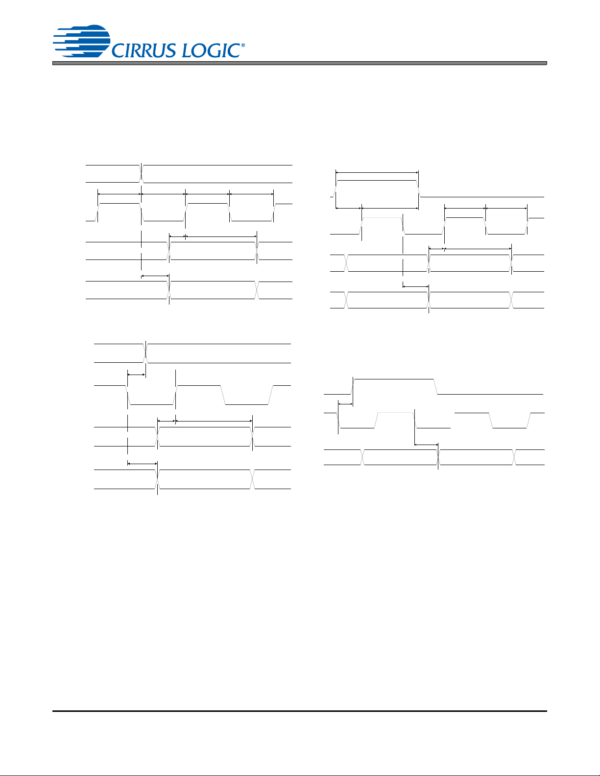
CS8422
t
ds
OLRCK
(input)
t
dh
t
sckh
t
sckl
t
fsh
t
fss
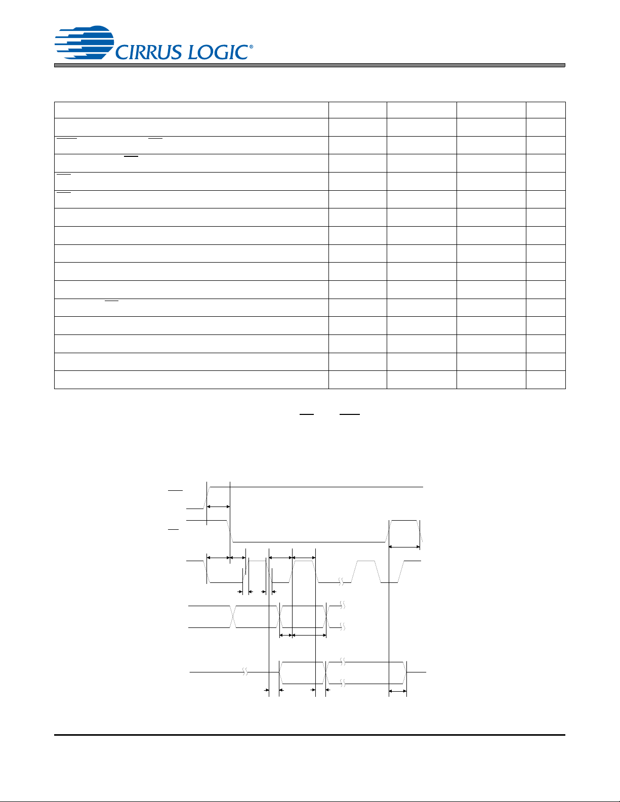
OSCLK
(input)
TDM_IN
(input)
SDOUT
(output)
MSB
t
dpd
MSB-1
MSB
MSB-1
t
lrckh
t
ds
MSB
t
dh
t
dpd
MSB-1
I/OLRCK
(input)
I/OSCLK
(input)
SDIN
(input)
SDOUT
(output)
MSB
MSB-1
t
sckh
t
sckl
t
lcks
t
lckd
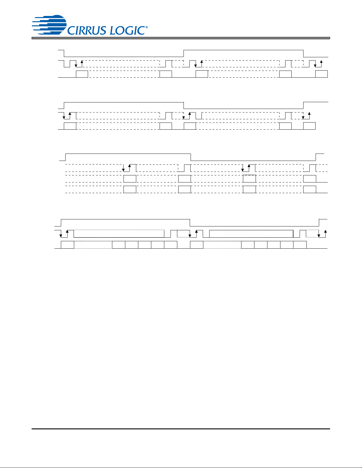
Figure 1. Non-TDM Slave Mode Timing Figure 2. TDM Slave Mode Timing
OLRCK
(output)
t
dpd
t
fsm
OSCLK
(output)
SDOUT
(output)
MSB
MSB-1
t
ds
MSB
t
dh
t
dpd
MSB-1
t
lcks
I/OLRCK
(output)
I/OSCLK
(output)
SDIN
(input)
SDOUT
(output)
MSB
MSB-1
Figure 3. Non-TDM Master Mode Timing Figure 4. TDM Master Mode Timing
9. Typical base band jitter in accordance with AES-12id-2006 section 3.4.2. Measurements are Time Interval Error (TIE) taken with 3rd order 100 Hz to 40 kHz band-pass filter. Measured with Sample Rate
= 48 kHz.
10. OLRCK must remain high for at least 1 OSCLK period and at most 255 OSCLK periods in TDM Mode.
11. In TDM formatted master mode, the TDM_IN pin is not supported.
12. In TDM formatted master mode, the OSCLK frequency is fixed at 256*OLRCK.
DS692F2 19
Page 20
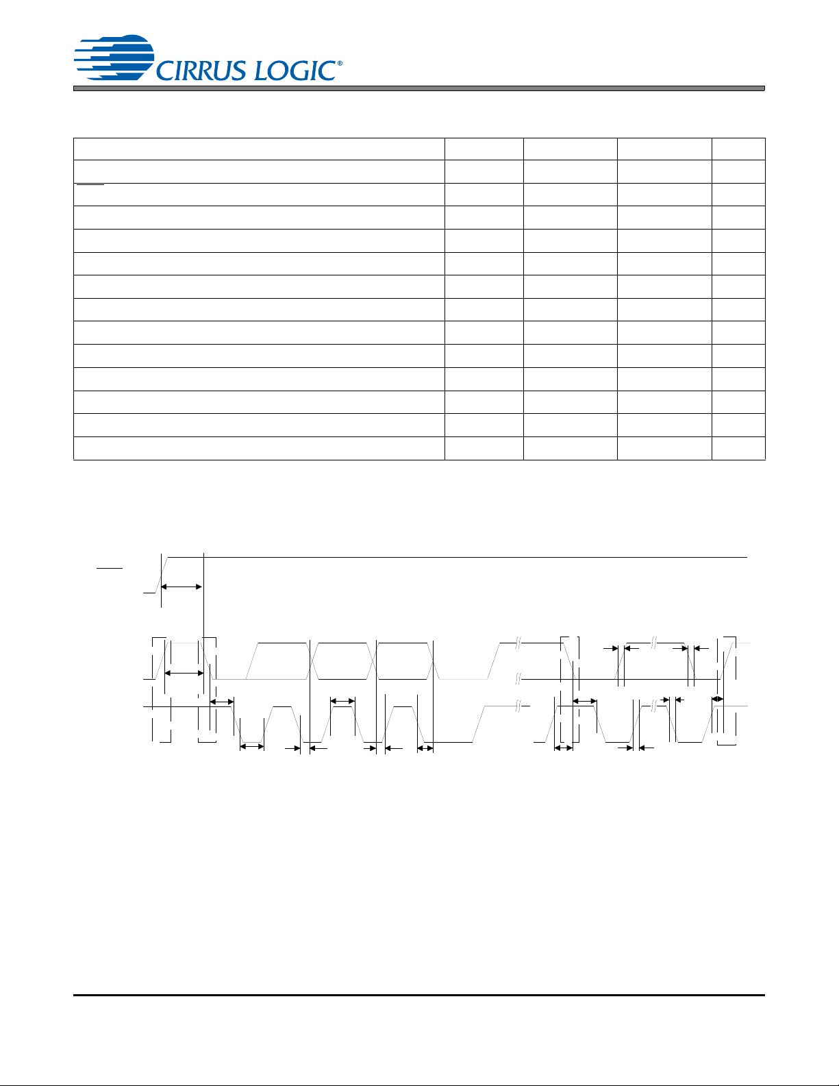
SWITCHING CHARACTERISTICS - CONTROL PORT - SPI MODE
t
r2
t
f2
t
dsu
t
dh
t
sch
t
scl
CS
CCLK
CDIN
t
css
t
csh
t
spi
t
srs
RST
CDOUT
t
scdov
t
scdov
t
cscdo
Hi-Impedance
Figure 5. SPI Mode Timing
Inputs: Logic 0 = 0 V, Logic 1 = VL; CL = 20 pF.
Parameter Symbol Min M ax Unit
CCLK Clock Frequency
RST
Rising Edge to CS Falling
CCLK Edge to CS
CS
High Time Between Transmissions
CS
Falling to CCLK Edge
Falling (Note 13)
CCLK Low Time
CCLK High Time
CDIN to CCLK Rising Setup Time
CCLK Rising to DATA Hold Time (Note 14)
CCLK Falling to CDOUT Valid (Note 15)
Time from CS
Rising to CDOUT High-Z
CDOUT Rise Time
CDOUT Fall Time
CCLK and CDIN Rise Time (Note 16)
CCLK and CDIN Fall Time (Note 16)
f
sck
t
srs
t
spi
t
csh
t
css
t
scl
t
sch
t
dsu
t
dh
t
scdov
t
cscdo
t
r1
t
f1
t
r2
t
f2
06.0MHz
500 - µs
500 - ns
1.0 - µs
20 - ns
66 - ns
66 - ns
40 - ns
15 - ns
-100ns
-100ns
-25ns
-25ns
-100ns
-100ns
CS8422
Notes:
13. t
only needed before first falling edge of CS after RST rising edge. t
spi
14. Data must be held for sufficient time to bridge the transition time of CCLK.
15. CDOUT should not be sampled during this time.
16. For f
< 1 MHz.
sck
= 0 at all other times.
spi
20 DS692F2
Page 21
SWITCHING CHARACTERISTICS - CONTROL PORT - I²C MODE
t
buf
t
hdst
t
low
t
hdd
t
high
t
sud
Stop Start
SDA
SCL
t
irs
RST
t
hdst
t
rc
t
fc
t
sust
t
susp
Start
Stop
Repeated
t
rd
t
fd
t
ack
Figure 6. I²C Mode Timing
Inputs: Logic 0 = 0 V, Logic 1 = VL; CL = 20 pF.
Parameter Symbol Min Max Unit
SCL Clock Frequency
RST
Rising Edge to Start
Bus Free Time Between Transmissions
Start Condition Hold Time (prior to first clock pulse)
Clock Low time
Clock High Time
Setup Time for Repeated Start Condition
SDA Hold Time from SCL Falling (Note 17)
SDA Setup time to SCL Rising
Rise Time of SCL and SDA
Fall Time SCL and SDA
Setup Time for Stop Condition
Acknowledge Delay from SCL Falling
t
t
t
t
t
t
t
t
rc
t
fc
t
susp
t
f
scl
t
irs
buf
hdst
low
high
sust
hdd
sud
, t
, t
ack
rd
fd
- 100 kHz
500 - µs
4.7 - µs
4.0 - µs
4.7 - µs
4.0 - µs
4.7 - µs
10 - ns
250 - ns
- 1000 ns
-300ns
4.7 - µs
300 1000 ns
CS8422
Notes:
17. Data must be held for sufficient time to bridge the transition time, t
, of SCL.
fc
DS692F2 21
Page 22
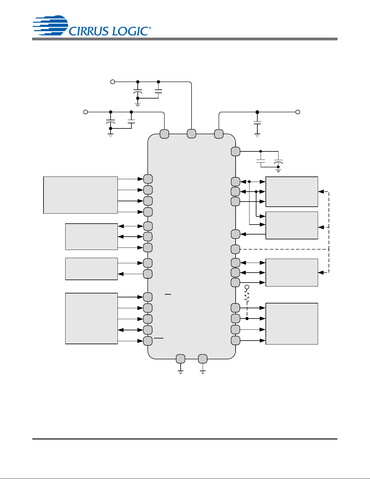
3. TYPICAL CONNECTION DIAGRAMS
CS8422
VD_FILT
Serial Audio Input
Device
Crystal/Clock Source
Microcontroller
Serial Audio Input
Device
Serial Audio Output
Device
AES3/SPDIF/IEC60958
Receiver Circuitry
Clock Routing,
Interrupt Control,
Channel-Status, and
User Data Output
TDM Output Device
RX0/RXP0
1
RX1/RXN0
2
RX2/RXP1
5
RX3/RXN1
5
ILRCK
13
ISCLK
14
SDIN
15
XTI
11
XTO
12
AD0/CS
7
AD1/CDIN
8
SCL/CCLK
9
SDA/CDOUT
10
RST
32 GPO0
16
GPO1
17
GPO2
18
GPO3
30
D
G
N
D
21
A
GND
4
20
10 µF0.1 µF
+
RMCK
31
SDOUT2
23
OSCLK2
24
OLRCK2
25
TDM_IN
26
SDOUT1
27
OLRCK1
29
OSCLK1
28
10 µF
0.1 µF
+
V
A
3
+3.3V
V
L
+1.8V to +5V
0.1 µF
22
10 µF
0.1 µF
+
V_R
EG
19
+3.3V
20 k
+VL
Figure 7. Typical Connection Diagram, Software Mode
See section 12.3 for details.
3.1 Software Mode
CS8422
22 DS692F2
Page 23
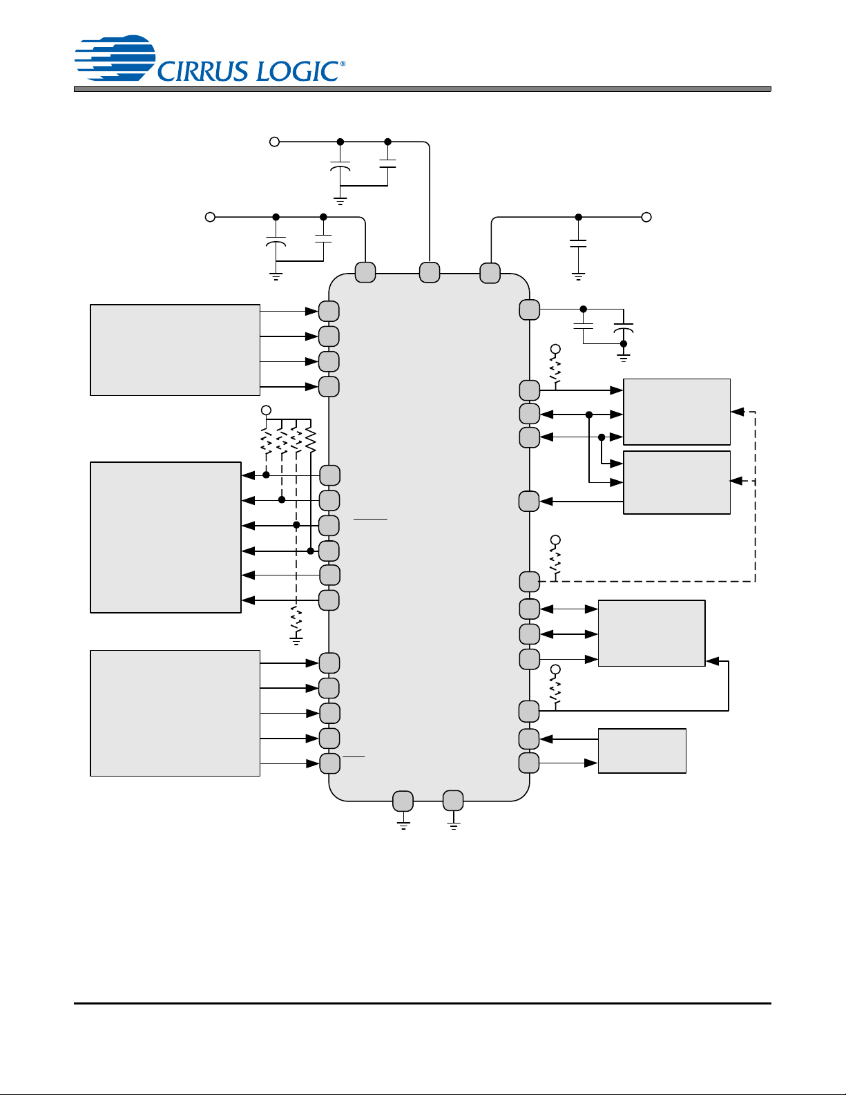
3.2 Hardware Mode
CS8422
VD_FILT
Serial Audio Input
Device
AES3/SPDIF/IEC60958
Receiver Circuitry
TDM Output Device
RXP0
1
RXN0
2
RXP1
5
RXN1
6
A
G
N
D
4
D
GN
D
21
SDOUT2
23
OSCLK2
24
OLRCK2
25
13
MCLK_OUT
TDM_IN
26
SDOUT1
29
OSCLK1
28
OLRCK1
27
Serial Audio Input
Device
Crystal/Clock
Source
XTI
11
XTO
12
10 µF
0.1 µF
+
20
Hardware Control Circuitry
RX_SEL
15
TX_SEL
14
SRC_UNLOCK
30
NV/RERR
9
RCBL
16
C
17
TX/U
18
V/AUDIO
10
+VL
20 k
RST
32
SAOF
7
MS_SEL
8
Channel Status, User, and
Validity Data Handling and
TX Passthrough
+
10 µF
0.1 µF
V
A
+3.3V
3
+
10 µF
0.1 µF
V_R
E
G
+3.3V
19
0.1 µF
V
L
+1.8V to +5V
22
31RMCK
20 k
+VL
20 k
+VL
20 k
+VL
20 k
Figure 8. Typical Connection Diagram, Hardware Mode
See section 12.3 for details.
CS8422
DS692F2 23
Page 24

CS8422
4. OVERVIEW
The CS8422 is a 24-bit, high performance, monolithic CMOS stereo asynchronous sample r ate converter with integrated digital audio interface receiver that decodes audio data according to EIAJ CP1201, IEC-60958, AES3, and
S/PDIF interface standards.
Audio data is input through either a 3-wire serial audio port or the AES3-compatible digital interface receiver. Audio
data is output through one of two 3-wire serial audio output ports. The serial audio ports are capable of 24, 20, 18,
or 16-bit word lengths. Data in to the digital inter face receiver can be up to 24- bit. Input and output data can be completely asynchronous, synchronous to an external data clock through XTI, or synchronous to the master clock recovered from the incoming S/PDIF or AES3 data.
CS8422 can be controlled either in Software Mode or in a stand-alone Hardware Mod e. In Software Mode, the user
can control the device through either a SPI or I²C control port.
Target applications include digital recording systems (DVD-R/RW, CD-R/RW, PVR, DAT, MD, and VTR), digital mixing consoles, high quality D/A, effects processors, and computer audio systems.
Figure 7 and Figure 8 show typical connections to the CS8422.
5. THREE-WIRE SERIAL INPUT/OUTPUT AUDIO PORT
The CS8422 provides two independent 3-wire serial audio output ports, and a 3-wire serial audio input (only available in Software Mode). The interface format should be chosen to suit the attached device either through the control
port in Software Mode, or through the MS_SEL and SAOF pins in Hardware Mode. The following parameters are
adjustable:
Hardware Mode
• Master or slave mode operation
• Master-mode MCLK-to-OLRCK (OLRCK1 and OLRCK2) ratios: 128, 256, and 512
• Audio data resolution of 16, 20, or 24-bits
• Left-Justified, I²S, or Right-Justified serial data formats
• Multi-channel TDM serial audio format (Serial Audio Output 1 only)
Software Mode
• Master or slave mode operation
• Master-mode MCLK-to-ILRCK and MCLK-to-OLRCK (OLRCK1 and OLRCK2) ratios: 64, 128, 192, 256,
384, 512, 768, and 1024
• Audio data resolution of 16, 18, 20, or 24-bits
• Left-Justified, I²S, or Right-Justified serial data formats
• Multi-channel TDM serial audio format
• AES3 Direct Output format
Figures 9, 10, 11, and 12 show the standard input/output formats available. The TDM serial audio format is de-
scribed in Section 5.1.5 on page 27. For more information about serial audio formats, refer to the Cirrus Logic applications note AN282, “The 2-Channel Serial Audio Interface: A Tutorial”, available at www.cirrus.com.
24 DS692F2
Page 25

5.1 Serial Port Clock Operation
5.1.1 Master Mode
When a serial port is set to master mode, its left/righ t clock (I LRCK, OLRCK1, or OLRCK2), and its serial
bit-clock (ISCLK, OSCLK1, or OSCLK2) are outputs. If a serial output is source d directly by the AES3 receiver, then that serial port’s left/right clock and serial bit-clock will be synchronous with RMCK. If a serial
port is routed to or from the sample rate converter (SRC), then that serial port’s left/right clock and serial
bit-clock can be synchronous with either the XTI-XTO or RMCK when it is in master mode.
If a serial output is source directly by the serial input port without the use of the SRC, then all associated
clocks must be synchrono us, so both serial ports must use the same master clock source. It is for this
reason that, when in this mode, the serial output clock control is done throu gh the Serial Audio Input Clock
Control (07h) register.
5.1.2 Slave Mode
When a serial port is in slave mode, its left/right clock (ILRCK, OLRCK1, or OLRCK2), and its serial bitclock (ISCLK, OSCLK1, or OSCLK2) are inputs. If the serial input or a serial output has the SRC in its
data path, then the serial port’s LRCK and SCLK may be asynchronous to all other serial ports. The
left/right clock should be continuous, but the duty cycle can be less than 50% if enough serial clocks are
present in each associated LRCK phase to clock all of the data bits.
CS8422
If there are fewer SCLK periods than required to clock all the bits present in on e half LRCK period in LeftJustified and I²S Modes, data will be truncated beginning with the LSB. In Right-Justified Modes, the data
will be invalid.
If a serial audio output is operated in slave mode and sourced directly by the AES3 receiver or the serial
input port without the use of the sample rate converter, then the OLRCK supplied to the seri al audio output
should be synchronous to Fsi or ILRCK to avoid skipped or repeated samples. The OSLIP bit (“Interrupt
Status (14h)” on page 60) is provided to indicate when skipped or repeated samples occur.
If the input sample rate, Fsi or ILRCK, is greater than the slave-mode OLRCK frequency, then dropped
samples will occur. If Fsi or ILRCK is less than the slave-mode OLRCK frequency, then samples will be
repeated. In either case the OSLIP bit will be set to 1 and will not be cleared until read through the control
port.
5.1.3 Hardware Mode Control
In Hardware Mode, the serial audio input port is not available. SDOUT1 is th e ser ial da ta outp ut fr om the
sample rate converter, and SDOUT2 is the serial audio output directly from the AES3-compatible receiver.
Because there is no serial audio input available in Hardware Mode, all audio data input is done through
the AES3-compatible receiver. In Hardware Mode, the serial output ports are controlled through the SAOF
and MS_SEL pins. See “Hardware Mode Serial Audio Port Control” on page 41 for more details.
In Hardware Mode, there are always 64 SCLK pe riods per LRCK period when a ser ial port is set to master
mode.
5.1.4 Software Mode Control
In Software Mode, the CS8422 provides a serial audio input port and two serial audio output ports. Each
serial port’s clocking and data routin g options ar e fully configu rable as show n in Serial Audio Input Data
Format (0Bh), Serial A udio Ou tput Data Forma t - SDOUT 1 (0Ch) , and Serial Au dio Ou tput Dat a Forma t
- SDOUT2 (0Dh) registers, found on pages 54, 55, and 56.
DS692F2 25
Page 26
CS8422
I/OLRCK
I/OSCLK
MSB LSB
MSB
LSB
Channel A
SDIN
SDOUT
MSB
Channel B
Figure 9. Serial Audio Interface Format – I²S
MSB LSB
MSB
LSB
MSB
I/OLRCK
I/OSCLK
SDIN
SDOUT
Channel A Channel B
Figure 10. Serial Audio Interface Format – Left-Justified
I/OLRCK
I/OSCLK
Channel A
SDIN
Channel B
MSB
SDOUT
MSB
MSB
MSB LSB
LSB
LSB
LSB
MSB Extended MSB Extended
Figure 11. Serial Audio Interface Format – Right-Justified (Mast er Mode only)
OLRCK
OSCLK
SDOUT
Channel A Channel B
LSB MSB V U C Z
LSB
MSB V U C Z
Figure 12. Serial Audio Interface Format – AES3 Direct Output
26 DS692F2
Page 27

5.1.5 Time Division Multiplexing (TDM) Mode
TDM Mode allows several TDM-compatible devices to be serially connected together allowing their corresponding serial output data to be multiplexed onto one line for input into a DSP or other TDM capable
input device.
In TDM Mode, the TDM_IN pin is used to in put TDM-formatted da ta while the SDOUT1 or SDOUT2 ( Software Mode only) pin is used to output TDM data. If the CS8422 is the first TDM device in the chain, it
should have its TDM_IN connected to GND. Data is transmitted from SDOUTx (SDOUT1 or SDOUT2)
most significant bit first on the first falling OSCLKx edge after an OLRCKx rising edge and is valid on the
rising edge of OSCLKx.
5.1.5.1 TDM Master Mode
In TDM master mode, OSCLKx frequency is fixed at 256*OLRCKx (where x = 1 or x = 2 depending on
which serial output port is selected as being in TDM Mode). Each sample time slot is 32 bit-clock periods
long; providing 8 channels of digital audio multiplexed together, with the first two channels being supplied
by the CS8422 which has been placed in master mode. An OSCLKx-wide OLRCKx pulse identifies the
start of a new frame, with the valid data sample beginning one OSCLKx after the OLRCKx r ising edge. In
TDM master mode, the master clock source for the TDM serial port must be 256, 512, or 10 24*Fso. Valid
data lengths are 16, 18, 20, or 24 bits. Figure 13 shows the interface format for TDM master mode. In
TDM master mode, the TDM_IN pin is not supported. Thus the CS8422 placed in TDM master mode
should be the first TDM device in the chain, as shown in Figure 16
CS8422
5.1.5.2 TDM Slave Mode
In TDM slave mode, the number of channels that can by multiplexed to one serial data line depends on
the output sample rate. For slave mode, OSCLKx must operate at N*64*Fso, where N is the number of
CS8422’s in the TDM chain. For example, if Fso = 96 kHz, N = 4 (8 channels of serial audio data),
OSCLKx frequency must be 24.576 MHz. Note that the maximum OSCL Kx fre quency in sla ve mod e is a
function of the VL supply voltage, as shown in “Switching Specifications” on page 17. Figure 14 shows
the interface format for TDM slave mode.
5.1.5.3 Hardware Mode Control
In Hardware Mode, TDM Mode is selected through the SAOF pin. See Section 8.1 on page 41 for more
details.
5.1.5.4 Software Mode Control
In Software Mode, TDM Mode is selected through the Serial Audio Outp ut Data Format - SDOUT1 ( 0Ch)
register, found on page 55.
DS692F2 27
Page 28

CS8422
OLRCK
OSCLK
SDOUT/
TDM_IN
MSB
32 OSCLKs
SDOUT 4, ch A
32 OSCLKs
SDOUT 4, ch B
32 OSCLKs
SDOUT 3, ch A
32 OSCLKs
SDOUT 3, ch B
32 OSCLKs
SDOUT 2, ch A
32 OSCLKs
SDOUT 2, ch B
32 OSCLKs
SDOUT 1, ch A
32 OSCLKs
SDOUT 1, ch B
MSB MSB MSB MSB MSB MSB MSB
MSB LSB
Data
Figure 13. TDM Master Mode Timing Diagram
OLRCK
OSCLK
SDOUT/
TDM_IN
MSB
32 OSCLKs
SDOUT 4, ch A
32 OSCLKs
SDOUT 4, ch B
32 OSCLKs
SDOUT 3, ch A
32 OSCLKs
SDOUT 3, ch B
32 OSCLKs
SDOUT 2, ch A
32 OSCLKs
SDOUT 2, ch B
32 OSCLKs
SDOUT 1, ch A
32 OSCLKs
SDOUT 1, ch B
MSB MSB MSB MSB MSB MSB MSB
MSB LSB
Data
Figure 14. TDM Slave Mode Timing Diagram
ILRCK
ISCLK
SDIN
OLRCK
OSCLK
SDOUTTDM_IN
OLRCK
OSCLK
SDOUTTDM_IN
ILRCK
ISCLK
SDIN
OLRCK OSCLK SDOUT
PCM Source 2
OLRCK OSCLK SDOUT
PCM Source 1
CS8422
1
Slave
CS8422
2
Slave
LRCK
SCLK
SDIN
DSP
Master
OLRCK
OSCLK
SDOUTTDM_IN
ILRCK
ISCLK
SDIN
CS8422
3
Slave
OLRCK
OSCLK
SDOUTTDM_IN
ILRCK
ISCLK
SDIN
CS8422
4
Slave
OLRCK OSCLK SDOUT
PCM Source 3
OLRCK OSCLK SDOUT
PCM Source 4
Figure 15. TDM Mode Configuration (All CS8422 outputs are slave)
ILRCK
ISCLK
SDIN
OLRCK
OSCLK
SDOUTTDM_IN
CS8422
1
OLRCK OSCLK SDOUT
PCM Source 2
OLRCK OSCLK SDOUT
PCM Source 1
Master
LRCK
SCLK
SDIN
DSP
Slave
OLRCK
OSCLK
SDOUTTDM_IN
ILRCK
ISCLK
SDIN
CS8422
4
Slave
OLRCK
OSCLK
SDOUTTDM_IN
ILRCK
ISCLK
SDIN
CS8422
2
Slave
OLRCK
OSCLK
SDOUTTDM_IN
ILRCK
ISCLK
SDIN
CS8422
3
Slave
OLRCK OSCLK SDOUT
PCM Source 3
OLRCK OSCLK SDOUT
PCM Source 4
Figure 16. TDM Mode Configuration (First CS8422 output is master, all others are slave)
28 DS692F2
Page 29

CS8422
6. DIGITAL INTERFACE RECEIVER
The CS8422 includes a digital interface receiver that can receive and decode audio data according to the AES3,
IEC60958, S/PDIF, and EIJ CP1201 interface standards.
The CS8422 uses either a 4:1 single-ended or 2:1 differential input mux to select the input pin(s) that will receive
input data to be decoded. A low-jitter clock (RMCK) is recovered using a PLL, which provides the digital inte rface
receiver with a master clock. T he decoded au dio data can either be routed through the SRC for sample rate conversion, or can be an output on one of two serial audio output ports. The channel status and Q-subcode data portion
of the user data are assembled and buffered in Channel Status Registers (23h - 2Ch) a nd Q-Channel Subcode (19 h
- 22h), and may be accessed through the control port in either SPI or I²C Mode.
6.1 AES3 and S/PDIF Standards
This document assumes that the user is familiar with the AES3 and S/PDIF data formats. It is advisable to
have current copies of the AES3, IEC60958, IEC61937, and EIJ CP1201 specifications on hand for easy
reference.
The latest AES3 standard is available from the Audio Engineering Society at www.aes.org
IEC60958/61937 standard is available from the International Electrotechnical Commission at www.iec.ch
The latest EIAJ CP-1201 standard is available from the Japanese Electronics Bureau at www.jei-
ta.or.jp/eiaj/.
Application Note 22: Overview of Digital Audio Interface Data Structures, available at www.cirrus.com, con-
tains a useful tutorial on digital audio specifications, but it should not b e considered a substitute for the standards.
The paper titled An Understanding and Implementation of the SCMS Serial Copy Management System for
Digital A udio Transmission, by Clifton Sanchez, is an excellent tutorial on SCMS. It is available from the
AES as reprint 3518.
6.2 Receiver Input Multiplexer
The CS8422’s receiver input multiplexer allows input of data compatible with AES3, S/PDIF, IEC60958, and
EIAJ CP-1201 standards. For information about reco mmended receiver input circuits, see “External Receiv-
er Components” on page 65.
6.2.1 Hardware Mode Control
In Hardware Mode, the receiver input multiplexer is limited to a selection between two differential inputs,
RXP0/RXN0 and RXP1/RXN1. The receiver input multiplexer will decode data present at the differential
input selected by the RX_SEL pin. See Section 8. “Hardware Mode Control” on page 39 for more details.
Multiplexer inputs are floating when not selected. Unused inputs should be tied to AGND/DGND
. The latest
.
6.2.2 Software Mode Control
In Software Mode, CS8422 offers either a 4:1 single-ended, or a 2:1 differential input multiplexer to accommodate switching between up to four channels of AES3 or S/PDIF-compatible data input. In SingleEnded Mode, the CS8422 can switch between four single-ended signals present at RX[3:0]. In differential
mode, the CS8422 can switch between two differential signals, present on RXP0/RXN0 and RXP1/RXN1.
Multiplexer inputs are floating when not selected. Unused inputs should be tied to AGND/DGND
In Software Mode, the receiver input multiplexer is controlled through the register described in Section
11.3 “Receiver Input Control (03h)” on page 49.
DS692F2 29
Page 30
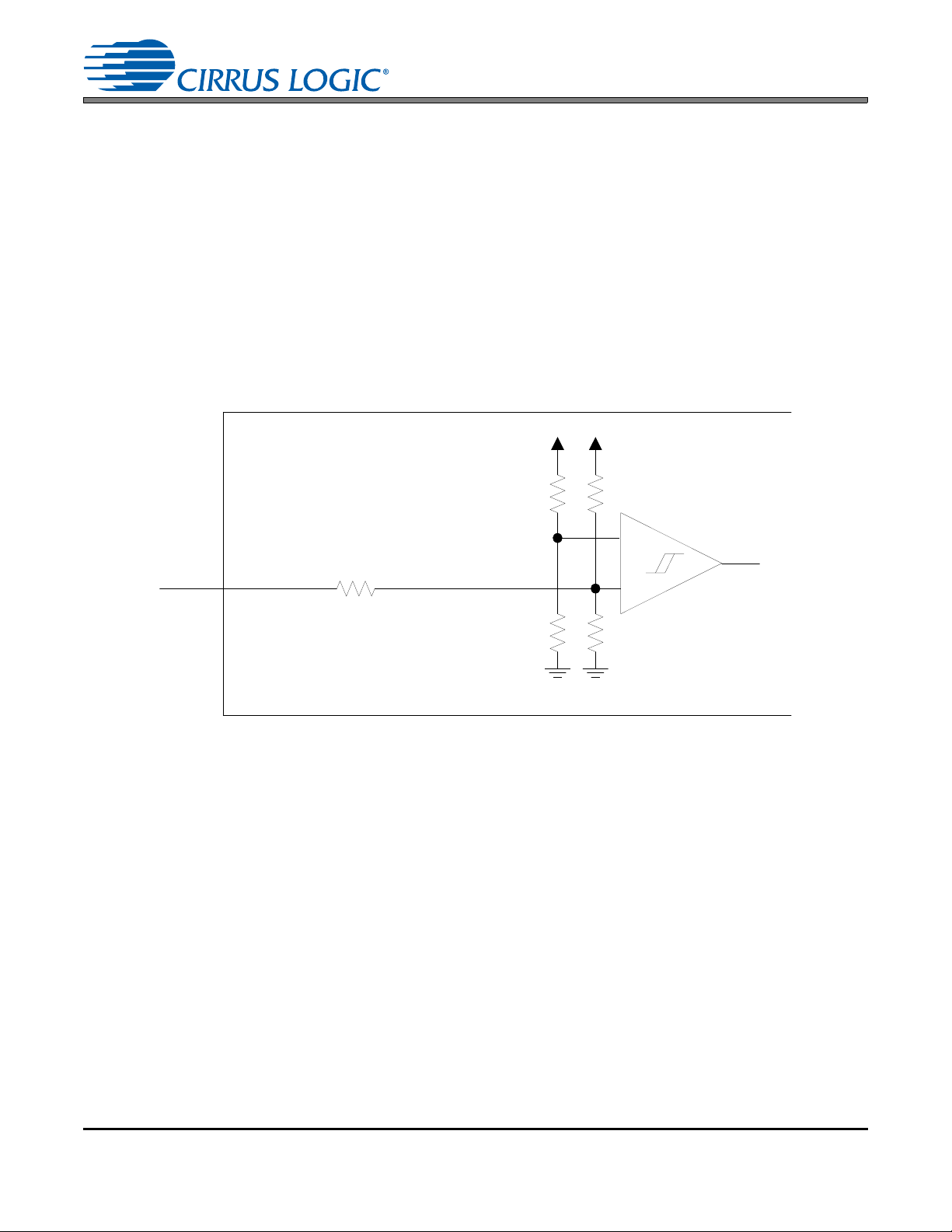
CS8422
+
-
VA
22 k
(22000/N) 22 k
AGND
RX[3:0]
(1500 + 1500/N)
(22000/N)
Note:
1. If RX[3:0] is selected by either the receiver MUX or the TX pass-through MUX, N=1.
2. If RX[3:0] is selected by both the receiver MUX and the TX pass-through MUX, N=2.
3. If RX[3:0] is not selected at all, N=0 (i.e. high impedance).
6.2.2.1 Single-Ended Input Mode
When the receiver input multiplexer is set to Single-Ended Mode, the receiver inputs can be switched between operation as comparator inputs or digital inputs.
Receiver Input Mode 1 (Analog Sensitivity Mode)
If Mode 1 is selected, the inputs are biased at VA/2 and should be coupled through a capacitor. The recommended value for the AC coupling capacitors is 0.01 µF to 0.1 µF. The recommended dielectrics for
the AC coupling capacitors are C0G or X7R.
When the receiver input multiplexer is in Mode 1, the receiver input p ins allow very low a mplitude signals
to be decoded reliably. In this mode, the maximum allowable input amplitude is determined by VA, which
is nominally 3.3 volts. If input amplitudes greater than 3.3 Volts to a single pin of the receiver input multiplexer are required, then attenuation is necessary prior to the receiver input to avoid damage to the part
(See “Attenuating Input signals” on page 66 for more details). Figure 17 shows the input structure of the
receiver in Single-Ended Mode.
Figure 17. Single-Ended Receiver Input Structure, Receiver Mode 1
Receiver Input Mode 2 (Digital Sensitivity Mode)
If Mode 2 is selected, the receiver inputs should be driven by a digital signal referenced to VA. In this
mode, the selected receiver input is not biased, and does not require the use of an AC coupling capacitor
(as with the use of a typical optical receiver output).
When the receiver input multiplexer is in Mode 2 the specifications for V
ifications” on page 17 for more details).
apply (see “Switching Spec-
IH/VIL
6.2.2.2 Differential Input Mode
When the receiver input multiplexer is set to differential input mode, the inputs are biased at VA/2, and
require the use of AC coupling capacitors, as mentioned in Section 6.2.2.1. Figure 18 shows the structure
of the receiver in differential mode.
30 DS692F2
Page 31

CS8422
+
-
VA
(22000/N)
AGND
RXP[1:0]
(1500 + 1500/N)
(22000/N)
RXN[1:0]
(1500 + 1500/N)
(22000/N)
(22000/N)
Note:
1. If RXP/N[1:0] is selected by either the receiver MUX or the TX pass-through MUX, N=1.
2. If RXP/N[1:0] is selected by both the receiver MUX and the TX pass-through MUX, N=2.
3. If RXP/N[1:0] is not selected at all, N=0 (i.e. high impedance).
Figure 18. Differential Receiver Input Structure
6.3 Recovered Master Clock - RMCK
The CS8422 has an internal PLL which recovers a high-frequency system clock, referred to as the recovered master clock (RMCK). RMCK can be generated by incoming AES3-compatible data or the ISCLK
(slave mode and Software Mode only). This clock is used as the master clock source for the AES3 receiver
and the master-mode serial port that it directly supplies data to, and is available as an output on the RMCK
pin. In addition, the user can set the RMCK as the master clock of either of the two remaining serial ports.
6.3.1 Hardware Mode Control
In Hardware Mode, the RMCK frequency is determined by the incoming AES3 frame rate and the
MS_SEL pin. RMCK can be routed for use as the master clock for the serial audio output associated with
SDOUT1 by connecting a 20 k resistor from the RMCK pin to VL. See “Hardware Mode Control” on
page 39 for more details.
6.3.2 Software Mode Control
In Software Mode, The RMCK frequency is determined by the incoming AES3 frame rate or ISCLK/64
(slave mode only). The RMCK frequency is configured in the register described in Section 11.9 “Recov-
ered Master Clock Ratio Control & Misc. (09h)” on page 53. If the ISCLK is chosen as the source for RM-
CK, then the ratios in the “Recovered Master Clock Ratio Control & Misc. (09h)” register reflect the ratio
of 64*RMCK/ISCLK.
6.4 XTI System Clock Mode
A special clock switching mode is available that allows the clock present at the XTI-XTO clock input to automatically replace RMCK when the PLL becomes unlocked. This is accomplished without spurious transitions or glitches on RMCK.
When clock switching is enabled, the PLL’s loss of lock will cause the XTI-XTO clock input to be output on
RMCK. If a serial port is set master mode and has RMCK as its master clock source, its LRCK and SCLK
DS692F2 31
Page 32

frequencies will be derived from the XTI-XTO clock when clock switching has taken place and the RMCKto-LRCK ratio will be maintained.
When clock switching is not enabled and the PLL has lost lock, RMCK will be derived from the VCO idle
frequency. The frequency of the RMCK output will still be determined by the ratio selected by the RMCK[2:0]
bits in register 09h, or the MS_SEL pin in Hardware Mode. When the PLL has lost lock, the VCO idle frequency is equivalent to AES3 input data with Fs 54 kHz ± 5% (or ISCLK 3.456 MHz ± 5%).
6.4.1 Hardware Mode Control
In Hardware Mode, XTI System Clock Mode is always enabled.
6.4.2 Software Mode Control
In Software Mode, XTI System Clock Mode is cont rolled through the register des cribed in Section 11.2
“Clock Control (02h)” on page 48.
6.5 AES11 Behavior
When an AES3-derived OLRCK is configured as a master, the rising or falling edge of OLRCK (depending
on the serial port interface format setting) will be within -1.5%(1/Fs) to 1.5%(1/Fs) from the start of the preamble X/Z. In master mode, the latency through the receiver depends on the input sample frequency. In
master mode the latency of the audio data will be 3 frames in AES3 direct mode, and 4 frames in all other
cases.
CS8422
When an AES3-derived OLRCK is configured as a slave, any synchronized input within +/-25% of an AES3
frame from the positive or negative edge of OLRCK (depending on the serial port interface format setting)
will be treated as being sampled at the same time. Since the CS8422 has no control of the OLRCK in slave
mode, the latency of the data through the part will be a multiple of 1/Fs plus the intrinsic delay between OLRCK and the preambles also present in master mode.
Both of these conditions are within the tolerance range set forth in the AES11 standard.
6.6 Error and Status Reporting
While decoding the incoming bi-phase encoded data stream, the CS8422 has the ability to identify various
error conditions. Refer to Sections 6.6.1 and 6.6.2 for details.
6.6.1 Software Mode
Software Mode allows the most flexibility in reading errors. When unmasked, bits in the Receiver Error
register (13h) indicate the following errors:
1. QCRC – CRC error in Q subcode data.
2. CCRC – CRC error in channel status data.
3. UNLOCK – PLL is not locked to incoming bi-phase data str eam, or 2 valid Z p reamb les have no t ye t
been detected.
4. V – Data Validity bit is set.
5. CONF – The input data stream may be near error condition due to jitter degradation.
6. BIP – Bi-phase encoding error.
7. PAR – Parity error in incoming data.
32 DS692F2
Page 33

CS8422
The error bits are “sticky”, meaning that they are set o n the first occu rrence of the as sociated error and
will remain set until the user reads the register through the control port. This enables the register to log all
unmasked errors that occurred since the last time the register was read.
As a result of the bits “stickiness”, it is necessary to perform two reads on these registers to see if the error
condition still exists.
The Receiver Error Mask register (0Eh) allows masking of individual errors. The bits in this register default
to 00h and serve as masks for the corresponding bits of the Receiver Error register. If a mask bit is set to
1, the error is unmasked, which implies the following: its occurrence will be reported in the receiver error
register, induce a pulse on RERR, invoke the occurrence of a RERR interrupt, and affect the current audio
sample according to the status of the HOLD bits. The exceptions are the QCRC and CCRC errors, which
do not affect the current audio sample, even if unmasked.
The HOLD bits allow a choice of the following:
– Holding the previous sample
– Replacing the current sample with zero (mute)
– Not changing the current audio sample
If needed, the current receiver error status can be output to a GPO pin in software mode, see Section
11.6. The receiver error (RERR) and non-validity receiver error (NVERR) signals output to the GPO pins
are level active; therefore they are active only while an unmasked receiver error (register 0Eh) is occurring. Reading the receiver status register (13h) does not affect the RERR/NVERR signals output to the
GPO pins. The difference between the RERR and NVERR signals on the GPO pins is that the NVERR
signal is not active while an unmasked validity bit error is occurring
For more details, refer to “Receive r Error Unmasking (0Eh)” on page 57, “Interrupt Unmasking (0Fh)” on
page 58, “Interrupt Mode (10h)” on page 58, “Receiver Error (13h)” on page 59, and “Interrupt Status
(14h)” on page 60.
6.6.2 Hardware Mode Control
In Hardware Mode, the user may choose to output ei ther the Non-Validity Receiver Error (NVERR) or the
Receiver Error (RERR) on the NV/RERR pin. By default the pin will output the NRERR signal. If upon startup a 20 kresistor is connected between the pin and VL, the NV/RERR pin will output the RERR error
signal. Both RERR and NVERR are updated on AES3 subfr ame b oun da ries. See “ H ard ware Mo de Con-
trol” on page 39 for more details.
NVERR – The previous audio sample is held and passed to the serial audio output port if a parity, biphase, confidence or PLL lock error occurs during the current sample or if a Q-subcode data or channel
status block CRC error occurs.
RERR – The previous audio sample is held and passed to the serial audio output port if the validity bit is
high, or a parity, bi-phase, confidence or PLL lock error occurs during the current sample or if a Q-su bcode
data or channel status block CRC error occurs.
6.7 Non-Audio Detection
An AES3 data stream may be used to convey non-audio data, thus it is important to know whether the incoming AES3 data stream is digital audio or not. This information is typically conveyed in channel status bit
1, which is extracted automatically by the CS8422. However, ce rtain non -a udio so ur ce s, such as AC-3
MPEG encoders, may not adhere to this convention and the bit may not be properly set. The CS8422 AES3
receiver can detect such non-audio data through the use of an au to-detect module. The auto -detect module
is similar to auto-detect software used in Cirrus Logic DSPs.
®
or
DS692F2 33
Page 34

CS8422
If the AES3 stream contains sync codes in the proper format for IEC61937 or DTS® data transmission, an
internal AUTODETECT signal will be asserted. If the sync codes no longer appear after a certain amount
of time, auto-detection will time-out and AUTODETECT will be de-asserted until another format is detected.
The AUDIO
signal is the logical OR of AUTODETECT and the received channel status bit 1.
In Software Mode AUDIO
processed exactly as if it were normal audio. The exception is the use of de-emphasis auto-select feature
which will bypass the de-emphasis filter if the input stream is detected to be non-audio. It is up to the user
to mute the outputs as required.
is available through the GPO pins. If non-audio data is detected, the data is still
6.7.1 Hardware Mode Control
In Hardware Mode, AUDIO is output on the V/AUDIO pin when a 20 k resistor is connected from the
V/AUDIO
pin to VL.
6.7.2 Software Mode Control
In Software Mode, the AUDIO signal is available through the GPO pins. See “GPO Control 1 (05h)” on
page 51 for more details.
6.8 Format Detection (Software Mode Only)
In Software Mode, the CS8422 can automatically detect various serial audio input fo rmats. The Format Detect Status register (12h) is used to indicate a detected format. The register will indicate if uncompressed
PCM data, IEC61937 data, DTS_LD data, DTS_CD data, or digital silence was detected. Additionally, the
IEC61937 Pc/Pd burst preambles are available in regi sters 2Dh-30h. See the regist er descriptions for more
information.
6.9 Interrupts (Software Mode Only)
The INT signal, available in Software Mode, indicates when an interrupt condition has occurred and may be
output on one of the GPOs. It can be set through bits INT[1:0] in the Control1 register (02h) to be active low,
active high, or open-drain active low. This last mode is used for active low, wired-OR hook-ups, with multiple
peripherals connected to the microcontroller interrupt input pin.
Many conditions can cause an interrupt, as listed in the interrupt status register descriptions. Each source
may be masked off through mask register bits. In addition, some sources may be set to rising edge, falling
edge, or level sensitive. Combined with the option of level sensitive or edge sensitive modes within the microcontroller, many different configuratio ns are poss ible, dependin g on the needs of the equipment designer. Refer to the register descriptions for the Interrupt Unmasking (0Fh), Interrupt Mode (10h), and Interrupt
Status (14h) registers
6.10 Channel Status and User Data Handling
“Channel Status Buffer Management” on page 67 describes the overall handling of Channel Status and
User data.
6.10.1 Hardware Mode Control
In Hardware Mode, Received Channel Status (C), and User ( U) bits are output on the C and TX/U pins
(U data output must be selected on the TX/U pin, see “Hardware Mode Control” on page 39 for details).
OLRCK2 and RCBL are made available to qualify the C and U data output. Figure 19 illustrates timing of
the C and U data and their related signals.
34 DS692F2
Page 35

6.10.2 Software Mode Control
In Software Mode, several options are available for accessing the Channel Status and User data that is
encoded in the received AES3 or SPDIF data.
The first option allows access directly through registers. T he first 5 by tes of the Ch annel Status block ar e
decoded into the “Channel Status Registers (23h - 2Ch)”. Register s 23h-27h contain the A channel status
data. Registers 28h-2Ch contain the B channel status data.
CS8422
Received Channel Status (C), User (U), and EMPH
appropriately setting the GPOxSEL bits in the “GPO Control 1 (05h)” registers. OLRCK and RCBL can be
made available to qualify the C and U data output. In serial port slave mode, VLRCK and RCBL can be
made available to qualify the C and U data output. VLRCK is a virtual word clock, equal to the receiver
recovered sample rate, that can be used to frame the C/U outp ut. VLRCK and RCBL are available through
the GPO pins. Figure 19 illustrates timing of the C and U data, and their related signals. To recover serial
C-data or U-data with either OLRCK1 or OLRCK2, the correspond ing serial port must be directly sour ced
by the AES3 receiver (not the SRC).
To source an SDOUT signal direc tly from th e RX rece iver, the receiver should be set in master mode in
order to recover the received data. In this configuration, the SDOUT signal sourced from the receiver will
toggle at the AES frame rate. If the RX receiver is set to slave mode, the user must ensure that its associated input OLRCK signal is externally synchronized to the input S/PDIF stream in order to recover the
received data. In both configurations, VLRCK is equal to th e OLRCK signal associated with the serial port
used to clock the recovered receiver data.
When both SDOUTs are sourced from the RX receiver, VLRCK will equal OLRCK1. When both SDOUTs
are sourced from the SRC, then VLRCK will equal the recovered AES frame rate, not OLRCK.
SDOUT1 SDOUT2 VLRCK COMMENT
RX RX OLRCK1 see (Note 4)
RX SRC OLRCK1 see (Not e 4)
SRC RX OLRCK2 see (Note 4)
SRC SRC AES FRAMES see (N ot e 6)
bits may also be serial outputs to the GPO pins by
Table 1. VLRCK Behavior
The user may also access all of the C and U bits directly from the output data stream (SDOUT) by setting
bits SOFSELx[1:0]=11 (AES3 Direct mode) in “Serial Audio Output Data Format - SDOUT1 (0Ch)” or “Se-
rial Audio Output Data Format - SDOUT2 (0Dh)”. The appropriate bits can be stripped from the SDOUT
signal by external control logic such as a DSP or microcontroller. AES3 Direct mode is only valid if the
serial port in question is directly sourced by the AES3 receiver (not the SRC).
If the incoming User data bits have been encoded as Q-channel subcode, the data is decoded, buffered,
and presented in 10 consecutive register locations located in “Q-Channel Subcode (19h - 22h)” register.
An interrupt may be enabled to indicate the decoding of a new Q-channel block, which may be read
through the “Interrupt Status (14h)” register.
The encoded Channel Status bits which indicate sample word length are decoded according to
AES3-2003 or IEC 60958. The number of auxiliary bits are reported in bits 7 through 4 of the “Receiver
Channel Status (11h)”.
DS692F2 35
Page 36
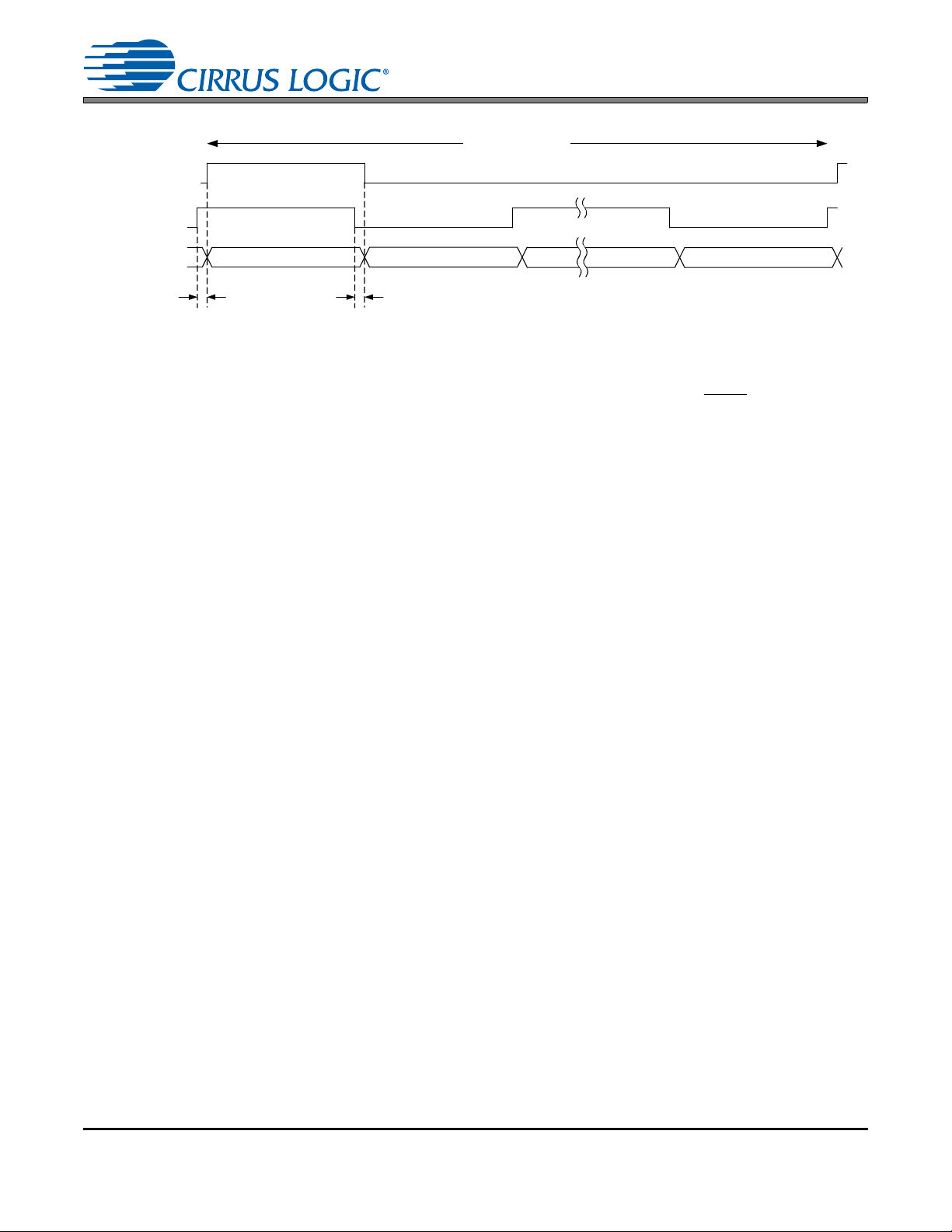
CS8422
RCBL (out)
VLRCK (out)
C/U (out)
C/U[0] C/U[1] C/U[383]
t t
192 AES3 Frames
Figure 19. C/U Data Outputs
Note:
1. RCBL will go high on the transition of the first output C/U data bit (C/U[0]) and will remain high until the C/U[0] - C/U[1] transition.
2. VLRCK is a virtual word clock that is available through the GPO pins, and can be used to frame the C/U output.
3. VLRCK frequency is always equal to the incoming frame rate of the AES3-compatible data. If there are an even number of OSCLK
periods per OLRCK, then the VLRCK duty cycle is 50%, otherwise it is 50% ± one OSCLK period.
4. If a serial audio output port is sourced directly by the AES3-compatible receiver VLRCK = OLRCK
in I²S Mode, and
VLRCK = OLRCK in left-justified and Right-Justified Modes.
5. If a serial port is sourced directly by the AES3-compatible receiver, the data will transition on the fourth OSCLK falling edge after a
VLRCK edge and will be valid on VLRCK edges (t = 4 OSCLK period).
6. If a serial port is not sourced directly by the AES3-compatible receiver (as in a sample rate conversion application), the data will
transition 1/64*Fsi after a VLRCK edge, and will be valid on VLRCK edges (t = 1/64*Fsi).
36 DS692F2
Page 37

CS8422
7. SAMPLE RATE CONVERTER (SRC)
Multirate digital signal processing techniques are used to conceptually upsample the incoming data to a very high
rate and then downsample to the outgoing rate. Internal filtering is designed so that a full input audio bandwidth of
20 kHz is preserved if the input sample and output sample rates are greater than or equal to 44.1 kHz. When the
output sample rate becomes less than the input sample rate, the input is automatically band limited to avoid aliasing
artifacts in the output signal. Any jitter in the incoming signal has little impact on the dynamic performance of the rate
converter and has no influence on the output clock.
7.1 SRC Data Resolution and Dither
When using the serial audio input port in left justified and I²S Modes, all input data is treated as 24- bits wide.
Any truncation that has been done prior to the CS8422 to less than 24-bits should have been done using
an appropriate dithering process. If the serial audio input port is in Right-Justified Mode, the input data will
be truncated to the bit depth set through the “Serial Audio Input Data Format (0Bh)” reg ister. If the bit depth
is set to 16 bits, and the input data is 24-bits wide, then truncation distortion will occur. Similarly, in any serial
audio input port mode, if an inadequate number of bit clocks are entered (i.e. 16 clocks instead of 20 clocks),
then the input words will be truncated, causing truncation distortion at low levels. In summary, there is no
dithering mechanism on the input side of the CS8422, and care must be take n to en sure th at no truncation
occurs.
The output side of the SRC can be set to 16, 18, 20, or 24. Ditherin g is applied and is automatically scaled
to the selected output word length. This dither is not correlated between left and right channel.
7.1.1 Hardware Mode Control
In Hardware Mode, the SRC is the data source for SDOUT1, and its serial output port data resolution is
controlled through the SAOF pin. See Section 8.1 on page 41 for more details.
7.1.2 Software Mode Control
In Software Mode, the serial port data resolution is controlled through the “Serial Audio Input Data For mat
(0Bh)”, “Serial Audio Output Data Format - SDOUT1 (0Ch)”, and “Serial Audio Output Data Format SDOUT2 (0Dh)” registers.
7.2 SRC Locking
The SRC calculates the ratio between the input sample rate and the output sample rate, and uses this information to set up various parameters inside the SRC block. The SRC takes some time to make this calculation (approximately ~100 ms when Fso = 48 kHz).
The SRC_UNLOCK signal is used to indicate when the SRC is not locked. When RST
is a change in Fsi or Fso, SRC_UNLOCK will be set high. The SRC_UNLOCK pin will continue to be high
until the SRC has reacquired lock and settled, at which point it will transition low. When the SRC_UNLOCK
pin is set low, SDOUT is outputting valid audio data. This can be used to signal a DAC to unmute its output.
The SRC_UNLOCK signal is available through the control port register 15h, or through the SRC_UNLOCK
pin in Hardware Mode.
is asserted, or if there
DS692F2 37
Page 38

7.3 SRC Muting
XTI XTO
CC
Figure 20. Typical Connection Diagram for Crystal Circuit
The SDOUT pin sourced by the SRC (SDOUT1 or SDOUT2 in Software Mode, SDOUT1 in Hardware
Mode) is set to all zero output (full mute) immediately after the RST
the SRC becomes valid, SDOUT will be soft unmuted over a period of approximately 27488/Fsi while in interpolation mode (Fsi < Fso) or 54976/Fso while in decimation mode (Fsi > Fso). When the ou tput becomes
invalid the SRC’s SDOUT is immediately set to all zero output (hard muted). After all invalid states have
been cleared, the SRC will soft unmute SDOUT.
7.4 SRC Master Clock
The CS8422 can use the clock signal supplied through XTI-XTO, the PLL, or an internal ring oscillator as
its master clock (MCLK). If the SRC MCLK source is selected as being XTI-XTO, care must be taken to ensure that the SRC MCLK source does not exceed 33 MHz. If the SRC MCLK source exceeds 33 MHz, an
internal clock divider can be enabled to divide the SRC MCLK source by 2, allowing the use of higher frequency clocks. See Section 7.4.1 and Section 7.4.2 for more details.
If the SRC MCLK is applied through XTI then it can be supplied from a digital clock source, a crystal oscillator, or a fundamental mode crystal. If XTO is not used, such as with a digital clock source or crystal oscillator, XTO should be left unconnected or pulled low through a 20 k resistor to GND.
If a crystal in conjunction with the internal oscillator is used to supply the SRC MCLK, the crystal circuit
should be connected as shown in Figure 20. If VL < 2.5 Volts, it is recommended that the crystal attached
across XTI and XTO should be specified as operating with a load capacitance of 10pF (capacitors in
Figure 20 should be 20 pF). If VL 2.5 Volts, it is recommended that the crystal attached across XTI and
XTO should be specified as operating with a series capacitance of at 20pF (capacitors in Figure 20 should
be at 40 pF) . Please refer to the crys tal manufacturer’s specifications for more information about external
capacitor recommendations.
CS8422
pin is set high. While the output from
If the PLL clock is selected as the SRC MCLK, the SRC MCLK will be synchronous to incoming AES3-compatible data or ISCLK. Unlike RMCK, the user does not control PLL clock’s relationship to the sampling rate
of incoming AES3-compatible data (Fsi), or ISCLK. See Table 2 for the relationship between the Fsi or ISCLK/64, and the PLL clock.
The CS8422 has the ability to operate without a master clock input through XTI. This benefits the design by
not requiring extra external clock components (lowering production cost) and not requiring a master clock
to be routed to the CS8422, resulting in lowered noise contribution in the system. In this mode, an internal
38 DS692F2
Fsi (or ISCLK/64) PLL/Fsi
Fsi 49 kHz 512
60 kHz Fsi 98 kHz 256
120 kHz Fsi 128
Table 2. PLL Clock Ratios
Page 39

CS8422
oscillator provides the clock to run all of the internal logic. See Section 7.4.1 and Sectio n 7.4.2 for explanation of how the SRC MCLK can be selected.
7.4.1 Hardware Mode Control
In Hardware Mode, the default master clock source for the SRC is the internal ring oscillator. Therefore,
it is not necessary to apply an external MCLK source for the SRC. Optionally the user may select the PLL
clock as the SRC MCLK source by connecting a 20 k pull-up resistor between MCLK_OUT and VL.
7.4.2 Software Mode Control
In Software Mode, the SRC master clock source is selected by the SRC_MCLK[1:0] bits in the “SRC Out-
put Serial Port Clock Control (08h)” register . If the XTI clock is selected as the SRC MCLK and XTI is tied
to VL or DGND and XTO is left unconnected, then the internal ring oscillator will take the place of the XTIXTO clock source.
If the selected SRC MCLK source is XTI-XTO, and is greater tha t 33 MHz, the user can enable the internal
clock divide-by-two by setting the SRC_DIV bit in control port register 08h. See “SRC Output Serial Port
Clock Control (08h)” on page 52 for more details.
8. HARDWARE MODE CONTROL
The CS8422 provides a stand-alone hardware control mode in which the part does not require an I²C or SPI control
port. In Hardware Mode, the user is provided with a subset of the features available in Software Mode as shown in
Figure 21. The part will be in Hardware Mode if there is a 20 k pull-up resistor connected betwe en the C p in and
VL upon the release of RST
Controlling the CS8422 in Hardware Mode is done through dedicated control inputs, 20 k pull-up or pull-down resistors attached to dual-purpose pins, and by attaching a specific resistor values from one of two dedicated control
pins (SAOF and MS_SEL) to either VL or ground. In the case of SAOF and MS_SEL, the resistor should be connected as close to the pin as possible and should have a tolerance no greater than ±1%. Dedicated controls
(TX_SEL and RX_SEL) can be changed during operation whereas pull-up resistor controls are sensed on startup.
Figure 21 shows clock routing options available in Hardware Mode. Control signal names are in italics and are de-
scribed in the table below.
.
DS692F2 39
Page 40

CS8422
RXP/RXN0
RXP/RXN1
Receiver
Clock
Recovery
(PLL)
Sample
Rate
Converter
Serial
Audio
Output
2
OLRCK1
OSCLK1
SDOUT1
TDM_IN1
OLRCK2
OSCLK2
SDOUT2
Serial
Audio
Output
1
2
2
RX_SEL
TX_SEL
TX
Ring Oscillator
(RMCK Pull-Up)
2:1
MUX
(MCL K_OUT Pull-up)
Clock
Generator
XTI XTO
MCLK_OUT
2:1
MUX
2:1
MUX
MS_SEL
SAOF
MS_SEL
SAOF
RMCK
2:1
MUX
Figure 21. Hardware Mode Clock Routing
40 DS692F2
Page 41

CS8422
Pin Name Description Pin Configuration Selection
RX_SEL Selects Active AES3 RX Input
TX_SEL
SDOUT1
SAOF
MS_SEL
RMCK
MCLK_OUT
TX/U
C
NV/RERR
V/AUDIO
Selects RX Input to be output on
TX pin
Enables or Disables De-emphasis
Auto-detect
Selects data format for SDOUT1
& SDOUT2
Selects master/slave and clock
configuration for SDOUT1&
SDOUT 2
Selects master clock source for
SDOUT1 serial port
Selects master clock source for
the SRC
Selects TX pass-through output or
incoming U data output
Selects Software or Hardware
Mode
Selects error signal output on
NV/RERR
Selects either incoming Validity
data output or AUDIO indicator
output
Connected to GND RXP0/RXN0 is active
Connected to VL RXP1/RXN1 is active
Connected to GND RXP0/RXN0 to TX
Connected to VL RXP1/RXN1 to TX
No pull-up on SDOUT1
20 k pull-up on SDOUT1
See Table 4 on page 42
See Table 5 on page 42
No pull-up on RMCK XTI-XTO
20 k pull-up on RMCK RMCK
No pull-up on MCLK_OUT Ring Oscillator
20 k pull-up on MCLK_OUT PLL Clock
No pull-up on U TX Pass-through
20 k pull-up on U U Data Output
No pull-up on C Software Mode
20 k pull-up on C Hardware Mode
No pull-up on RERR/NVERR NVERR
20 k pull-up on RERR/NVERR RERR
20 k pull-down on V/AUDIO Validity data output
20 k pull-up on V/AUDIO
De-emphasis Auto-detect
Enabled
De-emphasis Auto-detect
Disabled
AUDIO indicator output
Table 3. Hardware Mode Control Settings
8.1 Hardware Mode Serial Audio Port Control
The CS8422 uses the resistors attached to the MS_SEL and SAOF p i ns to determin e the m ode s o f o peration for its serial output ports. After RST
sensed. This operation will take approximately 4 ms to complete. The SRC_UNLOCK pin will remain high
and both SDOUT pins will be muted until the mode detection sequence has completed. After this, if all clocks
are stable, SRC_UNLOCK will be brought low when audio output is valid and normal operation will begin.
The resistor attached to each mode selection pin sh ould be placed physically close to the CS84 22. The end
of the resistor not connected to the mode selection pins should be connecte d as close as possible to VL and
GND to minimize noise. Table 4 and Table 5 show the pin functions and their corresponding settings.
Table 4 shows the Hardware Mode options for output serial port format and the required SAOF pin config-
urations. In the case of SDOUT2, the output resolution depends on the resolution of the incoming AES3compatible data. In Right-Justified Modes, the serial format word-length will be equal to the AES3 input data
resolution. The exception is the case where Right-Justified Mode is selected and the AES3 input wordlength is an odd number of bits. In this case, the SDOUT2 word-length will be zero-stuffed to be 1 bit longer
then the AES3 input word-length (example: a 19-bit AES3 input word will result in an 20-bit right-justified
serial format). For a more detailed description of serial formats, refer to Section 5. on page 24.
Table 5 shows the Hardware Mode master/slave and clock options for both serial ports, and the required
MS_SEL pin configurations. For SDOUT1, when the serial port is set to master mode, the master clock ratio
DS692F2 41
is released, the resistor value and condition (VL or GND) are
Page 42

CS8422
determines what the output sample rate will be based on the MCLK selected for SDOUT1, as shown in the
hardware control pin descriptions shown above. For SDOUT2, the output sample rate is dictated by the incoming AES3 data, and the master mode clock ratio determines the frequency of RMCK relative to the incoming AES3 sample rate. Note: if TDM Mode is selected for SDOUT1, then SDOUT1 cannot be set to
“Master, Fso = MCLK/128”.
SAOF pin SDOUT1 Data Format SDOUT2 Data Format
32.4 k ± 1% to GND I²S 24-bit data I²S
16.2 k ± 1% to GND I²S 20-bit data I²S
8.06 k ± 1% to GND I²S 16-bit data I²S
4.02 k ± 1% to GND Left-Justified 24-bi t data Left-Justified
1.96 k ± 1% to GND Left-Justified 20-bi t data Left-Justified
1.0 k + 1% to GND Left-Justified 16-bit data Left-Justified
32.4 k ± 1% to VL Right-Justified 24-bit data
(Master mode only)
16.2 k ± 1% to VL Right-Justified 20-bit data
(Master mode only)
8.06 k ± 1% to VL Right-Justified 16-bit data
(Master mode only)
4.02 k ± 1% to VL TDM Mode 24-bit data I²S
1.96 k ± 1% to VL TDM Mode 20-bit data I²S
1.0 k + 1% to VL TDM Mode 16-bit data I²S
Right-Justified
(Master mode only)
Right-Justified
(Master mode only)
Right-Justified
(Master mode only)
Table 4. Hardware Mode Serial Audio Format Control
MS_SEL pin SDOUT1 SDOUT2
127.0 k ± 1% to GND Slave
63.4 k ± 1% to GND Master, Fso = MCLK/128
32.4 k ± 1% to GND Master, Fso = MCLK/256
16.2 k ± 1% to GND Master, Fso = MCLK/512
8.06 k ± 1% to GND Slave
4.02 k ± 1% to GND Master, Fso = MCLK/128
1.96 k ± 1% to GND Master, Fso = MCLK/256
1.0 k + 1% to GND Master, Fso = MCLK/512
127.0 k ± 1% to VL Slave
63.4 k ± 1% to VL Master, Fso = MCLK/128
32.4 k ± 1% to VL Master, Fso = MCLK/256
16.2 k ± 1% to VL Master, Fso = MCLK/512
8.06 k ± 1% to VL Slave
4.02 k ± 1% to VL Master, Fso = MCLK/128
1.96 k ± 1% to VL Master, Fso = MCLK/256
1.0 k + 1% to VL Master, Fso = MCLK/512
RMCK = 256 x Fsi
Master Mode,
RMCK = 128 x Fsi
Master Mode,
RMCK = 256 x Fsi
Master Mode,
RMCK = 512 x Fsi
Table 5. Hardware Mode Serial Audio Port Clock Control
Slave
42 DS692F2
Page 43

9. SOFTWARE MODE CONTROL
MAP
MSB
LSB
DATA
byte 1
byte n
R/W
R/W
ADDRESS
CHIP
ADDRESS
CHIP
CDIN
CCLK
CS
CDOUT
MSB
LSB
MSB
LSB
0010000
0010000
MAP = Memory Address Pointer,8 bits, MSB first
High Impedance
Figure 22. Control Port Timing in SPI Mode
9.1 Control Port Description
The control port is used to access the registers, allowing the CS8422 to be configured for the desired operational modes and formats. The operation of the control port may be completely asynchronous with r espect
to the audio sample rates. However, to avoid potential interference problems, the control port pins should
remain static if no operation is required.
The control port has two modes: SPI and I²C, with the CS8422 acting as a slave device. SPI Mode is selected if there is a high to low transition on the AD0/CS
Mode is selected by connecting the AD0/CS
selecting the desired AD0 bit address state.
9.1.1 SPI Mode
In SPI Mode, CS is the CS8422 chip select signal, CCLK is the control port bit clock (input into the CS8422
from the microcontroller), CD IN is t he in pu t d a ta line fr o m the m icr ocontroller, CDOUT is the output da ta
line to the microcontroller. Data is clocked in on the rising edge of CCLK and out on the falling edge.
CS8422
pin, after the RST pin has been brought high. I²C
pin through a resistor to VL or DGND, thereby permanently
Figure 22 shows the operation of the control port in SPI Mode. To write to a register, bring CS
low. The
first seven bits on CDIN form the chip address and must be 0010000. The eighth bit is a read/write indicator (R/W
), which should be low to write. The next eight bits include the 7-bit Memory Address Pointer
(MAP), which is set to the address of the register that is to be updated. The next eight bits are the data
which will be placed into the register designated by the MAP. During writes, the CDOUT output stays in
the Hi-Z state. It may be externally pulled high or low with a 20 k resistor, if desired.
To read a register, the MAP has to be set to the correct address by executing a partial write cycle which
finishes (CS
dress and set the read/write bit (R/W
high) immediately after the MAP byte. To begin a read, bring CS low, send out the chip ad-
) high. The next falling edge of CCLK will clock out the MSB of the
addressed register (CDOUT will leave the high impedance state). The MAP automatically increments, so
DS692F2 43
data for successive registers will appear consecutively.
Page 44

9.1.2 I²C Mode
4 5 6 7 24 25
SCL
CHIP ADDRESS (WRITE) MAP BYTE DATA
DATA +1
START
ACK
STOP
ACKACKACK
0 0 1 0 AD2 AD1 AD0 0
SDA
6 5 4 3 2 1 0
7 6 1 0 7 6 1 0 7 6 1 0
0 1 2 3 8 9 12 16 17 18 19 10 11 13 14 15 27 28
26
DATA +n
INC
Figure 23. Control Port Timing, I²C Slave Mode Write
SCL
CHIP ADDRESS (WRITE)
MAP BYTE
DATA
DATA +1
START
ACK
STOP
ACK
ACK
ACK
SDA
CHIP ADDRESS (READ)
START
6 5 4 3 2 1 0
7 0 7 0 7 0
NO
16 8 9 12 13 14 15 4 5 6 7 0 1 20 21 22 23 24
26 27 28
2 3 10 11 17 18 19 25
ACK
DATA + n
STOP
0 0 1 0 AD2 AD1 AD0 0 0 0 1 0 AD2 AD1 AD0 1
INC
Figure 24. Control Port Timing, I²C Slave Mode Read
In I²C Mode, SDA is a bidirectional data line. Data is clocked into and out of the part by the clock, SCL.
There is no CS
be connected to VL or DGND as desired. The GPO2 pin is used to set the AD2 bit by connecting a 20 k
resistor from the GPO2 pin to VL (a 20 k pull-up sets AD2 = 1, and the absence of a pull-up sets
AD2 = 0). The states of the pins are sensed after RST
The signal timings for a read and write cycle are shown in Figure 23 and Figure 24. A Start condition is
defined as a falling transition of SDA while the clock is high. A Stop condition is a rising transition while
the clock is high. All other transitions of SDA occur while the clock is low. The first byte sent to the CS8422
after a Start condition consists of a 7-bit chip address field and a R/W
The upper 4 bits of the 7-bit address field are fixed at 0010.
To communicate with a CS8422, the chip address field, which is the first byte sent to the CS8422, should
match 0010 followed by the settings of the AD2, AD1, and AD0 pins. The eighth bit of the address is the
R/W
bit. If the operation is a write, th e next byte in cludes the M emory Addr ess Pointer (MAP) which se lects the register to be read or written. If the operation is a read, the contents of the register pointed to by
the MAP will be output. Each byte is separated by an acknowledge bit (ACK). The ACK bit is output from
the CS8422 after each input byte is read, and is input to the CS8422 from the microcontroller after each
transmitted byte.
CS8422
pin. Pins AD0 and AD1 form the two least significant bits of the chip addr ess an d should
is released.
bit (high for a read, low for a write).
Note that the read operation can not set the MAP so an aborted write operation is used as a preamble.
As shown in Figure 24, the write operation is aborted after the acknowledge for the MAP byte by sending
a stop condition.
9.1.3 Memory Address Pointer (MAP)
The MAP is an 8-bit word containing the control port address to be read or written in both SPI and I²C Modes
and a bit to control an auto-increment feature. MAP[6:0] constitute the address to be read or written, while
bit 7 of the MAP (INC) de termin es whe ther or not M AP[6:0] will automa tically inc rement after each contro l
port read or write. If INC = 0, MAP[6:0] will not automatically increment after each control port read or write.
If INC = 1, MAP[6:0] will automatically increment after each control port read or write. The MAP byte is
shown in Figures 23 and 24.
44 DS692F2
Page 45

CS8422
10.REGISTER QUICK REFERENCE
This table shows the register names and default values for read-write registers.
AddrFunction76543210
01h Chip ID &
Version
02h Clock Control
03h Receiver Input
Control
04h Receiver Data
Control
05h GPO Control 1
06h GPO Control 2
07h SAI Clock Con-
trol
08h SRC SAO
Clock Control
09h RMCK Cntl.&
Misc.
0Ah Data Routing
Control
0Bh SAI Data
Format
0Ch SAO1 Data For-
mat & TDM
0Dh SAO2 Data For-
mat
0Eh RERR Unmask-
ing
0Fh Interrupt
Unmasking
10h Interrupt Mode
ID4 ID3 ID2 ID1 ID0 REV2 REV1 REV0
00010000
PDN FSWCLK SWCLK
10000000
RX_MODE RXSEL1 RXSEL0 TXSEL1 TXSEL0
00001000
TRUNC HOLD1 HOLD0 CHS DETCI
00000100
GPO0SEL3 GPO0SEL2 GPO0SEL1 GPO0SEL0 GPO1SEL3 GPO1SEL2 GPO1SEL1 GPO1SEL0
00000000
GPO2SEL3 GPO2SEL2 GPO2SEL1 GPO2SEL3 GPO3SEL2 GPO3SEL1 GPO3SEL0 GPO3SEL3
00000000
SAI_CLK3 SAI_CLK2 SAI_CLK1 SAI_CLK0 SAI_MCLK Reserved Reserved Reserved
01000000
SAO_CLK3 SAO_CLK2 SAO_CLK1 SAO_CLK0
01100000
RMCK3 RMCK2 RMCK1 RMCK0
00001000
SDOUT1_1 SDOUT1_0 SDOUT2_1 SDOUT2_0
00010000
SIMS SISF SIFSEL2 SIFSEL1 SIFSEL0 Reserved Reserved Reserved
00000000
SOMS1 SOSF1 SORES1_1 SORES1_0 SOFSEL1_1 SOFSEL1_0 TDM1 TDM0
00000000
SOMS2 SOSF2 SORES2_1 SORES2_0 SOFSEL2_1 SOFSEL2_0 Reserved Reserved
00000000
Reserved QCRCM CCRCM UNLOCKM VM CONFM BIPM PARM
00000000
PCCHM OSLIPM DETCM CCHM RERRM QCHM FCHM
00000000
Reserved Reserved Reserved Reserved RERR1 RERR0
00000000
RMCK_
CTL1
RMCK_
CTL0
SAO_
MCLK
SRC_
MUTE
MUTE_
SAO1
INT1 INT0 Reserved
INPUT_
TYPE
EMPH_
CNTL2
SRC_
MCLK1
Reserved Reserved Reserved
MUTE_
SAO2
Reserved Reserved
EMPH_
CNTL1
SRC_
MCLK2
SRCD Reserved
SRC_
UNLOCK1
EMPH_
CNTL0
SRC_DIV
SRC_
UNLOCKM
SRC_
UNLOCK0
Table 6. Summary of Software Register Bits
DS692F2 45
Page 46
CS8422
Addr Function 7 6 5 4 3 2 1 0
11h Receiver Chan-
nel
Status
AUX3 AUX2 AUX1 AUX0 PRO COPY ORIG EMPH
12h Format Detect
Status
13h Receiver Error Reserved QCRC CCRC UNLOCK V CONF BIP PAR
14h Interrupt
Status
15h PLL Status RX_
16h Receiver
Status
17h Fs/XTI Ratio
1
18h Fs/XTI Ratio
2
19h Q Subcode 1 CONTROL CONTROL CONTROL CONTROL ADDRESS ADDRESS ADDRESS ADDRESS
1Ah Q Subcode 2 TRACK TRACK TRACK TRACK TRACK TRACK TRACK TRACK
1Bh Q Subcode 3 INDEX INDEX INDEX INDEX INDEX INDEX INDEX INDEX
1Ch Q Subcode 4 MINUTE MINUTE MINUTE MINUTE MINUTE MINUTE MINUTE MINUTE
1Dh Q Subcode 5 SECOND SECOND SECOND SECOND SECOND SECOND SECOND SECOND
1Eh Q Subcode 6 FRAME FRAME FRAME FRAME FRAME FRAME FRAME FRAME
1Fh Q Subcode 7 ZERO ZERO ZERO ZERO ZERO ZERO ZERO ZERO
20h Q Subcode 8 ABS
21h Q Subcode 9 ABS
22h Q Subcode 10 ABS FRAME ABS FRAME ABS FRAME ABS FRAME ABS FRAME ABS FRAME ABS FRAME ABS FRAME
23h Channel A Sta-
tus Byte 0
24h Channel A Sta-
tus Byte 1
25h Channel A Sta-
tus Byte 2
26h Channel A Sta-
tus Byte 3
27h Channel A Sta-
tus Byte 4
28h Channel B Sta-
tus Byte 0
29h Channel B Sta-
tus Byte 1
2Ah Channel B Sta-
tus Byte 2
2Bh Channel B Sta-
tus Byte 3
PCM IEC61937 DTS_LD DTS_CD HD_CD DGTL_SIL Reserved Reserved
PCCH OSLIP DETC CCH RERR QCH FCH
ISCLK_
ACTIVE
CS_
UPDATE
0
FS_XT15 FS_XT14 FS_XT13 FS_XT12 FS_XT11 FS_XT10 FS_XT9 FS_XT8
FS_XT7 FS_XT6 FS_XT5 FS_XT4 FS_XT3 FS_XT2 FS_XT1 FS_XT0
MINUTE
SECOND
AC0[7] AC0[6] AC0[5] AC0[4] AC0[3] AC0[2] AC0[1] AC0[0]
AC1[7] AC1[6] AC1[5] AC1[4] AC1[3] AC1[2] AC1[1] AC1[0]
AC2[7] AC2[6] AC2[5] AC2[4] AC2[3] AC2[2] AC2[1] AC2[0]
AC3[7] AC3[6] AC3[5] AC3[4] AC3[3] AC3[2] AC3[1] AC3[0]
AC4[7] AC4[6] AC4[5] AC4[4] AC4[3] AC4[2] AC4[1] AC4[0]
BC0[7] BC0[6] BC0[5] BC0[4] BC0[3] BC0[2] BC0[1] BC0[0]
BC1[7] BC1[6] BC1[5] BC1[4] BC1[3] BC1[2] BC1[1] BC1[0]
BC2[7] BC2[6] BC2[5] BC2[4] BC2[3] BC2[2] BC2[1] BC2[0]
BC3[7] BC3[6] BC3[5] BC3[4] BC3[3] BC3[2] BC3[1] BC3[0]
ACTIVE
RCVR_
RATE1
ABS
MINUTE
ABS
SECOND
PLL_LOCK 96KHZ 192KHZ Reserved Reserved Reserved
RCVR_
RATE0
ABS
MINUTE
ABS
SECOND
RX_LOCK BLK_VERR BLK_CERR BLK_BERR BLK_PERR
ABS
MINUTE
ABS
SECOND
ABS
MINUTE
ABS
SECOND
ABS
MINUTE
ABS
SECOND
ABS
MINUTE
ABS
SECOND
SRC_
UNLOCK
ABS
MINUTE
ABS
SECOND
Table 6. Summary of Software Register Bits (Continued)
46 DS692F2
Page 47
CS8422
AddrFunction76543210
2Ch Channel B Sta-
tus Byte 4
2Dh Burst
Preamble PC
Byte 0
2Eh Burst
Preamble PC
Byte 1
2Fh Burst
Preamble Pd
Byte 0
30h Burst
Preamble PD
Byte 1
BC4[7] BC4[6] BC4[5] BC4[4] BC4[3] BC4[2] BC4[1] BC4[0]
PC0[7] PC0[6] PC0[5] PC0[4] PC0[3] PC0[2] PC0[1] PC0[0]
PC1[7] PC1[6] PC1[5] PC1[4] PC1[3] PC1[2] PC1[1] PC1[0]
PD0[7] PD0[6] PD0[5] PD0[4] PD0[3] PD0[2] PD0[1] PD0[0]
PD1[7] PD1[6] PD1[5] PD1[4] PD1[3] PD1[2] PD1[1] PD1[0]
Table 6. Summary of Software Register Bits (Continued)
DS692F2 47
Page 48

CS8422
11.SOFTWARE REGISTER BIT DEFINITIONS
The table row beneath the row that contain s the re giste r-bit name shows the register bit default value. Bits labeled
‘Reserved’ must remain at their default value.
11.1 CS8422 I.D. and Version Register (01h)
76543210
ID4 ID3 ID2 ID1 ID0 REV2 REV1 REV0
00010000
ID[4:0] - ID code for the CS8422. Permanently set to 00010
REV[2:0] = 000 (revision A)
REV[2:0] = 010 (revision B1)
11.2 Clock Control (02h)
76543210
PDN FSWCLK SWCLK
10000000
PDN - Controls the internal clocks, allowing the CS8422 to be placed in a “powered down”, low current consumption state. This bit must be written to the 0 state to allow the CS8422 to begin oper ation. All input clocks
should be stable in frequency and phase when PDN is set to 0.
RMCK_CTL1 RMCK_CTL0
INT1
INT0 Reserved
0- Normal part operation.
1- Internal clocks are stopped. Internal state machines are re set. The fully static control port is operational,
allowing registers to be read or changed. Power consumption is low.
FSWCLK – Forces the clock signal on XTI to be output on RMCK regardless of the SWCLK bit functionality
or PLL lock.
0 – Clock signal on XTI is output on RMCK according to the SWCLK bit functionality.
1 – Forces the clock signal on XTI to be output on RMCK regardless of the SWCLK bit functionality.
SWCLK - Outputs XTI clock signal on RMCK pin when PLL loses lock. Any OSCLK or OLRCK derived from
RMCK under normal conditions will be derived from XTI in this case.
0 - Disable automatic clock switching.
1 - Enable automatic clock switching on PLL unlock. Clock signal selected on XT I is a utomatica lly outpu t
on RMCK on PLL Unlock.
RMCK_CTL[1:0] - RMCK Control
00 - RMCK is an output and is derived from the frame rate of incoming AES3 data.
01 - RMCK is an output and is derived from the ISCLK input frequency divided by 64. Only valid if serial
audio input port is in slave mode (SIMS = 0 in “Serial Audio Input Data Forma t (0Bh)” on page 54).
10 - RMCK is high-impedance.
11 - Reserved
INT[1:0] - Interrupt output pin (INT) control
00 - Active high; high output indicates interrupt condition has occurred.
48 DS692F2
Page 49

CS8422
01 - Active low, low output indicates an interrupt condition has occurred.
10 - Open drain, active low. Requires an external pull-up resistor on the INT pin.
11 - Reserved.
11.3 Receiver Input Control (03h)
76543210
RX_MODE RXSEL1 RXSEL0 TXSEL1 TXSEL0
00010000
RX_MODE - Selects the input mode (single-ended or differential) of the RX pins
0 - Receiver inputs are differential-pair inputs RXP1/RXN1 and RXP0/RXN0.
1 - Receiver inputs are single-ended inputs RX[3:0].
RX_SEL[1:0] – Input multiplexer to the receiver
00 - RX0 or RXP0/RXN0
01 - RX1 (Only valid if RX_MODE = 1)
10 - RX2 or RXP1/RXN1
11 - RX3 (Only valid if RX_MODE = 1)
INPUT_TYPE
Reserved Reserved
TX_SEL[1:0] – Selects receiver input for GPO TX source
00 - RX0 or RXP0/RXN0
01 - RX1 (Only valid if RX_MODE = 1)
10 - RX2 or RXP1/RXN1
11 - RX3 (Only valid if RX_MODE = 1)
INPUT_TYPE – Selects receiver input type
0 - Mode 1, receiver multiplexer inputs are comparator inputs biased at VA/2.
1 - Mode 2, receiver multiplexer inputs are digital inputs, referenced to VA. Valid only if RX_MODE = 1.
11.4 Receiver Data Control (04h)
76543210
TRUNC HOLD1 HOLD0 CHS DETCI EMPH_CNTL2 EMPH_CNTL1 EMPH_CNTL0
00000100
TRUNC – Determines if the audio word length is set according to the incoming channel status data as decoded by the AUX[3:0] bits. The resulting word length in bits is 24 minus AUX[3:0].
0 – Incoming data is not truncated.
1 – Incoming data is truncated according to the length specified in the channel status data.
Truncation occurs before the de-emphasis filter. TRUNC has no effect on output data is detected as being
non-audio.
HOLD[1:0] – Determine how received AES3 audio sample is affected when a rece ive er ro r oc cu rs
00 - hold last audio sample.
DS692F2 49
Page 50

CS8422
Figure 25. De-Emphasis Filter Response
Gain
dB
-10dB
0dB
Frequency
T2 = 15 µs
T1=50 µs
F1 F2
3.183 kHz 10.61 kHz
01 - replace the current audio sample with all zeros (mute).
10 - do not change the received audio sample.
11 - reserved
CHS – Sets which channel's C data is decoded in the Receiver Channel Status register (11h) (Defau lt = ‘0’)
0 - A channel
1 - B channel
If CHS = 0 and TRUNC = 1, both channels' audio data will be truncated by the AUX[3:0] bits indicated in
the channel A Channel Status data. If CHS = 1 and TRUNC = 1, both channels' audio data will be truncated by the AUX[3:0] bits indicated in the channel B Channel Status data. This will occur even if the
AUX[3:0] bits indicated in the channel A Channel Sta tus data are not equal to the AUX[3:0] bits indicated
in the channel B Channel Status data.
DETCI - D to E status transfer inhibit
0 -Allow update
1 -Inhibit update
DEM_CNTL[2:0] – De-emphasis filter control. See Figure 25 for De-emphasis filter response.
000 - De-emphasis filter off.
001 - 32 kHz setting
010 - 44.1 kHz setting
011 - 48 kHz setting
100 - Auto-detect Sample Rate. If the PLL estimates that the incoming sample rate is below 49 kHz, de-
emphasis will be applied according to the Channel Status data of the incoming AES3 or S/PDIF data. If
the PLL estimates that the incoming sample rate is not below 49 kHz, de-emphasis will not be enabled. If
the incoming Channel Status data indicates that no de-emphasis should be applied, de-emphasis will not
be enabled. If data is detected as being non-audio, the de-emphasis filter will not be enabled.
50 DS692F2
Page 51

CS8422
11.5 GPO Control 1 (05h)
7 6 543210
GPO0SEL3 GPO0SEL2 GPO0SEL1 GPO0SEL0 GPO1SEL3 GPO1SEL2 GPO1SEL1 GPO1SEL0
0 0 000000
GPOxSEL[3:0] – GPO Source select for GPO0 and GPO1 pins. See Table 7 for available outputs for
GPO[3:0].
11.6 GPO Control 2 (06h)
7 6 543210
GPO2SEL3 GPO2SEL2 GPO2SEL1 GPO2SEL0 GPO3SEL3 GPO3SEL2 GPO3SEL1 GPO3SEL0
0 0 000000
GPOxSEL[3:0] – GPO Source select for GPO2 and GPO3 pins. See Table 7 for available outputs for
GPO[3:0].
Function Code Definition
GND 0000 Fixed low level
VL 0001 Fixed VL level.
EMPH
INT 0011 CS8422 interrupt output
C 0100 Channel status bit
U 0101 User data bit
RERR 0110 Receiver Error. Use of RERR and NVERR are described in Section 6.6.1.
NVERR 0111 Non-Validity Receiver Error (same signal as RERR except it does not become
RCBL 1000 Receiver Channel Status Block
96KHZ 1001 Defined in “PLL Status (15h)” on page 61.
192KHZ 1010 Defined in “PLL Status (15h)” on page 61.
AUDIO
VLRCK 1100 Virtual LRCK, can be used to frame the C and U output data.
TX 1101 Pass through of AES/SPDIF input selected by TXSEL[2:0] in Section 11.3
SRC_UNLOCK 1110 SRC unlock indicator
XTI_OUT 1111 Buffered XTI-XTO output
0010 State of EMPH bit in the incoming data stream
active when validity bit error occurs). Use of RERR and NVERR are described
in Section 6.6.1.
1011 Non-audio in dicator for decoded input stream
“Receiver Input Control (03h)” on page 49.
Table 7. GPO Pin Configurations
11.7 Serial Audio Input Clock Control (07h)
76543210
SAI_CLK3 SAI_CLK2 SAI_CLK1 SAI_CLK0 SAI_MCLK Reserved Reserved Reserved
01000———
SAI_CLK[3:0] – Selects the serial audio input master clock-to-ILRCK ratio when the serial audio inpu t port
is set to master mode (SIMS = 1 as shown in “Serial Audio Input Data Format (0Bh)” on page 54). Note: if
a serial audio output is sourced directly by the serial audio input port, SAI_CLK[3:0] determine the
MCLK/LRCK ratio for both serial ports if they are set to master mode.
DS692F2 51
Page 52

CS8422
0000 - ILRCK = MCLK/64
0001 - ILRCK = MCLK/96
0010 - ILRCK = MCLK/128
0011 - ILRCK = MCLK/192
0100 - ILRCK = MCLK/256
0101 - ILRCK = MCLK/384
0110 - ILRCK = MCLK/512
0111 - ILRCK = MCLK/768
1000 - ILRCK = MCLK/1024
SAI_MCLK – Selects the master clock (MCLK) source for the serial audio input when set to master mode
(SIMS = 1, as shown in “Serial Audio Input Data Format (0Bh)” on page 54). When set to master, ILRCK
and ISCLK are derived from the MCLK selected in this register. Note: if either serial audio output port is
sourced directly by the serial audio input port, this bit determines the master clock source for the selected
serial output port when it is in master mode.
0 - XTI-XTO
1 - RMCK
11.8 SRC Output Serial Port Clock Control (08h)
76543210
SAO_CLK3 SAO_CLK2 SAO_CLK1 SAO_CLK0 SAO_MCLK SRC_MCLK1 SRC_MCLK0 SRC_DIV
01000000
SAO_CLK[3:0] – Valid only for the serial port sourced by the SRC. Selects the serial audio input master
clock-to-OLRCK ratio when the serial audio output port is set to master mode (SOMS = 1 as shown in “Serial
Audio Output Data Format - SDOUT1 (0Ch)” on page 55 and “Serial Audio Output Data Format - SDOUT2
(0Dh)” on page 56).
0000 - OLRCK = MCLK/64
0001 - OLRCK = MCLK/96
0010 - OLRCK = MCLK/128
0011 - OLRCK = MCLK/192
0100 - OLRCK = MCLK/256
0101 - OLRCK = MCLK/384
0110 - OLRCK = MCLK/512
0111 - OLRCK = MCLK/768
1000 - OLRCK = MCLK/1024
SAO_MCLK – Selects the master clock (MCLK) source for the serial audio output, sourced by the SRC,
when set to master mode (SOMS1 or SOMS 2 = 1, as shown in “Serial Audio Output Data Format - SDOUT1
(0Ch)” on page 55 and “Serial Audio Output Data Format - SDOUT2 (0Dh)” on page 56). When set to mas-
ter, OLRCK and OSCLK are derived from the MCLK selected in this register.
52 DS692F2
Page 53

CS8422
0 - XTI-XTO
1 - RMCK
SRC_MCLK[1:0] - Controls the master clock (MCLK) source for the sample rate converter. See “SRC Mas-
ter Clock” on page 38 for details.
00 - XTI-XTO. If XTI is connected to GND or VL and XTO is left floating, the SRC MCLK will be the internal
ring oscillator.
01 - PLL clock
10 - Internal Ring Oscillator
11 - Reserved
SRC_DIV – Divide-by-two for the SRC MCLK source. Valid only if SRC_MCLK = 00.
0 - SRC MCLK is not divided. Maximum allowable SRC MCLK frequency is 33 MHz.
1 - SRC MCLK is divided. Maximum allowable SRC MCLK frequency is 49.152 MHz.
11.9 Recovered Master Clock Ratio Control & Misc. (09h)
76543210
RMCK3 RMCK2 RMCK1 RMCK0 SRC_MUTE Reserved Reserved Reserved
00001———
RMCK[3:0] – Selects the RMCK/Fsi ratio, where Fsi is the sample rate of the incoming AES3-compatible
data or ISCLK/64. Note: If a serial audio output port is in master mode and sourced directly by the AES3
receiver, then RMCK is the master clock source for the selected serial output p ort and RMCK[3:0] determine
the MCLK/OLRCK ratio for the selected serial output port.
0000 - RMCK = 64 x Fsi
0001 - RMCK = 96 x Fsi
0010 - RMCK = 128 x Fsi
0011 - RMCK = 192 x Fsi
0100 - RMCK = 256 x Fsi
0101 - RMCK = 384 x Fsi
0110 - RMCK = 512 x Fsi
0111 - RMCK = 768 x Fsi
1000 - RMCK = 1024 x Fsi
SRC_MUTE – When SRC_MUTE is set to ‘1’, the SRC will soft-mute when it loses lock and soft unmute
when it regains lock.
0 - Soft mute disabled
1 - Soft mute enabled
DS692F2 53
Page 54

CS8422
11.10 Data Routing Control(0Ah)
76543210
SDOUT1(1) SDOUT1(0) SDOUT2(1) SDOUT2(0) MUTESAO1 MUTESAO2 SRCD Reserved
0001000
SDOUT1[1:0] - Controls the data source for SDOUT1
00 - Sample Rate Converter
01 - AES3 Receiver Output
10 - SDIN (SDIN and SDOUT should be synchronous)
11 - Reserved
SDOUT2[1:0] - Controls the data source for SDOUT2
00 - Sample Rate Converter
01 - AES3 Receiver Output
10 - SDIN (SDIN and SDOUT should be synchronous)
11 - Reserved
MUTESAO1 - Mute control for the serial audio output port 1
0 - SDOUT1 not muted
1 - SDOUT1 muted (set to all zeros)
MUTESAO2 - Mute control for the serial audio output port 2
0 - SDOUT2 not muted.
1 - SDOUT2 muted (set to all zeros).
SRCD - Controls the data source of the sample rate converter
0 - Serial Audio Input Port (SDIN)
1 - AES3 Receiver Output
11.11 Serial Audio Input Data Format (0Bh)
76543210
SIMS SISF SIFSEL2 SIFSEL1 SIFSEL0 Reserved Reserved Reserved
00000———
SIMS - Master/Slave Mode Selector
0 - Serial audio input port is in slave mode. ISCLK and ILRCK are inpu ts.
1 - Serial audio input port is in master mode. ISCLK and ILRCK are outputs.
SISF - ISCLK Frequency. Valid only in master mode (SIMS = 1). Should be changed when PDN = 1. See
Table 8 for details.
SAI_CLK[3:0] MCLK/ILRCK Ratio
Table 8. ISCLK/ILRCK Ratios and SISF Settings
54 DS692F2
ISCLK/ILRCK Ratio
SISF = 0 SISF = 1
Page 55

0000 64 64 INVALID
0001 96 48 96
0010 128 64 128
0011 192 48 96
0100 256 64 128
0101 384 48 96
0110 512 64 128
0111 768 48 96
1000 1024 64 128
Table 8. ISCLK/ILRCK Ratios and SISF Settings
SIFSEL[2:0] - Serial audio input data format
000 - Left-Justified, up to 24-bit data
001 - I²S, up to 24-bit data
010 - Right-Justified, 24-bit data
011 - Right-Justified, 20-bit data
100 - Right-Justified, 18-bit data
CS8422
101 - Right-Justified, 16-bit data
110, 111 - Reserved
11.12 Serial Audio Output Data Format - SDOUT1 (0Ch)
76543210
SOMS1 SOSF1 SORES1_1 SORES1_0 SOFSEL1_1 SOFSEL1_0 TDM1 TDM0
00000000
SOMS1 - Master/Slave Mode Selector
0 - Serial audio output port is in slave mode. OSCLK and OLRCK are inputs.
1 - Serial audio output port is in master mode. OSCLK and OLRCK are outputs.
SOSF1 - OSCLK1 Frequency. Valid only in master mode (SOMS1 = 1). If the SRC is selected as the source
for SDOUT1 (SDOUT1[1:0] = 00 in register 0Ah), then the master clock (MCLK) is the SAO MCLK (as selected by the SAO_MCLK bit in register 08h). If the AES3 receiver is selected as the source for SDOUT1
(SDOUT1[1:0] = 01 in register 0Ah) , then the MCLK is RMCK. Should be changed when PDN = 1. See
Table 9 for details. Note: If serial output 1 is in maste r mode and sourced dir ectly by the serial input po rt,
SAI_CLK[3:0] determines the MCLK/OLRCK1 ratio.
SAO_CLK[3:0],
SAI_CLK[3:0], or
MCLK/OLRCK1 Ratio
RMCK[3:0]
0000 64 64 INVALID
0001 96 48 96
0010 128 64 128
0011 192 48 96
OSCLK1/OLRCK1 Ratio
SOSF1 = 0 SOSF1 = 1
Table 9. OSCLK1/OLRCK1 Ratios and SOSF1 Settings
DS692F2 55
Page 56

0100 256 64 128
0101 384 48 96
0110 512 64 128
0111 768 48 96
1000 1024 64 128
Table 9. OSCLK1/OLRCK1 Ratios and SOSF1 Settings
SORES1[1:0] - Resolution of the output data on SDOUT
00 - 24-bit resolution.
01 - 20-bit resolution.
10 - 18-bit resolution.
11 - 16-bit resolution
SOFSEL1[1:0] - Format of the output data on SDOUT
00 - Left-Justified
01 - I²S
10 - Right-Justified (Master mode only)
CS8422
11 - AES3 Direct. Direct copy of the received NRZ data from the AES3 receiver including C, U, and V bits.
The time slot occupied by the Z bit is used to indicate the location of the block star t. Only valid if serial port
sourced directly by the AES3-compatible receiver.
TDM[1:0] - Enable the time-division mu ltip le xing (T D M) th ro ug h TDM_IN and either SDOUT1 or SDOUT 2.
See “Time Division Multiplexing (TDM) Mode” on page 27 for more details.
00 - TDM Mode not enabled. Serial audio format selected by SOFSEL1[1:0]
01 - TDM Mode enabled through TDM_IN and SDOUT1. SOFSEL1[1:0] has no effect in this mode.
10 - TDM Mode enabled through TDM_IN and SDOUT2. SOFSEL2[1:0] has no effect in this mode.
11 - Reserved
11.13 Serial Audio Output Data Format - SDOUT2 (0Dh)
76543210
SOMS2 SOSF2 SORES2_1 SORES2_0 SOFSEL2_1 SOFSEL2_0 Reserved Reserved
000000——
SOMS2 - Master/Slave Mode Selector
0 - Serial audio output port is in slave mode. OSCLK and OLRCK are inputs.
1 - Serial audio output port is in master mode. OSCLK and OLRCK are outputs.
SOSF2 - OSCLK2 Frequency. Valid only in master mode (SOMS2 = 1). If the SRC is selected as the source
for SDOUT2 (SDOUT2[1:0] = 00 in register 0Ah), then the master clock (MCLK) is the SAO MCLK (as selected by the SAO_MCLK bit in re gister 08h). If t he AES3 receiver is selected as the source for SDOU T2
(SDOUT2[1:0] = 01 in register 0Ah), then the MCLK is RMCK. Should be changed when PDN = 1. See
Table 10 for details. Note: If serial output 2 is in master mode and sourced directly by the serial input port,
then SAI_CLK[3:0] determine the MCLK/OLRCK1 ratio.
56 DS692F2
Page 57

CS8422
SAO_CLK[3:0],
SAI_CLK[3:0], or
RMCK[3:0]
0000 64 64 INVALID
0001 96 48 96
0010 128 64 128
0011 192 48 96
0100 256 64 128
0101 384 48 96
0110 512 64 128
0111 768 48 96
1000 1024 64 128
Table 10. OSCLK2/OLRCK2 Ratios and SOSF2 Settings
SORES2[1:0] - Resolution of the output data on SDOUT
00 - 24-bit resolution.
01 - 20-bit resolution.
10 - 18-bit resolution.
11 - 16-bit resolution
MCLK/OLRCK2 Ratio
OSCLK2/OLRCK2 Ratio
SOSF2 = 0 SOSF2 = 1
SOFSEL2[1:0] - Format of the output data on SDOUT
00 - Left-Justified
01 - I²S
10 - Right-Justified (Master mode only)
11 - AES3 Direct. Direct copy of the received NRZ data from the AES3 receiver including C, U, and V bits.
The time slot occupied by the Z bit is used to indicate the location of the blo ck start. Only valid if serial port
source is the AES3-compatible receiver.
11.14 Receiver Error Unmasking (0Eh)
76543210
Reserved QCRCM CCRCM UNLOCKM VM CONFM BIPM PARM
—0000000
RECEIVER ERROR MASK[7:0]
The bits[7:0] in this register serve as masks for the corresponding bits of the Receiver Error Register. If a
mask bit is set to 1, the error is unmasked, meaning that its occurrence will appear in the receiver error register, will affect RERR[6:0], will affect the RERR interrupt, and will affect the current audio sample according
to the status of the HOLD bit. If a mask bit is set to 0, the error is masked, meaning that its occurrence will
not appear in the receiver error register, will not affect the RERR pin, will not affect the RERR interrupt, and
will not affect the current audio sample. The CCRC and QCRC bits behave differently from the other bits:
they do not affect the current audio sample even when unmasked. If QCRC, CCRC, CONF, BIP, or PARM
are unmasked, and RERRM in register 0Fh is unmasked, then RERR[1:0] should be set to “Rising Edge
Active” in the Interrupt Mode register (register 10h). This register defaults to 00h.
DS692F2 57
Page 58

CS8422
11.15 Interrupt Unmasking (0Fh)
7654321 0
PCCHM OSLIPM DETCM CCHM RERRM QCHM FCHM SRC_UNLOCKM
0000000 0
The bits of this register serve as a m ask for the Interrupt Status register. If a mask bit is set to 1, the error
is unmasked, meaning that its occurrence will affect the INT pin and the status register. If a mask bit is set
to 0, the error is masked, meaning that its occurrence will not affect the internal INT signal or the status register. The bit positions align with the corresponding bits in Interrupt Status register. This register defaults to
00h.
The INT signal may be selected to output on the GPO pins. See Section 11.5 on page 51 for more details.
11.16 Interrupt Mode (10h)
765432 1 0
Reserved Reserved Reserved Reserved RERR1 RERR0 SRC_UNLOCK1 SRC_UNLOCK0
———— 0 0 0 0
The interrupt mode control in the behavior of the INT pin to RERR and SRC_UNLOCK interrupts. There are
three ways to set the INT pin active in accordance with the interrupt condition. In the Rising edge active
mode, the INT pin becomes active on the arrival of the interrupt conditio n. In the Fa lling e dge active mode ,
the INT pin becomes active on the removal of the interrupt co ndition. In Level active mode, the INT i nterrupt
pin becomes active during the interrupt condition. Be aware that the active level (Active High or Low) only
depends on the INT[1:0] bits. These registers default to 00h. The interrupts in the Interrupt Status register
not represented here are all rising edge act i ve .
00 - Rising edge active
01 - Falling edge active
10 - Level active
11 - Reserved
11.17 Receiver Channel Status (11h)
76543210
AUX3 AUX2 AUX1 AUX0 PRO COPY ORIG EMPH
The bits in this register can be associated with either channel A or B of the received data. The desired channel is selected with the CHS bit of “Receiver Data Control (04h)” on page 49.
AUX3:0 - Incoming auxiliary data field width, as indicated by the incoming channel status bits, decoded according to IEC60958 and AES3.
0000 - Auxiliary data is not present.
0001 - Auxiliary data is 1 bit long.
0010 - Auxiliary data is 2 bits long.
0011 - Auxiliary data is 3 bits long.
0100 - Auxiliary data is 4 bits long.
0101 - Auxiliary data is 5 bits long.
0110 - Auxiliary data is 6 bits long.
0111 - Auxiliary data is 7 bits long.
58 DS692F2
Page 59

CS8422
1000 - Auxiliary data is 8 bits long.
1001 - 1111 Reserved
PRO - Channel status block format indicator
0 - Received channel status block is in the consumer format.
1 - Received channel status block is in the professional format.
COPY - SCMS copyright indicator
0 - Copyright asserted.
1 - Copyright not asserted. If the category code is set to General in the incoming AES3 stream, copyright
will always be indicated by COPY, even when the stream indicates no copyright.
ORIG - SCMS generation indicator, decoded from the category code and the L bit.
0 - Received data is 1st generation or higher.
1 - Received data is original.
Note: COPY and ORIG will both be set to 1 if incoming data is flagged as professional or if the receiver
is not in use.
EMPH
– Indicates if the input channel status data indicates that the incoming aud io data ha s been pr e-em-
phasized.
0 – 50 s/15 s pre-emphasis indicated.
1 – 50 s/15 s pre-emphasis not indicated.
11.18 Format Detect Status (12h)
76543210
PCM IEC61937 DTS_LD DTS_CD HD_CD DGTL_SIL Reserved Reserved
Note: PCM, DTS_LD, DTS_CD and IEC61937 are mutually exclusive. A ‘1’ indicated the condition
was detected.
PCM – Un-compressed PCM data was detected.
IEC61937 – IEC61937 data was detected.
DTS_LD – DTS_LD data was detected.
DTS_CD – DTS_CD data was detected.
HD_CD – HD_CD data was detected.
DGTL_SIL – Digital Silence was detected: at least 2047 consecutive constant samples of the same 24-bit
audio data on both channels.
11.19 Receiver Error (13h)
76543210
Reserved QCRC CCRC UNLOCK V CONF BIP PAR
This register contains the AES3 receiver status bits. Unmasked bits will go high on occurrence of the error,
and will stay high until the register is read. Reading the register resets all bits to 0, unless the receiver error
DS692F2 59
Page 60

CS8422
interrupt mode is set to level active and the error source is still true. Bits that are masked off in the receiver
error mask register will always be 0 in this register.
QCRC - Q-subcode data CRC error indicator. Updated on Q-subcode block boundaries
0 - No error.
1 - Error.
CCRC - Channel Status Block Cyclic Redundancy Check bit. Updated on CS block boundaries, valid only
in Pro mode.
0 - No error.
1 - Error.
UNLOCK - Receiver lock status when sourced by incoming AES3-compatible data. Updated on CS block
boundaries.
0 - Receiver locked.
1 - Receiver out of lock.
V - Received AES3 Validity bit status. Updated on sub-frame boundaries.
0 - Data is valid and is normally linear coded PCM audio.
1 - Data is invalid, or may be valid compressed audio.
CONF - Confidence bit. Updated on sub-frame boundaries.
0 - No error.
1 - Confidence error. The input data stream may be near error condition due to jitter degradation.
BIP - Bi-phase error bit. Updated on sub-frame boundaries.
0 - No error.
1 - Bi-phase error. This indicates an error in the received bi-phase coding.
PAR - Parity bit. Updated on sub-frame boundaries.
0 - No error.
1 - Parity error.
11.20 Interrupt Status (14h)
76543210
PCCH OSLIP DETC CCH RERR QCH FCH SRC_UNLOCK
For all bits in this register, a “1” means the associated interrupt condition has occurred at least once since
the register was last read. A “0” means the associated interrupt condition has NOT occurred since the last
reading of the register. Reading the register resets all bits to 0, unless the interrupt mode is set to level and
the interrupt source is still true. Status bits that are masked off in the associated mask register will always
be “0” in this register.
PCCH – PC burst preamble change.
60 DS692F2
Page 61
CS8422
Indicates that the PC byte has changed from its previous value. If the IEC61937 bit in the Format Detect
Status register goes high, it will cause a PCCH interrupt even if the PC byte hasn’t changed since the last
time the IEC61937 bit went high.
OSLIP - Serial audio output port data slip interrupt
When the serial audio output port is in slave mode, and OLRCK is asynchro nous to the por t data source,
this bit will go high every time a data sample is dropped or repeated. See “Serial Port Clock Operation”
on page 25 for more information.
DETC - D to E C-buffer transfer interrupt.
Indicates the completion of a D to E C-buffer transfer. See “Channe l Status Buffer Management” on page
53.
CCH - C-Data change.
Indicates that the current 10 bytes of channel status is different from the previous 10 bytes. (5 bytes per
channel)
RERR - A receiver error has occurred.
The Receiver Error register may be read to determine the nature of the error which caused the interrupt.
QCH – A new block of Q-subcode is available for reading.
The data must be read within 588 AES3 frames after the interrupt occurs to avoid corruption of the data
by the next block.
FCH – Format Change
Goes high when the PCM, IEC61937, DTS_LD, DTS_CD, or DGTL_SIL bits in the Format Detect Status
register transition from 0 to 1. When these bits in the Format Detect Status register transition from 1 to 0,
an interrupt will not be generated.
SRC_UNLOCK - SRC Unlock condition.
Indicates that the SRC has lost the ability to output valid data
11.21 PLL Status (15h)
76543210
RX_ACTIVE
RX_ACTIVE - Receiver Active
This bit is a level-signal version of the ACTIVE bit in register 13h.
ISCLK_ACTIVE- ISCLK Active
0 - There is no toggling on the ISCLK pin, or the frequency of toggling is less than 36 kHz on the ISCLK
pin.
ISCLK
ACTIVE
PLL_LOCK 96KHZ 192KHZ Reserved Reserved Reserved
1 - There is toggling at a frequency of at least 1.536 MHz on the ISCLK pin.
PLL_LOCK -
0 - The PLL has not achieved lock.
1 - The PLL, driven by either an AES3 or ISCLK input, has achieved lock.
DS692F2 61
Page 62

CS8422
96KHZ – Indicates the frequency range of the sample rate of incoming AES3 data (Fsi). If Fsi 49 kHz or
Fsi 120 kHz, this bit will output a “0”. If 60 kHz Fsi 98 kHz, this bit will output a “1”. Otherwise the output
is indeterminate.
192KHZ – Indicates the frequency range of the sample rate of incoming AES3 data (Fsi). If Fsi 98 kHz,
this bit will output a “0”. If Fsi 120 kHz, this bit will output a “1”. Otherwise the output is indeterminate.
11.22 Receiver Status (16h)
76543210
CS_UPDATE RCVR_RATE1 RCVR_RATE0 RX_LOCK BLK_VERR BLK_CERR BLK_BERR BLK_PERR
0-------
CS_UPDATE - Determines whether channel status registers and RCVR_RATE are updated in the presence
of
a receiver error (register 14h).
0 - The receiver channel status registers and RCVR_RATE are updated on each AES3 block boundary.
1 - The receiver channel status registers and RCVR_RATE are updated on each AES3 block boundary if
no biphase, confidence, parity, or CRCC error has occurred during the reception of the channel status
block.
RCVR_RATE - Input sample rate represented in the channel status data of incoming AES3 data.
00 - Reserved
01 - 32 kHz
10 - 44.1 kHz
11 - 48 kHz
RX_LOCK - AES3 Receiver PLL Lock
0 - The PLL has not achieved lock for more than 2 Z preambles or AES3 input is not driving PLL.
1 - Goes high 2 Z preambles after the PLL has achieved lock when an AES3 input has been selected to
drive the PLL.
BLK_VERR - Block Validity Error. Updated on DETC boundaries
0 - The Validity bit of the incoming AES3 data has remained low during the input of the last AES3 data
block.
1 - The Validity bit of incoming AES3 data has gone high at some point during the input of the last AES3
data block.
BLK_CERR - Block Confidence Error. Updated on DETC boundaries
0 - The Confidence bit associated with incoming AES3 data has remained high during the input of the last
AES3 data block.
1 - The Confidence bit associated with incoming AES3 data has gone low at least once during the input
of the last AES3 data block.
BLK_BERR - Block Biphase Error. Updated on DETC boundaries
0 - There has been no biphase error associated with incoming AES3 data during the input of the last AES3
data block.
62 DS692F2
Page 63

CS8422
1 - There has been at least one biphase error associated with incoming AES3 data during the input of the
last AES3 data block.
BLK_PERR - Block Parity Error. Updated on DETC boundaries
0 - There has been no parity error associated with incoming AES3 data during the input of the last AES3
data block.
1 - There has been at least one parity error associated with incoming AES3 data during the input of the
last AES3 data block.
11.23 Fs/XTI Ratio (17h - 18h)
76543210
FS_XT15 FS_XT14 FS_XT13 FS_XT12 FS_XT11 FS_XT10 FS_XT9 FS_XT8
FS_XT7 FS_XT6 FS_XT5 FS_XT4 FS_XT3 FS_XT2 FS_XT1 FS_XT0
FS_XTI[15:0] - 256*Fs/XTI, where Fs is the sample rate of incoming AES3-compatible data.
The integer part of FS_XT[15:0] is represented in bits [15:10] in register 17h, and the fractional part is represented in bits [9:0] of registers 17h and 18h; with a precision of 300 Hz in Fs and is updated approximately every 2048/(XTI frequency). Reading register 17h will cause the value of 18h to freeze until
register 18h is read.
11.24 Q-Channel Subcode (19h - 22h)
76543210
CONTROL CONTROL CONTROL CONTROL ADDRESS ADDRESS ADDRESS ADDRESS
TRACK TRACK TRACK TRACK TRACK TRACK TRACK TRACK
INDEX INDEX INDEX INDEX INDEX INDEX INDEX INDEX
MINUTE MINUTE MINUTE MINUTE MINUTE MINUTE MINUTE MINUTE
SECOND SECOND SECOND SECOND SECOND SECOND SECOND SECOND
FRAME FRAME FRAME FRAME FRAME FRAME FRAME FRAME
ZERO ZERO ZERO ZERO ZERO ZERO ZERO ZERO
ABS MINUTE ABS MINUTE ABS MINUTE ABS MINUTE ABS MINUTE ABS MINUTE ABS MINUTE ABS MINUTE
ABS SECOND ABS SECOND ABS SECOND ABS SECOND ABS SECOND ABS SECOND ABS SECOND ABS SECOND
ABS FRAME ABS FRAME ABS FRAME ABS FRAME ABS FRAME ABS FRAME ABS FRAME ABS FRAME
Each byte is LSB first with respect to the 80 Q-subcode bits Q[79:0]. Thus bit 7 of address 19h is Q[0] while
bit 0 of address 19h is Q[7]. Similarly bit 0 of address 22h corresponds to Q[79].
11.25 Channel Status Registers (23h - 2Ch)
Address Channel Status Byte Bit 7 Bit 6 Bit 5 Bit 4 Bit 3 Bit 2 Bit 1 Bit 0
23h Channel A Status Byte 0 AC0[7] AC0[6] AC0[5] AC0[4] AC0[3] AC0[2] AC0[1] AC0[0]
24h Channel A Status Byte 1 AC1[7] AC1[6] AC1[5] AC1[4] AC1[3] AC1[2] AC1[1] AC1[0]
25h Channel A Status Byte 2 AC2[7] AC2[6] AC2[5] AC2[4] AC2[3] AC2[2] AC2[1] AC2[0]
26h Channel A Status Byte 3 AC3[7] AC3[6] AC3[5] AC3[4] AC3[3] AC3[2] AC3[1] AC3[0]
27h Channel A Status Byte 4 AC4[7] AC4[6] AC4[5] AC4[4] AC4[3] AC4[2] AC4[1] AC4[0]
28h Channel B Status Byte 0 BC0[7] BC0[6] BC0[5] BC0[4] BC0[3] BC0[2] BC0[1] BC0[0]
29h Channel B Status Byte 1 BC1[7] BC1[6] BC1[5] BC1[4] BC1[3] BC1[2] BC1[1] BC1[0]
2Ah Channel B Status Byte 2 BC2[7] BC2[6] BC2[5] BC2[4] BC2[3] BC2[2] BC2[1] BC2[0]
2Bh Channel B Status Byte 3 BC3[7] BC3[6] BC3[5] BC3[4] BC3[3] BC3[2] BC3[1] BC3[0]
2Ch Channel B Status Byte 4 BC4[7] BC4[6] BC4[5] BC4[4] BC4[3] BC4[2] BC4[1] BC4[0]
DS692F2 63
Page 64

CS8422
Each byte is MSB first with respect to the 80 Channel Status bits. Thus bit 0 of address 23h, AC0[0], is the
location of the Pro bit. For N = 0-79, Channel Status bit N (per AES specification) is mapped to bit N mod 8
(remainder of N divided by 8) at address 23h+floor(N/8) (23h + integer result of N divided by 8 rounded
down). For example, Channel Status bit 35 is mapped to bit 3 (35/8 = 4 remainder 3) of address 27h (23h
+ 4h).
11.26 IEC61937 PC/PD Burst preamble (2Dh - 30h)
Address Burst Preamble Byte Bit 7 Bit 6 Bit 5 Bit 4 Bit 3 Bit 2 Bit 1 Bit 0
2Dh Burst Preamble PC Byte 0 PC0[7] PC0[6] PC0[5] PC0[4] PC0[3] PC0[2] PC0[1] PC0[0]
2Eh Burst Preamble PC Byte 1 PC1[7] PC1[6] PC1[5] PC0[4] PC1[3] PC1[2] PC1[1] PC1[0]
2Fh Burst Preamble PD Byte 0 PD0[7] PD0[6] PD0[5] PC0[4] PD0[3] PD0[2] PD0[1] PD0[0]
30h Burst Preamble PD Byte 1 PD1[7] PD1[6] PD1[5] PD1[4] PD1[3] PD1[2] PD1[1] PD1[0]
64 DS692F2
Page 65

12.APPLICATIONS
12.1 Reset, Power Down, and Start-Up
When RST is low the CS8422 enters a low power mode, all internal states are reset, and the outputs are
disabled. After RST
(MS_SEL and SAOF) and sets the appropriate mode of operation. After the mode has been set (approximately 4 s) the part is set to normal operation and all outputs are functional.
12.2 Power Supply, Grounding, and PCB layout
The CS8422 operates from a VA = +3.3 V and VL = +1.8 V to +5.0 V supp ly. These supplies may be set
independently. Follow normal supply decoupling practices, see Figure 7 and 8 for details.
Extensive use of power and ground planes, ground plane fill in unused areas, and surface mount decoupling
capacitors are recommended. Decoupling capacitors should be m oun ted o n the same sid e of the boa rd as
the CS8422 to minimize inductance effects and all decoupling capacitors should be as close to the CS8422
as possible. The pin of the configuration resistors not connected to MS_SEL and SAOF should be connected as close as possible to VL or DGND.
12.3 External Receiver Components
The CS8422 AES3 receiver is designed to accept both the professional and consumer interfaces. The digital audio specifications for professional use call for a balanced receiver, using XLR connectors, with
110 ± 20% impedance. The XLR connector on the receiver should have female pins with a male shell.
Since the receiver has a very high input impedance , a 110 resistor should be placed across the receiver
terminals to match the line impedance, as shown in Figure 26 and Figure 27. Although transformers are not
required by the AES specification, they are strongly recommended.
transitions from low to high the part senses the resistor value on the configuration pins
CS8422
If some isolation is desired without the use of transformers, a 0.01 F capacitor should be placed in series
with each input pin (RXP[3:0] an d RXN[ 3: 0]) a s s ho wn in Figure 27. However, if a transformer is not used,
high frequency energy could be coupled into the receiver, causing degradation in analog performance.
Figure 26 and Figure 27 show an optional (recommended) DC blocking capacitor (0.1 F to 0.47 F) in se-
ries with the cable input. This improves the robustness of the receiver, preventing the satura tion of the transformer, or any DC current flow, if a DC voltage is present on the cable.
The circuit in Figure 28 shows the input circuit for switching between up to four single-ended signals in receiver input Mode 1 (analog sensitivity mode). If the app lication requires switching be tween a single-en ded
consumer interface and a differential interface, the CS8422 must be in differential m ode and the input circuit
in Figure 29 should be used for the single ended source. Standards for the consumer interface call for an
unbalanced circuit having a receiver impedance of 75 ±5%. The connector for the consumer interface is
an RCA phono socket.
The circuit in Figure 30 shows the input circuit for switching between up to four single-ended TTL or CMOS
signals, and should be used when th e S/PDIF receiver is in Receiver Input Mode 2. If the application requires switching between a CMOS or TTL source and a differential source, the CS8422 must be in differential mode and the input circuit in Figure 31 should be used for the single-ended digital source. If the
application requires switching between a single ended source in Mode 1, and a TTL or CMOS source, the
circuit in Figure 31 should be used for the CMOS/TTL source (no RXN connection is present in this case).
When designing systems, it is important to avoid ground loops and DC current flowing down the shield of
the cable that could result when boxes with different ground potentials are connected. Generally, it is good
practice to ground the shield to the chassis of the transmitting unit, and connect the shield through a capacitor to chassis ground at the receiver. However, in some cases it is advantageous to have the ground of two
DS692F2 65
Page 66

CS8422
1
XLR
110
Twisted
Pair
110
CS8422
RXP
RXN
* See Text
1
XLR
110
CS8422
RXP0
RXN0
0.01 F
0.01 F
*SeeText
110
Twisted
Pair
Figure 26. Professional Input Circuit – Differential
Mode
Figure 27. Transformerless Professional Input Cir-
cuit – Differential Mode
RX3
RX0
RX2
75
.01F
.01F
.01F
.
.
.
75
Coax
75
75
75
Coax
75
Coax
CS8422
RCA Phono
RXP
RXN
CS8422
Coax
75
75
0.01 F
0.01F
Figure 28. S/PDIF MUX Input Circuit – Single-Ended Figure 29. Receiver Mode 1 Single-Ended Input
Circuit – Differential Mode
RXP
RXN
CS8422
0.01F
0.01 F
TTL/CMOS
RX3
CS8422
TTL/CMOS
RX0
Figure 30. S/PDIF MUX Input Circuit – Digital Mode Figure 31. TTL/CMOS Input Circuit – Differential
Mode
boxes held to the same potential, and the cable shield might be depended upon to make that electrical connection. Generally, it is a good idea to provide the option of groun ding or ca pacitively coup ling the shield to
the chassis.
12.3.1 Attenuating Input signals
The input signals to the RX, RXP, and RXN pins in all modes of operation are limited to amplitudes equal
to, or less than +3.3 V. In some cases it may be necessary to attenuate the input signal so the input to the
device is within the valid operating range. Figures 32 and 33 illustrate how this should be done for both single-ended and differential inputs. In both cases, equations (1) and (2) must be satisfied simultaneously.
66 DS692F2
Page 67

CS8422
RX
.01F
CS8422
AGND
R1
R2
V
in
+
-
R2 =
247.5
V
in
R1 = 75 – R2
75
Coax
(1)
(2)
Figure 32. Receiver Input Attenuation – Single-ended Input
110
Twisted
Pair
CS8422
RXP
RXN
R
in
R
in
R
AGND
V
in+
V
in-
(1)
R =
726
V
in+
- V
in-
(2)
R
in
= 55 -
R
2
Figure 33. Receiver Input Attenuation – Differential Input
12.3.2 Isolating Transformer Requirements
Please refer to the application note AN134: AES and SPDIF Recommended Transformers for resources on
transformer selection
12.4 Channel Status Buffer Management
12.4.1 AES3 Channel Status (C) Bit Management
The CS8422 contains sufficient RAM to store the first 5 bytes o f C data for both A and B channels (5 x 2 x 8
= 80 bits). The user may read from this buffer’s RAM through the control port.
The buffering scheme involves two buffers, named D and E, as shown in Figure 34. The MSB of each byte
represents the first bit in the serial C data stream. For example, the MSB of byte 0 (which is at control port
address 23h) is the consumer/professional bit for channel status block A.
The first buffer (D) accepts incoming C data from the AES receiver. The 2nd buffer (E) accepts entire blocks
of data from the D buffer. The E buffer is also accessible from the control port, allowing reading of the first
five bytes of C data.
The complete C data may be obtained through the C pin in Hardware Mode and through one of the GPO
pins in Software Mode. The C data is serially shifted out of the CS8422 clocked by the rising and falling
edges of OLRCK or VLRCK.
DS692F2 67
Page 68

CS8422
From
AES3
Receiver
E
8-bits 8-bits
AB
D
Received
Data
Buffer
5 words
C Data Serial Output
Control
Port
Registers
24 words
Figure 34. Channel Status Data Buffer Structure
D to E interrupt occurs
Optionally set D to E inhibit
Read E data
If set, clear D to E inhibit
Return
Figure 35. Flowchart for Reading the E Buffer
There are a number of conditions that will inhibit the buffer update. If the CS_UPDATE bit in “Receiver Sta-
tus (16h)” is set to ‘0’, the only condition that will inhibit the update is PLL phase unlock. If the CS_UPDATE
bit in “Receiver Status (16h)” is set to ‘1’, a biphase, confidence, parity, or CRC error will also inhibit the
update.
12.4.2 Accessing the E buffer
The user can monitor the incoming data by read ing the E buffer, wh ich is mapped in to the re gister space o f
the CS8422, through the control port.
The user can configure the interrupt enable register to cause interrupts to occur whenever D to E buffer
transfers occur. This allows determination of the allowable time periods to interact with the E buffer.
Also provided is a D to E inhibit bit in the “Receiver Data Control (04h )” register. This may be used whenever
“long” control port interactions are occurring or for debugging purposes.
A flowchart for reading the E buffer is shown in Figure 35. Since a D to E interrupt occurs just after reading,
there is a substantial time interval until the next D to E transfer (approximately 192 frames worth of time).
This is usually enough time to access the E data without having to inhibit the next transfer.
68 DS692F2
Page 69

12.4.3 Serial Copy Management System (SCMS)
Figure 36. CS8422 PLL Jitter Attenuation Characteristics
In Software Mode, the CS8422 allows read access to all the channel status bits. For consumer mode SCMS
compliance, the host microcontroller needs to read and in te rpre t th e Ca tegory Cod e, Co py bit and L bit appropriately.
In Hardware Mode, the SCMS protocol can be followed by using the C bit serial output pin. See “Channel
Status and User Data Handling” on page 34 for more details.
12.5 Jitter Attenuation
Figure 36 shows the jitter attenuation characteristics of the CS8422 PLL. The AES3 and IEC60958-4 spec-
ifications state a maximum of 2 dB jitter gain.
CS8422
DS692F2 69
Page 70

12.6 Jitter Tolerance
Figure 37. Jitter Tolerance Template
TotalGroupDelay
8.7
Fsi
------- -
5
Fso
--------- InterfaceDelay++
=
The CS8422 is compliant to the jitter tolerance requirements set forth in the AES-3 and IEC60958-4 specifications. Figure 37 shows the receiver jitter tolerance template as illustrated in the AES3 and IEC60958-4
specifications along with the measured tolerance of the CS8422.
CS8422
12.7 Group Delay
The group delay introduced by the CS8422 depends on the type of interfa ce selected, and inp ut and output sample
rates of the sample rate converter. The expression for t he group dela y through the CS8422 with the use of the sa mple rate converter is shown below, where the interface delay is 3 OLRCK periods in all modes except AES3 direct
mode, in which it is 2 OLRCK periods. If the sample rate converter is not being used, then the approximate group
delay will be equal to the interface delay.
70 DS692F2
Page 71

CS8422
-200
+0
-190
-180
-170
-160
-150
-140
-130
-120
-110
-100
-90
-80
-70
-60
-50
-40
-30
-20
-10
d
B
F
S
10k 90k20k 30k 40k 50k 60k 70k 80k
Hz
-200
+0
-190
-180
-170
-160
-150
-140
-130
-120
-110
-100
-90
-80
-70
-60
-50
-40
-30
-20
-10
d
B
F
S
2.5k 22.5k5k 7.5k 10k 12.5k 15k 17.5k 20k
Hz
Figure 38. Wideband FFT –
0 dBFS 1 kHz Tone, 48 kHz:48 kHz
Figure 39. Wideband FFT –
0dBFS 1kHz Tone, 44.1kHz:192kHz
-200
+0
-190
-180
-170
-160
-150
-140
-130
-120
-110
-100
-90
-80
-70
-60
-50
-40
-30
-20
-10
d
B
F
S
2.5k 22.5k5k 7.5k 10k 12. 5k 15k 17.5k 20k
Hz
-200
+0
-190
-180
-170
-160
-150
-140
-130
-120
-110
-100
-90
-80
-70
-60
-50
-40
-30
-20
-10
d
B
F
S
2k 22k4k 6k 8k 10k 12k 14k 16k 18k 20k
Hz
Figure 40. Wideband FFT –
0 dBFS 1 kHz Tone, 44.1 kHz:48 kHz
Figure 41. Wideband FFT –
0dBFS 1kHz Tone, 48kHz:44.1kHz
-200
+0
-190
-180
-170
-160
-150
-140
-130
-120
-110
-100
-90
-80
-70
-60
-50
-40
-30
-20
-10
d
B
F
S
5k 45k10k 15 k 20k 25k 30k 35k 40 k
Hz
-200
+0
-190
-180
-170
-160
-150
-140
-130
-120
-110
-100
-90
-80
-70
-60
-50
-40
-30
-20
-10
d
B
F
S
2.5k 22.5k5k 7.5k 10k 12. 5k 15k 17.5k 20k
Hz
Figure 42. Wideband FFT –
0 dBFS 1 kHz Tone, 48 kHz:96 kHz
Figure 43. Wideband FFT –
0dBFS 1kHz Tone, 96kHz:48kHz
13.PERFORMANCE PLOTS
Test conditions (unless otherwise specified): Measurement bandwidth is 20 Hz to Fso/2 Hz (unweighted);
VA = VL = V_REG = 3.3 V; XTI - XTO = 24.576 MHz; Input signal is a 0 dBFS 1 kHz sine wave; data resolution is
24 bits; Serial Audio Input and Output ports set to slave; Input and output clocks and data are asynchronous
DS692F2 71
Page 72

CS8422
-200
+0
-190
-180
-170
-160
-150
-140
-130
-120
-110
-100
-90
-80
-70
-60
-50
-40
-30
-20
-10
d
B
F
S
5k 45k10k 15k 20k 25k 30 k 35k 40k
Hz
-200
+0
-190
-180
-170
-160
-150
-140
-130
-120
-110
-100
-90
-80
-70
-60
-50
-40
-30
-20
-10
d
B
F
S
2.5k 22.5k5k 7.5k 10k 12.5k 15k 17.5k 20k
Hz
Figure 44. Wideband FFT –
0 dBFS 1 kHz Tone, 192 kHz:48 kHz
Figure 45. Wideband FFT –
-60 dBFS 1 kHz Tone, 48 kHz:96 kHz
-200
+0
-190
-180
-170
-160
-150
-140
-130
-120
-110
-100
-90
-80
-70
-60
-50
-40
-30
-20
-10
d
B
F
S
2.5k 22.5k5k 7.5k 10k 12.5k 15k 17.5k 20k
Hz
-200
+0
-190
-180
-170
-160
-150
-140
-130
-120
-110
-100
-90
-80
-70
-60
-50
-40
-30
-20
-10
d
B
F
S
10k 90k20k 30k 40k 50k 60 k 70k 80k
Hz
Figure 46. Wideband FFT –
-60dBFS 1kHz Tone, 48kHz:48kHz
Figure 47. Wideband FFT –
-60dBFS 1kHz Tone, 44.1kHz:192kHz
-200
+0
-190
-180
-170
-160
-150
-140
-130
-120
-110
-100
-90
-80
-70
-60
-50
-40
-30
-20
-10
d
B
F
S
2.5k 22.5k5k 7.5k 10k 12.5k 15k 17.5k 20k
Hz
-200
+0
-190
-180
-170
-160
-150
-140
-130
-120
-110
-100
-90
-80
-70
-60
-50
-40
-30
-20
-10
d
B
F
S
2k 22k4k 6k 8k 10k 12k 14k 1 6k 18k 20k
Hz
Figure 48. Wideband FFT –
-60 dBFS 1 kHz Tone, 44.1 kHz:48 kHz
Figure 49. Wideband FFT –
-60 dBFS 1 kHz Tone, 48 kHz:44.1 kHz
72 DS692F2
Page 73

CS8422
-200
+0
-190
-180
-170
-160
-150
-140
-130
-120
-110
-100
-90
-80
-70
-60
-50
-40
-30
-20
-10
d
B
F
S
2.5k 22.5k5k 7.5k 10k 12. 5k 15k 17.5k 20k
Hz
-200
+0
-190
-180
-170
-160
-150
-140
-130
-120
-110
-100
-90
-80
-70
-60
-50
-40
-30
-20
-10
d
B
F
S
2.5k 22.5k5k 7.5k 10k 12.5k 15k 17.5k 20k
Hz
Figure 50. Wideband FFT –
-60dBFS 1kHz Tone, 96kHz:48kHz
Figure 51. IMD –
10 kHz and 11 kHz -7 dBFS, 96 kHz:48 kHz
-200
+0
-190
-180
-170
-160
-150
-140
-130
-120
-110
-100
-90
-80
-70
-60
-50
-40
-30
-20
-10
d
B
F
S
2.5k 22.5k5k 7.5k 10k 12.5k 15k 17.5k 20k
Hz
-200
+0
-190
-180
-170
-160
-150
-140
-130
-120
-110
-100
-90
-80
-70
-60
-50
-40
-30
-20
-10
d
B
F
S
2k 22k4k 6k 8k 10k 12k 14k 1 6k 18k 20k
Hz
Figure 52. Wideband FFT –
-60 dBFS 1 kHz Tone, 192 kH z:48 kHz
Figure 53. IMD –
10 kHz and 11 kHz -7 dBFS, 48 kHz:44.1 kHz
-200
+0
-190
-180
-170
-160
-150
-140
-130
-120
-110
-100
-90
-80
-70
-60
-50
-40
-30
-20
-10
d
B
F
S
2.5k 22.5k5k 7.5k 10k 12.5k 15k 17.5k 20k
Hz
-200
+0
-190
-180
-170
-160
-150
-140
-130
-120
-110
-100
-90
-80
-70
-60
-50
-40
-30
-20
-10
d
B
F
S
2.5k 22.5k5k 7.5k 10k 12.5k 15k 17.5k 20k
Hz
Figure 54. IMD –
10 kHz and 11 kHz -7 dBFS, 44.1 kHz:48 kHz
Figure 55. Wideband FFT –
0 dBFS 20 kHz Tone, 44.1 kHz:48 kHz
DS692F2 73
Page 74

CS8422
-200
+0
-190
-180
-170
-160
-150
-140
-130
-120
-110
-100
-90
-80
-70
-60
-50
-40
-30
-20
-10
d
B
F
S
5k 45k10k 15k 20k 25k 30k 35k 40k
Hz
-200
+0
-190
-180
-170
-160
-150
-140
-130
-120
-110
-100
-90
-80
-70
-60
-50
-40
-30
-20
-10
d
B
F
S
10k 90k20k 30k 40k 50k 60k 70k 80k
Hz
Figure 56. Wideband FFT –
0 dBFS 80 kHz Tone, 192 kHz:192 kHz
Figure 57. Wideband FFT –
0 dBFS 20 kHz Tone, 48 kHz:96 kHz
-200
+0
-190
-180
-170
-160
-150
-140
-130
-120
-110
-100
-90
-80
-70
-60
-50
-40
-30
-20
-10
d
B
F
S
2.5k 22.5k5k 7.5k 10k 12.5k 15k 17.5k 20k
Hz
-200
+0
-190
-180
-170
-160
-150
-140
-130
-120
-110
-100
-90
-80
-70
-60
-50
-40
-30
-20
-10
d
B
F
S
2.5k 22.5k5k 7.5k 10k 12.5k 15k 17.5k 20k
Hz
Figure 58. Wideband FFT –
0 dBFS 20 kHz Tone, 48 kHz:48 kHz
Figure 59. Wideband FFT –
0 dBFS 20 kHz Tone, 96 kHz:48 kHz
-200
+0
-190
-180
-170
-160
-150
-140
-130
-120
-110
-100
-90
-80
-70
-60
-50
-40
-30
-20
-10
d
B
F
S
2k 22k4k 6k 8k 10k 12k 14k 1 6k 18k 20k
Hz
-200
+0
-190
-180
-170
-160
-150
-140
-130
-120
-110
-100
-90
-80
-70
-60
-50
-40
-30
-20
-10
d
B
F
S
40k 180k60k 80k 100k 120k 140k 160k
Hz
TT
Figure 60. Wideband FFT –
0 dBFS 20 kHz Tone, 48 kHz:44.1 kHz
Figure 61. THD+N vs. Output Sample Rate –
0dBFS 1kHz Tone, Fsi=192kHz
74 DS692F2
Page 75

CS8422
-200
+0
-190
-180
-170
-160
-150
-140
-130
-120
-110
-100
-90
-80
-70
-60
-50
-40
-30
-20
-10
d
B
F
S
40k 180k60k 80k 100k 120k 140k 160k
Hz
-200
+0
-190
-180
-170
-160
-150
-140
-130
-120
-110
-100
-90
-80
-70
-60
-50
-40
-30
-20
-10
d
B
F
S
40k 180k60k 80k 100k 120k 140k 160k
Hz
Figure 62. THD+N vs. Output Sample Rate –
0 dBFS 1 kHz Tone, Fsi = 48 kHz
Figure 63. THD+N vs. Output Sample Rate –
0 dBFS 1 kHz Tone, Fsi = 96 kHz
-200
+0
-190
-180
-170
-160
-150
-140
-130
-120
-110
-100
-90
-80
-70
-60
-50
-40
-30
-20
-10
d
B
F
S
40k 180k60k 80k 100k 120k 140k 160k
Hz
-200
+0
-190
-180
-170
-160
-150
-140
-130
-120
-110
-100
-90
-80
-70
-60
-50
-40
-30
-20
-10
d
B
F
S
40k 180k60k 80k 100k 120k 140k 160k
Hz
Figure 64. THD+N vs. Output Sample Rate –
0dBFS 1kHzTone, Fsi=44.1kHz
Figure 65. Dynamic Range vs. Output Sample Rate –
-60 dBFS 1 kHz Tone, Fsi = 192 kHz
-200
+0
-190
-180
-170
-160
-150
-140
-130
-120
-110
-100
-90
-80
-70
-60
-50
-40
-30
-20
-10
d
B
F
S
40k 180k60k 80k 100k 120k 140k 160k
Hz
-200
+0
-190
-180
-170
-160
-150
-140
-130
-120
-110
-100
-90
-80
-70
-60
-50
-40
-30
-20
-10
d
B
F
S
40k 180k60k 80k 100k 120k 140k 160k
Hz
Figure 66. THD+N vs. Output Sample Rate –
0 dBFS 1 kHz Tone, Fsi = 32 kHz
Figure 67. Dynamic Range vs. Output Sample Rate –
-60dBFS 1kHz Tone, Fsi=32kHz
DS692F2 75
Page 76

CS8422
-200
+0
-190
-180
-170
-160
-150
-140
-130
-120
-110
-100
-90
-80
-70
-60
-50
-40
-30
-20
-10
d
B
F
S
40k 180k60k 80k 100k 120k 140k 160k
Hz
-200
+0
-190
-180
-170
-160
-150
-140
-130
-120
-110
-100
-90
-80
-70
-60
-50
-40
-30
-20
-10
d
B
F
S
40k 180k60k 80k 100k 120k 140k 160k
Hz
Figure 68. Dynamic Range vs. Output Sample Rate –
-60 dBFS 1 kHz Tone, Fsi = 96 kHz
Figure 69. Dynamic Range vs. Output Sample Rate –
-60 dBFS 1 kHz Tone, Fsi = 44.1 kHz
-140
+5
-135
-130
-125
-120
-115
-110
-105
-100
-95
-90
-85
-80
-75
-70
-65
-60
-55
-50
-45
-40
-35
-30
-25
-20
-15
-10
-5
+0
d
B
F
S
10k 60k20k 30k 40k 50k
Hz
TT TTT T
-0.2
+0
-0.19
-0.18
-0.17
-0.16
-0.15
-0.14
-0.13
-0.12
-0.11
-0.1
-0.09
-0.08
-0.07
-0.06
-0.05
-0.04
-0.03
-0.02
-0.01
d
B
F
S
0 25k5k 10k 15k 20k
Hz
Figure 70. Frequency Response – 0 dBFS Input Figure 71. Passband Ripple – 192 kHz:48 kHz
192 kHz : 32 kHz
192 kHz : 48 kHz
192 kHz : 96 kHz
-200
+0
-190
-180
-170
-160
-150
-140
-130
-120
-110
-100
-90
-80
-70
-60
-50
-40
-30
-20
-10
d
B
F
S
40k 180k60k 80k 100k 120k 140k 160k
Hz
-140
+0
-135
-130
-125
-120
-115
-110
-105
-100
-95
-90
-85
-80
-75
-70
-65
-60
-55
-50
-45
-40
-35
-30
-25
-20
-15
-10
-5
d
B
F
S
-140 +0-120 -100 -80 -6 0 -4 0 -20
dBFS
Figure 72. Dynamic Range vs. Output Sample Rate –
-60 dBFS 1 kHz Tone, Fsi = 48 kHz
Figure 73. Linearity Error –
0 to -140 dBFS Input, 200 Hz Tone, 48 kHz:48 kHz
76 DS692F2
Page 77

CS8422
-140
+0
-135
-130
-125
-120
-115
-110
-105
-100
-95
-90
-85
-80
-75
-70
-65
-60
-55
-50
-45
-40
-35
-30
-25
-20
-15
-10
-5
d
B
F
S
-140 +0-1 2 0 -10 0 -80 -60 -40 -20
dBFS
-140
+0
-135
-130
-125
-120
-115
-110
-105
-100
-95
-90
-85
-80
-75
-70
-65
-60
-55
-50
-45
-40
-35
-30
-25
-20
-15
-10
-5
d
B
F
S
-140 +0-1 2 0 -10 0 -80 -60 -40 -20
dBFS
Figure 74. Linearity Error –
0 to -140 dBFS Input, 200 Hz Tone, 48 kHz:44.1 kHz
Figure 75. Linearity Error –
0 to -140 dBFS Inp ut, 200 Hz Tone, 48 kHz:96 kHz
-140
+0
-135
-130
-125
-120
-115
-110
-105
-100
-95
-90
-85
-80
-75
-70
-65
-60
-55
-50
-45
-40
-35
-30
-25
-20
-15
-10
-5
d
B
F
S
-140 +0-1 2 0 -10 0 -80 -60 -40 -20
dBFS
-140
+0
-135
-130
-125
-120
-115
-110
-105
-100
-95
-90
-85
-80
-75
-70
-65
-60
-55
-50
-45
-40
-35
-30
-25
-20
-15
-10
-5
d
B
F
S
-140 +0-1 2 0 -10 0 -80 -60 -40 -20
dBFS
Figure 76. Linearity Error –
0 to -140 dBFS Input, 200 Hz Tone, 96 kHz:48 kHz
Figure 77. Linearity Error –
0 to -140 dBFS Inp ut, 200 Hz Tone, 44.1 kHz:192 kHz
-140
+0
-135
-130
-125
-120
-115
-110
-105
-100
-95
-90
-85
-80
-75
-70
-65
-60
-55
-50
-45
-40
-35
-30
-25
-20
-15
-10
-5
d
B
F
S
-140 +0-1 2 0 -10 0 -80 -60 -40 -20
dBFS
-140
+0
-135
-130
-125
-120
-115
-110
-105
-100
-95
-90
-85
-80
-75
-70
-65
-60
-55
-50
-45
-40
-35
-30
-25
-20
-15
-10
-5
d
B
F
S
-140 +0-1 2 0 -10 0 -80 -60 -40 -20
dBFS
Figure 78. Linearity Error –
0 to -140 dBFS Input, 200 Hz Tone, 44.1 kHz:48 kHz
Figure 79. Linearity Error –
0to-140dBFS Input, 200HzTone, 192kHz:44.1kHz
DS692F2 77
Page 78

CS8422
-180
-100
-175
-170
-165
-160
-155
-150
-145
-140
-135
-130
-125
-120
-115
-110
-105
d
B
F
S
-140 +0-1 2 0 -10 0 -80 -60 -40 -20
dBFS
-180
-100
-175
-170
-165
-160
-155
-150
-145
-140
-135
-130
-125
-120
-115
-110
-105
d
B
F
S
-140 +0-1 2 0 -10 0 -80 -60 -40 -20
dBFS
Figure 80. THD+N vs. Input Amplitude –
1 kHz Tone, 48 kHz:44.1 kHz
Figure 81. THD+N vs. Input Amplitude –
1 kHz Tone, 48 kHz:96 kHz
-180
-100
-175
-170
-165
-160
-155
-150
-145
-140
-135
-130
-125
-120
-115
-110
-105
d
B
F
S
-140 +0-1 2 0 -10 0 -80 -60 -40 -20
dBFS
-180
-100
-175
-170
-165
-160
-155
-150
-145
-140
-135
-130
-125
-120
-115
-110
-105
d
B
F
S
-140 +0-1 2 0 -10 0 -80 -60 -40 -20
dBFS
Figure 82. THD+N vs. Input Amplitude –
1 kHz Tone, 96 kHz:48 kHz
Figure 83. THD+N vs. Input Amplitude –
1 kHz Tone, 44.1 kHz:192 kHz
-180
-100
-175
-170
-165
-160
-155
-150
-145
-140
-135
-130
-125
-120
-115
-110
-105
d
B
F
S
-140 +0-1 2 0 -10 0 -80 -60 -40 -20
dBFS
-180
-100
-175
-170
-165
-160
-155
-150
-145
-140
-135
-130
-125
-120
-115
-110
-105
d
B
F
S
-140 +0-1 2 0 -10 0 -80 -60 -40 -20
dBFS
Figure 84. THD+N vs. Input Amplitude –
1kHz Tone, 44.1kHz:48kHz
Figure 85. THD+N vs. Input Amplitude –
1kHz Tone, 192kHz:48kHz
78 DS692F2
Page 79

CS8422
-180
-100
-175
-170
-165
-160
-155
-150
-145
-140
-135
-130
-125
-120
-115
-110
-105
d
B
F
S
0 20k2k 4k 6k 8k 10k 12k 14k 1 6k 18k
Hz
-180
-100
-175
-170
-165
-160
-155
-150
-145
-140
-135
-130
-125
-120
-115
-110
-105
d
B
F
S
0 20k2k 4k 6k 8k 10k 12k 14k 16k 18k
Hz
Figure 86. THD+N vs. Input Frequency –
0 dBFS, 48 kHz:44.1 kHz
Figure 87. THD+N vs. Input Frequency –
0 dBFS, 48 kHz:96 kHz
-180
-100
-175
-170
-165
-160
-155
-150
-145
-140
-135
-130
-125
-120
-115
-110
-105
d
B
F
S
0 20k2k 4k 6k 8k 10k 12k 14k 16k 18k
Hz
-180
-100
-175
-170
-165
-160
-155
-150
-145
-140
-135
-130
-125
-120
-115
-110
-105
d
B
F
S
0 20k2k 4k 6k 8k 10k 12k 14 k 16k 18k
Hz
Figure 88. THD+N vs. Input Frequency –
0 dBFS, 44.1 kHz:48 kHz
Figure 89. THD+N vs. Input Frequency –
0 dBFS, 96 kHz:48 kHz
Figure 90. Total Power Supply Current vs. Differential
Mode Receiver Input Sample Frequency
VL = 1.8V
VL = 2.5V
VL = 3.3V
VL = 5V
DS692F2 79
Page 80

14.PACKAGE DIMENSIONS
Side View
A1
Bottom View
Top View
A
Pin #1 Corner
D
E
D2
L
b
e Pi n #1 Corner
E2
32L QFN (5 X 5 mm BODY) PACKAGE DRAWING
INCHES MILLIMETERS NOTE
DIM MIN NOM MAX MIN NOM MAX
A -- -- 0.0394 -- -- 1.00 1
A1 0.0000 -- 0.0020 0.00 -- 0.05 1
b 0.0079 0.0098 0.0118 0.20 0.25 0.30 1,2
D 0.1969 BSC 5.00 BSC 1
D2 0.1437 0.1457 0.1476 3.65 3.70 3.75 1
E 0.1969 BSC 5.00 BSC 1
E2 0.1437 0.1457 0.1476 3.65 3.70 3.75 1
e 0.0197 BSC 0.50 BSC 1
L 0.0118 0.0157 0.0197 0.30 0.40 0.50 1
CS8422
JEDEC #: MO-220
Controlling Dimension is Millimeters.
Notes:
1. Dimensioning and tolerance per ASME Y 14.5M-1995.
2. Dimensioning lead width applies to the plated terminal and is measured between 0.20 mm and 0.25 mm
from the terminal tip
15.THERMAL CHARACTERISTICS AND SPECIFICATIONS
Package Thermal Resistance (Note 1)
Allowable Junction Temperature - - 125 C
Notes:
80 DS692F2
1.
is specified according to JEDEC specifications for multi-layer PCBs.
JA
Parameters Symbol Min Typ Max Units
JA
-38-°C/Watt
Page 81

16.ORDERING INFORMATION
CS8422
Temp
Range Container
Rail CS8422-CNZ
-40° to
+85°C
Tape and Reel CS8422-CNZR
Order#
Product Description Package
24-bit, Asynchronous
CS8422
CDB8422
Sample Rate Converter with
Integrated Digital Interface
Receiver
Evaluation Board for
CS8422
QFN YES Commercial
- YES - - - CDB8422
Pb-Free
Grade
17.REFERENCES
1. Audio E ngineering Society AES3-2003: “AES standard for digital audio - Digital input-output interfacing Serial transmission format for two-channel linearly represented digital audio data,” September 2003.
2. Audio Engineering Society AES-12id-2006: “AES Information Document for digital audio measurements Jitter performance specifications,” May 2007.
3. Philips Semiconductor, “The I²C-Bus Specification: Version 2,” Dec. 1998.
http://www.semiconductors.philips.com
DS692F2 81
Page 82

18.REVISION HISTORY
Contacting Cirrus Logic Support
For all product questions and inquiries, contact a Cirrus Logic Sales Representative.
To find one nearest you, go to www.cirrus.com.
IMPORTANT NOTICE
Cirrus Logic, Inc. and its subsidiaries ("Cirrus") believe t hat the information contained in this document is accurate and reli able. However, the information is subject
to change without not ice and i s provi ded "AS IS " without warrant y of any ki nd (exp ress or i mplied) . Custome rs are ad vised to o btain the latest version of relevant
information to verify, before placing orders, that information being relied on is current and complete. All products are sold subject to the terms and conditions of sale
supplied at the time of order acknowled gment, including tho se pertaining to warra nty, indemnification, an d limitation of liability. No responsibility is assumed by Cirrus
for the use of this information, including use of this information as the basis for manufacture or sale of any items, or for infringement of patents or other rights of third
parties. This document is the property of Cirrus and by furnishing this information, Cirrus grants no lice n s e, e xpr ess or i m p lied under an y patents, mask wor k rights,
copyrights, trademarks, trade secrets or other intellectual property rights. Cirrus owns the copyrights associated with the information contained herein and g ives consent for copies to be made of the information only for use within your organization with respect to Cirrus integrated circuits or other products of Cirrus. This consent
does not extend to other copying such as copying for general distribution, advertising or promotional purposes, or for creating any work for resale.
CERTAIN APPLICATIONS USING SEMICONDUCTOR PRODUCTS MAY INVOLVE POTENTIAL RISKS OF DEATH, PERSONAL INJURY, OR SEVERE PROPERTY OR ENVIRONMENTAL DAMAGE (“CRITICAL APPLICATIONS”). CIRRUS PRODUCTS ARE NOT DESIGNED, AUTHORIZED OR WARRANTED FOR USE
IN PRODUCTS SURGICALLY IMPLANTED INTO THE BODY, AUTOMOTIVE SAFETY OR SECURITY DEVICES, LIFE SUPPORT PRODUCTS OR OTHER CRITICAL APPLICATIONS. INCLUSION OF CIRRUS PRODUCTS IN SUCH APPLICATIONS IS UNDERSTOOD TO BE FULLY AT THE CUSTOMER’S RISK AND CIRRUS DISCLAIMS AND MAKES NO WARRANTY, EXPRESS, STATUTORY OR IMPLIED, INCLUDING THE IMPLIED WARRANTIES OF MERCHANTABILITY AND
FITNESS FOR PARTICULAR PURPOSE, WITH REGARD TO ANY CIRRUS PRODUCT THAT IS USED IN SUCH A MANNER. IF THE CUSTOMER OR CUSTOMER’S CUSTOMER USES OR PERMITS THE USE OF CIRRUS PRODUCTS IN CRITICAL APPLICATIONS, CUSTOMER AGREES, BY SUCH USE, TO FULLY
INDEMNIFY CIRRUS, ITS OFFICERS, DI RECTORS, EMPL OYEES, DIST RIBUT ORS AND OTHER AGENTS FROM ANY AND ALL LIABILITY, INCLUDING ATTORNEYS’ FEES AND COSTS, THAT MAY RESULT FROM OR ARISE IN CONNECTION WITH THESE US ES .
Cirrus Logic, Cirrus, and the Cirrus Logic logo designs are trade marks of Cirrus Logic, Inc. All other brand and product names in this document may be trademarks
or service marks of their respective owners.
AC-3 is a registered trademark of Dolby Labo ratories, Inc.
DTS is a registered trademark of Digital Theater S ystems, Inc.
I²C is a trademark of Philips Semiconductor.
SPI is a trademark of Motorola, Inc.
Release Changes
F1 Final Release.
Changed VA, VREG, and VL = 5.0 V normal operation values in DC Electrical Characteristics table.
Updated Figure 37 with test data from CS8422.
Updated Figure 90.
Updated hardware mode NVERR and RERR descriptions in Section 6.6.2 Hardware Mode Control.
Updated values in Switching Specifications table.
Added TDM_IN pin not supported in master mode in Switching Specificati ons table and Section 5.1.5.1.
Updated Section 11.19 Receiver Error (13h) description.
F2 Removed references to Automotive package.
Fixed incorrect register address listed for Receiver Error register in Section 6.6.1 Software Mode.
Changed Bit 7 in register 0Eh and 13h to reserved.
Added information regarding RERR and NVERR to Section 6.6.1.
Fixed incorrect SRC unmute ramp time in Section 7.3 SRC Muting.
Added description of NVERR signal to Section 11.6 GPO Control 2 (06h).
CS8422
82 DS692F2
 Loading...