

Page 1
Digital Audio Sample Rate Converter
CS8420
Features
Complete IEC60958, AES3, S/PDIF, EIAJ
CP1201-compatible Transceiver with
Asynchronous Sample Rate Converter
Flexible 3-wire Serial Digital I/O Ports
8-kHz to 108-kHz Sample Rate Range
1:3 and 3:1 Maximum Input to Output Sample
Rate Ratio
128 dB Dynamic Range
-117 dB THD+N at 1 kHz
Excellent Performance at Almost a 1:1 Ratio
Excellent Clock Jitter Rejection
24-bit I/O Words
Pin and Microcontroller Read/Write Access to
Channel Status and User Data
Microcontroller and Stand-Alone Modes
General Description
The CS8420 is a stereo digital audio sample rate converter (SRC) with AES3-type and serial digital audio
inputs, AES3-type and serial digital audio outputs, and
includes comprehensive control ability via a 4-wire microcontroller port. Channel status and user data can be
assembled in block-sized buffers, making
read/modify/write cycles easy.
Digital audio inputs and outputs may be 24, 20, or 16
bits. The input data can be completely asynchronous to
the output data, with the output data being synchronous
to an external system clock.
The CS8420 is available in a 28-pin SOIC package in
both Commercial (-10º to +70º C) and Automotive
grades (-40º to +85º C). The CDB8420 Customer Demonstration board is also available for device evaluation
and implementation suggestions.
Please refer to “Ordering Information” on page 93 for ordering information.
Target applications include CD-R, DAT, MD, DVD and
VTR equipment, mixing consoles, digital audio transmission equipment, high-quality D/A and A/D
converters, effects processors, and computer audio
systems.
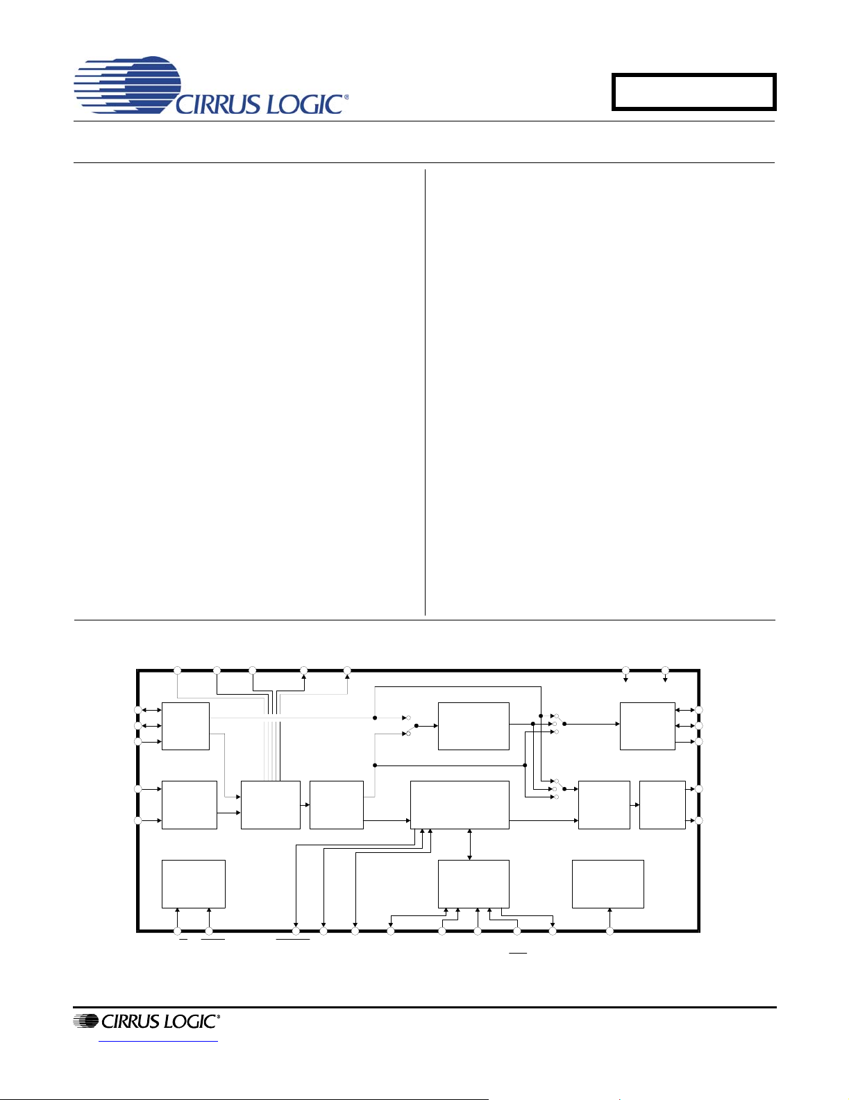
VA+
ILRCK
ISCLK
SDIN
RXP
RXN
http://www.cirrus.com
Serial
Audio
Input
Receiver
Misc.
Control
H/S
AGND
FILT RERR VD+
Clock &
Data
Recovery
RST OMCKEMPH U TCBL SDA/
RMCK
AES3
S/PDIF
Decoder
CDOUT
Copyright © Cirrus Logic, Inc. 2007
(All Rights Reserved)
Sample
Rate
Converter
C&Ubit
Data
Buffer
Control
Port &
Registers
SCL/
CCLK
AD1/
CDIN
AD0/CSINT
AES3
S/PDIF
Encoder
Output
Clock
Generator
DGND
Serial
Audio
Output
Driver
OLRCK
OSCLK
SDOUT
TXP
TXN
APRIL '07
DS245F4
Page 2

TABLE OF CONTENTS
1. CHARACTERISTICS AND SPECIFICATIONS ...................................................................................... 6
SPECIFIED OPERATING CONDITIONS .............................................................................................. 6
ABSOLUTE MAXIMUM RATINGS ........................................................................................................ 6
PERFORMANCE SPECIFICATIONS .................................................................................................... 7
DIGITAL FILTER CHARACTERISTICS .. ....................................... ... ... ... .... ... ... ... .... ... ...........................7
DC ELECTRICAL SPECIFICATIONS .................................................................................................... 7
DIGITAL INPUT CHARACTERISTICS ................................ ... .... ... ... ... ... .... ... ... ... .... ... ...........................8
DIGITAL INTERFACE SPECIFICATIONS ............................................................................................. 8
TRANSMITTER CHARACTERISTICS .................................................................................................. 8
SWITCHING CHARACTERISTICS .................................................. ... ... .... ... ... ..................................... 8
SWITCHING CHARACTERISTICS - SERIAL AUDIO PORTS .............................................................. 9
SWITCHING CHARACTERISTICS - CONTROL PORT - SPI™ MODE ............................................. 10
SWITCHING CHARACTERISTICS - CONTROL PORT - I²C® MODE ............................................... 11
2. TYPICAL CONNECTION DIAGRAM ................................................................................................... 12
3. GENERAL DESCRIPTION ................................................................................................................... 13
4. DATA I/O FLOW AND CLOCKING OPTIONS ..................................................................................... 14
5. SAMPLE RATE CONVERTER (SRC) .................................................................................................. 18
5.1 Dither ............................................................................................................................................. 18
5.2 SRC Locking, Varispeed and the Sample Rate Ratio Register ..................................................... 18
6. THREE-WIRE SERIAL AUDIO PORTS ...............................................................................................19
7. AES3 TRANSMITTER AND RECEIVER .............................................................................................. 22
7.1 AES3 Receiver ............................................................................................................................... 22
7.1.1 PLL, Jitter Attenuation, and Varispeed .................................................................................. 22
7.1.2 OMCK Out On RMCK ........................................................................................................... 22
7.1.3 Error Reporting and Hold Function ............................... ... ... ... ... .... ... ... ... .... ... ... ... ... .... ... ... ......22
7.1.4 Channel Status Data Handling .............. .................................................................... ............23
7.1.5 User Data Handling .. ... ... .... ... ... ... ... .... ... ....................................... ... ... ... .... ... ... ... ... .... ............ 23
7.1.6 Non-Audio Auto Detection ..................... ....................................... ................................... ...... 24
7.2 AES3 Transmitter ........................................................................................................................... 24
7.2.1 Transmitted Frame and Channel Status Boundary Timing ................................................... 24
7.2.2 TXN and TXP Drivers ............................................................................................................ 25
7.3 Mono Mode Operation ................................................................................................................... 25
8. AES3 TRANSMITTER AND RECEIVER .............................................................................................. 28
8.1 Sample Rate Converter ................................................................................................................. 28
8.2 Non-SRC Delay ............................................................................................................................. 29
9. CONTROL PORT DESCRIPTION AND TIMING ................................................................................. 30
9.1 SPI Mode ....................................................................................................................................... 30
9.2 I²C Mode ........................................................................................................................................ 31
9.3 Interrupts ........................................................................................................................................ 31
10. CONTROL PORT REGISTER BIT DEFINITIONS ............................................................................. 32
10.1 Memory Address Pointer (MAP) ......................................................... ... ... ... .... ... ... ... ... .... ... ....
10.2 Miscellaneous Control 1 (01h) ..................................................... ... .... ... ... ... .... ... ... ... ... .... ... ......... 34
10.3 Miscellaneous Control 2 (02h) ..................................................... ... .... ... ... ... .... ... ... ... ... .... ... ......... 35
10.4 Data Flow Control (03h) ............................................................................................................... 36
10.5 Clock Source Control (04h) .......................... .......................................... ... ... .... ... ... ...................... 37
10.6 Serial Audio Input Port Data Format (05h) ....................................................................... ............ 38
10.7 Serial Audio Output Port Data Format (06h) ................................................................................39
10.8 Interrupt 1 Register Status (07h) (Read Only) .............................................................................40
10.9 Interrupt Register 2 Status (08h) (Read Only) .............................................................................41
10.10 Interrupt 1 Register Mask (09h) ................................................................................................. 41
10.11 Interrupt Register 1 Mode Registers MSB & LSB (0Ah,0Bh) ............................... ...................... 41
10.12 Interrupt 2 Register Mask (0Ch) ................................................................................................. 42
CS8420
..... 32
2 DS245F4
Page 3

CS8420
10.13 Interrupt Register 2 Mode Registers MSB & LSB (0Dh,0Eh) ..................................................... 42
10.14 Receiver Channel Status (0Fh) (Read Only) ............................................................................. 43
10.15 Receiver Error (10h) (Read Only) .............................................................................................. 44
10.16 Receiver Error Mask (11h) ......................................................................................................... 45
10.17 Channel Status Data Buffer Control (12h) .................................................................................45
10.18 User Data Buffer Control (13h) .................................................................................................. 46
10.19 Sample Rate Ratio (1Eh) (Read Only) ................................................................. ...................... 47
10.20 C-Bit or U-Bit Data Buffer (20h - 37h) ........................................................................................ 47
10.21 CS8420 I.D. and Version Register (7Fh) (Read Only) ............................................................... 47
11. SYSTEM AND APPLICATIONS ISSUES ........................................................................................... 48
11.1 Reset, Power Down and Start-up Options ................................................................................... 48
11.2 Transmitter Startup ...................................................................................................................... 48
11.3 SRC Invalid State ......................................................................................................................... 49
11.4 C/U Buffer Data Corruption .......................... ............................................. ................................... 49
11.5 Block-Mode U-Data D-to-E Buffer Transfers ............................................................................... 50
11.6 ID Code and Revision Code ........................................................................................................ 50
11.7 Power Supply, Grounding, and PCB layout ................................................................................. 50
11.8 Synchronization of Multiple CS8420s .......................................................................................... 50
11.9 Extended Range Sample Rate Conversion ........................................ ... ...................................... 50
12. SOFTWARE MODE - PIN DESCRIPTION ......................................................................................... 51
13. HARDWARE MODES .................. .... ... ... ... ... ....................................... ... .... ... ... ... .... ... ... ... ................... 55
13.1 Overall Description ....................................................................................................................... 55
13.1.1 Hardware Mode Definitions ................................................................................................. 55
13.1.2 Serial Audio Port Formats ................................................................................................... 55
13.2 Hardware Mode 1 Description (DEFAULT Data Flow, AES3 Input) ............................................ 56
13.2.1 Pin Description - Hardware Mode 1 .................................................................................... 57
13.3 Hardware Mode 2 Description ..................................................................................................... 59
13.3.1 Pin Description - Hardware Mode 2 .................................................................................... 61
13.4 Hardware Mode 3 Description ..................................................................................................... 63
13.4.1 Pin Description - Hardware Mode 3 .................................................................................... 65
13.5 Hardware Mode 4 Description ..................................................................................................... 67
13.5.1 Pin Description - Hardware Mode 4 .................................................................................... 69
13.6 Hardware Mode 5 Description ..................................................................................................... 71
13.6.1 Pin Description - Hardware Mode 5 .................................................................................... 72
13.7 Hardware Mode 6 Description ..............................................................................................
13.7.1 Pin Description - Hardware Mode 6 .................................................................................... 76
14. EXTERNAL AES3/SPDIF/IEC60958 TRANSMITTER AND RECEIVER COMPONENTS ................ 78
14.1 AES3 Transmitter External Components ............................ ......................................................... 78
14.2 AES3 Receiver External Components ......................................................... ................................79
14.3 Isolating Transformer Requirements ............................................................................................ 80
15. CHANNEL STATUS AND USER DATA BUFFER MANAG EMENT ......................... ...................... ... 81
15.1 AES3 Channel Status(C) Bit Management .................................................................................. 81
15.1.1 Manually Accessing the E Buffer .........................................................................................82
15.1.2 Reserving the First 5 Bytes in the E Buffer ......................................................................... 83
15.1.3 Serial Copy Management System (SCMS) ......................................................................... 83
15.1.4 Channel Status Data E Buffer Access ................................................................................. 83
15.1.5 One-Byte Mode ............................................................. ... ... ... .... ... ... ... .... ............................ 84
15.1.6 Two-Byte Mode ............................................................. ... ... ... .... ... ...................................... 84
15.2 AES3 User (U) Bit Management .................................................................................................. 84
15.2.1 Mode 1: Transmit All Zeros ................................................................................................. 84
15.2.2 Mode 2: Block Mode .................................. .... ... ... ... .... ... ... ... ... ............................................. 84
15.2.3 IEC60958 Recommended U Data Format for Consumer Applications ............................... 85
15.2.4 Mode (3): Reserved ................................... .... ... ... ... .... ... ... ... ... .... ... ... ... .... ... ... ...................... 85
15.2.5 Mode (4): IEC Consumer B ................................................................................................. 85
....... 74
DS245F4 3
Page 4

16. PLL FILTER ........................................................................................................................................ 87
16.1 General ........................................................ ....................................... ... ... ... .... ... ......................... 87
16.2 External Filter Components ................................................................ ... ... ... .... ............................ 87
16.2.1 General ................................................................................................................................ 87
16.2.2 Capacitor Selection ............................................................................................................. 88
16.2.3 Circuit Board Layout ............................................................................................................ 88
16.3 Component Value Selection ........................................................................................................ 88
16.3.1 Identifying the Part Revision ................................................................................................ 88
16.3.2 Locking to the RXP/RXN Receiver Inputs ........................................................................... 89
16.3.3 Locking to the ILRCK Input ................................................................................................. 89
16.3.4 Jitter Tolerance .......................... ... ....... ...... ....... ...... ....... ...... ....... ... ...... ....... ...... ................... 90
16.3.5 Jitter Attenuation ................................................................................................................. 90
17. PARAMETER DEFINITIONS .............................................................................................................. 91
18. PACKAGE DIMENSIONS .................................................................................................................. 92
THERMAL CHARACTERISTICS AND SPECIFICATIONS ................................................................. 92
19. ORDERING INFORMATION .............................................................................................................. 93
20. REVISION HISTORY .......................................................................................................................... 93
LIST OF FIGURES
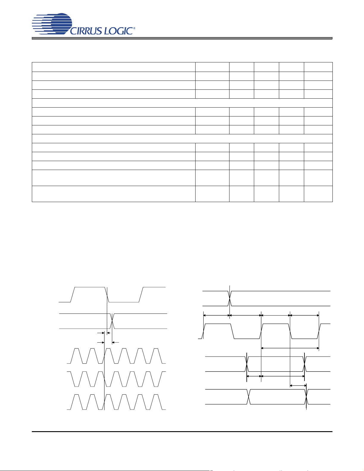
Figure 1.Audio Port Master Mode Timing ................................................................................................... 9
Figure 2.Audio Port Slave Mode and Data Input Timing .............................. .......................................... ..... 9
Figure 3.SPI Mode Timing ........................................................................................................................ 10
Figure 4.I²C Mode Timing ......................................................................................................................... 11
Figure 5.Recommended Connection Diagram for Software Mode ........................................................... 12
Figure 6.Software Mode Audio Data Flow Switching Options ............. ... ... ... .... ... ... ... .... ............................ 14
Figure 7.CS8420 Clock Routing ............................. ... ... ... .... ... ... ... .... ... ... ... ... .... ... ... ... ................................ 14
Figure 8.Serial Audio Input, using PLL, SRC Enabled .............................................................................. 16
Figure 9.Serial Audio Input, No PLL, SRC Enabled .................. .......................................... ...................... 16
Figure 10.AES3 Input, SRC Enabled ..... ... ... ... ... .... ... ... ... .... ... ... ... .... ... ... ... ... .... ... ...................................... 16
Figure 11.Serial Audio Input, AES3 Input Clock Source, SRC Enabled ...................................................16
Figure 12.Serial Audio Input, SRC Output Clocked by AES3 Recovered Clock ....................................... 16
Figure 13.AES3 Input, SRC to Serial Audio Output, Serial Audio Input to AES3 Out ............................... 16
Figure 14.AES3 Input to Serial Audio Output, Serial Audio Input to AES3 Out, No SRC ......................... 17
Figure 15.AES3 Input to Serial Audio Output Only ................................................................................... 17
Figure 16.Input Serial Port to AES3 Transmitter ....................................................................................... 17
Figure 17.Serial Audio Input Example Formats ........................................................................................ 20
Figure 18.Serial Audio Output Example Formats ...................................................................................... 21
Figure 19.AES3 Receiver Timing for C & U Pin Output Data ................................................................... 23
Figure 20.AES3 Transmitter Timing for C, U and V Pin Input Data .......................................................... 26
Figure 21.Mono Mode Operation Compared to Normal Stereo Operation ............................................... 27
Figure 22.Control Port Timing in SPI Mode .............................................................................................. 30
Figure 23.Control Port Timing in I²C Mode ............................................................................................... 31
Figure 24.Hardware Mode 1 - Default Data Flow, AES3 Input ................................................................. 56
Figure 25.Hardware Mode 2 - Default Data Flow, Serial Audio Input .... ... ... .... ... ... ... .... ... ... ... ... .... ... ... ... ... 59
Figure 26.Hardware Mode 3 - Transceive Data Flow, with SRC .............................................................. 63
Figure 27.Hardware Mode 4 - Transceive Data Flow, Without SRC ......................................................... 67
Figure 28.Hardware Mode 5 - AES3 Receiver Only .................................................................................71
Figure 29.Hardware Mode 6 - AES3 Transmitter Only ............................................................................. 74
Figure 30.Professional Output Circuit ....................................................................................................... 78
Figure 31.Consumer Output Circuit ............................. ... .... ... ... ... .... ... ... ... ... .... ... ... ... .... ... ... ... ... ... ............. 78
Figure 32.TTL/CMOS Output Circuit ......................................................................................................... 79
Figure 33.Professional Input Circuit .......................................................................................................... 79
Figure 34.Transformerless Professional Input Circuit ......................................... ... ... .... ............................ 79
CS8420
4 DS245F4
Page 5

Figure 35.Consumer Input Circuit ............................................................................................................. 80
Figure 36.TTL/CMOS Input Circuit ............................................................................................................ 80
Figure 37.Channel Status Data Buffer Structure ....................................................................................... 81
Figure 38.Channel Status Block Handling When Fso is Not Equal to Fsi .............................. ... .... ... ... ... ... 82
Figure 39.Flowchart for Reading the E Buffer ........................................................................................... 82
Figure 40.Flowchart for Writing the E Buffer ............................................................................................. 83
Figure 41.PLL Block Diagram ................................................................................................................... 87
Figure 42.Recommended Layout Example ............................................................................................... 88
Figure 43.Jitter Tolerance Template ......................................................................................................... 90
Figure 44.Revision D Jitter Attenuation ..................................................................................................... 90
Figure 45.Revision D1 Jitter Attenuation ................................................................................................... 90
LIST OF TABLES
Table 1. Minimizing Group Delay Through Multiple CS8420s When Locking to RXP/RXN ...................... 28
Table 2. Minimizing Group Delay Through Multiple CS8420s When Locking to ILRCK ........................... 28
Table 3. Non-SRC Delay ........................................................................................................................... 29
Table 4. Summary of all Bits in the Control Register Map ........................................................................ 33
Table 5. Hardware Mode Definitions ......................................................................................................... 55
Table 6. Serial Audio Output Formats Available in Hardware Mode ......................................................... 55
Table 7. Serial Audio Input Formats Available in Hardware Mode ............................................................ 55
Table 8. Hardware Mode 1 Start-Up Options ............................................................................................ 56
Table 9. HW Mode 2A COPY/C and ORIG/U Pin Function ............................................. ... ... ... .... ... ... ... ... 60
Table 10. HW Mode 2 Serial Audio Port Format Selection ....................................................................... 60
Table 11. Hardware Mode 2 Start-Up Options ............................. .... ... ... ... ... .... ... ...................................... 60
Table 12. Hardware Mode 3 Start-Up Options ............................. .... ... ... ... ... .... ... ...................................... 64
Table 13. Hardware Mode 4 Start-Up Options ............................. .... ... ... ... ... .... ... ...................................... 68
Table 14. Hardware Mode 5 Start-Up Options ............................. .... ... ... ... ... .... ... ...................................... 71
Table 15. HW 6 COPY/C and ORIG Pin Function ....................................................................................75
Table 16. HW 6 Serial Port Format Selection ........................................................................................... 75
Table 17. Second Line Part Marking .. .... ... ... ... ... .... .......................................... ... ... ... .... ... ... ... ... ................ 88
Table 18. Locking to RXP/RXN - Fs = 8 to 96 kHz ................................................................................... 89
Table 19. Locking to RXP/RXN - Fs = 32 to 96 kHz* ...... .......................................................... ................89
Table 20. Locking to the ILRCK Input ....................................................................................................... 89
CS8420
DS245F4 5
Page 6
CS8420
1. CHARACTERISTICS AND SPECIFICATIONS
All Min/Max characteristics and specifications are guaranteed over the Specified Operating Conditions. Typical
performance characteristics and spe cif icat ion s ar e de riv e d from measurements taken at nominal supply voltages
and T
= 25°C.
A
SPECIFIED OPERATING CONDITIONS
AGND, DGND = 0 V, all voltages with respect to 0 V.
Parameter Symbol Min Typ Max Units
Power Supply Voltage VD+, VA+ 4.75 5.0 5.25 V
Ambient Operating Temperature: Commercial Grade
Automotive Grade
T
A
-10
-40
-
-
+70
+85
°C
°C
ABSOLUTE MAXIMUM RATINGS
AGND, DGND = 0 V; all voltages with respect to 0 V. Operation beyond these limits may result in permanent damage to the device. Normal operation is not guaranteed at these extremes.
Parameter Symbol Min Max Units
Power Supply Voltage VD+, VA+ - 6.0 V
Input Current, Any Pin Except Supplies, RXP/RXN (Note 1) I
Input Voltage V
Ambient Operating Temperature (power applied) T
Storag e Temperature T
in
in
A
stg
-±10mA
-0.3 (VD+) + 0.3 V
-55 125 °C
-65 150 °C
Notes:
1. Transient currents of up to 100 mA will not cause SCR latch-up.
6 DS245F4
Page 7
CS8420
PERFORMANCE SPECIFICATIONS
Parameter* Symbol Min Typ Max Units
Dynamic Range 120 128 - dB
Input Sample Rate (serial input port) Fsi 8 - 108 kHz
Output Sample Rate Fso 8 - 108 kHz
Output to Input Sample Rate Ratio 0.33 - 3
Total Harmonic Distortion + Noise
1 kHz, -1 dBFS, 0.33 < Fso/Fsi < 1.7
1 kHz, -1 dBFS, 0.33 < Fso/Fsi < 3
10 kHz, -1 dBFS, 0.33 < Fso/Fsi < 1.7
10 kHz, -1 dBFS, 0.33 < Fso/Fsi < 3
Peak idle channel noise component - - -140 dBFS
Resolution 16 - 24 bits
Gain Error -0.12 - 0 dB
THD+N
-
-
-
-
-
-
-
-
-117
-112
-110
-107
dB
dB
dB
dB
DIGITAL FILTER CHARACTERISTICS
Parameter* Symbol Min Typ Max Units
Passband Upsampling
Downsampling
Passband Ripple - - ±0.007 dB
Stopband (Downsampling ) 0.5465*Fso - Fsi/2 Hz
Stopband Attenuation 110 - - dB
Group Delay (Note 2) t
Group Delay Variation vs. Frequency Δt
Interchannel Phase Deviation - - 0.0 °
2. See “AES3 Transmitter and Receiver” on page 28.
gd
gd
0
0
- - 1.75 ms
--0.0μs
-
-
0.4535*Fsi
0.4535*Fso
DC ELECTRICAL SPECIFICATIONS
AGND = DGND = 0 V; all voltages with respect to 0 V.
Parameters Symbol Min Typ Max Units
Power Down Mode (Note 3)
Supply Current in power down VA+
VD+
Normal Operation (Note 4)
Supply Current at 48 kHz F
Supply Current at 96 kHz F
and F
so
and F
so
si
si
VA+
VD+
VA+
VD+
-
-
-
-
-
-
20
20
3.7
66
7.0
125
-
-
-
-
-
-
Hz
Hz
μA
μA
mA
mA
mA
mA
3. Power Down Mode is defined as RST
4. Normal operation is defined as RST = HI.
DS245F4 7
= LO with all clocks and data lines held static.
Page 8
DIGITAL INPUT CHARACTERISTICS
Parameters Symbol Min Typ Max Units
Input Leakage Current I
Differential Input Voltage, RXP to RXN V
in
TH
DIGITAL INTERFACE SPECIFICATIONS
AGND = DGND = 0 V; all voltages with respect to 0 V.
Parameters Symbol Min Max Units
High-Level Output Voltage (I
Low-Level Output Voltage (I
High-Level Output Voltage (I
Low-Level Output Voltage (I
= -3.2 mA), except TXP/TXN V
OH
= 3.2 mA), except TXP/TXN V
OH
= -21 mA), TXP, TXN (VD+) - 0.7 - V
OH
= 21 mA), TXP, TXN - 0.7 V
OH
High-Level Input Voltage, except RXP, RXN V
Low-Level Input Voltage, except RXP, RXN V
TRANSMITTER CHARACTERISTICS
Parameters Symbol Typ Units
TXP Output Resistance R
TXN Output Resistance R
OH
OL
IH
IL
-±10±15μA
200 - - mVpp
(VD+) - 1.0 - V
-0.4V
2.0 (VD+) + 0.3 V
-0.3 0.8 V
TXP
TXN
25 Ω
25 Ω
CS8420
SWITCHING CHARACTERISTICS
Inputs: Logic 0 = 0 V, Logic 1 = VD+; CL = 20 pF.
Parameter Symbol Min Typ Max Units
pin Low Pulse Width 200 - - μs
RST
OMCK Frequency for OMCK = 512 * Fso 4.096 - 55.3 MHz
OMCK Low and High Width for OMCK = 512 * Fso 8.2 - - ns
OMCK Frequency for OMCK = 384 * Fso 3.072 - 41.5 MHz
OMCK Low and High Width for OMCK = 384 * Fso 12.3 - - ns
OMCK Frequency for OMCK = 256 * Fso 2.048 - 27.7 MHz
OMCK Low and High Width for OMCK = 256 * Fso 16.4 - - ns
PLL Clock Recovery Sample Rate Range 8.0 - 108.0 kHz
RMCK output jitter (Note 5) -200-ps RMS
RMCK output duty cycle 40 50 60 %
RMCK Input Frequency (Note 6) 2.048 - 27.7 MHz
RMCK Input Low and High Width (Note 6) 16.4 - - ns
AES3 Transmitter Output Jitter - - 1 ns
5. Cycle-to-cycle jitter using 32-96 kHz external PLL components.
6. PLL is bypassed (RXD1:0 bits in the Clock Source Control register set to 10b), clock is input to the RMCK
pin.
8 DS245F4
Page 9
CS8420
SWITCHING CHARACTERISTICS - SERIAL AUDIO PORTS
Inputs: Logic 0 = 0 V, Logic 1 = VD+; CL = 20 pF.
Parameter Symbol Min Typ Max Units
OSCLK Active Edge to SDOUT Output Valid (Note 7) t
SDIN Setup Time Before ISCLK Active Edge (Note 7) t
SDIN Hold Time After ISCLK Active Edge (Note 7) t
dpd
ds
dh
Master Mode
O/RMCK to I/OSCLK active edge delay (Note 7, 8) t
O/RMCK to I/OLRCK delay (Note 9) t
smd
lmd
I/OSCLK and I/OLRCK Duty Cycle - 50 - %
Slave Mode
I/OSCLK Period (Note 10) t
I/OSCLK Input Low Width t
I/OSCLK Input High Width t
I/OSCLK Active Edge to I/OLRCK Edge
sckw
sckl
sckh
t
lrckd
(Note 7, 9, 11)
I/OLRCK Edge Setup Before I/OSCLK Active Edge
t
lrcks
(Note 7, 9, 12)
- - 25 ns
20 - - ns
20 - - ns
0 - 16 ns
0 - 17 ns
36 - - ns
14 - - ns
14 - - ns
20 - - ns
20 - - ns
7. The active edges of ISCLK and OSCLK are pro gram m ab le .
8. When OSCLK, OLRCK, ISCLK, and ILRCK are derived from OMCK they are clocked from its r ising edge.
When these signals are derived from RMCK, they are clocked from its falling edge.
9. The polarity of ILRCK and OLRCK is programmable.
10. No more than 128 SCLK per frame.
11. This delay is to prevent the previous I/OSCLK edge from being interpreted as the first one after I/OLRCK
has changed.
12. This setup time ensures that this I/OSCLK edge is interpreted as the first one after I/OLRCK has changed.
ISC L K
OSCLK
(outpu t)
ILRCK
OLRCK
(outpu t)
RMCK
(outpu t)
RMCK
(outpu t)
OMCK
(input)
t
smd
Hard ware Mod e
Software Mode
t
lm d
ILRCK
OLRCK
(input)
ISCLK
OSCLK
(input)
SDIN
SDOUT
t
lrckd lrcks
t
t
sckh
t
ds
t
dh
t
sckw
t
sckl
t
dpd
Figure 1. Audio Port Master Mode Timing Figure 2. Audio Port Slave Mode and Data Input Timing
DS245F4 9
Page 10
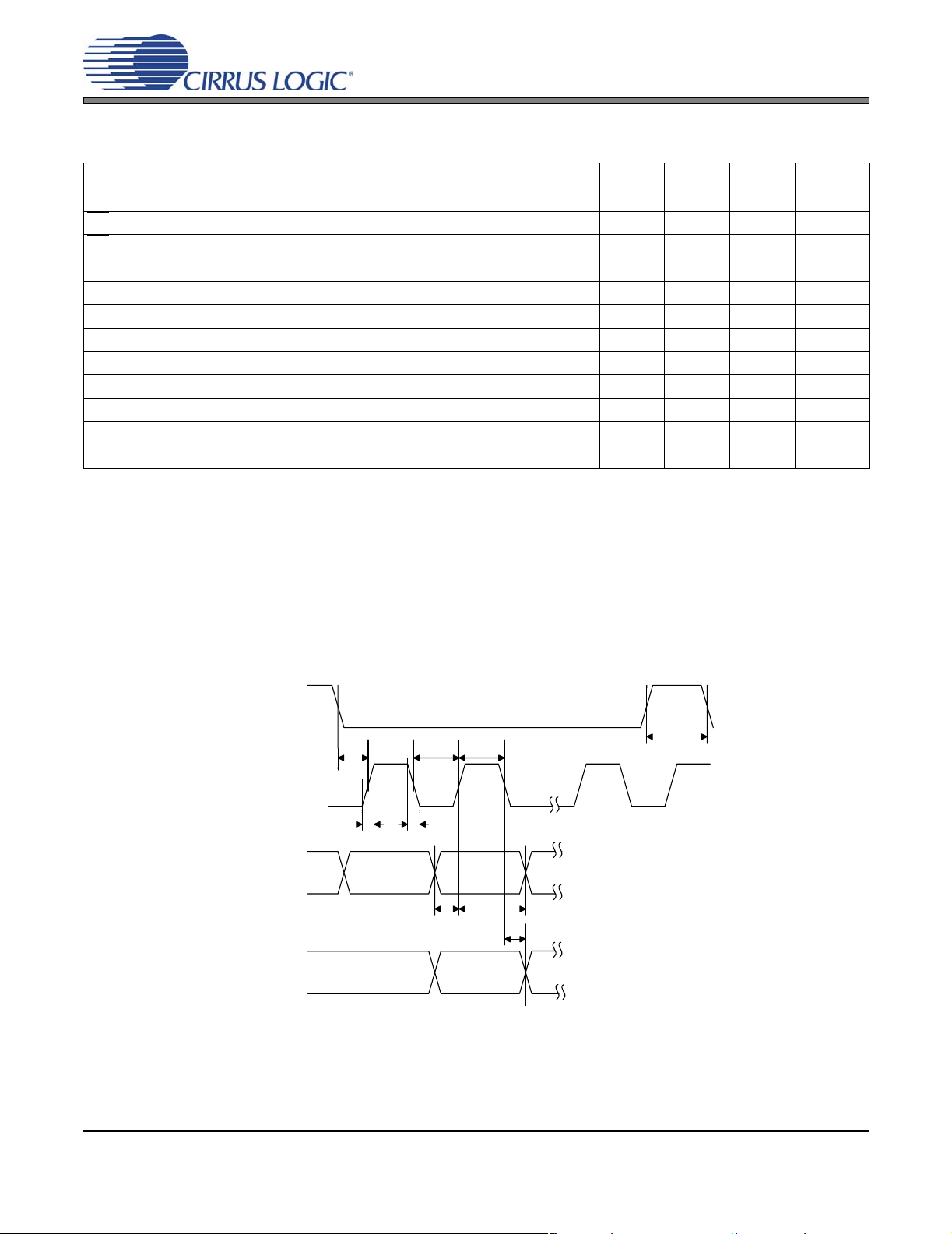
SWITCHING CHARACTERISTICS - CONTROL PORT - SPI™ MODE
Inputs: Logic 0 = 0 V, Logic 1 = VD+; CL = 20 pF.
Parameter Symbol Min Typ Max Units
CCLK Clock Frequency (Note 13) f
CS
High Time Between Transmissions t
CS
Falling to CCLK Edge t
CCLK Low Time t
CCLK High Time t
CDIN to CCLK Rising Setup Time t
CCLK Rising to DATA Hold Time (Note 14) t
CCLK Falling to CDOUT Stable t
Rise Time of CDOUT t
Fall Time of CDOUT t
Rise Time of CCLK and CDIN (Note 15) t
Fall Time of CCLK and CDIN (Note 15) t
sck
csh
css
scl
sch
dsu
dh
pd
r1
f1
r2
f2
13. If Fso or Fsi is lower than 46.875 kHz, the maximum CCLK freq uency should be less than 128 Fso an d
less than 128 Fsi. This is dictated by the timing requirements necessary to access the Channel Status and
User Bit buffer memory. Access to the control register file can be carried out at the full 6 MHz rate. The
minimum allowable input sample rate is 8 kHz, so choosing CCLK to be less than or equal to 1.024 MHz
should be safe for all possible conditions.
14. Data must be held for sufficient time to bridge the transition time of CCLK.
15. For f
< 1 MHz.
sck
0-6.0MHz
1.0 - - μs
20 - - ns
66 - - ns
66 - - ns
40 - - ns
18 - - ns
- - 45 ns
- - 25 ns
- - 25 ns
--100ns
--100ns
CS8420
CS
t
css
t
scl
sch
t
csh
t
CCLK
t
r2
t
f2
CDIN
t
dsu
t
dh
t
pd
CDOUT
Figure 3. SPI Mode Timing
10 DS245F4
Page 11
CS8420
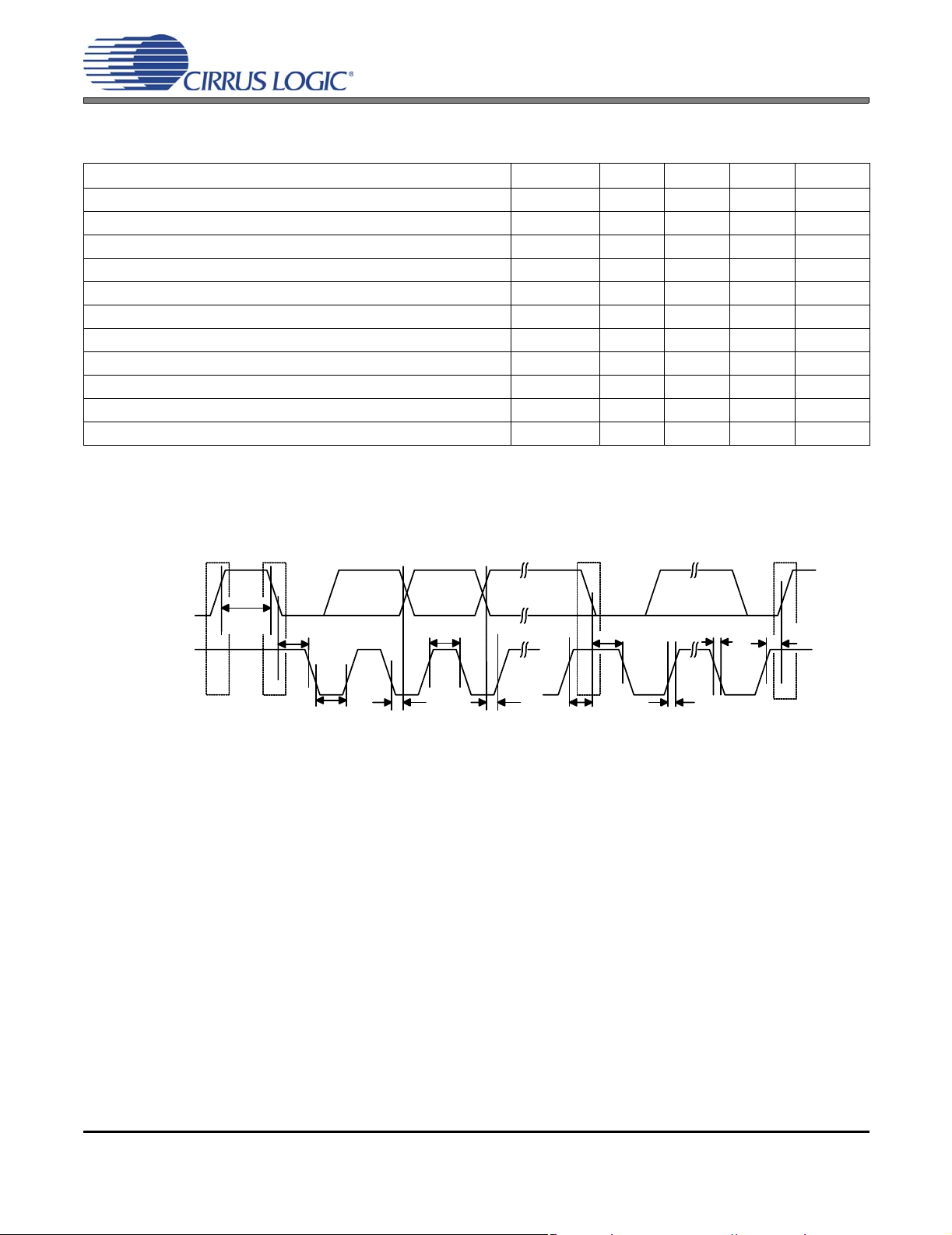
SWITCHING CHARACTERISTICS - CONTROL PORT - I²C® MODE
Inputs: Logic 0 = 0 V, Logic 1 = VD+; CL = 20 pF.
Parameter Symbol Min Typ Max Units
SCL Clock Frequency fscl - - 100 kHz
Bus Free Time Between Transmissions t
Start Condition Hold Time (prior to first clock pulse) t
Clock Low Time t
Clock High Time t
Setup Time for Repeated Start Condition t
SDA Hold Time from SCL Falling (Note 16) t
SDA Setup Time to SCL Rising t
Rise Time of Both SDA and SCL Lines t
Fall Time of Both SDA and SCL Lines t
Setup Time for Stop Condition t
buf
hdst
low
high
sust
hdd
sud
r
f
susp
16. Data must be held for sufficient time to bridge the 25 ns transition time of SCL.
Repeated
Stop Start
Start
4.7 - - μs
4.0 - - μs
4.7 - - μs
4.0 - - μs
4.7 - - μs
0--μs
250 - - ns
- - 25 ns
- - 25 ns
4.7 - - μs
Stop
SDA
SCL
t
buf
t
hdst
t
low
t
high
t
hdd
Figure 4. I²C Mode Timing
t
sud
t
sust
t
hdst
t
f
t
r
t
susp
DS245F4 11
Page 12
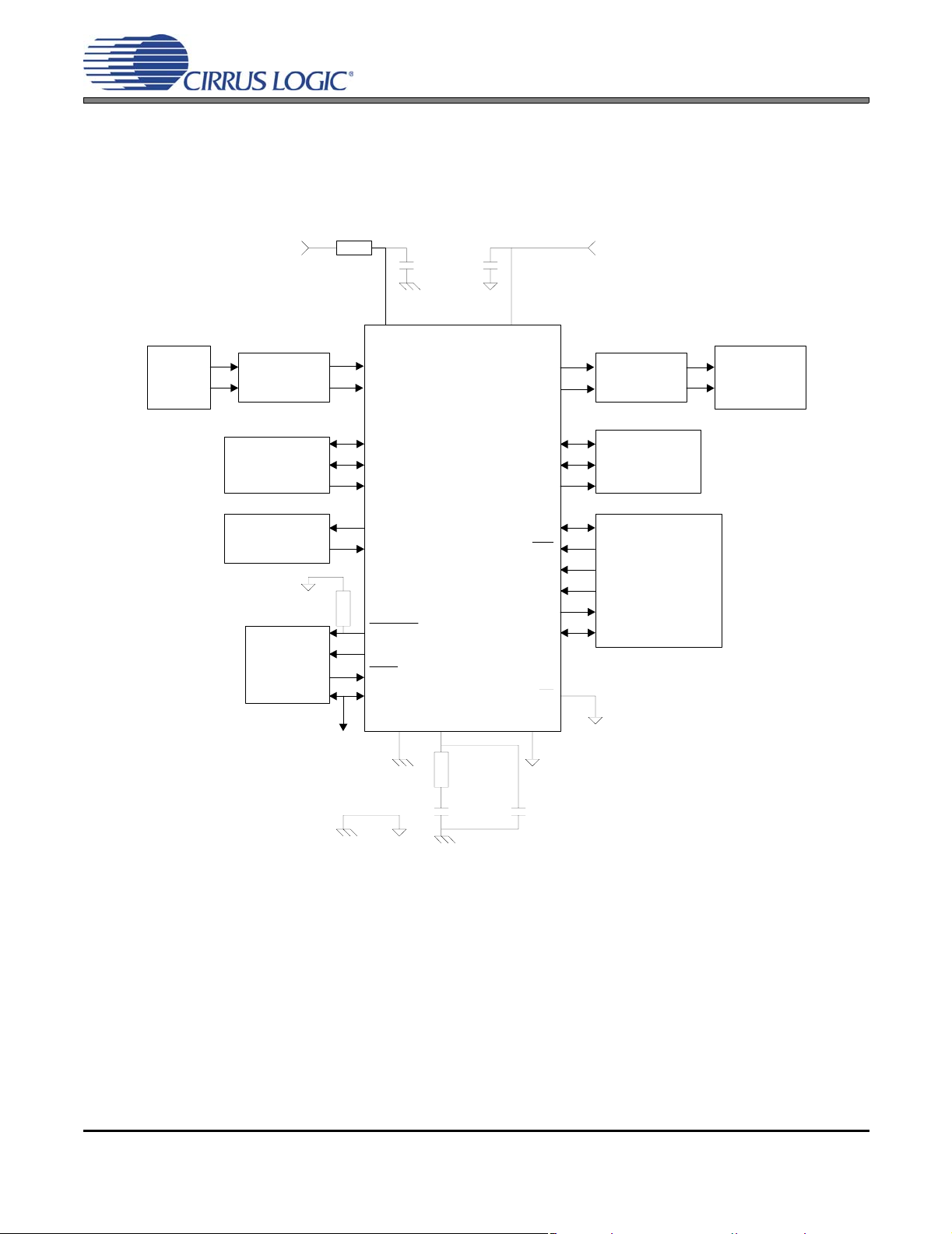
2. TYPICAL CONNECTION DIAGRAM
Ferrite *
Bead
0.1 Fμ
0.1 Fμ
VA+ VD+
RXP
RXN
CS8420
AES3/
SPDIF
Source
+5V
Analog
Supply *
Cable
Termination
TXP
TXN
+5V
Digital
Supply
Cable
Interface
CS8420
AES3/
SPDIF
Equipment
3-wire Serial
Audio Source
Clock Source
and Control
47kΩ
Hardware
Control
To other
CS8420's
ILRCK
ISCLK
SDIN
RMCK
OMCK
EMPH
RERR
RST
TCBL
SDA/CDOUT
SCL/CCLK
AD1/CDIN
/AD2
RFILT
CFILT CRIP
OLRCK
OSCLK
SDOUT
AD0/CS
INT
H/S
DGNDFILTAGND
3-wire Serial
Audio Input
Device
Microcontroller
U
* A separate analog supply is only necessary in applications where
RMCK is used for a jitter sensitive task. For applications where
RMCK is not used for a jitter sensitive task, connect VA+ to VD+
via a ferrite bead. Keep the decoupling capacitor between VA+
and AGND.
Figure 5. Recommended Connection Diagram for Software Mode
12 DS245F4
Page 13

CS8420
3. GENERAL DESCRIPTION
The CS8420 is a fully asynchronous sample rate converter plus AES3 transceiver intended to be used in digital audio systems. Such systems include digital mixing consoles, effects processors, tape recorders, and computer multimedia systems. The CS8420 is intended for 16-, 20-, and 24-bit applications where the input sample rate is
unknown, or is known to be asynchronous to the system sample rate.
On the input side of the CS8420, AES3 or 3-wire serial format can be chosen. The output side produces both AES3
and 3-wire serial format. An I²C/SPI-compatible microcon troller interface allows full block processing of channel status and user data via block reads from the incoming AES3 data stream and block writes to the outgoing AES3 data
stream. The user can also access information decoded from the input AES3 data stream, such as the presence of
non-audio data and pre-emphasis, as well as control the various modes of the device. For users who prefer not to
use a micro-controller, six hardware modes have been provide d and documented towards the end of this data sheet.
In these modes, flexibility is limited, with pins providing some programmability.
When used for AES3-input/AES3-output applications, the CS8420 can automatically transceive user data that conforms to the IEC60958-recommended format. The CS8420 also allows access to the relevant bits in the AES3 data
stream to comply with the serial copy management system (SCMS).
The diagram on the cover of this data sheet shows the main functional blocks of the CS8420. Figure 5 shows the
supply and external connections to the device.
Familiarity with the AES3 and IEC60958 specifications are assumed throughout this document. Application Note 22:
Overview of Digital Audio Interface Data Structures, contains a tutorial on digital audio specifications. The paper An
Understanding and Implementation of the SCMS Serial Copy Management System for Dig ita l Audio Tra nsmissi on,
by Clif Sanchez, is an excellent tutorial on SCMS. It may be obtained from Cirrus Logic, Inc., or from the AES.
To guarantee system compliance, the proper standards documents should be obtained. The latest AES3 standard
should be obtained from the Audio Engineering So ciety (ANSI), the latest IEC6 0958 standard from the Inte rnational
Electrotechnical Commission and the latest EIAJ CP-1201 standard from the Japanese Electronics Bureau.
DS245F4 13
Page 14
CS8420
T
4. DATA I/O FLOW AND CLOCKING OPTIONS
The CS8420 can be configured for nine connectivity alternatives, referred to as data flows. Each data flow has an
associated clocking set-up. Figure 6 shows the data flow switching, along with the control register bits which control
the switches. This drawing only shows the audio data paths for simplicity. Figure 7 shows the internal clock routing
and the associated control register bits. The clock routing constraints determine which data routing options are actually usable.
SPD1-0
ILRCK
ISCLK
SDIN
RXN
RXP
Serial
Audio
SRCD
Input
Sample
Rate
Converter
AES3
Receiver
AES3
Encoder
TXD1-0
Figure 6. Software Mode Audio Data Flow Switching Options
Serial
Audio
Output
TXOFFAESBP
OLRCK
OSCLK
SDOU
TXP
TXN
SDIN
ISCLK
ILRCK
RXP
SERIAL
AUDIO
INPUT
0
MUX
1
MUX
RXD0
01
PLL
SIMS
RMCKF
÷
SWCLK
UNLOCK
0
MUX
1
RXD1
MUX
01
SAMPLE
RATE
CONVERTER
INC
CHANNEL
STATUS
MEMORY
USER
BIT
MEMORY
MUX
1
CLK[1:0]
0
SERIAL
AUDIO
OUTPUT
AES3
TRANSMIT
OUTC
÷
SDOUT
OSCLK
OLRCK
TXN
TXP
OMCKRMCK
*Note: When SWCLK mode is enabled, signal input on OMCK is only output thr ough RM CK an d not
routed back through the RXD1 multiplexer; RMCK is not bi-directional in this mode.
Figure 7. CS8420 Clock Routing
14 DS245F4
Page 15

CS8420
The AESBP switch allows a TTL level, bi-phase mark-encoded data stream connected to RXP to be routed to the
TXP and TXN pin drivers. The TXOFF switch causes the TXP and TXN outputs to be driven to ground
In modes including the SRC function, there are two audio-data-related clock domains. One domain includes the input side of SRC, plus the attached data source. The second domain includes the output side of the SRC, plus any
attached output ports.
There are two possible clock sources. The first known as the recovered clock, is the output of a PLL, and is connected to the RCMK pin. The input to the PLL can be either the incoming AES3 data stream or the ILRCK word rate
clock from the serial audio input port. The second clock is input via the OMCK pin , and would normally be a cr ystalderived stable clock. The Clock Source Control Register bits determine which clock is connected to which domain.
By studying the following drawings, and appropriately setting the Data Flow Control and Clock Source Control register bits, the CS8420 can be configured to fit a variety of application requirements.
The following drawings illustrate the possible valid data flows. The audio data flow is indicated by the thin lines; the
clock routing is indicated by the bold lines. The register settings for the Data Flow Control register and the Clock
Source Register are also shown for each data flow. Some of the register settings may appear to be not relevant to
the particular data flow in question, but have been assigned a particular state. This is done to minimize power consumption. The AESBP data path from the RXP pin to the AES3 output drivers, and the TXOFF control, have been
omitted for clarity, but are present and functional in all modes where the AES3 transmitter is in use.
Figures 8 and 9 show audio data enterin g via the serial audio input p ort, then passing throug h the sample rate converter, and then output both to the serial audio output port and to the AES3 transmitter. Figure 8 shows the PLL
recovering the input clock from ILRCK word clock. Figure 9 shows using a direct 256*Fsi clock input via the RMCK
pin, instead of the PLL.
Figure 10 shows audio data entering via the AES3 Receiver. The PLL locks onto the pre-ambles in the incoming
audio stream, and generates a 256*Fsi clock. The rate-converted data is the n output via the serial au dio output port
and via the AES3 transmitter.
Figure 11 shows the same data flow as Figure 8. The input clock is derived from an incoming AES3 data stream.
The incoming data must be synchronous to the AES3 data stream.
Figure 12 shows the same data flow as Figure 8. The input data must be synchronous to OMCK. The output data
is clocked by the recovered PLL clock from an AES3 input stream. This may be used to implement a “house sync”
architecture.
Figure 8 shows audio data entering via the AES3 receiver, passing through the sample rate converter, and then ex-
iting via the serial audio output port. Synchronous audio data may then be input via the serial audio input port and
output via the AES3 transmitter.
Figure 14 is the same as Figure 13, but without the sample rate converter. The whole data path is clocked via the
PLL generated recovered clock.
Figure 15 illustrates a standard AES3 receiver function, with no rate conversion.
Figure 16 shows a standard AES3 transmitter function, with no rate conversion.
DS245F4 15
Page 16
CS8420
T
0
00
T
0
0
T
0
T
0
0
N
0
T
0
0
SDIN
ISCLK
ILRCK
Serial
Audio
Input
PLL
TXD1-0:
SPD1-0:
SRCD:
Sample
Rate
Converter
RMCK OMCK
Clock Source Control BitsData Flow Control Bits
00
00
Serial
Audio
Output
AES3
Encoder
&Driver
OUTC:
INC:
RXD1-0:
OLRCK
OSCLK
SDOU
TXP
TXN
0
0
SDIN
ISCLK
ILRCK
Serial
Audio
Input
TXD1-0:
SPD1-0:
SRCD:
Sample
Rate
Converter
RMCK OMCK
00
00
Clock Source Control BitsData Flow Control Bits
OUTC:
INC:
RXD1-0:
Serial
Audio
Output
AES3
Encoder
&Driver
0
0
1
OLRCK
OSCLK
SDOU
TXP
TXN
Figure 8. Serial Audio Input, using PLL, SRC Enabled Figure 9. Serial Audi o Input, No PLL, SRC Enabled
RXN
RXP
AES3
Rx &
Decode
PLL
TXD1-0:
SPD1-0:
SRCD:
Sample
Rate
Converter
RMCK OMCK
Clock Source Control BitsDataFlow Control Bits
00
00
1
Serial
Audio
Output
AES3
Encoder
&Driver
OUTC:
INC:
RXD1-0:
OLRCK
OSCLK
SDOU
TXP
TXN
0
0
1
SDIN
ISCLK
ILRCK
RXN
RXP
Serial
Audio
Input
AES3
Rx
TXD1-0:
SPD1-0:
SRCD:
Sample
Rate
Converter
PLL
RMCK OMCK
00
00
Clock Source Control BitsData Flow Control Bits
OUTC:
INC:
RXD1-0:
Serial
Audio
Output
AES3
Encoder
&Driver
0
0
OLRCK
OSCLK
SDOU
TXP
TXN
1
Figure 10. AES3 Input, SRC Enabled Figure 11. Serial Audio Input, AES3 Input Clock Source ,
ILRCK
Clock Source Control BitsData Flow Control Bits
OUTC:
INC:
RXD1-0:
Serial
Audio
Input
ISCLKSDIN
AES3
Encoder
&Driver
0
0
1
TXP
TX
SDIN
ISCLK
ILRCK
Serial
Audio
Input
TXD1-0:
SPD1-0:
SRCD:
Sample
Rate
Converter
00
00
PLL
AES3
Rx
RXP RXN
Clock Source Control BitsData Flow Control Bits
OUTC:
INC:
RXD1-0:
Serial
Audio
Output
AES3
Encoder
&Driver
RMCKOMCK
OLRCK
OSCLK
SDOU
TXP
TXN
1
1
1
Figure 12. Serial Audio Input, SRC Output Clocked by
AES3 Recovered Clock
OLRCKOSCLKSDOUT
Serial
Audio
Output
AES3
RXN
RXP
Sample
Rx &
Rate
Decode
Converter
PLL
RMCK OMCK
TXD1-0:
SPD1-0:
SRCD:
01
00
1
Figure 13. AES3 Input, SRC to Serial Audio Output, Serial
Audio Input to AES3 Out
16 DS245F4
Page 17
CS8420
N
0
0
T
N
0
00
ISCLKSDIN
AES3
Encoder
&Driver
1
0
1
ILRCK
TXP
TX
RXN
RXP
AES3
Rx &
Decode
PLL
TXD1-0:
SPD1-0:
SRCD:
RMCK
01
10
OLRCKOSCLKSDOUT
Serial
Audio
Output
Serial
Audio
Input
Clock Source Control BitsData Flow Control Bits
OUTC:
INC:
RXD1-0:
Figure 14. AES3 Input to Serial Audio Output, Serial Au-
dio Input to AES3 Out, No SRC
SDIN
ISCLK
ILRCK
Serial
Audio
Input
AES3
Encoder
&Driver
TXP
TX
RXN
RXP
AES3
Rx &
Decode
PLL
TXD1-0:
SPD1-0:
SRCD:
TXOFF:
RMCK
10
10
0
1
Clock Source Control BitsData Flow Control Bits
OUTC:
INC:
RXD1-0:
Serial
Audio
Output
1
0
01
OLRCK
OSCLK
SDOU
Figure 15. AES3 Input to Serial Audio Output Only
OMCK
Clock Source Control BitsData Flow Control Bits
TXD1-0:
SPD1-0:
SRCD:
01
01
OUTC:
INC:
RXD1-0:
0
1
Figure 16. Input Serial Port to AES3 Transmitter
DS245F4 17
Page 18

CS8420
5. SAMPLE RATE CONVERTER (SRC)
Multirate digital signal processing techniques are used to conceptually upsample the incoming data to very high rate
and then downsample to the outgoing rate, resulting in a 24-bit output, regardless of the width of the input. The filtering is designed so that a full input audio bandwidth of 20 kHz is preserved if the input sample and output sample
rates are greater than 44.1 kHz. When the output sample rate becomes less than the input sample rate, the input is
automatically band limited to avoid aliasing products in th e o utput. Careful design ensure s minim um ripp le a nd distortion products are added to the incoming signal. The SRC also determines the ratio between t he incoming and
outgoing sample rates, and sets the filter corner frequencies appropriately. Any jitter in the incoming signal has little
impact on the dynamic performance of the rate converter and has no influence on the output clock.
5.1 Dither
When using the AES3 input, and when using the serial audio input port in Left-Justified and I²S modes, all
input data is treated as 24 bits wide. Any truncation that has been done prior to the CS8420 to less than 24
bits should have been done using an appropriate dither p rocess. If the serial audio input port is used to feed
the SRC, and the port is in Right-Justified mode, then the input data will be truncated to the SIRES bit setting
value. If SIRES bits are set to 16 or 20 bits, and the input data is 24 bits wide, truncation distortion will occur.
Similarly, in any serial audio input port mode, if an inadequate number of bit clocks are entered (say 16 instead of 20), the input words will be truncated, causing truncation distortion at low levels. In summary, there
is no dithering mechanism on the input side of the CS8 420, and care must be ta ken to ensure th at no truncation occurs.
Dithering is used internally where appropriate inside the SRC block.
The output side of the SRC can be set to 16, 20, or 24 bits. Optional dithering can be applied, and is auto-
matically scaled to the selected output word length. This dither is not correlated between left and right channels. It is recommended that the dither control bit be left in its default ON state.
5.2 SRC Locking, Varispeed and the Sample Rate Ratio Register
The SRC calculates the ratio between the input sample ra te and the output samp le rate and uses this information to set up various parameters inside the SRC block. The SRC takes some time to make this calculation. For a worst case 3:1 to 1:3 input sample rate transition, the SRC will take 9400/Fso to settle (195 ms
at Fso of 48 kHz). For a power-up situation, the SRC will start from 1:1; the worst case time becomes
8300/Fso (172 ms at Fso of 48 kHz).
If the PLL is in use (either AES3 or serial input port), the worst case locking time for the PLL and the SRC
is the sum of each locking time.
If Fsi is changing, for example in a varispeed application, the REUNLOCK interrupt will occur, and the SRC
will track the incoming sample rate. During this tracking mode, the SRC will still rate convert the audio data,
but at increased distortion levels. Once the incoming sample rate is stable, the REUNLOCK interrupt will
become false, and the SRC will return to normal levels of audio quality.
The VFIFO interrupt occurs if the data buffer in the SRC overflows, which can occur if the input sample rate
changes at >10%/second.
Varispeed at Fsi slew rates approaching 10%/sec is only supported when the input is via the serial audio
input port. When using the AES3 input, high frame rate slew rates will cause the PLL to lose lock.
The sample rate ratio is also made available as a register, accessible via the control port. The upper 2 bits
of this register form the integer part of the ratio, while th e lower 6 bits for m the fractional part. Since, in many
instances Fso is known, this allows the calculation of the incoming sample rate by the host microcontroller.
18 DS245F4
Page 19

CS8420
6. THREE-WIRE SERIAL AUDIO PORTS
A 3-wire serial audio input port and a 3 -wire serial au dio output port is provid ed. Each port can be adjust ed to suit
the attached device via control registers. The following parameters are adjustable: master or slave, serial clock frequency, audio data resolution, left or right justification of the data relative to left/right clock, optional 1-bit cell delay
of the 1st data bit, the polarity of the bit clock and the polarity of the le ft/right clock. By setting the appropriate control
bits, many formats are possible.
Figure 17 shows a selection of common input formats, along with the control bit settings. The clocking of the input
section of the CS8420 may be derived from the incoming ILRCK word rate clock, using the on-chip PLL. Th e PLL
operation is described in the AES receiver description on page 22. In the case of use with the serial audio input port,
the PLL locks onto the leading edges of the ILRCK clock.
Figure 18 shows a selection of common output formats, along with the control bit settings. A special AES3 direct
output format is included, which allows serial output port access to the V, U, and C bits e mbedded in the serial audio
data stream. The P bit is replaced by a bit indicating the location of the start of a block. This format is only available
when the serial audio output port is being clocked by the AES3 receiver-recovered clock. Also, the received-channel
status block start signal is only available in Hardware mode 5, as the RCBL pin.
In Master mode, the left/right clock and the serial bit clock are outputs, derived from the appropriate clock dom ain
master clock.
In Slave mode, the left/right clock and the serial bit clock are inputs. The left/right clock must be synchronous to the
appropriate master clock, but the serial bit clock can be asynchronou s and discontinuous if required. By appropri ate
phasing of the left/right clock and control of the serial clocks, multiple CS8420’s can share one serial port. The
left/right clock should be continuous, but the duty cycle does not have to be 50%, provided that enough serial clocks
are present in each phase to clock all the data bits. When in Slave mode, the serial audio output port must be set to
left-justified or I²S data.
When using the serial audio output port in Slave mode with an OLRCK input which is asynchronous to the port’s
data source, then an interrupt bit is provided to indicate when repeated or dropped samples occur.
The CS8420 allows immediate mute of the serial audio output port audio data via a control register bit.
DS245F4 19
Page 20
CS8420
ILRCK
Channel A Channel B
Left
Justified
ISCLK
(In)
MSB
LSB
Channel B
I²S
SDIN
ILRCK
ISCLK
MSB LSB
Channel A
(In)
SDIN
ILRCK
MSB LSB
Channel A Channel B
MSB
LSB
Right
Justified
ISCLK
(In)
SDIN
MSB
SIMS SISF SIRES1/0 SIJUST SIDEL SISPOL SILRPOL
Left-Justified X X 00 0 0 0 0
I²S XX00+0101
Right-Justified X X XX* 1 0 0 0
X = don’t care to match format, but does need to be set to the desired setting
+ I²S can accept an arbitrary number of bits, determined by the number of ISCLK cycles
MSB LSBLSB
MSB
MSB
* not 11 - See Serial Input Port Data Format Register Bit Descript ions for an explanatio n of the meaning of e ach bit
Figure 17. Serial Audio Input Example Formats
20 DS245F4
Page 21
CS8420
Left
Justified
(Out)
I²S
(Out)
Right
Justified
(Out)
AES3
Direct
(Out)
OLRCK
OSCLK
SDOUT
OLRCK
OSCLK
SDOUT
OLRCK
OSCLK
SDOUT
OLRCK
OSCLK
SDOUT
Channel A Channel B
MSB
MSB
Channel A
MSB
LSB
MSB
Channel A Channel B
MSB Extended MSB Extended
Channel A
LSB
Frame 191
MSB
MSB
LSB
Channel B
MSB
LSB
LSB
Frame 0
Channel B
MSB
Channel A
MSB MSB
LSB
LSBLSB
LSB
Channel B
MSB
LSB
MSB
CUVZCUVCUVCUV
Z
SOMS SOSF SORES1/0 SOJUST SODEL SOSPOL SOLRPOL
Left-Justified X X XX* 0 0 0 0
I²S XXXX*0101
Right-Justified 1 X XX* 1 0 0 0
AES3 DirectXX110000
X = don’t care to match format, but does need to be set to the desired setting
* not 11 - See Serial Output Data Format Register Bit Descriptions for an explanation of the meaning of each bit
Figure 18. Serial Audio Output Example Formats
DS245F4 21
Page 22

CS8420
7. AES3 TRANSMITTER AND RECEIVER
The CS8420 includes an AES3-type digital audio receiver and an AES3-type digital audio transmitter. A comprehensive buffering scheme provides read/write a ccess to the channel status and user da ta. This buffering scheme is
described in “Channel Status and User Data Buffer Management” on page 81.
7.1 A ES3 Receiver
The AES3 receiver accepts and decodes audio and digital data according to the AES3, IEC60958 (S/PDIF),
and EIAJ CP-1201 interface standards. The receiver consists of a differe ntial input stage, accessed via pins
RXP and RXN, a PLL based clock recovery circuit, and a decoder which separates th e audio data from the
channel status and user data.
External components are used to termin ate an d isol ate the incoming data cables from the CS8420. These
components are detailed in “External AES3/SPDIF/IEC60958 Transmitter and Receiver Components” on
page 78.
7.1.1 PLL, Jitter Attenuation, and Varispeed
Please see “PLL Filter” on page 87 for general description of the PLL, selection of recommended PLL filter
components, and layout considerations. Figure 5 shows the recommended configuration of the two capacitors and one resistor that comprise the PLL filter.
7.1.2 OMCK Out On RMCK
A special mode is available that allows the clock that is being input through the OMCK pin to be output
through the RMCK pin. This feature is controlled by the SWCLK bit in register 4 of the control registers.
When the PLL loses lock, the frequency of the VCO dro ps to 300 kHz. The SWCLK function allows the
clock from RMCK to be used as a clock in the system without any disrup tio n when inp ut is remo ve d from
the Receiver.
7.1.3 Error Reporting and Hold Function
While decoding the incoming AES3 data stream, the CS84 20 can identify several kinds of error, indicated
in the Receiver Error register. The UNLOCK bit indicates whether the PLL is locked to the incoming AES3
data. The V bit reflects the current validity bit status. The CONF (confidence) bit indicates the amplitude
of the eye pattern opening, indicating a link that is close to generating errors. The BIP (bi-phase) err or bit
indicates an error in incoming bi-phase coding. The PAR (parity) bit indicates a received parity error.
The error bits are “sticky” - they are set on the first occurrence of the associated error and will remain set
until the user reads the register via the control port. This enables the register to log all unmasked errors
that occurred since the last time the register was read.
The Receiver Error Mask register allows masking of individual errors. The bits in this register serve as
masks for the corresponding bits of the Receiver Error Register. If a mask bit is set to 1, the error is considered unmasked, meaning that its occurrence will be reported in the receiver error register, will affect
the RERR pin, will invoke the occurrence of a RERR interrupt, and will affect the current audio sample
according to the status of the HOLD bits. The HOLD bits allow a choice of holding the previous sample,
replacing the current sample with zer o (mute ), or do no t chang e the curr ent audio sam ple. If a mask bit is
set to 0, the error is considered masked, meaning that its occurrence will not be reported in the receiver
error register, will not induce a pulse on RERR or generate a RERR interrupt, and will not affect the current
audio sample. The QCRC and CCRC errors do not affect the current audio sample, even if unmasked.
22 DS245F4
Page 23

7.1.4 Channel Status Data Handling
g
The first 2 bytes of the Channel Status block are decoded into the Receiver Channel Status register. The
setting of the CHS bit in the Channel Status Data Buffer Control register determin es whether the channel
status decodes are from the A channel (CHS = 0) or B channel (CHS = 1).
The PRO (professional) bit is extracted directly. Also, for consumer data, the COPY (copyright) bit is extracted, and the category code and L bits a re dec oded to dete rmine SCMS status, indica ted by the ORIG
(original) bit. Finally, the AUDIO
Non-Audio Auto Detection section below.
bit is extracted, and used to set an AUDIO indicator, as described in the
CS8420
If 50/15 µs pre-emphasis is detected, then this is reflected in the state of the EMPH
The encoded sample word length channel status bits are decoded according to AES3-1992 or IEC 60958.
If the AES3 receiver is the data source for the SRC, then the SRC audio input data is truncated according
to the channel status word length settings. Audio data routed to the serial audio output port is unaffected
by the word length settings; all 24 bits are passed on as received.
“Channel Status and User Data Buffer Management” on pag e 81 describes the overall handling of CS and
U data.
7.1.5 User Data Handling
The incoming user data is bu ffered in a us er-acc essible buffer. Various automatic modes of re-transmitting received U data are provided. “Channel Status and User Data Buffer Management” on page 81 describes the overall handling of CS and U data.
Received U data may also be output to the U pin, under the control of a control register bit. Depending on
the data flow and clocking options selected, there may not be a clock available to qualify the U data output.
Figure 19 illustrates the timing.
If the incoming user data bits have been encoded as Q-channel subcode, the data is decoded and presented in 10 consecutive register locations. An interrupt may be enabled to indicate the decoding of a new
Q-channel block, which may be read via the control port.
RCBL
out
pin.
VLRCK
C, U
Output
RCBL and C output are only available in hardware mode 5.
RCBL goes high 2 frames after receipt of a Z pre-amble, and is high for 16 frames.
VLRCK is a virtual word clock, which may not exist, but is used to illustrate the CU timing.
VLRCK duty cycle is 50%. VLRCK frequency is always equal to the incoming frame rate.
If no SRC is used, and the serial audio output port is in master mode, VLRCK = OLRCK.
If the serial audio output port is in slave mode, then VLRCK needs to be externally created, if required.
C, U transitions are ali
DS245F4 23
ned within 1% of VLRCKperiod to VLRCK edges
Figure 19. AES3 Receiver Timing for C & U Pin Output Data
±
Page 24

7.1.6 Non-Audio Auto Detection
Since it is possible to convey non-audio data in an AES3 data stream, it is important to know whether the
incoming AES3 data stream is digital audio or other data. This information is typically conveyed in channel
status bit 1 (AUDIO
es, such as AC-3
set. The CS8420 AES3 receiver can detect such non-audio data. This is accomplished by looking for a
96-bit sync code, consisting of 0x0000, 0x0000, 0x0000, 0x0000, 0xF872, and 0x4E1F. When the sync
code is detected, an internal AUTODETECT signal will be asserted. If no additional sync codes are detected within the next 4096 frames, AUTODETECT will be de-asserted until another sync code is detected. The AUDIO
received channel status bit 1. If non-audio data is detected, the data is still processed exactly as if it were
normal audio. It is up to the user to mute the outputs as required.
), which is extracted automatically by the CS8420. However, cer tain non-audio sou rc-
®
or MPEG encoders, may not adhere to this convention, and the bit may not be properly
bit in the Receiver Channel Status register is the logical OR of AUTODETECT and the
7.2 AES3 Transmitter
The AES3 transmitter encodes and transmits audio and digital data according to the AES3, IEC60958
(S/PDIF), and EIAJ CP-1201 interface standards. Audio and control data are multiplexed together and
bi-phase mark-encoded. The resulting bit stream is then driven directly, or through a transformer, to an
output connector.
The transmitter is usually clocked from the output side clock domain of the sample rate converter. This
clock may be derived from the clock input pin OMCK, or from the incoming data. In data flows with no
SRC, and where OMCK is asynchronous to the data source, an interrupt bit is provided that will go high
every time a data sample is dropped or repeated.
CS8420
The channel status (C) and user channel (U) bits in the transmitted data stream are taken from storage
areas within the CS8420. The user can manipulate the contents of the internal storage with a microcontroller. The CS8420 will also run in one of several automatic modes. “Channel Status and User Data Buffer
Management” on page 81 provides detailed descriptions of each automatic mode, and describes methods
for accessing the storage areas. The transmitted user da ta can optionally be input via the U pin, under the
control of a control port registe r bit . Figure 20 shows the timing requirements for inputting U data via the
U pin.
7.2.1 Transmitted Frame and Channel Status Boundary Timing
The TCBL pin may be an input or an output, a nd is used to control or indicate the star t of transmitted channel status block boundaries.
In some applications, it may be necessary to control the precise timing of the transmitted AES3 frame
boundaries. This may be achieved in 3 ways:
1) With TCBL configured as an input, and TCBL transitions high for >3 OMCK clocks, it will cause a frame
start, and a new channel status block start.
2) If the AES3 output comes from the AES3 input, while there is no SRC, setting TCBL as output will cause
AES3 output frame boundaries to align with AES3 input frame boundaries.
3) If the AES3 output comes from the serial audio input port while the port is in Slave mode, and TCBL is
set to output, then the start of the A channel sub-frame will be aligned with the leading edge of ILRCK.
24 DS245F4
Page 25

7.2.2 TXN and TXP Drivers
The line drivers are low-skew, low-impedance, differential outputs capable of driving cables directly. Both
drivers are set to ground during reset (RST
ally under the control of a register bit. The CS8420 also allows immediate mute of the AES3 transmitter
audio data via a control register bit.
External components are used to terminate and isolat e the exter nal ca ble from the CS8 420 . These components are detailed in “External AES3/SPDIF/IEC60958 Transmitter and Receiver Components” on
page 78.
7.3 Mono Mode Operation
Currently, the AES3 standard is being updated to include options for 96-kHz sample rate operation. One
method is to double the frame rate of the current format. This results in a
96-kHz sample rate, stereo signal carried over a sing le twisted pair cable. An alternate meth od is where the
2 sub-frames in a 48-kHz frame rate AES3 signal are used to carry consecutive samples of a mono signal,
resulting in a 96-kHz sample rate stream. This allows older equipment, whose AES3 transmitters and receivers are not rated for 96-kHz frame rate operation, to handle 96-kHz sample rate information. In this
“mono mode”, 2 AES3 cables are needed for stereo data transfer. The CS8420 offers mono mode operation, both for the AES3 receiver and for the AES3 transmitter. Figure 21 shows the operation of mono mode
in comparison with normal stereo mode. The receiver and transmitter sections may be independently set to
mono mode via the MMR and MMT control bits.
CS8420
= low), when no AES3 transmit clock is provided, and option-
The receiver mono mode effectively doubles Fsi compared to the input frame rate. The clo ck outp ut on th e
RMCK pin tracks Fsi, and so is do ubled in frequency comp ared to stereo mode. In m ono mode, A and B
sub-frames are routed to the SRC inputs as consecutive samples.
When the transmitter is in mono mode, either A or B SRC consecutive outputs are routed alternately to A
and B sub-frames in the AES3 output stream. Which channel status block is transmitted is also selectable.
For the AES3 input to serial audio port output data flow, in receiver mono mode, then the receiver will run
at a frame rate of Fsi/2, and the serial audio output port will run at Fsi. Identical data will appear in both left
and right data fields on the SDOUT pin.
For the serial audio input port to AES3 transmitter data flow, in transmitter mono mode, then the input port
will run at Fso audio sample rate, while the AES3 transmitter frame rate will be at Fso/2. The data from either
consecutive left, or right, positions will be selected for transmitting in A and B sub-frames.
DS245F4 25
Page 26
CS8420
TCBL
In or Out
TCBL
In or Out
VLRCK
VLRCK
VCU
Input
SDIN
Input
TXP(N)
U
Input
SDIN
Input
TXP(N)
Output
Tth
Tsetup
VCU[0] VCU[1] VCU[2] VCU[3] VCU[4]
Data [4] Data [5] Data [6] Data [7] Data [8]
Data [0] Data [1] Data [2] Data [3] Data [4]Z Y X Y X
Tth
Data [4] Data [5] Data [6] Data [7] Data [8]
*Assume MMTLR = 0
Thold
AES3 Transmitter in Stereo Mode
U[0] U[2]
Data [0]* Data [2]* Data [4]*Z Y X
Tsetup => 7.5% AES3 frame time
Thold = 0
Tth > 3 OMCK if TCBL is Input
TXP(N)
Output
*Assume MMTLR = 1
Data [1]* Data [3]* Data [5]*ZYX
AES3 Transmitter in Mono Mode
Tsetup => 15% AES3 frame time
Thold = 0
Tth > 3 OMCK if TCBL is Input
VLRCK is a virtual word clock, which may not exist, and is used to illustrate CUV timing.
VLRCK duty cycle is 50%
In stereo mode, VLRCK frequency = AES3 frame rate. In mono mode, ALRCK frequency = 2xAES3 frame rate.
If the serial audio input port is in slave mode and TCBL is an output, the VLRCK=ILRCK if SILRPOL=0 and
.
VLRCK= ILRCK if SILRPOL = 1.
If the serial audio input port is in master mode and TCBL i s an input, the VLRCK=ILRCK if SILRPOL=0 and
VLRCK= ILRCK if SILRPOL = 1.
Figure 20. AES3 Transmitter Timing for C, U and V Pin Input Data
26 DS245F4
Page 27
CS8420
d
C
selected
SRC
RE
STEREO MODE
96kHz stereo
96kHz frame rate
AES3
Receiver
RECEIVER
MONO MODE
96kHz mono
48kHz frame rate
AES3
Receiver
EIVER
PLL
TRANSMITTER
STEREO MODE
96kHz
Fsi
In OutAA AA
BB BB
256x96kHz
SRC
96kHz
Fso
OMCK
AES3
Transmitter
(256, 384, or 512x 96kHz)
TRANSMITTER
MONO MODE
96kHz
Fsi
*
BB BB
In OutAA AA
SRC
96kHz
Fso
MMTLR
+
AES3
Transmitter
96kHz stereo
96kHz frame rate
96kHz mono
48kHz frame rate
PLL (x2)
A & B sub-frames data are time-multiplexed
*+
into consecutive samples
RECEIVER TIMING
Frame
Incoming
AES3
A1
B1
A2
STEREO
SRC Ain
SRC Bin
A1
B1
MONO
Ain & Bin
A1
B1
256x96kHz
B2
A2
B2
A2
B2
OMCK
Consecutive samples are alternately route
to A & B sub-fames
SRC Aout
SRC Bout
Outgoing
AES3
Outgoing
AES3
A selected
Outgoing
AES3
B
(256, 384, or 512x 96kHz)
TRANSMITTER TIMING
A1
B1
STEREO
MONO
A2
B2
Frame
A1 B1
A1 A2
B1 B2
A2 B2
Frame
Figure 21. Mono Mode Operation Compared to Normal Stereo Operation
DS245F4 27
Page 28
8. AES3 TRANSMITTER AND RECEIVER
8.1 Sample Rate Converter
The equation for the group delay through the sample rate converter, with th e serial ports in Master mode is:
CS8420
((input interface delay + 43) / F
The unit of delay depends on the frame rate (sample rate) F
frames. The AES transmitter, th e serial input port, and th e serial outp ut port each have an inte rface del ay
of 1 frame. The ± 0.5 frame delay in the second half of the equation is due to the start-up uncertainty of the
logic within the part.
When using multiple parts together, it is possible to start the parts simultaneously in a fashion that minimizes
the relative group delay between the parts. When multiple parts are started together in the proper way, the
variation in signal delay through the parts is ±1.5 μs.
To start the parts simultaneously, set up each one so that the PLL will lock, with the active input port driving
both output ports. Then simultaneously enable the RUN bits in all of the parts. TCBL on o ne of the CS8420
parts should be set as an output, while the remaining TCBL pins should be set as inputs. This synchronizes
the AES transmitter on all of the parts.
Depending upon software considerations, it may be advantageous to configure the registers so that an interrupt is generated on the INT pin when lock occurs. The control logic should ei ther poll the unlock bits until
all PLL’s are locked or wait for the interrupts to indicate that all are locked, depending on which approach
you’ve chosen.
When all of the PLL’s are locked, the CS8420’s should be advance d to the next state together. Dr ive all the
serial control ports together with the same clock and data. Change the configuration in register 03h accor ding to Table 1 or Table 2.
Register
(HEX)
01 01 or 00 01 or 00
03 95 81
04 41 41
11 10 10
) + ((43 + output interface delay ± 0.5) / Fso)
si
. The AES receiver has a interf ac e delay of 2
s
Initial Value
(HEX)
Value After Advancing to the Running
State, After the PLL’s are Locked (HEX)
Table 1. Minimizing Group Delay Through Multiple CS8420s When Locking to RXP/RXN
Register
(HEX)
01 01 or 00 01 or 00
03 8A 80
04 40 40
11 10 10
Table 2. Minimizing Group Delay Through Multiple CS8420s When Lock in g to ILRCK
28 DS245F4
Initial Value
(HEX)
Value After Advancing to the Running
State, After the PLL’s are Locked (HEX)
Page 29
8.2 Non-SRC Delay
The unit of delay depends on the frame rate (sample rate) Fs. The AES receiver has a interface delay of two
frames. The AES transmitter, the serial input port, and the serial output port each have an interface delay
of 1 frame. The ± 0.5 frame delay in the second half of the equation is due to the startup uncertainty of the
logic within the part.
1. All inputs are slaves and all outputs are masters, both with respect to the outside world.
2. The inputs and outputs are synchronous to one another.
CS8420
Path Delay (in units of a frame)
RX to TX 3 ± 1/128
Serial Input to TX 2 ± 1/128
RX to Serial Output 3 ± 1/128
Serial Input to Serial Output 2 ± 1/128
Table 3. Non-SRC Delay
DS245F4 29
Page 30

CS8420
9. CONTROL PORT DESCRIPTION AND TIMING
The control port is used to access the registers, allowin g the CS8420 to be configured for the desired operational
modes and formats. In addition, Channel Status and User data may be read and written via the control port. The
operation of the control port may be completely asynchronous with respect to the audio sample rates. However, to
avoid potential interference problems, the control port pins should remain static if no operation is required.
The control port has two modes: SPI and I²C, wit h the CS8420 acting as a slave device. SPI mode is selected if
there is a high-to-low transition on the AD0/CS
by connecting the AD0/CS
pin to VD+ or DGND, thereby permanently selecting the desired AD0 bit address state.
9.1 SPI Mode
In SPI mode, CS is the CS8420 chip select signal. CCLK is the control port bit clock (input into the CS8420
from the microcontroller), CDIN is the input data line from the microcontroller, CDOUT is the output data line
to the microcontroller. Data is clocked in on the rising edge of CCLK and out on the falling edge.
pin after the RST pin has been brought high. I²C mode is selected
Figure 22 shows the operation of the control port in SPI mode. To write to a register, bring CS
low. The first
7 bits on CDIN form the chip address and must be 001 0000b. The eighth bit is a re ad/write indicato r (R/W
which should be low to write. The next 8 bits form the Memory Address Pointer (MAP), which is set to the
address of the register that is to be updated. The next 8 bits are the data which will be placed into the register
designated by the MAP. During writes, the CDOUT output stays in the Hi-Z state. It may be externally pulled
high or low with a 47 kΩ resistor, if desired.
CS
CCLK
CHIP
ADDRESS
0010000
R/W
MSB
LSB
MSB
LSB
CDIN
CDOUT
CHIP
ADDRESS
0010000
High Impedance
MAP = MemoryAddress Pointer, 8 bits, MSB first
MAP
R/W
Figure 22. Control Port Timing in SPI Mode
DATA
MSB
byte 1
LSB
byte n
),
There is a MAP auto-increment capability, enabled by the INCR bit in the MAP register. If INCR is a zero,
then the MAP will stay constant for successive read or writes. If INCR is set to a 1, then the MAP will autoincrement after each byte is read or written, allowing block reads or writes of successive registers.
To read a register, the MAP has to be set to the corre ct address by executing a partial write cyc le which
finishes (CS
as desired. To begin a read, bring CS
high) immediately after the MAP byte. The MAP auto-increment bit (INCR) may be set or not,
low, send out the chip address and set the read/write bit (R/W) high.
The next falling edge of CCLK will clock out the MSB of the addressed register (CDOUT will leave the highimpedance state). If the MAP auto-increment bit is set to 1, the data for successive registers will appear
consecutively.
30 DS245F4
Page 31

9.2 I²C Mode
In I²C mode, SDA is a bidirectional data line. Data is clocked into and out of the part by the clock, SCL, with
the clock to data relationship as shown in Figure 23. There is no CS
unique address. Pins AD[1:0] form the two least significant bits of the chip address and should be connected
to VD+ or DGND as desired. The EMPH
EMPH
pin to VD+ or to DGND. The state of the pin is sensed while the CS8420 is being reset. The upper
four bits of the 7-bit address field are fixed at 001 0b. To communicate with a CS8420, the chip a ddress field,
which is the first byte sent to the CS8420, should match 0010b followed by the settings of the EMPH
and AD0. The eighth bit of the address is the R/W
Address Pointer (MAP) which selects the register to be read or written. If the operation is a read, the contents of the register pointed to by the MAP will be output. Setting the auto-increment bit in MAP allows successive reads or writes of consecutive registers. Each byte is separated by an acknowledge bit. The ACK
bit is output from the CS8420 after each input byte is read and is input to the CS8420 from the microcontroller after each transmitted byte.
CS8420
pin. Each individual CS8420 is given a
pin is used to set the AD2 bit, by connecting a resistor from the
, AD1,
bit. If the operation is a write, the next byte is the Memory
SDA
SCL
Notes:
1. AD2 is derived from a resistor attached to the EMPH pin
2. If operation is a write, this byte contains the Memory Address Pointer, MAP.
3. If operation is a read, the last bit of the read should be NACK (high).
9.3 Interrupts
The CS8420 has a comprehensive interrupt capability. The INT output pin is intended to drive the interrupt
input pin on the host microcontroller. The INT pin may be set to be active-low, active-high, or active -low with
no active pull-up transistor. This last mode is used for active-low, wired-OR hook-ups, with multiple peripherals connected to the microcontroller interrupt input pin.
Many conditions can cause an interrup t, as liste d in th e interrupt status register descriptions. Each source
may be masked via mask registers. In addition, each source may be set to rising-edge, falling-edge, or levelsensitive. Combined with the option of level-sensitive or edge-sensitive modes within the microcontroller,
many different set-ups are possible, depending on the needs of the equipment designer.
Note 1
0010
Start
AD1, and AD0 are determined by the state of the corresponding pins.
AD2-0
Figure 23. Control Port Timing in I²C Mode
R/W
ACK
DATA7-0
Note 2
ACK
DATA7-0
Note 3
ACK
Stop
DS245F4 31
Page 32

CS8420
10. CONTROL PORT REGISTER BIT DEFINITIONS
10.1 Memory Address Pointer (MAP)
7 6 543210
INCR MAP6 MAP5 MAP4 MAP3 MAP2 MAP1 MAP0
This register defaults to 01
INCR Auto-Increment Address Control Bit
0 - Auto-increment address off
1 - Auto-increment address on
MAP6-MAP0 Register address and function list
0 - Reserved
1 - Misc. Control 1
2 - Misc. Control 2
3 - Data Flow Control
4 - Clock Source Control
5 - Serial Audio Input Port Data Format
6 - Serial Audio Output Port Data Format
7 - Interrupt Register 1 Status
8 - Interrupt Register 2 Status
9 - Interrupt Register 1 Mask
10 - Interrupt Register1 Mode (MSB)
11 - Interrupt Register 1 Mode (LSB)
12 - Interrupt Register 2 Mask
13 - Interrupt Register 2 Mode (MSB)
14 - Interrupt Register 2 Mode (LSB)
15 - Receiver Channel Status Bits
16 - Receiver Error Status
17 - Receiver Error Mask
18 - Channel Status Data Buffer Control
19 - User Data Buffer Control
20 to 29 - Q-channel Subcode Bytes 0 to 9
30 - Sample Rate Ratio
31 - Reserved
32 to 55 - C-bit or U-bit Data Buffer
56 to 126 - Reserved
127 - Chip ID and version register
Reserved registers must not be written to during normal operation. Some reserved registers are used for
test modes, which can completely alter the normal operation of the CS8420.
32 DS245F4
Page 33

CS8420
Addr
Function 7 6 5 4 3 2 1 0
(HEX)
01 Control 1
02 Control 2
03 Data Flow Control
04 Clock Source Control
05 Serial Input Format
06 Serial Output Format
07 Interrupt 1 Status
08 Interrupt 2 Status
09 Interrupt 1 Mask
0A Interrupt 1 Mode (MSB)
0B Interrupt 1 Mode (LSB)
0C Interrupt 2 Mask
0D Interrupt 2 Mode (MSB)
0E Interrupt 2 Mode (LSB)
0F Receiver CS Data
10 Receiver Errors
11 Receiver Error Mask
12 CS Data Buffer Control
13 U Data Buffer Control
14-1D Q Sub-Code Data
1E Sample Rate Ratio
20-37 C or U Data Buffer
7F ID and Version
SWCLK VSET MUTESAO MUTEAES DITH INT1 INT0 TCBLD
TRUNC HOLD1 HOLD0 RMCKF MMR MMT MMTCS MMTLR
AMLL TXOFF AESBP TXD1 TXD0 SPD1 SPD0 SRCD
0 RUN CLK1 CLK0 OUTC INC RXD1 RXD0
SIMS SISF SIRES1 SIRES0 SIJUST SIDEL SISPOL SILRPOL
SOMS SOSF SORES1 SORES0 SOJUST SODEL SOSPOL SOLRPOL
TSLIP OSLIP SRE OVRGL OVRGR DETC EFTC RERR
0 0 VFIFO REUNLOCK DETU EFTU QCH UOVW
TSLIPM OSLIPM SREM OVRGLM OVRGRM DETCM EFTCM RERRM
TSLIP1 OSLIP1 SRE1 OVRGL1 OVRGR1 DETC1 EFTC1 RERR1
TSLIP0 OSLIP0 SRE0 OVRGL0 OVRGR0 DETC0 EFTC0 RERR0
0 0 VFIFOM REUNLOCKM DETUM EFTUM QCHM UOVWM
0 0 VFIFO1 REUNLOCK1 DETU1 EFTU1 QCH1 UOVW1
0 0 VFIFO0 REUNLOCK0 DETU0 EFTU0 QCH0 UOVW0
AUX3 AUX2 AUX1 AUX0 PRO AUDIO COPY ORIG
0 QCRC CCRC UNLOCK V CONF BIP PAR
0 QCRCM CCRCM UNLOCKM VM CONFM BIPM PARM
0 0 BSEL CBMR DETCI EFTCI CAM CHS
0 0 0 UD UBM1 UBM0 DETUI EFTUI
SRR7 SRR6 SRR5 SRR4 SRR3 SRR2 SRR1 SRR0
ID3 ID2 ID1 ID0 VER3 VER2 VER1 VER0
Table 4. Summary of all Bits in the Control Register Map
DS245F4 33
Page 34

CS8420
10.2 Miscellaneous Control 1 (01h)
7 6 543210
SWCLK VSET MUTESAO MUTEAES DITH INT1 INT0 TCBLD
SWCLK Causes OMCK to be output through the RMCK pin when the PLL is unlocked
0 - RMCK is driven by the PLL VCO (default)
1 - OMCK is switched to output through the RMCK pin when the PL L is unlocked. Circuitry driven by the PLL is driven by OMCK.
VSET Transmitted V bit level
0 - Transmit a 0 for the V bit, indicating that the data is valid, and is norma lly linear PCM audio
(default)
1 - Transmit a 1 for the V bit, indicating that the data is invalid or is not linear PCM audio data
MUTESAO Mute control for the serial audio output port
0 - Normal output (default)
1 - Mute the serial audio output port
MUTEAES Mute control for the AES3 transmitter output
0 - Normal output (default)
1 - Mute the AES3 transmitter output
DITH Dither Control
0 - Triangular PDF dither applied to output data. The level of the dither is auto matically adjusted
to be appropriate for the output word length selected by the SORES bits (default)
1 - No dither applied to output data.
INT[1:0] Interrupt (INT) output pin control
00 - Active high, high output indicates an interrupt condition has occur red (default)
01 - Active low, low output indicates an interrupt condition has occurred
10 - Open drain, active low. This setting requires an external pull up resistor on the INT pin.
11 - Reserved
TCBLD Transmit Channel Status Block pin (TCBL) direction specifier
0 - TCBL is an input (default)
1 - TCBL is an output
34 DS245F4
Page 35

CS8420
10.3 Miscellaneous Control 2 (02h)
7 6 543210
TRUNC HOLD1 HOLD0 RMCKF MMR MMT MMTCS MMTLR
TRUNC Determines whether the word length is set according to the incoming Channel Status data
0 - Data to the SRC is not truncated (default)
1 - Data to the SRC is set according to the AUX field in the incoming data stream
HOLD[1:0] The HOLD bits determine how the received audio sample is affected when a receiver
error occurs.
00 - Hold the last valid audio sample (default)
01 - Replace the current audio sample with 00 (mute)
10 - Do not change the received audio sample
11 - Reserved
RMCKF Select recovered master clock output pin frequency.
0 - RMCK is equal to 256 * Fsi (default)
1 - RMCK is equal to 128 * Fsi
MMR Select AES3 receiver mono or stereo operation
0 - Interpret A and B subframes as two independent channels (normal stereo operation, default)
1 - Interpret A and B subframes as consecutive samples of one channel of data.This data is
duplicated to both left and right parallel outputs of the AES receiver block. The input sample
rate (Fsi) is doubled compared to MMR=0
MMT Select AES3 transmitter mono or stereo operation
0 - Outputs left channel input into A subfra me and right cha nnel input in to B subfram e (norma l
stereo operation, default).
1 - Output either left or right channel inputs into consecutive subframe outputs (mono mode, left
or right is determined by MMTLR bit)
MMTCS Select A or B channel status data to transmit in mono mode
0 - Use channel A CS data for the A sub-frame slot and use channel B CS data for the B subframe slot (default)
1 - Use the same CS data for both the A and B sub-frame output slots. If MMTLR = 0, use the
left channel CS data. If MMTLR = 1, use the right channel CS data.
MMTLR Channel Selection for AES Transmitter mono mode
0 - Use left channel input data for consecutive sub-frame outputs (default)
1 - Use right channel input data for consecutive sub-frame outputs
DS245F4 35
Page 36

CS8420
10.4 Data Flow Control (03h)
7 6 543210
AMLL TXOFF AESBP TXD1 TXD0 SPD1 SPD0 SRCD
The Data Flow Control register configures the flow of audio data to/from the following blocks:
Serial Audio Input Port, Serial Audio Output Port, AES3 receiver, AES3 transmitter, and Sample
Rate Converter. In conjunction with the Clock Source Control register, multiple Receiver/Transmitter/Transceiver modes may be selected. The output data should b e muted prior to changing
bits in this register to avoid transients.
AMLL Auto Mutes the SRC data sink when Receiver lock is lost, zero data is transmitted. The SRC
data sink may be either, or both, the Transmitter and the Serial Audio Output Port.
0 - Disables Auto Mute on loss of lock (default)
1 - Enables Auto Mute on loss of lock
TXOFF AES3 Transmitter Output Driver Control
0 - AES3 transmitter output pin drivers normal operation (default)
1 - AES3 transmitter output pin drivers drive to 0 V.
AESBP AES3 bypass mode selection
0 - normal operation
1 - Connect the AES3 transmitter driver input directly to the RXP pin, which become a normal
TTL threshold digital input.
TXD[1:0] AES3 Transmitter Data Source
00 - SRC output (default)
01 - Serial audio input port
10 - AES3 receiver
11 - Reserved
SPD[1:0] Serial Audio Output Port Data Source
00 - SRC output (default)
01 - Serial Audio Input Port
10 - AES3 receiver
11 - Reserved
SRCD Input Data Source for SRC
0 - Serial Audio Input Port (default)
1 - AES3 Receiver
36 DS245F4
Page 37

CS8420
10.5 Clock Source Control (04h)
7 6543210
0 RUN CLK1 CLK0 OUTC INC RXD1 RXD0
This register configures the clock sources of various blocks. In conjunction with the Data Flow
Control register, various Receiver/Transmitter/Transceiver modes may be selected.
RUN The RUN bit controls the internal clocks, allowing the CS8420 to be placed in a
“powered down”, low current consumption, state.
0 - Internal clocks are stopped. Internal state machines are reset. The fully static
control port is operational, allowing registers to be read or changed. Reading and
writing the U and C data buffers is not possible. Power consumption is low (default).
1 - Normal part operation. This bit must be written to the 1 state to allow the CS8420
to begin operation. All input clocks should be stable in frequency and phase when
RUN is set to 1.
CLK[1:0] Output side master clock input (OMCK) frequency to output sample rate (Fso) ratio selector. If
these bits are changed during normal operatio n, then always stop the CS8420 first ( RUN = 0),
then write the new value, then start the CS8420 (RUN = 1).
00 - OMCK frequency is 256*Fso(default)
01 - OMCK frequency is 384*Fso
10 - OMCK frequency is 512*Fso
11 - reserved
OUTC Output Time Base
0 - OMCK input pin (modified by the selected divide ratio bits CLK1 & CLK0,
(default)
1 - Recovered Input Clock
INC Input Time Base Clock Source
0 - Recovered Input Clock (default)
1 - OMCK input pin (modified by the selected divide ratio bits CLK1 & CLK0)
RXD[1:0] Recovered Input Clock Source
00 - 256*Fsi, where Fsi is derived from the ILRCK pin (only possible when the
serial audio input port is in Slave mode, default)
01 - 256*Fsi, where Fsi is derived from the AES3 input frame rate
10 - Bypass the PLL and apply an external 256*Fsi clock via the RMCK pin. The AES3
receiver is held in synchronous reset. This setting is useful to prevent UNLOCK
interrupts when using an external RMCK and inputting data via the serial audio
input port.
11 - Reserved
DS245F4 37
Page 38

CS8420
10.6 Serial Audio Input Port Data Format (05h)
7 6 543210
SIMS SISF SIRES1 SIRES0 SIJUST SIDEL SISPOL SILRPOL
SIMS Master/Slave Mode Selector
0 - Serial audio input port is in Slave mode (default)
1 - Serial audio input port is in Master mode
SISF ISCLK frequency (for Master mode)
0 - 64*Fsi (default)
1 - 128*Fsi
SIRES[1:0] Resolution of the input data, for right-justified formats
00 - 24 bit resolution (default)
01 - 20 bit resolution
10 - 16 bit resolution
11 - Reserved
SIJUST Justification of SDIN data relative to ILRCK
0 - Left-Justified (default)
1 - Right-Justified
SIDEL Delay of SDIN data relative to ILRCK, for left-justified data formats
0 - MSB of SDIN data occurs in the first ISCLK period after the ILRCK edge (default)
1 - MSB of SDIN data occurs in the second ISCLK period after the ILRCK edge
SISPOL ISCLK clock polarity
0 - SDIN sampled on rising edges of ISCLK (default)
1 - SDIN sampled on falling edges of ISCLK
SILRPOL ILRCK clock polarity
0 - SDIN data is for the left channel when ILRCK is high (default)
1 - SDIN data is for the right channel when ILRCK is high
38 DS245F4
Page 39

CS8420
10.7 Serial Audio Output Port Data Format (06h)
7 6 543210
SOMS SOSF SORES1 SORES0 SOJUST SODEL SOSPOL SOLRPOL
SOMS Master/Slave Mode Selector
0 - Serial audio output port is in Slave mode (defaul t)
1 - Serial audio output port is in Master mode
SOSF OSCLK frequency (for Master mode )
0 - 64*Fso (default)
1 - 128*Fso
SORES[1:0] Resolution of the output data on SDOUT and AES3 output when the sample rate converter is
set as the source
00 - 24 bit resolution (default)
01 - 20 bit resolution
10 - 16 bit resolution
11 - Direct copy of the received NRZ data from the AES3 receiver (including C, U, and
V bits, the time slot normally occupied by the P bit is used to indicate the location
of the block start, SDOUT pin only, serial audio output port clock must be derived
from the AES3 receiver recovered clock)
SOJUST Justification of SDOUT data relative to OLRCK
0 - Left-Justified (default)
1 - Right-Justified (Master mode only)
SODEL Delay of SDOUT data relative to OLRCK, for left-justified data formats
0 - MSB of SDOUT data occurs in the first OSCLK period after the OLRCK edge
(default)
1 - MSB of SDOUT data occurs in the second OSCLK period after the OLRCK edge
SOSPOL OSCLK clock polarity
0 - SDOUT transitions occur on falling edges of OSCLK (default)
1 - SDOUT transitions occur on rising edges of OSCLK
SOLRPOL OLRCK clock polarity
0 - SDOUT data is for the left channel when OLRCK is high (default)
1 - SDOUT data is for the right channel when OLRCK is high
DS245F4 39
Page 40

CS8420
10.8 Interrupt 1 Register Status (07h) (Read Only)
7 6543210
TSLIP OSLIP SRE OVRGL OVRGR DETC EFTC RERR
For all bits in this register, a “1” means the associated interrupt condition has occurred at least
once since the register was last read. A”0” means the associated interrupt condition has NOT
occurred since the last reading of the register. Reading the register resets all bits to 0, unless
the interrupt mode is set to level and the interrupt source is still true. Status bits that are masked
off in the associated mask register will always be “0” in this register. This register defaults to 00.
TSLIP AES3 transm itter source data slip interrupt. In data flows with no SRC, and where OMCK, which
clocks the AES3 transmitter, is asynchronous to the data source, this bit will go high every time
a data sample is dropped or repeated. Also, when TCBL is an input, and when the SRC is not
in use, this bit will go high on receipt of a new TCBL signal.
OSLIP Serial audio output port data slip interrupt. When the serial audio output port is in Slave mode,
and OLRCK is asynchronous to the port data source, this bit will go high every time a data sample is dropped or repeated. Also, when the SRC is used, and the SRC output goes to the output
serial port configured in Slave mode, this bit will indicate if the ratio of OMCK frequency to OL-
RCK frequency does not match what is set in the CLK1 and CLK0 bits.
SRE Sample rate range exceeded indicator. Occurs if Fsi/Fso or Fso/Fsi exceeds 3.
OVRGL Over-range indicator for left (A) channel SRC output. Occurs on internal over-range for left
channel data. Note that the CS8420 automatically clips over-ranges to plus or minus full scale.
OVRGR Over-range indicator for right (B) channel SRC output. Occurs on internal over-range for right
channel data. Note that the CS8420 automatically clips over-ranges to plus or minus full scale
DETC D to E C-buffer transfer interrupt. The source for this bit is true during the D to E buffer transfer
in the C bit buffer management process.
EFTC E to F C-buffer transfer interrupt. The source for this bit is true during the E to F buffer transfer
in the C bit buffer management process.
RERR A receiver error has occurred. The Receiver Error register may be read to determine the nature
of the error which caused the interrupt.
40 DS245F4
Page 41
CS8420
10.9 Interrupt Register 2 Status (08h) (Read Only)
7 6 543210
0 0 VFIFO REUNLOCK DETU EFTU QCH UOVW
For all bits in this register, a “1” means the associated interru pt condition has occu rred at least
once since the register was last read. A”0” means the associated interrupt condition has NOT
occurred since the last reading of the register. Reading the register resets all bits to 0, unless
the interrupt mode is set to level and the interrupt source is still true. Status bits that are masked
off in the associated mask register will always be “0” in this register. This register defaults to 00.
VFIFO Varispeed FIFO overflow indicator. Occurs if the data buffer in the SRC overflows. This will oc-
cur if the input sample rate slows too fast.
REUNLOCK Sample rate converter unlock indicator. This interrupt occurs if the SRC is still tracking a chang-
ing input or output sample rate.
DETU D to E U-buffer transfer interrupt. The source of this bit is true during the D to E buffer transfer
in the U bit buffer management process (block mode only).
EFTU E to F U-buffer transfer interrupt. The source of this bit is true during the E to F buffer transfer
in the U bit buffer management process (block mode only).
QCH A new block of Q-subcode data is available for reading. The data must be completely read with-
in 588 AES3 frames after the interrupt occurs to avoid corruption of the data by the next block.
UOVW U-bit FIFO Overwrite. This interrupt occurs on an overwrite in the U-bit FIFO.
10.10 Interrupt 1 Register Mask (09h)
7 6 543210
TSLIPM OSLIPM SREM OVRGLM OVRGRM DETCM EFTCM RERRM
The bits of this register serve as a mask for the Interrupt 1 Register. If a mask bit is set to 1, the error is
considered unmasked, meaning that its occurrence will affect the INT pin and the status register. If a mask
bit is set to 0, the error is considered masked, meaning that its occurrence will not affect the INT pin or the
status register. The bit posit ions align with the corresponding bits in Interrupt Regist er 1. This re gister defaults to 00.
10.11 Interrupt Register 1 Mode Registers MSB & LSB (0Ah,0Bh)
7 6 543210
TSLIP1 OSLIP1 SRE1 OVRGL1 OVRGR1 DETC1 EFTC1 RERR1
TSLIP0 OSLIP0 SRE0 OVRGL0 OVRGR0 DETC0 EFTC0 RERR0
The two Interrupt Mode registers form a 2-bit code for each Interrupt Register 1 function. This code determines whether the INT pin is set active on the arrival of the interrupt condition, on the removal of the interrupt
condition, or on the continuing occurrence of the interrupt condition. These registers default to 00.
00 - Rising edge active
01 - Falling edge active
10 - Level active
11 - Reserved
DS245F4 41
Page 42

CS8420
10.12 Interrupt 2 Register Mask (0Ch)
76543210
0 0 VFIFOM REUNLOCKM DETUM EFTUM QCHM UOVWM
The bits of this register serve a s a mask for the Interrupt 2 Regi ster. If a mask bit is set to 1, the er ror is
considered unmasked, meaning that its occurrence will affect the INT pin and the status register. If a mask
bit is set to 0, the error is considered masked, meaning that its occurrence will not affect the INT pin or the
status register. The bit positions align with the corresponding bits in Interrupt Register 2. This register defaults to 00.
10.13 Interrupt Register 2 Mode Registers MSB & LSB (0Dh,0Eh)
76543210
0 0 VFIFO1 REUNLOCK1 DETU1 EFTU1 QCH1 UOVW1
0 0 VFIFO0 REUNLOCK0 DETU0 EFTU0 QCH0 UOVW0
The two Interrupt mode registers form a 2-bit code for each Interrupt 2 register function. This code determines whether the INT pin is set active on the arrival of the interrupt condition, on the removal of the interrupt
condition, or on the continuing occurrence of the interrupt condition. These register s default to 00.
00 - Rising edge active
01 - Falling edge active
10 - Level active
11 - Reserved
42 DS245F4
Page 43

CS8420
10.14 Receiver Channel Status (0Fh) (Read Only)
76543210
AUX3 AUX2 AUX1 AUX0 PRO AUDIO
The bits in this register can be associated with either channel A or B of the re ceived data. The
desired channel is selected with the CHS bit of the Channel Status Data Buffer Control Regis-
ter.
AUX[3:0] The AUX3-0 bits indicate the width of the incoming auxiliary data field, as indicated by the in-
coming channel status bits, decoded according to IEC60958 and AES3.
0000 - Auxiliary data is not present
0001 - Auxiliary data is 1 bit long
0010 - Auxiliary data is 2 bits long
0011 - Auxiliary data is 3 bits long
0100 - Auxiliary data is 4 bits long
0101 - Auxiliary data is 5 bits long
0110 - Auxiliary data is 6 bits long
0111 - Auxiliary data is 7 bits long
1000 - Auxiliary data is 8 bits long
1001 - 1111 Reserved
PRO Channel status block format indicator
0 - Received channel status block is in consumer format
1 - Received channel status block is in professional format
COPY ORIG
AUDIO
COPY SCMS copyright indicator
ORIG SCMS generation indicator. This is decoded from the category code and the L bit.
Note: COPY and ORIG will both be set to 1 if the incoming data is flagged as professional or if the receiver is not
in use.
Audio indicator
0 - Received data is linearly coded PCM audio
1 - Received data is not linearly coded PCM audio
0 - Copyright asserted
1 - Copyright not asserted
0 - Received data is 1st generation or higher
1 - Received data is original
DS245F4 43
Page 44

CS8420
10.15 Receiver Error (10h) (Read Only)
76543210
0 QCRC CCRC UNLOCK V CONF BIP PAR
This register contains the AES3 receiver and PLL status bits. Unmasked bits will go high on
occurrence of the error, and will stay high until the register is read. Reading the register resets
all bits to 0, unless the error source is still true. Bits that are masked off in the receiver error
mask register will always be 0 in this register. This register defaults to 00.
QCRC Q-subcode data CRC error has occurred. Updated on Q-subcode block boundaries.
0 - No error
1 - Error
CCRC Channel Status Block Cyclic Redundancy Check bit. Updated on CS block boundaries.
This bit is valid in Professional mode only.
0 - No error
1 - Error
UNLOCK PLL lock status bit. Updated on CS block boundaries.
0 - PLL locked
1 - PLL out of lock
V Received AES3 Validity bit status. Updated on sub-frame boundaries.
0 - Data is valid and is normally linear coded PCM audio
1 - Data is invalid, or may be valid compressed audio
CONF Confidence bit. Updated on sub-frame boundaries.
0 - No error
1 - Confidence error. This indicates that the received data eye opening is less than
half a bit period, indicating a poor link that is not meeting specifications.
BIP Bi-phase error bit. Updated on sub-frame boundaries.
0 - No error
1 - Bi-phase error. This indicates an error in the received bi-phase coding.
PAR Parity bit. Updated on sub-frame boundaries.
0 - No error
1 - Parity error
44 DS245F4
Page 45

CS8420
10.16 Receiver Error Mask (11h)
76543210
0 QCRCM CCRCM UNLOCKM VM CONFM BIPM PARM
The bits in this register serve as masks for the corresponding bits of the Receiver Error Regis-
ter. If a mask bit is set to 1, the error is considered unmasked, meaning that its occurrence wil l
appear in the receiver error register, will affect the RERR pin, will affect the RERR interrupt, and
will affect the current audio sample according to the status of the HOLD bit. If a mask bit is set
to 0, the error is considered masked, meaning that its occurrence will not appear in the receiver
error register, will not affect the RERR pin, will not affect the RERR interrupt, and will not affect
the current audio sample. The CCRC and QCRC bits behave differently from the other bits: they
do not affect the current audio sample even when unmasked. This register defaults to 00.
10.17 Channel Status Data Buffer Control (12h)
76543210
0 0 BSEL CBMR DETCI EFTCI CAM CHS
BSEL Selects the data buffer register addresses to contain User data or Channel Status data
0 - Data buffer address space contains Channel Status data (default)
1 - Data buffer address space contains User data
CBMR Control for the first 5 bytes of channel status “E” buffer
0 - Allow D to E buffer transfers to overwrite the first 5 bytes of channel status data
(default)
1 - Prevent D to E buffer transfers from overwriting first 5 bytes of channel status data
DETCI D to E C-data buffer transfer inhibit bit.
0 - Allow C-data D to E buffer transfers (default)
1 - Inhibit C-data D to E buffer transfers
EFTCI E to F C-data buffer transfer inhibit bit.
0 - Allow C-data E to F buffer transfers (default)
1 - Inhibit C-data E to F buffer transfers
CAM C-data buffer control port access mode bit
0 - One byte mode
1 - Two byte mode
CHS Channel select bit
0 - Channel A information is displayed at the EMPH
status register. Channel A information is output during control port reads when
CAM is set to 0 (One Byte Mode)
1 - Channel B information is displayed at the EMPH
status register. Channel B information is output during control port reads when
CAM is set to 0 (One Byte Mode)
pin and in the receiver channel
pin and in the receiver channel
DS245F4 45
Page 46

CS8420
10.18 User Data Buffer Control (13h)
76543210
0 0 0 UD UBM1 UBM0 DETUI EFTUI
UD User data pin (U) direction specifier
0 - The U pin is an input. The U data is latched in on both rising and falling edges of
OLRCK. This setting also chooses the U pin as the source for transmitted
U data (default).
1 - The U pin is an output. The received U data is clocked out on both risin g and falling edges
of ILRCK. This setting also chooses the U data buffer as the source of transmitted
U data.
UBM[1:0] Sets the operating mode of the AES3 U bit manager
00 - Transmit all zeros mode (default)
01 - Block mode
10 - Reserved
11 - IEC consumer mode B
DETUI D to E U-data buffer transfer inhibit bit (valid in block mode only).
0 - Allow U-data D to E buffer transfers (default)
1 - Inhibit U-data D to E buffer transfers
EFTUI E to F U-data buffer transfer inhibit bit (valid in block mode only).
0 - Allow U-data E to F buffer transfers (default)
1 - Inhibit U-data E to F buffer transfer
Q-Channel Subcode Bytes 0 to 9 (14h - 1Dh) (Read Only)
The following 10 registers contain the decode d Q-ch a nn el su bc od e da ta
76543210
CONTROL CONTROL CONTROL CONTROL ADDRESS ADDRESS ADDRESS ADDRESS
TRACK TRACK TRACK TRACK TRACK TRACK TRACK TRACK
INDEX INDEX INDEX INDEX INDEX INDEX INDEX INDEX
MINUTE MINUTE MINUTE MINUTE MINUTE MINUTE MINUTE MINUTE
SECOND SECOND SECOND SECOND SECOND SECOND SECOND SECOND
FRAME FRAME FRAME FRAME FRAME FRAME FRAME FRAME
ZERO ZERO ZERO ZERO ZERO ZERO ZERO ZERO
ABS MINUTE ABS MINUTE ABS MINUTE ABS MINUTE ABS MINUTE ABS MINUTE ABS MINUTE ABS MINUTE
ABS SECOND ABS SECOND ABS SECOND ABS SECOND ABS SECOND ABS SECOND ABS SECOND ABS SECOND
ABS FRAME ABS FRAME ABS FRAME ABS FRAME ABS FRAME ABS FRAME ABS FRAME ABS FRAME
Each byte is LSB first with respect to the 80 Q-subcode bits Q[79:0]. Thus bit 7 of address 14h is Q[0] while
bit 0 of address 14h is Q[7]. Similarly bit 0 of address 1Dh corresponds to Q[79].
46 DS245F4
Page 47

CS8420
10.19 Sample Rate Ratio (1Eh) (Read Only)
76543210
SRR7 SRR6 SRR5 SRR4 SRR3 SRR2 SRR1 SRR0
The Sample Rate Ratio is Fso divided by Fsi. This value is represented as an integer and a
fractional part. The value is meaningful only after the both the PLL and SRC have reached lock,
and the SRC output is being used
SRR[7:6 The integer part of the sample rate ratio
SRR[5:0] The fractional part of the sample rate ratio
10.20 C-Bit or U-Bit Data Buffer (20h - 37h)
Either channel status data buffer E or user data buffer E (provided UBM bits are set to block mode) is accessible via these register addresses.
10.21 CS8420 I.D. and Version Register (7Fh) (Read Only)
7654321ID3
ID3 ID2 ID1 ID0 VER3 VER2 VER1 VER0
ID[3:0] ID code for the CS8420. Permanently set to 0001
VER[3:0] CS8420 Revision Level:
Revision B is coded as 0001
Revision C is coded as 0011
Revision D is coded as 0100
DS245F4 47
Page 48

11. SYSTEM AND APPLICATIONS ISSUES
11.1 Reset, Power Down and Start-up Options
When RST is low, the CS8420 enters a low-power mode. All internal states are reset, including the control
port and registers, and the outputs are muted. When RST
the desired settings should be loaded into the control registers. Writing a 1 to the RUN bit will then cause
the part to leave the low-power state and begin operation. After the PLL and the SRC have settled, the AES3
and serial audio outputs will be enabled.
Some options within the CS8420 are controlled by a start-up mechanism. During the reset state, some of
the output pins are reconfigured internally to be inputs. Immediately upon exiting the reset state, the level
of these pins is sensed. The pins are then switched to be outputs. This mechanism allows output pins to be
used to set alternative modes in the CS8420 by connecting a 4 7 kΩ resistor between the pin and either VD+
(High) or DGND (Low). For each mode, every start-up option select pin MUST have an external pull-up or
pull-down resistor. In software mode , the on ly start-up option p in is EMPH
dress bit for the control port in I²C mode. Hardware modes use ma ny start-up optio ns, which are detailed in
the hardware definition section at the end of this data sheet.
11.2 Transmitter Startup
When the CS8420 is taken out of power-down and the AES3 receiver is configured to be in-circuit, the part
uses the clock recovered from the AES3 input stream to advance its internal state machine to run. This can
be a problem if no valid AES3 stream is present at the RXP/RXN pins and data input through the serial audio
port needs to be output through the AES3 transmitter.
CS8420
is high, the control port becomes oper ational, and
, which is used to set a chip ad-
To complete initialization and begin operation when the AES3 receiver is in-circuit and no valid AES3 input
stream is presented to the RXP/RXN pins, the user must execute the following sequence:
1. Place the CS8420 in power-down (RUN = 0).
2. Set the serial audio input and output ports to Slave mode (SIMS = 0, SOMS = 0).
3. Set the input and output time base to the OMCK input pin (OUTC = 0, INC = 1).
4. Configure the SRC to receive its input from the serial audio input port (SRCD = 0).
5. Configure the serial audio output port to receive its input from the serial audio input port (SPD[1:0] = 01).
6. Configure the AES3 transmitter to receive its input from the serial audio input port (TXD[1:0] = 01).
7. Set the RUN bit (RUN = 1).
After completing steps 1-7, the transmitter will function properly, and the data flow can be altered for the
application without powering down.
48 DS245F4
Page 49
11.3 SRC Invalid State
Occasionally the CS8420 SRC will enter an invalid state. This can happen after the RUN bit has been set
when an AES3 stream is first plugged into the part or when a source device interrupts the SRC input stream.
When this happens, two symptoms may be noticeable: notches occurring in the frequency response and
spurious tones being generated in response to some input frequencies.
To avoid this problem in Software mode, use the microcontroller to monitor the UNLOCK bi t in control register 10h. When the part achieves lock, clear the RUN bit in register 4 and then set it again. This will reset
all internal state machines. Alternately, the user may use the following sequence:
1. Power on CS8420.
2. Write the following register sequence:
3. Wait for PLL to lock.
4. Wait 250ms for SRC to lock.
CS8420
Register Value
04h 09h
03h 95h
04h 49h
5. Write the following register sequence:
Register Value
6. If PLL goes out of lock, start at step 2 and repeat.
When synchronizing multiple CS8420s, wait for all PLLs to lock before continuing to the next step. These
actions clear the invalid state if it has occurred.
In Hardware mode, monitor the RERR pin for receiver lock sta tus. When the part achieves lock, set the RST
pin low for at least 200 μs and then set it high again. This action clears the invalid st ate if it has occu rred.
When polling the RERR pin again, the user must account for the fact that the RERR pin will be high during
reset and remain high until the PLL has reachieved lock.
In either Software or Hardware mode, when clearing the invalid state, it is advisable to mute any devices
connected to the output of the CS8420.
11.4 C/U Buffer Data Corruption
Occasionally the C/U buffer data may be corrupted. This can happen after the RUN bit has been set and
data has been written to the C/U buffer (20h-37 h) . If no furth er data is wr itten to the C buffer after the initial
write and the receiver input is interrupted multiple times, the contents of the buffer may be reset to all zeros.
The buffer will not be corrupted if the buffer data is being updated, only when the data is static and the receiver input has been interrupted multiple times.
03h 81h
04h 41h
To avoid this problem in Software mode when the C/U buffer contents should remain static, use the microcontroller to monitor the UNLOCK bit in control register 10h or the RERR pin. If the part indicates the PLL
has lost lock, rewrite the C/U buffer data. Repeat this action every time the PLL goes out of lock.
In Hardware mode, this limitation does not exist as the serial C/U data is bein g fed directly to the transmitter.
DS245F4 49
Page 50

11.5 Block-Mode U-Data D-to-E Buffer Transfers
When Fsi ≠ Fso, Block-Mode U-data transfers from the D buffer to the E buffer are not synchronous to the
input clock domain. D-to-E buffer transfers can always be detected by the activation of the DETU b it (bit 3
in register 08h) when Fsi ≠ Fso or Fsi = Fso. IEC Consumer B mode, serial U-data output, and the Qchannel subcode bytes (registers 14h - 1Dh) are unaffected by the input/output sample rate relationship.
11.6 ID Code and Revision Code
The CS8420 has a register that contains a 4-bit code to indicate that the addressed device is a CS8420.
This is useful when other CS84xx family members are resident in the same system, allowing common software modules.
The CS8420 4-bit revision code is also available. This allows the software driver for the CS8420 to identify
which revision of the device is in a particular system, and modify its behavior accordingly. To allow for future
revisions, it is strongly recommend that the revision code is read into a variable area within the microcontroller, and used wherever appropriate as revision details become known.
11.7 Power Supply, Grounding, and PCB layout
For most applications, the CS8420 can be operated from a single +5V supply, following normal supply decoupling practice (see Figure 5. “Recommended Connection Diagram for Software Mode” on page 12). For
applications where the recovered input clock, output on the RMCK pin, is required to be low-jitter, then use
a separate, quiet, analog +5V supply for VA+, decoupled to AGND. In addition, a separate region of analog
ground plane around the FILT, AGND, VA+, RXP and RXN pins is recommended.
CS8420
The VD+ supply should be well-decoupled with a 0.1 μF capacitor to DGND to minimize AES3 transmitter
induced transients.
Extensive use of power and ground planes, ground plane fill in unused areas and surface mount decoupling
capacitors are recommended. Make sure decoupling capacitors are mounted on the same side of the board
as the CS8420, to minimize via inductance effec ts. All decoupling capacitors should be as close to the
CS8420 as possible.
11.8 Synchronization of Multiple CS8420s
The serial audio output ports of multiple CS8420s can be synchronized by sharing the same master clock,
OSCLK, OLRCK, and RST
falling edge. Either all the ports need to be in Slave mode, or one can be set as a master.
The AES3 transmitters may be synchronized by sharing the same master clock, TCBL, and RST
and ensuring all devices leave the reset state on the same master clock falling edg e. The TCBL pin is used
to synchronize multiple CS8420 AES3 transmitters at the channel status block boundaries. One CS8420
must have its TCBL set to master; the others must be set to slave TCBL. Alternatively, TCBL can be derived
from some external logic, in which case all the CS8420 devices should be set to slave TCBL.
line and ensuring that all devices leave the reset state on the same master clock
11.9 Extended Range Sample Rate Conversion
For handling sampling rate conversion ratios greater than 3:1 or less than 1:3, the user can use a cascade
of two devices. The product of the conversion ratio of the two devices should equal the target conversion
ratio.
signals,
50 DS245F4
Page 51

CS8420
12. SOFTWARE MODE - PIN DESCRIPTION
The above diagram and the following pin descriptions apply to Software mode. In Hardware mode, some pins
change their function as described in subsequent sections of this da ta sheet. Fixe d function pin s are mark ed with a
*, and will be described once in this section. Pins marked with a + are used upon reset to select various start-up
options, and require a pull-up or pull-down resistor.
Power Supply Connections:
VD+ - Positive Digital Power *
Positive supply for the digital section. Nominally +5.0 V.
VA+ - Positive Analog Power *
Positive supply for the analog section. Nominally +5.0 V. This supply should be as quiet as possible since noise on
this pin will directly affect the jitter performance of the recovered clock.
DGND - Digital Ground *
Ground for the digital section. DGND should be connected to the same ground as AGND.
AGND - Analog Ground *
Ground for the analog section. AGND should be connected to the same ground as DGND.
Clock-Related Pins:
OMCK - Output Section Master Clock Input
Output section master clock input. The frequency must be 256x, 384x, or 512x the output sample rate (Fso).
RMCK - Input Section Recovered Master Clock Output
Input section recovered master clock output. Will be at a frequency of 128x or 256x the input sample rate (Fsi).
DS245F4 51
Page 52

CS8420
FILT - PLL Loop Filter *
An RC network should be connected between this pin and ground. Recommended schematic and component values are given in “PLL Filter” on page 87.
Overall Device Control:
H/S - Hardware or Software Control Mode Select *
The H/S
and U data. In Software mode, device control and CS and U data access is primarily via the control port, using a
microcontroller. In Hardware mode, alternate modes and access to CS and U data is provided by pins. This pin
should be permanently tied to VD+ or DGND.
RST
When RST
must be held low until the power su pply is stable, and all input clocks are stable in frequency and phase. This is
particularly true in Hardware mode with multiple CS8420 devices, wh ere synchronization between devices is important.
INT - Interrupt Output
The INT output pin indicates errors and key events during the operation of the CS8420. All bits affecting INT are
maskable via control registers. The condition(s) that initiated interrupt are readab le via a control register. The polarity
of the INT output, as well as selection of a standard or open -drain output, is set via a control regi ster. Once set true ,
the INT pin goes false only after the interrupt status registers have bee n read , a nd th e inter rupt sta tus b its h ave returned to zero.
pin determines the method of controlling the operation of the CS8420, and the method of accessing CS
- Reset Input *
is low, the CS8420 enters a low-power mode and all internal states are reset. On initial power-up, RST
Audio Input Interface:
SDIN - Serial Audio Input Port Data Input
Audio data serial input pin.
ISCLK - Serial Audio Input Port Bit Clock Input or Output
Serial bit clock for audio data on the SDIN pin.
ILRCK - Serial Audio Input Port Left/Right Clock Input or Output
Word rate clock for the audio data on the SDIN pin. The frequency will be at the input sample rate (Fsi)
AES3/SPDIF Receiver Interface:
RXP, RXN - Differential Line Receiver Inputs
Differential line receiver inputs, carrying AES3-type data.
RERR - Receiver Error Indicator
When high, indicates a problem with the operation of the AES3 receiver. The status of this pin is upda ted once per
sub-frame of incoming AES3 data. Conditions that can cause RERR to go high are: validity, parity error, bi-phase
coding error, confidence, QCRC and CCRC errors, as well as loss of lock in the PLL. Optionally, each condition may
be masked from affecting the RERR pin using the Re ceiver Error Mask Register. T he RERR pin tr acks the status
of the unmasked errors: the pin goes high as soon as an unmasked error occurs and goes low immediately when
all unmasked errors go away.
52 DS245F4
Page 53

CS8420
EMPH - Pre-Emphasis Indicator Output
EMPH
is low when the incoming AES3 data indicates the presence of 50/15 μs pre-emphasis. When the AES3 data
indicates the absence of pre-emphasis or the presence of other than 5 0/15 μs pre-emphasis EMPH
also a start-up option pin, and requires a 47 kΩ resistor to either VD+ or DGND, which determines the AD2 address
bit for the control port in I²C mode.
Audio Output Interface:
SDOUT - Serial Audio Output Port Data Output
Audio data serial output pin.
OSCLK - Serial Audio Output Port Bit Clock Input or Output
Serial bit clock for audio data on the SDOUT pin.
OLRCK - Serial Audio Output Port Left/Right Clock Input or Output
Word rate clock for the audio data on the SDOUT pin. The frequency will be at the output sample rate (Fso)
AES3/SPDIF Transmitter Interface:
TCBL - Transmit Channel Status Block Start
This pin can be configured as an input or output. When ope rate d as o utput, TCBL is high dur ing th e first sub- fr ame
of a transmitted channel status block, and low at all other times. When operated as input, driving TCBL high for at
least three OMCK (or RMCK, depending on which clock is operating the AES3 encoder block) clocks will cause the
next transmitted sub-frame to be the start of a channel status block.
is high. This is
TXN, TXP - Differential Line Driver Outputs
Differential line driver outputs, transmitting AES3 type data. Drivers are pulled to low while the CS8420 is in the reset
state.
Control Port Signals:
SCL/CCLK - Control Port Clock
SCL/CCLK is the serial control interface clock, and is used to clock control data bits into and out of the CS8420.
AD0/CS
A falling edge on this pin puts the CS8420 into SPI Control Port mode. With no falling edge, the CS8420 defaults to
I²C mode. In I²C mode, AD0 is a chip address pin. In SPI mode, CS
the CS8420.
AD1/CDIN - Address Bit 1 (I²C) / Serial Control Data In (SPI)
In I²C mode, AD1 is a chip address pin. In SPI mode, CDIN is the input data line for the control port interface
SDA/CDOUT - Serial Control Data I/O (I²C) / Data Out (SPI)
In I²C mode, SDA is the control I/O data line. SDA is open drain and requires an external pull-up resistor to VD+. In
SPI mode, CDOUT is the output data from the control port interface on the CS8420.
- Address Bit 0 (I²C) / Control Port Chip Select (SPI)
is used to enable the control port interface on
DS245F4 53
Page 54

CS8420
Miscellaneous Pins:
U - User Data
The U pin may optionally be used to input User data for transmission by the AES3 transmitter (see Figure 20 for
timing information). Alternatively, the U pin may be set to output User data from the AES3 receiver (see Figure 19
for timing information). If not driven, a 47 kΩ pull-down resistor is recommended for the U pin since the default state
of the UD direction bit sets the U pin as an input. The pull-down resistor ensures that the transmitted user data will
be zero. If the U pin is always set to be an output, thereby causing the U bit manager to be the source of the U data,
the resistor is not necessary. The U pin should not be tied di rectly to ground in case it is programmed to be an output
and subsequently tries to output a logic high. This situation may affect the long-term reliability of the device. If the U
pin is driven by a logic level output, a 100 Ω series resistor is recommended.
54 DS245F4
Page 55
13. HARDWARE MODES
13.1 Overall Description
The CS8420 has six Hardware modes, which allow use of the device without using a micro-controller to access the device control registers and CS & U data. The flexibility of the CS8420 is necessarily limited in
Hardware mode. Various pins change function in Hardware mode, and various data paths are also p ossible.
These alternatives are identified by Hardware mode numbers 1 through 6. The following sections describe
the data flows and pin definitions for each Hardware mode.
13.1.1 Hardware Mode Definitions
Hardware mode is selected by connecting the H/S pin to ‘1’. In Hardware mode, 3 pins (DFC0, DFC1 &
S/AES
) determine the Hardware mode number, according to Table 5. Start-up options ar e used extensively in Hardware mode. Options include whether the se rial audio output ports are master or slave, the
serial audio ports’ format and whether TCBL is an input or an output. Which output pins are used to set
which modes depends on which Hardware mode is being used.
CS8420
DFC1 DFC0 S/AES
0 0 0 1 - Default Data Flow, AES3 input
0 0 1 2 - Default Data Flow, serial input
0 1 - 3 - Transceive Flow, with SRC
1 0 - 4 - Transceive Flow, no SRC
1 1 0 5 - AES3 Rx only, AES3 input
1 1 1 6 - AES3 Tx only, serial input
Table 5. Hardware Mode Definitions
Hardware Mode Number
13.1.2 Serial Audio Port Formats
In Hardware mode, only a limited number of alternative serial audio port formats are available. These formats are described by Tables 6 and 7, which define the equivalent Software mode bit settings for each
format. Timing diagrams are shown in Figures 17 and 18.
For each Hardware mode, the following pages contain a data flow diagram, a pin-out drawing, a pin descriptions list and a definition of the available start-up options.
SOSF SORES1/0 SOJUST SODEL SOSPOL SOLRPOL
OF1 - Left-Justified 0 00 0 0 1 0
OF2 - I²S 24-bit data 0 00 0 1 0 1
OF3 - Right-Justified, Master
mode only
OF4 - I²S 16-bit data 0 10 0 1 0 1
OF5 - Direct AES3 data 0 11 0 0 1 0
Ta bl e 6. Serial Audio Output Formats A v ailable in Hardware Mode
000 10 0 0
SISF SIRES1/0 SIJUST SIDEL SISPOL SILRPOL
IF1 - Left-Justified 0 00 0 0 1 0
IF2 - I²S 0 00 0 1 0 1
IF3 - Right-Justified 24-bit data 0 00 1 0 0 0
IF4 - Right-Justified 16-bit data 0 10 1 0 0 0
Table 7. Serial Audio Input Formats Available in Hardware Mode
DS245F4 55
Page 56

13.2 Hardware Mode 1 Description (DEFAULT Data Flow, AES3 Input)
T
O
g
Hardware Mode 1 data flow is shown in Figure 24. Audio data is input via the AES3 receiver, and rate converted. The audio data at the new rate is then output both via the serial
transmitter.
The channel status data, user data and validity bit information are handled in four alternative modes: 1A and
1B, determined by a start-up resistor on the COPY pin. In mode 1A, the receive d PRO, COPY, ORIG, EMPH, and AUDIO channel status bits are output on pins. The transmitted channel status bits are copied from
the received channel status data, and the tran sm itte d U and V bits ar e 0.
In mode 1B, only the COPY and ORIG pins are output, and reflect the received channel status data. The
transmitted channel status bits, user data and validity bits are input serially via the PRO/C, EMPH
AUDIO
/V pins. Figure 20 shows the timing requirements.
Start-up options are shown in Table 8, and allow choice of the serial audio output port as a master or slave,
choice of four serial audio output port formats, and the source for transmitted C, U and V data. The following
pages contain the detailed pin descriptions for Hardware mode 1.
If a validity, parity, bi-phase, or lock receiver error occurs, the current audio sample will be held.
DFC0 DFC1 S/AES
VD+
H/S
Clock
Source
audio output port and via the AES3
utput
OMCK
CS8420
/U and
Clocked by
Input Derived Clock
RXP
RXN
AES3 Rx
&
Decoder
RMCK RERR
Power supply pins (VD+, VA+, DGND, AGND), the reset pin (RST) and the PLL filter pin (FILT)
are omitted from this dia
PRO/C
ram. Please refer to the Typical Connection Diagram for hook-up details.
Clocked by
Output Clock
Sample
Rate
Converter
C&UbitDataBuffer
COPY ORIG EMPH/U
Serial
Audio
Output
AES3
Encoder
&Tx
AUDIO/V
OLRCK
OSCLK
SDOU
TXP
TXN
TCBLD
TCBLMUTE
Figure 24. Hardware Mode 1 - Default Data Flow, AES3 Input
SDOUT RMCK R ERR COPY Function
LO - - - Serial Output Port is Slave
HI - - - Serial Output Port is Master
- - - LO Mode1A: C transmitted data is copied from received data, U & V = 0,
- - - HI Mode 1B: CUV transmitted data is input serially on pins, received PRO,
- LO LO Serial Output Format OF1
- LO HI Serial Output Format OF2
- HI LO Serial Output Format OF3
- HI HI Serial Output Format OF4
received PRO, EMPH
EMPH
, AUDIO are not visible
, AUDIO are visible.
Table 8. Hardware Mode 1 Start-Up Options
56 DS245F4
Page 57

13.2.1 Pin Description - Hardware Mode 1
CS8420
Overall Device Control:
DFC0, DFC1 - Data Flow Control Inputs
DFC0 and DFC1 inputs determine the major data flow options available in Hardware mode, as shown in Table 5.
S/AES
S/AES is connected to ground in Hardware mode 1 in order to select the AES3 input.
MUTE - Mute Output Data Input
If MUTE is low, audio data is passed normally. If MUTE is high, both the AES3 transmitted audio data and the serial
audio output port data is set to digital zero.
OMCK - Output Section Master Clock Input
Output section master clock input. The frequency must be 256x the output sample rate (Fso).
- Serial Audio or AES3 Input Select
AES3/SPDIF Receiver Interface:
RXP, RXN - Differential Line Receiver Inputs
Differential line receiver inputs, carrying AES3 type data.
RMCK - Input Section Recovered Master Clock Output
Input section recovered master clock output. Will be at a frequency of 256x the input sample rate (Fsi). This is also
a start-up option pin and requires a pull-up or pull-down resistor.
DS245F4 57
Page 58

CS8420
RERR - Receiver Error Indicator
When high, indicates a problem with the operation of the AES3 receiver. The status of this pin is upda ted once per
sub-frame of incoming AES3 data. Conditions that cause RERR to go high are: parity error, and bi-phase coding
error, as well as loss of lock in the PLL. This is also a start-up option pin, and requires a pull-up or pull-down resistor.
EMPH
/U - Pre-Emphasis Indicator Output or U-Bit Data Input
The EMPH
or is the serial U-bit input for the AES3 type transmitted data, clocked by OLRCK. When indicating emphasis,
EMPH
COPY - Copy Channel Status Bit Output
The COPY pin reflects the state of the COPY Channel Status bit in the incoming AES3 type data stream. This is
also a start-up option pin, and requires a pull-up or pull-down resistor.
ORIG - Original Channel Status Output
SCMS generation indicator. This is decoded from the incoming category code and the L bit. A low output indicates
that the audio data stream is 1st generation or higher. A high indicates that the audio data stream is original.
PRO/C - Professional Channel Status Bit Output or C-Bit Data Input
The PRO/C pin either reflects the state of the Professional/Consumer Channel Status bit in the incoming AES3 type
data stream, or is the serial C-bit input for the AES3 type transmitted data, clocked by OLRCK.
AUDIO
The AUDIO
stream, or is the V-bit data input for the AES3 type transmitted data stream, clocked by OLRCK.
/U pin reflects either the state of the EMPH channel status bits in the incoming AES3 type data stream,
/U is low if the incoming data indicates 50/15 μs pre-emphasis and high otherwise.
/V - Audio Channel Status Bit Output or V-Bit Data Input
/V pin either reflects the state of the audio/non audio Channel Status bit in the incoming AES3 type data
Audio Output Interface:
SDOUT - Serial Audio Output Port Data Output
Audio data serial output pin. This is also a start-up option pin, and requires a pull-up or pull-down resistor.
OSCLK - Serial Audio Output Port Bit Clock Input or Output
Serial bit clock for audio data on the SDOUT pin.
OLRCK - Serial Audio Output Port Left/Right Clock Input or Output
Word rate clock for the audio data on the SDOUT pin. The frequency will be at the output sample rate (Fso)
AES3/SPDIF Transmitter Interface:
TCBL - Transmit Chan nel Status Block Start
When operated as output, TCBL is high during the first sub-frame of a transmitted channel status block, and low at
all other times. When operated as input, driving TCBL high for at least three OMCK clocks will cause the current
transmitted sub-frame to be the start of a channel status block.
TCBLD - Transmit Channel Status Block Direction Input
Connect TCBLD to VD+ to set TCBL as an output. Connect TCBLD to DGND to set TCBL as an input.
TXN, TXP - Differential Line Driver Outputs
Differential line driver outputs, transmitting AES3 type data. Drivers are pulled to low while the CS8420 is in the reset
state.
58 DS245F4
Page 59

13.3 Hardware Mode 2 Description
T
g
(DEFAULT Data Flow, Serial Input)
Hardware Mode 2 data flow is shown in Figure 25. Audio data is input via the serial audio input port, and
rate converted. The audio data at the new rate is then output both via the serial audio output port and via
the AES3 transmitter.
The C, U, and V bits in the AES3 output stream may be set in two methods, selected by the CUVEN pin.
When CUVEN is low, mode 2A is selected, where COPY/C, ORIG/U, and EMPH
channel status data bits to be set. The COPY and ORIG pins are used to set the pro bit, the copy bit, and
the L bit, as shown in Table 9. In consumer mode, the transmitted category code shall be 0101100b, which
indicates sample rate converter. The transmitted U and V bits ar e zero.When th e CUVEN pin is high, mode
2B is selected, where COPY/C, ORIG/U, and EMPH
data is clocked by both edges of OLRCK, and the channel status block start is indicated or determined by
TCBL. Figure 20 shows the timing requirements.
Audio serial port data formats are selected as shown in Tables 6, 7 and 10.
Start-up options are shown in Table 11, and allow choice of the serial audio output port as a master or slave
and whether TCBL is an input or an output. The serial audio input port is always a slave.
CS8420
/V pins allow selected
/V become serial bit inputs for C, U, and V data. This
ILRCK
ISCLK
SDIN
S/AES
VD+
H/S
Clocked by
Output Clock
Sample
Rate
Converter
C&UbitDataBuffer
VD+
DFC0 DFC1
Clocked by
Input Derived Clock
Serial
Audio
Input
SFMT1 SFMT0
RMCK
Power supply pins (VD+, VA+,DGND, AGND) & the reset pin (RST) and the PLL filter pin (FILT)
areomittedfromthisdia
LOCK COPY/C ORIG/U EMPH/V CUVEN TCBL
ram. Please refer to the Typical Connection Diagram for hook-up details.
Output
Clock
Source
OMCK
Serial
Audio
Output
AES3
Encoder
&Tx
Figure 25. Hardware Mode 2 - Default Data Flow, Serial Au dio Input
OLRCK
OSCLK
SDOU
TXP
TXN
DS245F4 59
Page 60

COPY/C ORIG/U Function
00
01
10
11
T ab le 9. HW Mode 2A COPY/C an d ORIG /U Pin Fu nctio n
PRO=0, COPY=0, L=0
PRO=0, COPY=0, L=1
PRO=0, COPY=1, L=0
PRO=1
SFMT1 SFMT0 Function
00
01
10
11
Table 10. HW Mode 2 Serial Audio Port Format Selection
Serial Input & Output Format IF1&OF1
Serial Input & Output Format IF2&OF2
Serial Input & Output Format IF3&OF3
Serial Input & Output Format IF4&OF3
SDOUT LOCK Function
LO
HI
-
-
- Serial Output Port is Slave
- Serial Output Port is Master
LO TCBL is an input
HI TCBL is an output
CS8420
T able 11. Hardware Mode 2 Start-Up Options
60 DS245F4
Page 61

13.3.1 Pin Description - Hardware Mode 2
CS8420
Overall Device Control:
DFC0, DFC1 - Data Flow Control Inputs
DFC0 and DFC1 inputs determine the major data flow options available in Hardware mode, according to Table 5.
S/AES
S/AES
SFMT0, SFMT1 - Serial Audio Port Data Format Select Inputs
SFMT0 and SFMT1 select the serial audio input and output ports’ format. See Table 10.
OMCK - Output Section Master Clock Input
Output section master clock input. The frequency must be 256x the output sample rate (Fso).
- Serial Audio or AES3 Input Select
is connected to VD+ in Hardware mode 2, in order to select the serial audio input.
Audio Input Interface:
SDIN - Serial Audio Input Port Data Input
Audio data serial input pin.
ISCLK - Serial Audio Input Port Bit Clock Input or Output
Serial bit clock for audio data on the SDIN pin.
ILRCK - Serial Audio Input Port Left/Right Clock Input or Output
Word rate clock for the audio data on the SDIN pin. The frequency will be at the input sample rate (Fsi)
DS245F4 61
Page 62

CS8420
RMCK - Input Section Recovered Master Clock Output
Input section recovered master clock output. Will be at a frequency of 256x the input sample rate (Fsi).
LOCK
- PLL Lock Indicator Output
LOCK
low indicates that the PLL is locked. This is also a start-up option pin, and requires a pull-up or pull-down
resistor.
Audio Output Interface:
SDOUT - Serial Audio Output Port Data Output
Audio data serial output pin. This is also a start-up option pin, and requires a pull-up or pull-down resistor.
OSCLK - Serial Audio Output Port Bit Clock Input or Output
Serial bit clock for audio data on the SDOUT pin.
OLRCK - Serial Audio Output Port Left/Right Clock Input or Output
Word rate clock for the audio data on the SDOUT pin. The frequency will be at the output sample rate (Fso).
AES3/SPDIF Transmitter Interface:
TXN, TXP - Differential Line Driver Outputs
Differential line driver outputs, transmitting AES3 type data. Drivers are pulled to low while the CS8420 is in the reset
state.
TCBL - Transmit Chan nel Status Block Start
When operated as output, TCBL is high during the first sub-frame of a transmitted channel status block, and low at
all other times. When operated as input, driving TCBL high for at least three OMCK clocks will cause the current
transmitted sub-frame to be the start of a channel status block.
CUVEN - C, U and V bit Input Enable Mode Input
The CUVEN pin determines how the channel status data, user data and validity bit is input. When CUVEN is low,
Hardware mode 2A is selected, where the EMPH
status data. When CUVEN is high, hardware 2B is selected, wher e the EMPH
used to enter serial C, U and V data.
EMPH
/V - Pre-Emphasis Indicator Input or V Bit Input
In mode 2A, EMPH
sets the 3 EMPH
audio. EMPH
COPY/C - COPY Channel Status Bit Input or C Bit Input
In mode 2A, the COPY/C pin determines th e state of the COPY, PRO and L Channel Status bits in the outgoing
AES3 type data stream (See Table 9). In mode 2B, COPY/C becomes the direct C bit input data pin.
ORIG/U - ORIG Channel Status Bit Input or U Bit Input
/V low sets the 3 EMPH channel status bits to indicate 50/15 μs pre-emphasis. EMPH/V high
bits to 000 indicating no pre-emphasis. In mode 2B, EMPH/V low sets the V bit to indicate valid
/V high sets the V-bit to indicate non-valid audio.
/V, COPY/C and ORIG/U pins are used to enter selected channel
/V, COPY/C and ORIG/U pins are
In mode 2A, the ORIG/U pin determines the state of the COPY, PRO and L Channel Status bits in the outgoing AES3
type data stream. (See Table 9). In mode 2B, ORIG/U becomes the direct U bit input data pin.
62 DS245F4
Page 63

13.4 Hardware Mode 3 Description
N
O
g
(Transceive Data Flow, with SRC)
Hardware Mode 3 data flow is shown in Figure 26. Audio data is input via the AES3 receiver, and rate con-
verted. The audio data at the new rate is then output via the serial audio output port. Different audio data,
synchronous to OMCK, may be input into the serial audio input port, and output via the AES3 transmitter.
The channel status data, user data, and validity bit information are handled in two alternative modes: 3A
and 3B, determined by a start-up resistor on the COPY pin. In mode 3A, the received PRO, COPY, ORIG,
and AUDIO
received channel status data, and the transmitted U and V bits are zero.
In mode 3B, only the COPY, and ORIG pins are output, and reflect the received channel status data. The
transmitted channel status bits, user data, and validity bits are input serially via the PRO/C, EMPH
AUDIO
The serial audio input port is always a slave.
If a validity, parity, bi-phase, or lock receiver error occurs, the current audio sample will be held.
Start-up options are shown in Table 12, and allow choice of the serial audio output port as a master or slave,
whether TCBL is an input or an output, the serial audio ports formats, and the source of the transmitted C ,
U, and V data. The following pages contain the detailed pin descriptions for Hardware mode 3.
channel status bits are output on pins. The transmitted channel status bits are copied from the
/V pins. Figure 20 shows the timing requirements.
CS8420
/U, and
VD+
DFC0 DFC1
Clocked by
Input Derived Clock
RXP
RXN
AES3 Rx
&
Decoder
RMCK RERR
Power supply pins (VD+, VA+, DGND, AGND) & the reset pin (RST) and the PLL filter pin (FILT)
are omitted from this dia
VD+
OSCLK
H/S
Sample
Rate
Converter
ram. Please refer to the Typical Connection Diagram for hook-up details.
SDOUT
Clocked by
Output Clock
PRO/C
OLRCK
Serial
Audio
Output
C & U bit Data Buffer
COPY ORIG
ILRCK
EMPH/U
ISCLK
SDIN
Serial
Audio
Input
AES3
Encoder
&Tx
AUDIO/V
Figure 26. Hardware Mode 3 - Transceive Data Flow, with SRC
utput
Clock
Source
OMCK
TXP
TX
TCBL
DS245F4 63
Page 64
SDOUT RMCK RERR ORIG COPY Function
LO - - - - Serial Output Port is Slave
HI - - - - Serial Output Port is Master
- - - - LO Mode 3A: C transmitted data is copied from received data, U & V =0,
received PRO, EMPH
- - - - HI Mode 3B: CUV transmitted data is input serially on pins, received PRO,
EMPH
and AUDIO is not visible
- LO LO - - Serial Input & Output Format IF1&OF1
- LO HI - - Serial Input & Output Format IF2&OF2
- HI LO - - Serial Input & Output Format IF3&OF3
- HI HI - - Serial Input & Output Format IF2&OF4
- - - LO - TCBL is an input
- - - HI - TCBL is an output
T able 12. Hardware Mode 3 Start-Up Options
, AUDIO is visible
CS8420
64 DS245F4
Page 65

13.4.1 Pin Description - Hardware Mode 3
CS8420
Overall Device Control:
DFC0, DFC1 - Data Flow Control Inputs
DFC0 and DFC1 inputs determine the major data flow options available in Hardware mode, according to Table 5.
OMCK - Output Section Master Clock Input
Output section master clock input. The frequency must be 256x the output sample rate (Fso).
Audio Input Interface:
SDIN - Serial Audio Input Port Data Input
Audio data serial input pin. This data will be transmitted out the AES3 port.
ISCLK - Serial Audio Input Port Bit Clock Input
Serial bit clock for audio data on the SDIN pin.
ILRCK - Serial Audio Input Port Left/Right Clock Input
Word rate clock for the audio data on the SDIN pin. The frequency will be at the output sample rate (Fso)
Audio Output Interface:
SDOUT - Serial Audio Output Port Data Output
Audio data serial output pin. This is also a start-up option pin, and requires a pull-up or pull-down resistor.
OSCLK - Serial Audio Output Port Bit Clock Input or Output
Serial bit clock for audio data on the SDOUT pin.
DS245F4 65
Page 66

CS8420
OLRCK - Serial Audio Output Port Left/Right Clock Input or Output
Word rate clock for the audio data on the SDOUT pin. The frequency will be at the output sample rate (Fso).
AES3/SPDIF Transmitter Interface:
TXN, TXP - Differential Line Driver Outputs
Differential line driver outputs, transmitting AES3 type data. Drivers are pulled to low while the CS8420 is in the reset
state.
TCBL - Transmit Chan nel Status Block Start
When operated as output, TCBL is high during the first sub-frame of a transmitted channel status block, and low at
all other times. When operated as input, driving TCBL high for at least three OMCK clocks will cause the current
transmitted sub-frame to be the start of a channel status block.
AES3/SPDIF Receiver Interface:
RXP, RXN - Differential Line Receiver Inputs
Differential line receiver inputs, carrying AES3 type data.
RMCK - Input Section Recovered Master Clock Output
Input section recovered master clock output. Will be at a frequency of 256x the input sample rate (Fsi). This is also
a start-up option pin, and requires a pull-up or pull-down resistor.
RERR - Receiver Error Indicator Output
When high, indicates a problem with the operation of the AES3 receiver. The status of this pin is upda ted once per
sub-frame of incoming AES3 data. Conditions that cause RERR to go high are: parity error, and bi-phase coding
error, as well as loss of lock in the PLL. This is also a start-up option pin, and requires a pull-up or pull-down resistor.
EMPH
/U - Pre-emphasis Indicator Output or U-Bit Data Input
The EMPH
or is the serial U-bit input for the AES3 type transmitted data, clocked by OLRCK. If indicating emphasis EMPH
is low when the incoming data indicates 50/15 μs pre-emphasis and high otherwise.
COPY - Copy Channel Status Bit Output
The COPY pin reflects the state of the COPY Channel Status bit in the incoming AES3 type data stream. This is
also a start-up option pin, and requires a pull-up or pull-down resistor.
ORIG - Original Channel Status Output
SCMS generation indicator. This is decoded from the incoming category code and the L bit. A low output indicates
that the audio data stream is 1st generation or higher. A high indicates that the audio data str eam is origina l. This is
also a start-up option pin, and requires a pull-up or pull-down resistor.
PRO/C - Professional Channel Status Bit Output or C-Bit Data Input
The PRO/C pin either reflects the state of the Professional/Consumer Channel Status bit in the incoming AES3 type
data stream, or is the serial C-bit input for the AES3 type transmitted data, clocked by OLRCK.
/U pin either reflects the state of the EMPH channel status bits in the incoming AES3 type data stream,
/U
AUDIO
The AUDIO
stream, or is the V-bit data input for the AES3 type transmitted data stream, clocked by OLRCK.
66 DS245F4
/V - Audio Channel Status Bit Output or V-Bit Data Input
/V pin either reflects the state of the audio/non audio Channel Status bit in the incoming AES3 type data
Page 67

13.5 Hardware Mode 4 Description
S
(Transceive Data Flow, No SRC)
Hardware mode 4 data flow is shown in Figure 27. Audio data is input via the AES3 receiver, and routed to
the serial audio output port. Different audio data synchronous to RMCK may be input into the serial audio
input port, and output via the AES3 transmitter.
The channel status data, user data, and validity bit information are handled in two alternative modes: 4A
and 4B, determined by a start-up resistor on the COPY pin. In mode 4A, the received PRO, COPY, ORIG,
EMPH
, and AUDIO channel status bits are output on pins. The transmitted channel status bits are copied
from the received channel status data, and the tr an sm itte d U and V bits ar e 0.
In mode 4B, only the COPY and ORIG pins are output, and reflect the received channel status data. The
transmitted channel status bits, user data, and validity bits are input serially via the PRO/C, EMPH
AUDIO
The APMS pin allows the serial audio input port to be set to master or slave.
If a validity, parity, bi-phase, or lock receiver error occurs, the current audio sample is passed unmodified
to the serial audio output port.
Start-up options are shown in Table 13, and allow choice of the serial audio output port as a master or slave,
whether TCBL is an input or an output, the audio serial ports formats, and the sou r ce of the transmitted C,
U, and V data.
/V pins. Figure 20 shows the timing requirements.
CS8420
/U, and
The following pages contain the detailed pin descriptions for Hardware mode 4.
VD+
DFC0 DFC1
RXP
RXN
AES3 Rx
&
Decoder
RMCK
Power supply pins (VD+, VA+, DGND, AGND) & the reset pin (RST) and the PLL filter pin (FILT)
are omitted from this diagram. Please refer to the Typical Connection Diagram for hook-up details.
RERR COPY ORIG EMPH/U
VD+
H/S
SDOUT
PRO/C
OSCLK
OLRCK
Serial
Audio
Output
C&UbitDataBuffer
ISCLK
ILRCK
SDIN
Serial
Audio
Input
AES3
Encoder
&Tx
AUDIO/V
APM
TXP
TXN
TCBL
Figure 27. Hardware Mode 4 - Transceive Data Flow, Without SRC
DS245F4 67
Page 68

SDOUT RMCK RERR ORIG COPY Function
LO - - - - Serial Output Port is Slave
HI - - - - Serial Output Port is Master
- - - - LO Mode 4A: C transmitted data is copied from received data, U & V =0,
received PRO, EMPH
- - - - HI Mode 4B: CUV transmitted data is input serially on pins, received PRO,
EMPH
and AUDIO is not visible
- LO LO - - Serial Input & Output Format IF1&OF1
- LO HI - - Serial Input & Output Format IF2&OF2
- HI LO - - Serial Input & Output Format IF3&OF3
- HI HI - - Serial Input & Output Format IF1&OF5
- - - LO - TCBL is an input
- - - HI - TCBL is an output
T able 13. Hardware Mode 4 Start-Up Options
, AUDIO is visible
CS8420
68 DS245F4
Page 69

13.5.1 Pin Description - Hardware Mode 4
CS8420
Overall Device Control:
DFC0, DFC1 - Data Flow Control Inputs
DFC0 and DFC1 inputs determine the major data flow options available in Hardware mode, according to Table 5.
Audio Input Interface:
SDIN - Serial Audio Input Port Data Input
Audio data serial input pin. This data will be transmitted out the AES3 port.
ISCLK - Serial Audio Input Port Bit Clock Input or Output
Serial bit clock for audio data on the SDIN pin.
ILRCK - Serial Audio Input Port Left/Right Clock Input or Output
Word rate clock for the audio data on the SDIN pin. The frequency will be at the input sample rate (Fsi)
APMS - Serial Audio Input Port Master or Slave
APMS should be connected to VD+ to set serial audio input port as a master, or connected to DGND to set the port
as a slave.
Audio Output Interface:
SDOUT - Serial Audio Output Port Data Output
Audio data serial output pin. This is also a start-up option pin, and requires a pull-up or pull-down resistor.
DS245F4 69
Page 70

CS8420
OSCLK - Serial Audio Output Port Bit Clock Input or Output
Serial bit clock for audio data on the SDOUT pin.
OLRCK - Serial Audio Output Port Left/Right Clock Input or Output
Word rate clock for the audio data on the SDOUT pin. The frequency will be at the input sample rate (Fsi).
AES3/SPDIF Transmitter Interface:
TXN, TXP - Differential Line Driver Outputs
Differential line driver outputs, transmitting AES3 type data. Drivers are pulled to low while the CS8420 is in the reset
state.
TCBL - Transmit Chan nel Status Block Start
When operated as output, TCBL is high during the first sub-frame of a transmitted channel status block, and low at
all other times. When operated as input, driving TCBL high for at least three RMCK clocks will cause the current
transmitted sub-frame to be the start of a channel status block.
AES3/SPDIF Receiver Interface:
RXP, RXN - Differential Line Receiver Inputs
Differential line receiver inputs, carrying AES3 type data.
RMCK - Input Section Recovered Master Clock Output
Input section recovered master clock output. Will be at a frequency of 256x the input sample rate (Fsi). This is also
a start-up option pin, and requires a pull-up or pull-down resistor.
RERR - Receiver Error Indicator Output
When high, indicates a problem with the operation of the AES3 receiver. The status of this pin is upda ted once per
sub-frame of incoming AES3 data. Conditions that cause RERR to go high are: parity error, and bi-phase coding
error, as well as loss of lock in the PLL. This is also a start-up option pin, and requires a pull-up or pull-down resistor.
EMPH
/U - Pre-emphasis Indicator Output or U-Bit Data Input
The EMPH
is the serial U-bit input for the AES3 type transmitted data, clocked by OLRCK. If indicating emphasis EMPH
high when the incoming data indicates 50/15 μs pre-emphasis and low otherwise.
COPY - Copy Channel Status Bit Output
The COPY pin reflects the state of the COPY Channel Status bit in the incoming AES3 type data stream. This is
also a start-up option pin, and requires a pull-up or pull-down resistor.
ORIG - Original Channel Status Output
SCMS generation indicator. This is decoded from the incoming category code and the L bit. A low output indicates
that the audio data stream is 1st generation or higher. A high indicates that the audio data str eam is origina l. This is
also a start-up option pin, and requires a pull-up or pull-down resistor.
PRO/C - Professional Channel Status Bit Output or C-Bit Data Input
The PRO/C pin either reflects the state of the Professional/Consumer Channel Status bit in the incoming AES3 type
data stream, or is the serial C-bit input for the AES3 type transmitted data, clocked by OLRCK.
AUDIO
/U pin either reflects the state of the EMPH channel status bit in the incoming AES3 type data stream, or
/U is
/V - Audio Channel Status Bit Output or V-Bit Data Input
The AUDIO
stream, or is the V-bit data input for the AES3 type transmitted data stream, clocked by OLRCK.
70 DS245F4
/V pin either reflects the state of the audio/non audio Channel Status bit in the incoming AES3 type data
Page 71

13.6 Hardware Mode 5 Description
T
(AES3 Receiver Only)
Hardware Mode 5 data flow is shown in Figure 28. Audio data is input via the AES3 receiver, and routed to
the serial audio output port. The PRO, COPY, ORIG, EMPH
pins. The decoded C and U bits are also output, clocked by both edges of OLRCK (Master mode only, see
Figure 19).
If a validity, parity, bi-phase, or lock receiver error occurs, the current audio sample is passed unmodified
to the serial audio output port.
Start-up options are shown in Table 14, and allow choice of the serial audio output port as a master or slave,
and the serial audio port format. The following pages contain the detailed pin descriptions for Hardware
mode 5.
CS8420
, and AUDIO channel status bits are output on
VD+
DFC0 DFC1 S/AES
RXP
RXN
AES3 Rx
&
Decoder
RMCK RERR
Power supply pins (VD+, VA+,DGND, AGND) & the reset pin (RST) and the PLL filter pin (FILT)
are omitted from this diagram. Please refer to the Typical Connection Diagram for hook-up details.
NVERR
CHS
COPY ORIG EMPH RCBLPRO AUDIO
VD+VD+
H/S
Serial
Audio
Output
C&UbitDataBuffer
Figure 28. Hardware Mode 5 - AES3 Receiver Only
OMCK
OLRCK
OSCLK
SDOU
C
U
SDOUT ORIG EMPH
Function
LO - - Serial Output Port is Slave
HI - - Serial Output Port is Master
- LO LO Serial Output Format OF1
- LO HI Serial Output Format OF2
- HI LO Serial Output Format OF3
- HI HI Serial Output Format OF5
Table 14. Hardware Mode 5 Start-Up Options
DS245F4 71
Page 72

13.6.1 Pin Description - Hardware Mode 5
CS8420
Overall Device Control:
DFC0, DFC1 - Data Flow Control Inputs
DFC0 and DFC1 inputs determine the major data flow options available in Hardware mode, according to Table 5.
S/AES
S/AES
OMCK - Output Section Master Clock Input
Output section master clock input. This pin is not used in this mode and should be connected to DGND.
- Serial Audio or AES3 Input Select
is connected to DGND in Hardware mode 5, in order to select the AES3 input.
Audio Output Interface:
SDOUT - Serial Audio Output Port Data Output
Audio data serial output pin. This is also a start-up option pin, and requires a pull-up or pull-down resistor.
OSCLK - Serial Audio Output Port Bit Clock Input or Output
Serial bit clock for audio data on the SDOUT pin.
OLRCK - Serial Audio Output Port Left/Right Clock Input or Output
Word rate clock for the audio data on the SDOUT pin. The frequency will be at the input sample rate (Fsi).
72 DS245F4
Page 73

CS8420
AES3/SPDIF Receiver Interface:
RXP, RXN - Differential Line Receiver Inputs
Differential line receiver inputs, carrying AES3 type data.
RMCK - Input Section Recovered Master Clock Output
Input section recovered master clock output. Will be at a frequency of 256x the input sample rate (Fsi).
RERR - Receiver Error Indicator
When high, indicates a problem with the operation of the AES3 receiver. The status of this pin is updated once per
sub-frame of incoming AES3 data. Cond itions that caus e RERR to go high are: validity, pa rity error, and b i-phase
coding error, as well as loss of lock in the PLL.
NVERR - No Validity Receiver Error Indicator
When high, indicates a problem with the operation of the AES3 receiver. The status of this pin is updated once per
frame of incoming AES3 data. Conditions that cause NVERR to go high are: parity error, and bi-phase coding error,
as well as loss of lock in the PLL.
EMPH
- Pre-emphasis Indicator Output
EMPH
is low when the incoming AES3 data indicates the presence of 50/15 μs pre-emphasis. When the AES3 data
indicates the absence of pre-emphasis or the presence of non 50 /15μs pre-emphasis EMPH
start-up option pin, and requires a pull-up or pull-down resistor.
is high. This is also a
COPY - Copy Channel Status Bit Output
The COPY pin reflects the state of the COPY Channel Status bit in the incoming AES3 type data stream.
ORIG - Original Channel Status Output
SCMS generation indicator. This is deco de d fro m th e in co mi ng ca tego ry code and the L bit. A low output indi ca te s
that the audio data stream is 1st generation or higher. A high indicates that the audio da ta stream is original. This is
also a start-up option pin, and requires a pull-up or pull-down resistor.
PRO - Professional Channel Status Bit Output
The PRO pin reflects the state of the Professional/Consumer Channel Status bit in the incoming AES3 type data
stream.
AUDIO
The AUDIO
RCBL - Receiver Channel Status Block Output
RCBL indicates the beginning of a received channel status block. RCBL goes high 2 frames after the reception of a
Z preamble, remains high for 16 frames while COPY, ORIG, AUDIO, EMPH
for the remainder of the block. RCBL changes on rising edges of RMCK.
CHS - Channel Select Input
Selects which sub-frame’s channel status data is output on the EMPH
nel A is selected when CHS is low, channel B is selected when CHS is high.
U - User Data Output
- Audio Channel Status Bit Output
pin reflects the state of the audio/non audio Channel Status bit in the incoming AES3 type data stream.
and PRO are updated, and returns low
, COPY, ORIG, PRO and AUDIO pins. Chan-
The U pin outputs user data from the AES3 receiver, clocked by rising and falling edges of OLRCK.
C - Channel Status Data Output
The C pin outputs channel status data from the AES3 receiver, clocked by rising and falling edges of OLRCK.
DS245F4 73
Page 74
13.7 Hardware Mode 6 Description
g
N
(AES3 Transmitter Only)
Hardware Mode 6 data flow is shown in Figure 29. Audio data is input via the s erial audio input port and
routed to the AES3 transmitter.
The transmitted channel status, user, and validity data may be input in two alternative methods, determined
by the state of the CEN pin. Mode 6A is select ed wh en th e CEN pin is low. In mode 6A, th e user data an d
validity bit are input via the U and V pins, clocked by both edges of ILRCK. The channel status data is derived from the state of the COPY/C, ORIG, EMPH
ORIG pins map to channel status bits. In consumer mode, the transmitted category code shall be set to
Sample Rate Converter (0101100b).
Mode 6B is selected when the CEN pin is high. In mode 6B, the channel status, user data and validity bit
are input serially via the COPY/C, U, and V pins. These pins are clocked by both ed ges of ILRCK (if th e port
is in Master mode). Figure 20 shows the timing requirements.
The channel status block pin (TCBL) may be an input or an output, determined b y the sta te of th e TCBLD
pin. The serial audio input port data format is selected as shown in Table 15, and may be set to master or
slave by the state of the APMS input pin.
The following pages contain detailed pin descriptions for Hardware mode 6.
CS8420
, and AUDIO pins. Table 15 shows how the COPY/C and
ILRCK
ISCLK
SDIN
VD+
APMS
Power supply pins (VD+, VA+, DGND, AGND) & the reset pin (RST)
are omitted from this dia
DFC0
Serial
Audio
Input
SFMT1 SFMT0
VD+
VD+
DFC1
S/AES
ram. Please refer to the Typical Connection Diagram for hook-up details.
VD+
COPY/C
H/S
FILT
C, U, V Data Buffer
ORIG EMPH AUDIO TCBL
Figure 29. Hardware Mode 6 - AES3 Transmitter Only
Output
Clock
Source
AES3
Encoder
&Tx
OMCK
TXP
TXN
CE
U
V
TCBLD
74 DS245F4
Page 75

COPY/C ORIG Function
00
01
10
11
Table 15. HW 6 COPY/C and ORIG Pin Function
PRO=0, COPY=0, L=0
PRO=0, COPY=0, L=1
PRO=0, COPY=1, L=0
PRO=1
SFMT1 SFMT0 Function
00
01
10
11
Table 16. HW 6 Serial Port Format Selection
Serial Input Format IF1
Serial Input Format IF2
Serial Input Format IF3
Serial Input Format IF4
CS8420
DS245F4 75
Page 76

13.7.1 Pin Description - Hardware Mode 6
.
CS8420
COPY/C
DFC0
EMPH
SFMT0
SFMT1
VA+
AGND
FILT
RST
APMS
TCBLD
ILRCK
ISCLK
SDIN
*Pinswhichremain the same function in all modes
1
2
3
4
5
6*
7*
8*
9*
10
11
12
13
14
28
27
26
25
*24
*23
*22
21
20
19
18
17
16
15
ORIG
DFC1
TXP
TXN
H/S
VD+
DGND
OMCK
S/AES
AUDIO
U
V
CEN
TCBL
Overall Device Control:
DFC0, DFC1 - Data Flow Control Inputs
DFC0 and DFC1 inputs determine the major data flow options available in Hardware mode, according to Table 5.
S/AES
S/AES
SFMT0, SFMT1 - Serial Audio Input Port Data Format Select Inputs
SFMT0 and SFMT1 select the serial audio input port format. See Table 15.
OMCK - Output Section Master Clock Input
Output section master clock input. The frequency must be 256x the output sample rate (Fso).
Audio Input Interface:
SDIN - Serial Audio Input Port
Data Input Audio data serial input pin.
ISCLK - Serial Audio Input Port Bit Clock
Input or Output Serial bit clock for audio data on the SDIN pin.
- Serial Audio or AES3 Input Select
is connected to VD+ in Hardware mode 6, in order to select the serial audio input.
76 DS245F4
Page 77

CS8420
ILRCK - Serial Audio Input Port Left/Right Clock
Input or Output Word rate clock for the audio data on the SDIN pin.
APMS - Serial Audio Input Port Master or Slave.
APMS should be connected to VD+ to set serial audio input port as a ma ster, or connected to DGND to set the port
as a slave.
AES3/SPDIF Transmitter Interface:
TXN, TXP - Differential Line Driver Outputs
Differential line driver outputs, transmitting AES3 type data. Drivers are pulled to low while the CS8420 is in the reset
state.
TCBL - Transmit Channel Status Block Start
When operated as output, TCBL is high during the first sub-frame of a transmitted channel status block, and low at
all other times. When operated as input, driving TCBL high for at least three OMCK clocks will cause the current
transmitted sub-frame to be the start of a channel status block.
TCBLD - Transmit Channel Status Block Direction Input
Connect TCBLD to VD+ to set TCBL as an output. Connect TCBLD to DGND to set TCBL as an input.
EMPH
- Pre-Emphasis Indicator Input
In mode 6B, EMPH
the 3 EMPH
COPY/C - COPY Channel Status Bit Input or C Bit Input
In mode 6B, the COPY/C pin determines the state of the COPY, PRO and L Channel Status bits in the outgoing
AES3 type data stream (See Table 15). In mode 6A, the COPY/C pin becomes the direct C bit input data pin.
ORIG - ORIG Channel Status Bit Input
In mode 6B, the ORIG pin determines the state of the COPY, PRO and L Channel Status bits in the outgoing AES3
type data stream. See Table 15.
AUDIO
In mode 6B, the AUDIO
type data stream.
V - Validity Bit Input
In modes 6A and 6B, the V pin in put de term ines the s tate of the validity bit in the outgoing AES3 transmitted data.
This pin is sampled on both edges of the ILRCK.
U - User Data Bit Input
In modes 6A and 6B, the U pin input determines the state of the user data bit in the outgoing AES3 tran smitted data.
This pin is sampled on both edges of the ILRCK.
channel status bits are set to 000 indicating no pre-emphasis.
- Audio Channel Status Bit Input
pin low sets the 3 EMPH channel status bits to indicate 50/15 μs pre-emphasis. If EMPH is high
pin determines the state of the audio/non audio Channel Status bit in the outgoing AES3
CEN - C Bit Input Enable Mode Input
The CEN pin determines how the channel status data bits are input. When CEN is low, Hardware mode 6A is selected, where the COPY/C, ORIG, EMPH
CEN is high, Hardware mode 6B is selected, where the COPY/C pin is used to enter serial channel status data.
DS245F4 77
and AUDIO pins are used to enter selected channel status data. When
Page 78
CS8420
14. EXTERNAL AES3/SPDIF/IEC60958 TRANSMITTER AND RECEIVER COMPONENTS
This section details the external components required to interface the AES3 transmitter and receiver to cables and
fiber-optic components.
14.1 AES3 Transmitter External Components
The output drivers on the CS8420 are designed to drive both the professiona l and consumer interfaces. The
AES3 specification for professional/broadcast use calls for a 110 Ω source impedance and a balanced drive
capability. Since the transmitter output impedance is very low, a 110 Ω resistor should be placed in series
with one of the transmit pins. The specifications call for a balanced output drive of 2-7 volts peak-to-peak
into a 110 Ω load with no cable attached. Using the circuit in Figure 30, the output of the transformer is shortcircuit protected, has the proper source imp edance, and provides a 5 volts peak-to-peak signal into a 110 Ω
load. Lastly, the two output pins should be attached to an XLR connector with male pins and a female shell,
and with pin 1 of the connector grounded.
CS8420
TXP
TXN
Figure 30. Professional Output Circuit
110-(R
TXP+RTXN
)
XLR
1
In the case of consumer use, the IEC60958 specifications call for an unb alanced drive circuit with an output
impedance of 75 Ω and a output drive level of 0.5 V peak-to-peak ±20% when measured across a 75 Ω load
using no cable. The circuit shown in Figure 31 only uses the TXP pin and provides the proper output impedance and drive level using standard 1% resistors. The connector for a consumer application would be an
RCA phono socket. This circuit is also short circuit protected.
CS8420
TXP
TXN
Figure 31. Consumer Output Circuit
374-R
90.9
TXP
Ω
RCA
Phono
78 DS245F4
Page 79
The TXP pin may be used to drive TTL or CMOS gates as shown in Figure 32. This circuit may be used for
optical connectors for digital audio since they usually have TTL or CMOS compatible inputs. This circuit is
also useful when driving multiple digital audio outputs since RS422 line drivers have TTL compatible inputs.
CS8420
TXP
TXN
Figure 32. TTL/CMOS Output Circuit
14.2 AES3 Receiver External Components
The CS8420 AES3 receiver is designed to accept both the professional and consumer interfaces. The digital audio specifications for professional use call for a balanced receiver, using XLR connectors, with 110 Ω
±20% impedance. The XLR connector on the receiver should have female pins with a male shell. Since the
receiver has a very high input impedance, a 110Ω r esis to r sh ou ld be pla ce d across the receiver terminals
to match the line impedance, as shown in Figure 33. Alth ough transformers are not required by the AES,
they are, however, strongly recommended.
CS8420
TTL or
CMOS Gate
CS8420
RXP
RXN
110
Twisted
Pair
XLR
Ω
1
*SeeText
110
Ω
Figure 33. Professional Input Circuit
If some isolation is desired without the use of transformers, a 0.01 μF capacitor should be placed in series
with each input pin (RXP and RXN) as shown in Figure 34. Howev er, if a transformer is not u sed, high
frequency energy could be coupled into the receiver, causing degradation in analog performance.
CS8420
RXP
RXN
110
Twisted
Pair
XLR
Ω
1
*SeeText
110
Ω
0.01 F
μ
0.01 F
μ
Figure 34. Transformerless Professional Input Circuit
Figures 33 and 34 show an optional DC blocking capacitor (0.1 μF to 0.47 μF) in series with the cable input.
This improves the robustness of the receiver, preventing the saturatio n of the transformer, or any DC current
flow, if a DC voltage is present on the cable.
In the configuration of systems, it is important to a void ground loops and DC current flowing down the shield
of the cable that could result when boxes with different ground potentials are connected. Generally, it is
good practice to ground the shield to the chassis of the transmitting unit, and connect the shield through a
capacitor to chassis ground at the receiver. However, in so me case s it is advantageo us to have the ground
of two boxes held to the same potential, and the cable sh ield might be depended upon to make that electrical
DS245F4 79
Page 80

CS8420
connection. Generally, it may be a good idea to provide the option of grounding or capa citively coupling the
shield to the chassis.
In the case of the consumer interface, the standards call for an unba lanced cir cuit having a r eceiver impedance of 75 Ω ±5%. The connector for the consumer interface is an RCA phono socket. The receiver circuit
for the consumer interface is shown in Figure 35.
RCA Phono
75
Ω
Coax
Figure 35. Consumer Input Circuit
75
Ω
The circuit shown in Figure 36 may be used when external RS422 receivers, optical receivers or other
TTL/CMOS logic outputs drive the CS8420 receiver section.
TTL/CMOS
Gate
Figure 36. TTL/CMOS Input Circuit
14.3 Isolating Transformer Requirements
The transformer should be ca pable of oper ating from 1.5 to 14 MHz, which is equivalent to an audio data
rate of 25 kHz to 108 kHz after bi-phase mark encoding. Transformers provide isolation from ground loops,
60 Hz noise, and common mode noise and interference. One of the important considerations when choosing transformers is minimizing shunt capacitance between primar y and secondary windings. The highe r the
shunt capacitance, the lower the isolation between primary and secondary, and the more coupling of high
frequency energy. This energy appears in the form of common mode noise on the receive side ground and
has the potential to degrade analog performance. Therefore, for best performance, shielded transformers
optimized for minimum shunt capacitance should be used. Se e Application Note 134 for a selection of manufacturers and their part numbers.
0.01 F
0.01 F
μ
0.01 F
0.01 F
μ
μ
μ
CS8420
RXP
RXN
CS8420
RXP
RXN
80 DS245F4
Page 81

CS8420
r
15. CHANNEL STATUS AND USER DATA BUFFER MANAGEMENT
The CS8420 has a comprehensive channe l statu s (C) and us er (U) data buffering scheme, which allows automatic
management of channel status blocks and user data. Alternatively, sufficient control and access is provided to allow
the user to completely manage the C and U data via the control port.
15.1 AES3 Channel Status(C) Bit Management
The CS8420 contains sufficient RAM to store a full block of C data for both A and B channels (192x2 = 384
bits), and also 384 bits of U information. The u ser may read from or write to these RAMs via the control port.
Unlike the audio data, it is not possible to 'sample-rate' convert the C bits. This is because specific meanings
are associated with fixed-length data patterns, which should not be altered. Since the output data rate of the
CS8420 will differ from the input rate when sample-rate conversion is done, it is not feasible to directly transfer incoming C data to the output. The CS8420 manages the flow of channel status data at the block level,
meaning that entire blocks of channel status information are buffered at the input, synchr onized to the output
timebase, and then transmitted. The buffering scheme involves a cascade of three block-sized buffers,
named D,E, and F as shown in Figure 37. The MSB of each byte represents the first bit in the serial C data
stream. For example, the MSB of byte 0 (which is at control port address 20h) is the consumer/professional
bit for channel status block A.
AB
8-bits 8-bits
From
AES3
Receiver
DF
Received
Data
Buffer
E
24
words
Transmit
Data
Buffer
To
AES3
Transmitte
Control Port
Figure 37. Channel Status Data Buffer Structure
The first buffer, D, accepts incoming C data from the AES receiver. The 2nd buffer, E, accepts entire blocks
of data from the D buffer. The E buffer is also accessible from the control port, allowing read and writing of
the C data. The 3rd buffer (F) is used as the source of C data for the AES3 transmitter. The F buffer accepts
block transfers from the E buffer.
If the input rate is slower than the output rate (so that in a given time interval, more channel status blocks
are transmitted than received), some buffered C blocks will be transmitted multiple times. If the input rate is
faster than the output rate, some will not be transmitted at all. This is illustrated in (Figure 38). In this manner,
channel status block integrity is maintained. If the transmitted sample count bits are important in the application, then they will need to be updated via the control port by the microcontroller for every outgoing block.
DS245F4 81
Page 82

15.1.1 Manually Accessing the E Buffer
etu
The user can monitor the data being tr ansferred by reading the E bu ffer, which is mapped into the register
space of the CS8420, via the control port. The user can modify the
E buffer.
Fso > Fsi (3/2) Causes blocks 1 and 3 to be transmitted twice
CS8420
data to be transmitted by writing to the
Contents of E buffer
Updated at Fsi rate
Contents of F buffer
Updated from E
Output at Fso rate
Contents of E buffer
Updated at Fs i rate
Contents of F buffer
Updated from E
Output at Fso rate
The user can configure the interrupt enable r egister to cause interrup ts to occur whenever D-to-E o r E-toF buffer transfers occur. This allows determination of the allowable time periods to interact with the E buffer.
Also provided are D-to-E and E-to-F inhibit bits. The associated buffer transfer is disabled whenever the
user sets these bits. These may be used whenever “l ong” control port interactions are occurring. They can
also be used to align the behavior of the buffers with the selected audio data flow. For example, if the
audio data flow is serial port in to AES3 out, then it is necessary to inhibit D-to-E transfers, since these
would overwrite the desired transmit C data with invalid data.
Flowcharts for reading and writing to the E buffer are shown in Figures 39 and 40. For reading, since a D-
to-E interrupt just occurred, then there a sub stantial time inter val until the next D-to-E transfer (approximately 192 frames worth of time). This is usually plenty of time to access the E data without having to
inhibit the next transfer. For writing, the sequence starts after a E-to-F transfer, which is based on the output timebase. Since a D-to-E transfer could occur at any time (this is based on the input timebase), then
it is important to inhibit D-to-E transfers while writing to the E buffer until all writes are complete. Then wait
until the next E-to-F transfer occurs before enabling D-to-E transfers. This ensures that the data written
to the E buffer actually gets transmitted and not overwritten by a D-to-E transfer.
block 1
block 1 block 1 block 2 block 3 block 3 block 4 block 5
block 1
block 1 block 2
block 2 block 3
block 2
Fso < Fsi (2/3) Causes blocks 3 and 6 to not be transmitted
block 3
block 4
block 4
block 5
block 4
block 6 block 7
block 5
Figure 38. Channel Status Block Handling When Fs o is Not Equal to Fsi
block 5
block 7
If the channel status block to transmit indicates PRO mode, then the CRCC byte is automatically calculated by the CS8420, and does not have to be written into the last byte of the block by the host microcontroller.
D to E interrupt occurs
Optionally set D to E inhibit
Read E data
If set, clear D to E inhibit
R
rn
Figure 39. Flowchart for Reading the E Buffer
82 DS245F4
Page 83

.
EtoFi
nterrupt occurs
Optionally set E to F inhibit
Set D to E inhibit
Write E data
If set, clear E to F inhibit
Wait for E to F transfer
Clear D to E inhibit
Return
Figure 40. Flowchart for Writing the E Buffer
15.1.2 Reserving the First 5 Bytes in the E Buffer
D-to-E buffer transfers periodically overwrite the data stored in the E buffer. This can be a problem for
users who want to transmit certain channel status settings which are different from the incoming settings.
In this case, the user would have to superimpose his settings on the E buffer after every D-to-E overwrite.
CS8420
To avoid this problem, the CS8420 has the capability of reserving the first 5 bytes of the E buffer for user
writes only. When this capability is in use, internal D-to-E buffer transfers will NOT affect the first 5 bytes
of the E buffer. Therefore, the user can set values in these first 5 E bytes once, and the settings will persist
until the next user change. This mode is enabled via the Channel Status Data Buffer Control register.
15.1.3 Serial Copy Management System (SCMS)
In Software mode, the CS8420 allows read/modify/write access to all the channel status bits. For Consumer mode SCMS compliance, the host microcontroller needs to read and manipulate the Category
Code, Copy bit and L bit appropriately.
In Hardware mode, the SCMS protocol can be followed by either using the COPY and ORIG input pins,
or by using the C bit serial input pin. These optio ns are documented in the Hardware mode section of this
data sheet (See “Hardware Modes” on page 55)
15.1.4 Channel Status Data E Buffer Access
The E buffer is organized as 24 x 16-bit words. For each word the MS Byte is the A channel data, and the
LS Byte is the B channel data (see Figure 37).
There are two methods of accessing this memory, known as one -byte mode and two-b yte mode. The desired mode is selected via a control register bit.
DS245F4 83
Page 84

15.1.5 One-Byte Mode
In many applications, the channel status blocks for the A and B channels will be identical. In this situation,
if the user reads a byte from one of the channel's blocks, the corresponding byte for th e other channel will
be the same. Similarly, if the user wrote a byte to one channel's block, it would be necessary to write the
same byte to the other block. One-Byte m ode takes advantage of the often identical nature of A and B
channel status data.
When reading data in one-byte mode, a single byte is returned, which can be from channel A or B data,
depending on a register control bit. If a write is being done, the CS8420 expects a single byte to be inpu t
to its control port. This byte will be written to both the A and B locations in the addressed word.
One-Byte mode saves the user substantial control port access time, as it effectively accesses 2 bytes’
worth of information in 1 byte's worth of access time. If the control port's auto-increment addressing is
used in combination with this mode, multi-byte accesses such as full-block reads or writes can be done
especially efficiently.
15.1.6 Two-Byte Mode
There are those applications in which the A and B channel status blocks will not be the same, and the
user is interested in accessing both blocks. In these situations, Two-Byte mode should be used to access
the E buffer.
In this mode, a read will cause the CS8420 to output two bytes from its control port. The first byte out will
represent the A channel status data, and the 2nd byte will represent the B channel status data. Writing is
similar, in that two bytes must now be input to the CS8420's control port. The A channel status data is
first, B channel status data second.
CS8420
15.2 AES3 User (U) Bit Management
The CS8420 U bit manager has four operating modes:
Mode 1. Transmit all zeros
Mode 2. Block mode
Mode 3. Reserved
Mode 4. IEC Consumer B
15.2.1 Mode 1: Transmit All Zeros
Mode 1 causes only zeros to be transmitted in the output U data, regardless of E buffer contents or U data
embedded in an input AES3 data stream. This mode is intended for the user who does not want to transceive U data, and simply wants the output U channel to contain no data.
15.2.2 Mode 2: Block Mode
Mode 2 is very similar to the scheme used to control the C bits. Entir e blocks of U data are buffered from
input to output, using a cascade of three block-sized RAMs to perfor m the buffering. The user has access
to the second of these three buffers, denoted the E buffer, via the control port. Block mode is designed
for use in AES3 in, AES3 out situations in which input U data is decoded using a microcontroller via the
control port. It is also the only mode in which the user can merge his/her own U data into the transmitted
AES3 data stream.
The U buffer access only operates in Two-Byte mode, since there is no co ncept of A and B blocks for user
data. The arrangement of the data in the each byte is that the MSB is the first received bit and is the first
84 DS245F4
Page 85

transmitted bit. The first byte read is the first byte received, and the first byte sent is the first byte transmitted.
15.2.3 IEC60958 Recommended U Data Format for Consumer Applications
Modes (3) and (4) are intended for use in AES3 in, AES3 out situations, in which the input U data is formatted as recommended in the “IEC60958 Digital Audio Interface, part 3: Consumer applications” document.
In this format, “messages” are formed in the U data from Information Units or IUs. An IU is 8 bits long, and
the MSB is always 1, and is called the start bit, or 'P' bit. The remaining 7-bits are called Q, R, S, T, U, V,
& W, and carry the desired data.
A “message” consists of 3 to 129 IUs. Multiple IUs are considered to be in the same message if they are
separated by 0 to 8 zeros, denoted here as filler. A filler sequence of nine or more zeros indicates an intermessage gap. The desired information is normally carried in the sequence of corresponding bits in the
IUs. For example, the sequential Q bits from each IU make up the Q sub-code da ta that is used to indicate
Compact Disk track information. This data is automatically extracted from the received IEC60958 stream,
and is presented in the control port register map space.
Where incoming U data is coded in the above format, and needs to be re-transmitted, the data transfer
cannot be done using shift registers, because of the d ifferent Fsi a nd Fso sampling clocks. In stead, input
data must be buffered in a FIFO structure, and then read out by the AES3 transmitter at appropriate times.
CS8420
Each bit of each IU must be transceived; unlike the audio samples, ther e can be no sample rate conversion of the U data. Therefore, there are two potential problems:
(1) Message Partitioning
When Fso > Fsi, more data is transmitted than received per unit time. The FIFO will frequently be com-
pletely emptied. Sensible behavior must occur when the FIFO is empty, otherwise, a single incomi ng message may be erroneously partitioned into multiple, smaller, messages.
(2) Overwriting
When Fso < Fsi, more data is received than transmitted per unit time. There is a danger of the FIFO be-
coming completely full, allowing incoming data to overwrite data that has not yet be en ou tput throug h th e
AES3 transmitter.
15.2.4 Mode (3): Reserved
This mode has been removed. Use IEC Consumer mode B.
15.2.5 Mode (4): IEC Consumer B
In this mode, the partitioning problem is solved by buffering an entir e message befo re starting to tr ansmit
it. In this scheme, zero-segments between messages will be expanded when Fso > Fsi, but the integrity
of individual messages is preserved.
The overwriting problem (when Fso < Fs i) is solved by only storing a portion of the input U data in the
FIFO. Specifically, only the IUs themselves are stored (and not the zeros that provide inter-IU and intermessage “filler”). An inter-IU filler segment of fixed length (OF) will be added back to the messages at the
FIFO output, where the length of OF is equal to the shortest observed input filler segment (IF).
Storing only IUs (and not filler) within the FIFO makes it possible for the slower AES3 transmitter to “catch
up” to the faster AES3 receiver as data is read out of the FIFO. This is because nothing is written into the
FIFO when long strings of zeros are input to the AES-EBU receiver. During this time of no writing, the
DS245F4 85
Page 86

CS8420
transmitter can read out data that had previously accumulated, allowing the FIFO to empty out. If the FIFO
becomes completely empty, zeros are transmitted until a complete message is written into the FIFO.
Mode 4 is not fail-safe; the FIFO can still get completely full if there isn't enough “zero-padding” between
incoming messages. It is up to the user to provide proper padding, as defined below:
Minimum padding
= (Fsi/Fso - 1)*[8N + (N-1)*IF +9] + 9
where N is the number of IUs in the message, IF is the number of filler bits between each IU, and Fso ≤ Fsi.
Example 1: Fsi/Fso = 2, N=4, IF=1: minimum proper padding is 53 bits.
Example 2: Fsi/Fso = 1, N=4, IF=7: min proper padding is 9 bits.
The CS8420 detects when an overwrite has occurred in the FIFO, and synchronously resets the entire
FIFO structure to prevent corrupted U data from being merged into the transmitted AES3 data stream.
The CS8420 can be configured to generate an interrupt when this occurs.
Mode 4 is recommended for properly formatted U data where mode 3 cannot provide acceptable performance, either because of a too-extreme Fsi/Fso ratio, or beca use it's unacceptable to ch ange the lengths
of filler segments. Mode 4 provides error-free performance over the complete range of Fsi/Fso ratios (provided that the input messages are properly zero-padded for Fsi > Fso).
86 DS245F4
Page 87

16. PLL FILTER
16.1 General
An on-chip Phase Locked Loop (PLL) is used to recover the clock from the incoming data stream. Figure
41 is a simplified diagram of the PLL in CS8420 devices. When the PLL is locked to an AES3 input stream,
it is updated at each preamble in the AES3 stream. This occurs at twice the sampling frequency, F
the PLL is locked to ILRCK, it is updated at F
There are some applications where low jitter in the recovered clock, presented on the RMCK pin, is important. For this reason, the PLL has been designed to have good jitter attenuation characteristics, as shown
in Figure 44 and Figure 45. In addition, the PLL has been designed to use only the preambles of the AES3
stream to provide lock update information to the PLL . This results in the PLL being immune to data-dependent jitter effects because the AES3 preambles do not vary with the data.
The PLL has the ability to lock onto a wide range of input sample rates with no external component changes.
If the sample rate of the input subsequently changes, for example in a varispeed application, the PLL will
only track up to ±12.5% from the nominal center sample rate . The nominal center sample rate is the sample
rate that the PLL first locks onto upon application of an AES3 data stream or after enabling the CS8420
clocks by setting the RUN control bit. If the 12.5% sample rate limit is exceeded, the PLL will return to its
wide lock range mode and re-acquire a new nominal center sample rate.
CS8420
so that the duty cycle of the input doesn’t affect jitter.
S
. When
S
INPUT
Phase
Comparator
and Charge Pump
÷
N
16.2 External Filter Components
16.2.1 General
The PLL behavior is affected by the external filter component values. Figure 5 on page 1 2 shows the recommended configuration of the two capacitors and one resistor that comprise the PLL filter. In Table 19
and Table 20, the component values shown for the 32 to 96 kHz range have the highest corner frequency
jitter attenuation curve, takes the shortest time to lock, and offers the best output jitter performance. The
component values shown in Table 18 and Table 20 for the 8to96kHz range allows the lowest input sample rate to be 8 kHz, and increases the lock time of the PLL. Lock times are worst case for an Fsi transition
of 96 kHz.
R
filt
C
C
filt
Figure 41. PLL Block Diagram
rip
VCO
RMCK
DS245F4 87
Page 88

16.2.2 Capacitor Selection
The type of capacitors used for the PLL filter can have a significant effect on receiver pe rformance. Large
or exotic film capacitors are not necessar y as their lea ds and the r equire d longer cir cuit boa rd traces a dd
undesirable inductance to the circuit. Surface mount ceramic capacito rs are a good ch oice because their
own inductance is low, and they can be mounted close to the FILT pin to minimize trace induct an ce . Fo r
C
, a C0G or NPO dielectric is recommended, and for C
RIP
pacitors with large temperature coefficients, or capacitors with high dielectric constants, that are sensitive
to shock and vibration. These include the Z5U and Y5V dielectrics.
16.2.3 Circuit Board Layout
Board layout and capacitor choice affect each other and determine the performance of the PLL. Figure
42 contains a suggested layout for the PLL filter components and fo r bypassing the analog supply voltage.
The 0.1 µF bypass capacitor is in a 1206 form factor. R
form factor. The traces are on the top surface of the board with the IC so that there is no via inductance.
The traces themselves are short to minimize the inductance in the filter path. The VA+ and AGND traces
extend back to their origin and are shown only in truncated form in the drawing.
CS8420
, an X7R dielectric is preferred. Avoid ca-
FILT
and the other three capacitors are in an 0805
FILT
Figure 42. Recommended Layout Example
16.3 Component Value Selection
When transitioning from one revision of the part another, component values need to be changed. It is ma ndatory for customers to change the ex ternal PLL component values when transitioning from revision D to
revision D1.
16.3.1 Identifying the Part Revision
The first line of the part marking on the package indicates the part number and package type
CS8420-xx. Table 17 shows a list of part revisions and their corresponding second line part marking,
which indicates what revision the part is.
VA+
1000
.1µF
pF
AGND
C
rip
C
filt
FILT
Rfilt
Revision Pre-October 2002 (10-Digit) New (12-Digit)
D Zxxxxxxxxx ZFBADXxxxxxx
D1 Rxxxxxxxxx RFBAD1xxxxxx
Table 17. Second Line Part Marking
88 DS245F4
Page 89

16.3.2 Locking to the RXP/RXN Receiver Inputs
CS8420 parts that are configured to lock to only the RXP/RXN receiver inputs should use the external
PLL component values listed in Table 18 and Table 19. Values listed for the 32 to 96 kHz Fs range will
have the highest corner frequency jitter attenuation curv e, take the shortest time to lock, and offer the best
output jitter performance.
R
Revision
(kΩ)C
FILT
D 0.909 1.8 33 56
D1 0.4 0.47 47 60
Revision
Table 18. Locking to RXP/RXN - Fs = 8 to 96 kHz
(kΩ)C
R
FILT
D 3.0 0.047 2.2 35
D1 1.60.334.7 35
Table 19. Locking to RXP/RXN - Fs = 32 to 96 kHz*
* Parts used in applications that are required to pass the AES3 or IEC60958-4 specification for receiver
jitter tolerance should use these component values. Please note that the AES3 and IEC60958 specifications do not have allowances for locking to sample rate s less than 32 kHz or for locking to the ILRCK input.
Also note that many factors can affect jitter performance in a system. Please follow the circuit and layout
recommendations outlined previously.
(μF) C
FILT
(μF) C
FILT
RIP
RIP
(nF)
(nF)
CS8420
PLL Lock Time (ms)
PLL Lock Time (ms)
16.3.3 Locking to the ILRCK Input
CS8420 parts that are configured to lock to the ILRCK input should use the external PLL component values listed in Table 20. Note that parts that need to lock to both ILRCK and RXP/RXN should use
these values. Values listed for the 32 to 96 kHz Fs range will have the highest corner frequency jitter attenuation curve, take the shortest time to lock, and offer the best output jitter performance.
Fs Range
Revision
(kHz)
D 8 to 96 1.3 2.7 62 120
D 32-96 5.1 0.15 3.9 70
D1 8 to 96 0.3 1.0 100 120
D1 32-96 0.6 0.22 22 70
R
FILT
T a ble 20. Locking to the ILRCK Input
(kΩ)C
FILT
(μF) C
RIP
(nF)
PLL Lock Time (ms)
DS245F4 89
Page 90

16.3.4 Jitter Tolerance
Shown in Figure 43 is the Receiver Jitter Tolerance template as illustrated in the AES3 and IEC60958-4
specification. CS8420 parts used with the appropriate external PLL component values (as noted in
Table 19) have been tested to pass this template.
CS8420
16.3.5 Jitter Attenuation
Shown in Figure 44 and Figure 45 are jitter attenuation plots for the various revision s of the CS8420 when
used with the appropriate external PLL component values (as noted in Table 19). The AES3 and
IEC60958-4 specifications do not have allowances for locking to sample rates less than 32 kHz or for locking to the ILRCK input. These specifications state a maximum of 2 dB jitter gain or peaking.
5
0
−5
−10
Jitter Attenuation (dB)
−15
−20
−1
10
0
10
1
10
Jitter Frequency (Hz)
2
10
Figure 44. Revision D Jitter Attenuation Figure 45. Revision D1 Jitter Attenuation
Figure 43. Jitter Tolerance Template
5
0
−5
−10
Jitter Attenuation (dB)
−15
−20
3
10
4
10
−25
5
10
−1
10
0
10
1
10
Jitter Frequency (Hz)
2
10
3
10
4
10
5
10
90 DS245F4
Page 91

17. PARAMETER DEFINITIONS
Input Sample Rate (Fsi)
The sample rate of the incoming digital audio.
Input Frame Rate
The frame rate of the received AES3 format data.
Output Sample Rate (Fso)
The sample rate of the outgoing digital audio.
Output Frame Rate
The frame rate of the transmitted AES3 format data.
Dynamic Range
The ratio of the maximum signal level to the noise floor.
Total Harmonic Distortion and Noise
The ratio of the noise and distortion to the test signal level. Normally referenced to 0 dBFS.
Peak Idle Channel Noise Component
CS8420
With an all-zero input, what is th e amplitude of the largest frequency component visible with a 16K point
FFT. The value is in dB ratio to full-scale.
Input Jitter Tolerance
The amplitude of jitter on the AES3 stream, or in the ILRCK clock, that will cause measurable artifacts in the
SRC output. Test signal is full scale 9 kHz, Fsi is 48 kHz, Fso is different 48 kHz, jitter is 2 kHz sinusoidal,
and audio band white noise.
AES3 Transmitter Output Jitter
With a jitter free OMCK clock, what is the jitter added by the AES3 transmitter.
Gain Error
The difference in amplitude between the output and the input signal level, within the passban d of the digital
filter in the SRC.
DS245F4 91
Page 92

18. PACKAGE DIMENSIONS
28L SOIC (300 MIL BODY) PACKAGE DRAWING
1
b
CS8420
HE
c
D
SEATING
PLANE
A
e
A1
L
INCHES MILLIMETERS
DIM MIN MAX MIN MAX
A 0.093 0.104 2.35 2.65
A1 0.004 0.012 0.10 0.30
B 0.013 0.020 0.33 0.51
C 0.009 0.013 0.23 0.32
D 0.697 0.713 17.70 18.10
E 0.291 0.299 7.40 7.60
e 0.040 0.060 1.02 1.52
H 0.394 0.419 10.00 10.65
L 0.016 0.050 0.40 1.27
∝
0° 8° 0° 8°
THERMAL CHARACTERISTICS AND SPECIFICATIONS
Parameter Symbol Min Typ Max Units
Junction to Ambient thermal impedance (28 pin SOIC) θJA - 65 - °C/W
Allowable Junction Temperature T
J
--135°C
∝
92 DS245F4
Page 93

CS8420
19. ORDERING INFORMATION
Product Description Package Pb-Free Grade Temp Range Container Order#
Rail CS8420-CS
Tape and Reel CS8420-CSR
Rail CS8420-CSZ
Tape and Reel CS8420-CSZR
Rail CS8420-DSZ
Tape and Reel CS8420-DSZR
CS8420
CDB8420
Digital Audio Sample
Rate Converter
Evaluation Board for
CS8420
No Commercial -10º to +70ºC
28-SOIC
Commercial -10º to +70ºC
Yes
Automotive -40º to +85ºC
- - - - - CDB8420
20. REVISION HISTORY
Release Changes
PP1 1st Preli mi nary Release
PP2 2nd Preli mi nary Release
PP3 3rd Prelimin ary Relea s e
-Added IS package to front page.
PP4
PP5
PP6 -Ad ded lead-free ordering information.
F1
F2
F3
F4
-Added IS package to
-Corrected
-Revised
-Added DS package to front page.
-Added DS package to
-Corrected
-Corrected
-Corrected
-Corrected
-Added
Final Release 1
-Changed format of
-Changed SORES description to refer to sample rate converter as data source in
“Minimizing Group Delay Through Multiple CS8420s When Locking to ILRCK” on page28.
“SRC Invalid State” on page 49.
“tdpd” on page 9.
“tlmd” on page 9.
“tsmd” on page 9.
“tdh” on page 10.
“C/U Buffer Data Corruption” on page 49
Data Format (06h)” on page 39
-Added
-Integrated D1 Errata in
Final Release 2
-Updated Ordering Information.
-Added
Final Release 3
-Updated Ordering Information.
Final Release 4
-Updated Leaded/Lead-Free information in
“Transmitter Startup” on page 48.
“Block-Mode U-Data D-to-E Buffer Transfers” on page 50.
“Ambient Operating Temperature:” on page 6.
“Ambient Operating Temperature:” on page 6.
Figure 17 on page 20 and Figure 18 on page 21.
“Serial Audio Output Port
.
Section 16.2 on page 87 .
“Ordering Information” on page 93.
DS245F4 93
Page 94

CS8420
Contacting Cirrus Logic Support
For all product questions and inquiries, contact a Cirrus Logic Sales Representative.
To find the one nearest you, go to www.cirrus.com
IMPORTANT NOTICE
Cirrus Logic, Inc. and its subsidiaries ("Cirrus") believe that the information contained in this document is accurate and reliable. However, the information is subject
to change without not ice and is pr ovided "AS I S" wit hout warr anty of any kind (express or implied). Customers are advised to obtain the latest version of relevant
information to verify, before placing orde rs, that i nforma tion b ein g re lied on is curren t a nd com plete. All p roducts are so ld s ubject to the terms and conditions of sale
supplied at the time of order acknowledgment, including those pertaining to warranty, indemnification, and limitation of liability. No responsibility is assumed by Cirrus
for the use of this information, including use of this information as the basis for manufacture or sale of any items, or for infringement of patents or other rights of third
parties. This document is the property of Cirrus and by furnishing this information, Cirrus grants no license, express or implied under any patents, mask work rights,
copyrights, trademarks, trade secrets or other inte llectual property rights. Cirrus owns the copyrights associated with the information contained herein and gives consent for copies to be made of the information only for use within your organization with respect to Cirrus integrated circuits or other products of Cirrus. This consent
does not extend to other copying such as copying for general distribution, advertising or promotional purposes, or for creating any work for resale.
CERTAIN APPLICATIONS USING SEMICONDUCTOR PRODUCTS MAY INVOLVE POTENTIAL RISKS OF DEATH, PERSONAL INJURY, OR SEVERE PROPERTY OR ENVIRONMENTAL DAMAGE ("CRITICAL APPLICATIONS"). CIRRUS PRODUCTS ARE NOT DESIGNED, AUTHORIZED OR WARRANTED FOR USE
IN AIRCRAFT SYSTEMS, MILITARY APPLICATIONS, PRODUCTS SURGICALLY IMPLANTED INTO THE BODY, AUTOMOTIVE SAFETY OR SECURITY DEVICES, LIFE SUPPORT PRODUCTS OR OTHER CRITICAL APPLICATIONS. INCLUSION OF CIRRUS PRODUCTS IN SUCH APPLICATIONS IS UNDERSTOOD TO BE FULLY AT THE CUSTOMER'S RISK AND CIRRUS DISCLAIMS AND MAKES NO WARRANTY, EXPRESS, STATUTORY OR IMPLIED,
INCLUDING THE IMPLIED WARRANTIES OF MERCHANTABILITY AND FITNESS FOR PARTICULAR PURPOSE, WITH REGARD TO ANY CIRRUS PRODUCT
THAT IS USED IN SUCH A MANNER. IF THE CUSTOMER OR C USTOMER'S CUSTOMER USES OR PERMITS THE USE OF CIRRUS PRODUCTS IN CRITICAL
APPLICATIONS, CUSTOMER AGREES, BY SUCH USE, TO FULLY I NDEMNIF Y CIRRUS, ITS OF FICERS, DIRE CTORS , EMPLOY EES, DIS TRIBUTO RS AND
OTHER AGENTS FROM ANY AND ALL LIABILITY, I NCLUDING ATTORNEYS' FEES AND COSTS, THAT MA Y RESULT FROM OR ARISE IN CONNECTION
WITH THESE USES.
Cirrus Logic, Cirrus, and the Cirrus Logic logo designs are trademarks of Cirrus Logic, Inc. All other brand and product names in this document may be trademarks
or service marks of their respective owners.
SPI is a trademark of Motorola Inc.
AC-3 is a registered trademark of Dolby Laboratories, Inc.
I²C is a registered tradem ar k of Philips Semiconductor.
94 DS245F4
 Loading...