

CS8416
192 kHz Digital Audio Interface Receiver
Features
Complete EIAJ CP1201, IEC-60958, AES3,
S/PDIF compatible receiver
+3.3 V Analog Supply(VA)
+3.3 V to +5.0 V Digital Interface Supply (VL)
+3.3 V Digital Supply (VD)
8:2 S/PDIF Input MUX
AES/SPDIF input pins selectable in hardware
mode
3 General Purpose Outputs (GPO) allow signal
routing
Selectable signal routing to GPO pins
S/PDIF to TX inputs selectable in hardware mode
Flexible 3-wire serial digital output port
32 kHz to 192 kHz sample frequency range
Low jitter clock recovery
Pin and microcontroller read access to Channel
Status and User data
SPI or I2C control port Software Mode and
standalone Hardware Mode
Differential cable receiver
On-chip Channel Status data buffer memories
Auto-detection of compressed audio input
streams
Decodes CD Q sub-code
OMCK System Clock Mode
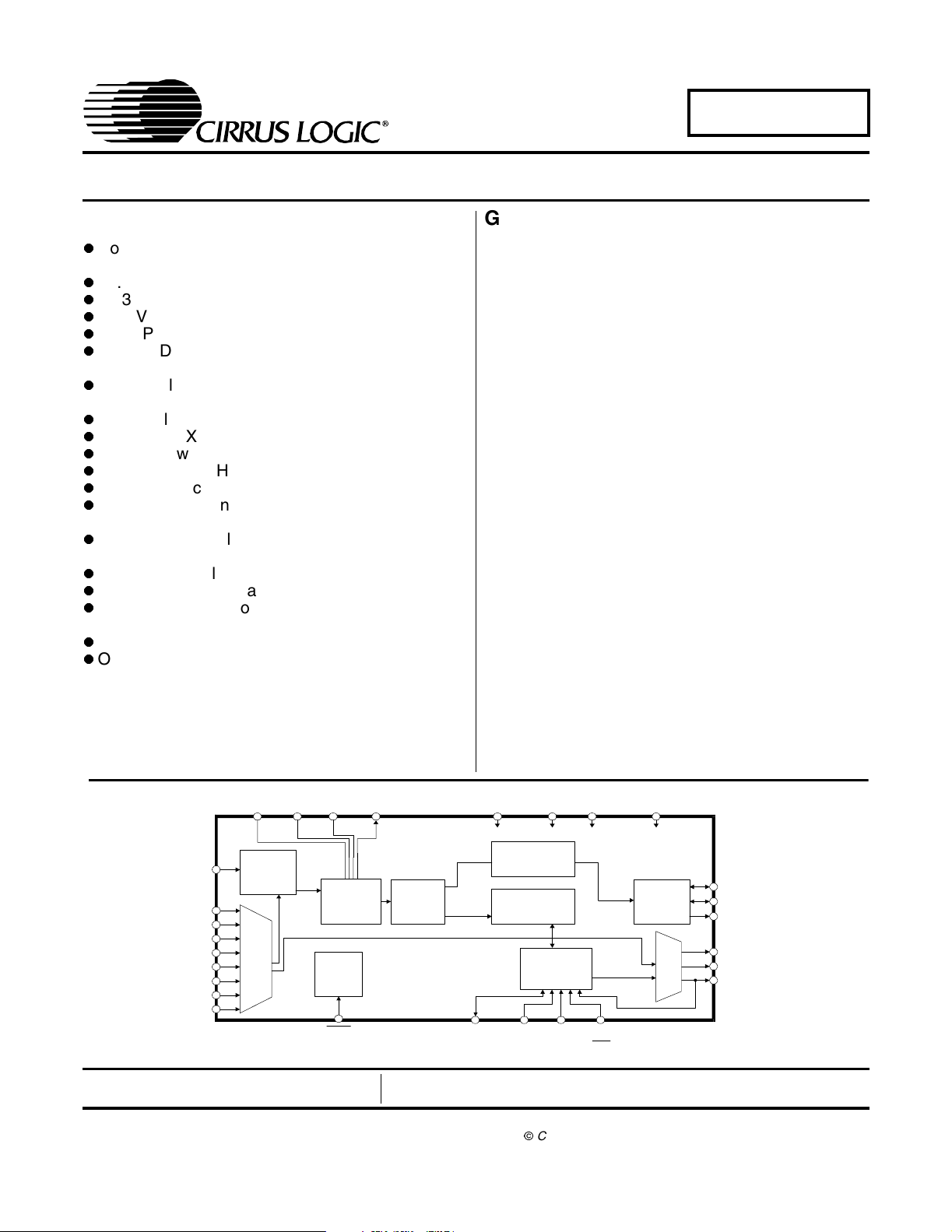
General Description
The CS8416 is a monolithic CMOS device which receives and decodes one of 8 channels of audio data
according to the IEC60958, S/PDIF, EIAJ CP1201, or
AES3 interface standards. The CS8416 has a serial digital audio output port and comprehensive control ability
through a selectable control port in Software Mode or
through selectable pins in Hardware Mode. Channel status data are assembled in buffers, making read access
easy.
GPO pins may be assigned to route a variety of signals
to output pins
A low jitter clock recovery mechanism yields a very clean
recoveredclockfromtheincomingAES3stream.
Stand-alone operation allows systems with no microcontroller to operate the CS8416 with dedicated output pins
for channel status data.
Target applications include A/V receivers, CD-R, DVD
receivers, multimedia speakers, digital mixing consoles,
effects processors, set-top boxes, and computer and automotive audio systems.
ORDERING INFORMATION
CS8416-CS 28-pin SOIC -10 to +70°C
CS8416-CZ 28-pin TSSOP -10 to +70°C
CS8416-IS 28-pin SOIC -40 to +85°C
CS8416-IZ 28-pin TSSOP -40 to +85°C
VA+ AG ND FI LT
RXN
RXP0
RXP1
RXP2
RXP3
RXP4
RXP5
RXP6
RXP7
Receiver
8:2
MUX
Clock &
Data
Recovery
Misc.
Control
RST
Advance Product Information
Cirrus Logic, Inc.
http://www.cirrus.com
RMCK
AES3
S/PDIF
Decod er
This document contains information for a new product.
Cirrus Logic reserves the right to modify this product without notice.
VD+
SDA/
CDOUT
CopyrightCirrus Logic, Inc. 2002
VL+ DGND
De-emphasis
Filter
C&Ubit
Data Buffer
Control
Port &
Registe rs
SCL/
AD1/
CDIN
AD0/
CS
CCLK
(All Rights Reserved)
OMCK
Serial
Audi o
Outpu t
MUX
n:3
OLRCK
OSCLK
SDOUT
GPO0
GPO1
AD2/GPO2
AUG ‘02
DS578PP2
1

TABLE OF CONTENTS
1 CHARACTERISTICS AND SPECIFICATIONS ......................................................................... 5
Power and Thermal Characteristics..........................................................................................5
Absolute Maximum Ratings ...................................................................................................... 5
Digital Characteristics............................................................................................................... 6
Switching Characteristics - Serial Audio Ports.......................................................................... 7
Switching Characteristics - Control Port - SPI Mode ................................................................ 8
Switching Characteristics - Control Port- I
2 TYPICAL CONNECTION DIAGRAMS .................................................................................... 10
3 GENERAL DESCRIPTION ......................................................................................................12
3.1 AES3 and S/PDIF Standards Documents ........................................................................ 12
4 SERIAL AUDIO OUTPUT PORT ............................................................................................. 13
4.1 Slip/Repeat Behavior ....................................................................................................... 13
4.2 AES11 Behavior .............................................................................................................. 14
5 S/PDIF RECEIVER .................................................................................................................. 16
5.1 8:2 S/PDIF Input Multiplexer ............................................................................................16
5.2 PLL, Jitter Attenuation, and Clock Switching ................................................................... 16
5.2.1 OMCK System Clock Mode ................................................................................ 17
5.2.2 PLL External Components .................................................................................. 17
5.3 Error Reporting and Hold Function .................................................................................. 17
5.4 Channel Status Data Handling ......................................................................................... 18
5.5 User Data Handling .......................................................................................................... 18
5.5.1 Non-Audio Auto-Detection .................................................................................. 18
6 CONTROL PORT DESCRIPTION AND TIMING ..................................................................... 20
6.1 SPI Mode ......................................................................................................................... 20
2
6.2 I
C Mode .......................................................................................................................... 21
6.3 General Purpose Outputs ................................................................................................ 22
6.4 Interrupts ..........................................................................................................................22
7 CONTROL PORT REGISTER SUMMARY .............................................................................23
8 CONTROL PORT REGISTER BIT DEFINITIONS ................................................................... 25
8.1 Control0 (00h)................................................................................................................... 25
8.2 Control1 (01h)................................................................................................................... 25
CS8416
2
C format................................................................. 9
Contacting Cirrus Logic Support
For all product questions and inquiries contact a Cirrus Logic Sales Representative.
To find one nearest you go to <http://www.cirrus.com/corporate/contacts/sales.cfm>
IMPORTANT NOTICE
"Preliminary" product information describes products that are in production, but for which full characterization data is not yet available. "Advance" product inf ormation describes products that are i n development and subject to development changes. Cirrus Logic, I nc. and its subsidiaries ("Cirrus") believe that the information contained in this document is accurate and reliable. However, the informati on is subject to change without notice and is provided "AS IS" without warranty
of any kind (express or implied). Customers are advised to obtain the latest version of relevant i nformation to verify, before placing orders, that information being
relied on is current and complete. All products are sold subject to the terms and conditions of sale supplied at the time of order acknowledgment, including those
pertaining to warranty, patent infringement, and limitation of liability. No responsibility i s assumed by Cirrus f or the use of this informati on, i ncludi ng use of this
information as the basis for manufacture or sale of any items, or for i nfringement of patents or other rights of third parties. This document is the property of Cir rus
and by furnishi ng this information, Cirrus grants no license, express or implied under any patents, mask work rights, copyrights, trademarks, trade secrets or
other intellectual property ri ghts. Ci rrus owns the copyrights of the information contained herein and gives consent for copies to be made of the info rmation only
for use within your organization wi th respect to Cirrus integr ated ci rcuits or other parts of Cirrus. This consent does not extend to other copying such as copying
for general distribution, advertising or pr omotional purposes, or for creating any work for resale.
An export permit needs to be obtained from the competent authorities of the Japanese Government if any of the products or technologies described in thismaterial and controlled under the "Foreign Exchange and Foreign Trade Law" is to be exported or taken out of Japan. An export li cense and/or quota needs to be
obtained from the competent authorities of the Chinese Government if any of the products or technologies describ ed in this material is subject to the PRC Foreign
Trade Law and i s to be exported or taken out of the PRC.
CERTAIN APPLICATIONS USING SEMICONDUCTOR PRODUCTS MAY INVOLVE POTENTIAL RISKS OF DEATH, PERSONAL INJURY, OR SEVERE
PROPERTY OR ENVIRONMENTAL DAMAGE (" CRITICAL APPLICATIONS") . CIRRUS PRODUCTS ARE NOT DESIGNED, AUTHORIZED, OR WARRANTED TO BE SUITABLE FOR USE IN LIFE-SUPPORT DEVICES OR SYSTEMS OR OTHER CRITICAL APPLICATIONS. INCLUSION OF CIRRUS PRODUCTS
IN SUCH APPLICATIONS IS UNDERSTOOD TO BE FULLY AT THE CUSTOMER'S RISK.
Cirrus Logic, Cirrus, and the Cirrus Logi c logo desi gns are trademarks of Cirrus Logic, Inc. All other brand and product names in this d ocument may be trademarks or service marks of their respective owners.
2 DS578PP2

CS8416
8.3 Control2 (02h)................................................................................................................... 26
8.4 Control3 (03h)................................................................................................................... 26
8.5 Control4 (04h)................................................................................................................... 27
8.6 Serial Audio Data Format (05h)........................................................................................ 27
8.7 Receiver Error Mask (06h) .............................................................................................. 29
8.8 Interrupt Mask (07h) ......................................................................................................... 29
8.9 Interrupt Mode MSB (08h) and Interrupt Mode LSB(09h) ................................................ 29
8.10 Receiver Channel Status (0Ah) ..................................................................................... 30
8.11 Format Detect Status (0Bh)............................................................................................ 30
8.12 Receiver Error (0Ch) ..................................................................................................... 31
8.13 Interrupt 1 Status (0Dh) ................................................................................................. 32
8.14 Q-Channel Subcode (0Eh - 17h) .................................................................................... 32
8.15 OMCK/RMCK Ratio (18h) .............................................................................................. 33
8.16 Channel Status Registers (19h - 22h) ............................................................................ 33
8.17 IEC61937 PC/PD Burst preamble (23h - 26h)................................................................ 33
8.18 CS8416 I.D. and Version Register (7Fh)........................................................................ 33
8.19 Memory Address Pointer (MAP)..................................................................................... 34
9. PIN DESCRIPTION - SOFTWARE MODE ............................................................................ 35
10 HARDWARE MODE .............................................................................................................. 37
10.1 Serial Audio Port Formats ............................................................................................. 37
11 PIN DESCRIPTION - HARDWARE MODE ........................................................................... 38
11.1 Hardware Mode Function Selection .............................................................................. 40
11.2 Hardware Mode Settings (Defaults & Controls) ............................................................. 40
12 APPLICATIONS .................................................................................................................... 42
12.1 Reset, Power Down and Start-up .................................................................................. 42
12.2 ID Code and Revision Code .......................................................................................... 42
12.3 Power Supply, Grounding, and PCB layout ................................................................... 42
13 PACKAGE DIMENSIONS ..................................................................................................... 43
14 APPENDIX A: EXTERNAL AES3/SPDIF/IEC60958 RECEIVER COMPONENTS .............. 45
14.1 AES3 Receiver External Components ........................................................................... 45
14.2 Isolating Transformer Requirements ............................................................................. 45
15 APPENDIX B: CHANNEL STATUS BUFFER MANAGEMENT .......................................... 47
15.1 AES3 Channel Status (C) Bit Management ................................................................... 47
15.2 Accessing the E buffer ................................................................................................... 47
15.2.1 Serial Copy Management System (SCMS) ....................................................... 47
DS578PP2 3

LIST OF FIGURES
Figure 1. Audio Port Master Mode Timing....................................................................................... 7
Figure 2. Audio Port Slave Mode and Data Input Timing ................................................................ 7
Figure 3. SPI Mode Timing.............................................................................................................. 8
Figure 4. I2C Mode Timing.............................................................................................................. 9
Figure 5. Typical Connection Diagram - Software Mode............................................................... 10
Figure 6. Typical Connection Diagram - Hardware Mode ............................................................. 11
Figure 7. AES3 Data Format ......................................................................................................... 14
Figure 8. Serial Audio Output Example Formats........................................................................... 15
Figure 9. C/U data outputs ............................................................................................................ 19
Figure 10. De-emphasis filter ........................................................................................................ 19
Figure 11. Control Port Timing In SPI Mode .................................................................................20
Figure 12. Control Port Timing in I
Figure 13. Hardware Mode Data Flow ..........................................................................................37
Figure 14. Professional Input Circuit ............................................................................................. 46
Figure 15. Transformerless Professional Input Circuit ..................................................................46
Figure 16. Consumer Input Circuit ................................................................................................ 46
Figure 17. S/PDIF MUX Input Circuit ............................................................................................ 46
Figure 18. TTL/CMOS Input Circuit............................................................................................... 46
Figure 19. Channel Status Data Buffer Structure .......................................................................... 47
Figure 20. Flowchart for Reading the E Buffer.............................................................................. 47
CS8416
2
C Mode .................................................................................. 21
LIST OF TABLES
Table 1. Delays by Frequency Values ................................................................................................. 14
Table 2. External PLL Component Values........................................................................................... 17
Table 3. GPO Pin Configurations ........................................................................................................ 22
Table 4. Hardware Mode Serial Audio Format Select ......................................................................... 41
4 DS578PP2
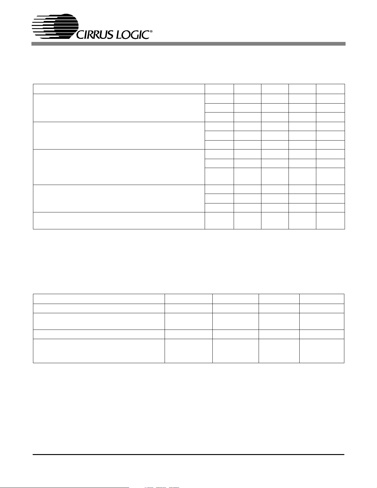
1 CHARACTERISTICS AND SPECIFICATIONS
POWER AND THERMAL CHARACTERISTICS
(AGND, DGND = 0 V, all voltages with respect to ground)
Parameter Symbol Min Typ Max Unit
Power Supply Voltage
Supply Current at 48 KHz frame rate
Supply Current at 192 KHz frame rate (Note 1)
Supply Current in Power Down
Ambient Operating Temperature: ‘-CS’ & ‘-CZ’ (Note 2)
‘-IS’ & ‘-IZ’ (Note 3)
CS8416
VA+ 3.13 3.3 3.46 V
VD+ 3.13 3.3 3.46 V
VL+ 3.13 3.3 5.5 V
IA - 5.7 - mA
ID - 5.9 - mA
IL - 2.8 - mA
IA - 9.4 - mA
ID - 23 - mA
-7.8-mA
IL
IA - 10 - uA
ID - 70 - uA
IL - 10 - uA
T
A
-10°
-40°
25°
-
70°
85°
°C
Notes: 1. Assumes that no digital inputs are left floating. It is recommended that all digital inputs be driven high
or low at all times.
2. ‘-CS’ and ‘-CZ’ parts are specified to operate over -10° C to 70° C but are tested at 25° C only.
3. ‘-IS’ and ‘-IZ’ parts are tested over the full -40° C to 85° C temperature range.
ABSOLUTE MAXIMUM RATINGS
(AGND, DGND = 0 V, all voltages with respect to ground)
Parameter Symbol Min Max Unit
Power Supply Voltage VD+, VA+, VL+ - 6 Volts
Input Current, Any Pin Except Supplies
(Note 4)
Input Voltage V
Ambient Operating Temperature
Notes: 4. Transient currents of up to 100mA will not cause SCR latch-up.
I
in
in
T
A
CS8416-C
CS8416-I
-10 10 mA
-0.3 VL+.03 Volts
-10°
-40°
70°
85°
°C
°C
DS578PP2 5
CS8416
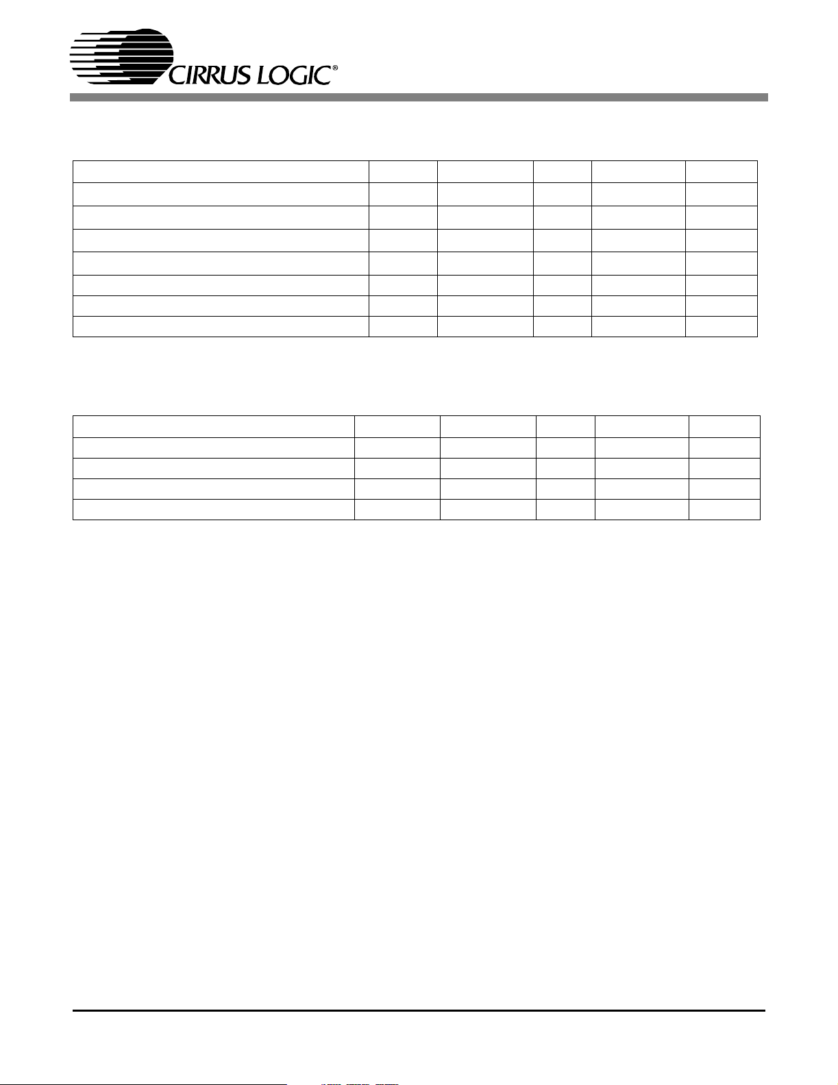
DIGITAL CHARACTERISTICS
(TA= 25 °C for suffixes ‘CS’ &’CZ’, TA= -40 to 85 °C for ‘IS’ & ‘IZ’ ; VA+ = VD+ = 3.3 V ± 5%, VL+ = 3.135 V to 5.5 V
Parameter Symbol Min Typ Max Units
High-Level Input Voltage except RX
Low-Level Input Voltage except RX
Low-Level Output Voltage (I
High-Level Output Voltage (I
O
O
Input hysteresis V
Input Leakage Current I
Differential Input Sensitivity RXPn to RXN0 - 150 200 mV
SWITCHING CHARACTERISTICS
(TA= 25 °C for suffixes ‘CS’ &’CZ’, TA= -40 to 85°C for ‘IS’ & ‘IZ’ ; VA+ = VD+ = 3.3 V ± 5%, VL+ = 3.135 V to 5.5
V, Inputs: Logic 0 = 0V, Logic 1 = VL+; C
Parameter Symbol Min Typ Max Units
RST/Pin Low Pulse Width 200 - - uS
PLL Clock Recovery Sample Rate Range 30 - 200 kHz
RMCK Output Jitter (Time Deviation) - - 200 ps RMS
RMCK Output Duty-Cycle 45 50 55 %
:VIH2 - (VL+)+0.3 Volts
n
:VIL-0.3 - 0.8 Volts
n
=3.2mA) V
=3.2mA) V
=20pF)
L
OL
OH
H
IN
- - 0.5 Volts
(VL+) - 1 - VL+ Volts
0.25 - 1.0 Volts
-10 - 10 uA
)
6 DS578PP2
CS8416
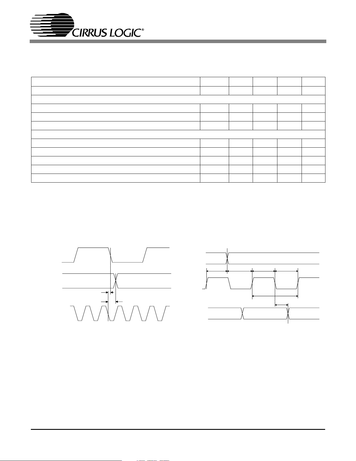
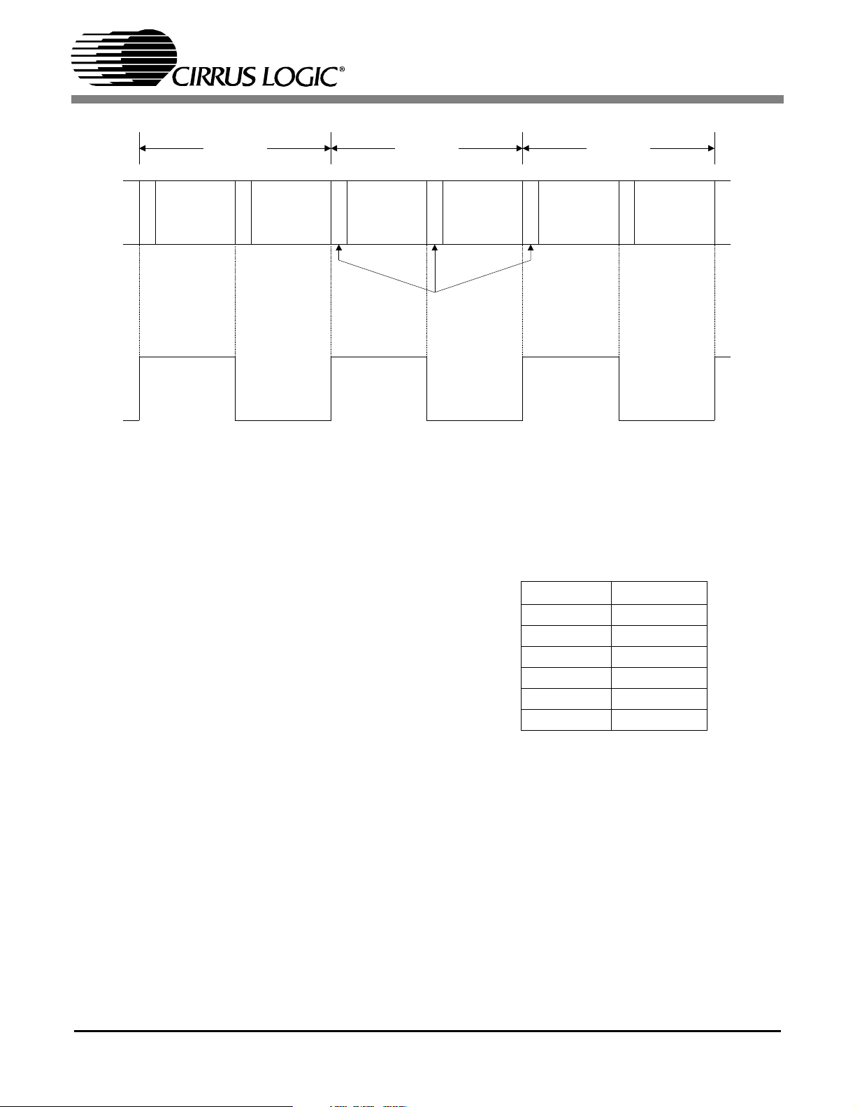
SWITCHING CHARACTERISTICS - SERIAL AUDIO PORTS
(TA= 25 °C for suffixes ‘CS’ & ’CZ’, TA= -40 to 85 °C for ‘IS’ & ‘IZ’ ; VA+ = VD+ = 3.3 V ± 5%, VL+ = 3.135 V to 5.5
V, Inputs: Logic 0 = 0 V, Logic 1 = VL+; C
Parameter Symbol Min Typ Max Units
OSCLK Active Edge to SDOUT Output Valid (Note 5)t
Master Mode
RMCK to OSCLK active edge delay (Note 5)t
RMCK to OLRCK delay (Note 6)t
OSCLK and OLRCK Duty Cycle - 50 - %
Slave Mode
OSCLK Period t
OSCLK Input Low Width t
OSCLK Input High Width t
OSCLK Active Edge to OLRCK Edge (Notes 5,6,7)t
OSCLK Edge Setup Before OSCLK Active-Edge (Notes 5,6,8)t
Notes: 5. In Software mode the active edges of OSCLK are programmable.
6. In Software mode the polarity of OLRCK is programmable.
7. This delay is to prevent the previous OSCLK edge from being interpreted as the first one after OLRCK
has changed.
8. This setup time ensures that this OSCLK edge is interpreted as the first one after OLRCK has changed.
=20pF)
L
dpd
smd
lmd
sckw
sckl
sckh
lrckd
lrcks
- - 15 ns
0 - 10 ns
0 - 10 ns
36 - - ns
14 - - ns
14 - - ns
10 - - ns
10 - - ns
OSCLK
(output)
OLRCK
(output)
RMCK
(output)
t
smd
t
lmd
OLRCK
(input)
OSCLK
(input)
SDOUT
t
lrckd
t
lrcks
t
sckh
t
sckw
t
sckl
t
dpd
Figure 1. Audio Port Master Mode Timing Figure 2. Audio Port Slave Mode and Data Input Timing
DS578PP2 7
CS8416
SWITCHING CHARACTERISTICS - CONTROL PORT - SPI MODE
(TA= 25 °C for suffixes ‘CS’ &’CZ’, TA= -40 to 85°C for ‘IS’ & ‘IZ’ ; VA+ = VD+ = 3.3 V ± 5%, VL+ = 3.135 to 5.5V,
Inputs: Logic 0 = 0 V, Logic 1 = VL+; C
Parameter Symbol Min Max Unit
CCLK Clock Frequency (Note 9)f
High Time Between Transmissions
CS
CS
Falling to CCLK Edge
CCLK Low Time t
CCLK High Time t
CDIN to CCLK Rising Setup Time t
CCLK Rising to DATA Hold Time (Note 10)t
CCLK Falling to CDOUT Stable t
Rise Time of CDOUT t
Fall Time of CDOUT t
Rise Time of CCLK and CDIN (Note 11)
Fall Time of CCLK and CDIN (Note 11)t
=20pF)
L
t
t
sck
csh
css
scl
sch
dsu
dh
pd
r1
f1
t
r2
r2
06.0MHz
1.0 - µs
20 - ns
66 - ns
66 - ns
40 - ns
15 - ns
-50ns
-25ns
-25ns
- 100 ns
- 100 ns
Notes: 9. If Fs is lower than 46.875 kHz, the maximum CCLK frequency should be less than 128 Fs. This is
dictated by the timing requirements necessary to access the Channel Status memory. Access to the
control register file can be carried out at the full 6 MHz rate. The minimum allowable input sample rate
is 32 kHz, so choosing CCLK to be less than or equal to 4.1 MHz should be safe for all possible
conditions.
10. Data must be held for sufficient time to bridge the transition time of CCLK.
11. For f
sck
<1 MHz.
CDOUT
CS
CCLK
CDIN
t
css
t
t
sch
scl
t
r2
t
dsu
t
f2
t
dh
t
pd
t
csh
Figure 3. SPI Mode Timing
8 DS578PP2
CS8416
SWITCHING CHARACTERISTICS - CONTROL PORT- I2CFORMAT
(TA= 25° C; VA+ = VD+ = 3.3 V ± 5%, VL = 3.135 V to 5.5 V Inputs: Logic 0 = GND, Logic 1 = VL,CL=20pF)
Parameter Symbol Min Max Unit
SCL Clock Frequency f
Bus Free Time Between Transmissions t
Start Condition Hold Time (prior to first clock pulse) t
Clock Low time t
Clock High Time t
Setup Time for Repeated Start Condition t
SDA Hold Time from SCL Falling (Note 12)t
SDA Setup time to SCL Rising t
Rise Time of SCL and SDA t
Fall Time SCL and SDA t
Setup Time for Stop Condition t
Notes: 12. Data must be held for sufficient time to bridge the 25 ns transition time of SCL.
scl
buf
hdst
low
high
sust
hdd
sud
r
f
susp
- 100 kHz
4.7 - µs
4.0 - µs
4.7 - µs
4.0 - µs
4.7 - µs
10 - ns
250 - ns
-25ns
-25ns
4.7 - µs
SDA
SCL
Stop Start
t
buf
t
hdst
t
low
t
high
t
hdd
Figure 4. I2CModeTiming
t
sud
Repeated
Start
t
t
sust
hdst
Stop
t
f
t
r
t
susp
DS578PP2 9
2 TYPICAL CONNECTION DIAGRAMS
+3.3V
*
+3.3V
Analog
Supply
Ferrite
Bead
*
10 Fµ
VL+
VL+
0.1 Fµ
AES3 /
**
S/PDIF
Sources
Microcontroller SCL / CCLK
1nF
VA+
RXN
RXP0
RXP1
RXP2
RXP3
RXP4
RXP5
RXP6
RXP7
AD0 / CS
AD1 / CDIN
SDA / CDOUT
RST
10 Fµ 0.1 Fµ 1nF
VD+
CS8416
VL+
SDOUT
OLRCK
OSCLK
RMCK
OMCK
GPO0
GPO1
AD2/GPO2
0.1 Fµ
47KΩ
Clock Control
Clock Source
CS8416
+3.3V to +5V
1nF
Serial Audio
Input
Device
External
Interface
FILT DGNDAGND
Rflt
Cflt Crip
***
A seperate analog supply is only necessary in applications where RMCK is used for a jitter
*
sensitive tast. For applications where RMCK is not used for a jitter sensitive task, connect
VA+ to VD+ via a ferrite bead. Keep decoupling capacitors between VA+ and AGND.
Please see section 5.1 "8:2 S/PDIF Input Multiplexer" and Appendix
**
A for typical input configurations and recommended input circuits.
For best jitter performance connect the filter ground directly to the AGND pin.
***
SeeTable2forPLLfiltervalues.
Figure 5. Typical Connection Diagram - Software Mode
10 DS578PP2
+3.3V
Analog
Supply
**
Ferrite
Bead
VL+
VL+
**
10 Fµ
***
0.1 Fµ 1nF
AES3 /
S/PDIF
Sources
Hardware
Control
+3.3V
VD+
VA+
RXN
RXP0
RXP1
RXP2
RXP3
RST
RXSEL0
RXSEL1
TXSEL0
TXSEL1
NV/RERR
*
AUDIO
96KHZ
*
RCBL
*
*
U
C
*
10 Fµ 0.1 Fµ 1nF
VL+
OLRCK
OSCLK
SDOUT
CS8416
RMCK
*
OMCK Clock Source
TX
0.1 Fµ
Serial Audio
Input Device
47KΩ
Clock Control
External
Interface
CS8416
+3.3V to +5V
1nF
FILT DGNDAGND
Rflt
Cflt Crip
****
These pins must be pulled high to VL+ or low to DGND through a 47KΩ resistor.
*
A seperate analog supply is only necessary in applications where RMCK is used for a jitter
**
sensitive tast. For applications where RMCK is not used for a jitter sensitive task, connect
VA+ to VD+ via a ferrite bead. Keep decoupling capacitors between VA+ and AGND.
Please see section 5.1 "8:2 S/PDIF Input Multiplexer" and Appendix
***
A for typical input configurations and recommended input circuits.
For best jitter performance connect the filter ground directly to the AGND pin.
****
See Table 2 for PLL filter values.
Figure 6. Typical Connection Diagram - Hardware Mode
DS578PP2 11

CS8416
3 GENERAL DESCRIPTION
The CS8416 is a monolithic CMOS device which
receives and decodes audio data according to the
AES3, IEC60958, S/PDIF, and EIAJ CP1201 interface standards.
The CS8416 utilizes an 8:2 multiplexer to select
between eight inputs for decoding and to allow an
input signal to be routed to an output of the
CS8416. Input data is either differential or singleended. A low jitter clock is recovered from the incoming data using a PLL. The decoded audio data
is output through a configurable, 3-wire output
port. The channel status and Q-channel subcode
portion of the user data are assembled in registers
and may be accessed through an SPI or I
Three General Purpose Output (GPO) pins are provided to allow a variety of signals to be accessed
under software control. In hardware mode, dedicated pins are used to select audio stream inputs for
decoding and transmission to a dedicated TX pin.
Hardware mode also allows direct access to channel status and user data output pins.
Figure 5 and Figure 6 show the power supply and
external connections to the CS8416 when configured for software and hardware modes. Please note
2
C port.
that all I/O pins, including RXN and RXP[7:0], operate at the VL+ voltage.
3.1 AES3 and S/PDIF Standards Documents
This document assumes that the user is familiar
with the AES3 and S/PDIF data formats. It is advisable to have current copies of the AES3, IEC60958,
and IEC61937 specifications on hand for easy reference.
The latest AES3 standard is available from the Audio Engineering Society or ANSI at www.aes.org
or at www.ansi.org. Obtain a copy of the latest
IEC60958/61937 standard from ANSI or from the
International Electrotechnical Commission at
www.iec.ch
available from the Japanese Electronics Bureau.
Application Note 22: Overview of Digital Audio In-
terface Data Structures contains a useful tutorial
on digital audio specifications, but it should not be
considered a substitute for the standards.
The paper An Understanding and Implementation
of the SCMS Serial Copy Management System for
Digital Audio Transmission, by Clifton Sanchez, is
an excellent tutorial on SCMS. It is available from
the AES as reprint 3518.
. The latest EIAJ CP-1201 standard is
12 DS578PP2

CS8416
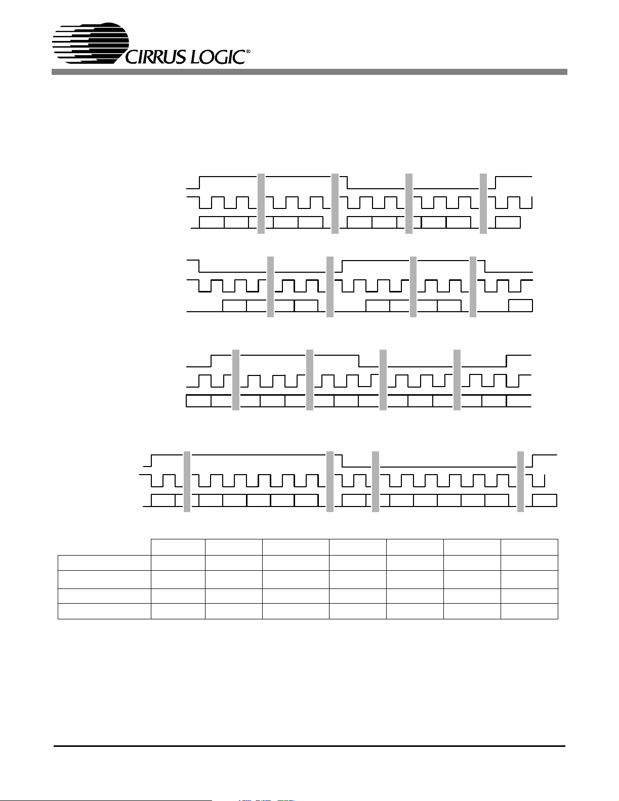
4 SERIAL AUDIO OUTPUT PORT
A 3-wire serial audio output port is provided. The
port can be adjusted to suit the attached device setting the control registers. The following parameters
are adjustable: master or slave, serial clock frequency, audio data resolution, left or right justification of the data relative to left/right clock, optional
one-bit cell delay of the first data bit, the polarity of
the bit clock, and the polarity of the left/right clock.
By setting the appropriate control bits, many formats are possible.
Figure 8 shows a selection of common output for-
mats, along with the control bit settings. A special
AES3 direct output format is included, which allows the serial output port access to the V, U, and
C bits embedded in the serial audio data stream.
The P bit, which would normally be a parity bit, is
replaced by a Z bit, which is used to indicate the
start of each block. The received channel status
block start signal is also available as the RCBL pin
in hardware mode and through a GPO pin in software mode.
In master mode, the left/right clock (OLRCK) and
the serial bit clock (OSCLK) are outputs, derived
from the recovered RMCK clock. In slave mode,
OLRCK and OSCLK are inputs. OLRCK is normally synchronous to the appropriate master clock,
but OSCLK can be asynchronous and discontinuous if required. By appropriate phasing of OLRCK
and control of the serial clocks, multiple CS8416’s
can share one serial port. OLRCK should be continuous, but the duty cycle can be less than the
specified typical value of 50% if enough serial
clocks are present in each phase to clock all the data
bits. When in slave mode, the serial audio output
port cannot be set for right-justified data. The
CS8416 allows immediate mute of the serial audio
output port audio data by the MUTESAO bit of
Control Register 1.
4.1 Slip/Repeat Behavior
When using the serial audio output port in slave
mode with an OLRCK input that is asynchronous
to the incoming AES3 data, the interrupt bit OSLIP
(bit 5 in the Interrupt 1 Status register, 0Dh) is provided to indicate when repeated or dropped samples occur. Refer to Figure 7 for a AES3 data
format diagram.
When the serial output port is configured as slave,
depending on the relative frequency of OLRCK to
the input AES3 data (Z/X) preamble frequency, the
data will be slipped or repeated at the output of the
CS8416.
After a fixed delay from the Z/X preamble (a few
periods of the internal clock, which is running at
256Fs), the circuit will look back in time until the
previous Z/X preamble:
1) If during that time, the internal data buffer was
not updated, then a slip has occurred. Data from
the previous frame will be output and OSLIP
will be set to 1. Due to the OSLIP bit being
“sticky,” it will remain 1 until the register is
read. It will then be reset until another slip/repeat condition occurs.
2) If during that time the internal data buffer did
not update between two positive or negative
edges (depending on OLRPOL) of OLRCK,
then a repeat has occurred. In this case the buffer data was updated twice, so the part has lost
one frame of data. This event will also trigger
OSLIP to be set to 1. Due to the OSLIP bit being “sticky,” it will remain 1 until the register is
read. It will then be reset until another slip/repeat condition occurs.
3) If during that time, it did see a positive edge on
OLRCK (or negative edge if the SOLRPOL is
set to 1) then no slip or repeat has happened.
Due to the OSLIP bit being “sticky,” it will remain in its previous state until either the register is read or a slip/repeat condition occurs.
DS578PP2 13
Frame 191 Frame 0 Frame 1
CS8416
Channel A
X
Data
Y
Channel B
Data
Channel A
Z Y X Y
Data
Preambles
OLRCK (in slave mode)
Figure 7. AES3 Data Format
If the user reads OSLIP as soon as the event triggers, over a long period of time the rate of occurring INT will be equal to the difference in
frequency between the input AES data and the
slave serial output LRCK. The CS8416 uses a hysteresis window when a slip/repeat event occurs.
The slip/repeat is triggered when an edge of OLRCK passes a window size from the beginning of
the Z/X preamble. Without the hysteresis window,
jitter on OLRCK with a frequency very close to Fs
could slip back and forth, causing multiple slip/repeat events. The CS8416 uses a hysteresis window
to ensure that only one slip/repeat happens even
with jitter on OLRCK.
4.2 AES11 Behavior
When OLRCK is configured as a master, the positive or negative edge of OLRCK (depending on the
setting of SOLRPOL in register 05h) will be within
-1.0%(1/Fs) to 1.1%(1/Fs) from the start of the preamble X/Z. In master mode, the latency through the
part is dependent on the input sample frequency.
The delay through the part from the beginning of
the preamble to the active edge of OLRCK for the
various sample frequencies is given in Table 1.In
Channel B
Data
Channel A
Data
Channel B
Data
master mode without the de-emphasis filter engaged, the latency of the audio data will be 3
frames.
Fs (kHz) Delay (ns)
32 96.6
44.1 78.6
48 74.6
64 60.6
96 50.6
192 TBD
Table 1. Delays by Frequency Values
When OLRCK is configured as a slave any synchronized input within +/-28%(1/Fs) from the positive or negative edge of OLRCK (depending on
the setting of SOLRPOL in register 05h) will be
treated as being sampled at the same time. Since the
CS8416 has no control of the OLRCK in slave
mode, the latency of the data through the part will
be a multiple of 1/Fs plus the delay between OLRCK and the preambles.
Both of these conditions are within the tolerance
range set forth in the AES11 standard.
14 DS578PP2
CS8416
AES3
Direct
(Out)
Left
Justified
(Out)
2
IS
(Out)
Right
Justified
(Out)
OLRCK
OSCLK
SDOUT
OLRCK
OSCLK
SDOUT
OLRCK
OSCLK
SDOUT
OLRCK
OSCLK
SDOUT
LSB
Right
MSB
LSB
Right
Right
MSB
UC
VZ
Left
MSB LSB MSB LSB MSB
Left Right
MSB
MSB Extende d MSB Extended
LSB MSB LSB
VZ
MSB
MSB LSB
Left
UCLSB
LSB
Left
MSB
MSB Ex
LSB
SOMS* SOSF* SORES[1:0]* SOJUST* SODEL* SOSPOL* SOLRPOL*
Left Justified X X XX 0 0 0 0
2
S
I
XXXX0101
Right Justified 1 X XX 1 0 0 0
AES3 Direct X X 11 0 0 0 0
X = don’t care to match format, but does need to be set to the desired setting
* See Serial Output Data Format Register Bit Descriptions for an explanation of the meaning of each bit
Figure 8. Serial Audio Output Example Formats
DS578PP2 15

CS8416
5 S/PDIF RECEIVER
The CS8416 includes an AES3/SPDIF digital audio receiver. The AES3 receiver accepts and decodes audio and digital data according to the AES3,
IEC60958 (S/PDIF), and EIAJ CP-1201 interface
standards. The receiver consists of an analog differential input stage, driven through analog input pins
RXP0 to RXP7 and a common RXN, a PLL based
clock recovery circuit, and a decoder which separates the audio data from the channel status and
user data.
Software Mode
The first 5 bytes of both channels status block is
stored in dedicated registers. Channel A status data
is stored in control port registers 19h to 1Dh. Channel B status data is stored in control port registers
1Eh to 22h.
Q Subcode data is stored in control port registers
0Eh to 17h.
PC Burst preamble is stored in control port registers 23h and 24h. PD Burst preamble is stored in
control port registers 25h and 26h.
U and C data may be selected for output on GPO
pins.
External components are used to terminate and isolate the incoming data cables from the CS8416.
These components are detailed in Appendix A.
Hardware Mode
U and C bits are output on pins 18 and 19 respectively. See Section “Hardware Mode Function Se-
lection” on page 40 and “Hardware Mode Settings
(Defaults & Controls)” on page 40 to configure
these pins.
5.1 8:2 S/PDIF Input Multiplexer
nals are accommodated by using RXP inputs and
AC coupling RXN to ground.
All inputs to the CS8416 8:2 input multiplexer
should be coupled through a capacitor. The recommended capacitor value is 0.01uF to 0.1uF. The
recommended dielectrics are COG or X7R.
Software Mode
The multiplexer select line control is accessed
through bits RXSEL[2:0] in control port register 4.
The multiplexer defaults to RXP0.
The second output of the input multiplexer is used
to provide the selected input as a source to be output on a GPO pin via the internal TX pin. This pass
through signal is selected by TXSEL[2:0] in control port register 04h. The single-ended signal is resolved to full-rail, but is not de-jittered before it is
output.
Hardware Mode
In hardware mode the input to the decoder is selected by dedicated pins, RXSEL[1:0].
The pass through signal is selected by dedicated
pins, TXSEL[1:0] for output on the dedicated TX
pin.
Selectable inputs are restricted to RXP0 to RXP3
for both the receiver and the TX output pin. These
inputs are selected by RXSEL[1:0] and TXSEL[1:0] respectively.
General
Unused multiplexer inputs should be left floating
or grounded.
The input voltage range for the input multiplexer is
set by the I/O power supply pin, VL+. The input
voltage of the RXP and RXN pins is also set by the
level of VL+.
The CS8416 employs a 8:2 S/PDIF input multiplexer to accommodate up to eight channels of input digital audio data. Digital audio data may be
single- ended or differential. Differential inputs utilize RXP[0-7] and a shared RXN. Single ended sig-
16 DS578PP2
5.2 PLL, Jitter Attenuation, and Clock Switching
An on-chip Phase Locked Loop (PLL) is used to recover the clock from the incoming data stream.

CS8416
There are some applications where low jitter in the
recovered clock, presented on the RMCK pin, is
important. For this reason, the PLL has been designed to have good jitter attenuation characteristics. In addition, the PLL has been designed to only
use the preambles of the AES3 or S/PDIF stream to
provide lock update information to the PLL. This
results in the PLL being immune to data dependent
jitter affects because the AES3 or S/PDIF preambles do not vary with the data.
In applications where jitter must be minimized,
special attention should be given to reducing the
noise on the analog power supply and ground for
the PLL filter components. Connecting the filter
components directly to AGND will help decrease
jitter.
The PLL has the ability to lock onto a wide range
of input sample rates with no external component
changes.
5.2.1 OMCK System Clock Mode
A special clock switching mode is available that allows the OMCK clock input to replace RMCK
when the PLL becomes unlocked.
In Software mode this feature is enabled by setting
SWCLK bit in Control1 register to a “1”.
recommended configuration of the two capacitors
and one resistor required. There are two sets of
component values recommended, depending on the
sample rate of the application. (See Table 2.) The
default set, called “fast”, accommodates input sample rates of 96 KHz to 192 Hz with no component
changes. It has the highest corner frequency jitter
attenuation curve, and takes the shortest time to
lock. The alternate component set, called “medium” allows the lowest input sample rate to be 32
kHz, and increases the lock time of the PLL. Lock
times are worst case for an Fs transition from unlocked state to locking to 192 kHz.
Range
(kHz) Rflt Cflt Crip
32 - 192 1 KΩ 220 nF 10 nF 11ms medium
96 - 192 3 KΩ 22 nF 1 nF 4ms fast
Table 2. External PLL Component Values
Settling
Time
It is important to treat the PLL FLT pin as a low
level analog input. It is suggested that the ground
end of the PLL filter be returned directly to the
AGND pin independently of the digital ground
plane.
5.3 Error Reporting and Hold Function
Software Mode
In Hardware Mode this feature is always active.
Clock switching is accomplished without spurious
transitions or glitches on RMCK.
OSCLK and OLRCK are derived from the OMCK
input when the clock has been switched and the serial port is in master mode.
When the PLL loses lock, the frequency of the
VCO drops to ~500 kHz. When this system clock
mode is not enabled, the OSCLK and OLRCK will
be based on the VCO when the PLL is not locked
While decoding the incoming AES3 data stream,
the CS8416 can identify several kinds of error, indicated in the Receiver Error register (0Ch).
The errors indicated are:
1) QCRC – CRC error in Q subcode data
2) CCRC – CRC error in channel status data
3) UNLOCK – PLL is not locked to incoming data
stream
4) V – Data Validity bit is set
5) CONF – Input data stream is near error condi-
5.2.2 PLL External Components
The PLL behavior is affected by the external filter
tion due to jitter degradation
6) BIP – Biphase encoding error
component values. Figure 5 and Figure 6 show the
7) PAR – Parity error in incoming data
DS578PP2 17

CS8416
The error bits are “sticky”; they are set on the first
occurrence of the associated error and will remain
set until the user reads the register through the control port. This enables the register to log all unmasked errors that occurred since the last time the
register was read.
As a result of the bits “stickiness”, it is necessary to
perform two reads on these registers to see if the error condition still exists.
The Receiver Error Mask register (06h) allows
masking of individual errors. The bits in this register default to 00h and serve as masks for the corresponding bits of the Receiver Error register. If a
mask bit is set to 1, the error is unmasked, which
implies the following: its occurrence will be reported in the receiver error register, induce a pulse on
RERR, invoke the occurrence of a RERR interrupt,
and affect the current audio sample according to the
status of the HOLD bits. The exceptions are the
QCRC and CCRC errors, which do not affect the
current audio sample, even if unmasked.
The HOLD bits allow a choice of:
• Holding the previous sample
• Replacing the current sample with zero (mute)
OR
• Not changing the current audio sample
RERR – The logical OR of all unmasked receiver
error bits, not ‘sticky”. RERR may be selected for
output on a GPO pin.
NVERR – Non-Validity Receiver error
Hardware Mode
In Hardware mode the user may choose between
NVERR or RERR by pulling the NV/RERR pin
low or high respectively.
5.4 Channel Status Data Handling
Software Mode
The first 5 bytes of the Channel Status block are decoded into the Receiver Channel Status Registers
19h - 22h. Registers 19h - 1Dh contain the A channel status data. Registers 1Eh - 22h contain the B
channel status data.
The EMPH
pins by appropriately setting the GPOxSEL bits in
control port registers 02h and 03h.
The encoded channel status bits which indicate
sample word length are decoded according to
AES3-1992 or IEC 60958. The number of auxiliary
bits are reported in bits 7 to 4 of the Receiver Channel Status register.
Appendix B describes the overall handling of
Channel Status and User data.
, C, and U bits may be selected on GPO
5.5 User Data Handling
Received User data may also be output to the U pin
under the control of a control register bit. VLRCK
(a virtual word clock, available through GPO pins,
that can used to frame the C/U output) and OLRCK
in serial port master mode can be made available to
qualify the U data output in software mode.
Figure 9 illustrates the timing. In hardware mode,
only OLRCK in master mode is available to qualify
the U output. If the incoming user data bits have
been encoded as Q- channel subcode, the data is decoded, buffered, and presented in 10 consecutive
register locations. An interrupt may be enabled to
indicate the decoding of a new Q-channel block,
which may be read through the control port.
5.5.1 Non-Audio Auto-Detection
An AES3 data stream may be used to convey nonaudio data, thus it is important to know whether the
incoming AES3 data stream is digital audio or not.
This information is typically conveyed in channel
status bit 1 (AUDIO), which is extracted automatically by the CS8416. However, certain non-audio
sources, such as AC-3 or MPEG encoders, may not
adhere to this convention, and the bit may not be
properly set. The CS8416 AES3 receiver can detect
such non-audio data through the use of an autodetect module. The autodetect module is similar to
18 DS578PP2

CS8416
autodetect software used in Cirrus Logic DSPs. If
the AES3 stream contains sync codes in the proper
format for IEC61937 or DTS data transmission, an
internal AUTODETECT signal will be asserted. If
the sync codes no longer appear after a certain
amount of time, autodetection will time-out and
AUTODETECT will be de-asserted until another
format is detected. In Hardware Mode, the AUDIO
pin is the logical OR of AUTODETECT and the received channel status bit 1. In Software mode the
AUDIO
pin is available through the GPO pins. Al-
so, the specific data or audio format found by the
RCBL
out
VLRCK
C, U
Output
Figure 9. C/U data outputs
RCBL goes high 2 frames after receipt of a Z pre-amble, and is high for 16 frames.
VLRCK is a virtual word clock, available through GPO pins, that can used to frame the C/U ouput.
VLRCK duty cycle is 50%. VLRCK frequency is always equal to the incoming frame rate.
If the serial audio output port is in master mode, VLRCK = OLRCK.
C, U transitions are aligned within 1% of VLRCK period to VLRCK edges
±
autodetect module is available in register 0Bh. Additionally, the Pc/Pd burst preambles are available
in registers 23h-26h. If non-audio data is detected,
the data is still processed exactly as if it were normal audio. The exception is the use of de-emphasis
auto-select feature which will bypass the de-emphasis filter if the input stream is detected to be
non-audio. It is up to the user to mute the outputs as
required.
Gain,
dB
0
-10
T1 =
50us
T2
=15us
3.183
Figure 10. De-emphasis filter
F2F1
10.61
Frequency,
KHz
DS578PP2 19

CS8416
6 CONTROL PORT DESCRIPTION
AND TIMING
The control port is used to access the registers, allowing the CS8416 to be configured for the desired
operational modes and formats. In addition, Channel Status and User data may be read through the
control port. The operation of the control port may
be completely asynchronous with respect to the audio sample rates. However, to avoid potential interference problems, the control port pins should
remain static if no operation is required.
The control port has 2 modes: SPI and I
2
C, with the
CS8416 acting as a slave device in both modes. SPI
mode is selected if there is a high to low transition
on the AD0/CS
brought high. I
the AD0/CS
pin, after the RST pin has been
2
C mode is selected by connecting
pin to VL+ or DGND, thereby perma-
nently selecting the desired AD0 bit address state.
6.1 SPI Mode
In SPI mode, CS is the CS8416 chip select signal,
CCLK is the control port bit clock (input into the
CS8416 from the microcontroller), CDIN is the input data line from the microcontroller, CDOUT is
the output data line to the microcontroller. Data is
clocked in on the rising edge of CCLK and out on
the falling edge.
Figure 11 shows the operation of the control port in
SPI mode. To write to a register, bring CS low. The
first seven bits on CDIN form the chip address and
must be 0010000. The eighth bit is a read/write indicator (R/W
), which should be low to write. The
next eight bits form the Memory Address Pointer
(MAP), which is set to the address of the register
that is to be updated. The next eight bits are the data
which will be placed into the register designated by
the MAP. During writes, the CDOUT output stays
in the Hi-Z state. It may be externally pulled high
or low with a 47 KΩ resistor, if desired.
There is a MAP auto increment capability, enabled
by the INCR bit in the MAP register. If INCR is a
zero, the MAP will stay constant for successive
read or writes. If INCR is set to a 1, the MAP will
auto increment after each byte is read or written, allowing block reads or writes of successive registers. In the autoincrement mode, the MAP is
incremented in a linear fashion. Allowance must be
made for unused registers.
To read a register, the MAP has to be set to the correct address by executing a partial write cycle
which finishes (CS high) immediately after the
MAP byte. The MAP auto increment bit (INCR)
may be set or not, as desired. To begin a read, bring
low, send out the chip address and set the
CS
CS
CCLK
CHIP
ADDRESS
CDIN
CDOUT
20 DS578PP2
0010000
MAP = Memory Address Pointer, 8 bits, MSB first
R/W
High Impedance
MAP
Figure 11. Control Port Timing In SPI Mode
MSB
byte 1
DATA
LSB
byte n
CHIP
ADDRESS
0010000
R/W
MSB
LSB
MSB
LSB

CS8416
read/write bit (R/W) high. The next falling edge of
CCLK will clock out the MSB of the addressed
register (CDOUT will leave the high impedance
state). If the MAP auto increment bit is set to 1, the
data for successive registers will appear consecutively.
The auto increment function is strictly linear. This
may result in operations on undefined registers.
Reads from undefined registers will produce indeterminate results. Writing to undefined registers
will be ignored.
6.2 I2C Mode
In I2C mode, SDA is a bidirectional data line. Data
is clocked into and out of the part by the clock,
SCL, with the clock to data relationship as shown
in Figure 12. There is no CS
CS8416 is given a unique address. Pins AD0 and
AD1 form the two least significant bits of the chip
address and should be connected to VL+ or DGND
pin. Each individual
as desired. The GPO2 pin is used to set the AD2 bit
by connecting a 47K resistor from the GPO2 pin to
VL+ or to DGND. The state of the pin is sensed
while the CS8416 is being reset. The upper 4 bits of
the 7-bit address field are fixed at 0010. To communicate with a CS8416, the chip address field,
which is the first byte sent to the CS8416, should
match 0010 followed by the settings of the GPO2,
AD1, and AD0. The eighth bit of the address is the
R/W bit. If the operation is a write, the next byte is
the Memory Address Pointer (MAP) which selects
the register to be read or written. If the operation is
a read, the contents of the register pointed to by the
MAP will be output. Setting the auto increment bit
in MAP allows successive reads or writes of consecutive registers. Each byte is separated by an acknowledge bit. The ACK bit is output from the
CS8416 after each input byte is read, and is input to
the CS8416 from the microcontroller after each
transmitted byte.
Note 1
0010
SDA
SCL
Star t
Notes: 1. AD2 is derived from a resistor attached to the
AD1 and AD0 are determined by the state of the corresponding pins.
2. If operation is a write, this byte contains the Memory Address Pointer, MAP.
3. If operation is a read, the last bit of the read should be NACK (high).
AD2-0
Figure 12. Control Port Timing in I2CMode
R/W
ACK DATA7-0 ACK
Note 2
DATA7-0
ACK
GPO2 pin.
Note 3
Stop
DS578PP2 21

CS8416
6.3 General Purpose Outputs
Three General Purpose outputs are provided to allow the equipment designer flexibility in configuring the
CS8416.
Fourteen signals are available to be routed to the GPOs.
GPO pins may be configured to provide the following data:
Function Code Definition
TX 0000 AES/SPDIF input selected by TXSEL[2:0]
EMPH
INT 0010 CS8416 interrupt
C 0011 Channel status bit
U 0100 User data bit
RERR 0101 Receiver Error
NVERR 0110 Non-Validity Receiver Error
RCBL 0111 Receiver Channel Status Block
96KHZ 1000 Input F
AUDIO
VLRCK 1010 Virtual LRCK
GND 1011 Fixed low Level
VDD 1100 VDD fixed high level
HRMCK 1101
Codes 1110 to 1111 - Reserved
0001 State of EMPH bit in incoming stream. Same polarity as EMPHb bit.
≥ 88.1
S
1001 Non-audio indicator for decoded input stream
X 512 (Note 13)
F
S
Table 3. GPO Pin Configurations
Notes: 13. Frequency = 25 MHz Max, duty cycle not guaranteed, target duty cycle = 50% @ FS=48kHz.
6.4 Interrupts
The CS8416 has a comprehensive interrupt capability. The INT pin may be set to be active low, active high or active low with no active pull-up
transistor. This last mode is used for active low,
wired-OR hook- ups, with multiple peripherals
connected to the microcontroller interrupt input
pin.
Many conditions can cause an interrupt, as listed in
the interrupt status register descriptions. Each
source may be masked off through mask register
bits. In addition, each source may be set to rising
edge, falling edge, or level sensitive. Combined
with the option of level sensitive or edge sensitive
modes within the microcontroller, many different
configurations are possible, depending on the
needs of the equipment designer.
22 DS578PP2

7 CONTROL PORT REGISTER SUMMARY
CS8416
Addr (HEX)
00 R/W Control 0 0 0 0 0 0 TRUNC Reserved Reserved
01 R/W Control1 SWCLK MUTSAO INT1 INT0 HOLD1 HOLD0 RMCKF CHS
02 R/W Control2 DETCI EMPH_C
03 R/W Control3 GPO1SEL3GPO1SEL2GPO1SEL1GPO1SEL0GPO2SEL3GPO2SEL2GPO2SEL1GPO2SE
04 R/W Control4 RUN RXD RXSEL2 RXSEL1 RXSEL0 TXSEL2 TXSEL1 TXSEL0
05 R/W Serial Audio Data Format SOMS SOSF SORES1 SORES0 SOJUST SODEL SOSPOL SOLR-
06 R/W Receiver Error Mask 0 QCRCM CCRCM UNLOCKMVM CONFM BIPM PARM
07 R/W Interrupt Mask 0 PCCHM OSLIPM DETCM CCHM RERRM QCHM FCHM
08 R/W Interrupt Mode MSB 0 PCCH1 OSLIP1 DETC1 CCH1 RERR1 QCH1 FCH1
09 R/W Interrupt Mode LSB 0 PCCH0 OSLIP0 DETC0 CCH0 RERR0 QCH0 FCH0
0A R Receiver Channel Status AUX3 AUX2 AUX1 AUX0 PRO COPY ORIG EMPH
0B R Audio Format Detect 0 PCM IEC61937 DTS_LD DTS_CD Reserved DGTL_SIL96KHZ
0C R Receiver Error 0 QCRC CCRC UNLOCK V CONF BIP PAR
0D R Interrupt Status 0 PCCH OSLIP DETC CCH RERR QCH FCH
0E R Q-Channel Subcode
0F R [8:15] TRACK TRACK TRACK TRACK TRACK TRACK TRACK TRACK
10 R [16:23] INDEX INDEX INDEX INDEX INDEX INDEX INDEX INDEX
11 R [24:31] MINUTE MINUTE MINUTE MINUTE MINUTE MINUTE MINUTE MINUTE
12 R [32:39] SECOND SECOND SECOND SECOND SECOND SECOND SECOND SECOND
13 R [40:47] FRAME FRAME FRAME FRAME FRAME FRAME FRAME FRAME
14 R [48:55] ZERO ZERO ZERO ZERO ZERO ZERO ZERO ZERO
15 R [56:63] ABS
16 R [64:71] ABS SEC-
17 R [72:79] ABS
18 R OMCK_RMCK Ratio ORR7 ORR6 ORR5 ORR4 ORR3 ORR2 ORR1 ORR0
19 R Channel A Status AC0[7] AC0[6] AC0[5] AC0[4] AC0[3] AC0[2] AC0[1] AC0[0]
1A R Channel A Status AC1[7] AC1[6] AC1[5] AC1[4] AC1[3] AC1[2] AC1[1] AC1[0]
1B R Channel A Status AC2[7] AC2[6] AC2[5] AC2[4] AC2[3] AC2[2] AC2[1] AC2[0]
1C R Channel A Status AC3[7] AC3[6] AC3[5] AC3[4] AC3[3] AC3[2] AC3[1] AC3[0]
1D R Channel A Status AC4[7] AC4[6] AC4[5] AC4[4] AC4[3] AC4[2] AC4[1] AC4[0]
1E R Channel B Status BC0[7] BC0[6] BC0[5] BC0[4] BC0[3] BC0[2] BC0[1] BC0[0]
1F R Channel B Status BC1[7] BC1[6] BC1[5] BC1[4] BC1[3] BC1[2] BC1[1] BC1[0]
20 R Channel B Status BC2[7] BC2[6] BC2[5] BC2[4] BC2[3] BC2[2] BC2[1] BC2[0]
21 R Channel B Status BC3[7] BC3[6] BC3[5] BC3[4] BC3[3] BC3[2] BC3[1] BC3[0]
22 R Channel B Status BC4[7] BC4[6] BC4[5] BC4[4] BC4[3] BC4[2] BC4[1] BC4[0]
23 R Burst Preamble PC Byte 0 PC0[7] PC0[6] PC0[5] PC0[4] PC0[3] PC0[2] PC0[1] PC0[0]
R/W Function 7 6 5 4 3 2 1 0
[0:7]
CONTROL
MINUTE
OND
FRAME
NTL2
CON-
TROL
ABS
MINUTE
ABS SEC-
OND
ABS
FRAME
EMPH_C
NTL1
CON-
TROL
ABS
MINUTE
ABS SEC-
OND
ABS
FRAME
EMPH_C
NTL0
CON-
TROL
ABS
MINUTE
ABS SEC-
OND
ABS
FRAME
GPO0SEL3GPO0SEL2GPO0SEL1GPO0SE
ADDRESSADDRESSADDRESSADDRES
ABS
MINUTE
ABS SEC-
OND
ABS
FRAME
ABS
MINUTE
ABS SEC-
OND
ABS
FRAME
ABS
MINUTE
ABS SEC-
OND
ABS
FRAME
L0
L0
POL
S
ABS
MINUTE
ABS SEC-
OND
ABS
FRAME
DS578PP2 23

CS8416
Addr (HEX)
24 R Burst Preamble PC Byte 1 PC1[7] PC1[6] PC1[5] PC1[4] PC1[3] PC1[2] PC1[1] PC1[0]
25 R Burst Preamble PD Byte 0 PD0[7] PD0[6] PD0[5] PD0[4] PD0[3] PD0[2] PD0[1] PD0[0]
26 R Burst Preamble PD Byte 1 PD1[7] PD1[6] PD1[5] PD1[4] PD1[3] PD1[2] PD1[1] PD1[0]
7F R ID & Version ID3 ID2 ID1 ID0 VER3 VER2 VER1 VER0
R/W Function 7 6 5 4 3 2 1 0
24 DS578PP2

CS8416
8 CONTROL PORT REGISTER BIT DEFINITIONS
8.1 Control0 (00h)
76543210
0 0 0 0 0 TRUNC Reserved Reserved
TRUNC – Determines if the audio word length is set according to the incoming channel status data as decoded by
the AUX[3:0] bits. The resulting word length in bits is 24-AUX[3:0].
Default = 0
0 – incoming data is not truncated
1 – incoming data is truncated according to the length specified in the channel status data
Truncation occurs before the de-emphasis filter. TRUNC has no effect on output data if de-emphasis
filter is not used.
Reserved[1:0] – These bits may change state depending on the input audio data.
8.2 Control1 (01h)
76543210
SWCLK MUTESAO INT1 INT0 HOLD1 HOLD0 RMCKF CHS
SWCLK - Lets OMCK determine RMCK, OSCLK, OLRCK when PLL loses lock
Default = ‘0’
0 – Output clocks determined by PLL
1 – Output clocks determined by OMCK
RMCKF – Recovered Master Clock Frequency
Default = “0”
0 – Frequency is 256 FS
1 – Frequency is 128 FS
MUTESAO - Mute control for the serial audio output port
Default = ‘0’
0-SDOUT(NotMuted)
1 – SDOUT (Muted)
HOLD[1:0] – Determine how received audio sample is affected when a receive error occurs
Default = “00”
00 – hold last audio sample
01 – replace the current audio sample with 00 (mute)
10- do not change the received audio sample
11 - reserved
DS578PP2 25

CS8416
INT[1:0] - Interrupt output pin (INT) control
Default = ‘00’
00 - Active high; high output indicates interrupt condition has occurred
01 - Active low, low output indicates an interrupt condition has occurred
10 - Open drain, active low. Requires an external pull-up resistor on the INT pin. Thus it is not recom-
mended to multiplex INT onto GPO2 in I
quired on GPO2 to specify the AD2 bit of the chip address.
11 – Reserved
CHS – Sets which channel's C data is decoded in the Receiver Channel Status register
0 – A channel
1 – B channel
8.3 Control2 (02h)
76543210
DETCI EMPH_CNTL2 EMPH_CNTL1 EMPH_CNTL0 GPO0SEL3 GPO0SEL2 GPO0SEL1 GPO0SEL0
DETCI – D to E status transfer inhibit
2
C control port mode since an external resistor is re-
Default = ‘0’
0 – Allow update
1 – Inhibit update
Emph_CNTL[2:0] – De-emphasis filter control
Default = 000
000 – De-emphasis filter off
001 – 32 KHz setting
010 – 44.1 KHz setting
011 – 48 KHz
100 – 50us/15us de-emphasis filter auto-select on. Coefficients(32, 44.1 or 48 KHz or no de-emphasis filter at all) match the pre-emphasis and sample frequency indicators in the channel status bits of
Channel A. Thus it is impossible to have de-emphasis applied to one channel but not the other. Also
it turns off the de-emphasis filter if the audio data is detected to be non-linear data.
GPO0SEL[3:0] – GPO0 Source select. See GPO section in main text for settings table.
Default = 0000
8.4 Control3 (03h)
7 6 543210
GPO1SEL3 GPO1SEL2 GPO1SEL1 GPO1SEL0 GPO2SEL3 GPO2SEL2 GPO2SEL1 GPO2SEL0
26 DS578PP2

CS8416
GPO1SEL[3:0] – GPO1 Source select
Default = 0000
GPO2SEL[3:0] – GPO2 source select
Default = 0000
8.5 Control4 (04h)
76543210
RUN RXD RXSEL2 RXSEL1 RXSEL0 TXSEL2 TXSEL1 TXSEL0
RUN - Controls the internal clocks, allowing the CS8416 to be placed in a “powered down”, low current consumption,
state.
Default = ‘0’
0 - Internal clocks are stopped. Internal state machines are reset. The fully static control port is operational, allowing registers to be read or changed. Power consumption is low.
1 - Normal part operation. This bit must be written to the 1 state to allow the CS8416 to begin operation. All input clocks should be stable in frequency and phase when RUN is set to 1.
RXD – RMCK High-Z
Default = “0”
0 -RMCK is an output, Clock is derived from input frame rate
1 – RMCK becomes high impedance
RX_SEL[2:0] – Selects RXP0 to RXP7 for input to the receiver
Default =000
000 – RXP0
001 – RXP1, etc
TX_SEL[2:0] – Selects RXP0 to RXP7 as the input for GPO TX source
Default =000
000 – RXP0
001 – RXP1, etc
8.6 Serial Audio Data Format (05h)
76543210
SOMS SOSF SORES1 SORES0 SOJUST SODEL SOSPOL SOLRPOL
SOMS - Master/Slave Mode Selector
Default = ‘0’
DS578PP2 27

0 - Serial audio output port is in slave mode
1 - Serial audio output port is in master mode
SOSF - OSCLK frequency (for master mode)
Default = ‘0’
0-64*Fs
1 - 128*Fs
SORES[1:0] - Resolution of the output data on SDOUT
Default = ‘00’
00 - 24-bit resolution
01 - 20-bit resolution
10 - 16-bit resolution
11 - Direct copy of the received NRZ data from the AES3 receiver including C, U, and V bits. The time
slot occupied by the Z bit is used to indicate the location of the block start. This setting forces the
SOJUST bit to be “0”.
SOJUST - Justification of SDOUT data relative to OLRCK
Default = ‘0’
CS8416
0 - Left-justified
1 - Right-justified (master mode only and SORES ≠11)
SODEL - Delay of SDOUT data relative to OLRCK, for left-justified data formats
(This control is only valid in left justified mode)
Default = ‘0’
0 - MSB of SDOUT data occurs in the first OSCLK period after the OLRCK edge
1 - MSB of SDOUT data occurs in the second OSCLK period after the OLRCK edge
SOSPOL - OSCLK clock polarity
Default = ‘0’
0 - SDOUT sampled on rising edges of OSCLK
1 - SDOUT sampled on falling edges of OSCLK
SOLRPOL - OLRCK clock polarity
Default = ‘0’
0 - SDOUT data is for the left channel when OLRCK is high
1 - SDOUT data is for the right channel when OLRCK is high
28 DS578PP2

CS8416
8.7 Receiver Error Mask (06h)
76543210
0 QCRCM CCRCM UNLOCKM VM CONFM BIPM PARM
The bits in this register serve as masks for the corresponding bits of the Receiver Error Register. If a
mask bit is set to 1, the error is unmasked, meaning that its occurrence will appear in the receiver
error register, will affect the RERR pin, will affect the RERR interrupt, and will affect the current audio
sample according to the status of the HOLD bit. If a mask bit is set to 0, the error is masked, meaning
that its occurrence will not appear in the receiver error register, will not affect the RERR pin, will not
affect the RERR interrupt, and will not affect the current audio sample. The CCRC and QCRC bits
behave differently from the other bits: they do not affect the current audio sample even when unmasked. This register defaults to 00h.
8.8 Interrupt Mask (07h)
76543210
0 PCCHM OSLIPM DETCM CCHM RERRM QCHM FCHM
The bits of this register serve as a mask for the Interrupt Status register.Ifamaskbitissetto1,the
error is unmasked, meaning that its occurrence will affect the INT pin and the status register. If a mask
bit is set to 0, the error is masked, meaning that its occurrence will not affect the internal INT signal
or the status register. The bit positions align with the corresponding bits in Interrupt Status register.
This register defaults to 00h.
The INT signal may be selected to appear on the GPO pins.
8.9 Interrupt Mode MSB (08h) and Interrupt Mode LSB(09h)
76543210
0 PCCH1 OSLIP1 DETC1 CCH1 RERR1 QCH1 FCH1
0 PCCH0 OSLIP0 DETC0 CCH0 RERR0 QCH0 FCH0
The two Interrupt Mode registers form a 2-bit code for each Interrupt Status register function. There
are three ways to set the INT pin active in accordance with the interrupt condition. In the Rising edge
active mode, the INT pin becomes active on the arrival of the interrupt condition. In the Falling edge
active mode, the INT pin becomes active on the removal of the interrupt condition. In Level active
mode, the INT interrupt pin becomes active during the interrupt condition. Be aware that the active
level(Active High or Low) only depends on the INT[1:0] bits. These registers default to 00h.
00 - Rising edge active
01 - Falling edge active
10 - Level active
11 - Reserved
DS578PP2 29

CS8416
8.10 Receiver Channel Status (0Ah)
76543210
AUX3 AUX2 AUX1 AUX0 PRO COPY ORIG
The bits in this register can be associated with either channel A or B of the received data. The desired
channel is selected with the CHS bit of the Control1 register.
AUX3:0 - Incoming auxiliary data field width, as indicated by the incoming channel status bits, decoded according to IEC60958 and AES3.
0000 - Auxiliary data is not present
0001 - Auxiliary data is 1 bit long
0010 - Auxiliary data is 2 bits long
0011 - Auxiliary data is 3 bits long
0100 - Auxiliary data is 4 bits long
0101 - Auxiliary data is 5 bits long
0110 - Auxiliary data is 6 bits long
0111 - Auxiliary data is 7 bits long
1000 - Auxiliary data is 8 bits long
1001 - 1111 Reserved
EMPH
PRO - Channel status block format indicator
0 - Received channel status block is in consumer format
1 - Received channel status block is in professional format
COPY - SCMS copyright indicator
0 - Copyright asserted
1 - Copyright not asserted If the category code is set to General in the incoming AES3 stream, copyright will always be indicated by COPY, even when the stream indicates no copyright.
ORIG - SCMS generation indicator, decoded from the category code and the L bit.
0 - Received data is 1st generation or higher
1 - Received data is original
Note: COPY and ORIG will both be set to 1 if incoming data is flagged as professional or if the receiver
is not in use.
EMPH – Indicates whether the input audio data has been pre-emphasized. Also indicates turning
on of the de-emphasis filter during de-emphasis auto-select mode.
0 – 50us/15us pre-emphasis indicated
1 – 50us/15us pre-emphasis not indicated
8.11 Format Detect Status (0Bh)
76543210
0 PCM IEC61937 DTS_LD DTS_CD Reserved DGTL_SIL 96KHZ
Note: PCM, DTS_LD, DTS_CD and IEC61937 are mutually exclusive.
PCM – Uncompressed PCM data was detected
IEC61937 – IEC61937 data was detected
DTS_LD – DTS_LD data was detected
30 DS578PP2

CS8416
DTS_CD – DTS_CD data was detected
Reserved – This bit may change state depending on the input audio data.
DGTL_SIL – Digital Silence was detected: at least 2047 consecutive constant samples of the same 24-bit
audio data on both channels.
96KHZ – if input sample rate is ≤ 48 KHz, outputs a “0”. Outputs a “1” if the sample rate is ≥ 88.1 KHz.
Otherwise output indeterminate.
8.12 Receiver Error (0Ch)
76543210
0 QCRC CCRC UNLOCK V CONF BIP PAR
This register contains the AES3 receiver and PLL status bits. Unmasked bits will go high on occurrence of the error, and will stay high until the register is read. Reading the register resets all bits to 0,
unless the error source is still true. Bits that are masked off in the receiver error mask register will
always be 0 in this register.
QCRC - Q-subcode data CRC error indicator. Updated on Q-subcode block boundaries
0 - No error
1 - Error
CCRC - Channel Status Block Cyclic Redundancy Check bit. Updated on CS block boundaries,
valid in Pro mode
0 - No error
1 - Error
UNLOCK - PLL lock status bit. Updated on CS block boundaries.
0-PLLlocked
1 - PLL out of lock
V - Received AES3 Validity bit status. Updated on sub-frame boundaries.
0 - Data is valid and is normally linear coded PCM audio
1 - Data is invalid, or may be valid compressed audio
CONF - Confidence bit. Updated on sub-frame boundaries.
0 - No error
1 - Confidence error. This indicates that the received data eye opening is less than half a bit period,
indicating a poor link that is not meeting specifications.
BIP - Bi-phase error bit. Updated on sub-frame boundaries.
0 - No error
1 - Bi-phase error. This indicates an error in the received bi-phase coding.
PAR - Parity bit. Updated on sub-frame boundaries.
0 - No error
1 - Parity error
DS578PP2 31

CS8416
8.13 Interrupt 1 Status (0Dh)
76543210
0 PCCH OSLIP DETC CCH RERR QCH FCH
For all bits in this register, a “1” means the associated interrupt condition has occurred at least once
since the register was last read. A “0” means the associated interrupt condition has NOT occurred
since the last reading of the register. Reading the register resets all bits to 0, unless the interrupt mode
is set to level and the interrupt source is still true. Status bits that are masked off in the associated
mask register will always be “0” in this register.
PCCH – PC burst preamble change.
Indicates that the PC byte has changed from its previous value. The user has TBD frames to read
new value before it can potentially be overwritten again. If the IEC61937 bit in the Format Detect Status register goes high, it will cause a PCCH interrupt even if the PC byte hasn’t changed since the last
time the IEC61937 bit went high.
OSLIP - Serial audio output port data slip interrupt
When the serial audio output port is in slave mode, and OLRCK is asynchronous to the port data
source, This bit will go high every time a data sample is dropped or repeated.
DETC - D to E C-buffer transfer interrupt.
The source for this bit is true during the D to E buffer transfer in the C bit buffer management process.
C_CHANGE -Indicates that the current 10 bytes of channel status is different from the previous
10 bytes. (5 bytes per channel)
RERR - A receiver error has occurred.
The Receiver Error register may be read to determine the nature of the error which caused the interrupt.
QCH – A new block of Q-subcode is available for reading. The data must be read within 588 AES3
frames after the interrupt occurs to avoid corruption of the data by the next block.
FCH – Format Change: Goes high when the PCM, IEC61937, DTS_LD, DTS_CD, or DGTL_SIL
bits in the Format Detect Status register transition from 0 to 1. When these bits in the Format
Detect Status register transition from 1 to 0, an interrupt will not be generated.
8.14 Q-Channel Subcode (0Eh - 17h)
76543210
CONTROL CONTROL CONTROL CONTROL ADDRESS ADDRESS ADDRESS ADDRESS
TRACK TRACK TRACK TRACK TRACK TRACK TRACK TRACK
INDEX INDEX INDEX INDEX INDEX INDEX INDEX INDEX
MINUTE MINUTE MINUTE MINUTE MINUTE MINUTE MINUTE MINUTE
SECOND SECOND SECOND SECOND SECOND SECOND SECOND SECOND
FRAME FRAME FRAME FRAME FRAME FRAME FRAME FRAME
ZERO ZERO ZERO ZERO ZERO ZERO ZERO ZERO
ABS MINUTE ABS MINUTE ABS MINUTE ABS MINUTE ABS MINUTE ABS MINUTE ABS MINUTE ABS MINUTE
ABS SECOND ABS SECOND ABS SECOND ABS SECOND ABS SECOND ABS SECOND ABS SECOND ABS SECOND
ABS FRAME ABS FRAME ABS FRAME ABS FRAME ABS FRAME ABS FRAME ABS FRAME ABS FRAME
Each byte is LSB first with respect to the 80 Q-subcode bits Q[79:0]. Thus bit 7 of address 0Eh is Q[0]
while bit 0 of address 0Eh is Q[7]. Similarly bit 0 of address 17h corresponds to Q[79].
32 DS578PP2

CS8416
8.15 OMCK/RMCK Ratio (18h)
76543210
ORR7 ORR6 ORR5 ORR4 ORR3 ORR2 ORR1 ORR0
This register allows the calculation of the incoming sample rate by the host microcontroller from the
equation ORR=Fso/Fsi. The Fso is determined by OMCK, whose frequency is assumed to be 256
Fso. ORR is represented as an unsigned 2-bit integer and a 6-bit fractional part. The value is meaningful only after the PLL has reached lock. For example, if the OMCK is 12.288MHz, Fso would be
48KHz (48KHz = 12.288MHz/256). Then if the input sample rate is also 48KHz, you would get 1.0
from the ORR register.(The value from the ORR register is hexadecimal, so the actual value you will
get is 40h). If F
SO/FSI
ORR. Therefore a small amount of jitter on either clock can cause the LSB ORR[0] to oscillate.
ORR[7:6] - Integer part of the ratio (Integer value=Integer(SRR[7:6]))
ORR[5:0] - Fractional part of the ratio (Fraction value=Integer(SRR[5:0])/64)
8.16 Channel Status Registers (19h - 22h)
25 Channel A Status Byte 0 AC0[7] AC0[6] AC0[5] AC0[4] AC0[3] AC0[2] AC0[1] AC0[0]
26 Channel A Status Byte 1 AC1[7] AC1[6] AC1[5] AC1[4] AC1[3] AC1[2] AC1[1] AC1[0]
63
> 3
/64, ORR will saturate at the value FFh. Also, there is no hysteresis on
27 Channel A Status Byte 2 AC2[7] AC2[6] AC2[5] AC2[4] AC2[3] AC2[2] AC2[1] AC2[0]
28 Channel A Status Byte 3 AC3[7] AC3[6] AC3[5] AC3[4] AC3[3] AC3[2] AC3[1] AC3[0]
29 Channel A Status Byte 4 AC4[7] AC4[6] AC4[5] AC4[4] AC4[3] AC4[2] AC4[1] AC4[0]
30 Channel B Status Byte 0 BC0[7] BC0[6] BC0[5] BC0[4] BC0[3] BC0[2] BC0[1] BC0[0]
31 Channel B Status Byte 1 BC1[7] BC1[6] BC1[5] BC1[4] BC1[3] BC1[2] BC1[1] BC1[0]
32 Channel B Status Byte 2 BC2[7] BC2[6] BC2[5] BC2[4] BC2[3] BC2[2] BC2[1] BC2[0]
33 Channel B Status Byte 3 BC3[7] BC3[6] BC3[5] BC3[4] BC3[3] BC3[2] BC3[1] BC3[0]
34 Channel B Status Byte 4 BC4[7] BC4[6] BC4[5] BC4[4] BC4[3] BC4[2] BC4[1] BC4[0]
8.17 IEC61937 PC/PD Burst preamble (23h - 26h)
35 Burst Preamble PC Byte 0 PC0[7] PC0[6] PC0[5] PC0[4] PC0[3] PC0[2] PC0[1] PC0[0]
36 Burst Preamble PC Byte 1 PC1[7] PC1[6] PC1[5] PC0[4] PC1[3] PC1[2] PC1[1] PC1[0]
37 Burst Preamble PD Byte 0 PD0[7] PD0[6] PD0[5] PC0[4] PD0[3] PD0[2] PD0[1] PD0[0]
38 Burst Preamble PD Byte 1 PD1[7] PD1[6] PD1[5] PD1[4] PD1[3] PD1[2] PD1[1] PD1[0]
8.18 CS8416 I.D. and Version Register (7Fh)
76543210
ID3 ID2 ID1 ID0 VER3 VER2 VER1 VER0
ID[3:0]= 0010
VER[3:0] = 0001 (revision A)
DS578PP2 33

8.19 Memory Address Pointer (MAP)
76 543210
INCR MAP6 MAP5 MAP4 MAP3 MAP2 MAP1 MAP0
INCR - Auto Increment Address Control Bit
Default = ‘0’
0 - Disabled
1-Enabled
MAP6:MAP0 - Register address
CS8416
34 DS578PP2

9. PIN DESCRIPTION - SOFTWARE MODE
CS8416
RXP[7:0]
RXP3
RXP2
RXP1
RXP0
RXN
VA+
AGND
FILT
RST
RXP4
RXP5
RXP6
RXP7
AD0/CS
Additional AES3/SPDIF Receiver Port (Input) - Single-ended receiver inputs carrying AES3 or
13
S/PDIF digital data. These inputs comprise the 8:2 S/PDIF Input Multiplexer. The select line control is
12
accessed using the Control 4 register. Please note that any unused inputs can be left floating or tied to
11
ground. See Appendix A for recommended input circuits.
10
1
2
3
4
1
2
3
4
5
6
7
821
9
10
11
12 17
13
14 15
OLRCK
28
OSCLK
27
SDOUT
26
OMCK
25
RMCK
24
VD+
23
DGND
22
VL+
GPO0
20
GPO1
19
AD2/GPO2
18
SDA/CDOUT
SCL/CCLK
16
AD1/CDIN
5
RXN
VA+
VD+
VL+
AGND
DGND
FILT
DS578PP2 35
AES/SPDIF input - Used along with RXP[X] to form an AES3 differential input. In single-ended
operation this should be capacitively coupled to ground.
6
Positive Analog Power - Positive supply for the analog section. Nominally +3.3 V. This supply should
be as quiet as possible since noise on this pin will directly affect the jitter performance of the recovered
clock
Positive Digital Power – Nominally 3.3 V
23
Positive – Interface Power – 3.3 V to 5.0 V: this supply sets the CS8416 I/O levels, including RXPx &
21
RXN
6
Analog Ground - Ground for the analog circuitry in the chip. AGND and DGND should be con nected
to a common ground area under the chip.
Digital & I/O Ground
22
8 PLL Loop Filter (Output) - An RC network should be connected between this pin and analog ground.
For minimum PLL jitter, return the ground end of the filter network directly to AGND

CS8416
RST 9 Reset (Input)-WhenRSTis low, the CS8416 enters a low power mode and all internal states are
reset. On initial power up, RST
are stable in frequency and phase.
must be held low until the power supply is stable, and all input clocks
AD0/CS 14
Address Bit 0 (I2C) / Control Port Chip Select (SPI) (Input) - A falling edge on this pin puts the
CS8416 into SPI control port mode. With no falling edge, the CS8416 defaults to I
mode, AD0 is a chip address pin. In SPI mode, CS
is used to enable the control port interface on the
2
C mode. In I2C
CS8416
AD1/CDIN 15
Address Bit 1 (I2C)/SerialControlDatain(SPI) (Input)-InI
2
C mode, AD1 is a chip address pin. In
SPI mode, CDIN is the input data line for the control port interface
SCL/CCLK 16 Control Port Clock (Input) - Serial control interface clock and is used to clock control data bits into and
out of the CS8416.
SDA/
CDOUT
17
Serial Control Data I/O (I2C) / Data Out (SPI) (Input/Output)-InI
line. SDA is open drain and requires an external pull-up resistor to VL+. In SPI mode, CDOUT is the
2
C mode, SDA is the control I/O data
output data from the control port interface on the CS8416
AD2/GPO2 18
GPO1 19 General Purpose Output 1 (Output) See “General Purpose Outputs” on page 22 for GPO functions.
GPO0 20 General Purpose Output 0 (Output) See “General Purpose Outputs” on page 22 for GPO functions.
SDOUT 26 Serial Audio Output Data (Output) - Audio data serial output pin. This pin must be pulled high to VL+
OLRCK 28 Serial Audio Output Left/Right Clock (Input/Output) - Word rate clock for the audio data on the
General Purpose Output 2 (Output) -IfusingtheI
througha47k
througha47K
Ω resistor. See “General Purpose Outputs” on page 22 for GPO functions.
Ω resistor to place the part in Software Mode.
2
C control port, this pin must be pulled high or low
SDOUT pin. Frequency will be the output sample rate (Fs)
OSCLK 27 Serial Audio Output Bit Clock (Input/Output) - Serial bit clock for audio data on the SDOUT pin
OMCK 25 System Clock (Input) - When the OMCK System Clock Mode is enabled using the SWCLK bit in the
Control 1 register, the clock signal input on this pin is output through RMCK. OMCK serves as
reference signal for OMCK/RMCK ratio expressed in register 24
RMCK 24 Input Section Recovered Master Clock (Output) - Input section recovered master clock output when
PLL is used. Frequency defaults to 256x the sample rate (Fs) and may be set to 128x. It may also be
tri-stated by the RXD bit in the Control 4 register (04h).
36 DS578PP2

CS8416
10 HARDWARE MODE
The CS8416 has a hardware mode which allows using the device without a microcontroller. Hardware
mode is selected by connecting the 47K pull-up/down resistor on the SDOUT pin to ground. Various pins
change function in hardware mode, described in the hardware mode pin definition section (Section 11).
Hardware mode data flow is shown in Figure 13. Audio data is input through the AES3/SPDIF receiver,
and routed to the serial audio output port. The decoded C and U bits are also output, clocked at both edges
of OLRCK (master mode only, see Figure 9).
An error in the incoming audio stream will be indicated on the NV/RERR. This pin can be configured in
one of two ways. If RERR is chosen by pulling NV/RERR to ground, the previous audio sample is held
and passed to the serial audio output port if the validity bit is high, or a parity, bi-phase, confidence or PLL
lock error occurs during the current sample. If NVERR is chosen by pulling NV/RERR to VL+, only parity, bi-phase, confidence or PLL lock error cause the previous audio sample to be held.
10.1 Serial Audio Port Formats
In hardware mode, only a limited number of alternative serial audio port formats are available. Table 4 defines the equivalent software mode bit settings for each format.
The start-up options, shown in Table 4, allow choice of the serial audio output port as a master or slave,
and the serial audio port format.
RXSEL[1:0] TXSEL[1:0]
RXP0
RXP1
RXP2
RXP3
RXN
4:2
MUX
AES3 Rx
&
Decoder
NV/RERR
Power supply pins (VA+, VD+, VL+, AGND, DGND, the reset pin (RST) and the PLL filter pin (FILT)
are omitted from the diagram. Please refer to the Typical Connection Diagram for connection details.
96kHzRMCK
Figure 13. Hardware Mode Data Flow
OMCK
De-emphasis
Filter
AUDIO RCBL
Serial
Audio
Output
TX
OLRCK
OSCLK
SDOUT
C
U
DS578PP2 37

11 PIN DESCRIPTION - HARDWARE MODE
CS8416
RXP[3:0]
RXP3
RXP2
RXP1
RXP0
RXN
VA+
AGND
FILT
RST
RXSEL1
RXSEL0
TXSEL1
TXSEL0
NV/RERR
1
Additional AES3/SPDIF Receiver Port (Input) - Single-ended receiver inputs carrying AES3 or
S/PDIF digital data. These inputs comprise the 4:2 S/PDIF Input Multiplexer. The select line control is
2
the RXSEL[1:0] pins. Please note that any unused inputs can be left floating. See Appendix A for rec-
3
ommended input circuits.
4
1
2
3
4
5
6
7
821
9
10
11
12 17
13
14 15
28
27
26
25
24
23
22
20
19
18
16
OLRCK
OSCLK
SDOUT
OMCK
RMCK
VD+
DGND
VL+
TX
C
U
RCBL
96 KHZ
AUDIO
5
RXN
VD+
VA+
VL+
DGND
AGND
RX_SEL0
RX_SEL1
TX_SEL0
TX_SEL1
FILT 8 PLL Filter Pin – A RC network should be connected from this pin to AGND. For best PLL jitter
RST 9 RESET(Input) – active low input . Resets CS8416 to default state, configuration pins are read on the
NV/RERR 14 Non-Validity Receiver Error/Receiver Error (output)
AES/SPDIF Input - Used along with RXP[X] to form an AES3 differential input. In single-ended
operation this should be capacitively coupled to ground
23
Positive Digital Power –3.3V
6
Positive Analog Power –3.3 V
21
Positive Interface Power – 3.3V –5.0V
22
Digital/Interface Ground
7
Analog Ground
10
Receiver_MUX Selector (Input) - used to select which pin, RXP[3:0], is used for the receiver
11
input.
12
TX Pin MUX SELECTION(Input) - used to select which pin, RXP[3:0], is used for the TX pin
13
output.
performance, this pin should be returned directly to the AGND pin
rising edge of this pin
.
38 DS578PP2

CS8416
AUDIO 15 Audio Channel Status Bit(output) – When low, a valid linear PCM audio stream is indicated.
96KHZ 16
RCBL 17
U 18 User Data (Output) - Outputs user data from the AES3 receiver, clocked by the rising and falling
C 19 Channel Status Data (Output) - Outputs channel status data from the AES3 receiver, clocked by the
TX 20 S/PDIF MUX Pass through (Output)
SDOUT
OLRCK 28 Serial Audio Output Left/Right Clock (Input/Output) - Word rate clock for the audio data on the
OSCLK 27 Serial Audio Output Bit Clock (Input/Output) - Serial bit clock for audio data on the SDOUT pin.
OMCK 25 System Clock (Input) - When the OMCK System Clock Mode is enabled using the SWCLK bit in the
96 khz Sample Rate Detect(output) - if input sample rate is ≤ 48 KHz, ouputs a “0”. Outputs a “1” if
thesamplerateis
Receiver Channel Status Block (Output) -Indicates the beginning of a received channel status
block. RCBL goes high two frames after the reception of a Z preamble, remains high for 16 frames
and then returns low for the remainder of the block. RCBL changes on rising edges of RMCK.
edges of OLRCK.
ris ing and falling edges of OLRCK.
26 Serial Audio Output Data (Output) - Audio data serial output pin. This pin must be pulled to low to
DGND through a 47 K
SDOUT pin. Frequency will be the output sample rate (Fs).
Control 1 register, the clock signal input on this pin is output through RMCK. OMCK serves as
reference signal for OMCK/RMCK ratio expressed in register 24
≥ 88.1 KHz. Otherwise output indeterminate.
Ω resistor.
RMCK 24 Recovered Master Clock (Output) - Recovered master clock output when PLL is locked to the
incoming AES3 stream. Frequency is 128/256x the sample rate (Fs).
DS578PP2 39

CS8416
11.1 Hardware Mode Function Selection
Hardware Mode and several options for that mode are selected by pulling CS8416 pins up or down immediately after RST
1) SDOUT – Hardware/Software Mode select
2) RCBL – Serial Port slave/master select
3) NV/RERR – NVERR/RERR select
is released.
4) AUDIO
5) C – Serial Port Format select[0] (0/1)
6) U – RMCK Frequency Select (256/128)
7) 96KHZ – Emphasis Audio Match Off/On
For these pins, the first option is selected by using a pulldown. The second option is selected via a pullup.
– Serial Port Format select[1] (0/1)
11.2 Hardware Mode Settings (Defaults & Controls)
Control Register 0
TRUNC = 0
FS[1:0] = 00
Control Register 1
SWCLK = 1
MUTSAO = 0
INT = N/A, there is no interrupt pin in hardware mode
HOLD[1:0] = 00
RMCKF = Set by U pin pull-up/down at startup
CHS = 0
Control Register 2
DETCI = N/A
EMPH_CNTL[2] = set by 96KHZ pull-up/down at startup
EMPH_CNTL[1:0] = 00
GPO0SEL[3:0] = N/A
Control Register 3
GPO1SEL[3:0] = N/A
GPO2SEL[3:0] = N/A
Control Register 4
RUN = 1
RXD = 0
RX_SEL[2] = 0
RX_SEL[1:0] = RX_SEL[1:0] pins
40 DS578PP2

TX_SEL[2] = 0
TX_SEL[1:0] = TX_SEL[1:0] pins
Control Register 5 - Serial Port Format
SOSM: set by RCBL pullup/pulldown at startup.
CS8416
bits[6:0]: Set by startup pull up/Pull down on AUDIO
Serial Port Format Select [1:0] SOSF SORES[1:0] SOJUST SODEL SOSPOL SOLRPOL
00 (left justified) 0 00 0 0 0 0
01(I2S 24 bit) 0 00 0 1 0 1
10 (Right justified) 0 00 1 0 0 0
11 (Direct AES3) 0 11 0 0 0 0
Table4.HardwareModeSerialAudioFormatSelect
& C at startup:
Control Register 6 – Receiver Error Mask
{QCRCM,CRCM} = 00
{UNLOCKM,CONFM,BIPM,PARM} = 1111
VM set by pullup/pulldown on NV/RERR select
Control Register 7 - Interrupt Status Mask
N/A
Control Register 8,9 - Interrupt Mode
N/A
DS578PP2 41

CS8416
12 APPLICATIONS
12.1 Reset, Power Down and Start-up
When RST is low, the CS8416 enters a low power
mode and all internal states are reset, including the
control port and registers, and the outputs are muted. In Software Mode, when RST
trol port becomes operational and the desired
settings should be loaded into the control registers.
Writing a 1 to the RUN bit will then cause the part
to leave the low power state and begin operation.
After the PLL has settled, the serial audio outputs
will be enabled.
Some options within the CS8416 are controlled by
a start-up mechanism. During the reset state, some
of the pins are reconfigured internally to be inputs.
Immediately upon exiting the reset state, the level
of these pins is sensed. The pins are then switched
to be outputs. This mechanism allows output pins
to be used to set alternative modes in the CS8416
by connecting a 47K resistor to between the pin and
either VL+ (HI) or DGND (LO). For each mode,
every start-up option select pin MUST have an external pull-up or pull-down resistor. In software
mode, the only start-up option pins are GPO2,
which are used to set a chip address bit for the control port in I
between Hardware and Software Modes. The hardware mode uses many start-up options, which are
detailed in the hardware definition section at the
end of this data sheet.
2
C mode, and SDOUT, which selects
is high, the con-
12.2 ID Code and Revision Code
The CS8416 has a register that contains a 4-bit
code to indicate that the addressed device is a
CS8416. This is useful when other CS84XX
family members are resident in the same system,
allowing common software modules.
The CS8416 4-bit revision code is also available.
This allows the software driver for the CS8416 to
identify which revision of the device is in a
particular system, and modify its behavior
accordingly. To allow for future revisions, it is
strongly recommend that the revision code is read
into a variable area within the microcontroller, and
used wherever appropriate as revision details
become known.
12.3 Power Supply, Grounding, and PCB
layout
For most applications, the CS8416 can be operated
from a single +3.3 V supply, following normal
supply decoupling practices. (See Figure 5 and
Figure 6). For applications where the recovered
input clock, output on the RMCK pin, is required
to be low jitter, then use a separate, quiet, analog
+3.3 V supply for VA+, decoupled to AGND. In
addition, a separate region of analog ground plane
around the FILT, AGND, VA+, RXP0-7 and RXN
pins is recommended. VL+ sets the level for the
digital inputs and outputs, as well as the
AES/SPDIF inputs.
Extensive use of power and ground planes, ground
plane fill in unused areas and surface mount decoupling capacitors are recommended. Decoupling capacitors should be mounted on the same side of the
board as the CS8416 to minimize inductance effects, and all decoupling capacitors should be as
close to the CS8416 as possible. Refer to AN159
for examples of proper techniques.
42 DS578PP2

13 PACKAGE DIMENSIONS
28L SOIC (300 MIL BODY) PACKAGE DRAWING
1
b
CS8416
HE
c
D
SEATING
PLANE
e
A
A1
INCHES MILLIMETERS
DIM MIN NOM MAX MIN NOM MAX
A 0.093 0.098 0.104 2.35 2.50 2.65
A1 0.004 0.008 0.012 0.10 0.20 0.30
b 0.013 0.017 0.020 0.33 0.42 0.51
C 0.009 0.011 0.013 0.23 0.28 0.32
D 0.697 0.705 0.713 17.70 17.90 18.10
E 0.291 0.295 0.299 7.40 7.50 7.60
e 0.040 0.050 0.060 1.02 1.27 1.52
H 0.394 0.407 0.419 10.00 10.34 10.65
L 0.016 0.026 0.050 0.40 0.65 1.27
∝
0° 4° 8° 0° 4° 8°
JEDEC #: MS-013
Controlling Dimension is Millimeters
∝
L
DS578PP2 43

CS8416
28L TSSOP (4.4 mm BODY) PACKAGE DRAWING
N
1
23
TOP VIEW
D
E
e
2
b
SIDE VIEW
A2
A1
A
SEATING
PLANE
L
INCHES MILLIMETERS
1
E1
END VIEW
NOTE
DIM MIN NOM MAX MIN NOM MAX
A----0.47----1.20
A1 0.002 0.004 0.006 0.05 0.10 0.15
A2 0.03150 0.035 0.04 0.80 0.90 1.00
b 0.00748 0.0096 0.012 0.19 0.245 0.30 2,3
D 0.378 BSC 0.382 BSC 0.386 BSC 9.60 BSC 9.70 BSC 9.80 BSC 1
E 0.248 0.2519 0.256 6.30 6.40 6.50
E1 0.169 0.1732 0.177 4.30 4.40 4.50 1
e -- 0.026 BSC -- -- 0.65 BSC --
L 0.020 0.024 0.029 0.50 0.60 0.75
∝
0° 4° 8° 0° 4° 8°
∝
JEDEC #: MO-153
Controlling Dimension is Millimeters.
Notes: 1. “D” and “E1” are reference datums and do not included mold flash or protrusions, but do include mold
mismatch and are measured at the parting line, mold flash or protrusions shall not exceed 0.20 mm per
side.
2. Dimension “b” does not include dambar protrusion/intrusion. Allowable dambar protrusion shall be
0.13 mm total in excess of “b” dimension at maximum material condition. Dambar intrusion shall not
reduce dimension “b” by more than 0.07 mm at least material condition.
3. These dimensions apply to the flat section of the lead between 0.10 and 0.25 mm from lead tips.
44 DS578PP2

CS8416
14 APPENDIX A: EXTERNAL
AES3/SPDIF/IEC60958 RECEIVER
COMPONENTS
14.1 AES3 Receiver External Components
The CS8416 AES3 receiver is designed to accept
both the professional and consumer interfaces. The
digital audio specifications for professional use call
for a balanced receiver, using XLR connectors,
with 110 Ω ±20% impedance. The XLR connector
on the receiver should have female pins with a male
shell. Since the receiver has a very high input impedance, a 110 Ω resistor should be placed across
the receiver terminals to match the line impedance,
as shown in Figure 14 and Figure 15. Although
transformers are not required by the AES, they are,
however, strongly recommended.
If some isolation is desired without the use of transformers, a 0.01µF capacitor should be placed in series with each input pin (RXP0 and RXN0) as
shown in Figure . However, if a transformer is not
used, high frequency energy could be coupled into
the receiver, causing degradation in analog performance.
Figure 14 and Figure 15 show an optional DC
blocking capacitor (0.1µFto0.47µF) in series with
the cable input. This improves the robustness of the
receiver, preventing the saturation of the transformer, or any DC current flow, if a DC voltage is
present on the cable.
In the configuration of systems, it is important to
avoid ground loops and DC current flowing down
the shield of the cable that could result when boxes
with different ground potentials are connected.
Generally, it is good practice to ground the shield
to the chassis of the transmitting unit, and connect
the shield through a capacitor to chassis ground at
the receiver. However, in some cases it is advantageous to have the ground of two boxes held to the
same potential, and the cable shield might be depended upon to make that electrical connection.
Generally, it may be a good idea to provide the option of grounding or capacitively coupling the
shield to the chassis.
In the case of the consumer interface, the standards
call for an unbalanced circuit having a receiver impedance of 75 Ω ±5%. The connector for the consumer interface is an RCA phono socket. The
receiver circuit for the consumer interface is shown
in Figure . Figure shows an implementation of the
Input S/PDIF Multiplexer using the consumer interface.
The circuit shown in Figure maybeusedwhenex-
ternal RS422 receivers, optical receivers or other
TTL/CMOS logic outputs drive the CS8416 receiver section.
14.2 Isolating Transformer Requirements
Please refer to the application note AN134: AES
and SPDIF Recommended Transformers for re-
sources on transformer selection.
DS578PP2 45

110 Ω
Twisted
Pair
CS8416
XLR
*SeeText
110 Ω
1
CS8416
RXP0
RXN0
Twis ted
110 Ω
Pair
XLR
*SeeText
11 0 Ω
1
0.01 Fµ
0.01 Fµ
Figure 14. Professional Input Circuit Figure 15. Transformerless Professional Input Circuit
CS841
RXP0
RXN0
6
.01µF
75 Ω
Coax
RCA Phono
75 Ω
0.01 µF
0.01 µF
CS8416
RXP0
RXN0
75 Ω
Coax
75 Ω
Coax
75 Ω
Coax
75 Ω
.01µF
75 Ω
.01µF
75 Ω
.01µF
Figure 16. Consumer Input Circuit Figure 17. S/PDIF MUX Input Circuit
TTL/CMOS
Gate
0.01 µF
CS8416
RXP0
CS8416
RXP7
RXP6
.
.
.
RXP0
RXN0
0.01 µF
RXN0
Figure 18. TTL/CMOS Input Circuit
46 DS578PP2

CS8416
15 APPENDIX B: CHANNEL STATUS
BUFFER MANAGEMENT
15.1 AES3 Channel Status (C) Bit Management
The CS8416 contains sufficient RAM to store the
first 5 bytes of C data for both A and B channels
(5 x 2 x 8 = 80 bits). The user may read from this
buffer’s RAM through the control port.
The buffering scheme involves 2 80-bit buffers,
named D and E, as shown in Figure 19. The MSB
of each byte represents the first bit in the serial C
data stream. For example, the MSB of byte 0
(which is at control port address 32) is the consumer/professional bit for channel status block A.
The first buffer (D) accepts incoming C data from
the AES receiver. The 2nd buffer (E) accepts entire
blocks of data from the D buffer. The E buffer is
also accessible from the control port, allowing
reading of the C data.
transfers occur. This allows determination of the allowable time periods to interact with the E buffer.
Also provided is a D to E inhibit bit. This may be
used whenever “long” control port interactions are
occurring.
A flowchart for reading the E buffer is shown in
Figure 20. Since a D to E interrupt just occurred af-
ter reading, there is a substantial time interval until
the next D to E transfer (approximately 192 frames
worth of time). This is usually plenty of time to access the E data without having to inhibit the next
transfer.
15.2.1 Serial Copy Management System (SCMS)
In software mode, the CS8416 allows read access
to all the channel status bits. For consumer mode
SCMS compliance, the host microcontroller needs
to read and interpret the Category Code, Copy bit
and L bit appropriately.
15.2 Accessing the E buffer
The user can monitor the incoming data by reading
the E buffer, which is mapped into the register
space of the CS8416, through the control port.
The user can configure the interrupt enable register
to cause interrupts to occur whenever D to E buffer
AB
8-bits 8-bits
From
AES3
Receiver
D
Received
Data
Buffer
E
24
words
Control Port
In hardware mode, the SCMS protocol can be followedbyeitherusingtheCOPYandORIGoutput
pins, or by using the C bit serial output pin. These
options are documented in the hardware mode section of this data sheet.
D to E interrupt occurs
Optionally set D to E inhibit
Read E data
If set, clear D to E inhibit
Return
Figure 19. Channel Status Data Buffer Structure
DS578PP2 47
Figure 20. Flowchart for Reading the E Buffer

 Loading...