

CS8415A
96 kHz Digital Audio Interface Receiver
Features
l Complete EIAJ CP1201, IEC-60958, AES3,
S/PDIF compatible receiver
l +5 V Analog Supply(VA)
l +3 V to +5 V Digital Interface Supply (VL)
l 7:1 S/PDIF Input MUX
l Flexible 3-wire serial digital output port
l 8 kHz to 96 kHz sample frequency range
l Low jitter clock recovery
l Pin and microcontroller read access to
Channel Status and User data
l Microcontroller and standalone modes
l Differential cable receiver
l On-chip Channel Status and User data buffer
memories
l Auto-detection of compressed audio input
streams
l Decodes CD Q sub-code
l OMCK System Clock Mode
I
General Description
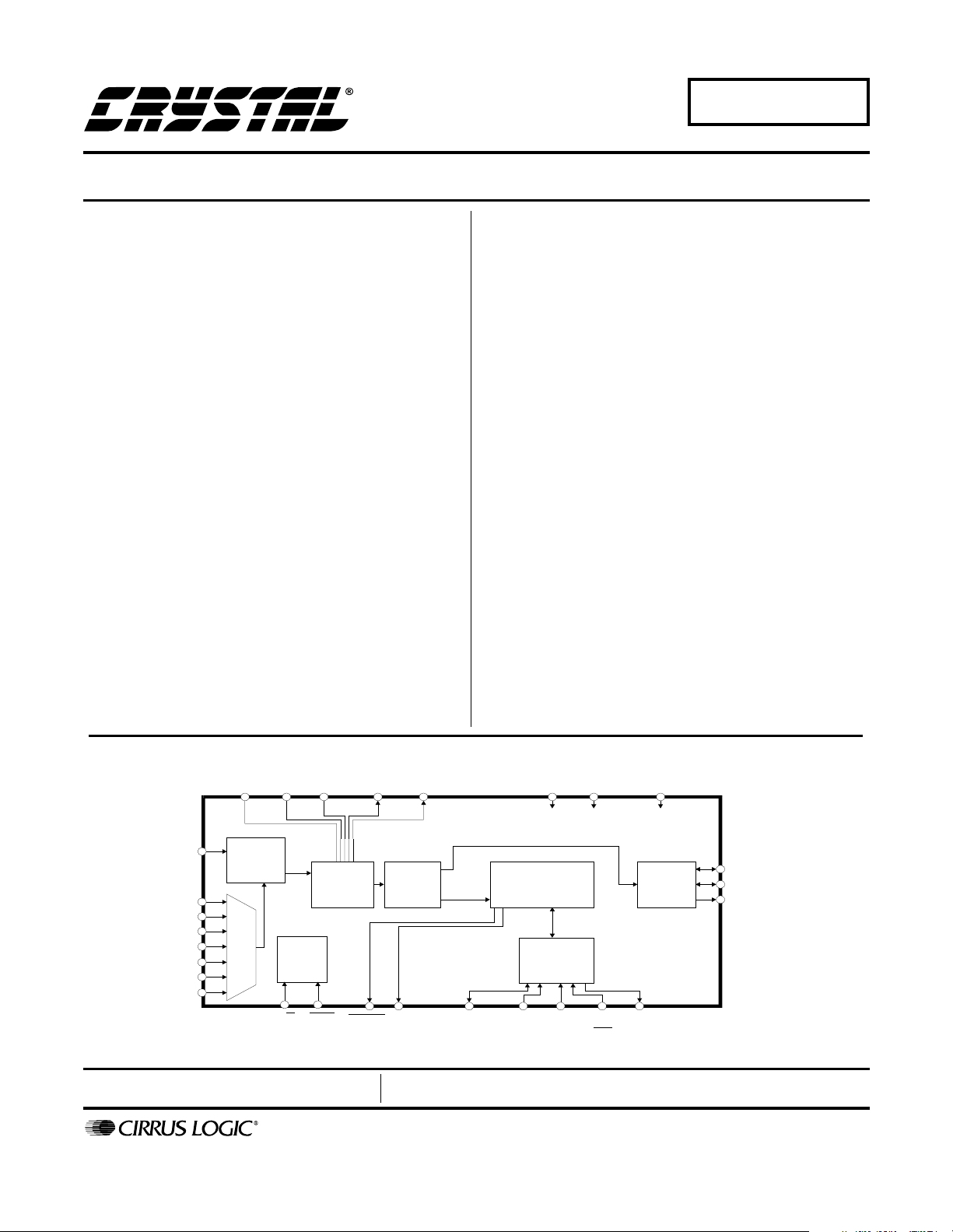
The CS8415A is a monolithic CMOS device which receives and decodes one of 7 channels of audio data
according to the IEC60958, S/PDIF, EIAJ CP1201, or
AES3. The CS8415A has a serial digital audio output
port and comprehensive control ability through a 4-wire
microcontroller port. Channel status and user data are
assembled in block sized buffers, making read access
easy.
A low jitter clock recovery mechanism yields a very
clean recovered clock from the incoming AES3 stream.
Stand-alone operation allows systems with no microcontroller to operate the CS8415A with dedicated output
pins for channel status data.
Target applications include A/V receivers, CD-R, DVD
receivers, multimedia speakers, digital mixing consoles,
effects processors, set-top boxes, and computer and
automotive audio systems.
ORDERING INFOMATION
CS8415A-CS 28-pin SOIC -10 to +70°C
CS8415A-CZ 28-pin TSSOP -10 to +70°C
CS8415A-IS 28-pin SOIC -40 to +85°C
CS8415A-IZ 28-pin TSSOP -40 to +85°C
CDB8415A Evaluation Board
VA+ AGND FILT RE RR
RXN0
RXP6
RXP5
RXP4
RXP3
RXP2
RXP1
RXP0
Receiver
7:1
MUX
Misc.
Control
H/S
Clock &
Data
Recovery
RST
EMPH U SDA/
Preliminary Product Information
P.O. Box 17847, Austin, Texas 78760
(512) 445 7222 FAX: (512) 445 7581
http://www.cirrus.com
RMCK
AES3
S/PDIF
Decoder
CDOUT
This document contains information for a new product.
Cirrus Logic reserves the right to modify this product without notice.
Copyright Cirrus Logic, Inc. 2001
VL+ DGND
C&Ubit
Data
Buffer
Control
Port &
Registers
SCL/
AD1/
CCLK
CDIN
(All Rights Reserved)
OMCK
AD0/CSINT
Serial
Audio
Output
OLRCK
OSCLK
SDOUT
MAY ‘01
DS470PP3
1

TABLE OF CONTENTS
1. CHARACTERISTICS AND SPECIFICATIONS ........................................................................ 4
POWER AND THERMAL CHARACTERISTICS....................................................................... 4
ABSOLUTE MAXIMUM RATINGS ........................................................................................... 4
DIGITAL CHARACTERISTICS ................................................................................................. 5
SWITCHING CHARACTERISTICS .......................................................................................... 5
SWITCHING CHARACTERISTICS - SERIAL AUDIO PORTS................................................. 6
SWITCHING CHARACTERISTICS - CONTROL PORT - SPI MODE ...................................... 7
SWITCHING CHARACTERISTICS - CONTROL PORT - TWO-WIRE MODE......................... 8
2. TYPICAL CONNECTION DIAGRAM ........................................................................................ 9
3. GENERAL DESCRIPTION ..................................................................................................... 10
3.1 AES3 and S/PDIF Standards Documents ........................................................................ 10
3.2 PLL Applications Note ......................................................................................................10
4. SERIAL AUDIO OUTPUT PORT ............................................................................................ 10
5. AES3 RECEIVER .................................................................................................................... 13
5.1 7:1 S/PDIF Input Multiplexer ............................................................................................ 13
5.2 PLL, Jitter Attenuation, and Varispeed ............................................................................ 13
5.2.1 OMCK System Clock Mode ................................................................................ 13
5.2.2 PLL External Components .................................................................................. 13
5.3 Error Reporting and Hold Function .................................................................................. 14
5.4 Channel Status Data Handling ......................................................................................... 15
5.5 User Data Handling .......................................................................................................... 15
5.5.1 Non-Audio Auto-Detection .................................................................................. 15
5.6 Mono Mode Operation ..................................................................................................... 16
6. CONTROL PORT DESCRIPTION AND TIMING .................................................................... 17
6.1 SPI Mode ......................................................................................................................... 17
6.2 Two-Wire Mode ................................................................................................................ 18
6.3 Interrupts .......................................................................................................................... 18
7. CONTROL PORT REGISTER SUMMARY ............................................................................. 20
7.1 Memory Address Pointer (MAP) ....................................................................................... 20
8. CONTROL PORT REGISTER BIT DEFINITIONS .................................................................. 21
8.1 Control 1(1h) ..................................................................................................................... 21
8.2 Control 2 (2h) .................................................................................................................... 21
8.3 Clock Source Control (4h)................................................................................................. 22
8.4 Serial Audio Output Port Data Format (6h)....................................................................... 22
8.5 Interrupt 1 Status (7h) (Read Only)................................................................................... 23
8.6 Interrupt 2 Status (8h) (Read Only)................................................................................... 24
8.7 Interrupt 1 Mask (9h)......................................................................................................... 24
8.8 Interrupt 1 Mode MSB (Ah) and Interrupt 1 Mode LSB(Bh) .............................................. 24
8.9 Interrupt 2 Mask (Ch) ........................................................................................................ 25
8.10 Interrupt 2 Mode MSB (Dh) and Interrupt 2 Mode LSB(Eh)............................................ 25
8.11 Receiver Channel Status (Fh) (Read Only) .................................................................... 25
8.12 Receiver Error (10h) (Read Only) ................................................................................... 27
CS8415A
Contacting Cirrus Logic Support
For a complete listing of Direct Sales, Distributor, and Sales Representative contacts, visit the Cirrus Logic web site at:
http://www.cirrus.com/corporate/contacts/
Preliminary product information describes products which are in production, but for which full characterization data is not yet available. Advance product information describes products which are in development and subject to development changes. Cirrus Logic, Inc. has made best efforts to ensure that the information
contained in this document is accurate and reliable. However, the information is subject to change without notice and is provided “AS IS” without warranty of
any kind (express or implied). No responsibility is assumed by Cirrus Logic, Inc. for the use of this information, nor for infringements of patents or other rights
of third parties. This document is the property of Cirrus Logic, Inc. and implies no license under patents, copyrights, trademarks, or trade secrets. No part of
this publication may be copied, reproduced, stored in a retrieval system, or transmitted, in any form or by any means (electronic, mechanical, photographic, or
otherwise) without the prior written consent of Cirrus Logic, Inc. Items from any Cirrus Logic website or disk may be printed for use by the user. However, no
part of the printout or electronic files may be copied, reproduced, stored in a retrieval system, or transmitted, in any form or by any means (electronic, mechanical,
photographic, or otherwise) without the prior written consent of Cirrus Logic, Inc.Furthermore, no part of this publication may be used as a basis for manufacture
or sale of any items without the prior written consent of Cirrus Logic, Inc. The names of products of Cirrus Logic, Inc. or other vendors and suppliers appearing
in this document may be trademarks or service marks of their respective owners which may be registered in some jurisdictions. A list of Cirrus Logic, Inc. trademarks and service marks can be found at http://www.cirrus.com.
2 DS470PP3

CS8415A
8.13 Receiver Error Mask (11h) ............................................................................................. 28
8.14 Channel Status Data Buffer Control (12h) ...................................................................... 28
8.15 User Data Buffer Control (13h)....................................................................................... 29
8.16 Q-Channel Subcode Bytes 0 to 9 (14h - 1Dh) (Read Only) ........................................... 29
8.17 OMCK/RMCK Ratio (1Eh) (Read Only).......................................................................... 29
8.18 C-bit or U-bit Data Buffer (1Fh - 37h) ............................................................................. 29
8.19 CS8415A I.D. and Version Register (7Fh) (Read Only) ................................................. 29
9. PIN DESCRIPTION - SOFTWARE MODE ............................................................................. 30
10. HARDWARE MODE .............................................................................................................32
10.1 Serial Audio Port Formats ............................................................................................. 32
11. PIN DESCRIPTION - HARDWARE MODE .......................................................................... 33
12. APPLICATIONS .................................................................................................................. 35
12.1 Reset, Power Down and Start-up .................................................................................. 35
12.2 ID Code and Revision Code .......................................................................................... 35
12.3 Power Supply, Grounding, and PCB layout ................................................................... 35
13. PACKAGE DIMENSIONS ................................................................................................... 36
14. APPENDIX A: EXTERNAL AES3/SPDIF/IEC60958 RECEIVER COMPONENTS ............. 38
14.1 AES3 Receiver External Components ........................................................................... 38
14.2 Isolating Transformer Requirements ............................................................................. 38
15. APPENDIX B: CHANNEL STATUS AND USER DATA BUFFER MANAGEMENT ........... 40
15.1 AES3 Channel Status (C) Bit Management ................................................................... 40
15.2 Accessing the E buffer ................................................................................................... 40
15.2.1 Reserving the first 5 bytes in the E buffer ......................................................... 40
15.2.2 Serial Copy Management System (SCMS) ....................................................... 41
15.2.3 Channel Status Data E Buffer Access .............................................................. 41
15.3 AES3 User (U) Bit Management .................................................................................... 41
LIST OF FIGURES
Figure 1. Audio Port Master Mode Timing ...................................................................................... 6
Figure 2. Audio Port Slave Mode and Data Input Timing................................................................ 6
Figure 3. SPI Mode Timing ............................................................................................................. 7
Figure 4. Two-Wire Mode timing ..................................................................................................... 8
Figure 5. Recommended Connection Diagram for Software Mode ................................................ 9
Figure 6. Serial Audio Output Example Formats........................................................................... 12
Figure 7. Jitter Attenuation Characteristics of PLL with 8-96 kHz Fs Filter Components.............. 14
Figure 8. Jitter Attenuation Characteristics of PLL with 32-96 kHz Fs Filter Components............ 14
Figure 9. AES3 Receiver Timing for C & U pin output data .......................................................... 16
Figure 10. Control Port Timing in SPI Mode ................................................................................. 17
Figure 11. Hardware Mode ........................................................................................................... 18
Figure 12. Control Port Timing in Two-Wire Mode........................................................................ 19
Figure 12. Professional Input Circuit ............................................................................................. 38
Figure 13. Transformerless Professional Input Circuit .................................................................. 38
Figure 14. Consumer Input Circuit ................................................................................................ 39
Figure 15. S/PDIF MUX Input Circuit ............................................................................................ 39
Figure 16. TTL/CMOS Input Circuit...............................................................................................39
Figure 17. Channel Status Data Buffer Structure.......................................................................... 40
Figure 18. Flowchart for Reading the E Buffer.............................................................................. 40
LIST OF TABLES
Table 1. PLL External Component Values .................................................................................... 14
Table 2. Control Register Map Summary...................................................................................... 20
Table 3. Equivalent Software Mode Bit Definitions ....................................................................... 32
Table 4. Hardware Mode Start-up Options ................................................................................... 32
DS470PP3 3
CS8415A
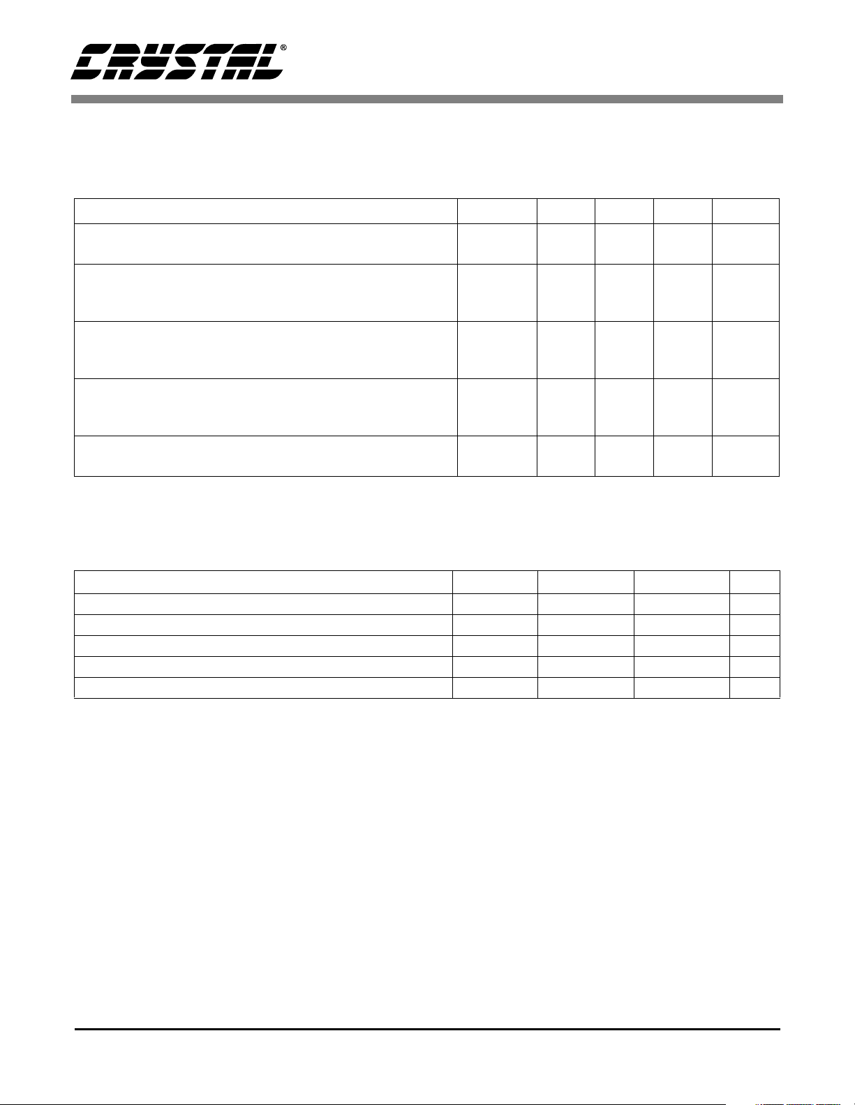
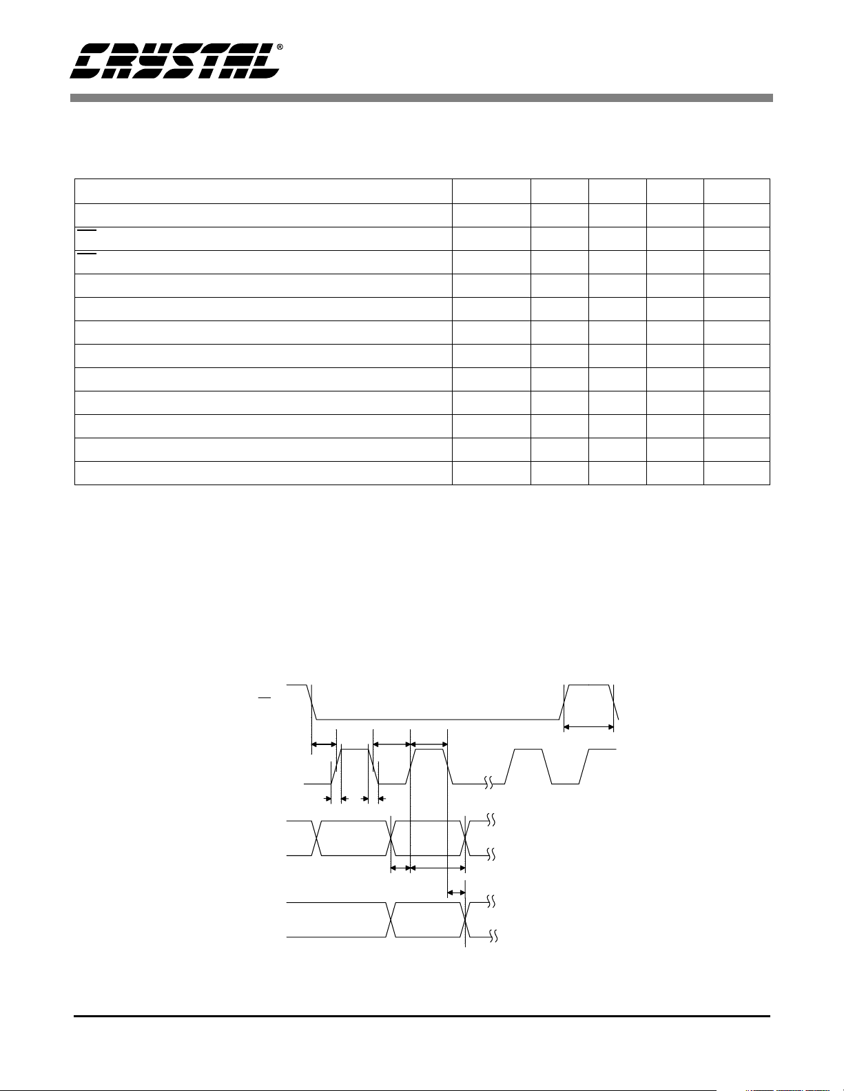
1. CHARACTERISTICS AND SPECIFICATIONS
POWER AND THERMAL CHARACTERISTICS (AGND, DGND = 0 V, all voltages with respect
to ground)
Parameter Symbol Min Typ Max Units
Power Supply Voltage VA+
VL+
Supply Current at 48 kHz frame rate VA+
VL+ = 3 V
VL+ = 5 V
Supply Current at 96 kHz frame rate VA+
VL+ = 3 V
VL+ = 5 V
Supply Current in power down Reset high, VA+
Reset high, VL+ = 3 V
Reset high, VL+ = 5 V
Ambient Operating Temperature : ‘-CS’ & ‘-CZ’ (Note 1)
‘-IS’ & ‘-IZ’ (Note 2)
Notes: 1. ‘-CS’ and ‘-CZ’ parts are specified to operate over -10° C to 70° C but are tested at 25° C only.
2. ‘-IS’ and ‘-IZ’ parts are tested over the full -40° C to 85° C temperature range.
T
A
4.5
2.85/4.5
-
-
-
-
-
-
-
-
-
-10
-40
5.0
3.0/5.0
6.3
30.1
46.5
6.6
44.8
76.6
20
60
60
25 70
5.5
3.15/5.5
-
-
-
-
-
-
-
-
-
85
V
V
mA
mA
mA
mA
mA
mA
µA
µA
µA
°C
ABSOLUTE MAXIMUM RATINGS (AGND, DGND = 0 V, all voltages with respect to ground)
Parameter Symbol Min Max Units
Power Supply Voltage VL+,VA+ - 6.0 V
Input Current, Any Pin Except Supplies (Note 3) I
Input Voltage V
Ambient Operating Temperature (power applied) T
Storage Temperature T
in
in
A
stg
-±10mA
-0.3 (VL+) + 0.3 V
-55 125 °C
-65 150 °C
Notes: 3. Transient currents of up to 100mA will not cause SCR latch-up.
4 DS470PP3
CS8415A
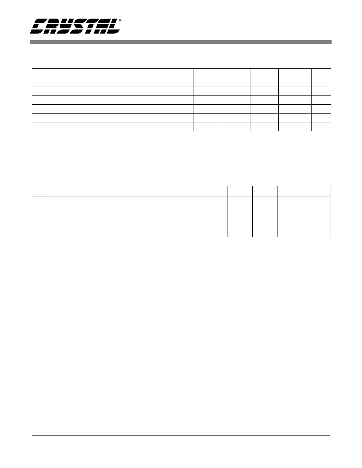
DIGITAL CHARACTERISTICS
(TA = 25 °C for suffixes ‘CS’ &’CZ’, TA = -40 to 85°C for ‘IS’ & ‘IZ’ ; VA+ = 5V±10%, VL+ = 3/5V ±5/10% )
Parameter Symbol Min Typ Max Units
High-Level Input Voltage, except RXP0, RXN0 V
Low-Level Input Voltage, except RXP0, RXN0 (Note 4) V
Low-Level Output Voltage, (Io=-20 uA) V
High-Level Output Voltage, (Io=20 uA) V
Input Leakage Current I
Differential Input Voltage, RXP0 to RXN0 V
IH
IL
OL
OH
in
TH
2.0 - (VL+) + 0.3 V
-0.3 - 0.4/ 0.8 V
--0.4V
(VL+) - 1 - - V
-±1±10µA
-200 -mV
Notes: 4. At 5V mode, V
= 0.8V (Max), at 3V mode, VIL =0.4V (Max).
IL
* Specifications are subject to change without notice.
SWITCHING CHARACTERISTICS
(TA = 25 °C for suffixes ‘CS’ &’CZ’, TA = -40 to 85°C for ‘IS’ & ‘IZ’ ; VA+ = 5V±10%, VL+ = 3/5V ±5/10% , Inputs:
Logic 0 = 0V, Logic 1 = VL+; C
RST
pin Low Pulse Width 200 - - µs
PLL Clock Recovery Sample Rate Range 8.0 - 108.0 kHz
RMCK output jitter - 200 - ps RMS
RMCK output duty cycle 40 50 60 %
= 20 pF)
L
Parameter Symbol Min Typ Max Units
DS470PP3 5
CS8415A
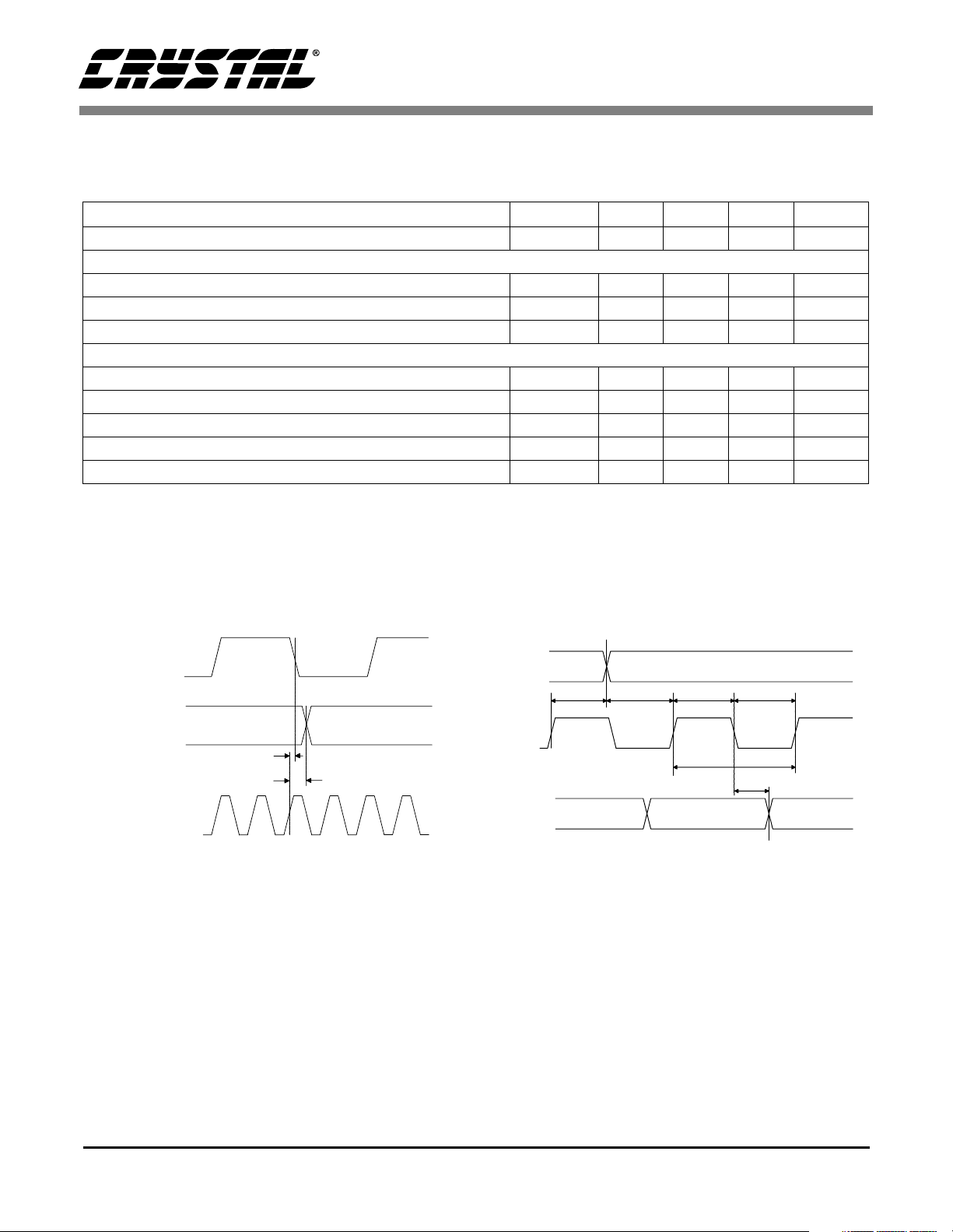
SWITCHING CHARACTERISTICS - SERIAL AUDIO PORTS
(TA = 25 °C for suffixes ‘CS’ &’CZ’, TA = -40 to 85°C for ‘IS’ & ‘IZ’ ; VA+ = 5V±10%, VL+ = 3/5V ±5/10% , Inputs:
Logic 0 = 0 V, Logic 1 = VL+; C
Parameter Symbol Min Typ Max Units
OSCLK Active Edge to SDOUT Output Valid (Note 5) t
Master Mode
RMCK to OSCLK active edge delay (Note 5) t
RMCK to OLRCK delay (Note 6) t
OSCLK and OLRCK Duty Cycle - 50 - %
Slave Mode
OSCLK Period (Note 7) t
OSCLK Input Low Width t
OSCLK Input High Width t
OSCLK Active Edge to OLRCK Edge (Note 5,6,8) t
OLRCK Edge Setup Before OSCLK Active Edge (Note 5,6,9) t
Notes: 5. The active edges of OSCLK are programmable.
6. The polarity OLRCK is programmable.
7. No more than 128 SCLK per frame.
8. This delay is to prevent the previous OSCLK edge from being interpreted as the first one after OLRCK
has changed.
9. This setup time ensures that this OSCLK edge is interpreted as the first one after OLRCK has changed.
= 20 pF)
L
dpd
smd
lmd
sckw
sckl
sckh
lrckd
lrcks
--20ns
0-10ns
0-10ns
36 - - ns
14 - - ns
14 - - ns
20 - - ns
20 - - ns
OSCLK
(output)
OLRCK
(output)
RMCK
(input)
t
smd
t
lmd
OLRCK
(input)
OSCLK
(input)
SDOUT
t
lrckd
t
lrcks
t
sckh
t
sckw
t
sckl
t
dpd
Figure 1. Audio Port Master Mode Timing Figure 2. Audio Port Slave Mode and Data Input Timing
6 DS470PP3
CS8415A
SWITCHING CHARACTERISTICS - CONTROL PORT - SPI MODE
(TA = 25 °C for suffixes ‘CS’ &’CZ’, TA = -40 to 85°C for ‘IS’ & ‘IZ’ ; VA+ = 5V±10%, VL+ = 3/5V ±5/10% , Inputs:
Logic 0 = 0 V, Logic 1 = VL+; C
Parameter Symbol Min Typ Max Units
= 20 pF)
L
CCLK Clock Frequency (Note 10) f
High Time Between Transmissions t
CS
CS
Falling to CCLK Edge t
CCLK Low Time t
CCLK High Time t
CDIN to CCLK Rising Setup Time t
CCLK Rising to DATA Hold Time (Note 11) t
CCLK Falling to CDOUT Stable t
Rise Time of CDOUT t
Fall Time of CDOUT t
Rise Time of CCLK and CDIN (Note 12) t
Fall Time of CCLK and CDIN (Note 12) t
sck
csh
css
scl
sch
dsu
dh
pd
r1
f1
r2
f2
0-6.0MHz
1.0 - - µs
20 - - ns
66 - - ns
66 - - ns
40 - - ns
15 - - ns
--50ns
--25ns
--25ns
- - 100 ns
- - 100 ns
Notes: 10. If Fs is lower than 46.875 kHz, the maximum CCLK frequency should be less than 128 Fs. This is
dictated by the timing requirements necessary to access the Channel Status and User Bit buffer
memory. Access to the control register file can be carried out at the full 6 MHz rate. The minimum
allowable input sample rate is 8 kHz, so choosing CCLK to be less than or equal to 1.024 MHz should
be safe for all possible conditions.
11. Data must be held for sufficient time to bridge the transition time of CCLK.
12. For f
<1 MHz.
sck
CS
t
t
sch
CCLK
CDIN
CDOUT
t
css
scl
t
r2
t
dsu
t
f2
t
dh
t
pd
t
csh
Figure 3. SPI Mode Timing
DS470PP3 7
CS8415A
SWITCHING CHARACTERISTICS - CONTROL PORT - Two-Wire MODE
(Note 13, TA = 25 °C for suffixes ‘CS’ &’CZ’, TA = -40 to 85°C for ‘IS’ & ‘IZ’ ; VA+ = VL+ = 5V ±10%, Inputs: Logic 0
= 0 V, Logic 1 = VL+; C
SCL Clock Frequency f
Bus Free Time Between Transmissions t
Start Condition Hold Time (prior to first clock pulse) t
Clock Low Time t
Clock High Time t
Setup Time for Repeated Start Condition t
SDA Hold Time from SCL Falling (Note 14) t
SDA Setup Time to SCL Rising t
Rise Time of Both SDA and SCL Lines t
Fall Time of Both SDA and SCL Lines t
Setup Time for Stop Condition t
Notes: 13. The Two-Wire Mode is compatible with I
14. Data must be held for sufficient time to bridge the 300 ns transition time of SCL.
= 20 pF)
L
Parameter Symbol Min Typ Max Units
scl
buf
hdst
low
high
sust
hdd
sud
r
f
susp
2C®
protocol and is supported only at 5V mode.
- - 100 kHz
4.7 - - µs
4.0 - - µs
4.7 - - µs
4.0 - - µs
4.7 - - µs
0--µs
250 - - ns
--25ns
--25ns
4.7 - - µs
SDA
SCL
Stop Start
t
buf
t
hdst
t
low
Repeated
t
high
t
hdd
t
sud
Figure 4. Two-Wire Mode timing
Start
t
sust
t
hdst
Stop
t
f
t
r
t
susp
8 DS470PP3
2. TYPICAL CONNECTION DIAGRAM
Ferrite *
+5V
Analog
Supply *
Bead
0.1 Fµ
0.1 Fµ
VA+ V L+
+3V to
Digital
Supply
CS8415A
+5V
**
AES3/
SPDIF
Sources
Clock Control RMCK
Hardware
Control
RXP6
RXP5
RXP4
RXP3
RXP2
RXP1
RXP0
RXN0
EMPH
RERR
RST
CS8415A
SDA/CDOUT
SCL/CCLK
AD1/CDIN
A2D
/
RFILT
CFILT CRIP
OLRCK
OSCLK
SDOUT
AD0/CS
INT
DGND2
H/S
DGNDFILTAGND
3-wire Serial
Audio Input
Device
Microcontroller
U
* A separate analog supply is only necessary in applications where RMCK is used
for a jitter sensitive task. For applications where RMCK is not used for a jitter
sensitive task, connect VA+ to VD+ via a ferrite bead. Keep the decoupling
capacitor between VA+ and AGND.
Please see section 5.1 "7:1 S/PDIF Input Multiplexer" and Appendix A for typical
**
input configurations and recommended input circuits.
Figure 5. Recommended Connection Diagram for Software Mode
DS470PP3 9

CS8415A
3. GENERAL DESCRIPTION
The CS8415A is a monolithic CMOS device which
receives and decodes audio data according to the
AES3, IEC60958, S/PDIF, and EIAJ CP1201 interface standards.
Input data is either differential or single-ended. A
low jitter clock is recovered from the incoming data
using a PLL. The decoded audio data is output
through a configurable, 3-wire output port. The
channel status and user data are assembled in block
sized buffers and may be accessed through an SPI
or Two-Wire microcontroller port. For systems
with no microcontroller, a stand alone mode allows
direct access to channel status and user data output
pins.
Target applications include AVR, CD-R, DAT,
DVD, multimedia speakers, MD and VTR equipment, mixing consoles, digital audio transmission
and receiving equipment, high quality D/A and
A/D converters, effects processors, set-top TV boxes, and computer audio systems.
Figure 5 shows the supply and external connections to the CS8415A, when configured for operation with a microcontroller.
3.1 AES3 and S/PDIF Standards Documents
tutorial on digital audio specifications, but it should
not be considered a substitute for the standards.
The paper An Understanding and Implementation
of the SCMS Serial Copy Management System for
Digital Audio Transmission, by Clifton Sanchez, is
an excellent tutorial on SCMS. It is available from
the AES as preprint 3518.
3.2 PLL Applications Note
See Crystal Application Note 159: PLL Filter Optimization for the CS8415A, CS8420, and CS8427
by Patrick Muyshondt and Stuart Dudley Dimond
III for a tutorial on the CS8415A Phase-LockedLoop. This document gives equations for selecting
the proper PLL filter and guidelines on laying out
the PC board for the best performance.
4. SERIAL AUDIO OUTPUT PORT
A 3-wire serial audio output port is provided. The
port can be adjusted to suit the attached device setting the control registers. The following parameters
are adjustable: master or slave, serial clock frequency, audio data resolution, left or right justification of the data relative to left/right clock, optional
one-bit cell delay of the first data bit, the polarity of
the bit clock and the polarity of the left/right clock.
By setting the appropriate control bits, many formats are possible.
This data sheet assumes that the user is familiar
with the AES3 and S/PDIF data formats. It is advisable to have current copies of the AES3 and
IEC60958 specifications on hand for easy reference.
The latest AES3 standard is available from the Audio Engineering Society or ANSI at www.aes.org
or www.ansi.org. Obtain the latest IEC60958 standard from ANSI or from the International Electrotechnical Commission at www.iec.ch. The latest
EIAJ CP-1201 standard is available from the Japanese Electronics Bureau.
Crystal Application Note 22: Overview of Digital
Audio Interface Data Structures contains a useful
10 DS470PP3
Figure 6 shows a selection of common output formats, along with the control bit settings. A special
AES3 direct output format is included, which allows the serial output port access to the V, U, and
C bits embedded in the serial audio data stream.
The P bit is replaced by a Z bit that marks the start
of each block. The received channel status block
start signal is only available in hardware mode, as
the RCBL pin.
In master mode, the left/right clock and the serial
bit clock are outputs, derived from the recovered
RMCK clock. In slave mode, the left/right clock
and the serial bit clock are inputs. The left/right
clock must be synchronous to the appropriate mas-

CS8415A
ter clock, but the serial bit clock can be asynchronous and discontinuous if required. By appropriate
phasing of the left/right clock and control of the serial clocks, multiple CS8415A’s can share one serial port. The left/right clock should be continuous,
but the duty cycle can be less than the specified typical value of 50% if enough serial clocks are
present in each phase to clock all the data bits.
When in slave mode, the serial audio output port
must not be set for right-justified data. When using
the serial audio output port in slave mode with an
OLRCK input which is asynchronous to the incoming AES3 data, then an interrupt bit(OSLIP) is provided to indicate when repeated or dropped
samples occur.
The CS8415A allows immediate mute of the serial
audio output port audio data by the MUTESAO bit
of Control Register 1.
DS470PP3 11
CS8415A
AES3
Direct
(Out)
Left
Justified
(Out)
2
I S
(Out)
Right
Justified
(Out)
OLRCK
OSCLK
SDOUT
OLRCK
OSCLK
SDOUT
OLRCK
OSCLK
SDOUT
OLRCK
OSCLK
SDOUT
LSB
Right
MSB
LSB
Right
MSB LSB
Right
MSB
UC
VZ
Left
MSB LSB MSB LSB MSB
Left Right
LSB
LSB
MSB
Left
MSB LSB
Left
MSB
UCLSB
VZ
MSB
LSB
SOMS* SOSF* SORES[1:0]* SOJUST* SODEL* SOSPOL* SOLRPOL*
Left Justified X X XX 0 0 0 0
2
I
S
XXXX0101
Right Justified 1 X XX 1 0 0 0
AES3 Direct X X 11 0 0 0 0
X = don’t care to match format, but does need to be set to the desired setting
* See Serial Output Data Format Register Bit Descriptions for an explanation of the meaning of each bit
Figure 6. Serial Audio Output Example Formats
12 DS470PP3

CS8415A
5. AES3 RECEIVER
The CS8415A includes an AES3 digital audio receiver. A comprehensive buffering scheme provides read access to the channel status and user
data. This buffering scheme is described in Appendix B.
The AES3 receiver accepts and decodes audio and
digital data according to the AES3, IEC60958
(S/PDIF), and EIAJ CP-1201 interface standards.
The receiver consists of a differential input stage,
driven through pins RXP0 and RXN0, a PLL based
clock recovery circuit, and a decoder which separates the audio data from the channel status and
user data.
External components are used to terminate and isolate the incoming data cables from the CS8415A.
These components are detailed in Appendix A.
5.1 7:1 S/PDIF Input Multiplexer
The CS8415A employs a 7:1 S/PDIF Input Multiplexer to accommodate up to seven channels of input digital audio data. Digital audio data is singleended and input through the RXP0-6 pins. When
any portion of the multiplexer is implemented, unused RXP pins should be tied to ground, and RXN0
must be ac-coupled to ground. The multiplexer select line control is accessed through bits MUX2:0
in the Control 2 register. The multiplexer defaults
to RXP0. Therefore, the default configuration is for
a differential signal to be input through RXP0 &
RXN0. Please see Appendix A for recommended
input circuits.
5.2 PLL, Jitter Attenuation, and Varispeed
An on-chip Phase Locked Loop (PLL) is used to recover the clock from the incoming data stream.
There are some applications where low jitter in the
recovered clock, presented on the RMCK pin, is
important. For this reason, the PLL has been designed to have good jitter attenuation characteristics, shown in Figures 7 and 8. In addition, the PLL
has been designed to only use the preambles of the
AES3 stream to provide lock update information to
the PLL. This results in the PLL being immune to
data dependent jitter affects because the AES3 preambles do not vary with the data.
The PLL has the ability to lock onto a wide range
of input sample rates with no external component
changes. If the sample rate of the input subsequently changes, for example in a varispeed application,
the PLL will only track up to ±12.5% from the
nominal center sample rate. The nominal center
sample rate is the sample rate that the PLL first
locks onto upon application of an AES3 data
stream or after enabling the CS8415A clocks by
setting the RUN control bit. If the 12.5% sample
rate limit is exceeded, the PLL will return to its
wide lock range mode and re-acquire a new nominal center sample rate.
5.2.1 OMCK System Clock Mode
A special clock switching mode is available that allows the clock that is input through the OMCK pin
to be output through the RMCK pin. This feature is
controlled by the SWCLK bit in register 1 of the
control registers. When the PLL loses lock, the frequency of the VCO drops to 300 kHz. The clock
switching mode allows the clock input through
OMCK to be used as a clock in the system without
any disruption when the PLL loses lock, for example, when the input is removed from the receiver.
When SWCLK is enabled and this mode is implemented, RMCK is an output and is not bi-directional. This clock switching is done glitch free. Please
note that internal circuitry associated with RMCK
is not driven by OMCK. This means that OSCLK
and OLRCK continue to be derived from the PLL
and are not usable in this mode.
5.2.2 PLL External Components
The PLL behavior is affected by the external filter
component values. Figure 5 shows the recommended configuration of the two capacitors and
DS470PP3 13

CS8415A
10
-1
10
0
10
1
10
2
10
3
10
4
10
5
-45
-40
-35
-30
-25
-20
-15
-10
-5
0
5
Magnitude response (dB)
Frequency (Hz)
Digital Bode plot
one resistor required. There are two sets of component values recommended, depending on the sample rate of the application, see Table 1. The default
set, called “fast”, accommodates input sample rates
of 32 kHz to 96 Hz with no component changes. It
has the highest corner frequency jitter attenuation
curve, and takes the shortest time to lock. The alternate component set, called “medium” allows the
lowest input sample rate to be 8 kHz, and increases
the lock time of the PLL. Lock times are worst case
for an Fsi transition of 96 kHz.
5.3 Error Reporting and Hold Function
While decoding the incoming AES3 data stream,
the CS8415A can identify several kinds of error,
indicated in the Receiver Error register. The UNLOCK bit indicates whether the PLL is locked to
the incoming AES3 data. The V bit reflects the cur-
rent validity bit status. The CONF (confidence) bit
indicates the amplitude of the eye pattern opening,
indicating a link that is close to generating errors.
The BIP (bi-phase) error bit indicates an error in incoming bi-phase coding. The PAR (parity) bit indicates a received parity error.
The error bits are "sticky": they are set on the first
occurrence of the associated error and will remain
set until the user reads the register through the control port. This enables the register to log all unmasked errors that occurred since the last time the
register was read.
The Receiver Error Mask register allows masking
of individual errors. The bits in this register serve
as masks for the corresponding bits of the Receiver
Error Register. If a mask bit is set to 1, the error is
unmasked, which implies the following: its occur-
Fs Range (kHz) RFILT (kΩ)CFILT (µF) CRIP (nF) PLL Lock Time
8 to 96 0.909 1.8 33 56
32 to 96 3.0 0.047 2.2 35
Table 1. PLL External Component Values
Figure 7. Jitter Attenuation Characteristics of PLL
with 8-96 kHz Fs Filter Components
1
10
Digital Bode plot
2
10
Frequency (Hz)
3
10
4
10
5
0
-5
-10
-15
-20
-25
Magnitude response (dB)
-30
-35
-40
-45
-1
10
10
0
Figure 8. Jitter Attenuation Characteristics of PLL
with 32-96 kHz Fs Filter Components
5
10
14 DS470PP3

CS8415A
rence will be reported in the receiver error register,
induce a pulse on RERR, invoke the occurrence of
a RERR interrupt, and affect the current audio sample according to the status of the HOLD bits. The
HOLD bits allow a choice of holding the previous
sample, replacing the current sample with zero
(mute), or not changing the current audio sample. If
a mask bit is set to 0, the error is masked, which implies the following: its occurrence will not be reported in the receiver error register, will not induce
a pulse on RERR or generate a RERR interrupt, and
will not affect the current audio sample. The QCRC
and CCRC errors do not affect the current audio
sample, even if unmasked.
5.4 Channel Status Data Handling
The first 2 bytes of the Channel Status block are decoded into the Receiver Channel Status register.
The setting of the CHS bit in the Channel Status
Data Buffer Control register determines whether
the channel status decodes are from the A channel
(CHS = 0) or B channel (CHS = 1).
The PRO (professional) bit is extracted directly.
For consumer data, the COPY (copyright) bit is extracted, and the category code and L bits are decoded to determine SCMS status, indicated by the
ORIG (original) bit. If the category code is set to
General on the incoming AES3 stream, copyright
will always be indicated even when the stream indicates no copyright. Finally, the AUDIO bit is extracted and used to set an AUDIO indicator, as
described in the Non-Audio Auto-Detection section below.
If 50/15 µs pre-emphasis is detected, the state of
the EMPH pin is adjusted accordingly.
The encoded channel status bits which indicate
sample word length are decoded according to
AES3-1992 or IEC 60958. Audio data routed to the
serial audio output port is unaffected by the word
length settings; all 24 bits are passed on as received.
Appendix A describes the overall handling of
Channel Status and User data.
5.5 User Data Handling
The incoming user data is buffered in a user accessible buffer. Received User data may also be output
to the U pin under the control of a control register
bit. Depending on the clocking options selected,
there may not be a clock available to qualify the U
data output. Figure 9 illustrates the timing. If the
incoming user data bits have been encoded as Qchannel subcode, the data is decoded and presented
in 10 consecutive register locations. An interrupt
may be enabled to indicate the decoding of a new
Q-channel block, which may be read through the
control port.
5.5.1 Non-Audio Auto-Detection
An AES3 data stream may be used to convey nonaudio data, thus it is important to know whether the
incoming AES3 data stream is digital audio or not.
This information is typically conveyed in channel
status bit 1 (AUDIO), which is extracted automatically by the CS8415A. However, certain non-audio
sources, such as AC-3 or MPEG encoders, may
not adhere to this convention, and the bit may not
be properly set. The CS8415A AES3 receiver can
detect such non-audio data. This is accomplished
by looking for a 96-bit sync code, consisting of
0x0000, 0x0000, 0x0000, 0x0000, 0xF872, and
0x4E1F. When the sync code is detected, an internal AUTODETECT signal will be asserted. If no
additional sync codes are detected within the next
4096 frames, AUTODETECT will be de-asserted
until another sync code is detected. The AUDIO bit
in the Receiver Channel Status register is the logical OR of AUTODETECT and the received channel status bit 1. If non-audio data is detected, the
data is still processed exactly as if it were normal
audio. It is up to the user to mute the outputs as required.
DS470PP3 15

CS8415A
5.6 Mono Mode Operation
An AES3 stream may be used in more than one
way to transmit 96 kHz sample rate data. One
method is to double the frame rate of the current
format. This results in a stereo signal with a sample
rate of 96 kHz, carried over a single twisted pair cable. An alternate method is implemented using the
2 sub-frames in a 48 kHz frame rate AES3 signal to
carry consecutive samples of a mono signal, resulting in a 96 kHz sample rate stream. This allows
older equipment, whose AES3 transmitters and receivers are not rated for 96 kHz frame rate operation, to handle 96 kHz sample rate information. In
this “mono mode”, 2 AES3 cables are needed for
stereo data transfer. The CS8415A offers mono
mode operation, controlled through the MMR control register bit.
The receiver mono mode effectively doubles Fs
compared to the input frame rate. The clock output
on the RMCK pin tracks Fs, and so is doubled in
frequency compared to stereo mode. The receiver
will run at a frame rate of Fs/2, and the serial audio
output port will run at Fs. Sub-frame A data will be
routed to both the left and right data fields on SDOUT. Similarly, sub-frame B data will be routed to
both the left and right data fields of the next word
clock cycle of SDOUT.
Using mono mode is only necessary if the serial audio output port must run at 96 kHz. If the CS8415A
is kept in normal stereo mode, and receives AES3
data arranged in mono mode, then the serial audio
output port will run at 48 kHz, with left and right
data fields representing consecutive audio samples.
RCBL
out
VLRCK
C, U
Output
RCBL and C output are only available in hardware mode.
RCBL goes high 2 frames after receipt of a Z pre-amble, and is high for 16 frames.
VLRCK is a virtual word clock, which may not exist, but is used to illustrate the CU timing.
VLRCK duty cycle is 50%. VLRCK frequency is always equal to the incoming frame rate.
If the serial audio output port is in master mode, VLRCK = OLRCK.
If the serial audio output port is in slave mode, then VLRCK needs to be externally created, if required.
C, U transitions are aligned within 1% of VLRCK period to VLRCK edges
Figure 9. AES3 Receiver Timing for C & U pin output data
±
16 DS470PP3

CS8415A
6. CONTROL PORT DESCRIPTION
AND TIMING
The control port is used to access the registers, allowing the CS8415A to be configured for the desired operational modes and formats. In addition,
Channel Status and User data may be read through
the control port. The operation of the control port
may be completely asynchronous with respect to
the audio sample rates. However, to avoid potential
interference problems, the control port pins should
remain static if no operation is required.
The control port has 2 modes: SPI and Two-Wire,
with the CS8415A acting as a slave device. SPI
mode is selected if there is a high to low transition
on the AD0/CS
pin, after the RST pin has been
brought high. Two-Wire mode is selected by connecting the AD0/CS pin to VL+ or DGND, thereby
permanently selecting the desired AD0 bit address
state.
6.1 SPI Mode
In SPI mode, CS is the CS8415A chip select signal,
CCLK is the control port bit clock (input into the
CS8415A from the microcontroller), CDIN is the
input data line from the microcontroller, CDOUT is
the output data line to the microcontroller. Data is
clocked in on the rising edge of CCLK and out on
the falling edge.
Figure 10 shows the operation of the control port in
SPI mode. To write to a register, bring CS low. The
first seven bits on CDIN form the chip address and
must be 0010000. The eighth bit is a read/write indicator (R/W), which should be low to write. The
next eight bits form the Memory Address Pointer
(MAP), which is set to the address of the register
that is to be updated. The next eight bits are the data
which will be placed into the register designated by
the MAP. During writes, the CDOUT output stays
in the Hi-Z state. It may be externally pulled high
or low with a 47 KΩ resistor, if desired.
There is a MAP auto increment capability, enabled
by the INCR bit in the MAP register. If INCR is a
zero, the MAP will stay constant for successive
read or writes. If INCR is set to a 1, the MAP will
autoincrement after each byte is read or written, allowing block reads or writes of successive registers.
To read a register, the MAP has to be set to the correct address by executing a partial write cycle
which finishes (CS
high) immediately after the
MAP byte. The MAP auto increment bit (INCR)
may be set or not, as desired. To begin a read, bring
CS
CCLK
CHIP
ADDRESS
CDIN
CDOUT
DS470PP3 17
0010000
MAP = Memory Address Pointer, 8 bits, MSB first
R/W
High Impedance
MAP
Figure 10. Control Port Timing in SPI Mode
MSB
byte 1
DATA
LSB
byte n
CHIP
ADDRESS
0010000
R/W
MSB
LSB
MSB
LSB

CS8415A
CS low, send out the chip address and set the
read/write bit (R/W) high. The next falling edge of
CCLK will clock out the MSB of the addressed
register (CDOUT will leave the high impedance
state). If the MAP auto increment bit is set to 1, the
data for successive registers will appear consecutively.
6.2 Two-Wire Mode
In Two-Wire mode, SDA is a bidirectional data
line. Data is clocked into and out of the part by the
clock, SCL, with the clock to data relationship as
shown in Figure 11. There is no CS pin. Each individual CS8415A is given a unique address. Pins
AD0 and AD1 form the two least significant bits of
the chip address and should be connected to VL+ or
DGND as desired. The EMPH pin is used to set the
AD2 bit by connecting a resistor from the EMPH
pin to VL+ or to DGND. The state of the pin is
sensed while the CS8415A is being reset. The upper 4 bits of the 7-bit address field are fixed at
0010. To communicate with a CS8415A, the chip
address field, which is the first byte sent to the
CS8415A, should match 0010 followed by the settings of the EMPH, AD1, and AD0. The eighth bit
of the address is the R/W bit. If the operation is a
write, the next byte is the Memory Address Pointer
(MAP) which selects the register to be read or written. If the operation is a read, the contents of the
register pointed to by the MAP will be output. Setting the auto increment bit in MAP allows successive reads or writes of consecutive registers. Each
byte is separated by an acknowledge bit. The ACK
bit is output from the CS8415A after each input
byte is read, and is input to the CS8415A from the
microcontroller after each transmitted byte.The
Two-Wire mode is compatible with the I2C Protocol.
6.3 Interrupts
The CS8415A has a comprehensive interrupt capability. The INT output pin is intended to drive the
interrupt input pin on the host microcontroller. The
INT pin may be set to be active low, active high or
active low with no active pull-up transistor. This
last mode is used for active low, wired-OR hookups, with multiple peripherals connected to the microcontroller interrupt input pin.
Many conditions can cause an interrupt, as listed in
the interrupt status register descriptions. Each
source may be masked off through mask register
bits. In addition, each source may be set to rising
edge, falling edge, or level sensitive. Combined
with the option of level sensitive or edge sensitive
modes within the microcontroller, many different
configurations are possible, depending on the
needs of the equipment designer.
VL+
H/S
RXP
RXN
18 DS470PP3
AES3 Rx
&
Decoder
C&UbitDataBuffer
RMCK RERR
Power supply pins (VD+, VA+, DGND , AGND) & the reset pin (RST) and the PLL filter pin (FILT)
are omitted from this diagram. Please refer to the Typical Connection Diagram for hook-up details.
NVERR
CHS
COPY ORIG EMPH RCBLPRO AUDIO
Figure 11. Hardware Mode
Serial
Audio
Output
OLRCK
OSCLK
SDOUT
C
U

CS8415A
SDA
SCL
Start
0010
Note 1
AD2-0
R/W
ACK
DATA7-0
Note 2
ACK
DATA7-0
Figure 12. Control Port Timing in Two-Wire Mode
Notes: 1. AD 2 is derived from a resistor attached to the EMPH pin.
AD 1 and AD 0 are determined by the state of the corresponding pins.
2. If operation is a write, this byte contains the Memory Address Pointer, MAP.
3. If operation is a read, the last bit of the read should be NACK (high).
Note 3
ACK
Stop
DS470PP3 19

CS8415A
7. CONTROL PORT REGISTER SUMMARY
Addr(Hex) Function 7 6 5 4 3 2 1 0
1 Control 1 SWCLK 0 MUTESAO 0 0 INT1 INT0 0
2 Control 2 0 HOLD1 HOLD0 RMCKF MMR MUX2 MUX1 MUX0
4 Clock Source Control 0 RUN 0 0 0 0 0 1
6 Serial Output Format SOMS SOSF SORES1 SORES0 SOJUST SODEL SOSPOL SOLRPOL
7 Interrupt 1 Status 0 OSLIP 0 0 0 DETC 0 RERR
8 Interrupt 2 Status 0 0 0 0 DETU 0 QCH 0
9 Interrupt 1 Mask 0 OSLIPM 0 0 0 DETCM 0 RERRM
A Interrupt 1 Mode (MSB) 0 OSLIP1 0 0 0 DETC1 0 RERR1
B Interrupt 1 Mode (LSB) 0 OSLIP0 0 0 0 DETC0 0 RERR0
C Interrupt 2 Mask 0 0 0 0 DETUM 0 QCHM 0
D Interrupt 2 Mode (MSB) 0 0 0 0 DETU1 0 QCH1 0
E Interrupt 2 Mode (LSB) 0 0 0 0 DETU0 0 QCH0 0
F Receiver CS Data AUX3 AUX2 AUX1 AUX0 PRO AUDIO
10 Receiver Errors 0 QCRC CCRC UNLOCK V CONF BIP PAR
11 Receiver Error Mask 0 QCRCM CCRCM UNLOCKM VM CONFM BIPM PARM
12 CS Data Buffer Control 0 0 BSEL CBMR DETCI 0 CAM CHS
13 U Data Buffer Control 0 0 0 0 0 0 DETUI 0
14-1D Q sub-code Data
1E OMCK/RMCK Ratio ORR7 ORR6 ORR5 ORR4 ORR3 ORR2 ORR1 ORR0
1F-37 C or U Data Buffer
7F ID and Version ID3 ID2 ID1 ID0 VER3 VER2 VER1 VER0
COPY ORIG
Table 2. Control Register Map Summary
7.1 Memory Address Pointer (MAP)
7 6 543210
INCR MAP6 MAP5 MAP4 MAP3 MAP2 MAP1 MAP0
INCR - Auto Increment Address Control Bit
Default = ‘0’
0 - Disabled
1 - Enabled
MAP6:MAP0 - Register address
Note: Reserved registers must not be written to during normal operation. Some reserved registers are used for
test modes, which can completely alter the normal operation of the CS8415A.
20 DS470PP3

CS8415A
8. CONTROL PORT REGISTER BIT DEFINITIONS
8.1 Control 1(1h)
7 6 543210
SWCLK 0 MUTESAO 0 0 INT1 INT0 0
SWCLK - Controls output of OMCK on RMCK when PLL loses lock
Default = ‘0’
0 - RMCK default function
1 - OMCK output on RMCK pin
MUTESAO - Mute control for the serial audio output port
Default = ‘0’
0 - Disabled
1 - Enabled
INT1:INT0 - Interrupt output pin (INT) control
Default = ‘00’
00 - Active high; high output indicates interrupt condition has occurred
01 - Active low, low output indicates an interrupt condition has occurred
10 - Open drain, active low. Requires an external pull-up resistor on the INT pin.
11 - Reserved
8.2 Control 2 (2h)
7 6 543210
0 HOLD1 HOLD0 RMCKF MMR MUX2 MUX1 MUX0
HOLD1:HOLD0 - Determine how received audio sample is affected when a receiver error occurs
Default = ‘00’
00 - Hold the last valid audio sample
01 - Replace the current audio sample with 00 (mute)
10 - Do not change the received audio sample
11 - Reserved
RMCKF - Select recovered master clock output pin frequency.
Default = ‘0’
0 - RMCK is equal to 256 * Fs
1 - RMCK is equal to 128 * Fs
MMR - Select AES3 receiver mono or stereo operation
Default = ‘0’
0 - Normal stereo operation
1 - A and B subframes treated as consecutive samples of one channel of data.
Data is duplicated to both left and right parallel outputs of the AES receiver block.
The sample rate (Fs) is doubled compared to MMR=0
DS470PP3 21

CS8415A
MUX2:0 - 7:1 S/PDIF Input Multiplexer Select Line Control
Default = ‘000’
000 - RXP0
001 - RXP1
010 - RXP2
011 - RXP3
100 - RXP4
101 - RXP5
110 - RXP6
111 - Reserved
8.3 Clock Source Control (4h)
7 6 543210
0 RUN 0 0 0 0 0 1
This register configures the clock sources of various blocks. In conjunction with the Data Flow Control register, various Receiver/Transmitter/Transceiver modes may be selected.
RUN - Controls the internal clocks, allowing the CS8415A to be placed in a “powered down”, low
current consumption, state.
Default = ‘0’
0 - Internal clocks are stopped. Internal state machines are reset. The fully static control port is
operational, allowing registers to be read or changed. Reading and writing the U and C data
buffers is not possible. Power consumption is low.
1 - Normal part operation. This bit must be written to the 1 state to allow the CS8415A to begin
operation. All input clocks should be stable in frequency and phase when RUN is set to 1.
8.4 Serial Audio Output Port Data Format (6h)
7 6 543210
SOMS SOSF SORES1 SORES0 SOJUST SODEL SOSPOL SOLRPOL
SOMS - Master/Slave Mode Selector
Default = ‘0’
0 - Serial audio output port is in slave mode
1 - Serial audio output port is in master mode
SOSF - OSCLK frequency (for master mode)
Default = ‘0’
0 - 64*Fs
1 - 128*Fs
SORES1:0 - Resolution of the output data on SDOUT
Default = ‘00’
00 - 24-bit resolution
01 - 20-bit resolution
10 - 16-bit resolution
11 - Direct copy of the received NRZ data from the AES3 receiver (including C, U, and V bits,
22 DS470PP3

the time slot normally occupied by the P bit is used to indicate the location of the block start,
SDOUT pin only, serial audio output port clock must be derived from the AES3 receiver recovered clock)
SOJUST - Justification of SDOUT data relative to OLRCK
Default = ‘0’
0 - Left-justified
1 - Right-justified (master mode only)
SODEL - Delay of SDOUT data relative to OLRCK, for left-justified data formats
Default = ‘0’
0 - MSB of SDOUT data occurs in the first OSCLK period after the OLRCK edge
1 - MSB of SDOUT data occurs in the second OSCLK period after the OLRCK edge
SOSPOL - OSCLK clock polarity
Default = ‘0’
0 - SDOUT sampled on rising edges of OSCLK
1 - SDOUT sampled on falling edges of OSCLK
CS8415A
SOLRPOL - OLRCK clock polarity
Default = ‘0’
0 - SDOUT data is for the left channel when OLRCK is high
1 - SDOUT data is for the right channel when OLRCK is high
8.5 Interrupt 1 Status (7h) (Read Only)
7 6 543210
0 OSLIP 0 0 0 DETC 0 RERR
For all bits in this register, a “1” means the associated interrupt condition has occurred at least once since the register
was last read. A ”0” means the associated interrupt condition has NOT occurred since the last reading of the register.
Reading the register resets all bits to 0, unless the interrupt mode is set to level and the interrupt source is still true.
Status bits that are masked off in the associated mask register will always be “0” in this register. This register defaults
to 00h.
OSLIP - Serial audio output port data slip interrupt
When the serial audio output port is in slave mode, and OLRCK is asynchronous to the port
data source, This bit will go high every time a data sample is dropped or repeated.
DETC - D to E C-buffer transfer interrupt.
The source for this bit is true during the D to E buffer transfer in the C bit buffer management
process.
RERR - A receiver error has occurred.
The Receiver Error register may be read to determine the nature of the error which caused the
interrupt.
DS470PP3 23

CS8415A
8.6 Interrupt 2 Status (8h) (Read Only)
7 6 543210
0 0 0 0 DETU 0 QCH 0
For all bits in this register, a “1” means the associated interrupt condition has occurred at least once since the register
was last read. A ”0” means the associated interrupt condition has NOT occurred since the last reading of the register.
Reading the register resets all bits to 0, unless the interrupt mode is set to level and the interrupt source is still true.
Status bits that are masked off in the associated mask register will always be “0” in this register. This register defaults
to 00h.
DETU - D to E U-buffer transfer interrupt. (Block Mode only)
The source of this bit is true during the D to E buffer transfer in the U bit buffer management
process.
QCH - A new block of Q-subcode data is available for reading.
The data must be completely read within 588 AES3 frames after the interrupt occurs to avoid
corruption of the data by the next block.
8.7 Interrupt 1 Mask (9h)
7 6 543210
0 OSLIPM 0 0 0 DETCM 0 RERRM
The bits of this register serve as a mask for the Interrupt 1 register. If a mask bit is set to 1, the error is unmasked,
meaning that its occurrence will affect the INT pin and the status register. If a mask bit is set to 0, the error is masked,
meaning that its occurrence will not affect the INT pin or the status register. The bit positions align with the corresponding bits in Interrupt 1 register. This register defaults to 00h.
8.8 Interrupt 1 Mode MSB (Ah) and Interrupt 1 Mode LSB(Bh)
7 6 543210
0 OSLIP1 0 0 0 DETC1 0 RERR1
0 OSLIP0 0 0 0 DETC0 0 RERR0
The two Interrupt Mode registers form a 2-bit code for each Interrupt Register 1 function. There are three ways to
set the INT pin active in accordance with the interrupt condition. In the Rising edge active mode, the INT pin becomes active on the arrival of the interrupt condition. In the Falling edge active mode, the INT pin becomes active
on the removal of the interrupt condition. In Level active mode, the INT interrupt pin becomes active during the interrupt condition. Be aware that the active level(Actice High or Low) only depends on the INT[1:0] bits. These registers default to 00.
00 - Rising edge active
01 - Falling edge active
10 - Level active
11 - Reserved
24 DS470PP3

CS8415A
8.9 Interrupt 2 Mask (Ch)
7 6 543210
0 0 0 0 DETUM 0 QCHM 0
The bits of this register serve as a mask for the Interrupt 2 register. If a mask bit is set to 1, the error is unmasked,
meaning that its occurrence will affect the INT pin and the status register. If a mask bit is set to 0, the error is masked,
meaning that its occurrence will not affect the INT pin or the status register. The bit positions align with the corresponding bits in Interrupt 2 register. This register defaults to 00h.
8.10 Interrupt 2 Mode MSB (Dh) and Interrupt 2 Mode LSB(Eh)
7 6 543210
0 0 0 0 DETU1 0 QCH1 0
0 0 0 0 DETU0 0 QCH0 0
The two Interrupt Mode registers form a 2-bit code for each Interrupt Register 1 function. There are three ways to
set the INT pin active in accordance with the interrupt condition. In the Rising edge active mode, the INT pin becomes active on the arrival of the interrupt condition. In the Falling edge active mode, the INT pin becomes active
on the removal of the interrupt condition. In Level active mode, the INT interrupt pin becomes active during the interrupt condition. Be aware that the active level(Actice High or Low) only depends on the INT[1:0] bits. These registers default to 00.
00 - Rising edge active
01 - Falling edge active
10 - Level active
11 - Reserved
8.11 Receiver Channel Status (Fh) (Read Only)
7 6 543210
AUX3 AUX2 AUX1 AUX0 PRO AUDIO COPY ORIG
The bits in this register can be associated with either channel A or B of the received data. The desired channel is
selected with the CHS bit of the Channel Status Data Buffer Control Register.
AUX3:0 - Incoming auxiliary data field width, as indicated by the incoming channel status bits, decoded according to IEC60958 and AES3.
0000 - Auxiliary data is not present
0001 - Auxiliary data is 1 bit long
0010 - Auxiliary data is 2 bits long
0011 - Auxiliary data is 3 bits long
0100 - Auxiliary data is 4 bits long
0101 - Auxiliary data is 5 bits long
0110 - Auxiliary data is 6 bits long
0111 - Auxiliary data is 7 bits long
1000 - Auxiliary data is 8 bits long
1001 - 1111 Reserved
PRO - Channel status block format indicator
0 - Received channel status block is in consumer format
1 - Received channel status block is in professional format
DS470PP3 25

AUDIO - Audio indicator
0 - Received data is linearly coded PCM audio
1 - Received data is not linearly coded PCM audio
COPY - SCMS copyright indicator
0 - Copyright asserted
1 - Copyright not asserted
CS8415A
26 DS470PP3

CS8415A
If the category code is set to General in the incoming AES3 stream, copyright will always be indicated by COPY,
even when the stream indicates no copyright.
ORIG - SCMS generation indicator, decoded from the category code and the L bit.
0 - Received data is 1st generation or higher
1 - Received data is original
Note: COPY and ORIG will both be set to 1 if the incoming data is flagged as professional, or if the receiver is not
in use.
8.12 Receiver Error (10h) (Read Only)
7 6 543210
0 QCRC CCRC UNLOCK V CONF BIP PAR
This register contains the AES3 receiver and PLL status bits. Unmasked bits will go high on occurrence of the error,
and will stay high until the register is read. Reading the register resets all bits to 0, unless the error source is still
true. Bits that are masked off in the receiver error mask register will always be 0 in this register. This register defaults
to 00h.
QCRC - Q-subcode data CRC error indicator. Updated on Q-subcode block boundaries
0 - No error
1 - Error
CCRC - Channel Status Block Cyclic Redundancy Check bit. Updated on CS block boundaries,
valid in Pro mode
0 - No error
1 - Error
UNLOCK - PLL lock status bit. Updated on CS block boundaries.
0 - PLL locked
1 - PLL out of lock
V - Received AES3 Validity bit status. Updated on sub-frame boundaries.
0 - Data is valid and is normally linear coded PCM audio
1 - Data is invalid, or may be valid compressed audio
CONF - Confidence bit. Updated on sub-frame boundaries.
0 - No error
1 - Confidence error. This indicates that the received data eye opening is less than half a bit
period, indicating a poor link that is not meeting specifications.
BIP - Bi-phase error bit. Updated on sub-frame boundaries.
0 - No error
1 - Bi-phase error. This indicates an error in the received bi-phase coding.
PAR - Parity bit. Updated on sub-frame boundaries.
0 - No error
1 - Parity error
DS470PP3 27

CS8415A
8.13 Receiver Error Mask (11h)
7 6 543210
0 QCRCM CCRCM UNLOCKM VM CONFM BIPM PARM
The bits in this register serve as masks for the corresponding bits of the Receiver Error Register. If a mask bit is set
to 1, the error is unmasked, meaning that its occurrence will appear in the receiver error register, will affect the RERR
pin, will affect the RERR interrupt, and will affect the current audio sample according to the status of the HOLD bit.
If a mask bit is set to 0, the error is masked, meaning that its occurrence will not appear in the receiver error register,
will not affect the RERR pin, will not affect the RERR interrupt, and will not affect the current audio sample. The
CCRC and QCRC bits behave differently from the other bits: they do not affect the current audio sample even when
unmasked. This register defaults to 00h.
8.14 Channel Status Data Buffer Control (12h)
7 6 543210
0 0 BSEL CBMR DETCI 0 CAM CHS
BSEL - Selects the data buffer register addresses to contain User data or Channel Status data
Default = ‘0’
0 - Data buffer address space contains Channel Status data
1 - Data buffer address space contains User data
CBMR - Control for the first 5 bytes of channel status “E” buffer
Default = ‘0’
0 - Allow D to E buffer transfers to overwrite the first 5 bytes of channel status data
1 - Prevent D to E buffer transfers from overwriting first 5 bytes of channel status data
DETCI - D to E C-data buffer transfer inhibit bit.
Default = ‘0’
0 - Allow C-data D to E buffer transfers
1 - Inhibit C-data D to E buffer transfers
CAM - C-data buffer control port access mode bit
Default = ‘0’
0 - One byte mode
1 - Two byte mode
CHS - Channel select bit
Default = ‘0’
0 - Channel A information is displayed at the EMPH
ister. Channel A information is output during control port reads when CAM is set to 0 (One
Byte Mode)
1 - Channel B information is displayed at the EMPH
ister. Channel B information is output during control port reads when CAM is set to 0 (One
Byte Mode)
pin and in the receiver channel status reg-
pin and in the receiver channel status reg-
28 DS470PP3

CS8415A
8.15 User Data Buffer Control (13h)
7 6 543210
000000DETUI0
DETUI - D to E U-data buffer transfer inhibit bit (valid in block mode only).
Default = ‘0’
0 - Allow U-data D to E buffer transfers
1 - Inhibit U-data D to E buffer transfers
8.16 Q-Channel Subcode Bytes 0 to 9 (14h - 1Dh) (Read Only)
The following 10 registers contain the decoded Q-channel subcode data
7 6 543210
ADDRESS ADDRESS ADDRESS ADDRESS CONTROL CONTROL CONTROL CONTROL
TRACK TRACK TRACK TRACK TRACK TRACK TRACK TRACK
INDEX INDEX INDEX INDEX INDEX INDEX INDEX INDEX
MINUTE MINUTE MINUTE MINUTE MINUTE MINUTE MINUTE MINUTE
SECOND SECOND SECOND SECOND SECOND SECOND SECOND SECOND
FRAME FRAME FRAME FRAME FRAME FRAME FRAME FRAME
ZERO ZERO ZERO ZERO ZERO ZERO ZERO ZERO
ABS MINUTE ABS MINUTE ABS MINUTE ABS MINUTE ABS MINUTE ABS MINUTE ABS MINUTE ABS MINUTE
ABS SECOND ABS SECOND ABS SECOND ABS SECOND ABS SECOND ABS SECOND ABS SECOND ABS SECOND
ABS FRAME ABS FRAME ABS FRAME ABS FRAME ABS FRAME ABS FRAME ABS FRAME ABS FRAME
8.17 OMCK/RMCK Ratio (1Eh) (Read Only)
7 6 543210
ORR7 ORR6 ORR5 ORR4 ORR3 ORR2 ORR1 ORR0
This register allows the calculation of the incoming sample rate by the host microcontroller from the equation
SRR=Fso/Fsi. The Fso is determined by OMCK. This value is represented as an integer and a fractional part. The
value is meaningful only after the both the PLL has reached lock. F
or example, if the OMCK is 12.288MHz, Fso
would be 48KHz(48KHz=12.288MHz/256). Then if the in put sample rate is also 48KHz, you would get
1.0 from the SRR register.(The value from the SRR register is hexadecimal, so the actual value you will
get is 40h)
.
ORR7:6 - Integer part of the ratio (Integer value=Integer(SRR[7:6]))
ORR5:0 - Fractional part of the ratio (Fraction value=Integer(SRR[5:0])/64)
8.18 C-bit or U-bit Data Buffer (1Fh - 37h)
Either channel status data buffer E or user data buffer E is accessible through these register addresses.
8.19 CS8415A I.D. and Version Register (7Fh) (Read Only)
7 6 543210
ID3 ID2 ID1 ID0 VER3 VER2 VER1 VER0
ID3:0 - ID code for the CS8415A. Permanently set to 0100
VER3:0 - CS8415A revision level. Revision A is coded as 0001
DS470PP3 29

9. PIN DESCRIPTION - SOFTWARE MODE
CS8415A
SDA/CDOUT
AD0/CS
EMPH
RXP0
RXN0
VA+
AGND
FILT
RST
RMCK
RERR
RXP1
RXP2
RXP3 RXP4
* Pins which remain the same function in all modes.
+ Pins which require a pull up or pull down resistor
to select the desired startup option.
SDA/CDOUT 1 Serial Control Data I/O (Two-Wire) / Data Out (SPI) (Input/Output) - In Two-Wire mode, SDA is the
control I/O data line. SDA is open drain and requires an external pull-up resistor to VL+. In SPI mode,
CDOUT is the output data from the control port interface on the CS8415A
AD0/CS
EMPH
RXP0
RXN0
RXP1
RXP2
RXP3
RXP4
RXP5
RXP6
VA+ 6 Positive Analog Power (Input) - Positive supply for the analog section. Nominally +5 V. This supply
AGND 7 Analog Ground (Input) - Ground for the analog circuitry in the chip. AGND and DGND should be con-
FILT 8 PLL Loop Filter (Output) - An RC network should be connected between this pin and ground. Recom-
RST
2 Address Bit 0 (Two-Wire) / Control Port Chip Select (SPI) (Input/Output) - A falling edge on this pin
puts the CS8415A into SPI control port mode. With no falling edge, the CS8415A defaults to Two-Wire
mode. In Two-Wire mode, AD0 is a chip address pin. In SPI mode, CS
interface on the CS8415A
3 Pre-Emphasis (Output) - EMPH is low when the incoming Channel Status data indicates 50/15 µs pre-
emphasis. EMPH
emphasis other than 50/15 µs. This is also a start-up option pin, and requires a 47 kΩ resistor to either
VL+ or DGND, which determines the AD2 address bit for the control port in Two-Wire mode
45AES3/SPDIF Receiver Port (Input) - Differential line receiver inputs carrying AES3 data. RXP0 may be
used as a single-ended input as part of 7:1 S/PDIF Input MUX. If RXP0 is used in MUX, RXN0 must be
ac coupled to ground.
12
Additional AES3/SPDIF Receiver Port (Input) - Single-ended receiver inputs carrying AES3 or S/PDIF
13
digital data. These inputs, along with RXP0, comprise the 7:1 S/PDIF Input Multiplexer and select line
14
control is accessed using the MUX2:0 bits in the Control 2 register. Please note that any unused inputs
15
should be tied to ground. See Appendix A for recommended input circuits.
25
26
should be as quiet as possible since noise on this pin will directly affect the jitter performance of the
recovered clock
nected to a common ground area under the chip.
mended schematic and component values are given in Figure 5 and Table 1, respectively. Application
note AN159 provides additional resources for the PLL.
9 Reset (Input) - When RST is low, the CS8415A enters a low power mode and all internal states are
reset. On initial power up, RST
stable in frequency and phase. This is particularly true in hardware mode with multiple CS8415A devices
where synchronization between devices is important
is high when the Channel Status data indicates no pre-emphasis or indicates pre-
1
2
3*+
4*
5*
6*
7*
8*
9*
10*
11*
12
13
14
must be held low until the power supply is stable, and all input clocks are
28
27
26
25
*24
*23
*22
*21
20
19
*18
*17
*16
15
SCL/CCLK
AD1/CDIN
RXP6
RXP5
H/S
V+
L
DGND
OMCK
U
INT
SDOUT
OLRCK
OSCLK
is used to enable the control port
30 DS470PP3

CS8415A
RMCK 10 Input Section Recovered Master Clock (Input/Output) - Input section recovered master clock output
when PLL is used. Frequency defaults to 256x the sample rate (Fs) and may be set to 128x. When the
PLL is bypassed by using the RXD0 bit in the Clock Source Control register, an external clock of 256 Fs
may be applied to this pin
RERR 11 Receiver Error (Output) - When high, indicates a problem with the operation of the AES3 receiver. The
status of this pin is updated once per sub-frame of incoming AES3 data. Conditions that can cause
RERR to go high are: validity, parity error, bi-phase coding error, confidence, QCRC and CCRC errors,
as well as loss of lock in the PLL. Each condition may be optionally masked from affecting the RERR pin
using the Receiver Error Mask Register. The RERR pin tracks the status of the unmasked errors: the pin
goes high as soon as an unmasked error occurs and goes low immediately when all unmasked errors go
away
OSCLK 16 Serial Audio Output Bit Clock (Input/Output) - Serial bit clock for audio data on the SDOUT pin
OLRCK 17 Serial Audio Output Left/Right Clock (Input/Output) - Word rate clock for the audio data on the
SDOUT pin. Frequency will be the output sample rate (Fs)
SDOUT 18 Serial Audio Output Data (Output) - Audio data serial output pin
INT 19 Interrupt (Output) - Indicates errors and key events during the operation of the CS8415A. All bits affect-
ing INT may be unmasked through bits in the control registers. The condition(s) that initiated interrupt are
readable through a control register. The polarity of the INT output, as well as selection of a standard or
open drain output, is set through a control register. Once set true, the INT pin goes false only after the
interrupt status registers have been read and the interrupt status bits have returned to zero
U 20 User Data (Output) - Outputs User data from the AES3 receiver, see Figure 9 for timing information
OMCK 21 System Clock (Input) - When the OMCK System Clock Mode is enabled using the SWCLK bit in the
Control 1 register, the clock signal input on this pin is output through RMCK. OMCK serves as reference
signal for OMCK/RMCK ratio expressed in register 0x1E
DGND 22 Digital Ground (Input) - Ground for the digital circuitry in the chip. DGND and AGND should be con-
nected to a common ground area under the chip.
VL+ 23 Positive Digital Power (Input) - Positive supply for the digital section. Typically +3 to +5 V.
H/S
AD1/CDIN 27 Address Bit 1 (Two-Wire) / Serial Control Data in (SPI) (Input) - In Two-Wire mode, AD1 is a chip
SCL/CCLK 28 Control Port Clock (Input) - Serial control interface clock and is used to clock control data bits into and
24 Hardware/Software Mode Control (Input) - Determines the method of controlling the operation of the
CS8415A, and the method of accessing CS and U data. In software mode, device control and CS and U
data access is primarily through the control port, using a microcontroller. Hardware mode provides an
alternate mode of operation and access to the CS and U data through dedicated pins. This pin should be
permanently tied to VL+ or DGND
address pin. In SPI mode, CDIN is the input data line for the control port interface
out of the CS8415A. In Two-Wire mode, SCL requires an external pull-up resistor to VL+
DS470PP3 31

CS8415A
10. HARDWARE MODE
The CS8415A has a hardware mode which allows
using the device without a microcontroller. Hardware mode is selected by connecting the H/S pin to
VL+. Various pins change function in hardware
The current audio sample is passed unmodified to
the serial audio output port if the validity bit is
high, or a parity, bi-phase, or PLL lock error occurs.
10.1 Serial Audio Port Formats
mode, described in the hardware mode pin definition section.
In hardware mode, only a limited number of alternative serial audio port formats are available.
Hardware mode data flow is shown in Figure 11.
Audio data is input through the AES3 receiver, and
Table 3 defines the equivalent software mode bit
settings for each format.
routed to the serial audio output port. The PRO,
COPY, ORIG, EMPH
, and AUDIO channel status
bits are output on pins. The decoded C and U bits
are also output, clocked at both edges of OLRCK
Start-up options are shown in Table 4, and allow
choice of the serial audio output port as a master or
slave, and the serial audio port format.
(master mode only, see Figure 9).
SOSF SORES1/0 SOJUST SODEL SOSPOL SOLRPOL
OF1 - Left Justified 0 00 0 0 0 0
2
OF2 - I
OF3 - Right Justified, master mode only 0 00 1 0 0 0
OF4 - I
OF5 - Direct AES3 data 0 11 0 0 0 0
S 24-bit data
2
S 16 bit data
Table 3. Equivalent Software Mode Bit Definitions
000 010 1
010 010 1
SDOUT ORIG EMPH Function
LO - - Serial Output Port is Slave
HI - - Serial Output Port is Master
- LO LO Left Justified
- LO HI I2S 24-bit data
- HI LO Right Justified
- HI HI Direct AES3 data
Table 4. Hardware Mode Start-up Options
32 DS470PP3

11. PIN DESCRIPTION - HARDWARE MODE
CS8415A
COPY 1
VL2+
VL+
VL3+
EMPH
RXP0
RXN0
VA+ 6 Positive Analog Power (Input) - Nominally +5 V. This supply should be as quiet as possible since noise
AGND 7 Analog Ground (Input) - Ground for the analog circuitry in the chip. AGND and DGND should be con-
FILT 8 PLL Loop Filter (Output) - An RC network should be connected between this pin and ground. Recom-
RST
RMCK 10 Recovered Master Clock (Input/Output) - Recovered master clock output when PLL is locked to the
RERR 11 Receiver Error (Output) - When high, indicates an error condition in the AES3 receiver. The status of
COPY Channel Status Bit (Output)
ing AES3 data stream. If the category code is set to General, copyright will be indicated whatever the
state of the Copyright bit.
2
Positive Digital Power (Input) - Typically +3 to +5V.
23
27
3 Pre-Emphasis (Output) - EMPH is low when the incoming Channel Status data indicates 50/15 µs pre-
emphasis. EMPH
emphasis other than 50/15 µs. This is also a start-up option pin, and requires a 47 kΩ resistor to either
VL+ or DGND, which determines the AD2 address bit for the control port in Two-Wire mode.
45AES3/SPDIF Receiver Port (Input) - Differential line receiver inputs for the AES3 biphase encoded data.
See Appendix A for recommended circuits.
on this pin will directly affect the jitter performance of the recovered clock.
nected to a common ground area under the chip.
mended schematic and component values are given in Figure 5 and Table 1, respectively. Application
note AN159 provides additional information about the PLL.
9 Reset (Input) - When RST is low, the CS8415A enters a low power mode and all internal states are
reset. On initial power up, RST
stable in frequency and phase. This is particularly true in hardware mode with multiple CS8415A devices
where synchronization between devices is important.
incoming AES3 stream. Frequency is 256x the sample rate (Fs).
this pin is updated once per sub-frame of incoming AES3 data. Conditions that can cause RERR to go
high are: validity bit high, parity error, bi-phase coding error, and loss of lock by the PLL.
is high when the Channel Status data indicates no pre-emphasis or indicates pre-
- Reflects the state of the Copyright Channel Status bit in the incom-
must be held low until the power supply is stable, and all input clocks are
DS470PP3 33

CS8415A
RCBL 12
PRO 13
CHS 14 Channel Select (Input) - Selects which sub-frame’s channel status data is output on the EMPH,
NVERR 15
OSCLK 16 Serial Audio Output Bit Clock (Input/Output) - Serial bit clock for audio data on the SDOUT pin.
OLRCK 17 Serial Audio Output Left/Right Clock (Input/Output) - Word rate clock for the audio data on the
SDOUT 18 Serial Audio Output Data (Output) - Audio data serial output pin
AUDIO
DGND3
DGND2
DGND
H/S
U 25 User Data (Output) - Outputs user data from the AES3 receiver, clocked by the rising and falling edges
C 26 Channel Status Data (Output) - Outputs channel status data from the AES3 receiver, clocked by the ris-
ORIG 28
Receiver Channel Status Block
block. RCBL goes high two frames after the reception of a Z preamble, remains high for 16 frames
while COPY, ORIG, AUDIO, EMPH
block. RCBL changes on rising edges of RMCK.
PRO Channel Status Bit (Output)
bit in the incoming AES3 data stream. Low indicates Consumer and high indicates Professional.
COPY, ORIG, PRO and AUDIO
when CHS is high.
No Validity Receiver Error Indicator (Output)
the AES3 receiver. The status of this pin is updated once per frame of incoming AES3 data. Conditions
that cause NVERR to go high are: parity error, and bi-phase coding error, and loss of lock by the PLL.
SDOUT pin. Frequency will be the output sample rate (Fs).
19
Audio Channel Status Bit (Output)
the incoming AES3 data stream. When this bit is low a valid audio stream is indicated.
20
Digital Ground (Input) - Ground for the digital circuitry in the chip. DGND and AGND should be con-
21
nected to a common ground area under the chip.
22
24 Hardware/Software Mode Control (Input) - Determines the method of controlling the operation of the
CS8415A, and the method of accessing CS and U data. In software mode, device control and CS and U
data access is primarily through the control port, using a microcontroller. Hardware mode provides an
alternate mode of operation and access to the CS and U data through dedicated pins. This pin should be
permanently tied to VL+ or DGND.
of OLRCK.
ing and falling edges of OLRCK.
Original Channel Status (Output)
egory code and the L bit in the Channel Status bits. A low output indicates that the source of the audio
data stream is a copy not an original. A high indicates that the audio data stream is original. This is also
a start-up option pin, and requires a pull-up or pull-down resistor.
(Output) -Indicates the beginning of a received channel status
and PRO are updated, and returns low for the remainder of the
- Reflects the state of the Professional/Consumer Channel Status
pins. Channel A is selected when CHS is low, channel B is selected
- A high output indicates a problem with the operation of
- Reflects the state of the audio/non audio Channel Status bit in
- SCMS generation indicator. This is decoded from the incoming cat-
34 DS470PP3

CS8415A
12. APPLICATIONS
12.1 Reset, Power Down and Start-up
When RST is low, the CS8415A enters a low power mode and all internal states are reset, including
the control port and registers, and the outputs are
muted. When RST is high, the control port becomes operational and the desired settings should
be loaded into the control registers. Writing a 1 to
the RUN bit will then cause the part to leave the
low power state and begin operation. After the PLL
has settled, the serial audio outputs will be enabled.
Some options within the CS8415A are controlled
by a start-up mechanism. During the reset state,
some of the output pins are reconfigured internally
to be inputs. Immediately upon exiting the reset
state, the level of these pins is sensed. The pins are
then switched to be outputs. This mechanism allows output pins to be used to set alternative modes
in the CS8415A by connecting a 47 KΩ resistor to
between the pin and either VL+ (HI) or DGND
(LO). For each mode, every start-up option select
pin MUST have an external pull-up or pull-down
resistor. In software mode, the only start-up option
pin is EMPH, which is used to set a chip address bit
for the control port in Two-Wire mode. The hardware mode uses many start-up options, which are
detailed in the hardware definition section at the
end of this data sheet.
ular system, and modify its behavior accordingly.
To allow for future revisions, it is strongly recommend that the revision code is read into a variable
area within the microcontroller, and used wherever
appropriate as revision details become known.
12.3 Power Supply, Grounding, and PCB layout
For most applications, the CS8415A can be operated from a single +5 V supply, following normal
supply decoupling practices, see Figure 5. For applications where the recovered input clock, output
on the RMCK pin, is required to be low jitter, then
use a separate, quiet, analog +5 V supply for VA+,
decoupled to AGND. In addition, a separate region
of analog ground plane around the FILT, AGND,
VA+, RXP0-6 and RXN0 pins is recommended.
Extensive use of power and ground planes, ground
plane fill in unused areas and surface mount decoupling capacitors are recommended. Decoupling capacitors should be mounted on the same side of the
board as the CS8415A to minimize inductance effects, and all decoupling capacitors should be as
close to the CS8415A as possible.
12.2 ID Code and Revision Code
The CS8415A has a register that contains a 4-bit
code to indicate that the addressed device is a
CS8415A. This is useful when other CS84XX family members are resident in the same system, allowing common software modules.
The CS8415A 4-bit revision code is also available.
This allows the software driver for the CS8415A to
identify which revision of the device is in a partic-
DS470PP3 35

13. PACKAGE DIMENSIONS
28L SOIC (300 MIL BODY) PACKAGE DRAWING
1
b
CS8415A
HE
c
D
SEATING
PLANE
A
e
A1
L
INCHES MILLIMETERS
DIM MIN NOM MAX MIN NOM MAX
A 0.093 0.098 0.104 2.35 2.50 2.65
A1 0.004 0.008 0.012 0.10 0.20 0.30
b 0.013 0.017 0.020 0.33 0.42 0.51
C 0.009 0.011 0.013 0.23 0.28 0.32
D 0.697 0.705 0.713 17.70 17.90 18.10
E 0.291 0.295 0.299 7.40 7.50 7.60
e 0.040 0.050 0.060 1.02 1.27 1.52
H 0.394 0.407 0.419 10.00 10.34 10.65
L 0.016 0.026 0.050 0.40 0.65 1.27
∝
0° 4° 8° 0° 4° 8°
JEDEC #: MS-013
Controlling Dimension is Millimeters
∝
36 DS470PP3

CS8415A
28L TSSOP (4.4 mm BODY) PACKAGE DRAWING
N
1
23
TOP VIEW
D
E
e
2
b
SIDE VIEW
A2
A1
A
SEATING
PLANE
L
INCHES MILLIMETERS
1
E1
END VIEW
NOTE
DIM MIN NOM MAX MIN NOM MAX
A -- -- 0.47 -- -- 1.20
A1 0.002 0.004 0.006 0.05 0.10 0.15
A2 0.03150 0.035 0.04 0.80 0.90 1.00
b 0.00748 0.0096 0.012 0.19 0.245 0.30 2,3
D 0.378 BSC 0.382 BSC 0.386 BSC 9.60 BSC 9.70 BSC 9.80 BSC 1
E 0.248 0.2519 0.256 6.30 6.40 6.50
E1 0.169 0.1732 0.177 4.30 4.40 4.50 1
e -- 0.026 BSC -- -- 0.65 BSC --
L 0.020 0.024 0.029 0.50 0.60 0.75
∝
0° 4° 8° 0° 4° 8°
∝
JEDEC #: MO-153
Controlling Dimension is Millimeters.
Notes: 1. “D” and “E1” are reference datums and do not included mold flash or protrusions, but do include mold
mismatch and are measured at the parting line, mold flash or protrusions shall not exceed 0.20 mm per
side.
2. Dimension “b” does not include dambar protrusion/intrusion. Allowable dambar protrusion shall be
0.13 mm total in excess of “b” dimension at maximum material condition. Dambar intrusion shall not
reduce dimension “b” by more than 0.07 mm at least material condition.
3. These dimensions apply to the flat section of the lead between 0.10 and 0.25 mm from lead tips.
DS470PP3 37

CS8415A
14. APPENDIX A: EXTERNAL AES3/SPDIF/IEC60958 RECEIVER COMPONENTS
14.1 AES3 Receiver External Components
The CS8415A AES3 receiver is designed to accept
both the professional and consumer interfaces. The
digital audio specifications for professional use call
for a balanced receiver, using XLR connectors,
with 110 Ω ±20% impedance. The XLR connector
on the receiver should have female pins with a male
shell. Since the receiver has a very high input impedance, a 110 Ω resistor should be placed across
the receiver terminals to match the line impedance,
as shown in Figure 12. Although transformers are
not required by the AES, they are, however, strongly recommended.
If some isolation is desired without the use of transformers, a 0.01 µF capacitor should be placed in series with each input pin (RXP0 and RXN0) as
shown in Figure 13. However, if a transformer is
not used, high frequency energy could be coupled
into the receiver, causing degradation in analog
performance.
Figures 12 and 13 show an optional DC blocking
capacitor (0.1 µF to 0.47 µF) in series with the cable input. This improves the robustness of the receiver, preventing the saturation of the transformer,
or any DC current flow, if a DC voltage is present
on the cable.
In the configuration of systems, it is important to
avoid ground loops and DC current flowing down
the shield of the cable that could result when boxes
with different ground potentials are connected.
Generally, it is good practice to ground the shield
to the chassis of the transmitting unit, and connect
the shield through a capacitor to chassis ground at
the receiver. However, in some cases it is advantageous to have the ground of two boxes held to the
same potential, and the cable shield might be depended upon to make that electrical connection.
Generally, it may be a good idea to provide the option of grounding or capacitively coupling the
shield to the chassis.
In the case of the consumer interface, the standards
call for an unbalanced circuit having a receiver impedance of 75 Ω ±5%. The connector for the consumer interface is an RCA phono socket. The
receiver circuit for the consumer interface is shown
in Figure 14. Figure 15 shows an implementation
of the Input S/PDIF Multiplexer using the consumer interface.
The circuit shown in Figure 16 may be used when
external RS422 receivers, optical receivers or other
TTL/CMOS logic outputs drive the CS8415A receiver section.
14.2 Isolating Transformer Requirements
Please refer to the application note AN134: AES
and SPDIF Recommended Transformers for re-
sources on transformer selection.
5A
XLR
110 Ω
Twisted
Pair
Figure 12. Professional Input Circuit Figure 13. Transformerless Professional Input Circuit
38 DS470PP3
* See Text
110 Ω
1
CS8415A
RXP0
RXN0
Twist ed
110 Ω
Pair
XLR
*SeeText
110 Ω
1
0.01 Fµ
0.01 Fµ
CS841
RXP0
RXN0

RCA Phono
RXP0
RXN0
CS8415A
Coax
75 Ω
75 Ω
0.01 µF
0.01 µF
.01µF
75 Ω
Coax
75 Ω
Coax
75 Ω
Coax
75 Ω
.01µF
75 Ω
.01µF
75 Ω
.01µF
Figure 14. Consumer Input Circuit Figure 15. S/PDIF MUX Input Circuit
CS8415A
RXP6
RXP5
.
.
.
RXP0
RXN0
TTL/CMOS
Gate
0.01 µF
0.01 µF
Figure 16. TTL/CMOS Input Circuit
CS8415A
RXP0
RXN0
DS470PP3 39

CS8415A
Figure 17. Channel Status Data Buffer Structure
15. APPENDIX B: CHANNEL STATUS AND USER DATA BUFFER MANAGEMENT
15.1 AES3 Channel Status (C) Bit
Management
The CS8415A contains sufficient RAM to store a
full block of C data for both A and B channels (192
x 2 = 384 bits), and also 384 bits of U information.
The user may read from these buffer RAMs
through the control port.
The buffering scheme involves 2 block-sized buffers, named D and E, as shown in Figure 17. The
MSB of each byte represents the first bit in the serial C data stream. For example, the MSB of byte 0
(which is at control port address 32) is the consumer/professional bit for channel status block A.
The first buffer (D) accepts incoming C data from
the AES receiver. The 2nd buffer (E) accepts entire
blocks of data from the D buffer. The E buffer is
also accessible from the control port, allowing
reading of the C data.
15.2 Accessing the E buffer
The user can monitor the incoming data by reading
the E buffer, which is mapped into the register
space of the CS8415A, through the control port.
The user can configure the interrupt enable register
to cause interrupts to occur whenever D to E buffer
transfers occur. This allows determination of the allowable time periods to interact with the E buffer.
Also provided is a D to E inhibit bit. This may be
used whenever “long” control port interactions are
occurring.
A flowchart for reading the E buffer is shown in
Figure 18. Since a D to E interrupt just occurred after reading, there is a substantial time interval until
the next D to E transfer (approximately 24 frames
worth of time). This is usually plenty of time to access the E data without having to inhibit the next
transfer.
15.2.1 Reserving the first 5 bytes in the E buffer
D to E buffer transfers periodically overwrite the
data stored in the E buffer. The CS8415A has the
capability of reserving the first 5 bytes of the E
buffer for user writes only. When this capability is
in use, internal D to E buffer transfers will NOT affect the first 5 bytes of the E buffer. Therefore, the
user can set values in these first 5 E bytes once, and
the settings will persist until the next user change.
This mode is enabled using the Channel Status
Data Buffer Control register.
8-bits 8-bits
From
AES3
Receiver
40 DS470PP3
D
Received
Data
Buffer
AB
E
24
words
Control Port
D to E interrupt occurs
Optionally set D to E inhibit
Read E data
If set, clear D to E inhibit
Return
Figure 18. Flowchart for Reading the E Buffer

CS8415A
15.2.2 Serial Copy Management System (SCMS)
In software mode, the CS8415A allows read access
to all the channel status bits. For consumer mode
SCMS compliance, the host microcontroller needs
to read and interpret the Category Code, Copy bit
and L bit appropriately.
In hardware mode, the SCMS protocol can be followed by either using the COPY and ORIG output
pins, or by using the C bit serial output pin. These
options are documented in the hardware mode section of this data sheet.
15.2.3 Channel Status Data E Buffer Access
The E buffer is organized as 24 x 16-bit words. For
each word the MS Byte is the A channel data, and
the LS Byte is the B channel data (see Figure 17).
There are two methods of accessing this memory,
known as one byte mode and two byte mode. The
desired mode is selected by setting a control register bit.
15.2.3.1 One Byte mode
In many applications, the channel status blocks for
the A and B channels will be identical. In this situation, if the user reads a byte from one of the channel’s blocks, the corresponding byte for the other
channel will be the same. One byte mode takes advantage of the often identical nature of A and B
channel status data. When reading data in one byte
mode, a single byte is returned, which can be from
channel A or B data, depending on a register control bit.
worth of information in 1 byte’s worth of access
time. If the control port’s autoincrement addressing
is used in combination with this mode, multi-byte
accesses such as full-block reads can be done especially efficiently.
15.2.3.2 Two Byte mode
There are those applications in which the A and B
channel status blocks will not be the same, and the
user is interested in accessing both blocks. In these
situations, two byte mode should be used to access
the E buffer.
In this mode, a read will cause the CS8415A to output two bytes from its control port. The first byte
out will represent the A channel status data, and the
2nd byte will represent the B channel status data.
15.3 AES3 User (U) Bit Management
Entire blocks of U data are buffered using a cascade of 2 block-sized RAMs to perform the buffering. The user has access to the second of these
buffers, denoted the E buffer, through the control
port. The U buffer access only operates in two byte
mode, since there is no concept of A and B blocks
for user data. The arrangement of the data is as followings:
Bit15[A7]Bit14[B7]Bit13[A6]Bit12[B6]...Bit1[A
0]Bit0[B0]. The arrangement of the data in the each
byte is that the MSB is the first received bit and is
the first transmitted bit. The first byte read is the
first byte received, and the first byte sent is the first
byte transmitted. If you read two bytes from the E
buffer, you will get the following arrangement:
A[7]B[7]A[6]B[6]....A[0]B[0].
One byte mode saves the user substantial control
port access time, as it effectively accesses 2 bytes
DS470PP3 41

 Loading...