

Page 1
CS8415A
96 kHz Digital Audio Interface Receiver
Features
! Complete EIAJ CP1201, IEC-60958, AES3,
S/PDIF-compatible Receiver
! +5.0 V Analog Supply (VA+)
! +3.3 V or +5.0 V Digital Interface (VL+)
! 7:1 S/PDIF Input MUX
! Flexible 3-wire Serial Digital Output Port
! 8-kHz to 96-kHz Sample Frequency Range
! Low-jitter Clock Recovery
! Pin and Microcontroller Read Access to
Channel Status and User Data
! Microcontroller and Standalone Modes
! Differential Cable Receiver
! On-chip Channel Status and User Data Buffer
Memories
! Auto-detection of Compressed Audio Input
Streams
! Decodes CD Q Sub-Code
! OMCK System Clock Mode
General Description
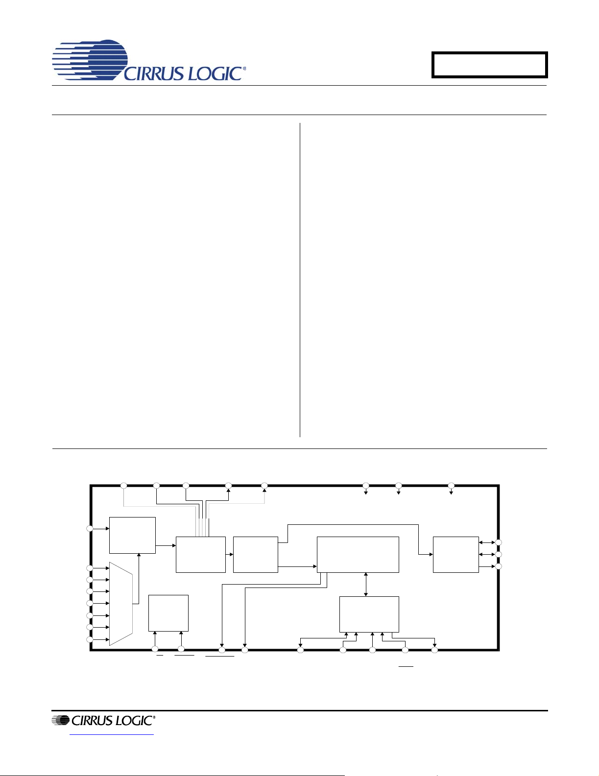
The CS8415A is a monolithic CMOS device which receives and decodes one of 7 channels of audio data
according to the IEC60958, S/PDIF, EIAJ CP1201, or
AES3. The CS8415A has a serial digital audio output
port and comprehensive control ability through a 4-wire
microcontroller port. Channel status and user data are
assembled in block-sized buffers, making read access
easy.
A low-jitter clock recovery mechanism yields a very
clean recovered clock from the incoming AES3 stream.
Stand-alone operation allows systems with no microcontroller to operate the CS8415A with dedicated
output pins for channel status data.
The CS8415A is available in a 28-pin TSSOP and SOIC
package in both Commerical (-10 to +70°C) and Industrial grades (-40 to +85° C). The CDB8415A Customer
Demonstration board is also available for device evaluation and implementation suggestions. Please ref er to
page 2 for ordering informa tion.
Target applications include A/V receivers, CD-R, DVD
receivers, multimedia speakers, digital mixing consoles,
effects processors, set-top boxes, and computer and
automotive audio systems.
VA+ AGND FILT RERR
RXN0
RXP6
RXP5
RXP4
RXP3
RXP2
RXP1
RXP0
http://www.cirrus.com
Receiver
7:1
MUX
Misc.
Control
H/S
Clock &
Data
Recovery
RST
RMCK
AES3
S/PDIF
Decoder
EMPH U SDA/
CDOUT
Copyright © Cirrus Logic, Inc. 2005
(All Rights Reserved)
VL+ DGND
C&Ubit
Data
Buffer
Control
Port &
Registers
SCL/
CCLK
AD1/
CDIN
OMCK
AD0/CSINT
Serial
Audio
Output
OLRCK
OSCLK
SDOUT
AUGUST '05
DS470F4
Page 2
CS8415A
ORDERING INFORMATION
Temp
Product Description Package Grade
28-
TSSOP
96 kHz Digital
CS8415A
2 DS470F4
Audio Interface
Receiver
28-SOIC Commercial -10 to +70°C
Commercial -10 to +70°C
Industrial -40 to +85°C YES
----
Range Pb-Free Container Order Number
YES
NO
YES
NO
Rail CS8415A-CZZ
Tape and Reel CS8415A-CZZR
Rail CS8415A-CZ
Tape and Reel CS8415A-CZR
Rail CS8415A-IZZ
Tape and Reel CS8415A-IZZR
Rail CS8415A-CSZ
Tape and Reel CS8415A-CSZR
Rail CS8415A-CS
Tape and Reel CS8415A-CSR
Page 3

TABLE OF CONTENTS
1. CHARACTERISTICS AND SPECIFICATIONS ..................................................................................... 6
SPECIFIED OPERATING CONDITIONS.............................................................................................. 6
ABSOLUTE MAXIMUM RATINGS........................................................................................................6
DC ELECTRICAL CHARACTERISTICS ................ ............................................. .... ... ... ... ... .................. 6
DIGITAL INPUT CHARACTERISTICS..................................................................................................7
DIGITAL INTERFACE SPECIFICATIONS ............................................................................................ 7
SWITCHING CHARACTERISTICS.......................................................................................................7
SWITCHING CHARACTERISTICS - SERIAL AUDIO PORTS ............................................................. 8
SWITCHING CHARACTERISTICS - CONTROL PORT - SPI MODE................................................... 9
SWITCHING CHARACTERISTICS - CONTROL PORT - I²C MODE...................................... ... ... ... ... 10
2. TYPICAL CONNECTION DIAGRAM .................................................................................................. 11
3. GENERAL DESCRIPTION .................................................................................................................. 12
3.1 AES3 and S/PDIF Standards Documents .................................................................................... 12
4. SERIAL AUDIO OUTPUT PORT ......................................................................................................... 13
5. AES3 RECEIVER ................................................................................................................................ 15
5.1 7:1 S/PDIF Input Multiplexer .. .... ... ... ... ... .... ............................................. ... ... .... ... ... ... ... .... ............ 15
5.2 OMCK System Clock Mode ............. ... ... .... ... ... ... .... ... ............................................. ... ... .... ... ......... 15
5.3 PLL, Jitter Attenuation, and Varispeed ......................................................................................... 15
5.4 Error Reporting and Hold Function ............................................................................................... 15
5.5 Channel Status Data Handling ..................................................................................................... 16
5.6 User Data Handling ...................................... ... ... .... ... ... ... ............................................. ................ 16
5.7 Non-Audio Auto-Detection ......................... ... ... ... .... ... ... ... .... ... ... ... ... .... ... ... ... .... ... ... ... ... .... ............ 16
5.8 Mono Mode Operation ............... ... ... ... ... .... ... ............................................. ... .... ... ... ...................... 17
6. CONTROL PORT DESCRIPTION AND TIMING ................................................................................ 18
6.1 SPITM Mode ............. .... ... ............................................. ... .... ... ... ................................................... 18
6.2 I²C Mode ................................................................. ... ............................................. ...................... 19
6.3 Interrupts ......... ... ... ... .... ... ... ... .... ............................................. ... ... ................................................ 19
7. CONTROL PORT REGISTER SUMMARY ......................................................................................... 20
7.1 Memory Address Pointer (MAP) ............................. ............................................................. .........20
8. CONTROL PORT REGISTER BIT DEFINITIONS .............................................................................. 21
8.1 Control 1 (01h) ............... ... ............................................. .... ......................................................... 21
8.2 Control 2 (02h) .......... .............................................. ... ... ................................................................ 21
8.3 Clock Source Control (04h) .......................................................................................................... 22
8.4 Serial Audio Output Port Data Format (06h) .................................................................................22
8.5 Interrupt 1 Status (07h) (Read Only) ............................................................................................ 23
8.6 Interrupt 2 Status (08h) (Read Only) ............................................................................................ 24
8.7 Interrupt 1 Mask (09h) .................................................................................................................. 24
8.8 Interrupt 1 Mode MSB (0Ah) and Interrupt 1 Mode LSB (0Bh) ..................................................... 24
8.9 Interrupt 2 Mask (0Ch) .................................................................................................................. 24
8.10 Interrupt 2 Mode MSB (0Dh) and Interrupt 2 Mode LSB (0Eh) ................................................... 25
8.11 Receiver Channel Status (0Fh) (Read Only) .............................................................................. 25
8.12 Receiver Error (10h) (Read Only) ............................................................................................... 26
8.13 Receiver Error Mask (11h) .......................................................................................................... 26
8.14 Channel Status Data Buffer Control (12h) ..................................................................................27
8.15 User Data Buffer Control (13h) ................................................................................................... 27
8.16 Q-Channel Subcode Bytes 0 to 9 (14h - 1Dh) (Read Only) ........................................................28
8.17 OMCK/RMCK Ratio (1Eh) (Read Only) ...................................................................................... 28
8.18 C-bit or U-bit Data Buffer (20h - 37h) .......................................................................................... 28
8.19 CS8415A I.D. and Version Register (7Fh) (Read Only) ............................................................. 28
9. PIN DESCRIPTION - SOFTWARE MODE .......................................................................................... 29
10. HARDWARE MODE .......................................................................................................................... 31
10.1 Serial Audio Port Formats .......................................................................................................... 31
11. PIN DESCRIPTION - HARDWARE MODE ....................................................................................... 32
12. APPLICATIONS ............................................................................................................................... 34
12.1 Reset, Power Down and Start-Up .............................................................................................. 34
12.2 ID Code and Revision Code ....................................................................................................... 34
12.3 Power Supply, Grounding, and PCB Layout ..............................................................................34
CS8415A
DS470F4 3
Page 4

CS8415A
13. APPENDIX A: EXTERNAL AES3/SPDIF/IEC60958 RECEIVER COMPONENTS .......................... 35
13.1 AES3 Receiver External Components ........................................................................................ 35
13.2 Isolating Transformer Requirements .......................................................................................... 36
14. APPENDIX B: CHANNEL STATUS AND USER DATA BUFFER MANAGEMENT ........................ 37
14.1 AES3 Channel Status (C) Bit Management ................................................................................ 37
14.2 Accessing the E Buffer ............................................................................................................... 37
14.2.1 Reserving the First 5 Bytes in the E Buffer .............................. ...................................... 38
14.2.2 Serial Copy Management System (SCMS) .................................................................... 38
14.2.3 Channel Status Data E Buffer Access ........................................................................... 38
14.2.3.1 One-Byte Mode............................ ... ... ... .... ... ... ... ... .... ......................................... 38
14.2.3.2 Two-Byte Mode...................................................................... ... ... ... ................... 39
14.3 AES3 User (U) Bit Management ................................................................................................. 39
15. APPENDIX C: PLL FILTER ............................................................................................................... 40
15.1 General ....................... ... ... ... .... ... ... ............................................. ... .... ... ... ................................... 40
15.2 External Filter Components .............................. .... ... ... ... .... ... ... ... ... .... ... ...................................... 41
15.2.1 General ................ ... .... ............................................. ... ... ... .... ... ...................................... 41
15.2.2 Capacitor Selection ........................................................................................................ 41
15.2.3 Circuit Board Layout ...................... ... ... .... ... ... ... .... ... ... ............................................. ...... 41
15.3 Component Value Selection ....................................................................................................... 42
15.3.1 Identifying the Part Revision .......................................................................................... 42
15.3.2 External Components .............................. ... ... ................................................................ 42
15.3.3 Jitter Tolerance ................. ... ... .... ... ... ... .... ............................................. ... ... ... .... ... ......... 43
15.3.4 Jitter Attenuation ......... ... ............................................. ... ... .... ... ... ... .... ... ... ...................... 44
16. REVISION HISTORY ........................................................................................................................ 45
4 DS470F4
Page 5

LIST OF FIGURES
Figure 1. Audio Port Master Mode Timing ................................................................................................... 8
Figure 2. Audio Port Slave Mode and Data Input Timing............................................................................. 8
Figure 3. SPI Mode Timing .......................................................................................................................... 9
Figure 4. I²C Mode Timing ......................................................................................................................... 10
Figure 5. Recommended Connection Diagram for Software Mode ........................................................... 11
Figure 6. Serial Audio Output Example Formats........................................................................................ 14
Figure 7. AES3 ReceiverTiming for C & U Pin Output Data ...................................................................... 17
Figure 8. Control Port Timing in SPI Mode ................................................................................................ 18
Figure 9. Control Port Timing in I²C Mode ................................................................................................. 19
Figure 10. Hardware Mode ........................................................................................................................ 31
Figure 11. Professional Input Circuit.......................................................................................................... 36
Figure 12. Transformerless Professional Input Circuit............................................................................... 36
Figure 13. Consumer Input Circuit ............................................................................................................. 36
Figure 14. S/PDIF MUX Input Circuit ......................................................................................................... 36
Figure 15. TTL/CMOS Input Circuit............................................................................................................ 36
Figure 16. Channel Status Data Buffer Structure....................................................................................... 37
Figure 17. Flowchart for Reading the E Buffer........................................................................................... 38
Figure 18. PLL Block Diagram ................................................................................................................... 40
Figure 19. Recommended Layout Example.................................. .... ... ... ... ... .... ... ... ................................... 41
Figure 20. Jitter Tolerance Template......................................................................................................... 43
Figure 21. Revision A................................................................................................................................. 44
Figure 22. Revision A1............................................................................................................................... 44
Figure 23. Revision A2 using A1 Values.................................................................................................... 44
Figure 24. Revision A2 using A2* Values .................................................................................................. 44
CS8415A
LIST OF TABLES
Table 1. Control Register Map Summary................................................................................................... 20
Table 2. Equivalent Software Mode Bit Definitions.................................................................................... 31
Table 3. Hardware Mode Start-Up Options................ ... ... .... ... ............................................. ... ... .... ... ......... 31
Table 4. Second Line Part Marking............................................................................................................ 42
Table 5. Fs = 8 to 96 kHz........................................................................................................................... 42
Table 6. Fs = 32 to 96 kHz......................................................................................................................... 42
Table 7. Revision History........................................................................................................................... 45
DS470F4 5
Page 6
CS8415A
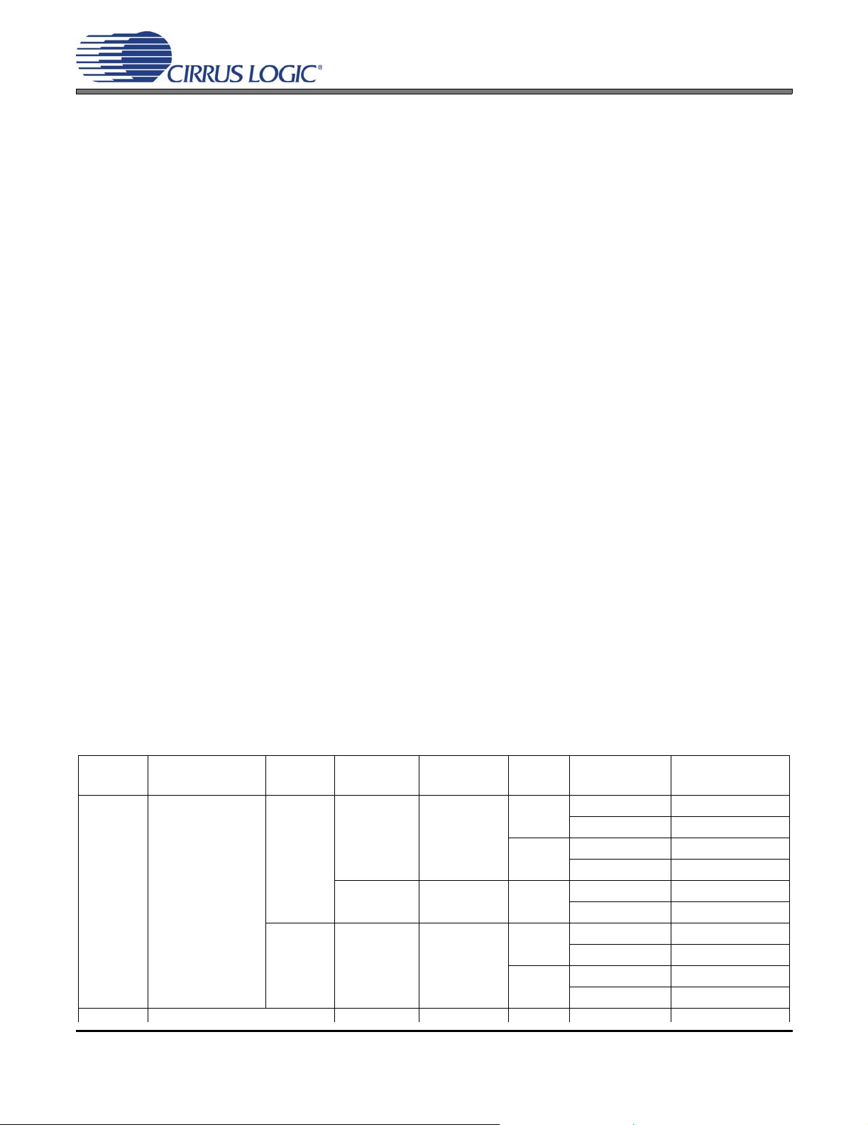
1. CHARACTERISTICS AND SPECIFICATIONS
All Min/Max characteristics and specifications are guaranteed over the Specified Operat ing Conditions. Typical performance characteristics and specifications are derived from measurements taken at nominal supply voltages and
T
= 25°C.
A
SPECIFIED OPERATING CONDITIONS
AGND, DGND = 0 V, all voltages with respect to 0 V.
Parameter Symbol Min Typ Max Units
Power Supply Voltage
(Note 1)
Ambient Operating Temperature: Commercial Grade
Industrial Grade
VA+
VL+
T
A
4.5
2.85
-10
-40
5.0
3.3 or 5.0
-
-
5.5
5.5
+70
+85
V
V
°C
Notes:
1. I²C protocol is supported only in VL+ = 5.0 V mode.
ABSOLUTE MAXIMUM RATINGS
AGND, DGND = 0 V; all voltages with respect to 0 V. Operation beyond these limits may result in permanent damage to the device. Normal operation is not guaranteed at these extremes.
Parameter Symbol Min Max Units
Power Supply Voltage
Input Current, Any Pin Except Supplies (Note 2)
Input Voltage
Ambient Operating Temperature (power applied)
Storage Temperature
2. Transient currents of up to 100 mA will not cause SCR latch-up.
VL+,VA+ - 6.0 V
I
in
V
in
T
A
T
stg
-±10mA
-0.3 (VL+) + 0.3 V
-55 125 °C
-65 150 °C
DC ELECTRICAL CHARACTERISTICS
AGND = DGND = 0 V; all voltages with respect to 0 V.
Parameters Symbol Min Typ Max Units
Power-down Mode (Note 3)
Supply Current in power down V A+
VL+ = 3.3 V
VL+ = 5.0 V
-
-
-
Normal Operation (Note 4)
Supply Current at 48 kHz frame rate VA+
VL+ = 3.3 V
VL+ = 5.0 V
Supply Current at 96 kHz frame rate VA+
VL+ = 3.3 V
VL+ = 5.0 V
3. Power Down Mode is defined as RST
4. Normal operation is defined as RST
= LO with all clocks and data lines held static.
= HI.
-
-
-
-
-
-
6 DS470F4
20
60
60
6.3
30.1
46.5
6.6
44.8
76.6
-
-
-
-
-
-
-
-
-
µA
µA
µA
mA
mA
mA
mA
mA
mA
Page 7
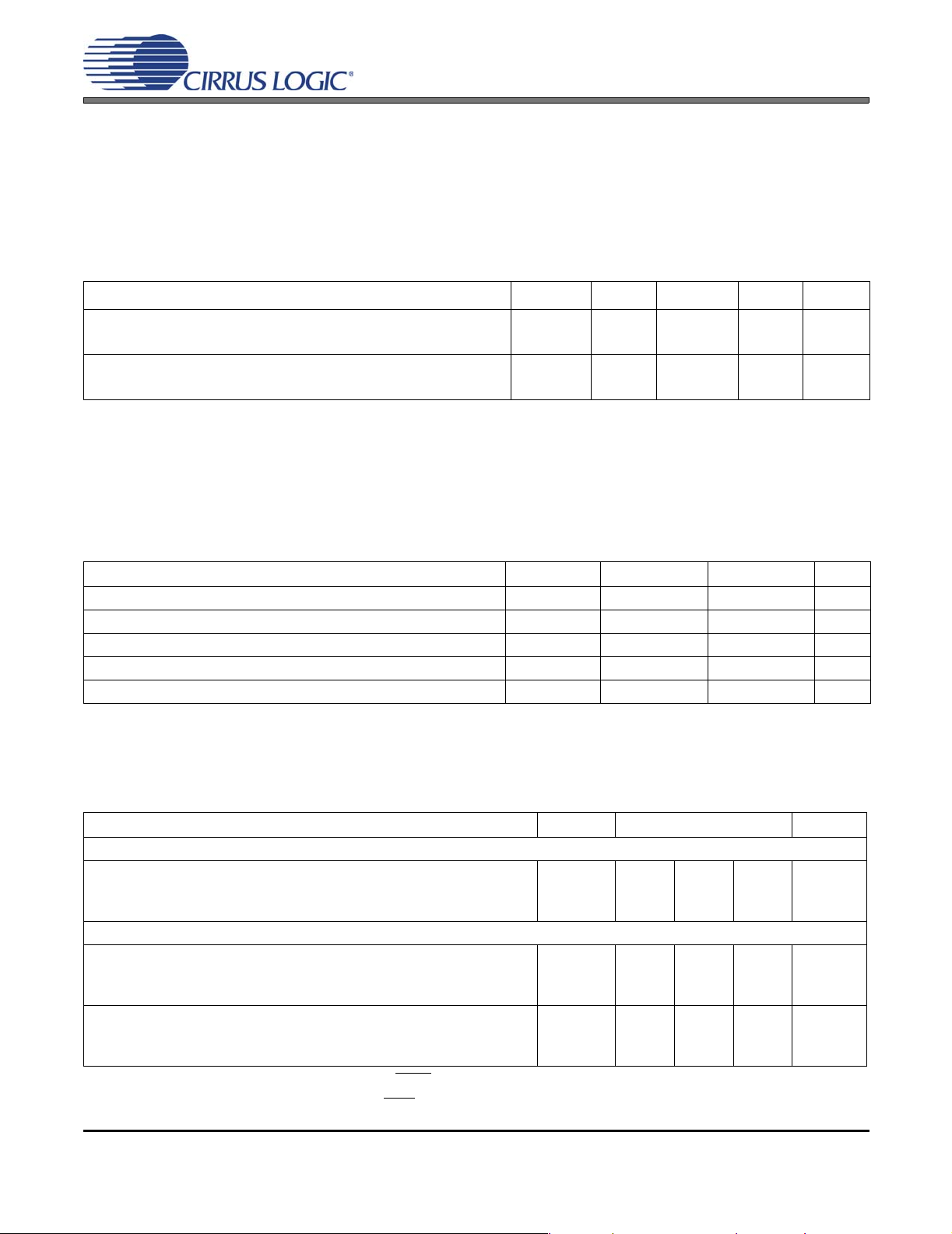
DIGITAL INPUT CHARACTERISTICS
Parameters Symbol Min Typ Max Units
Input Leakage Current
Differential Input Voltage, RXP0 to RXN0
DIGITAL INTERFACE SPECIFICATIONS
AGND = DGND = 0 V; all voltages with respect to 0 V.
Parameters Symbol Min Max Units
High-Level Output Voltage (IOH = -3.2 mA)
Low-Level Output Voltage (IOH = 3.2 mA)
High-Level Input Voltage, except RX
Low-Level Input Voltage, except RX
n
n
(Note 5)
CS8415A
I
in
V
TH
V
OH
V
OL
V
IH
V
IL
-±1±10µA
-200- mV
(VL+) - 1.0 - V
-0.4V
2.0 (VL+) + 0.3 V
-0.3 0.4/0.8 V
5. At 5.0 V mode, V
= 0.8 V (Max), at 3.3 V mode, VIL =0.4 V (Max).
IL
SWITCHING CHARACTERISTICS
Inputs: Logic 0 = 0 V, Logic 1 = VL+; CL = 20 pF.
Parameter Symbol Min Typ Max Units
RST pin Low Pulse Width
PLL Clock Recovery Sample Rate Range
RMCK output jitter (Note 6)
RMCK output duty cycle
6. Cycle-to-cycle using 32 to 96 kHz external PLL filter components.
200 - - µs
8.0 - 108.0 kHz
- 200 - ps RMS
40 50 60 %
DS470F4 7
Page 8
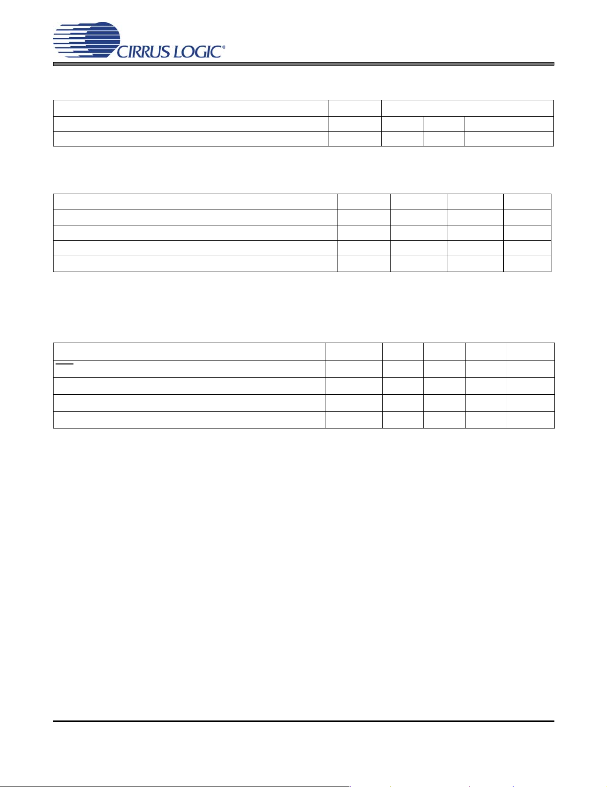
SWITCHING CHARACTERISTICS - SERIAL AUDIO PORTS
Inputs: Logic 0 = 0 V, Logic 1 = VL+; CL = 20 pF.
Parameter Symbol Min Typ Max Units
OSCLK Active Edge to SDOUT Output Valid (Note 7)
Master Mode
RMCK to OSCLK active edge delay (Note 7)
RMCK to OLRCK delay (Note 8)
OSCLK and OLRCK Duty Cycle
Slave Mode
OSCLK Period (Note 9)
OSCLK Input Low Width
OSCLK Input High Width
OSCLK Active Edge to OLRCK Edge (Note 7, 8, 10)
OLRCK Edge Setup Before OSCLK Active Edge
Notes 7, 8, 11
7. The active edges of OSCLK are program m ab le.
8. The polarity OLRCK is programmable.
t
dpd
t
smd
t
lmd
t
sckw
t
sckl
t
sckh
t
lrckd
t
lrcks
- - 20 ns
0 - 10 ns
0 - 10 ns
-50- %
36 - - ns
14 - - ns
14 - - ns
20 - - ns
20 - - ns
CS8415A
9. No more than 128 SCLK per frame.
10. This delay is to prevent the previous OSCLK edge from being interpreted as the first one after OLRCK
has changed.
11. This setup time ensures that this OSCLK edge is interpreted as the first one after OLRCK has changed.
OSCLK
(output)
OLRCK
(output)
t
smd
RMCK
(output)
Hardware Mode
RMCK
(output)
Software M ode
t
lm d
Figure 1. Audio Port Master Mode Timing Figure 2. Audio Port Slave Mode and Data Input Timing
OLRCK
(input)
OSCLK
(input)
SDOUT
t
lrckd
t
lrcks
t
sckh
t
sckw
t
sckl
t
dpd
8 DS470F4
Page 9
SWITCHING CHARACTERISTICS - CONTROL PORT - SPI MODE
Inputs: Logic 0 = 0 V, Logic 1 = VL+; CL = 20 pF.
Parameter Symbol Min Typ Max Units
CCLK Clock Frequency (Note 12)
CS High Time Between Transmissions
CS Falling to CCLK Edge
CCLK Low Time
CCLK High Time
CDIN to CCLK Rising Setup Time
CCLK Rising to DATA Hold Time (Note 13)
CCLK Falling to CDOUT Stable
Rise Time of CDOUT
Fall Time of CDOUT
Rise Time of CCLK and CDIN (Note 14)
Fall Time of CCLK and CDIN (Note 14)
12. If Fs is lower than 46.875 kHz, the maximum CCLK frequency should be less than 128 Fs. This is dictated by the timing requirements necessary to access the Channel Status and User Bit buffer memory.
Access to the control register file can be carried out at the full 6 MHz rate. The minimum allowable input
sample rate is 8 kHz, so choosing CCLK to be less than or equal to 1.024 MHz should be safe for all
possible conditions.
f
t
t
t
t
t
sck
csh
css
scl
sch
dsu
t
dh
t
pd
t
r1
t
f1
t
r2
t
f2
0-6.0MHz
1.0 - - µs
20 - - ns
66 - - ns
66 - - ns
40 - - ns
15 - - ns
- - 50 ns
- - 25 ns
- - 25 ns
- - 100 ns
- - 100 ns
CS8415A
13. Data must be held for sufficient time to bridge the transition time of CCLK.
14. For f
<1 MHz.
sck
CS
CCLK
CDIN
CDOUT
t
css
t
t
sch
scl
t
r2
Figure 3. SPI Mode Timing
t
dsu
t
f2
t
dh
t
csh
t
pd
DS470F4 9
Page 10
SWITCHING CHARACTERISTICS - CONTROL PORT - I²C MODE
(Note 15), Inputs: Logic 0 = 0 V, Logic 1 = VL+; CL = 20 pF.
Parameter Symbol Min Typ Max Units
SCL Clock Frequency
Bus Free Time Between Transmissions
Start Condition Hold Time (prior to first clock pulse)
Clock Low Time
Clock High Time
Setup Time for Repeated Start Condition
SDA Hold Time from SCL Falling (Note 16)
SDA Setup Time to SCL Rising
Rise Time of Both SDA and SCL Lines
Fall Time of Both SDA and SCL Lines
Setup Time for Stop Condition
15. I²C protocol is supported only in VL+ = 5.0 V mode.
16. Data must be held for sufficient time to bridge the 25 ns transition time of SCL.
fscl - - 100 kHz
t
t
hdst
t
low
t
high
t
sust
t
hdd
t
sud
t
susp
buf
t
t
r
f
4.7 - - µs
4.0 - - µs
4.7 - - µs
4.0 - - µs
4.7 - - µs
0--µs
250 - - ns
- - 25 ns
- - 25 ns
4.7 - - µs
CS8415A
SDA
SCL
Stop Start
t
buf
t
hdst
t
low
t
high
t
hdd
Figure 4. I²C Mode Timing
t
sud
Repeated
Start
t
t
sust
hdst
Stop
t
f
t
r
t
susp
10 DS470F4
Page 11
2. TYPICAL CONNECTION DIAGRAM
Ferrite *
+5.0 V
Analog
Supply*
Bead
0.1 Fµ
0.1 Fµ
VA+ VL+
CS8415A
+3.3 V or +5.0 V
Digital Supply
**
AES3/
SPDIF
Sources
Clock Control RMCK
Hardware
Control
RXP6
RXP5
RXP4
RXP3
RXP2
RXP1
RXP0
RXN0
EMPH
RERR
RST
CS8415A
SDA/CDOUT
SCL/CCLK
A2D
/
RFILT
CFILT CRIP
OLRCK
OSCLK
SDOUT
AD0/CS
AD1/CDIN
INT
DGND2
H/S
DGNDFILTAGND
3-wire Serial
Audio Input
Device
Microcontroller
U
* A separate analog supply is only necessary in applications where RMCK is used
for a jitter sensitive task. For applications where RMCK is not used for a jitter
sensitive task, connect VA+ to VD+ via a ferrite bead. Keep the decoupling
capacitor between VA+ and AGND.
Please see section 5.1 "7:1 S/PDIF Input Multiplexer" and Appendix A for typical
**
input configurations and recommended input circuits.
Figure 5. Recommended Connection Diagram for Software Mode
DS470F4 11
Page 12

CS8415A
3. GENERAL DESCRIPTION
The CS8415A is a monolithic CMOS device which receives and decodes audio data according to the AES3,
IEC60958, S/PDIF, and EIAJ CP1201 inte rface standard s.
Input data is either differential or single-ended. A low-jitter clock is recovered from the incoming data using a PLL.
The decoded audio data is output through a configurable, 3-wire output port. The channel status and user data are
assembled in block-sized buffers and may be accessed through an SPI or I²C microcontroller port. For systems
with no microcontroller, a stand-alone mode allows direct access to channel status and user data output pins.
Target applications include AVR, CD-R, DAT, DVD, multimedia speakers, MD and VTR equipment, mixing consoles, digital audio transmission and receiving equipment, high-quality D/A and A/D converters, effects processors,
set-top boxes, and computer audio systems.
Figure 5 shows the supply and external connections to the CS8415A, when configured for operation with a micro-
controller.
3.1 AES3 and S/PDIF Standards Documents
This data sheet assumes that the user is familiar with the AES3 and S/PDIF data formats. It is advisable to
have current copies of the AES3 and IEC60958 specifications on hand for easy reference.
The latest AES3 standard is available from the Audio Engineering Society or ANSI at www.aes.org or
www.ansi.org. Obtain the latest IEC60958 standard from ANSI or from the International Electrotechnical
Commission at www.iec.ch. The latest EIAJ CP-1201 standard is available from the Japanese Electronics
Bureau.
Cirrus Logic Application Note 22: Overview of Digital Audio Interface Data Structures contains a useful tu-
torial on digital audio specifications, but it should not be considered a substitute for the standards.
The paper An Understanding and Implementation of the SCMS Serial Copy Management System for Digital
Audio Transmission, by Clifton Sanchez, is an excellent tutorial on SCMS. It is available from the AES as
preprint 3518.
12 DS470F4
Page 13

CS8415A
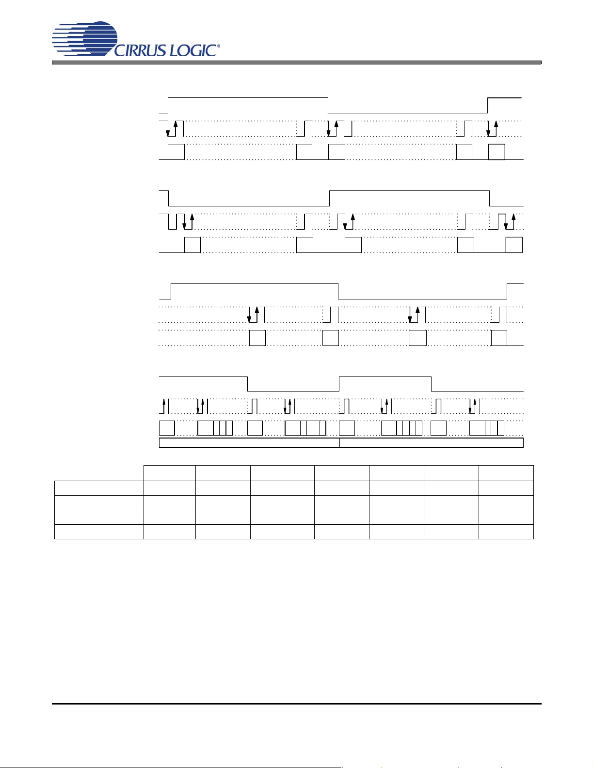
4. SERIAL AUDIO OUTPUT PORT
A 3-wire serial audio output port is provided. The port can be adjusted to suit the att ached device setting the control
registers. The following parameters are adjustable: master or slave, serial clock frequency, audio data resolution,
left or right justification of the data relative to lef t/right clock, optio nal one-b it cell delay of the first dat a bit, the po larity of the bit clock, and the polarity of the left/right clock. By setting the appropriate control bits, many formats are
possible.
Figure 6 shows the selection of common output formats including the control bit settings. It should be noted that in
right-justified mode, the serial audio output data is "MSB extended". This means that in a sub-frame where the
MSB of the data is '1', all bits preceding the MSB in the sub-frame will also be '1'. Conversely , in a sub-frame where
the MSB of the data is '0', all bits preceding the MSB in the sub-frame will also be '0'.
A special AES3 direct output format is included, which allows the serial output port access to the V, U, and C bits
embedded in the serial audio data stream. The P bit is replaced by a Z bit that marks the subframe just prior to the
start of each block. The received channel sta tus block star t signal is only available in hardwar e mode, as the RCBL
pin.
In master mode, the left/right clock and the serial bit clock a re outputs, derived from the recovered RMCK clock. In
slave mode, the left/right clock and the serial bit clock are inputs. The left/right clock must be synchronous to the
appropriate master clock, but the serial bit clock can be asynchronous and discontinuous if required. By appropriate phasing of the left/right clock and control of the serial clocks, multiple CS8415As can share one serial port. The
left/right clock should be continuous, but the duty cycle can be less than the specified typical value of 50% if
enough serial clocks are present in each phase to clock all the data bits. When in slave mode, the serial audio output port must not be set for right-justified data. When using the serial audio output port in slave mode with an
OLRCK input which is asynchronous to the incoming AES3 data, an interrupt bit (OSLIP) is provided to indicate
DS470F4 13
Page 14
CS8415A
when repeated or dropped samples occur. The CS8415A allows immediate mute of the serial audio output port
audio data by the MUTESAO bit of Control Register 1.
Left
Justified
(Out)
I²S
(Out)
Right
Justified
(Out)
AES3
Direct
(Out)
OLRCK
OSCLK
SDOUT
OLRCK
OSCLK
SDOUT
OLRCK
OSCLK
SDOUT
OLRCK
OSCLK
SDOUT
Channel A Channel B
MSB
MSB
Channel A
MSB
LSB
MSB
Channel A Channel B
MSB Extended MSB Extended
Channel A
LSB
Frame 191
MSB
MSB
LSB
Channel B
MSB
LSB
LSB
Frame 0
Channel B
MSB
Channel A
MSB MSB
LSB
LSBLSB
LSB
Channel B
MSB
MSB
LSB
CUVZCUVZCUVCUV
SOMS* SOSF* SORES[1:0]* SOJUST* SODEL* SOSPOL* SOLRPOL*
Left Justified X X XX 0 0 0 0
I²S X X XX 0 1 0 1
Right Justified 1 X XX 1 0 0 0
AES3 Direct X X 11 0 0 0 0
X = don’t care to match format, but does need to be set to the desired setting
* See Serial Output Data Format Register Bit Descriptions for an explanation of the meaning of each bit
Figure 6. Serial Audio Output Example Formats
14 DS470F4
Page 15

CS8415A
5. AES3 RECEIVER
The CS8415A includes an AES3 digital audio receiver. A comprehensive buffering scheme provides read access
to the channel status and user data. This buffering scheme is described in Appendix B.
The AES3 receiver accepts and decodes audio and digital data according to the AES3, IEC60958 (S/PDIF), and
EIAJ CP-1201 interface standards. The receiver consists of a differential input stage, driven through pins RXP0
and RXN0, a PLL-based clock recovery circuit, and a decoder which separates the audio data from the channel
status and user data.
External components are used to terminate and isolate the incoming data cables from the CS8415A. These components are detailed in Appendix A.
5.1 7:1 S/PDIF Input Multiplexer
The CS8415A employs a 7:1 S/PDIF Input Multiplexer to accommodate up to seven channels of input digital
audio data. Digital audio data is single-ended and input through the RXP[0:6] pins. Wh en any portion of the
multiplexer is implemented, unused RXP pins should be tied to ground, and RXN0 must be AC-coupled to
ground. The multiplexer select line control is accessed through bits MUX[2:0] in the Control 2 register. The
multiplexer defaults to RXP0. Therefore, the default configuration is for a differential signal to be input
through RXP0 & RXN0. Please see Appendix A for recommended input circuits.
5.2 OMCK System Clock Mode
A special clock switching mode is available that allows the clock that is input through the OMCK pin to be
output through the RMCK pin. This feature is controlled by the SWCLK bit in register 1 of the control registers. When the PLL loses lock, the frequency of the VCO drop s to 300 kHz. The clock switching mode allows
the clock input through OMCK to be used as a clock in the system without any disruption when the PLL loses
lock. For example, when the input is removed from the receiver. When SWCL K is enabled and this mode is
implemented, RMCK is an output and
Please note that internal circuitry associated with RMCK is not driven by OMCK. This means that OSCLK
and OLRCK continue to be derived from the PLL and are not usable in this mode. This function is available
only in software mode.
is not bi-directional.
5.3 PLL, Jitter Attenuation, and Varispeed
Please see Appendix C for general description of the PLL, selection of recommended PLL filter components, and layout considerations. Figure 5 shows the recommended configuration of the two capacitors an d
one resistor that comprise the PLL filter.
5.4 Error Reporting and Hold Function
While decoding the incoming AES3 data stream, the CS8415A can identify several kinds of error, indicated
in the Receiver Error register. The UNLOCK bit indicates whether the PLL is locked to the incoming AES3
data. The V bit reflects the current validity bit status. The CONF (confidence) bit is the logical OR of BIP and
UNLOCK. The BIP (bi-phase) error bit indicates an error in incoming bi-phase coding. The PAR (parity) bit
indicates a received parity error.
The error bits are "sticky" - they are set on the first occurrence of the associated error and will remain set
until the user reads the register through the control port. This enables the register to log all unmasked errors
that occurred since the last time the register was read.
This clock switching is performed glitch-free.
The Receiver Error Mask register allows masking of individual errors. The bits in this register serve as
masks for the corresponding bits of the Receiver Error Register. If a mask bit is set to 1, the error is unmasked, which implies the following: its occurrence will be reported in the receiver error register, induce a
DS470F4 15
Page 16

pulse on RERR, invoke the occurrence of a RERR interrupt, and affect the cur rent audio sam ple accord ing
to the status of the HOLD bits. The HOLD bits allow a choice of holding the previous sample, replacing the
current sample with zero (mute), or not changing the current audio sample . If a mask bit is set to 0, the error
is masked, which implies the following: its occurrence will not be reported in the receiver error register, will
not induce a pulse on RERR or generate a RERR interrupt, and will not affect the current audio sample. The
QCRC and CCRC errors do not affect the current audio sample, even if unmasked.
5.5 Channel Status Data Handling
The first 2 bytes of the Channel Status block are decoded into the Receiver Channel Status register. The
setting of the CHS bit in the Channel Status Data Buffer Control register determines whether the channel
status decodes are from the A channel (CHS = 0) or B channel (CHS = 1).
The PRO (professional) bit is extracted directly. For consumer data, the COPY (copyright) bit is extracte d,
and the category code and L bits are decoded to determine SCMS status, indicated by the ORIG (original)
bit. If the category code is set to General on the incoming AES3 stream, copyright will always be indicated
even when the stream indicates no copyright. Finally, the AUDIO
indicator, as described in the Non-audio Auto-detection section below.
CS8415A
bit is extracted and used to set an AUDIO
If 50/15 µs pre-emphasis is detected, the state of the EMPH
The encoded channel status bits which indicate sample word length are decoded according to AES3-1992
or IEC 60958. Audio data routed to the seria l audio output port is unaffected by the word length settings and
all 24 bits are passed on as received.
Appendix A describes the overall handling of Channel Status and User data.
5.6 User Data Handling
The incoming user data is buffered in a user accessible buffer. Received user data may also be output to
the U pin under the control of a control register bit. De pe nd in g o n th e clo ck ing op tio ns sele cte d , the r e m ay
not be a clock available to qualify the U data output. Figure 7 illustrates the timing. If the incoming user data
bits have been encoded as Q-channel subcode, the data is decoded and presente d in 10 consecutive re gister locations. An interrupt may be enabled to indicate the decoding of a new Q-channel block, which may
be read through the control port.
5.7 Non-Audio Auto-Detection
An AES3 data stream may be used to convey non-audio data, thus it is important to know whether the incoming AES3 data stream is digital audio or not. This information is typically conveyed in channel status bit
1 (AUDIO
AC-3
CS8415A AES3 receiver can detect such non-audio data. This is acco mplished by looking fo r a 96-bit sync
code, consisting of 0x0000, 0x0000, 0x0000, 0x0000, 0xF 872, and 0x4E1F . When the sync code is detected, an internal AUTODETECT signal will be asserted. If no additional sync codes are detected within the
next 4096 frames, AUTODETECT will be de-asserted until another sync code is detected. The AUDIO
in the Receiver Channel Status register is the logical OR of AUTODETECT and the received channel status
bit 1. If non-audio data is detected, the data is still processed exactly as if it were normal audio. It is up to
the user to mute the outputs as required.
), which is extracted automatically by the CS8415A. However , certain non-audio sources, such as
®
or MPEG encoders, may not adhere to this convention, and the bit may not be properly set. The
pin is adjusted accordingly.
bit
16 DS470F4
Page 17

5.8 Mono Mode Operation
An AES3 stream may be used in more than one way to transmit 96 kHz sample rate data. One method is
to double the frame rate of the current form at. This re sults in a stereo signal with a sa mple rate o f 96 kHz,
carried over a single twisted pair cable. An alternate metho d is implemented using the 2 sub-frames in a 48kHz frame rate AES3 signal to carry consecutive samples of a mono signal, resulting in a 96-kHz sample
rate stream. This allows older equipment, whose AES3 transmitters and receivers are not rated for 96-kHz
frame rate operation, to handle 96-kHz sample rate information. In this “mono mode”, 2 AES3 cables are
needed for stereo data transfer. The CS8415A offers mono mode operation, controlled through the MMR
control register bit.
The receiver mono mode effectively doubles Fs compared to the input frame rate. The clock output on the
RMCK pin tracks Fs, and so is doubled in frequency compared to stereo mode. The receiver will run at a
frame rate of Fs/2, and the serial audio output port will run at Fs. Sub-frame A data will be routed to both
the left and right data fields on SDOUT. Similarly, sub-frame B data will be routed to both the left and right
data fields of the next word clock cycle of SDOUT.
Using mono mode is only necessary if the serial audio output port must run at 96 kHz. If the CS8415A is
kept in normal stereo mode, and receives AES3 data arranged in mono mode, then the serial audio output
port will run at 48 kHz, with left and right data fields representing consecutive audio samples.
RCBL
Out
CS8415A
VLRCK
C, U
Output
- RCBL and C output are only available in hardware mode.
- RCBL goes high 2 frames after receipt of a Z preamble, and is high for 16 frames.
- V L RC K is a v irt u a l wor d c lo c k , which may n o t e x is t, but is u s ed to illustrate the C/U timing.
- VLRC K duty cycle is 50% . VLR C K frequency is always equal to the incoming frame rate.
- If the serial audio output port is in master mode, VLRCK = O LRC K
- If the serial audio output port is in slave mode, then VLRCK needs to be externally created, if required.
- C and U transitions are aligned within ± 1% of VLRCK period to VLRCK edges.
Figure 7. AES3 ReceiverTiming for C & U Pin Output Data
DS470F4 17
Page 18

CS8415A
6. CONTROL PORT DESCRIPTION AND TIMING
The control port is used to access the registers, allowing the CS8415A to be configured for the desired operational
modes and formats. In addition, Channel Status and User data may be read through the control port. The operation
of the control port may be completely asynchronous with respect to the audio sample rates. However, to avoi d
potential interference problems, the control port pins should remain static if no operation is required.
The control port has 2 modes: SPI and I²C, with the CS8415A acting as a slave device. SPI mode is selected if
there is a high-to-low transition on the AD0/CS
by connecting the AD0/CS
pin to VL+ or DGND, thereby permanently selecting the desired AD0 bit address state.
6.1 SPITM Mode
In SPI mode, CS is the CS8415A chip select signal, CCLK is the control port bit clock (input into the
CS8415A from the microcontroller), CDIN is the in put da ta lin e from the mi crocontr oller, CDOUT is the o utput data line to the microcontroller. Data is clocked in on the rising edge of CCLK and out on the falling edge.
pin, after the RST pin has been brought high. I²C mode is selected
Figure 8 shows the operation of the control port in SPI mode. To write to a register, bring CS
low. The first
seven bits on CDIN form the chip address and must be 0010000b. The eighth bit is a read/write indicator
(R/W
), which should be low to write. The next eight bits form the Memory Address Pointer (MAP), which is
set to the address of the register that is to be updated. The next eight bits are the data which will be placed
into the register designated by the MAP. During writes, the CDOUT output stays in the Hi-Z state. It may be
externally pulled high or low with a 47 kΩ resistor, if desired.
There is a MAP auto increment capability, enabled by the INCR bit in the MAP register. If INCR is a zero,
the MAP will stay constant for successive read or writes. If INCR is set to a 1, the MAP will autoincrement
after each byte is read or written, allowing block reads or writes of successive registers.
To read a register, the MAP has to be set to the corre ct address by executing a partial write cyc le which
finishes (CS
as desired. To begin a read, bring CS
high) immediately after the MAP byte. The MAP auto increment bit (INCR) may be set or not,
low, send out the chip address and set the read/write bit (R/W) high.
The next falling edge of CCLK will clock out the MSB of the addressed register (CDOUT will leave the high
impedance state). If the MAP auto increm ent bit is set to 1, the data for successive registers will appear
consecutively.
CS
CCLK
CHIP
ADDRESS
0010000
R/W
CDIN
CHIP
ADDRESS
0010000
R/W
MAP
MSB
byte 1
DATA
LSB
byte n
CDOUT
High Impedance
MAP = Memory Address Pointer, 8 bits, MSB first
Figure 8. Control Port Timing in SPI Mode
MSB
LSB
MSB
LSB
18 DS470F4
Page 19

6.2 I²C Mode
In I²C mode, SDA is a bidirectional data line. Data is clocked into and out of the part by the clock, SCL, with
the clock to data relationship as shown in Figure 9. There is no CS
a unique address. Pins AD0 and AD1 form the two least significant bits of the chip address and should be
connected to VL+ or DGND as desired. The EMPH
from the EMPH
The upper 4 bits of the 7-bit address field are fixed at 0010b. To communicate with a CS8415A, the chip
address field, which is the first byte sent to the CS8415A, should match 0010b followed by the settings of
the EMPH
, AD1, and AD0. The eighth bit of the address is the R/W bit. If the operation is a write, the next
byte is the Memory Address Pointer (MAP) which selects the register to be read or written. If the operation
is a read, the contents of the register pointed to by the MAP will be output. Setting the auto increment bit in
MAP allows successive reads or writes of consecutive registers. Each byte is separated by an acknowledge
bit. The ACK bit is output from the CS8415A after each input byte is read, and is input to the CS8415A from
the microcontroller after each transmitted byte. I²C mode is supported only with VL+ in 5V mode.
6.3 Interrupts
The CS8415A has a comprehensive interrupt capability. The INT output pin is intended to drive the interrupt
input pin on the host microcontroller. The INT pin may be set to be active-low, active-high or active-low with
no active pull-up transistor. This last mode is used for active-low, wired-OR hook-ups, with multiple peripherals connected to the microcontroller interrupt input pin.
CS8415A
pin. Each individual CS8415A is given
pin is used to set the AD2 bit by connecting a resistor
pin to VL+ or to DGND. The state of the pin is sensed while the CS8415A is being reset.
Notes:
Many conditions can cause an interrup t, as liste d in th e interrupt status register descriptions. Each source
may be masked off through mask register bits. In addition, each source may be set to rising edge, falling
edge, or level-sensitive. Combined with the option of level- sensitive or edg e-sens itive modes within the microcontroller, many different configurations are possible, depending on the n eeds of the e quipment designer.
Note 1
0010
SDA
SCL
AD2-0
Start
Figure 9. Control Port Timing in I²C Mo de
R/W
ACK
1. AD2 is derived from a resistor attached to the EMPH
DATA7-0
Note 2
ACK
pin.
DATA7-0
Note 3
ACK
Stop
AD1 and AD0 are determined by the state of the corresponding pins.
2. If operation is a write, this byte contains the Memory Address Pointer, MAP.
3. If operation is a read, the last bit of the read should be NACK (high).
DS470F4 19
Page 20

7. CONTROL PORT REGISTER SUMMARY
CS8415A
Addr
Function 7 6 5 4 3 2 1 0
(HEX)
01 Control 1 SWCLK 0 MUTESAO 0 0 INT1 INT0 0
02 Control 2 0 HOLD1 HOLD0 RMCKF MMR MUX2 MUX1 MUX0
04 Clock Source Control 0 RUN 0 0 0 0 0 0
06 Serial Output Format SOMS SOSF SORES1 SORES0 SOJUST SODEL SOSPOL SOLRPOL
07 Interrupt 1 Status 0 OSLIP 0 0 0 DETC 0 RERR
08 Interrupt 2 Status 0 0 0 0 DETU 0 QCH 0
09 Interrupt 1 Mask 0 OSLIPM 0 0 0 DETCM 0 RERRM
0A Interrupt 1 Mode (MSB) 0 OSLIP1 0 0 0 DETC1 0 RERR1
0B Interrupt 1 Mode (LSB) 0 OSLIP0 0 0 0 DETC0 0 RERR0
0C Interrupt 2 Mask 0 0 0 0 DETUM 0 QCHM 0
0D Interrupt 2 Mode (MSB) 0 0 0 0 DETU1 0 QCH1 0
0E Interrupt 2 Mode (LSB) 0 0 0 0 DETU0 0 QCH0 0
0F Receiver CS Data AUX3 AUX2 AUX1 AUX0 PRO AUDIO
10 Receiver Errors 0 QCRC CCRC UNLOCK V CONF BIP PAR
11 Receiver Error Mask 0 QCRCM CCRCM UNLOCKM VM CONFM BIPM PARM
12 CS Data Buffer Control 0 0 BSEL CBMR DETCI 0 CAM CHS
13 U Data Buffer Control 0 0 0 0 0 0 DETUI 0
14-1D Q sub-code Data
1E OMCK/RMCK Ratio ORR7 ORR6 ORR5 ORR4 ORR3 ORR2 ORR1 ORR0
20-37 C or U Data Buffer
7F ID and Version ID3 ID2 ID1 ID0 VER3 VER2 VER1 VER0
COPY ORIG
T a ble 1. Control Register Map Summary
7.1 Memory Address Pointer (MAP)
7 6 543210
INCR MAP6 MAP5 MAP4 MAP3 MAP2 MAP1 MAP0
INCR - Auto Increment Address Control Bit
Default = ‘0’
0 - Disabled
1 - Enabled
MAP6:MAP0 - Register address
Note: Reserved registers must not be written to during normal operation. Some reserved registers are
used for test modes, which can completely alter the normal operation of the CS8415A.
20 DS470F4
Page 21

CS8415A
8. CONTROL PORT REGISTER BIT DEFINITIONS
8.1 Control 1 (01h)
7 6 543210
SWCLK 0 MUTESAO 0 0 INT1 INT0 0
SWCLK - Controls output of OMCK on RMCK when PLL loses lock
Default = ‘0’
0 - RMCK default function
1 - OMCK output on RMCK pin
MUTESAO - Mute control for the serial audio output port
Default = ‘0’
0 - Disabled
1 - Enabled
INT1:0 - Interrupt output pin (INT) control
Default = ‘00’
00 - Active high; high output indicates interrupt condition has occurred
01 - Active low, low output indicates an interrupt condition has occurred
10 - Open drain, active low. Requires an external pull-up resistor on the INT pin.
11 - Reserved
8.2 Control 2 (02h)
7 6 543210
0 HOLD1 HOLD0 RMCKF MMR MUX2 MUX1 MUX0
HOLD1:0 - Determine how received audio sample is affected when a receiver error occurs
Default = ‘00’
00 - Hold the last valid audio sample
01 - Replace the current audio sample with 00 (mute)
10 - Do not change the received audio sample
11 - Reserved
RMCKF - Select recovered master clock output pin frequency.
Default = ‘0’
0 - RMCK is equal to 256 * Fs
1 - RMCK is equal to 128 * Fs
MMR - Select AES3 receiver mono or stereo operation
Default = ‘0’
0 - Normal stereo operation
1 - A and B subframes treated as consecutive samples of one channel of data.
Data is duplicated to both left and right parallel outputs of the AES receiver block.
The sample rate (Fs) is doubled compared to MMR=0
DS470F4 21
Page 22

CS8415A
MUX2:0 - 7:1 S/PDIF Input Multiplexer Select Line Control
Default = ‘000’
000 - RXP0
001 - RXP1
010 - RXP2
011 - RXP3
100 - RXP4
101 - RXP5
110 - RXP6
111 - Reserved
8.3 Clock Source Control (04h)
7 6 543210
0RUN000000
This register configures the clock sources of various blocks. In conjunction with the Data Flow Control register, various Receiver/Transmitter/Transceiver modes may be se lected.
RUN - Controls the internal clocks, allowing the CS8415A to be placed in a “powered down”, low current
consumption, state.
Default = ‘0’
0 - Internal clocks are stopped. Internal state machines are reset. The fully static control port is operational,
allowing registers to be read or changed. Reading and wr iting the U and C data buffers is not possible. Power consumption is low.
1 - Normal part operation. This bit must be written to the 1 state to allow the CS8415A to begin operation.
All input clocks should be stable in frequency and phase when RUN is set to 1.
8.4 Serial Audio Output Port Data Format (06h)
7 6 543210
SOMS SOSF SORES1 SORES0 SOJUST SODEL SOSPOL SOLRPOL
SOMS - Master/Slave Mode Selector
Default = ‘0’
0 - Serial audio output port is in slave mode
1 - Serial audio output port is in master mode
SOSF - OSCLK frequency (for master mode)
Default = ‘0’
0 - 64*Fs
1 - 128*Fs
SORES1:0 - Resolution of the output data on SDOUT
Default = ‘00’
00 - 24-bit resolution
01 - 20-bit resolution
10 - 16-bit resolution
11 - Direct copy of the received NRZ data from the AES3 receiver (including C, U, and V bits, the time slot
22 DS470F4
Page 23

CS8415A
normally occupied by the P bit is used to indicate the location of the block start, SDOUT pin only, serial audio
output port clock must be derived from the AES3 receiver recovered clock)
SOJUST - Justification of SDOUT data relative to OLRCK
Default = ‘0’
0 - Left-justified
1 - Right-justified (master mode only)
SODEL - Delay of SDOUT data relative to OLRCK, for left-justified data formats
Default = ‘0’
0 - MSB of SDOUT data occurs in the first OSCLK period after the OLRCK edge
1 - MSB of SDOUT data occurs in the second OSCLK period after the OLRCK edge
SOSPOL - OSCLK clock polarity
Default = ‘0’
0 - SDOUT sampled on rising edges of OSCLK
1 - SDOUT sampled on falling edges of OSCLK
SOLRPOL - OLRCK clock polarity
Default = ‘0’
0 - SDOUT data is for the left channel when OLRCK is high
1 - SDOUT data is for the right channel when OLRCK is high
8.5 Interrupt 1 Status (07h) (Read Only)
7 6 543210
0 OSLIP 0 0 0 DETC 0 RERR
For all bits in this register, a “1” means the associated interrupt condition has occurred at least once since
the register was last read. A ”0” means the associated interrupt condition has NOT occurred since the last
reading of the register. Reading the register resets all bits to 0, unless the interrupt mode is set to level and
the interrupt source is still true. Status bits that are masked off in the associated mask register will always
be “0” in this register. This register defaults to 00h.
OSLIP - Serial audio output port data slip interrupt
When the serial audio output port is in slave mode, and OLRCK is asynchronous to the port data source,
This bit will go high every time a data sample is dropped or repeated.
DETC - D to E C-buffer transfer interrupt.
Indicates the completion of a D to E C-buffer transfer. See “Channel Status and User Data Buffer Manage-
ment” on page 38 for more information.
RERR - A receiver error has occurred.
The Receiver Error register may be read to determine the nature of the error which caused the interrupt.
DS470F4 23
Page 24

CS8415A
8.6 Interrupt 2 Status (08h) (Read Only)
76543210
0000DETU0QCH0
For all bits in this register, a “1” means the associated interrupt condition has occurred at least once since
the register was last read. A ”0” means the associated interrupt condition has NOT occurred since the last
reading of the register. Reading the register resets all bits to 0, unless the interrupt mode is set to level and
the interrupt source is still true. Status bits that are masked off in the associated mask register will always
be “0” in this register. This register defaults to 00h.
DETU - D to E U-buffer transfer interrupt.
Indicates the completion of a D to E U-buffer transfer. See “Channel Status and User Data Buffer Manage-
ment” on page 38 for more information.
QCH - A new block of Q-subcode data is available for reading.
The data must be completely read within 588 AES3 frames after the interrupt occurs to avoid corruption of
the data by the next block.
8.7 Interrupt 1 Mask (09h)
76543210
0 OSLIPM 0 0 0 DETCM 0 RERRM
The bits of this register serve as a mask for the Interrupt 1 register. If a mask bit is set to 1, the error is unmasked, meaning that its occurrence will affect the INT pin and the status register. If a mask bit is set to 0,
the error is masked, meaning that its occurrence will not affect the INT pin or the status register. The bit
positions align with the corresponding bits in Interrupt 1 register. This register defaults to 00h.
8.8 Interrupt 1 Mode MSB (0Ah) and Interrupt 1 Mode LSB (0Bh)
76543210
0 OSLIP1 0 0 0 DETC1 0 RERR1
0 OSLIP0 0 0 0 DETC0 0 RERR0
The two Interrupt Mode registers form a 2-bit code for each Interrupt Register 1 function. There are three
ways to set the INT pin active in accordance with the interrupt condition. In the Rising edge active mode,
the INT pin becomes active on the arrival of the interrupt condition. In the Falling edge active mode, the INT
pin becomes active on the removal of the interrupt condition. In Level active mode, the INT interrupt p in becomes active during the interrupt condition. Be aware that the active level (Actice High or Low) only depends
on the INT[1:0] bits. These registers default to 00.
00 - Rising edge active
01 - Falling edge active
10 - Level active
11 - Reserved
8.9 Interrupt 2 Mask (0Ch)
7 6 543210
0000DETUM0QCHM0
The bits of this register serve as a mask for the Interrupt 2 register. If a mask bit is set to 1, the error is unmasked, meaning that its occurrence will affect the INT pin and the status register. If a mask bit is set to 0,
the error is masked, meaning that its occurrence will not affect the INT pin or the status register. The bit
positions align with the corresponding bits in Interrupt 2 register. This register defaults to 00h.
24 DS470F4
Page 25

CS8415A
8.10 Interrupt 2 Mode MSB (0Dh) and Interrupt 2 Mode LSB (0Eh)
7 6 543210
0 0 0 0 DETU1 0 QCH1 0
0 0 0 0 DETU0 0 QCH0 0
The two Interrupt Mode register s form a 2-bit code for each Interrupt Regist er 1 function. There a re three
ways to set the INT pin act ive in accordance with the interrupt condition. In the Rising edge active mode,
the INT pin becomes active on the arrival of the interr upt condition. In the Falling edge active mode, th e INT
pin becomes active on the removal of the interrupt condition. In Level active mode, the INT interrupt pin becomes active during the interrupt condition. Be awar e that the active level (Actice High or Low) only depen ds
on the INT[1:0] bits. These registers defa ult to 00.
00 - Rising edge active
01 - Falling edge active
10 - Level active
11 - Reserved
8.11 Receiver Channel Status (0Fh) (Read Only)
7 6 543210
AUX3 AUX2 AUX1 AUX0 PRO AUDIO COPY ORIG
The bits in this register can be associated with either channel A or B of the received data. The desired channel is selected with the CHS bit of the Channel Status Data Buffer Control Register.
AUX3:0 - Incoming auxiliary data field width, as indicated by the incoming channel status bits, decoded according to IEC60958 and AES3.
0000 - Auxiliary data is not present
0001 - Auxiliary data is 1 bit long
0010 - Auxiliary data is 2 bits long
0011 - Auxiliary data is 3 bits long
0100 - Auxiliary data is 4 bits long
0101 - Auxiliary data is 5 bits long
0110 - Auxiliary data is 6 bits long
0111 - Auxiliary data is 7 bits long
1000 - Auxiliary data is 8 bits long
1001 - 1111 Reserved
PRO - Channel status block format indicator
0 - Received channel status block is in consumer format
1 - Received channel status block is in professional format
AUDIO
0 - Received data is linearly coded PCM audio
1 - Received data is not linearly coded PCM audio
COPY - SCMS copyright indicator
0 - Copyright asserted
1 - Copyright not asserted
- Audio indicator
If the category code is set to General in the incoming AES3 stream, copyright will always be indicated by
COPY, even when the stream indicates no copyright.
DS470F4 25
Page 26

CS8415A
ORIG - SCMS generation indicator, decoded from the category code and the L bit.
0 - Received data is 1st generation or higher
1 - Received data is original
Note: COPY and ORIG will both be set to 1 if the incoming data is flagged as professional, or if the re-
ceiver is not in use.
8.12 Receiver Error (10h) (Read Only)
76543210
0 QCRC CCRC UNLOCK V CONF BIP PAR
This register contains the AES3 receiver and PLL status bits. Unmasked bits will go high on occurrence of
the error, and will stay high until the register is read. Reading the register resets all bits to 0, unless the error
source is still true. Bits that are masked off in the receiver error mask register will always be 0 in this register.
This register defaults to 00h.
QCRC - Q-subcode data CRC error indicator. Updated on Q-subcode block boundaries
0 - No error
1 - Error
CCRC - Channel Status Block Cyclic Redundancy Check bit. Updated on CS block boundaries, valid in Pro
mode
0 - No error
1 - Error
UNLOCK - PLL lock status bit. Updated on CS block boundaries.
0 - PLL locked
1 - PLL out of lock
V - Received AES3 Validity bit status. Updated on sub-frame boundaries.
0 - Data is valid and is normally linear coded PCM audio
1 - Data is invalid, or may be valid compressed audio
CONF - Confidence bit. Updated on sub-frame boundaries.
0 - No error
1 - Confidence error. This is the logical OR of BIP and UNLOCK.
BIP - Bi-phase error bit. Updated on sub-frame boundaries.
0 - No error
1 - Bi-phase error. This indicates an error in the received bi-phase coding.
PAR - Parity bit. Updated on sub-frame boundaries.
0 - No error
1 - Parity error
26 DS470F4
Page 27

CS8415A
8.13 Receiver Error Mask (11h)
7 6 543210
0 QCRCM CCRCM UNLOCKM VM CONFM BIPM PARM
The bits in this register serve as masks for the corresponding bits of the Receiver Error Register. If a mask
bit is set to 1, the error is unmasked, meaning that its occurrence will appear in the receiver error register,
will affect the RERR pin, will affect the RERR interrupt, and will affect the current audio sample according
to the status of the HOLD bit. If a mask bit is set to 0, the error is masked, meaning that its occurrence will
not appear in the receiver error register, will not affect the RERR pin, will not affect the RERR interrupt, and
will not affect the current audio sample. The CCRC and QCRC bits behave differently from the other bits:
they do not affect the current audio sample even when unmasked. This register defaults to 00h.
8.14 Channel Status Data Buffer Control (12h)
7 6 543210
0 0 BSEL CBMR DETCI 0 CAM CHS
BSEL - Selects the data buffer register addresses to contain User data or Channel Status data
Default = ‘0’
0 - Data buffer address space contains Channel Status data
1 - Data buffer address space contains User data
CBMR - Control for the first 5 bytes of channel status “E” buffer
Default = ‘0’
0 - Allow D to E buffer transfers to overwrite the first 5 bytes of channel status data
1 - Prevent D to E buffer transfers from overwriting first 5 bytes of channel status data
DETCI - D to E C-data buffer transfer inhibit bit.
Default = ‘0’
0 - Allow C-data D to E buffer transfers
1 - Inhibit C-data D to E buffer transfers
CAM - C-data buffer control port access mode bit
Default = ‘0’
0 - One byte mode
1 - Two byte mode
CHS - Channel select bit
Default = ‘0’
0 - Channel A information is displayed at the EMPH
A information is output during control port reads when CAM is set to 0 (One Byte Mode)
1 - Channel B information is displayed at the EMPH
B information is output during control port reads when CAM is set to 0 (One Byte Mode)
pin and in the receiver channel status register. Channel
pin and in the receiver channel status register. Channel
DS470F4 27
Page 28
CS8415A
8.15 User Data Buffer Control (13h)
76543210
000000DETUI0
DETUI - D to E U-data buffer transfer inhibit bit.
Default = ‘0’
0 - Allow U-data D to E buffer transfers
1 - Inhibit U-data D to E buffer transfers
8.16 Q-Channel Subcode Bytes 0 to 9 (14h - 1Dh) (Read Only)
The following 10 registers contain the decoded Q-channel subcode data
76543210
CONTROL CONTROL CONTROL CONTROL ADDRESS ADDRESS ADDRESS ADDRESS
TRACK TRACK TRACK TRACK TRACK TRACK TRACK TRACK
INDEX INDEX INDEX INDEX INDEX INDEX INDEX INDEX
MINUTE MINUTE MINUTE MINUTE MINUTE MINUTE MINUTE MINUTE
SECOND SECOND SECOND SECOND SECOND SECOND SECOND SECOND
FRAME FRAME FRAME FRAME FRAME FRAME FRAME FRAME
ZERO ZERO ZERO ZERO ZERO ZERO ZERO ZERO
ABS MINUTE ABS MINUTE ABS MINUTE ABS MINUTE ABS MINUTE ABS MINUTE ABS MINUTE ABS MINUTE
ABS SECOND ABS SECOND ABS SECOND ABS SECOND ABS SECOND ABS SECOND ABS SECOND ABS SECOND
ABS FRAME ABS FRAME ABS FRAME ABS FRAME ABS FRAME ABS FRAME ABS FRAME ABS FRAME
Each byte is LSB first with respect to the 80 Q-subcode bits Q[79:0]. Thus bit 7 of address 14h is Q[0] while
bit 0 of address 0Eh is Q[7]. Similarly bit 0 of address 1Dh corresponds to Q[79].
8.17 OMCK/RMCK Ratio (1Eh) (Read Only)
76543210
ORR7 ORR6 ORR5 ORR4 ORR3 ORR2 ORR1 ORR0
This register allows the calculation of the incoming sample rate by the host microcontroller from the equ ation
ORR=Fso/Fsi. The Fso is determined by OMCK, whose frequency is assumed to be 256 Fso. ORR is represented as an unsigned 2-bit integer and a 6-bit fractional part. The value is meaningfu l only after the PLL
has reached lock. For example, if the OMCK is 12.288 MHz, Fso would be 48 kHz (48 kHz =
12.288 MHz/256). Then if the input sample rate is also 48 kHz, you would get 1.0 from the ORR register.(The value from the ORR register is hexadecimal, so the actual value you will get is 40h). If F
63
/64, ORR will saturate at the value FFh. Also, there is no hysteresis on ORR. Therefore a small amount of
SO/FSI
jitter on either clock can cause the LSB ORR[0] to oscillate.
ORR7:6 - Integer part of the ratio (Integer value=Integer(SRR[7:6]))
ORR5:0 - Fractional part of the ratio (Fraction value=Integer(SRR[5:0])/64)
8.18 C-bit or U-bit Data Buffer (20h - 37h)
Either channel status data buffer E or user data buffer E is accessible through these register addresses.
> 3
28 DS470F4
Page 29

CS8415A
8.19 CS8415A I.D. and Version Register (7Fh) (Read Only)
7 6 543210
ID3 ID2 ID1 ID0 VER3 VER2 VER1 VER0
ID3:0 - ID code for the CS8415A. Permanently set to 0100
VER3:0 - CS8415A revision level. Revision A is coded as 0001
DS470F4 29
Page 30

9. PIN DESCRIPTION - SOFTWARE MODE
CS8415A
SDA/CDOUT
AD0/CS
EMPH
RXP0
RXN0
VA+
AGND
FILT
RST
RMCK
RERR
RXP1
RXP2
RXP3 RXP4
* P ins which remain the same function in all modes.
+Pinswhichrequireapulluporpulldownresistor
to select the desired startup option.
1
2
3*+
4*
5*
6*
7*
8*
9*
10*
11*
12
13
14
28
27
26
25
*24
*23
*22
*21
20
19
*18
*17
*16
15
SCL/CCLK
AD1/CDIN
RXP6
RXP5
H/S
V+
L
DGND
OMCK
U
INT
SDOUT
OLRCK
OSCLK
Pin Name # Pin Description
Serial Control Data I/O (I²C) / Data Out (SPI) (Input/Output) - In I²C mode, SDA is the control I/O data
SDA/CDOUT
AD0/CS
EMPH
RXP0
RXN0
RXP1
RXP2 RXP3
RXP4 RXP5
RXP6
VA+
line. SDA is open drain and requires an external pull-up resistor to VL+. In SPI mode, CDOUT is the out-
1
put data from the control port int erface on the CS8415A
Address Bit 0 (I²C) / Control Port Chip Select (SPI) (Input) - A falling edge on this pin puts the
CS8415A into SPI control port mode. With no falling edge, the CS8415A defaults to I²C mode. In I²C
2
mode, AD0 is a chip address pin. In SPI mode, CS is used to enable the control port interface on the
CS8415A
Pre-Emphasis (Output) - EMPH
pre-emphasis.
3
emphasis other than 50/15 ms. This is also a start-up option pin, and requires a 47 kΩ resistor to either
VL+ or DGND, which determines the AD2 address bit for the control port in I²C mode
AES3/SPDIF Receiver Port (Input) - Differential line receiver inputs carrying AES3 data. RXP0 may be
4
used as a single-ended input as part of 7:1 S/PDIF Input MUX. If RXP0 is used in MUX, RXN0 must be
5
ac coupled to ground.
12
13
Additional AES3/SPDIF Receiver Port (Input) - Single-ended receiver inputs carrying AES3 or S/PDIF
14
digital data. These inputs, along with RXP0, comprise the 7:1 S/PDIF Input Multiplexer and select line
control is accessed using the MUX2:0 bits in the Control 2 register. Please note that any unused inputs
15
should be tied to ground. See Appendix A for recommended input circuits.
25
26
Positive Analog Power (Input) - Positive supply for the analog section. Nominally +5.0 V. This supply
should be as quiet as possible since noise on this pin will directly affect the jitter performance of the
6
recovered clock
is low when the incoming Channel Status data indicates 50/15 ms
EMPH is high when the Channel Status data indicates no pre-emphasis or indicates pre-
30 DS470F4
Page 31

Pin Name # Pin Description
AGND
FILT
RST
RMCK
RERR
OSCLK
OLRCK
SDOUT
INT
U
OMCK
DGND
VL+
H/S
AD1/CDIN
SCL/CCLK
Analog Ground (Input) - Ground for the analog circuitry in the chip. AGND and DGND should be con-
7
nected to a common ground area under the chip.
PLL Loop Filter (Output) - An RC network should be connected between this pin and ground. See
8
“Appendix C: PLL Filter” on page 41 for recommended schematic and component values.
Reset (Input) - When RST is low, the CS8415A enters a low power mode and all internal states are
reset. On initial power up, RST must be held low until the power supply is stable, and all input clocks are
9
stable in frequency and phase. This is particularly true in hardware mode with multiple CS8415A
devices where synchronization between devices is important
Input Section Recovered Master Clock (Output) - Input section recovered master clock output when
10
PLL is used. Frequency defaults to 256x the sample rate (Fs) and may be set to 128x.
Receiver Error (Output) - When high, indicates a problem with the operation of the AES3 receiver. The
status of this pin is updated once per sub-frame of incoming AES3 data. Conditions that can cause
RERR to go high are: validity, parity error, bi-phase coding error, confidence, QCRC and CCRC errors,
as well as loss of lock in the PLL. Each condition may be optionally masked from affecting the RERR pin
11
using the Receiver Error Mask Register. The RERR pin tracks the st atus of the unmasked errors: the pin
goes high as soon as an unmasked error occurs and goes low immediately when all unmasked errors
go away.
Serial Audio Output Bit Clock (Input/Output) - Serial bit clock for audio data on the SDOUT pin
16
Serial Audio Output Left/Right Clock (Input/Output) - Word rate clock for the audio data on the
17
SDOUT pin. Frequency will be the output sample rate (Fs)
Serial Audio Output Data (Output) - Audio data serial output pin
18
Interrupt (Output) - Indicates errors and key events during the operation of the CS8415A. All bits affect-
ing INT may be unmasked through bits in the control registers. The condition(s) that initiated interrupt
are readable through a control register. The polarity of the INT output, as well as selection of a standard
19
or open drain output, is set through a control register. Once set true, the INT pin goes false only after the
interrupt status registers have been read and the interrupt status bits have returned to zero
20 User Data (Output) - Outputs User data from the AES3 receiver, see Figure 7 for timing information
System Clock (Input) - When the OMCK System Clock Mode is enabled using the SWCLK bit in the
Control 1 register, the clock signal input on this pin is output through RMCK. OMCK serves as reference
21
signal for OMCK/RMCK ratio expressed in register 1Eh
Digital Ground (Input) - Ground for the digital circuitry in the chip. DGND and AGND should be con-
22
nected to a common ground area under the chip.
Positive Digital Power (Input) - Positive supply for the digital section. Typically +3.3 V or +5.0 V.
23
Hardware/Software Mode Control (Input) - Determines the method of cont ro ll i n g th e op e r a ti o n of the
CS8415A, and the method of accessing CS and U data. In software mode, device control and CS and U
data access is primarily through the control port, using a microcontroller. Hardware mode provides an
24
alternate mode of operation and access to the CS and U data through dedicated pins. This pin should
be permanently tied to VL+ or DGND
Address Bit 1 (I²C) / Serial Control Data in (SPI) (Input) - In I²C mode, AD1 is a chip address pin. In
27
SPI mode, CDIN is the input data line for the control port interface
Control Port Clock (Input) - Serial control interface clock and is used to clock control data bits into and
28
out of the CS8415A. In I²C mode, SCL requires an external pull-up resistor to VL+
CS8415A
DS470F4 31
Page 32

CS8415A
10.HARDWARE MODE
The CS8415A has a hardware mode which allows using the device without a microcontroller. Hardware mode is
selected by connecting the H/S
ware mode pin definition section.
Hardware mode data flow is shown in Figure 10. Audio data is input through the AES3 receiver, and routed to the
serial audio output port. The PRO, COPY, ORIG, EMPH
decoded C and U bits are also output, cloc ke d at both edge s of OL RCK (ma ste r mode on ly, see Figure 7).The current audio sample is passed unmodified to the serial audio ou tput port if the validity bit is high, or a p arity, bi-phase,
or PLL lock error occurs.
10.1 Serial Audio Port Formats
In hardware mode, only a limited number of alternative serial audio port formats are available. Table 2 defines the equivalent software mode bit settings for each format. Start-up options are shown in Table3, and
allow choice of the serial audio output port as a master or slave, and the serial audio port format.
OF1 - Left Justified 0 00 0 0 0 0
OF2 - I²S 24-bit data 0 00 0 1 0 1
OF3 - Right Justified, master mode only 0 00 1 0 0 0
OF4 - Direct AES3 data 0 11 0 0 0 0
pin to VL+. Various pins change function in hardware mode, described in the hard-
, and AUDIO channel status bits are output on pins. The
SOSF SORES1/0 SOJUST SODEL SOSPOL SOLRPOL
Table 2. Equivalent Software Mode Bit Definitions
SDOUT ORIG EMPH Function
LO - - Serial Output Port is Slave
HI - - Serial Output Port is Master
- LO LO Left Justified
- LO HI I²S 24-bit data
- HI LO Right Justified
- HI HI Direct AES3 data
Table 3. Hardware Mode Start-Up Options
VL+
H/S
RXP
RXN
AES3 Rx
&
Decoder
C & U bit Data Buffer
RMCK RERR
Power supply pins (VD+, VA+, DGND, AG ND) & the reset pin (RST) and the PLL filter pin (FILT)
are omitted from this diagram. P lease refer to the Typical C onnection Diagram for hook-up details.
NVERR
CHS
COPY ORIG EMPH RCBLPRO AUDIO
Serial
Audio
Output
OLRCK
OSCLK
SDOUT
C
U
Figure 10. Hardware Mode
32 DS470F4
Page 33

11.PIN DESCRIPTION - HARDWARE MODE
CS8415A
Pin Name # Pin Description
COPY Channel Status Bit (Output) - Reflects the state of the Copyright Channel Status bit in the incoming
COPY
VL2+
VL+
VL3+
AES3 data stream. If the category code is set to General, copyright will be indicated whatever the state of
1
the Copyright bit.
2
Positive Digital Power (Input) - Typically +3.3 V or +5.0 V.
23
27
Pre-Emphasis (Output) - EMPH
EMPH
RXP0
RXN0
VA+
AGND
FILT
RST
emphasis.
3
sis other than 50/15 ms. This pin is also a start-up option which, along with ORIG , determines the serial port
format. A 47 kΩ resistor to either VL+ or DGND is required.
4
AES3/SPDIF Receiver Port (Input) - Differential line receiver inputs for the AES3 biphase encoded data.
See Appendix A for recommended circuits.
5
Positive Analog Power (Input) - Nominally +5.0 V. This supply should be as quiet as possible since noise
6
on this pin will directly affect the jitter performance of the recovered clock.
Analog Ground (Input) - Ground for the analog circuitry in the chip. AGND and DGND should be connected
7
to a common ground area under the chip.
PLL Loop Filter (Output) - An RC network should be connected between this pin and ground. See “Appen-
8
dix C: PLL Filter” on page 41
Reset (Input) - When RST is low, the CS8415A enters a low power mode and all internal states are reset.
On initial power up, RST
9
frequency and phase. This is particularly true in hardware mode with multiple CS8415A devices where synchronization between devices is important.
EMPH is high when the Channel Status data indicates no pre-emphasis or indicates pre-empha-
is low when the incoming Channel Status data indicates 50/15 ms pre-
for recommended schematic and component values.
must be held low until the power supply is stable, and all input clocks are stable in
DS470F4 33
Page 34

Pin Name # Pin Description
RMCK
RERR
RCBL
PRO
CHS
NVERR
OSCLK
OLRCK
SDOUT
AUDIO
DGND3
DGND2
DGND
H/S
U
C
ORIG
Recovered Master Clock (Output) - Recovered master clock output when PLL is locked to the incoming
10
AES3 stream. Frequency is 256x the sample rate (Fs).
Receiver Error (Output) - When high, indicates an error condition in the AES3 receiver. The status of this
pin is updated once per sub-frame of incoming AES3 data. Conditions that can cause RERR to go high are:
11
validity bit high, parity error, bi-phase coding error, and loss of lock by the PLL.
Receiver Channel Status Block (Output) -Indicates the beginning of a received channel status block.
RCBL goes high two frames after the reception of a Z preamble, remains high for 16 frames while COPY,
12
ORIG, AUDIO, EMPH and PRO are updated, and returns low for the remainder of the block. RCBL
changes on rising edges of RMCK.
PRO Channel Status Bit (Output) - Reflects the state of the Professional/Consumer Channel Status bit in
13
the incoming AES3 data stream. Low indicates Consumer and high indicates Professional.
Channel Select (Input) - Selects which sub-frame’s channel status data is output on the EMPH, COPY,
14
ORIG, PRO and AUDIO pins. Channel A is selected when CHS is low, channel B is selected when CHS is
high.
No Validity Receiver Error Indicator (Output) - A high output indicates a problem with the operation of the
AES3 receiver. The status of this pin is updated once per frame of incoming AES3 data. Conditions that
15
cause NVERR to go high are: parity error, and bi-phase coding error, and loss of lock by the PLL.
Serial Audio Output Bit Clock (Input/Output) - Serial bit clock for audio data on the SDOUT pin.
16
Serial Audio Output Left/Right Clock (Input/Output) - Word rate clock for the audio data on the SDOUT
17
pin. Frequency will be the output sample rate (Fs).
Serial Audio Output Data (Output) - Audio data serial output pin. This pin is also a start-up option which
18
determines if the serial audio port is master or slave. A 47 kΩ resistor to either VL+ or DGND is required.
Audio Channel Status Bit (Output) - Reflects the state of the audio/non audio Channel Status
19
bit in the incoming AES3 data stream. When this bit is low a valid audio stream is indicated.
20
Digital Ground (Input) - Ground for the digital circuitry in the chip. DGND and AGND should be connected
21
to a common ground area under the chip.
22
Hardware/Software Mode Control (Input) - Determines the method of cont ro ll i n g th e op e r a ti o n of the
CS8415A, and the method of accessing CS and U data. In software mode, device control and CS and U
data access is primarily through the control port, using a microcontroller. Hardware mode provides an alter-
24
nate mode of operation and access to the CS and U data through dedicated pins. This pin should be permanently tied to VL+ or DGND.
User Data (Output) - Outputs user data from the AES3 receiver, clocked by the rising and falling edges of
25
OLRCK.
Channel St atu s Data (Output) - Outputs channel status data from the AES3 receiver, clocked by the rising
26
and falling edges of OLRCK.
Original Channel Status (Output) - SCMS generation indicator. This is decoded from the incoming cate-
gory code and the L bit in the Channel Status bits. A low output indicates that the source of the audio data
stream is a copy not an original. A high indicates that the audio data stream is original. This pin is also a
28
start-up option which, along with
VL+ or DGND is required.
CS8415A
EMPH, determines the serial audio port format. A 47 kΩ resistor to either
34 DS470F4
Page 35

12. APPLICATIONS
12.1 Reset, Power Down and Start-Up
When RST is low, the CS8415A enters a low-power mode and all internal states are reset, including the
control port and registers, and the outputs are muted. When RST
tional and the desired settings should be loaded into the control registers. Writing a 1 to the RUN bit will then
cause the part to leave the low-power state and begin operation. After the PLL has se ttle d, the ser ial a ud io
outputs will be enabled.
Some options within the CS8415A are controlled by a start-up mech ani sm. Dur ing th e reset state , some of
the output pins are reconfigured internally to be inputs. Immediately upon exiting the reset state, the level
of these pins is sensed. The pins are then switched to be outputs. This mechanism allows output pins to be
used to set alternative modes in the CS8415A by connecting a 47 kΩ resistor to between the pin and either
VL+ (HI) or DGND (LO). For each mode, every start-up option select pin MUST have an external pull-up or
pull-down resistor. In software mode, the only start-up option pin is EMPH
dress bit for the control port in I²C mode. The hardware mode uses many start-up options, which are detailed
in the hardware definition section at the end of this data sheet.
12.2 ID Code and Revision Code
The CS8415A has a register that contains a 4-bit code to indicate that the addressed device is a CS8415A.
This is useful when other CS84xx family members are resident in the same system, allowing common software modules.
CS8415A
is high, the control port becomes opera-
, which is used to set a chip ad-
The CS8415A 4-bit revision code is also available. This allows the software driver for the CS8415A to identify which revision of the device is in a particular system, and modify its behavior accordingly. To allow for
future revisions, it is strongly recommend that the revision code is read into a variable area within the microcontroller, and used wherever appropriate as revision details become known.
12.3 Power Supply, Grounding, and PCB Layout
For most applications, the CS8415A can be operated from a single +5.0 V supply, following normal supply
decoupling practices. See Figure 5. Note that the I²C protocol is supported only in VL+ = 5.0 V mode. For
applications where the recovered input clock, output on the RMCK pin, is re quired to be low-jitte r, then use
a separate, quiet, analog +5.0 V supply for VA+, decoupled to AGND. In addition, a separate region of analog ground plane around the FILT, AGND, VA+, RXP[0:6] and RXN0 pins is recommended.
Extensive use of power and ground planes, ground plane fill in unused areas and surface mount decoupling
capacitors are recommended. Decoupling capacitors should be m oun ted o n the same sid e of the boa rd as
the CS8415A to minimize inductance effects, and all decoupling capacitors should be as close to the
CS8415A as possible.
DS470F4 35
Page 36

13.APPENDIX A: EXTERNAL AES3/SPDIF/IEC60958 RECEIVER COMPONENTS
13.1 AES3 Receiver External Components
The CS8415A AES3 receiver is designed to accept both the professional and consumer interfaces. The digital audio specifications for professional use call for a balanced receiver, using XLR connectors, with 110Ω
±20% impedance. The XLR connector on the receiver should have female pins with a male shell. Since the
receiver has a very high input impedance, a 110 Ω resistor should be placed across the re ce ive r te rm inals
to match the line impedance, as shown in Figure 11. Although transformers are not required by the AES,
they are strongly recommended.
If some isolation is desired witho ut th e u se of tr an sf or m er s, a 0.01 µF capacitor should be placed in series
with each input pin (RXP0 and RXN0) as shown in Figure 12. However, if a transformer is not used, high frequency energy could be coupled into the receiver, causing degradation in analog performance.
Figures 11 and 12 show an optional DC blocking capacitor (0.1 µF to 0.47 µF) in series with the cable input.
This improves the robustness of the receiver, preventi ng the saturation of the transformer, or any DC curren t
flow, if a DC voltage is present on the cable.
In the configuration of systems, it is important to avoid ground loops and DC current flowing down the shield
of the cable that could result when boxes with different ground potentials are connected. Generally, it is
good practice to ground the shield to the chassis of the transmitting unit, and connect the shield through a
capacitor to chassis ground at the receiver. However, in some cases it is advantageous to have the ground
of two boxes held to the same potential, and the cable shield might be depended upon to make that electrical
connection. Generally, it may be a good idea to provide the option of grounding or capa citively coupling the
shield to the chassis.
CS8415A
In the case of the consumer interface, the standards call for an unba lanced cir cuit having a r eceiver impedance of 75 Ω ±5%. The connector for the consumer interface is an RCA phono socket. The receiver circuit
for the consumer interface is shown in Figure 13. Figure 14 shows an implementation of the input S/PDIF
multiplexer using the consumer interface.
The circuit shown in Figure 15 may be used when external RS422 receivers, optical receivers or other
TTL/CMOS logic outputs drive the CS8415A receiver section.
36 DS470F4
Page 37

13.2 Isolating Transformer Requirements
Please refer to the application note AN134: AES and SPDIF Recommended Transformers for resources on
transformer selection.
XLR
110 Ω
Twisted
Pair
* See Text
110 Ω
1
Figure 11. Professional Input Circuit Figure 12. Transformerless Professional Input Circuit
0.01 µF
0.01 µF
75 Ω
Coax
RCA Phono
75 Ω
CS8415A
RXP0
RXN0
CS8415A
RXP0
RXN0
110 Ω
Twisted
Pair
XLR
1
75 Ω
Coax
75 Ω
Coax
75 Ω
Coax
*SeeText
110 Ω
75 Ω
75 Ω
75 Ω
0.01 Fµ
0.01 Fµ
.01µF
.01µF
.01µF
.01µF
CS8415A
5A
CS841
RXP0
RXN0
RXP6
RXP5
.
.
.
RXP0
RXN0
Figure 13. Consumer Input Circuit Figure 14. S/PDIF MUX Input Circuit
TTL/CMOS
Gate
0.01 µF
CS8415A
RXP0
RXN0
0.01 µF
Figure 15. TTL/CMOS Input Circuit
DS470F4 37
Page 38

14.APPENDIX B: CHANNEL STATUS AND USER DATA BUFFER MANAGEMENT
14.1 AES3 Channel Status (C) Bit Management
The CS8415A contains sufficient RAM to store a full block of C data for both A and B channels (192 x 2 =
384 bits), and also 384 bits of U information. The user may read from these buffer RAMs through the cont rol
port.
The buffering scheme involves 2 block-sized buffers, named D and E, as shown in Figure 16. The MSB of
each byte represents the first bit in the serial C data stream. For example, the MSB of byte 0 (which is at
control port address 20h) is the consumer/professional bit for channel status block A.
AB
8-bits 8-bits
CS8415A
From
AES3
Receiver
Figure 16. Channel Status Data Buffer Structure
The first buffer (D) accepts incoming C data from the AES receiver. The 2nd buffer (E) accepts entire blocks
of data from the D buffer. The E buffer is also accessible from the control port, allowing reading of the C data.
14.2 Accessing the E Buffer
The user can monitor the incoming data by read ing the E buffer, wh ich is mappe d into the re gister space o f
the CS8415A, through the control port.
The user can configure the interrupt enable register to cause interrupts to occur whenever D-to-E buffer
transfers occur. This allows determination of the allowable time periods to interact with the E buffer.
Also provided is a D-to-E inhibit bit. This may be used whenever “long” control port interactions are occurring.
D
Received
Data
Buffer
E
24
words
Control Port
38 DS470F4
Page 39

A flowchart for reading the E buffer is shown in Figure 17. Since a D-to-E interrupt just occurred after reading, there is a substantial time interval until the next D-to-E transfer (approximately 24 frames worth of time).
This is usually plenty of time to access the E data without having to inhibit the next transfer.
D to E interrupt occurs
Optionally set D to E inhibit
Read E data
If set, clear D to E inhibit
Return
Figure 17. Flowchart for Reading the E Buffer
14.2.1 Reserving the First 5 Bytes in the E Buffer
CS8415A
D-to-E buffer transfers periodically overwrite the data stored in the E buffer. The CS8415A has the capability of reserving the first 5 bytes of the E buffer for user writes only. When this capability is in use, internal
D-to-E buffer transfers will NOT affect the first 5 bytes of the E buffer. Therefore, the user can set values
in these first 5 E bytes once, and the settings will persist until the next user change. This mode is enabled
using the Channel Status Data Buffer Control register.
14.2.2 Serial Copy Management System (SCMS)
In software mode, the CS8415A allows read access to all the channel status bits. For consumer mode
SCMS compliance, the host microcontroller needs to read an d interpret the Category Code , Copy bit and
L bit appropriately.
In hardware mode, the SCMS protocol can be followed by either using the COPY and ORIG output pins,
or by using the C bit serial output pin. These options are documented in the hardware mode section of
this data sheet.
14.2.3 Channel Status Data E Buffer Access
The E buffer is organized as 24 x 16-bit words. For each word the MS Byte is the A channel data, and the
LS Byte is the B channel data (see Figure 16).
There are two methods of accessing this memory, known as one byte mode and two byte mode. The desired mode is selected by setting a control register bit.
14.2.3.1 One-Byte Mode
In many applications, the channel status blocks for the A and B channels will be identical. In this situation,
if the user reads a byte from one of the channel's blocks, the corresponding byte for the other channel will
be the same. One byte mode takes advantage of the often iden tical nature of A and B chan nel status data.
When reading data in one byte mode, a single byte is returned, which can be from channel A or B data,
depending on a register control bit.
DS470F4 39
Page 40

One-byte mode saves the user substantial control port access time, as it effectively accesses 2 bytes worth
of information in 1 byte's worth of access time. If the control port's autoincreme nt addressing is used in combination with this mode, multi-byte accesses such as full-block reads can be done especially efficiently.
14.2.3.2 Two-Byte Mode
There are those applications in which the A and B channel status blocks will not be the same, and the user
is interested in accessing both blocks. In these situations, two-byte mode should be used to access the E
buffer.
In this mode, a read will cause the CS8415A to output two bytes from its control port. The first byte out will
represent the A channel status data, and the 2nd byte will represent the B channel status data.
14.3 AES3 User (U) Bit Management
Entire blocks of U data are buff ered usin g a casca de of 2 bl ock-sized RAM s to perf orm the buffering. The
user has access to the second of these buffers, denoted the E buffer, through the control port. Th e U buffer
access only operates in two-byte mode, since there is no concept of A and B blocks for user data. The arrangement of the data is as followings: Bit15[A7]Bit14[B7]Bit13[A6]Bit12[B6]...Bit1[A0]Bit0[B0]. The arrangement of the data in the each byte is that the MSB is the first received bit and is the first transmitted bit.
The first byte read is the first byte received, and the first byte sent is the first byte transmitted. If you read
two bytes from the E buffer, you will get the following arrangement: A[7]B[7]A[6]B[6]....A[0]B[0].
CS8415A
40 DS470F4
Page 41

15.APPENDIX C: PLL FILTER
15.1 General
An on-chip Phase Locked Loop (PLL) is used to recover the clock from the incoming d ata stream. Figure 18
is a simplified diagram of the PLL in these parts. When the PLL is locked to an AES3 input stream, it is updated at each preamble in the AES3 stream. This occurs at twice the sampling frequency, F
PLL is locked to ILRCK, it is updated at F
There are some applications where low-jitter in the recovered clock, presented on the RMCK pin, is important. For this reason, the PLL has been designed to have good jitter attenuation characteristics, as sh own
in Figure 21, Figure 22, Figure 23, and Figure 24. In addition, the PLL has been designed to only use the
preambles of the AES3 stream to provide lock update information to the PLL. This results in the PLL being
immune to data-dependent jitter affects because the AES3 preambles do not vary with the data.
The PLL has the ability to lock onto a wide range of input sample rates with no external component changes.
If the sample rate of the input subsequently changes, for example in a varispeed application, the PLL will
only track up to ±12.5% from the nominal center sample rate . The nominal center sample rate is the sample
rate that the PLL first locks onto upon application of an AES3 data stream or after enabling the CS8415A
clocks by setting the RUN control bit. If the 12.5% sample rate limit is exceeded, the PLL will return to its
wide lock range mode and re-acquire a new nominal center sample rate.
so that the duty cycle of the input doesn’t affect jitter.
S
CS8415A
. When the
S
INPUT
Phase
Comparator
and Charge Pump
÷N
Figure 18. PLL Block Diagram
VCO
R
FLT
C
C
FLT
RIP
RMCK
DS470F4 41
Page 42

15.2 External Filter Components
15.2.1 General
The PLL behavior is affected by the external filter componen t values. Figure 5 on page 11 shows the r ecommended configuration of the two capacitors and one resistor that comprise the PLL filter. In Table 6,
the component values shown have the highest corner frequency jitter attenuation curve, takes the shortest time to lock, and offers the best output jitter performance. The component values shown in Table 5
allows the lowest input sample rate to be 8 kHz, and increases the lock time of the PLL. Lock times are
worst case for an Fsi transition of 96 kHz.
15.2.2 Capacitor Selection
The type of capacitors used for the PLL filter can have a significant effect on receiver pe rformance. Large
or exotic film capacitors are not necessar y as their lea ds and the r equire d longer cir cuit boa rd traces a dd
undesirable inductance to the circuit. Surface mount ceramic capacito rs are a good ch oice because their
own inductance is low, and they can be mounted close to the FILT pin to minimize trace inductan ce . Fo r
C
, a C0G or NPO dielectric is recommended, and for C
RIP
pacitors with large temperature coefficients, or capacitors with high dielectric constants, that are sensitive
to shock and vibration. These include the Z5U and Y5V dielectrics.
15.2.3 Circuit Board Layout
CS8415A
, an X7R dielectric is preferred. Avoid ca-
FILT
Board layout and capacitor choice affect each other and determine the performance of the PLL. Figure
19 contains a suggested layout for the PLL filter components and fo r bypassing the analog supply voltage.
The 0.1 µF bypass capacitor is in a 1206 form factor. R
and the other three capacitors are in an 08 05
FILT
form factor. The traces are on the top surface of the board with the IC so that there is no via inductance.
The traces themselves are short to minimize the inductance in the filter path. The VA+ and AGND traces
extend back to their origin and are shown only in truncated form in the drawing.
VA
.1µF
Figure 19. Recommended Layout Example
1000
pF
AGND
FILT
C
RIP
FLT
R
C
FLT
42 DS470F4
Page 43

15.3 Component Value Selection
When transitioning from one revision of the p art another, component values may need to be changed. While
it is mandatory for customers to change the external PLL component values when transitioning from revision
A to revision A1 or from revision A to revision A2, customers do not need to change external PLL component
values when transitioning from revision A1 to revision A2, unless the part is used in an application that is
required to pass the AES3 or IEC60958-4 specification for receiver jitter tolerance (see Table 6).
15.3.1 Identifying the Part Revision
The first line of the part marking on the package indicates the part number and package type (CS8415Axx). Table 4 shows a list of part revisions and their corresponding second line part marking, which indicates what revision the part is.
CS8415A
Pre-October 2002
Revision
SOIC & TSSOP (10-Digit)
A Zxxxxxxxxx ZFBAAXxxxxxx NAAXxxxxxx
A1 Rxxxxxxxxx RFBAA1xxxxxx NAA1xxxxxx
A2 N/A RFBAA2xxxxxx NAA2xxxxxx
15.3.2 External Components
Shown in Table 5 and Table 6 are the external PLL component values for each revision. Values listed for
the 32 to 96 kHz Fs range will have the highest corner frequency jitter attenuation curve, take the shortest
time to lock, and offer the best output jitter performance.
(kΩ)C
Revision
A 0.909 1.8 33 56
A1 0.4 0.47 47 60
A2 0.4 0.47 47 60
Revision
A* 3.0 0.047 2.2 35
A1* 1.2 0.1 4.7 35
A2 1.2 0.1 4.7 35
A2* 1.6 0.33 4.7 35
R
FILT
(kΩ)C
R
FILT
New SOIC
(12-Digit)
Table 4. Second Line Part Marking
(µF) C
FILT
Table 5. Fs = 8 to 96 kHz
(µF) C
FILT
RIP
RIP
(nF)
(nF)
New TSSOP
(10-Digit)
PLL Lock Time (ms)
PLL Lock Time (ms)
Table 6. Fs = 32 to 96 kHz
* Parts used in applications that are required to pass the AES3 or IEC60958-4 specification for receiver jitter tolerance should use these component values. Please note that the
AES3 and IEC60958 specifications do not have allowances for locking to sample rates
less than 32 kHz. Also note that many factors can affect jitter performance in a system.
DS470F4 43
Page 44

15.3.3 Jitter Tolerance
Shown in Figure 20 is the Receiver Jitter Tolerance template as illustrated in the AES3 and IEC60958-4
specification. CS8415A parts used with the appropriate external PLL component values (as noted in
Table 6) have been tested to pass this template.
CS8415A
Figure 20. Jitter Tolerance Template
44 DS470F4
Page 45

15.3.4 Jitter Attenuation
Shown in Figure 21, Figure 22, Figure 23, and Figure 24 are jitter attenuation plots for the various revisions of the CS8415A when used with the appropriate external PLL component values (as noted in
Table 6). The AES3 and IEC60958-4 specifications do not have allowances for locking to sample rates
less than 32 kHz. These specifications state a maximum of 2 dB jitter gain or peaking.
CS8415A
5
0
−5
−10
Jitter Attenuation (dB)
−15
−20
−1
10
5
0
5
0
−5
−10
Jitter Attenuation (dB)
−15
−20
0
10
1
10
Jitter Frequency (Hz)
2
10
3
10
4
10
10
−1
5
10
0
10
1
10
Jitter Frequency (Hz)
Figure 21. Revision A Figure 22. Revision A1
5
0
2
10
3
10
4
10
5
10
5
10
−5
−10
Jitter Attenuation (dB)
−15
−20
−25
−1
10
0
10
1
10
Jitter Frequency (Hz)
2
10
3
10
4
10
5
10
−5
−10
Jitter Attenuation (dB)
−15
−20
−25
−1
10
0
10
1
10
Jitter Frequency (Hz)
2
10
3
10
4
10
Figure 23. Revision A2 using A1 Values Figure 24. Revision A2 using A2* Values
DS470F4 45
Page 46

16.REVISION HISTORY
Release Date Changes
PP1 November 1999 1st Preliminary Release
PP2 November 2000 2nd Preliminary Release
PP3 May 2001 3rd Preliminary Release
PP4 January 2003 4th Preliminary Release
F1 January 2004 Final Release
Updated “Appendix C: PLL Filter” on page 41 to include information from errata
ER470E2
F2 August 2004 -Added lead-free device ordering information.
F3 December 2004 -Changed format of Figure 6 on page 14.
-Corrected AES3 Direct (Out) format in Figure 6 on page 14 and text reference to
AES3 Direct on page 13.
-Corrected bit 0 of regitster 04h to default to 0 on page 22.
-Changed description of DETC and DETU bits in “Control Port Register Bit Defini-
tions” on page 21.
-Removed reference to Block Mode from DETU and DETUI on page 24 and
page 27.
F4 August 2005 -Updated “Ordering Information” on page 2.
CS8415A
Contacting Cirrus Logic Support
For all product questions and inquiries contact a Cirrus Logic Sales Representative.
To find the one nearest to you go to www.cirrus.com
IMPORTANT NOTICE
Cirrus Logic, Inc. and its subsidiaries ("Cir r us") believe that the information contained in this document is accurate and reliable. However, the information is subject
to change without not ice and is pr ovided "AS I S" wit hout warr anty of any kind (express or implied). Customers are advised to obtain the latest version of relevant
information to verify, before placing orde rs, that i nforma tion b ein g re lied on is curren t a nd com plete. All p roducts are so ld s ubject to the terms and conditions of sale
supplied at the time of order acknowledgment, including those pertaining to warranty, indemnification, and limitation of liability. No responsibility is assumed by Cirrus
for the use of this information, including use of this information as the basis for manufacture or sale of any items, or for infringement of patents or other rights of third
parties. This document is the property of Cirrus and by furnishing this information, Cirrus grants no license, express or implied under any patents, mask work rights,
copyrights, trademarks, trade secrets or other inte llectual property rights. Cirrus owns the copyrights associated with the information contained herein and gives consent for copies to be made of the information only for use within your organization with respect to Cirrus integrated circuits or other products of Cirrus. This consent
does not extend to other copying such as copying for general distribution, advertising or promotional purposes, or for creating any work for resale.
CERTAIN APPLICATIONS USING SEMICONDUCTOR PRODUCTS MAY INVOLVE POTENTIAL RISKS OF DEATH, PERSONAL INJURY, OR SEVERE PROPERTY OR ENVIRONMENTAL DAMAGE ("CRITICAL APPLICATIONS"). CIRRUS PRODUCTS ARE NOT DESIGNED, AUTHORIZED OR WARRANTED FOR USE
IN AIRCRAFT SYSTEMS, MILITARY APPLICATIONS, PRODUCTS SURGICALLY IMPLANTED INTO THE BODY, AUTOMOTIVE SAFETY OR SECURITY DEVICES, LIFE SUPPORT PRODUCTS OR OTHER CRITICAL APPLICATIONS. INCLUSION OF CIRRUS PRODUCTS IN SUCH APPLICATIONS IS UNDERSTOOD TO BE FULLY AT THE CUSTOMER'S RISK AND CIRRUS DISCLAIMS AND MAKES NO WARRANTY, EXPRESS, STATUTORY OR IMPLIED,
INCLUDING THE IMPLIED WARRANTIES OF MERCHANTABILITY AND FITNESS FOR PARTICULAR PURPOSE, WITH REGARD TO ANY CIRRUS PRODUCT
THAT IS USED IN SUCH A MANNER. IF THE CUSTOMER OR C USTOMER'S CUSTOMER USES OR PERMITS THE USE OF CIRRUS PRODUCTS IN CRITICAL
APPLICATIONS, CUSTOMER AGREES, BY SUCH USE, TO FULLY I NDEMNIF Y CIRRUS, ITS OF FICERS, DIRE CTORS , EMPLOY EES, DIS TRIBUTO RS AND
OTHER AGENTS FROM ANY AND ALL LIABILITY, I NCLUDING ATTORNEYS' FEES AND COSTS, THAT MA Y RESULT FROM OR ARISE IN CONNECTION
WITH THESE USES.
Cirrus Logic, Cirrus, and the Cirrus Logic logo designs are trademarks of Cirrus Logic, Inc. All other brand and product names in this document may be trademarks
or service marks of their respective owners.
SPI is a trademark of Motorola Inc.
AC-3 is a registered trademark of Dolby Laboratories Liscencing, Inc.
46 DS470F4
 Loading...