

96 kHz Digital Audio Receiver
CS8413
CS8414
Features
l Sample Rates to >100 kHz
l Low-Jitter, On-Chip Clock Recovery
256xFs Output clock Provided
l Supports: AES/EBU, IEC 958, S/PDIF, &
EIAJ CP340/1201 Professional and
Consumer Formats
l Extensive Error Reporting
Repeat Last Sample on Error Option
l On-Chip RS422 Line Receiver
l Configurable Buffer Memory (CS8413)
l Pin Compatible wi th CS8411 and CS8412
I
FILT
CS8413
CS8414
RXP
RXN
RXP
RXN
9
10
9
10
VD+
7
RS422
Receiver
VD+
7
RS422
Receiver
CS12/
DGND
8
DGND
8
MUX
13
FCK
VA+
20
22
Clock and Data Recovery
FILT
VA+
20
22
Clock and Data Recovery
16
SEL
/
AGND
21
IEnable and Status
ERF INT
AGND
21
MUX
4365
Description
The CS8413 and CS8414 are monolithic CMOS devices
which receive and de code audio data up to 96k Hz according to the AES/EBU, IEC958, S/PDIF, and EIAJ
CP340/1201 interface standards. The CS8413 and
CS8414 receive data from a transmission l ine, recover
the clock and synch ronization signals, an d de-multiplex
the audio and digital data. Differential or single ended inputs can be decoded.
The CS8413 has a configura ble intern al b uffe r me mory ,
read through a parallel port, which may be used to buffer
channel status, auxiliary data, and/or user data.
The CS8414 de-multiple xes the channel, user, a nd validity data directly to serial output pins with dedicated
output pins for the most important channel status bits.
ORDERING INFORMATION
CS8413-CS 0° to 70° C 28-pin Plastic SOIC
CS8414-CS 0° to 70° C 28-pin Plastic SOIC
MCK
19
De-MUX
25 14
MCK
19
De-MUX
227
Ce/Cd/Cc/Cb/Ca/C0
F2F1F0E2E1E0
Audio
Serial Port
Configurable
Buffer
Memory
M317M2
ERF25CBL
M124M0
18
Audio
Serial Port
Registers
15
23
26
SDATA
12
SCK
11
FSYNC
13
A4/FCK
4
A3-A0
8
D7-D0
24
CS
23
RD/WR
26
SDATA
12
SCK
11
FSYNC
1
C
14
U
28
VERF
Cirrus Logic, Inc.
Crystal Semiconductor Products Division
P.O. Box 17847, Austin, Texas 78760
(512) 445 7222 FAX: (512) 445 7581
http://www.crystal.com
Copyright Cirrus Logic, Inc. 1998
(All Rights Reserved)
OCT ‘98
DS240F1
1

TABLE OF CONTENTS
CHARACTERISTICS/SPECIFICATIONS ................................................ ............3
RECOMMENDED OPERATING CONDITIONS.......................................... 3
DIGITAL CHARACTERISTICS....................................................................3
DIGITAL CHARACTERISTICS - RS422 RECEIVERS................................4
SWITCHING CHARACTERISTICS - CS8413 PARALLEL PORT...............4
SWITCHING CHARACTERISTICS - SERIAL PORTS................................5
GENERAL DESCRIPTION .................................................................................. 7
Line Receiver .............................................................................................. 7
Clocks and Jitter Attenuation ...................................................................... 7
CS8413 DESCRIPTION .......................................................................................8
Parallel Port .......................................................... ....... ............................... 8
Status and IEnable Registers .....................................................................9
Control Registers ......................................................................................11
Audio Serial Port ....................................................................................... 14
Normal Modes .................................................................................... 14
Special Modes ....................................................................................14
Buffer Memory ..........................................................................................15
Buffer Mode 0 .....................................................................................16
Buffer Mode 1 .....................................................................................17
Buffer Mode 2 .....................................................................................18
Buffer Updates and Interrupt Timing ......................................................... 19
ERF Pin Timing ......................................................................................... 19
CS8414 DESCRIPTION .....................................................................................20
Audio Serial Port ....................................................................................... 20
Normal Modes (M3 = 0) .....................................................................21
Special Modes (M3 = 1) .....................................................................21
C, U, VERF, ERF, and CBL Serial Outputs .............................................. 23
Multifunction Pins ...................................................................................... 24
Error and Frequency Reporting ..........................................................24
Channel Status Reporting ..................................................................24
Professional Channel Status (C0 = 0) ................................................ 25
Consumer Channel Status (C0 = 1) ...................................................25
SCMS ............................. .................................................... ................25
PIN DESCRIPTIONS: CS8413 .......................................................................... 27
PIN DESCRIPTIONS: CS8414 .......................................................................... 30
PACKAGE DIMENSIONS ................................................................................. 33
APPENDIX A: RS422 RECEIVER INFORMATION .......................................... 34
Professional Interface ...............................................................................34
Consumer Interface ..................................................................................35
TTL/CMOS Levels .................................................................................... 35
Transformers ............................................................................................ 35
APPENDIX B: SUGGESTED RESET CIRCUIT FOR CS8414 ........................ 36
CS8413 CS8414
Prelimina ry pro du ct i nfo rma tion desc ri bes prod ucts wh ich are i n pr oduc ti on, bu t f or w hich ful l c har act eri za tion d ata is not yet available. Advance
product inf ormat ion des crib es pro ducts wh ich ar e in deve lopmen t and s ubjec t to deve lopmen t cha nges. Ci rrus Lo gic, I nc. has made be st ef forts
to ensure t ha t the informat ion contained i n this document is accurate and reliabl e. However, th e i nformation is s u bject to change without not i c e
and is provid ed “AS IS” without warranty of any kind (express or implied). No responsibility is assumed by Cirrus Logic, Inc. for the use of this
information, no r for in fringe ments of pate nts or other rights of third partie s. This d ocume nt is t he prop erty of Cirrus Logic , Inc. and implies no
license unde r pat ents , co pyr ight s, t rade mar ks, or tra de secr ets. N o part of t his pu bl icat io n may be copi ed, repr oduc ed, sto red i n a retrieval system, or trans m it ted, in any form or by any means (electronic, m echanical, photographic, or ot herwise). Furthermore, no par t of this publica t ion
may be used as a basis for manufacture or sale of any items without the prior written consent of Cirrus Logic, Inc. The names of products of
Cirrus Logic, Inc. or other vendors and suppliers appearing in this document may be trademarks or service marks of their respective owners
which may be registered in some jurisdictions. A list of Cirrus Logic, Inc. trademarks and service marks can be found at http://www.cirrus.com.
2 DS240F1
CS8413 CS8414
CHARACTERISTICS/SPECIFICATIONS
ABSOLUTE MAXIMUM RATINGS (GND = 0V, all voltages with respect to ground)
Parameters Symbol Min Max Units
Power Supply Voltage VD+, VA+ - 6.0 V
Input Current, Any Pin Except Supply (Note 1) I
Input Voltage, Any Pin Except RXP, RXN V
Input Voltage, RXP and RXN V
Ambient Operating Temperature (power applied) T
Storage Temperature T
in
IN
IN
A
stg
Notes: 1. Transient currents of up to 100 mA will not cause SCR latch-up
RECOMMENDED OPERATING CONDITIONS (GND = 0V, all voltages with respect to ground)
Parameters Symbol Min Typ Max Units
Power Supply Voltage VD+, VA+ 4.75 5.0 5.25 V
Supply Current VA+
VD+
Ambient Operating Temperature: (Note 2) T
Power Consumption P
I
A
I
D
A
D
-±10mA
-0.3 (VD+) + 0.3 V
-12 12 V
-55 125 °C
-65 150 °C
-
-
20
20
30
30
mA
mA
02570°C
- 175 315 mW
Notes: 2. The ‘-CS’ parts are specified to operate over 0 to 70 °C but are tested at 25 °C only.
DIGITAL CHARACTERISTICS (T
= 25 °C; VD+, VA+ = 5V ± 5%)
A
Parameters Symbol Min Typ Max Units
High-Level Input Voltage except RXP, RXN V
Low-Level Input Voltage except RXP, RXN V
High-Level Output Voltage (I
= 200 µA) V
O
IH
IL
OH
2.0 - - V
--+0.4V
(VD+) -
--V
1.0
Low-Level Output Voltage (I
Input Leakage Current I
Input Sample Frequency: (Note 3) F
Master Clock Frequency (Note 3) MCK 7.28 256xF
MCK Clock Jitter t
= -3.2 mA) V
O
OL
in
S
j
--0.5V
-1.010µA
28.4 - 100 kHz
25.6 MHz
S
- 200 - psRMS
MCK Duty Cycle (high time/cycle time) - 50 - %
Notes: 3. F
is defined as the incoming audio sample frequency per channel.
S
DS240F1 3
DIGITAL CHARACTERISTICS - RS422 RECEIVERS
(RXP, RXN pins only; VD+, VA+ = 5V ± 5%)
Parameters Symbol Min Typ Max Units
Input Resistance (-7V < V
Differential Input Voltage, (-7V < V
RXP to RXN
Input Hysteresis V
< 7V) (Note 4) Z
CM
< 7V) (Notes 4 and 5)
CM
V
HYST
IN
TH
CS8413 CS8414
-10-k
200 - - mV
-50-mV
Ω
Notes: 4. V
- Input Common Mode Range
CM
5. When the receiver inputs are configured for single ended operation (e.g. consumer configuration) the
signal amplitude must exceed 400 mVp-p for the differential voltage on RXP to RXN to exceed 200 mV.
This represents twice the minimum signal level of 200 mVp-p specified in CP340/1201 and IEC-958
(which are not RS-422 compliant).
SWITCHING CHARACTERISTICS - CS8413 PARALLEL PORT
(TA = 25 °C;VD+, VA+ = 5V ± 5%; Inputs: Logic 0 = DGND, Logic 1 = VD+; CL = 20 pF)
Parameters Symbol Min Typ Max Units
ADDRESS valid to CS
CS
high to ADDRESS invalid t
RD/WR
CS
CS
valid to CS low t
low to RD/WR invalid t
low t
DATA valid to CS
CS
high to DATA invalid RD/WR low (writing) t
CS
falling to DATA valid RD/WR high (reading) t
CS
rising to DATA Hi-Z RD/WR high (reading) t
low t
rising RD/WR low (writing) t
A4 - A0
adcss
csadh
rwcss
csrwi
csl
dcssw
csdhw
csddr
csdhr
13.5 - - ns
0--ns
10 - - ns
35 - - ns
35 - - ns
32 - - ns
0--ns
--35ns
5--ns
RD/WR
Writing
D7 - D0
RD/WR
Reading
D7 - D0
CS
t
adcss
t
rwcss
t
csddr
t
csrwi
t
csl
t
dcssw
t
csadh
t
csdhw
t
csdhr
CS8413 Parallel Port timing
4 DS240F1
CS8413 CS8414
SWITCHING CHARACTERISTICS - SERIAL PORTS
(TA = 25 °C; VD+, VA+ = 5V ± 5%; Inputs: Logic 0 = DGND, Logic 1 = VD+; CL = 20 pF)
Parameters Symbol Min Typ Max Units
-
SCK Frequency Master Mode (Notes 6 and 7)
Slave Mode (Note 7)
SCK falling to FSYNC delay Master Mode (Notes 7 and 8) t
SCK Pulse Width Low Slave Mode (Note 7) t
SCK Pulse Width High Slave Mode (Note 7) t
SCK rising to FSYNC edge delay Slave Mode (Notes 7 and 8) t
FSYNC edge to SCK rising setup Slave Mode (Notes 7 and 8) t
SCK falling (rising) to SDATA valid (Note 8) t
C, U, CBL valid to FSYNC edge CS8414 (Note 8) t
MCK to FSYNC edge delay FSYNC from RXN/RXP t
f
sck
sfdm
sckl
sckh
sfds
fss
ssv
cuvf
mfd
OWRx32
-20 - 20 ns
40 - - ns
40 - - ns
20 - - ns
20 - - ns
OWRx32
-
- - 20 ns
-1/f
sck
-15-ns
Notes: 6. The output word rate, OWR, refers to the frequency at which an audio sample is output from the part.
(A stereo pair is two audio samples.) Therefore, in Master mode, there are always 32 SCK periods in
one audio sample. In Slave mode, exactly 32 SCK periods per audio sample must be provided in most
serial port formats. Therefor, if SCK is 128 x Fs, then SCK must be gated to provide exactly 32 periods
per audio sample.
7. In Master mode, SCK and FSYNC are outputs. In Slave mode, they are inputs. In the CS8413, control
reg. 2 bit 1, MSTR, selects master. In the CS8414, formats 1, 3 and 9 are slaves.
8. The table above assumes data is output on the falling edge and latched on the rising edge. With the
CS8413 the edge is selectable. The table is defined for the CS8413 with control reg. 2 bit 0, SCED, set
to one, and for the CS8414 in formats 2, 3, 5, 6 and 7. For the other formats, the table and figure edges
must be reversed (i.e. “rising” to “falling” and vice versa.)
-
128 x F
Hz
Hz
S
-s
FSYNC
t
sfds
SCK
SDATA
FSYNC
t
sfds
SCK
SDATA
Serial Output Timing - Slave Mode
t
fss
t
t
ssv
MSB
(Mode 1)
t
t
fss
(Mode 3)
sckl
sckl
t
ssv
MSB
t
sckh
t
sckh
C, U
FSYNC
SCK
(Modes 2,3,5,6,
7,10,12, and 13)
SCK
(Modes 0,1,4,
8,9, and 11)
SDATA
MCK
FSYNC
FSYNC Generated From
Received Data
t
sfdm
t
ssv
Serial Output Timing -
Master Mode & C, U Port
t
cuvf
t
mfd
DS240F1 5
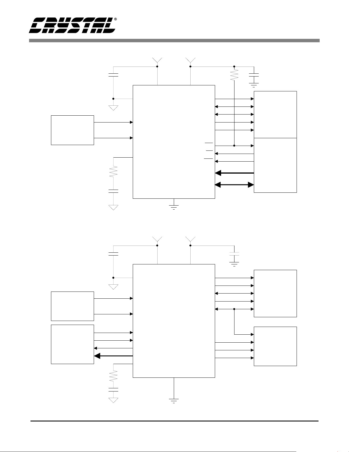
+5V Analog +5V Digital
CS8413 CS8414
Receiver
Circuit
(See Appendix A)
0.068 µF
0.1 µF
470
21
10
20
9
AGND
RXP
RXN
FILT
22
VA+
CS8413
7
VD+
FSYNC
SDATA
RD/WR
Ω
DGND
8
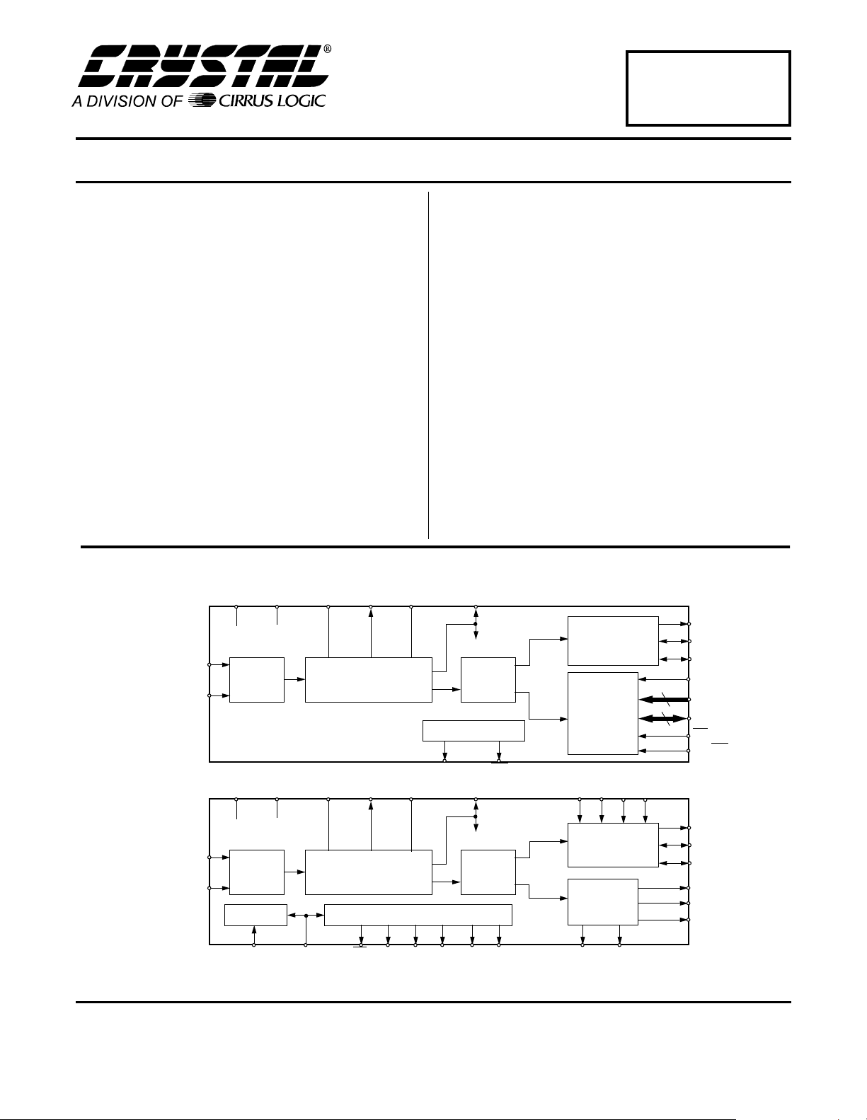
Figure 1. CS8413 Typical Connection Diagram
+5V Analog +5V Digital
MCK
SCK
ERF
INT
CS
A0-A4
D0-D7
5k
19
11
12
26
25
14
24
23
Ω
0.1 µF
Audio
Data
Processor
Audio
Data
Processor
or
Microcontroller
Receiver
Circuit
(See Appendix A)
Channel Status
and/or
Error/Frequency
Reporting
0.068 µF
0.1 µF
Ω
470
21
10
9
22
VA+
AGND
RXP
RXN
7
VD+
MCK
VERF
SCK
SDATA
FSYNC
CS8414
13
CS12/FCK
16
SEL
25
20
ERF
6 C/E-F bits
FILT
DGND
8
27, 2-6
Figure 2. CS8414 Typical Connection Diagram
C
U
CBL
19
28
12
26
11
1
14
15
0.1 µF
Audio
Data
Processor
Microcontroller
or
Logic
6 DS240F1

CS8413 CS8414
GENERAL DESCRIPTION
The CS8413/14 are monolithic CMOS circuits that
receive and decode audio and digital data according to the AES/EBU, IEC 958, S/PDIF, and EIAJ
CP340/1201 interface standards. Both chips contain RS422 line receivers and Phase-Locked Loops
(PLL) that recover the clock and synchronization
signals, and de-multiplex the audio and digital data.
The CS8413 contains a configurable internal buffer
memory, read via a parallel port, which can buffer
channel status, user, and optionally auxiliary data.
The CS8414 de-multiplexes the channel status, user, and validity information directly to serial output
pins with dedicated pins for the most important
channel status bits. Both chips also contain extensive error reporting as well as incoming sample frequency indication for auto-set applications.
The CS8413/14 are pin-compatible with the
CS8411/12 digital audio receiver parts. The functionality of the CS8413/14 is the same as the
CS8411/12 with two exceptions: first, the operating frequency (sample rate) of the CS8413/14 is extended to include 96 kHz, and second, the
frequency reporting bits are modified to delete the
±400 ppm ranges, and include 88.2 kHz and
96 kHz ranges.
Familiarity with the AES/EBU and IEC 958 specifications are assumed throughout this document.
The App Note, Overview of Digital Audio Interface Data Structures, contains information on digital audio specifications; however, it is not meant to
be a complete reference. To guarantee compliance,
the proper standards documents should be obtained. The AES/EBU standard, AES3-1985,
should be obtained from the Audio Engineering
Society or ANSI (ANSI document # ANSI S4.40-
1985); the IEC 958 standard from the International
Electrotechnical Commission; and the EIAJ
CP340/1201 standard from the Japanese Electronics Bureau.
Line Receiver
The RS422 line receiver can decode differential as
well as single ended inputs. The receiver consists
of a differential input Schmitt trigger with 50mV of
hysteresis. The hysteresis prevents noisy signals
from corrupting the phase detector. Appendix A
contains more information on how to configure the
line receivers for differential and single ende d signals.
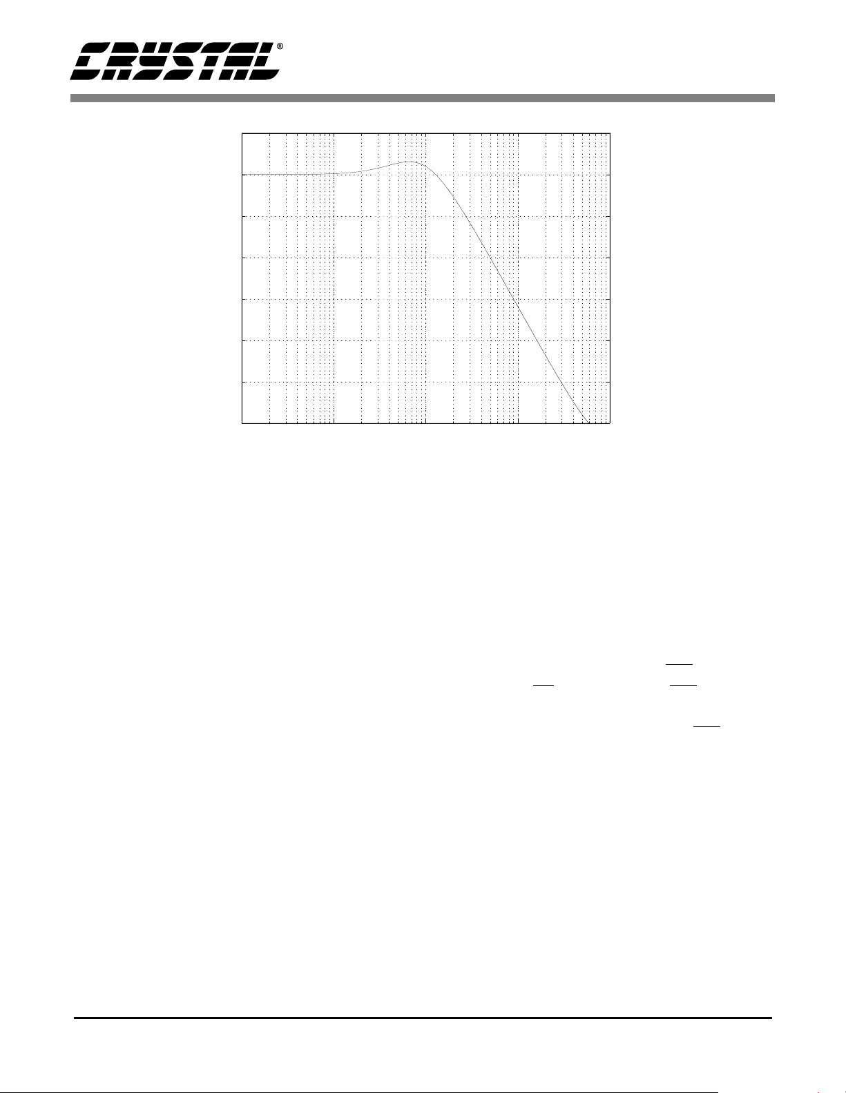
Clocks and Jitter Attenuation
The primary function of these chips is to recover
audio data and low jitter clocks from a digital audio
transmission line. The clocks that can be generated
are MCK (256xFS), SCK (64xFS), and FSYNC (F
or 2xFS). MCK is the output of the voltage controlled oscillator which is a component of the PLL.
The PLL consists of phase and frequency detectors,
a second-order loop filter, and a voltage controlled
oscillator. All components of the PLL are on chip
with the exception of a resistor and capacitor used
in the loop filter. This filter is connected betwe en
the FILT pin and AGND. The typical closed-loop
transfer function, which specifies the PLL’s jitter
attenuation characteristics, is shown in Figure 3.
Most jitter introduced by the transmission line is
high in frequency and will be strongly attenuated.
Multiple frequency detectors are used to minimize
the time it takes the PLL to lock to the incoming
data stream and to prevent false lock conditions.
When the PLL is not locked to the incoming data
stream, the frequency detectors pull the VCO frequency within the lock range of the PLL. When no
digital audio data is present, the VCO frequency is
pulled to its minimum value.
As a master, SCK is always MCK divided by four,
producing a frequency of 64xFS. In the CS8413,
FSYNC can be programmed to be a divided version
of MCK or it can be generated directly from the incoming data stream. In the CS8414, FSYNC is always generated from the incoming data stream.
When FSYNC is generated from the data, its edges
S
DS240F1 7
CS8413 CS8414
5
0
-5
-10
-15
Jitter Attenuation (dB)
-20
-25
-30
10
2
10
3
Jitter Frequency (Hz)
10
4
10
5
10
6
Figure 3. Typical Jitter Attenuation Characteristics
are extracted at times when intersymbol interference is at a minimum. This provides a sample frequency clock that is as spectrally pure as the digital
audio source clock for moderate length transmission lines. For long transmission lines, the CS8413
can be programmed to generate FSYNC from
MCK instead of from the incoming data.
CS8413 DESCRIPTION
The CS8413 is more flexible than the CS8414 but
requires a microcontroller or DSP to load internal
registers. The CS8414 does not have internal registers so it may be used in a stand-alone mode where
a microprocessor or DSP is not available.
The CS8413 accepts data from a transmission line
coded according to the digital audio interface standards. The I.C. recovers clocks and data, and separates the audio data from control information. The
audio data is output through a configurable serial
port and the control information is stored in interna l
dual-port RAM. Extensive error reporting is available via internal registers with the option of repeating the last sample when an error occurs. A block
diagram of the CS8413 is shown in Figure 4
Parallel Port
The parallel port accesses two status registers, two
interrupt enable registers, two control registers, and
28 bytes of dual-port buffer memory. The status
registers and interrupt enable registers occupy the
same address space. A bit in control register 1 selects the two registers, either status or interrupt enable, that occupy addresses 0 and 1 in the memory
map. The address bus and the RD/WR line should
be valid when CS goes low. If RD/WR is low, the
value on the data bus will be written into the buffer
memory at the specified address. If RD/WR is high,
the value in the buffer memory, at the spe cified address, is placed on the data bus. Detailed timing for
the parallel port can be found in the Switching
Characteristics - Parallel Port table.
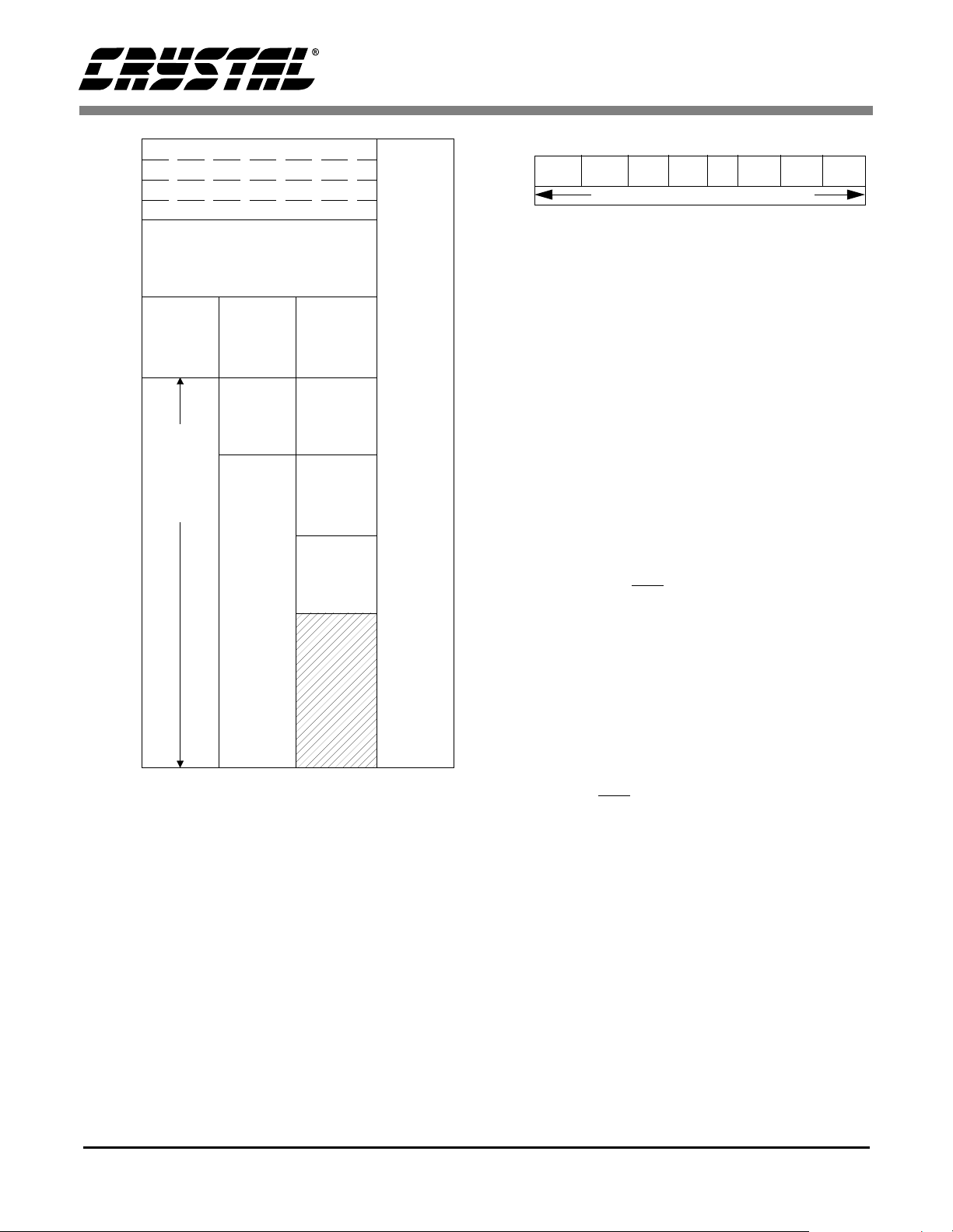
The memory space on the CS8413 is allocated as
shown in Figure 5. There are three defined buffer
modes selectable by two bits in control register 1.
Further information on the buffer modes can be
found in the Control Registers section.
8 DS240F1
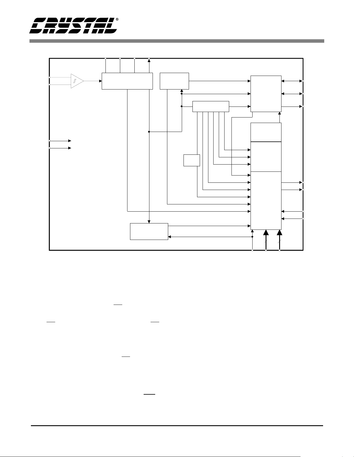
RXP
C
A
R
RXN
VD+
DGND
9
10
7
8
VA+
FIL T A GND MCK
22 20 21 19
Clock & Data
Recovery
Bi-phase
Decoder
De-Multiplexor
crc
check
user
slipped
parity
validity
crc
coding
no lock
CS8413 CS8414
Audio
Serial
Port
Control
Registers
2 X 8
aux
C.S.
Buffer
Memory
28 X 8
IEnable
&
Status
4 X 8
11
12
26
14
25
24
23
FSYN
SCK
SDAT
INT
ERF
CS
RD/W
Frequency
Comparator
Figure 4. CS8413 Block Diagram
Status and IEnable Registers
The status and interrupt enable registers occupy the
same address space. The IER/SR bit in control register 1 selects whether the status registers
(IER/SR = 0) or the IEnable registers (IER/SR = 1)
occupy addresses 0 and 1. Upon power-up, the control and IEnable registers contain all zeros; therefore, the status registers are visible and all
interrupts are disabled. The IER/SR bit must be set
to make the IEnable registers visible.
Status register 1 (SR1), shown in Figure 6, reports
all the conditions that can generate a low pulse four
SCLK cycles wide on the interrupt pin (INT ). The
three least significant bits, FLAG2-FLAG0, are
48
13
A4/
A0-A3D0-
FCK
D7
used to monitor the ram buffer. These bits continually change and indicate the position of the buffer
pointer which points to the buffer memory location
currently being written. Each flag has a corresponding interrupt enable bit in IEnable register 1
which, when set, allows a transition on the flag to
generate a pulse on the interrupt pin. FLAG0 and
FLAG1 cause interrupts on both edges whereas
FLAG2 causes an interrupt on the rising edge only.
Further information, including timing, on the flags
can be found in the Buffer Memory section.
The next five bits; ERF, SLIP, CCHG,
CRCE/CRC1, and CSDIF/CRC2, are latches
which are set when their corresponding conditions
occur, and are reset when SR1 is read. Interrupt
DS240F1 9
CS8413 CS8414
01
2
3
User Data
1st Four
Bytes of
C. S. Data
1st Four
Bytes of
C. S. Data
1st Four
Bytes of
Left C. S.
Data
Auxiliary
Data
Last
20 Bytes
Channel
Status
Data
Status 1 / IEn able 1
C. S.
Data
Left
C. S.
Data
Right
C. S.
Data
1st Four
Bytes of
Right
C. S. Data
U
N
D
E
F
I
N
E
D
A
D
D
R
E
S
S
Memory Mode
0
1
2
3
4
5
6
7
8
9
A
B
C
D
E
F
10
11
12
13
14
15
16
17
18
19
1A
1B
1C
1D
1E
1F
Control Register 1
Control Register 2
Status 2 / IEn able 2
Figure 5. CS8413 Buffer Memory Map
X:00 7 6 5 4 3 2 1 0
X:00 7 6 5 4 3 2 1 0
SR1. CSDIF/
SR1. CSDIF/
IER1. INTERRUPT ENABLE BITS FOR ABOVE
IER1. INTERRUPT ENABLE BITS FOR ABOVE
SR1: CSDIF: CS different between sub-frames. Buffer modes 0 & 1
SR1: CSDIF: CS different between sub-frames. Buffer modes 0 & 1
CRC2: CRC Error - sub-frame 2. Buffer mode 2 only.
CRC2: CRC Error - sub-frame 2. Buffer mode 2 only.
CRCE: CRC Error - selected sub-frame. Buffer modes 0 & 1
CRCE: CRC Error - selected sub-frame. Buffer modes 0 & 1
CRC1: CRC Error - sub-frame 1. Buffer mode 2 only.
CRC1: CRC Error - sub-frame 1. Buffer mode 2 only.
CCHG: Channel Status changed
CCHG: Channel Status changed
SLIP: Slipped an audio sample
SLIP: Slipped an audio sample
ERF: Error Flag. ORing of all errors in SR2.
ERF: Error Flag. ORing of all errors in SR2.
FLAG2: High for first four bytes of channel status
FLAG2: High for first four bytes of channel status
FLAG1: Memory mode dependent - See Figure 11.
FLAG1: Memory mode dependent - See Figure 11.
FLAG0: High for last two bytes of user data.
FLAG0: High for last two bytes of user data.
IER1: Enables the corresponding bit in SR1.
IER1: Enables the corresponding bit in SR1.
A “1” enables the interrupt. A “0” masks the interrupt.
A “1” enables the interrupt. A “0” masks the interrupt.
reread because the audio data output from the part
is at a different frequency than the data received
from the transmission line. CCHG is set when any
bit in channel status bytes 0 through 3, stored in the
buffer, changes from one block to the next. In buffer modes 0 and 1, only one channel of channel status data is buffered, so CCHG is only affected by
that channel. (CS2/CS1 in CR1 selects which channel is buffered.) In buffer mode 2 both channels are
buffered, so both channels affect CCHG. This bit is
updated after each byte (0 to 3) is written to the
buffer. The two most significant bits in SR1,
pulses are generated the first time that condition occurs. If the status register is not read, further instances of that same condition will not generate
another interrupt. ERF is the error flag bit and is set
when the ERF pin goes high. It is an OR’ing of the
errors listed in status register 2, bits 0 through 4,
AND’ed with their associated interrupt enable bits
CRCE/CRC1 and CSDIF/CRC2, are dual function
flags. In buffer modes 0 and 1, they are CRCE and
CSDIF, and in buffer mode 2, they are CRC1 and
CRC2. In buffer modes 0 and 1, the channel selected by the CS2/CS1 bit is stored in RAM and CRCE
indicates that a CRC error occurred in that channel.
CSDIF is set if there is any difference between the
channel status bits of each channel. In buffer mode
2 channel status from both channels is buffered,
with CRC1 indicating a CRC error in channel 1 and
CRC2 indicating a CRC error in channel 2. CRCE,
CRC1, and CRC2 are updated at the block boundary. Block boundary violations also cause CRC1,2
or CRCE to be set.
in IEnable register 2.
IEnable register 1, which occupies the same ad-
SLIP is only valid when the audio port is in slave
mode (FSYNC and SCK are inputs to the CS8413).
This flag is set when an audio sample is dropped or
10 DS240F1
dress space as status register 1, contains interrupt
enable bits for all conditions in status register 1. A
“1” in a bit location enabl es the same bit loca tion in
CRCE/
CCHG SLIP ERF FLAG2 FLAG1 FLAG0
CRCE/
CRC2
CRC2
CCHG SLIP ERF FLAG2 FLAG1 FLAG0
CRC1
CRC1
Figure 6. Status/IEnable Register 1
CS8413 CS8414
SR2: FREQ2: The 3 FREQ bits indicate incoming sample frequency.
FREQ1: (must have 6.144 MHz clock on FCK pin and FCEN
FREQ0: must be “1”)
LOCK: Out-of-Lock error
CODE: Coding violation
PARITY: Parity error
V: Validity bit high
IER2: TEST1,0: (0 on power-up) Must stay at “0”.
INT. ENABLES: Enables the corresponding bit in SR2.
A “1” enables the interrupt. A “0” masks the interrupt.
X:01765 4 3210
SR2. FREQ2 FREQ1 FREQ0 Reserved LOCK CODE PARITY V
IER2. TEST1 TEST0 INT. ENABLE BITS
FOR ABOVE
Figure 7. Status/IEnable Register 2
status register 1 to generate an interrupt pulse. A
“0” masks that particular status bit from causing an
interrupt.
Status register 2 (SR2) reports all the conditions
that can affect the error flag bit in SR1 and the error
pin (ERF), and can specify the received clock frequency. As previously mentioned, the first five bits
of SR2 are AND’ed with their interrupt enable bits
(in IER2) and then OR’ed to create ERF. The V,
PARITY, CODE and LOCK bits are latches which
are set when their corresponding conditions occur,
and are reset when SR2 is read. The ERF pin is asserted each time the error occurs assuming the interrupt enable bit in IER2 is set for that particular
error. When the E RF pin is ass erte d, the E RF bit in
SR1 is set. If the ERF bit was not set prior to the
ERF pin assertion, an interrupt will be generated
(assuming bit 3 in IER1 is set). Although the ERF
pin is asserted for each occurrence of an enabled error condition, the ERF bit will only cause an interrupt once if SR1 is not read.
The upper three bits in SR2, FREQ2-FREQ0, can
report the receiver f requency when the receive r is
locked. These bits are only valid when FCEN in
control register 1 is set, and a 6.144 MHz clock is
applied to the FCK pin. When FCEN is set, the
A4/FCK pin is used as FCK and A4 is internally set
to zero; therefore, only the lower half of the buffer
can be accessed. Table 1 lists the frequency ranges
reported. The FREQ bits are updated three times
per block and the clock on the FCK pin must be valid for two thirds of a block for the FREQ bits to be
accurate. The FREQ bits are invalid when the PLL
is out of lock.
FREQ2 FREQ1 FREQ0 Sample Frequency
0 0 0 Out of Range
0 0 1 reserved
0 1 0 reserved
011 96 kHz ± 4%
1 0 0 88.2 kHz ± 4%
1 0 1 48 kHz ± 4%
1 1 0 44.1 kHz ± 4%
1 1 1 32 kHz ± 4%
V is the validity status bit whi ch is set a ny tim e t he
received validity bit is high. PARITY is set when a
parity error is detected. CODE is set when a biphase coding error is detected. LOCK is asserted
when the receiver PLL is not locked and occurs
when there is no input on RXP/RXN, or if the received frequency is out of the receiver lock range
(28.4 kHz to 100 kHz).
DS240F1 11
Table 1. Incoming Sample Frequency Bits
IEnable register 2 has corresponding interrupt enable bits for the first five bits in SR2. A “1” enables
the condition in SR2 to cause ERF to go high, while
a “0” masks that condition. Bit 5 is unused and bits
6 and 7, the two most significant bits, are factory
test bits and must be set to zero when writing to this
register. The CS8413 sets these bits to zero on power-up.
Control Registers
The CS8413 contains two control registers. Control
register 1 (CR1), at address 2, selects system level
features, while control register 2 (CR2), at address
3, configures the audio serial port.
In control register 1, when RST is low, all outputs
are reset except MCK (FSYNC and SCLK are high
impedance). The CS8413 should be reset imediately after power-up and any time the user performs a
CS8413 CS8414
system-wide reset. After the user sets R ST high, the
CS8413 comes fully out of reset when the block
boundary is found. The serial port, in master mode,
will begin to operate as soon as RST goes high. B0
and B1 select one of three buffer modes listed in
Table and illustrated in Figure 5. In all modes four
bytes of user data are stored. In mode 0, one entire
block of channel status is stored. In mode 1 eight
bytes of channel status and sixteen bytes of auxiliary data are stored. In mode 2, eight bytes of channel
status from each sub-frame are stored. The buffer
modes are discussed in more detail in the Buffer
Memory section. The next bit, CS2/CS1, selects the
particular sub-frame of channel status to buffer in
modes 0 and 1, and has no effect in mode 2. When
CS2/CS1 is low, sub-frame 1 is buffered, and when
CS2/CS1 is high, sub-frame 2 is buff ered. IER/SR
selects which set of registers, either IEnable or status, occupy addresses 0 and 1. When IER/SR is
low, the status registers occupy the first two addresses, and when IER/SR is high, the IEnable registers occupy those addresses. FCEN enables the
internal frequency counter. A 6.144 MHz clock
must be connected to the FCK pin as a reference.
The value of the FREQ bits in SR2 are not valid until two thirds of a block of data is received. Since
FCK and A4, the most significant address bit, occupy the same pin, A4 is internally set to zero when
FCEN is high. Since A4 is forced to zero, the upper
half of the buffer is not accessible while using the
frequency compare feature. FPLL determines how
FSYNC is derived. When FPLL is low, FS YNC is
derived from the incoming data, and when FPLL is
high, it is derived from the internal phase-locked
loop.
Control Register 2 configures the serial port which
consists of three pins: SCK, SDATA, and FSYNC.
SDATA is always an output, but SCK and FSYNC
can be configured as inputs or outputs. FSYNC and
SDATA can have a variety of relationships to each
other, and the polarity of SCK can be controlled.
The large variety of audio data formats provides an
easy interface to most DSPs and other audio processors. SDATA is normally just audio data, but
special modes are provided that output received biphase data, or received NRZ data with zeros substituted for preamble. Another special mode allows an
asynchronous SCK input to read audio data from
the serial port without slipping samples. In this
mode FSYNC and SDATA are outputs synchronized to the SCK input. Since SCK is asynchronous
to the received clock, the number of SCK c ycles
between FSYNC edges will vary.
B1 B0 Mode Buffer Memory Contents
0 0 0 Channel Status
011 Auxiliary Data
1 0 2 Independent Channel Status
113 Reserved
Table 2. Buffer Memory Modes
X:027 6 5 4 3210
CR1. FPLL FCEN
CR1: FPLL: 0 - FSYNC from RXP/RXN, 1 - FSYNC from PLL
FCEN: enables freq. comparator (FCK must be 6.144 MHz).
: [X:00,01] 0 - status, 1 - interrupt enable registers.
IER/SR
CS2/CS1
B1: with B0, selects the buffer memory mode.
B0: with B1, selects the buffer memory mode.
: Resets internal counters. Set to “1” for normal operation.
RST
X:0376543210
CR2.
ROER
CR2: ROER: Repeat previous value on error (audio data)
SDF2: with SDF0 & SDF1, select serial data format.
SDF1: with SDF0 & SDF2, select serial data format.
SDF0: with SDF1 & SDF2, select serial data format.
FSF1: with FSF0, select FSYNC format.
FSF0: with FSF1, select FSYNC format.
MSTR: When set, SCK and FSYNC are output
SCED: When set, falling edge of SCK outputs data.
IER/SR
: ch. status to buffer; 0 - sub-frame 1, 1 - sub-frame 2.
Figure 8. Control Register 1
SDF2 SDF1 SDF0 FSF1 FSF0 MSTR SCED
When clear, rising edge of SCK outputs data.
Figure 9. Control Register 2
CS2/CS1
B1 B0 RST
ROER, when set, causes the last audio sample to be
reread if the error pin, ERF, is active. When out of
lock, the CS8413 will output zeros if ROER is set
12 DS240F1

CS8413 CS8414
X
and output random data if ROER is not set. The
conditions that activate ERF are those reported in
SR2 and enabled in IER2. Figure 10 illustrates the
modes selectable by SDF2-SDF0 and FSF1-FSF0.
MSTR, which in most applications will be set to
one, determines whether FSYNC and SCK are outputs (MSTR = 1) or inputs (MSTR = 0). When
FSYNC and SCK are inputs (slave mode) the audio
FSF
10 (bit)
00
01
10
11
00
01
10
MSTR
0
FSYNC Input
FSYNC Input
0
FSYNC Input
0
FSYNC Input
0
1
FSYNC Output
1
FSYNC Output
1
FSYNC Output
16 Clocks
16 Clocks
32 Bits
32 Clocks
data can be read twice or missed if the device controlling FSYNC and SCK is on a different timebase than the CS8413. If the audio data is read
twice or missed, the SLIP bit in SR1 is set. SCED
selects the SCK edge to output data on. SCED high
causes data to be output on the falling edge, and
SCED low causes data to be output on the rising
edge.
32 Bits
16 Clocks
16 Clocks
32 Clocks
11
1
FSYNC Output
SDF
210 (bit)
000
001
011
101
111
SPECIAL MODES:
SDF
210 MSTR Name
100
110 0
010 0
010*† 1
100* 1
* Error flags are not accurate in these modes
† FSYNC is inverted FSF = 11
Name
MSB First - 32
MSB Last
LSB Last - 16
LSB Last - 18
LSB Last - 20
Async SCK
0
MSB First - 24
MSB First - 16
NRZ Data
Bi-Phase Data
MSB
MSB
LSB
LSB LSBMSB LSBMSB
LSB MSB
MSB
MSB
MSB MSB MSBLSBLSB
Figure 10. CS8413 Serial Port SDATA and FSYNC Timing
32 Clocks
Left Sample
24 Bits, Incl. Aux
LSB
24 Bits, Incl. Aux 24 Bits, Incl. Aux
LSB MSB
16 Bits
18 Bits
20 Bits
24 Bits, Incl. Aux 24 Bits, Incl. Aux
LSB
24 Bits, Incl. Aux
16 Bits
32 Bits 32 Bits
AUX
LSB
MSB
LSBMSB
LSB
LSB
VUCP
MSB
MSB
MSB
32 Clocks
Right Sample
24 Bits, Incl. Aux
LSB MSB
MSB LSB
24 Bits, Incl. Aux
16 Bits
LSB
AUX
Bi-Phase Mark DataBi-Phase Mark Data
LSB MSB
16 Bits
MSB
18 Bits
20 Bits
LSB
MSB
LSB
LSB
VUCP
MSB
MSB
AU
DS240F1 13

CS8413 CS8414
Audio Serial Port
The audio serial port outputs the audio data portion
from the received data and consists of three pins:
SCK, SDATA, and FSYNC. SCK clocks the data
out on the SDATA line. The edge that SCK uses to
output data is programmable from CR2. FSYNC
delineates the audio samples and may indicate the
particular channel, left or right. Figure 10 illustrates the multitude of formats that SDATA and
FSYNC can take.
Normal Modes
SCK and FSYNC can be inputs (MSTR = 0) or outputs (MSTR = 1), and are usually programmed as
outputs. As outputs, SCK contains 32 periods for
each sample and FSYNC has four formats. The
first two output formats of FSYNC (shown in Figure 10) delineate each word and the identification
of the particular channel must be kept track of externally. This may be done using the rising edge of
FLAG2 to indicate the next data word is left channel data. The last two output formats of FSYNC
also delineate each channel with the polarity of
FSYNC indicating the particular channel. The last
format has FSYNC change one SCK cycle before
the frame containing the data and may be used to
generate an I2S compatible interface.
When SCK is programmed as an input, 32 SCK cycles per sample must be provided. (There are two
formats in the Special Modes section where SCK
can have 16 or 24 clocks per sample.) The four
modes where FSYNC is an input are similar to the
FSYNC output modes. The first two require a transition of FSYNC to start the sample frame, whereas
the last two are identical to the corresponding
FSYNC output modes. If the circuit generating
SCK and FSYNC is not locked to the master clock
of the CS8413, the serial port will eventually be reread or a sample will be missed. When this occurs,
the SLIP bit in SR1 will be set.
SDATA can take on five formats in the normal serial port modes. The first format (see Figure 10),
MSB First, has the MSB aligned with the start of a
sample frame. Twenty-four audio bits are output
including the auxiliary bits. This mode is compatible with many DSPs. If the auxiliary bits are used
for something other than audio data, they must be
masked off. The second format, MSB Last, outputs
data LSB first with the MSB aligned to the end of
the sample frame. This format is conducive to serial arithmetic. Both of the above formats output all
audio bits from the received data. The last three formats are LSB Last formats that output the most significant 16, 18, and 20 bits respectively, with the
LSB aligned to the end of the sample frame. These
formats are used by many interpolation filters.
Special Modes
Five special modes are included for unique applications. In these modes, the master bit, MSTR, must
be defined as shown in Figure 10. In the first mode,
Asynchronous SCK, FSYNC (which is an output in
this mode) is aligned to the incoming SCK. This
mode is useful when the SCK is locked to an external event and cannot be derived from MCK. Since
SCK is asynchronous, the number of SCK cycles
per sample frame will vary. The data output will be
MSB first, 24 bits, and aligned to the beginning of
a sample frame. The second and third special
modes are unique in that they contain 24 and 16
SCK cycles respectively per sample frame, whereas all normal modes contain 32 SCK cycles. In
these two modes, the data is MSB first and fil ls the
entire frame. The fourth special mode outputs NRZ
data including the V, U, C, and P bits and the preamble replaced with zeros. SCK is an output with
32 SCK cycles per sample frame. The fifth mode
outputs the biphase data recovered from the transmission line with 64 SCK cycles output per sample
frame, with data changing on the rising edge.
Normally, data recovered by the CS8413 is delayed
by two frames in propagating through the part, but
14 DS240F1

CS8413 CS8414
in the fourth and fifth special modes, the data is delayed only a few bit periods before being output.
However, error codes, and the C, U and V bits follow the normal pathway with a two frame delay (so
that the error code would be output with the offending data in the other modes). As a result, in special
modes four and five, the error codes are nearly two
frames behind the data output on SDATA.
Buffer Memory
In all buffer modes, the status, mask, and control
registers are located at addresses 0-3, and the user
data is buffered at locations 4 through 7. The parallel port can access any location in the user data
buffer at any time; however, care should be taken
not to read a location when that location is being
updated internally. This internal writing is done
through a second port of the buffer and is done in a
cyclic manner. As data is received, the bits are assembled in an internal 8-bit shift register which,
when full, is loaded into the buffer memory. The
first bit received is stored in D0 and, after D7 is received, the byte is written into the proper buffer
memory location.
The user data is received one bit per sub-frame. At
the channel status block boundary, the internal
pointer for writing user data is initialized to 04H
(Hex). After receiving eight user bits, the byte is
written to the address indicated by the user pointer
which is then incremented to point to the next address. After receiving all four bytes of user data, 32
audio samples, the user pointer is set to 04H again
and the cycle repeats. FLAG0, in SR1 can be used
to monitor the user data buffer. When the last byte
of the user buffer, location 07H, is written, FLAG0
is set low and when the second byte, location 05H,
is written, FLAG0 is set high. If the corresponding
bit in the interrupt enable register (IER1, bit 0) is
set, a transition of FLAG0 will generate a low pulse
on the interrupt pin. The level of FLAG0 indicates
which two bytes the part will write next, thereby indicating which two bytes are free to be read.
FLAG1 is buffer mode dependent and is discussed
in the individual buffer mode sections. A transition
of FLAG1 will generate an interrupt if the appropriate interrupt enable bit is set.
FLAG2 is set high after channel status byte 23, the
last byte of the block, is written and set low after
channel status byte 3 is written to the buffer memory. FLAG2 is unique in that only the rising edge
can cause an interrupt if the appropriate interrupt
enable bit in IER1 is set.
Figure 11 illustrates the flag timing for an entire
channel status block which includes 24 bytes of
channel status data per channel and 384 audio samples. The lower portion of Figure 11 expands the
first byte of channel status showing eight pairs of
data, with a pair defined as a frame. This is further
expanded showing the first sub-frame (A0) to contain 32 bits defined as per the digital audio standards. When receiving stereo, channel A is left and
channel B is right.
For all three buffer modes, the three most significant bits in SR1, shown in Figure 6, can be used to
monitor the channel status data. In buffer mode 2,
bits 7 and 6 change definition and are described in
that section. Channel status data, as described in the
standards, is independent for each channel. Each
channel contains its own block of channel status
data, and in most systems, both channels will contain the same channel status data. Buffer modes 0
and 1 operate on one block of channel status with
the particular block selected by the CS2/CS1 bit in
CR1. CSDIF, bit 7 in SR1, indicates when the
channel status data for each channel is not the same
even though only one channel is being buffered.
CRCE, bit 6 in SR1, indicates a CRC error occurred in the buffered channel. CCHG, bit 5 in
SR1, is set when any bit in the buffered channel status bytes 0 to 3, change from one block to the next.
DS240F1 15

Flag 2
Flag 1
Mode 0
Flag 1
Modes 1 & 2
Flag 0
230123456789 1011121314 15 16 171819 20 21 222301
CS8413 CS8414
Block
(384 Audio Samples)
Channel Status Byte
(Expanded)
Frame
A 0
0347
bit
Preamble
B 0
Aux Data
A 1
Figure 11. CS8413 Status Register Flag Timing
B 1
(Expanded)
8
LSB
Buffer Mode 0
The user data buffer previously described is identical for all modes. Buffer mode 0 allocates the rest
of the buffer to channel status data. This mode
stores an entire block of channel status in 24 memory locations from address 08H to 1FH. Channel
status (CS) data is different from user data in that
B 2A 2
Sub-frame
Audio Data
A 7
Validity
User Data
Channel Status Data
Parity Bit
B 7
27
282930 31
VU
CPMSB
channel status data is independent for each channel.
A block of CS data is defined as one bit per frame,
not one bit per sub-frame; therefore, t here are two
blocks of channel status. The CS2/CS1 bit in CR1
selects which channel is stored in the buffer. In a
typical system sending stereo data, the channel status data for each channel would be identical.
16 DS240F1

CS8413 CS8414
FLAG1 in status register 1, SR1, can be used to
monitor the channel status buffer. In mode 0,
FLAG1 is set low after channel status byte 23 (the
last byte) is written, and is set high when channel
status byte 15, location 17H is written. If the corresponding interrupt enable bit in IER1 is set, a transition of FLAG1 will generate a pulse on the
interrupt pin. Figure 12 illustrates the memory
write sequence for buffer mode 0 along with flag
timing. The arrows on the flag timing indicate
when an interrupt will occur if the appropriate interrupt enable bit is set. FLAG0 ca n cause an inte rrupt on either edge, which is only shown in the
expanded portion of the figure for clarity.
Buffer Mode 1
In buffer mode 1, eight bytes are allocated for channel status data and sixteen bytes for auxiliary data
as shown in Figure 5. The user data buffer is the
same for all modes. The channel status buffer, locations 08H to 0FH, is divided into two sections. The
first four locations always contain the first four
bytes of channel status, identical to mode 0, and are
written once per channel status block. The second
four locations, addresses 0CH to 0FH, provide a
cyclic buffer for the last 20 bytes of channel status
data. The channel status buffer is divided in this
fashion because the first four bytes are the most important ones; whereas, the last 20 bytes are often
not used (except for byte 23, CRC).
FLAG1 and FLAG2 can be used to monitor this
buffer as shown in Figure 13. FLAG1 is set high
when CS byte 1, location 09H, is written and is toggled when every other byte is written. FLAG2 is set
high after CS byte 23 is written and set low after CS
byte 3, location 0BH, is written. FLAG2 determines whether the channel status pointer is writing
to the first four-byte section of the channel status
buffer or the second four-byte section, while
FLAG1 indicates which two bytes of the section
are free to update.
The auxiliary data buffer, locations 10H to 1FH, is
written to in a cyclic manner similar to the other
buffers. Four auxiliary data bits are received per
audio sample (sub-frame) and, since the auxiliary
data is four times larger than the user data, the auxiliary data buffer on the CS8413 is four times larger
allowing FLAG0 to be used to monitor both.
Block
(384 Audio Samples)
FLAG2
FLAG1
FLAG0
10
C.S. Byte
C.S. Address
0123456789
08
0B 0C
11 12 13 14
15
16 17 18 19
20
21 22 23 0 1
1F 08
(Expanded)
FLAG0
C.S. Addr.
User Addr.
DS240F1 17
07
08 09
04
05 06 07 04 05 06 07
Figure 12. CS8413 Buffer Memory Write Sequence - MODE 0
0A 0B1F
(Addresses are in Hex)

FLAG2
FLAG1
FLAG0
C.S. Byte
C.S. Addr e ss
FLAG1
FLAG0
C.S. Addr.
User Addr.
Aux. Addr.
CS8413 CS8414
Block
(384 Audio Samples)
0123456789
08 0B 0C 0F 08
0F
04 05 06 07 04 05 06 0707
10 13,14 17 18 1B,1C 1F 10 13,14 17 18 1B,1C
08 09
0F 0C 0F 0C 0F 0C 0F 0C
Figure 13. CS8413 Buffer Memory Write Sequence - MODE 1
10
11 12 13 14
15
(Expanded)
0A 0B
16 17 18 19
20
21 22 23 0
(Addresses are in Hex)
1F1F
1
(384 Audio Sa mples)
FLAG2
FLAG1
FLAG0
Left C.S. Ad.
Right C.S. Ad.
012
08 0B 0C 0F 08
10 13 14 17 1017 14 17 14 17 14 17 14
3
4 5 6 7 8 9 10111213141516171819202122230 1C.S. Byte
0F 0C 0F 0C 0F 0C 0F 0C
(Expanded)
FLAG1
FLAG0
Left C.S. Ad.
Right C.S. Ad.
User Addres s
08 09
10 11
05 06 07 04
0A 0B
12
05
06 0704
Figure 14. CS8413 Buffer Memory Write Sequence - MODE 2
Buffer Mode 2
In buffer mode 2, two 8-byte buffers are available
to independently buffer each channel of channel
status data. Both buffers are identical to the channel
status buffer in mode 1 and are written to simulta-
Block
(Addresses are in Hex)
13
neously, with locations 08H to 0FH containing CS
data for channel A and locations 10H to 17H containing CS data for channel B. Both CS buffers can
be monitored using FLAG1 and FLAG2 as described in the BUFFER MODE 1 section.
18 DS240F1

CS8413 CS8414
The two most significant bits in SR1 change definition for buffer mode 2. These two bits, when set, indicate CRC errors for thei r respective channe ls. A
CRC error occurs when the internal calculated
CRC for channel status bytes 0 through 22 does not
match channel status byte 23. CCHG, bit 5 in SR1,
is set when any bit in the first four channel status
bytes of either channel changes from one block to
the next. Since channel status doesn’t change very
often, this bit may be monitored rather than checking all the bits in the first four bytes. These bits are
illustrated in Figure 6.
Buffer Updates and Interrupt Timing
As mentioned previously in the buffer mode sections, conflicts between externally reading the
buffer RAM and the CS8413 internally writing to it
may be averted by using the flag levels to avoid the
section currently being addressed by the part. However, if the interrupt line, along with the flags, is
utilized, the actual byte that was just updated can be
determined. In this way, the entire buffer can be
read without concern for internal updates.
Figure 15 shows the detailed timing for the inter-
rupt line, flags, and the RAM write line. SCK is 64
times the incoming sample frequency, and is the
same SCK output in master mode. The FSYNC
shown is valid for all master modes except the I2S
compatible mode. The interrupt pulse is shown to
be 4 SCK periods wide and goes low 5 SCK periods after the RAM is written. Using the above information, the entire data buffer may be read
starting with the next byte to be updated by the internal pointer.
ERF Pin Timing
ERF signals that an error occurred while receiving
the audio sample that is currently being read from
the serial port. ERF changes with the active edge of
FSYNC and is high during the erroneous sample.
ERF is affected by the error conditions reported in
SR2: LOCK, CODE, PARITY, and V. Any of
these conditions may be masked off using the corresponding bits in IER2. The ERF pin will go high
for each error that occurs. The ERF bit in SR1 is
different from the ERF pin in that it only causes an
interrupt the first time an error occurs until SR1 is
read. More information on the ERF pin and bit is
SCK
FSYNC
IWRITE
INT
INT
FSF1,0
MSTR
SCED
DS240F1 19
(FLAG0,1)
(FLAG2)
= 1 0
= 1
= 1
Left 191 Right 191 Left 0
Figure 15. RAM/Buffer - Write and Interrupt Timing

CS8413 CS8414
contained at the end of the Status and IEnable Registers section.
CS8414 DESCRIPTION
The CS8414 does not need a microprocessor to
handle the non-audio data (although a micro may
be used with the C and U serial ports). Instead, dedicated pins are available for the most important
channel status bits. The CS8414 is a monolithic
CMOS circuit that receives and decodes digital audio data which was encoded according to the digital
audio interface standards. It contains an RS422 line
receiver and clock and data recovery utilizing an
on-chip phase-locked loop. The audio data is output through a configurable serial port that supports
14 formats. The channel status and user data have
their own serial pins and the validity flag is OR’ed
VA+ FILT AGND MCK
22 20 21 19
RXP
RXN
VD+
DGND
CS12/
FCK
SEL
9
10
7
8
13
Frequency
Comparator
33
16
Parity
Check
6
Clock & Data
Recovery
Encoder
6
5
Ca/
C0/
E1
E0
Bi-phase
Decoder
and
Frame
Sync
Error
Multiplexer
4
32
Cb/
E2
Cc/
F0
Cd/
F1
CRC
check
27
Ce/
F2
with the ERF flag to provide a single pin, VERF,
indicating that the audio output may not be valid.
This pin may be used by interpolation filters that
provide error correction. A block diagram of the
CS8414 is illustrated in Figure 16.
The line receiver and jitter performance are described in the sections directly preceding the
CS8413 sections in the beginning of this data sheet.
Audio Serial Port
The audio serial port is used primarily to output audio data and consists of three pins: SCK, FSYNC,
and SDATA. These pins are configured via four
control pins: M0, M1, M2, and M3. M3 selects between eight normal serial formats (M3 = 0), and six
special formats (M3 = 1).
M0M1M2M3
17 18 24 23
Timing
11
De-Multiplexer
Channel
Status
Latch
6
Audio
Serial
Port
R
e
g
i
s
t
e
r
s
12
26
1
14
28
15
25
FSYNC
SCK
SDATA
C
U
VERF
CBL
ERF
Figure 16. CS8414 Block Diagram
20 DS240F1

CS8413 CS8414
Normal Modes (M3 = 0)
When M3 is low, the normal serial port formats
shown in Figure 17 are selected using M2, M1, and
M0. These formats are also listed in Table 3,
wherein the first word past the format number
(Out-In) indicates whether FSYNC and SCK are
outputs from the CS8414 or are inputs. The next
word (L/R-WSYNC) indicates whether FSYNC indicates the particular channel or just delineates
each word. If an error occurs (ERF = 1) while using
one of these formats, the previous valid audio data
for that channel will be output. As long as ERF is
high, that same data word will be output. If the
CS8414 is not locked, it will output all zeroes. In
some modes FSYNC and SCK are outputs and in
others they are inputs. In Table 3, LSBJ is short for
LSB justified where the LSB is justified to the end
of the audio frame and the MSB varies with word
length. As outputs the CS8414 generates 32 SCK
periods per audio sample (64 per stereo sample)
and, as inputs, 32 SCK periods must be provided
per audio sample. When FSYNC and SCK are inputs, one stereo sample is double buffered. For
those modes which output 24 bits of audio data, the
auxiliary bits will be included. If the auxiliary bits
are not used for audio data, they must be masked
off.
M2 M1 M0 Format
0 0 0 0 - Out, L/R, 16-24 Bits
0 0 1 1 - In, L/R, 16-24 Bits
010
011
1 0 0 4 - Out, WSYNC, 16-24 Bits
1 0 1 5 - Out, L/R, 16 Bits LSBJ
1 1 0 6 - Out, L/R, 18 Bits LSBJ
1 1 1 7 - Out, L/R, MSB Last
Table 3. Normal Audio Port Modes (M3 = 0)
2 - Out, L/R, I
3 - In, L/R, I
2
S Compatible
2
S Compatible
Special Modes (M3 = 1)
When M3 is high, the special audio modes described in Table 4 are selected via M2, M1, and
M0. In formats 8, 9, and 10, SCK, FSYNC, and
SDATA are the same as in formats 0, 1, and 2 respectively; however, the recovered data is output as
is even if ERF is high, indicating an error. (In
modes 0-2 the previous valid sample is output.)
Similarly, when out of lock, the CS8414 will still
output all the recovered data, which should be zeros if there is no input to the RXP, RXN pins. Format 11 is similar to format 0 except that SCK is an
input and FSYNC is an output. In this mode
FSYNC and SDATA are synchronized to the incoming SCK, and the number of SCK periods between FSYNC edges will vary since SCK is not
synchronous to received data stream. This mode
may be useful when writing data to storage.
M2 M1 M0 Format
0 0 0 8 - Format 0 - No repeat on error
0 0 1 9 - Format 1 - No repeat on error
0 1 0 10 - Format 2 - No repeat on error
0 1 1 11 - Format 0 - Async. SCK input
1 0 0 12 - Received NRZ Data
1 0 1 13 - Received Bi-phase Data
1 1 0 14 - Reserved
1 1 1 15 - CS8414 Reset
Table 4. Special Audio Port Modes (M3 = 1)
Format 12 is similar to format 7 except that SDATA is the entire data word received from the transmission line including the C, U, V, and P bits, with
zeros in place of the preamble. In format 13 SDATA contains the entire biphase encoded data from
the transmission line including the preamble, and
SCK is twice the normal frequency. The normal
two frame delay of data from input to output is reduced to only a few bit periods in formats 12 and
13. However, the C, U, V bits and error codes follow their normal pathways and therefore follow the
output data by nearly two frames. Figure 18 illustrates formats 12 and 13. Format 14 is reserved and
not presently used, and format 15 causes the
CS8414 to go into a reset state. While in reset all
outputs will be inactive except MCK. The CS8414
comes out of reset at the first block boundary after
DS240F1 21

FMT
No.
0
M2 M1 M0
000
FSYNC (out)
SCK (out)
Left
CS8413 CS8414
Right
SDATA (out)
1
2
3
4
1
0
FSYNC (in)
100
SDATA (out)
FSYNC (out)
001
SDATA (out)
FSYNC (in)
10
SDATA (out)
FSYNC (out)
01
SCK (out)
SDATA (out)
SCK (in)
SCK (out)
SCK (in)
MSB
Left
MSB
Left
MSB
Left
MSB
Left
MSB
LSB
LSB
LSB MSB
LSB
LSB
MSB
MSB
MSB
MSB
Right
Right
Right
Right
LSB
LSB
LSB
LSB
LSB
MSB
MSB
MSB
MSB
MSB
FSYNC (out)
5
6
7
11
0
1
1
SDATA (out)
FSYNC (out)
01
SCK (out)
SDATA (out)
FSYNC (out)
11
SCK (out)
SDATA (out)
SCK (out)
LSB
LSB
MSB
Left
MSB LSB
16 Bits
Left
MSB
18 Bits
Left
LSB
LSB
MSB
Right
MSB
Right
MSB
Right
LSB
LSB
16 Bits
LSB
18 Bits
MSB
Figure 17. CS8414 Audio Serial Port Formats
22 DS240F1

No.
CS8413 CS8414
FSYNC (out)
12*
SCK (out)
SDATA (out)
FSYNC (out)
13*
SCK (out)
SDATA (out)
* Error flags are n ot accur a te in these mode s
Figure 18. Special Audio Port Formats 12 and 13
Left
Left
leaving the reset state. The CS8414 should be reset
immediately after power-up and any time the user
performs a system-wide reset. See Appendix B for
a suggested reset circuit.
C, U, VERF, ERF, and CBL Serial Outputs
The C and U bits and CBL are output one SCK period prior to the active edge of FSYNC in all serial
port formats except 2 and 3 (I2S modes). The active
edge of FSYNC may be used to latch C, U, and
CBL externally. In formats 2 and 3, the C and U
bits and CBL are updated with the active edge of
FSYNC. The validity + error flag (VERF) and the
error flag (ERF) are always updated at the active
edge of FSYNC. This timing is illustrated in
Figure 19.
Right
MSB VUCPLSBAUX MSB VUCPLSBAUX
Right
VUCPLSB VUCPLSB
MSB MSBAUX AUX
The C output contains the channel status bits with
CBL rising indicating the start of a new channel
status block. CBL is high for the first four bytes of
channel status (32 frames or 64 samples) and low
for the last 20 bytes of channel status (160 frames
or 320 samples). The U output contains the User
Channel data. The V bit is OR ’ed with the ERF flag
and output on the VERF pin. This indicates that the
audio sample may be in error and can be used by interpolation filters to interpolate through the error.
ERF being high indicates a serious error occurred
on the transmission line. There are three errors that
cause ERF to go high: a parity error or biphase coding violation during that sample, or an out of lock
PLL receiver. Timing for the above pins is illustrated in Figure 19.
CBL
C0,
Ca-Ce
SDATA
FSYNC
ERF,
VERF
C, U
DS240F1 23
Left 0 Left 1Right 0 Left 0Left 32 Right 191Right 31Right 191
Figure 19. CBL Timing

CS8413 CS8414
Multifunction Pins
There are seven multifunction pins which contain
either error and received frequency information, or
channel status information, selectable by SEL.
Error and Frequency Reporting
When SEL is low, error and received frequency information are selected. The error information is encoded on pins E2, E1, and E0, and is decoded as
shown in Table 5. When an error occurs, the corresponding error code is latched. Clearing is then accomplished by bringing SEL high for more than
eight MCK cycles. The errors have a priority associated with their error code, with validity having
the lowest priority and no lock having the highest
priority. Since only one code can be displayed, the
error with the highest priority that occurred since
the last clearing will be selected.
E2 E1 E0 Error
000 No Error
0 0 1 Validity Bit High
0 1 0 Reserved
0 1 1 Slipped Sample
1 0 0 CRC Error (PRO only)
101 Parity Error
1 1 0 Bi-phase Coding Error
1 1 1 No Lock
Table 5. Error Decoding
The validity flag indicates that the va lidity bit for a
previous sample was high since the last clearing of
the error codes. The slipped sample error can only
occur when FSYNC and SCK of the audio serial
port are inputs. In this case, if FSYNC is asynchronous to the received data rate, periodically a stereo
sample will be dropped or reread depending on
whether the re ad rate is slower or fast er than th e received data rate. When this occurs, the slipped sam-
ple error code will appear on the ‘E’ pins. The CRC
error is updated at the beginning of a channel status
block, and is only valid when the professional for-
mat of channel status data is received. This error is
indicated when the CS8414 calculated CRC value
does not match the CRC byte of the channel status
block or when a block boundary changes (as in removing samples while editing). The parity error occurs when the incoming sub-frame does not have
even parity as specified by the standards. The biphase coding error indicates a biphase coding violation occurred. The no lock error indicates that the
PLL is not locked onto the incoming data stream.
The received frequency information is encoded on
pins F2, F1, and F0, and is decoded as shown in Table 6. The on-chip frequency comparator compares
the received clock frequency to an externally supplied 6.144 MHz clock which is input on the FCK
pin. The ‘F’ pins are updated three times during a
channel status block including prior to the rising
edge of CBL. CBL may be used to externally latch
the ‘F’ pins. The clock on FCK must be valid for
two thirds of a block for the ‘F’ pins to be accurate.
The ‘F’ pins are invalid when the PLL is out of
lock.
F2 F1 F0 Sample Frequency
0 0 0 Out of Range
0 0 1 reserved
0 1 0 reserved
011 96 kHz ±4%
1 0 0 88.2 kHz ±4%
1 0 1 48 kHz ±4%
1 1 0 44.1 kHz ±4%
1 1 1 32 kHz ±4%
Table 6. Sample Frequency Decoding
Channel Status Reporting
When SEL is high, channel status is displayed on
C0, and Ca-Ce for the channel selected by CS12. If
CS12 is low, channel status for sub-frame 1 is displayed, and if CS12 is high, channel status for subframe 2 is displayed. The contents of Ca-Ce depend
24 DS240F1

CS8413 CS8414
upon the C0 professional/consumer bit. The information reported is shown in Table 7.
Pin Professional Consumer
C0
Ca C1
Cb EM0 C2
Cc EM1 C3
Cd C9 ORIG
Ce CRCE IGCAT
Table 7. Channel Status Pins
0 (low) 1 (high)
C1
Professional Channel Status (C0 = 0)
When C0 is low, the received channel status block
is encoded according to the professional/broadcast
format. The Ca through Ce pins are defined for
some of the more important professional bits. As
listed in Table 7, Ca is the inverse of channel status
bit 1. Therefore, if the incoming channel status bit
1 is 1, Ca, defined as C1, will be 0. C1 indicates
whether audio (C1 = 1) or non-audio (C1 = 0) data
is being received. Cb and Cc, defined as EM0 and
EM1 respectively, indicate emphasis and are encoded versions of channel status bits 2, 3, and 4.
The decoding is listed in Table 8. Cd, defined as
C9, is the inverse of channel status bit 9, which
gives some indication of channel mode. (Bit 9 is
also defined as bit 1 of byte 1.) When Ce, defined
as CRCE, is low, the CS8414 calculated CRC val ue
does not match the received CRC value. This signal
may be used to qualify Ca through Cd. If Ca
through Ce are being displayed, Ce going low can
indicate not to update the display.
EM1 EM0 C2 C3 C4 Emphasis
0 0 1 1 1 CCITT J.17 emphasis
0 1 1 1 0 50/15 µs emphasis
1 0 1 0 0 No Emphasis
1 1 0 0 0 Not Indicated
Table 8. Emphasis Encoding
Consumer Channel Status (C0 = 1)
When C0 is high, the received channel status block
is encoded according to the consumer format. In
this case Ca through Ce are defined diff erently as
shown in Table 7. Ca is the inverse of channel status bit 1, C1, indicating audio (C1 = 1) or non-audio
(C1 = 0). Cb is defined as the inverse of channel
status bit 2, C2, which indicates copy inhibit/copyright information. Cc, defined as C3, is the emphasis bit of channel status, with C3 low indicat ing the
data has had pre-emphasis added.
The audio standards, in consumer mode, describe
bit 15, L, as the generation status which indicates
whether the audio data is an original work or a copy
(1st generation or higher). The definition of the L
bit is reversed for three category codes: two broad-
cast codes, and laser-optical (CD’s). Therefore, to
interpret the L bit properly, the category code must
be decoded. The CS8414 does this decoding internally and provides the ORIG signal that, when low,
indicates that the audio data is origi nal over al l category codes.
SCMS
The consumer audio standards also mention a serial
copy management system, SCMS, for dealing with
copy protection of copyrighted works. SCMS is designed to allow unlimited duplication of the original work, but no duplication of any copies of the
original. This system utilizes the channel status bit
2, Copy, and channel status bit 15, L or generation
status, along with the category codes. If the Copy
bit is 0, copyright protection is asserted over the
material. Then, the L bit is used to determine if the
material is an original or a duplication. (As mentioned in the previous paragraph, the definition of
the L bit can be reversed based on the category
codes.) There are two category codes that get special attention: general and A/D converters without
C or L bit information. For these two categories the
SCMS standard requires that equipment interfacing
to these categories set the C bit to 0 (copyright pro-
DS240F1 25

tection asserted) and the L bit to 1 (original). To
support this feature, Ce, in the consumer mode, is
defined as IGCAT (ignorant category) which is low
for the “general” (0000000) and “A/D converter
without copyright information” (01100xx) categories.
CS8413 CS8414
26 DS240F1

PIN DESCRIPTIONS: CS8413
CS8413 CS8414
CS8413
DATA BUS BIT 2 DATA BUS BIT 1
DATA BUS BIT 3 DATA BUS BIT 0
DATA BUS BIT 4 SERIAL OUTPUT DATA
DATA BUS BIT 5 ERROR FLAG
DATA BUS BIT 6 CHIP SELECT
DATA BUS BIT 7
DIGITAL POWER ANALOG POWER
DIGITAL G ROUND ANALOG GROUND
RECEIVE POSITI VE
RECEIVE NEGATIV E MASTER CLOCK
FRAME SYNC ADDRESS BUS BIT 0
SERIAL DATA CLOCK A DDRESS BUS BIT 1
ADDRESS BUS BIT 4/FCLOCK ADDRESS BUS BIT 2
VD+ VA+
DGND AGND
RXP FILT
RXN MCK
FSYNC A0
SCK
A4/FCK
INTERRUPT
1
D2 D1
2
D3 D0
3
D4
4
D5
5
D6 CS
6
D7 RD/WR
7
8
9
10
11
12
13
14
INT A3
28
27
26
25
24
23
22
21
20
19
18
17
16
15
SDATA
ERF
READ/WRITE SELECT
FILTER
A1
A2
ADDRESS BUS BIT 3
Power Supply Connections
VD+ - Positive Digital Power, PIN 7.
Positive supply for the digital section. Nominally +5 volts.
VA+ - Positive Analog Power, PIN 22.
Positive supply for the analog section. Nominally +5 volts. This supply should be as quiet as
possible since noise on this pin will directly affect the jitter performance of the recovered
clock.
DGND - Digital Ground, PIN 8.
Ground for the digital section. DGND should be connected to same ground as AGND.
AGND - Analog Ground, PIN 21.
Ground for the analog section. AGND should be connected to same ground as DGND.
DS240F1 27

Audio Output Interface
SCK - Serial Clock, PIN 12.
Serial clock for SDATA pin which can be configured (via control register 2) as an input or
output, and can sample data on the rising or falling edge. As an input, SCK must contain 32
clocks for every audio sample in all normal audio serial port formats.
FSYNC - Frame Sync, PIN 11.
Delineates the serial data and may indicate the particular channel, left or right. Also, FSYNC
may be configured as an input or output. The format is based on bits in control register 2.
SDATA - Serial Data, PIN 26.
Audio data serial output pin.
ERF - Error Flag, PIN 25.
Signals that an error has occurred while receiving the audio sample currently being read from
the serial port. The errors that cause ERF to go high are enumerated in status register 2 and
enabled by setting the corresponding bit in IEnable register 2.
CS8413 CS8414
A4/FCK - Address Bus Bit 4/Frequency Clock, PIN 13.
This pin has a dual function and is controlled by the FCEN bit in control register 1. A4 is the
address bus pin as defined below. When used as FCK, an internal frequency comparator
compares a 6.144 MHz clock input on this pin to the received clock frequency and stores the
value in status register 1 as three FREQ bits. These bits indicate the incoming frequency. When
defined as FCK, A4 is internally set to 0.
Parallel Interface
CS - Chip Select, PIN 24.
This input is active low and allows access to the 32 bytes of internal memory. The address bus
and RD/WR must be valid while CS is low.
RD/WR - Read/Write, PIN 23.
If RD/WR is low when CS goes active (low), the data on the data bus is written to internal
memory. If RD/WR is high when CS goes active, the data in the internal memory is placed on
the data bus.
A4-A0 - Address Bus, PINS 13, 15-18.
Parallel port address bus that selects the internal memory location to be read from or written to.
Note that A4 is the dual function pin A4/FCK as described above.
D0-D7 - Data Bus, PINS 27-28, 1-6.
Parallel port data bus used to check status, read or write control words, or read internal buffer
memory.
28 DS240F1

INT - Interrupt, PIN 14.
Open drain output that can signal the state of the internal buffer memory as well as error
information. A 5kΩ resistor to VD+ is typically used to support logic gates. All bits affecting
INT are maskable to allow total control over the interrupt mechanism.
Receiver Interface
RXP, RXN - Diffe rential Line Receivers, PINS 9, 10.
RS422 compatible line receivers. Described in detail in Appendix A.
Phase Locked Loop
MCK - Master Clock, PIN 19.
Low jitter clock output of 256 times the received sample frequency.
FILT - Filter, PIN 20.
CS8413 CS8414
An external 470Ω resistor and 0.068µF capacitor are required from the FILT pin to analog
ground.
DS240F1 29

PIN DESCRIPTIONS: CS8414
CS8413 CS8414
CS8414
1
CHANNEL STATUS OUTPUT VALIDITY + ERROR FLAG
CS d/FREQ REPORT 1 CS e/FREQ REPORT 2
CS c/FREQ REPORT 0 SERIAL OUTPUT DATA
CS b/ERROR CONDITION 2 ERROR FLAG
CS a/ERROR CONDITION 1 SERIAL PORT MODE SELECT 1
CS 0/ERROR CONDITION 0 SERIAL PORT MODE SELECT 0
DIGITAL POWER ANALOG POWER
DIGITAL GROUND ANALOG GROUND
RECE IVE PO SIT IVE FILTER
RECEIVE NEGATIVE MASTER CLOCK
FRAME SYNC SERIAL PORT MODE SELECT 2
SERIAL DATA CLOCK SERIAL PORT MODE SELECT 3
CHANNEL SELECT/FCLOCK FREQ/CS SELECT
CS12/FCK SEL
USER DATA OUTPUT CS BLOCK START
CVERF
Cd/F1 Ce/F2
Cc/F0 SDATA
Cb/E2 ERF
Ca/E1 M 1
C0/E0 M 0
DGND AGND
RXP
RXN MCK
FSYNC
SCK
2
3
4
5
6
7
VD+ VA+
8
9
10
11
12
13
14
U CBL
28
27
26
25
24
23
22
21
20
19
18
17
16
15
FILT
M2
M3
Power Supply Connections
VD+ - Positive Digital Power, PIN 7.
Positive supply for the digital section. Nominally +5 volts.
VA+ - Positive Analog Power, PIN 22.
Positive supply for the analog section. Nominally +5 volts.
DGND - Digital Ground, PIN 8.
Ground for the digital section. DGND should be connected to same ground as AGND.
AGND - Analog Ground, PIN 21.
Ground for the analog section. AGND should be connected to same ground as DGND.
30 DS240F1

Audio Output Interface
SCK - Serial Clock, PIN 12.
Serial clock for SDATA pin which can be configured (via the M0, M1, M2, and M3 pins) as
an input or output, and can sample data on the rising or falling edge. As an output, SCK will
generate 32 clocks for every audio sample. As an input, 32 SCK periods per audio sample must
be provided in all normal modes.
FSYNC - Frame Sync, PIN 11.
Delineates the serial data and may indicate the particular channel, left or right, and may be an
input or output. The format is based on M0, M1, M2, and M3 pins.
SDATA - Serial Data, PIN 26.
Audio data serial output pin.
M0, M1, M2, M3 - Serial Port Mode Select, PINS 23, 24, 18, 17.
Selects the format of FSY NC and the sample edge of SCK with r espect to SDATA. M3 selects
between eight normal modes (M3 = 0), and six special modes (M3 = 1).
CS8413 CS8414
Control Pins
VERF - Validity + Error Flag, PIN 28.
A logical OR’ing of the validity bit from the received data and the error flag. May be used by
interpolation filters to interpolate through errors.
U - User Bit, PIN 14.
Received user bit serial output port. FSYNC may be used to latch this bit e xternally. (Except in
I2S modes when this pin is updated on the active edge of FSYNC.)
C - Channel Status Output, PIN 1.
Received channel status bit serial output port. FSYNC may be used to latch this bit externally.
(Except in I2S modes when this pin is updated on the active edge of FSYNC.)
CBL - Channel Status Block Start, PIN 15.
The channel status block output is high for the first four bytes of channel status and low for the
last 20 bytes.
SEL - Select, PIN 16.
Control pin that selects either channel status information (SEL = 1) or error and frequency
information (SEL = 0) to be displayed on six of the following pins.
DS240F1 31

C0, Ca, Cb, Cc, Cd, Ce - Channel Status Output Bits, PINS 2-6, 27.
These pins are dual function with the ‘C’ bits selected when SEL is high. Channel status
information is displayed for the channel selected by CS12. C0, which is channel status bit 0,
defines professional (C0 = 0) or consumer (C0 = 1) mode and further controls the definition of
the Ca-Ce pins. These pins are updated with the rising edge of CBL.
CS12 - Channel Select, PIN 13.
This pin is also dual function and is selected by bringing SEL high. CS12 selects sub-frame 1
(when low) or sub-frame 2 (when high) to be displayed by channel status pins C0 and Ca
through Ce.
FCK - Frequency Clock, PI N 13.
Frequency Clock input that is enabled by bringing SEL low. FCK is compared to the received
clock frequency with the value displayed on F2 through F0. Nominal input value is 6.144 MHz.
E0, E1, E2 - Error Condition, PINS 4-6.
Encoded error information that is enabled by bringing SEL low. The error codes are prioritized
and latched so that the error code displayed is the highest level of error since the last clearing
of the error pins. Clearing is accomplished by bring SEL high for more than 8 MCK cycles.
CS8413 CS8414
F0, F1, F2 - Frequency Reporting Bits, PINS 2-3, 27.
Encoded sample frequency information that is enabled by bringing SEL low. A proper clock on
FCK must be input for at least two thirds of a channel status block for these pins to be valid.
They are updated three times per block, starting at the block boundary. These pins are invalid
when the PLL is out of lock.
ERF - Error Flag, PIN 25.
Signals that an error has occurred while receiving the audio sample currently being read from
the serial port. Three errors cause ERF to go high: a parity or biphase coding violation during
the current sample, or an out of loc k PLL receiver.
Receiver Interface
RXP, RXN - Diffe rential Line Receivers, PINS 9, 10.
RS422 compatible line receivers.
Phase Locked Loop
MCK - Master Clock, PIN 19.
Low jitter clock output of 256 times the received sample frequency.
FILT - Filter, PIN 20.
An external 470Ω resistor and 0.068µ F capacitor is required from FILT pin to analog ground.
32 DS240F1

PACKAGE DIMENSIONS
28L SOIC (300 MIL BODY) PACKAGE DRAWING
1
b
CS8413 CS8414
E
H
SEATING
PLANE
D
A
e
A1
INCHES MILLIMETERS
DIM MIN MAX MIN MAX
A 0.093 0.104 2.35 2.65
A1 0.004 0.012 0.10 0.30
B 0.013 0.020 0.33 0.51
C 0.009 0.013 0.23 0.32
D 0.697 0.713 17.70 18.10
E 0.291 0.299 7.40 7.60
e 0.040 0.060 1.02 1.52
H 0.394 0.419 10.00 10.65
L 0.016 0.050 0.40 1.27
∝ 0° 8° 0° 8°
c
∝
L
DS240F1 33

CS8413 CS8414
+
-
8k
Ω
8k
Ω
4k
Ω
4k
Ω
16k
Ω
16k
Ω
RXP
RXN
9
10
Figure 20. RS422 Receiver Internal Circuit
APPENDIX A: RS422 RECEIVER INFORMATION
The RS422 receivers on the CS8413 and CS8414
are designed to receive both the professional and
consumer interfaces, and meet all specifications
listed in the digital audio standards. Figure A20 illustrates the internal schematic of the receiver portion of both chips. The receiver has a differential
input. A Schmitt trigger is incorporated to add hysteresis which prevents noisy signals from corrupting the phase detector.
Professional Interface
The digital audio specifications for professional
use call for a balanced receiver, using XLR connectors, with 110Ω ±20% impedance. (The XLR con-
nector on the receiver should have female pins with
a male shell.) Since the receiver has a very high impedance, a 110Ω resistor should be placed across
the receiver terminals to matc h the line im pedance,
as shown in Figure A21, and, since the part has internal biasing, no external biasing network is needed. If some isolation is desired without the use of
transformers, a 0.01µ F capacitor should be placed
on the input of each pin (RXP and RXN) as shown
in Figure A22. However, if transformers are not
used, high frequency energy could be coupled between transmitter and receiver causi ng degradation
in analog performance.
Although transformers are not required by AES
they are strongly recommended. The EBU requires
transformers. Figures A21 and A22 show an optional DC blocking capacitor on the transmission
line. A 0.1 to 0.47µF ceramic capacitor may be
used to block any DC voltage that is accidentally
connected to the digital audio receiver. The use of
this capacitor is an issue of robustness as the digital
audio transmission line does not have a DC voltage
component.
Grounding the shield of the cable is a tricky issue.
In the configuration of systems, it is important to
avoid ground loops and DC current flowing down
the shield of the cable that could result when boxes
with different ground potentials are connected.
Generally, it is good practice to ground the shield
to the chassis of the transmitting unit, and connect
the shield through a capacitor to chassis ground at
the receiver. However, in some cases it is advantageous to have the ground of two boxes held to the
same potential, and the cable shield might be depended upon to make that electrical connection.
Generally, it may be a good idea to provide the op-
XLR
Ω
110
Twisted
Pair
1
* See Text
110
Ω
CS8413/14
RXP
RXN
34 DS240F1
Figure 21. Professional Input Circuit
XLR
Ω
110
Twisted
Pair
1
Figure 22. Transformerless Professional Circuit
* See Text
110
Ω
0.01 µF
0.01 µF
CS8413/14
RXP
RXN

CS8413 CS8414
Figure 23. Consumer Input Circuit
tion of grounding or capacitively coupling to
ground with a “ground-lift” circuit.
Consumer Interface
In the case of the consumer interface, the standards
call for an unbalanced circuit having a receiver impedance of 75Ω ±5%. The connector for the consumer interface is an RCA phono plug (fixed
socket described in Table IV of IEC 268-11). The
receiver circuit for the consumer interface is shown
in Figure A23.
CS8413/14
RXP
RXN
75
Coax
RCA Phono
Ω
Ω
75
0.01 µF
0.01 µF
TTL/CMOS Levels
The circuit shown in Figure A24 may be used when
external RS422 receivers or TTL/CMOS logic
drive the CS8413/14 receiver section.
Transformers
Please refer Application Note AN134: AES and
S/PDIF Recommended Transformers for further
information.
TTL/CMOS
Gate
0.01 µF
0.01 µF
Figure 24. TTL/CMOS Interface
CS8413/14
RXP
RXN
DS240F1 35

CS8413 CS8414
T
APPENDIX B: SUGGESTED RESET CIRCUIT FOR CS8414
M0
M1
CS8414
M2
M0
M1
M2
M3
Figure 25. CS8414 Reset Circuit
The CS8414 should be reset immediately after
power-up and any time the user issues a systemwide reset. This is accomplished by pulling all four
M3
RESE
Mode Select pins high. Figure 25 shows a simple
circuit to implement this. The OR gates can be
74LS32 type gates.
36 DS240F1

• Notes •

 Loading...