Cirrus Logic CS8414-CS, CS8413-CS Datasheet
96 kHz Digital Audio Receiver
CS8413
CS8414
Features
l Sample Rates to >100 kHz
l Low-Jitter, On-Chip Clock Recovery
256xFs Output clock Provided
l Supports: AES/EBU, IEC 958, S/PDIF, &
EIAJ CP340/1201 Professional and
Consumer Formats
l Extensive Error Reporting
Repeat Last Sample on Error Option
l On-Chip RS422 Line Receiver
l Configurable Buffer Memory (CS8413)
l Pin Compatible wi th CS8411 and CS8412
I
FILT
CS8413
CS8414
RXP
RXN
RXP
RXN
9
10
9
10
VD+
7
RS422
Receiver
VD+
7
RS422
Receiver
CS12/
DGND
8
DGND
8
MUX
13
FCK
VA+
20
22
Clock and Data Recovery
FILT
VA+
20
22
Clock and Data Recovery
16
SEL
/
AGND
21
IEnable and Status
ERF INT
AGND
21
MUX
4365
Description
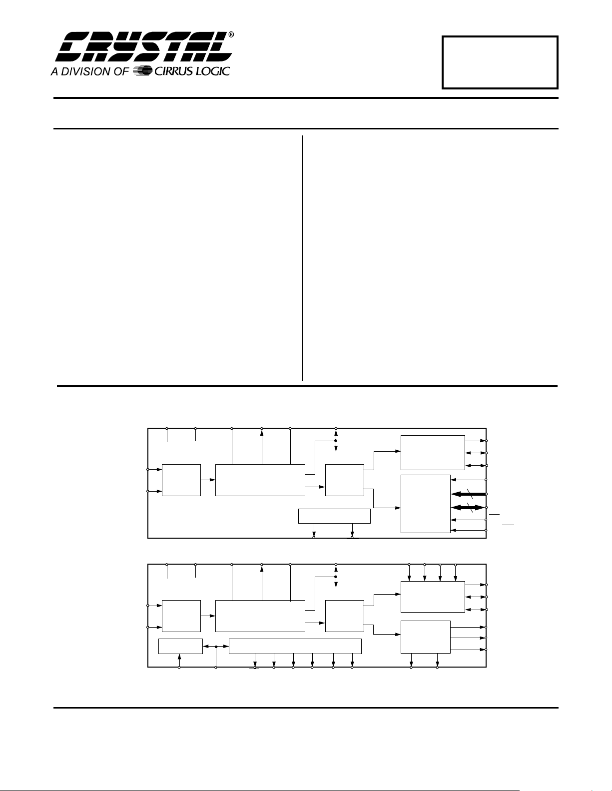
The CS8413 and CS8414 are monolithic CMOS devices
which receive and de code audio data up to 96k Hz according to the AES/EBU, IEC958, S/PDIF, and EIAJ
CP340/1201 interface standards. The CS8413 and
CS8414 receive data from a transmission l ine, recover
the clock and synch ronization signals, an d de-multiplex
the audio and digital data. Differential or single ended inputs can be decoded.
The CS8413 has a configura ble intern al b uffe r me mory ,
read through a parallel port, which may be used to buffer
channel status, auxiliary data, and/or user data.
The CS8414 de-multiple xes the channel, user, a nd validity data directly to serial output pins with dedicated
output pins for the most important channel status bits.
ORDERING INFORMATION
CS8413-CS 0° to 70° C 28-pin Plastic SOIC
CS8414-CS 0° to 70° C 28-pin Plastic SOIC
MCK
19
De-MUX
25 14
MCK
19
De-MUX
227
Ce/Cd/Cc/Cb/Ca/C0
F2F1F0E2E1E0
Audio
Serial Port
Configurable
Buffer
Memory
M317M2
ERF25CBL
M124M0
18
Audio
Serial Port
Registers
15
23
26
SDATA
12
SCK
11
FSYNC
13
A4/FCK
4
A3-A0
8
D7-D0
24
CS
23
RD/WR
26
SDATA
12
SCK
11
FSYNC
1
C
14
U
28
VERF
Cirrus Logic, Inc.
Crystal Semiconductor Products Division
P.O. Box 17847, Austin, Texas 78760
(512) 445 7222 FAX: (512) 445 7581
http://www.crystal.com
Copyright Cirrus Logic, Inc. 1998
(All Rights Reserved)
OCT ‘98
DS240F1
1

TABLE OF CONTENTS
CHARACTERISTICS/SPECIFICATIONS ................................................ ............3
RECOMMENDED OPERATING CONDITIONS.......................................... 3
DIGITAL CHARACTERISTICS....................................................................3
DIGITAL CHARACTERISTICS - RS422 RECEIVERS................................4
SWITCHING CHARACTERISTICS - CS8413 PARALLEL PORT...............4
SWITCHING CHARACTERISTICS - SERIAL PORTS................................5
GENERAL DESCRIPTION .................................................................................. 7
Line Receiver .............................................................................................. 7
Clocks and Jitter Attenuation ...................................................................... 7
CS8413 DESCRIPTION .......................................................................................8
Parallel Port .......................................................... ....... ............................... 8
Status and IEnable Registers .....................................................................9
Control Registers ......................................................................................11
Audio Serial Port ....................................................................................... 14
Normal Modes .................................................................................... 14
Special Modes ....................................................................................14
Buffer Memory ..........................................................................................15
Buffer Mode 0 .....................................................................................16
Buffer Mode 1 .....................................................................................17
Buffer Mode 2 .....................................................................................18
Buffer Updates and Interrupt Timing ......................................................... 19
ERF Pin Timing ......................................................................................... 19
CS8414 DESCRIPTION .....................................................................................20
Audio Serial Port ....................................................................................... 20
Normal Modes (M3 = 0) .....................................................................21
Special Modes (M3 = 1) .....................................................................21
C, U, VERF, ERF, and CBL Serial Outputs .............................................. 23
Multifunction Pins ...................................................................................... 24
Error and Frequency Reporting ..........................................................24
Channel Status Reporting ..................................................................24
Professional Channel Status (C0 = 0) ................................................ 25
Consumer Channel Status (C0 = 1) ...................................................25
SCMS ............................. .................................................... ................25
PIN DESCRIPTIONS: CS8413 .......................................................................... 27
PIN DESCRIPTIONS: CS8414 .......................................................................... 30
PACKAGE DIMENSIONS ................................................................................. 33
APPENDIX A: RS422 RECEIVER INFORMATION .......................................... 34
Professional Interface ...............................................................................34
Consumer Interface ..................................................................................35
TTL/CMOS Levels .................................................................................... 35
Transformers ............................................................................................ 35
APPENDIX B: SUGGESTED RESET CIRCUIT FOR CS8414 ........................ 36
CS8413 CS8414
Prelimina ry pro du ct i nfo rma tion desc ri bes prod ucts wh ich are i n pr oduc ti on, bu t f or w hich ful l c har act eri za tion d ata is not yet available. Advance
product inf ormat ion des crib es pro ducts wh ich ar e in deve lopmen t and s ubjec t to deve lopmen t cha nges. Ci rrus Lo gic, I nc. has made be st ef forts
to ensure t ha t the informat ion contained i n this document is accurate and reliabl e. However, th e i nformation is s u bject to change without not i c e
and is provid ed “AS IS” without warranty of any kind (express or implied). No responsibility is assumed by Cirrus Logic, Inc. for the use of this
information, no r for in fringe ments of pate nts or other rights of third partie s. This d ocume nt is t he prop erty of Cirrus Logic , Inc. and implies no
license unde r pat ents , co pyr ight s, t rade mar ks, or tra de secr ets. N o part of t his pu bl icat io n may be copi ed, repr oduc ed, sto red i n a retrieval system, or trans m it ted, in any form or by any means (electronic, m echanical, photographic, or ot herwise). Furthermore, no par t of this publica t ion
may be used as a basis for manufacture or sale of any items without the prior written consent of Cirrus Logic, Inc. The names of products of
Cirrus Logic, Inc. or other vendors and suppliers appearing in this document may be trademarks or service marks of their respective owners
which may be registered in some jurisdictions. A list of Cirrus Logic, Inc. trademarks and service marks can be found at http://www.cirrus.com.
2 DS240F1
CS8413 CS8414
CHARACTERISTICS/SPECIFICATIONS
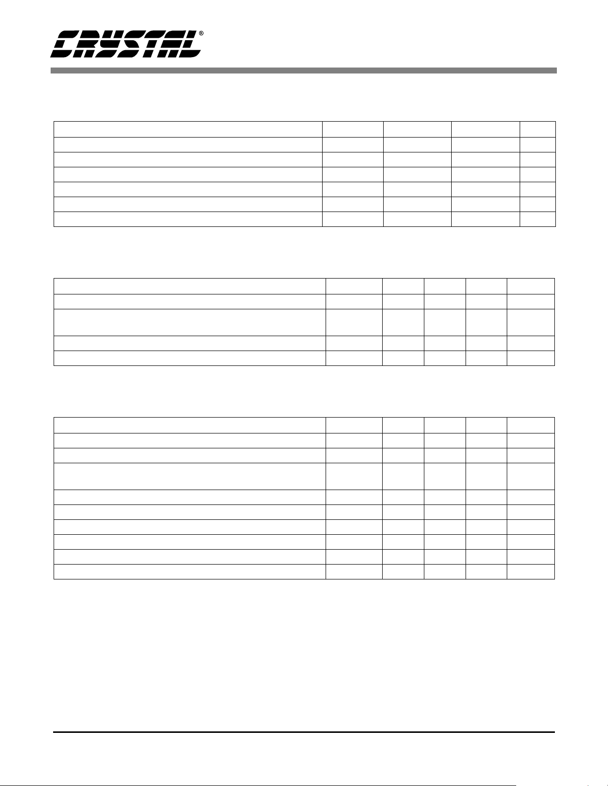
ABSOLUTE MAXIMUM RATINGS (GND = 0V, all voltages with respect to ground)
Parameters Symbol Min Max Units
Power Supply Voltage VD+, VA+ - 6.0 V
Input Current, Any Pin Except Supply (Note 1) I
Input Voltage, Any Pin Except RXP, RXN V
Input Voltage, RXP and RXN V
Ambient Operating Temperature (power applied) T
Storage Temperature T
in
IN
IN
A
stg
Notes: 1. Transient currents of up to 100 mA will not cause SCR latch-up
RECOMMENDED OPERATING CONDITIONS (GND = 0V, all voltages with respect to ground)
Parameters Symbol Min Typ Max Units
Power Supply Voltage VD+, VA+ 4.75 5.0 5.25 V
Supply Current VA+
VD+
Ambient Operating Temperature: (Note 2) T
Power Consumption P
I
A
I
D
A
D
-±10mA
-0.3 (VD+) + 0.3 V
-12 12 V
-55 125 °C
-65 150 °C
-
-
20
20
30
30
mA
mA
02570°C
- 175 315 mW
Notes: 2. The ‘-CS’ parts are specified to operate over 0 to 70 °C but are tested at 25 °C only.
DIGITAL CHARACTERISTICS (T
= 25 °C; VD+, VA+ = 5V ± 5%)
A
Parameters Symbol Min Typ Max Units
High-Level Input Voltage except RXP, RXN V
Low-Level Input Voltage except RXP, RXN V
High-Level Output Voltage (I
= 200 µA) V
O
IH
IL
OH
2.0 - - V
--+0.4V
(VD+) -
--V
1.0
Low-Level Output Voltage (I
Input Leakage Current I
Input Sample Frequency: (Note 3) F
Master Clock Frequency (Note 3) MCK 7.28 256xF
MCK Clock Jitter t
= -3.2 mA) V
O
OL
in
S
j
--0.5V
-1.010µA
28.4 - 100 kHz
25.6 MHz
S
- 200 - psRMS
MCK Duty Cycle (high time/cycle time) - 50 - %
Notes: 3. F
is defined as the incoming audio sample frequency per channel.
S
DS240F1 3
DIGITAL CHARACTERISTICS - RS422 RECEIVERS
(RXP, RXN pins only; VD+, VA+ = 5V ± 5%)
Parameters Symbol Min Typ Max Units
Input Resistance (-7V < V
Differential Input Voltage, (-7V < V
RXP to RXN
Input Hysteresis V
< 7V) (Note 4) Z
CM
< 7V) (Notes 4 and 5)
CM
V
HYST
IN
TH
CS8413 CS8414
-10-k
200 - - mV
-50-mV
Ω
Notes: 4. V
- Input Common Mode Range
CM
5. When the receiver inputs are configured for single ended operation (e.g. consumer configuration) the
signal amplitude must exceed 400 mVp-p for the differential voltage on RXP to RXN to exceed 200 mV.
This represents twice the minimum signal level of 200 mVp-p specified in CP340/1201 and IEC-958
(which are not RS-422 compliant).
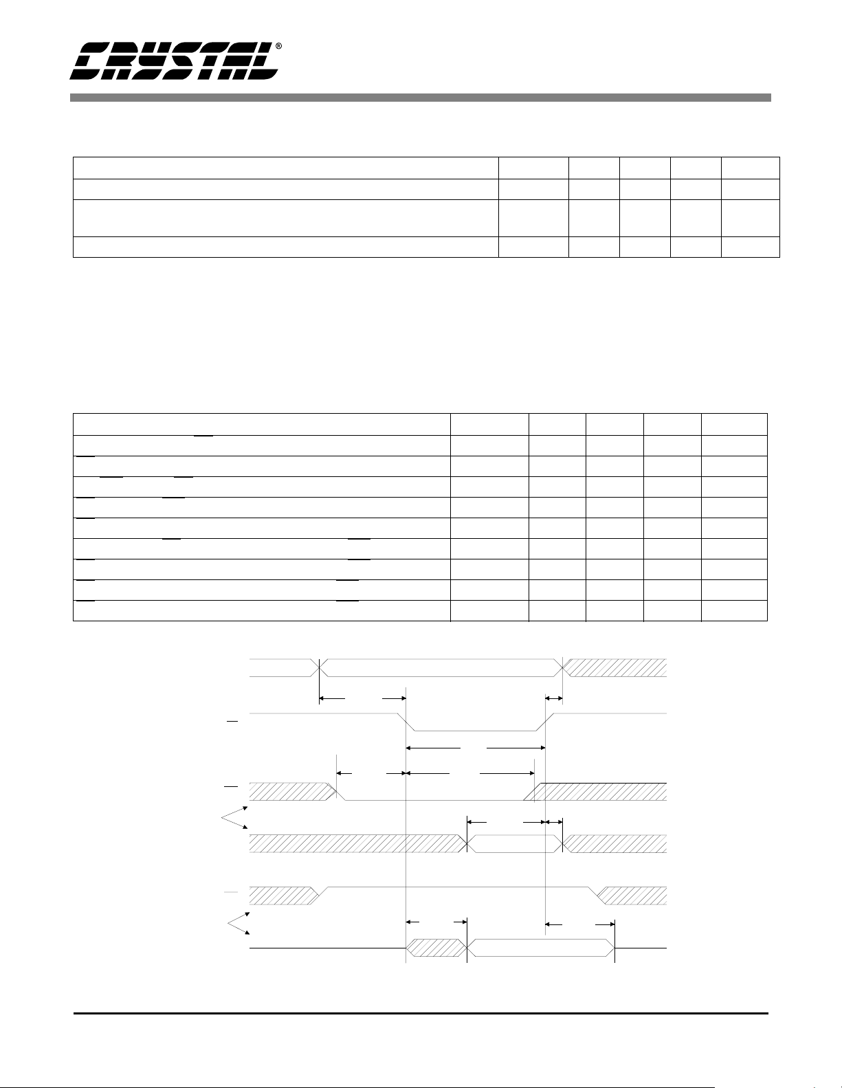
SWITCHING CHARACTERISTICS - CS8413 PARALLEL PORT
(TA = 25 °C;VD+, VA+ = 5V ± 5%; Inputs: Logic 0 = DGND, Logic 1 = VD+; CL = 20 pF)
Parameters Symbol Min Typ Max Units
ADDRESS valid to CS
CS
high to ADDRESS invalid t
RD/WR
CS
CS
valid to CS low t
low to RD/WR invalid t
low t
DATA valid to CS
CS
high to DATA invalid RD/WR low (writing) t
CS
falling to DATA valid RD/WR high (reading) t
CS
rising to DATA Hi-Z RD/WR high (reading) t
low t
rising RD/WR low (writing) t
A4 - A0
adcss
csadh
rwcss
csrwi
csl
dcssw
csdhw
csddr
csdhr
13.5 - - ns
0--ns
10 - - ns
35 - - ns
35 - - ns
32 - - ns
0--ns
--35ns
5--ns
RD/WR
Writing
D7 - D0
RD/WR
Reading
D7 - D0
CS
t
adcss
t
rwcss
t
csddr
t
csrwi
t
csl
t
dcssw
t
csadh
t
csdhw
t
csdhr
CS8413 Parallel Port timing
4 DS240F1
CS8413 CS8414
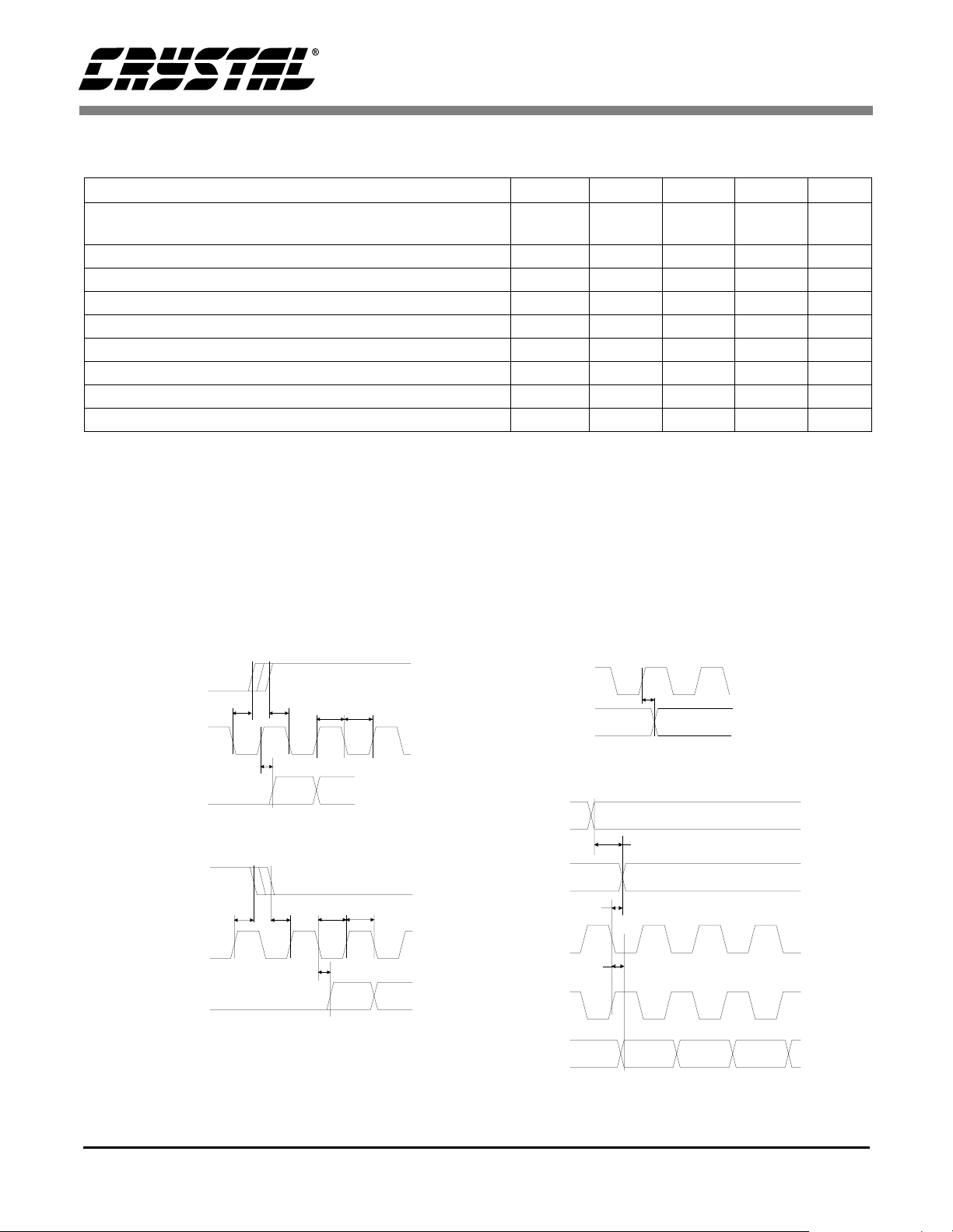
SWITCHING CHARACTERISTICS - SERIAL PORTS
(TA = 25 °C; VD+, VA+ = 5V ± 5%; Inputs: Logic 0 = DGND, Logic 1 = VD+; CL = 20 pF)
Parameters Symbol Min Typ Max Units
-
SCK Frequency Master Mode (Notes 6 and 7)
Slave Mode (Note 7)
SCK falling to FSYNC delay Master Mode (Notes 7 and 8) t
SCK Pulse Width Low Slave Mode (Note 7) t
SCK Pulse Width High Slave Mode (Note 7) t
SCK rising to FSYNC edge delay Slave Mode (Notes 7 and 8) t
FSYNC edge to SCK rising setup Slave Mode (Notes 7 and 8) t
SCK falling (rising) to SDATA valid (Note 8) t
C, U, CBL valid to FSYNC edge CS8414 (Note 8) t
MCK to FSYNC edge delay FSYNC from RXN/RXP t
f
sck
sfdm
sckl
sckh
sfds
fss
ssv
cuvf
mfd
OWRx32
-20 - 20 ns
40 - - ns
40 - - ns
20 - - ns
20 - - ns
OWRx32
-
- - 20 ns
-1/f
sck
-15-ns
Notes: 6. The output word rate, OWR, refers to the frequency at which an audio sample is output from the part.
(A stereo pair is two audio samples.) Therefore, in Master mode, there are always 32 SCK periods in
one audio sample. In Slave mode, exactly 32 SCK periods per audio sample must be provided in most
serial port formats. Therefor, if SCK is 128 x Fs, then SCK must be gated to provide exactly 32 periods
per audio sample.
7. In Master mode, SCK and FSYNC are outputs. In Slave mode, they are inputs. In the CS8413, control
reg. 2 bit 1, MSTR, selects master. In the CS8414, formats 1, 3 and 9 are slaves.
8. The table above assumes data is output on the falling edge and latched on the rising edge. With the
CS8413 the edge is selectable. The table is defined for the CS8413 with control reg. 2 bit 0, SCED, set
to one, and for the CS8414 in formats 2, 3, 5, 6 and 7. For the other formats, the table and figure edges
must be reversed (i.e. “rising” to “falling” and vice versa.)
-
128 x F
Hz
Hz
S
-s
FSYNC
t
sfds
SCK
SDATA
FSYNC
t
sfds
SCK
SDATA
Serial Output Timing - Slave Mode
t
fss
t
t
ssv
MSB
(Mode 1)
t
t
fss
(Mode 3)
sckl
sckl
t
ssv
MSB
t
sckh
t
sckh
C, U
FSYNC
SCK
(Modes 2,3,5,6,
7,10,12, and 13)
SCK
(Modes 0,1,4,
8,9, and 11)
SDATA
MCK
FSYNC
FSYNC Generated From
Received Data
t
sfdm
t
ssv
Serial Output Timing -
Master Mode & C, U Port
t
cuvf
t
mfd
DS240F1 5
+5V Analog +5V Digital
CS8413 CS8414
Receiver
Circuit
(See Appendix A)
0.068 µF
0.1 µF
470
21
10
20
9
AGND
RXP
RXN
FILT
22
VA+
CS8413
7
VD+
FSYNC
SDATA
RD/WR
Ω
DGND
8
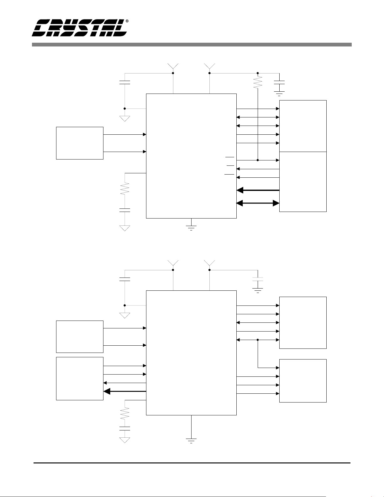
Figure 1. CS8413 Typical Connection Diagram
+5V Analog +5V Digital
MCK
SCK
ERF
INT
CS
A0-A4
D0-D7
5k
19
11
12
26
25
14
24
23
Ω
0.1 µF
Audio
Data
Processor
Audio
Data
Processor
or
Microcontroller
Receiver
Circuit
(See Appendix A)
Channel Status
and/or
Error/Frequency
Reporting
0.068 µF
0.1 µF
Ω
470
21
10
9
22
VA+
AGND
RXP
RXN
7
VD+
MCK
VERF
SCK
SDATA
FSYNC
CS8414
13
CS12/FCK
16
SEL
25
20
ERF
6 C/E-F bits
FILT
DGND
8
27, 2-6
Figure 2. CS8414 Typical Connection Diagram
C
U
CBL
19
28
12
26
11
1
14
15
0.1 µF
Audio
Data
Processor
Microcontroller
or
Logic
6 DS240F1

CS8413 CS8414
GENERAL DESCRIPTION
The CS8413/14 are monolithic CMOS circuits that
receive and decode audio and digital data according to the AES/EBU, IEC 958, S/PDIF, and EIAJ
CP340/1201 interface standards. Both chips contain RS422 line receivers and Phase-Locked Loops
(PLL) that recover the clock and synchronization
signals, and de-multiplex the audio and digital data.
The CS8413 contains a configurable internal buffer
memory, read via a parallel port, which can buffer
channel status, user, and optionally auxiliary data.
The CS8414 de-multiplexes the channel status, user, and validity information directly to serial output
pins with dedicated pins for the most important
channel status bits. Both chips also contain extensive error reporting as well as incoming sample frequency indication for auto-set applications.
The CS8413/14 are pin-compatible with the
CS8411/12 digital audio receiver parts. The functionality of the CS8413/14 is the same as the
CS8411/12 with two exceptions: first, the operating frequency (sample rate) of the CS8413/14 is extended to include 96 kHz, and second, the
frequency reporting bits are modified to delete the
±400 ppm ranges, and include 88.2 kHz and
96 kHz ranges.
Familiarity with the AES/EBU and IEC 958 specifications are assumed throughout this document.
The App Note, Overview of Digital Audio Interface Data Structures, contains information on digital audio specifications; however, it is not meant to
be a complete reference. To guarantee compliance,
the proper standards documents should be obtained. The AES/EBU standard, AES3-1985,
should be obtained from the Audio Engineering
Society or ANSI (ANSI document # ANSI S4.40-
1985); the IEC 958 standard from the International
Electrotechnical Commission; and the EIAJ
CP340/1201 standard from the Japanese Electronics Bureau.
Line Receiver
The RS422 line receiver can decode differential as
well as single ended inputs. The receiver consists
of a differential input Schmitt trigger with 50mV of
hysteresis. The hysteresis prevents noisy signals
from corrupting the phase detector. Appendix A
contains more information on how to configure the
line receivers for differential and single ende d signals.
Clocks and Jitter Attenuation
The primary function of these chips is to recover
audio data and low jitter clocks from a digital audio
transmission line. The clocks that can be generated
are MCK (256xFS), SCK (64xFS), and FSYNC (F
or 2xFS). MCK is the output of the voltage controlled oscillator which is a component of the PLL.
The PLL consists of phase and frequency detectors,
a second-order loop filter, and a voltage controlled
oscillator. All components of the PLL are on chip
with the exception of a resistor and capacitor used
in the loop filter. This filter is connected betwe en
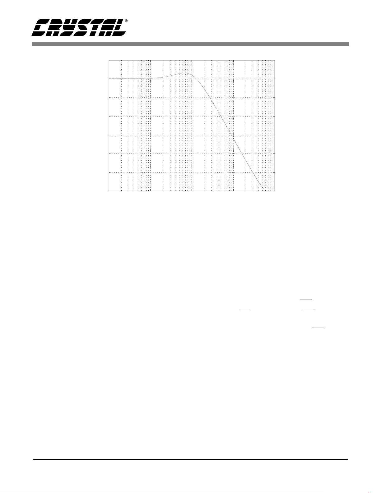
the FILT pin and AGND. The typical closed-loop
transfer function, which specifies the PLL’s jitter
attenuation characteristics, is shown in Figure 3.
Most jitter introduced by the transmission line is
high in frequency and will be strongly attenuated.
Multiple frequency detectors are used to minimize
the time it takes the PLL to lock to the incoming
data stream and to prevent false lock conditions.
When the PLL is not locked to the incoming data
stream, the frequency detectors pull the VCO frequency within the lock range of the PLL. When no
digital audio data is present, the VCO frequency is
pulled to its minimum value.
As a master, SCK is always MCK divided by four,
producing a frequency of 64xFS. In the CS8413,
FSYNC can be programmed to be a divided version
of MCK or it can be generated directly from the incoming data stream. In the CS8414, FSYNC is always generated from the incoming data stream.
When FSYNC is generated from the data, its edges
S
DS240F1 7
CS8413 CS8414
5
0
-5
-10
-15
Jitter Attenuation (dB)
-20
-25
-30
10
2
10
3
Jitter Frequency (Hz)
10
4
10
5
10
6
Figure 3. Typical Jitter Attenuation Characteristics
are extracted at times when intersymbol interference is at a minimum. This provides a sample frequency clock that is as spectrally pure as the digital
audio source clock for moderate length transmission lines. For long transmission lines, the CS8413
can be programmed to generate FSYNC from
MCK instead of from the incoming data.
CS8413 DESCRIPTION
The CS8413 is more flexible than the CS8414 but
requires a microcontroller or DSP to load internal
registers. The CS8414 does not have internal registers so it may be used in a stand-alone mode where
a microprocessor or DSP is not available.
The CS8413 accepts data from a transmission line
coded according to the digital audio interface standards. The I.C. recovers clocks and data, and separates the audio data from control information. The
audio data is output through a configurable serial
port and the control information is stored in interna l
dual-port RAM. Extensive error reporting is available via internal registers with the option of repeating the last sample when an error occurs. A block
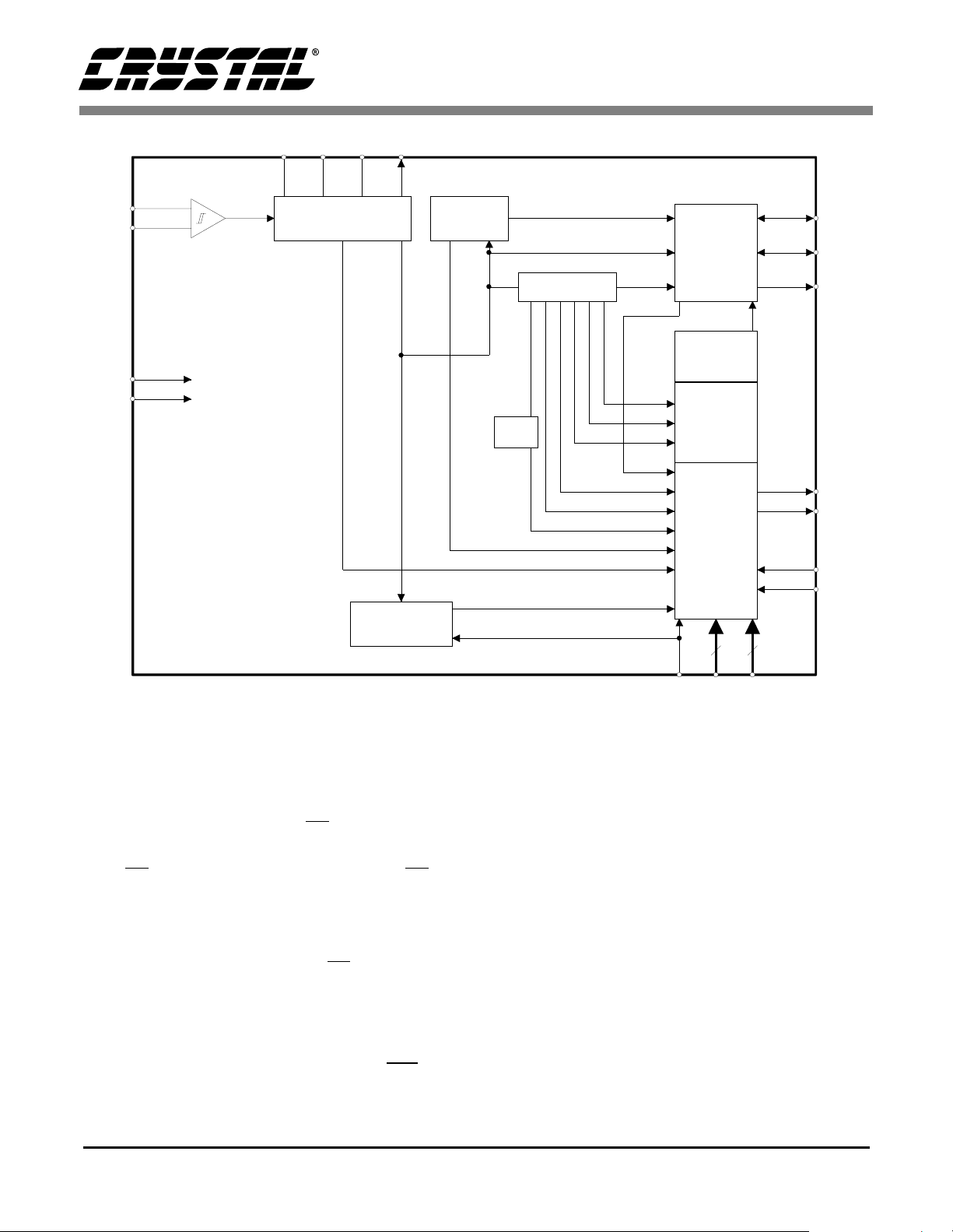
diagram of the CS8413 is shown in Figure 4
Parallel Port
The parallel port accesses two status registers, two
interrupt enable registers, two control registers, and
28 bytes of dual-port buffer memory. The status
registers and interrupt enable registers occupy the
same address space. A bit in control register 1 selects the two registers, either status or interrupt enable, that occupy addresses 0 and 1 in the memory
map. The address bus and the RD/WR line should
be valid when CS goes low. If RD/WR is low, the
value on the data bus will be written into the buffer
memory at the specified address. If RD/WR is high,
the value in the buffer memory, at the spe cified address, is placed on the data bus. Detailed timing for
the parallel port can be found in the Switching
Characteristics - Parallel Port table.
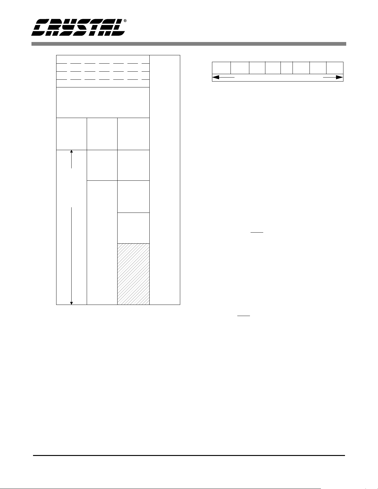
The memory space on the CS8413 is allocated as
shown in Figure 5. There are three defined buffer
modes selectable by two bits in control register 1.
Further information on the buffer modes can be
found in the Control Registers section.
8 DS240F1
RXP
C
A
R
RXN
VD+
DGND
9
10
7
8
VA+
FIL T A GND MCK
22 20 21 19
Clock & Data
Recovery
Bi-phase
Decoder
De-Multiplexor
crc
check
user
slipped
parity
validity
crc
coding
no lock
CS8413 CS8414
Audio
Serial
Port
Control
Registers
2 X 8
aux
C.S.
Buffer
Memory
28 X 8
IEnable
&
Status
4 X 8
11
12
26
14
25
24
23
FSYN
SCK
SDAT
INT
ERF
CS
RD/W
Frequency
Comparator
Figure 4. CS8413 Block Diagram
Status and IEnable Registers
The status and interrupt enable registers occupy the
same address space. The IER/SR bit in control register 1 selects whether the status registers
(IER/SR = 0) or the IEnable registers (IER/SR = 1)
occupy addresses 0 and 1. Upon power-up, the control and IEnable registers contain all zeros; therefore, the status registers are visible and all
interrupts are disabled. The IER/SR bit must be set
to make the IEnable registers visible.
Status register 1 (SR1), shown in Figure 6, reports
all the conditions that can generate a low pulse four
SCLK cycles wide on the interrupt pin (INT ). The
three least significant bits, FLAG2-FLAG0, are
48
13
A4/
A0-A3D0-
FCK
D7
used to monitor the ram buffer. These bits continually change and indicate the position of the buffer
pointer which points to the buffer memory location
currently being written. Each flag has a corresponding interrupt enable bit in IEnable register 1
which, when set, allows a transition on the flag to
generate a pulse on the interrupt pin. FLAG0 and
FLAG1 cause interrupts on both edges whereas
FLAG2 causes an interrupt on the rising edge only.
Further information, including timing, on the flags
can be found in the Buffer Memory section.
The next five bits; ERF, SLIP, CCHG,
CRCE/CRC1, and CSDIF/CRC2, are latches
which are set when their corresponding conditions
occur, and are reset when SR1 is read. Interrupt
DS240F1 9
CS8413 CS8414
01
2
3
User Data
1st Four
Bytes of
C. S. Data
1st Four
Bytes of
C. S. Data
1st Four
Bytes of
Left C. S.
Data
Auxiliary
Data
Last
20 Bytes
Channel
Status
Data
Status 1 / IEn able 1
C. S.
Data
Left
C. S.
Data
Right
C. S.
Data
1st Four
Bytes of
Right
C. S. Data
U
N
D
E
F
I
N
E
D
A
D
D
R
E
S
S
Memory Mode
0
1
2
3
4
5
6
7
8
9
A
B
C
D
E
F
10
11
12
13
14
15
16
17
18
19
1A
1B
1C
1D
1E
1F
Control Register 1
Control Register 2
Status 2 / IEn able 2
Figure 5. CS8413 Buffer Memory Map
X:00 7 6 5 4 3 2 1 0
X:00 7 6 5 4 3 2 1 0
SR1. CSDIF/
SR1. CSDIF/
IER1. INTERRUPT ENABLE BITS FOR ABOVE
IER1. INTERRUPT ENABLE BITS FOR ABOVE
SR1: CSDIF: CS different between sub-frames. Buffer modes 0 & 1
SR1: CSDIF: CS different between sub-frames. Buffer modes 0 & 1
CRC2: CRC Error - sub-frame 2. Buffer mode 2 only.
CRC2: CRC Error - sub-frame 2. Buffer mode 2 only.
CRCE: CRC Error - selected sub-frame. Buffer modes 0 & 1
CRCE: CRC Error - selected sub-frame. Buffer modes 0 & 1
CRC1: CRC Error - sub-frame 1. Buffer mode 2 only.
CRC1: CRC Error - sub-frame 1. Buffer mode 2 only.
CCHG: Channel Status changed
CCHG: Channel Status changed
SLIP: Slipped an audio sample
SLIP: Slipped an audio sample
ERF: Error Flag. ORing of all errors in SR2.
ERF: Error Flag. ORing of all errors in SR2.
FLAG2: High for first four bytes of channel status
FLAG2: High for first four bytes of channel status
FLAG1: Memory mode dependent - See Figure 11.
FLAG1: Memory mode dependent - See Figure 11.
FLAG0: High for last two bytes of user data.
FLAG0: High for last two bytes of user data.
IER1: Enables the corresponding bit in SR1.
IER1: Enables the corresponding bit in SR1.
A “1” enables the interrupt. A “0” masks the interrupt.
A “1” enables the interrupt. A “0” masks the interrupt.
reread because the audio data output from the part
is at a different frequency than the data received
from the transmission line. CCHG is set when any
bit in channel status bytes 0 through 3, stored in the
buffer, changes from one block to the next. In buffer modes 0 and 1, only one channel of channel status data is buffered, so CCHG is only affected by
that channel. (CS2/CS1 in CR1 selects which channel is buffered.) In buffer mode 2 both channels are
buffered, so both channels affect CCHG. This bit is
updated after each byte (0 to 3) is written to the
buffer. The two most significant bits in SR1,
pulses are generated the first time that condition occurs. If the status register is not read, further instances of that same condition will not generate
another interrupt. ERF is the error flag bit and is set
when the ERF pin goes high. It is an OR’ing of the
errors listed in status register 2, bits 0 through 4,
AND’ed with their associated interrupt enable bits
CRCE/CRC1 and CSDIF/CRC2, are dual function
flags. In buffer modes 0 and 1, they are CRCE and
CSDIF, and in buffer mode 2, they are CRC1 and
CRC2. In buffer modes 0 and 1, the channel selected by the CS2/CS1 bit is stored in RAM and CRCE
indicates that a CRC error occurred in that channel.
CSDIF is set if there is any difference between the
channel status bits of each channel. In buffer mode
2 channel status from both channels is buffered,
with CRC1 indicating a CRC error in channel 1 and
CRC2 indicating a CRC error in channel 2. CRCE,
CRC1, and CRC2 are updated at the block boundary. Block boundary violations also cause CRC1,2
or CRCE to be set.
in IEnable register 2.
IEnable register 1, which occupies the same ad-
SLIP is only valid when the audio port is in slave
mode (FSYNC and SCK are inputs to the CS8413).
This flag is set when an audio sample is dropped or
10 DS240F1
dress space as status register 1, contains interrupt
enable bits for all conditions in status register 1. A
“1” in a bit location enabl es the same bit loca tion in
CRCE/
CCHG SLIP ERF FLAG2 FLAG1 FLAG0
CRCE/
CRC2
CRC2
CCHG SLIP ERF FLAG2 FLAG1 FLAG0
CRC1
CRC1
Figure 6. Status/IEnable Register 1
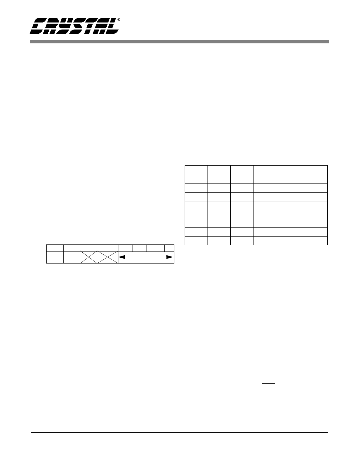
CS8413 CS8414
SR2: FREQ2: The 3 FREQ bits indicate incoming sample frequency.
FREQ1: (must have 6.144 MHz clock on FCK pin and FCEN
FREQ0: must be “1”)
LOCK: Out-of-Lock error
CODE: Coding violation
PARITY: Parity error
V: Validity bit high
IER2: TEST1,0: (0 on power-up) Must stay at “0”.
INT. ENABLES: Enables the corresponding bit in SR2.
A “1” enables the interrupt. A “0” masks the interrupt.
X:01765 4 3210
SR2. FREQ2 FREQ1 FREQ0 Reserved LOCK CODE PARITY V
IER2. TEST1 TEST0 INT. ENABLE BITS
FOR ABOVE
Figure 7. Status/IEnable Register 2
status register 1 to generate an interrupt pulse. A
“0” masks that particular status bit from causing an
interrupt.
Status register 2 (SR2) reports all the conditions
that can affect the error flag bit in SR1 and the error
pin (ERF), and can specify the received clock frequency. As previously mentioned, the first five bits
of SR2 are AND’ed with their interrupt enable bits
(in IER2) and then OR’ed to create ERF. The V,
PARITY, CODE and LOCK bits are latches which
are set when their corresponding conditions occur,
and are reset when SR2 is read. The ERF pin is asserted each time the error occurs assuming the interrupt enable bit in IER2 is set for that particular
error. When the E RF pin is ass erte d, the E RF bit in
SR1 is set. If the ERF bit was not set prior to the
ERF pin assertion, an interrupt will be generated
(assuming bit 3 in IER1 is set). Although the ERF
pin is asserted for each occurrence of an enabled error condition, the ERF bit will only cause an interrupt once if SR1 is not read.
The upper three bits in SR2, FREQ2-FREQ0, can
report the receiver f requency when the receive r is
locked. These bits are only valid when FCEN in
control register 1 is set, and a 6.144 MHz clock is
applied to the FCK pin. When FCEN is set, the
A4/FCK pin is used as FCK and A4 is internally set
to zero; therefore, only the lower half of the buffer
can be accessed. Table 1 lists the frequency ranges
reported. The FREQ bits are updated three times
per block and the clock on the FCK pin must be valid for two thirds of a block for the FREQ bits to be
accurate. The FREQ bits are invalid when the PLL
is out of lock.
FREQ2 FREQ1 FREQ0 Sample Frequency
0 0 0 Out of Range
0 0 1 reserved
0 1 0 reserved
011 96 kHz ± 4%
1 0 0 88.2 kHz ± 4%
1 0 1 48 kHz ± 4%
1 1 0 44.1 kHz ± 4%
1 1 1 32 kHz ± 4%
V is the validity status bit whi ch is set a ny tim e t he
received validity bit is high. PARITY is set when a
parity error is detected. CODE is set when a biphase coding error is detected. LOCK is asserted
when the receiver PLL is not locked and occurs
when there is no input on RXP/RXN, or if the received frequency is out of the receiver lock range
(28.4 kHz to 100 kHz).
DS240F1 11
Table 1. Incoming Sample Frequency Bits
IEnable register 2 has corresponding interrupt enable bits for the first five bits in SR2. A “1” enables
the condition in SR2 to cause ERF to go high, while
a “0” masks that condition. Bit 5 is unused and bits
6 and 7, the two most significant bits, are factory
test bits and must be set to zero when writing to this
register. The CS8413 sets these bits to zero on power-up.
Control Registers
The CS8413 contains two control registers. Control
register 1 (CR1), at address 2, selects system level
features, while control register 2 (CR2), at address
3, configures the audio serial port.
In control register 1, when RST is low, all outputs
are reset except MCK (FSYNC and SCLK are high
impedance). The CS8413 should be reset imediately after power-up and any time the user performs a
CS8413 CS8414
system-wide reset. After the user sets R ST high, the
CS8413 comes fully out of reset when the block
boundary is found. The serial port, in master mode,
will begin to operate as soon as RST goes high. B0
and B1 select one of three buffer modes listed in
Table and illustrated in Figure 5. In all modes four
bytes of user data are stored. In mode 0, one entire
block of channel status is stored. In mode 1 eight
bytes of channel status and sixteen bytes of auxiliary data are stored. In mode 2, eight bytes of channel
status from each sub-frame are stored. The buffer
modes are discussed in more detail in the Buffer
Memory section. The next bit, CS2/CS1, selects the
particular sub-frame of channel status to buffer in
modes 0 and 1, and has no effect in mode 2. When
CS2/CS1 is low, sub-frame 1 is buffered, and when
CS2/CS1 is high, sub-frame 2 is buff ered. IER/SR
selects which set of registers, either IEnable or status, occupy addresses 0 and 1. When IER/SR is
low, the status registers occupy the first two addresses, and when IER/SR is high, the IEnable registers occupy those addresses. FCEN enables the
internal frequency counter. A 6.144 MHz clock
must be connected to the FCK pin as a reference.
The value of the FREQ bits in SR2 are not valid until two thirds of a block of data is received. Since
FCK and A4, the most significant address bit, occupy the same pin, A4 is internally set to zero when
FCEN is high. Since A4 is forced to zero, the upper
half of the buffer is not accessible while using the
frequency compare feature. FPLL determines how
FSYNC is derived. When FPLL is low, FS YNC is
derived from the incoming data, and when FPLL is
high, it is derived from the internal phase-locked
loop.
Control Register 2 configures the serial port which
consists of three pins: SCK, SDATA, and FSYNC.
SDATA is always an output, but SCK and FSYNC
can be configured as inputs or outputs. FSYNC and
SDATA can have a variety of relationships to each
other, and the polarity of SCK can be controlled.
The large variety of audio data formats provides an
easy interface to most DSPs and other audio processors. SDATA is normally just audio data, but
special modes are provided that output received biphase data, or received NRZ data with zeros substituted for preamble. Another special mode allows an
asynchronous SCK input to read audio data from
the serial port without slipping samples. In this
mode FSYNC and SDATA are outputs synchronized to the SCK input. Since SCK is asynchronous
to the received clock, the number of SCK c ycles
between FSYNC edges will vary.
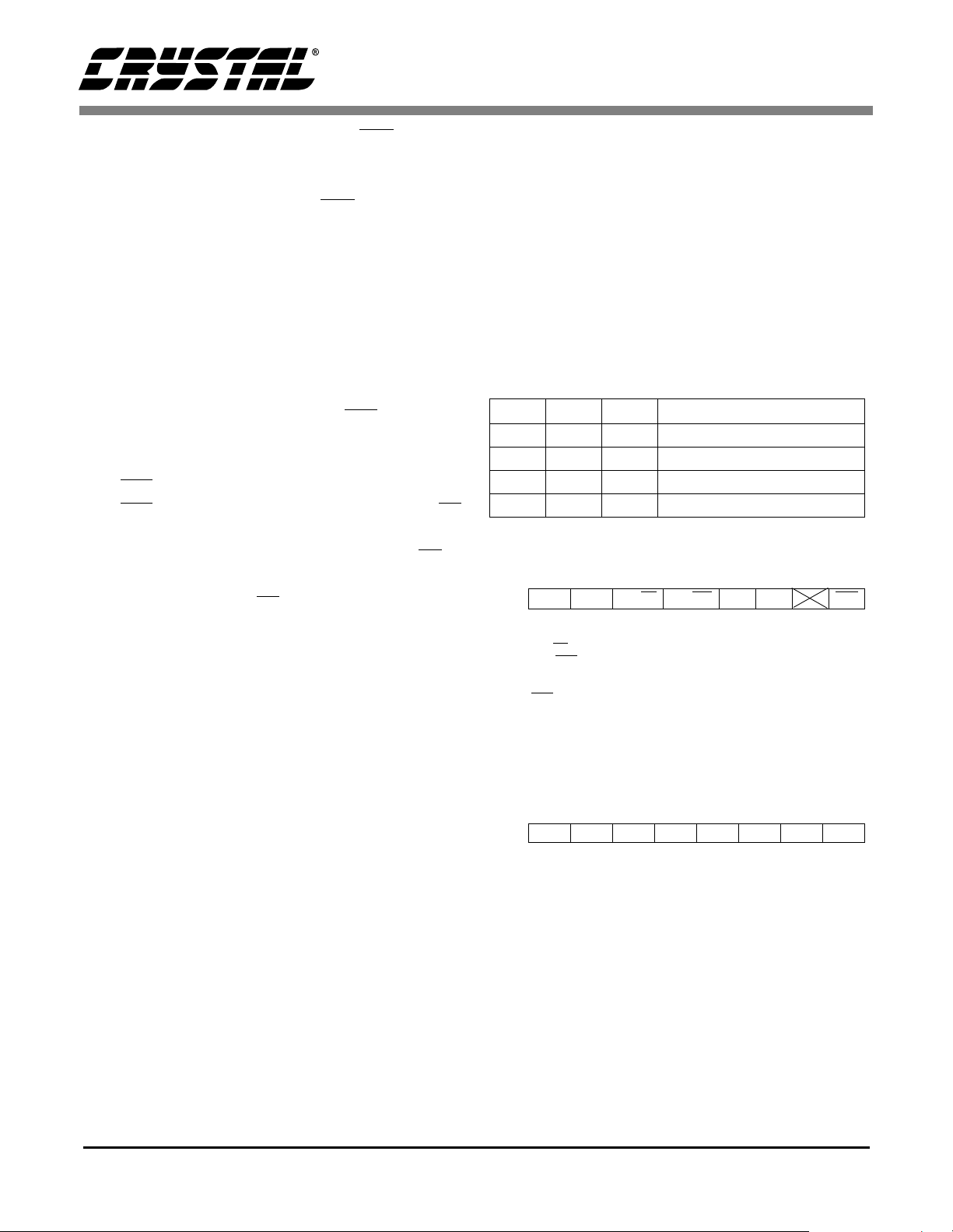
B1 B0 Mode Buffer Memory Contents
0 0 0 Channel Status
011 Auxiliary Data
1 0 2 Independent Channel Status
113 Reserved
Table 2. Buffer Memory Modes
X:027 6 5 4 3210
CR1. FPLL FCEN
CR1: FPLL: 0 - FSYNC from RXP/RXN, 1 - FSYNC from PLL
FCEN: enables freq. comparator (FCK must be 6.144 MHz).
: [X:00,01] 0 - status, 1 - interrupt enable registers.
IER/SR
CS2/CS1
B1: with B0, selects the buffer memory mode.
B0: with B1, selects the buffer memory mode.
: Resets internal counters. Set to “1” for normal operation.
RST
X:0376543210
CR2.
ROER
CR2: ROER: Repeat previous value on error (audio data)
SDF2: with SDF0 & SDF1, select serial data format.
SDF1: with SDF0 & SDF2, select serial data format.
SDF0: with SDF1 & SDF2, select serial data format.
FSF1: with FSF0, select FSYNC format.
FSF0: with FSF1, select FSYNC format.
MSTR: When set, SCK and FSYNC are output
SCED: When set, falling edge of SCK outputs data.
IER/SR
: ch. status to buffer; 0 - sub-frame 1, 1 - sub-frame 2.
Figure 8. Control Register 1
SDF2 SDF1 SDF0 FSF1 FSF0 MSTR SCED
When clear, rising edge of SCK outputs data.
Figure 9. Control Register 2
CS2/CS1
B1 B0 RST
ROER, when set, causes the last audio sample to be
reread if the error pin, ERF, is active. When out of
lock, the CS8413 will output zeros if ROER is set
12 DS240F1
 Loading...