

CS8405A
96 kHz Digital Audio Interface Transmitter
Features
Complete EIAJ CP1201, IEC-60958, AES3,
S/PDIF compatible transmitter
+5 V Digital Supply(VD)
+3 V to 5 V Digital Interface (VL)
On-chip Channel Status and User bit buffer
memories allow block sized updates
Flexible 3-wire serial digital audio input port
Up to 96 kHz frame rate
Microcontroller write access to Channel
Status and User bit data
On-chip differential line driver
Generates CRC codes and parity bits
Standalone mode allows use without a
microcontroller
I
General Description
The CS8405A is a monolithic CMOS device which encodes and transmits audio data according to the AES3,
IEC60958, S/PDIF, or EIAJ CP1201. The CS8405A accepts audio and digital data, which is then multiplexed,
encoded and driven onto a cable.
The audio data is input through a configurable, 3-wire input port. The channel status and user bit data are input
through an SPI or Two-Wire microcontroller port, and
may be assembled in block sized buffers. For systems
with no microcontroller, a stand alone mode allows direct access to channel status and user bit data pins.
Target applications include A/V Receivers, CD-R, DVD
receivers, digital mixing consoles, effects processors,
set-top boxes, and computer and automotive audio
systems.
ORDERING INFORMATION
CS8405A-CS 28-pin SOIC -10 to +70°C
CS8405A-CZ 28-pin TSSOP -10 to +70°C
CS8405A-IS 28-pin SOIC -40 to +85°C
CS8405A-IZ 28-pin TSSOP -40 to +85°C
CDB8415A Evaluation Board
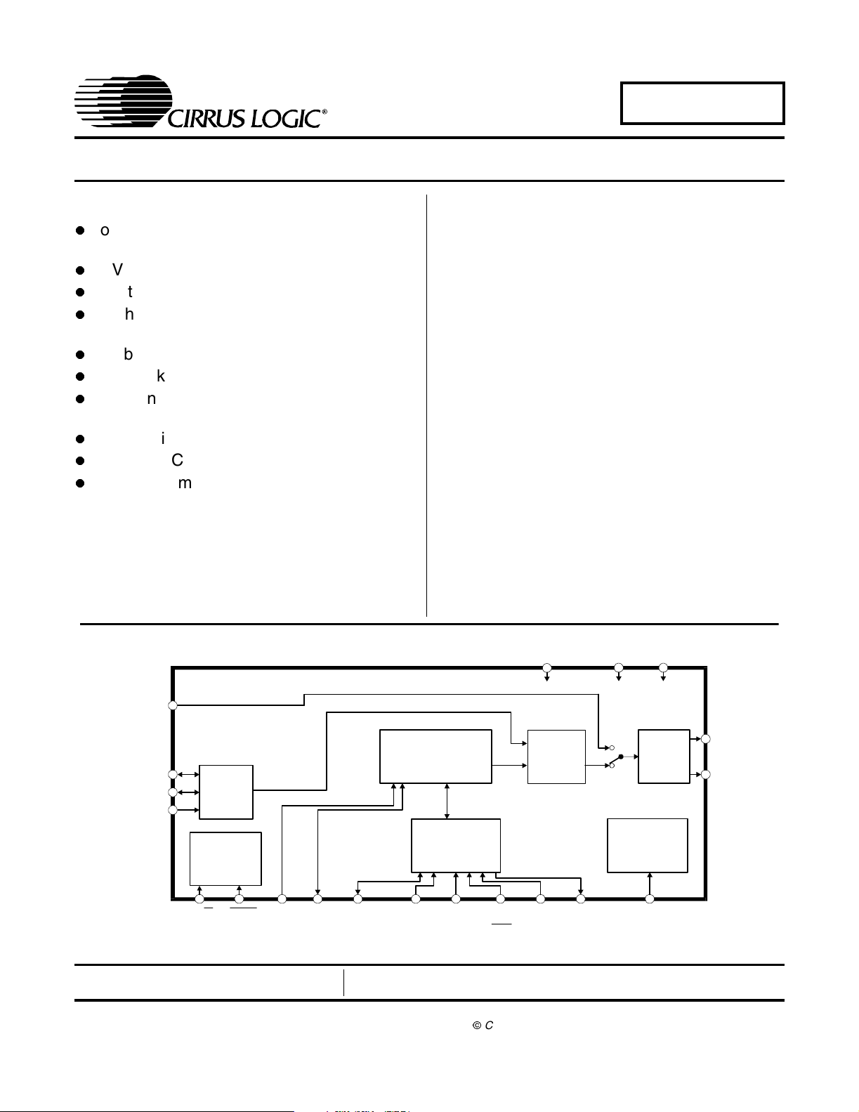
RXP
ILRCK
ISCLK
SDIN
Serial
Audio
Input
Misc.
Control
RST OMCKUTCBLSDA/
Preliminary Product Information
Cirrus Logic, Inc.
P.O. Box 17847, Austin, Texas 78760
(512) 445 7222 FAX: (512) 445 7581
http://www.cirrus.com
VD+
AD0/
CS
AES3
S/PDIF
Encoder
AD2H/S
C&Ubit
Data
Buffer
Control
Port &
Registers
SCL/
CDOUT
This document contains information for a new product.
Cirrus Logic reserves the right to modify this product without notice.
CCLK
AD1/
CDIN
CopyrightCirrus Logic, Inc. 2002
(All Rights Reserved)
VL+ DGND
Driver
Output
Clock
Generator
INT
TXP
TXN
JUN ‘02
DS469PP4
1
TABLE OF CONTENTS
1. CHARACTERISTICS AND SPECIFICATIONS ........................................................................ 4
POWER AND THERMAL CHARACTERISTICS....................................................................... 4
ABSOLUTE MAXIMUM RATINGS ........................................................................................... 4
DIGITAL CHARACTERISTICS................................................................................................. 5
SWITCHING CHARACTERISTICS .......................................................................................... 5
SWITCHING CHARACTERISTICS - SERIAL AUDIO PORTS.................................................6
SWITCHING CHARACTERISTICS - CONTROL PORT - SPI MODE...................................... 7
SWITCHING CHARACTERISTICS - CONTROL PORT - TWO-WIRE MODE.........................8
2. TYPICAL CONNECTION DIAGRAM ........................................................................................ 9
3. GENERAL DESCRIPTION ..................................................................................................... 10
3.1 AES3 and S/PDIF Standards Documents ........................................................................ 10
4. THREE-WIRE SERIAL INPUT AUDIO PORT ........................................................................ 10
5. AES3 TRANSMITTER ............................................................................................................ 12
5.1 Transmitted Frame and Channel Status Boundary Timing .............................................. 12
5.2 TXN and TXP Drivers ......................................................................................................12
5.3 Mono Mode Operation .....................................................................................................12
6. CONTROL PORT DESCRIPTION AND TIMING .................................................................... 14
6.1 SPI Mode ......................................................................................................................... 14
6.2 Two-Wire Mode ...............................................................................................................15
6.3 Interrupts ..........................................................................................................................15
7. CONTROL PORT REGISTER SUMMARY ............................................................................. 16
7.1 Memory Address Pointer (MAP) .......................................................................................16
8. CONTROL PORT REGISTER BIT DEFINITIONS ..................................................................17
8.1 Control 1 (1h).................................................................................................................... 17
8.2 Control 2 (2h).................................................................................................................... 18
8.3 Data Flow Control (3h)...................................................................................................... 18
8.4 Clock Source Control (4h).................................................................................................19
8.5 Serial Audio Input Port Data Format (5h).......................................................................... 19
8.6 Interrupt 1 Status (7h) (Read Only)...................................................................................20
8.7 Interrupt 2 Status (8h) (Read Only)...................................................................................21
8.8 Interrupt 1 Mask (9h)......................................................................................................... 21
CS8405A
Contacting Cirrus Logic Support
For a complete listing of Direct Sales, Distributor, and Sales Representative contacts, visit the Cirrus Logic web site at:
http://www.cirrus.com/corporate/contacts/sales.cfm
IMPORTANT NOTICE
"Preliminary" product inf ormation describes products that are in production, but for which full characterization data is not yet available. "Advance" product inf ormation describes products that are i n development and subject to development changes. Cirrus Logic, I nc. and its subsidiaries ("Cirrus") believe that the information contained in this document is accurate and reliable. However, the information is subject to change without notice and is provided "AS IS" without warranty
of any kind (express or implied). Customers are advised to obtain the latest version of relevant information to verify, before placing orders, that information being
relied on is current and complete. All products are sold subject to the terms and conditions of sale supplied at the time of order acknowledgment, including those
pertaining to warranty, patent infringement, and l imitation of liability. No responsibil ity is assumed by Cirrus f or the use of this information, includi ng use of this
information as the basis for manufacture or sale of any items, or for i nfringement of patents or other rights of third parties. This document is the property of Cir rus
and by furnishi ng this information, Cirrus grants no license, express or implied under any patents, mask work rights, copyrights, trademarks, trade secrets or
other intellectual property rights. Cirrus owns the copyrights of the i nformation contained herein and gives consent for copies to be made of the information only
for use within your or ganization with respect to Cirrus integrated circui ts or ot her parts of Cir rus. This consent does not ext end to ot her copying such as copying
for general distribution, advertising or pr omotional purposes, or for creating any work for resale.
An export permit needs to be obtained from the competent authorities of the Japanese Government if any of the products or technologies described in thismaterial and controll ed under the "Foreign Exchange and Forei gn Trade Law" i s to be exported or taken out of Japan. An export l icense and/or quota needs to be
obtained from the competent authorities of the Chinese Government if any of the products or technologies describe d in this material is subject to the PRC Foreign
Trade Law and i s to be exported or taken out of the PRC.
CERTAIN APPLICATIONS USING SEMICONDUCTOR PRODUCTS MAY INVOLVE POTENTIAL RISKS OF DEATH, PERSONAL INJURY, OR SEVERE
PROPERTY OR ENVIRONMENTAL DAMAGE ("CRITICAL APPLICATIONS"). CIRRUS PRODUCTS ARE NOT DESIGNED, AUTHORIZED, OR WARRANTED TO BE SUITABLE FOR USE IN LIFE-SUPPORT DEVICES OR SYSTEMS OR OTHER CRITICAL APPLICATIONS. INCLUSION OF CIRRUS PRODUCTS
IN SUCH APPLICATIONS IS UNDERSTOOD TO BE FULLY AT THE CUSTOMER'S RISK.
Cirrus Logic, Cirrus, and the Ci rrus Logi c logo designs are trademarks of Cirrus Logic, Inc. All other brand and product names in this document may be trademarks or service marks of their respective owners.
2 DS469PP4

CS8405A
8.9 Interrupt 1 Mode MSB (Ah) and Interrupt 1 Mode LSB(Bh).............................................. 21
8.10 Interrupt 2 Mask (Ch)...................................................................................................... 21
8.11 Interrupt 2 Mode MSB (Dh) and Interrupt Mode 2 LSB(Eh) ........................................... 22
8.12 Channel Status Data Buffer Control (12h) ...................................................................... 22
8.13 User Data Buffer Control (13h) ....................................................................................... 23
8.14 Channel Status bit or User bit Data Buffer (20h - 37h)................................................... 23
8.15 CS8405A I.D. and Version Register (7Fh) (Read Only) ................................................. 23
9. PIN DESCRIPTION - SOFTWARE MODE ............................................................................. 24
10. HARDWARE MODE ............................................................................................................. 26
10.1 Channel Status, User and Validity Data ........................................................................ 26
10.2 Serial Audio Port Formats ............................................................................................. 26
11. PIN DESCRIPTION - HARDWARE MODE .......................................................................... 28
12. APPLICATIONS ................................................................................................................... 30
12.1 Reset, Power Down and Start-up .................................................................................. 30
12.2 ID Code and Revision Code .......................................................................................... 30
12.3 Power Supply, Grounding, and PCB layout ................................................................... 30
12.4 Synchronization of Multiple CS8405As ......................................................................... 30
12.4 ORDERING INFORMATION ......................................................................................... 30
13. PACKAGE DIMENSIONS .................................................................................................. 31
14. APPENDIX A: EXTERNAL AES3/SPDIF/IEC60958 TRANSMITTER COMPONENTS ...... 33
14.1 AES3 Transmitter External Components ....................................................................... 33
14.2 Isolating Transformer Requirements ............................................................................. 33
15. APPENDIX B: CHANNEL STATUS AND USER DATA BUFFER MANAGEMENT ........... 34
15.1 AES3 Channel Status(C) Bit Management .................................................................... 34
15.1.1 Accessing the E buffer ...................................................................................... 34
15.1.2 Serial Copy Management System (SCMS) ....................................................... 35
15.1.3 Channel Status Data E Buffer Access .............................................................. 35
15.2 AES3 User (U) Bit Management .................................................................................... 35
15.2.1 Mode 1: Transmit All Zeros ............................................................................... 35
15.2.2 Mode 2: Block Mode ......................................................................................... 35
LIST OF FIGURES
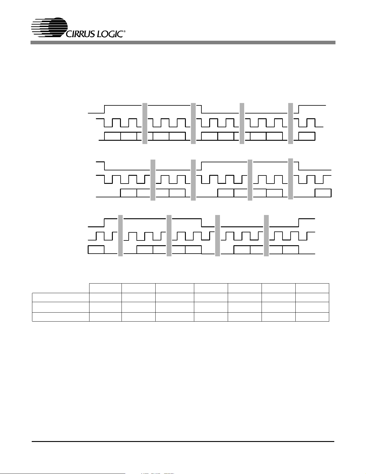
Figure 1. Audio Port Master Mode Timing ...................................................................................... 6
Figure 2. Audio Port Slave Mode and Data Input Timing................................................................ 6
Figure 3. SPI Mode timing............................................................................................................... 7
Figure 4. Two-Wire Mode timing..................................................................................................... 8
Figure 5. Recommended Connection Diagram for Software Mode ................................................ 9
Figure 6. Serial Audio Input Example Formats ............................................................................. 11
Figure 7. AES3 Transmitter Timing for C, U and V pin input data ................................................ 13
Figure 8. Control Port Timing in SPI Mode ................................................................................... 14
Figure 9. Control Port Timing in Two-Wire Mode.......................................................................... 15
Figure 10. Hardware Mode ...........................................................................................................26
Figure 11. Professional Output Circuit.......................................................................................... 33
Figure 12. Consumer Output Circuit ............................................................................................. 33
Figure 13. TTL/CMOS Output Circuit............................................................................................ 33
Figure 14. Channel Status Data Buffer Structure.......................................................................... 34
Figure 15. Flowchart for Writing the E Buffer................................................................................ 34
DS469PP4 3
CS8405A
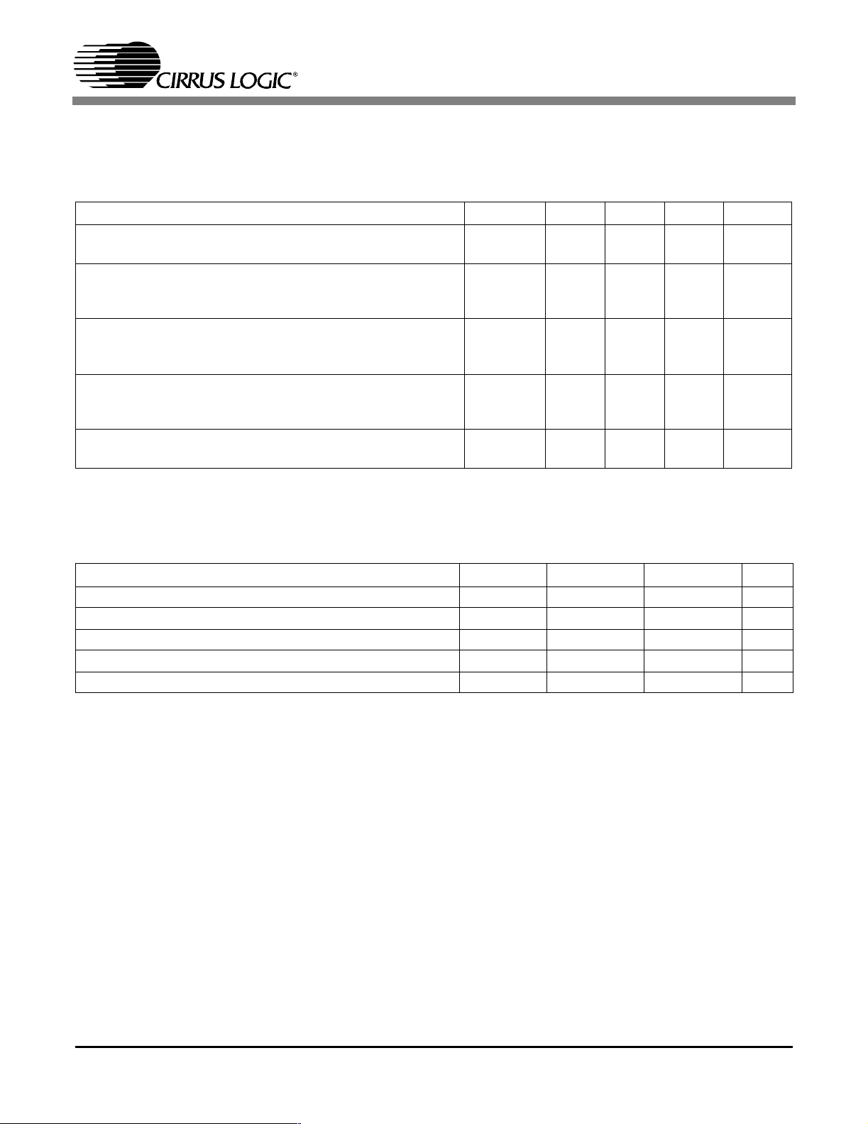
1. CHARACTERISTICS AND SPECIFICATIONS
POWER AND THERMAL CHARACTERISTICS (DGND = 0 V, all voltages with respect to
ground)
Parameter Symbol Min Typ Max Units
Power Supply Voltage VD+
VL+
Supply Current at 48 kHz frame rate VD+
VL+ = 3V
VL+ = 5V
Supply Current at 96 kHz frame rate VD+
VL+ = 3V
VL+ = 5V
Supply Current in power down Reset high, VD+
Reset high, VL+ = 3V
Reset high, VL+ = 5V
Ambient Operating Temperature:CS8405-CS & -CZ (Note 1)
CS8405-IS & -IZ (Note 2)
T
A
4.5
2.85
-
-
-
-
-
-
-
-
-
-10
-40
5.0
-
6.3
30.1
46.5
6.6
44.8
76.6
20
60
60
25 70
5.5
5.5
-
-
-
-
-
-
-
-
-
85
mA
mA
mA
mA
mA
mA
µA
µA
µA
V
V
°C
Notes: 1. -CS’ and ‘-CZ’ parts are specified to operate over -10 ° C to 70° C but are tested at 25° C only.
2. ‘- IS’ and ‘-IZ’ parts are tested over the full -40°C to 85°C temperature range.
ABSOLUTE MAXIMUM RATINGS (DGND = 0V, all voltages with respect to ground)
Parameter Symbol Min Max Units
Power Supply Voltage VD/VL+ - 6.0 V
Input Current, Any Pin Except Supply (Note 3) I
Input Voltage V
Ambient Operating Temperature (power applied) T
Storage Temperature T
Notes: 3. Transient currents of up to 100 mA will not cause SCR latch-up.
in
in
A
stg
-±10mA
-0.3 (VL+) + 0.3 V
-55 125 °C
-65 150 °C
4 DS469PP4
CS8405A
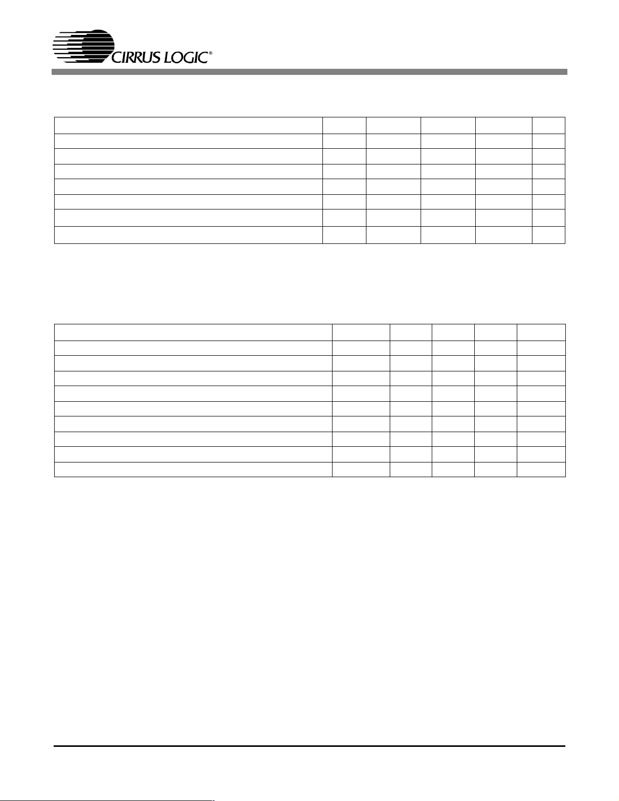
DIGITAL CHARACTERISTICS
(TA= 25 °C for suffixes ‘CS’ &’CZ’, TA= -40 to 85°C for ‘IS’ & ‘IZ’ ; VD+ = 5V±10%, VL+ = 3/5V ±5/10%)
Parameter Symbol Min Typ Max Units
High-Level Input Voltage V
Low-Level Input Voltage (Note 4) V
Low-Level Output Voltage, (Io=-3.2 mA), except TXP, TXN V
High-Level Output Voltage, (Io=3.2 mA), except TXP, TXN V
Input Leakage Current I
Output High Voltage, TXP, TXN (I
Output Low Voltage, TXP, TXN (I
= 14 mA) (VL+) - 0.7 (VL+) - 0.4 - V
OH
=14mA) - 0.4 0.7 V
OL
IH
IL
OL
OH
in
2.0 - (VL+) + 0.3 V
-0.3 - 0.4/0.8 V
--0.4V
(VL+) - 1 - - V
-±1±10µA
Notes: 4. At 5V mode, V
= 0.8V (Max), at 3V mode, VIL=0.4V (Max).
IL
SWITCHING CHARACTERISTICS
(TA= 25 °C for suffixes ‘CS’ &’CZ’, TA= -40 to 85°C for ‘IS’ & ‘IZ’ ; VD+ = 5V±10%, VL+ = 3/5V ±5/10%, Inputs:
Logic 0 = 0 V, Logic 1 = VL+; C
Parameter Symbol Min Typ Max Units
RST
pin Low Pulse Width 200 - - µs
OMCK Frequency for OMCK = 512*Fs 4.1 - 55.3 MHz
OMCK Low and High Width for OMCK = 512*Fs 7.2 - - ns
OMCK Frequency for OMCK = 384*Fs 3.1 - 41.5 MHz
OMCK Low and High Width for OMCK = 384*Fs 9.6 - - ns
OMCK Frequency for OMCK = 256*Fs 2.0 - 27.7 MHz
OMCK Low and High Width for OMCK = 256*Fs 14.4 - - ns
Frame Rate 8.0 - 108.0 kHz
AES3 Transmitter Output Jitter - - 1 ns
=20pF)
L
DS469PP4 5
CS8405A
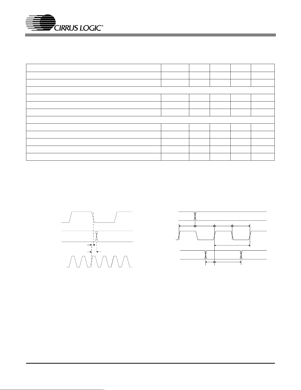
SWITCHING CHARACTERISTICS - SERIAL AUDIO PORTS
(TA= 25 °C for suffixes ‘CS’ &’CZ’, TA= -40 to 85°C for ‘IS’ & ‘IZ’ ; VD+ = 5V±10%, VL+ = 3/5V ±5/10%, Inputs:
Logic 0 = 0 V, Logic 1 = VL+; C
Parameter Symbol Min Typ Max Units
SDIN Setup Time Before ISCLK Active Edge (Note 5) t
SDIN Hold Time After ISCLK Active Edge (Note 5) t
Master Mode
OMCK to ISCLK active edge delay (Note 5) t
OMCK to ILRCK delay (Note 6) t
ISCLK and ILRCK Duty Cycle - 50 - %
Slave Mode
ISCLK Period (Note 7) t
ISCLK Input Low Width t
ISCLK Input High Width t
ISCLK Active Edge to ILRCK Edge (Note 5,6,8) t
ILRCK Edge Setup Before ISCLK Active Edge (Note 5,6,9) t
=20pF)
L
ds
dh
smd
lmd
sckw
sckl
sckh
lrckd
lrcks
20 - - ns
20 - - ns
0 - 10 ns
0 - 10 ns
36 - - ns
14 - - ns
14 - - ns
20 - - ns
20 - - ns
Notes: 5. The active edge of ISCLK is programmable.
6. The polarity of ILRCK is programmable.
7. No more than 128 SCLK per frame.
8. This delay is to prevent the previous ISCLK edge from being interpreted as the first one after ILRCK has
changed.
9. This setup time ensures that this ISCLK edge is interpreted as the first one after ILRCK has changed.
ISCLK
(output)
ILRCK
(output)
t
smd
OMCK
(input)
t
lmd
Figure 1. Audio Port Master Mode Timing Figure 2. Audio Port Slave Mode and Data Input Timing
ILRCK
(input)
ISCLK
(input)
SDIN
t
lrckd
t
lrcks
t
sckh
t
t
dh
ds
t
t
sckw
sckl
6 DS469PP4
CS8405A
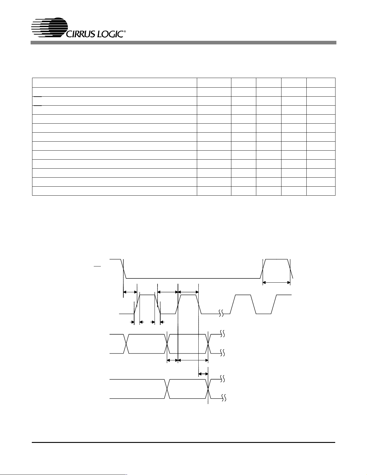
SWITCHING CHARACTERISTICS - CONTROL PORT - SPI MODE
(TA= 25 °C for suffixes ‘CS’ &’CZ’, TA= -40 to 85°C for ‘IS’ & ‘IZ’ ; VD+ = 5V±10%, VL+ = 3/5V ±5/10%, Inputs:
Logic 0 = 0 V, Logic 1 = VL+; C
Parameter Symbol Min Typ Max Units
CCLK Clock Frequency (Note 10) f
High Time Between Transmissions t
CS
Falling to CCLK Edge t
CS
CCLK Low Time t
CCLK High Time t
CDIN to CCLK Rising Setup Time t
CCLK Rising to DATA Hold Time (Note 11) t
CCLK Falling to CDOUT Stable t
Rise Time of CDOUT t
Fall Time of CDOUT t
Rise Time of CCLK and CDIN (Note 12) t
Fall Time of CCLK and CDIN (Note 12) t
=20pF)
L
sck
csh
css
scl
sch
dsu
dh
pd
r1
f1
r2
f2
0-6.0MHz
1.0 - - µs
20 - - ns
66 - - ns
66 - - ns
40 - - ns
15 - - ns
- - 50 ns
- - 25 ns
- - 25 ns
- - 100 ns
- - 100 ns
Notes: 10. If Fs is lower than 46.875 kHz, the maximum CCLK frequency should be less than 128 Fs. This is
dictated by the timing requirements necessary to access the Channel Status and User Bit buffer
memory. Access to the control register file can be carried out at the full 6 MHz rate. The minimum
allowable input sample rate is 8 kHz, so choosing CCLK to be less than or equal to 1.024 MHz should
be safe for all possible conditions.
11. Data must be held for sufficient time to bridge the transition time of CCLK.
12. For f
sck
<1 MHz.
CS
t
t
css
scl
t
sch
t
csh
CCLK
t
r2
t
f2
CDIN
t
dsu
t
dh
t
pd
CDOUT
Figure 3. SPI Mode timing
DS469PP4 7
CS8405A
SWITCHING CHARACTERISTICS - CONTROL PORT - Two-Wire MODE
(Note 13, TA= 25 °C for suffixes ‘CS’ &’CZ’, TA= -40 to 85°C for ‘IS’ & ‘IZ’ ; VD+ = VL+ = 5V ±10%, Inputs: Logic 0
= 0V, Logic 1 = VL+; C
SCL Clock Frequency f
Bus Free Time Between Transmissions t
Start Condition Hold Time (prior to first clock pulse) t
Clock Low Time t
Clock High Time t
Setup Time for Repeated Start Condition t
SDA Hold Time from SCL Falling (Note 14) t
SDA Setup Time to SCL Rising t
Rise Time of Both SDA and SCL Lines t
Fall Time of Both SDA and SCL Lines t
Setup Time for Stop Condition t
Notes: 13. Two-Wire Mode is compatible with the I
14. Data must be held for sufficient time to bridge the 300 ns transition time of SCL.
= 20pF)
L
Parameter Symbol Min Typ Max Units
scl
buf
hdst
low
high
sust
hdd
sud
r
f
susp
2C®
protocol and is supported only at 5V mode.
- - 100 kHz
4.7 - - µs
4.0 - - µs
4.7 - - µs
4.0 - - µs
4.7 - - µs
0--µs
250 - - ns
- - 25 ns
- - 25 ns
4.7 - - µs
SDA
SCL
Stop Start
t
buf
t
hdst
t
low
t
high
t
hdd
Figure 4. Two-Wire Mode timing
t
sud
Repeated
Start
t
sust
t
hdst
Stop
t
f
t
r
t
susp
8 DS469PP4
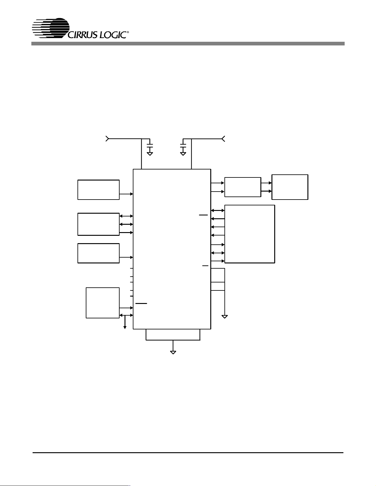
2. TYPICAL CONNECTION DIAGRAM
CS8405A
+5V Supply
AES3 Data
Source
3-wire Serial
Audio Source
Clock Source
and Control
Hardware
Control
To other
CS8405's
0.1 Fµ
VD+ VL+
RXP
ILRCK
ISCLK
SDIN
OMCK
NC1
NC2
NC3
NC4
NC5
RST
TCBL
0.1 Fµ
CS8405A
SDA/CDOUT
AD0/CS
SCL/CCLK
AD1/CDIN
DGND2
DGND3
TXP
TXN
DGNDDGND4
AD2
U
INT
H/S
+3V to
+5V
Supply
Cable
Interface
Microcontroller
AES3/
SPDIF
Equipment
Figure 5. Recommended Connection Diagram for Software Mode
DS469PP4 9

CS8405A
3. GENERAL DESCRIPTION
The CS8405A is a monolithic CMOS device which
encodes and transmits audio data according to the
AES3, IEC60958, S/PDIF, and EIAJ CP1201 interface standards. The CS8405A accepts audio, channel status and user data, which is then multiplexed,
encoded, and driven onto a cable.
The audio data is input through a configurable, 3wire input port. The channel status bits and user bit
data are input through an SPI or Two-Wire Mode
microcontroller port and may be assembled in separate block sized buffers.
For systems with no microcontroller, a stand alone
mode allows direct access to channel status and
user data input pins.
Target applications include CD-R, DAT, DVD,
MD and VTR equipment, mixing consoles, digital
audio transmission equipment, high quality A/D
converters, effects processors, set-top TV boxes,
and computer audio systems.
Figure 5 shows the supply and external connections to the CS8405A when configured for operation with a microcontroller.
3.1 AES3 and S/PDIF Standards Documents
This data sheet assumes that the user is familiar
with the AES3 and S/PDIF data formats. It is advisable to have current copies of the AES3 and
IEC60958 specifications on hand for easy reference.
The latest AES3 standard is available from the Audio Engineering Society or ANSI at www.aes.org
or www.ansi.org. Obtain the latest IEC60958 standard from ANSI or from the International Electrotechnical Commission at www.iec.ch. The latest
EIAJ CP-1201 standard is available from the Japanese Electronics Bureau.
Crystal Application Note 22: Overview of Digital
Audio Interface Data Structures contains a useful
tutorial on digital audio specifications, but it should
not be considered a substitute for the standards.
The paper An Understanding and Implementation
of the SCMS Serial Copy Management System for
Digital Audio Transmission, by Clifton Sanchez, is
an excellent tutorial on SCMS. It is available from
the AES as preprint 3518.
4. THREE-WIRE SERIAL INPUT AUDIO PORT
A 3-wire serial audio input port is provided. The interface format can be adjusted to suit the attached
device through the control registers. The following
parameters are adjustable:
• Masterorslave
• Serial clock frequency
• Audio data resolution
• Left or right justification of the data relative to
left/right clock
• Optional one-bit cell delay of the first data bit
• Polarity of the bit clock
• Polarity of the left/right clock. (By setting the
appropriate control bits, many formats are possible).
Figure 6 shows a selection of common input formats with the corresponding control bit settings.
In master mode, the left/right clock and the serial
bit clock are outputs, derived from the OMCK input pin master clock.
In slave mode, the left/right clock and the serial bit
clock are inputs. The left/right clock must be synchronous to the OMCK master clock, but the serial
bit clock can be asynchronous and discontinuous if
required. The left/right clock should be continuous,
but the duty cycle can be less than the specified typical value of 50% if enough serial clocks are
present in each phase to clock all the data bits.
10 DS469PP4
CS8405A
Left
Justified
(In)
2
IS
(In)
Right
Justified
(In)
ILRCK
ISCLK
SDIN
ILRCK
ISCLK
SDIN
ILRCK
ISCLK
SDIN
Left
Right
MSB LSB MSB LSB MSB
Left Right
MSB
Left
LSB MSB LSB
MSB LSB
LSB
MSB
Right
LSB
MSB
SIMS* SISF* SIRES[1:0]* SIJUST* SIDEL* SISPOL* SILRPOL*
Left Justified X X 00+ 0 0 0 0
2
S
I
XX00+0 1 0 1
Right Justified X X XX 1 0 0 0
X = don’t care to match format, but does need to be set to the desired setting
2
S can accept an arbitrary number of bits, determined by the number of ISCLK cycles
+I
* See Serial Input Port Data Format Register Bit Descriptions for an explanation of the meaning of each bit
Figure 6. Serial Audio Input Example Formats
DS469PP4 11

CS8405A
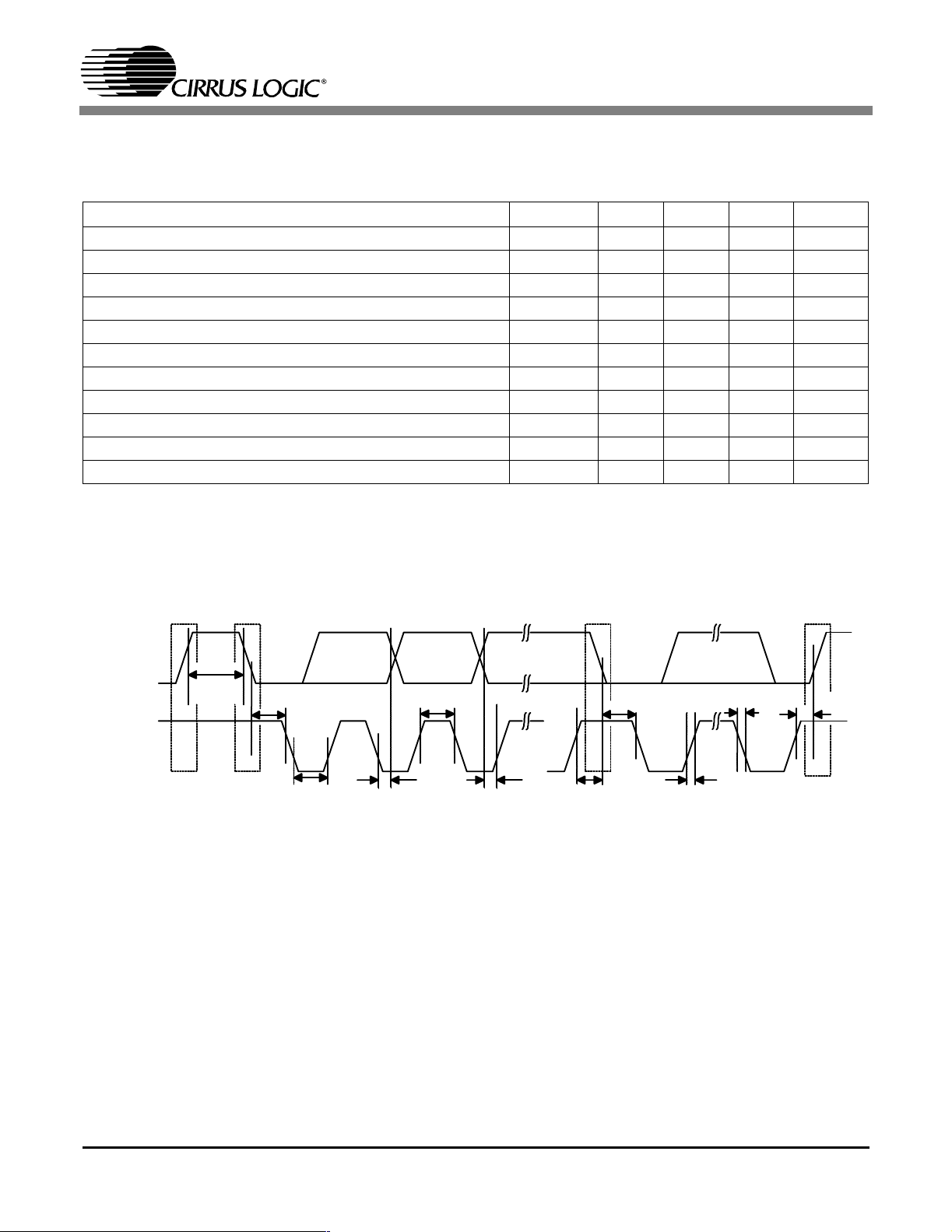
5. AES3 TRANSMITTER
The CS8405A includes an AES3 digital audio
transmitter. A comprehensive buffering scheme
provides write access to the channel status and user
data. This buffering scheme is described in “Appendix B: Channel Status and User Data Buffer
Management” on page 34.
The AES3 transmitter encodes and transmits audio
and digital data according to the AES3, IEC60958
(S/PDIF), and EIAJ CP-1201 interface standards.
Audio and control data are multiplexed together
and bi-phase mark encoded. The resulting bit
stream is driven to an output connector either directly or through a transformer. The transmitter is
clocked from the clock input pin, OMCK. If
OMCK is asynchronous to the data source, an interrupt bit(TSLIP) is provided that will go high every time a data sample is dropped or repeated. Be
aware that the pattern of slips does not have hysteresis and so the occurrence of the interrupt condition
is not deterministic.
The channel status (C) and user (U) bits in the
transmitted data stream are taken from storage areas within the CS8405A. The user can manually
access the internal storage or configure the
CS8405A to run in one of several automatic modes.
“Appendix B: Channel Status and User Data Buffer
Management” on page 34 provides detailed descriptions of each automatic mode and describes
methods of manually accessing the storage areas.
The transmitted user bit data can optionally be input through the U pin, under the control of a control
port register bit. Figure 7 shows the timing requirements for inputting U data through the U pin.
5.1 Transmitted Frame and Channel Status Boundary Timing
The TCBL pin is used to control or indicate the
start of transmitted channel status block boundaries
and may be an input or an output.
In some applications, it may be necessary to control
the precise timing of the transmitted AES3 frame
boundaries. This may be achieved in two ways:
a) With TCBL set to input, driving TCBL high for
>3 OMCK clocks will cause a frame start, as well
as a new channel status block start.
b) If the serial audio input port is in slave mode and
TCBL is set to output, the start of the A channel
sub-frame will be aligned with the leading edge of
ILRCK.
5.2 TXN and TXP Drivers
The line drivers are low skew, low impedance, differential outputs capable of driving cables directly.
Both drivers are set to ground during reset (RST
low), when no AES3 transmit clock is provided,
and optionally under the control of a register bit.
The CS8405A also allows immediate muting of the
AES3 transmitter audio data through a control register bit.
External components are used to terminate and isolate the external cable from the CS8405A. These
components are detailed in “Appendix A: External
AES3/SPDIF/IEC60958 Transmitter Components” on page 33.
5.3 Mono Mode Operation
An AES3 stream may be used in more than one
way to transmit 96 kHz sample rate data. One
method is to double the frame rate of the current
format. This results in a stereo signal with a sample
rate of 96 kHz, carried over a single twisted pair cable. An alternate method is implemented using the
two sub-frames in a 48 kHz frame rate AES3 signal
to carry consecutive samples of a mono signal, resulting in a 96 kHz sample rate stream. This allows
older equipment, whose AES3 transmitters and receivers are not rated for 96 kHz frame rate operation, to handle 96 kHz sample rate information. In
this “mono mode”, two AES3 cables are needed for
stereo data transfer. The CS8405A offers mono
=
12 DS469PP4

CS8405A
mode operation. The CS8405A is set to mono
mode by the MMT control bit.
In mono mode, the input port will run at the audio
sample rate (Fs), while the AES3 transmitter frame
rate will be at Fs/2. Consecutive left or right channel serial audio data samples may be selected for
transmission on the A and B sub-frames, and the
channel status block transmitted is also selectable.
Tth
TCBL
In or Ou t
VLRCK
VCU
Input
SDIN
Input
TXP(N)
Output
TCBL
In or Ou t
Tsetup
Data [4] Data [ 5] Data [6] Data [7] Data [8]
Data [0] Data [ 1] Data [2] Data [3] Data [4]
Z Y X Y X
Tth
Thold
VCU[0] VCU[1] VCU[2] VCU[3] VCU[4]
AES3 Transmitter in Stereo mode
Using mono mode is only necessary if the incoming audio sample rate is already at 96 kHz and contains both left and right audio data words. The
“mono mode” AES3 output stream may also be
achieved by keeping the CS8405A in normal stereo
mode, and placing consecutive audio samples in
the left and right positions in an incoming 48 kHz
word rate data stream.
Tsetup => 7.5% AES3 frame time
Thold = 0
Tth > 3OMCK if TCBL is Input
VLRCK
U
Input
SDIN
Input
TXP(N)
Output
TXP(N)
Output
VLRCK is a virtual word clock, which may not exist, and is used to illustrate the CUV timing.
VLRCK duty cycle is 50%.
In stereo mode, VLRCK frequency = AES3 frame rate. In mono mode, ALRCK frequency = 2xAES3 frame rate.
If the serial audio input port is on slave mode and TCBL is an output, then VLRCK=ILRCK if SILRPOL=0 and
VLRCK= ILRCK if SILRPOL =1.
If the serial audio input port is in master mode and TCBL is an input, then VLRCK=ILRCK if SILRPOL=0 and
VLRCK= ILRCK if SILRPOL =1.
Data [4] Data [ 5] Data [6] Data [7] Data [8]
Z Y X
* Assume MMTLR = 0
ZYX
* Assume MMTLR = 1
Data [0]* Data [2]* Data [4]*
Data [1]* Data [3]* Data [ 5]*
U[0] U[ 2]
AES3 Transmitter in Mono mode
Tsetup => 15% AES3 frame time
Thold = 0
Tth > 3OMCK if TCBL is Input
Figure 7. AES3 Transmitter Timing for C, U, and V Pin Input Data
DS469PP4 13

CS8405A
6. CONTROL PORT DESCRIPTION
AND TIMING
The control port is used to access the registers, allowing the CS8405A to be configured for the desired operational modes and formats. In addition,
Channel Status and User data may be read and written through the control port. The operation of the
control port may be completely asynchronous with
respect to the audio sample rate.
The control port has two modes: SPI and TwoWire, with the CS8405A acting as a slave device.
SPI mode is selected if there is a high to low transition on the AD0/CS
pin after the RST pin has
been brought high. Two-Wire mode is selected by
connecting the AD0/CS
pin to VL+ or DGND,
thereby permanently selecting the desired AD0 bit
address state.
6.1 SPI Mode
In SPI mode, CS is the CS8405A chip select signal,
CCLK is the control port bit clock (input into the
CS8405A from the microcontroller); CDIN is the
input data line from the microcontroller; and CDOUT is the output data line to the microcontroller.
Data is clocked in on the rising edge of CCLK and
out on the falling edge.
Figure 8 shows the operation of the control port in
SPI mode. To write to a register, bring CS
low. The
first seven bits on CDIN form the chip address and
must be 0010000. The eighth bit is a read/write indicator (R/W
), which should be low to write. The
next eight bits form the Memory Address Pointer
(MAP), which is set to the address of the register
that is to be updated. The next eight bits are the data
which will be placed into the register designated by
the MAP. During writes, the CDOUT output stays
in the Hi-Z state. It may be externally pulled high
or low with a 47 kΩ resistor, if desired.
There is a MAP auto increment capability, enabled
by the INCR bit in the MAP register. If INCR is a
zero, the MAP will stay constant for successive
read or writes. If INCR is set to a 1, then the MAP
will auto increment after each byte is read or written, allowing block reads or writes of successive
registers.
To read a register, the MAP has to be set to the correct address by executing a partial write cycle
which finishes (CS
high) immediately after the
CS
CCLK
CHIP
ADDRESS
CDIN
CDOUT
14 DS469PP4
0010000
MAP = Memory Address Pointer, 8 bits, MSB first
R/W
High Impedance
MAP
Figure 8. Control Port Timing in SPI Mode
MSB
byte 1
DATA
LSB
byte n
CHIP
ADDRESS
0010000
R/W
MSB
LSB
MSB
LSB

CS8405A
MAP byte. The MAP auto increment bit (INCR)
may be set or not, as desired. To begin a read, bring
low, send out the chip address and set the
CS
read/write bit (R/W
) high. The next falling edge of
CCLK will clock out the MSB of the addressed
register (CDOUT will leave the high impedance
state). If the MAP auto increment bit is set to 1, the
data for successive registers will appear consecutively.
6.2 Two-Wire Mode
In Two-Wire Mode, SDA is a bidirectional data
line. Data is clocked into and out of the part by the
clock, SCL, with the clock to data relationship as
shown in Figure 9. There is no CS
vidual CS8405A is given a unique address. Pins
AD0, AD1, and AD2 form the three least significant bits of the chip address, and should be connected to VL+ or DGND as desired. The upper four
bits of the seven-bit address field are fixed at 0010.
To communicate with a CS8405A, the chip address
field, which is the first byte sent to the CS8405A,
should match 0010 followed by the settings of
AD2, AD1, and AD0. The eighth bit of the address
is the R/W
bit. If the operation is a write, the next
byte is the Memory Address Pointer (MAP) which
selects the register to be read or written. If the operation is a read, the contents of the register pointed
pin. Each indi-
to by the MAP will be output. Setting the auto increment bit in MAP allows successive reads or
writes of consecutive registers. Each byte is separated by an acknowledge bit, ACK, which is output
from the CS8405A after each input byte is read.
The ACK bit is input to the CS8405A from the microcontroller after each transmitted byte. The TwoWire Mode is compatible with the I
2
C protocol.
6.3 Interrupts
The CS8405A has a comprehensive interrupt capability. The INT output pin is intended to drive the
interrupt input pin on the host microcontroller. The
INT pin may be set to be active low, active high or
active low with no active pull-up transistor. This
last mode is used for active low, wired-OR hookups, with multiple peripherals connected to the microcontroller interrupt input pin.
Many conditions can cause an interrupt, as listed in
the interrupt status register descriptions. Each
source may be masked off by a bit in the mask registers. In addition, each source may be set to rising
edge, falling edge, or level sensitive. Combined
with the option of level sensitive or edge sensitive
modes within the microcontroller, many different
set-ups are possible, depending on the needs of the
equipment designer.
Note 1
SDA
SCL
Start
Note 1: AD2 is derived from a resistor attached to the EMPH pin,
Note 2: If operation is a write, this byte contains the Memory Address Pointer, MAP
Note 3: If operation is a read, the last bit of the read should be a NACK(high)
DS469PP4 15
0010 AD2-0
AD1 and AD0 are determ ined by the state of the corresponding pins
Figure 9. Control Port Timing in Two-Wire Mode
R/W
ACK DATA7-0 ACK
Note 2
DATA7-0
Note 3
ACK
Stop

CS8405A
7. CONTROL PORT REGISTER SUMMARY
Addr Function 7 6 5 4 3 2 1 0
0 Reserved 0 0 0 0 0 0 0 0
1 Control 1 0 VSET 0 MUTEAES 0 INT1 INT0 TCBLD
2 Control 2 0 0 0 0 0 MMT MMCST MMTLR
3 Data Flow Control 0 TXOFF AESBP 0 0 0 0 0
4 Clock Source Control 0 RUN CLK1 CLK0 0 0 0 0
5 Serial Input Format SIMS SISF SIRES1 SIRES0 SIJUST SIDEL SISPOL SILRPOL
6 Reserved 0 0 0 0 0 0 0 0
7 Interrupt 1 Status TSLIP 0 0 0 0 0 EFTC 0
8 Interrupt 2 Status 0 0 0 0 0 EFTU 0 0
9 Interrupt 1 Mask TSLIPM 0 0 0 0 0 EFTCM 0
A Interrupt 1 Mode (MSB) TSLIP1 0 0 0 0 0 EFTC1 0
B Interrupt 1 Mode (LSB) TSLIP0 0 0 0 0 0 EFTC0 0
C Interrupt 2 Mask 0 0 0 0 0 EFTU
M
D Interrupt 2 Mode (MSB) 0 0 0 0 0 EFTU1 0 0
E Interrupt 2 Mode (LSB) 0 0 0 0 0 EFTU0 0 0
F-11 Reserved 0 0 0 0 0 0 0 0
12 CS Data Buffer Control 0 0 BSEL 0 0 EFTCI CAM 0
13 U Data Buffer Control 0 0 0 UD UBM1 UBM0 0 EFTUI
1E-1D Reserved 0 0 0 0 0 0 0 0
1F-37 C or U Data Buffer
7F ID and Version ID3 ID2 ID1 ID0 VER3 VER2 VER1 VER0
Table 1. Control Register Map Summary
00
7.1 MEMORY ADDRESS POINTER (MAP)
7 6 543210
INCR MAP6 MAP5 MAP4 MAP3 MAP2 MAP1 MAP0
INCR - Auto Increment Address Control Bit
Default = ‘0’
0 - Disable
1-Enable
MAP6:MAP0 - Register Address
Note: Reserved registers must not be written to during normal operation. Some reserved registers are used for
test modes, which can completely alter the normal operation of the CS8405A.
16 DS469PP4

CS8405A
8. CONTROL PORT REGISTER BIT DEFINITIONS
8.1 Control 1 (1h)
7 6 543210
0 VSET 0 MUTEAES 0 INT1 INT0 TCBLD
VSET - Transmitted Validity bit level
Default = ‘0’
0 - Indicates data is valid, linear PCM audio data
1 - Indicates data is invalid or not linear PCM audio data
MUTEAES - Mute control for the AES transmitter output
Default = ‘0’
0 - Not Muted
1-Muted
INT1:INT0 - Interrupt output pin (INT) control
Default = ‘00’
00 - Active high; high output indicates interrupt condition has occurred
01 - Active low, low output indicates an interrupt condition has occurred
10 - Open drain, active low. Requires an external pull-up resistor on the INT pin.
11 - Reserved
TCBLD - Transmit Channel Status Block pin (TCBL) direction specifier
Default = ‘0’
0-TCBLisaninput
1 - TCBL is an output
DS469PP4 17

CS8405A
8.2 Control 2 (2h)
7 6 543210
0 0 0 0 0 MMT MMTCS MMTLR
MMT - Select AES3 transmitter mono or stereo operation
Default = ‘0’
0 - Normal stereo operation
1 - Output either left or right channel inputs into consecutive subframe outputs (mono
mode, left or right is determined by MMTLR bit)
MMTCS - Select A or B channel status data to transmit in mono mode
Default = ‘0’
0 - Use channel A CS data for the A subframe and use channel B CS data for the B subframe
1 - Use the same CS data for both the A and B subframe outputs. If MMTLR = 0, use the
left channel CS data. If MMTLR = 1, use the right channel CS data.
MMTLR - Channel Selection for AES Transmitter mono mode
Default = ‘0’
0 - Use left channel input data for consecutive subframe outputs
1- Use right channel input data for consecutive subframe outputs
8.3 Data Flow Control (3h)
7 6 543210
0TXOFFAESBP00000
The Data Flow Control register configures the flow of audio data. The output data should be muted prior to changing
bits in this register to avoid transients.
TXOFF - AES3 Transmitter Output Driver Control
Default = ‘0
0 - AES3 transmitter output pin drivers normal operation
1 - AES3 transmitter output pin drivers drive to 0 V.
AESBP - AES3 bypass mode selection
Default = ‘0’
0 - Normal operation
1 - Connect the AES3 transmitter driver input directly to the RXP pin, which becomes a normal TTL
threshold digital input.
18 DS469PP4

CS8405A
8.4 Clock Source Control (4h)
7 6 543210
0RUNCLK1CLK00000
This register configures the clock sources of various blocks. In conjunction with the Data Flow Control register, various Receiver/Transmitter/Transceiver modes may be selected.
RUN - Controls the internal clocks, allowing the CS8405A to be placed in a “powered down” low
current consumption, state.
Default = ‘0’
0 - Internal clocks are stopped. Internal state machines are reset. The fully static
control port registers are operational, allowing registers to be read or changed. Reading and
writing the U and C data buffers is not possible. Power consumption is low.
1 - Normal part operation. This bit must be set to 1 to allow the CS8405A
to begin operation. All input clocks should be stable in frequency and phase when
RUN is set to 1.
CLK1:0 - Output master clock (OMCK) input frequency to output sample rate (Fs) ratio selector.
If these bits are changed during normal operation, then always stop the CS8405A first (RUN = 0),
write the new value, then start the CS8405A (RUN = 1).
Default = ‘00’
00 - OMCK frequency is 256*Fs
01 - OMCK frequency is 384*Fs
10 - OMCK frequency is 512*Fs
11 - Reserved
8.5 Serial Audio Input Port Data Format (5h)
7 6 543210
SIMS SISF SIRES1 SIRES0 SIJUST SIDEL SISPOL SILRPOL
SIMS - Master/Slave Mode Selector
Default = ‘0’
0 - Serial audio input port is in slave mode
1 - Serial audio input port is in master mode
SISF - ISCLK frequency (for master mode)
Default = ‘0’
0-64*Fs
1 - 128*Fs
SIRES1:0 - Resolution of the input data, for right-justified formats
Default = ‘00’
00 - 24-bit resolution
01 - 20-bit resolution
10 - 16-bit resolution
11 - Reserved
DS469PP4 19

SIJUST - Justification of SDIN data relative to ILRCK
Default = ‘0’
0 - Left-justified
1 - Right-justified
SIDEL - Delay of SDIN data relative to ILRCK, for left-justified data formats
Default = ‘0’
CS8405A
0 - MSB of SDIN data occurs in the first ISCLK period after the ILRCK edge (left justified mode)
1 - MSB of SDIN data occurs in the second ISCLK period after the ILRCK edge (I
2
S mode)
SISPOL - ISCLK clock polarity
Default = ‘0’
0 - SDIN sampled on rising edges of ISCLK
1 - SDIN sampled on falling edges of ISCLK
SILRPOL - ILRCK clock polarity
Default = ‘0’
0 - SDIN data is for the left channel when ILRCK is high
1 - SDIN data is for the right channel when ILRCK is high
8.6 Interrupt 1 Status (7h) (Read Only)
7 6 543210
TSLIP0 0000EFTC0
For all bits in this register, a “1” means the associated interrupt condition has occurred at least once since the register
was last read. A ”0” means the associated interrupt condition has NOT occurred since the last reading of the register.
Reading the register resets all bits to 0, unless the interrupt mode is set to level and the interrupt source is still true.
Status bits that are masked off in the associated mask register will always be “0” in this register. This register defaults
to 00h.
TSLIP - AES3 transmitter source data slip interrupt
In data flows where OMCK, which clocks the AES3 transmitter, is asynchronous to the data source,
this bit will go high every time a data sample is dropped or repeated. When TCBL is an input, this bit
will
go high on receipt of a new TCBL signal.
EFTC - E to F C-buffer transfer interrupt.
The source for this bit is true during the E to F buffer transfer in the C bit buffer management process.
20 DS469PP4

CS8405A
8.7 Interrupt 2 Status (8h) (Read Only)
7 6 543210
00000EFTU00
For all bits in this register, a “1” means the associated interrupt condition has occurred at least once since the register
was last read. A ”0” means the associated interrupt condition has NOT occurred since the last reading of the register.
Reading the register resets all bits to 0, unless the interrupt mode is set to level and the interrupt source is still true.
Status bits that are masked off in the associated mask register will always be “0” in this register. This register defaults
to 00h.
EFTU - E to F U-buffer transfer interrupt. (Block Mode only)
The source of this bit is true during the E to F buffer transfer in the U bit buffer management process.
8.8 Interrupt 1 Mask (9h)
7 6 543210
TSLIPM0 0000EFTCM0
The bits of this register serve as a mask for the Interrupt 1 register. If a mask bit is set to 1, the error is unmasked,
meaning that its occurrence will affect the INT pin and the status register. If a mask bit is set to 0, the error is masked,
meaning that its occurrence will not affect the INT pin or the status register. The bit positions align with the corresponding bits in Interrupt 1 register. This register defaults to 00h.
8.9 Interrupt 1 Mode MSB (Ah) and Interrupt 1 Mode LSB(Bh)
7 6 543210
TSLIP1 0 0 0 0 0 EFTC1 0
TSLIP0 0 0 0 0 0 EFTC0 0
The two Interrupt Mode registers form a 2-bit code for each Interrupt Register 1 function. There are three ways to
set the INT pin active in accordance with the interrupt condition. In the Rising edge active mode, the INT pin becomes active on the arrival of the interrupt condition. In the Falling edge active mode, the INT pin becomes active
on the removal of the interrupt condition. In Level active mode, the INT interrupt pin becomes active during the interrupt condition. Be aware that the active level(Actice High or Low) only depends on the INT[1:0] bits. These registers default to 00.
00 - Rising edge active
01 - Falling edge active
10 - Level active
11 - Reserved
8.10 Interrupt 2 Mask (Ch)
7 6 543210
00000EFTUM00
The bits of this register serve as a mask for the Interrupt 2 register. If a mask bit is set to 1, the error is unmasked,
meaning that its occurrence will affect the INT pin and the status register. If a mask bit is set to 0, the error is masked,
meaning that its occurrence will not affect the INT pin or the status register. The bit positions align with the corresponding bits in Interrupt 2 register. This register defaults to 00h.
DS469PP4 21

CS8405A
8.11 Interrupt 2 Mode MSB (Dh) and Interrupt Mode 2 LSB(Eh)
7 6 543210
0 0 0 0 0 EFTU1 0 0
0 0 0 0 0 EFTU0 0 0
The two Interrupt Mode registers form a 2-bit code for each Interrupt Register 1 function. There are three ways to
set the INT pin active in accordance with the interrupt condition. In the Rising edge active mode, the INT pin becomes active on the arrival of the interrupt condition. In the Falling edge active mode, the INT pin becomes active
on the removal of the interrupt condition. In Level active mode, the INT interrupt pin becomes active during the interrupt condition. Be aware that the active level (Active High or Low) only depends on the INT[1:0] bits. These registers default to 00.
00 - Rising edge active
01 - Falling edge active
10 - Level active
11 - Reserved
8.12 Channel Status Data Buffer Control (12h)
7 6 543210
0 0 BSEL 0 0 EFTCI CAM 0
BSEL - Selects the data buffer register addresses to contain User data or Channel Status data
Default = ‘0’
0 - Data buffer address space contains Channel Status data
1 - Data buffer address space contains User data
Note: There are separate complete buffers for the Channel Status and User bits. This control bit determines which
buffer appears in the address space.
EFTCI - E to F C-data buffer transfer inhibit bit.
Default = ‘0’
0 - Allow C-data E to F buffer transfers
1 - Inhibit C-data E to F buffer transfers
CAM - C-data buffer control port access mode bit
Default = ‘0’
0-Onebytemode
1-Twobytemode
22 DS469PP4

CS8405A
8.13 User Data Buffer Control (13h)
7 6 543210
0 0 0 UD UBM1 UBM0 0 EFTUI
UD - User bit data pin (U) direction specifier
Default = ‘0’
0 - The U pin is an input. The User bit data is latched in on both rising and falling edges of
OLRCK. This setting also chooses the U pin as the source for transmitted U data.
1 - The U pin is an output. The received U data is clocked out on both rising and falling edges
of ILRCK. This setting also chooses the U data buffer as the source of transmitted U data.
UBM1:0 - Sets the operating mode of the AES3 User bit manager
Default = ‘00’
00 - Transmit all zeros mode
01 - Block mode
10 - Reserved
11 - Reserved
EFTUI - E to F U-data buffer transfer inhibit bit (valid in block mode only).
Default = ‘0’
0 - Allow U-data E to F buffer transfers
1 - Inhibit U-data E to F buffer transfer
8.14 Channel Status bit or User bit Data Buffer (20h - 37h)
Either the channel status data buffer E or the separate user bit data buffer E (provided UBM bits are set to block
mode) is accessible through these register addresses.
8.15 CS8405A I.D. and Version Register (7Fh) (Read Only)
7 6 543210
ID3 ID2 ID1 ID0 VER3 VER2 VER1 VER0
ID3:0 - ID code for the CS8405A. Permanently set to 0110
VER3:0 - CS8405A revision level. Revision A is coded as 0001
DS469PP4 23

CS8405A
9. PIN DESCRIPTION - SOFTWARE MODE
SDA/CDOUT 1 Serial Control Data I/O (Two-Wire Mode) / Data Out (SPI) (Input/Output)-InTwo-WireMode,SDAis
the control I/O data line. SDA is open drain and requires an external pull-up resistor to VL+. In SPI
mode, CDOUT is the output data from the control port interface on the CS8405A
AD0/CS
AD2 3
RXP 4
DGND2
DGND4
DGND3
DGND
VD+
VL+
RST
NC1
NC2
NC3
NC4
NC5
ILRCK 12 Serial Audio Input Left/Right Clock (Input/Output) - Word rate clock for the audio data on the SDIN
ISCLK 13 Serial Audio Bit Clock (Input/Output) - Serial bit clock for audio data on the SDIN pin.
SDIN 14 Serial Audio Data Port (Input) - Audio data serial input pin.
TCBL 15 Transmit Channel Status Block Start (Input/Output) - When operated as output, TCBL is high during
2 Address Bit 0 (Two-Wire Mode) / Control Port Chip Select (SPI) (Input/Output) - A falling edge on
this pin puts the CS8405A into SPI control port mode. With no falling edge, the CS8405A defaults to
Two-Wire mode. In Two-Wire mode, AD0 is a chip address pin. In SPI mode, CS
control port interface on the CS8405A
Address Bit 2 (Two-Wire Mode) (Input) - Determines the AD2 address bit for the control port in Two-
Wire mode, and should be connected to DGND or VL+. If SPI mode is used, the AD2 pin should be connected to DGND.
Auxiliary AES3 Receiver Port (Input) - Input for an alternate, already AES3 coded, audio data
5
Digital Ground (Input) - Ground for the digital section.
7
8
22
623Positive Digital Power (Input) - Typically +5 V. VD+ must be +5 V while VL+ may be operated at 3.3 V
9 Reset (Input)-WhenRSTis low, the CS8405A enters a low power mode and all internal states are
reset. On initial power up, RST
stable in frequency and phase. This is particularly true in hardware mode with multiple CS8405A
devices, where synchronization between devices is important.
No Connect - These pins should not be connected to any signals or PCB trace. They may be driven
10
high and/or low by the CS8405A.
11
16
17
18
pin.
the first sub-frame of a transmitted channel status block, and low at all other times. When operated as
input, driving TCBL high for at least three OMCK clocks will cause the next transmitted sub-frame to be
the start of a channel status block.
must be held low until the power supply is stable, and all input clocks are
is used to enable the
source.
24 DS469PP4

CS8405A
INT 19 Interrupt (Output) - Indicates key events during the operation of the CS8405A. All bits affecting INT
may be unmasked through bits in the control registers. Indication of the condition(s) that initiated an
interrupt are readable in the control registers. The polarity of the INT output, as well as selection of a
standard or open drain output, is set through a control register. Once set true, the INT pin goes false
only after the interrupt status registers have been read and the interrupt status bits have returned to
zero.
U 20 User Data (Input/Output) - May optionally be used to input User data for transmission by the AES3
transmitter, see Figure 7 for timing information. Alternatively, the U pin may be set to output, which also
selects the internal buffer as the source of transmitted U data. If not driven, a 47 kΩ pull-down resistor is
recommended for the U pin, because the default state of the UD direction bit sets the U pin as an input.
The pull-down resistor ensures that the transmitted user data will be zero. If the U pin is always set to be
an output, thereby causing the U bit manager to be the source of the U data, then the resistor is not necessary. The U pin should not be tied directly to ground, in case it is programmed to be an output, and
subsequently tries to output a logic high. This situation may affect the long term reliability of the device.
If the U pin is driven by a logic level output, then a 100 Ω series resistor is recommended.
OMCK 21 Master Clock (Input) - The frequency must be 256x, 384x, or 512x the sample rate.
H/S
TXN 2526Differential Line Drivers (Output) - Transmitting AES3 data. Drivers are pulled low while the CS8405A
TXP
AD1/CDIN 27 Address Bit 1 (Two-Wire Mode) / Serial Control Data in (SPI) (Input) - In Two-Wire mode, AD1 is a
SCL/CCLK 28 Control Port Clock (Input) - Serial control interface clock and is used to clock control data bits into and
24 Hardware/Software Control Mode Select (Input) -Determines the method of controlling the operation
of the CS8405A, and the method of accessing Channel Status and User bit data. In software mode,
device control and CS and U data access is primarily through the control port, using a microcontroller.
Hardware mode provides an alternate mode of operation, and access to CS and U data is provided by
dedicated pins. This pin should be permanently tied to VL+ or DGND.
is in the reset state.
chip address pin. In SPI mode, CDIN is the input data line for the control port interface.
out of the CS8405A. In Two-Wire mode, SCL requires an external pull-up resistor to VL+.
DS469PP4 25

CS8405A
10. HARDWARE MODE
The CS8405A has a hardware mode that allows the
use of the device without a microcontroller. Hardware mode is selected by connecting the H/S
pin to
VL+. The flexibility of the CS8405A is necessarily
limited in hardware mode. Various pins change
function as described in the hardware mode pin description section.
The hardware mode data flow is shown in
Figure 10. Audio data is input through the serial audio input port and routed to the AES3 transmitter.
10.1 Channel Status, User and Validity
Data
The transmitted channel status, user and validity
data can be input in two methods, determined by
the state of the CEN pin. Mode A is selected when
the CEN pin is low. In mode A, the user bit data and
the validity bit are input through the U and V pins,
clocked by both edges of ILRCK. The channel status data is derived from the state of the COPY/C,
ORIG, EMPH
how the COPY/C and ORIG pins map to channel
status bits. In consumer mode, the transmitted category code is set to Sample Rate Converter
(0101100).
, and AUDIO pins. Table 2 shows
Mode B is selected when the CEN pin is high. In
mode B, the channel status, user data bits and the
validity bit are input serially through the COPY/C,
U and V pins. Data is clocked into these pins at
both edges of ILRCK. Figure 7 shows the timing
requirements.
The channel status block pin (TCBL) may be an input or an output, determined by the state of the
TCBLD pin.
10.2 Serial Audio Port Formats
The serial audio input port data format is selected
as shown in Table 3, and may be set to master or
slave by the state of the APMS input pin. Table 4
describes the equivalent software mode, bit settings
for each of the available formats. Timing diagrams
areshowninFigure6.
COPY/C ORIG Function
00
01
10
11
Table 2. Hardware Mode COPY/C and ORIG pin
PRO=0, COPY=0, L=0 copyright
PRO=0, COPY=0, L=1 copyright,
pre-recorded
PRO=0, COPY=1, L=0
non-copyright
PRO=1
functions
VL+
H/S
ILRCK
ISCLK
SDIN
26 DS469PP4
Serial
Audio
Input
C, U, V Data Buffer
SFMT1 SFMT0
APMS
Power supply pins and the reset pin are omitted from this diagram.
Please refer to the Typical Connection Diagram for hook-up details.
Figure 10. Hardware Mode
COPY/C
ORIG EMPH AUDIO TCBL
Output
Clock
Source
AES3
Encoder
&Tx
OMCK
TXP
TXN
CEN
U
V
TCBLD

CS8405A
SFMT1 SFMT0 Function
00
01
10
11
Table 3. Hardware Mode Serial Audio Port Format Selection
IF1 - Left Justified 0 00 0 0 0 0
2
IF2 - I
S
IF3 - Right Justified, 24-bit data 0 00 1 0 0 0
IF4 - Right Justified, 16-bit data 0 10 1 0 0 0
Table 4. Equivalent Register Settings of Serial Audio Input Formats Available in Hardware Mode
Serial Input Format IF1 - Left Justified
Serial Input Format IF2 - I2S
Serial Input Format IF3 - Right Justified, 24bit data
Serial Input Format IF4 - Right Justified, 16bit data
SISF SIRES1/0 SIJUST SIDEL SISPOL SILRPOL
000 0 1 0 1
DS469PP4 27
CS8405A
11. PIN DESCRIPTION - HARDWARE MODE
COPY/C 1 COPY Channel Status Bit/C Bit (Input) - In hardware mode A (CEN = 0), the COPY/C and ORIG pins
determine the state of the Copyright, Pro, and L Channel Status bits in the outgoing AES3 data stream,
see Table 2. In hardware mode B, the COPY/C pin becomes the direct C bit input data pin.
VL2+
VD+
VL3+
VL+
VL4+
EMPH
SFMT0
SFMT1
DGND6
DGND3
DGND
RST
APMS 10 Serial Audio Data Port Master/Slave Select (Input) - APMS should be connected to VL+ to set serial
TCBLD 11 Transmit Channel Status Block Direction (Input) - Connect TCBLD to VL+ to set TCBL as an output.
ILRCK 12 Serial Audio Input Left/Right Clock (Input/Output) - Word rate clock for the audio data on the SDIN
ISCLK 13 Serial Audio Bit Clock (Input/Output) - Serial bit clock for audio data on the SDIN pin.
SDIN 14 Serial Audio Data Port (Input) - Audio data serial input pin.
TCBL 15 Transmit Channel Status Block Start (Input/Output) - When operated as output, TCBL is high during
Positive Digital Power (Input) - Typically +5 V. VD+ must be +5 V, the other VL+ pins may be operated
2
at (CEN = 0)+3.3 V
6
20
23
27
3 Pre-Emphasis Indicator (Input) - In hardware mode A (CEN = 0), the EMPH pin low sets the 3 empha-
sis channel status bits to indicate 50/15 µs pre-emphasis of the transmitted audio data. If EMPH
then the three EMPH
45Serial Audio Data Format Select (Input) - select the serial audio input port format. See Table 3.
7
Digital Ground (Input) - Ground for the digital section.
8
22
9 Reset (Input)-WhenRSTis low, the CS8405A enters a low power mode and all internal states are
reset. On initial power up, RST
stable in frequency and phase. This is particularly true in hardware mode with multiple CS8405A
devices, where synchronization between devices is important.
audio input port as a master or connected to DGND to set the port as a slave.
Connect TCBLD to DGND to set TCBL as an input.
pin.
the first sub-frame of a transmitted channel status block, and low at all other times. When operated as
input, driving TCBL high for at least three OMCK clocks will cause the next transmitted sub-frame to be
the start of a channel status block.
channel status bits are set to 000, indicating no pre-emphasis.
must be held low until the power supply is stable, and all input clocks are
is high,
28 DS469PP4
CS8405A
CEN 16 CBitEnable(Input) - Determines how the channel status data bits are input. When CEN is low, hard-
ware mode A is selected, where the COPY/C, ORIG, EMPH
channel status data. When CEN is high, hardware mode B is selected, where the COPY/C pin is used to
enter serial channel status data.
V 17 Validity Bit (Input) - In hardware modes A and B, the V pin input determines the state of the validity bit
in the outgoing AES3 transmitted data. This pin is sampled on both edges of the ILRCK.
U 18 User Data Bit (Input) - In hardware modes A and B, the U pin input determines the state of the user
data bit in the outgoing AES3 transmitted data. This pin is sampled on both edges of the ILRCK.
AUDIO
OMCK 21 Master Clock (Input) - The frequency must be only 256x the sample rate.
H/S
TXN
TXP
ORIG 28 ORIG Channel Status Bit Control (Input) - In hardware mode A (CEN = 0), the ORIG and COPY/C
19 Audio Channel Status Bit (Input)-InhardwaremodeA(CEN=0),theAUDIOpin determines the state
of the audio/non audio Channel Status bit in the outgoing AES3 data stream.
24 Hardware/Software Control Mode Select (Input) -Determines the method of controlling the operation
of the CS8405A, and the method of accessing CS and U data. In software mode, device control and CS
and U data access is primarily through the control port, using a microcontroller. Hardware mode provides an alternate mode of operation, and access to CS and U data is provided by dedicated pins. This
pin should be permanently tied to VL+ or DGND.
2526Differential Line Drivers (Output) - Transmitting AES3 data. The drivers are pulled low while the
CS8405A is in the reset state.
pins determine the state of the Copyright, Pro, and L Channel Status bits in the outgoing AES3 data
stream, see Table 2.
and AUDIO pins are used to enter selected
DS469PP4 29

CS8405A
12. APPLICATIONS
12.1 Reset, Power Down and Start-up
When RST is low, the CS8405A enters a low power mode and all internal states are reset, including
the control port and registers, and the outputs are
disabled. When RST
comes operational and the desired settings should
be loaded into the control registers. Writing a 1 to
the RUN bit will then cause the part to leave the
low power state and begin operation.
is high, the control port be-
12.2 ID Code and Revision Code
The CS8405A has a register that contains a four-bit
code to indicate that the addressed device is a
CS8405A. This is useful when other CS84XX family members are resident in the same or similar systems, allowing common software modules.
The CS8405A four-bit revision level code is also
available. This allows the software driver for the
CS8405A to identify which revision of the device
is in a particular system, and modify its behavior
accordingly. To allow for future revisions, it is
strongly recommended that the revision code is
read into a variable area within the microcontroller,
and used wherever appropriate as revision details
become known.
DGND to minimize AES3 transmitter induced
transients.
Extensive use of power and ground planes, ground
plane fill in unused areas and surface mount decoupling capacitors are recommended. Decoupling capacitors should be mounted on the same side of the
board as the CS8405A to minimize inductance effects, and all decoupling capacitors should be as
close to the CS8405A as possible.
12.4 Synchronization of Multiple CS8405As
The AES3 transmitters of multiple CS8405As can
be synchronized if all devices share the same master clock, TCBL, and RST
reset state on the same master clock falling edge.
The TCBL pin is used to synchronize multiple
CS8405A AES3 transmitters at the channel status
block boundaries. One CS8405A must have its
TCBL set to master; the others must be set to slave
TCBL. Alternatively, TCBL can be derived from
external logic, whereby all CS8405A devices
should be set to slave TCBL.
signals and all exit the
12.3 Power Supply, Grounding, and PCB layout
The CS8405A operates from a +5V supply. It may
also be operated with VD+ at +5V and the other
VL+ pins at +3.3 V. Follow normal supply decoupling practices, see Figure 5. The VL+ supplies
should be decoupled with a 0.1 µF capacitor to
30 DS469PP4

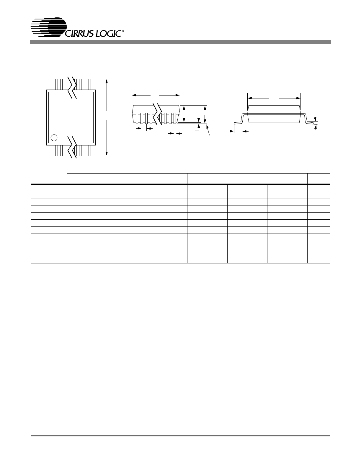
13. PACKAGE DIMENSIONS
28L SOIC (300 MIL BODY) PACKAGE DRAWING
1
b
CS8405A
HE
c
D
SEATING
PLANE
A
e
A1
L
INCHES MILLIMETERS
DIM MIN NOM MAX MIN NOM MAX
A 0.093 0.098 0.104 2.35 2.50 2.65
A1 0.004 0.008 0.012 0.10 0.20 0.30
b 0.013 0.017 0.020 0.33 0.42 0.51
C 0.009 0.011 0.013 0.23 0.28 0.32
D 0.697 0.705 0.713 17.70 17.90 18.10
E 0.291 0.295 0.299 7.40 7.50 7.60
e 0.040 0.050 0.060 1.02 1.27 1.52
H 0.394 0.407 0.419 10.00 10.34 10.65
L 0.016 0.026 0.050 0.40 0.65 1.27
∝
0° 4° 8° 0° 4° 8°
JEDEC #: MS-013
Controlling Dimension is Millimeters
∝
DS469PP4 31
CS8405A
28L TSSOP (4.4 mm BODY) PACKAGE DRAWING
N
1
23
TOP VIEW
D
E
e
2
b
SIDE VIEW
A2
A1
A
SEATING
PLANE
L
INCHES MILLIMETERS
1
E1
END VIEW
NOTE
DIM MIN NOM MAX MIN NOM MAX
A----0.47----1.20
A1 0.002 0.004 0.006 0.05 0.10 0.15
A2 0.03150 0.035 0.04 0.80 0.90 1.00
b 0.00748 0.0096 0.012 0.19 0.245 0.30 2,3
D 0.378 BSC 0.382 BSC 0.386 BSC 9.60 BSC 9.70 BSC 9.80 BSC 1
E 0.248 0.2519 0.256 6.30 6.40 6.50
E1 0.169 0.1732 0.177 4.30 4.40 4.50 1
e -- 0.026 BSC -- -- 0.65 BSC --
L 0.020 0.024 0.029 0.50 0.60 0.75
∝
0° 4° 8° 0° 4° 8°
∝
JEDEC #: MO-153
Controlling Dimension is Millimeters.
Notes: 1.“D” and “E1” are reference datums and do not included mold flash or protrusions, but do include mold
mismatch and are measured at the parting line, mold flash or protrusions shall not exceed 0.20 mm per
side.
2.Dimension “b” does not include dambar protrusion/intrusion. Allowable dambar protrusion shall be
0.13 mm total in excess of “b” dimension at maximum material condition. Dambar intrusion shall not
reduce dimension “b” by more than 0.07 mm at least material condition.
3.These dimensions apply to the flat section of the lead between 0.10 and 0.25 mm from lead tips.
32 DS469PP4

CS8405A
14. APPENDIX A: EXTERNAL AES3/SPDIF/IEC60958 TRANSMITTER COMPONENTS
This section details the external components required to interface the AES3 transmitter to cables
and fiber-optic components.
14.1 AES3 Transmitter External
Components
The output drivers on the CS8405A are designed to
drive both the professional and consumer interfaces. The AES3 specification for professional/broadcast use calls for a 110 Ω source impedance and a
balanced drive capability. Since the transmitter
output impedance is very low, a 110 Ω resistor
should be placed in series with one of the transmit
pins. The specifications call for a balanced output
drive of 2-7 volts peak-to-peak into a 110 Ω load
with no cable attached. Using the circuit in
Figure 11, the output of the transformer is shortcircuit protected, has the proper source impedance,
and provides a 5 volt peak-to-peak signal into a
110 Ω load. Lastly, the two output pins should be
attached to an XLR connector with male pins and a
female shell, and with pin 1 of the connector
grounded.
In the case of consumer use, the IEC60958 specifications call for an unbalanced drive circuit with an
output impedance of 75 Ω and a output drive level
of 0.5 volts peak-to-peak ±20% when measured
across a 75 Ω load using no cable. The circuit
shown in Figure 12 only uses the TXP pin and provides the proper output impedance and drive level
using standard 1% resistors. If VL+ is driven from
+3.3 V, use resistor values of 243 Ohms and
107 Ohms. The connector for a consumer application would be an RCA phono socket. This circuit is
also short circuit protected.
The TXP pin may be used to drive TTL or CMOS
gates as shown in Figure 13. This circuit may be
used for optical connectors for digital audio since
they usually have TTL or CMOS compatible inputs. This circuit is also useful when driving multiple digital audio outputs since RS422 line drivers
have TTL compatible inputs.
14.2 Isolating Transformer Requirements
Please refer to the application note AN134: AES
and SPDIF Recommended Transformers for re-
sources on transformer selection.
CS8405A
TXP
TXN
Figure 11. Professional Output Circuit Figure 12. Consumer Output Circuit
DS469PP4 33
110 Ω
XLR
1
CS8405A
TXP
TXN
Figure 13. TTL/CMOS Output Circuit
CS8405A
TTL or
CMOS Gate
TXP
TXN
374 Ω
90.9 Ω
RCA
Phono

CS8405A
15. APPENDIX B: CHANNEL STATUS AND USER DATA BUFFER MANAGEMENT
The CS8405A has a comprehensive channel status
(C) and user (U) data buffering scheme which allows the user to manage the C and U data through
the control port.
15.1 AES3 Channel Status(C) Bit
Management
The CS8405A contains sufficient RAM to store a
full block of C data for both A and B channels
(192x2 = 384 bits), and also 384 bits of U information. The user may read from or write to these RAM
buffers through the control port.
The CS8405A manages the flow of channel status
data at the block level, meaning that entire blocks
of channel status information are buffered at the input, synchronized to the output timebase, and then
transmitted. The buffering scheme involves a cascade of 2 block-sized buffers, named E and F, as
shown in Figure 14. The MSB of each byte represents the first bit in the serial C data stream. For example, the MSB of byte 0 (which is at control port
address 32) is the consumer/professional bit for
channel status block A.
15.1.1 Accessing the E buffer
The user can monitor the data being transferred by
reading the E buffer, which is mapped into the register space of the CS8405A, through the control
port. The user can modify the data to be transmitted
by writing to the E buffer.
The user can configure the interrupt enable register
to cause interrupts to occur whenever “E to F” buffer transfers occur. This allows determination of the
allowable time periods to interact with the E buffer.
Also provided is an “E to F” inhibit bit. The “E to
F” buffer transfer is disabled whenever the user sets
this bit. This may be used whenever “long” control
port interactions are occurring.
A flowchart for reading and writing to the E buffer
is shown in Figure 15. For writing, the sequence
starts after a E to F transfer, which is based on the
output timebase.
If the channel status block to transmit indicates
PRO mode, then the CRCC byte is automatically
calculated by the CS8405A, and does not have to
be written into the last byte of the block by the host
microcontroller. This is also true if the channel status data is entered serially through the COPY/C pin
when the part is in hardware mode.
The E buffer is accessible from the control port, allowing read and writing of the C data. The F buffer
is used as the source of C data for the AES3 transmitter. The F buffer accepts block transfers from
the E buffer.
AB
8-bits 8-bits
E
24
words
Control Port
Figure 14. Channel Status Data Buffer Structure
34 DS469PP4
F
Transmit
Data
Buffer
To
AES3
Transmitter
E to F interrupt occurs
Optionally set E to F inhibit
Write E data
If set, clear E to F inhibit
Wait for E to F transfer
Return
Figure 15. Flowchart for Writing the E Buffer

CS8405A
15.1.2 Serial Copy Management System
(SCMS)
In software mode, the CS8405A allows read/modify/write access to all the channel status bits. For
consumer mode SCMS compliance, the host microcontroller needs to manipulate the Category
Code, Copy bit and L bit appropriately.
In hardware mode, the SCMS protocol can be followed by either using the COPY and ORIG input
pins, or by using the C bit serial input pin. These
options are documented in the hardware mode section of this data sheet.
15.1.3 Channel Status Data E Buffer Access
The E buffer is organized as 24 x 16-bit words. For
each word the MS Byte is the A channel data, and
the LS Byte is the B channel data (see Figure 14).
There are two methods of accessing this memory,
known as one byte mode and two byte mode. The desired mode is selected through a control register bit.
15.1.3.1 One Byte mode
In many applications, the channel status blocks for
the A and B channels will be identical. In this situation, if the user reads a byte from one of the channel's blocks, the corresponding byte for the other
channel will be the same. Similarly, if the user
wrote a byte to one channel's block, it would be
necessary to write the same byte to the other block.
One byte mode takes advantage of the often identical nature of A and B channel status data.
When reading data in one byte mode, a single byte
is returned, which can be from channel A or B data,
depending on a register control bit. If a write is being done, the CS8405A expects a single byte to be
input to its control port. This byte will be written to
both the A and B locations in the addressed word.
One byte mode saves the user substantial control
port access time, as it effectively accesses 2 bytes
worth of information in 1 byte's worth of access
time. If the control port's auto increment addressing
is used in combination with this mode, multi-byte
accesses such as full-block reads or writes can be
done especially efficiently.
15.1.3.2 Two Byte mode
There are those applications in which the A and B
channel status blocks will not be the same, and the
user is interested in accessing both blocks. In these
situations, two byte mode should be used to access
the E buffer.
In this mode, a read will cause the CS8405A to output two bytes from its control port. The first byte
out will represent the A channel status data, and the
2nd byte will represent the B channel status data.
Writing is similar, in that two bytes must now be
input to the CS8405A's control port. The A channel
status data is first, B channel status data second.
15.2 AES3 User (U) Bit Management
The CS8405A U bit manager has two operating
modes:
Mode 1. Transmit all zeros.
Mode 2. Block mode.
15.2.1 Mode 1: Transmit All Zeros
Mode 1 causes only zeros to be transmitted in the
output U data, regardless of E buffer contents. This
mode is intended for the user who wants the output
U channel to contain no data.
15.2.2 Mode 2: Block Mode
Mode 2 is very similar to the scheme used to control
the C bits. Entire blocks of U data are buffered using
2 block-sized RAMs to perform the buffering. The
user has access to the first buffer, denoted the E buffer, through the control port. It is the only mode in
which the user can merge his own U data into the
transmitted AES3 data stream. The U buffer access
only operates in two byte mode, since there is no concept of A and B blocks for user data. The arrangement
ofthedataisasfollowings:
Bit15[A7]Bit14[B7]Bit13[A6]Bit12[B6]...Bit1[A0]
Bit0[B0]. The arrangement of the data in the each byte
is that the MSB is the first transmitted bit. The bit for
the A subframe is followed by the bit for the B subframe.
DS469PP4 35

 Loading...