

Semiconductor Corporation
Multi-Standard Infrared Transceiver
CS8130
Features
Adds IR port to standard UART
••
IrDA, HPSIR, ASK (CW) & TV remote
••
compatible
1200bps to 115kbps data rate
••
Programmable Tx LED power
••
Programmable Rx threshold level
••
Power down modes
••
Direct, no modulation, mode
••
Tiny 5x7mm 20 pin SSOP package
••
+2.7V to +5.5V supp ly
••
+Supply
General Description
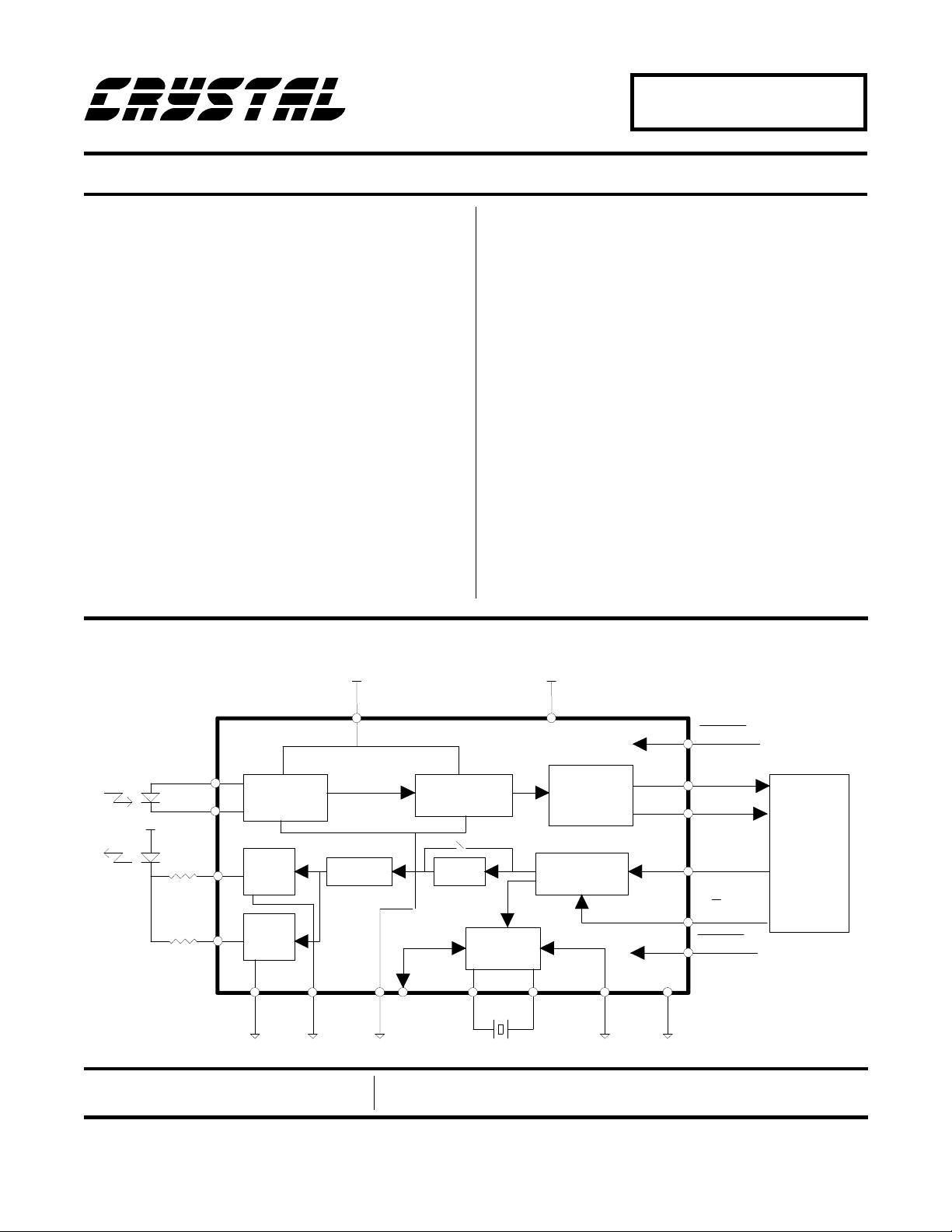
The CS8130 is an infrared transceiver integrated circuit. The receive channel includes on-chip high gain
PIN diode amplifier, IrDA, HPSIR, ASK & TV remote
compatible decoder, and data pulse stretcher. The
transmit path includes IrDA, HPSIR, ASK & TV remote
compatible encoder, and LED driver. The computer
data port is standard UART TxD and RxD compatible,
and operates from 1200 to 115200 baud.
External PIN diode and transmit LED are required. A
control mode is provided to allow easy UART programming of different modes.
The CS8130 operates from power supplies of +2.7V to
+5.5V.
Ordering Information:
CS8130-CS 0° to 70°C 20-pin SSOP
CDB8130 Evaluation kit
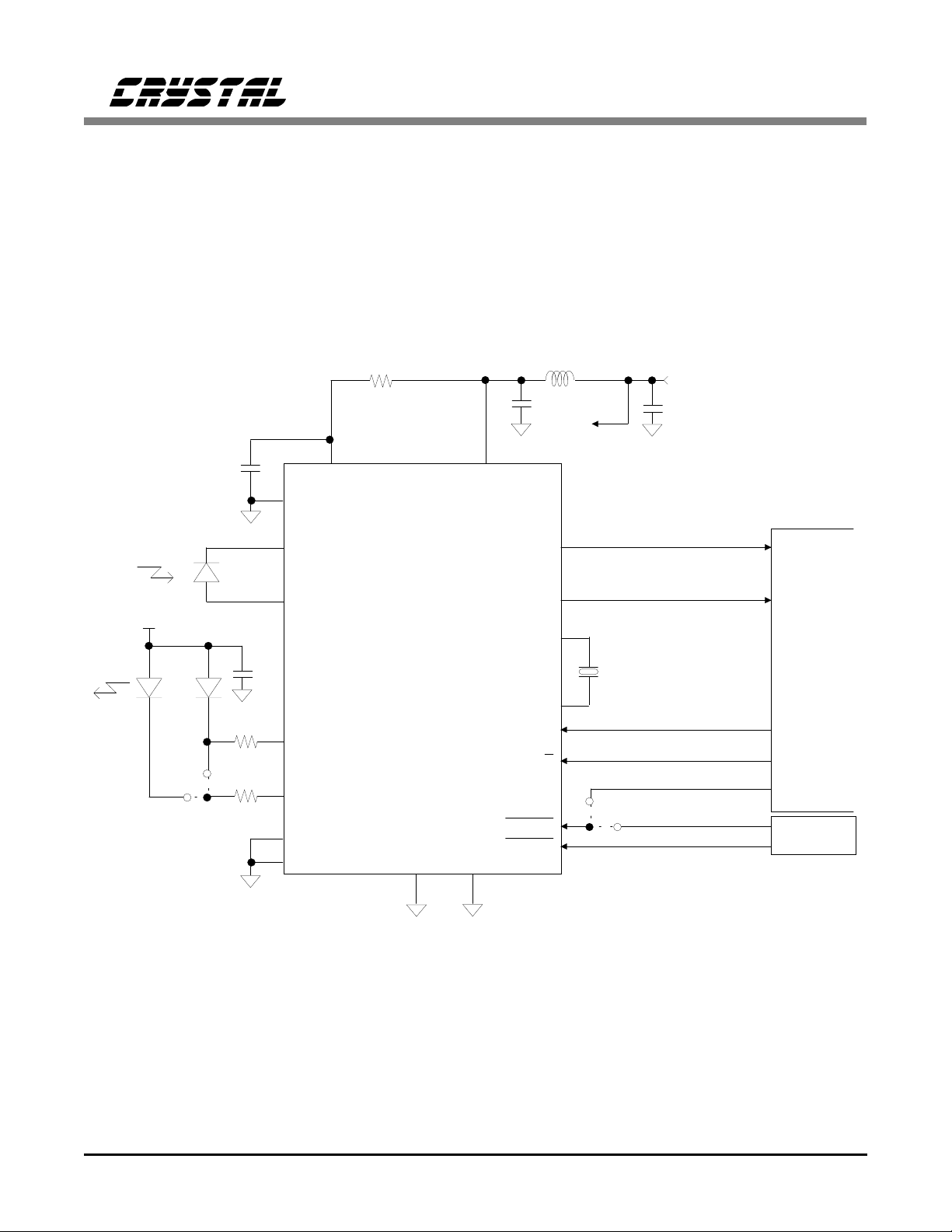
+Supply
8
6
PINA
PINC
+Supply
LED1C
LED2C
PIN Diode
7
Preamplifier
LED
1
Driver 1
4
LED
Driver 2
3
TGND2 TGND1
2
Modulator
AGND
Preliminary Product Information
Crystal Semiconductor Corporation
P.O. Box 17847, Austin, TX 78760
(512) 445-7222 FAX: (512) 445-7581
VA+
Threshold
Detect/Decode
FIFO
Baud Rate
Generator
5
19
EXTCLK
This document contains information for a new product. Crystal
Semiconductor reserves the right to modify this product without notice.
17
XTALIN
VD+
12
13
Demodulator
Data/Control
Decoder
18
XTALOUT
9
CLKFR
Copyright Crystal
Semiconductor Corporation 1994
(All Rights Reserved)
16
14
15
10
20
11
DGND
RESET
RXD
FORM/BSY
TXD
D/C
PWRDN
RxD
CTS
STANDARD
UART
TxD
DTR
JUN ’94
DS134PP2
1
CS8130
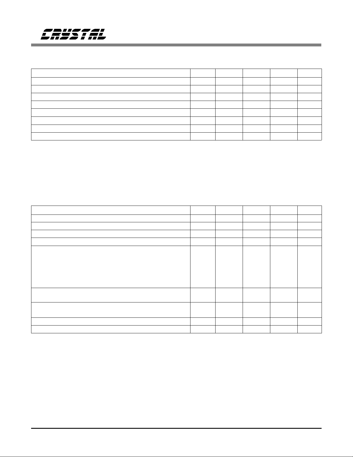
TRANSMITTER DRIVER CHARACTERISTICS (TA = 25 °C; All V+ = 3.0V, Digital Input Lev els: Logic 0 = 0V,
Logic 1 = V+; unless otherwise specified)
Parameter Symbol Min Typ Max Units
Output capacitance (Note 1) 10 TBD pF
Output rise time (10% to 90%) tr - 20 50 ns
Output fall time (90% to 10%) tf - 20 50 ns
Overshoot over final current - - 25 %
On resistance - - 0.5
Off leakage current - - 20
Output current (each driver) (Note 2) - - 250 mA
Output jitter relative a jitter free input clock - - 200 ns
Notes: 1. Typical LED junction capacitance is 20pF.
2. 50% duty cycle, max pulse width 165 µs (3/16 of (1/1200 bps + 5%)).
Ω
µA
RECEIVER CHARACTERISTICS (T
= 25 °C; All V+ = 3.0V, Digital Input Levels: Logic 0 = 0V, Logic 1 = V+;
A
unless otherwise specified)
Parameter Symbol Min Typ Max Units
Input capacitance (Note 3) - 10 T BD pF
Input noise current - - 11 pA/rtHz
Maximum signal input current from detector - - 2 mA
Maximum DC input current (typically sunlight) - - 200
Input current detection thresholds RS4-0=00000:
(Programmable with a 5 bit value) RS4-0=00001:
(Min, Max = Typical ±30%) RS4-0=00010:
(Note 4) ↓
RS4-0=11110:
RS4-0=11111:
Bandpass filter response High Pass -3dB:
Low Pass -3dB:
Receiver power up time With high (200µA) dc ambient
With normal (2µA) dc ambient
-
-
16.4
↓
169.5
175
-
-
-
-
7.8
15.6
23.4
↓
242.2
250
35
700
5
0.3
-
-
30.4
↓
314.9
325
-
-
10
1
µA
nA
nA
nA
"
nA
nA
kHz
kHz
ms
ms
Turn-around time, with receiver on continuously (Note 5) - 5 10 ms
EMI rejection of system (0.5MHz to 100MHz). (Note 6) 3 - - V/m
Notes: 3. Typical PIN diode junction capacitance is 50pF.
4. The ±30% tolerance covers chip-to-chip variation. The temperature coefficient of the receiver
threshold setting is low. Current detection thresholds are above the DC ambient condition.
Settings of RS4-0 of less than 00010 are not practical because of noise.
5. Turn-around time is the time taken for the PIN diode receiver to recover from the IR energy
from the transmitter. The remote end of the link must wait for this time after receiving data
before transmitting a reply. This time may be reduced to <1 ms by good IR shielding from
the transmit LED to the PIN diode.
6. This is a system specification. A metal shield over the P IN diode and CS8130 is
recommended to ensure system compliance.
Specifications are subject to change without notice.
2 DS134PP2
CS8130
POWER SUPPLY SPECIFICATIONS (TA = 25°C; V+ = 3.0V, Digital Input Levels: Logic 0 = 0V, Logic 1 = V+,
Note 7)
Parameter Symbol Min Typ Max Units
Power Supply Voltage 2.7 3.0 5.5 V
Power Supply Current - All functions enabled (Note 8) - - 2.5 mA
Power Supply Current - All functions disabled (Note 9) - - 1
Power Supply Current - Receiver only enabled (Note 8) - - 2.5 mA
Power Supply Current - Transmit only enabled (Note 10) - - 0.5 mA
Oscillator Power Supply Current low power mode:
normal power mode:
-
-
-
-
0.5
1.5
Data & State Retention Supply Voltage 2 - - V
Notes: 7. Power supply current specifications are with the supply at 3.0V. For approximate c onsumption at
+5.0V, multiply the above currents by 1.667.
8. Oscillator in low power mode, does not include LED current. Subtrac t oscillator current if using
an external clock to run the CS8130.
9. Floating digital inputs will not cause the power s upply to increase beyond the specification.
10. Does not include LED current, does include os cillator current in low power mode.
RECOMMENDED OPERATING CONDITIONS (All voltages with respect to 0V)
µA
mA
mA
Parameter Symbol Min Typ Max Units
Operating Ambient Temperature T
A
02570
Data and State Retention Temperature (In Power Down) -40 - 85
DIGITAL PIN CHARACTERISTICS (TA = 25°C, Supply = 3.0V)
Parameter Symbol Min Typ Max Units
High-level Input Voltage V
Low-level Input Voltage V
High-level Output Voltage at IO = -2.0mA V
Low-level Output Voltage at IO = 2.0mA V
IH
IL
OH
OL
2.0 - - V
--0.8V
VD-0.3 - - V
--0.3V
Output Leakage Current in Hi-Z state 0.2
Input Leakage Current (Digital Inputs) - - 0.2
Output Capacitance C
Input Capacitance C
OUT
IN
-5-pF
-5-pF
°C
°C
µA
µA
DS134PP2 3
CS8130
ABSOLUTE MAXIMUM RATINGS (All v oltages with respect to 0V)
Parameter Symbol Min Max Units
Power Supplies -0.3 6.0 V
Input Current Except Supply Pins & Driver P ins Input Voltage -0.3 VD+0.3 V
Ambient temperature (Power Applied) -55 +125
Storage Temperature -65 +150
ESD using human body model (100pF with series 1.5kΩ)
2000 - V
Warning: Operation beyond these limits may result in permanent damage to the device.
Normal operation is not guaranteed at these extremes.
±10
mA
°C
°C
SWITCHING CHARACTERISTICS (T
= 25 °C; All V+ = 3.0V, Digital Input Levels: Logic 0 = 0V, Logic 1 = V+;
A
unless otherwise specified)
Parameter Symbol Min Typ Max Units
XTALIN frequencies CLKFR pin low:
(Note 11) CLKFR pin high:
-
-
3.6864
1.8432
-
-
MHz
MHz
XTALIN duty cycle 45 50 55 %
Crystal Oscillator start up time - - 25 ms
Notes: 11. In normal oscillator mode, the crystal is internally loaded with 20 pF, which is the standard loading
at which the crystal frequency is tuned. In low power oscillator mode, the internal loading on the
crystal is reduced to approximately 5pF. T he crystal frequency will therefore increase by
about 0.03% in low power mode.
4 DS134PP2
10
CS8130
Ferrite
Ω
Bead
0.1 µF
To LED
+3.0V supply
+
10 µF
TGND1, 2
0.1 µF
AGND
PINC
PIN
Diode
PINA
+ Supply
47 µF
LED2
Use: LED1/R1
or:LED1/R1 & R2
or: LED1/R1 &
LED2/R2
For 2 LED, +5V supply systems,
connect 2 LEDs i n series. Use R1 & R2
to give programmable output level.
LED1
+
R1 TBD
R2 TBD
Ω
LED1C
Ω
LED2C
TGND1
TGND2 DGND CLKFR
VA+ VD+
FORM/BSY
CS8130
RXD
EXTCLK
XTALIN
XTALOUT
TXD
D/C
RESET
3.6864 MHz or 1.8432 MHz.
Can also use an external
clock at 3.6864 MHz
or 1.8432 MHz
PWRDN
CLKFR low for 3. 686 4 MHz cl ock
CLKFR high for 1.8432 MHz c l ock
RxD
CTS
UART
TxD
DTR
RTS
System
Control
Figure 1. Recommended Connection Diagram
DS134PP2 5

CS8130
OVERVIEW
The CS8130 is an infrared transceiver I.C. The
receive channel includes on-chip high gain PIN
diode amplifier, IrDA, HP-SIR, 500 kHz Amplitude Shift Keying (ASK) & TV remote
compatible decoder, and data pulse stretcher. The
transmit path includes IrDA, HPSIR, 500 kHz
ASK & TV remote compatible encoder, and
LED drivers. The computer data port is standard
UART TxD and RxD compatible, and operates
from 1200 to 115200 baud. An on-chip baud rate
generator is provided.
External PIN diode and transmit LED(s) are required. A control mode is provided to allow easy
UART programming of different modes.
The CS8130 operates from power supplies of
+2.7 V to +5.5 V. The device is supplied in a 20pin SSOP package
Serial Infrared (SIR) Physical Layer Link Specification, Version 1.0, April 27 1994). Figure 2
shows the format of Mode 1. A pulse of IR energy indicates a logic ’0’. No IR indicates a
logic ’1’. The pulse can be from 3/16 of a bit
cell time at 115200 (~1.6 µs), to 3/16 of a bit
cell time at 2400 bps (~78 µs). The width of the
pulse may be fixed at 1.6µs for all baud rates, or
may scale with the baud rate. The initial baud
rate for IrDA is 9600 bps, with a negotiated baud
rate possibility of 2400 to 115200 bps.
Mode 2 500 kHz ASK
Figure 3 shows the infrared data format for
Mode 2. This is a Carrier Wave (CW) type system, where the presence of a 500kHz carrier is
treated as a ’0’, and absence of a carrier is
treated as a ’1’. Normally used baud rates are
9600 bps, 19.2 kbps and 38.4 kbps.
FUNCTIONAL DESCRIPTION
The following pages describe the detailed operation of the CS8130.
IR Data Formats
The CS8130 supports three infrared data transmission formats: IrDA/HPSIR, 500kHz ASK and
38kHz ASK (TV Remote). There is also a direct
access mode, which bypasses the CS8130 encoder and decoders, and gives direct access to
the IR raw data. This mode is for situations
where the encoding and/or decoding is done externally.
Modes may be set independently for transmit
and receive, although this would be unusual.
Mode 1 IrDA/HP-SIR
The CS8130 is designed to allow easy realization of an IrDA compatible IR port (see IrDA
Mode 3 38 kHz ASK (TV remote mode)
Figure 4 shows the infrared data format for
Mode 3, the TV remote control mode. This is
similar to Mode 2, except that the modulation
frequency is ~38kHz. The IR bit rate is approximately 2400 bps. Both modulation frequency
and bit rate vary significantly for different manufacturer and model remote controls.
Mode 4 Direct Access Mode
In Mode 4, the IR transmission tracks directly
what is present on the TXD pin. A logic ’1’
means that the LED is off, a logic ’0’ means that
the LED is on. Care must be taken to ensure that
the LED is not ’on’ continuously, otherwise the
LED may be damaged.
In Mode 4, received IR is compared against the
programmed threshold. The resulting logic output is routed directly to the RXD pin. A logic ’1’
means no IR is detected, a logic ’0’ means IR is
being detected. If a IR carrier is being received,
6 DS134PP2
CS8130
TRANSMITTER
RECEIVER
A: 1/baud rate
B: 3/16 of 1/115200 o
C: 3/16 of 1/115200 t
TRANSMITTER
TXD
* LED Output
PIN Input
** RXD
r 3/16 of A (selectable)
o 3/16 of A
10
B
C * LED1C and LED2C go low to turn on LED.
A
1
** RXD output is delayed from the PIN diode
input by A (1 bit).
Figure 2. Infra Red Data Format Mode 1 (IRDA/HPSIR)
10
TXD
LED Output
B
On
Off
Light
No Light
1
On
Off
RECEIVER
A: 1/baud rate
B: 1/527kHz
C: 1/500kHz +/- 10%
TRANSMIT TER
RECEIVER
A: 1/2400
B: 1/38.4kHz
C: 1/40kHz +/- 10%
PIN Input
C
RXD
A
Figure 3. Infra Red Data Format Mode 2 (500kHz ASK)
10
TXD Data *
LED Output
PIN Input
RXD Data *
These numbers are typical values.
TV Remote Bit Rate and Modulation
Frequency are programmable.
B
C
A
1
Light
No Light
On
Off
Light
No Light
* The timing of data
on the RXD and TXD pins
is faster than shown here
Figure 4. Infra Red Data Format 3 (TV Remote, 38kHz ASK)
DS134PP2 7

CS8130
then the RXD pin will oscillate at the carrier frequency.
Transmit Path
Data for transmission is input to the CS8130 on
the TXD pin. The selected modulation scheme is
then applied to the data, and the resulting signals
are used to drive the LED. There are 2 LED output pins: LED1C and LED2C. They are open
drain outputs, which pull down to TGND or
float. The LED is connected via resistors to both
LED1C and LED2C. The current level flowing
through the LED is determined by the external
resistors. Normally, LED1C is used to drive the
LED. If additional current is needed, (for example for TV remote operation), then the second
driver may be enabled. The amount of ’boost’
current is determined by the external resistor
connected to the LED2C pin.
For larger amounts of IR output, it may be preferable to use two LEDs, rather than drive a large
current through one LED. For a +3V supply system using two LEDs, each one is connected, via
a resistor, to each driver output. For a +5V supply system, 2 LEDS may be connected in series,
and then routed to each driver via 2 resistors,
one for each driver. This minimizes the power
dissipation in the resistors.
Mode 1 Transmit Choices
In Mode 1 (IrDA), the pulse width may be fixed
at 1.6 µs, or set to 3/16 of the bit period. Either
of these settings will meet the IrDA standard, but
fixed 1.6 µs pulses will save power at lower
baud rates.
In addition, there is a choice which affects the
output pulse jitter. The default state causes the
CS8130 to look for the start bit on TXD. All
subsequent LED transitions for that character are
timed relative to the internal baud rate clock.
Therefore there will be no jitter in the LED out-
put pulse timing. However, the CS8130 now has
to be programmed with the desired number of
bits per character, which for IrDA compliance, is
8.
Alternatively, the CS8130 can generate output
pulses based entirely on individual transitions on
TXD, with no knowledge of which bit is the
start bit. Thus a 1 to 0 transition will generate a
pulse based on that transition edge. If TXD is
low for multiple successive bits, then the
CS8130 will generate pulses based on its internal
clock. Therefore there is the possibility of jitter
in the output pulses of N*271 ns. N can be 0, 1
2....., depending on the difference in frequency
between the UART baud rate clock and the
CS8130 clock. Clearly, if the CS8130 and its associated UART are running from the same clock,
the possibility of jitter is eliminated.
Mode 2 (ASK) Transmit Choices
The modulation frequency is determined by the
modulator divider registers. For nominal
500 kHz, use a divide value of 6, which yields a
modulation frequency of 527 kHz.
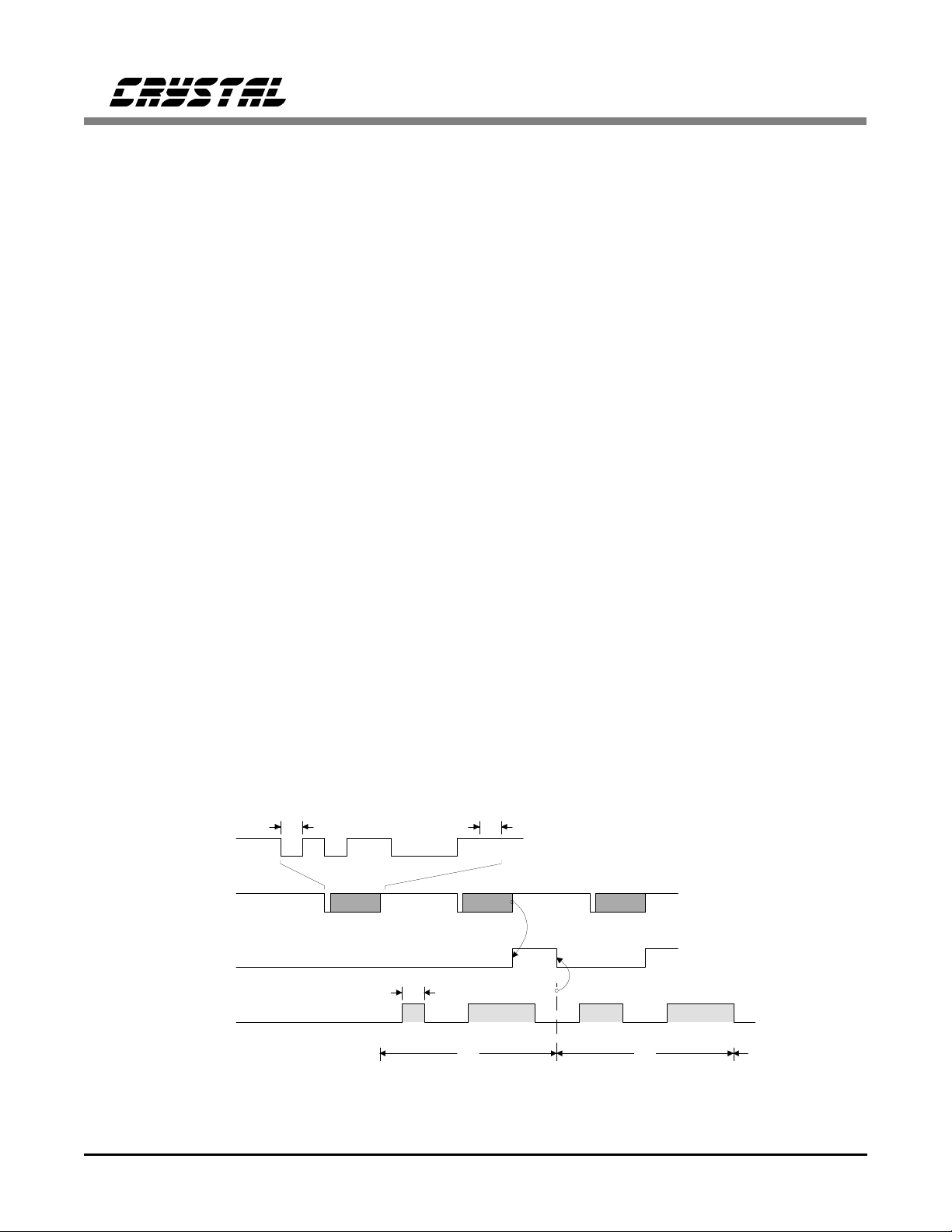
Mode 3 (TV Remote) Transmit Choices
During transmission of IR, the start and stop bits
present in the incoming data from the UART are
stripped off (see Figure 5). The remaining data
bits are then sent out at ~2400 bps. Since there
should be no gaps in the transmitted data, the
input data is buffered in a 22-character location
FIFO. Characters can be received on the TXD
pin while the previous characters are being transmitted. To prevent overflow, a hardware
handshake mechanism is provided. If the FIFO
is one character away from being full, the
FORM/BSY pin is brought high, indicating that
the UART should not send any more data. Once
another character has been transmitted,
FORM/BSY pin is brought low, indicating to the
UART that it is OK to send another character.
8 DS134PP2
CS8130
The modulation frequency is determined by the
modulator divider registers. The transmit bit rate
is determined by the TV Remote transmit bit rate
divider. The UART to CS8130 baud rate must be
set to at least 20% faster than the transmit bit
rate.
Receive Path
A PIN diode is attached to the PINA and PINC
pins. Compensation for the DC ambient light is
applied to the photocurrent from the diode. The
change in photocurrent from ambient is amplified and compared to a threshold value. If the
photocurrent is greater than the set threshold, the
output is set to ’light’. If the photocurrent is less
than the set threshold, the output is set to ’no
light’. The threshold current is programmable.
This allows users to make the tradeoff between
noise immunity and the reliable transmission distance of the link. The PIN diode amplifier has a
bandpass filter characteristic, to limit the effects
of IR interference. The resulting logic signal is
further qualified, depending on the IR format selected.
An autodetect feature is provided. If autodetect
mode is enabled, and transmit TV remote mode
is disabled, the FORM/BSY output pin indicates
the format of incoming data. If high, then the
incoming data is in IrDA/HPSIR format. If low,
the data is in ASK format which matches the
programmed modulation frequency.
Mode 1 (IrDA) Receive Choices
For Mode 1a, a logic circuit is set to only look
for pulse widths of 1.6µs. For Mode 1b, a logic
circuit looks for pulses of 3/16 of the set baud
rate bit period. For Mode 1c, a logic circuit
looks for pulse widths of ≥1.6 µs, but ≤3/16 of
the set baud rate bit period.
Mode 2 (ASK) Receive Choices
For Mode 2, a logic circuit looks for sequences
of ’light’ and ’no light’ which matches the expected 500kHz carrier. The modulator divider
registers must be set to 6. The ASK receive timing sensitivity register should be set to 0,
yielding a valid incoming frequency range of
461 kHz to 614 kHz.
The RXD data transitions will lag behind the infrared activity by 3 modulation cycles. This
allows the modulation detect circuit time to verify the correct modulation frequency.
Start
Bit
10
11
TXD*
TXD*
A
FORM/BSY
1/2400
LED
OUTPUT
* TXD Baud rate can be set
from 4800 to 115200 bps
Figure 5. Mode 3 ( TV Remote ) Transmit D ata Form at
DS134PP2 9
00
10
Stop
Bit
01
BC
ON
10
1
001 0011000
ABC
1
1
OFF

CS8130
Mode 3 (TV remote) Receive Choices
The modulation frequency must be set into the
modulator divider registers. The tolerance on the
expected frequency must be programmed into
the Receive ASK Timing Sensitivity (RATS) register. The RATS register sets the time window
that the demodulator will accept for the period of
valid data. Since the RATS register specifies
time windows which are negative (e.g. 1000b (8)
= +0.27 µs to -4.61 µs), then the modulation
frequency must be set to lower than the desired
nominal setting. For example, with RATS set to
1000 (8), and the desired nominal frequency being 38 kHz, then set the modulation divider
registers to 35.10 kHz. With these settings, the
demodulator will accept any frequency from
34.78 kHz to 41.88 kHz as valid. Smaller RATS
register settings will result in tighter tolerance on
the accepted receive modulation frequency.
Changes in the RATS register settings must be
accompanied by changes in the modulation frequency register to keep the nominal desired
frequency in the center of the valid frequency
band.
There are two TV remote receive data modes:
"oversampled" mode and "programmed T period" mode. For "oversampled" mode, first
choose the UART to CS8130 baud rate, typically
115.2 kbps. Then set the TV remote receive tim-
ing register to a rate which is less than 80% of
the UART baud rate. The CS8130 will now start
sampling the demodulated infrared data at the
TV remote receive sample rate. The stream of
samples will be assembled into characters, with a
start bit and a stop bit, and will be transmitted to
the UART via RXD at the UART baud rate. The
system software can then concatenate successive
characters and reconstruct the incoming bit
stream.
"Programmed T period" mode requires that the
bit period of the bursts of modulated carrier be
known. This period is programmed into the TV
remote receive timing registers. The UART to
CS8130 baud rate must be set to at least 20%
greater than 1/T. The CS8130 will now use the
edges of the demodulated incoming infrared data
to indicate each bit state. For continuous periods
of low or high, the CS8130 will sample the level
in the center of each incoming bit period (using
T as the bit period). Any transition will reset the
timer that is used for the sampling process,
thereby eliminating errors caused by the sample
timing being different to the incoming bit period.
Characters are assembled and sent to the UART
every 8 bits (see Figure 6).
If the T period is not known, it is possible to
measure T by using "oversampled" mode, and
1/2400
1
0 1
1
LIGHT
INPUT
RXD*
RXD*
*RXD Baud rat e c a n be s et
from 4800 to 115200 bps
Figure 6. Mode 3 (TV remote) Receive Data Format
10 DS134PP2
001110011001 1
1
0110011
8 data bits
Start
Bit
Stop
Bit
0
0
LIGHT
NO LIGHT

CS8130
then switch to "programmed T period" mode to
reduce processing overhead in the host CPU.
Clock Generation
The primary clock required is 3.6864 MHz. This
may be generated by attaching a 3.6864 MHz
crystal to the XTALIN and XTALOUT pins. In
this case, the EXTCLK pin becomes an output,
and may be used to drive external devices. If this
is not required, power may be saved by disabling
the EXTCLK output. The CLKFR pin should be
connected to DGND, which causes the clock circuits to be configured for 3.6864 MHz operation.
The oscillator has a low power mode. This reduces the internal crystal loading capacitance on
XTALOUT and XTALIN. The selection of this
mode is via a bit in Control Register #4. Since
the loading capacitance is reduced, then the crystal frequency will increase by approximately
0.03%.
Alternatively, a 3.6864 MHz clock may be input
into the EXTCLK pin, in which case XTALIN
must be grounded, and XTALOUT is left floating. The CLKFR pin must be connected to
DGND.
If only a 1.8432 MHz clock is available, then it
may be input into the EXTCLK pin and the
CLKFR pin connected to VD+. This causes the
CS8130 to double the incoming 1.8432 MHz
clock to 3.6864 MHz for internal use. XTALIN
must be grounded, and the XTALOUT pin is left
floating.
The CS8130 automatically sets the direction of
the EXTCLK pin. If the crystal oscillator is running when RESET goes high, then EXTCLK
becomes an output. Since the crystal oscillator
can take up to 25 ms to start, then it follows that
RESET must be held low, with PWRDN high
and power applied, for at least 25 ms. If using an
external clock, then RESET low can be short
(>1 µs).
Power Down
When the PWRDN pin is brought low, all internal logic is stopped, including the crystal
oscillator. The power consumption in power
down mode is very low (<1 µA). When the
PWRDN pin is brought high, the crystal oscillator will start. If using the crystal oscillator, allow
25 ms for oscillator start up after bringing
PWRDN high, before trying to use the CS8130.
The control register status will not be changed
by toggling PWRDN.
Control Register #1 allows for individual disabling and enabling of the transmit and receive
sections of the CS8130.
The CS8130 also goes into power down if both
transmit enable and receive enable bits are false,
and the D/C pin is brought high. This allows
control of power down in a pod environment,
where access to the PWRDN pin is difficult. In
this mode, it is possible to select, via a control
register bit, whether the crystal oscillator remains
running, or is powered off. If the oscillator remains running, then it consumes power, but
offers instant wake up. If the oscillator is powered off, then it consumes no power, but will
take 25 ms to start up.
The PWRDN pin must always be ’high’ or
’low’. If this pin is allowed to float, excessive
power consumption may occur. All other digital
inputs may be allowed to float without causing
excessive power consumption in the CS8130 in
power down mode.
The RXD and FORM/BSY output pins may be
programmed to be high, low or float in power
down. This allows maximum flexibility in different applications.
DS134PP2 11
CS8130
Reset
Bringing the RESET pin low will force the internal logic, including the control registers, into a
known state, provided the PWRDN pin is high.
RESET is disabled if the PWRDN pin is low.
The reset state is given in each register definition
table. RESET must be low for >25 ms if using
the crystal oscillator (see Clock Generation
above).
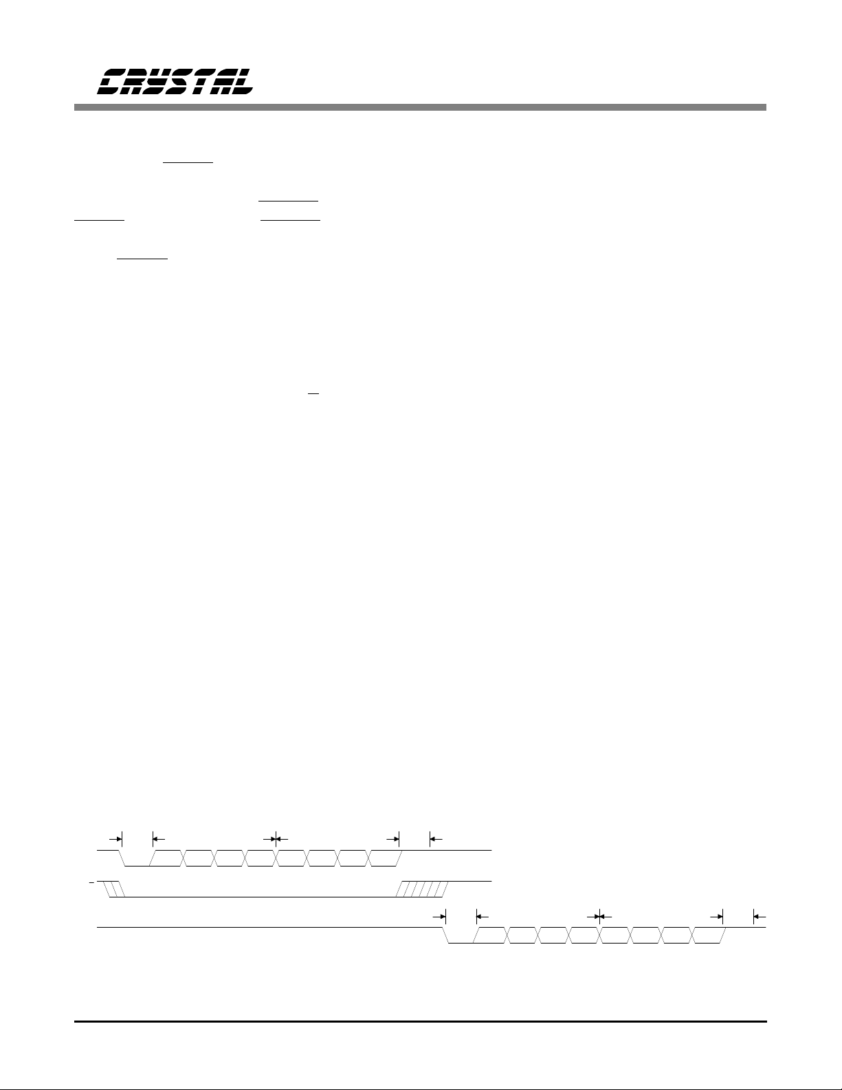
Control Register Definitions
The various control registers within the CS8130
may be written by setting the D/C pin to low,
and sending characters from the UART to the
TXD pin. The characters are interpreted as a 4bit address field and a 4-bit data field, as shown
in Figure 7. After the control character is received and written into the control register, it is
optionally echoed back out the RXD pin. The
baud rate used for this control mode is whatever
is currently set in the baud rate register. If the
"load baud rate" bit is written to, then the new
baud rate takes effect after the character has been
echoed back, if echo is enabled. Otherwise, the
new baud rate is effective immediately.
register is always accessible, independent of the
state of the shadow bit. The shadow bit must be
written to 0 to enable access to registers 0
through 15.
The following tables define the detailed function
of all the registers inside the CS8130.
One of the control registers contains a shadow
register set enable bit, which effectively becomes
the MSB of the 5-bit register address. Hence
there are 31 4-bit registers. The shadow bit must
be written to a 1 to allow access to the registers
with addresses 16 through 31. The shadow bit
Start
Bit
TXD
D/C
RXD
12 DS134PP2
CD0 CD1 CD2 CD3 AD0 AD1
Data Address
AD2
Figure 7. Control Mode Timing
AD3
Stop
Bit
Start
Bit
CD0 CD1 CD2 CD3 AD0
Data Address
AD1
AD2
Stop
Bit
AD3
Control Data Byte Format
D7 D6 D5 D4 D3 D2 D1 D0
AD3 AD2 AD1 AD0 CD3 CD2 CD1 CD0
CS8130
BIT NAME
AD3-0 Register Address
(4 bits of
transmitted address
+ MSB, which is the
shadow (SHDW) bit
state [Control Reg
#3]. All registers
have 4 data bits).
VALUE
0_0000
0_0001
0_0010
0_0011
0_0100
0_0101
0_0110
0_0111
0_1000
0_1001
0_1010
0_1011
0_1100
0_1101
0_1110
0_1111
1_0000
1_0001
1_0010
1_0011
1_0100
1_0101
1_0110
1_0111
1_1000
1_1001
1_1010
1_1011
1_1100
1_1101
1_1110
1_1111
0
1
2
3
4
5
6
7
8
9
10
11
12
13
14
15
16
17
18
19
20
21
22
23
24
25
26
27
28
29
30
31
FUNCTION
Control register #1
Control register #2
Transmit Mode Register #1
Transmit Mode Register #2
Output Power register
Receive Mode register
Receive Sensitivity register #1
Receive Sensitivity register #2
Baud Rate Divider register #1
Baud Rate Divider register #2
Modulator Divider register #1
Modulator Divider register #2
Digital Output Pin Control register
Control Register #3
Reserved
Status register (read only)
TV Remote Receive Sample Rate & T Period Divider
TV Remote Receive Sample Rate & T Period Divider
TV Remote Receive Sample Rate & T Period Divider
TV Remote Transmit Bit Rate Divider #1
TV Remote Transmit Bit Rate Divider #2
Control Register #4
Reserved
Reserved
ASK Receive Timing Sensitivity register
Reserved
Reserved
Reserved
CS8130 Revision Level register (Read Only)
Reserved
R e ser v ed ( R ese t s t o 1111 ; m u s t n o t be c hanged)
R e ser v ed ( R ese t s t o 1111 ; m u s t n o t be c hanged)
CD3-0 Control Data Contains control register data.
It is essential that all reserved registers and bits are not changed from their reset state. If reserved bits
are changed, then internal test modes may be invoked, which may change some input pins to output
pins, and may completely change the definition of some functions and signals. Reserved bits in registers, and reserved registers, may not return a known state when read, and should be ignored. Registers
28 and 15 are read only. Other non-reserved registers are write only. The CS8130 can be set to echo
back register write commands to verify correct reception of the control settings.
DS134PP2 13

Register 0, Control Register #1
D3 D2 D1 D0
Register
Reset (R)
BIT NAME VALUE FUNCTION
ECHO Echo Control
RXEN Receiver Enable 0
TXEN Transmitter Enable 0
ECHO 0 RXEN TXEN
0000
Characters
0
1
1
1
R Do not echo control characters
Echo control characters.
R Receiver disabled
Receiver enabled
R Transmitter disbabled
Transmitter enabled
Register 1, Control Register #2
D3 D2 D1 D0
Register
Reset (R)
0 0 AUTD LODB
0000
CS8130
BIT NAME VALUE FUNCTION
AUTD Receiver auto
detect mode enable
LODB Load Baud Rate
Counter
0
1
0
1
R Auto detect receive format disabled
Auto detect receive format enabled
R Do not load new baud rate count value
Load new baud rate count value
The LODB bit resets to 0 automatically.
14 DS134PP2

Register 2, Transmit Mode Register #1
D3 D2 D1 D0
Register
Reset (R)
BIT NAME VALUE FUNCTION
DIR Direct Mode Enable 0
TVR TV Remote Mode
PWID Select Pulse Width 0
MODU Select Modulation
DIR TVR PWID MODU
0000
Enable
Method
R Mode 4 Direct access mode disabled
1
0
1
1
0
1
Mode 4 Direct access mode enabled
R Mode 3 TV remote mode disabled
Mode 3 TV remote mode enabled
R
Set pulse width to 1.6 µS
Set pulse width to 3/16 of the bit period
R Mode 1 IrDA pulse modulation enabled
Mode 2 Amplitude modulated carrier modulation
Register 3, Transmit Mode Register #2
D3 D2 D1 D0
Register
Reset (R)
0 CHSY BC1 BC0
0110
CS8130
BIT NAME VALUE FUNCTION
CHSY Character/bit
synchronized
BC1-0 Number of bits per
character (only
needed if CHSY = 1)
0
1R
00
01
10
11
0
1
2R
3
Bits are transmitted based on TXD bit transitions
Bits are transmitted timed from the start bit
6 data bits per character
7 data bits per character
8 data bits per character
9 data bits ( 8 data, 1 parity) per character
Register 4, Output Power Register
D3 D2 D1 D0
Register
Reset (R)
BIT NAME VALUE FUNCTION
OP1-0 Output Power Level 00
00OP1OP0
0000
01
10
11
0R
1
2
3
No LED output enabled
LED1C output only enabled
LED2C output only enabled
Both LED1C and LED2C outputs enabled
DS134PP2 15

Register 5, Receive Mode Register
D3 D2 D1 D0
Register
Reset (R)
BIT NAME VALUE FUNCTION
RTVR ,
RMOD,
RWID S,
RWID L
RTVR RMOD RWIDS RWIDL
0011
Receive Mode 0000
0001
0010
0011
0100
1000
1100
0
1
2
3R
4
8
12
Mode 2 Amplitude modulated carrier mode
Mode 1a IRDA - fixed 1.6µs pulse
Mode 1b IRDA - variable 3/16 bit cell time pulse
Mode 1c IRDA - Any width pulse from 1.6µs to
3/16 bit cell time
Mode 4 Direct access mode
Mode 3 TV remote mode, oversampling receive
Mode 3 TV remote mode, timed bit cell receive
All other combinations are reserved
CS8130
Register 6, Receive Sensitivity Register #1
D3 D2 D1 D0
Register
Reset (R)
RS3 RS2 RS1 RS0
0111
Register 7, Receive Sensitivity Register #2
D3 D2 D1 D0
Register
Reset (R)
BIT NAME VALUE FUNCTION
RS4-0 Receive threshold
000RS4
0000
setting.
00000
00001
"
00111
"
11110
11111
0
1
"
7R
"
30
31
7.8 nA nominal receive threshold
15.6 nA nominal receive threshold
"
62.5 nA nominal receive threshold
"
242.2 nA nominal receive threshold
250 nA nominal receive threshold
Threshold settings of less than 20nA should not be used because background noise will cause the
apparent occurrence of constant signal.
16 DS134PP2

Register 8, Baud Rate Divider Register #1
D3 D2 D1 D0
Register
Reset (R)
BR3 BR2 BR1 BR0
0111
Register 9, Baud Rate Divider Register #2
D3 D2 D1 D0
Register
Reset (R)
BIT NAME VALUE FUNCTION
BR7-0 Baud Rate Divider
BR7 BR6 BR5 BR4
0001
Value (BRD).
BRD=(3.6864E6/
(16*BR))-1,
where BRD =
divider value and
BR = desired baud
rate.
01011111
00101111
00010111
00001011
00001001
00000010
00000001
95
47
23 R
11
5
2
1
2400 bps
4800 bps
9600 bps
19.2 kbps
38.4 kbps
76.8 kbps
115.2 kbps
CS8130
Register 10, Modulator Divider Register #1
D3 D2 D1 D0
Register
Reset (R)
MD3 MD2 MD1 MD0
0110
Register 11, Modulator Divider Register #2
D3 D2 D1 D0
Register
Reset (R)
BIT NAME VALUE FUNCTION
MD7-0 Modulator Divider
MD7 MD6 MD5 MD4
0000
Value (MD).
MD=(3.6864E6/FR)1, where MD =
divider value and
FR = desired
modulation
frequency.
01100000
00000110966R
38 kHz
527kHz
The transmitted modulation frequency will be exact. The receive carrier detection frequency can be
slightly different from the programmed frequency (see Receive ASK Carri er Timing Register).
DS134PP2 17
Register 12, Output Pin Control Register
D3 D2 D1 D0
Register
Reset (R)
BIT NAME VALUE FUNCTION
RXDT RXD output pin
RXDH RXD output pin
FORT FORM/BSY output
FORH FORM/BSY output
RXDT RXDH FORT FORH
0101
three-state enable
high/low enable
pin three-state
enable
pin high/low enable
0
1
0
1R
0
1
0
1R
R In power dow n, RXD will go high or low.
In power down, RXD will float.
In power down, RXD will go low, if RXDT = 0
In power down, RXD will go high, if RXDT = 0
R In power dow n, FORM/BSY will go high or low.
In power down, FORM/BSY will float.
In power down, FORM/BSY will go low, if FORT = 0
In power down, FORM/BSY will go high, if FORT = 0
Register 13, Control Regis ter #3
D3 D2 D1 D0
Register
Reset (R)
0 0 0 SHDW
0000
CS8130
BIT NAME VALUE FUNCTION
SHDW Shadow register set
enable
0
1
R E nable access to registers 0 though 15
Enable access to shadow registers (16 through 31)
Register 15, Status Registe r
D3 D2 D1 D0
Register
Reset (R)
BIT NAME VALUE FUNCTION
OSCR Oscillator running
ERR Framing error flag 0
DMOD Detected
0 OSCR ERR DMOD
000
flag
Modulation Type
0
1
1
0
1
Oscillator not running, using external cloc k input,
oscillator circuit is powered down.
Oscillator running, EXTCLK is an output, if enabled.
R No error
A framing error has occurred since the last read of
this bit. Resets after read
R IrD A pulse style data format detected
Amplitude modulated carrier style data format
detected
To read this register, write 0000 to address 15. Independent of the setting of the ECHO bit, the CS8130
will transmit the above contents, with an address field of 1111.
18 DS134PP2

Register 16, TV Remote Rece ive Timing Register #1
D3 D2 D1 D0
Register
Reset (R)
TVR3 TVR2 TVR1 TVR0
1111
Register 17, TV Remote Rece ive Timing Register #2
D3 D2 D1 D0
Register
Reset (R)
TVR7 TVR6 TVR5 TVR4
1111
Register 18, TV Remote Rece ive Timing Register #3
D3 D2 D1 D0
Register
Reset (R)
BIT NAME VALUE FUNCTION
TVR11-0 TV remote mode
TVR11 TVR10 TVR9 TVR8
0111
000000000000
receiver timing
register
TVR = (3.6864E6 *
T) -1
where T = the
incoming bit period,
and TVR = this
register value.
000000000001
↓
011111111111
↓
111111111111
0
1
↓
2047R
↓
4095
T = 271 ns
T = 542 ns
↓
T = 555 µs (1800 bps)
↓
T = 1.11 ms
CS8130
For TV remote receive "oversampled" mode, this register value determines the input data sample rate.
The sample rate is 3.6864 MHz divided by this register value. The sample rate should be set to as fast
as possible, to give the best resolution on the incoming data edges, but should be less than 80% of the
main UART communication baud rate.
For TV remote receive "programmed T period" mode, this register sets the expected incoming bit cell
time (T). The main UART communications rate must be set to at least 20% greater than 1/T.
DS134PP2 19

Register 19, TV Remote Transmit Bit Rate Divider Register #1
D3 D2 D1 D0
Register
Reset (R)
TBR3 TBR2 TBR1 TBR0
1111
Register 20, TV Remote Transmit Bit Rate Divider Register #2
D3 D2 D1 D0
Register
Reset (R)
BIT NAME VALUE FUNCTION
TBR7-0 TV remote mode
TBR7 TBR6 TBR5 TBR4
0111
0 1111111 127 R RATE = 1800 bps
transmit bit rate
register
TBR=
(3.6864E6/(16*RATE))
-1
where TBR is this
register value &
RATE is the desired
transmit bit rate.
CS8130
Register 21, Control Regis ter #4
D3 D2 D1 D0
Register
Reset (R)
BIT NAME VALUE FUNCTION
OSCE Disable crystal
OSCL Set oscillator in low
EXCK Disable external
SRES Software Reset 0
20 DS134PP2
OSCE OSCL EXCK SRES
0000
oscillator in D/
controlled
power down state
power mode
clock output driver
C
0
1
0
1
0
1
1
RIn D/
R Oscillator in normal power, high accuracy, mode.
R If crystal is used, enable clock output driver
R Normal operation
C controlled power down state, crystal
oscillator stays running.
C controlled power down state, crystal
In D/
oscillator stops.
Oscillator in low power, medium accuracy mode.
If crystal is used, disable clock output driver (Hi-Z)
Causes a software reset, which forces all registers
into their reset state. If ECHO is true, then the echo
will occur at the current baud rate, before the baud
rate changes to the default value.

Register 24, Receive ASK Timing Sensitivity Register
D3 D2 D1 D0
Register
Reset (R)
BIT NAME VALUE FUNCTION
RAT3-0 Receiver ASK
RAT3 RAT2 RAT1 RAT0
0000
Timing Sensitivity.
Timing window =
+0.27 µs to
-RAT(2/3.6864E06)
- 0.27 µs
0000
0001
0010
↓
1111
0R
1
2
↓
15
+0.27 µs to -0.27 µs window (500 kHz ASK mode)
+0.27 µs to -0.54 - 0.27 µs window
+0.27 µs to -1.08 - 0.27 µs window
↓
+0.27 µs to -8.14 - 0.27 µs window
The timing window is relative to the modulation divider register nominal setting.
CS8130
Register 28, CS8130 Si licon Revision Register
D3 D2 D1 D0
Register
BIT NAME VALUE FUNCTION
REV3-0 CS8130 silicon
REV3 REV2 REV1 REV0
revision level
0000 1st silic on, designed to meet DS134PP2 data sheet,
dated June 1994
This register should be read by the CS8130 driver to allow CS8130 future enhancements to be recognized, and incorporated into future versions of the driver.
DS134PP2 21

CS8130
Grounding & Layout
Grounding and layout for the CS8130 are critical, because of the sensitive nature of the PIN
diode amplifier. The CS8130 should be over its
own dedicated ground plane. The PIN diode
should be very close to the PINA and PINC
pins. The PIN diode traces should be very short
(< 5 mm), and should be surrounded by ground
plane. There should be holes in the ground plane
provided for mounting a metal shield over the
CS8130 and the PIN diode for EMI shielding.
The PIN diode and transmit LEDs should be positioned so as to line up the front optical surfaces
of the packages. The optical surface of the PIN
diode and transmit LED(s) should be positioned
1cm back from the daylight IR filter window inside the case of the equipment. This ensures that
direct sunlight does not fall upon the top surface
of the PIN diode.
Optical Components
TEMIC (Tel: 408 970 5684) provides Telefunken
infrared LEDs and PIN diodes which are compatible with the CS8130. Contact Crystal for
details of additional qualified LED and PIN diode sources.
Example Application Schematics
Crystal has prepared some example schematics
which demonstrate possible uses for the CS8130.
Figure 8 shows a computer or PDA motherboard
example, where one UART is used to drive both
a wired RS232 COM port and an IR port.
Figure 9 shows a pod schematic. This is an external unit which can be plugged into any
existing COM port to create an IR port.
An evaluation kit, CDB8130, is available from
Crystal. This may be used as an example of the
correct layout for the CS8130 and the optical
components.
Schematic & Layout Review Service
Confirm Optimum
Schematic & Layout
Before Building Your Board.
For Our Free Review Service
Call Applications Engineering.
Call:(512) 445-7222
22 DS134PP2

TSHA5502
10 µF
BPV23NF
+
47 µF
5.2
5.2
+
+3V
Ω (2)
Ω (2)
Ω
10
0.1 µF
812
5
7
6
VA+ VD+
AGND
PINC
PINA
CS8130
1
LED1C
4
LED2C
TGND1 TGND2 DGND
2
F
0.1
µ
XTALIN
RESET
RXD
TXD
D/C
CLKFR
19
17
18
11
13
16
14
15
10
9
EXTCLK
XTALOUT
FORM/BSY
PWRDN
320
+
10 µF
3.6864 MHz
CS8130
+3V
Notes:
(1) This circuit has not yet been
built and d ebugged.
(2) Choice of LED, power consumption
and physical positioning will affect R value.
DB9
Serial
Connector
(COM PORT)
6
8
2
1
9
4
7
3
5
0.33 µF
0.33 µF
DSR
CTS
RXD
DCD
RI
DTR
RTS
TXD
SG
23
22
21
20
19
18
17
5
2
4
3
CIACIA+
CIB-
CIB+
R1IN
R2IN
R3IN
R4IN
R5IN
T1OUT
T2OUT
T3OUT
1
VCC
MAX562
GND
27
+3V
0.33 µF
14
EN
15
SHDN
25
C2+
C2-
R1OUT
R2OUT
R3OUT
R4OUT
R5OUT
T1IN
T2IN
T3IN16
V-
V+
0.68 µF 0.33 µF
0.33
24
6
7
8
9
10
11
12
13
26
28
RS-232/IR
SELECT
F
µ
UART
DSR
CTS
RXD
DCD
RI
DTR
RTS
TXD
UART to both RS232 and IR Port Interface
Motherboard Example Schematic
Steven Harris
Crystal Semiconductor
5/26/94
Figure 8. IR and RS232 from 1 UART
DS134PP2 23

10 µF
CS8130
Ω
10
+
0.1 µF
0.1
µ
F
+
+3V
10 µF
+3V
0.33 µF
812
5
Ω (2)
Ω (2)
7
6
+3V
1
4
BPV23NF
TSHA5502
+
47 µF
5.5
5.5
Notes:
(1) This circuit has not yet been built and debugged.
(2) Choice of LED, power consumption and physical positioning will affect R value.
(3) The creation of +3V or +5V supply is not included here.
VA+ VD+
AGND
PINC
CS8130
PINA
LED1C
LED2C
TGND1 TGND2 DGN D
2
XTALOUT
FORM/BSY
320
EXTCLK
XTALIN
PWRDN
RXD
TXD
D/C
RESET
CLKFR
19
17
18
13
16
14
15
11
10
9
0.33 µF 0.33 µF
3.6864 MHz
+3V
+3V
5
2
11
12
6
7
8
14
15
1
CIACIA+
T1IN
T2IN
R1OUT
R2OUT
R3OUT
EN
SHDN
VCC
MAX562
GND
27
4
CIB-
3
CIB+
25
C2+
C2-
T1OUT
T2OUT
R1IN
R2IN
R3IN
V-
V+
0.68 µF 0.33 µF
24
18
17
23
22
21
26
28
0.33
RS232 COM PORT to Infra Red Interface
Pod Schematic
Steven Harris
Crystal Semiconductor
5/26/94
µ
F
RXD
2
CTS
8
TXD
3
DTR
4
RTS
7
5
DB9
Serial
Connector
(COM PORT)
Figure 9. Example Pod Schematic
24 DS134PP2

CS8130
LED1 CATHODE LED1C DGND DIGITAL GROUND
TRANSMIT GROUND 1 TGND1 EXTCLK EXTERNAL CLOCK
TRANSMIT GROUND 2 TGND2 XTALOUT CRYSTAL OUTPUT
LED2 CATHODE LED2C XTALIN CRYSTAL INPUT
ANALOG GROUND AGND FORM/BSY FORMAT/BUSY
PIN DIODE ANODE PINA D/
PIN DIODE CATHODE PINC TXD TRANSMIT DA TA
ANALOG SUPPLY VA+ RXD RECEIVE DATA
CLOCK FREQUENCY CLKFR VD+ DIGITAL SUPPLY
POWER DOWN
PWRDN RESET RESET
1
2
3
4
5
6
7
8
9
10
20
19
18
17
16
15
14
13
12
11
C DATA/CONTROL
Power Supplies
VD+ - Digital Positive Supply.
Digital positive supply voltage. Nominally +3V
VA+ - Analog Positive Supply.
Analog positive supply voltage. Nominally +3V.
DGND - Digital Ground.
Digital ground, 0V, connection.
AGND - Analog Ground.
Analog ground, 0V, connection.
TGND1, TGND2 - Transmitter Grounds.
LED Transmitter grounds, 0V, connections.
Analog Pins
LED1C, LED2C - Transmit LED Cathode.
These pins are connected to the transmit LED cathode via resistors. Appropriate resistor choice
allows user setting of LED current options. The anode of the LED is connected to the positive
supply.
PINC - Receiver PIN Diode Cathode
Receiver PIN diode cathode.
PINA - Receiver PIN Diode Anode.
Receiver PIN diode anode.
DS134PP2 25

Digital Pins
RXD - Receiver Data Output
Receiver output data. Normally connected to RxD on the UART.
TXD - Transmit Data Input
Transmitter input data. Normally connected to TxD on the UART.
D/C - Data/Control Mode Input
The D/C pin determines whether the input data on TXD is treated as data to be transmitted via
the LED, or as control information to set up the CS8130 internal registers. The D/C pin also
can act as a power down control.
FORM/BSY - Received Data Format Output/Busy Signal Output
If auto format detect mode is enabled, this pin indicates the format of the incoming data.
FORM is low for ASK format data, and high for IRDA/HPSIR format data.
In TV remote data mode (Mode 3), this pin becomes a handshake signal to the UART.
FORM/BSY low means OK to send a character. FORM/BSY high means "I am busy, do not
send another character".
CS8130
PWRDN - Power Down Control Input
PWRDN low places the CS8130 into a very low power consumption "off" state.
RESET - Reset Input
RESET low places all the internal logic into a known state. All the control register bits are
forced high or low, as defined in the register definition section. If the crystal oscillator is in use,
then RESET must be held low for >25 ms, with PWRDN high and power applied. If an
external clock is used, then the RESET pulse can be short (>1 µs).
XTALIN, XTALOUT - Crystal Connections
To use the internal oscillator, connect either a 3.6864 MHz or a 1.8432 MHz crystal between
XTALOUT and XTALIN. If using an external clock, connect XTALIN to DGND.
EXTCLK - External Clock Input or Output
If no crystal is present on XTALIN and XTALOUT, EXTCLK becomes an input. A
3.6864 MHz or 1.8432 MHz clock should be connected to EXTCLK. XTALIN should be
connected to DGND.
If a crystal is present on XTALIN and XTALOUT, EXTCLK becomes an output. EXTCLK will
output the same frequency as the crystal. The EXTCLK output driver may be disabled to
conserve power.
CLKFR - Clock Frequency Select Input
Tie CLKFR to ground to select a 3.6864 MHz clock. Connect CLKFR to the VD+ pin to select
a 1.8432 MHz clock.
26 DS134PP2

20 PIN SSOP
28 PIN SSOP
N
E
132
TOP VIEW
1
D
A
A
2
A
e
1
2
b
Seating
Plane
L
SIDE VIEW
Notes:
1. "D" and "E " are reference datums
1
and do not include mold flash or
protrusions, but do include mold
mismatch and are measured at the
parting line, mold flash or protrusions
shall not exceed 0.20mm per side.
2. Dimension b does not include
dambar protrusion/intrusion.
Allowable dambar protrusion shall
be 0.13mm total in excess of b
dimension at maximum material
condition. Dambar intrusion shall
not reduce dimension b by more than
0.07mm at least material condition.
3. These dimensions apply to the flat
section of the lead between 0.10 and
0.25mm from lead tips.
SSOP Package
Dimensions
1
E
1
END VIEW
MILLIMETERS
DIM
MIN NOM MAX
-
A
0.05 0.15 0.25
A
1
1.62 1.75 1.88
A
2
0.22 0.30 0.38
b
see other table
D
7.40 7.80 8.20
E
5.00 5.30 5.60
E
1
0.61 0.65 0.69
e
0.63 0.90 1.03
L
see other table
N
0°4°8°
∝
MILLIMETERS
N
MIN NOM MAX
6.90 7.20 7.50
20
9.90 10.20 10.50
28
INCHES
MIN NOM MAX
-
2.13
-
-
0.002
0.006
0.070
0.064
0.012
0.009
see other table
0.291
0.307
0.197
0.209
0.024
0.026
0.035
0.025
see other table
0° 4° 8°
D
INCHES
MIN NOM MAX
0.272
0.283
0.390 0.402 0.413
0.084
0.010
0.074
0.015
0.323
0.220
0.027
0.040
0.295
Note
2, 3
1
1
Note
1
1
44

Smart
Analog
TM
is a Trademark of Crystal Semiconductor Corporation
 Loading...