

Page 1
CS7666
Digital Color-Space Processor for CCD Cameras
Features
l
ITU-601 Compliant Image Formatting
l
ITU-656 and SMPTE-125/M Transport
l
Provides Separate HREF and VREF (or
alternately HSYNC and VSYNC) Signals
l
I2C Control Interface
l
Limited Secondary I2C Bus Master
l
Automatic White Balance
l
Programmable Gamma Correction
l
Programmable Interpolation
l
Programmable Luma Gain and Saturation
Control
l
Fully Programmable Color Separation Matrix
Coefficients
l
Supports up to 1440, active pixels per line,
with no limitation on Vertical Size
l
Pin and software compatible with the CS7665
l
Programmable "Color Killer" circuit
l
Highly integrated for low part count cameras
I
Description
The CS7666 is a low-power Digital Color-Space Processor for CCD cameras. It provides all necessary digital
image processing for standard four-color interline transfer CCD imagers. The CS7666 processes the magenta,
yellow, cyan, and green (MYCG) CCD imager data into
YCrCb formatted component digital video. Internal processing includes color separation, automatic white
balance, user programmable gamma correction, programmable scaling (interpolation), and output
formatting. Also, a special "Co lor Killer " circuit eliminates
false colors during saturation. The digital output of the
CS7666 can be configured to comply with the ITU-601,
ITU-656 and SMPTE-125/M standards. Additionally,
HREF and VREF (or HSYNC and VSYNC) output pins
are provided to support older analog video encoders and
the current ZV-Port defi nition.
The CS7666 is designed to work directly with the
CS7615 CCD Imager Analog Process or, a nd i s a dro p in
replacement for the CS7665.
ORDERING INFORMATION
CS7666-KQ 0° to 70° C 64-pin TQFP
(10 mm x 10 mm x 1.4 mm)
CCD
DATA
SECONDARY
2
I
C BUS
DEFORMATTER
I2C INTERFACE
PRIMARY
I2C BUS
Preliminary Product Information
Cirrus Logic, Inc.
Crystal Semiconductor Products Division
P.O. Box 17847, Austin, Texas 78760
(512) 445 7222 FAX: (512) 445 7581
http://www.crystal.com
COLOR SEPARATION
AND ANITALIASING
GAMMA
CORRECTION
REGISTER PLL AND OUTPUT
BLOCK CLOCK DRIVER TIMING
This document contains information for a new product.
Cirrus Logic reserves the right to modify this product without notice.
Copyright Cirrus Logic, Inc. 1998
WHITE
BALANCE
SCALER
XTAL
(All Rights Reserved)
AWB
CONTROL
OUTPUT
FORMATTER
YCrCb
DATA
VREF/VSYNC
HREF/HSYNC
JUL ‘98
DS302PP1
1
Page 2

TABLE OF CONTENTS
CHARACTERISTICS AND SPECIFICATIONS ...................................................3
DIGITAL CHARACTERISTICS.................................................................... 3
SWITCHING CHARACTERISTICS ............................................................. 3
POWER CONSUMPTION ........................................................................... 3
CONTROL PORT CHARACTERISTICS.....................................................4
RECOMMENDED OPERATING CHARACTERISTICS...............................5
ABSOLUTE MAXIMUM RATINGS ..............................................................5
GENERAL D E SC R IPTION .................................. ....................................... ......... 6
Overview ......... ......... ....... ......... ......... .......... ...... .......... ......... ....... ......... ....... 6
The 640 Pixel Horizontal Line .....................................................................7
Embedded ITU-656 EAV and SAV Timing ...............................................10
Individual Timing and Synchronization Signals ........................................11
HREFOUT /HSYNC ......... ....... ......... ......... ......... ....... .......... ......... ....... ....... 11
VREFOUT/VSYNC ................................................................................... 11
Digital Output Formats ..............................................................................11
Internal Horizontal Scaler .........................................................................14
CLKIN and CLKIN2X Input Timing ...........................................................14
CLKOUT ................................................................................................... 15
INTERNAL PROCESSING ................................................................................15
Input Data Format and Chroma Separator ...............................................15
Color Saturation Control ........................................................................... 15
White Balance and Gamma Correction .............................. ......................15
Chroma K ill ................. ............................. ....................................... .......... 16
Internal Filters ...........................................................................................16
INTERNAL REGISTER STRUCTURE AND USER INTERFACE .....................16
Operating CS7666 in Normal I2C Configuration (Three-Byte Mode) .......16
Station Address ..................................................................................17
Write Operations in Three-Byte Mode ................................................17
Address S e t O p e ra ti o n .. ............................. ....................................... . 17
Read Operations in Three-Byte Mode ...............................................17
Operating CS7666 in Four-Byte I2 C Confi guration ................. ...........17
Write Operations in Four-Byte mode ..................................................18
Read Operations in Four-Byte Mode .................................................18
Initializing Slave Devices on Secondary I2C bus from an EPROM ..........19
Controlling the Configuration Process ......................................................19
Reserved Registers and Test Pins ...........................................................20
PIN DESCR I P T IO N S ................................. ....................................... ................. 34
Power Supp ly Connec t io n ... ....................................... ............................. . 34
Input Data and Clocks ...................................................................... .. ......35
I2C Serial Control ..................................................................................... 35
Digital Video Outputs and Clocking ..........................................................36
Miscellaneous ........................................................................................... 38
DEFINIT IONS .. ....... ....... .... ....... ....... ....... .... ....... ....... ..... ....... ....... ...... ..... ....... ..... 39
PACKAGE DIMENSIONS ..................................................................................40
CS7666
2 DS302PP1
Page 3
CS7666
CHARACTERISTICS AND SPECIFICATIONS
DIGITAL CHARACTERISTICS
(TA = 25 °C; VDD = 5 V; CL = 30 pF; Input Levels: logic 0 = 0 V, logic 1 = VDD.)
Parameter Symbol Min Typ Max Unit
Logic Inputs
High-Level Input Voltage V
Low-Level Input Voltage V
Input Leakage Current I
Input Pin Capacitance C
IH
IL
IN
DI
Input Clamp Voltage - -0.7 - V
Logic Outputs
High-Level Output Voltage @ IOH = 2mA V
Low-Level Output Voltage @ I
= 2mA V
OL
High-Z Leakage Current I
OH
OL
Z
VDD - 0.8 - - V
--0.8V
- - 10.0 µA
-10-pF
VDD - 0.4 - - V
0.4 - - V
- - 10.0 µA
SWITCHING CHARACTERISTICS
(TA = 25 °C; VDD = 5 V; CL = 30 pF; Input Levels: logic 0 = 0 V, logic 1 = VDD.)
Parameter Symbol Min Typ Max Unit
Digital Input
CLKIN2X Frequency Range (Note 1) f
Input Data setup time, DI[9:0] t
Input Data hold time, DI[9:0] t
CLK2X
S1
H1
Digital Output
Channel A/B Digital Data Output Clock Interleaved Dat a
f
CLKOUT
Parallel Data
Channel A/B Output Hold Time t
Channel A/B Output Propag ation Delay t
Digital Output Rise Time with 30 pF load t
Digital Output Fall Time with 30 pF load t
Notes: 1. CLKIN, f
CLK
, is f
/2 in non-interpolat ed mode and f
CLK2X
OH
PD
R
F
* 2/5 in interpolated mode.
CLK2X
POWER CONSUMPTION
(TA = 25 °C; VDD = 5 V; CL = no load; Input Levels: logic 0 = 0 V, logic 1 = VDD.)
Parameter Symbol Min Typ Max Unit
Normal Mode I
Low Power Mode I
DD
DD
--30MHz
5--ns
5--ns
-
-
-
-
30
15
MHz
MHz
-0-ns
-1.95ns
-15-ns
-15-ns
- 80 100 mA
-716mA
Specifications are subject to change without notice
DS302PP1 3
Page 4
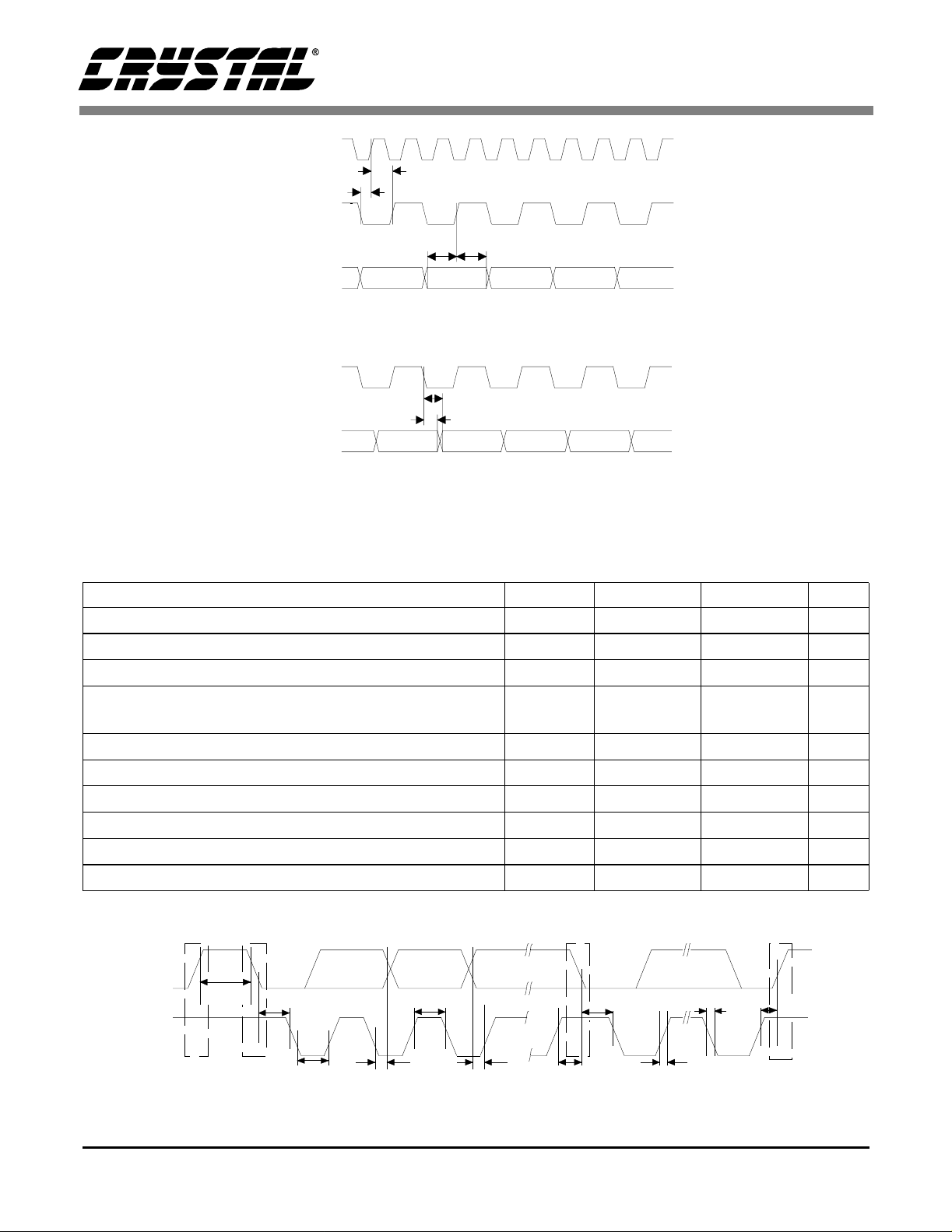
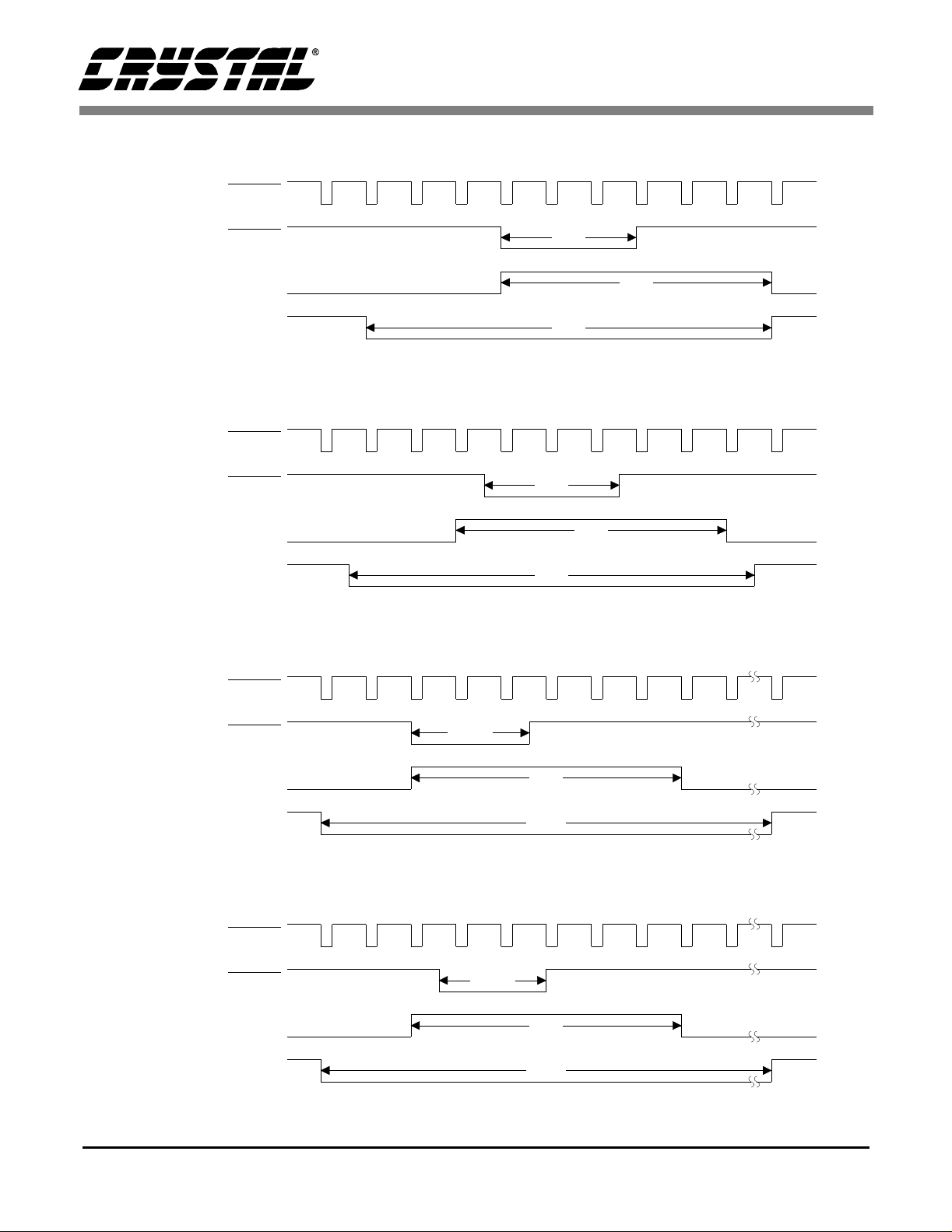
CLKIN2X
CLKIN
Mosaic
Input Data
DI[9:0]
CLKOUT
Output Data
DOA[9:0]
DOB[9:0]
CS7666
t
H2
t
S2
t
t
H1
S1
Input Timing Diagram
t
PD
t
OH
Output Timing Diagram
CONTROL PORT CHARACTERISTICS
(TA = 25 °C; VDD = 5 V; Input Levels: logic 0 = 0 V, logic 1 = VDD.)
Parameter Symbol Min Max Unit
SCL Clock Frequency f
Bus Free Time Between Transmissions t
St art Condition Hold Time t
Clock Pulse Width High
Low
Setup Time for Repeat Star t Condition t
SDAIN Hold Time from SCL Falling t
SDAIN Setup Time from SCL Rising t
SDAIN and SCL Rise Time t
SDAIN and SCL Fall Time t
Setup Time for Stop Condition t
Stop Start
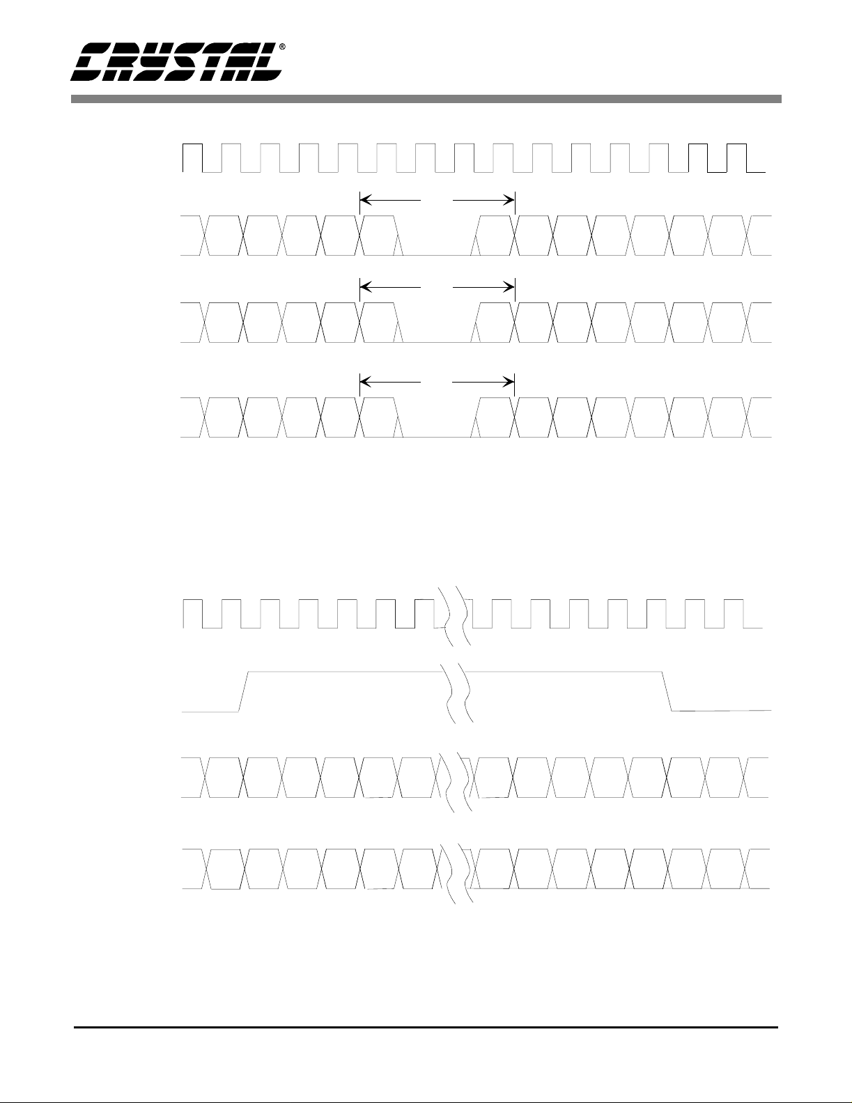
SDA
SCL
t
buf
t
hdst
t
high
SCL
buf
hdst
t
high
t
low
sust
hdd
sud
r
f
susp
Repeated
Start
-400kHz
1.3 - µs
0.6 - µs
0.6
1.3
-
-
µs
µs
0.6 - µs
0-µs
0.1 - µs
-1.0µs
-0.3µs
0.6 - µs
Stop
t
hdst
t
f
t
susp
t
low
t
hdd
t
sud
t
sust
t
r
I2C Timing Diagram
4 DS302PP1
Page 5
CS7666
RECOMMENDED OPERATING CHARACTERISTICS
Parameter Symbol Min Typ Max Unit
Power Supply Voltage V
DD
Ground to Ground Voltage Differential - - 10 mV
Digital Input Rise/Fall Time - - 10 ns
CLKIN Level Setup to CLKIN2X Rising (non-interpolated) t
CLKIN Level Hold after CLKIN2X Rising (non-interpolated) t
S2
H2
Digital Input Voltage Range 0 - V
Operating Temper ature Range T
A
ABSOLUTE MAXIMUM RATINGS
Parameter Symbol Min Max Unit
Power Supply Voltage V
Digital Input Voltage Range GND - 0.3 V
Forced Digital Output Current - 50 mA
Sustained Digital Output Voltage GND - 0.3 V
Output Short Circuit Current - - mA
Operating Temper ature Range T
Lead Solder Temperature (10 s duration) - +260 °C
Storage Temperature Range -65 +160 °C
DD
A
4.5 5.0 5.5 V
8--ns
8--ns
DD
0-70°C
-0.3 7.0 V
+ 0.3 V
DD
+ 0.3 V
DD
070°C
V
WARNING: Operation at or beyond these limits may result in permanent damage to the device.
Normal operation is not guaranteed at these extremes.
DS302PP1 5
Page 6
CS7666
GENERAL DESCRIPTION
Overview
The CS7666 forms the hea rt of a fo ur chip dig ital
CCD Camera. The four chips include the CCD imager, the CS7615 CCD digitizer, the CS7666 color
space proces s or, and a vertical drive in terface-chip
for the CCD image r. Most four-phase C CD imagers (and their associated vertical drives) can be
used with the CS7615 digitizer and the CS7666
processor to form a simple and cost-effective
YCrCb output format digi tal ca mera. The CS7615
and CS7666 together support imager formats rang-
ing from 175× 175 pixels up to 1 000x1000 pixels.
Timing control is located in the CS7615 analog
processor, while the CS7666 synchronizes itself by
decoding the timing cues embedded in the CS7615
data stream. Al terna tel y, th e CS 7666 a ccep ts hori zontal and vertical timing signals on pin inputs.
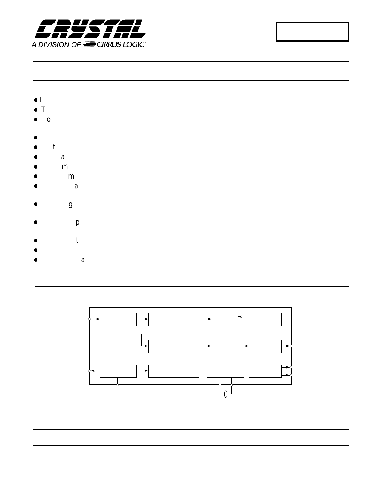
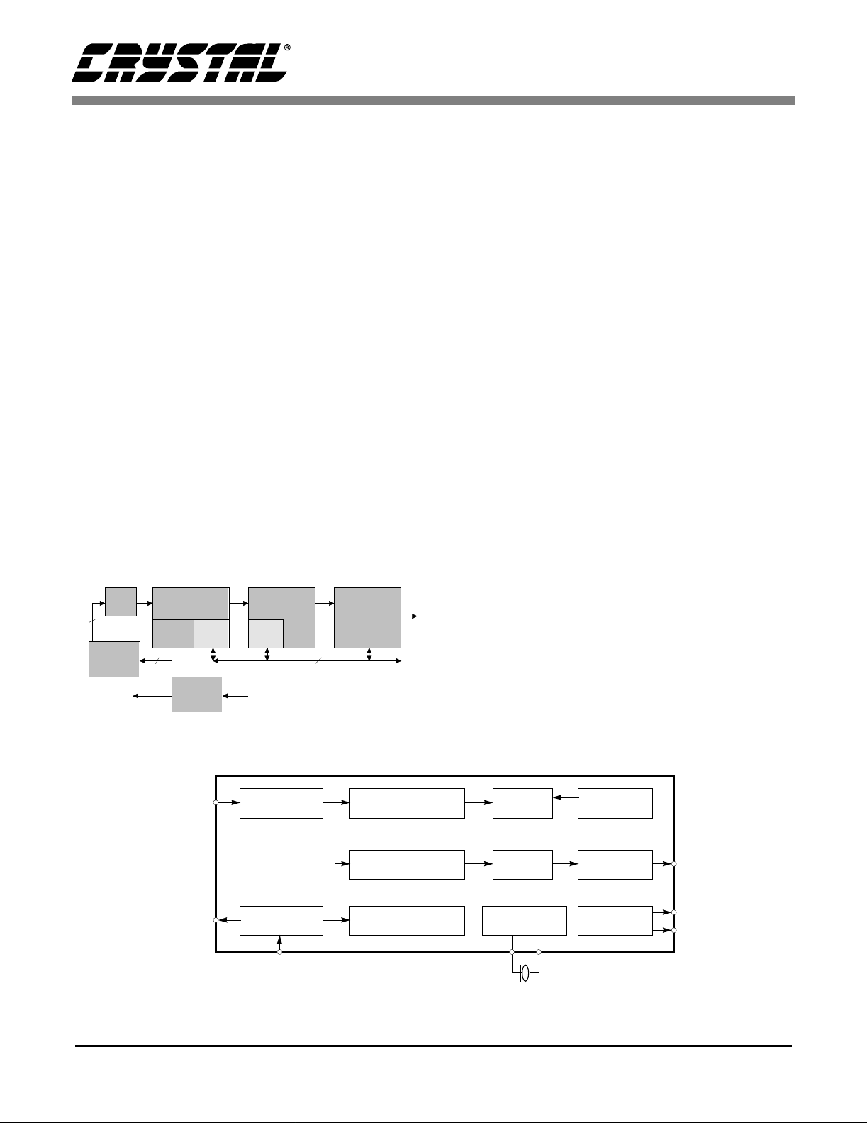
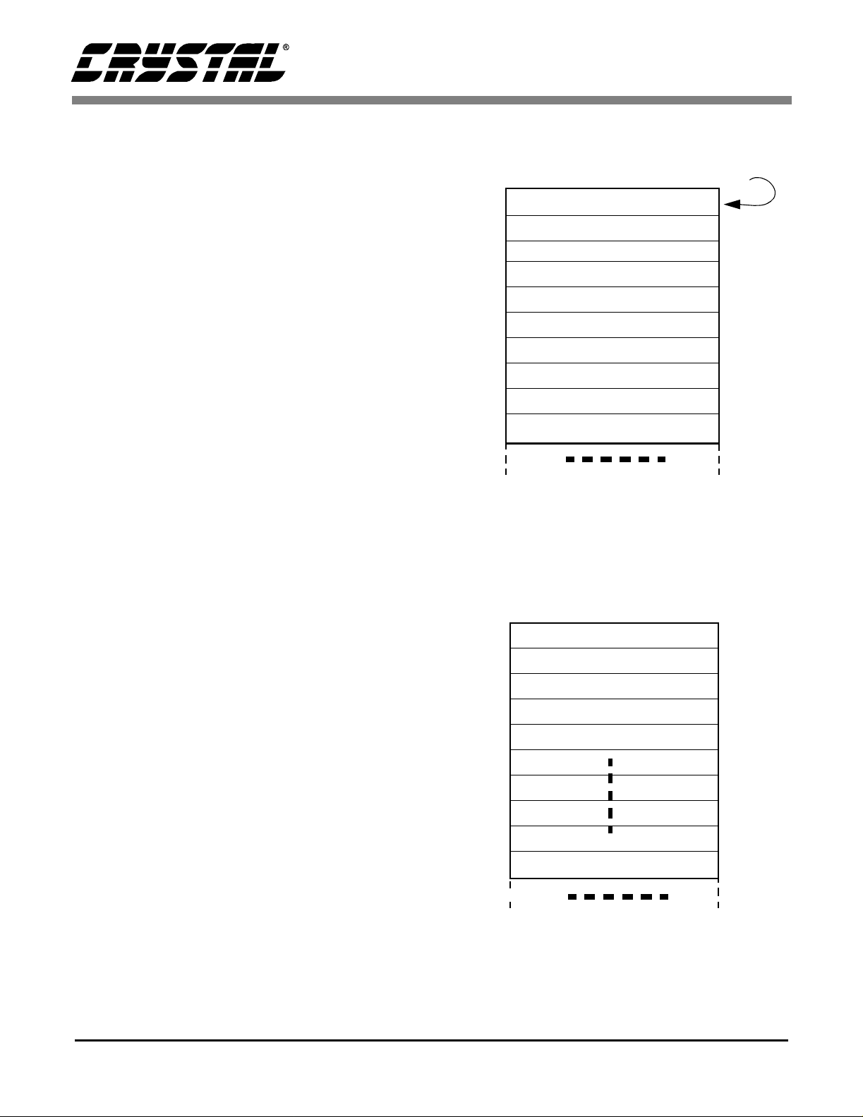
The block dia gram i n Figure 1 illustra tes a typ ical
system interconnect.
CS7666
Image
Processor
+5V
6
Vertic al
Drive
CCD
512x480
+18V to +12 V
Timing
6
CS7615
CDS/ADC
I2C I2C
CCD
Bias
Figure 1. Typical 4-Chip Digital CCD Camera
CS4954
Video
Codec
2
C
2
I
Bus
The CS7666 is a CCD camera color separation and
color-space processor designed to process the fourcolor mosai c CCD image r data into ITU-601 compliant 4:2:2 YCr Cb digital component vi deo. The
CS7666 timing control is based on the built-in crystal oscillator or on the master clock provided by the
CS7615, and provides formatted component digital
video compliant with SMPTE-125 and ITU-656
transport protocols.
The CS7666 prov ides co lor separa tion of stand ard
MYCG chroma blo ck data from in dustry standard
four-color CCD imagers. Gamma correction and
white balance adjustment functions are also included in the CS7666. The YCrCb (luminance and
chrominace) data is output at the scaled CCD pixel
rate in 20 -bit format, or at twic e the scaled pixel
rate in 10-bit format (see discussion on Digital Output Formats). The YCrCb output data from the
CS7666 confo rms to t he ITU-65 6 parall el com ponent digital video recommendation with embedded
synchronization (see Embedded EAV and SAV
discussion). External horizontal and vertical synchronization signals are also provided to support
ITU-601 interfaces, as well a s t he PC-Card Zoom Video standard being used in notebook computers.
The CS7666 incorporates an internal horizontal
scaler which may be turned on to increase the horizontal pixel count of the popular 360 (CIF) and 512
horizontal pixe l per line imagers. The most com -
CCD
DATA
SECONDARY
2
I
C BUS
DEFORMATTER
I2C INTERFACE
PRIMARY
I2C BUS
COLOR SEPARATION
AND ANITALIASING
GAMMA
CORRECTION
REGISTER PLL AND OUTPUT
BLOCK CLOCK DRIVER TIMING
WHITE
BALANCE
SCALER
XTAL
AWB
CONTROL
OUTPUT
FORMATTER
YCrCb
DATA
VREF/VSYNC
HREF/HSYNC
Figure 2. CS7666 Block Diagram
6 DS302PP1
Page 7

CS7666
mon target resolutions for the scaler are 640 and
720 pixels per line (square and rectangular pixel
formats), but it is possible to pro vide gener ic scaling of M/N where M and N are values from 1 to 31.
The CS7615 and CS 7666 chip set supports a wide
range of imager form ats while providi ng an output
format that fol lows the IT U-601 C ompon en t Digi tal Video recommendation. The ITU-601 document primarily spe cifies horizontal resolutions o f
720 active h orizonta l pixels (which i s require d for
broadcast television compatibility). However,
many of today’s digital video receivers are capable
of operatin g wi th a wide range of vi deo image formats. Even th ough the se dig ital video rec eive rs allow image formats not specified in the ITU601/656 recommendation, all of these receivers expect the basic ITU-601/656 protocol to be followed
in terms of data seque nce an d timin g cue s. Th is is
the case with the CS7666, where all output formats
follow the ITU-601/656 recommendation even if
the image form ats differ in ho rizontal and ve rtical
pixel dimensi ons.
The 640 Pixel Horizontal Line
The following di scussion assumes th at a 512 horizontal pixel class ima ger has be en sel ected for t he
camera, the CS 7615 h as b een progra mme d to pro vide 512 ac ti ve pixels an d 112 inacti ve pixels, and
that the intern al 4 :5 h orizonta l sca ler ha s bee n en -
abled (scaler mode 1). Many other imager/scaler
combinations are possible, but the digital video format would not be significantly different than the
640x480 case described.
Transmitte d durin g each active line a re 1280 multiplexed luminance and chrominance values (640
luminance, 320 chrominance Cr, and 320 chrominance Cb values). Eight of the remaining 280 interface clock intervals are used to transmit
synchronizing i nforma tion . The first of th ese 156 0
interface clock intervals is designated line 0 word 0
for the purpose of reference only. The 1560 sample
words per total line are therefore numbered 0
through 1559. Interva ls 0 through 1279, inc lusive,
contain vid eo data.
The inte rface clock intervals o cc urring durin g digital blanking are designated 1280 through 1559. Intervals 1280 through 1283 are reserved for the endactive-video (EAV) timing reference. Intervals
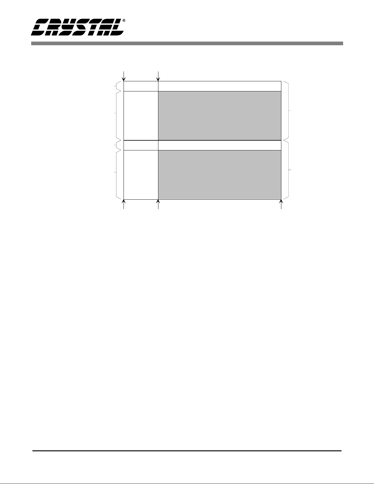
1556 through 1559 are reserved for the start-of-active-video (SAV ) timing reference. Figure 3 indicates the val ues of th e ti ming re fere nce si gnal s (F,
V, H) for an entire frame of interlaced video. Please
note the scan lines are numbered 1 through 525
consecutively in the time domain (spatially they are
interlaced ). Table 1 defines t he 1560 samples of a
single scan line of video.
DS302PP1 7
Page 8
CS7666
Lines 1 to 19 V=1
Lines 20 to 263
V=0
Lines 264 to 282 V=1
Lines 283 to 525
V=0
EAV
H=1
640
SAV
H=0
Vertical Blanking
Active Vid e o
Field 1
Blanking
Horizontal
Vertical Blanking
Active Vid e o
Field 2
Blanking
Horizontal
0
779
Figure 3. Horizontal and Vertical Timing States
(640×480 resolution)
F=0
Lines
4 to 265
F=1
Lines
266 to 3
639
8 DS302PP1
Page 9
CS7666
Word Data Content Pixel Notes
1280 1111 1111 640 EAV
1281 0000 0000 EAV
1282 0000 0000 EAV
1283 1FV1 P3P2P1P0 641 EAV
1284 1000 0000 642 Fro pixels 642 to 777
1285 0001 0000
1286 1000 0000
1287 0001 0000 643
1552 1000 0000 776
1553 0001 0000
1554 1000 0000
1555 0001 0000 777
1556 1111 1111 778 SAV
1557 0000 0000 SAV
1558 0000 0000 SAV
1559 1FV0 P3P2P1P0 779 SAV
0 Cb0 0 St a rt of Digital Vide o
1 Y0 For VBLANK line 1 to 19
2Cr0
3Y1 1
4Cb2 2
5Y2
6Cr2
7Y3 3
2n Cbn n For active pixels 20
2n + 1 Yn
2n + 3 Crn
Yn+1 n+1
1272 Cb636 636
1273 Y636
1274 Cr636
1275 Y637 637
1276 Cb638 638
1277 Y638
1278 Cr638
1279 Y639 End of Digital VIdeo
Table 1. Detail of Scan Line for 640x480 Image
Cr = Cb = 80h
Y = 10h
and 264 to 283
Cr = Cb = 80h
Y = 10h
through 263 and 283 to
525 for n=even from pix-
els 0 to 638
DS302PP1 9
Page 10
CS7666
Embedded ITU-656 EAV and SAV Timing
The lines in Figure 3 are numbe red 1 through 525.
Video data is not present on lines 1 to 19 or 264 to
282, which constitute the vertical blanking periods.
The vertical blanking is in full line increments,
where Y samples are set to 10h, while Cb and Cr
samples a re set to 80h. The interval startin g with
EAV and ending with SAV is the digital horizontal
synchronizati on, whi ch occ urs on e ve ry line.
It is implicit that the timing reference signals are
contiguous with the video data and continue
through the vertical blanking interval. Each timing
reference signal consists of the four-word sequence
in Table 2 . The first three words are a preamble,
followed by a fourth wo rd indica ting a) even fie ld
(field 2) identification, b) state of vertical blanking,
and c) sta te of ho rizon tal blank in g. T able 1 deta ils
the timing reference format. The protected bit
states are dependent on the F, V, and H bits according to Table 3.
Value Description
First Byte FFh Fixed
Second Byte 00h Fixed
Third Byte 00h Fi xed
Fourth Byte xyh See Table 3
Table 2. Timing Reference Signal
Protected State Bits - In Ta bles 3 and 4, H, V, an d
F bits provide all the necessary timing and state information . Bits 0 to 3 provide error detection an d
correction information. The protection bits allow
for correction o f single-bit error s and detection of
two-bit errors. The F or field bit indicates which of
the interlaced fields is active, the first/odd field
which contai ns 262 l ines, or the sec ond/eve n fiel d
which contains 263 lines.
Bit Position Word 1281
and 1556
7 1001Fixed
6 1 0 0 F F = 0 during Field 1/ODDF = 1
5 1 0 0 V V = 0 during Active VideoV = 1
4 1 0 0 H H = 1 at end of Active VideoH = 0
3 1 0 0 P3 see Protected Bits State Table 4
2 1 0 0 P2 see Protected Bits State Table 4
1 1 0 0 P1 see Protected Bits State Table 4
0 1 0 0 P0 see Protected Bits State Table 4
Bit 7 Bit 6 (F) Bit 5 (V) Bit 4 (H) Bit 3 (P3) Bit 2 (P2) Bit 1 (P1) Bit 0 (P0)
10000000
10011101
10101011
10110110
11000111
11011010
11101100
11110001
Word 1281
and 1557
Table 3. EAV and SAV Timing Reference Signal Detail.
Table 4. EAV and SAV Protected Bit States Detail.
Word 1282
and 1558
Word 1283
and 1589
during Field 2/EVEN
during Vertical Blanking
at start of Active Video
Description
10 DS302PP1
Page 11

CS7666
Individual Timing and Synchronization Signals
In addition to the embedded EAV and SAV timing
signals, the CS7666 provides individual synchronization output signals which are employed by many
video encode r circuits. T hese synch ronization signals are typically used to interface the ITU-656 digital video stream to other components and
subsystems. The individual synchronization signals include HREFOUT and VREFOUT.
HREFOUT/HSYNC
HREFOUT is an active-high signal indicating
when active pixel data is being transmitted on
DOA[9:0] or DOB[9:0]. HREFOUT is low whe n
non-active pi c ture d ata i s be ing tr an smi tted durin g
horizontal blanking. Depending on the mode of operation, the HREFOUT signal follows either the
HREFIN signal or the HREF defined by t he EAV
and SAV code.
The HREFOUT pin may also be configured to provide a HSYNC output tha t provides an active low
pulse for 64 pixel clocks whose falling edge occurs
16 pixel clocks after the end of active video for
NTSC (12 clocks for PAL) as per the ITU-R
BT.601 specification. HSYNC is chosen by setting
the Operation Control Register II (07h) HS_SEL
bit (bit 0) to a value of 1. This pin may be inverted
by setting the H_INV bit (register 07h bit2) to a
value of 1. Th e HSY NC signa l ma y be dela yed by
0, 0.5, 1, or 1.5 pixel clocks by setting H_SFT[1-0]
appropriately (register 07h bits 5 and 4.)
VREFOUT/VSYNC
VREFOUT is an output signal that is active high
when the CS7666 i s put ting out a ctiv e video l ines.
The active-low portion of this signal defines the
vertical bla nki ng period. If the VS_SEL bit i n register 07h is set, this output pin produc es a vertical
sync signal that i s com pati bl e with curr en t PAL or
NTSC analog systems. See Figure 4. This signal is
active for 3 line times in NTSC mode (bit 5 of register 04h = 0) and 2.5 line times in PAL mode (bit5
of register 0 4h = 1.) This line may be inverted by
setting the V_INV bit (register 07h) to a value of 1.
Alternate ly, wh en the ZV mod e bit in re giste r 06h
is set, this output behaves as a VSYNC signal appropriate for ZV ports. In the ZV mode, the
VSYNC signal is active-high during the first six
horizontal line periods of every field. The transition
in VSYNC signal lags the HREF signal’s rising
edge during odd fields a nd leads the rising edge of
HREF during even fi el ds.
Digital Output Formats
The CS7666 outputs data in a 20-Bit wide format at
the output pixel clock rate. Alternately, the data can
be multiplexed in a 10-bit format at a 2x output pixel clock rat e. Figures 5 and 6 detail the c lock and
data relationships. The output data transitions on
the falling edge of the clock such that the rising
edge of th e clock can be used to latc h the data i nt o
subsequent circuit ry.
The CS7666 del ivers 4:2: 2 compone nt digit al video output data in YCrCb format. The data conforms
to the ITU-R BT.656 specification. The Y component range is 16-235 (8-bit data) and the Cr and Cb
component ranges are 16-240 (8-bi t data). However, by setting CLIP_OFF (register 07h bit 6) to a
value of 1, the output data can be extended to a
range of 1-254 (8-bit data). Only 00 a nd FF are restricted to all o w digital timing codes.
The digital outputs can be configured for 10-bit interleaved Y and CrCb data, or for 20-bit parallel
operation. The INTERL bit of the Operational Control Register 06h determines which output format is
active. Logic 0 places the CS7666 in interleave
mode with output data on channel "A." Logic 1
places the CS7 666 in non -in terlea ve d mode where
luminance data is output on channel "A" and
chrominance data is ou tput on chann el "B."
DS302PP1 11
Page 12
Line
HSYNC
NTSC Vert ical Timing (odd field)
525 1 2
3 4
5 6
7 8
CS7666
9 10
VSYNC
VSYNC ZV Mode
VREF
Line
HSYNC
VSYNC
VSYNC ZV Mode
VREF
Line
HSYNC
NTSC Vertical Timing (even field)
263 264 265 266 267 268 269 270 271 272 273
PAL Vertical Timing (odd field)
624 625 1
2 3
3H
9H
3H
9H
6H
4 5
6H
6 7
23
VSYNC
VSYNC ZV Mode
VREF
Line
HSYNC
VSYNC
VSYNC ZV Mode
VREF
PA L Vertical Timing (even field)
311 312 313 314 315 316 317 318 319 336
2.5H
6H
24H
2.5H
6H
25H
Figure 4. Vertical Timing
12 DS302PP1
Page 13
24.5454MHz
CLKOUT
SAV
DO [9-0]
A
Line 3 Pixel 776
to Line 4 Pixel 3
DO [9-0]
A
Line 263 Pixel 638
to Line 264 Pix el 645
DO [9-0]
A
Line 525 Pixel 638
to Line 1 Pixel 645
NOTE: EAV, SAV, and Blanking data values are based on the 8 MSB’s of the output data, the two LSBs are considered fractional.
Cb638 Y638 Cr638 Y639 FFh 00h 00h 9Dh 80h 1 0h 80h 10h 80h 10h
FFh 00h 00h ABh 80h 10h 80h 10h 80h 10h80h 10h 80h 10h
EAV
FFh 00h 00h F1h 80h 10h 80h 10h 80h 10h80h 10h 80h 10h
EAV
CS7666
12.2727MHz
CLKOUT
HREF
DO [9-0]
A
DO [9-0]
B
Figure 5. 2x Pixel Clock, 10-Bit interleaved Output Format for 640x480 Image Format.
10h Y0 Y1 Y2 Y3 Y4 Y633 Y634 Y635 Y636 Y637 Y638 Y639 10h
80h Cb0 Cr0 Cb2 Cr2 Cb4 Cb632 Cr634 Cb634 Cr636 Cb636 Cr638Cb638 80h
NOTE: EAV, SAV, and Blanking data values are based on the 8 MSB’s of the output data, the two LSBs are considered fractional.
Figure 6. 1x Pixel Clock, 20-Bit Parallel Output Format for 640x480 Image Format.
DS302PP1 13
Page 14

CS7666
In 20-bit wide mo de, t he lum ina nce in forma tion is
output on DOA[9:0] and the chrominance information is output on DOB[9:0].
Parallel
INTERL = 1
DOA[9:0] 10-Bit
Luminance Data
DOB[9:0] 10-Bit
Chrominance Data
CLKOUT Pixel Rate 2x Pixel Rate
Table 5. INTERL Controlled Output Formats
Interleaved
INTERL = 0
Interleaved 10-Bit
Luminance Data
and 10-Bit
Chrominance Data
0
The CS7666 su pports both 8 -bit and 10-bit operation as per the ITU-656 recommendation. The ITU656 recommendation defines the primary data path
as 8-bits wide with two additional fractional bits
that can b e us ed to form a 10-bi t d ata p ath. If o nly
8-bits of output data are used, the two LSBs, DOA1
and DOA0 (DOB1, DOB0) are not used. However,
DOA[9:2] (DOB[9:2]) are connected exactly the
same as in a 10-bit system. This is essential to
properly pass t he image data and synchronization
signals to the next component.
Internal Horizontal Scaler
selected by se ttin g the IN TERP pin (pin 54 on the
CS7666) to a logica l one. The 4:5 scal er will c onvert a standard 512 horizontal pixel width CCD imager used for cam-corde rs into the VGA 640x480
format. The CS7615 (if that device i s used in the
system) must also have its INTE RP pi n set hig h.
Register 04h
bit 4
0 0 CS7 665 mod e 1:1
0 1 CS7 665 mod e 4:5
1 X CS7666 mode programmable
Pin 54 Operation Scaling Ratio
Table 6. INTERP Pin (Pin 54)
When the CS7 666 is in the native CS7666 m ode
(True_7666 in reg ister 04h set to 1), the INTERP
pin is ignored a nd the in ternal sc aling ra tio is pro grammed by the user. The CS7615 mu st have its
INTERP pin tied to ground.
Several pre-def ined scaler mode s may be selected
by writing a 3-bit val ue to bi ts 0-2 of regi ster 0 4h.
These default scaling modes are described in
Table 7. If t he CUSTOM bit (bi t 3 of register 04h)
is set to a 1, th e n the scaling ratio is de termined b y
the M and N values contained in the Scaler Control
registers (2Dh - 2Fh.)
The inte rnal h orizo nta l sca ler i s use d to b rid ge be tween common CCD imager formats and computer
or television form ats. In the CS766 5 compat ibility
mode (defau lt after reset) a 4:5 data r ate scaler is
Mode CCD Format CCD Clock (MHz) Output Format Input Clock (MHz) Scaling Ratio
000 CCD ½ input clock same as CCD (30 MHz max.) 1:1
001 512x480 9.818 640x480 24.5454 4:5
010 512x480 9.346 720x480 27.000 9:13
011 512x576 9.281 720x480 27.000 11:16
100 362x480 6.75 640x480 24.5454 11:20
101 362x480 6.75 720x480 27.000 1:2
362x576 6.75 720x576 27.000
110 512x576 9.563 720x576 27.000 17:24
111 512x480 9.000 720x480 27.000 2:3
512x576 9.000 720x576 27.000
Table 7. Default Scaling Modes (Register 04h)
14 DS302PP1
CLKIN and CLKIN2X Input Timing
The CLKIN, pin 55, will alway s require a prim ary
pixel rate clock source. CCD manufacturers generally specify a pixel clock frequency that is compat-
Page 15

CS7666
ible with one of the analog encoders that can be
used with a gi ven imager. If a n analog encode r is
used in the camera to generate an analog output, the
pixel clock frequency expected by the encoder
must be matched precisely. However, digital display systems, such as those based on VGA graphics
adapter cards a nd Zoom Video systems, are ge nerally not sensitive to pixel clock frequency, and will
tolerate a wide range of pixel and frame rates.
Specific pixel-rate clock frequencies for analog encoders include 14.31818 MHz for 768H image rs,
the primary ITU-601 13.5 MH z for 720H imagers,
and down to 1 2. 272727 MHz clock rates for 640H
VGA format imagers.
In CS7665 compatibility mode (register 04h bit 4 =
0), The CLKIN2X, pin 56, will either require a
2.5X CCD pixel r ate clock when the i nternal 4:5
scaler is enable d (INTERP pi n high) or a 2x time s
the CCD pixel rate clock in non-interpolation
mode (INTERP pin low). The CLKIN2X pin is
used as a crystal in put pin when the C S7666 is in
native mode (register 04h bit4 = 1).
terlaced image data into the various color space formats. These include RGB and YUV, as well as
YCrCb. Th e individual image adju stments are performed in the mo st appropriate color sp ace representation. Ultimately the image is converted to
YCrCb format for outputting data.
Color Saturation Control
Color saturati on control is via the Red Saturat ion
and the Blue Sat uration control re gister addresses
0Ah and 0Bh.
White Balance and Gamma Correction
The red and blue color balances can be adjusted
2
through the I
tomatic white balance) sequence the red level is adjusted to minimize the (Y-R) difference
component ; similarly the blue leve l is adjusted to
minimize the (Y-B) color difference component.
An autom atic w hit e bala nce i s init iated by wr iting
a 1 to register 05h bit 1. For manual control, the red
balance is a ccessed thr ough register 08h, and the
blue balance is accessed through register 09h.
C control port. During the AWB (au-
CLKOUT
CLKOUT follows the output data rate as described
in the D igital O utput Format s sect ion. In the non interleav ed mode the c lock output is a t the output
luma sa mple ra te wh erea s in the in terle aved mode
the clock output is at 2x the output luma sample
rate.
INTERNAL PROCESSING
The inte rnal o per atio n o f the CS76 66 ca n be sepa rated into several distinct blocks. The following
section provides an overvi ew of how these blocks
operate and interact.
Input Data Format and Chroma Separator
The CS7666 accepts up to 10-bit MYCG image
data from a CCD digitizer such as the CS7615.
suitable CCD ana log pro cessin g uni t. Th e CS 7666
internally c onver ts t he four -co lor CC D MYC G in-
Gamma correction is provided to offset the non-linear illumination profile of the display device. Separate 256 entry tables a re supplied fo r red, green,
and blue. Eac h entry is 8-bi ts. T he g amm a t able is
programmed throu gh register 0Ch. The write format is similar to th e write format descr ibed in the
normal I
ment. The first byte contains the CS7666 device
address and wri te bit, the seco nd byt e c ontai ns the
CS7666 gamma table register address (0Ch), the
third byte determines which gamma RAM to update (red, green, and blue), the next 256 bytes contain the gamma ta ble entries.
The blue gamma RAM is selected by setting register 0Ch bit 0 to a one; the green gamma RAM is selected by setting register 0Ch bit 1 to a one; and the
red gamma RAM is selected by setting register 0Ch
bit2 to a one. Any, or all of the gamma RAMs may
be selected . The most common implementation is
2
C operation section later in this docu-
DS302PP1 15
Page 16

CS7666
to write the same gamma table to all 3 RAMs by
setting bits 0-2 high. The gamma table itself is
loaded from low to high. The first byte after the
RAM selectio n byte will correspond to the value
used when the input data is 00h, the 256th byte after
the RAM selection byte will correspond to the value used when t h e input data is FF h .
The gamma table is read in a similar manner. However, certain restri ctions are made t o reads. First,
the gamma RAMs may only be read one at a time
(RAM selection byte = 01,02,04 only) and, second,
the gamm a table may only be read when gamma
correctio n is disabled (register 05 bit2 = 0).
Chroma Kill
As the brightness of an image increa s es, the green,
yellow, cya n, and mage nta pixels within the CC D
array will saturate at different intensity levels. As a
result, a h ighly illuminated obj ect or light source
may start to look cyan. To overcome this effect, an
internal Chroma killer circuit compares the luma
and chroma values of each pixel to a set of pro-
grammable thre shol ds. If the pixel’s luma value is
greater than the Y_THR value (register 27h) and its
Cr and Cb values are between the CR_THR_H ,
CR_THR_L , CB_THR_H, and CB_THR_L
threshold va lues respectively, then tha t pixel will
lose its chroma value (become white.) These
thresholds are stored in registers 27h - 2Ch.
Internal Filters
The CS7666 has an internal low-pass chroma filter
to reduce the effects of color al iasing. Th i s filter is
enabled b y wri ting a value o f 0 to bit 4 of re giste r
05h. The CS7666 also contains a luma peaking filter to enhance the edges of blurred images. This filter is enabled by setting register 05h bit 3 to a value
of 0.
INTERNAL REGISTER STRUCTURE AND USER INTERFACE
The user interface describes the user’s external
view of the CS7666 and the basic control operations. These areas include digital data output modes
and organiz ation, timing a nd synchronizatio n sig-
2
nals, I
The CS7666 has two I
called the primary I
port with limited I
mary I
C interface , an d miscellaneous co ntrols.
2
C ports: (1) a slave I2C port
2
C port, and (2) a secondary I2C
2
C master capabilities. The pri-
2
C port allow s a n external cont roller to control the CS7666. It is assumed the external
controller wi ll also directly co ntrol any other I
2
slave devices on the camera board. This is the nor-
2
mal I
C operation mode of CS7666. The secondary
2
C port, on the other hand, may be used to control
I
all the other slave devices on a camera board
through the CS7666 only. This feature is useful
when the externa l I
2
C controller is used t o control
multiple cam er as. Wh en u sed i n th is co nfigur at io n
the 4BYTEMODE pin (pin 1) of the C S766 6 must
be tied high and the device is operated in four-byte
mode.
Operating CS7666 in Normal I2C Configuration (Three-Byte Mode)
In normal mode, the CS7666 is connected as a
2
slave device to an external I
2
the prima ry I
C port. The co nnect ion i s done vi a a
two-wire serial bus. Other I
era may also share the same serial bus. The external
controlle r communicates with the I
sending and rec eivi ng short pa cket s of 8-bi t words
in accordance with the I
contain the st ation address of the t arget device, t he
desired register add ress, and data.
There are three packet formats: WRITE format,
ADDRESS SET forma t, and READ format. Each
packet is ad dressed to a device by the stat ion address. The LSB of the station address is the R/W
(data direction) bit. This bit is set LOW in the
WRITE and ADDRESS SET packets, and it is set
C controller thr ough
2
C devices on the cam-
2
C devices by
2
C protocol. T he packets
C
16 DS302PP1
Page 17
CS7666
HIGH for READ packets. The master can read an d
write to non-existent re gisters within the selected
device. WRITE operations will have no effect;
READ operations will return a value of 00h.
Station Address
Each device on the I2C bus has a uni que 7-bit ad dress. An eighth bi t, the R/W bi t, determines if the
current data transfer write s dat a to the slave devi ce
or reads data from the slave device. It is common to
represent the station address and R/W bit as two 8bit station addresses, one address for write accesses
and another address for read accesses. We will follow this p ractice. The CS 7666 default sta tion address is 34h for writes and 35h for reads. The
station address can be changed by writing a new
station address to register FFh. The value written to
this regis ter does n ot inclu de the R /W bit. For example. The default station address (34h write / 35h
read) will be stored as 1Ah in register FFh.
Byte Sequence WRITE Format Packet Detail
First Byte Station Address with LSB Set LOW
Second Byte Device Register Address (0..255)
Third Byte Register Data (0..255)
Table 8. WRITE Format Packet
Address Set Operation
The ADDRESS SET format consists of a two-byte
packet which sets the address of a subsequent
READ operati on. The first byte of t he St atio n Ad dress with the LSB (data direction bit) set LOW t o
indicate a write opera tion. The secon d byte is the
register address (0..255). The ADDRESS SET format is the sam e as t he WR IT E form at, witho ut t he
register data (third byte).
Byte Sequence ADD RESS SET format
Packet Details
First Byte Station Address with LSB Set LOW
Second Byte Device Register Address (0..255)
Ta bl e 9. ADDRESS SET Format Packet Operation
Write Operations in Three-Byte Mode
The WRITE format consists of a three-byte packet.
The first byte is the station address with the data direction bit set LOW to indicate a write. The second
byte is the device register address (0..255). The
third byte is the register data (0..255). No additional bytes ar e al lowed.
EPROM
CS7615
CS7666
C
2
CS4954
Figure 7. I
secondary I
To other sub-systems
2
C configuration showing primary
and secondary I
C
2
primary I
2
C busses.
External
controller
Read Operations in Three-Byte Mode
The READ opera tion may consist of two or more
bytes. Th e firs t b yte is th e st at ion a dd ress w ith t he
LSB (data direction bit) set HIGH indicating a read
operation. Th e addressed de vice the n sends one or
more bytes back from the register last addressed by
the previous WRITE operation or the previous ADDRESS SET operation.
Byte Sequence READ Format Packet Details
First Byte Station Address with LSB set HIGH;
Source Device then Returns One
Byte of Register Data (0..255)
Second Byte Returned data from CS7666
Table 10. READ Format Packet.
Operating CS7666 in Four-Byte I2C Configuration
In this configuration the external controller talks
2
only to the C S766 6 thro ugh t he p rim ary I
face. All the other slave devices on the camera
C inter-
DS302PP1 17
Page 18
CS7666
board are tied to the secondary I2C port of the
CS7666. WRITE and READ packet s only are defined in four -byte mode. Independent address set
operations to slave devices on the secondary I
2
C
bus is not allowed in four-byte mode. Four-by te
mode is active when the 4BYTEMODE pin (pin 1)
is logic high.
Write Operations in Four-Byte mode
All WRITE operations from an external controller,
through the C S7666, to any slave device m ust use
the four-byte mode; this includes writing to the
CS7666 itself. The external controller sends a fourbyte WRITE c ommand to the CS7666 whic h initiates a WRITE operation to the destination slave
device and sets the I2CBUSY bit in the status register (01h). The I2CBUSY bi t is cleared when the
write operation o n the secondary bus is comple te.
The Exte rnal con troll er ca n poll t he sta tus re giste r
to check if the CS7666 has completed the command.
The CS7666 h as a one com mand buffer which allows the external controller to queue one additional
command while the current com mand is still being
executed. If more than one command is sent before
the I2CBUSY bit is cleared, the CS7666 saves only
the last com mand an d executes i t after the current
one is com pleted. C omman ds that i nvolve wr iting
or reading onl y to CS7666 r egisters are not put in
the queue but are executed immediately without affecting any transactions occurring on the master
2
I
C interface .
Any attempt by the external I
to the CS7 666 registe rs while th e CS7666 is busy
initiali zing from an ex ternal EEPR OM will be ig nored. However, reads from the CS7666 are allowed duri ng this time.
If, during a READ or WRITE o peratio n to a sla ve
device, the CS7666 fails to receive an acknowledge
bit the execution of the command is aborted and the
NODEV bit in the status register is set high. This
2
C contr o ller to wri te
bit remains set unless it is explicitly cleared by
writing to it or a new command is written to
CS7666.
Byte Sequence WRITE Format Packet Detail
First Byte S tat ion Address of CS7666 with LSB
Set LOW
Second Byte Station Address of target slave
device with LSB Set LOW
Third Byte Device Register Address (0. .255)
Fourth Byte Register Data (0.. 255)
Table 11. Four-byte WRITE Format Packet
Read Operations in Four-Byte Mode
The READ operation in four-byte mode first requires a three-byte READ-TRIGGER packet to the
CS7666. The first byte is the station address of the
CS7666 with the LSB set LOW. The second byte is
the target slave device’s station address with the
LSB (data direction bit) set HIGH. The third byte is
the register address (0..255).
Byte Sequence READ-TRIGGER format Packet
Details
First Byte CS7666 Station Address with LSB
Set LOW
Second Byte Target device Station Address with
LSB Set HIGH
Third Byte Device Register Address (0. .255)
Table 12. READ-TRIGGER packet in four-byte mode
The READ-TRIGGER packet initiates a READ
operation by t he CS7666 from the target slave de vice on the s econdary I
in the CS7666 may be checked to see if the read operation has been completed. The I2CBUSY bit in
status register 01h is set to zero when the operation
is completed.
On comple tion of a r ead cycle from the target de vice, the CS7666 places the data read into the Slave
Data Hold register at address 19h. The external
controller can read this data through the primary
2
I
C port. This requires first performing an AD-
DRESS SET operation to set the address to 19h and
2
C bus. The status registe r
18 DS302PP1
Page 19
CS7666
then sending a one-b yte station address indic ating
read to the CS7666. The data from regist er 19h is
then returned by the CS7666.
Byte Sequence WRITE Format Packet Detail
First Byte Station Address of CS7666 with
LSB Set LOW
Second Byte Station Address of CS7666 with
LSB Set LOW
Third Byte Slave Data Hold reg. address 19h
Table 13. Address Set for Slave Data Hold register in
Four-byte mode
Byte Sequence READ Format Packet Det ails
First Byte CS7666 Station Address with LSB
set HIGH.
Second Byte Returned data from register 19h of
CS7666
Table 14. READ Format Packet.
Initializing Slave Devices on Secondary I2C bus from an EPROM
An EPROM may be atta ch ed to th e se co ndary I2C
bus for initialization purposes. Resetting the
CS7666 initiates a download of register values
from the EPROM int o any of th e slave d evices o n
2
the second ary I
be at station addr ess A0h. If during initialization,
the CS7666 does not receive an a cknowledge bit
from the EPROM, all transactions with the
EPROM are aborted and the NODEV status bit is
set in status register at address 01h.
The data within the EPROM is formatted in threebyte packets tha t represent the de sti nat i on address,
register add ress, and da ta. Afte r read ing a p acket,
the CS7666 ini tiates an I
byte as the de vice s tation addres s, th e seco nd byte
as the device register address, an d the third byte as
the data being written to the device. If an acknowledge is received from the target device, the CS7666
will fetch the next 3 bytes from the EPROM and repeat the process. The only exception being the
gamma table who se enti re 256 byte s is transferred
in one I
2
C write cycle. This process will continue
C bus. The EPROM is assumed to
2
C bus cycle us ing the fi rst
until the total number of packets read equals the
value in the EEPROM count register (registers 1Ah
and 1Bh), a HALT command is executed, or no acknowledge is re ce ived from the target device .
While the CS7666 is downloading from the
EPROM, the INITACT bit (register 01h bit3) is set
in the status register of CS7666. All attempts to
write to CS7666 registers by a n e xternal controller
will be ignored during this ti me .
Controlling the Configuration Process
The simplest configuration would consist of an
EPROM with one co nfiguration file. In this ca se,
the first commands in the EPROM should write the
total number of packets in the EEPROM. This data
is written t o the EEPROM co unt hi gh and low byt e
registers (registers 1Ah and 1Bh). Subsequent
bytes would cont ain all the n ecessary dat a to configure the cam era. This data will be read in a sequential fashion.
If, however, multiple configurations are desired,
the EEPROM may be programmed with multiple
sets of data, and the CS7666 programmed to select
one of 8 configurat ions. The CS7666 inc orporates
3 commands to handle multiple configurations:
SKIP, JUMP, and HALT.
The SKIP command tells the CS7666 to skip to the
address within the EEPROM specified by the Configuration Control registers (30h - 3Fh). The Con figuration Control registers are used in pairs to
provide a 11-bit EEPROM address. The Configuration Index register deter mines which t wo of the 8
pairs will be used.
The Configur ation Index Register is loade d automatically after reset by the CS7666. The CS766 6
will attempt a read cycle from the pa ra llel I/O port
of a Crystal CS495X series video encoder or
SAA8574 I
conductors. If the read cycle is successful, the Configuration Index register will contain the state of
the lower 3 bits of th e para llel I/O port. If b oth the
2
C port expander from Philips Semi-
DS302PP1 19
Page 20
SAA8574 and a CS495X series part are present, the
CS495X series part I/O port valu e will be used. A
set of shunts or DIP switches attached to the I/O
port provides a convenient way to select up to 8
configurations. The SKIP command is executed by
writing a 1 to bit 1 of the EEPROM Control register
(42h).
The JUMP is similar to the SKIP command. The
user loads a jump address into the Jump Control
registers (40h and 41h) and then executes the
JUMP command by setting bit 2 of the EEPROM
Control reg ister (42h) to a 1. The jump c ommand
may be used to red uce t he am ount of requ ired E EPROM space by allowing m ultiple configuratio ns
to share common data. For example, three configurations may be nece ssary to adj ust for th ree dif fer ent CCD timings, but they may all share a common
gamma table.
The HALT com ma nd is us ed to sto p the ex ecut ion
of the boot state machine. When all nece s s ary data
has been read from the EEPROM, writing a 1 to bit
0 (HALT) of the EEPROM Control register will
safely stop the boot process.
CS7666
EPROM Block 000 (binary)
Address 00h
CS7666 station address[7] +W
1Ah (addrs of low byte Count)
count value
CS7666 station address[7] +W
1Bh (addrs of high byte Count)
count value
Dest. station address + W
Dest. device address
data value
Dest. station address + W
Figure 8. Map of EPROM table for initialization
of registers
The total num ber of packets t hat may be store d in
the external EEPROM is 2k/ 3 or 682 3-by te commands. Ga m ma table pack ets contain 25 9bytes.
A typical map of the EPROM table is shown in Figure 8. The only exception to this organization is
data for the C S 7666 gamma table. The dat a for the
gamma table is organized as shown in Figure 9.
Reserved Registers and Test Pins
To ensure proper operation of the CS7666, connect
SCANMODE (pin 53) and SCANENABLE
(pin 64) to ground, and connect TESTPINB
(pin 60) and TRANSP (pin 6 1) to VDD. Registers
23h - 26h must be set to a valu e of FFh af ter rese t.
All other reserv ed registers may be left in the i r de fault states.
CS7666 station address[7] +W
0Ch (gamma reg. addrs)
data = select RGB ram
data [gamma loc 00h]
data [gamma loc 01h]
data [gamma loc FFh]
Figure 9. Map of EPROM table f or stori ng gamma
ram initialization data.
20 DS302PP1
Page 21

CS7666
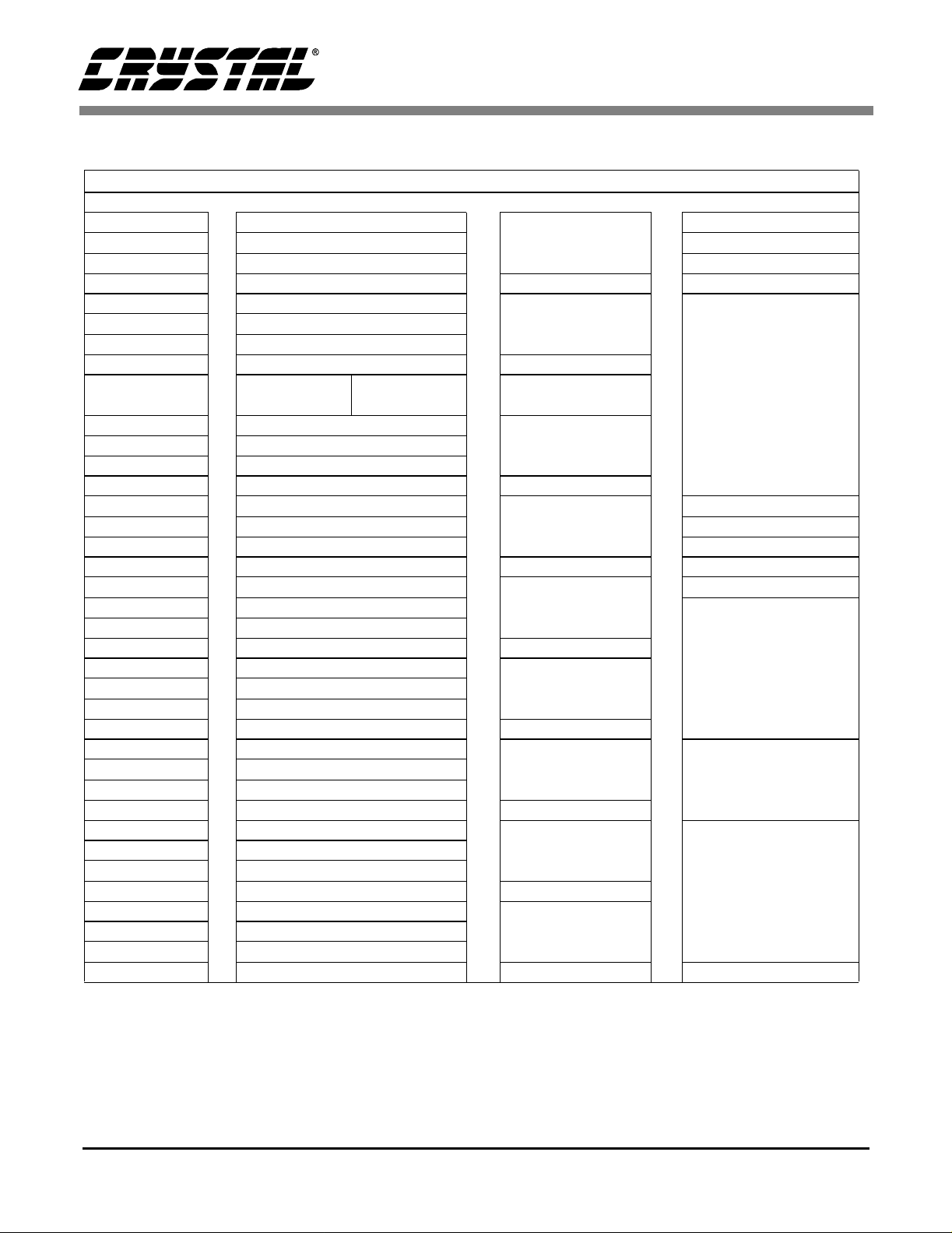
Master Reset Register (00h)
76543210
res res res res res res res MR
Reserved W
MR Setting bit MR0 to logic high will initiate a CS7666 master reset equivalent to executing an ex-
ternal reset usi ng the RESET
load of any external EPROM present on the secondary I
cleared.
Status Register (01h)
76543210
res P4BYTE INTERP HIZENB INITACT I2CBUSY NODEV EVNFLD
ReservedRRRRRRR
EVNFLD Logic high indicates even field of interline-transfer CCD. Logic low indicates odd field of inter-
line-transfe r CCD. This bit provides a course means of synchronizing to the fi eld rate.
NODEV Logic high indicate s that the addressed slave dev ice on the s econdary I
I2CBUSY Logic high indicates that the CS7666 secondary I
slave device.
INITACT Logic high indicates the CS7666 master is busy initializing registers from the external I
EPROM on the secondary I
pin. All registers will be pl aced in their def ault state, and the do wn-
2
C bus will be initiated. The bit is self -
2
C bus did not respond .
2
C master is busy accessing the addressed
2
2
C bus (if present).
C
HIZENB Pin 63 status.
INTERP Pin 54 status.
P4BYTE Pin 1 status.
PIN I/O Control (02h)
76543210
res res res res res UV_ENB FIELDOUT PLLOUT
Reserved R/W R/W R/W
PLLOUT Logic high enables the PLL clock output to the CS7615 (pin 51). This pin was a NC on the
CS7665.
FIELDOUT Logic high changes FIELD (pin 62) from an input to an output pin. Default is input.
UV_ENB Logic high replaces FIELD with a U/V clock.
Digital Gain Register (03h)
76543210
res res res DG4 DG3 DG2 DG1 DG0
Reserved R/W
DG[4:0] Controls the di gital gain ap plied to t he Y (Luminanc e) s ignal after the RGB to YCrCb conver ter
block. The range of ga ins are fr om 0 to 31/8 in incr ements of 1/8. A gai n of 0, indicat es no bright-
ness.
DS302PP1 21
Page 22
CS7666
Scaler Control (04 h)
76543210
res res PAL TRUE_7666 CUSTOM MODE2 MODE1 MODE0
Reserved R/W R/W R/W R/W
MODE[2:0] Selects 1 of 8 pre-defined scaling ratios.
CUSTOM When set, scaler uses custom values held i n registers 2Dh-2Fh.
TRUE_7666 When set, pin 54 is ignored and the CS7666 is in native mode. The default is CS7665 compat -
ibility mod e. (p in 54 se le c t s 5 :4 sc a le r.)
PAL Logic 1 selects PAL timing for HREF and VREF. Default is NTSC.
Feature Control Register (05h)
76543210
res res res CHROFF LUMOFF GAMON AWB res
Reserved R/W R/W R/W R/W Reserved
AWB The Automatic White Balance procedure is initiated by pointing to a whit e scene and setting this
bit high. The bit will return a logic high while the AWB procedure is in progress. Setting this bit
low will have no effect. This bit will always be read as a “0” when the AWB is not in progress.
GAMON The gamma correction fr om the gamma ram look up tab le is app lied t o the video si gnal in R-G-
B space when this bi t is set high. The ga mma ram i s a ful ly use r p rogramma ble, 25 6 entry lo ok
up table.
LUMOFF Setting LUMOFF bit high disables the luma peaking filter.
CHROFF Setting the CHROFF bit high disables the chroma low-pass filter for minimizing color aliasing.
22 DS302PP1
Page 23
CS7666
Operational Control Register (06h)
76543210
res ZV INTERL INREF OE POSPIX EBLU OBLU
Reserved R /W R/W R/W R/W R/W R/W R/W
OBLU Logic high causes the fi rst line after VREF of the odd field to be processed as a BLUE l ine. Logic
low causes the first line of the odd field to be processed as a RED line.
EBLU Logic high causes the first line after VREF of the even field to be processed as a BLUE line.
Logic low causes the first line of the even field to be processed as a RED line.
POSPIX Logic “1” causes the first pixel of the first line to be treated as a positive pixel in the color sep-
aration block. Logic “0” caus es the fi rst pi xel to be treat ed as a negative pi xel. Try t oggling this
bit if the colors appear “reversed”.
OE The Output Enable Bit opera tes in conjunc ti on with the ext ernal Output Enabl e Pin, as illu str at-
ed in Table 15.
OE Bit OE Pin Digital
Outputs
0 0 Enabled
0 1 High-Z
1 0 High-Z
1 1 Enabled
Table 15. OE Pin and Bit Operation
INREF Logic “1” causes CS7666 to accept HREF input and VREF input pins as the reference inputs
signals. EAV and SAV codes in the CCD dat a stream are ignor ed. Logic “ 0” causes t he internal
de-formatter to decode and fol low the embedded EAV and SAV codes sent from the CCD digitizer (as with th e CS7615).
INTERL Logic “0” places the digital outputs in interleaved mode with alternate Y and CrCb data on the
DO
DO
ZV A Logic “1” causes VREFOUT
] 10-Bit output. Logic “1” places the digital outputs in parallel mode with Y data on
[A0..A9
] and CrCb on the DO
[A0..A9
pin to output a VSYNC signal compatible with ZV port specifica-
[B0..B9]
outputs.
tions as well as many composite video encoders.
DS302PP1 23
Page 24
CS7666
Operational Cont rol Re gist er II (07h)
76543210
TEST_AA CLIP_OFF H_SFT1 H_SFT0 V_INV H_INV VS_SEL HS_SEL
R/W R/W R/W R/W R/W R/W R/W
HS_SEL Logic 1 causes HSYNC to be output on pin 31. Logic low cau ses HREF (hor izontal bla nk) to be
output on pin 31.
VS_SEL L.ogic 1 causes VSYNC to be output on pin 30. Logic low causes VREF (vertical blank) to be
output on pin 30.
H_INV Logic 1 inverts the polarity of pin 31.
V_INV Logic 1inverts the polarity of pin 30.
H_SFT[1:0] Shifts the the signal on pin 30 from 0 to 3 clock cycles.
CLIP_OFF When set , excludes only 00 and FF from output data. Otherwise ITU BT
TEST_AA This bit is reserved for test purposes and may be set as a 1 or a 0.
Red Balance R eg ist er (08h)
76543210
RB7 RB6 RB5 RB4 RB3 RB2 RB1 RB0
R/W
RB[7:0] The Red Balance register controls the red contribution to the R-Y chrominance signal . W hen
the register v alue is 00h, the red contribution is minimized; when the register value is FFh, the
red contribution is maximized. When the AWB correction is in progress, this register value is
adjusted such that the absolute magnitude of the R-Y signal is minimized.
Blue Balan ce Register (09h)
76543210
BB7 BB6 BB5 BB4 BB3 BB2 BB1 BB0
R/W
BB[7:0] The Blue Balance register controls the blue contribution to the B-Y chrominance signal. When
the register value is 00h, the blue contri bution is mini mized; when the register value is FFh, the
blue contribution is maximized. When the AWB correction is in progress, this regi ster value is
adjusted such that the absolute magnitude of the B-Y signal is minimized.
Red Saturati on Register (0Ah)
76543210
RS7 RS6 RS5 RS4 RS3 RS2 RS1 RS0
R/W
RS[7:0] The Red Sa turation register value cont rols the amplitude o f the R-Y c hrominance si gnal. When
the register value is 00h, the amplitude of the R-Y is minimized ; when the reg ister value is FFh,
the amplitude of the R-Y is maximized.
24 DS302PP1
Page 25

CS7666
Blue Saturatio n Register (0Bh)
76543210
BS7 BS6 BS5 BS4 BS3 BS2 BS1 BS0
R/W
BS[7:0] The Blue Saturation reg ister value controls t he amplitude of the B-Y chr ominance signal. When
the register value is 00h, the amplitude of the B-Y is minimize d; when the regist er value is FFh,
the amplitude of the B-Y is maximized.
Gamma Correction Register (0Ch)
Writing to the gamma register (0Ch) selects the R, G, and/o r B ram. Continuing data writes without sending a stop
bit after the register write results in writes to the ram locations starting with 00h a nd continuing to FFh. Reads f rom
register 0Ch function in a similar way. NOTE: All three gamma rams may be selected for simultaneous writes, but
read should be done one ram table at a time.
76543210
GC7 GC6 GC5 GC4 GC3 GC2 GC1 GC0
R/W
GC0 Logic “1” selects BLUE gamma ram for subsequent access.
GC1 Logic “1” selects GREEN gamma ram for subsequent ram access.
GC2 Logic “1” selects RED gamma ram for subsequent ram access.
GC[0:7] Provide R/W access to ram after gamma ram table has been selected.
Test Control A Register (0Eh)
This register is reserved
Test Control B Register (0Fh)
This register is reserved.
YR Coefficient Register (10h)
76543210
YR7 YR6 YR5 YR4 YR3 YR2 YR1 YR0
R/W
Color separation and color space conversion coefficient.
CrR Coefficient Register (11h)
76543210
CrR7 CrR6 CrR5 CrR4 CrR3 CrR2 CrR1 CrR0
R/W
Color separation and color space conversion coefficient.
DS302PP1 25
Page 26

CS7666
CbR Coeffi cient Regis t er (12h)
76543210
CbR7 CbR6 CbR5 CbR4 CbR3 CbR2 CbR1 CbR0
R/W
Color separation and color space conversion coefficient.
YG Coefficien t Re gi ster (13h)
76543210
YG7 YG6 YG5 YG4 YG3 YG2 YG1 YG0
R/W
Color separation and color space conversion coefficient.
CrG Coeffi cient Register (14h)
76543210
CrG7 CrG6 CrG5 CrG4 CrG3 CrG2 CrG1 CrG0
R/W
Color separation and color space conversion coefficient.
CbG Coefficient Register (15h)
76543210
CbG7 CbG6 CbG5 CbG4 CbG3 CbG2 CbG1 CbG0
R/W
Color separation and color space conversion coefficient.
YB Coefficient Register (16h)
76543210
YB7 YB6 YB5 YB4 YB3 YB2 YB1 YB0
R/W
Color separation and color space conversion coefficient.
CrB Coefficient Register (17h)
76543210
CrB7 CrB6 CrB5 CrB4 CrB3 CrB2 CrB1 CrB0
R/W
Color separation and color space conversion coefficient.
26 DS302PP1
Page 27
CS7666
CbB Coeffi cient Regis t er (18h)
76543210
CbB7 CbB6 CbB5 CbB4 CbB3 CbB2 CbB1 CbB0
R/W
Color separation and color space conversion coefficient.
Slave Data Hold Re gi ster (19h)
When an external I2C controller initi ates a register read from a slave devic e on the secondary I2C bus through
CS7666, the return ed data is placed in this register. The external controller may then read the data from the Slave
Data Hold register. This register is read only.
EPROM Count Low Byte Register (1Ah)
Lower byte of the number of triple- bytes to be read from EPROM upon reset of CS7666. This register is read only.
EPROM C ount High Byte Registe r ( 1Bh)
Upper byte of the number of triple-bytes to be read from EPROM upon reset of CS7666. This register is read only.
Version (Major) Re gist er (1Ch)
The major version regist er (device ID) in the CS7666 is assigned the value FEh. This register is read only.
Version (Minor) Re gist er (1Dh)
The minor version register in CS7666 rev A. is assigned the value 00h. With each minor revision the value is increased by 1. This register is read only.
Low Power Register (20h)
76543210
res res res res res res res PD
Reserved R/W
PD Setting bi t PD to “1” will place the CS7666 in low power mode.
Test Enable Register (21h )
This register is reserved.
Reserved Regi ster (22h)
This register is res erved and returns a valud of 00 when read.
Test_AA1 (23h)
This register is res erved and must be set to FFh for normal operation.
Test_AA2 (24h)
This register is res erved and must be set to FFh for normal operation
DS302PP1 27
Page 28

CS7666
Test_AA3 (25h)
This register is res erved and must be set to FFh for normal operation
Test_AA4 (26h)
This register is res erved and must be set to FFh for normal operation
Flare Control 1 (27h)
76543210
Y_THR9 Y_THR8 Y_THR7 Y_THR6 Y_THR5 Y_THR4 Y_THR3 Y_THR2
R/W
Y_THR[9:2] Flare control filter Y threshold bits 9-2 (MSB). (Bits 1 and 0 set to 0.)
Flare Control 2 (28h)
76543210
Cr_L9 Cr_L8 Cr_L7 Cr_L6 Cr_L5 Cr_L4 Cr_L3 Cr_L2
R/W
Cr_L[9:2] Flare control filt er Cr low threshold bits 9-2 (MSB).
Flare Control 3 (29h)
76543210
Cb_L9 Cb_L8 Cb_L7 Cb_L6 Cb_L5 Cb_L4 Cb_L3 Cb_L2
R/W
Cb_L[9:2] Flare control filter Cb low threshold bits 9-2 (MSB). (Bits 1 and 0 set to 0.)
Flare Control 4 (2Ah)
76543210
Cr_H9 Cr_H Cr_H7 Cr_H6 Cr_H5 Cr_H4 Cr_H3 Cr_H2
R/W
Cr_H[9:2] Flar e control filter Cr high threshol d bits 9-2 (MSB).
Flare Control 5 (2Bh)
76543210
Cb_H9 Cb_H8 Cb_H7 Cb_H6 Cb_H5 Cb_H4 Cb_H3 Cb_H2
R/W
Cb_H[9:2] Flare control filter Cb high threshol d bits 9-2 (MSB). (Bits 1 and 0 set to 0.)
28 DS302PP1
Page 29

CS7666
Flare Control 6 (2Ch)
76543210
Cb_H1 Cb_H0 Cr_H1 Cr_H0 Cb_L1 Cb_L0 Cr_L1 Cr_L0
R/W R/W R/W R/W
Cr_L[1:0] Flare control filt er Cr low threshold bits 1 and 0.
Cb_L[1:0] Flare control filt er Cb low threshold bits 1 and 0.
Cr_H[1:0] Flar e control filter Cr high threshol d bits 1 and 0.
Cb_H[1:0] Flare control filter Cb high threshold bits 1 and 0.
Scaler Control 1 (2Dh )
76543210
BYPASS1 BYPASS0 res PLL_M4 PLL_M3 PLL_M2 PLL_M1 PLL_M0
R/W Reserved R/W
PLL_M[4:0] This is the PLL M value when the CUSTOM bit (bit 3 register 04h) is set.
BYPASS[1:0] See PLL section.
Scaler Control 2 (2Eh)
76543210
HALF res res PLL_N4 PLL_N3 PLL_N2 PLL_N1 PLL_N0
R/W Reserved R/W
PLL_N[4:0] This is the PLL N value when the CUSTOM bit (bit 3 register 04h) is set.
HALF Sets the internal PLL reference clock to 1/2 the input clock.
Scaler Control 3 (2Fh)
76543210
OFFSET7 OFFSET6 OFFSET5 OFFSET4 OFFSET3 OFFSET2 OFFSET1 OFFSET0
R/W
OFFSET[7:0] Thi s value controls the offset fo the int ernal Scaler.
Configuration Control 0 (30h)
76543210
res res res res res SKP010 SKP09 SKP08
Reserved R/W
This register co ntains the 3 MSBs of t he EEPROM address used when the SKIP bit is se t (bit1 r egister 42h) and t he
Configuration Index Register (43h) is set to 00h.
DS302PP1 29
Page 30

CS7666
Configuration Control 1 (31h)
76543210
SKP07 SKP06 SKP05 SKP04 SKP03 SKP02 SKP01 SKP00
R/W
This register contain s the 8 LSBs of the EEPROM start address used when the SKIP bit i s set (bit1 register 42h) and
the Configuration Index Register (43h) is set to 00h.
Configuration Control 2 (32h)
76543210
res res res res res SKP110 SKP19 SKP18
Reserved R/W
This register co ntains the 3 MSBs of t he EEPROM address used when the SKIP bit is se t (bit1 r egister 42h) and t he
Configuration Index Register (43h) is set to 01h.
Configuration Control 3 (33h)
76543210
SKP17 SKP16 SKP15 SKP14 SKP13 SKP12 SKP11 SKP10
R/W
This register contain s the 8 LSBs of the EEPROM start address used when the SKIP bit i s set (bit1 register 42h) and
the Configuration Index Register (43h) is set to 01h.
Configuration Control 4 (34h)
76543210
res res res res res SKP210 SKP29 SKP28
Reserved R/W
This register co ntains the 3 MSBs of t he EEPROM address used when the SKIP bit is se t (bit1 r egister 42h) and t he
Configuration Index Register (43h) is set to 02h.
Configuration Control 5 (35h)
76543210
SKP27 SKP26 SKP25 SKP24 SKP23 SKP22 SKP21 SKP20
R/W
This register contain s the 8 LSBs of the EEPROM start address used when the SKIP bit i s set (bit1 register 42h) and
the Configuration Index Register (43h) is set to 02h.
Configuration Control 6 (36h)
76543210
res res res res res SKP310 SKP39 SKP38
Reserved R/W
This register co ntains the 3 MSBs of t he EEPROM address used when the SKIP bit is se t (bit1 r egister 42h) and t he
Configuration Index Register (43h) is set to 03h.
30 DS302PP1
Page 31

CS7666
Configuration Control 7 (37h)
76543210
SKP37 SKP36 SKP35 SKP34 SKP33 SKP32 SKP31 SKP30
R/W
This register contain s the 8 LSBs of the EEPROM start address used when the SKIP bit i s set (bit1 register 42h) and
the Configuration Index Register (43h) is set to 03h.
Configuration Control 8 (38h)
76543210
res res res res res SKP410 SKP49 SKP48
Reserved R/W
This register co ntains the 3 MSBs of t he EEPROM address used when the SKIP bit is se t (bit1 r egister 42h) and t he
Configuration Index Register (43h) is set to 04h.
Configuration Control 9 (39h)
76543210
SKP47 SKP46 SKP45 SKP44 SKP43 SKP42 SKP41 SKP40
R/W
This register contain s the 8 LSBs of the EEPROM start address used when the SKIP bit i s set (bit1 register 42h) and
the Configuration Index Register (43h) is set to 04h.
Configurati on Control 10 (3Ah)
76543210
res res res res res SKP510 SKP59 SKP58
Reserved R/W
This register co ntains the 3 MSBs of t he EEPROM address used when the SKIP bit is se t (bit1 r egister 42h) and t he
Configuration Index Register (43h) is set to 05h.
Configurati on Control 11 (3Bh)
76543210
SKP57 SKP56 SKP55 SKP54 SKP53 SKP52 SKP51 SKP50
R/W
This register contain s the 8 LSBs of the EEPROM start address used when the SKIP bit i s set (bit1 register 42h) and
the Configuration Index Register (43h) is set to 05h.
Configurati on Control 12 (3Ch)
76543210
res res res res res SKP610 SKP69 SKP68
Reserved R/W
This register co ntains the 3 MSBs of t he EEPROM address used when the SKIP bit is se t (bit1 r egister 42h) and t he
Configuration Index Register (43h) is set to 06h.
DS302PP1 31
Page 32
CS7666
Configuration Control 13 (3Dh)
76543210
SKP67 SKP66 SKP65 SKP64 SKP63 SKP62 SKP61 SKP60
R/W
This register contain s the 8 LSBs of the EEPROM start address used when the SKIP bit i s set (bit1 register 42h) and
the Configuration Index Register (43h) is set to 06h.
Configurati on Control 14 (3Eh)
76543210
res res res res res SKP710 SKP79 SKP78
Reserved R/W
This register co ntains the 3 MSBs of t he EEPROM address used when the SKIP bit is se t (bit1 r egister 42h) and t he
Configuration Index Register (43h) is set to 07h.
Configurati on Control 15 (3Fh)
76543210
SKP77 SKP76 SKP75 SKP74 SKP73 SKP72 SKP71 SKP70
R/W
This register contain s the 8 LSBs of the EEPROM start address used when the SKIP bit i s set (bit1 register 42h) and
the Configuration Index Register (43h) is set to 07h.
Jump Control 0 (40 h)
76543210
res res res res res JMP10 JMP9 JPM8
Reserved R/W
This register contains the 3 MSBs of the EEPROM address used when the JUMP bit is set (bit2 register 42h).
Jump Control 1 (41 h)
76543210
JMP7 JMP6 JMP5 JMP4 JMP3 JMP2 JM P1 JPM0
R/W
This register contains the 8 LSBs of the EEPROM start address used when the JUMP bit is set (bit2 register 42h).
32 DS302PP1
Page 33
CS7666
EEPROM Control (42h)
76543210
res res res res res JUMP SKIP HALT
R/W
State machine commands for loading EEPROM data after reset. (see extended EPROM configuration)
HALT Writing a 1 to this bit stops the readi ng of EEPROM data.
SKIP Writing a 1 to this bit forces the next EEPROM read cycle to occur at the address held i n the
Configuration Control (n) regi ster, where "n" is the value h eld in the Configuration Index Re gister (43h)
JUMP Writing a 1 to this bit forc es t he next EEPROM acce ss t o occur at the addr ess held i n re gister s
40h and 40h.
Configurati on Index Register (43h)
76543210
res res res res res SW2 SW1 SW0
Reserved R/W
This contains the DIP switch s tatus at reset. (se e extended EPROM conf igurati on) The val ue of thi s regist er select s
the appropriate Configuration register when the SKIP command is executed.
Reserved Registers (44h - FEh)
These registers are reserved and return a value of 00h when read.
Station Address Register (FFh)
76543210
res SA6 SA5 SA4 SA3 SA2 SA1 SA0
Reserved R/W
CS7666 station address, 7 MSBs (the LSB of the complete 8-bit station address is determined by the LSB which
acts as a read/write dir ection bit).
DS302PP1 33
Page 34

PIN DESCRIPTIONS
CS7666
GND
VDD
CLKOUT
TESTPINB
TRANSP
FIELD
OE
SCANENABLE
4BYTEMODE
DOA9(MSB)
DOA8
DOA7
DOA6
DOA5
DOA4
DOA3
DOA2
GND
VDD
DOA1
DOA0(LSB)
DOB9(MSB)
DOB8
DOB7
DOB6
DOB5
DOB4
DOB3
GND
VDD
DOB2
DOB1
63 61 59 57 55 53 51 49
64 62 60 58 56 54 52 50
1
2
3
4
5
6
7
8
9
10
11
12
13
14
15
16
17 19 21 23 25 27 29 31
18 20 22 24 26 28 30 32
64-pin TQFP
Top View
CLKIN2X
CLKIN
INTERP
SCANMODE
XTAL_OUT
CLK_GRG
GND
ISET
SCLSEC
SDASEC
48
47
46
45
44
43
42
41
40
39
38
37
36
35
34
33
DI0(LSB)
DI1
DI2
DI3
DI4
VDD
GND
DI5
DI6
DI7
DI8
DI9(MSB)
RESET
VREFIN
HREFIN
VREFOUT
HREFOUT
SCL
SDA
GND
VDD
DOB0(LSB)
Power Supply Connection
VDD - Power Supply, PINS 11, 22 , 26, 41, 58.
Positive digital supplies. Nominally +5 volts.
Pin 58 is an analog supply pin used for the internal PLL but may be connected to the digital
supply pins under m ost circumsta nces.
GND - Digital Ground, PINS 10, 21, 27, 40, 50, 57.
Digital ground suppl ies.
Pin 57 is an analog ground pin used for the internal PLL but may be connected to the digital
ground pins und er most circum stances.
34 DS302PP1
Page 35

Input Data and Clocks
DI[9:0] - Digital Mosaic Inputs.
CMOS level m osaic code d CCD input da ta from CCD d igitizer
CLKIN - Mosaic Input Data Clock, PIN 55.
Main system input clock, used to strobe incoming digital CCD mosaic data. The CLKIN
frequency is the mosaic in put data ra te.
CLKIN2X - Mosaic Input Data Interpolation Clock, PIN 56.
Mosaic input data interpolation clock or crystal oscillator input. Twice the CLKIN input in
CS7665 compatibility mode (non-interpolated output data ... see INTERP description). Twice
the 5/4 output rate clock when internal 5 to 4 horizontal data rate scaler is in operation
(CS7665 com patibility m ode.) In CS7 666 native mode, thi s pin operate s as the cryst al oscillato r
input pin. The required c rystal frequency is 2 X (SCALER R ATIO) X (INPUT DATA RATE).
For example a 512x492 pixel imager running at 9.818 MHz and scaled by a factor of 5:4
would require 2 X (5/4 ) X (9.818) = 24 .54 MHz.
CS7666
CLK_GRG - CCD Sample Clock, PIN 51.
This clock is sca led by th e interna l PLL an d is equa l to the CLKIN2X frequen cy divid ed by the
scaling ratio . This clock i s intended t o connect t o the CS761 5 master cloc k pin (pin 32).
XTAL_OUT – Crystal oscillator output , PIN 52.
When using the internal crystal oscillator, connect the external crystal to the XTAL_OUT and
CLKIN2X pins.
HREFIN - Horizontal Input Timing Ref erence, PIN 32.
Active low horizontal input timing reference. Used to synchronize the output timing signals
with the incoming mosaic data and timing. When used with CCD digitizers like the CS7615
which imbed t he necessary timing sign als in the data stream, the HREFIN signal i s not nee ded.
VREFIN - Vertical Input Timing Reference , PIN 33.
Active low vert ical input timing referen ce. Used to synchronize the output timing signa ls with
the incom ing mosaic data and timing. When used w ith CCD digitizers like the CS7615 whic h
embed the necessar y timin g signals in the dat a stream, t he VREF IN sign al is not n eeded.
2
I
C Serial Control
SDA - Primary I2C Data Bus, PIN 28.
Primary I
SCL - Primar y I
Primary I
DS302PP1 35
2
C data bus. Used wit h SCL to rea d and write the internal regi ster set.
2
C Clock, PIN 29.
2
C Clock. Used with SDA to read and write the internal register set.
Page 36

SDASEC - Secondary I2C Data Bus, PIN 47.
Secondary I
write I
from the pr imary I
after RESET
2
2
C data bus w ith limi ted bus m asterin g capabi lities. U sed with SCLSE C to read an d
C devices locate d on the secondary bus. Various devices can be isola ted by the CS7666
2
C bus. The CS76 66 will start re ading I2C EPROM devices at addresses A0h
. It will download the EPROM contents into the specified registers inside the
secondary bus devices as well as any CS7666 registers specified in the EPROM entries.
Devices are typically connected to either the primary or the secondary I
two busses may be connected together when system design requires the use of EPROM
initialization while at the same allowing direct access to all the camera devices from the
external I
2
C contr oller.
CS7666
2
C bus. However, the
SCLSEC - Secondary I
Secondary I
write I
2
C devices locate d on the secondary bus. Various devices can be isola ted by the CS7666
from the pr imary I
after RESET
2
C Clock, PIN 48.
2
C clock with limited bus mastering capabilities. Used with SDASEC to read and
2
C bus. The CS76 66 will start re ading I2C EPROM devices at addresses A0h
, and dow nload the EPR OM contents into the spe cified second ary bus regist ers, as
well as any C S7666 registers specified in th e EPROM entrie s. Devices are t ypically connect ed
to either the primary or the secondary I
together when system des ign requ ires the use of EPROM initialization whi le at the same time
allowing direct ac cess to al l the ca mera devi ces from t he externa l I
4BYTEMODE - Four-byte Mode I
2
C Operation Enable, PIN 1.
Places CS7666 in the Four-byte mode for I
Digital Video Outputs and Clocking
DOA[9:0] - "A" Channel Digital Outp ut Bits.
CMOS level 10-bit digital video output channel "A." Either YCrCb interleaved digital video
output data, or Y co mponent digital video data is available at this port according to the state of
bit 5 in register 06h. DOA0(LSB) is the least significant bit of channel "A"; DOA9(MSB) is
the most signif icant bit o f chan nel "A."
2
C bus. However, the two busses may be connected
2
C contr oller.
2
C transactio ns on the primary I2C bus. Active high.
DOB[9:0] - "B" Channe l Digital Output B its.
CMOS level 10-bit digital video output channel "B." Either logic "0" in interleaved digital
video output data mode, or CrCb component digital video data is available at this port
according to t he state of bit 5 in register 06 h. DOB0(LSB) is t he least signif icant bit o f channel
"B;" DOB 9(MSB) is the most s ignificant bit of ch annel "B ."
36 DS302PP1
Page 37

CLKOUT - Digita l Output Data Clock, PIN 59.
Digital output clock for both channel "A" and channel "B." Output data transitions on the
falling edge of CLKOUT a nd can be latched on the rising edge. In the non-interleaved output
mode, the CLKOUT rate is equal to the input mosaic pixel rate multipli ed by the scaling ratio
currently in use with Y data avai lable on channel "A" and C rCb output data on Ch annel " B." In
interleaved output mode, the CLKOUT rate is equal to twice
multiplied by the cu rrent scali ng ratio with Y a nd CrCb out put data av ailable o n Channe l "A".
CS7666
the input mosaic pixel rate
Output Mode Mosaic
Data Rate
Interleaved, scal er disabled 9.818 MHz 9.818 MHz 19.63 MHz YcrCb logi c "0” 19.63 MHz 512
Interleaved, scal er enabled 9.818 MHz 9.818 MHz 24.54 MHz YcrCb logic "0” 24.54 MHz 640
Parallel, scaler disabled 9.818 MHz 9.818 MHz 19.63 MHz Y CrCb 9.818 MHz 512
Parallel, scaler enabled 9.818 MHz 9.818 MHz 24.54 MHz Y CrCb 12.27 MHz 640
CLKIN CLKIN2 Channel
“A”
Channel
"B”
CLKOUT Horizontal
Pixels
Table 16. Example 51 2x492 Imager Output Options
(4:5 scaling rati o chose n)
INTERP - Digital Video Horizont al Data Rate Sca ler Enable, PIN 54.
CMOS input enabling the internal 4:5 horizontal data rate scaler when the CS7666 is in
CS7665 co mpatibility mod e (default.) Req uires that CLK IN2 be supplied wi th a 5/2 rate cl ock
relative to the CLKIN c lock input w hich is the i ncoming CCD mosaic data . This pin con trol is
active logi c high. This pin is ignored in CS7666 nat ive mode.
HREFOUT - H orizo ntal Ref erence Outpu t, PIN 30 .
CMOS output pro viding HREF, or alternatively HSY NC horizontal b lanking signal .
VREFOUT - Vertical Re ference Ou tput, PIN 31.
CMOS output providing a VREF, or alternatively VSYNC vertical blanking signal.
FIELD - Odd/Even Field Indicator, PIN 62.
CMOS input/output. As an input, the field pin synchronizes the EAV/SAV timing codes
embedded i n the outp ut video datastream . As an output , the FIE LD indica tor change s accordin g
to the embedded EAV/SAV timing codes in the input video datastream or the HREFIN and
VREFIN inputs. Odd fields are indicated with logic low, and even fields are indicated with
logic high. Al ternately, the Field pin ca n be configu red as a U/V cl ock.
OE - Output Enable, PIN 63.
CMOS input used to place a ll output p ins in a High-Z m ode. This co ntrol works i n conjunctio n
with the OE bit (bit 3)in reg ister 06h.
DS302PP1 37
Page 38

Miscellaneous
RESET - Master Ex ternal Reset Control, PIN 34.
CS7666
CMOS input which initiates a complete power-on reset, where all registers are reset to their
defaults, and the secondary I
This pin ope rates in conjun ction with b it 0 of regist er 00h. RESET
ISET – PLL bias , PIN 49.
Connect this pin to a nalog GND (pin 57) thro ugh a 6,000 oh m 1% resistor.
SCANMODE - Test Pin, PIN 53.
Test pin, connect to GND.
TESTPINB - Test Pin, PIN 60.
Test pin, connect to VDD.
TRANSP - Test Pin, PIN 61.
Test pin, connect to VDD.
SCANENABLE - Test Pin, PIN 64.
Test pin, connect to GND.
2
C bus attempts to load any EPROM configuration information.
is an active logic lo w input.
38 DS302PP1
Page 39

DEFINITIONS
Color Space
A color space is a mathematical representation of a set of colors. Three fundamental color
models are RGB (used in color computer g raphics and col or television), YIQ, YU V, or YCrC b
(used in broad cast and tele vision syste ms), and CMYK (used in color printing).
RGB Color Space
The red, green, and blue (RGB) is widely used throughout computer graphics and imaging.
Red, green, and blue are three primary additive colors where the individual components are
added togethe r to form the desired col or.
YUV Color Space
The YUV color spa ce is the basic c olor space used by th e PAL (Phas e Alterna tion Line ), NTSC
(National Television System Committee), and SECAM (Sequential Couleur Avec Memoire or
Sequential C olor with Memory) co mposite color video st andards. The format conveys intensity
in the Y component and color information in the U and V components. In an 8-bit system,
where RGB range from code 0 to code 255, Y has a range of code 0 to code 255. The U
component ra nges over code 0 ± 112 codes, and the V c omponent ranges ove r code 0 ± 157.
CS7666
YCrCb Color Space
The YCrCb color space was developed as part of Recommendation ITU-601 during the
development of a world-wide digital component video standard. YCrCb are scaled and offset
versions of YUV color space. Y is defined to have a nominal r ange of code 16 to c ode 235; Cr
and Cb are de fined to ha ve a rang e of code 16 t o code 240 , with code e qual to the zero leve l.
MYCG Colors
Standard "color" CCD imagers employ integrated filter dots over the individual pixels.
Typically, four color filters ar e used, Magent a, Yellow, Cyan, and Green.
Chroma Block
A group of four adjacent CCD pixel with integrated MYCG filter dots. These four pixels are
generally fo rmed with t wo pixels on o ne horizon tal scan line, and two physically just below on
the next scan line. There can also be some slight horizontal shift of the pixels to smooth the
image. The chroma block is generally proc essed using a "color separa tor" into YUV, YCrCb, or
RGB color spac e before an y image proce ssing.
DS302PP1 39
Page 40
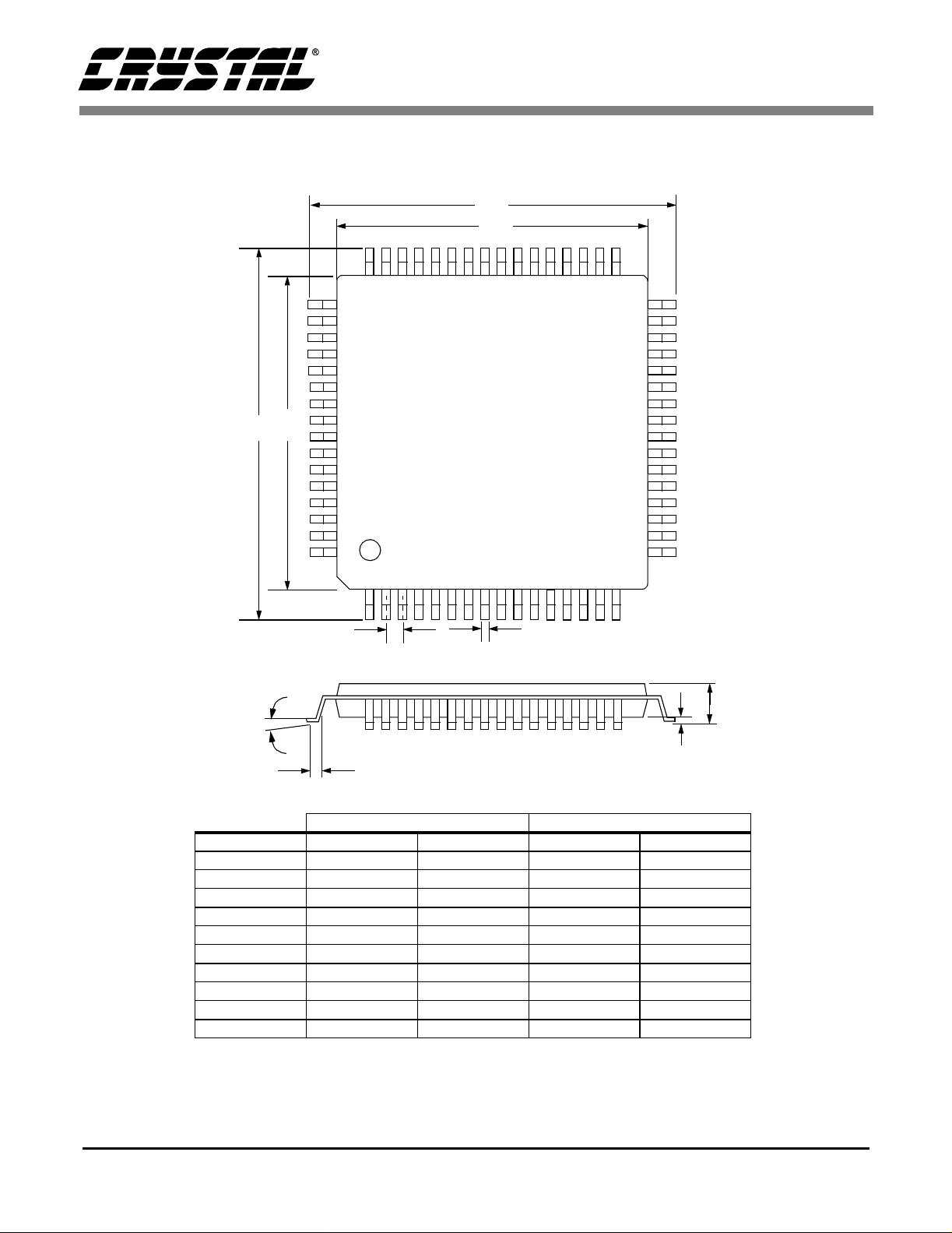
PACKAGE DIMENSIONS
D1
D
CS7666
64L TQFP PACKAGE DRAWING
E
E1
1
e
B
∝
A1
L
INCHES MILLIMETERS
DIM MIN MAX MIN MAX
A 0.000 0.063 0.00 1.60
A1 0.002 0.006 0.05 0.15
B 0.007 0.011 0.17 0.27
D 0.461 0.484 11.70 12.30
D1 0.390 0.398 9.90 10.10
E 0.461 0.484 11.70 12.30
E1 0.390 0.398 9.90 10.10
e 0.016 0.024 0.40 0.60
L 0.018 0.030 0.45 0.75
∝ 0.000 7.000 0.00 7.00
A
40 DS302PP1
Page 41

• Notes •
Page 42

 Loading...