

Page 1
CS7654
CCD Color-Space Processor with Analog Output
Features
l ITU-601 Compliant Image Formatting
l ITU-656 and SMPT E-125/M Transport s
2
l I
C Control Interface
l Limited Secondary I
l Automatic White Balance
l Programmable Gamma Correction
l Programmable Interpolation
l Programmable Luma Gain and Saturation
Control
l Fully Programmable Color Separation Matrix
Coefficients
l Supports up to 1440, active pixels per line,
with no limitation on Vertical Size
l Programmable "Chroma Kill" circ uit
l Highly integrated for low part count camer as
l Three DACs providing simultaneous composite,
S-video outputs
l Multi-standard su pport for N TSC-M, NTS C-
JAPAN, PAL (B, D, G, H, I, M, N, Combinatio n N)
l On-chip voltage r eference generator m odes, tri-
state DACs and p ower down mode.
2
C Bus Master
Description
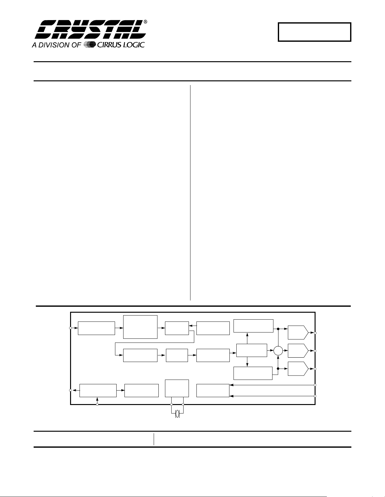
The CS7654 is a low-power Digital Color-Space Processor for CCD cameras. It provides all the necessary digital
image processing for sta nda rd four- color in terline tr ansfer CCD imagers. The CS 765 4 p roce sses t he mag enta ,
yellow, cyan, and green (MYCG) CCD imager data int o
YCrCb formatted c omponent digital video a nd into a nalog PAL or NTSC. Internal processing includes color
separation, autom atic white balance, user p rogrammable gamma correction, programmable scaling
(interpolation), digital output formatting and encoding
function for analo g outp ut. Al so, a speci al " Chroma Kill"
circuit eliminates false colors during saturation. Video
output can be formatted to be compatible with NTSC-M,
NTSC-J, PAL-B,D,G,H,I,M,N, and Combination N systems. Closed Caption is suppo rted in NTSC. Three 10bit DACs provide two channels for an S-Video output
port and one composite video outputs.A High-speed I
compatible control interface is provided for in system design.
A general purpose I/O port is als o av aila ble to he lp c onserve valuable b oard space and to pro vide up to eight
“boot” configurations.The CS7654 is designed to work
directly with the CS7615 CCD Imager Analog Processor.
ORDERING INFORMATION
CS7654-KQ 0° to 70° C 64-pin TQFP
(10 mm x 10 mm x 1.4 mm)
I
2
C
CCD
MOSAIC
DATA
SECONDARY
2
C BUS
I
DEFORMATTER
I2C INTERFACE
PRIMARY
I2C BUS
COLOR
SEPARATION
AND
ANITALIASING
GAMMA
CORRECTION
REGISTER
BLOCK
Preliminary Product Information
Cirrus Logic, Inc.
P.O. Box 17847, Austin, Texas 78760
(512) 445 7222 FAX: (512) 445 7581
http://www.crystal.com
WHITE
BALANCE
SCALER
PLL AND
CLOCK
DRIVER
XTAL
AWB
CONTROL
OUTPUT
FORMATTER
EXTERNAL
TIMING
INTERPOLATION
AND FILTER
CHROMA
VIDEO
FORMATTER
LUMA
INTERPOLATION
AND DELAY
10-BIT
DAC
10-BIT
Σ
DAC
10-BIT
DAC
CHROMA
COMPOSITE
LUMA
VREF/
VSYNC
HREF/
HSYNC
This document contains information for a new product.
Cirrus Logic reserves the right to modify this product without notice.
Copyright Cirrus Logic, Inc. 1998
(All Rights Reserved)
DS330PP2
MAY ‘99
1
Page 2

TABLE OF CONTENTS
CHARACTERISTICS/SPECIFICATIONS.............................. ...... ....... ...... ....... .... 4
DIGITAL CHARACTERISTICS....................................................................4
SWITCHING CHARACTERISTICS ........................................................ ..... 4
POWER CONSUMPTION ..... ....... ...... ....... ...... ...... ....... ............................... 5
POWER CONSUMPTION ..... ....... ...... ....... ...... ...... ....... ............................... 6
CONTROL PORT CHARACTERISTICS ..................................................... 6
RECOMMENDED OPERATING CHARACTERISTICS...............................7
ABSOLUTE MAXIMUM RATINGS.............................................................. 7
GENERAL DESCRIPTION .................................................................................. 8
Overview ......................... ................................ ................................ ............ 8
Digital Output Formats ..............................................................................11
Internal Horizontal Scaler ......................................................................... 11
CLKIN2X Input Timing ..............................................................................12
CLKOUT_GRG ..................... .......................................................... .......... 12
INTERN.AL PROCESSING ............................................................................... 13
Input Data Format and Chroma Separator ............................................... 13
White Balance and Gamma Correction ....................................................13
Chroma Kill ...............................................................................................13
Internal Filters ...........................................................................................14
Analog Video Timing Generator ...............................................................14
Color Subcarrier Synthesizer ....................................................................14
Chroma Path ............................................................................................. 14
Luma Path ................................................................................................14
Digital to Analog Converters .....................................................................15
Voltage Reference ....................................................................................15
Current Reference ................ ....... ...... ....... ...... ...... ....... ...... ....... ...... ..........15
Closed Caption Insertion .......................................................................... 15
Control Registers ......................................................................................16
Testability .................................................................................................. 16
OPERATIONAL DESCRIPTION ........................................................................ 16
Reset Hierarchy . ...... ....... ...... ....... ...... ....... ...... .......................................... 16
Vertical Timing ............................................................ ....... ...... ....... ... 16
NTSC Interlaced .................................................................................17
PAL Interlaced ....................................................................................18
Progressive Scan ............................................................................... 18
Digital Video Input Modes ......................................................................... 18
Multi-standard Output Format Modes .......................................................20
Subcarrier Generation ..............................................................................20
Color Bar Generator .................................................................................20
Super White/Super Black support ............................................................. 21
FILTER RESPONSES ................................................................................ 23
CS7654
Preliminary produc t informat ion des cribes p roducts w hich are in product ion, but for which f ull char acteriz ation dat a is not yet avai lable. Adv anced
product inf ormat ion des crib es pro ducts wh ich ar e in deve lopmen t and s ubjec t to deve lopmen t cha nges. Ci rrus Lo gic, I nc. has made be st ef forts
to ensure t ha t the informat ion contained i n this document is accurate and reliabl e. H ow ev er, the infor m at i on is subject t o c hange without no t i c e
and is provid ed “AS IS” without warranty of any k i nd (express or im plied). No responsibility is assume d by Cirrus Logic , Inc. for the use of this
information, no r for in fringe ments of pate nts or other rights of third partie s. This d ocume nt is t he prop erty of Cirrus Logic , Inc. and implies no
license unde r pat ents , co pyr ight s, t rade mar ks, or tra de secr ets. N o part of t his pu bl icat io n may be copi ed, repr oduc ed, sto red i n a retrieval system, or trans m it ted, in any form or by any mean s (electronic, mec hanical, photographic, or otherwise). Furthermore, no part of this publication
may be used as a basis for manufacture or sale of any items without the prior written consent of Cirrus Logic, Inc. The names of products of
Cirrus Logic, Inc. or other vendors and suppliers appearing in this document may be trademarks or service marks of their respective owners
which may be registered in some jurisdictions. A list of Cirrus Logic, Inc. trademarks and service marks can be found at http://www.cirrus.com.
2
Page 3

INTERNAL REGISTER STRUCTURE AND USER INTERFACE ..................... 25
Operating CS7654 in Normal I2C Configuration (Three-Byte Mode) ....... 25
Station Address .................................................................................. 25
Write Operations in Three-Byte Mode ............................................... 25
Address Set Operation ....................................................................... 26
Read Operations in Three-Byte Mode ............................................ ... 2 6
Operating CS7654 in Four-Byte I2C Configuration ............................ 26
Write Operations in Four-Byte mode ................................................. 26
Read Operations in Four-Byte Mode ....................................... ....... ... 27
Initializing Slave Devices on Secondary I2C bus from an EPROM .......... 27
Controlling the Configuration Process ...................................................... 28
Reserved Registers and Test Pins ........................................................... 29
General Purpose I/O Port ......................................................................... 29
ANALOG ........................... ....... ...... ....... ...... ....... ...... ...... .................................... 30
Analog Timing .......................................................................................... 30
VREF .............................. ................................................... ....................... 30
ISET-DAC ....................... ............. ................... ................... .................... ... 30
DACs ........................................................................................................ 30
Luminance DAC ................................................................................. 30
Chrominance DAC ............................................................................. 31
COMP_VID DAC ................................................................................ 31
REGISTER DESCRIPTION ............................................................................... 32
BOARD DESIGN AND LAYOUT CONSIDERATIONS ..................................... 53
Power and Ground Planes ....................................................................... 53
Power Supply Decoupling ........................................................................ 53
Digital Interconnect ................................................................................... 53
Analog Interconnect ................................................................................. 53
Analog Output Protection ......................................................................... 54
ESD and Latch up Protection ................................................................... 54
External DAC Output Filter ....................................................................... 54
PIN DESCRIPTIONS ......................................................................................... 55
PACKAGE DIMENSIONS ................................................................................. 60
CS7654
3
Page 4
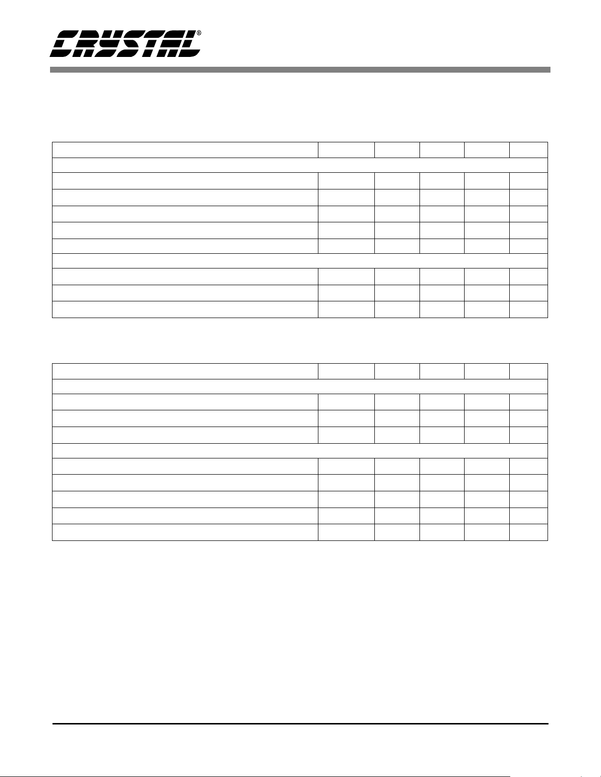
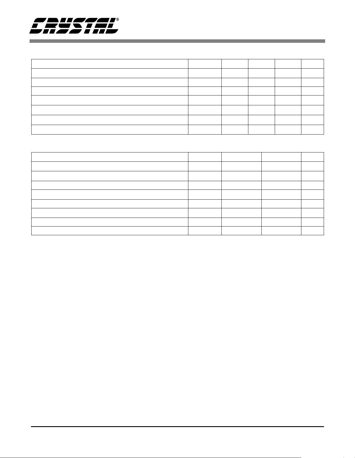
CHARACTERISTICS/SPECIFICATIONS
CS7654
DIGITAL CHARACTERISTICS (T
1 = V
DD
.)
= 25 °C; VDD = 5 V; CL = 30 pF; Input Levels: logic 0 = 0 V, logic
A
Parameter Symbol Min Typ Max Unit
Logic Inputs
High-Level Input Voltage V
Low-Level Input Volt age V
Input Leakage Current I
Input Pin Capacitance C
IH
IL
IN
DI
VDD - 0.8 - - V
--0.8V
- - 10.0 µA
-10-pF
Input Clamp Voltage - -0.7 - V
Logic Outputs
High-Level Output Source Current @ IOH = 1mA V
Low-Level Output Sink Current @ I
= 1mA V
OL
High-Z Leakage Current I
SWITCHING CHARACTERISTICS (T
logic 1 = V
DD
.)
= 25 °C; VDD = 5 V; CL = 30 pF; Input Levels: logic 0 = 0 V,
A
OH
OL
Z
VDD - 0.4 - - V
0.4 - - V
- - 10.0 µA
Parameter Symbol Min Typ Max Unit
Digital Input
CLKIN2X Frequency Range f
Input Data setup time, DI[9:0] t
Input Data hold time, DI[9:0] t
CLK2X
S1
H1
-2730MHz
5--ns
5--ns
Digital Output
Channel A/B Digital Data Output Clock Interleaved Data
Channel A/B Output Hold Time t
Channel A/B Output Propagation Delay t
Digital Output Rise Time with 30 pF load t
Digital Output Fall Time with 30 pF load t
f
CLKOUT_GRG
OH
PD
R
F
--30MHz
-0-ns
-1.95ns
-15-ns
-15-ns
.
Specifications are subject to change without notice
4
Page 5
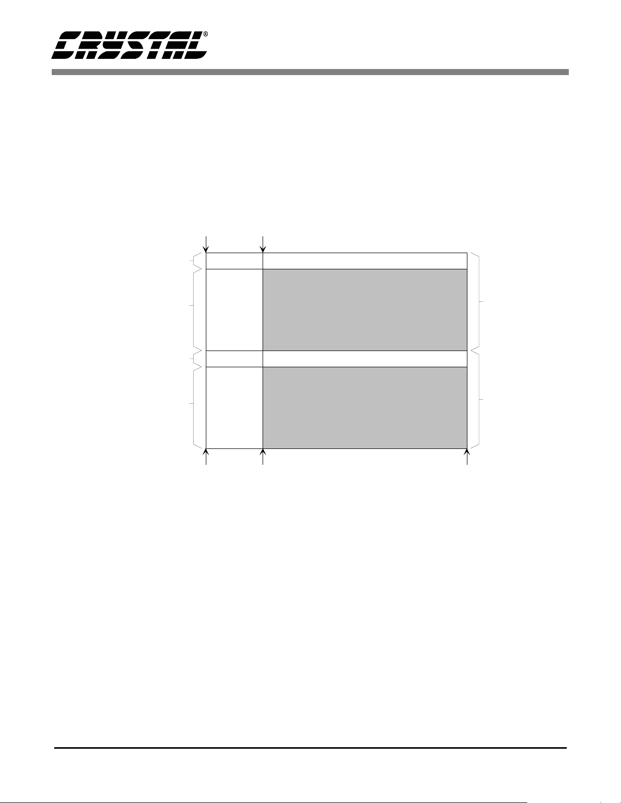
CLKIN2X
CLKIN
Mosaic
Input Data
DI[9:0]
CLKOUT
Output Data
DOA[9:0]
DOB[9:0]
t
H2
t
S2
tH1t
S1
Input Timing Diagram
t
PD
t
OH
Output Timing Diagram
CS7654
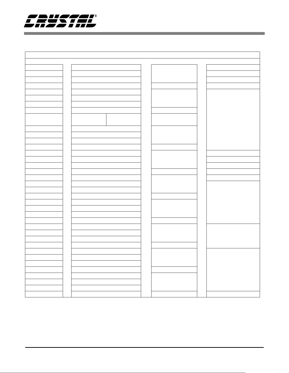
POWER CONSUMPTION (
TA = 25 °C; VDD = 5 V; CL = no load; Input Levels: logic 0 = 0 V, logic 1 = VDD.)
Parameter Symbol Min Typ Max Unit
Power Supply
Supply Voltage VAA 4.75 5.0 5.25 V
Digital Supply Current (Encoder) IAA1 - 70 mA
Analog Supply (Encoder) Low-Z (Note 1) IAA2 - 100 - mA
Power Supply Rejection Ratio PSRR - 0.02 0.05 %/%
Normal Mode I
Low Power Mode I
DD
DD
-150200mA
-716mA
Analog Outputs
Full Scale Output Current COMP_VID/Y/C (Notes 2, 3) IO 32.9 34.7 36.5 mA
Full Scale Output Current COMP_VID/Y/C (Notes 2, 4) IO 8.22 8.68 9.13 mA
LSB Current COMP_VID/Y/C (Notes 2, 3) IB 32.2 33.9 35.7 mA
LSB Current COMP_VID/Y/C (Notes 2, 4) IB 8.04 8.48 8.92 mA
DAC-to DAC Matching MAT - 2 - %
Output Compliance VOC 0 - + 1.4 V
Output Impedance ROUT - 15 - k
Output Capacitance COUT - - 30 pF
DAC Output Delay ODEL - 4 12 nsec
DAC Rise/Fall Time (Note 5) TRF - 2.5 5 nsec
Ω
Notes: 1. Low-Z - 3 dacs on
2. Output current levels with ISET = 4 KΩ , VREF = 1.232 V.
3. DACs are set to low impedance mode
4. DACs are set to high impedance mode
5. Times for black-to-white-level and white-to-black-level transitions.
5
Page 6
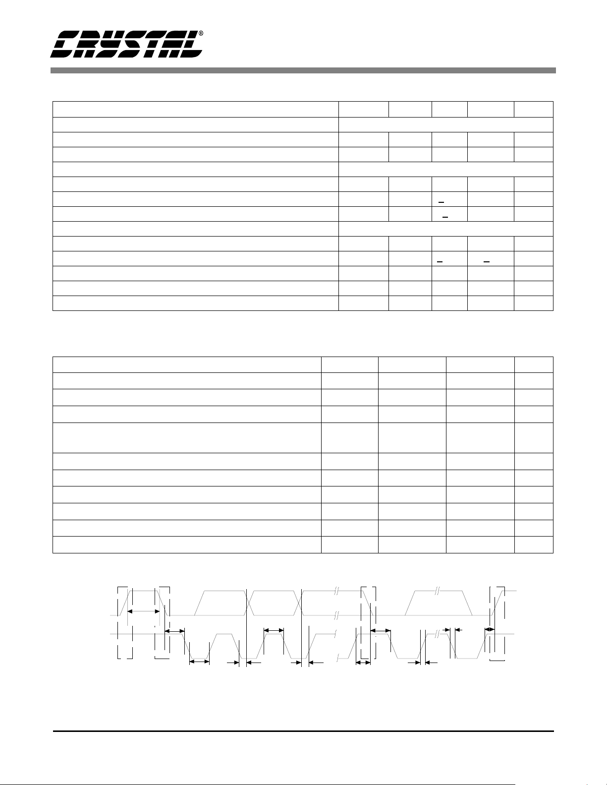
CS7654
POWER CONSUMPTION (Continued)
Parameter Symbol Min Typ Max Units
Voltage Reference
Reference Voltage Output VOV 1.170 1.232 1.294 V
Rreference Input Current UVC - - 10 uA
Static Performance
DAC Resolution - - 10 Bits
Differential Non-Linearity DNL -1 +
Integral Non-Linearity INL - 2 +
Dynamic Performance
Differential Gain DG - 2 5 %
Differential Phase DP - +
Hue Accuracy HA - - 2 deg
Signal to Noise Ratio SNR 70 - - dB
Saturation Accuracy SAT - 1 2 %
0.5 + 1 LSB
1+ 2LSB
0. 5 + 2deg
CONTROL PORT CHARACTERISTICS (T
1 = V
DD
.)
= 25 °C; VDD = 5 V; Input Levels: logic 0 = 0 V, logic
A
Parameter Symbol Min Max Unit
SCL Clock Frequency f
Bus Free Time Between Transmissions t
Start Condition Hold Time t
Clock Pulse Width High
Low
Setup Time for Repeat Start Condition t
SDAIN Hold Time from SCL Falling t
SDAIN Setup Time from SCL Rising t
SDAIN and SCL Rise Time t
SDAIN and SCL Fall Time t
Setup Time for Stop Condition t
Stop Start
SDA
t
buf
CL
S
t
hdst
t
high
SCL
buf
hdst
t
high
t
low
sust
hdd
sud
r
f
susp
Repeated
Start
-400kHz
1.3 - µs
0.6 - µs
0.6
1.3
-
-
µs
µs
0.6 - µs
0-µs
0.1 - µs
-1.0µs
-0.3µs
0.6 - µs
Stop
t
hdst
t
f
t
susp
t
low
t
hdd
t
sud
t
sust
t
r
I2C Timing Diagram
6
Page 7
CS7654
RECOMMENDED OPERATING CHARACTERISTICS
Parameter Symbol Min Typ Max Unit
Power Supply Voltage V
DD
Ground to Ground Voltage Differential - - 10 mV
Digital Input Rise/Fall Time - - 10 ns
CLKIN Level Setup to CLKIN2X Rising (non-interpolated) t
CLKIN Level Hold after CLKIN2X Rising (non-interpolated) t
S2
H2
Digital Input Voltage Range 0 - V
Operating Temperature Range T
A
ABSOLUTE MAXIMUM RATINGS
Parameter Symbol Min Max Unit
Power Supply Voltage V
Digital Input Voltage Range GND - 0.3 V
Forced Digital Output Current - 50 mA
Sustained Digital Output Voltage GND - 0.3 V
Output Short Circuit Current - - mA
Operating Temperature Range T
Lead Solder Temperature (10 s duration) - +260 °C
Storage Temperature Range -65 +160 °C
DD
A
4.5 5.0 5.5 V
8--ns
8--ns
DD
0-70°C
-0.3 6.0 V
+ 0.3 V
DD
+ 0.3 V
DD
070°C
V
WARNING: Operation at or beyond these limits may result in permanent damage to the device.
Normal operation is not guaranteed at these extremes.
7
Page 8

CS7654
GENERAL DESCRIPTION
Overview
The CS7654 is a complete color space converter
and multi-standard digital video encoder implemented in current CMOS technology. It provides
all necessary digital image processing for standard
four-color interline transfer CCD imagers. The
CS7654 processes the magenta, yellow, cyan, and
green (MYCG) CCD imager data into YCrCb formatted component and into NTSC-M, NTSC-J,
PAL-B, PAL-D, PAL-G, PAL-H, PAL-I, PAL-M,
PAL-N, or PAL-N Argentina-compatible analog
video.
Two 10-bit DAC outputs provide high quality SVideo analog output while another 10-bit DAC simultaneously generates composite analog video.
In order to lower overall system costs, the CS7654
provides an internal voltage reference that eliminates the requirement for an external, discrete,
three-pin voltage reference.
The CS7654 forms the heart of a four chip digital
CCD Camera. The four chips include the CCD imager, the CS7615 CCD digitizer, the CS7654 color
space processor, and a vertical drive interface-chip
for the CCD imager. Most four-phase CCD imagers (and their associated vertical drives) can be
used with the CS7615 digitizer and the CS7654
processor to form a simple and cost-effective Analog output format digital camera. The CS7615 and
CS7654 together support imager formats ranging
from 175×175 pixels up to 1000x1000 pixels. Timing control is located in the CS7615 analog processor, while the CS7654 synchronizes itself by
decoding the timing cues embedded in the CS7615
data stream. Alternately, the CS7654 accepts horizontal and vertical timing signals on HREFIN and
VREFIN pins. The block diagram in Figure 1 illustrates a typical system interconnect.
The CS7654 provides color separation of standard
MYCG chroma block data from industry standard
CS7615
CCD
6
512x480
Vertical
Drive
+18V to +12V
Figure 1. Typical 4-Chip Digital CCD Camera
CDS/ADC
Timing
6
I2C I2C
CCD
Bias
CS7654
Image
Processor
2
+5V
four-color CCD imagers. Gamma correction and
white balance adjustment functions are also included in the CS7654. The YCrCb (luminance and
chrominance) data is output at twice the scaled
pixel rate in 10-bit format. The digital YCrCb output data from the CS7654 conforms to the ITU-656
parallel component digital video recommendation
with embedded synchronization (see Embedded
EAV and SAV discussion).
The CS7654 incorporates an internal horizontal
scaler which may be turned on to increase the horizontal pixel count of the popular 360 (CIF) and
512 horizontal pixel per line imagers. The most
common target resolutions for the scaler are 640
and 720 pixels per line (square and rectangular pixel formats), but it is possible to provide generic
scaling of M/N where M and N are values from 1 to
31.
The CS7615 and CS7654 chip set supports a wide
range of imager formats while providing an output
format that follows the ITU-601 Component Digital Video recommendation. The ITU-601 document primarily specifies horizontal resolutions of
720 active horizontal pixels (which is required for
broadcast television compatibility). However,
many of today’s digital video receivers are capable
of operating with a wide range of video image formats. Even though these digital video receivers allow image formats not specified in the ITU601/656 recommendation, all of these receivers expect the basic ITU-601/656 protocol to be followed
in terms of data sequence and timing cues. This is
the case with the CS7654, where all output formats
8
Page 9
CS7654
follow the ITU-601/656 recommendation even if
the image formats differ in horizontal a nd vertical
pixel dimensions.
EAV
H=1
Lines 1 to 19 V=1
Lines 20 to 26 3
V=0
Lines 264 to 282 V=1
Blanking
Horizontal
SAV
H=0
.
Vertical Blanking
Active Video
Field 1
Vertical Blanking
F=0
Lines
4 to 265
Lines 283 to 525
V=0
Active Video
Field 2
Blanking
Horizontal
640
0
779
Figure 2. Horizontal and Vertical Timing States
(640×480 resolution)
F=1
Lines
266 to 3
639
9
Page 10
CS7654
Word Data Content Pixel Notes
1280 1111 1111 640 EAV
1281 0000 0000 EAV
1282 0000 0000 EAV
1283 1FV1 P3P2P1P0 641 EAV
1284 1000 0000 642 For pixels 642 to 777
1285 0001 0000
1286 1000 0000
1287 0001 0000 643
1552 1000 0000 776
1553 0001 0000
1554 1000 0000
1555 0001 0000 777
1556 1111 1111 778 SAV
1557 0000 0000 SAV
1558 0000 0000 SAV
1559 1FV0 P3P2P1P0 779 SAV
0 Cb0 0 Start of Digital Video
1 Y0 For VBLANK line 1 to 19
2Cr0
3Y1 1
4Cb2 2
5Y2
6Cr2
7Y3 3
2n Cbn n For active pixels 20
2n + 1 Yn
2n + 3 Crn
Yn+1 n+1
1272 Cb636 636
1273 Y636
1274 Cr636
1275 Y637 637
1276 Cb638 638
1277 Y638
1278 Cr638
1279 Y639 End of Digital VIdeo
Table 1. Detail of Scan Line for 640x480 Image
Cr = Cb = 80h
Y = 10h
and 264 to 283
Cr = Cb = 80h
Y = 10h
through 263 and 283 to
525 for n=even from pix-
els 0 to 638
10
Page 11

CS7654
Digital Output Formats
The CS7654 can output data in a 10-bit format at
a 2x output pixel clock rate. Figure 3 details the
clock and data relationships. The output data transitions on the falling edge of the clock such that the
rising edge of the clock can be used to latch the data
into subsequent circuitry.
The CS7654 delivers 4:2:2 component digital video output data in YCrCb format. The data conforms
to the ITU-R BT.656 specification. The Y component range is 16-235 (8-bit data) and the Cr and Cb
component ranges are 16-240 (8-bit data). However, by setting CLIP_OFF (register 07h bit 6 at
SA34h) to a value of 1, the output data can be extended to a range of 1-254 (8-bit data). Only 00 and
FF are restricted to allow digital timing codes. The
CLIP_OFF register will set the digital section on
the data path to the extended range of value. If you
want to have the analog output set to extended
range, you will also have to set Register 06h at Station Address (SA ) 0x00.
The digital outputs are configured for 10-bit interleaved Y and CrCb data
The CS7654 supports both 8-bit and 10-bit operation as per the ITU-656 recommendation. The ITU656 recommendation defines the primary data path
as 8-bits wide with two additional fractional bits
that can be used to form a 10-bit data path. If only
8-bits of output data are used, the two LSBs,
DOUT1 and DOUT0 are not used. However,
DOUT[9:2] is connected exactly the same as in a
10-bit system. This is essential to properly pass the
image data and synchronization signals to the next
component.
Internal Horizontal Scaler
The internal horizontal scaler is used to bridge between common CCD imager formats and computer
or television formats.
Several pre-defined scaler modes may be selected
by writing a 3-bit value to bits 0-2 of register 04h at
SA 0x34h. These default scaling modes are described in Table 2. If the CUSTOM bit (bit 3 of register 04h at SA 0x34h) is set to a 1, then the scaling
ratio is determined by the M and N values contained in the Scaler Control registers (2Dh - 2Fh at
SA 0x34h.)
24.5454MHz
CLKOUT
SAV
DO [9-0]
A
Line 3 Pixel 776
to Line 4 P i xel 3
DO [9-0]
A
Line 263 Pixel 638
to Line 264 Pixel 645
DO [9-0]
A
Line 525 Pixel 638
to Line 1 Pixel 645
NOTE: EAV, SAV, and Blanking data values are based on the 8 MSB’s of the output data, the two LSBs are considered fractional.
Cb638 Y638 Cr638 Y639 FFh 00h 00h 9Dh 80h 10h 80h 10h 80h 10h
Figure 3. 2x Pixel Clock, 10-Bit interleaved Output Format for 640x480 Image Format.
FFh 00h 00h ABh 80h 10h 80h 10h 80h 10h80h 10h 80h 10h
EAV
FFh 00h 00h F1h 80h 10h 80h 10h 80h 10h80h 10h 80h 10h
EAV
11
Page 12

CS7654
CLKIN2X Input Timing
The CLKIN2X, pin 59, will always require a primary pixel rate clock source. CCD manufacturers
generally specify a pixel clock frequency that is
compatible with one of the analog encoders that
can be used with a given imager. If the analog out-
Specific pixel-rate clock frequencies for analog encoders include 14.31818 MHz for 768H imagers,
the primary ITU-601 13.5 MHz for 720H imagers,
and down to 12.272727 MHz clock rates for 640H
VGA format imagers.
CLKOUT_GRG
put is used, the clock frequency input must be
matched precisely. However, digital display systems, such as those based on VGA graphics adapter
cards and Zoom Video systems, are generally not
sensitive to pixel clock frequency, and will tolerate
CLKOUT_GRG follows the output data rate The
clock output is at 2x the output luma sample rate,
there is no non-interlaced digital output on the
CS7654.
a wide range of pixel and frame rates.
Mode CCD Format CCD Clock (MHz) Output Format Input Clock (MHz) Scaling Ratio
000 CCD ½ input clock same as CCD (30 MHz max.) 1:1
001 512x480 9.818 640x480 24.5454 4:5
010 512x480 9.346 720x480 27.000 9:13
011 512x576 9.281 720x480 27.000 11:16
100 362x480 6.75 640x480 24.5454 11:20
101 362x480 6.75 720x480 27.000 1:2
362x576 6.75 720x576 27.000
110 512x576 9.563 720x576 27.000 17:24
11 1 512x480 9.000 720x480 27.000 2:3
512x576 9.000 720x576 27.000
Table 2. Default S caling Modes (Reg i ster 04h at SA34h)
12
Page 13

CS7654
INTERNAL PROCESSING
The internal operation of the CS7654 can be separated into several distinct blocks. The following
section provides an overview of how these blocks
operate and interact.
Input Data Format and Chroma Separator
The CS7654 accepts up to 10-bit MYCG image
data from a CCD digitizer such as the CS7615.
The CS7654 internally converts the four-color
CCD MYCG interlaced image data into the various
color space for mats. Thes e include R GB and YU V,
as well as YCrCb. The individual image adjustments are performed in the most appropriate color
space representation. Ultimately the image is converted to YCrCb format for outputting digital data.
The same digital output data is also encoded in the
digital video encoder post processor section and
converted to analog NTSC or PAL.
White Balance and Gamma Correction
The red and blue color balances can be adjusted
through the I2C control port. During the AWB (automatic white balance) sequence the red level is adjusted to minimize the (Y-R) difference
component; similarly the blue level is adjusted to
minimize the (Y-B) color difference component.
An automatic white balance is initiated by writing
a 1 to register 05h bit 1 at SA 0x34h. For manual
control, the red balance is accessed through register
08h, and the blue balance is accessed through register 09h ( both at SA 0x34h).
Gamma correction is provided to offset the non-linear illumination profile of the display device. Separate 256 entry tables are supplied for red, green,
and blue. Each entry is 8-bits. The gamma table is
programmed through register 0Ch at SA 0x34h.
The write format is similar to the write format described in the normal I2C operation section later in
this document. The first byte contains the CS7654
device address and write bit, the second byte con-
tains the CS7654 gamma table register address
(0Ch), the third byte determines which gamma
RAM to update (red, green, and blue), the next 256
bytes contain the gamma table entries.
The blue gamma RAM is selected by setting register 0Ch bit 0 to a one; the green gamma RAM is selected by setting register 0Ch bit 1 to a one; and the
red gamma RAM is selected by setting register 0Ch
bit 2 to a one. Any, or all of the gamma RAMs may
be selected . The most common implementation is
to write the same gamma table to all 3 RAMs by
setting bits 0-2 high. The gamma table itself is
loaded from low to high. The first byte after the
RAM selection byte will correspond to the value
used when the input data is 00h, the 256th byte after
the RAM selection byte will correspond to the value used when the input data is FFh.
The gamma table is read in a similar manner. However, certain restrictions ar e made to reads. First,
the gamma RAMs may only be read one at a time
(RAM selection byte = 01,02,04 only) and, second,
the gamma table may only be read when gamma
correction is disabled (register 05 bit2 = 0).
Chroma Kill
As the brightness of an image increases, the green,
yellow, cyan, and magenta pixels within the CCD
array will saturate at different intens ity levels. As a
result, a highly illuminated object or light source
may start to look cyan. To overcome this effect, an
internal Chroma kill circuit compares the luma and
chroma values of each pixel to a set of programma-
ble thresholds. If the pixel’s luma value is greater
than the Y_THR value (register 27h at SA 0x34h )
and its Cr and Cb values are between the
CR_THR_H , CR_THR_L , CB_THR_H, and
CB_THR_L threshold values respectively, then
that pixel will lose its chroma value (become
white.) These thresholds are stored in registers 27h
- 2Ch at SA 0x34h.
13
Page 14

CS7654
Internal Filters
The CS7654 has an internal low-pass chroma filter
to reduce the effects of color aliasing. This filter is
enabled by writing a value of 0 to bit 4 of register
01h at SA 0x00h. The CS7654 also contains a luma
peaking filter to enhance the edges of blurred images. This filter is enabled by setting register 05h bit
3 to a value of 0 at SA 0x34h. By default the lowpass chrome filter is off and the peaking filter is on.
Analog Video Timing Generator
All timing generation is accomplished via a
27 MHz input applied to the CLKIN2X pin.
The Video Timing Generator is responsible for orchestrating most of the other modules in the device.
It automatically disables color burst on appropriate
scan lines and automatically generates serration
and equalization pulses on appropriate scan lines.
Color Subcarrier Synthesizer
The subcarrier synthesizer is a digital frequency
synthesizer that produces the appropriate subcarrier frequency for NTSC or PAL. The CS7654 generates the color burst frequency based on the CLK
input (27 MHz). Color burst accuracy and stability
are limited by the accuracy of the 27 MHz input. If
the frequency varies, then the color burst frequency
will also vary accordingly.
Controls are provided for phase adjustment of the
burst to permit color adjustment and phase compensation. Chroma hue control is provided by the
CS7654 via a 10-bit Hue Control Register
(HUE_LSB and H_MSB). Burst amplitude control
is also made available to the host via the 8-bit burst
amplitude register (SC_AMP). Horizontal sync to
color burst phase adjust is possible by programming the SCH register (register 17h, SA 00h).
Chroma Path
The Video Input Formatter delivers 4:2:2 YUV
outputs into separate chroma and luma data paths.
The chroma path will be discussed here.
The chroma output of the Video Input Formatter is
directed to a chroma low-pass 19-tap FIR filter.
The filter bandwidth is selected (or the filter can be
bypassed) via the CONTROL_1 Register. The
passband of the filter is either 650 KHz or 1.3 MHz
and the passband ripple is less than or equal to
0.05 dB. The stopband for the 1.3 MHz selection
begins at 3 MHz with an attenuation of greater than
35 dB. The stopband for the 650 KHz selection begins around 1.1 MHz with an attenuation of greater
than 20 dB.
The output of the chroma low-pass filter is connected to the chroma interpolation filter in which upsampling from 4:2:2 to 4:4:4 is accomplished.
Following the interpolation filter, the U and V
chroma signals pass through two independent variable gain amplifiers in which the chroma amplitude
can be varied via the U_AMP and V_AMP 8-bit
host addressable registers.
The U and V chroma signals are fed to a quadrature
modulator in which they are combined with the
output from the subcarrier synthesizer to produce
the proper modulated chrominance signal.
The chroma then is interpolated by a factor of two
in order to operate the output DACs at twice the
pixel rate. The interpolated filters enable running
the DACs at twice the pixel rate and this helps reduce the sinx/x roll-off for higher frequencies and
reduces the complexity of the external analog low
pass filters.
Luma Path
Along with the chroma output path, the CS7654
Video Input Formatter initiates a parallel luma data
path by directing the luma data to a digital delay
line. The delay line is built as a digital FIFO in
which the depth of the FIFO replicates the clock
period delay associated with the more complex
chroma path. Brightness adjustment is also provided via the 8-bit BRIGHTNESS_OFFSET Register.
14
Page 15

CS7654
Following the luma delay, the data is passed
through an interpolation filter that has a programmable bandwidth, followed by a variable gain amplifier in which the luma dc values are modifiable
via the Y_AMP Register.
The output of the luma amplifier connects to the
sync insertion block. Sync insertion is accomplished by multiplexing, into the luma data path,
the different sync dc values at the appropriate
times. The digital sync generator takes horizontal
sync and vertical sync timing signals and generates
the appropriate composite sync timing (including
vertical equalization and serration pulses), blanking information, and burst flag. The sync edge rates
conform to RS-170A or ITU R.BT601 and ITU
R.BT470 specifications.
It is also possible to delay the luminance signal,
with respect to the chrominance signal, by up to
three pixel clocks. This variable delay is useful to
offset different propagation delays of the luma
baseband and modulated chroma signals. This adjustable luma delay is available only on the
COMP_VID output.
Digital to Analog Converters
The CS7654 provides three discrete 27 MHz DACs
for analog video. The default configuration is one
10-bit DAC for S-video chrominance, one 10-bit
DAC for S-Video luminance, one 10-bit DAC for
composite output. All three DACs are designed for
driving either low-impedance loads (double terminated 75 Ω) or high-impedance loads (double terminated 300 Ω).
The DACs can be put into tri-state mode via hostaddressable control register bits. Each of the six
DACs has its own associated DAC enable bit. In
the Disable Mode, the 10-bit DACs source (or sink)
zero current.
For lower power standby scenarios, the CS7654
also provides power shut-off control for the DACs.
Each DAC has an associated DAC shut-off bit.
Voltage Reference
The CS7654 is equipped with an on-board voltage
reference generator (1.232 V) that is used by the
DACs. The internal reference voltage is accurate
enough to guarantee a maximum of 3% overall gain
error on the analog outputs. However, it is possible
to override the internal reference voltage by applying an external voltage source to the VREF pin.
Current Reference
The DAC output current-per-bit is derived in the
current reference block. The current step is specified by the size of resistor placed between the
ISET_DAC current reference pin and electrical
ground.
A 4 kΩ resistor needs to be connected between
ISET_DAC pin and GND. The DAC output currents are optimized to either drive a doubly terminated load of 75 Ω (low impedence mode) or a
double terminated load of 300 Ω (high impedence
mode). The 2 output current modes are software selectable through a register bit. Note that there are
two ISET pins on the device, one for the DACS,
and one for the PLL.
Closed Caption Insertion
The CS7654 is capable of NTSC Closed Caption
insertion on lines 21 and 284 independently.
Closed captioning is enabled for either one or both
lines via the CC_EN [1:0] Register bits and the
data to be inserted is also written into the four
Closed Caption Data registers. The CS7654, when
enabled, automatically generates the seven cycles
of clock run-in (32 times the line rate), start bit insertion (001), and finally insertion of the two data
bytes per line. Data low at the video outputs corresponds to 0 IRE and data high corresponds to 50
IRE.
There are two independent 8-bit registers per line
(CC_21_1 & CC_21_2 for line 21 and CC_284_1
& CC_284_2 for line 284). Interrupts are also provided to simplify the handshake between the driver
15
Page 16

CS7654
software and the device. Typically the host would
write all 4 bytes to be inserted into the registers and
then enable closed caption insertion and interrupts.
As the closed caption interrupts occur the host software would respond by writing the next two bytes
to be inserted to the correct control registers and
then clear the interrupt and wait for the next field.
Control Registers
The control and configuration of the CS7654 is accomplished primarily through the control register
block. All of the control registers are uniquely addressable via the internal address register. The control register bits are initialized during device
RESET.
See the Programming section of this data sheet for
the individual register bit allocations, bit operational descriptions, and initialization states.
The registers of the CS7654 are located in two separate Station Address ( SA ), the first one at 0x00h
and the second one at 0x34h. Be careful to select
the proper SA when accessing register because
some registers have the same address but are located in a different Station Address. Note that both
sections of this device cannot bear the same I2C address.
Testability
The digital circuits are completely scanned by an
internal scan chain, thus providing close to 100%
fault coverage.
OPERATIONAL DESCRIPTION
Reset Hierarchy
The CS7654 is equipped with an active low asynchronous reset input pin, RESET. RESET is used to
initialize the internal registers and the internal state
machines for subsequent default operation. See the
electrical and timing specification section of this
data sheet for specific CS7654 device RESET and
power-on signal timing requirements and restrictions.
While the RESET pin is held low, the host interface
in the CS7654 is disabled and will not respond to
host-initiated bus cycles. All outputs are valid after
a time period following RESET pin low.
A device RESET initializes the CS7654 internal
registers to their default values as described by Table 13 and 14, Control Registers. In the default
state, the CS7654 video DACs are disabled and the
device is internally configured to provide blue field
video data to the DACs (any input data present on
the V [7:0] pins is ignored at this time). Otherwise,
the CS7654 registers are configured for NTSC-M
ITU R.BT601 output operation. At a minimum, the
DAC Registers 0x04 and 0x05 at Station Address
0x00 must be written (to enable the DACs) and the
IN_MODE bit of the CONTROL_0 SA 0x00, Register (0x00) must be set (to enable ITU R.BT601
data input on V [7:0]) for the CS7654 to become
operational after RESET.
Vertical Timing
The CS7654 encoder section can be configured to
operate in any of four different analog timing
modes: PAL, which is 625 vertical lines, 25 frames
per second interlaced; NTSC, which is 525 vertical
lines, 30 frames per second interlaced; and either
PAL or NTSC in Progressive Scan, in which the
display is non-interlaced. These modes are selected
in the CONTROL_0 Register (0x00) at SA
0x00h.Note that there are several digital mode
(scaler settings ) which will not have an equivalent
analog timing mode.
The CS7654 conforms to standard digital decompression dimensions and does not process digital
input data for the active analog video half lines as
they are typically in the over/underscan region of
televisions. 240 active lines total per field are processed for NTSC, and 288 active lines total per
field are processed for PAL. Frame vertical dimensions are 480 lines for NTSC and 576 lines for
PAL. Table 3 specifies active line numbers for both
NTSC and PAL.
16
Page 17
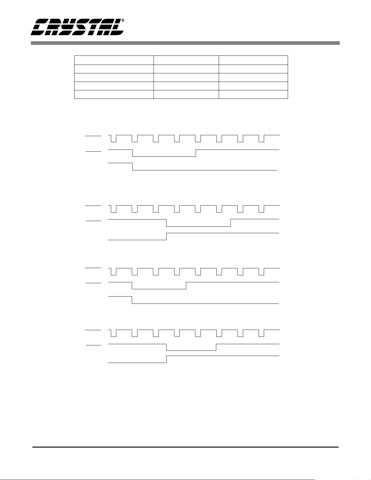
Mode Field Active Lines
NTSC 1, 3; 2, 4 22-261; 285-524
PAL 1, 3, 5, 7; 2, 4, 6, 8 23-310; 336-623
NTSC Progressive-Scan NA 22-261
PAL Progressive-Scan NA 23-310
Table 3. Vertical Timing
NTSC Vertical Timing (odd field)
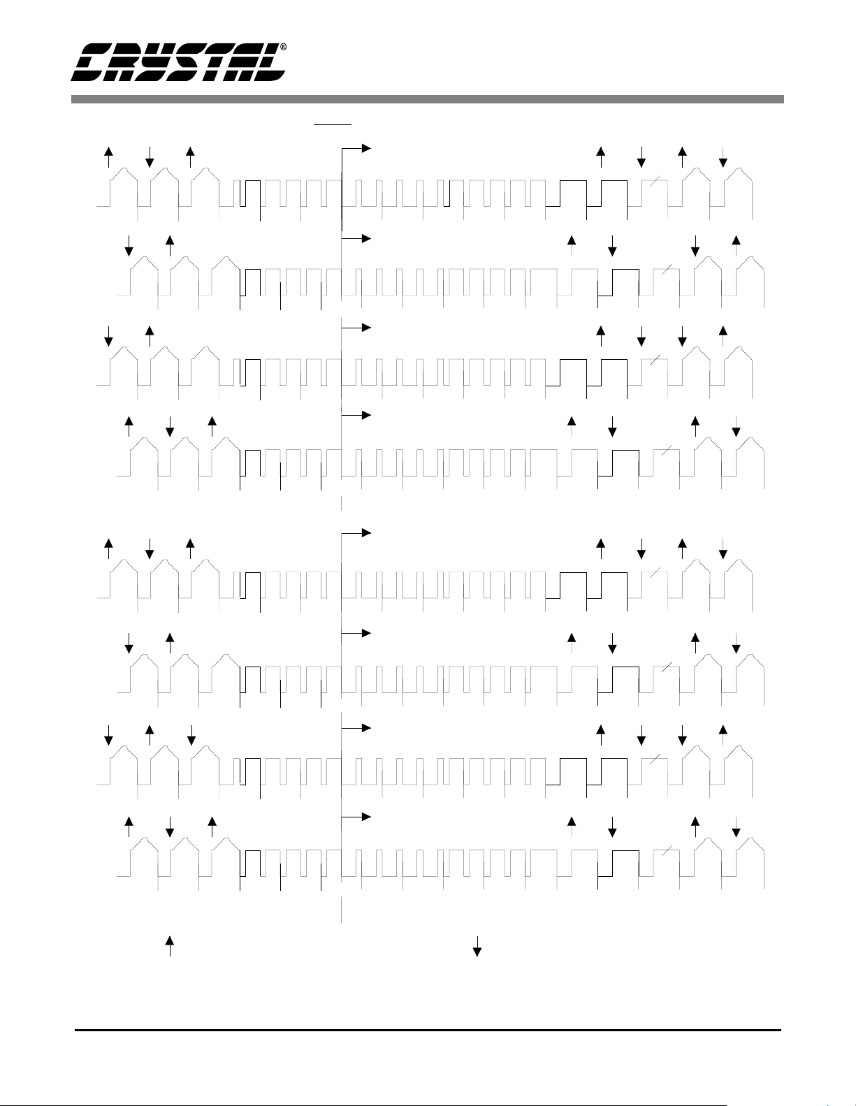
CS7654
Line
HSYNC
VSYNC
FIELD
Line
HSYNC
VSYNC
FIELD
Line
HSYNC
VSYNC
FIELD
3
NTSC Vertical Timing (even field)
264 265
PAL Vertical Timing (odd field)
265 1 2
4
5 6
266 267 268 269 270
7 8 9
3 4 5 6
10
271
7
PAL Vertical Timing (even field)
Line
HSYNC
VSYNC
FIELD
311 312
313 314 315 316 317
Figure 4. Vertical Timing
NTSC Interlaced
The CS7654 supports analog NTSC-M, NTSC-J
and PAL-M modes where there are 525 total lines
per frame and two fixed 262.5-line fields per frame
and 30 total frames occurring per second. NTSC in-
318
terlaced vertical timing is illustrated in Figure 5.
Each field consists of one line for closed caption,
240 active lines of video, plus 21.5 lines of blanking.
17
Page 18

CS7654
Analog
Field 1
523 524 525 1 2 3 4 5 6 7 8 9
Analog
Field 2
261 262 263
Analog
Field 3
523 524 525
261 262 263
Burst begins with positive half-cycle Burst begins with negative half-cycle
1 23456 789
Analog
Field 4
VSYNC Drops
VSYNC Drops
10 22
285284272271270269268267266265264
10 22
285284272271270269268267266265264
Figure 5. NTSC Video Interlaced Timing
PAL Interlaced
The CS7654 supports analog PAL modes B, D, G,
H, I, N, and Combination N, in which there are 625
total lines per frame, two fixed 312.5 line fields per
frame, and 25 total frames per second. Figure 7 illustrates PAL interlaced vertical timing. Each field
consists of 287 active lines of video plus 25.5 lines.
Progressive Scan
The CS7654 supports an analog progessive scan
mode in which the video output is non-interlaced.
This is accomplished by displaying only the odd
video field for NTSC or PAL. To preserve precise
MPEG-2 frame rates of 30 and 25 per second, the
CS7654 displays the same odd field repetitively but
alternately varies the field times. This mode is in
contrast to other digital video encoders, which
commonly support progressive scan by repetitively
displaying a 262 line field (524/525 lines for
NTSC). The common method is flawed: over time,
the output display rate will overrun a system-clo cklocked MPEG-2 decompressor and display a field
twice every 8.75 seconds. NTSC non-interlaced
timing is illustrated in Figure 7. PAL non-interlaced timing is illustrated in Figure 8.
Digital Video Input Modes
The CS7654 provides two different digital video
input modes that are selectable through the
IN_MODE bit in the CONTROL_0 Register at SA
0x00.
In Mode 0 and upon RESET, the CS7654 defaults
to output a solid color (one of a possible of 256 colors). The background color is selected by writing
the BKG_COLOR Register (0x08) at SA 0x00.
The colorspace of the register is RGB 3:3:2 and is
unaffected by gamma correction. The default color
following RESET is blue.
18
Page 19
VSY NC Drops
Analog
Field 1
CS7654
620 624 625 1 2 3 4 5 6 7 23 24
620 624 625 1 2 3 4 5 6 7 23 24
620 624 625 1 2 3 4 5 6 7 23 24
621 622 623
Analog
Field 2
308 311 312 313 314 315 316 317 318 319 320 336 337
308 311 312 313 314 315 316 317 318 319 320 336 337
309 310
Analog
Field 3
621 622 623
Analog
Field 4
309 310
Analog
Field 5
621 622 623
Analog
Field 6
308 311 312 313 314 315 316 317 318 319 320 336 337
620 624 625 1 2 3 4 5 6 7 23 24
308 311 312 313 314 315 316 317 318 319 320 336 337
309 310
Analog
Field 7
621 622 623
Analog
Field 8
309 310
Burst Phase = 135 degrees relative to U Burst Phase = 225 degrees relative to U
Figure 6. PAL Interlaced Timing
19
Page 20

CS7654
Start of
VSYNC
262 263
261 262
262 263
261 262
Burst begins with positive half-cycle Burst begins with negative half-cycle
Burst phase = refere nce phase = 180 relativ e to B-Y
12345678910 22
12345678910 22
Start of
VSYNC
12345678910 22
123456789
0
Figure 7. NTSC Video Non-Interlaced Progressive Scan Timing
Field 1
Field 2
Field 3
Field 4
10 22
Burst phase = refer enc e phase = 180 relative to B-Y
0
In mode 1 the CS7654 displays the image captured
by the camera.
Multi-standard Output Format Modes
The CS7654 supports a wide range of analog output formats compatible with worldwide broadcast
standards. These formats include NTSC-M, NTSCJ, PAL-B/D/G/H/I, PAL-M, PAL-N, and PAL
Combination N (PAL-Nc) which is the broadcast
standard used in Argentina. After RESET, the
CS7654 defaults to NTSC-M operation with ITU
R.BT 601 analog timing. NTSC-J can also be supported in the Japanese format by turning off the 7.5
IRE pedestal through the PED bit in the
CONTROL_1 Register (0x01) at SA 0x00.
Output formats are configured by writing control
registers with the values shown in Table 5.
Subcarrier Generation
The CS7654 automatically synthesizes NTSC and
PAL color subcarrier clocks using the CLK frequency and four control registers
(SC_SYNTH0/1/2/3). The NTSC subcarrier synthesizer is reset every four fields (every eight fields
for PAL).
The SC_SYNTH0/1/2/3 registers used together
provide a 32-bit value that defaults to NTSC
(43E0F83Eh) following RESET. Table 4 shows the
32-bit value required for each of the different
broadcast formats.
Color Bar Generator
The CS7654 is equipped with a color bar generator
that is enabled through the CBAR bit of the
CONTROL_1 Register lodated at SA 0x00. The
color bar generator works in master Mode only and
has no effect on the video input/output timing. The
color bar generator will override the video input
pixel data.
The output of the color bar generator is instantiated
after the chroma interpolation filter and before the
luma delay line. The generated color bar numbers
are for 100% amplitude, 100% saturation NTSC
EIA color bars or 100% amplitude, 100% satura-
20
Page 21

VSYNC Drop s
Analog
Field 1
CS7654
309 310 311
309
308 311 312
309 310 311
309
308 311 312 12345 67 23 24310
Burst Phase = 135 degrees relative to U Burst Phase = 225 degrees relative to U
312 313 1 2 3 4 5 6 7 23 24
312 313 1 2 3 4 5 6 7 23 24
Figure 8. PAL Video Non-Interlaced Progressive Scan Timing
Analog
Field 2
12345 67 23 24310
Analog
Field 3
Analog
Field 4
System Fsubcarrier Value (hex)
NTSC-M, NTSC-J 3.5795455 MHz 43E0F83E
PAL-B, D, G, H, I, N 4.43361875 MHz 54131596
PAL-N (Argentina) 3.582056 MHz 43ED288D
PAL-M 3.579611 MHz 43CDDFC7
tion PAL EBU color bars. For PAL color bars, the
CS7654 generates NTSC color bar values, which
are very close to standard PAL values.
Super White/Super Black support
The ITU-R BT.601 recommendation limits the allowed range for the digital video data between
0×10 - 0×EB (16 - 235 ) for luma and between
0×10 - 0×F0 (16 - 240 ) for the chrominance values.
This chip will clip any digital input value which is
Table 4.
out of this range to conform to the ITU-R BT.601
specifications.
However for some applications it is useful to allow
a wider input range. By setting the CLIP_OFF bit
(CONTROL_6 register at Station Address 0x00)
the allowed input range is extended between 0×01
- 0×FE ( 1 - 254 ) for both luma and chrominance
values.
21
Page 22

CS7654
Address
for
SA 0x00 Register
0×00 CONTROL_0 01h 01h 21h 41h 61h A1h 81h
0×01 CONTROL_1 12h 10h 16h 30h 12h 30h 30h
0×04 CONTROL_4 07h 07h 07h 07h 07h 07h 07h
0×05 CONTROL_5 78h 78h 78h 78h 78h 78h 78h
0×10 SC_AMP 1Ch 1Ch 1Ch 15h 15h 15h 15h
0×11 SC_SYNTH0 3Eh 3Eh 3Eh 96h C7h 96h 8Ch
0×12 SC_SYNTH1 F8h F8h F8h 15h DFh 15h 28h
0×13 SC_SYNTH2 E0h E0h E0h 13h CDh 13h EDh
0×14 SC_SYNTH3 43h 43h 43h 54h 43h 54h 43h
NTSC-M
ITU
R.BT601
Table 5. Multi-standard Format Register Configurations
NTSC-J
ITU
R.BT601
NTSC-M
RS170A
PAL-
B,D,G,H,I PAL-M PAL-N
Note that 0×00 and 0×FF values are never allowed,
since they are reserved for synchronization information.
PAL-N
Comb.
(Argent)
22
Page 23

FILTER RESPONSES
CS7654
0
-10
-20
-30
-40
magnitude - dB
-50
-60
-70
0 1 2 3 4 5 6
1.3 Mhz. filter frequency response
frequency (Hz)
x 10
6
Figure 9. 1.3 Mhz Chrominance low-pass filter transfer
characteristic
650 Khz. filter frequency response
0
-5
1.3 Mhz. filter passband response
0
-0.1
-0.2
magnitude - dB
-0.3
-0.4
-0.5
0 2 4 6 8 10 12
frequency (Hz)
Figure 10. 1.3 Mhz Chrominance low-pass filter
transfer characterstic (passband)
650 Khz. filter passband response
0
-0.5
x 10
5
-10
-15
magnitude - dB
-20
-25
-30
0 1 2 3 4 5 6
Figure 11. 650 kHz Chrominance low-pass filter
transfer characteristic
x 10
-1
-1.5
magnitude - dB
-2
-2.5
-3
6
0 2 4 6 8 10 12
x 10
5
Figure 12. 650 kHz Chrominance low-pass filter
transfer characteristic (passband)
23
Page 24

CS7654
0 0.5 1 1.5 2 2.5 3 3.5 4 4.5 5
-1
-0.8
-0.6
-0.4
-0.2
0
0.2
0.4
0.6
0.8
1
Chroma Output Interpolator Pass band
Frequency (MHz)
Magnitude Response (dB)
Luma Output Interpolation Filter Response at 27MHz full scale
0
-5
-10
-15
-20
-25
Magnitude Response (dB)
-30
-35
-40
0 2 4 6 8 10 12 14
Frequency (MHz)
Figure 13. Chrominance output interpolation filter
transfer characteristic (passband)
Luma Output Interpolation Filter Response at 27 MHz (-3 dB)
0.5
0
-0.5
-1
-1.5
-2
Magnitude Response (dB)
-2.5
-3
-3.5
0 1 2 3 4 5 6 7 8
Figure 15. Luminance interpolation filter transfer characterstic (passband)
Figure 14. Luminance interpolation filter transfer
characteristic
Frequency (MHz)
24
Page 25

CS7654
INTERNAL REGISTER STRUCTURE AND USER INTERFACE
The user interface describes the user’s external
view of the CS7654 and the basic control operations. These areas include digital data, analog output modes and organization, timing and
synchronization signals, I2C interface, and miscellaneous controls.
The CS7654 has two I2C ports: (1) a slave I2C port
called the primary I2C port, and (2) a secondary I2C
port with limited I2C master capabilities. The primary I2C port allows an external controller to control the CS7654 ( See Station Address section for
more details on Station Address structure ). It is assumed the external controller wi ll also directly control any other I2C slave devices on the camera
board. This is the normal I2C operation mode of
CS7654. The secondary I2C port, on the other
hand, may be used to control all the other slave devices on a camera board through the CS7654 only.
This feature is useful when the external I2C controller is used to control multiple cameras. When
used in this configuration the P4BYTMODE pin
(pin 46) of the CS7654 must be tied high and the
device is operated in four-byte mode.
Operating CS7654 in Normal I2C Configuration (Three-Byte Mode)
In normal mode, the CS7654 is connected as a
slave device to an external I2C controller through
the primary I2C port. The connection is done via a
two-wire serial bus. Other I2C devices on the camera may also share the same serial bus. The external
controller communicates with the I2C devices by
sending and receiving short packets of 8-bit words
in accordance with t he I2C protocol. The packets
contain the station address of the target device, the
desired register address, and data.
There are three packet formats: WRITE format,
ADDRESS SET format, and READ format. Each
packet is addressed to a device by the station ad-
dress. The LSB of the station address is the R/W
(data direction) bit. This bit is set LOW in the
WRITE and ADDRESS SET packets, and it is set
HIGH for READ packets. The master can read and
write to non-existent registers within the selected
device. WRITE operations will have no effect;
READ operations will return a value of 00h.
Station Address
Each device on the I2C bus has a unique 7-bit address. An eighth bit, the R/W bit, determines if the
current data transfer writes data to the slave de vice
or reads data from the slave device. It is common to
represent the station address and R/W bit as two 8bit station addresses, one address for write accesses
and another address for read accesses. We will follow this practice. Please note t hat because t he register of the CS7654 are physically implemented in
two different banks, the use of two different Station
Addresses are necessary. Therefore, to access the
proper registers you must first select the proper Station Address. Both Station Adresses have to be different from one another or an internal register
conflict will occur.
The CS7654 default station address are 34h for
writes and 35h for reads for the color processing
section and 00h and 01h for the encoder portion of
the CS7654. The station address can be changed by
writing a new station address to register FFh. The
value written to this register does not include the
R/W bit. For example. The default station address
(34h write / 35h read) will be stored as 1Ah in register FFh.
Write Operations in Three-Byte Mode
The WRITE fo rmat co nsists o f a thre e-byte packet .
The first byte is the station address with the data direction bit set LOW to indicate a write. The second
byte is the device register address (0..255). The
third byte is the register data (0..255). No additional bytes are allowed.
25
Page 26

Byte Sequence WRITE Format Packet Detail
External
EPROM
secondary I
2
C
primary I
2
C
CS7615
CS7654
controller
Figure 16. I
2
C configuration showing primary
and secondary I
2
C busses.
To other sub-systems
First Byte Station Address with LSB Set LOW
Second Byte Device Register Address (0..255)
Third Byte Register Data (0..255)
Table 6. WRITE Format Packet
Address Set Operation
CS7654
the previous WRITE operation or the previous ADDRESS SET operation.
Byte Sequence READ Format Packet Details
First Byte Station Address with LSB set HIGH;
Source Device then Returns One
Byte of Register Data (0..255)
Second Byte Returned data from CS7654
Table 8. READ Format Packet.
Operating CS7654 in Four-Byte I2C Configuration
In this configuration the external controller talks
only to the CS7654 through the primary I2C interface. All the other slave devices on the camera
board are tied to the secondary I2C port of the
CS7654. WRITE and READ packets only are defined in four-byte mode. Independent address set
operations to slave devices on the secondary I2C
bus is not allowed in four-byte mode. Four-byte
mode is active when the P4BYTMODE pin (pin
46) is logic high.
The ADDRESS SET format consists of a two-byte
packet which sets the address of a subsequent
READ operation. The first byte of the Station Address with the LSB (data direction bit) set LOW to
indicate a write operation. The second byte is the
register address (0..255). The ADDRESS SET format is the same as the WRITE format, without the
register data (third byte).
Byte Sequence ADDRESS SET format
Packet Details
First Byte Station Address with LSB Set LOW
Second Byte Device Register Address (0..255)
Table 7. ADDRESS SET Format Packet Operation
Read Operations in Three-Byte Mode
The READ operation may consist of two or more
bytes. The first byte is the station address with the
LSB (data direction bit) set HIGH indicating a read
operation. The addressed device then sends one or
more bytes back from the register last addressed by
Write Operations in Four-Byte mode
All WRITE operations from an external controller,
through the CS7654, to any slave device must use
the four-byte mode; this includes writing to the
CS7654 itself. The external controller sends a fourbyte WRITE command to the CS7654 which initiates a WRITE operation to the destination slave
device and sets the I2CBUSY bit in the status register ( 01h at SA 0x34h ). The I2CBUSY bit is
cleared when the write operation on the secondary
bus is complete. The External controller can poll
the status register to check if the CS7654 has completed the command.
The CS7654 has a one-command-buffer which allows the external controller to queue one additional
command while the current command is still being
executed. If more than one command is sent before
the I2CBUSY bit is cleared, the CS7654 saves only
the last command and executes it after the cur rent
one is completed. Commands that involve writing
26
Page 27

CS7654
or reading only to CS7654 registers are not put in
the queue but are executed immediately without affecting any transactions occurring on the master
I2C interface.
Any attempt by the external I2C controller to write
to the CS7654 registers while the CS7654 is busy
initializing from an external EEPROM will be ignored. However, reads from the CS7654 are allowed during this time.
If, during a READ or WRITE operation to a slave
device, the CS7654 fails to receive an acknowledge
bit the execution of the command is aborted and the
NODEV bit in the status register is set high. This
bit remains set unless it is explicitly cleared by
writing to it or a new command is written to
CS7654.
Byte Sequence WRITE Format Packet Detail
First Byte Station Address of CS7654 with LSB
Set LOW
Second Byte Station Address of target slave
device with LSB Set LOW
Third Byte Device Register Address (0..255)
Fourth Byte Register Data (0..255)
Table 9. Four-byte WRITE Format Packet
The READ-TRIGGER packet initiates a READ
operation by the CS7654 from the target slave device on the secondary I2C bus. The status register
in the CS7654 may be checked to see if the read operation has been completed. The I2CBUSY bit in
status register 01h at SA 0x34h is set to zero when
the operation is completed.
On completion of a read cycle from the target device, the CS7654 places the data read into the Slave
Data Hold register at address 19h at SA 0x34h. The
external controller can read this data through the
primary I2C port. This requires first performing an
ADDRESS SET operation to set the address to 19h
at SA 0x34h and then sending a one-byte station
address indicating read to the CS7654. The data
from register 19h at SA 0x34h is then returned by
the CS7654.
Byte Sequence WRITE Format Packet Detail
First Byte Station Address of CS7654 with
LSB Set LOW
Second Byte Station Address of CS7654 with
LSB Set LOW
Third Byte Slave Data Hold reg. address 19h
Table 11. Address Set for Slave Data Hold register in
Four-byte mode
Read Operations in Four-Byte Mode
The READ operation in four-byte mode first requires a three-byte READ-TRIGGER packet to the
CS7654. The first byte is the station address of the
CS7654 with the LSB set LOW. The second byte is
the target slave device’s station address with the
LSB (data direction bit) set HIGH. The third byte is
the register address (0..255).
Byte Sequence READ-TRIGGER format Packet
Details
First Byte CS7654 Station Address with LSB
Set LOW
Second Byte Target device Station Address with
LSB Set HIGH
Third Byte Device Register Address (0..255)
Table 10. READ-TRIGGER packet in four-byte mode
Byte Sequence READ Format Packet Details
First Byte CS7654 Station Address with LSB
set HIGH.
Second Byte Returned data from register 19h of
CS7654
Table 12. READ Format Packet.
Initializing Slave Devices on Secondary I2C bus from an EPROM
An EPROM may be attached to the secondary I2C
bus for initialization purposes. Resetting the
CS7654 initiates a download of register values
from the EPROM into any of the slave devices on
the secondary I2C bus. The EPROM is assumed to
be at station address A0h. If during initialization,
the CS7654 does not receive an acknowledge bit
from the EPROM, all transactions with the
27
Page 28

CS7654
EPROM are aborted and the NODEV status bit is
set in status register at address 01h at SA 0x34h.
The data within the EPROM is formatted in threebyte packets that represent the destination address,
register address, and data. After reading a packet,
the CS7654 initiates an I2C bus cycle using the first
byte as the device station address, the second byte
as the device register address, and the third byte as
the data being written to the device. If an acknowledge is received from the target device, the CS7654
will fetch the next 3 bytes from the EPROM and repeat the process. The only exception being the
gamma table whose entire 256 bytes is transferred
in one I2C write cycle. This process will continue
until the total number of packets read equals the
value in the EEPROM count register (registers 1Ah
and 1Bh at SA 0x34h), a HALT command is executed, or NO ACKNOWLEDGE is received from
the target device.
While the CS7654 is downloading from the
EPROM, the INITACT bit (register 01h bit3 at SA
0x34h) is set in the status register of CS7654. All
attempts to write to CS7654 registers by an external
controller will be ignored during this time.
Controlling the Configuration Process
The simplest configuration would consist of an
EPROM with one configuration file. In this case,
the first commands in the EPROM should write the
total number of packets in the EEPROM. This data
is written to the EEPROM count high and low byte
registers (registers 1Ah and 1Bh at SA 0x34h).
Subsequent bytes would contain all the necessary
data to configure the camera. This data will be read
in a sequential fashion.
If, however, multiple configurations are desired,
the EEPROM may be programmed with multiple
sets of data, and the CS7654 programmed to select
one of 8 configurations. The appropriate configuration is defined by the 3 GPIO[2:0] pins. The
CS7654 incorporates 3 commands to handle multiple configurations: SKIP, JUMP, and HALT.
The SKIP command tells the CS7654 to skip to the
address within the EEPROM specified by t he Configuration Control registers (30h - 3Fh at SA
0x34h). The Configuration Control registers are
used in pairs to provide a 11-bit EEPROM address.
The Configuration Index Register determines
which two of the 8 pairs will be used.
The Configuration Index Register is loaded automatically after reset by the CS7654. The CS7654
will read from the GPIO port. If the read cycle is
successful, the Configuration Index Register will
contain the state of the lower 3 bits of the parallel
I/O port. A set of shunts or DIP switches attached
to the I/O port provides a convenient way to select
up to 8 configurations. The SKIP command is executed by writing a 1 to bit 1 of the EEPROM Control Register (42h at SA 0x34h).
The JUMP is similar to the SKIP command. The
user loads a jump address into the Jump Control
Registers (40h and 41h at SA 0x34h) and then executes the JUMP command by setting bit 2 of the
EEPROM Control Register (42h at SA 0x34h) to a
1. The jump command may be used to reduce the
amount of required EEPROM space by allowing
multiple configurations to share common data. For
example, three configurations may be necessary to
adjust for three different CCD timings, but they
may all share a common gamma table.
The HALT command is used to stop the execution
of the boot state machine. When all necessary data
has been read from the EEPROM, writing a 1 to bit
0 (HALT) of the EEPROM Control Register will
safely stop the boot process.
The total number of packets that may be stored in
the external EEPROM is 2k/3 or 682 3-byte commands. Gamma table packets contain 259bytes.
A typical map of the EPROM table is shown in Figure 17. The only exception to this organization is
data for the CS7654 gamma table. The data for the
gamma table is organized as shown in Figure 18.
28
Page 29

CS7654 station address[7] +W
1Ah (addrs of low byte Count)
count value
CS7654 station address[7] +W
1Bh (addrs of high byte Count)
count value
Dest. station address + W
Dest. device address
data value
Dest. station address + W
EPROM Block 000 (binary)
Address 00h
Figure 17. Map of EPROM table for initialization
of registers
CS7654 station address[7] +W
0Ch (gamma reg. addrs)
data = select RGB ram
data [gamma loc 00h]
data [gamma loc 01h]
data [gamma loc FFh]
CS7654
Reserved Registers and Test Pins
To ensure proper operation of the CS7654, connect
and SCENABLE (pin 45) to ground, and connect
TEST1 (pin 64) and TEST2 (pin 42) to VDD. Registers 23h - 26h at SA 0x34h must be set to a value
of FFh after reset. All other reserved registers may
be left in their default states.
General Purpose I/O Port
The CS7654 has a GPIO port and register that is
available when the device is configured for I2C host
interface operation. The GPIO [2:0] pins operate as
input or outputs pins for the GPIO_DATA_REG
Register (0×0A at SA 0x00h). The GPIO [2:0] pins
are configured for input ope ration when the corre-
Figure 18. Map of EPROM table for storing
gamma ram initialization data.
sponding GPIO_CTRL_REG [2:0
] bits are set to 0
and output when set to 1. In GPIO input mode, the
CS7654 will latch the data on the [2:0] pins into the
corresponding bit locations of GPIO_DATA_REG
when it detects register address 0×0A at SA 0x00h
through the I2C interface. A detection of address
0×0A can happen in two ways. The first and most
common way this will happen is when address
0×0A is written to the CS7654 via its I2C interface.
The second method for detecting address 0×0A is
implemented by accessing register address 0×09 at
SA 0x00h through I2C. In I2C host interface operation, the CS7654 register address pointer will autoincrement to address 0×0A after an address 0×09
access ( at SA 0x00h ).
29
Page 30

CS7654
ANALOG
Analog Timing
All CS7654 analog timing and sequencing is derived
from 27 MH z clock input. The analog outputs are
controlled internally by the video timing generator in
conjunction with master and slave timing. The video
output signals perform accordingly for NTSC and
PAL specifications.
Being that the CS7654 is almost entirely a digital
circuit, great care has been taken to guarantee analog timing and slew rate performance as specified
in the NTSC and PAL analog specifications. Reference the Analog Parameters section of this data
sheet for exact performance parameters.
VREF
The CS7654 can operate with or without the aid of
an external voltage reference. The CS7654 is designed with an internal voltage reference generator
that provides a vrefout signal at the VREF pin. The
internal voltage reference is utilized by not making
a connection to the VREF pin. The VREF pin can
also be connected to an external precision
1.232 volt reference, which the n overrides the internal reference.
ISET-DAC
All three of the CS7654 digital to analog converter
DACs are output current normalized with a common ISET-DAC device pin. The DAC output current per bit is determined by the size of the resistor
connected between ISET-DAC pin and electrical
ground. Typically a 4 KΩ, 1% metal film resistor
should be used. The ISET resistance can be
changed by the user to accommodate varying video
output attenuation via post filters and also to suit
individual preferred performance.
In conjunction with the ISET-DAC value, the user
can also independently vary the chroma, luma and
colorburst amplitude levels via host addressable
control register bits that are used to control internal
digital amplifiers. The DAC output levels are defined by the following operations:
VREF/RISET = IREF
(e.g., 1.232 V/4K Ω = 308 µA
COMP_VID/Y/C outputs in low impedance mode:
VOUT (m ax ) = IR E F* 112.88* 3 7. 5 Ω = 1.304V
COMP_VID/Y/C outputs in high impedance mode:
VOUT (max) = IREF*28.22*150Ω=1.304V
)
DACs
The CS7654 is equipped with three independent,
video-grade, current-output, digital-to-analog converters (DACs). They are 10-bit DACs operating at
a 27 MHz two-times-oversampling rate. All three
DACs are disabled and default to a low power
mode upon RESET. Each DAC can be individually
powered down and disabled. The output-currentper-bit of all three DACs is determined by the size
of the resistor connected between the ISET_DAC
pin and electrical ground.
Luminance DAC
The SVID_Y pin is driven from a 10-bit 27 MHz
current output DAC that internally receives the
SVID_Y, or luminance portion, of the video signal
(black and white only). SVID_Y is designed to
drive proper video levels into a 37.5 Ω load. Reference the detailed electri cal section of this data sheet
for the exact SVID_Y digital to analog AC and DC
performance data. A EN_L enable control bit in the
Control Register 5 (0×05 at SA 0x00h) is provided
to enable or disable the luminance DAC. For a
complete disable and lower power operation the luminance DAC can be totally shut down via the
SVIDLUM_PD control bit in the Control Register 4
(0×04 at SA 0x00h). In this mode, turn-on through
the control register will not be instantaneous.
30
Page 31

CS7654
Chrominance DAC
The SVID_C pin is driven from a 10-bit 27 MHz
current output DAC that internally receives the
SVID_C or chrominance portion of the video signal (color only). SVID_C is designed to drive proper video levels into a 37.5 Ω load. Reference the
detailed electrical section of this data sheet for the
exact SVID_C digital to analog AC and DC performance data. A EN_C enable control register bit in
the Control Register 1 (0×05 at SA 0x00h) is provided to enable or disable the chrominance DAC.
For a complete disable and lower power operation
the chrominance DAC can be totally shut down via
the SVIDCHR_PD re gister bit in the Control Register 4 (0×04 at SA 0x00h). In this mode turn-on
through the control register will not be instantaneous.
COMP_VID DAC
The COMP_VID pin is driven from a 10-bit
27 MHz current output DAC that internally receives a combined luma and chroma signal to provide composite video output. COMP_VID is
designed to drive proper composite video levels
into a 37.5 Ω load. Reference the detailed electrical
section of this data sheet for the exact COMP _VID
digital to analog ac and dc performance data. The
EN_COM enable control register bit, in Control
Register 1 (0×05 at SA 0x00h), is provided to enable or disable the output pin. When disabled, there
is no current flow from the output. For a complete
disable and lower power operation, the
COMP_VID DAC can be totally shut down via the
COMDAC_PD control register bit in Control
Register 4 (0×04 at SA 0x00h). In this mode turnon through the control register will not be instantaneous.
Depending on the external resistor connected to the
ISET_DAC pin the output drive of the DACs can
be changed. There are two modes in which the
DACs should either be operated in. An external resistor of 4 kΩ must be connected to the ISET_DAC
pin.
The first mode is the high impedance mode
(LOW_IMP bit set to 0). The DAC outputs will
then drive a double terminated load of 300 Ω and
will output a video signal which conforms to the
analog video specifications for NTSC and PAL.
External buffers will be needed if the DAC output
load differs from 300 Ω.
The second mode is the low impedence mode
(LOW_IMP but set to 1). The DAC output will
then drive a double terminated load of 75 Ω and
will output a video signal which conforms to the
analog video specifications for NTSC and PAL. No
external buffers are necessary, the ouputs can directly drive a television input.
Note If some of the 3 DACs are not used, it is
strongly recommended to power them down (see
CONTROL_4 register) in order to reduce the power dissipation.
31
Page 32

REGISTER DESCRIPTION
Control Registers of encoder section :SA0x00
Address Register Name Type Defaultvalue
0
×00 control_0 r/w 01h
0
×01 control_1 r/w 02h
0
×02 control_2 r/w 00h
0
×03 control_3 r/w 00h
0
×04 control_4 r/w 3Fh
0
×05 control_5 r/w 00h
0
×06 control_6 r/w 00h
0
×07 RESERVED
×08 bkg_color r/w 03h
0
0
×09 gpio_ctrl_reg r/w 00h
0
×0A gpio_data_reg r/w 00h
0
×0B - 0×0C RESERVED
0
×0D SYNC_0 r/w 90h
0
×0E SYNC_1 r/w F4h
0
×0F I
0
×10 SC_AMP r/w 1Ch
0
×11 SC_SYNTH0 r/w 3Eh
0
×12 SC_SYNTH1 r/w F8h
0
×13 SC_SYNTH2 r/w E0h
0
×14 SC_SYNTH3 r/w 43h
0
×15 HUE_LSB r/w 00h
0
×16 HUE_MSB r/w 00h
0
×17 SCH PHASE ADJUST r/w 00h
0
×18 CC_EN r/w 00h
0
×19 CC_21_1 r/w 00h
0
×1A CC_21_2 r/w 00h
0
×1B CC_284_1 r/w 00h
0
×1C CC_284_2 r/w 00h
0
×1D - 0×21 RESERVED
0
×22 CB_AMP r/w 80h
0
×23 CR_AMP r/w 80h
0
×24 Y_AMP r/w 80h
0
×25 R_AMP r/w 80h
0
×26 G_AMP r/w 80h
0
×27 B_AMP r/w 80h
0
×28 BRIGHT_OFFSET r/w 00h
0
×29 - 0×31 RESERVED
0
×32 INT_EN r/w 00h
0
×33 INT_CLR r/w 00h
0
×34 STATUS_0 read only
0
×35 - 0×59 RESERVED
0
×5A STATUS_1 read only 04h
0
×61 - 0×7F RESERVED
Table 13. Encoder Control Registers
2
CS7654
C_ADR r/w 00h
32
Page 33

Control Register 0 at SA 0x00h
Address 0×00 CONTROL_0 Read/Write Default Value = 01h
CS7654
Bit Number
Bit Name
Default
76543210
TV_FMT MSTR CCIR656 PROG IN_MODE CBCR_UV
00001001
Bit Mnemonic Function
selects the TV display format
000: NTSC-M CCIR601 timing (default)
001: NTSC-M RS170A timing
010: PAL-B, D, G, H, I
7:5 TV_FMT
011: PAL-M
100: PAL-N (Argentina)
101: PAL-N (non Argentina)
110-111: reserved
4 Reserved
3 CCIR656
2PROG
1 IN_MODE
0 CBCR_UV
Set to 0
Set to 1
Progressive scanning enable (enable = 1)
Input select (0 = solid background, 1 = use V [7:0] data)
enable YCbCr to YUV conversion (1 = enable, 0 = disable)
Control Register 1 at SA 0x00h
Address 0×01 CONTROL_1 Read/Write Default Value = 02h
Bit Number
Bit Name
Default
Bit Mnemonic Function
7:6 LUM DEL
5 CH BW
4LPF ON
3 Reserved
2 Reserved
1 PED
0 Reserved
76543210
LUM DEL CH BW LPF_ON res res PED res
0 0 0 0 Reserved Reserved 1 Reserved
luma delay on the composite output
00: no delay (default)
01: 1 pixel clock delay
10: 2 pixel clock delay
11: 3 pixel clock delay
chroma lpf bandwidth (0 = 650 kHz, 1 = 1.3 Mhz)
chroma lpf on/off (0 = off, 1 = on)
Reserved
Reserved
Pedestal offset (0: 0 IRE, 1: 7.5 IRE)
Reserved
33
Page 34

Control Register 2 at SA 0x00h
Address 0×02 CONTROL_2 Read/Write Default Value = 00h
CS7654
Bit Number
Bit Name
Default
76543210
res res res res res res res BU_DIS
Reserved 0
Bit Mnemonic Function
7:1 Reserved Set to 0
0BU DIS
Chroma burst disable (1 = disable)
Control Register 3 at SA 0x00h
Address 0×03 CONTROL_3 Read/Write Default Value = 00h
Bit Number
Bit Name
Default
76543210
res res res res res res res CBAR
Reserved 0
Bit Mnemonic Function
7:1 Reserved
0 CBAR
Set to 0
internal color bar generator (0 = off, 1 = on)
Control Register 4 at SA 0x00h
Address 0×04 CONTROL_4 Read/Write Default Value = 3Fh
Bit Number
Bit Name
Default
76543210
res res COMDAC_PD SVIDLUM_PD SVIDCHR_PD res res res
Reserved 1 1 1 Reserved
Bit Mnemonic Function
7:6 -
Reserved
power down composite DAC
5 COMDAC_PD
0: power up, 1: power down
power down luma s-video DAC
4 SVIDLUM_PD
0: power up, 1: power down
power down chroma s-video DAC
3 SVIDCHR_PD
0: power up, 1: power down
2:0 -
Reserved set to “111”
Control Register 5 at SA 0x00h
Address 0×05 CONTROL_5 Read/Write Default Value = 00h
Bit Number
Bit Name
76543210
RSVD LOW IMP EN COM EN LEN Cres res res
34
Page 35

CS7654
Default
00000 Reserved
Bit Mnemonic Function
76LOW IMP
5EN COM
4EN L
3EN C
2:0 -
reserved
selects between high output impedance (0) or low output impedance (1) mode of DACs
enable DAC for composite output 0: tri-state, 1: enable
enable s-video DAC for luma output 0: tri-state, 1: enable
enable s-video DAC for chroma output 0: tri-state, 1: enable
Reserved set to 0
Control Register 6 at SA 0x00h
Address 0×06 CONTROL_6 Read/Write Default Value = 00h
Bit Number
Bit Name
Default
Bit Mnemonic Function
7 res set to 0
6CLIP OFF
5:0 res set to 0
76543210
res CLIP OFF res res res res res res
00000000
Clipping input signals disable (0: clipping active 1: no clipping)
Background Color Register at SA 0x00h
Address 0×08 BKG_COLOR Read/Write Default Value = 03h
Bit Number
Bit Name
Default
76543210
BG
00000011
Bit Mnemonic Function
7:0 BG
Background color (7:5 = R, 4:2 = G, 1:0 = B) (default is 0000 0011 - blue)
GPIO Control Register at SA 0x00h
Address 0×09 GPIO__REG Read/Write Default Value = 00h
Bit Number
Bit Name
Default
Bit Mnemonic Function
2:0 GPR CNTRL
76543210
GPR_CNTRL
res res res res res 0 0 0
Input(0)/output(1) control of GPIO registers (bit 0: GPIO(0), bit 2: GPIO(2))
35
Page 36

GPIO Data Register at SA 0x00h
Address 0×0A GPIO_REG Read/Write Default Value = 00h
CS7654
Bit Number
Bit Name
Default
76543210
GPIO REG
resresresresres 0 0 0
Bit Mnemonic Function
2:0 GPIO REG
GPIO data register ( data is output on GPIO bus if appropriate bit in address 09 is set
to “1”, otherwise data is input/output through I
2
I
C mode.
2
C)- This register is only accessible in
Sync Register 0 at SA 0x00h
Address 0×0D Sync_0 Read/Write Default Value = 90h
Bit Number
Bit Name
Default
76543210
res res res res res r es res res
10010000
Bit Mnemonic Function
7:0 Reserved
Sync Register 1 at SA 0x00h
Address 0×0E Sync_1 Read/Write Default Value = F4h
Bit Number
Bit Name
Default
76543210
res res res res res res res res
11110100
Bit Mnemonic Function
7:0 res res
I2C Address Register of TV encoder at SA 0x00h
Address 0×0F I2C_ADR Read/Write Default Value = 00h
Bit Number
Bit Name
Default
Bit Mnemonic Function
7-
6:0
76543210
RESERVED
00000000
2
I
C ADR
reserved
2
I
C
I2C device address (programmable) do not program to 34h
36
Page 37

Subcarrier Amplitude Register at SA 0x00h
Address 0×10 SC_AMP Read/Write Default Value = 1Ch
CS7654
Bit Number
Bit Name
Default
Bit Mnemonic Function
7:0 BU AMP
76543210
BU AMP
00011100
Color burst amplitude
Subcarrier Synthesis Register at SA 0x00h
Address 0×11 SC_SYNTH0 Read/Write Default Value = 3Eh
0
×12 SC_SYNTH1 F8h
0
×13 SC_SYNTH2 E0h
0
×14 SC_SYNTH3 43h
Register Bits Mnemonic Function
SC_SYNTH0 7:0 CC 0
SC_SYNTH1 7:0 CC 1
SC_SYNTH2 7:0 CC 2
SC_SYNTH3 7:0 CC 3
Subcarrier synthesis bits 7:0
Subcarrier synthesis bits 15:8
Subcarrier synthesis bits 23:16
Subcarrier synthesis bits 31:24
Hue LSB Adjust Register at SA 0x00h
Address 0×15 HUE_LSB Read/Write Default Value = 00h
Bit Number
Bit Name
Default
Bit Mnemonic Function
7:0 HUE LSB
76543210
HUE LSB
00000000
8 LSBs for hue phase shift
Hue MSB Adjust Register at SA 0x00h
Address 0×16 HUE_MSB Read/Write Default Value = 00h
Bit Number
Bit Name
Default
Bit Mnemonic Function
7:2 1:0 HUE MSB
76543210
RESERVED MSB
00000000
reserved
2 MSBs for hue phase shift
37
Page 38

SCH Sync Phase Adjust at SA 0x00h
Address 0×17 SCH Read/Write Default Value = 00h
Bit Mnemonic Function
7:0 SCH
Default - 00h in increments of ≈1.4 degree per bit up to 360°
Closed Caption Enable Register at SA 0x00h
Address 0×18 CC_EN Read/Write Default Value = 00h
CS7654
Bit Number
Bit Name
Default
Bit Mnemonic Function
7:2 -
1 CC EN[1]
0 CC EN[0]
765432 1 0
RESERVED EN_284 EN_21
000000 0 0
reserved
enable closed caption for line 284
enable closed caption for line 21
Closed Caption Data Register at SA 0x00h
Address 0×19 CC_21_1 Read/Write Default Value = 00h
0
×1A CC_21_2 00h
0
×1B CC_284_1 00h
0
×1C CC_284_2 00h
Bit Mnemonic Function
7:0 CC_21_1
7:0 CC_21_2
7:0 CC_284_1
7:0 CC_284_2
first closed caption databyte of line 21
second closed caption databyte of line 21
first closed caption databyte of line 284
second closed caption databyte of line 284
Filter Register 0 at SA 0x00h
Address 0×22 CB_AMP Read/Write Default Value = 80h
Bit Number
Bit Name
Default
Bit Mnemonic Function
7:0 U_AMP
76543210
U_AMP
10000000
U(Cb) amplitude coefficient
Filter Register 1 at SA 0x00h
Address 0×23 CR_AMP Read/Write Default Value = 80h
Bit Number
38
76543210
Page 39

CS7654
Bit Name
Default
Bit Mnemonic Function
7:0 V_AMP
10000000
V(Cr) amplitude coefficient
V_AMP
Filter Register 2 at SA 0x00h
Address 0×24 Y_AMP Read/Write Default Value = 80h
Bit Number
Bit Name
Default
Bit Mnemonic Function
7:0 Y_AMP
76543210
Y_AMP
10000000
Luma amplitude coefficient
Filter Register 6 at SA 0x00h
Address 0×28 Bright_Offsett Read/Write Default Value = 00h
Bit Number
Bit Name
Default
76543210
BRIGHTNESS_OFFSET
00000000
Bit Mnemonic Function
7:0 BRGHT_OFFSET
Brightness adjustment ( range: -128 to +127)
39
Page 40

Control Register of Color Space Processor Section: SA 0x34h
Address Register Name Type De faultvalue
[00] Master reset r/w 00h
[01] Status r only 00h
[02] Pin i/o control r/w 00h
[03] Digital gain r/w 08h
[04] Scaler control r/w 00h
[05] Feature control r/w 00h
[06] Operation control 1 r/w 0Dh
[07] Operation control 2 r/w 00h
[08] Red balance r/w 80h
[09] Blue balance r/w 80h
[0A] Red saturation r/w 80h
[0B] Blue saturation r/w 80h
[0C] Gamma correction r/w 01h
[0D] Reserved
[0E] Reserved
[0F] Reserved
[10] YR coefficient r/w 80h
[11] CrR coefficient r/w 7Ch
[12] CbR coefficient r/w E0h
[13] YG coefficient r/w 80h
[14] CrG coefficient r/w E4h
[15] CbG coefficient r/w DCh
[16] YB coefficient r/w 80h
[17] CrB coefficient r/w ECh
[18] CbB coefficient r/w 7Ch
[19] Slave data hold
[1A] EEPROM count LSB
[1B] EEPROM count MSB
[1C] Vers ion_major
[1D] Version_minor
[1E] Reserved
[1F] Reserved
[20] Low power
[21] Reserved
[22] Reserved
[23] Anti-alias
[24] Reserved
[25] Reserved
[26] Reserved
[27] Flare control 1
[28] Flare control 2
[29] Flare control 3
[2A] Flare control 4
[2B] Flare control 5
Table 14. DSP Control Register
CS7654
r/w 00h
r/w 00h
r/w 00h
r only FDh
r only 00h
r/w 00h
r/w 00h
r/w 00h
r/w 00h
r/w 00h
r/w 00h
r/w 00h
40
Page 41

CS7654
Address Register Name Type De faultvalue
[2C] Flare control 6
[2D] Scaler control 1
[2E] Scaler control 2
[2F] Scaler control 3
[30] Config 0
[31] Config 1
[32] Config 2
[33] Config 3
[34] Config 4
[35] Config 5
[36] Config 6
[37] Config 7
[38] Config 8
[39] Config 9
[3A] Config 10
[3B] Config 11
[3C] Config 12
[3D] Config 13
[3E] Config 14
[3F] Config 15
[40] Jump 0
[41] Jump 1
[42] EEPROM control
[43] Config index
[44] Reserved
[FE] Reserved
[FF] Station address
Table 14. DSP Control Register (Continued)
r/w 00h
r/w 00h
r/w 00h
r/w 00h
r/w 00h
r/w 00h
r/w 00h
r/w 00h
r/w 00h
r/w 00h
r/w 00h
r/w 00h
r/w 00h
r/w 00h
r/w 00h
r/w 00h
r/w 00h
r/w 00h
r/w 00h
r/w 00h
r/w 00h
r/w 00h
r/w 00h
r/w 00h
r/w 1Ah
Master Reset Register (00h at SA 0x34h )
76543210
res res res res res res res MR
Reserved W
MR Setting bit MR0 to logic high will initiate a CS7654 master reset equivalent to executing an ex-
ternal reset using the RESET
load of any external EPROM present on the secondary I2C bus will be initiated. The bit is self-
pin. All registers will be placed in their default state, and the down-
cleared.
Status Register (01h at SA 0x34h)
76543210
res P4BYTE res HIZENB INITACT I2CBUSY NODEV EVNFLD
Reserved R Reserved R R R R R
EVNFLD Logic high indicates even field of interline-transfer CCD. Logic low indicates odd field of inter-
line-transfer CCD. This bit provides a course means of synchronizing to the field rate.
NODEV Logic high indicates that the addressed slave device on the secondary I
2
C bus did not respond.
41
Page 42

CS7654
I2CBUSY Logic high indicates that the CS7654 secondary I2C master is busy accessing the addressed
slave device.
INITACT Logic high indicates the CS7654 master is busy initializing registers from the external I
EEPROM on the secondary I
2
C bus (if present).
HIZENB Pin 44 status.
P4BYTE Pin 46 status.
PIN I/O Control (02h at SA 0x34h)
76543210
res res res res res res res PLLOUT
Reserved Reserved Reserved R/W
PLLOUT Logic high enables the PLL clock output to the CS7615 (pin 51).
Digital Gain Register (03h at SA 0x34h)
76543210
res res res DG4 DG3 DG2 DG1 DG0
Reserved R/W
2
C
DG[0:4] Controls the digital gain applied to the SVID_Y (Luminance) signal after the RGB to YCrCb con-
verter block. The range of gains are from 0 to 31/8 in increments of 1/8. A gain of 0, indicates
no brightness.
Scaler Control (04h at SA 0x34h)
76543210
res res res res CUSTOM MODE2 MODE1 MODE0
Reserved Reserved Reserved R/W R/W
MODE[2:0] Selects 1 of 8 pre-defined scaling ratios.
CUSTOM When set, scaler uses custom values held in registers 2Dh-2Fh.
Feature Control Register (05h at SA 0x34h)
76543210
res res res CHROFF LUMOFF GAMON AWB res
Reserved R/W R/W R/W R/W Reserved
AWB The Automatic White Balance procedure is initiated by pointing to a white scene and setting this
bit high. The bit will return a logic high while the AWB procedure is in progress. Setting this bit
low will have no effect. This bit will always be read as a “0” when the AWB is not in progress.
GAMON The gamma correction from the gamma ram look up table is applied to the video signal in R-G-
B space when this bit is set high. The gamma ram is a fully user programmable, 256 entry look
up table.
LUMOFF Setting LUMOFF bit high disables the luma peaking filter.
CHROFF Setting the CHROFF bit high disables the chroma low-pass filter for minimizing color aliasing.
42
Page 43

CS7654
Operational Control Register (06h at SA 0x34h)
76543210
res res res INREF OE POSPIX EBLU OBLU
Reserved Reserved Reserved R/W R/W R/W R/W R/W
OBLU Logic high causes the first line after VREF of the odd field to be processed as a BLUE line. Logic
low causes the first line of the odd field to be processed as a RED line.
EBLU Logic high causes the first line after VREF of the even field to be processed as a BLUE line.
Logic low causes the first line of the even field to be processed as a RED line.
POSPIX Logic “1” causes the first pixel of the first line to be treated as a positive pixel in the color sep-
aration block. Logic “0” causes the first pixel to be treated as a negative pixel. Try toggling this
bit if the colors appear “reversed.”
OE The Output Enable Bit operates in conjunction with the external HIZEN
ble 15.
OE Bit HIZEN Pin Digital Outputs
0 0 High-Z
0 1 High-Z
1 0 High-Z
1 1 Enabled
Table 15. OE Pin and Bit Operation
INREF Logic “1” causes CS7654 to accept HREF input and VREF input pins as the reference inputs
signals. EAV and SAV codes in the CCD data stream are ignored. Logic “0” causes the internal
de-formatter to decode and follow the embedded EAV and SAV codes sent from the CCD digitizer (as with the CS7615).
Pin, as illustra ted in Ta-
Operational Control Register II (07h at SA 0x34h)
76543210
TEST_AA CLIP_OFF res res res res res res
R/W R/W Reserved Reserved Reserved Reserved Reserved Reserved
CLIP_OFF When set, excludes only 00 and FF from output data. Otherwise ITU BT 601 definition
TEST_AA This bit is reserved for test purposes and may be set as a 1 or a 0.
Red Balance Register (08h at SA 0x34h)
76543210
RB7 RB6 RB5 RB4 RB3 RB2 RB1 RB0
R/W
RB[7:0] The Red Balance register controls the red contribution to the R-Y chrominance signal. When
the register value is 00h, the red contribution is minimized; when the register value is FFh, the
red contribution is maximized. When the AWB correction is in progress, this register value is
adjusted such that the absolute magnitude of the R-Y signal is minimized.
43
Page 44

CS7654
Blue Balance Register (09h at SA 0x34h)
76543210
BB7 BB6 BB5 BB4 BB3 BB2 BB1 BB0
R/W
BB[7:0] The Blue Balance register controls the blue contribution to the B-Y chrominance signal. When
the register value is 00h, the blue contribution is minimized; when the register value is FFh, the
blue contribution is maximized. When the AWB correction is in progress, this register value is
adjusted such that the absolute magnitude of the B-Y signal is minimized.
Red Saturation Register (0Ah at SA 0x34h)
76543210
RS7RS6RS5RS4RS3RS2RS1RS0
R/W
RS[7:0] The Red Saturation register value controls the amplitude of the R-Y chrominance signal. When
the register value is 00h, the amplitude of the R-Y is minimized; when the register value is FFh,
the amplitude of the R-Y is maximized.
Blue Saturation Register (0Bh at SA 0x34h)
76543210
BS7 BS6 BS5 BS4 BS3 BS2 BS1 BS0
R/W
BS[7:0] The Blue Saturation register value controls the amplitude of the B-Y chrominance signal. When
the register value is 00h, the amplitude of the B-Y is minimized; when the register value is FFh,
the amplitude of the B-Y is maximized.
Gamma Correction Register (0Ch at SA 0x34h)
Writing to the gamma register (0Ch at SA 0x34h) selects the R, G, and/or B RAM. Continuing data writes without
sending a stop bit after the register write results in writes to the ram locations starting with 00h and continuing to
FFh. Reads from register 0Ch function in a similar way. NOTE: All three gamma rams may be selected for simultaneous writes, but read should be done one ram table at a time.
76543210
GC7 GC6 GC5 GC4 GC3 GC2 GC1 GC0
R/W
GC0 Logic “1” selects BLUE gamma RAM for subsequent access.
GC1 Logic “1” selects GREEN gamma RAM for subsequent ram access.
GC2 Logic “1” selects RED gamma RAM for subsequent ram access.
GC[0:7] Provide R/W access to RAM after gamma RAM table has been selected.
Test Control A Register (0Eh at SA 0x34h)
This register is reserved
44
Page 45

CS7654
Test Control B Register (0Fh at SA 0x34h)
This register is reserved.
YR Coefficient Register (10h at SA 0x34h)
76543210
YR7 YR6 YR5 YR4 YR3 YR2 YR1 YR0
R/W
Color separation and color space conversion coefficient.
CrR Coefficient Register (11h at SA 0x34h)
76543210
CrR7 CrR6 CrR5 CrR4 CrR3 CrR2 CrR1 CrR0
R/W
Color separation and color space conversion coefficient.
CbR Coefficient Register (12h at SA 0x34h)
76543210
CbR7 CbR6 CbR5 CbR4 CbR3 CbR2 CbR1 CbR0
R/W
Color separation and color space conversion coefficient.
YG Coefficient Register (13h at SA 0x34h)
76543210
YG7 YG6 YG5 YG4 YG3 YG2 YG1 YG0
R/W
Color separation and color space conversion coefficient.
CrG Coefficient Register (14h at SA 0x34h)
76543210
CrG7 CrG6 CrG5 CrG4 CrG3 CrG2 CrG1 CrG0
R/W
Color separation and color space conversion coefficient.
45
Page 46

CS7654
CbG Coefficient Register (15h at SA 0x34h)
76543210
CbG7 CbG6 CbG5 CbG4 CbG3 CbG2 CbG1 CbG0
R/W
Color separation and color space conversion coefficient.
YB Coefficient Register (16h at SA 0x34h)
76543210
YB7 YB6 YB5 YB4 YB3 YB2 YB1 YB0
R/W
Color separation and color space conversion coefficient.
CrB Coefficient Register (17h at SA 0x34h)
76543210
CrB7 CrB6 CrB5 CrB4 CrB3 CrB2 CrB1 CrB0
R/W
Color separation and color space conversion coefficient.
CbB Coefficient Register (18h at SA 0x34h)
76543210
CbB7 CbB6 CbB5 CbB4 CbB3 CbB2 CbB1 CbB0
R/W
Color separation and color space conversion coefficient.
Slave Data Hold Register (19h at SA 0x34h)
When an external I2C controller initiates a register read from a slave device on the secondary I2C bus through
CS7654, the returned data is placed in this register. The external controller may then read the data from the Slave
Data Hold register. This register is read only.
EPROM Count Low Byte Register (1Ah at SA 0x34h)
Lower byte of the number of triple-bytes to be read from EPROM upon reset of CS7654. This register is read only.
EPROM Count High Byte Register (1Bh at SA 0x34h)
Upper byte of the number of triple-bytes to be read from EPROM upon reset of CS7654. This register is read only.
Version (Major) Register (1Ch at SA 0x34h)
The major version register (device ID) in the CS7654 is assigned the value FDh. This register is read only.
Version (Minor) Register (1Dh at SA 0x34h)
The minor version register in CS7654 rev A. is assigned the value 00h. With each minor revision the value is increased by 1. This register is read only.
46
Page 47

CS7654
Low Power Register (20h at SA 0x34h)
76543210
res res res res res res res PD
Reserved R/W
PD Setting bit PD to “1” will place the CS7654 in low power mode.
Test Enable Register (21h at SA 0x34h)
This register is reserved.
Reserved Register (22h at SA 0x34h)
This register is reserved and returns a valud of 00 when read.
Anti-Alias (23h at SA 0x34h)
This register is reserved and must be set to 08h for normal operation.
Test_AA2 (24h at SA 0x34h)
This register is reserved and must be set to FFh for normal operation
Test_AA3 (25h at SA 0x34h)
This register is reserved and must be set to FFh for normal operation
Test_AA4 (26h at SA 0x34h)
This register is reserved and must be set to FFh for normal operation
Flare Control 1 (27h at SA 0x34h)
76543210
Y_THR9 Y_THR8 Y_THR7 Y_THR6 Y_THR5 Y_THR4 Y_THR3 Y_THR2
R/W
Y_THR[9:2] Flare control filter Y threshold bits 9-2 (MSB). (Bits 1 and 0 set to 0.)
Flare Control 2 (28h at SA 0x34h)
76543210
Cr_L9 Cr_L8 Cr_L7 Cr_L6 Cr_L5 Cr_L4 Cr_L3 Cr_L2
R/W
Cr_L[9:2] Flare control filter Cr low threshold bits 9-2 (MSB).
47
Page 48

CS7654
Flare Control 3 (29h at SA 0x34h)
76543210
Cb_L9 Cb_L8 Cb_L7 Cb_L6 Cb_L5 Cb_L4 Cb_L3 Cb_L2
R/W
Cb_L[9:2] Flare control filter Cb low threshold bits 9-2 (MSB). (Bits 1 and 0 set to 0.)
Flare Control 4 (2Ah at SA 0x34h)
76543210
Cr_H9 Cr_H Cr_H7 Cr_H6 Cr_H5 Cr_H4 Cr_H3 Cr_H2
R/W
Cr_H[9:2] Flare control filter Cr high threshold bits 9-2 (MSB).
Flare Control 5 (2Bh at SA 0x34h)
76543210
Cb_H9 Cb_H8 Cb_H7 Cb_H6 Cb_H5 Cb_H4 Cb_H3 Cb_H2
R/W
Cb_H[9:2] Flare control filter Cb high threshold bits 9-2 (MSB). (Bits 1 and 0 set to 0.)
Flare Control 6 (2Ch at SA 0x34h)
76543210
Cb_H1 Cb_H0 Cr_H1 Cr_H0 Cb_L1 Cb_L0 Cr_L1 Cr_L0
R/W R/W R/W R/W
Cr_L[1:0] Flare control filter Cr low threshold bits 1 and 0.
Cb_L[1:0] Flare control filter Cb low threshold bits 1 and 0.
Cr_H[1:0] Flare control filter Cr high threshold bits 1 and 0.
Cb_H[1:0] Flare control filter Cb high threshold bits 1 and 0.
Scaler Control 1 (2Dh at SA 0x34h)
76543210
BYPASS1 BYPASS0 res PLL_M4 PLL_M3 PLL_M2 PLL_M1 PLL_M0
R/W Reserved R/W
PLL_M[4:0] This is the PLL M value when the CUSTOM bit (bit 3 register 04h) is set.
BYPASS[1:0] See PLL section.
Scaler Control 2 (2Eh at SA 0x34h)
76543210
HALF res res PLL_N4 PLL_N3 PLL_N2 PLL_N1 PLL_N0
R/W Reserved R/W
PLL_N[4:0] This is the PLL N value when the CUSTOM bit (bit 3 register 04h at SA 0x34h) is set.
HALF Sets the internal PLL reference clock to 1/2 the input clock.
48
Page 49

CS7654
Scaler Control 3 (2Fh at SA 0x34h)
76543210
OFFSET7 OFFSET6 OFFSET5 OFFSET4 OFFSET3 OFFSET2 OFFSET1 OFFSET0
R/W
OFFSET[7:0] This value controls the offset fo the internal Scaler.
Configuration Control 0 (30h at SA 0x34h)
76543210
res res res res res SKP010 SKP09 SKP08
Reserved R/W
This register contains the 3 MSBs of the EEPROM address used when the SKIP bit is set (bit1 register 42h at SA
0x34h) and the Configuration Index Register (43h at SA 0x34h) is set to 00h.
Configuration Control 1 (31h at SA 0x34h)
76543210
SKP07 SKP06 SKP05 SKP04 SKP03 SKP02 SKP01 SKP00
R/W
This register contains the 8 LSBs of the EEPROM start address used when the SKIP bit is set (bit1 register 42h at
SA 0x34h) and the Configuration Index Register (43h at SA 0x34h) is set to 00h.
Configuration Control 2 (32h at SA 0x34h)
76543210
res res res res res SKP110 SKP19 SKP18
Reserved R/W
This register contains the 3 MSBs of the EEPROM address used when the SKIP bit is set (bit1 register 42h at SA
0x34h) and the Configuration Index Register (43h at SA 0x34h) is set to 01h.
Configuration Control 3 (33h at SA 0x34h)
76543210
SKP17 SKP16 SKP15 SKP14 SKP13 SKP12 SKP11 SKP10
R/W
This register contains the 8 LSBs of the EEPROM start address used when the SKIP bit is set (bit1 register 42h at
SA 0x34h) and the Configuration Index Register (43h at SA 0x34h) is set to 01h.
Configuration Control 4 (34h at SA 0x34h)
76543210
res res res res res SKP210 SKP29 SKP28
Reserved R/W
This register contains the 3 MSBs of the EEPROM address used when the SKIP bit is set (bit1 register 42h at SA
0x34h) and the Configuration Index Register (43h at SA 0x34h) is set to 02h.
49
Page 50

CS7654
Configuration Control 5 (35h at SA 0x34h)
76543210
SKP27 SKP26 SKP25 SKP24 SKP23 SKP22 SKP21 SKP20
R/W
This register contains the 8 LSBs of the EEPROM start address used when the SKIP bit is set (bit1 register 42h at
SA 0x34h) and the Configuration Index Register (43h at SA 0x34h) is set to 02h.
Configuration Control 6 (36h at SA 0x34h)
76543210
res res res res res SKP310 SKP39 SKP38
Reserved R/W
This register contains the 3 MSBs of the EEPROM address used when the SKIP bit is set (bit1 register 42h at SA
0x34h) and the Configuration Index Register (43h at SA 0x34h) is set to 03h.
Configuration Control 7 (37h at SA 0x34h)
76543210
SKP37 SKP36 SKP35 SKP34 SKP33 SKP32 SKP31 SKP30
R/W
This register contains the 8 LSBs of the EEPROM start address used when the SKIP bit is set (bit1 register 42h at
SA 0x34h) and the Configuration Index Register (43h at SA 0x34h ) is set to 03h.
Configuration Control 8 (38h at SA 0x34h)
76543210
res res res res res SKP410 SKP49 SKP48
Reserved R/W
This register contains the 3 MSBs of the EEPROM address used when the SKIP bit is set (bit1 register 42h at SA
0x34h) and the Configuration Index Register (43h at SA 0x34h) is set to 04h.
Configuration Control 9 (39h at SA 0x34h)
76543210
SKP47 SKP46 SKP45 SKP44 SKP43 SKP42 SKP41 SKP40
R/W
This register contains the 8 LSBs of the EEPROM start address used when the SKIP bit is set (bit 1 register 42h at
SA 0x34h) and the Configuration Index Register (43h at SA 0x34h) is set to 04h.
Configuration Control 10 (3Ah at SA 0x34h)
76543210
res res res res res SKP510 SKP59 SKP58
Reserved R/W
This register contains the 3 MSBs of the EEPROM address used when the SKIP bit is set (bit 1 register 42h at SA
0x34h) and the Configuration Index Register (43h at SA 0x34h) is set to 05h.
50
Page 51

CS7654
Configuration Control 11 (3Bh at SA 0x34h)
76543210
SKP57 SKP56 SKP55 SKP54 SKP53 SKP52 SKP51 SKP50
R/W
This register contains the 8 LSBs of the EEPROM start address used when the SKIP bit is set (bit 1 register 42h at
SA 0x34h) and the Configuration Index Register (43h at SA 0x34h) is set to 05h.
Configuration Control 12 (3Ch at SA 0x34h)
76543210
res res res res res SKP610 SKP69 SKP68
Reserved R/W
This register contains the 3 MSBs of the EEPROM address used when the SKIP bit is set (bit 1 register 42h at SA
0x34h) and the Configuration Index Register (43h at SA 0x34h) is set to 06h.
Configuration Control 13 (3Dh at SA 0x34h)
76543210
SKP67 SKP66 SKP65 SKP64 SKP63 SKP62 SKP61 SKP60
R/W
This register contains the 8 LSBs of the EEPROM start address used when the SKIP bit is set (bit 1 register 42h at
SA 0x34h) and the Configuration Index Register (43h at SA 0x34h) is set to 06h.
Configuration Control 14 (3Eh at SA 0x34h)
76543210
res res res res res SKP710 SKP79 SKP78
Reserved R/W
This register contains the 3 MSBs of the EEPROM address used when the SKIP bit is set (bit 1 register 42h at SA
0x34h) and the Configuration Index Register (43h at SA 0x34h) is set to 07h.
Configuration Control 15 (3Fh at SA 0x34h)
76543210
SKP77 SKP76 SKP75 SKP74 SKP73 SKP72 SKP71 SKP70
R/W
This register contains the 8 LSBs of the EEPROM start address used when the SKIP bit is set (bit 1 register 42h at
SA 0x34h) and the Configuration Index Register (43h at SA 0x34h) is set to 07h.
Jump Control 0 (40h at SA 0x34h)
76543210
res res res res res JMP10 JMP9 JPM8
Reserved R/W
This register contains the 3 MSBs of the EEPROM address used when the JUMP bit is set (bit 2 register 42h at SA
0x34h).
51
Page 52

CS7654
Jump Control 1 (41h at SA 0x34h)
76543210
JMP7 JMP6 JMP5 JMP4 JMP3 JMP2 JMP1 JPM0
R/W
This register contains the 8 LSBs of the EEPROM start address used when the JUMP bit is set (bit 2 register 42h
at SA 0x34h).
EEPROM Control (42h at SA 0x34h)
76543210
res res res res res JUMP SKIP HALT
R/W
State machine commands for loading EEPROM data after reset. (see extended EPROM configuration)
HALT Writing a 1 to this bit stops the reading of EEPROM data.
SKIP Writing a 1 to this bit forces the next EEPROM read cycle to occur at the address held in the
Configuration Control (n) register, where "n" is the value held in the Configuration Index Regis-
ter (43h
JUMP Writing a 1 to this bit forces the next EEPROM access to occur at the address held in registers
40h and 41h
at SA 0x34h)
at SA 0x34h .
Configuration Index Register (43h at SA 0x34h)
76543210
res res res res res SW2 SW1 SW0
Reserved R/W
This contains the DIP switch status at reset. (see extended EPROM configuration) The value of this register selects
the appropriate Configuration register when the SKIP command is executed.
Reserved Registers (44h - FEh at SA 0x34h)
These registers are reserved and return a value of 00h when read.
Station Address Register (FFh at SA 0x34h)
76543210
res SA6 SA5 SA4 SA3 SA2 SA1 SA0
Reserved R/W
CS7654 station address of the color processor, 7 MSBs (the LSB of the complete 8-bit station address is determined
by the LSB which acts as a read/write direction bit).
52
Page 53

CS7654
BOARD DESIGN AND LAYOUT CONSIDERATIONS
The printed circuit layout should be optimized for
lowest noise on the CS7654 placed as close to the
output connectors as possible. All analog supply
traces should be as short as possible to minimize inductive ringing.
A well designed power distribution network is essential in eliminating digital switching noise. The
ground planes must provide a low-impedance return path for the digital circuits. A PC boa rd with a
minimun of four layers is recommended. The
ground layer should be used as a shield to isolate
noise from the analog traces. The top layer (1)
should be reserved for analog traces but digital
traces can share this layer if the digital signals have
low edge rates and switch little current or if they are
separated from the analog traces by a signigicant
distance (dependent on their frequency content and
current). The second layer should then be the
ground plane followed by the analog power plane
on layer three and the digital signal layer on layer
four.
Power and Ground Planes
The power and ground planes need isolation gaps
of at least 0.05" to minimize digital switching noise
effects on the analog signals and components. A
split analog/digital ground plane should be connected at one point as close as possible to the
CS7654.
Power Supply Decoupling
Start by reducing power supply ripple and wiring
harness inductance by placing a large (33-100 µF)
capacitor as close to the power entry point as possible. Use separate power planes or traces for the
digital and analog sections even if they use the
same supply. If necessary, further isolate the digital
and analog power supplies by using ferrite beads on
each supply branch followed by a low ESR ca pacitor.
Place all decoupling caps as close as possible the
the device as possible. Surface mount capacitors
generally have lower inductance than radial lead or
axial lead components. Surface mount caps should
be place on the component side of the PCB to minimize inductance caused by board vias. Any vias,
especially to ground, should be as large as possible
to reduce their inductive effects.
Digital Interconnect
The digital inputs and outputs of the CS7654
should be isolated from the analog outputs as much
as possible. Use separate signal layers whenever
possible and do not route digital signals over the
analog power and ground planes.
Noise from the digital section is related to the digital edge rates used. Ringing, overshoot, undershoot, and ground bounce are all related to edge
rate. Use lower speed logic such as HCMOS for the
host port interface to reduce switching noise. For
the video input ports, higher speed logic is required, but use the slowest practical edge rate to reduce noise. To reduce noise, it is important to
match the source impedance, line impedance, and
load impedance as much as possible. Generally, if
the line length is greater than one fourth the signal
edge rate, line termination is necessary. Ringing
can also be reduced by damping the line with a series resistor (22-150 Ω). Under extreme cases, it
may be advisable to use microstrip techniques to
further reduce radiated switching noise if very fast
edge rates (<2 ns) are used. If microstrip techniques are used, split the analog and digital ground
planes and use proper RF decoupling techniques.
Analog Interconnect
The CS7654 should be located as close as possible
the output connectors to minimize noise pickup and
reflections due to impedance mismatch. All unused
analog outputs should be placed in shutdown. This
reduces the total power that the CS7654 requires,
and eliminates the impedance mismatch presented
53
Page 54

CS7654
by an unused connector. The analog outputs should
not overlay the analog power plane to maximize
high frequency power supply rejection.
Analog Output Protection
To minimize the possibility of damage to the analog output sections, make sure that all video connectors are well grounded. The connector should
have a good DC ground path to the analog and digital power supply grounds. If no DC (and low frequency) path is present, improperly grounded
equipment can impose damaging reverse currents
on the video out lines. Therefore, it is also a good
idea to use output filters that are AC coupled to
avoid any problems.
ESD and Latch up Protection
All MOS devices are sensitive to Electro Static
Discharge (ESD). When manipulating these devices, proper ESD precautions are recommended to
avoid performance degradation or permanen t dramage.
At power up, make sure that the analog and digital
supply are settled to their nominal voltage before
applying any signal pin.
To further prevent from external voltage anomalies
a 3.3 V zener diode should be applied. The diode
should be located after the filter, close to the connector. Anode connected to ground and cathode
connected to the video output pin.
External DAC Output Filter
If an output filter is required, the low pass filter
shown in Figure 19 can be used.
To prevent latch up, make sure that the analog
ground and the digital ground are at the same potential, it also apply to the analog supply and the
digital supply, they must be at the same potential.
2.2 µH
IN
C
330 pF 220 pF
1
Figure 19. External Low Pass Filter
C
should be chosen so that C1 = C2 + C
2
OUT
C
2
cable
3.3 V
54
Page 55

PIN DESCRIPTIONS
CS7654
SVID_Y
XTAL_OUT
XTAL_IN/CLKIN2X
CLKOUT_GRG
VDD_PLL
GND_PLL
ISET_PLL
TEST1
NC
NC
DIN0
DIN1
DIN2
DIN3
DIN4
VDD
GND
DIN5
DIN6
DIN7
DIN8
DIN9
NC
NC
SDAM
64 6 2 60 58 56 54 52 50
63 6 1 59 57 55 53 51 49
1
2
3
4
5
6
7
8
9
10
11
12
13
14
15
16
18 2 0 22 24 26 28 30 32
17 1 9 21 23 25 27 29 31
CS7654
64-pin TQFP
Top View
48
47
46
45
44
43
42
41
40
39
38
37
36
35
34
33
SVID_C
VDD_DAC
GND_DAC
COMP_VID
ISET_DAC
VREF
VDD_BG
GND_BG
NC
NC
P4BYTMODE
SCENABLE
HIZEN
CLKIN_GRG
TEST2
RESET
VDD
GND
VREFIN
HREFIN
SCLS
SDAS
NC
NC
GPIO2
SCLM
DOUT0
DOUT1
DOUT2
DOUT3
DOUT4
DOUT5
GPIO1
GPIO0
CLKOUT
DOUT9
DOUT8
DOUT7
DOUT6
55
Page 56

Power Supply Connection
VDD - Power Supply, PINS 8, 40.
Positive digital supplies. Nominally +5 volts.
VDD_BG, VDD_DAC, VDD_PLL - Power Supply, PINS 50, 55, 61.
Positive analog supplies. Nominally +5 volts. Respectively Bandgap, DAC and PLL supplies.
GND - Digital Ground, PINS 9, 39.
Digital ground supplies.
GND_BG, GND_DAC, GND_PLL - Digital Ground, PINS 49, 54, 62.
Digital ground supplies. Respectively Bandgap, DAC and PLL ground.
Input Data and Clocks
DIN[9:0] - Digital Mosaic Inputs, Pins [15:10, 7:3].
CS7654
CMOS level mosaic coded CCD input data from CCD digitizer
CLKIN_GRG - Mosaic Input Data Clock, PIN 43.
Main system input clock, used to strobe incoming digital CCD mosaic data. The CLKIN
frequency is identical to the mosaic input data rate.
XTAL_IN/CLKIN2X - Mosaic Input Data Interpolation Clock, PIN 59.
Mosaic input data interpolation clock or crystal oscillator input.
CLKOUT_GRG - CCD Sample Clock, PIN 60.
This clock is scaled by the internal PLL and is equal to the CLKIN2X frequency divided by the
scaling ratio. This clock is intended to connect to the CS7615 master clock pin (pin 32).
XTAL_OUT – Crystal oscillator output, PIN 58.
When using the internal crystal oscillator, connect the external crystal to the XTAL_OUT and
CLKIN2X pins. If unused leave floating.
HREFIN - Horizontal Input Timing Reference, PIN 37.
Active low horizontal input timing reference. Used to synchronize the output timing signals
with the incoming mosaic data and timing. When used with CCD digitizers like the CS7615
which imbed the necessary timing signals in the data stream, the HREFIN signal is not needed.
VREFIN - Vertical Input Timing Reference, PIN 38.
Active low vertical input timing reference. Used to synchronize the output timing signals with
the incoming mosaic data and timing. When used with CCD digitizers like the CS7615 which
embed the necessary timing signals in the data stream, the VREFIN signal is not needed.
56
Page 57

I2C Serial Control
SDAS - Primary I2C Data Bus, PIN 35.
Primary I2C data bus. Used with SCL to read and write the internal register set.
SCLS - Primary I2C Clock, PIN 36.
Primary I2C Clock. Used with SDA to read and write the internal register set.
SDAM - Secondary I2C Data Bus, PIN 17.
Secondary I2C data bus with limited bus mastering capabilities. Used with SCLSEC to read and
write I2C devices located on the secondary bus. Various devices can be isolated by the CS7654
from the primary I2C bus. The CS7654 will start reading I2C EPROM devices at addresses A0h
after RESET. It will download the EPROM contents into the specified registers inside the
secondary bus devices as well as any CS7654 registers specified in the EPROM entries.
Devices are typically connected to either the primary or the secondary I2C bus. However, the
two busses may be connected together when system design requires the use of EPROM
initialization while at the same allowing direct access to all the camera devices from the
external I2C controller.
CS7654
SCLM - Secondary I2C Clock, PIN 18.
Secondary I2C clock with limited bus mastering capabilities. Used with SDASEC to read and
write I2C devices located on the secondary bus. Various devices can be isolated by the CS7654
from the primary I2C bus. The CS7654 will start reading I2C EPROM devices at addresses A0h
after RESET, and download the EPROM contents into the specified secondary bus registers, as
well as any CS7654 registers specified in the EPROM entries. Devices are typically connected
to either the primary or the secondary I2C bus. However, the two busses may be connected
together when system design requires the use of EPROM initialization while at the same time
allowing direct access t o all the camera device s from the external I2C controller.
P4BYTMODE - Four-byte Mode I2C Operation Enable, PIN 46.
Places CS7654 in the Four-byte mode for I2C transactions on the primary I2C bus. Active high.
Digital Video Outputs and Clocking
DOUT[9:0] - Channel Digital Output Bits, Pins [28: 19].
CMOS level 10-bit digital video output channel "A." Either YCrCb interleaved digital video
output data, or Y component digital video data is available at this port according to the state of
bit 5 in register 06h at SA 0x34h.
HIZEN - Output enable, PIN 44.
CMOS level digital input pin to place all digital video output in HI-Z mode. This pin works in
conjunction with OE bit in register 06h at SA 0x34h. To disable/power down DAC see registers
description 0x04h and 0x05h at SA 0x00h.
57
Page 58

CLKOUT - Digital Output Data Clock, PIN 29.
Digital output clock. Output data transitions on the falling edge of CLKOUT and can be
latched on the rising edge. The CLKOUT rate is equal to twice the input mosaic pixel rate
multiplied by the current scaling ratio with Y and CrCb output data available on DOUT [9:0].
Analog
VREF - External voltage reference, PIN 51.
Input to an external voltage reference of 1.235V. Leave floating if unused.
ISET_DAC - DAC bias, PIN 52.
Connect this pin to analog ground ( AGND ) through a 4K00 Ohms 1% resistor.
ISET_PLL - PLL bias, PIN 63.
Connect this pin to analog ground ( AGND ) through a 6K00 Ohms 1% resistor.
SVID_Y - S-Video output, LUMA , PIN 57.
CS7654
Current DAC output, must have a doubly terminated load of 75R0 Ohms 1% resistor.
SVID_C - S-Video output, CHROMA , PIN 56.
Current DAC output, must have a doubly terminated load of 75R0 Ohms 1% resistor.
COMP_VID - Composite video output, PIN 53.
Current DAC output, must have a doubly terminated load of 75R0 Ohms 1% resistor.
Miscellaneous
RESET - Master External Reset Control, PIN 41.
CMOS input which initiates a complete power-on reset, where all registers are reset to their
defaults, and the secondary I2C bus attempts to load any EPROM configuration information.
This pin operates in conjunction with bit 0 of register 00h. RESET is an active logic low input.
TEST2 - Test Pin, PIN 42.
Test pin, connect to DGND.
TEST1 - Test Pin, PIN 64.
Test pin, connect to DGND.
SCENABLE - Test Pin, PIN 45.
Test pin, connect to GND.
58
Page 59

GPIO[2..0]- General Purpose I/O port, PIN [32:30].
CMOS I/O. Also use by EPROM for configuration.
NC - No connect, PIN 1, 2, 15, 16, 33, 34, 47, 48.
No connect, leave floating.
CS7654
59
Page 60

PACKAGE DIMENSIONS
D1
D
CS7654
64L TQFP PACKAGE DRAWING
E
E1
1
e
B
∝
A1
L
INCHES MILLIMETERS
DIM MIN MAX MIN MAX
A 0.000 0.063 0.00 1.60
A1 0.002 0.006 0.05 0.15
B 0.007 0.011 0.17 0.27
D 0.461 0.484 11.70 12.30
D1 0.390 0.398 9.90 10.10
E 0.461 0.484 11.70 12.30
E1 0.390 0.398 9.90 10.10
e 0.016 0.024 0.40 0.60
L 0.018 0.030 0.45 0.75
∝ 0.000 7.000 0.00 7.00
A
60
Page 61

• Notes •
Page 62

 Loading...