

Page 1
CCD Imager Analog Processor
CS7615
Features
l
10-Bit A/D Converter
l
Multi-Sync CCD Timing Generator,
handles imagers up to 1000 pixels wide
l
Integrated Correlated Double Sampler
l
38 dB Automatic Analog Gain Control
l
Up to 90 dB Total Gain Adjust Range
l
Closed-Loop “Fuzzy” AGC/Exposure
l
Code 16 Black Level Clamp
l
I2C Control Bus
l
4-Phase Vertical CCD Timing Signals
l
No CCD Buffer Amplifier Required
l
Master Clock or Crystal Controlled
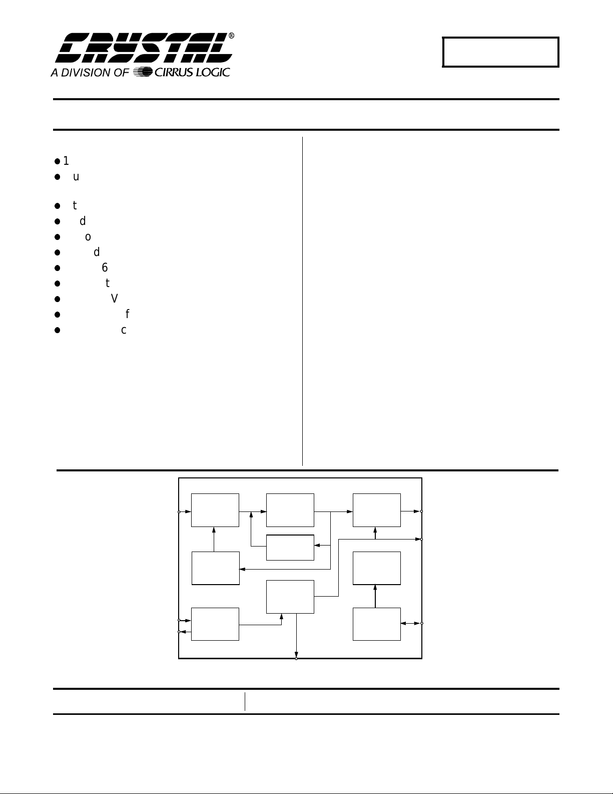
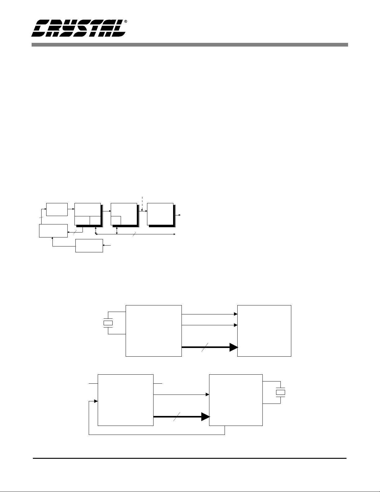
Description
The CS7615 is a low-power Analog front-end processor
for standard four-color interline transfer CCD imagers.
The architecture includes a correlated double sampler,
AGC amplifier, black-level clamp, 10-Bit A/D converter,
and a complete multi-sync CCD timing generator. The
analog CCD imager output can be directly connected to
the CS7615 input, which does not require an external
buffer amplifier . The pi xel data i s double sampl ed for i mproved noise performance, and gain adjusted prior to
being digitized by t he A/D conv erter. Feedbac k from t he
A/D converter holds the image black level at code-16
(assumes 8-bit data path), addressing ITU-601 compliance issues. The multi-sync CCD timing generator is
programmed via the I
wide range of interline transfer CCD imagers up to 1000
pixels wide. The CS7615 supports full ITU-601 compliance for images up to 720 pixels wide , and is compatible
with both NTSC and PAL timing. The CS7615 is designed to be used along with either the CS7665 or
CS7666 Digital Color-Space Processor for CCD Cameras, which generates a 4:2:2 component digital video
output.
2
C bus, and can be used with a
CCD Output
Master Clock
CDS/AGC Data Out
AGC
Controller
PLL
Preliminary Product Information
Cirrus Logic, Inc.
Crystal Semiconductor Products Division
P.O. Box 17847, Austin, Texas 78760
(512) 445 7222 FAX: (512) 445 7581
http://www.crystal.com
ORDERING INFORMATION
CS7615-KQ 0° to +70° C 44-pin TQFP
(10 mm × 10 mm × 1.6 mm)
A/D
Converter
Black
Level
Timing
Generator
CCD Timing Signals
This document contains information for a new product.
Cirrus Logic reserves the right to modify this product without notice.
Copyright Cirrus Logic, Inc. 1998
(All Rights Reserved)
Output
Formatter
Register
Block
I2C
Clocks Out
I2C Bus
DS231PP6
JUL ‘98
1
Page 2

TABLE OF CONTENTS
ANALOG C H A RA C T E RISTICS: ........ ... .................... .............................. ..............3
DIGITAL CHARACTERISTICS: ............................................................................ 3
POWER CONSUMPTION:....................................................................................3
CONTROL PORT CHARACTERISTICS:..............................................................4
SWITCHING CHARACTERISTICS:...................................................................... 5
RECOMMENDED OPERATING CHARACTERISTICS: ....................................... 5
ABSOLUTE MAXIMUM RATINGS:...................................................... ...... ...........5
GENERAL D E SC R IPTION .... .. ..................... ....................................... ................ 6
Overview ......... ......... ....... ......... ......... .......... ...... .......... ......... ....... ......... ....... 6
Interfacing the CS7615 with CS7665 or CS7666 ..................... ..................6
Operatio n .......... .............. .............. ........... .............. .............. .............. ......... 6
CCD Timing Generator ......................................... .... ........................ .. .... .. ..8
Vertical Timing Specifications ..................................................................... 8
Horizontal Timing Specifications .................................................................8
Description of Opera tion . .. ... ....................................... ............................. ... 9
Automatic Gain Control ............................................................................... 9
Correlated Double Sampling (CDS) .......................................................... 11
Analog to Digital Converter ....................................................................... 15
Black Level Adjust to Code 16 (10-bit Code 64) .......................................15
Formatter .................................................................................................. 15
SERIAL CO N T RO L B U S ................ .. ..................... ....................................... ..... 16
Station Address ........................................................................................ 16
Write Operations ................................................................................ 16
Address S e t O p e ra ti o n .. ............................. ....................................... . 16
Read Opera tions ............. .. .............................. .............................. .....16
REGISTER DESCRIPTIONS ............................................................................. 17
PIN DESCR I P T IO N S ............................. .............................. ..............................30
PACKAGE DIMENSIONS ..................................................................................34
CS7615
2 DS231PP6
Page 3
CS7615
ANALOG CHARACTERISTICS: (T
=25°C; VAA=VDD=5V; Output Load=30pF )
A
Parameter Symbol Min Typ Max Units
Dynamic Performance
Integral Non-Linearity INL - 1 - LSB
Differential Non-Linearity DNL - 0.75 - LSB
Analog Input
Analog Input Capacitance C
IN
-10-pF
Automa tic G a in C o n tr o l
Maximum Gain G
Minimum Gain G
Gain Increment
DIGITAL CHARACTERISTICS: (T
=25°C; VAA=VDD=5V; Output Load=30pF )
A
MAX
MIN
∆
G - 78.4 117.6 mdB
-20-dB
-0-dB
Parameter Symbol Min Typ Max Units
Logic Inputs
High-Level Input Voltage V
Low-Level Input Voltage V
Input Leakage Current I
IH
IL
IN
VDD-0.8 - - V
--0.8V
--10mA
Logic Outputs
High-Level Output Source Current @ VOH = VDD-0.4V I
Low-Level Output Sink Current @ V
= 0.4V I
OL
3-State Leakage Current I
OH
OL
OZ
--1mA
--1mA
--10µA
POWER CONSUMPTION: (T
=25°C; VAA=VDD=5V; Output Load=30pF )
A
Parameter Symbol Min Typ Max Units
Power Dissipation P
Analog Power Supply Current Normal Mode
Low-Power Mode
DIgital Power Supply Current Normal Mode
Low-Power Mode
I
AN
I
ALP
I
DN
I
DLP
D
-650-mW
-
-
-
-
99
63
55
22
-
-
-
-
mA
mA
mA
mA
DS231PP6 3
Page 4
CS7615
CONTROL PORT CHARACTERISTICS: (T
Parameter Symbol Min Typ Max Units
SCL Clock Frequency f
Bus Free Time Between Transmissions t
St art Condition Hold Time t
Clock Pulse Width High
Setup TIme for Repeat Start Condition t
SDAIN Hold Time from SCL Falling t
SDAIN Setup Time from SCL Rising t
SDAIN and SCL Rise Time t
SDAIN and SCL Fall Time t
Setup Time for Stop Condition t
=25°C; VAA=VDD=5V; Output Load=30pF )
A
Low
Stop Start
SDA
t
buf
t
hdst
t
high
SCL
buf
hdst
t
high
t
low
sust
hdd
sud
r
f
susp
Repeated
Start
t
- - 100 kHz
4.7 - -
4.0 - -
4.0
4.7
4.7 - 0--µs
0.25 - -
--1.0µs
--0.3µs
4.0 - -
--µs
Stop
t
hdst
f
t
susp
µ
s
µ
s
µ
s
µ
s
µ
s
µ
s
CL
S
t
low
t
hdd
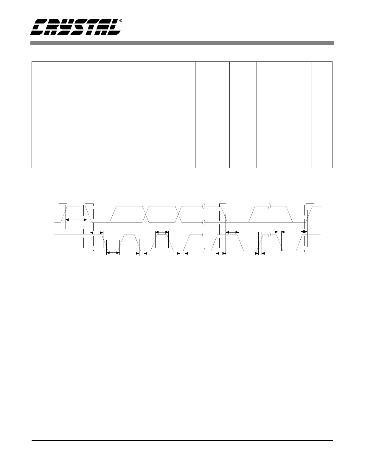
Figure 1. I2C Timing Diagram
t
sud
t
sust
t
r
4 DS231PP6
Page 5
CS7615
SWITCHING CHARACTERISTICS: (T
=25°C; VSS=VDD=5V; Output Load=30pF )
A
Parameter Symbol Min Typ Max Units
Crystal Frequency Range f
CRY
6.75 27 MHz
Crystal Oscill ator Duty Cycle 4 0 60 %
CLKO Frequency f
CLK2XO Frequency f
pix
dat
6.75 13.5 MHz
13.5 27 MHz
CLKO duty cycle 50 %
CLK2XO duty cycle 50 %
CLK2XO falling edge to CLKO falling edge 4 8 ns
FR Clock (CCD reset gate clock) Duty Cycle 25 %
H1 Clock
H2 Clock
Duty Cycle 50 %
Duty Cycle 50 %
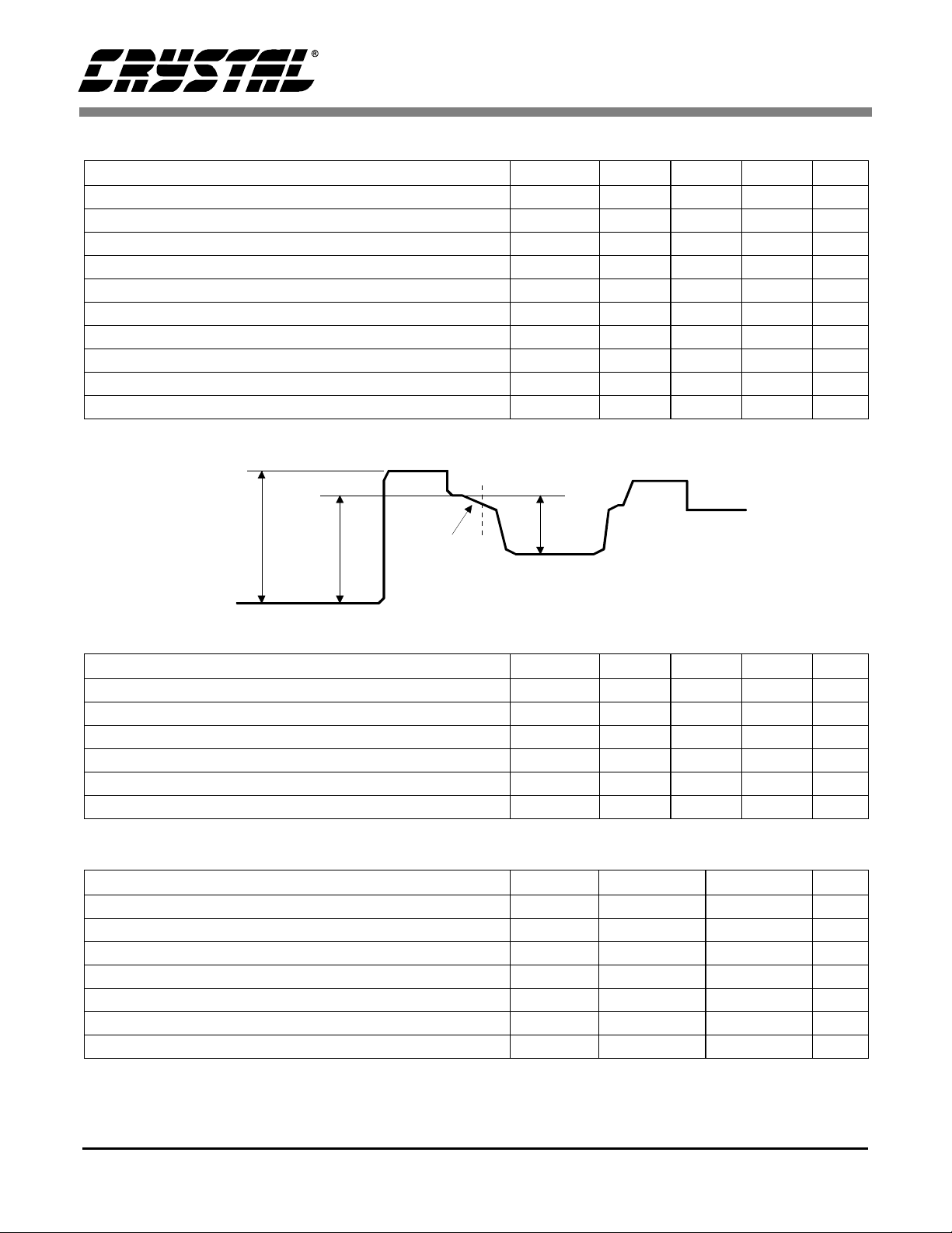
RECOMMENDED OPERATING CHARACTERISTICS:
V
AC
V
AIN
V
DC
Feedthrough
Level
GND
Figure 2. Analog Input
Parameter Symbol Min Typ Max Units
Power Supply Voltage V
AA
, V
DD
4.5 5.0 5.5 V
GNDA to GNDD Voltage Dif ferential 10 mV
Crystal Frequency Range 6.75 27 MHz
Analog Input AC Range (Figure 2) V
Analog Input DC Offset (Figure 2) V
Analog Input Voltage (Figu re 2) A
AC
DC
IN
01.65V
12 V
018V
ABSOLUTE MAXIMUM RATINGS:
Parameter Symbol Min Max Units
Power Supply Voltage V
AA
, V
DD
Digital Input Voltage GNDD-0.3 (V
Analog Input Voltage - AIN only A
IN
Input Current (except supply pins) 10 mA
Ambient Temperature Range -0 +70 °C
Lead Solder Temperature (10sec duration) +260 °C
Storage Temperature Range -65 +150 °C
-0.3 7.0 V
)+0.3 V
DD
GNDA-(0.3) 20 V
Specifications are su bject to change without notice.
DS231PP6 5
Page 6
CS7615
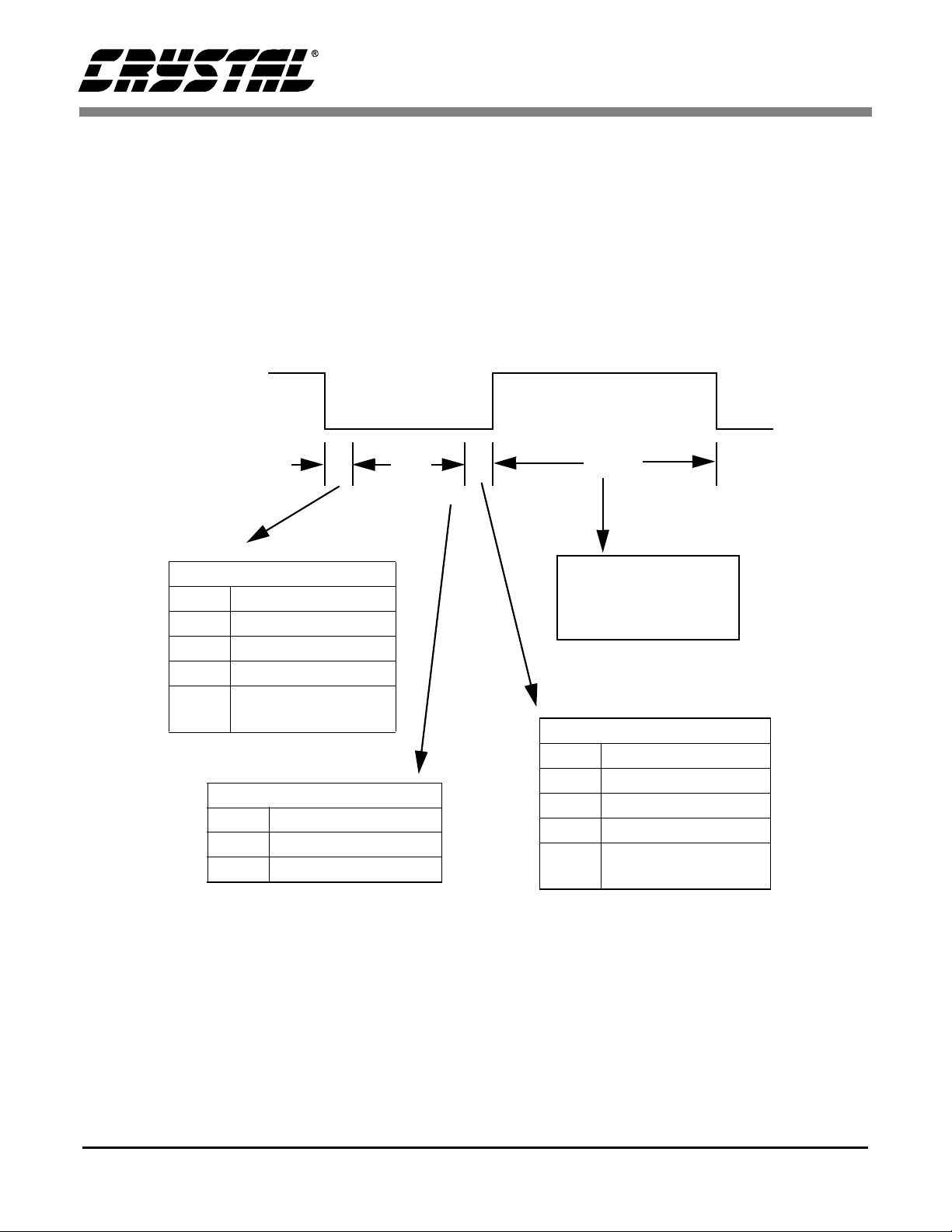
GENERAL DESCRIPTION
Overview
The CS7615 performs the analog functions in a
four chip digital CCD Camera. The four main chips
include the CCD imager, the CS7615 CCD digitizer, the CS7665 or CS7666 color space processor,
and a vertical drive interface-chip for the CCD imager. Several CCD imagers (and their associated
vertical drivers) can be used with the CS7615 digitizer and the CS7665 or CS7666 proc essor to form
a simple and cost-effective YCrCb output format
digital camera. The block diagram in Figure 3 illustrates the s ys tem interco nnect.
4:2:2, H.656 VIDEO
IMAGE
PROCESSO R
2
I C
+5 V
CS4952 or
CS4954
2
2
I C BUS
CCD CDS/ADC
7
512x480
VERTICAL
DRIVE
+8 V TO +12 V
CS7615
TIMING
9
DC-DC
CONVERTER
I C
2
CS7665 or CS7666
Figure 3. Typical 4-Chip Digital CCD Camera
Interfacing the CS7615 with CS7665 or CS7666
The CS7666 is a direct replacement for the
CS7665. No board or softwa re cha nges are needed
for existing designs. However, slight changes to
existing hardware and software are necessary to
take advan tage of th e CS766 6. See Figu re 4 and 5
and the CS7666 data she et for m ore det ails.
Operation
The CS7615 digitizer is designed to provide all
necessary an al og functions and conversion to digital data of a standard CCD image r output signal as
well as prov ide all the timin g and control sig nals
for the CCD imager. The architecture includes a
correlated dou ble sampler, va riable gain am plifier
with an integrated AGC loop, black level clamp,
10-bit A/D converter, output formatter, and a complete multi-sync CCD timing generator. The output
of the A/D converter ranges from code 004h to
code 3FBh a nd the form atter adds spec ial end-of active-video (EAV) and start-of-active-video
(SAV) codes to each line, making the output of the
CS7615 simila r to the descrip tion in the ITU-65 6
recommenda tion.
56
55
CS7665CLK2x0 CLOCK
XTAL
32
33
CS7615
39
CLK0
4
10-BIT DATA
Figure 4. CS7615/CS7665 Interface
NC
CS7615
33
32 XTALIN
39
CLK0
4
10-BIT DATA
CS7666NC
55 CLKIN
CCLOKG
56
XTAL
52
Figure 5. CS7615/CS7666 Interface
6 DS231PP6
Page 7
CS7615
The EAV/SAV code definitions are consistent with
an 8-bit data path. As per the ITU-656 recommen-
dation, the LSB’s of the CS7615 ar e fractional bit s
which are not used when delivering 8-bit output data. In 10-bit mode, all ten digital outputs can be
connected directly to the CS 7665.
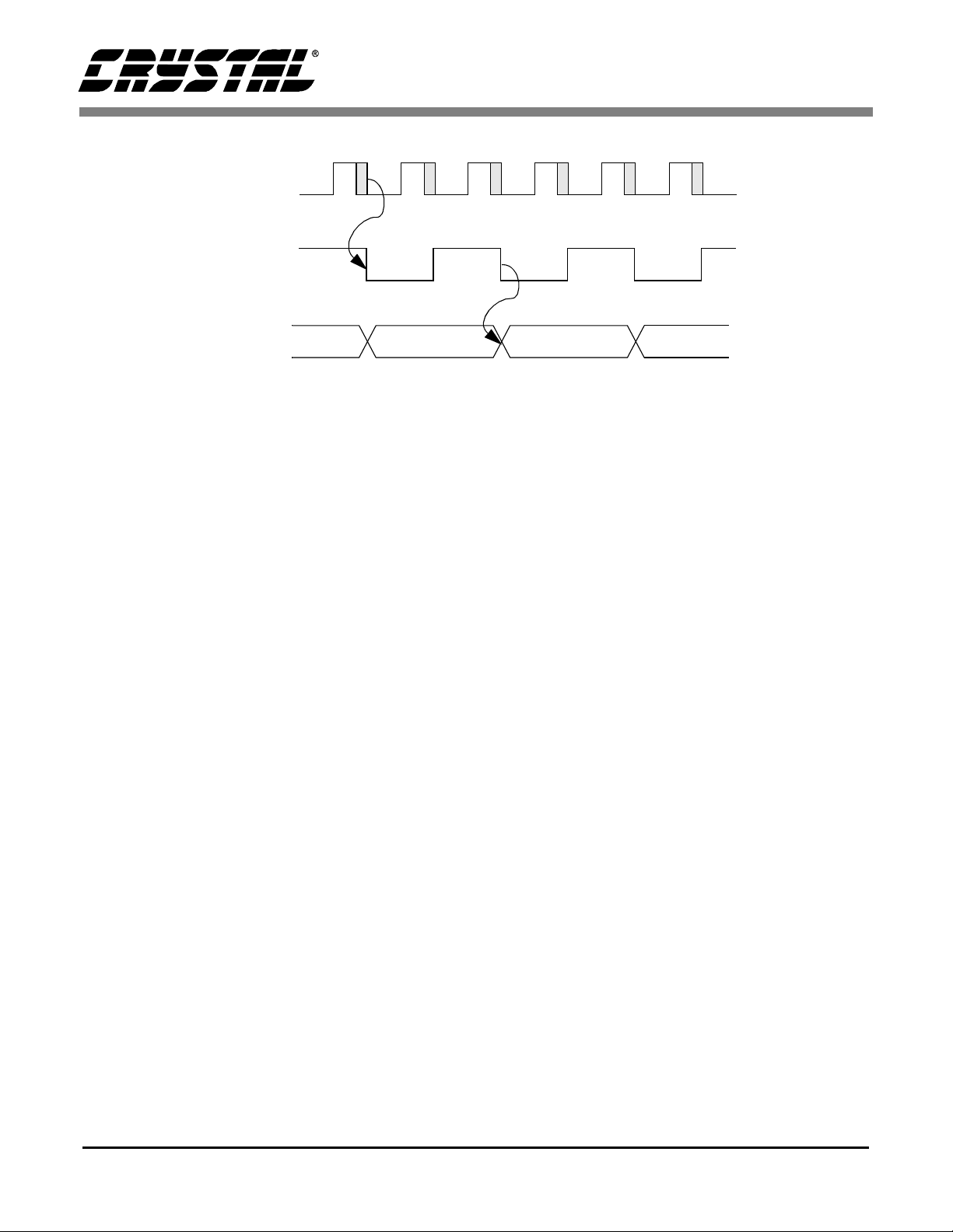
The output da ta format from the CS7615 formatte r
is shown in Figure 6. The CS7615 also outputs two
clocks, one at the pi xe l rate and t he other at 2× the
HREF
Blanking period
EAV code (10 bits)
Smpl. Word
0 3FFh
1 000h
2 000h
3
Smpl. Word
4 040h
Binary
1
fv1P3P2P1P
Blank code (10 bits)
repeat above word
4T
00
0
N
T
b
output pixel data rate (see pin description for
CLK2XO). The ou tput of the formatter i s available at the pins D
and it transitions at the fall-
O[0..9]
ing edge of the pixel rate clock CLKO. Figure 7
shows the basic output timing diagram. The falling
edges of CLKO lag t he fall ing ed ges of CLK2XO
by 4 to 8 ns and both clocks hav e approximately
50% duty cycles.
Active video
4T
AV*T
T = output pixel period
During active video,
samples of mosai c d ata;
during vertical blanking,
040h.
At reset or power down, 040h.
SAV code (10 bits)
Smpl. Word
0 3FFh
1 000h
2 000h
3
Binary
fv0P3P2P1P
1
00
0
f
= field bit; 0 (odd field), 1 (even field)
v
= vertical blanking bit; 0 (active video lines), 1(verti cal blanking)
P3P2P1P
DS231PP6 7
= error protection bits (as per ITU-656).
0
Figure 6. CS7615 Output Data Format
Page 8
CLK2XO
CLKO
D
O[0..9]
CS7615
Figure 7. CS7615 Output Data and Clocks
CCD Timing Generator
The CCD timing and control signal outputs are dictated by the programmable register settings. This
allows for compatibility with a variety of CCDs.
The HSYNC signal is also output for use in a genlock confi guration. The op en-drain HCLK can be
used to clock dc -dc voltage converters whi ch are
typically used to generate the CCD imager bias
voltages. The following description explains the
various output signals provided to the vertical driver and CCD a s well as t he progra mmabl e parame ters that may be set to control these signals.
HREF* - horizontal reference signal. It stays
high during the active video portion of the line.
HENB* - Horizontal shift register clock enable
signal. Enables H1 a nd H2 out of analog timing.
CLAMP* - Black clamp signal provided to the
ADC.
V1X, V2X, V3X, V4X - Vertical register shift
clock. Used both during vertical transfer and
charge read out.
VH1X, VH3X - CCD charge read out pulse.
HCLK - Signal used by the dc - dc converter. In
the norma l mode, it is th e same as HREF; In
fast mode, i t ope rate s at about 16× of the h orizontal line fre quency and is rese t at the beg in-
ning of HREF.
HSYNC - Horizontal sync signal.
OFDX - Overflow drain control clock. This
signal sets the ele c tronic shutter speed .
VRST - Vertica l fi eld reset signa l.
VREF* - Vertical reference signal. It is high
during the active video lines.
*Internal sign a l on the CS7615 - not a chip output.
Vertical Timing Specifications
The CCD array i s read out alternate ly as odd and
even fields with interlaced horizontal lines. Thus
each field has half the total nu mber of horizontal
rows. Table 1 specifi es the progr ammable ve rtical
timings which are defined in Figure 8. The timings
vary based on odd o r even field, 525 or 625 line
CCD, and the manufa c turer.
Horizontal Timing Specifications
Each horizontal row of the CCD is divided into
several regions co rrespon din g to the type of pixel s
present. Different CCDs have different numbers of
pixels in e ach region and the timing si gnals must
take this into account. The d ifferent pixe l types include optic al bla ck pi xe ls (fro nt an d rea r), d um my
pixels, active video pixels, and blank video. The
horizontal t iming for t he CCD is based on maintaining a fi xed 63.5 µs horizont al line time.
8 DS231PP6
Page 9
Symbol Description Register
VLO # of lines in odd field 33h, 39h
VLE # of lin e s in even field 34h, 39h
VBO End of VREF line # 36h, 39h
XSO Charge transfer line # 38h, 39h
VBE End of VREF line # 35h, 39h
XSE Charge transfer line # 37h, 39h
Table 1. CCD vertical timing specifications
Table 2 speci fies all of the program mable timing
parameters related to horizontal timing signals.
These parame ters are defined in Figure 9.
Figure 9 shows the timings for HREF, HSYNC,
CLAMP, and HENB. Their relationship to different kinds of pixels on each horizontal row output
from the CCD is also shown . The waveforms for
these signals are repeated on every line. The horizontal shi ft regi ster clock s, H1 and H 2, operat e at
the CLKO frequency and are active throughout the
horizontal line period except when HENB is high.
CS7615
Figure 10 shows the t imings for the V1 X through
V4X signals. The specified waveforms repeat on
every horizontal line except during the charge
transfer line. During this line the CCD charge is
read out an d the timing is differen t as shown in Figure 11. In addition signals VH1X and VH3X are
also required during charge read out a s shown in
Figure 1 2.
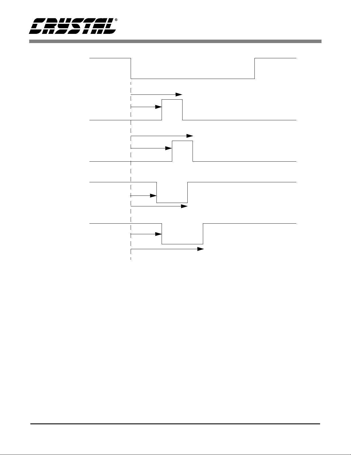
The overflo w drai n cont rol si gnal is shown in Fig ure 13. The OFDX signal is used to control the
electronic sh utter timin g of the CCD. Sh utter timing for vario us set ti ngs of the shutter control is described in the register section of this document.
Description of Operation
The interna l o perat io n of the CS76 15 ca n b e sepa rated into several distinct blocks. The following
section provides an overvi ew of how these blocks
operate and interact.
Automatic Gain Control
The pixel dat a ente ri ng the CS 7615 from th e CC D
is scaled as det ermined by the au t o m atic gain control loop. By pro perly applyin g gain to the signal,
the full range of the A/D converter is used. The in-
VLO
VREF*
HREF
FLD
DS231PP6 9
1
VBO: end of VREF
XSO: charge transfer line
Not to scale
Figure 8. Vertical Timing Signals -Internal to CS7615
VBE: end of VREF
XSE: charge transfer line
VLE
Page 10
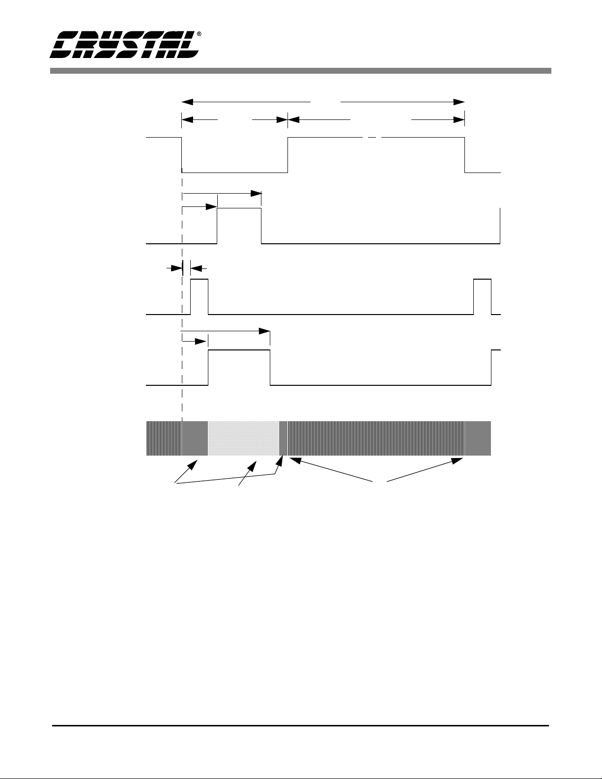
Hlen
CS7615
HREF
HSYNC
CLAMP
HENB
0
BC
Hsnyr
Hstart
HBPD
Hsynf
Hend
Active Video
CCD
OUTPUT
Optical
black pixels
Figure 9. Timing Diagram for Href, HSYNC, Clamp, and Henb
Inactive
video
ternal analog gain range is 38 dB in steps of
0.078 dB ideal. Adjustments made in these small
steps sh oul d c ause n o not ice able bri gh tne ss chan ge
in the image from frame to frame. In addition to the
internal an alog gain , the con trol loo p will var y the
shutter speed through the OFDX output from 0 to 54 dB as it deems necessary.
The AGC algorithm uses a luma or mosaic histogramming technique in which the brightness of
each pixel is binned into one of seven bins. The
Active video
number of pixels in a bin will produce an error signal that is then used to update the gain. The following paramete rs control the loop d ynamics and are
programma ble to meet th e needs of the us er.
PAL bit: Selects a PAL or NTSC camera system.
AGC Window: Adjusts what portion of the
frame is used for the AGC algorithm.
Luma/Mosaic: Selects whether luma or mosai c
data are used in the histogramming.
10 DS231PP6
Page 11
HREF
V1X
V2X
V3X
CS7615
V1f
V1r
V2f
V2r
V3f
V3r
V4X
V4f
V4r
Figure 10. Vertical Shift Register Signal Timings
Flickerless Mode: Restricts the shutter speed to
only flickerless values for the given system and
environment. If the scene is too bright, the
AGC loop will select exposure settings shorter
than the flickerless modes.
PAL Environment: Selects PAL or NTSC environment.
Target Value: Adjusts the brightness threshold.
A lower target re sults in the loop settli ng to a
lower gain.
Max Gain: Sets a maximum gain value that will
not be exceeded even if the target brightness
has not been me t.
Slew: Contro ls the rate of decay of the gai n as
the AGC loop slews because of light intensity
variation.
Speed: Cont rols the overall lo op gai n and th us
speed of gain correc t ion.
Min Gain: Sets the m inimum on-chip gain al lowed. Thi s va lue s ho uld be us ed if the sat ura tion voltag e is less than 1. 6V .
Correlated Double Sampling (CDS)
Correlated Do uble Sampling, as applied to CCDbased imaging systems, is a method used to remove
low-frequency noise from the output of a CCD imager leaving only the signal of interest. The CDS is
applied prior to amplification by the VGA.
DS231PP6 11
Page 12

Note: line #s shown here are for 525 line systems
CS7615
HREF
V1X
V2X
ODD FIELDEVEN FIELD
V3X
V4X
HREF
LINE #17
V2of
V2or
V3of
LINE #279 LINE #280
LINE #18
V3or
(no pulse on V1X)
V1X
V2X
V3X
V4X
Figure 11. Vertical Shift Register Signal Timings for Charge Read Out Phase
12 DS231PP6
V2er
V2ef
V3ef
V3er
V4ef
V4er
Page 13

CS7615
HREF
VH1X
VH3X
VREF
LINE #17 and #279
VH1r
VH1f
VH3r
VH3f
Figure 12. Charge Read Out Signal Timing
19 H
Note: Line #s shown are for 525 line system.
262 H
or 263 H
OFDX
HREF
Notes: OFDX remains high when shutter is
OFDX
OFDW
Figure 13. Electronic Shutter Control Signal Timing
DS231PP6 13
Horizontal line co unt =
Shutter control register value
set to 00h.
Line #s shown are for 525 line system.
Page 14

Symbol Description Register
HBPD Horizontal blanking period 40h
Hlen Total number of horizontal pixels 41h, 42h
Hsynr
Hsynf
BC
Hend
Hstart Hz. clock disable peri od 47h
V1r V1 clock leading edge 48h
V1f V1 clock trailing edge 47h
V2r V2 clock leading edge 4Ah
V2f V2 clock trailing edge 4Bh
V3f V3 clock leading edge 4Ch
V3r V3 clock tr ailing edge 4Dh
V4f V4 clock leading edge 4Eh
V4r V4 clock trailing edge 4Fh
V2or V2odd clock leading edge 50h, 52h
V2of V2odd clock trailing edge 51h, 52h
V3of V3odd clock leading edge 53h, 55h
V3or V3odd clock trailing edge 54h
V2er V2even clock leading edge 56h, 58h
V2ef V2even clock trailing edge 57h
V3ef V3even clock leading edge 59h, 5Bh
V3er V3even clock trailing edge 5Ah
V4ef V4even clock leading edge 5Ch, 5Eh
V4er V4even clock trailing edge 5Dh
VH1f Charge read clock leading edge 5Fh, 61h
VH1r Charge read clock trailing edge 60h, 61h
VH3f Charge rd clock leading edge 62h, 64h
VH3r Charge rd clock trailing edge 63h, 64h
OFDW OFDW pulse width 65h
HREF to HSYNC leading edge 43h
HREF to HSYNC trailing edge 44h
HREF to CLAMP leading edge
(clamp trailing edge at Hend)
HREF to HENB leading edge 46h
45h
CS7615
Table 2. Horizontal timing specifications
14 DS231PP6
Page 15

CS7615
Analog to Digital Converter
After the pixel dat a is double sampl ed and the appropriate gain has been applie d, it is digitized by
the intern al 10-bit A/D c onverter. Thes e resulting
mosaic data are i nput to the formatter which for mats the da ta bef ore sending it to th e chip output.
The output of the A/D converter is also used by the
internal AG C loop in deter mining the prop er gain
setting, and by the black le ve l adjust when reading
the black pixels.
Black Level Adjust to Code 16 (10-bit Code
64)
The output data are adjusted to hold the image
black level at the 8-bit code of 16, in compliance to
the ITU-601 recommendation. During the blanking
periods, the black level adjustment is updated when
over black pixels. The number of black pixels used
is programmable by the user through the I
face.
2
C inter-
Formatter
The formatter adds the necessary EAV/SAV timing
codes to the output data in accordance with the
ITU-656 recomm endation.
DS231PP6 15
Page 16

CS7615
SERIAL CONTROL BUS
The serial c ontrol bu s protoc ol i s an 8-b it pro tocol
controlled receiver. To the receiver, the control bus
looks like an 8-bit bi-directional channel down
which short packets are sent or received. Each
source devi ce appe ar s to the re ceiv er as a se t of 8 bit registers, which are addressable to a device
through a station address. Packets are used to write
and read the c ont ents of these devic e re gi sters.
There are three packet formats: WRITE format,
ADDRESS SET format, a nd READ format. Each
packet is addressed to a device by its station address. The LSB of the station address is the data direction bi t. T his b it is se t LO W i n th e WR IT E and
ADDRESS SET packets, and it is set HIGH for
READ packets. The receiver can read and write to
non-existent registers within the selected device.
WRITE opera tion s will h av e no e ffect ; RE AD operations wil l ret urn a value of 00h.
Station Address
The CS7615 rev A default station address is A8h
for writes and A9h for re ads. Sub sequen t versions
of the CS7615, starting with r ev B, will use a de fault station a ddress of 68 h for writes a nd 69h for
reads.
third byte is the register data (0..255). No extra
bytes should be sent.
Byte Sequence WRITE Format Packet Detail
First Byte Station Address
with LSB Set LOW
Second Byte Device Register Address (0. .255)
Third Byte Register Data (0..255)
Table 3. WRITE Format Packet
Address Set Operation
The ADDRESS SET format consists of a two-byte
packet which sets the address of a subsequent
READ operation . The first byte of the station Address with the LSB (data direction bit) set LOW t o
indicate a write opera tion. The secon d byte is the
register address (0..255). The ADDRESS SET format is the sam e as t he WR IT E form at, witho ut t he
register data.
ADDRESS SET format
Byte Sequence
First Byte Station Address
Second Byte Device Register Address (0. .255)
Table 4. ADDRESS SET Format Packet Operation
Packet Details
with LSB Set LOW
Read Operations
The station address can be changed by writing a
new base station address to internal I2C register
FEh. Note that the station address register describes only the 7 MSBs of the CS7615 station address. The base writ e a ddress will need to be ri ght
shifted by one pla ce before being writ ten into the
FEh register.
Write Operations
The WRITE format consists of a three-byte packet.
The first byte is the station address with the data direction bit set LOW to indicate a write. The second
byte is the device register address (0..255). The
16 DS231PP6
The READ operation consist of two or more bytes.
The first b yte is the station address with the LSB
(data direc tion bit ) set HIG H i ndic ating a read op eration. The addressed device then sends one or
more bytes back from the register last addressed by
the previous WRITE operation, or ADDRESS SET
operation.
Byte Sequence READ Format Packet Details
First Byte Station Address with LSB set
HIGH; Source Device then
Returns One Byte of Register
Data (0..255)
Second Byte Returned data from CS7615
Table 5. READ Format Packet.
Page 17

CS7615
REGISTER DESCRIPTIONS
Software Reset Register (00h)
76543210
res res res SR4 res res res r es
rrrwrrrr
SR4 Setting bit SR4 to l ogic high will initiate a CS7615 software reset. Software reset resets all the
digital block s except for I
bit automatically clears.
2
C and the ADC calibration lo gic. The clocks remain run ning. This reset
Low Power Register (20h)
76543210
res res res PD4 res res res r es
rrrr/wrrrr
PD4 Setting bit PD4 to l ogic high will place the CS7615 chi p in a low power mode. The I2C interface
and clock generation circuitry will remain powered up.
Operational control #1 Register (24h)
76543210
PAL AGCW1 AGCW2 AGCDIS AGCCALG CCDTYP FLCKLS PALENV
r/w r/w r/w r/w r/w r/w r/w r/w
PAL Logic high indicates a PAL standard camera system, logic low indicates NTSC. Default = 0.
AGCW Used to window the portion of the frame to use for AGC. Default = 00.
00 = use entire frame
01 = use center 1/4 area of frame
10 = use center 1/16 area of frame
11 = reserved
AGCDI Logic high disables CS7615’s automatic gain cont rol cir cui try. User may manuall y contro l gain
through the gain register 25h/26h. Default = 0.
AGCALG Controls da ta used in CS7615’s AGC loop. Logic high i ndicates mosaic data, logi c low indicates
luma data. Default = 0.
CCDTYP Logic high signifies that a Type B CCD is being used , logic low si gnifies a Type A CCD. Default
= 0.
FLCKLS Logic high restricts shutter to flicker less settings. Default = 0.
PALENV Logic high when the camera system is being used in a PAL environment, logic low in an NTSC
environment. Default = 0.
R/W Read/Write
R Read
WWrite
RES Reserved
DS231PP6 17
Page 18

CS7615
Gain Registers (25-26h)
25h:
76543210
AGC10 AGC9 AGC8 AGC7 AGC6 AGC5 AGC4 AGC3
r/w r/w r/w r/w r/w r/w r/w r/w
26h:
76543210
res res res res res AGC2 AGC1 AGC0
rrrrrr/wr/wr/w
AGC(10:0) Gain control word for the automati c gain control. This 11 bit word is a 2’s compliment number
which has a minimum value of -784 (decimal ) (Reg 26h = 04h; Reg 25h = 5F0h) for PAL or 765d for NTSC (R eg 26h = 05h ; Reg 25 h = 03) a nd a maximu m value of 484d (Reg 26h = 01h;
Reg 25h = E4h). The gain ra nge is -54 dB to 38 dB in steps of 0 .078 dB ideal, 0.12 dB max step
is guaranteed only for chip GAIN. Default is 000h.
AGC Error Statistic Re gister (27h):
76543210
agcer7 agcer6 agcer5 agcer4 agcer3 agcer2 agcer1 agcer0
rrrrrrrr
AGCER The 8 MSBs of the gain error statistic calculated as part of the AGC loop.
AGC Count Statistic Register (28h)
76543210
res agcct6 agcct5 agcct4 agcct3 agcct2 agct1 agcct0
rrrrrrrr
AGCCT The output of the 1-of-7 block which denotes the bin where the AGC target was met.
AGC Target Value Register (29h)
76543210
res res res res res agctg2 agctg1 agctg0
rrrrrr/wr/wr/w
AGCTG The target value use d in the AGC loop. I t denotes the number o f pixel s that must b e exce eded
for an intensity bin to give an output of ‘1’. Default is 0h.
000=64 100=1024
001=128 101=2048
010=256 110=4096
011=512 111=8192
18 DS231PP6
Page 19
CS7615
AGC Maximum Gain Register (2Ah)
76543210
mgn7 mgn6 mgn5 mgn4 mgn3 mgn2 mgn1 mgn0
r/w r/w r/w r/w r/w r/w r/w r/w
MGN Sets the maximum gain allowable if the user chooses to limit the chip gain beyond a certain
value. The range is 0-242, with the act ual max gain word being twi ce th is value. Default is F2h.
AGC Slew and Speed Registe r ( 2B h )
76543210
res res res res slew1 slew0 spd1 spd0
rrrrr/wr/wr/wr/w
SLEW Sets the rate of decay of gain when the gain target i s exceeded in the maximum intensity bin.
Default is 0h.
00 = -8 10 = -32
01 = -16 11 = -64
SPD Varies the AGC loop gain. The error signal used for correction is multiplied by the speed num-
ber before being added to the accumulator. Default is 0h.
00 = 1x 10 = 4x
01 = 2x 11 = 8x
AGC Minimum Gain Re gi ster (2Ch)
76543210
mng7 mng6 mng5 mng4 mng3 mng2 mng1 mng0
r/w r/w r/w r/w r/w r/w r/w r/w
MNGN Sets the minimum gain allowable i f t he user choose s t o li mit t he ch ip gai n from a cert ain value.
Default is 00h.
CCD Signal Alignment Reg ist er (2Dh)
76543210
HR1 HR0 HF1 HF0 FRR1 FRR0 FRF1 FRF0
r/w r/w r/w r/w r/w r/w r/w r/w
These signals adjust the edges of H1 or FR with res pect to the internal sampling clock.
HR Adjusts the location of the rising edge of H1.
HF Adjusts the locat ion of the falling edge of H1.
FRR Adjusts the location of the rising edge of FR.
FRF Adjusts the location of the falling edge of FR.
DS231PP6 19
Page 20

CS7615
VRST Registers (2Eh, 2Fh)
2Eh:
76543210
VRSTN8 VRSTN7 VRSTN6 VRSTN5 VRSTN4 VRSTN3 VRSTN2 VRSTN1
r/w r/w r/w r/w r/w r/w r/w r/w
2Fh:
76543210
res res res res res VRSTDY VRSTFLD VRSTN0
rrrrrr/wr/wr/w
These parameters are needed only when the VRST input is used .
VRSTN The line number gets reset to this value on a negative edge of VRST. Default is 004h.
VRSTDY Logic high deno tes VRST will be dela yed with respect to the line position. Defaul t = 0 (no del ay).
VRSTFLD Logic high denotes the field is reset t o even on a negat ive edge of VRST, logi c low denotes t he
field is reset to odd. Defaul t = 0.
Maximum Shutter Exp osure Regi ste r (3 0h)
76543210
MSXH7 MSXH6 MSXH5 MSXH4 MSXH3 MSXH2 MSXH1 MSXH0
r/w r/w r/w r/w r/w r/w r/w r/w
MXSH If the user chooses to limi t the expo sure t ime, the max shut ter ga in is set to thi s value. 00h=ful l
exposure, BFh=min exposure f or NTSC, C4h= min exposure for PAL.
Operational Control #2 Register (31h)
76543210
res res res res BLKDIS ADCAL1 ADCAL2 CNVF ST
rrrrr/wr/wr/wr/w
BLKDIS Logic high disables the black level loop. Black level remains at t he current value. Default =0.
ADCAL1 Analog-to-digital converter option. When written to a logic high, calibration is immediately en-
tered. This bit goes back low when cali bration is complete.
ADCAL2 Analog- to-digital conver ter option. Logic hi gh results in cali bration being done after every frame,
logic low results in calibration only on power up. Default = 0.
CNVFST Logic high sets the frequency of HCLK to 16×the line frequency, logic low sets HCLK to 1×the
line frequency. Default = 0.
20 DS231PP6
Page 21

CS7615
Timing Control- Line Number Regist ers (33h -39h)
33h:
76543210
VLO8 VLO7 VLO6 VLO5 VLO4 VLO3 VLO2 VLO1
r/w r/w r/w r/w r/w r/w r/w r/w
34h:
76543210
VLE8 VLE7 VLE6 VLE5 VLE4 VLE3 VLE2 VLE1
r/w r/w r/w r/w r/w r/w r/w r/w
35h:
76543210
VBE8 VBE7 VBE6 VBE5 VBE4 VBE3 VBE2 VBE1
r/w r/w r/w r/w r/w r/w r/w r/w
36h:
76543210
VBO8 VBO7 VBO6 VBO5 VBO4 VBO3 VBO2 VBO1
r/w r/w r/w r/w r/w r/w r/w r/w
37h:
76543210
XSE8 XSE7 XSE6 XSE5 XSE4 XSE3 XSE2 XSE1
r/w r/w r/w r/w r/w r/w r/w r/w
38h:
76543210
XSO8 XSO7 XSO6 XSO5 XSO4 XSO3 XSO2 XSO1
r/w r/w r/w r/w r/w r/w r/w r/w
39h:
76543210
res res VLO0 VLE0 VBE0 VBO0 XSE0 XSO0
r r r/w r/w r/w r/w r/w r/w
VLO The number of lines in an odd field. Default is 106h.
VLE The number of lines in an even field. Default is 107h.
VBE Line number for end of VREF for even field. Default is 013h.
VBO Li ne number for end of VREF for odd field. Default is 012h.
XSE Line number for charge transfer for even field. Default is 011h.
XSO Li ne number for charge transfer for odd field. Default is 010h.
DS231PP6 21
Page 22

CS7615
Timing Control-Horizontal Blank Pd Register (40h)
76543210
HBPD7 HBPD6 HBPD5 HBPD4 HBPD3 HBPD2 HBPD1 HBPD0
r/w r/w r/w r/w r/w r/w r/w r/w
HBPD Number of pixel clocks in the horizontal blank period. Default is 70h.
Timing Control- Line Length Register (41h-42h)
41h:
76543210
HLEN9 HLEN8 HLEN7 HLEN6 HLEN5 HLEN4 HLEN3 HLEN2
r/w r/w r/w r/w r/w r/w r/w r/w
42h:
76543210
res res res res res res HLEN1 HLEN0
rrrrrrr/wr/w
HLEN Total number of pixels in line length. Default is 270h.
Timing Control- HSYNC Registers (43h-44h)
43h:
76543210
HSYNR7 HSYNR6 HSYNR5 HSYNR4 HSYNR3 HSYNR2 HSYNR1 HSYNR0
r/w r/w r/w r/w r/w r/w r/w r/w
44h:
76543210
HSYNF7 HSYNF6 HSYNF5 HSYNF4 HSYNF3 HSYNF2 HSYNF1 HSYNF0
r/w r/w r/w r/w r/w r/w r/w r/w
HSYNR Number of pixels from HREF to leading edge of HSYNC. Default is 14h.
HSYNF Number of pixels from HREF to trailing edge of HSYNC. Default is 44h.
Timing Control - Black Clamp Register (45h )
76543210
BC7 BC6 BC5 BC4 BC3 BC2 BC1 BC0
r/w r/w r/w r/w r/w r/w r/w r/w
BC Number of pixels from HREF to leading edge of black clamp. Default is 08h. Black cla mp falls
on leading edge of HENB.
22 DS231PP6
Page 23
CS7615
Timing Control - HENB Registers (46h-47h)
46h:
76543210
HEND7 HEND6 HEND5 HEND4 HEND3 HEND2 HEND1 HEND0
r/w r/w r/w r/w r/w r/w r/w r/w
47h:
76543210
HSTART7 HSTART6 HSTART5 HSTART4 HSTART3 HSTART2 HSTART1 HSTART0
r/w r/w r/w r/w r/w r/w r/w r/w
HEND Number of pixels from HREF to leading edge of HENB. Default is 1Ch.
HSTART Number of pixels from HREF to trailing edge of HENB. Default is 68h.
Timing Control - V1X Registers (48h-49h)
48h:
76543210
V1R7 V1R6 V1R5 V1R4 V1R3 V1R2 V1R1 V1R0
r/w r/w r/w r/w r/w r/w r/w r/w
49h:
76543210
V1F7 V1F6 V1F5 V1F4 V1F3 V1F2 V1F1 V1F0
r/w r/w r/w r/w r/w r/w r/w r/w
V1X is a vertical register shift clock.
V1R Number of pixels from HREF to leading edge of V1X. Default is 22h.
V1F Number of pix els from HREF to trailing edge of V1X. Default is 36h.
DS231PP6 23
Page 24
CS7615
Timing Control - V2X Registers (4Ah-4Bh)
4Ah:
76543210
V2R7 V2R6 V2R5 V2R4 V2R3 V2R2 V2R1 V2R0
r/w r/w r/w r/w r/w r/w r/w r/w
4Bh:
76543210
V2F7 V2F6 V2F5 V2F4 V2F3 V2F2 V2F1 V2F0
r/w r/w r/w r/w r/w r/w r/w r/w
V2X is a vertical register shift clock.
V2R Number of pixels from HREF to leading edge of V2X. Default is 2Ch.
V2F Number of pix els from HREF to trailing edge of V2X. Default is 40h.
Timing Control - V3X Registers (4Ch-4Dh)
4Ch:
76543210
V3F7 V3F6 V3F5 V3F4 V3F3 V3F2 V3F1 V3F0
r/w r/w r/w r/w r/w r/w r/w r/w
4Dh:
76543210
V3R7 V3R6 V3R5 V3R4 V3R3 V3R2 V3R1 V3R0
r/w r/w r/w r/w r/w r/w r/w r/w
V3X is a vertical register shift clock.
V3F Number of pixels from HREF to leading edge of V3X. Default is 1Dh.
V3R Number of pixels from HREF to traili ng edge of V3X. Default is 3Bh.
24 DS231PP6
Page 25

CS7615
Timing Control - V4X Registers (4Eh-4Fh):
4Eh:
76543210
V4F7 V4F6 V4F5 V4F4 V4F3 V4F2 V4F1 V4F0
r/w r/w r/w r/w r/w r/w r/w r/w
4Fh:
76543210
V4R7 V4R6 V4R5 V4R4 V4R3 V4R2 V4R1 V4R0
r/w r/w r/w r/w r/w r/w r/w r/w
V4X is a vertical register shift clock.
V4F Number of pixels from HREF to leading edge of V4X. Default is 29h.
V4R Number of pixels from HREF to traili ng edge of V4X. Default is 45h.
Timing Control - Charge Read Out in Odd Field V2X Registers (50h-52h)
50h:
76543210
V2OR9 V2OR8 V2OR7 V2OR6 V2OR5 V2OR4 V2OR3 V2OR2
r/w r/w r/w r/w r/w r/w r/w r/w
51h:
76543210
V2OF9 V2OF8 V2OF7 V2OF6 V2OF5 V2OF4 V2OF3 V2OF2
r/w r/w r/w r/w r/w r/w r/w r/w
52h:
76543210
res res res res V2OF1 V2OF0 V2OR1 V2OR0
rrrrr/wr/wr/wr/w
Charge readout timing for V2X in an odd field in number of pix els.
V2OR From HREF to leading edge of V2X. Default is 185h.
V2OF From HREF to trailing edge of V2X. Defaul t is 1E9h.
DS231PP6 25
Page 26

CS7615
Timing Control - Charge Read Out in Odd Field V3X Registers (53h-55h)
53h:
76543210
V3OF9 V3OF8 V3OF7 V3OF6 V3OF5 V3OF4 V3OF3 V3OF2
r/w r/w r/w r/w r/w r/w r/w r/w
54h:
76543210
V3OR7 V3OR6 V3OR5 V3OR4 V3OR3 V3OR2 V3OR1 V3OR0
r/w r/w r/w r/w r/w r/w r/w r/w
55h:
76543210
res res res res res res V3OF1 V3OF0
rrrrrrr/wr/w
Charge readout timing for V3X in an odd field in number of pix els.
V3OF From HREF to leading edge of V3X. Default is 188h.
V3OR From HREF to trailing edge of V3X. Default is 3Bh.
Timing control - Charge R ead Out in Even Field V2X Registers (56h-58h)
56h:
76543210
V2ER9 V2ER8 V2ER7 V2ER6 V2ER5 V2ER4 V2ER3 V2ER2
r/w r/w r/w r/w r/w r/w r/w r/w
57h:
76543210
V2EF7 V2EF6 V2EF5 V2EF4 V2EF3 V2EF2 V2EF1 V2EF0
r/w r/w r/w r/w r/w r/w r/w r/w
58h:
76543210
res res res res res res V2ER1 V2ER0
rrrrrrr/wr/w
Charge readout timing for V2X in an even field i n numbe r of pixels.
V2ER From HREF to leading edge of V2X. Default is 185h.
V2EF From HREF to trailing edge of V2X. Default is 40h.
26 DS231PP6
Page 27

CS7615
Timing Control - Charge Read Out in Even Fiel d V3X Registers (59h-5B h)
59h:
76543210
V3EF9 V3EF8 V3EF7 V3EF6 V3EF5 V3EF4 V3EF3 V3EF2
r/w r/w r/w r/w r/w r/w r/w r/w
5Ah:
76543210
V3ER7 V3ER6 V3ER5 V3ER4 V3ER3 V3ER2 V3ER1 V3ER0
r/w r/w r/w r/w r/w r/w r/w r/w
5Bh:
76543210
res res res res res res V3EF1 V3EF0
rrrrrrr/wr/w
Charge readout timing for V3X in an even field i n numbe r of pixels.
V3EF From HREF to leading edge of V3X. Default is 188h.
V3ER From HREF to trailing edge of V3X. Default is 3Bh.
Timing Control - Charge Read Out in Even Fiel d V4X Registers (5Ch-5E h)
5Ch:
76543210
V4EF9 V4EF8 V4EF7 V4EF6 V4EF5 V4EF4 V4EF3 V4EF2
r/w r/w r/w r/w r/w r/w r/w r/w
5Dh:
76543210
V4ER7 V4ER6 V4ER5 V4ER4 V4ER3 V4ER2 V4ER1 V4ER0
r/w r/w r/w r/w r/w r/w r/w r/w
5Eh:
76543210
res res res res res res V4EF1 V4EF0
rrrrrrr/wr/w
Charge readout timing for V4X in an even field i n numbe r of pixels.
V4EF From HREF to leading edge of V4X. Default is 1E9h.
V4ER From HREF to trailing edge of V4X. Default is 45h.
DS231PP6 27
Page 28

CS7615
Timing Control - H1X Registers (5Fh-61h)
5Fh:
76543210
VH1F9 VH1F8 VH1F7 VH1F6 VH1F5 VH1F4 VH1F3 VH1F2
r/w r/w r/w r/w r/w r/w r/w r/w
60h:
76543210
VH1R9 VH1R8 VH1R7 VH1R6 VH1R5 VH1R4 VH1R3 VH1R2
r/w r/w r/w r/w r/w r/w r/w r/w
61h:
76543210
res res res res VH1R1 VH1R0 VH1F1 VH1F0
rrrrr/wr/wr/wr/w
Charge read out timing for VH1X in number of pixels.
VH1F From HREF to leading edge of VH1X. Default is 18Fh.
VH1R From HREF to trailing edge of VH1X. Default is 1ADh.
Timing Control - VH1X Registers (62h-64h)
62h:
76543210
VH3F9 VH3F8 VH3F7 VH3F6 VH3F5 VH3F4 VH3F3 VH3F2
r/w r/w r/w r/w r/w r/w r/w r/w
63h:
76543210
VH3R9 VH3R8 VH3R7 VH3R6 VH3R5 VH3R4 VH3R3 VH3R2
r/w r/w r/w r/w r/w r/w r/w r/w
64h:
76543210
res res res res VH3R1 VH3R0 VH3F1 VH3F0
rrrrr/wr/wr/wr/w
Charge read out timing for VH3X in number of pixels.
VH3F From HREF to leading edge of VH3X. Default is 1B7h.
VH3R From HREF to trailing edge of VH3X. Default is 1D5h.
28 DS231PP6
Page 29

CS7615
Black Leve l Adjust Reg is t er (68h)
76543210
BLK7 BLK6 BLK5 BLK4 BLK3 BLK2 BLK1 BLK0
r/w r/w r/w r/w r/w r/w r/w r/w
BLK Offset added to input of ADC so that the output of ADC during blac k pixels is code 64. 00h-FFh
represents a voltage range of 0-186mV. Default is 8Fh. This regi ster is automatically updated
when black level adjust is enabled.
Version (Minor) Re gist er (69h)
76543210
76543210
rrrrrrrr
The minor version registe r in the CS7615 rev A i s assigned t he value 00h. The Rev B device i s assigned the value
01h. With each minor version the value is increased by 1.
Version (Major) Re gister (6Ah)
76543210
76543210
rrrrrrrr
The major version regist er in the CS7615 rev A is assigned the value FFh. With each major version the value is
decreased by 1.
Station Address Register (FEh)
76543210
res STA6STA5STA4STA3STA2STA1STA0
r r/w r/w r/w r/w r/w r/w r/w
STA CS7615’s Station addr ess, 7 MSBs (LSB of complete 8-bit station address determined by
read/write bit) .
DS231PP6 29
Page 30

PIN DESCRIPTIONS
CLK2XO
CS7615
GNDD
VDD
DO4
DO5
DO6
DO7
DO8
DO9(MSB)
CLKO
VDD
GNDD
HSYNC
SDA
SCL
VRST
4443424140393837363534
1
2
3
4
5
6
7
8
9
10
11
1213141516171819202122
CS7615-KQ
44-pin TQFP
Top View
33
32
31
30
29
28
27
26
25
24
23
DO3
DO2
DO1
DO0(LSB)
HCLK
XTALOUT
XTALIN
OFDX
V2X
V1X
VH1X
V3X
VH3X
V4X
H2
INTERP
GNDA
FCLKIN
RESET
GNDA
GNDA
Power Supply Connections
VAA - Analog power supply, PIN 19, 21.
Nominally +5 volts .
VDD - Digital power supply, PIN 5, 41.
Nominally +5 volts .
H1
GNDA
VAA
FR
VAA
GNDA
AIN
30 DS231PP6
Page 31

GNDA - Analog Ground, PIN 12, 15, 16, 18, 22.
Analog ground reference.
GNDD - Digital Ground, PIN 6, 40.
Digital ground reference.
Analog Input
AIN - Video Input, PIN 17.
CCD output signa l.
Digital Inputs
VRST - Vertical sync reset, PIN 10.
Used to reset v ertical line c ounter in ge nlock mode . VRST is fallin g edge tr iggered.
CS7615
INTERP - Digital Video Horizont al Data Rate Sca ler Enable, PIN 11.
Active high logic input sets CLKO output rate to 1× non-interpolated data rate, and the
CLK2XO output rate to 2× interpolated data rate (5/2× CLKO rate). Logic low causes the
CLKO output rate to be the pixel rate, while CLKX2O is set to twice the pixel rate.
FCLKIN - Frequency of crystal input, PIN 13.
Logic inp ut identifying the external crystal as a 1× rate or a 2× ra te crystal. This pi n should
be set high for a 1 × crystal or cl ock source; l ogic low for a 2× crystal or clock source .
RESET - Master reset, PIN 14.
May be connec ted to external power-on-reset-c ircuit. Clears regi sters to default va lues. Active
logic high.
XTALIN - Crystal input, PIN 32.
May be 1× or 2× the d ata rate.
XTALOUT - Oscillator output to crystal, PIN 33.
If the on-chip oscil lator is used, thi s output conne cts to the cryst al.
Timing Generator Outputs
HSYNC - Horizontal sync signal, PIN 7.
To be used in genlock mode. HSYNC is a rising pulse.
DS231PP6 31
Page 32

FR- Reset gate clock pulse for CCD, PIN 20.
Connect direc tly to CCD. FR i s a rising pulse.
H1- Horizontal shift regi ster clock #1, PIN 2 3.
Connect direc tly to CCD.
H2- Horizontal shift regi ster clock #2, PIN 2 4.
Connect direc tly to CCD.
V4X- Ver tical shift register clock, PIN 25.
Connects to vertica l driver.
VH3X- Charge read out pulse, PIN 26.
Connect to vertical dr iver.
V3X- Ver tical shift register clock, PIN 27.
Connects to vertica l driver.
CS7615
VH1X- Charge read out pulse, PIN 28.
Connect to vertical dr iver.
V1X- Ver tical shift register clock, PIN 29.
Connects to vertica l driver.
V2X- Ver tical shift register clock, PIN 30.
Connects to vertica l driver.
OFDX- Charge sweep out pulse for shutter control, PIN 31.
Connect to vertical driver. OFDX is a falling pulse.
HCLK- Horizontal line frequency clock, PIN 34.
Connect to DC-D C converter. HCLK is a fall ing pulse when it is in “HREF” output mode.
Mosaic Data and clo ck Outputs
D
- Digital Mosaic Outputs.
O[0..9]
CMOS level Mo saic coded CCD o utput data.
32 DS231PP6
Page 33

Pin Name Pin Function Pin Number
CS7615
D
O0(LSB)
D
O1
D
O2
D
O3
D
O4
D
O5
D
O6
D
O7
D
O8
D
O9(MSB)
Digital Mosaic Output (LSB) 35
Digital Mosaic Output 36
Digital Mosaic Output 37
Digital Mosaic Output 38
Digital Mosaic Output 42
Digital Mosaic Output 43
Digital Mosaic Output 44
Digital Mosaic Output 1
Digital Mosaic Output 2
Digital Mosaic Output (MSB) 3
Table 6. Digital Mosaic Outputs.
CLKO - Mosaic Output Data Clock, PIN 4.
Main system output clock, used to strob e outgoing digital CCD mosaic data. Dat a transitions
on the falling edge.
CLK2XO - Mosaic Output Data Interpolation Cl ock, PIN 39.
Mosaic output data interpolation clock. 2X the CLKO frequency in normal mode (non-
interpolate d output data... see INTER P description), and 2.5× th e CLKO frequency when a 4: 5
horizontal da ta rate s caler is used in the c olor proce ssor.
2
C Serial Control
I
SDA - Primary I2C Data Bus, PIN 8.
Primary I
SCL - Primary I
Primary I
DS231PP6 33
2
C data bus. Used wit h SCL to rea d and write the internal regi ster set.
2
C Clock, PIN 9.
2
C Clock. Used with SDA to read and write the internal register set.
Page 34

PACKAGE DIMENSIONS
D
CS7615
44L TQFP PACKAGE DRAWING
E
E1
D1
1
e
∝
B
A
A1
L
INCHES MILLIMETERS
DIM MIN MAX MIN MAX
A 0.000 0.065 0.00 1.60
A1 0.002 0.006 0.05 0.15
B 0.012 0.018 0.30 0.45
D 0.478 0.502 11.70 12.30
D1 0.404 0.412 9.90 10.10
E 0.478 0.502 11.70 12.30
E1 0.404 0.412 9.90 10.10
e 0.029 0.037 0.70 0.90
L 0.018 0.030 0.45 0.75
∝
0.000 7.000 0.00 7.00
JEDEC # : MS-026
34 DS231PP6
Page 35

• Notes •
Page 36

 Loading...