

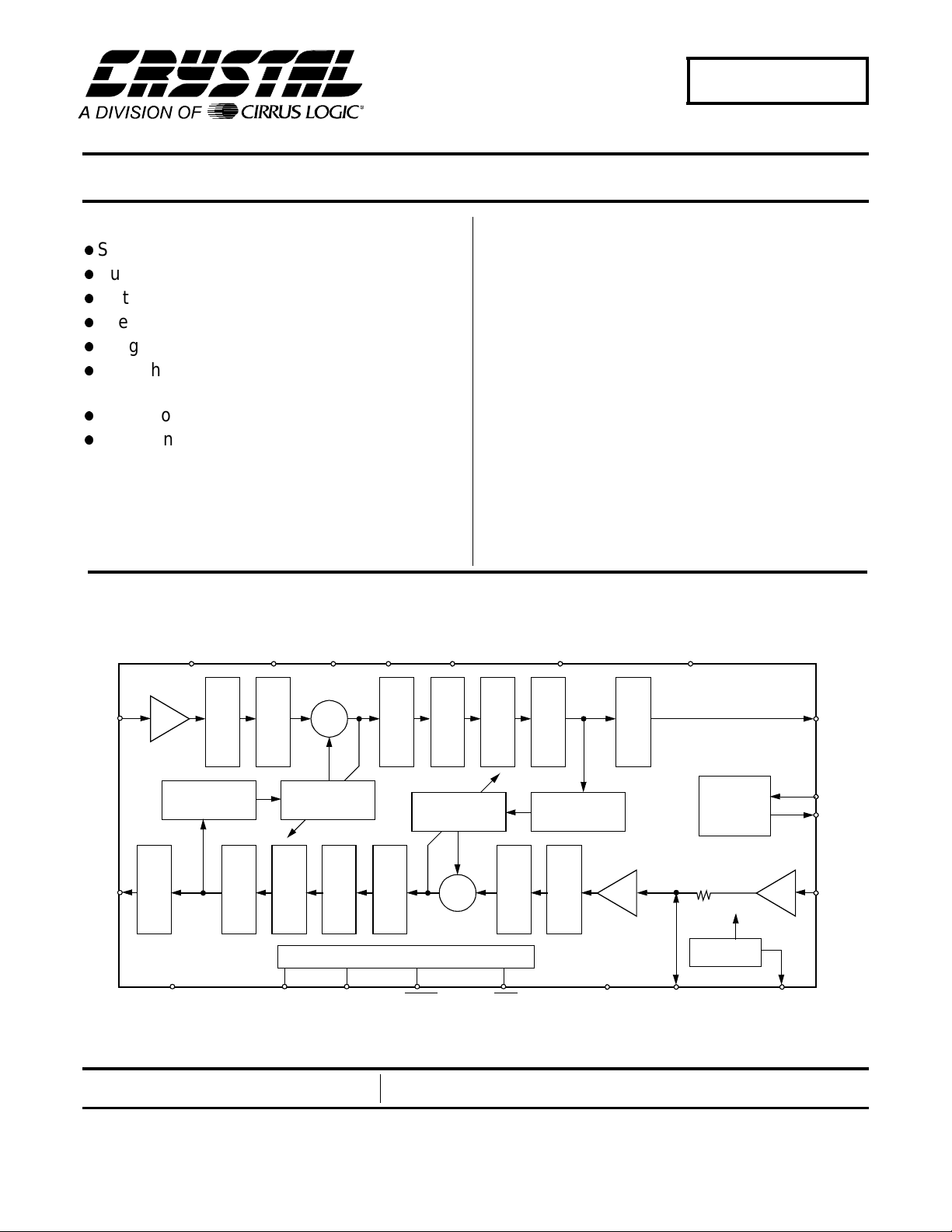
Full-Duplex Speakerphone Chip
CS6420
Features
l
Single-chip full-duplex hands-free operation
l
Automatic gain control
l
Optional 34 dB microphone preamplifier
l
Integrated mute and volume control
l
Integrated 80 dB IDR dual codec
l
Speech-trained Network and Acoustic Echo
Cancellers
l
Powerdown mode
l
Microcontroller Interface
DGND
NC4 NC3 NC2 NC1 AGND
General Description
Most modern speakerphones use half-duplex ope ration,
which switches transmission between the far-end talker
and the speakerphone user. This is done because the
acoustic coupling between the speaker and microphone
is much higher in speakerphones than in handsets
where the coupling is mechanicall y suppressed.
The CS6420 enables full-d uplex conversat ion with a single-chip solution. The CS6420 can easily replace
existing half-duplex speakerphone ICs with a huge increase in conversation quality.
The CS6420 consists of telephone & audio interfaces,
two codecs and an echo-cancelling DSP.
ORDERING INFORMATION
CS6420-CS 20-pin SOIC
CDB6420 Evaluation Board
AVDD
NI
NO
ADC
0,6,9.5,12dB
Pre-Emphasis Network
DAC
Mute/Volume
DVDD
Control
+
Σ
Filter
High Pass
-
Echo CancellerFilter
Tx
Half Duplex
Microcontroller Interface
DA TA STROBE DRDY
Preliminary Product Information
Cirrus Logic, Inc.
Crystal Semiconductor Products Division
P.O. Box 17847, Austin, Texas 78760
(512) 445 7222 FAX: (512) 445 7581
http://www.crystal.com
Rx
RxAGC
Acoustic Pre-Emphasis
TxAGC
Suppression
This document contains information for a new product.
Cirrus Logic reserves the right to modify this product without notice.
Σ
Half Duplex
Suppression
-
+
Hgih Pass
RST
Copyright Cirrus Logic, I nc. 1997
(All Rights Reserv ed)
Control
Mute/Volume
FilterEcho Canceller
ADC
Filter
0,6,9.5,12dB
AVDD
DAC
Generation
1 kΩ
2.12V
BANDGAP
APO MB
Clock
34 dB
3.5V
AO
CLKI
CLKO
API
JUN ‘97
DS205PP2
1

TABLE OF CONTENTS
Absolute Maximum Ratings..............................................................................................4
Recommended Operating Conditions..............................................................................4
Power Consumption ................................................................... ......... ........ ......................4
Analog Charac te rist ics....... ... .... ... ... ... ... ................ ... ... ... ................ ... ... ... ... ................ ... ... ...4
Analog Transmission Characteristics..............................................................................5
Microphone Amplifier........................................................................................................5
Digital Characteristics .......................................................................................................5
Overview ............................................................................................................................8
Functional Description .....................................................................................................8
Analog Interface .......................................................................................................8
Acoustic Interface ..............................................................................................9
Network Interface ............................................................................................10
Microcontroller Interface .........................................................................................10
Description ......................................................................................................10
Register Definitions ............................................ ........ ......... ........ ......... ........ ...11
Register 0..................................................................................................12
Mic - Microphone Preamplifier Enable...............................................12
TSD - Transmit Suppression Disable.................................................12
GB - Graded Beta..............................................................................12
ACC - Acoustic Coefficient Control....................................................13
RVol - Receive Volume Control.........................................................13
TGain - Transmit Analog Gain...........................................................13
Register 1..................................................................................................14
HD - Half-Duplex Disable...................................................................14
RSD - Receive Suppression Disable.................................................14
Taps - AEC/NEC Tap Allocation........................................................15
NCC - Network Coefficient Control....................................................15
TVol - Transmit Volume Control.........................................................15
RGain - Receive Analog Gain............................................................15
Register 2..................................................................................................16
NErle - Network ERLE Threshold......................................................16
NFNse - Network Full-Duplex Noise Threshold.................................16
RHDet - Receive Half-Duplex Detection Threshold...........................17
HDly - Half-Duplex Holdover Delay....................................................17
NseRmp - Background Noise Power Estimator Ramp Rate..............17
RSThd - Receive Suppression Threshold..........................................17
PCSen- Path Change Sensitivity.......................................................17
Register 3..................................................................................................18
AErle - Acoustic ERLE Threshold......................................................18
AFNse - Acoustic Full-Duplex Noise Threshold.................................18
THDet - Transmit Half-Duplex Detection Threshold..........................18
TSAtt - Transmit Suppression Attenuation.........................................19
TSBias - Transmit Suppression Bias.................................................19
TSThd - Transmit Suppression Threshold.........................................19
HHold - Hold in Half-Duplex on Howl.................................................19
Reset ...............................................................................................................19
Clocking ..................................................................................................................19
Power Supply .........................................................................................................20
Power Down Mode ..........................................................................................20
Noise and Grounding ......................................................................................21
Design Considerations ...................................................................................................22
Algorithmic Considerations .....................................................................................22
Full-Duplex Mode ............................................................................................22
Theory of Operation..................................................................................22
Adaptive Filter...........................................................................................23
Pre-Emphasis....................................................................................23
Graded Beta.......................................................................................23
Update Control..........................................................................................24
CS6420
2 DS205PP2

Speech Detection .....................................................................................24
Half-Duplex Mode ...........................................................................................24
AGC ................................................................................................................ 25
Suppression .................................................................................................... 25
Transmit Suppression...............................................................................26
Receive Suppression................................................................................27
Circuit Design .........................................................................................................27
Interface Considerations .................................................................................27
Analog Interface........................................................................................27
Microcontroller Interface ...........................................................................27
Grounding Considerations ..............................................................................28
Layout Considerations ........................................................ ........ ....................28
System Design .......................................................................................................28
Gain Structure .................................................................................................28
Testing Issues .................................................................................................29
ERLE ........................................................................................................29
Convergence Time...................................................................................30
Half-Duplex Switching.......................................... ......... ........ ......... ...........30
Pin Descriptions ..............................................................................................................31
Analog Interface ..............................................................................................31
Microcontroller Interface .................................................................................32
Clock ............................................................................................................... 32
Power Supply ..................................................................................................32
Miscellaneous .................................................................................................33
Glossary ...........................................................................................................................34
Package Dimensions ......................................................................................................37
CS6420
DS205PP2 3
CS6420
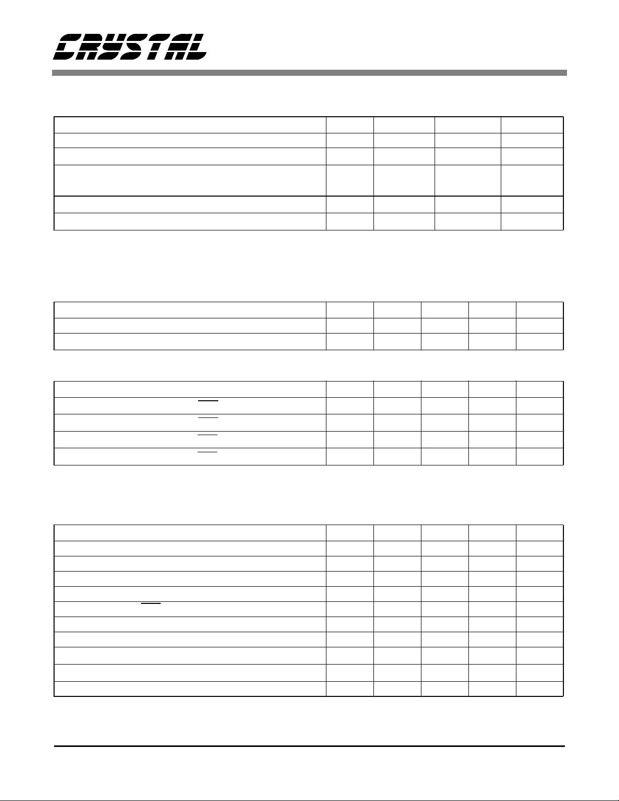
ABSOLUTE MAXIMUM RATINGS
Parameter Symbol Min Max Units
DC Supply (AVDD, DVDD) -0.3 6.0 V
Input Current (Except supply pins)
Input Voltage Analog
Digital
Ambient Operating Temperature
Storage Temperature
I
in
V
ina
V
ind
T
A
T
stg
WARNING: Operation beyond these limits may result in permanent damage to the device.
Normal operation is not guarant eed at these extremes.
RECOMMENDED OPERATING CONDITIONS
Parameter Symbol Min Typ Max Units
DC Supply (AVDD, DVDD) 4.5 5.0 5.5 V
Ambient Operating Temperature
T
AOp
-10 +10 mA
-0.3
-0.3
AVDD+0.3
DVDD+0.3
V
-40 85 °C
-65 150 °C
0 2570°C
POWER CONSUMPTION (T
= 25°C, DVDD = AVDD = 5V, f
A
= 20.480 MHz) (Note 1)
XTAL
Parameter Symbol Min Typ Max Units
Power Supply Current, Analog (RST
Power Supply Current, Analog (RST
Power Supply Current, Digital (RST
Power Supply Current, Digital (RST
=0)
=1)
=0)
=1)
P
P
P
P
DA0
DA
DD0
DD
10 20 mA
50 60 mA
1mA
1mA
Notes: 1. AO and NO outputs are not loaded.
ANALOG CHARACTERISTICS (T
= 25°C, DVDD = AVDD = 5V, f
A
= 20.480 MHz)
XTAL
Parameter Symbol Min Typ Max Units
Input Offset Voltage (APO, NI) 2.12 V
Output Offset Voltage (AO, NO) 2.12 V
Transmit Group Delay (Note 2) 6 ms
Receive Group Delay (Note 2) 6 ms
Settling Time from RST
rising 104 ms
MB Output Voltage 3.5 V
MB Drive Capability 10
Input Impedance (APO, NI) (Note 2)
Load Impedance (AO, NO) (Note 2)
Z
Z
in
load
10 kΩ
300 k
µ
Power Supply Rejection (1 kHz) 40 dB
A
Ω
Notes: 2. These parameters are guaranteed by design or by characterization.
4 DS205PP2
CS6420
ANALOG TRANSMISSION CHARACTERISTICS (T
= 25°C, DVDD = AVDD = 5V, f
A
XTAL
=
20.480 MHz, RVol=TVol=RGain=TGain= 0 dB, HD=TSD=RSD=1, analog inputs and ouputs loaded with resistors
and capacitors as shown in the typical connection diagram, Figure 2)
Parameter Symbol Min Typ Max Unit s
Idle Channel Noise A-weighted (0-20 kHz)
(Inputs grounded C-Message weighted (0-4 kHz)
through a capacitor) Psophometrically weighted (0-4 kHz)
Signal-to-Noise Ratio A-weighted (0-20 kHz)
(Full Scale, 1kHz C-Message weighted (0-4 kHz)
sine wave input) Psophometrically weighted (0-4 kHz)
17
-67
SNR 69
17
-67
-69 dBV
dBrnC0
dBm0p
dB
dBrnC0
dBm0p
Total Harmonic Distortion C-Message Weighted (0-4 kHz) THD 0.1 %
Programmable Gain RGain/TGain = 00
RGain/TGain = 01
RGain/TGain = 10
RGain/TGain = 11
0
6
9.5
12
dB
Volume Control Stepsize (TVol/RVol) 3 dB
ADC Full-scale Voltage Input 0.9 1.0 Vrms
DAC Full-scale Voltage Output 1.0 1.1 Vrms
ADC Noise Floor C-Message Weighted (0-4 kHz) -80 dBV
DAC Noise Floor, DAC muted C-Message Weighted (0-4 kHz) -85 dBV
MICROPHONE AMPLIFIER (T
= 25°C, DVDD = AVDD = 5V,f
A
Parameter Symbol Min Typ Max Units
Gain (Zsource = 50Ω)
Signal-to-Noise Ratio A-weighted (0-20 kHz)
Input Impedance
Input Offset Voltage
DIGITAL CHARACTERISTICS (T
= 25°C, DVDD = AVDD = 5V,f
A
Parameter Symbol Min Typ Max Units
High-Level Input Voltage
Low-Level Input Voltage
Input Leakage Current
Input Capacitance
A
mic
SNR
Z
inm
V
offm
V
V
I
leak
C
= 20.480 MHz)
XTAL
34 dB
m
63 dB
5k
Ω
2.12 V
= 20.480 MHz)
XTAL
IH
IL
IN
DVDD-1.0 V
1.0 V
10
µ
5pF
A
DS205PP2 5
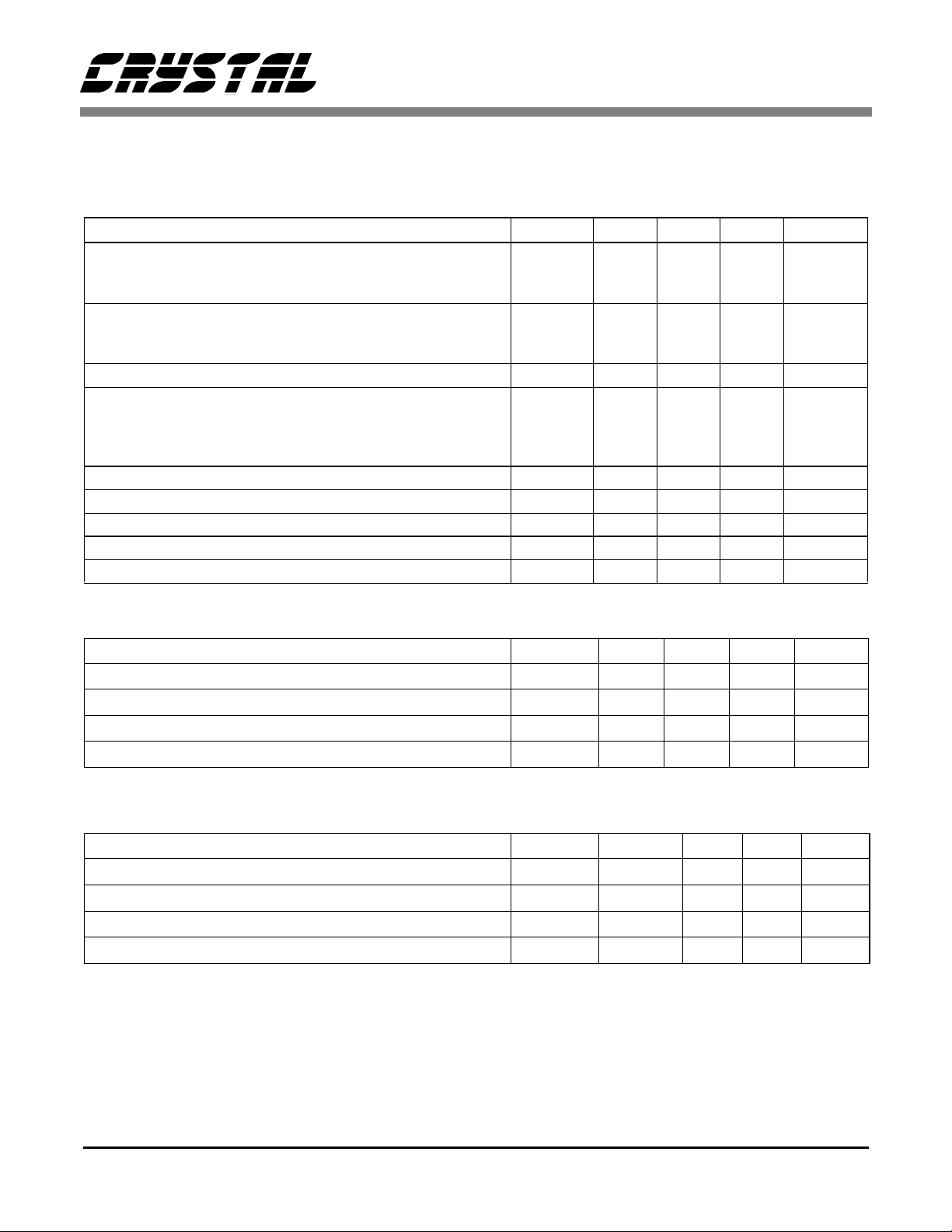
SWITCHING CHARACTERISTICS
Parameter Symbol Min Typ Max Units
Input rise time
low time
RST
CLKI frequency
CLKI duty cycle
frequency
DRDY
STROBE frequency
to STROBE setup time
DRDY
DATA to STROBE setup time
STROBE to DATA hold time
STROBE to DRDY
hold time
t
rise
t
RSTL
f
XTAL
t
LCLKI
f
DRDY
f
STROBE
t
sDRDY
t
sDATA
t
hDATA
t
hDRDY
CS6420
1.0 µs
1.0 µs
18.432 20.480 22.528 MHz
40 50 60 %
DC f
DC 9.0 MHz
30 ns
30 ns
30 ns
30 ns
/ 2560 kHz
XTAL
DRDY
t
sDRDY
t
hDRDY
STROBE
DATA
t
sDATA
Bit15
t
hDATA
Bit14
Bit0
Figure 1. Microcontroller Interface Switching Characteristics
6 DS205PP2
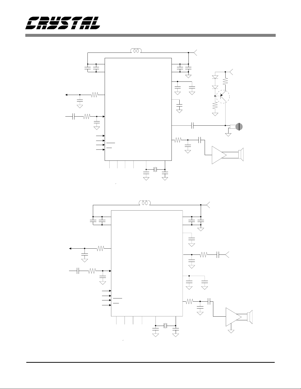
Telephone
Line Out
Telephone
Line In
3300 pF
0.47 µF
1 µF
6.04 k
3300 pF
+
0.1 µF
12.1 k
Ω
CS6420
ferrite bead
+5V Analog
µ
0.1
16
DVDD
15
DGND
Ω
4
NO
17
NI
AVDD
AGND
MB
APO
API
F
1
2
19
18
20
0.1 µF
0.022
0.47 µF
+
1 µF
+
µ
F
10 µF
10 k
Ω
+5V Analog
1.5 k
Ω
Telephone
Line Out
Telephone
Line In
From
Microprocessor
8
7
6
5
DATA
STROBE
DRDY
RST
NC1NC2NC3NC4
14
9
10
1112
20.480 MHz
22pF
12.1 k
Ω
3
AO
3300pF
CLKOCLKI
13
22pF
Figure 2. Typical Connection Diagram (Microphone Preamplifier Enabled)
ferrite bead
+5V Analog
µ
0.1
F
1
2
+
1 µF
20
0.47 µF
6.04 k
Ω
18
0.47
3300 pF
19
0.1 µF
10 µF
+
3300 pF
0.47 µF
µ
F
1
6.04 k
3300 pF
+
0.1 µF
12.1 k
Ω
16
15
DVDD
DGND
AVDD
AGND
API
Ω
4
NO
APO
17
NI
MB
µ
F
near-end
input
8
DATA
7
From
Microprocessor
6
5
STROBE
DRDY
RST
NC1NC2NC3NC4
20.480 MHz
22pF
12.1 k
Ω
3
AO
3300pF
CLKOCLKI
13149101112
22pF
Figure 3. Typical Connection Diagram (Microphone Preamplifier Disabled)
DS205PP2 7

CS6420
OVERVIEW
The CS6420 is a full-duplex speakerphone chip for
use in hands-free comm unications with teleph ony
quality audio. Common applications include
speakerphones, inexpensive video-conferencing,
and cellular ph one car kits. The CS6420 require s
very few external comp onents and allows system
control through a microcontroller int erface.
Hands-free com munication thro ugh a microph one
and speaker t ypically results i n acoustic feedba ck
or howling because the loop gain of the system exceeds un ity by the time audi o amplitudes are ad justed to a reasonable level. The solution to the
howling problem has typically been half-duplex,
where either the transmit or the receive channel is
active, neve r both at the same time. T his prevent s
the howl ing, but di minishe s the ove rall com munication quality by clipping words and forcing the
talker at each end to wait for the talker at the other
end to stop speaking.
Full-duplex conv er sation , where bot h transm it and
receive c hannels are active simult aneously, is t he
conversation quality we enjoy when using handsets. Full-duplex for hands-free communications is
achieved in the CS 6420 using a digita l signal pro-
cessing te chnique called “Echo Cancellation.” The
end result is a more natural conversation than halfduplex, with no awkward breaks and pauses, as if
both parties were spea king to each other directly.
Echo Cancellation reduces overall loop gain and
the acousti c coupling between speaker and m icrophone. This coupling reduction prevents the annoying effect of hearing one’s own delayed speech, the
effect being w orse when there is delay in the system, such as vocoder delay in digital cellular
phones.
The CS6 420 i s a comp le te sys tem im pl eme ntat ion
of a Digital Signal Processor with RAM and pro gram ROM, running Echo Cancellation algorithms
developed at Crystal Semiconductor using customer input, integrated with two delta-sigma codecs.
The CS6420 is intended to provide a full-duplex
speakerphone so lution with a mi nimum of design
effort while displa cing exist ing ha lf-dupl ex spe akerphone chips.
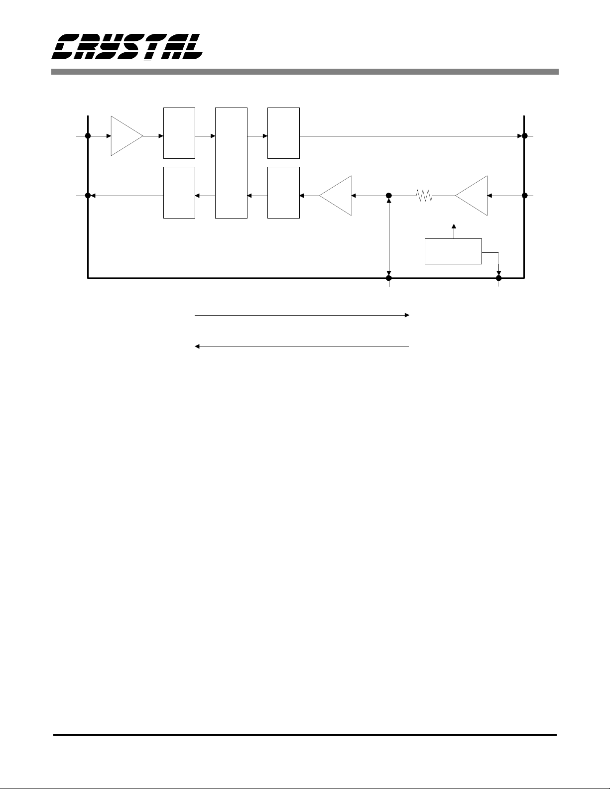
FUNCTIONAL DESCRIPTION
The CS6420 is ro ughly divided into four external
interface blocks. The analog inte rfaces connect the
chip to the transmit and receive paths. Certain control functions are accessible through the microcontroller interface. Two pins accommodate either a
crystal or an externally applied digital clock signal.
Analog and digit al powe r and ground are provided
through four pin s.
Analog Interface
In a speakerphone application, one input of the
CS6420 connects to the signal from the microphone, sometimes called the near-end input or
transmit input, and one output connects to the
speaker. The output that leads to the speaker is
sometimes called the near-end output or receive
output. Together, the input and output that connect
to the microphone and speaker are referred to as the
Acoustic Interface.
The signal received at the near-end input is then
passed to the far-end output or transmit output after
acoustic echo cancellation. This signal is sent to the
telephone l ine. The signal fr om the telephon e line
is received at the f ar-end i nput, al so called the receive input , and t his s igna l is pa ssed to the rec eive
output after network echo cancell ation. Together,
the far-end in put an d output form the Network In terface.
The analog interfaces are physically implemented
using delta sigma converters runnin g at an output
word rate of 8 kHz, resulting in a passband from
DC to 4 kHz. Because the inputs are analog to digital converters (ADCs), certain design considerations must be kept in mind: specifically, antialiasing and full-scale input voltage. The ADCs expect a single-pole RC filter with a corner at 8 kHz,
8 DS205PP2
CS6420
NI
17
NO
4
PGA
0,6,9.5,12 dB
ADC
D
S
P
DAC
FAR-END
DAC
ADC
Receive Path
Transmit Path
Figure 4. Analog Interface
and they are post-compensated internally to prevent any resultant passband droop. The ADCs also
expect a max imum of 1 V
(2.8 Vpp) at their in -
rms
puts (which are biased around 2.12 VDC). A signal
of higher amplitude will clip the ADC input and
may result in poor echo canceller performance. See
the Design Considerations section for more details.
The outputs a re delta-si gma digita l to analo g converters (DACs) and have similar requirements to
the ADCs. Th e DACs are pre -compensated to expect a single-pole RC filter with a corner frequency
at 4 kHz. The full scale voltage output from a DAC
is 1 V
(2.8 Vpp) swinging around a DC bias o f
rms
2.12 V.
Acoustic Interface
The pins API (pin 20), APO (pin 18), MB (pin 19),
and AO (pin 3) make up the A coustic Inter face. A
block diagram of the Acoustic Interface is shown in
Figure 4.
AO
3
PGA
0,6,9.5,12 dB
Ω
1k
2.12V
BANDGAP
NEAR-END
34 dB
3.5V
19 MB18 APO
API
20
API and APO are, respective ly, the input and out put of the built-in analog pre-amplifier. The preamplifier is an inverting amplifier with a fixed gain
of 34 dB biased around an input offset voltage
) of 2.12 V. APO is the ou tput of t he pre-a m-
(V
off
plifier after a 1 kΩ resistor. The circuitry connected
to the amplifier input must present low source impedance (<100Ω) to the API pin or the gain will be
reduced. When using the pre-amplifier, connecting
a 0.022 µF capa citor to g round off AP O will pro vide the anti-aliasing filter required by the ADC, as
shown in Figure 2. The pre-amplifier may be bypassed by clearing Mic (Register 0, bit 15) using the
Microcontroller Interface (see Microcontroller In-
terface se ctio n), grounding API th rough a capacito r,
and driving APO direc tly. In this case , the signal into
APO must be low-pass filtered by a single-pole RC
filter with a corner f requency at 8 kHz (see Figu re 3 ).
Following the pre-amplifier is a programmable analog gain stage (PGA) which is controllable
through the Microcontroller Interface. This gain
DS205PP2 9
CS6420
stage a llows gai ns of 0 dB, 6 dB, 9. 5 dB, an d 12 dB
to be added prior to the ADC input. The default
gain stage setting i s 0 dB.
The signal at APO sh ould no t exceed 2.8 V
at the
pp
default gai n stage setting. If other gain stages are
used then the full-scale signal at APO must also
change. Ta ble 1 shows ful l-scale voltages as measured at APO for given programmable gains:
Gain Setting Full-scale Voltage
0 dB
6 dB
9.5 dB
12 dB
Table 1. Full scale voltages for each gain stage.
2.8 V
1.4 V
0.94 V
0.71 V
pp
pp
pp
pp
MB provides a stable 3.5 VDC output from the onboard voltage reference of the CS64 20. MB may
not be connected to any load. MB serves to provide
decoupling for the inte rnal 2.12 VDC bandgap reference, and must have a 0.1 µF and a 10 µF capacitor to ground for bypass. Noise on MB will
strongly influence the overall analog performance of the CS6420.
The acoustic out put, AO, should connect to a single-pole low-pass RC network with a corner frequency of 4 kHz, which will filter out-of-band
components. The maximum voltage swing at AO is
2.8 V
. AO is capable of driving down to a 10 kΩ
pp
load.
Network Interface
The pins NI (pin 17) and NO (pin 4) make up t he
Network Inter face. The deta ils of the Netwo rk Interface are shown in Figure 4.
NI is the input from the telephone network side into
the CS6420 . The signal i nto NI mu st be low pass
filtered by a single-pole RC filter with a corner frequency of 8 kHz.
A programmable analog gain stage (PGA) accessible through the Microcontroller Interface amplifies
signals received at NI. This gain stage allows gains
of 0 dB, 6 dB, 9.5 d B, and 12 dB to be added prio r
to the ADC input. The default gain stage setting for
the network sid e is 0 dB .
The signal at NI should not exceed 2.8 V
at the
pp
default gai n stage setting. If other gain stages are
used then the full-scale signal at NI must also
change. Ta ble 1 shows ful l-scale vo ltages as me asured at NI for given prog rammable gains.
The output to the telephone network side, NO,
should conne c t t o a single pole RC network with a
corner frequency at 4 kHz, which will filter out-ofband component s. The maximum swing NO is capable of producing is 2.8 V
. NO is capable of
pp
driving down to a 10 kΩ load.
Microcontroller Interface
Several control functions of the CS6420 are accessible through its Microc ontroller Interface, which
consists of three pins: DATA (pin 8), STROBE
(pin 7), and DRDY
(pin 6). These inputs are intended to connect to th e outputs of a microcontroll er to
allow write-only access to the 16-bit Microcontroller Control Regi ster (MCR).
The RST
(pin 5 ) pin, wh ich aff ects th e entir e inte grated circuit, is especially significant to the Microcontroller Interface. RST
is used to place the
CS6420 into a known state of opera tion. Two subtypes of reset are possible: cold reset and warm reset.
Description
The Microcont roller Interface is imple mented by a
serial shift register gated by DRDY
troller begins the transaction by setting DRDY
and STROBE low. The most significant bit (MSB),
Bit 15, of the 16-bit data word should be presented
to the DATA pin and then STROBE should be
brought hi gh to shi ft the data bi t into the CS64 20.
STROBE should be brought low again so it is ready
. The microcon-
low
10 DS205PP2
CS6420
to shift t h e next bit into the shift register. The next
data bit s hould then be p res ented to the DA T A pin
ready to be latched by the rising edge of STROBE.
This procedure repeats for all sixteen bits as shown
in Figure 5. A fter the last bit has be en shifted in,
DRDY
should be brou ght high to indicate the conclusion of the transfer, and four extra STROBE
pulses must be applied to latch the data into the
CS6420.
Since the MCR is a shift register, the STROBE can
be run arbitrarily slow with a duty cycle limited
only by the hold time specified in the Switching
Characterstics table. The Microcontroller Interface
STROBE
is read once every 125 µs, so it must not be updated
faster than thi s .
Register Definitions
The four control registers accessible through the
MCR are described in detail in the following tables.
These regi sters are a ddresse d by bits b 2 and b1 of
the MCR. Bit b0 must always be 0. Table 2 shows
the relat ive bit positions of al l the registers. T ables
3 to 6 show the four control registers in more detail.
The Register Map at the top of each register description shows the names of all the bits, with their
reset va lues belo w the bit field name. The reset va lue can also be found in the Word column of the bit-
field summ ary as indicated by an ‘*’.
four extra strobe pulses
1234
Bit15 Bit14 Bit13
DRDY
b15 b14 b13 b12 b11 b10 b9 b8 b7 b6 b5 b4 b3 b2 b1 b0
Mic TSD GB ACC RVol TGain 0 0 0
HD RSD Taps NCC TVol RGain 0 1 0
NErle NFNse RHDet HDly NseRmp RSThd PCSen 1 0 0
AErle AFNse THDet TSAtt TSBias TSThd HHold 1 1 0
Bit12
Bit11 Bit10
Bit9
Bit8
Bit7 Bit6 Bit5 Bit4
Figure 5. Microcontroller Interface
Table 2. MCR Control Register Mapping
Bit3
Bit2
Bit1
Bit0DATA
DS205PP2 11

CS6420
Register 0
b15 b14 b13 b12 b11 b10 b9 b8 b7 b6 b5 b4 b3 b2 b1 b0
Mic TSD GB ACC RVol TGain 0 0 0
1 0 10 00 00100 00 0 0 0
Bits Name Function Word Operation
15 Mic Microphone Preamplifier Enable
14 TSD Tx Suppression Disable
13-12 GB Graded Beta
11-10 ACC AEC Coefficient Control
9-5 RVol Rx Volume Control
4-3 TGa i n Tx Ana log Gain
0
1*
0*
1
00
01
10*
11
00*
01
10
11
00000
00001
---
00100*
--01010
01011
--11101
11110
11111
00*
01
10
11
disable preamp
enable preamp
enable Tx suppression
disable Tx suppression
0.00 dB/ms
0.75 dB/ms
0.38 dB/ms
0.19 dB/ms
Normal
Clear
Freeze
reserved
+30 dB
+27 dB
+18 dB
+0 dB
-3 dB
-57 dB
-60 dB
mute
0 dB
6 dB
9.5 dB
12 dB
* Denotes reset value
Mic - Microphone Preamplifier Enable
The microphone preamplifier described in the
Acoustic Interface section is enabled by default, but
may be disabled by se tting Mic to 0. Refer to the
Acoustic Interf ace section for more de tails on using/disabling the Microphone Preamplifier.
Table 3. Register 0 Bit Definitions
(see Register 3) dB of attenuation into the transmit
path only when there is sp eech d etected in th e receive path and no near-end speech. When only
near-end speec h is presen t, or if t he re is no sp ee ch
in either direction, the suppression attenuation is
removed. By default, the transmit suppression
function is enabled.
TSD - Transmit Suppression Disable
GB - Graded Beta
The Transmit Supplementary Echo Suppression
function i s a non-linear echo control mechanism .
The Transmit Suppression will introduce TSAtt
12 DS205PP2
The room-size adjustment scheme called “graded
beta,” provided for the acoustic echo canceller in the

CS6420
CS6420, is controlled by GB. The network echo
canceller does not support gr aded beta.
Graded be ta is an architectural enhancement to the
CS6420 which takes advantage of the fact that
acoustic echoes tend to decay exponentially with
time. The CS6 420 can i ncre ase th e bet a, o r up date
gain, for the coefficients of the adaptive filter
which occur earlier in time and decrease it for those
that occur later in time, which increases convergence speed while maintaining stability. In order to
make this improvement, there is an implicit assumption that the decay rate of the echo is known. The
graded beta control allows the system designer to adjust this. For very acoustically live r ooms, use either
no decay (00) o r sl ight decay (11) . Cars and acou stically dead rooms can benefit fr om the most rapid decay (01).
ACC - Acoustic Coefficient Control
The coeffi cients of t he AEC adap tive fi lters i n the
CS6420 are control led by ACC. The default position (00) yields normal operation, which means the
coefficients are free to adjust themselves to the
echo path in order to ca ncel ec ho. Whe n set to the
clear posit ion (01), the a daptive filte r coefficient s
are all held at zero, so the echo canceller is effectively disabled. Note that unless the half-duplex
mode is dis abled, this will force the CS6420 i nto
half-duplex m ode. Th e freeze position (10) cause s
the coefficients to hold their cu rrent values.
RVol - Receive Volume Control
Volume in th e recei ve pat h is set by RVol . The vo lume control in the receive direction is implemented
by a peak-lim iting automatic gain control (AGC)
and digital attenuation at the near-end output DAC.
The AGC is discussed in det ail in the Design Con-
siderations section. See the sub-section on AGC
for a full explana ti on of how it functions.
When the refere nce l evel is set to +0 dB , the AGC
is effectively disabled. Volume control is implemented by digital attenuation in 3 dB steps from
this point on down. The maximum gain is +30 dB
and the minimum is -60 dB in 3 dB steps. The lowest gain setting (11111) mutes th e receive path.
The default setting for the receive reference level is
+18 dB.
TGain - Transmit Analog Gain
TGain selects the amount of additional on-chip analog gain to be supplied to the acoustic input of the
CS6420. A programmable gain amplifier (PGA)
exists be fore each A DC wh ich allo ws 0 dB , 6 d B,
9.5 dB, or 12 dB of ga in to be adde d to the signal
path. The aco usti c si de de faults to 0 dB of gain.
Note: Changing the analog gain will change the full-
scale voltage as applied to the input pin. Make
sure that the ADC input does not clip with the gain
stage on.
DS205PP2 13

CS6420
Register 1
b15 b14 b13 b12 b11 b10 b9 b8 b7 b6 b5 b4 b3 b2 b1 b0
HD RSD Taps NCC TVol RGain 0 1 0
0 0 10 00 01010 00 0 1 0
Bits Name Function Word Operation
15 HD Half-Duplex Disable
14 RSD Rx Suppression Disable
13-12 Taps AEC/NEC Tap Allocati on
11-10 NCC NEC Coefficient Control
9-5 TVol Tx Volume Control
4-3 RGai n Rx An alog Gain
0*
1
0*
1
00
01
10*
11
00*
01
10
11
00000
00001
---
00100
---
01010*
01011
--11101
11110
11111
00*
01
10
11
enable half-duplex
disable half-duplex
enable Rx suppression
disable Rx suppression
444/0 (55.5ms/disabled)
380/128 (47.5ms/16ms)
316/192 (39.5ms/24ms)
252/256 (31.5ms/32ms)
Normal
Clear
Freeze
reserved
+30 dB
+27 dB
+18 dB
+0 dB
-3 dB
-57 dB
-60 dB
mute
0 dB
6 dB
9.5 dB
12 dB
* Denotes reset value
HD - Half-Duplex Disable
In normal opera tion, th e CS6420 will be in a half duplex mode i f the echo canc ell er is n ot prov id ing
Table 4. Register 1 Bit Definitions
mode is undesirable. By default, the half-duplex
mode is enable d.
RSD - Receive Suppression Disable
enough loop gain reduction to prevent howling.
This half-dup lex mode would be act ive at powerup, for example, before the adaptive filter has had a
chance to adapt. This half-duplex mode prevents
howling an d al s o ma s k s the convergence proc es s .
In some cases, such as when measuring convergence speed (see Testing Issues), the half-duplex
14 DS205PP2
The Receive Supplementary Echo Suppression
function i s a non-linear echo control mechanism .
Supplementary Echo Suppression attenuates signals in the receive direction by 24 dB when far-end
speech is ab sent in the receiv e path. The atten uation is released only when the receive channel is active. It is also designed to not be triggered by

CS6420
network echo. By de fault , the re cei ve suppre ssion
function is ena bled.
Taps - AEC/NEC Tap Allocation
The CS6420 has a total of 63.5 ms of echo canceller
taps that it can partition for use by the network and
acoustic echo cancellers. By default, the CS6420
allocate s 39.5 ms for th e AEC and 24 ms f or the
NEC. Some applications will never have a network
echo path, and so should allocate all taps for the
AEC. See NErle and NFNse in Register 2, and
AErle and AFNse in Register 3 for more options
when an echo path i s none xistent.
NCC - Network Coefficient Control
The NEC adaptive filter’s coefficients are controlled by NCC. See ACC in Register 0 for more
details. The default setting for NCC is Normal
mode.
TVol - Transmit Volume Control
Volume in the transmit path is co ntrolled by TVol .
Like receive volume, the transmit vol ume is controlled by an AGC. See RVol in Register 0 for more
details. The default setting for the transmit reference level is +0 dB.
RGain - Receive Analog Gain
RGain selects the amount of additional on-chip analog gain to be supplied to the network input of the
CS6420. A programmable gain amplifier (PGA)
exists be fore each A DC wh ich allow s 0 dB , 6 d B,
9.5 dB, or 12 dB of ga in to be adde d to the signal
path. The network side defaults to 0 dB of gain.
Note: Changing the analog gain will change the full-
scale voltage as applied to the input pin. Make
sure that the ADC input does not clip with the gain
stage on.
DS205PP2 15

CS6420
Register 2
b15 b14 b13 b12 b11 b10 b9 b8 b7 b6 b5 b4 b3 b2 b1 b0
NErle NFNse RHDet HDly NseRmp RSThd PCSen 1 0 0
00 00 00 00 00 00 0 1 0 0
Bits Name Function Word Operation
15-14 NErle NEC ERLE Threshold
13-12 NFNse NEC Full-Duplex Noise Threshold
11-10 RHDet Rx Half-Duplex Detection Threshold
9-8 HDly Half-Duplex Holdover Delay
7-6 NseRmp Background Power Estimator Ramp Rate
5-4 RSThd Rx Suppression Threshold
3 PCSen Path Change Sensitivity
00*
01
10
11
00*
01
10
11
00*
01
10
11
00*
01
10
11
00*
01
10
11
00*
01
10
11
0*
1
24 dB
18 dB
30 dB
reserved
zero
-42 dB
-54 dB
reserved
5 dB
3 dB
6 dB
reserved
200 ms
100 ms
150 ms
reserved
1 s
0.5 s
2 s
reserved
5 dB
3 dB
6 dB
reserved
high sensitivity
low sensit iv it y
* Denotes reset value
NErle - Network ERLE Threshold
The CS6420 wil l allow full- duplex ope ration only
when the Ne tw o rk ERLE exceed s th e threshold s et
by NErle. See also NFNse. See Glossary for a definition o f ERLE.
Table 5. Register 2 Bit Definitions
far-end input is greater than NFNse , then NErle is
used to determ ine if full-dupl ex is allowed. If the
noise level is below the level of NFNse, the
CS6420 uses an internal estimate of asymptotic
performance to determine whether or not to transition to full-duplex. If NFNse is zero, NErle is al-
NFNse - Network Full-Duplex Noise Threshold
NFNse works in conjunction with NErle to determine when the CS64 20 should tra nsition in to fullduplex ope ration. If the curr ent noise leve l at the
16 DS205PP2
ways used as the full-duplex criterion. The other
values exi st f or c ase s wh ere the re is n ot a net work
path to converge to, or the existence of a network
path can not be determined prior to pl acing a call.

CS6420
RHDet - Receive Half-Duplex Detection
Threshold
The sensitivity of the speech detector controls
channel switching and ownership in half-duplex
mode. The receive speech detector registers speech
if the receive channel signal power is RHDet above
the noise floor for the receive channel.
HDly - Half-Duplex Holdover Delay
After a channel goe s idle in the half-dup lex mode
of operation , a chan ge of ch annel own ership is inhibited for HDly in order to prevent false switching
due to echoes. The half-duplex will be more immune to false swit ching if this delay is longer, but
it will also prevent a fast response to legitimate
channel cha nges.
NseRmp - Background Noise Pow er Estima tor
Ramp Rate
The background noise power estimators increase at
a rate of 3 dB/Nse Rmp u ntil the b ackgr oun d noise
power estimate equals the current input power estimate. The background noise power estimators
quickly track drops in the current input power estimate. Choose sma ll va lues o f NseR mp if the envi ronment is expec ted to have rapidly varying no ise
levels. Choose large values of NseRmp if the environment is expected to have relatively constant
noise power.
RSThd - Receive Suppression Threshold
This parameter sets the threshold for far-end
speech detectio n for disengaging rece ive suppression. The speech detector that disengages the receive supp ression has its sensiti vity controlled by
RSThd. The suppr ession is inserted into the receive
path unless sign al from the fa r-end e xcee ds th e receive channel noise power by RSThd, in which
case speech is assumed to be detected and the suppression is defeat ed until speech is no longer detected. Decreasing RSThd to make the speech
detector more sensitive cou ld result in false dete ctions due to spurious noise events which may cause
an unpleasant noise modulation at the near-end. Increasing RSThd to make it robust to spurious noise,
but may cause weak far-end talkers to not be heard.
RSThd does not affect the ability of the receive
suppressor to attenu ate residual network echo.
PCSen- Path Change Sensitivity
The Acoustic Interfac e is likel y to ha ve many path
changes, fo r e xample, as people move about in the
room where the ful l-duple x speake rphone is be ing
used. The sensitivity of the path change detector
can be changed with the PCSen Bit. Set PCSen to 0
for high sensitivity an d 1 for l ow sensitivity.
If PCSen is set to hi gh, extended doublet alk may
cause the CS6 420 to b riefl y drop in to half -dup lex.
When PCSen is set to low, brief echo may be heard
during path changes.
DS205PP2 17

CS6420
Register 3
b15 b14 b13 b12 b11 b10 b9 b8 b7 b6 b5 b4 b3 b2 b1 b0
AErle AFNse THDet TSAtt TSBias TSThd HHold 1 1 0
00 00 00 00 00 00 0 1 1 0
Bits Name Function Word Operation
15-14 AErle AEC ERLE Threshold
13-12 AFNse AEC Full-Duplex Noise Threshold
11-10 T HDet Tx Half-Duplex Detection Threshold
9-8 TSAtt Tx Suppression Attenuation
7-6 TSBias Tx Suppression Bias
5-4 TSThd Tx Suppression Threshold
3 HHold Hold in Half-Duplex on Howl
00*
01
10
11
00*
01
10
11
00*
01
10
11
00*
01
10
11
00*
01
10
11
00*
01
10
11
0*
1
24 dB
18 dB
30 dB
reserved
zero
-42 dB
-54 dB
reserved
5 dB
3 dB
6 dB
reserved
18 dB
12 dB
24 dB
reserved
18 dB
15 dB
21 dB
reserved
15 dB
12 dB
9 dB
reserved
disable
enable
* Denotes reset value
AErle - Acoustic ERLE Threshold
The CS6420 wil l allow full- duplex ope ration only
when the Acoustic ERLE it provides exceeds AErle. See also AFNse. See Glossary for a de finition
of ERLE.
Table 6. Register 3 Bit Definitions
used to determ ine if full-dupl ex is allowed. If the
noise level is below the level of AFNse, the
CS6420 uses an internal estimate of asymptotic
performance to determine whether or not to transition to full-duplex. If AFNse is zero, AErle is always used as the full-duplex criterion. The other
AFNse - Acoustic Full-Duplex Noise Threshold
AFNse works in conjunction with AErle to determine when the CS64 20 should tra nsition in to full-
values exis t for cases where th ere may not be an
acoustic path to converge to.
THDet - Transmit Half-Duplex Detection
duplex ope ration. If the curr ent noise leve l at the
near-end input is greater than AFNse, then AErle is
18 DS205PP2

CS6420
Threshold
The sensitivity of the speech detector controls
channel switching and ownership in half-duplex
mode. The transmit speech detector registers
speech if the transmit channel signal power is THDet above the noise floor of the transmit channel.
TSAtt - Transmit Suppression Attenuation
This paramet er sets the amount of sup pression attenuation inserted into the transmit path when
transmit suppression is engage d.
TSBias - Transmit Suppression Bias
The bias level affects the ease with which near-end
speech may break-in or be crushed by far-end
speech. See the Design Considerations secti on on
Transmit Suppression for full details.
TSThd - Transmit Suppression Threshold
This paramet er sets the ERLE requirement for discriminatio n between echo and ne ar-end spe ech by
the supplementary echo suppressor. See the De-
sign Considera tions sectio n on Transmit Suppre ssion for full details.
HHold - Hold in Half-Duplex on Howl
This is a control flag which, if enab led, holds the
system in the half-duplex operation if it were to
howl for any reason and the howl detectors trip and
clear coefficients. The system may transition to
full-duplex if the flag is subsequently cleared.
Reset
A hardware reset, achiev ed by bringing RST low
for at least 1 µs and then high again, must be applied after initi al powe r-on.
When RST
of the CS6420 are powered down. When RST
brought high, th e oscil lator i s ena bled and app rox imately 4 m s late r, all dig ital clo cks begin operat ing. The ADCs and DACs are calibrated and all
internal digital initializations occur. The MCR is
is held low, the various in terna l bloc ks
is
sampled after the rese t timer ex pires (104 ms after
the rise of RST
scribed below) to de termine whet her the rese t was
warm or cold. After the MCR is initiall y sample d,
the default (reset) values of the MCR are res tored
to it.
Cold reset is a tota l reset of all the components of
the CS6420. The ADCs and DACs are reset, the
echo canceller memories and registers are all
cleared, and the default settings of the MCR are restored. Cold reset is the default reset mode upon
power up or in the absence of a microcontroller.
Warm reset is like cold reset except that the echo
canceller coefficients and certain key vari a bles are
not cleared , but inste ad keep their pre -reset valu e.
This gives the CS6420 a headstart in adapting to its
environme nt if the echo environment i s relatively
stable, ass uming a co ld reset ha ppened at least once
since power up.
The CS6420 is warm reset by r aising the RST
high, waiting 4 ms for the digital clocks to start, and
then writin g 0111111111111110 (0x7FFE) to the
MCR within 104 ms after RST
control word is sent, the CS6420 will cold reset. If
the control word is sent after the timer has expired,
it is interprete d as a normal control word.
Another special re set option is to exit the 100 ms
reset timer befor e the 100 ms has el apsed. This is
accomplished by writing a control word to the
MCR with Bit 15 set high. To ex it the t imer early
in cold rese t, write 10000 000 0000 0 (0x80 00). T he
timer may be bypa ssed and warm reset asserted by
sending 1111111111111110 (0xFFFE). The
100 ms timer prevents operation until the bias voltages gener ated on-chip settle, but the startup d el ay
might be objecti onable in some applications.
or sooner if using the early exit de-
pin
goes high. If no
Clocking
The clock for the converters and DS P is provided
via the clocking pins, CLKI (pin 14) and CLKO
(pin 13). A 20.480 MHz parallel resonant crystal
DS205PP2 19

CS6420
placed between these two pins and loaded with
22 pF capacitors will allow the on-chip oscillator to
provide this system clock. Alternatively, t he CLKI
pin may be driven by a CMO S level clock signal.
The clock may vary from 20.480 MHz by up to
10%, however, this will change the sampling rate
of the converters and echo canceller, which will affect the bandwidth of the analog signals and the duration of echo that the echo canceller can
accommodate. CLKO is not connected when CLKI
is driven by the CMOS signal.
Power Supply
The pins AVDD (pin 1) and AGN D (pin 2) p ower
the analog sections of the CS6420, and DVDD (pin
16) and DGND (pin 15) power the digital sections.
This distinction is important because internal to the
part, the d igital power supply is likely to contain
high-frequency energy. The analog power supply is
kept clean internally by drawing current from a dif-
ferent pin, ther eby achieving high pe rformance in
the convert ers .
The digital supply of the CS6420 should not be
connecte d to the system digital supply, if there is
one, as the CS6420 has internal timing mechanisms
designed to minimize the detrimental effects of its
own digital noise, but cannot use these to compensate for externally introduced digital noise. The
CS6420 digital power supply should be derived
from its analog power supply through a ferrite bead
with low (< 1 Ω) DC impedance.
Power Down Mode
Typical power consumption of the CS6420 is 60
mA, assuming normal operating conditions. This
current consump tion can be further re duced by in voking the p owerdown mode, which is en tered by
holding RST
down all the internal blocks of the CS6420 and stop
the oscillator. In powerdown mode, current consumption drops to less than 1 mA.
low. Holding RST low will power
+5V
Analog
Supply
AVDD
AGND
DVDD
DGND
Figure 6. Suggested Layout
20 DS205PP2
MB
From
Ferrite
Bead

CS6420
Noise and Grounding
Since the C S64 20 is a mi xed-si gnal in tegra ted c ir cuit, the system designer must pay special attention
to layout and decoupling to minimize noise concerns. The three best methods to reduce noise when
using the CS64 20 are to have go od decoupling o f
power supplies, separation of analog and digital
power and ground , an d careful board layout.
Figure 6 shows the suggested placement of decoupling capa citors for the p ower supplies . Note that
the trace l ength from the power pin to the capacitors is minimized. Also note that the smaller valued
capacito r is pl ace d clos er to the pin than t he larg er
valued capacitor. The smaller capacitor decouples
high frequency noise and the larger capacitor attenuates lower frequencies.
The separation of analog and digital power and
ground is done in two ways. The power is separated
by deriving the di gita l power for th e CS6 420 from
the analog th rough a ferrite bea d to isolate analog
from digital, as shown in Figure 7. The ferrite bead
serves as a low-pass fi lter to remove CS64 20 digi tal switching n oise from the analog p ower suppl y.
The ground is sepa rate d by iso lating a ll the d igit al
components of the system board on one ground
plane and all th e anal og and line ar comp onents on
a different ground plane. The CS6420 should be
placed over the analog ground plane. This prevents
digital switching noise from the digital components
of the board from coupl in g into t he conver te rs and
aliasing into the passband.
+5V
(Analog)
µ
1
F0.1µF0.1
Figure 7. Ground Planes
Ferrite Bead
AVDD
AGND
Microcontroller
DVDD
DGND
An alog Gr oun d Pla ne
Digital Ground Plane
µ
F1µF
DS205PP2 21

CS6420
DESIGN CONSIDERATIONS
When designing the CS6420 in to a syste m, it is important to keep several considerations in mind.
These conce rns can be loosel y grouped into thr ee
categories: algorithmic considerations, circuit design considerations, and system design considerations.
Algorithmic Considerations
The CS6420 facilitates full-duplex hands-free
communication via many algorithms running on
the Digita l Signal Pr ocessor t hat is the core of the
CS6420. Among th ese are the algor ithm s that perform the adaptive filtering, the half-duplex switch ing, digital volume control, and supplementary
echo suppression.
Full-Duplex Mode
Full-duplex hands-free communication is achieved
through a tec hnique called adapt ive filtering. The
basic prin ciple be hind adap tive filterin g is that the
acoustic path between speaker and microphone can
be modeled by a transfer function which can be dynamically de termined by an adaptive dig ital filte r.
This principle assumes good update control and
speech/tone detection algorithms to prevent the filter from mistraining.
Theory of Operation
Figure 8 illustrates how the adaptive filter can cancel echo an d redu ce loop gain. The echo path of the
system is betwee n points B and C: the speaker to
A
F
Adaptive Filter
D
+
E
Figure 8. Simplified Acoustic Echo Canceller
Σ
Block Diagram
B
C
microphone coupling. A signal injected at A
(sometime s called a “t raining signal”) i s sent both
to B, the input of the echo path, and to F, the input
of the adaptive filter. The signal at B is modified by
the trans ducers and th e enviro nmen t, and re ceived
at point C (an “E cho”). Mean while, let us ass ume
for argument’ s sake tha t the adap tive filt er has ex actly the right transfer function to match the echo
path BC, and so the signal at point D is approximately equal to the signal at point C. After these are
subtracted by th e sum ming e lem ent, a ll that is l eft
is the error signal at point E, whic h should be very
small.
If a person were to speak into the microphone at
point C, that signal would pass through the summing element unchanged because the adaptive filter had no com parable input to subt ra ct out. In this
manner, the person at A and the person at C may simultaneously speak and A will not hear his own
echo.
In the real wo rld, the echo path is not static. It will
change, for example, when people move in the
room, when so meone moves the speaker o r the microphone, or when someone drops a piece of paper
on top of t he spea ker. So , the fi lter n eeds to adapt
to modify i ts tr an sfer fu nct ion to m atc h that o f t he
environment. It does so by measuring the error signal at point E and trying to minimize it. This signal
is fed back to the adaptive filter to measure perfor mance and how best to adapt, or train.
The trouble arises wh en t he perso n at the ne ar- end
(C) speaks: th e error signal will be non-ze ro, but
the adapt ive filter shou ld not change . If it tries to
train to the near-end si gnal, the a daptive fi lter has
no way to reduce the error signa l, because t here is
no input to t he f ilte r, a nd the re fore n o out put fr om
it. The adaptive filter wou ld mistrain.
To prevent this mistraining, the echo canceller uses
double-talk detection algorithms to determine
when to update. These update control algorithms
22 DS205PP2

CS6420
are the heart of most echo canceller implementations.
The worst ca se situation for the CS6420 is when
parties at bo th en ds a re sp eaki ng an d the person at
the near-en d is movi ng. In this ca se, the ec ho canceller will cease to adapt because of the doubletalk, but the echo will not be optimally reduced because of the change in path.
Adaptive Filter
The adaptive filter in the CS6420 uses an algorithm
called the “Normalized Least-Mean-Square
(NLMS)” update algorithm to learn the ec ho path
transfer function. This Finite Impulse Response
(FIR) filter has 508 taps, which can model up to
63.5ms of total pa th respo nse at a sam pli ng rate of
8kHz. The cove rage tim e is calc ulate d by the following formula:
1
-------------
8kHz
The CS6420 ’s adaptive filter, like all FIR filters,
only models L inear and Time I nvariant (L TI) systems. So, any non-linearity in the echo path can not
be modeled b y t he adap ti ve fi lt er and th e res u lting
signals will not be cancelled. Signal cli pping and
poor-quality spea kers are very common sour ce s of
non-linearit y and distortion.
A common integration problem for echo cancellers
is signal clip ping i n the ech o path . For e xam ple, if
a speaker dri ve r is d riv en to i t s rai ls, th e d ist ortion
of the speech may be hard to perceive, but it is very
bad for the echo canceller. This technique has been
used in half-duplex phones to provide good lowlevel signal ga in at the expense of di stortion with
high amplitude signals. Since this does not work
for the CS6420, an AGC mechanism ha s been introduced to provide equivalent behavior without
clipping. See the section on AGC for more details.
Another common problem is speaker quality. A
poor qualit y spea ker w hich is perf ectly accept able
for a half-duplex speakerphone, may limit the echo
canceller’s performance in a full-duplex speaker-
508 = 63.5 ms.
x
phone. The distortion elements will not be modeled
by the adaptive filter and so limit its effectiveness.
Speakers should have be tter than 2% THD performance to not im pe de the adaptive filter.
Volume contr ol shoul d be implemented only using
the CS6420 Micro controll er Interface . A real-time
external ch ange in the gain o f the speaker drive r,
for example, wou ld result in a c hange in the t ransfer function of the e cho path, and so would force
the adapt ive filter to readapt. If the volume control
is done before the inp ut to the adaptive filte r, the
echo path does not change, and no retraining is necessary. Another side benefit of the CS6420 volume
control is that it transparently provides dynamic
range compression.
Pre-Emphasis
The typical training signal for the adaptive filter
will be speech, but most adapti ve filters work opt imally with whit e noise. Speech has ve ry different
spectral characteristics than white noise because of
its quasi-periodic nature.
Research at Crystal has shown that quasi-period ic
signals cause the formation of spurious non-zero
coefficie nts within th e adaptive filter at tap intervals determined by the periodicity of the signal.
This results in small changes in period b eing very
destructiv e to the adaptive filter’s pe rformance.
One mechanism the CS6420 uses to prevent this
filter corruption with speech is to pre-emphasize
the signal sent to the adaptive filter so that much of
the low frequency content is removed.
The CS6420 works very well with a speech training
signal because of the pre-emphasis filter. White
noise training signa ls, however, will re sult in suboptimal perform anc e, so when te sting, whi te no ise
is not recommende d as a training signal.
Graded Beta
The update gain of an adaptive filter, sometimes
called t he “b eta”, is the rate at wh ich th e filt er co -
DS205PP2 23

CS6420
efficient s can change . If beta i s too low, the ad aptive filter will be slow to ada pt . Conversely, if it is
too high, the filter will be unsta ble and will create
unwante d no ise in the system.
In most echo canceller implementations, the beta is
a fixed value for all t he f ilter c oeffic ient s. In some
situations, though, through knowled ge of the characteristics of echo path response, the beta can be
varied for groups of coefficients. This preserves
stability by allowing the beta to be higher for some
coefficients and compensating by reducing beta below nominal for others.
For example, acoustic echo tends to decay exponentially, so the first taps need t o be large and the
later taps will be sm all. Having a large beta for the
first taps w i ll allow those taps to be adapted faster,
while having a small beta for the later taps will
keep the f ilte r stab le. This h as an added bene fit o f
suppressing the spurious taps mentioned in the Pre-
Emphasis Filter section above.
The Microcontro ller Interface allo ws four settings
for graded beta: none, 0.19 dB/ms, 0.38 dB/ms, and
0.75 dB/ms. Use 0.75 dB/m s for acoustic ally dead
rooms or cars, and 0.19 dB/ms or no grading of beta
for large, or acou stically live rooms.
Update Control
As mentioned in the Theory of Operat ion sectio n,
the update co ntrol algorithm s are the heart of any
useful echo cancelle r impleme ntation. Asi de from
telling the adaptive filter when to adapt, they are responsible for correcting performance when the path
changes too quic kly for the filter. For example , if
the adaptive filter is actually a dding signal power
instead of cancelling, the update control algorithms
will reset th e ada ptive filter to cleared coe fficients,
forcing it to resta rt .
Speech Detection
The CS6420 detects speech by using power estimators to track deviations from a background noise
power level. The power esti mators fi lter and a verage the raw inc o m ing samples from the A D C .
A background noise level is established by a register that incre ases 3 dB at intervals determ ined by
NseRmp (Register 2, bits 7 and 6). When the power
estimator level rises, the background noise level
will slowly increase to try to match it. When the
power estimator level is below the background
noise level, the backgroun d noise level is qu ickly
reset to match the power estimator level. This
method allows significant flexibility in tracking the
background no ise lev el .
Speech is detected when the power estimator level
rises above the bac kground no ise level by a given
threshold. The half-duplex receive speech detector
threshold is set by RHDet (Register 2, bit s 11 and
10), the half-duplex transmit speech detector
threshold is se t by THDet (R egister 3, bit s 11 and
10), and the receive suppression speech detector
threshold is set by RSThd (Register 2, bits 5 and 4).
The transmit spe ech det ect ors for both ha lf-dupl ex
and suppression defa ult to 5 dB.
Note that consta nt power signals whi ch persist fo r
long duratio ns, suc h as tones from a signal generator, will be detected as speech only as long as the
background noi se level has not risen to with in the
speech detection threshold of the signal power.
When a tone has persisted for long enough, the
background noise l evel will be e qual to the p ower
estimator level, and so the tone will no longer be
considered speech. This duration is dependent
upon the power differen ce between t he signal and
the ambient noise power, as well as NseRmp. It
should be noted that the CS6420 has a tone detector
to prevent updates when tones are present and allow
tones to persist regardless of the speech detectors.
Half-Duplex Mode
In cases wh ere the s ystem re lies on th e echo can celler for stabili ty, a fail-safe me chanism must be in
place for in stances when the echo canc eller is not
24 DS205PP2

CS6420
performing ade quate ly. T he CS642 0 im plem ent s a
half-duplex mode to guarantee communication
even when t he echo canceller is disabled.
When the CS6 420 is fi rst powere d on, or emerge s
from a reset, the echo canceller coefficients are
cleared, and the echo cancelle rs provide no benefit
at this point. The half-duplex mode is on to prevent
howling and ec ho from in terfe ring wi th co mmu ni-
cation. Once the CS6420’s adaptive filters have
adapted suffici en tly, the ha lf-dup le x mode is au tomatically disabled, and full-duplex communication
can occur.
The half-duplex mode allows three states: transmit,
receive, and idle. In the trans mit state, the transmit
channel is open a nd the receive cha nnel is muted.
The receive state mutes the transmit channel. The
idle sta te is an internal state which i s used to enhance switching decision making. The CS6420
must be idle before it will allow a sta te chang e between transmit and receive.
The half-duplex controller can be susceptible to
echo, so a holdov er timer is provide d to help prevent false switching. Holdover will force the channel to remain in its current state for a fixed duration
after speech ha s stopped. HDly ( Register 2, bits 9
and 8) sets the duration of the holdover. Longer
holdover will tend to make interrupting much harder, but will be much more robust to spurious
switching caused by echo.
from the inpu t is a bove this refe rence, it is at tenu ated to the reference level wit h an attack time o f
125 µs. This attenua tion level de cays with a time
constant of 30 ms unless another signal greater than
the reference level is detected. After the attenuation, a post-scaler scales the reference level to fullscale (the max imum digital co d e) , which amplifies
all signals by the differe nce bet ween the re feren ce
level and full-scale.
For example, Figu re 9 shows h ow the AG C works
with a referen ce level of + 30 dB (W ord = 0 0000).
Any signal greater than 30 dB below ful l-sc a le (a),
is scaled down to 30 dB (b). This signal is then
scaled up +30 dB (the reference l evel) to provide
the final output (c). Note that the combination of attenuation an d gain results in less than +30 dB t otal
gain being applied. If the input signal is b elow 30
dB below full -sc al e (d), no attenuation is do ne and
the full +30 dB of gai n is applied to the signal (e).
When the refere nce l evel is set to +0 dB , the AGC
is effectively disabled. Volume control is implemented by digital attenuation in 3 dB steps from
this point on down. The maximum gain is +30 dB
and the minimum is -60 dB in 3 dB steps. The lowest gain setting (11111) mutes th e path. The sign al
scaling take s place in betwee n the two canc ellers,
and so does not disturb the echo canceller as changing gain in the ec ho path would (see the A daptive
Filter section for more details).
AGC
The CS6420 implements a peak-limitin g AGC in
both the transmit and receive directions in order to
boost low-le ve l sign als wi thou t co mpro mis ing pe rformance when high amplitude signals are present.
The technique effectively result s in dynamic range
compression.
The AGC works by sett ing a re fere nce leve l based
on the value represen ted by TVol (Registe r 1, bits
9-5) for the transmit d irection an d RVol (Re gister
0, bits 9-5) for th e receive directio n. If the signal
DS205PP2 25
Suppression
Echo cancellation is somewhat of a misnomer in
that echo is merely attenuated, not entirely cancelled. Some residual echo still exists after the
summing node. This residual echo, though very
low, may be audible when the near-end talker is not
speaking. Suppression further attenuates the echoed signal.
The CS6420 employs supplementary echo suppression which adds attenuation on top of the cancellation to remo ve the re sid ual e c ho. For ex ampl e, t he

CS6420
Fs
0dB 0dB
-30dB
(a) Input Sig na l
Fs
-30dB
(d) Input Sig na l
Figure 9. How AGC works (TVol = 00000)
Fs
-30dB
t
Fs
0dB0dB
-30dB
t
(b) AGC Attenuation
(e) AGC Gain
transmit channel will engage extra attenuation
whenever only the far-end talker is speaking. However, if th e near-end talke r starts speaki ng, the attenuation i s removed and the system rel ies on the
near-end talker’s spe ec h to mask residual echo.
Suppression causes some modulation of the per-
ceived background noise which may be dist rac t ing
to some users. As a result, it may be desirable to
limit the suppression attenuation to the minimum
necessary. The CS6420 provides TSAtt (Register
3, bits 9 and 8) to control the amount of attenuation
introduced by sup pre ssion in the tran s mit chan ne l.
Receive suppression attenuates by 24 dB.
The suppression in the transmit suppression and
that in the recei ve direct ion work very differen tly.
The transmi t suppression works in a “default o ff”
mode while the receive supp ression is “default on.”
Transmit Suppression
The transmit suppressor attenuates the transmit
path when only far-end speech is present, hence the
name “default off. ” This ensures that the suppre ssion engages only when nece ssary.
Fs
0dB
-30dB
t
t
(c) AGC Gain
t
Recall that the purpo se of Tran smit Sup pression is
to mask residual echo by inserting additional
loss/attenuation in the transmit path in the scenario
when only far- end speech is present; the re sidual
echo, if any , in d ouble -tal k bei ng ma sked by ne arend speec h as s uming reasonable levels of ERLE.
There are two controls/tweekable parameters for
governing the behavior of Transmit Suppression.
The two controls are adjustable through the Microcontrolle r Interfac e, and they ar e TSTh d (Registe r
3, bits 5 and 4) an d TSBi as (Regist er 3, bits 7 and
6). TSThd is the prima ry control and should be adjusted before changing the value of TSBias from its
default setting. TSThd sets the ERLE expectation
to be used in discriminating between near-end
speech and f ar-end echo. This contro l setting wi ll
by far predominate in affecting the manner in
which Transmit Suppressi on be ha ves.
TSBias is a secondary control . This is to be adjusted after the system designer is more or less satisfied
with the behavior of Transmit Suppression with the
TSThd set. It affects the ease with which a near-end
talker may disengage Transmit Suppression and
26 DS205PP2

CS6420
keep it disengaged. We recommend using larger
values of TSB ias relati ve to TSThd settings in or der to facilitate ease of near- end speech transmission. For exam pl e, the default setting for TSThd is
15 dB and 18 dB for TSBias.
In some scenarios, especially when the dynamic
range of vol ume control i s significan tly large, we
also recomm end t he use of differe nt co mbin ations
of TSThd and T SBias se ttin g rela tive to outpu t volume of the acoustic interface.
Receive Suppression
The “defa ult on” receiv e suppressor is n ominally
attenuat ing unless far-end spee ch is present. This
behavior is more consistent with behavior observed
in modern speakerphones, and helps keep noise
levels lo w .
One side effect of this scheme is that a constant
power signal, such as noi se from a no ise gene rato r
or a tone, wi ll eventually be att enuated when the
background noise level estimate turns off the receive supp ression speech detector . See the s ection
on Speech Detection from more details.
RSThd (Register 2, bits 5 and 4) sets the speech detection thre shold o f th e suppre ssor’ s spee ch de tec tor. See the Speech Detection section for more
details.
Circuit Design
The design of the CS6420 i nterfa ce ci rcuit ry pla ys
an important role in achieving optimum performance. The actual circuit design is important, especially the analog interface. Proper grounding and
layout will help minimize the noise that might get
coupled into the CS6420.
Interface Considerations
Of the CS642 0 interfaces, the ana log interface and
the microcontroller interface are the most important to pay special attention to during circuit design. The analog interface especially will
determine how well the echo canceller can perform.
Analog Interface
The Analog In terface feeds informa tion about the
echo path t o t he ad ap ti ve fil te r, s o it i s cr it ical th at
this interface be well design ed . Using high -quali ty
transduc ers and ci rcuits th at guaran tee lo w-distor tion and minimal clipping are essential to the success of any echo cance ller ba sed design.
As mentioned in the Adaptive Filter section, the
adaptive filter ass umes that t he e cho pa th is linea r
and time-inva riant. As such, poor quali ty spea kers
are a common cause of poor echo canceller performance due to th eir high distortio n. Speakers must
be selected with their linearity in mind. In general,
the speaker should have less than 2% Total Harmonic Distortion. This will result in distortion
terms 34 dB below the desired signal, enough headroom for the echo canceller to function adequately.
The other major c onsiderat ion i n the de sign of the
analog int erface is tha t the c ircu itry tha t proc esses
the transdu cer si gnal s not clip or distor t it. For ex ample, a common problem is the use of a sp eaker
amplifier with a fixed gain, which clips when driving the speaker. Although the distortion may not be
objectionab le to the h uman ear, it wi ll prevent the
adaptive filter from modeling the path correctly.
That which work ed for hal f-dupl ex sp eake rph ones
will not necessaril y work for full-duple x speakerphones. Microphone amplifier circuitry is also suspect when looking for sources of clipping and
distortion.
Microcontroller Interface
The Microcontroller Interface is the only asynchronous digital connec tion t o th e CS6420, so it is the
most likely pla ce f or d igita l noi se co uplin g t o be a
problem. The interface itself is fairly straightforward and requires only three pins from a microcontroller.
DS205PP2 27

CS6420
The three pins that comprise the Microcontroller
Interface are STROBE, DATA, and DRDY
STROBE mus t no t exce ed th e s ys tem clo ck of the
CS6420 in speed. Also, four extra clocks are required after DRDY
the data into th e CS6420, as is shown in Figure 5.
is brought high in order to latch
Grounding Considerations
Proper grounding of the CS6420 is necessary for
optimal performance from this mixed-signal device. The CS6 420 should be consid ered an ana log
device for grounding purposes.
The digital sections of the CS6420 are synchronized with it s ADCs and DACs to mi nimiz e th e effects of digital noise coupling. However, for
external di gi tal devices that are asynchronous wi th
respect to the CS6420, precautions should be taken
to minim ize the chan ces of digita l noise coup ling
into the CS6420.
A design with the CS6420 should have a separa te
ground plane for any digital devices. For exampl e,
a system microcontroller should be on a digital
ground plane wi th its control lines lea ding to the
CS6420 in the shortest reasonable distance. The
CS6420 itself shoul d lie comple tely on the ana log
ground plane.
Layout Considerations
The physic al layout of the traces a nd compone nts
around the CS6420 will also strongly affect the performance of the de vice. Special attentio n must be
paid to decoupling capacitors, the crystal oscillator,
and the input ant i-aliasing filters.
The decoupli ng capacitors for the pow er supplies
of the CS6 420 shou ld be pl aced as cl ose as po ssibl e
to the power pins for be st performance . There are
two capacitors per pin: t he 0.1 µF capacitor needs
to be closest to the pin to decouple the high frequency compon en ts, an d the l arge r cap c an be farther away. The MB pin is the most critical as it
connects dir ectly to the on-chi p volta ge refe rence.
AVDD and DVDD are secondary to MB with re-
.
spect to priority.
The crysta l oscilla tor shoul d be placed as clo se as
possible to reduce the distance that the high frequency sign als must tr avel . If the c rystal is placed
too far away, the trace inductance may cause problems with oscillator startup.
The next c on ce rn w ith p la cem en t is th e inp ut an ti aliasing filte rs for the ADC inputs. NI has an RC
low-pass network with a corner frequency of 8
kHz. The capacitor of this low-pass network should
be placed very close to the pin so that there is very
little expo se d tra ce to pi ck u p nois e. I f th e o n-chip
microphone amp lifier i s used , the 0.022 µF capacitor on APO will provide the appropriate cutoff frequency, and so shou ld be place d close to the APO
pin. If the on-boa rd pream plifier is n ot used, APO
will have the same RC network a s NI, and should
be treated similarly.
The conne ctions fr om the controll er to th e Micro controller In te rface shoul d b e shor t stra ight tra ces,
if possible. Th e tr ac es shou ld not ru n ver y cl ose to
any digital cl oc ks to avoid cross coupling.
System Design
The CS6420 is ultimately only one part of a bigger
full-duplex hands-free system. In order for that system to work well, it needs to be properly balanced.
The dist ribution of th e system gain s will make or
break the echo canceller. In order to judge performance, however, the system integrator must be
armed with the means to test th e product.
Gain Structure
The distribution of the system gains is an important
design cons ideration to keep in mind. Gain distri bution is an i ntricate balancing ac t where the s ystem integrator tries to maximize dynamic range
while minimizing noise, and at the same time, getting excelle nt echo canceller perfor m anc e.
28 DS205PP2

CS6420
The basic constraint on getting good echo canceller
performance is that the maximum output should
not clip when coupled to the input. For example, if
in a speakerphone, AO provides 1 V
to a speak-
rms
er, the refle ctions reac hing the microph one should
present no more than 1 V
to the Acoustic ADC.
rms
In fact, it is advisable to allo w 6 dB or even 12 dB
of margin, such that in the above e xample, the signal present at the Acoustic ADC is 250 mV
rms
.
After this coup ling le vel is esta blis hed , the d esired
signal gain must be es tablished. To continu e from
the previous example, the transmit gain must be adjusted to m ake sure the near-e nd talker is easy to
hear at the far- end. If the signal fro m the ne ar-end
talker cli ps at the AD C, it is not sign ificant to the
echo path because the AEC should not be updating
anyway.
In general, to min imize noise, system gain should
be concentrat ed bef ore the ADC. However, this is
not practical in all cases, mostly because of the cou-
pling constraint. The CS6420 offers the AGC’d
gains provided by TVo l and RVol to help provi de
the desired gain.
The CS6420 offers two different programmable
gain sources: TGain/RGain and TVol/RVol. TGain
and RGain switch in different size sampling capacitors at the ADC to provide a choice of 0 dB, 6 dB,
9.5 dB, and 12 dB of analog g ain. TVol and RVol
introduce digital gain and attenuation in 3 dB steps.
The difference is si gnifica nt in that th e digi tal gai n
will gain up the noise of the ADC as well as the desired signal, whereas the analog gain will not.
Testing Issues
The followin g tests are suggestions for measuring
echo canceller and half-duplex performance.
the level of signal without the echo canceller compared to the level of signal with the echo canceller.
When measuri ng ERLE, it is import ant that any p otential aco ustic loop s be bro ken; so t o mea sure the
ERLE of the Acoustic Canceller, the NO output
should be disconnected from the rest of the network. This will p revent f eedback whi ch could occur when all of the CS6420’s failsafes are disabled.
The following example outlines the steps necessary
to measure the ERLE of the acoustic echo canceller.
It is important t o choose a good te st signal for the
tests to be valid. As mentioned in the Adaptive Fil-
ter section, the CS6420 does not work optimally
with white noise. The best signal to use would be a
repeatable spee ch signal, like a recording of someone counting or saying “ah.”
Use the Microcon troller Interfac e to disable transmit and receive suppression as well as half-duplex.
Allocate al l the ta ps to the Ac oustic Canc eller in order to allow full-duplex without t he Network Canceller being trained. The gains should be set
appropriate for good system performance.
The first measurement is a baseli ne figure of performance with no e cho canceller. Use the Microcontrolle r Interface t o clear the acoustic can celler
coefficients. Inject the test signal at NI and measure
the rms voltage at NO. This measurement gives the
baseline coupling level (denomina tor).
Use the Microc ontrol ler In te rface to se t the acou stic cancelle r coefficients to norm al which will allow the adaptive filter to adapt. Inject the test signal
at NI and allow a few seconds for the filter to adapt.
Measure the rms voltage at NO. This measurement
gives the cance ll ed echo level (numerat or).
ERLE
Echo Return-Loss Enhancement (E RLE) is a measure of the atte nuation that an echo cance ller provides. The numb er is an ex pression of the ratio of
DS205PP2 29
Convert both voltages to deci bels and subtra ct the
echo cancelled level from the ba sel ine level to calculate the ERLE. At the factory, with known good
components, we typically see 30 dB of ERLE with
speech.

CS6420
Convergence Time
Convergence t im e is a measure of how quickly the
adaptive filter can model the echo path. From
cleared coeffi cients, the tra ining signal is in jected
into the ec ho cancell er and the ti me for th e ERLE
to reach a given threshold value is the convergence
time. Different customers will have different
threshold leve ls, so Crystal does not spe cify convergence tim e.
The follow ing examp le will measure c onvergen ce
time for the acoustic echo canceller:
Set up the system as for the ERLE test. Clear the
acoustic canc eller coefficie nts through the Mic rocontroller Interface. Apply the training signal to
NI, set the coefficients to normal, and simultaneously start a timer. Once the measured ERLE
reaches the th reshold the system designer desires,
stop the timer. The elapsed time is the convergence
time. A good va lue f or the thre shold woul d be the
AErle value fr om Register 3, since th is would be
the time for the CS6420 to go from half-duplex
mode to full-duplex mode.
A good tool for thi s meas urement i s a digita l storage oscilloscope set to a slow sweep so that about
five seconds o f signal is shown on the sc re en. One
channel of the oscilloscope should monitor the
ADC input (for an unca ncelle d refer en ce), and an other channel should monitor the echo cancelled
output. This tec hnique is especially effec ti ve when
speech is the training signal.
Half-Duplex Switching
Although the CS6 420 tra nsiti ons from half-d uplex
operation from reset after only a few utterances are
passed throug h the syste m, the p erform ance of t he
half-duplex is critical to the end-user in cases
where the echo canceller is not adequate . The halfduplex switching characteristics can be subjectively tested with the following procedure:
Set the CS6420 Microcontroller Interface to the
nominal register values for the system, but clear the
acoustic and n etwork echo canceller coefficients.
This will force the CS6420 to remain in half-duplex
mode.
The most useful test of practical performance
found at Crystal has been the “alternating counting
test.” In thi s test th e per son at the nea r-end counts
all the odd num bers and the person a t the far-end
counts all the even numbers. This tests the interruptibility of the half-duplexer. During testing, system parameters for the half-du plex m ay need to be
changed to accommoda te the level of performance
expected for t he produc t . See the Half-Duplex and
Register Definitions sections for more de tails.
We see about 2-5 seconds of training time using
known good equipment. This time assumes continuous speech as the training signal. Pauses will extend the conv ergence time.
30 DS205PP2

PIN DESCRIPTIONS
CS6420
AVDD
AGND
AO
NO
RST
DRDY
STROBE
DATA
NC1
NC2
Analog Interface
AO - Acoustic Interface Output, Pin 3
Analog voltage output for the acoustic side (near-end output/receive output). Maximum output
signal is 1 V
speaker driver . The output is pre-compen sated to expe ct a single-p ole RC low pa ss filter with a
corner frequenc y of 4 kHz.
(2.8 Vpp). This output c an drive down to 10 kΩ and is usual ly followed by a
rms
1
2
3
4
CS6420
5
6
7
8
9
10
20
19
18
17
16
15
14
13
12
11
API
MB
APO
NI
DVDD
DGND
CLKI
CLKO
NC4
NC3
NO - Network Interface Output, Pin 4
Analog voltage output for the network side (far-end output/transmit output). Maximum output
signal is 1 V
(2.8 Vpp). This output can drive down to 10 kΩ. The output is pre-
rms
compensat ed to expect a single-pole RC low pa ss filter with a c orner freq uency of 4 kH z.
API - Acoustic Interface Preamplifier Input, Pin 20
Input to the acoustic side microphone preamplifier. Signal source resistance at this pin will
reduce the 34 dB gain inherent in the preamplifier. The maximum signal without clipping is
20 mV
(57 mVpp), assuming def ault settings.
rms
APO - Acoustic Interface Preamplifier Output, Pin 18
Output of the acoustic side microphone preamplifier and input to the acoustic side analog-todigital converter (near-end input/transmit input). This input expects a single-pole RC antialiasing filter with a corner frequency of 8 kHz. Maximum signal level before clipping at this
point is 1 V
(2.8 Vpp), assuming defa ult settings for the Tx Analo g Gain.
rms
MB - Microphone Bias Voltage Output, Pin 19
Output of 3.5 VDC provides the internal voltage reference for the CS6420. MB must be
decoupled with a 10 µF and 0.1 µF capacitor to prevent noise from affecting the on-chip
voltage refer ence. MB must not be co nnected to any lo ad.
DS205PP2 31

NI - Network Interface Input, Pin 17
Input to the network side analog-to-digital converter (far-end input/receive input). This input
expects a singl e-pole RC anti -aliasing filter with a corner freq uency of 8 kHz. Maximum signal
level before clipping at this point is 1 V
Analog Gain.
Microcontroller Interface
RST - Active Low Reset Input, Pin 5
CS6420
(2.8 Vpp), assuming default settings for the Rx
rms
When RST
idle. Wh en RST
DRDY
STROBE - Microcontroller Interface Clock Input, Pin 7
DATA - Microcontroller Interface Data Input, Pin 8
- Active Low Microcontroller Interfac e Data Ready Input, Pin 6
DRDY
The rising edge of STROBE latches DATA into the Microcontroller Interface while DRDY
low.
DATA is latched into t he Microcon troller Interf ace on the r ising edge of STRO BE.
is held low, the CS6420 is put into a low power mode with all functional blocks
goes high, the C S6420 is star ted in a know n state.
is a low pul se used to ga te valid inpu t data int o the Mic rocontrolle r Interface .
Clock
CLKI - Clock Oscillator Input, Pin 14
A 20.480 MHz parallel-resonant crystal should be connected between CLKI and CLKO.
Alternatively, CLKI may be driven directly with an 20.480 MHz CMOS level clock.
CLKO - Clock Oscillator Output, Pin 13
A 20.480 MHz parallel-resonant crystal should be connected between CLKI and CLKO. Must
be floating if CLKI is driven directly with a CMOS level clock.
is
Power Supply
AVDD - Analog Supply, Pin 1
+5 Volt analog power supp ly.
AGND - Analog Ground, Pin 2
Analog ground reference.
DVDD - Digital Supply, Pin 16
+5 Volt digital power supply.
DGND - Digital Ground, Pin 15
Digital ground reference.
32 DS205PP2

Miscellaneous
NC1 - No Connect, Pin 9
Must be floating for normal operat ion.
NC2 - No Connect, Pin 10
Must be floating for normal operat ion.
NC3 - No Connect, Pin 11
Must be floating for normal operat ion.
NC4 - No Connect, Pin 12
Must be floating for normal operat ion.
CS6420
DS205PP2 33

GLOSSARY
Echo
A signal th at retu rns to its s ource afte r some del ay.
Network Echo
Echo resulti ng from signal reflection due to an imp edance mismatc h in a 2-to-4 wire converter
(hybrid).
Acoustic Echo
Echo create d by signal propagatio n in a room from a spea ker to a mic rophone.
Reverberation
Local inf ormation tha t bounces ar ound the room before it reaches th e micropho ne. An examp le
of reverberat ion is when y our back is to the speakerp hone, and your voice bou nces off the wa ll
before it reac hes the mic rophone.
Near-End
The locatio n with the acou stic interf ace (speaker and micropho ne).
CS6420
Far-End
The locat ion conn ected to th e network interfa ce.
Transmit Path
The signal pat h from Near-E nd input to Far-End ou tput.
Receive Path
The signal pat h from Far-En d input t o Near-End ou tput.
Full-Duplex
The state w hen both T ransm it and Rec eive paths are sim ultaneous ly activ e.
Half-Duplex
The state w hen ei ther Tra nsmit or Receiv e path is a ctive.
Supplementary Echo Suppression
Dynamic attenu ation placed in the opposite path of the act ive path to mask residua l echo. For
example, if the receive path is active, the transmit path is attenuated. When both paths are
simultaneously active, the suppression a ttenuation is removed . See the section on Suppre ssion
in Design Considerations for mor e details.
34 DS205PP2

Howling
In full-duplex operation, both the microphone and speaker are active at the same time, which,
in conjunction with the reflection off the hybrid, creates a closed loop. The signal coupling
between the speaker and the microphone can cause feedback oscillation or howling. This
happens when the coupling between the speaker and microphone is strong enough to increase
the system ’s closed l oop gain above uni ty.
Acoustic Coupling
The strength of t he output si gnal from th e speaker th at is receive d at the mi crophone inp ut.
Adaptive Filter
A digital FIR filter that adjusts its coefficients to match a transfer function, such as the echo
path between the speaker and microphone. The adaptive filter is able to compensate for
different and c hanging con ditions, such a s someone mo ving in th e room.
Echo Path
The acoustic echo path describes the acoustic coupling between the speaker and the
microphone. I t describes both the m agnitude and d elay characteristi cs of the echoed si gnal. It is
affected by the spea ker, microphone, phone housing, room, obje cts in the room, movem ent, and
the talker. Th e network ec ho path is com prised of the transfer f unction betw een NO and NI.
CS6420
Path Change
A change in the transfer function that describes the Echo Path. Changes in the acoustic echo
path are most commonly due to motion in the room or gain changes at an external speaker.
Network echo path is most e asily chan ged by picki ng up an exte nsion or hangi ng up the p hone.
AGC
The CS6420 implements a peak-limiting Automatic Gain Control to allow a greater dynamic
range without clipping the signal. See the section on AGC in the Design Considerations
section for details on how it works.
Doubletalk
The condit ion occ urring when both Nea r End and Fa r End ta lkers a re speaking simul taneously.
ERLE
Echo Return-Loss Enhancement is the amount of attenuation of echo signal an echo canceller
provides (not counting Suppression) as measured in dB. ERLE is a measure of the echo
canceller’s perfo rmance . The larger t he valu e for ERLE, t he better t he echo ca ncellati on.
DS205PP2 35

Coverage Time
The CS6420 echo canceller has 508 taps and it can sample an analog signal at a n 8 kHz rate.
512 x 1/8kHz = 63.5 ms. Sound travels through ai r at a rate of around 1 ft/ms. Thus th e echo
canceller c an be used in a room with walls 32 feet away, discounting m ultiple reflection s. But
remember that at this distance, most of the echo has been attenuated due to the physical
separation. The majority of the ac oustic coupling com es from the first arrival , or directly from
the spea ker to the m icrophon e. The f irst signal is by far th e stronges t.
Convergence Time
A high quality echo canceller is continuously modifying its internal model of the echo path
characteristics (See Adaptive Filter). When the model is complete, the echo canceller will be
able to cancel echo to the extent of its rated capabilities. Convergence time is the duration it
takes the echo canceller to train itself, from cleared coefficients, and switch to full-duplex
operation, in th e presenc e of speech.
CS6420
36 DS205PP2

PACKAGE DIMENSIONS
D
CS6420
MILLIMETERS
20-Pin
E
E
1
SOIC
DIM
A
A
A
1
2.29
2
b
c
0.203
12.45
D
E
10.11
E
A
2
A
c
A
e
b
1
L
∝
1
e
L
∝
NOM
MIN MAX
2.41
0.33
0.280
12.70
10.41
7.42
1.14
0.41
0°
2.54
-
0.46
7.49
1.27
-
-
2.67
2.542.41
0.51
0.381
12.95
10.67
7.57
1.40
0.89
8°
INCHES
MIN
0.095
0.008
0.490
0.398
0.292 0.298
0.040
0.016
NOM
0.100
-
0.018
0.011
0.500
0.410
0.295
0.050
-
-
MAX
0.105
0.0120.0050.127 0.300
0.1000.090 0.095
0.0200.013
0.015
0.510
0.420
0.055
0.035
8°0°
DS205PP2 37

• Notes •

CS6420 Evaluation Board
CDB6420
Features
l
Small size of important board components
eases system integration
l
Speaker driver included
l
Microphone bias circuitry provided
l
Easy connection to PC Parallel Port
l
Windows-based control software included
l
Analog and Digital Patch Area
l
Includes Evaluation Board, 3 1/2” Software
Diskette, and 25-Pin D Connection Cable.
Digital
Patch Area
Description
The CDB6420 allows an end-user to quickly and easily
integrate the CS642 0 Full-Duplex Speakerphone I C into
a system and evaluate its performance. The board
comes with software which allows the registers of the
CS6420 to be manipulated from a personal computer
running Windows. Evaluation requires a +5 V power
supply. Connections for analog audio sources are provided on the board.
The CDB6420 includes a business card-sized section
which contains the CS6420 and all the elements necessary to provide a speakerphone interface. This section
is available for dir ect insert ion in to a t arget sys tem, if the
target system can provide the signals required by the
CS6420 Network Interface.
ORDERING INFORMATION
CDB6420 Evaluation Board
Analog
Patch Area
B
Parallel
Port
Connector
Cirrus Logic, Inc.
Crystal Semiconductor Products Division
P.O. Box 17847, Austin, Texas 78760
(512) 445 7222 FAX: (512) 445 7581
http://www.crystal.com
4
U
F
F
E
R
4
NO
AO
CS6420
AGND +5VA
Copyright Cirrus Logic, I nc. 1998
(All Rights Reserv ed)
API
APO
NI
BIAS
NO
AO
SPEAKER
MICIN
APO_IN
NI
JUN ‘97
DS205DB1
39

CDB6420
RECOMMENDED OPERATING CONDITIONS
Parameter Symbol Min Typ Max Units
DC Supply (AVDD, DVDD) +5VA 4.5 5.0 5.5 V
Ambient Operating Temperature
Maximum Analog Input Level (APO, NI) Note 1
Maximum Analog Output Level (AO, NO)
Input and Output Offset Voltage
Maximum Speaker Output Voltage
1. Assumes TGain=RGain= 0 dB.
T
V
V
V
V
AOp
in
out
off
spkr
02570°C
2.8
2.8
V
V
2.12 VDC
6.4
V
pp
pp
pp
40 DS205DB1

CDB6420
HARDWARE
Power Supplies
The CDB6420 po wer supply circu itry is shown in
Figure 1. The evaluation board expects a clean
+5V DC power supply to be applied to the +5VA
binding post. This power s the anal og comp onents
of the evaluation board. Power for the digital components is de rived through a ferrite be ad to filter
out the high freque nc y components.
Analog Signal Connections
Figure 2 shows the R CA c onnectors for the analog
signals. These RCA connectors connect directly to
the test points with the same names. All the connectors have a nominal maximum input and output
voltage of 2.8 V
output impedance at the connector and have a lowpass corner at 4 kHz. APO_IN and NI both have
input anti-aliasing filters with corners at 8 kHz, and
an nominal input impe dance of 6 kΩ.
. NO and AO present 12 kΩ of
pp
Microphone Bias
A constant curre nt source providi ng the necessary
bias for electret microphones is shown in Figure 3.
A 1/8" stereo microp hone ja c k (J8) is prov ided for
easy connection to microphones with 1/8" plugs.
HDR3 provides an easy way to connect a microphone with bare wires. The stereo microphone jack
is self-shorting, so when connecting to the test
point MICIN or HDR4, make sure that either a plug
is in the jack , or the trace f rom the jack has been cut
(HDR4 is a convenient place to do this).
Speaker Driver
A speake r driver circuit, i mpleme nted with a Motorola MC34119, is shown in Figure 4. This circuit
provides 6.4 V
terminals (J1 a nd J2). Th is circui t can drive down
to an 8 Ω load. When using the speaker driver, the
speaker driver must be connected to AO by HDR3.
This will connect t he speak er driver t o AO, but in
doing so will create a voltage divider at the AO test
point resulting in a 1.4 V
AO test point and connector. The CDB6420 is
shipped with the speaker driver enabled by default.
differentially to the SPEAKER
pp
full-scale swing at the
pp
In order t o disable t he speake r driver, re move the
jumper shorting HDR3. This will result in the connection betwe en AO and the speaker drive r input
being broken and allowing the signal at the AO test
point and connec tor to swing to its full extr eme of
Figure 1. Power Supply
2.8 V
full-scale.
pp
CS6420
The heart of t he CDB6420, the CS6 420 Full-Duplex Speakerphone Chip, is shown in Figure 5. The
outputs AO and NO are shown with the output lowpass filters that remove the high frequency components from the delta-sigma DACs. The inputs
APO_IN and NI are show n with the anti-aliasing
network they require.
When using APO as the input, the CS6420 does not
use the on-chip 34 dB preamplifier. HDR1 must be
Figure 2. RCA Connections
DS205DB1 41
changed to the PREAMP OFF (1-2) position when

Figure 3. Microphone Input Circuit
CDB6420
Figure 4. Speaker Output Circuit
42 DS205DB1

CDB6420
Figure 5. CS6420 Connection Diagram
using AP O_IN as an inpu t. Th is c on ne cts th e sig nal path approp riatel y. The contro l bit in the soft ware (Mic) must be set to APO as well. When
using MICIN as the acoustic side input source,
HDR1 must be in the PREAMP ON (3-4) position,
and the Mic bit in the software should be set to API.
The test loops lab eled API and APO are provided to
allow easy pr obing of the pi ns of the same name . The
maximum sig nal present a t APO should be 2.8 V
pp
with TGain (see the Software section) set to 0 dB.
Parallel Port Interface
Figure 6 shows the parallel port interface of the
CDB6420 that connects to a PC’ s parallel port. The
74HCT541 buffer serves to protect the CS6420
from any damaging surges. The buffer is socketed
for easy replacement. Four of the parallel port data
lines are used to control the micr ocontroller interface
pins of the CS64 20. The R C network ser ves to min imize the ringing common to HCT devices. Test
loops are provided f or easy oscilloscope access.
Figure 7. Grounds
DS205DB1 43

CDB6420
Figure 6. Parallel Port
SOFTWARE
Requirements
Windows 3.1 or better
availabl e L P T port
100KB Hard Disk space
Selecting an LPT Address
When starting the program for the first time, an
LPT address must be specified to communicate
with the CDB64 20. This addre ss is usually ava ilable from the B IOS information displayed at system boot or from the PC’s CMOS setup p rogram.
This address is necessary for the CDB6420 program to manipulate the registers on the board.
Select the LPT address by choosing the appropriate
address in the "Control | LPT Address..." menuitem. A g ood way to tell if you have se lected the
correct address is to change the Reset Option to
Powerdown (see the Reset Options section), and
press the Current Reset Option button. If you have
an ammete r on the power sup ply to the CDB6 420,
you will see a dramatic decrease in current consumption. Alternatively, you can probe the RST
line and you shoul d see it go low when you pre ss
the button.
Reset Options
A dialog box w hich supports the various CS6420
reset options is shown in Figure 8. This dialog box
is invoked by selecting the menuitem "Control | Reset Options...".
The "Exit T imer" ed it box all ows the sy stem in tegrator to test the effects of an early exit from reset.
An integer from 0 to 100 may be ent ered here to
specify how long after RS T
word to terminate the reset timer early will be sent.
See the CS6420 dat asheet for more details.
The CS6420 is capable of e ither a cold rese t or a
warm reset. A cold reset resets all registers and
goes high the control
44 DS205DB1

Figure 8. Reset Options
variables to their default values. A warm reset
saves certain ke y varia bles to allow the CS 6420 to
adapt to the echo path more quickly .
The functio n of the reset button in the main window are controlled by the radio buttons in the group
"When Reset Bu tton is pushed:". The first option
will force the CS6420 in to a low power mode by
holding RST
(the text on t he butto n will chang e to refl ect this).
The sec ond option will send the current sett ings of
the four r egist ers to th e C S64 20 im me diat ely afte r
performing the reset. The last o ption will restore
the default val ues of the registers to the CS6420,
which is the mode selected when the program is
initially started. Note that this option also changes
the register settings in the main window. Also note
that once this type of reset is invoked, the reset type
will automatically be changed to restore current
register values.
low until t he button is push ed again
Main Window
Figure 9 shows the main win dow of the CDB6 420
Control Program. The main window is a b lock diagram representation of the internals of the CS6420
with all the registers placed in their appropriate locations in the signal flow. The right side of the
screen is the Near End (or Acoustic Interface), and
the left side i s the Far End (or Net work Interface.
See figure 9). Th e u pper pa th is the R ec eive Path,
and the lower path is the Transmit Path. The hexadecimal values of the registers given the current
CDB6420
settings of the controls is given in the lower left
corner. These values are sent to the CS6420 over
the microcontroller interface.
The Controls
There are 27 controls in the CDB6420 Control Program main window. These controls map to the four
registers in the C S6420 whose register values can
be seen in hexade cima l forma t in th e lo wer left of
the main window. The controls can be easily navigated by u sing the " Tab" key t o travers e the con trols from left to right , and "Shift-Tab" to reverse
the direction. Furthermore, the four most commonly used control s have hotke ys which will take you
to them: RVol (Ctrl+1), TVol (Ctrl+2), NCC
(Ctrl+3), and ACC (Ct rl+4). These are also acces-
sible from the “Control” menu.
Drop-down Box Hints
Once familiar with the values in the drop-down
boxes, one can easily choose specific values by
typing the first let ter of the selection, or usin g the
up and down arrow keys. Typing the first letter of
the selection can help avoid lots of scrolling and
unnecessary writes to the microcontroller interface.
For example, if RVol is currently selected, its value
can be changed to 30 dB by pressing 3 once and to
3 dB by pressing it again. 0 dB is selected by pressing 0, and pres si ng "m " wi ll s ele ct m ute. A lte rnatively, if the value is 0 dB, pressing the down arrow
will set the register to -3 dB, and pressing the up arrow will set t he value to 3 dB.
As another example, when manipulating the
Acoustic Coefficient Controls (ACC) drop-down
box, the desired setting of the three available selections ("Normal", "Clear", and "Freeze") can be
chosen with the keys "n", "c", and "f". If using the
arrow keys, going to Freeze from Normal would always result in a Clear, which may not be desired, so
pressing "f" would b e pref era ble. Yo u can alwa ys
use the mouse to select the value.
DS205DB1 45

CDB6420
Button Hints
The four checkboxes (RSD, HHold, HD, and TSD)
can be toggle d by pressing the space bar when the
checkbox is selected. The radio button for Mic
(choosing betwee n API and APO for the ADC in put source) is changed by using the up or down arrow. The Reset Bu tton (at t he bott om of the main
window) can be pressed when selected by pressing
the spacebar, or at anytime by pressing the enter
key. As above, you can always use the mouse to select the value.
Controls in Detail
The control s are discusse d in detail below . Each
description has the register name, the available
choices, a nd the co nseque nce of each ch oice summarized. The following descriptions are only
meant as a supplement to the CS6420 datasheet.
Please carefully read the Register section of that
document for ful l de tails.
RGain - Receive ADC Analog Gain
0 dB, 6 dB, 9.5 dB, 12 dB:
set gain of the ADC at NI
RSD - Receive Suppression Disable
checked: disable receive suppression
unchecked: enable receive suppression
Figure 9. Main Control Panel
46 DS205DB1

CDB6420
RSThd - Receive Suppression speech-detection
Threshold
5dB: default
3 dB: make disengaging receive suppression easier
(sensitive to bursty far end noise)
6 dB: make receive suppression harder to disengage
(less sensitive to far end noise).
NCC - Network (echo canceller) Coefficient
Control
Normal: coefficients adapt to echo path
Clear: coefficients held to zero (no cancellation)
Freeze: coefficients held to current values and adapta-
tion hal t ed
NErle - Network ERLE threshold
24 dB: default
18 dB: network echo canceller tends to go to full-du-
plex more easily (faster)
30 dB: network echo canceller requires good perfor-
mance to go to full-duplex (slower)
NFNse - Network Full-duplex Noise threshold
zero: use NErle as sole criterion to transition to full-
duplex.
-42 dB: echo path may not exist, so go to full-duplex
when noise level is be low -4 2 dB (easy) and internal determination of path/no path is complete
-54 dB: echo path may not exist, so go to full-duplex
when noise level is be low -54 dB (hard) and i nternal determination of path/no path is complete
TVol - Transmit Volume
30 dB, 27 dB, ... , -57 dB, -60 dB, mute:
digital volume control, positive numbers are
AGC’d.
RHDet - Receive Half-duplex Detect threshold
HDly - Half-duplex holdover Delay
200 ms: default
100 ms: very easy to break in, but may falsely switch
150 ms: somewhat easy to break in, but may falsely
switch
HD - Half-duplex Disable
checked: CS6420 will never be in half-duplex.
unchecked: CS6420 can be in half-duplex as needed.
NseRmp - Noise estimator Ramp rate
1 sec: noise estimator increases noise level by
3dB/1sec
0.5 sec: estimated noise level in creas es by 3 dB/ 0.5 sec
(improves tracking of dynamic noise levels)
2 sec: estimated noise level increases by 3 dB/ 2 sec
(improves detection of long bursts of speech)
THDet - Transmit Half-duplex Detect
threshold
5 dB: default
3 dB: half-duplex tends to detect transmit speech
more easily (more sensitive to near end noise)
6 dB: half-duplex is less sensitive to transmit speech
(less sensitive to near end noise)
RVol - Receive Volume
30 dB, 27 dB, ... , -57 dB, -60 dB, mute:
digital volume control where positive numbers
are AGC’d
ACC - Acoustic (echo canceller) Coefficient
Control
Normal: coefficients adapt to echo path
Clear: coefficients held to zero (no cancellation)
Freeze: coefficients held to current values and adapta-
tion hal t ed
5dB: default
3 dB: half-duplex detects far end speech more easily
(more sensitive to far end noise)
6 dB: half-d uplex les s sensit ive to fa r end sp eech (les s
sensitive to far end noise)
HHold - Half-duplex Hold on howl
checked: after howl, CS6420 remains in half-duplex
unchecked: after howl, CS6420 readapts
DS205DB1 47
AErle - Acoustic ERLE threshold
24 dB: default
18 dB: acoustic echo canceller tends to go to full-du-
plex more easily (faster)
30 dB: acoustic echo canceller requires good perfor-
mance to go to full-duplex (slower)

CDB6420
AFNse - Acoustic Full-duplex Noise threshold
zero: use AErle as sole criterion to transition to full-
duplex.
-42 dB: echo path may not exist, so go to full-duplex
when noise level is be low -4 2 dB (easy) and internal determination of path/no path is complete
-54 dB: echo path may not exist, so go to full-duplex
when noise level is be low -54 dB (hard) and i nternal determination of path/no path is complete
PCSen - Path-Change Sensitivity
high: more sens itive to near en d path cha nges (on rare
occasions may briefly drop into half-duplex
during doubletalk)
low: less sensitive to path changes and more robust
to doubletalk
GB - Graded Beta
0.00 dB/ms: use to disable beta grading
0.75 dB/ms: use for acoustically dead rooms (e.g. inside a
car)
0.38 dB/ms: use for "typical" rooms
0.19 dB/ms: use for very acoustically live rooms (e.g. glass
or tile walls, no carpet, etc.)
Taps - allocation of filter Taps
55.5ms /- --: allocate all ta ps t o A c ous ti c ca nce ll e r ( dis ab le s
Network canceller)
47.5ms/16ms:use for short Network path echo durations or
for long er Acoustic path
38.5ms/24ms:use for typical Network path echo durations
31.5ms/32ms:use for long Net w ork p ath echo dura ti ons (note
that Acoustic performance may suffer)
TSD - Transmit Suppression Disable
checked: disable transmit suppression
unchecked enable transmit suppre ssi on
TSThd - Transmit Suppression Threshold
15 dB: need 15dB ERLE at acoustic canceller to dis-
criminate between speech and echo
12 dB: les s sensi tive t o near end speech ( more pr one to
suppressing near-end speech)
9 dB: least se nsitive to near end speech (most prone to
suppressing near-end speech)
TSAtt - Transmit Suppression Attenuation level
18 dB: default
12 dB: use if noise modulation caused by suppression
is annoying and res idual ech o is not percepti ble
24 dB: use i f r esi dua l echo after suppr es si on is per cep-
tible
TSBias - Transmit Suppression Bias
18 dB: default
15 dB: harder for near end to break in. See CS6420
datasheet for details
21 dB: easier for near end to break in. See CS6420
datasheet for details
TGain - Transmit ADC analog Gain
0 dB, 6 dB, 9.5 dB, 12 dB:
set gain of the ADC at API/APO
Mic - Microphone preamplifier select
API: ADC i nput is taken from API/MICIN through
34 dB amplifier (HDR1 on board must be set to
PREAMP ON)
APO: ADC input is taken from APO/APO_IN (HDR1
on board must be set to PREAMP OFF)
Reset Button
Cold Reset, Default:
cold reset to default register values
Warm Reset, Default:
warm reset to default register values
Cold Reset, Current:
cold reset to register values indicated by controls
Warm Reset, Current:
warm reset to register values indicated by controls
Power Down:
hold CS6420 RST
mode
Power Up, Cold Reset, Current:
bring CS6420 RST
indicated by controls
Power Up, Warm Reset, Current:
bring CS6420 RST
store register values indicated by controls
low to force low power
high; restore register values
high; warm reset and re-
48 DS205DB1

CDB6420
DS205DB1 49

CDB6420
50 DS205DB1

CDB6420
DS205DB1 51

 Loading...