

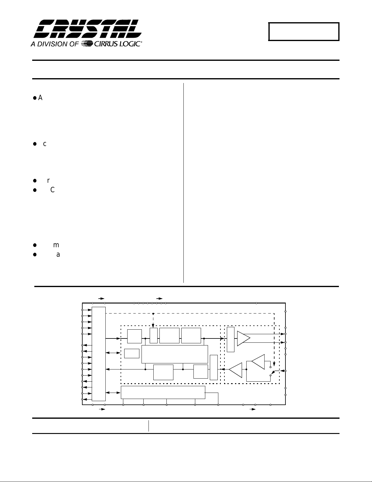
Echo-Cancelling Codec
CS6403
Features
l
Applicable in:
- Digital-Cellular Hands-Free Phones
- Analog-Cellular Hands-Free Phones
- Office Speaker Phones
- Desktop & Video Teleconferencing
l
Echo Cancellation
- Up to 60 dB ERLE
- 512 Tap (64 ms at 8 kHz sampling rate)
- Split Mode For Two Echo Cancellers
l
Serial Data/Control Interface
l
On-Chip Delta-Sigma Codec
- < 1% THD, 8 Ω Load On Output
- > 70 dB S/(N+D) on Input
- 300-3600 Hz Bandwidth (8 kHz sampling rate)
- Volume Control
- Microphone Preamp
l
Automatic Gain Control (AGC)
l
No Training Signals Generated
I
Description
The CS6403 is an application-specific digital signal processor optimized for network and acoustic echo
cancellation applications. A high-quality codec is integrated with the processor to provide a complete, lowcost echo-cancellation solution.
The CS6403 is a fully independent processor that requires no signal processing support to implement its
cancellation functions. Volume control, AGC, and sleep
functions are also prov ided.
The on-chip ADC and DAC employ over-sampling technology, which eliminates the need for complex external
anti-aliasing and reconstruction filters, further reducing
system cost.
The CS6403 has a serial interface that i s compatibl e with
most DSPs and PCM codecs. Clock and sync lines control the tr ansfer of seri al data via the separate ser ial datain and data-out pins. Both 16-bit audio data and control/status information may be multiplexed on this serial
channel using a steering bit.
ORDERING INFORMATION
CS6403-IQ -40° to +85° C 44-pin TQFP
CS6403-IL -40° to +85° C 44-pin PLCC
CDB6403 Evaluation Board
CONFIG
GPIN0
GPIN1
GPIN2
GPIN3
GPOUT0
GPOUT1
SFRAME
SMASTER
UALAW
SSYNC
SCLK
SDO_1
SDI_A
SYNCOUT
DVDD0 1
Serial I/O
DGND0 1
Control
Status
RESERVED0 6
DSP
High
Pass
Control
CLKIN CLKOUTSCLK_RATE0
Preliminary Product Information
Cirrus Logic, Inc.
Crystal Semiconductor Products Division
P.O. Box 17847, Austin, Texas 78760
(512) 445 7222 FAX: (512) 445 7581
http://www.crystal.com
AVDD
Analog I/O
Nonlinear
A
Echo
G
Control
C
Echo Cancellers
Nonlinear
Echo
Control
PLL + Clock Manager
This document contains information for a new product.
Cirrus Logic reserves the right to modify this product without notice.
Volume
Control
High
Pass
SCLK_RATE1
Copyright Cirrus Logic, I nc. 1997
CLK_SEL NC
(All Rights Reserv ed)
A
T
D/A
T
E
N
A
T
T
E
N
A/D
AGND0 1
26 dB
RESET
PVDD
SPKROUTP
SPKROUTN
PGND0
PGND1
MICIN
VCM
VREF
MAR ‘96
DS192PP7
1
CS6403
ADC CHARACTERISTICS (T
Logic 0 = 0V, Logic 1 = DVDD; Signal test frequency 1kHz, word rate (Fs) = 8kHz, audio signal measurement
bandwidth is 20Hz to 4kHz; Microphone amp gain = 0dB; SPRKOUT outputs connected to 8Ω load; CLKIN frequency = 8.192MHz; unless otherwise specified) Note 1.
Parameter Symbol Min Typ Max Units
ADC Resolution With No Missing Codes 12 - - bits
Instantaneous Dynamic Range IDR 67 72 - dB
Total Harmonic Distortion at -0.5dBFS signal level THD - 0.01 0.05 %
Gain Drift (Note 2) - 150 - ppm/°C
Offset E rror - 0 2 LSB
Full Scale Input Voltage (Note 3) 0.85 1.0 1.1 V
Input Resistance (at MICIN) (Note 2) 25 - Input Capacitance (at MICIN) (Note 2) - 15 - pF
Sample Rate Fs - 8 - kHz
Microphone Amp Gain (switchable on/off) 24 26 28 dB
Anti-aliasing Rejection - 30 - dB
Power Supply Rejection (1kHz) PSR 40 - - dB
Frequency Response -0.6 - 0.6 dB
Transition Band 0.45 - 0.6 Fs
Stop Band Rejection 70 - - dB
VREF Reference Voltage Output - 2 .0 - V
VCM Voltag e Output constan t load only , >100 kΩ
Group Delay (Note 4) - 1 - ms
Group Delay Variations vs. Frequency (Note 4) - 0.0 -
Notes: 1. Bench testing is done with Crystal part CXT8192 driving CLKIN, automated device testing utilizes
test system provided clock sources.
2. Guaranteed by design/characterization.
3. This is the peak input voltage (in volts) with the mic amp gain set to 0 dB. Peak-to-peak voltage is
2x peak. Input signals will be properly clipped if the peak signal is greater than full scale, but less
than 2x full scale.
4. This group-delay specification is for the ADC only; additional group delay is introduced by the
AGC and high-pass filter that is implemented on the CS6403 in software.
= 25 °C; All DVDD, AVDD, and PVDD = 5.0V, Digital Input Levels:
A
-1.0-V
p
kΩ
µs
2 DS192PP6
CS6403
DAC CHARACTERISTICS (T
Logic 0 = 0V, Logic 1 = DVDD; Signal test frequency 1kHz, word rate (Fs) = 8kHz, audio signal measurement
bandwidth is 20Hz to 20kHz; Microphone amp gain = 0dB; SPRKOUT outputs connected to 8Ω load; CLKIN frequency = 8.192MHz; unless otherwise specified)
Parameter Symbol Min Typ Max Units
DAC Resolution 12 - - bits
DAC step size error - Instantaneous Dynamic Range (20 Hz - 20 kHz) IDR 60 72 - dB
Frequency Response -0.8 - +0.6 dB
Programmable Output Level Attenuator Range (Note 5) -92.2 - 0 dB
Gain Step Size - 2.49 - dB
Gain Drift (Note 2) - 150 - ppm/°C
VREF Reference Output Voltage - 2.0 - V
VCM Output Voltage constant load only, >100kΩ
Offset E rror - 25 50 mV
Full Scale Output Voltage (SPKROUT pins) (Note 6) 1.40 1.75 1.93 V
Common Mode Output Voltage (SPKROUT pins) - 1.30 - V
Total Harmonic Distortion at -0.5dBFS level, SPKROUT(Note 9) THD - - 0.8 %
Output Impedance SPKROUT pins - 0 .4 Load Impedance SPKROUT pins 8 - Output Capacitance - 15 - pF
Audible Stop Band Attenuation (<20kHz) 68 - - dB
Integrated Inaudible Energy (>20kHz to 100kHz) (Note 7) - - 30 mVrms
Power Supply Rejection (1kHz) PSR 40 60 - dB
Filter Transition Band 0.45 - 0.6 Fs
Group Delay (Note 8) - 1 - ms
Notes: 5. Attenuation settings greater than 92.2 dB will cause a full scale input signal to be completely
attenuated to zero signal level.
6. This is the peak differential output voltage. The peak-to-peak signal level on each output pin is
equal to the peak differential value.
7. Assuming an external 43.2 kHz RC output filter.
8. This group-delay specification is for the DAC only; additional group delay is introduced by the
AGC and high-pass filter that is implemented on the CS6403 in software.
9. Room temperature only.
= 25 °C; All DVDD, AVDD, and PVDD = 5.0V, Digital Input Levels:
A
±0.5
-1.0-V
LSB
p
Ω
Ω
DS192PP6 3
CS6403
PHASE-LOCKED LOOP CHARACTERISTICS (T
= 25°C; AVDD, DVDD, and PVDD = +5V;
A
Input Levels: Logic 0 = 0V, Logic 1 = DVDD)
Parameter Symbol Min Typ Max Units
PLL acquisition time T
ACQ
0.3 1 ms
PLL frequency range 23.35 24.58 25.80 MHz
PLL jitter 200 ps rms
Input ref frequency 1.95
0.97
243
DIGITAL CHARACTERISTICS (T
= 25°C; AVDD, DVDD, and PVDD = 5V)
A
2.048
1.024
256
2.15
1.08
268
MHz
MHz
kHz
Parameter Symbol Min Typ Max Units
High-level Input Voltage V
Low-level Input Voltage V
High-level Output Voltage at I0 = -2.0 mA V
Low-level Output Voltage at I0 = +2.0 mA V
Input Leakage Current (Digital Inputs) I
OH
OL
IN
Output Leakage Current (High-Z Digital Outputs) - - 10
Output Capacitance (Note 2) C
OUT
Input Capacitance (Note 2) C
DVDD - 1.0 - - V
IH
IL
--1.0V
DVDD - 0.3 - - V
--0.3V
--10
--15pF
IN
--15pF
µA
µA
ABSOLUTE MAXIMUM RATINGS (All voltages with respect to 0V)
Parameter Symbol Min Typ Max Units
Power Supplies AVDD
DVDD
PVDD
Input Current Except Supply Pins & Driver Pins I
Short Circuit Current Limit SPKROUT pins (Note 10) I
Analog Input Voltage V
Digital Input Voltage V
Ambient Temperature (Power Applied) T
Storage Temperature T
ESD using human body model (100pF with series 1.5kΩ)
IN
SC
INA
IND
AMAX
STG
V
ESD
Notes: 10. SPKROUTP or SPKROUTN shorted to ground.
Warning: Operation beyond these limits may result in permanent damage to the device.
Normal operation is not guaranteed at these extremes.
4 DS192PP6
-0.3 - 6.0 V
--10.0mA
- - 500 mA
-0.3 - AVDD + 0.3 V
-0.3 - DVDD + 0.3 V
-55 - 125 °C
-65 - 150 °C
2000 - - V
CS6403
POWER CONSUMPTION (T
1kHz; Word Rate (Fs) = 8kHz; SPRKOUT outputs connected to 8Ω load; Mode 2 SCLK = 256 kHz; unless otherwise specified) Full scale output.
Parameter Symbol Min Typ Max Units
Normal Operation Power Dissipation P
High-Impedance Output (Note 11) P
RESET High P
RESET High, clocks halted (Note 12) P
Powerdown Asserted in Software P
Notes: 11. SPKROUT outputs connected to 1 kΩ load.
12. RESET high, CLKIN grounded (Mode 1) or SCLK grounded (Mode 2), and CLK_SEL (PIN 15Q, 21L)
high to disable PLL.
= 25°C; All DVDD, AVDD and PVDD = 5.0V; Signal test frequency
A
D
NS
RH
RNC
PDN
- 800 - mW
- 300 - mW
-55-mW
-15-mW
-55-mW
RECOMMENDED OPERATING CONDITIONS (All voltages with respect to 0V)
Parameter Symbol Min Typ Max Units
DC Power Supplies: AVDD
DVDD
PVDD
Ambient Operating Temperature T
A
4.50 5.0 5.50 V
-40 85 °C
t
t
ckl
ckh
CLKIN
t
pd3
SCLK
SYNCOUT
(Master Mode)
SCLK & SYNCOUT Output Timing
Mode 1 - MASTER
DS192PP6 5
CS6403
SWITCHING CHARACTERISTICS (T
= 25°C; AVDD and DVDD = +5V, output loaded with
A
30 pF; Input Levels: Logic 0 = 0V, Logic 1 = DVDD)
Parameter Symbol Min Typ Max Units
Mode 1 - MASTER
Input clock (CLKIN) frequency CLKIN 7.78 8.192 8.60 MHz
CLKIN low time t
CLKIN high time t
ckl
ckh
30 - - ns
30 - - ns
Sample Rate Fs - 8 - kHz
SCLK and SYNCOUT output delay from CLKIN rising t
SCLK duty cycle (Note 12) t
SCLK rising to SYNCOUT rising t
SCLK rising to SYNCOUT falling t
SDO delay from SCLK edge t
SDI setup time to SCLK edge t
SDI hold time from SCLK edge t
SDO to Hi-Z state t
SDO to non-Hi-Z bit 1 t
pd3
sckw
sr1
sf1
pd1
s1
h1
hz
nz
RESET pulse width high 250 - -
- - 50 ns
-50-%
-1230ns
- 6 30 ns
- - 70 ns
15 - - ns
10 - - ns
- - 50 ns
5--ns
µs
Mode 2 - SLAVE
Input clock (SCLK) frequency SCLK 243
0.97
1.95
SCLK low time t
SCLK high time t
SYNCOUT output delay from SSYNC rising t
SYNCOUT output delay from SSYNC falling t
ckl
ckh
pdsr
pdsf
150 - - ns
150 - - ns
- - 50 ns
- - 50 ns
256
1.024
2.048
268
1.08
2.15
kHz
MHz
MHz
Sample Rate Fs - 8 - kHz
SDI/SSYNC setup time to SCLK edge t
SDI/SSYNC hold time from SCLK edge t
SDO delay from SCLK edge t
SDO to Hi-Z state bit 16/8 t
SDO to non-Hi-Z bit 1 t
s1
h1
pd1
hz
nz
RESET pulse width high 250 - -
15 - - ns
10 - - ns
- - 70 ns
- - 50 ns
5--ns
µs
Notes: 12. When the CS6403 is in master mode (SSYNC and SCLK outputs), the SCLK duty cycle is 50%.
The period of SCLK is 4/CLKIN.
6 DS192PP6
t
A
A
A
A
A
A
A
A
A
A
A
A
A
A
A
A
A
A
A
A
A
A
A
A
A
A
A
A
A
A
A
A
A
A
A
A
A
A
A
A
A
A
A
A
A
A
A
A
A
A
A
A
A
A
A
A
A
A
A
A
A
A
A
A
A
A
A
A
A
A
A
AAA
A
A
A
A
A
A
A
A
A
A
A
A
A
A
A
A
A
A
A
A
A
A
A
A
A
A
A
A
A
A
A
A
A
A
A
A
A
A
A
A
A
A
A
A
A
A
A
A
A
A
A
A
A
A
A
A
A
A
A
A
A
A
A
A
A
A
A
A
A
A
A
AAA
A
A
A
A
A
A
A
A
A
A
A
A
A
A
A
A
A
A
A
A
A
A
A
A
A
A
A
A
A
A
A
A
A
A
A
A
A
A
A
A
A
A
A
A
A
A
A
A
A
A
A
A
A
A
A
A
A
A
A
A
A
A
A
A
A
A
A
A
A
A
A
A
A
A
A
A
A
A
A
A
A
A
A
A
A
A
A
A
A
A
A
A
A
A
A
A
A
A
A
A
A
A
A
A
A
A
A
A
A
A
A
A
sckw
SCLK
t
t
sr1
sckhtsckl
t
sf1
SYNCOUT
(Short Frame)
t
sr1
SYNCOUT
1
(Long Frame)
t
h1
t
s1
SDI
t
nz
Bit 1 Bit 2 Bit 7 Bit 8
t
pd1
t
pd1
SDO
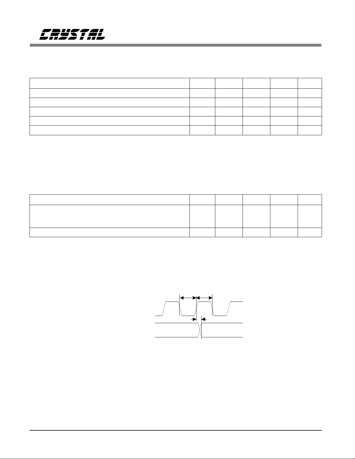
Note: 1. SYNCOUT is long frame when SFRAME = 1.
Master Mod e Seria l Port Tim ing
(Mode 1)
CS6403
AA
AA
AA
AA
AA
AA
AA
AA
AA
AA
AA
AA
AA
AA
AA
AA
AA
AA
AA
AA
AA
AA
AA
AA
AA
AA
AA
AA
AA
AA
AA
AA
AA
AA
AA
AA
AA
AA
AA
AA
AA
AA
AA
AA
AA
AA
AA
AA
AA
AA
AA
AA
AA
AA
AA
AA
AA
AA
AA
AA
AA
AA
AA
AA
AA
AA
AA
AA
AA
AA
AA
AA
AA
AA
AA
AA
AA
AA
AA
AA
AA
AA
AA
AA
AA
AA
AA
AA
AA
AA
AA
AA
AA
AA
AA
AA
AA
AA
AA
AA
AA
AA
AA
AA
AA
AA
AA
AA
AA
AA
AA
AA
AA
AA
AA
AA
AA
AA
AA
AA
AA
AA
AA
AA
AA
AA
AA
AA
AA
AA
AA
AA
AA
AA
AA
AA
AA
AA
AA
AA
AA
AA
AA
AA
Bit 8Bit 7Bit 1 Bit 2
t
sf1
t
hz
t
sckhtsckl
SCLK
th1t
s1
SSYNC
t
pdsf
t
pdsr
DS192PP6 7
SYNCOUT
SDI
SDO
t
h1
t
s1
Bit 1 Bit 2
t
pd1
t
nz
t
pd1
Bit 1 Bit 2
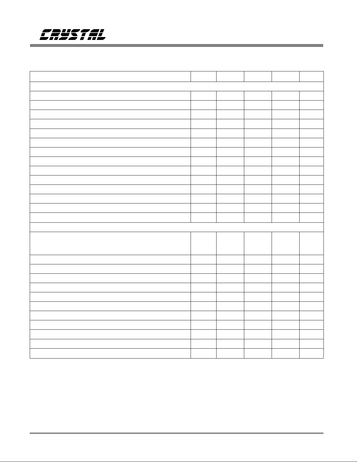
Slave Mode Serial Port Timing
AA
AA
AA
AA
AA
AA
AA
AA
AA
AA
AA
AA
AA
AA
AA
AA
AA
AA
AA
AA
AA
AA
AA
AA
AA
AA
AA
AA
AA
AA
AA
AA
AA
AA
AA
AA
AA
AA
AA
AA
AA
AA
AA
AA
AA
AA
AA
AA
AA
AA
AA
AA
AA
AA
AA
AA
(Mode 2)
AA
AA
AA
AA
AA
AA
AA
AA
AA
AA
AA
AA
AA
AA
AA
AA
AA
AA
AA
AA
AA
AA
AA
AA
AA
AA
AA
AA
AA
AA
AA
AA
AA
AA
AA
AA
AA
AA
AA
AA
AA
AA
AA
AA
AA
AA
AA
AA
AA
AA
AA
AA
Bit 15
AA
AA
AA
(Bit 7)
AA
Bit 15
(Bit 7)
Bit 16
(Bit 8)
Bit 16
(Bit 8)
t
hz
60.0
40.0
CS6403
ERLE
ERLE (dB)
20.0
Speech Training Signal
0.0
0.02.04.06.08.0
Figure 1 . Typ ical ER LE Conv ergen ce Chara cter istics
Echo Canceller Characteristics
The typical Echo Return-Loss Enhancement
(ERLE) convergence characteristics for the
CS6403 are illustrated in the above diagram
under the following conditions:
• Echo-canceller l ength: 512 taps
• Echo-canceller initial conditions: zeroed filter
taps, updates disabled unt il t=0.12 5s
• Sampling rate : 8 kHz
• Echo path (in cludin g micropho ne, speaker,
and amplifiers):
- spectrally flat
-linear
- duration < 64 ms
- noise free
- time invariant
Speech (mV)
0.3
0.0
-0.3
Seconds
• Near-end high-pass filter: enabled
• Pre-emphas is fil ter: ena bled
• Graded-beta profile: 64 echo-canceller filter
taps pr ocessed per 2 x red uction in upd ate g ain
• Train ing si gna l: spe ech, fu ll sca le
• Unlimited S/(N+D) on linear ADC
Note: Many of these conditions may be
significantly different in real
appl icatio ns, re sulti ng i n sign ific antly
different measured ERLE performance.
8 DS192PP6
CS6403
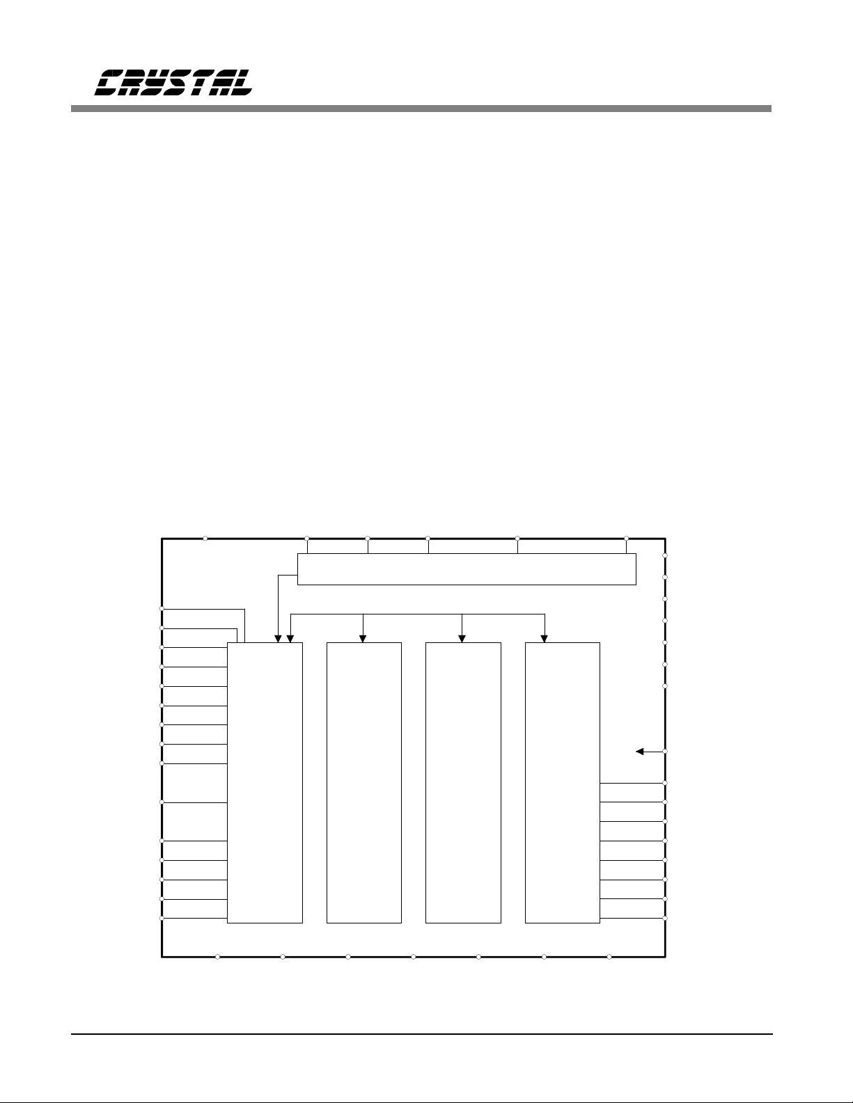
OVERVIEW
In hands-free speakerphones, the signal from the
far end may echo about the near-end environment and then be received at the near-end
microphone. When heard at the far end, this
echo signal can be very annoying, particularly if
the signal is delayed by transmission or signalprocessing delays.
Voice switching is a particularly simple technique for eliminating this echo, but since it
imposes half-duplex communication, it seriously
compromises conversation quality.
Echo cancellation can provide high-quality, fullduplex communication, but typically must be
implemented using expensive digital signal-processing hardware.
NC
CLK_SEL
CLKIN CLKOUT
Echo Cancellation in the CS6403
The CS6403 provides high-quality echo cancellation at low cost. This breakthrough in
cost/performance is made possible on the
CS6403 by custom, application-optimized processing blocks, which are integrated on a single
die, as shown in Figure 2.
One of these processing blocks is the AFP
(Adaptive Filter Processor). This block implements a 512-tap AFIR (Adaptive Finite
Impulse-Response) filter which is updated using
an enhanced least-mean squared (LMS) algorithm. At a sampling rate of 8 kHz, it can cancel
up to 64 ms of echo. By default, 10 ms of the
available 64 ms are allocated to a network canceller (NEC), and the remaining 54 ms are
allocated to an acoustic echo canceller (AEC).
SCLK_RATE0 SCLK_RATE1
CONFIG
GPIN0
GPIN1
GPIN2
GPIN3
GPOUT0
GPOUT1
SCLK
SDI
SDO
SFRAME
SMASTER
SSYNC
SYNCOUT
UALAW
PLL/Oscillator
SSI CPU AFP CO DEC
RESERVED0
RESERVED1
RESERVED2
RESERVED3
RESERVED4
RESERVED5
RESERVED6
RESET
AGND0
AGND1
AVDD
MICIN
SPKROUTP
SPKROUTN
VCM
VREF
DVDD0
DVDD1 DGND1 PVDD PGND0 PGND1
DGND0
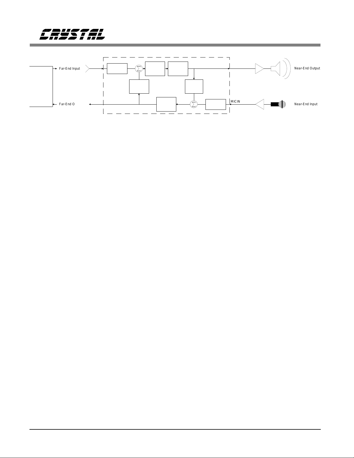
Figure 2. CS6403 Internal Block Diagram
DS192PP6 9
CS6403
AAAA
AAAA
AAAA
AAAA
AAAA
AAAA
CS6403
DSP or
PCM Codec
Far-End Input
Far-End Output
SDI
SDO
High Pass
Filter
+
Network
Canceller
Echo
AGC/
Volume
Control
-
Non-linear
Echo
Control
Figure 3. Functional Diagram
The Central Processing Unit (CPU) does all the
other miscellaneous processing, like update control and double talk detection. This processing
has a critical influence on overall echo-cancellation performance. Double-talk detection is a
particularly important part of this processing.
Double-talk detection and other algorithms were
carefully developed and validated at Crystal under real-world conditions.
To increase the CS6403’s echo return-loss enhancement (ERLE), supplemental echo
suppression is used. A sophisticated voice-detection algorithm is used to reduce echo with
minimal impact on conversation quality, assuring
the highest quality conversation.
Figure 3 describes the functional behavior of the
CS6403 in a typical application. Digital data
from the far-end interface comes into SDI of the
CS6403 where it is acted upon by the various
algorithms running in the CPU. First, a HighPass Filter eliminates DC offset and low
frequency noise before sending the far-end input
data onto the summing node for the network
echo canceller. Assuming there is no speech
from the near-end, the signal after the summing
node is unaffected.
The signal then passes on to the AGC/Volume
Control block where the signal level is boosted,
if necessary. The volume control is implemented
in part by the AGC (for more details, see the
section entitled "Embedded Signal Processing
Functions").
Non-linear
Echo
Control
Acoustic
Echo
Canceller
+
High Pass
Filter
SPKROUT
MICIN
*
*
* Optional
The signal then passes on to the Non-linear Echo
Control block which controls the half-duplex
failsafe and the supplementary echo suppressor
which act to enhance and supplement the performance of the echo canceller.
The signal after this block is then fed to both the
speaker output and the input to the acoustic echo
canceller (implemented by the AFP). The
speaker output couples to the microphone input
by various echo paths. The signal received at
the microphone is then filtered and sent on to the
summing node of the Acoustic Echo Canceller.
The Acoustic Echo Canceller constructs a model
of the echo paths between the speaker and microphone and processes its input signal with its
digital representation of the echo paths. As such,
its output should very closely match the input
from the microphone and so the output from the
summing node should be a very small signal,
which is referred to as the "error signal." This
error signal is fed back to the echo canceller to
let it adapt its performance should there be a
change in the echo path.
The Non-linear Echo Control block following
the summing node further attenuates any vestiges
of signal received at the microphone that originated from the speaker. This signal is then sent
to the far-end output by SDO as well as to the
input of the Network Echo Canceller, where a
function similar to that performed by the Acoustic Echo Canceller is performed.
Near-End Output
Near-End Input
10 DS192PP6

CS6403
Analog Interface
The codec block provides an analog-to-digital
converter (ADC) and a digital-to-analog converter that can be connected directly to a
microphone and a speaker, respectively.
The output of the microphone should be lowpass filtered, then AC-coupled to the audio input,
MICIN. A 26 dB gain stage is included in the
CS6403 at the ADC input to amplify the microphone signal. However, this gain stage may be
bypassed in modes in which a line-level source
is connected to the CS6403 instead of a microphone. The CS6403 also includes a speaker
driver, which can drive an 8Ω speaker directly,
or alternatively, it can drive a high-impedance
differential input on an external amplifier.
With the 26 dB gain stage on, the fullscale input
for the MICIN pin is 100mV peak-to-peak. Any
signal over 100mV peak-to-peak will clip the input to the ADC. With the gain stage off, a 2V
peak-to-peak signal is the maximum allowed.
The fullscale output voltage from the DAC is
1.75V peak-to-peak single-ended, or 3.5V peakto-peak differentially.
SCLK
SMASTER
0 0 0 256 kHz I slave
0 0 1 undefined
0 1 0 1.024 MHz I slave
0 1 1 2.048 MHz I slave
SCLK_RATE1
SCLK_RATE0
Clock Rate I/O mode
It is very important to not clip signals anywhere
in the system. An echo canceller can only remove echo that passes through a linear, time
invariant path. Echo that passes through a nonlinearity (like clipping) will not be removed by
the echo canceller.
Both the DAC and ADC paths are bandlimited
as a function of sampling rate. At a sampling
rate of 8 kHz, the paths are limited to 03600 Hz.
Synchronous Serial Interface
The Synchronous Serial Interface (SSI) provides
a data and control interface to the CS6403. The
SSI can be connected to an external network
codec for applications like speakerphones or to a
DSP for high-end applications like video teleconferencing.
Depending on the state of the SMASTER
(PIN 42Q, 4L) pin at RESET, the CS6403 can
operate as either a system timing master or slave.
As a master, the serial clock pin (SCLK) is an
output. As a system timing slave, SCLK must
be driven by an external source. When SMASTER is high, the SCLK output frequency is a
fixed 2.048 MHz derived from the 8.192 MHz
crystal oscillator connected across CLKIN and
CLKOUT. When SMASTER is low, internal
timing is generated by the Phase Locked Loop
(PLL), which uses SCLK’s input as a timing reference, so no external crystal is necessary. In
slave timing mode, SCLK can be driven at 256
kHz, 1.024 MHz, or 2.048 MHz. The CS6403 is
informed of the SCLK rate via the
SCLK_RATE0 (PIN 29Q, 35L) and
SCLK_RATE1 (PIN 30Q, 36L) pins.
1 0 0 undefined
1 0 1 undefined
1 1 0 undefined
1 1 1 2.048 MHz O master
Table 1 shows the various options for SCLK.
Table 1. Clock Options
DS192PP6 11
CS6403
Configuration
Mode 1: Master Interface (e.g. CODEC⇔CS6403)
Application: Low-cost speaker phone
1.1: Short-Frame Mode 0 1 0
1.2: Long-Frame Mode 1 1 0
Mode 2: Slave Interface (e.g. DSP⇔CS6403)
Application: Digital cellular
2.1: 16-bit Mode 0 0 1
2.2: 8-bit Mode 0 0 0
Table 2. CS6403 Configurations
Mode Selection
The behavior of the CS6403 is controlled by
configuration-control input pins. The behavior of
the CS6403 for each possible state of these control signals is illustrated in Table 2.
As indicated in Table 2, the CS6403 has two basic operating modes. These operating modes are
illustrated in Figure 4.
The simplest operating mode is Mode 1. This
operating mode is useful in applications where
the data link to the far end is analog, as in analog cellular hands free, or in analog speaker
phones. The SSI is the system timing master in
Mode 1. Long or short framing signals can be
generated. Word length is always 8 bits.
SFRAME
SMASTER
CONFIG
Mode 2 is useful in applications where the data
link to the far end is digital, as in digital cellular
hands free, or in digital (ISDN) speaker phones.
The SSI is the system timing slave in Mode 2.
Only short framing pulses are accepted. Word
length can be 8 or 16 bits. Mode 2 allows access to control registers in 16-bit Mode.
States of Operation
Reset
Reset may be asserted either by setting the RESET (PIN 41Q, 3L) pin high, or by setting the
Reset bit in Synchronous Serial Interface Control
Register 0 (RST: SSI_CR0.11). The only functional difference between these two operations is
that setting the RESET pin clears the RST bit.
During Reset, all chip functions are halted ex-
Codec
Far End Near End
DSP
CS6403
Mode 1
CS6403
Mode 2
Figure 4. Operating Modes
12 DS192PP6
CS6403
cept for the SSI, though writes to any control bit
except RST are ignored. Power down is not enabled.
Upon exiting Reset, control registers and RAM
are cleared, and then control constants are loaded
into Data RAM from the Program ROM.
External
µ
-law
Codec
Digital
Ground
FSR
FST
BCLKR
BCLKT
MCLK
DR
DT
+
1 µF
0.1 µF
Analog
Ground
SYNCOUT
SCLK
SSYNC
SDO
SDI
RESERVED1
SCLK_RATE0
SCLK_RATE1
SMASTER
SFRAME
UALAW
CLK_SEL
CONFIG
GPIN0
GPIN1
GPIN2
GPIN3
RESERVED0
RESERVED2
RESERVED3
RESERVED4
RESERVED5
RESERVED6
DVDD0
DVDD1
DGND1
DGND0
Speaker
Ground
RESET
CS6403
System
Reset
AGND1
Power-Down
Power Down is initiated by setting the Sleep bit
in SSI Control Register 0 (SLP: SSI_CR0.10).
In Power Down, the CPU and the AFP are powered down, but the SSI and the Codec are still
operational. Power Down is only accessible in
Mode 2 (16-bit).
Since the SSI and the Codec are active during
Power Down, it is possible to serially transfer
SPKROUTP
SPKROUTN
GPOUT0
GPOUT1
CLKOUT
PGND0
PGND1
AGND0
VREF
VCM
NC
MICIN
CLKIN
PVDD
AVDD
470 pF
0.1µF
0.1µF
F0.1 µF0.1
0.1
µ
0.1
8
Ω
+
1µF
+
1µF
Microphone
Phantom Power
Supply
33 pF
33 pF
µ
Φ0.1 µΦ
2.2k
0.47µF
150
Ω
F
0.022
µ
NPO
8.192MHz
++
µ
F
Ω
Microphone
+5V Analog
Supply
+
10 µF
2
Ω
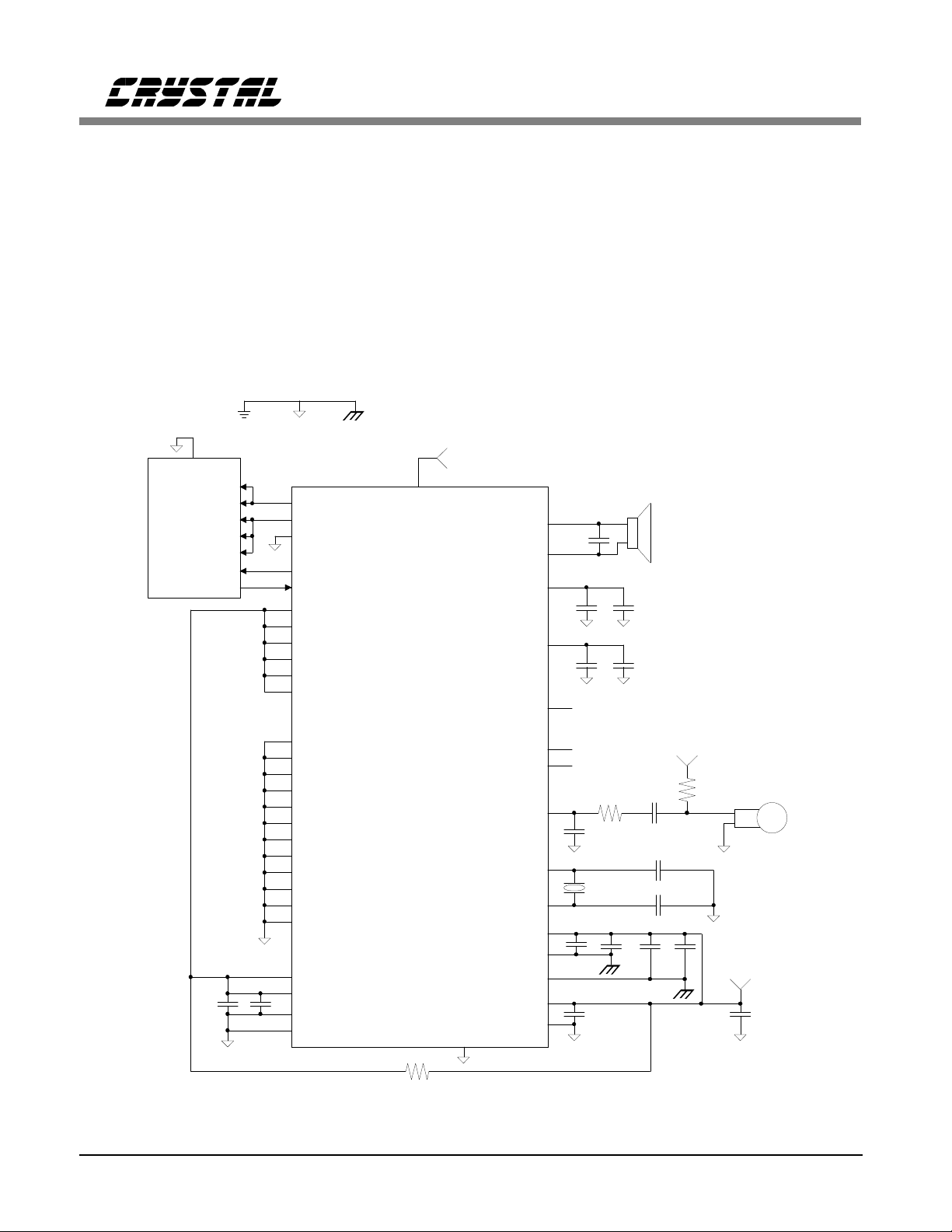
Figure 5. External Mu-law Codec Connection Diagram
DS192PP6 13

CS6403
audio and control data while SLP is asserted, bypassing the CPU and AFP. Note, however, that
since the CPU is powered down, no scaling is
performed on the ADC input, no echo is cancelled, and audio data is not companded.
Using the CS6403
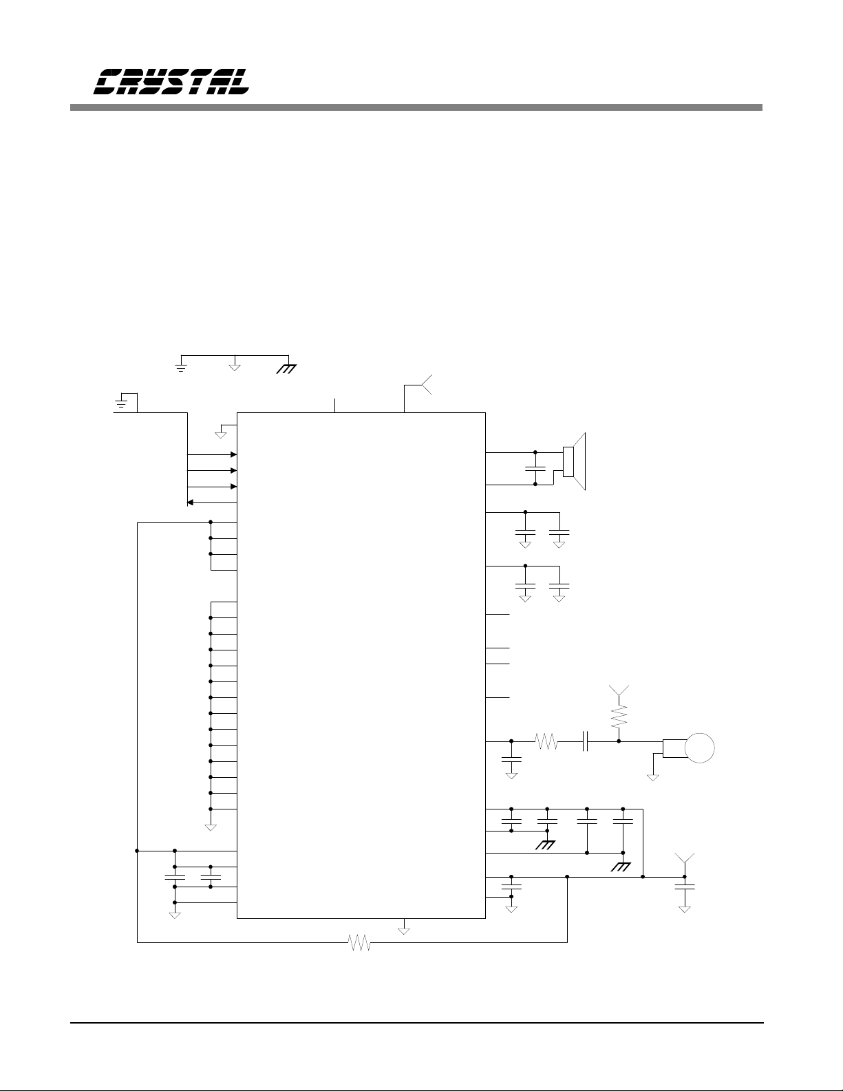
Interfacing as a Master to an external codec
(Mode 1)
In applications like speakerphones, it is possible
to connect the CS6403 directly to an external
network codec. An example circuit is shown in
Figure 5.
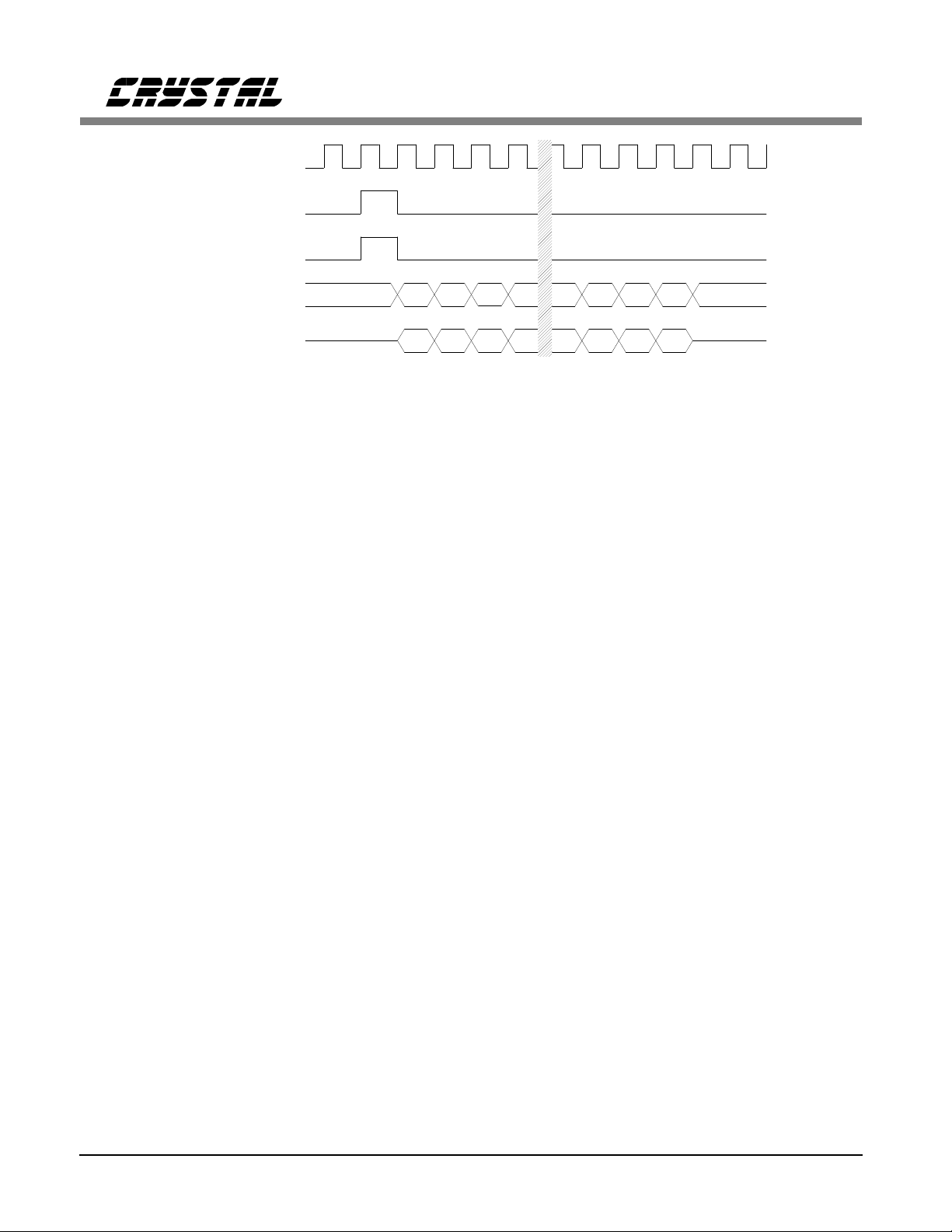
Mode 1.1 (Short-Frame Mode)
SFRAME=0; SSYNC = 0
In this application, SYNCOUT and SCLK are
sourced by the CS6403 (i.e., SMASTER=1), and
CLKIN is generated by connecting a crystal between CLKOUT and CLKIN. The timing for
these signals is illustrated in Figure 6.
Audio-data samples in Mode 1 are 8 bits and are
µ−law or A-law companded depending on the
state of the UALAW pin (PIN 13Q, 19L). No
control information can be transferred in Mode
1, so there is no control/data steering bit. Also
note that since control information cannot be
transferred, the default settings of the control
registers established after Reset are used.
In Mode 1, 80 echo-canceller taps (out of the
available 512) are permanently allocated to network-echo cancellation (see Figure 3).
SCLK (out)
SYNCOUT (out: 8kHz)
SDI (in)
SDO (out)
Mode 1.2 (Long-Frame Mode)
SFRAME=1; SSYNC = 0
SCLK (out)
SYNCOUT (out: 8kHz)
SDI (in)
SDO (out)
b7 b6 b5 b4 b3 b2 b1 b0
b7 b6 b5 b4 b3 b2 b1 b0
b7 b6 b5 b4 b3 b2 b1 b0
b7 b6 b5 b4 b3 b2 b1 b0
Figure 6. External-Codec Mode Timing (Mode 1)
14 DS192PP6
CS6403
Interfacing as a Slave to an external DSP
(Mode 2)
When interfacing to an external DSP (Mode 2),
the CS6403 is configured as a slave to the DSP:
SSI; i.e., SCLK, and SSYNC signals are provided to the CS6403 by the DSP. An example of
the interface circuitry is shown in Figure 7.
Speaker
Ground
CLKIN CLKOUT
SDI
SCLK
SSYNC
SDO
CONFIG
RESERVED1
SCLK_RATE0
SCLK_RATE1
CS6403
RESET
DSP
Digital
Ground
Analog
Ground
In this case, the DSP sends a single start-offrame pulse to the SSYNC input one SCLK
period before the start of a data frame. Since
there is only one SSYNC input, every data frame
includes both a data read from the CS6403 and a
data write to the CS6403. The behavior of the
serial interface is illustrated in Figure 8.
System
Reset
SPKROUTP
SPKROUTN
VREF
VCM
470 pF
0.1
µ
0.1
µ
8
Ω
+
F
F
+
1 µF
1
µ
F
1 µF
CLK_SEL
GPIN0
GPIN1
GPIN2
GPIN3
RESERVED0
RESERVED2
RESERVED3
RESERVED4
RESERVED5
RESERVED6
SFRAME
SMASTER
UALAW
0.1 µF
+
DVDD0
DVDD1
DGND1
DGND0
AGND1
2
Ω
NC
GPOUT0
GPOUT1
SYNCOUT
MICIN
PVDD
PGND0
PGND1
AVDD
AGND0
0.1
µ
0.022
NPO
F
0.1
150
0.1
µ
0.47µF
Ω
µ
F
F
µ
F
Microphone
Phantom Power
Supply
0.1
F
0.1
µ
++
2.2k
F
µ
Ω
Microphone
+5V Analog
Supply
+
10
F
µ
Figure 7. DSP Connection Diagram (Mode 2)
DS192PP6 15
SCLK (in)
SSYNC (in)
SYNCOUT (out)
SDI (in) b15 b14 b13 b12 b3 b2 b1 b0
SDO (out) b15 b14 b13 b12 b3 b2 b1 b0
Figure 8. Serial Port Timing for Mode 2 (16-bit) - SLAVE
CS6403
Mode 2 (8-bit) Slave
Mode 2 (8-bit) provides a slaved SSI which may
be needed for 8-bit companded audio interfacing,
as is the case with many ISDN transceivers.
Mode 2 (8-bit) timing is similar to Mode 2 (16bit) timing, but the serial data is 8-bit
companded, with the type of companding determined by the state of the UALAW pin. All 8
bits are used for audio, so no steering bit is necessary, and consequently, no control information
can be transferred in this mode.
Mode 2 (8-bit) is selected by setting CONFIG
low, as opposed to high in Mode 2 (16-bit). See
Table 2 for more details. SCLK frequency is determined by the SCLK_RATE1 and
SCLK_RATE0 pins as given by Table 1. As in
Mode 2 (16-bit), the CS6403 will phase-lock to
the SCLK provided to it and derive its own timing from it.
Mode 2 (16-bit) Slave
Setting CONFIG high selects Mode 2 (16-bit).
When a DSP is connected to a CS6403 in
Mode 2 (16-bit), the DSP can reconfigure the
CS6403 by writing to the CS6403’s control registers via the SSI. To multiplex both data and
control on one serial interface, a steering bit is
used. The first bit sent (MSB) by the DSP determines whether a word is control or data, as
shown in Table 3.
If STR, the Steering Bit (b15), is zero, then the
data transferred on the Serial Interface is audio
data. Note that since a transfer typically consists
of 16 bits, this allows 15-bit precision for input
audio data. Output audio data remains in 16-bit
precision.
Companded audio data is treated differently than
16-bit data. Input companded audio data has
eight zeroes followed by the 8-bit companded
data. Output companded audio data is formatted
such that 8-bit data is followed by eight zeroes.
If STR is one, the word transferred on the Serial
Interface is control information. If the RNW bit
is a zero, the word written by the external DSP
is stored by the CS6403 in the indicated destination register, and simultaneously, the state of the
destination register before the write is read back
into the DSP. If RNW is one, the data written
by the external DSP is ignored. The state of the
destination register is read back to the DSP.
Note that only one control word or one data
word may be transferred in a sample time, meaning that no audio data is transferred in sample
times where control information is transferred. In
such sample times, the CS6403 will reuse (double-sample) the audio data from the previous
sample time. As a result, to minimize distortion
of the audio signal, control transactions should
be made infrequently.
16 DS192PP6
CS6403
The CS6403 requires one sample time to effect a
write to a control register. As a result, a controlword write should not be followed in the next
control word with a read to the same control
word. There should be at least one intervening
sample time prior to the next control word read
to that control word.
Control Register Definitions
The CS6403 has four control registers that are
accessible via the SSI, which allow a user to
monitor and control the behavior of the CS6403.
Note that these registers are accessible only in
Mode 2 (16-bit). Some visibility and control is
provided by the GPIN and GPOUT pins (see
PIN DESCRIPTIONS).
The following table defines the four registers accessible by the serial interface in 16-bit modes.
These registers are accessed by setting b15 high.
The state of b14 indicates whether the register
access operation is a read (high) or a write (low).
Bits b13 and b12 together address the register as
follows:
b13 : b12 Register
00 SSI_CR0
01 SSI_CR1
10 SSI_CR2
11 (reserved)
Note that CR0 is different from the other three
control registers, in that CR0 is read by the
CS6403 CPU only at reset. Also, CR0 may be
changed via a serial control operation only immediately after the control word "0x8400" is
written to the CS6403 (which puts the CS6403
into "sleep" mode).
Input Companded Audio Word (8-bit)
b7 b 6 b5 b4 b3 b2 b1 b0
Output Companded Audio Word (8-bit)
b7 b 6 b5 b4 b3 b2 b1 b0
Input Companded Audio Word (16-bit)
00000000b7b6b5b4b3b2b1b0
Output Companded Audio Word (16-bit)
b7b6b5b4b3b2b1b000000000
Input Linear Audio Word (16-bit)
0b14b13b12b11b10b9b8b7b6b5b4b3b2b1b0
Output Linear Audio Word (16-bit)
b15b14b13b12b11b10b9b8b7b6b5b4b3b2b1b0
Input Control Word (16-bit)
1 R NW a1 a0 b11 b10 b9 b8 b7 b6 b5 b4 b3 b2 b1 b0
Output Control Word (16-bit)
1 R NW a1 a0 b11 b10 b9 b8 b7 b6 b5 b4 b3 b2 b1 b0
Table 3. Audio and Control Data Format for Mode 2
DS192PP6 17

CS6403
After reset (or after CR0 is written), at least four
data words must be written to the CS6403 before
another control-word access may be executed.
For example, the following serial-data sequence
will reset the CS6403, set CR0 to a new value,
and initialize CR1 and CR2:
hex data intent
8800 Software reset
8000 Release reset
8400 Enter "sleep" mode
8[0-3]XX Update CR0 (with "[0-3]XX")
0000 dummy data 1
0000 dummy data 2
0000 dummy data 3
0000 dummy data 4
9XXX Update CR1
AXXX Update CR2
0000 First real data item
In the following tables describing each bit of the
control registers, the bit names of each 12-bit
register are at the top of the page. The Reset
state of each register is shown immediately below the bit names at the top of the page. The
Reset state is also noted by an "R" beside the
appropriate value in the "value" column.
18 DS192PP6

CS6403
Register SSI_CR0
B11 B10 B9 B8 B 7 B6 B 5 B4 B3 B2 B1 B0
RST SLP AGCRD NECD FHPD NHPD CE P ED GBC1 GBC0 AECB1 AECB0
000000001010
This register is read from the SSI by the CPU only upon exit from Reset and Sleep. This register is
cleared at reset except for B3-B0 (see below).
BIT NAME VALUE FUNCTION
RST Reset 0
SLP Sleep 0
AGCRD AGC-Rescale Disable 0
NECD NEC Disable 0
FHPD FE_IN High-Pass
Disable
NHPD NE_IN High-Pass Disable 0
CE Companding Enable 0
PED Pre-Emphasis Disable 0
1
1
1
1
0
1
1
1
1
Normal operation.
R
Control registers and RAMs are cleared, and then
control constants are loaded into Data RAM. SSI is
still operational, though writes to any control bit
except RST are ignored.
Normal operation.
R
The CPU and AFP on the CS6403 are powered
down. Control registers and RAMs are unaffected.
Serial Data transactions that occur during power
down are transferred directly between the SSI and
the codec, bypassing the CPU. As a result, echo is
passed uncancelled.
R
SPKROUT volume is scaled to full-scale after
peak-limiter.
SPKROUT signal is peak-limited version of far-end
input.
R
10 ms of the available 64 ms of EC taps are
allocated by default to network echo cancellation.
No taps are allocated to network echo cancellation.
R
A high-pass filter ((1-D)/(1-0.75D)) is inserted in the
far-end input signal path.
This filter is bypassed.
R
A high-pass filter ((1-D)/(1-0.75D)) is inserted in the
near-end input signal path.
This filter is bypassed.
R
Data in 16-bit data modes is linear (i.e., not
companded).
b15 is still used as the steering bit, but if b15=0, the
least significant 8 bits are companded data.
R
A pre-emphasis filter is placed before the input to the
adaptive filter.
This filter is bypassed.
"R" indicates value after Reset
DS192PP6 19

Register SSI_CR0 (cont.)
BIT NAME VALUE FUNCTION
GBC1
GBC0-
Graded-Beta Count Graded-Beta Count - These bits control the rate at
which the update gain decays in the AEC as the
adaptive-filter taps are updated in a particular
sample time. For each setting below, some
number of taps are processed, after which the
update gain is divided by two. The possible
settings are given below:
Taps Processed
CS6403
Equivalent path-decay rate
AECB1
AECB0
AEC Beta These bits scale the adaptive filter update gain that
"R" indicates value after Reset
Recommended settings for D3-D0:
0001 --No graded beta
0111 --"dead" room/car;
1010 --medium room; (default)
1100 --large (or "live") room;
00
01
R
10
11
is present at the start of each sample time.
00
01
R
10
11
0.75 dB/ms path decay
0.28 dB/ms path decay
0.19 dB/ms decay
512
64
128
256
0 dB/ms
0.75 dB/ms
0.38 dB/ms
0.19 dB/ms
Update Gain
0.25
0.5
1.0
2.0
20 DS192PP6

CS6403
Register SSI_CR1
B11 B10 B9 B8 B 7 B6 B 5 B4 B3 B2 B1 B0
CB AGCD res res CAL GADCI res res NCC HDD SD ACC
000000000000
This register is read/written by the CPU every sample time. This register is cleared at Reset by the SSI.
BIT NAME VALUE FUNCTION
CB Codec Bypass 0
1
AGCD AGC Disable 0
1
res Reserved for test 0
res Reserved for test 0
CAL Codec Analog Loopback 0
1
GADCI Ground ADC Input 0
1
res Reserved for test 0
res Reserved for test 0
NCC NEC Coefficient Clear 0
1
HDD Half-Duplex Disable 0
1
SD Suppression Disable 0
1
ACC AEC Coefficient Clear 0
1
Normal operation.
R
Codec is bypassed by the CPU to facilitate test.
Normal operation.
R
AGC is disabled. Will affect volume control.
R
Must be 0.
R
Must be 0.
Normal operation.
R
Connect ADC to DAC internally.
Normal operation.
R
ADC input is grounded to facilitate test.
R
Must be 0.
R
Must be 0.
Normal operation.
R
The network canceller coefficients are cleared.
Normal operation.
R
Half-duplex mode, which is normally used during
convergence, is disabled.
Normal operation.
R
Supplementary suppression in the transmit path,
which normally operates in conjunction with the
echo cancellers, is disabled.
Normal operation.
R
The acoustic canceller coefficients are cleared.
"R" indicates value after Reset
DS192PP6 21

CS6403
Register SSI_CR2
B11 B10 B9 B8 B 7 B6 B 5 B4 B3 B2 B1 B0
PDC PDSD MGD res res res res res AV3 AV2 AV1 AV0
000000000000
This register is cleared at Reset by the SSI. This register is read/written by the CPU every sample time.
BIT NAME VALUE FUNCTION
PDC Power Down Codec 0
1
PDSD Power Down Speaker
Driver
MGD Microphone 26 dB Gain
Disable
res Reserved for test 00000
AV 3-AV0 ADC Volume 0000
0
1
0
1
.
.
1111
Normal operation.
R
The entire codec is powered down.
Normal operation.
R
Only the speaker driver in the codec is powered
down.
Normal operation.
R
The 26 dB microphone preamp is bypassed.
R
Must be 00000.
R
ADC volume control is implemented in the CPU, with
the attenuation being -3 dB times the ADC-volume
value.
"R" indicates value after Reset
22 DS192PP6

2
CS6403
Ω
DVDD0
1 µF
+
0.1 µF
DVDD1
DGND1
DGND0
CS6403
AGND1
AGND0
PGND0
PGND1
Figure 9. Power Supply Connections
Detailed Power Supply Connections
Figure 9 shows the detailed power supply connections. The CS6403 requires a clean analog
quality +5V supply. The digital supply for the
CS6403 should be derived through a 2Ω resistor
from the clean system analog supply, and should
not be connected directly to the board-level digital 5V supply.
AVDD
PVDD
0.1 µF
0.1 µF
1
+
µ
F
0.1
+
10 µF
1
F
µ
+
F
µ
Analog
Ground
+5V
Analog
Supply
Speaker
Ground
The power and ground connections for the
speaker (PVDD and PGND) should be routed
separately from the analog power and ground
planes to prevent the high speaker currents from
flowing in the same ground plane as the microphone signal. In applications where the speaker
driver is not used no separate ground routing is
required.
Grounding and Layout
The CS6403 requires very careful attention to
layout, power supplies, and decoupling to
achieve rated performance. Extensive use of
Embedded Signal-Processing Functions
As shown in Figure 3, the CS6403 provides several processing functions that are required for
good full-duplex, hands-free performance.
ground planes and ground-plane fill is recommended. The system performance is optimized
when the circuit board is partitioned into a digital region and an analog region, each with its
Schematic & Layout Review Service
own, non-overlapping, ground plane. The
CS6403 should be completely over the analog
ground plane, close to the digital region. The
package should be oriented so that the digital
Confirm Optimum
Schematic & Layout
Before Building Your Board.
pins face toward the digital region of the board.
Figure 10 shows the general guidelines for
proper layout.
DS192PP6 23
For Our Free Review Service
Call Applications Engineering.
Call:(512)445-7222

AAAA
AAAA
AAAA
AAAA
AAAA
AAAA
AAAA
AAAA
AAAA
AAAA
AAAA
AAAA
AAAA
AAAA
AAAA
AAAA
AAAA
AAAA
AAAA
AAAA
AAAA
AAAA
AAAA
AAAA
AAAA
AAAA
AAAA
AAAA
A
A
A
A
A
A
A
A
A
A
A
A
A
A
A
A
A
A
A
A
A
A
A
A
A
A
A
A
A
A
A
A
A
A
A
A
A
A
A
A
A
A
A
A
A
A
A
A
A
A
A
A
A
A
A
A
A
A
A
A
A
A
A
A
A
A
A
A
A
A
A
A
A
A
A
A
A
A
A
A
A
AAAA
AAAA
AAAA
AAAA
AAAA
AAAA
AAAA
AAAA
AAAA
AAAA
AAAA
AAAA
AAAA
AAAA
A
A
A
A
A
A
A
A
A
A
A
A
A
A
A
A
A
A
A
A
A
A
A
A
A
A
A
A
A
A
A
A
A
A
A
A
A
A
A
A
A
A
A
A
A
A
A
A
A
A
A
A
A
A
A
A
A
A
A
A
A
A
A
A
A
A
A
A
A
A
A
A
A
A
A
A
A
A
A
A
A
>
>
CS6403
1/8"
AAA
AAAA
AAA
AAAA
AAA
AAAA
AAA
AAAA
AAA
AAAA
AAA
AAAA
AAA
AAAA
AAA
AAAA
AAA
AAAA
AAA
AAAA
AAA
AAAA
AAA
AAAA
AAA
AAAA
AAA
AAAA
AAA
AAAA
AAA
AAAA
AAA
AAAA
AAA
AAAA
AAA
AAAA
AAA
AAAA
AAA
AAAA
AAA
AAAA
AAA
AAAA
AAA
AAAA
AAA
AAAA
AAA
AAAA
AAA
AAAA
AAA
AAAA
AAA
AAAA
AAA
AAAA
AAA
AAAA
AAA
AAAA
AAA
AAAA
AAA
AAAA
AAA
AAAA
AAA
AAAA
AAA
AAAA
AAA
AAAA
AAA
AAAA
AAA
AAAA
AAA
AAAA
AAA
AAAA
AAA
AAAA
AAA
AAAA
AAA
AAAA
AAA
AAAA
AAA
AAAA
AAA
AAAA
AAA
AAAA
AAA
AAAA
AAA
AAAA
AAA
AAAA
AAA
AAAA
AAA
AAAA
AAA
AAAA
AAA
AAAA
AAA
AAAA
AAA
AAAA
AAA
AAAA
AAA
AAAA
AAA
AAAA
AAA
AAAA
AAA
AAAA
AAA
AAAA
AAA
AAAA
AAA
AAAA
AAA
AAAA
AAA
AAAA
AAA
AAAA
AAA
AAAA
AAA
AAAA
AAA
AAAA
AAA
AAAA
AAA
AAAA
AAA
AAAA
AAA
AAAA
AAA
AAAA
AAA
AAAA
AAA
AAAA
AAA
AAAA
AAA
AAAA
AAAA
AAAA
AAAA
AAAA
AAAA
AAAA
AAAA
AAAA
AAAA
AAAA
AAAA
AAAA
AAAA
AAAA
AAAA
AAAA
AAAA
AAAA
AAAA
AAAA
AAAA
AAAA
AAAA
AAAA
AAAA
AAAA
AAAA
AAAA
AAAA
AAAA
AAAA
AAAA
AAAA
AAAA
AAAA
AAAA
AAAA
AAAA
AAAA
AAAA
AAAA
AAAA
AAAA
AAAA
AAAA
AAAA
AAAA
AAAA
AAAA
AAAA
AAAA
AAAA
AAAA
AAAA
AAAA
AAAA
AAAA
AAAA
AAAA
AAAA
AAAA
AAAA
AAAA
AAAA
AAAA
AAAA
AAAA
AAAA
AAAA
AAAA
AAAA
AAAA
AAAA
AAAA
AAAA
AAAA
AAAA
AAAA
AAAA
AAAA
AAAA
AAAA
AAAA
AAAA
AAAA
AAAA
AAAA
AAAA
AAAA
AAAA
AAAA
AAAA
AAAA
AAAA
AAAA
AAAA
AAAA
AAAA
AAAA
AAAA
AAAA
AAAA
AAAA
AAAA
AAAA
AAAA
AAAA
AAAA
AAAA
AAAA
AAAA
AAAA
AAAA
AAAA
AAAA
AAAA
AAAA
AAAA
AAAA
AAAA
AAAA
AAAA
AAAA
AAAA
AAAA
AAAA
AAAA
AAAA
AAAA
AAAA
AAAA
AAAA
AAAA
AAAA
AAAA
AAAA
AAAA
AAAA
AAAA
AAAA
AAAA
AAAA
AAAA
AAAA
AAAA
AAAA
AAAA
AAAA
AAAA
AAAA
AAAA
AAAA
AAAA
AAAA
AAAA
AAAA
AAAA
AAAA
AAAA
AAAA
AAAA
AAAA
AAAA
AAAA
AAAA
AAAA
AAAA
AAAA
AAAA
AAAA
AAAA
AAAA
AAAA
AAAA
AAAA
AAAA
AAAA
AAAA
AAAA
AAAA
AAAA
AAAA
AAAA
AAAA
AAAA
AAAA
AAAA
AAAA
AAAA
AAAA
AAAA
AAAA
AAAA
AAAA
AAAA
AAAA
AAAA
AAAA
AAAA
AAAA
AAAA
AAAA
AAAA
AAAA
AAAA
AAAA
AAAA
AAAA
AAAA
AAAA
AAAA
AAAA
AAAA
AAAA
AAAA
AAAA
AAAA
AAAA
AAAA
AAAA
AAAA
AAAA
AAAA
AAAA
AAAA
AAAA
AAAA
AAAA
AAAA
AAAA
AAAA
AAAA
AAAA
AAAA
AAAA
AAAA
AAAA
AAAA
AAAA
AAAA
AAAA
AAAA
AAAA
AAAA
AAAA
AAAA
AAAA
AAAA
AAAA
AAAA
AAAA
AAAA
AAAA
AAAA
AAAA
AAAA
AAAA
AAAA
AAAA
AAAA
Digital
AAAA
AAAA
AAAA
AAAA
AAAA
AAAA
AAAA
AAAA
AAAA
AAAA
AAAA
AAAA
AAAA
AAAA
AAAA
AAAA
AAAA
AAAA
AAAA
AAAA
AAAA
AAAA
AAAA
AAAA
Ground
AAAA
AAAA
AAAA
AAAA
AAAA
AAAA
AAAA
AAAA
AAAA
AAAA
AAAA
AAAA
AAAA
AAAA
AAAA
AAAA
AAAA
AAAA
AAAA
AAAA
Plane
AAAA
AAAA
AAAA
AAAA
AAAA
AAAA
AAAA
AAAA
AAAA
AAAA
AAAA
AAAA
AAAA
AAAA
AAAA
AAAA
AAAA
AAAA
AAAA
AAAA
AAAA
AAAA
AAAA
AAAA
AAAA
AAAA
AAAA
AAAA
AAAA
AAAA
AAAA
AAAA
AAAA
AAAA
AAAA
AAAA
AAAA
AAAA
AAAA
AAAA
AAAA
AAAA
AAAA
AAAA
AAAA
AAAA
AAAA
AAAA
AAAA
AAAA
AAAA
AAAA
AAAA
AAAA
AAAA
AAAA
AAAA
AAAA
AAAA
AAAA
AAAA
AAAA
AAAA
AAAA
AAAA
AAAA
AAAA
AAAA
AAAA
AAAA
AAAA
AAAA
AAAA
AAAA
AAAA
AAAA
AAAA
AAAA
AAAA
AAAA
AAAA
AAAA
AAAA
AAAA
AAAA
AAAA
AAAA
AAAA
AAAA
AAAA
AAAA
AAAA
AAAA
AAAA
AAAA
AAAA
AAAA
AAAA
AAAA
AAAA
AAAA
AAAA
AAAA
AAAA
AAAA
AAAA
AAAA
AAAA
AAAA
AAAA
AAAA
AAAA
AAAA
AAAA
AAAA
AAAA
AAAA
AAAA
AAAA
AAAA
AAAA
AAAA
AAAA
AAAA
AAAA
AAAA
AAAA
AAAA
AAAA
AAAA
AAAA
AAAA
AAAA
AAAA
AAAA
AAAA
AAAA
AAAA
AAAA
AAAA
AAAA
AAAA
AAAA
AAAA
AAAA
AAAA
AAAA
AAAA
AAAA
AAAA
AAAA
AAAA
AAAA
AAAA
AAAA
AAAA
AAAA
AAAA
AAAA
AAAA
AAAA
AAAA
AAAA
AAAA
AAAA
AAAA
AAAA
AAAA
AAAA
AAAA
AAAA
AAAA
AAAA
AAAA
AAAA
AAAA
AAAA
AAAA
AAAA
AAAA
AAAA
AAAA
AAAA
AAAA
AAAA
AAAA
AAAA
AAAA
AAAA
AAAA
AAAA
AAAA
AAAA
AAAA
AAAA
AAAA
AAAA
AAAA
AAAA
AAAA
AAAA
AAAA
AAAA
AAAA
AAAA
AAAA
AAAA
AAAA
AAAA
AAAA
AAAA
AAAA
AAAA
AAAA
AAAA
AAAA
AAAA
AAAA
AAAA
AAAA
AAAA
AAAA
AAAA
AAAA
AAAA
AAAA
AAAA
AAAA
AAAA
AAAA
AAAA
AAAA
AAAA
AAAA
AAAA
AAAA
AAAA
AAAA
AAAA
AAAA
AAAA
AAAA
AAAA
AAAA
AAAA
AAAA
AAAA
AAAA
AAAA
AAAA
AAAA
AAAA
AAAA
AAAA
AAAA
AAAA
AAAA
AAAA
AAAA
AAAA
AAAA
AAAA
AAAA
AAAA
AAAA
AAAA
AAAA
AAAA
AAAA
AAAA
AAAA
AAAA
AAAA
AAAA
AAAA
AAAA
AAAA
AAAA
AAAA
AAAA
AAAA
AAAA
AAAA
AAAA
AAAA
AAAA
AAAA
AAAA
AAAA
AAAA
AAAA
AAAA
AAAA
AAAA
AAAA
AAAA
AAAA
AAAA
AAAA
AAAA
AAAA
AAAA
AAAA
AAAA
AAAA
AAAA
AAAA
AAAA
AAAA
AAAA
AAAA
AAAA
AAAA
AAAA
AAAA
AAAA
AAAA
AAAA
AAAA
AAAA
AAAA
AAAA
AAAA
AAAA
AAAA
AAAA
AAAA
AAAA
AAAA
AAAA
AAAA
AAAA
AAAA
AAAA
AAAA
AAAA
AAAA
AAAA
AAAA
AAAA
AAAA
AAAA
AAAA
AAAA
AAAA
AAAA
AAAA
AAAA
AAAA
AAAA
AAAA
AAAA
AAAA
AAAA
AAAA
AAAA
AAAA
AAAA
AAAA
AAAA
AAAA
AAAA
AAAA
AAAA
AAAA
AAAA
AAAA
AAAA
AAAA
AAAA
AAAA
AAAA
AAAA
AAAA
AAAA
AAAA
AAAA
AAAA
AAAA
AAAA
AAAA
AAAA
AAAA
AAAA
AAAA
AAAA
AAAA
AAAA
AAAA
AAAA
AAAA
AAAA
AAAA
AAAA
AAAA
AAAA
AAAA
AAAA
AAAA
AAAA
AAAA
AAAA
AAAA
AAAA
AAAA
AAAA
AAAA
AAAA
AAAA
AAAA
AAAA
AAAA
AAAA
AAAA
AAAA
AAAA
AAAA
AAAA
AAAA
AAAA
AAAA
AAAA
AAAA
AAAA
AAAA
AAAA
AAAA
AAAA
AAAA
AAAA
AAAA
AAAA
AAAA
AAAA
AAAA
AAAA
AAAA
AAAA
AAAA
AAAA
AAAA
AAAA
AAAA
AAAA
AAAA
AAAA
AAAA
AAAA
AAAA
AAAA
AAAA
AAAA
AAAA
AAAA
AAAA
AAAA
AAAA
AAAA
AAAA
AAAA
AAAA
AAAA
AAAA
AAAA
AAAA
AAAA
AAAA
AAAA
AAAA
AAAA
AAAA
AAAA
AAAA
AAAA
AAAA
AAAA
AAAA
AAAA
AAAA
AAAA
AAAA
AAAA
AAAA
AAAA
AAAA
AAAA
AAAA
AAAA
AAAA
AAAA
AAAA
AAAA
AAAA
AAAA
AAAA
AAAA
AAAA
AAAA
AAAA
AAAA
AAAA
AAAA
AAAA
AAAA
AAAA
AAAA
AAAA
AAAA
AAAA
AAAA
AAAA
AAAA
AAAA
AAAA
AAAA
AAAA
AAAA
AAAA
AAAA
AAAA
AAAA
AAAA
AAAA
AAAA
AAAA
AAAA
AAAA
AAAA
AAAA
AAAA
AAAA
AAAA
AAAA
AAAA
AAAA
AAAA
AAAA
AAAA
AAAA
AAAA
AAAA
AAAA
AAAA
AAAA
AAAA
AAAA
AAAA
AAAA
AAAA
AAAA
AAAA
AAAA
AAAA
AAAA
AAAA
AAAA
AAAA
AAAA
AAAA
AAAA
AAAA
AAAA
AAAA
AAAA
AAAA
AAAA
AAAA
AAAA
AAAA
AAAA
AAAA
AAAA
AAAA
AAAA
AAAA
AAAA
AAAA
AAAA
AAAA
AAAA
AAAA
AAAA
AAAA
AAAA
AAAA
AAAA
AAAA
AAAA
AAAA
AAAA
AAAA
AAAA
AAAA
AAAA
AAAA
AAAA
AAAA
AAAA
AAAA
AAAA
AAAA
AAAA
AAAA
AAAA
AAAA
AAAA
AAAA
AAAA
AAAA
AAAA
AAAA
AAAA
AAAA
AAAA
AAAA
AAAA
AAAA
AAAA
AAAA
AAAA
AAAA
AAAA
AAAA
AAAA
AAAA
AAAA
AAAA
AAAA
AAAA
AAAA
AAAA
AAAA
AAAA
AAAA
AAAA
AAAA
AAAA
AAAA
AAAA
AAAA
AAAA
AAAA
AAAA
AAAA
AAAA
AAAA
AAAA
AAAA
AAAA
AAAA
AAAA
AAAA
AAAA
AAAA
AAAA
AAAA
AAAA
AAAA
AAAA
AAAA
AAAA
AAAA
AAAA
AAAA
AAAA
AAAA
AAAA
AAAA
AAAA
AAAA
AAAA
AAAA
AAAA
AAAA
AAAA
AAAA
AAAA
AAAA
AAAA
AAAA
AAAA
AAAA
AAAA
AAAA
AAAA
AAAA
AAAA
AAAA
AAAA
AAAA
AAAA
AAAA
AAAA
AAAA
AAAA
AAAA
AAAA
AAAA
AAAA
AAAA
AAAA
AAAA
AAAA
AAAA
AAAA
AAAA
AAAA
AAAA
AAAA
AAAA
AAAA
AAAA
AAAA
AAAA
AAAA
AAAA
AAAA
AAAA
AAAA
AAAA
AAAA
AAAA
AAAA
AAAA
AAAA
AAAA
AAAA
AAAA
AAAA
AAAA
AAAA
AAAA
AAAA
AAAA
AAAA
AAAA
AAAA
AAAA
AAAA
AAAA
AAAA
AAAA
AAAA
AAAA
AAAA
AAAA
AAAA
AAAA
AAAA
AAAA
AAAA
AAAA
AAAA
AAAA
AAAA
AAAA
AAAA
AAAA
AAAA
AAAA
AAAA
AAAA
AAAA
AAAA
AAAA
AAAA
AAAA
AAAA
AAAA
AAAA
AAAA
AAAA
AAAA
AAAA
AAAA
AAAA
AAAA
AAAA
AAAA
AAAA
AAAA
AAAA
AAAA
AAAA
AAAA
AAAA
AAAA
AAAA
AAAA
AAAA
AAAA
AAAA
AAAA
AAAA
AAAA
AAAA
AAAA
AAAA
AAAA
AAAA
AAAA
AAAA
AAAA
AAAA
AAAA
AAAA
AAAA
AAAA
AAAA
AAAA
AAAA
AAAA
AAAA
AAAA
AAAA
AAAA
AAAA
AAAA
AAAA
AAAA
AAAA
AAAA
AAAA
AAAA
AAAA
AAAA
AAAA
AAAA
AAAA
AAAA
AAAA
AAAA
AAAA
AAAA
AAAA
AAAA
AAAA
AAAA
AAAA
AAAA
AAAA
AAAA
AAAA
AAAA
AAAA
AAAA
AAAA
AAAA
AAAA
AAAA
AAAA
AAAA
AAAA
AAAA
AAAA
AAAA
AAAA
AAAA
AAAA
AAAA
AAAA
AAAA
AAAA
AAAA
AAAA
AAAA
AAAA
AAAA
AAAA
AAAA
AAAA
AAAA
AAAA
AAAA
AAAA
AAAA
AAAA
AAAA
AAAA
AAAA
AAAA
AAAA
AAAA
AAAA
AAAA
AAAA
AAAA
AAAA
AAAA
AAAA
AAAA
AAAA
AAAA
AAAA
AAAA
AAAA
AAAA
AAAA
AAAA
AAAA
AAAA
AAAA
AAAA
AAAA
AAAA
AAAA
AAAA
AAAA
AAAA
AAAA
AAAA
AAAA
AAAA
AAAA
AAAA
AAAA
AAAA
AAAA
AAAA
AAAA
AAAA
AAAA
AAAA
AAAA
AAAA
AAAA
AAAA
AAAA
AAAA
AAAA
AAAA
AAAA
AAAA
AAAA
AAAA
AAAA
AAAA
AAAA
AAAA
AAAA
AAAA
AAAA
AAAA
AAAA
AAAA
AAAA
AAAA
AAAA
AAAA
AAAA
AAAA
AAAA
AAAA
AAAA
AAAA
AAAA
AAAA
AAAA
AAAA
AAAA
AAAA
AAAA
AAAA
AAAA
AAAA
AAAA
AAAA
AAAA
AAAA
AAAA
AAAA
AAAA
AAAA
AAAA
AAAA
AAAA
AAAA
AAAA
AAAA
AAAA
AAAA
AAAA
AAAA
AAAA
AAAA
AAAA
AAAA
AAAA
AAAA
AAAA
AAAA
AAAA
AAAA
AAAA
AAAA
AAAA
AAAA
AAAA
AAAA
AAAA
AAAA
AAAA
AAAA
AAAA
AAAA
AAAA
AAAA
AAAA
AAAA
AAAA
AAAA
AAAA
AAAA
AAAA
AAAA
AAAA
AAAA
AAAA
AAAA
AAAA
AAAA
AAAA
AAAA
AAAA
AAAA
AAAA
AAAA
AAAA
AAAA
AAAA
AAAA
AAAA
AAAA
AAAA
AAAA
AAAA
AAAA
AAAA
AAAA
AAAA
AAAA
AAAA
AAAA
AAAA
AAAA
AAAA
AAAA
AAAA
AAAA
AAAA
AAAA
AAAA
AAAA
AAAA
AAAA
AAAA
AAAA
AAAA
AAAA
AAAA
AAAA
AAAA
AAAA
AAAA
AAAA
AAAA
AAAA
AAAA
AAAA
AAAA
AAAA
AAAA
AAAA
AAAA
AAAA
AAAA
AAAA
AAAA
AAAA
AAAA
AAAA
AAAA
AAAA
AAAA
AAAA
AAAA
AAAA
AAAA
AAAA
AAAA
AAAA
AAAA
AAAA
AAAA
AAAA
AAAA
AAAA
AAAA
AAAA
Ground
AAAA
AAAA
AAAA
AAAA
AAAA
AAAA
AAAA
AAAA
AAAA
AAAA
AAAA
AAAA
AAAA
AAAA
AAAA
AAAA
AAAA
AAAA
AAAA
AAAA
AAAA
AAAA
AAAA
AAAA
Connection
AAAA
AAAA
AAAA
AAAA
AAAA
AAAA
AAAA
AAAA
AAAA
AAAA
AAAA
AAAA
AAAA
AAAA
AAAA
AAAA
AAAA
AAAA
AAAA
AAAA
AAAA
AAAA
AAAA
AAAA
AAAA
AAAA
AAAA
AAAA
AAAA
AAAA
AAAA
AAAA
AAAA
AAAA
AAAA
AAAA
AAAA
AAAA
AAAA
AAAA
AAAA
AAAA
AAAA
AAAA
AAAA
AAAA
AAAA
AAAA
AAAA
AAAA
AAAA
AAAA
AAAA
AAAA
AAAA
AAAA
AAAA
AAAA
AAAA
AAAA
AAAA
AAAA
AAAA
AAAA
AAAA
AAAA
AAAA
AAAA
AAAA
AAAA
AAAA
AAAA
AAAA
AAAA
AAAA
AAAA
AAAA
AAAA
AAAA
AAAA
AAAA
AAAA
AAAA
AAAA
AAAA
AAAA
AAAA
AAAA
AAAA
AAAA
AAAA
AAAA
AAAA
AAAA
AAAA
AAAA
AAAA
AAAA
AAAA
AAAA
AAAA
AAAA
AAAA
AAAA
AAAA
AAAA
AAAA
AAAA
AAAA
AAAA
AAAA
AAAA
AAAA
AAAA
AAAA
AAAA
AAAA
AAAA
AAAA
AAAA
AAAA
AAAA
AAAA
AAAA
AAAA
AAAA
AAAA
AAAA
AAAA
AAAA
AAAA
AAAA
AAAA
AAAA
AAAA
AAAA
AAAA
AAAA
AAAA
AAAA
AAAA
AAAA
AAAA
AAAA
AAAA
AAAA
AAAA
AAAA
AAAA
AAAA
AAAA
AAAA
AAAA
AAAA
AAAA
AAAA
AAAA
AAAA
AAAA
AAAA
AAAA
AAAA
AAAA
AAAA
AAAA
AAAA
AAAA
AAAA
AAAA
AAAA
AAAA
AAAA
AAAA
AAAA
AAAA
AAAA
AAAA
AAAA
AAAA
AAAA
AAAA
AAAA
AAAA
AAAA
AAAA
AAAA
AAAA
AAAA
AAAA
AAAA
AAAA
AAAA
AAAA
AAAA
AAAA
AAAA
AAAA
AAAA
AAAA
AAAA
AAAA
AAAA
AAAA
AAAA
AAAA
AAAA
AAAA
AAAA
AAAA
AAAA
AAAA
AAAA
AAAA
AAAA
AAAA
AAAA
AAAA
AAAA
AAAA
AAAA
AAAA
AAAA
AAAA
AAAA
AAAA
AAAA
AAAA
AAAA
AAAA
AAAA
AAAA
AAAA
AAAA
AAAA
AAAA
AAAA
AAAA
AAAA
AAAA
AAAA
AAAA
AAAA
AAAA
AAAA
AAAA
AAAA
AAAA
AAAA
AAAA
AAAA
AAAA
AAAA
AAAA
AAAA
AAAA
AAAA
AAAA
AAAA
AAAA
AAAA
AAAA
AAAA
AAAA
AAAA
AAAA
AAAA
AAAA
AAAA
AAAA
AAAA
AAAA
AAAA
AAAA
AAAA
AAAA
AAAA
AAAA
AAAA
AAAA
AAAA
AAAA
AAAA
AAAA
AAAA
AAAA
AAAA
AAAA
AAAA
AAAA
AAAA
AAAA
AAAA
AAAA
AAAA
AAAA
AAAA
AAAA
AAAA
AAAA
AAAA
AAAA
AAAA
AAAA
AAAA
AAAA
AAAA
AAAA
AAAA
AAAA
AAAA
AAAA
AAAA
AAAA
AAAA
AAAA
AAAA
AAAA
AAAA
AAAA
AAAA
AAAA
AAAA
AAAA
AAAA
AAAA
AAAA
AAAA
AAAA
AAAA
AAAA
AAAA
+5V
AAAA
AAAA
AAAA
AAAA
AAAA
AAAA
AAAA
AAAA
AAAA
AAAA
AAAA
AAAA
AAAA
AAAA
AAAA
AAAA
AAAA
AAAA
Ferrite
AAAA
AAAA
AAAA
AAAA
AAAA
AAAA
AAAA
AAAA
AAAA
AAAA
AAAA
AAAA
AAAA
AAAA
AAAA
AAAA
AAAA
AAAA
Bead
AAAA
AAAA
AAAA
AAAA
AAAA
AAAA
AAAA
AAAA
AAAA
AAAA
AAAA
AAAA
AAAA
AAAA
AAAA
AAAA
AAAA
AAAA
AAAA
AAAA
AAAA
AAAA
AAAA
AAAA
AAAA
AAAA
AAAA
AAAA
AAAA
AAAA
AAAA
AAAA
AAAA
AAAA
AAAA
AAAA
AAAA
AAAA
AAAA
AAAA
AAAA
AAAA
AAAA
AAAA
AAAA
AAAA
AAAA
AAAA
AAAA
AAAA
AAAA
AAAA
AAAA
AAAA
AAAA
AAAA
AAAA
AAAA
AAAA
AAAA
AAAA
AAAA
AAAA
AAAA
AAAA
AAAA
AAAA
AAAA
AAAA
AAAA
AAAA
AAAA
AAAA
AAAA
AAAA
AAAA
AAAA
AAAA
AAAA
AAAA
AAAA
AAAA
AAAA
AAAA
AAAA
AAAA
AAAA
AAAA
AAAA
AAAA
AAAA
AAAA
AAAA
AAAA
AAAA
AAAA
AAAA
AAAA
AAAA
AAAA
AAAA
AAAA
AAAA
AAAA
AAAA
AAAA
AAAA
AAAA
AAAA
AAAA
AAAA
AAAA
AAAA
AAAA
AAAA
AAAA
AAAA
AAAA
AAAA
AAAA
AAAA
AAAA
AAAA
AAAA
AAAA
AAAA
AAAA
AAAA
AAAA
AAAA
AAAA
AAAA
AAAA
AAAA
AAAA
AAAA
AAAA
AAAA
AAAA
AAAA
AAAA
AAAA
AAAA
AAAA
AAAA
AAAA
AAAA
AAAA
AAAA
AAAA
Digital Logic
AAA
AAAA
AAAA
AAAA
AAAA
AAAA
AAAA
AAAA
AAAA
AAAA
AAAA
AAAA
AAAA
AAAA
AAAA
AAAA
AAAA
AAAA
AAAA
AAAA
AAA
AAAA
AAAA
AAAA
AAAA
AAAA
AAAA
AAAA
AAAA
AAAA
AAAA
AAAA
AAAA
AAA
AAAA
AAAA
AAAA
AAAA
AAAA
AAAA
AAAA
AAAA
AAA
AAAA
AAAA
AAAA
AAAA
AAAA
AAAA
AAAA
AAAA
AAAA
AAAA
AAAA
AAAA
AAAA
AAAA
AAAA
AAAA
AAAA
AAAA
AAAA
AAAA
AAAA
AAAA
AAAA
AAAA
AAAA
AAAA
AAAA
AAAA
AAAA
AAAA
AAAA
AAAA
AAAA
AAAA
AAAA
AAAA
AAAA
AAAA
AAAA
AAAA
AAAA
AAAA
AAAA
AAAA
AAAA
AAAA
AAAA
AAAA
AAAA
AAAA
AAAA
AAAA
AAAA
AAAA
AAAA
AAAA
AAAA
AAAA
AAAA
AAAA
AAAA
AAAA
AAAA
AAAA
AAAA
AAAA
AAAA
AAAA
AAAA
AAAA
AAAA
AAAA
AAAA
AAAA
AAAA
AAAA
AAAA
AAAA
AAAA
AAAA
AAAA
AAAA
AAAA
AAAA
AAAA
AAAA
AAAA
AAAA
AAAA
AAAA
AAAA
AAAA
AAAA
AAAA
AAAA
AAAA
AAAA
AAAA
AAAA
AAAA
AAAA
AAAA
AAAA
AAAA
AAAA
AAAA
AAAA
AAAA
AAAA
AAAA
AAAA
AAAA
AAAA
AAAA
AAAA
AAAA
AAAA
AAAA
AAAA
AAAA
AAAA
AAAA
AAAA
AAAA
AAAA
AAAA
AAAA
AAAA
AAAA
AAAA
AAAA
AAAA
AAAA
AAAA
AAAA
AAAA
AAAA
AAAA
AAAA
AAAA
AAAA
AAAA
AAAA
AAAA
AAAA
AAAA
AAAA
AAAA
AAAA
AAAA
AAAA
AAAA
AAAA
AAAA
AAAA
AAAA
AAAA
AAA
AAAA
AAAA
AAAA
AAA
AAAA
AAAA
AAAA
AAA
AAAA
AAAA
AAAA
AAA
AAAA
AAAA
AAAA
AAA
AAAA
AAAA
AAAA
AAA
AAAA
AAAA
AAAA
AAA
AAAA
AAAA
AAAA
AAA
AAAA
AAAA
AAAA
AAA
AAAA
AAAA
AAAA
AAA
AAAA
AAAA
AAAA
AAA
AAAA
AAAA
AAAA
AAA
AAAA
AAAA
AAAA
AAA
AAAA
AAAA
AAAA
AAA
AAAA
AAAA
AAAA
AAA
AAAA
AAAA
AAAA
AAA
AAAA
AAAA
AAAA
AAA
AAAA
AAAA
AAAA
AAA
AAAA
AAAA
AAAA
AAA
AAAA
AAAA
AAAA
AAA
AAAA
AAAA
AAAA
AAA
AAAA
AAAA
AAAA
AAA
AAAA
AAAA
AAAA
AAA
AAAA
AAAA
AAAA
AAA
AAAA
AAAA
AAAA
AAA
AAAA
AAAA
AAAA
AAA
AAAA
AAAA
AAAA
AAA
AAAA
AAAA
AAAA
AAA
AAAA
AAAA
AAAA
AAA
AAAA
AAAA
AAAA
AAA
AAAA
AAAA
AAAA
AAA
AAAA
AAAA
AAAA
AAA
AAAA
AAAA
AAAA
AAA
AAAA
AAAA
AAAA
AAA
AAAA
AAAA
AAAA
AAA
AAAA
AAAA
AAAA
AAA
AAAA
AAAA
AAAA
AAA
AAAA
AAAA
AAAA
AAA
AAAA
AAAA
AAAA
AAA
AAAA
AAAA
AAAA
AAA
AAAA
AAAA
AAAA
AAA
AAAA
AAAA
AAAA
AAA
AAAA
AAAA
AAAA
AAA
AAAA
AAAA
AAAA
AAA
AAAA
AAAA
AAAA
AAA
AAAA
AAAA
AAAA
AAA
AAAA
AAAA
AAAA
AAA
AAAA
AAAA
AAAA
AAA
AAAA
AAAA
AAAA
AAA
AAAA
AAAA
AAAA
AAA
AAAA
AAAA
AAAA
AAA
AAAA
AAAA
AAAA
AAA
AAAA
AAAA
AAAA
AAA
AAAA
AAAA
AAAA
AAA
AAAA
AAAA
AAAA
AAA
AAAA
AAAA
AAAA
AAA
AAAA
AAAA
AAAA
AAA
AAAA
AAAA
AAAA
AAA
AAAA
AAAA
AAAA
AAA
AAAA
AAAA
AAAA
AAA
AAAA
AAAA
AAAA
AAA
AAAA
AAAA
AAAA
AAA
AAAA
AAAA
AAAA
AAA
AAAA
AAAA
AAAA
AAA
AAAA
AAAA
AAAA
AAA
AAAA
AAAA
AAAA
AAA
AAAA
AAAA
AAAA
AAA
AAAA
AAAA
AAAA
AAA
AAAA
AAAA
AAAA
AAA
AAAA
AAAA
AAAA
AAA
AAAA
AAAA
AAAA
AAA
AAAA
AAAA
AAAA
AAA
AAAA
AAAA
AAAA
AAA
AAAA
AAAA
AAAA
AAA
AAAA
AAAA
AAAA
AAA
AAAA
AAAA
AAAA
AAA
AAAA
AAAA
AAAA
AAA
AAAA
AAAA
AAAA
AAAA
AAAA
AAAA
AAAA
AAAA
AAAA
AAAA
AAAA
AAAA
AAAA
AAAA
AAAA
AAAA
AAAA
AAAA
AAAA
AAAA
AAAA
AAAA
AAAA
AAAA
AAAA
AAAA
AAAA
AAAA
AAAA
AAAA
AAAA
AAAA
AAAA
AAAA
AAAA
AAAA
AAAA
AAAA
AAAA
AAAA
AAAA
AAAA
AAAA
AAAA
AAAA
AAAA
AAAA
AAAA
AAAA
AAAA
AAAA
AAAA
AAAA
XTAL
AAAA
AAAA
AAAA
AAAA
AAAA
AAAA
AAAA
AAAA
AAAA
AAAA
AAAA
AAAA
AAAA
AAAA
AAAA
AAAA
AAAA
AAAA
AAAA
AAAA
AAAA
AAAA
AAAA
AAAA
AAAA
AAAA
AAAA
AAAA
AAAA
AAAA
AAAA
AAAA
AAAA
AAAA
AAAA
AAAA
AAAA
AAAA
AAAA
AAAA
AAAA
AAAA
AAAA
AAAA
AAAA
AAAA
AAAA
AAAA
AAAA
AAAA
AAAA
AAAA
AAAA
AAAA
AAAA
AAAA
AAAA
CS6403-IQ
AAAA
AAAA
AAAA
AAAA
AAAA
AAAA
AAAA
AAAA
AAAA
AAAA
AAAA
AAAA
AAAA
AAAA
AAAA
AAAA
AAAA
AAAA
AAAA
AAAA
AAAA
AAAA
AAAA
AAAA
AAAA
AAAA
AAAA
AAAA
AAAA
AAAA
AAAA
AAAA
AAAA
AAAA
AAAA
AAAA
AAAA
AAAA
AAAA
AAAA
AAAA
AAAA
AAAA
AAAA
AAAA
AAAA
AAAA
AAAA
AAAA
AAAA
AAAA
AAAA
AAAA
AAAA
AAAA
AAAA
AAAA
AAAA
AAAA
AAAA
AAAA
AAAA
AAAA
AAAA
AAAA
AAAA
AAAA
AAAA
AAAA
AAAA
AAAA
AAAA
AAAA
AAAA
AAAA
AAAA
AAAA
AAAA
AAAA
AAAA
AAAA
AAAA
AAAA
AAAA
AAAA
AAAA
AAAA
AAAA
AAAA
AAAA
AAAA
AAAA
AAAA
AAAA
AAAA
AAAA
AAAA
AAAA
AAAA
AAAA
AAAA
AAAA
AAAA
AAAA
AAAA
AAAA
AAAA
AAAA
AAAA
AAAA
AAAA
AAAA
AAAA
AAAA
AAAA
AAAA
AAAA
AAAA
AAAA
AAAA
AAAA
AAAA
AAAA
AAAA
AAAA
AAAA
AAAA
AAAA
AAAA
AAAA
AAAA
AAAA
AAAA
AAAA
AAAA
AAAA
AAAA
AAAA
AAAA
AAAA
AAAA
AAAA
AAAA
AAAA
AAAA
AAAA
AAAA
AAAA
AAAA
AAAA
AAAA
AAAA
AAAA
AAAA
AAAA
AAAA
AAAA
AAAA
AAAA
AAAA
AAAA
AAAA
AAAA
AAAA
AAAA
AAAA
AAAA
AAAA
AAAA
AAAA
AAAA
AAAA
AAAA
AAAA
AAAA
AAAA
AAAA
AAAA
AAAA
AAAA
AAAA
AAAA
AAAA
AAAA
AAAA
AAAA
AAAA
AAAA
AAAA
AAAA
AAAA
AAAA
AAAA
AAAA
AAAA
AAAA
AAAA
AAAA
AAAA
AAAA
AAAA
AAAA
AAAA
AAAA
AAAA
Codec
Digital
Signals
AAAA
AAAA
AAAA
AAAA
AAAA
AAAA
AAAA
AAAA
AAAA
AAAA
AAAA
AAAA
AAAA
AAAA
AAAA
AAAA
AAAA
AAAA
AAAA
AAAA
AAAA
AAAA
AAAA
AAAA
AAAA
AAAA
AAAA
AAAA
AAAA
AAAA
AAAA
AAAA
AAAA
AAAA
AAAA
AAAA
AAAA
AAAA
AAAA
AAAA
AAAA
AAAA
AAAA
AAAA
AAAA
AAAA
AAAA
AAAA
AAAA
AAAA
AAAA
AAAA
AAAA
AAAA
AAAA
AAAA
AAAA
AAAA
AAAA
AAAA
AAAA
AAAA
AAAA
AAAA
AAAA
AAAA
AAAA
AAAA
AAAA
AAAA
AAAA
AAAA
AAAA
AAAA
AAAA
AAAA
AAAA
AAAA
AAAA
AAAA
AAAA
AAAA
AAAA
AAAA
AAAA
AAAA
AAAA
AAAA
AAAA
AAAA
AAAA
AAAA
AAAA
AAAA
AAAA
AAAA
AAAA
AAAA
AAAA
AAAA
AAAA
AAAA
AAAA
AAAA
AAAA
AAAA
AAAA
AAAA
AAAA
AAAA
AAAA
AAAA
AAAA
AAAA
AAAA
AAAA
AAAA
AAAA
AAAA
AAAA
AAAA
AAAA
AAAA
AAAA
AAAA
AAAA
AAAA
AAAA
AAAA
AAAA
AAAA
AAAA
AAAA
AAAA
AAAA
AAAA
AAAA
AAAA
AAAA
AAAA
AAAA
AAAA
AAAA
AAAA
AAAA
AAAA
AAAA
AAAA
AAAA
AAAA
AAAA
AAAA
AAAA
AAAA
AAAA
AAAA
AAAA
AAAA
AAAA
AAAA
AAAA
AAAA
AAAA
AAAA
AAAA
AAAA
AAAA
AAAA
AAAA
AAAA
AAAA
AAAA
AAAA
AAAA
AAAA
AAAA
AAAA
AAAA
AAAA
AAAA
AAAA
AAAA
AAAA
AAAA
AAAA
AAAA
AAAA
AAAA
AAAA
AAAA
AAAA
AAAA
AAAA
AAAA
AAAA
AAAA
AAAA
AAAA
AAAA
AAAA
AAAA
AAAA
AAAA
AAAA
AAAA
AAAA
AAAA
AAAA
AAAA
AAAA
AAAA
AAAA
AAAA
AAAA
AAAA
AAAA
AAAA
AAAA
AAAA
AAAA
AAAA
AAAA
AAAA
AAAA
AAAA
AAAA
AAAA
AAAA
AAAA
AAAA
AAAA
AAAA
AAAA
AAAA
AAAA
AAAA
AAAA
AAAA
AAAA
AAAA
AAAA
AAAA
AAAA
AAAA
AAAA
AAAA
AAAA
AAAA
AAAA
AAAA
AAAA
AAAA
AAAA
Analog
AAAA
AAAA
AAAA
AAAA
AAAA
AAAA
AAAA
AAAA
AAAA
AAAA
AAAA
AAAA
AAAA
AAAA
AAAA
AAAA
AAAA
AAAA
AAAA
AAAA
AAAA
AAAA
AAAA
AAAA
Ground
AAAA
AAAA
AAAA
AAAA
AAAA
AAAA
AAAA
AAAA
AAAA
AAAA
AAAA
AAAA
AAAA
AAAA
AAAA
AAAA
AAAA
AAAA
AAAA
AAAA
Plane
AAAA
AAAA
AAAA
AAAA
AAAA
AAAA
AAAA
AAAA
AAAA
AAAA
AAAA
AAAA
AAAA
AAAA
AAAA
AAAA
AAAA
AAAA
AAAA
AAAA
Codec
Analog
Signals &
Components
AAAA
AAAA
AAAA
AAAA
AAAA
AAAA
AAAA
AAAA
AAAA
AAAA
AAAA
AAAA
AAAA
AAAA
AAAA
AAAA
AAAA
AAAA
AAAA
AAAA
AAAA
AAAA
AAAA
AAAA
AAAA
AAAA
AAAA
AAAA
AAAA
AAAA
AAAA
AAAA
AAAA
AAAA
AAAA
AAAA
AAAA
AAAA
AAAA
AAAA
AAAA
AAAA
AAAA
AAAA
AAAA
AAAA
AAAA
AAAA
AAAA
AAAA
AAAA
AAAA
AAAA
AAAA
AAAA
AAAA
AAAA
AAAA
AAAA
AAAA
AAAA
AAAA
AAAA
AAAA
AAAA
AAAA
AAAA
AAAA
AAAA
AAAA
AAAA
AAAA
AAAA
AAAA
AAAA
AAAA
AAAA
AAAA
AAAA
AAAA
AAAA
AAAA
AAAA
AAAA
AAAA
AAAA
AAAA
AAAA
AAAA
AAAA
AAAA
AAAA
AAAA
AAAA
AAAA
AAAA
AAAA
AAAA
AAAA
AAAA
AAAA
AAAA
AAAA
AAAA
AAAA
AAAA
AAAA
AAAA
AAAA
AAAA
AAAA
AAAA
AAAA
AAAA
AAAA
AAAA
AAAA
AAAA
AAAA
AAAA
AAAA
AAAA
AAAA
AAAA
AAAA
AAAA
AAAA
AAAA
AAAA
AAAA
AAAA
AAAA
AAAA
AAAA
AAAA
AAAA
AAAA
AAAA
AAAA
AAAA
AAAA
AAAA
AAAA
AAAA
AAAA
AAAA
AAAA
AAAA
AAAA
AAAA
AAAA
AAAA
AAAA
AAAA
AAAA
AAAA
AAAA
AAAA
AAAA
AAAA
AAAA
AAAA
AAAA
AAAA
AAAA
AAAA
AAAA
Note that the CS6403 is
AAAA
AAAA
AAAA
AAAA
AAAA
AAAA
AAAA
AAAA
AAAA
AAAA
AAAA
AAAA
oriented with its digital pins
AAAA
AAAA
AAAA
AAAA
AAAA
AAAA
AAAA
AAAA
AAAA
AAAA
AAAA
AAAA
(pins 1-17 and 29-44)
AAAA
AAAA
AAAA
AAAA
AAAA
AAAA
AAAA
AAAA
AAAA
AAAA
AAAA
AAAA
towards the digital end of
AAAA
AAAA
AAAA
AAAA
AAAA
AAAA
AAAA
AAAA
AAAA
AAAA
AAAA
AAAA
the board.
AAAA
AAAA
AAAA
AAAA
AAAA
AAAA
AAAA
AAAA
AAAA
AAAA
AAAA
AAAA
AAAA
AAAA
AAAA
AAAA
AAAA
AAAA
AAAA
AAAA
AAAA
AAAA
AAAA
AAAA
AAAA
AAAA
AAAA
AAAA
AAAA
AAAA
AAAA
AAAA
AAAA
AAAA
AAAA
AAAA
AAAA
AAAA
AAAA
AAAA
AAAA
AAAA
AAAA
AAAA
AAAA
AAAA
AAAA
AAAA
AAAA
AAAA
AAAA
AAAA
AAAA
AAAA
AAAA
AAAA
AAAA
AAAA
AAAA
AAAA
AAAA
AAAA
AAAA
AAAA
AAAA
AAAA
AAAA
AAAA
AAAA
AAAA
AAAA
AAAA
AAAA
AAAA
AAAA
AAAA
AAAA
AAAA
AAAA
AAAA
AAAA
AAAA
AAAA
AAAA
AAAA
AAAA
AAAA
AAAA
AAAA
AAAA
AAAA
AAAA
AAAA
AAAA
AAAA
AAAA
AAAA
AAAA
AAAA
AAAA
AAAA
AAAA
AAAA
AAAA
AAAA
AAAA
Figure 10. Suggested Layout Guideline
These processing blocks are described in the following sections.
A CS6403 provides two echo cancellers: an
acoustic echo canceller, and a network canceller
(see Figure 3). The network canceller removes
Echo Cancellers
reflections due to impedance mismatches in the
network. The acoustic canceller removes near
Echo cancellers provide two benefits to full-duplex communication systems: loop-gain
reduction and echo reduction. Loop-gain reduction can prevent acoustic instability and acoustic
howling in systems where closed acoustic paths
are present. Echo reduction can prevent a talker
from hearing his own voice reflected back. Such
reflections are particularly annoying in systems
end speaker signals that are coupled into the
near-end microphone. In systems where there is
no network echo (e.g., in some ISDN applica-
tions), the network canceller can be disabled,
causing all 64 ms of echo cancellation available
on the CS6403 to be allocated to acoustic echo
cancellation. This is done by setting NECD:
SSI_CR0.8 = 1.
where there is a large transport or coding delay
in the communications paths. An echo canceller
provides echo reduction by estimating the impulse response of the reflecting path, and then
substracting out the echo.
The echo cancellers in the CS6403 are designed
to best cancel echo produced in linear, time-invariant paths. Nonlinearities and time variance
in the paths can limit echo return-loss enhancement (ERLE) performance.
24 DS192PP6
The echo cancellers on the CS6403 train con-
tinuously using the speech signals (i.e, no special
training signals are generated by the CS6403 at
any time) from the far end (for the acoustic can-
celler) and from the near end (for the network
canceller). The echo cancellers’ convergence
performance has been optimized for speech; as a
result, testing the echo-canceller performance
with white noise will not give a useful indication
of expected performance.

CS6403
Several echo-canceller controls are provided in
Mode 2 (16 bit) operation via the SSI control
registers. In addition, visibility and control functions are provided through the general-purpose
I/O pins (see the pin-definition section).
Graded Beta
"Graded Beta" is a performance enhancement
used to improve the convergence speed and asymptotic ERLE performance of the acoustic
echo canceller on the CS6403. Given a lower
limit to the decay rate of the expected echo responses, the CS6403 will adjust the updates to
the acoustic echo canceller to take advantage of
that information.
By default, the CS6403 assumes a decay rate of
at least 0.38 dB per ms. Based on experiments
performed at Crystal, the acoustic echo-path decay rate for car interiors tends to be at least one
dB per ms. Offices, on the other hand, tend to
be more "live", with decay rate potentially below
0.38 dB per ms. Note that the minimum-expected decay rate can be set via SSI_CR0 bits 3
and 2.
Half-Duplex Suppression
After the CS6403 is powered up or reset, 2-3
seconds of far end and near end speech must be
processed by the echo cancellers to sufficiently
reduce loop-gain and therefore prevent acoustic
howling. To prevent howling while the echo
cancellers are not properly trained, a half-duplex
echo suppressor is enabled. Once the echo cancellers are properly trained, the half-duplex
suppressor is automatically disabled. (Note that
whether the CS6403 is operating in half or full
duplex at any particular time is indicated via the
GPOUT1 output pin).
This half-duplex suppressor works like the suppressor in a half-duplex speakerphone; i.e., it
allows signals to pass through the CS6403 in
only one direction at a time. The talker at one
end of a conversation cannot be heard at the
other end until the talker at the other end is si-
lent.
The half-duplex algorithm in the CS6403 has
been designed to discriminate between noise and
speech, and should provide good performance in
noisy environments.
Full-Duplex Suppression
After the echo cancellers have been trained, the
half-duplex suppressor is automatically disabled.
This transition occurs when the ERLE perform-
ance of the echo cancellers exceeds a fixed
threshold.
In some cases, due to impairments like non-
linearities, the echo cancellers may not provide
sufficient ERLE. To accommodate such situ-
ations, the CS6403 provides supplementary
full-duplex suppression. This full-duplex sup-
pression technique provides additional ERLE
using dynamic gain-control and accounts for the
"Non-linear Echo Control" block in Figure 3.
Operation in Noise
The CS6403 echo cancellers have been designed
to give good performance in noisy environments.
However, for best performance, the echo cancel-
lers should be trained in a low-noise
environment. If the noise level is high during
the training interval, the echo canceller may not
be able to achieve enough ERLE to transition
out of half duplex, regardless of how much
speech is received.
If the noise level subsequently drops sufficiently
while a speech training signal is present, the
echo canceller can train, allowing the CS6403 to
transition to full duplex. If the noise level then
increases, the echo canceller will use the path-re-
sponse estimate calculated while the noise level
was low, allowing the echo canceller to remain
in full duplex.
DS192PP6 25

CS6403
Automatic Gain Control (AGC)
By default, automatic gain-control is provided in
the far-end receive path (see Figure 3). This
AGC provides dynamic gain changes to keep the
signal strength at the near-end output the same
for weak and strong far-end input signals. The
AGC may be disabled either via AGCD:
SSI_CR1.10, or by setting the volume control to
level 10.
Real-time controls
The GPIN pins allow real-time control over
common functions such as mute, volume control,
half-duplex control, and echo canceller status.
GPIN3 controls the microphone gain stage status
at reset and mute after reset (see Table 4).
GPIN2, GPIN1, and GPIN0 work in concert to
implement volume control, half-duplex disable/enable, and filter coefficient control.
GPIN3
(at reset)
0 0 26 dB enable, no mute
0 1 26 dB enable, mute
1 0 26 dB disable, mute
1 1 26 dB disable, no mute
GPIN3
(1ms after reset) Action
Table 4. Mute Controls.
user control of the echo canceller. To enter a
state, the user must apply the appropriate value
at GPIN2/1/0 for 375µS (3 samples) before the
change will take effect. For example, to increase
the SPKROUT volume by one step, GPIN2/1/0
needs to be: 110. Applying 110 to GPIN2/1/0
for 375µS (or longer) will cause the volume to
be raised by 3dB. To again raise the volume by
3dB, the system would have to change state
away from 110 to another state for 375µS (100
is a don’t care state), then switch back to 110 for
at least 375µS.
Half-Duplex Disable (011,111)
GPIN3
GPIN3 controls two chip functions: microphone
gain stage and mute. Immediately after reset,
GPIN3 is sampled and, if high, the 26dB microphone gain stage is disabled. With the
microphone gain disabled, full scale input is 1
Vp. With the microphone gain enabled, full scale
is 50 mVp.
1 ms after reset, a change in the state of GPIN3
will mute the transmit path (send all zeroes out
SDO), and set the receive path full on. So, if
GPIN3 was high at reset, setting it low will mute
the microphone. Restoring the state of GPIN3
will unmute the microphone.
GPIN2/1/0
GPIN2/1/0 act in concert to encode eight states
as described by Table 5 in the pin description
section. These pins are meant to be driven by a
microcontroller or other digital device to allow
In some applications, the half-duplex mode of
the CS6403 may be unnecessary or undesirable.
In these cases, the GPIN pins may be used to
disable the half-duplex mode by setting
GPIN2/1/0 to either 011 or 111.
Half-Duplex Enable (000)
This state is on by default when the CS6403 is
reset. If the half- duplex mode is disabled using
the 011 or 111 setting, it can be restored by set-
ting GPIN2/1/0 to 000.
Clear Coefficients (001)
Clearing the coefficients of the adaptive filter ef-
fectively disables the echo canceller. This will
force the CS6403 to operate in half- duplex
mode unless half-duplex mode is disabled as de-
scribed above. Clear Coefficients is maintained
only as long as 001 is applied to the GPIN2/1/0
pins.
26 DS192PP6

CS6403
Increase Volume (110)
Setting GPIN2/1/0 to 110 for 375µS will decrement the volume increment counter by one step
causing an increase in the SPKROUT volume.
To increase volume again, the GPIN2/1/0 pins
must be changed to another state before returning to 110. See section entitled "Volume
Control/ AGC" for more details.
Decrease Volume (101)
Setting GPIN2/1/0 to 101 for 375µS will increment the volume increment counter by one step
causing an decrease in the SPKROUT volume.
To decrease volume again, the GPIN2/1/0 pins
must be changed to another state before returning to 101. The section below entitled "Volume
Control/AGC" explains this function in greater
detail.
are subsequently scaled up so that the threshold
is full scale. The threshold value which is
roughly determined by the formula: Threshold =
Full Scale - (10 - Volume Increment) x 3dB. For
example, a volume increment of 0 (the loudest
output volume possible) would force signals
greater than 30dB below full scale (10 x 3dB) to
30dB below full scale and then scale all signals
up 30dB so that 30dB below full scale becomes
full scale.
When the AGC is controlling the output volume,
the steps are effectively 3dB per volume incre-
ment. Note that if the signals are already strong,
increasing the volume may not make the sound
any louder since they are already being scaled up
to full scale. Also note that the AGC is effec-
tively disabled by setting the volume increment
to 10. The default volume increment (set upon
reset) is 4.
Don’t Care (010, 100)
When the GPIN2/1/0 pins are set to 010, or 100,
the CS6403 ignores the input. This state is provided in order to provide a "resting place"
between consecutive volume increase or volume
decrease requests.
Volume Control/AGC
The SPKROUT volume control of the CS6403 is
implemented in two stages: the upper ten volume
increments are implemented by a software peaklimiting automatic gain control (AGC); the lower
32 volume increments are controlled by a hardware DAC attenuation stage with software
compensation at the adaptive filter to avoid
changing the echo path. The volume increments
range from 0 (loudest) to 41 (quietest).
The AGC works by comparing the digital codes
coming from SDI to a threshold value, and if the
signal amplitude is greater than the threshold, it
is scaled down to the threshold. These signals
When the DAC attenuation stage is controlling
the output volume, the step size is 2.5dB per
volume increment. The 32 steps (from volume
increment 10 to 41) yield up to 77.5dB of addi-
tional attenuation.
Note that if the AGCD (SSI_CR1.10) is set in
Mode 2 (16-bit), then the DAC is attenuated by
10 dB (4 x 2.5 dB), and the effective volume
control range is from volume increment 0 to 31,
with each increment equal to 2.5 dB of attenu-
ation.
The volume increment defaults to 4 upon reset.
If an attempt is made to increase volume beyond
volume increment 0, the GPOUT0 pin will go
high for 125µS. GPOUT0 will also go high if
an attempt is made to decrease volume beyond
volume increment 41.
DS192PP6 27

PIN DESCRIPTIONS
SMASTER RESERVED5
CLKOUT GPOUT1
SFRAME GPIN2
SYNCOUT GPIN0
RESERVED3 SCLK_RATE0
RESERVED1 VCM
CONFIG AGND0
RESERVED2 PGND1
UALAW SPKROUTP
RESERVED0 PVDD
CLK_SEL SPKROUTN
RESERVED4 PGND0
DVDD1
DVDD0 DGND1
RESET DGND0
CLKIN GPOUT0
GPIN3 GPIN1
7
8
NC SCLK_RATE1
SDO MICIN
SDI AVDD
SCLK AGND1
SSYNC VREF
9
10
11
12
13
14
15
16
17 29
18 20 22 24 26 28
1246404244
CS6403 - IL
44-pin PLCC
39
38
37
36
35
34
analogdigital
33
32
31
30
RESERVED6
CS6403
28 DS192PP6

DVDD1
DVDD0 DGND1
RESET DGND0
SMASTER RESERVED5
CLKOUT GPOUT1
CLKIN GPOUT0
SFRAME GPIN2
GPIN3 GPIN1
SYNCOUT GPIN0
NC SCLK_RATE1
RESERVED3 SCLK_RATE0
SDO MICIN
SDI AVDD
SCLK AGND1
SSYNC VREF
RESERVED1 VCM
44
1
2
3
4
5
6
7
8
9
10
11 23
12 14 16 18 20 22
4042 343638
CS6403 - IQ
44-pin TQFP
33
32
31
30
29
28
analogdigital
27
26
25
24
CONFIG AGND0
RESERVED2 PGND1
UALAW SPKROUTP
RESERVED0 PVDD
CLK_SEL SPKROUTN
RESERVED4 PGND0
RESERVED6
CS6403
Power Supply
AGND0 - Analog ground, PIN 23Q, 29L
Analog ground.
AGND1 - Analog ground, PIN 26Q, 32L
Analog ground.
AVDD - Analog supply, PIN 27Q, 33L
+5V Analog supply.
DGND0 - Digital ground, PIN 37Q, 43L
Digital ground.
DGND1 - Digital ground, PIN 38Q, 44L
Digital ground.
DS192PP6 29

DVDD0 - Digital supply, PIN 40Q, 2L
Digital +5V supply.
DVDD1 - Digital supply, PIN 39Q, 1L
Digital +5V supply.
PGND0 - Speaker-driver ground, PIN 18Q, 24L
Speaker driver ground.
PGND1 - Speaker-driver ground, PIN 22Q, 28L
Speaker driver ground.
PVDD - Speaker-driver supply, PIN 20Q, 26L
Speaker-driver +5V supply.
Analog I/O
MICIN - ADC input, PIN 28Q, 34L
Audio analog input.
CS6403
SPKROUTN - DAC inverted output, PIN 19Q, 25L
Negative differential speaker-driver output. The voltage on SPKROUTN will decrease if the
DAC value is increased.
SPKROUTP - DAC output, PIN 21Q, 27L
Positive differential speaker-driver output. The voltage on SPKROUTP will increase if the
DAC value is increased.
VCM - Voltage reference common out, PIN 24Q, 30L
No time-varying loads should be attached to VCM. Output voltage is about 1V into a load of
not less than 100kΩ. Must be connected to AGND0 via a 1 µF and a 0.1 µF capacitors.
Connections should be made with short, fat traces.
VREF - Voltage reference bypass out, PIN 25Q, 31L
Voltage reference used internal to the CS6403. Must be connected to AGND0 via a 1 µF and a
0.1 µF capacitors. Connections should be made with short, fat traces. No external loads should
be connected to VREF.
Reserved
RESERVED0 - PIN 14Q, 20L
Must be grounded in normal operation.
RESERVED1 - PIN 10Q, 16L
Must be held high in normal operation.
30 DS192PP6

RESERVED2 - PIN 12Q, 18L
Must be grounded in normal operation.
RESERVED3 - PIN 5Q, 11L
Must be grounded in normal operation.
RESERVED4 - PIN 16Q, 22L
Must be grounded in normal operation.
RESERVED5 - PIN 36Q, 42L
Must be grounded in normal operation.
RESERVED6 - PIN 17Q, 23L
Must be grounded in normal operation.
Mode Control
CONFIG - Configuration-control input, PIN 11Q, 17L
CONFIG is used in conjunction with other configuration-control pins to control operating mode
(see Table 2). Serial data is 16-bits long in Mode 2 if CONFIG is high, 8-bits if CONFIG is
low.
CS6403
SCLK_RATE0 - SCLK frequency control, PIN 29Q, 35L
Used in conjunction with SCLK_RATE1 to set the SCLK frequency when the CS6403 is a
timing slave. Possible frequencies are 2.048 MHz, 1.024 MHz, and 256 kHz, for
SCLK_RATE1:SCLK_RATE0 being 11, 10, and 00, respectively. However, if the CS6403 is a
timing master (i.e., SMASTER is high), the SCLK frequency may only be 2.048 MHz, so in
this case, SCLK_RATE0 must be high.
SCLK_RATE1 - SCLK frequency control, PIN 30Q, 36L
Used in conjunction with SCLK_RATE0 to set the SCLK frequency when the CS6403 is a
timing slave. Possible frequencies are 2.048 MHz, 1.024 MHz, and 256 kHz, for
SCLK_RATE1:SCLK_RATE0 being 11, 10, and 00, respectively. However, if the CS6403 is a
timing master (i.e., SMASTER is high), the SCLK frequency may only be 2.048 MHz, so in
this case, SCLK_RATE1 must be high.
SFRAME - SSYNC frame/pulse control, PIN 1Q, 7L
If SFRAME is high, SYNCOUT is high during serial data transactions. If SFRAME is low,
SYNCOUT is pulsed high for one SCLK period before the start of a serial-data transaction.
DS192PP6 31

SMASTER - SCLK direction control, PIN 42Q, 4L
SMASTER is used in conjunction with other configuration-control pins to control operating
mode (see Tables 1 and 2). If SMASTER is high, the CS6403 is a timing master, meaning that
SCLK is an output, and the SCLK rate is set by the on-board crystal oscillator (nominally
2.048 MHz for an 8.192 MHz crystal). If SMASTER is low, the CS6403 is a timing slave,
meaning that SCLK is an input, and the SCLK rate is set by the external DSP, but
SCLK_RATE0 and SCLK_RATE1 must be set to reflect the nominal SCLK rate.
UALAW - PIN 13Q, 19L
When UALAW is high, 8-bit serial data is µ-law; when UALAW is low, 8-bit serial data is
A-law.
Serial Digital I/O
SCLK - Serial clock, PIN 8Q, 14L
SCLK is the bit clock for the serial interface. It may be an output operating at 2.048 MHz or
an input operating at 256 kHz, 1.024 MHz, or 2.048 MHz depending on the states of
SCLK_RATE0, SCLK_RATE1 and SMASTER.
CS6403
SDI - Serial data in, PIN 7Q, 13L
SDI is the serial-data input to the CS6403.
SDO - Serial data out, PIN 6Q, 12L
SDO is the serial-data output from the CS6403.
SSYNC - Input synchronization signal for serial port, PIN 9Q, 15L
SSYNC is the serial-data synchronization strobe used when the CS6403 is a system-timing
slave. Should be grounded in master mode (SMASTER = 1).
SYNCOUT - Output synchronization signal for serial port, PIN 3Q, 9L
SYNCOUT is the serial-data synchronization strobe used when the CS6403 is a system-timing
master. Timing and duration depends on SFRAME.
Miscellaneous
CLK_SEL - PIN 15Q, 21L
Disable the on-chip phase-locked loop when high.
CLKIN - System input clock from external master, PIN 44Q, 6L
If the CS6403 is a system-timing master, a 8.192 MHz clock-crystal circuit is connected
between CLKIN and CLKOUT. If the CS6403 is a system-timing slave, CLKIN must be
grounded.
CLKOUT - System output clock, PIN 43Q, 5L
If the CS6403 is a system-timing master, a 8.192 MHz clock-crystal circuit is connected
between CLKIN and CLKOUT. Otherwise, CLKOUT is unconnected.
32 DS192PP6

GPIN0 - General-purpose input, PIN 31Q, 37L
Refer to Table 5 below.
GPIN1 - General-purpose input, PIN 32Q, 38L
Refer to Table 5 below.
GPIN2 - General-purpose input, PIN 33Q, 39L
Refer to Table 5 below.
GPIN3 - General-purpose input, PIN 2Q, 8L
Disables 26dB microphone gain when high at reset. Controls Mute after reset. See Table 4 for
more details.
GPOUT0 - General-purpose outputs, PIN 34Q, 40L
GPOUT0 is high when a volume change request is made that exceeds the available range.
GPOUT1 - General-purpose outputs, PIN 35Q, 41L
GPOUT1 is high while the CS6403 is in half-duplex mode during initial convergence.
CS6403
RESET - System reset, PIN 41Q, 3L
RESET must be asserted high for at least two SCLK periods after powerup to place the CS6403
in a known state.
NC - No Connect, PIN 4Q, 10L
NC must be left floating in normal operation.
GPIN2 GPIN1 GPIN0
0 0 0 Move to HD-enable state
0 0 1 Clear coefficients (not debounced)
0 1 0 Don’t care
0 1 1 Move to HD-disable state
1 0 0 Don’t care
1 0 1 Decrease volume one step
1 1 0 Increase volume one step
1 1 1 Move to HD-disable state
Table 5. Algorithmic Controls.
DS192PP6 33

PARAMETER DEFINITION
Anti-Alias Rejection
The rejection of input frequencies in the frequency range >Fs/2 of all multiples of the input
sample rate (64 x Fs). This rejection is almost solely dependent on the external input RC.
Audible (<20kHz) Noise
The DAC audible noise floor. Measured by applying a -60dB, 1kHz sine wave. S/(N+D) is
then measured (over a Fs/2 to 20kHz bandwidth). Then add 60dB to the answer, to compensate
for the -60dB signal level.
Convergence
The process by which an echo canceller improves its path estimate, thereby improving its echo
return-loss enhancement. Convergence is complete once the echo return-loss enhancement
reaches its best value for a given environment.
Differential Nonlinearity
The worst case deviation from the ideal codewidth. Units in LSB.
CS6403
ERLE
Echo signal-power reduction (Echo Return-Loss Enhancement) provided by an echo canceller.
Maximum ERLE for an echo canceller is dependent on training-signal statistics and echo-path
attributes. Units in dB.
Frequency Response
Worst case variation in output signal level versus frequency over the passband (20Hz to
0.45Fs), referenced to the level at 1kHz. Units in dB.
Instantaneous Dynamic Range
IDR is the ratio of a full-scale rms signal to the rms noise available at any instant in time,
without changing the input gain or output attenuation settings. It is measured using S/(N+D)
with a 1 kHz, -60 dB input signal, with 60 dB added to compensate for the small input signal.
Use of a small input signal reduces the harmonic distortion components to insignificance when
compared to the noise. Units in dB.
Integrated Inaudible (>20kHz) Energy
The integrated signal level on the analog output pin after a 20kHz hi-pass filter. Zero digital
input into the DAC. Units in mVrms.
Offset Error
For the ADC, the deviation of the output code from the mid-scale with the selected input at
VCM. For the DAC, the deviation of the output from VCM with mid-scale input code. Units
in LSB’s for the ADC and millivolts for the DAC.
34 DS192PP6

Resolution
The number of bits in the input words to the DAC, and in the output words from the ADC.
Total Dynamic Range
TDR is the ratio of the rms value of a full scale signal to the lowest obtainable noise floor. It is
measured by comparing a full scale signal to the lowest noise floor possible in the codec (i.e.,
attenuation bits for the DAC at full attenuation). Units in dB.
Total Harmonic Distortion
THD is the ratio of the rms amplitude of the test signal to the rms sum of all the harmonic
components. 1 kHz is used for testing. Units in dB.
CS6403
DS192PP6 35

•• Notes ••
CS6403
36 DS192PP6

Evaluation Board for CS6403
CDB6403
Features
l
Easy access to CS6403 SSI
l
Phantom power for microphone
l
Easy access to algorithm controls
l
Includes far-end codec for stand-alone
operation
l
Analog and Digital Patch Area
I
FE_IN
FE_OUT
SPKROUT
+
-
PCM
Codec
Analog
Patch
Area
SSI
CS6403
Description
The CDB6403 allows an end-user to quickly integrate
the CS6403 Echo Cancelling Codec into a system and
evaluate its performance . The board provides every thing
needed to enable flexible setup and evaluation. Evaluation requires only a +5 V power supply for standalone
mode testing. Connections for analog audio sources are
provided on the board.
ORDERING INFORMATION
CDB6403 Evaluation Board
Reset
EPLD
LEDS
A
G
O
R
H
M
C
O
N
R
O
L
I
T
Digital
Patch
Area
T
L
MICIN
Cirrus Logic, Inc.
Crystal Semiconductor Products Division
P.O. Box 17847, Austin, Texas 78760
(512) 445 7222 FAX: (512) 445 7581
http://www.crystal.com
+
-
DIP Switch+5VA +5VD
AGND DGND
Copyright Cirrus Logic, I nc. 1998
(All Rights Reserv ed)
MAR ‘96
DS192DB3
37

CDB6403
Hardware
Power Supply
The CDB6403 requires +5V DC power to operate. Two terminal blocks provide power to the
evaluation board. One powers the ana log side of
the board and the other powers the digital side.
Note th at the digi tal power for t he CS6403 i tself
is derived from the analog power supply thr ough
a 2Ω resistor. Fi gure 1 shows the power supply
circuitry in greater detail.
Near-End Analog Interface
SPKROUT is a screw terminal connector which
allows you to connect d irectly to an 8Ω speaker.
J14 and J15 provide the ability to access the
SPKROUT signals before they get to the connector. These allow the system evaluator to
implement their own speaker driver in the patch
area and connect it to the SPKROUT connector.
DGND
1 µF
TANT
DGND
J2
+5VD
P6KE6.8
Z1
C2
+
+5VD
Figure 1. Power Supply Circiutry
AGND
AGND
P6KE6.8
1 µF
TANT
J9
Z3
C14
+
+5VA
R5
2
Ω
+5VD1
+5VA
The MICIN connector is a 1/8" stereo jack.
Only the left channel is connected since micro-
phones are usually monophonic. Note that the
MICIN connector provides phantom power by
default. You may want to use the patch area to
provide a n altern ative connector.
Microphone Circuitry
A MC33078 dual op-amp performs two neces-
sary functions: provide a clean phantom power
supply, and provide additional input gain. Fig-
ure 2 shows how this circuitr y is impleme nted.
Phantom power is provided via pin 7 of the
MC33078 through a resistor. The input voltage
for this non-inverting amplifier is VCM which is
a stable 1 V reference produced by the CS6403.
The amplifier provides a 2.3x gain to produce a
stable 2.3VDC output for phantom power.
Additional gain is provided by the other half of
the MC 33078. The c onfig uration is a differ enti al
amplifier with the swing biased around VCM
(1VDC).
Note that t he default gain of the differe ntial am-
plifier is 6dB. In order to change the gain,
change R105, R104, and C101. It is important
to make sure R104 and R105 are the same value,
and th at R101 × C100 is app roximately equ al to
(R106+R104) × C101. These conditions will en-
sure g ood co mmon mode r ejecti on.
VCMOUT
Ω
1k
R100
Ω
1k
R107
C100
1
+
C101
0.33
Ω
20k
Ω
10k
µ
F
R101
+
Ω
10k
R106
µ
F
R105
2
-
3
+
20k
R104
+5VA
1
Ω
VCM
J12
C103
0.1
µ
F
VCM
10k
R103
6
+
7
5
-
Ω
13k
Ω
R102
VCMOUT
Figure 2. Microphone Phantom Power and Supplemental Amplifier
38 DS192DB3

CDB6403
Another important note about the differential
amplifier is that it is biased to swing around
1VDC. This is fin e when the CS6403 gain stage
is on, as full scale into the part is 100mVpp.
When the gain stage is off, however, the full
scale input is 2Vpp, which forces the op-amp to
swing from 2V to 0V. Since the op-amp won’t
drive this close to the negative rail, it is advisable to change the bias point to about 2VDC.
This can be easily acheived by connectin g pin 7
of the op-amp to the right side of R104, cutting
the trace above and below the right-hand pad of
R104, and strapping VCM to pin 5 of the opamp.
Far-End Analog Interface
In Mode 1 the far-end signals ar e provi ded to the
CS6403 via the MC145480 PCM codec by default. The analog signals provided to the
MC145480 are shown in Figure 3. The FE_IN
terminal block provides a differential input for
the far-end input. The fullscale voltage for this
input is 1.575Vp referenced to 2.4V in its current unity gain configuration (see PCM Codec
below).
The FE_OUT terminal block provides the farend output either differentially or single-ended
depen ding on w hether J8 or J10 is shorted. The
outpu t level of each ind ividual out put is 1 .575V p
referenced about 2.4V. The FE_OUT is capable
of driving a 2kΩ loa d.
Signal polarity is indicated by "+" and "-" sym-
bols silkscreened near the connectors. These
conne ctors a re no t used in Mo de 2.
J10
FE_OUT-
J3
J8
AGND
FE_OUT+
CS6403
The CS6403 Echo Cancelling Codec, shown in
Figure 4, is the heart of the evaluation board.
See the CS6403 datasheet for full details on this
part.
The evaluation board is a good example of
proper layout and grounding of the CS6403.
Note th at the part res ides comp letely on the ana-
log groun d plane and tha t all the power supplies
are decoupled with a 0.1µF and 1µF capacitor
with the smaller capacitor closest to the chip.
VCM are also w ell b ypassed and t est po ints exi st
to monitor these values.
A test point l abeled MICIN allows the evaluator
to monitor the signal at the MICIN pin of the
CS6403. This signal should be a maximum of
2Vpp with the internal gain stage off (GPIN3
high) , and 100mV pp with th e internal ga in stage
on (GPIN3 low).
SPKROUTP and SPKROUTN also have test
points on either side of the screw terminal. J14
and J15 are provided so that intermediate cir-
cuitry can intercept and process the SPKROUT
signals, if desired. Note that SPKROUTP and
SPKROUTN each drive a maximum of 1.75Vpp
into an 8Ω load. Since they are 180 degrees out
of phase, this can be applied differentially to
produce 3.5Vpp. Do not ground either
SPKROUTP or SPKROUTN as this may damage
the speaker driver int ernally.
An 8.192MHz crystal is provided for Mode 1
applica tions. I f the CS6403 is configure d to op-
erate in Mode 2, the crystal should be removed
to prevent possible noise from interfering c locks.
The cr ystal i s socket ed t o facil itate r emoval.
FE_IN+
FE_IN-
Figure 3 . Far -En d In put and O utp ut
Analog Connections
DS192DB3 39
J4

CDB6403
PCM Codec
The MC1454 80 codec is a +5V o nly PCM codec
with filter. It can be used in either µ-law or A-
law companding modes depending on the state
of the UALAW DIP switch. It is included to provide a far-end analog interface for Mode 1
applications.
SYNCOUT
SCLK
SSYNC
SDO
SDI
SCLK_RATE0
SCLK_RATE1
CLK_SEL
CONFIG2
GPIN0
GPIN1
GPIN2
GPIN3
SFRAME
SMASTER
TMODE2
UALAW
+5VD1
+5VD1
1 µF
C12
Digital
Ground
0.1 µF
+
C10
Analog
Ground
9
SYNCOUT
14
SCLK
15
SSYNC
12
SDO
13
SDI
35
SCLK_RATE0
36
SCLK_RATE1
21
CLK_SEL
17
CONFIG
37
GPIN0
38
GPIN1
39
GPIN2
8
GPIN3
7
SFRAME
4
SMASTER
23
RESERVED6
19
UALAW
16
RESERVED1
20
RESERVED0
18
RESERVED2
11
RESERVED3
22
RESERVED4
42
RESERVED5
2
DVDD0
1
DVDD1
44
DGND1
43
DGND0
Speaker
Ground
3
RESET
U1
CS6403
AGND1
When Mode 2 is selected for the CS 6403 by set-
ting the CONFIG DIP switch to OFF, the
MC145480 is powered down with its serial port
outputs put into a high-im pedance state. This be-
havior eliminates the need to cut traces to
prevent si gnal co nte ntion.
System
Reset
SPKROUTP
SPKROUTN
32
VREF
VCM
N/C
GPOUT0
GPOUT1
MICIN
CLKIN
CLKOUT
PVDD
PGND0
PGND1
AVDD
AGND0
27
470pF
C102
25
31
0.1µF
C3 C17
30
0.1µF
C4 C19
10
40
41
34
6
5
26
24
28
33
29
GPOUT0
GPOUT1
MICIN
R6
150
C13
0.022µF
NPO
8.192MHz
0.1 µF
+
C22
0.1 µF
C16
+
+
Ω
1 µF
C20
J15
J14
1µF
VCM
1µF
C15
0.47µF
C6
33 pF
C7
33 pF
0.1 µF1 µF
C21 C23
SPKROUTP
J16
SPKROUTN
Microphone
J12
Jack
+
+5VA
10 µF
+
C18
Figure 4. CS6403 and Associated Circuitry
40 DS192DB3

CDB6403
J5
10
1
2
3
4
5
6
7
8
9
RO+
RO-
PI
POPO+
VDD
FSR
DR
BCLKR
PDI
U3
MC145480
FE_OUT+
FE_OUT-
+5VA
SDO
CONFIG
X7R
0.1 µF
C5
Figure 5. On-board PCM Codec
The far-end input ga in is determined by R2, R3,
R9, and R10 which are all currently 10kΩ. The
resis tors a re pa rt of a diff eren tial am plifi er wh ose
gain is (-R2/R3). Note that R2 and R9 should
have the same value, as should R3 and R10.
Both FE_IN+ and FE_IN- are connected through
a 0.1µF D C bloc king ca pacito r.
The far-end output drive capability can be
boosted by using the PI, PO+ and PO- pins of
the MC145480. PI and PO- are equivalent to the
inverting input and output, respectively, of an
opamp. PO+ and PO- are differential drivers ca-
pable of driving a 150Ω lo ad. Easy access to PI,
PO-, and PO+ is provided through J5, J6, and J7,
respectively. See the MC145480 datasheet and
Figure 5 for more details.
EPLD
The EMP7032 EPLD from Altera handles some
miscellaneous logic functions on the evaluation
board, but is not necessary for operation. It is
mainly used to encode the Algorithm Control
Switches (SW2-6) to the GPIN2/1/0 pins. It also
buffers the DIP switches, and it provides inverters for the LED bank.
20
19
18
17
16
15
14
13
12
11
C8
X7R
0.1
AGND
R9
µ
F
10k
R2
10k
R10
10k
R3
10k
C9
X7R
0.1 µF
C11
X7R
0.1
µ
FE_IN-
FE_IN+
F
UALAW
SYNCOUT
SDI
SCLK
AGND
VAG
TI+
TI-
TG
MU/A
VSS
FST
DT
BCLKT
MCLK
The encoding of SW2-6 could have been done
without using programmable logic, but the
EPLD assures that only legal combinations of
buttons are accepted for all modes of operation
of the evaluation board. The EPLD prov ides the
function of several buffers, inverters, and
AND/OR gates. A Schmitt-trigger inverter U101
is added to provide hardware debouncing of the
switches.
An added benefit of the EPLD is that it demonstrates effective use of sep arate gro und planes f or
analog and digital components. Althoug h all of
the digital logic in the EPLD is relatively static,
the CDB6403 provides a good example of how
to split the digital and analog sides of a board.
Note that the CS6403 resides completely on the
analog side of the board and digital signals cross
the break in the ground planes by taking the
shor test p ossible rout e.
DS192DB3 41

SSI
SSYNC
SCLK
SDI
SDO
+5VD
RP1
47k
Ω
J1
AGND
Mode 2 of the CS6403 requires that the far-end input and output are provided to the CS6403 digitally
via the Synchronous Serial Interface (SSI). The ten
pin dual-row stake header J1 presents these signals
for easy access to a DSP serial port. Se e Figu re 6
for pinout.
These signa ls are stil l available in Mode 1, however,
SDI will be driven by the MC145480 and care
should be taken to avoid contention on this pin if
anything is connected to the SSI.
Reset
The Reset button is used to reset the CS6403 to
a known state. The reset circuitry is intend ed to
perform a power-on reset function. The Schmitttrigger inverter corrects the sense of the RESET
signal for the CS6403 and debounces the switch.
Figure 7 shows the Reset circuit, as well as, the
EPLD and connected switches.
Algorithm Control
A bank of switches near the digital patch area allows the user some control of the behavior of the
algorithms running on the CS6403. SW6 is labelled NORMAL and CLEAR and controls the
state of the coefficients in the echo canceller’s
adaptive filter. SW2-5 are momentary contact
pushbutton switches which provide volume control and control of the half-duplex mode of the
CS6403.
In NORMAL mode the sig nal injected at FE_IN
will come out SPKROUT, be picked up by MICIN, and transmitted to FE_OUT. The signal at
FE_OUT should be echo cancelled, that is, the
signal coupling at the near-end is substantially
attenuated at the far-end output. It will take a
few seconds of far-end speech, with the near-end
being quiet t o converge the ec ho cancel ler. Until
then, a half-duplex mode is in place to prevent
howling and to hide the echoes present before
the echo canc eller is converged.
CDB6403
Figure 6. Synchronous Serial Interface (SSI)
Stake Header
If SW6 is moved to the CLEAR position, the coefficients in the adaptive filter will be cleared,
effectively disabling the echo canceller. Note
that if the half-duplex mode is enabled (it is by
default), the CS6403 will be held in half-duplex
mode. If half-duplex is disabled, the signal at
FE_OUT will be whatever is received at MICIN.
In order to disable the half-duplex mode, the
user need only push the HD OFF pushbutton
(SW5).
The four control buttons are momentary contact
buttons which change the state of operation of
the echo-canceller. The "HD ON" button enables the half-duplex fallback mode of the echo
canceller. The "HD OFF" button disables the
half-duplex mode. Note that if the echo-canceller cannot provide enough echo suppression,
howling may occur with the half-duplex mode
disabled. "VOL UP" and "VOL DOWN" control
the output volume of the SPKROUT pins.
Pressing "VOL UP" will increase the volume by
one step and pressing "VOL DOWN" will decrease it. Volume may be raised to a level of 0
and down to 41. GPOUT0 will go high for
125µs (visible as a flash) if an attempt is made
to go out of the volume range.
The reset state of the CS6403 is half-duplex
mode enabled a nd volume level of 4.
42 DS192DB3

LED
An LED bank is provided to give visual indication of board status as defined by GPOUT1 and
GPOUT0. GPOUT1 is lit when the echo canceller is in half-duplex mode and dim when in
full-duplex mode. GPOUT0 indicates when the
volume control range has been exceeded by
flashing the LED m omentarily.
CDB6403
RESERVED6
CLK_SEL
UALAW
CONFIG
CONFIG
GPIN3
SFRAME
SMASTER
RESET
GPOUT1
GPOUT0
GPIN2
GPIN1
GPIN0
SCLK_RATE1
SCLK_RATE0
+5VD
11
12
13
14
16
17
18
19
20
21
15
23
35
10
22
30
42
4
5
6
7
8
9
3
+5VD
U4
EPM7032
1
2
2
1
44
43
4
41
40
39
13 12
38
37
34
33
32
31
29
28
27
26
11
J17
J18
+5VD
D3
C1
+
SW1
RESET
1
F
µ
NORMAL
SW6
CLEAR
SW5
HD ON
SW4
HD OFF
SW3
VOL UP
SW2
VOL DOWN
+5VD
D2
USER1
USER0
GPOUT1
GPOUT0
SW7
SFRAME
SMASTER
SCLK_RATE1
SCLK_RATE0
CONFIG
UALAW
GPIN3
CLK_SEL
R4
47 k
Ω
3
5
6
9
8
10
+5VD
C24
0.1 µF
C25
0.1 µF
+5VD
C26
0.1 µF
C27
0.1 µF
C104
0.1 µF
R1
47 k
Ω
Figure 7. EPLD and Algorithm Controls
DS192DB3 43

CDB6403
DIP Switches
The DIP switch SW7 provides access to mode
settin g pins on the CS6403. The defa ult setti ngs
indicate how it is shipped from the factory
(Mode 1).
When a switc h is in the ON position, a logic low
is applied to the corresponding pin on the
CS6403. Conversely, the OFF position corresponds to logi c high.
Pin Name
SFRAME
SMASTER
SCLK_RATE1 see note OFF
SCLK_RATE0 see note OFF
CONFIG Mode 1 Mode 2 ON
UALAW
GPIN3
CLK_SEL PLL active
Note: SCLK_RATE1 and SCLK_RATE0 determine
the frequency of SCLK the part should expect in
Mode 1. In Mode 2, both of these switches should
be OFF. Mode 1 SCLK frequency is given by the following table:
SCLK_RATE1 SCLK_RATE0
ON ON 256 kHz
ON OFF Invalid
OFF ON 1.024MHz
OFF OFF 2.048MHz
ON
Definition
Pulse-type
SYNC
SCLK is an
input
A-law
companding
26dB Mic
gain on
OFF
Definition
Frame-type
SYNC
SCLK is an
output
µ-law
companding
26dB Mic
gain off
PLL
bypassed
(use CLKIN)
SCLK
Frequency
Default
ON
OFF
OFF
ON
ON
Using the CDB6403 Evaluation Board
General Setup
The CDB6403 requires only a +5V power supply capable of sourcing 200mA of current in
order to work. It is importan t to power both the
analog and d igital sections. Separa te power supplies would be ideal, however, separate leads
from the same power supply is acceptable. Once
power is applied, press the RESET button to ensure the boa rd is in a kn own state.
Definitions
We defin e the near-end as the end where the pr imary echo exists. Signal comes out of the
near-end outp ut and is p icked up by the near-end
input. For speakerphone applications, the nearend would be the acoustic path between the
microp hone a nd speak er. For network echo can cellers, the near-end would consist of the lossy
hybrid. The near-end i nput of the CS6403 is the
MICIN pin and the near-end output is the
SPKROUT pins. The near-end input is sometimes referred to as the transmit input (TXI) and
the ne ar-end outp ut is simi larly so metimes cal led
the receive output (RXO).
We define t he far-end a s the en d where ei ther no
echo or secondary echo exists. Signal presented
to the far-end input comes out the near-end output. Echo cancelled near-end input sign al comes
out the far-end output. For speakerphone applicati ons, th e far-end would be the n etwork s ide of
the phone. T he CS6403 far-end interface is digital (via the SSI). For Mode 1 applications, a
PCM codec is provided as an analog interface
with FE_IN as the far-end in put and FE_OUT as
the far-en d output . Mode 2 appli cations conn ect
directly to the SSI of the CDB6403. Receive input (RXI) and transmit output (TXO) are other
names commonly used to refer to far-end input
and far-end output, respectively.
44 DS192DB3

CDB6403
GPIN3
By default, the CS6403 runs with an internal
26dB gain stage on MICIN. This feature is not
desirable in some applications and so GPIN3 is
provided to disable this feature. If the application you wish to implement needs the ad ditional
26dB MICIN gain, set GPIN3 to ground, otherwise set it high.
The 26dB disable/enable status is read only at
reset. If the state of GPIN3 is toggled anytime
after reset, the CS6403 MICIN will be muted.
Mode 1 Setup
To configure the CDB6403 for Mode 1 operation, the DIP switches should be set as follows
(* indicates a no n-mode specific op tion):
Switch State Details
SFRAME ON*
SMASTER OFF CS6403 must source SCLK
SCLK_RATE1 OFF
SCLK_RATE0 OFF
CONFIG ON Select Mode 1
UALAW OFF*
GPIN3 ON*
CLK_SEL ON Enable on-chip PLL
Pulse-type SYNC
(frame-type should work, also)
Mode 1 requires 2.048MHz
SCLK to be generated
Mode 1 requires 2.048MHz
SCLK to be generated
Select µ-law companding (Alaw should work, also)
Enable MIC gain
(may not be ne cessa ry )
Connect the far-end signals to FE_IN and
FE_OUT, and the near-end signals to MICIN
and SPKROUT.
Mode 2 Setup
To configure the CDB6403 for Mode 2 operation, the DIP switches should be set as follows
(* indica tes a n on-mode s pecific opti on):
Switch State D etai ls
SFRAME ON Pulse-type SYNC
SMASTER ON CS6403 must slave to SCLK
SCLK_RATE1 OFF*
SCLK_RATE0 OFF*
CONFIG OFF Select Mode 2
UALAW OFF*
GPIN3 ON*
CLK_SEL ON Enable on-chip PLL
Varies based on SCLK
presented to SSI
Varies based on SCLK
presented to SSI
Since data is linear in Mode
2, this does not apply
Enable MIC gain
(may not be necessary)
Connect the near-end signals to MICIN and
SPKROUT. The far-end signals sho uld be prov id e d
through the SSI. A DSP serial port is ideal for this.
Setting the CDB6403 up to interface to
line-level signals
Much audio equipment is designed to expect
line-level signals. These signals are a maximum
of 2Vrms or approximately 5.6Vpp. The
CDB6403 is not configured to handle signals of
this amplitude by default, but can be easily
modified to a ccomm odate it.
To configure the far-end input, FE_IN, to accommodate 5.6Vpp, we have to scale down the
signal to 3.15Vpp (full scale input of the
MC145480). This is easily accomplished by
merely changing R2 and R9 to 5.6kΩ, which
will change the gain of the differentia l amplifier
at the input to the MC145 480 to 0.5 6 (3.15/5.6).
DS192DB3 45

CDB6403
FE_OUT is capable of producing 6.3Vpp differentially or 3.15Vpp single-ended. If the
equipment intended to interface to FE_OUT is
capable of accepting a differential input, a resistive divider which attenuates the differential
signal by a factor of 0.89 will be sufficient. If
the equipment requires a ground reference, an
external ampl ifier pr ovidin g a ga in of 1. 78 to t he
single- ende d sign al is n ecessar y.
The full-scale input at MICIN is 2Vpp with the
gain stage off (GPIN3 is high). The gain of the
differenti al amplifier p rovided by U10 0 needs to
be decreased to 0.36 times. Replacing R104
and R105 with 3.6kΩ resistors and changing
C101 to 0.74µF (0.68µF in parallel with
0.068µF) will change the gain appropriately
while ma intaining good common-mo de rejection
at all frequencies. It is important to make sure
that the opamp is referenced around >2VDC
rather than VCM, as clipping is likely to occur
otherwise. This change is described in the section explaining the Micropho ne Circuitry.
• When the 26dB gain stage is not in use, the
differential amplifier provided by U100
should be referenced around >2V, not VCM.
• Signal applied at FE_IN will come out of
SPKROUT. Signal applied at MICIN will
come out of FE _OUT.
• The signal applied at FE_IN should only be
picked up by MICIN from SPKROUT.
• Constant power signals (such as fixed ampli-
tude sine waves) will attenuate after several
seconds as the noise estimators determine
this signa l to be noise.
Mode 1 hints :
• If the GPOUT1 LED is not lit after RESET,
the board is not operating properly. Make
sure the crystal is in the socket and make
sure it is oscillating. SCLK should be
2.048MHz.
SPKROUT drives 1.75Vpp with respect to
ground out of both SPKROUTP and
SPKROUTN. Even taken differentially, the resulting 3.5Vpp is not enough to reach the
required 5.6Vpp. An external amplifier providing 3.2 times gain to SPKROUTP is required to
produce the req uired outpu t signal level.
Troublesho oting Tips
If the CDB6403 is not working properly or is
not working as expected, this list of common
setup problems m ay help.
General hints:
• Make sure 5VDC is app lied to both the digi-
tal and ana log suppl ies.
• RESET the evaluation board after powerup.
• The MICIN jack is self-shorting. Make sure
there is either something in the jack or that
the trac es to t he c apacit ors have b een cu t.
• Make sure CONFIG is ON. Otherwise the
MC145480 is powered down.
• The default operation of the CS6403 will
force half-duplex mode up on powerup. Several seconds of speech in both transmit and
receive directions will be necessary for fullduplex op erat ion.
Mode 2 hints :
• Make sure CONFIG is OFF. This powers
down the MC145480 and avoids contention
on SDI.
• Make sure SCLK and SSYNC are being re-
ceived.
46 DS192DB3

CDB6403
Perfo rmance Measurements
ERLE
Echo Return-Loss Enhancement (ERLE) is defined as the amount of attenuation in echo that
the ech o cancelle r provides , usually ex pressed in
decibels. In general, half-duplex should be disabled for ERLE measurement.
For best case performance, a sine wave is an
ideal far-end input signal. Provide a -6dBFS
sine wave at 1kHz to the far-end input (the SSI
in Mode 2 or the far-end codec in Mode 1). It
should come out the SPKROUT and couple to
MICIN. The signal at MICIN will then be present at the far-end output. Measure this with
coefficients cleared (RMS voltage is suggested).
Measure again after the echo canceller has
adapted (coefficie nts in normal mo de). The difference between the decibel value of the two is
the ERLE in dB.
Half-Duplex
The half-duplex mode of the echo canceller is
provided as a fail-safe mechanism to ensure
communication in s ituations where the echo canceller is not providing enough ERLE for good
quality conversation. To freeze the CDB6403 in
half-duplex mode, push the "HD ON" switch and
move the switch to the "CLEAR" position.
Schematic & Layout Review Service
Confirm Optimum
Schematic & Layout
Before Building Your Board.
For Our Free Review Service
Call Applications Engineering.
Call:(512)445-7222
To tes t with real speech, us e an easily repeatabl e
speech sample. Capture the non-cancelled
speech with a Digital Storage Oscilloscope that
can calcu late RMS volta ge. Do the sam e for the
cancelled speech. There should be a delay of
about five seconds of far-end speech before making the measurement to ensure that the echo
cancelle r has t ime to adap t.
Converg ence Time
Convergence is loo sely defined to be the state at
which the e cho canceller h as adapted sufficiently
to render the echo inaudible. Therefore, convergence time may be defined as the time required
for convergence from cleared coefficients.
Convergence time may be measured using the
Digital Storage Oscilloscope approach mentioned a bove. Once a level of attenuat ion which
defines convergence has been chose n, a compa rison of the pre-canceller and post-canceller
voltage levels should indicate when convergence
occurs.
DS192DB3 47

CDB6403
Figure 8. CDB6403 Silk Screen
48 DS192DB3

CDB6403
Figure 9. CDB6403 Component Side
DS192DB3 49

CDB6403
Figure 10. CDB6403 Solder Side
50 DS192DB3

44 PIN TQFP
D
D1
DIM
E1
E
D/E
D1/E1
1
∝∝
c
e
b
L
A2
A1
ccc
A
ccc
MIN
A
A1
0.05
A2
1.35 0.053
b
c
0.09 0.004
11.75
9.90 0.390
e
0.70
L
0.45
∝∝
0°
44 LEAD TQFP
MILLIMETERS
NOM
1.40
0.37
0.145
12.0
10.0
0.80
0.60
12.25
10.10
3.5°
INCHES
MAX
1.60
0.15
1.45
0.45
0.20
0.90
0.75
0.10
MIN MAX
0.002
0.014
0.462
0.026
0.018
7° 7°
0°
NOM
0.055
0.016
0.006
0.472
0.394
0.031
0.024
3.5°
0.063
0.006
0.057
0.0180.30
0.008
0.482
0.398
0.036
0.030
0.004

D1
D
E1
44 pin
PLCC
NO. OF TERMINALS
E
DIM
A
A1
B
D/E
D1/E1
D2/E2
e
MILLIMETERS INCHES
NOM
2.29 0.090
17.53
16.59
15.50
1.19 1.35 0.047 0.053
MAXMIN MAXMIN
4.45
2.79
0.41
4.574.20 0.1800.165
3.04 0.120
0.530.33 0.0210.013
17.6517.40 0.685
16.6616.51 0.650 0.656
16.0014.99 0.590 0.630
1.27
NOM
0.175
0.110
0.016
0.690
0.653
0.610
0.050
0.695
D2/E2
e
A1
A
B

.OTES

 Loading...